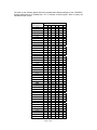
1
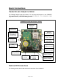
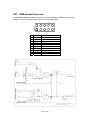
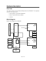
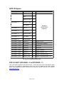
COM16055ER / COM16055RER User's Manual GSM/GPRS Modem and GPS PC/104 Module BDM-610020057 Rev. B COM16055ER / COM16055RER User's Manual RTD EMBEDDED TECHNOLOGIES, INC. 103 Innovation Blvd State College, PA 16803-0906 Phone: +1-814-234-8087 FAX: +1-814-234-5218 E-mail [email protected] [email protected] Web Site http://www.rtd.com Page 2 of 44 Manual Revision History Rev A New manual Rev B Changed to MC55ii and TRM:3 modules Published by: RTD Embedded Technologies, Inc. 103 Innovation Boulevard State College, PA 16803 Copyright 2006-2009 by RTD Embedded Technologies, Inc. All rights reserved The RTD Embedded Technologies Logo is a registered trademark of RTD Embedded Technologies. dspModule, cpuModule, and utilityModule are trademarks of RTD Embedded Technologies. PC/104, PC/104, and PCI-104 are registered trademarks of the PC/104 Consortium. All other trademarks appearing in this document are the property of their respective owners. Page 3 of 44 Table of Contents Introduction ...................................................................................................................................... 7 Product Overview ......................................................................................................................... 7 Board Features ............................................................................................................................ 7 COM16055 Features ............................................................................................................ 7 GSM Receiver ...................................................................................................................... 7 GPS Receiver ....................................................................................................................... 8 I/O Interfaces................................................................................................................................ 8 16C550 Compatible UARTs ................................................................................................. 8 Connector Description .......................................................................................................... 8 Available Options ......................................................................................................................... 8 Getting Technical Support ........................................................................................................... 9 Board Connections ........................................................................................................................ 10 Connector and Jumper Locations .............................................................................................. 10 External I/O Connections ........................................................................................................... 10 CN8 – Digital Input/Output Connector .................................................................................... 11 CN6 – SIM Module/Connector ............................................................................................... 12 CN7 – GSM Headset Connector ............................................................................................ 13 Jumpers ..................................................................................................................................... 14 GPS (JP6) or GSM (JP7) Base Address Jumpers (Default: GPS = 3E8h, GSM = 2E8h) .... 14 IRQ Jumpers for GSM (JP2) and GPS (JP3) (Default: GPS IRQ 11 closed, G Jumper closed) (Default: GSM IRQ 5 closed, G Jumper closed) ...................................................... 16 Reserved IRQs ................................................................................................................... 16 The G Jumper ..................................................................................................................... 17 LED Indicators............................................................................................................................ 17 Board Installation ........................................................................................................................... 19 Installing the Hardware .............................................................................................................. 19 Static Precautions .................................................................................................................. 19 Steps for Installing .................................................................................................................. 19 Configuring Software ................................................................................................................. 19 Page 4 of 44 Serial Port Setup .................................................................................................................... 19 Installing Drivers ..................................................................................................................... 20 Hardware Description .................................................................................................................... 21 Overview .................................................................................................................................... 21 Block Diagram ............................................................................................................................ 21 The GPRS GSM wireless modem module ................................................................................ 22 GPRS/GSM wireless modem module interfaces ................................................................... 22 GSM Antenna considerations................................................................................................. 22 SIM-card reader ..................................................................................................................... 23 Fastrax iTrax03-02 GPS Receiver ............................................................................................. 23 GPS module interfaces .......................................................................................................... 24 GPS Antenna considerations ................................................................................................. 24 COM16055 Digital I/O ................................................................................................................ 25 Interrupts .................................................................................................................................... 25 COM16055 Module Programming ................................................................................................. 26 Defining the Memory Map .......................................................................................................... 26 UART Interfaces......................................................................................................................... 26 Digital I/O ................................................................................................................................... 26 Digital I/O – R/W at BASE + 400h .......................................................................................... 27 Advanced Digital I/O – R/W at GSM BASE + 404h ............................................................... 27 GSM I/O Space .......................................................................................................................... 30 GSM I/O UART (GSM BASE + 0 to GSM BASE + 7) ............................................................ 30 GSM Status – R/W at GSM BASE + 402h (00h after reset) .................................................. 31 GSM Control – R/W at GSM BASE + 403h (00h after reset) ................................................. 31 GPS I/O Space........................................................................................................................... 32 GPS I/O UART (GPS BASE + 0 to GPS BASE + 7) .............................................................. 32 GPS I/O Digital I/O – R/W at GPS BASE + 400h ................................................................... 33 GPS Status – R/W at GPS BASE + 401h (00h after reset) ................................................... 33 RTD ISA ID ................................................................................................................................ 33 BA + 800h/BA + 801h RTD ID Data (read only, 8-bit or 16-bit) ............................................. 33 Page 5 of 44 BA + 802h RTD ID Reset Pointer (read only, 8-bit only)........................................................ 34 RTD ID Data Read Indexes.................................................................................................... 34 Using the GSM Engine .............................................................................................................. 34 Starting up and logging into the GSM network....................................................................... 34 Using SMS.............................................................................................................................. 35 GPS Software Interface ............................................................................................................. 35 Reading the GPS Data ........................................................................................................... 35 Selecting the GPS Protocol .................................................................................................... 35 Parsing the GPS Data ............................................................................................................ 35 Fastrax iSuite SDK ................................................................................................................. 35 Interrupts Programming Information .......................................................................................... 36 COM16055 Specifications ............................................................................................................. 40 COM16055 Specifications ......................................................................................................... 40 Cinterion MC55i GSM Modem Specifications............................................................................ 40 Fastrax iTrax03-02 GPS Receiver Specifications...................................................................... 41 COM16055 Operating Conditions .............................................................................................. 42 Additional Information .................................................................................................................... 43 Fastrax iTrax03-0202 GPS Receiver ......................................................................................... 43 NMEA-0183 v2.01 Standard ...................................................................................................... 43 Limited Warranty............................................................................................................................ 44 Page 6 of 44 Introduction Product Overview The COM16055ER / COM16055RER are designed to provide quad-band GSM and GPRS with a global positioning system (GPS) for PC/104 based systems. Included on the COM16055 is a Cinterion MC55i quad-band GSM cellular modem and COM16055RER is a Triorail TRM:3 quadband GSM cellular modem for railroad applications. Each module includes a Fastrax iTrax03-02 GPS Receiver module. The COM16055 has a dual-UART chip that permits communication with the serial port on the GSM as well as either serial port on the GPS receiver module over the PC/104 bus without using other serial ports in the PC/104 system. The GSM module supports an enhanced AT command set and the GPS supports iTalk binary protocol and National Marine Electronics Association (NMEA-0183) messages. Board Features COM16055 Features o o o o o o Direct connections to the Cinterion MC55i/TRM:3 GSM module Quad-band GSM module COM16055ER: 850/900/1800/1900 MHz (MC55i) COM16055RER: GSM-R/900/1800/1900 MHz (TRM:3) GPRS Multislot Class 10 AT command set SMS Fax Direct connection to the Fastrax iTrax03-02 GPS receiver module selectable between the iTrax binary port or the NMEA port GPS message formats iTalk Binary NMEA COM17045 compatible mode PC/104 compliant GSM Receiver The COM16055 wireless GPRS/GSM modem unit provides a direct and reliable GPRS connection to GPRS/GSM 850/900/1800/1900MHz mobile fields around the world. GPRS/GSM connectivity is achieved using the Cinterion MC55i. This unit works in the 850/900/1800/1900MHz bands. Connect any standard quad-band GSM antenna directly to the OSX connector of the COM16055. The antenna should be connected to the MC55i using a flexible 50-Ohm cable. In IDAN installations the antenna connection is brought to the front side of the IDAN frame. A SIM card socket is located on the solder side of the module. The SIM card can only be removed when the MC55i has been placed in shutdown mode. Page 7 of 44 GPS Receiver Integrated on your COM16055 is a fast fix 12-channel low power iTrax03-02 GPS receiver from Fastrax. This GPS receiver will work reliably in a variety of installations. The receiver will work with either 3.3V or 5.0 Volt active or with passive antennas. The power consumption of the GPS receiver is 125 mW fully operational. The iTrax03-02 features a fast 1 to 5 Hz update rate. Two output formats are available: the NMEA-0183 ASCII protocol or the iTalk proprietary binary protocol. Each protocol has its own dedicated serial interface. I/O Interfaces The COM16055 can be controlled and monitored by software through the two dedicated serial ports of the module. 16C550 Compatible UARTs The GSM/GPS receiver module communicates through two dedicated UART channels allowing other serial ports in the system to be free for the user. Connector Description The GSM and GPS antenna interfaces are female MMCX type miniature coaxial connectors. Connect your antenna directly to the COM16055 antenna connector, or use a short cable inside your enclosure to connect to a feed through connector to allow connection of the antenna to the wall of your enclosure. The GPS module supplies up to 100 mA of 3.3 or 5.0 VDC for antenna LNA. All other I/O connections to the COM16055 use 0.1” header type terminals. Available Options The COM16055 is available as a starter kit, bundled with an active antenna. It may also be purchased as an IDAN module for integration into an RTD IDAN system. The following is a summary of the different COM16055 configurations: Part Number Description COM16055ER COM16055ER with Cinterion MC55i GSM module SK-COM16055ER COM16055ER with active antennas for GPS and GSM IDAN-COM16055ERS COM16055ER mounted in an IDAN frame IDAN-SK-COM16055ERS COM16055ER mounted in an IDAN frame with active antennas for GPS and GSM COM16055RER COM16055RER with Triorail TRM:3 GSM module SK-COM16055RER COM16055RER with active antennas for GPS and GSM IDAN-COM16055RERS COM16055RER mounted in an IDAN frame IDAN-SK-COM16055RERS COM16055RER mounted in an IDAN frame with active antennas for GPS and GSM Page 8 of 44 For antenna specifications, please refer to the “Additional Information” chapter of this manual. Getting Technical Support If you are having problems with your system, please try the following troubleshooting steps: • Simplify the System – Remove modules one at a time from your system to see if there is a specific module that is causing a problem. • Swap Components – Try replacing parts in the system one-at-a-time with similar parts to determine if a part is faulty or if a type of part is configured incorrectly. If problems persist, or you have questions about configuring this product, obtain the PCI BIOS listing information of the COM16055 and other modules in the system. After you have this information, contact RTD Embedded Technologies via the following methods: Phone: +1-814-234-8087 E-Mail: [email protected] Be sure to check the RTD web site (http://www.rtd.com) frequently for product updates, including newer versions of the board manual and application software. Page 9 of 44 Board Connections Connector and Jumper Locations The following diagram shows the location of all connectors and jumpers on the COM16055. Future revisions of the COM16055 may have cosmetic differences. For a description of each jumper and connector, refer to the following sections. COM16055 Connector and Jumper Locations JP8 COM16055 / COM17045 Jumper CN5 SIM Installed LED CN4 GPS Antenna Input SIM Card socket (on bottom) or connector CN6 JP1 GPS LNA Power Jumper CN7 Headset Connector CN3 GSM Antenna Input CN8 Digital I/O JP6 GPS Address Jumpers JP7 GSM Address Jumpers JP4 & JP5 DIO Pullup/Pulldown JP2 GSM Interrupt Jumpers J4 Factory use only CN1 & CN2 PC/104 ISA Bus External I/O Connections The following sections describe the external I/O connections of the COM16055. Page 10 of 44 JP3 GPS Interrupt Jumpers CN8 – Digital Input/Output Connector The COM16055 offers 16 bit-programmable digital I/O lines. These can be pulled high or low through 10K Ohm resistors using JP4 to control bits 0 – 7 and JP5 to control bits 8 - 15. Pin 1 2 3 4 5 6 7 8 9 10 11 12 13 14 15 16 17 18 19 20 Name GND DIO0 DIO1 DIO2 DIO3 DIO4 DIO5 DIO6 DIO7 +5 VDC GND DIO8 DIO9 DIO10 DIO11 DIO12 DIO13 DIO14 DIO15 +5 VDC CN8 Description COM16055 Mode Ground Digital Input/Output Bit 0 or 1PPS Digital Input/Output Bit 1 Digital Input/Output Bit 2 Digital Input/Output Bit 3 Digital Input/Output Bit 4 Digital Input/Output Bit 5 Digital Input/Output Bit 6 Digital Input/Output Bit 7 +5 Volts DC Ground Digital Input/Output Bit 8 Digital Input/Output Bit 9 Digital Input/Output Bit 10 Digital Input/Output Bit 11 Digital Input/Output Bit 12 Digital Input/Output Bit 13 Digital Input/Output Bit 14 Digital Input/Output Bit 15 +5 Volts DC Pin 1 2 3 4 5 6 7 8 9 10 11 12 13 14 15 16 17 18 19 20 Name GND DIO0 DIO1 DIO2 DIO3 DIO4 DIO5 DIO6 DIO7 +5 VDC GND DIO8 DIO9 DIO10 DIO11 DIO12 DIO13 DIO14 DIO15 +5 VDC CN8 Description COM17045 Mode Ground Digital Output Bit 0 Digital Output Bit 1 Digital Output Bit 2 Digital Output Bit 3 Digital Output Bit 4 Digital Output Bit 5 Digital Output Bit 6 Digital Output Bit 7 +5 Volts DC Ground Digital Input Bit 0 Digital Input Bit 1 Digital Input Bit 2 Digital Input Bit 3 Digital Input Bit 4 Digital Input Bit 5 Digital Input Bit 6 Digital Input Bit 7 +5 Volts DC Page 11 of 44 CN6 – SIM Module/Connector The COM16055 can use either an onboard SIM module or an external SIM connected through a cable. The COM16055-1 uses an on-board SIM module and will not have CN6 installed. The COM16055-2 uses an external SIM module. The pin out of the external connector CN6 is shown below. Pin 1 2 3 4 5 6 7 8 9 10 Name GND Vcc RST GND IO GND CLK IN Vcc GND CN6 Description Ground SIM Power SIM Reset Ground SIM I/O Data Ground SIM Clock SIM Card Detect SIM Power Ground The figure below shows a picture of the external SIM card interface board. ESIM2035 board Page 12 of 44 CN7 – GSM Headset Connector The COM16055 Headset connector is used to connect a headset to the GSM module for voice operation. The pin out of the external connector CN7 is shown below. Pin 1 2 3 4 5 6 7 8 9 10 Name GND MICP1 MICN1 EPP1 EPN1 MICP2 MICN2 EPP2 EPN2 GND CN7 Description Ground Microphone 1+ Microphone 1Earphone 1+ Earphone 1Microphone 2+ Microphone 2Earphone 2+ Earphone 2Ground Page 13 of 44 Microphone interface 1 is high impedance (~50k Ohm) and shall be used preferably if an opamp or a CODEC is connected or additional microphone feeding is needed. Microphone interface 2 is high impedance (~1k Ohm) and shall be used preferably if internal microphone feeding can be used, e.g. for an internal microphone. Both EP1 and EP2 are the same. Jumpers The following sections describe the jumper configuration options available on the COM16055. For a reference that shows the location of each set of jumpers, refer to the diagram of the COM16055 at the beginning of this chapter. The default factory jumper settings are listed in the following table: Jumper Description JP1 JP2 JP3 GPS Active Antenna Power (100 ma max) GSM Interrupt Jumper GPS Interrupt Jumper JP4 Pull-up or Pull-down for DIO0-7 JP5 Pull-up or Pull-down for DIO8-15 JP7 GPS Base Address Jumper (A8 – A3, A9 must be high) GSM Base Address Jumper (A8 – A3, A9 must be high) JP8 COM16055/COM17045 Mode JP6 Default Factory Setting 1-2 – +5.0 VDC (default) 2-3 – +3.3 VDC Open for passive antennas Default Interrupt 5 and G Default Interrupt 11 and G 1-2 – Pull-up 2-3 – Pull-down (default) No connect – Neither 1-2 – Pull-up 2-3 – Pull-down (default) No connect – Neither Default 3E8h Default 2E8h 1-2 – COM17045 Compatible 2-3 – COM16055 (default) GPS (JP6) or GSM (JP7) Base Address Jumpers (Default: GPS = 3E8h, GSM = 2E8h) The base address selection jumpers (A3 through A8) allow you to set the base address of the first UART that connects to the GPS module and the second UART that connects to the GSM module. Any software that accesses the board will do so through reads and writes to the I/O address set by the jumpers. To function properly, the I/O address the software is expecting must match the base address set by the jumpers. As shown in the figure below, A3 is located at the left end of the jumper block, while A8 is located at the right end: Page 14 of 44 The table on the following pages shows the possible base address settings for the COM16055. All base addresses are in hexadecimal. An ‘X’ indicates a closed jumper, while an empty cell indicates an open jumper. Base Address (Hexadecimal) 200 208 210 218 220 228 230 238 240 248 250 258 260 268 270 278 280 288 290 298 2A0 2A8 2B0 2B8 2C0 2C8 2D0 2D8 2E0 2E8 2F0 2F8 300 308 310 318 320 328 330 338 340 348 350 358 360 368 370 A8 A7 Jumpers A6 A5 A4 A3 X X X X X X X X X X X X X X X X X X X X X X X X X X X X X X X X X X X X X X X X X X X X X X X X X X X X X X X X X X X X X X X X X X X X X X X X X X X X X X X X X X X X X X X X X X X X X X X X X X X X X X X X X X X X X Page 15 of 44 X X X X X X X X X X X X X X 378 380 388 390 398 3A0 3A8 3B0 3B8 3C0 3C8 3D0 3D8 3E0 3E8 3F0 3F8 X X X X X X X X X X X X X X X X X X X X X X X X X X X X X X X X X X X X X X X X X X X X X X X X X X X X X X X X X X X X X X X X X X X X X By default, the COM16055 comes configured with a base address of 0x3E8 for the GPS UART and 0x2E8 for the GSM UART. When selecting a base address for the COM16055, please observe the following guidelines: • Every device in your PC/104 system must have a unique base address! When selecting a base address for the COM16055, make certain that it does not conflict with any other devices. • Base addresses 0x3F8 and 0x2F8 are typically used by serial ports COM1 and COM2, respectively. If you wish to use one of those base addresses, you will need to disable any conflicting serial port. • Some operating systems expect UART devices to be located at the standard serial port base addresses (0x3F8, 0x2F8, 0x3E8, and 0x2E8). Setting your COM16055 to one of these addresses can make system setup and configuration easier. IRQ Jumpers for GSM (JP2) and GPS (JP3) (Default: GPS IRQ 11 closed, G Jumper closed) (Default: GSM IRQ 5 closed, G Jumper closed) The IRQ selection jumpers allow you to set the IRQ used by the serial port UART of the COM16055. The COM16055 can be configured for any one of the following IRQs: 2, 5, 6, 7, 10, 11, 12, 14, or 15. The IRQ can be set by closing the appropriately labeled jumper on the board. Note: Typically IRQs cannot be shared; although there are some special cases (see “The G Jumper” later in this document). In general, the IRQ you select should not be used by any other devices in your system. Reserved IRQs Some of the IRQ choices on the COM16055 may already be used by your CPU’s onboard peripherals. Some commonly-used IRQs are: Page 16 of 44 • IRQ 2/9 is used by some VGA controllers. • IRQ 5 or 7 may be used by the CPU’s parallel port. Check your CPU’s configuration to avoid a conflict. • IRQ 12 is used by the PS/2 mouse. To use this IRQ, you will need to remove the PS/2 mouse from the system. Some CPUs also require a BIOS setting to disable the PS/2 mouse controller. • IRQ 14 is used by the primary IDE controller. To use this IRQ, you will need to disable the primary IDE controller. • IRQ 15 is used by the secondary IDE controller. To use this IRQ, you will need to disable the secondary IDE controller. The G Jumper The COM16055 supports shared interrupts as defined by the PC/104 specification. This sharing is accomplished via the G jumper, which is located adjacent to the IRQ jumpers. The G jumper installs a 1K-ohm resistor to pull the signal to the low state, allowing an interrupt to drive the signal high. To share interrupts, configure the devices for the same IRQ, then close the G jumper on one (and only one) of the devices. When using interrupt sharing, consider the following guidelines: • An interrupt can only be shared if all devices on the IRQ support it. If you have two sharing and one non-sharing device on the same IRQ, it will not work. • To share interrupts, the system’s drivers and operating system must support it. The Interrupt Service routines must be written to check all devices on an IRQ when the interrupt is detected. Many popular operating systems do not support interrupt sharing for ISA devices. Note: If you are not sharing interrupts, make sure you leave the COM16055’s G jumper closed! LED Indicators D1 – On when the SIM card is enabled. D2 – Provides GPS status information • Continuously low state – Navigation stopped or not tracking satellites • Short blink 20% on – Tracking satellites but not enough information to calculate pseudo-ranges • Long blink 80% on – Pseudo range information available but not navigating • Continuously high state – Navigating, Valid fix D3 – COM16055 mode • GPS 1 PPS COM17045 Mode • Off = NMEA protocol, On = iTalk protocol D4 – On when GSM is transmitting Page 17 of 44 Note: The GSM AT^SSYNC command serves to configure the SYNC pin of the application interface. The pin can either be used to indicate the current consumption in a transmit burst (default setting) or to drive a status LED connected to the pin. See the AT^SSYNC command for details. Page 18 of 44 Board Installation Installing the Hardware The COM16055 can be installed into a PC/104. It can be located almost anywhere in the stack, above or below the CPU as long as all PC/104 bus constraints are met. Static Precautions Keep your board in its antistatic bag until you are ready to install it into your system! When removing it from the bag, hold the board at the edges, and do not touch the components or connectors. Handle the board in an antistatic environment, and use a grounded workbench for testing and handling of your hardware. Steps for Installing 1. Shut down the PC/104 system and unplug the power cord. 2. Ground yourself with an anti-static strap. 3. Line up the pins of the COM16055’s PC/104 connector with the PC/104 bus of the stack and gently press the board onto the stack. The board should slide into the matching PC/104 connector easily. Do not attempt to force the board, as this can lead to bent/broken pins. 4. Attach the external antennas to the MMCX connectors. 5. If any boards are to be stacked above the COM16055, install them. 6. Attach any necessary cables to the PC/104 stack. 7. Re-connect the power cord and apply power to the stack. 8. Apply power to the system, and verify that all of the hardware is working properly. Once power is applied, the GSM module and GPS receiver will automatically initialize. Configuring Software After physically installing the COM16055, your operating system must be configured to recognize the new board. Serial Port Setup The COM16055 uses a standard dual-channel serial port UART for host communication. Therefore, you must “install” two serial ports under your host operating system for the COM16055 to be recognized. If the COM16055 was installed using standard serial port base addresses (0x3F8, 0x2F8, 0x3E8, or 0x2E8), your operating system may detect the UART channels automatically. If they are not auto-detected, or were configured with a non-standard base address, the serial port will need to be configured manually. Page 19 of 44 The procedure for installing and configuring the serial ports will vary depending on the operating system. Consult the operating system’s documentation for instructions on how to do this. Note: Under Windows 2000/XP, the GPS may be incorrectly detected as a Serial Mouse, causing erratic mouse cursor behavior. This issue has been documented by Microsoft, and can be resolved by a Registry change. For more information, refer to Microsoft Knowledge Base Article 283063. Installing Drivers The GSM and GPS are accessed via the serial port UART, and therefore need no special drivers. However, the digital I/O and certain control functions are accessed via their own registers (located at Base Address + 0x400). To use the digital I/O, or to use these control functions (e.g. switch GPS protocols from NMEA to iTalk), you will need to access these registers. This is typically done through a “driver”. RTD provides drivers for supported operating systems. If you are using an operating system not supported by RTD, you will need to develop your own driver. You may also be able to access the registers directly. Note: If you are only using ASCII/NMEA GPS functions, without digital I/O or the iTalk protocol, there is no need to install any special drivers. Page 20 of 44 Hardware Description Overview This chapter describes the major hardware building blocks of the COM16055. The components discussed in this chapter include: • Cinterion MC55i or Triorail TRM:3 GSM Module • Fastrax iTrax03-02 GPS Receiver Module • Antennas Block Diagram Below is a block diagram of the COM16055. UART I S A ASC0 COM a (not used) GSM Engine ASC1 B U S Interrupts SIM COM b LED D1 Antenna LED D2 LED D3 NMEA Mux iTalk LED D4 Fastrax iTrax03-02 GPS Engine 1PPS Address Jumpers EPLD Antenna Digital I/O CN7 Page 21 of 44 The GPRS GSM wireless modem module The COM16055 wireless GPRS/GSM modem is built around the Cinterion MC55i quad-band 850/900/1800/1900 MHz GPRS cellular engine. It is designed both for handling complex industrial applications such as telemetry, telematics or communication, and for integration in stationary or mobile fields all over the world. General information on this product is available at www.cinterion.com. The COM16055 is capable of powerful communication using GSM data interfacing. GPRS data rates can reach up to 85.6 kbit/s max downlink depending on the network capacity and the network load. Engineers must take into account that GPRS data rates will vary dynamically depending on network conditions. This must be considered when designing software and system specifications. Roaming agreements and GPRS data support may not in all cases be available when moving from country to country. Check with your local network provider for GPRS coverage. The COM16055 is capable of FAX and standard SMS text messages. The data terminal rate is 9600 baud for all host commands (AT commands). The COM16055 modem module antenna interface connector uses an OSX connector. The mating antenna connectors and cables are supplied by RTD. Note: The Cinterion MC55i module has two serial ports, labeled ASC0 and ASC1. However, only port ASC0 is available for use on the COM16055. GPRS/GSM wireless modem module interfaces The COM16055 GPRS/GSM modem is connected to the host computer through a dedicated ISA serial port. The remaining serial port is connected to the GPS module. The default configuration for the GSM serial ports is: GSM Interface • 9600 baud • 8 data bits • No parity • 1 stop bit GSM Antenna considerations Typically standard GSM antennas use a female FME connector. This connector needs an adapter unit before it can be connected to the COM16055. RTD recommends the use of high quality antennas with the COM16055. We have tested successfully with antennas from Hirschmann Rheinmetall Elektronik. Visit http://www.hirschmann.de/ for information on GSM antenna. A very useful AT command that shows quality of the signal reception is: AT+CSQ. The format of the response is AT+CSQ: received signal strength, bit error rate. The received signal strength shows the quality of the network signal and ranges from 0 to 31 as shown in the table below. A value of greater than 10 should give an acceptable connection. The bit error rate number will range between 0 and 7. Page 22 of 44 0 1 2 3 4 5 6 7 Received Signal Strength Values (99 = undetectable signal) - 113 dBm 8 - 97 dBm 16 - 81 dBm 24 - 65 dBm - 111 dBm 9 - 95 dBm 17 - 79 dBm 25 - 63 dBm - 109 dBm 10 - 93 dBm 18 - 77 dBm 26 - 61 dBm - 107 dBm 11 - 91 dBm 19 - 75 dBm 27 - 59 dBm - 105 dBm 21 - 89 dBm 20 - 73 dBm 28 - 57 dBm - 103 dBm 13 - 87 dBm 21 - 71 dBm 29 - 55 dBm - 101 dBm 14 - 85 dBm 22 - 69 dBm 30 - 53 dBm - 99 dBm 15 - 83 dBm 23 - 67 dBm 31 => - 51 dBm SIM-card reader Standard 3V and 1.8V SIM-cards can be used with the COM16055. Older 5V SIM cards will not work, though they may operate in standard GSM cellular phones. The SIM-card holder has a card detection circuit that will in theory allow hot insertion and removal of the card. This is NOT recommended, since the SIM card contents can become corrupted if it is removed while the MC55i/56 GSM modem is writing to it. LED D1 will turn on when a SIM card is enabled. A very useful AT command that shows detection of the SIM card is: AT^SCID. The SIM card identifier is given as a reply ^SCID: value shows the ID of the SIM card. If no ID is detected the MC55i/56 cannot read the SIM card and cannot connect to the GSM service provider network. To add an entry to your SIM card you may use the AT+CPBW command. In this example we add the RTD phone number +1-814-234-8087 to the SIM card memory location “1” with the following AT command set: AT+CPBW=1, 18142348087, 145, RTD AT+CREG? Will indicate if the COM16055 is logged into the network. If the reply for example is +CREG: 0, 1 it means that connection to the home network is valid. A complete AT-instruction set documentation is included in the MC55i/56 user’s manual. Fastrax iTrax03-02 GPS Receiver Integrated on the COM16055 is an iTrax03-02 low power fast-fix 12-channel GPS receiver from Fastrax. This GPS receiver is especially designed for portable and mobile applications. This version of the GPS does not support differential operation. The iTrax03-02 sensitivity provides continuous tracking and navigation down to a signal level of – 152 dBm and a cold start TTFF of 40 seconds (no initialization), 33 seconds for warm start (almanac) and four seconds for quick start. Even with this performance, the power consumption is approximately 125mW with a 1s update-rate. This figure does not include the active antenna power consumption. A complete GPS configuration program for the iTrax03-02 GPS Workbench is available from the manufacturer’s website at www.fastrax.com. This program allows you to completely reconfigure the operation of the GPS receiver. Page 23 of 44 GPS data is output only when the receiver has a fix. The COM16055 is configured to output NMEA-0183 version 3.0 data by default and selectable Fastrax’s binary protocol iTalk. GPS module interfaces The iTrax03-02 GPS is connected to the host computer through a dedicated ISA serial port. The default configuration for the serial ports is: NEMA Interface (Default) • 4800 baud • 8 data bits • No parity • 1 stop bit • No flow control iTalk Interface (selectable in I/O register) • 115,200 baud • 8 data bits • No parity • 1 stop bit • No flow control GPS Antenna considerations Most GPS antennas are “active” which means they have a low noise amplifier (LNA) built into the antenna that requires a power source for the GPS module. While the COM16055 will work with a passive antenna, better performance will be achieved with an active antenna. The COM16055 provides either +5.0 V or +3.3 V for active GPS antennas. A three-terminal header is used to select the operating voltage of the antenna. The internal gain of the GPS receiver can be adjusted to low-output signals or even to interface to passive antennas. This operation is normally not needed, but it can be done using the Fastrax GPS Workbench program. Fig. 4-2 GPS antenna bias voltage Page 24 of 44 A 90 degree 50 Ohm OSX connector should be selected to directly plug into the antenna connector on the board. High quality low loss antenna cable should be used. Try to reduce the number of connectors on the cable to minimize signal reflections. Signal reflections on the antenna line may cause incorrect readings for altitude information. COM16055 Digital I/O The COM16055 has 16 bit-programmable digital I/O bits. RTD’s driver software exports functions to use the digital I/O and the operation is covered in the Drivers Users Manual. JP4 controls a 10K Ohm pull up/down on DIO bits 1-8 and JP5 controls a 10K Ohm pull up/down on DIO bits 9 16. For programming information see COM16055 Module Programming section. Interrupts Interrupts are used to notify the host CPU that an event happened on a particular device. In general, interrupts are more efficient than a polling technique, where the CPU must query the device status at regular intervals. Devices that use interrupts have a special connection to the CPU, called an interrupt request line (IRQ). When the device needs the CPUs attention, it asserts the IRQ line. Once the interrupt has been processed, the IRQ line is de-asserted. The COM16055 uses one ISA interrupt for the GPS and another for the GSM. However, it will not actually generate interrupts unless the Interrupt Enable register has been properly programmed. Since the COM16055 has 16C550 UARTs, it supports all of the standard serial port interrupt events. These events include: • Received data available • Transmit buffer empty • Line Status Register change • Modem Status Register change A detailed explanation of serial port interrupts is beyond the scope of this manual. For more information, consult a serial port programming reference. The chapter titled “Additional Information” lists some resources to help the user. Note: When the UART clock is running at a higher frequency, transmit/receive interrupts will happen more frequently. Many operating systems cannot process interrupts quickly enough to handle this load. When developing your software, be sure to consider the operating system’s limitations. Page 25 of 44 COM16055 Module Programming This chapter shows you how to program and use your COM16055. It provides a general description of the I/O map. Defining the Memory Map The memory map of the COM16055 occupies two groups of eight bytes of host PC I/O space. This window is freely selectable by the user by jumpers JP6 for GPS BASE and JP7 for the GSM BASE. After setting the base address you have access to the internal resources of the COM16055 control logic. The board also has 16 digital I/O lines that can be accessed several ways. UART Interfaces The primary method of interfacing with the COM16055 is via the dual channel UART. Once the COM16055 is properly installed and configured in the system, the board will appear as two extra COM ports to the CPU. The first COM port is attached to the GSM engine. The second port is attached to the GPS. Detailed serial port programming tips are not within the scope of this manual. However books and web sites explaining serial port programming are readily available. Digital I/O The 16 digital I/O bits have different functionality in COM17045 and COM16055 modes. COM17045 mode is designed to be software compatible with the RTD COM17045 GSM/GPS module which is 8 outputs and 8 inputs. COM16055 mode, which is the default, allows bit programmable direction for all bits. Note the digital I/O registers can be accessed at 400h and 404h – 407h above either the GPS or GSM. COM17045 Mode (JP8 = COM17045) ADDR (hex) REGISTER GSM BASE + 400h Digital I/O DIR I/O COMMENTS Digital I/O Port COM16055 Mode (JP8 = COM16055 -- Default) ADDR (hex) REGISTER DIR GSM BASE + 400h Digital I/O I/O Digital I/O Port GSM BASE + 404h Digital I/O I/O Digital I/O bits 0 - 7 GSM BASE + 405h Digital I/O I/O Digital I/O bits 8 – 15 Page 26 of 44 COMMENTS GSM BASE + 406h Digital I/O Dir I/O Digital I/O direction bits 0 - 7 GSM BASE + 407h Digital I/O Dir I/O Digital I/O direction bits 8 - 15 Digital I/O – R/W at BASE + 400h This register is intended for COM17045 compatibility. If you are using the board in COM16055 mode, please use registers at BASE + 404h – 407h. This address is used to interface to the digital I/O port of the COM16055, writing to this address will transfer the data out of the output port, while reading from this address will return the data from the digital inputs. The same digital I/O is accessed at GPS BASE + 400h and GSM BASE + 400h. This register is compatible with the COM17045 module, but works in either COM17045 or COM16055 mode. Note the default direction of the 16 digital I/O bits is that bits 0 - 7 are outputs and 8 - 15 are inputs. If you are in COM16055 mode and you change the default direction registers, then this register will not operate properly. Digital I/O – Write GSM BASE + 400h or GPS BASE + 400h COM16055 or COM17045 Modes Bit 0 Bit 1 Bit 2 Bit 3 Bit 4 Bit 5 Bit 6 Bit 7 Output 0 Output 1 Output 2 Output 3 Output 4 Output 5 Output 6 Output 7 CN8 Pin 2 CN8 Pin 3 CN8 Pin 4 CN8 Pin 5 CN8 Pin 6 CN8 Pin 7 CN8 Pin 8 CN8 Pin 9 Digital I/O – Read GSM BASE + 400h or GPS BASE + 400h COM16055 or COM17045 Modes Bit 0 Bit 1 Bit 2 Bit 3 Bit 4 Bit 5 Bit 6 Bit 7 Input 0 Input 1 Input 2 Input 3 Input 4 Input 5 Input 6 Input 7 CN8 Pin 12 CN8 Pin 13 CN8 Pin 14 CN8 Pin 15 CN8 Pin 16 CN8 Pin 17 CN8 Pin 18 CN8 Pin 19 Advanced Digital I/O – R/W at GSM BASE + 404h These addresses are used to interface to the digital I/O port in COM16055 mode. These are the same digital I/O as above, but with enhanced capability. The 16 bits each have a direction bit. If the direction bit is set to output, a value written to the data bit is provided on the connector. A read will result in the value on the connector pin (i.e. the output value). If the direction is set to Page 27 of 44 input, a value written to the data bit is ignored and a read will result in the value on the connector pin. Digital I/O Data – Write/Read GSM BASE + 404h or GPS BASE + 404h COM16055 Mode Only (Reset = 00h) Bit 0 Bit 1 Bit 2 Bit 3 Bit 4 Bit 5 Bit 6 Bit 7 I/O 0 I/O 1 I/O 2 I/O 3 I/O 4 I/O 5 I/O 6 I/O 7 CN8 Pin 2 CN8 Pin 3 CN8 Pin 4 CN8 Pin 5 CN8 Pin 6 CN8 Pin 7 CN8 Pin 8 CN8 Pin 9 Digital I/O Data – Write/Read GSM BASE + 405h or GPS BASE + 405h COM16055 Mode Only (Reset = 00h) Bit 0 Bit 1 Bit 2 Bit 3 Bit 4 Bit 5 Bit 6 Bit 7 I/O 8 I/O 9 I/O 10 I/O 11 I/O 12 I/O 13 I/O 14 I/O 15 CN8 Pin 12 CN8 Pin 13 CN8 Pin 14 CN8 Pin 15 CN8 Pin 16 CN8 Pin 17 CN8 Pin 18 CN8 Pin 19 Digital I/O Direction – Write/Read GSM BASE + 406h or GPS BASE + 406h COM16055 Mode Only (Reset = 00h) Bit 0 Bit 1 Bit 2 Bit 3 Bit 4 Bit 5 Bit 6 Bit 7 I/O 0 I/O 1 I/O 2 I/O 3 I/O 4 I/O 5 I/O 6 I/O 7 0 = CN8 Pin 2 is an input, 1 = output 0 = CN8 Pin 3 is an input, 1 = output 0 = CN8 Pin 4 is an input, 1 = output 0 = CN8 Pin 5 is an input, 1 = output 0 = CN8 Pin 6 is an input, 1 = output 0 = CN8 Pin 7 is an input, 1 = output 0 = CN8 Pin 8 is an input, 1 = output 0 = CN8 Pin 9 is an input, 1 = output Digital I/O Direction – Write/Read GSM BASE + 407h or GPS BASE + 407h COM16055 Mode Only (Reset = FFh) Bit 0 Bit 1 Bit 2 Bit 3 Bit 4 Bit 5 Bit 6 I/O 8 I/O 9 I/O 10 I/O 11 I/O 12 I/O 13 I/O 14 0 = CN8 Pin 12 is an input, 1 = output 0 = CN8 Pin 13 is an input, 1 = output 0 = CN8 Pin 14 is an input, 1 = output 0 = CN8 Pin 15 is an input, 1 = output 0 = CN8 Pin 16 is an input, 1 = output 0 = CN8 Pin 17 is an input, 1 = output 0 = CN8 Pin 18 is an input, 1 = output Page 28 of 44 Digital I/O Direction – Write/Read GSM BASE + 407h or GPS BASE + 407h COM16055 Mode Only (Reset = FFh) Bit 7 I/O 15 0 = CN8 Pin 19 is an input, 1 = output Page 29 of 44 GSM I/O Space ADDR (hex) REGISTER DIR GSM BASE + 0 TXD O RXD I COMMENTS BAUD div. Low I/O BAUD div. High I/O IRQ enable I/O GSM BASE + 2 IRQ ID I/O GSM BASE + 3 Line control I/O GSM BASE + 4 Modem control I/O GSM BASE + 5 Line status I/O GSM BASE + 6 Modem status I/O GSM BASE + 400h Digital I/O I/O GSM BASE + 401h Reserved GSM BASE + 402h GSM status I/O Configuration registers GSM BASE + 403h GSM control I/O Power control GSM BASE + 404h Digital I/O I/O Digital I/O bits 0 - 7 GSM BASE + 405h Digital I/O I/O Digital I/O bits 8 – 15 GSM BASE + 406h Digital I/O Dir I/O Digital I/O direction bits 0 - 7 GSM BASE + 407h Digital I/O Dir I/O Digital I/O direction bits 8 - 15 GSM BASE + 1 Standard 16C550 UART Registers Digital I/O Port Reserved I/O map of the COM16055 GSM UART GSM I/O UART (GSM BASE + 0 to GSM BASE + 7) This is the UART registers for the GSM module. These resources are not described in detail, since they are mapped as a standard PC serial port. For more details on the EXAR 16C550 UART chip programming please download the component specific data from the website: http://www.exar.com. Page 30 of 44 GSM Status – R/W at GSM BASE + 402h (00h after reset) GSM Status – Write GSM BASE + 402h Bit 0 Bit 1 Bit 2 Bit 3 Bit 4 Bit 5 Bit 6 Bit 7 RESERVED /EN_INT RESERVED RESERVED RESERVED RESERVED RESERVED RESERVED Bit 0 Bit 1 Bit 2 Bit 3 Bit 4 Bit 5 Bit 6 Bit 7 /EN_RST /EN_INT TEMP_LOW TEMP_HIGH RESERVED RESERVED RESERVED RESERVED GSM interrupt enabled; 1 - disabled GSM Status – Read GSM BASE + 402h 1 – Reset GSM in reset, 0 – GSM active GSM interrupt enabled; 1 – disabled 1 - Board temperature below -20C 1 - Board temperature over +70C GSM Control – R/W at GSM BASE + 403h (00h after reset) GSM Control – Write GSM BASE + 403h Bit 0 Bit 1 Bit 2 Bit 3 Bit 4 Bit 5 Bit 6 Bit 7 Ignition signal Powerdown MC55i RESERVED RESERVED RESERVED RESERVED RESERVED RESERVED 1 – > 0 – results in IGN signal 1 – Power down; 0 – Power on GSM Control – Read GSM BASE + 403h Bit 0 Bit 1 Bit 2 Bit 3 Bit 4 Bit 5 Bit 6 Bit 7 Ignition signal Powerdown MC55i RESERVED RESERVED RESERVED RESERVED RESERVED RESERVED State of Ignition Bit 1 – Power down; 0 – Power on Page 31 of 44 GPS I/O Space ADDR (hex) REGISTER DIR GPS BASE + 0 TXD O RXD I COMMENTS BAUD div. Low I/O BAUD div. High I/O IRQ enable I/O GPS BASE + 2 IRQ ID I/O GPS BASE + 3 Line control I/O GPS BASE + 4 Modem control I/O GPS BASE + 5 Line status I/O GPS BASE + 6 Modem status I/O GPS BASE + 400h Digital I/O I/O Digital I/O Port GPS BASE + 401h GPS status I/O Configuration registers GPS BASE + 402h Reserved Reserved GPS BASE + 403h Reserved Reserved GPS BASE + 404h Digital I/O I/O Digital I/O bits 0 - 7 GPS BASE + 405h Digital I/O I/O Digital I/O bits 8 – 15 GPS BASE + 406h Digital I/O Dir I/O Digital I/O direction bits 0 - 7 GPS BASE + 407h Digital I/O Dir I/O Digital I/O direction bits 8 - 15 GPS BASE + 1 Standard 16C550 UART Registers I/O map of the COM16055 GPS UART GPS I/O UART (GPS BASE + 0 to GPS BASE + 7) This is the UART registers for the GPS module. These resources are not described in detail, since they are mapped as a standard PC serial port. For more details on the EXAR 16C550 UART chip programming please download the component specific data from the website: http://www.exar.com. Page 32 of 44 GPS I/O Digital I/O – R/W at GPS BASE + 400h This address is used to interface to the digital I/O port of the COM16055, writing to this address will transfer the data out of the output port, while reading from this address will return the data from the digital inputs. This is the same digital I/O that is accessed at GSM BASE + 400h. GPS Status – R/W at GPS BASE + 401h (00h after reset) GPS Status – Write GPS BASE + 401h Bit 0 Bit 1 Bit 2 Bit 3 Bit 4 Bit 5 Bit 6 Bit 7 CH_SEL GPS_RESET RESERVED /EN_INT RESERVED RESERVED 1PPS/DIO0 RESERVED Bit 0 Bit 1 CH_SEL GPS_RESET Continuously low Short blink 20% 0 – NMEA mode; 1 – iTalk protocol 1 – Reset GPS receiver, 0 – GPS active 0 – GPS interrupt enabled; 1 – disabled 1 = DIO0 <= 1PPS, 0 = DIO0 <= DIO0 (default = 0) GPS Status – Read GPS BASE + 401h Bit 2 Bit 3 Bit 4 Bit 5 Bit 6 Bit 7 Long blink 80% Continuously high /EN_INT RESERVED RESERVED 1PPS/DIO0 1PPS 0 – NMEA mode; 1 – iTalk protocol 1 – Reset GPS receiver, 0 – GPS active Navigation stopped or not tracking satellites Tracking satellites but not enough information to calculate pseudo-ranges Pseudo-range information available but not navigating Navigating, Valid fix 0 – GPS interrupt enabled; 1 – disabled 1 = DIO0 <= 1PPS, 0 = DIO0 <= DIO0 (default = 0) 1 Pulse Per Second from GPS RTD ISA ID ADDR (hex) REGISTER DIR COMMENTS BASE + 800h RTD ID Data Read Read next RTD ID Character BASE + 801h RTD ID Data Read Read next RTD ID Character BASE + 802h Reset RTD ID Read Reset RTD ID counter I/O map of the COM16055 RTD ISA ID BA + 800h/BA + 801h RTD ID Data (read only, 8-bit or 16-bit) RTD ID is a method to identify a board on the ISA bus. There are two 8-bit registers mapped at BA + 800h and BA + 801h. This can be either the GSM base address or the GPS base address. The registers can be read as two 8-bit or one 16-bit. An internal pointer is auto-incremented with Page 33 of 44 every read to either address so the data read will step through each index as indicated below. The pointer is set to zero at reset and can be reset to zero by a read to BA + 802h. BA + 802h RTD ID Reset Pointer (read only, 8-bit only) A read to BA + 802h will set the internal pointer to zero. The pointer is set to zero at reset. RTD ID Data Read Indexes Index 0 1 2 3 4 5 6–9 10 11 12 13 14 15 16 17 18 19 20–255 Data Device ID Device ID RTD Vendor ID RTD Vendor ID EPLD Revision EPLD Revision Reserved Board Name String Board Name String Board Name String Board Name String Board Name String Board Name String Board Name String Board Name String Unused 8-Bit Read 55h 60h 35h 14h Revision LSD Revision MSD Ignore C O M 1 6 0 5 5 <nul> <nul> FFh 16-Bit Read 6055h — 1435h — Revision — Ignore CO — M1 — 60 — 55 — <nul><nul> — FFFFh Using the GSM Engine The GSM engine is controlled via the industry-standard ASCII ‘AT’ command set. A user can operate the GSM simply by sending it command strings from a terminal emulator program (e.g. Windows HyperTerminal). The complete list of AT command strings supported by the MC55i are described in a document provided by Cinterion. Refer to the Additional Information section of this manual for more information. Starting up and logging into the GSM network With no power applied insert your +3V or dual voltage SIM into the card- holder on the solder side of the board. Connect the antenna cable to the MC55i antenna connector and power up your PC/104 system. The COM16055 will be initialized by the system. After this the status LED will blink for a while until the MC55i is logged into the network. If you have the PIN code enabled, the COM16055 status LED will continue to blink until the PIN code is given through the terminal mode with AT command AT+CPIN”XXXX”, unless AT^SFLC (facility lock for PIN code) has been set. Once the COM16055 is logged onto the network the LED will be lit continuously. Page 34 of 44 Note: Many cellular network operators provide software for connecting to their GSM/GPRS networks. This software can automate many of the commands described above. Using SMS The SMS features of the Cinterion MC55i are controlled by AT command strings. The Cinterion documentation covers these commands in depth. GPS Software Interface Reading the GPS Data At power-up, the COM16055 starts transmitting GPS data. Since the board is UART-based, it appears as a standard COM port to the CPU. The user can open a terminal program (e.g. Windows HyperTerminal) and observe the incoming GPS data. Any software application that interfaces with the GPS must “open” the COM port of the GPS and read the incoming data. This is typically done via the serial port drivers of the operating system. Consult your operating system’s documentation for information. Selecting the GPS Protocol The iTrax03-02 outputs GPS data in two protocols: NMEA-0183 or iTalk. At power-up, the board defaults to NMEA-0183. NMEA-0183 is an ASCII-based GPS message format. It is a standard format, used by many popular GPS engines. Many commercial third-party GPS programs are written for this protocol. iTalk is a proprietary binary protocol supported by Fastrax GPS engines. It is primarily used by the Fastrax iSuite SDK. The control registers are used to select which protocol is used. A user application can select the GPS protocol at runtime by manipulating the appropriate bit. Parsing the GPS Data To actually get the longitude, latitude, etc, the application running on the host PC must parse the incoming GPS data. The algorithm for parsing the GPS data will depend on the protocol (NMEA or iTalk). A complete explanation of GPS protocols and how to parse them is beyond the scope of this manual. See the Additional Information section for the protocol specifications. RTD provides sample applications which demonstrate how to parse the GPS protocols. Source code is also provided. These samples can be used as a starting point to develop your own GPS application. Fastrax iSuite SDK Fastrax provides the iSuite Software Development Kit, which can be used to create GPS applications. See the Additional Information section of this manual for more information. Note that iSuite relies on the iTalk protocol, so you must switch the board into iTalk mode before using iSuite. Page 35 of 44 Interrupts Programming Information What is an interrupt? An interrupt is an event that causes the processor in your computer to temporarily halt its current process and execute another routine. Upon completion of the new routine, control is returned to the original routine at the point where its execution was interrupted. Interrupts are a very flexible way of dealing with asynchronous events. Keyboard activity is a good example; your computer cannot predict when you might press a key and it would be a waste of processor time to do nothing whilst waiting for a keystroke to occur. Thus the interrupt scheme is used and the processor proceeds with other tasks. When a keystroke finally occurs, the keyboard then 'interrupts' the processor so that it can get the keyboard data. It then places it into the memory, and then returns to what it was doing before the interrupt occurred. Other common devices that use interrupts are A/D boards, network boards, other used serial ports etc. Interrupt request lines To allow different peripheral devices to generate interrupts on the same computer, the PC AT bus has interrupt request channels (IRQ's). A rising edge transition on one of these lines will be latched into the interrupt controller. The interrupt controller checks to see if the interrupts are to be acknowledged from that IRQ and, if another interrupt is being processed, it decides if the new request should supersede the one in progress or if it has to wait until the one in progress has been completed. The priority level of the interrupt is determined by the number of the IRQ as follows; IRQ0 has the highest priority whilst IRQ15 has the lowest. Many of the IRQ's are already used by the standard system resources, IRQ0 is dedicated to the internal timer, IRQ1 is dedicated to the keyboard input, IRQ3 for the serial port COM2, and IRQ4 for the serial port COM1. Often interrupts 2,5,7,10,11 and 15 are free for the user. 8259 Programmable Interrupt Controller The chip responsible for handling interrupt requests in a PC is the 8259 Interrupt Controller. To use interrupts you will need to know how to read and set the 8259's internal interrupt mask register (IMR) and how to send the end-of-interrupt (EOI) command to acknowledge the 8259 interrupt controller. Interrupt Mask Register (IMR) Each bit in the interrupt mask register (IMR) contains the mask status of the interrupt line. If a bit is set (equal to 1), then the corresponding IRQ is masked, and it will not generate an interrupt. If a bit is cleared (equal to 0), then the corresponding IRQ is not masked, and it can then generate an interrupt. The interrupt mask register is programmed through port 21h. End-of-Interrupt (EOI) Command After an interrupt service routine is complete, the 8259 Interrupt Controller must be acknowledged by writing the value 20h to port 20h. What exactly happens when an interrupt occurs? Understanding the sequence of events when an interrupt is triggered is necessary to correctly write interrupt handlers. When an interrupt request line is driven high by a peripheral device (such as the COM16055), the interrupt controller checks to see if interrupts are enabled for that IRQ. It then checks to see if other interrupts are active or requested and determines which interrupt has priority. The interrupt controller then interrupts the processor. The current code segment (CS), instruction pointer (IP), and flags are pushed onto the system stack, and a new set if CS and IP are loaded from the lowest 1024 bytes of memory. Page 36 of 44 This table is referred to as the interrupt vector table and each entry to this table is called an interrupt vector. Once the new CS and IP are loaded from the interrupt vector table, the processor starts to execute code from the new Code Segment (CS) and from the new Instruction Pointer (IP). When the interrupt routine is completed, the old CS and IP are popped from the system stack and the program execution continues from the point where interruption occurred. Using Interrupts in your Program Adding interrupt support to your program is not as difficult as it may seem especially when programming under DOS. The following discussion will cover programming under DOS. Note that even the smallest mistake in your interrupt program may cause the computer to hang up and will only restart after a reboot. This can be frustrating and time-consuming. Writing an Interrupt Service Routine (ISR) The first step in adding interrupts to your software is to write an interrupt service routine (ISR). This is the routine that will be executed automatically each time an interrupt request occurs for the specified IRQ. An ISR is different from other sub-routines or procedures. First on entrance the processor registers must be pushed onto the stack before anything else! Second, just before exiting the routine, you must clear the interrupt on the COM16055 by writing to the Status register, and write the EOI command to the interrupt controller. Finally, when exiting the interrupt routine the processor registers must be popped from the system stack and you must execute the IRET assembly instruction. This instruction pops the CS, IP and processor flags from the system stack. These were pushed onto the stack when entering the ISR. Most compilers allow you to identify a function as an interrupt type and will automatically add these instructions to your ISR with one exception: most compilers do not automatically add the EOI command to the function, you must do it yourself. Other than this and a few exceptions discussed below, you can write your ISR as any code routine. It can call other functions and procedures in your program and it can access global data. If you are writing your first ISR, we recommend you stick to the basics; just something that enables you to verify you have entered the ISR and executed it successfully. For example: set a flag in your ISR and in your main program check for the flag. Note: If you choose to write your ISR in in-line Assembly, you must push and pop registers correctly and exit the routine with the IRET instruction instead of the RET instruction. There are a few precautions you must consider when writing ISR's. The most important is, do not use any DOS functions or functions that call DOS functions from an interrupt routine. DOS is not re-entrant; that is, a DOS function cannot call itself. In typical programming, this will not happen because of the way DOS is written. But what about using interrupts? Consider then the following situation in your program: If DOS function X is being executed when an interrupt occurs and the interrupt routine makes a call to the same DOS function X, then function X is essentially being called while active. Such cases will cause the computer to crash. DOS does not support such operations. The general rule is do not call any functions that use the screen, read keyboard input or any file I/O routines, these should not be used in ISR's. The same problem of reentrancy also exists for many floating-point emulators. This effectively means that you should also avoid floating point mathematical operations in your ISR. Note that the problem of reentrancy exists, no matter what programming language you use. Even, if you are writing your ISR in Assembly language, DOS and many floating point emulators are not re-entrant. Of course there are ways to avoid this problem, such as those which activate when your ISR is called. Such solutions are, however, beyond the scope of this manual. The second major concern when writing ISR's is to make them as short as possible in term of execution time. Spending long times in interrupt service routines may mean that other important Page 37 of 44 interrupts are not serviced. Also, if you spend too long in your ISR, it may be called again before you have exited. This will lead to your computer hanging up and will require a reboot. Your ISR should have the following structure: Push any processor registers used in your ISR. Put the body of your routine here Clear the interrupt bit by reading COM16055 RXD register Issue the EOI command to the 8259 by writing 20h to 20h Pop all registers. Most C compilers do this automatically The following C example shows what the shell of your ISR should be like: /*------------------------------------------------------------------------------| Function: new_IRQ_handler | Inputs: Nothing | Returns: Nothing |-------------------------------------------------------------------------------*/ void interrupt far new_IRQ_handler(void) { IRQ_flag = 1; // Indicate to process interrupt has occurred { // Your program code to read UART // read to a data buffer for example: Guc_buffer[Gi_bufpos++] = inp(gi_SERIAL_DATA); } outp(0x20, 0x20); // Acknowledge the interrupt controller } Saving the Startup Interrupt Mask Register (IMR) and interrupt vector The next step after writing the ISR is to save the startup-state of the interrupt mask register, (IMR) and the original interrupt vector you are using. The IMR is located in address 21h. The interrupt vector you will be using is located in the interrupt vector table which is an array of pointers (addresses) and it is locate din the first 1024 bytes of the memory (Segment 0 offset 0). You can read this value directly, but it is better practice to use DOS function 35h (get interrupt vector) to do this. Most C compilers have a special function available for doing this. The vectors for the hardware interrupts on the XT - bus are vectors 8-15, where IRQ0 uses vector 8 and IRQ7 uses vector 15. Thus if your COM16055 is using IRQ5 it corresponds to vector number 13. Before you install your ISR, temporarily mask out the IRQ you will be using. This prevents the IRQ from requesting an interrupt while you are installing and initializing your ISR. To mask the IRQ, read the current IMR at I/O port 21h, and set the bit that corresponds to the IRQ. The IMR is arranged so that bit 0 is for IRQ0 and bit 7 is for IRQ7. See the paragraph entitled Interrupt Mask Register (IMR) earlier in this discussion for help in determining your IRQ's bit. After setting the bit, write the new value to I/O port 21h. With the startup IMR saved and the interrupts temporarily disabled, you can assign the interrupt vector to point to your ISR. Again you can overwrite the appropriate entry in the vector table with a direct memory write, but this is not recommended. Instead use the DOS function 25h (Set Interrupt Vector) or, if your compiler provides it, the library routine for setting up interrupt vectors. Remember that interrupt vector 8 corresponds to IRQ0, vector 9 for IRQ1 etc. If you need to program the source of your interrupts, do that next. For example, if you are using transmitted or received messages as an interrupt source program it to do that. Finally, clear the mask bit for your IRQ in the IMR. This will enable your IRQ. Page 38 of 44 Common Interrupt mistakes Remember hardware interrupts are from 8-15, XT IRQ's are numbered 0-7. Do not forget to clear the IRQ mask bit in the IMR Forgetting to send the EOI command after ISR code. Disables further interrupts. Example on Interrupt vector table setup in C-code: void far _interrupt new_IRQ1_handler(void ); #define IRQ1_VECTOR 3 void (interrupt far *old_IRQ1_dispatcher) (es,ds,di,si,bp,sp,bx,dx,cx,ax,ip,cs,flags); void far _interrupt new_IRQ1_handler(void ); /* ISR function */ /* Name for IRQ */ /* Variable to store old IRQ_Vector */ /*---------------------------------------------------------------------| Function: init_irq_handlers | Purpose: Set the pointers in the interrupt table to point to | our functions i.e. setup for ISR's. |----------------------------------------------------------------------*/ void init_irq_handlers(void) { _disable(); old_IRQ1_handler = _dos_getvect(IRQ1_VECTOR + 8); _dos_setvect(IRQ1_VECTOR + 8, new_IRQ1_handler); Gi_old_mask = inp(0x21); outp(0x21,Gi_old_mask & ~(1 << IRQ1_VECTOR)); _enable(); } |/*---------------------------------------------------------------------| Function: restore, do this before exiting program | Purpose: Restore the interrupt vector table. |----------------------------------------------------------------------*/ void restore(void) { /* Restore the old vectors */ _disable(); _dos_setvect(IRQ1_VECTOR + 8, old_IRQ1_handler); outp(0x21,Gi_old_mask); _enable(); } Page 39 of 44 COM16055 Specifications COM16055 Specifications o o o o o o PC/104 interface o 8-bit, 8.25 MHz (typical) o Individual ISA Interrupt for GSM and GPS UART o 2 channels 16C550 with 16 byte FIFOs o Oscillator frequency 14.7456 MHz Digital I/O o 16 bit-programmable in COM16055 mode (COM17045 mode is 8 in and 8 out) o Jumper selected 10K pull up/down in 8-bit blocks Size: 3.6”L x 3.8”W x 0.6”H (90mm L x 96mm W x 15mm H) Weight: 0.24bs (0.10 Kg) Power Consumption: 2W @ 5 VDC Typical Cinterion MC55i GSM Modem Specifications General Features: o Cinterion MC55i Quad-band GSM o 850/900/1800/1900 MHz o Triorail TRM:3 Quad-band GSM o GSM-R/900/1800/1900 MHz o Compliant to GSM phase 2/2+ o Output power: o class 4 (2 W) for EGSM850/EGSM900/GSM-R o class 1 (1 W) for GSM1800/GSM1900 o AT commands Hayes GSM 07.05 and GSM 07.07 o AT commands for RIL compatibility (RIL/NDIS) o TCP/IP stack access via AT commands o (SAT Release 99) o Ambient temperature: -20ºC to +70ºC o Restrictedoperation: -40ºC to +70ºC o Auto switch-off at < -40 ºC or > +70ºC Specification for fax: o Group 3, class 1 Specifications for data (GPRS): o Multislot class 10: max 85.6 kbit/s (downlink) o Modulation and coding scheme MCS 1– 4 o Mobile station class B Specifications for SMS: o Point-to-point MO and MT Page 40 of 44 o Text and PDU mode o SMS cell broadcast Specifications for voice: o Basic hands free operation: o Echo cancellation o Noise reduction SIM card reader: o 3.3V and 1.8V cards o SIM card detection Antenna Interface o 50 Ohms Impedance o MCX straight jack receptacle connector Fastrax iTrax03-02 GPS Receiver Specifications Specifications (based on 3.31 firmware) General: o L1 frequency, C/A code (SPS) o 12 independent tracking channels o Separate search and acquisition engine Update rate: o 1 fix/s (user configurable up to 5Hz) Accuracy: o Position: 3m (CEP), 8m (95%) o Velocity: 0.2m/s RMS o Time: TBD Time to first fix: o Cold Start (out of the box): 40s typical o Warm Start 33s typical o Hot start: 4s typical Sensitivity: o Acquisition (cold): -139 dBm o Acquisition (hot, warm): -149 dBm o Tracking: -153 dBm o Navigation: -152 dBm Power Drain o Navigating 1 fix/s: 125mW typical o Idle Mode: 15mW typical o Sleep Mode: 60uW typical Operating temperature: -40C..+85C Storage temperature: -40C..+85C Flash memory: o iTrax03-02/8: 8MBit I/O ports: o Two asynchronous serial ports (only one connected to CPU at a time) Page 41 of 44 o 1PPS output Protocol: o NMEA 0183 o iTalk Binary Protocol Antenna Input: o 50ohm o MCX straight jack receptacle connector Antenna bias: o External input Chipset: o u-Nav uN8021 RF o u-Nav uN8130 Baseband SW Features: o Kalman Navigation o Reprogramming on the fly o Data-logger o A-GPS Support o WAAS / EGNOS Support (in 4Q-2005) o Multipath mitigation o Automatic Interval mode o 1 PPS COM16055 Operating Conditions Cooling Operating temperature Limited operation (Emergency voice calls only) Humidity Storage temperature range Page 42 of 44 Convection -20º to +70º C -40º to +70º C RH up to 95% non-condensing -40o C to +85o C Additional Information Fastrax iTrax03-0202 GPS Receiver For a downloadable datasheet for the iTrax03-02 GPS receiver visit the receiver Fastrax’s website: www.fastrax.com NMEA-0183 v2.01 Standard For a complete description on the National Marine Electronics Association (NMEA-0183) protocol visit the Fastrax website: www.fastrax.com Page 43 of 44 Limited Warranty RTD Embedded Technologies, Inc. warrants the hardware and software products it manufactures and produces to be free from defects in materials and workmanship for one year following the date of shipment from RTD EMBEDDED TECHNOLOGIES, INC. This warranty is limited to the original purchaser of product and is not transferable. During the one year warranty period, RTD EMBEDDED TECHNOLOGIES will repair or replace, at its option, any defective products or parts at no additional charge, provided that the product is returned, shipping prepaid, to RTD EMBEDDED TECHNOLOGIES. All replaced parts and products become the property of RTD EMBEDDED TECHNOLOGIES. Before returning any product for repair, customers are required to contact the factory for an RMA number. THIS LIMITED WARRANTY DOES NOT EXTEND TO ANY PRODUCTS WHICH HAVE BEEN DAMAGED AS A RESULT OF ACCIDENT, MISUSE, ABUSE (such as: use of incorrect input voltages, improper or insufficient ventilation, failure to follow the operating instructions that are provided by RTD EMBEDDED TECHNOLOGIES, "acts of God" or other contingencies beyond the control of RTD EMBEDDED TECHNOLOGIES), OR AS A RESULT OF SERVICE OR MODIFICATION BY ANYONE OTHER THAN RTD EMBEDDED TECHNOLOGIES. EXCEPT AS EXPRESSLY SET FORTH ABOVE, NO OTHER WARRANTIES ARE EXPRESSED OR IMPLIED, INCLUDING, BUT NOT LIMITED TO, ANY IMPLIED WARRANTIES OF MERCHANTABILITY AND FITNESS FOR A PARTICULAR PURPOSE, AND RTD EMBEDDED TECHNOLOGIES EXPRESSLY DISCLAIMS ALL WARRANTIES NOT STATED HEREIN. ALL IMPLIED WARRANTIES, INCLUDING IMPLIED WARRANTIES FOR MECHANTABILITY AND FITNESS FOR A PARTICULAR PURPOSE, ARE LIMITED TO THE DURATION OF THIS WARRANTY. IN THE EVENT THE PRODUCT IS NOT FREE FROM DEFECTS AS WARRANTED ABOVE, THE PURCHASER'S SOLE REMEDY SHALL BE REPAIR OR REPLACEMENT AS PROVIDED ABOVE. UNDER NO CIRCUMSTANCES WILL RTD EMBEDDED TECHNOLOGIES BE LIABLE TO THE PURCHASER OR ANY USER FOR ANY DAMAGES, INCLUDING ANY INCIDENTAL OR CONSEQUENTIAL DAMAGES, EXPENSES, LOST PROFITS, LOST SAVINGS, OR OTHER DAMAGES ARISING OUT OF THE USE OR INABILITY TO USE THE PRODUCT. SOME STATES DO NOT ALLOW THE EXCLUSION OR LIMITATION OF INCIDENTAL OR CONSEQUENTIAL DAMAGES FOR CONSUMER PRODUCTS AND SOME STATES DO NOT ALLOW LIMITATIONS ON HOW LONG AN IMPLIED WARRANTY LASTS, SO THE ABOVE LIMITATIONS OR EXCLUSIONS MAY NOT APPLY TO YOU. THIS WARRANTY GIVES YOU SPECIFIC LEGAL RIGHTS, AND YOU MAY ALSO HAVE OTHER RIGHTS WHICH VARY FROM STATE TO STATE. Page 44 of 44