1
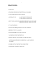
1
USER MANUAL
PC40
4 Channel Digital to Synchro or
Digital to Resolver
Converter Card
LOW COST BOARDS FOR IBM PC, XT, AT, PS/2 AND COMPATIBLE
COMPUTER SYSTEMS
2
Copyright Boston Technology 1992
All rights reserved. No part of this publication may be reproduced,
stored in a retrieval system, or transmitted in any form by any
means, electronic, mechanical, by photocopying, recording, or
otherwise without prior written permission.
First edition
August 1992
August 1992 printing
Information supplied in this manual is believed to be accurate and
reliable, however, no responsibility is assumed for its use, nor any
infringements of patents or other rights of third parties which may
result from its use.
IBM, PC/XT/AT, and IBM PS/2 are trademarks of International
Business Machine Corporation.
Microsoft is a trademark of Microsoft Corporation.
3
FEATURES:
- LOW COST
- SYNCHRO OR RESOLVER OPTIONS AVAILABLE
- 12 OR 14 BIT RESOLUTION OPTION
- ACCURACY OF:
4 ARC MINUTE FOR 14 BIT
6 ARC MINUTE FOR 12 BIT
- INPUT DATA RATE OF: 4000 DEGS PER SEC MAX FOR 14 BIT
8000 DEGS PER SEC MAX FOR 12 BIT
- 1 TO 4 CHANNELS
- EXCITATION FREQUENCIES OF 60 Hz OR 400 Hz
- DRIVES UP TO 5 VA LOADS
- TRANSFORMER ISOLATED OUTPUTS
- "LOCKED ROTOR" PROTECTION
- SHORT CIRCUIT AND OVERLOAD PROTECTION
- SOFTWARE SUPPLIED FOR DRIVING 1 AND 2-SPEED
SYSTEMS
- POWER SUPPLY PROTECTION CIRCUITRY
- SOFTWARE CONTROLLABLE PSU
4
TABLE OF CONTENTS:
PREFACE.
FEATURES.
1.0 INTRODUCTION.
1.1 Software.
1.2 Applications.
1.3 Ordering information.
1
1
1
2
2.0 HARDWARE.
2.1 Architecture.
2.2 Addressing Requirements.
2.3 Interconnections.
2.3.1 Output Connector.
2.3.2 Pin Definitions.
2.4 Timing Requirements.
3
3
5
6
6
6
8
3.0 SOFTWARE.
3.1 Programming the PC40.
3.1.1 Address Allocation.
3.1.2 Register Functions.
3.1.3 Data Format.
3.2 Software Drivers and Demonstration Software.
3.2.1 Operation.
3.2.2 Software Drivers.
3.2.3 Sample Programs.
9
9
9
9
11
11
11
13
15
4.0 SINGLE AND DUAL SPEED SYSTEM SETUP.
17
BIBLIOGRAPHY
19
APPENDICES
APPENDIX A
APPENDIX B
APPENDIX C
SPECIFICATIONS
LOAD TUNING
APPLICATIONS
5
PREFACE:
This manual is written for users of the PC40 series I/O cards. It
provides all the necessary information required to successfully
operate and program the PC40 series.
This manual assumes:
a)
That you have a detailed knowledge of synchro and
resolver operation.
b)
That you are familiar with the PC environment.
c)
That you are capable of writing your own programs or
modifying the demonstration software for your own
use.
6
1.0 INTRODUCTION.
The PC40 is a versatile, full size IBM PC card designed for 1 to 4
channels of Digital to Synchro or Digital to Resolver conversion.
Options with output voltages of 90VL-L or 11.8VL-L are available.
Frequency options available are 60Hz or 400Hz. High power
outputs of up to 5VA are provided. The outputs are transformer
isolated and provide maximum protection to the computer.
The card is double buffered and the 12 or 14 bit angle information
is provided in two 8-bit bytes from the computer. The I/O
addressing space is switch selectable with a DIP switch. The
modules are protected by a power supply protection circuit, whose
status can be read. The power supply can be switched on and off
under computer control.
1.1 Software.
Complete Pascal and C software drivers and demonstration
programs are provided. In addition to the normal single- speed
software, two-speed driver software is provided to allow twospeed systems to be set up. In the future, Fortran and Basic
software will be provided.
1.2 Applications.
The multi-channel PC40 is designed for use in high performance
control and simulation systems. With the high power output, the
PC40 is an excellent choice for applications including motor
control, antenna positioning, machine tooling, robot axis control
and process control.
7
1.3 Ordering Information.
Numerous models are provided:
PC40-XY-P
where
X is:
Y is:
P is:
S for 12 bits
T for 14 bits
A, B, C, D, E, F, or G.
M for 5 VA
N for 4.5 VA
O for 1.5 VA
MODEL
REF VOLTAGE
L-L VOLTAGE
FREQUENCY
TYPE
A
115V
90V
400Hz
SYNCH
B
26V
11.8V
400Hz
SYNCH
C
115V
90V
400Hz
RSVR
D
26V
11.8V
400Hz
RSVR
E*
115V
90V
60Hz
SYNC
The following models do not require ± 15V power supplies,
since the power is drawn from the reference:
MODEL
REF VOLTAGE
L-L VOLTAGE
FREQUENCY
TYPE
F*
G ***
115V
115V
90V
90V
60Hz
400Hz
SYNCH
SYNCH
* = This 60Hz version requires external transformers.
** = Only available in 4.5VA, 14 bit.
*** = Only available in 1.5VA, 14 bit.
eg.:
PC40-SC-M is a 12 bit 90V, 400Hz, 5VA resolver output
converter.
8
2.0 HARDWARE.
2.1 Architecture:
The PC40 is a full size IBM PC card which can accept up to four
channels of digital to synchro or resolver conversion channels. The
maximum resolution is 14 bits, however, the resolution can be
much improved if a two-speed system is set up with two singlespeed systems and the appropriate software drivers.
The digital angle information is converted to synchro or resolver
format when a channel is strobed. The data for each channel is
arranged in two 8-bit bytes. Once the high byte and low bytes have
been latched in, the channel strobe must be activated to load the
data into the channel latch.
A power supply (PSU) protection circuit has been incorporated,
which provides overvoltage protection and reverse power supply
protection from the external PSU. The power supply status can be
read in, and in addition, the user has full control over the enabling
of the power supply. If the PSU protection circuitry is activated,
then the PC40 will not allowed to be activated under software
control.
9
S1 S2 S3
BLOCK DIAGRAM OF PC40
10
PC 40 HARDWARE REQUIREMENTS
COMPUTER HARDWARE REQUIREMENTS:
IBM PC/XT/AT or compatible with 512K RAM
PARAMETER
VALUE
POWER SUPPLY: 5V from computer
0.3A with 4 chan.
TEMPERATURE RANGE
Operating Temp
0 to 70° C
Storage
-55 to 125°C
PHYSICAL ATTRIBUTES
13.1 x 4.1 x 0.9 in.
Fullsize IBM PC card
33.4 x 10.5 x 2.2cm
2.2 Addressing Requirements.
11
2.3 Interconnections.
2.3.1 Output Connector.
The output connector on the PC40 card is a DB37 male connector.
The connections are shown below:
1
2
3
4
5
6
7
8
9
10
11
12
13
14
15
16
17
18
19
-15V
-15V
0V
0V
+15V
+15V
CS4
CS3
CS2
CS1
CREFLO
CREFHI
AS4
AS3
AS2
AS1
AREFLO
AREFHI
20
21
22
23
24
25
26
27
28
29
30
31
32
33
34
35
36
37
DS4
DS3
DS2
DS1
DREFLO
DREFHI
BS4
BS3
BS2
BS1
BREFLO
BREFHI
2.3.2 Pin Definitions.
Note that the prefix A, B, C or D refers to the channel numbers 1, 2, 3, or 4
respectively.
a)
+15V, -15V, and 0V are provided from an external power supply.
The requirements are as follows:
12
PC40 models F and G do not require external ± 15V power
supplies since the power is drawn from the reference.
1.5 VA PC40 models require:
150mA average per channel
450mA peak per channel without current limiting.
5 VA PC40 models require:
700mA average per channel
2A peak per channel without current limiting.
Note: The loads can be tuned so that more devices can be
driven. See appendix B for details.
All the PC40 models except the F and the G models must
have a power supply accuracy of ± 15V + 8%. If the voltage
exceeds 16.2 V ± 0.2 V then the power supply protection
circuitry will be activated.
b)
REFHI and REFLO are the reference input to the digital to synchro
/ resolver converter. The reference voltage and frequency
must be accurate to within ±10% of voltage and frequency.
NOTE:
c)
If required, a solid state reference oscillator can
be used. The ordering code is PC42.
S1, S2, S3, and S4 are the outputs from the converter. These
pins are connected to the torque receiver or control
transformer. For a resolver type, S1 and S2 are connected to
the first stator coil, whilst S3 and S4 are connected to the
second stator coil. For a synchro type, S1, S2, and S3 are
connected to S1, S2, and S3 of the synchro motor. Note that
these outputs are transformer isolated.
2.4 Timing Requirements.
A delay of 100us for settling time is required for a stepped input.
13
The PC40 uses high-speed components, thereby allowing it to be
addressed with zero wait states.
14
3.0 SOFTWARE.
3.1 Programming the PC40.
3.1.1 Address Allocation:
The PC40 uses 8 consecutive address locations in the I/O space:
ADDRESS ALLOCATION TABLE
ADDRESS OFFSET FROM BASE
FUNCTION
OFFSET = 0
STROBE CHANNEL 1
OFFSET = 1
STROBE CHANNEL 2
OFFSET = 2
STROBE CHANNEL 3
OFFSET = 3
STROBE CHANNEL 4
OFFSET = 4
LOW BYTE LATCH
OFFSET = 5
HIGH BYTE LATCH
OFFSET = 6
PSU RELAY ON
OFFSET = 7
PSU RELAY OFF
OFFSET = 8
PSU STATUS
3.1.2 Register Functions.
OFFSET 0 TO 3 – CHANNEL STROBE – WRITE ONLY
STROBES THE DATA INTO THE SECOND BUFFER.
WRITE A ‘0’ TO THE RELEVANT OFFSET LOCATION.
OFFSET 4 – LOW BYTE LATCH – WRITE ONLY
WRITES LOW BYTE INTO FIRST BUFFER
15
OFFSET 5 – HIGH BYTE LATCH – WRITE ONLY
WRITES HIGH BYTE INTO FIRST BUFFER
Note that the data is left justified and hence the upper 8 bits are
stored in the HIGH BYTE LATCH, whilst the lower 6 bits are
stored in the LOW BYTE LATCH. See bit weights in the latter bit
weight table.
OFFSET 6 – PSU RELAY ON – WRITE ONLY
STROBES THE PSU RELAY ON.
WRITE A “0” TO THE RELEVANT OFFSET LOCATION
OFFSET 7 – PSU RELAY OFF – WRITE ONLY
STROBES THE PSU RELAY OFF.
WRITE A “0” TO THE RELEVANT OFFSET LOCATION.
OFFSET 8 – PSU STATUS – READ ONLY
BIT:
D7
D6
D5
D4
D3
D2
D1
D0
X
X
X
X
X
X
X
X
D0 CLEAR = ERROR
D0 SET = OK
16
3.1.3 Data format.
NOTE: FOR 12 BIT UNITS D1 AND D2 ARE NOT USED.
eg.
An angle of 224 degrees would be 10100000000000 binary or
2800 Hex.
3.2 Software Drivers and Demonstration Software.
3.2.1 Operation.
The following algorithm is provided.
STEP 1:
GET PSU STATUS.
STEP 2:
IF NO PSU ERROR THEN SWITCH RELAY ON AND
CONTINUE, ELSE SWITCH RELAY OFF AND EXIT.
17
STEP 3:
WRITE HIGH BYTE TO HIGH BYTE LATCH (OFFSET 5).
STEP 4:
WRITE LOW BYTE TO HIGH BYTE LATCH (OFFSET 4).
STEP 5:
STROBE THE RELEVANT CHANNEL STROBE.
STEP 6:
DELAY 100us FOR SETTLING TIME.
The following formula can be used to convert the shaft angle to
two digital bytes:
HIGH BYTE
LOW
BYTE
=
ANGLE
--- *
360
65536
DIV 256
=
ANGLE
--- *
360
65536
MOD 256
[ shaft angle in degrees ]
NOTE:
The high byte and low byte can be written to in any
order.
Full software drivers for single and dual speed systems are
provided. They are written in C and Pascal. Fortran and Basic
drivers will be available shortly. Also included, is full
demonstration software, which can be used in real applications.
18
3.2.2 Software Drivers.
A number of driver routines are provided in the PC40.X file in
turbo Pascal and Borland C++ on the accompanying disc. They can
be set up as units, include files, or simply inserted in a single
program file if desired. They are:
write_angle :
write_2speed_angle :
load a channel with an angle.
load 2 channels with an angle and a speed ratio for a two
speed system.
PSU_error :
get PSU status.
PSU_on :
switch PSU on.
PSU_off :
switch PSU off.
set_base :
set card base address.
For C the function prototypes are:
void set_base(unsigned int base_add);
input parameters:
base_add
void write_angle(int chan_num, float angle);
input parameters:
chan_num
angle
[channel number]
[in degrees]
19
void write_2speed_angle(int ratio, int chan_num1,
int chan_num2, float angle);
input parameters:
ratio
[gearing ratio]
chan_num1 [fine channel]
chan_num2 [coarse channel]
angle
int
[in degrees]
PSU_error();
parameters:
none
This function returns true if there is an
overvoltage condition at the PSU.
void PSU_on();
parameters:
none
void PSU_off();
parameters:
none
When using the drivers, the include file PC40.h must be
incorporated in the source file. Please remember to create project
files for Borland C++ or make files for Microsoft C, QuichC, etc.
“exe” files also provided.
For Pascal the function prototypes are:
procedure set_base(base_add : word);
input parameters:
base_add
20
procedure write_angle(chan_num : integer; angle : real);
input parameters:
chan_num
angle
[channel number]
[in degrees]
procedure write_2speed_angle(ratio : integer; chan_num1,
chan_num2 : integer;
angle : real);
input parameters:
ratio
[gearing ratio]
chan_num1 [fine channel]
chan_num2 [coarse channel]
angle
function
[in degrees]
PSU_error : boolean;
parameters:
none
procedure PSU_on;
parameters:
none
procedure PSU_off;
parameters:
none
When using the drivers, the unit PC40.TPU must be incorporated
in the source file.
Note: The channel parameters are 0 to 3 for channels 1 to 4.
21
3.2.3 Sample Programs.
Sample programs are provided in Turbo Pascal and Borland C++.
These versions of C and Pascal can be easily modified to other
versions of C and Pascal by merely modifying the clrscr and delay
functions to the equivalents. The 'exe' files are also provided.
The following programs are for single-speed systems:
PC40eg1.c and PC40eg1.pas
PC40eg2.c and PC40eg2.pas
The following programs are for two-speed systems:
PC40eg3.c and PC40eg3.pas
PC40eg4.c and PC40eg4.pas
Program Descriptions:
PC40eg1.X prompts the user for a channel number and an angle,
and loads the received data into the system.
PC40eg2.X prompts the user for a channel number and then steps
through from 0 degrees to 360 degrees in steps of 20 degrees.
The delay between steps is 1 second.
PC40eg3.X prompts the user for two channel numbers, the speed
ratio and an angle and loads the received data into the
system.
PC40eg4.X prompts the user for two channel numbers, the speed
ratio and then steps through from 0 degrees to 360 degrees in
steps of 20 degrees. The delay between steps is 1 second.
22
Note that the channel numbers in the software are 0 to 3 for channels 1
to 4.
23
4.0 SINGLE AND DUAL SPEED
SYSTEM SETUP.
Dual speed system:
24
2-Channel Single Speed System
25
BIBLIOGRAPHY:
1)
SYNCHRO CONVERSION : ILC DATA DEVICE
CORPORATION, 1990.
2)
SYNCHRO AND RESOLVER CONVERSION : ANALOG
DEVICES, 1980.
26
APPENDIX A
SPECIFICATIONS
27
APPENDIX B
LOAD TUNING
28
APPENDIX C
APPLICATIONS
(From Synchro & Resolver Conversion - Analog Devices)