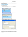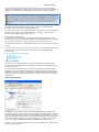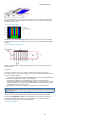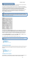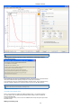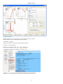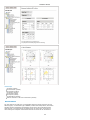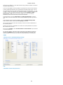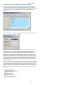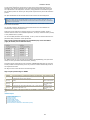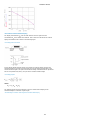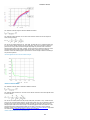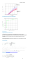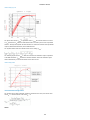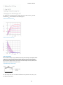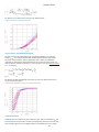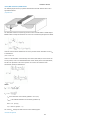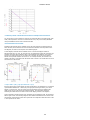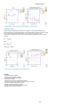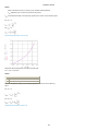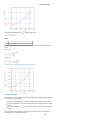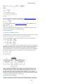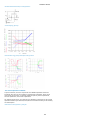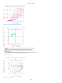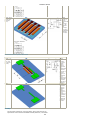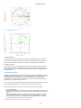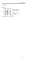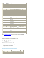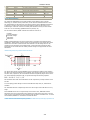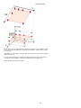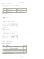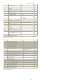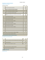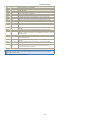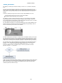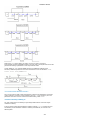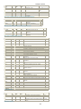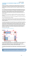
1
MOSFET Models ICCAP 2012.01 January 2012 MOSFET Models 1 MOSFET Models © Agilent Technologies, Inc. 20002011 3501 Stevens Creek Blvd., Santa Clara, CA 95052 USA No part of this documentation may be reproduced in any form or by any means (including electronic storage and retrieval or translation into a foreign language) without prior agreement and written consent from Agilent Technologies, Inc. as governed by United States and international copyright laws. Acknowledgments UNIX ® is a registered trademark of the Open Group. MSDOS ®, Windows ®, and MS Windows ® are U.S. registered trademarks of Microsoft Corporation. Pentium ® is a U.S. registered trademark of Intel Corporation. PostScript® is a trademark of Adobe Systems Incorporated. Java™ is a U.S. trademark of Sun Microsystems, Inc. Mentor Graphics is a trademark of Mentor Graphics Corporation in the U.S. and other countries. Qt Version 4.6 Qt Notice The Qt code was modified. Used by permission. Qt Copyright Qt Version 4.6, Copyright (c) 2009 by Nokia Corporation. All Rights Reserved. Qt License Your use or distribution of Qt or any modified version of Qt implies that you agree to this License. This library is free software; you can redistribute it and/or modify it under the terms of the GNU Lesser General Public License as published by the Free Software Foundation; either version 2.1 of the License, or (at your option) any later version. This library is distributed in the hope that it will be useful, but WITHOUT ANY WARRANTY; without even the implied warranty of MERCHANTABILITY or FITNESS FOR A PARTICULAR PURPOSE. See the GNU Lesser General Public License for more details. You should have received a copy of the GNU Lesser General Public License along with this library; if not, write to the Free Software Foundation, Inc., 51 Franklin St, Fifth Floor, Boston, MA 02110-1301 USA Permission is hereby granted to use or copy this program under the terms of the GNU LGPL, provided that the Copyright, this License, and the Availability of the original version is retained on all copies. User documentation of any code that uses this code or any modified version of this code must cite the Copyright, this License, the Availability note, and "Used by permission." Permission to modify the code and to distribute modified code is granted, provided the Copyright, this License, and the Availability note are retained, and a notice that the code was modified is included. Qt Availability http://www.qtsoftware.com/downloads Patches Applied to Qt can be found in the installation at: $HPEESOF_DIR/prod/licenses/thirdparty/qt/patches. You may also contact Brian Buchanan at Agilent Inc. at [email protected] for more information. For details see: http://bmaster.soco.agilent.com/mw/Qt_License_Information Errata The IC-CAP product may contain references to "HP" or "HPEESOF" such as in file names and directory names. The business entity formerly known as "HP EEsof" is now part of Agilent Technologies and is known as "Agilent EEsof." To avoid broken functionality and to maintain backward compatibility for our customers, we did not change all the names and labels that contain "HP" or "HPEESOF" references. Warranty The material contained in this documentation is provided "as is", and is subject to being changed, without notice, in future editions. Further, to the maximum extent permitted by applicable law, Agilent disclaims all warranties, either express or implied, with regard to this manual and any information contained herein, including but not limited to the implied warranties of merchantability and fitness for a particular purpose. Agilent shall not be liable for errors or for incidental or consequential damages in connection with the furnishing, use, or performance of this document or of any information contained herein. Should Agilent and the user have a separate written agreement with warranty terms covering the material in this document that conflict with these terms, the warranty terms in the separate agreement shall control. Technology Licenses The hardware and/or software described in this document are furnished under a license and may be used or copied only in accordance with the terms of such license. Restricted Rights Legend U.S. Government Restricted Rights. Software and technical data rights granted to the federal government include only those rights customarily provided to end user customers. Agilent provides this customary commercial license in Software and technical data pursuant to FAR 12.211 (Technical Data) and 12.212 (Computer Software) and, for the Department of Defense, DFARS 252.227-7015 (Technical Data - Commercial Items) and DFARS 227.7202-3 (Rights in Commercial Computer Software or Computer Software Documentation). 2 MOSFET Models Supported Model Versions . . . . . . . . . . . . . . . . . . . . . . . . . . Using the MOS Modeling Packages . . . . . . . . . . . . . . . . . . . . Introduction to the MOS Modeling Packages . . . . . . . . . . . . Data Structure in MOS Modeling Packages . . . . . . . . . . . . . Getting Started with MOS Modeling . . . . . . . . . . . . . . . . . . DC and CV Measurement . . . . . . . . . . . . . . . . . . . . . . . . . Using DC and CV Measurement Module with WaferPro . . . . . RF Measurement . . . . . . . . . . . . . . . . . . . . . . . . . . . . . . . Extraction of DC/CV Parameters . . . . . . . . . . . . . . . . . . . . Modifying Existing Functions . . . . . . . . . . . . . . . . . . . . . . . . Defining Extraction Functions . . . . . . . . . . . . . . . . . . . . . . . . Programming details . . . . . . . . . . . . . . . . . . . . . . . . . . . . . . Extraction of Parameters for the RF Models . . . . . . . . . . . . BSIM3v3 Characterization . . . . . . . . . . . . . . . . . . . . . . . . . . What's New in the BSIM3v3 Modeling Package . . . . . . . . . . Introduction to BSIM3 Model . . . . . . . . . . . . . . . . . . . . . . The Unified I-V Model of BSIM3v3 . . . . . . . . . . . . . . . . . . . Capacitance Model . . . . . . . . . . . . . . . . . . . . . . . . . . . . . . High Frequency Behavior . . . . . . . . . . . . . . . . . . . . . . . . . Temperature Dependence . . . . . . . . . . . . . . . . . . . . . . . . Noise Model . . . . . . . . . . . . . . . . . . . . . . . . . . . . . . . . . . SPICE Model Parameters of the BSIM3v3 Model . . . . . . . . . Test structures for Deep Submicron CMOS Processes . . . . . . Extraction of Model Parameters . . . . . . . . . . . . . . . . . . . . . Binning of Model Parameters . . . . . . . . . . . . . . . . . . . . . . Importing older version BSIM3v3 Files . . . . . . . . . . . . . . . . References and Copyright Information . . . . . . . . . . . . . . . . BSIM4 Characterization . . . . . . . . . . . . . . . . . . . . . . . . . . . . What's new inside the BSIM4 Modeling Package: . . . . . . . . Basic Effects Modeled in BSIM4 . . . . . . . . . . . . . . . . . . . . . Key Features of the BSIM4 Modeling Package . . . . . . . . . . . BSIM4 DC Behavioral Modeling . . . . . . . . . . . . . . . . . . . . . CV Modeling . . . . . . . . . . . . . . . . . . . . . . . . . . . . . . . . . . The BSIM4 RF Simulation Model . . . . . . . . . . . . . . . . . . . . SPICE Model Parameters for BSIM4.6.2 . . . . . . . . . . . . . . . HiSIM2 Characterization . . . . . . . . . . . . . . . . . . . . . . . . . . . Introduction to HiSIM2 Characterization . . . . . . . . . . . . . . . HiSIM_HV Model . . . . . . . . . . . . . . . . . . . . . . . . . . . . . . . Modeled Device Characteristics of the HiSIM2 model . . . . . . SPICE Model Parameters for the HiSIM MOS Model . . . . . . . RF Circuit used for HiSIM2 . . . . . . . . . . . . . . . . . . . . . . . . HiSIM_HV Model . . . . . . . . . . . . . . . . . . . . . . . . . . . . . . . . . PSP Characterization . . . . . . . . . . . . . . . . . . . . . . . . . . . . . . Extraction of Parameters using the Local - Global approach . Parameter Extraction using Global Model only . . . . . . . . . . . Simultaneous Adjustment of Local and Global Parameters . . Binning of PSP Models . . . . . . . . . . . . . . . . . . . . . . . . . . . Parameters for the PSP model . . . . . . . . . . . . . . . . . . . . . . Extraction of Parameters using the Local - Global approach . BSIMSOI4 Characterization . . . . . . . . . . . . . . . . . . . . . . . . . Introduction to BSIMSOI Model . . . . . . . . . . . . . . . . . . . . . IV Characterization . . . . . . . . . . . . . . . . . . . . . . . . . . . . . Binning of Model Parameters in BSIMSOI4 . . . . . . . . . . . . . CV Characterization . . . . . . . . . . . . . . . . . . . . . . . . . . . . . High Frequency Model . . . . . . . . . . . . . . . . . . . . . . . . . . . Test Structures for SOI MOSFET . . . . . . . . . . . . . . . . . . . . SPICE Model Parameters . . . . . . . . . . . . . . . . . . . . . . . . . Agilent Root MOSFET Model Generator . . . . . . . . . . . . . . . . . MOS Model 9 Characterization . . . . . . . . . . . . . . . . . . . . . . . Introduction to MOS Model 9 . . . . . . . . . . . . . . . . . . . . . . The MM9 Model File . . . . . . . . . . . . . . . . . . . . . . . . . . . . . Parameter Extraction . . . . . . . . . . . . . . . . . . . . . . . . . . . . Optimizing MOS Model 9 . . . . . . . . . . . . . . . . . . . . . . . . . The JUNCAP Model . . . . . . . . . . . . . . . . . . . . . . . . . . . . . . New Features in AdMOS Modeling Toolskits for ICCAP 2012.10 UCB MOS Level 2 and 3 Characterization . . . . . . . . . . . . . . . . Introduction to UCB MOS Level 2 and 3 Characterization . . . UCB MOSFET Model, Simulators, and Model Parameters . . . . Test Instruments . . . . . . . . . . . . . . . . . . . . . . . . . . . . . . . Measuring and Extracting . . . . . . . . . . . . . . . . . . . . . . . . . Extraction Algorithms . . . . . . . . . . . . . . . . . . . . . . . . . . . . HSPICE LEVEL 6 MOSFET Model . . . . . . . . . . . . . . . . . . . . . . . . . . . . . . . . . . . . . . . . . . . . . . . . . . . . . . . . . . . . . . . . . . . . . . . . . . . . . . . . . . . . . . . . . . . . . . . . . . . . . . . . . . . . . . . . . . . . . . . . . . . . . . . . . . . . . . . . . . . . . . . . . . . . . . . . . . . . . . . . . . . . . . . . . . . . . . . . . . . . . . . . . . . . . . . . . . . . . . . . . . . . . . . . . . . . . . . . . . . . . . . . . . . . . . . . . . . . . . . . . . . . . . . . . . . . . . . . . . . . . . . . . . . . . . . . . . . . . . . . . . . . . . . . . . . . . . . . . . . . . . . . . . . . . . . . . . . . . . . . . . . . . . . . . . . . . . . . . . . . . . . . . . . . . . . . . . . . . . . . . . . . . . . . . . . . . . . . . . . . . . . . . . . . . . . . . . . . . . . . . . . . . . . . . . . . . . . . . . . . . . . . . . . . . . . . . . . . . . . . . . . . . . . . . . . . . . . . . . . . . . . . . . . . . . . . . . . . . . . . . . . . . . . . . . . . . . . . . . . . . . . . . . . . . . . . . . . . . . . . . . . . . . . . . . . . . . . . . . . . . . . . . . . . . . . . . . . . . . . . . . . . . . . . . . . . . . . . . . . . . . . . . . . . . . . . . . . . . . . . . . . . . . . . . . . . . . . . . . . . . . . . . . . . . . . . . . . . . . . . . . . . . . . . . . . . . . . . . . . . . . . . . . . . . . . . . . . . . . . . . . . . . . . . . . . . . . . . . . . . . . . . . . . . . . . . . . . . . . . . . . . . . . . . . . . . . . . . . . . . . . . . . . . . . . . . . . . . . . . . . . . . . . . . . . . . . . . . . . . . . . . . . . . . . . . . . . . . . . . . . . . . . . . . . . . . . . . . . . . . . . . . . . . . . . . . . . . . . . . . . . . . . . . . . . . . . . . . . . . . . . . . . . . . . . . . . . . . . . . . . . . . . . . . . . . . . . . . . . . . . . . . . . . . . . . . . . . . . . . . . . . . . . . . . . . . . . . . . . . . . . . . . . . . . . . . . . . . . . . . . . . . . . . . . . . . . . . . . . . . . . . . . . . . . . . . . . . . . . . . . . . . . . . . . . . . . . . . . . . . . . . . . . . . . . . . . . . . . . . . . . . . . . . . . . . . . . . . . . . . . . . . . . . . . . . . . . . . . . . . . . . . . . . . . . . . . . . . . . . . 3 . . . . . . . . . . . . . . . . . . . . . . . . . . . . . . . . . . . . . . . . . . . . . . . . . . . . . . . . . . . . . . . . . . . . . . . . . . . . . . . . . . . . . . . . . . . . . . . . . . . . . . . . . . . . . . . . . . . . . . . . . . . . . . . . . . . . . . . . . . . . . . . . . . . . . . . . . . . . . . . . . . . . . . . . . . . . . . . . . . . . . . . . . . . . . . . . . . . . . . . . . . . . . . . . . . . . . . . . . . . . . . . . . . . . . . . . . . . . . . . . . . . . . . . . . . . . . . . . . . . . . . . . . . . . . . . . . . . . . . . . . . . . . . . . . . . . . . . . . . . . . . . . . . . . . . . . . . . . . . . . . . . . . . . . . . . . . . . . . . . . . . . . . . . . . . . . . . . . . . . . . . . . . . . . . . . . . . . . . . . . . . . . . . . . . . . . . . . . . . . . . . . . . . . . . . . . . . . . . . . . . . . . . . . . . . . . . . . . . . . . . . . . . . . . . . . . . . . . . . . . . . . . . . . . . . . . . . . . . . . . . . . . . . . . . . . . . . . . . . . . . . . . . . . . . . . . . . . . . . . . . . . . . . . . . . . . . . . . . . . . . . . . . . . . . . . . . . . . . . . . . . . . . . . . . . . . . . . . . . . . . . . . . . . . . . . . . . . . . . . . . . . . . . . . . . . . . . . . . . . . . . . . . . . . . . . . . . . . . . . . . . . . . . . . 4 5 6 7 10 12 38 43 50 73 79 90 109 116 117 119 121 140 148 156 160 162 166 176 179 184 186 187 188 188 188 192 208 211 219 228 229 230 236 237 245 247 253 255 259 261 267 271 285 289 290 295 299 302 306 311 314 321 343 344 345 358 360 362 369 371 369 369 376 377 381 383 MOSFET Models Supported Model Versions The following table lists the model versions supported by the MOS Modeling Toolkits for supported models and simulators. Model Circuits ADS 2011_01 Verilog A HSpice F2011.09 MMSIM 11.1 Eldo 2011.1 BSIM3 3.3.2.4 3.3 _ 3.3.2.4 3.3 3.3.2.4 BSIM4 4.7 4.6.5 _ 4.7 4.7 4.7 BSIMSOI4 4.4.0 4.4 _ 4.4 4.4 4.4 HiSIM 2 2.4.1 2.5.1 2.5.1 2.5.1 2.5.1 1.2 1.2.1 1.2.1/2.00 1.2.2 1.2.1 _ 103.1.1 103.1.1 103.1.1 2.5.1 HiSIM HV 1.2.1 PSP 103.1.1 103.1.1 4 MOSFET Models Using the MOS Modeling Packages This section provides information on the following topics: Introduction to MOS Modeling Packages (mosfet) Data Structure in MOS Modeling Packages (mosfet) Getting Started with MOS Modeling (mosfet) DC and CV Measurement (mosfet) Using DC and CV Measurement Module with WaferPro (mosfet) RF Measurement (mosfet) Extraction of DC and CV Parameters (mosfet) Extraction of Parameters for the RF Models (mosfet) 5 MOSFET Models Introduction to the MOS Modeling Packages AdMOS has developed the technology for measurement and extraction of parameters using the MOS Modeling Packages for HISIM2, HISIM_HV, BSIM3v3, BSIM4, BSIMSOI4, and PSP model parameters. These Modeling Packages use similar Graphic User Interfaces (GUI) and are handling the measurement and extraction tasks in a similar way and therefore only need to be described once. The model specific parts are located in: BSIM3v3 Characterization (mosfet) BSIM4 Characterization (mosfet) BSIMSOI4 Characterization (mosfet) PSP Characterization (mosfet) HiSIM2 Characterization (mosfet) HiSIM_HV Characterization (mosfet) The above sections describe theoretical aspect of each model. Supported Measurements The modeling packages support measurements for the following: Single-finger (normal) transistors Parasitic diodes Capacitance Oxide Overlap Bulk-drain and source-drain junction Intrinsic RF multifinger transistors Supported Extractions The modeling packages supports extractions for the following: Basic transistor behavior Parasitic diodes Capacitances RF behavior (S-parameters) See Also Key Features of the MOS Modeling Packages Data Structure used for the MOS Modeling Packages Getting Started with MOS Modeling (mosfet) DC and CV Measurement (mosfet) RF Measurement (mosfet) Extraction of DC and CV Parameters (mosfet) Extraction of Parameters for the RF Models (mosfet) 6 MOSFET Models Data Structure in MOS Modeling Packages The MOS Modeling Packages use a different and more advanced data storing concept as compared to former modeling products in IC-CAP. The drawback of recent modeling products is that measured data is always stored in model files with transforms, macros, plot definitions, and so on. This method had two major disadvantages: The additional information is stored n times and is therefore highly redundant. The combination of data and code makes it very difficult to introduce updates to the code. Now, the new architecture of the MOS Modeling Packages overcome these disadvantages. The measurement module contains all measurement related items like DUTs/Setups to perform measurements and setup of test and measurement conditions. The measured data is stored together with device information like gate length, pin numbers of a switch matrix used, and so forth in IC-CAP .mdm data base format. These .mdm files are organized as projects that can be identified by project name. Now, the extraction module extracts the necessary data from stored .mdm files to perform model parameter extraction and visualization of measured and simulated results. In addition, this method enables the generation of new data representations where the scalability of a model can be easily verified. Files Resulting from Measurement and Extraction using the Modeling Packages This section describes the files resulting from measurement and extraction of MOS devices using the MOS Modeling Packages. The following table shows how file names are being used. The bold printed words inside the left most column names the task the files are being used for and the normal printed names are the appropriate file names used to store the files for a specific project. The columns marked DC and RF list the task performed by each file. For example, measure+extract in the column DC means that this file is used in measurement and extraction of DC parameters. Note The following characters are excluded from use in file or project names: " / \ , . ; : * ? ~ % $ ' ä Ä ö Ö ü Ü as well as "empty space". Data Structure of MOS Modeling Packages File Usage DC RF Comment Project search *dc_idvg*.mdm measure + extract *rf_s_dut*.mdm measure + extract Settings project_name~dc_meas~settings.set measure + extract project_name~rf_meas~settings.set project_name~lwc(model name)~settings.set measure + extract extract extract 7 MOSFET Models Boundaries *~lwc(model name)~boundaries.set extract extract default for export, * = project_name measure + extract measure + extract for scaled model extract for single model MPS project_name~lwc(model name).mps project_name~DUT_name~lwc(model name).mps LIB project_name~DUT_name~Simulator~lwc(model name).lib project_name~Simulator~lwc(model name).lib extract for single model extract extract for scaled model extract extract Logfile project_name~lwc(model name)~log_fail.txt MDMs project_name~DUT_name~dc_idvg~TempK.mdm measure + extract project_name~DUT_name~dc_idvd~TempK.mdm measure + extract project_name~DUT_name~c_bd_area~TempK.mdm measure + extract project_name~DUT_name~c_bd_perim~TempK.mdm measure + extract project_name~DUT_name~c_bd_perim_gate~TempK.mdm measure + extract project_name~DUT_name~c_bs_area~TempK.mdm measure + extract project_name~DUT_name~c_bs_perim~TempK.mdm measure + extract project_name~DUT_name~c_bs_perim_gate~TempK.mdm measure + extract project_name~DUT_name~c_d_g~TempK.mdm measure + extract project_name~DUT_name~c_g_ds~TempK.mdm measure + extract project_name~DUT_name~c_g_dsb~TempK.mdm measure + extract project_name~DUT_name~di_bd_area~TempK.mdm measure + extract project_name~DUT_name~di_bd_perim~TempK.mdm measure + extract project_name~DUT_name~di_bd_perim_gate~TempK.mdm measure + extract project_name~DUT_name~di_bs_area~TempK.mdm measure + extract project_name~DUT_name~di_bs_perim~TempK.mdm measure + extract project_name~DUT_name~di_bs_perim_gate~TempK.mdm measure + extract project_name~DUT_name~rf_s_dut~TempK.mdm measure + extract project_name~DUT_name~rf_id_bias_points~TempK.mdm measure project_name~DUT_name~rf_idvd~TempK.mdm measure + extract project_name~DUT_name~rf_s_open~TempK.mdm measure project_name~DUT_name~rf_s_short~TempK.mdm measure project_name~DUT_name~rf_s_through~TempK.mdm measure HTML PathHTML/index.htm extract extract PathHTML/*.htm extract extract Start file PathHTML/menu.js extract extract File structure PathHTML/imgmenu/* extract extract Pictures for file structure PathHTML/setups/*.htm extract extract Measurement Setups PathHTML/results/*.htm extract extract Pages with results PathHTML/results/*.txt extract extract Parameter set for displaying HTML PathHTML/results/images/*.gif extract extract Images PathHTML/results/imgzoom/*.gif extract extract Zoomed Images See Also Getting Started with MOS Modeling (mosfet) 8 MOSFET Models DC and CV Measurement (mosfet) RF Measurement (mosfet) Extraction of DC and CV Parameters (mosfet) Extraction of Parameters for the RF Models (mosfet) Using the MOS Modeling Packages (mosfet) 9 MOSFET Models Getting Started with MOS Modeling IC-CAP provides example files with the Modeling Packages which you can load and experiment with the settings of different modules like DC_CV_Measurement,Extraction, or RF Measurement and Extraction. Opening a MOS Modeling Example To open a MOS Modeling example: 1. Choose File > Examples > model_files > mosfet from the IC-CAP Main window to open a MOS model file. For example, BSIM4_DC_CV_Extract.mdl file in the BSIM4 folder. The Model icon is displayed in the IC-CAP Main window. 2. Double-click the BSIM4_DC_CV_Extract model icon to start the measurement module. The BSIM4_DC_CV_Extract Model window is displayed. 3. Choose File > Examples in the BSIM4_DC_CV_Extract Model window. The Copy Example Project dialog box is displayed. 4. In the Copy Example Project dialog box, select an example project to be loaded from the Examples list. 5. Specify a Path where the selected example project needs to be copied. The selected example is loaded in the Model window. Each Modeling Package contains example files for DC and RF Projects. As the example model parameter files are copied to a directory, the original files are not overwritten. Therefore, you can test with every IC-CAP function that is implemented without modifying the original files. 10 MOSFET Models Notes Ensure that you have write permissions for the directory where you want to copy the example project. Files with same name in the target directory are overwritten. If files with the same name exist, you will be prompted before they are overwritten. See Also Using the MOS Modeling Packages (mosfet) Data Structure in MOS Modeling Packages (mosfet) DC and CV Measurement (mosfet) RF Measurement (mosfet) Extraction of DC and CV Parameters (mosfet) Extraction of Parameters for the RF Models (mosfet) 11 MOSFET Models DC and CV Measurement This section provides information on the DC and CV measurement of MOS Model and other necessary measurements of your devices. It provides information on features of the MOS Modeling Packages and how to use the Model graphic user interface (GUI). For tips on how to measure and what to measure using the right devices, see BSIM3v3 Characterization (mosfet), BSIM4 Characterization (mosfet), BSIMSOI4 Characterization (mosfet), HiSIM2 Characterization (mosfet), and PSP Characterization (mosfet). Note As the measurement modules of the MOS Modeling Packages are identical, only one is described in detail. Double-click the Model icon (BSIM3, BSIM4, or PSP icon) in the IC-CAP Main window to open the Model GUI. The BSIM3, BSIM4, or PSP Icon which appears in the IC-CAP/Main window after you open one of the example files. To open an example file, choose File > Examples > model_files > mosfet > bsim3 (or bsim4 or PSP ) then select a Measure or Extract model file. The following figure shows four of the files in one IC-CAP/Main window, using BSIM3 as an example. Starting the BSIM3 GUI from ICCAP/Main window After you have double clicked the DC_CV_Measurement icon for example, the GUI window of the MOS Modeling Packages (figure below) appears on your screen. Measurement part of the Graphic User Interface for the MOS Modeling Packages The top row of the GUI shows the File, Configuration, Data, Tools, and Help menus. Some menu topics are only activated when using specific tasks (depending on which folder is activated!). For example, if you are setting up the conditions for a Temperature measurement, the Configuration menu only allows you to add or delete temperatures. The rest of the menu is not active since it is not necessary to set or sort categories during temperature setup, for example. The File menu has entries to Import and Export list and measurement data from measurement software other than IC-CAP. Those functions are described in Import Wizard 12 MOSFET Models (mosfet). To import data from other software or saved in another data format, use the Import Wizard. This feature is accessible through the following file menu: File > Import > Import Wizard (mosfet) The standard IC-CAP icons (from left to right) are located below the menu. Use these icons to create a New, to Open an existing, to Copy and Open an Example, to Save Setups or Entries, to Measure, to Display and Close plots, to Add or Delete, to define Temperature Measurements, to Set categories, or to Check SMU connections. You will be prompted before the selected action takes place. Again, some of the icons are only activated when specific folders are active. The lower part of the window displays the project name and project directory. To Print a setup, choose File > Print Setup. This opens a dialog box. In this dialog box, enter the command line for your specific printing device and choose OK. The folder will be printed. Note On Windows operating system, the command line is print /d:<printer name>. For example, if the printer is connected to a server named MYFS1 and the printer is named MY0017, type: print /d:'\\MYFS1\MY0017' Note If you don't enter a printer command, the output will be redirected to the IC-CAP/Status window. From the Help menu you can choose between browsing the Topics or getting help for each of the different task folders described below. There are in depth hints for the task, for example, which device geometries to use or how to connect the instrument to the device under test to get the best extraction results from your measurements. You will find links that bring you to PSP Characterization (mosfet), BSIM4 Characterization (mosfet), or BSIM3v3 Characterization (mosfet). Use your Browsers Back button to return to the location you were at before following the link. Below the top row of icons are five folders. Basically, each folder is assigned to a specific task in the measurement process. They are intended to be parsed from left to right, but you are not bound to that order. Some entries into one or the other folder will change settings on another folder. For the new user: You should process the folders in the order from left to right. Each of the following sections describe one folder of the GUI. BSIM3, BSIM4, and PSP model folders are usually equal to each other. DC/CV Measurement Module Folders Notes (mosfet) Temperature Setup (mosfet) Switch Matrix (mosfet) Device Definition (mosfet) Options (mosfet) How to Import measured Data not compatible with the ICCAP format Import Wizard (mosfet) See Also Using the MOS Modeling Packages (mosfet) Introduction to MOS Modeling Packages (mosfet) Data Structure used for the MOS Modeling Packages Getting Started with MOS Modeling (mosfet) RF Measurement (mosfet) Extraction of DC and CV Parameters (mosfet) Extraction of Parameters for the RF Models (mosfet) Project Notes The notes folder is provided to store notes you take on a specific project. You can enter general data like technology used to produce this wafer as well as lot, wafer, and chip number. There is a field to enter the operator's name and the date the measurement was taken. Space has been provided to enter notes on that project. Notes entered into the measurement module will be transferred to the Information folder inside the DC_CV_Extraction modules. Other DC/CV Measurement Module Folders Temperature Setup (mosfet) Switch Matrix (mosfet) Device Definition (mosfet) Options (mosfet) 13 MOSFET Models Temperature Setup Use this folder to define measurements at specified temperatures. Basically, the measurement of all DUTs is performed at SPICE default temperature TNOM, which is set to 27° Celsius. Note To change the default value of 27°C to represent your measurement temperature, double click and enter the actual environment temperature inside your measurement lab into the TNOM field. Add new measurement temperatures using the Add icon or the Configuration menu. If you no longer need a measurement temperature, click the Delete button. You will be prompted for the temperature to be deleted. If there is a file containing measured data for this temperature, the data file will be deleted if you choose OK on the prompt dialog. The delete window does not contain an entry for the temperature set as TNOM, since TNOM cannot be excluded from measurement and extraction. Note Don't forget to enter the actual temperature in degree Celsius (°C) into the TNOM field during measurement of the devices. It is not possible to delete the nominal temperature TNOM! When you add a new measurement temperature, a new column is added to the Device List folder's Device List table for DC Transistor, Capacitance, and DC Diode. Any changes on the Temperature Setup folder must be saved prior to selecting another folder. Other DC/CV Measurement Module Folders Notes (mosfet) Switch Matrix (mosfet) Device Definition (mosfet) Options (mosfet) Switch Matrix Use this folder to define which measurements use a switch matrix (see figure below). There are three options: Use a switch matrix for DC Transistor Measurements, for Capacitance Measurements, and for Diode Measurements. You can select any one or more than one by checking the appropriate boxes. Note If you are not using a switch matrix, leave all three check boxes unchecked. In this case, you do not have terminal assignment columns in the Transistor's Device List table in the Device List folder. Instead, you determine the connections by wiring the appropriate SMU to the desired transistor terminal. Note Assignments must use SMU1....SMU4. This assignment is done inside the hardware setup of IC-CAP. Usually, the default of the appropriate DC-CV-Analyzer is SMU1...4. In rare cases, such as the Agilent E5250 for example, the default SMU number corresponds to the slot number of the module inserted into the instrument. If your E5250 uses 4 SMU's at slot No. 1, 3, 5, 6, the default names of the SMU's are SMU1, SMU3, SMU5 and SMU6. You must change this default names to reflect SMU1, SMU2, SMU3 and SMU4 to properly communicate with the BSIM3/4 and PSP modules. Note To change or enter the names of the Source-Measurement-Units (SMU's), open the model for editing then go to the folder DUTs/Setup, subfolder Measure/Simulate. Configure the different inputs/outputs there. Defining the use of a switch matrix for measurements 14 MOSFET Models The Basic Settings provide a choice of several different Matrix Models, which are supported by IC-CAP. Type the appropriate Bus and GPIB address of the Switch Matrix (SWM Address; 22 in our example) as well as the GPIB-Interface name. See Prober (measurement) and Matrix Drivers (measurement) for a complete description of the GPIB settings for the selected switch matrix. Our example shows the use of an Agilent E5250A matrix model. For this type of instrument, you have to define which port is connected to which SMU or C meter input pin and which slot is equipped with a card. It is now possible to use Instrument Cards for your measurements. Activation is done using a port / pin combination, A1 or A26, for example. This means, Port A and Pin 1 or Port A and Pin 26 are activated. The Switch Matrix folder shows an additonal field to enter a pin number. Therefore, when using Instrument Cards, you need to define a port as well as a pin. Note On some instruments, ports are to be named using letters, others using numbers for their ports. Choosing the instrument from the drop-down list of Matrix Models shows you how to name your instrument ports. Using the Agilent E5250A Switch Matrix, you need to define consecutive numbers ranging from 1 to 48, regardless of the card used inside the matrix. Again, you have to save your changes prior to leaving this folder. The actual pin connections are entered into the DUT Variables folder for the measurement selected to use a switch matrix (one or more of the DC Transistor, Capacitance, or Diode Measurements). For example, if you've selected DC Transistor Measurements to use with 15 MOSFET Models a switch matrix, you must open the model file for editing and in the DUT/Setups folder select the DC Transistor then in the DUT Variables folder enter the switch matrix pin numbers in the fields below the node names. This is especially useful if you would like to make series measurements on wafers using a probe card (e.g., for quality control). Note When using a Switch Matrix for Capacitance Measurements, it is physically not possible to eliminate all stray capacitances up to the DUT. Therefore, you need to calibrate the instrument up to the switch matrix with all matrix connections set to open. Calibration will remove the capacitance of the cables between CVmeter and switch matrix. To calibrate the way all to the DUT, for each matrix connection the capacitance needs to be measured with the probe card in the "up" position (no DUTconnected). The measured capacitances for every switch matrix connection will be removed from the measurements of the DUTs capacitances. For automatic measurements, macros are available. These macros enable you to make automatic series measurements of complete dies or arrays. They are created for automatic measurements with or without heated chucks. For example, open the IC-CAP model for BSIM3_DC_CV_Measure (from the IC-CAP/Main window, right click the DC_CV_Measure model then select Edit). The Macros folder contains a macro called Example_Wafer_Prober. You will also find a macro in the $ICCAP_ROOT/examples/model_files/mosfet/BSIM3/examples/waferprober directory named prober_control.mdl. Please use this macro or model file and tailor it to your needs. There are readme sections to explain the steps to be taken inside the macros. The automatic measurement of model diagrams using the macro works without involving the GUI. For your convenience, the waferscan macro in the prober_control.mdl example model file can be loaded into IC-CAP and can be run in a demo mode without taking actual measurements. Other DC/CV Measurement Module Folders Notes (mosfet) Temperature Setup (mosfet) Device Definition (mosfet) Options (mosfet) Device Definition The next step in the modeling process is to set up the measurement conditions for different measurement tasks like DC, Capacitance, or Diode measurements and to enter the devices to be used. The Device Definition pane allows an easy setup of conditions for DC Transistor and Capacitance as well as DC Diode measurements. The following figure shows the Device Definition pane used for setting up measurement conditions as well as the devices to be measured. You can use the icons or the menu to save this settings before proceeding to the next task. Device Definition Folder The Data tree on the left-side of the Device Definition pane displays the Data for this measurement project. This tree definition can be different for different models. The above figure shows the tree structure used for extracting BSIM3 device parameters. If you are using the SOI Modeling Package, the Device Definition pane displays the entries which are not normally present on BISM3/4, HSIM, or PSP measurement projects. For example, there are no floating transistors to be measured in BSIM3 or 4 modeling tasks. Click the + sign to expand the Transistor, Diode, and Capacitance entries and reveal the Measurement and Device List. 16 MOSFET Models The Measurement node shows the predefined measurement sets as well as setups already selected for the specific measurement. To add a setup, click the + icon. You will be prompted to select a setup and enter a name for it. The new setup will be included in the tree below Measurement. There are fields named Compliance, where you may define compliance settings for your SMU. The settings are in Ampere (A) and are valid for all measurements defined. That is, you cannot define a compliance setting for the drain voltage source in one measurement and another one for the next measurement. The values are shown for reference only inside the different measurements. To the right of the compliance definition area, there is a field to be activated if you would like to use the Safe Operation Area (SOA), limiting the power delivered by the SMU to the drain of the DUT. There are choices If you select one of the measurement setups inside the tree, the folder changes to reflect the measurement conditions valid for the selected setup. Setups not assigned to a Measurement Set will be deleted on opening a project! The same is valid for Measurement Sets not used! To assign a setup to a Measurement Set, select Measurements from the tree. Now you can configure the measurement sets by clicking the icon Configure Measurement Set. The Configure Measurement Set window appears. or selecting Configuration > Add your setups to predefined measurement sets or define your own sets. As you will notice, the default settings are greyed out, they cannot be changed. However, there is an unlock field where you can remove the locking. You will be noted that devices cannot be used for extraction if idvd and idvg measurements are not performed. 17 MOSFET Models You are able to change the order of execution of the measurements by clicking Define Order and move the setups up or down in their order by using the right mouse button. Measurement Conditions for the idvgsetup On that form, you can enter the polarity of the devices to be measured and define the conditions for DC measurements as well as to specify current limits for the SMUs (compliance settings). Add new setups by selecting Measurement from the tree and clicking Configuration > Add or the Add-icon. You will be prompted to choose one of the predefined setups idvg or idvd and enter a name for the new setup. Now you are able to define the measurement steps for that setup, the current as well as the power compliance values. Polarity There are polarity buttons to specify whether you are measuring NMOS or PMOS devices. Select NMOS or PMOS. Our example shows the measurement of NMOS devices. Note All voltages are to be entered for NMOS devices. If you would like to measure a PMOS device, enter the voltages in the polarity for NMOS devices. On selecting the PMOS button, the polarity of the voltages will be changed internally so that the correct voltage will be applied to the DUT. Compliance DC Compliance settings for the source measurement units (SMUs) are located at the top of the form. You can set different compliance values for each SMU but the values set are valid for all measurements. Power Compliance You can specify whether to use a Power Compliance setting for your device. There is a Drop-Down list to select the method for Pwer Compliance calculation. You can select between Constant Power Compliance: PC=const. Scaled vs. W: PCdut= M*W*PCref using a block multiplier M and device width W together with a reference power compliance value (PCref in W/m) Scaled vs. W*Ldrift: PCdut= M*W*Ldrift*PCref using the drift length (PCref in W/m2 ). (A maximum allowable power dissipation per drift region area is assumed) Scaled vs. W*L: PCdut= M*W*L*PCref using the channel length (PCref in W/m2). (A maximum allowable power dissipation per channel region area is assumed) 18 MOSFET Models Scaled vs. W/L: PCdut= (M*W/L)*PCref using the channel length (PCref in W). (Simple W/L scaling assumed) To the right of the drop-down menu you will find a field to enter the PC and PCref value. The Safe Operation Area is the region of the Id vs Vd-diagram which is safe for the transistor to be operated in. This means, the maximum allowable power consumption of the transistor will not be exceeded. During measurement of a transistor, the power delivered to the transistor will be calculated by multiplying Vd with Id. This value will be compared to the PC value entered or computed. Inside the diagram, the safe operation area is marked using the red line. As you can see, measurements using values to the right of the SOA line will not be performed. DC The Measurement Data tree uses setups to define different measurement configurations. For compatibility reasons with former versions of IC-CAP, there are two basic setups provided: One called idvg for measuring the drain current dependency from the gate voltage of the device (e.g., transconductance of the device). The other one called idvd for measuring the drain current dependency from the drain voltage, the so called output characteristics of the device. idvg: Transconductance (ID =f(V G )) This part of the measurement conditions is designed for transfer diagram measurements. Again, there is a choice between a Linear sweep and a List of discrete voltage values, where you can enter a number of points and their respective value. For Linear sweep mode, you specify Start, Step, and Stop voltages for gate, bulk, and drain nodes. Stop value of drain voltage is set to a fixed value in order to measure the relevant range of voltages for proper extraction of the parameters used to model this device behavior. The following figure shows the typical form of a transconductance diagram. Transconductance diagram 19 MOSFET Models If you change the settings of the diagram in the figure above, one of the effects appearing in submicron semiconductor devices becomes visible. The following figure shows a typical transconductance diagram using a logarithmic y-axis to show the influence of the GIDL (gate induced drain leakage) effect on transistor behavior. Transconductance diagram showing GIDL effect idvd : Output characteristics (ID =f(V D )) Here you specify the stimulus voltages used for measuring the output characteristic of your devices. You can choose either a Linear sweep or a List of discrete voltage values where you enter a number of points and their respective value. For Linear sweep mode, you define Start, Step, and Stop voltages for drain, gate, and bulk nodes, respectively. The following figure shows the typical measured output characteristic of a MOSFET. Output diagram of a MOSFET The setups previously described cover the required standard measurement procedure and represent the minimal configuration necessary. The purpose of sweep type, LIN(Vt) is to reduce measurement time by excluding areas of the output diagram that are not relevant for extraction. The following figures should help clarify this case. Output characteristic of the same device measured at different values of bulk voltage: left: vb = 0, right: vb = 1.2V 20 MOSFET Models The gate voltage vg in the diagrams shown above has a fixed sweep from 0.6 to 1.8V. Because the bulk voltage changed, the threshold voltage changes, which in turn changes the output characteristic too. The curves marked with a red arrow are measurements at low current levels and therefore need a considerable amount of time due to the integration of noisy currents. Therefore, the lowest gate voltage consumes a lot of time with minimal benefit for the extraction. For example, it would be better to start the left hand diagram at vg = 0.7V and the right hand diagram at vg = 0.8V. This can be achieved by making the gate voltage sweep starting points dependent on Vth of this device. The LIN f(Vth)-sweep is a linear sweep using a starting value dependent on an extracted threshold voltage value from another Vg-type sweep. This sweep needs a reference to another sweep of type vg. The stop condition is fixed and the start point is depending on the threshold voltage of the reference sweep. If this sweep is selected, the setup must not have any other sweeps (e.g., vb, vs, ...) because the ICCAP rectangular data format does not support it. The referenced sweep must include the vb, vs, ( ve ) value of the actual sweep, which is defined to be a constant value. In the case of vd (1st sweep), the threshold voltages in the reference sweep at all vd values are taken and a mean value is generated. Furthermore, it is necessary to specify a resolution value in order to send reasonable voltage values to a measuring instrument. Taking this into account, the effective start and step values are calculated according to the following formulas: The following table shows the minimum source configuration. It is now possible to select an output from each source, for example, ig, ib, id, is. The source's output current is in bold letters to indicate that it was used as the minimum required output. Minimum measurement setups Name Sweep order Mode voltage to be swept Fixed settings Default settings Options idvg idvd 1 vg 2 vb LIN LIN LIST CON 3 vd LIN LIST CON 4 vs CON LIN LIST 1 vd 2 vg LIN LIST CON LIN f(Vth) 3 vb LIN LIST CON 4 vs CON LIN LIST LIN When selecting LIN f(Vth), restrictions apply to the sweep options that are underlined in the table above. To configure a LIN f(Vth)-sweep, select the idvd-setup and choose LIN f(Vth) from the Vg pull-down list of sweep types. See the following figure. Part of the Device List folder with sweep type Lin f(Vth) selected 21 MOSFET Models Choose an appropriate vg type setup ( idvg in our example), and set Idref, offset, resolution (res), stop value, and the number of points (No.Pts.). The vg start voltage value will be calculated using this settings. List f(Vth) A new type of sweep has been introduced: List Vth. The usage of this type of sweep is simular to the Lin f(Vth) sweep. The start value of the gate voltage for the List f(Vth) sweep will be calculated like the Lin f(Vth) sweep. The difference is, you define a list with Start Value, Number of Points, and Step value to be used for this sweep. If you would like to add measurement setups, choose Configuration > Add from the menu or use the appropriate icon from the top row of icons. A window opens for you to select one of the standard setups and to enter a name for the copy of this setup. By clicking Add , the new setup will appear inside the list of setups. It will use the same settings as defined in the standard setup from which it was created. Adjust all the settings for this new setup according to your needs. A newly created setup must be configured into a measurement set, which in turn can be used to measure the devices. Click Configuration > Configure Measurement Setup, or use the configure icon, to open a window for creating a new measurement set or to add a newly created setup to the standard measurement sets. Just click the desired setups to be added or use the Add button to create a new set. Thus, you are able to define measurement sets measuring data from different setups. Transistor Device List Select Device List from the tree to enter the devices to be measured. When creating a new project, the device list contains predefined device names that you can simply overwrite with device names of your choice. The device list table contains additional columns for each temperature you've entered on the Temperature Setup folder. Device List tree with entries for the devices to be measured 22 MOSFET Models The column named Measure shows the allocation of measurement sets to the devices. For each device, you have to select a measurement set to be used for this device. Using the Device List, you can define which set will be used for which device. Select Configuration > Configure Measurement Set to display a list of devices to be measured. Select a device, then select one of the available measurement sets you wish to assign to this device and click OK. Note Selecting Configuration > Configure Measurement Set from the menu actually has two different meanings, depending on the subfolder selected from the tree. If the Measurement subfolder is selected, Configure Measurement Set means to add a new measurement set to the list of available sets. If the Device List subfolder is selected, then you can define which set to use for which device. The Device List under the Transistor branch in the tree view is used to enter DUT names, geometries, and connections to the appropriate DUTs. Since there are differences between the BSIM3 and BSIM4/PSP models, some parameters are to be used only inside the appropriate model and only activated there. The BSIM4/PSP models enables stress effect modeling, which is not possible in BSIM3. Therefore, all stress effect parameters are only used inside the BSIM4/PSP Modeling Packages and are activated only there. If you would like to enter additional parameters to the default model parameters, select the Device List from the tree, choose Configuration > Add Device Parameter and enter the desired additional parameter. Those parameters will be shown on the device list (see figure below, the added parameter is named NEW) and will be inserted into all .mdm-files. The .mdm-files will be written to disk - this will take a while. There is a document to be found inside the Knowledge Center describing the procedure of adding new parameters. The Configuration menu enables you to set BSIM4/PSP-specific values. You can use different area and perimeter values as well as Number of Squares for the Drain and Source regions of the transistors to be measured (AS, AD, PS, PD, NRD, NRS). Further on you can set stress effect parameters SA, SB, SD. See Stress Effect Modeling (mosfet) for details. If you deactivate one of the Configuration menu points (AS=AD, PS=PD, for example), additional columns appear in the Device List table. Now you can enter STI-related parameters. Refer to Shallow Trench Isolation (mosfet) for details on these parameters. Well Proximity Effect Taken from: P. G. Drennan, M. L. Kniffin, D. R. Locascio "Implications of Proximity Effects for Analog Design"; to be found at http://www.ieee-cicc.org/06-8-6.pdf Highly scaled bulk CMOS technologies make use of high energy implants to form the deep retrograde well profiles needed for latch-up protection and suppression of lateral punch- 23 MOSFET Models through. During the implant process, atoms can scatter laterally from the edge of the photoresist mask and become embedded in the silicon surface in the vicinity of the well edge, as illustrated in Figure 12. The result is a well surface concentration that changes with lateral distance from the mask edge, over the range of 1um or more. This lateral non-uniformity in well doping causes the MOSFET threshold voltages and other electrical characteristics to vary with the distance of the transistor to the edge of the well. This phenomenon is commonly known as the well proximity effect (WPE). Well Proximity Effect: a) caused by ion scattering during well implantation; b) Orientation of devices inside the well The Well Proximity model considers the influence of the effect on threshold voltage, mobility as well as body effects. The Configuration menu contains a selection to activate the well proximity effect, or WPE. Activating the well proximity effect inserts additional rows for WPE parameters SCA, SCB, SCC, and SC into the device list. It is possible to enter SC only after selecting the respective menu item from the Configuration menu. If this option is chosen, parameters SCA, SCB, and SCC are calculated from SC-they cannot be modified once this option is set. They will be updated as soon as you enter an SC value and select save. SC is defined as "The distance to a single well edge used in calculations of SCA, SCB and SCC when layout information is not available". If SCA, SCB, and SCC are not given due to lack of detailed layout information, their estimation can be made by simulators based on the assumption that for most layouts, the devices are close to only one well edge. For details, see the BSIM4 manual from the University of Berkeley. Their website contains a link where you can download the complete manual. The address is http://wwwdevice.eecs.berkeley.edu/~bsim3/bsim4_get.html . Defining Devices For your convenience, there are predefined DUTs on the Device List folder when creating a new project. You can either use those predefined DUTs, only adjusting names, device geometries, connections and so on, or you can delete existing DUTs and add your own. Choose Add from the row of icons or Configuration > Add from the menu. You will be prompted for the DUTs to copy. Select the desired names and choose Add from the Add DUT window. It is also possible to set the number of copies of the selected DUTs. Added DUTs will automatically get the extension "_new" to the name of the original DUTs. For each line, enter a name for the DUT, gate length and width (L, W), drain and source areas (AD, AS), perimeter length of drain and source (PD, PS), and the number of device fingers (NF) of the transistor to be measured. If modeling stress effects in BSIM4 or PSP, enter SA, SB, and SD as well. See Cross section of a MOSFET showing device geometries as well as Top view of a multifinger MOSFET for details on device geometry, respective Shallow Trench Isolation related parameters for details on STI modeling parameters. Well Proximity modeling requires the entry of parameters SCA, SCB, SCC, and/or SC. Note Remember, all geometries are to be given in microns (μm). Geometries Shown in the following two figures are views of MOSFET's, where you can find the geometries required by the BSIM3 and BSIM4/PSP Modeling Packages. Cross section of a MOSFET showing device geometries 24 MOSFET Models You are not bound to an order of entry. This means, you are not required to begin with the large transistor, the short transistor or the narrow one. Just type in the geometries into each line as you like. Top view of a multifinger MOSFET In addition to the standard BSIM4 definitions, columns for SA, SB and SD are available, see the following figure for a definition of the parameters used in shallow trench isolation modeling. Shallow trench isolation related parameters Moreover, each transistor is assigned to two different categories as is described in the following section. Categories The Device List shows one or more category columns, depending on what you are extracting: The first one is the size category, the second one is the STI category, and the third one is the WPE category. Size category (applicable for BSIM3 and BSIM4/PSP): determines the properties of a transistor regarding channel length (L) and width (W). STI category (applicable only for BSIM4/PSP): determines the properties of a transistor regarding the actual value of SA/SB. Mainly, this category defines, whether a device belongs to the reference values SAREF, SBREF or has SA, SB values, which are different from the reference values. WPE category: determines the properties regarding the well proximity effect. Note Devices at SA=SAREF and SB=SBREF are used to determine all other model parameters except the STI related parameters. The Configuration menu enables you to Sort the entries into an order or to Set the size category of your devices manually. See Transistors for DC measurements (mosfet). You can use Configuration > Sort or the appropriate icon to set the size category of your devices automatically. Otherwise, you are required to enter the size category manually using the form shown in the following figure. Set geometry and STI categories 25 MOSFET Models The device category is used for extraction purposes. See Transistors for DC measurements (mosfet) for an explanation of categories and requirements for proper extraction of device parameters as well as the paragraph about Stress Effect Modeling (mosfet). If you would like to delete devices: Choose Delete from the row of icons or from the Configuration > Delete menu. You will be prompted with a list of DUTs. Select the DUTs to be deleted and choose Delete on the Delete DUT form. A prompt dialog box appears. Select OK if you are satisfied with your choice of DUTs to be deleted. According to your choice of temperatures on the Temperature Setup folder, one or more columns marked with the temperatures you have entered appear. The fields of those columns show either (0) for no measured data available, (M) for DUT already measured or ( - ) for DUT not to be measured at that temperature. To select devices to be measured at different temperatures: Choose Temperature Measurement from the icons or from the Configuration menu. You will be prompted with a list of DUTs. Select the devices to be measured at those temperatures entered in the Temperature Setup folder and click OK. You can select more than one DUT at a time for temperature measurement by repeated clicks on each one you want to choose. Note You cannot prevent a DUT from being measured at TNOM. All DUTs are measured at that temperature. If you have entered one or more temperatures (T1 and T2, for example) on the Temperature Setup folder, the DUTs selected for temperature measurement are all measured at those temperatures. In other words, you cannot select a DUT for measurement at temperature T1 but not at temperature T2. Note To extract temperature effects on parameters, a large, a short, and a small device is necessary! You can enter a comment for each DUT. If you are using a switch matrix, you can enter a module name and the pin numbers of the switch matrix pin connections to the transistor in the fields below the node names (those fields are present only if the use of a switch matrix is selected on the Switch Matrix folder). See figure below for details. Note For the Agilent E5250, the port number to be entered consists of 3 numbers. If, for example, SMU1 is to be connected to Card No.1, Port No. 3: Enter the number 103 into the field below the transistor's node name. Port No. 12 for Card No. 4 would have to be entered as 412. Note When using module names to measure devices with probe cards, pay attention to the node numbers you are entering. Each device uses 4 connections to the switch matrix. You have to enter the correct pin numbers for each DUT and must not exceed the total pin count for each port of your matrix. Connections to the DUTs The following figure shows an example for a connected device under test (DUT) to the source measurement units (SMUs) during DC Transistor measurements. The node numbers shown are to be entered into the fields on the Device List folder, see Device List tree with entries for the devices to be measured. The above mentioned figure shows "0" under all terminal names. Those numbers have to be changed to "10" for the gate, "12" for the source, "11" for the bulk, and "9" for the drain terminal to reflect the connections used inside the following schematic. Please be careful to use the names SMU1...SMU4 during hardware setup in IC-CAP, since these are required by the measurement module of the BSIM3/4 and PSP Modeling Packages. SMU connections to the device under test 26 MOSFET Models Measurement of the Devices Once all DUTs are entered with their respective geometries, switch matrix pin connection and measurement temperatures, the actual measurement of devices can take place. For this purpose, you can use predefined measurement sets if you use the standard measurements called idvg and idvd. If you've designed a specific measurement for your purposes, you can also define a Measurement Set for those measurements. Select the Measurement subtree and Configuration > Configure Measurement Set from the menu. A window opens where you can define a name for the new measurement set and the measurement, for which this set should be used. After selecting OK, the newly defined set appears in the list of available measurement sets. Now you can assign the measurement sets to your devices. For this purpose, select the Device List inside the tree view, then select Configuration > Configure Measurement Set from the menu. A window opens for you to select the appropriate measurement set to use for each of your devices to be measured. The following figure shows the Assign Measurement Sets to Devices window. Select a device, then select one of the available Measurement Sets to use for this device. The list and the appropriate column on the Device List subfolder - will be updated to reflect the actual assignment of Measurement Sets to Devices. Configuration of Measurement Sets 27 MOSFET Models Importing measured data You are able to import data in other than IC-CAP format by using the Tools-menu and choosing Import Measured Data from other File Formats. You can import data from UTMOST using the .dat-extension, for example. The Import Data window opens and lets you browse or enter the input file name as well as the output file location and a project name. Starting the measurement of the devices You will find an appropriate icon inside the row of icons or you can use Data > Measure from the menu. To start measurement of the devices: Click the Measure icon (or Data > Measure) from the menu and select the DUT or Module to be measured using the dialog box that opens. You can select a measurement temperature (if there is a temperature other than TNOM defined in the temperature setup folder) as well as a specific DUT or a Module (containing all DUTs to be measured at a specific temperature). If you select a temperature other than TNOM, (must be defined under TemperatureSetup ), only the devices set up for measurement at that temperature are selectable for measurement. Start measurement with Measure (or MeasureDUT in BSIM4/PSP) on that dialog box. If measuring at elevated temperatures, be sure to wait until your devices are heated up or cooled down to the desired temperature. 28 MOSFET Models Note For your convenience, you will find a supplemental model file called " prober_control.mdl " which is suitable to be used with automatic temperature measurements under the directories $ICCAP_ROOT/ examples/modelFiles/mosfet/BSIM3(4)/examples/waferprober. Tailor this model file to your specific Thermochuck model and requirements. Otherwise, be sure to set chuck temperature manually! IC-CAP does not support heated chuck drivers. If you select measurement of a module, all DUTs in this module are measured automatically if the use of a switch matrix is activated. The DUTs/Setup folder in the BSIM3/4_DC_CV_Measure model contains an AutoMeasure setup for the Configuration DUT. Using this AutoMeasure setup, you can program automatic measurements for all DUTs in one module. Note Automatic measurement uses a macro for the wafer prober. This macro is programmed to start measurement as soon as the wafer prober has reached its programmed destination. You'll find the macro "Example_Wafer_Prober" and it's transforms together with a description of the transforms in the Macro folder of the BSIM3/4_DC_CV_Measure model. If you would like to clear some or all measured data, select Clear Data from the Data menu. You can select whether you would like to clear measured data of some or all DUTs at specified temperatures and choose Clear Data to delete measured data files. Using the Data menu's Synthesize Measured Data, you can simulate data from existing model parameters. By selecting this feature, already measured data files are overwritten with synthesized data. You will be prompted before existing data files are overwritten. There is the choice of either synthesizing data or loading an MPS File. This synthesized data uses the voltages set on the Measurement Conditions folder to generate "measurement" data from a known set of SPICE parameters. This feature might be especially useful to convert parameters of other models into BSIM4 parameters by loading the created "measurement data" into the extraction routines and extract BSIM4 parameters. To see the diagrams of what has just been measured, use the Display Plots icon or Data > Display Plots. You will see a Multiplot window with different folders. Using those folders, you can change the plot types as well as the devices, whose plots are to be shown. This is a convenient way to detect measurement errors before starting the extraction routines. If you are satisfied with the data plots you've just measured, choose the Close Plots icon to close the displayed plots of measured data. The Data menu has an entry Check Data consistency to see if measurement errors have occurred. If you select this menu item, a Multiplot window opens for a quick consistency check. If errors are detected, an error window opens and gives you a hint on what might be inconsistent within your measurements. Select one of the available plots and use the Plots > ZoomPlot > SelectedPlot menu item to see a zoomed display of the saturation current of all measured devices, for example. The plot to be displayed should look similar to the one shown below. For an explanation of this consistency check feature, see Consistency Check of DC measurement data for multiple measured devices (mosfet). A check for the consistency of measured data can be activated by choosing Configuration > Check Data Consistency. This check is only possible when the Measurement subfolder is selected in the tree view. You will get a message if the rules of strict consistency are observed, otherwise you will get an error message. See Consistency Check of DC measurement data for multiple measured devices (mosfet) for details. 29 MOSFET Models If the Device List subfolder is activated, you can check the DUT configuration by selecting Configuration > Check DUT Configuration from the menu. A window opens up to show misconfigured devices in detail. You can dump the contents of this window to the IC-CAP status window for reference. Capacitance Click on the + sign in front of Capacitance in the tree view to open the Measurement definitions and the Device List for preparing capacitance measurements. Select Measurement to enter the polarity of the device, the measuring voltages and connections of the instrument as shown in the following figure. Physically Connecting Test Structures to your Capacitance Measurement Device The following figure shows how to connect the CV instrument to measure oxide and overlap capacitances. See also the paragraph on test structures for CV measurement. In Test Structures for CV Measurements (mosfet) you'll find recommended test structures for specific capacitances to be measured together with recommended instrument connections. Measurement of oxide and overlap capacitance The following figure shows a typical gate-to-drain/source overlap capacitance diagram that you would expect to measure with this type of connection and the default values for Start, Step, and Stop voltage VG. Note To correctly extract overlap capacitance effects, two devices are essential: Standard CV measurement masks the channel capacity in short channel devices. This is the so called Short Channel Effect. To overcome this masking, you need a short channel device for proper extraction of overlap capacitance parameters. To extract the parameter NGATE, you need to measure a long channel device in inversion since there is no short channel effect present in such a device. Example diagram of measured overlap capacity Test Structures for CV Measurements See Test Structures for CV Measurements (mosfet) for a table of recommended test structures for CV measurements. Capacitance Device List Click Device List to define the devices to be measured and their respective geometries. See the following cut out for an example. 30 MOSFET Models This folder provides fields to enter names of DUTs, geometries and switch matrix connections, and to select temperatures at which to measure the DUTs. To add new DUTs: Choose the Add icon. You will be prompted for a group of capacitances to add DUTs to. Select the desired category (junction bulk-drain or bulk-source, oxide, overlap, or intrinsic) and choose Add. New lines are added according to the selection you made. Note Selecting overlap capacitances actually adds two DUTs: Overlap_GDS and Overlap_GDSB (Not for Overlap_GD and Overlap_GS!). For proper parameter extraction, you are required to measure both DUTs and extract the parameters from both measurements. Therefore, it only makes sense to add those DUTs together.Since oxide capacitance requires only one test structure, you are able to have only one oxide capacitance DUT. It is now possible to use different capacitances for drain and source area! GD and GS are extracted by default only for the HISIM-HV model. However, it is possible to add a sufficient extraction step for other models using Finetuning. This makes sense only for the HISIM and BSIM4 models, since only for these models asymmetric drain/source capacitances are possible! For each line, you can change the predefined name for the DUT and enter necessary geometrical data. For your convenience, only relevant data should be entered for a specific group of capacities. Relevant data fields are shown with white background and can be edited. Gray shaded data fields are not editable. For example, DUTs to measure bulkdrain junction capacitances do not require gate length and width (L, W), source area (AS) and perimeter length of source (PS) geometrical data. You only have to provide drain area (AD) and drain perimeter (PD) as well as the number of device fingers (NF) of the transistor to be measured. See Device geometries for some details on capacitances and geometries. Note W, AD, AS, PD, and PS are total values including all fingers of the device! Note Usually, you use single finger transistors for DC measurements. Multifinger devices are common only in high frequency characterization of MOS devices, since the input resistance of a network analyzer is typically 50 Ohm. Remember, all geometries are to be given in microns (μm). Device geometries Depending on your choice of temperatures on the Temperature Setup folder, one or more columns are marked with the temperatures you have entered appear. The fields of 31 MOSFET Models those columns show either (0) for no measured data available, (M) for DUT already measured or ( - ) for DUT not to be measured at that temperature. You can enter a comment for each DUT. When using a switch matrix for capacitance measurements, you can enter a module name to measure one complete module with all its DUTs at once. This is intended for use with a prober card and taking measurements using the "step and repeat" function of a wafer prober. If you are using a switch matrix, you must enter the pin numbers of the switch matrix pin connections to the capacity you're about to measure. The fields for high and low connection of the CV measuring instrument are marked H or L respectively, the ground connection is to be entered in the column marked 0. Since a ground connection is not required for every measurement, only those fields where a ground connection is not required are marked with a "-", all others are predefined to node No. "0". See Test Structures for CV Measurements (mosfet) for details on device geometries and requirements for proper extraction of capacitances of your devices like test lead connections and so on. To delete DUTs: Choose the Delete icon or Delete from the Configure menu. You will be prompted with a list of DUTs. Select the DUTs to be deleted and choose Delete on the Delete DUT folder. A prompt dialog box appears. Select OK if you are satisfied with your choice of DUTs to be deleted. To select devices to be measured at different temperatures: Choose the Temperature Measurement icon or Temperature Measurement from the Configuration menu. You will be prompted with a list of DUTs. Select the devices to be measured at those temperatures entered in the Temperature Setup folder and click OK. Note You cannot prevent a DUT from being measured at TNOM. All DUTs are measured automatically at that temperature. If you have entered one or more temperatures on the Temperature Setup folder, the DUTs selected for temperature measurement are all measured at those temperatures. In other words, you cannot select a DUT for measurement at temperature T1 but not at another temperature T2. To start measurement of the devices: Choose the Measure icon and select the DUTs to be measured on the dialog box that opens. You can select measurement temperature (if there is a temperature other than TNOM defined in the Temperature Setup folder) as well as a specific DUT or all DUTs. Start the measurement with Measure on that dialog box. If measuring at elevated temperatures, be sure to wait until your devices are heated up or cooled down to the desired temperature. If you would like to clear some or all measured data, choose Clear Data from the Data menu. You can select whether you would like to clear measured data of some or all DUTs at specified temperatures and click Clear Data to delete measured data files. Using Synthesize Measured Data from the Data menu, you can simulate capacitance data from existing parameters. These synthesized data use the voltages set on the Measurement Conditions folder to generate "measurement" data from a known set of SPICE parameters. It might be especially useful to convert parameters of other models into BSIM3 or BSIM4 parameters by loading the created "measurement data" into the extraction routines and extract parameters for the desired model. To see the diagrams of what has just been measured, click the Display Plots icon or Data > Display Plots. You will see a dialog box to select which measured data set you would like to display. After choosing the plots you would like to see, click Display Plots on that dialog box to open the selected plots. This is a convenient way to detect measurement errors before starting the extraction routines. If you are satisfied with the data you have just measured, choose Close Plots to close the windows that show diagrams of measured data. Diode This part of the Data tree is used to define measurements for Junctions/Diodes of the devices to be measured. First, define the measurement conditions to reflect the desired voltages, Number of Points, and Compliances used for the measurement. 32 MOSFET Models Next, select the Device List to enter names of DUTs, geometries and switch matrix connections, and to select temperatures at which to measure the DUTs. Don't forget to Save your setup after you've entered the DUT data. Test Structures for Drain/Source Bulk Diodes (mosfet) briefly describes usable test structures to characterize diode behavior. Diode device list To add new DUTs: Click the Add icon. You will be prompted with a list to select DUTs to add. Select the desired DUTs and click Add. New lines are added according to the selection you've made. Note If you have entered all necessary categories, clicking Add will not open a window to select new diode DUTs, since all are present. Measuring more diode DUTs will not create new information, since the measured values will be the same as the one's that have been measured already. For each line, enter a name for the DUT and necessary geometrical data. For your convenience, only relevant data is to be entered for specific diodes. Relevant data fields have a white background, irrelevant data fields show a dashed line. For example, DUTs to measure bulk-drain diodes do not require source area (AS) and perimeter length of source (PS) geometrical data. You only have to enter drain area (AD) and drain perimeter (PD) as well as the number of device fingers (NF) of the diode to be measured. Remember, all geometries are to be given in microns (μm). 33 MOSFET Models Note W, AD, AS, PD, and PS are total values including all fingers of the device! Depending on your choice of temperatures on the Temperature Setup folder, one or more columns marked with the temperatures you have entered appear. The fields of those columns show either (0) for no measured data available, (M) for DUT already measured or ( - ) for DUT not to be measured at that temperature. You can enter a comment for each DUT. If you are using a switch matrix, you can enter a module name as well as the pin numbers of the switch matrix pin connections to the transistor. Only relevant connections should be entered. In the case of the bulk-drain diode, no source connection should be entered (the appropriate field shows a dashed line). See Device geometries for details on device geometries and Test Structures for Intrinsic Capacitance Measurements (mosfet) for requirements on a proper extraction of diode data. To delete DUTs: Choose Delete from the icons or menu. You will be prompted with a list of DUTs. Select the DUTs to be deleted and click Delete on the Delete DUT folder. A prompt dialog box appears. Choose OK if you are satisfied with your choice of DUTs to be deleted. To select devices to be measured at different temperatures: Choose Temperature Measurement from the Configuration menu. You will be prompted with a list of DUTs. Select the devices to be measured at the temperatures entered in the Temperature Setup folder and click OK. Note You cannot prevent a DUT from being measured at TNOM. All DUTs are measured automatically at that temperature. If you have entered one or more temperatures on the Temperature Setup folder, the DUTs selected for temperature measurement are all measured at those temperatures. In other words, you cannot select a DUT for measurement at temperature T1 but not at another temperature T2. To start measurement of the devices: Click the Measure icon and select the DUTs to be measured on the dialog box that opens. You can select measurement temperature (if there is a temperature other than TNOM defined in the Temperature Setup folder) as well as a specific DUT. Start the measurement with Measure on that dialog box. If measuring at elevated temperatures, be sure to wait until your devices are heated or cooled down to the desired temperature. If you would like to clear data of some or all measured DUTs, use Clear Data from the Data menu. Select whether you would like to clear measured data of some or all DUTs at specified temperatures, and click Clear Data to delete measured data files. Using Synthesize Measured Data from the Data menu, you can simulate data from existing parameters. This synthesized data uses the voltages set on the Measurement Conditions folder to generate "measurement" data from a known set of SPICE parameters. To see the diagrams of what has just been measured, use the Display Plots icon or Data > Display Plots. You will see a dialog box to select which measured data set you would like to display. Choosing the plots you would like to see, opens the selected plots. This is a convenient way to detect measurement errors before starting the extraction routines. If you are satisfied with the data you just measured, use the Close Plots icon to close the windows that show diagrams of measured data. Drain/Source Bulk Diodes for DC Measurements For test structures to measure DC Drain/Source-to-Bulk diodes, see Drain/Source - Bulk Diodes for DC Measurements (mosfet). Other DC/CV Measurement Module Folders Notes (mosfet) Temperature Setup (mosfet) Switch Matrix (mosfet) Options (mosfet) Options This folder lets you define options for the appearance of the plot windows. Options folder 34 MOSFET Models To change the plot window size, deselect the FIX_PLOT_SIZE. To change the background color of a plot window, in the plot window select Options > Exchange Black-White. This changes a white background to black or a black background to white. You can select if you want to include Delta W and Delta L into the VTH extraction process. You can also set a value for the normalized reference current, as well as Channel width and length reduction values for VTH extraction. Those values should be entered as a dimension in meters. Other DC/CV Measurement Module Folders Notes (mosfet) Temperature Setup (mosfet) Switch Matrix (mosfet) Device Definition (mosfet) Import Wizard This feature enables you to import data measured using data formats or software not compatible with the IC-CAP format. The base for this task are project description files in spreadsheet format ( .csv files). As a template for these csv files, the File > Export menu contains selections to create devices lists for DC, Capacitance, and Diode data. Load a project into the IC-CAP Measurement module, then select either DC device list, Capacitance device list, or Diode device list. A csv style file will be created. This file can be opened with EXCEL, for example. It contains all device data that was entered into the DC, Capacitance, or Diode DUTs folder. You can edit the project document or you can create a new one using the same format. The first row of the sheet contains keywords. The values below these keywords will be read into IC-CAP and are assigned to the appropriate values in the MOS Modeling Toolkits. By default, the list contains a certain set of keywords. However, you can add more keywords to help define the import paths. All keywords can be used later to describe the name and the location of the stored .mdm file. The Role of the MDM_FILE_CONSTRUCTOR The major problem in accessing raw .mdm data is that there are many possible data organization schemes. The mdm files can be sorted according to the temperature in different directories and in one directory per device and so on. To cover these different solutions, the MDM_FILE_CONSTRUCTOR is introduced. Its purpose is to enable you to define the mdm file structure. This is done using the different keywords from the device list files and the import GUI. Functionality The import routine performs the following steps: 1. Scanning the files According to the definition in the MDM_FILE_CONSTRUCTOR, the import routine looks for all available files first, which are described by this expression. Let's assume that the MDM_FILE_CONSTRUCTOR looks like <DIR>\<DEVICE_NAME>\<TEMP_ALIAS>\mos_<MDM_FILE>.mdm and the different keywords have the following entries: <DIR> <DEVICE_NAME> <TEMP_ALIAS> <MDMFILE> C:\tmp Transistor_1 minus40 idvg Transistor_2 25 idvd Transistor_3 125 my_idvg One possible file would be: c:\tmp\Transistor1\minus40\mos_idvg.mdm In this case, all possible combinations using the 4 keywords are generated, and each 35 MOSFET Models combination is then checked as to whether or not the file exists. 2. Import to IC-CAP In the second step, the existing files are imported to IC-CAP. The necessary device information ( L, W, e.t.c.) is taken from the device list and is added to the file. Furthermore, different checks are performed to make sure that the file is correct. If necessary, settings are corrected or added. In particular, these are: node numbers ( G is associated to vg, e.t.c.) name of inputs ( vg must be in lower case) After these modifications, the files are saved in the new project directory. Example Export/Import Procedure Export a csv Sheet as a Template Open the DC_CV_Measurement module using the model you would like to import data into (e.g., BSIM4_DC_CV_Measure). Open a project (e.g., BSIM4_for_experts ). Choose File > Export > DC device list (or Capacitance device list or Diode device list). A window opens for you to enter the name and path for the file. Once the entries are made, click Save. A .csv file will be saved with the specified name and path. The following figure shows the file. Via Export generated csv sheet You can edit the template to suit your specific needs (e.g., dimensions, device names, and so on). Import Data into the BSIM4 MOS Modeling Package After adapting the template to your project, select File > Import > Import Wizard (.mdm). The mdm Import Wizard window opens and the "Model"_DC_CV_Measure window. Select File > New from the wizard, browse to the location where you want to store the project, and enter a name for your project. Select Create. On the Temperature Setup folder, enter TNOM in Kelvin and, if used, a temperature alias. If you have data measured at other temperatures, add those temperatures as well. Next, open the DC Transistor DUTs folder, select the desired device list as well as the Basic data directory, then enter the MDM_FILE_CONSTRUCTOR into the line at the bottom of the window (see the following figure). Don't forget to enter the correct .mdm description in import files assignment. Check the entries by clicking the Assignment icon to check the input/output assignment. Correct, if necessary. In the following example, the files in the Import Wizard window are located in G:\tmp and are named W25_L50_idvg.mdm respective W25_L50_idvd.mdm. 36 MOSFET Models When all folders are filled with the required information, start the automatic checking process by clicking . The Import check window appears-see below. You can check each setting step-by-step using the Next button or you can Do All checks automatically. You will get error messages if something is wrong. If no errors occur, the Finish button on the Import window will be activated. Press this button to complete the import process before saving the changes and exiting the wizard. The DC_CV_Measure GUI opens again and the project just created is now ready to open. 37 MOSFET Models Using DC and CV Measurement Module with WaferPro IC-CAP Wafer Professional (WaferPro) is a measurement application that is fully integrated into the IC-CAP platform. WaferPro is a solution to real customer characterization needs. It takes advantage of IC-CAP’s powerful measurement and programming environment to enable a library of efficient measurement routines (built-in and user defined), such as adaptive measurement algorithms, that can greatly reduce the overall measurement time. An introduction to WaferPro is available at WaferPro Introduction (waferpro). You must be familiar with WaferPro to utilize the features with the MOS Modeling Tools. Setting the WaferPro Root Environment Variable Before you begin using DC and CV Measurement Module with WaferPro, ensure to set the environment variable ICCAP_WPRO_ROOT to install_path\waferpro, where install_path is your IC-CAP installation directory. The following screenshot shows an example if IC-CAP is installed in C:\agilent\ICCAP_2011_04\waferpro path. Exporting Measurements Routines There is an option from the MOS Modeling Tools to export measurements defined in the MOS Modeling Packages Device Definition folder to an open WaferPro project. The following figure shows the Routine view for WaferPro displaying the default routines defined. Follow the steps below to export measurements defined in the MOS Modeling Packages to a WaferPro project: 1. From IC-CAP Main window, open IC-CAP Wafer Professional (WaferPro) measurement application. 2. Open the MOS Modeling toolkit and an example model file, for example, BSIM3_DC_CV_Measure.mdl. 3. Double-click the MOS Modeling file to open the Model window. 4. In the Model window, select Tools > Configure WaferPro from the menu bar. You will get a warning that the default model file for WaferPro will be overwritten. 5. Select Yes. If you select Yes, the existing WaferPro model file will be overwritten. 6. In WaferPro window, choose Tools > Synchronize ICCAP routines to update WaferPro with the new measurement routines. A warning to synchronize the Routine and Measurement Condition may appear. 38 MOSFET Models 6. 7. Select an appropriate option in the Routine and Measurement Condition warning dialog box. After the WaferPro is updated with the new measurement routines, the measurement routines defined in your MOS Modeling Toolkit gets added to the default routines and additional device type definitions are imported. The following screenshot shows the imported measurement routines. Along with the measurement routines, the additional device type definitions are also imported as shown in screenshot below. To view the new measurement routines, select Test Plan > Measurement Conditions in the WaferPro window. In the Edit Measurement pane, you can select the new routines from the Routines drop-down list. The following screenshot displays the added routines in the WaferPro window. 39 MOSFET Models Importing Devices Types Similarly to measurement routines, you can also import the defined devices from the MOS Modeling Toolkit to a WaferPro project. The device list in the MOS Modeling toolkit can be exported in a .csv format which can be further imported in a WaferPro project. Follow the steps below to import the defined devices from the MOS Modeling Toolkit to a WaferPro project: 1. In the MOS Modeling Toolkit window, choose File > Export and select the required Device List you wish to export (DC Device List, Capacitance Device List, or Diode Device List). The Export Device List window is displayed. 2. In the Export Device List window, choose the path where you can store the device list data in .csv format. 3. Type the Device list file name, for example, Device_List and click Save. 4. Now, In WaferPro window, choose Wafer Map > Device Info under the Navigation view and click Device Type View tab. to load the .csv file with the MOS Modeling Toolkit 5. Click the Load_Device_icon device information. The IC-CAP WaferPro Load Subsite/Device Infor from .cvs File window appears. 6. Click Select.. and select the .csv file. 7. Select the required subsites in the Select Subsites pane. If you are using the Add User Parameters feature in one of your model file, the imported devices will not reflect the settings. To get the correct settings, close IC-CAP and launch it again as the configuration is written only when you launch IC-CAP. The following figures display the imported modules from the BSIM4_for_experts example file. Subsite View in WaferPro 40 MOSFET Models Device Type View in WaferPro You are ready to use WaferPro for the measurement of your devices. Enter a path for WaferPro to store the output files and a Lot name, if not already entered. Choose Configuration in the Navigation View and enter the desired path and lot name and other required information. WaferPro stores the output files produced during measurement of dies on wafers in the provided Storage Path. Executing the Modified Test Plan To make yourself familiar with the procedure prior to measuring an actual project, WaferPro allows you to create files in a test mode. To create files in a test mode, go to the Test Plan Run in the Navigation view and click Run icon . The Test Plan is simulated and results are displayed as shown in below screenshot. WaferPro creates a directory using the storage path and name provided in Configuration settings. In this example, the Storage Path is D:\users\default\WaferPro and the lot name is frie. After you execute the test plan, WaferPro creates a sub-directory under D:\users\default\WaferPro called as frie. The frie sub-directory stores the various .csv files, log files, and an additional directory called as FRIE_WAF_1. The FRIE_WAF_1 is the wafer name provided in the Configuration > Bench > Wafer Name field. Depending on your configuration of projects, subsites, dies, and devices, a number of subdirectories are created which store the IC-CAP .mdm files. Additionally, there is a subdirectory called as AdMOS where you can find the created measurement data files as well as a project settings file converted into a format to be opened by the MOS Modeling Packages. These files are the measurement files created by the WaferPro measuring routines. Importing Measured Data in the MOS Modeling Toolkit You can import the measurement files created by the WaferPro measuring routines into the MOS Modeling Toolkit. Follow the steps below to import the measurement files: 1. Open the DC_CV_Measurement module for the measurements created with WaferPro. 2. In the Model window of the DC_CV_Measurement module, choose File > Open. The Project Open dialog box is displayed. 3. Browse to the location where the generated Measurement files are placed. The following example uses the D:\users\default\WaferPro path and a lot name as frie entered in the WaferPro configuration. The wafer name FRIE_WAF1 is defined in the Configuration > Bench view. The AdMOS directory is added to store the data files for the Prj_N11 die Die_X-3-Y3 project. 41 MOSFET Models 3. 4. In BSIM4_DC_CV_Measure model, choose File > Open and open the project Prj_N11. While opening the created measurements with the DC_CV_Measure model, additional checks are performed and required settings are added. Now, you can view the measured diagrams imported through WaferPro in the DC_CV_Measurement modules. You can save the project and continue with the Extraction of Parameters. See Also Using the MOS Modeling Packages (mosfet) DC and CV Measurement (mosfet) RF Measurement (mosfet) Extraction of DC and CV Parameters (mosfet) Extraction of Parameters for the RF Models (mosfet) 42 MOSFET Models RF Measurement This section provides information on the RF measurements using the BSIM3, BSIM4,and PSP Modeling Packages. The RF module GUI is divided into a number of folders for each task. The top row icons are similar to DC and CV measurement module. For information on the function on each folder for the specified task, refer to DC and CV Measurement (mosfet). RF Measurement Modules The following topics are included in RF Measurement Module: RF Notes (mosfet) RF Measurement Conditions (mosfet) De-embedding (mosfet) DUTs (mosfet) RF Options (mosfet) See Also DC and CV Measurement (mosfet) Extraction of DC and CV Parameters (mosfet) Extraction of Parameters for the RF Models (mosfet) Using the MOS Modeling Packages (mosfet) Deembedding/Pad Structures The De-embedding/Pad Structures folder enables you to select the type of pad structure used for de-embedding the parasitics of the measurements. Measurement of the transistors for parameter extraction requires connecting the devices to the instruments. Therefore, the basic transistor element to be measured must be connected using pads and metal connections on the wafer. In order to get the parameters of the basic transistor without metal connections and pads, the parasitics must be de-embedded from measurement results. A device library should contain only the basic transistor element. The connections to other elements in a circuit have to be modeled separately since this is part of the interconnection between elements on a chip. Basically, you perform error correction of your network analyzer in order to eliminate measurement errors resulting from cable connections used to interface the analyzer to the wafer prober and up to the probe tips. Your test chip design must contain structures to eliminate the parasitics as a result of connecting prober needles via metal lines to transistor terminals. This folder is intended to define the structures used to de-embed the transistor parameters from measured ones. Additional icons are visible when choosing this folder. They are designed to Add, Delete, Verify or Configure De-embedding sets, and are displayed in the following figure from left to right. Deembedding Pad Parasitics The section De-embedding Method provides check boxes to select the method for deembedding to be used. Check one of No Deembedding, Open, OpenShort, or User 43 MOSFET Models defined. Your selection of the de-embedding method will affect the definition of deembedding sets described later in this paragraph. There is a section Verification of Deembedding where you can check a box to perform verification of de-embedding using the through device, if applicable. The field Pad Structures is intended to declare dummy pads for de-embedding purposes. Click the Add icon and select the type of pad by clicking Open, Short, or Through on the appearing window, see below. A new line will be inserted inside the field Pad Structures. You can change the name of the dummy pads as you like. The following rows are showing the status (not measured, showing "0", measured, showing "M" or not applicable, showing "-") as well as a user comment. The Data > Measure menu is used to perform the measurement of the defined pads. Or you can press the Measure icon and select the pad you would like to measure in the appearing Measure form before clicking Measure DUT. After the measurement has been performed, plots can be displayed using the appropriate icon or menu function, so that the measured results could be checked for plausibility of the measured data. Click the Close Plots icon to close the displayed plots of measured pads. You can view the measured pad data at any time after a measurement has been performed by clicking Display Plots under the Data menu, or the appropriate icon, then selecting the pad to be displayed. The data will be displayed on Smith charts and can be closed using the Close Plots icon or the Data menu. If you have chosen to perform a Verification of de-embedding by activating the Perform Verification of de-embedding Using... check box on the top right part of the folder, the field De-embedding Sets is being activated and you are able to configure the sets for use within the DUTs folder. Save the settings before configuring de-embedding sets. A de-embedding set actually is a combination of pad structures to be use for deembedding of measured devices. They can be used for one or more devices and can consist of any available pad structure. Click the Add Deembedding Set icon once for each set to be used. A line for each set will be added. You are able to overwrite the predefined name of the sets. Click the Configure/Allocate icon to assign a pad structure to a selected de-embedding set on the Configuration of deembedding Sets form. Depending on the type of deembedding you have chosen ( No de-embedding, Open, Short or User Defined ) in the Deembedding Method part of this folder, you are able to assign the respective pads to the sets. In other words, if you select Open as the de-embedding method, you can passing only pads of type Open to selected de-embedding sets. If you select OpenShort or User defined, you are able to assign pads of type Open, Short and Through to a set. You can select the check box Perform Verification of De-embedding using the Through device if you have a Through device available on your test chip. Only after activating the verification, you can click the Verify Set icon to perform the verification of a selected set. Note Ideal de-embedding means: The S-Parameters should behave like an ideal matched transmission line with Z0 = 50Ω and a time delay TD representing the electrical length of the TROUGH device measured. S11 and S22 should be concentrated at the center of the Smith chart, while S21 and S12 both start at (1 _ j0) and turn clockwise on the unity circle. If this is not true, the following items should be checked: Is the calibration OK? If the OPEN method is used: De-embedding quality can be enhanced by switching to the OPENSHORT method. For very high frequencies (approximately above 30 GHz) the assumptions for using the OPENSHORT method might not be given. You should probably change to an alternate calibration method. The verification will be done and the plots will be displayed after clicking OK on the upcoming message window. The following plots show what is to be expected for correct de-embedding. 44 MOSFET Models An error message will show up if one of the sets is not configured correctly. After the de-embedding is done, you can assign the appropriate pad sets on the DUTs folder to their respective devices. Deembedding of Parasitic Structures The section Test Structures for CV Measurements (mosfet) describes the effects of deembedding. It is intended to give you an insight into de-embedding methods and describes the results of S-Parameter measurements with and without de-embedding. Related Topics RF Notes (mosfet) RF Measurement Conditions (mosfet) DUTs (mosfet) RF Options (mosfet) Back to RF Measurement (mosfet) DUTs The DUTs folder is used to define transistor geometries for the DUT to be measured. Following the column for entering the name of the DUT, there is a column showing the status of the DUT. This column shows "0" if no measurement and de-embedding has been performed. It changes to "M" if a measurement has been performed and to "M, D" if measurement and de-embedding has been done. The geometries to be entered into the following columns are Width and Length of the transistor, Number of transistor Fingers (NF), Drain and Source Area and Perimeter Length (AD, AS, PD, PS). If the appropriate check boxes are checked or if the menu item Configuration > Geometric Entries has been set to GEOMOD=0, RGEOMOD=0 or NRS=0, NRD=0 and so on, the model selectors GEOMOD and RGEOMOD appear as a column (applicable to BSIM4/PSP only), and are set to their default values (0). The columns NRS, NRD and MIN are originally BSIM4 parameters, but are used also inside the extended BSIM3 model from AdMOS. Note W, AD, AS, PD, and PS are total values including all fingers of the device! There are two newly introduced instance parameters: Blocks (Number of Blocks) and NGCON (Number of Gate contacts). The Blocks parameter is actually a multiplier for the transistor. The other parameters (L, W, AD, AS ...) refer to Blocks = 1. The second new parameter, NGCON, defines the number of Gate contacts a transistor actually has, thus reducing resistance, for example. Those parameters can be activated or deactivated using the menu Configuration > Geometric Entries. By default, both parameters are on and set to 1. If they are set to off, the columns inside the DUTs folder will not be present. Note The DUTs folder looks the same for BSIM3 and BSIM4/PSP. However, this folder contains some parameters and model flags that are only applicable for BSIM4/PSP. The default values for parameters not used in BSIM3 are set in such a way, that BSIM3 ignores them. This is done to make the form compatible for both models. The following graphic describes how the parameters are used to describe an example device consisting of four blocks, each having 4 fingers, as shown in the inset to the left top of the following figure. 45 MOSFET Models The parameter W declares the total width of all fingers in one block, in our case this is W = Wf * NF = Wf * 4 (width of one finger times the number of fingers). Our model device consists of four blocks, Blocks = 4. In BSIM4, the model selector GEOMOD is used to select a geometry-dependent parasitics model that specifies whether the end source/drain diffusions are connected or not. The default value is (0) - not connected. The parameter RGEOMOD is the source/drain diffusion resistance model selector. It specifies the type of end source/drain diffusion contact type: point, wide or merged contact. The default value is (0) - no source/drain diffusion resistance. See the BSIM4 manual from UC Berkeley [1] on page 11-5 and 11-6 for a definition of GEOMOD and RGEOMOD model selector values. The parameters NRS, NRD and MIN are the layout dependent parameters Number of Source/Drain diffusion squares and Minimization of diffusion squares for even numbered devices. They are set to their default values (0), too. The last column enables you to enter a comment for this DUT. DUTs folder, all options are activated There are icons to Calibrate the network analyzer, to start a Measurement using the Start, Stop and Step definitions on the measurement setup folder, to Add or Delete DUTs, to Configure the De-embedding, and to De-embed All DUTs. To Clear measured data or to Synthesize data, use the Data menu. Once a DUT has been measured completely, the Status column will change from "0" to "M" to show the state of measurement. Synthesize data performs a simulation of S-parameters, using the frequency definitions on the DUTs folder and a set of parameters loaded into the program from any other extraction task, to see correlations or to extract parameters into BSIM4 from another model release. A De-embedding task starts with configuration before de-embedding the measurement setup ( De-embed All ). Click Configuration/Configure De-embedding Set or use the icon to assign a de-embedding set defined on the De-embedding/Pad Structures folder to a specific DUT. You will get a list of DUTs and de-embedding sets defined for assignment. 46 MOSFET Models Click the DUT, then click the SET to be assigned to the selected DUT. Click the Deembed All icon to start de-embedding measured data for each DUT with a de-embedding set assigned. The Display Plots icon is intended to check the measurement results in the form of diagrams, using the settings made on the Options folder. You can Display and Close Plots using the appropriate icon for this task. Select the plots you would like to see or view all plots in one window. Related Topics RF Notes (mosfet) RF Measurement Conditions (mosfet) De-embedding (mosfet) RF Options (mosfet) Back to RF Measurement (mosfet) RF Measurement Conditions The first task during RF modeling is to set up measurement conditions. Use the Measurement Conditions folder shown in the following figure to enter the measurement conditions at which you would like to measure and extract RF parameters. Measurement Conditions folder Select the Polarity of the transistor to be measured (NMOS or PMOS) using the appropriate check box. Enter the measurement temperature TNOM, if the measurement is being conducted at any other temperature than the default of 300K. 47 MOSFET Models Note Be sure to enter the temperature value in Kelvin! The DC Transistor fields in this folder enable you to set sweep values for gate and drain voltages respectively. Enter Step values for the Output fields. The purpose of this field is to define measurement of DC characteristics of multifinger transistors used for RF NWA measurements. This step is necessary, since the DC behavior of a multifinger transistor differs from that of a single finger transistor. During DC measurement and extraction, a single finger transistor is being used, whereas a multifinger transistor is used in RF measurements to deliver sufficient drain currents for network analyzers to improve the measurement accuracy. Actual transistor DC measurements are used to set start points for S-parameters at low frequencies and control extraction at those points. Note It is necessary to use the same values of start, stop, and step voltages for RF measurements as have been used for DC measurements. This is because it might be difficult for the optimizer to find parameter optimums during extraction, if the operating points differ in DC and RF measurements, since DC values are used as starting points for RF extractions. Sparameter part of the Measurement Conditions folder The Measurement Conditions folder provides fields to enter conditions for S-Parameter measurements. Enter Start and Stop frequency, choose the desired sweep ( Lin ear or Log arithmic) and enter the number of Frequency Points to be measured during linear sweep or the number of Frequency Points/Decade for logarithmic sweep. Only the field ahead of the chosen sweep type (Lin or Log) is enabled allowing data to be entered. Use the field Bias Conditions to enter sweep voltage Start, Step, and Stop values for drain and gate voltages during S-Parameter measurements. For extraction purposes, VD/VG steps should lead an integer value. Note Be careful not to exceed the maximum DC Input voltage of the Network Analyzer used during measurements! Related Topics RF Notes (mosfet) De-embedding (mosfet) DUTs (mosfet) RF Options (mosfet) Back to RF Measurement (mosfet) RF Measurement Notes The RF measurement module also contains a Notes folder to take notes on the project. It has the same look as the Notes folder of the DC/CV-measurement module, see Notes (mosfet). Related Topics RF Measurement Conditions (mosfet) De-embedding (mosfet) DUTs (mosfet) RF Options (mosfet) Back to RF Measurement (mosfet) RF Measurement Options Using this folder, you can set the size of the plot window to fixed. The functionality is the same as in the DC/CV Measurement module, see Options (mosfet) for details. 48 MOSFET Models Related Topics RF Notes (mosfet) RF Measurement Conditions (mosfet) De-embedding (mosfet) DUTs (mosfet) Back to RF Measurement (mosfet) 49 MOSFET Models Extraction of DC/CV Parameters Extraction of the complete BSIM3-, BSIM4-, or PSP-model parameters is done using two different modules. There is a module inside each Modeling Package for extraction of DC/CV parameters and a module for RF parameter extraction. Note The RF extraction module needs start values for some parameters of a given process. Usually, those start values are taken from the DC/CV extraction process. Therefore, you should extract DC/CV parameters first. The following figure shows the GUI used for extraction purposes. You can see the folders for the tasks during the extraction process. Again, ordered from left to right are folders for Notes, for measurement Information, and to Initialize the extraction process. The next folders are used for Binning, to Extract parameters from measurement data, to create a report in HTML format for publishing the parameters extracted together with some graphics of simulations using the parameters extracted, and to set some Options and Boundaries for the parameters to be extracted. GUI for the Parameter Extraction Process The top row of the GUI window contains a menu to perform file operations like Open, Examples, Save Setup/Entries, Export and Import Extraction, and Batch Processing. The next menu items are used to Initialize extractions, to set Binning items and Extract options, to show Plots, to create HTML reports, to set Options and Boundaries, and to call the Help menu. The Help menu gives access to specific help for the different tasks during extraction of parameters. You'll find help for each folder of the BSIM Modeling Packages as well as a list of topics. The Info menu item provides some information about the BSIM Modeling Package like version, date, and its creators-AdMOS. You can find most of the menu settings in the form of icons just below the menu. Some icons are only activated for specific tasks. At the bottom of the extract window, you can find the project name and project directory used for the extraction. Using the File > Examples menu, a form opens to let you copy an example project to a path and a location where you have write access. This step is necessary, since the IC-CAP example directories are usually write protected and you need write access to modify the example files. If you would like to Open an existing project, select the project path and name in the Open Project dialog box. Using Export Extraction opens the Export Extractions form which enables you to choose path and name of the saved extraction settings file. It is not possible to create a non-existing path on Windows. Instead, you must create the desired folders, if non-existent, using the Windows Explorer. Note Opening a project takes some time. You are able to reduce this time by saving the complete ~.mdl file. Reloading the ~.mdl file is faster than opening a project. However, since the ~.mdl file contains a large amount of data which is already stored somewhere in the system, you need to have extra storage capacity on your hard disc. You are able to Import Extractions by selecting the path and name of the saved extraction settings file inside the Import Extractions dialog box. This might be useful, for example, if you found a special extraction sequence that best fulfills the need of your parameter extraction process. You save those sequence by exporting the settings to a file and using this file as template for following extraction processes. Note Importing extraction settings will overwrite the actual settings within the active extraction process! The Batch Processing menu option enables you to run extractions overnight, for example. It is possible to specify the path and name of several projects for extraction or for 50 MOSFET Models generation of HTML reports. The tasks to be performed are ordered using different folders from the left to the right side of the BSIM3/4_extract window. They should be performed in this manner. Some of the folders have default values for your convenience. If you are satisfied with the defaults, those folders could be left as they are. However, you are not required to follow this order. DC/CV Extraction Module Folders DC DC DC DC DC DC DC DC Notes (mosfet) Information (mosfet) Initialize (mosfet) Binning (mosfet) Extract (mosfet) HTML (mosfet) Options (mosfet) Boundaries (mosfet) See Also Data Structure used for the MOS Modeling Packages Getting Started with MOS Modeling (mosfet) DC and CV Measurement (mosfet) RF Measurement (mosfet) Extraction of Parameters for the RF Models (mosfet) Using the MOS Modeling Packages (mosfet) DC Boundaries The folder Boundaries is intended to set optimizer boundaries for some parameters. Since the parameters differ between BSIM3 and BSIM4/PSP, there are little differences in the look of the boundaries folders. Boundaries Boundary settings for the BSIM Modeling Packages On the left side, you can see the parameters to be optimized. The following columns display the minimum for the named parameter (the parameter's reasonable physical minimum), an optimizer minimum and maximum column, followed by the parameter's maximum, if a reasonable one exists. The white fields let you enter optimizer settings fitting your process needs. You can Save these settings for future extractions using the File menu. You can restore boundaries by clicking Boundaries > Set to Default from the menu. The parameters and min/max values are taken from the IC-CAP Model Parameters folder. Related Topics DC Notes (mosfet) DC Information (mosfet) DC Initialize (mosfet) DC Binning (mosfet) DC Extract (mosfet) DC HTML (mosfet) DC Options (mosfet) Back to Extraction of DC and CV Parameters (mosfet) 51 MOSFET Models DC Extract The next folder, Extract, defines the Extraction Flow for the devices. There is a standard extraction flow implemented, but you can change this flow if you find another one better suiting your requirements. If you would like to implement your own extractions, there is a feature called the Configuration Wizard (mosfet). You are able to define custom extraction functions and insert them into the GUI Extract folder as well as extending an existing standard optimizer/tuner or an extraction. This feature is described in detail in Customized Functions (mosfet). The PSP model extraction flow is somewhat different, since it extracts local and global parameters in alternating steps, although the handling is the same. It is described in detail under Extraction of Parameters for the PSP Model (mosfet). You can also add custom extraction steps using a feature called Finetuning. See Finetune (mosfet). It is possible to rename the default names inside the Extraction Flow. This is possible for all Main Groups and for Extraction Groups, but not for Devices and special extractions like Save Paramter or Reset Parameter. To rename a Group, select the appropriate entry from the list using the right mouse button. An entry field will be opened where you can enter the desired name. Default names will be restored if the prompt is left empty. The changes will be stored with the project. Extract form The folder shows fields named Extraction Flow, Extraction, Function Flow, and Available Functions. The Extraction Flow field shows the name for the selected extraction step. There is the option to change a predefined extraction name. If you select a main group using the right mouse button, you are able to Rename those group. The renaming function is possible only for main groups, not for the steps in a main group, see the red arrows in the following figure. 52 MOSFET Models Under Function Flow, the functions used for the selected extraction flow are listed. The Available Functions field shows a list of functions to be used for a selected extraction flow. Mark the desired function and click the arrow in between the Function Flow and Available Functions fields to add the function to the flow list. The letters in front of the function name explain the extraction method used for this function: E represents extraction, O stands for optimization, and T for tuning. The extraction list inside the field Extraction is organized into two main groups to provide a better overview when using a large number of steps or devices for extraction. This is done by introducing extraction groups for Global or Binning extraction, and hiding or expanding the list of extraction groups (for global extractions) respective to the list of devices (for binning extractions). Extraction List Selecting an extraction step will show the available functions for this step in the right part of the window. There is also a message section in the lower right part of the extract folder. You will get messages regarding the selected extraction step. You are able to select more than one extraction step for execution by using the Shift or Ctrl button of your keyboard. If you are not satisfied with a predefined function flow, you are able to change the flow by re-arranging the functions using the up or down icons or you can add another function to the flow. Changed extractions will be marked with an asterisk behind the name of the extraction. Extractions are meaningful only if the setup used for measurement will be used for the extraction, too! If the project will be closed and re-opened again, the default extraction flow will be loaded! You can select the dependency from L, W, and P (L*W) for some of the parameters using the Extract > Edit Global Binning Parameter menu. A window opens up, where you can check parameters and dependencies to acknowledge during the global binning process. Predefined extractions or optimizations for global binning parameters are not available. You can configure optimizations for global binning parameters in two ways: Generate a plot optimizer and invoke it in the group Finetuning inside the extraction flow. Manually add global binning parameters to predefined optimizers. This change is 53 MOSFET Models saved as a user defined customization. You can set initial conditions for binning using the Extract > Extraction Flow > Initial Conditions menu or clicking the appropriate icon from the icon bar. A window opens enabling you to configure full parameter sets for each device from other devices and add single parameters to this global binning extraction step from a list of parameters. You can select the intermediate results to use from a drop down list at the bottom of the Add Starting Parameters window that shows already extracted devices up to this stage of extractions. You are also able to delete single parameters from the list. Note Global binning in this context means, there is the possibility to extract some parameters in a more global way. The device parameters are already extracted, now you are interested in geometrical influences on some parameters. Binning in the usual way recognizes dependencies on device length and width, represented through bins. Those bins represent ranges of lengths and widths of the devices. However, global binning uses no bins, but tries to extract the influences over length (parameter L), width (parameter W), and the product of L*W (parameter P). Using this feature, it is possible, for example, to represent a normally not on length and width depending parameter like VTH0 in a geometry dependent way through extraction over several different devices in this global binning approach! Using the menu Extract > Extraction Flow, there are buttons to Add or Delete Extractions from the flow. There are icons provided for these actions too. You will be prompted with a list of available extractions. Select one of the extraction steps and press Add on that form. If you have already extracted parameters, the Extraction Status field shows intermediate steps. This will show which results are being used for the selected extraction step. Now, if you Add or Delete, change the arrangement of the steps or reset to Defaults, the following extractions will become invalid because they are based on the results of the extraction immediately before them. Therefore, you will be warned before changes are made! Arranging the flow is possible by using the Move Up or Move Down buttons below the Function Flow or by using the icons provided. To extract parameters from one flow only: Select the desired flow under the Extraction Flow section in the left half of this folder and choose Extract > Single Extraction. Again, you will be warned before the selected extraction will be performed. To go through the extraction process one step at a time, highlight the step and choose Extract > Step by Step Extraction. A dialog box may appear, prompting you for input. To automatically extract all parameters using the extraction flows listed under the Extraction Flow section, choose Extract > Automatic Extraction. The programmed Extraction Flow will be extracting all parameters defined in the active extraction flow list. The programmed extraction flow has to begin with the Reset Parameters step, otherwise you will get an error message. In case you would start an extraction of some parameters after you already have extracted some other parameters, you are not able to start from the beginning without resetting all parameters, including the ones already extracted. To re-extract or to optimize one parameter after some other parameters are already extracted, simply add the desired step in the extraction flow list on a place further down the list. In that case, the extraction process uses the parameters already extracted during an earlier step in the extraction process and you overcome the reset parameter step. All warnings and errors during the extraction process are written to the failure log, which is opened using the Extract > Failure Log menu item. Note The contents of the Failure Log window doesn't contain all the warnings written to the IC-CAP status window. Only the warnings and errors regarding parameter extraction are re-directed to the Failure Log. 54 MOSFET Models You can add several steps of the same extraction after each other. The extraction method selected in one step could be another one in a further extraction step. In other words, you are able to set the tuner option in one extraction step and the optimizer option in another step, probably when other parameters of influence have been extracted in between the steps. Change the function flow inside the Function Flow field using the Move Up or Move Down buttons below that section to move a selected extraction routine one step up or down. The Default button restores the order of parameter extractions inside the Function Flow list as it was in the beginning of a project. To delete an extraction from the Function Flow, choose Delete. Note You cannot delete the first (Reset Parameters) or the last (Save Parameters) extraction step inside an extraction flow. Below the Extraction Flow field, check boxes enable you to Deactivate Tuners or to use the Test Mode without saving the extracted parameters. This mode is intended for you to test influences of some parameters on others without overwriting already extracted parameters from the selected step. You are able to use every *.mps file with every extraction step without saving and resetting parameters. You will notice the changing of colors on the Extraction Folder. This is a visual warning that intermediate results are not stored in this mode! Note This feature makes it possible to test influences of any other *.mps file to compare extraction results. Test mode starts with the last step taken in the flow. No results are overwritten or saved! To export the extracted parameters during the defined extraction flow for the purpose of saving intermediate results, use Export Extraction under the Extract menu. You must specify the path and the name for the parameter file to be exported. Exported files will be packed into a .tar file using the project name as a file name and appending Export and a number to the extracted .tar file. (~ project_name~Export_1 , for example) An item is provided under the Extract menu to Import Model Parameter Set, from an earlier project, for example. You will receive a warning message stating that importing parameters will overwrite the actual model parameters in IC-CAP. Select either a Project or, if existing, an exported .tar file for a specific project. In this case, you must select the project as well as the exported extractions. Then you will be able to select whether you would like to use all or specific parts of the saved extraction project components by de-activating the components not to be used (results, settings, boundaries and finetuning). If there are stored files, they will be shown under the Files section of this window. Note This feature makes it possible to import any other *.mps file to compare results. But be careful, importing other parameter files will overwrite the actual parameters. Don't use this option during an extraction session with partly extracted parameters unless you've saved the work in progress! Interactive Extraction Mode A new, powerful feature of IC-CAP and the BSIM Modeling Packages is the ability to display several plots in one window. It is called a Multiplot window. This feature is used when you enter the Interactive Extraction Mode. Either use the Extract menu or the interactive mode icon, , to invoke this mode. The Interactive Extraction Mode opens a Multiplot window with a default number of plots shown. To the right of the interactive plot window, you can see three folders: Devices : This folder is used to select devices for extraction. You will find a list of devices as has been defined inside the measurement module, DC Transistor DUTs. Select one of the devices for extraction. Extract : This folder shows one or more parameters to be extracted during this extraction step. You can select a device of your choice within the Devices folder or use the Default button (to be found on Devices ) to accept the default transistor suggested by AdMOS. To the left of the Interactive Plot window, the extraction step and the extraction function for the selected step are shown. Start extraction by clicking Execute. The parameters are extracted and the plot window shows the simulated diagrams together with the measured ones. Now you are able to Store the results or continue the extraction process without storing intermediate results. Use the >-button to go on to the next step inside the extraction flow or extract all parameters of this step using the >>-button. During extraction of some parameters inside the Extract folder, the Region Boundaries section is activated. Then you are able to select a specific extraction region by using Show button. The upper left of the plots is now showing a rectangle. This is the region where extraction takes place. You are able to change the predefined extraction area by opening a rectangle in Plot 0 (the upper left plot) using the left mouse button. A rectangle is shown. If you are satisfied with the selected area, use the right mouse button and select Add 55 MOSFET Models Region. The added rectangle now changes color and is used as the extraction region for this step. Remove the rectangle (the defined region is still valid) by using Hide. The PEL button opens a window showing the default region calculation. This is done using the PEL language. Use this window to change the calculation by editing the values or changing the formulas used for calculation. Within this region calculation window, you are also able to reset any changes made using the Default button and/or to Accept and Show changes in Plot 0. Using OK, the selected or calculated region is accepted and used for this extraction step. The Store button enables you to store intermediate results. This is useful for a what-if-scenario. Once you've stored parameters, the selection field to the right of the Store button enables you to select either the stored parameters or the results of the default step to be used for the next extraction step. Each parameter set you've stored will be given an extraction number using the sequence of the extraction. If there is an optimizer step programmed during this extraction, the folder name changes from Extract to Optimize and there are fields to select optimizer features like Algorithm or Error. The Parameters field now enables you to enter parameter values manually by double clicking the parameter field and entering a value. You are also able to change boundaries of the parameters by using Autoset (the parameter value will be multiplied by 0.5 and 5 to determine the boundaries) or Reset (boundaries as have been defined inside IC-CAP model parameters window are used). Adopt will overwrite the standard IC-CAP values and the changed values are used for this extraction session. The Parameters field of this folder enables you to add parameters to this step using the blank parameter field below the predefined parameters used in this step. If you enter a valid BSIM parameter and press enter, the value of this parameter as has been extracted so far will be shown in the middle column. If you check the Save actual Optimizer Min/Max values check box, a new invocation of IC-CAP will use the changed boundaries, otherwise the standard values will be used again. You can enter an exclamation mark (!) in front of a parameter to temporarily deactivate a parameter without removing it from the list. Using the Tuner feature, this folder will change the name from Extract or Optimize to Parameter. The Parameters field of this folder has the same function as has been described for the optimizer above. The third folder now changes from n/a to Tuner. It shows the parameter tuner sliders for interactive tuning. The results of changing the slider positions will be shown immediately inside the plots. Again, you are able to store results under predefined names. You can use the results of this step or go on without the results of the tuning step. Plots Click Open Display from the Plots menu. The Multiplot window opens displaying the plot data. Data Display 56 MOSFET Models Configure the plot window using the Plot Layout pull-down menu to select a specific type of display layout. You can change between automatic and a predefined number of plot rows and columns or a user defined number of plots in the Plot window. Note, that the defined number of plots are opened only if an appropriate number of devices, outputs, or temperatures is selected. This means, if you manually set a plot display of 3x3 plots, select the IdVg-plot of one device at one temperature and one output, you will only see one plot! Choosing the Automatic plot layout displays the appropriate number of plots according to your selection! To the right, you are able to select Devices, Bias Conditions, and Outputs to be plotted. Changes take place if you press Redisplay. Under the Plot menu of the Plot window, you can zoom in on a specific plot or get a full screen plot. You will be prompted for the plot to zoom to. This menu is also used to undo the display changes. There is a pull-down menu, located below the top row of the multiplot window, named Display Template. It is used to store a set of displayed plots under a user specified name. This feature is intended to compare plots created with different extraction steps, for example. Arrange all plots you want to be stored, then press the save button and enter a name into the appearing window or accept the given one. To open an arrangement already saved, simply choose the one to be displayed from the Display Templates pulldown menu. Folder Cycle Devices Inside the Select Bias Condition area, select one or both diagram types: IdVg and/or IdVd. Then, click the desired voltages, temperatures, and outputs for the selected diagram types. You are able to mark one or more rows in each of the columns. To mark more than one voltage, temperature, or device, press and hold the left mouse button and select the items to be displayed. The Select Device area shows the devices with the appropriate type of data according to your choice. For example, selecting a temperature other than room temperature will show only devices that are measured at those temperatures. Press Redisplay after you've made your choice. 57 MOSFET Models A selection of more than one value of Vd or Temperature displays the chosen diagram (output) with a number of curves corresponding to your choice of Bias or Temperature. Folder Cycle Plot Types This folder enables you to choose different data representations or to compare the diagrams of different devices. For example, you can add a second y-axis to any plot, adding - let's say - the gate current to a diagram of the drain current vs. gate voltage. If you selected a number of devices to be displayed using the same diagram for comparison and want to examine a curve that seems to be different from the others, you can zoom in on a plot. To zoom in on a plot, either select a plot and then Plots > Zoom Plot > Selected Plot from the menu of the multiplot window, or Zoom Plot or Full Page Plot and select one of the plots by number. The plots are numbered from top left to bottom right. The window changes in the Zoom Plot mode to one magnified plot and all other plots are displayed very small. In the Zoom Plot mode, you can jump to zoom another plot just by clicking the desired plot with the left mouse button. You can also select one curve of the chosen plot to be enhanced for reading voltages or currents from specific data points. Those currents and voltages are displayed above the diagram for the selected and marked data point. You can either select the devices to be viewed by clicking on the device name inside the Select Device area or you can click the ...select button to select the devices from the Select Devices window, as shown below. There are the short, the small, the narrow, and the large devices selected. Choose the devices you would like to look at and click OK. The plot window will be updated with the diagrams of the devices selected. You can change the default axis settings by a number of math operations. To choose a math operation, click on the arrow inside the math-field of a specific axis. Note Be aware that derivatives of functions need a number of data points to lead to correct results. Choose at least 5 to 7 data points, otherwise the results will not be correct.! Folder All Diagrams Using this folder, you can display different plots to be compared or used for optimization. In contrast to the other folders of this window, you should define a Plot Layout first. If you select a 2x3-configuration, for example, you will get 6 empty plots inside the display area of the window. Click on one of those empty plots, open a menu by using the right mouse button and select Flexible Plot Configuration from this menu. Now you can select a 58 MOSFET Models predefined plot type from the All Diagrams folder and choose the desired voltages, axis settings, temperature, or devices to be displayed inside the selected plot. Using another plot, choose Transistor Capacitance > C oxide from the menu below the right mouse button, for example. This gives you the ability to mix plot types and devices in any configuration you'd like! For details, see the example provided in the following section. There is the possibility to define plot headers to your needs. Select a plot, use the right mouse button context menu and choose Define Caption. Enter the header you wish to be displayed above this plot. You can copy plot definitions from one plot to another. Choose the plot to be copied, select Copy Plot Configuration from the context menu, then choose the plot to be configured and select Paste Plot Configuration. You are able to Export or Import plot data. Select a plot, then choose Export from the Data Table area at the top of the plot window, marked with a blue rectangle below. You will be prompted for a name of the table to be saved, the file extension for this table will be .txt. This feature is useful to compare different settings of parameter, for example. If you've saved a data table, you can change a parameter value, simulate the device Finetune This feature enables you to add customized optimization steps. You can select one or more measured diagrams to create and save an extraction step in which to adjust certain parameters for a specific region of device behavior. This step can be inserted into the extraction flow at any desired step in the extraction procedure. To use the finetuning feature, do the following: Open a Data Display. Select the desired Plot Types, Devices, and Bias Conditions to be displayed. Activate a diagram. Activate this diagram for optimization ( PO button to the right of the diagram). Repeat the steps above for each plot you would like included in your finetuning step. Open the Plot Optimizer (right mouse button: Optimizer > Open Optimizer). From the parameter list of the Plot Optimizer, select the parameters you would like to finetune using the selected diagrams. Save your configuration. Once the configuration has been stored, it will be present inside the BSIM4/PSP GUI extract folder under Available Functions in the Finetuning step and can be inserted into the Function Flow. The following is an example using this feature to extract the threshold voltage from two different types of plots. Open the Data Display (Menu: Plots > Open Display ) and go to folder All Diagrams. Select a 2x1 plot layout from the Plot Layout menu Select one of the plots, then use the right mouse button to access Flexible Plot Configuration. Under the Plot Type pull-down menu in the All Diagrams folder, change plot type to IdVg: The measured devices together with the measurement voltages and temperatures appear. Select the desired voltages, temperatures, and devices then press Redisplay. The plot will be displayed! Activate the second plot using the right mouse button to select Other Diagrams(Vth, Cap.,...) > Transistor Capacitance > C Overlap GDS to display the overlap capacitance measured at the same voltages already selected for the first plot. Plot Optimizer Now, activate Area Tools located under the Options menu. To the right of each of the plots, the area tools are displayed. These are tools to change the display of the plot to a zoomed condition, to change axis settings, to display relative or absolute errors, and to activate the Plot Optimizer. See the following figure: 59 MOSFET Models When you activate the Plot Optimizer, the color of the PO button changes to blue. At the same time, a blue rectangle appears around the plot window. Draw a rectangle around the area of the plot you'd like to use for optimization by pressing and holding the left mouse button. The rectangle appears in black color. Use the right mouse button to access the menu, choose Optimizer > Global Region > Add or simply press r on your keyboard. The rectangle's color changes to blue and the optimizer area is ready. Select the appropriate area inside the second plot the same way. If the optimizer area in both plots appear with a blue rectangle, the plot optimizer is ready for use. Open the Plot Optimizer window by choosing Optimize > Open Optimizer from the menu or simply press o on your keyboard. The optimizer window opens. Inside the Plot Optimizer, select the parameters for use with this optimizing step. In our example, this would be VTH0. Save the configuration by clicking Save in the Plot Optimizer region at the top of the Data Display window (not the Optimizer window!) and enter a name for this configuration. Now, you can close the Data Display window and go to the Extract folder inside the BSIM4/PSP-GUI. Press Extract > Extraction Flow > Add, choose to add the Finetuning Extraction step. This step will be inserted into the extraction flow. If you click on this finetuning extraction, the optimizing routine you just defined is available under the Available Functions list to the right of the Extract window and is ready to use. The Options menu enables you to add the calculated errors to the plot window, to set trace colors, or exchange the background color. Related Topics DC Notes (mosfet) DC Information (mosfet) DC Initialize (mosfet) DC Binning (mosfet) DC HTML (mosfet) DC Options (mosfet) DC Boundaries (mosfet) Back to Extraction of DC and CV Parameters (mosfet) Configuration Wizard 60 MOSFET Models Use this Wizard for Customized Available Extractions Customized Functions Customized Default Extraction Flows Start Configuration •Open a "DC_CV_Extract" modelfile: From the File menu choose Examples > model_files> mosfet > PSP (or BSIM3, BSIM4 or any other MOSFET DC extract model file) > PSP_DC_CV_Extract •Open a project: File > Examples > psp_nmos > Copy and Open. You’re able to do some easy configurations without opening an example. Since actions like displaying a plot or execute an Extraction PEL must be able to load measured data from a project, it is recommended to load one prior to start working with the wizard. •You need to save possible changes in a currently loaded project before opening the Configuration Wizard. Otherwise, the changes will be overwritten. •Open the Configuration Wizard (either from the menu: Tools / Configuration Wizard or from Extract > Configuration Wizard). Note: This may take some time! •You will be prompted to save changes to the active project prior to opening the wizard! Configuration Wizard GUI The Configuration Wizard GUI uses 3 tabs: Available Extractions, Overview Customized Functions, and Default Extraction Flows. The Available Extractions tab shows the extractions defined for a specific model file. Either a model file delivered with IC-CAP (Default Model File or Factory Settings) or a customized model file can be loaded. All extraction groups and functions included into that model file are shown on the Available Extractions tab. Once you have added customized groups and 61 MOSFET Models functions, they will be inserted into that first tab. The Overview Customized Functions tab lists all user defined (customized) functions as well as the groups they are used for. This tab is originally empty if you load a default extraction model such as PSP_DC_CV_Extract or any other extraction model file from the supported MOS models. Supported models are: •BSIM3 •BSIM4 •BSIMSOI4 •HiSIM and HiSIM_HV •PSP The third tab, Default Extraction Flows, lists the extraction flows for the loaded model file. Customization of groups or functions must be performed on the Available Extractions tab. Once the customized groups and functions are defined, you are able to change them on any of the tabs – the other tabs will be updated with the customizations! Customization is model dependent and will be saved for a specific model only. It is not possible, for example, to customize the BSIM3_DC_CV_Extract model and use the customization for the PSP model. If you open a customized project using a default model file, warnings will occur, stating that customized functions or extraction flows have been inserted into the project but are not available with the default model file. You need to open customized projects with the same model file that has been used to create the customization for that project. Otherwise, customizations will be deleted and the project will use default extraction flows and functions. A customized model file can either be saved as the default model file, overwriting the installation (default) model, or in a user directory. If it is saved as the default configuration, the customization will be present whenever you open the model files delivered with IC-CAP. These files will be overwritten when installing updates and new releases of ICCAP! Plus, you are bound to use the customized model whenever you use IC-CAP. Sometimes, it won’t be necessary to use customized models for extractions! If your customized model file is stored in another location, it won’t be overwritten by updates. You load the customized model file only for the purpose of using the customization! Available Extractions Add a simple Customized Function To add a customized function, open the Global > Capacitance - Oxide extraction step. Use the right mouse button to click on O - TOXO, NSUBO, VFBO. Choose Generate Customized Function from the sub-menu, see Figure 2. Generate a Customized Function •Add a parameter by using button Add to the right of the window under Parameters. A window opens where you can select one of the parameters valid for this model, see Figure 3. In our example, the parameter DLQ is added to the selected extraction step. Select a parameter from a list of available parameters for this model 62 MOSFET Models •Click OK to add the desired parameter to the selected extraction step. The list of parameters will be updated. Parameter DLQ added to the list of parameters used with this Optimizer / Tuner •Press the button " < " (marked red) to auto-generate a name of the function from the actual parameter list. The name will change to: "O - TOXO, NSUBO, VFBO, DLQ". •You can enter a name into the Name field if you like to use your own names instead. •Use the File menu to store the changed model file using a unique file name. With this step, the Available Extractions list to the left of the window will be updated with the newly generated extraction name: "O - TOXO, NSUBO, VFBO, DLQ". Store the model file using a name you can easily remember, since this model has to be used everytime you are working with projects that contain those newly defined Customized Functions. Using a new function in a project •Exit the Configuration Wizard. •Double-click the actual modified model in the Main Window. Note that the displayed model name in the IC-CAP Main Window has not changed! •Load a project (e.g.example "psp_nmos") •Go to Extraction Flow: Global / Capacitance - Oxide •Add the newly generated function: They will be shown in Available Functions to the right. Adding a new function prompts you to allow the deletion of results already present within the loaded project, since this extraction results may be different when using an additional parameter for optimization or tuning. •Execute the function in Interactive Mode and the added parameter "DLQ" will be used in the Optimizer by default. Interactive extraction of Cox, using an additional parameter DLQ 63 MOSFET Models If a modified project is loaded using the default PSP_DC_CV_Extract model, a message will appear that the project is using functions which are not available in this modelfile. Warning when opening a project using a modelfile not containing required customized functions If you would like to remove the unavailable functions, store the project. All used functions other than default functions (factory settings of IC-CAP) will be removed! If you would like to use the customized functions with this project, close it without saving. Load the modelfile containing the required functions into the IC-CAP Main Window. The displayed file name in the IC-CAP Main Window uses the default extraction modelfile name, PSP_DC_CV_Extract, for example! Open the project using this modelfile. Since the required customized functions are stored with this modelfile, no warning occurs. Additional Modifications Custom Main Groups and Extraction Groups Since it is not possible to modify the default extraction steps – the “factory settings” -, you must define your own Main Groups and Extraction Groups in order to modify an existing extraction flow. To add a New Main Group, select one of the available Main Groups using the right mouse: New Main Group. Adding a new main group 64 MOSFET Models You will be prompted to enter a name for the main group to be created. The new main group will be inserted below the group it is based on. Newly created Main Group In rare cases, a newly added main group will not be empty as it should be. Instead, there are items in the new group. Even though there are items shown, you cannot select any of those functions. If you do, there will be an error stating that there is a variable array not to be found. This is a problem with the IC-CAP tree GUI element. There is a workaround to this problem: If you move the New Main Group to the end of the tree by using the right mouse menu: Move Down, it will be empty. Adding a new group works in the same way: Right click on a Main Group, select Add Group, and rename the new group to the desired name. The inserted group will be marked with a green triangle to show that this group can be modified, see Figure 9 below. Editable group, marked with a green triangle Adding functions to new groups An easy and convenient way to create modified functions is the Copy and Paste menu item. Using this item, you are able to copy existing functions from default extraction steps to your newly created groups. Select any extraction step, use the right mouse menu to copy that step. Copying of an existing extraction step Now, navigate to any editable group (any group other than default groups) and select that group using the right mouse menu Paste. Paste the extraction step to an editable group You are able to add spaces to organize the extraction flow, making it more readable by 65 MOSFET Models pressing Insert Space from the right mouse menu. You can move the spaces up and down to suit your needs. Spaces have been inserted to enhance readability There are some constraints to the Copy and Paste function. Factory settings (default extractions) cannot be deleted by users. This is to protect a working extraction environment from accidentally being destroyed. The following table gives an overview over the actions a user is able to perform. Action Factory defined Groups Customized Groups Factory defined Functions Customized Functions Copy X X X X Paste - X - X Delete - X - X Rename - X - X Modify - X - X You are able to copy a factory defined (default) function, but you can only paste into a customized group. It cannot be pasted into a factory defined (default) group. A default function cannot be deleted inside the default group it belongs to, but in a customized group. You cannot accidentally delete a default function or group because the right mouse menu prevents actions not allowed. Operations not permitted are not available in the menu. You can add a customized function to a default group by selecting any default function using the right mouse menu: “Generate Customized Function”. The use of customized groups or functions has been described earlier in "Using a new function in a project" Modifying Customized Functions Some of the features are only available in "Expert Mode“! Enter “Expert Mode” through the menu Options > Expert Mode. Example: Adding a plot Use the IC-CAP Main Window to edit the Model File, go to the C_Oxide setup to select cg_vg. Go to the Plots folder and copy the Cox_vg-plot, as shown below. The copied plot has been renamed to Cox1! Plot Cox_vg has been copied to Cox1 66 MOSFET Models Change to the Configuration Wizard window, select the customized function "O \ TOXO, NSUBO, VFBO, DQL", generated before Press the "Configure" button, marked red in the following Figure. Configuration of Plots inside a customized function Add the previously copied plot, Cox1, by selection inside the “Add Plot” window. Selection of an additional plot to be used in this extraction step 67 MOSFET Models The added plot will be used only for optimization if the checkbox "Use Plot in Optimizer / Show Region in Plot" is checked, see the following figure. Otherwise, the plot will be used to display data during optimization. Freshly added plot can be used during optimization Overview Customized Functions On this tab, all generated Customized Functions are listed. If the tree node is opened by clicking the +-sign , you can see where a function is used. Generated Customized Functions and their use on the “Available Extractions” tab 68 MOSFET Models The functions can be modified on this tab, too. Default Extraction Flows The third tab, “Default Extraction Flows” shows all Available Extractions. Configure the Extraction Flow in the DC_CV_Extract window using the menu Extract > Extraction Flow > Default Extraction Flow. Configuration of the Default Extraction Flow 69 MOSFET Models You can add any of the Available Extractions to the Default Extraction Flows to the right of the tab. The Default Extraction Flows marked (Factory Flow) cannot be modified. Instead, copy a factory flow and add the groups and functions to the copied extraction flow! Available Extractions and Default Extraction Flows The new default flow can be modified. The Available Extractions defined on the first tab are shown on the left side of the window. For each optimizer, a tuner will be inserted. Copy the previously created Customized Function into the new flow by selecting the function on the left side of the tab and copy it to the right side, using the arrow. Adding a customized function to the Default Extraction Flow 70 MOSFET Models It is only posssible to copy a Group or a Function into a Main Group or a Group it belongs to. For example, the function "E - TOX" cannot be used in Extraction Group "Capacitance Overlap", this function can only be used in the group "Capacitance - Oxide" as defined in "Available Extractions" on the first tab. Adding a function to a different extraction step If you try to add this function to the Capacitance – Overlap extraction step, you will get an error message. Error message when trying to insert a function into a group it does not belong to Group and Function ID’s, Export and Import of Customized Extractions Identifikation 71 MOSFET Models Each item has a unique ID. This ID will be used to identify functions in a poroject. Menu: Options Display ID's It will take some time to prepare the display Export To export a configuration, use the menu Configuration > Export Model Configuration The Configuration will be exported using the IC-CAP *.dut format. Import It is possible to import configurations created using the Configuration Wizard. This will be necessary if IC-CAP updates are installed! •Open PSP_DC_CV_Extract, for example •Open a project (necessary to modify the functions) •Open the Configuration Wizard (Menu: Tools / Configuration Wizard) •Import the previously exported configuration (see Export). (Menu: Configuration / Import Model Configuration) Exported configurations cannot be imported into other MOS models (e.g. a PSP configuration cannot be imported into BSIM3). Exported configurations cannot be merged because their ID's are not unique. To get a model which provides all Customized Functions it is necessary to import the Model Configuration first before using the Configuration Wizard for further modifications when working with newly installed default models. Back to DC Extract (mosfet) Back to Extraction of DC and CV Parameters (mosfet) Overview The MOS Modeling Packages allow the user to define his own extraction functions and insert them into the GUI Extract folder as well as to extend an existing standard optimizer/tuner or an extraction. The following paragraphs describe how the user can modify existing functions or implement his own extraction functions. 72 MOSFET Models Modifying Existing Functions Note Modifications of existing tuners or extraction functions are overwritten with the default installation routine of ICCAP. Therefore, changes should be saved before updating IC-CAP and added again afterwards. As an example, the following sections are discussing how to extend the existing tuner/optimizer “T(O) - U0, UA, UB, EU, UC” by adding additional plots and parameters. We will use the large transistor as an example. Tuner “T - U0, UA, UB, EU, UC” extended by a plot (second derivative of the drain current), an extraction region and the parameter “DELTA”* Getting Started In the Main window, open “model_files\mosfet\bsim4\BSIM4_DC_CV_Extract.mdl” from your IC-CAP example folder and edit it. ICCAP Main window 73 MOSFET Models Open the DUT “Large” (found under DCTransistor) and select the setup “idvg”. Adding a New Plot Change to the “Plots” tab and create a new plot by copying the existing plot “gm”. Rename the plot and change the “Y Data 0” from the first derivative to the second derivative. Also, make sure to change the Y Data 0 description to provide a unique name after the '!!'. Plot with the second derivative of the drain current versus gate voltage* Change to the tab “Extract / Optimize” and select the transform “opt_U0_UA_UB_EU_UC”. Add your new plot to the existing plots by appending F_UsedPlot[2] = "Large/idvg/plotname" where plotname is the name of the new plot defined in the previous step. 74 MOSFET Models Increase the number of elements in the ICCAP-ARRAY F_UsedPlot F_UsedPlot = “ICCAP_ARRAY[3]”. The modifications are marked red in the next figure for clarity. Plots defined in transform “opt_UO_UA_UB_EU_UC“ Now, double click the modified model file “BSIM4_DC_CV_Extract” in the main window to open the GUI. Within the GUI, open a project and go to the “Extract” folder. The new plot will appear in the multiplot window of the tuner and optimizer “T(O) U0_UA_UB_EU_UC”. In this state the plot will be shown for information only and will not be taken in account for optimization. Tuner “T U0_UA_UB_EU_UC” with additional plot “d2id_dvg” Adding a Plot and an Extraction Region for the Optimizer Add a new plot to the tuner/optimizer “T(O) - U0_UA_UB_EU_UC” as shown before. Select the transform “opt_U0_UA_UB_EU_UC” (DUT “Large”, Setup “idvg”) and extend the variable “F_RegionPEL_default” with !-- Plot 2: d2ig_dvg -Plot2_x1 = min(vg) Plot2_x2 = max(vg) 75 MOSFET Models Plot2_y1 = max(derivative(vg,smooth3(id.m),2)) Plot2_y2 = 0.5*Plot2_y1 Default extraction region for Optimizer "O U0, UA, UB, EU, UC" The value of the variable “F_RegionPEL_default” is included in apostrophes ’ ‘ (marked with red circles). Comment lines are preceded by an exclamation mark (!). The variable names of the x data boundaries are “Plot2_x1” and “Plot2_x2” as well as “Plot2_y1” and “Plot2_y2” of the y data. The variable names must be exact as specified, while the number of the plot (Plot2) is corresponding to the plot number defined by F_UsedPlot[2] = … (see figure above). It is irrelevant whether Plot2_x1 (Plot2_y1) is lower than Plot2_x2 (Plot2_y1) or not, the boundaries will be corrected automatically. Now, select the transform “execute_U0_UA_UB_EU_UC_opt” and change to the “Inputs” tab. Add the target and simulated data as well as the boundaries for the x- and y-range by writing into the third column. Don’t forget to enter the y-boundaries in the Target Min/Max-field, located above x Min/Max. Optimizer definition for “opt_U0_UA_UB_EU_UC” Note Parameters defined on the “Parameters” tab will be overwritten by those defined in transform “opt_U0_UA_UB_EU_UC” when opening the tuner/optimizer in the GUI window. The plot will show the new extraction region, the data points inside the extraction region will be used for optimization. Optimizer “E U0_UA_UB_EU_UC” with an additional extraction region 76 MOSFET Models Adding a Parameter Select the transform “opt_U0_UA_UB_EU_UC” (DUT “Large”, Setup “idvg”). Add an additional parameter to the existing parameters by appending F_ParName[4] = "DELTA" Increase the number of elements in the ICCAP-ARRAY F_ParName F_ParName = “ICCAP_ARRAY[5]”. Parameter for optimizer/tuner "T(O) U0, UA, UB, EU, UC" Optimizer “O U0_UA_UB_EU_UC” showing the newly introduced parameter 77 MOSFET Models Saving the Changes Go to the main window, select File > Save As and save the mdl-file under a new name into a user directory. The path may not include spaces. Use this file for future parameter extractions. Note Do not rename the model file as it is displayed in the main window. A renamed file cannot be opened, since the program requires a standard file name to be used in the IC-CAP main window! The model name has to be XXX_DC_CV_Extract, where XXX defines a place holder for BSIM3/BSIM4/PSP/HiSIM. The model file name to be saved may be different! 78 MOSFET Models Defining Extraction Functions Experienced users would like to implement their own extraction functions which they found to give good results for a specific semiconductor process. Note This is recommended only for users who are familiar with the PEL language in IC-CAP. We will provide the basics of implementation, using an example PEL program. The program definitions and variables are presented together with some graphic representations of the program and how it looks like inside the PSP Modeling Package. If users modify an existing tuner or extraction function or add a new function they need to consider that the changes are overwritten with the default ICCAP installation. Therefore, changes should be saved before updating IC-CAP and added again afterwards. Only global extraction steps can be added to an existing Modeling Package. This means, in case of the PSP Modeling Package, extraction steps can only be added to the Main Group “Global” or “PSP – Scale Parameters” but not to the Main Group “Local - xxx”. In the BSIM3 and BSIM4 Modeling Packages, all extraction steps are global. The following paragraphs explain how to add new extraction steps with user-defined functions to the existing Extraction Flow, using PSP_DC_CV_Extract as an example. First, it is shown how to add an extraction step to the main group “Global”, which contains a tuner with modified parameters, an additional plot and modified boundaries of the optimization region. Secondly it is shown how to add an extraction step to the main group “PSP – Scale Parameters”, which contains a user defined extraction function with modified code as well as already existing functions. It is also shown how to define the default Function Flow. Modified Extraction Flow with user defined extraction steps Getting Started In the Main window edit “model_files\mosfet\PSP\PSP_DC_CV_Extract.mdl” from your ICCAP example folder. Open the DUT “C_Oxide” and add a new setup named “User_cg_vg” to the DUT. You can use any name for the setup according the IC-CAP conventions. Adding a user defined function to a global main group Copy the existing transforms “opt_TOXO_NSUBO_VFBO” and 79 MOSFET Models “execute_TOXO_NSUBO_VFBO_opt” from the setup “cg_vg” to the new setup. Rename the transform to “opt_TOXO_VFBO” and “execute_TOXO_VFBO_opt”. Note All transforms managing an optimizer must begin with “opt_”, while all transforms managing an extraction step must begin with “extr_”. Do not start any other transforms with “opt_” or “extr_”. In contrast you can use any name for the transform containing the optimizer (“execute_TOXO_VFBO_opt”) – besides opt_xxx or extr_xxx. Change the code of the transform “opt_TOXO_VFBO”: Assign a unique ID F_ID = “USER_001” Do not begin the ID with “AdMOS_”, thus this IDs may be used. Assign a name to be display in the GUI F_Name = "O - TOXO, VFBO - User defined" The name of an optimizer step must start with “O – “ and the name of the extraction step must start with “E – “. There must be a blank before and after the dash. Set the variable for the setup to the new setup F_Setup = "C_Oxide/User_cg_vg" PSP module with new setup and a user defined function Repeat the procedure for the DUT Scaling: (Mind the naming conventions described above.) Add a new setup named “User_execute” in the DUT “Scaling” Copy the transform “extr_NPO_NPL” from the setup “execute” to the new setup. Change the code of the new transform “extr_NPO_NPL”: Use a different ID from the ID of function “opt_TOXO_VFBO”. | Function definitions of the user defined function “extr_NPO_NPL”* 80 MOSFET Models Before you can execute the steps described above, the paths to plots, data, etc. must be corrected as shown in the two figures below. F_ParRef = "execute_TOXO_VFBO_opt" Use the name of the transform of the new optimizer. You can use an existing optimizer. In this case you need to correct the path e. g.: F_ParRef = "../cg_vg/execute_TOXO_NSUBO_VFBO_opt" Correct the path to the plots and to the data used in the upper and lower limit for the optimizer (default region pel). F_UsedPlot[0] = "../cg_vg/Cox_vg" Plot0_x1 = min(../cg_vg/vg) Plot0_x2 = max(../cg_vg/vg) Plot0_y2 = max(../cg_vg/cox.m) Plot0_y1 = 1.5*min(../cg_vg/cox.m) Add a “Reference SetUp” in the optimize transform (execute_TOXO_VFBO_opt) In the transform Scaling/User_execute/extr_NPO_NPL the value of the variables F_Prepare[0] and F_Simulate[0] has to be corrected to "../execute/manageScale" Correct paths of the transform managing the optimizer* 81 MOSFET Models Correct paths of optimize transform* Define the Initialize Part Parameters, plots, default region and data handling are defined in the initialize section of the transform. The begin and the end of the initialize section is defined by if val$(action$)= ="" then . . . end if Define Parameters Parameters are defined by the variable F_ParName. In the example a parameter is deleted from the optimizer. Delete the parameter 82 MOSFET Models F_ParName[1] = "NSUBO" Decrease the number of elements in the ICCAP-ARRAY F_ParName and the number of the variable of the parameter VFBO F_ParName = “ICCAP_ARRAY[2]”. F_ParName[1] = "VFBO" Define Plots and Default Region You can add new plots to the user defined setup and use them in the new extraction or optimizer. Add a new plot to the setup C_Oxide/User_cg_vg: Define a new plot* Add the new plot to the plot definition of the optimizer: F_UsedPlot[1] = "log_Cox_vg" Decrease the number of elements in the ICCAP-ARRAY F_UsedPlot F_UsedPlot="ICCAP_ARRAY[2]" The plot will not be considered for optimization until it is added to the Optimizer “execute_TOXO_VFBO_opt” . Change the default region of the optimizer by increasing the upper limit of the y data: Plot0_y1 = 2*min(../cg_vg/cox.m) Definition of the plots and default region 83 MOSFET Models Define the execution part The function to be executed by the “Execute” button in the Interactive Plot window is defined by the executing section, it will be executed from an automatic extraction as well. Begin and end of the executing section is defined by if val$(action$)=="execute" then . . end if In this section, you can define our own extraction function. A function to fit the curve through the first and the last data point only is presented as an example. User defined extraction function* Define the error handling The error message of the failcode set in the execution section is defined by the error handling section. Begin and end of the error handling section is defined by if val$(action$)=="error" then . . end if Add code for the error message of the failcode defined in the executing section, e. g. if val$(failcode) == "NPO_NPL_3" then msg1 = "Failure:" msg2 = " Laux is constant" 84 MOSFET Models end if Error handling* Extended specifications for the configuration routine Open the the setup “Extract” and the DUT “Customer_Configuration”. Add a new extracton Group Edit the transform “defineExtractionGroups”. There are three user defined extraction groups provided which can be used as a pattern. Modify the code of this transform: Definitions of the user defined extraction groups* 85 MOSFET Models Change the number of user defined extension groups to “2” NoOwnGroups=2 and delete the third user defined function Assign an unique ID for the new extraction group MyExtrGroup_ID[ptrGr] = "Customer_G01" Assign a name, which is displayed in the GUI MyExtrGroup_Name[ptrGr] = "My C_Oxide Extraction" Assign the main group. Either "AdMOS_3_M01" for the main group “Global” or "AdMOS_3_M06" for the main group “PSP – Scaling” MyExtrGroup_Main[ptrGr] = "AdMOS_3_M01"!---Functions ;In BSIM3 only the main group “AdMOS_1_M01” and in BSIM4 only the main group “AdMOS_2_M01“ can be used. Define the function of the new extension groups (This functions are shown in the window “Available Functions” of the GUI, when assigning this extraction group) MyExtrGroup_Func[ptrGr] = "ICCAP_ARRAY[2]" MyExtrGroup_Func[ptrGr][0] = "USER_001"! Optimizer MyExtrGroup_Func[ptrGr][1] = "USER_001T" ! Tuner Each optimizer can be used as a tuner as well, by adding a T to the ID Define the default function flow (This functions are shown in the window “Function Flow” of the GUI, when adding this extraction group) MyExtrGroup_Def[ptrGr] = "ICCAP_ARRAY[2]" MyExtrGroup_Def[ptrGr][0] = "USER_001" MyExtrGroup_Def[ptrGr][1] = "USER_001T" User defined extraction step in the GUI* 86 MOSFET Models Note The new extraction steps are not available until thecustomer extractions are generated Repeat the procedure for the new scaling extraction group: Assign a different ID MyExtrGroup_ID[ptrGr] = "Customer_G02" MyExtrGroup_Name[ptrGr] = "My Scale Extraction Group" MyExtrGroup_Main[ptrGr] = "AdMOS_3_M06" The user defined extraction can consist of every existing function, not only user defined functions. MyExtrGroup_Func[ptrGr] = "ICCAP_ARRAY[9]" MyExtrGroup_Func[ptrGr][0] = "USER_002" MyExtrGroup_Func[ptrGr][1] = "AdMOS_3_193T" MyExtrGroup_Func[ptrGr][2] = "AdMOS_3_193" MyExtrGroup_Func[ptrGr][3] = "" MyExtrGroup_Func[ptrGr][4] = "AdMOS_3_194T" MyExtrGroup_Func[ptrGr][5] = "AdMOS_3_194" MyExtrGroup_Func[ptrGr][6] = "AdMOS_3_128 MyExtrGroup_Func[ptrGr][7] = "AdMOS_3_042T MyExtrGroup_Func[ptrGr][8] = "AdMOS_3_042" The definition MyExtrGroup_Func[ptrGr][3] = "" inserts a blank line. MyExtrGroup_Def[ptrGr] = "ICCAP_ARRAY[4]" MyExtrGroup_Def[ptrGr][0] = "USER_001" MyExtrGroup_Def[ptrGr][1] = "AdMOS_3_193" MyExtrGroup_Def[ptrGr][2] = "AdMOS_3_194" MyExtrGroup_Def[ptrGr][3] = "AdMOS_3_042" User defined extraction step in the GUI* Extend an existing extraction Group Edit the transform “defineAddFunctionsToAdmosGroups”. There is one user defined extended extraction group provided, which can be used as a pattern. Modify the code of this transform: Change the number of user defined functions to add: “2” NoToAdd=2 Define the functions and the group to add to AddFuncToGroup_ID_Group[ptrAdd] = "AdMOS_3_G02" !"Capacitance - Oxide" AddFuncToGroup_ID_Func[ptrAdd] = "USER_001" ! O - TOXO, VFBO - User defined ptrAdd=ptrAdd+1 AddFuncToGroup_ID_Group[ptrAdd] = "AdMOS_3_G46" !"PSP Scale Capacitance Cgg" AddFuncToGroup_ID_Func[ptrAdd] = "USER_002" ! E - NPO, NPL - User defined ptrAdd=ptrAdd+1 Definitions of the user defined extension of an extraction groups* 87 MOSFET Models User defined extraction function in the GUI* Implementation of a user defined extraction routine into a model file To implement the new extraction groups into a specific model file, execute the following steps: Go to the main window and open the GUI by double-clicking on the model file Open the menu item “Extract” and execute “Generate Customer Extractions” Confirm the following window with “OK”. The menu is not available if a project is opened. Implementation of the new extraction groups* The new extraction groups are now implemented in the extraction flow and ready for use. 88 MOSFET Models Global main groups, extended by user defined extraction steps* Saving and Restoring Changes after an Update Save Changes Change to the main window select the menu “file” and than “Save As…. Save the mdl-file under a new name in a user directory, not in the IC-CAP install directory. The path may not include a space. Use this file for future parameter extraction. Do not rename the model name as displayed in the main window. Restore Changes after Update After an update to a newer version of the modeling package, you should use the new model files as basis. To resume the user defined additions in the new model file go through the following steps: Open the user defined model file in the main window and rename it. Do not save this model when its name is changed. It wouldn’t work. Open the new model file “model_files\mosfet\PSP\PSP_DC_CV_Extract.mdl” from your ICCAP example folder and edit both model files. Copy the user defined setups to the new model file. In the Example copy setup PSP_DC_CV_Extract_635102/Scaling/User_execute to DUT PSP_DC_CV_Extract/Scaling and PSP_DC_CV_Extract_635102/C_Oxide/User_cg_vg to DUT PSP_DC_CV_Extract/C_Oxide. | Assign change of transform Customer_Configuration/Extract/defineExtractionGroups from user defined model (PSP_DC_CV_Extract_635102) to the new model (PSP_DC_CV_Extract). Execute steps to implement a user defined extraction routine into a model file as described above. Save the new model file under a new name. 89 MOSFET Models Programming details Initializing ; Common variable F_ID: A unique ID (do not use the string 'AdMOS'). For each ID of an optimizer, a tuner ID will be generated, because every optimizer can be used as a tuner, too. The tuner ID is the optimizer with an added 'T'. This has to be considered when naming the IDs. Example: Never use 'UserID1' and UserID1T' as well. F_Name: Name of function, start with "E - " for extractions and "O - " for optimizations. The generating routine will automatically add a tuner "T - ". Note: There is a blank before and behind the “-“. F_Setup: = Location of the transform (starting with the name of the DUT) Data Source NoData=1: Local variable for the number of data lists. 1 to 4 sources can be used. F_DataSourceHead[list]="" : Headline of the list field where used sources can be selected. Only to be configured if more than one source is used (NoData contains the number). F_DataTargetSetup[list] = "ICCAP_ARRAY[1]" : Must be an array. Another setup can be loaded with the same data. F_DataTargetSetup[list][0]="Large/idvg" : Setup, to which the data will be loaded. F_DataSourceType[list]="dc_idvg" : Listed type of DUTs (see attached list). Only one kind can be used. F_DataSourceDefault_Func[list]="|Large|" : Default selection of DUTs. More types can be used (see attached list). F_DataSourceDefault_STI[list] = "|SA ref|" : Default selection of DUTs . More types can be used (see attached list). F_DataSourceAllowMulti[list] for example, uses 1. = 0 : Allow multiple selection of DUTs (0/1). Scaling, F_DataSourceSortDUT[list] = "" : If multiple selection is allowed, sort data by values of the content of the array in model variables. To sort by length, use F_DataSourceSortDUT[0]="DUT_L", because the length is stored in the model variable array "DUT_L". Parameters The parameters must always be specified for Extractions, Optimizer/Tuners. For an extraction: F_ParRef F_ParName = "ParameterSet" : Shows the model parameters = "ICCAP_ARRAY[2]" : Array of the parameter names. F_ParName[0] = "PARAMETER 1" : Parameter which is shown. F_ParName[1] = "PARAMETER 2" : Parameter which is shown. For an optimization: F_ParRef = "execute_VTH0_K12_DVTx_LPEx_opt": Points to an optimizer. Without specifying the path to the optimizer, the setup which is configured in the variable " F_Setup" is used. The configured variables in the optimizer are overwritten from these configurations. F_ParName = "ICCAP_ARRAY[2]" : Array of the parameter names. F_ParName[0] = "PARAMETER 1" : Parameter which is shown. 90 MOSFET Models F_ParName[1] = "PARAMETER 2" : Parameter which is shown. Special data handling and simulation Transforms to be executed after data is loaded. F_Prepare = "ICCAP_ARRAY[0]" : No transform is executed. F_Prepare = "ICCAP_ARRAY[2]" : More transforms are executed ordered from [0] up to [x]. F_Prepare[0]="TRANSFORM" : Name of the transform in the setup where F_Setup points to. F_Prepare[1]="DUT/SETUP/TRANSFORM" : Begin with DUT, if a transform is not in this setup. Transforms to be executed instead of simulation. F_Simulate = "ICCAP_ARRAY[0]" : The setup specified in variable (F_Setup) will be simulated. F_Simulate = "ICCAP_ARRAY[2]" F_Simulate[0]="TRANSFORM" : Name of the transform in the setup where F_Setup points to. F_Simulate[1]="DUT/SETUP/TRANSFORM" : Start with DUT, if a transform is not used in this setup. ; Plots F_UsedPlot="ICCAP_ARRAY[4]" : Number of displayed plots. Counting starts at the upper left corner, filling up a row first before going to the next row. F_UsedPlot[0] = " log_id_vg" : Plot displayed top/left. Plot is specified inside the setup by F_Setup. F_UsedPlot[1] = "Large/idvg/id_vg"" : Plot displayed top/right. F_UsedPlot[2] = " log_id_vd" : Plot displayed bottom/left. Plot is in the setup specified by F_Setup. F_UsedPlot[3] = "Large/idvg/id_vd"" : Plot displayed bottom/right. Region PEL code F_RegionPEL_default="" : If empty, no region PEL code is used, no user defined code can be edited, too . In the PEL code the following variables can be used: Plot0_x1 : First x value of Plot0 (plot specified in variable F_UsedPlot[0]) Plot0_x2 : Second x value of Plot0 Plot0_y1 : First y value of Plot0 Plot0_y2 : Second y value of Plot0 Plot1_x1, Plot1_x2, Plot1_y1, Plot1_y2: Plot1 is specified in variable F_UsedPlot[1]) Plot..._x1, Plot..._x2, Plot..._y1, Plot..._y2: Plot... is specified in variable F_UsedPlot[...]) Example: F_RegionPEL_default=' Plot0_x1 = 0 Plot0_x2 = 0.9*VTH0 Plot0_y1 = 1e-12 Plot0_y2 = max(abs(id.m)) ' 91 MOSFET Models From the content of the variable F_RegionPEL_default a transform will be created. This transform is copied into the setup which is specified in the variable F_Setup. So if no path is used, the PEL code is using the local variables, inputs, outputs, parameters, etc. of the setup F_Setup. Attachments initializing Available content of: F_DataSourceType[*list]* Transistor ~dc_idvg~ CJunction ~c_bd_area~ ~c_bd_perim~ ~c_bd_perim_gate~ ~c_bs_area~ ~c_bs_perim~ ~c_bs_perim_gate~ COxide ~c_oxide~ COverlap ~c_g_ds~ ~c_g_dsb~ CIntrinsic ~c_d_g~ Diode ~di_bs_area~ ~di_bs_perim~ ~di_bs_perim_gate~ ~di_bd_area~ ~di_bd_perim~ ~di_bd_perim_gate~ Available content of: F_DataSourceDefault_Func[*list]* Empty ("") disables this section for default selection: All DUTs will be selected by default. Transistor Large Short Narrow Small L Scale W Scale LW Scale Capacitance or Diode BD Area BD Perim 92 MOSFET Models BD Perim Gate BS Area BS Perim BS Perim Gate Capacitance Oxide Overlap1 GDS ... Overlapx GDS Overlap1 GDSB ... Overlapx GDSB Intrinsic Example Overlap: F_DataSourceDefault_Func[0]= "|Overlap GDSB|Overlap1 GDSB|Overlap2 GDSB|Overlap3 GDSB|Overlap4 GDSB|Overlap5 GDSB|Overlap6 GDSB|" F_DataSourceDefault_Func[1]= "|Overlap GDS|Overlap1 GDS|Overlap2 GDS|Overlap3 GDS|Overlap4 GDS|Overlap5 GDS|Overlap6 GDS|" Example Transistors: F_DataSourceDefault_Func[0]= "|Large|Narrow|Short|Small|L Scale|W Scale|LW Scale|Additional|" Available content of: F_DataSourceDefault_STI[*list]* Empty ("") disables this section for default selection: all DUTs will be selected by default. Examples: F_DataSourceDefault_STI[0]= "" F_DataSourceDefault_STI[0]= "|SA ref|" F_DataSourceDefault_STI[0]= "|SA ref| SA 1| SA 3| Execution Specials: failcode="" : This will be used for error messages (see 1.3). Need to be empty if no error occurred. Plots..._x1, Plot..._x2, Plot..._y1, Plot..._y2 have to be used if they are set by the RegionPELcode. Error Handling The variable 'failcode' is checked after returning from executing a transform. If it is not empty, the transform will be called again with the parameter 'error'. This allows for setting the message variable msg1... msg6. If the variable 'MESSAGE' is activated on the 'Options' page, those messages are displayed in a box. In any case, the messages are written to the file log_fail.txt. Example: if val$(action$)=="error" then if val$(failcode) == "VOFF_NFACTOR_DataRange" then msg1 = "Failure in Large/idvg/extr_VOFF_NFACTOR:" msg2 = " Plot0_x1 or Plot0_x2 or Plot0_y1 or Plot0_y2 is not defined in region selection" msg3 = " Make sure, the region selection sets those boundaries !" end if 2.1 Initializing 2.1.1 Common variable 93 MOSFET Models F_ID: A unique ID (do not use the string 'AdMOS'). For each ID of an optimizer, a tuner ID will be generated, because every optimizer can be used as a tuner, too. The tuner ID is the optimizer with an added 'T'. This has to be considered when naming the IDs. Example: Never use 'UserID1' and UserID1T' as well. F_Name: Name of function, start with "E - " for extractions and "O - " for optimizations. The generating routine will automatically add a tuner "T - ". Note: There is a blank before and behind the “-“. F_Setup: = Location of the transform (starting with the name of the DUT) 2.1.2 Data Source NoData=1: Local variable for the number of data lists. 1 to 4 sources can be used. F_DataSourceHead[list]="" : Headline of the list field where used sources can be selected. Only to be configured if more than one source is used (NoData contains the number). F_DataTargetSetup[list] = "ICCAP_ARRAY[1]" : Must be an array. Another setup can be loaded with the same data. F_DataTargetSetup[list][0]="Large/idvg" : Setup, to which the data will be loaded. F_DataSourceType[list]="dc_idvg" : Listed type of DUTs (see attached list). Only one kind can be used. F_DataSourceDefault_Func[list]="|Large|" : Default selection of DUTs. More types can be used (see attached list). F_DataSourceDefault_STI[list] = "|SA ref|" : Default selection of DUTs . More types can be used (see attached list). F_DataSourceAllowMulti[list] for example, uses 1. = 0 : Allow multiple selection of DUTs (0/1). Scaling, F_DataSourceSortDUT[list] = "" : If multiple selection is allowed, sort data by values of the content of the array in model variables. To sort by length, use F_DataSourceSortDUT[0]="DUT_L", because the length is stored in the model variable array "DUT_L". 2.1.3 Parameters The parameters must always be specified for Extractions, Optimizer/Tuners. For an extraction: F_ParRef F_ParName = "ParameterSet" : Shows the model parameters = "ICCAP_ARRAY[2]" : Array of the parameter names. F_ParName[0] = "PARAMETER 1" : Parameter which is shown. F_ParName[1] = "PARAMETER 2" : Parameter which is shown. For an optimization: F_ParRef = "execute_VTH0_K12_DVTx_LPEx_opt": Points to an optimizer. Without specifying the path to the optimizer, the setup which is configured in the variable " F_Setup" is used. The configured variables in the optimizer are overwritten from these configurations. F_ParName = "ICCAP_ARRAY[2]" : Array of the parameter names. F_ParName[0] = "PARAMETER 1" : Parameter which is shown. F_ParName[1] = "PARAMETER 2" : Parameter which is shown. 2.1.4 Special data handling and simulation 94 MOSFET Models Transforms to be executed after data is loaded. F_Prepare = "ICCAP_ARRAY[0]" : No transform is executed. F_Prepare = "ICCAP_ARRAY[2]" : More transforms are executed ordered from [0] up to [x]. F_Prepare[0]="TRANSFORM" : Name of the transform in the setup where F_Setup points to. F_Prepare[1]="DUT/SETUP/TRANSFORM" : Begin with DUT, if a transform is not in this setup. Transforms to be executed instead of simulation. F_Simulate = "ICCAP_ARRAY[0]" : The setup specified in variable (F_Setup) will be simulated. F_Simulate = "ICCAP_ARRAY[2]" F_Simulate[0]="TRANSFORM" : Name of the transform in the setup where F_Setup points to. F_Simulate[1]="DUT/SETUP/TRANSFORM" : Start with DUT, if a transform is not used in this setup. 2.1.5 Plots F_UsedPlot="ICCAP_ARRAY[4]" : Number of displayed plots. Counting starts at the upper left corner, filling up a row first before going to the next row. F_UsedPlot[0] = " log_id_vg" : Plot displayed top/left. Plot is specified inside the setup by F_Setup. F_UsedPlot[1] = "Large/idvg/id_vg"" : Plot displayed top/right. F_UsedPlot[2] = " log_id_vd" : Plot displayed bottom/left. Plot is in the setup specified by F_Setup. F_UsedPlot[3] = "Large/idvg/id_vd"" : Plot displayed bottom/right. 2.1.6 Region PEL code F_RegionPEL_default="" : If empty, no region PEL code is used, no user defined code can be edited, too . In the PEL code the following variables can be used: Plot0_x1 : First x value of Plot0 (plot specified in variable F_UsedPlot[0]) Plot0_x2 : Second x value of Plot0 Plot0_y1 : First y value of Plot0 Plot0_y2 : Second y value of Plot0 Plot1_x1, Plot1_x2, Plot1_y1, Plot1_y2: Plot1 is specified in variable F_UsedPlot[1]) Plot..._x1, Plot..._x2, Plot..._y1, Plot..._y2: Plot... is specified in variable F_UsedPlot[...]) Example: F_RegionPEL_default=' Plot0_x1 = 0 Plot0_x2 = 0.9*VTH0 Plot0_y1 = 1e-12 Plot0_y2 = max(abs(id.m)) ' From the content of the variable F_RegionPEL_default a transform will be created. 95 MOSFET Models This transform is copied into the setup which is specified in the variable F_Setup. So if no path is used, the PEL code is using the local variables, inputs, outputs, parameters, etc. of the setup F_Setup. 2.1.7 Attachments initializing Available content of: F_DataSourceType[*list]* Transistor ~dc_idvg~ CJunction ~c_bd_area~ ~c_bd_perim~ ~c_bd_perim_gate~ ~c_bs_area~ ~c_bs_perim~ ~c_bs_perim_gate~ COxide ~c_oxide~ COverlap ~c_g_ds~ ~c_g_dsb~ CIntrinsic ~c_d_g~ Diode ~di_bs_area~ ~di_bs_perim~ ~di_bs_perim_gate~ ~di_bd_area~ ~di_bd_perim~ ~di_bd_perim_gate~ Available content of: F_DataSourceDefault_Func[*list]* Empty ("") disables this selection for default selection: All DUTs will be selected by default. Transistor Large Short Narrow Small L Scale W Scale LW Scale Capacitance or Diode 96 MOSFET Models BD Area BD Perim BD Perim Gate BS Area BS Perim BS Perim Gate Capacitance Oxide Overlap1 GDS ... Overlapx GDS Overlap1 GDSB ... Overlapx GDSB Intrinsic Example Overlap: F_DataSourceDefault_Func[0]= "|Overlap GDSB|Overlap1 GDSB|Overlap2 GDSB|Overlap3 GDSB|Overlap4 GDSB|Overlap5 GDSB|Overlap6 GDSB|" F_DataSourceDefault_Func[1]= "|Overlap GDS|Overlap1 GDS|Overlap2 GDS|Overlap3 GDS|Overlap4 GDS|Overlap5 GDS|Overlap6 GDS|" Example Transistors: F_DataSourceDefault_Func[0]= "|Large|Narrow|Short|Small|L Scale|W Scale|LW Scale|Additional|" Available content of: F_DataSourceDefault_STI[*list]* Empty ("") disables this selection for default selection: all DUTs will be selected by default. Examples: F_DataSourceDefault_STI[0]= "" F_DataSourceDefault_STI[0]= "|SA ref|" F_DataSourceDefault_STI[0]= "|SA ref| SA 1| SA 3| 2.2 Execution Specials: failcode="" : This will be used for error messages (see 1.3). Need to be empty if no error occurred. Plots..._x1, Plot..._x2, Plot..._y1, Plot..._y2 have to be used if they are set by the RegionPELcode. 2.3 Error The variable 'failcode' is checked after returning from executing a transform. If it is not empty, the transform will be called again with the parameter 'error'. This allows for setting the message variable msg1... msg6. If the variable 'MESSAGE' is activated on the 'Options' page, those messages are displayed in a box. In any case, the messages are written to the file log_fail.txt. Example: if val$(action$)=="error" then if val$(failcode) == "VOFF_NFACTOR_DataRange" then msg1 = "Failure in Large/idvg/extr_VOFF_NFACTOR:" msg2 = " Plot0_x1 or Plot0_x2 or Plot0_y1 or Plot0_y2 is not defined in region selection" msg3 = " Make sure, the region selection sets those boundaries !" 97 MOSFET Models end if DC HTML The folder HTML is used to generate a report file in HTML format. You can define a headline and comments for the report, specify the path to save the report, as well as the command to start the browser. You can also define the size of plots and the diagram background as it appears in the HTML report. Note Generate HTML uses the project mps file (project_name~bsim*_dc_cv_extract.mps), not the loaded or imported one. If you use a path where an HTML project report already exists, you will get a warning. If the path doesn't exist, you will be a prompted to accept creation of the specified directory. The following figures show part of a generated HTML report. This report could be published over the intranet for use inside your company or over the web for customer use. 98 MOSFET Models Related Topics DC Notes (mosfet) DC Information (mosfet) DC Initialize (mosfet) DC Binning (mosfet) DC Extract (mosfet) DC Options (mosfet) DC Boundaries (mosfet) Back to Extraction of DC and CV Parameters (mosfet) DC Information The next folder to the right gives you Information about the devices measured (see the following figure). You'll find the type of MOSFET, measurement temperatures, DUT names together with their geometries and categories as well as the notes entered during the measurement. If no measurement was performed on any of the DUTs, there will be a notice stating the incomplete measurement status at the end of the line for that DUT. 99 MOSFET Models Note It is not possible to change the measurement information during the extraction session. This folder is for information on measurements only! Information Folder during Extraction Related Topics DC Notes (mosfet) DC Initialize (mosfet) DC Binning (mosfet) DC Extract (mosfet) DC HTML (mosfet) DC Options (mosfet) DC Boundaries (mosfet) Back to Extraction of DC and CV Parameters (mosfet) DC Initialize The folder Initialize is intended to set initial conditions for parameter extraction. Since the initial conditions for BSIM3 and BSIM4/PSP models differ, the following section shows both Initialize folders, one after the other. BSIM3 Initialize folder to set initial conditions for the extraction of BSIM3 parameters The Initial Values section of the folder contains fields for Model Parameters and Model Flags. Into the field Model Parameters, enter process related parameters like oxide thickness (TOX) or doping concentrations (channel doping concentration NCH respective gate doping concentration NGATE), and so on. Entering values into the fields and selecting Save starts a routine to check the values entered. This routine will flag an error message and change the color of the field whose parameter is given an unrealistic value. The specific field will be marked with red color and remains red until the value is corrected. 100 MOSFET Models The Model Flags section is used to set BSIM3 model flags. There are fields for global model flags like BINUNIT or PARAMCHK as well as fields for DC/Capacitance and Noise model flags. The model flags are set to a default value as has been described in the BSIM3 manual from UC Berkeley [1]. See Model Selection Flags (mosfet) for details or the above mentioned UCB manual [1]. If you are using HSPICE, a field is provided to set parameters for Gate current extraction. A section called Initial Parameter Set is located below the Initial Values section. You can use a parameter set from any other extraction with IC-CAP, a circuit simulator ( .cir ) file, or a text ( .model ) file. Using the .cir or .model file requires you to specify an appropriate simulator. You enter the required information using the menu Initialize > Initial Parameter Set > Add. The form that opens enables you to enter the necessary information, browse to the file location, and select the simulator. To change between using the Initial Values and Initial Parameter Sets, select the radio button to the left of each section. Select which initialization procedure you want to use. If you would like to use the binning capability, check the Generate Binning Model button. With this button checked, the folder Binning is activated. There is a field provided to enter PEL commands, which are executed at initialization of the extraction process. Note that the sequence of initialization uses values of the model parameters first, before PEL commands are executed. From the menu Initialize, chose Set Initial Values to Circuit Defaults if you would like to reset the parameters. You can Add or Remove a Parameter from the list shown in the middle of the folder by selecting the Initialize menu. You will get a list with parameters to select from. This might be helpful if you would like to extract some specific parameters at initialization. BSIM4/PSP Initialize Folder for the BSIM4 Modeling Package Initialization of PSP model parameters The Initialize menu contains a field to Set Initial Values to Circuit Defaults. Inside the Initial Values, Model Parameters section, enter process related parameters like the relative dielectric constant of the gate oxide, EPSROX. Advanced CMOS process generations are more and more making use of high-k gate dielectrics. Therefore, you can specify the relative dielectric constant of your process by changing EPSROX from 3.9 (default value for SiO2 gate dielectric). There are other process parameters to be specified on this folder, including electrical, process, or measured gate oxide thickness, TOXE, TOXP, TOXM; junction depth, doping concentrations, and sheet resistances. You will find a description of the model parameters and model flags for the BSIM4 model in Main Model Parameters (mosfet) and for the PSP model in Parameters for the PSP model (mosfet). See also the manual from UC Berkeley Appendix A: "Complete Parameter List," for more details on 101 MOSFET Models model parameters as well as the PSP manual. Entering values into the fields and selecting the Save button starts a routine to check the values entered. This routine will flag an error message and change the color of the field whose parameter is given an unrealistic value. For example, if you enter -3 into the EPSROX field, this field will be marked with red color and remains red until the value is corrected. You are able to add BSIM4/PSP parameters to the Initial Values by clicking Add Parameter inside the Initialize menu. You will be prompted with a list of BSIM4/PSP parameters. Select the parameters you would like to add and click OK. The parameters are added and you are able to enter initial values as desired. The Model Flags section is used to set BSIM4/PSP model flags. The fields only enable settings as defined in the BSIM4/PSP model and are predefined to standard settings. There is a field defining the symmetry of the drain and source areas. Check the appropriate box(es) if drain and source are processed using the same dose of implantation as well as the same geometry, and therefore the parameters are equal for drain and source areas. Note Since most MOS processes use symmetric source and drain processing parameters, there is no need to extract the parameters for the bulk-source or bulk-drain diodes separately. Instead, check that the symmetry fields and the respective parameters are set equally. Only for unsymmetrical processes, which could be modeled in BSIM4/PSP, the fields remain unchecked and a separate parameter set will be extracted for bulk-source and bulk-drain diodes. HiSIM_HV Initialize Folder for the HiSIM_HV Modeling Package You can enter parameters and/or change flags. The parameters you've entered or changed will be taken into account only after you've pressed "Reset Parameters and Results" button, located on the Extract Tab. Related Topics DC Notes (mosfet) DC Information (mosfet) Binning (appendixb) DC Extract (mosfet) DC HTML (mosfet) DC Options (mosfet) DC Boundaries (mosfet) Back to Extraction of DC and CV Parameters (mosfet) DC Notes There is a folder provided to take some Notes on the project. It has the same look as the one used in the Measurement modules - see Notes (mosfet). Note This folder is intended for notes on extraction. It will not overwrite your notes entered and saved during the measurement session. These are kept in the information folder. Related Topics DC Information (mosfet) DC Initialize (mosfet) DC Binning (mosfet) DC Extract (mosfet) DC HTML (mosfet) DC Options (mosfet) DC Boundaries (mosfet) Back to Extraction of DC and CV Parameters (mosfet) DC Options 102 MOSFET Models The folder Options lets you define some environmental conditions used in extraction. You can set the Simulator used by selecting the Change Simulator and Circuits button from the Options menu. You will see a window like the following one: You can select which simulator to use from a pull-down list of ADS, SPICE3, Spectre, or HSPICE and you can select a SIMULATOR variable. You can also select the path to the appropriate circuit files respective the test circuit files. Usually, you will find those files in: ICCAP_ROOT/examples/model_files/mosfet/bsim3(or bsim4 or psp)/circuits/SIMULATOR/cir(tci). Note If you would like to modify the standard circuit/test circuit files, be sure to copy the directory ICCAP_ROOT/examples/model_files/bsim3(or bsim4 or psp)/circuits/<SIMULATOR> and change the files inside the copied directory, not the original ones. There are predefined values for the variables. You can change those variables or accept the values. Using those variables you can define a minimum usable current for extraction. The purpose of these variables is to cut out noisy current measurements by defining the lower limit of currents used for extraction of different parameters. Related Topics DC Notes (mosfet) DC Information (mosfet) DC Initialize (mosfet) DC Binning (mosfet) DC Extract (mosfet) DC HTML (mosfet) DC Boundaries (mosfet) Back to Extraction of DC and CV Parameters (mosfet) DC Initialize The folder Initialize is intended to set initial conditions for parameter extraction. Since the initial conditions for BSIM3, BSIM4, PSP, HiSIM2, HiSIM_HV, and BSIMSOI4 models differ, the following section shows each Initialize folder, one after the other. BSIM3 Initialize folder to set initial conditions for the extraction of BSIM3 parameters The Initial Values section of the folder contains fields for Model Parameters and Model Flags. Into the field Model Parameters, enter process related parameters like oxide thickness (TOX) or doping concentrations (channel doping concentration NCH respective gate doping concentration NGATE), and so on. Entering values into the fields and selecting Save starts a routine to check the values entered. This routine will flag an error message and change the color of the field whose parameter is given an unrealistic value. The specific field will be marked with red color and remains red until the value is corrected. The Model Flags section is used to set BSIM3 model flags. There are fields for global model flags like BINUNIT or PARAMCHK as well as fields for DC/Capacitance and Noise model 103 MOSFET Models flags. The model flags are set to a default value as has been described in the BSIM3 manual from UC Berkeley [1]. See Model Selection Flags (mosfet) for details or the above mentioned UCB manual [1]. If you are using HSPICE, a field is provided to set parameters for Gate current extraction. A section called Initial Parameter Set is located below the Initial Values section. You can use a parameter set from any other extraction with IC-CAP, a circuit simulator ( .cir ) file, or a text ( .model ) file. Using the .cir or .model file requires you to specify an appropriate simulator. You enter the required information using the menu Initialize > Initial Parameter Set > Add. The form that opens enables you to enter the necessary information, browse to the file location, and select the simulator. To change between using the Initial Values and Initial Parameter Sets, select the radio button to the left of each section. Select which initialization procedure you want to use. If you would like to use the binning capability, check the Generate Binning Model button. With this button checked, the folder Binning is activated. There is a field provided to enter PEL commands, which are executed at initialization of the extraction process. Note that the sequence of initialization uses values of the model parameters first, before PEL commands are executed. From the menu Initialize, chose Set Initial Values to Circuit Defaults if you would like to reset the parameters. You can Add or Remove a Parameter from the list shown in the middle of the folder by selecting the Initialize menu. You will get a list with parameters to select from. This might be helpful if you would like to extract some specific parameters at initialization. BSIM4 Initialize Folder for the BSIM4 Modeling Package PSP Initialization of PSP model parameters 104 MOSFET Models The Initialize menu contains a field to Set Initial Values to Circuit Defaults. Inside the Initial Values, Model Parameters section, enter process related parameters like the relative dielectric constant of the gate oxide, EPSROX. Advanced CMOS process generations are more and more making use of high-k gate dielectrics. Therefore, you can specify the relative dielectric constant of your process by changing EPSROX from 3.9 (default value for SiO2 gate dielectric). There are other process parameters to be specified on this folder, including electrical, process, or measured gate oxide thickness, TOXE, TOXP, TOXM; junction depth, doping concentrations, and sheet resistances. You will find a description of the model parameters and model flags for the BSIM4 model in Main Model Parameters (mosfet) and for the PSP model in Parameters for the PSP model (mosfet). See also the manual from UC Berkeley Appendix A: "Complete Parameter List," for more details on model parameters as well as the PSP manual. Entering values into the fields and selecting the Save button starts a routine to check the values entered. This routine will flag an error message and change the color of the field whose parameter is given an unrealistic value. For example, if you enter -3 into the EPSROX field, this field will be marked with red color and remains red until the value is corrected. You are able to add BSIM4/PSP parameters to the Initial Values by clicking Add Parameter inside the Initialize menu. You will be prompted with a list of BSIM4/PSP parameters. Select the parameters you would like to add and click OK. The parameters are added and you are able to enter initial values as desired. The Model Flags section is used to set BSIM4/PSP model flags. The fields only enable settings as defined in the BSIM4/PSP model and are predefined to standard settings. There is a field defining the symmetry of the drain and source areas. Check the appropriate box(es) if drain and source are processed using the same dose of implantation as well as the same geometry, and therefore the parameters are equal for drain and source areas. Note Since most MOS processes use symmetric source and drain processing parameters, there is no need to extract the parameters for the bulk-source or bulk-drain diodes separately. Instead, check that the symmetry fields and the respective parameters are set equally. Only for unsymmetrical processes, which could be modeled in BSIM4/PSP, the fields remain unchecked and a separate parameter set will be extracted for bulk-source and bulk-drain diodes. HiSIM2 Initialize Folder for the HiSIM2 Modeling Package HiSIM_HV Initialize Folder for the HiSIM_HV Modeling Package 105 MOSFET Models BSIMSOI4 Initialize Folder for the BSIMSOI4 Modeling Package You can enter parameters and/or change flags. The parameters you've entered or changed will be taken into account only after you've pressed "Reset Parameters and Results" button, located on the Extract Tab. Related Topics DC Notes (mosfet) DC Information (mosfet) DC Binning (mosfet) DC Extract (mosfet) DC HTML (mosfet) DC Options (mosfet) DC Boundaries (mosfet) Back to Extraction of DC and CV Parameters (mosfet) Binning You will find some theory on binning inside Binning of Model Parameters (mosfet). The following figure shows the Binning folder, used in binning model parameters. This folder is active only if the flag Generate Binning Model is checked, otherwise you will find an n/a sign next to the folder name. This flag is located on the Initialize folder under Generate Binning Model. Part of the Binning Folder Unable to render embedded object: File (icmdl-02-1-31.gif) not found. Show Devices By selecting Binning > Show Devices, you will see a diagram using logarithmic axes of gate width over length, ranging from 0.1 to 100 microns showing the defined bin boundaries. Inside this diagram you will find markers for existing (measured) devices for this project. Diagram of measured devices (red), extension devices (blue) and binned devices (magenta) Unable to render embedded object: File (icmdl-02-1-32.gif) not found. Set Bin 106 MOSFET Models Select bin boundaries by using the displayed diagram, marking two adjacent corners of a rectangle representing the bin and choose Set Bin from the Binning menu. Be sure to include devices at every corner of your bin, otherwise you will get an error message stating that the selected bin is not rectangular. See the figures below for clarification. Unable to render embedded object: File (icmdl-02-1-66.gif) not found. Binning areas Left: Not correct, because not every corner of the marked rectangle has a measured device. Right: Correctly defined binning area. The selected binning areas are automatically entered into the form using a bin number and the geometries of the four corners for this bin. Delete all Bins Using this menu item, all bins are deleted from the graphic as well as the form. Change Tolerance The purpose of this menu item is to change a predefined tolerance for the binning areas. This tolerance is needed because of the definition of Binning Boundaries. There are boundaries for each binning area: LMIN, LMAX, WMIN, WMAX. Those boundaries will be analyzed using Leff and Weff. If Unable to render embedded object: File (icmdl-021-67.gif) not found., a subcircuit will be used. This means, if a device with L=10μm is used and this is LMAX, then it is not possible to simulate this device using the binned model. This is due to the above mentioned region for the parameters: Unable to render embedded object: File (icmdl-02-1-68.gif) not found.. So if L = LMAX, the device does not fit into the binning boundaries (which require a value smaller than LMAX) and cannot be used for simulations. Therefore, tolerances are implemented to correct for this error. You are able to change the predefined tolerance (0.01μm) to a value which suits your needs. The results within the measured and extracted areas will not be altered. But it is now possible to simulate devices having a gate length or width a little delta L or delta W outside the defined binning areas. Add Extension By choosing this button, you will get a form to enter Extension Delta Values like the one shown below. Extension values form Unable to render embedded object: File (icmdl-02-1-33.gif) not found. If the extension is not activated, certain simulators would not be able to simulate devices with L=Lmax or W=Wmax of certain bins. The extension delta values define the extensions from the measured devices. This means, you must set extension delta values Lmin and Wmin within the range of the minimal measured device, otherwise you will get an error message. In other words, if your minimal measured device uses a gate length of 0.15μm, the extension in Lmin direction must be set between 0 and 0.149μm. There is no limit for the extension in the Lmax and Wmax direction. If you select one of the defined bins, the fields under Devices in Bin<No> will become green shaded and will show the name of the corner devices of this bin and the corner geometries. At the same time, the diagram will show the selected bin boundaries in light blue color. Delete Extension You can delete the entered extensions by choosing the menu item Binning > Delete Extension button. The field Parameters to switch off scalable effects is used to set which parameters use the scalable possibilities as defined inside the BSIM4/PSP model and which parameters are prevented from scalable modeling in BSIM4/PSP. All deselected parameters are using the extracted values, whereas all selected parameters (marked with blue background) are using default values for binning purposes. The parameters DWG and DWB are always off, therefore they cannot be de-selected. Related Topics DC Notes (mosfet) DC Information (mosfet) DC Initialize (mosfet) 107 MOSFET Models DC Extract (mosfet) DC HTML (mosfet) DC Options (mosfet) DC Boundaries (mosfet) Back to Extraction of DC and CV Parameters (mosfet) 108 MOSFET Models Extraction of Parameters for the RF Models Start extraction of RF parameters for the BSIM3 or BSIM4/PSP models by clicking the appropriate extract model to open the graphic user interface (GUI) you are already familiar with. The tasks are separated on subfolders for easy handling. Some of the folders are using the same look as in the DC Extraction part of the BSIM3 and BSIM4/PSP Modeling Tools. The top row menus are described in DC and CV Measurement (mosfet). As soon as you click File > Open, the PreSelection dialog box opens, prompting you for some basic definitions for parameter extraction. Within this window, select some DC and frequency settings for the extraction process. Transit frequency fT of a transistor is being calculated using the standard procedure of measuring the gain at a predefined frequency and extrapolating fT from the gainbandwidth product of one. Enter the frequency to be used for extraction into the PreSelection window. Only frequencies defined in the measurement section using the Measurement Conditions folder are allowed. Inside this folder you've entered Start and Stop Frequency as well as Number of Frequencies to be measured. Frequency sweep divided by number of frequency points results in specific frequencies to be measured. Those are the frequencies you are able to select as constant frequency for fT calculation. Be aware of the network analyzer's accuracy at lower frequencies when selecting the calculation frequency. You can further specify the smallest gate and drain voltages to be used for S-parameter simulations. Choose the minimum gate voltage to be greater than the threshold voltage to ensure that the device is operating inside the active region. Otherwise, there will be a problem in extracting Rout. This resistance is very high if the transistor is turned off, resulting in large errors during extraction. Measurement is being carried out at gate and drain voltages from zero volts upward, but parameter extraction will lead to erroneous values. RF Extraction Module Folders RF RF RF RF RF RF RF RF Extract Notes (mosfet) Extract Information (mosfet) Initialize (mosfet) Extract (mosfet) Display (mosfet) Extract HTML (mosfet) Extract Options (mosfet) Extract Boundaries (mosfet) 109 MOSFET Models See Also Using the MOS Modeling Packages (mosfet) Data Structure used for the MOS Modeling Packages Getting Started with MOS Modeling (mosfet) DC and CV Measurement (mosfet) RF Measurement (mosfet) Extraction of DC and CV Parameters (mosfet) RF Extract Display Within this folder, you will find fields to select plots for display. Display folder There are three fields to select models for display on this folder: Select Device : Use Actual Model Parameter Set or choose one of the buttons to the left of the transistors name for plots to be displayed. Open plots for the selected transistor by clicking the name of the plot inside the Plots Single Transistor field on the folder. Open plots for scalable transistor models by clicking the name of the desired plots inside the Plots Scalable Transistor field on this folder. Note You can only choose a plot for the extracted model that was selected in the field Type of Extracted Model on the Initialize folder. Plots inside the other fields are not selectable. Each plot is opened in a new window. Close all windows by using the Close All button on the right side of the Display folder or close single windows using the Close icon inside the appropriate window. Related Topics RF Extract Notes (mosfet) RF Extract Information (mosfet) RF Initialize (mosfet) RF Extract (mosfet) RF Extract HTML (mosfet) RF Extract Options (mosfet) RF Extract Boundaries (mosfet) Back to Extraction of Parameters for the RF Models (mosfet) RF Extract Within this folder, you define the extraction process for the parameters of the devices. There is a standard extraction flow implemented, but you can change this flow if you find another one suits your needs better than the default flow. Extract Folder 110 MOSFET Models To extract parameters from one flow: Select the desired flow under the Extraction Flow section of this folder and choose the Single button. Only the selected extraction will be performed. The status of extraction is visible in the status field. This field shows a '-' if extraction of this parameters is not completed yet or 'done' if the parameters from this step are extracted. To go through the extraction process one step at a time, highlight the step then choose Step by Step. A dialog box may appear, prompting you for input. To automatically extract all parameters using the extraction flows listed under the Extraction Flow section: Choose Automatic. The programmed extraction flow will be extracting all parameters defined in the active extraction flow. All warnings and errors during the extraction process are written to the failure log, which is opened using the Failure Log button. If you would like to clear the status of extraction, use Clear Status. Note Already extracted parameters are reset to defaults! You can add steps to the extraction flow by clicking the Add button on the left side of the folder under the section Extraction Flow. You will be prompted for an extraction to add. Select the desired extraction and choose Add on the Add Extraction folder. Change the flow of extraction by using the Move Up or Move Down buttons to move a selected extraction routine one step up or down. The Default button restores the order of parameter extraction as it was in the beginning of a project. To delete a step: Choose the Delete button. Note You cannot delete the first (Reset Parameters) and the last (Save Parameters) step inside an extraction flow. To export the extracted parameters: The step Save Parameters inside the Extraction Flow informs you of the path and name for the saved .mps or .lib file. On the right side of the Extract folder, you will find a field named Extraction. This field shows the name of the extraction as well as name and path of the transform used in this extraction step. There is a field, Function Flow, which is used to set the flow of extraction steps. Select the desired function out of the list found under Available Functions by selecting the function and clicking the arrow in between the Function Flow and the Available Functions fields. Arranging the functions inside the function flow is done using the buttons provided below the Function Flow field. 111 MOSFET Models Under Available Functions you will find in the example above three functions for this function flow. The first function is an extraction step (E), the second one uses the tuner (T), the third one uses the optimizer (O). Related Topics RF Extract Notes (mosfet) RF Extract Information (mosfet) RF Initialize (mosfet) RF Display (mosfet) RF Extract HTML (mosfet) RF Extract Options (mosfet) RF Extract Boundaries (mosfet) Back to Extraction of Parameters for the RF Models (mosfet) RF Extract Boundaries The Boundaries folder is the same as the one in DC Extraction. For details, see DC Boundaries (mosfet). Related Topics RF Extract Notes (mosfet) RF Extract Information (mosfet) RF Initialize (mosfet) RF Extract (mosfet) RF Display (mosfet) RF Extract HTML (mosfet) RF Extract Options (mosfet) Back to Extraction of Parameters for the RF Models (mosfet) RF Extract HTML This folder helps you to prepare a report file in HTML format to be displayed using an internet browser. Since this folder is the same as in the DC Extraction section, see DC HTML (mosfet) for details. Related Topics RF Extract Notes (mosfet) RF Extract Information (mosfet) RF Initialize (mosfet) RF Extract (mosfet) RF Display (mosfet) RF Extract Options (mosfet) RF Extract Boundaries (mosfet) Back to Extraction of Parameters for the RF Models (mosfet) RF Extract Information The second folder, Information, has the same look and function as the one in DC Extraction. See DC Information (mosfet). Related Topics RF Extract Notes (mosfet) 112 MOSFET Models RF Extract Notes (mosfet) RF Initialize (mosfet) RF Extract (mosfet) RF Display (mosfet) RF Extract HTML (mosfet) RF Extract Options (mosfet) RF Extract Boundaries (mosfet) Back to Extraction of Parameters for the RF Models (mosfet) RF Extract Notes The Notes folder has the same functionality as the one being used in the DC modules and has been described already. See DC Notes (mosfet). Related Topics RF Extract Information (mosfet) RF Initialize (mosfet) RF Extract (mosfet) RF Display (mosfet) RF Extract HTML (mosfet) RF Extract Options (mosfet) RF Extract Boundaries (mosfet) Back to Extraction of Parameters for the RF Models (mosfet) RF Extract Options This folder is used to set variables for the extraction process and options for plots to be displayed. Options Folder The Simulator variable field and the paths to circuit and test circuit files have a blue background. You cannot change those field entries directly. Instead, you have to choose the Simulator and Circuits Change button to set another target simulator as well as paths to circuit and test circuit files. If you use your own circuit files, it is recommended to copy the entire examples directory into a directory where you have write access and set the path according to your situation. You will find the path to the examples directory on the options folder! If you are satisfied with the default settings or to use as a starting point, just leave the path entries as provided. There is a field to enter the printer command for printing the plots (see the notes on printing in the section DC and CV Measurement (mosfet)). If you want to change the plot window size, choose Use X-Y Plot Size: Fixed_Plot_Size and enter the desired X and Y size into the respective fields. You are able to change the background color of the plot window from black to white by activating the field: White background of plots. Circuit Files The circuit files are located in: ICCAP_ROOT/example/model_files/mosfet/bsim3(or bsim4 or psp)/circuits You will find subdirectories below the circuits directory for each supported simulator (hpeesofsim, hspice, spectre, spice3). Each directory contains a circuit (cir) as well as a test circuit (tci) directory, which contain the circuit files using the appropriate simulator syntax. 113 MOSFET Models Related Topics RF Extract Notes (mosfet) RF Extract Information (mosfet) RF Initialize (mosfet) RF Extract (mosfet) RF Display (mosfet) RF Extract HTML (mosfet) RF Extract Boundaries (mosfet) Back to Extraction of Parameters for the RF Models (mosfet) RF Initialize The folder Initialize is used to set initial values during extraction for process and geometric parameters as well as model flags. There are differences in initializing BSIM3 and BSIM4/PSP models. The following figures show the initialization folders of each of the models. BSIM3 Initialize Initialize folder for the BSIM3 model BSIM4/PSP Initialize Initialize folder for the BSIM4 model The Initialize folders contain sections to enter PEL commands to be executed at initialization of the extraction process. Model Parameter Sets From the Initialize menu, you can Import DC/CV Start Set to be used for RF extraction. You get a list of existing *.mps files for selection. A selected *.mps file will be copied into the RF project directory. This action will set parameter values extracted from DC/CV measurements as starting points for RF extraction. Since the devices measured for RF extraction are very compact multifinger transistors due to design requirements (and also to enhance accuracy through reducing measurement noise during network analyzer 114 MOSFET Models measurements), their parameters differ from the ones extracted from DC measurements. To get results consistent for the process-not only for the actual measured device-the extraction of RF relevant parameters must start with initial parameter start points to fit the S-parameters at low frequencies. Therefore, using parameters extracted during the DC extraction process are used to give start points of good accuracy for the RF extraction process. The path and filename of the selected start set will be shown on blue background. Note You cannot change directly the path and filename of the start set in the field DC Parameter Set to use. Instead, use the Import DC/CV Start Set button from the menu to enter the correct path or to browse for the location of your start set. Set parameters to circuit default values: Choosing the Set to Circuit Default Values menu item restores the defaults. You can Add or Remove Parameters from the Initial Values list in the middle of the Initialize folder using the Initialize menu. Select the type of model to be extracted. There are two selections possible: Single or Scalable Transistor Model. For a detailed explanation, see Single Transistor Model (mosfet) or Fully Scalable Device (mosfet). You can set initial parameter values manually. To do so, enter the desired values into the parameter fields provided for several parameters. High Frequency Model Flag Selection for the BSIM3 (left) and for the BSIM4 (right) RF models (Part of Initialize Folder) The BSIM3 model only uses one flag for RF modeling-the NQSMOD flag (non-quasi-static model, see Non-Quasi-Static Model Parameters (mosfet)). Set high frequency Model Flags for the extraction of BSIM4/PSP parameters by using the arrows provided to change the flag value. The process is limited to allowed flag values of the respective RF model. The flags can have values as listed in the following table. High Frequency Model Flags for BSIM4 Values Meaning RGATEMOD [Page 8-8] 0 (no gate resistance) 1 (constant gate resistance) 2 (variable gate resistance) 3 (two gate resistances, overlap capacitance current will not pass through intrinsic input resistance) Gate resistance model selector RBODYMOD [Page 8-9] 0 (no substrate resistance network) 1 (five substrate resistors are present) Substrate resistance network model selector TRNQSMOD [Page 8-3] 0 (charge deficit NQS model is off) 1 (charge deficit NQS model is on) Transient Non-QuasiStatic (NQS) model selector ACNQSMOD [Page 8-5] 0 (small signal AC charge deficit NQS model is off) 1 (small signal AC AC small-signal Noncharge deficit NQS model is on) Quasi-Static model selector Note [Page 8-X] refers to the page numbers of the BSIM4.3.0 Manual from UC Berkeley [1] Related Topics RF Extract Notes (mosfet) RF Extract Information (mosfet) RF Extract (mosfet) RF Display (mosfet) RF Extract HTML (mosfet) RF Extract Options (mosfet) RF Extract Boundaries (mosfet) Back to Extraction of Parameters for the RF Models (mosfet) 115 MOSFET Models BSIM3v3 Characterization This section provides information on the following topics: Whats New in BSIM3 Modeling Package (mosfet) Introduction to BSIM3 Model (mosfet) The Unified I-V Model of BSIM3v3 (mosfet) Capacitance Model (mosfet) High Frequency Behavior (mosfet) Temperature Dependence (mosfet) Noise Model (mosfet) SPICE Model Parameters for BSIM3v3 (mosfet) Test structures for Deep Submicron CMOS Processes (mosfet) Extraction of Model Parameters (mosfet) Binning of Model Parameters (mosfet) Importing older version BSIM3v3 Files (mosfet) References and Copyright Information (mosfet) 116 MOSFET Models What's New in the BSIM3v3 Modeling Package This section lists the enhancements and changes made to the Modeling Package for each revision since IC-CAP 2002. They are listed in reverse order so that the new version is on top, followed by changes made in former versions. Version Features/Enhancements IC-CAP The BSIM3 Modeling Package is enhanced to the model version BSIM3v3.3.2. 2011.04, April 2011 IC-CAP 2006, spring 2007 IC-CAP 2004, spring 2005 IC-CAP 2004, January 2004 The BSIM3 model version enhanced to the model version BSIM3v3.3.0. The GUI is updated to look similar to BSIM4 and PSP Modeling Packages. BSIM3_DC_CV_Measure - The time to load a new project has been dramatically reduced (also in BSIM3_DC_CV_Extract, BSIM3_RF_Measure, BSIM3_RF_Extract).List sweeps are now supported. BSIM3_DC_CV_Extract - The extraction flow has been enhanced to store and retrieve complete extraction scenarios including intermediate results and boundary settings. The usability of the plot optimizer inside the BSIM3 Package has been enhanced and user configured plot optimizers can be easily integrated into the extraction flow. BSIM3_RF_Measure - New scheme to define de-embedding structures. The Graphic User Interface from BSIM4 has been adopted. One of the main advantages of this concept is that the measured data can be used by BSIM3 and BSIM4 Modeling Packages for parameter extraction. The BSIM3 Modeling Package now generates model cards and scalable RF models for the following simulators: Spice3 (delivered with IC-CAP) Advanced Design System Hspice Spectre The documentation was totally reworked to account for the common user interface with the BSIM4 Modeling Package and similar upcoming modeling products. In addition, a detailed description of all the files of the Modeling Package is given. All temperatures in the setup and documentation are now given in [K] instead of [degree C]. The supported model is BSIM3v3.2.4, released on Dec.21st, 2001. *BSIM3_DC_CV_Measure - The Keithley switching matrix models K707 and K708a are now supported. The maximum compliance values can now be defined together with the other measurement settings. Three new functions are implemented to drive the BSIM3_DC_CV_Measure module from a wafer prober control macro. An example for such a control macro can be found in .../examples/model_files/mosfet/BSIM3/examples/waferprober/prober_control.mdl BSIM3_DC_CV_Extract - A complete new extraction flow is implemented. A certain extraction group (e.g., 'Basic VTH, Mobility') can be invoked several times with different configurations. Moreover, the flow inside an extraction group can be specified in any desired order. This gives the highest available flexibility for adopting any parameter extraction to a certain process. Automatic generation of binned model files is now supported. A new folder Binning in the BSIM3_DC_CV_Extract module allows the specification of the binning areas as well as extended binning. Final circuits are generated for Hspice, Spectre, and ADS. Generation of HTML files enhanced to include a navigation tree through all results. In addition, all measured data at each temperature for each device is compared with the simulated results. The new IC-CAP feature Plot Optimizer is supported by a user friendly configuration of the devices and setups for a final fine tuning approach. A new function is implemented to extract multiple projects in batch mode. This can be very useful for statistical modeling, where a large number of model parameter sets must be generated for the same type of devices but from different measured test chips. Please see the macro ' Example_Wafer_Extraction ' in the BSIM3_DC_CV_Extract.mdl file. Parameter extractions have been steadily enhanced due to user's feedback. BSIM3_RF_Extract - A complete new extraction flow is implemented. Please see 3.) BSIM3_DC_CV_Extract for more details. The automatic generation of HTML files has been enhanced to include a navigation tree through all results. Documentation - The documentation was totally reworked to account for the common user interface with the BSIM4 Modeling Package and similar upcoming modeling products. In addition, a detailed description of all files of the Modeling Packages is included. IC-CAP 2002, March 2003 This is an update to the already existing BSIM3v3 Modeling Package in IC-CAP. The complete user interface and data structure was modified and reworked to have the same style as the existing BSIM4 Modeling Package. One of the main advantages of this concept is the usage of measured data by the BSIM3 Modeling Package as well as the BSIM4 Modeling Package for parameter extraction. Please note, for compatibility reasons the old BSIM3v3 files can still be accessed in the $ICCAP_ROOT/examples/model_files/mosfet/bsim3v3 directory.The new style files are located in the directory: $ICCAP_ROOT/examples/model_files/mosfet/bsim3 Don't get confused by the missing version information of the "bsim3" term. The new style files don't use the version information any more. BSIM3_DC_CV_Measure - A feature "Import BSIM3v3" was added to reuse data in the file format of the former BSIM3v3 Modeling Package. The measured data of the new BSIM3 Modeling Package is now in a format that can be used for the generation of BSIM3 and BSIM4 models BSIM3_DC_CV_Extract - The existing extraction functions have been ported to the new style user interface. A new, more user friendly HTML report can be generated, which allows a comparison of measured and simulated data for each device. In addition, the report can be easily included in a word processing program. BSIM3_RF_Measure - This module measures all data which is necessary for the generation of RF models. The data is compatible with the BSIM4_RF_Measure module and can also be used for the generation of BSIM4 RF models. 117 MOSFET Models BSIM3_RF_Extract - A new, fully scalable subcircuit model for the BSIM3 RF behavior was added. The user can now select whether he wants to create a single device model (one model for each test device) or a fully scalable model that covers all available test devices. BSIM3_Tutorial - These are the well known files for learning more about the BSIM3 model itself. Documentation - The Help buttons are still linked to the BSIM4 Online Help. This is OK, because the usage of the BSIM3 Modeling Package and the BSIM4 Modeling Package is identical. For more information about the BSIM3 model itself, please refer to this section. A reworked version of the documentation is included in the IC-CAP 2004 release. See Also Introduction to BSIM3 Model (mosfet) The Unified I-V Model of BSIM3v3 (mosfet) Capacitance Model (mosfet) High Frequency Behavior (mosfet) Temperature Dependence (mosfet) Noise Model (mosfet) SPICE Model Parameters for BSIM3v3 (mosfet) Test structures for Deep Submicron CMOS Processes (mosfet) Extraction of Model Parameters (mosfet) Binning of Model Parameters (mosfet) Importing older version BSIM3v3 Files (mosfet) BSIM3v3 Characterization (mosfet) 118 MOSFET Models Introduction to BSIM3 Model The BSIM3 Model The BSIM3 model (BSIM = Berkeley Short channel Insulated gate field effect transistor Model) was published by the University of California at Berkeley in July 1993. BSIM3 is a public model and is intended to simulate analog and digital circuits that consist of deep submicron MOS devices down to channel lengths of 0.18 micron. Since this channel length is no longer state-of-the-art for modern MOS devices, the model has been adopted several times to model effects not present in devices with greater channel lengths. BSIM3 is a physical model with built-in dependencies of important device dimensions and process parameters like the channel length and width, the gate oxide thickness, substrate doping concentration and LDD structures. Due to its physical nature and its built-in geometry dependence, the prediction of device behavior of advanced devices based on the parameters of the existing process is possible. As a further improvement, one set of model parameters covers the whole range of channel lengths and channel widths of a certain process that can be used in circuit designs. Due to the physical meaning of many model parameters, the BSIM3 model is the ideal basis for the statistical analysis of process fluctuations. BSIM3 can model the following physical effects of modern submicron MOS transistors: Threshold Voltage Vertical and lateral non-uniform doping Short channel effects Narrow channel effects Mobility Mobility reduction due to vertical fields Carrier Velocity Saturation Drain Current Bulk charge effect Subthreshold conduction Source/drain parasitic resistance Bulk Current Output Resistance Drain induced barrier lowering (DIBL) Channel length modulation (CLM) Substrate current induced body effect (SCBE) Short channel capacitance model Temperature dependence of the device behavior For a detailed description of these features, refer to the BSIM3 manual from Berkeley University. You can order this manual from Berkeley or you can get it over the Internet. See References (mosfet) for details. The BSIM3v3 Modeling Package provides a complete extraction strategy for the model parameters of the BSIM3v3.3.0 model. The extraction routines are based on the BSIM3v3.3.0 device equations to ensure that the extracted model parameters represent as good as possible the original physical meaning. Therefore, no or only a minimum of optimization is needed to get a good fit between measured and simulated device behavior. The routines of this release refer to version 3.3.0 of the BSIM3 model that was released by University of California at Berkeley in July 2005. Versions of the BSIM3 Model University of California at Berkeley released four versions of its BSIM3 model. The first three versions have differences in some model parameters, and the model parameter sets are not compatible. The following example of the parameter UC, which is a part of the mobility reduction, demonstrates the problem: In BSIM3v2, the effective mobility μeff was calculated according to the following formula: In BSIM3v3.2.2, the formula changed to: It can easily be recognized, that UC has quite different values in both equations. That means, if BSIM3v2 is implemented in the simulator and the parameter is extracted for BSIM3v3.2.2, the simulation will give catastrophic results (in the case of UC). 119 MOSFET Models Therefore, you must be sure that you use the same version of BSIM3 in both your simulator and your extraction tool. The latest release, BSIM3v3.3.0 is a minor change to BSIM3v3.2.4 with only a few bug fixes and some enhancements in noise modeling. The model equations used are mainly the same in those versions. Additionally, a few effects are modeled by introducing the ACNQSMOD as well as the LINTNOI model parameters from BSIM4. See Also Whats New in BSIM3 Modeling Package (mosfet) The Unified I-V Model of BSIM3v3 (mosfet) Capacitance Model (mosfet) High Frequency Behavior (mosfet) Temperature Dependence (mosfet) Noise Model (mosfet) SPICE Model Parameters for BSIM3v3 (mosfet) Test structures for Deep Submicron CMOS Processes (mosfet) Extraction of Model Parameters (mosfet) Binning of Model Parameters (mosfet) Importing older version BSIM3v3 Files (mosfet) 120 MOSFET Models The Unified IV Model of BSIM3v3 For a complete summary of all equations of the BSIM3v3.2.4 model, please refer to the original documentation from University of California at Berkeley (see BSIM3v3 References (mosfet) to order this paper). The main equations of the BSIM3v3.3.0 model are shown together with a graphical representation for a better understanding of the model. Threshold Voltage The threshold voltage is one of the most important parameters of deep submicron MOS transistors and is affected by many different effects when the devices are scaled down into the region of 0.1 microns. The complete equation of the threshold voltage in BSIM3v3.3.0 is given below. The different parts of this complex equation are expressed by the following sub-equations in more detail: Ideal Threshold Voltage The basic equation of the threshold voltage is: where: Vthideal = ideal threshold voltage VFB = flatband voltage Φs = surface potential ni = 1.45 • 1010 (Tnom /300.15)1.5 (21.5566 - Eg0 /2V tmo) Eg 0 = 1.16 - 7.02 • 10-4 T nom 2 /(Tnom + 1108) This equation had been implemented into the first MOS simulation models assuming long and wide channels and uniform substrate doping. The following sections describe the effects that overlay this basic equation. NonUniform Vertical Channel Doping The substrate doping concentration N is not constant in the vertical direction of the channel, as shown in the following figure. Vertical Doping Profile in the Channel 121 MOSFET Models It is usually higher near the silicon to silicon dioxide interface than deeper in the substrate. This higher doping concentration is used to adjust the threshold voltage of the device. The distribution of impurity atoms inside the substrate is approximately a half Gaussian distribution, which can be approximated by a step function with NCH for the peak concentration in the channel near the Si-SiO2 interface and Nsub in the deep bulk. XT is the depth where the approximation of the implant profile switches from NCH to NSUB. The non-uniform vertical channel doping affects the threshold voltage when a bulk source voltage is applied to the device and is represented here as the part ΔVth(1) of the overall threshold voltage. where: Vbx = substrate bias voltage when the depletion width x t equals Vbm = maximum substrate bias voltage Toxm = gate oxide thickness at which parameters are extracted Tox = default value of Toxm Vbseff δ1 = 0.001V Vbc In BSIM3, either the model parameters K1 and K2 or NCH, NSUB, VBM or XT can be used to model this effect. The following figure shows the threshold voltage V th as a function of the applied bulk voltage for a transistor with a large channel length and a wide channel width (LARGE). Threshold Voltage Vth as a Function of Vbs 122 MOSFET Models NonUniform Lateral Channel Doping The doping concentration Nds near the drain and the source is higher than the concentration Na in the middle of the channel. This is referred to as lateral non-uniform doping concentration and is shown in the following figure. Lateral Doping Profile in the Channel As the channel length becomes shorter, the lateral non-uniform doping will cause the threshold voltage to increase strongly because the average doping concentration in the channel becomes higher. This part of the threshold voltage is modeled with the parameter Nlx and is represented by ΔVth(2) as a part of the overall threshold voltage. Lateral Doping Equation where: Nlx = 2Lx (Nds - Na)/Na The following figure shows the influence of the non-uniform lateral doping on the threshold voltage as a function of gate length. Threshold Voltage as a Function of Gate Length Due to Lateral NonUniform Doping 123 MOSFET Models You can distinguish between the theoretical trace following Lateral Doping Equation and the real world ones with the short channel effect described in the next section. Short Channel Effect The threshold voltage of a long channel device is independent of the channel length and the drain voltage as it is shown in the equation of the ideal threshold voltage. The decreasing of device dimensions causes the so-called short-channel effects: threshold voltage roll-off and degradation of the subthreshold slope, that in turn increases the offcurrent level and power dissipation. The threshold voltage then depends on geometrical parameters like the effective channel length and the shape of the source-bulk and drainbulk junctions. These device dimensions have a strong influence on the surface potential along the channel. A shallow junction with a weak lateral spread is desirable for the control of short-channel effects while the source and drain resistance must be kept as low as possible. However, a trade-off between the search for very shallow junctions and the degradation of the maximum achievable current through the parasitic resistance of low doped drain regions must be found. Those effects can be shown in device simulators, where drift, diffusion, and additionally the hot electron behavior can be simulated. The following equations are responsible for the modeling of the short channel effect part ΔVth(3) in the BSIM3 model: where: Vbi built-in voltage of the PN junction between the source/drain and the substrate | Nd = source/drain doping concentration (or in the LDD regions) if they exist DVT0, DVT1, DVT2 are parameters used to make the model fit different technologies Influence of Short Channel Effects on the Threshold Voltage 124 MOSFET Models For short channel lengths together with small channel widths, the following additional expression ΔVth(4) is needed to formulate the threshold voltage: where: Narrow Channel Effect All the effects on the threshold voltage are based on the non-uniformity along the channel length. Regarding the channel width, the depletion region is always larger due to the existence of fringing fields at the side of the channel. This effect becomes very substantial as the channel width decreases and the depletion region underneath the fringing field becomes comparable to the depletion layer formed from the vertical field. This additional depletion region results in an increase of the threshold voltage with smaller channel widths, which is expressed by ΔVth(5). Influence of Narrow Channel Effects on the Threshold Voltage Threshold Voltage Reduction Through DIBL The effect of the drain induced barrier lowering (DIBL) will be explained later. BSIM3 uses the following equation to model the DIBL effect in the threshold voltage: 125 MOSFET Models Carrier Mobility Reduction BSIM3v3 provides 3 different equations for the modeling of the mobility reduction. They can be selected by the flag MOBMOD. MOBMOD=1: MOBMOD=2: MOBMOD=3: The influence of the mobility reduction parameters is demonstrated in the following figure where the simulated drain current with and without mobility reduction is shown. Influence of Mobility Reduction The following figure shows the effective mobility as a function of gate voltage and bulksource voltage. Effective Mobility μeff as a Function of Gate and BulkSourceVoltage Effective Channel Length and Width Effective Channel Length Influence of Channel Length Reduction on the Drain Current 126 MOSFET Models The effective channel length is defined in BSIM3 as follows: The channel length reduction on one side of the channel consists of several empirical terms as shown below: The use of the model parameters LL, LLN, LWN, LW and LWL is very critical because they are only used for fitting purposes. On the other hand, they may be needed to achieve a good fit over a large area of channel lengths especially for processes with a minimum designed gate length of less than 0.25μm. The previous figure shows the influence of the geometrical channel length reduction LINT on the drain current of a short channel transistor while The following figure represents the channel length reduction according to the previous equation. Channel Length Reduction dL as a Function of Channel Length L Effective Channel Width The effective channel width is defined in BSIM3 as follows: The channel width reduction on one side of the channel consists of several empirical terms as shown below: The use of the model parameters WL, WLN, WWN, WW, and WWL is very critical because they are only used for fitting purposes. On the other hand, they may be needed to achieve a good fit over a large area of channel widths especially for processes with a minimum designed gate width of less than 0.25μm. The following figure shows the influence of the geometrical channel width reduction WINT on the drain current of a narrow channel transistor while Channel Width Reduction dW as a Function of Channel Width W represents the channel width reduction according to the previous equation. Influence of Channel Width Reduction on the Drain Current 127 MOSFET Models Channel Width Reduction dW as a Function of Channel Width W Drain Current Single Equation for Drain Current In contrast to former implementations of the BSIM3 model, the drain current is represented through a single equation in all three areas of operation (subthreshold region, linear region, and saturation region). Due to this single formula, all first order derivatives of the drain current are continuous, which is an important prerequisite for analog simulations. In the case that no parasitic drain/source resistance is given, the equation for the drain current is given below: Drain Current Equation This equation is valid for all three regions of operation of the MOS transistor because the voltages at drain, gate and bulk are replaced by effective drain voltage Vdseff, the effective gate voltage Vgsteff and the effective bulk voltage Vbseff, which are all defined by the continuous equations below: The following equation shows the effective (Vgs - Vth) voltage, where the factor n is defined in the Drain Current in the Subthreshold Region equation. Effective Voltage Vgs Vth Equation 128 MOSFET Models Effective Voltage Vgs Vth The figure above shows Vgsteff in logarithmic scale. Vgsteff fits a linear function for values of Vgs greater than Vth while the subthreshold area is covered by the fit of an exponential function. Through this equation the first derivative is continuous between both operational regions (subthreshold and linear) of the MOS transistor. The equation below shows the effective drain source voltage, Vdseff: The following figure shows Vdseff in both the linear and the saturation region of operation of the MOS transistor. Vdseff models the transition between linear and saturation region without discontinuity in the first derivative of the drain current. Effective Voltage Vdseff Drain Saturation Voltage Vdsat The equation for the drain saturation voltage is divided into two cases, the intrinsic case with Rds = 0 and the extrinsic case with Rds > 0: where: 129 MOSFET Models The influence of the maximum carrier velocity VSAT on the drain current Ids and the conductance gds is demonstrated in the following figure. Influence of VSAT on Drain Current I ds Influence of VSAT on Conductance gds Bulk Charge Effect When the drain voltage is high, combined with a long channel length, the depletion depth of the channel is not uniform along the channel length. This will cause the threshold voltage to vary along the channel length and is called bulk charge effect. The following figure shows the depletion depth as a function of channel length. For long channels, this effect causes a reduction of the drain current. Depletion Width along the Channel Length The bulk charge effect Abulk is modeled in BSIM3 with the parameters A0, AGS, B0, B1, and KETA as shown below. 130 MOSFET Models The influence on the drain current is shown in the following figure. Influence of A0 and KETA on Ids at High Drain Voltages Drain Current in the Subthreshold Region The drain current in the subthreshold region is modeled in BSIM3v3 by the effective voltage Vgsteff. The model parameters VOFF and NFACTOR describe the subthreshold current for a large transistor, while the parameters CDSC, CDSCD, and CDSCB are responsible for modeling the subthreshold behavior as a function of channel length. All these parameters contribute to the factor n in the formula for Vgsteff (see Effective Voltage Vgs - Vth Equation). The influence of VOFF and NFACTOR on the drain current in the subthreshold region is shown in the following figure. Influence of VOFF and NFACTOR on Drain Current in the Subthreshold Region Parasitic Resistance As MOS devices are scaled into the deep submicron region, both the conductance gm and the current of the device increase. Therefore the voltage drop across the source and drain series resistance becomes a non-negligible fraction of the applied drain source voltage. 131 MOSFET Models The resistance components associated with a MOSFET structure are shown in the following figure. These include the contact resistance (Rcontact) between metallization and source/drain area, the diffusion sheet resistance (Rsheet) of the drain/source area, the spreading resistance (Rspread) that arises from the current spreading from the channel, and the accumulation layer resistance (Raccum.). Resistance Components of a MOS Device These components are put together to form the following equation in the BSIM3v3: The diagram in the following figure visualizes the equation of Rds. It should be noted that BSIM3 assumes that the drain resistance is equal to the source resistance. This symmetrical approach may cause difficulties if a device with a nonsymmetrical drain source resistance, for example a DMOS power transistor, should be modeled. In this case, a scalable SPICE macro model should add the required behavior to BSIM3. Drain Source Resistance Rds as a Function of Vg and Vb With this enhancement, the Drain Current Equation can be rewritten: Enhanced Drain Current Equation The influence of the parasitic resistance on the drain current is demonstrated for a SHORT and a SMALL transistor in the following figure. Influence of Drain Source Resistance on Drain Current 132 MOSFET Models Output Resistance a) Early Voltage The drain current in the saturation region of submicron MOSFETs is influenced by the effects of channel length modulation (CLM), drain induced barrier lowering (DIBL), and substrate current induced body effect (SCBE). These effects can be seen clearly looking at the output resistance Rout of the device, which is defined as: In the following figure, the measured drain current and the output resistance of an n-type MOS transistor with a channel length of 0.5 μm are shown. Drain Current and Output Resistance in Linear and Saturation Region The left most region in the figure above is the linear region, in which carrier velocity is not saturated. The output resistance is small because the drain current has a strong dependence on the drain voltage. The other three regions belong to the saturation region. The three physical effects CLM, DIBL, and SCBE can be seen in the saturation region and are discussed in the following sections. 133 MOSFET Models With the output resistance, the equation for the drain current (Enhanced Drain Current Equation) is enhanced by two additional terms and can be rewritten as: The behavior of the output resistance is modeled in BSIM3 in the same way as the Early voltage of a bipolar transistor is modeled in the Gummel-Poon model. The Early voltage is divided in two parts, VA due to DIBL and CLM and VASCBE due to SCBE. VA is given by: where VAsat is the Early voltage at Vdsat : b) Channel length modulation (CLM) When the drain bias approaches the drain saturation voltage, a region of high electric field forms near the drain and the electron velocity in this region saturates. In saturation, the length ΔL of the high-field region increases by an expansion in the direction of the source with increasing drain-source voltage Vds and the MOSFET behaves as if the effective channel length has been reduced by ΔL. This phenomena is termed channel length modulation (CLM). CLM is not a special short-channel phenomenon, since the effect is present if a MOSFET is short or long. However, its relative importance increases and the effect on the saturated output conductance becomes distinctly more pronounced at shorter gate lengths. The part of the Early voltage due to CLM is given by: Channel Length Modulation (CLM) c) Drain Induced Barrier Lowering (DIBL) The depletion charges near source and drain are under the shared control of these contacts and the gate. In a short-channel device, this shared charge will constitute a 134 MOSFET Models relatively large fraction of the total gate depletion charge and can be shown to give rise to an increasingly large shift in the threshold voltage Vth with decreasing channel length L. Also, the shared depletion charge near drain expands with increasing drain-source bias, resulting in an additional Vds dependent shift in Vth. This effect is related to a drain voltage induced lowering of the injection barrier between the source and the channel and is termed the drain induced barrier lowering (DIBL). The following figure shows the band diagram at the semiconductor-insulator interface of an 0.1 μm n-channel MOSFET simulated by a device simulator. The symmetrical profiles correspond to Vds= 0 and the asymmetrical profiles to Vds> 0. In the figure, the simulated potential barrier near the source is observed to decrease with increasing drain bias, which indicates the origin of the DIBL effect. Band Diagram at SiSiO2 Interface of a 0.1 μm MOSFET The DIBL effect is modeled in BSIM3v3 with the following equations: with The following figure shows the influence of the DIBL effect on the output resistance of a short channel transistor. Influence of Drain Induced Barrier Lowering (DIBL) effect on output resistance d) Substrate Current Induced Body Effect (SCBE) Substrate current is induced through hot electrons at high drain voltages, as described in Substrate Current. It is suggested that the substrate current increases exponentially with the applied drain voltage. The total drain current will change, because it is the sum of the channel current from the source as well as the substrate current. It can be expressed as: Ids = Isource + Ibulk The increase of the total drain current through hot electrons will be described by the part VASCBE of the Early voltage which results in a lowering of the output resistance for high 135 MOSFET Models drain voltage (following figure). Substrate Current Body Effect (SCBE) Substrate Current In a n-channel MOSFET, electrons in the channel experience a very large field near the drain. In this high field, some electrons coming from the source will be energetic enough to cause impact ionization, and additional electrons and holes are generated by avalanche multiplication. The high energy electrons are referred as hot electrons. The generated electrons are attracted to the drain, adding to the channel current, while holes are collected by the substrate contact, resulting in a substrate current, which is shown in the following figure. Generation of Substrate Current in an nchannel MOSFET Substrate Current Ibs parameterized by Vg The substrate current is described in BSIM3 by the following equation: 136 MOSFET Models Drain/Bulk and Source/Bulk Diodes The following figure shows a pn-junction diode between the bulk and the drain of an ntype MOS Transistor. pnjunction diode The drain/bulk and the source/bulk pn-junctions can be used as diodes in CMOS designs. BSIM3v3 offers a simple DC model for the current Ibs or Ibd flowing through these diodes. where NJ is the emission coefficient of the source junction and the saturation current Isbs is calculated as: \Isbs = ASJS + PS where JS is the saturation current density of the source/bulk diode, AS is the area of the source junction, JSSW is the sidewall saturation current density of the source/bulk diode, and PS is the perimeter of the source junction. JS and JSSW are functions of the temperature and can be described as: where: JS0 is the saturation current density (default is 10-4 A/m2) JS0SW is the sidewall saturation current density (default is 0) NVtm = NJ · (Kb T/q) Vjsm = NVtm ln (ijth/Isbs + 1) The current Ibs through the diode is shown in the following figure: Current Ibs Through Diode 137 MOSFET Models Current Ibs Through Diode Consistency Check of DC measurement data for multiple measured devices You can perform a quick consistency check of the measured data versus gate length, gate width, and temperature. If there are measurement errors, they can be easily identified using this additional check of DC measurement data. Drain Saturation Current Idsat Displaying the absolute values of IDSAT versus the gate length of all measured devices does not easily show measurement errors because the absolute currents spread all over the diagram, as shown in the left part of the following figure. In this diagram, absolute values of IDSAT versus L and W are displayed. IDSAT is determined at max. Vg, max. Vd, and Vb=0 for one temperature. Each dot represents one transistor and each color a different value of the transistors gate width W. The legend is shown to the right of the plot. If you select one of the dots, at the top of the plot the details of this specific transistor are shown. In our example of Idsat, the red dot in the middle of the plot is a transistor with W=250nm and L=400nm. The actual drain current of this geometry is also shown! Left part: IDSAT = f(W, L); right part: IDSATnorm = f(W, L) But if the same values (measured at the same temperature) are displayed in a normalized representation IDSATnorm = Idsat*L/W (see right part of the figure above), the values appear in a sorted way. They are shown from the transistors having the highest gate width values on top of the lower gate width transistors. The transistors having the smallest gate width values are shown at the lowest display position in the diagram. If the temperature measurements of the transistors are normalized as well, the measured data is again sorted. The following diagram shows IDSAT and IDSATnorm for devices with temperature measurements. Each color represents one temperature and each value of the x-axis represents one device. 138 MOSFET Models Left part: IDSAT = f(temp, device); right part: IDSATnorm = f(temp, device) Threshold voltage Similar normalized data representations are available for the threshold voltage Vth of measured devices, see the following figure. Vth is determined for each device at Vb=0 and low Vd. The following diagram shows Vth as a function of L, W (left part), and temperature (right part) for those devices. Vth is determined using the reference current method: with: using Left part: Vth = f(L, W); Right part: Vth = f(temp, device) See Also Capacitance Model (mosfet) High Frequency Behavior (mosfet) Temperature Dependence (mosfet) Noise Model (mosfet) SPICE Model Parameters for BSIM3v3 (mosfet) Test structures for Deep Submicron CMOS Processes (mosfet) Extraction of Model Parameters (mosfet) Binning of Model Parameters (mosfet) Importing older version BSIM3v3 Files (mosfet) BSIM3v3 Characterization (mosfet) 139 MOSFET Models Capacitance Model Please use the examples provided with the Modeling BSIM3v3 Modeling Package to visualize the capacitance model parameters. Load the file into IC-CAP and run the different macros to see how certain parameters affect the device behavior of a deep submicron MOS transistor. The capacitance in a MOS transistor can be divided into three different parts: Junction capacitance CJunc between source/drain and the bulk region Capacitance of the extrinsic MOS transistor which consists of: The outer fringing capacitance CF between polysilicon gate and the source/drain The overlap capacitance CGDO between the gate and the heavily doped source/drain regions The overlap capacitance CGDOL between the gate and the lightly doped source/drain regions Capacitance of the intrinsic MOS transistor in the region between the metallurgical source and drain junction when the gate is at flat band voltage. These different parts of the capacitance of a MOS transistors are shown in the following figure. The following three sections explain each type of capacitance and its implementation in the BSIM3v3 model. Different Parts of the Capacitance of a MOS Transistor Junction Capacitance The source/drain-bulk junction capacitance can be divided into three components as shown in the following figure. The calculation is shown for the drain-bulk junction capacitance. The source-bulk capacitance is calculated in the same way with the same model parameters. The overall junction capacitance Cjdb is given by: where: CAREA is the bottom area capacitance CSW is the sidewall or peripheral capacitance along the three sides of the junction's field oxide CSWG is the sidewall or peripheral capacitance along the gate oxide side of the junction Dimensions of Drain/Source Region and Different Capacitance Parts Bottom area capacitance CAREA CAREA = AD*Cjbd 140 MOSFET Models where: AD area of bottom side of pn junction, given as SPICE model parameter Cjbd capacitance per unit area of the drain-bulk junction Cjbd is calculated according to the following equation and is shown in the following figure. For Vbs < 0: For Vbs ≥ 0: Bottom Area Capacitance Cjbd as a Function of Vg Peripheral sidewall capacitance CSW along the field oxide CSW = (PD - Weff)Cjbdsw where: PD total perimeter of pn junction, given as SPICE model parameter Weff effective gate width of transistor, calculated in SPICE Cjbdsw capacitance per unit length Cjbdsw is calculated according to the following equation and is shown in the following figure: For Vbs < 0: For Vbs ≥ 0: Sidewall Capacitance Cjbdsw as a Function of Vg 141 MOSFET Models Peripheral sidewall capacitance CSWG along the gate oxide CSWG = Weff Cjbdswg where: Weff effective gate width of transistor, calculated in SPICE Cjbdswg capacitance per unit length Cjbdswg is calculated according to the following equation and is shown in the following figure. For Vbs < 0: For Vbs ≥ 0: Sidewall Capacitance Cjbdswg Along the Gate Oxide as a Function of Vg Extrinsic Capacitance As mentioned in the introduction, the extrinsic capacitance of a MOS transistor consists of the following three components: the outer fringing capacitance CF between polysilicon gate and the source/drain the overlap capacitance CGDO between the gate and the heavily doped source/drain regions the overlap capacitance CGDOL between the gate and the lightly doped source/drain regions The contribution of these different components to the overall extrinsic capacitance is demonstrated in the following two figures. 142 MOSFET Models Different Components of the Extrinsic Capacitance Overlap Capacitance Between Gate and Drain/Source/Bulk a) Fringing Capacitance The fringing capacitance of a MOS transistor consists of a bias independent outer fringing capacitance and a bias dependent inner fringing capacitance. In the present release of the BSIM3v3 model, only the bias independent outer fringing capacitance is implemented. Experimentally, it is virtually impossible to separate this capacitance with the overlap capacitance. Nonetheless if the model parameter CF is not given, the outer fringing capacitance can be calculated with the following equation: b) Overlap Capacitance In BSIM3v3 an accurate model for the overlap capacitance is implemented. In old capacitance models this capacitance is assumed to be bias independent. However, experimental data show that the overlap capacitance changes with gate to source and gate to drain biases. In a single drain structure or the heavily doped S/D to gate overlap region in a LDD structure, the bias dependence is the result of depleting the surface of the source and drain regions. Since the modulation is expected to be very small, this region can be modeled with a constant capacitance. However in LDD MOSFETs a substantial portion of the LDD region can be depleted, both in the vertical and lateral directions. This can lead to a large reduction of overlap capacitance. This LDD region can be in accumulation or depletion. In BSIM3v3, a single equation is implemented for both regions by using such smoothing parameters as Vgsoverlap and Vgdoverlap for the source and drain side, respectively. Unlike the case with the intrinsic capacitance, the overlap capacitances are reciprocal. In other words, Cgsoverlap = Csgoverlap and Cgdoverlap = Cdgoverlap. The model equations for the overlap capacitance are shown for the drain overlap capacitance and are identical for the source overlap capacitance: Overlap charge per gate width: Overlap Capacitance Equation 143 MOSFET Models where: with the smoothing parameter: for the measurement and simulation conditions given in Different Components of the Extrinsic Capacitance, this results in the overlap capacitance: The model parameter CGDO in Overlap Capacitance Equation can be calculated by the following equation: where DLC represents the channel length reduction in the BSIM3v3 capacitance model. Please see the next section for more details about DLC: Intrinsic Capacitance a) Geometry for Capacitance Model The BSIM3v3 model uses different expressions for the effective channel length Leff and the effective channel width Weff for the I-V and the C-V parts of the model. The geometry dependence for the intrinsic capacitance part is given as the following: Lactive and Wactive are the effective length and width of the intrinsic device for capacitance calculations. The parameter ΔL is equal to the source/drain to gate overlap length plus the difference between drawn and actual poly gate length due to processing (gate printing, etching, and oxidation) on one side. The Lactive parameter extracted from the capacitance method is a close representation of the metallurgical junction length (physical length). Dimensions of a MOSFET While the authors of the BSIM3v3 model suggest to use a parameter LINT for the I-V model, which is different from DLC, other literature sources (References and Copyright Information (mosfet) #3) propose that LINT should have the same value as DLC. This approach is also implemented in the BSIM3v3 Modeling Package to ensure that the extracted values of the channel length reduction are very close to the real device physics. Therefore, the channel length reduction LINT for the I-V model will be set to DLC from the C-V model extracted from capacitance measurements. b) Intrinsic Capacitance Model The intrinsic capacitance model that is implemented in the BSIM3 model is based on the principle of conservation of charge. There are a few major considerations in modeling the 144 MOSFET Models intrinsic capacitance of a deep submicron MOS transistor: The difficulty in capacitance measurement, especially in the deep submicron regime. At very short channel lengths, the MOSFET intrinsic capacitance is very small while the conductance is large. Charge can only be measured at high impedance nodes (i.e., the gate and substrate nodes), only 8 of the 16 capacitance components in an intrinsic MOSFET can be directly measured. An alternative solution is to use a 2-D device simulator. The access to the internal charges in a simulator. Therefore, this section presents no details about the intrinsic charge formulations. Please refer to the BSIM3v3 manual (References and Copyright Information (mosfet) #1) for more information. Only the basic principles are described here. To ensure charge conservation, terminal charges instead of the terminal voltages are used as state variables. The terminal charges Qg, Qb, Qs, and Qd are the charges associated with the gate, bulk, source, and drain. The gate charge is comprised of mirror charges from 3 components: The channel minority (inversion) charge (Qinv) The channel majority (accumulation) charge (Qacc) The substrate fixed charge (Qsub) The accumulation charge and the substrate charge are associated with the substrate node while the channel charge comes from the source and drain nodes: The inversion charges are supplied from the source and drain electrodes. The ratio of Qd and Qs is the charge partitioning ratio. Existing charge partitioning schemes are 0/100, 50/50 and 40/60 (given by the model parameter XPART = 0, 0.5, and 1) which are the ratios of Qd to Qs in the saturation region. From these four terminal charges, 9 transcapacitances C(terminal,voltage) are calculated inside the BSIM3 model as partial derivatives with respect to the voltages Vgb, Vdb, and V sb. The abbreviation can be interpreted as: Cggb ..... partial derivative of Qg with respect to Vgb Partial derivatives of Qg : Partial derivatives of Qd : Partial derivatives of Qb : The 9 transcapacitances previously introduced are shown in the following three plots for a simulation setup as shown in the following figure: 145 MOSFET Models Simulation and Measurement Setup for Overlap Capacitances Terminal charges Qg, Qb and Qd Partial derivatives of Qg, Qb and Qd with respect to Vdb, Vgb and Vsb The Overall Capacitance in BSIM3 In previous sections, the three components of the BSIM3 capacitance model were introduced. Now when an AC simulation is performed the capacitance, which can be measured at the terminals, is composed of different parts of junction capacitances, extrinsic capacitances, and intrinsic capacitances. The following figure shows, as an example, the capacitance components for the overlap capacitance between gate and bulk/source/drain as simulated according to the following circuit description: Different Parts of Overlap Capacitance C_Gate_SDB 146 MOSFET Models The overlap capacitance C_Gate_SDB consists of: where: Cggb intrinsic capacitance Cgd,overlap overlap capacitance between gate and drain Cgs,overlap overlap capacitance between gate and source Cgb,overlap overlap capacitance between gate and bulk Other capacitances can be calculated in the same way. Please refer to the BSIM3 manual for more details. Back to BSIM3v3 Characterization (mosfet) 147 MOSFET Models High Frequency Behavior Macro Model for High Frequency Application Using the BSIM3v3 model for the simulation of high frequency applications requires a major change in the model structure. A new concept of a SPICE simulation model for deep submicron devices based on the standard BSIM3v3.3.0 model was found, which is able to satisfy a correct DC simulation and the representation of the RF behavior of the MOS devices. The following figure shows the subcircuit used for RF simulation using the BSIM3 model together with an explanation of the physical structure responsible for each element of the subcircuit. Equivalent Circuit for the SPICE Macro Model The model itself is implemented as the macro model shown above-no changes are done in the BSIM3v3.3.0 model code itself. This is the ultimate precondition for its use in a commercial circuit simulator that includes the BSIM3v3.3.0 model and makes it available to circuit design engineers. The BSIM3v3.3.0 model already consists of a non-quasi-static model and an accurate capacitance model, which makes it the ideal base for RF simulations. However, the description of the resistance behavior of a transistor is very poor. In the BSIM3v3.3.0 model itself, no gate resistance is included. Due to the nature of the MOS transistor, such a resistance cannot be seen in the DC operation region. However, looking at the real existing poly silicon gates of modern MOS devices, there is a resistance which cannot be neglected in AC simulations. This resistance, Rgate, has a major influence on the reflection coefficient S11 of an input signal to the MOS transistor as demonstrated in the following figure. It should be noted that the parameter Rgate in this high frequency model is used to fit the input reflection of the MOS transistor. Therefore, it is very likely that Rgate has a different value as the measured sheet resistance of the poly-Si gate during process characterization on PCMs using for instance a van-der-Pauw test structure. The second enhancement in the RF BSIM3v3.3.0 macro model is a resistance network for the substrate resistance, which is described by four resistors RBPD, RBPS, RBDB, and RBSB (References (mosfet) #7, #8). The substrate resistance can be seen in the reversereflection coefficient S22 at the output of the transistor. Together with the resistance network, the internal drain-bulk and source-bulk junction diodes of the BSIM3v3.3.0 model are replaced by the external elements Djdb_area, Djdb_perim, Djsb_area, and Djsb_perim. The decoupling diodes account for the same voltage dependant values of the bottom and the sidewall capacity as the internal junction capacitances. This replacement is the prerequisite for a correct modeling of the substrate resistance. With this approach, the model is valid for both the DC and the RF behavior of the transistor. Influence of gate resistance on input reflection S11 148 MOSFET Models Single Subcircuit Model for BSIM3v3 RF Transistors The macro model approach results in a subcircuit for single RF MOS transistors, which the following circuit file shows. Subcircuit for RF modeling of single transistors using the BSIM3model Following is part of the SPICE netlist used for single transistors in BSIM3v3 RF modeling. LINK CIRC Circuit { data { circuitdeck { .OPTIONS GMIN=1.0E-14 * ----------------------------------------------------------------------------* Single subcircuit model for BSIM3v3.3.0 RF n-type devices * * Simulator: UCB Spice3e2 * Model: BSIM3 Modeling Package * Date: 25.04.2003 * Origin: ICCAP_ROOT/..../bsim3/code/circuits/spice3/cir/rf_nmos_single.cir * ----------------------------------------------------------------------------* .subckt bsim3_rf_extract 1 2 3 4 * *--- BSIM3 model card --------------------------------------------------------#echo .MODEL BSIM3_HF NMOS #echo + LEVEL=$mpar(LEVEL=8) VERSION=3.2.4 BINUNIT=$mpar(BINUNIT=2) #echo + MOBMOD=$mpar(MOBMOD=1 CAPMOD=$mpar(CAPMOD=3) NOIMOD=$mpar(NOIMOD=1) #echo + PARAMCHK=$mpar(PARAMCHK=1) #echo + DELTA=$mpar(DELTA=0.01)TNOM=$mpar(TNOM=27)TOX=$mpar(TOX=7.5E-9) #echo + TOXM=$mpar(TOXM=7.5E-9) #echo + NCH =$mpar(NCH=1.7e17) XJ=$mpar(XJ=1.5E-7) NGATE=$mpar(NGATE=0) RSH =$mpar(RSH=0) #echo + VTH0=$mpar(VTH0=0.7) K1=$mpar(K1=0.53) K2=$mpar(K2=-0.013) K3=$mpar(K3=0) #echo + K3B =$mpar(K3B=0) W0=$mpar(W0=2.5E-6) NLX =$mpar(NLX=0.174u) DVT0=$mpar(DVT0=2.2) #echo + DVT1=$mpar(DVT1=0.53) DVT2=$mpar(DVT2=-0.032) DVT0W=$mpar(DVT0W=0) #echo + DVT1W=$mpar(DVT1W=5.3E6) #echo + DVT2W=$mpar(DVT2W=-0.032) ETA0=$mpar(ETA0=0) ETAB=$mpar(ETAB=0) 149 MOSFET Models #echo + DSUB=$mpar(DSUB=0.56) #echo + U0=$mpar(U0=670) UA=$mpar(UA=2.25E-9) UB=$mpar(UB=5.87E-19) UC=$mpar(UC=4.65E-11) #echo + VSAT=$mpar(VSAT=8e4) A0=$mpar(A0=1) AGS =$mpar(AGS=0) B0=$mpar(B0=0) #echo + B1=$mpar(B1=0) KETA=$mpar(KETA=-0.047) A1=$mpar(A1=0) A2=$mpar(A2=1) #echo + RDSW=$mpar(RDSW=0) PRWB=$mpar(PRWB=0) PRWG=$mpar(PRWG=0) WR=$mpar(WR=1) #echo + WINT=$mpar(WINT=0) WL=$mpar(WL=0) WLN =$mpar(WLN=1) WW=$mpar(WW=0) #echo + WWN =$mpar(WWN=1) WWL =$mpar(WWL=0) DWG =$mpar(DWG=0) DWB =$mpar(DWB=0) #echo + LINT=$mpar(LINT=0) LL=$mpar(LL=0) LLN =$mpar(LLN=1) LW=$mpar(LW=0) #echo + LWN =$mpar(LWN=1) LWL =$mpar(LWL=0) #echo + VOFF=$mpar(VOFF=-0.08) NFACTOR=$mpar(NFACTOR=1) CIT =$mpar(CIT=0) #echo + CDSC=$mpar(CDSC=2.4E-4) #echo + CDSCB=$mpar(CDSCB=0) CDSCD=$mpar(CDSCD=0) PCLM=$mpar(PCLM=1.3) #echo + PDIBLC1=$mpar(PDIBLC1=0.39) #echo + PDIBLC2=$mpar(PDIBLC2=0.0086) PDIBLCB=$mpar(PDIBLCB=0.0) DROUT=$mpar(DROUT=0.56) #echo + PSCBE1=$mpar(PSCBE1=4.24E8) #echo + PSCBE2=$mpar(PSCBE2=1.0E-5) PVAG=$mpar(PVAG=0) VBM =$mpar(VBM=-3) #echo + ALPHA0=$mpar(ALPHA0=0) ALPHA1=$mpar(ALPHA1=0) BETA0=$mpar(BETA0=30) #echo + JS=1e-20 JSW =1.0E-20 NJ=1 IJTH=$mpar(IJTH=0.1) #echo + CJ=0 MJ=0.5 PB=1 CJSW=0 #echo + MJSW=0.33 PBSW=1 CJSWG=$mpar(CJSWG=5E-10) MJSWG=$mpar(MJSWG=0.33) #echo + PBSWG=$mpar(PBSWG=1) CGDO=$mpar(CGDO=0) CGSO=$mpar(CGSO=0) #echo +CGBO=$mpar(CGBO=0) #echo +CGBO=$mpar(CGBO=0) CGSL=$mpar(CGSL=0) CGDL=$mpar(CGDL=0) #echo + CKAPPA=$mpar(CKAPPA=0.6) CF=$mpar(CF=0) #echo + NOFF=$mpar(NOFF=1) VOFFCV=$mpar(VOFFCV=0) ACDE=$mpar(ACDE=1) #echo + MOIN=$mpar(MOIN=15) DLC=$mpar(DLC=0) DWC=$mpar(DWC=0) #echo + LLC=$mpar(LLC=0) LWC=$mpar(LWC=0) LWLC=$mpar(LWLC=0) #echo + WLC=$mpar(WLC=0) WWC=$mpar(WWC=0) WWLC=$mpar(WWLC=0) #echo + CLC=$mpar(CLC=0.1E-6) CLE=$mpar(CLE=0.6) ELM=$mpar(ELM=2) #echo + XPART=$mpar(XPART=0.5) KT1=$mpar(KT1=-0.11) KT1L=$mpar(KT1L=0) #echo + KT2=$mpar(KT2=0.022) UTE=$mpar(UTE=-1.5) UA1=$mpar(UA1=4.31E-9) #echo + UB1=$mpar(UB1=-7.6E-18) UC1=$mpar(UC1=-5.6E-11) AT=$mpar(AT=3.3E4) #echo + PRT=$mpar(PRT=0) XTI=$mpar(XTI=3.0) TPB=$mpar(TPB=0) #echo + TPBSW=$mpar(TPBSW=0) TPBSWG=$mpar(TPBSWG=0) #echo + TCJ=$mpar(TCJ=0) TCJSW=$mpar(TCJSW=0) TCJSWG=$mpar(TCJSWG=0) #echo + AF=$mpar(AF=1.5) EF=$mpar(EF=1.5) KF=$mpar(KF=1e-17) EM=$mpar(EM=4.1E7) #echo + NOIA=$mpar(NOIA=2e29) NOIB=$mpar(NOIB=5e4) NOIC=$mpar(NOIC=-1.4e-12) *--- Parasitic diode model cards ---------------------------------------------#echo .MODEL bsim_diode_area D #echo + CJO=$mpar(CJ=5E-4) VJ=$mpar(PB=1) M=$mpar(MJ=0.5) #echo + IS=$mpar(JS=1.0E-4) N=$mpar(NJ=1) #echo .MODEL bsim_diode_perim D CJO=$mpar(CJSW=5E-10) VJ=$mpar(PBSW=1) #echo + M=$mpar(MJSW=0.33) IS=$mpar(JSW=1.0E-12) N=$dpar(CALC.NJSW=1) * --------- Gate network -----------------------------------------------------CGDEXT 20 10 0.1f CGSEXT 20 30 0.1f RGATE 20 21 100 LGATE 2 20 1p * --------- Drain network ----------------------------------------------------CDSEXT 10 30 0.1f LDRAIN 1 10 1p * --------- Source network ---------------------------------------------------LSOURCE 3 30 1p * --------- Substrate network ------------------------------------------------* Diodes are for n-type MOS transistors #echo Djdb_area 12 10 bsim_diode_area AREA=$dpar(x_rf_transistor.AD=10e-12) #echo Djdb_perim 12 10 bsim_diode_perim AREA=$dpar(x_rf_transistor.PD=22e-6) #echo Djsb_area 32 30 bsim_diode_area AREA=$dpar(x_rf_transistor.AS=10e-12) #echo Djsb_perim 32 30 bsim_diode_perim AREA=$dpar(x_rf_transistor.PS=22e-6) RBDB 12 40 100 RBSB 32 40 100 RBPD 12 41 100 RBPS 32 41 100 LBULK 4 40 1p *--- call single MOSFET ------------------------------------------------------#echo MAIN 10 21 30 41 BSIM3_HF #echo + L=$dpar(x_rf_transistor.L=1u) W=$dpar(x_rf_transistor.W=10e-6) #echo + AD=$dpar(x_rf_transistor.AD=10e-12) AS=$dpar(x_rf_transistor.AS=10e-12) #echo + PD=$dpar(x_rf_transistor.PD=22e-6) PS=$dpar(x_rf_transistor.PS=22e-6) #echo + NRS=$dpar(x_rf_transistor.NRS=0) NRD=$dpar(x_rf_transistor.NRD=0) #echo + NQSMOD=$mpar(NQSMOD=0) .ends } } } The single BSIM3 RF model represents exactly one measured test device, the substrate resistance network uses fixed values for the resistors RBPS, RBPD, RBDB, and RBSB. Also, the external parasitics (L, C, ...) are fixed and valid only for one measured device. Using this approach, the parameters extracted are valid only for a specific transistor geometry, which means you must have RF parameters for each of your possible device geometries. This requires measurement and library creation for every transistor geometry in your design. Design engineers often need to have scalable transistors for easy design processes. Therefore, extensions are made to use a scalable BSIM3 model. Those are described in the following section. Fully Scalable Subcircuit Model for BSIM3v3 RF Transistors The following figure shows a cross section of a multifinger RF MOSFET with the distances marked from the bulk connection point to the physical transistor connections. Distances between the bulk connection and the terminals of a multifinger RF transistor 150 MOSFET Models The distances are: DDCB: distance between bulk connection point and drain DDCS: distance between bulk connection point and source DGG: distance between gate stripes Additionally, the sheet resistance of the bulk connection, RSHB, is needed. Implementations according to "MOS Transistor Modeling for RF IC Design" (BSIM3v3 References (mosfet) #8) and our own findings to model a scalable substrate resistance behavior are leading to the following equations, which are implemented into the SPICE subcircuit for the fully scalable BSIM3 RF model. Using the distances according to the previous figure, the resistors are calculated from: factor-even-odd = 0.5 for even number of fingers (NF) factor-even-odd = 1 for odd number of fingers (NF) The values of the elements of the SPICE equivalent circuit are calculated from device dimensions of the actual device (W, L, NF...) and additional model parameters like the gate sheet resistance RSHG. Following is a SPICE netlist for the fully scalable BSIM3 model. LINK CIRC Circuit { data { circuitdeck { * * -----------------------------------------------------------------------------------* Fully scalable subcircuit model for BSIM3v3 RF n-type devices * Simulator: UCB Spice3e2 * Model: BSIM3 Modeling Package * Date: 08.11.2003 * Origin: ICCAP_ROOT/..../bsim3/circuits/spice3/cir/rf_nmos_scale.cir * -----------------------------------------------------------------------------------* .subckt bsim3_rf_extract 1 2 3 4 * *--- Information for model implementation -------------------------------------------* * Due to the limitation of UCB spice3e2, the equations for the scaled RF model behavior are included in the DUT parameters of the DUT RF_Transistor_Scale in the IC-CAP model BSIM3_RF_Extract * * To implement this scalable model in your target simulator, please include those equations using the appropriate syntax in the final model deck. * *--- BSIM3 model card ---------------------------------------------------------------#echo .MODEL BSIM3_HF NMOS #echo + LEVEL=$mpar(LEVEL=8) VERSION=3.2.4 BINUNIT=$mpar(BINUNIT=2) #echo + MOBMOD=$mpar(MOBMOD=1) CAPMOD=$mpar(CAPMOD=3) NOIMOD=$mpar(NOIMOD=1) #echo + PARAMCHK= $mpar(PARAMCHK=1) DELTA=$mpar(DELTA=0.01) TNOM=$mpar(TNOM=27) #echo + TOX=$mpar(TOX=7.5E-9) TOXM=$mpar(TOXM=7.5E-9) #echo + NCH=$mpar(NCH=1.7e17) XJ=$mpar(XJ=1.5E-7) NGATE=$mpar(NGATE=0) RSH=$mpar(RSH=0) #echo + #echo + VTH0=$mpar(VTH0=0.7) K1=$mpar(K1=0.53) K2=$mpar(K2=-0.013) K3=$mpar(K3=0) #echo + K3B=$mpar(K3B=0) W0=$mpar(W0=2.5E-6) NLX=$mpar(NLX=0.174u) DVT0=$mpar(DVT0=2.2) #echo + DVT1=$mpar(DVT1=0.53) DVT2=$mpar(DVT2=-0.032) DVT0W=$mpar(DVT0W=0) #echo + DVT1W=$mpar(DVT1W=5.3E6) DVT2W=$mpar(DVT2W=-0.032) 151 MOSFET Models #echo + ETA0=$mpar(ETA0=0) ETAB=$mpar(ETAB=0) DSUB=$mpar(DSUB=0.56) #echo + #echo + U0=$mpar(U0=670) UA=$mpar(UA=2.25E-9) UB=$mpar(UB=5.87E-19) UC=$mpar(UC=4.65E-11) #echo + VSAT=$mpar(VSAT=8e4) A0=$mpar(A0=1) AGS=$mpar(AGS=0) B0=$mpar(B0=0) #echo + B1=$mpar(B1=0) KETA=$mpar(KETA=-0.047) A1=$mpar(A1=0) A2=$mpar(A2=1) #echo + RDSW=$mpar(RDSW=0) PRWB=$mpar(PRWB=0) PRWG=$mpar(PRWG=0) WR=$mpar(WR=1) #echo + #echo + WINT=$mpar(WINT=0) WL=$mpar(WL=0) WLN=$mpar(WLN=1) WW=$mpar(WW=0) #echo + WWN=$mpar(WWN=1) WWL=$mpar(WWL=0) DWG=$mpar(DWG=0) DWB=$mpar(DWB=0) #echo + LINT=$mpar(LINT=0) LL=$mpar(LL=0) LLN=$mpar(LLN=1) LW=$mpar(LW=0) #echo + LWN=$mpar(LWN=1) LWL=$mpar(LWL=0) #echo + VOFF=$mpar(VOFF=-0.08) NFACTOR=$mpar(NFACTOR=1) CIT=$mpar(CIT=0) #echo + CDSC=$mpar(CDSC=2.4E-4) #echo + CDSCB=$mpar(CDSCB=0) CDSCD=$mpar(CDSCD=0) PCLM=$mpar(PCLM=1.3) #echo +PDIBLC1=$mpar(PDIBLC1=0.39) #echo + PDIBLC2=$mpar(PDIBLC2=0.0086) PDIBLCB=$mpar(PDIBLCB=0.0) DROUT=$mpar(DROUT=0.56) #echo + PSCBE1=$mpar(PSCBE1=4.24E8) #echo + PSCBE2=$mpar(PSCBE2=1.0E-5) PVAG=$mpar(PVAG=0) VBM=$mpar(VBM=-3) #echo + ALPHA0=$mpar(ALPHA0=0) ALPHA1=$mpar(ALPHA1=0) BETA0=$mpar(BETA0=30) #echo + #echo + JS=1e-20 JSW=1.0E-20 NJ=1 IJTH=$mpar(IJTH=0.1) #echo + #echo + CJ=0 MJ=0.5 PB=1 CJSW=0 #echo + MJSW=0.33 PBSW=1 CJSWG=$mpar(CJSWG=5E-10) MJSWG=$mpar(MJSWG=0.33) #echo + PBSWG=$mpar(PBSWG=1) CGDO=$mpar(CGDO=0) CGSO=$mpar(CGSO=0) CGBO=$mpar(CGBO=0) #echo + CGSL=$mpar(CGSL=0) CGDL=$mpar(CGDL=0) CKAPPA=$mpar(CKAPPA=0.6) CF=$mpar(CF=0) #echo + NOFF=$mpar(NOFF=1) VOFFCV=$mpar(VOFFCV=0) ACDE=$mpar(ACDE=1) MOIN=$mpar(MOIN=15) #echo + DLC=$mpar(DLC=0) DWC=$mpar(DWC=0) LLC=$mpar(LLC=0) LWC=$mpar(LWC=0) #echo + LWLC=$mpar(LWLC=0) WLC=$mpar(WLC=0) WWC=$mpar(WWC=0) WWLC=$mpar(WWLC=0) #echo + CLC=$mpar(CLC=0.1E-6) CLE=$mpar(CLE=0.6) #echo + ELM=$mpar(ELM=2) XPART=$mpar(XPART=0.5) #echo + #echo + KT1=$mpar(KT1=-0.11) KT1L=$mpar(KT1L=0) KT2=$mpar(KT2=0.022) UTE=$mpar(UTE=-1.5) #echo + UA1=$mpar(UA1=4.31E-9) UB1=$mpar(UB1=-7.6E-18) UC1=$mpar(UC1=-5.6E-11) #echo + AT=$mpar(AT=3.3E4) #echo + PRT=$mpar(PRT=0) XTI=$mpar(XTI=3.0) TPB=$mpar(TPB=0) TPBSW=$mpar(TPBSW=0) #echo + TPBSWG=$mpar(TPBSWG=0) TCJ=$mpar(TCJ=0) TCJSW=$mpar(TCJSW=0) TCJSWG=$mpar(TCJSWG=0) #echo + #echo + AF=$mpar(AF=1.5) EF=$mpar(EF=1.5) KF=$mpar(KF=1e-17) EM=$mpar(EM=4.1E7) #echo + NOIA=$mpar(NOIA=2e29) NOIB=$mpar(NOIB=5e4) NOIC=$mpar(NOIC=-1.4e-12) * * *--- Parasitic diode model cards ---------------------------------------------------#echo .MODEL bsim_diode_area D #echo + CJO=$mpar(CJ=5E-4) VJ=$mpar(PB=1) M=$mpar(MJ=0.5) #echo + IS=$mpar(JS=1.0E-4) N=$mpar(NJ=1) * #echo .MODEL bsim_diode_perim D #echo + CJO=$mpar(CJSW=5E-10) VJ=$mpar(PBSW=1) M=$mpar(MJSW=0.33) #echo + IS=$mpar(JSW=1.0E-12) N=$dpar(CALC.NJSW=1) * * *--- Additional model parameters necessary for scalability--------------------------* - scalable external capacitors and inductors to account for cross coupling in the metal stripes and additional delay due to large sizes * - a scalable substrate network * - a scalable channel length reduction * #echo * CGDEXT0=$mpar(CGDEXT0=1e-9) ext. cap. gate-drain per gate width and finger [F/m] #echo * CGSEXT0=$mpar(CGSEXT0=1e-9) ext. cap. gate-source per gate width and finger [F/m] #echo * CDSEXT0=$mpar(CDSEXT0=1e-9) ext. cap. drain-source per gate width and finger [F/m] #echo * RSHG=$mpar(RSHG=25) gate sheet resistance [Ohm sq] #echo * LDRAIN0=$mpar(LDRAIN0=1e-6) drain inductance per gate width and gate finger [H/m] #echo * LGATE0=$mpar(LGATE0=1e-6) gate inductance per gate width and gate finger [H/m] #echo * LSOURCE0=$mpar(LSOURCE0=1e-6) source inductance per gate width and finger [H/m] #echo * LBULK0=$mpar(LBULK0=1e-6) bulk inductance per gate width and finger [H/m] #echo * RSHB=$mpar(RSHB=25) bulk sheet resistance [Ohm sq] #echo * DSBC=$mpar(DSBC=2e-6) distance source implant to bulk contact [m] #echo * DDBC=$mpar(DDBC=2e-6) distance drain implant to bulk contact [m] #echo * DGG=$mpar(DGG=2e-6) distance gate to gate [m] #echo * DL0=$mpar(DL0=0) basic channel length reduction correction [m] #echo * DL1=$mpar(DL1=0) channel length reduction correction 1. and 2. outer fingers [m] #echo * DL2=$mpar(DL2=0) channel length reduction correction outer fingers [m] * * * --------- Gate network -----------------------------------------------------------#echo LGATE 2 20 $dpar(CALC.LGATE=0.1p) #echo RGATE 20 21 $dpar(CALC.RGATE=10) #echo CGDEXT 20 10 $dpar(CALC.CGDEXT=0.1f) #echo CGSEXT 20 30 $dpar(CALC.CGSEXT=0.1f) * * --------- Drain network ----------------------------------------------------------#echo LDRAIN 1 10 $dpar(CALC.LDRAIN=0.1p) #echo CDSEXT 10 30 $dpar(CALC.CDSEXT=0.1f) * --------- Source network ---------------------------------------------------------#echo LSOURCE 3 30 $dpar(CALC.LSOURCE=0.1p) * * --------- Substrate network ------------------------------------------------------* Diodes are for n-type MOS transistors * #echo Djdb_area 12 10 bsim_diode_area AREA=$dpar(x_rf_transistor.AD=10e-12) #echo Djdb_perim 12 10 bsim_diode_perim AREA=$dpar(x_rf_transistor.PD=22e-6) * #echo Djsb_area 32 30 bsim_diode_area AREA=$dpar(x_rf_transistor.AS=10e-12) #echo Djsb_perim 32 30 bsim_diode_perim AREA=$dpar(x_rf_transistor.PS=22e-6) * #echo RBDB 12 40 $dpar(CALC.RBDB=100) 152 MOSFET Models #echo RBSB 32 40 $dpar(CALC.RBSB=100) #echo RBPD 12 41 $dpar(CALC.RBPD=100) #echo RBPS 32 41 $dpar(CALC.RBPS=100) * #echo LBULK 4 40 $dpar(CALC.LBULK=0.1p) * *--- call single MOSFET ----------------------------------------------------------#echo MAIN 10 21 30 41 BSIM3_HF #echo + L=$dpar(x_rf_transistor.L=1u) W=$dpar(x_rf_transistor.W=10e-6) #echo + AD=$dpar(x_rf_transistor.AD=10e-12) AS=$dpar(x_rf_transistor.AS=10e-12) #echo + PD=$dpar(x_rf_transistor.PD=22e-6) PS=$dpar(x_rf_transistor.PS=22e-6) #echo + NRS=$dpar(x_rf_transistor.NRS=0) NRD=$dpar(x_rf_transistor.NRD=0) #echo + NQSMOD=$mpar(NQSMOD=0) * .ends } } } Modeling Strategy Modeling the AC behavior of a MOS device with the BSIM3v3 model heavily depends on the accurate modeling of the DC curves and the capacitances at low frequencies, for example, 10kHz to 1MHz. However, more and more applications, especially in the telecommunication industry, require the modeling of MOS transistors for the use in a frequency range of 1 to 10 GHz. Therefore, S-parameter measurements have to be done (see also Test Structures for S-parameter Measurements (mosfet)) to cover this frequency range by a proper device model. As is pointed out, using the BSIM3v3 model for high frequency applications requires some special attention to the modeling strategy. We found the following procedure to give the most accurate results: Measurement of DC and CV curves. Extraction of the BSIM3v3 model parameters from DC and CV measurements with a special emphasis on a physically based extraction strategy. Here, model parameters should not be used for fitting purposes, they should have a correct physical meaning. The modeling of the output characteristic Id=f(Vds) and the output resistance Rout =f(Vds) is very important for further S-parameter measurements (see Input Reflection Parameter S11 and Influence of Incorrectly Modeled Output Characteristic on S21). Performing S-parameter measurements and proper de-embedding of parasitics. The starting points of the S-parameter curves at the lowest frequency can be modeled by fitting the curves with DC and capacitance parameters. The following diagrams describe this influence on the high frequency behavior. Incorrectly Modeled Drain Current Incorrectly Modeled Output Characteristic 153 MOSFET Models Influence of Incorrectly Modeled Output Characteristic on S21 Extraction of the gate resistance from the input reflection S11 (see the following figure) Verification of the gate-drain overlap capacitance for higher frequencies Extraction of the substrate resistance network parameters from S22 (see the following figure) If a good fitting could not be found, additional peripheral elements like inductances at drain, gate, or source should be added in a further sub-circuit Input Reflection Parameter S11 Output Reflection Parameter S22 154 MOSFET Models Forward Transmission Parameter S21 Reverse Transmission Parameter S12 Back to BSIM3v3 Characterization (mosfet) 155 MOSFET Models Temperature Dependence This chapter gives some information about the temperature model used in BSIM3v3. Builtin Temperature Dependencies The BSIM3v3 model uses some physically based built-in temperature dependencies as listed below: Temperature voltage: Intrinsic carrier concentration: Unfortunately, the surface potential ΦS, which is a very important model parameter from a physical point of view is not temperature dependent in BSIM3. Temperature Effects In addition to the built-in temperature dependencies, the following temperature related effects are modeled in BSIM3. They are related to threshold voltage, mobility, saturation of carrier velocity, drain-source resistance, and the saturation current of the drain/source bulk diodes. a) Threshold Voltage The behavior of the threshold voltage for a large and a short device is shown in the following figure. Threshold Voltage Vth=f(T) of a Large Device Threshold Voltage Vth=f(T) of a Short Device 156 MOSFET Models b) Carrier Mobility All four model parameters of the carrier mobility are implemented in BSIM3 with a temperature dependence: The following two diagrams show the effect of temperature dependent mobility on the transconductance of a large transistor. Temperature Dependence of Carrier Mobility U0: Influence on Drain Current Temperature Dependence of Carrier Mobility U0: Dependence from UTE 157 MOSFET Models c) Saturation of Carrier Velocity The carrier velocity VSAT is reduced with increasing temperature as shown in the following equation and Output Characteristic VSAT = f(T): Output Characteristic Id=f(Vd,T) Output Characteristic VSAT = f(T) d) Drain source resistance The temperature dependence of the drain source resistance is given by the following equation (see Drain source resistance RDSW = f(T)): 158 MOSFET Models Drain source resistance RDSW = f(T) e) Saturation Current of Drain/Source Bulk Diodes The temperature dependence of the drain/source bulk diodes is given by the following equation for the saturation current density JS: The influence of XTI on diode current and saturation current density JS is shown below. Saturation Current as Function of Temperature Back to BSIM3v3 Characterization (mosfet) 159 MOSFET Models Noise Model There are two noise models implemented in BSIM3-a conventional noise model named Spice2 model and a newly formulated noise model, which is referred to as BSIM3v3 noise model. The following equations and diagrams should give insight into these two noise formulations. Conventional Noise Model for MOS Devices Flicker noise: Channel thermal noise: Influence of AF on Effective Noise Voltage Influence of EF on Effective Noise Voltage BSIM3v3 Noise Model The BSIM3v3 noise model uses the following equation to describe the flicker noise: where: No is the charge density at the source given by: 160 MOSFET Models Nl is the charge density at the drain given by: The channel thermal noise is given by: with: Back to BSIM3v3 Characterization (mosfet) 161 MOSFET Models SPICE Model Parameters of the BSIM3v3 Model The model parameters of the BSIM3v3 model can be divided into several groups. The main model parameters are used to model the key physical effects in the DC and CV behavior of submicron MOS devices at room temperature. Here they are grouped into subsections related to the physical effects of the MOS transistor. The second group are the process related parameters. They should only be changed if a detailed knowledge of a certain MOS production process is given. The third group of parameters are the temperature modeling parameters. The following two groups are used to model the AC and noise behavior of the MOS transistor. Finally the last group contains flags to select certain modes of operations and user definable model parameters. For more details about these operation modes refer to the BSIM3v3 manual (References (mosfet) #1). Main Model Parameters Parameter Description Default Value (NMOS/PMOS) Unit VTHO Ideal threshold voltage 0.7/-0.7 V K1 First-order body effect coefficient 0.5 V0.5 K2 Second-order body effect coefficient 0.5 - K3 Narrow width coefficient 80.0 - K3B Body effect coefficient of K3 0.0 1/V W0 Narrow width parameter 2.5E-6 m NLX Lateral non-uniform doping coefficient 1.74E-7 m VBM Maximum applied body bias in VTH calculation -5.0 V DVT0 First coefficient of short-channel effect on VTH 2.2 - DVT1 Second coefficient of short-channel effect on VTH 0.53 - DVT2 Body-bias coefficient of short-channel effect on -0.032 VTH 1/V DVT0W First coefficient of narrow-channel effect on VTH 2.2 - DVT1W Second coefficient of narrow-channel effect on VTH 5.3E6 - DVT2W Body-bias coefficient of narrow-channel effect on VTH -0.032 1/V ETA0 DIBL coefficient in the subthreshold region 0.08 - ETAB Body-bias for the subthreshold DIBL effect -0.07 1/V DSUB DIBL coefficient in subthreshold region DROUT - U0 Mobility 670 / 250 cm2 /(Vs) UA First-order mobility degradation coefficient 2.25E-9 m/V UB Second-order mobility degradation coefficient 5.87E-19 (m/V)2 UC Body-effect of mobility degradation -4.65E-11 (m/V)2 VSAT Saturation velocity 8.0E6 cm/s A0 Bulk charge effect coefficient 1.0 - A1 First non saturation factor 0/0.23 1/V A2 Second non saturation factor 1.0/0.08 - AGS Gate-bias coefficient of Abulk 0.0 1/V B0 Bulk charge effect coeff. for channel width 0.0 m B1 Bulk charge effect width offset 0.0 m KETA Body-bias coefficient of the bulk charge effect. -0.047 1/V VOFF Offset voltage in the subthreshold region -0.11 V NFACTOR Subthreshold swing factor 1.0 - CIT Interface trap density 0 F/m2 CDSC Drain-Source to channel coupling capacitance 2.4E-4 F/m2 CDSCB Body-bias coefficient of CDSC 0 F/Vm2 CDSCD Drain-bias coefficient of CDSC 0 F/Vm2 RDSW Parasitic resistance per unit width 0 Ωμ m WR Width offset from Weff for RDS calculation 1.0 - PRWB Body effect coefficient of RDSW 0 V-0.5 PRWG Gate bias effect coefficient of RDSW 0 1/V WINT Channel width reduction on one side 0 m WL Coeff. of length dependence for width offset 0 m WLN Power of length dependence for width offset 1 - WW Coeff. of width dependence for width offset 0 m Threshold Voltage Mobility Drain current Subthreshold region Drainsource resistance Channel geometry 162 MOSFET Models WWN Power of width dependence for width offset 1 WWL Coeff. of length and width cross term for width 0 offset m LINT Channel length reduction on one side 0 m LL Coeff. of length dependence for length offset 0 m LLN Power of length dependence for length offset 1 - LW Coeff. of width dependence for length offset 0 m LWN Power of width dependence for length offset 1 - LWL Coeff. of length and width cross term for length 0 offset m DWG Coefficient of Weff's gate dependence 0 m/V DWB Coefficient of Weff's substrate dependence 0 m/V0.5 PCLM Channel length modulation coefficient 1.3 - PDIBLC1 First output resistance DIBL effect 0.39 - PDIBLC2 Second output resistance DIBL effect 0.0086 - PDIBLCB Body effect coefficient of output resistance DIBL effect 0 1/V DROUT L dependent coefficient of the DIBL effect in output resistance 0.56 PSCBE1 First substrate current body-effect coefficient 4.24E8 V/m PSCBE2 Second substrate current body-effect coefficient 1.0E-5 m/V PVAG Gate dependence of Early voltage 0 - ALPHA0 The first parameter of impact ionization 0 m/V ALPHA1 Length dependent substrate current parameter 0 BETA0 The second parameter of impact ionization 30 JS Source drain junction saturation density 1E-4 A/m2 JSSW Side wall saturation current density 0 A/m NJ Emission coefficient of junction 1 - IJTH Diode limiting current 0.1 A CJ Source/drain bottom junction capacitance per unit area 5.0E-4 F/m2 CJSW Source/drain side junction capacitance per unit 5.0E-10 length F/m CJSWG Source/drain gate side junction capacitance per CJSW unit length F/m MJ Bottom junction capacitance grading coefficient 0.5 - MJSW Source/drain side junction capacitance grading 0.33 coefficient - MJSWG Source/drain gate side junction cap. grading coefficient MJSW - PB Bottom junction built-in potential 1.0 V PBSW Source/drain side junction built-in potential 1.0 V PBSWG Source/drain gate side junction built-in potential PBSW V CGSO Gate-source overlap capacitance per unit W XJ*COX/2 F/m CGDO Gate-drain overlap capacitance per unit W XJ*COX/2 F/m GGBO Gate-bulk overlap capacitance per unit W 0.0 F/m CGSL Light doped source-gate region overlap capacitance 0.0 F/m CGDL Light doped drain-gate region overlap capacitance 0.0 F/m CKAPPA Coefficient for lightly doped region overlap 0.6 F/m CF Fringing field capacitance - F/m CLC Constant term for the short channel model 0.1E-6 m CLE Exponential term for the short channel model 0.6 DLC Length offset fitting parameter from C-V LINT m DWC Width offset fitting parameter from C-V WINT m NOFF Subthreshold swing factor for CV model 1 - VOFFCV Offset voltage for CV model 0 V Output resistance 1/V Diode characteristic Capacitance Process Related Parameters 163 MOSFET Models Parameter Description Default Value Unit TOXM Gate oxide thickness at which parameters are extracted 15e-9 m TOX Gate oxide thickness 15E-9 m XJ Junction depth 150E-9 m NCH Doping concentration near interface 1.7E17 1/cm 3 NSUB Doping concentration away from interface 6E16 1/cm 3 NGATE Poly gate doping concentration 0 1/cm 3 VFB Flat-band voltage -1.0 V gamma1 Body-effect near interface V1/2 gamma2 Body-effect far from interface V1/2 XT Doping depth 1.55E-7 RSH Source/Drain Sheet resistance 0 V Temperature Modeling Parameters Parameter Description Default Value Unit UTE Mobility temperature coefficient -1.5 - KT1 Threshold voltage temperature coefficient -0.11 V KT1L Channel length dependence of KT1 0.0 Vm KT2 Threshold voltage temperature coefficient 0.022 - UA1 Temperature coefficient for UA 4.31E-19 m/V UB1 Temperature coefficient for UB -7.61E-18 (m/V)2 UC1 Temperature coefficient for UC -0.056 m/V2 PRT Temperature coefficient for RDSW 0.0 Ωμ m AT Saturation velocity temperature coefficient 3.3E4 m/s XTI Junction current temperature exponent coefficient 3.0 - TPB Temperature coefficient for PB 0 V/K TPBSW Temperature coefficient for PBSW 0 V/K TPBSWG Temperature coefficient for PBSWG 0 V/K TCJ Temperature coefficient for CJ 0 1/K TCJSW Temperature coefficient for CJSW 0 1/K TCJSWG Temperature coefficient for CJSWG 0 1/K Flicker Noise Model Parameters Parameter Description Default Value (NMOS/PMOS) Unit NOIA Noise parameter A 1E20 / 9.9E18 - NOIB Noise parameter B 5E4 / 2.4E3 - NOIC Noise parameter C -1.4E-12 / 1.4E12 - EM Saturation field 4.1E7 V/m AF Frequency exponent 1 - EF Flicker exponent 1 - KF Flicker noise parameter 0 - LINTNOI Length reduction parameter offset 0 m NonQuasiStatic Model Parameters Parameter Description Default Value Unit ELM 5 Elmore constant of the channel - Model Selection Flags 164 MOSFET Models Parameter Value Type of Model LEVEL 8 BSIM3v3 model selector (in UCB SPICE) MOBMOD 1 Mobility model 2 3 CAPMOD 0 Capacitance model 1 2 3 NQSMOD 0 Non quasi static model 1 ACNQSMOD 0 introduced from BSIM4 1 NOIMOD 1 Noise model 2 3 4 5 new thermal noise / SPICE2 flicker noise 6 new thermal noise / BSIM3 flicker noise User Definable Parameters Parameter Description Default Value Unit XPART Charge partitioning coefficient 0 - DELTA Parameter for smoothness of effective Vds 0.01 - calculation Additional Parameters needed for accurate RF modeling RF Parameters for the RF subcircuit Parameter Description Default Value Unit RSHB bulk sheet resistance 25 DGG distance between gate stripes 2E-6 m DSCB distance source to bulk contact 2E-6 m DDCB distance drain to bulk contact 2E-6 m RBDB resistance between bulk connection point and drain 100 RBSB resistance between bulk connection point and source 100 RBPD resistance between the region below the channel and the drain region 100 RBPS resistance between the region below the channel and the source region 100 Back to BSIM3v3 Characterization (mosfet) 165 MOSFET Models Test structures for Deep Submicron CMOS Processes A very important prerequisite for a proper model parameter extraction is the selection of appropriate test structures. The following sections describe the necessary test structures for the determination of CV and DC model parameters. A very detailed description of ideal test structures can be found in the JESSI AC-41 reports (References (mosfet) #2). Transistors for DC measurements The minimum set of devices for a proper extraction of DC model parameters is marked with in the following figure. This means one transistor with large and wide channel (and therefore showing no short/narrow effects), one transistor with a narrow channel, one transistor with a short channel, and one device with both short and narrow channel. Please note that with this minimum set of devices some parameters cannot be determined correctly (see Programming (extractionandprog)) and they are set to default values during the extraction. For an extraction of all model parameters and a better fit of the simulated devices over the whole range of designed gate length and gate width, use more devices with different gate lengths and gate widths as shown in the following figure with signs. You can use additional devices, for example, for evaluating the extraction results for certain channel lengths and widths used in your process. They are marked . Recommended Test Transistor Geometries for proper parameter extraction Requirements for Devices Large For a proper extraction of the basic model parameters, the short and narrow channel effects should not affect the large device extraction. Also the drainsource-resistance parameters should not have an influence on the simulated behavior of the large device. For a typical 0.5 micron CMOS process with a gate oxide thickness of 11 nm, a large device with channel length of 10 microns and channel width of 10 microns was found to meet these requirements. You can check this prerequisite if you only extract the parameters in the idvg/Large setup and then perform a simulation of the setup idvg/Large_m. After that simulation, perform the other geometry extractions and re-simulate the idvg/Large setup again. Now, the curve ID = f(Vgs) should not change more than roughly 5% compared to the first simulation. If the difference is bigger, a larger device should be used to enable a good extraction of the basic model parameters. Narrow For the DUT Narrow_m you should use a device with the smallest designed gate width of your process. Using more narrow devices will increase the number of parameters that can be extracted and will lead to a better fit of the curves over the range of different channel widths. Short For the DUT Short_m you should use a device with the shortest designed gate length of your process. Using more short devices will increase the number of parameters that can be extracted and will lead to a better fit of the curves over the range of different channel lengths. Small For the DUT Small_m you should use a device with the shortest designed gate length and the smallest designed gate width of your process. This small device will incorporate all short and narrow channel effects and will be an indicator of how good your parameter extractions are. In general It is recommended to use the designed gate lengths and widths. Effects due to 166 MOSFET Models under diffusion or decrease of poly-Si gate length are sufficiently covered by the extraction routines and the model itself. Drain/Source Bulk Diodes for DC Measurements Test Structures for Drain/Source Bulk Diodes DUT Shape Comment Diode_Perim_m Finger diode with a large perimeter and a small area (shown here for an n-type device) Diode_Area_m Area diode with a large area and a small perimeter (shown here for an n-type device) Test Structures for CV Measurements The following table provides example test structures for measuring capacitance-voltage properties. Each test structure includes a description as well as a schematic for setting up the measurements. You can modify these examples by changing the low and high connection of the CV meter. Test Structures for CV Measurements DUT Shape Applied bias (ntype) C_Area_m (pnjunction) Comment Area diode with a large area, a small perimeter and the doping concentration n+ of the drain/source region (shown here for an n-type device). C_Perim_m (pnjunction) 167 MOSFET Models C_Perim_m (pnjunction) Finger diode with a large perimeter, a small area and the doping concentration n+ of the drain/source region (shown here for an n-type device). C_Perim_Gate_m (pn-junction) Finger diode with a large perimeter, a small area and the doping concentration n- of the LDD region (shown here for an n-type device). BSIM3, BSIM4: PERMOD=1 BSIM4: PERMOD=0 C_Oxide_m (Gate oxide) Large area MOS capacitor C_Gate_SD_m (Overlap gate drain/source) A large number of parallel switched LDD MOS transistors (e.g., 200 transistors with L=0.25μm, W=10.0μm) or multifinger transistors (see shape) BSIM3, BSIM4: PERMOD=1 168 MOSFET Models BSIM4: PERMOD=0 C_Gate_SDB_m (Overlap gate bulk/drain/ source) A large number of parallel switched LDD MOS transistors (e.g., 200 transistors with L=0.25μm, W=10.0μm) or multifinger transistors (see shape) BSIM3, BSIM4: PERMOD=1 BSIM4: PERMOD=0 Test Structures for Intrinsic Capacitance Measurements DUT Shape Applied bias (ntype) Comment C_Gate_D_m (Overlap gate - drain with applied DC bias) A short channel transistor, with such a channel width or different fingers that the measurement instrument (CV-meter or Network Analyzer) is not overloaded by DC currents and a reasonable capacitance value can be measured. OPEN For very small capacitance values, an additional OPEN calibration structure on chip is necessary to compensate the capacitance of pads and lines to the transistor. Testchips You will find an example for a test chip design, which meets most of the requirements of the extraction of BSIM3v3 model parameter, in the JESSI 169 MOSFET Models Report AC 41 94-3 "Description of parametrized European Mini Test Chip." Please check also the test chip design of the Fabless Semiconductor Association in the U.S. (http://www.fsa.org ). Sparameter Test Structures and Deembedding procedures Test Structures Performing S-parameter measurements with MOS devices on a wafer requires properly designed test structures that meet certain requirements: The test devices must drive enough current for correct measurement results They should fulfill the specifications for high frequency probes Additional structures should be available for the measurement of parasitic elements to de-embed them from the measurements on the test device A principle layout of such a test structure is shown in the following figure (References (mosfet) #9). Layout of a Test Structure for a MOS Transistor The MOS transistor is designed as a finger structure with four common gates, three source areas and two drain areas. In summary, this compact layout results in a very wide gate width, which can drive a high current Ids. The probes are connected in a Ground-Signal-Ground scheme according to the recommendations in (References (mosfet) #4). As it is shown above, the calibration plane of the network analyzer is at the end of the probe head. This means, the transmission lines that connect the DUT with the probe head must be modeled and their effect must be de-embedded from the measured data of the DUT. This can be done by measuring an OPEN and a SHORT test device without a DUT and using these measurements to deembed the parasitic influence of the pads. The following two figures show the design of these OPEN and SHORT test structures. Both of these test structures will be used for a simple and effective de-embedding procedure (OPEN_SHORT) as will be shown later. Additional test devices, like a THROUGH device can be used to verify the de-embedding strategy. In general, the complexity of the de-embedding procedure depends on the frequency range of the measurements and the design of the test structures. However, a proper de-embedding is the absolute pre-requisite for an accurate AC modeling of the MOS transistor. OPEN, SHORT and THROUGH structure without MOS transistor Test Structures for Sparameter Measurements 170 MOSFET Models Test Top View Structure Input in '___Define DUT One single transistor No of gates: No of drains: No of sources: L: W: Area drain: Area source: Per. drain: Per. source: 11 1L W AD AS PD PS n parallel transistors No of gates: No of drains: No of sources: L: W: Area drain: Area source: Per. drain: Per. source: 33 3L W AD AS PD PS No of gates: No of drains: No of sources: L: W: Area drain: Area source: Per. drain: Per. source: 64 3L W1 AD1 AS1 PD1 PS1 BSIM3, BSIM4: PERMOD = 1 BSIM4: PERMOD = 0 multifinger transistors Deembedding procedures The DUT Deembedding > Calculation contains five different setups, two for general purposes and three with different de-embedding methods, to be selected depending on the availability of test structures and the frequency range of measurements. They are: no_deembedding resetDeembedding and deembed_open deembed_open_short deembed_user_defined 1. OPEN: This the simplest way of de-embedding and is often used for frequency ranges up to 10 GHz. It is assumed that the parasitics can be modeled using the following equivalent 171 MOSFET Models circuit: Equivalent circuit for the parasitic elements (including MOSTransistor) The OPEN device is measured and the S-parameters of the DUT are calculated as shown next: Stotal > Ytotal, Sopen > Yopen Ydut > Sdut where: Stotal -> measured S-parameters of the DUT including parasitics Sopen -> measured S-parameters of the OPEN test structure Sdut -> S-parameters of the DUT without influence of the parasitics Yxxx -> transformed Y-parameters with: 'Ytotal = TwoPort(Stotal,"S","Y")' The typical behavior of this test structure is shown in the following 2 figures. S11,22 of the OPEN structure S12,21 of the OPEN structure 172 MOSFET Models 2.OPEN_SHORT: This is a very fast and effective way of de-embedding from measurements of an OPEN and a SHORT device. It is useful for frequencies above roughly 3.5 GHz if the accuracy of the OPEN method is not satisfying. This method is described in detail in the IC-CAP demo_features. (See the file: $ ICCAP_ROOT/examples/demo_features/4extraction/ deemb_short_open.mdl) It is assumed that the parasitics can be modeled using the following equivalent circuit: Detailed equivalent circuit of MOSTransistor The transistor is located between nodes: Gate = 222, Drain = 111, Source, Bulk = 333 Regarding the two test structures OPEN and SHORT and their equivalent circuits, it is assumed that there are ONLY parallel parasitics followed by serial parasitics. If this prerequisite is valid, the measured data of the SHORT device and the measured data from the DUT have to be de-embedded from the outer parallel parasitic elements first (after a conversion of S to Y parameters): Zdut_without_open = Z(Ytotal - Yopen) Zshort_without_open = Z(Yshort - Yopen) The subsequent step is to de-embed the measured data of the DUT from the serial parasitic elements and convert them back to S-parameters: Sdut = S(Zdut_without_open - Zshort_without_open) The typical behavior of the OPEN_SHORT structure is shown in the two figures below: S11,22 of the OPEN_SHORT structure 173 MOSFET Models S12,21 of the OPEN_SHORT structure 3.USER_DEFINED: This setup can be used to implement user-specific de-embedding procedures with other test structures than OPEN and SHORT or to achieve a higher quality in de-embedding. Please see the transform deembed_all to locate the entry point for your specific deembedding procedure. The ultimate tool for de-embedding with IC-CAP is the De-embedding Tool-kit where a large number of ready-to-go solutions together with the theoretical background can be found. Please contact Dr. Franz Sischka from Agilent EEsof ([email protected]) for more details. Verification procedures The BSIM3v3 Modeling Package provides a method to verify the de-embedding. It uses a THROUGH dummy test device. After a correct de-embedding of the parasitic components, the S-parameters of the THROUGH should show the behavior of an ideal, matched transmission line with Z0=50 Ohm and a TD that represents the electrical length of the through line in the THROUGH dummy device. The S11 and S22 curve should be concentrated in the center of the Smith chart, while S21 and S12 should both begin at (1+j*0) and turn clockwise on the unity circle. If these pre assumptions are not given, the following items should be checked: Is the calibration OK? If the OPEN method is used, consider to enhance the de-embedding quality by using the OPEN_SHORT method, which removes the inductive parasitics in the measured data. If the OPEN_SHORT method is used and the frequency is very high (>30 GHz), it should be checked whether the assumptions for using OPEN_SHORT are still given. The easiest way to do this is to model the OPEN and the SHORT device using the equivalent circuits given in Test_open and Test_short. Physical Length Verification of the Through Test Structure 174 MOSFET Models Checking the physical length of the Through line involves a measurement of the phase angle between the input and output signal of the through. Since it is assumed that the through line is designed to give a Z0 of 50 Ohms (as is used for RF measurements using a network analyzer), the output and input signal amplitude are the same. The S-parameter measurement gives a phase difference between input and output signals. Using the Smith diagram, you can calculate the physical length of the through line between the pads using the phase difference of the signals. This phase difference is calculated from: L = length of the line (distance between pads) = wave length c = speed of light = 3 × 10⁸m/s Since , the electrical length of the line is The formulas above are valid only for air as dielectricum, since the velocity of the wave depends on the relative dielectric and permeable constants of the material. Building standard test structures on silicon wafers using silicon dioxide as dielectric, changes the propagation velocity of the waves from light speed (c) to: The constants for silicon and silicon dioxide are: Material μr εr Silicon 1 11.8 Silicon dioxide 1 3.9 Typically, the test structures are built on a silicon wafer on top of the silicon dioxide isolator. This leads us to a propagation velocity of: Using this result, the physical length of the line would be: Example A measurement gives a phase difference between input and output of a through line as 10° at a frequency of 5 GHz. The test structure uses silicon dioxide as the isolator material. We would like to know the electrical length of our through test structure. Using the above formula leads to: Therefore, the physical length of the measured line is 0.84E-3 m or 840 μm. Back to BSIM3v3 Characterization (mosfet) 175 MOSFET Models Extraction of Model Parameters This section describes the parameter extraction sequence and the extraction strategy. Parameter Extraction Sequence The default setting of the extraction flow is programmed according to a procedure found to give best extraction results. Using this macro, everything is done automatically. The extraction functions are equipped with error and plausibility checks. If an error occurs or some parameters have strange or unrealistic values, you will get an error warning at the end of the macro. In some cases, it can be useful not to extract all the parameters. For instance, if a 3.0 micron CMOS process has to be modeled with BSIM3, the typical short channel effects of the threshold voltage are not given and the extraction of the parameters DVT0, DVT1, and so on can result in very unrealistic values. In this case, those parameters should be removed from the extraction flow. In general, if the macro produces errors, you should add the visual tuning feature to those parameters that caused the error. In a further run, the correspondent curves are simulated and displayed, and the user can try to find the source of the error. The sequence of the model parameter extraction is shown in the following figure. You can modify this extraction flow by editing the flow if you find another sequence that better fits your special process. Extraction Strategy This section describes two aspects of the extraction strategy: a group extraction and a physically oriented model parameter extraction. Group Extraction Strategy A major enhancement of the BSIM3v3 model compared to older simulation models is that one set of model parameters covers the whole range of channel lengths and channel widths of a certain process that can be used in circuit designs. Many effects in the BSIM3 model depend very strongly on device dimensions such as the channel length and width. This is considered in the determination of model parameters in the BSIM3v3 Modeling Package through the use of a group extraction strategy. The following figure shows the principle procedure of model parameter extraction as it was used in older models like the MOS Level 3 model. The model parameter Px is determined from the measured electrical behavior of one single test transistor. The measured data is transformed in such a way that Px can be determined with regression methods. Model Parameter Extraction from Single Devices In contrast, the group extraction strategy, which is shown in the following figure, uses the measured electrical behavior of several test transistors with different gate lengths and gate widths. Group Extraction Strategy 176 MOSFET Models In a first step, intermediate values like the threshold voltage Vth are determined and stored in a new data array as a function of gate length. In the next step, this new data array is transformed in such a way that the model parameters Px can be determined with regression methods. Parameters extracted with this method describes the behavior very well of the devices in a wide range of channel lengths and channel widths. Physically Oriented Model Parameter Extraction For the determination of device model parameters from measured I-V or C-V curves, usually two general principles are applied-the optimization of the simulated device behavior or the parameter extraction based on the device equation. The basis of the optimization process is the simulation of a device with exactly the same inputs (voltages, currents) that are used to measure the device. The error between simulated and measured data is the cost function for the optimization algorithms, which changes certain model parameters of the device, re-simulates it, and checks whether the error has increased or decreased. The advantage of this procedure is that the fitting between the measured curves and the simulated ones can be very good because the optimizer always tries to minimize this difference. However, in order to achieve this very good fitting, the optimization algorithm can give the model parameter physically unreasonable values. Another disadvantage is that many optimization algorithms are not able to find the global minimum of the failure function, which is the difference between measurement and simulation, and the success of the optimization depends on the start values of the model parameters. The last difficulty that can arise by using pure optimization algorithms for the model parameter determination is that the boundaries for the optimization process must be set very carefully. This means that the user of the optimization algorithm must have good knowledge about the device model and where the different model parameters have their influence on the device behavior in order to restrict the optimization process to a certain range of data. In contrast to the optimization strategy, the extraction strategy is strictly based upon the device equations. If these device equations are physically oriented, as in the case of the BSIM3v3 model for MOS transistors, the extraction of the model parameters must give an accurate and realistic representation of the device physics. The basic idea of this extraction strategy is to transform measured data into such a form that model parameters of a certain part of the device equations can be derived by mathematical regression methods. The extraction routines must therefore incorporate much more knowledge about the model and its behavior. Generally, model parameters extracted in this way are more realistic and physically oriented. However, the fitting between the measured and simulated curves can be less accurate than in the case of an optimization, because the extraction method gives a realistic physical representation of the device while the optimization only targets a minimum error between measurement and simulations. Extraction of Short Channel Effect Parameters DVT0, DVT1 shows the principle data flow of such an extraction routine for the short channel model parameters DVT0 and DVT1. In this example, the threshold voltage Vth of several test transistors with different gate lengths is determined and stored in an intermediate data array. The short channel effect ΔVth is isolated in the next step from Vth as a function of gate length and bulk voltage Vbs. The following figure shows ΔVth as a function of those two variables. Only a subset of this data array is used for the determination of DVT0 and DVT1, and the boundaries for defining this subset are set by the extraction routine. As shown in the flowchart in Extraction of Short Channel Effect Parameters DVT0, DVT1, different results from this action are possible. In the first case, no data point is available for the extraction and the user is informed with a warning message. This may occur for instance after measurement errors or with old CMOS processes that do not show a short channel effect. As a further possible result, only one usable data point is returned. From this data point, one model parameter can be determined while the second one has to be set to its default value. Short Channel Effects in Vth as a Function of Gate Length and Vbs 177 MOSFET Models In the normal case, a group of usable data points can be identified and transformed in such a way that DVT0 and DVT1 can be extracted through linear regression methods. Extraction of Short Channel Effect Parameters DVT0, DVT1 Back to BSIM3v3 Characterization (mosfet) 178 MOSFET Models Binning of Model Parameters Usage of binned models in a simulator The binning idea The idea of binning is to provide different model parameter sets for a scalable model (e.g., a MOS device) according to the device dimensions. In the case of MOSFETs, the validity of such a parameter set is determined by LMIN, LMAX, WMIN, WMAX for each bin. Major commercial simulators like HSPICE, Spectre, and ADS support the binning feature for semiconductor models. However, it is not included in standard UC Berkeley SPICE3f5! Binned model according to the measured devices Lets take the example shown in the diagram above: we have 4 different bins with 4 different parameter sets. If we look only at the bins with the smallest width (see the arrow above), we still have 2 different parameter sets: set #1 and set #2. The simulator would take the bins according to the following table: Bin Conditions L < LMIN(bin1) Error: not specified! LMIN(bin1) ≤ L < LMAX(bin1) BIN1 interpolated LMIN(bin2) ≤ L < LMAX(bin2) BIN2 interpolated L ≥ LMAX(bin2) Error: not specified! Please note: LMAX(bin1) = LMIN(bin2) The simulator now calculates an effective model parameter P(L) from the different binned parameter sets and the actual gate length of the device to simulate. In addition, inside a certain bin, the parameter itself is interpolated so that we end up with the following diagram: Calculation of binned model parameters Advanced binning approaches 179 MOSFET Models As the diagram in the previous figure clearly shows, the model is defined only inside the gate length of the characterized devices. This is a critical condition, because the following two scenarios are very common for MOS devices: It is very usual to use a transistor with, for example, L = 10 μm as the largest measured device and to extrapolate the parameter set to devices with larger gate lengths. This is not a problem because the 10 μm transistor already behaves like an ideal MOS transistor without short and narrow channel effects. For statistical simulations, the gate length and widths are overlaid by a statistical variation to reflect variations in lithography. If gate length or gate width are already at the boundary of the available model bins, this would not work. Both described effects would cause no problem using the normal BSIM3 or BSIM4 model without binning. However, having the restrictions of the binning implementation in the simulators, the following two alternatives would help to overcome this bottleneck. Extension of binning to include virtual devices The first idea is to add additional model sets for areas in the L-W-space, which are not fully covered by measured devices. The following diagram shows such a scenario: Extension of binning The binned model parameter sets for region 1 through 4 have been determined from measured devices. Now, for the generation of the parameter set of region 9, it is assumed that the parameters for device d are equal to the parameters of device c and parameters from h are equal the parameters from g. The gate length of d and h are selected so large, that they cover all useful applications. The diagram in the following figure shows the principal calculation of the parameter P over an available range of gate lengths L. Calculation of binned model parameters with extensions Extraction of binned model parameters General algorithm For each device Di, at the boundary of the bins, the original parameter Poi = Pi is determined using a circuit/model parameter set without the binning feature! For each bin, the parameter is interpolated for the actual length and width according to the following equation: P(L, W)i = Pi + PLi/Leff{} + PWi/Weff{} + PPi/(WeffLeff{~}) The binning parameters Pi, PLi, PWi, PPi for one bin must be determined from the original parameters Po and Po . This is also very important to make sure that the 180 MOSFET Models i i+1 parameter P is continuous at the boundary between two bins. That's the reason why the devices at the edges of a bin are used to determine the parameters! Poi original model parameter, for example, VTH0 extracted separately for each device P(L)i finally used interpolated model parameter inside a bin (internal SPICE value) Pi constant model parameter inside a bin (in model parameter set) Please note: this is the same parameter as Poi but with a different meaning! PLi length dependant model parameter inside a bin (in model parameter set) PWi width dependant model parameter inside a bin (in model parameter set) PPi length-width dependant model parameter inside a bin (in model parameter set) Leff effective gate length Weff effective gate width For BSIM3: For BSIM4: Implementation into the BSIM3/4 Modeling Packages Output for the selected simulator The output of the BSIM3/BSIM4 Modeling Packages is ready for use with a simulator. One of the major problems is that the basic SPICE3F5 simulator of UC Berkeley does not include the binning features of ADS, HSPICE, or Spectre. Therefore, binning will be limited to those commercial simulators! The following listing shows a typical binned library for ADS: ; example ADS BinModel ; Min[ , ] (inclusive) ; Max[ , ] (exclusive, inclusive if Max=Min) ; model my_nmos BinModel \ Model[1]="my_nmos1" \ Model[2]="my_nmos2" \ Model[3]="my_nmos3" \ Model[4]="my_nmos4" \ Model[5]="my_nmos5" \ Model[6]="my_nmos6" \ Model[7]="my_nmos7" \ Model[8]="my_nmos8" \ Model[9]="my_nmos9" \ Param[1]="Length" \ Param[2]="Width" \ Min[1,1]=L1 Max[1,1]=L2 Min[1,2]=W1 Max[1,2]=W2 Min[2,1]=L2 Max[2,1]=L3 Min[2,2]=W1 Max[2,2]=W2 Min[3,1]=L3 Max[3,1]=L4 Min[3,2]=W1 Max[3,2]=W2 Min[4,1]=L1 Max[4,1]=L2 Min[4,2]=W2 Max[4,2]=W3 Min[5,1]=L2 Max[5,1]=L3 Min[5,2]=W2 Max[4,2]=W3 Min[6,1]=L3 Max[6,1]=L4 Min[6,2]=W2 Max[4,2]=W3 Min[7,1]=L1 Max[7,1]=L2 Min[7,2]=W3 Max[4,2]=W4 Min[8,1]=L2 Max[8,1]=L3 Min[8,2]=W3 Max[4,2]=W4 Min[9,1]=L3 Max[9,1]=L4 Min[9,2]=W3 Max[4,2]=W4 ; model my_nmos1 MOSFET NMOS=1 PMOS=0 etc ... model my_nmos2 MOSFET NMOS=1 PMOS=0 etc ... model my_nmos3 MOSFET NMOS=1 PMOS=0 etc ... model my_nmos4 MOSFET NMOS=1 PMOS=0 etc ... model my_nmos5 MOSFET NMOS=1 PMOS=0 etc ... model my_nmos6 MOSFET NMOS=1 PMOS=0 etc ... model my_nmos7 MOSFET NMOS=1 PMOS=0 etc ... model my_nmos8 MOSFET NMOS=1 PMOS=0 etc ... model my_nmos9 MOSFET NMOS=1 PMOS=0 etc ... \ \ \ \ \ \ \ \ Definition of binning areas One of the major disadvantages of the binning approach is, that the scalability feature of a model is not fully taken into account. With the binning approach, all binned parameters are interpolated using the same functions 1/L and 1/W. Typically a scalable model behavior, for example, the threshold voltage, is replaced by the binning approach. The following example will make this more clear: 181 MOSFET Models The threshold voltage of BSIM4 is given above. It is a complex equation that describes length and width related effects. In a binned model, parameters describing those effects (DVT0, DVT1, LPE0, e.t.c.) are normally not used. Instead the basic threshold voltage parameters VTH0, K1, and K2 together with the binning extensions PVTH0, LVTH0, WVTH0, ...., WK2 are describing these effects. If we have a Vth-function like in the following figure, it is clear that a proper selection of binning areas is necessary to cover this behavior! Typical Vth behavior of a 0.18um CMOS process (ntype) Two different binning scenarios The previous diagram clearly shows the difficulty in defining proper boundaries for the different binning areas. While the binning scenario 1 covers the typical behavior of Vth, the second scenario would miss the point of maximum Vth. 182 MOSFET Models To verify the correct behavior, additional devices between the binning boundaries are necessary, especially in the critical areas with minimum gate lengths and widths as outlined below: Devices for verification Back to BSIM3v3 Characterization (mosfet) 183 MOSFET Models Importing older version BSIM3v3 Files This section is intended for users wishing to import model files created with former versions of the BSIM3 Modeling Package (the non-graphic version) into the new BSIM3 Modeling Package using the GUI. If you have a model file created with a former, non-graphic version of the BSIM3 Modeling Package, please proceed as described in the following example. Open ../examples/model_files/mosfet/BSIM3/BSIM3_DC_CV_Measure as well as the BSIM3v3-Model-File.mdl you wish to import. For example, if the BSIM3v3.mdl file is located in .../examples/model_files/mosfet/bsim3v3/examples/dc_modeling/ MASTER_MEAS_nmos.mdl, open that one. The next step is to choose ImportBSIM3v3 in the header of the new GUI BSIM3_DC_CV_Measure.mdl. You will get a prompt as shown in the following figure: Enter the name and location of the new BSIM3 project to be created and choose Import. After the data is imported, you will get a message stating that the BSIM3v3-data has been successfully imported and you should go to the DC Transistor DUTs-folder, which looks like the following figure. Imported MASTER_MEAS_nmos.mdl from a former BSIM3v3 project All transistors with the exception of the Large one are set to Additional. Note The DUT names already contain the functionality! This may be confusing, but you can change the names after the import procedure. When starting the Size Category Set action, the following GUI appears: Perform Auto Set and select Large_m as the Large Transistor inside the Set Category window. 184 MOSFET Models Now the size categories are defined automatically and the resulting DCTransistorDUTs folder is shown in the following figure. DC Transistor DUTsfolder after successful set size categories You can now save the project and proceed as you would with measured project data. Hints If you do not have such clearly defined test structures at hand, you may have to select the size category manually. The following example demonstrates this. In the following figure, the Large transistor does not fit the max. L of the Length scaled and the max. W of the Width scaled devices because it's size is 5 μm × 5 μm. Therefore, the automatic assignment of the size categories does not lead to satisfying results. To set the size manually, click at a certain device and change the category by selecting the appropriate category from a pull-down menu in the middle of the bottom row of buttons in the Select Categories window. Back to BSIM3v3 Characterization (mosfet) 185 MOSFET Models References and Copyright Information References 1. "BSIM3v3.3 Manual," University of California at Berkeley, July 2005 2. "Characterization System for Submicron CMOS Technologies," JESSI Reports AC41 94-1 through 94-6 3. Peter Klein, "A consistent parameter extraction method for deep submicron MOSFETs," Proc. 27th European Solid-State Device Research Conference, Stuttgart, Germany, 1997 4. "Layout Rules for GHz Probing", Application Note Cascade Microtech 5. F. Sischka, "Deembedding Toolkit," Agilent, GmbH, Boblingen, Germany 6. File: "deemb_short_open.mdl" in IC-CAP examples, Agilent EEsof 7. W. Liu et al., "R.F. MOSFET Modeling Accounting for Distributed Substrate and Channel Resistances with Emphasis on the BSIM3v3 SPICE Model," Proc. IEEE IEDM, 1997 8. C. Enz, "MOS Transistor Modeling for RF IC Design", Silicon RF IC: Modeling and Simulation Workshop, Lausanne, Switzerland, 2000 9. M.Jamal Deen (Ed.), T.A.Fjeldly, "CMOS RF Modeling, Characterization and Applications", Worldscientific, Co-authors: F.Sischka and T.Gneiting 10. W. Liu, "MOSFET Models for SPICE Simulation, including BSIM3v3 and BSIM4", WileyInterscience, 2001 How to get the BSIM3v3 manual from University of Berkeley/California: University of Berkeley/California provides an easy way to get a free copy of the BSIM3v3 manual and the BSIM3v3 source code from their world-wide web home page: http://www-device.EECS.Berkeley.EDU/~bsim3 Other useful internet addresses: Advanced Modeling Solutions: http://www.admos.de Agilent EEsof homepage http://www.agilent.com/find/eesof/ Copyright BSIM3 has been developed by the Device Research Group of the Department of Electrical Engineering and Computer Science, University of California, Berkeley and is copyrighted by the University of California. 186 MOSFET Models BSIM4 Characterization This section provides a theoretical background for the BSIM4 model. It is based on the model revision BSIM7, released by the University of California at Berkeley on April 08, 2011. Using the Modeling Packages is described in Using the MOS Modeling Packages (mosfet). BSIM4.7 enhancements: Imporoved DIBL/Rout model from BSIMSOI Improved GIDL/GISL model from BSIMSOI Improved sub-threshold temperature dependence Improved thermal noise model (tnoiMod=2) Limiting of diode ideality factor (NJS,NJD) New parameter "mtrlCompatMod" to ensure consistent results of mtrlMod=0 versus mtrlMod=1. BSIM4.6.5 bug fix: Source and Drain diode current shows unrealistic high values for Aseff=Pseff=Adeff=Pdeff=0, although it shows correct prediction for positive values of Aseff, Pseff, Adeff and Pdeff BSIM4.6.2 brings some bug fixes and enhancements. In detail, these are: Bug Fixes: Output conductance model : VASCBE Thermal noise model (tnoiMod= 0) Negative thermal noise (tnoiMod= 1) Source/Drain bulk junction capacitance Derivative issue in capacitance model (capMod=0) Toxpcalculation in MTRLMOD = 1 Divide by zero in Rend Typo in “SC” Drain/Body breakdown voltage SCEFF calculation Enhancements: Width dependent TAT model *High k mobility model The BSIM4.6.2 source code, BSIM4.6.2 user manual, BSIM4.5.0 new enhancement document and testing examples can be downloaded at http://wwwdevice.eecs.berkeley.edu/bsim/?page=BSIM4_Arc (see also BSIM4 References (mosfet) #1): This section provides information on the following topics: Whats new inside the BSIM4 Modeling Package (mosfet) Basic Effects Modeled in BSIM4 (mosfet) Key Features of the BSIM4 Modeling Package (mosfet) BSIM4 DC Behavioral Modeling (mosfet) BSIM4 CV Modeling (mosfet) The BSIM4 RF Simulation Model (mosfet) Test structures for Deep Submicron CMOS Processes (mosfet) SPICE Model Parameters for BSIM4.6.2 (mosfet) References 1. BSIM4.6.2 Manual, University of California at Berkeley, Copyright © 2008 The Regents of the University of California. See the web site of the device research group at UCB. You can download the manual from the Internet, using the following Web address: http://www-device.eecs.berkeley.edu/bsim/?page=BSIM4_Arc 2. "Characterization System for Submicron CMOS Technologies," JESSI Reports AC41 94-1 through 94-6 3. C. Enz, "MOS Transistor Modeling for RF IC Design", Silicon RF IC: Modeling and Simulation Workshop, Lausanne 2000 4. T. Gneiting, "BSIM4, BSIM3v3 and BSIMSOI RF MOS Modeling", RF Modeling and Measurement Workshop, European Microwave Week, Paris 2000 5. William Liu, "Mosfet Models for Spice Simulation: Including BSIM3v3 and BSIM4", John Wiley & Sons, January 2001 6. M. J. Deen (Ed.), T.A.Fjeldly, "CMOS RF Modeling, Characterization and Applications", Worldscientific, Co-authors: F.Sischka and T.Gneiting 7. List of Bug Fixes and Enhancements for the BSIM4.6.2 model "BSIM4.6.2", September 2008, to be found at the following Web address: http://wwwdevice.eecs.berkeley.edu/bsim/?page=BSIM4_Arc Acknowledgements The BSIM4 model was developed by the UC Berkeley BSIM Device Research Group of the Department of Electrical Engineering and Computer Science, University of California, 187 MOSFET Models Berkeley and is copyrighted by the University of California. 188 MOSFET Models What's new inside the BSIM4 Modeling Package: This section lists the enhancements and changes made to the Modeling Package. New features in the BSIM4 Modeling Package, Rev. ICCAP 2012.01, Jan. 2012 Note The supported model is now BSIM7, released by UCB in April 2011. 1.) General There are newly modeled effects included into this release of BSIM4: GIDLMOD=1 is introduced to decouple Vd from Vg through new parameters RGIDL, KGIDL and FGIDL (same for GISL) Existing DIBL /Rout model in BSIMSOI is proposed to enhance with additional term DVTP5, to better capture Vdseffect in long channel device Improved formulation to capture temperature dependence of Sub-threshold Leakage Current New switch “mtrlCompatMod” introduced to make mtrlMod=0 compatibile with mtrlMod=1, C-V Discrepancy also fixed Enhanced Thermal Noise Model for BSIM4 2.) Bug Fixes Source and Drain diode current shows unphysical and high values for Aseff=Pseff=Adeff=Pdeff=0 Redundant ‘toxe’ term appearing in the Igc formulation Back to BSIM4 Characterization (mosfet) 189 MOSFET Models Basic Effects Modeled in BSIM4 Short and narrow channel effects on threshold voltage Non-uniform doping effects Mobility reduction due to vertical field Bulk charge effect Carrier velocity saturation Drain induced barrier lowering (DIBL) Channel length modulation (CLM) Substrate current induced body effect (SCBE) Parasitic resistance effects Quantum mechanic charge thickness model Well proximity effect Enhanced temperature mode (TempMod=2) Enhanced mobility model using Leff dependency Enhanced drain current model VTH model for pocket/retrograde technologies New predictive mobility model Gate induced drain leakage (GIDL) Internal/external bias-dependent drain source resistance RF and highspeed model Intrinsic input resistance (Rgate) model Non-Quasi-Static (NQS) model Holistic and noise-partition thermal noise model Substrate resistance network Calculation of layout-dependent parasitic elements Asymmetrical source/drain junction diode model I-V and breakdown model Gate dielectric tunneling current model Back to BSIM4 Characterization (mosfet) 190 MOSFET Models Key Features of the BSIM4 Modeling Package The graphical user interface in Agilent's IC-CAP enables the quick setup of tests and measurements followed by automatic parameter extraction routines. The data management concept allows a powerful and flexible handling of measurement data using an open and easy data base concept. The powerful extraction procedures can be easily adapted to different CMOS processes. They support all possible configurations of the BSIM4 model. Quality assurance procedures are checking every step in the modeling flow from measurements to the final export of the SPICE model parameter set. The fully automatic generation of HTML reports is included to enable web publishing of a modeling project. The modeling package supports SPICE3e2 and major commercial simulator formats such as HSPICE, Spectre, or Agilent's ADS. The Modeling Package Supports Measurements on Single finger (normal) transistors Parasitic diodes Capacitances: Oxide and Overlap Bulk-Drain and Source-Drain junction Intrinsic RF multifinger transistors The Modeling Package Supports Extractions for Basic transistor behavior Parasitic diodes Capacitances RF behavior (S-parameters) Back to BSIM4 Characterization (mosfet) 191 MOSFET Models BSIM4 DC Behavioral Modeling DC Behavioral Modeling This section provides a theoretical background of the BSIM4 DC model. You will find some basic device equations together with some explanations on model selectors used inside the BSIM4 model and the BSIM4 Modeling Package. Since this theoretical section can only be of introductional character, we strongly recommend that you consult the manual from the University of California, Berkeley for a detailed description of device equations and relevant parameters ([BSIM4 References|BSIM4 Characterization#References#1) as well as further literature located in BSIM4 References (mosfet). Threshold Voltage Model The complete threshold voltage model equation implemented in the BSIM4 model for SPICE is (the influence of the well-proximity effect is described at the end of this paragraph): The equation above contains some shortcuts for better readability (Part1, Part2, Part3, and Part4). Expanded they read: To set an upper boundary for body bias during simulations, the effective body bias has been introduced: where and Vbc is the maximum allowable Vbs and is calculated from to be Furthermore, there are some shortcuts used to make the Threshold Voltage Model equation more readable. - built-in voltage of the Source/Drain regions: - characteristic length lt: 192 MOSFET Models and - effective channel length and width, Leff and Weff: WellProximity effect modeling With BSIM4.5.0, the calculation of influences from the so called well-proximity has been introduced. Deep buried layers, possible by using high-energy implanters, affect devices located near the mask edge. Ions, scattered at the edge of the photo resist film, can influence the threshold voltage of those edge devices. A threshold voltage shift in the order of around 100 mV have been observed (BSIM4 References (mosfet) #1). The following figure shows the effect (BSIM4 References (mosfet) #7). BSIM4.5.0 considers the variations of threshold voltage, mobility, and body effect through newly introduced parameters SCA, SCB, SCC, SC, WEB, WEC, KVTH0WE, K2WE, KU0WE, SCREF, and WPEMOD. The relevant model equations are: Variables and parameters used in modeling threshold voltage 193 MOSFET Models Equation Variable BSIM4 Parameter Description Default Value VTH0 VTH0 long channel threshold voltage at Vbs = 0 NMOS: 0.7 V PMOS: -0.7 V K1 K1 first-order body effect coefficient 0.5 K2 K2 second-order body effect coefficient 0 K3 K3 narrow width coefficient 80.0 K3B K3B Body effect coefficient of K3 0.0 1/ V W0 W0 narrow width parameter 2.5E-6 m LPE0 LPE0 lateral non-uniform doping parameter at Vbs = 0 1.74e-7 LPEB LPEB lateral non-uniform doping effect on K1 0V kB Boltzmann's constant ( T T ) absolute temperature in Kelvin q 300 charge of an Electron ( ) Ldrawn - channel length as drawn on mask - Wdrawn - channel width as drawn on mask - NF NF number of gate fingers 1 TOXE TOXE electrical gate equivalent oxide thickness 3E-9m TOXM TOXM Gate oxide thickness at which parameters are extracted TOXE DVT0 DVT0 first coefficient of short-channel effect on VTH 2.2 DVT0W DVT0W first coefficient of narrow-width effect on VTH for small 0 channel length DVT1 DVT1 second coefficient of short-channel effect on VTH 0.53 DVT1W DVT1W second coefficient of narrow-width effect on VTH for small channel length 5.3E6m DVT2 DVT2 body-bias coefficient of short-channel effect on VTH -0.032 1/V DVT2W DVT2W body-bias coefficient of narrow-width effect on VTH for -0.032 1/V small channel length DSUB DSUB DIBL coefficient exponent in subthreshold region DROUT ETA0 ETA0 DIBL coefficient in the subthreshold region 0.08 ETAB ETAB body-bias for the subthreshold DIBL effect -0.07 1/V NDEP NDEP channel doping concentration at 1E17 cm -3 , the depletion edge at doping concentration of the S/D diffusions 1e20 cm -3 relative dielectric constant of silicon 11.8 gate isolators relative dielectric constant (silicon dioxide) 3.9 surface potential - Vbs Bulk-Source voltage - Vds Drain-Source voltage - NSD NSD EPSROX EPSROX The following sections provide equations for effects modeled in the complete equation above, Threshold Voltage Model. Starting from the basic equation for long and wide channels, the effects of shrinking dimensions and substrate doping variations are modeled step by step. Basic Threshold voltage equation For long and wide channels the following equation is valid: The equation above is valid under the following assumptions: constant substrate (channel) doping long and wide channel Model parameters used for the equation above are listed in the table below: BSIM4 model parameters used in the basic threshold voltage equation Equation Variable BSIM4 Parameter Description Nsubstrate Default Value GAMMA body bias coefficient NSUB uniform substrate doping concentration 6E16 cm -3 VFB flatband voltage Coxe VFB -1.0 V If the substrate doping is not constant or if the channel is short and/or narrow, the basic 194 MOSFET Models equation should be modified. The following sections show modifications to the basic equation for non-uniform doping concentration and for short or narrow channel effects. NonUniform Substrate Doping If the substrate doping concentration is not uniform in vertical direction, the body bias coefficient is a function of the substrate bias and the depth from the interface. The threshold voltage in case of non-uniform vertical doping is: where The doping profile is assumed to be a steep retrograde and is approximated in BSIM4. For details on how it is modeled, see the manual from UC Berkeley (BSIM4 References (mosfet) #1) starting on page 2-2. The model parameters K1 and K2 can be calculated from NSUB, XT, VBX, VBM, and so on. This is done the same way as in BSIM3v3. Details can be found on page 2-4 of the BSIM4 manual. Nonuniform substrate doping model parameters Equation Variable BSIM4 Parameter ni PHIN Description Default Value intrinsic carrier concentration in the channel region PHIN Non-uniform vertical doping effect on surface potential 0.0 NonUniform Lateral Doping: Pocket or Halo Implant The doping concentration in this case varies from the middle of the channel towards the source/drain junctions. Shorter channel lengths will result in a roll-up of Vth from the rise of the effective channel doping concentration and the changes of the body bias effect. Those effects are considered using the following formulation: Additionally, drain-induced threshold shift (DITS) has to be considered in long-channel devices using pocket implant. For Vds in a range of interest, a simplified threshold voltage shift caused by DITS was implemented: Using TEMPMOD=2, this formula changes to ShortChannel and DrainInducedBarrierLowering (DIBL) Effects For shorter channels, the threshold voltage is more sensitive to drain bias (DIBL effect) and less sensitive to body bias because of reduced control of the depletion region. The short channel effect coefficient is given by 195 MOSFET Models In BSIM3v3 this equation is approximated, which results in a phantom second roll-up when Leff becomes very small. To avoid this effect, the exact formulation is used in BSIM4. Model flexibility is increased for different technologies with additional parameters introduced and the short-channel and drain-induced-barrier-lowering effects are modeled separately. This leads to a short-channel effect coefficient of the form: and a variation of Vth due to the short-channel effect of: Drain-induced barrier lowering is modeled the same way, the threshold voltage shift due to DIBL is calculated as: DVT1 is basically equal to 1/(h) 1/2 , ETAB and DVT2 represent the influence of substrate bias effects on SCE and DIBL. NarrowWidth Effect The existence of fringing fields leads to a depletion region in the channel that is always larger as is calculated using one-dimensional analysis. This effect gains more influence with decreasing channel widths since the depletion region underneath the fringing field becomes comparable to the depletion field formed in vertical direction. The result is an increase of Vth. The formulation for the narrow-width effect is: Subthreshold Swing In the subthreshold region, the drain current flow is modeled by: where 196 MOSFET Models is the thermal voltage. The expression represents the offset voltage and gives the channel current at . The subthreshold swing parameter n is determined by channel length and interface state density and is calculated using The parameter NFACTOR is used to compensate for errors in calculating the depletion width capacitance. Subthreshold swing parameters Equation Variable BSIM4 Parameter Description Default Value W W channel width 0.25E-6 L L channel length 5E-6 cm2 carrier mobility /Vsec VOFF VOFF Offset voltage in subthreshold region for large W and L -0.08 mV VOFFL VOFFL Channel length dependence of VOFF 0V NFACTOR NFACTOR Subthreshold swing factor 1.0 CIT CIT Interface trap capacitance 0 F/m 2 CDSC CDSC Drain-Source to channel coupling capacitance 2.4E-4 F/m 2 CDSCB CDSCB Body-bias coefficient of CDSC 0 F/Vm 2 CDSCD CDSCD Drain-bias coefficient of CDSC 0 F/Vm 2 Cdep depletion capacitance Gate Direct Tunneling Current Model Gate oxide thickness is decreasing, therefore tunneling currents from the gate contact are playing an important role in the modeling of sub micrometer MOSFET's. In BSIM4, the gate current consists of one part tunneling from gate to bulk (Igb) and one part tunneling from gate to channel (Igc). The latter one again is partitioned to flow to the source contact (Igcs) and to the drain contact (Igcd), as well as from the gate to the source and drain diffusion regions (Igs, Igd), as is shown in the following figure. Cross section of a MOSFET with gate tunneling current components Two model selectors are used to turn on or off tunneling current components, IGBMOD and IGCMOD. Setting IGBMOD = 1 turns on Igb, IGCMOD = 1 turns on Igc, Igs and Igd. Setting IGBMOB = IBGCMOD = 0 turns off modeling of gate tunneling currents. The BSIM4.3.0 Version of the model allows the modeling of Gate Current Tunneling through Multiple-Layer Stacks by use of a tunneling attenuation coefficient. GatetoBulk Current 197 MOSFET Models This current consists of two parts, tunneling of electrons from the conduction band and from the valence band. The first part is significant in the accumulation region, the second one during device inversion. The accumulation region tunneling current is dominated by electron tunneling from the conduction band and is given by: Inside this equation, the auxiliary voltage is: Auxiliary Voltage Equation The constants in this equation are: A = 4.97232E-7 A/V2 B = 7.45669E11 (g/F-s2)0.5 Tunneling Current Equation The tunneling current dominating the inversion region is caused by electron tunneling from the valence band. It is calculated by: Inside this equation, the auxiliary voltage is: The constants in the above equation are: C = 3.75956E-7 A/V2 D= 9.82222E11 (g/F-s2)0. The voltage across the gate oxide Vox consists of the oxide voltage in accumulation and the one in inversion, as used in Auxiliary Voltage Equation and Tunneling Current Equation. Gate Oxide Equation The parts of Vox are calculated by: The flatband voltage, calculated from zero-bias Vth is: 198 MOSFET Models Gate Oxide Equation is continuously valid from accumulation through depletion to inversion. Gate Tunneling Parameters Equation Variable BSIM4 Parameter Description Default Value TOXREF TOXREF Nominal gate oxide thickness for gate direct tunneling model 3E-9 m NTOX NTOX Exponent for the gate oxide ratio 1.0 AIGBACC AIGBACC Parameter for Igb in accumulation 0.43 BIGBACC BIGBACC Parameter for Igb in accumulation 0.054 CIGBACC CIGBACC Parameter for Igb in accumulation 0.075 NIGBACC NIGBACC Parameter for Igb in accumulation 1.0 AIGBINV AIGBINV Parameter for Igb in inversion 0.35 BIGBINV BIGBINV Parameter for Igb in inversion 0.03 CIGBINV CIGBINV Parameter for Igb in inversion 0.006 NIGBINV NIGBINV Parameter for Igb in inversion 1.1 GatetoChannel Current Igc The gate-to-channel current is determined by electrons tunneling from the conduction band in NMOS transistors respective holes tunneling from the valence band in PMOS transistors. The physical constants E and F are listed in the table "Values of constants for gate-channel and gate S/D tunneling" below. GatetoSource and GatetoDrain tunneling currents These currents tunnel from the gate contact to the source or drain diffusion regions. They are caused by electron tunneling from the conduction band in NMOS transistors and by hole tunneling from the valence band in PMOS transistors. For the computing of Igd, the values of Vgs in equation above has to be replaced by Vgd. The flat-band voltage between and the source or drain diffusion areas is dependent from NGATE: If NGATE >0.0: Else: To take drain bias effects into account, the tunneling current from the gate contact splits into two components and it is . The components are calculated as: 199 MOSFET Models If the model parameter PIGCD is not specified, it is calculated by: The constants used in the equations above have different values for NMOS and PMOS transistors: Values of constants for gatechannel and gate S/D tunneling NMOS PMOS E 4.97232 A/V2 3.42537 A/V2 F 7.45669E11 1.16645E12 Gate Tunneling Parameters (continued from Gate Tunneling Parameters) Equation Variable BSIM4 Parameter Description Default Value DLCIG DLCIG Source/Drain overlap length for Igs and Igd LINT POXEDGE POXEDGE Factor for gate oxide thickness in source/drain overlap regions 1.0 AIGSD AIGSD Parameter for Igs and Igd NMOS: 0.43 PMOS: 0.31 BIGSD BIGSD Parameter for Igs and Igd NMOS: 0.054 PMOS: 0.024 CIGSD CIGSD Parameter for Igs and Igd NMOS: 0.075 PMOS: 0.03 [V] NIGC NIGC Parameter for Igcs, Igcd, Igs and Igd 1.0 PIGCD PIGCD Vgs dependence of Igcs and Igcd 1.0 Drain Current Model Bulk Charge If a drain-source voltage other than zero volts is applied, the depletion width along the channel will not be uniform. Therefore, the threshold voltage VTH will vary along the channel. This phenomenon is known as the Bulk Charge Effect. Inside BSIM4, the bulk charge effect is formulated as follows: 200 MOSFET Models Note Abulk is about 1 for small channel lengths and increases with increasing channel length. Drain Current Parameters Equation Variable BSIM4 Parameter Description Abulk Default Value Bulk charge effect A0 A0 Bulk charge effect coefficient 1.0 XJ XJ Source/Drain junction depth 150E-9 m Xdep depletion depth AGS AGS Coefficient of Vgs dependence of bulk charge effect 0.0 1/V B0 B0 Bulk charge effect coeff. for channel width 0.0 m B1 B1 Bulk charge effect width offset 0.0 m KETA KETA Body-bias coefficient of the bulk charge effect -0.047 1/V Unified Mobility Model Mobility of carriers depends on many process parameters and bias conditions. Modeling mobility accurately is critical to precise modeling of MOS transistors. BSIM4 provides three different mobility models, selectable through the MOBMOD flag. The MOBMOD = 0 and 1 models are the same as being used in BSIM3v3. There is a new and accurate universal mobility model, selectable through MOBMOD = 2, which is also suitable for predictive modeling (BSIM4 References (mosfet) #1). With BSIM4.5.0, an Leff dependency was added to the formulas for the effective mobility using the newly introduced parameters UD and UP (see parameter list for details). MOBMOD = 0: MOBMOD = 1: MOBMOD = 2 201 MOSFET Models The constant C0 has different values for different MOS processes. For NMOS processes C0 = 2, for PMOS processes C0 = 2.5 is used. Using UD = 0.0 and UP = 0.0, the model is backwards compatible. Mobility Model Parameters quation Variable BSIM4 Parameter Description Default Value U0 U0 Low-field mobility NMOS: 670 PMOS: 250 [cm 2/(Vs)] UA UA First-order mobility degradation coefficient due to vertical field MOBMOD=0, 1: 1E-9 MOBMOD=2: 1e-15 [m/V] UB UB Second-order mobility degradation coefficient 1E-19 (m/V)2 UC UC Coefficient of the body-bias effect of mobility degradation MOBMOD=1: -0.0465 1/V; MOBMOD=0, 2: 0.0465E-9 m/V 2 UD UD Mobility coulomb scattering coefficient 1E14 (1/m2) UP UP Mobility channel length coefficient 0 (1/m 2) EU EU Exponent for mobility degradation of MOBMOD = 2 NMOS: 1.67 PMOS: 1.0 Drain/Source Resistance Model The resistances of the drain/source regions are modeled using two components: The sheet resistance, which is bias-independent, and a bias-dependent LDD resistance. In contrast to the BSIM3 models, the drain and source LDD resistances are not necessarily the same, they could be asymmetric. This is a prerequisite for accurate RF simulations. A further enhancement of the BSIM4 model over BSIM3 is the external or internal RDS option, invoked by the model selector RDSMOD = 0 (internal RDS) or RDSMOD = 1 (external RDS). The external RDS option looks at a resistance connected between the internal and external source and drain nodes. See the following figure. RDSMOD = 0 (internal Rs(V)) RDSMOD = 1 (external Rd(V) and Rs(V)) 202 MOSFET Models The flatband voltage Vfbsd is calculated as follows: If NGATE > 0: Else: Drain Source Resistance Parameters Equation Variable BSIM4 Parameter Description Default Value NGATE NGATE Poly Si-gate doping concentration 0.0 cm -3 PRWB PRWB Body bias coefficient of LDD resistance 0.0 V -0.5 PRWG PRWG Gate bias dependence of LDD resistance 1.0 1/V RDSW RDSW Zero bias LDD resistance per unit width for RDSMOD = 0 200 Ω (μm) RDSWMIN RDSWMIN LDD resistance per unit width at high Vgs and zero Vbs for 0.0 Ω (μm) WR RDSMOD = 0 WR WR Channel width dependence parameter of LDD resistance WR 1.0 Saturation Region Output Conductance Model The following figure shows a typical MOSFET Ids vs. Vds diagram. The calculated output resistance is inserted into the diagram as well. This output resistance curve can be divided into four distinct regions, each region is affected by different physical effects. The first region at low Vds is characterized by a very small output resistance. It is called the linear region, where carrier velocity is not yet saturated. Increasing Vds leads to a region that is dominated by carrier velocity saturation; this is the so-called saturation region. In this region, three different physical mechanisms are controlling device behavior. Those mechanisms are Channel Length Modulation (CLM), Drain-Induced Barrier Lowering (DIBL), and Substrate-Current Induced Body Effect (SCBE). Each of those mechanisms dominate the output resistance in a specific region. Output Resistance vs. DrainSource Voltage The continuous channel current equation for the linear and saturation region as 203 MOSFET Models implemented in BSIM4 is: The Early voltage VAsat at Vds = Vdsat is used to get continuous expressions for drain current and output resistance between linear and saturation region. In this equation, the channel current dependencies are modeled using specific Early voltages VA, as will be described in the following sections. Channel Length Modulation CLM Through integration based on a quasi two-dimensional analysis, we obtain DrainInduced Barrier Lowering DIBL The gate voltage modulates the DIBL effect. To correctly model DIBL, the parameter PDIBLC2 is introduced. This parameter becomes significant only for long channel devices. The parameter is channel length dependent in the same manner as the DIBL effect in VTH, but different parameters are used here. SubstrateCurrent Induced Body Effect SCBE Due to increasing Vds, some electrons flowing from the source of an NMOS device will gain high energies and are able to cause impact ionization. Electron-hole pairs will be 204 MOSFET Models generated and the substrate current created by impact ionization will increase exponentially with the drain voltage. The early voltage due to SCBE is calculated by If the device is produced using pocket implantation, a potential barrier at the drain end of the channel will be introduced. The potential barrier can be reduced by the drain voltage even in long channel devices. This effect is called Drain-Induced Threshold Shift (DITS) and the early voltage due to DITS is Saturation Region Output Conductance Parameters Equation Variable BSIM4 Parameter Description Default Value DROUT DROUT Channel-length dependence coefficient of the DIBL effect on 0.56 output resistance PSCBE1 PSCBE1 First substrate current induced body-effect parameter 4.24E8 V/m PSCBE2 PSCBE2 Second substrate current induced body-effect coefficient 1.0E-5 m/V PVAG PVAG Gate-bias dependence of Early voltage 0.0 FPROUT FPROUT Effect of pocket implant on Rout degradation 0.0 V/m 0.5 PDITS PDITS Impact of drain-induced Vth shift on Rout 0.0 V -1 PDITSL PDITSL Channel-length dependence of drain-induced Vth shift on Rout 0.0 PDITSD PDITSD Vds dependence of drain-induced Vth shift on Rout 0.0V -1 PCLM PCLM Channel length modulation parameter 1.3 PDIBLC1 PDIBLC1 First output resistance DIBL effect parameter 0.39 PDIBLC2 PDIBLC2 Second output resistance DIBL effect parameter 8.6m PDIBLCB PDIBLCB Body bias coefficient of output resistance DIBL effect 0.0 1/V Body Current Model The substrate current of a MOSFET consists of diode junction currents, gate-to-body tunneling current, impact-ionization (Iii) and gate-induced drain leakage currents (IGIDL). Impact Ionization Model BSIM4 uses the same impact ionization model as was introduced in BSIM3v3.2. The impact ionization current is calculated by GateInduced Drain Leakage The GIDL effect is modeled by Body Current Model Parameters 205 MOSFET Models Equation Variable Parameter Name Description Default Value ALPHA0 ALPHA0 First impact ionization parameter 0.0 Am/V ALPHA1 ALPHA1 Length dependent substrate current parameter 0.0 A/V BETA0 BETA0 Second impact ionization parameter 30 V AGIDL AGIDL Pre-exponential coefficient for GIDL 0.0 mho (1/Ohm) BGIDL BGIDL Exponential coefficient for GIDL 2.3e9 V/m CGIDL CGIDL Parameter for body-bias effect on GIDL 0.5 V3 EGIDL EGIDL Fitting parameter for band bending for GIDL 0.8 V Stress Effect Modeling The scaling of CMOS feature sizes makes shallow trench isolation (STI) a popular technology. To enhance device performance, strain channel materials have been used. The mechanical stress introduced by using these processes causes MOSFET performance to become a function of the active device area and the location of the device in the isolated region. Influence of stress on mobility and saturation velocity has been known since the 0.13 um technology (BSIM4 References (mosfet) #1). For the named reasons, BSIM4 considers the influence of stress on: mobility velocity saturation threshold voltage body effect DIBL effect Mobility related dependence of device performance is induced through band structure modification. Doping profile variation results in Vth dependence of the stress effect. Both effects follow the same 1/LOD trend but have different L and W scaling influence. By modifying some parameters in the BSIM model, a phenomenological model has been implemented. The model assumes mobility relative change to be proportional to stress distribution. MOSFET device geometry using a shallow trench isolation scheme The figure above shows a typical MOSFET layout surrounded by shallow trench isolation. SA, SB are the distances between trench isolation edge to Gate-PolySi from one and from the other side, respectively. SD is the distance between neighboring fingers of the device. The Length of Oxide Definition (LOD) is expressed through the following equation: 2D simulation shows that stress distribution can be expressed by a simple function of SA and SB. To cover doping profile changes in devices with different LOD, Vth0, K2, and ETA0 are modified. The total LOD effect for multiple finger devices is the average of the LOD effect on every finger. Since MOSFETs often use an irregular shape of their active area, additional instance parameters have to be introduced to fully describe the shape of the active area. This will result in many new parameters in the netlists and an increase in simulation time. To avoid this drawbacks, BSIM4.3.0 uses effective SA and SB values. A "third" dimension is added to standard geometry parameters of MOSFET devices by introducing new parameters SA and SB to model stress effect influence on device performance 206 MOSFET Models The left part of the figure above shows the geometry parameters used in MOSFET models so far. To the right, the SAREF-plane represents the standard L, W plane which is varied by SA and SB. Until BSIM4.2.1, gate length (L) and gate width (W) have been the major device geometry parameters required. For more details regarding the modeled stress effect influences on device performance, see Chapter 13 of the BSIM4.3.0 manual (see BSIM4 References (mosfet) #1). Back to BSIM4 Characterization (mosfet) 207 MOSFET Models CV Modeling Capacitance Model To accurately model MOSFET behavior, a good capacitance model considering intrinsic and extrinsic (overlap/fringing) capacitances is important. BSIM4 provides three options to select different capacitance models. These are the models from BSIM3v3.2, which are taken without changes. There is only one exception: Different parameters for source and drain sides are introduced, which are used to precisely model different doping concentrations and so on. The model flag CAPMOD allows three values. CAPMOD = 0 uses piece-wise and simple equations, whereas with CAPMOD = 1 and 2 uses smooth and single equation models. For CAPMOD = 0, VTH is taken from a long-channel device; for CAPMOD = 1 and 2, VTH is consistent with the BSIM4 DC model. The overlap capacitance model uses a bias-independent part to model the effective overlap capacitance between gate and heavily doped source/drain regions and a gate-bias dependent part between the gate and the lightly doped source/drain regions. Fringing capacitances between gate and source as well as gate and drain are modeled bias-independent. Intrinsic Capacitance Modeling All capacitances in Intrinsic Capacitance Model formulations are derived from terminal charges instead of terminal voltages to ensure charge conservation. Long channel device models assume the mobility to be constant and no channel length modulation occurs. However, with shrinking device dimensions, velocity saturation and channel length modulation are to be considered to accurately model device behavior. For capacitance modeling in BSIM4, a drain bias is defined, at which the channel charge becomes constant. For capacitance modeling, Abulk is defined different from DC: Numerical simulation has shown that the charged layer under the gate of a MOSFET has a significant thickness in all regions of operation. Therefore, a Charge-Thickness Model has been introduced in BSIM4. This model uses a capacity in series with the oxide capacitance Cox and an effective oxide capacitance is used: DC charge layer thickness in accumulation and depletion is calculated by: 208 MOSFET Models whereas in inversion By introducing the VFB term in the equation above, the calculation is valid for N+ or P+ poly-silicon gates and future gate materials too. Using TEMPMOD=2, the calculation of Vfbzb becomes temperature dependent and is calculated the following way: Intrinsic Capacitance Model Equations There are three intrinsic capacitance models to choose from using the model flag CAPMOD. Additionally, there are three charge partitioning schemes: 40/60, 50/50, and 0/100. Those schemes describe distribution of the intrinsic capacitance charges between drain and source side. The exact formulations for the different operation regimes and charge partitioning schemes are in the UC Berkeley manual (References #1) on pages 7-13 to 7-19. Fringing Capacitance Models The fringing capacitance consists of a bias-independent outer fringing capacitance and an inner fringing capacitance, bias-dependent. The outer fringing capacitance is modeled in BSIM4 (if not given) through: The inner capacitance is not modeled. Overlap Capacitance Model For accurate simulation results, especially the drain side overlap capacitance has to be modeled exactly because the influence of this capacitance is amplified by the gain of the transistor (Miller effect). Formerly used capacitance models assume a bias -independent overlap capacitance. However, experimental data show a gate-bias dependent overlap capacitance, which is invoked using CAPMOD = 1 or 2. Using CAPMOD = 0, a simple biasindependent model is invoked. For CAPMOD = 0, the overlap charges are expressed by: Gatetosource overlap charge: Gatetodrain overlap charge: Gatetobulk overlap charge: 209 MOSFET Models The parameters CGSO and CGDO are calculated (if not given) by: CGSO and CGDO Parameters CGSO If DLC is given and > 0 CGDO if CGSO < 0: CGSO = 0 if CGDO < 0: CGDO = 0 Else If CGBO is not given, it is calculated by: For CAPMOD = 1 or 2, the bias-dependent overlap charge is modeled at the source side by: at the drain side by: and the gate overlap charge by: Intrinsic Capacitance Model Parameters Equation Variable BSIM4 Parameter Description Default Value NOFF NOFF CV parameter in Vgsteff,CV for weak to strong inversion 1.0 VOFFCV VOFFCV CV parameter in Vgsteff,CV for weak to strong inversion 0.0 V ACDE ACDE Exponential coefficient for charge thickness in accumulation and depletion regions in CAPMOD=2 1.0 m/V CKAPPAS CKAPPAS Coefficient of bias-dependent overlap capacitance on source side 0.6 V CKAPPAD CKAPPAD Coefficient of bias-dependent overlap capacitance on drain side CKAPPAS CLC CLC Constant term for the short channel model 0.1E-7 m CLE CLE Exponential term for the short channel model 0.6 Back to BSIM4 Characterization (mosfet) 210 MOSFET Models The BSIM4 RF Simulation Model Structure of the BSIM4 RF Simulation Model The BSIM4 model consists of some major features that make it ideal for use in real high frequency simulations. It contains: scalable gate resistance dedicated thermal noise model formulation different device layouts (multifinger devices) are taken into account substrate resistance network with correct connection to the main transistor through parasitic diodes New in BSIM4.3.0: Horseshoe substrate contacts While the first three effects are fully scalable, which means the influence of the device dimensions like gate length or width is already included in the model formulation, the substrate resistance effect included into BSIM4 has not included any of this information up to version 4.3.0. To specify the substrate resistance effect, only fixed values for up to 5 different resistors could have been set. However, in reality, the substrate resistance effect depends on sheet resistance of the body, number of gate fingers and width of the devices. Due to this shortcoming, it is not possible to generate one fully scalable model card for a family of typical RF multifinger transistors. This is the reason why the BSIM4 Modeling Package includes two different approaches for generating BSIM4 RF models: Single transistor models describe the very classic approach, where one simulation model is generated for each available test device. A design library based on such models does not enable the circuit designer to modify major device dimensions. Only available devices can be used to design circuits. A major benefit of this approach is that the accuracy of such a model may be very high because only one certain device behavior has to be fitted by the model parameters. Scalable transistor models cover a certain range of major device dimensions. In the case of a RF MOS transistor, these are the gate length and gate width of a single transistor finger and the number of gate fingers. These models have a structure, such that a design engineer can change the parameters to get an optimum transistor behavior for a certain application. In BSIM4.3.0, there is a newly introduced enhancement to modeling the substrate resistance. To take care of different geometric layouts, a so called "horseshoe" contact geometry was added (see details below inside the paragraph about Substrate contact resistance scaling). The following two sections describe the structure of the single and the scalable model approaches. At first, the general structure of the BSIM4 RF model is shown. Single Transistor Model Schematic for the Single Transistor Model For the single transistor model, all substrate resistance parameters RBPB, RBPD, RBPS, RBDB, and RBSB are set to fixed values for one certain device. This is the default 211 MOSFET Models approach, which is supported by the BSIM4 model. The description of the model in a simulator is very easy because only the call of a model card is necessary. The following netlist in spice3e2 syntax shows an example for this model description: .OPTIONS GMIN=1.0E-14 ----------------------------------------------------------------------* Model card for BSIM4.3.0 n-type devices \| * \| * Simulator: SPICE3e2 \| * Model: BSIM4 Modeling Package \| * Date: 16.07.2004 \| * Origin: ICCAP_ROOT/..../bsim4/circuits/spice3/cir/nmos.cir \| * ----------------------------------------------------------------------M1 1=D 2=G 3=S 4=B MOSMOD L=0.25u W=5u NF=1 AD=5p AS=5p PD=12u PS=12u SA=0 SB=0 SD=0 NRD=0 NRS=0 .MODEL MOSMOD NMOS LEVEL = 14 VERSION = 4.3.0 BINUNIT = 2 PARAMCHK = 1 + MOBMOD = 1 RDSMOD = 0 IGCMOD = 0 IGBMOD = 0 CAPMOD = 2 + RGATEMOD = 0 RBODYMOD = 0 TRNQSMOD = 0 ACNQSMOD = 0 FNOIMOD = 1 + TNOIMOD = 0 DIOMOD = 1 PERMOD = 1 GEOMOD = 0 Fully Scalable Device The fully scalable model has the same structure in principal as the single transistor model, but uses additional, scalable, external inductors and capacitors. It uses equations to determine the values for the substrate resistance parameters. These equations are derived from simple assumptions according to "MOS Transistor Modeling for RF IC Design"(BSIM4 References (mosfet) #3). Please see the following schematic and cross section as well as the model equations for more details. * Scalable BSIM4 RF model Cross Section of a Multifinger RF MOS Transistor The substrate resistance network parameters RBPB, RBPD, RBPS, RBDB, and RBSB are derived using 4 new model parameters: RSHB: sheet resistance of the substrate DSCB: distance between the source contact and the outer source area DDCB: distance between the drain contact and the outer drain area DGG: distance between two gate stripes Relevant Model Equations for Substrate Resistance Parameters 212 MOSFET Models Substrate contact resistance scaling Due to different layouts of RF multifinger MOS transistors, BSIM4.3.0 has been enhanced with a new flag to model the substrate resistance according to the substrate contacts used. The flag, RSUB_EQ, can have two values: RSUB_EQ = 0 : symmetric substrate contacts RSUB_EQ = 1 : horseshoe substrate contact For the horseshoe contact, a new dimension has been defined, as can be seen in 3dimensional view of a horseshoe substrate contact with Source connected to Substrate: DHSDBC: distance between Drain or Source edge and substrate contact of the horseshoe Inside the Modeling Package, temporary parameters are used to calculate the values for the five resistances used inside BSIM4. Symmetric substrate contacts, top view as well as Horseshoe substrate contacts, top view are showing the use of those temporary parameters, tmp_rdb1, tmp_rdb2, tmp_rsb1 and tmp_rsb2. The following figure shows a RF multifinger MOS transistor with symmetric substrate contacts (use RSUB_EQ = 0), whereas 3-dimensional view of a symmetric substrate contact with Source connected to Substrate shows a 3-dimensional view of such a contact. Symmetric substrate contacts, top view 3dimensional view of a symmetric substrate contact with Source connected to Substrate The following equations are used to calculate substrate resistance temporary values inside the fully scalable model: 213 MOSFET Models The following figures show the horseshoe substrate contact as well as a 3-dimensional view of such a contact (use RSUB_EQ=1). Horseshoe substrate contacts, top view The temporary values calculated above are combined to give BSIM4 model parameters as follows: RSUB_EQ = 0: 3dimensional view of a horseshoe substrate contact with Source connected to Substrate RSUB_EQ = 1: In addition, the channel length variation inside a multifinger device is not constant (BSIM4 References (mosfet) #4). This behavior is taken into account using a variable channel length variation as a function of the number of gate fingers. Using the parameters DL0, DL1, and DL2 this channel length variation can be set. Channel Length Reduction Difference DL0, DL1, DL2 Channel Length Reduction Difference inside a Multifinger Device 214 MOSFET Models The implementation of these enhancements requires the fully scalable model defined in a subcircuit. The following example shows the netlist implemented into the ADS simulator. LINK CIRC "Circuit" { data { circuitdeck { ; ----------------------------------------------------------------------------------------; Fully scalable subcircuit model for BSIM4.5.0 RF n-type devices ; ; Simulator: Agilent Advanced Design System ; ; ; Model: Date: Origin: BSIM4 Modeling Package 09.02.2006 ICCAP_ROOT/..../bsim4/circuits/hpeesofsim/cir/rf_nmos_scale.cir ; ----------------------------------------------------------------------------------------; ; --- Information for model implementation ------------------------------------------------; In ADS, call the sub circuit model as follows with the actual values of L, W, etc. ; ; BSIM4_RF_Extract:x_rf_transistor n1 n2 n3 n4 tmp_l= 0.25u tmp_w= 80u .... ; ; Please note, that according to the BSIM4 model definition, the parameters tmp_w, tmp_ad, ; tmp_as, tmp_pd, tmp_ps, tmp_nrs, tmp_nrd always define the TOTAL width (drain area, ..., ; number of drain squares) of the multi finger device. ; The width (drain area, ..) of a single finger of the multifinger MOSFET will be calculated ; inside the BSIM4 model using the instance parameter 'NF' and the selected 'GEOMOD' parameter. ; ; define bsim4_rf_extract (i1 i2 i3 i4) ;--- parameters for sub-circuit ----------------------------------------------------------parameters tmp_l= 1u tmp_w= 10e-6 tmp_nf= 1 tmp_ad= 10e-12 tmp_as= 10e-12 tmp_pd= 22e-6 tmp_ps= 22e-6 tmp_sa= 0 tmp_sb= 0 tmp_sd= 0 tmp_nrd= 0 tmp_nrs= 0 ; ;--- BSIM4 model card --------------------------------------------------------------------NMOS = 1 PMOS = 0 VERSION = 4.50 BINUNIT = 2 PARAMCHK = 1 MOBMOD = 1 RDSMOD = 0 IGCMOD = 0 IGBMOD = 0 CAPMOD = 2 RGATEMOD = 0 RBODYMOD = 0 TRNQSMOD = 0 ACNQSMOD = 0 FNOIMOD = 1 TNOIMOD = 0 DIOMOD = 1 PERMOD = 1 GEOMOD = 0 EPSROX = 3.9 TOXE = 3e-9 TOXP = 3e-9 TOXM = 3e-9 DTOX = 0 XJ = 1.5e-7 NDEP = 1.7e17 NGATE = 0 NSD = 1e20 XT = 1.55e-7 RSH = 0 RSHG = 0.1 VTH0 = 0.7 PHIN = 0 K1 = 0.33 K2 = -0.018 K3 = 2 K3B = 0 W0 = 2.5e-6 LPE0 = 1.74e-7 LPEB = 0 VBM = -3 DVT0 = 2.2 DVT1 = 0.53 DVT2 = -0.032 DVTP0 = 0 DVTP1 = 0.001 DVT0W = 0 DVT1W = 5.3e6 DVT2W = -0.032 ETA0 = 0.08 ETAB = -0.07 DSUB = 0.56 U0 = 0.067 UA = 1e-9 UB = 1e-19 UC = -0.0465 UD = 1e+14 UP = 0 LP = 1e-8 EU = 1.67 VSAT = 8e4 A0 = 1 AGS = 0 B0 = 0 B1 = 0 KETA = -0.047 A1 = 0 A2 = 1 VOFF = -0.08 VOFFL = 0 MINV = 0 NFACTOR = 1 CIT = 0 CDSC = 2.4e-4 CDSCB = 0 CDSCD = 0 PCLM = 1.3 PDIBLC1 = 0.39 PDIBLC2 = 0.0086 PDIBLCB = 0 DROUT = 0.56 PSCBE1 = 4.24e8 PSCBE2 = 1e-5 PVAG = 0 DELTA = 0.01 FPROUT = 0 PDITS = 1m PDITSL = 0 PDITSD = 0 RDSW = 200 RDSWMIN = 0 RDW = 100 RDWMIN = 0 RSW = 100 RSWMIN = 0 PRWG = 1 PRWB = 0 WR = 1 LINT = 0 WINT = 0 DWG = 0 DWB = 0 WL = 0 WLN = 1 WW = 0 WWN = 1 WWL = 0 LL = 0 LLN = 1 LW = 0 LWN = 1 LWL = 0 LLC = 0 LWC = 0 LWLC = 0 215 MOSFET Models WLC = 0 WWC = 0 WWLC = 0 ALPHA0 = 1e-5 ALPHA1 = 0 BETA0 = 15 AGIDL = 0 BGIDL = 2.3e9 CGIDL = 0.5 EGIDL = 0.8 AIGBACC = 0.43 BIGBACC = 0.054 CIGBACC = 0.075 NIGBACC = 1 AIGBINV = 0.35 BIGBINV = 0.03 CIGBINV = 0.006 EIGBINV = 1.1 NIGBINV = 3 AIGC = 0.54 BIGC = 0.054 CIGC = 0.075 AIGSD = 0.43 BIGSD = 0.054 CIGSD = 0.075 DLCIG = 0 NIGC = 1 POXEDGE = 1 PIGCD = 1 NTOX = 1 TOXREF = 3e-9 XPART = 0 CGSO = 0 CGDO = 0 CGBO = 0 CGSL = 0 CGDL = 0 CKAPPAS = 0.6 CKAPPAD = 0.6 CF = 0 CLC = 1e-7 CLE = 0.6 DLC = 0 DWC = 0 VFBCV = -1 NOFF = 1 VOFFCV = 0 ACDE = 1 MOIN = 15 XRCRG1 = 12 XRCRG2 = 1 RBPB = 50 RBPD = 50 RBPS = 15 RBDB = 50 RBSB = 50 GBMIN = 1e-12 RBPS0 = 50 RBPSL = 0 RBPSW = 0 RBPSNF = 0 RBPD0 = 50 RBPDL = 0 RBPDW = 0 RBPDNF = 0 RBPBX0 = 100 RBPBXL = 0 RBPBXW = 0 RBPBXNF = 0 RBPBY0 = 100 RBPBYL = 0 RBPBYW = 0 RBPBYNF = 0 RBSBX0 = 100 RBSBY0 = 100 RBDBX0 = 100 RBDBY0 = 100 RBSDBXL = 0 RBSDBXW = 0 RBSDBXNF = 0 RBSDBYL = 0 RBSDBYW = 0 RBSDBYNF = 0 NOIA = 6.25e41 NOIB = 3.125e26 NOIC = 8.75 EM = 4.1e7 AF = 1 EF = 1 KF = 0 NTNOI = 1 TNOIA = 1.5 TNOIB = 3.5 DMCG = 0 DMCI = 0 DMDG = 0 DMCGT = 0 DWJ = 0 XGW = 0 XGL = 0 NGCON = 1 XL = 0 XW = 0 IJTHSREV = 0.1 IJTHSFWD = 0.1 XJBVS = 1 BVS = 10 JSS = 1e-4 JSWS = 0 JSWGS = 0 CJS = 5e-4 MJS = 0.5 MJSWS = 0.33 CJSWS = 5e-10 CJSWGS = 5e-10 MJSWGS = 0.33 PBS = 1 PBSWS = 1 PBSWGS = 1 IJTHDREV = 0.1 IJTHDFWD = 0.1 XJBVD = 1 BVD = 10 JSD = 1e-4 JSWD = 0 JSWGD = 0 CJD = 5e-4 MJD = 0.5 MJSWD = 0.33 CJSWD = 5e-10 CJSWGD = 5e-10 MJSWGD = 0.33 PBD = 1 PBSWD = 1 PBSWGD = 1 SAREF = 1E-6 SBREF = 1E-6 WLOD = 2E-6 KU0 = 4E-6 KVSAT = 0.2 KVTH0 = -2E-8 TKU0 = 0.0 LLODKU0 = 1.1 WLODKU0 = 1.1 LLODVTH = 1.0 WLODVTH = 1.0 LKU0 = 1E-6 WKU0 = 1E-6 PKU0 = 0.0 LKVTH0 = 1.1E-6 WKVTH0 = 1.1E-6 PKVTH0 = 0.0 STK2 = 0.0 LODK2 = 1.0 STETA0 = 0.0 LODETA0 = 1.0 LAMBDA = 0 VTL = 2e5 LC = 0 XN = 3 TEMPMOD = 0 TNOM = 27 UTE = -1.5 KT1 = -0.11 KT1L = 0 KT2 = 0.022 UA1 = 1e-9 UB1 = -1e-18 UC1 = 0.067 UD1 = 0 AT = 3.3e4 PRT = 0 TVFBSDOFF= 0 TVOFF = 0 NJS = 1 NJD = 1 XTIS = 3 XTID = 3 TPB = 0 TPBSW = 0 TPBSWG = 0 TCJ = 0 TCJSW = 0 TCJSWG = 0 JTSS = 0 JTSD = 0 JTSSWS = 0 JTSSWD = 0 JTSSWGS = 0 JTSSWGD = 0 NJTS = 20.0 NJTSSW = 20 NJTSSWG = 20 VTSS = 10 VTSD = 10 VTSSWS = 10 VTSSWD = 10 VTSSWGS = 10 VTSSWGD = 10 XTSS = 0.02 XTSD = 0.02 XTSSWS = 0.02 XTSSWD = 0.02 XTSSWGS = 0.02 XTSSWGD = 0.02 TNJTS = 0 TNJTSSW = 0 TNJTSSWG= 0 LINTNOI = 0 VFBSDOFF = 0.0 WEB = 0 WEC = 0 KVTH0WE = 0 K2WE = 0 KU0WE = 0 SCREF = 1E-6 WPEMOD = 0 ; ; model bsim4_mos BSIM4 \ NMOS = NMOS PMOS = PMOS \ Version = VERSION Binunit = BINUNIT Paramchk = PARAMCHK \ Mobmod = MOBMOD Rdsmod = RDSMOD Igcmod = IGCMOD Igbmod = IGBMOD \ Capmod = CAPMOD Rgatemod = RGATEMOD Rbodymod = RBODYMOD Trnqsmod = TRNQSMOD \ Acnqsmod = ACNQSMOD Fnoimod = FNOIMOD Tnoimod = TNOIMOD Diomod = DIOMOD \ Permod = PERMOD Geomod = GEOMOD Epsrox = EPSROX Toxe = TOXE \ Toxp = TOXP Toxm = TOXM Dtox = DTOX Xj = XJ \ Ndep = NDEP Ngate = NGATE Nsd = NSD Xt = XT \ Rsh = RSH Rshg = RSHG Vth0 = VTH0 Phin = PHIN \ K1 = K1 K2 = K2 K3 = K3 K3b = K3B \ W0 = W0 Lpe0 = LPE0 Lpeb = LPEB Vbm = VBM \ Dvt0 = DVT0 Dvt1 = DVT1 Dvt2 = DVT2 Dvtp0 = DVTP0 \ Dvtp1 = DVTP1 Dvt0w = DVT0W Dvt1w = DVT1W Dvt2w = DVT2W \ Eta0 = ETA0 Etab = ETAB Dsub = DSUB U0 = U0 \ Ua = UA Ub = UB Uc = UC Ud = UD \ Up = UP Lp = LP Eu = EU Vsat = VSAT \ A0 = A0 Ags = AGS B0 = B0 B1 = B1 \ Keta = KETA A1 = A1 A2 = A2 Voff = VOFF \ Voffl = VOFFL Minv = MINV Nfactor = NFACTOR Cit = CIT \ Cdsc = CDSC Cdscb = CDSCB Cdscd = CDSCD Pclm = PCLM \ Pdiblc1 = PDIBLC1 Pdiblc2 = PDIBLC2 Pdiblcb = PDIBLCB Drout = DROUT \ Pscbe1 = PSCBE1 Pscbe2 = PSCBE2 Pvag = PVAG Delta = DELTA \ Fprout = FPROUT Pdits = PDITS Pditsl = PDITSL Pditsd = PDITSD \ Rdsw = RDSW Rdswmin = RDSWMIN Rdw = RDW Rdwmin = RDWMIN \ Rsw = RSW Rswmin = RSWMIN Prwg = PRWG Prwb = PRWB \ Wr = WR Lint = LINT Wint = WINT Dwg = DWG \ Dwb = DWB Wl = WL Wln = WLN Ww = WW \ Wwn = WWN Wwl = WWL Ll = LL Lln = LLN \ Lw = LW Lwn = LWN Lwl = LWL Llc = LLC \ Lwc = LWC Lwlc = LWLC Wlc = WLC Wwc = WWC \ Wwlc = WWLC \ Alpha0 = ALPHA0 Alpha1 = ALPHA1 Beta0 = BETA0 \ Agidl = AGIDL Bgidl = BGIDL Cgidl = CGIDL Egidl = EGIDL \ Aigbacc = AIGBACC Bigbacc = BIGBACC Cigbacc = CIGBACC Nigbacc = NIGBACC \ Aigbinv = AIGBINV Bigbinv = BIGBINV Cigbinv = CIGBINV Eigbinv = EIGBINV \ Nigbinv = NIGBINV Aigc = AIGC Bigc = BIGC Cigc = CIGC \ Aigsd = AIGSD Bigsd = BIGSD Cigsd = CIGSD Dlcig = DLCIG \ Nigc = NIGC Poxedge = POXEDGE Pigcd = PIGCD Ntox = NTOX \ Toxref = TOXREF \ Xpart = XPART Cgso = CGSO Cgdo = CGDO Cgbo = CGBO \ Cgsl = CGSL Cgdl = CGDL Ckappas = CKAPPAS Ckappad = CKAPPAD \ Cf = CF Clc = CLC Cle = CLE Dlc = DLC \ Dwc = DWC Vfbcv = VFBCV Noff = NOFF Voffcv = VOFFCV \ Acde = ACDE Moin = MOIN \ Xrcrg1 = XRCRG1 Xrcrg2 = XRCRG2 Rbpb = RBPB Rbpd = RBPD \ Rbps = RBPS \ Rbdb = RBDB Rbsb = RBSB Gbmin = GBMIN \ Rbps0 = RBPS0 Rbpsl = RBPSL Rbpsw = RBPSW Rbpsnf = RBPSNF \ Rbpd0 = RBPD0 Rbpdl = RBPDL Rbpdw = RBPDW Rbpdnf = RBPDNF \ Rbpbx0 = RBPBX0 Rbpbxl = RBPBXL Rbpbxw = RBPBXW Rbpbxnf = RBPBXNF \ 216 MOSFET Models Rbpby0 = RBPBY0 Rbpbyl = RBPBYL Rbpbyw = RBPBYW Rbpbynf = RBPBYNF \ Rbsbx0 = RBSBX0 Rbsby0 = RBSBY0 Rbdbx0 = RBDBX0 Rbdby0 = RBDBY0 \ Rbsdbxl = RBSDBXL Rbsdbxw = RBSDBXW Rbsdbxnf = RBSDBXNF \ Rbsdbyl = RBSDBYL Rbsdbyw = RBSDBYW Rbsdbynf = RBSDBYNF \ Noia = NOIA Noib = NOIB Noic = NOIC Em = EM \ Af = AF Ef = EF Kf = KF Ntnoi = NTNOI \ Tnoia = TNOIA Tnoib = TNOIB \ Dmcg = DMCG Dmci = DMCI Dmdg = DMDG Dmcgt = DMCGT \ Dwj = DWJ Xgw = XGW Xgl = XGL Ngcon = NGCON \ Xl = XL Xw = XW \ Ijthsrev = IJTHSREV Ijthsfwd = IJTHSFWD Xjbvs = XJBVS Bvs = BVS \ Jss = JSS Jsws = JSWS Jswgs = JSWGS Cjs = CJS \ Mjs = MJS Mjsws = MJSWS Cjsws = CJSWS Cjswgs = CJSWGS \ Mjswgs = MJSWGS Pbs = PBS Pbsws = PBSWS Pbswgs = PBSWGS \ Ijthdrev = IJTHDREV Ijthdfwd = IJTHDFWD Xjbvd = XJBVD Bvd = BVD \ Jsd = JSD Jswd = JSWD Jswgd = JSWGD Cjd = CJD \ Mjd = MJD Mjswd = MJSWD Cjswd = CJSWD Cjswgd = CJSWGD \ Mjswgd = MJSWGD Pbd = PBD Pbswd = PBSWD Pbswgd = PBSWGD \ Saref = SAREF Sbref = SBREF Wlod = WLOD Ku0 = KU0 \ Kvsat = KVSAT Kvth0 = KVTH0 Tku0 = TKU0 Llodku0 = LLODKU0 \ Wlodku0 = WLODKU0 Llodvth = LLODVTH Wlodvth = WLODVTH Lku0 = LKU0 \ Wku0 = WKU0 Pku0 = PKU0 Lkvth0 = LKVTH0 Wkvth0 = WKVTH0 \ Pkvth0 = PKVTH0 Stk2 = STK2 Lodk2 = LODK2 Steta0 = STETA0 \ Lodeta0 = LODETA0 Lambda = LAMBDA Vtl = VTL Lc = LC \ Xn = XN \ Tempmod = TEMPMOD \ Tnom = TNOM Ute = UTE Kt1 = KT1 Kt1l = KT1L \ Kt2 = KT2 Ua1 = UA1 Ub1 = UB1 Uc1 = UC1 \ Ud1 = UD1 At = AT Prt = PRT Tvfbsdoff= TVFBSDOFF \ Tvoff = TVOFF Njs = NJS Njd = NJD Xtis = XTIS \ Xtid = XTID Tpb = TPB Tpbsw = TPBSW Tpbswg = TPBSWG \ Tcj = TCJ Tcjsw = TCJSW Tcjswg = TCJSWG Jtss = JTSS \ Jtsd = JTSD Jtssws = JTSSWS Jtsswd = JTSSWD Jtsswgs = JTSSWGS \ Jtsswgd = JTSSWGD Njts = NJTS Njtssw = NJTSSW Njtsswg = NJTSSWG \ Vtss = VTSS Vtsd = VTSD Vtssws = VTSSWS Vtsswd = VTSSWD \ Vtsswgs = VTSSWGS Vtsswgd = VTSSWGD Xtss = XTSS Xtsd = XTSD \ Xtssws = XTSSWS Xtsswd = XTSSWD Xtsswgs = XTSSWGS Xtsswgd = XTSSWGD \ Tnjts = TNJTS Tnjtssw = TNJTSSW Tnjtsswg = TNJTSSWG Lintnoi = LINTNOI \ Vfbsdoff = VFBDSDOFF Web = WEB Wec = WEC Kvth0we = KVTH0WE \ K2we = K2WE Ku0we = KU0WE Scref = SCREF Wpemod = WPEMOD ; ; ;--- Extension to BSIM4 to enable: ----------------------------------------; - scalable external capacitors taking into account cross coupling between metal lines and ; inductors to account for delay effects due to the size of the devices ; - scalable channel length reduction in multi finger devices ; - a scalable substrate network using different configurations (symmetric / horseshoe) ; - scalable Delta L reduction ; CGDEXT0 = 1e-9 ; external capacitance gate - drain per gate width and gate finger [F/m] CGSEXT0 = 1e-9 ; external capacitance gate - source per gate width and gate finger [F/m] CDSEXT0 = 1e-9 ; external capacitance drain - source per gate width and gate finger [F/m] LDRAIN0 = 1e-6 ; drain inductance per gate width and gate finger [H/m] LGATE0 = 1e-6 ; gate inductance per gate width and gate finger [H/m] LSOURCE0 = 1e-6 ; source inductance per gate width and gate finger [H/m] LBULK0 = 1e-6 ; bulk inductance per gate width and gate finger [H/m] RSHB = 25 ; bulk sheet resistance [Ohms sq] DSBC = 2e-6 ; distance source implant to bulk contact [m] DDBC = 2e-6 ; distance drain implant to bulk contact [m] DGG = 2e-6 ; distance gate to gate [m] DHSDBC = 2e-6 ; distance drain/source edge to horseshoe substrate contact [m] DL0 = 0 ; basic channel length reduction correction [m] DL1 = 0 ; channel length reduction correction 1. and 2. outer fingers [m] DL2 = 0 ; channel length reduction correction outer fingers [m] RSUBEQ = 0 ; selection flag for different substrate resistance configurations [-] ; RSUBEQ= 0: symmetric substrate resistance contacts ; RSUBEQ= 1: horseshoe substrate resistance contacts \-\-\- temporary constants#echo factor_even_odd = 0.5*\(1+\(tmp_nf\-2*int\(0.5*tmp_nf\)\)\) #echo tmp_dl1 = \(tmp_nf\-4.5\)/\(2*abs\(tmp_nf\-4.5\)\) * 8/ tmp_nf #echo tmp_dl2 = \(tmp_nf\-2.5\)/\(2*abs\(tmp_nf\-2.5\)\) * 4/ tmp_nf; \-\-\- calculation of substrate resistance for different configurations #echo tmp_rdb1 = factor_even_odd*tmp_nf*DDBC*RSHB / tmp_w #echo tmp_rsb1 = factor_even_odd*tmp_nf*DSBC*RSHB / tmp_w #echo tmp_rdb2 = DHSDBC*RSHB / \(tmp_nf*\(DGG+tmp_l\)\) #echo tmp_rsb2 = tmp_rdb2 #echo tmp_rdb_rsubeq0 = tmp_rdb1 ; RSUBEQ= 0 symmetric substrate contacts #echo tmp_rsb_rsubeq0 = tmp_rsb1 #echo tmp_rdb_rsubeq1 = \(tmp_rdb1*tmp_rdb2\)/\(tmp_rdb1+tmp_rdb2\) ; RSUBEQ= 1 horseshoe #echo tmp_rsb_rsubeq1 = \(tmp_rsb1*tmp_rsb2\)/\(tmp_rsb1+tmp_rsb2\) ; substrate contacts #echo tmp_flag_rsubeq0 = 1/\(1+abs\(RSUBEQ\)*1e9\) ; flag to select substrate equations #echo tmp_flag_rsubeq1 = 1/\(1+abs\(RSUBEQ\-1\)*1e9\) #echo tmp_rbdb = tmp_flag_rsubeq0*tmp_rdb_rsubeq0 + tmp_flag_rsubeq1*tmp_rdb_rsubeq1 #echo tmp_rbsb = tmp_flag_rsubeq0*tmp_rsb_rsubeq0 + tmp_flag_rsubeq1*tmp_rsb_rsubeq1; ; ; --------- Gate network -----------------------------C:Cgdext n20 n10 C= CGDEXT0*tmp_w C:Cgsext n20 n30 C= CGSEXT0*tmp_w L:Lgate i2 n20 L= LGATE0*tmp_w ; ; --------- Drain network ----------------------------C:Cdsext n10 n30 C= CDSEXT0*tmp_w L:Ldrain i1 n10 L= LDRAIN0*tmp_w ; ; --------- Source network ----------------------------L:Lsource i3 n30 L= LSOURCE0*tmp_w ; 217 MOSFET Models ; --------- Substrate network ------------------------L:Lbulk i4 n40 L= LBULK0*tmp_w ; ;--- call fully scalable MOSFET ----------------------------------------------------------#echo bsim4_mos:M1 n10 n20 n30 n40 \ #echo Length= tmp_l - 2*(DL0+tmp_dl1*DL1+tmp_dl2*DL2) \ #echo Width= tmp_w Nf= tmp_nf Ad= tmp_ad As= tmp_as Pd= tmp_pd Ps= tmp_ps \ #echo Sa= tmp_sa Sb= tmp_sb Sd= tmp_sd \ #echo Nrd= tmp_nrd Nrs= tmp_nrs \ #echo Rbpb= 1e9 \ #echo Rbps= 0.5*RSHB*(tmp_l+DGG) / tmp_w \ #echo Rbpd= 0.5*RSHB*(tmp_l+DGG) / tmp_w \ #echo Rbsb= tmp_rbsb \ #echo Rbdb= tmp_rbdb ; end BSIM4_RF_Extract } } } Back to BSIM4 Characterization (mosfet) 218 MOSFET Models SPICE Model Parameters for BSIM4.6.2 The model parameters of the BSIM4 model can be divided into several groups. The main model parameters are used to model the key physical effects in the DC and CV behavior of submicron MOS devices at room temperature. Here they are grouped into subsections related to the physical effects of the MOS transistor. The second group of parameters are the process related parameters. They should only be changed if a detailed knowledge of a certain MOS production process is given. The third group of parameters are the temperature modeling parameters. The following two groups are used to model the AC and noise behavior of the MOS transistor. Finally the last group contains flags to select certain modes of operations and user definable model parameters. For more details about these operation modes, refer to the BSIM4 manual (BSIM4 References (mosfet)). Main Model Parameters Main Model Parameters Parameter Description Default Value Unit Process related Parameters EPSROX relative gate dielectric constant 3.9 (SiO2) - TOXE Electrical gate equivalent oxide thickness 3E-9 m EOT equivalent SiO2 thickness 1.5E-9 m TOXP Physical gate equivalent oxide thickness TOXE - TOXM Gate oxide thickness at which parameters are extracted TOXE - DTOX defined as TOXE-TOXP 0.0 m XJ Source / Drain junction depth 150E-9 m GAMMA1 Body-effect coefficient near the surface V 1/2 GAMMA2 Body-effect coefficient in the substrate V 1/2 NGATE Poly Si-gate doping concentration 0.0 NDEP Channel doping concentration at depletion edge for zero body bias If NDEP is not given but GAMMA1 is cm -3 given: If both are not NSUB Substrate doping concentration 6E16 cm -3 NSD Source / Drain doping concentration 1e20 cm -3 XT Doping depth 1.55E-7 V VBX Vbs at which depletion region equals XT RSH Sheet resistance 0.0 RSHG Gate electrode sheet resistance 0.1 cm -3 given: NDEP=1E17 V Threshold Voltage VFB Flatband voltage VDDEOT Gate voltage at which EOT is measured NMOS: 1.5 PMOS: -1.5 -1.0 V V LEFFEOT effective Gate length at which EOT is measured 1u m WEFFEOT effective gate width at which EOT is measured 10u m TEMPEOT Temperature at which EOT is measured 27 °C VTH0 Long channel threshold voltage at Vbs =0 NMOS: 0.7 PMOS: -0.7 V DELVTO Zero bias threshold voltage variation 0 V PHIN Non-uniform vertical doping effect on surface potential 0.0 V K1 First-order body effect coefficient 0.5 V 0.5 K2 Second-order body effect coefficient 0.0 - K3 Narrow width coefficient 80.0 - K3B Body effect coefficient of K3 0.0 1/V W0 Narrow width parameter 2.5E-6 m LPE0 Lateral non-uniform doping parameter at Vbs = 0 1.74e-7 m LPEB Lateral non-uniform doping effect on K1 0.0 m VBM Maximum applied body bias in VTH0 calculation. -3.0 V DVT0 First coefficient of short-channel effect on VTH 2.2 - DVT1 Second coefficient of short-channel effect on VTH 0.53 - DVT2 Body-bias coefficient of short-channel -0.032 1/V 219 MOSFET Models effect on VTH DVTP0 First coefficient of drain-induced Vth shift for long-channel pocket devices 0.0 m DVTP1 Second coefficient of drain-induced Vth 0.0 shift for long-channel pocket devices V DVT0W First coefficient of narrow-width effect on VTH for small channel length 0.0 - DVT1W Second coefficient of narrow-width effect on VTH for small channel length 5.3E6 1/m DVT2W Body-bias coefficient of narrow-width effect on VTH for small channel length -0.032 1/V ETA0 DIBL coefficient in the subthreshold region 0.08 - ETAB Body-bias for the subthreshold DIBL effect -0.07 1/V DSUB DIBL coefficient exponent in subthreshold region DROUT - Mobility U0 Low-field mobility NMOS: 670 PMOS: 250 cm 2 /(Vs) UA First-order mobility degradation coefficient due to vertical field MOBMOD=0 and 1: 1E-9 MOBMOD=2: 1E-15 m/V UB Second-order mobility degradation coefficient 1E-19 (m/V) 2 UC Coefficient of the body-bias effect of mobility degradation MOBMOD=1: -0.0465 MOBMOD=0 and 2: 0.0465E-9 1/V m/V 2 UD Mobility coulomb scattering coefficient 1E14 1/m 2 UP Mobility channel length coefficient 0 1/m 2 LP Mobility channel length exponential coefficient 1E-8 m EU Exponent for mobility degradation of MOBMOD = 2 NMOS: 1.67 PMOS: 1.0 - Drain current VSAT Saturation velocity 8.0E4 m/s A0 Bulk charge effect coefficient 1.0 - A1 First non-saturation effect factor 0.0 1/V A2 Second non-saturation effect factor 1.0 - AGS Coefficient of Vgs dependence of bulk charge effect 0.0 1/V B0 Bulk charge effect coeff. for channel width 0.0 m B1 Bulk charge effect width offset 0.0 m KETA Body-bias coefficient of the bulk charge -0.047 effect 1/V Subthreshold region VOFF Offset voltage in subthreshold region for large W and L -0.08 V VOFFL Channel length dependence of VOFF 0.0 mV MINV Vgsteff fitting parameter for moderate inversion condition 0.0 - NFACTOR Subthreshold swing factor 1.0 - CIT Interface trap capacitance 0.0 F/m 2 CDSC Drain-Source to channel coupling capacitance 2.4E-4 F/m 2 CDSCB Body-bias coefficient of CDSC 0.0 F/Vm 2 CDSCD Drain-bias coefficient of CDSC 0.0 F/Vm 2 RDSW Zero bias LDD resistance per unit width 200 for RDSMOD = 0 Ω (μm) RDSWMIN LDD resistance per unit width at high Vgs and zero Vbs for RDSMOD = 0 0.0 Ω (μm) RDW Zero bias LDD drain resistance per unit 100 width for RDSMOD = 1 Ω (μm) RDWMIN Zero bias LDD drain resistance per unit 0.0 width at high Vgs and zero Vbs for RDSMOD = 1 Ω (μm) RSW Zero bias LDD source resistance per unit width for RDSMOD = 1 Ω (μm) RSWMIN Zero bias LDD resistance per unit width 0.0 at high Vgs and zero Vbs for RDSMOD =1 Ω! (μm) WR Channel width dependence parameter of LDD resistance 1.0 - PRWB Body bias coefficient of LDD resistance 0.0 V -0.5 PRWG Gate bias dependence of LDD resistance 1.0 1/V NRS Number of source diffusion squares 1.0 - NRD Number of drain diffusion squares 1.0 - DrainSource resistance WR WR WR WR 100 WR WR 220 MOSFET Models Channel geometry WINT Channel width offset parameter 0.0 m WL Coeff. of length dependence for width offset 0.0 m WLN WLN Power of length dependence for width offset 1.0 - WW Coeff. of width dependence for width offset 0.0 m WWN WWN Power of width dependence for width offset 1.0 - WWL Coeff. of length and width cross term for width offset 0.0 m LINT Channel length offset parameter 0.0 m LL Coeff. of length dependence for length offset 0.0 m LLN LLN Power of length dependence for length offset 1.0 - LW Coeff. of width dependence for length offset 0.0 m LWN LWN Power of width dependence for length offset 1.0 - LWL Coeff. of length and width cross term for length offset 0.0 m LLC Coefficient of length dependence for CV LL channel length offset - LWC Coefficient of width dependence for CV channel length offset - LWLC Coefficient of length and width cross LWL term dependence for CV channel length offset - WLC Coefficient of length dependence for CV WL channel width offset - WWC Coefficient of width dependence for CV channel width offset WW - WWLC Coefficient of length and width cross term dependence for CV channel width offset WWL - LMIN Minimum channel length 0.0 m LMAX Maximum channel length 1.0 m WMIN Minimum channel width 0.0 m WMAX Maximum channel width 1.0 m DWG Coefficient of gate bias dependence of Weff 0.0 m/V DWB Coefficient of substrate bias dependence of Weff 0.0 m/V 0.5 WLN+WWN LWN+LLN LW Output resistance PCLM Channel length modulation parameter 1.3 - PDIBL1 First output resistance DIBL effect parameter 0.39 - PDIBL2 Second output resistance DIBL effect parameter 8.6m - PDIBLB Body bias coefficient of output resistance DIBL effect 0.0 1/V DROUT Channel-length dependence coefficient of the DIBL effect on output resistance 0.56 - PSCBE1 First substrate current induced bodyeffect parameter 4.24E8 V/m PSCBE2 Second substrate current induced body- 1.0E-5 effect coefficient m/V PVAG Gate-bias dependence of Early voltage 0.0 - FPROUT Effect of pocket implant on Rout degradation 0.0 V/m 0.5 PDITS Impact of drain-induced Vth shift on Rout 0.0 V -1 PDITSL Channel-length dependence of draininduced Vth shift on Rout 0.0 m -1 PDITSD Vds dependence of drain-induced Vth shift on Rout 0.0 V -1 ALPHA0 First impact ionization parameter 0.0 Am/V ALPHA1 Length dependent substrate current parameter 0.0 A/V BETA0 First VDS dependent parameter of impact ionization current 0 1/V BETA1 Second VDS dependent parameter of impact ionization current 0 BETA2 Third VDS dependent parameter of impact ionization current 0.1 V VDSATII0 Nominal drain saturation voltage at threshold for impact ionization current 0.9 V TII Temperature dependent parameter for 0 221 MOSFET Models impact ionization current LII Channel length dependent parameter at 0 threshold for impact ionization current ESATII Saturation channel electric field for impact ionization current 1E7 1/m SII0 First VGS dependent parameter for impact ionization current 0.5 1/V SII1 Second VGS dependent parameter for impact ionization current 0.1 1/V SII2 Third VGS dependent parameter for impact ionization current 0 SIID VDS dependent parameter of drain 0 saturation voltage for impact ionization current 1/V Unified Current Saturation LAMBDA Velocity overshoot coefficient If not 2.0E-5 given or , velocity overshoot will be turned off! m/s VTL Thermal velocity If not given or , 2.0E-5 source end thermal velocity limit will be turned off! m/s LC Velocity back scattering coefficient (~5E-9m at room temperature) 0.0 m XN Second velocity back scattering coefficient 3.0 GateInduced Drain Leakage model AGIDL Pre-exponential coefficient for GIDL 0.0 mho (1/Ohm) BGIDL Exponential coefficient for GIDL 2.3e9 V/m CGIDL Parameter for body-bias effect on GIDL 0.5 V3 EGIDL Fitting parameter for band bending for GIDL 0.8 V AGISL Pre-exponential coefficient for GISL AGIDL mho (1/Ohm) BGISL Exponential coefficient for GISL BGIDL V/m CGISL Parameter for body-bias effect on GISL CGIDL V3 EGISL Fitting parameter for band bending for GISL V EGIDL Gate Dielectric Tunneling Current AIGBACC Parameter for Igb in accumulation 0.43 BIGBACC Parameter for Igb in accumulation 0.054 CIGBACC Parameter for Igb in accumulation 0.075 1/V NIGBACC Parameter for Igb in accumulation 1.0 - AIGBINV Parameter for Igb in inversion 0.35 BIGBINV Parameter for Igb in inversion 0.03 CIGBINV Parameter for Igb in inversion 0.006 1/V EIGBINV Parameter for Igb in inversion 1.1 V NIGBINV Parameter for Igb in inversion 3.0 - AIGC Parameter for Igcs and Igcd NMOS: 0.054 PMOS: 0.31 BIGC Parameter for Igcs and Igcd NMOS: 0.054 PMOS: 0.024 CIGC Parameter for Igcs and Igcd NMOS: 0.075 PMOS: 0.03 AIGS Parameter for Igs NMOS: 0.43 PMOS: 0.31 BIGS Parameter for Igs NMOS: 0.054 PMOS: 0.024 CIGS Parameter for Igs NMOS: 0.075 PMOS: 0.03 AIGD Parameter for Igd NMOS: 0.43 PMOS: 0.31 BIGD Parameter for Igd NMOS: 0.054 PMOS: 0.024 CIGD Parameter for Igd NMOS: 0.075 PMOS: 0.03 V DLCIG Source/Drain overlap length for Igs LINT - DLCIGD Source/Drain overlap length for Igd LINT - NIGC Parameter for Igcs, Igcd, Igs and Igd 1.0 - POXEDGE Factor for gate oxide thickness in 1.0 - V V 222 MOSFET Models source/drain overlap regions PIGCD Vgs dependence of Igcs and Igcd 1.0 - NTOX Exponent for the gate oxide ratio 1.0 - TOXREF Nominal gate oxide thickness for gate direct tunneling model 3E-9 m VFBSDOFF Flatband Voltage Offset Parameter 0 V Diode Characteristics IJTHSREV IJTHDREV (Source) Limiting current in reverse bias region (Drain) IJTHSREV =0.1 IJTHDREV =IJTHSREV A IJTHSFWD IJTHDFWD (Source) Limiting current in forward bias region (Drain) IJTHSFWD =0.1 IJTHDFWD =IJTHSFWD A XJBVS XJBVD (Source) Fitting parameter for diode breakdown (Drain) XJBVS=1.0 XJBVD =XJBVS - BVS BVD (Source) Breakdown voltage (Drain) BVS=10.0 BVD=BVS V JSS JSD (Source) Bottom junction reverse saturation current density (Drain) JSS=1.0e-4 JSD=JSS A/m2 JSWS JSWD Isolation-edge sidewall reverse saturation current density JSWS =0.0 JSWD =JSWS A/m JSWGS JSWGD Gate-edge sidewall reverse saturation current density JSWGS=0.0 JSWGD=JSWGS A/m CJS CJD Bottom junction capacitance per unit area at zero bias CJS=5.0e-4 CJD=CJS F/m2 MJS MJD Bottom junction capacitance grating coefficient MJS=0.5 MJD=MJS - MJSWS MJSWD Isolation-edge sidewall junction capacitance grading coefficient MJSWS =0.33 MJSWD =MJSWS - CJSWS= 5.0e-10 CJSWD=CJSWS F/m CJSWS CJSWD Isolation-edge sidewall junction capacitance per unit area CJSWGS CJSWGD Gate-edge sidewall junction capacitance CJSWGS =CJSWS CJSWGD =CJSWS per unit length - MJSWGS MJSWGD Gate-edge sidewall junction capacitance MJSWGS=MJSWS MJSWGD=MJSWS grading coefficient - PBS Source bottom junction built-in potential PBS=1.0 V PBD Drain bottom junction built-in potential PBD=PBS V PBSWS Isolation-edge sidewall junction built-in PBSWS =1.0 potential of source junction V PBSWD Isolation-edge sidewall junction built-in PBSWD=PBSWS potential of drain junction V PBSWGS Gate-edge sidewall junction built-in potential of source junction PBSWGS =PBSWS V PBSWGD Gate-edge sidewall junction built-in potential of drain junction PBSWGD=PBSWS V Asymmetric Source/Drain Junction Diode Model JTSS JTSD Bottom trap-assisted saturation current 0.0 =JTSS density (Source side / Drain side) A/m JTSSWS JTSSWD STI sidewall trap-assisted saturation current density (Source side / Drain side) 0.0 JTSSWS A/m JTSSWGS JTSSWGD Gate sidewall trap-assisted saturation current density (Source side / Drain side) 0.0 JTSSWGS A/m NJTS \NTJSD Non-ideality factor for JTSS, JTSD NTJS:20 \NTJSD:NTJS NJTSSW \NJTSSWD Non-ideality factor for JTSSWS, JTSSWD NTJSSW:20 \NTJSSWD: NTJSSW NJTSSWG \NTJSSWGD Non-ideality factor for JTSSWGS, JTSSWGD NTJSSWG:20 \NTJSSWGD: NTJSSWG XTSS XTSD Power dependence of JTSS, JTSD on temperature (Source side / Drain side) 0.02 XTSSWS XTSSWD Power dependence of JTSSWS, JTSSWD 0.02 on temperature (Source side / Drain side) XTSSWGS XTSSWGD Power dependence of JTSSWGS, 0.02 JTSSWGD on temperature (Source side / Drain side) VTSS VTSD Bottom trap-assisted voltage dependent 10 =VTSS parameter (Source side / Drain side) V VTSSWS VTSSWD STI sidewall trap-assisted voltage dependent parameter (Source side / Drain side) 10 VTSSWS V VTSSWGS VTSSWGD STI sidewall trap-assisted voltage dependent parameter (Source side / Drain side) 10 VTSSWGS V TNJTS Temperature coefficient for NJTS 0 TNJTSSW Temperature coefficient for NJTSSW 0 TNJTSSWG Temperature coefficient for NJTSSWG 0 Capacitance XPART Charge partitioning parameter 0.0 - CGSO Non LDD region gate-source overlap capacitance per unit W calculated, see Overlap Capacitance Model F/m 223 MOSFET Models CGDO Non LDD region gate-drain overlap capacitance per unit W calculated, see Overlap Capacitance Model F/m CGBO Gate-bulk overlap capacitance per unit L 0.0 F/m CGSL Light doped gate-source region overlap 0.0 capacitance F/m CGDL Light doped gate-drain region overlap capacitance 0.0 F/m CKAPPAS Coefficient of bias-dependent overlap capacitance on source side 0.6 V CKAPPAD Coefficient of bias-dependent overlap capacitance on drain side CKAPPAS V CF Fringing field capacitance CLC Constant term for the short channel model 0.1E-7 m CLE Exponential term for the short channel model 0.6 - DLC Length offset fitting parameter for CV model LINT m DWC Width offset fitting parameter for CV model WINT m VFBCV Flatband voltage parameter for CAPMOD = 0 -1.0 V NOFF CV parameter in Vgsteff,CV for weak to 1.0 strong inversion - VOFFCV CV parameter in Vgsteff,CV for weak to 0.0 strong inversion V ACDE Exponential coefficient for charge 1.0 thickness in accumulation and depletion regions in CAPMOD=2 m/V MOIN Coefficient for the gate-bias dependent 15.0 surface potential - F/m Temperature Modeling Parameters Temperature Modeling Parameters Parameter Description Default Value Unit TNOM Parameter extraction temperature 27 °C UTE Mobility temperature coefficient -1.5 - KT1 Threshold voltage temperature coefficient -0.11 V KT1L Channel length dependence of KT1 0.0 Vm KT2 Threshold voltage temperature coefficient 0.022 - UA1 Temperature coefficient for UA 1E-9 m/V UB1 Temperature coefficient for UB -1E-18 (m/V) 2 UC1 Temperature coefficient for UC MOBMOD=1: 0.056 MOBMOD=0 and 2: 0.056E-9 1/V m/V 2 UD1 Temperature coefficient for UD 0 (1/m) 2 PRT Temperature coefficient for RDSW 0.0 AT Saturation velocity temperature coefficient 3.3E4 m/s NJS Emission coefficient for Source junction 1.0 - NJD Emission coefficient for Drain junction NJS - XTIS Junction current temperature exponent coefficient 3.0 of source body junction - XTID Junction current temperature exponent coefficient XTIS of drain body junction - TPB Temperature coefficient for PB 0.0 V/K TPBSW Temperature coefficient for PBSW 0.0 V/K TPBSWG Temperature coefficient for PBSWG 0.0 V/K TCJ Temperature coefficient for CJ 0.0 1/K TCJSW Temperature coefficient for CJSW 0.0 1/K TCJSWG Temperature coefficient for CJSWG 0.0 1/K TVOFF Temperature coefficient of VOFF 0 1/K 0 1/K TVFBSDOFF Temperature coefficient of VFBSDOFF m Flicker Noise Model Parameters Flicker Noise Model Parameters 224 MOSFET Models Parameter Description Default Value Unit NOIA Flicker noise parameter A NMOS: 6.25e41 PMOS: 6.188e40 (eV) -1 s 1-EF m -3 NOIB Flicker noise parameter B NMOS: 3.125e26 PMOS: (eV) -1 s 1-EF 1.5e25 m -1 NOIC Flicker noise parameter C 8.75 (eV) -1 s 1-EF m EM Saturation field 4.1e7 V/m AF Flicker noise exponent 1.0 - EF Flicker noise frequency exponent 1.0 - KF Flicker noise coefficient 0.0 A 2-EF s 1-EF F LINTNOI Length Reduction Parameter Offset 0 m NTNOI Noise factor for short-channel devices for TNOIMOD=0 only 1.0 - TNOIA Coefficient of channel-length dependence of total channel thermal noise 1.5 - TNOIB Channel-length dependence parameter for channel thermal noise partitioning 3.5 - Holistic Thermal Noise RNOIA Thermal noise coefficient 0.577 RNOIB Thermal noise coefficient 0.37 Stress Effect Modeling Stress Effect Model Parameters Parameter Description Default Value Unit SA Instance parameter: Distance between OD edge to poly Si from one side, see MOSFET device geometry using a shallow trench isolation scheme (mosfet) If not given or , stress effect will be turned off! 0.0 m SB Instance parameter: Distance between OD edge to poly Si from the other side, see MOSFET device geometry using a shallow trench isolation scheme (mosfet) If not given or , stress effect will be turned off! 0.0 m SD Instance parameter: Distance between neighboring fingers, see MOSFET device geometry using a shallow trench isolation scheme (mosfet) For NF > 1: if not given or , stress effect will be turned off! 0.0 m SAREF Reference distance between OD edge to poly Si from one side 1E-6 m SBREF Reference distance between OD edge to poly Si from the other side 1E-6 m WLOD Width parameter for stress effect 0.0 m KU0 stress effect mobility degradation/enhancement coefficient 0.0 1/m KVSAT Stress effect saturation velocity degradation/enhancement parameter 0.0 TKU0 KU0 temperature coefficient 0.0 LKU0 KU0 length dependence 0.0 WKU0 KU0 width dependence 0.0 PKU0 KU0 cross-term dependence 0.0 LLODKU0 Length parameter for U0 stress effect (>0) 0.0 WLODKU0 width parameter for U0 stress effect (>0) 0.0 KVTH0 stress effect threshold shift parameter 0.0 LKVTH0 KVTH0 length dependence 0.0 WKVTH0 KVTH0 width dependence 0.0 PKVTH0 KVTH0 cross-term dependence 0.0 LLODVTH VTH stress effect length parameter (>0) 0.0 WLODVTH VTH stress effect width parameter (>0) 0.0 STK2 Shift factor for K2 with changing VTH0 0.0 LODK2 K2 shift modification factor for stress effect (>0) 1.0 STETA0 Shift factor for ETA0, related to change of VTH0 0.0 LODETA0 ETA0 shift modification factor for stress effect (>0) 1.0 WellProximity Modeling WellProximity Effect Model Parameters Parameter Description Default Value Unit SCA Integral of the first distribution function for scattered well dopant 0 SCB Integral of the second distribution function for scattered well dopant 0 SCC Integral of the third distribution function for scattered well dopant 0 SC Distance to a single well edge 0 WEB Coefficient for SCB 0 WEC Coefficient for SCC 0 KVTH0WE Threshold shift factor for well proximity effect 0 K2WE K2 shift factor for well proximity effect 0 KU0WE Mobility degradation factor for well proximity effect 0 SCREF Reference distance to calculate SCA, SCB, and SCC 1E-6 m m 225 MOSFET Models HighSpeed / RF Model Parameters HighSpeed/RF Model Parameters Parameter Description Default Value Unit XRCRG1 Parameter for distributed channel resistance effect for both intrinsic input resistance and charge-deficit NQS models 12.0 - XRCRG2 Parameter to account for the excess channel diffusion resistance for both intrinsic input resistance and charge-deficit NQS models 1.0 - RBPB Resistance connected between bNodePrime and bNode 50.0 Ohm RBPD Resistance connected between bNodePrime and dbNode 50.0 Ohm RBPS Resistance connected between bNodePrime and sbNode 50.0 Ohm RBDB Resistance connected between dbNode and bNode 50.0 Ohm RBSB Resistance connected between sbNode and bNode 50.0 Ohm GBMIN Conductance in parallel with each of the five substrate resistances to avoid potential numerical instability due to unreasonably too large a substrate resistance 1.0e-12 mho RBPS0 Scaling prefactor for RBPS 50.0 Ohm RBPSL Length scaling parameter for RBPS 0.0 Ohm RBPSW Width scaling parameter for RBPS 0.0 Ohm RBPSNF Number of fingers scaling parameter for RBPS 0.0 Ohm RBPD0 Scaling prefactor for RBPD 50.0 Ohm RBPDL Length scaling parameter for RBPD 0.0 RBPDW Width scaling parameter for RBPD 0.0 RBPDNF Number of fingers scaling parameter for RBPD 0.0 RBPBX0 Scaling prefactor for RBPBX 100.0 RBPBXL Length scaling parameter for RBPBX 0 RBPBXW Width scaling parameter for RBPBX 0 RBPBXNF Number of fingers scaling parameter for RBPBX 0 RBPBY0 Scaling prefactor for RBPBY 100.0 RBPBYL Length scaling parameter for RBPBY 0 RBPBYW Width scaling parameter for RBPBY 0 RBPBYNF Number of fingers scaling parameter for RBPBY 0 RBSBX0 Scaling prefactor for RBSBX 100.0 0hm RBSBY0 Scaling prefactor for RBSBY 100.0 0hm RBDBX0 Scaling prefactor for RBDBX 100.0 0hm RBDBY0 Scaling prefactor for RBDBY 100.0 0hm RBSDBXL Length scaling parameter for RBSBX and RBDBX 0 RBSDBXW Width scaling parameter for RBSBX and RBDBX 0 RBSDBXNF Number of fingers scaling parameter for RBSBX and RBDBX 0 RBSDBYL Length scaling parameter for RBSBY and RBDBY 0 RBSDBYW Width scaling parameter for RBSBY and RBDBY 0 RBSDBYNF Number of fingers scaling parameter for RBSBY and RBDBY 0 Ohm 0hm LayoutDependent Parasitics Model Parameters LayoutDependent Parasitics Model Parameters Parameter Description Default Value Unit DMCG Distance from S/D contact center to the gate edge 0.0 m DMCI Distance from S/D contact center to the isolation edge in the channel length DMCG direction - DMDG Same as DMCG but for merged device only 0.0 m DMCGT DMCG of test structures 0.0 m NF Number of device fingers 1.0 - DWJ Offset of the S/D junction width (in CV model) DWC - MIN Whether to minimize the number of drain or source diffusions for even number fingered devices 0.0 - XGW Distance from the gate contact to the channel edge 0.0 m XGL Offset of the gate length due to variations in patterning 0.0 m XL Channel length offset due to mask/etch effect 0.0 m XW Channel width offset due to mask/etch effect 0.0 m NGCON Number of gate contacts 1.0 - Model Selection Flags Model Selection Flags 226 MOSFET Models Parameter Values Type of Model LEVEL 14 BSIM4 model selector (in UCB SPICE3) VERSION 4.5.0 Model version number BINUNIT 0,1 Binning unit selector PARAMCHK 0, 1 Switch for Parameter value check (Parameters checked) MOBMOD 0, 1, 2 Mobility model (same as in BSIM3v3.2) RDSMOD 0, 1 Bias-dependent source/drain resistance model selector (internal Rds(V)) IGCMOD 0, 1 Gate-to-channel tunneling current model selector (Igc, Igs, Igd are off) IGBMOD 0, 1 Gate-to-substrate tunneling current model selector (Igb is off) CAPMOD 0, 1, 2 Capacitance model selector (single-equation and charge-thickness model) RGATEMOD 0, 1, 2, 3 Gate resistance model selector (no gate resistance) RBODYMOD 0, 1 Substrate resistance network model selector (network off) TRNQSMOD 0, 1 Charge-deficit transient non quasi static model selector (charge-deficit model off) ACNQSMOD 0, 1 Charge-deficit AC small signal non quasi static model selector (charge-deficit model off) FNOIMOD 0, 1 Flicker noise model selector (unified physical flicker noise model is used) TEMPMOD 0, 1 Temperature mode selector TEMPMOD=0: original temperature model TEMPMOD=1: BSIM4.3.0 temperature model TEMPMOD=2: BSIM4.5.0 enhanced temperature model TNOIMOD 0, 1 Thermal noise model selector (charge-based thermal noise model) DIOMOD 0, 1, 2 Asymmetric source/drain junction diode IV model selector (Junction diodes are modeled breakdown-free) PERMOD 0, 1 PS / PD parameters include gate-edge perimeter (including the gate-edge perimeter) GEOMOD 0, 1, 2, 3, 4, 5, Geometry-dependent parasitics model selector - specify how the end S/D6, 7, 8, 9, 10 diffusions are connected (isolated) RGEOMOD 0, 1, 2, 3, 4, 5, S/D diffusion resistance and contact model selector: specifying the end S/D 6, 7, 8 contact type (point, wide or merged) and how S/D parasitic resistance is computed (no S/D diffusion resistance) WPEMOD 0, 1 Well Proximity Effect Model (no well proximity) Note Underlined values in bold italics are defaults, underlined comments in italics (in brackets) are valid for default model selector values. Back to BSIM4 Characterization (mosfet) 227 MOSFET Models HiSIM2 Characterization This section provides information on the following topics: Introduction to HiSIM2 Characterization (mosfet) Modeled Device Characteristics of the HiSIM2 model (mosfet) SPICE Model Parameters for the HiSIM2 model (mosfet) RF Circuit used for HiSIM2 (mosfet) References 1. HiSIM Web Site: http://home.hiroshima-u.ac.jp/usdl/HiSIM.html 2. H.J.Mattausch et al., "Accuracy and Speed Performance of HiSIM Versions 231 and 240", Compact Modeling for CMOS/Nano Technologies, MOS-AK / ESSDERC / ESSCIRC Workshop, Munich, Germany, September 14th, 2007 3. M.Miura-Mattausch et al.: "HiSIM: Self-Consistent Surface- Potential MOS-Model Valid Down to Sub-100nm Technologies", Technical Proceedings of the 2002 International Conference on Modeling and Simulation of Microsystems, Vol.1 (Nanotech 2002), P. 678 - 681, NSTI Nano Science and Technology Institute 2002, Cambridge, Massachusetts, USA; also to be found at: http://www.nsti.org/procs/MSM2002/13/T41.03 228 MOSFET Models Introduction to HiSIM2 Characterization This section describes the measurement and extraction of parameters for the HiSIM2 model, developed by AdMOS. The Modeling Packages use similar Graphic User Interfaces (GUI). Performing the measurement and extraction tasks using one of the Modeling Packages is similar and therefore described only once at Using the MOS Modeling Packages (mosfet). HiSIM is a complete Surface-Potential-Based model to simulate new generation MOSFETs, developed by Hiroshima University. The web address listed in HiSIM References Point 1 (mosfet) points to the website of the HiSIM research center. This short documentation lists the effects of modern MOSFETs using 45nm-technology or smaller, and the SPICE parameters used. It is based on HiSIM 2.5.1, released March, 2010 respective on HiSIM_HV 1.2.1, released Nov., 2010. Back to HiSIM2 Characterization (mosfet) 229 MOSFET Models HiSIM_HV Model The HiSIM_HV model topic is based on HiSIM_HV Version 1.2.1, released in November, 2010. This part of the documentation is dedicated to the HISIM high voltage model. As this model is based on the HISIM2 model, the HV part only describes the differences between those models. The high voltage model uses some additional parameters not present in HISIM2. Commonly, following two types of structures for high voltage MOSFET's are used: Laterally diffused asymmetric structure usually called LDMOS Symmetric structure referred to as HV structure The HiSIM_HV model is valid for both the structures. It is an extension to the HiSIM2 model developed by the University of Hiroshima together with the STARC consortium. Here, STARC stands for Semiconductor Technology Academic Research Center, co-funded by major Japanese semiconductor companies in 1995. The main differences between a conventional MOSFET and a high voltage MOSFET arises from the drift region introduced to enhance the sustainability to high voltages, which is shown in the following cross section of a HV MOSFET. Accurate modeling of the drift region is a major task in HV MOSFET modeling. This region not only affects the resistance, through additional charges inside the drift region, but the capacitances are affected as well. The basic equations of the HiSIM2 model are used for HiSIM_HV also and complete with additional equations to model the drift region influence. The HV model can be used for simulation of symmetrical as well as asymmetrical device structure. A flag is introduced to switch from the symmetric to the asymmetric device structure. COSYM=0 refers to the asymmetric LDMOS structure and COSYM=1 to the symmetric HVMOS structure. The following figure shows the parameter extraction approach using the COSYM parameter. HiSIM_HV solves the Poisson equation iteratively, including the highly resistive drift region effects, depending on the structure of the MOS transistor to be modeled. The following figure cross section through a LDMOS and a HVMOS structure shows the drift region resistance parameters and their usage. 230 MOSFET Models With Version 1.1.1 of the HiSIM_HV-model, you have the choice of using an asymmetrically structured HVMOS transistor. The lower part of the figure above shows the geometrical meaning of parameters of the asymmetrical model. Version HiSIM_HV 1.2.0 includes LDMOS devices with additional substrate node. Therefore, additional parameters have been introduced to cover this situation: VBISUB, RDVDSUB, RDVSUB, DDRIFT, and NSUBSUB. Cross Sections and Drift Resistance Parameters There is a limit for the bulk voltage considered to model the bias dependency of the drift region resistance. This limit is set per default to Vbs,min = -10.5V. However, there is a parameter that can be used to override this default setting, called VBSMIN. Resistance Modeling in HiSIM_HV The most critical aspect of modeling a high voltage MOS transistor is the drift region resistance modeling. A flag is used to switch between different resistance settings, CORSRD. This flag can have the following values that affect resistance modeling of RS and RD, as is shown in the following table. 231 MOSFET Models CORSRD value Drift region resistance modeling valid only if RS, RD ≠0 0 RS and RD are not considered 1 RS , RD considered as internal HiSIM resistances -1 RS , RD considered as external HiSIM resistances 2 RS , RD considered using an analytical solution 3 RS , RDD considered using both, internal and analytical solution. This is the default case. The CORSRD flag provides a few more options as shown below. Options Selected by CORSRD Be careful when using the CORSRD flag since more parameters are taken into account depending on the CORSRD flag value. There is the possibility that some parameters may not be considered if others are set to zero. For instance, the equation to calculate the parameter RDVD uses a multiplication of parameters (among others) as shown here: RDVD = (...) × {LDRIFT1 + RDICT1) × (LDRIFT2 + RDICT2) × (...) If either LDRIFT1 and RDICT1 or LDRIFT2 and RDICT2 are zero, the whole expression is zero. The following table gives an overview of the different parameters used with each possible CORSRD flag. CORSRD Model parameters used for this selection 0 No resistances -1 RS, NRS, RSH, RDVG11, RDVG12, RDVB, RDS, RDSP, NRD RD, RDVD, RDVDL, RDVDLP, RDVDS, RDVDSP, RDSLP1, RDICT1, RDSLP2, RDICT2, RDOV11, RDOV12 1 Same as CORSRD = -1, but nodes solved internally 2 RD21, RD22, RD23, RD23L, RD23LP, RD23S, RD23SP, RD24, RD25, RD20 3 This model flag considers both, CORSRD = 1 and CORSRD = 2! RDVG11, RDVB, RDVD, RDTEMP1, RDTEMP2, RDVDTEMP1, RDVDTEMP2 The flag CORSRD = 3 is the most comprehensive using the most model parameters. In most cases, you should use the CORSRD flag with the value 3, which is the default setting in HiSIM_HV. 232 MOSFET Models Additional SPICE Model Parameters for HiSIM_HV The following tables list the model parameters used in the HiSIM_HV MOS model together with the default values and the range possible for that parameter. Parameters Introduced for HiSIM_HV 233 MOSFET Models Parameter Name Default Range min Range max Description Unit NSUBCW 1.0 cmNSUBCWP NSUBCWP 0 - SCSTI3 0 - SUBLD1 0 - SUBLD2 0 MPHDFM -0.3 FALPH 1.0 - RTH0 0.1 Kcm/W CTH0 1E-7 Ws/(Kcm) RTH0W 0 - RTH0WP 1 - RTH0NF 0 POWRAT 1.0 XLDLD 1E-6 m LOVERLD 1E-6 m NOVER 3E16 cm-3 NOVERS 0 cm-3 VFBOVER -0.5 CVDSOVER 0 QOVSM 0.2 For smoothing of Q over - LDRIFT1 0 Length of the lightly doped drift region m LDRIFT2 1E-6 Length of the heavily doped drift region m LDRIFT1S 0 Length of the lightly doped drift region m LDRIFT1S 1E-6 Length of the heavily doped drift region m RDVG11 100m - RDVG12 100 - RDVD 1E-2 Ω/V RDVB 0 - RDS 0 - RDSP 1 - RDVDL 0 - RDVDP 1 - RDVDS 0 - RDVDSP 1 - RD20 0 - RD21 1 - RD22 0 RD22D 0 RD23 0.5 Ωm/VRD21 RD23L 0 - RD23LP 1 - RD23S 0 - RD23SP 1 - RD24 0 Ωm/VRD21 -3 3 0 1.0 - V 0 1.0 For modifying Cgg spikes Ωm/VRD22D 0 2.0 +1 RD25 0 RDOV11 0 Lover dependent resistance V - RDOV12 1.0 Lover dependent resistance - RDOV13 0 Lover dependent resistance - RDSLP1 0 Ldrift1 dependent resistance - RDICT1 1.0 Ldrift1 dependent resistance - RDSLP2 1.0 Ldrift2 dependent resistance - RDICT2 0 Ldrift2 dependent resistance - RDTEMP1 0 Temp dependent resistance m/K RDTEMP2 0 Temp dependent resistance m/K2 RDVDTEMP1 0 Temp dependent resistance - RDVDTEMP2 0 Temp dependent resistance - SHEMAX 500 limiter for the temperature increase due to the self-heating effect K VBISUB 0.7 Built-in potential at the drift/substrate junction - RDVDSUB 1.0 Vds dependence of depletion width - RDVSUB 1.0 Vsub dependence of depletion width - DDRIFT 1.0E-6 Depth of the drift region m NSUBSUB 1.0E15 Impurity concentration of the substrate cm-3 1.0 300 1.0 600 The following parameter settings are used to prevent the modeling of some effects: 234 MOSFET Models Effect to be excluded Parameters and Settings Short-channel effect SC1 = SC2 = SC3 = 0 Reverse short-channel effect LP = 0 Quantum mechanical effect QME1 = QME3 = 0 Poly-depletion effect PGD1 = PGD2 = PGD3 = 0 Channel-length modulation CLM1 = CLM2 = CLM3 = 0 Narrow-channel effect WFC = MUEPHW = WL1 = 0 Small-size effect WL2 = 0 Model Flags (Default values are in bold) Flag Name Values Description COSYM 0 1 asymmetrical (LDMOS) structure HV-MOS structure CORSRD 0 1 2 3 -1 no contact resistance RS and RD RS/RD ≠ 0, internal resistance nodes RD ≠ 0, analytical description RD ≠ 0, both internal nodes and analytical description RS/RD ≠ 0, external resistance nodes COQOVSM 0 1 2 Qover is calculated with an analytical equation excluding the inversion charge Qover is calculated with an iterative procedure including the inversion charge Qover is calculated with an analytical equation including the inversion charge (HV 1.1.1 original) COADOV 0 1 no overlap charges / capacitances are added to intrinsic ones overlap charges / capacitances are added to intrinsic ones COOVLP 0 1 constant overlap capacitance bias dependent overlap capacitance model at drain side COOVLPS 0 1 constant overlap capacitance bias dependent overlap capacitance model at source side COSELFHEAT 0 1 no selfheating self-heating considered COISUB 0 1 no substrate current calculated substrate current is calculated COIIGS 0 1 no gate current gate current is calculated COIGIDL 0 1 no GIDL current GIDL current is calculated COISTI 0 1 no STI leakage current STI leakage current is calculated CONQS 0 1 no quasistatic mode quasi-static mode is invoked CORG 0 1 gatecontact resistance not included gate-contact resistance is included CORBNET 0 1 no substrate resistance network included substrate resistance network is invoked COFLICK 0 1 no 1/fnoise calculated 1/f-noise is calculated COTHRML 0 1 no thermal noise considered thermal noise is calculated COTEMP 0 1 2 3 RD=T+δT, RDVD=VMAX=NINVD=T0 RD=RDVD=VMAX=NINVD=T0 RD=RDVD=VMAX=NINVD=T+δT RD=RDVD=T+δT, VMAX=NINVD=T0 COIGN 0 1 and COTHRML = 0: no induced gate and cross correlation noise and COTHRML = 1: ind. gate and cross corr. noise are calculated COPPRV 0 1 previous calculated ΦS is not used for next iteration previous calculated ΦS is used for iteration CODFM 0 1 parameter variations for DFM support not considered parameter variations for DFM support is considered Back to HiSIM2 and HiSIM_HV Characterization (mosfet) 235 MOSFET Models Modeled Device Characteristics of the HiSIM2 model In HISIM 2.4.0, the following device characteristics are included (see HiSIM References #2): Drain Current IDS Short Channel Effect Reverse Short Channel Effect: impurity pile-up and pocket implant Mobility Models: Universal High Field Quantum-Mechanical Effect Gate-Poly Depletion Effect Channel Length Modulation Narrow Channel Effect Temperature Dependency: Thermal Voltage Band Gap ni Phonon Scattering Maximum Velocity Pinch-Off Shallow Trench Isolation: Threshold Voltage Mobility Leakage Current Leakage Currents Modeled: IBS IGate IGIDL Capacitances Intrinsic Overlap Lateral-Field-Induced Fringing Junction Diodes: Current Capacitances Higher Order Phenomena Harmonic Distortion Noise Characteristics: 1/f Thermal Induced Gate GIDL Small-Signal Analysis Large-Signal Analysis Source/Drain Resistances Back to HiSIM2 Characterization (mosfet) 236 MOSFET Models SPICE Model Parameters for the HiSIM MOS Model The following tables list the model parameters used in the HISIM MOS model with their default values and the possible parameter range. A separate section shows additional and removed parameters used in HISIM 2.5.1 Additional and removed Parameters from HISIM2.4.1 to HISIM2.5.1 Instance Parameters Basic Device Parameters Saturation Velocity Parameters Quantum Mechanical Effect Parameters Poly-Silicon Gate Depletion Effect Parameters Short Channel Effect Parameters Mobility Parameters Channel-Length Modulation Parameters Narrow Channel Effect Parameters Small Size Effect Parameters Substrate Current Parameters Subthreshold Swing Parameters Impact-ionization Induced Bulk Potential Change Parameters Gate Leakage Current Parameters GIDL Current Parameters Conservation of the Symmetry at Vds=0 for Short-Channel MOSFETs Parameters Smoothing Coefficient between Linear and Saturation Region Parameters Source/Bulk and Drain/Bulk Diodes Parameters 1/f Noise Parameters DFM Support Parameters Non-Quasi-Static Model Parameters Capacitance Parameters Parasitic Resistances Parameters Binning Model Parameters Instance Parameters Parameter Name Description Unit L gate length - L gate m W gate width - Wgate m AD drain junction area m2 AS source junction area m2 PD drain junction perimeter m PS source junction perimeter m NRS number of source squares - NRD number of drain squares - XGW distance from the gate contact to the channel edge m XGL offset of the gate length m NF number of gate fingers - M multiplication factor - NGCON number of gate contacts - RBPB substrate resistance network Ω RBPD substrate resistance network Ω RBPS substrate resistance network Ω RBDB substrate resistance network Ω RBSB substrate resistance network Ω SA diffusion length between gate and STI m SB diffusion length between gate and STI m SD diffusion length between gates m TEMP device temperature °C DTEMP device temperature change °C NSUBCDFM substrate impurity concentration m^-3^ SUBLD1 substrate current induced in Ldrift A SUBLD2 substrate current induced in Ldrift A Basic Device Parameters 237 MOSFET Models Parameter Name Default Range min Range max Description Unit TOX XL 30n physical oxide thickness m 0 difference between real and drawn gate length m XW 0 XLD 0 0 50n gate-overlap length m XWD 0 -10n 100n gate-overlap width m TPOLY 2.00E-07 height of the gate poly-Si for fringing capacitance m LL 0 coefficient of gate length modification - LLD 0 coefficient of gate length modification m LLN 0 coefficient of gate length modification - WL 0 coefficient of gate width modification - WLD 0 coefficient of gate width modification m WLN 0 coefficient of gate width modification - NSUBC 0 substrate-impurity concentration cm^-3^ NSUBP 1.00E 17 1E16 1E19 maximum pocket concentration cm^-3^ LP 15n 300n pocket penetration length m NPEXT 5.00E+17 1E16 1E18 maximum concentration of pocket tail cm^-3^ NPEXTW 1.0 width dependence of pocket tail - NPEXTWP 1.0 second parameter width dependence of pocket tail LPEXT 1.00E-50 1E-50 10E-6 extension length of pocket tail m VFBC -1 -1.2 -0.8 flat-band voltage V VBI 1.1 1.0 1.2 built-in potential V KAPPA 3.9 dielectric constant for gate dielectric - EG0 1.1785 1.0 1.3 bandgap eV BGTMP1 90.25μ 50μ 100μ temperature dependence of bandgap eV·K^1^ BGTMP2 0.1μ -1μ 1μ temperature dependence of bandgap eV·K^2^ TNOM 27 temperature selected as a nominal temperature value degC difference between real and drawn gate width m 0 Saturation Velocity Parameters Parameter Name Default Range min Range max Description Unit VMAX 10E6 1E6 20E6 saturation velocity cm·s^1^ VOVER 0.3 0 1.0 velocity overshoot effect cm VOVERP 0.3 0 2 Leff dependence of velocity overshoot - VTMP 0 -2.0 1.0 temperature dependence of the saturation velocity cm·s^1^ Quantum Mechanical Effect Parameters Parameter Name Default Range min Range max Description Unit QME1 0 0 300n Vgs dependence of quantum mechanical effect m·V^2^ QME2 1.0 0 3.0 Vgs dependence of quantum mechanical effect V QME3 0 0 800p minimum Tox modification m PolySilicon Gate Depletion Effect Parameters Parameter Name Default Range min Range max Description Unit PGD1 0 0 50m strength of poly-depletion effect V PGD2 1.0 0 1.5 threshold voltage of poly-depletion effect V PGD3 0.8 0 1.0 Vds dependence of poly-depletion effect - PGD4 0 0 3.0 Lgate dependence of poly-depletion effect - Short Channel Effect Parameters 238 MOSFET Models Parameter Name Default Range min Range max Description Unit PARL2 10n 0 50n depletion width of channel/contact junction m SC1 1.0 0 200 magnitude of short-channel effect - SC2 1.0 0 50 Vds dependence of short-channel effect V^-1^ SC3 0 0 1m Vbs dependence of short-channel effect m·V^1^ SC4 0 0 - SCP1 1.0 0 50 magnitude of short-channel effect due to pocket - SCP2 0.1 0 50 Vds dependence of short-channel due to pocket V^-1^ SCP3 0 0 1m Vbs dependence of short-channel effect due to pocket m·V^1^ SCP21 0 0 5.0 short-channel-effect modification for small Vds V SCP22 0 0 50m short-channel-effect modification for small Vds V4 BS1 0 0 100m body-coefficient modification by impurity profile V2 BS2 0.9 0.5 1.0 body-coefficient modification by impurity profile V - Mobility Parameters Parameter Name Default Range min Range max Description Unit MUECB0 1E3 100 100E3 coulomb scattering cm2·V^1^·s^-1^ MUECB1 100 15 10E3 coulomb scattering cm2·V^1^·s^-1^ MUEPH0 0.3 0.25 0.3 phonon scattering - MUEPH1 25E3(NMOS) 9E3(PMOS) 2E3 30E3 phonon scattering cm2·V^1^·s^-1^ MUETMP 1.5 0.5 2.0 temperature dependence of phonon scattering - MUEPHL 0 length dependence of phonon mobility reduction - MUEPLP 1.0 length dependence of phonon mobility reduction - MUESR0 2.0 1.8 2.2 surface-roughness scattering - MUESR1 1E15 1E14 1E16 surface-roughness scattering cm2·V^1^·s^-1^ MUESRL 0 length dependence of surface roughness mobility reduction - MUESLP 1.0 length dependence of surface roughness mobility reduction - NDEP 1.0 depletion charge contribution on effective-electric field - NDEPL 1.0 modification of QB contribution for short-channel case - NDEPW 1.0 width modification of QB contribution for short-channel case - NDEPWD 1.0 second width modification of QB contribution for short-channel case - NDEPLP 1.0 modification of QB contribution for short-channel case - NINV 0.5 inversion charge contribution on effective-electric field - BB 2.0 high-field-mobility degradation - 0 1.0 0 1.0 ChannelLength Modulation Parameters Parameter Name Default Range min Range max Description Unit CLM1 0.05 0.01 1.0 hardness coefficient of channel/contact junction - CLM2 2.0 1.0 2.0 coefficient for QB contribution - CLM3 1.0 1.0 5.0 coefficient for QI contribution - CLM4 1.0 1.0 5.0 used in former versions - CLM5 1.0 0 5.0 effect of pocket implantation - CLM6 0 0 5.0 effect of pocket implantation - Narrow Channel Effect Parameters 239 MOSFET Models Parameter Name Default Range min WFC 0 WVTH0 NSUBP0 Range max Description Unit threshold voltage change due to capacitance change F·cm^2^·m^-1^ 0 threshold voltage shift - 0 modification of pocket concentration for narrow width cm^-3^ NSUBWP 1.0 modification of pocket concentration for narrow width - MUEPHW 0 phonon related mobility reduction - MUEPWP 1.0 phonon related mobility reduction - MUESRW 0 change of surface roughness related mobility - MUESWP 1.0 change of surface roughness related mobility - VTHSTI 0 threshold voltage shift due to STI - VDSTI 0 Vds dependence of STI subthreshold - SCSTI1 0 the same effect as SC1 but at STI edge - SCSTI2 0 the same effect as SC2 but at STI edge - NSTI 5E17 WSTI 0 width of the high-field region at STI edge m WSTIL 0 channel-length dependence of WSTI m WSTILP 0 channel-length dependence of WSTI m WSTIW 0 channel-width dependence of WSTI m WSTIWP 0 channel-width dependence of WSTI m WL1 0 threshold voltage shift of STI leakage due to small size effect - WL1P 1.0 threshold voltage shift of STI leakage due to small size effect - NSUBPSTI1 0 pocket concentration change due to diffusionregion length between gate and STI m NSUBPSTI2 0 pocket concentration change due to diffusionregion length between gate and STI m NSUBPSTI3 1.0 pocket concentration change due to diffusionregion length between gate and STI m MUESTI1 0 mobility change due to diffusion-region length between gate and STI - MUESTI2 0 mobility change due to diffusion-region length between gate and STI - MUESTI3 1.0 mobility change due to diffusion-region length between gate and STI - SAREF 1.0E-6 reference length of diffusion between gate and STI m SBREF 1.0E-6 reference length of diffusion between gate and STI m -5.0E-15 1E-6 1E16 1E19 substrate-impurity concentration at the STI edge cm^-3^ Small Size Effect Parameters Parameter Name Default Range min WL2 WL2P Range max Description Unit 0 threshold voltage shift due to small size effect - 1.0 threshold voltage shift due to small size effect - MUEPHS 0 mobility modification due to small size - MUEPSP 1.0 mobility modification due to small size - VOVERS 0 modification of maximum velocity due to small size - VOVERSP 0 modification of maximum velocity due to small size - Substrate Current Parameters 240 MOSFET Models Parameter Name Default Range min Range max Description Unit SUB1 50E-3 substrate current coefficient of magnitude V^1^ SUB1L 2.5E-3 Lgate dependence SUB1 m SUB1LP 1.0 Lgate dependence SUB1 - SUB2 100 substrate current coefficient of exponential term V SUB2L 2E-6 Lgate dependence of SUB2 m SVDS 0.8 substrate current dependence on Vds - SLG 3E-8 substrate current dependence on Lgate m SLGL 0 substrate current dependence on Lgate m SLGLP 1.0 substrate current dependence on Lgate - SVBS 0.5 substrate current dependence on Vbs - SVBSL 0 Lgate dependence of SVBS m SVBSLP 1.0 Lgate dependence of SVBS - SVGS 0.8 substrate current dependence on Vgs - SVGSL 0 Lgate dependence of SVGS m SVGSLP 1.0 Lgate dependence of SVGS - SVGSW 0 Wgate dependence of SVGS m SVGSWP 1.0 Wgate dependence of SVGS - 0 1.0 Subthreshold Swing Parameters Parameter Name Default Range min Range max Description PTHROU 0 0 50m Unit correction for subthreshold swing - Impactionization induced Bulk Potential Change Parameters Parameter Name Default Range min Range max Description Unit IBPC1 0 0 1.0E12 impact-ionization induced bulk potential change Ohm IBPC2 0 0 1.0E12 impact-ionization induced bulk potential change V^1^ Gate Leakage Current Parameters Parameter Name Default Range min GLEAK1 Description Unit 50 gate to channel current coefficient A·V^3/2^·C^-1^ GLEAK2 10E6 gate to channel current coefficient V^-1/2^·m^1^ GLEAK3 60E-3 gate to channel current coefficient - GLEAK4 4.0 gate to channel current coefficient m^-1^ GLEAK5 7.5E3 gate to channel current coefficient short channel V·m-1 correction GLEAK6 250E-3 gate to channel current coefficient Vds dependence correction V GLEAK7 1E-6 gate to channel current coefficient gate length and width dependence correction m2 EGIG 0.0 temperature dependence of gate leakage V IGTEMP2 0 temperature dependence of gate leakage V·K IGTEMP3 0 temperature dependence of gate leakage V·K 2 GLKSD1 1f gate to source/drain current coefficient A·m·V^-2^ GLKSD2 5E6 gate to source/drain current coefficient V^-1^·m^1^ GLKSD3 -5E6 gate to source/drain current coefficient m^-1^ GLKB1 5E-16 gate to bulk current coefficient A·V^-2^ GLKB2 1.0 gate to bulk current coefficient m·V^-1^ GLKB3 1.0 flat-bans shift for gate to bulk current m·V-1 GLPART1 0.5 partitioning ratio of gate leakage current - FN1 50 first coefficient of Fowler-Nordheim-current contribution V^-1.5^·m2 FN2 170E-6 second coefficient of Fowler-Nordheim-current contribution V^-0.5^·m^1^ FN3 0 coefficient of Fowler-Nordheim-current contribution V FVBS 12E-3 Vbs dependence of Fowler-Nordheim current - 0.0 Range max 1.0 GIDL Current Parameters 241 MOSFET Models Parameter Name Default Range min GIDL1 GIDL2 Range max Description Unit 2.0 magnitude of GIDL A·V^-3/2^·C^-1^·m 3E7 field dependence of GIDL V^-2^·m^-1^·F^3/2^ GIDL3 0.9 Vds dependence of GIDL - GIDL4 0 threshold of Vds dependence V GIDL5 0.2 correction of high-field contribution - Conservation of the Symmetry at Vds=0 for ShortChannel MOSFETs Parameters Parameter Name Default Range min Range max Description Unit VZADD0 10m symmetry conservation coefficient V PZADD0 5m symmetry conservation coefficient V Smoothing coefficient between linear and saturation region Parameters Parameter Name Default Range min Range max Description Unit DDLTMAX 10 0.0 20.0 smoothing coefficient for Vds V DDLTSLP 0 0.0 20.0 Lgate dependence of smoothing coefficient V DDLTICT 10 -3.0 20.0 Lgate dependence of smoothing coefficient V Source/Bulk and Drain/Bulk Diodes Parameters Parameter Name Default Range min JS0 Range max Description Unit 0.5E-6 saturation current density A·m^2^ JS0SW 0 sidewall saturation current density A·m^1^ NJ 1.0 emission coefficient - NJSW 1.0 sidewall emission coefficient - XTI 2.0 temperature coefficient for forward current densities - XTI2 0 temperature coefficient for reverse current densities - DIVX 0 reverse current coefficient V^-1^ CTEMP 0 temperature coefficient of reverse currents - CISB 0 reverse biased saturation current - CISBK 0 reverse biased saturation current at low temperature A CVB 0 bias dependence coefficient of CISB - CVBK 0 bias dependence coefficient of CISB at low temperature - CJ 5E-4 bottom junction capacitance per unit area at zero bias F·m^2^ CJSW 5E-10 source/drain sidewall junction cap. grading coefficient per unit length at zero bias F·m^1^ CJSWG 5E-10 source/drain sidewall junction capacitance per unit length at zero bias F·m^1^ MJ 0.5 bottom junction capacitance grading coefficient - MJSW 0.33 source/drain sidewall junction capacitance grading coefficient - MJSWG 0.33 source/drain gate sidewall junction capacitance grading coefficient - PB 1.0 bottom junction build-in potential V PBSW 1.0 source/drain sidewall junction build-in potential V PBSWG 1.0 source/drain gate sidewall junction build-in potential V VDIFFJ 0.6E^3^ diode threshold voltage between source/drain and substrate TCJBD 0 - TCJBDSW 0 - TCJBDSWG 0 - TCJBS 0 - TCJBSSW 0 - TCJBSSWG 0 - V 1/f Noise Parameters Parameter Name Default Range min NFALP NFTRP CIT Range max Description Unit 1E-19 contribution of the mobility fluctuation cm·s 10G ratio of trap density to attenuation coefficient V-1·cm^2^ 0 capacitance caused by the interface trapped carriers DFM Support Parameters 242 F·cm^-2^ MOSFET Models Parameter Name Default Range min Range max Description Unit MPHDFM -0.3 3 mobility dependence on NSUBC due to phonon mobility - -3 NonQuasiStatic Model Parameters Parameter Name Default Range min Range max Description Unit DLY1 100E-12 coefficient for delay due to diffusion of carriers s DLY2 0.7 coefficient for delay due to conduction of carriers - DLY3 0.8E-6 coefficient for RC delay of bulk carriers Ohm Capacitance Parameters Parameter Name Default Range min Range max Description Unit XQY 0 0 50n distance drain junction to maximum electric field point m XQY1 0 0 50n Vbs dependence of Qy m XQY2 0 0 50n Lgate dependence of Qy m LOVER 30n overlap length m NOVER 1E19 impurity concentration in overlap region (changed from 2.5.1 Beta1) cm^3^ VFBOVER 0 flat-band voltage in overlap region (changed from 2.5.1 Beta1) V OVSLP 2.1E-7 coefficient for overlap capacitance - OVMAG 0.6 coefficient for overlap capacitance V CGSO 0 0 100n gate-to-source overlap capacitance F·m^1^ CGDO 0 0 100n gate-to-drain overlap capacitance F·m^1^ CGBO 0 0 100n gate-to-bulk overlap capacitance F·m^1^ Parasitic Resistances Parameters Parameter Name Default Range min Range max Description Unit RS 0 0 10m source-contact resistance in LDD region Ohm·m RD 0 0 10m drain-contact resistance in LDD region Ohm·m RSH 0 0 1m source/drain sheet resistance Ohm/square RSHG 0 0 100μ gate sheet resistance Ohm/square GBMIN 1E-12 substrate resistance network - RBPB 50 substrate resistance network Ohm RBPD 50 substrate resistance network Ohm RBPS 50 substrate resistance network Ohm RBDB 50 substrate resistance network Ohm RBSB 50 substrate resistance network Ohm Binning Model Parameters Parameter Name Default Range min Range max Description Unit LBINN 1 power of Ldrawn dependence - WBINN 1 power of Wdrawn dependence - LMAX 1μ maximum length of Ldrawn valid μm LMIN 1μ minimum length of Ldrawn valid μm WMAX 1μ maximum length of Wdrawn valid μm WMIN 1μ minimum length of Wdrawn valid μm Additional and removed HISM 2.5.1 Parameters (with respect to HISIM 2.4.1) 243 MOSFET Models Parameter Name Default Model Control Flags COQOVSM 1 CORECIP 1 COQY 0 Process Parameters NPEXTW 0 NPEXTWP 1.0 Velocity Saturation SC4 0 PTL 0 PTLP 1.0 PTP 3.5 PT2 0 PT4 0 PT4P 1.0 GDL 0 GDLP 0 GDLD 0 NSUBPL 0.001 NSUBPFAC 1.0 removed PTHROU 0 Mobility Model MUEPHL2 0 MUEPLP2 1.0 MUEPLD 0 NDEPW 0 NDEPWP 1.0 NINVD 0 Narrow Channel Effect NSUBCW 0 NSUBCWP 1.0 NSUBCW2 0 NSUBCWP2 1.0 NSUBCMAX 5E18 NSUBPW 0 NSUBPWP 1.0 MUEPWD 0 MUEPHW2 0 MUEPWP2 1.0 VGSMIN -5 n-type +5 p-type SC3VBS -2.5 removed NSUBP0 0 NSUBWP 1 Diode TCJBD 0 TCJBDSW 0 TCJBDSWG 0 TCJBS 0 TCJBSSW 0 TCJBSSWG 0 Noise FALPH 1.0 Capacitance QYRAT 0.5 Bypass Option BYPTOL 0 Bypass Option removed GLPART1 0.5 FN1 50 FN2 0.017 FN3 0 FVBS 0.012 Back to HiSIM2 and HiSIM_HV Characterization (mosfet) 244 MOSFET Models RF Circuit used for HiSIM2 The following listing represents a scalable HiSIM2 NMOS-transistor used for RF extraction, complete with extensions to account for parasitic capacitances arising from metal crossovers and inductors to account for device size. -----------------------------------------------------------; Scalable subcircuit model for hsim2.4.0 RF n-type devices ; Simulator: Agilent Advanced Design System ; Model: hsim2 Modeling Package ; Date: 11.04.2008 ; Origin: ; ICCAP_ROOT/..../hsim2/circuits/hpeesofsim/cir/rf_nmos_scale.cir ; -----------------------------------------------------------; ; --- Information for model implementation --------------; In ADS, call the sub circuit model as follows with the ; actual values of L, W, etc. ; hsim2_RF_Extract:x_rf_transistor n1 n2 n3 n4 ; tmp_l=0.25u tmp_w=80u .... ; ; Please note: The parameters tmp_w, tmp_ad, tmp_as, tmp_pd, ; tmp_ps, tmp_nrs, tmp_nrd always define the TOTAL width ; (drain area, ..., number of drain squares) of the multi ; finger device. ; The width (drain area, ..) of a single finger of the ; multifinger MOSFET will internally be calculated by ; Width=tmp_w/tmp_nf. This hsim2 RF model finally uses the ; multiplier "_M" to account for "_M=tmp_nf" number of gate ; fingers (see the call of the MOSFET below). ; define hsim2_RF_Extract (i1 i2 i3 i4) ; ;--- parameters for sub-circuit ---------------------------parameters tmp_l=1u tmp_w=10e-6 tmp_nf=1 tmp_ad=10e-12 tmp_as=10e-12 tmp_pd=22e-6 tmp_ps=22e-6 tmp_nrd=0 tmp_nrs=0 ngcon=1 ; ;--- hsim2 model card -------------------------------------; Parameters for the MOS device NMOS=1 PMOS=0 IDSMOD=8 VERSION=3.3 BINUNIT=2 ACM=12 MOBMOD=1 CAPMOD=3 NOIMOD=1 PARAMCHK=1 DELTA=0.01 TNOM=27 TOX=7.5e-9 TOXM=7.5e-9 NCH=1.7e17 XJ=1.5e-7 NGATE=0 RSH=0 VTH0=0.7 K1=0.53 K2=-0.013 K3=0 K3B=0 W0=2.5e-6 NLX=0.174e-6 DVT0=2.2 DVT1=0.53 DVT2=-0.032 DVT0W=0 DVT1W=5.3e6 DVT2W=-0.032 ETA0=0 ETAB=0 DSUB=0.56 U0=670 UA=2.25e-9 UB=5.87e-19 UC=4.65e-11 VSAT=8e4 A0=1 AGS=0 B0=0 B1=0 KETA=-0.047 A1=0 A2=1 RDSW=0 PRWB=0 PRWG=0 WR=1 WINT=0 WL=0 WLN=1 WW=0 WWN=1 WWL=0 DWG=0 DWB=0 LINT=0 LL=0 LLN=1 LW=0 LWN=1 LWL=0 VOFF=-0.08 NFACTOR=1 CIT=0 CDSC=2.4e-4 CDSCB=0 CDSCD=0 PCLM=1.3 PDIBLC1=0.39 PDIBLC2=0.0086 PDIBLCB=0.0 DROUT=0.56 PSCBE1=4.24e8 PSCBE2=1.0e-5 PVAG=0 VBM=-3 ALPHA0=0 ALPHA1=0 BETA0=30 JS=1.0e-4 JSW=1e-12 NJ=1 IJTH=0.1 CJ=5e-4 MJ=0.5 PB=1 CJSW=5e-10 MJSW=0.33 PBSW=1 CJSWG=5e-10 MJSWG=0.33 PBSWG=1 CGDO=0 CGSO=0 CGBO=0 CGSL=0 CGDL=0 CKAPPA=0.6 CF=0 NOFF=1 VOFFCV=0 ACDE=1 MOIN=15 DLC=0 DWC=0 LLC=0 LWC=0 LWLC=0 WLC=0 WWC=0 WWLC=0 CLC=0.1e-6 CLE=0.6 ELM=2 XPART=0.5 KT1=-0.11 KT1L=0 KT2=0.022 UTE=-1.5 UA1=4.31e-9 UB1=-7.6e-18 UC1=-5.6e-11 AT=3.3e4 PRT=0 XTI=3.0 TPB=0 TPBSW=0 TPBSWG=0 TCJ=0 TCJSW=0 TCJSWG=0 AF=1.5 EF=1.5 KF=1e-17 EM=4.1e7 NOIA=2e29 NOIB=5e4 NOIC=-1.4e-12 LINTNOI=0 ;--- Additional model parameters necessary for scalability-; - scalable external capacitors taking into account cross ; coupling between metal lines and inductors to account for ; delay effects due to the size of the devices ; - scalable channel length reduction in multi finger devices ; - a scalable substrate network and scalable Delta L reduction CGDEXT0=1e-9 ;external capacitance gate-drain per gate width and gate finger [F/m] CGSEXT0=1e-9 ;external capacitance gate-source per gate width and gate finger ; [F/m] CDSEXT0=1e-9 ;external capacitance drain-source per gate width and gate finger ; [F/m] RSHG=25 ; gate sheet resistance [Ohm sq] LDRAIN0=1e-6 245 MOSFET Models ; drain inductance per gate width and gate finger [H/m] LGATE0=1e-6 ; gate inductance per gate width and gate finger [H/m] LSOURCE0=1e-6 ; source inductance per gate width and gate finger [H/m] LBULK0=1e-6 ; bulk inductance per gate width and gate finger [H/m] RSHB=25 ; bulk sheet resistance [Ohm sq] DSBC=2e-6 ; distance source implant to bulk contact [m] DDBC=2e-6 ; distance drain implant to bulk contact [m] DGG=2e-6 ; distance gate to gate [m] DL0=0 ; basic channel length reduction correction [m] DL1=0 ; channel length reduction correction 1. and 2. fingers [m] DL2=0 ; channel length reduction correction outer fingers [m] ; ; --- internal temporary variables factor_even_odd = 0.5*(1+(tmp_nf-2*int(0.5*tmp_nf))) tmp_dl1 = (tmp_nf-4.5)/(2*abs(tmp_nf-4.5)) * 8/ tmp_nf tmp_dl2 = (tmp_nf-2.5)/(2*abs(tmp_nf-2.5)) * 4/ tmp_nf Leff = tmp_l - 2*(DL0+tmp_dl1*DL1+tmp_dl2*DL2) ; ; --------- Gate network -----------------------------C:CGDEXT n20 n10 C=CGDEXT0*tmp_w C:CGSEXT n20 n30 C=CGSEXT0*tmp_w R:RGATE n20 n21 + R=(0.333*RSHG*tmp_w/(tmp_l*tmp_nf*tmp_nf*ngcon^2)) Noise=1 L:LGATE i2 n20 L=LGATE0*tmp_w ; --------- Drain network ----------------------------C:CDSEXT n10 n30 C=CDSEXT0*tmp_w L:LDRAIN i1 n10 L=LDRAIN0*tmp_w ; --------- Source network ----------------------------L:LSOURCE i3 n30 L=LSOURCE0*tmp_w ; --------- Substrate network ------------------------; Diodes are for n-type MOS transistors hsim_diode_area:Djdb_area n12 n10 Area=tmp_ad hsim_diode_perim:Djdb_perim n12 n10 Area=tmp_pd hsim_diode_area:Djsb_area n32 n30 Area=tmp_as hsim_diode_perim:Djsb_perim n32 n30 Area=tmp_ps ; R:RBDB n12 n40 + R=abs(factor_even_odd*tmp_nf*DDBC*RSHB / tmp_w) Noise=1 R:RBSB n32 n40 + R=abs(factor_even_odd*tmp_nf*DSBC*RSHB / tmp_w) Noise=1 R:RBPD n12 n41 + R=abs(0.5*RSHB*(tmp_l+DGG) / tmp_w) Noise=1 R:RBPS n32 n41 + R=abs(0.5*RSHB*(tmp_l+DGG) / tmp_w) Noise=1 ; L:LBULK i4 n40 L=LBULK0*tmp_w ; ; --------- Ideal mos transistor ---------------------tmp_nqsmod = $mpar(NQSMOD=0) tmp_acnqsmod = $mpar(ACNQSMOD=0) hsim2_mos:MAIN n10 n21 n30 n41 + Length=Leff Width=tmp_w/tmp_nf \ + Ad=tmp_ad/tmp_nf As=tmp_as/tmp_nf \ + Pd=tmp_pd/tmp_nf Ps=tmp_ps/tmp_nf \ + Nrd=tmp_nrd/tmp_nf Nrs=tmp_nrs/tmp_nf \ + Nqsmod=tmp_nqsmod Acnqsmod=tmp_acnqsmod _M=tmp_nf ; end hsim2_RF_Extract Back to HiSIM2 Characterization (mosfet) 246 MOSFET Models HiSIM_HV Model The HiSIM_HV model topic is based on HiSIM_HV Version 2.01, released in April, 2012. The user has the choice between versions 1.21, 1.22 or 2.01. This part of the documentation is dedicated to the HISIM high voltage model. As this model is based on the HISIM2 model, the HV part only describes the differences between those models. The high voltage model uses some additional parameters not present in HISIM2. Commonly, following two types of structures for high voltage MOSFET's are used: Laterally diffused asymmetric structure usually called LDMOS Symmetric structure referred to as HV structure The HiSIM_HV model is valid for both the structures. It is an extension to the HiSIM2 model developed by the University of Hiroshima together with the STARC consortium. Here, STARC stands for Semiconductor Technology Academic Research Center, co-funded by major Japanese semiconductor companies in 1995. The main differences between a conventional MOSFET and a high voltage MOSFET arises from the drift region introduced to enhance the sustainability to high voltages, which is shown in the following cross section of a HV MOSFET. Accurate modeling of the drift region is a major task in HV MOSFET modeling. This region not only affects the resistance, through additional charges inside the drift region, but the capacitances are affected as well. The basic equations of the HiSIM2 model are used for HiSIM_HV also and complete with additional equations to model the drift region influence. The HV model can be used for simulation of symmetrical as well as asymmetrical device structure. A flag is introduced to switch from the symmetric to the asymmetric device structure. COSYM=0 refers to the asymmetric LDMOS structure and COSYM=1 to the symmetric HVMOS structure. The following figure shows the parameter extraction approach using the COSYM parameter. HiSIM_HV solves the Poisson equation iteratively, including the highly resistive drift region effects, depending on the structure of the MOS transistor to be modeled. The following figure cross section through a LDMOS and a HVMOS structure shows the drift region resistance parameters and their usage. 247 MOSFET Models With Version 1.1.1 of the HiSIM_HV-model, you have the choice of using an asymmetrically structured HVMOS transistor. The lower part of the figure above shows the geometrical meaning of parameters of the asymmetrical model. Version HiSIM_HV 1.2.0 includes LDMOS devices with additional substrate node. Therefore, additional parameters have been introduced to cover this situation: VBISUB, RDVDSUB, RDVSUB, DDRIFT, and NSUBSUB. Cross Sections and Drift Resistance Parameters There is a limit for the bulk voltage considered to model the bias dependency of the drift region resistance. This limit is set per default to Vbs,min = -10.5V. However, there is a parameter that can be used to override this default setting, called VBSMIN. Resistance Modeling in HiSIM_HV The most critical aspect of modeling a high voltage MOS transistor is the drift region resistance modeling. A flag is used to switch between different resistance settings, CORSRD. This flag can have the following values that affect resistance modeling of RS and RD, as is shown in the following table. 248 MOSFET Models CORSRD value Drift region resistance modeling valid only if RS, RD ≠0 0 RS and RD are not considered 1 RS , RD considered as internal HiSIM resistances -1 RS , RD considered as external HiSIM resistances 2 RS , RD considered using an analytical solution 3 RS , RDD considered using both, internal and analytical solution. This is the default case. The CORSRD flag provides a few more options as shown below. Options Selected by CORSRD Be careful when using the CORSRD flag since more parameters are taken into account depending on the CORSRD flag value. There is the possibility that some parameters may not be considered if others are set to zero. For instance, the equation to calculate the parameter RDVD uses a multiplication of parameters (among others) as shown here: RDVD = (...) × {LDRIFT1 + RDICT1) × (LDRIFT2 + RDICT2) × (...) If either LDRIFT1 and RDICT1 or LDRIFT2 and RDICT2 are zero, the whole expression is zero. The following table gives an overview of the different parameters used with each possible CORSRD flag. CORSRD Model parameters used for this selection 0 No resistances -1 RS, NRS, RSH, RDVG11, RDVG12, RDVB, RDS, RDSP, NRD RD, RDVD, RDVDL, RDVDLP, RDVDS, RDVDSP, RDSLP1, RDICT1, RDSLP2, RDICT2, RDOV11, RDOV12 1 Same as CORSRD = -1, but nodes solved internally 2 RD21, RD22, RD23, RD23L, RD23LP, RD23S, RD23SP, RD24, RD25, RD20 3 This model flag considers both, CORSRD = 1 and CORSRD = 2! RDVG11, RDVB, RDVD, RDTEMP1, RDTEMP2, RDVDTEMP1, RDVDTEMP2 The flag CORSRD = 3 is the most comprehensive using the most model parameters. In most cases, you should use the CORSRD flag with the value 3, which is the default setting in HiSIM_HV. 249 MOSFET Models Additional SPICE Model Parameters for HiSIM_HV The following tables list the model parameters used in the HiSIM_HV MOS model together with the default values and the range possible for that parameter. Parameters Introduced for HiSIM_HV 250 MOSFET Models Parameter Name Default Range min Range max Description Unit NSUBCW 1.0 cmNSUBCWP NSUBCWP 0 - SCSTI3 0 - SUBLD1 0 - SUBLD2 0 MPHDFM -0.3 FALPH 1.0 - RTH0 0.1 Kcm/W CTH0 1E-7 Ws/(Kcm) RTH0W 0 - RTH0WP 1 - RTH0NF 0 POWRAT 1.0 XLDLD 1E-6 m LOVERLD 1E-6 m NOVER 3E16 cm-3 NOVERS 0 cm-3 VFBOVER -0.5 CVDSOVER 0 QOVSM 0.2 For smoothing of Q over - LDRIFT1 0 Length of the lightly doped drift region m LDRIFT2 1E-6 Length of the heavily doped drift region m LDRIFT1S 0 Length of the lightly doped drift region m LDRIFT1S 1E-6 Length of the heavily doped drift region m RDVG11 100m - RDVG12 100 - RDVD 1E-2 Ω/V RDVB 0 - RDS 0 - RDSP 1 - RDVDL 0 - RDVDP 1 - RDVDS 0 - RDVDSP 1 - RD20 0 - RD21 1 - RD22 0 RD22D 0 RD23 0.5 Ωm/VRD21 RD23L 0 - RD23LP 1 - RD23S 0 - RD23SP 1 - RD24 0 Ωm/VRD21 -3 3 0 1.0 - V 0 1.0 For modifying Cgg spikes Ωm/VRD22D 0 2.0 +1 RD25 0 RDOV11 0 Lover dependent resistance V - RDOV12 1.0 Lover dependent resistance - RDOV13 0 Lover dependent resistance - RDSLP1 0 Ldrift1 dependent resistance - RDICT1 1.0 Ldrift1 dependent resistance - RDSLP2 1.0 Ldrift2 dependent resistance - RDICT2 0 Ldrift2 dependent resistance - RDTEMP1 0 Temp dependent resistance m/K RDTEMP2 0 Temp dependent resistance m/K2 RDVDTEMP1 0 Temp dependent resistance - RDVDTEMP2 0 Temp dependent resistance - SHEMAX 500 limiter for the temperature increase due to the self-heating effect K VBISUB 0.7 Built-in potential at the drift/substrate junction - RDVDSUB 1.0 Vds dependence of depletion width - RDVSUB 1.0 Vsub dependence of depletion width - DDRIFT 1.0E-6 Depth of the drift region m NSUBSUB 1.0E15 Impurity concentration of the substrate cm-3 1.0 300 1.0 600 The following parameter settings are used to prevent the modeling of some effects: 251 MOSFET Models Effect to be excluded Parameters and Settings Short-channel effect SC1 = SC2 = SC3 = 0 Reverse short-channel effect LP = 0 Quantum mechanical effect QME1 = QME3 = 0 Poly-depletion effect PGD1 = PGD2 = PGD3 = 0 Channel-length modulation CLM1 = CLM2 = CLM3 = 0 Narrow-channel effect WFC = MUEPHW = WL1 = 0 Small-size effect WL2 = 0 Model Flags (Default values are in bold) Flag Name Values Description COSYM 0 1 asymmetrical (LDMOS) structure HV-MOS structure CORSRD 0 1 2 3 -1 no contact resistance RS and RD RS/RD ≠ 0, internal resistance nodes RD ≠ 0, analytical description RD ≠ 0, both internal nodes and analytical description RS/RD ≠ 0, external resistance nodes COQOVSM 0 1 2 Qover is calculated with an analytical equation excluding the inversion charge Qover is calculated with an iterative procedure including the inversion charge Qover is calculated with an analytical equation including the inversion charge (HV 1.1.1 original) COADOV 0 1 no overlap charges / capacitances are added to intrinsic ones overlap charges / capacitances are added to intrinsic ones COOVLP 0 1 constant overlap capacitance bias dependent overlap capacitance model at drain side COOVLPS 0 1 constant overlap capacitance bias dependent overlap capacitance model at source side COSELFHEAT 0 1 no selfheating self-heating considered COISUB 0 1 no substrate current calculated substrate current is calculated COIIGS 0 1 no gate current gate current is calculated COIGIDL 0 1 no GIDL current GIDL current is calculated COISTI 0 1 no STI leakage current STI leakage current is calculated CONQS 0 1 no quasistatic mode quasi-static mode is invoked CORG 0 1 gatecontact resistance not included gate-contact resistance is included CORBNET 0 1 no substrate resistance network included substrate resistance network is invoked COFLICK 0 1 no 1/fnoise calculated 1/f-noise is calculated COTHRML 0 1 no thermal noise considered thermal noise is calculated COTEMP 0 1 2 3 RD=T+δT, RDVD=VMAX=NINVD=T0 RD=RDVD=VMAX=NINVD=T0 RD=RDVD=VMAX=NINVD=T+δT RD=RDVD=T+δT, VMAX=NINVD=T0 COIGN 0 1 and COTHRML = 0: no induced gate and cross correlation noise and COTHRML = 1: ind. gate and cross corr. noise are calculated COPPRV 0 1 previous calculated ΦS is not used for next iteration previous calculated ΦS is used for iteration CODFM 0 1 parameter variations for DFM support not considered parameter variations for DFM support is considered Back to MOSFET Models (mosfet) 252 MOSFET Models PSP Characterization This section provides a theoretical background for the PSP model. It is based on the model revision PSP103.1.1, which released in December 2009. The PSP model is a compact MOSFET model that is intended for digital, analog, and RF design. PSP is a surface-potential based model. It includes all relevant physical effects (mobility reduction, velocity saturation, DIBL, gate current, lateral doping gradient effects, STI stress, and so on) to model deep submicron bulk CMOS technologies. A source/drain junction model, the JUNCAP2 model, is an integrated part of PSP. In December 2005, the Compact Model Council (CMC) selected PSP as the new industrial standard model for compact MOSFET modeling. You can download the PSP source code, user manual, and testing examples from http://pspmodel.asu.edu or http://www.nxp.com/Philips_Models/mos_models/psp PSP Model Overview The PSP model uses a hierarchical structure; therefore, global and local parameter are set. A separation exists between the scaling rules that are used for the global model and the parameters of the local model. The model can be used at each level. With the introduction of PSP103.0 in November, 2008, the Global, Local, and Binning models are unified. The model selector, SWGEO, decides the usage of a certain model. By default, when SWGEO = 1, the model selector selects the Global model. Setting SWGEO = 0 selects the Local model. The Binning model is invoked when SWGEO = 2. Global Level A global parameter set is used to model a range of geometries that are used in a given process. Combined with instance parameters L and W, a local model is derived from the global parameter set, and processed at the local level for each geometry. Local Level A local parameter set is used to simulate one discrete geometry. At this level, the temperature scaling is included. Each parameter of the local parameter set can be derived from electrical measurements. Consequently, a local parameter set gives a complete description of one device for a specific geometry. Most of the local parameters scale with geometry. A whole range of geometries that are used in a MOS process can be described by a larger set of parameters, that is, the global parameter set. Hierarchical Structure of the PSP Model PSP also enables you to use binning through an independent parameter set. A local set is derived from the binning parameters, similar to the use of the global model. PSP Model Hierarchy as described by global and local levels 253 MOSFET Models PSP Modeling Package The PSP Modeling Package uses Graphical User Interface (GUI) similar to BSIM3 and BSIM4 model parameters extraction; therefore, for modeling process, refer to the Using the MOS Modeling Packages (mosfet) section. The PSP GUI enables the quick setup of tests and measurements followed by automatic parameter extraction routines. The data management concept allows a powerful and flexible handling of measurement data using an open and easy database concept. The extraction procedure can be adapted to meet different needs. Although the extraction procedure is recommended by the model developers and followed by the standard extraction flow; however, experienced users can change the flow. Note Since parameter extraction for the global model depends on the extraction sequence, only an experienced user should manipulate the default extraction flow, as described in PSP User Manual. Parameter Extraction Sequence The following sections describe the extraction sequence of parameters: Extraction of Parameters using the Local - Global approach (mosfet) Parameter Extraction using Global Model (mosfet) Simultaneous Adjustment of Local and Global Parameters (mosfet) Binning of PSP Models (mosfet) Parameters for the PSP model (mosfet) See Also Using the MOS Modeling Packages (mosfet) BSIM3v3 Characterization (mosfet) BSIM4 Characterization (mosfet) BSIMSOI4 Characterization (mosfet) 254 MOSFET Models Extraction of Parameters using the Local Global approach Because of correlations, you should not derive all local parameters for a specific device simultaneously. The model developers outline a practical extraction sequence. This recommendation is the base for the default extraction flow programmed into the PSP Modeling Toolkit. The following describes the sequence of parameter extraction used in the toolkit. For every device, the extraction of local parameters must be performed. However, not every local parameter for all devices must be extracted. Some parameters are extracted for only one device. Other parameters are extracted for a few devices and are fixed for other devices. A number of parameters can be kept fixed at default values and only optimized in fine tuning steps during extraction. Note, that for all extractions, the reference temperature TR must be set to the actual room temperature the devices are measured under. Before extraction, switch parameters SWIGATE, SWIMPACT, SWGIDL, SWJUNCAP, and TYPE are set to appropriate values and QMC is set to 1 to include quantum mechanical corrections. Some parameters influencing the DC behavior of a MOSFET are extracted accurately only from CV measurements (NP, for example). In order to get good DC parameter values, you should start from the default parameter set and use a value of TOX as is known from technology. With this settings, extractions of VFB, NEFF, DPHIB, NP, and COX can be done using the measurement of CGG vs. VGS of the long, wide device. The extraction process starts with local parameters for the Long/Wide device, followed by extraction of local parameters for the rest of the devices with max. length. Then there is a global parameter extraction/optimization step involving all devices of max. length. The next step uses the Short/Wide device (same width, but shortest length) to extract local parameters and so on. The following figure is a graphical representation of the extraction sequence. The numbers show the extraction order, the circles and squares with blue background (or shaded in a black and white representation) and blue numbers are local parameter extraction steps, the ones with a red frame and red numbers are global parameter extraction steps. Flow of Extraction as programmed inside the PSP Toolkit This procedure was enhanced since the one recommended by the model developers needs a totally regular arrangement of devices, a requirement usually not given in practice. Therefore, the PSP Modeling Package uses a somewhat different approach: local parameters that do not have, for example, a width dependency will be computed from global parameters and will not be extracted for the local model again. The following table should clarify the extraction sequence as programmed for the standard extraction flow. This table shows, due to limited space, a reduced number of parameters only. Note Inside the extraction flow window, some parameters shown have an x appended. This is a place holder used during multiple extractions/optimizations for this parameter, not a real parameter name. Extraction Flow of the PSP Toolkit 255 MOSFET Models Extraction Group Device Configuration Local Level Global Notes Parameters Level Parameters Global: Capacitance and Junction parameters VFB, TOX, TOXOV, NP, NOV, IDSAT, VBR, .. etc. Extraction of capacitance parameters from the Long/Wide device Local: Long/Wide NEFF, BETN, CS, MUE, DPHIB, VP, XCOR, THEMU, THESAT, GCO, GC2, GC3, A1, A2,...etc. Local parameters fixed for all devices (among others): VP, THEMU, GCO,GC2, A2, A3,.... Local: Long/Width dependence VFB, NP, NEFF, BETN, DPHIB, MUE, IINV, IGOV.... etc. Local parameter extraction of all long devices PSP - Scale Parameters: Long/Width dependence Local: Short/Wide MUEO, Global MUEW, CSO, extraction CSW, .. using all the long devices to extract width dependent parameters which do not have a length dependency THESATG, THESATB, RS, RSB, XCOR, ALP, ALP1, ALP2, .... etc. Local extraction using the short/wide device Local: Length Dependence/ Wide 256 MOSFET Models Local: Length Dependence/ Wide PSP Scale: Length Dependence/ Wide Local and Global: Short/ Width Dependence NEFF, DPHIB, XCOR, ALP, ALP1, ALP2, CF, AX .... etc. Local extraction using all devices with max. W to extract length dependent parameters without width dependency AXO, AXL NEFF, BETN, RSW1, DPHIB, RS, RSW2 ... etc. Global extraction using the wide devices with different length Local and global extractions of the short devices (steps 7 and 8) Local: Length /Width Dependence PSP Scale: Length/ Width NSUB, NSUBOW, DPHIBO, DPHIBL, DPHIBW, XCORO, XCORL, XCORW, XCORLW ... etc. Global Optimizations 257 global extraction using all devices MOSFET Models Global Optimizations optimize corner devices as well as length, width, and length/width scaling Back to PSP Characterization (mosfet) 258 MOSFET Models Parameter Extraction using Global Model only Using Parameter Extraction using Global Model only process, the extraction of parameters for the PSP model follows the extraction flow of other MOS models, without using the Local - Global approach. Example File You will find an example project where you are able to experiment with the Parameter Extraction using the Global Model approach: During extraction setup, you have the choice to apply a standard extraction flow for the Local - Global approach or for the Global only extraction. Choose Extract > Extraction Flow > Default Flow to choose between two standard flows: Local to Global or Global. The default flow for the Local to Global extraction is shown below. 259 MOSFET Models With this default flow, there are sequences of extraction for the Global model mixed with extractions for the Local model. If you choose the Global extraction flow, the extraction sequence will be as shown in the next figure. This default extraction flow doesn't contain extractions for the Local model, only Global extractions are present. See Also Extraction of Parameters using the Local - Global approach (mosfet) Simultaneous Adjustment of Local and Global Parameters (mosfet) Binning of PSP Models (mosfet) Parameters for the PSP model (mosfet) 260 MOSFET Models Simultaneous Adjustment of Local and Global Parameters The extraction flow starts with the extraction of some global parameters followed by local extractions and the scaling process, as described before. For this purpose, you can use manual or automatic extractions. After that, iterations are necessary to adjust local and global model behavior. Since these extractions/ optimizations are very sensitive, no automatic extractions are programmed so you have complete control over the process. Extraction Flow used for the PSP Modeling Package For this adjustment purpose, a special arrangement of plots has been defined, see the following figure. The plot area is divided into three regions: a global parameter region with scaling plots of up to three parameters an electrical scaling region with additional plots to show the scaling behavior of the global simulation model. It is useful to have, for example, diagrams of Vtlin(L) or Idsat(W) to view the influences of parameter changes onto the electrical behavior of all devices a local extraction region to invoke a specific local device with its parameter set In addition to what the modeling engineer is used to, the PSP model parameter extraction shows plots of parameters vs. geometric values and gate length, for example. For an overview of device behavior, see electrical values vs. geometry, which is called Electrical Scaling. This arrangement shows global parameters to the left, electrical scaling in the middle, and local model parameters to the right of the window. Special Arrangement of Plots to Adjust Local to Global Parameters 261 MOSFET Models This arrangement enables you to: show more than one group of global parameters simultaneously (e.g., DPHIB and NEFF) display scaling behavior of the global model for several devices show the typical behavior of a selected local device select a device and invoke the local parameter tuner/optimizer for this device show the change of parameters in the local device behavior invoke tuning/optimization for global parameters show the effects of changing global parameters on the electrical device behavior take global parameters and calculate local parameters for a selected device To use this feature, proceed as follows (see figure below): In the Configuration region (top right), select parameters for global scaling to be displayed in the global region of the window Add plots to be shown in the electrical scaling region Using the tabs provided, you can switch between global scaling and local extraction configurations. Using the Global Scaling folder, you can select a parameter for global scaling, select or deselect certain devices or disable parameters temporarily to have their influence isolated. You can also save intermediate results or retrieve saved ones (see the next figure). You can start optimization or tuning for the selected configuration of devices, parameters, and plots. 262 MOSFET Models Using the Local Extraction folder, the same possibilities exist on the local level, as can be seen in the following figure. Setting up the Extraction Flow to Use this Feature Switch to the Extract folder. Scroll down the Extraction Flow list to the PSP Scale Parameters extraction. At this point, add an extraction step (Extractions > Extraction Flow > Add, for example), select PSP Scale Parameters from the Main Groups, and select Global/Local from the Extraction Groups/Devices field. The following figures explain this step by step. 263 MOSFET Models Select the Global/Local step just added and start extraction using Interactive Extraction or Step-by-Step Extraction-the Multiplot window opens with a basic setting. This may take a while, since the specified simulator will be opened in the background, performing simulations of device behavior using the parameters so far extracted. The basic settings are shown in the following figure. Multiplot Window to Adjust Local Versus Global Parameters Under Configuration in the top right area of the window, you can select which parameters to adjust and which electrical properties (diagrams) to show. You can select more than one plot or parameter. If you change any of the settings, red arrows appear to the left of the Update button (see figure below), reminding you to press Update now to refresh the display and perform the necessary simulations. Two tabs are located below the Configuration area-one for Global Scaling and one for Local Extractions. The Global Scaling folder enables you to select one of the parameters of the Configuration for optimization or tuning. If you select Automatic update of Electrical Property Plots, each time you change a parameter, the plots will be updated immediately. Otherwise, you have to use the Update button. You will see any changes made to a parameter in the plots. Inside the global scaling plots are squares for each device of the setup. By selecting one of the squares using the left mouse button, you can open a sub-menu with the right mouse button. This sub-menu allows you to read device information and select this device for local parameter extraction. The following figure shows a selected device as well as the sub-menu. 264 MOSFET Models The next screenshot explains how the tuning of a local parameter influences the electrical behavior of that local device, as well as the adjustment to the scaled diagram. Simultaneous update of local parameter and the influence on scaling The right side of the window displays two tabs-Global Scaling and Local Extraction. Those tabs are used to select parameters, devices, optimizer algorithms, or tuners for either local or global devices. Using the Local Extraction folder, you can select between the available devices and the available tuners/optimizers. If you change one of the local parameters, you will see its influence on electrical device behavior for the selected device. The following figures show, for example, the global 265 MOSFET Models influence of the parameter NEFF, changed using a local device. The first value shows a good agreement between the global influence and the value of the local parameter (left plot). By changing the local value for NEFF, the plot to the right shows a different behavior for this value (marked by a red arrow). Using this feature, it is easy to see influences from local parameters to global behavior. On the other hand, it is possible to calculate local parameters from global behavior. At the bottom of the Local Extractions folder is a button marked G --> L. Using this button, parameters for the selected local device are calculated by scaling the global model. The difference is that this is not an extraction from measured local device data, but a calculation of the local parameters from the global behavior, which is what local parameters should be in order to have good agreement between local and global extractions. This feature is especially useful in a situation where one of the local devices might not fit into the global extractions. Additional buttons are located at the bottom to Clear parameters, to Save an actual copy of the parameters, and to Close the window. *Back to PSP Characterization (mosfet) * 266 MOSFET Models Binning of PSP Models Binning Rules in PSP The PSP Model (Version 102) has 3 different binning rules with a fixed assignment to certain parameters: Type I: Type II: Type III: Binning Parameters Parameter Name Explanation LE effective channel length WE effective channel width LEN normalized channel length (=1E-6) WEN normalized channel width (=1E-6) par(LE,WE) effective parameter (calculated by the simulator) for a certain effective length and width. "par" can be any binnable parameter (VFB, for example). This parameter will be renamed in the binned PSP model. Prefixes are added to name the dependency of the parameter: PO, PL, PW or PLW. The parameter VFB will become POVFB, PLVFB, PWVFB, and PLWVFB. Channel length reduction LE, WE are calculated as: The parameter LAP in the first equation is defined as the effective channel length reduction, the parameter WOT in the second equation as the effective channel width reduction due to lateral diffusion of channel stop implant ions. In contrast to BSIM4, the model parameters of the binned PSP model originate from 2 different sources: The local and the global model. The table below describes the source of the final binning parameters and whether an extension (PO, PL, PW, PLW) is to be added. Name Parameter name in Parameter name in local or global model final binned circuit Comment Simulator specific parameter Level = 1020 Level = 1021 Parameter from a local circuit which is binned VFB POVFB, PLVFB, PWVFB, PLWVFB Parameter from a local circuit which could be binned but is actually identical in all local devices. VFB POVFB Parameter from a local circuit which is not binned but changes his name NSUB PONSUB Parameter from a local circuit which cannot be binned and doesn't change his name CJORBOT CJORBOT JUNCAP2 parameter Parameters taken from a global circuit LVARO, KUO LVARO, KUO Process or STI parameters only the constant part will be calculated Generation Process for a Binned Simulation Model The PSP Modeling Package comes with an example model file called _psp_binning. This model file shows the typical extraction flow to generate a binned simulation model. If you create a binned model, make sure the Generate Binning Model flag in the Initialize folder is marked and the bins are set correctly to include the available devices into the defined bins. See details in Binning (appendixb). When you open the example, you can see that the Generate Binning Model marker on the Initialize folder is activated and the bins are set according to the devices available. Binning Extraction Flow The general extraction flow for a binned project is shown in the following screenshot. The extraction flow follows the general rules as previously described (see Extraction of 267 MOSFET Models Parameters for the PSP Model (mosfet)). After extracting global model parameters, local parameters for the devices selected inside the different bins during initialization are extracted. Then, the calculation of the binned model is done, before global parameters like the ones used for Stress Effect modeling are handled. Furthermore, the extraction of the local models should be done in a special order to preserve the correct nature of a binned PSP model. The order is as follows: Long/Wide device Short/Wide device all other devices The sequence shown in the following figure must be followed, since some of the necessary parameters are to be extracted from the Long/Wide or the Short/Wide device only and are used for all other devices. Extraction order to create a binned model Extraction step: Calculate Binning Model To correctly extract the binning model parameters, you must select which intermediate result (which preceding extraction step) to use for the actual step. For the Long/Wide device, the preceding step is a step from the global extraction (this is the default). For all other devices, the results must be out of the Binning main group, otherwise, the parameters extracted are not correct! To set the steps, use the Initial Conditions window, either from the pull-down menu Extract > Extraction Flow > Initial Conditions or using the appropriate icon. The following 268 MOSFET Models figure explains this in more detail. Configuration of Initial Conditions for devices to be binned Inside the Configuration of Initial Conditions window, you can select the Full Parameter Set appropriate for this device by using the pull-down menu to the right of each device. There is a tailored function flow adopted to the requirements of _Binning as shown in the following three screenshots. The first one shows the Function Flow for the Long/Wide device, the second one for the Short/Wide device. Special functions for these devices are marked with a comment in brackets behind the parameter name, showing for which device this function is used. When selecting the Long/Wide device, the Function Flow to the right of the Extract folder shows special optimizations for the Long/Wide device. 269 MOSFET Models In this case, the Short/Wide device was selected and the Function Flow shows optimizations especially for Short/Wide devices. The extraction Calculate Binned Model creates a binned circuit, which depends on the devices selected in bins. As soon as this circuit is created, it is loaded inside the extraction flow after that function and the HTML report is created using the circuit. If you change the position inside the extraction flow to one created before binning was started (for example, in using the test mode) at that position the regular circuit (not the binned one) will be loaded. Back to PSP Characterization (mosfet) 270 MOSFET Models Parameters for the PSP model This section lists the parameters used for the PSP model together with a description of their meaning as well as the default, minimum, and maximum values. The instance and switch parameters are listed first, followed by the regular parameters. Instance parameters for local and global model Parameter Parameter used only for Local*, Global, B{*}inning Description Unit Default Min Max L G, B Drawn channel length m 1.0E-6 1E- 9 W G, B Drawn channel width m 1.0E-6 1E- 9 SA L, G, B Distance between OD-edge and poly at source side m 0 - - SB L, G, B Distance between OD-edge and poly at drain side m 0 - - ABSOURCE L, G, B Source junction area m2 1.0E-12 0 LSSOURCE L, G, B STI-edge part of source junction perimeter m 1.0E-06 0 - LGSOURCE L, G, B Gate-edge part of source junction m perimeter 1.0E-06 0 - ABDRAIN L, G, B Drain junction area m2 1.0E-12 0 - LSDRAIN L, G, B STI-edge part of drain junction perimeter m 1.0E-6 0 - LGDRAIN L, G, B Gate-edge part of drain junction perimeter m 1.0E-6 0 - AS L, G, B Source junction area m2 1E-12 0 - AD L, G, B Drain junction area m2 1E-12 0 - PS L, G, B Source STI-edge perimeter m 1E-6 0 - PD L, G, B Drain STI-edge perimeter m 1E-6 0 - MULT L, G, B Number of devices in parallel JW L Junction Width 1 m 10E-6 0 If SA = SB = 0, the stress equations are not computed! Switching Parameter SWJUNCAP for Capacitance Calculation (global and local level) SOURCE DRAIN SWJUNCAP AB LS LG AB LS LG 0 0 0 0 0 0 0 1 ABSOURCE LSSOURCE LGSOURCE ABDRAIN LSDRAIN LGDRAIN 2 AS PS 0 AD PD 0 3 AS PS-WE WE AD PD-WE WE AB = junction area LS = STI-edge part of the junction perimeter LG = gate-edge part of the junction perimeter Note Since the transistor width W is not available at the local level, an additional parameter for the junction width (JW) is necessary for SWJUNCAP = 3 or 4. This parameter replaces WE in the table above. Since PSP uses a hierarchical approach, parameters are used inside the local, the global, or both models. For this reason, the following tables have a column for parameters of the local model and one column for parameters of the global model. Under the column for the local model, only parameters used inside the local model are listed. The global model column lists global model parameters only. If you are extracting parameters just for a local model (e.g., for one geometry exactly), only the parameters in the first column are needed for this task. But if you are extracting a global model, the parameters inside both of the columns are relevant. This is because you can use a local model separately, but a global model always needs local models. The table is organized in a way that you can see the relations of the parameters. For example, you will find a parameter called VFB (flat band voltage) in the local level column under the process parameters section of the table. The field at the global level beside this entry is empty. Beneath the VFB entry, the fields of the local level column are empty. But 271 MOSFET Models there are entries at the global level: VFBO, VFBL, VFBW, and VFBLW. Those parameters describe influences of the device geometry onto the behavior used in the global model. VFBO means the geometry-independent part of VFB, VFBL describes the length influence, and VFBW the width influence, whereas VFBLW describes the area influence of device geometry onto the flatband voltage of the device. Using this arrangement, you can easily see parameter correspondences between the local and the global model of the PSP hierarchy. The following table lists the model parameters used. This table shows whether a local parameter has length and/or width dependant elements, which generally use the same parameter name followed by L for a length dependency, W for a width dependency, or LW for a length and width dependency. Parameters in the global parameter set that begin with the letters ST refer to the temperature scaling of a parameter. Parameters used for local, global, and binning model Parameter Parameter used Description for Global*, Local , B{*}inning Unit Default Min Max LEVEL L, G, B Model selection parameter - 103 - - TYPE L, G, B Channel type parameter: 1 = NMOS; -1 = PMOS - 1 -1 1 TR L, G, B Reference temperature oC 21 -273 - DTA L, G, B Temperature offset w.r.t. ambient circuit temperature K 0 - - SWGEO L, G, B Geometrical Model flag Local = 0, Global = 1, Binning = 2 - 1 0 2 SWIGATE L, G, B Flag for gate current: 0 = off - 0 0 1 SWIMPACT L, G, B Flag for impact ionization current - 0 0 1 SWGIDL L, G, B Flag for GIDL/GISL current 0 = off - 0 0 1 SWJUNCAP L, G, B Flag for JUNCAP 0 = off - 0 0 3 SWJUNASYM L, G, B Asymmetric junction flag: Off = 0 - 0 0 1 SWNUD L, G, B NUD effect flag: Off = 0 - 0 0 1 SWDELVTAC L, G, B separate charge calculation flag - 0 0 1 QMC L, G, B Quantum-mechanical correction factor - 1 0 - LMIN B Dummy parameter to label binning set m 0 - - LMAX B Dummy parameter to label binning set m 1 - - WMIN B Dummy parameter to label binning set m 0 - - WMAX B Dummy parameter to label binning set m 1 - - LVARO G, B Geometry independent difference m between actual and programmed polysilicon gate length 0 - - LVARL G, B Length dependence of difference between actual and programmed polysilicon gate length 0 LVARW G, B Width dependence of difference between actual and programmed polysilicon gate length 0 LAP G, B Effective channel length reduction m per side due to lateral diffusion of source/drain dopant ions 0 WVARO G, B Geometry independent difference between actual and programmed field-oxide opening 0 WVARL G, B Length dependence of difference between the actual and the programmed field-oxide opening 0 WVARW G, B Width dependence of difference between actual and programmed 0 Switch parameters Labels for Binning Set Process Parameters 272 MOSFET Models field oxide opening WOT G, B Effective reduction of channel width per side due to lateral diffusion of channel-stop dopant ions m 0 DLQ G, B Effective channel length offset for m CV 0 DWQ G, B Effective channel width offset for CV m 0 VFB L Flat-band voltage at TR V 0 VFBO G Geometry-independent flat-band voltage at TR V -1 VFBL G Length dependence of flat-band voltage 0 VFBW G Width dependence of flat-band voltage 0 VFBLW G Area dependence of flat-band voltage 0 STVFB L Temperature dependence of VFB V/K 5E-4 STVFB0 L Geometry-independent temperature dependence of VFB V/K 5E-4 STVFBL L Length dependence of STVFB STVFBW L Width dependence of STVFB STVFBLW L Area dependence of STVFB TOX L Gate oxide thickness at local level m 2E-9 1E-10 TOXO G Gate oxide thickness at global level m 2E-9 1E-10 NEFF L Substrate doping m-3 5E23 1E20 1E26 NSUB0 G Geometry independent substrate m-3 doping 3E23 1E20 - NSUBW G Width dependence of substrate doping due to segregation 0 WSEG G Characteristic length of segregation of substrate doping m 1E-8 1E-10 - NPCK G Pocket doping level m-3 1E24 0 - NPCKW G Coefficient describing width dependence of pocket doping due to segregation 0 WSEGP G Characteristic length of segregation of pocket doping m 1E-8 1E-10 - LPCK G Characteristic length of lateral doping profile m 1E-8 1E-10 - LPCKW G Coefficient describing width dependence of characteristic length of lateral doping profile - 0 FOL1 G First order length dependence of short channel body effect - 0 FOL2 G Second order length dependence of short channel body effect 0 VNSUB L Effective doping bias-dependence V parameter 0 VNSUBO G Effective doping bias-dependence V parameter 0 NLSP L Effective doping bias-dependence V parameter 0.05 1E-3 - NLSPO G Effective doping bias-dependence V parameter 0.05 - - DNSUB L Effective doping bias-dependence V--1 parameter 0 0 - DNSUBO G Effective doping bias-dependence V--1 parameter 0 0 - DPHIB L Offset of V 0 - - DPHIBO G Geometry independent offset of V 0 - - DPHIBL G Length dependence of DPHIB - 0 - - DPHIBLEXP G Exponent for length dependence of DPHIB - 1 - - DPHIBW G Width dependence of DPHIB - 0 - - DPHIBLW G Area dependence of DPHIB - 0 - - DELVTACO G Geometry independent part V 0 - - DELVTACL G Length dependence V 0 - - DELVTACLEXP G Exponent for length dependence - 1 - - DELVTACW G Width dependence V 0 - - DELVTACLW G Area dependence V 0 - - NP L Gate poly-silicon doping m-3 1E26 0 - NP0 G Geometry-independent gate polysilicon doping m-3 1E26 - - NPL G Length dependence of gate polysilicon doping CT L Interface states factor 0 - 0 - 0 - 0 273 MOSFET Models CT0 G Geometry-independent part of interface states factor CT - 0 - - CTL G Length dependence of interface states - 0 - - CTLEXP G Exponent describing length dependence of interface states factor CT - 1 - - CTW G Width dependence of interface states - 0 - - CTLW G Area dependence of CT - 0 - - TOXOV L Overlap oxide thickness m 2E-9 1E-10 - TOXOVO G Overlap oxide thickness m 2E-9 1E-10 - LOV G Overlap length for gate/drain and m gate/source overlap capacitance 0 0 - NOV L Effective doping of overlap region m-3 5E25 1E20 1E27 NOVO G Geometry independent part of overlap region m-3 5E25 - - NOVD L Effective doping of overlap region m-3 drain side 5E25 1E20 1E27 NOVDO G Geometry independent part of overlap region drain side m-3 5E25 - - CF L DIBL-parameter V-1 0 0 - CFL G Length dependence of DIBLparameter V-1 0 - - CFLEXP G Exponent for length dependence of CF - 2 - - CFW G Width dependence of CF - 0 - - CFB L Back-bias dependence of CF V-1 0 0 - CFBO G Back-bias dependence of CF V-1 0 0 1 UO G Zero-field mobility at TR m2s/V 5E-2 - - FBET1 G Relative mobility decrease due to first lateral profile 0 - - FBET1W G Width dependence of FBET1 - 0 - - LP1 G Mobility-related characteristic length of first lateral profile m 1E-8 1E-10 - LP1W G Width dependence of LP1 - 0 - - FBET2 G Relative mobility decrease due to second lateral profile 0 - - LP2 G Mobility-related characteristic length of second lateral profile m 1E-8 1E-10 - BETN G Product of channel aspect ratio and zero field mobility at TR m2s/V 7E-2 0 - BETW1 G First higher-order width scaling coefficient of BETN - 0 - - BETW2 G Second higher-order width scaling coefficient of BETN - 0 - - WBET G Characteristic width for width scaling of BETN m 1E-9 1E-10 - STBET L Temperature dependence of BETN - 1 - - STBETO G Geometry independent temperature dependence of BETN 1 - - STBETL G Length dependence of STBET - 0 - - STBETW G Width dependence of STBET - 0 - - STBETLW G Area dependence of STBET - 0 - - MUE L Mobility reduction coefficient at TR m/V 0.5 0 - MUEO G Geometry independent mobility reduction coefficient at TR m/V 0.5 - - MUEW G Width dependence of MUE - 0 - - STMUE L Temperature dependence of MUE - 0 - - STMUEO G Temperature dependence of MUE - 0 - - THEMU L Mobility reduction exponent at TR - 1.5 0 - THEMUO G Mobility reduction exponent at TR - 1.5 0 - STTHEMU L Temperature dependence of THEMU - 1.5 - - STTHEMUO G Temperature dependence of THEMU - 1.5 - - CS L Coulomb scattering parameter at TR 0 0 - CSO G Geometry independent Coulomb scattering parameter at TR - 0 - - CSL G Length dependence of CS - 0 - - CSLEXP G Exponent for length dependence of CS - 1 - - CSW G Width dependence of CS - 0 - - DIBL Parameters Mobility Parameters 274 MOSFET Models CSLW G Area dependence of CS - 0 - - STCS L Temperature dependence of CS - 0 - - STCSO G Temperature dependence of CS - 0 - - XCOR L Non-universality parameter V -1 0 0 - XCORO G Geometry independent nonuniversality parameter V -1 0 - - XCORL G Length dependence of XCOR - 0 - - XCORW G Width dependence of XCOR - 0 - - XCORLW G Area dependence of XCOR - 0 - - STXCOR L Temperature dependence of XCOR - 0 - - STXCORO G Temperature dependence of XCOR - 0 - - FETA L Effective field parameter - 1 0 - FETAO G Effective field parameter - 1 - - RS L Source/drain series resistance at TR 30 0 - RSW1 G Source/drain series resistance for channel width WEN at TR 2500 - - RSW2 G Higher-order width scaling of source/drain series resistance - 0 - - STRS L Temperature dependence of RS - 1 - - STRSO G Temperature dependence of RS - 1 - - RSB L Back-bias dependence of RS V -1 0 -0.5 1 RSBO G Back-bias dependence of RS V -1 0 - - RSG L Gate-bias dependence of RS V -1 0 -0.5 - RSGO G Gate-bias dependence of RS V -1 0 - - THESAT L Velocity saturation parameter at TR V -1 1 0 - THESATO G Geometry independent velocity saturation parameter at TR V -1 0 - - THESATL G Length dependence of THESAT V -1 0.05 - - THESATLXP G Exponent for length dependence of THESAT - 1 - - THESATW G Width dependence of THESAT - 0 - - THESATLW G Area dependence THESAT - 0 - - STTHESAT L Temperature dependence of THESAT - 1 - - STTHESATO G Geometry independent temperature dependence of THESAT - 1 - - STTHESATL G Length dependence of STTHESAT - 0 - - STTHESATW G Width dependence of STTHESAT - 0 - - STTHESATLW G Area dependence of STTHESAT - 0 - - THESATB L Back-bias dependence of velocity V -1 saturation 0 -0.5 1 THESATBO G Back-bias dependence of THESAT V -1 0 - - THESATG L Gate-bias dependence of velocity V -1 saturation 0 -0.5 - THESATGO G Gate-bias dependence of THESAT V -1 0 - - AX L Linear/saturation transition factor - 3 2 - AXO G Geometry independent linear/saturation transition factor 18 - - AXL G Length dependence of AX - 0.4 0 - ALP L CLM pre-factor - 0.01 0 - ALPL G Length dependence of CLM prefactor ALP - 5E-4 - - ALPLEXP G Exponent for length dependence of ALP - 1 - - ALPW G Width dependence of ALP - 0 - - ALP1 L CLM enhancement factor above threshold V 0 0 - ALP1L1 G Length dependence of CLM enhancement factor above threshold V 0 - - ALP1LEXP G Exponent describing the length dependence of ALP1 - 0.5 - - ALP1L2 G Second order length dependence of ALP1 0 0 - Series Resistance Parameters Velocity Saturation Parameters Saturation Voltage Parameters Channel Length Modulation (CLM) Parameters 275 MOSFET Models ALP1W G Width dependence of ALP1 - 0 - - ALP2 L CLM enhancement factor below threshold V -1 0 0 - ALP2L1 G Length dependence of CLM enhancement factor below threshold V 0 - - ALP2LEXP G Exponent describing the length dependence ALP2 - 0.5 - - ALP2L2 G Second order length dependence of ALP2 0 0 - ALP2W G Width dependence of ALP2 - 0 - - VP L CLM logarithmic dependence parameter V 0.05 1E-10 - VPO G CLM logarithmic dependence parameter V 0.05 1E-10 - A1 L Impact-ionization pre-factor - 1 0 - A1O G Geometry independent part of impact ionization pre-factor A1 - 1 - - A1L G Length dependence of A1 - 0 - - A1W G Width dependence of A1 - 0 - - A2 L Impact-ionization exponent at TR V 10 0 - A2O G Impact-ionization exponent at TR V 10 - - STA2 L Temperature dependence of A2 V 0 - - STA2O G Temperature dependence of A2 V 0 - - A3 L Saturation-voltage dependence of II - 1 0 A3O G Geometry independent saturation-voltage dependence of II 1 - - A3L G Length dependence of A3 - 0 - - A3W G Width dependence of A3 - 0 - - A4 L Back-bias dependence of II 0 0 - A4O G Geometry independent back-bias dependence of II 0 - - A4L G Length dependence of A4 - 0 - - A4W G Width dependence of A4 - 0 - - GCO L Gate tunnelling energy adjustment - 0 -10 10 GCOO G Gate tunneling energy adjustment - 0 - - IGINV L Gate channel current pre-factor A 0 0 - IGINVLW G Gate channel current pre-factor for a channel area of WEN x LEN A 0 - - IGOV L Gate overlap current pre-factor A 0 0 - IGOVW G Gate overlap current pre-factor for a channel width of WEN A 0 - - STIG L Temperature dependence of gate current 2 - - STIGO G Temperature dependence of gate current 2 - - GC2 L Gate current slope factor - 0.375 0 10 GC2O G Gate current slope factor - 0.375 - - GC3 L Gate current curvature factor - 0.063 -2 2 GC3O G Gate current curvature factor - 0.063 - - CHIB L Tunnelling barrier height V 3.1 1 - CHIBO G Tunnelling barrier height V 3.1 1 - AGIDL L GIDL pre-factor A/V3 0 0 - AGIDLW G Width dependence of GIDL prefactor A/V3 0 - - BGIDL L GIDL probability factor at TR V 41 0 - BGIDLO G GIDL probability factor at TR V 41 - - STBGIDL L Temperature dependence of BGIDL V/K 0 - - STBGIDLO G Temperature dependence of BGIDL V/K 0 - - CGIDL L Back-bias dependence of GIDL - 0 - - CGIDLO G Back-bias dependence of GIDL - 0 - - L Oxide capacitance for intrinsic channel F 1E-14 0 - Impact Ionization (II) Parameters Gate Current Parameters Gate Induced Drain Leakage (GIDL) Parameters Charge Model Parameters COX 276 MOSFET Models CGOV L Oxide capacitance for gatedrain/source overlap F 1E-15 0 - CGBOV L Oxide capacitance for gate-bulk overlap F 0 0 - CGBOVL L Oxide capacitance for gate-bulk F overlap for an area of WEN x LEN 0 - - CFR L Outer fringe capacitance F 0 0 - CFRW G Outer fringe capacitance for a channel width of WEN F 0 - - FNT L Thermal noise coefficient - 1.0 0 - FNTO G Thermal noise coefficient - 1.0 - - NFA L First coefficient of flicker noise V1/m4 8E22 0 - NFALW G First coefficient of flicker noise for V a channel area of WEN x LEN 1/m4 8E22 - - NFB L Second coefficient of flicker noise V 1/m2 3E7 0 - NFBLW G Second coefficient of flicker noise V for a channel area of WEN x LEN 1/m2 3E7 - - NFC L Third coefficient of flicker noise V -1 0 0 - NFCLW G Third coefficient of flicker noise for a channel area of WEN x LEN V -1 0 - - L Temperature offset with respect to ambient circuit temperature K 0 - - TRJ Reference temperature oC 21 -273 - IMAX Maximum current up to which forward current behaves exponentially A 1000 1E-12 - Noise Model Parameters Other Parameters DTA Parameters for the Source/DrainBulk Junction Model Capacitance Parameters CJORBOT L, G Zero-bias capacitance per area unit of bottom component F/m2 1E-3 1E-12 - CJORSTI L, G Zero-bias capacitance per length unit of STI-edge component F/m 1E-9 1E-18 - CJORGAT L, G Zero-bias capacitance per length unit of gate-edge component F/m 1E-9 1E-18 - VBIRBOT L, G Built-in voltage at the reference temperature of bottom component V 1 Vbi,low - VBIRSTI L, G Built-in voltage at the reference temperature of STI-edge component V 1 Vbi,low - VBIRGAT L, G Built-in voltage at the reference temperature of gate-edge component V 1 Vbi,low - PBOT L, G Grading coefficient of bottom component - 0.5 0.05 0.95 PSTI L, G Grading coefficient of STI-edge component - 0.5 0.05 0.95 PGAT L, G Grading coefficient of gate-edge component - 0.5 0.05 0.95 PHIGBOT L, G Zero-temperature bandgapvoltage of bottom component V 1.16 - - PHIGSTI L, G Zero-temperature bandgapvoltage of STI-edge component V 1.16 - - PHIGGAT L, G Zero-temperature bandgapvoltage of gate-edge component V 1.16 - - IDSATRBOT L, G Saturation-current density at the A/m2 reference temperature of bottom component 1E-12 0 - IDSATRSTI L, G Saturation-current density at the A/m reference temperature of STIedge component 1E-18 0 - IDSATRGAT L, G Saturation-current density at the A/m reference temperature of gateedge component 1E-18 0 - CSRHBOT L, G Shockley-Read-Hall prefactor of bottom component A/m2 1E2 0 - CSRHSTI L, G Shockley-Read-Hall prefactor of STI-edge component A/m2 1E-4 0 - CSRHGAT L, G Shockley-Read-Hall prefactor of gate-edge component A/m2 1E-4 0 - XJUNSTI L, G Junction depth of STI-edge m 1E-7 1E-9 - Idealcurrent Parameters 277 MOSFET Models component XJUNGAT L, G Junction depth of gate-edge component CTATBOT L, G CTATSTI m 1E-7 1E-9 - Trap-assisted tunneling prefactor A/m2 of bottom component 1E2 0 - L, G Trap-assisted tunneling prefactor A/m2 of STI-edge component 1E-4 0 - CTATGAT L, G Trap-assisted tunneling prefactor A/m2 of gate-edge component 1E-4 0 - MEFFTATBOT L, G Effective mass (in units of m0) for trap-assisted tunneling of bottom component - 0.25 0.01 - MEFFTATSTI L, G Effective mass (in units of m0) for trap-assisted tunneling of STI-edge component - 0.25 0.01 - MEFFTATGAT L, G Effective mass (in units of m0) for trap-assisted tunneling of gate-edge component - 0.25 0.01 - CBBTBOT L, G Band-to-band tunneling prefactor AV -3 of bottom component 1E-12 0 - CBBTSTI L, G Band-to-band tunneling prefactor AV -3 of STI-edge component 1E-18 0 - CBBTGAT L, G Band-to-band tunneling prefactor AV -3 of gate-edge component 1E-18 0 - FBBTBOT L, G Normalization field at the reference temperature for bandto-band tunneling of bottom component V/m 1E-9 - - FBBTSTI L, G Normalization field at the reference temperature for bandto-band tunneling of STI-edge component V/m 1E-9 - - FBBTGAT L, G Normalization field at the reference temperature for bandto-band tunneling of gate-edge component V/m 1E-9 - - STFBBTBOT L, G Temperature scaling parameter for band-to-band tunneling of bottom component 1/K -1E-3 - - STFBBTSTI L, G Temperature scaling parameter for band-to-band tunneling of STI-edge component 1/K -1E-3 - - STFBBTGAT L, G Temperature scaling parameter for band-to-band tunneling of gate-edge component 1/K -1E-3 - - VBRBOT L, G Breakdown voltage of bottom component V 10 0.1 - CBBTSTI L, G Breakdown voltage of STI-edge component V 10 0.1 - CBBTGAT L, G Breakdown voltage of gate-edge component V 10 0.1 - PBRBOT L, G Breakdown onset tuning parameter of bottom component V 4 0.1 - PBRSTI L, G Breakdown onset tuning parameter of STI-edge component V 4 0.1 - PBRGAT L, G Breakdown onset tuning parameter of gate-edge component V 4 0.1 - Bandtoband Tunneling Parameters Avalange and Breakdown Parameters Binning Model Parameters used for binning model Parameter Description LEVEL Model selection parameter Unit 1011 - - TYPE Channel type parameter: 1 = NMOS; -1 = PMOS 1 -1 1 TR Reference temperature 21 273 0 0 oC Default Min Max Switch parameters SWIGATE Flag for gate current: 0 = off 278 1 MOSFET Models SWIMPACT Flag for impact ionization current 0 0 1 SWGIDL Flag for GIDL / GISL current 0 = off 0 0 1 SWJUNCAP Flag for JUNCAP 0 = off 0 0 3 QMC Quantum-mechanical correction factor 1 0 - 0 - - Process Parameters LVARO Geometry independent difference between actual and programmed polysilicon gate length m LVARL Length dependence of difference between actual and programmed polysilicon gate length 0 - - LVARW Width dependence of difference between actual and programmed polysilicon gate length - 0 - - LAP Effective channel length reduction per side due to lateral diffusion of source/drain dopant ions m 0 - - WVARO Geometry independent difference between actual and programmed field oxide opening m 0 - - WVARL Length dependence of difference between the actual and the programmed field-oxide opening 0 - - WVARW Width dependence of difference between actual and programmed field oxide opening - 0 - - WOT Effective reduction of channel width per side due to lateral diffusion of channel-stop dopant ions m 0 - - DLQ Effective channel length reduction for CV m 0 - - DWQ Effective channel width reduction for CV m 0 - - POVFB Coefficient for the geometry independent part of the V flat-band voltage at TR -1 - - PLVFB Coefficient for the length dependence of the flatband voltage at TR V 0 - - PWVFB Coefficient for the width dependence of the flat-band V voltage at TR 0 - - PLWVFB Coefficient for the length times width dependence of V the flat-band voltage at TR 0 - - POSTVFB Coefficient for the geometry independent part of temperature dependence of VFB V/K 5E-4 - - PLSTVFB Coefficient for the length dependent part of temperature dependence of VFB V/K 0 - - PWSTVFB Coefficient for the width dependent part of temperature dependence of VFB V/K 0 - - PLWSTVFB Coefficient for the length times width dependent part V/K of temperature dependence of VFB 0 - - POTOX Coefficient for the geometry independent part of Gate oxide thickness m 2E-9 - - PONEFF Coefficient for the geometry independent part of substrate doping m -3 5E23 - - PLNEFF Coefficient for the length dependence of substrate doping m -3 0 - - PWNEFF Coefficient for the width dependence of substrate doping m -3 0 - - PLWNEFF Coefficient for the length times width dependence of m -3 substrate doping 0 - - POVNSUB Coefficient for the geometry independent part of effective doping bias-dependence parameter V 0 - - PONSLP Coefficient for the geometry independent part of effective doping bias-dependence parameter V 5E-2 - - PODNSUB Coefficient for the geometry independent part of effective doping bias-dependence parameter V -1 0 - - PODPHIB Coefficient for the geometry independent part of the V offset of 0 - - PLDPHIB Coefficient for the length dependence of offset of V 0 - - PWDPHIB Coefficient for the width dependence of offset of V 0 - - PLWDPHIB Coefficient for the length times width dependence of V offset of 0 - - PONP Coefficient for the geometry independent part of gate poly-silicon doping m -3 1E26 - - PLNP Coefficient for the length dependence of gate polysilicon doping m -3 0 - - PWNP Coefficient for the width dependence of gate polysilicon doping m -3 0 - - PLWNP Coefficient for the length times width dependence of m -3 gate poly-silicon doping 0 - - POCT Coefficient for the geometry independent part of interface states factor 0 - - PLCT Coefficient for the length dependence of interface states factor 0 - - PWCT Coefficient for the width dependence of interface states factor 0 - - PLWCT Coefficient for the length times width dependence of interface states factor 0 - - POTOXOV Coefficient for the geometry independent part of overlap oxide thickness m 2E-9 - - PONOV Coefficient for the geometry independent part of effective doping of overlap region m -3 5E25 - - 279 MOSFET Models PLNOV Coefficient for the length dependence of effective doping of overlap region m -3 0 - - PWNOV Coefficient for the width dependence of effective doping of overlap region m -3 0 - - PLWNOV Coefficient for the length times width dependence of m -3 effective doping of overlap region 0 - - POCF Coefficient for the geometry independent part of DIBL parameter V -1 0 - - PLCF Coefficient for the length dependence of DIBL parameter V -1 0 - - PWCF Coefficient for the width dependence of DIBL parameter V -1 0 - - PLWCF Coefficient for the length times width dependence of V -1 DIBL parameter 0 - - POCFB Coefficient for the geometry independent part of back-bias dependence of CF V -1 0 - - POBETN Coefficient for the geometry independent part of product of channel aspect ratio and zero-field mobility at TR m2s/V 7E-2 - - PLBETN Coefficient for the length dependence of product of channel aspect ratio and zero field mobility at TR m2s/V 0 - - PWBETN Coefficient for the width dependence of product of channel aspect ratio and zero field mobility at TR m2s/V 0 - - PLWBETN Coefficient for the length times width dependence of m2s/V 0 product of channel aspect ratio and zero-field mobility at TR - - POSTBET Coefficient for the geometry independent part of temperature dependence of BETN 1 - - PLSTBET Coefficient for the length dependence of temperature dependence of BETN 0 - - PWSTBET Coefficient for the width dependence of temperature dependence of BETN 0 - - PLWSTBET Coefficient for the length times width dependence of temperature dependence of BETN 0 - - POMUE Coefficient for the geometry independent part of mobility reduction coefficient at TR m/V 0.5 - - PLMUE Coefficient for the length dependence of mobility reduction coefficient at TR m/V 0 - - PWMUE Coefficient for the width dependence of mobility reduction coefficient at TR m/V 0 - - PLWMUE Coefficient for the length times width dependence of m/V mobility reduction coefficient at TR 0 - - POSTMUE Coefficient for the geometry independent part of temperature dependence of MUE 0 - - POTHEMU Coefficient for the geometry independent part of mobility reduction exponent at TR 1.5 - - POSTTHEMU Coefficient for the geometry independent part of temperature dependence of THEMU 1.5 - - POCS Coefficient for the geometry independent part of Coulomb scattering parameter at TR 0 - - PLCS Coefficient for the length dependence of Coulomb scattering parameter at TR 0 - - PWCS Coefficient for the width dependence of Coulomb scattering parameter at TR 0 - - PLWCS Coefficient for the length times width dependence of Coulomb scattering parameter at TR 0 - - POSTCS Coefficient for the geometry independent part of temperature dependence of CS 0 - - POXCOR Coefficient for the geometry independent part of non-universality parameter V -1 0 - - PLXCOR Coefficient for the length dependence of nonuniversality parameter V -1 0 - - PWXCOR Coefficient for the width dependence of nonuniversality parameter V -1 0 - - PLWXCOR Coefficient for the length times width dependence of V -1 non-universality parameter 0 - - POSTXCOR Coefficient for the geometry independent part of temperature dependence of XCOR 0 - - POFETA Coefficient for the geometry independent part of effective field parameter 1 - - PORS Coefficient for the geometry independent part of source/drain series resistance at TR 30 - - PLRS Coefficient for the length dependence of source/drain series resistance at TR 0 - - PWRS Coefficient for the width dependence of source/drain series resistance at TR 0 - - PLWRS Coefficient for the length times width dependence of source/drain series resistance at TR 0 - - DIBL Parameters Mobility Parameters Series Resistance Parameters 280 MOSFET Models POSTRS Coefficient for the geometry independent part of temperature dependence of RS 1 - - PORSB Coefficient for the geometry independent part of back-bias dependence of RS V -1 0 - - PORSG Coefficient for the geometry independent part of gate-bias dependence of RS V -1 0 - - POTHESAT Coefficient for the geometry independent part of velocity saturation parameter at TR V -1 1 0 0 PLTHESAT Coefficient for the length dependence of velocity saturation parameter at TR V -1 0 - - PWTHESAT Coefficient for the width dependence of velocity saturation parameter at TR V -1 0 - - PLWTHESAT Coefficient for the length times width dependence of V -1 velocity saturation parameter at TR 0 - - POSTTHESAT Coefficient for the geometry independent part of temperature dependence of THESAT 1 - - PLSTTHESAT Coefficient for the length dependence of temperature dependence of THESAT 0 - - PWSTTHESAT Coefficient for the width dependence of temperature dependence of THESAT 0 - - PLWSTTHESAT Coefficient for the length times width dependence of temperature dependence of THESAT 0 - - POTHESATB Coefficient for the geometry independent part of back-bias dependence of velocity saturation V -1 0 - - PLTHESATB Coefficient for the length dependence of back-bias dependence of velocity saturation V -1 0 - - PWTHESATB Coefficient for the width dependence of back-bias dependence of velocity saturation V -1 0 - - PLWTHESATB Coefficient for the length times width dependence of V -1 back-bias dependence of velocity saturation 0 - - POTHESATG Coefficient for the geometry independent part of gate-bias dependence of velocity saturation V -1 0 - - PLTHESATG Coefficient for the length dependence of gate-bias dependence of velocity saturation V -1 0 - - PWTHESATG Coefficient for the width dependence of gate-bias dependence of velocity saturation V -1 0 - - PLWTHESATG Coefficient for the length times width dependence of V -1 gate-bias dependence of velocity saturation 0 - - POAX Coefficient for the geometry independent part of linear/saturation transition factor 3 - - PLAX Coefficient for the length dependence of linear/saturation transition factor 0 - - PWAX Coefficient for the width dependence of linear/saturation transition factor 0 - - PLWAX Coefficient for the length times width dependence of linear/saturation transition factor 0 - - POALP Coefficient for the geometry independent part of CLM pre-factor 0 - - PLALP Coefficient for the length dependence of CLM prefactor 0 - - PWALP Coefficient for the width dependence of CLM prefactor 0 - - PLWALP Coefficient for the length times width dependence of CLM pre-factor 0 - - POALP1 Coefficient for the geometry independent part of CLM enhancement factor above threshold V 0 - - PLALP1 Coefficient for the length dependence of CLM enhancement factor above threshold V 0 - - PWALP1 Coefficient for the width dependence of CLM enhancement factor above threshold V 0 - - PLWALP1 Coefficient for the length times width dependence of V CLM enhancement factor above threshold 0 - - POALP2 Coefficient for the geometry independent part of CLM enhancement factor below threshold V -1 0 - - PLALP2 Coefficient for the length dependence of CLM enhancement factor below threshold V -1 0 - - PWALP2 Coefficient for the width dependence of CLM enhancement factor below threshold V -1 0 - - PLWALP2 Coefficient for the length times width dependence of V -1 CLM enhancement factor below threshold 0 - - POVP Coefficient for the geometry independent part of CLM logarithmic dependence parameter 5E-2 - - 1 - - Velocity Saturation Parameters Saturation Voltage Parameters Channel Length Modulation (CLM) Parameters V Impact Ionization Parameters POA1 Coefficient for the geometry independent part of 281 MOSFET Models impact ionization pre-factor PLA1 Coefficient for the length dependence of impactionization pre-factor 0 - - PWA1 Coefficient for the width dependence of impactionization pre-factor 0 - - PLWA1 Coefficient for the length times width dependence of impact-ionization pre-factor 0 - - POA2 Coefficient for the geometry independent part of impact-ionization exponent at TR V 10 - - POSTA2 Coefficient for the geometry independent part of temperature dependence of A2 V 0 - - POA3 Coefficient for the geometry independent part of saturation-voltage dependence of II 1 - - PLA3 Coefficient for the length dependence of saturationvoltage dependence of II 0 - - PWA3 Coefficient for the width dependence of saturationvoltage dependence of II 0 - - PLWA3 Coefficient for the length times width dependence of saturation-voltage dependence of II 0 - - POA4 Coefficient for the geometry independent part of back-bias dependence of II 0 - - PLA4 Coefficient for the length dependence of back-bias dependence of II 0 - - PWA4 Coefficient for the width dependence of back-bias dependence of II 0 - - PLWA4 Coefficient for the length times width dependence of back-bias dependence of II 0 - - POGCO Coefficient for the geometry independent part of gate-tunneling energy adjustment 0 - - POIGINV Coefficient for the geometry independent part of gate channel current pre-factor A 0 - - PLIGINV Coefficient for the length dependence of gate channel current pre-factor A 0 - - PWIGINV Coefficient for the width dependence of gate channel A current pre-factor 0 - - PLWIGINV Coefficient for the length times width dependence of A gate channel current prefactor 0 - - POIGOV Coefficient for the geometry independent part of gate overlap current pre-factor A 0 - - PLIGOV Coefficient for the length dependence of gate overlap current pre-factor A 0 - - PWIGOV Coefficient for the width dependence of gate overlap A current pre-factor 0 - - PLWIGOV Coefficient for the length times width dependence of A gate overlap current pre-factor 0 - - POSTIG Coefficient for the geometry independent part of temperature dependence of gate current 2 - - POGC2 Coefficient for the geometry independent part of gate current slope factor 0.375 - - POGC3 Coefficient for the geometry independent part of gate current curvature factor 6.3E-2 - - POCHIB Coefficient for the geometry independent part of tunneling barrier height V 3.1 - - POAGIDL Coefficient for the geometry independent part of GIDL pre-factor A/V3 0 - - PLAGIDL Coefficient for the length dependence of GIDL prefactor A/V3 0 - - PWAGIDL Coefficient for the width dependence of GIDL prefactor A/V3 0 - - PLWAGIDL Coefficient for the length times width dependence of A/V3 GIDL pre-factor 0 - - POBGIDL Coefficient for the geometry independent part of GIDL probability factor at TR V 41 - - POSTBGIDL Coefficient for the geometry independent part of temperature dependence of BGIDL V/K 0 - - POCGIDL Coefficient for the geometry independent part of back-bias dependence of GIDL 0 - - Gate Current Parameters Gate Induced Drain Leakage (GIDL) Parameters Charge Model Parameters POCOX Coefficient for the geometry independent part of oxide capacitance for intrinsic channel F 1E-14 - - PLCOX Coefficient for the length dependence of oxide capacitance for intrinsic channel F 0 - - PWCOX Coefficient for the width dependence of oxide capacitance for intrinsic channel F 0 - - PLWCOX Coefficient for the length times width dependent part F of oxide capacitance for intrinsic channel 0 - - POCGOV Coefficient for the geometry independent part of 1E-15 - - F 282 MOSFET Models oxide capacitance for gate-drain/source overlap PLCGOV Coefficient for the length dependence of oxide capacitance for gate-drain/source overlap F 0 - - PWCGOV Coefficient for the width dependence of oxide capacitance for gate-drain/source overlap F 0 - - PLWCGOV Coefficient for the length times width dependence of F oxide capacitance for gate-drain/source overlap 0 - - POCGBOV Coefficient for the geometry independent part of oxide capacitance for gate-bulk overlap F 0 - - PLCGBOV Coefficient for the length dependence of oxide capacitance for gate-bulk overlap F 0 - - PWCGBOV Coefficient for the width dependence of oxide capacitance for gate-bulk overlap F 0 - - PLWCGBOV Coefficient for the length times width dependence of F oxide capacitance for gate-bulk overlap 0 - - POCFR Coefficient for the geometry independent part of outer fringe capacitance F 0 - - PLCFR Coefficient for the length dependence of outer fringe F capacitance 0 - - PWCFR Coefficient for the width dependence of outer fringe capacitance F 0 - - PLWCFR Coefficient for the length times width dependence of F outer fringe capacitance 0 - - POFNT Coefficient for the geometry independent part of thermal noise coefficient 1 - - PONFA Coefficient for the geometry independent part of first 1/Vm4 8E22 coefficient of flicker noise - - PLNFA Coefficient for the length dependence of first coefficient of flicker noise 1/Vm4 0 - - PWNFA Coefficient for the width dependence of first coefficient of flicker noise 1/Vm4 0 - - PLWNFA Coefficient for the length times width dependence of 1/Vm4 0 first coefficient of flicker noise - - PONFB Coefficient for the geometry independent part of second coefficient of flicker noise 1/Vm2 3E7 - - PLNFB Coefficient for the length dependence of second coefficient of flicker noise 1/Vm2 0 - - PWNFB Coefficient for the width dependence of second coefficient of flicker noise 1/Vm2 0 - - PLWNFB Coefficient for the length times width dependence of 1/Vm2 0 second coefficient of flicker noise - - PONFC Coefficient for the geometry independent part of third coefficient of flicker noise 1/V 0 - - PLNFC Coefficient for the length dependence of third coefficient of flicker noise 1/V 0 - - PWNFC Coefficient for the width dependence of third coefficient of flicker noise 1/Vm4 0 - - PLWNFC Coefficient for the length times width dependence of 1/Vm4 0 third coefficient of flicker noise - - temperature offset with respect to ambient circuit temperature - - Noise Model Parameters Other Parameters DTA K 0 Stress Model The stress model is adopted from BSIM4.4 and has undergone only minor changes. Parameters for stress model 283 MOSFET Models Parameter Description Unit Default SAREF Reference distance between OD edge to poly from one side m 1E-6 1E- 9 SBREF Reference distance between OD edge to poly from other side m 1E-6 1E- 9 WLOD Width parameter m 0 - - KUO Mobility degradation/enhancement parameter m 0 - - KVSAT Saturation velocity degradation/ enhancement parameter m 0 -1 +1 TKUO Temperature coefficient of KUO - 0 - - LKUO Length dependence of KUO mLLODKUO 0 - - WKUO Width dependence of KUO mWLODKUO 0 - - PKUO Cross-term dependence of KUO m(LLODKUO+WLODKOU) 0 - - LLODKUO Length parameter for mobility stress effect - 0 0 - WLODKUO Width parameter for mobility stress effect - 0 0 - KVTHO Threshold shift parameter Vm 0 - - LKVTHO Length dependence of KVTHO mLLODVTH 0 - - WKVTHO Width dependence of KVTHO mWLODVTH 0 - - PKVTHO Cross-term dependence of KVTHO m(LLODVTH+WLODVTH) 0 - - LLODVTH Length parameter for threshold voltage stress effect - 0 0 - WLODVTH Width parameter for threshold voltage stress effect - 0 0 - STETAO ETAO shift factor related to threshold voltage m 0 - - LODETAO ETAO shift modification factor - 1 0 - Back to PSP Characterization (mosfet) 284 MOSFET Models Extraction of Parameters using the Local Global approach Because of correlations, you should not derive all local parameters for a specific device simultaneously. The model developers outline a practical extraction sequence. This recommendation is the base for the default extraction flow programmed into the PSP Modeling Toolkit. The following describes the sequence of parameter extraction used in the toolkit. For every device, the extraction of local parameters must be performed. However, not every local parameter for all devices must be extracted. Some parameters are extracted for only one device. Other parameters are extracted for a few devices and are fixed for other devices. A number of parameters can be kept fixed at default values and only optimized in fine tuning steps during extraction. Note, that for all extractions, the reference temperature TR must be set to the actual room temperature the devices are measured under. Before extraction, switch parameters SWIGATE, SWIMPACT, SWGIDL, SWJUNCAP, and TYPE are set to appropriate values and QMC is set to 1 to include quantum mechanical corrections. Some parameters influencing the DC behavior of a MOSFET are extracted accurately only from CV measurements (NP, for example). In order to get good DC parameter values, you should start from the default parameter set and use a value of TOX as is known from technology. With this settings, extractions of VFB, NEFF, DPHIB, NP, and COX can be done using the measurement of CGG vs. VGS of the long, wide device. The extraction process starts with local parameters for the Long/Wide device, followed by extraction of local parameters for the rest of the devices with max. length. Then there is a global parameter extraction/optimization step involving all devices of max. length. The next step uses the Short/Wide device (same width, but shortest length) to extract local parameters and so on. The following figure is a graphical representation of the extraction sequence. The numbers show the extraction order, the circles and squares with blue background (or shaded in a black and white representation) and blue numbers are local parameter extraction steps, the ones with a red frame and red numbers are global parameter extraction steps. Flow of Extraction as programmed inside the PSP Toolkit This procedure was enhanced since the one recommended by the model developers needs a totally regular arrangement of devices, a requirement usually not given in practice. Therefore, the PSP Modeling Package uses a somewhat different approach: local parameters that do not have, for example, a width dependency will be computed from global parameters and will not be extracted for the local model again. The following table should clarify the extraction sequence as programmed for the standard extraction flow. This table shows, due to limited space, a reduced number of parameters only. Note Inside the extraction flow window, some parameters shown have an x appended. This is a place holder used during multiple extractions/optimizations for this parameter, not a real parameter name. Extraction Flow of the PSP Toolkit 285 MOSFET Models Extraction Group Device Configuration Local Level Global Notes Parameters Level Parameters Global: Capacitance and Junction parameters VFB, TOX, TOXOV, NP, NOV, IDSAT, VBR, .. etc. Extraction of capacitance parameters from the Long/Wide device Local: Long/Wide NEFF, BETN, CS, MUE, DPHIB, VP, XCOR, THEMU, THESAT, GCO, GC2, GC3, A1, A2,...etc. Local parameters fixed for all devices (among others): VP, THEMU, GCO,GC2, A2, A3,.... Local: Long/Width dependence VFB, NP, NEFF, BETN, DPHIB, MUE, IINV, IGOV.... etc. Local parameter extraction of all long devices PSP - Scale Parameters: Long/Width dependence Local: Short/Wide MUEO, Global MUEW, CSO, extraction CSW, .. using all the long devices to extract width dependent parameters which do not have a length dependency THESATG, THESATB, RS, RSB, XCOR, ALP, ALP1, ALP2, .... etc. Local extraction using the short/wide device Local: Length Dependence/ Wide 286 MOSFET Models Local: Length Dependence/ Wide PSP Scale: Length Dependence/ Wide Local and Global: Short/ Width Dependence NEFF, DPHIB, XCOR, ALP, ALP1, ALP2, CF, AX .... etc. Local extraction using all devices with max. W to extract length dependent parameters without width dependency AXO, AXL NEFF, BETN, RSW1, DPHIB, RS, RSW2 ... etc. Global extraction using the wide devices with different length Local and global extractions of the short devices (steps 7 and 8) Local: Length /Width Dependence PSP Scale: Length/ Width NSUB, NSUBOW, DPHIBO, DPHIBL, DPHIBW, XCORO, XCORL, XCORW, XCORLW ... etc. Global Optimizations 287 global extraction using all devices MOSFET Models Global Optimizations optimize corner devices as well as length, width, and length/width scaling Related Topics Simultaneous Adjustment of Local and Global Parameters (mosfet) Binning of PSP Models (mosfet) Parameters for the PSP model (mosfet) Back to PSP Characterization (mosfet) 288 MOSFET Models BSIMSOI4 Characterization The BSIMSOI Modeling Package provides the user with a complete extraction strategy for all model parameters of the BSIMSOI model. The extraction routines are based on BSIMSOI device equations to ensure that the extracted model parameters represent as good as possible the original physical meaning. Therefore, no or only a minimum of optimization is needed to get a good fit between measured and simulated device behavior. This section provides information on the following topics: Introduction to the BSIMSOI Model (mosfet) IV Characterization (mosfet) Binning of Floating and Fixed Devices (mosfet) CV Characterization (mosfet) High Frequency Model (mosfet) Test Structures for SOI MOSFET (mosfet) SPICE Model Parameters (mosfet) How to get the BSIMSOI manual from University of Berkeley/California University of California at Berkeley provides an easy way to get a free copy of the BSIMSOI manual and the BSIMSOI source code from their world-wide web home page at: http://www-device.eecs.berkeley.edu/~bsimsoi Other useful internet addresses Advanced Modeling Solutions at: http://www.admos.de Agilent EEsof homepage at: http://eesof.tm.agilent.com/ Copyright Information BSIMSOI is developed by the Device Research Group of the Department of Electrical Engineering and Computer Science, University of California, Berkeley and copyrighted by the University of California at Berkeley. References "BSIM3SOI", University of California at Berkeley, August 1997 "BSIMSOI3p2", University of California at Berkeley, February 2004 "BSIM3v3", University of California at Berkeley, June 1998 "BSIMSOI4.0", University of California at Berkeley, November 2005 J.Gautier, J.Y.-C. Sun: "On the transient operation of partially depleted SOI NMOSFET's", IEEE Electron device letters, vol.16, no.11, pp.497 - 499, Nov. 1995 6. D.Sinitsky, R.Tu, C.Liang, M.Chan, J.Bokor, and C.Hu: "AC output conductance of SOI MOSFET's and impact on analog applications", IEEE Electron device letters, vol.18, no.2, pp. 36 - 38, Feb. 1997 7. "BSIMSOI v2.1", p. 5-5, University of California at Berkeley, 1999 8. "Characterisation System for Submicron CMOS Technologies," JESSI Reports AC41 94-1 through 94-6 1. 2. 3. 4. 5. 289 MOSFET Models Introduction to BSIMSOI Model The BSIMSOI model (BSIMSOI = Berkeley Short channel Insulated gate field effect transistor Model for Silicon On Insulator devices) was published in the first version by the University of California at Berkeley in 1997. The current version of the model is BSIMSOI4.4.0, released by the University of California at Berkeley in December, 2010. This Modeling Package is based on version BSIMSOI4.4. BSIMSOI is a public model and intends to simulate analog and digital circuits that consist of deep sub-micron MOS devices manufactured in Silicon-on-Insulator technology. It is based on the well known BSIM3 model for bulk MOSFET devices. It is a physical model intended for the simulation of both Partially Depleted (PD) and Fully Depleted (FD) devices with built-in dependencies of important device dimensions and process parameters like channel length and width, gate oxide thickness, substrate doping concentration and LDD structures. Due to its physical nature and built-in geometry dependence, prediction of device behavior of advanced devices based on parameters of the existing process is possible. As a further improvement, one set of model parameters covers the whole range of channel lengths and widths of a certain process which can be used in circuit designs. Due to the physical meaning of many model parameters, the BSIMSOI model is an ideal basis for the statistical analysis of process fluctuations. BSIMSOI models the following physical effects of modern sub-micron MOS transistors manufactured in Silicon-on-Insulator technology: Threshold Voltage Vertical and lateral non-uniform doping Short channel effects Narrow channel effects Mobility Mobility reduction due to vertical fields Carrier Velocity Saturation Drain Current Bulk charge effect Sub threshold conduction Source/drain parasitic resistance Bulk Current Output Resistance Drain induced barrier lowering (DIBL) Channel length modulation (CLM) Substrate current induced body effect (SCBE) Short channel capacitance model Temperature dependence of the device behavior BSIMSOI4 Enhancements The following enhancements are done in BSIMSOI4 to account for constantly shrinking design features and effects caused by the shrinking dimensions: 1. Scalable stress effect model for process induced stress effect, device performance becoming thus a function of the active area geometry and the location of the device in the active area 2. Asymmetric current/capacitance model, S/D diode and asymmetric S/D resistance 3. Improved GIDL model with BSIM4 GIDL compatibility 4. Noise model Improvements Improved width/length dependence on flicker noise SPICE2 thermal noise model is introduced as TNOIMOD=2 with parameter NTNOI that adjusts the magnitude of the noise density Thermal noise induced by the body resistance network as well as the Body contact resistance Shot noises induced by Ibs and Ibd separated 5. A two resistor body resistance network introduced for RF simulation 6. Threshold voltage model enhancement Long channel DIBL effect model added Channel-length dependence of body effect improved 7. Drain induced threshold shift(DITS) model introduced in output conductance 8. Improved model accuracy in moderate inversion region with BSIM4 compatible Vgsteff 9. Multi-finger device with instance parameter NF 10. Gate current improvement for body contact 11. Threshold voltage variations are included For a detailed description of these features, refer to the BSIMSOI manual of The University of California at Berkeley: http://www-device.eecs.berkeley.edu/~bsimsoi/archive/bsimsoi4p0/ BSIMSOI Model Basics The following sections describe some SOI effects with some basic description of the BSIMSOI4 model with a graphical representation for better understanding the model. Some model parameters and effects are taken from the BSIM3v3 bulk MOSFET model; they are listed inside the BSIM3v3 manual of the University of California at Berkeley. Links 290 MOSFET Models are provided to the appropriate paragraphs of the BSIM documentation, where you can find a description of some effects together with basic equations used. A typical cross section of a SOI MOSFET device is shown in Cross section of SOI MOSFET Device figure. In contrast to a bulk MOSFET device, there is a buried oxide with thickness Tbox just below the channel of the SOI MOSFET. Using the floating body configuration, there are four external bias voltages applied to the device. These are the gate voltage Vg, the drain voltage Vd, the source voltage Vs and the substrate voltage Ve. The internal body node voltage Vb is usually iterated in circuit simulation. However, in case of an existing body contact, one more external bias has to be applied: the external body contact voltage Vp. Cross section of SOI MOSFET Device SOI MOSFET's Model Categories SOI MOSFET's are classified into three categories: The figures show the depletion of the SOI MOSFET's channel region in red color. NonFullyDepleted (NFD) Partially Depleted (PD) 291 MOSFET Models Fully Depleted (FD) devices Differences between NonFullyDepleted, Partially Depleted, and Fully Depleted Categories The following table summarizes the differences among the Non-Fully-Depleted, Partially Depleted, and Fully Depleted categories. Nonfully depleted (NFD) Partially depleted (PD) Fully depleted (FD) Not coupled Partially coupled Coupled Backgate coupling: sub-threshold Not coupled Not coupled Not coupled/coupled Bulk charge effect on Id Similar to bulk MOSFET between FD and NFD constant bulk charge Source-to-body junction Conventional Conventional Fully depleted diode Drain-to- body junction Conventional Fully depleted diode Fully depleted diode Backgate coupling: strong inversion The NFD device has almost identical characteristics as a bulk MOSFET device. Therefore, the NFD model is a modified bulk MOSFET model with added SOI specific effects like parasitic bipolar effect, self heating and body contact resistance. The FD device in contrast has very different characteristics, as mentioned in Differences between Non-FullyDepleted, Partially Depleted, and Fully Depleted Categories. Firstly, a very strong back gate effect exists. The body is not floating as is the case in a NFD device, hence the body charge is constant. The PD devices have characteristics between NFD and FD devices. The device is classified as PD device If in normal operation, full depletion at the drain end of the device could occurs. There is a difference in modeling the bulk charge effect of FD devices. In state-ofthe-art SOI devices with a silicon film thickness of around 40nm and buried oxide thickness in the range of 100nm, a negative back gate bias with respect to the source terminal drives the back interface into accumulation and therefore turns the device into PD. The transitional behavior of a FD SOI device is usually very strong, whereas a PD device does not exhibit a strong transition behavior. However, in future technologies the buried oxide as well as the silicon film thickness could be reduced further to avoid short channel and self heating effects and the transition behavior of PD devices is likely to become stronger. In BSIMSOI, there is a model selector flag to switch between models. 292 MOSFET Models The flag SOIMOD has value 0 for partially depleted devices (default is BSIMPD). Setting SOIMOD = 1 switches the model to the unified model for partially and fully depleted SOIMOS, whereas for SOIMOD = 2 the ideal fully depleted model equations are used. For SOIMOD = 3, BSIMSOI selects the operation mode for the user based on the estimated value of Vbs0 at phi=2FB (bias independent), Vbs0t: If Vbs0t > Vbs0fd, BSIMSOI is in the ideal FD mode (SoiMod=2). If Vbs0t < Vbs0pd, BSIMSOI is in the BSIMPD mode (SoiMod=0). Otherwise, BSIMSOI operates under SoiMod=1. Both Vbs0fd and Vbs0pd are model parameters. Note With SOIMOD set to 1 or 2, the default model equations (BSIMPD model) are used with the enhancements of the FD-module. In CV and IV formulations, the back gate effect is taken into account. SOI specific effects such as body contact, parasitic bipolar, and self heating are implemented. For this reason, a lot of the physical effects are common in bulk and SOI MOSFET's and the BSIM3v3 model for bulk MOSFET devices could be used. The common physical effects of bulk and SOI devices are: Short channel effect Poly depletion Velocity saturation DIBL in sub threshold and output resistance Mobility degradation Narrow width effect Source/drain series resistance BSIMSOI always uses a floating body. Few proposed FD SOI models use a body potential derived from diode, leakage, and impact ionization currents. The body therefore is not floating in those models. Models of this type can be made simpler than BSIMSOI but cannot model the possible transition between PD and FD as well as the frequency or time dependent kink effect. (Reference 4) In BSIMSOI, the SPICE simulator iterates the floating body voltage by use of diode current, impact ionization, GIDL, and body contact current for DC simulations. In AC simulations, the displacement currents of the capacitance are also taken into account. To model the dynamic depletion, several new concepts have been developed. The effective body bias (Vbseff) concept allows the use of one single equation for threshold voltage, mobility, and sub threshold for the cases with and without quasi-neutral body regions. Also, the full depletion body voltage Vbs0eff is being modeled. Full depletion condition means, Vbs is close to Vbs0eff. Furthermore, the effective bulk charge effect accounts for the different bulk charge effects in PD and FD operation. Finally, vertical coupling dependency is incorporated into the diode current. Using these advanced concepts, it is possible to integrate SOI physics into the BSIM3v3 model with only a few alterations. Body Potential The body potential at full depletion is the dominant factor for PD to FD transition. This potential is Vbs0eff for all regions of operation but not strong inversion, in this region it will be Vbs0. With the help of Vbs0 the classification of SOI devices is as follows: if Vbs0 is larger than 0V, the device operates in FD mode if Vbs0 is smaller than 0V, the devices operates as PD / NFD device If the potential Vbs0 is higher than 0.4V, the device can be considered as "strongly fully depleted" [5] and the kink and floating body effects are negligible. If it is less than -Vdd, the device operates as NFD. Turn-on characteristics of the devices are influenced by both back gate and external biases. The external bias contacts the body and hence controls Vth if the device is PD, i.e. Vps > Vbs0eff. By increasing Ves or decreasing Vps(Vps < Vbs0eff), the device becomes more and more FD and back gate bias controls Vth. The sub-threshold swing S is non-ideal for Vbs0eff < V ps, the device becomes FD and therefore Vbs = Vbs0eff. For short channel devices, Vbs0 can be increased by source and drain junction depletion and hence show different Vth. For this reason, the channel length dependency of Vbs0 is modeled in BSIMSOI. Temperature Modeling This section lists some temperature effects modeled in BSIMSOI. 293 MOSFET Models Builtin Temperature Dependencies The BSIMSOI model uses some physically based built-in temperature dependencies as listed below: Temperature voltage Intrinsic carrier concentration Unfortunately, the surface potential FS, which is a very important model parameter from a physical point of view is not temperature dependent in BSIMSOI. Temperature Effects In addition to the built-in temperature dependencies, the following temperature dependencies are modeled in BSIMSOI: Threshold voltage Carrier mobility Saturation of carrier velocity Drain-source resistance Saturation current of the drain/source body diodes Thermal resistance Thermal capacity of a SOIMOS transistor Threshold Voltage, Carrier Mobility, Saturation velocity, and series resistance. Temperature dependency of threshold voltage, carrier mobility, saturation velocity and series resistance are modeled the same way as in BSIM3v3. Current Components of Drain/Source Body Diodes The temperature dependency of the drain/source body diode current components is different from BSIM3v3. Details are given on page 5-1 of the BSIMSOI4 manual (see Reference 4). Self Heating Self-heating in SOI is more important than in bulk since the thermal conductivity of silicon dioxide is about two orders of magnitude lower than that of silicon. It may degrade the carrier mobility, increase the junction leakage, enhance the impact ionization rate, and therefore affect the output characteristics of floating-body SOI devices. The self heating of a SOIMOS transistor is modeled using auxiliary components Rth and Cth as thermal resistance and thermal capacity, if the self-heating model selector SHMOD is set to ON. See page 5-3 of the BSIMSOI4 manual for details (Reference 4). Noise Model The flicker and thermal noise model implemented in BSIMSOI is compatible to the BSIM4 noise model. To account for SOI-specific noise sources, shot noise from gate tunneling and thermal noise due to gate resistance has been implemented, as is described in Chapter 8 of the BSIMSOI4 manual. Back to BSIMSOI4 Characterization (mosfet) 294 MOSFET Models IV Characterization Threshold Voltage The threshold voltage is one of the most important parameters of deep sub-micron SOI MOS transistors and is affected by many different effects when the devices are scaled down into the region of 0.1 microns. The different parts of the complex threshold voltage equation are explained in the UCB BSIMSOI manual. See Threshold Voltage (mosfet) under BSIM3v3 Characterization for in-depth information on effects common in BSIMSOI4 and BSIM3v3. The following effects are taken into account for BSIMSOI modeling: Ideal Threshold Voltage: valid only for long and wide devices NonUniform Vertical Channel Doping: The doping concentration is usually higher near the silicon to silicon dioxide interface than deeper inside the silicon film In BSIMSOI, either the model parameters K1 and K2 or NCH, NSUB, VBM or XT can be used to model this effect. The following figure shows the threshold voltage Vth as a function of the applied bulk voltage for a transistor with a large channel length and a wide channel width (LARGE). NonUniform Lateral Channel Doping: The doping concentration Nds near the drain and the source is higher than the concentration Na in the middle of the channel. This is referred to as lateral non-uniform doping concentration. The figure shows the lateral doping profile inside the channel of a SOI MOSFET. The next figure shows the influence of the non-uniform lateral channel doping onto the 295 MOSFET Models threshold voltage of a MOSFET. Short Channel Effect: The decreasing of device dimensions causes the shortchannel effect: threshold voltage roll-off and degradation of the sub threshold slope, that in turn increases the off-current level and power dissipation. Narrow Channel Effect Threshold Voltage Reduction through DIBL Carrier Mobility Reduction As in BSIM3v3, BSIMSOI4 provides 3 different equations for the modeling of the mobility reduction, see Carrier Mobility Reduction (mosfet). They can be selected the MOBMOD flag! *Effective Channel Length and Width Effective channel length and width are modelled the same way as in BSIM3v3, see Effective Channel Length and Width (mosfet) Single Equation for Drain Current The drain current is represented in BSIMSOI through a single equation in all three areas of operation (sub threshold, linear, and saturation region). Due to this single formula, all first order derivatives of the drain current are continuous. This is important for convergence in analog simulations. Drain Saturation Voltage Vdsat: The drain saturation voltage is divided into two cases, the intrinsic case with Rds = 0 and the extrinsic case with Rds > 0. Those cases are explained inside the BSIM3v3 documentation (Refer to Drain Current (mosfet)) Effective Bulk Charge Factor: When the drain voltage is high, combined with a long channel length, the depletion depth of the channel is not uniform along the channel length. This will cause the threshold voltage to vary along the channel length, this effect is known as the bulk charge effect. Parasitic Resistance: As MOS devices are scaled into the deep sub-micron region, both the conductance gm and the current of the device increase. Therefore, the voltage drop across the source and drain series resistance becomes a non-negligible fraction of the applied drain source voltage. Early Voltage: The drain current in the saturation region of sub-micron MOSFET's is influenced by the effects of channel length modulation (CLM), drain induced barrier lowering (DIBL) and substrate current induced body effect (SCBE). These effects can 296 MOSFET Models be seen clearly looking at the output resistance Rout of the device. Channel length modulation (CLM): With drain bias approaching the drain saturation voltage, a region of high electric field forms near the drain and the electron velocity in this region saturates. In saturation, the length deltaL of the highfield region increases by an expansion in the direction of the source with increasing drain-source voltage Vds and the MOSFET behaves as if the effective channel length has been reduced by deltaL. This phenomenon is termed channel length modulation (CLM). CLM is not a special short-channel phenomenon, since the effect is present no matter how long the MOSFET's channel is . However, its relative importance increases and the effect on the saturated output conductance becomes distinctly more pronounced at shorter gate lengths. The effect of CLM is visible in the foloowing figure. Drain Induced Barrier Lowering (DIBL): This effect is related to a drain voltage induced lowering of the injection barrier between the source and the channel and is termed the drain induced barrier lowering (DIBL). Body Current The total body current consists of six currents in BSIMSOI: This is one of the most important equations within the BSIMSOI formulations since it determines the body potential through the balance of the various body current parts. Only after determining the body potential, the IV-characteristics of a SOI-MOSFET can be predicted precisely. The parts of this current are shown in the following figure, which is taken from the original UC Berkeley documentation. 297 MOSFET Models The parts of this current are: Impact Ionization Current: The electrons in the channel of an n-channel MOSFET are exposed to a very large electrical field near the drain. In this high field, some electrons coming from the source will gather enough energy to cause impact ionization, and additional electrons and holes are generated by avalanche multiplication. Gate Induced Drain Leackage: At low Vgs and high Vds in long channel devices, the DC body potential can be affected by the gate induced drain leakage effect. Diode and BJT Modeling There are five current components included into the modeling of diodes and parasitic bipolar action within BSIMSOI. These are injection currents from body to source/drain and from source/drain to body, recombination in the body to source/drain junction depletion region and in the neutral body, as well as tunneling current. If there is a neutral region present, a conventional pn-junction diode model could be used. But in full depletion, with only a few majority carriers available for diffusion or recombination, the body potential is bound to Vbs0eff. The diode current reduces to zero if Vbs is equal to Vbs0eff. Modeling the source-side diode and BJT currents uses four body-to-source current components: Backward injection current into body-to-source diode Recombination in space-charge region Recombination in the neutral body Reverse bias tunneling leakage current Body Contact Current For a thin silicon film, the body resistance is a function of body and back gate bias. It approaches infinite if the device becomes fully depleted. Therefore, the device at full depletion turns into a floating body device. Back to BSIMSOI4 Characterization (mosfet) 298 MOSFET Models Binning of Model Parameters in BSIMSOI4 Binning of model parameters has been described in detail at Binning of Model Parameters (mosfet). For the BSIMSOI models, it is useful to have binning not only for floating, but also for fixed devices. This feature will be described here. To switch ON Binning of Fixed Devices ·Go to the Binning folder ·Select from the Menu Binning / Use Fixed Devices instead of Float Devices ·The previously defined Binning configuration will be removed Define Binning Areas ·Press button Show Devices· A window showing the devices defined for the actual project will be opened. Draw a rectangle for each bin and press the button Set Bin 299 MOSFET Models Remember: Bins must include devices at each corner of the bin, otherwise you'll get an error message. Press Set Bin after each selecting rectangle. The devices selected for binning will be listed inside the Binning Area of the folder. Add Fixed Binning to Extraxction Flow ·Change to the Extract folder 300 MOSFET Models ·Select from the menu Extract / Extraction Flow / Add Click Binning Fixed Devices at the AddExtraction-window The previously defined bins will be inserted into the Extraction Flow. Now you are able to use the fixed devices binning feature. Back to BSIMSOI4 Characterization (mosfet) 301 MOSFET Models CV Characterization BSIMSOI model includes the following features: A separate effective channel length and width equation for the CV model (other than for the IV model) A single equation is used for each nodal charge to cover all regions of operation The inversion and body capacitance are continuous at threshold voltage Threshold voltage formulation is consistent with the IV mode Body effect and DIBL are incorporated into the capacitance model There are two options for the intrinsic capacitance model taken from BSIM3v3 (capmod=0 or 1 options are not supported in BSIMSOI4). capmod=2: based on BSIM3v3.1 short channel capacitance model. The drain voltage induced channel depletion charge Qsubs is modified due to dynamic depletion. For silicon films much thicker than the depletion width, the original BSIM3v3.1 formulation is retained. capmod=3: A new option for better prediction of capacitive coupling. The same charge formula is used as in capmod=2 but Qsubs is derived from channel potential. This approach results in better precision at high positive biased Vbs. Gate overlap capacitance: one part is bias independent and counts for the effective overlap capacitance Cgdo between gate and source/drain, the other part is the gate bias dependent capacitance Cgdol between gate and LDD region. Fringing capacitance CF between gate and source as well as gate and drain. There is also a sidewall source/drain-to-substrate (under the buried oxide) fringing capacitance Cs/desw included. A parasitic MOS capacitor between source/drain and substrate Cs/d,e with the buried oxide as dielectric. For FD and PD devices, a front-to-backgate coupling charge has been included, which is only effective at the fully depleted drain side region in a PD device. A coupling charge between body and backgate, Qsicv. For SOI MOSFET's, correct modeling of charges is even more important as for bulk MOSFET's. The transient behavior in the floating body mode depends heavily on capacitive currents as well as external bias voltages. If the thickness of the silicon film on top of the buried oxide is comparable to the depletion width, source/drain-to-body capacitance becomes a strong function of backgate bias (Reference2). The capacitance in a SOI MOS transistor can be divided into the following parts: Junction capacitance Cjswg between source/drain and the body region Sidewall source/drain-to-substrate capacitance Area capacitance between source/drain bottom and substrate with the silicon oxide as dielectric Capacitance of the extrinsic MOS transistor which consists of: Capacitance of the intrinsic MOS transistor in the region between the metallurgical source and drain junction when the gate is at flat band voltage. These different parts of the capacitance of a SOI MOS transistor are shown below. The following sub chapters explain each type of capacitance and its implementation in the BSIMSOI model. Different Parts of the Capacitance of a SOI MOS Transistor 302 MOSFET Models Source and Drain Capacitance The source/drain body junction capacitance consists of only one component in a SOI MOSFET structure since source or drain are contacted to the silicon film only at the gate side. The bottom of the source/drain region is on top of the buried oxide as can be seen in Different Parts of the Capacitance of a SOI MOS Transistor. Therefore, a bottom area capacitance is present in SOI MOS transistors, which actually is a MOS capacitor, since it's dielectric is the buried oxide. The calculation of this capacitance will be done in the next sub chapter. The junction capacitance is voltage dependent and is calculated as is described inside the BSIMSOI4 manual. Extrinsic Capacitance As mentioned in the introduction to this chapter, the extrinsic capacitance of a MOS transistor consists of the following five components: The outer fringing capacitance CF between polysilicon gate and the source/drain The overlap capacitance CGSO between the gate and the heavily doped source/drain regions The overlap capacitance CGSOL between the gate and the lightly doped source/drain regions The substrate-to-source/drain sidewall capacitance Cessw / Cesdw The substrate-to-source/drain bottom capacitance Cesb / Cedb The contribution of these different components to the overall extrinsic capacitance is demonstrated below. Different Components of the Extrinsic Capacitance Overlap Capacitance between Gate and Drain/Source/Substrate 303 MOSFET Models Fringing Capacitance The fringing capacitance of a MOS transistor consists of a bias independent outer fringing capacitance and a bias dependent inner fringing capacitance. In the present release of the BSIMSOI model, only the bias independent outer fringing capacitance is implemented. Experimentally, it is virtually impossible to separate this capacitance with the overlap capacitance. Nonetheless, if the model parameter CFis not given, the outer fringing capacitance can be calculated. Overlap Capacitance In BSIMSOI, the overlap capacitance model from BSIM3v3 has been implemented. See Overlap Capacitance (mosfet) for details. Sidewall Source/Drain Capacitance The parasitic source/drain-to-substrate capacitance has the buried oxide layer for dielectric and is bias dependent. For Vs,d=0 this MOS structure might be in accumulation and for Vs,d=Vddit is driven into depletion. This results in a much smaller capacitance of the MOS structure, because the Si substrate in SOI technology is only lightly doped. The bias dependency of this capacitance might be substantial in devices with large source/drain diffusion areas. Source/Drain Bottom Capacitance Source bottom capacitance The substrate-to-source bottom capacitance is modeled in BSIMSOI with piece wise expressions. 304 MOSFET Models The necessary physical parameters like flat band voltage as well as threshold voltage and minimal capacitance of the MOS structure can be easily extracted from measurements of appropriate MOS structures on test wafers. Intrinsic Capacitance The intrinsic capacitance of the BSIMSOI model has been taken from BSIM3v3. Refer to Intrinsic Capacitance Modeling (mosfet) for further details. Inversion Charge The inversion charges are supplied from source and drain electrodes. The ratio of Qd to Qs is the charge partitioning ratio. Existing charge partitioning schemes are 0/100, 50/50 and 40/60 _(_given by the model parameter XPART = 0, 0.5 and 1) which are the ratios of Qdto Qs in the saturation region. The exact formulation is described inside the BSIMSOI4 manual. Back Gate Charges Typically, the buried oxide thickness of SOI devices lies in a range from 400 nm down to about 100 nm. Compared to channel inversion and depletion charges, back gate charge along the channel has not much influence. However, to achieve a proper back gate coupling factor and a continuous gate charge, the back gate charge model is important. Back gate charge has two components: One component is coupled to the body, the other component is coupled directly to the gate. Back to BSIMSOI4 Characterization (mosfet) 305 MOSFET Models High Frequency Model This paragraph describes the high frequency model used for the BSIMSOI4 Modeling Package Macro Model for High Frequency Application Using the BSIMSOI model to simulate high frequency applications requires a major change in the model structure. A new concept of a SPICE simulation model for deep sub-micron devices based on the standard BSIM3v3.2 model was found to be able to satisfy a correct DC simulation and the representation of the RF behavior of the MOS device. The model itself is implemented as a macro model and no changes are made to the BSIM3v3.2 model code itself. This is the ultimate pre-condition for its use in a commercial circuit simulator which includes the BSIM3v3.2 model and makes it available to circuit design engineers. The BSIM3v3.2 model already consists of a non-quasi-static model and an accurate capacitance model which makes it the ideal basis for RF simulations. However, the description of the resistance behavior of a transistor is very poor. In the BSIM3v3.2 model itself, no gate resistance is included. Due to the nature of the MOS transistor, such a resistance cannot be seen in the DC operation region. However, looking at the real existing poly silicon gates of modern MOS devices, there is a resistance which cannot be neglected in AC simulations. 3Dview of a multifinger SOI MOSFET This resistance, Rgate, has a major influence on the reflections of an input signal to the MOS transistor (S11) as is demonstrated below. It should be noted, that the parameter Rgate in this high frequency model is used to fit the input reflection of the MOS transistor. Therefore it is very likely that Rgate has a different value as the measured sheet resistance of the poly-Si gate during process characterization on PCM's using van-der-Pauw test structures, for instance. With this approach, the model is valid for both the DC and the RF behavior of the transistor. This macro model approach results in a sub circuit for scalable RF SOI-MOS transistors, parts of which is listed below. Part of the SOI RF macro model used #echo + MOIN=$mpar(MOIN=15.0) 306 MOSFET Models #echo + DELVT=$mpar(DELVT=0.0) KB1=$mpar(KB1=1.0) DLBG=$mpar(DLBG=0.0) #echo + TOXQM=$mpar(TOXQM=10.0E-9) #echo + WTH0=$mpar(WTH0=0.0) RHALO=$mpar(RHALO=1E15) NTOX=$mpar(NTOX=1) #echo + TOXREF=$mpar(TOXREF=2.5E-9) #echo + EBG=$mpar(EBG=1.2) VEVB=$mpar(VEVB=3) LPHAGB1=$mpar(ALPHAGB1=0.35) #echo + BETAGB1=$mpar(BETAGB1=0.03) #echo + VGB1=$mpar(VGB1=300) VECB=$mpar(VECB=1) #echo + BETAGB2=$mpar(BETAGB2=0.05) #echo + VGB2=$mpar(VGB2=17) VOXH=$mpar(VOXH=5.0) #echo + NOFF=$mpar(NOFF=1.0) #echo + NOIA=$mpar(NOIA=1E20) NOIB=$mpar(NOIB=5E4) NOIC=$mpar(NOIC=1.4E-12) #echo + EM=$mpar(EM=4.1E7) #echo + EF=$mpar(EF=1.0) AF=$mpar(AF=1.0) KF=$mpar(KF=0.0) #echo + TNOIA=$mpar(TNOIA=1.5) TNOIB=$mpar(TNOIB=3.5) #echo + RNOIB=$mpar(RNOIB=0.37) NTNOI=$mpar(NTNOI=1.0) #echo + KT1=$mpar(KT1=-0.11) KT1L=$mpar(KT1L=0.0) KT2=$mpar(KT2=0.022) #echo + UA1=$mpar(UA1=4.31E-9) #echo + UB1=$mpar(UB1=-7.61E-18) UC1=$mpar(UC1=-0.056E-9) UTE=$mpar(UTE=1.5) #echo + AT=$mpar(AT=3.3E4) #echo + TCJSWG=$mpar(TCJSWG=0.0) TPBSWG=$mpar(TPBSWG=0.0) #echo + NGCON=$mpar(NGCON=1) RSHG=$mpar(RSHG=0) XRCRG1=$mpar(XRCRG1=0) #echo + XRCRG2=$mpar(XRCRG2=0) * * Additional model parameters necessary for scalability * - scalable external capacitors and inductors to account for cross coupling in the metal * stripes and additional delay due to large sizes * - a scalable substrate network * - a scalable channel length reduction * #echo * CGDEXT0=$mpar(CGDEXT0=1e-9) * external capacitance gate - drain per gate width and gate finger [F/m] #echo * CGSEXT0=$mpar(CGSEXT0=1e-9) * external capacitance gate - source per gate width and gate finger [F/m] #echo * CDSEXT0=$mpar(CDSEXT0=1e-9) * external capacitance drain - source per gate width and gate finger [F/m] #echo * LDRAIN0=$mpar(LDRAIN0=1e-6) drain inductance per gate width and gate finger [H/m] #echo * LGATE0=$mpar(LGATE0=1e-6) gate inductance per gate width and gate finger [H/m] #echo * LSOURCE0=$mpar(LSOURCE0=1e-6) source inductance per gate width and gate finger [H/m] #echo * DGG=$mpar(DGG=2e-6) distance gate to gate [m] #echo * DL0=$mpar(DL0=0) basic channel length reduction correction [m] #echo * DL1=$mpar(DL1=0) channel length reduction correction 1. and 2. outer fingers [m] #echo * DL2=$mpar(DL2=0) channel length reduction correction outer fingers [m] * * Gate network #echo LGATE 2 20 $dpar(CALC.LGATE=0.1p) #echo CGDEXT 20 10 $dpar(CALC.CGDEXT=0.1f) #echo CGSEXT 20 30 $dpar(CALC.CGSEXT=0.1f) * * Drain network #echo LDRAIN 1 10 $dpar(CALC.LDRAIN=0.1p) #echo CDSEXT 10 30 $dpar(CALC.CDSEXT=0.1f) * *Source network #echo LSOURCE 3 30 $dpar(CALC.LSOURCE=0.1p) * * call single MOSFET #echo MAIN 10 20 30 4 BSIMSOI_HF #echo + L=$dpar(x_rf_transistor.L=1u) W=$dpar(x_rf_transistor.W=10e-6) #echo + AD=$dpar(x_rf_transistor.AD=10e-12) AS=$dpar(x_rf_transistor.AS=10e-12) #echo + PD=$dpar(x_rf_transistor.PD=22e-6) PS=$dpar(x_rf_transistor.PS=22e-6) #echo + NRD=$dpar(x_rf_transistor.NRD=0) NRS=$dpar(x_rf_transistor.NRS=0) * .ends Modeling Strategy Modeling the AC behavior of a MOS device with the BSIMSOI model heavily depends on the accurate modeling of the DC curves and the capacitances at low frequencies, e.g. 10 kHz to 1MHz. However, more and more applications, especially in the telecommunication industry, require the modeling of MOS transistors for use in a frequency range of 1 to 10GHz. Therefore, S?parameter measurements have to be done (see also Test Structures for SOI Transistors (mosfet) to cover this frequency range by a proper device model. 307 MOSFET Models As is pointed out, using the BSIMSOI model for high frequency applications requires some special attention to the modeling strategy. We found the following procedure to give the most accurate results: Measurement of DC and CV curves Extraction of the BSIMSOI model parameters from DC and CV measurements with special emphasis on a physically based extraction strategy. Here, model parameters should not be used for fitting purposes, they should have their correct physical meaning Modeling of the output characteristic Id=f(Vds) and the output resistance Rout=f(Vds) is very important for S-parameter fitting Perform S-parameter measurements and proper de-embed parasitics The starting points of the S-parameter curves at the lowest frequency are to be modeled by fitting the curves with DC and capacitance parameters. The following sequence of diagrams is intended to describe this process: DC measurement of Id = f (Vd) Output Characteristic of a SOI MOSFET Use Id = f (Vd) to model Rout= f (Vd), as shown below R out as a function of drain voltage Measure S-Parameters as function of (Vd) Fit low frequency S-Parameters with DC diagrams as shown in the following figure by the colored circle to lead low frequency starting points for this parameter, see the second figure. Measured and deembedded parameter S22 308 MOSFET Models Starting points of |S22| as function of voltage Extraction of the gate resistance from the input reflection coefficient S11 Input reflection coefficient S11 Output reflection coefficient S22 309 MOSFET Models Verification of the gate - drain overlap capacitance for higher frequencies If no good fit could be found, additional peripheral elements like inductors at drain, gate or source should be added in a further sub-circuit Back to BSIMSOI4 Characterization (mosfet) 310 MOSFET Models Test Structures for SOI MOSFET A very important prerequisite for a proper model parameter extraction is the selection of appropriate test structures. The following subsections describe the necessary test structures for proper determination of CV and DC model parameters. A very detailed description of ideal test structures can be found in the JESSI AC-41 reports (Reference 8). Floating versus fixed body biased devices Due to the nature of a SOI transistor, the internal body is normally floating. However, for modeling purposes to determine the effect of parasitic diodes and parasitic bipolar transistors, it is very useful to have an additional contact to this internal body. Therefore, the BSIMSOI Modeling Tool includes a flexible approach to make the following I-V curve measurements: Fixed body transistors (example: Large_m) • Large_m/__biased_body_ve0 MOS transistor at fixed body bias Vbs *idvg *idvgh *idvd *idvd2 Large_m/floating_body_ve0 MOS transistor at floating body bias Vbs (this is the normal operation of a SOI MOS transistor) *idvg_float *idvgh_float *idvd_float Large_m/parasitics *fearly *fgummel *idiode (parasitic source/drain-to-bulk diodes) Floating body transistors (example: Large_float_m) Large_float_m/floating_body_ve0 MOS transistor at floating body bias Vbs (= "normal" operation) *idvg_float *idvgh_float *idvd_float IMPORTANT NOTE !!! It is not possible to use floating body devices for the modeling. Only the use of biased body devices enables the determination of parasitic bipolar and diode effects. The floating body devices should only be used for verification purposes! Test Structures for CV Measurements DUT Shape Applied bias (ntype) C_Drain_ Sub_Area _m C_Drain_ Sub_ _Perim_ m Comment Large area MOS capacitor of high doping concentration n+, buried oxide insulation layer and underlying substrate Large finger MOS capacitor of high doping concentration n+, buried oxide insulation layer and underlying substrate. C_Perim_ Gate_m (pn-junction) 311 MOSFET Models C_Perim_ Gate_m (pn-junction) Finger diode with a large perimeter, a small area and the low doping concentration n- of the LDD region (shown here for an ntype device). PERMOD=0 PERMOD=1 C_Oxide_ m(Gate oxide) Large area MOS capacitor with polysilicon gate, SiO2 insulation layer and bulk related to the device type (shown here for a n-type device) C_Gate_S D_m (Overlap gate source/ drain) A large number of parallel switched LDD MOS transistors (e.g. 2000 transistors with L=0.25µm, W=10.0µm)or multi-finger transistors (see shape) PERMOD=0: PERMOD=1: C_Gate_S DB_m (Overlap gate source/drain/ bulk) A large number of parallel switched LDD MOS transistors (e.g. 2000 transistors with L=0.25µm, W=10.0µm) or multi-finger transistors (see shape) PERMOD=0: PERMOD=1: 312 MOSFET Models Test Structures for Intrinsic Capacitance Measurements DUT Shape Applied bias (ntype) Comment One or more parallel switched LDD MOS transistors (e.g. 2 transistors with L=0.25µm and W=10µm)which can be used for reliable CV measurements and do not overload the CV-meter at high DC bias between drain and source. Use of a Network Analyzer is also possible. C_Gate_ D_m (Overlap gate drain with applied DC bias) For very small capacitance values, an additional OPEN calibration structure on the chip is necessary to compensate the capacitance of the pads and the lines to the transistor. Test Structures for RF Measurements To extract RF Parameters, you will need Teststructures to measure S-Parameters. Structures, which fulfill the requirements are described in Test Structures for S-parameter Measurements (mosfet). Back to BSIMSOI4 Characterization (mosfet) 313 MOSFET Models SPICE Model Parameters The first table in this section contains flags to select certain modes of operations and user definable model parameters. For more details about these operation modes refer to the BSIMSOI manual 1. The model parameters of the BSIMSOI model can be divided into several groups. The main model parameters are used to model the key physical effects in the DC and CV behavior of submicron MOS devices at room temperature. Here they are grouped into subsections related to the physical effects of the MOS transistor. The third table contains process related parameters. They should only be changed if a detailed knowledge of a certain MOS production process is given. The next group of parameters are the temperature modeling parameters. The following table lists parameters that are used to model the AC behavior of SOI MOS transistor. Finally, there is a table listing the parameters used to model the RF behavior for the BSIM SOI model. Model Selection Flags Table: Model Selection Flags Parameter = Default Values Type of Model / Description of values LEVEL = 10 BSIMSOI model selector (in UCB SPICE) SOIMOD = 0 SOI model selector 0 BSIMPD 1 Unified model for PD & FD 2 ideal FD 3 auto selection by BSIMSOI MOBMOD = 1 Mobility model selector 1 Mobility model based on the effective electrical field concept 2 Mobility model for depletion mode devices 3 Like MOBMOD = 1, body bias dependence included CAPMOD = 2 Intrinsic Capacitance model selector 0, 1 In BSIMSOI, CAPMOD = 0 and 1 are not supported 2 model based on BSIM3v3.2 short channel capacitance model 3 charge-thickness model FNOIMOD = 1 Flicker noise model selector 0 simple flicker noise model 1 unified physical flicker noise model TNOIMOD = 0 Thermal noise model selector 0 charge based thermal noise model 1 heuristic thermal noise model SHMOD = 0 Self heating model selector 0 no self heating 1 self heating RGATEMOD = 0 Gate resistance model selector 0 No gate resistance 1 Constant gate resistance 2 Rii model with variable resistance 3 Rii model using two nodes RBODYMOD = 0 Body resistance model selector 0 No body resistance 1 Two resistor body model RDSMOD = 0 Bias dependent source/drain resistance model selector IGMOD = 0 Gate current model selector 0 1 IGBMOD = 0 GateBody tunneling current model selector 0 1 IGCMOD = 0 GateChannel tunneling current model selector 0 1 BINUNIT = 0 Bin unit selector 0 Units for Leff and Weff in the binnig equation are in meters 1 Units for Leff and Weff in the binnig equation are in microns Main Model Parameters Table: Main Model Parameters Parameter Description Default Value 314 Unit MOSFET Models 2.1 Threshold Voltage VTH0 Threshold voltage @Vbs=0 for long and wide device 0.7 V VOFF Offset voltage in subthreshold region for large L and W -0.08 V K1 First-order body effect coefficient 0.6 V0.5 K1W1 First body effect width dependent parameter 0 m K1W2 Second-order body effect width dependent parameter 0 m K2 Second-order body effect coefficient 0 K3 Narrow width coefficient 0 K3B Body effect coefficient of K3 0 KB1 Backgate body charge coefficient 1 W0 Narrow width parameter 0 m LPE0 Lateral non-uniform doping parameter called NLX in BSIMSOI3 1.74E-7 m DVT0 First coefficient of short-channel effect on VTH 2.2 - DVT1 Second coefficient of short-channel effect on VTH 0.53 DVT2 Body-bias coefficient of short-channel effect on VTH -0.032 DVT0W First coefficient of narrow-channel effect on VTH 0 DVT1W Second coefficient of narrow-channel effect on VTH 5.3E6 DVT2W Body-bias coefficient of narrow-channel effect on VTH -0.032 ETA0 DIBL coefficient in the subthreshold region 0.08 ETAB Body-bias for the subthreshold DIBL effect -0.07 DSUB DIBL coefficient exponent 0.56 U0 Mobility at T = TNOM NMOS: 670 UA First-order mobility degradation coefficient 2.25E-9 m/V UB Second-order mobility degradation coefficient 5.87E-19 (m/V)2 UC Body-effect of mobility degradation -0.0465 (1/V) VSAT Saturation velocity 8.0E4 m/s A0 Bulk charge effect coefficient 1.0 - A1 First non saturation factor 0 1/V A2 Second non saturation factor 1.0 - AGS Gate-bias coefficient of Abulk 0.0 1/V B0 Bulk charge effect coeff. for channel width 0.0 m B1 Bulk charge effect width offset 0.0 m KETA Body-bias coefficient of the bulk charge effect 0.0 1/V KETAS Surface potential adjustment for bulk charge effect 0 V NTOX Power term of gate current 1 TOXQM effective oxide thickness for Igb calculation TOX m EBG effective bandgap in gate current calculation 1.2 V ALPHAGB1 First VOX dependent parameter for gate current in inversion 0.35 1/V BETAGB1 Second VOX dependent parameter for gate current in inversion 0.03 1/V² VGB1 Third VOX dependent parameter for gate current in inversion 300 V ALPHAGB2 First VOX dependent parameter for gate current in accumulation 0.43 1/V BETAGB2 Second VOX dependent parameter for gate current in accumulation 0.05 1/V² VGB2 Third VOX dependent parameter for gate current in accumulation 17 V VOXH Limit of VOX in gate current calculation 5.0 DELTAVOX Smoothing parameter in VOX smoothing function 0.005 VEVB electron tunneling parameter for valence band auxiliary voltage calculation 0.075 VECB electron tunneling parameter for conduction band auxiliary voltage calculation 1.0 VOFFFD Smoothing parameter in FD module 0 NOFFFD Smoothing parameter in FD module 1 K1B First backgate body effect parameter 1 K2b Second backgate body effect parameter for short channel effect 0 dk2b Third backgate body effect parameter for short channel effect 0 dvbd0 First short channel effect parameter in FD module 0 dvbd1 Second short channel effect parameter in FD module 0 moinfd Gate bias dependence coefficient of surface potential in FD module 1E3 vbs0pd Upper bound of built-in potential lowering for BSIMPD operation 0.0 V vbs0fd Lowering bound of built-in potential lowering for ideal FD 0.5 V 1/V 1/V 1/V 1/V 2.2 Mobility PMOS: 250 2.3 Drain current 2.4 Gate current 2.5 Subthreshold region 315 V - MOSFET Models operation RDSW Parasitic resistance per unit width 100 Wµm WR Width offset from Weff for RDS calculation 1.0 PRWB Body effect coefficient of RDSW 0 1/V PRWG Gate bias effect coefficient of RDSW 0 1/V0.5 WINT width offset fitting parameter from IV without bias 0 m WL Coeff. of length dependence for width offset 0 m WLN Power of length dependence for width offset 1 WW Coeff. of width dependence for width offset 0 WWN Power of width dependence for width offset 1 WWL Coeff. of length and width cross term for width offset 0 m LINT length offset fitting parameter from IV without bias 0 m LL Coeff. of length dependence for length offset 0 m LLN Power of length dependence for length offset 1 LW Coeff. of width dependence for length offset 0 LWN Power of width dependence for length offset 1 LWL Coefficient of length and width cross term for length offset 0 m DWG Coefficient of the gate dependence of Weff 0 m/V DWB Coefficient of the body bias dependence of Weff 0 m/V0.5 DWBC Width offset for body contact isolation edge 0 m Wr 2.7 Channel geometry m m 2.8 Output resistance PCLM Channel length modulation coefficient 1.3 PDIBLC1 First output resistance DIBL effect correction parameter 0.39 PDIBLC2 Second output resistance DIBL effect correction parameter 0.086 PDIBLCB Body effect coefficient of output resistance DIBL effect correction parameter 0 DROUT L dependence coefficient of the DIBL correction parameter in output resistance 0.56 DELTA Effective Vds -parameter 0.01 VDSATII0 Nominal drain saturation voltage at threshold for impact ionization current 0.9 PVAG Gate dependence of Early voltage 0 ALPHA0 first parameter of impact ionization current 0 FBJTII Fraction of bipolar current affecting impact ionization 0 BETA0 First VDS-dependent parameter of impact ionization current 0 BETA1 Second VDS-dependent parameter of impact ionization current 0 BETA2 Third VDS-dependent parameter of impact ionization current 0.1 LII Channel length parameter at threshold for impact ionization current 0 ESATII Saturation channel electric field for impact ionization current 1E7 SII0 First VGS-dependent parameter of impact ionization current 0.5 SII1 Second VGS-dependent parameter of impact ionization current 0.1 SII2 Third VDS-dependent parameter of impact ionization current 0 SIID VDS-dependent parameter of drain saturation voltage for impact 0 1/V V m/V V^1^ V V/m ionization current AGIDL pre-exponential GIDL constant 0 BGIDL GIDL exponential coefficient 2.3E- V/m 9 CGIDL Parameter for body bias effect on GIDL 0.5 V^3^ EGIDL Fitting parameter for band bending for GIDL - called NGIDL in BSIMSOI3 1.2 V 316 MOSFET Models 2.9 Diode and BJT characteristic NTUN Reverse tunneling non-ideality factor, source side 10.0 NTUND Reverse tunneling non-ideality factor, drain side 10.0 NDIODE Diode non-ideality factor, source side 1.0 NDIODED Diode non-ideality factor, drain side 1.0 NRECF0 Recombination non-ideality factor at forward bias for Source 2.0 NRECF0D Recombination non-ideality factor at forward bias for Drain default to source value NRECR0 Recombination non-ideality factor at reversed bias for 10.0 Source NRECR0D Recombination non-ideality factor at reversed bias for default to source Drain value NTRECF Temperature coefficient for NRECF 0 NTRECR Temperature coefficient for NRECR 0 ISBJT BJT injection saturation current, source side 1E-6 A/m2 IDBJT BJT injection saturation current, drain side 1E-6 A/m2 ISDIF Body to source injection saturation current 0 A/m² IDDIF Body to drain injection saturation current 0 A/m² ISREC Recombination in depletion saturation current, source side 1E-5 A/m² IDREC Recombination in depletion saturation current, drain side 1E-5 A/m² ISTUN Reverse tunneling saturation current, source side 0 A/m² IDTUN Reverse tunneling saturation current, drain side 0 A/m² LN Electron/hole diffusion length 2E-6 m VREC0 Voltage dependent parameter for recombination current, source side 0 V VREC0D Voltage dependent parameter for recombination current, drain side defaults to source value V VTUN0 Voltage dependent parameter for tunneling current, source side 0 V VTUN0D Voltage dependent parameter for tunneling current, drain side defaults to source value V NBJT Power coefficient of channel length dependency for bipolar current 1 LBJT0 Reference channel length for bipolar current 0.2E-6 m VABJT Early voltage for bipolar current 10.0 V AELY Channel length dependency of Early voltage for bipolar current 0 V/m AHLI High level injection parameter for bipolar current, source side 0 AHLID High level injection parameter for bipolar current, drain side 0 317 MOSFET Models 2.10 Capacitance XPART Charge partitioning rate flag 0 CJSWG Source (gate side)sidewall junction capacitance per unit width, normalized to 100nm Si 1E-10 CJSWGD Drain (gate side)sidewall junction capacitance per unit defaults to source side value width, normalized to 100nm Si MJSWG Source (gate side) sidewall junction capacitance grading coefficient MJSWGD Drain (gate side) sidewall junction capacitance grading defaults to source side value coefficient PBSWG Source (gate side) sidewall junction capacitance builtin potential PBSWGD Drain (gate side) sidewall junction capacitance built-in defaults to source side value potential V TT Diffusion capacitance transit time coefficient 1E-12 s NDIF Power coefficient of channel length dependency for diffusion capacitance -1 LDIF0 Channel-length dependency coefficient of diffusion cap 1 VSDFB Source/drain bottom capacitance flatband voltage calculated, see Appendix B of the BSIMSOI4 manual V VSDTH Source/drain bottom capacitance threshold voltage calculated, see Appendix B of the BSIMSOI4 manual V CSDMIN Source/drain bottom minimum capacitance 0 F ASD Source/drain bottom diffusion smoothing parameter 0.3 CSDESW Source/drain sidewall-to-substrate fringing capacitance 0 per unit length F/m CGSO Non-LDD region gate-source overlap capacitance per channel length calculated, see Appendix B of the BSIMSOI4 manual F/m CGDO Non-LDD region gate-drain overlap capacitance per channel length calculated the same way as CGSO F/m CGEO Gate-substrate overlap capacitance per unit channel length 0 F/m CGSL Light doped source-gate region overlap capacitance 0.0 F/m CGDL Light doped drain-gate region overlap capacitance 0.0 F/m CKAPPA Coefficient for lightly doped region overlap capacitance 0.6 fringing field F/m CF Fringing field capacitance calculated, see Appendix B of the BSIMSOI4 manual F/m CLC Constant term for the short channel model 0.1E-7 m CLE Exponential term for the short channel model 0.0 DLC Length offset fitting parameter for gate charge from CV LINT m DLCB Length offset fitting parameter for body charge from CV 0 m DLBG Length offset fitting parameter for backgate charge from CV 0 m DWC Width offset fitting parameter from CV WINT m DELVT Threshold voltage adjust for CV 0 V FBODY Scaling factor for body charge 1.0 ACDE Exponential coefficient for charge thickness in capmod=3 for accumulation and depletion regions 1.0 m/V MOIN Coefficient for the gate-bias dependent surface potential 15.0 V1/2 F/m² F/m² 0.5 0.7 V Process Related Parameters Table: Process Related Parameters 318 MOSFET Models Parameter Description Default Value Unit TOX Gate oxide thickness 1E-8 m TOXM Gate oxide thickness used in extraction TOX m TSI Silicon film thickness 1E-7 m TBOX Thickness of the buried oxide 3E-7 m TOXREF Target oxide thickness 2.5E-9 m XJ Source/Drain junction depth TSi m NCH Channel doping concentration near interface 1.7E17 1/cm³ NSUB Substrate doping concentration 6E16 1/cm³ NGATE Poly gate doping concentration 0 1/cm3 RBODY Intinsic body contact sheet resistance 0 Ω/square RBSH Extrinsic body contact sheet resistance 0 Ω/square RSH Source / drain sheet resistance 0 Ω/square RHALO Body halo sheet resistance 1E15 Ω/m RSW Zero bias lightly-doped source resistance per unit width for RDSMOD=1 50 Ω*(μm) RSWMIN Lightly-doped source resistance per unit width at high Vgs and zero Vbs for RDSMOD=1 0 Ω*(μm) RDW Zero bias lightly-doped drain resistance per unit width for RDSMOD=1 50 Ω*(μm) RDWMIN Lightly-doped source resistance per unit width at high Vgs and zero Vbs for RDSMOD=1 0 Ω*(μm) DVTP0 First parameter for Vth shift due to p ocket 0.0 m DVTP1 Second parameter for Vth shift due to p ocket 0.0 V^-1^ PDITS Coefficient for drain-induced Vth shifts 1e-20 V^-1^ PDITSL Length dependence of drain-induced Vt h shifts 0 m^-1^ PDITSD Vds dependence of drain-induced Vth shifts 0 V^-1^ FPROUT Effect of pocket implant on rout degradation 0.0 V/m0.5 MINV Vgsteff fitting parameter for moderate inversion 0.0 WR WR WR WR Temperature Modeling Parameters Table: Temperature Modeling Parameters Parameter Description Default Value Unit TNOM Nominal Temperature 27 °C UTE Mobility temperature exponent -1.5 - KT1 Threshold voltage temperature coefficient -0.11 V KT11 Channel length dependence of KT1 0.0 Vm KT2 Body bias coefficient of KT1 0.022 - UA1 Temperature coefficient for UA 4.31E-9 m/V UB1 Temperature coefficient for UB -7.61E-18 (m/V)2 UC1 Temperature coefficient for UC -0.056 1/V PRT Temperature coefficient for RDSW 0.0 W µm AT Saturation velocity temperature coefficient 3.3E4 m/s TPBSWG Temperature coefficient for PBSWG 0 V/K Default: source value V/K TPBSWGD Temperature coefficient for PBSWGD TII Temperature dependent parameter for impact ionization current 0 - TCJSWG Temperature coefficient for CJSWG 0 1/K TCJSWGD Temperature coefficient for CJSWGD Default: source value 1/K CTH0 Normalized thermal capacity 1E-5 RTH0 Normalized thermal resistance 0 WTH0 Minimum width for thermal resistance calculation 0 m XBJT Power dependence of jbjts on temperature 1 - XDIF Power dependence of jdif son temperature XBJT - XREC Power dependence of jrecs on temperature 1 - XTUN Power dependence of jtun on temperature 0 - XDIFD Power dependence of jdifd on temperature XBJT - XRECD Power dependence of jrecd on temperature 1 - XTUND Power dependence of jtund on temperature 0 - Noise Model Parameters Table: Noise Modeling Parameters 319 MOSFET Models Parameter Description Default Value Unit NOIA Noise parameter A 1E20/9.9E18 - NOIB Noise parameter B 5E4/2.4E3 - NOIC Noise parameter C -1.4E12/1.4E12 - NOIF Floating body excess noise ideality factor 1.0 - EM Saturation field 4.1E7 V/m AF Frequency exponent 1 - EF Flicker exponent 1 - KF Flicker noise parameter 0 - TNOIA coefficient of channel length dependence of total channel noise 1.5 - TNOIB Channel-length dependence parameter for channel thermal noise partitioning 3.5 NTNOI Noise factor for short-channel devices (TNOIMOD = 0 or 2) 1.0 RNOIA Thermal noise parameter 0.577 RNOIB Thermal noise parameter 0.37 - W0flk Flicker noise width dependence parameter -1 - bf Flicker noise length dependence exponent 2.0 - BSIMSOI Stress Model Parameters Table: BSIMSOI Stress Model Parameters Parameter Description Default Value Unit SA Distance between OD edge to poly from one side 0.0 m SB Distance between OD edge to poly from another side 0.0 m SD Distance between neighbouring fingers 0.0 m SAREF Reference distance between OD and edge to poly of one side 1e-6 m SBREF Reference distance between OD and edge to poly of another side 1e-6 m WLOD Width parameter for stress effect 0.0 m KU0 Mobility degradation/enhancement 0.0 m KVSAT Saturation velocity degradation /enhancement parameter for stress effect 0.0 m TKU0 Temperature coefficient of KU0 0.0 LKU0 Length dependence of KU0 0.0 WKU0 width dependence of KU0 0.0 PKU0 Cross-term dependence of KU0 0.0 LLODKU0 Length parameter for u0 stress effect 0.0 WLODKU 0 Width parameter for u0 stress effect 0.0 KVTH0 Threshold shift parameter for stress effect 0.0 LKVTH0 Length dependence of KVHT0 0.0 WKVTH0 Width dependence of KVHT0 0.0 PKVTH0 Cross term dependence of KVHT0 0.0 LLODVTH Length parameter for Vth stress effect 0.0 WLODVTH Width parameter for Vth stress effect 0.0 STK2 K2 shift factor related to Vth0 change 0.0 LODk2 K2 shift modification factor for stress effect 1.0 STETA0 Eta0 shift factor related to vth0 change 0.0 LODETA0 Eta0 shift modification factor for stress effect 1.0 Vm m m RF Model Parameters Table: RF Model Parameters Parameter Description Default Value XRCRG1 Parameter for distributed channel-resistance effect for intrinsic input resistance 12 XRCRG2 Parameter to account for the excess channel diffusion resistance for intrinsic input resistance 1.0 NGCON Number of gate contacts 1 XGW Distance from the gate contact to the channel edge 0.0 m XGL Offset of the gate length due to patterning variations 0.0 m rbsb Resistance between sbNode and bNode 50 Ω rbdb Resistance between dbNode and bNode 50 Ω gbmin Conductance parallel with RBSB/RBDB 1E-12 1/Ω Back to BSIMSOI4 Characterization (mosfet) 320 Unit MOSFET Models Agilent Root MOSFET Model Generator This section describes the Agilent 85194B Agilent Root MOSFET model generator. It also provides an example procedure, with step-by-step instructions to achieve data acquisition and model generation. This complete procedure includes the steps required to generate a new device model by modifying variable values in macros and factory default tables. After setting the variables, subsequent measurement and model generation are much faster. Model Description The Agilent Root MOSFET model applies to MOS devices with the same database modeling principles as used in the Root FET model. This three-terminal model can be applied to vertical, LD, and power MOS devices, where substrate effects are not required to be a part of the model. It can be used for both NMOS and PMOS devices. Similarly to Root FET model, the Root MOS model is generated from small-signal S-parameters measured at numerous bias points over the entire operating current-voltage (IV) plane. Based on current and power dissipation device compliance provided in software, the data acquisition system calculates the safe operating range for the device. Within this region, the model takes data adaptively at multiple bias points, depending on the specific nonlinearities of the device. Measurements are densely spaced in the most nonlinear regions, such as, at the knees of the IV curves and the onset of breakdown. However, it is less densely spaced in linear regions. The data set of internodal nonlinear current and charge components at each bias point is then mathematically generated and stored. Therefore, the model is generated without the usual need for simulation and optimization as required by all previous empirical models. The Root MOS model captures the nonlinear device behavior for any MOSFET device for which measured data can be taken, but for which there are no good physical or empirical models. Based on your inputs, the data acquisition system sets the DC bias levels and controls the system hardware to measure DC and S-parameters. The model generator processes the measured data and generates the lookup tables required by a circuit simulator. It produces data files that are directly readable by the Agilent RF and Microwave Design System (MDS). Both IC-CAP and MDS can run simultaneously in the X Windows environment. During simulation, the tabular state-function data (from the generated Agilent Root MOS model) is interpolated using multidimensional spline functions to emulate the terminal characteristics of the device. Prerequisites Before getting started with this tutorial, ensure the following: The system is set up and switched on. The calibration standards are removed from their containers to allow them to reach ambient room temperature. IC-CAP is properly installed on the computer. IC-CAP is configured to recognize the system hardware, and the SMUs are renamed to following: Rename a medium-power SMU connected to the device base as SMU1. Rename a high-power SMU connected to the collector as SMU2. Rename the GNDU unit (which must be connected to the emitter) as GND. Getting Started with Agilent Root MOSFET Model Generator To open Agilent Root MOS model example file: 1. Launch IC-CAP and choose the required model file. The default Agilent Root MOS model file used as a starting point in this tutorial is /examples/model_files/mosfet/HPRootMos.mdl. 2. Choose File > Examples > model_files > mosfet from the IC-CAP Main window and open the HPRootMos.mdl Agilent Root MOS model example file. The Model icon is displayed in the IC-CAP Main window. 3. Double-click the HPRootMos model icon to start the measurement module. The HPRootMos Model window is displayed. Important Do not install the device yet. This tutorial provides instructions to install it after extracting the measurement port resistances. Before you continue with the IC-CAP procedure, create a directory in an appropriate location in the UNIX structure, using the mkdir command, to store the generated data and model files. Rename the new directory to associate it with the device you are going to model. Use the cd command to change to the new directory in UNIX. Using the Agilent Root MOS Model This section provides an example step-by-step procedure for measurement and model generation of an NMOS device. The values you use in generating your own device model depend on the particular characteristics of your device. Therefore, it is recommended to use the device data sheet (if available) as a reference. 321 MOSFET Models This example is a starting point and utilizes only a subset of total capabilities provided by IC-CAP. It describes all the steps necessary to configure IC-CAP with the parameters for preverification measurements, parasitic extractions, and the main data acquisition. Once a model is developed for a particular device type, the built-in scaling feature allows you to apply it to any device with the same process and a different total gate width and/or number of fingers. Notes In this example, you can modify the variable values in factory default files but do not change the names of any variables or setups. These variables or setups are used by IC-CAP in data acquisition and model generation process. This example measures the MOSFET under test in a common-source configuration. The Agilent Root MOS Model example provides detailed instructions on how to: Initialize device parameters. Measure and extract the system measurement port series resistances. Perform a DC measurement to preverify device DC performance. Calibrate the network analyzer for both swept and CW measurements. Perform an S-parameter measurement to preverify device performance at high frequencies. Measure and extract the device parasitic resistances. Set up and initiate the main data acquisition, and plot the measured data. Set up and initiate the model generation, and plot the calculated state functions. Verify the model against measured data. Store the data and model files for circuit simulation in Agilent MDS. Notes Measurement parameters and measured data are specific to individual devices. Information and data provided here are examples and guidelines, and are not intended to represent the only correct results. The procedure provides guidelines on setting values to measure your device. However, the values you use is based on your device and information in its data sheet, and the guidelines presented here, which may or may not correspond with the example values. The illustrations of plotted data are provided as visual examples of possible results. They are not intended to represent a single device, and may not correspond with the values given in the procedure. The plots can be used to check the reasonableness of your own data, which should appear similar in shape but not necessarily coincident in values. DUT and Setups The Model window is the central access point for measurement and model generation process. It includes the DUT/Setup panel and the file tabs to access the Model Parameters table, the model variable table, and other needed IC-CAP features. The illustration shows the DUT/Setup panel for the model generator file HPRootMos.mdl. The DUTs (for example pre_verify) indicated by the inverted triangles are groupings of similar measurement setups used to make related measurements or extract related model parameters. The setups (for example _idvd_vg) contain the information used to define the inputs and outputs for each measurement and extraction, as well as the measurement hardware configurations and the transforms and plots associated with each setup. Agilent Root MOSFET DUT/Setup Panel Initializing Device Parameters You begin the procedure by giving the device an identifying name, and entering the number of fingers and gate width. For this you use the init_parameters macro. When this macro is executed, it also initializes internal program functions that are essential in the model generation process, and it provides annotations for the data plots. (IC-CAP macros are used to combine or simplify operations.) 1. Click the Macros tab to display the macro names. 2. From the Select Macro list, select init_parameters, and Execute. 3. In the dialog box that appears, enter a name to identify the device under test, then click OK or press Return. 4. In the next dialog box, enter the number of gate fingers. 322 MOSFET Models 5. Next enter the gate width in meters. 6. The next dialog box prompts you for a directory name. Click OK to store the model files in the directory shown, enter the name of another existing directory. Click OK or press Return. 7. The macro is executed, and the values you selected are entered in the model variable table. You can open the table by clicking on the Model Variables tab. Note Do not edit the init_parameters macro. The macro includes executable code; modifying it can cause problems in the program. Setting the Extraction Frequency You use the model variable table to set the frequency at which the model will be generated. To edit the variable table, move the mouse pointer to the appropriate variable value, click left, and move the pointer over the old information to highlight it. Then type in the new value over the old. Model Variable Table 1. Enter the CW frequency you intend to use for the data acquisition and model generation. This must be the same as the frequency of the network analyzer CW calibration you will perform before doing any S-parameter measurements. Refer to the explanation under Calibrating the Network Analyzer, which explains how to perform a CW calibration and how to decide the CW frequency. 2. Make sure the Value listed for SIMULATOR in the model variable table is mns, to ensure that the mns link is in place to allow verification of the model in IC-CAP. 3. Do not change the other values in the table at this time. Values in the Parameters Table The illustration shows the Model Parameters table, with the initial values for the extrinsic parasitic capacitances and inductances. The table is presented here so that you can enter values for these extrinsic parasitics based on your knowledge of the device, or on estimates, or on measurements of the open fixture. In addition, you can set limits by entering minimum and maximum values for each parameter. Parameter values that are outside their limits are clamped to their minimum or maximum values. Model Parameters Table To access the Parameters table, click on the Model Parameters tab. To change a value in the Parameters table, move the mouse pointer over the current entry and click left to highlight it, then type in a new value. The default for all the c values is 0.000. A reasonable capacitance value to enter for a pad on a wafer might be 50 fF. The l_ext.l values are the bond inductances for the three terminals. The default value for all three is 0.000. If you know or can estimate the bond inductances for your device based on wire length or grid size, enter appropriate values. Extracting the Measurement Port Series Resistances This procedure need be performed only following initial installation of the system or if changes are made in the system hardware. The procedure measures a short circuit at the normal device measurement interface plane. IC-CAP controls the DC source/monitor to force a gate current and monitor the gate 323 MOSFET Models voltage. The primary measurement is at port 1, and the port 2 measurement is synchronized to the port 1 measurement. You set the measurement parameters by defining the instrument state and the DC input values, as explained in the next pages. The software calculates the series resistances from the outputs of the bias networks to the inputs of the device under test. The resistance values are then incorporated into the model file, and their effects are removed from the device response during the modeling process. The default port resistance for both port 1 and port 2 is 0Ω. Note that the first part of the procedure differs for probe station and in-fixture measurements. Setting Up for the Measurement 1. If you are using a probe station, position an impedance standard substrate (ISS) on the chuck. Place both the port 1 and port 2 probes on a short circuit standard. 2. If you are using a fixture, insert the short from the in-fixture calibration kit. 3. From the DUT/Setup panel select the r_series setup. Renaming the SMUs Use this procedure any time you change device types, such as from FET to BJT or from BJT to FET, so that the measurement setups can properly communicate with the bias supplies. When you run the IC-CAP software, it initially identifies the plug-in SMUs according to the numbers of the Agilent 4142 slots in which they are installed. A medium-power SMU occupies one slot. A high-power SMU occupies two slots, and is identified by the higher slot number of the two. An Agilent 85123 system can include different combinations of SMUs: the standard system includes two SMUs, one Agilent 41421B medium-power SMU and one Agilent 41420A high-power SMU. The medium-power SMU is factory-installed in slot 1 and is initially identified in the IC-CAP software as MPSMU1. The high-power SMU is installed in slots 2 and 3, initially identified as HPSMU3. The ground unit is identified as GNDU. It is generally more convenient to assign unit names to the SMUs that identify their purpose in a device measurement, depending on the bias connections at the device terminals and the type of device you are modeling. In configuring IC-CAP to recognize the system hardware, you need to set the SMU names used in software to identify the SMU connections at the measurement terminals. In a FET measurement, the SMUs are identified as VG (gate supply) and VD (drain supply). In a BJT measurement, the SMUs are identified as SMU1 and SMU2, corresponding to the network analyzer test ports: this helps to facilitate measurement of a BJT with only two SMUs, since the port 2 SMU is used for measurements at both the collector and emitter terminals. Some models use more than two SMUs: their SMU names are defined in their respective chapters. The following figure illustrates the SMU unit names for a FET measurement and the corresponding device terminal connections. SMU Unit Names for a FET Measurement The following figure illustrates the SMU unit names for a Gummel-Poon BJT measurement and the corresponding device terminal connections. SMU Unit Names for a BJT Measurement 324 MOSFET Models 1. In the Instrument List click on HP4142 to highlight it. Select Configure and the Configuration of HP4142 window is displayed. 2. The Unit Table lists the SMUs. Also listed for each is a unit ID (identification) name that can be edited. In a FET measurement, the medium-power MPSMU1 is renamed VG, because it is connected to the gate terminal; and the high-power HPSMU3 is renamed VD, because it is connected to the drain terminal. In a Gummel-Poon BJT measurement, the medium-power MPSMU1 is renamed SMU1 because it is the port 1 SMU; and the high-power HPSMU3 is renamed SMU2 because it is the port 2 SMU. 3. To make this change, click left with the mouse and move the mouse pointer over the name assigned to MPSMU1 to highlight it. Then type in the new name, and press Return. Similarly, change MPSMU3's assigned unit name. Then select OK to close the configuration window. 4. To save this hardware configuration in a file for future use, select File > Save. A file filter is displayed, showing the pathname of the current directory. Type in an appropriate name for the .hdw file you are creating, and select OK. 5. Close the hardware window. Defining the DC Source/Monitor Instrument State Note For details on IC-CAP instrument options (instrument states) for specific instruments, refer to Supported Instruments (measurement). IC-CAP provides remote control of the DC source/monitor and the network analyzer to measure the device under test. This procedure configures IC-CAP with the instrument state settings (instrument options) for the DC source/monitor. Use this procedure if you have been referred here from one of the device modeling procedures. You will need to set the DC source/monitor instrument state separately for each DC or DCbiased measurement setup in a modeling procedure. However, use the same settings for all the measurement setups in one model (except that Integ Time can differ among setups). Unless you use the default settings documented here, it is helpful to write down the settings to duplicate in the other setups. Note DC signal levels and other input parameters that differ among measurement setups are not set in this procedure, but in the individual setup procedures in each model chapter. The settings used in this procedure are defaults and the explanations are general. 1. Select the DC measurement setup of your choice. 2. Select the Instrument Options tab, and a window will be displayed showing the instrument states for the DC source/monitor. The following figure illustrates example DC source/monitor instrument states. 3. Set each of the DC source/monitor measurement parameters according to the actual Agilent 4142 configuration and the device to be measured, using the guidelines in the following steps. Example Agilent 4142 DC Source/Monitor Instrument State 325 MOSFET Models 4. Set Use User Sweep to No, as it is unnecessary for these procedures, and the source/monitor internal sweep is faster. 5. Hold Time is the delay in seconds before starting a sweep, to allow for DC settling. Generally, no hold time is required. 6. Delay Time is the time in seconds the instrument waits before taking a measurement at each step of a sweep. Generally no delay time is needed. 7. For Integ Time, M (medium) is a good default choice. In measurements where a long integration time is needed for noise reduction, you would use L (long), and you will be instructed to do so in certain procedures. You can speed up a measurement by using S (short), but this is not recommended because it degrades the dynamic range of the measurement. 8. Set Range to 0 to implement SMU autoranging. 9. Power Compliance is used to set the maximum current/voltage combination for the DC source/monitor. However, in the models, SMU voltage and current compliances are set individually in the individual setups. Therefore the value here can be set to 0.000. 10. Set SMU Filters ON to Yes. This switches in low-pass filters on the SMU outputs, to protect the device from voltage spikes caused by DAC output changes. 11. High-frequency IC-CAP is not generally configured for pulsed measurements, therefore Pulse Unit can be left blank. All other Pulse settings are then irrelevant and can be ignored. 12. Module Control is not used in these procedures: leave the field blank. 13. Init Command sets the instrument to a mode not supported by other fields in this table. It is not generally used in these models. Leave the field blank unless instructed otherwise. 14. If you wish, refer to the DC source/monitor manual for more detail. 15. If the measurement setup you are configuring calls for a DC measurement only, close the instrument options window. Then return to the modeling procedure. Set Integ Time to M (medium). Then return to this section and continue. Setting the r_series Inputs Use the following guidelines to set the ig and id inputs (most will not need to be changed from the default settings): For the ig input Set To Mode I To Node G (gate) From Node GROUND Compliance as high as 5 to 10V, because the device is not yet connected Start, Stop values that define a current range within the limits of the bias network 1. of Points a value sufficient to make several measurements across the current range The Step Size will be set automatically The Unit name must match the name of the SMU connected to the device gate (probably VG). This is also the SMU unit name set in the hardware window. Refer to Renaming the SMUs. With a current input, compliance refers to voltage. 326 MOSFET Models Caution The bias networks can be destroyed if IC-CAP measurement current values are set too high! Be sure you know the maximum current ratings of your bias networks, and do not set current values beyond these limits. (The standard bias networks are rated at 0.5 amp.) For the id input Set To Mode I To Node D (drain) From Node GROUND Unit VD Compliance the same as for ig Sweep Type SYNC Ratio 1.000, so that the id sweep is synchronized to the ig sweep Offset 0.0 Master Sweep ig, so that the id sweep is synchronized to the ig sweep The Outputs are factory set, and should not be changed. Measuring and Extracting the Port Series Resistance Values 1. Under Measure/Simulate select Measure. 2. When the measurement is complete, the Measuring light on the DC source/monitor goes out and the IC-CAP wristwatch icon goes away. 3. Select the Extract/Optimize tab. 4. Select compute_rseries > Execute. The transform calculates the port series resistances from the measured data and enters the values into the model variable table as r1s and r2s. Installing the Device Caution Ground yourself with an antistatic wrist strap to reduce the chance of electrostatic discharge. Install the device carefully on the probe chuck or in the fixture. Be sure to handle the device as little as possible, to avoid damaging it. Once the device is in place, avoid bumping the test station. Caution Remove any high-intensity light sources such as microscope light before taking a measurement. One simple method of blocking light is to place an opaque box on the fixture directly above the device. Preverifying the Device DC Data This procedure uses the idvd_vg setup to measure drain current and gate current with respect to drain voltage, at several values of gate voltage. The drain voltage is swept from 0V to the upper limit of its normal operating range. This is an opportunity to take a first look at the device performance and explore its characteristics. This also lets you select the most appropriate measurement range for the main data acquisition and other measurements. In addition, this is a quick way to verify that the device DC characteristics are good, before starting a complete data acquisition and modeling generation. The data from this measurement can also be used for later comparison with data predicted by the generated model. It is not necessary to do the preverification measurement every time you perform a model generation, especially if you are using a data sheet. Device Configuration: The input values you set in this procedure configure the device as shown in the following figure. MOSFET Bias Configuration for DC Preverification Defining the DC Source/Monitor Instrument State Follow the same process you used in the r_series measurement. Use the same settings. Then return to this section and continue. Setting the idvd_vg Inputs 327 MOSFET Models This procedure defines the input signals to be applied to the device under test for the DC preverification measurement. The actual settings you use will be dependent on the compliance limits for both the device and the SMUs/bias networks, and on the range of measurements you wish to take. Since this measurement is intended only to preverify the device, the values can be quite conservative and need not stress the device to the boundaries of its performance. If you are measuring a series of devices of the same type and have already set the input parameters, go directly to Measuring and Plotting. Otherwise, select the idvd_vg setup use the following settings as a guideline: For the vd input Set To Mode V Compliance no greater than the maximum breakdown current value for the device Sweep Type LIN, to provide a linear voltage sweep from start to stop voltage values Start 0.0 Stop at or below the upper limit of the device's normal operating range 1. of Points sufficient to clearly display the measurement results The Step Size will be set automatically For the vg input Set To Mode V Compliance no greater than the maximum allowable gate current value. Sweep Type LIN, to provide a linear voltage sweep from start to stop voltage values Start, Stop, # of Points such that three to five values (points) will be measured, in a range from approximately Vgs=Vthreshold to Vgs=3 or 4V. Set Start to a value close to Vthreshold, but not so close that the curve will be difficult to discern. The Step Size will be set automatically Note The vd and vg ranges apply to an NMOS device. Recognize that for a PMOS device both vd Start and vg Start will be negative, and Stop will be 0.000. The Unit names must conform to the names you set in the hardware window when you configured IC-CAP to recognize the system hardware (probably VD and VG). They must also correspond with the actual SMU (source/monitor unit) connections from the Agilent 4142. Since the device source terminal is grounded, only the drain and gate inputs need to be set. You provide compliance values to limit SMU output voltage or current and thus prevent damage to the device under test, as well as to the SMUs, bias networks, and probes if used. With a voltage input, compliance refers to current. The Outputs are factory set, and should not be changed. Measuring and Plotting This procedure triggers the DC source/monitor measurement and monitors the results. Note Before making the DC measurement, manually put the network analyzer in hold sweep mode by pressing STIMULUS > MENU > MORE > HOLD on an Agilent 8510, or MENU > TRIGGER MENU > HOLD on an Agilent 8753. Be sure to keep a UNIX window open so that you will see any compliance error that may be reported by the DC source/monitor. 1. From the Plots tab, select Display All (to the left of the setup window). Two plots are displayed. 2. Select the Measure/Simulate tab, then select Measure. When the measurement is complete, the Measuring light on the DC source/monitor goes out, the IC-CAP wristwatch icon disappears, and the measured data is displayed in the plot window. 3. Check the id_vd plot. The data displayed should resemble that shown in the following figure, with the lowest curve close to the X-axis to show the threshold characteristics. If the data indicates the device is not operating in its normal range, go back to the inputs and change the gate voltage values. (If more than one curve is low, change vg Start to a higher value. Or if all the curves are high, change vg Start to a lower value.) Then select Measure again. Example Measured pre_verify id_vd Data 328 MOSFET Models 4. If the measured data looks wrong for your device, check the probe contacts, the bias connections, and the measuring instruments. Make sure the device is oriented properly, with the right ports connected to the right terminals. If none of these resolves the problem, the device may be defective. For example, if all the curves are superimposed, the gate may be shorted. 5. To save the measured data for later comparison with data predicted by the extracted model, choose File > Save As and a filename with the suffix .set (for example dc_test.set). Then click OK. 6. The following figure illustrates a typical id_vd plot for a PMOS device. Example Measured id_vd Data for a PMOS Device 7. Close the plots. Calibrating the Network Analyzer It is important to calibrate the network analyzer before you perform any S-parameter measurements. Good calibration of the network analyzer is critical to a good measurement and model generation. The Agilent Root MOS measurement procedures require two network analyzer calibrations: a swept broadband cal and a CW cal. The broadband cal is used for the S-parameter preverification and parasitics measurements. The CW cal is used for the main data acquisition. For a system with an Agilent 8510 network analyzer, this procedure uses the frequency list cal mode for both the broadband and CW calibrations. The two calibrations can be done with only one set of standards measurements, by making the CW cal a subset of the broadband cal. For a system with an Agilent 8753 or 8720 network analyzer, two separate calibrations must be performed. Frequency list calibration procedures for an Agilent 8510-based system and an Agilent 8753-based system are provided in the next few pages. A CW calibration subset procedure for an Agilent 8510-based system is also provided. Calibration for an Agilent 8753Based System Although the Agilent 8753 has frequency list capability, IC-CAP does not support the subset calibration technique used in an Agilent 8510 system. Therefore it is necessary to perform two separate calibrations for an Agilent 8753- or 8720-based system: one frequency list calibration and one CW calibration. A separate set of standards measurements must be made for each calibration. Frequency List Mode Frequency list lets you define an arbitrary list of frequencies in one or more segments. During the measurement sweep the synthesizer is phase-locked at each frequency point, as in the stepped-sweep mode. The advantage of frequency list mode for use in a tablebased model such as this is that it lets you define a smaller number of measurement points than for a step or ramp frequency cal. This reduces the total measurement time. A # of Points of 11 provides adequate measurement resolution as well as a quite fast total measurement time. For the purpose of this model you will define two frequency segments in the list, a swept 329 MOSFET Models broadband segment and a CW segment. Set the broadband frequency list segment range at least as wide as the operating range of the device. Set the CW frequency segment to the frequency you intend to use for the data acquisition, the same frequency you set in the model variable table at the beginning of this procedure. This frequency should be above 200 MHz to eliminate the effects of test set coupler roll-off at low frequencies, and low enough to eliminate bond inductances and other parasitic inductance considerations. Based on the broadband cal, use a calibrated measurement point equal to the start frequency plus an integer multiple of the step size. An example frequency might be 600 MHz. 200 MHz (start freq)+1·400 MHz (step size)= 600 MHz Frequency List Calibration for an Agilent 8510Based System If you are using an Agilent 8510-based system, follow the steps below. 1. On the network analyzer press PRESET. 2. To define a linear frequency list, on the network analyzer press STIMULUS > MENU > MORE > EDIT LIST > ADD. A default frequency list segment is presented. 3. To change the segment to your chosen frequency range press SEGMENT: START, and use the numerical keypad to set the start frequency, ending with one of the terminator keys (such as M/μ) at the right of the keypad. Similarly, press STOP and set the stop frequency. Note Use the SEGMENT: START and STOP softkeys, not the START and STOP hardkeys in the STIMULUS area of the front panel. 4. Press SEGMENT: NUMBER of POINTS, and enter the number of frequency points to be measured across the range. Keep in mind that the fewer the number of points, the less time the measurements take. 5. Press DONE to return to the frequency list menu. The segment you just defined is listed on the screen. 6. Press DONE to return to the main stimulus menu. Press FREQUENCY LIST to activate the frequency list mode. 7. Press PRIOR MENU > MORE > CONTINUAL to set a continual stimulus sweep. 8. Press PRIOR MENU > POWER MENU, and set the desired power level. In setting the source power and attenuation, take care that the power level will not be excessive at the device input. Also consider the gain of the device, and set a power level that will not saturate the input port samplers of the analyzer. If the power level at the sampler goes above ≈-8 dBm, an *IF OVERLOAD* error message is displayed and you will need to reduce the source output power. The default network analyzer power level is 0 dBm. 9. For a device with power drop-off at higher frequencies, you may wish to set a power slope using the stimulus menus. An appropriate power slope would be in the region of 2-3 dB/GHz. 10. Press RESPONSE MENU > AVERAGING ON/restart, and enter an averaging factor high enough to reduce trace noise and increase dynamic range as appropriate for your device measurements. Although the default is 256, you may wish to use an averaging factor as low as 16 to reduce overall measurement time. 11. If the cal kit constants for your calibration kit are not loaded into the network analyzer, load them from disc now by pressing DISC > LOAD and specifying the data type and file name. 12. If you wish to modify one of the internal cal kit definitions, do so now. 13. Press CAL > CAL1 or CAL2 (depending on your cal kit), and perform a two-port calibration, measuring each of the standard devices in turn and pressing the softkeys as each measurement is complete. 14. At the end of the calibration sequence, the cal set numbers are listed in the softkey menu. Press CAL SET #1 to store the calibration in cal set #1. (Or use another available cal set.) CW Calibration Subset for an Agilent 8510Based System 1. To create a CW frequency subset of the broadband frequency list calibration, press CAL > CORRECTION ON > CAL SET 1 (this turns on the broadband cal you just completed), then MORE > MODIFY CAL SET > FREQUENCY SUBSET. Use the SUBSET: START and SUBSET: STOP softkeys in the SUBSET menu ( NOT the front panel keys) to set both start and stop to the same frequency. 2. Press CREATE & SAVE, and store this calibration in cal set #2 or another available cal set. 3. Note the numbers of the cal sets where you save the calibrations: you will need to list one of these numbers as part of the instrument state for each of the network analyzer measurements. Note For more detailed information, refer to the Agilent 8510 Operating and Programming Manual. Frequency List Calibration for an Agilent 8753Based System If you are using an Agilent 8753-based system, follow the steps below. 330 MOSFET Models 1. On the network analyzer, press LOCAL to gain front panel control. Press PRESET to return to a known standard state. 2. If you are using a system with the 6 GHz receiver option and you wish to measure in the 3 GHz to 6 GHz range, press SYSTEM > FREQ RANGE 3GHz6GHz. 3. To define a linear frequency list, on the network analyzer press MENU > SWEEP TYPE MENU > EDIT LIST > CLEAR LIST > YES > ADD. A default frequency list segment is presented. 4. To change the segment to your chosen frequency range press SEGMENT: START, and use the numerical keypad to set the start frequency, ending with one of the terminator keys (such as M/μ) at the right side of the keypad. Similarly, press STOP and set the stop frequency. Note Use the SEGMENT: START and STOP softkeys, not the START and STOP hardkeys on the front panel. 5. Press SEGMENT: NUMBER of POINTS, and enter the number of frequency points to be measured across the range, then press the x1 terminator key. Keep in mind that the fewer the number of points, the less time the measurements take. 6. Press DONE to return to the edit list menu. The segment you just defined is listed on the screen. 7. Press DONE to return to the sweep type menu. Press LIST FREQ > SINGLE SEG SWEEP to activate the frequency list mode and set the analyzer to sweep the segment you defined. 8. Press RETURN > RETURN > TRIGGER MENU > CONTINUOUS to set a continuous stimulus sweep. 9. Press MENU > POWER and set the desired power level, then press the x1 terminator key. In setting the source power and attenuation, take care that the power level will not be excessive at the device input. Also consider the gain of the device, and set a power level that will not saturate the input port samplers of the analyzer. If a receiver input is overloaded (>+14 dBm), the analyzer automatically reduces the output power of the source to -85 dBm and displays the error message OVERLOAD ON INPUT (R, A, B) POWER REDUCED. In addition, the annotation P appears in the left margin of the display to indicate that the power trip function has been activated. When this occurs, reset the power to a lower level, then toggle the SOURCE/PWR on/off softkey to switch on the power again. 10. Press AVG > AVERAGING FACTOR, and enter an averaging factor high enough to reduce trace noise and increase dynamic range as appropriate for your device measurements. A good default averaging factor is 256. To speed your measurements, you may find it convenient to set an averaging factor as low as 16. Press AVERAGING ON. 11. You can further reduce the noise floor by reducing the receiver input bandwidth. Press IF BW in the average menu, and enter one of the following allowed values in Hz: 3000, 1000, 300, 100, 30, or 10. A tenfold reduction in IF bandwidth lowers the measurement noise floor by about 10 dB; however, the sweep time may be slower. For more information on averaging and the different trace noise reduction techniques, refer to the Agilent 8753 operating manual. 12. Press CAL > CAL KIT, and select the appropriate default or user-defined cal kit for your calibration devices. 13. If you wish to modify an internal calibration kit definition, do so now. 14. Press CAL > CALIBRATE MENU, and perform the calibration of your choice at the analyzer front panel, measuring each of the standard devices in turn and pressing the softkeys as each measurement is complete. A full two-port cal provides the greatest accuracy. A TRL* or LRM* cal is an appropriate alternative for in-fixture measurements. Omit isolation cal. Press DONE, and save the cal in the register number specified in the instrument options table. 15. Detailed procedures for measurements of calibration standards are provided in the Agilent 8753 operating manual. Preverifying the Device SParameter (AC) Data This procedure uses the s_vgvdf setup to measure the device S-parameters across a calibrated frequency range, with the drain bias voltage swept from 0V to the upper limit of its normal operating range, and several values of gate bias. The procedure can be used as a quick check that the device performance is good at higher frequencies, before you do a complete data acquisition and model generation. It is not necessary to do the preverification every time you generate a model, especially if you are using data sheet values. Device Configuration: The input values you set in this procedure configure the device as shown in the following figure. MOSFET Bias Configuration for SParameter Preverification 331 MOSFET Models Defining the Instrument States Select the Instrument Options tab and follow the steps described in the appropriate section shown next (with the exceptions noted below): For an Agilent 8510based system You will need to set the instrument states separately for each measurement setup in a modeling procedure. However, use the same settings for all the swept S-parameter measurement setups in one model (except that Integ Time can differ among setups, as explained under Defining the DC Source/Monitor Instrument State) Unless you use the example settings documented here, write down the settings you use, to duplicate among setups within one model. This procedure uses the sparm_bias setup in the BJT measurement as an example, though the explanations here apply to all swept-frequency S-parameter measurements in the different device measurement procedures. Note Source parameters such as frequency range are not set in this procedure, but in the individual Sparameter setup procedures in each model chapter. Note Do not use these settings for a CW S-parameter measurement. The settings for a CW measurement are different, and are documented later. 1. In the DUT/Setup panel select the S-parameter setup you need, for example sparm_0v. 2. Select the Instrument Options tab. 3. Set the Agilent 4142 instrument state the same as for the DC measurements. 4. Set the Agilent 8510 instrument state according to the actual hardware configuration, the calibration used, and the device to be measured, following these guidelines: 5. Set Use User Sweep to No, to use the instrument's standard internal sweep. This is necessary for the network analyzer's calibration to be switched on. 6. Hold Time is the time in seconds before the instrument starts a sweep, to allow for DC settling. Generally, no hold time is required. 7. Delay Time is the delay in seconds the instrument waits before setting each frequency in user sweep mode. The default is 100.0m, but the value set will not affect an internal sweep. 8. Set Port 1 Atten and Port 2 Atten to the same levels in dB that you set in the network analyzer calibration. While the default is 0 dB, you may need to add attenuation for measurements of amplifiers or high-power devices. 9. Source Power is the RF synthesizer output power. Set it to the same value in dB that you set in the network analyzer calibration. 10. Power Slope is used only if you use power slope in the network analyzer calibration: if so, set the corresponding value here. This is useful to view the response of a device with power dropoff at higher frequencies. The units for power slope are dB/GHz; the default value is 0.000. (A network analyzer message will caution you that the correction may be invalid, but this can be ignored.) 11. Set Fast Sweep (RAMP) to No, because the network analyzer is in stepped-sweep mode, set earlier in the calibration procedure. 12. Sweep Time applies only to ramp sweep mode, therefore the value set is irrelevant for a stepped-sweep measurement. 13. Set Use Fast CW to Yes, to minimize repeated switching between the test set ports. 14. Trim Sweep is set to 0. This feature is used only in ramp sweep mode. 15. Set Avg Factor to the same averaging factor you set in the calibration. The default value is 256, but as little as 16 may be adequate. 16. Set Cal Type (SHN) to H, for hardware. 17. Set Cal Set No to the cal set number in the analyzer where you stored your swept calibration, so that IC-CAP can find the calibration. 18. Soft Cal Sequence refers to the sequence of measurements of the cal standard devices: load-open-short-thru. 19. Delay for Timeouts can generally be set to the default value of 0.000. 20. Set Use Linear List to No because this is a standard stepped-frequency measurement. 21. Init Command sets the instrument to a mode not supported by other fields in this table. It is not used in this model. Leave the field blank. 22. Close the instrument options window. Then return to the modeling procedure. For an Agilent 8753 or 8720based system You will need to set the instrument states separately for each measurement setup in a modeling procedure. However, use the same settings for all the swept S-parameter measurement setups in one model (except that Integ Time can differ among setups). Unless you use the example settings documented here, write down the settings you use, to duplicate among setups within one model. The settings used here are examples. Your settings may differ. Explanations here apply to all swept-frequency S-parameter measurements in the different device measurement procedures. 332 MOSFET Models Note Source parameters such as frequency range are not set in this procedure, but in the individual Sparameter setup procedures in each model chapter. Do not use these settings for a CW S-parameter measurement. The settings for a CW measurement are slightly different, and are documented following this procedure. 1. 2. 3. 4. 5. 6. 7. 8. 9. 10. 11. 12. 13. 14. 15. 16. 17. 18. 19. 20. 21. 22. 23. Select the swept S-parameter setup of your choice. Select the Instrument Options tab. Set the Agilent 4142 instrument state the same as for the DC measurements. Set the Agilent 8753 instrument state according to the actual hardware configuration, the calibration used, and the device to be measured, following these guidelines: Set Use User Sweep to No, because this is a standard internal sweep. Hold Time is the time in seconds before the instrument starts a sweep, to allow for DC settling. Generally, no hold time is required. Delay Time is the delay in seconds the instrument waits before setting each frequency. No delay is needed here, but the default is 100 ms. Port 1 Source Power and Port 2 Source Power are used with an analyzer that has an integrated test set. Set the power to the same level as in the network analyzer calibration. Take care that the power level will not be excessive at the device input or at the input port samplers of the analyzer. The default is -10 dBm. Port 1 Power Range and Port 2 Power Range are used with an analyzer that has an integrated test set. The synthesized source in the analyzer contains a programmable step attenuator with eight power ranges. This lets you determine which range is used: the default is 0. Port 1 and Port 2 Auto Power Range are used with an analyzer that has an integrated test set. These settings enable an autoranging power level and attenuation capability. The default IC-CAP setting is No. Coupled Port Power is used with an analyzer that has an integrated test set. It couples port 2 to the port 1 power settings, ignoring the settings for port 2. The default is Yes, to couple the ports together. If you calibrate with a power slope, set the corresponding value for Power Slope here, to better view the response of a device with power drop-off at higher frequencies. The units for power slope are dB/GHz; the default value is 0.000. (A network analyzer message will caution you that the correction may be invalid, but this can be ignored.) Set the same Sweep Time as in the network analyzer calibration. You can check this on the network analyzer in LOCAL mode by pressing MENU > SWEEP TIME. If you set a reduced IF bandwidth for calibration, the sweep time may have been slowed down automatically. Set IF Bandwidth to the same value as in the calibration. The noise floor can be reduced by reducing the receiver input bandwidth. Set Use Fast CW to No, because fast CW is not compatible with the instrument calibration. Set Avg Factor to the same averaging factor you set in the calibration. Set Cal Type to H (hardware) so that IC-CAP will recognize calibration device measurements at the network analyzer front panel. Cal Set No must be set to the analyzer register number where you store your swept broadband calibration. Do not use register 6, which stores the active instrument state. Soft Cal Sequence refers to the sequence of measurements of the cal standard devices: load-open-short-thru. You can set a different sequence if you prefer. Delay for Timeouts increases the timeout and wait times. It can generally be set to the default value of 0.000. If you define a specific number of points for the measurement calibration, set Use Linear List to No, the normal setting for a swept measurement. The setting would be Yes for a log or list sweep. If necessary, refer to the "Application and Operation Concepts" chapter of the Agilent 8753C Operating Manual for more detail. Close the instrument options window. Then return to the modeling procedure. Different Settings for Agilent 8753 with External Test Set An Agilent 8753 with an external test set uses different settings for power level and attenuation. Also, these analyzers do not have the power autoranging or coupled port power functions. These are the different settings: 1. Port 1 Atten and Port 2 Atten must be set to the same level of attenuation you set in the network analyzer calibration. The default is 20 dB. 2. Source Power must be set to the same level as in the network analyzer calibration. The default is -10 dBm. Exceptions Because you used a frequency list cal rather than a swept frequency cal, note the following: Be sure the instrument states you set for the network analyzer correspond to the values you set in your calibration. Set Use Fast CW to No. Be sure to set the averaging factor the same as in your calibration. Set Cal Type [SHN] to H for hardware. Set Cal Set No to the cal set or register where you stored your calibration. 333 MOSFET Models Set Use Linear List to Yes. Then return to this section and continue. Setting the s_vgvdf Inputs This procedure defines the input signals from both the DC source/monitor and the network analyzer for this measurement. Since this measurement only preverifies the device, the values can be quite conservative and need not stress the device to the limits of its performance. Select the s_vgvdf setup. For the vd input Set To Mode V Compliance no greater than the maximum breakdown current value for the device. Sweep Type LIN Sweep Order 2 Start 0.0 Stop at or below the upper limit of the device's normal operating range 1. of Points 2 or 3 is sufficient to display the data while giving fast results For the vg input Set To Mode V Compliance no greater than the maximum allowable gate current value. Sweep Type LIN Sweep Order 3 Start, Stop, # of Points to measure at two or three different bias points, in a range from approximately Vgs=Vthreshold to Vgs=3 or 4V. Note The vd and vg ranges apply to an NMOS device. Recognize that for a PMOS device both vd Start and vg Start are negative, and Stop is 0.000. For the freq input Set To Mode F To Node From Node Unit Compliance Sweep Type LIN Sweep Order 1 Start, Stop, # of Points correspond with the broadband frequency list calibration you performed. Note If you set a MHz value, write MEG in full. Measuring and Plotting Note Before performing the S-parameter measurements, manually take the network analyzer out of hold sweep mode. Press STIMULUS > MENU > MORE > CONTINUAL on an Agilent 8510, or MENU > TRIGGER MENU > CONTINUOUS on an Agilent 8753, to initiate continuous sweep. 1. From the Plots tab, select Display All. Two S-parameter plots are displayed. 2. Select Measure/Simulate > Measure. 3. Check the S-parameter plots. If the results are unexpected, recheck the values you set in Inputs and Instrument Options. In particular, be sure the instrument states and input stimulus signals match the values you set in the network analyzer broadband calibration. 1. If you change the inputs or instrument states, repeat the measurement. If the data still looks abnormal, the device may be defective and may need to be replaced with an acceptable one. 2. To save the measured data, select File > Save As, type in an appropriate filename (for example spar_test.set), and select OK. 3. Close the plots. If you are satisfied with the measured data for your device, continue with the procedures. Measuring and Extracting Parasitic Resistance Values This procedure measures the device S-parameters across the frequency range of operation, with the device in an unbiased condition (that is, with both the gate and drain bias set to zero). Under these conditions, the transconductance and drain conductance are negligible, so the equivalent circuit consists only of the parasitic elements and 334 MOSFET Models capacitances. The program calculates the intrinsic parasitic resistance from the measured data. Device Configuration: The input values you set in this procedure configure the device as shown in the following figure. MOSFET Bias Configuration for parasitics Measurement Note Make sure you have calibrated the network analyzer before you begin this procedure. Refer to the instructions earlier in this section. Defining the Instrument States Perform the same procedure you did for the s_vgvdf measurement. Pay particular attention to the notes listed in that procedure. The instrument states need to be set independently for each setup. Then return to this section and continue. Setting the parasitics Inputs Most of the input values for this measurement are factory preset and should not be changed. 1. Select the parasitics setup. 2. Set the current Compliance for vg and vd to any reasonable values: in this unbiased condition, current values to the device will be negligible. 3. The Sweep Type is set to {{CO}}stant for both vg and vd. 4. The vg Value is set to 0 to ground the gate. 5. The vd Value is set to 0 to ground the drain. 6. The freq inputs set the network analyzer for a linear sweep of the calibrated frequency range. Set the freq Start, Stop, and # of Points to correspond with your broadband calibration. Measuring, Plotting, and Extracting 1. Select Plots > r_f > Display Plot. 2. Select Measure/Simulate > Measure. 3. When the measurement is complete, select Extract/Optimize > z > Execute. The transform calculates the parasitic R values vs frequency from the measured data and enters them in a file named Para.data. 4. The r_f plot illustrated shows parasitic resistance with frequency. The resistance data displayed is the real part of the measured device impedance z.m. Example parasitics r_f Data 5. If you wish, you can recompute the resistance values over the linear portion of the data only, using the X-low/X-high function as follows: Select Setup Variables. A variable table will appear, listing X_LOW and X_HIGH with their default values of 0 or current values. Choose a relatively linear portion of the plotted traces. Click at the lower and upper boundary points of the linear portion to make a box on the trace, as shown next. Choosing a Relatively Linear Portion of the Traces 335 MOSFET Models From the plot menu select Options > Copy to Variables. This changes the X_LOW and X_HIGH values in the table to the boundary points you selected. 6. Select Extract/Optimize > compute_r > Execute. The transform recalculates the parasitic resistance values as the average of the linear data you defined, and modifies the Para.data file accordingly. The values for rs, rd, and rg are listed in the IC-CAP Status window. 7. The parasitic values can be modified after the main data acquisition, just before the model generation. 8. Close the plot. Setting Up the Main Data Acquisition This sets up the values for the main measurement procedure, which takes the data from which the model will be generated. The procedure measures S-parameters at a calibrated CW frequency, across a range of drain and gate bias voltages. It takes adaptive measurements, densely spaced in the most nonlinear regions such as at the knees of the I-V curves and at the onset of breakdown, and less densely spaced in the linear saturation region. The number of data points measured depends on the nonlinear behavior of the device and on the measurement conditions you set up. Some knowledge of the device characteristics is needed in order to enter valid parameters. The data you measured in the DC and S-parameter preverifications may be useful in determining appropriate values for your device. Do not exceed maximum allowable values. Perform the steps in the following paragraphs. The data acquisition rate is approximately 700 points per hour. Once you have initiated the transform, the data acquisition takes approximately 1 to 2 hours before your interaction is needed again. Defining the Instrument States The instrument states for the main data acquisition are set in the dc_bias and ac_bias setups. Caution Do not change the Inputs in the dc_bias or ac_bias setups. Their function is not the same as in the other setups. They contain factory-set information essential to the program, and they must not be changed. 1. Select the dc_bias setup. 2. Select the Instrument Options tab to display the DC source/monitor instrument states. 3. Set the Agilent 4142 instrument state the same as for the idvd_vg DC preverification measurement. 4. Select the ac_bias setup, then Instrument Options. 5. Note that the instrument states are different for CW and list frequency measurements. Set the instrument states almost the same as you did for the s_vgvdf preverification measurement, with the following exceptions (because you are now using the CW calibration instead of the broadband frequency list cal): Set Use User Sweep to Yes. Set Cal Set No to the cal set or register where you stored your CW calibration. Note If you fail to use the CW calibration and use the broadband cal instead, the measurement will take a great deal more time than expected. It will measure data at all the bias points at every frequency point. The plotted results will be hard to interpret! Setting the Variables You set the values that define the main measurement and the model generation in the data_acquisition and model_generator transforms in the create_mdl setup. Based on your information, IC-CAP characterizes the device within a subset range of the bias plane (VdVg plane). This range is typically larger than the normal safe range for long-term DC device operation specified in the data sheet. In other words, the device is briefly pushed beyond its long-term normal DC operating range. This is required by the model for simulating large-signal AC and transient pulsed operation, where the instantaneous voltages can temporarily exceed the boundaries of long-term safe DC operation. 1. Select the create_mdl setup. 2. Select the Extract/Optimize tab, and the create_mdl transforms are listed. 336 MOSFET Models 3. Select data_acquisition to display the variables used in the data acquisition. Variables in the data_acquisition Transform 4. Follow the steps below to enter variable values appropriate for your device. 5. Do not change the Function name at the top of the table. 6. For Power level, enter the total maximum power dissipation value. This should typically be 2 watts per mm of gate width for devices up to 1 mm. 7. For I Breakdown, enter the reverse gate current breakdown value. The next four voltage values define hard limits to the measurement domain. The voltage values are set well beyond the normal device operating range to explore the device's boundary response. If the values are set too conservatively, data will not be measured in the nonlinear areas of breakdown and maximum forward conduction. If this occurs in the measurement, return to this transform and change the voltage values. Reduce the minimum values and increase the maximum values. Min Vd should typically be slightly negative, to allow data to be taken slightly beyond the bounds of the model so that it is possible to properly extrapolate beyond the data. Max Vd should typically be slightly higher than any anticipated breakdown voltage. Min Vg should typically be one to several volts lower than Vthreshold for an NMOS device. Max Vg should typically be around the maximum gate operating voltage. 8. For Min Step, enter a value to define the step size between densely-spaced measurements. 9. For Max Step, enter a value to define the measurement step size where you expect the data to be relatively linear and you do not need densely-spaced measurements. 10. For Vth, enter the gate threshold voltage Vthreshold. 11. Delta defines a voltage range below Vth where a high density of Vgs measurements is needed due to the nonlinear decrease in drain current at threshold. 12. Eps (Epsilon) is used to predict the next point to be measured, and thus control automatic data acquisition step size. Increasing the value of epsilon decreases the sensitivity of the automatic data acquisition. 13. For Noise thresh, enter a current threshold value for both drain current and gate current below which you do not need closely-spaced measurements. The automatic step-size algorithm is not used below the Noise thresh value, where measured currents are sampled at the maximum step size. 14. For SMU Compl, enter the drain SMU maximum current compliance value in amps. This is the maximum output current capability of the Agilent 4142 plug-in source/monitor unit (SMU) supplying the drain terminal. In the example procedure, this is VD or HPSMU3. For the Agilent 41420A high-power SMU, the compliance is 1A; for the Agilent 41421B medium-power SMU, the compliance is 100 mA. Caution Also be aware of the current ratings of your bias networks, and do not set current values beyond their specified maximum limits. It is quite possible to destroy the bias networks, and the probes, by applying current values beyond the specified limits. (The standard bias networks are rated at 0.5 amp.) 15. You can save the values in the transform to use for another extraction. Select File > Save As, then the File Type Transform, type an appropriate filename, and select OK. The file is saved with the suffix .xfm. Performing the Data Acquisition Measurement This procedure performs the measurement you defined. Once you initiate the transform, the data acquisition takes approximately 1 to 2 hours to run before your interaction is needed again. The data acquisition rate is approximately 700 points per hour. The number of data points measured depends on the nonlinear behavior of the device and on the measurement conditions you set up. 1. In the create_mdl setup select the Extract/Optimize tab. 2. Select data_acquisition > Execute. During the data acquisition process, a running message in the UNIX window indicates the approximate percentage of completion. Caution Do not perform data acquisition more than once. This will write over the existing data, and will use more time and memory. 3. If you do attempt to perform data acquisition after the measurement has already 337 MOSFET Models been done, a dialog box will alert you that a measurement file exists. You then have several choices: If you do not need the data in the current file you can select OK or Return to overwrite it. Or you can abort your new measurement by selecting Cancel. Or if you wish to save the measured data and perform another data acquisition, go to a UNIX window, change directories if necessary, find the file Measured.data , and rename it with another appropriate name, then continue with the data acquisition. 4. Ignore this message if it occurs: CAUTION: CALSET X STATE MAY BE INVALID. 5. When the process is complete, a message similar to the following is shown in the UNIX window: INITIAL Extraction Results Max_num = 66.00 Max_row = 49.00 Done! The numbers are part of the internal function of the program, and irrelevant in user interaction with the program. They are associated with the maximum number of points for a given Vgs, and the number of Vgs steps. Plotting the Measured Data The plots in the create_mdl setup provide graphical outputs of the data acquisition and model generation. Most of the plots are of data measured in the main data acquisition. However, Qg and Qd are outputs of the model generator, and will be viewed later. For hardcopy output, black and white can be reversed for faster printing and easier reading on paper, as explained in the procedure. If you wish to plot data from a previously stored data set, you will need to perform the steps explained under "To Plot an Earlier Data Acquisition" on the next page. Otherwise, follow these steps: 1. From the Plots tab, select the plot of your choice, and Display Plot. 2. You can augment the annotation of a plot by specifying header and footer labels you wish to print with the data. However, it is essential not to change the Y data input fields. 3. To change a plot's annotation, go to the Header or Footer lines in the plot definition. You can type a label of your choice in the header or footer input field (right side of the definition table). Then select Options > Update Annotation, and your label is added to the plot. Note Changing the Y Data input fields can cause anomalies in the measurement and modeling results. 4. If you wish to exchange the black and white in a plot for better hardcopy quality, select Options from the plot menu, and Exchange BlackWhite from the pull-down menu. You can also change from colored traces to all black by selecting Options > Color. This is particularly useful if one of the traces is a light color such as yellow, which may not show well against a white background. 5. To get a hardcopy of a plot, from the plot menu select File > Print Setup. Enter the name of a printer and make any other changes to the printer/plotter setup you wish, then select OK. 6. If you have your printer setup completed, select File > Print. To Plot an Earlier Data Acquisition If you wish to view data from a previously stored Agilent RootMOS data acquisition, you will need to perform these extra steps to bring the data into this model and display the plots. 1. From the IC-CAP main menu select File > Change Directory. Type in the path name of the file where your data is stored, and select OK. 2. Select the create_mdl setup. 3. From the Plots tab, select the plot of your choice, and Display Plot. (The displayed plot window will be blank and an error message will be displayed. Ignore the error message and click OK.) Now select Display Plot again, and the plotted data will be properly displayed. (The first time you selected Display Plot, an internal function reinitialized the data from the changed directory.) The Measured Data Plots The plots listed next illustrate the data measured by the data_acquisition transform for an example device. Id_vd plots the DC measurement of drain current Id as a function of Vds for different values of Vgs. Check this plot to see if you are satisfied with the bias range of the measurement. If not, go back to Setting the Variables and make appropriate changes in the values of Min Vd, Max Vd, Min Vg, and Max Vg. Y11i plots the imaginary part of the Y11 admittance data. Y12i plots the imaginary part of the Y12 admittance data. Y21r plots the real part of the Y21 admittance data. Y22r plots the real part of the Y22 admittance data. Vd_Vg plots the distribution of test data in the Vgs-Vds plane. It shows how the data is taken adaptively depending on the device nonlinearities. More test data is taken 338 MOSFET Models where the device characteristics change rapidly such as at the knees of the I-V curves and the onset of breakdown, and less in the linear saturation region. If you are satisfied with the measured data for your device, proceed to the model generation. Be sure the limits of the measurement domain are adequate: the domain should extend beyond the normal operating range of the device. If the measured data does not show the limits of device behavior, you may wish to redefine the voltage ranges you set in the data_acquisition transform, using values that are less conservative, and perform the data_acquisition again. Generating the Model This procedure calculates the model parameters from the measured data, and generates a corresponding model for the device. The model nonlinear functions are calculated by contour integration, therefore you must provide the program with a starting point for the contour integration. If you are generating a model from a previously stored data set, perform the steps listed later in this procedure under Generating a Model from Previously Measured Data. Computing the Parasitics for the Model Generation An earlier part of the procedure calculated the intrinsic parasitic resistances of the device and entered them in the file Para.data. Now this procedure updates the data and gives you the opportunity to override the calculated values and input values of your own if you believe they are more appropriate. Select the main DUT, and the DUT Variables tab. A variable table is displayed, showing current values for the intrinsic parasitic resistances and inductances, as well as other variable values. The following figure illustrates the DUT variables table. Note the intrinsic inductances Ls_tot, Ld_tot, and Lg_tot all have default values of 1.000f. Variable Table of the main DUT, Showing Parasitic Values Do not change any of the other variable values in the table besides the R and L values. The other variables listed are internal functions necessary to the program, and can be ignored. If you have reason to change any of the parasitic values, you can change them in this variable table. For example, if you have calculated the parasitic values by another method, such as from material measurements or by using a different algorithm, you may prefer to use those values. Or based on the model generation results plotted later in the procedure, you may wish to return to this step and modify values, then perform the transforms again. Note If you make any changes to the parasitic values in the variable table, do not perform the compute_para transform. If you do not wish to make changes to the parasitic values, select the compute_para transform in the create_mdl setup, and Execute. You will probably observe changes in the parasitic values in the table. Note You can copy the variable table by selecting Detach to display it in a separate window. Resize the window and move it to a convenient place away from the central work area. Setting the Starting Point for Contour Integration Note For the modeled nonlinear functions to be valid, contour integration must be done in the normal operating range of the device. Outside the range, the results will be very different and less accurate. The further from the operating range, the less accurate the model will be. 339 MOSFET Models Use the following guidelines to set the starting point of contour integration: 1. The starting point should be set at an intersect of Vd and Vg that is within the saturated class A operating range of the device, where drain voltage is beyond the knee and less than breakdown, and gate voltage is between Vthreshold and Max Vg. Example of Appropriate Contour Integration Starting Point 2. If you know Vthreshold and Vbreakdown, set: Vthreshold < vg_start < vgmax*, and Vknee < vd_start < Vbreakdown or vg_start = Vthreshold/2, and vd_start = Vbreakdown/2 (*vgmax is the approximate gate voltage corresponding to the maximum device drain current for a typical drain voltage in saturation. vgmax is generally lower in magnitude than Max Vg.) The figure above shows an appropriate value for the contour integration point of an example device, marked with a + on the plot. Setting the model_generator Variables 1. Select create_mdl > Extract/Optimize > model_generator. The table illustrated below is displayed. Variables in the model_generator Transform 2. Enter an appropriate value for vd_start. Note that for a PMOS device this will be ≤0V. 3. Enter an appropriate value for vg_start. Note that for a PMOS device this will be ≤0V. 4. Enter an appropriate value for t_dispersion. This is the dispersion time constant, and its default value is 1e-17 or 10 attoseconds, 10.00a. In most cases, t_dispersion is not a significant factor although it is used in the model generation calculations. However, in a case where you wish to add time dispersion effects, you can increase the value. Executing the Model Generator Transform 1. Select Execute to start the model_generator transform. 2. A dialog box asks you for an MDS file name. The standard file generated by the model for interface with MDS is named State.mds. If you want to retain this filename select OK or press Enter. Otherwise change the name to a new filename that associates this model with the device, retaining the suffix .mds for compatibility with MDS. Note If you plan to do a verification, retain the filename State.mds for now, as the verification process requires this filename. You will have another opportunity to change the filename after the verification process. 3. The model generation takes a few seconds. A Done! message in the UNIX window indicates the model generation is complete. Generating a Model from Previously Measured Data If you wish to generate a model from a previously stored measurement, you will need to perform these additional steps to bring the data into this model in the correct form. 1. From the IC-CAP Main window select File > Change Directory. Type in the path name of the file where your data is stored, and select OK. 2. Select the create_mdl setup. 3. Select compute_para > Execute. 4. Now perform the standard procedures described under Setting the Starting Point for Contour Integration and Executing the Model Generator Transform. 340 MOSFET Models Note To plot the data, note the extra steps described under To Plot an Earlier Data Acquisition. Plotting the Generated Data In the create_mdl setup, the Qg and Qd plots show the calculated state function data generated by the model_generator transform. Note The modeled state function data will not be plotted unless the init_parameters macro has been executed (see the instructions near the beginning of this section). The icplotnotes file generated by the init_parameters macro provides the x-axis information needed to plot the modeled data. IC-CAP will display an error message if you have not executed the init_parameters macro. 1. From the Plots tab, select the plot of your choice, and Display Plot. Qg is the distribution of charge current under the gate. The illustration shows this data for an example device. Qd is the distribution of charge current under the drain. Other Outputs of the Model Generation Process The model generation process results in a number of different output files to be used for different purposes. These include the model file for MDS interface, data on various modeled parameters, measured device data, and files for internal use by the program. Some files have default filenames assigned by the program. Others may be files you created during the procedure to save device-specific information. Caution In general, the files should NOT be modified, because changing them can cause problems that may invalidate the model. It is also important that you do not change the names of files created by the model generator, with the exception of State.mds. Following is a list of some files that will be or may be created during the modeling process: icplotnotes. This is the only file you can safely edit or add to. The program appends it as a label to any graphical outputs, to identify the device. It includes a device ID string and any additional information you choose to add to graphs when they are plotted. icplotnumbers. This is an internal file used by the program to generate a graphical interface. It is related to the Max_num and Max_row messages that appear in the variable table of the main DUT and in the UNIX window at the end of the data acquisition. While these parameters are irrelevant to user interaction with the program, they are essential to its function, and they must appear on-screen. Do not change this file. Measured.data. This is the raw measured S-parameter data as a function of bias and frequency, produced by the create_mdl data acquisition process. Para.data. This is the S-parameter vs frequency data with the device in an unbiased condition, used by the program to calculate parasitic resistance and inductance values. State.data. This file is used by the program in plotting nonlinear functions such as Qg and Qd. Do not change this file. State.mds. This is the model file used by the Agilent RF and Microwave Design System (MDS) in a circuit simulation. It is also used in verifying the model, and needs to retain the name State.mds in the verification process in order to maintain the MNS simulator link. However, since every Agilent RootMOS model initially has this name, you change the name to identify the device, either when you execute the transform to generate the model (if you are not performing a verification), or at a later time as described at the end of this section. Y.data. This file contains the Y-parameters as a function of bias, to examine through graphical interface. NO changes can be made to the Y.data file, except for adding header and footer labels as explained under Plotting the Measured Data. dc_test.set (or some other name designated by you). If you decided to save it, this is the measured DC data generated in the idvd_vg DC preverification procedure. spar_test.set (or some other name designated by you). If you decided to save it, this is the measured S-parameter data generated in the s_vgvdf S-parameter (AC) preverification. Verifying the Model DC Data This procedure verifies the model DC data against the DC data measured in the idvd_vg preverification setup, using the MNS simulator link. Note The simulator used must be MNS. If the SIMULATOR in the model variable table is set to another value, change it to mns. The name of the model file must be State.mds for the purposes of verification, to maintain the MNS simulator link. 1. Select the idvd_vg setup. Make sure the output Type is set to B for both measured and simulated data. 2. From the Plots tab, select the id_vd plot, and Display Plot. Select Measure/Simulate > Simulate. 341 MOSFET Models 3. Example Measured and Simulated id_vd Data 4. Check that the simulated data (dotted line) and measured data agree. The illustration shows example measured and simulated id_vd data. Verifying the Model SParameter Data This procedure verifies the model S-parameter data against the S-parameter data measured in the s_vgvdf setup, using the MNS simulator link. Note The simulator used must be MNS. If the SIMULATOR in the model variable table is set to another value, change it to mns. The name of the model file must be State.mds for the purposes of verification, to maintain the MNS simulator link. 1. Select the s_vgvdf setup. Make sure the s output Type is set to B. 2. Select Plots > Display All. Two S-parameter plots are displayed. 1. s11_s22 shows example measured and simulated S11 and S22 data 2. s12_s21 shows example measured and simulated S12 and S21 data 3. Select Measure/Simulate > Simulate. Check the agreement between the simulated data (dotted lines) and measured data. 4. Close the plots. Storing Your Model and Interfacing with MDS Once you have developed your device model, you can store it in a file for future use. You can use it for circuit simulation in the Agilent RF and Microwave Design System, inserting it into circuits under design to emulate the characteristics of your device. It can be used to represent any device with the same geometry from the same process, or scaled to represent a different-sized device. It will predict the gain, power, gain compression, and harmonics performance of the device as a component in circuits you design using MDS. It will predict large-signal device operation over a range of bias points and loading conditions. The file generated by the modeling process for interface with MDS is called State.mds. You need to change the name to one that will identify the device under test, since every Agilent RootMOS model file is initially named State.mds. If you chose not to perform a verification, you may already have changed the filename using the dialog box presented before the model_generator transform. If not, you can change the filename now in UNIX and store the file as follows: Storing the Model 1. Use the UNIX directory you created at the beginning of the procedure, when you first opened the model file. 2. From the IC-CAP Main window select File > Save As. 3. A dialog box is displayed. Select the desired File Type (for example, .mdl for a complete model). 4. Select a new filename that associates this model with the device. 5. Use the UNIX cp command to copy the file State.mds to the new filename, including the path name of the designated directory. Select OK. This completes the example Agilent Root MOSFET measurement and model generation procedure. 342 MOSFET Models MOS Model 9 Characterization This section provides information on the following topics: Introduction to MOS Model 9 (mosfet) The MM9 Model File (mosfet) Parameter Extraction (mosfet) Optimizing MOS Model 9 (mosfet) The JUNCAP Model (mosfet) References "Compact MOS modeling for analog circuit simulation" (IEDM '93) "The high-frequency analogue performance of MOSFETs" (IEDM '94) "Circuit Sensitivity Analysis in Terms of Process Parameters" (SISDEP '95) Unclassified report, NL-UR 003/94, R.M.D.A. Velghe, D.B.M. Klaassen, F. M. Klaassen, Philips Research Laboratories, June, 1995 5. Unclassified report, NL-UR 028/95, R.M.D.A. Velghe 1. 2. 3. 4. 343 MOSFET Models Introduction to MOS Model 9 MOS Model 9, developed by Philips, is a compact model for circuit simulation, suitable for both digital and analog applications. It provides the following features: Non-uniform doping effect on VTH Mobility reduction due to vertical field Vbs influence on mobility reduction Velocity saturation Channel length modulation Subthreshold conduction DIBL/Static-feedback Substrate current Parameter scaling with respect to W, L, and temperature Based on single-equation I-V and Q-V formulations Continuous gm, gm Id and gds behavior in the weak to strong inversion and linear to saturation transition regions This implementation is intended only for enhancement mode MOSFETs. Although MOS Model 9 also has applications for depletion mode devices, this implementation does not support this option. It is intended to work in the absence of a circuit simulator with MOS Model 9 being available to IC-CAP. Thus, the MOS Model 9 equations are implemented with C routines that are linked directly to the IC-CAP executable. The suitability and accuracy for DC, AC and statistical applications have been demonstrated by Philips in several publications (see References (mosfet) #1, #2, and #3 ). MOS Model 9 Model MOS Model 9 uses two IC-CAP models: mm9 and mm9_tempx. Both of these models are stored in the file mm9.mdl. When saving in the Main window, ensure both model definitions are kept. mm9 is the main model definition file and contains the templates for measurements and extraction. mm9_tempx is the template file for data that will be measured at non-nominal temperature. The most important aspect of this file is that the MM9 parameter values are set to the values in the model MM9. The primary method of model evaluation relies on the function MM9, which appears in the Function Group MM9. This function requires the inputs VD, VG, VS, and VB, which are arrays that give the drain, gate, source, and bulk voltages, respectively. It also requires the parameter Output, which controls the current returned by the function and is defined by one of the following options: D to return drain current S to return source current B to return bulk (avalanche) current The calculations performed by this function are also influenced by two variables (MODLEVEL and EQNTYPE). These quantities and their influence are shown in MM9 Variables (mosfet). The following figure illustrates the overall structure of the model. Overall Structure of MOS Model 9 344 MOSFET Models The MM9 Model File This section describes the MOS Model 9 model parameters, model variables, DUT/setup details, and macros. Model Parameters The following table describes the MOS Model 9 parameters. MOS Model 9 Parameters Parameter Description Default LER Effective channel length of the reference transistor. 501.3n WER Effective channel width of the reference transistor. 9.787u LVAR Difference between the actual and the programmed poly-silicon gate length. -198.7n LAP Effective channel length reduction per side due to the lateral diffusion of the source/drain dopant ions. 0.000 WVAR Difference between the actual and the programmed field-oxide opening. -212.7n WOT Effective channel width reduction per side due to the lateral diffusion of the channelstop dopant ions. 0.000 TR Temperature at which the parameters have been determined. 27.00 VTOR Threshold voltage at zero back-bias. 810.2m STVTO Coefficient of the temperature dependence of VTO. 1.508m SLVTO Coefficient of the length dependence of VTO. 18.95n SL2VTO Second coefficient of the length dependence of VTO. -15.09f SWVTO Coefficient of the width dependence of VTO. 55.35n KOR Low-back-bias body factor. 610.0m SLKO Coefficient of the length dependence of KO. -76.45n SWKO Coefficient of the width dependence of KO. 55.79n KR High-back-bias body factor. 170.5m SLK Coefficient of the length dependence of K. -293.1n SWK Coefficient of the width dependence of K. 185.5n VSBXR Transition voltage for the dual-k factor model. 1.926 SLVSBX Coefficient of the length dependence of VSBX. 443.2n SWVSBX Coefficient of the width dependence of VSBX. -349.8n BETSQ Gain factor. 155.9u ETABET Exponent of the temperature dependence of the gain factor. 1.655 THE1R Coefficient of the mobility due to the gate induced field. 306.3m STTHE1R Coefficient of the temperature dependence of THE1. -613.8u SLTHE1R Coefficient of the length dependence of THE1. 66.10n STLTHE1 Coefficient of the temperature dependence of the length dependence of THE1. -95.78p SWTHE1 Coefficient of the width dependence of THE1. -44.23n THE2R Coefficient of the mobility due to the back-bias. 43.49m STTHE2R Coefficient of the temperature dependence of THE2. 97.75u SLTHE2R Coefficient of the length dependence of THE2. -56.97n STLTHE2 Coefficient of the temperature dependence of the length dependence of THE2. -13.64p SWTHE2 Coefficient of the width dependence of THE2. 19.14n THE3R Coefficient of the mobility due to the lateral field. 264.4m STTHE3R Coefficient of the temperature dependence of THE3. 8.227u SLTHE3R Coefficient of the length dependence of THE3. 135.8n STLTHE3 Coefficient of the temperature dependence of the length dependence of THE3. -509.4p SWTHE3 Coefficient of the width dependence of THE3. -20.09n GAM1R Coefficient for the drain induced threshold shift for large gate drive. 65.48m SLGAM1 Coefficient of the length dependence of GAM1. 28.22n SWGAM1 Coefficient of the width dependence of GAM1. -9.967n ETADSR Exponent of the VDS dependence of GAM1. 600.0m ALPR Factor of the channel-length modulation. 6.248m ETAALP Exponent of length dependence of ALP. 0.000 SLALP Coefficient of the length dependence of ALP. 0.000 SWALP Coefficient of the width dependence of ALP. 4.761n VPR Characteristic voltage of channel length modulation. 443.5m GAMOOR Coefficient of the drain induced threshold shift at zero gate drive. 20.40m SLGAMOO Coefficient of the length dependence of GAMO. 5.295f ETAGAMR Exponent of the back-bias dependence of GAMO. 2.000 MOR Factor of the subthreshold slope. 536.6m STMO Coefficient of the temperature dependence of MO. 470.4u SLMO Coefficient of the length dependence of MO. 164.2u ETAMR Exponent of the back-bias dependence of M. 2.000 ZET1R Weak-inversion correction factor. 1.815 ETAZET Exponent of length dependence of ZET1. 500.0m SLZET1 Coefficient of the length dependence of ZET1. 1.413m 345 MOSFET Models VSBTR Limiting voltage of the VSB dependence of M and GAMO. 15.97 SLVSBT Coefficient of the length dependence of VSBT. 10.12u A1R Factor of the weak-avalanche current. 61.47 STA1 Coefficient of the temperature dependence of A1. 50.07m SLA1 Coefficient of the length dependence of A1. -907.0n SWA1 Coefficient of the width dependence of A1. -7.211u A2R Exponent of the weak-avalanche current. 31.48 SLA2 Coefficient of the length dependence of A2. -877.5n SWA2 Coefficient of the width dependence of A2. -923.4n A3R Factor of the drain-source voltage above which weak-avalanche occurs. 755.6m SLA3 Coefficient of the length dependence of A3. -114.4n SWA3 Coefficient of the width dependence of A3. 12.17n TOX Thickness of the oxide layer. 15.00n COL Gate overlap per unit channel width. 100.0p NTR Coefficient of the thermal noise. 0.000 NFR Coefficient of the flicker noise. 0.000 Model Variables The following table describes the MOS Model 9 model variables. MM9 Variables Variable Name Description Default Value VP_large VP of large device in dataset 4.210 L_large Length of large device in dataset 10.00u SETUP_LIST_SIZE Default number of visible setups 1 MACRO_LIST_SIZE Default number of visible macros 16 VAR_ROW_SIZE 22 Default number of visible variables PARAM_ROW_SIZE Default number of visible parameters 22 VSUP Maximum bias voltage 5.000 NUMDUT Number of devices in dataset 14.00 DUT Present device being measured/extracted 2 COMGATE Scanner pin connected to common device gate 20.00 COMSOURCE Scanner pin connected to common device source 26.00 COMBULK Scanner pin connected to common device bulk 18.00 MATADD Address of scanner as used in SWM_init statement 22.00 MATNAME Name of scanner as used in SWM_init statement HP4085B DUT_LARGE Index number for the DUT considered to be large 1.000 YLOW Low bound for drain current optimization 500.0f YHIGH High bound for drain current optimization 1 KFACTOR Choice of 1 or 2 K-factor model 2.000 YLOW_SUB Low bound for substrate current optimization -1 YHIGH_SUB High bound for substrate current optimization -5E-13 LIN_VGSSTEP Vgs step size for linear region curves 100.0m VBS1 Vbs bias used for saturation and subthreshold sweeps 0.000 VBS2 Vbs bias used for saturation and subthreshold sweeps 2.000 VBS3 Vbs bias used for saturation and subthreshold sweeps 5.000 SAT_DELVGS First saturation region curve in idvg1 is measured for VGS = TYPE 100.0m * (VTH + SAT_DELVGS) SAT_VGS2 Vgs value for saturation region curves 2.000 SAT_VGS3 Vgs value for saturation region curves 3.500 SAT_VGS4 Vgs value for saturation region curves 5.000 SAT_VDSSTEP Vds step size for saturation region curves 100.0m SVT_DELVGS1 For the subthreshold curves Vgs is varied from 600.0m SVT_DELVGS2 TYPE*(VTH-SVT_DELVGS1) to TYPE*(VTH-SVT_DELVGS2) 300.0m SVT_VGSSTEP Vgs step size for subthreshold region curves 50.00m SUB_VDS1 Vds value for substrate current curves 4.000 SUB_VDS2 Vds value for substrate current curves 4.500 SUB_VDS3 Vds value for substrate current curves 5.000 SUB_VGSSTEP Vgs step size for substrate current curves 100.0m SVT_VDS1 Vds value for subthreshold curves 1.000 SVT_VDS2 Vds value for subthreshold curves 3.000 SVT_VDS3 Vds value for subthreshold curves 5.000 LIN_VDS Vds for linear region curves 100.0m NUMLPLOT Array size for the data in extract/par_vs_L 7.000 NUMWPLOT Array size for the data in extract/par_vs_W 5.000 NUMRPLOT Array size for the data in extract/par_vs_R 3.000 IMIN Low current limit used for determining optimization targets and the minimum current predicted by MM9 500.0f EQNTYPE Allows equation simplification for linear parameter extraction: 0 = 0 Use normal parameter extraction equations. 1 = Use a simplification to help linear region extraction. 2 = Use the 346 MOSFET Models extended equations that would be implemented in a circuit simulator. MODLEVEL Selects equation and parameter set for miniset, maxiset, single 1 temperature or all temperature extraction: 0 = Use the miniset parameters to evaluate the currents. These miniset parameters are read from the variable table of the DUT from which MM9 is invoked. 1 = Use the maxiset parameters and the full scaling rules but assuming operation at nominal temperature. The maxiset parameters are read from the model parameter list. 2 = Use the full geometry and temperature scaling rules (i.e., the normal model equation). The model parameters are read from the model parameter list. 3 = Use the full geometry scaling rules with the geometry coefficients as read from the model parameter list. However the values of the temperature sensitive parameters are read from the variable table of the model from which the function is invoked (usually a model holding data at a non-nominal temperature). TYPE Device type: 1 for NMOS, -1 for PMOS 1.000 TEMP Measurement temperature 21.00 MULTDUT Indicates if there are multiple transistors connected in parallel N PROBETYPE Indicates how the devices are to be connected: M : manually; A: automatically with a scanner M NUMTEMP Number of temperatures at which the devices will be measured for temperature parameter extraction 2.000 GEOMFILE Name of system file in which the miniset parameters will be temporarily stored mm9_geompars TEMPFILE Name of system file in which the temperature specific parameters mm9_temppars will be temporarily stored LIN_NUMVBS Number of curves measured in the linear region DISPLAYPLOTS Automatically displays plots when measuring or optimizing. Hint: N For a small number of devices, such as two, you may want to set this variable to Y. When measuring or optimizing three or more, set this variable to N. DATASOURCE Enables you to generate measured data from the model code if measured data is not available. To do this, set this variable to S and execute one of the measure macros. When measuring real data, this variable must be set to M. M SWAPDIRECTION Help variable used during the setup of the non-nominal temperature models 1 TA_SWAP Help variable used to set temperature 100 NUMTPLOT Array size for the data in extract/par_vs_T 3.000 GDSMIN Low GDS limit used for determining optimization targets 1.000p VBSTOP Last value of Vbs for linear region 5.0 LIMIT_FLAG Indicates if one of the parameters is at its allowed limit 0 ERROR Used to indicate an error with the quick extraction routines for the linear, subthreshold or saturation regions 0 THE3_STORE Temporary store for THE3 RECALC Indicates whether a quick extraction function should do a measurement or use existing data 6.000 0 Linear Region Variables for Quick Extraction VSBREF A reference value of Vsb to set the threshold voltage to at the end of the quick extraction routines. 0 VT_RANGE The maximum expected change in threshold voltage between successive iterations. If the change in threshold voltage exceeds this value, an error occurs. 3 K_MODEL Choice of K-factor model 1: a single K-factor is used 2: the dual K-factor model is used 2 DOBODY Control variable for body-effect parameters 0: no body-effect parameters are extracted 1: body-effect parameters are extracted 1 VGATE1 First gate overdrive voltage 0.6 VGATE2 Second gate overdrive voltage 1.5 VGATE3 Third gate overdrive voltage 3.5 VSB11 1st Vsb 0 VSB12 2nd Vsb 0.3 VSB21 3rd Vsb 4 VSB22 4th Vsb 5 VTHMAX The maximum absolute value of threshold voltage anticipated for -0.15 the device under test. VDSPRG The drain voltage to be used during linear region extractions. 0.1 Subthreshold Region Variables for Quick Extraction VDSSTH1 1st Vds 1 VDSSTH2 2nd Vds 5 VGATST1 Offset from threshold voltage of 1st Vgs bias -0.15 VGATST2 Offset from threshold voltage of 2nd Vgs bias -0.2 VSBSTH1 1st Vbs 0 VSBSTH2 2nd Vbs 5 Saturation Region Variables for Quick Extraction NUMIDS Number of points chosen to optimize with respect to ids. 3 NUMGDS Number of points chosen to optimize with respect to gds 3 347 MOSFET Models VSBSAT Vbs for saturation measurements DVDGDS The increment in drain voltage to be used when measuring output 0.05 conductance 0 Weak Avalanche Variables for Quick Extraction VSBWA Vbs for weak avalanche measurements 0 VGSWA1 Offset from threshold voltage of 1st Vgs 0.75 VGSWA2 Offset from threshold voltage of 2nd Vgs 0.5 VGSWA3 Offset from threshold voltage of 3rd Vgs 1.5 VDSWA1 1st Vds 5 VDSWA2 2nd Vds 6.5 QTRANS_NAME Holds the name of the transform in quick_ext/store, which can be quick_extraction_setup used to set the variables associated with quick extraction KO_INIT Initial value for KO 0.8 K_INIT Initial value for K 0.2 VSBX_INIT Initial value for VSBX 1.5 GAMOO_INIT Initial value for GAMOO 0.01 MO_INIT Initial value for MO 0.5 ZET1_INIT Initial value for ZET1 1 VP_INIT Initial value for VP 1.5 ALP_INIT Initial value for ALP 0.01 THE3_INIT Initial value for THE3 0 GAM1_INIT Initial value for GAM1 0.01 The extract DUT The extract device contains all of the sequences used for the parameter optimizations and much of the setup information. extract/devices holds setup information that has the form of an array. The input index is used to establish the size of the various arrays. Its size in turn is controlled by the variable NUMDUT from the model variable table. Note that the DUTs are labeled from 1 to the number of devices but the arrays holding the DUT information begin with index 0. The outputs for this setup are shown next. width Holds the widths of the devices to be measured length Holds the lengths of the devices to be measured mult Holds the values for MULT for each device, that is, the number of similar structures connected in parallel. drain Holds the matrix pin numbers connected to the drains (if a switching matrix is being used) gate The matrix pin numbers connected to the gates source The matrix pin numbers connected to the sources bulk The matrix pin numbers connected to the bulks dotemp An array that indicates if the devices are to be measured at temperature. If the value of dotemp for any device is set to 1, then this device will be measured at temperature. The devices setup contains the following transforms: connect calls SWM_init and Connect to connect the matrix for a particular device or prompts you to connect the device. It uses information contained in the outputs described for the setup devices. dummy is an empty (apart from comments) PEL transform. It was found that when a variable that affects the array size in any setup (NUMDUT in this case) is changed from a C transform, then a call to a dummy transform is necessary to force IC-CAP to re-establish the proper array dimensions before attempting to write to these arrays. extract/single_ext contains the sequences for extracting the miniset parameters. The variable table of this setup contains a list of MIN and MAX values for use in the optimization steps. It is easier to modify the optimization limits from such a variable table rather than from the individual optimization transforms. For the extraction of a miniset for any particular DUT, this setup is first copied into the appropriate DUT. The optimizations then operate on the miniset variables local to that DUT. The single_ext setup contains the following transforms: full_extract is the controlling PEL for miniset extraction. For more information, refer to the discussion on full_extract in the section Optimization Transforms and Macros (mosfet). par_init initializes parameter (local variables in fact) values at the beginning of miniset extraction. lin_opt1 is an optimization call for linear region fitting at Vbs = 0 for the parameters BET, THE1, and VTO lin_opt2 is an optimization call for linear region fitting for all Vbs for the parameters KO, THE2, VSBX, and K. This transform is used for the case of the 2 k-factor model. 348 MOSFET Models lin_opt3 is an optimization call for linear region fitting for all Vbs for the parameters KO and THE2. This transform is used for the case of the 1 k-factor model. subvt_opt1 is an optimization call for subthreshold region fitting at Vbs = 0 for the parameters GAMOO, MO, and ZET1. normal_gds_opt1 is an optimization call for gds fitting at Vbs = 0 for the normal devices and for the parameters GAM1 and ALP large_gds_opt1 calls an optimization sequence for gds for the special case of the device with the largest length. This sequence in turn calls vp_opt and alp_opt. vp_opt is an optimization call for gds fitting at Vbs = 0 for the parameter VP. alp_opt is an optimization call for gds fitting at Vbs = 0 for the parameter ALP set_VP sets the VP of any device by scaling of the VP of the large device. set_VP_large sets a model level variable VP_large to hold the VP of the large device. ids_opt1 is an optimization call for ids fitting at Vbs = 0 for the parameter THE3. isub_opt1 is an optimization call for avalanche current fitting for Vbs = 0 for the parameters A1, A2, and A3. subvt_opt2 is an optimization call for subthreshold region fitting for all Vbs for the parameter VSBT. limit_check is called at the end of each miniset optimization to check the parameters with respect to the miniset limits. It is used by the macros extract_one_miniset and extract_all_minisets. extract/scaled_ext contains the optimization sequences necessary for scaled (maxiset) extraction at the nominal temperature. The variable table of this setup contains the parameter MIN and MAX limits that will be used during optimization. The scaled_ext setup contains the following transforms: sim_all cause the currents in all the DUTs at the nominal temperature to be resimulated (i.e., evaluated with the MM9 C transform). sca_opt controls the sequence for maxiset optimizations. For more information, refer to the discussion on sca_opt in the section Optimization Transforms and Macros (mosfet). read_sca_opt_files reads the definitions of the optimization transforms from the UNIX file system. When you execute SETUP, the number of devices may change and the optimization tables for maxiset extraction need to be rebuilt. This is performed by the C transform SETUP which writes the new optimization definitions to the file system. This transform then reads these new definitions back into IC-CAP. sca_lin_opt1 is an optimization call for linear region fitting at Vbs = 0 for the parameters VTOR, SLVTO, SL2VTO, SWVTO, BETSQ, THE1R, SLTHE1R, and SWTHE1. sca_lin_opt2 is an optimization call for linear region fitting at all Vbs for the parameters THE2R, SLTHE2R, SWTHE2, KOR, SLKO, SWKO, KR, SLK, SWK, VSBXR, SLVSBX, and SWVSBX. This sequence is used for the 2 k-factor model option. sca_lin_opt3 is an optimization call for linear region fitting at all Vbs for the parameters THE2R, SLTHE2R, SWTHE2, KOR, SLKO, and SWKO. This sequence is used for the 1 k-factor model option. sca_subvt_opt1 is an optimization call for subthreshold optimization at Vbs = 0 for the parameters GAMOOR, SLGAMOO, MOR, SLMO, ZET1R and SLZET1. sca_gds_opt1 is an optimization call for gds fitting for Vbs = 0 for the parameters GAM1R, SLGAM1, SWGAM1, ALPR, SLALP, SWALP and VPR. sca_ids_opt1 is an optimization call for ids fitting for Vbs = 0 for the parameters THE3R, SLTHE3R, and SWTHE3. sca_isub_opt1 is an optimization call for substrate (avalanche) current fitting at Vbs = 0 for the parameters A1R, SLA1, SWA1, A2R, SLA2, SWA2, A3R, SLA3 and SWA3. 349 MOSFET Models sca_opt_subvt2 is an optimization call for subthreshold current fitting for all Vbs for the parameters VSBTR and SLVSBT. sca_limit_check is called at the end of a maxiset extraction or optimization to check the parameters with respect to the maxiset limits. It is used by the macros extract_maxiset and optimize_maxiset. extract/single_temp_extract contains the optimization sequences necessary for the extraction of the temperature sensitive parameters at a single temperature. It will be copied into each model that exists for a non-nominal temperature and the extraction sequences in this setup will therefore modify the variables of the model in which this setup occurs. At a model level, the variables that represent the temperature-sensitive parameters are xVTOR, xBETSQ, xTHE1R, xSLTHE1R, xTHE2R, xSLTHE2R, xTHE3R, xSLTHE3R, xMOR and xAIR. The variable table of single_temp_extract contains the upper and lower bounds that will be used during the optimization sequences. The single_temp_extract setup contains the following transforms: temp_par_init initializes the temperature-sensitive parameters at any temperature to their value at the nominal temperature. select_single_temp_model sets MODLEVEL and EQNTYPE so that the single temperature option of the MM9 transform will be used. That is to say, where most parameters are read from the Parameters table and full geometry scaling is used, but where the values for the temperature-dependent parameters are read from the variable table of the model that has measurements at a nonnominal temperature. swapdata is used to transfer setup information (mainly bias voltages and temperatures) from the MM9 model to any model containing temperature data. single_temp_opt controls the optimization sequence for temperature optimizations at one temperature. For more information, refer to the discussion on single_temp_opt in the section Optimization Transforms and Macros (mosfet). single_temp_lin_opt1 is an optimization call to fit linear region data at Vbs = 0 for all the devices at a particular non-nominal temperature. The variables optimized are xVTOR, xBETSQ, xTHE1R, and xSLTHE1R. single_temp_lin_opt2 is an optimization call to fit linear region data for all Vbs for all the devices at a particular non-nominal temperature. The variables optimized are xTHE2R and xSLTHE2R. single_temp_subvt_opt1 is an optimization call to fit subthreshold data for Vbs = 0 for all the devices at a single non-nominal temperature. The variable optimized is xMOR. single_temp_ids_opt1 is an optimization call to fit ids at Vbs = 0 for all the devices at a single non-nominal temperature. The variables optimized are xTHE3R and xSLTHE3R. single_temp_isub_opt1 is an optimization call to fit the avalanche current at Vbs = 0 for all the devices at a single non-nominal temperature. The variable optimized is xA1R. single_temp_limit_check is called at the end of the parameter optimization for a single non-nominal temperature to check the single temperature parameters with respect to their limits. It is used by the macro optimize_at_one_temperature. extract/all_temp_extract contains the extraction sequences needed for optimization of the temperature coefficients of MOS Model 9 for all the devices measured at all nonnominal temperatures. These parameters are ETABET, STVTO, STTHE1R, STLTHE1, STTHE2R, STLTHE2, STMO, STTHE3R, STLTHE3, and STA1. The variable table of this setup contains the MIN and MAX limits that are to be used for these parameters during optimization. There is one input defined in this setup ( index ) that is used to set up the array size for the output temp. This output holds the list of non-nominal temperatures at which you want measurements to be performed. This array will be updated whenever you execute the SETUP macro. The all_temp_extract setup contains the following transforms: dummy is an empty (except for comments) PEL that is used to re-establish the array size in this setup when the variable NUMTEMP changes. read_all_temp_opt_files forces the optimization tables to be rebuilt and read 350 MOSFET Models from the file system whenever SETUP macro is run. all_temp_lin_opt1 fits the linear region data at Vbs = 0 by optimizing the parameters and ETABET, STVTO, STTHE1R, STLTHE1. all_temp_lin_opt2 fits the linear region data at all Vbs by optimizing the parameters STTHE2R and STLTHE2 all_temp_subvt_opt1 fits the subthreshold region data at Vbs = 0 by optimizing the parameter STMO. all_temp_ids_opt1 fits the ids (saturation) data at Vbs = 0 by optimizing the parameters STTHE3R and STLTHE3. all_temp_isub_opt1 fits the avalanche current data at Vbs = 0 by optimizing the parameter STA1. all_temp_limit_check is used to check the overall temperature parameters with respect to their limits. It is used by the macros extract_temperature_coefficients and optimize_temperature_coefficients. extract/par_vs_L , * par_vs_W* , * par_vs_R*, and par_vs_T are used to illustrate the geometry (L, W, R) and temperature (T) scaling. The par_vs_L, par_vs_W, and par_vs_R setups store graphs of the miniset parameters A1, A2, A3, ALP, GAM1, GAMOO, K, KO, MO, THE1, THE2, THE3, VP, VSBT, VSBX, VTO, ZET1 and BET vs. 1/Leff, 1/Weff, or 1/Reff where Reff is a dimension number associated with transistors that do not lie on the standard length and width arrays. The parameters in these 3 setups are initially created by the C transform MM9_GEOMSCAL, which extracts the geometry scaling coefficients (the maxiset model). In any of these plots, the variables with extension .m (e.g., VTO.m ) represent the values of the miniset parameters as extracted for an individual device. The variables with extension .s (e.g., VTO.s ) represent the miniset value predicted by using the scaled model. Because the scaled model can be optimized, these values can be recalculated for the new scaling coefficients by a call to the C transform MM9_GEOMPAR. The variables with suffix _lsq are used to hold the initial fits to the miniset parameters just after the least-squares fitting in MM9_GEOMSCAL. The par_vs_T setup shows the variation of the temperature-sensitive parameters VTOR, BETSQ, THE1R, SLTHE1R, THE2R, SLTHE2R, THE3R, SLTHE3R, MOR and A1R with temperature and their fitting with the temperature scaling rules. In these plots, the extension .m indicates the parameter values extracted at a single temperature, while the extension .s indicates the predicted value of the parameter using the temperature coefficients of the current model set (assuming the plots have been updated with a call to the C transform MM9_TEMPPAR) and the suffix _lsq indicates the fits that were obtained by the temperature coefficients obtained from the least-squares extraction transform MM9_TEMPSCAL. extract/par_vs_L2 and par_vs_W2 enable parameter versus length plots for a user-specified width and parameter versus width plots for a user-specified length to be generated. This is useful if the device set includes more than one "L-array" and more than one "W-array." The quick_ext DUT The quick_ext device contains the measurement templates and the transforms used for quick extraction of the miniset parameters of MOS Model 9. The DUT variables are used to store the current values of the miniset parameters as they are being extracted. quick_ext/lin_quick_ext is used during the extraction of the linear region parameters. It contains input definitions for the bias voltages vd, vg, vs, and vb, as well as the definition for the current to be measured, id. The lin_quick_ext setup contains the following inputs and outputs: vd A constant value set by the variable VDS vg A list with three voltages set by the variables: VGS0, VGS1, and VGS2 vs A constant value of 0V vb A constant value set by the variable VBS id The current output from the vd terminal The variables VDS, VGS0, VGS1, VGS2 and VBS are setup variables and are set automatically by the function MM9_LIN_EXT. The lin_quick_ext setup contains the following transforms: mm9_ids calls the MM9 transform for current simulation. 351 MOSFET Models copy_ids allows current to be copied from mm9_ids to id.m. set_dimensions sets the dimension information in the quick_ext DUT from the information in the extract/devices arrays. linear_extract calls the linear region extraction functions. quick_measure used by MM9_LIN_EXT to initiate measurements. If the variable DATASOURCE is set to M, then real measurements are to be performed. If not, then it is assumed that measurements are being made using an ideal miniset. This causes a little confusion because the quick extraction changes the miniset parameters as it proceeds. Thus the ideal miniset parameters and the quick extraction miniset parameters have to be used appropriately. Some transforms in the setup store are used to achieve this. par_init_quick_ext sets initial values of ETAGAM and ETAM. quick_ext/svt_quick_ext used during the extraction of the subthreshold region parameters. It contains input definitions for the bias voltages vd, vg, vs and vb, as well as the definition for the current to be measured, id. The svt_quick_ext setup contains the following inputs and outputs: vd A constant value set by the variable VD vg A constant value set by the variable VG vs A constant value set by the variable VS vb A constant value set by the variable VB id The current output from the vd terminal The variables VD, VG, VS, and VB are setup variables and are set automatically by the function MM9_STH_EXT. The svt_quick_ext setup contains the following transforms: mm9_ids calls the MM9 transform for current simulation. copy_ids allows current to be copied from mm9_ids to id.m. subvt_extract calls the subthreshold region extraction functions. quick_measure used by MM9_STH_EXT to initiate subthreshold region measurements. Its functionality is the same as that of quick_measure in lin_quick_ext. quick_ext/sat_quick_ext used during the extraction of the saturation (including output conductance) parameters. It contains input definitions for the bias voltages vd, vg, vs, and vb, as well as the definition for the current to be measured, id. The sat_quick_ext setup contains the following inputs and outputs: vd A constant value set by the variable VD vg A constant value set by the variable VG vs A constant value set by the variable VS vb A constant value set by the variable VB id The current output from the vd terminal The variables VD, VG, VS, and VB are setup variables and are set automatically by the function MM9_SAT_EXT. The sat_quick_ext setup contains the following transforms: mm9_ids calls the MM9 transform for current simulation. copy_ids allows current to be copied from mm9_ids to id.m. saturation_extract calls the saturation region extraction functions. quick_measure used by MM9_SAT_EXT to initiate saturation region measurements. Its functionality is the same as that of quick_measure in lin_quick_ext. quick_ext/weav_quick_ext used during the extraction of the weak avalanche parameters. It contains input definitions for the bias voltages vd, vg, vs, and vb, as well as the definitions for the current to be measured, id and ib. The weav_quick_ext setup contains the following inputs and outputs: 352 MOSFET Models vd A constant value set by the variable VD vg A constant value set by the variable VG vs A constant value set by the variable VS vb A constant value set by the variable VB id The current output from the vd terminal ib The current output from the vb terminal The variables VD, VG, VS, and VB are setup variables and are set automatically by the function MM9_WEAVAL_EXT. The weav_quick_ext setup contains the following transforms: mm9_ids calls the MM9 transform for current simulation. copy_ids allows current to be copied from mm9_ids to id.m. mm9_ib calls the MM9 transform for ib simulation. copy_ib allows current to be copied from mm9_ids to ib.m. weaval_extract calls the weak avalanche extraction functions. quick_measure used by MM9_WEAVAL_EXT to initiate weak avalanche region measurements. Its functionality is the same as that of quick_measure in lin_quick_ext. quick_ext/store contains miscellaneous data and transforms used during quick extraction. The store setup contains the following inputs and outputs: index An input definition used to set up array sizes vdsids An array containing the drain voltage offsets to be used by MM9_SAT_EXT for Ids measurements vgsids An array containing the gate voltages to be used by MM9_SAT_EXT for Ids measurements vdsgds An array containing the drain voltage offsets to be used by MM9_SAT_EXT for gds measurements vgsgds An array containing the gate voltages to be used by MM9_SAT_EXT for gds measurements The store setup contains the following transforms: ideal_parameters used to copy the present miniset parameters into the transform array. restore_ideal_parameters used to set the miniset parameters to the values stored in the array ideal_parameters working_parameters used to copy the present miniset parameters into the transform array restore_working_parameters used to set the miniset parameters to the values stored in the array print_par a call to MM9_SAVE_SPARS that appends the list of miniset variables to the file whose name is held in the model variable GEOMFILE. quick_extraction_setup used to specify the quick extraction setup details including options and bias voltages. It can be used as an alternative to entering these details from the keyboard. You can make multiple copies of this transform (with different names) to store the setup information for frequently used processes. The setups in the present transform apply to a typical 5V process. The new quick extraction functions control all aspects of quick extraction, that is, determining the bias levels to be applied to the device, initiating measurements, and performing calculations to extract the appropriate parameters. MM9_LIN_EXT Performs the linear region parameter extractions MM9_STH_EXT Performs the subthreshold parameter extractions MM9_SAT_EXT Performs the saturation parameter extractions including output conductance MM9_WEAVAL_EXT Performs the weak avalanche (substrate current) parameter extractions The following arrays in quick_ext/store control the applied drain and gate biases: vgsids gate voltages for ids measurement vdsids drain voltages for ids measurement vgsgds gate voltages for gds measurement vdsgds drain voltages for gds measurement Note that Vds is never allowed to have a value of less than 0.1V during saturation region quick extraction measurements. The dutx DUT The variable table of dutx contains the miniset parameters and the quantities VT1, VT2, and VT3, which are used to store the measured threshold voltages at the three backbiases used for the saturation and subthreshold measurements. 353 MOSFET Models dutx/measure_vt performs a linear region measurement, that is, Ids vs. Vgs for a low value of Vds to determine the threshold voltage of the devices at the three values of Vbs used for subsequent measurements. An estimate of these threshold voltages is necessary to establish the gate biases for the saturation and subthreshold measurements. The measure_vt setup contains the following transforms: id_fit estimates Vt. It looks for the point of maximum transconductance, fits a straight line in the neighborhood of this point and estimates the threshold voltage from the intercept of this line with the Vgs axis. The output of this transform is the calculated current, based on the resulting transconductance and threshold voltage for display on the vt_fit plot. calc_vt invokes id_fit for each of three Ids - Vgs curves measured in the setup. This transform also rounds the Vt values to the nearest 10mV. mm9_ids calls the MM9 transform to evaluate the model current. copy_sim_to_meas Copies the current generated by the MM9 transform into the measured array. It is used for making sample measured data. It uses the MM9_COPY C transform, which is necessary to enable data to be copied into a measured array. The variables table of measure_vt contains two quantities VT_FIT and CURVE where CURVE points to the curve that calc_vt is working on at a given time and VT_FIT is the threshold voltage associated with this curve. dutx/idvg performs the measurements required for extraction of the linear region parameters. The idvg setup contains the following transforms: The idvg setup contains the following transforms: mm9_ids calls the MM9 transform to evaluate the model current. set_dimensions Sets the correct values for W, L and MULT. For the measurement of any device, dutx is first copied to a new DUT. Then the dimension information in this DUT has to be set to correct values. tid_lin converts the measured data to make a target array for the linear region extractions. It is common practice in Philips to filter any data points with current less than 10% of maximum when doing the linear region optimizations. This transform mimics this procedure by setting any points less than 10% of maximum to a value of 0.5*IMIN. Because IMIN will be used to set an optimization floor, the resulting data points are ignored. calc_all causes all the currents in the DUT to be re-evaluated with calls to MM9. print_par calls the MM9_SAVE_SPARS transform that writes the miniset parameters to a file. copy_sim_to_meas copies the current generated by the MM9 transform into the measured array. It is used for making sample measured data. It uses the MM9_COPY C transform which is necessary to enable data to be copied into a measured array. set_par_from_quick_ext transfers miniset parameter values from the DUT quick_ext to a DUT containing the conventional optimization-type measured data. (found in idvg setup of dutx). dutx/idvd1 performs the saturation region measurements for the first Vbs value (0V) that are needed for the optimization of the output conductance and saturation parameters. The idvd1 setup contains the following transforms: gds is a call to the derivative function to evaluate the derivative of the measured current. mm9_gds is a call to the derivative function to evaluate the derivative of the simulated current mm9_ids calls the MM9 transform to evaluate the model current. copy_sim_to_meas copies the current generated by the MM9 transform into the measured array. It is used for making sample measured data. It uses the MM9_COPY C transform which is necessary to enable data to be copied into a measured array. set_vth stores the threshold voltage in the setup variable VTH. dutx/idvd2, idvd3 perform the saturation region measurements at the two non-zero Vbs values. The data in these setups is not used during the parameter optimization sequences 354 MOSFET Models but is used as an extra check on model accuracy. The idvd2, idvd3 setups contain the following transforms: gds is a call to the derivative function to evaluate the derivative of the measured current mm9_gds is a call to the derivative function to evaluate the derivative of the simulated current mm9_ids calls the MM9 transform to evaluate the model current. copy_sim_to_meas copies the current generated by the MM9 transform into the measured array. It is used for making sample measured data. It uses the MM9_COPY C transform which is necessary to enable data to be copied into a measured array. dutx/subvt1 performs the subthreshold measurements for the first value of Vbs (0V). These measurements are used for the subthreshold optimizations at Vbs = 0V. The subvt1 setup contains the following transforms: mm9_ids calls the MM9 transform to evaluate the model current. abs_vg is a call to the equation transform to calculate the absolute value of Vgs. This is necessary for the plot logidvg_vbs which shows the subthreshold current at non-zero Vbs values. tid_svt generates target current values for subthreshold optimization. The main purpose is to eliminate data that could lie on the noise floor. It evaluates the transconductance on a log scale and eliminates points that have a transconductance of less than 70% of maximum on the low current side of the maximum point by setting their value to 0.5*IMIN. copy_sim_to_meas copies the current generated by the MM9 transform into the measured array. It is used for making sample measured data. It uses the MM9_COPY C transform which is necessary to enable data to be copied into a measured array. set_vth stores the threshold voltage in the setup variable VTH. dutx/subvt2, subvt3 enable measurement of subthreshold data for non-zero Vbs values that are required for the non-zero Vbs subthreshold optimizations. The subvt2, subvt3 setups contain the following transforms: mm9_ids calls the MM9 transform to evaluate the model current. abs_vg is a call to the equation transform to calculate the absolute value of Vgs. This is necessary for the plot logidvg_vbs which shows the subthreshold current at non-zero Vbs values. tid_svt generates target current values for subthreshold optimization. The main purpose is to eliminate data that could lie on the noise floor. It evaluates the transconductance on a log scale and eliminates points that have a transconductance of less than 70% of maximum on the low current side of the maximum point by setting their value to 0.5*IMIN. copy_sim_to_meas copies the current generated by the MM9 transform into the measured array. It is used for making sample measured data. It uses the MM9_COPY C transform which is necessary to enable data to be copied into a measured array. set_vth stores the threshold voltage in the setup variable VTH. dutx/ibvg allows the measurement of substrate (avalanche) current needed for the extraction of the substrate (avalanche) current parameters. The ibvg setup contains the following transforms: mm9_isub calls the MM9 transform to evaluate the avalanche current copy_sim_to_meas copies the current generated by the MM9 transform into the measured array. It is used for making sample measured data. It uses the MM9_COPY C transform which is necessary to enable data to be copied into a measured array. Macros Macros control the overall extraction sequence. SETUP Lets you provide setup information to describe the device type, dimensions, and matrix connections if appropriate, the bias voltages used, the nominal measurement 355 MOSFET Models temperature and the measurement temperatures for temperature coefficient extraction. You can also specify minimum current and conductance levels for extraction. You can use setup to modify existing information as well as specify new information. The setup information is held in the model variable table of MM9 and in the devices and all_temp_ext setups of the extract DUT. Any information that can be represented by a single value is held in the variable table, while information represented as an array is held in the setups. When SETUP is run, the information is first read from the existing IC-CAP arrays or variables. At the end of SETUP, the information is written back into the IC-CAP tables or arrays. SETUP also builds optimization tables for use in the maxiset and temperature extractions and puts them in the setups scaled_ext, single_temp_ext, and all_temp_ext. measure Controls the measurement sequence for all specified devices. The macro prompts you to specify whether you want to measure the devices at the nominal temperature or at another temperature. The template for the measurements is located in dutx. When you measure devices at the nominal temperature, dutx is copied as dut1, dut2, etc., for each device specified, and then the measurement transforms are invoked in each of these new DUTs. When you measure devices at non-nominal temperatures, a new model is created for each specified temperature by copying mm9_tempx to a new model, mm9_tx, where x is a number representing the temperature. extract_one_miniset Invokes the miniset extraction sequence for one device. It is a special case of the extract_all_minisets macro. extract_all_minisets Controls the miniset extraction for all the devices measured at the nominal temperature. Miniset extraction consists of a series of optimizations that act on the miniset parameters. These miniset parameters are stored as DUT variables in the individual DUTs. The template for the extraction sequence is held in the setup extract/single_ext. As the miniset parameters for each DUT are being extracted, the setup extract/single_ext is first copied into the DUT. The optimizations are then performed and the single_ext setup is then deleted from the DUT. This procedure was implemented to prevent multiple copies of what should be the same extraction sequence. extract_maxiset Invokes the extraction of the maxiset parameters, i.e., the normal MOS Model 9 parameters at nominal temperature. First each of the miniset parameter sets is written to a file (whose name is given by the variable GEOMFILE) and then the transform MM9_GEOMSCAL is called. This reads the miniset parameters from the file just created and performs a least-squares fitting to obtain the maxiset parameters. This function writes the new parameter values into the parameter list and creates plots in the par_vs_L, par_vs_W, and par_vs_R setups of extract showing the variation of the miniset parameters with geometry and the fitting of this variation achieved by the maxiset parameters. Finally all the nominal devices are resimulated using the new maxiset parameters. optimize_maxiset Calls the optimization sequence for the maxiset parameters at the nominal temperature. The extraction sequence itself is controlled by the transform extract/scaled_ext/sca_opt. After the optimization, all the devices are resimulated using the new model parameters. display_parameter_vs_geometry_plots Displays plots of the chosen miniset parameters vs. geometry. simulate_using_extended_equations Causes all the DUTs at the nominal temperature to be resimulated using the extended equations as would be used in a circuit simulator. optimize_at_one_temperature Prompts you to specify the temperature of interest, calls the extract/single_temp_ext/single_temp_opt transform to perform optimizations of the temperature sensitive parameters at the chosen temperature, and then causes all the devices at this temperature to be resimulated using the new parameters. You would typically execute this macro once for each non-nominal temperature being used. extract_temperature_coefficients Controls the extraction of the temperature coefficients that are valid over the full range of temperatures. First the temperaturesensitive parameters at all the temperatures are written to a file whose name is given by the variable TEMPFILE. Then the function MM9_TEMPSCAL is called which reads the parameters from the file just created and extracts the temperature coefficients using least-squares fitting. The DUTs at the non-nominal temperatures are then resimulated with the new parameters. optimize_temperature_coefficients Calls the optimization sequences in extract/all_temp_ext to optimize the temperature coefficients for all the devices measured at the non-nominal temperatures. Each such device is resimulated with the new parameters when the optimizations are complete. display_parameter_vs_temperature_plots Displays plots of specified parameters versus temperature. quick_extraction_one_dut This asks the user to specify a DUT number (one of the 356 MOSFET Models devices already specified in setup) and then performs the quick extraction procedures on these. The measurements are performed in the quick_ext DUT and the miniset parameters extracted are placed in this DUT also. Therefore performing a quick extraction on a device will overwrite any data or miniset parameters in quick_ext associated with a previous device. Therefore, performing a quick extraction does not create any new data structures in IC-CAP. This choice to consider the quick extraction data as temporary and not to create new data structures for every device measured was made to keep the quick extraction time to a minimum and to avoid the possibility of generating an unmanageable model size when IC-CAP is being used to gather volume data (i.e. hundreds or more model sets) for statistical analysis. test_quick_ext_with_ideal_pars This macro is used to test the quick extraction algorithms using synthetic data generated from a previously extracted/optimized set of miniset parameters. make_extra_par_vs_geometry_plots This macro is used to create parameters versus length plots for a user-specified width and parameter versus width plots for a userspecified length. This is useful if the device set includes more than one "L-array" and more than one "W-array." display_extra_par_vs_geometry_plots Displays plots of the chosen miniset parameters versus L2 and W2. read_data_from_directory Reads data previously stored in a subdirectory under the current working directory. write_data_to_directory Writes data to a subdirectory under the current working directory. 357 MOSFET Models Parameter Extraction The purpose of parameter extraction is to determine the maxiset parameters needed to characterize a particular process. The implementation of MM9 in IC-CAP allows the extraction of all the model parameters that control DC behavior over a wide temperature range. The aim of this implementation is to extract values for parameters 1 through 70 in section 4.4, "List of scaling and reference parameters" of the Philips MOS Model 9 documentation (see References (mosfet) #4). The main extraction sequence is defined as a set of optimization transforms with a special function (MM9GEOMSCAL) used to determine a first-guess for the maxiset parameters by regression. The main steps for parameter extraction are as follows: 1. Measure several devices at nominal temperature. 2. For each device, extract values for parameters 1 through 21 in section 4.5, "List of Parameters for an individual transistor" of the Philips MOS Model 9 documentation (see References (mosfet) #4). These parameters are referred to as the miniset parameters. In practice, this step consists of a series of optimizations on the data for the individual devices. a. Initialize parameter values Choose 1 or 2 body-effect factors Set ETAM, ETAGAM and ETADS b. Linear Ids - Vgs data Optimize BET, THE1 and VTO for Vsb = 0V Optimize KO, (K, VSBX) and THE2 for all Vsb c. Subthreshold Ids - Vgs data for Vsb = 0V Optimize GAMOO, MO and ZET1 d. Saturation gds - Vds data for Vsb = 0V Optimize VP for large device Optimize GAM1 and ALP for other devices e. Saturation Ids - Vds data for Vsb = 0V Optimize THE3 f. Substrate current (Isub - Vgs ) data for Vsb = 0V} Optimize A1, A2 and A3 g. Repeat steps b through f h. Subthreshold Ids - Vgs data for all Vsb Optimize VSBT 3. Apply the geometry scaling rules to the parameter sets generated in the previous step, and generate the full set of device parameters at the nominal temperature. (In practice, this step consists of a least-squares fitting procedure followed by optimizations on all the devices at nominal temperature.) This set of parameters is referred to as the maxiset. An initial estimate is obtained by fitting the scaling rules directly to the miniset parameters. This step also sets the parameters ETAALP, ETAGAMR, ETAMR, ETAZET, and ETADSR to their correct constant values. The resulting parameters are optimized to the measured characteristics of all the devices in the set. 4. For each temperature above or below the nominal, extract values of the temperature-sensitive parameters appropriate to this temperature. (In practice, this step consists of a series of optimizations on the devices measured at a particular non-nominal temperature.) 5. Apply the temperature scaling rules to the sets of parameters extracted in the previous step to generate the temperature coefficients of the model. (In practice, this step consists of a least-squares fitting followed by optimizations on all the devices measured at the non-nominal temperature.) Data Organization For extraction of MOS Model 9 parameters, I-V data is measured in accordance with the recommendations of the Philips' report NL-UR 003/94 "MOS Model 9." This is basically: Linear region data: Ids - Vgs for low Vds, range of Vsb Vgs > Vth Subthreshold region data: Ids - Vgs for range of Vds and Vsb Vgs low to just above Vth Saturation characteristics: Ids - Vds for range of Vgs and Vsb includes one curve at Vgs = Vth + 100 mV Output conductance data: 358 MOSFET Models gds - Vds (derivative of Ids - Vds data) Substrate current data: Isub - Vgs for range of Vds and Vsb = 0V Scaling Rules This section describes the scaling rules applied to individual parameters. ALP where ETAALP = 0 or 1. BET where dW = 2WOT - WVAR and dL = 2LAP - LVAR Here, BETSQ, dW, and dL can be extracted by a nonlinear fit to the miniset parameter BET versus W and L. GAMOO, MO, ZET1 and VSBT where n can have the value of 2, 0.5, ETAZET (0.5 or 1) or 1. Here, the reference parameter PR and the scaling coefficients SL and SW can be extracted by linear regression. The quantities Wer and Ler are the effective width and length of a reference device you choose. KO, K, VSBX, THE1, THE2, THE3, GAM1, A1, A2, and A3 VP VTO Device Geometries The recommended criteria for selecting devices for extraction is illustrated in the following figure where L-array represents a set of devices with the same width but different lengths and W-array represents a set of devices with the same length but different widths. Device Size Selection A quantity Reff is defined to aid visualization of the scaling rules. For devices on the L and W arrays respectively: or For the other devices: 359 MOSFET Models Optimizing MOS Model 9 The steps below represent the basic maxiset optimization sequence. 1. Linear Ids - Vgs data Vsb =0V: Optimize VTOR, SLVTO, SL2VTO, SWVTO, BETSQ, THE1R, SLTHE1R, and SWTHE1. Varying Vsb : Optimize KOR, SLKO, SWKO, (KR, SLK, SWK, VSBXR, SLVSBX, SWVSBX), THE2R, SLTHE2R, and SWTHE2. 2. Subthreshold Ids - Vgs data Vsb = 0V: Optimize GAMOOR, SLGAMOO, MOR, SLMO, ZET1R, and SLZET1. 3. Saturation gds - Vds data Vsb = 0V: Optimize GAM1R, SLGAM1, SWGAM1, ALPR, SLALP, SWALP, and VPR. 4. Saturation Ids - Vds data Vsb = 0V: Optimize THE3R, SLTHE3R, and SWTHE3. 5. Substrate current (Isub - Vgs ) data Vsb = 0V: Optimize A1R, SLA1, SWA1, A2R, SLA2, SWA2, A3R, SLA3, and SWA3. 6. Subthreshold Ids - Vgs data Varying Vsb : Optimize VSBTR and SLVSBT. Optimization Transforms and Macros The transforms described in this section are available with the DUT extract. full_extract The full_extract transform controls the optimization sequence for miniset extraction. It can be found under the setup single_ext. 1. Initialize parameters ( par_init ) 2. Linear region fitting at Vbs = 0 ( lin_opt1 ) 3. Linear region fitting at all Vbs ( lin_opt2 for 2 k-factor model) or ( lin_opt3 for 1 kfactor model) 4. Subthreshold fitting at Vbs = 0 ( subvt_opt1 ) 5. Gds fitting at Vbs = 0 ( normal_gds_opt1 for most devices) or ( large_gds_opt1 for the large device) 6. Ids fitting for Vbs = 0 ( ids_opt1 ) 7. Avalanche fitting for Vbs = 0 ( isub_opt1 ) 8. Repeat steps 2 through 7 9. Subthreshold fitting for all Vbs ( subvt_opt2 ) sca_opt The sca_opt transform controls the optimization sequence for maxiset extraction. It can be found under the setup scaled_ext. 1. Linear region fitting at Vbs = 0 ( sca_lin_opt1 ) 2. Linear region fitting for all Vbs ( sca_lin_opt2 for the 2 k-factor option) or ( sca_lin_opt3 for the 1 k-factor option) 3. Subthreshold fitting at Vbs = 0 ( sca_subvt_opt1 ) 4. Gds fitting at Vbs = 0 ( sca_gds_opt1 ) 5. Ids fitting at Vbs = 0 ( sca_ids_opt1 ) 6. Avalanche current fitting at Vbs = 0 ( sca_isub_opt1 ) 7. Subthreshold fitting for all Vbs ( sca_subvt_opt2 ) single_temp_opt The single_temp_opt transform controls the optimization sequence for the temperaturedependent parameters at a single non-nominal temperature. It can be found under the setup single_temp_extract. 360 MOSFET Models 1. 2. 3. 4. 5. 6. Initialize variables ( temp_par_init ) Linear fitting at Vbs = 0 ( single_temp_lin_opt1 ) Linear fitting at all Vbs ( single_tep_lin_opt2 ) Subthreshold fitting at Vbs = 0 ( single_temp_subvt_opt1 ) Ids fitting at Vbs = 0 ( single_temp_ids_opt1 ) Avalanche current fitting at Vbs = 0 ( single_temp_isub_opt1 ) optimize_temperature_coefficients The optimize_temperature_coefficients macro controls the optimization sequence for the temperature coefficients by calling the transforms listed below (found under the all_temp_extract setup) in the order shown. 1. 2. 3. 4. 5. all_temp_lin_opt1 all_temp_lin_opt2 all_temp_subvt_opt1 all_temp_ids_opt1 all_temp_isub_opt1 361 MOSFET Models The JUNCAP Model The JUNCAP model represents the C-V and I-V behavior of the parasitic source and drain regions of MOSFET devices ( References (mosfet) #5). The JUNCAP model file contains four DUTs: area, locos, gate and analysis. The area, locos, and gate DUTs hold the data for the area, locos and gate test structures, respectively. The analysis DUT, and its associated setups, contains the transforms that control the parameter extraction strategies. The area, locos, and gate DUTs The area, locos, and gate DUTs all have the same structure, as shown in the following table. Parameters for area, locos and gate Test Structures area locos gate AB is set to AB1 LS is set to LS1 and LG is set to 0 AB is set to AB2 LS is set to LS2 and LG is set to 0 AB is set to AB3, LS is set to LS3 and LG is set to LG3 Each of these DUTs contain three setups: cv, fwd_iv and rev_iv. cv This setup contains measured and simulated C-V data. It consists of the following: va This input defines the voltage sweep for C-V measurement. It uses the variables CVSTART, CVSTOP and CVSTEP as defined in the setup_details macro. cap This output holds the measured capacitance. cap_sim This transform calls JUNCAP to evaluate the simulated capacitance. make_cv_data This transform is used for making synthetic data for demonstration purposes. It performs a model evaluation using the existing parameter set by calling cap_sim and then copies the resulting simulated data into the m part of the cap output. This macro assumes that the MOS Model 9 function MM9_COPY is available. connect_cv Modify this transform to enable automatic connection to the area DUT for C-V measurements. cv_plot This is a plot definition showing measured and simulated C-V data. fwd_iv This setup contains the measured and simulated forward I-V data. It consists of the following: va, vk These inputs define the anode and cathode voltages for forward I-V measurements. The variables FIVSTART, FIVSTOP and FIVSTEP control the voltage sweeps. id The output current id_sim A call to JUNCAP to evaluate the simulated current make_iv_data A transform to make synthetic forward I-V data. The function MM9_COPY is used in this transform. connect_fiv Modify this transform to enable automatic connection to the DUT for forward I-V measurements. fwd_ivplot The plot definition for the forward I-V data rev_iv This setup contains the measured and simulated reverse I-V data. It consists of the following: va, vk These inputs define the anode and cathode voltages for reverse I-V measurements. The variables RIVSTART, RIVSTOP and RIVSTEP control the voltage sweeps. id The output current id_sim A call to JUNCAP to evaluate the simulated current set_temp This transform sets the setup level variable TEMP to the model level variable TREVERSE. The reverse data may be measured at a different temperature, TREVERSE, than the forward I-V or C-V data. However, the JUNCAP function looks for a variable TEMP to determine the device temperature. Therefore TEMP is defined as a setup level variable in the area/rev_iv, locos/rev_iv, gate/rev_iv and analysis/rev_iv setups. Thus, during simulations in these setups, the setup variable TEMP will supersede the model level variable TEMP. make_iv_data A transform to make synthetic reverse I-V data. The function 362 MOSFET Models MM9_COPY is used is this transform. connect_riv You can modify this transform to enable automatic connection to the DUT for reverse I-V measurements. rev_ivplot The plot definition for the reverse I-V data. The analysis DUT In the analysis DUT, the dimensions AB, LS and LG are set to unity. The setups are cv, fwd_iv and rev_iv. cv This setup controls the extraction of the C-V parameters and contains the following: va This input definition for the anode voltage is the same as that in the area/cv, locos/cv and gate/cv setups. cjbvn A transform that extracts (and holds) the normalized area sub-region contribution to capacitance from the measurements in the area/cv, locos/cv and gate/cv setups. set_cjbr A transform that makes an initial approximation to the parameter CJBR by setting it to the value of cjbvn at the point where the anode voltage is closest to zero. cjbvn_sim A transform that calls JUNCAP to evaluate the area sub-region component of capacitance. fit_cjbvn An optimization definition that causes the parameters CJBR, PB and VDBR to be optimized with respect to the normalized area sub-region capacitance. The parameter limits are controlled by the following model variables, which you can change in the model variables table: CJBR_MIN CJBR_MAX PB_MIN PB_MAX VDBR_MIN VDBR_MAX The data limits are controlled by the following variables, which are also in the model variables table: CV_VMIN CV_VMAX cjsvn A transform that extracts (and holds) the normalized locos sub-region contribution to capacitance from the measurements in the area/cv, locos/cv and gate/cv setups. set_cjsr A transform that makes an initial approximation to the parameter CJSR by setting it to the value of cjsvn at the point where the anode voltage is closest to zero. cjsvn_sim A transform that calls JUNCAP to evaluate the locos sub-region component of capacitance fit_cjsvn An optimization definition that causes the parameters CJSR, PS and VDSR to be optimized with respect to the normalized locos sub-region capacitance. The parameter limits are controlled by the following model variables, which you can change in the model variables table. CJSR_MIN CJSR_MAX PS_MIN PS_MAX VDSR_MIN VDSR_MAX The data limits are controlled by the variables, which are also in the model variables table. CV_VMIN CV_VMAX cjgvn A transform that extracts (and holds) the normalized gate sub-region contribution to capacitance from the measurements in the area/cv, locos/cv and gate/cv setups. set_cjgr A transform that makes an initial approximation to the parameter CJGR by setting it to the value of cjgvn at the point where the anode voltage is closest to zero. cjgvn_sim A transform that calls JUNCAP to evaluate the gate sub-region component of capacitance fit_cjgvn An optimization definition that causes the parameters CJGR, PG and VDGR to be optimized with respect to the normalized gate sub-region capacitance. The parameter limits are controlled by the following model variables, which you can change in the model variables table. CJGR_MIN CJGR_MAX PG_MIN PG_MAX VDGR_MIN VDGR_MAX 363 MOSFET Models The data limits are controlled by the following variables, which are also in the model variables table: CV_VMIN CV_VMAX init_cv_pars A transform to initialize some of the C-V parameters before optimization begins. The parameters initialized are: VDBR = VDSR = VDGR = 0.75 PB = PS = PG = 0.4 opt_all_cv An optimization definition that causes all the C-V parameters to be optimized with respect to the measured data in the area/cv, locos/cv and gate/cv setups. The parameters optimized are: CJBR CJSR CJGR VDBR VDSR VDGR PB PS PG The parameter limits are controlled by the following model variables: CJBR_MIN CJBR_MAX CJSR_MIN CJSR_MAX CJGR_MIN CJGR_MAX VDBR_MIN VDBR_MAX VDSR_MIN VDSR_MAX VDGR_MIN VDGR_MAX PB_MIN PS_MAX PG_MIN PB_MAX PS_MIN PG_MAX The data limits are controlled by the following variables: CV_VMIN CV_VMAX set_unit_dimensions A transform that sets the dimensions AB, LS and LG in the analysis DUT to unity. update_cv_curves A transform that resimulates all the C-V curves in the area/cv, locos/cv, gate/cv and analysis/cv setups. cjb A plot definition for the normalized area sub-region contribution to capacitance. cjs A plot definition for the normalized locos sub-region contribution to capacitance. cjs A plot definition for the normalized gate sub-region contribution to capacitance. fwd_iv This setup controls the extraction of the I-V parameters with respect to the forward I-V data. In the forward region at moderate and high applied voltages the diffusion current components dominate. However for low-applied voltages the generation components are also important. Therefore all the optimizations to the forward I-V curves target both the diffusion and generation parameters. va, vk These input definitions for the anode and cathode voltages are the same as those in the area/fwd_iv, locos/fwd_iv and gate/fwd_iv setups. ibn A transform that extracts (and holds) the normalized area sub-region contribution to forward current from the measurements in the area/fwd_iv, locos/fwd_iv and gate/fwd_iv setups. ibn_sim A transform that calls JUNCAP to evaluate the area sub-region component of current. fit_ibn An optimization definition that causes the parameters JSDBR, NB and JSGBR to be optimized with respect to the normalized area sub-region forward current. The parameter limits are controlled by the model variables, which you can change in the model variables table. JSDBR_MIN JSDBR_MAX NB_MIN NB_MAX JSGBR_MIN JSGBR_MAX The data limits are controlled by the following variables, which are also in the model variables table. FIV_VMIN FIV_VMAX isn A transform that extracts (and holds) the normalized locos sub-region contribution to forward current from the measurements in the area/fwd_iv, locos/fwd_iv and gate/fwd_iv setups. isn_sim A transform that calls JUNCAP to evaluate the locos sub-region component of current. fit_isn An optimization definition that causes the parameters JSDSR, NS and JSGSR to be optimized with respect to the normalized locos sub-region forward current. The parameter limits are controlled by the following model variables, 364 MOSFET Models which you can change in the model variables table. JSDSR_MIN JSDSR_MAX NS_MIN NS_MAX JSGSR_MIN JSGSR_MAX The data limits are controlled by the following variables, which are also in the model variables table: FIV_VMIN FIV_VMAX ign A transform that extracts (and holds) the normalized gate sub-region contribution to forward current from the measurements in the area/fwd_iv, locos/fwd_iv and gate/fwd_iv setups. ign_sim A transform that calls JUNCAP to evaluate the gate sub-region component of current. fit_ign An optimization definition that causes the parameters JSDGR, NG and JSGGR to be optimized with respect to the normalized gate sub-region forward current. The parameter limits are controlled by the following model variables, which you can change in the model variables table: JSDGR_MIN JSDGR_MAX NG_MIN NG_MAX JSGGR_MIN JSGGR_MAX The data limits are controlled by the following variables, which are also in the model variables table. FIV_VMIN FIV_VMAX init_iv_pars A transform to initialize some of the I-V parameters before optimization begins. The parameters initialized are: JSDBR = 10n JSDSR = JSDGR = 10f JSGBR = 1u NB = NS = NG = 1 JSGSR = JSGGR = 100p opt_all_fwd_iv An optimization definition that causes all the I-V parameters to be optimized with respect to the measured data in the area/fwd_iv, locos/fwd_iv and gate/fwd_iv setups. The parameters optimized are: JSDBR JSDSR JSDGR NB NG NS JSGBR JSGSR JSGGR The parameter limits are controlled by the following model variables: JSDBR_MIN JSDBR_MAX JSDSR_MIN JSDSR_MAX JSDGR_MIN JSDGR_MAX NB_MIN NB_MAX NS_MIN NG_MAX NS_MAX NG_MIN JSGBR_MIN JSGBR_MAX JSGSR_MIN JSGSR_MAX, JSGGR_MIN JSGGR_MAX The data limits are controlled by the variables: FIV_VMIN FIV_VMAX update_iv_curves A transform that resimulates all the I-V curves in the following setups: area fwd_iv, rev_iv locos fwd_iv, rev_iv gate fwd_iv, rev_iv analysis fwd_iv, rev_iv ib A plot definition for the normalized area sub-region contribution to current is A plot definition for the normalized locos sub-region contribution to current ig A plot definition for the normalized gate sub-region contribution to current rev_iv This setup controls the extraction of the I-V parameters with respect to the reverse I-V data. Current in the reverse region is dominated by the generation effects and so only the generation parameters are considered during these extractions. va, vk These input definitions for the anode and cathode voltages are the same as those in the area/rev_iv, locos/rev_iv and gate/rev_iv setups. ibn A transform that extracts (and holds) the normalized area sub-region contribution to reverse current from the measurements in the area/rev_iv, locos/rev_iv and gate/rev_iv setups. ibn_sim A transform that calls JUNCAP to evaluate the area sub-region component of current. fit_ibn An optimization definition that causes the parameter JSGBR to be optimized with respect to the normalized area sub-region reverse current. The 365 MOSFET Models parameter limits are controlled by the following model variables, which you can change in the model variables table. JSGBR_MIN JSGBR_MAX The data limits are controlled by the following variables, which are also in the model variables table. RIV_VMIN RIV_VMAX isn A transform that extracts (and holds) the normalized locos sub-region contribution to reverse current from the measurements in the area/rev_iv, locos/rev_iv and gate/rev_iv setups. isn_sim A transform that calls JUNCAP to evaluate the locos sub-region component of current. fit_isn An optimization definition that causes the parameter JSGSR to be optimized with respect to the normalized locos sub-region reverse current. The parameter limits are controlled by the following model variables, which you can change in the model variables table. JSGSR_MIN JSGSR_MAX The data limits are controlled by the following variables, which are also in the model variables table. RIV_VMIN RIV_VMAX ign A transform that extracts (and holds) the normalized gate sub-region contribution to reverse current from the measurements in the area/rev_iv, locos/rev_iv and gate/rev_iv setups. ign_sim A transform that calls JUNCAP to evaluate the gate sub-region component of current. fit_ign An optimization definition that causes the parameter JSGGR to be optimized with respect to the normalized gate sub-region reverse current. The parameter limits are controlled by the following model variables, which you can change in the model variables table. JSGGR_MIN JSGGR_MAX The data limits are controlled by the following variables, which are also in the model variables table. RIV_VMIN RIV_VMAX set_temp This transform sets the setup level variable TEMP to the model level variable TREVERSE. opt_all_rev_iv An optimization definition that causes all the generation parameters to be optimized with respect to the measured data in the area/rev_iv, locos/rev_iv and gate/rev_iv setups. The parameters optimized are: JSGBR JSGSR JSGGR The parameter limits are controlled by the following model variables: JSGBR_MIN JSGBR_MAX JSGSR_MIN JSGSR_MAX JSGGR_MIN JSGGR_MAX The data limits are controlled by the following variables: FIV_VMIN FIV_VMAX ib A plot definition for the normalized area sub-region contribution to current. is A plot definition for the normalized locos sub-region contribution to current. ig A plot definition for the normalized gate sub-region contribution to current. Macros This section describes the macros provided with the JUNCAP model. setup_details This macro prompts you for various setup details. These details are stored in the model variables table. The current values of the variables are used as prompts so you can easily change one setting by executing the macro a second time and choosing OK to all questions except the change required. The information requested by this macro is as follows: 366 MOSFET Models TR Model parameter representing reference temperature VR Model parameter representing the reference voltage for parameter scaling (usually 0) TEMP Ambient temperature at which the forward I-V and the C-V curves will be measured TREVERSE The temperature at which the reverse I-V curves will be measured. If possible, this should be higher than TEMP to accentuate the current component from generation effects AB1 The area of the area DUT LS1 The locos perimeter length of the area DUT AB2 The area of the locos DUT LS2 The locos perimeter length of the locos DUT AB3 The area of the gate DUT LS3 The locos perimeter length of the gate DUT LG3 The gate perimeter length of the gate DUT CONNECT_CV This variable is set depending on whether the user wishes to use manual or automatic connections for C-V measurement. CONNECT_FIV This variable is set depending on whether the user wishes to use manual or automatic connections for forward I-V measurement. CONNECT_RIV This variable is set depending on whether the user wishes to use manual or automatic connections for reverse I-V measurement. CVSTART The start voltage for C-V sweeps CVSTOP The stop voltage for C-V sweeps CVSTEP The voltage step for C-V sweeps FIVSTART The start voltage for forward I-V sweeps FIVSTOP The stop voltage for forward I-V sweeps FIVSTEP The voltage step for forward I-V sweeps RIVSTART The start voltage for reverse I-V sweeps RIVSTOP The stop voltage for reverse I-V sweeps RIVSTEP The voltage step for reverse I-V sweeps DATASOURCE If set to M, measurements will be taken. Otherwise data will be generated from simulations DISPLAYPLOTS If set to Y, plots are displayed during measurement and optimizations. Otherwise they are not (unless they have previously been displayed and not closed). The setup_details macro also calls the transform set_unit_dimensions, which sets the dimensions in the analysis DUT to unity. measure_cv This macro causes a measurement to be taken in the cv setups of the area, locos and gate DUTs. At the end of these measurements, you are prompted to specify the following information: CV_VMI The lower voltage limit for optimizations with respect to the C-V data CV_VMAX The upper voltage limit for optimizations with respect to the C-V data measure_forward_iv This macro causes a measurement to be taken in the fwd_iv setups of the area, locos and gate DUTs. At the end of these measurements. you are prompted to specify the following information: FIV_VMIN The lower voltage limit for optimizations with respect to the forward I-V data FIV_VMAX The upper voltage limit for optimizations with respect to the forward I-V data measure_reverse_iv This macro causes a measurement to be taken in the rev_iv setups of the area, locos and gate DUTs. At the end of these measurements, you are prompted to specify the following information: RIV_VMIN The lower voltage limit for optimizations with respect to the reverse I-V data RIV_VMAX The upper voltage limit for optimizations with respect to the reverse I-V data extract_cv_pars This macro controls the extraction of the C-V parameters by splitting the C-V data into the area, locos and gate contributions and optimizing the parameters to these. At the end of the extractions, the simulated C-V arrays in the area, locos, gate and analysis DUTS are updated with the new parameters. extract_fwd_iv_pars This macro controls the extraction of the forward I-V parameters by splitting the forward I-V data into the area, locos and gate contributions and optimizing the parameters to these. At the end of the extractions, the simulated I-V arrays (forward and reverse) in the area, locos, gate and analysis DUTS are updated with the new parameters. extract_rev_iv_pars This macro controls the extraction of the reverse I-V parameters by splitting the reverse I-V data into the area, locos and gate contributions and optimizing the parameters to these. At the end of the extractions, the simulated I-V arrays (forward and reverse) in the area, locos, gate and analysis DUTS are updated with the new parameters. opt_all_cv This macro controls the optimization of the full set of C-V parameters with respect to the measured data in the area, locos and gate DUTs. At the end of the extractions, the simulated C-V arrays in the area, locos, gate and analysis DUTS are updated with the new parameters. opt_all_fwd_iv This macro controls the optimization of the full set of I-V parameters with respect to the measured forward I-V data in the area, locos and gate DUTs. At the end of the extractions, the simulated I-V arrays (forward and reverse) in the area, locos, gate and analysis DUTS are updated with the new parameters. 367 MOSFET Models opt_all_rev_iv This macro controls the optimization of the generation current parameters with respect to the measured reverse I-V data in the area, locos and gate DUTs. At the end of the extractions, the simulated I-V arrays (forward and reverse) in the area, locos, gate and analysis DUTS are updated with the new parameters. simulate_all_curves This macro allows all the curves to be resimulated. set_new_TR This macro allows the model parameters to be recalculated for a new reference temperature. read_data_from_directory Reads data previously stored in a subdirectory under the current working directory. write_data_to_directory Writes the data to a subdirectory under the current working directory. General Extraction Methodology The JUNCAP model extraction methodology assumes that the parasitic source and drain regions consist of three sub-regions: The area of the source/drain On an IC layout, this is the area of the source/drain active region. This area is labeled AB and has dimensions of m2. The LOCOS edge On an IC layout, this is the perimeter of the source/drain region that is shared with the LOCOS edge. This perimeter is labeled LS and has dimensions of m. The gate edge On an IC layout, this is the perimeter of the source/drain region that is shared with the gate polysilicon edge. This perimeter is labeled LG and has dimensions of m. Parameters are specified for each of these three sub-regions separately. To enable these parameters to be uniquely determined, at least three different source/drain regions must be measured with various dimensions for the three sub-regions. The present implementation assumes that three different test structures labeled area, locos and gate will be measured, as shown in the following table. Test Structures for JUNCAP Model DUT AB LS LG area AB1 large LS1 small LG1 zero locos AB2 small LS2 large LG2 zero gate AB3 intermediate LS2 intermediate LG3 non-zero The parameters AB1, AB2 and AB3 are the areas associated with the three DUTs; LS1, LS2 and LS3 are the LOCOS perimeters; and LG1, LG2, and LG3 are the gate perimeters. In the area DUT, the contribution of the area sub-region is assumed to be large while the contributions of the locos and gate sub-regions are small or zero. The locos DUT is assumed to have a larger contribution from the locos sub-region and the gate DUT has a non-zero contribution from the gate sub-region. The capacitance associated with any DUT is considered to be the sum of the contributions of the three sub-regions. For example, for the DUT gate, the capacitance at any voltage V is given by: C(V) = C_AREA(V).AB3 + C_LOCOS(V).LS3 + C_GATE(V).LG3 where C_AREA(V),C_LOCOS(V) and C_GATE(V) are the normalized contributions of the area, locos and gate sub-regions at voltage V. With respect to current, JUNCAP includes two mechanisms: diffusion and generation. These are described separately for each sub-region so that for the DUT gate, the current flow at any voltage V is given by: I(V) = ( ID_AREA(V) + IG_AREA(V) ).AB3 + ( ID_LOCOS(V) + IG_LOCOS(V) ).AL3 + ( ID_GATE(V) + IG_GATE(V) ).AG3 where ID_AREA(V) and IR_AREA(V) are the normalized contributions of the diffusion current and generation current, respectively, for the area sub-region at voltage V with similar notation being used for the locos and gate sub-regions. Once the three DUTs have been measured, a set of simultaneous equations can be solved that allows the contributions of the area, locos and gate sub-regions to be separated and normalized. Parameter extraction then proceeds by optimizing the relevant parameters to each of the sub-region contributions in turn. Finally, the model parameters may be finetuned by optimization with respect to the directly-measured data in the area, locos and gate DUTs. 368 MOSFET Models For the case of a well diode, you should specify that there is no gate test structure by setting the variable AB3 to zero. With AB3=0, the gate device will be ignored during measurements and optimizations. 369 MOSFET Models New Features in AdMOS Modeling Toolskits for ICCAP 2012.10 For IC-CAP 2012.10 there is a model update for HiSIM HV: HiSIM HV 2.01, released by the University of Hiroshima in April, 2012, has been added. The user is able to change between model versions 1.21, 1.22 or 2.01. Enhancements to the following features have been added: Data Display: Refined selection of curve data Organize plot location Select devices improved usability Switch all Plot Optimizers simultaneous on and off in a multi plot window Measurement Tool Sort devices New setups idvb, idvs Synchronized measurement input 370 MOSFET Models UCB MOS Level 2 and 3 Characterization This section provides information on the following topics: Introduction to UCB MOS Level 2 and 3 Characterization (mosfet) UCB MOSFET Model, Simulators, and Model Parameters (mosfet) MOSFET Test Instruments (mosfet) MOSFET Measuring and Extracting (mosfet) MOSFET Extraction Algorithms (mosfet) HSPICE LEVEL 6 MOSFET Model (mosfet) References 1. A. Vladmirescu and Sally Liu. Simulation of MOS Integrated Circuits Using SPICE2, UCB/ERL M80/7, University of California at Berkeley. 2. HSPICE User's Manual, H92 Release, Meta-Software, Inc., 1992. 371 MOSFET Models Introduction to UCB MOS Level 2 and 3 Characterization This section describes the UC Berkeley MOSFET transistor model supported in SPICE. Descriptions of model setup, instrument connections, and model parameters are included as well as test instrument information. Information is included for making DC and capacitance measurements and their corresponding extractions. Note The HSPICE LEVEL 6 MOSFET model is an enhanced version of the MOSFET LEVEL 2 model; refer to the section HSPICE LEVEL 6 MOSFET Model (mosfet) for parameter measurement and extraction information. The IC-CAP MOSFET modeling module provides setups that can be used for general measurement and model extraction for MOS devices. Four example files are provided for the MOSFET model; the files can also be used as a template for creating custom model configurations. nmos2.mdl extracts parameters for the LEVEL 2 N-channel model pmos2.mdl extracts parameters for the LEVEL 2 P-channel model nmos3.mdl extracts parameters for the LEVEL 3 N-channel model pmos3.mdl extracts parameters for the LEVEL 3 P-channel model The IC-CAP system offers the flexibility to modify any measurement or simulation specification. The model extractions provided are also intended for general MOS IC processes. If you have another method of extracting specific model parameters, you can do so with the Program function or by writing a function in C and linking it to the function list. For Program function details or for writing user-defined C-language routines, refer to Transforms and Functions (extractionandprog). 372 MOSFET Models UCB MOSFET Model, Simulators, and Model Parameters UCB MOSFET Model The UCB MOSFET model is fully compatible with the UCB model developed for use with the UCB SPICE simulator. The model is actually a combination of three models, each being specified by an appropriate value of the LEVEL parameter. After specifying the model, enter the correct set of parameters for that model. Some of these parameters are shared between different models, while others affect only a specific model. Extraction for the LEVEL 1 model (Shichman-Hodges) is not supplied with this release of IC-CAP. The LEVEL 2 model (References (mosfet) #1) is an advanced version of LEVEL 1, and can use either electrical or process type parameters. The LEVEL 3 (References (mosfet) #1) model is semi-empirical because it uses parameters that are defined by curve fitting rather than by device physics. Simulators The MOSFET model is supported by the SPICE simulators included with IC-CAP: SPICE2, SPICE3 and HPSPICE. The model files provided can also be used with the HSPICE simulator and, with some modification, the Saber simulator. Note Simulators are provided as a courtesy to IC-CAP users; they are not supported by Agilent Technologies. The default nominal temperature for HPSPICE is 25°C; for SPICE2 and SPICE3 it is 27°C. To force a nominal temperature, set the TNOM variable to the desired value. MOSFET Model Parameters The following table lists parameters for the three model levels according to DC and cv extraction in IC-CAP. (Some of these parameters are redundant and therefore only a subset of them is extracted in IC-CAP.) UCB MOSFET Parameters describes model parameters by related categories and provide default values. The parameter values are displayed in the Circuit folder. MOSFET Setup Attributes lists setup attributes. Summary of UCB MOSFET Controlling Model Parameters Type LEVEL 1 LEVEL 2† Classical VTO, GAMMA, PHI KP IS, JS, TOX NSUB, UO, UCRIT, UEXP, UTRA, NSUB, UO, THETA, NFS, NSS, TPG NFS, NSS, TPG Short-channel LD, XJ LEVEL 3† LD, XJ DELTA, WD††† Narrow-width Saturation LAMBDA External resistance NRD††, NRS†† RD, RS Junction capacitance AD††, AS††, CBD, CBS CJ, FC, MJ, PB Sidewall capacitance PD††, PS††, CSJW, MJSW Overlap capacitance CGBO, CGDO, CGSO General LEVEL, L††, W†† IC-CAP Temperature Specification TNOM (system variable) NEFF, VMAX ETA, KAPPA †LEVEL 2 and LEVEL 3 also include LEVEL 1 parameters. device parameters (model and device parameters are listed together). †††WD does not exist in the SPICE UCB version; it has been added to some SPICE versions and is included in IC-CAP. If WD is not in your simulator, ignore the result (set to zero), or subtract 2·WD from the channel width. In the MOS model files provided with ICCAP, the width specification W in each of the DUTs has been modified to subtract the value of 2·WD from the drawn width. WD is specified in Model Variables. †† Indicates UCB MOSFET Parameters Name Description Default Capacitance CGBO Gate to Bulk Overlap Capacitance. Capacitance due to design rules that require the gate be extended beyond the channel by some amount. Not voltage dependent. Total Cgb capacitance equals Cgbo times channel length. CGDO Gate to Drain Overlap Capacitance. Capacitance due to the lateral diffusion of the drain in 0 F/m an Si gate MOSFET. Not voltage dependent. Total Gcd capacitance equals Cgdo times the channel width. CGSO Gate to Source Overlap Capacitance. Capacitance due to the lateral diffusion of the source 0 F/m in an Si gate MOSFET. Not voltage dependent because it is not a junction capacitance. Total Cgs capacitance equals Cgso times channel width. CJSW Zero Bias Junction Sidewall Capacitance. Models the nonlinear junction capacitance between the drain and the source junction sidewall. (Pd + Ps) * CJSW = total junction sidewall capacitance. 0 F/m MJSW Grading Coefficient of Junction Sidewall. Models the grading coefficient for the junction 0.33 373 0 F/m MOSFET Models sidewall capacitance. PB Bulk Junction Potential. Models the built-in potential of the bulk-drain or bulk-source junctions. The default is usually adequate. 0.8 volt FC Forward Bias Non-Ideal Junction Capacitance Coefficient. Models the point (FC * PB) at which junction capacitance makes the transition between forward and reverse bias. 0.5 Electrical Process IS Substrate Junction Saturation Current. Helps model current flow through the bulk-source or bulk-drain junction. 1×10-16 Amp JS Substrate Junction Saturation Current/m2 . Js equals Is divided by the junction area. For example, Isd=Js*Ad where Ad is the drain area. 1×10⁻⁴ A/m2 RD Drain Ohmic Resistance. This parameter is geometry independent in SPICE and IC-CAP. In fact, it is inversely proportional to channel width. 0 Ohm UCRIT Critical Field for Mobility Degradation. Used in level=2 model only. 1000 V · cm-1 UEXP Critical Field Exponent. Used in level=2 model only. 0 UO Surface Mobility at Low Gate Levels. Specifies mobility in level=2 and level=3 models. In the level=2 model, if Kp is UTRA 600 cm2 /(V × S) UTRA Transverse Field Coefficient. Used in level=2 model only. Set UTRA to 0 to obtain same result as SPICE. 0 VMAX Maximum Drift Velocity of Carriers. Determines whether Vdsat is a function of scattering 0 m · s-1 velocity limited carriers or a function of drain depletion region pinch-off.VMAX is valid only for level=2 and level=3 models. If VMAX is specified, the scattering velocity limited carrier model is used to determine Vdsat. NEFF Total Channel Charge. A multiplicative factor of NSUB, NEFF determines saturated output conductance. Used only in the level=2 model, and only when Vmax is specified. 1.0 Physical Process LD Lateral Diffusion Coefficient. Used to determine the effective channel length. 0 Meter TOX Oxide Thickness. Used when calculating conduction factor, backgate bias effects, and gate-channel capacitances. 100 × 109 Meter TPG Type of Gate. Indicates whether gate is of metal or poly-silicon material (0=aluminum; 1 1=opposite substrate; -1=same as substrate). Used in calculating threshold voltage when Vto is not specified. WD Channel Width Reduction. Used to determine the effective channel width This parameter is assumed to be 0 in SPICE. 0 Meter XJ Metallurgical Junction Depth. Defines the distance into the diffused region around the drain or source at which the dopant concentration becomes negligible. Used to model some short channel effects. 0 Meter Threshold Related NFS Effective Fast Surface State Density. Used to determine subthreshold current flow. Not valid for extracting simple linear region classical parameters. 0 cm-2 NSS Effective Surface Charge Density. Used to calculate threshold voltage when Vto is not specified. 0 cm-2 NSUB Substrate Doping Concentration. Used in most calculations for electrical parameters. It is more accurate to specify Vto rather than deriving it from NSUB. However, NSUB should be specified when modeling the back gate bias dependency of Vto. 1 × 10 15 cm-3 DELTA Width Effect on Threshold Voltage. Used in LEVEL=2 and LEVEL=3 models to shift threshold voltage for different channel widths. 0 ETA Static Feedback. Used in LEVEL=3 model to decrease threshold for higher drain voltage. 0 GAMMA Bulk Threshold. The proportionality factor that defines the threshold voltage to backgate bias relationship. Used in the derivation of Vto, Ids, and Vdsat. If not specified in LEVEL=2 and LEVEL=3 models, it is computed from NSUB. 0 V1/2 VTO 0 Volt Extrapolated Zero Bias. Threshold Voltage Models the onset of strong inversion in the LEVEL=1 model. Marks the point at which the device starts conducting if weak inversion current is ignored. Electrical Process KAPPA Saturation Field Factor. Used in the level=3 model to control saturation output conductance. 0.2 KP Intrinsic Transconductance. If not specified for the level=2 model, KP is computed from Kp=u0*Cox. In some of the literature, KP may be shown as k'. The default for the LEVEL=1 model is 2x10e-5. 0 A/V2 LAMBDA Channel Length Modulation Models. The finite output conductance of a MOSFET in saturation. It is equivalent to the inverse of Early Voltage in a bipolar transistor. Specifying this parameter ensures that a MOSFET will have a finite output conductance when saturated. In the level=1 model, if lambda is not specified a zero output conductance is assumed. In the level=2 model, if lambda is not specified, it will be computed. 0 V-1 PHI Surface Potential Models. The surface potential at strong inversion.If not specified in level=2 and level=3 models, it is computed as PHI=2kT/q *ln(Nsub/ni). PHI also may be shown as 2*PHIb. 0 Volt THETA Mobility Reduction. Used in level=3 to model the degradation of mobility due to the normal field. 0 V-1 Device Geometry L Drawn or Mask Channel Length. Physical length of the channel. 1 × 10 -4 Meter W Drawn or Mask Channel Width. Physical width of channel. 1 × 10 -4 Meter AD Area of Drain Area of drain diffusion. Used in computing Is (from Js), and drain and source capacitance from Cbd=CjAd. 0 m2 AS Area of Source diffusion. Can be used as described for AD. 0 m2 NRD Equivalent Squares in Drain Diffusion. Number of equivalent squares in the drain diffusion. Multiplied by Rsh to obtain parasitic drain resistance (Rd). 1.0 374 MOSFET Models NRS Equivalent Squares in Source Diffusion. Number of equivalent squares in the source diffusion. Multiplied by Rsh to obtain parasitic source resistance (Rs). 1.0 PD Drain Junction Perimeter. Used with CJSW and MJSW to model the junction sidewall capacitance of the drain. 0 Meter PS Source Junction Perimeter. Used with CJSW and MJSW to model the junction sidewall capacitance of the source. 0 Meter General LEVEL Extraction Level. Specifies one of four extraction levels. 1 MOSFET Setup Attributes DUT/ Setup Inputs Outputs Transform Function Extractions large/ idvg vg, vb, vd, vs id extract MOSDC_lev2_lin_large NSUB, UO, UEXP, VTO optimize NSUB, UO, UEXP, VTO narrow/ idvg // // extract MOSDC_lev2_lin_narrow DELTA, WD optimize DELTA, WD short/ idvg // // extract MOSDC_lev2_lin_short LD, XJ optimize LD, RD, RS, XJ short/ idvd vd, vg, vb, vs id extract MOSDC_lev2_sat_short NEFF, VMAX optimize NEFF, VMAX cbd1/ cjdarea vb, vd cbd set_CJ extract Program initial zero bias CJ Optimize CJ, MJ, PB cbd2/ cjdp3erimeter vb, vd cbd extract MOSCV_total_cap CJ, MJ, CJSW, MJSW, PB large/ idvg vg, vb, vd, vs id extract MOSDC_lev3_lin_large NSUB, UO, THETA, VTO optimize NSUB, UO, THETA, VTO narrow/ idvg // // extract MOSDC_lev3_lin_narrow DELTA, WD optimize DELTA, WD short/ idvg // // extract MOSDC_lev3_lin_short LD, RD, RS, XJ optimize LD, RD, RS, XJ short/ idvd vd, vg, vb, vs id extract MOSDC_lev3_sat_short ETA, KAPPA optimize ETA, KAPPA cbd1/ cjdarea vb, vd cbd set_CJ extract Program initial zero bias CJ Optimize CJ, MJ, PB cbd2/ cjdperimeter vb, vd cbd extract MOSCV_total_cap CJ, MJ, CJSW, MJSW, PB LEVEL 2 Model LEVEL 3 Model 375 MOSFET Models Test Instruments The HP 4141, HP/Agilent 4142, or HP 4145 can be used to derive DC model parameters from measured DC voltage and current characteristics.The HP 4271, HP 4275, HP 4280, HP/Agilent 4284, or HP 4194 can be used to derive capacitance model parameters from measured capacitance characteristics at the device junctions. InstrumenttoDevice Connections When the device is installed in a test fixture, verify the correct connection of device nodes by checking the inputs and outputs for the DUTs. The following table is a cross-reference of connections between the terminals of a typical MOSFET device and various measurement units. These connections and measurement units are defined in the model file. Input and output tables in the various setups use abbreviations D (drain), G (gate), S (source), and B (bulk [substrate]) for the MOSFET device nodes. These nodes are defined in the Circuit folder. Measurement units (abbreviated as follows) are defined in Hardware Setup. SMU# for DC measurement units VS# for voltage source units VM# for voltage monitor units CM for capacitance measurement units NWA for network analyzer ports units InstrumenttoDevice Connections DUT Drain Gate Source Bulk large SMU1 SMU2 SMU3 SMU4 Comments narrow SMU1 SMU2 SMU3 SMU4 short SMU1 SMU2 SMU3 SMU4 cbd1 CM(L) open open CM(H) calibrate for parasitic capacitance cbd2 CM(L) open open CM(H) calibrate for parasitic capacitance Notes: DUT is the name of the DUT as specified in DUT-Setup. Example: DUT large has the DC measurement unit SMU1 connected to its drain, SMU2 connected to its gate, SMU3 connected to its source, and SMU4 connected to its bulk. 376 MOSFET Models Measuring and Extracting This section provides guidelines as well as procedures for performing measurements and extractions of MOSFET devices. Measurement and Extraction Guidelines The following guidelines are provided to help you achieve more successful model measurements and extractions. Setting Instrument Options Before starting a measurement, you can quickly verify instrument options settings. Save the current instrument option settings by saving the model file to <file_name>.mdl from the model window. Some of the Instrument Options specify instrument calibration. For the most accurate results, calibrate the instruments before taking IC-CAP measurements. Typical DC and cv instrument options are: DC measurements are generally taken with Integration Time = Medium. CV measurements in the femtofarad region usually require High Resolution = Yes and Measurement Freq (kHz) = 1000. Measuring Instruments Ensure that the measuring instruments (specified by unit names in the inputs and outputs) are correctly connected to the DUT. Refer to Instrument-to-Device Connections (mosfet) for a list of nodes and corresponding measurement units. The quality of the measuring equipment (instruments, cables, test fixture, transistor sockets, and probes) can influence the noise level in the measurements and extracted parameter values. For some measurements the instruments or test hardware must be calibrated to remove non-device parasitics from the DUT. For MOS devices, stray capacitance due to probe systems, bond pads, and so on should be calibrated out prior to each measurement. Extracting Model Parameters For a given setup, you can find the extraction transforms in the Extract/Optimize folder. IC-CAP's extraction algorithms exist as functions; choose Browse to list the functions available for a setup. When the Extract command is selected from the setup, all extractions in the setup are performed in the order listed in the setup. This order is usually critical to proper extraction performance. Extractions are typically completed instantly and the newly extracted model parameter values are placed in Model Parameters. Simulating Device Response Simulation uses model parameter values currently in Model Parameters. A SPICE deck is created and the simulation performed. The output of the SPICE simulation is then read into IC-CAP as simulated data. Select a simulator from Tools > Hardware Setup or define a SIMULATOR variable. DC simulations generally run much faster than cv simulations. CV simulations can be done in a much shorter time by executing the calc_mos_cbd_model transform instead of running the simulator. If simulated results are not as expected, use the Simulation Debugger (Tools menu) to examine the input and output simulation files. The output of manual simulations is not available for further processing by IC-CAP functions (such as transforms and plots). For more information refer to Using the Simulation Debugger (simulation). Displaying Plots The Display Plot function displays all graphical plots defined in a setup. The currently active graphs are listed in the Plots folder in each setup. Measured data is displayed as a solid line; simulated data is displayed as a dashed or dotted line. After an extraction and subsequent simulation, view the plots for agreement between measured and simulated data. Plots are automatically updated each time a measurement or simulation is performed. Optimizing Model Parameters Optimization of model parameters improves the agreement between measured and simulated data. An optimize transform whose Extract Flag is set to Yes is automatically called after any extraction that precedes it in the transform list. Extracting Parameters 377 MOSFET Models This section describes the general procedure for extracting model parameter data from the UCB MOSFET transistor. The general procedure applies to all types of parameters; differences between extracting one type and another are primarily in the types of instruments, setups, and transforms used. Also included in this section is information specific to DC and capacitance measurements and extractions. Parameters are extracted from measured data taken directly from instruments connected to the inputs and outputs of the DUT. Using the extracted parameters simulated data can be generated by the simulator. Once measured and simulated data have been obtained, each data set can be plotted and the resulting Plots visually compared in the Plot window. IC-CAP also extracts model parameters from simulated data. This capability is useful for creating a set of model parameters from the parameters of another model (parameter conversion) or for testing the accuracy of the extraction. The general extraction procedure is summarized next, starting with the measurement process. 1. Install the device to test in a test fixture and connect the test instruments. 2. Ensure the test fixture, signal source and measuring instruments, and workstation are physically and logically configured for the IC-CAP system. 3. Load the model. 4. Select the DUT. In the DUT Parameters folder, enter the W and L device parameters for the selected DUT. 5. In the Macros folder, select the appropriate macro to enter the process parameters. 6. Select the setup. 7. Issue the Measure command. 8. Issue the Extract command. 9. Issue the Simulate command. 10. Display the results. 11. Fine tune the extracted parameters if needed by optimizing. DC Measurement and Extraction In DC parameter extraction, the extracted parameters are directly related to the geometries of the devices being tested. For a DUT to accurately extract DC model parameters, it must have the correct L (drawn or mask channel length) and W (drawn or mask channel width) device parameters. Before executing an extraction or simulation, edit each DUT to ensure the L and W parameters are correct. Before starting the extraction, enter several process parameters. The most important of these is TOX. Determine TOX by reading the process information for the device, or by measuring the oxide capacitance; TOX is measured in meters. Enter its value directly in Model Parameters, or run the init_parameters macro. Also use the init_parameters macro to enter initial values for XJ, LD, and RS. These initial values can contribute to the accuracy of the extracted parameters. They are overwritten by new values when the XJ, LD, and RS are extracted during the extraction process. Accurate results depend on the sequence of the extraction. Follow this DC extraction sequence. Extract the classical parameters from the large device. Because length and width effects are not critical for the device used in this step, the classical parameters can be extracted very accurately. These parameters are used for the remainder of the extractions. Extract parameters from a narrow device, in which length effects are not important but the width effect and width parameters are. Extract length parameters using a short channel device and the classical parameter data acquired in the first extraction. RS and RD parameters, which predominate in this device, are also extracted in this step. All of the parameters extracted are used to calculate the saturation parameters for the short channel device. The short channel device is used for this procedure because of the predominance of the saturation parameters. Do all of the measurements, followed by all of the extractions, and finally, the simulations. Extraction usually provides a reasonable fit to the measured data, but you can optimize data to attain an increased level of accuracy. Execute the optimization after extracting the DC parameters for each setup. To perform DC parameter measurements: 1. Choose File > Open > Examples. Select <filename>.mdl and choose OK. Open the model window. When the model window appears you are ready to begin measurement and extraction operations. Note P-channel and N-channel MOS extractions are handled the same. pmos2.mdl or pmos3.mdl files are used for P-channel extractions; nmos2.mdl and nmos3.mdl files are used for N-channel extractions. 2. Select the DUT large. Enter the values for L and W. To include the effect of WD, 378 MOSFET Models enter the following expression for W: < value > - 2 · WD where value is the drawn width and WD is defined as a model variable. 3. In Macros, select init_parameters. Enter the values for TOX, XJ, LD, and RS. Default values can be used by simply choosing OK in each dialog box. 4. Select the idvg setup and issue the Measure command. 5. Repeat these steps for narrow/idvg, short/idvg, and short/idvd. To perform DC parameter extractions: 1. Select large/idvg. Select the transform extract and execute the selection to extract the LEVEL 2 classical parameters. 2. Repeat this procedure for narrow/idvg, short/idvg, and short/idvd. All DC model parameters have now been extracted and their values are listed in Model Parameters. Notes on DC Parameter Extraction These procedures assume that the large device is large enough to make small geometry effects irrelevant. This condition exists when the device geometries are much larger than LD and WD. For a typical process, 50*50 microns should be sufficient. To improve accuracy, enter the approximate values of LD and WD in Model Parameters so they can be taken into consideration in the first extraction step. A more accurate value for each is produced by the second and third extractions. When a very large device is not available and you cannot enter LD and WD, try the following: 1. Use the largest available device for the large setup and execute all four steps of the DC extraction. 2. Repeat the extraction sequence starting with the first step (you do not need to reenter the parameters). The previously extracted parameters (particularly LD and WD) are used as the initial values. To extract DC parameters when only one size of device is available, extract model parameters using the following sequence. This sequence does not extract geometrydependent parameters but does extract a subset of parameters to fully model that size device. 1. Perform the large/idvg extraction to obtain the classical parameters. 2. Perform the short/idvd extraction to obtain the saturation parameters. Enter the same L and W device parameters for both DUTs. The model can be reconfigured so that it has only one DUT with two setups, one similar to idvg and one similar to idvd. Copy the setup from large/idvg and the setup from short/idvd (copy complete setups so the appropriate extraction and optimization functions are included). If you cannot determine the L and W for a single geometry device (as might be the case with a packaged transistor), set estimated values. The actual values are less important than the ratio between them. An incorrect ratio of W/L results in extraction of an unreasonable value for UO. In general, the mobility parameter UO should be set between 200 and 800. Start the extraction after setting the ratio of L and W to 1, then change the ratio of L to W to scale back the extracted value of UO. Capacitance Measurement and Extraction Capacitance parameters can be extracted before or after the DC parameters. The extraction requires that two different DUTs be measured; model parameters are extracted from the second DUT. The extraction in the cbd1/cjdarea setup requires a single geometry to be measured and produces the parameters CJ, MJ, and PB. The extraction uses a transform set_CJ to find the initial zero bias value of CJ then uses optimization to obtain all three parameter values. The extraction in the cbd2/cjdperimeter setup requires two geometries to be measured (one in the cbd1/cjdarea setup and one in the cbd2/cjdperimeter setup) that produces the parameters CJ, MJ, PB, CJSW, and MJSW-and therefore a more complete capacitance model. The extract transform uses the MOSCV_total_cap function to simultaneously solve for the bottom area and sidewall capacitance parameters. To extract the capacitance contributions from the bottom area and the sidewall periphery the geometries must have different area-to-perimeter ratios. The device measured with the cbd1/cjdarea setup should have a high bottom area to perimeter area ratio and the device measured with the cbd2/cjdperimeter should have a low bottom area to perimeter area ratio. Place the device to be measured into the test fixture. Ensure that the CMs (Capacitance Meters Units) connected to the device correspond to the same CMs in Instrument-toDevice Connections (mosfet) for each of the next two measurements. Calibrate the 379 MOSFET Models capacitance meter before taking each measurement. The extractions of the sidewall capacitance parameter sets use the measured data from both setups-measure both setups before performing the extraction. 1. In Macros, select init_cap_parameters and Execute. 2. Enter the drain area and perimeter information. 3. Connect the low terminal of the capacitance meter (CM low) to drain and connect the high terminal (CM high) to bulk. 4. Select cbd1/cjdarea and Measure to measure the first drain-bulk junction capacitance. 5. Repeat steps 3 and 4 for cbd2/cjdperimeter if both geometry sizes are being measured. Perform the model parameter extractions. 1. If a single geometry was measured, select cbd1/cjdarea. If two different geometries were measured, select cbd2/cjdperimeter. 2. Choose Extract. Optimization is usually not required for capacitance data. Notes on Capacitance Parameter Extraction The drain-to-substrate and source-to-substrate junction capacitances are modeled as a combination of the sidewall and bottom (area) capacitances. To extract the parameters for these capacitances, first measure capacitance against voltage on two different size capacitors. Then execute the extraction command using two setups: cjdarea and cjdperimeter. Execute cjdarea on a square-shaped capacitance with a small sidewall to bottom ratio, and cjdperimeter on a long, narrow junction with a large sidewall to bottom ratio. Each p-n junction should be reverse-biased when measured. Extraction is performed by the MOSCV_total_cap function. The parameters CJ, MJ, CJSW, MJSW, and PB are calculated from a combination of the two measurements. Before running the extraction, specify the area and perimeter of the capacitance. Enter these numbers by executing the init_cap_parameters macro. This sets the variables defined at the model level for the area and perimeter of the two DUTs. The parameters AD or AS (area) and PD or PS (perimeter) in the cbd1 and cbd2 DUTs are set by these variables. Simulating To simulate any individual setup choose Simulate with an active setup. Simulations can be performed in any order once all of the model parameters have been extracted. IC-CAP provides a special function, MOSCVmodCBD, to speed up capacitance simulation in the cbd1 and cbd2 DUTs. This function models the simple pn junction capacitance and provides a fast simulation of the CBD capacitance. Use this function to execute a simulation by specifying the transform calc_mos_cbd_model in the setups for the two DUTs and Execute the Transform rather than issuing the Simulate command. For more information, refer to Transforms and Functions (extractionandprog). For more information on simulation, refer to Simulation (simulation). Displaying Plots Plots can be displayed from the Plots folder for the setup. To display plots issue the Plot Display command from a DUT to display the plots for all setups in that DUT. The plots use the most recent set of measured and simulated data. Viewing plots is an ideal way to compare measured and simulated data to determine if further optimization would be useful. For more information on plots, refer to Printing and Plotting (printandplot). Optimizing The optimization operation uses a numerical approach to minimize errors between measured and simulated data. As with the other IC-CAP commands, optimization can be performed at either the DUT or setup level. Optimization is typically interactive in nature, with the best results obtained when you specify the characteristics of the optimization function. For more information, refer to Optimization (optimization). 380 MOSFET Models Extraction Algorithms This section describes the extraction algorithms for the classical, narrow width, short channel, saturation region, and sidewall capacitance extractions. Classical Parameter Extractions This extraction calculates the classical model parameters UO, VTO, NSUB, and UEXP from the ID versus Vg measurement at varying bulk voltages on a large device. Select the gate voltage range to cover the cutoff as well as the linear region, including the mobility reduction range. The bulk should be biased at 0V as well as at values that cover the normal operating range of the device. Parameters UO and VTO are first extracted from the Vb = 0 curve. To calculate these parameters, a least-squares fit is carried out to the maximum slope of the curve in the linear region. The parameter UEXP is calculated to fit the reduction in the slope of the same curve when higher gate voltages are applied. The parameter is calculated based on the specified value of UCRIT. The combination of UO, UEXP and UCRIT has a redundant parameter. IC-CAP keeps the UCRIT fixed at its specified value and extracts UO and UEXP. An unreasonable value for UCRIT might result in an unexpected value for the mobility UO. The same curve fitting is carried out on the curve with the largest absolute value of bulk voltage. The threshold voltage at this bias is then calculated from the intersection of this line. The parameter NSUB is calculated from the difference in the two threshold voltages. NarrowWidth Parameter Extractions This extraction calculates the narrow device parameters WD and DELTA from the Id versus Vg measurement. The setup and extraction are similar to the classical extraction. The threshold voltage (VTH) and Beta (effective mobility) are calculated using least-squares fitting. The parameter WD is calculated from Beta and UO. The parameter DELTA is calculated from the shift in threshold voltage (the difference of VTH and VTO). ShortChannel Parameter Extractions This extraction calculates the short channel parameters LD and XJ from the Id versus Vg measurement. The setup and extraction are similar to the classical and narrow width. The effective Gamma (or effective NSUB) and Beta (effective mobility) are calculated using least-squares fitting. The parameter LD is calculated from Beta and UO. The parameter XJ is calculated from the change in Gamma (or NSUB). The parameter XJ is the only parameter that controls the effect of channel length on the shift of threshold voltage due to bulk bias. This parameter is extracted by IC-CAP to fit the threshold shift and therefore its extracted value may not correspond to the metallurgical junction depth. In other words, XJ is an empirical (not a physical) parameter in this model. Saturation Parameter Extractions This extraction calculates the saturation parameters VMAX and NEFF from the Id versus Vd measurement. The measurement can be taken at a single gate voltage or at various gate voltages. Only the highest gate voltage curve is used in the extraction. Ensure the drain voltage sweep is sufficient to cover both the linear and saturation regions. In this extraction, first the knee point or the saturation point is found from the shape of the curve for the maximum gate voltage. VMAX is calculated from the saturation point. NEFF is then calculated to fit the saturation portion of the curve. Sidewall and Junction Capacitance Parameter Extractions To accomplish total cv extraction (due to both bottom area and sidewall area), measure two DUTs using the same setup specifications. In these extractions, CJ and CJSW are calculated, then PB, MJ and MJSW are extracted. CJ and CJSW Extractions The values of CJ and CJSW are extracted from the measured capacitance data from the two different structures. The capacitors should have different ratios of their bottom area to sidewall area for best resolution of the equations. The areas and perimeters used for the calculations are stored in the Model level variable table. The example MOS Model files provided with IC-CAP use variable names AreaCap1, PerimCap1, AreaCap2, and PerimCap2 . The capacitor in the cjdarea Setup has a capacitance dominated by the bottom area of the device. The capacitor in the cjdperimeter Setup has a capacitance whose perimeter area contribution is significant. The names in the variable table and in the DUT must match for the extraction to perform properly. 381 MOSFET Models PB, MJ and MJSW Extractions The parameter PB is extracted using the junction capacitance measurement not dominated by the sidewall effect. This is the DUT named cbd1 in the example MOS Model files. The total capacitance is modeled by two equations that represent the bottom junction area and the sidewall junction area. The values of MJ and MJSW are obtained by simultaneously solving the two equations for total capacitance of each of the measured structures. An iterative method is used to obtain the built-in potential and grading factors. 382 MOSFET Models HSPICE LEVEL 6 MOSFET Model The general form of the Ids equation for the HSPICE LEVEL 6 MOSFET model is similar to the UCB MOS LEVEL 2 model. However, small geometry effects such as mobility reduction and channel length modulation are modeled differently. Also, the LEVEL 6 model can be used for modeling MOS transistors with ion-implanted channels due to its multi-level GAMMA capability. The HSPICE MOS LEVEL 6 model is based on the ASPEC, MSINC, and ISPICE MOSFET model equations and has been enhanced by Meta-Software. Different versions of the model are invoked with the switch parameter UPDATE. There are more than 5 other switch parameters that are used for selecting different model equations. Refer to the HSPICE User's Manual (References (mosfet) #2) for more information on this model. The IC-CAP LEVEL 6 model parameter extraction routines and configuration file are described in this section. Three extraction functions for this model are included in the ICCAP function library. The configuration file, hnmos6.mdl supports a limited number and combination of parameters in the LEVEL 6 model. However, different parameter combinations can be supported by modifying the included optimization strategy. This configuration file can also be used for the HSPICE MOS LEVEL 7 model, provided that the PHI parameter is set to PHI/2 following the extraction. Note Set the SIMULATOR variable to your version of HSPICE after loading the hnmos6.mdl configuration file into IC-CAP. Refer to Simulation (simulation) for additional details on using HSPICE. Model Parameters The parameters used in the hnmos6.mdl example file are listed in the following table. Six switch parameters are selected in the supplied configuration. The fixed parameter values are based on typical MOSFETs; they may need to be altered for certain devices. An important feature of the HSPICE LEVEL 6 model is its multi-level Gamma capability. ICCAP extraction routines support both single- and multi-level Gamma parameters extractions. If VBO is set to 0 before the Large IdVg extraction, only GAMMA is extracted. Otherwise, GAMMA, LGAMMA, and VBO are extracted. Optimization is necessary with the LEVEL 6 model for optimum agreement between measured and simulated data. The IC-CAP Setup attributes for the LEVEL 6 model are listed in HSPICE LEVEL 6 Model Setup Attributes. HSPICE LEVEL 6 Parameters used in hnmos6.mdl Switch Parameters Fixed Parameters Extracted Parameters UPDATE = 1 BULK = 99 KU ACM = 0 FDS = 0.9 MAL CAPOP = 4 LATD = 0.2 MBL MOB = 1 ESAT = 86.0E3 PHI CLM = 3 KL = 0.05 VT WIC = 1 KA = 0.97 GAMMA VSH = 0.7 LGAMMA (Optional) KCL = 1.0 VBO (Optional) MCL = 1.0 F1, LAMBDA, UB TOX (Input Parameter) F3 L (Input Parameter) NFS W (Input Parameter) LD or LDEL, WD or WDEL, RD, RS, XJ, DELTA, NWM, SCM, CJ, MJ, PB, CJSW, MJSW HSPICE LEVEL 6 Model Setup Attributes 383 MOSFET Models DUT/ Setup Inputs Outputs Tranform Function Extractions large/ idvg vg, vb, vd, vs id extract MOSDC_lev6_lin_large PHI, VT, GAMMA, LGAMMA, VBO, LAMBDA, UB, NFS optimize Optimize PHI, VT, GAMMA, LGAMMA, VBO F1, F3 opt_NFS Optimize NFS narrow/ idvg // // extract MOSDC_lev6_lin_narrow NWM, WD(EL), DELTA optimize Optimize NWM, WDEL short/ idvg // // extract MOSDC_lev6_lin_short SCM, XJ, LD(EL) optimize Optimize SCM, XJ, LDEL, RD, RS short/ idvd vd, vg, vb, vs id optimize Optimize KU, MAL, LAMBDA, MBL cbd1/ cjdarea vb, vd cbd set_CJ Program initial zero bias CJ extract Optimize CJ, MJ, PB cbd2/ cjdperimeter vb, vd cbd extract MOSCV_total_cap CJ, MJ, CJSW, MJSW, PB Measurement The measurement setups are identical to the UCB MOS LEVEL 2 and LEVEL 3 model example files. However, to obtain accurate GAMMA and LGAMMA parameters for ionimplanted devices, the measured data must clearly express the body effects. Therefore, the bulk voltage should be set broadly on the Large IdVg measurement. The following sequence for DC measurements is recommended: 1. 2. 3. 4. Large IdVg Narrow IdVg Short IdVg Short IdVd Extraction and Optimization All DC parameters are extracted and optimized with the DCExtraction macro. Alternately, extractions and optimizations can be performed interactively as described for the LEVEL 2 and LEVEL 3 MOSFET models. There is no extraction routine in the short IdVd setup for saturation region parameters. Instead, the parameters KU, MAL, MBL, and LAMBDA must be optimized. For certain devices it may be necessary to alter the optimization setup and default parameter values for accurate results. 384