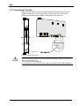
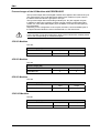
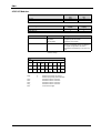
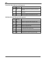
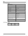
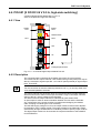
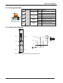
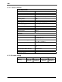
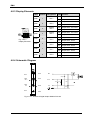
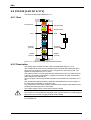
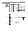
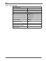
1
Electromechanical Automation North
America
Parker I/O-System
PROFIBUS DP ECO + I/O-Modules
PIO-343
Manual
Technical description,
installation and configuration
We reserve the right to make technical changes
The data contained in this manual correspond to the current status at the time of printing.
88-022349-01 October 2003
PIO Parker I/O-System
ii
88-022349-01A October 2003
AllgemeinesError! S
Copyright © 2003 Parker Hannifin GmbH EME
All rights reserved.
Microsoft Word, Microsoft Office, Windows®, Window 95™, Window 98™,
Windows NT®, Window 2000™, Window XP™ and MS-DOS™ are trademarks of
Microsoft Corporation.
EME - Electromechanical Automation Europe
Germany: Parker Hannifin GmbH
Electromechanical Automation
Postfach: 77607-1720
Robert-Bosch-Str. 22
D-77656 Offenburg
Tel.: +49 (0)781 509-0
Fax: +49 (0)781 509-176
E-mail: [email protected] mailto:[email protected]
Internet: www.parker-eme.com http://www.parker-eme.com
England: Parker Hannifin plc
Electromechanical Automation
21 Balena Close
Poole, Dorset England, BH17 /DX UK
Tel.: +44 (0)1202 69 9000
Fax: +44 (0)1202 69 5750
E-mail: [email protected] mailto:[email protected]
Internet: www.parker-eme.com http://www.parker-eme.com
Italy: Parker Hannifin S. p. A
Electromechanical Automation
Via Gounod 1
I-20092 Cinisello Balsamo (MI), Italy
Tel.: +39 (0)2660 12459
Fax: +39 (0)2660 12808
E-mail: [email protected] mailto:[email protected]
Internet: www.parker-eme.com http://www.parker-eme.com
EMN - Electromechanical Automation North America
USA: Parker Hannifin Corporation
Electromechanical Automation
5500 Business Park Drive
Rohnert Park, CA 94928
Phone #: (800) 358-9068
FAX #: (707) 584-3715
E-mail: [email protected] mailto:[email protected]
Internet: www.compumotor.com http://www.compumotor.com
88-022349-01A October 2003
iii
PIO Parker I/O-System
TABLE OF CONTENTS
1 Important comments ............................................................................................ 5
1.1
Legal principles ................................................................................................ 5
1.2
Symbols ........................................................................................................... 6
1.3
Font Conventions............................................................................................. 6
1.4
Number Notation .............................................................................................. 6
1.5
Safety Notes..................................................................................................... 7
1.6
Scope ............................................................................................................... 8
1.7
Abbreviation ..................................................................................................... 8
2 I/O-SYSTEM ........................................................................................................... 9
2.1
I/O-System Description .................................................................................... 9
2.2
Technical Data ............................................................................................... 10
2.3
Manufacturing Number .................................................................................. 14
2.4
Storage, Assembly and Transport ................................................................. 14
2.5
Mechanical Setup........................................................................................... 15
2.6
Power Supply ................................................................................................. 21
2.7
Grounding ...................................................................................................... 25
2.8
Shielding (Screening)..................................................................................... 28
2.9
Assembly Guidelines / Standards .................................................................. 28
3 Fieldbus Coupler ................................................................................................ 29
3.1
Fieldbus ECO-Coupler................................................................................... 29
4 I/O Modules ......................................................................................................... 70
4.1
PIO-400 [2 DI DC 24 V 3.0 ms, high-side switching] ..................................... 70
4.2
PIO-402 [4 DI DC 24 V 3.0 ms, high-side switching] ..................................... 73
4.3
PIO-430 [8 DI DC 24 V 3.0 ms, high-side switching] ..................................... 76
4.4
PIO-468 [4 AI DC 0-10 V, Single-Ended]....................................................... 79
4.5
PIO-480 [2 AI 0-20 mA Differential Measurement Input] ............................... 83
4.6
PIO-501 [2 DO DC 24 V 0.5 A, high-side switching]...................................... 87
4.7
PIO-504 [4 DO DC 24 V 0.5 A, high-side switching]...................................... 90
4.8
PIO-530 [8 DO DC 24 V 0.5 A, high-side switching]...................................... 93
4.9
PIO-550 [2 AO DC 0-10 V]............................................................................. 96
4.10
PIO-552 [2 AO 0-20 mA]................................................................................ 99
4.11
PIO-600 [End Module] ................................................................................. 103
4.12
PIO-602 [24 V DC Power Supply]................................................................ 104
5 PROFIBUS ......................................................................................................... 107
5.1
Description ................................................................................................... 107
5.2
Wiring ........................................................................................................... 108
6 Use in Hazardous Environments .................................................................... 110
6.1
Foreword ...................................................................................................... 110
6.2
Protective measures .................................................................................... 110
6.3
Classification meeting CENELEC and IEC.................................................. 110
6.4
Classifications meeting the NEC 500 .......................................................... 113
6.5
Identification ................................................................................................. 115
6.6
Installation regulations ................................................................................. 117
4
7
Glossary ............................................................................................................ 118
8
Literature list ..................................................................................................... 119
9
Index .................................................................................................................. 120
88-022349-01A October 2003
EMN
88-022349-01A October 2003
5
PIO Parker I/O-System
1 Important comments
To ensure fast installation and start-up of the units described in this manual, we
strongly recommend that the following information and explanation is carefully read
and adhered to.
1.1 Legal principles
1.1.1 Copyright
This manual is copyrighted, together with all figures and illustrations contained
therein. Any use of this manual which infringes the copyright provisions stipulated
herein, is not permitted. Reproduction, translation and electronic and photo-technical
archiving and amendments require the written consent. Non-observance will entail
the right of claims for damages.
1.1.2 Personnel qualification
The use of the product detailed in this manual is exclusively geared to specialists
having qualifications in PLC programming, electrical specialists or persons instructed
by electrical specialists who are also familiar with the valid standards. The
manufacturer declines all liability resulting from improper action and damage to
products and third party products due to non-observance of the information contained
in this manual.
1.1.3 Intended use
For each individual application, the components supplied are to work with a dedicated
hardware and software configuration. Modifications are only admitted within the
framework of the possibilities documented in the manuals. All other changes to the
hardware and/or software and the non-conforming use of the components entail the
exclusion of liability.
6
88-022349-01A October 2003
EMN
1.2 Symbols
Danger
Always abide by this information to protect persons from injury.
Warning
Always abide by this information to prevent damage to the device.
Attention
Marginal conditions must always be observed to ensure smooth operation.
ESD (Electrostatic Discharge)
Warning of damage to the components by electrostatic discharge. Observe the
precautionary measure for handling components at risk.
Note
Routines or advice for efficient use of the device and software optimization.
More information
References on additional literature, manuals, data sheets and INTERNET pages
1.3 Font Conventions
Italic
Names of path and files are marked italic
i.e.:
C:\programs\
Italic
Menu items are marked as bold italic
i.e.:
Save
\
A backslash between two names marks a sequence of menu
items
i.e.:
File\New
END
Press buttons are marked as bold with small capitals
i.e.:
ENTER
<>
Keys are marked bold within angle brackets
i.e.:
<F5>
Courier
Program code is printed with the font Courier.
i.e.:
END_VAR
1.4 Number Notation
Number Code
Example
Note
Decimal
100
normal notation
Hexadecimal
0x64
C notation
Binary
'100'
'0110.0100'
Within ',
Nibble separated with dots
88-022349-01A October 2003
7
PIO Parker I/O-System
1.5 Safety Notes
Attention
Switch off the I/O-System prior to working on bus modules!
In the event of deformed contacts, the module in question is to be replaced, as its
functionality can no longer be ensured on a long-term basis.
The components are not resistant against materials having seeping and insulating
properties. Belonging to this group of materials is: e.g. aerosols, silicones,
triglycerides (found in some hand creams).
If it cannot be ruled out that these materials appear in the component environment,
then additional measures are to be taken:
- installation of the components into an appropriate enclosure
- handling of the components only with clean tools and materials.
Attention
Cleaning of soiled contacts may only be done with ethyl alcohol and leather cloths.
Thereby, the ESD information is to be regarded.
Do not use any contact spray. The spray may impair the functioning of the contact
area.
The I/O-SYSTEM and its components are an open system. It must only be
assembled in housings, cabinets or in electrical operation rooms. Access must only
be given via a key or tool to authorized qualified personnel.
The relevant valid and applicable standards and guidelines concerning the
installation of switch boxes are to be observed.
ESD (Electrostatic Discharge)
The modules are equipped with electronic components that may be destroyed by
electrostatic discharge. When handling the modules, ensure that the environment
(persons, workplace and packing) is well grounded. Avoid touching conductive
components, e.g. gold contacts.
8
88-022349-01A October 2003
EMN
1.6 Scope
This manual describes the field bus independent I/O-SYSTEM with the Fieldbus
Coupler for PROFIBUS.
Components
ECO-coupler PROFIBUS 12 MBd
1.7 Abbreviation
AO
Analog Output Module
AI
Analog Input Module
DI
Digital Input
DO
Digital Output
I/O
input/output
ID
Identifier
PI
Process Images
PLC
Programmable Logic Control
RTS
Running Time System
SM
Special Module
88-022349-01A October 2003
9
PIO Parker I/O-System
2 I/O-SYSTEM
2.1 I/O-System Description
The I/O-SYSTEM is a modular, fieldbus independent I/O system. The structure
described here consists of an ECO fieldbus coupler (1) and up to 64 connected
fieldbus modules (2) for any kind of signal. Together, these make up the fieldbus
node. The end module (3) completes the node.
DE DE
DE DE
E1
E2
E3
E4
+
+
+
+
AE AE
+
+
E5
E6
+
+
+
+
DA DA
DA DA
DA DA
DA DA
AA AA
AE AE
A1
A2
A3
A4
A5
A6
A7
A8
A9
A10
E7
E8
+
+
+
+
+
+
+
+
+
+
+
+
+
+
AA AA
A11 A12 E9
+
+
DA DA
AE AE
+
E10
+
A13 A14
+
+
+
+
PIO-400 PIO-400 PIO-602 PIO-XXX PIO-602 PIO-501 PIO-501 PIO-501 PIO-501 PIO-602 PIO-XXX PIO-XXX PIO-XXX PIO-XXX PIO-602 PIO-501 PIO-600
2
1
3
Fig. 2-1: Fieldbus node
ECO couplers for fieldbus systems such as PROFIBUS DP, CANopen and DeviceNet
are available.
The ECO coupler contains the fieldbus interface, electronics and a power supply
terminal. The fieldbus interface forms the physical interface to the relevant fieldbus.
The electronics process the data of the bus modules and make it available for the
fieldbus communication. The 24 V system supply are fed in via the integrated power
supply terminal.
The fieldbus coupler communicates via the relevant fieldbus.
At first the ECO coupler is concepted for applications with digital I/O functions. Bus
modules for diverse digital and analog I/O functions and special functions can be
connected as well. The communication between the ECO coupler and the bus
modules is carried out via an internal bus.
The I/O-SYSTEM has a clear port level with LEDs the status indication, insertable
mini WSB markers and pullout group marker carriers. The 3-wire technology
supplemented by a ground wire connection allows for direct sensor/actuator wiring.
10
88-022349-01A October 2003
EMN
2.2 Technical Data
Mechanic
Material
Polycarbonate, Polyamide 6.6
Dimensions Coupler
50 mm x 65* mm x 97 mm
Dimensions I/O module, single
12 mm x 64* mm x 100 mm
Dimensions I/O module, double
24 mm x 64* mm x 100 mm
Installation
on DIN 35 with interlock
modular by
double featherkey-dovetail
Mounting position
any position
Length of entire node
≤ 831 mm
Marking
marking label type 247 and 248
paper marking label 8 x 47 mm
Wire range
CAGE CLAMP® Connection
0,08 mm² ... 2,5 mm²
AWG 28-14
8 – 9 mm Stripped length
Wire range
Contacts
Power jumpers contacts
blade/spring contact
self-cleaning
Current via power contacts max
10 A
Voltage drop at Imax
< 1 V/64 modules
Data contacts
slide contact, hard gold plated
1,5µ, self-cleaning
Climatic environmental conditions
Operating temperature
0 °C ... 55 °C
Storage temperature
-20 °C ... +85 °C
Relative humidity
95 % without condensation
Resistance to harmful
substances
acc. to IEC 60068-2-42 and IEC 60068-2-43
Special conditions
Ensure that additional measures for
components are taken, which are used in an
environment involving:
– dust, caustic vapors or gasses
– ionization radiation.
Mechanical strength
Vibration resistance
acc. to IEC 60068-2-6
Shock resistance
acc. to IEC 60068-2-27
Free fall
acc. to IEC 60068-2-32
≤ 1m (module in original packing)
* from upper edge of DIN 35 rail
88-022349-01A October 2003
11
PIO Parker I/O-System
Safe electrical isolation
Air and creepage distance
acc. to IEC 60664-1
Degree of protection
Degree of protection
IP 20
Electromagnetic compatibility*
Directive
Test values
Strength
class
Evaluation
criteria
Immunity to interference acc. to EN 50082-2 (96)
EN 61000-4-2
4kV/8kV
EN 61000-4-3
10V/m 80% AM
EN 61000-4-4
2kV
EN 61000-4-6
10V/m 80% AM
Emission of interference acc. to EN 50081-2 (94)
EN 55011
30 dBµV/m
(2/4)
B
(3)
A
(3/4)
B
(3)
A
Measuring
distance
Class
(30m)
A
37 dBµV/m
Emission of interference acc. to EN 50081-1 (93)
EN 55022
30 dBµV/m
Measuring
distance
Class
(10m)
B
37 dBµV/m
Range of
application
Required specification
emission of interference
Required specification
immunity to interference
Industrial areas
EN 50081-2 : 1993
EN 50082-2 : 1996
Residential areas
*)
EN 50081-1 : 1993
EN 50082-1 : 1992
*) The I/O-System meets the requirements on emission of interference in residential
areas with the fieldbus coupler for:
CANopen PIO-337
DeviceNet PIO-306
With a special permit, the I/O-System can also be implemented with other
fieldbus couplers in residential areas (housing, commercial and business areas,
small-scale enterprises). The special permit can be obtained from an authority or
inspection office. In Germany, the Federal Office for Post and
Telecommunications and its branch offices issues the permit.
It is possible to use other field bus couplers under certain boundary conditions.
Please contact the manufacturer.
12
88-022349-01A October 2003
EMN
Maximum power dissipation of the components
Bus modules
0,8 W / bus terminal (total power dissipation,
system/field)
ECO Fieldbus coupler
2,0 W / coupler
Warning
The power dissipation of all installed components must not exceed the maximum
conductible power of the housing (cabinet).
When dimensioning the housing, care is to be taken that even under high external
temperatures, the temperature inside the housing does not exceed the permissible
ambient temperature of 55 °C.
88-022349-01A October 2003
13
PIO Parker I/O-System
Dimensions
Dimensions in mm
Side view
Fig. 2-2: Dimensions
14
88-022349-01A October 2003
EMN
2.3 Manufacturing Number
The manufacturing number is part of the lateral marking on the component.
PIO
Manufacturing Number
Calendar
week
Year
Software
version
Hardware
version
Fig. 2-3: Manufacturing Number
The manufacturing number consists of the production week and year, the software
version (if available), the hardware version of the component, the firmware loader (if
available) and further internal information for the
manufacturer.
The production number is also printed on the cover of the configuration and
programming interface of the fieldbus coupler.
2.4 Storage, Assembly and Transport
Wherever possible, the components are to be stored in their original packaging.
Likewise, the original packaging provides optimal protection during transport.
When assembling or repacking the components, the contacts must not be soiled or
damaged. The components must be stored and transported in appropriate
containers/packaging. Thereby, the ESD information is to be regarded.
Statically shielded transport bags with metal coatings are to be used for the transport
of open components for which soiling with amine, amide and silicone has been ruled
out, e.g. 3M 1900E.
88-022349-01A October 2003
15
PIO Parker I/O-System
2.5 Mechanical Setup
2.5.1 Installation Position
Along with horizontal and vertical installation, all other installation positions are
allowed.
Attention
In the case of vertical assembly, an end stop has to be mounted as an additional
safeguard against slipping.
2.5.2 Total Expansion
The maximum total expansion of a node is calculated as follows:
Quantity
Width
Components
1
50 mm
ECO coupler
64
12 mm
bus modules
- inputs / outputs
– power supply modules
- etc.
1
12 mm
end module
sum
830 mm
Warning
The maximal total expansion of a node must not exceed 830 mm.
16
88-022349-01A October 2003
EMN
2.5.3 Assembly onto Carrier Rail
Carrier Rail Properties
All I/O-System components can be snapped directly onto a carrier rail in accordance
with the European standard EN 50022 (DIN 35).
Carrier rails have different mechanical and electrical properties. For the optimal I/OSystem setup on a carrier rail, certain guidelines must be observed:
•
The material must be non-corrosive.
•
Most components have a contact to the carrier rail to ground electro-magnetic
disturbances. In order to avoid corrosion, this tin-plated carrier rail contact must
not form a galvanic cell with the material of the carrier rail which generates a
differential voltage above 0.5 V (saline solution of 0.3% at 20°C) .
•
The carrier rail must optimally support the EMC measures integrated into the I/OSystem and the shielding of the bus module connections.
•
A sufficiently stable carrier rail should be selected and, if necessary, several
mounting points (every 20 cm) should be used in order to prevent bending and
twisting (torsion).
•
The geometry of the carrier rail must not be altered in order to secure the safe
hold of the components. In particular, when shortening or mounting the carrier
rail, it must not be crushed or bent..
•
The base of the I/O components extends into the profile of the carrier rail. For
carrier rails with a height of 7.5 mm, mounting points are to be riveted under the
node in the carrier rail (slotted head captive screws or blind rivets).
2.5.4 Spacing
The spacing between adjacent components, cable conduits, casing and frame sides
must be maintained for the complete field bus node.
Fig. 2-4: Spacing
The spacing creates room for heat transfer, installation or wiring. The spacing to
cable conduits also prevents conducted electromagnetic interferences from
influencing the operation.
88-022349-01A October 2003
17
PIO Parker I/O-System
2.5.5 Plugging and Removal of the Components
Warning
Before work is done on the components, the voltage supply must be turned off.
In order to safeguard the ECO coupler from jamming, it should be fixed onto the
carrier rail with the locking disc To do so, push on the upper groove of the locking
disc using a screwdriver.
To pull out the fieldbus coupler, release the locking disc by pressing on the bottom
groove with a screwdriver and then pulling the orange colored unlocking lug.
locking disc
fix
loosen
Release lug
Fig. 2-5: Coupler and unlocking lug
It is also possible to release an individual I/O module from the unit by pulling an
unlocking lug.
Fig. 2-6: removing bus terminal
Danger
Ensure that an interruption of the PE will not result in a condition which could
endanger a person or equipment!
For planning the ring feeding of the ground wire, please see chapter "Grounding
Protection“
18
88-022349-01A October 2003
EMN
2.5.6 Assembly Sequence
All I/O-System components can be snapped directly on a carrier rail in accordance
with the European standard EN 50022 (DIN 35).
The reliable positioning and connection is made using a tongue and groove system.
Due to the automatic locking, the individual components are securely seated on the
rail after installing.
Starting with the ECO coupler, the bus modules are assembled adjacent to each
other according to the project planning. Errors in the planning of the node in terms of
the potential groups (connection via the power contacts) are recognized, as the bus
modules with power contacts (male contacts) cannot be linked to bus modules with
fewer power contacts.
Attention
Always link the bus modules with the ECO coupler, and always plug from above.
Warning
Never plug bus modules from the direction of the end terminal. A ground wire power
contact, which is inserted into a terminal without contacts, e.g. a 4-channel digital
input module, has a decreased air and creepage distance to the neighboring
contact.
Always terminate the fieldbus node with an end module.
2.5.7 Internal Bus / Data Contacts
Communication between the ECO coupler and the bus modules as well as the I/OSystem supply of the bus modules is carried out via the internal bus. It is comprised
of 6 data contacts, which are available as self-cleaning gold spring contacts.
Fig. 2-7: Data contacts
Warning
Do not touch the gold spring contacts on the I/O Modules in order to avoid soiling or
scratching!
ESD (Electrostatic Discharge)
The modules are equipped with electronic components that may be destroyed by
electrostatic discharge. When handling the modules, ensure that the environment
(persons, workplace and packing) is well grounded. Avoid touching conductive
components, e.g. gold contacts.
88-022349-01A October 2003
19
PIO Parker I/O-System
2.5.8 Power Contacts
Self-cleaning power contacts , are situated on the side of the components which
further conduct the supply voltage for the field side. These contacts come as
touchproof spring contacts on the right side of the coupler and the bus module. As
fitting counterparts the module has male contacts on the left side.
Danger
The power contacts are sharp-edged. Handle the module carefully to prevent injury.
Attention
Please take into consideration that some bus modules have no or only a few power
jumper contacts. The design of some modules does not allow them to be physically
assembled in rows, as the grooves for the male contacts are closed at the top.
Fig. 2-8: Example for the arrangement of power contacts
20
88-022349-01A October 2003
EMN
2.5.9 Wire Connection
All components have CAGE CLAMP® connections.
The CAGE CLAMP® connection is appropriate for solid, stranded and fine–stranded
conductors. Each clamping unit accommodates one conductor.
Fig. 2-9: CAGE CLAMP® Connection
The operating tool is inserted into the opening above the connection. This opens the
CAGE CLAMP®. Subsequently the conductor can be inserted into the opening. After
removing the operating tool, the conductor is safely clamped.
More than one conductor per connection is not permissible. If several conductors
have to be made at one connection point, then they should be made away from the
connection point using Terminal Blocks. The terminal blocks may be jumpered
together and a single wire brought back to the I/Omodule connection point.
Attention
If it is unavoidable to jointly connect 2 conductors, then a ferrule must be used to join
the wires together.
Ferrule:
Length
8 mm
1 mm2 for 2 conductors with 0.5 mm2 each
Nominal cross sectionmax.
88-022349-01A October 2003
21
PIO Parker I/O-System
2.6 Power Supply
2.6.1 Isolation
Within the fieldbus node, there are three electrically isolated potentials.
•
Operational voltage for the fieldbus interface.
•
Electronics of the couplers and the bus modules (internal bus).
•
All bus modules have an electrical isolation between the electronics (internal bus,
logic) and the field electronics. Some analog input modules have each channel
electrically isolated, please see catalog.
Potential of the system supply
Electrical isolation
to the field level
per module
per channel
Potential
Fieldbus interface
Potentials
in the field level
Fig. 2-10: Isolation
Attention
The ground wire connection must be present in each group. In order that all
protective conductor functions are maintained under all circumstances, it is
recommended that a ground wire be connected at the beginning and end of a
potential group. (ring format, please see chapter Grounding Protection"). Thus, if a
bus module comes loose from the node during servicing, then the protective
conductor connection is still guaranteed for all connected field devices.
When using a joint power supply unit for the 24 V system supply and the 24 V field
supply, the electrical isolation between the internal bus and the field level is
eliminated for the potential group.
22
88-022349-01A October 2003
EMN
2.6.2 System Supply
Connection
The I/O-SYSTEM requires a 24 V direct current system supply (-15% or +20 %).
The power supply is provided via the coupler. The voltage supply is reverse voltage
protected.
system-supply
Fig. 2-11: System Supply
The direct current supplies all internal I/O-System components, e.g. ECO coupler
electronics, fieldbus interface and bus modules via the internal bus (5 V system
voltage). The 5 V system voltage is electrically connected to the 24 V system supply.
Alignment
Recommendation
A stable network supply cannot be taken for granted always and everywhere.
Therefore, regulated power supply units should be used in order to guarantee the
quality of the supply voltage.
The supply capacity of the ECO coupler can be taken from the technical data of the
components.
Internal current consumption *)
Current consumption via system voltage:
5 V for electronics of the bus modules and ECO
coupler
Residual current for bus
terminals *)
Available current for the bus modules. See
technical data ECO coupler.
88-022349-01A October 2003
23
PIO Parker I/O-System
Example
ECO coupler:
internal current consumption : 350 mA at 5V
residual current for bus modules : 650 mA at 5V
sum I(5V) total : 1000 mA at 5V
The internal current consumption is indicated in the technical data for each bus
terminal. In order to determine the overall requirement, add together the values of all
bus modules in the node.
A node with a PROFIBUS ECO Coupler consists of 16
digital output modules (PIO-530) and 14 digital input
modules (PIO-430).
Example:
Current consumption:
16*25 mA = 400 mA
14*17 mA = 238 mA
Sum : 638 mA
The coupler can provide 638 mA (max. 650 mA) for the
bus modules.
The maximum input current of the 24 V system supply is 260 mA. The exact electrical
consumption (I(24 V)) can be determined with the following formulas:
ECO Coupler
I(5 V) total. =
Sum of all the internal current consumption of the
connected bus modules
+ internal current consumption of the ECO coupler
I(5 V) total. =
Sum of all the internal current consumptions of the
connected bus modules
Input current m I(24 V) =
5 V / 24 V * I(5 V) total. / η
η = 0.80 (at nominal load)
Note
If the electrical consumption of the power supply point for the 24 V-system supply
exceeds 260 mA for the ECO coupler, then the cause may be an improperly aligned
node or a defect.
During the test, all outputs must be active.
24
88-022349-01A October 2003
EMN
2.6.3 Field Supply
Connection
Sensors and actuators can be directly connected to the relevant channel of the bus
module in 1-/4 conductor connection technology. The bus module supplies power to
the sensors and actuators. The input and output drivers of some bus modules require
the field side supply voltage.
Power supply modules provides field side power. The connections are linked in pairs
with a power contact.
Field supply
Protective
conductor
PIO
PIO
Power jumper
contacts
Potential distribution to
adjacent I/O modules
Fig. 2-12: Field Supply (Sensor / Actuator)
The supply voltage for the field side is automatically passed to the next module via
the power jumper contacts when assembling the bus modules .
The current load of the power contacts must not exceed 10 A on a continual basis.
The current load capacity between two connection terminals is identical to the load
capacity of the connection wires.
By inserting an additional power supply module, the field supply via the power
contacts is disrupted. From there a new power supply occurs which may also contain
a new voltage potential.
Attention
Some bus modules have no or very few power contacts (depending on the I/O
function). Due to this, the passing through of the relevant potential is disrupted. If a
field supply is required for subsequent bus modules, then a power supply module
must be used.
Note the data sheets of the bus modules.
88-022349-01A October 2003
25
PIO Parker I/O-System
2.6.4 Power Supply Unit
The I/O-SYSTEM requires a 24 V direct current system supply with a maximum
deviation of -15% or +20 %.
Recommendation
A stable network supply cannot be taken for granted always and everywhere.
Therefore, regulated power supply units should be used in order to guarantee the
quality of the supply voltage.
A buffer (200 µF per 1 A current load) should be provided for brief voltage dips. The
I/O system buffers for approx. 1 ms.
The electrical requirement for the field supply is to be determined individually for each
power supply point. Thereby all loads through the field devices and bus modules
should be considered. The field supply as well influences the bus modules, as the
inputs and outputs of some bus modules require the voltage of the field supply.
Note
The system supply and the field supply should be isolated in order to ensure bus
operation in the event of short circuits on the actuator side.
2.7 Grounding
2.7.1 Grounding the DIN Rail
Framework Assembly
When setting up the framework, the carrier rail must be screwed together with the
electrically conducting cabinet or housing frame. The framework or the housing must
be grounded. The electronic connection is established via the screw. Thus, the carrier
rail is grounded.
Attention
Care must be taken to ensure the flawless electrical connection between the carrier
rail and the frame or housing in order to guarantee sufficient grounding.
Insulated Assembly
Insulated assembly has been achieved when there is constructively no direct
conduction connection between the cabinet frame or machine parts and the carrier
rail. Here the earth must be set up via an electrical conductor.
The connected grounding conductor should have a cross section of at least 4 mm2.
Recommendation
The optimal insulated setup is a metallic assembly plate with grounding connection
with an electrical conductive link with the carrier rail.
26
88-022349-01A October 2003
EMN
2.7.2 Grounding Function
The grounding function increases the resistance against disturbances from electromagnetic interferences. Some components in the I/O system have a carrier rail
contact that dissipates electro-magnetic disturbances to the carrier rail.
PIO
Fig. 2-13: Carrier rail contact
Attention
Care must be taken to ensure the direct electrical connection between the carrier rail
contact and the carrier rail.
The carrier rail must be grounded.
For information on carrier rail properties, please see chapter "Carrier Rail Properties".
88-022349-01A October 2003
27
PIO Parker I/O-System
2.7.3 Grounding Protection
For the field side, the ground wire is connected to the lowest connection terminals of
the power supply module. The ground connection is then connected to the next
module via the Power Jumper Contact (PJC). If the bus module has the lower power
jumper contact, then the ground wire connection of the field devices can be directly
connected to the lower connection terminals of the bus module.
Attention
Should the ground conductor connection of the power jumper contacts within the
node become disrupted, e.g. due to a 4-channel bus terminal, the ground connection
will need to be re-established.
The ring feeding of the grounding potential will increase the I/O-System safety. When
one bus module is removed from the group, the grounding connection will remain
intact.
The ring feeding method has the grounding conductor connected to the beginning
and end of each potential group.
Fig. 2-14: Ring-feeding
28
88-022349-01A October 2003
EMN
2.8 Shielding (Screening)
2.8.1 General
The shielding of the data and signal conductors reduces electromagnetic interference
thereby increasing the signal quality. Measurement errors, data transmission errors
and even disturbances caused by overvoltage can be avoided.
Attention
Constant shielding is absolutely required in order to ensure the technical
specifications in terms of the measurement accuracy.
The data and signal conductors should be separated from all high-voltage cables.
The cable shield should be potential. With this, incoming disturbances can be easily
diverted.
The shielding should be placed over the entrance of the cabinet or housing in order
to already repel disturbances at the entrance.
2.8.2 Bus Conductors
The shielding of the bus conductor is described in the relevant assembly guideline of
the bus system.
2.8.3 Signal Conductors
Bus modules for most analog signals along with many of the interface bus modules
include a connection for the shield.
2.9 Assembly Guidelines / Standards
DIN 60204,
Electrical equipping of machines
DIN EN 50178
Equipping of high-voltage systems with electronic
components (replacement for VDE 0160)
EN 60439
Low voltage – switch box combinatio
88-022349-01A October 2003
29
PIO Parker I/O-System
3 Fieldbus Coupler
3.1 Fieldbus ECO-Coupler
This chapter includes:
3.1.1
3.1.2
3.1.3
3.1.4
3.1.5
3.1.6
3.1.7
3.1.8
3.1.9
3.1.10
3.1.11
3.1.12
30
Description..................................................................................................... 30
Hardware ....................................................................................................... 31
Operating System.......................................................................................... 34
Process Image............................................................................................... 35
Configuration ................................................................................................. 39
Configuring the Coupler ................................................................................ 43
Configuring the Process Data Channel ......................................................... 45
Configuration of I/O Modules......................................................................... 46
Diagnostics .................................................................................................... 55
LED Signaling................................................................................................ 62
Fault Behavior ............................................................................................... 68
Technical Data............................................................................................... 69
88-022349-01A October 2003
EMN
3.1.1 Description
The Fieldbus Coupler maps the peripheral data of all I/O modules in the I/O-SYSTEM
on PROFIBUS DP.
In the initialization phase, the Fieldbus Coupler determines the physical structure of
the node and creates a process image with all inputs and outputs. I/O modules with a
bit width smaller than 8 can be combined to form one byte in order to optimize the
address space.
In addition the possibility exists to deactivate projected I/O modules. In this manner
the physical structure of the node can be individually designed with regard to the
peripheral signals, without undertaking any changes to an already existing control
application. This is done by correspondingly configuring the modules with the aid of
the software configuration tool (for instance, COM PROFIBUS, STEP7, ProfiMap,
etc.)
The diagnostics feature is based on an identification and channel based diagnostics
in accordance with EN 50170 (PROFIBUS). Thus it is not necessary to program
modules for the evaluation of manufacturer specific diagnostics information.
•
Process data length
Max. 32 byte input process image
Max. 32 byte output process image
•
Automatic recognition of transmission speed on the PROFIBUS from 9.6 kBd to
12 MBd
•
All I/O modules from theI/O-SYSTEM are supported
•
Process image can accept virtual placeholders for future expansion
•
Configurable substitute value for each channel
•
D-Sub 9 pole bus connection
88-022349-01A October 2003
31
PIO Parker I/O-System
3.1.2 Hardware
View
PROFIBUS
RUN
DIP switch
Address
Status indication
-Fieldbus
-Fieldbus node
BF
DIA
Data contacts
BUS
I/O
01 02 03 04
Marking area
Fieldbus
connection
D-Sub
Supply
24V
0V
Configuration
interface
Fig. 3-1: Fieldbus ECO-Coupler PROFIBUS DP
The Fieldbus Coupler comprises of:
32
•
Supply module with internal system supply module for the system supply.
•
Fieldbus interface with the bus connection
•
DIP switch for the node address (binary)
•
Display elements (LED's) for status display of the operation, the bus
communication, the operating voltages as well as for fault messages and
diagnostics
•
Configuration Interface
•
Electronics for communication with the I/O modules (internal bus) and the fieldbus
interface
88-022349-01A October 2003
EMN
Device Supply
The supply is made via terminal bocks with CAGE CLAMP® connection. The device
supply is intended both for the I/O-System and the field units.
I/OModules
24V
1/2
24V
5V
10nF
3/4
0V
5V
Fieldbus
Interface
10nF
24V
1
0V
2
3
4
PIO-343
Fig. 3-2: Device supply
The integrated internal system supply module generates the necessary voltage to
supply the electronics and the connected I/O modules.
The fieldbus interface is supplied with electrically isolated voltage from the internal
system supply module.
Fieldbus Connection
The PROFIBUS interface is designed as a D-Sub connection in accordance with the
US Standard EIA RS 485 for cable linked data transmission.
Fig. 3-3: Bus connection, D-Sub female connector
Pin
Signal
Description
3
RxD(TxD)-P
Transmit (receive) signal
4
RTS
Ready To Send
5
GND
Supply ground (earth)
6
Vcc
Voltage supply
8
RxD(TxD) N
Transmit (receive) signal
The electrical isolation between the fieldbus system and the electronics is achieved
by means of DC/DC converters and optocouplers located in the fieldbus interface.
The fieldbus connection point is designed to permit the node to fit into an 80 mm high
switch box once connected.
88-022349-01A October 2003
33
PIO Parker I/O-System
Display Elements
The operating condition of the Fieldbus Coupler or node is signaled via light diodes
(LED).
Fig. 3-4: Display elements PIO-343
LED
Color
Meaning
RUN
green
The RUN-LED indicates to the operator if the Fieldbus
Coupler is correctly initialized.
BF
red
The BF-LED indicates whether the communication functions
via the PROFIBUS.
DIA
red
The DIA-LED indicates external diagnostics. The signaling
is not supported by all devices.
BUS
red
The BUS-LED signals a projecting fault.
IO
red / green The I/O-LED indicates the operation of the node and signals
/ orange
faults encountered.
Node Address
The node address (decimal) is determined using two rotary switches on the electronic
module.
Fig. 3-5: Setting the node address
The binary significance of the individual DIP switches increases according to the
switch number, i.e. the module ID 1 is set by DIP1 = ON, the module ID 8 by
DIP4 = ON, etc.
The binary value (20–27) of the dip switches increases from switch 1 to switch 8, a
logic 1 being represented by “ON“.
Address
DIP8 DIP7 DIP6 DIP5 DIP4 DIP3 DIP2 DIP1
0
-
OFF
OFF
OFF
OFF
OFF
OFF
OFF
-
OFF
OFF
OFF
OFF
OFF
OFF
ON
-
OFF
OFF
OFF
OFF
OFF
ON
OFF
-
ON
ON
ON
ON
ON
ON
ON
1
*)
2
:
127
*)
default setting
Node addresses between 0 and 127 can be set.
34
88-022349-01A October 2003
EMN
If an invalid address is set, the coupler adopts the address that has been assigned
via Set_Slave_Address. This address is stored in the power fail safe EEPROM. The
default address is 126.
The node address is saved in the Fieldbus Coupler after switching on the device
(initialization phase). Adjustments of the switch have no effect during operation.
Configuration Interface
The configuration interface used for the communication or for firmware upload is
located behind the cover flap.
open
flap
Configuration
interface
Fig. 3-6: Configuration interface
3.1.3 Operating System
Once the node is configured in the software, the node address is set and the node is
wired properly, the power can be applied.
After switching on the supply voltage, the coupler performs a self-test of all of the
device functions, the I/O module and the fieldbus interface. If the power supply is
working correctly the I/O-LED is green. Following this the I/O modules and the
present configuration is determined, whereby an internal list is generated. This list
includes an input and an output area on which is represented the fieldbus RAM of the
protocol chip.
In the event of a fault the Coupler changes to the "Stop" condition. The I/O-LED
flashes red. After a fault free start up the Coupler changes to the "Fieldbus start"
status.
Fig. 3-7: Operating system PIO-343
88-022349-01A October 2003
35
PIO Parker I/O-System
3.1.4 Process Image
Local Process Image
After switching on, the Coupler recognizes all I/O modules plugged into the node
which supply or wait for data (data width/bit width > 0). Both analog and digital I/O
modules can be used in the same node.
Note
For the number of input and output bits or bytes of the individual I/O module please
refer to the corresponding I/O module description.
The Coupler produces an internal process image from the data width and the type of
I/O module as well as the position of the I/O modules in the node. It is divided into an
input and an output data area.
Allocation of the Input and Output Data
The process data is exchanged via the PROFIBUS master. A maximum of 32 bytes
of data is transmitted from the master to the Coupler or from the node to the output
data. The Coupler responds by returning a maximum of 32 bytes input data to the
master.
Modules are configured according to their position in the node. The information
covering the possible modules is contained in the GSD files.
Fig. 3-8: Allocation of the input and output data
36
88-022349-01A October 2003
EMN
Process Images of the I/O-Modules with PROFIBUS-DP
The input and output data of the digital modules are mapped to the Profibus bit by bit.
The configuration of the node determines whether each module occupies a byte or
the data of several modules is grouped in one byte.
The input and output data of the analog modules (D0...Dn) are mapped via bytes.
In addition to data bytes, specialty modules (counter modules, pulse width output
module, etc.) also send Status Bytes (S) to the Master or receive Control Bytes (C)
from the Master.
Depending on the configuration of the coupler, the status, control and data bytes of
the byte-oriented modules are sent in the Motorola or in the Intel format.
Note
For the number of input and output bits or bytes of the individual I/O modules please
refer to the corresponding I/O module description.
2 DI I/O-Modules
PIO-400,
Process Image [bit]
PROFIBUS-DP
Input
Output
2
0
Input
Output
4
0
Input
Output
8
0
4 DI I/O-Modules
PIO-402
Process Image [bit]
PROFIBUS-DP
8 DI I/O-Modules
PIO-430
Process Image [bit]
PROFIBUS-DP
2 DO I/O-Modules
PIO-501
Process Image [bit]
PROFIBUS-DP
Input
Output
0
2
88-022349-01A October 2003
37
PIO Parker I/O-System
4 DO I/O-Modules
PIO-504
Process Image [bit]
Input
Output
0
4
Input
Output
0
8
PROFIBUS-DP
8 DO I/O-Modules
PIO-530
Process Image [bit]
PROFIBUS-DP
2 AI I/O-Modules
PIO-480
Process Image [byte]
Input
Output
4
0
PROFIBUS-DP
PROFIBUS-DP Mapping
MOTOROLA
Channel 1
Channel 2
38
INTEL
Input
Output
Input
Output
D1
-
D0
-
D0
-
D1
-
D3
-
D2
-
D2
-
D3
-
88-022349-01A October 2003
EMN
4 AI I/O-Modules
PIO-468
Process Image [byte]
Input
Output
8
0
PROFIBUS-DP
PROFIBUS-DP Mapping
MOTOROLA
Channel 1
Channel 2
Channel 3
Channel 4
INTEL
Input
Output
Input
Output
D1
-
D0
-
D0
-
D1
-
D3
-
D2
-
D2
-
D3
-
D5
-
D4
-
D4
-
D5
-
D7
-
D6
-
D6
-
D7
-
2 AO I/O-Modules
PIO-550, PIO-552
Process Image [byte]
Input
Output
0
4
PROFIBUS-DP
PROFIBUS-DP Mapping
MOTOROLA
Channel 1
Channel 2
INTEL
Input
Output
Input
Output
-
D1
-
D0
-
D0
-
D1
-
D3
-
D2
-
D2
-
D3
88-022349-01A October 2003
39
PIO Parker I/O-System
3.1.5 Configuration
The configuration of the node is performed in accordance with the physical placement
of the Fieldbus Coupler and I/O modules.
The Fieldbus Coupler or the process data channel is to be configured on the first
slot.The other slots are configured in accordance with the physical placement of the
I/O modules. Here only I/O modules with process data are relevant.
There are one or two entries in the hardware cataloge for each I/O module.
The module appear as PIO-xyz ..., for example PIO-400 2 DI/24 V DC/3.0 ms.
For all binary modules an additional entry is made, *PIO-xyz .... When using this
notation the Coupler adds the binary information to the current module in a byte
which was previously opened with PIO-xyz .... The use of a „*“ module is only
permitted when the number of channels is less than or equal to the remaining bits in
the previously opened byte. The binary I/O modules combined in a byte can be
arranged at separate locations, i.e. binary I/O modules with a different signal type or
also byte orientated I/O modules can be combined.
GSD Files
Under PROFIBUS DP, the modules features are defined by the manufacturers in the
form of a GSD file (unit basic data).
Structure, content and coding of this unit basic data are standardized and made
available to the user allowing for optional DP slaves using the GSD files of various
manufacturers.
Further information
The PNO provides information about the GSD files of all listed manufacturers.
GSD and symbol files for the configuration of the I/O modules are available under
the order number PIO-910 on disks or from the PARKER INTERNET page.
http://www.wago.com
GSD file for I/O-Module PIO-343
PARKERB757.GSD
The GSD file is read by the configuration software and the corresponding settings
transmitted. For the necessary inputs and handling steps please refer to the software
user manuals.
40
88-022349-01A October 2003
EMN
Identification Bytes
The identification bytes contain information about the design and structure of the
module inputs and outputs. For the configuration, each I/O module, or each channel
is allocated an identification (module).
Bit
7
Meaning
6
5
0
0
1
1
4
3
2
1
0
0
0
0
...
1
0
0
0
...
1
0
0
1
...
1
0
1
0
...
1
Data length
1 byte or word
2 bytes or words
3 bytes or words
...
16 bytes or words
Input and output
spec. identification formats
Input
Output
Input and output
0
1
0
1
Format
0 = Byte structure
1 = Word structure
0
1
Consistence over
Byte or word
Total length
0
1
This information is saved in the GSD file. During configuring the I/O module is
selected in accordance with the article number using the configuration software in the
hardware cataloge.
Modules are compiled in the table to make things simpler.
Module
Description
Example
Module
Configuration of I/O modules
PIO-400 2 DI/24 V DC/3.0 ms
*-Module
Configuration of digital I/O
modules.
*PIO-400 2 DI/24 V DC/3.0 ms
Binary data is mapped to a byte
that has already been started by
“Module”.
88-022349-01A October 2003
41
PIO Parker I/O-System
Example
The allocation of a fieldbus node with a Coupler and 17 I/O modules is shown below.
1
602
2
3
4
5
DI DI
DI DI
DI DI
AI AI
6
402
402
402
7
8
9
10
11
DO DO DO DO DO DO DO DO
480
602
504
504
504
504
12
13
AO AO AI AI
602
550
14
15
16
17
AO AO AI AI
480
550
480
18
DO DO
504
602
600
PROFIBUS
Fig. 3-9: Example application
No.
I/O modules
Module
Identification
PI Master *
Inputs
Outputs
---
1
Potential supply
Potential supply
---
2
Digital input
PIO-402 4 DI/24 V DC/3.0 ms
EB13.0
Digital input
0x10
EB13.1
3
4
5
Digital input
EB13.2
Digital input
EB13.3
Digital input
*PIO-402 4 DI/24 V DC/3.0
ms
EB12.4
Digital input
0x00
EB12.5
Digital input
EB12.6
Digital input
EB12.7
Digital input
PIO-402 4 DI/24 V DC/3.0 ms
EB13.0
Digital input
0x10
EB13.1
Digital input
EB13.2
Digital input
EB13.3
Analog input
PIO-452 2 AI/0-20 mA/diff.
EW0
PIO-480 ?
Analog input
0x51
EW2
6
Potential supply
Potential supply
---
7
Digital output
PIO-504 4 DO/24 V DC/0.5 A
AB8.0
Digital output
0x20
AB8.1
8
No.
42
---
Digital output
AB8.2
Digital output
AB8.3
Digital output
*PIO-504 4 DO/24 V DC/0.5
A
AB8.4
Digital output
0x00
AB8.5
Digital output
AB8.6
Digital output
AB8.7
I/O modules
Module
Identification
88-022349-01A October 2003
PI Master *
Inputs
Outputs
EMN
9
10
Digital output
PIO-504 4 DO/24 V DC/0.5 A
AB9.0
Digital output
0x20
AB9.1
Digital output
AB9.2
Digital output
AB9.3
Digital output
*PIO-504 4 DO/24 V DC/0.5
A
AB9.4
Digital output
0x00
AB9.5
Digital output
AB9.6
Digital output
AB9.7
11
Potential supply
Potential supply
12
Analog output
PIO-550 2 AO/0-10 V
AW0
Analog output
0x61
AW2
Analog input
PIO-452 2 AI/0-20 mA/diff.
EW4
Analog input
0x51
EW6
13
14
---
---
Analog output
PIO-550 2 AO/0-10 V
AW4
Analog output
0x61
AW6
Analog input
PIO-452 2 AI/0-20 mA/diff.
EW8
Analog input
0x51
EW10
16
Potential supply
Potential supply
---
17
Digital output
PIO-504 4 DO/24 V DC/0.5 A
AB10.0
Digital output
0x20
AB10.1
15
18
---
Digital output
AB10.2
Digital output
AB10.3
End module
End module
---
---
* The master addresses listed in the table correspond to the allocation of the
process data given in the master configuration.
88-022349-01A October 2003
43
PIO Parker I/O-System
3.1.6 Configuring the Coupler
Before a data exchange is possible between the master and slaves, configuring the
coupler is necessary.
The extended parameters (extended User_Prm_Data) is available as a selectable
text in the configuration programs using the GSD files.
Description
Value
Meaning
Restart the internal bus after
a fault
Stop PROFIBUS data
*)
exchange
Restart of the internal bus following a fault,
such as missing termination module,
after interruption of the I/O module supply
immediately after overcoming I/O module
fault
The diagnostics information about all
diagnostics capable I/O modules, with
which the diagnostics is released are
transferred to PROFIBUS DP master
not transferred to PROFIBUS DP master
Word or double word orientated process
data is transferred to the PROFIBUS DP
master in:
„Little Endian Format“
„Big Endian Format“
In the case of a fault with the
PROFIBUS DP communication the status
of the inserted output periphery can be
influenced in various manners:
the process data exchange of the internal
bus is stopped, all outputs drop out after a
module specific monitoring time of 100 ms
all outputs are reset immediately
all outputs contain the last status before the
fault
all outputs switch a parameter substitute
value
In the case of a fault with the internal
communication between the Fieldbus
Coupler and I/O modules, such as, for
example: no termination module,
the data exchange with the PROFIBUS
master is stopped.
Set start image to zero
the input information is set to zero
Freeze starting image
the input information before the fault is
maintained
*)
POWER ON RESET
AUTORESET
I/O module diagnostics
released
lock
*)
Process value display
INTEL
*)
MOTOROLA
Behavior in case of a
PROFIBUS DP fault
Stop internal bus
transmission
Set start image to zero
Freeze starting image
Write substitute values
*)
Reaction to internal bus faults
*)
44
Default settings
88-022349-01A October 2003
EMN
The complete parameter record encompasses 34 configuration bytes. The first 10
bytes are laid down by the DP and DPV1 standard. The others contain manufacturer
specific parameters.
Byte No.
Bit No.
Value
Meaning
Standard Parameters
0
1
2
0-7
0-7
0-7
2-255
2-255
3
0-7
11-255
4
5
6
0-7
0-7
0-7
183, 0xB7
84, 0x54
7
8
9
0-7
0-7
0-7
Stations status (see EN 50170)
Watchdog factor 1
Watchdog factor 2
Watchdog:
The reaction monitoring is determined in accordance with the
Watchdog_Factor_1 x Watchdog_Factor_2 x 10 ms (1 ms)
Min TSDR,
Earliest time in TBit after which the slave may answer
Manufacturer code (high byte)
Manufacturer code (low byte)
Group allocation,
Broad and multicast telegrams (SYNC, FREEZE)
DPV1 status 1 (see EN 50170)
DPV1 status 2 (see EN 50170)
DPV1 status 3 (see EN 50170)
Manufacturer Parameters
10
11
12
0-7
0-7
0-7
0
0
0
Table 0, register 0 LB, reserved
Table 0, register 0 HB, reserved
Table 0, register 1 LB, reserved
13
14
0-7
0
0
0
1
1
2-7
0
*)
1
0
*)
1
0
Table 0, register 1 HB, reserved
Table 0, register 2 LB
Module diagnostics locked
Module diagnostics released
Internal bus restart after fault: POWER-ON-RESET
Internal bus restart after fault: AUTORESET
reserved
0-7
0
0-2
3
3
4-7
'011'
0
*)
1
'1100'
15
16
17
0-2
'000'
'001'
'010'
*)
'011'
'100' - '111'
3-5
*)
Table 0, register 2 HB, reserved
Table 0, register 3 LB
reserved
Data format byte orientated I/O modules: INTEL
Data format byte orientated I/O modules: MOTOROLA
reserved
Table 0, register 3 HB
Reaction to fieldbus fault:
- Internal bus transmission stopped
- Set output image to zero
- Freeze output image
- Write substitute values
- not possible
Reaction to internal bus fault:
- Leave data exchange
- Set input image to zero
- Freeze input image
- not possible
reserved
6-7
'000'
'001'
'010'
'011' - '111'
'00'
18
19
20
21
0-7
0-7
0-7
0-7
'1100.0011'
'0111.1111'
'0000.0000'
'0000.0001'
Table 0, register 4 LB, reserved
Table 0, register 4 HB, reserved
Table 100, register 0 LB, reserved
Table 100, register 0 HB, reserved
22
23
24
25
0-7
0-7
0-7
0-7
'0000.0000'
'0000.0000'
'0000.0000'
'0000.0000'
Table 100, register 1 LB, reserved
Table 100, register 1 HB, reserved
Table 100, register 2 LB, reserved
Table 100, register 2 HB, reserved
88-022349-01A October 2003
45
PIO Parker I/O-System
3.1.7 Configuring the Process Data Channel
The process data channel serves for the communication between the Coupler and
the higher ranking systems (Master or project and diagnostics PC).
This channel is allocated to the Coupler and can not be used. When designing the
node, this position should therefore always show “PIO-343 No process data channel”.
Module
Identification
hex
Identification
dec.
PIO-343 No process data channel
PIO-343 2 byte process data channel
0x00
0xB1
0
177
Process Image
Input Image
in [byte]
Output Image
in [byte]
Internal bus
PROFIBUS DP
0
2
0
2
Parameter
Value
Meaning
plug fitted
not plug fitted
The I/O module process data is:
- supplied by the I/O module
- set to zero by the Coupler
I/O module is physically
*)
*)
Default settings
Parameter
Offset
Information
0
7
6
5
4
3
2
1
0
1
0
0
0
0
0
0
0
7
6
5
4
3
2
1
0
0
0
1
0
0
0
0
1
7
6
5
4
3
2
1
0
0
0
0
0
0
0
Reg
Intf
0
1
2
RegIntf1
italic
0
1
Register Interface switched off (PIO-343 No process data channel)
Register Interface switched on (PIO-343 2 byte process data channel)
Cannot be changed
Attention
One of these configuration modules has to be selected for the first module slot of the
configuration table. Otherwise, the bus coupler signals a configuration error on the
BUS-LED and in the status signal of the PROFIBUS diagnostics if it was released
when configuring the bus coupler.
46
88-022349-01A October 2003
EMN
3.1.8 Configuration of I/O Modules
Digital I/O Modules
All binary I/O modules contain configuration information extended by 3 bytes, to
serve, amongst others, for identification on the internal bus and the structure of the
mapping table. With diagnostics capable terminals the diagnostics message can be
suppressed or released for a channel or module. Binary outputs offer the alternative
to switch to configured default values in the case of a master failure.
Note
For simplification, the tables only show the article number for the module
designation. The module „PIO-400“ thus corresponds to the module „PIO-400 2
DI/24 V DC/3.0 ms“
2 DI I/O Modules
Module
Identification
hex
Identification
dec
0x10
0x00
16
0
Process Image
Input Image
in [bit]
Output Image
in [bit]
Internal bus
PROFIBUS DP
2
2
0
0
PIO-400
*PIO-400
Parameter
Value
Meaning
I/O module is physically
The I/O module process data is:
- supplied by the I/O module
- set to zero by the Coupler
*)
plug fitted
not plug fitted
*)
Default settings
Parameter
Offset
Information
0
7
6
5
4
3
2
1
0
0
0
Plug
0
0
0
0
0
7
6
5
4
3
2
1
0
0
0
0
0
0
0
0
1
7
6
5
4
3
2
1
0
0
0
0
0
0
0
0
0
1
2
Plug5
Italic
0
1
Module is physically not present
Module is physically present (default)
Cannot be changed
88-022349-01A October 2003
47
PIO Parker I/O-System
4 DI I/O Modules
Module
Identification
hex
Identification
dec
0x10
0x00
16
0
Process Image
Input Image
in [bit]
Output Image
in [bit]
Internal bus
PROFIBUS DP
4
4
0
0
PIO-402
*PIO-402
Parameter
Value
Meaning
plug fitted
not plug fitted
The I/O module process data is:
- supplied by the I/O module
- Set to zero by the Coupler
I/O module is physically
*)
*)
Default settings
Parameter
Offset
Information
0
7
6
5
4
3
2
1
0
0
0
Plug 0
0
0
0
1
7
6
5
4
3
2
1
0
0
0
0
0
0
0
0
1
7
6
5
4
3
2
1
0
0
0
0
0
0
0
0
0
1
2
Plug5
Italic
48
0
1
Module is physically not present
Module is physically present (default)
Cannot be changed
88-022349-01A October 2003
EMN
8 DI I/O Modules
Module
Identification
hex
Identification
dec
PIO-430
0x10
16
Process Image
Input Image
in [bit]
Output Image
in [bit]
Internal bus
PROFIBUS DP
8
8
0
0
Parameter
Value
Meaning
plug fitted
not plug fitted
The I/O module process data is:
- supplied by the I/O module
- Set to zero by the Coupler
I/O module is physically
*)
*)
Default settings
Parameter
Offset
Information
0
7
6
5
4
3
2
1
0
0
0
Plug 0
0
0
1
1
1
2
Plug5
Italic
7
6
5
4
3
2
1
0
0
0
0
0
0
0
0
1
7
6
5
4
3
2
1
0
0
0
0
0
0
0
0
0
0
1
Module is physically not present
Module is physically present (default)
Cannot be changed
88-022349-01A October 2003
49
PIO Parker I/O-System
2 DO I/O Modules
Module
Identification
hex
Identification
dec
0x20
0x00
32
0
Process Image
Input Image
in [bit]
Output Image
in [bit]
Internal bus
PROFIBUS DP
0
0
2
2
PIO-501
*PIO-501
Parameter
Value
Meaning
I/O module is physically
The I/O module process data is:
- supplied to the I/O module
- ignored by the Coupler
If, in the case of a PROFIBUS DP fault, the
switching of substitute values is enabled by
the Coupler configuration, this data is
transmitted to the periphery in the case of a
fault.
*)
plug fitted
not plug fitted
Substitute channel x
0
1
*)
*)
Default settings
Parameter
Offset
Information
0
7
6
5
4
3
2
1
0
0
0
Plug 0
0
0
0
0
1
2
Plug5
SV00
SV01
Italic
50
7
6
5
4
3
2
1
0
0
0
0
0
0
0
1
0
7
6
5
4
3
2
1
0
0
0
0
0
0
0
SV1
SV0
0
1
Module is physically not present
Module is physically present (default)
Substitute value for channel 1
Substitute value for channel 2
Cannot be changed
88-022349-01A October 2003
EMN
4 DO I/O Modules
Module
Identification
hex
Identification
dec
0x20
0x00
32
0
Process Image
Input Image
in [bit]
Output Image
in [bit]
Internal bus
PROFIBUS DP
0
0
4
4
PIO-504
*PIO-504
Parameter
Value
Meaning
I/O module is physically
The I/O module process data is:
- supplied by the I/O module
- ignored by the Coupler
If, in the case of a PROFIBUS DP fault, the
switching of substitute values is enabled by
the Coupler configuration, this data is
transmitted to the periphery in the case of a
fault.
*)
plug fitted
not plug fitted
Substitute channel x
0
1
*)
*)
Default settings
Parameter
Offset
Information
0
7
6
5
4
3
2
1
0
0
0
Plug 0
0
0
0
1
1
2
Plug5
SV00
SV01
SV02
SV03
Italic
7
6
5
4
3
2
1
0
0
0
0
0
0
0
1
0
7
6
5
4
3
2
1
0
0
0
0
0
SV3
SV2
SV1
SV0
0
1
Module is physically not present
Module is physically present (default)
Substitute value for channel 1
Substitute value for channel 2
Substitute value for channel 3
Substitute value for channel 4
Cannot be changed
88-022349-01A October 2003
51
PIO Parker I/O-System
8 DO I/O Modules
Module
Identification
hex
Identification
dec
PIO-530
0x20
32
Process Image
Input Image
in [bit]
Output Image
in [bit]
Internal bus
PROFIBUS DP
0
0
8
8
Parameter
Value
Meaning
I/O module is physically
The I/O module process data is:
- supplied by the I/O module
- ignored by the Coupler
If, in the case of a PROFIBUS DP fault, the
switching of substitute values is enabled by
the Coupler configuration, this data is
transmitted to the periphery in the case of a
fault.
*)
plug fitted
not plug fitted
Substitute channel x
0
1
*)
*)
Default settings
Parameter
Offset
Information
0
7
6
5
4
3
2
1
0
0
0
Plug 0
0
0
1
1
1
2
Plug5
SV00
SV11
SV22
SV33
SV44
SV55
SV66
SV77
Italic
52
7
6
5
4
3
2
1
0
0
0
0
0
0
0
1
0
7
6
5
4
3
2
1
0
SV7
SV6
SV5
SV4
SV3
SV2
SV1
SV0
0
1
Module is physically not present
Module is physically present (default)
Substitute value for channel 1
Substitute value for channel 2
Substitute value for channel 3
Substitute value for channel 4
Substitute value for channel 5
Substitute value for channel 6
Substitute value for channel 7
Substitute value for channel 8
Cannot be changed
88-022349-01A October 2003
EMN
Analog I/O Modules
All analog I/O modules have 2 bytes of extendable configuration information, which
serves for identification on internal bus and the formation of a mapping table.
Analog inputs are followed by 2 bytes reserved for future options. The diagnostics
message can be suppressed or released for each individual channel by means of
modules capable of diagnostics.
Analog outputs have 2 byte configuration data for each channel. These are used to
save the substitute values for corresponding channel.
2 AI I/O Modules
Module
Identification
hex
Identification
dec
PIO-480
0x51
81
Process Image
Input Image
in [byte]
Output Image
in [byte]
Internal bus
PROFIBUS DP
6
4
6
0
Parameter
Value
Meaning
I/O module is physically
The I/O module process data is:
- supplied by the I/O module
- set to zero by the Coupler
The diagnostics information of the
corresponding channel is
- transmitted to PROFIBUS DP master
- not transmitted to PROFIBUS DP master
*)
plug fitted
not plug fitted
Diagnostics channel x
released
locked
*)
*)
Default settings
Parameter
Offset
Information
0
7
6
5
0
0
7
6
1
2
4
1
0
Plug 0
Diag Diag 0
En1 En0
0
5
3
0
4
3
2
2
1
0
1
ID5
ID4
ID3
ID2
ID1
ID0
15
14
13
12
11
10
9
8
5
4
3
2
1
0
reserved
3
7
6
reserved
Plug5
DiagEn02
DiagEn13
ID5 .. ID0
Italic
0
1
0
1
0
1
Module is physically not present
Module is physically present (default)
Diagnostics channel 1 locked
Diagnostics channel 1 released
Diagnostics channel 2 locked
Diagnostics channel 2 released
Order number less 450
Cannot be changed
88-022349-01A October 2003
53
PIO Parker I/O-System
4 AI I/O Module
Module
Identification
hex
Identification
dec
PIO-468
0x53
83
Process Image
Input Image
in [byte]
Output Image
in [byte]
Internal bus
PROFIBUS DP
12
8
12
0
Parameter
Value
Meaning
I/O module is physically
The I/O module process data is:
- supplied by the I/O module
- set to zero by the Coupler
The diagnostics information of the
corresponding channel is
- transmitted to PROFIBUS DP master
- not transmitted to PROFIBUS DP master
*)
plug fitted
not plug fitted
Diagnostics channel x
released
locked
*)
*)
Default settings
Parameter
Offset
Information
0
7
6
5
0
0
Plug 0
1
2
4
3
2
1
0
Diag Diag Diag Diag
En1 En0 En3 En2
7
6
5
4
3
2
1
0
0
1
ID5
ID4
ID3
ID2
ID1
ID0
15
14
13
12
11
10
9
8
5
4
3
2
1
0
reserved
3
7
6
reserved
Plug5
DiagEn20
DiagEn31
DiagEn02
DiagEn13
ID5 .. ID0
Italic
54
0
1
0
1
0
1
0
1
0
1
Module is physically not present
Module is physically present (default)
Diagnostics channel 3 locked
Diagnostics channel 3 released
Diagnostics channel 4 locked
Diagnostics channel 4 released
Diagnostics channel 1 locked
Diagnostics channel 1 released
Diagnostics channel 2 locked
Diagnostics channel 2 released
Order number less 450
Cannot be changed
88-022349-01A October 2003
EMN
2 AO I/O Modules
Module
Identification
hex
PIO-550, PIO-552
0x61
Identification
dec
97
Process Image
Input Image
in [byte]
Output Image
in [byte]
Internal bus
PROFIBUS DP
6
0
6
4
Parameter
Value
Meaning
I/O module is physically
The I/O module process data is:
- supplied by the I/O module
- ignored by the Coupler
The diagnostics information of the
corresponding channel is
- transmitted to PROFIBUS DP master
- not transmitted to PROFIBUS DP master
If, in the case of a PROFIBUS DP fault, the
switching of substitute values is enabled by
the Coupler configuration, this data is
transmitted to the periphery in the case of a
fault.
plug fitted*)
not plug fitted
Diagnostics channel x
released
*)
locked
Substitute value channel x
0x0000 or 0x8000
0 or -32767
... 0x7FFF
... 32767
*)
Default settings
Parameter
Offset
Information
0
7
6
5
4
3
2
1
0
0
0
Plug 0
0
0
0
0
7
6
5
3
2
1
0
1
2
4
1
0
ID5
ID4
ID3
ID2
ID1
ID0
15
14
13
12
11
9
8
7
4
3
2
1
0
12
11
10
9
8
4
3
2
1
0
SubVal_Ch1_HB
3
7
6
5
SubVal_Ch1_LB
4
15
14
13
SubVal_Ch2_HB
5
7
6
5
SubVal_Ch2_LB
Plug5
SubVal_Ch1
SubVal_Ch2
ID5 .. ID0
Italic
0
1
0x0000
:
0xFFFF
0x0000
:
0xFFFF
Module is physically not present
Module is physically present (default)
Substitute value channel 1
2
Order number less 550 (e.g. PIO-550 would be coded as (550-550) = 0
Cannot be changed
88-022349-01A October 2003
55
PIO Parker I/O-System
3.1.9 Diagnostics
The slave diagnostics of the Coupler now comprises of a 6 byte standard diagnostics,
a 9 byte identification diagnostics, a 7 byte device status and an up to 42 byte
channel based diagnostics.
In the reply telegram of the diagnostics, selection the identification based diagnostics
and the device status are transmitted together with the standard diagnostics. This can
be followed by up to 14 channel based diagnostics messages (3 byte per message).
Byte
0
Station status 1 to 3
1
2
3
PROFIBUS DP master address
4
Manufacturer identification
5
6
Identification based diagnostics
7
:
:
14
:
15
Device status
21
22
Channel based diagnostics
(3 bytes per channel)
63
56
88-022349-01A October 2003
EMN
Station Status 1 to 3
see EN 50170
PROFIBUS DP Master Address
The PROFIBUS DP master address is located in byte 3 of the slave diagnostics and
includes the address of the master which has been configured at the node and which
has read and write access.
Manufacturer‘s Identification
The manufacturer’s identification is located in byte 4 and 5 and includes a 16 bit
code, which serves for the identification of the device or the device class.
Identification Based Diagnostics
The identification based diagnostics is comprised of a bit field, which contains one bit
of information for each connected module. The individual bit provides evidence about
the current operating status. A 0 means no fault, a 1 indicates a faulty module
condition. The Coupler can be equipped with up to 63 modules, so that the
identification based diagnostics including the header covers 9 bytes from byte 6 to
byte 14.
Byte
Information
Meaning
6
0
1
0
0
1
0
0
1
7
7
6
5
4
3
2
1
0
8
15 14 13 12 11 10 9
8
9
23 22 21 20 19 18 17 16 Diagnostics allocation to
10
31 30 29 28 27 26 25 24 I/O module n (n=1 ... 63)
11
39 38 37 36 35 34 33 32 Coupler (n=0)
12
47 46 45 44 43 42 41 40
13
55 54 53 52 51 50 49 48
14
63 62 61 60 59 58 57 56
Header byte
(9 byte identification based
diagnostics
incl. header)
88-022349-01A October 2003
57
PIO Parker I/O-System
Device Status
The device status encompasses 7 bytes including the required overhead and
transmits status information of an internal nature and relating to the I/O module
(internal bus), PROFIBUS DP and the PFC-RTS to the master or the higher ranking
controls.
Byte
Information
Meaning
15
0
0
0
0
0
1
1
1
Header byte
(7 byte status information
incl. header)
16
1
0
1
0
0
0
0
0
Status type
(manufacturer specific device status)
17
0
0
0
0
0
0
0
0
Slot number 0
18
0
0
0
0
0
0
0
0
Status differentiation
(none)
19
q
q
n
n
n
n
n
n
Status message
q – Status source
'00' Internal status
'01' Internal bus status
'10' PROFIBUS DP status
n – Status number
20
x
x
x
x
x
x
x
x
Status argument
21
0
0
0
0
0
0
0
0
Reserved
Internal Status Messages and Arguments
58
Status
Status
Message Argument
Description
0x00
0x00
No fault
0x01
0x01
Overflow inline code buffer
0x01
0x02
Unknown data type
0x01
0x03
EEPROM checksum fault
0x01
0x04
Fault when writing into the serial EEPROM
0x01
0x05
Fault when reading from the serial EEPROM
0x01
0x06
Changed I/O modules configuration determined
following AUTORESET
0x01
0x07
Reserved
0x01
0x08
Timeout when writing into the serial EEPROM
88-022349-01A October 2003
EMN
Internal Bus Status Messages and Arguments
Status
Status
Message Argument
Description
0x43
0xFF
At least one module cannot interpret an internal bus
command
0x44
0x00
A data fault or an internal bus interruption exists after
the Coupler
0x44
n
An internal bus interruption exists after the module n
0x45
n
Fault in the register communication with module n
PROFIBUS DP Status Messages and Arguments
Status
messag
e
Status
argument
Description
0x81
0x01
Insufficient configuration data configuration data
0x81
0x02
Too much configuration data
0x82
n
n. parameter byte faulty
0x83
0x01
Insufficient configuration data
0x83
0x02
Too much configuration data
0x84
n
n. configuration byte (module) faulty
0x85
0x01
maximum input data length exceeded
0x85
0x02
maximum output data length exceeded
0x86
0x01
Compiled buffer overflow for DP process image
88-022349-01A October 2003
59
PIO Parker I/O-System
Channel Based Diagnostics
The channel based diagnostics is intended for detailing the identification based
diagnostics. A structure is added to the device status for each faulty slot comprised of
a header byte, a byte, the channel type supplying the channel number and a third
byte, which describes the fault type and the channel organization.
Byte
Information
22
1
0
x
x
x
x
x
x
Header channel based diagnostics
(x: 1 to 63, slots of the module)
23
a
a
x
x
x
x
x
x
Channel type (a) and
channel number x: 0 to 3
0
1
Input channel
1
0
Output channel
1
1
Input / output channel
t
t
t
0
0
0
No allocation
0
0
1
1 Bit
0
1
0
2 Bit
0
1
1
4 Bit
1
0
0
1 Byte
1
0
1
1 Word
1
1
0
2 Words
24
60
Meaning
x
x
x
x
x
Channel type (t) and
fault type (x)
25-27
Next channel based diagnostics message (as byte 22 – 24)
28-30
Next channel based diagnostics message (as byte 22 – 24)
...
...
61-63
Last displayable channel based diagnostics message (such as byte 22 –
24)
88-022349-01A October 2003
EMN
Fault Types of I/O Modules with Diagnostic Capability
The fault types refer to standardized types.
Fault
type
Meaning
0
Not specified
1
Short circuit
2
Low voltage
3
High voltage
4
Overload
5
Over temperature
6
Line break
7
Upper limit value exceeded
8
Lower limit value exceeded
9
Fault
10 ... 15
Reserved
16 ... 31
Manufacturer specific
17
Field voltage fault
18
Fuse fault
19
Buffer overflow
20
Check sum fault
21
Parity fault
22
Receive Timeout (partner)
23
Receive Timeout
26
SSI_IN fault
27
SSI FRAME fault
31
I/O module fault
88-022349-01A October 2003
61
PIO Parker I/O-System
I/O Modules Fault Cases
Part Number
PIO-468, PIO-480
62
Channel
Type
Fault
Type
'001
0.1001'
Fault (line break, overload or
short circuit)
'001
0.0001'
0.0010'
0.0110'
0.1001'
Short circuit
Lower voltage
Line break
Error
'101
0.0110'
0.1000'
1.0000'
1.1111'
Line break
Lower limit value gone below
Configuration fault
I/O module fault
'101
0.0111'
0.1000'
1.0000'
1.1111'
Upper limit value exceeded
Lower limit value gone below
Configuration fault
I/O module fault
'101
0.0011'
0.0111'
1.1111'
Voltage overrun
Upper limit value exceeded
I/O module fault
'001
1.0001'
1.0010'
Field voltage fault
Fuse fault
'110
1.1010'
1.1011'
1.0000'
1.1111'
SSI_IN fault (external fault)
SSI FRAME fault
Configuration fault
I/O module fault
'110
0.1001'
1.0000'
1.1111'
Error
Configuration fault
I/O module fault
'000
0.1001'
1.0000'
1.1111'
Error
Configuration fault
I/O module fault
'110
('000)
0.1001'
1.0000'
1.1111'
Buffer overflow
Configuration fault
I/O module fault
88-022349-01A October 2003
Meaning
EMN
3.1.10
LED Signaling
The Coupler possesses several LED's for on site signaling of the Coupler operating
status or the complete node
Fig. 3-10: Display elements PIO-343
The upper four LEDs (RUN, BF, DIA, BUS) display the state of the PROFIBUS
communication.
The lower LED (I/O) displays the internal state of the complete node.
Blink Code
Detailed fault messages are displayed with the aid of a blink code. A fault is cyclically
displayed with up to 3 blink sequences.
•
The first blink sequence (approx. 10 Hz) starts the fault display.
•
The second blink sequence (approx. 1 Hz) following a pause. The number of blink
pulses indicates the fault code.
•
The third blink sequence (approx. 1 Hz) follows after a further pause. The number
of blink pulses indicates the fault argument.
88-022349-01A October 2003
63
PIO Parker I/O-System
Fieldbus Status
The upper four LED's signal the operating conditions of the PROFIBUS
communication.
LED
Color
Meaning
RUN
green
The RUN-LED indicates the correct power supply of the
Fieldbus Coupler.
BF
red
The BF-LED indicates that the communication functions via
the PROFIBUS.
DIA
red
The DIA-LED indicates an external diagnostics.
BUS
red
The BUS-LED signals a configuration fault.
RUN
BF
DIA
BUS
Meaning
Remedy
off
off
off
off
No operating voltage
to the Coupler (status
LED of the Coupler
supply does not light
up) or a hardware
fault is present.
Check the voltage supply for
the bus coupler and replace
the bus coupler if necessary.
on
on
*
off
PROFIBUS interface Check to see whether the
started, baud rate was PROFIBUS is connected.
not yet recognized.
Check to see whether the
baud rate configuration on
the master is supported by
the coupler.
Replace the bus coupler
because there is a hardware
defect.
on
blinks *
off
Baud rate recognized, Check the configuration and
node not yet
the slave addresses.
configured.
Load the configuration and
start the coupler by
switching the supply voltage
off and on again.
on
blinks on
blinks Slave was incorrectly
cyclic configured.
ally
Fault message via
blink code
Evaluate the blink code.
on
off
*
off
The Coupler is
exchanging data.
OK
on
*
on
*
The Coupler signals
an existing
diagnostics.
The data exchange is
functioning without any
problems so that you may
obtain diagnostic
information, for instance on
a cable break in an analog
input terminal.
* Not relevant
64
88-022349-01A October 2003
EMN
Fault Message via Blink Code of the BUS-LED
Fault
Argument
Fault Description
Remedy
Fault code 1: Fault in Configuration Telegram
1
Insufficient configuration data
Get in contact with PARKER support.
The GSD file is defective or the
parameter data were entered
improperly.
2
Excessive configuration data
Get in contact with PARKER support.
The GSD file is defective or the
configuration data was entered
improperly.
Fault code 2: Fault in Configuration Telegram
n
Faulty configuration byte n
Get in contact with PARKER support.
Fault code 3: Fault in Configuration Telegram
1
Insufficient configuration data
Check the configuration because
a module was probably forgotten
in the configuration. Load the
configuration and start the
coupler by switching the supply
voltage off and on again.
2
Excessive configuration data
Check the configuration because
a module was probably forgotten
in the configuration. Load the
configuration and start the
coupler by switching the supply
voltage off and on again.
Fault code 4: Fault in Configuration Telegram
n
Configuration byte (module) n Check the nth module in the
is faulty
configuration. Load the
configuration and start the
coupler by switching the supply
voltage off and on again.
Fault code 5: Fault in the Data Length
1
Maximum input data length
exceeded (more than 128
byte input data), more than
244 Byte from SW 03).
Switch off the supply voltage of
the coupler. Remove some
modules from the node and
switch the supply voltage on
again.
2
Maximum output data length
exceeded (more than 128
byte output data), more than
244 Byte from SW 03).
Switch off the supply voltage of
the coupler. Remove some
modules from the node and
switch the supply voltage on
again.
Fault code 6: Compiled Buffer Overflow
1
Compiled buffer overflow for
DP process image
88-022349-01A October 2003
Get in contact with PARKER support.
65
PIO Parker I/O-System
Node Status
The I/O-LED indicates the node operation and signals faults occurring.
I/O
Meaning
green
Data cycle on the internal bus
off
No data cycle on the internal bus
red
Coupler hardware defective
red
blinks
When starting: internal bus is initialized
During operation: general internal bus fault
red
blinks cyclically
Fault message during internal bus reset and internal fault:
orange
Firmware loader active
The Coupler starts after switching on the supply voltage. The I/O-LED flashes red.
Following a fault free start up the I/O-LED changes to a green steady light.
In the case of a fault, the I/O-LED continues blinking red. The fault is cyclically
displayed with the blink code.
Fig. 3-11: Signaling the node status
After fixing a fault, restart the Coupler by switching off and on the supply voltage.
66
88-022349-01A October 2003
EMN
Fault Message via the Blink Code of the I/O LED
Fault
Argument
Fault Description
Remedy
Fault code 1: Hardware and Configuration Fault
1
Overflow of the internal buffer
memory for the inline code
Replace the Coupler
2
Unknown data type
Replace the Coupler
3
EEPROM checksum fault
Replace the Coupler
4
Fault during writing into the
flash memory
Replace the Coupler
5
Fault during reading from the
FLASH memory
Replace the Coupler
6
Changed I/O module
configuration found after
AUTORESET
Adapt the configuration to the
changed physical node
arrangement.
Load the configuration and start
the coupler by switching the
supply voltage off and on again.
7
Reserved
Replace the Coupler
8
Timeout when writing into the
serial EEPROM
Replace the Coupler
Fault code 2: Not Used
-
-
-
Fault code 3: Internal Bus Command Fault
0
I/O module(s) has (have)
identified internal bus
command as incorrect
88-022349-01A October 2003
Check out at what point the
communication bus is
interrupted. Therefore disconnect
the Profibus cable from the
coupler!. Then plug the end
module into the middle of the
node. Switch the coupler off and
on again. If the I/O LED
continues to flash, shift the end
module again. If there is only one
module on the coupler and the
I/O Err LED is illuminated, either
this module or the coupler is
defective. Replace the defective
component.
67
PIO Parker I/O-System
Fault
Argument
Fault Description
Remedy
Fault code 4: Internal Bus Data Fault
0
Data fault on internal bus or
Internal bus interruption on
Coupler
Replace the Coupler
n* (n>0)
Internal bus interrupted after
I/O module n
Switch off the supply voltage of the
coupler. Replace the nth module
and switch the supply voltage on
again.
Fault code 5: Register Communication Fault
n*
Internal bus fault during
register communication with
the I/O module n
Switch off the supply voltage of the
coupler. Replace the nth module
and switch the supply voltage on
again.
* The number of blink pulses (n) indicates the position of the I/O module. I/O modules
without data are not counted (e.g. supply module without diagnostics)
Example: the 13th I/O Module is Removed.
1. The I/O-LED generates a fault display with the first blink sequence (approx. 10 Hz)
2. The first pause is followed by the second blink sequence (approx. 1 Hz). The
I/O-LED blinks four times and thus signals the fault code 4 (internal bus data fault).
3. The third blink sequence follows the second pause. The I/O-LED blinks twelve
times. The fault argument 12 means that the internal bus is interrupted after the
12th I/O module.
68
88-022349-01A October 2003
EMN
3.1.11
Fault Behavior
Fieldbus Failure
A fieldbus failure has occurred when the master is switched off or the bus cable is
interrupted. A fault in the master can also lead to a fieldbus failure.
The red BF-LED lights up.
The failure of the fieldbus can activate the substitute value of the I/O modules. During
configuring of the inputs and outputs a substitute value can be laid down for each
channel.
Substitute Value
Strategy
Value (bit orientated)
Digital Output Modules
Value (byte orientated)
Analog Output Modules
Minimum value
0
0 or 4 mA, 0 V
Maximum value
1
20 mA, 10 V
Substitute value
0 or 1
0/4 ... 20 mA, -10 ... +10 V
Stop internal bus
Behavior determined by I/O module
The value is entered in the output process image by the Coupler. With I/O modules
with byte orientated data width, e.g. the pulse width module, the substitute value is
determined via the value area.
As soon as the fieldbus is active the process data is transmitted and the output
correspondingly set in the nodes.
Internal Bus Fault
An internal bus fault is created, for example, if an I/O module is removed. If this fault
occurs during operation the output modules behave in the same manner as an I/O
module stops.
The I/O-LED blinks red. The slave generates a detailed fault message.
Once the internal bus fault has been fixed the Coupler starts up automatically in
accordance with the configured restart routine. The process data transfer is then
restarted and the outputs reset in the nodes.
88-022349-01A October 2003
69
PIO Parker I/O-System
3.1.12
Technical Data
System Data
Number of I/O modules
125 with repeater
Number of I/O points
approx. 6000 (master dependent)
Transmission medium
Cu cable in accordance with EN 50170
Bus segment length
100 m ... 1200 m
(baud rate dependent / cable dependent)
Transmission rate
9.6 kBaud ... 12 MBaud
Transmission time with 10 modules
each with 32 DI and 32 DO, 12 MBaud
typically 1 ms
max. 3.3 ms
Bus connection
1 x D-SUB 9; female
Standards and Approvals
UL (UL508)
E198563
Standard
EN 50170
Conformity marking
CE
Technical Data
70
Number of I/O modules
63
Protocol
DP
Input process image
max. 32 byte
Output process image
max. 32 byte
Configuration
via PC or controls
Voltage supply
DC 24 V (-15 % / + 20 %)
Input currentmax
260 mA at 24 V
Internal system supply module
efficiency
80 %
Internal power consumption
350 mA at 5 V
Total current for I/O modules
650 mA at 5 V
Voltage via power jumper contacts
DC 24 V (-15 % / + 20 %)
Current via power jumper contactmax
DC 10 A
Dimensions (mm) W x H x L
50 x 65* x 100
*from upper edge of DIN 35 rail
Weight
ca. 120 g
EMC interference resistance
acc. to EN 50082-2 (96)
EMC interference transmission
acc. to EN 50081-2 (94)
88-022349-01A October 2003
EMN
4 I/O Modules
4.1 PIO-400 [2 DI DC 24 V 3.0 ms, high-side switching]
2-Channel Digital Input Module DC 24 V 3.0 ms,
2-, 3- or 4-conductor connection; high-side switching
4.1.1 View
Status
DI1
A
C
Status
DI2
B
D
Datacontacts
DI2
DI1
+-
+-
24V
0V
PIO-400
Powerjumpercontacts
Fig. 4.1.1-1: 2-Channel Digital Input Module PIO-400
4.1.2 Description
The digital input module PIO-400 receives control signals from digital field devices
(sensors, switches, etc.).
The module is a 2- to 4-conductor device and has two input channels. Two sensors
may be directly connected to the module.
Two 4-conductor sensors with ground (earth) wire may be directly connected to 24 V,
0 V, PE (earth potential), signal input DI 1 or signal input DI 2.
Each input module has an RC noise rejection filter with a time constant of 3.0 ms.
The status of the input channels is indicated via status LEDs.
An optocoupler is used for electrical isolation between the bus and the field side.
Any configuration of the input modules is possible when designing the fieldbus node.
Grouping of module types is not necessary.
The field side supply voltage of 24 V for the input module is derived from adjacent I/O
modules or from a supply module. The supply voltage for the field side is made
automatically through the individual I/O modules by means of power jumper contacts.
The digital input module can be used with all couplers/controllers of the PARKER-I/OSYSTEM PIO.
88-022349-01A October 2003
71
PIO Parker I/O-System
4.1.3 Display Elements
LED
A
A
C
Channel
Designation State Function
A
C green
1
Status
DI 1
off
Input DI 1: Signal voltage (0)
on
Input DI 1: Signal voltage (1)
C
green
2
Status
DI 2
off
Input DI 2: Signal voltage (0)
on
Input DI 2: Signal voltage (1)
B
D
Fig. 4.1.3-1:
Display Elements
4.1.4 Schematic Diagram
DI1
1
5
2
6
DI2
DI
270pF
24V
24V
10nF
3
7
0V
0V
10nF
4
8
PIO-400
Fig. 4.1.4-1: 2-Channel Digital Input Module PIO-400
72
DI
88-022349-01A October 2003
EMN
4.1.5 Technical Data
Module Specific Data
Number of inputs
2
Current consumption (internal)
3.7 mA
Nominal voltage
DC 24 V (-15 % / +20%)
Signal voltage (0)
DC -3 V to +5 V
Signal voltage (1)
DC 15 V to 30 V
Input filter
3.0 ms
Current supply typ.
4.5 mA
Isolation
500 Veff (Field/System)
Internal bit width
2 Bit
Weight
ca. 50 g
Approvals
UL
E198563, UL508
KEMA
01ATEX1024 X
II 3 G EEx nA II T4
GL (Germanischer Lloyd)
40 197-01 HH
Cat. A, B, C, D
LR (Lloyd's Register)
02/20026
Env. 1, 2, 3, 4
DNV (Det Norske Veritas)
A-8471
Cl. B
RINA (Registro Italiano Navale)
MAC30402CS1
ABS (American Bureau of Shipping)
03-HG374860-PDA
Conformity marking
CE
4.1.6 Process Image
Input bit
Meaning
B1
B0
Signal status
Signal status
DI 2 – Channel 2 DI 1 – Channel 1
88-022349-01A October 2003
73
PIO Parker I/O-System
4.2 PIO-402 [4 DI DC 24 V 3.0 ms, high-side switching]
4- Channel Digital Input Module DC 24 V 3.0 ms,
2- or 3- conductor connection; high-side switching
4.2.1 View
Status
DI1
DI3
A
C
B
D
Status
DI2
DI4
Datacontacts
DI2
DI1
+24V
0V
DI4
DI3
PIO-402
Powerjumpercontacts
Fig. 4.2.1-1: 4- Channel Digital Input Module PIO-402
4.2.2 Description
The digital input module PIO-402 receives control signals from digital field devices
(sensors, switches, etc.).
The module is a 2- to 3-conductor device and has 4 input channels. Two sensors may
be directly connected to the module.
As an example, two 3-conductor sensors can be directly connected using connection
24V, 0V and signal input DI1 or DI2.
Each input module has an RC noise rejection filter with a time constant of 3.0 ms.
The status of the input channels is indicated via status LEDs.
An optocoupler is used for electrical isolation between the bus and the field side.
Any configuration of the input modules is possible when designing the fieldbus node.
Grouping of module types is not necessary.
The field side supply voltage of 24V for the input module is derived from adjacent I/O
modules or from a supply module. The supply voltage for the field side is made
automatically through the individual I/O modules by means of power jumper contacts.
The digital input module can be used with all couplers/controllers of the PARKER-I/OSYSTEM PIO.
74
88-022349-01A October 2003
EMN
4.2.3 Display Elements
A
B
AA
C
BB
D
Fig. 4.2.3-1:
Display Elements
LED
Channel
A
green
1
C
green
2
C
D B
green
3
4
D
green
Designation State Function
Status
DI 1
off
Input DI 1: Signal voltage (0)
on
Input DI 1: Signal voltage (1)
Status
DI 2
off
Input DI 2: Signal voltage (0)
on
Input DI 2: Signal voltage (1)
Status
DI 3
off
Input DI 3: Signal voltage (0)
on
Input DI 3: Signal voltage (1)
Status
DI 4
off
Input DI 4: Signal voltage (0)
on
Input DI 4: Signal voltage (1)
4.2.4 Schematic Diagram
DI1
1
5
2
6
DI2
DI
270pF
24V
24V
10nF
3
7
DI
0V
0V
10nF
4
DI3
8
DI4
PIO-402
Fig. 4.2.4-1: 4-Channel Digital Input Module PIO-402
88-022349-01A October 2003
75
PIO Parker I/O-System
4.2.5 Technical Data
Module Specific Data
Number of inputs
4
Current consumption (internal)
7.5 mA
Nominal voltage
DC 24 V (-15 % / +20 %)
Signal voltage (0)
DC -3 V to +5 V
Signal voltage (1)
DC 15 V to 30 V
Input filter
3.0 ms
Current supply typ.
4.5 mA
Isolation
500 Veff. (Field/System)
Internal bit width
4 Bit
Weight
ca. 50 g
Approvals
UL
E198563, UL508
KEMA
01ATEX1024 X
II 3 G EEx nA II T4
GL (Germanischer Lloyd)
40 197-01 HH
Cat. A, B, C, D
LR (Lloyd's Register)
02/20026
Env. 1, 2, 3, 4
DNV (Det Norske Veritas)
A-8471
Cl. B
RINA (Registro Italiano Navale)
MAC30402CS1
ABS (American Bureau of Shipping)
03-HG374860-PDA
Conformity marking
CE
4.2.6 Process Image
Input bit
Meaning
76
B3
B2
B1
B0
Signal status Signal status Signal status Signal status
DI 4 –
DI 3 –
DI 2 –
DI 1 –
Channel 4
Channel 3
Channel 2
Channel 1
88-022349-01A October 2003
EMN
4.3 PIO-430 [8 DI DC 24 V 3.0 ms, high-side switching]
8-Channel Digital Input Module DC 24 V 3.0 ms,
1-conductor connection; high-side switching
4.3.1 View
Status
DI1…D8
Datacontacts
DI1
DI2
DI3
DI4
DI5
DI6
DI7
PIO-430
DI8
Powerjumpercontacts
Fig. 4.3.1-1: 8-Channel Digital Input Module PIO-430
4.3.2 Description
The digital input module PIO-430 receives control signals from digital field devices
(sensors, switches, etc.).
The module is a 1-conductor device and has eight input channels. Eight 1-conductor
sensors may be directly connected to signal input DI 1, ... DI 8.
Each input module has an RC noise rejection filter with a time constant of 3.0 ms.
All inputs are isolated.
The status of the input channels is indicated via status LEDs.
An optocoupler is used for electrical isolation between the bus and the field side.
Any configuration of the input modules is possible when designing the fieldbus node.
Grouping of module types is not necessary.
Note
The module possesses power jumper contacts to pass through supply voltage for the
field side to the following modules.
The field side supply voltage of 24V for the input module is derived from adjacent I/O
modules or from a supply module. The supply voltage for the field side is made
automatically through the individual I/O modules by means of power jumper contacts.
The digital input module can be used with all couplers/controllers of the PARKER-I/OSYSTEM PIO.
88-022349-01A October 2003
77
PIO Parker I/O-System
4.3.3 Display Elements
DI2
DI4
DI6
DI8
DI1
DI3
DI5
DI7
Fig. 4.3.3-1:
Display Elements
LED
Channel
Designation
green
1
Status
DI 1
green
2
Status
DI 2
green
3
Status
DI 3
green
4
Status
DI 4
green
5
Status
DI 5
green
6
Status
DI 6
green
7
green
8
State Function
off
Input DI 1: Signal voltage (0)
on
Input DI 1: Signal voltage (1)
off
Input DI 2: Signal voltage (0)
on
Input DI 2: Signal voltage (1)
off
Input DI 3: Signal voltage (0)
on
Input DI 3: Signal voltage (1)
off
Input DI 4: Signal voltage (0)
on
Input DI 4: Signal voltage (1)
off
Input DI 5: Signal voltage (0)
on
Input DI 5: Signal voltage (1)
off
Input DI 6: Signal voltage (0)
on
Input DI 6: Signal voltage (1)
Status
DI 7
aus
Input DI 7: Signal voltage (0)
on
Input DI 7: Signal voltage (1)
Status
DI 8
off
Input DI 8: Signal voltage (0)
on
Input DI 8: Signal voltage (1)
4.3.4 Schematic Diagram
1
5
DI1
2
DI
DI4
24V
6
DI3
24V
10nF
3
DI6
4
0V
8
PIO-430
DI8
Fig. 4.3.4-1: 8-Channel Digital Input Module PIO-430
78
DI
7
DI5
0V
DI7
DI2
88-022349-01A October 2003
10nF
EMN
4.3.5 Technical Data
Module Specific Data
Number of inputs
8
Current consumption (internal)
17 mA
Signal voltage (0)
DC -3 V to +5 V
Signal voltage (1)
DC 15 V to 30 V
Input filter
3.0 ms
Current supply typ.
2.8 mA
Isolation
500 Veff (Field/System)
Internal bit width
8 Bit
Weight
ca. 50 g
Approvals
UL
E198563, UL508
DEMKO
02 ATEX 132273 X
II 3 GD EEx nA II T4
Conformity marking
CE
4.3.6 Process Image
Input bit
Meaning
B7
B6
B5
B4
B3
B2
B1
B0
Signal
Signal
Signal
Signal
Signal
Signal
Signal
Signal
status
status
status
status
status
status
status
status
DI 8 –
DI 7 –
DI 6 –
DI 5 –
DI 4 –
DI 3 –
DI 2 –
DI 1 –
Channel 8 Channel 7 Channel 6 Channel 5 Channel 4 Channel 3 Channel 2 Channel 1
88-022349-01A October 2003
79
PIO Parker I/O-System
4.4 PIO-468 [4 AI DC 0-10 V, Single-Ended]
4-Channel Analog Input Module (0-10V, Single-Ended)
4.4.1 View
FunctionAI1
FunctionAI3
A
C
B
D
FunctionAI2
FunctionAI4
Datacontacts
AI1
AI2
AI3
AI4
Common
(ground)
Common
(ground)
Shield
(screen)
Shield
(screen)
PIO-468
Fig. 4.4.1-1: 4-Channel Analog Input Module PIO-468
4.4.2 Description
The analog input module receives signals with the standardized values of 0-10 V.
The module has four input channels. As an example, the fieldside signals may be
received via the connections AI 1 and Common (ground) or AI 2 and Common
(ground). The connection of more sensors to signal inputs AI 3 and AI 4 requires a
suitable measure for the Common (ground) and the Shield (screen) connection, if
need be.
The input channels of a module have a common ground and a shield (screen)
connection (S). The Shield (sreen) is directly connected to the DIN rail.
A capacitive connection is made automatically when snapped onto the DIN rail.
The input signal of each channel is electrically isolated and will be transmitted with a
resolution of 12 bits.
The operational readiness and the trouble-free internal data bus communication of
the channels are indicated via a green function LED.
Any configuration of the input modules is possible when designing the fieldbus node.
Grouping of module types is not necessary
The voltage supply is done via system voltage.
Attention
This module has no power contacts. For field supply to downstream I/O modules, a
supply module will be needed.
The analog input module can be used with all couplers/controllers of the PARKERI/O-SYSTEM PIO.
80
88-022349-01A October 2003
EMN
4.4.3 Display Elements
A
B
AA
LED
Channel
A
green
1
C
green
2
B
green
3
D
green
4
C
D
C
BB
D
Fig. 4.4.3-1:
Display Elements
Designation State Function
No operational readiness or
the internal data bus
off
communication is
Function
interrupted
AI 1
Operational readiness and
on trouble-free internal data
bus communication
No operational readiness or
the internal data bus
off
communication is
Function
interrupted
AI 2
Operational readiness and
on trouble-free internal data
bus communication
No operational readiness or
the internal data bus
off
communication is
Function
interrupted
AI 3
Operational readiness and
on trouble-free internal data
bus communication
No operational readiness or
the internal data bus
off
communication is
Function
interrupted
AI 4
Operational readiness and
on trouble-free internal data
bus communication
4.4.4 Schematic Diagram
AI1
1
5
2
6
Common
(ground)
3
7
Shield
(screen)
4
AI3
AI2
A
Al
D
Logic
Function
AI4
270pF
Common
(ground)
10nF
8
Shield
(screen)
PIO-468
Fig. 4.4.4-1: 4-Channel Analog Input Module PIO-468
88-022349-01A October 2003
81
PIO Parker I/O-System
4.4.5 Technical Data
Module Specific Data
Number of inputs
4
Voltage supply
via system voltage DC /DC
Current consumption typ. (internal)
60 mA
Input voltage max.
35 V
Signal voltage
0 V... 10 V
Internal resistance typ.
133 kΩ
Resolution
12 Bit
Conversion time typ.
4 ms
Measuring error 25 °C
<± 0,2 % of the full scale value
Temperature coefficient
<± 0,01 % /K of the full scale value
Isolation
500 Veff (system/supply)
Bit width
4 x 16 bits data
4 x 8 bits control / status(option)
Weight
ca. 55 g
Approvals
UL
E198563, UL508
KEMA
01ATEX1024 X
II 3 G EEx nA II T4
GL (Germanischer Lloyd)
40 197-01 HH
Cat. A, B, C, D
LR (Lloyd's Register)
02/20026
Env. 1, 2, 3, 4
DNV (Det Norske Veritas)
A-8471
Cl. B
RINA (Registro Italiano Navale)
MAC30402CS1
ABS (American Bureau of Shipping)
03-HG374860-PDA
Conformity marking
CE
4.4.6 Process Image
The analog input module PIO-468 transmit 16-bit measured values and 8 status bits
per channel.
The digitalized measured value is transmitted in a data word (16 bits) as input byte 0
(low) and input byte 1 (high) into the process image of the coupler / controller.
This value is represented with a 12 bit resolution on bit B3 ... B14.
From the manufacturing number |32|02|XX|XX| onwards, the status information
included in the three least significant bits (B0 ... B2) can be parsed in the event of an
error. Bit B0 = 1 is set when the range of measurement is overranged.
For modules having a previous manufacturing number, the last 3 bits are not parsed.
The manufacturing number is part of the lateral marking on the module enclosure.
Some fieldbus systems can process input channel status information by means of a
status byte.
However, the coupler / controller process operation is optional, which means that
accessing or parsing the status information depends on the fieldbus system.
82
88-022349-01A October 2003
EMN
Attention
The representation of the process data of some fieldbus modules in the process
image depends on the fieldbus coupler/-controller used. Please take this information
as well as the particular design of the respective control/status bytes from the section
"Fieldbus specific design of the process data" included in the description of the
process image of the corresponding coupler/ controller.
4.4.7 Standard Format
For the standard module PIO-468, the input voltage ranging from < 0 V to > 10 V is
scaled on the numerical values ranging from 0x0000 to 0x7FF9.
Process values of module PIO-468
Input current
numerical value
statusbyte
binary
hex.
dec.
)
0 - 10 V
value
* XFÜ
hex.
0
0000 0000 0000 0 000
00 00
0
00
5
0100 0000 0000 0 000
40 00
16384
00
10
0111 1111 1111 1 000
7F F8 32760
00
> 10
0111 1111 1111 1 001
7F F9 32761
42
*) status bits: X = not used, F = short-circuit, Ü = oversize
88-022349-01A October 2003
83
PIO Parker I/O-System
4.5 PIO-480 [2 AI 0-20 mA Differential Measurement Input]
2-Channel Analog Input Module 0-20 mA,
differential measurement input
4.5.1 View
FunctionAI1
ErrorAI1
A
C
B
D
FunctionAI2
ErrorAI2
Datacontacts
+AI1
+AI2
-AI1
-AI2
Shield
(screen)
Shield
(screen)
PIO-480
Fig. 4.5.1-1: 2-Channel Analog Input Module 0-20 mA
4.5.2 Description
The analog input module receives differential signals of values 0-20 mA.
The module has two differential input channels and can receive differential signals via
the connections +AI 1 and -AI 1 or +AI 2 and -AI 2.
The shield (sreen) is directly connected to the DIN rail. A capacitive connection is
made automatically when snapped onto the DIN rail.
The input signal of each channel is electrically isolated and will be transmitted with a
resolution of 13 bits.
The operational readiness and trouble-free internal data bus communication of the
channels are indicated via a Function LED. Overrange or underflow of the measuring
range is indicated via an Error LED.
Any configuration of the input modules is possible when designing the fieldbus node.
Grouping of module types is not necessary.
The voltage supply is done via system voltage.
Attention
This module has no power contacts. For field supply to downstream I/O modules, a
supply module will be needed.
The analog input module can be used with all couplers/controllers of the PARKERI/O-SYSTEM PIO.
84
88-022349-01A October 2003
EMN
4.5.3 Display Elements
LED
Channel
A
green
Designation
A
C
C
B
B
D
red
D
B
Error
AI 1
Fig. 4.5.3-1:
Display Elements
C
green
No operational readiness or
the internal data bus
communication is interrupted
on
Operational readiness and
trouble-free internal data bus
communication
off
Normal operation
on
Overrange/underflow of the
admissible measuring range
off
No operational readiness or
the internal data bus
communication is interrupted
on
Operational readiness and
trouble-free internal data bus
communication
off
Normal operation
on
Overrange/underflow of the
admissible measuring range
Function
AI 2
2
Error
AI 2
D
red
off
Function
AI 1
1
A
State Function
4.5.4 Schematic Diagram
+AI1
-AI1
1
5
2
6
+AI2
+Al
-AI2
-Al
A
3
7
Error
270pF
Shield
(screen)
Logic
D
270pF
4
8
Function
Shield
(screen)
PIO-480
Fig. 4.5.4-1: 2-Channel Analog Input Module 0-20 mA
88-022349-01A October 2003
85
PIO Parker I/O-System
4.5.5 Technical Data
Module Specific Data
Number of outputs
2, electrically isolated from each other
Measured-value acquisition
time synchronous (both inputs)
Voltage supply
via system voltage DC /DC
Current consumption (internal)
≤ 100 mA
Signal current
0 ... 20 mA
Internal resistance
< 270 Ω at 20 mA
Overrange/
measuring range underflow
status byte and LED
Input filter
low pass first order, fG = 5 kHz
Resolution of the A/D converter
14 Bit
Monotonicity without missing
codes
yes
Resolution of the measured value
13 Bit
Value of a LSB (Bit 2)
(Least Significant Bit)
2.4 µA
Measuring error 25 °C
≤ ±0.05% of the full scale value
Temperature coefficient
< ±0.01%/K of the full scale value
Measuring error
≤ 0.4 % over whole temperature range
≤ 0.1 % of upper range value (non-linearity)
Crosstalk attenuation
≥ 80 db
Sampling time of repetition
1 ms
Sampling delay (module)
1 ms
Sampling delay (channel/channel)
≤ 1 µs
Sampling duration
≤ 5 µs
Method of conversion
SAR (Successive Approximation Register)
Operating mode
continuously sampling (preset)
Protection
non-linear limiting
Admissible continuous overload
30 V
Voltage resistance
DC 500V channel/channel or channel/system
Bit width
2 x 16 bits data
2 x 8 Bit bits control/status (option)
Weight
ca. 55 g
Approvals
86
UL
E198563, UL508
DEMKO
02 ATEX 132273 X
II 3 GD EEx nA II T4
Conformity marking
CE
88-022349-01A October 2003
EMN
4.5.6 Process Image
The analog input module PIO-480 transmits 16-bit measured values and 8 optional
status bits per channel.
The digitalized measured value is transmitted in a data word (16 bits) as input byte 0
(low) and input byte 1 (high) into the process image of the coupler / controller.
This value is represented with a 13 bit resolution on bit B2 ... B14.
The most significant bit15 (MSB) is always '0'.
The states of the first two least significant bits B0 and B1 are not defined in the range
between 0 and 20 mA. Therefore, they are represented with a ‘X‘ in the table.
The hexadecimal and decimal measured values are listed in the table provided that
the first two bits have the state '0'. If the state '1' is taken into consideration for both
bits, the decimal measured value will be higher by the value 3 as it is indicated in the
table.
Some fieldbus systems can process input channel status information by means of a
status byte.
However, processing via the coupler / controller is optional, which means that
accessing or parsing the status information depends on the fieldbus system.
Attention
The representation of the process data of some I/O modules in the process image
depends on the fieldbus coupler/-controller used. Please take this information as well
as the particular design of the respective control/status bytes from the section
"Fieldbus Specific Design of the Process Data" included in the description concerning
the process image of the corresponding coupler/controller.
4.5.7 Standard Format
For the standard module PIO-480, the input current ranging from < 0 mA to > 20 mA
is scaled on the numerical values ranging from 0x0000 to 0x7FFF.
Process values of module PIO-480
Input current
0 - 20 mA
> 21
> 20
20,00
17,50
15,00
12,50
10,00
7,50
5,00
2,50
0,00
<0
< -1
numerical value
binary
hex.
'0111.1111.1111.11XX'
0x7FFC
'0111.1111.1111.11XX'
0x7FFC
'0111.1111.1111.11XX'
0x7FFC
'0111.0000.0000.00XX'
0x7000
'0110.0000.0000.00XX'
0x6000
'0101.0000.0000.00XX'
0x5000
'0100.0000.0000.00XX'
0x4000
'0011.0000.0000.00XX'
0x3000
'0010.0000.0000.00XX'
0x2000
'0001.0000.0000.00XX'
0x1000
'0000.0000.0000.00XX'
0x0000
'0000.0000.0000.00XX'
0x0000
'0000.0000.0000.00XX'
0x0000
88-022349-01A October 2003
dec.
32764
32764
32764
28672
24576
20480
16384
12288
8192
4096
0
0
0
statusbyte
hex.
0x42
0x00
0x00
0x00
0x00
0x00
0x00
0x00
0x00
0x00
0x00
0x00
0x41
LED
error
AI 1, 2
on
off
off
off
off
off
off
off
off
off
off
off
on
87
PIO Parker I/O-System
4.6 PIO-501 [2 DO DC 24 V 0.5 A, high-side switching]
2-Channel Digital Output Module DC 24 V 0.5 A,
short-circuit-protected, high-side switching
4.6.1 View
Status
DO1
A
C
B
Status
DO2
D
Datacontacts
DO2
DO1
24V
0V
PIO-501
Powerjumpercontacts
Fig. 4.6.1-1: 2-Channel Digital Output Module PIO-501
4.6.2 Description
The connected load is switched via the digital output from the control system.
The module has two output channels. Two actuators with ground (earth) wire may be
directly connected to signal output DO 1, 0V and PE (earth potential) or signal output
DO 2, 0V and PE.
Note
For the connection of inductive loads a protected circuit, e. g. a recovery diode, has
to be switched parallel to this load.
The output channels are electrically short-circuit-protected and high-side switching.
Which means that the status of the output channels is "high" if the output channels
switch to the 24 V supply voltage for the field side.
The status of the two output channels is indicated via green status LEDs.
An optocoupler is used for electrical isolation between the bus and the field side.
Any configuration of the output modules is possible when designing the fieldbus
node. Grouping of module types is not necessary.
The field side supply voltage of 24 V for the output module is derived from adjacent
I/O modules or from a supply module. The supply voltage for the field side is made
automatically through the individual I/O modules by means of power jumper contacts.
The digital output module can be used with all couplers/controllers of the PARKERI/O-SYSTEM PIO.
88
88-022349-01A October 2003
EMN
4.6.3 Display Elements
LED
A
A
C
Channel
Designation
A
C green
1
Status
DO 1
C
green
2
Status
DO 2
State Function
off
Output DO 1: not active
on
Output DO 1: active
off
Output DO 2: not active
on
Output DO 2: active
B
D
Fig. 4.6.3-1:
Display Elements
4.6.4 Schematic Diagram
DO1
1
5
2
6
DO2
DO
C
24V
24V
10nF
3
DO
7
0V
0V
10nF
4
8
PIO-501
Fig. 4.6.4-1: 2-Channel Digital Output Module PIO-501
88-022349-01A October 2003
89
PIO Parker I/O-System
4.6.5 Technical Data
Module Specific Data
Number of outputs
2
Current consumption (internal)max.
3.5 mA
Voltage via power jumper contacts
DC 24 V (-15 % / +20%)
Type of load
resistive, inductive, lamps
Switching rate max.
5 kHz
Reverse voltage protection
no
Output current
0.5 A
Absorbable energy Wmax.
(unique switching off)
0.5 J
Lmax. = 2 Wmax. /I²
Isolation
500 V (system/field)
Current consumption typ.(field side)
15 mA (per module) + load
Internal bit width
2 Bit out
Weight
ca. 50 g
Approvals
UL
E198563, UL508
KEMA
01ATEX1024 X
II 3 G EEx nA II T4
GL (Germanischer Lloyd)
40 197-01 HH
Cat. A, B, C, D (EMC1)
LR (Lloyd's Register)
02/20026
Env. 1, 2, 3, 4
DNV (Det Norske Veritas)
A-8471
Cl. B
RINA (Registro Italiano Navale)
MAC30402CS1
ABS (American Bureau of Shipping)
03-HG374860-PDA
Conformity marking
CE
4.6.6 Process Image
Output bit
Meaning
90
B1
B0
controls DO 2 controls DO 1
Channel 2
Channel 1
88-022349-01A October 2003
EMN
4.7 PIO-504 [4 DO DC 24 V 0.5 A, high-side switching]
4-Channel Digital Output Module DC 24 V 0.5 A,
short-circuit-protected, high-side switching
4.7.1 View
Status
DO1
DO3
A
C
B
D
Status
DO2
DO4
Datacontacts
DO1
DO2
24V
0V
DO3
DO4
PIO-504
Powerjumpercontacts
Fig. 4.7.1-1: 4-Channel Digital Output Module PIO-504
4.7.2 Description
The connected load is switched via the digital output from the control system.
The module has four output channels. Two actuators may be directly connected to
the module.
As an example, two 2-conductor actuators may be directly connected using
connection 0 V and signal output DO 1 or 0 V and signal output DO 2.
Note
For the connection of inductive loads a protected circuit, e. g. a recovery diode, has
to be switched parallel to this load.
The output channels are electrically short-circuit-protected and high-side switching.
Which means that the status of the output channels is "high" if the output channels
switch to the 24 V supply voltage for the field side.
The supply voltage for the field side is derived from an adjacent supply module by
means of power jumper contacts.
The status of the four output channels is indicated via green status LEDs.
An optocoupler is used for electrical isolation between the bus and the field side.
Any configuration of the output modules is possible when designing the fieldbus
node. Grouping of module types is not necessary.
The field side supply voltage of 24 V for the output module is derived from adjacent
I/O modules or from a supply module. The supply voltage for the field side is made
automatically through the individual I/O modules by means of power jumper contacts.
The digital output module can be used with all couplers/controllers of the PARKERI/O-SYSTEM PIO.
88-022349-01A October 2003
91
PIO Parker I/O-System
4.7.3 Display Elements
A
B
AA
LED
Channel
Designation
A
green
1
Status
DO 1
C
green
2
C
D B
green
C
BB
D
Fig. 4.7.3-1:
Display Elements
3
4
D
green
Status
DO 2
Status
DO 3
Status
DO 4
State Function
off
Output DO 1: not active
on
Output DO 1: active
off
Output DO 2: not active
on
Output DO 2: active
off
Output DO 3: not active
on
Output DO 3: active
off
Output DO 4: not active
on
Output DO 4: active
4.7.4 Schematic Diagram
DO1
1
5
2
6
DO2
DO
270pF
24V
24V
10nF
3
0V
0V
10nF
4
8
DO4
DO3
PIO-504
Fig. 4.7.4-1: 4-Channel Digital Output Module PIO-504
92
DO
7
88-022349-01A October 2003
EMN
4.7.5 Technical Data
Module Specific Data
Number of outputs
4
Current consumption (internal)max.
7 mA
Voltage via power jumper contacts
DC 24 V (-15 % / + 20 %)
Type of load
resistive, inductive, lamps
Switching rate max.
1 kHz
Reverse voltage protection
no
Output current
0.5 A short-circuit-protected
Absorbable energy Wmax.
(unique switching off)
0.3 J
Lmax. = 2 Wmax. /I²
Isolation
500 V (system/field)
Current consumption typ.(field side)
30 mA (per module) + load
Internal bit width
4 Bit out
Weight
ca. 50 g
Approvals
UL
E198563, UL508
KEMA
01ATEX1024 X
II 3 G EEx nA II T4
GL (Germanischer Lloyd)
40 197-01 HH
Cat. A, B, C, D (EMC1)
LR (Lloyd's Register)
02/20026
Env. 1, 2, 3, 4
DNV (Det Norske Veritas)
A-8471
Cl. B
RINA (Registro Italiano Navale)
MAC30402CS1
ABS (American Bureau of Shipping)
03-HG374860-PDA
Conformity marking
CE
4.7.6 Process Image
Output bit
Meaning
B3
B2
B1
B0
controls DO 4 controls DO 3 controls DO 2 controls DO 1
Channel 4
Channel 3
Channel 2
Channel 1
88-022349-01A October 2003
93
PIO Parker I/O-System
4.8 PIO-530 [8 DO DC 24 V 0.5 A, high-side switching]
8-Channel Digital Output Module DC 24 V 0.5 A,
short-circuit-protected, high-side switching
4.8.1 View
Status
DO1…DO8
Datacontacts
DO2
DO1
DO3
DO4
DO5
DO6
DO7
DO8
PIO-530
Powerjumpercontacts
Fig. 4.8.1-1: 8-Channel Digital Output Module PIO-530
4.8.2 Description
The connected load is switched via the digital output from the control system.
The module has eight output channels. Eight actuators may be directly connected
using the connections signal output DO 1 to DO 8.
Note
For the connection of inductive loads a protected circuit, e. g. a recovery diode, has
to be switched parallel to this load.
The output channels are high-side switching. This means that the status of the output
channels is "high" when the 24 V field side supply voltage is internally connected to
the output channels.
This voltage is fed in via the power jumper contacts of an adjacent supply module.
The status of the eight short-circuit-protected output channels is indicated via green
status LEDs.
An optocoupler is used for electrical isolation between the bus and the field side.
Any configuration of the output modules is possible when designing the fieldbus
node. Grouping of module types is not necessary.
The field side supply voltage of 24 V for the output module is derived from adjacent
I/O modules or from a supply module. The supply voltage for the field side is made
automatically through the individual I/O modules by means of power jumper contacts.
The digital output module can be used with all couplers/controllers of the PARKERI/O-SYSTEM PIO.
94
88-022349-01A October 2003
EMN
4.8.3 Display Elements
DO1
DO5
DO7
LED
Channel
Designation State Function
green
1
Status
DO 1
green
2
green
off
Output DO 1: not active
on
Output DO 1: active
Status
DO 2
off
Output DO 2: not active
on
Output DO 2: active
3
Status
DO 3
off
Output DO 3: not active
on
Output DO 3: active
green
4
Status
DO 4
off
Output DO 4: not active
on
Output DO 4: active
green
5
Status
DO 5
off
Output DO 5: not active
on
Output DO 5: active
green
6
Status
DO 6
off
Output DO 6: not active
on
Output DO 6: active
green
7
Status
DO 7
off
Output DO 7: not active
on
Output DO 7: active
green
8
Status
DO 8
off
Output DO 8: not active
on
Output DO 8: active
DO8
Fig. 4.8.3-1:
Display Elements
4.8.4 Schematic Diagram
1
5
DO2
DO1
DO
270 pF
DO3
24 V
2
6
DO4
24 V
10 nF
DO5
0V
3
10 nF
DO
7
DO6
0V
10 nF
4
8
DO7
DO8
PIO-530
Fig. 4.8.4-1: 8-Channel Digital Output Module PIO-530
88-022349-01A October 2003
95
PIO Parker I/O-System
4.8.5 Technical Data
Module Specific Data
Number of outputs
8
Current consumption (internal)
25 mA
Voltage via power jumper contacts
DC 24 V (-15 % / +20%)
Type of load
resistive, inductive, lamps
Switching rate max.
2 kHz
Reverse voltage protection
yes
Output current
0.5 A short-circuit-protected
Absorbable energy Wmax.
(unique switching off)
0.9 J
Lmax. = 2 Wmax. /I²
Isolation
500 V (system/field)
Current consumption typ.(field side)
15 mA (per module) + load
Internal bit width
8 Bit out
Weight
ca. 50 g
Approvals
UL
E198563, UL508
DEMKO
02 ATEX 132273 X
II 3 GD EEx nA II T4
Conformity marking
CE
4.8.6 Process Image
Output bit
Meaning
96
B7
B6
B5
B4
B3
B2
B1
B0
controls
DO 8 –
Channel 8
controls
DO 7 –
Channel 7
controls
DO 6 –
Channel 6
controls
DO 5 –
Channel 5
controls
DO 4 –
Channel 4
controls
DO 3 –
Channel 3
controls
DO 2 –
Channel 2
controls
DO 1 –
Channel 1
88-022349-01A October 2003
EMN
4.9 PIO-550 [2 AO DC 0-10 V]
2-Channel Analog Output Module 0-10 V
4.9.1 View
FunctionAO1
A
C
FunctionAO2
B
D
Datacontacts
AO2
AO1
Common
(ground)
Common
(ground)
Shield
(screen)
Shield
(screen)
PIO-550
Fig. 4.9.1-1: 2-Channel Analog Output Module PIO-550
4.9.2 Description
The analog output module PIO-550 create a standardized signal of 0-10 V.
The module has two short circuit protected output channels and enables the direct
wiring of two 2-conductor actuators to AO 1 and ground or AO 2 and ground. The
signals are transmitted via AO 1 or AO 2.
The channels have a common ground and a shield (screen) (S). The shield (screen)
is directly connected to the DIN rail. A capacitive connection is made automatically
when snapped onto the DIN rail.
The input signal is electrically isolated and will be transmitted with a resolution of 12
bits.
The operational readiness and the trouble-free internal data bus communication of
the channels are indicated via a function LED.
Any configuration of the input modules is possible when designing the fieldbus node.
Grouping of module types is not necessary.
The voltage supply is done via the internal system voltage.
Attention
This module is not provided with integrated power jumper contacts. For field supply to
downstream I/O modules, a supply module will be needed.
The analog output module can be used with all couplers/controllers of the PARKERI/O-SYSTEM PIO.
88-022349-01A October 2003
97
PIO Parker I/O-System
4.9.3 Display Elements
LED
A
A
C
C
A
green
B
D
Channel
1
Designation State Function
2
No operational readiness or
the internal data bus
communication is interrupted
on
Operational readiness and
trouble-free operational
readiness
off
No operational readiness or
the internal data bus
communication is interrupted
on
Operational readiness and
trouble-free operational
readiness
Function
AO 1
Fig. 4.9.3-1:
Display Elements
C
green
off
Function
AO 2
4.9.4 Schematic Diagram
AO1
1
5
2
6
Common
(ground)
3
7
Shield
(screen)
4
AO2
A
AO
D
Function
270pF
8
Common
(ground)
10nF
Shield
(screen)
PIO-550
Fig. 4.9.4-1: 2-Channel Analog Output Module PIO-550
98
Logic
88-022349-01A October 2003
EMN
4.9.5 Technical Data
Module Specific Data
Number of outputs
2
Voltage supply
via system voltage DC/DC
Current consumption typ. (internal)
65 mA
Signal voltage
0 ... 10 V
Load impedance
> 5 kΩ
Resolution
12 Bit
Conversion time typ.
2 ms
Measuring error 25°C
<± 0,1 % of the full scale value
Temperature coefficient
<± 0,01 %/°K of the full scale value
Isolation
500 Veff (system/supply)
Bit width
2 x 16 bits data
2 x 8 bits control/status(option)
Weight
ca. 55 g
Approvals
UL
E198563, UL508
KEMA
01ATEX1024 X
II3G EEx nA II T4
GL (Germanischer Lloyd)
40 197-01 HH
Cat. A,B,C,D (EMC1)
LR (Lloyd's Register)
02/20026
Env. 1, 2, 3, 4
DNV (Det Norske Veritas)
A-8471
Cl. B
RINA (Registro Italiano Navale)
MAC30402CS1
ABS (American Bureau of Shipping)
03-HG374860-PDA
Conformity marking
CE
4.9.6 Process Image
The analog output module PIO-550 transmit 16-bit data and 8 status bits per channel.
The digitalized output value is transmitted in a data word (16 bits) as output byte 0
(low) and output byte 1 (high) into the process image of the coupler / controller.
This value is represented with a 12 bit resolution on bit B3 ... B14.
The three least significant bits (B0 ... B2) are not parsed.
Some fieldbus systems can process status information by means of a status byte.
As the returned status byte of this output module is always zero, it will not be parsed.
88-022349-01A October 2003
99
PIO Parker I/O-System
4.9.7 Standard Format
For the standard module PIO-550, the numerical values ranging from 0x0000 to
0x7FFF are scaled on the output voltage ranging from 0 V to 10 V.
Process values of module PIO-550
Output voltage
numerical value
binary
hex.
0 - 10 V
ouptput value
0
0000 0000 0000 0000
00 00
1,25
0001 0000 0000 0000
10 00
2,5
0010 0000 0000 0000
20 00
3,75
0011 0000 0000 0000
30 00
5
0100 0000 0000 0000
40 00
6,25
0101 0000 0000 0000
50 00
7,5
0110 0000 0000 0000
60 00
8,75
0111 0000 0000 0000
70 00
10
0111 1111 1111 1111
7F FF
100
88-022349-01A October 2003
dec.
0
4096
8192
12288
16384
20480
24576
28672
32764
statusbyte
hex.
00
00
00
00
00
00
00
00
00
EMN
4.10 PIO-552 [2 AO 0-20 mA]
2-Channel Analog Output Module 0-20 mA.
4.10.1
View
FunctionAO1
A
C
FunctionAO2
B
D
Datacontacts
AO2
AO1
24V
0V
Shield
(screen)
Shield
(screen)
PIO-552
Powerjumpercontacts
Fig. 4.10.1-1: 2-Channel Analog Output Module PIO-552
4.10.2
Description
The analog output module PIO-552 create a standardized signal of 0-20 mA.
The module has two output channels and enables, for example, the direct wiring of
two 2-conductor actuators to the connections AO 1 and 0V or AO 2 and 0V. The
signals are transmitted via AO 1 or AO 2.
The channels have a common ground and a shield (screen) (S). The shield (screen)
is directly connected to the DIN rail. A capacitive connection is made automatically
when snapped onto the DIN rail.
The input signal is electrically isolated and will be transmitted with a resolution of 12
bits.
The operational readiness and the trouble-free internal data bus communication of
the channels are indicated via a green function LED.
Any configuration of the input modules is possible when designing the fieldbus node.
Grouping of module types is not necessary.
The voltage supply is done via the field supply.
The field side supply voltage of 24 V for the output module is derived from an
adjacent I/O module or from a supply module. A capacitive connection of the supply
potential to the adjacent I/O modules is made automatically via the internal power
contacts when snapping the output modules.
Note
Use an appropriate supply module (e.g. PIO-602) if an electrically isolated voltage
supply is required!
The analog output module can be used with all couplers/controllers of the PARKERI/O-SYSTEM PIO.
88-022349-01A October 2003
101
PIO Parker I/O-System
4.10.3
Display Elements
LED
A
A
C
Channel
State
C
B
A
green
D
Fig. 4.10.3-1:
Display Elements
1
C
green
4.10.4
Designation
2
off
No operational readiness
or the internal data bus
communication is
interrupted
on
Operational readiness and
trouble-free internal data
bus communication
off
No operational readiness
or the internal data bus
communication is
interrupted
on
Operational readiness and
trouble-free internal data
bus communication
Function
AO 1
Function
AO 2
Schematic Diagram
AO1
1
5
2
AO2
I
AO
270pF
10nF
10nF
7
0V
0V
10nF
4
8
D
Logic
Function
24V
3
Shield
(screen)
A
U
6
24V
Shield
(screen)
PIO-552
Fig. 4.10.4-1: 2-Channel Analog Output Module PIO-552
102
Function
88-022349-01A October 2003
EMN
4.10.5
Technical Data
Module Specific Data
Number of outputs
2
Voltage supply
via system voltage DC 24 V (-15% ... +20%)
Current consumption typ. (internal)
60 mA
Signal voltage
0... 20 mA
Load impedance
< 500 Ω
Linearity
± 2 LSB
Resolution
12 Bit
Conversion time typ.
2 ms
Measurung error 25°C
<± 0,1 % of the full scale value
Temperature coefficient
<± 0,01 %/°K of the full scale value
Isolation
500 Veff (system/supply)
Bit width
2 x 16 bits data
2 x 8 bits control/status(option)
Weight
ca. 55 g
Approvals
4.10.6
UL
E198563, UL508
KEMA
01ATEX1024 X
II 3 G EEx nA II T4
GL (Germanischer Lloyd)
40 197-01 HH
Cat. A, B, C, D (EMC1)
LR (Lloyd's Register)
02/20026
Env. 1, 2, 3, 4
DNV (Det Norske Veritas)
A-8471
Cl. B
RINA (Registro Italiano Navale)
MAC30402CS1
ABS (American Bureau of Shipping)
03-HG374860-PDA
Conformity marking
CE
Process Image
The analog output module PIO-552 transmit 16-bit data and 8 status bits per channel.
The digitalized output value is transmitted in a data word (16 bits) as output byte 0
(low) and output byte 1 (high) via the process image of the coupler / controller.
This value is represented with a 12 bit resolution on bit B3 ... B14.The three least
significant bits (B0 ... B2) are not parsed.
Some fieldbus systems can process the status information using by means of a
status byte.
As the returned status byte of this output module is always zero, it will not be parsed.
88-022349-01A October 2003
103
PIO Parker I/O-System
4.10.7
Standard Format
For the standard module PIO-552, the numerical values ranging from 0x0000 to
0x7FFF are scaled on the output current ranging from 0 mA to 20 mA.
Process values of module PIO-552
Ouput current
numerical value
binary
hex.
0 - 20 mA
output value
0
0000 0000 0000 0000
00 00
2,5
0001 0000 0000 0000
10 00
5
0010 0000 0000 0000
20 00
7,5
0011 0000 0000 0000
30 00
10
0100 0000 0000 0000
40 00
12,5
0101 0000 0000 0000
50 00
15
0110 0000 0000 0000
60 00
17,5
0111 0000 0000 0000
70 00
20
0111 1111 1111 1111
7F FF
104
88-022349-01A October 2003
dec.
0
4096
8192
12288
16384
20480
24576
28672
32764
statusbyte
hex.
00
00
00
00
00
00
00
00
00
EMN
4.11 PIO-600 [End Module]
End Module
4.11.1
View
A
C
B
D
PIO-600
Fig. 4.11.1-1: End Module PIO-600
4.11.2
Description
After the fieldbus node is assembled with the correct buscoupler and selected I/O
modules , the end module PIO-600 is snapped onto the assembly.
This module completes the internal data circuit and ensures correct data flow.
The end module is a necessary component to all PARKER-I/O-SYSTEM PIO fieldbus
nodes.
88-022349-01A October 2003
105
PIO Parker I/O-System
4.11.3
Technical Data
Module Specific Data
Weight
ca. 35 g
Approvals
106
UL
E198563, UL508
KEMA
01ATEX1024 X
II 3 G EEx nA II T4
GL (Germanischer Lloyd)
40 197-01 HH
Cat. A, B, C, D (EMC1)
LR (Lloyd's Register)
02/20026
Env. 1, 2, 3, 4
DNV (Det Norske Veritas)
A-8471
Cl. B
RINA (Registro Italiano Navale)
MAC30402CS1
ABS (American Bureau of Shipping)
03-HG374860-PDA
Conformity marking
CE
88-022349-01A October 2003
EMN
4.12 PIO-602 [24 V DC Power Supply]
Supply Module DC 24 V, passive
4.12.1
View
A
C
Status voltage supply
-Powerjumpercontacts
B
D
Datacontacts
Supply via powerjumper-contacts
24V
0V
PIO-602
Powerjumpercontacts
Fig. 4.12.1-1: Suppy Module PIO-602
4.12.2
Description
The supply module PIO-602 provides an electrically isolated DC 24 V fieldside power
to the adjacent I/O modules.
The module is fed in external via the 24 V, 0V and PE (earth potential) connections.
A capacitive connection of the potentials to the adjacent I/O modules is made
automatically via the internal power contacts when snapping the I/O modules
together.
Note
Maximum current supply to all connected modules is 10 A. Should more current be
needed, additional supply modules may be added in the assembly.
Note
Pay particular attention to the admissible voltage of each I/O module when using the
supply modules.
The operating voltage of 24 V is indicated via a green status LED.
Any configuration of the output modules is possible when designing the fieldbus
node. Grouping of module types is not necessary.
The supply module can be used with all couplers/controllers of the PARKER-I/OSYSTEM PIO.
88-022349-01A October 2003
107
PIO Parker I/O-System
4.12.3
Display Elements
A
C
B
C
D
LED
Designation
State
off
C
green
Status voltage
supply
–Power
jumper
contacts
No DC 24 V voltage supply via
power jumper contacts.
on
DC 24 V voltage supply via
power jumper contacts.
Fig. 4.12.3-1:
Display Elements
4.12.4
Function
Schematic Diagram
1
5
2
6
24V
24V
Status
3
7
0V
4
0V
8
PIO-602
Fig. 4.12.4-1: Supply Module PIO-602
108
88-022349-01A October 2003
EMN
4.12.5
Technical Data
Module Specific Data
Voltage via power jumper contacts max
DC 24 V
Current via power jumper contacts max.
10 A
Weight
ca. 45 g
Approvals
UL
E198563, UL508
KEMA
01ATEX1024 X
II 3 G EEx nA II T4
GL (Germanischer Lloyd) 1)
40 197-01 HH
Cat. A, B, C, D
LR (Lloyd's Register) 1)
02/20026
Env. 1, 2, 3, 4
DNV (Det Norske Veritas) 1)
A-8471
Cl. B
RINA (Registro Italiano Navale) 1)
MAC30402CS1
ABS
(American Bureau of Shipping) 1)
03-HG374860-PDA
Conformity marking
CE
1)
Note information on “Voltage Supply“!
88-022349-01A October 2003
109
PIO Parker I/O-System
5 PROFIBUS
5.1 Description
PROFIBUS is an open fieldbus standard, laid down in the European Standard EN
50170, Vol. 2 (also IEC).
PROFIBUS DP has been designed for a fast and efficient data exchange between a
control (PLC / PC) and decentralized peripheral equipment, for example sensors and
actuators, digital or analog input and output modules.
A DP System consists of a master and up to 124 slaves:
Master: A DP Master exchanges the data with the slaves via PROFIBUS DP and
controls the bus. It transfers the data between a supervisory control and the
decentralized peripheral equipment.
Slave: DP Slaves are the link to the field side. They edit the input data of the
peripheral equipment for the communication with the master and output the Master
data to the peripheral equipment.
PROFIBUS uses the master/slave method for data transmission. The master
cyclically reads the input data from the slaves and cyclically writes the output data to
the slaves. PROFIBUS DP V1 also supports an acyclic data exchange. PROFIBUS
DP has baud rates from 9.6 kbaud up to 12 Mbaud.
PROFIBUS DP features:
•
fast system response times
•
high immunity to interference
•
master and slave diagnostic
•
single slaves may fail or be turned off without the fieldbus operations being
interrupted.
•
Every configuration is stored in the master.
•
Every slave has a manufacturer-specific identifier that has been assigned by the
PNO (PROFIBUS Nutzerorganisation).
The slaves are described in the GSD files. The GSD file is imported into the
configuration software which makes the configuration of the slave easier.
Further information
The PNO provides further documentation for its members in INTERNET:
- Technical descriptions
- Guidelines
http://www.profibus.com/
110
88-022349-01A October 2003
EMN
5.2 Wiring
On the PROFIBUS with RS 485 transmission technology all devices are connected in
a line structure. The bus line comprises of a twisted and screened pair of wires.
The fieldbus line is specified in EN 50170 as a line type A and must provide certain
line parameters. The line type B also described in the EN 50170 is an old type and
should no longer be used.
Parameter
Value
Wave resistance
135 ... 165 Ω
Operating capacity
< 30 pF/m
Loop resistance
110 Ω/km
Wire diameter*)
> 0.64 mm
*)
> 0.34 mm2
Wire cross section
*)
The wire cross sections used must conform with connection possibilities on the
bus plug.
Line type A allows maximum line lengths for a bus segment dependent upon the
transmission speed.
Transmission speed
Max. bus segment length
9.6 / 19.2 / 45.45 / 93.75 kBaud
1200 m
187.5 kBaud
1000 m
500 kBaud
400 m
1500 kBaud
200 m
3000 / 6000 / 12000 kBaud
100 m
The plugs available on the market offer the possibility that arriving and departing data
cables can be directly connected to the plug. In this manner drop cables are avoided
and the bus plug can be connected to or disconnected from the bus at any time
without interrupting the data traffic. A cut-in type bus connection is integrated in these
plugs. Due to the capacitative load of the subscribers and the resulting generated line
reflection the connection plugs used should have integrated length inductivity. This is
indispensable for transmission rates of > 1.5 MBaud.
9 pole D-SUB
Connector
Further
Fieldbus Nodes
9 pole D-SUB
Connector with
Terminating Resisto
VP
6
3
4
390
2
RxD/TxD-P
Pin 3 - B L ine
RT S
9
8
2
RxD/TxD-P
RT S
RxD/TxD-N
RxD/TxD-N
Pin 8 - A Line
390
7
5
3
4
1
220
1
6
9
8
7
DGND
5
Series inductance = 110 nH
Fig. 5-1: Bus connection
88-022349-01A October 2003
111
PIO Parker I/O-System
Note
When connecting the subscriber ensure that the data lines are not mixed up.
The bus termination at the start and end of the bus line must be installed. The bus
connection requires the supply voltage VP from the device. For this reason ensure
that the slave unit installed on the bus termination, is always supplied with voltage.
Due to the integrated length inductivity in the connection plug ensure that the plug is
installed without connected field devices as the missing capacity of the device could
cause transmission faults.
In order to achieve a high disturbance resistance of the I/O-System against
electromagnetic radiated interference ensure that a screened PROFIBUS cable is
used. Where possible connect the screen at both ends with good conduction and
using large surface area screen clips. In addition ensure that the cables are laid
separated from all power line cables if possible. With a data rate of ≥1.5 Mbit/s
ensure that spur lines are avoided.
Further information
The PNO provides further documentation for its members in INTERNET. Cable
specification information can be obtained from, for example, the „Installation
Guideline for PROFIBUS-FMS/DP", 2.112
http://www.profibus.com/
Note
PARKER offers this screen connection I/O-System for the optimum connection
between fieldbus screening and function earth.
112
88-022349-01A October 2003
EMN
6 Use in Hazardous Environments
6.1 Foreword
Today’s development shows that many chemical and petrochemical companies have
production plants, production, and process automation machines in operation which
use gas-air, vapor-air and dust-air mixtures which can be explosive. For this reason,
the electrical components used in such plants and I/O-systems must not pose a risk
of explosion resulting in injury to persons or damage to property. This is backed by
law, directives or regulations on a national and international scale. The I/O-SYSTEM
(electrical components) is designed for use in zone 2 explosive environments. The
following basic explosion protection related terms have been defined.
6.2 Protective measures
Primarily, explosion protection describes how to prevent the formation of an explosive
atmosphere. For instance by avoiding the use of combustible liquids, reducing the
concentration levels, ventilation measures, to name but a few. But there are a large
number of applications, which do not allow the implementation of primary protection
measures. In such cases, the secondary explosion protection comes into play.
Following is a detailed description of such secondary measures.
6.3 Classification meeting CENELEC and IEC
The specifications outlined here are valid for use in Europe and are based on the
following standards: EN50... of CENELEC (European Committee for Electrotechnical
Standardization). On an international scale, these are reflected by the IEC 60079-...
standards of the IEC (International Electrotechnical Commission).
6.3.1 Divisions
Explosive environments are areas in which the atmosphere can potentially become
explosive. The term explosive means a special mixture of ignitable substances
existing in the form of air-borne gases, fumes, mist or dust under atmospheric
conditions which, when heated beyond a tolerable temperature or subjected to an
electric arc or sparks, can produce explosions. Explosive zones have been created to
describe the concentrations level of an explosive atmosphere. This division, based on
the probability of an explosion occurring, is of great importance both for technical
safety and feasibility reasons. Knowing that the demands placed on electrical
components permanently employed in an explosive environment have to be much
more stringent than those placed on electrical components that are only rarely and, if
at all, for short periods, subject to a dangerous explosive environment.
88-022349-01A October 2003
113
PIO Parker I/O-System
Explosive areas resulting from gases, fumes or mist:
•
Zone 0 areas are subject to an explosive atmosphere
(> 1000 h /year) continuously or for extended periods.
•
Zone 1 areas can expect the occasional occurrence of an explosive atmosphere
(> 10 h ≤ 1000 h /year).
•
Zone 2 areas can expect the rare or short-term occurrence of an explosive
atmosphere (> 0 h ≤ 10 h /year).
Explosive areas subject to air-borne dust:
•
Zone 20 areas are subject to an explosive atmosphere
(> 1000 h /year) continuously or for extended periods.
•
Zone 21 areas can expect the occasional occurrence of an explosive atmosphere
(> 10 h ≤ 1000 h /year).
•
Zone 22 areas can expect the rare or short-term occurrence of an explosive
atmosphere (> 0 h ≤ 10 h /year).
6.3.2 Explosion protection group
In addition, the electrical components for explosive areas are subdivided into two
groups:
Group I:
Group I includes electrical components for use in fire-damp
endangered mine structures.
Group II:
Group II includes electrical components for use in all other
explosive environments. This group is further subdivided by
pertinent combustible gases in the environment.
Subdivision IIA, IIB and IIC takes into account that different
materials/substances/gases have various ignition energy
characteristic values. For this reason the three sub-groups are
assigned representative types of gases:
• IIA – Propane
• IIB – Ethylene
• IIC – Hydrogen
Minimal ignition energy of representative types of gases
Explosion group
I
IIA
IIB
IIC
Gases
Methane
Propane
Ethylene
Hydrogen
Ignition energy (µJ)
280
250
82
16
Hydrogen being commonly encountered in chemical plants, frequently the explosion
group IIC is requested for maximum safety.
114
88-022349-01A October 2003
EMN
6.3.3 Unit categories
Moreover, the areas of use (zones) and the conditions of use (explosion groups) are
subdivided into categories for the electrical operating means:
Unit
categories
Explosion
group
Area of use
M1
I
Fire-damp protection
M2
I
Fire-damp protection
1G
II
Zone 0 Explosive environment by gas, fumes or mist
2G
II
Zone 1 Explosive environment by gas, fumes or mist
3G
II
Zone 2 Explosive environment by gas, fumes or mist
1D
II
Zone 20 Explosive environment by dust
2D
II
Zone 21 Explosive environment by dust
3D
II
Zone 22 Explosive environment by dust
6.3.4 Temperature classes
The maximum surface temperature for electrical components of explosion protection
group I is 150 °C (danger due to coal dust deposits) or 450 °C (if there is no danger of
coal dust deposit).
In line with the maximum surface temperature for all ignition protection types, the
electrical components are subdivided into temperature classes, as far as electrical
components of explosion protection group II are concerned. Here the temperatures
refer to a surrounding temperature of 40 °C for operation and testing of the electrical
components. The lowest ignition temperature of the existing explosive atmosphere
must be higher than the maximum surface temperature.
Temperature classes
Maximum surface
temperature
Ignition temperature
of the combustible materials
T1
450 °C
> 450 °C
T2
300 °C
> 300 °C to 450 °C
T3
200 °C
> 200 °C to 300 °C
T4
135 °C
> 135 °C to 200 °C
T5
100 °C
>100 °C to 135 °C
T6
85°C
> 85 °C to 100 °C
The following table represents the division and attributes of the materials to the
temperature classes and material groups in percent:
Temperature classes
T1
T2
T3
26.6 %
42.8 %
25.5 %
94.9 %
T4
T5
T6
Total*
4.9 %
0%
0.2 %
432
Explosion group
IIA
85.2%
IIB
13.8 %
IIC
1,0 %
Total*
501
*
Number of classified materials
88-022349-01A October 2003
115
PIO Parker I/O-System
6.3.5 Types of ignition protection
Ignition protection defines the special measures to be taken for electrical components
in order to prevent the ignition of surrounding explosive atmospheres. For this reason
a differentiation is made between the following types of ignition protection:
Identification
CENELEC
standard
IEC
standard
Explanation
Application
EEx o
EN 50 015
IEC 79-6
Oil encapsulation
Zone 1 + 2
EEx p
EN 50 016
IEC 79-2
Overpressure
encapsulation
Zone 1 + 2
EEx q
EN 50 017
IEC 79-5
Sand encapsulation
Zone 1 + 2
EEx d
EN 50 018
IEC 79-1
Pressure resistant
encapsulation
Zone 1 + 2
EEx e
EN 50 019
IEC 79-7
Increased safety
Zone 1 + 2
EEx m
EN 50 028
IEC 79-18
Cast encapsulation
Zone 1 + 2
EEx i
EN 50 020 (unit)
EN 50 039
(system)
IEC 79-11
Intrinsic safety
Zone 0 + 1 + 2
EEx n
EN 50 021
IEC 79-15
Electrical
components for
zone 2 (see below)
Zone 2
Ignition protection “n" describes exclusively the use of explosion protected electrical
components in zone 2. This zone encompasses areas where explosive atmospheres
can only be expected to occur rarely or short-term. It represents the transition
between the area of zone 1, which requires an explosion protection and safe area in
which for instance welding is allowed at any time.
Regulations covering these electrical components are being prepared on a worldwide scale. The standard EN 50 021 allows electrical component manufacturers to
obtain certificates from the corresponding authorities for instance KEMA in the
Netherlands or the PTB in Germany, certifying that the tested components meet the
above mentioned standards draft.
Type “n” ignition protection additionally requires electrical components to be marked
with the following extended identification:
i
•
A – non spark generating (function modules without relay /without switches)
•
AC – spark generating, contacts protected by seals (function modules with relays
/ without switches)
•
L
– limited energy (function modules with switch)
Further information
For more detailed information please refer to the national and/or international
standards, directives and regulations!
6.4 Classifications meeting the NEC 500
The following classifications according to NEC 500 (National Electric Code) are valid
for North America.
116
88-022349-01A October 2003
EMN
6.4.1 Divisions
The "Divisions" describe the degree of probability of whatever type of dangerous
situation occurring. Here the following assignments apply:
Explosion endangered areas due to combustible gases, fumes, mist and dust:
Division 1
Encompasses areas in which explosive atmospheres are to be
expected occasionally (> 10 h ≤ 1000 h /year) as well as
continuously and long-term (> 1000 h /year).
Division 2
Encompasses areas in which explosive atmospheres can be
expected rarely and short-term (>0 h ≤ 10 h /year).
6.4.2 Explosion protection groups
Electrical components for explosion endangered areas are subdivided in three danger
categories:
Class I (gases and fumes):
Group A (Acetylene)
Group B (Hydrogen)
Group C (Ethylene)
Group D (Methane)
Class II (dust):
Group E (Metal dust)
Group F (Coal dust)
Group G (Flour, starch and cereal dust)
Class III (fibers):
No sub-groups
6.4.3 Temperature classes
Electrical components for explosive areas are differentiated by temperature classes:
Temperature classes
Maximum
surface temperature
Ignition temperature
of the combustible materials
T1
450 °C
> 450 °C
T2
300 °C
> 300 °C to 450 °C
T2A
280 °C
> 280 °C to 300 °C
T2B
260 °C
> 260 °C to 280 °C
T2C
230 °C
>230 °C to 260 °C
T2D
215 °C
>215 °C to 230 °C
T3
200 °C
>200 °C to 215 °C
T3A
180 °C
>180 °C to 200 °C
T3B
165 °C
>165 °C to 180 °C
T3C
160 °C
>160 °C to 165 °C
T4
135 °C
>135 °C to 160 °C
T4A
120 °C
>120 °C to 135 °C
T5
100 °C
>100 °C to 120 °C
T6
85 °C
> 85 °C to 100 °C
88-022349-01A October 2003
117
PIO Parker I/O-System
6.5 Identification
6.5.1 For Europe
According to CENELEC and IEC
Unit category
Explosion protection group
Community symbol for
explosion protected
electrical components
II 3 G
KEMA 01ATEX1024 X
EEx nA II T4
Temperature class
Approval body and/or number of
the examination certificate
Explosion protection group
E = conforming with European standards
Ex = explosion protected component
n = Type of ignition
Extended identification
Fig. 6-1: Example for lateral labeling of bus modules
(PIO-400, 2 channel digital input module 24 V DC)
118
88-022349-01A October 2003
EMN
6.5.2 For America
According to NEC 500
Area of application (zone)
Explosion protection group
(condition of use category)
Explosion group
(gas group)
CL I DIV 2
Grp. ABCD
optemp code T4A
Temperature class
Fig. 6-2: Example for lateral labeling of bus modules
(PIO-400, 2 channel digital input module 24 V DC)
88-022349-01A October 2003
119
PIO Parker I/O-System
6.6 Installation regulations
In the Federal Republic of Germany, various national regulations for the installation
in explosive areas must be taken into consideration. The basis being the ElexV
complemented by the installation regulation DIN VDE 0165/2.91. The following are
excerpts from additional VDE regulations:
DIN VDE 0100
Installation in power plants with rated voltages up to 1000 V
DIN VDE 0101
Installation in power plants with rated voltages above 1 kV
DIN VDE 0800
Installation and operation in telecommunication plants
including information processing equipment
DIN VDE 0185
lightning protection I/O-systems
The USA and Canada have their own regulations. The following are excerpts from
these regulations:
NFPA 70
National Electrical Code Art. 500 Hazardous Locations
ANSI/ISA-RP 12.6-1987
Recommended Practice
C22.1
Canadian Electrical Code
•
Danger
When using the I/O-SYSTEM (electrical operation) with Ex approval, the
following points are mandatory:
A. The fieldbus independent I/O-system Modules Type PIO-xxx are to be installed
in enclosures that provide for the degree of ingress protection of at least IP54.
For use in the presence of combustible dust, the above mentioned modules are
to be installed in enclosures that provide for the degree of ingress protection of
at least IP64.
B. The fieldbus independent I/O-system may only be installed in hazardous areas
(Europe: Group II, Zone 2 or America: Class I, Division 2, Group A, B, C, D) or in
non-hazardous areas!
C. Installation, connection, addition, removal or replacement of modules, fieldbus
connectors or fuses may only take place when the I/O-system supply and the
field supply are switched off, or when the area is known to be non-hazardous.
D. Ensure that only approved modules of the electrical operating type will be used.
The Substitution or Replacement of modules can jeopardize the suitability of the
I/O-system in hazardous environments!
E. Operation of intrinsically safe EEx i modules with direct connection to
sensors/actuators in hazardous areas of Zone 0 + 1 and Division 1 type requires
the use of a 24 V DC Power Supply EEx i module!
F. DIP switches and potentiometers are only to be adjusted when the area is know
to be non-hazardous.
i
120
Further Information
Proof of certification is available on request.
Also take note of the information given on the module technical information sheet.
88-022349-01A October 2003
EMN
7 Glossary
B
Fieldbus
I/O-System for serial
information transmission
between devices in
automation technology in
field areas close to the
process.
Bit
Smallest information unit. Its
value can either be 1 or 0.
Bit rate
Number of bits transmitted
within a time unit.
Fieldbus variable
[PFC variable]
Process data from the user
program of the fieldbus
controller.
Bus
Line for bit serial or bit
parallel, clocked data
transfer. A bus for the bit
parallel data transmission
comprises of address, data,
control and supply bus. The
width of the data bus (8-,16, 32-, 64 bit) and its clock
speed is decisive for the
speed at which data can be
transferred. The address
bus width limits the possible
architecture of a network.
H
Hardware
Electronic, electric and
mechanical components of
an assembly group.
O
Operating system
Software, which links the
user programs with the
hardware.
Byte
Binary Yoked Transfer
Element. A data element
greater than one bit and
smaller than a word.
Generally a byte contains 8
bits. With a 36 bit computer
a byte may contain 9 bits.
S
Segment
A network is generally
structured by Router or
Repeater in various physical
network segments.
Bootstrap
Operating mode of the
Fieldbus Coupler in which
the device awaits a firmware
upload.
Server
Serving device within a
Client Server System. The
service to be provided is
requested by the Client.
D
Data bus
see Bus.
Sub-network
Sub-division of a network
into logical sub-networks.
F
88-022349-01A October 2003
121
PIO Parker I/O-System
8 Literature list
Further information
The PNO provides further documentation for its members in INTERNET. Cable
specification information can be obtained from, for example, the „Installation
Guideline for PROFIBUS-FMS/DP", 2.112
http://www.profibus.com/
TU
122
UT
88-022349-01A October 2003
EMN
9 Index
C
carrier rail ...................................................................... 16, 18
contacts
data- .............................................................................. 18
power-............................................................................ 24
D
data contacts....................................................................... 18
L
locking disc ......................................................................... 17
P
PIO-400 [2 DI DC 24 V 3.0 ms, High-Side Switching] ........ 70
PIO-402 [4 DI DC 24 V 3.0 ms, High-Side Switching] ........ 73
PIO-430 [8 DI DC 24 V 3.0 ms, High-Side Switching] ........ 76
PIO-468 [4 AI DC 0-10 V, Single-Ended]............................ 79
PIO-480 [2 AI 0-20 mA Differential Measurement Input] .... 83
PIO-501 [2 DO DC 24 V 0.5 A, High-Side Switching] ......... 87
PIO-504 [4 DO DC 24 V 0.5 A, High-Side Switching] ......... 90
PIO-530 [8 DO DC 24 V 0.5 A, High-Side Switching] ......... 93
PIO-550 [2 AO DC 0-10 V].................................................. 96
PIO-552 [2 AO 0-20 mA]..................................................... 99
PIO-600 [End Module] ...................................................... 103
PIO-602 [24 V DC Power Supply]..................................... 104
Power contacts ............................................................. 19, 24
not carried out................................................................ 24
U
unlocking lug ....................................................................... 17
88-022349-01A October 2003
123