1
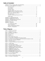
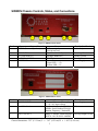
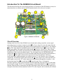
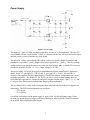
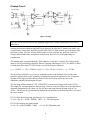
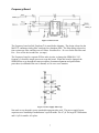
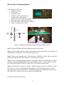
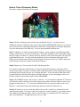
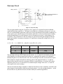
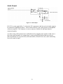
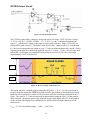
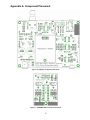
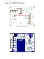
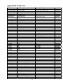
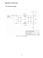
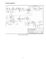
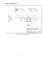
Solar Sudden Ionospheric Disturbance Monitor
Technical Manual
Authors:
Ray Mitchell, Chief Engineer
Bill Clark, Senior Circuit Design Lead
Document Status: PRELIMINARY
Draft Version 1.0
02-Aug-2006
1
Table of Contents:
SIDMON Chassis Controls, Status, and Connections ....................................................................... 3
Introduction To The SIDMON Circuit Board ................................................................................... 4
Circuit Overview..................................................................................................... 4
Power Supply .......................................................................................................... 5
Preamp Circuit ........................................................................................................ 6
Frequency Board..................................................................................................... 7
Frequency Board Tuning Resistor Table ................................................................ 8
SIDMON & Frequency Board Connectors............................................................. 8
How to tune a Frequency Board ............................................................................. 9
Post-amp Circuit ................................................................................................... 11
Amplitude Modulation Detection Circuit ............................................................. 12
Audio Output ........................................................................................................ 13
Appendix A: Component Placement ............................................................................................... 15
Appendix B: SIDMON PCB Artwork ............................................................................................. 16
Appendix C: FREQBOARD PCB Artwork..................................................................................... 17
Appendix D Test Points Glossary.................................................................................................... 18
Appendix E: Parts List ..................................................................................................................... 19
Appendix F: Schematics .................................................................................................................. 20
+5/-5 Volt Power Supply ...................................................................................... 20
Pre/Post Amplifiers............................................................................................... 21
Audio and Analog Data Outputs........................................................................... 22
Frequency Tuning Board ...................................................................................... 23
Table of figures:
Figure 1: SIDMON Front Panel......................................................................................................... 3
Figure 2: SIDMON Rear Panel.......................................................................................................... 3
Figure 3: SIDMON Circuit Board ..................................................................................................... 4
Figure 4: Power Supply ..................................................................................................................... 5
Figure 5: Preamp................................................................................................................................ 6
Figure 6: Filter Circuit ....................................................................................................................... 7
Figure 7: Power Supply Filter Caps................................................................................................... 7
Figure 8: Connections on SIDMON and Frequency boards.............................................................. 8
Figure 9: Test Fixture (left: Schematic, right: the homemade attenuator circuit) ............................. 9
Figure 10: Example of Tuning a SIDMON ..................................................................................... 10
Figure 11: Post-Gain Amp ............................................................................................................... 11
Figure 12: Amplitude Modulation Detection Circuit....................................................................... 12
Figure 13: Audio Output.................................................................................................................. 13
Figure 14: DATAQ Output Circuit.................................................................................................. 14
Figure 15: DATAQ Output Calibration Notes................................................................................. 14
Figure 16: SIDMON Component Placement................................................................................... 15
Figure 17: FREQBOARD Component Placement .......................................................................... 15
Figure 18: SIDMON PCB Top Layer.............................................................................................. 16
Figure 19: SIDMON PCB Bottom Layer ........................................................................................ 16
Figure 20: FREQBOARD PCB Top Layer ..................................................................................... 17
Figure 21: FREQBOARD PCB Bottom Layer................................................................................ 17
Figure 22: +5/-5 Volt Power Supply................................................................................................ 20
Figure 23: Pre/Post Amplifier.......................................................................................................... 21
Figure 24: Audio and Analog Data Outputs .................................................................................... 22
Figure 25: Frequency Tuning Board................................................................................................ 23
2
SIDMON Chassis Controls, Status, and Connections
1
2
3
4
5
Figure 1: SIDMON Front Panel
Number Connectors / Status / Controls
1
AUDIO (Powered Speakers)
2
3
4
5
X1 X5 X10
RF GAIN ADJUST
ANTENNA INPUT
POWER ON
6
Parameters
1/8” stereo jack
Line-in/out level
Post Gain Switch (3 pos)
Preamp (200KΩ R3)
TNC Connector
Power Status:
Green LED = +5v
Yellow LED = -5v
7
Details (See Circuit)
Audio Output
Post Amp Circuit
Preamp Circuit
Preamp Circuit
Power Supply
8
Figure 2: SIDMON Rear Panel
Number Connectors / Status / Controls
6
POWER INPUT
7
Serial Number Area
8
DATA OUTPUT
Parameters
Mates w/ 2.1 mm x 5.5 mm plug
9 ~ 10 VAC input voltage
Top line: Serial number S-####
Middle: Serial Number FB-####
Bottom: Frequency / Station ID
Mates w/ Phoenix connector part#
803578, 3.81 2P PLUG 180DEG
Details (See Circuit)
Power Supply
N/A
DATAQ Output Circuit
Chassis Dimensions: 5.25” (13.34 cm) L x 3.63” (9.22 cm) W x 1.825” (4.636 cm)
3
Introduction To The SIDMON Circuit Board
This document describes the circuit design and theory of operation of the SID Monitor circuit; for
instructions how to calibrate and use the SID monitor please refer to the user’s manual.
2
5
3
7
4
6
8
1
Figure 3: SIDMON Circuit Board
9
Circuit Overview
Starting at the lower left of the SIDMON circuit board and working around the various signal
processing stages or sections in numeric order: 1The Power Supply Section takes input from the
9-10 VAC from the transformer and produces both regulated positive and negative 5 volt supplies.
2 The TNC input feeds the broadband signal in from the antenna into the 3 Preamp Stage with
the RF gain control. The signal is then routed into the 4 Frequency Board Filter Stage (called
FREQBOARD). This section extracts the desired VLF transmitter station frequency as Amplitude
Modulation (AM) from the broadband signal. The AM signal leaves the FREQBOARD and
routed to the 5 Post-Amp Stage for a user-selectable signal boost the post-amp switch labeled x1,
x5 and x10. 6 The signal is routed to the Signal Detect Stage that performs a full-wave
rectification of the signal making the waveform all positive, i.e. the absolute value of all signal
components. The detected signal is then routed to the 7 Audio Output Stage where the line-level
audio signal is sent out the 1/8” audio output jack and monitored through power speakers. Also
the detected signal from 6 is routed into the 8 Signal Strength Stage. An integrator
(Resistor/Capacitor circuit) converts the detected AM signal into an average DC level, indicating
overall signal strength. The DC level (analog output) exits the SID Monitor via 9 the 2-position
Phoenix connector that is connected to the DATAQ module (ADC) that converts the analog level
to digital values that are then transmitted via RS-232 to the computer and recorded by the software.
4
Power Supply
Figure 4: Power Supply
The input is a 2.5mm x 5.0mm jack that accepts the 9-10 volt AC wall transformer. The fuse (F1)
is a re-settable 250mA circuit breaker. If there is a short circuit the fuse will open and remain open
until the power is removed and the fuse cools down.
The AC to DC voltage conversion is achieved by a half-wave rectifier (diodes D1 and D2) and
smoothed by capacitors C1 and C2 (Higher frequencies bypassed by C5 and C6). The DC working
voltage on these caps should be rated at two times the input voltage, plus we added 50% more as a
precaution, therefore: WVDC = 2.5 x Vac (input voltage) = 25 VDC.
The power supply is a typical design per recommendations from the manufacture’s application
sheets; for the +5 volt supply IC1 (78L05) and –5 volt supply IC2 (79L05). We used the ‘L’
versions of the regulator for their characteristics of both lower dropout voltages and over current
regulation properties. The diodes (D3, D4, D5, D6) prevent a reverse voltage situation that can
result when the capacitors are charged up and power reapplied on the input. Caps C3, C4, C7, and
C8 are part of the filtering and recommended design by the manufacturer.
The two status-LED’s visible on the front panel show independently that both power supplies are
functioning. The LED color assignments are as follows:
+5V is green.
–5V is yellow.
Overall the current draw on the power supply is small, in the 100-200 milliamps range. It was
necessary to design the power supply with lots of filtering in order to provide clean DC power to
all of the RF filters and amplification stages.
5
Preamp Circuit
Figure 5: Preamp
Note: this circuit does not include any lightning suppressors; it is the responsibility of the user to
install them.
Another protection mechanism suggested by an engineer, but after the PC boards were made, was
a signal-limiter clamp made from two signal diodes (1N914’s) back-to-back across the input of the
first stage op amp. As of the writing of this manual, we have not seen any problems with overvoltage, and not added these components to the boards, however it is worth mentioning for
consideration.
The antenna input is inputted through a TNC connector. Capacitor C8 isolates DC voltage on the
input as well as performing a high-pass filter RC function consisting of C8 (0.1 μF) and R4 (2.2KΩ)
is a high-pass filter (about 723 Hz) to help reject 50/60 Hz power-line hum.
fo = 1 / (2πRC) = 1 / (2π x 2.2KΩ x 0.1μF) = 1 / (2π x 2.2x103 x 0.1x10-6) ∴ fo = 723 Hz
The R4 resistor could also serve as an AC impedance match to the antenna, however this value
cannot be optimized due to the variability of antenna design and consequences to the fo frequency
response of the high-pass filter thus it is better for the user to make up for the loss in the
impedance match by increasing the RF gain.
The first stage of the preamp (IC3:G1 TLE2082CP) is a non-inverted input with a gain of 201x.
The output (DC decoupled) runs to the next stage, which is an inverted input, has a gain that has an
adjustable potentiometer (R3) from 0 to 20x, giving a total gain from the preamp stage of 0 to
4,020x. The RF gain (R3) potentiometer adjustment will be made by the end-user and is covered in
the user’s manual.
IC3 G$1 Non-Inverted op amp gain formula (A = Amplification)
A = (R5 + R6)/ R5 = (1KΩ + 200KΩ) / 1KΩ ∴ A = 201 (Fixed gain)
IC3 G$2 Inverted op amp gain formula
A = R3 / R7 = (0Ω to 200KΩ) / 10KΩ ∴ A = 0 to 20 (Adjustable gain)
6
Frequency Board
Figure 6: Filter Circuit
The Frequency board (called “Freqboard”) is tuned before shipping. The design is based on the
MAX275 continuous analog filter configured as a bandpass filter. The filter tuning is based on
four resistors per filter, and there are two filters. Resistors R100 – R104 are for the first filter and
R200 – R204 are for the second filter (or stage)
The Frequency board is a separate PCB to make it easier to change the SIDMON’s VLF
frequency. It would be simple process to swap this board. When this board is changed, the
SIDMON has to go through the same procedures of antenna alignment and qualification
procedures (as outlined in the user’s manual) as if it were a new monitor.
Figure 7: Power Supply Filter Caps
Not much to say about this, pretty standard design principles used. The power supply bypass
capacitors were installed per manufacturer’s specifications. The 4.7 μF for large DC fluctuations
and 0.1 μF for smaller AC spikes.
7
Frequency Board Tuning Resistor Table
With the components as outlined in the schematic it is possible only to tune a very narrow range of
VLF stations: 24.0 NAA, 24.8 NLK, and 25.2 NML. Frequencies above or below this range are
unreachable. To tune to other frequencies, you need to run the filter design software from
MAXIM to determine the correct values for the resistors. Use 1% resistors. We used the
Butterworth filter with 4 poles (requires 2 stages to implement the filter).
Frequency Range
R101 / R201
18.3 – 19.0 KHz*
24.0 – 25.2 KHz
R102 / R202
Sets Center frequency
R103 / R203
Sets Gain
Sets Q
R104 / R204
Sets Center Frequency
200.0 KΩ
200.0 KΩ
115.0 KΩ* ?
76.8 KΩ
549.0 KΩ
549.0 KΩ
90.9 KΩ* ?
75.0 KΩ
*Resistor values untested – also: to do add more frequencies to this table.
All resistors are 1% (or better). R100 and R200 are 10K Potentiometers in series with R102 and R202
respectively. Calculate resistors in the sequence given below:
(Equations from MAXIM 274/275 Data Sheet)
Formula
Comments
9
R2 = R x02 + Rx00 = (2 * 10 ) / F0
Where F0 is the desired center frequency, this resistor is
R2 in the MAXIM document, it is in series with Rx00
Rx04 = Rx02 – 5KΩ
Rx04 might be less than 5KΩ because of internal 5KΩ
resistor, limits BPO_ loading
Rx03 = (Q * 109) / (5 * F0 )
Limits 5KΩ < Rx03 < 4MΩ
9
Rx01 = (2 * 10 ) / (5 *F0 * HOLP)
HOLP is the gain of LPO_ at DC
SIDMON & Frequency Board Connectors
SIGNAL IN
FREQ OUT
SIDMON
FREQBOARD
Figure 8: Connections on SIDMON and Frequency boards
Signal Description
Neg. 5V
GND
Pos. 5V
Signal Input
Freq A (for tuning)
Freq B (Frequency Out)
Pin# SIDMON Side
1,3
4,5,8
7,9
2
6 (no connection)
10
8
Pin# FREQBOARD Side
2,4
3,6,7
8,10
1
5
9
How to tune a Frequency Board
Tools / Supplies you’ll need:
• Frequency generator
• Oscilloscope
• Frequency counter
• Small screwdriver, preferably nonmetallic (contact with a metal
screwdriver seems to affect the readings –keep this in mind while tuning)
• BNC patch cords, oscilloscope probe, etc.
• TNC male to BNC female adaptor / connector
• Resistor / Attenuator test fixture
200 Ohm
Signal
Generator
Input
Output
(To SIDMON)
1 ohm
Figure 9: Test Fixture (left: Schematic, right: the homemade attenuator circuit)
Step 1: Plug the FREQBOARD in the SIDMON and turn on the power.
Step 2: Set the frequency generator output to the smallest output signal possible, then attenuate the
signal further with a simple 2-resistor circuit See figure above.
Step 3: Connect probe ground lead to a GND point on the SIDMON. (I usually like to connect the
ground clip to the top of the TNC connector – see picture on next page.)
Step 4: Use the oscilloscope probe connected to a frequency counter (or oscilloscope w/ a built-in
counter) to probe the FREQBOARD at the test point labeled “input.” Adjust the RF gain control
(R3) on the main SIDMON board to a voltage level of 100 millivolts peak-to-peak.
Step 5: Verify the proper frequency is present. Adjust the frequency generator, and error of ±100
Hz is okay. Be sure to verify throughout the tuning process that the signal generator is on the
desired frequency and hasn’t drifted off. I found for best results let the signal generator warm up
and stabilize for a couple of hours before tuning the FREQBOARD.
(Procedure continued on next page)
9
How to Tune a Frequency Board
(Procedure continued from the previous page)
Figure 10: Example of Tuning a SIDMON
Step 6: Put the oscilloscope probe on the test point labeled “Freq A.” (As shown above)
Additional comment: The picture above shows the finalized FREQBOARD, that is to say, the two
pots are locked down with fingernail polish to finalize the settings and prevent further adjustment
as per the instructions of the final step – leave the pots unpainted until that time.
Step 7: Adjust R100 to achieve the peak signal response. A peak response is the highest possible
response of the filter as seen on the oscilloscope. Watch the amplitude on the scope while turning
the pot in either a clockwise or counter-clockwise direction; one of these directions will cause the
signal amplitude to rise. At some point the amplitude crosses it maximum and begins to fall.
Simply reverse the direction of the pot and the signal will again rise back up. Find the setting on
the pot that gives the peak response to the input frequency.
Step 8: Repeat step 7 for test point “Freq B” and adjust pot R200.
It is normal to adjust the volts/division several times during this operation, as the gain will be
around 4x per stage. If you hear a clicking sound coming from the pot while turning, then you have
reached the end of travel of the pot, try reversing directions. If you traveled to either limit of the
pot and still did not find the peak response, then the frequency you are attempting to tune is not
possible with the current resistor values on the FREQBORD.
Step 9: The SIDMON is now ready to test, or “burn-in,” we recommend a minimum of 24 hours to
verify that the signal is being received and to discover any other electronic failures (such as caps
plugged in backwards etc.). To burn-in the SIDMON follow the setup procedure in the User’s
Manual, i.e. adjust the RF gain and pointing the antenna towards the transmitter, etc.
Step 10: If the burn-in is successful, then finalize the pots R100 and R200 by painting them with
some fingernail polish. Of course, if the burn-in process reveals a problem, e.g. no sunrise/sunset
effect then repeat tuning procedure. One caveat to be aware of: sometimes the VLF stations go
down for maintenance – it might not be the receiver’s fault.
10
Post-amp Circuit
FREQ OUTÆ
Æ TO Amplitude Modulation
Detection Circuit
Figure 11: Post-Gain Amp
The post gain amplifier takes the “Frequency Out” signal, now separated from the broadband
signal, and this stage amplifies it. The stage was included as a contingency because we were not
sure if we needed another gain boost so this was to deal with unknown and variable conditions of a
weak signal or poor antenna design. We decided to make this a selector switch instead of adding
another potentiometers to avoid confusion. So far all monitors are using x1 with perhaps a few
exceptions. I have found the x5 and x10 settings are good to boost the gain enough to make the
input signal audible for antenna orientation. It is important to change this setting back to x1 for
data logging.
A = R17 / Rx ∴ A = 100KΩ / Rx ; where Rx is one of R14, R15, or R16
Switch Setting
(Label on chassis)
X1
X5
X10
Resistor
Value
Actual Gain (A)
R14
R15
R16
49.9KΩ
20.0KΩ
4.7KΩ
2.004
5.000
21.277
The gain slide switch is a DP3T labeled on the chassis: x1, x5, and x10 note that the actual gains
of the amplifier are different than labeled on the box –admittedly this appears to be dishonest.
Initially the plan was to make them the same, but as the design went on it was decided to keep the
labels on the box simple and make the make-up gains on the output look like 1x, 5x, and 10x
instead of the internal circuits be consistent with their external labeling. (For those still curious:
When the gains were set “as advertised” the resultant output voltages were not x1, x5, and x10
with respect to the switch setting.)
This was an empirical design, and then we found out later that it wasn’t completely consistent with
other frequency cards that have different gain characteristics. It is only an approximation… and in
the end I have to say that this decision was done mainly for aesthetic appearances.
11
Amplitude Modulation Detection Circuit
From Post Gain Æ
Figure 12: Amplitude Modulation Detection Circuit
This circuit is called an “Absolute-Value Circuit Full-Wave Precision Rectifier” taken from the
“Op Amp Design Cookbook” Third Edition by Walter G. Jung pp236-237. We found the circuit
would sometimes go into oscillation very easily, thus C17 (22 pF) was necessary to eliminate the
oscillations.
Test point “Signal Detect” is the full-wave, rectified signal that is sent to the audio buffer circuit.
(See: Audio Output for more information)
Test point “Signal Strength” is the integrated signal to produce the signal strength – this is a DC
level. The RC circuit (R33 and C21) has an RC time constant is approximately between 5 and 9
seconds. (T = RC = 20KΩ x 470 μF = 20x103 x 470x10-6 ∴ T = 9.4 Seconds). This is
approximate because capacitors have lower precision tolerances and we added a discharge resistor,
R20, to provide a small load to discharge the capacitor (C21) in order to make the circuit respond to
a lowering level faster than allowing its internal resistance to discharge the capacitor.
The design of this filter was chosen carefully to reject short lived signal bursts, such as lightning,
but allow longer persistent signal-strength changes such as those caused by solar flares, to affect
the overall signal strength characteristics.
Without this filter in place the resultant graph was too noisy to reliably detect solar flares,
especially smaller class-C flares. Engineers would often ask me “why not filter in software?” and
the answer is that we only sample once every 5 seconds, thus we would need to take more sample
and run some sort of median or averaging algorithm to filter out the noise. This eliminates postprocessing and allows direct viewing of the data. However, engineers might be interested in
experimenting with the RC values or even eliminating the RC circuit so that real-time monitoring
of lightning and possible GRB (Gamma Ray Bursts) would be possible (it would also require to
increase the cadence of the data logging, etc.)
12
Audio Output
Figure 13: Audio Output
IC4 G$2 is a unity-gain buffer, C14 isolates the DC component to the line-out level audio output to
be connected to amplified speakers – do not connect directly to an 8 ohm speakers or headphones
without an amplifier. The connector is a stereo connector with the left and right channels
connected together.
As of the writing of this document it is still unknown why plugging in the speaker would cause a
dip in the signal strength level, perhaps there is some ground loop problem that has not been
detected (both devices are powered by wall transformers). Whatever the cause, audio monitoring
lowers the signal strength.
13
DATAQ Output Circuit
Figure 14: DATAQ Output Circuit
The LT1490 op amp allows voltages to swing from rail-to-rail. Stage 1 (IC6 G$1) has a gain of
33.127 (A = R8/ R10 = 267KΩ / 8.06KΩ ∴ A = 33.127). C12 and C13 dampen fluctuations and
spikes. C16 stabilizes the voltage on the input to form a stable reference. Stage 2 (IC6 G$2) is a
voltage shifter with a gain of 1. The shifter works because the (-) input is tied to +5 volts through
R11, the inverter input makes the output to go to –5 Volts, the midpoint between R12 and R11 form a
summing point therefore translates the input DC level to –5 volts to + 5 volts, a 10 volt range, thus
making the overall signal easy enough for the DATAQ to read over it’s 20 volt / 10 bit range
(approximately 0.0195 volts per bits).
2/3
1/3
Vnoon = -1.667 V
Figure 15: DATAQ Output Calibration Notes
The reason why user’s manual suggests setting the RF gain to –1.25 to –1.5 volts at noontime is
because while developing the SIDMON we had to resolve the problem of determining how much
headroom was required to record M- and X-class flares while not sacrificing resolution for the CFlares. The value of –1.5 volts was derrived by approximately using the first 1/3 of the graph to
allow for noon – the highest point on the graph for daytime allowing the other 2/3 of the graph to
be able to record the largest flares, and this level is usually still much higher than sunrise and
sunset levels.
Vnoon = 1/3 (10 volts absolute range) – 5volts = -1.667 Volts
14
Appendix A: Component Placement
Figure 16: SIDMON Component Placement
Figure 17: FREQBOARD Component Placement
15
Appendix B: SIDMON PCB Artwork
Figure 18: SIDMON PCB Top Layer
Figure 19: SIDMON PCB Bottom Layer
16
Appendix C: FREQBOARD PCB Artwork
Figure 20: FREQBOARD PCB Top Layer
Figure 21: FREQBOARD PCB Bottom Layer
17
Appendix D Test Points Glossary
SIDMON
Test Point Name
-5v
+5v
GND
PREAMP
FILTER OUT
DETECT
STRENGTH
DATA OUTPUT
Meaning
-5 Volt supply
+5 Volt supply
Ground (0 volt / reference)
Antenna signal output from first two stages
Return signal from Frequency board,
(should have been output of Op Amp IC4 G$1)
Output of the full-wave signal rectifier
Integrated signal (DC level)
Shifted (DC level)
FREQBOARD
Test Point Name
-5v
+5v
GND
FREQ A
FREQ B
Meaning
-5 Volt supply
+5 Volt supply
Ground (0 volt / reference)
First stage frequency filter (used for calibration)
Second stage frequency filter (used for calibration), Same as “FILTER_OUT”
Test Point signal on SIDMON board
18
Appendix E: Parts List
Part#
Part Description
Schematic Designation
80-C315C104M5U 0.1uF Monolithic
140-50N2-120J
12 pF
140-XRL25V2200
2200uF
140-NPRL50V4.7
4.7 NON-POLAR
399-1302-ND
4.7uF Tant. Cap
140-XRL10V470
470uF
1N4001RLOSCT-ND 1N4001
1N914CT-ND
1N914A
350-1403-ND
LZR182, LED 2-Color
AN78L05-ND
78L05
AN79L05-ND
79L05
296-1874-5-ND
TLE2082CP
LT1490CN8-ND
LT1490
MAX275BCPP-ND MAX275BCCP
271-100K
100K
271-10K
10K
271-1K
1K
271-2.2K
2.2K
271-20K
20K
271-200K
200K
271-267K
267K
271-4.7K
4.7K
271-40.2K
40.2K
271-49.9K
49.9K
271-549K
549K
271-75K
75K
271-76.8K
76.8K
271-8.06K
8.06K
72-T93YA-10K
10K Pot Vertical Adj.
652-3006P-1-204
200K Pot Horizontal Adj.
612-EG2308
DP3T
652-MFR025
Resettable fuse
8400K-ND
4-40, .375 Male/Female Standoff
H342-ND
4-40 1/4" Screw
H236-ND
4-40 Internal tooth Star Washers
H216-ND
4-40 Nut
CP-102AH-ND
Power Jack: 2.1x5.5mm
A24648-ND
RF Connect JACK TNC Right Angle
651-1803578
Analog output mating Screw terminal
651-1803277
Analog Output, PCB Mount
161-3153
Audio output: 3.5mm Stereo jack
649-69168-110
Board-to-Board Male
649-68683-305
Board-To-Board Female
#210745
10 VAC Transformer
MM-11892
Chassis
P82368
SIDMON PCB (REV 2)
P73970
FREQBOARD PCB (REV 1)
DI-194RS
DATA Acquisition Module
19
C5, C6, C7, C8, C9, C10, C11, C12, C13,
C18, C20, C103, C104, C105
C17
C1, C2
C14
C3, C4, C101, C102
C21
D1, D2, D3, D4, D5, D6
D7, D8
DZ1
IC1
IC2
IC3, IC4, IC5
IC6
IC100
R17
R7, R8, R18, R19, R21, R29, R31, R32
R1, R2, R5
R4
R11, R12, R33, R15
R3, R6, R101, R201
R9
R10
R20
R14
R103, R203
R104, R204
R102, R202
R10
R100, R200
R3
SW1
F1
N/A
N/A
N/A
N/A
J1
J2
N/A (external part – mates with J4)
J4
J3
P1
SV1
N/A
N/A
N/A
N/A
N/A
Vendor
MOUSER
MOUSER
MOUSER
MOUSER
DIGI-KEY
MOUSER
DIGI-KEY
DIGI-KEY
DIGI-KEY
DIGI-KEY
DIGI-KEY
DIGI-KEY
DIGI-KEY
DIGI-KEY
MOUSER
MOUSER
MOUSER
MOUSER
MOUSER
MOUSER
MOUSER
MOUSER
MOUSER
MOUSER
MOUSER
MOUSER
MOUSER
MOUSER
MOUSER
MOUSER
MOUSER
MOUSER
DIGI-KEY
DIGI-KEY
DIGI-KEY
DIGI-KEY
DIGI-KEY
DIGI-KEY
MOUSER
MOUSER
MOUSER
MOUSER
MOUSER
JAMECO
MARTINEK
ADV. CIR.
ADV. CIR.
DATAQ
Appendix F: Schematics
+5/-5 Volt Power Supply
Figure 22: +5/-5 Volt Power Supply
20
Pre/Post Amplifiers
Figure 23: Pre/Post Amplifier
21
Audio and Analog Data Outputs
Figure 24: Audio and Analog Data Outputs
22
Frequency Tuning Board
Figure 25: Frequency Tuning Board
23