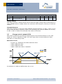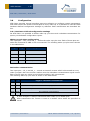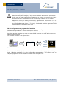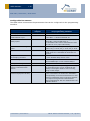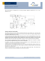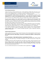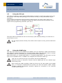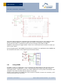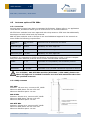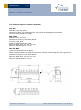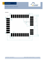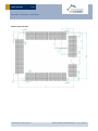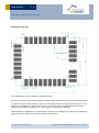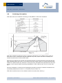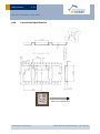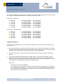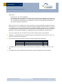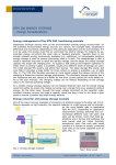
1
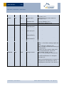
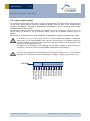
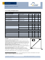
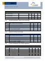
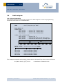
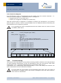
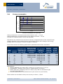
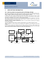
USER MANUAL V1.35 Scavenger Transceiver Module STM 300 / STM 300C / STM 300U July 1st, 2013 Observe precautions! Electrostatic sensitive devices! Patent protected: WO98/36395, DE 100 25 561, DE 101 50 128, WO 2004/051591, DE 103 01 678 A1, DE 10309334, WO 04/109236, WO 05/096482, WO 02/095707, US 6,747,573, US 7,019,241 EnOcean GmbH Kolpingring 18a 82041 Oberhaching Germany Phone +49.89.67 34 689-0 Fax +49.89.67 34 689-50 [email protected] www.enocean.com Subject to modifications STM 300 / STM 300C / STM 300U User Manual V1.35 July 24, 2013 Page 1/45 USER MANUAL 1.35 STM 300 / STM 300C / STM 300U REVISION HISTORY The following major modifications and improvements have been made to the first version of this document: No 1.01 1.10 1.20 1.25 1.26 1.30 1.31 1.32 1.33 1.34 1.35 Major Changes Tape running direction added in 3.8 Application note for multiple digital inputs with WAKE functionality added. Error corrected in 3.5.1. and 4.1: Maximum gain of external antenna at 50 Ohm output RF_50 is 0 dBi! Charging circuit in 3.1 corrected; remarks added regarding use of IOVDD in 2.3. Parameters of A/D converter corrected and specified in more detail in 2.3.2 Optional resolution at ADIO0, ADIO1, ADIO2 corrected in 2.3. Detailed description in 2.9.1 was correct! New improved application note in 3.1, which avoids deep discharge of the long term storage. Updated data on conducted output power in 1.2; improved layout recommendations in 3.6 Antenna recommendations removed and referred to external application note AN102, and AN105; Maximum Rating for IOVDD modified (IOVDD may now exceed VDD); Chapter “Related Documents” added. Figure added in 3.3.1; parameters for antenna requirements relaxed in 4.5.1. Added STM 300U (902.875 MHz), new product image Updated Agency certifications according to FCC / IC requirements Mitsubishi Materials Chip Antenna added to limited modular approval Published by EnOcean GmbH, Kolpingring 18a, 82041 Oberhaching, Germany www.enocean.com, [email protected], phone +49 (89) 6734 6890 © EnOcean GmbH All Rights Reserved Important! This information describes the type of component and shall not be considered as assured characteristics. No responsibility is assumed for possible omissions or inaccuracies. Circuitry and specifications are subject to change without notice. For the latest product specifications, refer to the EnOcean website: http://www.enocean.com. As far as patents or other rights of third parties are concerned, liability is only assumed for modules, not for the described applications, processes and circuits. EnOcean does not assume responsibility for use of modules described and limits its liability to the replacement of modules determined to be defective due to workmanship. Devices or systems containing RF components must meet the essential requirements of the local legal authorities. The modules must not be used in any relation with equipment that supports, directly or indirectly, human health or life or with applications that can result in danger for people, animals or real value. Components of the modules are considered and should be disposed of as hazardous waste. Local government regulations are to be observed. Packing: Please use the recycling operators known to you. © 2013 EnOcean | www.enocean.com STM 300 / STM 300C / STM 300U User Manual | V1.35 | Page 2/45 USER MANUAL 1.35 STM 300 / STM 300C / STM 300U TABLE OF CONTENT 1 MODULE VARIANTS AND RELATED DOCUMENTS ............................................... 4 2 2.1 2.2 2.3 2.4 2.5 GENERAL DESCRIPTION ................................................................................. 4 Basic functionality ......................................................................................... 4 Technical data ............................................................................................... 6 Physical dimensions ....................................................................................... 6 Environmental conditions ............................................................................... 7 Ordering Information ..................................................................................... 7 3 FUNCTIONAL DESCRIPTION ............................................................................ 8 3.1 Simplified firmware flow chart and block diagram .............................................. 8 3.2 Hardware pin out ........................................................................................... 9 3.3 Pin description and operational characteristics................................................. 10 3.3.1 GPIO supply voltage ................................................................................ 12 3.3.2 Analog and digital inputs .......................................................................... 13 3.4 Absolute maximum ratings (non operating) .................................................... 14 3.5 Maximum ratings (operating) ........................................................................ 14 3.6 Power management and voltage regulators .................................................... 14 3.7 Charge control output (CCO) ......................................................................... 15 3.8 Configuration .............................................................................................. 16 3.8.1 Hardware-defined configuration settings ..................................................... 16 3.8.2 Configuration via programming interface .................................................... 17 3.9 Radio telegram ............................................................................................ 19 3.9.1 Normal operation ..................................................................................... 19 3.9.2 Teach-in telegram ................................................................................... 20 3.10 Transmit timing ...................................................................................... 20 3.11 Energy consumption ............................................................................... 21 4 APPLICATIONS INFORMATION ....................................................................... 22 4.1 How to connect an energy harvester and energy storage .................................. 22 4.2 Using the SCO pin ....................................................................................... 25 4.3 Using the WAKE pins.................................................................................... 25 4.4 Using RVDD ................................................................................................ 26 4.5 Antenna options STM 300x ........................................................................... 27 4.5.1 Overview ................................................................................................ 27 4.5.2 Whip antenna.......................................................................................... 27 4.5.3 Helical antenna (supplier: EnOcean) .......................................................... 28 4.5.4 Chip antenna (supplier: Mitsubishi Material, Type AM11DG-ST01) ................. 29 4.6 Positioning of the whip antenna ..................................................................... 30 4.7 Recommendations for laying a whip antenna................................................... 31 4.8 Layout recommendations for foot pattern ....................................................... 32 4.9 Soldering information ................................................................................... 36 4.10 Tape & Reel specification ......................................................................... 37 4.11 Transmission range ................................................................................. 38 5 5.1 5.2 5.3 5.4 5.5 AGENCY CERTIFICATIONS ............................................................................ 39 CE approval ................................................................................................ 39 FCC (United States) Certification ................................................................... 40 FCC (United States) Regulatory Statements ................................................... 43 IC (Industry Canada) Certification ................................................................. 44 IC (Industry Canada) Regulatory Statements .................................................. 45 © 2013 EnOcean | www.enocean.com STM 300 / STM 300C / STM 300U User Manual | V1.35 | Page 3/45 USER MANUAL 1.35 STM 300 / STM 300C / STM 300U 1 MODULE VARIANTS AND RELATED DOCUMENTS The STM 300 Scavenger Transceiver Module is available in several operating frequency variants: STM 300: STM 300C: STM 300U: 868.350 MHz 315.000 MHz 902.875 MHz Inside this manual, the term “STM 300x” can be used to represent all of the above frequency variants. This document describes operation of STM 300x modules with their built-in firmware. If you want to write own firmware running on the integrated micro controller or need more detailed information on the Dolphin core please also refer to: Dolphin Core Description Dolphin API Documentation In addition we recommend following our application notes, in particular: AN102: Antenna Basics – Basic Antenna Design Considerations for EnOcean based Products AN105: 315 MHZ Internal Antenna Design – Considerations for EnOcean based Products AN207: ECS 300/310 Solar Panel - Design Considerations AN208: Energy Storage – Design Considerations AN209: STM 300 THERMO OR BATTERY POWERED – Power Supply Alternatives to Solar Panel 2 2.1 GENERAL DESCRIPTION Basic functionality The extremely power saving RF transmitter module family STM 300x of EnOcean enables the realization of wireless and maintenance free sensors and actuators such as room operating panels, motion sensors or valve actuators for heating control. Power supply is provided by an external energy harvester, e.g. a small solar cell (e.g. EnOcean ECS 3x0) or a thermal harvester. An energy storage device can be connected externally to bridge periods with no supply from the energy harvester. A voltage limiter avoids damaging of the module when the supply from the energy harvester gets too high. © 2013 EnOcean | www.enocean.com STM 300 / STM 300C / STM 300U User Manual | V1.35 | Page 4/45 USER MANUAL 1.35 STM 300 / STM 300C / STM 300U The module provides a user-configurable cyclic wake up. After wake up, a radio telegram (input data, unique 32 bit sensor ID, checksum) will be transmitted in case of a change of any digital input value compared to the last transmission or in case of a significant change of measured analogue values (different input sensitivities can be selected). In case of no relevant input change, a redundant retransmission signal is sent after a user configurable number of wake-ups to announce all current values. In addition, a wake up can also be triggered externally. Features with built-in firmware 3 A/D converter inputs 4 digital inputs Configurable wake-up and transmission cycle Wake-up via Wake pins Voltage limiter Threshold detector Application notes for calculation of energy budgets and management of external energy storages Product variants STM 300 / STM 300C / STM 300U Features accessible via API Using the Dolphin API library it is possible to write custom firmware for the module. STM 300x is in-system programmable. The API provides: Integrated 16 MHz 8051 CPU with 32 kB FLASH and 2 kB SRAM Receiver functionality Various power down and sleep modes down to typ. 0.2 µA current consumption Up to 16 configurable I/Os 10 bit ADC, 8 bit DAC © 2013 EnOcean | www.enocean.com STM 300 / STM 300C / STM 300U User Manual | V1.35 | Page 5/45 USER MANUAL 1.35 STM 300 / STM 300C / STM 300U 2.2 Technical data Antenna Frequency External whip or 50 Ω antenna mountable STM 300: 868.300MHz (ASK)1) STM 300C: 315.000MHz (ASK)1) STM 300U: 902.875 MHz (FSK) Data rate Receiver Sensitivity (at 25 °C) only via API 125 kbps typ. –96 dBm2) (868.300 MHz) typ. -98 dBm2) (315.000 MHz) typ. -98 dBm2) (902.875 MHz) Conducted Output Power @50 min / typ /max STM 300: 3.0 dBm / 5.7 dBm / 7.0 dBm STM 300C: 5.5 dBm / 7.5 dBm / 9.5 dBm STM 300U: -1 dBm / 1 dBm / 3dBm 3) 2.1 V–4.5 V, 2.6 V needed for start-up Power Supply Current Consumption Input Channels Deep Sleep mode : typ. 0.2 µA Transmit mode: typ. 24 mA, max. 33 mA Receive mode (via API only): typ. 33 mA, max. 43 mA 4x digital input, 2x WAKE input , 3x analog input Resolution: 3x 8 bit or 1x 10 bit, 1x 8 bit, 1x 6 bit Radio Regulations R&TTE EN 300 220 (STM 300) FCC CFR-47 Part 15 (STM 300C / STM 300U) 1) according to ISO/IEC 14543-3-10 2) @ 0.1% telegram error rate (based on transmitted sub-telegrams) 3) using +1dBm (V 1.13) power settings which comply to limited modular approval 2.3 Physical dimensions PCB dimensions 22 x 19 x 3.1 mm Weight 1.9 g Unless otherwise specified dimensions are in mm. Tolerances: PCB outline dimensions 0.2 mm All other tolerances 0.1 mm STM 300x (pads on bottom side of PCB!) © 2013 EnOcean | www.enocean.com STM 300 / STM 300C / STM 300U User Manual | V1.35 | Page 6/45 USER MANUAL 1.35 STM 300 / STM 300C / STM 300U 2.4 Environmental conditions Operating temperature -25 °C … +85 °C Storage temperature -40 °C … +85 °C Storage temperature in tape & reel package -20 °C … +50 °C Humidity 2.5 0% … 93% r.h., non-condensing Ordering Information Type STM 300 STM 300C STM 300U Ordering Code S3001-D300 S3031-D300 S3051-D300 Frequency 868.300 MHz 315.000 MHz 902.875 MHz The following solar cells are recommended for use with STM 300x indoors: Type ECS 300 ECS 310 Ordering Code S3005-D305 S3005-D310 Size 35.0 × 12.8 × 1.1 mm 50.0 × 20.0 × 1.1 mm For technical details regarding these solar cells please refer to the ECS 300 and ECS 310 homepages. © 2013 EnOcean | www.enocean.com STM 300 / STM 300C / STM 300U User Manual | V1.35 | Page 7/45 USER MANUAL 1.35 STM 300 / STM 300C / STM 300U 3 3.1 FUNCTIONAL DESCRIPTION Simplified firmware flow chart and block diagram © 2013 EnOcean | www.enocean.com STM 300 / STM 300C / STM 300U User Manual | V1.35 | Page 8/45 USER MANUAL 1.35 STM 300 / STM 300C / STM 300U RF_WHIP RF_50 VDD IOVDD GND VDDLIM RF Transceiver Power Management V_OUT DVDD µController PROG_EN CW_0 CW_1 CP_0 CP_1 SCO CCO RESET GND 1 GND RESET GND WXIDIO WXODIO GND UVDD WAKE0 Hardware pin out WAKE1 3.2 Mixed I/O Interface Ultra Low Power Unit WAKE0 LRN UVDD LED DI_0 DI_1 DI_2 DI_3 AD_0 AD_1 AD_2 26 DVDD VDD XTAL 16MHz VDDLIM GND IOVDD Antenna balun RSDADIO3 EO3000I RF_WHIP WSDADIO2 GND 18 SCSEDIO0 PROG_EN GND ADIO7 ADIO6 ADIO5 ADIO4 ADIO3 9 ADIO0 RVDD STM300 – TOP VIEW ADIO2 GND SCLKDIO1 ADIO1 RF_50 The figure above shows the pin out of the STM 300x hardware. The pins are named according to the naming of the EO3000I chip to simplify usage of the DOLPHIN API. The table in section 3.3 shows the translation of hardware pins to a naming that fits the functionality of the built-in firmware. When writing own firmware based on the DOLPHIN API please refer to the Dolphin Core Description and use this manual only for information regarding the module hardware, such as pin out, layout recommendations, charging circuitry, antenna options, and approvals. © 2013 EnOcean | www.enocean.com STM 300 / STM 300C / STM 300U User Manual | V1.35 | Page 9/45 USER MANUAL 1.35 STM 300 / STM 300C / STM 300U 3.3 STM 300x Hardware Symbol GND Pin description and operational characteristics Function Characteristics Ground connection Must be connected to GND VDD STM 300x STM 300x pin # Firmware Symbol 1, 5, 7, GND 17, 24, 26, 28, 31 2 VDD Supply voltage RVDD 8 V_OUT RF supply voltage regulator output DVDD 25 DVDD Digital supply voltage regulator output UVDD 32 UVDD Ultra low power supply voltage regulator output VDDLIM 3 VDDLIM IOVDD 23 IOVDD Supply voltage limiter input GPIO supply voltage RESET 27 RESET PROG_EN 18 Reset input Programming I/F PROG_EN Programming I/F ADIO0 9 AD_0 Analog input ADIO1 10 AD_1 Analog input ADIO2 11 AD_2 Analog input ADIO3 12 DI_0 Digital input ADIO4 13 DI_1 Digital input 2.1 V – 4.5 V; Start-up voltage: 2.6 V Maximum ripple: see 3.6 1.8 V. Output current: max. 10 mA. See 4.4! Supply for external circuitry, available while not in deep sleep mode. 1.8 V. Output current: max. 5 mA Supply for external circuitry, available while not in deep sleep mode. Not for supply of external circuitry! For use with WAKE pins, see section 4.3. Max. 1 µA output current! Limitation voltage: 4.5 V Maximum shunting current: 50 mA Must be connected to desired interface supply voltage as specified in 3.5, e.g. to DVDD. See also 0 Active high reset (1.8 V) Connect external 10 kΩ pull-down. HIGH: programming mode active LOW: operating mode Digital input, connect external 10 kΩ pull-down. Input read ~2 ms after wake-up. Resolution 8 bit (default) or 10 bit. See also 3.3.2. Input read ~2 ms after wake-up. Resolution 8 bit (default) or 6 bit. See also 3.3.2. Input read ~2 ms after wake-up. Resolution 8 bit. See also 3.3.2. Input read ~2 ms after wake-up. See also 3.3.2. Input read ~2 ms after wake-up. See also 3.3.2. © 2013 EnOcean | www.enocean.com STM 300 / STM 300C / STM 300U User Manual | V1.35 | Page 10/45 USER MANUAL 1.35 STM 300 / STM 300C / STM 300U ADIO5 14 DI_2 Digital input ADIO6 15 DI_3 Digital input ADIO7 16 LED Transmission indicator LED Input read ~2 ms after wake-up. See also 3.3.2. Input read ~2 ms after wake-up. See also 3.3.2. Max. output current: 2 mA @ IOVDD=3.3 V 0.65 mA @ IOVDD=1.8 V SCSEDIO0 19 CW_1 SCLKDIO1 20 CW_0 WSDADIO2 21 CP_1 RSDADIO3 22 CP_0 WXIDIO 29 SCO Programming I/F Encoding input for wake-up cycle Programming I/F Encoding input for wake-up cycle Programming I/F Encoding input for retransmission Programming I/F Encoding input for retransmission Programming I/F Sensor control WXODIO 30 CCO Charge control WAKE0 33 WAKE0 Wake input WAKE1 34 LRN LRN input RF_WHIP RF_50 4 6 RF_WHIP RF_50 RF output RF output © 2013 EnOcean | www.enocean.com Leave open or connect to GND Leave open or connect to GND Leave open or connect to GND Leave open or connect to GND Digital output, max. current 15 µA HIGH ~x ms before analog inputs are read (x=0…508 ms; default 2 ms.) LOW at wake-up and after reading of analog inputs Polarity can be inverted, delay time can be programmed, see 3.8.2. Max output current 15 µA See 3.7 for description of behaviour. Change of logic state leads to wakeup and transmission of a telegram. See also 4.3. Change of logic state to LOW leads to wake-up and transmission of teach-in telegram if a manufacturer code is programmed. See also 3.9.2 and 4.3. Output for whip antenna 50 Ohm output for external antenna STM 300 / STM 300C / STM 300U User Manual | V1.35 | Page 11/45 USER MANUAL 1.35 STM 300 / STM 300C / STM 300U 3.3.1 GPIO supply voltage For digital communication with other circuitry (peripherals) the digital I/O configured pins of the mixed signal sensor interface (ADIO0 to ADIO7) and the pins of the programming interface (SCSEDIO0, SCLKDIO1, WSDADIO2, RSDADIO3) may be operated from supply voltages different from DVDD. An interface supply voltage pin IOVDD is available for such use cases which can be connected either to DVDD or to an external supply within the tolerated voltage range of IOVDD. Note that the wristwatch XTAL I/Os WXIDIO and WXODIO are always supplied from UVDD. If DVDD=0 V (e.g. in any sleep mode or if VDD<VOFF) and IOVDD is supplied, there may be an unpredictable and varying current flow from IOVDD caused by internal floating nodes. It must be ensured that the current into IOVDD does not exceed 10 mA while DVDD=0 V. If DVDD=0 V and IOVDD is not supplied, do not apply voltage to any above mentioned pin. This may lead to unpredictable malfunction of the device. For I/O pins configured as analog pins, the IOVDD voltage level is not relevant! However it is important to connect IOVDD to a supply voltage as specified in 3.5. IOVDD If configured as digital I/O ADIO0 ADIO1 ADIO2 ADIO3 ADIO4 ADIO5 ADIO6 ADIO7 SCSEDIO0 SCLKDIO1 WSDADIO2 RSDADIO3 © 2013 EnOcean | www.enocean.com STM 300 / STM 300C / STM 300U User Manual | V1.35 | Page 12/45 USER MANUAL 1.35 STM 300 / STM 300C / STM 300U 3.3.2 Analog and digital inputs Parameter Analog Input Mode Measurement range Conditions / Notes Single ended Min Input capacitance DC 62.5 Single ended against GND @ 1 kHz Single ended against GND @ 1 kHz 10 10 DNL 8 bit measurement Offset error Gain error 6 8 +1 -4 +1 -1 Code <=50 Code >50 DNL CodeADC Offset Error: Describes the offset between the minimal possible code and 0xFF code 0x00. Gain Error: Describes the offset between maximum possible code and full scale (e.g. 0x3FF for 10 bit measurements). Integral Non-Linearity (INL): Describes the difference between the ideal characteristics and the real characteristics. Only values between minimum and maximum possible code are considered (excluding offset error and gain error). Differential Non-Linearity (DNL): Measures the maximum deviation from the ideal step size of 1 LSB (least significant bit). Effective resolution: Results from the signal-noise ratio of the ADC and is given in Bit. The number describes how many bits can be measured stable. The criterion selected here is that the noise of DNL is <±0.5 LSB. Measurement Bandwidth: The measurement bandwitdh is internally 0x00 limited by filters. A quasi static signal must be applied as long as the filter 0 needs to settle. SettlingTime= 1/(MeasurementBandwidth)*ln(2^resolution[Bit]) V pF Bit 23 32 +3 -14 +3 -4 Code >200 Units kHz M 10 Code <=200 INL RVDD0.12 Internal reference RVDD/2 Effective measurement resolution 10 bit measurement Offset error Gain error INL Max 0.067 Input coupling Measurement bandwidth1 Input impedance Typ 36 62 +6 -23 +6 -10 <±0.5 LSB LSB LSB 9 16 +2 -6 +2 -3 <±0.125 LSB LSB LSB LSB LSB LSB LSB Gain Error ideal real Offset Error For further details please refer to the Dolphin Core Description. 1 3 dB input bandwidth, resulting in 111 µs settling time to achieve a deviation of an input signal <1 LSB (<0.098% @ 10 bit resolution). © 2013 EnOcean | www.enocean.com STM 300 / STM 300C / STM 300U User Manual | V1.35 | Page 13/45 1 UADC URVDD USER MANUAL 1.35 STM 300 / STM 300C / STM 300U Parameter Digital Input Mode Conditions / Notes Min Typ Max 2/3 IOVDD Input HIGH voltage V 1/3 IOVDD 200 85 Input LOW voltage Pull up resistor 3.4 Symbol VDD VDDLIM IOVDD GND VINA VIND1 VIND2 3.5 Symbol VDD VDDLIM IOVDD GND VINA VIND1 VIND2 3.6 @IOVDD=1.7 … 1.9 V @IOVDD=3.0 … 3.6 V Units 90 38 132 54 V k k Absolute maximum ratings (non operating) Parameter Supply voltage at VDD and VDDLIM Min -0.5 Max 5.5 -0.5 0 -0.5 -0.5 3.6 0 2 3.6 V V V V -0.5 2 V GPIO supply voltage Ground connection Voltage at every analog input pin Voltage at RESET, WAKE0/1, and every digital input pin except WXIDIO/WXODIO Voltage at WXIDIO / WXODIO input pin Units V Maximum ratings (operating) Parameter Min VOFF Supply voltage at VDD and VDDLIM GPIO supply voltage (see also 0) Ground connection Voltage at every analog input pin Voltage at RESET, WAKE0/1, and every digital input pin except WXIDIO / WXODIO Voltage at WXIDIO / WXODIO input pin Max 4.5 Units V 1.7 0 0 0 3.6 0 2.0 3.6 V V V V 0 2.0 V Power management and voltage regulators Symbol Parameter Conditions / Notes Voltage Regulators Ripple on VDD, where VDDR Min(VDD) > VON UVDD Ultra Low Power supply RVDD RF supply DVDD Digital supply Voltage Limiter VLIM Limitation voltage ILIM Shunting current © 2013 EnOcean | www.enocean.com Min 1.7 1.7 Typ 1.8 1.8 1.8 Max Units 50 mVpp 1.9 1.9 V V V 50 V mA 4.5 STM 300 / STM 300C / STM 300U User Manual | V1.35 | Page 14/45 USER MANUAL 1.35 STM 300 / STM 300C / STM 300U Threshold Detector VON Turn on threshold VOFF Turn off threshold Automatic shutdown if VDD drops below VOFF 2.3 1.85 2.45 1.9 2.6 2.1 V V Voltage Limiter STM 300x provides a voltage limiter which limits the supply voltage VDD of STM 300x to a value VDDLIM which is slightly below the maximum VDD ratings by shunting of sufficient current. Threshold detector STM 300x provides an ultra low power ON/OFF threshold detector. If VDD > VON, it turns on the ultra low power regulator (UVDD), the watchdog timer and the WAKE# pin circuitry. If VDD ≤ VOFF it initiates the automatic shut down of STM 300x. 3.7 Charge control output (CCO) After start-up STM 300x provides the output signal of the threshold detector at the CCO output pin. CCO is supplied by UVDD. The CCO output value remains stable also when STM 300x is in deep sleep mode. Behaviour of CCO - At power up: TRISTATE until VDD>VON then HIGH if VDD>VON then HIGH if VDD<VON then LOW if VDD< VOFF then LOW or TRISTATE VDD CCO VDD VDD > VON VDD < VON VDD < VOFF VON VOFF 1.8V TRISTATE or LOW ~0.9V TRISTATE 0V t For definition of VON and VOFF please refer to 3.6. © 2013 EnOcean | www.enocean.com STM 300 / STM 300C / STM 300U User Manual | V1.35 | Page 15/45 USER MANUAL 1.35 STM 300 / STM 300C / STM 300U 3.8 Configuration STM 300x provides several encoding input pins allowing to configure certain parameters. STM 300x checks the status of these pins at every wake-up. It is possible to override these hardware-defined configuration settings by software. Both mechanisms are described below. 3.8.1 Hardware-defined configuration settings On STM 300x it is possible to define wake-up cycle time and redundant transmission frequency via dedicated configuration inputs. Wake-up cycle time configuration Two input pins – CW_0 and CW_1 – define the wake-up cycle time. Each of these pins can either be connected to GND or left unconnected. The resulting wake-up cycle time is shown in the table below. CW_0 CW_1 Wake-up cycle time NC NC 1 s ±20% GND NC 10 s ±20% NC GND 100 s ±20% GND GND No cyclic wake-up Redundant retransmission Two input pins – CP_0 and CP_1 – control an internal counter which is decreased at every wake-up signal. Once the counter reaches zero the redundant retransmission signal is sent. Each of these pins can either be connected to GND or left unconnected. The resulting wake-up cycle time is shown in the table below. CP_0 CP_1 NC NC Number of wake-ups that trigger a redundant retransmission Every timer wake-up signal GND NC Every 7th - 14th timer wake-up signal, affected at random NC GND Every 70th - 140th timer wake-up signal, affected at random GND GND No redundant retransmission A radio telegram is always transmitted after wake-up via WAKE pins! After transmission the counter is reset to a random value within the specified interval. © 2013 EnOcean | www.enocean.com STM 300 / STM 300C / STM 300U User Manual | V1.35 | Page 16/45 USER MANUAL 1.35 STM 300 / STM 300C / STM 300U According to FCC 15.231a) a redundant retransmission at every timer wake-up to determine the system integrity is only allowed in safety and security applications! In this case the total transmission time must not exceed two seconds per hour, which means that a combination with a 1 s wake-up cycle time is not allowed! If applied in other (non-safety, non-security) applications a minimum of 10 s between periodic transmissions is required. In addition the device has to comply with the lower field strength limits of 15.231e). The limited modular approval of STM 300C and 300U is not valid in this case. 3.8.2 Configuration via programming interface Via the programming interface the parameters stored in the configuration area can be modified which provides a lot more configuration options. Note that values set via programming interface override hardware settings. Note also that these settings are read only after RESET or power-on reset and not at every wake-up of the module. The interface is shown in the figure below: USB Dolphin Studio, or EOP USB <=> SPI interface SPI Reset PROG_EN ADIO7 SCSEDIO0 SCLKDIO1 WSDADIO2 RSDADIO3 STM 300 EnOcean provides EOPX (EnOcean Programmer, a command line program) and Dolphin Studio (Windows application for chip configuration, programming, and testing) and the USB/SPI programmer device as part of the EDK 350 developer´s kit. © 2013 EnOcean | www.enocean.com STM 300 / STM 300C / STM 300U User Manual | V1.35 | Page 17/45 USER MANUAL 1.35 STM 300 / STM 300C / STM 300U Configurable Parameters The table below summarizes the parameters that can be configured via the programming interface. Parameter Configuration via pins See section 3.8.1 Configuration via programming interface Value can be set from 1 s to 65534 s Redundant Retransmission cycle See section 3.8.1 Min…Max values for random interval If Min=Max -> random switched off Threshold values for analog inputs No The default values are: 5 LSB at AD_1 input, 6 LSB at AD_0 and 14 LSB at AD_2. The threshold value can be set between 0 and full scale for every input individually. Resolution of the analog inputs No Default: AD_0: 8 bit, AD_1: 8 bit, AD_2: 8 bit Option: AD_0: 10 bit, AD_1: 6 bit, AD_2: 8 bit Input mask No A digital input mask for ignoring changes on digital input pins. At default all input bits are checked. Delay time between SCO on and sampling moment No Value can be set from 0 ms to 508 ms in steps of 2 ms. Default delay time is 2 ms. Source of AD_2 No Select if AD_2 contains measurement value of external ADIO2 pin or from internal VDD/4 Polarity of SCO signal No Polarity can be inversed. Edge of wake pin change causing a telegram transmission No Every change of a wake pin triggers a wake-up. For both wake pins it can be configured individually if a telegram shall be sent on rising, falling or both edges. Manufacturer ID and EEP No (EnOcean Equipment Profile) Information about manufacturer and type of device. This feature is needed for “automatic” interoperability of sensors and actuators or bus systems. Information how to set these parameters requires an agreement with EnOcean. Unique manufacturer IDs are distributed by the EnOcean Alliance. Wake up cycle © 2013 EnOcean | www.enocean.com STM 300 / STM 300C / STM 300U User Manual | V1.35 | Page 18/45 USER MANUAL 1.35 STM 300 / STM 300C / STM 300U 3.9 Radio telegram 3.9.1 Normal operation The diagram below summarized the content of a data telegram as seen at programming interface of STM 300x or at DOLPHIN API: ORG = 0x07 (Telegram type “4BS”) Data_Byte1..3 3x8bit mode: DATA_BYTE3 DATA_BYTE2 DATA_BYTE1 = Value of AD_2 analog input = Value of AD_1 analog input = Value of AD_0 analog input 1x8bit, 1x6it, 1x10bit mode: DATA_BYTE3 = Value of AD_2 DATA_BYTE2 = Upper 2 bits of AD_0 and value of AD_1 DATA_BYTE1 = Lower 8 bits Value of AD_0 analog input DATA_BYTE3 AD_2 DATA_BYTE2 DATA_BYTE1 AD_1 AD_0 7 6 5 4 3 2 1 0 5 4 3 2 1 0 9 8 7 6 5 4 3 2 1 0 DATA_BYTE0 = Digital sensor inputs as follows: Bit 7 Bit 0 Reserved, set to 0 DI_3 DI_2 DI_1 DI_0 ID_BYTE3 ID_BYTE2 ID_BYTE1 ID_BYTE0 = = = = module module module module identifier identifier identifier identifier (Byte3) (Byte2) (Byte1) (Byte0) The voltages measured at the analog inputs can be calculated from these values as follows: U=(Value of AD_x)/(2n)x1.8 V © 2013 EnOcean | www.enocean.com n=resolution of channel in bit STM 300 / STM 300C / STM 300U User Manual | V1.35 | Page 19/45 USER MANUAL 1.35 STM 300 / STM 300C / STM 300U 3.9.2 Teach-in telegram If a manufacturer code is programmed into the module then the module transmits – instead of a normal telegram – a dedicated teach-in telegram if: Digital input DI_3=0 at wake-up or Wake-up is triggered via WAKE1 pin (LRN input) With this special teach-in telegram it is possible to identify the manufacturer, the function and the type of a device. There is a list available from the EnOcean Alliance describing the functionalities of the respective products. If no manufacturer code is programmed then the module does not react to events on WAKE1 (LRN input)! ORG = 0x07 (Telegram type “4BS”) DATA_BYTE0..3 see below LRN Type = 1 LRN = 0 DI0..DI2: current status of digital inputs Profile, Type, Manufacturer-ID defined by manufacturer RE0..2: set to 0 ID_BYTE3 ID_BYTE2 ID_BYTE1 ID_BYTE0 ORG module module module module Data_Byte3 Function 6 Bit 3.10 = = = = identifier identifier identifier identifier Data_Byte2 Type Manufacturer7 Bit ID 11 Bit (Byte3) (Byte2) (Byte1) (Byte0) Data_Byte1 Data_Byte0 ID LRN Type RE2 RE1 RE0 LRN DI2 DI1 DI0 1Bit 1Bit 1Bit 1Bit 1Bit 1Bit 1Bit 1Bit Transmit timing The setup of the transmission timing allows avoiding possible collisions with data packages of other EnOcean transmitters as well as disturbances from the environment. With each transmission cycle, 3 identical subtelegrams are transmitted within 40 ms. Transmission of a subtelegram lasts approximately 1.2 ms. The delay time between the three transmission bursts is affected at random. If a new wake-up occurs before all sub-telegrams have been sent, the series of transmissions is stopped and a new series of telegrams with new valid measurement values is transmitted. © 2013 EnOcean | www.enocean.com STM 300 / STM 300C / STM 300U User Manual | V1.35 | Page 20/45 USER MANUAL 1.35 STM 300 / STM 300C / STM 300U 3.11 Energy consumption 100 10 Current [mA] 1 0.1 0.01 0.001 0.0001 0.00001 0 10 20 30 40 50 60 70 80 90 100 Time [ms] Current Consumption of STM 300x Charge needed for one measurement and transmit cycle: ~130 µC Charge needed for one measurement cycle without transmit: ~30 µC (current for external sensor circuits not included) Calculations are performed on the basis of electric charges because of the internal linear voltage regulator of the module. Energy consumption varies with voltage of the energy storage while consumption of electric charge is constant. From these values the following performance parameters have been calculated: Wake cycle [s] Transmit interval Operation Time in darkness [h] when storage fully charged 1 1 1 10 10 10 100 100 100 1 10 100 1 10 100 1 10 100 0.5 1.7 2.1 5.1 16 20 43 98 112 Required reload time [h] at 200 lux within 24 h for continuous operation 24 h operation after 6 h illumination at x lux storage too small storage too small storage too small storage too small 21 16.8 7.8 3.6 3 storage too small storage too small storage too small storage too small storage too small storage too small 260 120 100 Current Illuminain µA tion level required in lux for for concontinuous tinuous operation operation 5220 1620 1250 540 175 140 65 30 25 130.5 40.5 31.3 13.5 4.4 3.5 1.6 0.8 0.6 Assumptions: Storage PAS614L-VL3 with 0.25 F, Umax=3.2 V, Umin=2.2 V, T=25 °C Consumption: Transmit cycle 100 µC, measurement cycle 30 µC Indoor solar cell, operating values 3 V and 5 µA @ 200 lux fluorescent light (e.g. ECS 300 solar cell) Current proportional to illumination level (not true at very low levels!) These values are calculated values, the accuracy is about +/-20%! © 2013 EnOcean | www.enocean.com STM 300 / STM 300C / STM 300U User Manual | V1.35 | Page 21/45 USER MANUAL 1.35 STM 300 / STM 300C / STM 300U 4 APPLICATIONS INFORMATION 4.1 How to connect an energy harvester and energy storage STM 300x is designed for use with an external energy harvester and external energy storage. In order to support both a fast start-up time and long term operation with no energy supply available usually two different types of energy storages are used. A small (short term) energy storage fills quickly and allows a fast start-up while a large (long term) energy storage fills more slowly but can provide a large buffer for times where no energy is available, e.g. at night in a solar powered sensor. Both short term and long term storage are typically implemented as capacitors. The short term storage capacitor is usually in the range of 470 to 1000 µF while for the long term storage a capacity of 0.25 F is suggested. STM 300x provides a digital output CCO (see also 3.7) which allows controlling the charging of such two storages. The block diagram below shows a typical implementation of a suitable charging circuit. There, capacitor C1 acts as short term storage while capacitor C2 provides the long term storage. If both energy storages are depleted and the supply voltage is below the VON voltage level then only the small storage is charged. Once the VON threshold is reached, the CCO output signal changes and the system will start to charge the large storage. Charge switcher Overvoltage Energy source protection e.g. solar panel STM 300 Vdd Undervoltage protection VDDLIM CCO C1 Short term storage © 2013 EnOcean | www.enocean.com RC delay C2 Long term storage STM 300 / STM 300C / STM 300U User Manual | V1.35 | Page 22/45 USER MANUAL 1.35 STM 300 / STM 300C / STM 300U The circuit below is designed for an energy storage capacitor specified for 3.3 V (e.g. PAS614L-VL3). Charge switcher functionality The charge switcher as shown above connects both short term storage (C1) and long term storage (C2) parallel to the energy source as soon as the STM 300x supply voltage reaches the typical VON threshold of 2.45 V. If VDD subsequently falls below VON, the energy source will be switched back to short term storage alone which will enable faster recharging. As long as the voltage of the long term storage remains below VON, the charge switcher will continuously switch the energy source between short term and long term storage, trying to ensure continuous device operation. This mechanism mitigates the effect of a potentially long charge time required to charge the long term storage sufficiently for the start of operation. In addition, the short term storage will not be charged over the VON threshold until the voltage on the long term storage also exceeds VON. Charge switcher is the PMOS transistor Q1, driven from the STM 300x charge control output CCO over T1A. If the STM 300x VDD voltage is below the VON threshold, only the small storage (C1) is filled via D3. Once the VON threshold is reached, the CCO control signal goes High, T1B and Q2 are turned on and the long term storage (C2) will be filled via Q2. © 2013 EnOcean | www.enocean.com STM 300 / STM 300C / STM 300U User Manual | V1.35 | Page 23/45 USER MANUAL 1.35 STM 300 / STM 300C / STM 300U Overvoltage protection Typical long term storage solutions have a rated operating voltage that must be not exceeded. Overvoltage protection is therefore an essential aspect of the supply circuit design. In the circuit suggested above, overvoltage protection is implemented by an S-1000C32-M5T1x voltage detector from Seiko (SII) - or alternatively a member of the NCP300LSN30T1G series from ON Semiconductor - which limits the maximum charging voltage to 3.3 V in order to avoid damaging long term energy storage. If a different voltage limit is required, this voltage detector has to be replaced by a suitable voltage variant. As soon as the voltage on the voltage detector input exceeds the selected threshold, the voltage detector transitions to a logic “High” level on its output which is connected to the T1A emitter. The T1A base will then have a lower voltage than its emitter and the transistor T1A will be turned off. That will result in the load switch Q1 being turned off as well which will switch off the supply to the long term storage. The selected voltage detector must both have an ultra-low quiescent current in the operating range and an appropriate threshold voltage in accordance to the parameters of the selected long term energy storage (e.g. a 3.2 V nominal threshold for a 3.3 V capacitor). If the selected threshold is too low then energy would be wasted. If the nominal threshold is too high then energy storage life expectation might be affected. The S-1000C32-M5T1x voltage detector with a 3.2 V nominal threshold provides a good compromise between those two constraints. Undervoltage protection Certain types of long term energy storage elements (such as PAS capacitors) should not be deep discharged to voltages below 1.5 V to avoid long term degradation of their capacity and lifetime. Therefore undervoltage protection is essential for systems containing such devices. In the circuit above, undervoltage protection is controlled through Q2. In normal operation, when VDD reaches the VON threshold, the STM 300x charge control output pin (CCO) goes high, T1B rapidly discharges C3 to GND and Q2 turns on long term storage. If VDD falls below the VOFF threshold then the STM 300x charge control CCO goes low and the C3 charge recovers very slowly over R6. If VDD remains below VOFF (and CCO consequently remains low) for a longer time then C3 will be charged sufficiently to turn off Q2 and thus switch off the discharge path from the long term storage C2 via D4 to STM 300x thus avoiding deep discharge of C2. For more details and alternative circuits please refer to application note AN208. © 2013 EnOcean | www.enocean.com STM 300 / STM 300C / STM 300U User Manual | V1.35 | Page 24/45 USER MANUAL 1.35 STM 300 / STM 300C / STM 300U 4.2 Using the SCO pin STM 300x provides an output signal at SCO which is suited to control the supply of the sensor circuitry. This helps saving energy as the sensor circuitry is only powered as long as necessary. In the default configuration SCO provides a HIGH signal 2 ms (delay time) before the analog inputs are read. It is possible to adjust the delay time and also the polarity of the signal via the programming interface (see 3.8.2). The figure above illustrates the use of the SCO pin (with default polarity) to control an external sensor circuit. Do not supply sensors directly from SCO as this output can only provide maximum 15 µA! 4.3 Using the WAKE pins The logic input circuits of the WAKE0 and WAKE1 pins are supplied by UVDD and therefore also usable in “Deep Sleep Mode” or “Flywheel Sleep Mode” (via API only). Due to current minimization there is no internal pull-up or pull-down at the WAKE pins. When STM 300x is in “Deep Sleep Mode” or “Flywheel Sleep Mode” (via API only) and the logic levels of WAKE0 and / or WAKE1 are changed then STM 300x starts up. There are no internal pull-up or pull-down cells at the WAKE pins. External circuitry is required to ensure that the WAKE pins are at a defined logic level at any time. When using the UVDD regulator output as source for the logic HIGH of the WAKE pins, it is strongly recommended to protect the ultra low power UVDD voltage regulator against (accidental) excessive loading by connection of an external 1.8 MΩ series resistor. © 2013 EnOcean | www.enocean.com STM 300 / STM 300C / STM 300U User Manual | V1.35 | Page 25/45 USER MANUAL 1.35 STM 300 / STM 300C / STM 300U The figure above shows two examples how the WAKE inputs may be used. When the LRN button is pressed WAKE1 is pulled to GND and a teach-in telegram is transmitted. As long as the button is pressed a small current is flowing from UVDD to GND. WAKE0 is connected to a toggle switch. There is no continuous flow of current in either position of the switch. If more digital inputs with WAKE functionality are needed in an application then WAKE0 can be combined with some of the digital inputs as shown below: 4.4 Using RVDD If RVDD is used in an application circuit a serial ferrite bead shall be used and wire length should be as short as possible (<3 cm). The following ferrite beads have been tested: 74279266 (0603), 74279205 (0805) from Würth Elektronik. During radio transmission and reception only small currents may be drawn (I<100 µA). Pulsed current drawn from RVDD has to be avoided. If pulsed currents are necessary, sufficient blocking has to be provided. © 2013 EnOcean | www.enocean.com STM 300 / STM 300C / STM 300U User Manual | V1.35 | Page 26/45 USER MANUAL 1.35 STM 300 / STM 300C / STM 300U 4.5 Antenna options STM 300x 4.5.1 Overview Several antenna types have been investigated by EnOcean. Please refer to our application notes AN102, and AN105 which give an overview on our recommendations. All STM 300x modules have been approved with whip antenna. STM 300U has additionally been approved with helical and chip antenna. 868.300 MHz modules used in Europe do not need additional approval if the external antenna fulfils the following requirements: Frequency band 868.300 MHz ISM Antenna must be suited for this band Antenna type Passive Mandatory for radio approval Impedance ~50 Ohm Mandatory for radio approval Maximum gain ≤ 0 dBd Mandatory for radio approval In addition it is important to fulfill the following requirements in order to achieve compatibility with other EnOcean products and to ensure excellent EMI robustness: VSWR ≤ 3:1 Important for compatibility with EnOcean protocol Return Loss > 6 dB Important for compatibility with EnOcean protocol Bandwidth ≤ 20 MHz Important if 10 V/m EMI robustness required for device For 315 MHz / 902.875 MHz modules (STM 300C / STM 300U) please note that a full approval is needed if modules are used with antennas other than the specified antennas. 4.5.2 Whip antenna 315 MHz Antenna: 150 mm wire, connect to RF_WHIP Minimum GND plane: 50 mm x 50 mm Minimum distance space: 10 mm 868.3 MHz Antenna: 86 mm wire, connect to RF_WHIP Minimum GND plane: 38 mm x 18 mm Minimum distance space: 10 mm 902.875 Antenna: Minimum Minimum MHz 64 mm wire, connect to RF_WHIP GND plane: 50 mm x 50 mm distance space: 10 mm © 2013 EnOcean | www.enocean.com STM 300 / STM 300C / STM 300U User Manual | V1.35 | Page 27/45 USER MANUAL 1.35 STM 300 / STM 300C / STM 300U 4.5.3 Helical antenna (supplier: EnOcean) 315 MHz EnOcean Type: ANT 300C Dimensions differ from drawing below. No limited modular approval available. Please contact EnOcean for MOQ. 868.3 MHz EnOcean Type: ANT 300 Dimensions according to drawing below Connect to RF_WHIP Please contact EnOcean for MOQ. Minimum GND plane: 35 mm x 30 mm Minimum distance space: 10 mm 902.875 MHz Limited modular approval available Please contact EnOcean for MOQ and necessary limited modular approval user agreement. Dimensions according to drawing below. Connect to RF_WHIP. Minimum GND plane: 35 mm x 30 mm Minimum distance space: 10 mm © 2013 EnOcean | www.enocean.com STM 300 / STM 300C / STM 300U User Manual | V1.35 | Page 28/45 USER MANUAL 1.35 STM 300 / STM 300C / STM 300U 4.5.4 Chip antenna (supplier: Mitsubishi Material, Type AM11DG-ST01) 315 MHz Modular approval not available. Range and gain significantly reduced because of antenna size vs. the wavelength. Small chip antennas at this frequency may be suited for spaceconstrained applications. Check with supplier for matching circuit and board design guidelines. Supplier can make recommendations or do testing to optimize individual PCB design. 868.3 MHz Additional matching circuit and proper board design is required. Check with supplier for matching circuit and board design guidelines. Connect matching circuit to RF_50 using 50 Ohm strip lines. Please follow 902 MHz board design recommendations and dimensions. Be aware that matching values differ! 902.875 MHz Limited modular approval is available. Please contact EnOcean to sign the mandatory limited modular approval user agreement. Dimensions may not be shortened. Matching circuit is part of the limited modular approval and may not be changed. Minimum top and bottom side ground plane required as shown below. Connect ground planes using multiple via as shown. Connect matching circuit to RF_50. Use High Q wire wound inductors, e.g. 0603 Murata LQW18A series. Matching circuits values: L1 = 3.9 nH; L2 = 33 nH, L3 = 12 nH. This antenna evaluation board is available upon request for use with EnOcean EDK 350 developer kit. For any further questions or chip antenna quotes, please refer to Mitsubishi Materials website at www.mmea.com or email to [email protected]. © 2013 EnOcean | www.enocean.com STM 300 / STM 300C / STM 300U User Manual | V1.35 | Page 29/45 USER MANUAL 1.35 STM 300 / STM 300C / STM 300U 4.6 Positioning of the whip antenna Positioning and choice of receiver and transmitter antennas are the most important factors in determining system transmission range. For good receiver performance, great care must be taken about the space immediately around the antenna since this has a strong influence on screening and detuning the antenna. The antenna should be drawn out as far as possible and must never be cut off. Mainly the far end of the wire should be mounted as far away as possible (at least 15 mm) from all metal parts, ground planes, PCB strip lines and fast logic components (e.g. microprocessors). Do not roll up or twist the whip antenna! Radio frequency hash from the motherboard desensitizes the receiver. Therefore: PCB strip lines on the user board should be designed as short as possible A PCB ground plane layer with sufficient ground via is strongly recommended Keep antenna away from noise generating parts of the circuit. Problems may especially occur with switching power supplies! © 2013 EnOcean | www.enocean.com STM 300 / STM 300C / STM 300U User Manual | V1.35 | Page 30/45 USER MANUAL 1.35 STM 300 / STM 300C / STM 300U 4.7 Recommendations for laying a whip antenna PCB with GND PCB without GND Antenna too close to GND area Antenna end led back to foot point Antenna too close to GND area © 2013 EnOcean | www.enocean.com STM 300 / STM 300C / STM 300U User Manual | V1.35 | Page 31/45 USER MANUAL 1.35 STM 300 / STM 300C / STM 300U 4.8 Layout recommendations for foot pattern The length of lines connected to I/Os should not exceed 5 cm. It is recommended to have a complete GND layer in the application PCB, at least in the area below the module and directly connected components (e.g. mid-layer of your application PCB). Due to non-isolated test points there are live signals accessible on the bottom side of the module. Please regard the following advices to prevent interference with your application circuit: Avoid any copper structure in the area directly underneath the module (top-layer layout of your application PCB). If this is not possible in your design, please provide coating on top of your PCB to prevent short circuits to the module test pads. All bare metal surfaces including via have to be covered (e.g. adequate layout of solder resist). It is mandatory that the area marked by the circle in the figure below is kept clear of any conductive structures in the top layer and 0.3 mm below. Otherwise RF performance will be degraded! Furthermore, any distortive signals (e.g. bus signals or power lines) should not be routed underneath the module. If such signals are present in your design, we suggest separating them by using a ground plane between module and these signal lines. The RVDD line should be kept as short as possible. Please consider recommendations in section 4.4. © 2013 EnOcean | www.enocean.com STM 300 / STM 300C / STM 300U User Manual | V1.35 | Page 32/45 USER MANUAL 1.35 STM 300 / STM 300C / STM 300U Top layer © 2013 EnOcean | www.enocean.com STM 300 / STM 300C / STM 300U User Manual | V1.35 | Page 33/45 USER MANUAL 1.35 STM 300 / STM 300C / STM 300U Solder resist top layer © 2013 EnOcean | www.enocean.com STM 300 / STM 300C / STM 300U User Manual | V1.35 | Page 34/45 USER MANUAL 1.35 STM 300 / STM 300C / STM 300U Solder paste top layer The data above is also available as EAGLE library. In order to ensure good solder quality a solder mask thickness of 150 µm is recommended. In case a 120 µm solder mask is used, it is recommended to enlarge the solder print. The pads on the solder print should then be 0.1 mm larger than the pad dimensions of the module as specified in chapter 2.3. (not relative to the above drawing). Nevertheless an application and production specific test regarding the amount of soldering paste should be performed to find optimum parameters. © 2013 EnOcean | www.enocean.com STM 300 / STM 300C / STM 300U User Manual | V1.35 | Page 35/45 USER MANUAL 1.35 STM 300 / STM 300C / STM 300U 4.9 Soldering information STM 300x has to be soldered according to IPC/JEDEC J-STD-020C standard. STM 300x shall be handled according to Moisture Sensitivity Level MSL4 which means a floor time of 72 h. STM 300x may be soldered only once, since one time is already consumed at production of the module itself. Once the dry pack bag is opened, the desired quantity of units should be removed and the bag resealed within two hours. If the bag is left open longer than 30 minutes the desiccant should be replaced with dry desiccant. If devices have exceeded the specified floor life time of 72 h, they may be baked according IPC/JEDEC J-STD-033B at max. 90°C for less than 60 h. Devices packaged in moisture-proof packaging should be stored in ambient conditions not exceeding temperatures of 40 °C or humidity levels of 90% r.h. STM 300x modules have to be soldered within 6 months after delivery! © 2013 EnOcean | www.enocean.com STM 300 / STM 300C / STM 300U User Manual | V1.35 | Page 36/45 USER MANUAL 1.35 STM 300 / STM 300C / STM 300U 4.10 Tape & Reel specification Tape running direction © 2013 EnOcean | www.enocean.com STM 300 / STM 300C / STM 300U User Manual | V1.35 | Page 37/45 USER MANUAL 1.35 STM 300 / STM 300C / STM 300U 4.11 Transmission range The main factors that influence the system transmission range are type and location of the antennas of the receiver and the transmitter, type of terrain and degree of obstruction of the link path, sources of interference affecting the receiver, and “Dead” spots caused by signal reflections from nearby conductive objects. Since the expected transmission range strongly depends on this system conditions, range tests should categorically be performed before notification of a particular range that will be attainable by a certain application. The following figures for expected transmission range are considered by using a PTM, a STM or a TCM radio transmitter device and the TCM radio receiver device with preinstalled whip antenna and may be used as a rough guide only: Line-of-sight connections: Typically 30 m range in corridors, up to 100 m in halls Plasterboard walls / dry wood: Typically 30 m range, through max. 5 walls Line-of-sight connections: Typically 30 m range in corridors, up to 100 m in halls Ferroconcrete walls / ceilings: Typically 10 m range, through max. 1 ceiling Fire-safety walls, elevator shafts, staircases and supply areas should be considered as screening. The angle at which the transmitted signal hits the wall is very important. The effective wall thickness – and with it the signal attenuation – varies according to this angle. Signals should be transmitted as directly as possible through the wall. Wall niches should be avoided. Other factors restricting transmission range: Switch mounted on metal surfaces (up to 30% loss of transmission range) Hollow lightweight walls filled with insulating wool on metal foil False ceilings with panels of metal or carbon fiber Lead glass or glass with metal coating, steel furniture The distance between EnOcean receivers and other transmitting devices such as computers, audio and video equipment that also emit high-frequency signals should be at least 0.5 m A summarized application note to determine the transmission range within buildings is available as download from www.enocean.com. © 2013 EnOcean | www.enocean.com STM 300 / STM 300C / STM 300U User Manual | V1.35 | Page 38/45 USER MANUAL 1.35 STM 300 / STM 300C / STM 300U 5 AGENCY CERTIFICATIONS STM 300x modules have been tested to fulfil the approval requirements for CE (STM 300) and FCC/IC (STM 300C / STM 300U) based on the built-in firmware. When developing customer specific firmware based on the API for this module, special care must be taken not to exceed the specified regulatory limits, e.g. the duty cycle limitations! 5.1 CE approval The modules bear the EC conformity marking CE and conform to the R&TTE EU-directive on radio equipment. The assembly conforms to the European and national requirements of electromagnetic compatibility. The conformity has been proven and the according documentation has been deposited at EnOcean. The modules can be operated without notification and free of charge in the area of the European Union, and in Switzerland. The following provisos apply: EnOcean RF modules must not be modified or used outside their specification limits. EnOcean RF modules may only be used to transfer digital or digitized data. Analog speech and/or music are not permitted. The final product incorporating EnOcean RF modules must itself meet the essential requirement of the R&TTE Directive and a CE marking must be affixed on the final product and on the sales packaging each. Operating instructions containing a Declaration of Conformity has to be attached. If the transmitter is used according to the regulations of the 868.3.3 MHz band, a so-called “Duty Cycle” of 1% per hour must not be exceeded. Permanent transmitters such as radio earphones are not allowed. The module must be used with only the following approved antenna(s). Type Parameter Value Wire/Monopole at RF_WHIP Maximum gain 1.0 dBi External antenna at RF_50 Antenna type Passive Impedance ~50 Ohm Maximum gain ≤ 0 dBd © 2013 EnOcean | www.enocean.com STM 300 / STM 300C / STM 300U User Manual | V1.35 | Page 39/45 USER MANUAL 1.35 STM 300 / STM 300C / STM 300U 5.2 FCC (United States) Certification STM 300C / STM 300U LIMITED MODULAR APPROVAL This is an RF module approved for Limited Modular use operating as an intentional transmitting device with respect to 47 CFR 15.231(a-c) and is limited to OEM installation. The module is optimized to operate using small amounts of energy, and may be powered by a battery. The module transmits short radio packets comprised of control signals, (in some cases the control signal may be accompanied with data) such as those used with alarm systems, door openers, remote switches, and the like. The module does not support continuous streaming of voice, video, or any other forms of streaming data; it sends only short packets containing control signals and possibly data. The module is designed to comply with, has been tested according to 15.231(a-c), and has been found to comply with each requirement. Thus, a finished device containing the STM 300C or the STM 300U radio module can be operated in the United States without additional Part 15 FCC approval (approval(s) for unintentional radiators may be required for the OEM’s finished product), under EnOcean’s FCC ID number. This greatly simplifies and shortens the design cycle and development costs for OEM integrators. The module can be triggered manually or automatically, which cases are described below. Manual Activation The radio module can be configured to transmit a short packetized control signal if triggered manually. The module can be triggered, by pressing a switch, for example. The packet contains one (or more) control signals that is(are) intended to control something at the receiving end. The packet may also contain data. Depending on how much energy is available from the energy source, subsequent manual triggers can initiate the transmission of additional control signals. This may be necessary if prior packet(s) was(were) lost to fading or interference. Subsequent triggers can also be initiated as a precaution if any doubt exists that the first packet didn’t arrive at the receiver. Each packet that is transmitted, regardless of whether it was the first one or a subsequent one, will only be transmitted if enough energy is available from the energy source. Automatic Activation The radio module also can be configured to transmit a short packetized control signal if triggered automatically, by a relevant change of its inputs or in response to receiving a signal from another transmitter, for example. Again, the packet contains a control signal that is intended to control something at the receiving end and may also contain data. As above, it is possible for the packet to get lost and never reach the receiver. However, if enough energy is available from the energy source, and the module has been configured to do so, then another packet or packets containing the control signal may be transmitted at a later time. © 2013 EnOcean | www.enocean.com STM 300 / STM 300C / STM 300U User Manual | V1.35 | Page 40/45 USER MANUAL 1.35 STM 300 / STM 300C / STM 300U The device is capable to operate as a repeater, which can receive signals from the following list of FCC/IC approved transmitters, and retransmit the signals. STM 300C (315 MHz): PTM 200C STM 110C TCM 200C TCM 220C TCM 300C TCM 310C STM 300C TCM 320C FCC FCC FCC FCC FCC FCC FCC FCC ID:SZV-PTM200C ID:SZV-STM110C ID:SZV-TCM2XXC ID:SZV-TCM2XXC ID:SZV-STM300C ID:SZV-STM300C ID:SZV-STM300C ID:SZV-TCM320C IC:5713A-PTM200C IC:5713A-STM110C IC:5713A-TCM2XXC IC:5713A-TCM2XXC IC:5713A-STM300C IC:5713A-STM300C IC:5713A-STM300C IC:5713A-TCM320C FCC FCC FCC FCC FCC FCC FCC FCC ID:SZV-PTM210U ID:SZV-PTM330U ID:SZV-STM300U ID:SZV-STM320U ID:SZV-STM332U ID:SZV-STM300U ID:SZV-STM300U ID:SZV-TCM320U IC:5713A-PTM210U IC:5713A-PTM330U IC:5713A-STM300U IC:5713A-STM320U IC:5713A-STM332U IC:5713A-STM300U IC:5713A-STM300U IC:5713A-TCM320U STM 300U: (902.875 MHz) PTM 210U PTM 330U STM 300U STM 320U STM 332U TCM 300U TCM 310U TCM 320U OEM Requirements In order to use EnOcean’s FCC ID number, the OEM must ensure that the following conditions are met: End users of products, which contain the module, must not have the ability to alter the firmware that governs the operation of the module. The agency grant is valid only when the module is incorporated into a final product by OEM integrators. The end-user must not be provided with instructions to remove, adjust or install the module. The Original Equipment Manufacturer (OEM) must ensure that FCC labeling requirements are met. This includes a clearly visible label on the outside of the final product. Attaching a label to a removable portion of the final product, such as a battery cover, is not permitted. The label must include the following text: STM 300C: Contains FCC ID: SZV-STM300C The enclosed device complies with Part 15 of the FCC Rules. Operation is subject to the following two conditions: (i.) this device may not cause harmful interference and (ii.) this device must accept any interference received, including interference that may cause undesired operation. © 2013 EnOcean | www.enocean.com STM 300 / STM 300C / STM 300U User Manual | V1.35 | Page 41/45 USER MANUAL 1.35 STM 300 / STM 300C / STM 300U STM 300U: Contains FCC ID: SZV-STM300U The enclosed device complies with Part 15 of the FCC Rules. Operation is subject to the following two conditions: (i.) this device may not cause harmful interference and (ii.) this device must accept any interference received, including interference that may cause undesired operation. When the device is so small or for such use that it is not practicable to place the statement above on it, the information required by this paragraph shall be placed in a prominent location in the instruction manual or pamphlet supplied to the user or, alternatively, shall be placed on the container in which the device is marketed. However, the FCC identifier or the unique identifier, as appropriate, must be displayed on the device. The user manual for the end product must also contain the text given above. Changes or modifications not expressly approved by EnOcean could void the user's authority to operate the equipment. The module must be used with only the following approved antenna(s): Part Number N.A. ANT 300 AM11DG-ST01 Type Wire/Monopole Helical Chip Gain 1.0 dBi 1.0 dBi 1.0 dBi The OEM must ensure that timing requirements according to 47 CFR 15.231(a-c) are met. The OEM must sign the OEM Limited Modular Approval Agreement with EnOcean © 2013 EnOcean | www.enocean.com STM 300 / STM 300C / STM 300U User Manual | V1.35 | Page 42/45 USER MANUAL 1.35 STM 300 / STM 300C / STM 300U 5.3 FCC (United States) Regulatory Statements This device complies with part 15 of the FCC rules. Operation is subject to the following two conditions: (1) This device may not cause harmful interference, and (2) this device must accept any interference received, including interference that may cause undesired operation. Any changes or modifications not expressly approved by manufacturer could void the user’s authority to operate the equipment. IMPORTANT! Any changes or modifications not expressly approved by the party responsible for compliance could void the user’s authority to operate this equipment. NOTE: This equipment has been tested and found to comply with the limits for a Class B digital device, pursuant to part 15 of the FCC Rules. These limits are designed to provide reasonable protection against harmful interference in a residential installation. This equipment generates, uses and can radiate radio frequency energy and, if not installed and used in accordance with the instructions, may cause harmful interference to radio communications. However, there is no guarantee that interference will not occur in a particular installation. If this equipment does cause harmful interference to radio or television reception, which can be determined by turning the equipment off and on, the user is encouraged to try to correct the interference by one or more of the following measures: Reorient or relocate the receiving antenna. Increase the separation between the equipment and receiver. Connect the equipment into an outlet on a circuit different from that to which the receiver is connected. Consult the dealer or an experienced radio/ TV technician for help. © 2013 EnOcean | www.enocean.com STM 300 / STM 300C / STM 300U User Manual | V1.35 | Page 43/45 USER MANUAL 1.35 STM 300 / STM 300C / STM 300U 5.4 IC (Industry Canada) Certification In order to use EnOcean’s IC number, the OEM must ensure that the following conditions are met: Labeling requirements for Industry Canada are similar to those required by the FCC. The Original Equipment Manufacturer (OEM) must ensure that IC labeling requirements are met. A clearly visible label on the outside of a non-removable part of the final product must include the following text: STM 300C: Contains IC: 5713A-STM300C Contient le module d'émission IC: 5713A-STM300C STM 300U: Contains IC: 5713A-STM300U Contient le module d'émission IC: 5713A-STM300U The OEM must sign the OEM Limited Modular Approval Agreement with EnOcean Pour utiliser le numéro IC EnOcean, le OEM doit s'assurer que les conditions suivantes sont remplies: Les exigences d'étiquetage pour Industrie Canada sont similaires à ceux exigés par la FCC. Le fabricant d'équipement d'origine (OEM) doit s'assurer que les exigences en matière d'étiquetage IC sont réunies. Une étiquette clairement visible à l'extérieur d'une partie non amovible du produit final doit contenir le texte suivant: STM 300C: Contains IC: 5713A-STM300C Contient le module d'émission IC: 5713A-STM300C STM 300U: Contains IC: 5713A-STM300U Contient le module d'émission IC: 5713A-STM300U L'OEM doit signer l'accord OEM limitée Approbation modulaire avec EnOcean © 2013 EnOcean | www.enocean.com STM 300 / STM 300C / STM 300U User Manual | V1.35 | Page 44/45 USER MANUAL 1.35 STM 300 / STM 300C / STM 300U 5.5 IC (Industry Canada) Regulatory Statements This device complies with Industry Canada licence-exempt RSS standard(s). Operation is subject to the following two conditions: (1) this device may not cause interference, and (2) this device must accept any interference, including interference that may cause undesired operation of the device. IMPORTANT! Any changes or modifications not expressly approved by the party responsible for compliance could void the user’s authority to operate this equipment. Le présent appareil est conforme aux CNR d’Industrie Canada applicables aux appareils radio exempts de licence. L’exploitation est autorisée aux deux conditions suivantes: (1) l’appareil ne doit pas produire de brouillage, et (2) l’utilisateur de l’appareil doit accepter tout brouillage radioélectrique subi, meme si le brouillage est susceptible d’en compromettre le fonctionnement. IMPORTANT! Tous les changements ou modifications pas expressément approuvés par la partie responsable de la conformité ont pu vider l’autorité de l’utilisateur pour actioner cet équipment. This Class B digital apparatus complies with Canadian ICES-003. Cet appareil numérique de la classe B est conforme à la norme NMB-003 du Canada © 2013 EnOcean | www.enocean.com STM 300 / STM 300C / STM 300U User Manual | V1.35 | Page 45/45