1
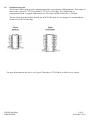
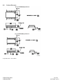
USB I/O Data Sheet
802x00
802600 USB Chip 16 Bit IO SOIC24
802300 USB Chip 12 Bit IO DIP20
802200 USB Chip 12 Bit IO SOIC20
802x70
802270 USB Chip 10 Bit IO SOIC18
802370 USB Chip 10 Bit IO DIP18
802670 USB Chip 16 Bit IO SOIC24
802770 USB Chip 16 Bit IO DIP24
Delcom Products
200 William Street
Port Chester, NY 10573
914-934-5170
914-934-5171 Fax
www.delcom-products.com
USB IO Data Sheet
USBIODS.PDF
1 of 16
10/8/2009 Ver2.0
Contents
1.0
2.0
3.0
4.0
Functional Overview
Pin Definitions
Pin Descriptions
Features
4.1
Write Strobe
4.2
Clock Generator
4.3
Port Setup
4.4
Read Buffer
4.5
Scratch Pad
4.6
Event Counter
4.7
Status LED
4.8
RS232 Serial Port
4.9
I2C Port
4.10 64 Bit Read/Write IO Command
4.11 SPI Port
5.0
Firmware Commands
5.1
General
5.2
Command Packet Format
5.3
Write Commands
5.4
Read Commands
6.0
Typical Schematic
7.0
Specifications
7.1
Absolute Maximum Ratings
7.2
Electrical Characteristics
8.0
9.0
10.0
11.0
12.0
Package Diagrams
Ordering Information
Firmware Release Notes
TroubleShooting
Notes
12.1 Power Notes
12.2 Interfacing Notes
USB IO Data Sheet
USBIODS.PDF
2 of 16
10/8/2009 Ver2.0
1.0
Functional Overview
The Delcom USB IO chips provide a preprogrammed low cost solution to USB peripherals. These chips are
based on the Cypress™ CY7C63xxx and the CY7C637xx USB chips. The USB IO chip are
preprogrammed with to support USB connectivity. The chips conform to the USB 1.1 standard.
The data sheets describes both the 802x00 and 802x70 USB chips. For new designs it is recommended to
use the newer 802x70 USB chips.
For more information on this device see Cypress™ data sheet CY7C63000A, available on our website.
USB IO Data Sheet
USBIODS.PDF
3 of 16
10/8/2009 Ver2.0
2.0
Pin Definitions
Name
I/O
P0.0
P0.1
P0.2
P0.3
P0.4
P0.5
P0.6
P0.7
P1.0
P1.1
P1.2
P1.3
P1.4
P1.5
P1.6
P1.7
XTALIN
XTALOUT
CEXT
D+
DVpp
Vcc
Vss
I/O
I/O
I/O
I/O
I/O
I/O
I/O
I/O
I/O
I/O
I/O
I/O
I/O
I/O
I/O
I/O
I
O
I/O
I/O
I/O
-
3.0
802200
802300
20-Pin
1
2
3
4
20
19
18
17
5
16
6
15
10
11
9
14
13
8
12
7
802600
Description
24-Pin
1
2
3
4
24
23
22
21
5
20
6
19
7
18
8
17
12
13
11
16
15
10
14
9
Port 0 bit 0 (I2C SCLK)
Port 0 bit 1 (I2C SDA)
Port 0 bit 2
Port 0 bit 3
Port 0 bit 4
Port 0 bit 5 (SPI MISO)
Port 0 bit 6 (SPI MOSI)
Port 0 bit 7 (SPI SCLK)
Port 1 bit 0
Port 1 bit 1
Port 1 bit 2
Port 1 bit 3
Port 1 bit 4
Port 1 bit 5
Port 1 bit 6
Port 1 bit 7
Clock In*
Clock Out*
Wake Up Pin
USB Data +
USB Data Programming voltage, Connect to Vss
Voltage Supply
Ground
Pin Descriptions
Name
Vcc
Vss
XtalIn
XtalOut
P0.0-7
P1.0-7
D+,DVpp, Cext
Description
Voltage Supply. Nominal 5V, Range 4.0Volts to 5.25Volts
Ground. Connect to ground
Clock Input
Clock Output
Port 0. Low Current GPIO. Programmable sink current & pullup.
Port 1. High Current GPIO. Programmable sink current & pullup.
USB data lines. Requires an external 7.5K resistor connected to D- to Vcc.
Unused pins. Vpp connect to ground. Cext leave open.
*Note - The 802x00 chips require a external 6MHz ceramic resonator as it’s clock source. The 802x70
chips do not require an external oscillator.
USB IO Data Sheet
USBIODS.PDF
4 of 16
10/8/2009 Ver2.0
4.0
Programmed Features
The USB I/O chip provides general 8 bit input output commands as well as individual set and reset
commands of each pin.
4.1
Write Strobe
The write strobe feature allows the USB I/O chip to interface to another device by using a standard 8-bit
data bus with a strobe pin. The data is placed on port 0 and the strobe is selectable on one of the port 1 pins.
Theses functions allow one to eight data bytes to be sent on either a positive and negative strobe (pulse).
The write strobe functions support an optional acknowledge signal.
4.2
Clock Generator
This function generates a clock source with variable frequency and duty cycle. Up to four separate clocks
can be configured. The clock outputs can be selected on port 1 pins 0 through 3.
4.3
Port Setup
These features allow the user to set the programmable output sink current and enable/disable the port pin
pull up resistor. Each port pin is of a open collector type. The sink current level can be set in 16 levels.
Each port pin has a pull up resistor of 16Kohms that can be enabled or disabled.
4.4
Read Buffer
This feature allows the USB I/O chip to interface to a device using a standard 8-bit data bus and a read
strobe pin. Data is read on port 0 with a read strobe (pulse) on one of the selectable port 1 pins. The data
read buffer is 7 bytes deep. If the read data buffer is full, new data will not be accepted and the over flow
flag will be set. Note this function cannot be used while the RS232 functions are in uses.
4.5
Scratch Pad
The scratch pad allows the user to write 8 bytes of user defined information in to the USB I/O device. This
area can be used for storing user variables, states or other information. Note this function cannot be used
while the RS232 functions are in uses.
4.6
Event Counter
The event counter feature allows the counting of events on one of the port 0 pins. The resolution of the
counter is 4 bytes. The active level on the count pins is user selectable.
4.7
Status Led
The status led feature toggles a port pin when there is activity on the USB bus. The feature is only
available on pin P1.3. The pin goes low while the USB I/O chip is processing the USB command. The
active low pulse is short and therefore may requires a pulse stretcher circuit in order to view.
4.8
RS232 Serial Port
The RS232 functions allow the chip to interface to a RS232 compliant device. Currently the baud rate is
fixed at 2400bit/sec with 8 data bit, one stop bit and no parity. To use the RS232 function first enable it
with commands 10-40, then use command 10-50 to send data and 11-50 to receive data. You can check the
internal buffer count with command 11-9. The RS232 pins are fixed with transmit at port 0 pin 7, receive
at port 0 pin 6 and clear to send at port 0 pin 5. This commands supports a maximum transfer of 7 bytes per
command.
4.9
I2C Port
The I2C functions allow the chip to interface to an I2C compliant device. The I2C port supports the
standard clock rate of 100KHz. The SCLK signal is on port 0 pin 0 and the SDA signal is on port o pin 1.
USB IO Data Sheet
5 of 16
USBIODS.PDF
10/8/2009 Ver2.0
There are four commands associated with the I2C port. They are 10-60 Write, 10-61 Selective read setup,
11-60 Read and 11-61 Selective read. This command supports a maximum transfer of eight bytes per
command.
4.10 64 Bit Read/Write command
The 64 bit read/write commands allows the user to read or write 64 bits (8 Bytes) of data with one
command. This commands requires extra hardware. See the USB64BIO-Sch.pdf schematic on our website.
4.11 SPI Port
Available in 802x70 chips only.
The SPI functions allow the chip to interface to an SPI compliant device. The I2C port supports a variable
clock period from 20ns to 5.1ms. The default clock is 200ns and can be changed with command 10-91.
There are three SPI commands they are 10-90 Write SPI Data, 11-90 Read SPI Data and 11-91 Write 8 bits
Read 1-64 bits. The SCLK signal is on port 0 pin 7, the MOSI signal is on port 0 pin 6 and the MISO signal
is on port 0 pin 5. This command supports a maximum transfer of eight bytes per command.
USB IO Data Sheet
USBIODS.PDF
6 of 16
10/8/2009 Ver2.0
5.0
Firmware Commands
5.1
General
All commands are passed to the USB I/O device in a command packet. The command is filled and sent to
the USB I/O device using the DeviceIOControl Windows™ function in the Setupapi.dll. Alternatively you
can uses the DelcomDLL which has specific functions already defined. See the USB I/O Programming
Manual and the Delcom DLL Manual available on our web site for more information.
All command packets are at least 8 byte long (16 bytes Max) and all receive data is 8 bytes long.
5.2
Command Packet Format:
Recipient
Byte Always 8 for the USB IO device.
Device Model
Byte Always 18 for the USB IO device
Major Command
Byte See Below
Minor Command
Byte See Below
Data LSB
Byte See Below
Data MSB
Byte See Below
Length
Short (2 Bytes) Length of DataExtension.
DataExtension
0-8 Bytes – (Optional) Version 5 and up.
USB IO Data Sheet
USBIODS.PDF
7 of 16
10/8/2009 Ver2.0
5.3
Write Commands
Command
Number
Major
Minor
VER
Family
Data
Length
Command Description
10
-
-
WRITE FUNCTIONS
10
10
10
10
10
0
1
2
10
11
0
0
0
0
0
10
12
0
10
13
0
10
14
0
10
15
1-8
10
16
1-8
Port Write Functions
Dummy command. Does nothing, used for testing.
Writes the LSB to port 0. Port 0 is defaulted high after reset.
Writes the LSB to port 1. Port 1 is defaulted high after reset.
Writes the LSB to port 0 and the MSB to port 1.
Sets or resets the port 0 pins individually. The LSB resets the corresponding port pin(s) and the MSB sets the
corresponding port pin(s) on port 0. Resetting the port pin(s) takes precedence over setting the bits.
Sets or resets the port 1 pins individually. The LSB resets the corresponding port pin(s) and the MSB sets the
corresponding port pin(s) on port 1. Resetting the port pin(s) takes precedence over setting the bits.
Write strobe high function. This commands writes the LSB to port 0 and then toggles the corresponding pin
marked in the MSB byte high then low. See Write strobe function sequence below.
Write strobe low function. This commands writes the LSB to port 0 and then toggles the corresponding pin
marked in the MSB byte low then high. See Write strobe function sequence below.
Write strobe function sequence. This command produces the following sequence; 1) Data in LSB is written to
Port 0. 2) The strobe pin is set active for 1.5ms. If the acknowledge pin is enabled the strobe pin will wait while
the acknowledge pin is held low (See command 10-40 bit 3). 3) Then the strobe pin is made non-active. 4) And
finally 0xFF is written to Port 0. The strobe pin and the data on port 0 must be initially preset before using this
function.
Write 8-byte strobe high function. This commands writes the Data Extension data to port 0 and then toggles the
corresponding pin marked in the MSB byte high then low and then delays for the specified time set in the LSB
byte. See Write 8-byte strobe function sequence below.
Write8-byte strobe low function. This commands writes the Data Extension data to port 0 and then toggles the
corresponding pin marked in the MSB byte low then high and then delays for the specified time set in the LSB
byte. See Write 8-byte strobe function sequence below.
Write 8-byte strobe function sequence. This command produces the following sequence; 1) Data in Data
Extension is written to Port 0 LSB first. 2) The strobe pin is set active for 1.5us. If the acknowledge pin is
enabled the strobe pin will wait while the acknowledge pin is held low (See command 10-40 bit 3). 3) Then the
strobe pin is made non-active. 4) And finally 0xFF is written to Port 0. 4) System then delays for the specified
time set in Data LSB byte. 5) Then the process is repeated till all data bytes in the Data Extension have been
sent. The delay is equal to 8.25us+(0.75us*DelayValue) Example: Command 8,18,10,15,10,1,4,0,0,0,0 will
send 4 bytes of data (all zeros here) on a high strobe on pin one of port one with a delay of 15.75us. The strobe
pin and the data on port 0 must be initially preset before using this function.
Write 64 Bit Command. This command writes 8 bytes of data to the external hardware latches. The data is
passed in the data extension registers. The LSB of the data extension is written to address zero. This commands
requires external hardware. See USB64BIO-Sch.pdf on our website.
Loads the Clock Generator Global Pre-scalar value. Default value is 10, range = 1 to 255. This value is passed
in the LSB register. Increasing this number decreases all the clock function frequencies.
10
17
8
10
19
0
10
20
0
10
10
10
10
21
22
23
24
0
0
0
0
10
25
0
10
10
10
10
26
27
28
29
0
0
0
0
10
30
0
10
31
0
10
32
0
USB IO Data Sheet
USBIODS.PDF
5
5
5
8
Enables or disables the clock generator on port 1. The lower nibble of the LSB disables the corresponding port
pin(s) and the lower nibble of the MSB enables the corresponding port pin(s). Disabling the port pin(s) takes
precedence over enabling.
Loads the frequency and duty cycle for port 1 pin 0. See below for format.
Loads the frequency and duty cycle for port 1 pin 1. See below for format.
Loads the frequency and duty cycle for port 1 pin 2. See below for format.
Loads the frequency and duty cycle for port 1 pin 3. See below for format.
Frequency and duty format. The LSB sets the period when the port pin is high and the MSB sets the period
when the port pin is low. The resolution of the period is 10ms. The resolution of the duty cycle is 0.39
percent. The minimum clock frequency is 25.6 seconds at 50% duty. The maximum clock frequency is 100ms
at 50% duty. Clock pins can be preset to a predefined state
Synchronizes the clock generation. This command synchronizes all the clock generators to start at an initial
phase delay, see below. The lower nibble of the LSB enables this function on the corresponding pins P1.0 to
P1.3. The lower nibble of the MSB presets the initial value on the corresponding pins P1.0 to P1.3. Initial phase
delay resolution is in 10ms and is passed in the LSB register. Initial phase delay registers are cleared after this
command is sent. Therefore the initial phase delay registers must be set each time this command is called.
Load initial phase delay on port 1 pin 0. See Synchronies function above.
Load initial phase delay on port 1 pin 1. See Synchronies function above.
Load initial phase delay on port 1 pin 2. See Synchronies function above.
Load initial phase delay on port 1 pin 3. See Synchronies function above.
Port Setup Functions
Enable or disable port 0 pull up resistors. A low bit in the LSB enable the corresponding port 0 pull up. A
high bit in LSB disables the corresponding port 0 pull up. The pull up resistor value is 16K. Default value is
0x00, all port 0 pull ups enabled.
Enable or disable port 1 pull up resistors. A low bit in the LSB enables the corresponding port 1 pull up. A
high bit in LSB disables the corresponding port 1 pull up. The pull up resistor value is 16K. Default value is
0x00, all port 1 pull ups enabled.
Setup port 0 pins sink current level. This functions sets the current sinking level of the port 0. The maximum
8 of 16
10/8/2009 Ver2.0
10
33
0
10
34
0
10
35
0
10
37
0
10
38
0
10
40
0
10
43
0
10
44
0
10
45
0
10
46
0
10
47
0
10
48
0
current sinking ability of port 0 is 1.5mA and the minimum current sinking ability is 0.3mA. The default value
for port 0 is 0x00. See below for format.
Setup port 1 pins sink current level. This functions sets the current sinking level of the port 0. The maximum
current sinking ability of port 1 is 24mA and the minimum current sinking ability is 1.5mA. The default value
for port 1 is 0x00. See below for format.
Setup port pin sink current level. The MSB selects which pin to set the sinking current level on. A zero in the
MSB selects the pin 0 and a 7 in the MSB selects pin 7. The lower nibble of LSB sets the current sinking level
of the port pin. A LSB of 0x00 sets the lowest current level and a LSB of 0x0F sets the highest current level.
Default value is 0x00, lowest current setting. Both ports can only source current at Vcc/16K when the pull up
is enabled, for example if the Vcc is 5volts a port pin would source 0.3mA maximum.
Load the PWM value for ports P1.0, P1.1, P1.2 and P1.3.
Port pins P1.0 through P1.3 can be placed is PWM mode by writing the PWM value with this command. The
LSB Data parameter is the port pin number, range is 0-3. The MSB Data parameter is the PWM value, range is
0-100.
Feature commands
Setup read buffer function. This command sets up the micro to read the current values on port 0 when a read
strobe in presented on the configured strobe pin on port 1. The LSB will enable the correspond pin on port 1 to
latch data on port 0 on the active edge. The active edge is set up the pull ups command 10-30 and 10-31. If the
pull-ups are enabled then the active transition is from high to low. Otherwise the active transition is from low to
high. The read buffer is only 7 bytes deep. Default is 0x00, read buffer disabled. See read buffer command
below (11-5). Note this function cannot be used while the RS232 functions are in uses.
802x70
Write scratch pad area. Writes the LSB to the scratch pad. The MSB contains the pointer to the scratch pad.
Pointer values can range from 0 to 7. The scratch pad area is 8 bytes deep. This area can be used for storing
user variables, states or information. Defaulted to all 0x00 on boot up. Note this function cannot be used while
the RS232 functions are in uses.
Enable/Disable Events Counter. This command sets up the event counter. LSB data byte enables this function
on the corresponding pin on port 0. The MSB data byte disabled this function on the corresponding pin on port
0. Once enabled the system will count events on the enabled pin on the active edge. The active edge is
configured by the pull ups command 10-30 and 10-31. If the pull-ups are enabled then the active transition is
from high to low. Otherwise the active transition is from low to high. The event counter value is read with
command 11-8. This feature is off by default.
Enable/Disable Control Register. This function sets the control register value. Each bit in this register controls
different options. The LSB data byte is written to this control register.
Bit 0: Status LED. When set Port1 pin 3 (P1.3) will toggle low when USB communications are present. Only
available on this pin.
Bit 1: Enables the RS232 Serial port with fixed 2400 baud rate. Version 5.
Bit 3: Enables the acknowledge pin in the write strobe functions 13,14,15 &16. The acknowledge pin is only
available on pin P1.2 and is active low. The write strobe will be extended while the acknowledge pin is held
low. Version 8.
Bits7-4,2: Future Implementation. These bits are reserved for future implementation and should be set to zero
for future compatibility.
Set Port 0 Interrupt Edge.
The LSB Data parameter sets the Port 0 Interrupt Edge. 1= Rising edge, 0=Falling edge.
Set Port 1 Interrupt Edge.
The LSB Data parameter sets the Port 1 Interrupt Edge. 1= Rising edge, 0=Falling edge.
Configures Port 0 GPIO – Mode 0 Register
The LSB data parameter is the value passed. Each bit represents a port pin. See the GPIO Mode table below.
Configures Port 0 GPIO – Mode 1 Register
The LSB data parameter is the value passed. Each bit represents a port pin. See the GPIO Mode table below.
Configures Port 1 GPIO – Mode 0 Register
The LSB data parameter is the value passed. Each bit represents a port pin. See the GPIO Mode table below.
Configures Port 1 GPIO – Mode 1 Register
The LSB data parameter is the value passed. Each bit represents a port pin. See the GPIO Mode table below.
GPIO Mode table
Mode 1 Value
Mode 0 Value
Port type when
Port type when
data out is low
data out is high
0
0
Hi-Z / CMOS
Hi-Z / TTL
0
1
Medium (8mA)
High (30mA)
Sink / CMOS
Drive / CMOS
1
0
Low (2mA) Sink /
Pull up (14K) /
Default / Boot up
CMOS
CMOS
Mode
1
1
High (50mA) Sink High (30mA)
/ CMOS
Drive / CMOS
Maximum cumulative source drive current for all GPIO is 30mA.
Maximum cumulative sink drive current for all GPIO is 70mA.
See http://www.delcom-eng.com/downloads/cy7c637xx-B.pdf for more GPIO details.
802x70
802x70
802x70
802x70
802x70
802x70
802x70
10
50
1-8
Writes to the RS232 Serial Port
This command sends data to the serial port. Both the data count and data are passed in the Data Extension. The
MSB and LSB bytes should be zero. The data count is in the LSB byte ( first byte of the DataExt) and the data
is in the remaining 7 bytes. Issuing this command clears the TX Status register (see 11-9). Example command
8,18,0,0,6,5,1,2,3,4,5 will send 5 bytes of data (1,2,3,4,5) to the serial port.
5
10
60
1-8
Write to the I2C Port
6
USB IO Data Sheet
USBIODS.PDF
9 of 16
10/8/2009 Ver2.0
10
61
0
10
77
8
10
86
8
10
90
0-8
10
91
0
USB IO Data Sheet
USBIODS.PDF
This command write the data found in the data extension to the I2C device. The device address/command is set
in the Data LSB byte and the number of bytes to send is set in the Data MSB byte. If an error occurs bit 4/7 of
byte 7 is set, else reset. See command 11-9.
I2C Selective Read Setup
This commands setups the selective read command 11-61. The Data LSB should be set to the device
address/command and the Data MSB should be set to the selective read address. See 11-61 for more
information.
Toggle Pin Function
This command will toggle the GPIO pins. Any GPIO pin on ports port0 and port1 can be toggled. To toggle
GPIO on port0 set the corresponding pin high in the LSBData parameter. For port1 use the MSBData
parameter. The function will toggle all the pins marked in LSBData and MSBData for X number of times. The
number of times -1 is passed in the DataExt0 variable. The DataExt1 variable holds the delay parameter. The
delay value equals 6us+(0.76us*DelayValue). See Toggle Pin Command for more in for.
This
Pulse Pin Function
This command allows the user to send a custom pulse stream on port 0 or port 1. The command
number is 76. All 8bits on either port0 or port1 can be changed. The LSBData parameter contains
the delay prescaler and the port select bit. Bit 7 of the LSBData selects the port, a low selects port 0
and high selects port 1. The remaining bits 6 through 0 hold the prescaler value. The prescaler range
is 0 to 127. The delay between the states is equal to (DelayValue+1) x Prescalar x ~2us. There are 5
port pin state change parameters and 4 delay parameters. The change the port data parameters
change the port value by executing a XOR with the current port value and the StateXPortXORData
value. So to toggle a pin set the StateXPortXORData bit value high. You can toggle as many pins as
you like. Up to 5 states can be set, for less than 5 states set the remaining data to all zeros. The
initial port value should be preset with the write port command. Note this command processes inline
and therefore no other command will be processed till this command terminates.
Write to the SPI port
This commands writes up to 8 bytes of data (passed in the DataExt) to the SPI port. The number of bit to write
is passed in the LSB Byte, range is 1-64. Also see command 11-91
Setup SPI Port
This command configures the SPI CLK timing. The LSB byte specify the SPI clock period. Default is 10 and
the units are 20us.
6
21
802x70
20
802x70
15
802x70
15
802x70
10 of 16
10/8/2009 Ver2.0
5.4
Read Commands
Command
Number
Major
Minor
ver
Data
Length
Command Description
11
-
-
READ FUNCTIONS
All read functions return 8 bytes. See individual commands for format.
11
0
0
Read ports 0 and port 1. The first byte (LSB) will contain the current value on port 0 and the second byte (MSB)
will contain the current value on port 1.
11
1
0
11
2
0
Reads port 0 with High strobe. Reads the current data on port 0 with a high strobe on pin X on port 1. The LSB
sets up which pin is to be used for the high strobe. See Read port 0 with strobe sequence below.
Reads port 0 with Low strobe. Reads the current data on port 0 with a low strobe on pin X on port 1. The LSB
sets up which pin is to be used for the low strobe. See Read port 0 with strobe sequence below.
Read port 0 with strobe sequence. These commands produce the following sequence; 1) The selected strobe pin is
made active. 2)Micro waits 1.5ms. 3) Data is latch from port 0 and stored. 4) The strobe pin is released. The
strobe pin and the data on port 0 must to preset before using this function.
Default is 0x00, command disabled.
11
5
0
Reads the Read Buffer. This command is setup with the read Buffer Setup Command(10-35). The LSB byte
returned is the read buffer status byte, it will contain the number of bytes available in the read buffer. The next 7
bytes contain the data. The read data buffer is only 7 bytes deep. Data is filled from byte 1 to byte 7. If the read
data buffer is full and another read strobe is presented then the read buffer status byte will be set to 0xFF and the
new data byte would be lost. The user must check the read status byte to if; new data is present, not present or
present with data over run. This commands resets the read status byte to zero. Note this function cannot be used
when the RS232 function is in use.
11
7
0
Reads the 8 bytes in the scratch pad area. Default values are zero.
11
8
0
Reads the event counter value. This command returns the 4 byte event counter value and then resets the counter.
If the counter over flows then the over flow status byte will be set to 0xFF otherwise it will be 0x0. The event
counter is returned in the first 4 bytes and the over flow byte is in the 5 byte.
11
9
0
Reads system variables. This function returns the following system variables.
Byte0: Control Register.
Byte1: Clock Generator Pre-Scalar.
Byte2: Port 0 Pull Up Register.
Byte3: Port 1 Pull Up Register.
Byte4: USB Port Address.
Byte5: RS232 Rx Status. Returns the available data count in the lower nibble.
Bit 7of 7 is set on Rx Buffer overflow and bit 6/7 is set on Rx framing error.
Byte6: RS232 Tx Status. The lower nibble returns the number of data bytes still pending in the Tx buffer.
Bit 7of 7 is set on a Tx buffer overflow.
Byte7: Bit 4/7 is set if an I2C error is detected. This bit is update each time an I2C function is called.
11
10
0
Reads the firmware information.
Byte 0-3: Unique Device Serial Number. DWORD Little Endian.
Byte 4: Firmware Version.
Byte 5: Firmware Date.
Byte 6: Firmware Month.
Byte 7: Firmware Year.
11
12
0
Reads 8 bytes of memory data.
This is peek functions used only for firmware debugging.
The LSB data bytes contains the start address of the 8 returned bytes.
5
11
17
1-8
8
11
18
1-8
Read 64 Bit Command. This command reads 8 bytes of data from the external hardware. The LSB of the returned
data is address zero. This commands requires external hardware. See USB64BIO-Sch.pdf on our website.
Write 2 bytes, Read 8 byte Command. This command reads 8 bytes of data from the external hardware, similar to
the above command. But the data in DataLSB and DataMSB is write to the write address latch 0 and 1
respectively. This command was added to increase through put. This commands requires external hardware. See
USB64BIO-Sch.pdf on our website.
11
50
0
USB IO Data Sheet
USBIODS.PDF
Reads the RS232 Rx Buffer.
This byte returns 8 bytes, the first byte is the Rx Buffer Status and data count and the remaining bytes are the
RS232 data bytes. The Rx buffer is 7 bytes deep and is in LSB first order. The Rx Status and data count byte are
cleared when this command is issued. The lower nibble of the status byte contains the Rx buffer data length count,
pin 7of 7 of the rx status byte is set on an Rx overflow and pin 6 of 7 is set on a Rx framing error. Note you can
read both the Rx Status and Tx Status bytes with command 11-9 without clearing there content.
10
5
11 of 16
10/8/2009 Ver2.0
11
60
0
Reads from the I2C Port.
Reads 1 to 8 bytes of data from the I2C port. The device address/command is set in the data LSB byte and the
number of requested bytes to read is set in the data MSB byte. If an error occurs bit 4/7 of byte 7 is set, else reset.
See command 11-9.
6
11
61
0
Selective Reads from the I2C Port.
This function sends a selective read command to the device, allowing the selective address to be sent before the
read command is sent. This command is typically used in nonvolatile RAM type device such as the Xicor
X24C04. The device address/command is set in the data LSB and the number of bytes requested is set in the data
MSB byte. The selective address is setup with command 10-61. This command produces the following sequence;
start, device address from 10-61 LSB byte is sent, selective address byte from 10-61 MSB byte is sent, start is sent
again, the device address/command (LSB data from this command) is sent, then the data from the device is read
and returned to the user. If an error occurs bit 4/7 of byte 7 is set, else reset. See command 11-9.
6
11
90
0-8
15
802x70
11
91
0-8
Read SPI Data
Reads up to 8 bytes (64bits) of data from the SPI port. To read data from the SPI port first send the 10-90 Write
SPI data command and then send this command. This command only returns the SPI data from the last 10-90
command issued. LSB and MSB bytes not used.
Write 1Byte Read 1-64 bits SPI
Writes 1 byte of SPI data with 64 clocks and then returns 64bits (8Bytes) of data. This command simultaneously
writes/reads to increase through put. The LSB byte should be set to the number of clocks required. The MSB byte
should be sent to the byte to write. The write size limited to 1 byte.
USB IO Data Sheet
USBIODS.PDF
15
802x70
12 of 16
10/8/2009 Ver2.0
6.0
7.0
Typical Schematic
Note - External oscillator not required on 802x70 chips.
Specifications
7.1
Absolute Maximum Ratings
Storage Temperature
Operating Temperature
Vss relative to Vcc
DC Input Voltage
DC voltage on HiZ pins
Max Current Summed on Port1 pins
Max Current Summed on Port0 pins
Power Dissipation
Static Discharge Voltage
Latch Up Current
7.2
Electrical Characteristics
Vcc Operating Current
Vcc Limits
Port 0 Max Current Sink
Port 0 Min Current Sink
Port 1 Max Current Sink
Port 1 Min Current Sink
Pull Up Resistor
Input Hysteresis Voltages P0 &P1
Packet Bandwidth
USB IO Data Sheet
USBIODS.PDF
-65C to +150C
-0C to +70C
-0.5V to +7.0V
-0.5V to Vcc+0.5V
-0.5V to Vcc+0.5V
60ma
10ma
300mW
>2000V
200mA
25mA
4 to 5.25V
1.5mA
0.3mA
24mA
4.8mA
16Kohms
Min6% Max12% Vcc
100 Packet/sec
13 of 16
10/8/2009 Ver2.0
8.0
Package Diagrams
20 pin DIP 0.300” also available.
USB IO Data Sheet
USBIODS.PDF
14 of 16
10/8/2009 Ver2.0
9.0
Ordering Information
Order Number
Number GPIO
802600*
16
802300*
12
802200*
12
802270
10
802370
10
802670
16
802770
16
* Not recommended for new designs
10.0
Package Type
24 Pin (300Mil) SOIC
20 Pin (0.300”) DIP
20 Pin (300Mil) SOIC
18 Pin (300Mil) SOIC
18 Pin (0.300”) DIP
24 Pin (300Mil) SOIC
24 Pin (0.300”) DIP
Firmware Release Notes
Version 1
- Initial Release
Version 2
- Added data strobe functions.
Version 3
- Added event counter function.
Version 4
- Fixed error with USB enumeration
Version 5
- Added RS232 and 8 byte Strobe Functions.
Version 6
- Added I2C communication functions.
Version 7
- Added buzzer functions.
Version 8
- Added 64 Bit Rd/Wr & Acknowledge pin.
Version 9
- Fixed error with RS232 Rx function.
Version 10
- Added 11-18 write 2 bytes & read 8 byte command.
Version 11
- I2C fixed, regarding data contention during the ACK bit.
Version 12
- 2005-05-25 Fixed I2C Stop condition introduced in v11. Changed I2C Start to SDA high,
then SCLK high to improve Selective reads. Added command 11-62 - Selective read 16 bit,
same as 11-61 but 16bit instead of 8bit address.
Version 12
- 2005-06-16 Added PWM functions on pins P1.0, P1.1 and P1.2, 78.125Hz used for LED
dimming, Default to 100(OFF) is USBIO and 80 in LAMP Firmware only.
Version 13
- 2005-06-29 Added I2C clock stretching option to read and write commands. Maximum
clock stretch per clock is 615us.
Version 14
- 2005-09-19 Re-added command 11-18 that was dropped in version 11 by mistake.
Version 15
- 2005-11-10 Added SPI support - P0.7=SPICLK P0.6=MOSI P0.7=MISO
- Change port configuration to first write 0xFF to the data latch and then change the mode to
open drain. Before the port mode was changed before the port data latch was set. This
caused a momentary low on the output pins.
Version 16
- 2005-11-16 Added string LUT max index test, code now returns a NAK if index is
invalid. Before this fix the USB host could request a index to string passed the end of the
table, this would cause the code to jump to a unknown location.
Version 18
- 2006-04-02 Changed P0.3 to CMOS drive type of USBVIDEL (Beacon only).
Version 19
- 2006-04-02 Change code to check data_toggle on WRITE-OUTS. Before the code was
checkin the DataVaild bit twice instead of the Data ;valid and datatoggle bits.
- 2009- Added Toggle Pin Command.
Version 20
- 2009-07-03 Changed SPI to just toggle the clock from where it started from. Allows users
to use rising or falling clocks with SPI.
Version 21
- 2009-10-08 Added Toggle Pin Command.
USB IO Data Sheet
USBIODS.PDF
15 of 16
10/8/2009 Ver2.0
11.0
Trouble Shooting
If Windows does not see the USB device in the Windows Device Manager or it is listed as an
'Unknown device' then you have a hardware problem. Most common errors are; Reserved D+/D(green/white) wires, 7.5K 1% resistor on incorrect pin, Missing +5Volts or Ground, and VPP pin
not tied to ground. Make sure your cuicuit matches the USBIODEVSCH.pdf schematic available on
the web.
12.0
Notes
12.1 Power Notes
When the device boots up the total current consumed by the device should be at a minimum to comply with
the USB standard.
Cable length and cable size should be selected in order to maintain an operating voltage at the USB I/O
chip of at least 4Volts.
This device can be used in a self-powered mode or with an external power supply if more than 450mA is
required by user. When using external power supplies, connect the USB I/O chip Vcc to the USB supplied
power and run the user added circuitry off the external power supply. Do not connect the USB Vcc and
external power supplies together, only connect the grounds.
12.2 Interfacing
When interfacing the USB I/O chip to other circuitry, one must be careful not to over load the current on
the pins and not to exceed the voltage on the pins. If the voltage or current is greater than and/or less than
the levels on the USB I/O chip, you will have to add some sort of buffering or interfacing. For example
most relays require more than 25mA to actuate the relay, and the USB I/O device can only sink 25mA.
Therefore a current amplifier is required, such as a transistor. When working with excessive currents,
voltages or with high EMI circuits it is recommended that you use relays and/or opto-couplers to isolate the
circuits. See ‘Interfacing to USB I/O Devices’ on the website.
USB IO Data Sheet
USBIODS.PDF
16 of 16
10/8/2009 Ver2.0