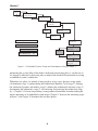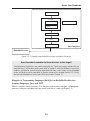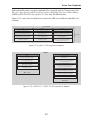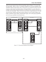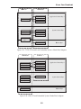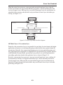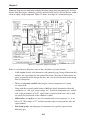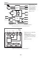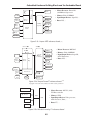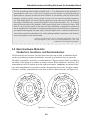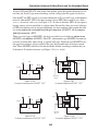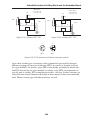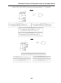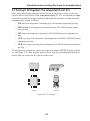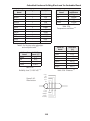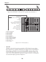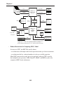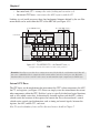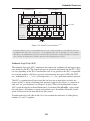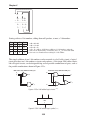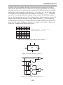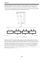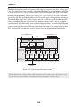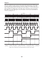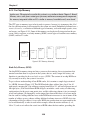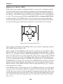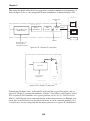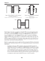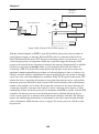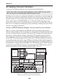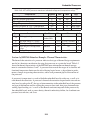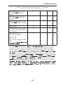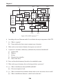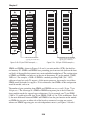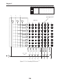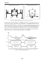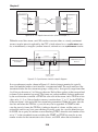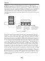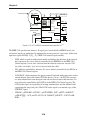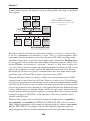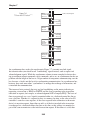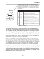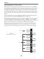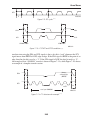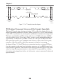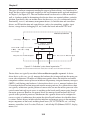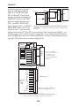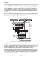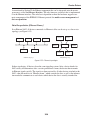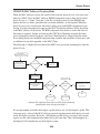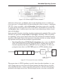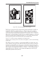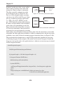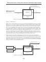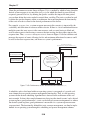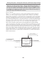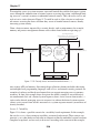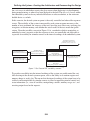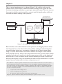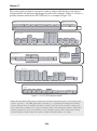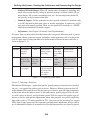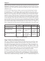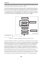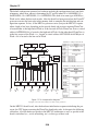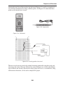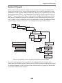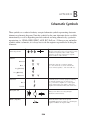
1
Embedded Systems Architecture This Page Intentionally Left Blank Embedded Systems Architecture A Comprehensive Guide for Engineers and Programmers By Tammy Noergaard AMSTERDAM BOSTON HEIDELBERG LONDON NEW YORK OXFORD PARIS SAN DIEGO SAN FRANCISCO SINGAPORE SYDNEY TOKYO Newnes is an imprint of Elsevier 30 Corporate Drive, Suite 400, Burlington, MA 01803, USA Linacre House, Jordan Hill, Oxford OX2 8DP, UK Copyright © 2005, Elsevier Inc. All rights reserved. No part of this publication may be reproduced, stored in a retrieval system, or transmitted in any form or by any means, electronic, mechanical, photocopying, recording, or otherwise, without the prior written permission of the publisher. Permissions may be sought directly from Elsevier’s Science & Technology Rights Department in Oxford, UK: phone: (+44) 1865 843830, fax: (+44) 1865 853333, e-mail: [email protected]. You may also complete your request on-line via the Elsevier homepage (http://elsevier.com), by selecting “Customer Support” and then “Obtaining Permissions.” Recognizing the importance of preserving what has been written, Elsevier prints its books on acid-free paper whenever possible. Library of Congress Cataloging-in-Publication Data (Application submitted.) British Library Cataloguing-in-Publication Data A catalogue record for this book is available from the British Library. ISBN: 0-7506-7792-9 For information on all Newnes publications visit our Web site at www.books.elsevier.com 04 05 06 07 08 09 10 9 8 7 6 5 4 3 2 1 Printed in the United States of America Dedication To the engineer and man I respect and admire the most, my father, Dr. Al M. Zied This Page Intentionally Left Blank Contents Foreword ...................................................................................................................xi Acknowledgments ..................................................................................................xiii About the Author ...................................................................................................xiv Section I: Introduction to Embedded Systems..............................................1 Chapter 1: A Systems Engineering Approach to Embedded Systems Design .......5 1.1 What Is an Embedded System? ...........................................................................................5 1.2 Embedded Systems Design..................................................................................................7 1.3 An Introduction to Embedded Systems Architecture ..........................................................9 1.4 Why Is the Architecture of an Embedded System Important?...........................................11 1.5 The Embedded Systems Model .........................................................................................12 1.6 Summary............................................................................................................................13 Chapter 1 Problems..................................................................................................................15 Chapter 2: Know Your Standards ...........................................................................17 2.1 An Overview of Programming Languages and Examples of Their Standards ..................30 2.2 Standards and Networking.................................................................................................46 2.3 Multiple Standards-Based Device Example: Digital Television (DTV) ...........................65 2.4 Summary............................................................................................................................67 Chapter 2 Problems..................................................................................................................69 Section II: Embedded Hardware ..................................................................73 Chapter 3: Embedded Hardware Building Blocks and the Embedded Board ......77 3.1 Lesson One on Hardware: Learn to Read a Schematic! ....................................................77 3.2 The Embedded Board and the von Neumann Model.........................................................82 3.3 Powering the Hardware......................................................................................................87 3.4 Basic Hardware Materials: Conductors, Insulators, and Semiconductors.........................89 3.5 Common Passive Components on Boards and in Chips: Resistors, Capacitors, and Inductors......................................................................................................................93 3.6 Semiconductors and the Active Building Blocks of Processors and Memory.................101 3.7 Putting It All Together: The Integrated Circuit (IC) ........................................................117 3.8 Summary..........................................................................................................................121 Chapter 3 Problems................................................................................................................122 vii Contents Chapter 4: Embedded Processors..........................................................................129 4.1 ISA Architecture Models .................................................................................................131 4.2 Internal Processor Design ................................................................................................145 4.3 Processor Performance ....................................................................................................203 4.4 Reading a Processor’s Datasheet .....................................................................................206 4.5 Summary..........................................................................................................................218 Chapter 4 Problems................................................................................................................219 Chapter 5: Board Memory .....................................................................................223 5.1 Read-Only Memory (ROM) ............................................................................................227 5.2 Random-Access Memory (RAM)....................................................................................232 5.3 Auxiliary Memory ...........................................................................................................242 5.4 Memory Management of External Memory ....................................................................247 5.5 Board Memory and Performance.....................................................................................249 5.6 Summary..........................................................................................................................250 Chapter 5 Problems................................................................................................................251 Chapter 6: Board I/O (Input/Output) ....................................................................253 6.1 Managing Data: Serial vs. Parallel I/O ...........................................................................257 6.2 Interfacing the I/O Components ......................................................................................277 6.3 I/O and Performance........................................................................................................280 6.4 Summary..........................................................................................................................282 Chapter 6 Problems................................................................................................................283 Chapter 7: Board Buses..........................................................................................287 7.1 Bus Arbitration and Timing .............................................................................................289 7.2 Integrating the Bus with Other Board Components.........................................................299 7.3 Bus Performance..............................................................................................................300 7.4 Summary..........................................................................................................................301 Chapter 7 Problems................................................................................................................302 Section III: Embedded Software Introduction...........................................307 Chapter 8: Device Drivers ......................................................................................311 8.1 Example 1: Device Drivers for Interrupt-Handling .........................................................315 8.2 Example 2: Memory Device Drivers ..............................................................................332 8.3 Example 3: On-board Bus Device Drivers ......................................................................351 8.4 Board I/O Driver Examples .............................................................................................358 8.5 Summary..........................................................................................................................379 Chapter 8 Problems................................................................................................................380 Chapter 9: Embedded Operating Systems ...........................................................383 9.1 What Is a Process? ...........................................................................................................388 9.2 Multitasking and Process Management ...........................................................................390 9.3 Memory Management......................................................................................................421 viii Contents 9.4 I/O and File System Management ...................................................................................435 9.5 OS Standards Example: POSIX (Portable Operating System Interface).........................437 9.6 OS Performance Guidelines.............................................................................................439 9.7 OSes and Board Support Packages (BSPs)......................................................................440 9.8 Summary..........................................................................................................................441 Chapter 9 Problems................................................................................................................442 Chapter 10: Middleware and Application Software............................................445 10.1 What Is Middleware? .....................................................................................................445 10.2 What Is an Application?.................................................................................................447 10.3 Middleware Examples....................................................................................................447 10.4 Application Layer Software Examples ..........................................................................484 10.5 Summary ........................................................................................................................498 Chapter 10 Problems..............................................................................................................499 Section IV: Putting It All Together: Design and Development.................505 Chapter 11: Defining the System—Creating the Architecture and Documenting the Design .................................................................................509 11.1 Creating an Embedded System Architecture .................................................................510 Stage 1: Have a Solid Technical Foundation ...................................................................511 Stage 2: Know the ABCs (Architecture Business Cycles) of Embedded Systems..........512 Stage 3: Define the Architectural Patterns and Reference Models ..................................523 Stage 4: Define the Architectural Structures....................................................................530 Stage 5: Document the Architecture ................................................................................533 Stage 6: Analyze and Evaluate the Architecture ..............................................................535 11.2 Summary ........................................................................................................................537 Chapter 11 Problems..............................................................................................................538 Chapter 12: The Final Phases of Embedded Design: Implementation and Testing........................................................................................................541 12.1 Implementing the Design...............................................................................................541 12.1.1 The Main Software Utility Tool: Writing Code in an Editor or IDE ...................542 12.1.2 Computer-Aided Design (CAD) and the Hardware ............................................543 12.1.3 Translation Tools—Preprocessors, Interpreters, Compilers, and Linkers ...........545 12.1.4 Debugging Tools ..................................................................................................548 12.1.5 System Boot-Up...................................................................................................555 12.2 Quality Assurance and Testing of the Design ................................................................563 12.3 Conclusion: Maintaining the Embedded System and Beyond.......................................566 Chapter 12 Problems..............................................................................................................567 Appendix A: Projects and Exercises ......................................................................571 Section I Projects ...................................................................................................................574 Section II Projects ..................................................................................................................578 ix Contents Section III Projects.................................................................................................................586 Section IV Projects ................................................................................................................589 Appendix B: Schematic Symbols...........................................................................594 Appendix C: Acronyms and Abbreviations ..........................................................601 Appendix D: Glossary ............................................................................................610 Index .......................................................................................................................627 What’s on the CD-ROM..........................................................................................640 x Foreword When Tammy Noergaard first told me she wanted to write a soup-to-nuts book about building embedded systems I tried to dissuade her. This field is so vast, requiring insight into electronics, logic circuits, computer design, software engineering, C, assembly, and far more. But as we talked she showed me how the industry’s literature lacks a definitive work on the subject. I warned her of the immensity of the project. A year and many discussions later Fedex arrived with the review copy of this book. At over 700 pages it’s appropriately twice the size of almost any other opus on the subject. The book you’re holding truly is “A Comprehensive Guide for Engineers and Programmers.” Sure, the minutia of programming a PIC’s timer might have been left out, but the scope is vast and important. Tammy starts with the first principles of electronics and advances through software to the expensive end-phase of maintenance. She treats hardware and software as an integrated whole, which sort of defines the nature of embedded systems. Ironically, though, developers are increasingly specialized. More than a few software folks haven’t a clue about transistors while too many EEs can’t accurately define middleware. I fear readers may skip those chapters that don’t immediately pertain to the project at hand. Resist any such temptation, gentle reader! Become a true master, an embedded sage, by broadening your horizons to cover all aspects of this fascinating field. We engineers are professionals; you and I know this in our hearts. Yet true professionals are those who learn new things, who apply newly evolving technologies to solve problems. Consider doctors: the discovery and production of penicillin in the 1940s changed the profession of medicine forever. Any doc who ignored this new technology, who continued to practice using only the skills learned in college, was suddenly rendered a butcher. Software and hardware developers are faced with the same situation. C wasn’t taught when I went to school. The FPGA hadn’t been invented. GOTOs were still just fine, thank you. We learned to program microprocessors in machine code using primitive toolchains. Today—well, we know how much has changed. The rate of change is increasing; change’s first derivative is an ever-escalating positive number. Professional developers will read this book from cover to cover, and will constantly seek out other sources of information. If you’re not at least surfing through a half dozen technical magazines a month and reading a handful of books like this per year, then it won’t take a Cretaceous asteroid to make you a dinosaur. xi Foreword Some of this book might surprise you. Ten pages about reading datasheets? Fact is, datasheets are dense formal compilations of contractual material. The vendor promises the part will do x as long as we use it in an agreed-on manner. Violate any of perhaps thousands of specifications and the part will either not work or will be unreliable. With some parts dissipating 100 watts or more, even such arcana as thermal characteristics are as important as the device’s instruction set. Tammy’s generous use of examples elucidates the more obscure points. Engineering—whether hardware or software—is the art of building things and solving problems. The academics can work with dry theory; we practicing developers often learn best by seeing how something works. So the chapter on device drivers does explain the intricacies of building these oftencomplex bits of code, but couples the explanation to a wealth of real-world examples. Finally, Tammy’s words about the Architecture Business Cycle of embedded systems resonate strongly with me. We don’t build these things just to have a good time (though we sure hope to have one along the way), but to solve important business problems. Every decision we make has business implications. Use too little horsepower and development costs skyrocket— sometimes to the point of making the project unviable. A poor analysis of the problem that leads you to toss in an excess of Flash might drive costs unacceptably high. Select a component (hardware or software) from a failing company and your outfit may share in the vendor’s demise. Enjoy this book, and futureproof your career at the same time. —Jack Ganssle xii Acknowledgments My greatest debt in creating this book goes to the reviewers, who I hope will be pleasantly surprised to see how many of their suggestions have been incorporated into the book. They include Dr. Al M. Zied, both of my brothers (especially my younger brother who also provided me the inspiration to write this book in the first place), Jack Ganssle, Dr. Volker Enders, Dr. Stefan Frank, Dr. Karl Mathia, and Steve Bailey. Thank you to my publisher Elsevier, specifically to my editor Carol Lewis and the rest of “my” Elsevier team for their hard work and dedication in making this book a reality. I would also like to acknowledge my mentor when I was with Sony Electronics, Kazuhisa Maruoka, who patiently trained me to design televisions and gave me such a strong foundation upon which to grow, as well as my manager at Sony Electronics, Satoshi Ishiguro, who took a chance and hired me. My journey in the embedded systems field that has led me to writing this book began with the great people I worked with at Sony in Japan and in San Diego. A very special thanks to my family for their support, which allowed me to write this book, and without whose support and encouragement I could never have completed it. To my husband, Christian, thank you for giving me the happiest days of my life, and the opportunity and encouragement to realize this book. For my beautiful baby girl Mia, thank you for being so patient with your Mama while I did my writing—always gifting me with endless smiles, hugs, and kisses when I really needed them. Thank you, Mom, for the times you flew out from Belgium, and thanks to my sister Mandy for flying up from Southern California, to help me at home so I could finish my writing, and for encouraging me every step of the way. Finally, a special thanks to Verónica Cervantes Gaona for taking such good care of Mia so that I could have the time and focus to write. I am very grateful for the quality time you spent with her. xiii About the Author Tammy Noergaard is uniquely qualified to write about all aspects of embedded systems architecture. Since beginning her embedded systems career in 1995, she has had wide experience in product development, system design and integration, operations, sales, marketing, and training. She has design experience using many hardware platforms, operating systems, and languages. Noergaard worked for Sony as a lead software engineer developing and testing embedded software for analog TVs, and also managed and trained new embedded engineers and programmers. The televisions that she helped to develop were critically acclaimed and rated #1 in Consumer Reports magazines. At Wind River she was the liaison engineer between developmental engineers and customers to provide design expertise, systems configuration, systems integration, and training for Wind River embedded software (OS, Java, device drivers, etc.) and all associated hardware for a variety of embedded systems in the Consumer Electronic market. Most recently she was a Field Engineering Specialist and Consultant with Esmertec North America, providing project management, system design, system integration, system configuration, support and expertise for various embedded Java systems using Jbed in everything from control systems to medical devices to digital TVs. Noergaard has lectured to engineering classes at the University of California at Berkeley and Stanford, the Embedded Internet Conference, and the Java User’s Group in San Jose, among others. xiv SECTION I Introduction to Embedded Systems This Page Intentionally Left Blank Introduction to Embedded Systems The field of embedded systems is wide and varied, and it is difficult to pin down exact definitions or descriptions. However, Chapter 1 introduces a useful model that can be applied to any embedded system. This model is introduced as a means for the reader to understand the major components that make up different types of electronic devices, regardless of their complexity or differences. Chapter 2 introduces and defines the common standards adhered to when building an embedded system. Because this book is an overview of embedded systems architecture, covering every possible standards-based component that could be implemented is beyond its scope. Therefore, significant examples of current standards-based components were selected, such as networking and Java, to demonstrate how standards define major components in an embedded system. The intention is for the reader to be able to use the methodology behind the model, standards, and real-world examples to understand any embedded system, and to be able to apply any other standard to an embedded system’s design. 3 This Page Intentionally Left Blank CHAPTER 1 A Systems Engineering Approach to Embedded Systems Design In This Chapter fDefine embedded system fIntroduce the design process fDefine an embedded systems architecture fDiscuss the impact of architecture fSummarize the remaining sections of the book 1.1 What Is an Embedded System? An embedded system is an applied computer system, as distinguished from other types of computer systems such as personal computers (PCs) or supercomputers. However, you will find that the definition of “embedded system” is fluid and difficult to pin down, as it constantly evolves with advances in technology and dramatic decreases in the cost of implementing various hardware and software components. In recent years, the field has outgrown many of its traditional descriptions. Because the reader will likely encounter some of these descriptions and definitions, it is important to understand the reasoning behind them and why they may or may not be accurate today, and to be able to discuss them knowledgeably. Following are a few of the more common descriptions of an embedded system: v Embedded systems are more limited in hardware and/or software functionality than a personal computer (PC). This holds true for a significant subset of the embedded systems family of computer systems. In terms of hardware limitations, this can mean limitations in processing performance, power consumption, memory, hardware functionality, and so forth. In software, this typically means limitations relative to a PC—fewer applications, scaled-down applications, no operating system (OS) or a limited OS, or less abstraction-level code. However, this definition is only partially true today as boards and software typically found in PCs of past and present have been repackaged into more complex embedded system designs. v An embedded system is designed to perform a dedicated function. Most embedded devices are primarily designed for one specific function. However, we now see devices such as personal data assistant (PDA)/cell phone hybrids, which are embedded systems designed to be able to do a variety of primary functions. Also, the latest digital TVs include interactive applications that perform a wide variety of general 5 Chapter 1 functions unrelated to the “TV” function but just as important, such as e-mail, web browsing, and games. v An embedded system is a computer system with higher quality and reliability requirements than other types of computer systems. Some families of embedded devices have a very high threshold of quality and reliability requirements. For example, if a car’s engine controller crashes while driving on a busy freeway or a critical medical device malfunctions during surgery, very serious problems result. However, there are also embedded devices, such as TVs, games, and cell phones, in which a malfunction is an inconvenience but not usually a life-threatening situation. v Some devices that are called embedded systems, such as PDAs or web pads, are not really embedded systems. There is some discussion as to whether or not computer systems that meet some, but not all of the traditional embedded system definitions are actually embedded systems or something else. Some feel that the designation of these more complex designs, such as PDAs, as embedded systems is driven by nontechnical marketing and sales professionals, rather than engineers. In reality, embedded engineers are divided as to whether these designs are or are not embedded systems, even though currently these systems are often discussed as such among these same designers. Whether or not the traditional embedded definitions should continue to evolve, or a new field of computer systems be designated to include these more complex systems will ultimately be determined by others in the industry. For now, since there is no new industry-supported field of computer systems designated for designs that fall in between the traditional embedded system and the general-purpose PC systems, this book supports the evolutionary view of embedded systems that encompasses these types of computer system designs. Electronic devices in just about every engineering market segment are classified as embedded systems (see Table 1-1). In short, outside of being “types of computer systems,” the only specific characterization that continues to hold true for the wide spectrum of embedded system devices is that there is no single definition reflecting them all. Table 1-1: Examples of embedded systems and their markets [1-1] Market Embedded Device Automotive Ignition System Engine Control Brake System (i.e., Antilock Braking System) Digital and Analog Televisions Set-Top Boxes (DVDs, VCRs, Cable Boxes, etc.) Personal Data Assistants (PDAs) Kitchen Appliances (Refrigerators, Toasters, Microwave Ovens) Automobiles Toys/Games Telephones/Cell Phones/Pagers Cameras Global Positioning Systems (GPS) Consumer Electronics 6 A Systems Engineering Approach to Embedded Systems Design Table 1-1: Examples of embedded systems and their markets [1-1] (continued) Market Embedded Device Industrial Control Medical Robotics and Control Systems (Manufacturing) Infusion Pumps Dialysis Machines Prosthetic Devices Cardiac Monitors Routers Hubs Gateways Fax Machine Photocopier Printers Monitors Scanners Networking Office Automation 1.2 Embedded Systems Design When approaching embedded systems architecture design from a systems engineering point of view, several models can be applied to describe the cycle of embedded system design. Most of these models are based upon one or some combination of the following development models:[1-5] v The big-bang model, in which there is essentially no planning or processes in place before and during the development of a system. v The code-and-fix model, in which product requirements are defined but no formal processes are in place before the start of development. v The waterfall model, in which there is a process for developing a system in steps, where results of one step flow into the next step. v The spiral model, in which there is a process for developing a system in steps, and throughout the various steps, feedback is obtained and incorporated back into the process. This book supports the model shown in Figure 1-1, which I refer to as the Embedded Systems Design and Development Lifecycle Model. This model is based on a combination of the popular waterfall and spiral industry models.[1-2] When I investigated and analyzed the many successful embedded projects that I have been a part of or had detailed knowledge about over the years, and analyzed the failed projects or those that ran into many difficulties meeting technical and/or business requirements, I concluded that the successful projects contained at least one common factor that the problem projects lacked. This factor is the process shown in Figure 1-1, and this is why I introduce this model as an important tool in understanding an embedded system’s design process. As shown in Figure 1-1, the embedded system design and development process is divided into four phases: creating the architecture, implementing the architecture, testing the system, and 7 Chapter 1 P roduct Concept rPeliminar y Analysis of Requ irements Creation of Architecture Design Develop eVrsio n of Architecture Incorp orat e Feedback Deliver eVrsio n of Architecture Review and Obtain Feedback Deliver Final V ersio n of Architecture hPase 1: Creating the Architecture hPase 2: Impl ementing the Architecture hPase 3: Testing the yS Develop[I mp le ment] the yS stem stem Incorp orat e Feedback hPase 4: aMintaining the yS stem Review and Test the yS stem Deliver and M aintain the yS stem Figure 1-1: Embedded Systems Design and Development Lifecycle Model [1-2] maintaining the system. Most of this book is dedicated to discussing phase 1, and the rest of this chapter is dedicated to discussing why so much of this book has been devoted to creating an embedded system’s architecture. Within this text, phase 1 is defined as being made up of six stages: having a strong technical foundation (stage 1), understanding the Architectural Business Cycle (stage 2), defining the architectural patterns and models (stage 3), defining the architectural structures (stage 4), documenting the architecture (stage 5), and analyzing and reviewing the architecture (stage 6)[1-3]. Chapters 2–10 focus on providing a strong technical foundation for understanding the major components of an embedded system design. Chapter 11 discusses the remaining stages of phase 1, and Chapter 12 introduces the last three phases. 8 A Systems Engineering Approach to Embedded Systems Design 1.3 An Introduction to Embedded Systems Architecture The architecture of an embedded system is an abstraction of the embedded device, meaning that it is a generalization of the system that typically doesn’t show detailed implementation information such as software source code or hardware circuit design. At the architectural level, the hardware and software components in an embedded system are instead represented as some composition of interacting elements. Elements are representations of hardware and/or software whose implementation details have been abstracted out, leaving only behavioral and inter-relationship information. Architectural elements can be internally integrated within the embedded device, or exist externally to the embedded system and interact with internal elements. In short, an embedded architecture includes elements of the embedded system, elements interacting with an embedded system, the properties of each of the individual elements, and the interactive relationships between the elements. Architecture-level information is physically represented in the form of structures. A structure is one possible representation of the architecture, containing its own set of represented elements, properties, and inter-relationship information. A structure is therefore a “snapshot” of the system’s hardware and software at design time and/or at run-time, given a particular environment and a given set of elements. Since it is very difficult for one “snapshot” to capture all the complexities of a system, an architecture is typically made up of more than one structure. All structures within an architecture are inherently related to each other, and it is the sum of all these structures that is the embedded architecture of a device. Table 1-2 summarizes some of the most common structures that can make up embedded architectures, and shows generally what the elements of a particular structure represent and how these elements interrelate. While Table 1-2 introduces concepts to be defined and discussed later, it also demonstrates the wide variety of architectural structures available to represent an embedded system. Architectures and their structures—how they interrelate, how to create an architecture, and so on—will be discussed in more detail in Chapter 11. 9 Chapter 1 Table 1-2: Examples of architectural structures [1-4] Structure Types* Definition Module Elements (referred to as modules) are defined as the different functional components (the essential hardware and/or software that the system needs to function correctly) within an embedded device. Marketing and sales architectural diagrams are typically represented as modular structures, since software or hardware is typically packaged for sale as modules (i.e., an operating system, a processor, a JVM, and so on). Uses (also referred to as subsystem and component) A type of modular structure representing system at runtime in which modules are inter-related by their usages (what module uses what other module, for example). Layers A type of Uses structure in which modules are organized in layers (i.e., hierarchical) in which modules in higher layers use (require) modules of lower layers. Kernel Structure presents modules that use modules (services) of an operating system kernel or are manipulated by the kernel. Channel Architecture Structure presents modules sequentially, showing the module transformations through their usages. Virtual Machine Structure presents modules that use modules of a virtual machine. Decomposition A type of modular structure in which some modules are actually subunits (decomposed units) of other modules, and inter-relations are indicated as such. Typically used to determine resource allocation, project management (planning), data management (encapsulation, privitization, etc.). Class (also referred to as generalization) This is a type of modular structure representing software and in which modules are referred to as classes, and inter-relationships are defined according to the object-oriented approach in which classes are inheriting from other classes, or are actual instances of a parent class (for example). Useful in designing systems with similar foundations. Component and Connector These structures are composed of elements that are either components (main hw/sw processing units, such as processors, a Java Virtual Machine, etc.) or connectors (communication mechanism that inter-connects components, such as a hw bus, or sw OS messages, etc.). Client/Server (also referred to as distribution) Structure of system at runtime where components are clients or servers (or objects), and connectors are the mechanisms used (protocols, messages, packets, etc.) used to intercommunicate between clients and servers (or objects). Process (also referred to as communicating processes) This structure is a SW structure of a system containing an operating system. Components are processes and/or threads (see Chapter 9 on OSes), and their connecters are the inter-process communication mechanisms (shared data, pipes, etc.) Useful for analyzing scheduling and performance. Concurrency and Resource This structure is a runtime snap shot of a system containing an OS, and in which components are connected via threads running in parallel (see Chapter 9, Operating Systems). Essentially, this structure is used for resource management and to determine if there are any problems with shared resources, as well as to determine what sw can be executed in parallel. Interrupt Structure represents the interrupt handling mechanisms in system. Scheduling (EDF, priority, roundrobin) Structure represents the task scheduling mechanism of threads demonstrating the fairness of the OS scheduler. Memory Safety and Reliability Allocation This runtime representation is of memory and data components with the memory allocation and deallocation (connector) schemes—essentially the memory management scheme of the system. Garbage Collection This structure represents the garbage allocation scheme (more in Chapter 2). Allocation This structure represents the memory allocation scheme of the system (static or dynamic, size, and so on). This structure is of the system at runtime in which redundant components (hw and sw elements) and their intercommunication mechanisms demonstrate the reliability and safety of a system in the event of problems (its ability to recover from a variety of problems). A structure representing relationships between sw and/or hw elements, and external elements in various environments. Work Assignment This structure assigns module responsibility to various development and design teams. Typically used in project management. Implementation This is a sw structure indicating where the sw is located on the development system’s file system. Deployment This structure is of the system at runtime where elements in this structure are hw and sw, and the relationship between elements are where the sw maps to in the hardware (resides, migrates to, etc). * Note that in many cases the terms “architecture” and “structure” (one snapshot) are sometimes used interchangeably, and this will be the case in this book. 10 A Systems Engineering Approach to Embedded Systems Design 1.4 Why Is the Architecture of an Embedded System Important? This book uses an architectural systems engineering approach to embedded systems because it is one of the most powerful tools that can be used to understand an embedded systems design or to resolve challenges faced when designing a new system. The most common of these challenges include: v v v v defining and capturing the design of a system cost limitations determining a system’s integrity, such as reliability and safety working within the confines of available elemental functionality (i.e., processing power, memory, battery life, etc.) v marketability and sellability v deterministic requirements In short, an embedded systems architecture can be used to resolve these challenges early in a project. Without defining or knowing any of the internal implementation details, the architecture of an embedded device can be the first tool to be analyzed and used as a high-level blueprint defining the infrastructure of a design, possible design options, and design constraints. What makes the architectural approach so powerful is its ability to informally and quickly communicate a design to a variety of people with or without technical backgrounds, even acting as a foundation in planning the project or actually designing a device. Because it clearly outlines the requirements of the system, an architecture can act as a solid basis for analyzing and testing the quality of a device and its performance under various circumstances. Furthermore, if understood, created, and leveraged correctly, an architecture can be used to accurately estimate and reduce costs through its demonstration of the risks involved in implementing the various elements, allowing for the mitigation of these risks. Finally, the various structures of an architecture can then be leveraged for designing future products with similar characteristics, thus allowing design knowledge to be reused, and leading to a decrease of future design and development costs. By using the architectural approach in this book, I hope to relay to the reader that defining and understanding the architecture of an embedded system is an essential component of good system design. This is because, in addition to the benefits listed above: 1. Every embedded system has an architecture, whether it is or is not documented, because every embedded system is composed of interacting elements (whether hardware or software). An architecture by definition is a set of representations of those elements and their relationships. Rather than having a faulty and costly architecture forced on you by not taking the time to define an architecture before starting development, take control of the design by defining the architecture first. 2. Because an embedded architecture captures various views, which are representations of the system, it is a useful tool in understanding all of the major elements, why each component is there, and why the elements behave the way they do. None of the 11 Chapter 1 elements within an embedded system works in a vacuum. Every element within a device interacts with some other element in some fashion. Furthermore, externally visible characteristics of elements may differ given a different set of other elements to work with. Without understanding the “whys” behind an element’s provided functionality, performance, and so on, it would be difficult to determine how the system would behave under a variety of circumstances in the real world. Even if the architectural structures are rough and informal, it is still better than nothing. As long as the architecture conveys in some way the critical components of a design and their relationships to each other, it can provide project members with key information about whether the device can meet its requirements, and how such a system can be constructed successfully. 1.5 The Embedded Systems Model Within the scope of this book, a variety of architectural structures are used to introduce technical concepts and fundamentals of an embedded system. I also introduce emerging architectural tools (i.e., reference models) used as the foundation for these architectural structures. At the highest level, the primary architectural tool used to introduce the major elements located within an embedded system design is what I will refer to as the Embedded Systems Model, shown in Figure 1-2. Application Software Layer (Optional) System Software Layer (Optional) Hardware Layer (Required) Figure 1-2: Embedded Systems Model What the Embedded Systems Model indicates is that all embedded systems share one similarity at the highest level; that is, they all have at least one layer (hardware) or all layers (hardware, system software and application software) into which all components fall. The hardware layer contains all the major physical components located on an embedded board, whereas the system and application software layers contain all of the software located on and being processed by the embedded system. This reference model is essentially a layered (modular) representation of an embedded systems architecture from which a modular architectural structure can be derived. Regardless of the differences between the devices shown in Table 1-1, it is possible to understand the architecture of all of these systems by visualizing and grouping the components within these devices as layers. While the concept of layering isn’t unique to embedded system design (architectures are relevant to all computer systems, and an embedded system is a type 12 A Systems Engineering Approach to Embedded Systems Design of computer system), it is a useful tool in visualizing the possible combinations of hundreds, if not thousands, of hardware and software components that can be used in designing an embedded system. In general, I selected this modular representation of embedded systems architecture as the primary structure for this book for two main reasons: 1. The visual representation of the main elements and their associated functions. The layered approach allows readers to visualize the various components of an embedded system and their interrelationship. 2. Modular architectural representations are typically the structures leveraged to structure the entire embedded project. This is mainly because the various modules (elements) within this type of structure are usually functionally independent. These elements also have a higher degree of interaction, thus separating these types of elements into layers improves the structural organization of the system without the risk of oversimplifying complex interactions or overlooking required functionality. Sections 2 and 3 of this book define the major modules that fall into the layers of the Embedded Systems Model, essentially outlining the major components that can be found in most embedded systems. Section 4 then puts these layers together from a design and development viewpoint, demonstrating to the reader how to apply the technical concepts covered in previous chapters along with the architectural process introduced in this chapter. Throughout this book, real-world suggestions and examples are provided to present a pragmatic view of the technical theories, and as the key teaching tool of embedded concepts. As you read these various examples, in order to gain the maximum benefits from this text and to be able to apply the information provided to future embedded projects, I recommend that the reader note: v the patterns that all these various examples follow, by mapping them not only to the technical concepts introduced in the section, but ultimately to the higher-level architectural representations. These patterns are what can be universally applied to understand or design any embedded system, regardless of the embedded system design being analyzed. v where the information came from. This is because valuable information on embedded systems design can be gathered from a variety of sources, including the internet, articles from embedded magazines, the Embedded Systems Conference, data sheets, user manuals, programming manuals, and schematics—to name just a few. 1.6 Summary This chapter began by defining what an embedded system is, including in the definition the most complex and recent innovations in the market. It then defined what an embedded systems architecture is in terms of the sum of the various representations (structures) of a system. This chapter also introduced why the architectural approach is used as the approach to introducing embedded concepts in this book, because it presents a clear visual of what the system is, or could be, composed of and how these elements function. In addition, this approach can provide early indicators into what may and may not work in a system, and possibly improve the integrity of a system and lower costs via reusability. 13 Chapter 1 The next chapter contains the first real-world examples of the book in reference to how industry standards play into an embedded design. Its purpose is to show the importance of knowing and understanding the standards associated with a particular device, and leveraging these standards to understand or create an architecture. 14 Chapter 1 Problems 1. Name three traditional or not-so-traditional definitions of embedded systems. 2. In what ways do traditional assumptions apply and not apply to more recent complex embedded designs? Give four examples. 3. [T/F] Embedded systems are all: A. medical devices. B. computer systems. C. very reliable. D. All of the above. E. None of the above. 4. [a] [b] Name and describe five different markets under which embedded systems commonly fall. Provide examples of four devices in each market. 5. Name and describe the four development models which most embedded projects are based upon. 6. [a] [b] [c] [d] 7. Which of the stages below is not part of creating an architecture, phase 1 of the Embedded Systems Design and Development Lifecycle Model? A. Understanding the architecture business cycle. B. Documenting the architecture. C. Maintaining the embedded system. D. Having a strong technical foundation. E. None of the above. 8. Name five challenges commonly faced when designing an embedded system. 9. What is the architecture of an embedded system? What is the Embedded Systems Design and Development Lifecycle Model [draw it]? What development models is this model based upon? How many phases are in this model? Name and describe each of its phases. 15 Chapter 1 10. [T/F] Every embedded system has an architecture. 11. [a] [b] What is an element of the embedded system architecture? Give four examples of architectural elements. 12. What is an architectural structure? 13. Name and define five types of structures. 14. [a] [b] Name at least three challenges in designing embedded systems. How can an architecture resolve these challenges? 15. [a] [b] [c] [d] What is the Embedded Systems Model? What structural approach does the Embedded Systems Model take? Draw and define the layers of this model. Why is this model introduced? 16. Why is a modular architectural representation useful? 17. All of the major elements within an embedded system fall under: A. The Hardware Layer. B. The System Software Layer. C. The Application Software Layer. D. The Hardware, System Software, and Application Software Layers. E. A or D, depending on the device. 18. Name six sources that can be used to gather embedded systems design information. 16 CHAPTER 2 Know Your Standards In This Chapter fDefining the meaning of standards fListing examples of different types of standards fDiscussing the impact of programming language standards on the architecture fDiscussing the OSI model and examples of networking protocols fUsing digital TV as an example that implements many standards Some of the most important components within an embedded system are derived from specific methodologies, commonly referred to as standards. Standards dictate how these components should be designed, and what additional components are required in the system to allow for their successful integration and function. As shown in Figure 2-1, standards can define functionality that is specific to each of the layers of the embedded systems model, and can be classified as market-specific standards, general-purpose standards, or standards that are applicable to both categories. Market Specific Standards General Purpose Standards PJava J2ME SSL128 .NET Ethernet TCP/IP HTTP … Application Software Layer MHP ATSC DTV HAVi FDA System Software Layer … … Hardware Layer Figure 2-1: Standards diagram Standards that are strictly market-specific define functionality that is relative to a particular group of related embedded systems that share similar technical or end user characteristics, including: 17 Chapter 2 v Consumer Electronics. Typically includes devices used by consumers in their personal lives, such as PDAs (personal data assistants), TVs (analog and digital), games, toys, home appliances (i.e., microwave ovens, dishwashers, washing machines), and internet appliances.[2-1] v Medical. Defined as “...any instrument, apparatus, appliance, material or other article, whether used alone or in combination, including the software necessary for its proper application intended by the manufacturer to be used for human beings for the purpose of: – diagnosis, prevention, monitoring, treatment or alleviation of disease, – diagnosis, monitoring, treatment, alleviation of or compensation for an injury or handicap, – investigation, replacement or modification of the anatomy or of a physiological process, – control of conception, and which does not achieve its principal intended action in or on the human body by pharmacological, immunological or metabolic means, but which may be assisted in its function by such means...” —European Medical Device Directive (93/42/EEC) [2-14] This includes dialysis machines, infusion pumps, cardiac monitors, drug delivery, prosthetics, and so forth.[2-1] v Industrial Automation and Control. “Smart” robotic devices (smart sensors, motion controllers, man/machine interface devices, industrial switches, etc.) used mainly in manufacturing industries to execute a cyclic automated process.[2-1] v Networking and Communications. Intermediary devices connecting networked end systems, devices such as hubs, gateways, routers and switches. This market segment also includes devices used for audio/video communication, such as cell phones (includes cell phone/PDA hybrids), pagers, video phones and ATM machines.[2-1] v Automotive. Subsystems implemented within automobiles, such as entertainment centers, engine controls, security, antilock brake controls and instrumentation.[2-1] v Aerospace and Defense. Systems implemented within aircraft or used by the military, such as flight management, “smart” weaponry and jet engine control.[2-1] v Commercial Office/Home Office Automation. Devices used in an office setting, such as printers, scanners, monitors, fax machines, photocopiers, printers and barcode readers/writers.[2-1] 18 Know Your Standards Practical Tip Embedded system market segments and their associated devices are always changing as new devices emerge and other devices are phased out. The market definitions can also vary from company to company semantically as well as how the devices are grouped by market segment. When I want a (very) quick overview of the current terms used to describe embedded markets and how devices are being vertically grouped, I go to three or four websites of leading embedded system software vendors. (In my engineering work, I have adopted the journalistic rule of checking with three or more independent sources to verify information.) Alternately, I simply use a search engine with keywords “embedded market segments” and take a look at the latest developments in device grouping. Most market-specific standards, excluding networking and some TV standards, are only implemented into embedded systems, because by definition they are intended for specific groups of embedded devices. General-purpose standards, on the other hand, are typically not intended for just one specific market of embedded devices; some are adopted (and in some cases originated) in nonembedded devices as well. Programming language-based standards are examples of general-purpose standards that can be implemented in a variety of embedded systems as well as nonembedded systems. Standards that can be considered both market-specific as well as general purpose include networking standards and some television standards. Networking functionality can be implemented in devices that fall under the networking market space, such as hubs and routers; in devices across various markets, such as wireless communication in networking devices, consumer electronics, etc.; and also in nonembedded devices. Television standards have been implemented in PCs, as well as in traditional TVs and set-top boxes. Table 2-1 lists some current real-world standards, and some of the purposes behind their implementations. 19 Chapter 2 Table 2-1: Examples of standards implemented in embedded systems Standard Type Market Consumer Specific Electronics Standard Purpose The Java TV Application Programming Interface (API) is an extension of the Java platform that provides access to functionality unique to a digital television receiver, such as: audio video streaming, conditional access, access to in-band and out-of-band data channels, access to service information data, tuner control for channel changing, on-screen graphics control, media-synchronization (allows interactive television content to be synchronized with the underlying video and background audio of a television program) and application lifecycle control. (Enables content to gracefully coexist with television programming content such as commercials).[2-3] JavaTV (See java.sun.com) Java-based standard used in digital TV designs. Introduces components in the system software layer, as well as provides recommendations for hardware and the types of applications that would be compatible with MHP. Basically, defines a generic interface between interactive digital applications and the terminals ranging from low-end to high-end set top boxes, integrated digital TV sets and multimedia PCs on which those applications execute. This interface decouples different provider’s applications from the specific hardware and software details of different MHP terminal implementations enabling digital content providers to address all types of terminals. The MHP extends the existing DVB open standards for broadcast and interactive services in all transmission networks including satellite, cable, terrestrial and microwave systems.[2-2] DVB (Digital Video Broadcasting) – MHP (Multimedia Home Platform) (See www.mhp.org) DAVIC is an industry standard for end-to-end interoperability of broadcast and interactive digital audio-visual information, and of multimedia communication.[2-4] ISO/IEC 16500 DAVIC (Digital Audio Visual Council) (See www.davic.org or www.iso.ch) The DASE standard defines a system software layer that allows programming content and applications to run on a “common receiver.” Interactive and enhanced applications need access to common receiver features in a platform-independent manner. This environment provides enhanced and interactive content creators with the specifications necessary to ensure that their applications and data will run uniformly on all brands and models of receivers. Manufacturers will thus be able to choose hardware platforms and operating systems for receivers, but provide the commonality necessary to support applications made by many content creators.[2-5] ATSC (Advanced Television Standards Committee) – DASE (Digital TV Applications Software Environment) (See www.atsc.org) 20 Know Your Standards Table 2-1: Examples of standards implemented in embedded systems (continued) Standard Type Market Consumer Specific Electronics (cont.) (cont.) Standard ATVEF (Advanced Television Enhancement Forum) – SMPTE (Society of Motion Picture and Television Engineers) DDE-1 Purpose The ATVEF Enhanced Content Specification defines fundamentals necessary to enable creation of HTML-enhanced television content that can be reliably broadcast across any network to any compliant receiver. ATVEF is a standard for creating enhanced, interactive television content and delivering that content to a range of television, set-top, and PC-based receivers. ATVEF [SMPTE DDE-1] defines the standards used to create enhanced content that can be delivered over a variety of mediums—including analog (NTSC) and digital (ATSC) television broadcasts—and a variety of networks, including terrestrial broadcast, cable, and satellite.[2-6] (See www.smpte.org/ or www.atvef.com) DTVIA is an organization made up of leading TV manufacturers, research institutes and broadcasting academies working on the key technologies and specifications for the China TV industry to transfer from analog to digital. DTVIA and Sun are working together to define the standard for nextgeneration interactive digital television leveraging Sun’s Java TV application programming interface (API) specification.[2-7] DTVIA (Digital Television Industrial Alliance of China) (See http://java.sun.com/pr/2000/05/pr000508-02.html, http://netvision.qianlong.com/8737/2003-6-4/39@878954. htm, or contact Guo Ke Digital TV Industry Alliance (DTVIA), +86-10-64383425, email: [email protected]) ARIB in 1999 established their standard titled “Data Coding and Transmission Specification for Digital Broadcasting” in Japan, an XML-based specification. The ARIB B24 specification derives BML (broadcast markup language) from an early working draft of the XHTML 1.0 Strict document type, which it extends and alters.[2-7] ARIB-BML (Association of Radio Industries and Business of Japan) (See www.arib.or.jp) The OpenCable Application Platform (OCAP) is a system software layer that provides an interface enabling application portability (applications written for OpenCable must be capable of running on any network and on any hardware platform, without recompilation). The OCAP specification is built on the DVB MHP specification with modifications for the North American Cable environment that includes a full time return channel. A major modification to the MHP is the addition of a Presentation Engine (PE), that supports HTML, XML, ECMAScript. A bridge between the PE and the Java Execution Engine (EE), enables PE applications to obtain privileges and directly manipulate privileged operations.[2-8] OCAP (OpenCable Application Forum) (See www.opencable.com) 21 Chapter 2 Table 2-1: Examples of standards implemented in embedded systems (continued) Standard Type Market Consumer Specific Electronics (cont.) (cont.) Standard OSGi (Open Services Gateway Initiative) Purpose The OSGi specification is designed to enhance all residential networking standards, such as Bluetooth™, CAL, CEBus, Convergence, emNET, HAVi™, HomePNA™, HomePlug™, HomeRF™, Jini™ technology, LonWorks, UPnP, 802.11B and VESA. The OSGi Framework and Specifications facilitate the installation and operation of multiple services on a single Open Services Gateway (set-top box, cable or DSL modem, PC, Web phone, automotive, multimedia gateway or dedicated residential gateway).[2-9] (See www.osgi.org) OpenTV has a proprietary DVB-compliant system software layer, called EN2, for interactive television digital set-top boxes. It complements MHP functionality. and provides functionality that is beyond the scope of the current MHP specification, such as HTML rendering and web browsing. OpenTV [2-10] (See www.opentv.com) MicrosoftTV is a proprietary interactive TV system software layer that combines both analog and digital TV technologies with Internet functionality. MicrosoftTV Technologies support current broadcast formats and standards, including NTSC, PAL, SECAM, ATSC, OpenCable, DVB, and SMPTE 363M (ATVEF specification) as well as Internet standards such as HTML, XML, and so on.[2-11] MicrosoftTV (See www.microsoft.com) HAVi provides a home networking standard for seamless interoperability between digital audio and video consumer devices, allowing all audio and video appliances within the network to interact with each other and allow functions on one or more appliances to be controlled from another appliance, regardless of the network configuration and appliance manufacturer.[2-12] HAVi (Home Audio Video Initiative) (See www.havi.org) Attempts to foster consumer electronics industry growth by developing industry standards and technical specifications that enable new products to come to market and encourage interoperability with existing devices. Standards include ANSI-EIA-639 Consumer Camcorder or Video Camera Low Light Performance, CEA-CEB4 Recommended Practice for VCR Specifications, and so on.[2-17] CEA (Consumer Electronics Association) (See www.ce.org) 22 Know Your Standards Table 2-1: Examples of standards implemented in embedded systems (continued) Standard Type Market Medical Specific Devices (cont.) Standard FDA (USA) Medical Devices Directive (EU) IEEE1073 Medical Device Communications Purpose U.S. government standards for medical devices relating to the aspects of safety and/or effectiveness of the device. Class I devices are defined as non-life sustaining. These products are the least complicated and their failure poses little risk. Class II devices are more complicated and present more risk than Class I, though are also non-life sustaining. They are also subject to any specific performance standards. Class III devices sustain or support life, so that their failure is life threatening. Standards include areas of anesthesia (i.e., Standard Specification for Minimum Performance and Safety Requirements for Resuscitators Intended for Use with Humans, Standard Specification for Ventilators Intended for Use in Critical Care, etc.), cardiovascular/neurology (i.e., Intracranial pressure monitoring devices, etc.), dental/ENT (i.e., Medical Electrical Equipment – Part 2: Particular Requirements for the Safety of Endoscope Equipment, etc.), plastic surgery (i.e., Standard Performance and Safety Specification for Cryosurgical Medical Instrumentation, etc.) ObGyn/Gastroenterology (i.e., Medical electrical equipment – Part 2: Particular requirements for the safety of haemodialysis, haemodiafiltration and haemofiltration equipment, etc.), and so on.[2-13] (See www.fda.gov/) European Medical Device Directive are standards for medical devices for EU member states relating to the aspects of safety and/or effectiveness of these devices. The lowest risk devices fall into Class I (Internal Control of Production and compilation of a Technical File compliance), whereas devices which exchange energy with the patient in a therapeutic manner or are used to diagnose or monitor medical conditions, are in Class IIa (i.e., ISO 9002 + EN 46002 compliance). If this is done in manner which could be hazardous for the patient, then the device falls into Class Iib (i.e., ISO 9001 + EN 46001). A device that connects directly with the Central Circulatory System or the Central Nervous System or contains a medicinal product, then the device falls into Class III (i.e., ISO 9001 + EN 46001 compliance, compilation of a Design Dossier).[2-14] (See europa.eu.int) IEEE 1073 standards for medical device communication provide plug-and-play interoperability at the point-of-care, optimized for the acute care environment. The IEEE 1073 General Committee is chartered under the IEEE Engineering in Medicine and Biology Society, and works closely with other national and international organizations, including HL7, NCCLS, ISO TC215, CEN TC251, and ANSI HISB.[2-15] (See www.ieee1073.org/) 23 Chapter 2 Table 2-1: Examples of standards implemented in embedded systems (continued) Standard Type Market Industrial Specific Control (cont.) Standard DICOM (Digital Imaging and Communications in Medicine) Purpose The American College of Radiology (ACR) and the National Electrical Manufacturers Association (NEMA) formed a joint committee in 1983 to develop the DICOM standard for transferring images and associated information between devices manufactured by various vendors, specifically to: • Promote communication of digital image information, regardless of device manufacturer • Facilitate the development and expansion of picture archiving and communication systems (PACS) that can also interface with other systems of hospital information • Allow the creation of diagnostic information data bases that can be interrogated by a wide variety of devices distributed geographically.[2-16] Department of Commerce (USA) – Office of Microelectronics, Medical Equipment and Instrumentation (EU) The Machinery Directive 98/37/EC IEC (International Electrotechnical Commission 60204-1) (See http://medical.nema.org/) Maintains a website that contains the global medical device regulatory requirements on a per country basis. (See www.ita.doc.gov/td/mdequip/regulations.html) EU directive for all machinery, moving machines, machine installations, and machines for lifting and transporting people, as well as safety components. In general, machinery being sold or used in the EU must comply with applicable mandatory Essential Health and Safety Requirements (EHSRs) from a long list given in the directive, and must undertake the correct conformity assessment procedure. Most machinery, considered less dangerous can be self-assessed by the supplier, and being able to assemble a Technical File. The 98/37/EC applies to an assembly of linked parts or components with at least one movable part—actuators, controls, and power circuits, processing, treating, moving, or packaging a material—several machines acting in combination, and so on.[2-18] (See www.europa.eu.int) Applies to the electrical and electronic equipment of industrial machines. Promotes the safety of persons who come into contact with industrial machines, not only from hazards associated with electricity (such as electrical shock and fire), but also resulting from the malfunction of the electrical equipment itself. Addresses hazards associated with the machine and its environment. Replaces the second edition of IEC 60204-1 as well as parts of IEC 60550 and ISO 4336.[2-19] (See www.iec.ch) Many standards in the manufacturing engineering segment, such as ISO/TR 10450—Industrial automation systems and integration—Operating conditions for discrete part manufacturing; Equipment in industrial environments, ISO/TR 13283 Industrial automation; Time-critical communications architectures; User requirements and network management for time-critical communications systems, and so on.[2-20] ISO (International Standards Organization) Standards (See www.iso.ch) 24 Know Your Standards Table 2-1: Examples of standards implemented in embedded systems (continued) Standard Type Standard Market Networking TCP (Transmission Control ProSpecific and Commu- tocol)/IP (Internet Protocol) (cont.) nications (See www.faqs.org/rfcs/) System software component based on RFCs 1661, 1332, and 1334 (more information in Chapter 10). PPP (Point-to-Point Protocol) (See www.faqs.org/rfcs/) Networking protocol that defines hardware and system software components for local area networks (LANs) (more information in Chapters 6 and 8). IEEE (Institute of Electronics and Electrical Engineers) 802.3 Ethernet (See www.ieee.org) Networking protocols implemented within cellular phones, such as CDMA (Code Division Multiple Access) and TDMA (Time Division Multiple Access) typically used in the US. TDMA is the basis of GSM (Global System for Mobile telecommunications) European international standard, UMTS (Universal Mobile Telecommunications System) broadband digital standard (3rd generation) Cellular Automotive Purpose Protocol stack based on RFCs (Request for Comments) 791(IP) & 793 (TCP) that define system software components (more information in Chapter 10). (See http://www.cdg.org/ for the CDMA Development Group, http://www.tiaonline.org/ for TDMA and GSM) GM standards are used in the design, manufacture, quality control, and assembly of automotive components and materials related to General Motors, specifically: adhesives, electrical, fuels and lubricants, general, paints, plastics, procedures, textiles, metals, metric and design.[2-27] GM Global Standards can be purchased from HIS Global at: http://www.ihs.com/standards/index.html The Ford standards are from the Engineering Material Specifications and Laboratory Test Methods volumes, the Approved Source List Collection, Global Manufacturing Standards, Non-Production Material Specifications, and the Engineering Material Specs & Lab Test Methods Handbook. Ford Standards [2-27] Standards can be purchased from IHS Global at http://www. ihs.com/standards/index.html The Code of Federal Regulations (CFR) contains the text of public regulations issued by the agencies of the U.S. Federal government. The CFR is divided into several titles which represent broad areas subject to Federal Regulation.[2-27] FMVSS (Federal Motor Vehicle Safety Standards) see http://www.nhtsa.dot.gov/cars/rules/standards/safstan2. htm USA National Highway Traffic Safety Administration 25 Chapter 2 Table 2-1: Examples of standards implemented in embedded systems (continued) Standard Type Market Automotive Specific (cont.) (cont.) Standard OPEL Engineering Material Specifications Jaguar Procedures and Standards Collection ISO/TS 16949 – The Harmonized Standard for the Automotive Supply Chain Aerospace and Defense SAE (Society of Automotive Engineers) – The Engineering Society For Advancing Mobility in Land Sea Air and Space AIA/NAS – Aerospace Industries Association of America, lnc. Department of Defense (DOD) –JTA (Joint Technical Architecture) Purpose OPEL’s standards are available in sections, such as: Metals, Miscellaneous, Plastics and Elastomers, Materials of Body— Equipment, Systems and Component Test Specifications, Test Methods, Laboratory Test Procedures (GME/GMI), body and electric, chassis, powertrain, road test procedures (GME/GMI), body and electric, chassis, powertrain, process, paint & environmental engineering materials, and so on.[2-27] Standards can be purchased from HIS Global at: http://www.ihs.com/standards/index.html The Jaguar standards are available as a complete collection or as individual standards collections such as: Jaguar-Test Procedures Collection, Jaguar-Engine & Fastener Standards Collection, Jaguar-Non-Metallic/Metallic Material Standards Collection, Jaguar-Laboratory Test Standards Collection, etc.[2-27] Standards can be purchased from IHS Global at http://www.ihs. com/standards/index.html Jointly developed by the IATF (International Automotive Task Force) members and forms the requirements for automotive production and relevant service part organizations. Based on ISO 9001:2000, AVSQ (Italian), EAQF (French), QS-9000 (U.S.) and VDA6.1 (German) automotive catalogs.[2-30] (See http://www.iaob.org/) SAE Aerospace Material Specifications, SAE Aerospace Standards (includes Aerospace Standards (AS), Aerospace Information Reports (AIR), and Aerospace Recommended Practices (ARP)). [2-27] (See www.sae.org) This standards service includes National Aerospace Standards (NAS) and metric standards (NA Series). It is an extensive collection that provides standards for components, design and process specifications for aircraft, spacecraft, major weapons systems and all types of ground and airborne electronic systems. It also contains procurement documents for parts and components of high technology systems, including fasteners, high pressure hoses, fittings, high-density electrical connectors, bearings and more.[2-27] (See http://www.aia-aerospace.org/) DOD initiatives, such as the Joint Technical Architecture (JTA) permits the smooth flow of information necessary to achieve interoperability, resulting in optimal readiness. The JTA was established by the U.S. Department of Defense to specify a minimal set of information technology standards, including Web standards, to achieve military interoperability. [2-27] (See http://www.disa.mil/main/jta.html) 26 Know Your Standards Table 2-1: Examples of standards implemented in embedded systems (continued) Standard Type Market Office Specific Automation (cont.) Standard IEEE Std 1284.1-1997 IEEE Standard for Information TechnologyTransport Independent Printer/System Interface (TIP/SI) Postscript ANSI/AIM BC2-1995, Uniform Symbology Specification for Bar Codes General Purpose Networking HTTP (Hypertext Transfer Protocol) TCP (Transmission Control Protocol)/IP (Internet Protocol) Purpose A protocol and methodology for software developers, computer vendors, and printer manufacturers to facilitate the orderly exchange of information between printers and host computers are defined in this standard. A minimum set of functions that permit meaningful data exchange is provided. Thus a foundation is established upon which compatible applications, computers, and printers can be developed, without compromising an individual organization’s desire for design innovation.[2-28] (See www.ieee.org) A programming language from Adobe that describes the appearance of a printed page that is an industry standard for printing and imaging. All major printer manufacturers make printers that contain or can be loaded with Postscript software (.ps file extensions). (See www.adobe.com) For encoding general purpose all-numeric data. Reference symbology for UCC/EAN Shipping Container Symbol. Character encoding, reference decode algorithm and optional check character calculation are included in this document. This specification is intended to be significantly identical to corresponding Commission for European Normalization (CEN) specification.[2-29] (See http://www.aimglobal.org/standards/aimpubs.htm) A World Wide Web (WWW) protocol defined by a number of different RFCs, including RFC2616, 2016, 2069, 2109, and so on—Application Layer networking protocol implemented within browsers on any device, for example. (See http://www.w3c.org/Protocols/Specs.html) Protocol stack based on RFCs (Request for Comments) 791(IP) & 793 (TCP) that define system software components (more information in Chapter 10). (See http://www.faqs.org/rfcs/) IEEE (Institute of Electron- Networking protocol that defines hardware and system software ics and Electrical Engineers) components for local area networks (LANs) (more information 802.3 Ethernet in Chapters 6 and 8). Bluetooth (See www.ieee.org) Bluetooth Specifications are developed by the Bluetooth Special Interest Group (SIG), which allows for developing interactive services and applications over interoperable radio modules and data communication protocols (more information on Bluetooth in Chapter 10).[2-21] (See www.bluetooth.org) 27 Chapter 2 Table 2-1: Examples of standards implemented in embedded systems (continued) Standard Type General ProgramPurpose ming (cont.) Languages Standard pJava (Personal Java) Purpose Embedded Java standard from Sun Microsystems targeted and larger embedded systems (more information in Section 2.1). (See java.sun.com) Set of embedded standards from Sun Microsystems targeting the entire range of embedded systems, both in size and vertical markets (more information in Section 2.1). J2ME (Java 2 Micro Edition) (See java.sun.com) Microsoft-based system that allows an embedded system to support applications written in several different languages, including C# and Visual Basic (more information in Section 2.1). .NET Compact Framework (See www.microsoft.com) Scripting language whose interpreter typically is implemented in a browser, WWW protocol (more information in Section 2.1). HTML (Hyper Text Markup Language) Security Netscape IETF (Internet Engineering Task Force) SSL (Secure Socket Layer) 128-bit Encryption (See http://wp.netscape.com/eng/ssl3/ for version 3 (latest version at the time this book was written) of Netscape’s SSL specification. Provides a group of specifications at the hardware and system software layer to implement security in networks. IEEE 802.10 Standards for Interoperable LAN/MAN Security (SILS) Quality Assurance (See www.w3c.org) The SSL is a security protocol that provides data encryption, server authentication, message integrity, and optional client authentication for a TCP/IP connection, and is typically integrated into browsers and web servers. There are different versions of SSL (40-bit, 128-bit, etc.), with “128-bit” referring to the length of the “session key” generated by every encrypted transaction (the longer the key, the more difficult it is to break the encryption code). SSL relies on session keys, as well as digital certificates (digital identification cards) for the authentication algorithm. (See http://standards.ieee.org/getieee802/index.html) A set of quality management process standards when developing products (not product standards in themselves) or providing a service, including ISO 9000:2000, ISO 9001:2000, ISO 9004:2000, and so on. ISO 9001:2000 presents requirements, while ISO 9000:2000 and ISO 9004:2000 present guidelines. ISO 9000 Standards (See www.iso.ch) 28 Know Your Standards Warning! While Table 2-1 lists market-specific standards in the context of a single market, some market-specific standards listed in this table have been implemented or adopted by other device market segments. This table simply shows “some” real-world examples. Furthermore, different countries, and even different regions of one country, may have unique standards for particular families of devices (i.e., DTV or cell phone standards; see Table 2-1). Also, in most industries, competing standards can exist for the same device, supported by competing interests. Find out who has adopted which standards and how these competing standards differ by using the Internet to look up published data sheets or manuals of the particular device, the documentation provided by the vendors of the components integrated within the device, or by attending the various tradeshows, seminars, and conferences associated with that particular industry or vendor, such as the Embedded Systems Conference (ESC), Java One, Real-Time Embedded and Computing Conference, Embedded Processor Forum, etc. This warning note is especially important for hardware engineers, who may have come from an environment where certain standards bodies, such as IEEE, have a strong influence on what is adopted. In the embedded software field there is currently no single standards body that has the level of influence that IEEE has in the hardware arena. The next three sections of this chapter contain real-world examples showing how specific standards define some of the most critical components of an embedded system. Section 2.1 presents general-purpose programming language standards that can affect the architecture of an embedded system. Section 2.2 presents networking protocols that can be implemented in a specific family of devices, across markets, and in stand-alone applications. Finally, Section 2.3 presents an example of a consumer appliance that implements functionality from a number of different standards. These examples demonstrate that a good starting point in demystifying the design of an embedded system is to simply derive from industry standards what the system requirements are and then determine where in the overall system these derived components belong. 29 Chapter 2 2.1 An Overview of Programming Languages and Examples of Their Standards Why Use Programming Languages as a Standards Example? In embedded systems design, there is no single language that is the perfect solution for every system. Programming language standards, and what they introduce into an embedded systems architecture, are used as an example in this section, because a programming language can introduce an additional component into an embedded architecture. In addition, embedded systems software is inherently based on one or some combination of multiple languages. The examples discussed in-depth in this section, such as Java and the .NET Compact Framework, are based upon specifications that add additional elements to an embedded architecture. Other languages which can be based upon a variety of standards, such as ANSI C vs. Kernighan and Ritchie C, aren’t discussed in-depth because using these languages in an embedded design does not usually require introducing an additional component into the architecture. Note: Details of when to use what programming language and the pros and cons of such usage are covered in Chapter 11. It is important for the reader to first understand the various components of an embedded system before trying to understand the reasoning behind using certain components over others at the design and development level. Language choice decisions aren’t based on the features of the language alone, and are often dependent on the other components within the system. The hardware components within an embedded system can only directly transmit, store, and execute machine code, a basic language consisting of ones and zeros. Machine code was used in earlier days to program computer systems, which made creating any complex application a long and tedious ordeal. In order to make programming more efficient, machine code was made visible to programmers through the creation of a hardware-specific set of instructions, where each instruction corresponded to one or more machine code operations. These hardware-specific sets of instructions were referred to as assembly language. Over time, other programming languages, such as C, C++, Java, etc., evolved with instruction sets that were (among other things) more hardware-independent. These are commonly referred to as highlevel languages because they are semantically further away from machine code, they more resemble human languages, and are typically independent of the hardware. This is in contrast to a low-level language, such as assembly language, which more closely resembles machine code. Unlike high-level languages, low-level languages are hardware dependent, meaning there is a unique instruction set for processors with different architectures. Table 2-2 outlines this evolution of programming languages. 30 Know Your Standards Table 2-2: Evolution of programming languages [2-22] Language Details 1st Generation 2nd Generation Machine code Assembly language 3rd Generation HOL (high-order languages)/procedural languages VHLL (very high level languages)/nonprocedural languages Natural languages Binary (0,1) and hardware dependent. Hardware-dependent representing corresponding binary machine code. High-level languages with more English-like phrases and more transportable, such as C, Pascal, etc. 4th Generation 5th Generation “Very” high-level languages: object-oriented languages (C++, Java,…), database query languages (SQL), etc. Programming similar to conversational languages, typically used in artificial intelligence (AI). Still in the research and development phases in most cases—not yet applicable in mainstream embedded systems. Note: Even in systems that implement some higher-level languages, some portions of embedded systems software are implemented in assembly language for architecture-specific or optimized-performance code. Because machine code is the only language the hardware can directly execute, all other languages need some type of mechanism to generate the corresponding machine code. This mechanism usually includes one or some combination of preprocessing, translation, and interpretation. Depending on the language, these mechanisms exist on the programmer’s host system (typically a nonembedded development system, such as a PC or Sparc station), or the target system (the embedded system being developed). See Figure 2-2. Target [Embedded System] Host [Development System] Application Layer Application Layer Prepr ocessor Compiler Link er … System Softwar e La yer System Softwar e La yer Hardware La yer Hardware La yer Figure 2-2: Host and target system diagram Preprocessing is an optional step that occurs before either the translation or interpretation of source code, and whose functionality is commonly implemented by a preprocessor. The preprocessor’s role is to organize and restructure the source code to make translation or interpretation of this code easier. As an example, in languages like C and C++, it is a preprocessor that allows the use of named code fragments, such as macros, that simplify code development by allowing the use of the macro’s name in the code to replace fragments of code. The preprocessor then replaces the macro name with the contents of the macro during preprocessing. The preprocessor can exist as a separate entity, or can be integrated within the translation or interpretation unit. 31 Chapter 2 Many languages convert source code, either directly or after having been preprocessed through use of a compiler, a program that generates a particular target language—such as machine code and Java byte code—from the source language (see Figure 2-3). Source Code Compiler Preprocessing Header File(s) for languages like C and C++ Compiling Target Code Figure 2-3: Compilation diagram A compiler typically “translates” all of the source code to some target code at one time. As is usually the case in embedded systems, compilers are located on the programmer’s host machine and generate target code for hardware platforms that differ from the platform the compiler is actually running on. These compilers are commonly referred to as cross-compilers. In the case of assembly language, the compiler is simply a specialized cross-compiler referred to as an assembler, and it always generates machine code. Other high-level language compilers are commonly referred to by the language name plus the term “compiler,” such as “Java compiler” and “C compiler.” High-level language compilers vary widely in terms of what is generated. Some generate machine code, while others generate other high-level code, which then requires what is produced to be run through at least one more compiler or interpreter, as discussed later in this section. Other compilers generate assembly code, which then must be run through an assembler. After all the compilation on the programmer’s host machine is completed, the remaining target code file is commonly referred to as an object file, and can contain anything from machine code to Java byte code (discussed later in this section), depending on the programming language used. As shown in Figure 2-4, after linking this object file to any system libraries required, the object file, commonly referred to as an executable, is then ready to be transferred to the target embedded system’s memory. 32 Know Your Standards C Source File (s) C Compiler Preprocessing C Header File (s) Compiling C Object File (s) Linker C Executable File C System Libraries Host Computer Embedded System Figure 2-4: C Example compilation/linking steps and object file results How Does the Executable Get from the Host to the Target? A combination of mechanisms are used to accomplish this. Details on memory and how files are executed from it will be discussed in more detail in Section II, while the different transmission mediums available for transmitting the executable file from a host system to an embedded system will be discussed in more detail in the next section of this chapter (Section 2.2). Finally, the common development tools used will be discussed in Chapter 12. Examples of Programming Languages that Affect an Embedded Architecture: Scripting Languages, Java, and .NET Where a compiler usually translates all of the given source code at one time, an interpreter generates (interprets) machine code one source code line at a time (see Figure 2-5). 33 Chapter 2 Target oCd e for Source 1L Source 1L Figure 2-5: Interpretation diagram Target oCd e for Source 2L Source 2L Source 3L Target oCd e for Source 3L Source 4L Source 5L . … Source 6L One of the most common subclasses of interpreted programming languages are scripting languages, which include PERL, JavaScript, and HTML. Scripting languages are high-level programming languages with enhanced features, including: v More platform independence than their compiled high-level language counterparts.[2-23] v Late binding, which is the resolution of data types on-the-fly (rather than at compile time) to allow for greater flexibility in their resolution.[2-23] v Importation and generation of source code at runtime, which is then executed immediately.[2-23] v Optimizations for efficient programming and rapid prototyping of certain types of applications, such as internet applications and graphical user interfaces (GUIs).[2-23] With embedded platforms that support programs written in a scripting language, an additional component—an interpreter—must be included in the embedded system’s architecture to allow for “on-the-fly” processing of code. Such is the case with the embedded system architectural software stack shown in Figure 2-6, where an internet browser can contain both an HTML and JavaScript interpreter to process downloaded web pages. Application Software Layer Browser SSL 128 Bit Encr yption Java Script HT T P HTML4.0 Real Audio DOM 0 System Softwar e La yer Hardware La yer Figure 2-6: HTML and Javascript in the application layer 34 CSS 1 … Know Your Standards While all scripting languages are interpreted, not all interpreted languages are scripting languages. For example, one popular embedded programming language that incorporates both compiling and interpreting machine code generation methods is Java. On the programmer’s host machine, Java must go through a compilation procedure that generates Java byte code from Java source code (see Figure 2-7). .java Java Source File (s) Figure 2-7: Embedded Java compilation and linking diagram Java Compiler .class Java Byte Code File (s) Java byte code is target code intended to be platform independent. In order for the Java byte code to run on an embedded system, a Java Virtual Machine (JVM) must exist on that system. Real-world JVMs are currently implemented in an embedded system in one of three ways: in the hardware, in the system software layer, or in the application layer (see Figure 2-8). pplicationL A aye System Softw ar aye r L r pplicationL A aye e System Softw ar aye r L Java D e vice D r ivers Java Virtual M achine r e ardw H are L ayer pplicationL A aye r Java Virtual M achine System Softw are L ayer ardw H are L ayer Java P rocessor ardw H are L ayer M R A JV M inhardw are,i.e., s’ G azelle,A Jile JV M part ofsystem layer ,i.e., Skelmir’ s Cee-J,E smertec/Insignia s’ Jeode and Jbed, aT o’s Intent, a va’s K K a vaV M JV M complied inapplication, i.e.,E smertec’ s Jbed,K a va K a vaV , M IBM s’ J9 s’ aj10 Figure 2-8: JVMs and the Embedded Systems Model Size, speed, and functionality are the technical characteristics of a JVM that most impact an embedded system design, and two JVM components are the primary differentiators between embedded JVMs: the JVM classes included within the JVM, and the execution engine that contains components needed to successfully process Java code (see Figure 2-9). 35 Chapter 2 JVM Application Classes JVM Classes Figure 2-9: Internal JVM components Class Loader Memory Execution Engine The JVM classes shown in Figure 2-9 are compiled libraries of Java byte code, commonly referred to as Java APIs (application program interfaces). Java APIs are application independent libraries provided by the JVM to, among other things, allow programmers to execute system functions and reuse code. Java applications require the Java API classes, in addition to their own code, to successfully execute. The size, functionality, and constraints provided by these APIs differ according to the Java specification they adhere to, but can include memory management features, graphics support, networking support, and so forth. Different standards with their corresponding APIs are intended for different families of embedded devices (see Figure 2-10). aPger T V oRobtics Cell ohPne P D A et-T op oBx S Jav a 2Micro Edition ConnectedeD v ice Conf iguration C (D C) CVM L a( r ger JVM basedon C “ ”for Compact ConnectedL imitedD e ) vice Conf iguration C (L C D VM S K m ( aller JVM absedon K ”“for K ilo ) ) 23 B k A RM b-61 it Arch itecture 01 MB A R M ib-46t Arch itecture Figure 2-10: J2ME family of devices 36 Know Your Standards In the embedded market, recognized embedded Java standards include J Consortium’s RealTime Core Specification, and Personal Java (pJava), Embedded Java, Java 2 Micro Edition (J2ME) and The Real-Time Specification for Java from Sun Microsystems. Figures 2-11a and b show the differences between the APIs of two different embedded Java standards. pJava JVM APIs Java.io (Supports input/output streaming) Java.math (For integer and floating point arthmetic) Java.security (Manages Java application and VM security) Java.applet (Java program usually running in browser) Java.net (Networking protocols) Java.sql (Implements Java database connectivity [JDBC]) Java.awt (Abstract Windowing Toolkit for graphics) Java.rmi (Remote method Invocation) Java.text (For internationalization) Java.lang (Java language components) Java.util (General-purpose utilities) Java.beans (Framework to create reusable, embeddable, modular software components) Figure 2-11a: pJava 1.2 API components diagram J2 MEJVM Java.io (Supports input/output streaming) Javax.microedition.lcdui (U ser interface) Java.lang (Java language components) Java.microedition.rms (Mobile information device profile for MIDlets to store and retrieve data) Java.util (General-purpose utilities) Java.microedition.midlet (Defines mobile information device profile applications and related functions) Java.microedition.io (Networking protocols) Java.io (Additional input/output streaming libraries) CL DC APIs Java.lang (Additional Java language components) .............. MIDP APIs Figure 2-11b: J2ME CLDC 1.1/MIDP 2.0 API components diagram 37 Java APIs Chapter 2 Table 2-3 shows several real-world JVMs and the standards they adhere to. Table 2-3: Real-world examples of JVMs based on embedded Java standards Embedded Java Standards Java Virtual Machines Personal Java (pJava) Tao Group’s Intent (www.tao-group.com) Insignia’s pJava Jeode (www.insignia.com) NSICom CrE-ME (www.nsicom.com) Skelmir’s pJava Cee-J (www.skelmir.com) Esmertec Embedded Java Jeode (www.esmertec.com) Esmertec’s Jbed for CLDC/MIDP and Insignia’s CDC Jeode (www.esmertec.com and www.insignia.com) Skelmir’s Cee-J CLDC/MIDP and CDC (www.skelmir.com) Tao Group’s Intent (www.tao-group.com) CLDC & MIDP Embedded Java Java 2 Micro Edition (J2ME) Note: Information in table was gathered at the time this book was written and is subject to change; check with specific vendors for latest information. Within the execution engine (shown in Figure 2-12), the main differentiators that impact the design and performance of JVMs that support the same specification are: v The garbage collector (GC), which is responsible for deallocating any memory no longer needed by the Java application. v The unit that processes byte codes, which is responsible for converting Java byte codes into machine code through interpretation, compilation (commonly referred to as way-ahead-of-time or WAT), or just-in-time (JIT), an algorithm that combines both compiling and interpreting. A JVM can implement one or more of these byte code processing algorithms within its execution engine. 38 Know Your Standards JVM Application Classes JVM Classes Class Loader Garbage Collector Memory Byte Code Execution Engine Execution Engine Figure 2-12: Internal execution engine components Garbage Collection Why Talk About Garbage Collection? While this section discusses garbage collection within the context of Java, I use it as a separate example because garbage collection isn’t unique to the Java language. A garbage collector can be implemented in support of other languages, such as C and C++[2-24], that don’t typically add an additional component to the system. When creating a garbage collector to support any language, it becomes part of an embedded system’s architecture. An application written in a language such as Java cannot deallocate memory that has been allocated for previous use (as can be done in native languages, such as using “free” in the C language, though as mentioned above, a garbage collector can be implemented to support any language). In Java, only the GC (garbage collector) can deallocate memory no longer in use by Java applications. GCs are provided as a safety mechanism for Java programmers so they do not accidentally deallocate objects that are still in use. While there are several garbage collection schemes, the most common are based upon the copying, mark and sweep, and generational GC algorithms. 39 Chapter 2 The copying garbage collection algorithm (shown in Figure 2-13) works by copying referenced objects to a different part of memory, and then freeing up the original memory space of unreferenced objects. This algorithm uses a larger memory area in order to work, and usually cannot be interrupted during the copy (it blocks the system). However, it does ensure that what memory is used is used efficiently by compacting objects in the new memory space. Memory Before GC Memory After GC Copying Garbage Collector Object 1 Object 1 Object 2 Object 2 Object 3 Object 4 Object 4 Figure 2-13: Copying GC The mark and sweep garbage collection algorithm (shown in Figure 2-14) works by “marking” all objects that are used, and then “sweeping” (deallocating) objects that are unmarked. This algorithm is usually nonblocking, meaning the system can interrupt the garbage collector to execute other functions when necessary. However, it doesn’t compact memory the way a copying garbage collector does, leading to memory fragmentation, the existence of small, unusable holes where deallocated objects used to exist. With a mark and sweep garbage collector, an additional memory compacting algorithm can be implemented, making it a mark (sweep) and compact algorithm. Memory Before GC Memory After GC Markandw eSep Garbage Collecto Object 1 r Object 1 √ Object 2 √ √ Object 2 M ( ark ) Object 3 ew S ( ep) Object 4 Object 4 √ Figure 2-14: Mark and sweep (no compaction) garbage collector diagram 40 Know Your Standards Finally, the generational garbage collection algorithm (shown in Figure 2-15) separates objects into groups, called generations, according to when they were allocated in memory. This algorithm assumes that most objects that are allocated by a Java program are short-lived, thus copying or compacting the remaining objects with longer lifetimes is a waste of time. So, it is objects in the younger generation group that are cleaned up more frequently than objects in the older generation groups. Objects can also be moved from a younger generation to an older generation group. Different generational garbage collectors also may employ different algorithms to deallocate objects within each generational group, such as the copying algorithm or mark and sweep algorithms described previously. Youngest Generation [Nursery] Memory Before GC lO de r Generation Memory After GC Memory Before GC Copying Garbage Collector ejbOtc 1 Mark,S eep andCompact Garbage Colletcor w ejbOtc ejbOtc 1 1 Memory After GC Mark & w S eep ejbOtc 1 ejbOtc 2 ejbOtc 4 √ ejbOtc 2 ejbOtc ejbOtc 2 2 √ √ [Mark] ejbOtc 3 ejbOtc ejbOtc 4 3 [Sw e ep] ejbOtc 4 ejbOtc 4 √ Copying GC Memory After GC Compaction [Compact ] ejbOtc 1 ejbOtc 2 ejbOtc 4 Mark S ( ew ep) & Compact GC Figure 2-15: Generational garbage collector diagram 41 Chapter 2 As mentioned at the start of this section, most real-world embedded JVMs implement some form of either the copying, mark and sweep, or generational algorithms (see Table 2-4). Table 2-4: Real-world examples of JVMs based on the garbage collection algorithms Garbage Collector Java Virtual Machine Copying Mark & Sweep NewMonic’s Perc (www.newmonics.com) Skelmir’s Cee-J (www.skelmir.com) Esmertec’s Jbed (www.esmertec.com) NewMonics’ Perc (www.newmonics.com) Tao Group’s Intent (www.tao-group.com) Skelmir’s Cee-J (www.skelmir.com) Generational Note: Information in table was gathered at the time this book was written and is subject to change; check with specific vendors for latest information. Processing Java Bytecode Why Talk About How Java Processes Bytecode? This section is included because Java is an illustration of many different real-world techniques that are used to translate source code into machine code in a variety of other languages. For example, in assembly, C, and C++, the compilation mechanisms exist on the host machine, whereas HTML scripting language source is interpreted directly on the target (with no compilation needed). In the case of Java, Java source code is compiled on the host into Java byte code, which then can be interpreted or compiled into machine code, depending on the JVM’s internal design. Any mechanism that resides on the target, which translates Java byte code into machine code, is part of an embedded system’s architecture. In short, Java’s translation mechanisms can exist both on the host and on the target, and so act as examples of various real-world techniques that can be used to understand how programming languages in general impact an embedded design. The JVM’s primary purpose in an embedded system is to process platform-independent Java byte code into platform-dependent code. This processing is handled in the execution engine of the JVM. The three most common byte code processing algorithms implemented in an execution engine to date are interpretation, just-in-time (JIT) compiling, and way-ahead-oftime/ahead-of-time compiling (WAT/AOT). 42 Know Your Standards Byte Code 1 Parsing Figure 2-16: Interpreter diagram vtab Byte Code 1 Byte Code 2 Byte Code 1 Interpreting Byte Code 2 Parsing Byte Code 3 Byte Code 2 Interpreting ... ... With interpretation, every time the Java program is loaded to be executed, every byte code instruction is parsed and converted to native code, one byte code at a time, by the JVM’s interpreter. Moreover, with interpretation, redundant portions of the code are reinterpreted every time they are run. Interpretation tends to have the lowest performance of the three algorithms, but it is typically the simplest algorithm to implement and to port to different types of hardware. A JIT compiler, on the other hand, interprets the program once, and then compiles and stores the native form of the byte code at runtime, thus allowing redundant code to be executed without having to reinterpret. The JIT algorithm performs better for redundant code, but it can have additional runtime overhead while converting the byte code into native code. Additional memory is also used for storing both the Java byte codes and the native compiled code. Variations on the JIT algorithm in real-world JVMs are also referred to as translators or dynamic adaptive compilation (DAC). Byte Code 1 Parsing and Interpreting Figure 2-17: JIT diagram vtab Byte Code 1 JITCom piling Byte Code 2 Parsing and Interpreting Byte Code 1 Com piled Byte Code 1 Byte Code 2 Com piled Byte Code 2 Byte Code 3 Com piled Byte Code 3 ... ... Byte Code 2 JITCom piling ... irst Pass ofProcessing F Byte Code econd and A S dditionalP asses ofProcessing Byte Code 43 Chapter 2 .class File Figure 2-18: WAT/AOT diagram JVM WAT Compiler Byte Code 1 Object File Byte Code 2 JVM Linker Byte Code 3 Runtime Libraries ... Executables Finally, in WAT/AOT compiling, all Java byte code is compiled into the native code at compile time, as with native languages, and no interpretation is done. This algorithm performs at least as well as the JIT for redundant code and better than a JIT for nonredundant code, but as with the JIT, there is additional runtime overhead when additional Java classes dynamically downloaded at runtime have to be compiled and introduced to the system. WAT/AOT can also be a more complex algorithm to implement. As seen in Table 2-5, there are real-world JVM execution engines that implement each of these algorithms, as well as execution engine hybrids that implement some or all of these algorithms. Table 2-5: Real-world examples of JVMs based on the various byte code processing algorithms Byte Code Processing Java Virtual Machine Interpretation Skelmir Cee-J (www.skelmir.com) NewMonics Perc (www.newmonics.com) Insignia’s Jeode (www.insignia.com) Skelmir Cee-J (two types of JITS) (www.skelmir.com) Tao Group’s Intent (www.tao-group.com) – translation NewMonics Perc (www.newmonics.com) Insignia’s Jeode DAC (www.insignia.com) NewMonics Perc (www.newmonics.com) Esmertec’s Jbed (www.esmertec.com) JIT WAT/AOT Note: Information in table was gathered at the time this book was written and is subject to change; check with specific vendors for latest information. 44 Know Your Standards Scripting languages and Java aren’t the only high-level languages that can automatically introduce an additional component within an embedded system. The .NET Compact Framework from Microsoft allows applications written in almost any high-level programming language (such as C#, Visual Basic and Javascript) to run on any embedded device, independent of hardware or system software design. Applications that fall under the .NET Compact Framework must go through a compilation and linking procedure that generates a CPUindependent intermediate language file, called MSIL (Microsoft Intermediate Language), from the original source code file (see Figure 2-19). For a high-level language to be compatible with the .NET Compact Framework, it must adhere to Microsoft’s Common Language Specification, a publicly available standard that anyone can use to create a compiler that is .NET compatible. Source Code Host IL (Intermediate Language) Compiler EXE/dll (IL and Metadata) Target Class Loader Class Libraries (IL and Metadata) JIT Compiler Native Code Figure 2-19: .NET Compact Framework execution model The .NET Compact Framework is made up of a common language runtime (CLR), a class loader, and platform extension libraries. The CLR is made up of an execution engine that processes the intermediate MSIL code into machine code, and a garbage collector. The platform extension libraries are within the base class library (BCL), which provides additional functionality to applications (such as graphics, networking and diagnostics). As shown in Figure 2-20, in order to run the intermediate MSIL file on an embedded system, the .NET Compact Framework must exist on that embedded system. At the current time, the .NET Compact Framework resides in the system software layer. 45 Chapter 2 Application Layer MSIL Application .NET Compact Framework BSL/Platform Extension Libraries Class Loader CLR GC (JIT) Execution Engine System Software Layer Hardware Layer Memory Figure 2-20: .NET Compact Framework and the Embedded Systems Model 2.2 Standards and Networking Why Use Networking as a Standards Example? A network, by definition, is two or more connected devices that can send and/or receive data. If an embedded system needs to communicate with any other system, whether a development host machine, a server, or another embedded device, it must implement some type of connection (networking) scheme. In order for communication to be successful, there needs to be a scheme that interconnecting systems agree upon, and so networking protocols (standards) have been put in place to allow for interoperability. As shown in Table 2-1, networking standards can be implemented in embedded devices specifically for the networking market, as well as in devices from other market segments that require networking connectivity, even if just to debug a system during the development phase of a project. Understanding what the required networking components are for an embedded device requires two steps: v Understanding the entire network into which the device will connect. v Using this understanding, along with a networking model, such as the OSI (Open Systems Interconnection) model discussed later in this section, to determine the device’s networking components. 46 Know Your Standards Understanding the entire network is important, because key features of the network will dictate the standards that need to be implemented within an embedded system. Initially, an embedded engineer should, at the very least, understand three features about the entire network the device will plug into: the distance between connected devices, the physical medium connecting the embedded device to the rest of the network, and the network’s overall structure (see Figure 2-21). Transmission Medium Server Device C Client C Networking Components Networking Components Networking Components Client A Device A Networking Components Networking Components Distance Device B Client B Networking Components Networking Components Network 1 – Peer -to-Peer Architecture Network 2 – Client/Server Architecture Network’s Overall Structure Figure 2-21: Network block diagram Distance Between Connected Devices Networks can be broadly defined as either local area networks (LANs) or wide area networks (WANS). A LAN is a network in which all devices are within close proximity to each other, such as in the same building or room. A WAN is a network that connects devices and/or LANs that are scattered over a wider geographical area, such as in multiple buildings or across the globe. While there are other variations of WANs (such as Metropolitan Area Networks (MAN) for inter-city networks, Campus Area Networks (CAN) for school-based networks, etc.) and LANs (i.e., short-distance wireless Personal Area Networks (PANs)) that exist, networks are all essentially either WANs or LANs. Warning! Watch those acroynyms! Many look similar but in fact can mean very different things. For example, a WAN (wide area network) should not be confused with WLAN (wireless local area network). 47 Chapter 2 Physical Medium In a network, devices are connected with transmission mediums that are either bound or unbound. Bound transmission mediums are cables or wires and are considered “guided” mediums since electromagnetic waves are guided along a physical path (the wires). Unbound transmission mediums are wireless connections, and they are considered unguided mediums because the electromagnetic waves that are transmitted are not guided via a physical path, but are transmitted through a vacuum, air, and/or water. In general, the key characteristics that differentiate all transmission mediums whether wired or wireless are: v The type of data the medium can carry (i.e., analog or digital). v How much data the medium can carry (capacity). v How fast the medium can carry the data from source to destination (speed). v How far the medium can carry the data (distance). For example, some mediums are lossless, meaning no energy is lost per unit distance traveled, while others are lossy mediums, which means a significant amount of energy is lost per unit distance traveled. Another example is the case of wireless networks, that are inherently subject to the laws of propagation, where given a constant amount of power, signal strengths decrease by the square of a given distance from the source (i.e., if distance = 2 ft., the signal becomes four times weaker; if distance = 10 ft., the signal is 100 times weaker, and so on). v How susceptible the medium is to external forces (interference such as electromagnetic interference (EMI), radio frequency interference (RFI), weather, and so forth). Note: the direction a transmission medium can transmit data (that is, data being able to travel in only one direction vs. bidirectional transmission) is dependent on the hardware and software components implemented within the device, and is typically not dependent on the transmission medium alone. This will be discussed later in this section. Understanding the features of the transmission medium is important, because these impact the overall network’s performance, affecting such variables as the network’s bandwidth (data rate in bits per second) and latency (the amount of time it takes data to travel between two given points, including delays). Tables 2-6a and b summarize a few examples of wired (bound) and wireless (unbound) transmission mediums, as well as some of their features. 48 Know Your Standards Table 2-6a: Wired transmission mediums [2-25] Medium Features Unshielded Twisted Pair (UTP) Copper wires are twisted into pairs and used to transmit analog or digital signals. Limits in length (distance) depending on the desired bandwidth. UTP used in telephone/telex networks; can support both analog and digital. Different categories of cables (3, 4, and 5) where CAT3 supports a data rate of up to 16 Mbps, CAT4 up to 20 MHz, and CAT5 up to 100 Mbps. Requires amplifiers every 5–6 km for analog signals, and repeaters every 2–3 km for digital signals (over long distances signals lose strength and are mistimed). Relatively easy and cheap to install, but with a security risk (can be tapped into). Subject to external electromagnetic interference. Can act as antennas receiving EMI/RFI from sources such as electric motors, high-voltage transmission lines, vehicle engines, radio or TV broadcast equipment. These signals, when superimposed on a data stream, may make it difficult for the receiver to differentiate between valid data and EMI/RFI-induced noise (especially true for long spans that incorporate components from multiple vendors). Crosstalk occurs when unwanted signals are coupled between “transmit” and “receive” copper pairs, creating corrupted data and making it difficult for the receiver to differentiate between normal and coupled signals. Lightning can be a problem when it strikes unprotected copper cable and attached equipment (energy may be coupled into the conductor and can propagate in both directions). Coaxial Baseband and broadband coaxial cables differ in features. Generally, coaxial cables are copper-wire and aluminum-wire connections that are used to transmit both analog and digital signals. Baseband coaxial commonly used for digital—cableTV/cable modems. Broadband used in analog (telephone) communication. Coaxial cable cannot carry signals beyond several thousand feet before amplification is required (i.e., by repeaters or boosters); higher data rates than twisted-pair cabling (several hundred Mbps and up to several km). Coaxial cables not secure (can be tapped into), but are shielded to reduce interference and therefore allow higher analog transmissions. Fiber Optic Clear, flexible tubing that allows laser beams to be transmitted along the cable for digital transmissions. Fiber optic mediums have a GHz (bandwidth) transmission capability up to 100 km. Because of their dielectric nature, optical fibers are immune to both EMI and RFI and cross-talk rarely occurs. Optical-fiber cables do not use metallic conductors for transmission, so all-dielectric, opticalfiber communications are less susceptible to electrical surges even if struck directly by lightning. More secure—difficult to tap into, but typically more costly than other terrestrial solutions. 49 Chapter 2 Table 2-6b: Wireless transmission mediums [2-26] Medium Features Terrestrial Microwave Classified as SHF (super high frequency). Transmission signal must be line of sight, meaning high-frequency radio (analog or digital) signals are transmitted via a number of ground stations and transmission between stations must be in a straight line that is unobstructed ground—often used in conjunction with satellite transmission. The distance between stations is typically 25–30 miles, with the transmission dishes on top of high buildings or on high points like hill tops. The use of the low GHz frequency range 2–40 GHz provides higher bandwidths (i.e., 2 GHz band has approx 7 MHz bandwidth whereas 18 GHz band has approx 220 MHz bandwidth) than those available using lower frequency radio waves. Satellite Microwave Satellites orbit above the earth and act as relay stations between different ground stations and embedded devices (their antennas) that are within the satellite’s line-of-sight and area covered (footprint), where the size and shape of the footprint on the earth’s surface vary with the design of the satellite. The ground station receives analog or digital data from some source (internet service provider, broadcaster, etc.) and modulates it onto a radio signal that it transmits to the satellite, as well as controls the position and monitors the operations of the satellite. At the satellite, a transponder receives the radio signal, amplifies it and relays it to a device’s antenna inside its footprint. Varying the footprint changes the transmission speeds, where focusing the signal on a smaller footprint increases transmission speeds. The large distances covered by a signal can also result in propagation delays of several seconds. A typical GEO (geosynchronous earth orbit) satellite (a satellite that orbits about 36,000 kilometers above the equator—the speed of the satellite is matched to the rotation of the Earth at the equator) contains between 20 and 80 transponders, each capable of transmitting digital information of up to about 30–40 Mbps. Broadcast Radio Uses a transmitter and a receiver (of the embedded device) tuned to a specific frequency for the transfer of signals. Broadcast communication occurs within a local area, where multiple sources receive one transmission. Subject to frequency limitations (managed by local communications companies and government) to ensure no two transmissions on the same frequency. Transmitter requires large antennas; frequency range of 10 kHz–1 GHz subdivided into LF (low frequency), MF (medium frequency), HF (high frequency), UHF (ultra high frequency) or VHF (very high frequency) bands. Higher frequency radio waves provide larger bandwidths (in the Mbps) for transmission, but they have less penetrating power than lower frequency radio waves (with bandwidths as low as in the kbps). IR (Infrared) Point-to-point link of two IR lasers lined up; blinking of laser beam reflects bit representations. THz (1,000GHz – 2 × 10¹¹ Hz – 2 × 10¹⁴ Hz) range of frequencies, with up to 20 Mbps bandwidth. Cannot have obstructions, more expensive, susceptible to bad weather (clouds, rain) and diluted by sunlight, difficult to “tap” (more secure). Used in small, open areas with a typical transmission distance of up to 200 meters. Cellular Microwave Works in UHF band—variable—depends on whether there are barriers. Signals can penetrate buildings/barriers, but degradation occurs and reduces the required distance the device must be from the cell site. 50 Know Your Standards The Network’s Architecture The relationship between connected devices in a network determines the network’s overall architecture. The most common architecture types for networks are peer-to-peer, client/ server, and hybrid architectures. Peer-to-peer architectures are network implementations in which there is no centralized area of control. Every device on the network must manage its own resources and requirements. Devices all communicate as equals, and can utilize each other’s resources. Peer-to-peer networks are usually implemented as LANs because, while simpler to implement, this architecture creates security and performance issues related to the visibility and accessibility of each device’s resources to the rest of the network. Client/server architectures are network implementations in which there is a centralized device, called the server, in control that manages most of the network’s requirements and resources. The other devices on the network, called clients, contain fewer resources and must utilize the server’s resources. The client/server architecture is more complex than the peer-to-peer architecture and has the single critical point of failure (the server). However, it is more secure than the peer-to-peer model, since only the server has visibility into other devices. Client/server architectures are also usually more reliable, since only the server has to be responsible for providing redundancy for the network’s resources in case of failures. Client/server architectures also have better performance, since the server device in this type of network usually needs to be more powerful in order to provide the network’s resources. This architecture is implemented in either LANs or WANs. Hybrid architectures are a combination of the peer-to-peer and client/server architecture models. This architecture is also implemented in both LANs and WANs. Note: A network’s architecture is not the same as its topology. A network’s topology is the physical arrangement of the connected devices, which is ultimately determined by the architecture, the transmission medium (wired vs. wireless), and the distance between the connected devices of the particular network. Open Systems Interconnection (OSI) Model To demonstrate the dependencies between the internal networking components of an embedded system and the network’s architecture, the distance between connected devices, and the transmission medium connecting the devices, this section associates networking components with a universal networking model, in this case the Open Systems Interconnection (OSI) Reference model. All the required networking components in a device can be grouped together into the OSI model, which was created in the early 1980s by the International Organization for Standardization (ISO). As shown in Figure 2-22, the OSI model represents the required hardware and software components within a networked device in the form of seven layers: physical, data-link, network, transport, session, presentation, and application layers. In relation to the Embedded Systems Model (Figure 1-1), the physical layer of the OSI model maps to the hardware layer of the Embedded Systems Model, the application, presentation, and session layers of the OSI model map to the application software layer of the Embedded Systems Model, and the remaining layers of the OSI model typically map to the system software layer of the embedded systems model. 51 Chapter 2 OSI Model pplication L A aye r resentation L P aye r pAplication Softawre aLyer Session L aye r Transport L aye r Netw orkL aye Data-L inkL aye hysical L P aye System Softw are L ayer r r ardw H are L ayer r Figure 2-22: OSI and Embedded Systems Model block diagram The key to understanding the purpose of each layer in the OSI model is to grasp that networking is not simply about connecting one device to another device. Instead, networking is primarily about the data being transmitted between devices or, as shown in Figure 2-23, between the different layers of each device. In short, a networking connection starts with data originating at the application layer of one device and flowing downward through all seven layers, with each layer adding a new bit of information to the data being sent across the network. Information, called the header (shown in Figure 2-24), is appended to the data at every layer (except for the physical and application layers) for peer layers in connected devices to process. In other words, the data is wrapped with information for other devices to unwrap and process. The data is then sent over the transmission medium to the physical layer of a connected device, and then up through the connected device’s layers. These layers then process the data (that is, strip the headers, reformat, etc.) as the data flows upward. The functionality and methodologies implemented at each layer based on the OSI model are also commonly referred to as networking protocols. 52 Know Your Standards aLyer 7 aLyer 1 pAp lication aLyer pAp lication aLyer resentation L P ayer resentation L P ayer Session L ayer Session L ayer Transport L ayer Transport L ayer Netw ork Layer Netw ork Layer Data iLnkaLyer Data iLnkaLyer hPy sical aLyer hPy sical aLyer aLyer 7 aLyer 1 Transmission Medium Figure 2-23: OSI model data flow diagram Header 1 Header 2 Header 3 Data Data Header 4 Data Header 5 Data Data Data Application Data Presentation Session Transport Network Data Link Physical Figure 2-24: Header diagram 53 Chapter 2 The OSI Model and Real-World Protocol Stacks Remember that the OSI model is simply a reference tool to use in understanding real-world networking protocols implemented in embedded devices. Thus, it isn’t always the case that there are seven layers, or that there is only one protocol per layer. In reality, the functionality of one layer of the OSI model can be implemented in one protocol, or it can be implemented across multiple protocols and layers. One protocol can also implement the functionality of multiple OSI layers as well. While the OSI model is a very powerful tool to use to understand networking, in some cases a group of protocols may have their own name and be grouped together in their own proprietary layers. For example, shown in Figure 2-25 is a TCP/IP protocol stack that is made up of four layers: the network access layer, internet layer, transport layer, and the application layer. The TCP/IP application layer incorporates the functionality of the top three layers of the OSI model (the application, presentation, and session layers), and the network access layer incorporates two layers of the OSI model (physical and data link). The internet layer corresponds to the network layer in the OSI model, and the transport layers of both models are identical. As another example, the wireless application protocol (WAP) stack (shown in Figure 2-26) provides five layers of upper layer protocols. The WAP application layer maps to the application layer of the OSI model, as do the transport layers of both models. The session and transaction layers of the WAP model map to the OSI session layer, and WAP’s security layer maps to OSI’s presentation layer. The final example in this section is the Bluetooth protocol stack (shown in Figure 2-27), which is a three-layer model made up of Bluetooth-specific as well as adopted protocols from other networking stacks, such as WAP and/or TCP/IP. The physical and lower data-link layers of the OSI model map to the transport layer of the Bluetooth model. The upper data-link, network, and transport layers of the OSI model map to the middleware layer of the Bluetooth model, and the remaining layers of the OSI model (session, presentation, and application) map to the application layer of the Bluetooth model. 54 Know Your Standards TC /IPModel P OSI Model Transport L aye r Application L aye r Application Software L aye r resentation L P ayer Session L aye r Transport L aye r Transport L aye r Internet L aye r NetworkL aye System Software aLyer r Data-L inkL ayer NetworkAcces s ayer L hysical L P aye r ardware L H ayer Figure 2-25: TCP/IP, OSI models and Embedded Systems Model block diagram OSI Model WAPMode l Application L ayer Application L aye r resentation L P aye r Session L aye r Transaction L aye r Transport L aye r System Software aLyer r Data-L inkL aye hysical aLye P Application Software aLye r Security L aye r Transport L aye r NetworkL aye Session L aye r r ardware aLyer H r Figure 2-26: WAP, OSI and Embedded Systems Model block diagram 55 Chapter 2 luetooth Model B Application rPotocol Group OSI Model Application aLyer Application Software aLye r resentation aLyer P WAP Middleware rPotocol Group Session aLye r Transport aLye r NetworkL aye TC /IP P System Software aLyer r Data-L inkL ayer Transport rPotocol Group hysical aLye P r ardware aLyer H Figure 2-27: Bluetooth, OSI and Embedded Systems Model block diagram OSI Model Layer 1: Physical Layer The physical layer represents all of the networking hardware physically located in an embedded device. Physical layer protocols defining the networking hardware of the device are located in the hardware layer of the Embedded Systems Model (see Figure 2-28). Physical layer hardware components connect the embedded system to some transmission medium. The distance between connected devices, as well as the network’s architecture, are important at this layer, since physical layer protocols can be classified as either LAN protocols or WAN protocols. LAN and WAN protocols can then be further subdivided according to the transmission medium connecting the device to the network (wired or wireless). The physical layer defines, manages, and processes, via hardware, the data signals—the actual voltage representations of 1’s and 0’s—coming over the communication medium. The physical layer is responsible for physically transferring the data bits over the medium received from higher layers within the embedded system, as well as for reassembling bits received over the medium for higher layers in the embedded system to process (see Figure 2-29). 56 Know Your Standards Application Software aLye r System Software aLyer ardware aLye H r AN L Wireless WAN Wired IE 802.11 E Wireless Radio & IR luetooth Radio an d B roadband B Wireless DMA C IE E802.3 E thernet IE E8 02.5 Tok en Ring IA/TIA 232 (RS-232) E TDMA ATM (SONET,...) TDMA ARC net FDDI ... Wired IA/TIA 449(RS-449 E ) .21 X GP RS ... IA/TIA 232 (RS-232) E GSM ... DP P C ... Figure 2-28: Physical layer protocols in the Embedded Systems Model Device 1 aLyer 2 Device 2 Data iLnkaLyer Data iLnkaLyer 1 0 0 1 1 aLyer 1 1 0 0 1 1 Transmission Medium hPy sical aLyer hPy sical aLyer Figure 2-29: Physical layer data flow block diagram 57 aLyer 2 aLyer 1 Chapter 2 OSI Model Layer 2: Data-Link Layer The data-link layer is the software closest to the hardware (physical layer). Thus, it includes, among other functions, any software needed to control the hardware. Bridging also occurs at this layer to allow networks interconnected with different physical layer protocols—for example, Ethernet LAN and an 802.11 LAN—to interconnect. Like physical layer protocols, data-link layer protocols are classified as either LAN protocols, WAN protocols, or protocols that can be used for both LANs and WANs. Data-link layer protocols that are reliant on a specific physical layer may be limited to the transmission medium involved, but in some cases (for instance, PPP over RS-232 or PPP over Bluetooth’s RFCOMM), data-link layer protocols can be ported to very different mediums if there is a layer that simulates the original medium the protocol was intended for, or if the protocol supports hardware-independent upper-data-link functionality. Data-link layer protocols are implemented in the system software layer, as shown in Figure 2-30. Application Software aLye r System Software aLyer AN L WAN Wireless Wired IE 02.2 L 8 E /SN C IE 02.11 MA 8 E AP C Wireless IE E8 02.2 L /SN C AP Wired NS SSGP B IE 02.3 E 8 E thernet .25 S X PTN A LP B P DL H C ... P ARC net luetooth M B L ,P 2C L AP , B aseband . . . RFC OMM FDDI IE E8 02.5 SL IP ATM ... Tok en Ring ... ... ardware aLyer H hysical aLyer P Figure 2-30: Data-link layer protocols 58 Know Your Standards The data-link layer is responsible for receiving data bits from the physical layer and formatting these bits into groups, called data-link frames. Different data-link standards have varying data-link frame formats and definitions, but in general this layer reads the bit fields of these frames to ensure that entire frames are received, that these frames are error free, that the frame is meant for this device by using the physical address retrieved from the networking hardware on the device, and where this frame came from. If the data is meant for the device, then all data-link layer headers are stripped from the frame, and the remaining data field, called a datagram, is passed up to the networking layer. These same header fields are appended to data coming down from upper layers by the data-link layer, and then the full data-link frame is passed to the physical layer for transmission (see Figure 2-31). Network Layer aLyer 3 Datagram Data iLnkaLyer d[ a ta] Data-linkeHad DataL i nk Frame Data-L i nkeHaders App Field ers Stripped ended to Data aLyer 2 110110101101110111011101110001100111000001100101000111 addra[] dmin][ data] [ error chk[] end of frame] S [ tart of frame] s[ our ce addr][ dest 1 1 1 0 1 aLyer 1 hPy sical aLyer Figure 2-31: Data-link layer data flow block diagram OSI Model Layer 3: Network Layer Network layer protocols, like data-link layer protocols, are implemented in the system software layer, but unlike the lower data-link layer protocols, the network layer is typically hardware independent and only dependent on the data-link layer implementations (see Figure 2-32). At the OSI network layer, networks can be divided into smaller sub-networks, called segments. Devices within a segment can communicate via their physical addresses. Devices in different segments, however, communicate through an additional address, called the network address. While the conversion between physical addresses and network addresses can occur in data-link layer protocols implemented in the device (i.e., ARP, RARP, etc.), network layer protocols can also convert between physical and networking addresses, as well as assign networking addresses. Through the network address scheme, the network layer manages datagram traffic and any routing of datagrams from the current device to another. 59 Chapter 2 Application Software Layer System Software Layer TCP/IP Stack OSPF ICMP RIP Banyan/VINES BGP ... RTP IP ICP ... VIP GPRS SCCP BSSAP BSSMAP ISDN ... Data-link Layer Hardware Layer Physical Layer Figure 2-32: Network Layer protocols in the Embedded Systems Model Like the data-link layer, if the data is meant for the device, then all network layer headers are stripped from the datagrams, and the remaining data field, called a packet, is passed up to the transport layer. These same header fields are appended to data coming down from upper layers by the network layer, and then the full network layer datagram is passed to the data-link layer for further processing (see Figure 2-33). Note that the term “packet” is sometimes used to discuss data transmitted over a network, in general, in addition to data processed at the transport layer. Transport Layer Layer 4 Packet Network Layer d[ a ta] Layer 3 Network Headers Stripped Network Datag ram 01 10 Network Header Appended to Data Field 101010 I[P Versi on] h[ eader len][ data type][data len][ frag info] #[ hops]u[ pper layer]c[ heck sum][s ou r ce IP]d[ e st IP]d[ ata] Datagram Data-link Layer Layer 2 Figure 2-33: Network layer data flow block diagram 60 Know Your Standards OSI Model Layer 4: Transport Layer Transport layer protocols (shown in Figure 2-34) sit on top of and are specific to the network layer protocols. They are typically responsible for establishing and dissolving communication between two specific devices. This type of communication is referred to as point-to-point communication. Protocols at this layer allow for multiple higher-layer applications running on the device to connect point-to-point to other devices. Some transport layer protocols can also ensure reliable point-to-point data transmission by ensuring that packets are received and transmitted in the correct order, are transmitted at a reasonable rate (flow control), and the data within the packets are not corrupted. Transport layer protocols can provide the acknowledgments to other devices upon receiving packets, and request packets to be retransmitted if an error is detected. Application Software Layer System Software Layer TCP/IP Stack TCP UDP GSM ... BSSMAP DTAP WAP ... WDP ... Network Layer Data-link Layer Hardware Layer Physical Layer Figure 2-34: Transport layer protocols in the Embedded Systems Model In general, when the transport layer processes a packet received from lower layers, then all transport layer headers are stripped from the packets, and the remaining data fields from one or multiple packets are reassembled into other packets, also referred to as messages, and passed to upper layers. Messages/packets are received from upper layers for transmission, and are divided into separate packets if too long. The transport layer header fields are then appended to the packets, and passed down to lower layers for further processing (see Figure 2-35). 61 Chapter 2 Layer 5 Session Layer Message/Pscket Transport Layer [data] Layer 4 Transport Headers Stripped TCP Packet Transport Header Appended to Data Field 11011011001101110001100001101101110111011101110001100111000001100101000111 [Src Port][Dest Port][Seq #][Ack #][H Len][Res][Uflag][Pflag][Rflag][Sflag][Fflag][WinSz][Chksum][UP[O] [Data] Packet Layer 3 Network Layer Figure 2-35: Transport layer data flow block diagram OSI Model Layer 5: Session Layer The connection between two networking applications on two different devices is called a session. Where the transport layer manages the point-to-point connection between devices for multiple applications, the management of a session is handled by the session layer, as shown in Figure 2-36. Generally, sessions are assigned a port (number), and the session layer protocol must separate and manage each session’s data, regulate the data flow of each session, handle any errors that arise with the applications involved in the session, and ensure the security of the session—for example, that the two applications involved in the session are the right applications. Application Software Layer TCP/IP Stack WAP Stack .. DNS NFS ... WSP .. System Software Layer Transport Layer Network Layer Data-link Layer Hardware Layer Physical Layer Figure 2-36: Session layer protocols in the Embedded Systems Model 62 Know Your Standards When the session layer processes a message/packet received from lower layers, then all session layer headers are stripped from the messages/packets, and the remaining data field is passed to upper layers. Messages that are received from upper layers for transmission are appended with session layer header fields and passed down to lower layers for further processing (see Figure 2-37). Presentation Layer Layer 6 Message Session Layer [data] Session Headers Stripped L2CAP Packet Session Header Appended to Data Field Layer 5 1101101100110111000110000110 [Length][Destination Channel ID][Data] Message/Packet Transport Layer Layer 4 Figure 2-37: Session layer data flow block diagram OSI Model Layer 6: Presentation Layer Protocols at the presentation layer are responsible for translating data into formats that higher applications can process, or translating data going to other devices into a generic format for transmission. Generally, data compression/decompression, data encryption/decryption, and data protocol/character conversions are implemented in presentation layer protocols. Relative to the Embedded Systems Model, presentation layer protocols are usually implemented in networking applications found in the application layer as shown in Figure 2-38. Basically, a presentation layer processes a message received from lower layers, and then all presentation layer headers are stripped from the messages, and the remaining data field is passed to upper layers. Messages that are received from upper layers for transmission are appended with presentation layer header fields and passed down to lower layers for further processing (see Figure 2-39). 63 Chapter 2 Application Softw are Laye JPE G MIDI SSL r .. MPE G Session Layer System Softawre Layer Transport Layer etw N orkLayer Data-linkLayer Hardw are Layer Physical Layer Figure 2-38: Presentation layer protocols in the Embedded Systems Model Application Layer Layer 7 Message Presentation Layer Message conversion [data] Presentation Header Appended to Data Field Bluetooth Message 1101101100110111000110000110 [Length][Destination Channel ID][Data] Message Session Layer Layer 5 Figure 2-39: Presentation layer data flow block diagram 64 Layer 6 Know Your Standards OSI Model Layer 7: Application Layer A device initiates a network connection to another device at the application layer (shown in Figure 2-40). In other words, application layer protocols are either used directly as network applications by end-users or the protocols are implemented in end-user network applications (see Chapter 10). These applications “virtually” connect to applications on other devices. Application Software Layer MIME POP3 SMTP IMAP4 FTP Finger Telnet HTTP NCP Bootp APPC SNMP BT-SDP RLOGIN NFS ... Presentation Layer Session Layer System Software Layer Transport Layer Network Layer Data-link Layer Hardware Layer Physical Layer Figure 2-40: Application layer protocols in the Embedded Systems Model 2.3 Multiple Standards-Based Device Example: Digital Television (DTV) Why Use Digital TV as a Standards Example? “There’s a frenzy about portals on the internet, but the average person spends about an hour online. The average consumer spends seven (7) hours a day watching TV, and TV is in 99% of U.S. homes.” —Forrester Research Analog TVs process incoming analog signals of traditional TV video and audio content, whereas digital TVs (DTVs) process both incoming analog and digital signals of TV video/ audio content, as well as application data content that is embedded within the entire digital 65 Chapter 2 data stream (a process called data broadcasting or data casting). This application data can either be unrelated to the video/audio TV content (noncoupled), related to video/audio TV content in terms of content but not in time (loosely coupled), or entirely synchronized with TV audio/video (tightly coupled). The type of application data embedded is dependent on the capabilities of the DTV receiver itself. While there are a wide variety of DTV receivers, most fall under one of three categories: enhanced broadcast receivers, which provide traditional broadcast TV enhanced with graphics controlled by the broadcast programming; interactive broadcast receivers, capable of providing e-commerce, video-on-demand, e-mail, and so on through a return channel on top of “enhanced” broadcasting; and multi-network receivers that include internet and local telephony functionality on top of interactive broadcast functionality. Depending on the type of receiver, DTVs can implement general-purpose, market-specific, and/or application-specific standards all into one DTV/set-top box (STB) system architecture design (shown in Table 2-7). Table 2-7: Examples of DTV standards Standard Type Standard Market Specific Digital video broadcasting (DVB) – multimedia home platform (MHP) Java TV Home audio/video interoperability (HAVi) Digital Audio Video Council (DAVIC) Advanced Television Standards Committee (ATSC)/Digital TV Applications Software Environment (DASE) Advanced Television Enhancement Forum (ATVEF) Digital Television Industrial Alliance of China (DTVIA) Association of Radio Industries and Business of Japan (ARIB-BML) OpenLabs OpenCable application platform (OCAP) Open services gateway initiative (OSGi) OpenTV MicrosoftTV HTTP (hypertext transfer protocol) – in browser applications POP3 (post office protocol) – in e-mail application IMAP4 (Internet message access protocol) – in e-mail application SMTP (simple mail transfer protocol) – in e-mail application Java Networking (terrestrial, cable, and satellite) POSIX General Purpose 66 Know Your Standards These standards then can define several of the major components that are implemented in all layers of the DTV Embedded Systems Model, as shown in Figure 2-41. -Mail E eW bB ro SMTP POP3 Application Software Layer wser HTML Video-On-D emand HTTP ... lEectronic Prog ram iuGde P E ( )G System Software Layer OC AP ATV E F MicrosoftTV OpenTV OSG i AR IB -ML TV D I A ... MHP DASE HAV i Ja vaTV A D V IC V D B M V J P D U TC P IP ... PPP OS POSIX Modem rDi ev r Smart aCrd ri ev r D PCaCrd rDi ev r AnalogC aptu re rD Video eDcod e ri ev r D iver rGaph ic s ri ev r D TuningD ri ev r IE E1 4 9 3 ri ev r D ... Hardware Layer SS-B R N V.9 0Modem Smart aCrd PODModu l Analog iV deo eDcod e e TSCD N ecode r AnalogT nue r Video oBard raph G ic s Tu ner IE E1 4 9 3 ... Figure 2-41: DTV standards in the Embedded Systems Model 2.4 Summary The purpose of this chapter was to show the importance of industry-supported standards when trying to understand and implement embedded system designs and concepts. The programming language, networking, and DTV examples provided in this chapter demonstrated how standards can define major elements within an embedded architecture. The programming language example provided an illustration of general-purpose standards that can be implemented in a wide variety of embedded devices. These examples specifically included Java, showing how a JVM was needed at the application, system, or hardware layer, and the .NET Compact Framework, for languages such as C# and Visual Basic, which demonstrated a programming language element that must be integrated into the systems software layer. Networking provided an example of standards that can be general purpose, specific to a family of devices (market driven), or specific to an application (http in a browser, for instance). In the case of networking, both the embedded systems and the OSI models were referenced to demonstrate where certain networking protocols fit into an embedded architecture. Finally, the digital TV STB example illustrated how one device implemented several standards that defined embedded components in all layers. 67 Chapter 2 Chapter 3, Embedded Hardware Building Blocks and the Embedded Board, is the first chapter of Section II: Embedded Hardware. Chapter 3 introduces the fundamental elements found on an embedded board and some of the most common basic electrical components that make up these elements, as well as those that can be found independently on a board. 68 Chapter 2 Problems 1. How can embedded system standards typically be classified? 2. [a] [b] Name and define four groups of market-specific standards. Give three examples of standards that fall under each of the four market-specific groups. 3. [a] [b] Name and define four classes of general-purpose standards. Give three examples of standards that fall under each of the four general-purpose groups. 4. Which standard below is neither a market-specific nor a general-purpose embedded systems standard? A. HTTP – Hypertext Transfer Protocol. B. MHP – Multimedia Home Platform. C. J2EE – Java 2 Enterprise Edition. D. All of the above. E. None of the above. 5. [a] [b] 6. [Select] A compiler can be located on: A. a target. B. a host. C. on a target and/or on a host. D. None of the above. 7. [a] [b] What is the difference between a cross-compiler and a compiler? What is the difference between a compiler and an assembler? 8. [a] [b] What is an interpreter? Give two examples of interpreted languages. 9. [T/F] All interpreted languages are scripting languages but not all scripting languages are interpreted. What is the difference between a high-level language and a low-level language? Give an example of each. 69 Chapter 2 10. [a] [b] In order to run Java, what is required on the target? How can the JVM be implemented in an embedded system? 11. Which standards below are embedded Java standards? A. pJava – Personal Java. B. RTSC – Real Time Core Specification. C. HTML – Hypertext Markup Language. D. A and B only. E. A and C only. 12. What are the two main differences between all embedded JVMs? 13. Name and describe three of the most common byte processing schemes. 14. [a] [b] What is the purpose of a GC? Name and describe two common GC schemes. 15 [a] [b] Name three qualities that Java and scripting languages have in common. Name two ways that they differ. 16. [a] [b] [c] What is the .NET Compact Framework? How is it similar to Java? How is it different? 17. What is the difference between LANs and WANs? 18. What are the two types of transmission mediums that can connect devices? 19. [a] [b] [c] [d] What is the OSI model? What are the layers of the OSI model? Give examples of two protocols under each layer. Where in the Embedded Systems Model does each layer of the OSI model fall? Draw it. 20. [a] [b] How does the OSI model compare to the TCP/IP model? How does the OSI model compare to Bluetooth? 70 Section I: Endnotes Chapter 1: Endnotes [1-1] Embedded Microcomputer Systems, Valvano, p. 3; Embedded Systems Building Blocks, Labrosse, p. 61. [1-2] The Embedded Systems Design and Development Lifecycle Model is specifically derived from the SEI’s Evolutionary Delivery Lifecycle Model and the Software Development Stages Model. [1-3] The six stages of creating an architecture outlined and applied to embedded systems in this book are inspired by the Architecture Business Cycle developed by SEI. For more on this brain child of SEI, read “Software Architecture in Practice,” by Bass, Clements, and Kazman which does a great job in capturing and articulating the process that so many of us have taken for granted over the years, or not even have bothered to think about. While SEI focuses on software in particular, their work is very much applicable to the entire arena of embedded systems, and I felt it was important to introduce and recognize the immense value of their contributions as such. [1-4] Software Architecture in Practice, Bass, Clements, Kazman; Real-Time Design Patterns, Douglass. [1-5] Software Testing, Ron Patton, pp. 31–36. Chapter 2: Endnotes [2-1] Embedded System Building Blocks, Labrosse, Jean, p. 61; “Embedded Microcomputer Systems,” Volvano, Jean, p. 3, Table 1.1. [2-2] http://www.mhp.org/what_is_mhp/index.html. [2-3] http://java.sun.com/products/javatv/overview.html. [2-4] http://www.davic.org. [2-5] http://www.atsc.org/standards.html. [2-6] http://www.atvef.com. [2-7] http://java.sun.com/pr/2000/05/pr000508-02.html and http://netvision.qianlong.com/8737/2003-64/[email protected]. [2-8] http://www.arib.or.jp. [2-9] http://www.osgi.org/resources/spec_overview.asp. [2-10] http://www.opentv.com. [2-11] http://www.microsoft.com/tv/default.mspx. [2-12] “HAVi, the A/V digital network revolution,” Whitepaper, p. 2. [2-13] http://www.accessdata.fda.gov/scripts/cdrh/cfdocs/cfStandards/search.cfm [2-14] http://europa.eu.int/smartapi/cgi/sga_doc?smartapi!celexapi!prod!CELEXnumdoc&lg = E N&numdoc=31 993L0042&model=guichett” [2-15] http://www.ieee1073.org. [2-16] Digital Imaging and Communications in Medicine (DICOM): Part 1: Introduction and Overview, p. 5. 71 Section I: Endnotes [2-17] http://www.ce.org/standards/default.asp. [2-18] http://europa.eu.int/comm/enterprise/mechan_equipment/machinery/. [2-19] https://domino.iec.ch/webstore/webstore.nsf/artnum/025140. [2-20] http://www.iso.ch/iso/en/CatalogueListPage.CatalogueList? ICS1=25&ICS2=40&ICS3=1. [2-21] “Bluetooth Protocol Architecture,” whitepaper. Riku Mettala, p. 4. [2-22] Systems Analysis and Design, Harris, David, p. 17. [2-23] “I/Opener,” Morin and Brown, Sun Expert Magazine, 1998. [2-24] “Boehm-Demers-Weiser conservative garbage collector: A garbage collector for C and C++”, Hans Boehm, http://www.hpl.hp.com/personal/Hans_Boehm/gc/. [2-25] “Selecting the Right Transmission Medium Optical fiber is moving to the forefront of transmission media choices leaving twisted copper and coaxial cable behind,” Curt Weinstein. [2-26] “This Is Microwave” Whitepaper, Stratex Networks. http://www.stratexnet.com/about_us/our_technology/tutorial/This_is_Microwave_expanded.pdf, “Satellite, Bandwidth Without Borders” whitepaper. Scott Beardsley, Pär Edin and Alan Miles. [2-27] http://www.ihs.com/standards/vis/collections.html and “IHS: Government Information Solutions,” p. 4. [2-28] http://standards.ieee.org/reading/ieee/std_public/description/busarch/1284.1-1997_desc.html. [2-29] http://www.aimglobal.org/aimstore/linearsymbologies.htm. [2-30] http://www.iaob.org/iso_ts.html. [2-31] http://www.praxiom.com/iso-intro.htm and the “Fourth-Generation Languages” whitepaper. Sheri Cummings. p. 1. [2-32] “Spread Spectrum: Regulation in Light of Changing Technologies,” whitepaper, Carter, Garcia, and Pearah, p. 7. 72 SECTION II Embedded Hardware This Page Intentionally Left Blank Embedded Hardware Section II consists of five chapters that introduce the fundamental hardware components of an embedded board and show how these components function together. The information reflected in this chapter is not intended to prepare the reader to create a detailed board design, but it will provide an architectural overview of some of the most important elements of an embedded board, and information as to the function of these components. Chapter 3 introduces the major hardware components of an embedded board using the von Neumann model, the Embedded Systems Model, and real-world boards as references. Chapters 4 through 7 discuss the major hardware components of an embedded board in detail. Wherever possible, the theoretical information introduced is directly related to actual embedded hardware, because it is the underlying physics of embedded hardware that directly impacts board design. Understanding the major hardware elements of an embedded board is critical to understanding the entire system’s architecture, because ultimately the capabilities of an embedded device are limited or enhanced by what the hardware is capable of. 75 This Page Intentionally Left Blank CHAPTER 3 Embedded Hardware Building Blocks and the Embedded Board In This Chapter fIntroducing the importance of being able to read a schematic diagram fDiscussing the major components of an embedded board fIntroducing the factors that allow an embedded device to work fDiscussing the fundamental elements of electronic components 3.1 Lesson One on Hardware: Learn to Read a Schematic! This section is especially important for embedded software engineers and programmers. Before diving into the details, note that it is important for all embedded designers to be able to understand the diagrams and symbols that hardware engineers create and use to describe their hardware designs to the outside world. These diagrams and symbols are the keys to quickly and efficiently understanding even the most complex hardware design, regardless of how much or little practical experience one has in designing real hardware. They also contain the information an embedded programmer needs to design any software that requires compatibility with the hardware, and they provide insight to a programmer as to how to successfully communicate the hardware requirements of the software to a hardware engineer. There are several different types of engineering hardware drawings, including: v Block diagrams, which typically depict the major components of a board (processors, buses, I/O, memory) or a single component (a processor, for example) at a systems architecture or higher level. In short, a block diagram is a basic overview of the hardware, with implementation details abstracted out. While a block diagram can reflect the actual physical layout of a board containing these major components, it mainly depicts how different components or units within a component function together at a systems architecture level. Block diagrams are used extensively throughout this book (in fact, Figures 3-5a through 3-5e later in this chapter are examples of block diagrams), because they are the simplest method in which to depict and describe the components within a system. The symbols used within a block diagram are simple, such as squares or rectangles for chips, and straight lines for buses. Block diagrams are typically not detailed enough for a software designer to be able to write all of the low-level software accurately enough to control the hardware (without a lot of 77 Chapter 3 headaches, trial and error, and even some burned-out hardware!). However, they are very useful in communicating a basic overview of the hardware, as well as providing a basis for creating more detailed hardware diagrams. v Schematics. Schematics are electronic circuit diagrams that provide a more detailed view of all of the devices within a circuit or within a single component—everything from processors down to resistors. A schematic diagram is not meant to depict the physical layout of the board or component, but provides information on the flow of data in the system, defining what signals are assigned where—which signals travel on the various lines of a bus, appear on the pins of a processor, and so on. In schematic diagrams, schematic symbols are used to depict all of the components within the system. They typically do not look anything like the physical components they represent but are a type of “shorthand” representation based on some type of schematic symbol standard. A schematic diagram is the most useful diagram to both hardware and software designers when trying to determine how a system actually operates, to debug hardware, or to write and debug the software managing the hardware. See Appendix B for a list of commonly used schematic symbols. v Wiring diagrams. These diagrams represent the bus connections between the major and minor components on a board or within a chip. In wiring diagrams, vertical and horizontal lines are used to represent the lines of a bus, and either schematic symbols or more simplified symbols (that physically resemble the other components on the board or elements within a component) are used. These diagrams may represent an approximate depiction of the physical layout of a component or board. v Logic diagrams/prints. Logic diagrams/prints are used to show a wide variety of circuit information using logical symbols (AND, OR, NOT, XOR, and so on), and logical inputs and outputs (the 1’s and 0’s). These diagrams do not replace schematics, but they can be useful in simplifying certain types of circuits in order to understand how they function. v Timing diagrams. Timing diagrams display timing graphs of various input and output signals of a circuit, as well as the relationships between the various signals. They are the most common diagrams (after block diagrams) in hardware user manuals and data sheets. Regardless of the type, in order to understand how to read and interpret these diagrams, it is first important to learn the standard symbols, conventions, and rules used. Examples of the symbols used in timing diagrams are shown in Table 3-1, along with the conventions for input/output signals associated with each of the symbols. 78 Embedded Hardware Building Blocks and the Embedded Board Table 3-1: Timing diagrams symbol table [3-9] Symbol Input Signals Output Signals Input signal must be valid Output signal will be valid Input signal doesn’t affect system, will work regardless Indeterminate output signal Garbage signal (nonsense) Output signal not driven (floating), tristate, HiZ, high impedance If the input signal rises Output signal will rise If the input signal falls Output signal will fall An example of a timing diagram is shown in Figure 3-1. In this figure, each row represents a different signal. In the case of the signal rising and falling symbols within the diagram, the rise time or fall time is indicated by the time it takes for the signal to move from LOW to HIGH or vice-versa (the entire length of the diagonal line of the symbol). When comparing two signals, a delay is measured at the center of the rising or falling symbols of each signal being compared. In Figure 3-1, there is a fall time delay between signals B and C and signals A and C in the first falling symbol. When comparing the first falling symbol of signals A and B in the figure, no delay is indicated by the timing diagram. Fall Time Rise Time Signal A Signal B Delay Signal C ……. Figure 3-1: Timing diagram example 79 Chapter 3 Schematic diagrams are much more complex than their timing diagram counterparts. As introduced earlier this chapter, schematics provide a more detailed view of all of the devices within a circuit or within a single component. Figure 3-2 shows an example of a schematic diagram. Figure 3-2: Schematic diagram example [3-7] In the case of schematic diagrams, some of the conventions and rules include: v A title section located at the bottom of each schematic page, listing information that includes, but is not limited to, the name of the circuit, the name of the hardware engineer responsible for the design, the date, and a list of revisions made to the design since its conception. v The use of schematic symbols indicating the various components of a circuit (see Appendix B). v Along with the assigned symbol comes a label that details information about the component (i.e., size, type, power ratings, etc.). Labels for components of a symbol, such as the pin numbers of an IC, signal names associated with wires, and so forth are usually located outside of the schematic symbol. v Abbreviations and prefixes are used for common units of measurement (i.e., k for kilo or 103, M for mega or 106) and these prefixes replace writing out the units and larger numbers. v Functional groups and subgroups of components are typically separated onto different pages. 80 Embedded Hardware Building Blocks and the Embedded Board v I/O and Voltage Source/Ground Terminals. In general, positive voltage supply terminals are located at the top of the page, and negative supply/ground at the bottom. Input components are usually on the left, and output components are on the right. Finally, while this book provides an introduction into understanding the various diagrams and recognizing schematic symbols and the devices they represent, it does not replace researching more specifics on the particular diagrams used by your organization, whether through additional reading or purchasing software, or asking the hardware engineers responsible for creating the diagrams what conventions and rules are followed. (For instance, indicating the voltage source and ground terminals on a schematic isn’t required, and may not be part of the convention scheme followed by those responsible for creating the schematics. However, a voltage source and a ground are required for any circuit to work, so don’t be afraid to ask.) At the very least, the block and schematic diagrams should contain nothing unfamiliar to anyone working on the embedded project, whether they are coding software or prototyping the hardware. This means becoming familiar with everything from where the name of the diagram is located to how the states of the components shown within the diagrams are represented. One of the most efficient ways of learning how to learn to read and/or create a hardware diagram is via the Traister and Lisk method[3-10], which involves: Step 1. Learning the basic symbols that can make up the type of diagram, such as timing or schematic symbols. To aid in the learning of these symbols, rotate between this step and steps 2 and/or 3. Step 2. Reading as many diagrams as possible, until reading them becomes boring (in that case rotate between this step and steps 1 and/or 3) or comfortable (so there is no longer the need to look up every other symbol while reading). Step 3. Writing a diagram to practice simulating what has been read, again until it either becomes boring (which means rotating back through steps 1 and/or 2) or comfortable. 81 Chapter 3 3.2 The Embedded Board and the von Neumann Model In embedded devices, all the electronics hardware resides on a board, also referred to as a printed wiring board (PW) or printed circuit board (PCB). PCBs are often made of thin sheets of fiberglass. The electrical path of the circuit is printed in copper, which carries the electrical signals between the various components connected on the board. All electronic components that make up the circuit are connected to this board, either by soldering, plugging in to a socket, or some other connection mechanism. All of the hardware on an embedded board is located in the hardware layer of the Embedded Systems Model (see Figure 3-3). Application Softwar e Layer System Softwar e Layer Figure 3-3: Embedded board and the Embedded Systems Model Hardware Layer Embedded B oard At the highest level, the major hardware components of most boards can be classified into five major categories: v Central Processing Unit (CPU) – the master processor v Memory – where the system’s software is stored v Input Device(s) – input slave processors and relative electrical components v Output Device(s) – output slave processors and relative electrical components v Data Pathway(s)/Bus(es) – interconnects the other components, providing a “highway” for data to travel on from one component to another, including any wires, bus bridges, and/or bus controllers 82 Embedded Hardware Building Blocks and the Embedded Board These five categories are based upon the major elements defined by the von Neumann model (see Figure 3-4), a tool that can be used to understand any electronic device’s hardware architecture. The von Neumann model is a result of the published work of John von Neumann in 1945, which defined the requirements of a general-purpose electronic computer. Because embedded systems are a type of computer system, this model can be applied as a means of understanding embedded systems hardware. EMBEDDED SYSTEM BOARD CONTROLS USAGE AND MANIPULATION OF DATA Master Processor 5 SYSTEM COMPONENTS COMMONLY CONNECTED VIA BUSES DATA FROM CPU OR INPUT DEVICES STORED IN MEMORY UNTIL A CPU OR OUTPUT DEVI CE REQUEST BRINGS DATA INTO THE EMBEDDED SYSTEM Memory Input Output TAKES DATA OUT OF THE EMBEDDED SYSTEM Figure 3-4: Embedded system board organization [3-11] Based upon the von Neumann architecture model (also referred to as the Princeton architecture). While board designs can vary widely as demonstrated in the examples of Figures 3-5a, b, c, and d, all of the major elements on these embedded boards—and on just about any embedded board—can be classified as either the master CPU(s), memory, input/output, or bus components. 83 Chapter 3 Data DDR SDR A M ddress/C A ontrol (32Mx 1 6 or 128 Mx 16 ) SDC s K L • Master Processor: Geode [email protected] (x86) Digital R G B TFT AMD Geode™ GX [email protected] rocessor P nalog R A G B • Memory: ROM (BIOS is located in), SDRAM T R C • Input/Output Devices: CS5535, Audio Codec... I 3.3V C P • Buses: LPC, PCI lock C Generator 14 MHz System ontrol C SBP U orts (2x2) 33 MHz AMD Geode™ CS5535 Companion Device ine Ou t L udio A Cdec o eadphone Out H FS2 JTA G eader H IDE /Flash P or t therne t E Cntrolle r o IDEH eader (44-pin, 2 mm) P C L IBOS Microphone In CB P L us GP IOs ow P er B utto Serial Data CH P L eader n Figure 3-5a: AMD/National Semiconductor x86 reference board [3-1] © 2004 Advanced Micro Devices, Inc. Reprinted with permission. 10B ase-T Thinnet 10/100B ase-T Serial IE E1284, Shared R M, A e gisterR Mode • Master Processor: Net+ARM ARM7 10B ase-T cvr X Thinnet cv X r 100B ase-T cv X r R232 S cv r X • Memory: Flash, RAM 16646 cvr X • Input/Output Devices: 10Base-T transceiver, Thinnet transceiver, 100Base-T transceiver, RS-232 transceiver, 16646 transceiver , … MII thernet E • Buses: System Bus, MII, … NE T+ MC R A hip System B us Flash Memory 8/16/32 M Memory A R 25 32 × 6K pplication A Specifi c ardw H are Figure 3-5b: Net Silicon ARM7 reference board [3-2] 84 Embedded Hardware Building Blocks and the Embedded Board uA1500 U P C core I Interfac C P Flash Memory Memory Interfac e IDEInterface • Input/Output Devices: Super I/O,… Floppy/ aP rallel P ort • Buses: PCI, … eKy board & Mouse P orts SouthB ridge (Super I/O) tEhernet orts (2) P Serial P ort (1) • Master Processor: Encore M3 (Au1500-based) processor • Memory: Flash, SODIMM IPH C ost ontroller C SOD IMM e IrDA ort P ePripheral Interfac e Serial P orts (2) SBP U orts (2) JT G E A P ort (1 ) Figure 3-5c: Ampro MIPS reference board [3-3] Motorola MP 8245 C VIAVT82C 68B U P C IDEInterface oP ewrP ™ C 603e core IP C us B SODIMM Flash Memory Memory oCntroller Super I/O & ontroller C (Southbridge) I C P rBidge Floppy/ aP rallel P ort eKy board & Mouse P orts • Master Processor: MPC8245 • Memory: Flash, SODIMM • Input/Output Devices: Super I/O, 82559 Transceiver, … • Buses: PCI, … IrDA ort P Serial P orts (2) SBP U orts (4) Serial Debug P ort JT G A oP w e r Supply Miscellaneous lock C 33 MHz tEhernet P or Intel 8259E R t I Interfac C P e Figure 3-5d: Ampro PowerPC reference board [3-4] Copyright of Freescale Semiconductor, Inc. 2004. Used by permission. Video P rocessor • Master Processor: M37273 (8-bit) TV Microcontroller A udio P rocessor • Memory: NVM I2C uBs • Input/Output Devices: Video processor, Audio Processor, Tuner, … M37 237 NVM • Buses: I2C, … Tuner Figure 3-5e: Mitsubishi analog TV reference board 85 Chapter 3 In order to understand how the major components on an embedded board function, it is useful to first understand what these components consist of and why. All of the components on an embedded board, including the major components introduced in the von Neumann model, are made up of one or some combination of interconnected basic electronic devices, such as wires, resistors, capacitors, inductors, and diodes. These devices also can act to connect the major components of a board together. At the highest level, these devices are typically classified as either passive or active components. In short, passive components include devices such as wires, resistors, capacitors and inductors that can only receive or store power. Active components, on the other hand, include devices such as transistors, diodes, and integrated circuits (ICs) that are capable of delivering as well as receiving and storing power. In some cases, active components themselves can be made up of passive components. Within the passive and active families of components, these circuit devices essentially differ according to how they respond to voltage and current. 86 Embedded Hardware Building Blocks and the Embedded Board 3.3 Powering the Hardware Power is the rate that energy is expended or work is performed. This means that in alternating current (AC) and direct current (DC) circuits, the power associated with each element on the board equals the current through the element multiplied by the voltage across the element (P = VI). Accurate power and energy calculations must be done for all elements on an embedded board to determine the power consumption requirements of that particular board. This is because each element can only handle a certain type of power, so AC-DC converters, DC-AC converters, direct AC-AC converters, and so on may be required. Also, each element has a limited amount of power that it requires to function, that it can handle, or that it dissipates. These calculations determine what type of voltage source can be used on a board, and how powerful the voltage source needs to be. In embedded systems, both AC and DC voltage sources are used, because each current generation technique has its pros and cons. AC is easier to generate in large amounts using generators driven by turbines turned by everything from wind to water. Producing large amounts of DC from electrochemical cells (batteries) is not as practical. Also, because transmitting current over long transmission lines results in a significant loss of energy due to the resistance of the wire, most modern electric company facilities transmit electricity to outlets in AC current since AC can be transformed to lower or higher voltages much more easily than DC. With AC, a device called a transformer, located at the service provider, is used to efficiently transmit current over long distances with lower losses. The transformer is a device that transfers electrical energy from one circuit to another, and can make changes to the current and voltage during the transfer. The service provider transmits lower levels of current at a higher voltage rate from the power plant, and then a transformer at the customer site decreases the voltage to the value required. On the flip-side, at very high voltages, wires offer less resistance to DC than AC, thus making DC more efficient to transmit than AC over very long distances. Some embedded boards integrate or plug into power supplies. Power supplies can be either AC or DC. To use an AC power supply to supply power to components using only DC, an AC-to-DC converter can be used to convert AC to the lower DC voltages required by the various components on an embedded board, which typically require 3.3, 5, or 12 volts. (Note: Other types of converters, such as DC-to-DC, DC-to-AC, or direct AC-to-AC can be used to handle the required power conversions for devices that have other requirements.) 87 Chapter 3 Other embedded boards or components on a board (such as non-volatile memory, discussed in more detail in Chapter 5) rely on batteries as voltage sources, which can be more practical for providing power because of their size. Battery-powered boards don’t rely on a power plant for energy, and they allow portability of embedded devices that don’t need to be plugged into an outlet. Also, because batteries supply DC current, no mechanism is needed to convert AC to DC for components that require DC, as is needed with boards that rely on a power supply and outlet supplying AC. Batteries, however, have a limited life and must be either recharged or replaced. A Quick Comment on Analog vs. Digital Signals A digital system processes only digital data, which is data represented by only 0’s and 1’s. On most boards, two voltages represent “0” and “1”, since all data is represented as some combination of 1’s and 0’s. No voltage (0 volts) is referred to as ground, VSS, or low, and 3, 5, or 12 volts are commonly referred to as VCC, VDD or HIGH. All signals within the system are one of the two voltages, or are transitioning to one of the two voltages. Systems can define “0” as low and “1” as high, or some range of 0–1 volts as LOW, and 4–5 volts as HIGH, for instance. Other signals can base the definition of a “1” or “0” on edges (low-to-high) or (highto-low). Because most major components on an embedded board, such as processors, inherently process the 1’s and 0’s of digital signals, a lot of embedded hardware is digital by nature. However, an embedded system can still process analog signals, which are continuous—that is, not only 1’s and 0’s but values in between as well. Obviously, a mechanism is needed on the board to convert analog signals to digital signals. An analog signal is digitized by a sampling process, and the resulting digital data can be translated back into a voltage “wave” that mirrors the original analog waveform. Real-World Advice Inaccurate Signals: Problems with Noise in Analog and Digital Signals One of the most serious problems in both the analog and digital signal realm involves noise distorting incoming signals, thus corrupting and affecting the accuracy of data. Noise is generally any unwanted signal alteration from an input source, any part of the input signal generated from something other than a sensor, or even noise generated from the sensor itself. Noise is a common problem with analog signals. Digital signals, on the other hand, are at greater risk if the signals are not generated locally to the embedded processor, so any digital signals coming across a longer transmission medium are the most susceptible to noise problems. Analog noise can come from a wide variety of sources—radio signals, lightning, power lines, the microprocessor, the analog sensing electronics themselves, etc. The same is true for digital noise, which can come from mechanical contacts used as computer inputs, dirty slip rings that transmit power/data, limits in accuracy/dependability of input source, and so forth. 88 Embedded Hardware Building Blocks and the Embedded Board The key to reducing either analog or digital noise is: 1) to follow basic design guidelines to avoid problems with noise. In the case of analog noise this includes not mixing analog and digital grounds, keeping sensitive electronic elements on the board a sufficient distance from elements switching current, limiting length of wires with low signal levels/high impedance, etc. With digital signals, this means routing signal wires away from noise-inducing high current cables, shielding wires, transmitting signals using correct techniques, etc.; 2) to clearly identify the root cause of the problem, which means exactly what is causing the noise. With point 2), once the root cause of the noise has been identified, a hardware or software fix can be implemented. Techniques for reducing analog noise include filtering out frequencies not needed and averaging the signal inputs, whereas digital noise is commonly addressed via transmitting correction codes/parity bits, and/or adding additional hardware to the board to correct any problems with received data. —Based on the articles by Jack Ganssle “Minimizing Analog Noise” (May 1997), “Taming Analog Noise” (Nov. 1992) and “Smoothing Digital Inputs” (Oct. 1992) Embedded Systems Programming Magazine 3.4 Basic Hardware Materials: Conductors, Insulators, and Semiconductors All electronic devices used on a board or that come into contact with an embedded board (such as networking transmission mediums) are made up of materials that are generally classified as conductors, insulators, or semiconductors. These categories differ according to the ability of the materials to conduct an electric current. While conductors, insulators, and semiconductors will all conduct given the right environment, conductors are materials that have fewer impediments to an electric current (meaning they more easily lose/gain valence electrons), and they (coincidentally) have three or fewer valence electrons (see Figure 3-6). - - - - - - - - - - - - - - - - 29 P 35 N - - 26 P 30 N - - - - C opper - Iron - - - - - - - - - - - - - - - - - - - Figure 3-6: Conductors 89 - - Chapter 3 Most metals are conductors, because most metallic elements have a crystalline makeup that doesn’t require a lot of energy to free the valence electrons of their atoms. The atomic lattice (structure) of these metals is composed of atoms that are bound so tightly together that valence electrons aren’t closely associated with any individual atom. This means that valence electrons are equally attached to surrounding atoms, and the force attaching them to an individual nucleus is practically nil. Thus, the amount of energy at room temperature to free these electrons is relatively small. Buses and wired transmission mediums are examples of one or more wires made up of conductive metallic material. A wire, in a schematic diagram, is typically represented by a straight line: “}}” (see Appendix B); in other electronic diagrams (i.e., block) they can also be represented as arrows “km” . Insulators typically have five or more valence electrons (see Figure 3-7), and impede an electric current. This means that they are less likely to lose or gain valence electrons without a great deal of applied energy to the material. For this reason, insulators are typically not the main materials used in buses. Note that some of the best insulators, like conductive metals, are very regular in their crystal lattice and their atoms do tightly bond. The main difference between a conductor and insulator lies in whether the energy of the valence electrons is enough to overcome any barriers between atoms. If this is the case, these electrons are free floating in the lattice. With an insulator, like NaCl for example (sodium chloride, a.k.a. table salt), the valence electrons would have to overcome a tremendous electric field. In short, insulators require greater amounts of energy at room temperature to free their valence electrons in comparison to conductors. Non-metals, such as air, paper, oil, plastic, glass, and rubber, are usually considered insulators. B3+ +O 2– B2 O3 B o ric O xide B a sed Glass (neither bor on nor o yxg en are metals— they creat e a m olecul e iwt h a n ionic bo nd containing 5> valence electr on s.) - 8P 8N - - 5P 6N 5P 6N - - - - Oxygen - - oron B oron B - - - - 8P 8N - - Oxygen - - 8P 8N - - - Oxygen - - - Figure 3-7: Insulators 90 Embedded Hardware Building Blocks and the Embedded Board Air Transmissions via Electromagnetic Waves The ability of an insulator, air, to transmit data is the basis of wireless communication. Data is transmitted specifically through electromagnetic waves that have the ability to induce a current in a receiving antenna. An antenna is basically a conducting wire that contains a vibrating current that radiates electromagnetic energy into its surroundings. In short, electromagnetic waves are created when an electric charge oscillates at the speed of light, such as within an antenna. The oscillation of an electric charge can be caused by many things—heat, AC circuitry, and so on—but in essence, all elements above the temperature of absolute zero emit some electromagnetic radiation. So, heat (for example) can generate electromagnetic radiation, because the higher the temperature, the faster the electrons oscillate per unit of time, and thus the more electromagnetic energy emitted. When the electromagnetic wave is emitted, it travels through the empty space, if any, between atoms (of air, of materials, etc.). The electromagnetic radiation is absorbed by that atom, causing its own electrons to vibrate and, after a time, emit a new electromagnetic wave of the same frequency as the wave it absorbed. It is, of course, usually intended at some point for some type of receiver to intercept one of these waves, but the remaining electromagnetic waves will continue to travel indefinitely at the speed of light (though they do weaken the further they travel from their original source—the amplitude/strength of a wave is inversely proportional to the square of the distance). It is for this reason that the different types of wireless mediums (satellite vs. Bluetooth for instance, discussed in Chapter 2) have their limitations in terms of the types of devices and networks they are used in and where their receivers need to be located. Semiconductors usually have four valence electrons, and are classified as materials whose base elements have a conductive nature that can be altered by introducing other elements into their structure. This means that semiconductive material has the ability to behave both as a conductor and as an insulator. Elements such as silicon and germanium can be modified in such a manner that they have a resistance about halfway between insulators and conductors. The process of turning these base elements into semiconductors starts with the purification of these elements. After purification, these elements have a crystalline structure in which atoms are rigidly locked together in a lattice with the electrons unable to move, making them strong insulators. These materials are then doped to enhance their abilities to conduct electrons. Doping is the process of introducing impurities, which in turn interweaves the silicon or germanium insulator structure with the conductive features of the donor. Certain impurities (like arsenic, phosphorus, antimony, etc.), called donors, create a surplus of electrons creating an N-type semiconductor, while other impurities called acceptors, such as boron, produce a shortage of electrons, creating a P-type semiconductor material (see Figures 3-8a and b). Note that the fact that semiconductors usually have four valence electrons is a coincidence (silicon and germanium both have four valence electrons, for example). A semiconductor is defined by the energy of the valence electron with respect to the barriers between lattice atoms. 91 Chapter 3 - cA ceptor - 5P 6N - Si - oron B - - - Si B - - - Si - - - - - - - 14 P 14 N - P ure Silicon - Missing electron makes this a P-type semiconductor ”P “[ of r positiv e charge] - - Si Si - Silicon - - - Figure 3-8a: P-type semiconductor - - - - - - - - - - - 14 P 14 N - - 15 P 16 N Ph osphorus - Silicon - - - - - - - Donor P ure Silicon - Si - - - Si P - - Si - - - txEra N “[ ” electron makes this an N-type semiconductor of r negative charge] Si - - Figure 3-8b: N-type semiconductor 92 Embedded Hardware Building Blocks and the Embedded Board 3.5 Common Passive Components on Boards and in Chips: Resistors, Capacitors, and Inductors Passive electronic components, including wires, can be integrated (along with semiconductive devices, discussed later in this chapter) to form processors and memory chips. These components can also be a part of the circuitry (input circuitry, output circuitry, and so on) found on the board. The next several sub-sections introduce passive components commonly found on an embedded board, mainly the resistor, the capacitor, and the inductor. 3.5.1 The Resistor Even the best of conductors will offer some resistance to current flow. Resistors are devices made up of conductive materials that have had their conductivity altered in some fashion to allow for an increase in resistance. For example, carbon-composition resistors are created by the mixing of carbon (the conductor) with an insulating material (the impurity). Another technique used in creating resistors is to change the physical shape of the material to alter its resistance, such as winding a wire into a coil, as is the case in wire-wound resistors. There are several different types of resistors in addition to wire-wound and carbon-composition, including current-limiting, carbon film, foil filament wound, fuse and metal film, to name a few. Regardless of type, all resistors provide the same inherent function, to create a resistive force in a circuit. Resistors are a means, within an AC or DC circuit, to control the current or voltage by providing some amount of resistance to the current or voltage that flows across them. Because resistors, as reflected in Ohm’s Law (V = IR), can be used to control current and voltage, they are commonly used in a variety of circuitry both on boards and integrated into processor or memory chips when needed to achieve a particular bias (voltage or current level) for some type of circuitry the resistors are connected to. This means that a set of resistors networked properly to perform a certain function—for example, as attenuators, voltage dividers, fuses, heaters, and so on—provides a specific voltage or current value adjustment that is required for some type of attached circuitry. Given two resistors with identical resistances, depending on how the resistor was made, a set of properties is considered when selecting between the two for use in a particular circuit. These properties include: v Tolerance in %, which represents at any one time how much more or less precise the resistance of the resistor is at any given time, given its labeled resistance value. The actual value of resistance should not exceed + or – the labeled tolerance. Typically, the more sensitive a particular circuit is to error, the tighter (smaller) the tolerances that are used. 93 Chapter 3 v Power rating. When a current encounters resistance, heat, along with some other forms of energy at times, such as light, is generated. The power rating indicates how much power a resistor can safely dissipate. Using a low-powered resistor in a higherpowered circuit can cause a melt-down of that resistor, as it is not able to release the generated heat from the current it carries as effectively as a higher-powered resistor can. v Reliability level rating in %, meaning how much change in resistance might occur in the resistor for every 1000 hours of resistor use. v Temperature coefficient of resistance, or TCR. The resistivity of materials that make up the resistor can vary with changes in temperature. The value representing a change in resistance relative to changes in temperature is referred to as the temperature coefficient. If a resistor’s resistivity doesn’t change in response to a temperature change, it has a “0” temperature coefficient. If a resistor’s resistivity increases when the temperature increases and decreases when the temperature decreases, then that resistor has a “positive” temperature coefficient. If a resistor’s resistivity decreases when the temperature increases, and increases when the temperature decreases, then that resistor has a “negative” temperature coefficient. For example, conductors typically have a “positive” temperature coefficient, and are usually most conductive (have the least resistance) at room temperature, while insulators typically have fewer freed valence electrons at room temperature. Thus, resistors made up of particular materials that display some characteristic at “room temperature,” and a measurably different one at warmer or cooler temperatures, impact what types of systems they ultimately may be used in (mobile embedded devices vs. indoor embedded devices, for example). While there are many different ways to make resistors, each with their own properties, at the highest level there are only two types of resistors: fixed and variable. Fixed resistors are resistors that are manufactured to have only one resistance value. Fixed resistors come in many different types and sizes depending on how they are made (see Figure 3-9a), though in spite of the differences in physical appearances, the schematic symbol representing fixed resistors remains the same depending on the schematic standard supported (Figure 3-9b). Europe USA/Japan Figure 3-9b: Fixed resistor schematic symbols Figure 3-9a: Fixed resistors 94 Embedded Hardware Building Blocks and the Embedded Board For fixed resistors with bodies that are too small to contain their printed property values, the values are calculated from color coded bands located physically on the resistor’s body. These color coded bands appear as either vertical stripes, used on fixed resistors with axial leads as shown in Figure 3-10a, or in various locations on the body, used on fixed resistors with radial leads as shown in Figure 3-10b. Figure 3-10a: Fixed resistors with axial leads Figure 3-10b: Fixed resistors with radial leads A resistor may also include additional color coded bands representing its various properties, such as reliability level ratings, temperature coefficient, tolerance, and so on. While different types of fixed resistors have different numbers and types of bands, the color definitions are typically the same. Tables 3-2a, b, c, and d show the various types of bands that can be found on the body of a fixed resistor along with their meanings. Color of Band Black Brown Red Orange Yellow Green Blue Purple Grey White Silver Gold Digits Multiplier 0 1 2 3 4 5 6 7 8 9 - s1 s10 s100 s1K s10K s100K s1M s10M s100M s1000M s0.01 s0.1 Table 3-2a: Resistor color code digits and multiplier table [3-6] Color of Band Brown Red Orange Yellow Temperature coefficient 100 ppm 50 ppm 15 ppm 25 ppm Table 3-2b: Temperature coefficient [3-6] 95 Chapter 3 Color of Band Reliability Level (%) Brown Red Orange Yellow Color of Band 1% 0.1% 0.01% 0.001% Silver Gold Brown Red Green Blue Purple Table 3-2c: Reliability level (%1000 HR) [3-6] Tolerance (%) ± 10% ± 5% ± 1% ± 2% ± 0.5% ± 0.25% ± 0.1% Table 3-2d: Tolerance [3-6] To understand how the color coding works, let’s take an example of a 5-band carbon composition resistor with axial leads, in which the bands are arranged as vertical stripes on the resistor’s body, with associated colors bands as shown in Figure 3-11. Bands 1 and 2 are digits, band 3 is the multiplier, band 4 is tolerance, and band 5 is reliability. Note that resistors can vary widely in the number and meanings of the bands, and that this is one specific example in which we’re given the information and are told how to use the tables to determine resistance and other various properties. This resistor’s first three bands are red = 2, green = 5, and brown = s10. Thus, this resistor has a resistance of 250 7 (2 and 5 of the red and green bands are the first and second digits, the third brown band “s10” value is the multiplier which is used to multiply “25” by 10, resulting in the value of 250). Taking into account the resistor’s tolerance reflected by the red band or p 2%, this resistor has a resistance value of 250 7 p 2%. The fifth band in this example is a yellow band, reflecting a reliability of 0.001%. This means that the resistance of this resistor might change by 0.001% from the labeled value (250 7 p 2% in this case) for every 1000 hours of use. Note: The amount of resistance provided by a resistor is measured in ohms (7). eY l low R ed rBo nw Green Figure 3-11: 5-band fixed resistor with axial leads example R ed 1st Digit 2nd Digit Multiplier Tolerance eRliability 96 Embedded Hardware Building Blocks and the Embedded Board Variable resistors vary their resistance on-the-fly, as opposed to manufactured fixed resistors. Resistance can be varied manually (potentiometers), by changes in light (photosensitive/photo resistor), by changes in temperature (thermally sensitive/termistor), and so on. Figures 3-12a and b show what some variable resistors physically look like, as well as how they are symbolized in schematics. Figure 3-12a: Variable resistor’s appearance T oPtentiometers hPoto resistor Termister Figure 3-12b: Variable resistor’s schematic symbols 3.5.2 The Capacitor Capacitors are made up of conductors typically in the form of two parallel metal plates separated by an insulator, which is a dielectric such as air, ceramic, polyester, mica, and so forth, as shown in Figure 3-13a. lEectric Field Figure 3-13a: Capacitor A C Voltage Source Figure 3-13b: Capacitor in circuit 97 Chapter 3 When each of the plates is connected to an AC voltage source (see Figure 3-13b), the plates accumulate opposing charges, positive in one plate and negative in the other. Electrons are surrounded by electric fields produced by that charge. An electric field emanates outwardly and downwardly from the source, in this case the charged plate, diminishing in field strength as it gets further from the source. The electric field created between the two plates acts to temporarily store the energy and keep the plates from discharging. If a wire were to connect the two plates, current would flow until both plates were no longer charged—or as is the case with AC voltage sources, when the polarity changes, the plates then discharge. In short, capacitors store energy in electric fields. Like the resistor, they impede the flow of energy, but unlike the resistor, which dissipates some of this energy intentionally and is typically used in both AC and DC circuits, the capacitor is more commonly used in AC circuits, and gives this same energy back to the circuit in its original form (electrically) when the plates are discharged. Note that, depending on how the capacitor is made, manufacturing imperfections may result in a capacitor not functioning perfectly, causing some unintentional loss of energy in the form of heat. Any two conductors located in close proximity can act as capacitors (with air being the dielectric). This phenomena is called inter-electrode capacitance. It is for this reason that in some devices (involving radio frequencies) this phenomena is minimized by enclosing some electronic components. A set of properties is considered when selecting capacitors for use in a particular circuit, namely: v Temperature coefficient of capacitance. Similar in meaning to TCR (temperature coefficient of resistance). If a capacitor’s conductance doesn’t change in response to a temperature change, it has a “0” temperature coefficient. If a capacitor’s capacitance increases when the temperature increases, and decreases when the temperature decreases, then that capacitor has a “positive” temperature coefficient. If a capacitor’s capacitance decreases when the temperature increases, and increases when the temperature decreases, then that capacitor has a “negative” temperature coefficient. v Tolerance in %, which represents at any one time how much more or less precise the capacitance of a capacitor is at any given time given its labeled capacitance value (the actual value of capacitance should not exceed + or – the labeled tolerance). 98 Embedded Hardware Building Blocks and the Embedded Board As with resistors, capacitors can be integrated into a chip, and depending on the capacitor, used in everything from DC power supplies to radio receivers and transmitters. Many different types of capacitors exist (variable, ceramic, electrolytic, epoxy, and so on), differing by the material of the plates and dielectric and, like resistors, by whether they can be adjusted on-the-fly (see Figures 3-14a and b). Figure 3-14a: Capacitors + Non-Polarized/Bipolar Fixed Fixed Polarized Variable Figure 3-14b: Capacitor’s schematic symbols 3.5.3 Inductors Inductors, like capacitors, store electrical energy in AC circuits. With capacitors, however, energy is temporarily stored in an electric field, whereas inductors temporarily store energy in a magnetic field. These magnetic fields are produced by the movement of electrons, and can be visualized as rings surrounding an electric current (see Figure 3-15a). The direction of electron flow determines the direction of the magnetic field (see Figure 3-15b). 99 Chapter 3 lE ectron Flow lE ectron Flow E l ectron Flow – Battery + Figure 3-15a: Magnetic fields Figure 3-15b: Direction of magnetic fields All materials, even conductors, have some resistance and thus give off some energy. Some of this energy is stored within the magnetic fields surrounding the wire. Inductance is the storage of energy within the magnetic field surrounding a wire with a current flowing through it (and like capacitance, can occur unintentionally). When a change occurs in the current stream, as happens in an AC circuit, the magnetic field changes and thus “induces a force on a charged object” (Faraday’s Law of Induction). Any expansion, due to a current increase, means an increase in the energy stored by the inductor, whereas a collapse of a magnetic field, due to a lack of current, will release that energy back into the circuit. Changes in current are reflected in how inductance is measured. Measured in units of henries (H), inductance is the ratio between the rate of current change and the voltage across the inductor. As mentioned, all wires with some current have some sort of inductance, however minimal. Because magnetic flux is much higher for a coiled wire than for a straighter wire, most common inductors are made up of a coiled wire, although, again, inductors can be made up of a single wire or set of wires. Adding some type of core other than air, such as ferrite or powdered iron within the coiled-up wire increases the magnetic flux density many times over. Figures 3-16a and b show some common inductors and their schematic symbol counterparts. Air Core Figure 3-16a: Inductor’s appearance Iron Core Figure 3-16b: Inductor’s schematic symbols 100 Embedded Hardware Building Blocks and the Embedded Board The properties that define inductance include the number of individual coils (the more coils, the larger the inductance), the diameter of the coils (which is directly proportional to inductance), the overall shape of the coil (cylindrical/solenoidal, doughnut-shaped/toroidal, and so on), and the overall length of the coiled wire (the longer it is, the smaller the inductance). 3.6 Semiconductors and the Active Building Blocks of Processors and Memory While P-type and N-type semiconductors are the basic types of semiconductors, as discussed in Section 3.4, they are not usually very useful on their own. These two types must be combined in order to be able to do anything practical. When P-type and N-type semiconductors are combined, the contact point, called the P-N Junction, acts as a one-way gate to allow electrons to flow within the device in a direction dependent on the polarity of the materials. P and N-type semiconductive materials form some of the most common basic electronic devices that act as the main building blocks in processor and memory chips: diodes and transistors. 3.6.1 Diodes A diode is a semiconductor device made up of two materials, one P-type and one N-type, joined together. A terminal is connected to each of the materials, called an anode, labeled “A” in the schematic symbol in Figure 3-17b, and a cathode, labeled “C” in the schematic in Figure 3-17b. Figure 3-17a: Diode and light emitting diode (LED) C A Diode C D E L A C (L ight m E itting Diode) C A hPotodiode/P hotosensiti ev Figure 3-17b: Diode schematic symbols 101 A eZner Chapter 3 These materials work together to allow current to flow in only one direction. Current flows through a diode from the anode to cathode as long as the anode has a higher (positive) voltage; this phenomena is called forward biasing. Current flows in this condition because the electrons flowing from the voltage source are attracted to the P-type material of the diode through the N-type material (see Figure 3-18a). u rrent Flow C + – – + Depletion eR gion -PT ype N-Type -PT ype P N Ju nction N-Type P N Ju nction Figure 3-18b: Diode in reverse bias Figure 3-18a: Diode in forward bias When current will not flow through the diode because the cathode has a higher (positive) voltage than the anode, the diode acts like a variable capacitor, whose capacitance changes depending on the amount of reverse voltage. This is called reverse biasing. In this case (as shown in Figure 3-18b), the electrons are pulled away from the P-type material in the diode, creating a depletion region, a section surrounding the P-N junction that has no charge and acts as an insulator, resisting current flow. There are several different types of diodes, each with their own common uses, such as rectifier diodes that convert AC to DC by keeping the polarity constant, PIN diodes as switches, zener diodes for voltage regulation, and so on. Some of the most recognizable diodes on a board are the Light Emitting Diodes or LEDs, shown in Figure 3-19. LEDs are the blinking or steady lights that can indicate anything from PowerON, to problems with the system, to remote-control signals, depending on how they are designed. LEDs are designed to emit visible or infrared (IR) light when forward biased in a circuit. As a final note, keep in mind that higher forms of semiconductor logic are based upon the diode depletion effect. This effect generates a region where the barrier is higher than the average valence electron energy, and the barrier can be influenced by voltage. 102 Embedded Hardware Building Blocks and the Embedded Board u rrent Flow C Figure 3-19: LED in forward bias + – -PT ype N-Type N Ju nction encased in doped shell P When electrons mov e into -P Type Material, hP otons emitted 3.6.2 Transistors “Transistor” is the contraction for current-transferring resistor.[3-5] Transistors are made up of some combination of P-type and N-type semiconductor material, with three terminals connecting to each of the three materials (see Figure 3-20a). It is the combination and versatility of these materials that, depending on the type of transistor, allow them to be used for a variety of purposes, such as current amplifiers (amplification), in oscillators (oscillation), in highspeed integrated circuits (ICs, to be discussed later this chapter), and/or in switching circuits (DIP switches, push buttons, and so on commonly found on off-the-shelf reference boards for example). While there are several different types of transistors, the two main types are the bipolar junction transistor (BJT) and the field effect transistor (FET). The BJT, also referred to as the bipolar transistor, is made up of three alternating types of P-type and N-type material, and are subclassed based on the combination of these materials. There are two main subclasses of bipolar transistors, PNP and NPN. As implied by their names, a PNP BJT is made up of two sections of P-type materials, separated by a thin section of N-type material, whereas the NPN bipolar transistor is made up of two sections of N-type material, separated by a thin section of P-type material. As shown in Figures 3-20a and b, each of these sections has an associated terminal (electrode): an emitter, base, and a collector. V+ 0V V+ 0V B ase B ase oCll ector N P P N N m E itt er m E itt er P N P N Ju nction P Ju nction Figure 3-20b: PNP BJT “OFF” Figure 3-20a: NPN BJT “OFF” 103 oCll ector Chapter 3 When the NPN BJT is OFF (as shown in Figure 3-20a), electrons in the emitter cannot bypass the P-N junction to flow to the collector, because there is no biasing voltage (0 volts) at the base to pressure electrons over the junctions. C urren t Flow + V V+ B ase m E itt er oCll ector N P N C B N Jun ction of rw P ard-bi E ased Figure 3-21b: NPN BJT schematic symbol Figure 3-21a: NPN BJT “ON” To turn the NPN BJT “ON” (as shown in Figure 3-21a), a positive voltage and input current must be applied at the base so escaping electrons from the emitter are attracted to the P-type base, and, because of the thinness of the P-type material, these electrons then flow to the collector. This then creates a (positive) current flow from the collector to the emitter. This current flow is a combination of the base current and collector current, and so, the larger the base voltage, the greater the emitter current flow. Figure 3-21b shows the NPN BJT schematic symbol, which includes an arrow indicating the direction of output current flow from the emitter when the transistor is ON. When the PNP BJT is OFF (as shown in Figure 3-20b), electrons in the collector cannot bypass the PN junction to flow to the emitter, because the 0 volts at the base is placing just enough pressure to keep electrons from flowing. To turn the PNP BJT ON (as shown in Figure 3-22a), a negative base voltage is used to decrease pressure and allow a positive current flow out of the collector, with a small output current flowing out of the base, as well. Figure 3-22b shows the PNP BJT schematic symbol, which includes an arrow indicating the direction of current flow into the emitter and out the collector terminal when the transistor is ON. C urren t Flow –V V+ B ase oCll ector m E itt er P N P C B N Jun ction forw P ard-bi E ased Figure 3-22a: PNP BJT “ON” Figure 3-22b: PNP BJT schematic symbol 104 Embedded Hardware Building Blocks and the Embedded Board In short, PNP and NPN BJTs work in the same manner, given the opposite directions of current flow, the P and N type material makeup, and the voltage polarities applied at the base. Like the BJT, the FET is made up of some combination of P-type and N-type semiconductor material. Like the BJT, FETs have three terminals, but in FETs these terminals are called a source, a drain/sink, and a gate (see Figure 3-22). In order to function, FETs do not require a biasing current, and are controlled via voltage alone. Beyond this, there are several subtypes of FETs that function and are designed differently, the most common falling under the families of the metal-oxide-semiconductor field-effect transistor (MOSFET) and the junction field-effect transistor (JFET). There are several types of MOSFETs, the main two subclasses of which are enhancement MOSFETs and depletion MOSFETs. Like BJTs, enhancement-type MOSFETs become less resistant to current flow when voltage is applied to the gate. Depletion-type MOSFETs have the opposite reaction to voltage applied to the gate: they become more resistant to current flow. These MOSFET subclasses can then be further divided according to whether they are P-channel or N-channel transistors (see Figure 3-23a, b, c, and d). −V V+ Gate V+ 0V Drain P Source Gate Drain N N Source N P N P Depletion Region Figure 3-23b: N-channel depletion MOSFET “OFF” Figure 3-23a: N-channel enhancement MOSFET “OFF” + V V+ Gate V+ 0V Source Gate Drain Source P Drain P N P P N N Depletion eR gion Figure 3-23c: P-channel enhancement MOSFET “OFF” Figure 3-23d: P-channel depletion MOSFET “OFF” 105 Chapter 3 In N-channel enhancement MOSFETs, the source and drains are N-type (– charge) semiconductor material and sit on top of P-type material (+ charge). In P-channel enhancement MOSFETs, the source and drains are P-type (+ charge) semiconductor material and sit on top of N-type material (– charge).When no voltage is applied to the gate, these transistors are in the OFF state (see Figure 3-23a and c), because there is no way for current to flow from the source to the drain (for N-channel enhancement MOSFETs) or from drain to source for P-channel enhancement MOSFETs. N-channel depletion MOSFETs are in the “OFF” state when a negative voltage is applied to the gate (as shown in Figure 3-23b) to create a depletion region, an area in which no current can flow, making it more difficult for electrons to flow through the transistor because of a smaller available channel for current to flow through. The more negative the voltage applied to the gate, the larger the depletion region, and the smaller the channel available for electron flow. As seen in Figure 3-23d, the same holds true for a P-channel depletion MOSFET, except because of the reversed type (polarity) of materials, the voltage applied at the gate to turn the transistor OFF is positive instead of negative. The N-channel enhancement MOSFET is in the ON state when “+” (positive) voltage is applied to the gate of the transistor. This is because electrons in the P-type material are attracted to the area under the gate when the voltage is applied, creating an electron channel between the drain and source. So, with the positive voltage on the other side of the drain, a current flows from the drain (and gate) to the source over this electron channel. P-channel enhancement MOSFETs, on the other hand, are in the ON state when “–” (negative) voltage is applied to the gate of the transistor. This is because electrons from the negative voltage source are attracted to the area under the gate when the voltage is applied, creating an electron channel between the source and drain. So, with the positive voltage on the other side of the source, current flows from the source to the drain (and gate) over this electron channel (see Figures 3-24a and c). Because depletion MOSFETs are inherently conductive, when there is no voltage applied to the gates of an N-channel or P-channel depletion MOSFET, there is a wider channel in which electrons are free to flow through the transistor from, in the case of an N-channel depletion MOSFET, the source to the drain and, in the case of the P-channel depletion MOSFET, the drain to the source. In these cases, the MOSFET depletion transistors are in the “ON” state (see Figures 3-24b and d). 106 Embedded Hardware Building Blocks and the Embedded Board C urren t Flow 0V Gate C urren t Flow Drain V+ + V P Source Source Drain N Gate N P N N P Figure 3-24b: N-channel depletion MOSFET “ON” Figure 3-24a: N-channel enhancement MOSFET “ON” C urren t Flow 0V Gate C urren t Flow V+ Source –V Gate Source N Drain Drain P P P N P N Figure 3-24d: P-channel depletion MOSFET “ON” Figure 3-24c: P-channel enhancement MOSFET “ON” As seen in Figure 3-25, the schematic symbols for the MOSFET enhancement and depletion N-channel and P-channel transistors contain an arrow that indicates the direction of current flow for N-channel MOSFET depletion and enhancement transistors (into the gate, and with what is coming into the drain, output to the source), and P-channel MOSFET depletion and enhancement transistors (into the source, and out of the gate and drain) when these transistors are ON. D G D G S N-C hannel Depletion D G D G S S S N-C hannel nEhancement -PhCannel Depletion -PhCannel nEhancemen t Figure 3-25: MOSFET schematic symbols 107 Chapter 3 The JFET transistors are subclassed as either N-channel or P-channel JFETs, and like depletion-type MOSFETs, become more resistive to current flow when voltage is applied to their gates. As shown in Figure 3-26a, an N-channel JFET is made up of the drain and source connecting to N-type material, with the gate connecting to two P-type sections on either side of the N-type material. A P-channel JFET has the opposite configuration, with the drain and source connecting to P-type material, and the gate connecting to two N-type sections on either side of the P-type material (see Figure 3-26b). −V V+ + V V+ Gate Drain Gate P Source N Source N Drain N P P P N Depletion Region Depletion eR gion Figure 3-26a: N-channel JFET “OFF” Figure 3-26b: P-channel JFET “OFF” In order to turn the N-channel JFET transistor “OFF”, a negative voltage must be applied to the gate (as shown in Figure 3-26a) to create a depletion region, an area in which no current can flow, making it more difficult for electrons to flow through the transistor because of a smaller available channel for current to flow through. The more negative the voltage applied to the gate, the larger the depletion region, and the smaller the channel available for electron flow. As seen in Figure 3-26b, the same holds true for a P-channel JFET, except because of the reversed type of materials, the voltage applied at the gate to turn the transistor OFF is positive instead of negative. When there is no voltage applied to the gates of an N-channel or P-channel JFET, there is a wider channel in which electrons are free to flow through the transistor from, in the case of an N-channel JFET, the source to the drain and, in the case of the P-channel JFET, the drain to the source. In this case, the JFET transistors are in the “ON” state (see Figures 3-27a and b). As seen in Figure 3-28, the schematic symbols for the JFET N-channel and P-channel transistors contain an arrow that indicates the direction of current flow for N-channel (into the gate, and with what is coming into the drain, output to the source) and P-channel (into the source, and out of the gate and drain) when these transistors are ON. 108 Embedded Hardware Building Blocks and the Embedded Board C urren t Flow C urren t Flow 0V 0V Gate Drain Gate P Source Source N N Drain N P P P N Figure 3-27a: N-channel JFET “ON” Figure 3-27b: P-channel JFET “ON” D D G G S N-C hannel -PhCannel Figure 3-28: JFET N-channel and P-channel schematic symbols Again, there are other types of transistors (such as unijunction) but essentially the major differences between all transistors include size (FETs can typically be designed to take up less space than BJTs, for instance), price (FETs can be cheaper and simpler to manufacture than BJTs, because they are only controlled via voltage), usage (FETs and unijunctions are typically used as switches, BJTs in amplification circuits), and so on. In short, transistors are some of the most critical elements in the design of more complex circuitry on an embedded board. The next several pages will indicate how they are used. 109 Chapter 3 3.6.3 Building More Complex Circuitry from the Basics: Gates Transistors that can operate as switches, such as MOSFETs, are operating in one of two positions at any one time: ON (1) or OFF (0). MOSFETs are implemented in a switched electronic circuit in which the switch (the transistor) controls the flow of electrons over the wire by (if an nMOS) being ON (completing the circuit path) or OFF (breaking the circuit path), or vice-versa if a pMOS. It is because embedded hardware communicates via various combinations of bits (0’s and 1’s) that transistors like the MOSFET are used in circuits that can store or process bits, since these types of transistors can function as a switch that is either a value of “0” or “1”. In fact, transistors, along with other electronic components such as diodes and resistors are the main “building blocks” of more complex types of electronic switching circuits, called logical circuits or gates. Gates are designed to perform logical binary operations, such as AND, OR, NOT, NOR, NAND, XOR, and so on. Being able to create logic circuits is important, because these operations are the basis of all mathematical and logical functions used by the programmer and processed by the hardware. Reflecting logical operations, gates are designed to have one or more input(s) and one output, supporting the requirements to perform logical binary operations. Figures 3-29a and b outline some examples of the truth tables of some logical binary operations, as well as one of the many possible ways transistors (MOSFETs are again used here as an example) can build such gates. AND I1 I2 0 0 0 1 1 0 1 1 O 0 0 0 1 OR I1 0 0 1 1 I2 0 1 0 1 O 0 1 1 1 NOT I1 O 0 1 1 0 NAND I1 I2 0 0 0 1 1 0 1 1 O 1 1 1 0 NOR I1 0 0 1 1 I2 0 1 0 1 O 1 0 0 0 Figure 3-29a: Truth tables of logical binary operations 110 XOR I1 0 0 1 1 I2 0 1 0 1 O 0 1 1 0 … Embedded Hardware Building Blocks and the Embedded Board Figure 3-29b: CMOS (MOSFET) gate transistor design examples [3-12] In the static CMOS (complementary metal-oxide semiconductor) logic method of implementing gates, both nMOS and pMOS gates are used in the design. (For simplicity and electrical reasons, transistors of the same polarity are often not mixed, but grouped separately, where transistors of one polarity type pull output a certain way with some input value, and the other pulls output the other way, given the same input.) The CMOS method is sequential-based, meaning there are no clocks in the circuit, and that circuit outputs are based upon all past and current inputs (as opposed to the combinatorial method whose output is based upon input at some moment in time). Sequential vs. combinatorial gates will be discussed in more detail later this section. The NOT Gate is simplest to understand, so we start with this example. **Note: inputs (I1 and I2) are inputs to the transistor gates. For P-channel (pMOS) enhancement transistors, the transistor is ON when gate is OFF, whereas for the N-channel (nMOS) enhancement transistor the transistor is ON when gate is ON. NOT Gate VDD T1 I1 O T2 VSS 0, nMOS T2 is OFF -- pMOS T1 is ON -- and with VDD will pull O =1. 1, pMOS T1 is OFF -- nMOS T2 is ON -- but Vss/Gnd w ill pull O = 0. 111 Schematic Symbol Chapter 3 Figure 3-29b: CMOS (MOSFET) gate transistor design examples [3-12] (continued) NOR Gate VDD I1 T2 I2 T3 Schematic Symbol O T4 T1 VSS I1 = 0 , I2 = 0 then O = 1 When I1 = 0 pMOS T2 is ON (pulled up by VDD ) – nMOS T4 is OFF I2 = 0 nMOS T1 is OFF -- pMOS T3 is ON(pulled up by VDD ) O determined by T1, T3, or T4 being ON – so O = 1 since T3 is ON I1 = 0 , I2 = 1 then O = 0 When I1 = 0 pMOS T2 is ON (pulled up by VDD ) – nMOS T4 is OFF I2 = 1 nMOS T1 is ON but pulled to 0 by Vss/GND -- pMOS T3 is OFF O determined by T1, T3, or T4 being ON – so O = 0 since no transistors pulled ON I1 = 1 , I2 = 0 then O = 0 When I1 = 1 pMOS T2 is OFF – nMOS T4 is ON but pulled to 0 by Vss/GND I2 = 0 nMOS T1 is OFF -- pMOS T3 is ON(pulled up by VDD ) O determined by T1, T3, or T4 being ON – so O = 0 since no transistors pulled ON I1 = 1 , I2 = 1 then O = 0 When I1 = 1 pMOS T2 is OFF – nMOS T4 is ON but pulled to 0 by Vss/GND I2 = 1 nMOS T1 is ON but pulled to 0 by Vss/GND -- pMOS T3 is OFF O determined by T1, T3, or T4 being ON – so O = 0 since no transistors pulled ON OR Gate VDD T1 I1 I2 Schematic Symbol T5 T3 T2 T4 O T6 VSS Note : This is circuit is a NOR gate with an inverter at the end of circuit.( T5 and T6) I1 = 0, I2 = 0 then O = 0 I1 (0) “NOR” I2 (0) resulted in O=1, thus inverted is O=0 I1 = 0 , I2 = 1 then O = 1 I1(0) “NOR” I2 (1) Resulted in O=0, thus inverted is O = 1 I1 = 1 , I2 = 0 then O = 1 I1(1) “NOR” I2 (0) Resulted in O=0, thus inverted is O = 1 I1 = 1 , I2 = 1 then O = 1 I1(1) “NOR” I2 (1) Resulted in O=0, thus inverted is O = 1 112 Embedded Hardware Building Blocks and the Embedded Board Figure 3-29b: CMOS (MOSFET) gate transistor design examples [3-12] (continued) NAND Gate VDD T1 T2 Schematic Symbol O T3 I1 T4 I2 VSS I1 = 0 , I2 = 0 then O = 1 When I1 = 0 pMOS T1 is ON (pulled up by VDD ) – nMOS T3 is OFF I2 = 0 nMOS T4 is OFF -- pMOS T2 is ON(pulled up by VDD ) O determined by T1, T2, or T3 being ON – so O = 1 since T1 and T2 is ON I1 = 0 , I2 = 1 then O = 1 When I1 = 0 pMOS T1 is ON (pulled up by VDD ) – nMOS T3 is OFF I2 = 1 nMOS T4 is ON but pulled to 0 by Vss/GND -- pMOS T2 is OFF O determined by T1, T2, or T3 being ON – so O = 1 since T1 is ON I1 = 1 , I2 = 0 then O = 1 When I1 = 1 pMOS T1 is OFF – nMOS T3 is ON but pulled to 0 by Vss/GND I2 = 0 nMOS T4 is OFF -- pMOS T2 is ON(pulled up by VDD ) O determined by T1, T2, or T3 being ON – so O = 1 since T2 is ON I1 = 1 , I2 = 1 then O = 0 When I1 = 1 pMOS T1 is OFF – nMOS T3 is ON but pulled to 0 by Vss/GND I2 = 1 nMOS T4 is ON but pulled to 0 by Vss/GND -- pMOS T2 is OFF O determined by T1, T2, or T3 being ON – so O = 0 since no transistors pulled ON AND Gate VDD Schematic Symbol T1 T3 T5 T4 T6 O I1 I2 T2 VSS Note : This is circuit is a NAND gate with an inverter a t the end of circuit.(T5 and T6) I1 = 0, I2 = 0 then O = 0 I1 (0) “NAND” I2 (0) resulted in O=1, thus inverted is O=0 I1 = 0 , I2 = 1 then O = 0 I1(0) “NAND” I2 (1) Resulted in O=1, thus inverted is O = 0 I1 = 1 , I2 = 0 then O = 0 I1(1) “NAND” I2 (0) Resulted in O=1, thus inverted is O = 0 I1 = 1 , I2 = 1 then O = 1 I1(1) “NAND” I2 (1) Resulted in O=0, thus inverted is O = 1 113 Chapter 3 Sequential Logic and the Clock Logic gates can be combined in many different ways to perform more useful and complex logic circuits (called sequential logic), such as circuits that have some type of memory. In order to accomplish this, there must be a sequential series of procedures to be followed to store and retrieve data at any moment in time. Sequential logic is typically based upon one of two models: a sequential or combinational circuit design. These models differ in what triggers their gate(s) into changing state, as well as what the results are of a changed state (output). All gates exist in some defined “state,” which is defined as the current values associated with the gate, as well as any behavior associated with the gate when the values change. Sequential Circuit Inputs I1 I2 Output O Figure 3-30: Sequential circuit diagram As shown in Figure 3-30, sequential circuits provide output that can be based upon current input values, as well as previous input and output values in a feedback loop. Sequential circuits can change states synchronously or asynchronously depending on the circuit. Asynchronous sequential circuits change states only when the inputs change. Synchronous sequential circuits change states based upon a clock signal generated by a clock generator connected to the circuit. iRsing egdE aF lling egdE 1 Cycle uPlse iW dt h iT m e Figure 3-31: Clock signal of synchronous sequential circuits Almost every embedded board has an oscillator, a circuit whose sole purpose is generating a repetitive signal of some type. Digital clock generators, or simply clocks, are oscillators that generate signals with a square waveform (see Figure 3-31). Different components may require oscillators that generate signals of various waveforms, such as sinusoidal, pulsed, saw tooth, and so on to drive them. In the case of components driven by a digital clock, it is the square waveform. The waveform forms a square, because the clock signal is a logical signal that continuously changes from 0 to 1 or 1 to 0. The output of the synchronous sequential circuit is synchronized with that clock. 114 Embedded Hardware Building Blocks and the Embedded Board Commonly used sequential circuits (synchronous and asynchronous) are multivibrators, logic circuits designed so that one or more of its outputs are fed back as input. The subtypes of multivibrators—astable, monostable or bistable—are based upon the states in which they hold stable. Monostable (or oneshot) multivibrators are circuits that have only one stable state, and produce one output in response to some input. The bistable multivibrator has two stable states (0 or 1), and can remain in either state indefinitely, whereas the astable multivibrator has no state in which it can hold stable. Latches are examples of bistable multivibrators. Latches are multivibrators, because signals from the output are fed back into inputs, and they are bistable because they have only one of two possible output states they can hold stable at: 0 or 1. Latches come in several different subtypes (S-R, Gated S-R, D Latch, etc.). Figure 3-32 demonstrates how the basic logical gates are combined to make different types of latches. S D (Q) (Q) C C Q Q R Gated D Latch Gated S-R NOR Latch Figure 3-32: Latches [3-8] One of the most commonly used types of latches in processors and memory circuitry is the flip-flop. Flip-flops are sequential circuits that derived their name because they function by alternating (flip-flopping) between both states (0 and 1), and the output is then switched (from 0-to-1 or from 1-to-0, for example). There are several types of flip-flops, but all essentially fall under either the asynchronous or synchronous categories. Flip-flops, and most sequential logic, can be made from a variety of different gate combinations, all achieving the same type of results. Figure 3-33 is an example of a synchronous flip-flop, specifically an edge-triggered D flip-flop. This type of flip-flop changes state on the rising edge or falling edge of a squarewave enable signal—in other words, it only changes states, thus changing the output, when it receives a trigger from a clock. 115 Chapter 3 Q Flip-Flop D CLK PRE Next State Initial or Current State Combinational Logic Inputs CLR Q C Outputs (Q) D Figure 3-33: D flip-flop diagram [3-8] Like the sequential circuit, combinational circuits can have one or more input(s) and only one output. However, both models primarily differ in that a combinatorial circuit’s output is dependent only on inputs applied at that instant, as a function of time, and “no” past conditions. A sequential circuit’s output, on the other hand, can be based upon previous outputs being fed back into the input, for instance. Figure 3-34 shows an example of a combinational circuit, which is essentially a circuit with no feedback loop. I1 I2 O Figure 3-34: Combinational circuit (no feedback loop) [3-9] All of the various logic gates introduced in the last sections, along with the other electronic devices discussed in this chapter so far, are the building blocks of more complex circuits that implement everything from the storage of data in memory to the mathematical computations performed on data within a processor. Memory and processors are all inherently complex circuits, explicitly integrated circuits (ICs). 116 Embedded Hardware Building Blocks and the Embedded Board 3.7 Putting It All Together: The Integrated Circuit (IC) Gates, along with the other electronic devices that can be located on a circuit, can be compacted to form a single device, called an integrated circuit (IC). ICs, also referred to as chips, are usually classified into groups according to the number of transistors and other electronic components they contain, as follows: v SSI (small scale integration) containing up to 100 electronic components per chip. v MSI (medium scale integration) containing between 100–3,000 electronic components per chip. v LSI (large scale integration) containing 3,000–100,000 electronic components per chip. v VLSI (very large scale integration) containing between 100,000–1,000,000 electronic components per chip. v ULSI (ultra large scale integration) containing over 1,000,000 electronic components per chip. ICs are physically enclosed in a variety of packages that includes SIP, DIP, flat pack, and others. (See Figure 3-35.) They basically appear as boxes with pins protruding from the body of the box. The pins connect the IC to the rest of the board. SIP DIP flat pack metal can Figure 3-35: IC packages 117 Chapter 3 Physically packaging so many electronic components in an IC has its advantages as well as drawbacks. These include: v Size. ICs are much more compact than their discrete counterparts, allowing for smaller and more advanced designs. v Speed. The buses interconnecting the various IC components are much, much smaller (and thus faster) than on a circuit with the equivalent discrete parts. v Power. ICs typically consume much less power than their discrete counterparts. v Reliability. Packaging typically protects IC components from interference (dirt, heat, corrosion, etc.) far better than if these components were located discretely on a board. v Debugging. It is usually simpler to replace one IC than try to track down one component that failed among 100,000 (for example) components. v Usability. Not all components can be put into an IC, especially those components that generate a large amount of heat, such as higher value inductors or high-powered amplifiers. In short, ICs are the master processors, slave processors, and memory chips located on embedded boards (see Figure 3-36a through e). Data DDR SDR A M ddress/C A ontrol (32Mx 1 6 or 128 Mx 16 ) SDC s K L Digital R G B TFT AMD Geode™ GX [email protected] rocessor P nalog R A G B T R C I 3.3V C P v Master Processor: Geode [email protected] (x86) v Memory: ROM (BIOS is located in), SDRAM v Input/Output Devices: CS5535, Audio Codec... lock C Generator 14 MHz System ontrol C SBP U orts (2x2) 33 MHz AMD Geode™ CS5535 Companion Device ine Ou t L eadphone Out H FS2 JTA G eader H udio A Cdec o IDE /Flash P or t therne t E Cntrolle r o v Buses: LPC, PCI IDEH eader (44-pin, 2 mm) P C L IBOS Microphone In CB P L us GP IOs ow P er B utto Serial Data CH P L eader n Figure 3-36a: AMD/National Semiconductor x86 reference board [3-1] © 2004 Advanced Micro Devices, Inc. Reprinted with permission. 118 Embedded Hardware Building Blocks and the Embedded Board ICs 10Base-T Thinnet 10/100Base-T 10Base-T Thinnet Xcvr Xcvr 100Base-T Xcvr Serial IEEE 1284, Shared RAM, RegisterMode 16646 Xcvr RS232 Xcvr v Master Processor: Net+ARM ARM7 v Memory: Flash, RAM v Input/Output Devices: 10Base-T transceiver, Thinnet transceiver, 100Base-T transceiver, RS-232 transceiver, 16646 transceiver, etc. MII Ethernet NET+ARM Chip System Bus 8/16/32 RAM Memory 256K×32 Flash Memory Application Specific Hardware Figure 3-36b: Net Silicon ARM7 reference board [3-2] Au 1500 CP U core P I Host C Controller SO DIM CI Interfac e P M Flash Memory Memory Interface SouthBridge (Super I/O ) Ethernet orts 2( ) P Serial oPrt 1( ) ePripheral Interface ICs v Master Processor: Encore M3 (Au1500-based) processor ID E Interface v Memory: Flash, SODIMM Floppy/ aP rallel oPrt v Input/Output Devices: Super I/O, etc. Keyb oard & Mouse oPrts IrDA ort P Serial oPrts 2( ) SB oPrts 2( ) U EJT AG oPrt 1( ) Figure 3-36c: Ampro MIPS reference board [3-3] 119 Chapter 3 Motorola MPC8245 ICs VIA VT82C686B CPU IDE Interface PowerPC™ 603e core PCI Bus SODIMM Flash Memory Memory Controller v Master Processor: MPC8245 v Memory: Flash, SODIMM Super I/O & Controller (Southbridge) PCI Bridge Floppy/ Parallel Port Keyboard & Mouse Ports v Input/Output Devices: Super I/O, 82559 Transceiver, etc. IrDA Port Serial Ports (2) USB Ports (4) Serial Debug Port Miscellaneous JTAG Power Supply Ethernet Port Intel 82559ER Clock 33 MHz PCI Interface Figure 3-36d: Ampro PowerPC reference board [3-4] Copyright of Freescale Semiconductor, Inc. 2004. Used by permission. ICs Video Processor v Master Processor: M37273 (8-bit) TV microcontroller v Memory: NVM Audio Processor v Input/Output Devices: Video processor, audio processor, tuner, etc. I2C Bus M37273 NVM Tuner Figure 3-36e: Mitsubishi analog TV reference board 120 Embedded Hardware Building Blocks and the Embedded Board 3.8 Summary The purpose of this chapter was to discuss the major functional hardware components of an embedded board. These components were defined as the master processor, memory, I/O, and buses—the basic components that make up the von Neumann model. The passive and active electrical elements that make up the von Neumann components, such as resistors, capacitors, diodes, and transistors, were also discussed in this chapter. It was demonstrated how these basic components can be used to build more complex circuitry, such as gates, flip-flops, and ICs, that can be integrated onto an embedded board. Finally, the importance of and how to read hardware technical documentation, such as timing diagrams and schematics, was introduced and discussed. The next chapter, Chapter 4: Embedded Processors, covers the design details of embedded processors by introducing the different ISA models, as well as how the von Neumann model is applicable to implementing an ISA in the internal design of a processor. 121 Chapter 3 Problems 1. [a] [b] [c] What is the von Neumann model? What are the main elements defined by the von Neumann model? Given the block diagrams in Figures 3-37a and b, and data sheet information on the accompanying CD under Chapter 3, files “ePMC-PPC” and “sbcARM7”, identify where the major elements in this diagram would fall relative to the von Neumann model. [optional] 2MB L2 Cache 2MB L2 Cache 64 64 P1 MPC7410 Altivec P0 MPC7410 Altivec 64-bit 60x Bus Solano Interface 32 SDRAM 512 MB 64 Flash Memory 4 MB 8 32 MPC 107 Solano B 1 33 MHz 32-bit PCI Bus FMC Connectors 0 A B Solano A 3 2 2 C D E 3 F 0 1 G H ePMC Connectors Figure 3-37a: PowerPC board block diagram [3-13] Copyright of Freescale Semiconductor, Inc. 2004. Used by permission. 122 Embedded Hardware Building Blocks and the Embedded Board UART 1 IR PORT UART[0..1] ARM 7 COM PORTS RS232 S3C4510B Com 1 U s e r I n t e r f a c e Co n n e c t o r ARM7TDMI MII Com 2 LEVELONE 97210/100Mb/s Ethernet LAN Controller SDRAM Control Processor ENET PORT A HDLC PORTS RS232/RS485 HDLC Port A HDLC Port B Switches /16/16 LED Display Misc. Logic EPM 7064A E-4 7 4 LCX 2 4 4 ALVCH16245 Bu f f e r e d Da t a [ 0 . . 7 ] ALVCH16245 (2) 29LV800BT 2MB Flash OR Intel StrataFlash 16MB Flash (2) 28F640J3A ALV CH 1 6 2 4 4 /8 Buffered Address [0..7] /8 8KX8 EEprom 28c64 7 4 LCX 2 4 5 Da t a [ 0 . . 3 1 ] Ad d r e s s [ 0 . . 2 1 ] Co n t r o l /OE ALV CH 1 6 2 4 4 Address, Control, Data M ict o r J 2 M ict o r J 3 M ict o r J 4 XData [0..32] J TAG M a il Bo x Co n n e ct o r 16MB SDRAM 3.3V- PC100 (2)--4MB X 16 Buffered Data [0..7] Buffered Address [0..21] CAN 1 INTERFACE CAN 2 INTERFACE USER S3C4510B LCD Display I/O Power INPUT +5V 3.3V REGULATOR Clocks Reset Reset Config. Figure 3-37b: ARM board block diagram [3-14] 2. [a] Given the simple flashlight shown in Figure 3-38, draw a corresponding schematic diagram. Flashlight Battery – Bulb + Switch Figure 3-38: Simple flashlight [3-15] 123 Chapter 3 [b] Read the schematic diagram in Figure 3-39, and identify the symbols in the diagram. Figure 3-39: Schematic diagram example [3-7] 3. [a] [b] [c] What are the basic materials that all components on an embedded board are composed of? What are the major differences between these materials? Give two examples of each type of material. 4. Finish the sentence: A wire is: A. not an insulator. B. a conductor. C. a semiconductor. D. Both A and B. E. None of the above. 5. [T/F] A surplus of electrons exists in a P-type semiconductor. 6. [a] [b] 7. [a] [b] What is the difference between a passive circuit element and an active circuit element? Name three examples of each. Define and explain the various properties of the fixed resistor in Figure 3-40 by reading its color-coded bands and referencing Tables 3-3 a, b, c, and d. Calculate its resistance. 124 Embedded Hardware Building Blocks and the Embedded Board Color of Band Black Brown Red Orange Yellow Green Blue Purple Grey White Silver Gold Digits Multiplier 0 1 2 3 4 5 6 7 8 9 - s1 s10 s100 s1K s10K s100K s1M s10M s100M s1000M s0.01 s0.1 Table 3-3a: Resistor color code digits and multiplier table [3-6] Color of Band Brown Red Orange Yellow Brown Red Orange Yellow Silver Gold Brown Red Green Blue Purple 1% 0.1% 0.01% 0.001% Table 3-3c: Reliability level (%1000 HR) [3-6] Temperature coefficient 100 ppm 50 ppm 15 ppm 25 ppm Table 3-3b: Temperature coefficient [3-6] Color of Band Reliability Level (%) Figure 3-40: Fixed resistor Color of Band Tolerance (%) ± 10% ± 5% ± 1% ± 2% ± 0.5% ± 0.25% ± 0.1% Table 3-3d: Tolerance [3-6] Orange Gold Brown Green Red 1st Digit 2nd Digit Multiplier Tolerance Reliability 125 Chapter 3 8. Where do capacitors store energy? A. In magnetic fields. B. In electric fields. D. None of the above. E. All of the above. 9. [a] [b] Where do inductors store energy? What happens to an inductor when the current stream changes? 10. What feature does not affect the inductance of a wire? A. The diameter of the wire. B. The diameter of the coils. B. The number of individual coils. C. The type of material the wire is made of. D. The overall length of the coiled wire. E. None of the above. 11. What is the PN junction? 12. [a] [b] What is an LED? How does an LED work? 13. [a] [b] What is a transistor? What is a transistor made of? 14. [T/F] The NPN-BJT transistor shown in Figure 3-41 is OFF. V+ +V Base Collector Emitter N P N PN Junction forward-biased Figure 3-41: NPN BJT transistor 126 Embedded Hardware Building Blocks and the Embedded Board 15. Which figure, of Figures 3-42a through d, shows a P-channel depletion MOSFET that is ON? 0V −V V+ Gate Drain Gate P Source N Drain Source N N P P P N Depletion Region Figure 3-42b: MOSFET 2 Figure 3-42a: MOSFET 1 +V V+ Gate V+ 0V Source N Drain Gate Drain P P Source N N N P Dep l etion eR ig on Figure 3-42c: MOSFET 3 Figure 3-42d: MOSFET 4 16. [a] [b] [c] What are gates? What are gates typically designed to perform? Draw the truth tables for the logical binary operations NOT, NAND, and AND. 17. [a] [b] [c] Draw and describe a NOT gate built from CMOS (MOSFET) transistors. Draw and describe a NAND gate built from CMOS (MOSFET) transistors. Draw and describe an AND gate built from CMOS (MOSFET) transistors. [Hint: this circuit is a NAND gate with an inverter at the end of the circuit.] 18. What is a flip-flop? 127 Chapter 3 19 [a] [b] What is an IC? Name and describe the classes of ICs according to the number of electronic components they contain. 20. Identify at least five ICs in Figures 3-37a and b under problem 1 of this section. 128 CHAPTER 4 Embedded Processors In This Chapter fWhat an ISA is and what it defines fDiscussion of the internal processor design as related to the von Neumann model fIntroduction to processor performance Processors are the main functional units of an embedded board, and are primarily responsible for processing instructions and data. An electronic device contains at least one master processor, acting as the central controlling device, and can have additional slave processors that work with and are controlled by the master processor. These slave processors may either extend the instruction set of the master processor or act to manage memory, buses, and I/O (input/output) devices. In the block diagram of an x86 reference board, shown in Figure 4-1, the Atlas STPC is the master processor, and the super I/O and ethernet controllers are slave processors. SDRAM (SODIMM ) CRT /TFT to Baseboard Keyboard & Mouse to Baseboard Serial Ports To Baseboard CPU Core PCI Bus to Baseboard STPC® Atlas (Computer In a Chip ) IDE to Baseboard Host Peripheral Interface Ethernet Controller USB (4) to Baseboard Internal Bus Real Time Clock (RTC ) Parallel /Floppy to Baseboard Super I /O Controller BIOS Infrared to Baseboard Figure 4-1: Ampro’s Encore 400 board [4-1] 129 Chapter 4 As shown in Figure 4-1, embedded boards are designed around the master processor. The complexity of the master processor usually determines whether it is classified as a microprocessor or a microcontroller. Traditionally, microprocessors contain a minimal set of integrated memory and I/O components, whereas microcontrollers have most of the system memory and I/O components integrated on the chip. However, keep in mind that these traditional definitions may not strictly apply to recent processor designs. For example, microprocessors are increasingly becoming more integrated. Why Use an Integrated Processor? While some components, like I/O, may show a decrease in performance when integrated into a master processor as opposed to remaining a dedicated slave chip, many others show an increase in performance because they no longer have to deal with the latencies involved with transmitting data over buses between processors. An integrated processor also simplifies the entire board design since there are fewer board components, resulting in a board that is simpler to debug (fewer points of failure at the board level). The power requirements of components integrated into a chip are typically a lot less than those same components implemented at the board level. With fewer components and lower power requirements, an integrated processor may result in a smaller and cheaper board. On the flip side, there is less flexibility in adding, changing, or removing functionality since components integrated into a processor cannot be changed as easily as if they had been implemented at the board level. There are literally hundreds of embedded processors available, and not one of them currently dominates embedded system designs. Despite the sheer number of available designs, embedded processors can be separated into various “groups” called architectures. What differentiates one processor group’s architecture from another is the set of machine code instructions that the processors within the architecture group can execute. Processors are considered to be of the same architecture when they can execute the same set of machine code instructions. Table 4-1 lists some examples of real-world processors and the architecture families they fall under. 130 Embedded Processors Table 4-1: Real-world architectures and processors Architecture Processor Manufacturer AMD ARM C16X ColdFire I960 M32/R M Core MIPS32 NEC PowerPC 68k Au1xxx ARM7, ARM9, … C167CS, C165H, C164CI, … 5282, 5272, 5307, 5407, … I960 32170, 32180, 32182, 32192, … MMC2113, MMC2114, … R3K, R4K, 5K, 16, … Vr55xx, Vr54xx, Vr41xx 82xx, 74xx,8xx,7xx,6xx,5xx,4xx 680x0 (68K, 68030, 68040, 68060, …), 683xx SH3 (7702,7707, 7708,7709), SH4 (7750) SHARC Advanced Micro Devices, … ARM, … Infineon, … Motorola/Freescale, … Vmetro, … Renesas/Mitsubishi, … Motorola/Freescale MTI4kx, IDT, MIPS Technologies, … NEC Corporation, … IBM, Motorola/Freescale, … Motorola/Freescale, … SuperH (SH) SHARC strongARM SPARC TMS320C6xxx x86 TriCore strongARM UltraSPARC II TMS320C6xxx X86 [386,486,Pentium (II, III, IV)…] TriCore1, TriCore2, … Hitachi, … Analog Devices, Transtech DSP, Radstone, … Intel, … Sun Microsystems, … Texas Instruments, … Intel, Transmeta, National Semiconductor, Atlas, … Infineon, … 4.1 ISA Architecture Models The features that are built into an architecture’s instruction set are commonly referred to as the Instruction Set Architecture or ISA. The ISA defines such features as the operations that can be used by programmers to create programs for that architecture, the operands (data) that are accepted and processed by an architecture, storage, addressing modes used to gain access to and process operands, and the handling of interrupts. These features are described in more detail below, because an ISA implementation is a determining factor in defining important characteristics of an embedded design, such as performance, design time, available functionality, and cost. 131 Chapter 4 v Operations Operations are made up of one or more instructions that execute certain commands. (Note that operations are commonly referred to simply as instructions.) Different processors can execute the exact same operations using a different number and different types of instructions. An ISA typically defines the types and formats of operations. Types of Operations Operations are the functions that can be performed on the data, and they typically include computations (math operations), movement (moving data from one memory location/register to another), branches (conditional/unconditional moves to another area of code to process), input/output operations (data transmitted between I/O components and master processor), and context switching operations (where location register information is temporarily stored when switching to some routine to be executed and after execution, by the recovery of the temporarily stored information, there is a switch back to executing the original instruction stream). The instruction set on a popular lower-end processor, the 8051, includes just over 100 instructions for math, data transfer, bit variable manipulation, logical operations, branch flow and control, and so on. In comparison, a higher end MPC823 (Motorola/Freescale PowerPC) has an instruction set a little larger than that of the 8051, but with many of the same types of operations contained in the 8051 set along with an additional handful, including integer operations/floating-point (math) operations, load and store operations, branch and flow control operations, processor control operations, memory synchronization operations, PowerPC VEA operations, and so on. Figure 4-2a lists examples of common operations defined in an ISA. Math and Logical Shift/Rotate Load/Store Add Subtract Multiply Divide AND OR XOR ….. Logical Shift Right Logical Shift Left Rotate Right Rotate Left ….. Stack PUSH Stack POP Load Store ….. Compare Instructions… Move Instructions… Branch Instructions … ….. Figure 4-2a: Sample ISA operations In short, different processors can have similar types of operations, but usually have different overall instruction sets. As mentioned above, what is also important to note is that different architectures can have operations with the same purpose (add, subtract, compare, etc.), but the operations may have different names or internally operate much differently, as seen in Figures 4-2b and c. 132 Embedded Processors CMP crfD,L,rA,rB … Figure 4-2b: MPC823 compare operation [4-2] a EXTS(rA) b EXTS(rB) if a<b then c 0b100 else if a>b then c 0b010 else c 0b001 CR[4 * crfD-4 *crfD +3] c || XER[SO} Copyright of Freescale Semiconductor, Inc. 2004. Used by permission. C.cond.S fs, ft C.cond.D fs, ft … The MIPS32/MIPS 1 compare operation is a floating point operation. The value in floating point register fs is compared to the value in floating point register ft. The MIPS I architecture defines a single floating point condition code, implemented as the coprocessor 1 condition signal (Cp1Cond) and the C bit in the FP Control/Status register. if SNaN(ValueFPR(fs, fmt)) or SNaN(ValueFPR(ft, fmt)) or QNaN(ValueFPR(fs, fmt)) or QNaN(ValueFPR(ft, fmt)) then less false equal false unordered true if (SNaN(ValueFPR(fs,fmt)) or SNaN(ValueFPR(ft,fmt))) or (cond3 and (QNaN(ValueFPR(fs,fmt)) or QNaN(ValueFPR(ft,fmt)))) then SignalException(InvalidOperation) endif else less ValueFPR(fs, fmt) <fmt ValueFPR(ft, fmt) equal ValueFPR(fs, fmt) =fmt ValueFPR(ft, fmt) unordered false endif condition (cond2 and less) or (cond1 and equal) or (cond0 and unordered) SetFPConditionCode(cc, condition) Figure 4-2c: MIPS32/MIPS I – compare operation [4-3] Operation Formats The format of an operation is the actual number and combination of bits (1’s and 0’s) that represent the operation, and is commonly referred to as the operation code or opcode. MPC823 opcodes, for instance, are structured the same and are all 6 bits long (0–63 decimal) (see Figure 4-3a). MIPS32/MIPS I opcodes are also 6 bits long, but the opcode can vary as to where it is located, as shown in Figure 4-3b. An architecture, like the SA-1100 which is based upon the ARM v4 Instruction Set, can have several instruction set formats depending on the type of operation being performed (see Figure 4-3c). Reserved CM PcrfD,L ,rA ,rB 31 0 crfD 5 6 0 L A 8 9 10 11 B 15 16 0000000000 20 21 Figure 4-3a: MPC823 “CMP” operation size [4-2] Copyright of Freescale Semiconductor, Inc. 2004. Used by permission. 133 0 30 31 Chapter 4 C condS fs, ft 31 ADD rd, rs,rt 26 25 21 20 16 15 11 10 8 7 6 5 4 3 COP1 FC fmt ft fs cc 0 0 11 5 5 5 3 1 1 2 010001 6 A 31 0 26 25 21 20 16 15 11 10 6 5 SPECIAL cond rs rt rd 5 5 5 000000 4 6 0 0 ADD 00000 100000 5 6 Figure 4-3b: MIPS32/MIPS I “CMP” and “ADD” operation sizes and locations [4-4] Instruction Type Data Processing1 / PSR Transfer Multiply Long Multiply Swap Load & Store Byte/Word Halfword Transfer : Immediate Offset Halfword Transfer : Register Offset Branch Branch Exchange Coprocessor Data Transfer Coprocessor Data Operation Coprocessor Register Transfer Software Interrupt … 31 2827 1615 S Rn 87 Rd 0 Cond 0 0 I Opcode Operand2 Cond 0 0 0 0 0 0 A S Rd Rn Rs 1 0 0 1 Rm Cond 0 0 0 0 1 U A S RdHi RdLo Rs 1 0 0 1 Rm Cond 0 0 0 1 0 B 0 0 Rn Rd 0 0 0 0 1 0 0 1 Rm Cond 01 I P U BW L Rn Rd Offset Cond 1 0 0 P U SW L Rn Cond 00 0 P U 1W L Rn Rd Offset 1 1 S H 1 Offset2 Cond 00 0 P U 0W L Rn Rd 0 0 0 0 1 S H1 Cond 10 1 L Cond 0 0 0 1 0 0 1 0 1 1 1 1 1 1 1 1 1 1 1 1 0 0 0 1 Cond 1 1 0 P U NW L Cond 1 1 1 0 Cond 1 1 1 0 Cond 1 1 1 1 Register List Rm Offset CPNum Rn Rn CRd Offset Op1 CRn CRd CPNum Op2 0 CRm Op1 L CRn Rd CPNum Op2 1 CRm SWI Number 1 - Data Processing OpCodes 0000 = AND − Rd: = Op1 AND Op2 0001 = EOR − Rd: = Op1 EOR Op2 0010 = SUR − Rd: = Op1 − Op2 0011 = RSB − Rd: = Op2 − Op1 0100 = ADD − Rd: = Op1 + Op2 0101 = ADC − Rd: = Op1 + Op2 + C 0110 = SEC − Rd: = Op2 − Op1 + C −1 0111 = RSC − Rd: = Op2 − Op1 + C − 1 1000 = TST − set condition codes on Op1 AND Op2 1001 = TEQ − set condition codes on Op1 EOR Op2 1010 = CMP − set condition codes on Op1 − Op2 1011 = CMN − set condition codes on Op1 + Op2 1100 = ORR − Rd: = Op1 OR Op2 1101 = MOV − Rd: = Op2 1110 = BIC − Rd: = Op1 AND NOT Op2 1111 = MVN − Rd: = NOT Op2 Figure 4-3c: SA-1100 instruction [4-5] v Operands Operands are the data that operations manipulate. An ISA defines the types and formats of operands for a particular architecture. For example, in the case of the MPC823 (Motorola/Freescale PowerPC), SA-1110 (Intel StrongARM), and many other architectures, the ISA defines simple operand types of bytes (8 bits), halfwords (16 bits), and words (32 bits). More complex data types such as integers, characters, or floating point are based on the simple types shown in Figure 4-4. 134 Embedded Processors 0 7 byte 0 15 halfword 0 31 word Figure 4-4: Simple operand types An ISA also defines the operand formats (how the data looks) that a particular architecture can support, such as binary, decimal and hexadecimal. See Figure 4-5 for an example showing how an architecture can support various operand formats. MOV MOV MOV ..... registerX, 10d registerX, $0Ah registerX, 00001010b ; Move decimal value 10 into register X ; Move hexadecimal value A (decimal 10) to register X ; Move binary value 00001010 (decimal 10) to register X Figure 4-5: Operand formats pseudocode example v Storage The ISA specifies the features of the programmable storage used to store the data being operated on, primarily: A. The organization of memory used to store operands. Memory is simply an array of programmable storage, like that shown in Figure 4-6, that stores data, including operations, operands, and so on. The indices of this array are locations referred to as memory addresses, where each location is a unit of memory that can be addressed separately. The actual physical or virtual range of addresses available to a processor is referred to as the address space. An ISA defines specific characteristics of the address space, such as whether it is: v Linear. A linear address space is one in which specific memory locations are represented incrementally, typically starting at “0” thru 2N-1, where N is the address width in bits. 135 Chapter 4 A2 A1 A0 Memory Cell Address Decoder ROM Matrix 3-state output buffers CE D7 D6 D5 D4 Figure 4-6: Block diagram of memory array [4-6] 136 D3 D2 D1 D0 Embedded Processors v Segmented. A segmented address space is a portion of memory that is divided into sections called segments. Specific memory locations can only be accessed by specifying a segment identifier, a segment number that can be explicitly defined or implicitly obtained from a register, and specifying the offset within a specific segment within the segmented address space. The offset within the segment contains a base address and a limit, which map to another portion of memory that is set up as a linear address space. If the offset is less than or equal to the limit, the offset is added to the base address, giving the unsegmented address within the linear address space. v Containing any special address regions. v Limited in any way. An important note regarding ISAs and memory is that different ISAs not only define where data is stored, but also how data is stored in memory—specifically in what order the bits (or bytes) that make up the data is stored, or byte ordering. The two byte-ordering approaches are big-endian, in which the most significant byte or bit is stored first, and little-endian, in which the least significant bit or byte is stored first. For example: v 68000 and SPARC are big-endian v x86 is little-endian v ARM, MIPS and PowerPC can be configured as either big-endian or little-endian using a bit in their machine state registers B. Register Set A register is simply fast programmable memory normally used to store operands that are immediately or frequently used. A processor’s set of registers is commonly referred to as the register set or the register file. Different processors have different register sets, and the number of registers in their sets vary between very few to several hundred (even over a thousand). For example, the SA-1110 register set has 37 32-bit registers, whereas the MPC823, on the other hand, has about a few hundred registers (general-purpose, special purpose, floating point registers, etc.). C. How Registers Are Used An ISA defines which registers can be used for what transactions, such as special purpose, floating point, and which can be used by the programmer in a general fashion (general purpose registers). 137 Chapter 4 As a final note on registers, one of many ways processors can be referenced is according to the size (in bits) of data that can be processed and the size (in bits) of the memory space that can be addressed in a single instruction by that processor. This specifically relates back to the basic building block of registers, the flip-flop, but this will be discussed in more detail in Section 4.2. Commonly used embedded processors support 4-bit, 8-bit, 16-bit, 32-bit, and/or 64-bit processing, as shown in Table 4-2. Some processors can process larger amounts of data and can access larger memory spaces in a single instruction, such as 128-bit architectures, but they are not commonly used in embedded designs. Table 4-2: “x-bit” architecture examples “X”-Bit 4 8 16 32 Architecture Intel 4004, … Mitsubishi M37273, 8051, 68HC08, Intel 8008/8080/8086, … ST ST10, TI MSP430, Intel 8086/286, … 68K, PowerPC, ARM, x86 (386+), MIPS32, … v Addressing Modes Addressing modes define how the processor can access operand storage. In fact, the usage of registers is partly determined by the ISA’s Memory Addressing Modes. The two most common types of addressing mode models are the: v Load-Store Architecture, which only allows operations to process data in registers, not anywhere else in memory. For example, the PowerPC architecture has only one addressing mode for load and store instructions: register plus displacement (supporting register indirect with immediate index, register indirect with index, etc.). v Register-Memory Architecture, which allows operations to be processed both within registers and other types of memory. Intel’s i960 Jx processor is an example of an addressing mode architecture that is based upon the register-memory model (supporting absolute, register indirect, etc.). v Interrupts and Exception Handling Interrupts (also referred to as exceptions or traps depending on the type) are mechanisms that stop the standard flow of the program in order to execute another set of code in response to some event, such as problems with the hardware, resets, and so forth. The ISA defines what if any type of hardware support a processor has for interrupts. (Note: because of their complexity, interrupts will be discussed in more detail in Section 4.2. later in this chapter.) 138 Embedded Processors There are several different ISA models that architectures are based upon, each with their own definitions for the various features. The most commonly implemented ISA models are application-specific, general purpose, instruction-level parallel, or some hybrid combination of these three ISAs. 4.1.1 Application-Specific ISA Models Application-specific ISA models define processors that are intended for specific embedded applications, such as processors made only for TVs. There are several types of applicationspecific ISA models implemented in embedded processors, the most common models being: v Controller Model The Controller ISA is implemented in processors that are not required to perform complex data manipulation, such as video and audio processors that are used as slave processors on a TV board, for example (see Figure 4-7). Video Processor Audio Processor Controller ISA Architecture I2C Bus M37273 NVM Tuner Figure 4-7: Analog TV board example with controller ISA implementations v Datapath Model The Datapath ISA is implemented in processors whose purpose is to repeatedly perform fixed computations on different sets of data, a common example being digital signal processors (DSPs), shown in Figure 4-8. 139 Chapter 4 Analog Baseband RF Section Antenna Microphone Voice Codec RF Codec DSP QPSK Modulator Signal Conditioning RF Speaker Amplifier Neg Supply Keyboard ARM Control PA Control Display Supply Voltage Supervisor IrDA PMOS Switches Battery Vin Battery/Temp Monitor Vout Analog Section EN Vin Vin Vout Digital Section EN Power Management Vout RF Section EN Integrated Power Supplies Figure 4-8: Board example with datapath ISA implementation—digital cellphone [4-7] v Finite State Machine with Datapath (FSMD) Model The FSMD ISA is an implementation based upon a combination of the Datapath ISA and the Controller ISA for processors that are not required to perform complex data manipulation and must repeatedly perform fixed computations on different sets of data. Common examples of an FSMD implementation are application-specific integrated circuits (ASICs) shown in Figure 4-9, programmable logic devices (PLDs), and field-programmable gate-arrays (FPGAs, which are essentially more complex PLDs). DATA oom/ Z AF SDRAM ADDR MPEG -4 ASIC DATA Sensor Controller ADDR Mics Speakers ITU 65 Buttons Flash Memory Card SB U CD L Figure 4-9: Board example with FSMD ISA implementation—solid-state digital camcorder [4-8] 140 Embedded Processors v Java Virtual Machine (JVM) Model The JVM ISA is based upon one of the Java Virtual Machine standards discussed in Chapter 2, Sun Microsystem’s Java Language. As described in Chapter 2, real-world JVMs can be implemented in an embedded system via hardware, such as in aJile’s aj-80 and aj-100 processors, for example (Figure 4-10). GPIO Headers SPI Header Touch Screen Controller 50-Pin LCD Connector LCD Controller RJ-45 10Base-T Ethernet Controller 1−4 MB Flash Memory aJ-100 1 MB SRAM IEEE 1149 Interface 2 × RS-232 Figure 4-10: JVM ISA implementation example [4-9] 4.1.2 General-Purpose ISA models General-purpose ISA models are typically implemented in processors targeted to be used in a wide variety of systems, rather than only in specific types of embedded systems. The most common types of general-purpose ISA architectures implemented in embedded processors are: v Complex Instruction Set Computing (CISC) Model The CISC ISA, as its name implies, defines complex operations made up of several instructions. Common examples of architectures that implement a CISC ISA are Intel’s x86 and Motorola/Freescale’s 68000 families of processors. 141 Chapter 4 Data Digital RGB DDR SDRAM Address/Control (32Mx16 or 128Mx16) SDCLKs TFT AMD Geode™ GX [email protected] Processor Analog RGB CRT PCI 3.3V 14MH z Clock Generator System Control SB Ports U (2x2) 33 MHz AMD Geode™ CS5535 Companion Device Line uO t Headp hone O t u FS2 JTAG Header Audio Codec IDE/Flash Port Ethernet Controller IDE Header (4 in,2 mm) -p 4 LPC BIO S Microp hone In LPC Bu s GPIO s Pow er Butto Serial Data LPC Header n Figure 4-11: CISC ISA implementation example [4-10] © 2004 Advanced Micro Devices, Inc. Reprinted with permission. v Reduced Instruction Set Computing (RISC) Model In contrast to CISC, the RISC ISA usually defines: – an architecture with simpler and/or fewer operations made up of fewer instructions. – an architecture that has a reduced number of cycles per available operation. Many RISC processors have only one-cycle operations, whereas CISCs typically have multiple cycle operations. ARM, PowerPC, SPARC, and MIPS are just a few examples of RISC-based architectures. 142 Embedded Processors 10Base-T Thinnet 10/100Base-T Serial IEEE 1284, Shared RAM, RegisterMode 10Base-T Thinnet Xcvr Xcvr 100Base-T Xcvr RS232 Xcvr 16646 Xcvr Ethernet MII NET+ARM Chip System Bus Flash Memory 8/16/32 RAM Memory 256K×32 Application Specific Hardware Figure 4-12: RISC ISA implementation example [4-11] Final Note on CISC vs. RISC In the area of general-purpose computing, note that many current processor designs fall under the CISC or RISC category primarily because of their heritage. RISC processors have become more complex, while CISC processors have become more efficient to compete with their RISC counterparts, thus blurring the lines between the definition of a RISC versus a CISC architecture. Technically, these processors have both RISC and CISC attributes, regardless of their definitions. 4.1.3 Instruction-Level Parallelism ISA Models Instruction-level Parallelism ISA architectures are similar to general-purpose ISAs, except that they execute multiple instructions in parallel, as the name implies. In fact, instructionlevel parallelism ISAs are considered higher evolutions of the RISC ISA, which typically has one-cycle operations, one of the main reasons why RISCs are the basis for parallelism. Examples of instruction-level parallelism ISAs include: 143 Chapter 4 v Single Instruction Multiple Data (SIMD) Model The SIMD Machine ISA is designed to process an instruction simultaneously on multiple data components that require action to be performed on them. OTI-4110 Controller Block Diagram Flash/ ROM Fax Modem SDRAM Scanner CCD/CI Scanner AFE Scanner Motor/ Lamp Motor/Lamp Drivers Laser Engine Controller OTI-4110 Head/Motor Drivers Inkjet Heads Motors USB Memory Device Card Connector Slot Figure 4-13: SIMD ISA implementation example [4-12] v Superscalar Machine Model The superscalar ISA is able to process multiple instructions simultaneously within one clock cycle through the implementation of multiple functional components within the processor. Instruction Memory Interface TriCare Superscalar CPU Instruction Control Unit Integer Pipeline Load/Store Pipeline General-Purpose Data Registers General-Purpose Address Registers System Registers Peripheral Interface Bus Interrupt Request Module Timer Module Serial BT Module ISPI, UART’s Debug Evaluation Module 2-channel DMA Data Memory Interface External Bus Interface Module Instruction Memory (Flash/OTP/DRAM) Data Memory (SRAM, DRAM, EEPROM) Figure 4-14: Superscalar ISA implementation example [4-13] 144 Embedded Processors v Very Long Instruction Word Computing (VLIW) Model The VLIW ISA defines an architecture in which a very long instruction word is made up of multiple operations. These operations are then broken down and processed in parallel by multiple execution units within the processor. Reference Board SDRAM Boot EPROM AuxAnalog Audio In ADC AuxSPD F Audio In SPD F to I2S COD C E NTSC Tuner MUX SPDF OUT Audio Codec L1 R1 L2 R2 L3 R3 L4 R4 Audio Codec NTSC Audio ecoder D Audio Mux NTSC Video Decoder Audio Codec Audio Codec TM-1100 MUX SB NIM V I2S Codec Colour Key Mux YUV to ROB Matrix OACs ALT, NIM NIM Control Module igital R D ecord & Playback HD50 MPEG-2 Decoder 1394 NTSC OENC RGB Out ( No Display) SDRAM JTAG PCI Bridge PR E OM On-Board PCI/XIO Bus Available PCI Slot PSIMCA Slot PCI-to-PCI Bridge South Bridge Flash T R C IDE IR /Po ew r Serial Super I/ O Parallel eKy board Mouse Figure 4-15: VLIW ISA implementation example—(VLIW) Trimedia-based DTV board [4-14] 4.2 Internal Processor Design The ISA defines what a processor can do, and it is the processor’s internal interconnected hardware components that physically implement the ISA’s features. Interestingly, the fundamental components that make up an embedded board are the same as those that implement an ISA’s features in a processor: a CPU, memory, input components, output components, and buses. As mentioned in Figure 4-16, these components are the basis of the von Neumann model. 145 Chapter 4 Embedded System Board Master Processor CPU Controls Usage and Manipulation of Data Memory Input Output 5 System Components Commonly Connected Via Buses Data From CPU or Input Devices Stored in Memory Until a CPU or Output Device Request Brings Data Into the Embedded System Memory Input Output Gets Data Out of the Embedded System Figure 4-16: Von Neumann-based processor diagram Of course, many current real-world processors are more complex in design than the von Neumann model has defined. However, most of these processors’ hardware designs are still based upon von Neumann components, or a version of the von Neumann model called the Harvard architecture model. These two models primarily differ in one area, and that is memory. A von Neumann architecture defines a single memory space to store instructions and data. A Harvard architecture defines separate memory spaces for instructions and data; separate data and instruction buses allow for simultaneous fetches and transfers to occur. The main reasoning behind using von Neumann versus a Harvard-based model for an architecture design is performance. Given certain types of ISAs, like Datapath model ISAs in DSPs, and their functions, such as continuously performing fixed computations on different sets of data, the separate data and instruction memory allow for an increase in the amount of data per unit of time that can be processed, given the lack of competing interests of space and bus accesses for transmissions of data and instructions. 146 Embedded Processors Harvard Processor von Neumann Processor CPU Address Pathway CPU Data & Instruction Pathway Instruction Address Pathway On-Chip Memory Input Data Address Pathway Instruction Pathway Instruction Memory Data Pathway Data Memory Output Input Output Figure 4-17: Von Neumann vs. Harvard architectures As mentioned previously, most processors are based upon some variation of the von Neumann model (in fact, the Harvard model itself is a variation of the von Neumann model). Real-world examples of Harvard-based processor designs include ARM’s ARM9/ARM10, MPC860, 8031, and DSPs (see Figure 4-18a), while ARM’s ARM7 and x86 are von Neumann-based designs (see Figure 4-18b). B u ses Instruction Memory ySstem Interface Unit 2 Memory Controller IU B ystem F S unctions ealT ime clock R PCMCIA Interface 4K 1Cache CPU of the MPC860 is the PowerPC core Data Memory I MMU Core U-bus 4 D K Cache PowerPC™ 1 D MMU ParallelI/O aud R B ate enerators G ParallelInterfac Port Internal Interrupt Memory Control ler pace S e 4G eneral Purpose iT mers 16S erial DMAs; 2V irtual1DM A -B 2 3 it R IS C μController R M Internal and Program O MA PeripheraluBs iT mers Input/Out put 3 CC1 S CC2 S CC3 S Time S lot Assigne CC4 S r MC1 S MC2 S PI1 S I2C Communications erialInterface S Processor Module Figure 4-18a: Harvard architecture example – MPC860 [4-15] Copyright of Freescale Semiconductor, Inc. 2004. Used by permission. While the MPC860 is a complex processor design, it is still based upon the fundamental components of the Harvard model: the CPU, instruction memory, data memory, I/O, and buses. 147 Chapter 4 SYSREF DOTREF Clock Module x86 CPU Core System PLL 16KB Icach e DOTCLK PLL 16KB Dcach e Integer Unit TLB SDCLKs 64-Bit DDR Test/Reset Interface GeodeLink™ Memory Controller (GLMC) Graphics Processor (GP) MMU Load/Store BLT Engine PU F Bu s Controller Unit Alpha Compositing GeodeLink™ Interface Unit 0 (GLIU0) 64-bit DDR SDRAM GeodeLink™ Control Processor (GLCP) ROP Unit Display Controller (DC) Compression Buffer GeodeLink™ Interface Unit 1 (GLIU1) Palette RAM Timing Power Mgmnt HW VGA Test RGB YUV Video Processor (VP) Diagnostic AMD Geode™ I/O Companion Device Interface Video Scalar GeodeLink™ PCI Bridge (GLPCI) TFT Controller Video Mixer Alpha Blender 3x8-Bit DAC AMD Geode™ CS5535 Companion Device PCI CRT TFT (Flat Panel) Figure 4-18b: Von Neumann architecture example – x86 {4-16] x86 is a complex processor design based upon the von Neumann model where, unlike the MPC860 processor, instructions and data share the same memory space. Why Talk About the von Neumann Model? The von Neumann model not only impacts the internals of a processor (what you don’t see) but it shapes what you do see and what you can access within a processor. As discussed in Chapter 3, ICs—and a processor is an IC—have protruding pins that connect them to the board. While different processors vary widely in the number of pins and their associated signals, the components of the von Neumann model, both at the board and at the internal processor level, also define the signals that all processors have. As shown in Figure 4-19, to accommodate board memory, processors typically have address and data signals to read and write data to and from memory. In order to communicate to memory or I/O, a processor usually has some type of READ and WRITE pins to indicate it wants to retrieve or transmit data. Of course there are other pins not explicitly defined by von Neumann that are required for practical purposes, such as a synchronizing mechanism like a clock signal to drive a processor, and some method of powering and grounding of the processor. However, regardless of the differences between processors, the von Neumann model essentially drives what external pins all processors have. (Continued on next page.) 148 Embedded Processors Voltage Source Address Pins A0–An Data Pins D0–Dn Figure 4-19: Von Neumann and processor pins Clock Processor Read Write Ground 4.2.1 Central Processing Unit (CPU) The semantics of this section can be a little confusing, because processors themselves are commonly referred to as CPUs, but it is actually the processing unit within a processor that is the CPU. The CPU is responsible for executing the cycle of fetching, decoding, and executing instructions (see Figure 4-20). This three-step process is commonly referred to as a threestage pipeline, and most recent CPUs are pipelined designs. Instruction to be Executed to be Determined Determine Instru ction Results Stored in Programmable Storage Result Store Instru ction Fetch Instruction Obtained from Programmable Storage Instru ction Decode Instruction Size and Purpose Determined CPU Execution Cycle Results of Instruction Operating on Operands Determined Execute Operand Fetch Operand Located and Retrieved from Operand Storage Figure 4-20: Fetch, decode and execution cycle of CPU While CPU designs can widely differ, understanding the basic components of a CPU will make it easier to understand processor design and the cycle shown in Figure 4-20. As defined by the von Neumann model, this cycle is implemented through some combination of four major CPU components: v the arithmetic logic unit (ALU) – implements the ISA’s operations v registers – a type of fast memory 149 Chapter 4 v the control unit (CU) – manages the entire fetching and execution cycle v the internal CPU buses – interconnect the ALU, registers, and the CU Looking at a real-world processor, these four fundamental elements defined by the von Neumann model can be seen within the CPU of the MPC860 (see Figure 4-21). I-cache/I-MMU interface D-cache/D-MMU interface L-addr Core Control Unit Sequencer Address generation 2 L-data 1 Branch unit 3 Instruction queue 4 control bus write back bus (2 slots/clock) Special Regs GPR 32x32 GPR history IMUL/ IDIV ALU/ BFU LDST address LDST fix data Buses source busses (4 slots/clock) ALU Registers Figure 4-21: The MPC860 CPU – the PowerPC core [4-15] Copyright of Freescale Semiconductor, Inc. 2004. Used by permission. Remember: Not all processors have these components as strictly defined by the von Neumann model, but will have some combination of these components under various aliases somewhere on the processor. Remember that this model is a reference tool the reader can use to understand the major components of a CPU design. Internal CPU Buses The CPU buses are the mechanisms that interconnect the CPU’s other components: the ALU, the CU, and registers (see Figure 4-22). Buses are simply wires that interconnect the various other components within the CPU. Each bus’s wire is typically divided into logical functions, such as data (which carries data, bi-directionally, between registers and the ALU), address (which carries the locations of the registers that contain the data to be transferred), control (which carries control signal information, such as timing and control signals, between the registers, the ALU, and the CU), and so on. Note: To avoid redundancy, buses will be discussed in more detail in Chapter 7. 150 Embedded Processors I-cache/I-MMU interface D-cache/D-MMU interface L-addr Core Sequencer Address generation 2 L-data 1 Branch unit 3 Instruction queue 4 Control Bus control bus write back bus (2 slots/clock) Special Regs GPR 32x32 GPR history IMUL/ IDIV ALU/ BFU LDST address LDST fix data source busses (4 slots/clock) Data Buses Figure 4-22: PowerPC core and buses [4-15] In the PowerPC Core, there is a Control Bus that carries the control signals between the ALU, CU, and registers. What the PowerPC calls “source buses,” are the data buses that carry the data between registers and the ALU. There is an additional bus called the write-back which is dedicated to writing back data received from a source bus directly back from the load/store unit to the fixed or floating point registers. Arithmetic Logic Unit (ALU) The arithmetic logic unit (ALU) implements the comparison, mathematical and logical operations defined by the ISA. The format and types of operations implemented in the CPU’s ALU can vary depending on the ISA. Considered the core of any processor, the ALU is responsible for accepting multiple n-bit binary operands and performing any logical (AND, OR, NOT, etc.), mathematical (+, –, *, etc.), and comparison (=, <, >, etc.) operations on these operands. The ALU is a combinational logic circuit that can have one or more inputs and only one output. An ALU’s output is dependent only on inputs applied at that instant, as a function of time, and “no” past conditions (see Chapter 3 on gates). The basic building block of most ALUs (from the simplest to the multifunctional) is considered the full adder, a logic circuit that takes three 1-bit numbers as inputs and produces two 1-bit numbers. How this actually works will be discussed in more detail later this section. To understand how a full adder works, let us first examine the mechanics of adding binary numbers (0’s and 1’s) together: 151 Chapter 4 Cin … Cin Xn … X1 X0 + Yn … Y1 Y0 ---------------------------------- S n … S1 S0 + … Cout … + + Cout Cout Starting with two 1-bit numbers, adding them will produce, at most, a 2-bit number: X0 Y0 S0 Cout 0 0 1 1 0 1 0 1 0 1 1 0 0 0 0 1 0b + 0b = 0b 0b + 1b = 0b 1b + 0b = 1b 1b + 1b = 10b (or 2d) In binary addition of 2 1-bit numbers, when the count exceeds 10 (the binary of 2 decimal), the 1 (Cout) is carried and added to the next row of numbers thus resulting in a 2-bit number. This simple addition of two 1-bit numbers can be executed via a half-adder circuit, a logical circuit that takes two 1-bit numbers as inputs and produces a 2-bit output. Half-adder circuits, like all logical circuits, can be designed using several possible combinations of gates, such as the possible combinations shown in Figure 4-23a. Half Adder using XOR and AND gates X0 Y0 Half Adder using NOR and AND gates X0 S0 S0 Cout Cout Y0 Figure 4-23a: Half-adder logic circuits [4-21] X C Y HA S Figure 4-23b: Half-adder logic symbol [4-21] 152 Embedded Processors In order to add a larger number, the adder circuit must increase in complexity, and this is where the full adder comes into play. When trying to add two-digit numbers, for example, a full adder must be used in conjunction with a half adder. The half adder takes care of adding the first digits of the two numbers to be added (i.e., x0, y0, and so on)—the full adder’s three 1-bit inputs are the second digits of the two numbers to be added (i.e., x1, y1,…) along with the carry (Cin) in from the half adder’s addition of the first digits. The half adder’s output is the sum (S0) along with the carry out (Cout) of the first digit’s addition operation; the two 1-bit outputs of the full adder are the sum (S1) along with the carry out (Cout) of the second digits’ addition operation. Figure 4-24a shows the logic equations and truth table, Figure 4-24b shows the logic symbol, and Figure 4-24c shows an example of a full adder at the gate level, in this case, a combination XOR and NAND gates. X 0 0 0 0 1 1 1 1 Y 0 0 1 1 0 0 1 1 Cin 0 1 0 1 0 1 0 1 S 0 1 1 0 1 0 0 1 Cout 0 0 0 1 0 1 1 1 Sum (S) = Y X Cin + Y XC ’ in’ + X’YC in’ + X’Y’ C in’ Carry Out (Cout) = Y X + X Cin = Y C in Figure 4-24a: Full adder truth table and logic equations [4-20] X Cout Y FA Cn S Figure 4-24b: Full adder logic symbol [4-20] X S Y Cni Cout Figure 4-24c: Full adder gate-level circuit [4-20] 153 Chapter 4 To add larger numbers, additional full adders can then be integrated (cascaded) to the halfadder/full-adder hybrid circuit (see Figure 4-25). The example shown in this figure is the basis of the ripple-carry adder (one of many types of adders), in which “n” full adders are cascaded so the carry produced by the lower stages propagates (ripples) through to the higher stages in order for the addition operation to complete successfully. Cin … Cin Xn … X1 X0 + Yn … Y1 Y0 ---------------------------------- Sn … S1 S0 + … Cout … Xn X Cout X2 Yn Y FA Cout X1 Y2 X Cin + + Cout Cout Y FA X Cin Cout X0 Y1 Y FA Y0 X Cin Cout Y HA S S S S Sn S2 S1 S0 Most Significant Bit Least Significant Bit Figure 4-25: Cascaded adders Multifunction ALUs that provide addition operations, along with other mathematical and logical operations, are designed around the adder circuitry, with additional circuitry incorporated for performing subtraction, logical AND, logical OR, and so on (see Figure 4-26a). The logic diagram shown in Figure 4-26b is an example of two stages of an n-bit multifunction ALU. The circuit in Figure 4-26 is based on the ripple-carry adder that was just described. In the logic circuit in Figure 4-26b, control inputs k0, k1, k2, and cin determine the function performed on the operand or operands. Operand inputs are X = xn−1 …x1x0 and Y = yn−1 …y1y0 and the output is sum (S) = sn−1…s1s0. 154 Embedded Processors Control Inputs k1 k0 k2 cin 0 0 0 0 0 0 0 0 1 1 1 1 0 1 0 1 0 1 0 1 … … … … 0 0 0 0 1 1 1 1 0 0 1 1 0 0 1 1 0 0 1 1 0 1 0 1 Result Function S=X S=X+1 S = X +Y S = X +Y + 1 S = X –Y – 1 S = X –Y S=X–1 S=X S = X OR Y S = X XOR Y S = X AND Y S = NOT X Transfer X Increment X Addition Add with Carry In Subtract with Borrow Subtraction Decrement X Transfer X Logical OR Logical XOR Logical AND Bit-wise Compliment Figure 4-26a: Multifunction ALU truth table and logic equations [4-20] X1 C2 y1 X Y Cout Cin C1 X0 y0 X Y Cout Cin S S S1 S0 k0 C0 Cin Figure 4-26b: Multifunction ALU gate-level circuitry [4-20] 155 k1 k2 Chapter 4 Where the ALU saves the generated results varies with different architectures. With the PowerPC shown in Figure 4-25, results are saved in a register called an Accumulator. Results can also be saved in memory (on a stack or elsewhere), or in some hybrid combination of these locations. I-cache/I-MMU interface D-cache/D-MMU interface L-addr Core Sequencer Address generation 2 L-data 1 Branch unit 3 Instruction queue 4 control bus write back bus (2 slots/clock) Special Regs GPR 32x32 GPR history IMUL/ IDIV ALU/ BFU LDST address LDST fix data source busses (4 slots/clock) ALU ALU Figure 4-27: PowerPC core and the ALU [4-15] In the PowerPC core, the ALU is part of the “Fixed Point Unit” that implements all fixed-point instructions other than load/store instructions. The ALU is responsible for fixed-point logic, add, and subtract instruction implementation. In the case of the PowerPC, generated results of the ALU are stored in an Accumulator. Also, note that the PowerPC has an IMUL/IDIV unit (essentially another ALU) specifically for performing multiplication and division operations. Registers Registers are simply a combination of various flip-flops that can be used to temporarily store data or to delay signals. A storage register is a form of fast programmable internal processor memory usually used to temporarily store, copy, and modify operands that are immediately or frequently used by the system. Shift registers delay signals by passing the signals between the various internal flip-flops with every clock pulse. Registers are made up of a set of flip-flops that can be activated either individually or as a set. In fact, it is the number of flip-flops in each register that is actually used to describe a processor (for example, a 32-bit processor has working registers that are 32 bits wide containing 32 flip-flops, a 16-bit processor has working registers that are 16 bits wide containing 16 flipflops, and so on). The number of flip-flops within these registers also determines the width of the data buses used in the system. Figure 4-28 shows an example of how eight flip-flops could comprise an 8-bit register, and thus impact the size of the data bus. In short, registers are made up of one flip-flop for every bit being manipulated or stored by the register. 156 Embedded Processors -8Bit Reg itsre (MSB) bit 7 bit 6 bit 5 bit 5 bit 4 (LSB) bit 3 bit 2 bit 1 bit 0 Data Bu s Q0 (LSB) Q CLK __ Q CLR D PRE Q CLK __ Q CLR Q3 Q2 PRE PRE D Q1 D Q4 PRE PRE Q CLK __ Q CLR D Q5 Q CLK __ Q CLR D PRE Q CLK __ Q CLR D Q7 (MSB) Q6 PRE PRE Q CLK __ Q CLR D Q D CLK __ Q CLR CLK __ Q CLR Clock -----Start Figure 4-28a: 8-bit register with 8 D flip-flops example [4-21] Pretes (PRE) Data (d ) Q Clock Pu les G enrator Q Clear (CLR) Figure 4-28b: Example of gate level circuit of flip-flop [4-21] 157 Q Chapter 4 While ISA designs do not all use registers in the same way to process the data, storage typically falls under one of two categories, either general purpose or special purpose (see Figure 4-29). General purpose registers can be used to store and manipulate any type of data determined by the programmer, whereas special purpose registers can only be used in a manner specified by the ISA, including holding results for specific types of computations, having predetermined flags (single bits within a register that can act and be controlled independently), acting as counters (registers that can be programmed to change states—that is, increment— asynchronously or synchronously after a specified length of time), and controlling I/O ports (registers managing the external I/O pins connected to the body of the processor and to board I/O). Shift registers are inherently special purpose, because of their limited functionality. I-cache/I-MMU interface D-cache/D-MMU interface L-addr Core Sequencer Address generation 2 L-data 1 Branch unit 3 Instruction queue 4 control bus write back bus (2 slots/clock) Special Regs GPR 32x32 GPR history IMUL/ IDIV ALU/ BFU LDST address LDST fix data source busses (4 slots/clock) Registers Figure 4-29: PowerPC core and register usage [4-15] The PowerPC Core has a “Register Unit” which contains all registers visible to a user. PowerPC processors generally have two types of registers: general-purpose and special-purpose (control) registers. 158 Embedded Processors The number of registers, the types of registers, and the size of the data that these registers can store (8-bit, 16-bit, 32-bit, and so forth) varies depending on the CPU, according to the ISA definitions. In the cycle of fetching and executing instructions, the CPU’s registers have to be fast, so as to quickly feed data to the ALU, for example, and to receive data from the CPUs internal data bus. Registers are also multi-ported so as to be able to both receive and transmit data to these CPU components. The next several pages of this section will give some realworld examples of how some common registers in architectures can be designed, specifically flags and counters. Example 1: Flags Flags are typically used to indicate to other circuitry that an event or a state change has occurred. In some architectures, flags can be grouped together into specific flag registers, while in other architectures, flags comprise some part of several different types of registers. To understand how a flag works, let’s examine a logic circuit that can be used in designing a flag. Given a register, for instance, let us assume that bit 0 is a flag (see Figures 4-30a and b) and the flip-flop associated with this flag bit is a set-reset (SR) flip-flop, the simplest of datastorage asynchronous sequential digital logic. The (cross NAND) SR flip-flop is used in this example to asynchronously detect an event that has occurred in attached circuitry via the set (S) or reset (R) input signal of the flip-flop. When the set/reset signal changes from 0 to 1 or 1 to 0, it immediately changes the state of the flip-flop, which results, depending on the input, in the flip-flop setting or resetting. (MSB) bit N N-Bit Register …… (LSB) bit 2 bit 1 bit 0 Figure 4-30a: N-bit register with flag and SR flip-flop example [4-21] Data Bus Q0 (LSB) Q0 …. flip-flop flip-flop QN (MSB) Preset (PRE) Q S PRE S S R Q CLR Q Q Clock CLR Start Figure 4-30b: SR flip-flop gate-level circuit example [4-21] 159 flip-flop Chapter 4 Example 2: Counters As mentioned at the beginning of this section, registers can also be designed to be counters, programmed to increment or decrement either asynchronously or synchronously, such as with a processor’s program counter (PC) or timers, which are essentially counters that count clock cycles. An asynchronous counter is a register whose flip-flops are not driven by the same central clock signal. Figure 4-31a shows an example of a 8-bit MOD-256 (modulus-256) asynchronous counter using JK flip-flops (which has 128 binary states—capable of counting between 0 and 255, 128 * 2 = 256). This counter is a binary counter, made up of 1’s and 0’s, with 8 digits, one flip-flop per digit. It loops counting between 00000000 and 11111111, recycling back to 00000000 when 11111111 is reached, ready to start over with the count. Increasing the size of the counter—the maximum number of digits the counter can count to—is only a matter of adding an additional flip-flop for every additional digit. +5 Volts PRE J PRE Q J Q K PRE Q J Q K PRE Q J Q K PRE Q J Q K PRE Q J Q K PRE Q J Q K PRE Q J Q K Q CLK …. K CLR CLR CLR CLR CLR CLR CLR CLR Q ____ CLR divide-by-4 divide-by-2 Q0 divide-by-8 Q1 (LSB) divide-by-16 Q2 divide-by-32 Q3 divide-by-64 Q4 divide-by-128 Q5 divide-by-256 Q6 Q7 (MSB) Figure 4-31a: 8-bit MOD-256 asynchronous counter example [4-21] PRE 0 1 0 1 1 1 1 1 CLR CLK 1 x 0 x 0 x 1 − 1 − 1 − 1 − 1 − 0.1 J x x x 0 0 1 1 1 K Q Q x 1 0 x 0 1 x 1 1 0 Q0 Q0 1 0 0 0 0 0 1 Q0 Q0 1 Q0 Q0 Mode Preset Clear Unused Hold Reset Set Toggle Hold Figure 4-31b: JK flip-flop truth table [4-21] Q Q PRE CLR J K CLK Figure 4-31c: JK flip-flop gate level diagram [4-21] 160 Embedded Processors All the flip flops of the counter are fixed in toggle mode; looking at the counter’s truth table in 4-31b under toggle mode, the flip-flop inputs (J and K) are both = 1 (HIGH). In toggle mode, the first flip-flop’s output (Q0) switches to the opposite of its current state at each active clock HIGH-to-LOW (falling) edge (see Figure 4-32). Rising Edge Falling Edge 1 Cycle Pulse Width CLK Q0 Output switch (0 to 1) Output switch (1 to 0) Output switch (0 to 1) Output switch (1 to 0) Figure 4-32: First flip-flop CLK timing waveform for MOD-256 counter As seen from Figure 4-32, the result of toggle mode is that Q0, the output of the first flip-flop, has half the frequency of the CLK signal that was input into its flip-flop. Q0 becomes the CLK signal for the next flip-flop in the counter. As seen from the timing diagram in Figure 4-33, Q1, the output of the second flip-flop signal has half the frequency of the CLK signal that was input into it (one-quarter of the original CLK signal). Rising Edge CLK of 1st Flip-Flop Falling Edge 1 Cycle Pulse iW dth CLK of 2nd Flip-Flop (Q0) Q1 Output switch (0 to 1) Output switch (1 to 0) Output switch (0 to 1) Figure 4-33: Second flip-flop CLK timing waveform for MOD-256 counter 161 Chapter 4 This cycle in which the output signals for the preceding flip-flops become the CLK signals for the next flip-flops continues until the last flip-flop is reached. The division of the CLK signal originally input into the first flip-flop can be seen in Figure 4-31a. The combination of output switching of all the flip-flops on the falling edges of the outputs of the previous flipflop, which acts as their CLK signals, is how the counter is able to count from 00000000 to 11111111 (see Figure 4-34). CLK of 1st Flip-Flop CLK of 2nd Flip-Flop CLK of 3rd Flip-Flop CLK of 4th Flip-Flop CLK of 5th Flip-Flop CLK of 6th Flip-Flop CLK of 7th Flip-Flop CLK of 8th Flip-Flop Counting Counting Counting Counting Counting Counting Counting Counting 00000000–00000111 00001000–00001111 00010000–00010111 00011000–00100000 00100001–00101000 00101001–00110000 00110001–01000000 01000001–01001000 Figure 4-34: All flip-flop CLK timing waveforms for MOD-256 counter 162 Embedded Processors With synchronous counters, all flip-flops within the counter are driven by a common clock input signal. Again using JK flip-flops, Figure 4-35 demonstrates how a MOD256 synchronous counter circuitry differs from a MOD-256 asynchronous counter (the previous example). +5 Volts PRE J PRE Q J flip-flop 1 K CLR PRE Q J flip-flop 3 Q K CLR PRE Q J ........ Q K CLR Q flip-flop 8 Q K CLR Q CLK CLR divide-by-2 divide-by-4 Q0 (LSB) divide-by-8 Q1 divide-by- ... Q2 divide-by-256 Q... Q0 (MSB) Figure 4-35: 8-bit MOD-256 synchronous counter example [4-21] The five additional AND gates (note: two of the five AND gates are not explicitly shown due to the scale of the diagram) in the synchronous counter example in Figure 4-35 serve to put the flip-flops either in HOLD mode if inputs J and K = 0 (LOW) or in TOGGLE mode if inputs J and K = 1 (HIGH). Refer to JK flip-flop truth table in Figure 4-30b. The synchronous counter in this example works because the first flip-flop is always in TOGGLE mode at the start of the count 00000000, while the rest are in HOLD mode. When counting (0 to 1 for the first flip-flop), the next flip-flop is then TOGGLED, leaving the remaining flip-flops on HOLD. This cycle continues (2–4 for the second flip-flop, 4–8 for the third flip-flop, 8–15 for the fourth flip-flop, 15–31 for the fifth flip-flop, and so on) until all counting is completed to 11111111 (255). At that point, all the flip-flops have been toggled and held accordingly. 163 Chapter 4 Control Unit (CU) The control unit (CU) is primarily responsible for generating timing signals, as well as controlling and coordinating the fetching, decoding, and execution of instructions in the CPU. After the instruction has been fetched from memory and decoded, the control unit then determines what operation will be performed by the ALU, and selects and writes signals appropriate to each functional unit within or outside of the CPU (i.e., memory, registers, ALU, etc.). To better understand how a processor’s control unit functions, let’s examine more closely the control unit of a PowerPC processor. Example: PowerPC Sequencer Unit I-cache/I-MMU interface D-cache/D-MMU interface L-addr Core Sequencer Control Unit Address generation 2 L-data 1 Branch unit 3 Instruction queue 4 control bus write back bus (2 slots/clock) Special Regs GPR 32x32 GPR history IMUL/ IDIV ALU/ BFU LDST address LDST fix data source busses (4 slots/clock) Figure 4-36: PowerPC core and the CU [4-15] As shown in Figure 4-36, the PowerPC core’s CU is called a “sequencer unit,” and is the heart of the PowerPC core. The sequencer unit is responsible for managing the continuous cycle of fetching, decoding, and executing instructions while the PowerPC has power, including such tasks as: v Provides the central control of the data and instruction flow among the other major units within the PowerPC core (CPU), such as registers, ALU and buses. v Implements the basic instruction pipeline. v Fetches instructions from memory to issue these instructions to available execution units. v Maintains a state history for handling exceptions. 164 Embedded Processors Like many CUs, the PowerPC’s sequencer unit isn’t one physically separate, explicitly defined unit; rather, it is made up of several circuits distributed within the CPU that all work together to provide the managing capabilities. Within the sequencer unit these components are mainly an address generation unit (provides address of next instruction to be processed), a branch prediction unit (processes branch instructions), a sequencer (provides information and centralized control of instruction flow to the other control sub-units), and an instruction queue (stores the next instructions to be processed and dispatches the next instructions in the queue to the appropriate execution unit). The CPU and the System (Master) Clock A processor’s execution is ultimately synchronized by an external system or master clock, located on the board.The master clock is an oscillator along with a few other components, such as a crystal. It produces a fixed frequency sequence of regular on/off pulse signals (square waves), as seen in Figure 4-37. The CU, along with several other components on an embedded board, depends on this master clock to function. Components are driven by either the actual level of the signal (a “0” or a “1”), the rising edge of a signal (the transition from “0” to “1”), and/or the falling edge of the signal (the transition from “1” to “0”). Different master clocks, depending on the circuitry, can run at a variety of frequencies, but typically must run so the slowest component on the board has its timing requirements met. In some cases, the master clock signal is divided by the components on the board to create other clock signals for their own use. Rising Edge Falling Edge 1 Cycle Pulse Width Time Figure 4-37: Clock signal In the case of the CU, for instance, the signal produced by the master clock is usually divided or multiplied within the CPU’s CU to generate at least one internal clock signal. The CU then uses internal clock signals to control and coordinate the fetching, decoding, and execution of instructions. 165 Chapter 4 4.2.2 On-Chip Memory Author note: The material covered in this section is very similar to that in Chapter 5: Board Memory, since, aside from certain types of memory and memory management components, the memory integrated within an IC is similar to memory located discretely on a board. The CPU goes to memory to get what it needs to process, because it is in memory that all of the data and instructions to be executed by the system are stored. Embedded platforms have a memory hierarchy, a collection of different types of memory, each with unique speeds, sizes, and usages (see Figure 4-38). Some of this memory can be physically integrated on the processor, such as registers, read-only memory (ROM), certain types of random access memory (RAM), and level-1 cache. Processor Level-1 Cache Level-2 Cache Level-3 Cache Main Memory Secondary/Tertiary Storage Figure 4-38: Memory hierarchy Read-Only Memory (ROM) On-chip ROM is memory integrated into a processor that contains data or instructions that remain even when there is no power in the system, due to a small, longer-life battery, and therefore is considered to be nonvolatile memory (NVM). The content of on-chip ROM usually can only be read by the system it is used in. To get a clearer understanding of how ROM works, let’s examine a sample logic circuit of 8 × 8 ROM, shown in Figure 4-39. This ROM includes three address lines (log28) for all eight words, meaning the 3-bit addresses ranging from 000 to 111 will each represent one of the eight bytes. (Note that different ROM designs can include a wide variety of addressing configurations for the exact same matrix size, and this addressing scheme is just an example of one such scheme.) D0 through D7 are the output lines from which data is read, one output line for each bit. Adding additional rows to the ROM matrix increases its size in terms of the number of address spaces, whereas adding additional columns increases a ROM’s data size (the number of bits per address) it can store. ROM size specifications are represented in the real world identically to what is used in this example, where the matrix reference (8 × 8, 16k × 32, and so on) reflects the actual size of ROM where the first number, preceding the 166 Embedded Processors “×”, is the number of addresses, and the second number, after the “×”, reflects the size of the data (number of bits) at each address location—8 = byte, 16 = half word, 32 = word, and so on. Also, note that in some design documentation, the ROM matrix size may be summarized. For example, 16 kB (kBytes) of ROM is 16K × 8 ROM, 32 MB of ROM is 32 M × 8 ROM, and so on. A2 A1 A0 Memory Cell Address Decoder ROM Matrix 3-state output buffers CE D7 D6 D5 D4 Figure 4-39: 8 x 8 ROM logic circuit D3 D2 D1 D0 [4-6] In this example, the 8 × 8 ROM is an 8 × 8 matrix, meaning it can store eight different 8-bit bytes, or 64 bits of information. Every intersection of a row and column in this matrix is a memory location, called a memory cell. Each memory cell can contain either a bipolar or MOSFET transistor (depending on the type of ROM) and a fusible link (see Figure 4-40). 167 Chapter 4 Bipolar Storage Memory Cell (MROMs, PROMs) MOSFET Storage Memory Cell (MROMS, PROMS, EPROMs, EEPROMs, Flash) Programmable Link VDD VDD Stores “1” Stores “0” Programmable Link VCC Stores “1” VCC Stores “0” Figure 4-40: 8 x 8 MOSFET and bipolar memory cells [4-21] When a programmable link is in place, the transistor is biased ON resulting in a 1 being stored. All ROM memory cells are typically manufactured in this configuration. When writing to ROM, a “0” is stored by breaking the programmable link. How links are broken depends on the type of ROM. How to read from a ROM depends on the ROM, but in this example, the chip enable (CE) line is toggled (HIGH to LOW) to allow the data stored to be output via D0–D7 after having received the 3-bit address requesting the row of data bits (see Figure 4-41). Finally, the most common types of on-chip ROM include: v MROM (mask ROM), which is ROM (with data content) that is permanently etched into the microchip during the manufacturing of the processor, and cannot be modified later. v PROMs (programmable ROM), or OTPs (one-time programmables), which is a type of ROM that can be integrated on-chip, that is one-time programmable by a PROM programmer (in other words, it can be programmed outside the manufacturing factory). v EPROM (erasable programmable ROM), which is ROM that can be integrated on a processor, in which content can be erased and reprogrammed more than once (the number of times erasure and re-use can occur depends on the processor). The content of EPROM is written to the device using special separate devices and erased, either selectively or in its entirety using other devices that output intense ultraviolet light into the processor’s built-in window. v EEPROM (electrically erasable programmable ROM), which, like EPROM, can be erased and reprogrammed more than once. The number of times erasure and re-use can occur depends on the processor. Unlike EPROMs, the content of EEPROM can be written and erased without using any special devices while the embedded system is functioning. With EEPROMs, erasing must be done in its entirety, unlike EPROMs, which can be erased selectively. A cheaper and faster variation of the EEPROM is Flash memory. Where EEPROMs are written and erased at the byte level, Flash can be written and erased in blocks or sectors (a group of bytes). Like EEPROM, Flash can be erased while still in the embedded device. 168 Embedded Processors Gate 1 2 3 4 5 6 7 8 A2 A1 A2 0 0 0 0 1 1 1 1 A1 0 0 1 1 0 0 1 1 A0 0 1 0 1 0 1 0 1 D7 1 1 0 0 1 1 0 1 D6 1 1 1 0 1 1 1 0 D5 1 0 1 1 1 1 1 1 D4 1 1 1 0 1 0 1 1 A0 D3 0 1 1 1 1 0 1 1 D2 1 1 0 1 1 0 1 1 D1 1 0 1 1 1 0 1 1 D0 1 1 1 1 1 1 1 0 Broken Programmable Link in Memory Cell Address Decoder ROM Matrix 1 2 3 4 5 6 7 8 3-state output buffers CE D7 D6 D5 D4 Figure 4-41: 8 x 8 reading ROM circuit [4-21] 169 D3 D2 D1 D0 Chapter 4 Random-Access Memory (RAM) RAM (random access memory), commonly referred to as main memory, is memory in which any location within it can be accessed directly (randomly, rather than sequentially from some starting point), and whose content can be changed more than once (the number depending on the hardware). Unlike ROM, contents of RAM are erased if RAM loses power, meaning RAM is volatile. The two main types of RAM are static RAM (SRAM) and dynamic RAM (DRAM). As shown in Figure 4-42a, SRAM memory cells are made up of transistor-based flip-flop circuitry that typically holds its data due to a moving current being switched bi-directionally on a pair of inverting gates in the circuit, until power is cut off or the data is overwritten. word bit bit Figure 4-42a: 6 Transistor SRAM cell [4-26] To get a clearer understanding of how SRAM works, let us examine a sample logic circuit of 4K x8 SRAM shown in Figure 4-42b. In this example, the 4K × 8 SRAM is a 4K × 8 matrix, meaning it can store 4096 (4 × 1024) different 8-bit bytes, or 32768 bits of information. As shown in the diagram below, 12 address lines (A0–A11) are needed to address all 4096 (000000000000b–111111111111b) possible addresses, one address line for every address digit of the address. In this example, the 4K × 8 SRAM is set up as a 64 × 64 array of rows and columns where addresses A0–A5 identifying the row, and A6–A11 identifying the column. As with ROM, every intersection of a row and column in the SRAM matrix is a memory cell, and in the case of SRAM memory cells, they can contain flip-flop circuitry mainly based on semiconductor devices such as polysilicon load resistors, bipolar transistors, and/or CMOS transistors. There are eight output lines (D0–D7), a byte for every byte stored at an address. In this SRAM example, when the chip select (CS) is HIGH, then memory is in standby mode (no read or writes are occurring). When CS is toggled to LOW and write-enable input (WE) is LOW, then a byte of data is written through the data input lines (D0–D7) at the address indicated by the address lines. Given the same CS value (LOW) and WE is HIGH, then a byte of data is being read from the data output lines (D0–D7) at the address indicated by the address lines (A0–A7). 170 Embedded Processors A0 A1 Row Select A2 64 × 64 SRAM Array A3 A4 A5 D0 Column I/O Circuits D1 Column Select D2 Data Input D0 D1 D2 D3 D3 D4 D5 D6 D4 D5 D6 A6 A7 A8 A 9 A 10 A 11 D7 Data Output D7 CS WE Figure 4-42b: 4K x 8 SRAM logic circuit [4-21] As shown in Figure 4-43, DRAM memory cells are circuits with capacitors that hold a charge in place (the charges or lack thereof reflecting data). DRAM capacitors need to be refreshed frequently with power in order to maintain their respective charges, and to recharge capacitors after DRAM is read (reading DRAM discharges the capacitor). The cycle of discharging and recharging of memory cells is why this type of RAM is called dynamic. Data Out Data In Figure 4-43: DRAM (capacitor-based) memory cell [4-21] 171 Chapter 4 Given a sample logic DRAM circuit of 16K x8, this RAM configuration is a twodimensional array of 128 rows and 128 columns, meaning it can store 16384 (16 × 1024) different 8-bit bytes, or 131072 bits of information. With this address configuration, larger DRAMs can either be designed with 14 address lines (A0–A13) needed to address all 16384 (000000000000b–11111111111111b) possible addresses—one address line for every address digit of the address—or these address lines can be multiplexed, or combined into fewer lines to share, with some type of data selection circuit managing the shared lines. Figure 4-44 demonstrates how a multiplexing of address lines could occur in this example. CAS Column Address Register A7 A8 A 9 A 10 A 11 A 12 A 13 EN RAS Column Address Decoder A0/A7 A0 A1/A8 A2/A9 A3/A10 EN A1 Row Address Register A2 A3 A4/A11 A4 A5/A12 A5 A6/A13 A6 D0 Row Address Decoder 128 × 128 DRAM Array I/O Buffers & Sense Amplifiers D1 D1 D2 Data Input D0 D2 W/R D3 D3 D4 D5 D6 D4 D5 D6 D7 D7 Figure 4-44: 16K x 8 SRAM logic circuit [4-21] 172 Data Output Embedded Processors The 16K × 8 DRAM is set up with addresses A0–A6 identifying the row, and A7–A13 identifying the column. In this example, the ROW address strobe (RAS) line is toggled (from HIGH to LOW) for A0–A6 to be transmitted, and then the Column Address Strobe (CAS) line is toggled (from HIGH to LOW) for A7–A7 to be transmitted. After this point the memory cell is latched and ready to be written to or read from. There are eight output lines (D0–D7), a byte for every byte stored at an address. When the write enable (WE) input line is HIGH, data can be read from output lines D0–D7 and when WE is LOW, data can be written to input lines D0–D7,. One of the major differences between SRAM and DRAM lies in the makeup of the DRAM memory array itself. The capacitors in the memory array of DRAM are not able to hold a charge (data). The charge gradually dissipates over time, thus requiring some additional mechanism to refresh DRAM, in order to maintain the integrity of the data. This mechanism reads the data in DRAM before it is lost, via a sense amplification circuit that senses a charge stored within the memory cell, and writes it back onto the DRAM circuitry. Ironically, the process of reading the cell also discharges the capacitor, even though reading the cell in the first place is part of the process of correcting the problem of the capacitor gradually discharging in the first place. A memory controller (see Section 5.4, Memory Management for more information) in the embedded system typically manages a DRAM’s recharging and discharging cycle by initiating refreshes and keeping track of the refresh sequence of events. It is this refresh cycling mechanism that discharges and recharges memory cells that gives this type of RAM its name—“dynamic” RAM (DRAM)—and the fact that the charge in SRAM stays put is the basis for its name, “static” RAM (SRAM). It is this same additional recharge circuitry that makes DRAM slower in comparison to SRAM. (Note that SRAM is usually slower than registers, because the transistors within the flip-flop are usually smaller, and thus do not carry as much current as those typically used within registers.) SRAMs also usually consume less power than DRAMs, since no extra energy is needed for a refresh. On the flip side, DRAM is typically cheaper than SRAM, because of its capacitancebased design, in comparison to its SRAM flip-flop counterpart (more than one transistor). DRAM also can hold more data than SRAM, since DRAM circuitry is much smaller than SRAM circuitry and more DRAM circuitry can be integrated into an IC. DRAM is usually the “main” memory in larger quantities, and is also used for video RAM and cache. DRAMs used for display memory are also commonly referred to as frame buffers. SRAM, because it is more expensive, is typically used in smaller quantities, but because it is also the fastest type of RAM, it is used in external cache (see Section 5.2) and video memory (when processing certain types of graphics, and given a more generous budget, a system can implement a better-performing RAM). Table 4-3 summarizes some examples of different types of integrated RAM and ROM used for various purposes in ICs. 173 Chapter 4 Table 4-3: On-chip memory [4-27] SRAM Main Memory Video Memory Cache NA RAMDAC (Random-Access Memory Digital-to-Analog Converter) SRAM has been used for both level-1 and level-2 caches. A type of SRAM, called BSRAM (Burst/SynchBurst Static Random-Access Memory), that is synchronized with either the system clock or a cache bus clock, has been primarily used for level-2 cache memory. (See Section 4.2.) RAMDAC processors are used in video cards for display systems without true color, to convert digital image data into analog display data for analog displays, such as CRTs (cathode ray tubes). The built-in SRAM contains the color palette table that provides the RGB (Red/Green/Blue) on version values used by the DACs (digitalto-analog converters), also built into the RAMDAC, to change the digital image data into the analog signals for the display units. DRAM SDRAM (Synchronous Dynamic Random-Access Memory) is DRAM that is synchronized with the microprocessor’s clock speed (in MHz). Several types of SDRAMs are used in various systems, such as the JDEC SDRAM (JEDEC Synchronous Dynamic Random-Access Memory), PC100 SDRAM (PC100 Synchronous Dynamic Random-Access Memory), and DDR SDRAM (Double Data Rate Synchronous Dynamic Random-Access Memory). ESDRAM (Enhanced Synchronous Dynamic Random-Access Memory) is SDRAM that integrates SRAM within the SDRAM, allows for faster SDRAM (basically the faster SRAM portion of the ESDRAM is checked first for data, then if not found, the remaining SDRAM portion is searched). RDRAM (On-Chip Rambus Dynamic Random-Access Memory) and MDRAM (On-Chip Multibank Dynamic Random-Access Memory) are DRAMs commonly used as display memory that store arrays of bit values (pixels of the image on the display). The resolution of the image is determined by the number of bits that have been defined per each pixel. DRDRAM (Direct Rambus Dynamic Random-Access Memory) and SLDRAM (SyncLink Dynamic Random-Access Memory) are DRAMs whose bus signals (see Section 2.1, Memory Buses for more information) can be integrated and accessed on one line, thus decreasing the access time (since synchronizing operations on multiple lines are not necessary). FPM DRAM (Fast Page Mode Dynamic Random-Access Memory), EDORAM/ EDO DRAM (Data Output Random-Access/Dynamic Random-Access Memory), and BEDO DRAM (Data Burst Extended Data Output Dynamic Random-Access Memory). . . . FRAM (Ferroelectric Random-Access Memory) is nonvolatile DRAM, meaning data isn’t lost from DRAM when power is shut off. FRAM has a lower power requirement than other types of SRAM, DRAM, and some ROMs (Flash), and is targeted for smaller handheld devices (PDAs, phones, etc.). FPM DRAM (Fast Page Mode Dynamic Random-Access Memory), EDORAM/ EDO DRAM (Data Output RandomAccess/Dynamic Random-Access Memory), and BEDO DRAM (Data Burst Extended Data Output Dynamic Random-Access Memory). . . . 174 Enhanced Dynamic Random-Access Memory (EDRAM) integrates SRAM within the DRAM, and is usually used as level-2 cache (see Section 4.2). The faster SRAM portion of EDRAM is searched first for the data, and if not found there, then the DRAM portion of EDRAM is searched. Embedded Processors Cache (Level-1 Cache) Cache is the level of memory between the CPU and main memory in the memory hierarchy (see Figure 4-45). Cache can be integrated into a processor or can be off-chip. Cache existing on-chip is commonly referred to as level-1 cache, and SRAM memory is usually used as level-1 cache. Because (SRAM) cache memory is typically more expensive due to its speed, processors usually have a small amount of cache, whether on-chip or off-chip. Processor Level-1 Cache Level-2 Cache Level-3 Cache Main Memory Secondary/Tertiary Storage Figure 4-45: Level-1 cache in the memory hierarchy Using cache has become popular in response to systems that display a good locality of reference, meaning that these systems in a given time period access most of their data from a limited section of memory. Cache is used to store subsets of main memory that are used or accessed often. Some processors have one cache for both instructions and data, while other processors have separate on-chip caches for each. von Neumann Processor Harvard Processor CPU Address Pathway CPU Instruction Address Pathway Data & Instruction Pathway Instruction Pathway Data Address Pathway On-Chip Cache Memory Instruction Cache Input O utput Data Pathway D ata Cache Input O utput Figure 4-46: Level-1 cache in the von Neumann and Harvard models 175 Chapter 4 Different strategies are used when writing to and reading data from level-1 cache and mainmemory. These strategies include transferring data between memory and cache in either one-word or multiword blocks. These blocks are made up of data from main memory, as well as the location of that data in main memory (called tags). In the case of writing to memory, given some memory address from the CPU, this address is translated to determine its equivalent location in level-1 cache, since cache is a snapshot of a subset of memory. Writes must be done in both cache and main memory to ensure that cache and main memory are consistent (have the same value). The two most common write strategies to guarantee this are write-through, in which data is written to both cache and main memory every time, and write-back, in which data is initially only written into cache, and only when it is to be bumped and replaced from cache is it written into main memory. When the CPU wants to read data from memory, level-1 cache is checked first. If the data is in cache, it is called a cache hit. The data is returned to the CPU and the memory access process is complete. If the data is not located in level-1 cache, it is called cache miss. Off-chip caches (if any) are then checked for the data desired. If this is a miss, then main memory is accessed to retrieve and return the data to the CPU. Data is usually stored in cache in one of three schemes: v Direct Mapped, where data in cache is located by its associated block address in memory (using the “tag” portion of the block). v Set Associative, where cache is divided into sets into which multiple blocks can be placed. Blocks are located according to an index field that maps into a cache’s particular set. v Full Associative, where blocks are placed anywhere in cache, and must be located by searching the entire cache every time. In systems with memory management units (MMU) to perform the translation of addresses (see Section 4.2), cache can be integrated between the CPU and the MMU, or the MMU and main memory. There are advantages and disadvantages to both methods of cache integration with an MMU, mostly surrounding the handling of DMA (direct memory access), which is the direct access of off-chip main memory by slave processors on the board without going through the main processor. When cache is integrated between the CPU and MMU, only the CPU accesses to memory affect cache; therefore DMA writes to memory can make cache inconsistent with main memory unless CPU access to memory is restricted while DMA data is being transferred or cache is being kept updated by other units within the system besides the CPU. When cache is integrated between the MMU and main memory, more address translations need to be done, since cache is affected by both the CPU and DMA devices. 176 Embedded Processors On-Chip Memory Management Many different types of memory can be integrated into a system, and there are also differences in how software running on the CPU views memory addresses (logical/virtual addresses) and the actual physical memory addresses (the two-dimensional array or row and column). Memory managers are ICs designed to manage these issues, and in some cases are integrated onto the master processor. The two most common types of memory managers that are integrated into the master processor are memory controllers (MEMC) and memory management units (MMUs). A memory controller (MEMC) is used to implement and provide glueless interfaces to the different types of memory in the system, such as cache, SRAM, and DRAM, synchronizing access to memory and verifying the integrity of the data being transferred. Memory controllers access memory directly with the memory’s own physical (two-dimensional) addresses. The controller manages the request from the master processor and accesses the appropriate banks, awaiting feedback and returning that feedback to the master processor. In some cases, where the memory controller is mainly managing one type of memory, it may be referred to by that memory’s name (such as DRAM controller, cache controller, and so forth). Memory management units (MMUs) are used to translate logical addresses into physical addresses (memory mapping), as well as handle memory security, control cache, handle bus arbitration between the CPU and memory, and generate appropriate exceptions. Figure 4-47 shows the MPC860, which has both an integrated MMU (in the core) and an integrated memory controller (in the system interface unit). Core 4K 1 Cache I MMU U-bus 4K D Cache PowerPC™ 1 D MMU System Interface Unit 2 Memory Controller BIU System F unctions Real Time clock PCMCIA Interface Parallel I/O Internal Interrupt 4 General Memory Controller Purpose Baud Rate Space Timers 16 Serial Generators DMAs; Parallel Interface 32-Bit RISC μ Controller 2 Virtual 1DMA Port Internal and Program ROM MA Timers Peripheral Bus 3 SCC1 SCC2 SCC3 SCC4 SMC1 SMC2 SPI1 I2C Communications Time Slot Assigne r Serial Interface Processor Module Figure 4-47: Memory management and the MPC860 [4-15] Copyright of Freescale Semiconductor, Inc. 2004. Used by permission. 177 Chapter 4 In the case of translated addresses, the MMU can use level-1 cache on the processor, or portions of cache allocated as buffers for caching address translations, commonly referred to as the translation lookaside buffer or TLB, to store the mappings of logical addresses to physical addresses. MMUs also must support the various schemes in translating addresses, mainly segmentation, paging, or some combination of both schemes. In general, segmentation is the division of logical memory into large variable-size sections, whereas paging is the dividing up of logical memory into smaller fixed-size units. The memory protection schemes then provide shared, read/write, or read-only accessibility to the various pages and/or segments. If a memory access is not defined or allowed, an interrupt is typically triggered. An interrupt is also triggered if a page or segment isn’t accessible during address translation (i.e., in the case of a paging scheme, a page fault, etc.). At that point the interrupt would need to be handled; the page or segment would need to be retrieved from secondary memory, for example. The scheme supporting segmentation and/or paging of the MMU typically depends on the software—that is, the operating system. See Chapter 9: Operating System for more on virtual memory and how MMUs are used along with the system software to manage virtual memory. Memory Organization Memory organization includes not only the makeup of the memory hierarchy of the particular platform, but also the internal organization of memory, specifically what different portions of memory may or may not be used for, as well as how all the different types of memory are organized and accessed by the rest of the system. For example, some architectures may split memory so that a portion stores only instructions and another only stores data. The SHARC DSP contains integrated memory that is divided into separate memory spaces (sections of memory) for data and programs (instructions). In the case of the ARM architectures, some are based upon the von Neumann model (for example, ARM7), which means it has one memory space for instructions and data, whereas other ARM architectures (namely ARM9) are based upon the Harvard model, meaning memory is divided into a section for data and a separate section for instructions. The master processor, along with the software, treats memory as one large one-dimensional array, called a Memory Map (see Figure 4-48). This map serves to clearly define what address or set of addresses are occupied by what components. FFFF FFFF Figure 4-48a: Memory map 0000 0000 178 Embedded Processors FFFF FFFF 0000 0000 Address Offset 000 004 008-00D 00E 010 014 018 01C 020 …. Register SIU module configuration register (SIUMCR) System Protection Control Register (SYPCR) Reserved Software Service Register (SWSR) SIU Interrupt Pending Register (SIPEND) SIU Interrupt Mask Register (SIMASK) SIU Interrupt Edge/Level Register (SIEL) SIU Interrupt Vector Register (SIVEC) Transfer Error Status Register (TESR) …. Size 32 bits 32 bits 6 bytes 16 bits 32 bits 32 bits 32 bits 32 bits 32 bits …. Figure 4-48b: MPC860 registers within memory map [4-15] Copyright of Freescale Semiconductor, Inc. 2004. Used by permission. Within this memory map, an architecture may define multiple address spaces accessible to only certain types of information. For example, some processors may require at a specific location—or given a random location—a set of offsets to be reserved as space for its own internal registers (see Figure 4-48b). The processor may also allow specific address spaces accessible to only internal I/O functionality, instructions (programs), and/or data. 4.2.3 Processor Input/Output (I/O) Author note: The material in this section is similar to material in Chapter 6: Board I/O, since aside from certain types of I/O or components of an I/O subsystem that are integrated on an IC versus discretely located on a board—the basics are essentially the same. Input/output components of a processor are responsible for moving information to and from the processor’s other components to any memory and I/O outside of the processor, on the board (see Figure 4-49). Processor I/O can either be input components that only bring information into the master processor, output components that bring information out of the master processor, or components that do both (see Figure 4-48). Virtually any electromechanical system, embedded and nonembedded, conventional (keyboard, mouse, etc.) as well as unconventional (power plants, human limbs, etc.), can be connected to an embedded board and act as an I/O device. I/O is a high-level group that can be subdivided into smaller groups of either output devices, input devices, or devices that are both input and output devices. Output devices can receive data from board I/O components and display that data in some manner, such as printing it to paper, to a disk, or to a screen, or a blinking LED light for a person to see. An input device transmits data to board I/O components, such as a mouse, keyboard, or remote control. I/O devices can do both, such as a networking device that can transmit data to and from the Internet, for instance. An I/O device can be connected to an embedded board via a wired or wireless data transmission medium, such as a keyboard or remote control, or can be located on the embedded board itself, such as an LED. 179 Chapter 4 Embedded System Board Master Processor CPU Controls Usage and Manipulation of Data Memory Output Input 5 System Components Commonly Connected Via Buses Data From CPU or Input Devices Stored in Memory Until a CPU or Output Device Request Brings Data Into the Embedded System Memory Input Output Gets Data Out if the Embedded System Figure 4-49: Processor I/O diagram Because I/O devices can be such a wide variety of electromechanical systems, ranging from simple circuits to another embedded system entirely, processor I/O components can be organized into categories based on the functions they support, the most common including: v Networking and communications I/O (the physical layer of the OSI model – see Chapter 2) v Input (keyboard, mouse, remote control, voice, etc.) v Graphics and output I/O (touch screen, CRT, printers, LEDs, etc.) v Storage I/O (optical disk controllers, magnetic disk controllers, magnetic tape controllers, etc.) v Debugging I/O (BDM, JTAG, serial port, parallel port, etc.) v Real-time and miscellaneous I/O (timers/counters, analog-to-digital converters and digital-to-analog converters, key switches, and so on) 180 Embedded Processors In short, an I/O subsystem can be as simple as a basic electronic circuit that connects the master processor directly to an I/O device (such as a master processor’s I/O port to a clock or LED located on the board) to more complex I/O subsystem circuitry that includes several units, as shown in Figure 4-50. I/O hardware is typically made up of all or some combination of six main logical units: v The transmission medium, wireless or wired medium connecting the I/O device to the embedded board for data communication and exchanges v A communication port, which is what the transmission medium connects to on the board, or if a wireless system, what receives the wireless signal v A communication interface, which manages data communication between master CPU and I/O device or I/O controller; also responsible for encoding data and decoding data to and from the logical level of an IC and the logical level of the I/O port. This interface can be integrated into the master processor, or can be a separate IC. v An I/O controller, a slave processor that manages the I/O device v I/O buses, the connection between the board I/O and master processor v The master processor integrated I/O …. …. Other Controllers HD Port Graphics Board Master Processor HD Controller Graphics Controller Port LED Oscillator (Clock) Printer Controller Port Printer Figure 4-50: Ports and device controllers on an embedded board 181 Monitor Chapter 4 This means that the I/O on the board can range from a complex combination of components, as shown in Figure 4-51a, to a few integrated I/O board components, as shown in Figure 4-51b. I/O Devices Communication Port CRT Embedded Board Integrated Master CPU Parallel Interface Video Controller Memory (Frame Buffer) Parallel Port Transmission Medium LCD … I/O Bus The Master Processor Integrated I/O and Communication Interface Figure 4-51a: Complex I/O subsystem I/O Port (Pin) Master CPU V + the master processor integrated I/O I/O Device (LED) Embedded Board Figure 4-51b: Simple I/O subsystem [4-30] Transmission mediums, buses, and board I/O are beyond the scope of this section, and are covered in Chapter 2 (transmission mediums), Chapter 7 (board buses) and Chapter 6 (board I/O), respectively. I/O controllers are a type of processor (see Section 4.1, ISA Architecture Models). An I/O device can be connected directly to the master processor via I/O ports (processor pins) if the I/O devices are located on the board, or can be connected indirectly via a communication interface integrated into the master processor or a separate IC on the board. 182 Embedded Processors As seen from the sample circuit in Figure 4-52, an I/O pin is typically connected to some type of current source and switching device. In this example it’s a MOSFET transistor. This sample circuit allows for the pin to be used for both input and output. When the transistor is turned OFF (open switch), the pin acts as an input pin, and when the switch is ON it operates as an output port. I/O Pin +V INPUT OUTPUT Figure 4-52: I/O port sample circuit [4-24] A pin or sets of pins on the processor can be programmed to support particular I/O functions (for example, Ethernet port receiver, serial port transmitter, bus signals, etc.), through a master processor’s control registers (see Figure 4-53). Optiona M A C thernEet J-45 R TP U A I l 8,16,ro32-bi ot B lue G PC M 860 T S E 6810M C 1 C S -42 S R -15 D Pow e r PC ore C DS M A R IM 16ro32-bits 2 C S ocaltk L T1/E 1L ine T1 /E 1 Transcei ev r 2-bi3t IS R C TD -A M IS N-B D asicorPrim ary /T/U S ocalL Term inal erialE S PR /ST/U Transcvr -23 S R TD -B M Tim e lot S signer A PI S r 3S C 4 C S 1 C M S span-860 Q ID A M ID A M 2 C M S OM M 2814 C oryM em ntrl C t O R M 1 2 PC IA C M Peripheral Peripheral uf fers B C F 1 2 PC I usB Port A Port B Peripheral Figure 4-53: MPC860 reference platform and I/O [4-25] Copyright of Freescale Semiconductor, Inc. 2004. Used by permission. In the case of the MPC860, the I/O such as Ethernet and RS-232 are implemented by the SCC registers, RS-232 by SMC2, and so on. The configuration of pins occurs in software, and so will be discussed in Chapter 8. 183 Chapter 4 Within the various I/O categories (networking, debugging, storage, and so forth), processor I/O is typically subgrouped according to how data is managed. Note that the actual subgroups may be entirely different depending on the architecture viewpoint, as related to the embedded systems model. Here “viewpoint” means that hardware and software can view (and hence subgroup) I/O differently. Within software, the subgroups can even differ depending on the level of software (i.e., system software versus application software, operating system versus device drivers, and so on). For example, in many operating systems, I/O is considered to be either block or character I/O. Block I/O stores and transmits data in fixed block sizes, and is addressable only in blocks. Character I/O, on the other hand, manages data in streams of characters, the size of the character depending on the architecture—such as one byte, for example. From a hardware viewpoint, I/O manages (transmits and/or stores) data in serial, in parallel, or both. Managing I/O Data: Serial vs. Parallel I/O Processor I/O that can transmit and receive serial data is made up of components in which data is stored, transferred and/or received one bit at a time. Serial I/O hardware is typically made up of some combination of the six main logical units outlined at the start of the chapter; serial communication then includes within its I/O subsystem a serial port and a serial interface. Serial interfaces manage the serial data transmission and reception between the master CPU and either the I/O device or its controller. They include reception and transmission buffers to store and encode or decide the data they are responsible for transmitting either to the master CPU or an I/O device. In terms of serial data transmission and reception schemes, they generally differ as to what direction data can be transmitted and received, as well as in the actual process of how the data bits are transmitted (and thus received) within the data stream. Data can be transmitted between two devices in one of three directions: one way, in both directions but at separate times because they share the same transmission line, and in both directions simultaneously. A simplex scheme for serial I/O data communication is one in which a data stream can only be transmitted—and thus received—in one direction (see Figure 4-54a). A half duplex scheme is one in which a data stream can be transmitted and received in either direction, but in only one direction at any one time (see Figure 4-54b). A full duplex scheme is one in which a data stream can be transmitted and received in either direction, simultaneously (see Figure 4-54c). Embedded Board Serial Interface Transfer Data (TxData) Printer Serial Port Serial Port Ground (Gnd) Serial Interface Receive Data (RxData) Ground (Gnd) Figure 4-54a: Simplex transmission scheme example [4-18] 184 Embedded Processors Embedded Board Modem Serial Interface Serial Interface Transfer Data (TxData) RTS Transfer Data (TxData) RTS Serial Port Serial Port Receive Data (RxData) Receive Data (RxData) Ground (Gnd) Ground (Gnd) Figure 4-54b: Half duplex transmission scheme example [4-18] Embedded Board oV IP Phon e Serial Interface Serial Interface Transfer Data (TxData) Transfer Data (TxData) Serial Port Serial Port Receive Data (RxDara) Receive Data (RxDara) Ground (Gnd) Ground (Gnd) Figure 4-54c: Full duplex transmission scheme example [4-18] Within the actual data stream, serial I/O transfers can occur either as a steady (continuous) stream at regular intervals regulated by the CPU’s clock, referred to as a synchronous transfer, or intermittently at irregular (random) intervals, referred to as an asynchronous transfer. STO P bit (s) Embedded System Transmitter STA R T bit 8data bits Idle Idle 0 0 1 1 1 0 1 1 MSB S LB Serial F rame Samp ling in middle of data bit epriod Figure 4-55: Asynchronous transfer sample diagram 185 Embedded System Receiver Chapter 4 In an asynchronous transfer (shown in Figure 4-55), the data being transmitted can be stored and modified within a serial interface’s transmission buffer or registers. The serial interface at the transmitter divides the data stream into packets that typically range from either 4–8 or 5–9 bits, the number of bits per character. Each of these packets is then encapsulated in frames to be transmitted separately. The frames are packets that are modified before transmission by the serial interface to include a START bit at the start of the stream, and a STOP bit or bits (i.e., can be 1, 1.5, or 2 bits in length to ensure a transition from “1” to “0” for the START bit of the next frame) at the end of the data stream being transmitted. Within the frame, after the data bits and before the STOP bit, a parity bit may also be appended. A START bit indicates the start of a frame, the STOP bit(s) indicates the end of a frame, and the parity is an optional bit used for very basic error checking. Basically, parity for a serial transmission can be NONE (for no parity bit and thus no error checking), EVEN (where the total number of bits set to “1” in the transmitted stream, excluding the START and STOP bits, needs to be an even number for the transmission to be a success), and ODD (where the total number of bits set to “1” in the transmitted stream, excluding the START and STOP bits, needs to be an odd number for the transmission to be a success). Between the transmission of frames, the communication channel is kept in an idle state, meaning a logical level “1” or non-return to zero (NRZ) state is maintained. The serial interface of the receiver then receives frames by synchronizing to the START bit of a frame, delays for a brief period, and then shifts in bits, one at a time, into its receive buffer until reaching the STOP bit (s). In order for asynchronous transmission to work, the bit rate (bandwidth) has to be synchronized in all serial interfaces involved in the communication. The bit rate is defined as: (number of actual data bits per frame/total number of bits per frame) * the baud rate. The baud rate is the total number of bits, regardless of type, per unit of time (kbits/sec, Mbits/sec, etc.) that can be transmitted. Both the transmitter’s serial interface and the receiver’s serial interface synchronize with separate bit-rate clocks to sample data bits appropriately. At the transmitter, the clock starts when transmission of a new frame starts, and continues until the end of the frame so that the data stream is sent at intervals the receiver can process. At the receiving end, the clock starts with the reception of a new frame, delaying when appropriate, in accordance with the bit rate, sampling the middle of each data bit period of time, and then stopping when receiving the frame’s STOP bit(s). 186 Embedded Processors Embedded System Transmitter Previous Frame Next Frame ………… 0 0 1 1 1 0 1 10 MSB ……….. Embedded System Receiver LSB Serial Frame Figure 4-56: Synchronous transfer sample diagram In a synchronous transmission (as shown in Figure 4-56), there are no START or STOP bits appended to the data stream, and there is no idle period. As with asynchronous transmissions, the data rates on the receiving and transmitting have to be in sync. However, unlike the separate clocks used in an asynchronous transfer, the devices involved in a synchronous transmission are synchronizing off of one common clock which does not start and stop with each new frame (and on some boards there may be an entirely separate clock line for the serial interface to coordinate the transfer of bits). In some synchronous serial interfaces, if there is no separate clock line, the clock signal may even be transmitted along with the data bits. The UART (universal asynchronous receiver-transmitter) is an example of a serial interface that does asynchronous serial transmission, whereas SPI (serial peripheral interface) is an example of a synchronous serial interface. Note: different architectures that integrate a UART or other types of serial interfaces can have varying names for the same type of interface, such as the MPC860 which has SMC (serial management controller) UARTs, for example. Review the relevant documentation to understand the specifics. Serial interfaces can either be separate slave ICs on the board, or integrated onto the master processor. The serial interface transmits data to and from an I/O device via a serial port (see Chapter 6). Serial ports are serial communication (COM) interfaces that are typically used to interconnect off-board serial I/O devices to on-board serial board I/O. The serial interface is then responsible for converting data that is coming to and from the serial port at the logic level of the serial port into data that the logic circuitry of the master CPU can process. Processor Serial I/O Example 1: An Integrated Universal Asynchronous Receiver-Transmitter (UART) The UART (universal asynchronous receiver-transmitter) is an example of a full duplex serial interface that can be integrated into the master processor and that does asynchronous serial transmission. As mentioned earlier, the UART can exist in many variations and under many names; however, they are all based upon the same design—the original 8251 UART controller implemented in older PCs. A UART (or something like it) must exist on both sides of the communication channel, in the I/O device as well as on the embedded board, in order for this communication scheme to work. 187 Chapter 4 In this example, we look at the MPC860 internal UART scheme since the MPC860 has more than one way to implement a UART. The MPC860 allows for two methods to configure a UART, either using an SCC (serial communication controller) or an SMC (serial management controller). Both of these controllers reside in the PowerPC’s Communication Processor Module (shown in Figure 4-57) and can be configured to support a variety of different communication schemes, such as Ethernet, HDLC, etc. for the SCC, and transparent, GCI, etc. for SMCs. In this example, however, we are only examining both being configured and functioning as a UART. Core 4K 1 Cache I MMU U-bus 4K D Cache PowerPC™ 1 D MMU System Interface Unit 2 Memory Controller BIU System F unctions Real Time clock PCMCIA Interface Parallel I/O Internal Interrupt 4 General Memory Controller Purpose Baud Rate Space Timers 16 Serial Generators DMAs; Parallel Interface 32-Bit RISC C μ ontroller 2 Virtual 1DMA Port Internal and Program ROM MA Timers Peripheral Bus 3 SCC1 SCC2 SCC3 SCC4 SMC1 SMC2 SPI1 I2C Communications Serial Interface Time Slot Assigner Processor Module Figure 4-57: MPC860 UARTs [4-25] Copyright of Freescale Semiconductor, Inc. 2004. Used by permission. MPC860 SCC in UART Mode As introduced at the start of this section, in an asynchronous transfer, the data being transmitted can be stored and modified within a serial interface’s transmission buffer. With the SCCs on the MPC860, there are two UART FIFO (first-in-first-out) buffers, one for receiving data for the processor and one for transmitting data to external I/O (see Figures 4-58a and b). Both buffers are typically allocated space in main memory. 188 Embedded Processors Baud Rate Generator(s) CLKx U-Bus MUX Control Registers SDMA Clock Generator Peripheral Bus Internal Clocks Receive Data Register RxD Shifter Control Unit Transmit Data Register Shifter SYNC TxD Figure 4-58a: SCC in receive mode [4-25] U-Bus TCLKx DPLL and Clock Recovery RCLKx Control Registers SDMA Clock Generator Peripheral Bus Receive Control Unit CDx* Internal Clocks Receive Data IF F O Transmit Data IF F O Shifter Shifter Transmit Control Unit RTS* CTS* TxD RxD Decoder Delimiter Delimiter ncoder E Figure 4-58b: SCC in transmit mode [4-25] As can be seen in Figures 4-58a and b, along with the reception and transmission buffers, there are control registers to define the baud rate, the number of bits per character, the parity, and the length of the stop bit, among other things. As shown in Figures 4-58a and b, as well as 4-59, there are five pins, extending out from the PowerPC chip, that the SCC is connected to for data transmission and reception: transmit (TxD), receive (RxD), carrier detect (CDx), collision on the transceiver (CTSx), and request-to-send (RTS). How these pins work together is described in the next few paragraphs. 189 Chapter 4 * TXDx - transmit pins * RXDx - receive pins * CDx - carrier detect pins * CTSx - clear-to-send pins * RTSx - request-to-send pins SCC Pin Summary PA[15] / RXD1 PA[14] / TXD1 PC[10] / CD1*/ TGATE1 PC[11] / CTS1* PB[19] / RTS1* / L1ST1 or PC[15] / RTS1* / L1ST1 / DREQ0 PA[13] / RXD2 PA[12] / TSD2 PC[8] / CD2* / TGATE2 PC[9] / CTS2* PB[18] / RTS2* / L1ST1 or PC[14] / RTS2* / L1ST2 / DREQ1 PD[11] / RXD3 PD[10] / TSD3 PC[6] / CD3* / L1RSYNCB PC[7] / CTS3* / SDACK2 / L1TSYNCB PD[7] / RTS3* PD[9] / RXD4 PD[8] / TXD4 PC[4] / CD4* / L1RSYNCA PC[5] / CTS4 / SDACK1 / L1TSYNCA PD[6] / RTS4* Figure 4-59: SCC pinouts [4-25] In either receive or transmit modes, the internal SCC clock is activated. In asynchronous transfers, every UART has its own internal clock that, though unsynchronized with the clock in the UART of the external I/O device, is set at the same baud rate as that of the UART it is in communication with. The carrier detect (CDx) is then asserted to allow the SCC to receive data, or the collision on the transceiver (CTSx) is asserted to allow the SCC to transmit data. As mentioned, data is encapsulated into frames in asynchronous serial transmissions. When transmitting data, the SDMA transfers the data to the transmit FIFO and the request-to-send pin asserts (because it is a transmit control pin and asserts when data is loaded into the transmit FIFO). The data is then transferred (in parallel) to the shifter. The shifter shifts the data (in serial) into the delimiter, which appends the framing bits (i.e., start bits, stop bits, and so on). The frame is then sent to the encoder for encoding before transmission. In the case of an SCC receiving data, the framed data is then decoded by the decoder and sent to the delimiter to strip the received frame of nondata bits, such as start bit, stop bit(s), and so on. The data is then shifted serially into the shifter, which transfers (in parallel) the received data into the receive data FIFO. Finally, the SDMA transfers the received data to another buffer for continued processing by the processor. MPC860 SMC in UART Mode As shown in Figure 4-60a, the internal design of the SMC differs greatly from the internal design of the SCC (shown in Figures 5-58a and b), and in fact has fewer capabilities than an SCC. An SMC has no encoder, decoder, delimiter, or receive/transmit FIFO buffers. It uses registers instead. As shown in Figure 4-60b, there are only three pins that an SMC is connected to: a transmit pin (SMTXDx), a receive pin (SMRXDx), and sync signal pin (SMSYN). The sync pin is used in transparent transmissions to control receive and transmit operations. 190 Embedded Processors *SMTXDx - transmit pins *SMRXDx - rece ive pins *SMSYNx - sy nch signal pins for transparent Baud Rate Generator(s) CLKx U-Bus MUX PB[24]/SMRXD1 PB[25]/SMTXD PB[23]/SMSYN1 /S Control Registers SDMA 1 DACK1 PB[20]/SMRXD2 /L1CL KOA PB[21]/SMTXD2 /L1CLK B O PB[2]/SMSYN2 /S DACK2 Clock Generator Peripheral Bus Internal Clocks Receive Data Register RxD Shifter Transmit Data Register Shifter Control Unit SYNC TxD Figure 4-60a: SMC [4-25] Figure 4-60b: SMC pins [4-25] Data is received via the receive pin into the receive shifter, and the SDMA then transfers the received data from the receive register. Data to be transmitted is stored in the transmit register, and then moved into the shifter for transmission over the transmit pin. Note that the SMC does not provide the framing and stripping of control bits (i.e., start bit, stop bit(s), and so on) that the SCC provides. Processor Serial I/O Example: An Integrated Serial Peripheral Interface (SPI) The serial peripheral interface (SPI) is an example of a full-duplex serial interface that can be integrated into the master processor and that does synchronous serial transmission. Like the UART, an SPI needs to exist on both sides of the communication channel (in the I/O device, as well as on the embedded board) in order for this communication scheme to work. In this example, we examine the MPC860 internal SPI, which resides in the PowerPC’s Communication Processor Module (shown in Figure 4-61). K 4 1Cache I MMU Core Pow erPC™ U-bus 4 D K Cache 1 D MMU Sy stem Interface Unit 2 MemoryController BIU System F unctions Real Time clock PCMCIA Interface Parallel I/O Internal Interrupt 4General Memory Controller Purpose Baud Rate Space Timers 16Serial Generators DMAs; Parallel Interface -Bit RISC μController 2 3 2V irtual 1DMA Port Internal and Program ROM MA Timers Peripheral Bus 3 SCC1 SCC2 SCC3 SCC4 SMC1 SMC2 SPI1 I2C Communications Time Slot Assigner Serial Interface Processor Module Figure 4-61: MPC860 SPI [4-15] Copyright of Freescale Semiconductor, Inc. 2004. Used by permission. 191 Chapter 4 In a synchronous serial communication scheme, both devices are synchronized by the same clock signal generated by one of the communicating devices. In such a case, a master-slave relationship develops in which the master generates the clock signal which it and the slave device, adheres to. It is this relationship that is the basis of the four pins that the MPC860 SPI is connected to (as shown in Figure 4-62b): the master out/slave in or transmit (SPIMOSI), master in/slave out or receive (SPIMISO), clock (SPICLK), and slave select (SPISEL). U-Bus Control Registers Peripheral Bus SDMA SPI Mode Reg 3 Counter Transmit Reg SPIMOSI SPIMISO TXD Clock SPIMOSI SPI BRG 2 SPICLK ave mode PB[2]/S 9 PIMOSI PB[2]/S 8 PIMISO/BRGO4 PB[30 ]/SPICLK PB[31]/SPISEL*/REJECT1* Receive Reg 1 Shift_Register RXD IN CLK Pins Interface SPISEL* * SPIMOSI - master out,sl ave in pin * SPIMISO - master in,sl ave out pin * SPICLK - SPI clockpi n * SPISEL - SPI slave select pin,used w hen 8 0SPI is in sl 6 SPIMISO SPISEL* BRGCLK Figure 4-62a: SPI [4-25] Figure 4-62b: SPI pins [4-25] When the SPI operates in a master mode, it generates the clock signals, while in slave mode, it receives clock signals as input. SPIMOSI in master mode is an output pin, SPMISO in master mode is an input pin, SPICLK supplies an output clock signal in master mode that synchronizes the shifting of received data over the SPIMISO pin or shifts out transmitted data over SPIMOSI. In slave mode, SPIMOSI is an input pin, SPIMISO is an output pin, and SPICLK receives a clock signal from the master synchronizing the shifting of data over the transmit and receive pins. The SPISEL is also relevant in slave mode, because it enables input into the slave. How these pins work together, along with the internal components of the SPI, are shown in Figure 4-62a. Essentially, data is received or transmitted via one shift register. If data is received, it is then moved into a receive register. The SDMA then transfers the data into a receive buffer that usually resides in main memory. In the case of a data transmission, the SDMA moves the data to be transmitted from the transfer buffer in main memory to the transmit register. SPI transmission and reception occurs simultaneously; as data is received into the shift register, it shifts out data that needs to be transmitted. 192 Embedded Processors Parallel I/O I/O components that transmit data in parallel allow data to be transferred in multiple bits simultaneously. Just as with serial I/O, parallel I/O hardware is also typically made up of some combination of six main logical units, as introduced at the start of this chapter, except that the port is a parallel port and the communication interface is a parallel interface. Parallel interfaces manage the parallel data transmission and reception between the master CPU and either the I/O device or its controller. They are responsible for decoding data bits received over the pins of the parallel port, transmitted from the I/O device, and receiving data being transmitted from the master CPU, and then encoding these data bits onto the parallel port pins. They include reception and transmission buffers to store and manipulate the data they are responsible for transmitting either to the master CPU or an I/O device. Parallel data transmission and reception schemes, like serial I/O transmission, generally differ in terms of what direction data can be transmitted and received, as well as the actual process of how the actual data bits are transmitted (and thus received) within the data stream. In the case of direction of transmission, as with serial I/O, parallel I/O uses simplex, half-duplex, or full-duplex modes. Again, like serial I/O, parallel I/O can be transmitted asynchronously or synchronously. Unlike serial I/O, parallel I/O does have a greater capacity to transmit data, because multiple bits can be transmitted or received simultaneously. Examples of I/O devices that transfer and receive data in parallel include IEEE1284 controllers (for printer/display I/O devices), CRT ports, and SCSI (for storage I/O devices). Interfacing the Master Processor with an I/O Controller When the communication interface is integrated into the master processor, as is the case with the MPC860, it is a matter of connecting the identical pins for transmitting data and receiving data from the master processor to an I/O controller. The remaining control pins are then connected according to their function. In Figure 4-63a, for instance, the RTS (request to send) on the PowerPC is connected to transmit enable (TENA) on the Ethernet controller, since RTS is automatically asserted if data is loaded into the transmit FIFO, indicating to the controller that data is on its way. The CTS (collision on the transceiver) on the PowerPC is connected to the CLSN (clear to send) on the Ethernet controller and the CD (carrier detect) is connected to the RENA (receive enable) pin, since when either CD or CTS are asserted, a transmission or data reception can take place. If the controller does not clear to send or receive enable to indicate data is on its way to the PowerPC, no transmission or reception can take place. Figure 4-63b shows a MPC860 SMC interfaced to an RS-232 IC, which takes the SMC signals (transmit pin (SMTXDx) and receive pin (SMRXDx)) and maps them to an RS-232 port in this example. 193 Chapter 4 MPC860 MC14 0D 7 5 7 W C1+ C2 + MC68160 TXD1 TX RTS1* TENA TPTX+ CLKn TCLK TPTX− RXD1 RX 10μ F 10μ F CD1* RENA CLKm RCLK CTS1* CLSN SMTXD1 TPRX+ SMRXD1 Parale Pin I/O TPRX− RS2 Enab 2 3 le C1− C2 − DI1 DI2 DI3 Tx 1 TX2 Tx 3 Rx 1 Rx 2 Rx 3 DO1 DO2 DO3 RSCD1* CTS1* 2 3 TXD1* RS2 nnecto r RXD1* Co DTR1* STB Figure 4-63a: MPC860 SCC UART interfaced to Ethernet controller [4-25] Figure 4-63b: MPC860 SMC interfaced to RS-232 [4-25] Copyright of Freescale Semiconductor, Inc. 2004. Used by permission. Copyright of Freescale Semiconductor, Inc. 2004. Used by permission. Interface Example MCM2814 EEPROM MPC860 SPIMISO SPISO SPIMOSI SPISI SPICLK SPICK Port Pin SPISS Figure 4-63c: MPC860 SPI interfaced to ROM [4-25] Copyright of Freescale Semiconductor, Inc. 2004. Used by permission. Finally, Figure 4-63c shows an example of a PowerPC SPI in master mode interfaced with some slave IC, in which the SPIMISO (master in/slave out) is mapped to SPISO (SPI slave out). Since in master mode SPIMISO is an input port, SPIMOSI (master out/slave in) is mapped to SPISI (slave in). Since SPIMOSI in master mode is an output port, SPICLK is mapped to SPICK (clock) since both ICs are synchronized according to the same clock, and SPISEL is mapped to SPISS (Slave Select input) which is only relevant if the PowerPC is in slave mode. If it were the other way around (that is, PowerPC in slave mode and slave IC in master mode), the interface would map identically. Finally, for a subsystem that contains an I/O controller to manage the I/O device, the interface between an I/O Controller and master CPU (via a communications interface) is based on four requirements: v An ability for the master CPU to initialize and monitor the I/O Controller. I/O controllers can typically be configured via control registers and monitored via status registers. These registers are all located on the I/O controller itself. Control registers can be modified by the master processor to configure the I/O controller. Status registers are read-only registers in which the master processor can get information as to the state of the I/O controller. The master CPU uses these status and control registers to communicate and/or control attached I/O devices via the I/O controller. 194 Embedded Processors v A way for the master processor to request I/O. The most common mechanisms used by the master processor to request I/O via the I/O controller are special I/O instructions (I/O mapped) in the ISA and memory-mapped I/O, in which the I/O controller registers have reserved spaces in main memory. v A way for the I/O device to contact the master CPU. I/O controllers that have the ability to contact the master processor via an interrupt are referred to as interrupt driven I/O. Generally, an I/O device initiates an asynchronous interrupt requesting signaling to indicate (for example) that control and status registers can be read from or written to. The master CPU then uses its interrupt scheme to determine when an interrupt will be discovered. v Some mechanism for both to exchange data. This refers to the process by which data is actually exchanged between the I/O controller and the master processor. In a programmed transfer, the master processor receives data from the I/O controller into its registers, and the CPU then transmits this data to memory. For memory-mapped I/O schemes, DMA (direct memory access) circuitry can be used to bypass the master CPU entirely. DMA has the ability to manage data transmissions or receptions directly to and from main memory and an I/O device. On some systems, DMA is integrated into the master processor, and on others there is a separate DMA controller. Note: More on I/O with examples of components will be covered in Chapter 6: Board I/O. Some (unintegrated) processors have I/O components that work in conjunction with board I/O, so there is a great deal of overlapping information. Interrupts Interrupts are signals triggered by some event during the execution of an instruction stream by the master processor. This means they can be initiated asynchronously, for external hardware devices, resets, power failures, or synchronously for instruction-related activities such as system calls, or illegal instructions. These signals cause the master processor to stop executing the current instruction stream and start the process of handling (processing) the interrupt. The three main types of interrupts are software, internal hardware, and external hardware. Software interrupts are explicitly triggered internally by some instruction within the current instruction stream being executed by the master processor. Internal hardware interrupts, on the other hand, are initiated by an event that is a result of a problem with the current instruction stream that is being executed by the master processor because of the features (or limitations) of the hardware, such as illegal math operations like overflow or divide-by-zero, debugging (single-stepping, breakpoints), invalid instructions (opcodes), and so on. Interrupts that are raised (requested) by some internal event to the master processor (basically, software and internal hardware interrupts) are also commonly referred to as exceptions or traps (depending on the type of interrupt). Finally, external hardware interrupts are interrupts initiated by hardware other than the master CPU (i.e., board buses, I/O, etc.). What actually triggers an interrupt is typically determined by the software via register bits that activate or deactivate potential interrupt sources in the initialization device driver code. 195 Chapter 4 For interrupts that are raised by external events, the master processor is either wired via an input pin(s), called an IRQ (Interrupt Request Level) pin or port, to outside intermediary hardware (i.e., interrupt controllers), or directly to other components on the board with dedicated interrupt ports that signal the master CPU when they want to raise the interrupt. These types of interrupts are triggered in one of two ways: level-triggered or edge-triggered. A level-triggered interrupt is initiated when the interrupt request (IRQ) signal is at a certain level (i.e., HIGH or LOW—see Figure 4-64a). These interrupts are processed when the CPU finds a request for a level-triggered interrupt when sampling its IRQ line, such as at the end of processing each instruction. Edge-triggered interrupts trigger when a change occurs on its IRQ line (from LOW to HIGH/ rising edge of signal or from HIGH to LOW/falling edge of signal—see Figure 8-64b). Once triggered, these interrupts latch into the CPU until processed. Level Triggered IRQ Sampling IRQ CPU Fetch Decode Execute Fetch Decode Execute Fetch Decode Execute Decode Execute Figure 4-64a: Level-triggered interrupts [4-24] Falling Edge Trigger of r Edge Triggered Interrupt Rising Edge Trigger of r Edge Triggered Interrupt IRQ CPU Fetch Decode Execute Fetch Decode Execute Fetch Figure 4-64b: Edge-triggered interrupts [4-24] Both types of interrupts have their strengths and drawbacks. With a level-triggered interrupt, as shown in Figure 4-65a, if the request is being processed and has not been disabled before the next sampling period, the CPU would try to service the same interrupt again. On the flip side, if the level-triggered interrupt were triggered and then disabled before the CPU’s sample period, the CPU would never note its existence and would therefore never process it. Edge level interrupts can have problems if they share the same IRQ line, if they are triggered in the same manner at about the same time (say before the CPU could process the first interrupt), resulting in the CPU being able to detect only one of the interrupts (see Figure 4-65b). Because of these drawbacks, level-triggered interrupts are generally recommended for interrupts that share IRQ lines, whereas edge-triggered interrupts are typically recommended for interrupt signals that are very short or very long. 196 Embedded Processors Level Triggered IRQ Sampling IRQ still active for same interrupt at 2 sampling periods IRQ inactive before CPUsampling period IRQ CPU Fetch Decode Execute Fetch Decode Execute Fetch Decode Execute Figure 4-65a: Level-triggered interrupts drawbacks [4-24] Problem if Falling Edge Trigger or Rising Edge Trigger for both Edge Triggered Interrupts around the same time with the CPU only processing 1 IRQ1 & IRQ 2 CPU Fetch Decode Execute Fetch Decode Execute Fetch Decode Execute Figure 4-65b: Edge-triggered interrupts drawbacks [4-24] At the point an IRQ of a master processor receives a signal that an interrupt has been raised, the interrupt is processed by the interrupt handling mechanisms within the system. These mechanisms are made up of a combination of both hardware and software components. In terms of hardware, an interrupt controller can be integrated onto a board or within a processor to mediate interrupt transactions in conjunction with software. Architectures that include an interrupt controller within their interrupt handling schemes include the 268/386 (x86) architectures that use two PICs (Intel’s Programmable Interrupt Controller); MIPS32, which relies on an external interrupt controller; and the MPC860 (shown in Figure 4-66a), which integrates two interrupt controllers, one in the CPM and one in its SIU. For systems with no interrupt controller (such as the Mitsubishi M37267M8 TV microcontroller shown in Figure 4-66b), the interrupt request lines are connected directly to the master processor, and interrupt transactions are controlled via software and some internal circuitry (registers, counters, etc.). PowerPC IU S IRQ0:7 Port C4 :15 LV :7 0 L CPM 17De vices ISU IC IREQ C P M IC Figure 4-66a: Motorola/Freescale MPC860 interrupt controllers [4-25] Copyright of Freescale Semiconductor, Inc. 2004. Used by permission. 197 Chapter 4 Mitsubishi Circuitry 8-3 16usec M37267M8 Interrupt Input Pins INT1 INT2 Control Unit 32usec RE1 Ports (P4) RE2 8-bit Binary up Counter INT2 INT1 RE2 Interrupt Interval Determination Register Selection Gate: Connected to Data Bus black colored portiot rest Figure 4-66b: Mitsubishi M37267M8 circuitry [4-22] Interrupt acknowledgment, or IACK, is typically handled by the master processor when an external device triggers an interrupt. Because IACK cycles are a function of the local bus, the IACK function of the master CPU depends on interrupt policies of system buses, as well as the interrupt policies of components within the system that trigger the interrupts. With respect to the external device triggering an interrupt, the interrupt scheme depends on whether that device can provide an interrupt vector (a place in memory that holds the address of an interrupt’s ISR). For devices that cannot provide the interrupt vector, master processors implement an auto-vectored interrupt scheme and acknowledgment is done via software. An interrupt vectored scheme is implemented to support peripherals that can provide an interrupt vector over a bus, and acknowledgment is automatic. Some IACK register on the master CPU informs the device, requesting the interrupt to stop requesting interrupt service, and provides the master processor with what it needs to process the correct interrupt (such as the interrupt number, vector number, and so forth). Based upon the activation of an external interrupt pin, an interrupt controller’s interrupt select register, a device’s interrupt select register, or some combination of these, the master processor can determine which ISR to execute. After the ISR completes, the master processor resets the interrupt status by adjusting the bits in the processor’s status register or an interrupt mask in the external interrupt controller. The interrupt request and acknowledge mechanisms are determined by the device requesting the interrupt (since it determines which interrupt service to trigger), the master processor, and the system bus protocols. 198 Embedded Processors Keep in mind that this is a general introduction to interrupt handling, covering some of the key features found in a variety of schemes. The overall interrupt handling scheme can vary widely from architecture to architecture. For example, PowerPC architectures implement an auto-vectored scheme, with no interrupt vector base register. The 68000 architecture supports both auto-vectored and interrupt vectored schemes, whereas MIPS32 architectures have no IACK cycle, and so the interrupt handler handles the triggered interrupts. All available interrupts within a processor have an associated interrupt level, which is the priority of that interrupt within the system. Typically, interrupts starting at level “1” are the highest priority within the system, and incrementally from there (2,3,4,…) the priorities of the associated interrupts decrease. Interrupts with higher levels (priorities) have precedence over any instruction stream being executed by the master processor. This means that not only do interrupts have precedence over the main program, but they also have precedence over interrupts with lower priorities as well. The master processor’s internal design determines the number and types of interrupts available, as well as the interrupt levels (priorities) supported within an embedded system. In Figure 4-67a, the MPC860 CPM, SIU, and PowerPC core all work together to implement interrupts on the MPC823 processor. The CPM allows for internal interrupts (two SCCs, two SMCs, SPI, I2C, PIP, general-purpose timers, two IDMAs, one SDMA, one RISC Timers) and 12 external pins of port C, and drives the interrupt levels on the SIU. The SIU receives interrupts from eight external pins (IRQ0-7), and eight internal sources, for a total of 16 sources PowerPC SIU IRQ0:7 Port C4:15 LVL0:7 CPM 17 Devices SIU IC IREQ C P M IC Figure 4-67a: Motorola/Freescale MPC860 interrupt pins and table [4-25] Copyright of Freescale Semiconductor, Inc. 2004. Used by permission. 199 Chapter 4 of interrupts (one of which can be the CPM), and drives the IREQ input to the core. When the IREQ pin is asserted, external interrupt processing begins. The priority levels are shown in Figure 4-67b. SWT REQ[0:7] DEC Edge/ Level NMI IRQ0 GEN Level 7 TB Level 6 PIT Level 5 RTC Level 4 PCMCIA Level 3 Level 2 Level 1 Level 0 NMI DEC S I U I N T C N T R L R EPPC CORE IREQ • SIU receives an interrupt from 1 of 8 external sources or 1 of 8 internal sources − Assuming no masking • SIU asserts the IREQ input to the EPPC core Debug DEBUG System Interface Unit (SIU) Port C[4:15] Timer1 Timer2 Timer3 Timer4 SCC1 SCC2 SMC1 Communication SMC2 Processor SPI Module I2C (CPM) PIP IDMA1 IDMA2 SDMA RISC Timers C P M To SIU Interrupt Controller I N T C N T R L R • CPIC Generates an interrupt to the SIU Interrupt Controller at a User Programmable Level Figure 4-67b: Motorola/Freescale MPC860 interrupt levels [4-25] Copyright of Freescale Semiconductor, Inc. 2004. Used by permission. In another architecture, such as the 68000, (shown in Figures 4-68a and b) there are eight levels of interrupts (0–7), and interrupts at level 7 are the highest priority. The 68000 interrupt table (Figure 4-68b) contains 256 32-bit vectors. 200 Embedded Processors There are three IRQ pins: IPL0, IPL1, and IPL2 Eight Internal IRQ’s 4 Times−4 Modern Keyboard Eight External IRQ’s MFP 68000 Vector Vector Number[s] O f fset (H ex) 0 000 1 004 2 008 3 00C 4 010 5 014 6 018 7 01C 8 020 9 024 10 028 11 02C Modem Disk 12 13 14 15 16−23 24 25 26 27 28 29 30 31 32−47 48 49 50 51 52 53 54 5 56 57 58 59−63 64-25 16 Possible Interrupts IPL0 IPL1 IPL2 GLUE VBLANK HBLANK MFP vs. Screen Interrupts Figure 4-68a: Motorola/Freescale 68K IRQs [4-23] 030 034 038 03C 040−050 060 064 068 06C 070 074 078 07C 080−08C 0C 0 0C 4 0C 8 0C C 0D0 0D4 0D8 0DC 0E0 0E4 0E8 0EC D0FC 100D3FC Assignment Reset Initial Interrupt Stack Pointer Reset initial Program C ounte r Access Fault Address Error Illegal Instruction Integer Divide by Z ero C HK,H C K2 instructio n FTRAPcc,TRAPcc,TRAPV instruction s Privilege Violation Trace Line 1010 Emulator (Unimplemented A-Line O pcode) Line 1111 Emulator (Unimplemented F-line O pcode ) ( nassigned,Reserv ed) U oprocessor Protocol Violation C Format Error Uninitialized Interrupt (Unassigned,Reserv ed) Spurious Interrupt Level 1 Interrupt Autovector Level 2 Interrupt Autovector Level 3Interrupt Auto vector Level 4 Interrupt Autovector Level 5Interrupt Auto vector Level 6 Interrupt Autovector Level 7Interrupt Auto vector TRAP #0 D 15Instructor Vectors FP Branch or Set on Unordered C onditio n FP Inexact Result FP Divide by Z ero FP Underflo w FP O perand Error FP O v erflo w FP Signaling NAN FP Unimplemented Data Type (Def ined for MC 68040) MMU oCnf iguration Error MMU Illegal pOeration Erro r MMU Access Level Violation Error (Unassigned,Reserv ed) User Defi ned Vectors (192) Figure 4-68b: Motorola/Freescale 68K IRQs table [4-23] The M37267M8 architecture (shown in Figure 4-69a) allows for interrupts to be caused by 16 events (13 internal, two external shown in the figure above, and one software) whose priorities and usages are summarized in Figure 4-69b. P41/MXGcan be used as external interrupt pin INT2. M37267M8 P44 can be used as external interrupt pin INT1. Figure 4-69a: Mitsubishi M37267M8 8-bit TV microcontroller interrupts [4-22] 201 Chapter 4 Interrupt Source Priority Interrupt Causes RESET CRT INT1 1 2 3 Data Slicer 4 Serial I/O Timer 4 Xin & 4096 Vsync Timer 3 Timer 2 Timer 1 INT2 5 6 7 8 9 10 11 12 Multimaster I2C Bus interface Timer 5 & 6 BRK instruction 13 (nonmaskable) Occurs after character block display to CRT is completed External Interrupt ** the processor detects that the level of a pin changes from 0 (LOW) to 1 (HIGH), or 1 (HIGH) to 0 (LOW) and generates an interrupt request. Interrupt occurs at end of line specified in caption position register Interrupt request from synchronous serial I/O function Interrupt generated by overflow of timer 4 Interrupt occurs regularly w/ a f(Xin)/4096 period. An interrupt request synchronized with the vertical sync signal Interrupt generated by overflow of timer 3 Interrupt generated by overflow of timer 2 Interrupt generated by overflow of timer 1 External Interrupt ** the processor detects that the level of a pin changes from 0 (LOW) to 1 (HIGH), or 1 (HIGH) to 0 (LOW) and generates an interrupt request. Related to I2C bus interface 14 15 Interrupt generated by overflow of timer 5 or 6 (nonmaskable software) Figure 4-69b: Mitsubishi M37267M8 8-bit TV microcontroller interrupt table [4-22] Several different priority schemes are implemented in various architectures. These schemes commonly fall under one of three models: the equal single level (where the latest interrupt to be triggered gets the CPU), the static multilevel (where priorities are assigned by a priority encoder, and the interrupt with the highest priority gets the CPU), and the dynamic multilevel (where a priority encoder assigns priorities, and the priorities are reassigned when a new interrupt is triggered). After the interrupt is acknowledged, the remaining interrupt handling process as described above is typically handled via software, and so the discussion of interrupts will be continued in Chapter 8: Device Drivers. 4.2.4 Processor Buses Like the CPU buses, the processor’s buses interconnect the processor’s major internal components (in this case the CPU, memory and I/O as shown in Figure 4-70) together, carrying signals between the different components. 202 Embedded Processors Core 4K 1 Cache I MMU System Interface Unit 2 Memory Controller BIU System F unctions Real Time clock PCMCIA Interface U-bus 4K D Cache PowerPC™ 1 D MMU Parallel I/O Internal Interrupt 4 General Memory Controller Purpose Baud Rate Space Timers 16 Serial Generators DMAs; Parallel Interface 32-Bit RISC μController 2 Virtual 1DMA Port and Prog r am ROM MA Internal Timers Peripheral Bus 3 SCC1 SCC2 SCC3 SCC4 SMC1 SMC2 SPI1 Time Slot Assig ne r I2C Serial Interface Communications Processor Module Figure 4-70: MPC860 processor buses [4-15] Copyright of Freescale Semiconductor, Inc. 2004. Used by permission. In the case of the MPC860, the processor buses include the U-bus interconnecting the system interface unit (SIU), the communications processor module (CPM), and the PowerPC core. Within the CPM, there is a peripheral bus, as well. Of course, this includes the buses within the CPU. A key feature of processor buses is their width which is (the number of bits that can be transmitted at any one time). This can vary depending on both the buses implemented within the processor—for example: x86 contains bus widths of 16/32/64, 68K has 8/16/32/ 64 bit buses, MIPS 32 has 32 bit buses, and so forth—as well as the ISA register size definitions. Each bus also has a bus speed (in MHz) that impacts the performance of the processor. Buses implemented in real-world processor designs include the U, peripheral, and CPM buses in the MPC8xx family of processors, and the C and X buses in the x86 Geode. To avoid redundancy, buses are covered in more detail in Chapter 7: Board Buses, and more examples are provided there. 4.3 Processor Performance There are several measures of processor performance, but are all based upon the processor’s behavior over a given length of time. One of the most common definitions of processor performance is a processor’s throughput, the amount of work the CPU completes in a given period of time. 203 Chapter 4 As discussed in Section 2.1, a processor’s execution is ultimately synchronized by an external system or master clock, located on the board. The master clock is simply an oscillator producing a fixed frequency sequence of regular on/off pulse signals that is usually divided or multiplied within the CPU’s CU (control unit) to generate at least one internal clock signal running at a constant number of clock cycles per second, or clock rate, to control and coordinate the fetching, decoding, and execution of instructions. The CPU’s clock rate is expressed in MHz (megahertz). Using the clock rate, the CPU’s execution time, which is the total time the processor takes to process some program in seconds per program (total number of bytes), can be calculated. From the clock rate, the length of time a CPU takes to complete a clock cycle is the inverse of the clock rate (1/clock rate), called the clock period or cycle time and expressed in seconds per cycle. The processor’s clock rate or clock period is usually located in the processor’s specification documentation. Looking at the instruction set, the CPI (average number of clock cycles per instruction) can be determined in several ways. One way is to obtain the CPI for each instruction (from the processor’s instruction set manual) and multiplying that by the frequency of that instruction, and then adding up the numbers for the total CPI. CPI = 3(CPI per instruction * instruction frequency) At this point the total CPU’s execution time can be determined by: CPU execution time in seconds per program = (total number of instructions per program or instruction count) * (CPI in number of cycle cycles/instruction) * (clock period in seconds per cycle) = ((instruction count) * (CPI in number of cycle cycles/ instruction)) / (clock rate in MHz) The processor’s average execution rate, also referred to as throughput or bandwidth, reflects the amount of work the CPU does in a period of time and is the inverse of the CPU’s execution time: CPU throughput (in bytes/sec or MB/sec) = 1 / CPU execution time = CPU performance Knowing the performance of two architectures (Geode and SA-1100, for example), the speedup of one architecture over another can then be calculated as follows: Performance(Geode) / Performance (SA-1100) = Execution Time (SA-1100) / Execution Time (Geode) = “X”, therefore, Geode is “X” times faster than SA-1100 Other definitions of performance besides throughput include: v A processor’s responsiveness, or latency, which is the length of elapsed time a processor takes to respond to some event. 204 Embedded Processors v A processor’s availability,which is the amount of time the processor runs normally without failure; reliability, the average time between failures or MTBF (mean time between failures); and recoverability, the average time the CPU takes to recover from failure or MTTR (mean time to recover). On a final note, a processor’s internal design determines a processor’s clock rate and the CPI; thus a processor’s performance depends on which ISA is implemented and how the ISA is implemented. For example, architectures that implement Instruction-level Parallelism ISA models have better performance over the application-specific and general-purpose based processors because of the parallelism that occurs within these architectures. Performance can be improved because of the actual physical implementations of the ISA within the processor, such as implementing pipelining in the ALU. (Note: There are variations on the full adder that provide additional performance improvements, such as the carry lookahead adder (CLA), carry completion adder, conditional sum adder, carry select adder, and so on. In fact, some algorithms that can improve the performance of a processor do so by designing the ALU to be able to process logical and mathematical instructions at a higher throughput—a technique called pipelining.) The increasing gap between the performance of processors and memory can be improved by cache algorithms that implement instruction and data prefetching (especially algorithms that make use of branch prediction to reduce stall time), and lockup-free caching. Basically, any design feature that allows for either an increase in the clock rate or decrease in the CPI will increase the overall performance of a processor. 4.3.1 Benchmarks One of the most common performance measures used for processors in the embedded market is millions of instructions per seconds or MIPS. MIPS = Instruction Count / (CPU execution time * 106) = Clock Rate / (CPI * 106) The MIPS performance measure gives the impression that faster processors have higher MIPS values, since part of the MIPS formula is inversely proportional to the CPU’s execution time. However, MIPS can be misleading when making this assumption for a number of reasons, including: v Instruction complexity and functionality aren’t taken into consideration in the MIPS formula, so MIPS cannot compare the capabilities of processors with different ISAs. v MIPS can vary on the same processor when running different programs (with varying instruction count and different types of instructions). Software programs called benchmarks can be run on a processor to measure its performance; the performance discussion will continue in Section IV, Putting It All Together. 205 Chapter 4 4.4 Reading a Processor’s Datasheet A processor’s datasheet provides key areas of useful processor information. Author note: I don’t assume that what I read from a vendor is 100% accurate, until I have seen the processor running and verified the features myself. Datasheets exist for almost any component, both hardware and software, and the information they contain varies between vendors. Some datasheets are a couple of pages long and list only the main features of a system, while others contain over 100 pages of technical information. In this section, I have used the MPC860EC rev. 6.3 datasheet, which is 80 pages, to summarize some of the key areas of useful information in a processor’s datasheet. The reader can then use it as an example for reading other processor datasheets, which typically have similar overviews and technical information. Section 2 of MPC860 Datasheet Example: Overview of the Processor’s Features Figure 4-71a shows a block diagram of the MPC860, which is described in the datasheet’s feature list shown in Figure 4-71b. As shown in the various shaded and unshaded sections of the overview, everything from the description of the physical IC packaging to the major features of the processor’s internal memory scheme is summarized. The remaining sections of the datasheet also provide a wide variety of information, including providing recommendations as to how the MPC860 should be integrated onto a PCB such as: VDD pins should be provided with low-impedance paths to the board’s supply, GND pins should be provided with low-impedance paths to ground, all unused inputs/signals that will be inputs during reset should be pulled up, to providing electrical specifications for the IEEE 1149.1 JTAG timings, the AC and DC electrical specifications for the CPM, the AC electrical specifications for the UTOPIA interface, the AC electrical specifications for the fast Ethernet controller (FEC), and so on. Core 4K 1 Cache I MMU U-bus 4K D Cache PowerPC™ 1 D MMU System Interface Unit 2 Memory Controller BIU System F unctions Real Time clock PCMCIA Interface Parallel I/O Internal Interrupt 4 General Memory Controller Purpose Baud Rate Space Timers 16 Serial Generators DMAs; Parallel Interface 32-Bit RISC μController 2 Virtual 1DMA Port and Prog r am ROM MA Internal Timers Peripheral Bus 3 SCC1 SCC2 SCC3 SCC4 SMC1 SMC2 SPI1 I2C Communications Time Slot Assig ne r Serial Interface Processor Module Figure 4-71a: MPC860 processor block diagram [4-15] Copyright of Freescale Semiconductor, Inc. 2004. Used by permission. 206 Embedded Processors Datasheet Overview • Embedded single-issue, 32-bit PowerPC core (implementing the PowerPC architecture) with thirty-two 32-bit general-purpose registers (GPRs) — The core performs branch prediction with conditional prefetch without conditional execution. On-chip Memory — 4- or 8-Kbyte data cache and 4- or 16-Kbyte instruction cache – 16-Kbyte instruction caches are four-way, set-associative with 256 sets; 4-Kbyte instruction caches are two-way, setassociative with 128 sets. – 8-Kbyte data caches are two-way, set-associative with 256 sets; 4-Kbyte data caches are two-way, set-associative with 128 sets. – Cache coherency for both instruction and data caches is maintained on 128-bit (4-word) cache blocks. – Caches are physically addressed, implement a least recently used (LRU) replacement algorithm, and are lockable on a cache block basis. Memory Management — MMUs with 32-entry TLB, fully-associative instruction, and data TLBs — MMUs support multiple page sizes of 4-, 16-, and 512-Kbytes, and 8-Mbytes; 16 virtual address spaces and 16 protection groups — Advanced on-chip-emulation debug mode External Data Bus Width and Support • Up to 32-bit data bus (dynamic bus sizing for 8, 16, and 32 bits) • 32 address lines • Operates at up to 80 MHz Memory Management • Memory controller (eight banks) — Contains complete dynamic RAM (DRAM) controller — Each bank can be a chip select or RAS to support a DRAM bank. — Up to 15 wait states programmable per memory bank — Glueless interface to DRAM, SIMMS, SRAM, EPROM, Flash EPROM, and other memory devices — DRAM controller programmable to support most size and speed memory interfaces — Four CAS lines, four WE lines, and one OE line — Boot chip-select available at reset (options for 8-, 16-, or 32-bit memory) — Variable block sizes (32 Kbyte to 256 Mbyte) — Selectable write protection — On-chip bus arbitration logic SIU features (timers, • General-purpose timers — Four 16-bit timers or two 32-bit timers — Gate mode can enable/disable counting — Interrupt can be masked on reference match and event capture. ports, etc.) • System integration unit (SIU) — Bus monitor — Software watchdog — Periodic interrupt timer (PIT) — Low-power stop mode — Clock synthesizer — Decrementer, time base, and real-time clock (RTC) from the PowerPC architecture — Reset controller — IEEE 1149.1 test access port (JTAG) Figure 4-71b: MPC860 overview from datasheet [4-17] Copyright of Freescale Semiconductor, Inc. 2004. Used by permission. 207 Chapter 4 Datasheet Overview Interrupt Scheme • Interrupts — Seven external interrupt request (IRQ) lines — 12 port pins with interrupt capability — 23 internal interrupt sources — Programmable priority between SCCs — Programmable highest priority request I/O NetworkingFeatures • 10/100 Mbps Ethernet support, fully compliant with the IEEE 802.3u Standard (not available when using ATM over UTOPIA interface) • ATM support compliant with ATM forum UNI 4.0 specification — Cell processing up to 50–70 Mbps at 50-MHz system clock — Cell multiplexing/demultiplexing — Support of AAL5 and AAL0 protocols on a per-VC basis. AAL0 support enables OAM and software implementation of other protocols. — ATM pace control (APC) scheduler, providing direct support for constant bit rate (CBR) and unspecified bit rate (UBR) and providing control mechanisms enabling software support of available bit rate (ABR) — Physical interface support for UTOPIA (10/100-Mbps is not supported with this interface) and byte-aligned serial (for example, T1/E1/ADSL) — UTOPIA-mode ATM supports level-1 master with cell-level handshake, multi-PHY (up to four physical layer devices), connection to 25-, 51-, or 155-Mbps framers, and UTOPIA/system clock ratios of 1/2 or 1/3. — Serial-mode ATM connection supports transmission convergence (TC) function for T1/E1/ADSL lines, cell delineation, cell payload scrambling/descrambling, automatic idle/unassigned cell insertion/stripping, header error control (HEC) generation, checking, and statistics. CPM Features • Communications processor module (CPM) — RISC communications processor (CP) — Communication-specific commands (for example, GRACEFUL –STOP-TRANSMIT, ENTER-HUNT-MODE, and RESTART-TRANSMIT) — Supports continuous mode transmission and reception on all serial channels — Up to 8 Kbytes of dual-port RAM — 16 serial DMA (SDMA) channels CPM Internal Memory and Memory Management — Three parallel I/O registers with open-drain capability CPM I/O • Four baud-rate generators (BRGs) — Independent (can be tied to any SCC or SMC) — Allows changes during operation — Autobaud support option • Four serial communications controllers (SCCs) CPM I/O — Ethernet/IEEE 802.3 optional on SCC1–4, supporting full 10-Mbps operation (available only on specially programmed devices) — HDLC/SDLC (all channels supported at 2 Mbps) — HDLC bus (implements an HDLC-based local area network (LAN)) — Asynchronous HDLC to support point-to-point protocol (PPP) — AppleTalk — Universal asynchronous receiver transmitter (UART) — Synchronous UART — Serial infrared (IrDA) — Binary synchronous communication (BISYNC) — Totally transparent (bit streams) — Totally transparent (frame-based with optional cyclic redundancy check (CRC)) Figure 4-71b: MPC860 overview from datasheet [4-17] (continued) Copyright of Freescale Semiconductor, Inc. 2004. Used by permission. 208 Embedded Processors Datasheet Overview CPM Features CPM I/O • Two SMCs (serial management channels) — UART — Transparent — General circuit interface (GCI) controller — Can be connected to the time-division multiplexed (TDM) channels • One SPI (serial peripheral interface) — Supports master and slave modes — Supports multimaster operation on the same bus External Bus Support • One I2C (inter-integrated circuit) port — Supports master and slave modes — Multiple-master environment support • Time-slot assigner (TSA) — Allows SCCs and SMCs to run in multiplexed and/or non-multiplexed operation — Supports T1, CEPT, PCM highway, ISDN basic rate, ISDN primary rate, user defined — 1- or 8-bit resolution — Allows independent transmit and receive routing, frame synchronization, and clocking — Allows dynamic changes — Can be internally connected to six serial channels (four SCCs and two SMCs) CPM I/O • Parallel interface port (PIP) — Centronics interface support — Supports fast connection between compatible ports on the MPC860 or the MC68360 • PCMCIA interface — Master (socket) interface, release 2.1 compliant — Supports two independent PCMCIA sockets — Supports eight memory or I/O windows • Low power support — Full on—all units fully powered — Doze—core functional units disabled except time base decrementer, PLL, memory controller, RTC, and CPM in lowpower standby — Sleep—all units disabled except RTC and PIT, PLL active for fast wake up — Deep sleep—all units disabled including PLL except RTC and PIT — Power down mode—all units powered down except PLL, RTC, PIT, time base, and decrementer Debugging Support • Debug interface — Eight comparators: four operate on instruction address, two operate on data address, and two operate on data — Supports conditions: =.< > — Each watchpoint can generate a break-point internally. Voltage Source/Power Information • 3.3-V operation with 5-V TTL compatibility except EXTAL and EXTCLK IC Packaging • 357-pin ball grid array (BGA) package Figure 4-71b: MPC860 overview from datasheet [4-17] (continued) Copyright of Freescale Semiconductor, Inc. 2004. Used by permission. 209 Chapter 4 Section 3 of MPC860 Datasheet Example: Maximum Tolerated Ratings This section of the MPC860 datasheet provides information on the maximum voltage and temperature ranges that this processor can be exposed to (for the MPC860, shown in Table 4-4a). The maximum tolerated temperature for processors is the maximum temperature a processor can withstand without damage, whereas the maximum tolerated voltage is the maximum voltage a processor can withstand without damage. Different processors will have their own maximum tolerated voltage and power ratings (as seen from Table 4-4b the tables for the maximum temperatures and voltages of the NET+ARM processor). Table 4-4a: MPC860 processor maximum tolerated voltage and temperature ratings [4-17] Copyright of Freescale Semiconductor, Inc. 2004. Used by permission. (GND = 0 V) Rating Supply voltage1 Input voltage2 Temperature3 (standard) Temperature3 (extended) Storage temperature range 1 2 3 Symbol VDDH VDDL KAPWR VDDSYN Vin Value −0.3 to 4.0 −0.3 to 4.0 −0.3 to 4.0 −0.3 to 4.0 GND − 0.3 to VDDH Unit V V V V V TA(min) Tj(max TA(min) Tj(max) Tsig 0 95 −40 95 −55 to 150 °C °C °C °C °C The power supply of the device must start its ramp from 0.0 V. Functional operating conditions are provided with the DC electrical specifications in Table 4-4b. Absolute maximum ratings are stress ratings only; functional operation at the maxima is not guaranteed. Stress beyond those listed may affect device reliability or cause permanent damage to the device. Caution: All inputs that tolerate 5 V cannot be more than 2.5 V greater than the supply voltage. This restriction applies to power-up and normal operation (that is, if the MPC860 is unpowered, voltage greater than 2.5 V must not be applied to its inputs). Minimum temperatures are guaranteed as ambient temperature, TA. Maximum temperatures are guaranteed as junction temperature, Tj. 210 Embedded Processors Table 4-4b: NET+ARM processor maximum tolerated voltage and temperature ratings [4-17] Characteristic Thermal Resistance − Junction to Ambient Operating Junction Temperature Operating Ambient Temperature Storage Temperature Internal Core Power @ 3.3V − Cache Enabled Internal Core Power @ 3.3V − Cache Disabled Sym VDD3 VI VO TEMP TSIG Parameter DC supply voltage DC input voltage, 3.3 V I/Os DC output voltage, 3.3 V I/Os Operating free air temperature range Storage Temperature Symbol QJA TJ TA TSTG PINT PINT Min −40 −40 −60 Max 31 100 85 150 15 9 Unit °C/W °C °C °C mW / MHz mW / MHz Conditions Min Max Unit Core and standard I/Os −0.3 4.6 V −0.3 −0.3 −40 VDD3+0.3, 4.6 max VDD3+0.3, 4.6 max +85 V V °C −60 +150 °C Industrial Section 4 of MPC860 Datasheet Example: Thermal Characteristics The thermal characteristics of a processor indicate what type of thermal design requirements need to be taken into consideration for using that processor on a particular board. Table 4-5 shows the thermal characteristics of the MPC860; more information on thermal management is contained in Sections 5 and 7. A processor that exceeds the ranges of its absolute and functional temperature limits runs the risk of having logical errors, a degradation in performance, changes in operating characteristics, and/or even permanent physical destruction of the processor. A processor’s temperature is a result of both the embedded board it resides on, as well as its own thermal characteristics. A processor’s thermal characteristics depend on the size and material used to package the IC, the type of interconnection to the embedded board, the presence and type of mechanism used for cooling the processor (heat sink, heat pipes, thermoelectric cooling, liquid cooling, etc.) as well as the thermal constraints imposed on the processor by the embedded board, such as power density, thermal conductivity/airflow, local ambient temperature, heat sink size, and so on. 211 Chapter 4 Table 4-5: MPC860 processor thermal characteristics [4-17] Copyright of Freescale Semiconductor, Inc. 2004. Used by permission. Rating Junction-to-ambient 1 Environment Natural convection Airflow (200 ft/min) Junction-to-board 4 Junction-to-case 5 Junction-to-package top 6 1 2 3 4 5 6 Single-layer board (1s) Four-layer board (2s2p) Single-layer board (1s) Four-layer board (2s2p) Natural convection Airflow (200 ft/min) Symbol Rev A RQJA 2 31 Rev B, C, D 40 RQJMA 3 20 25 RQJMA 3 26 32 RQJMA 3 16 21 RQJB RQJC 9JT 8 5 1 15 7 2 2 3 Unit °C/W Junction temperature is a function of on-chip power dissipation, package thermal resistance, mounting site (board) temperature, ambient temperature, air flow, power dissipation of other components on the board, and board thermal resistance. Per SEMI G38-87 and JEDEC JESD51-2 with the single layer board horizontal. Per JEDEC JESD51-6 with the board horizontal. Thermal resistance between the die and the printed circuit board per JEDEC JESD51-8. Board temperature is measured on the top surface of the board near the package. Indicates the average thermal resistance between the die and the case top surface as measured by the cold plate method (MIL SPEC-883 Method 1012.1) with the cold plate temperature used for the case temperature. For exposed pad packages where the pad would be expected to be soldered, junction-to-case thermal resistance is a simulated value from the junction to the exposed pad without contact resistance. Thermal characterization parameter indicating the temperature difference between the package top and the junction temperature per JEDEC JESD51-2. Section 5 of MPC860 Datasheet Example: Power Dissipation The thermal management of an embedded board includes the technologies, processes, and standards that must be implemented in order to remove heat that results from the power dissipation of a board component like a processor from individual components on an embedded board. The heat must be transferred in a controlled way to the board’s cooling mechanism, which is a device that keeps the board components from overheating by insuring that the temperatures of board components stay within functional temperature limits. A processor’s power dissipation results in an increase in temperature relative to the temperature of a reference point, with the increase depending on the net thermal resistance (opposition to the flow of expended heat energy, specified as the degree of temperature rise per unit of power) between the junction the die within the processor package, and a reference point. In fact, one of the most important factors that determines how much power a processor can handle is thermal resistance (more on thermal resistance in Section 7). 212 Embedded Processors Table 4-6 provides MPC860’s power dissipation for the processor running at a variety of frequencies, as well as in modes where the CPU and bus speeds are equal (1:1) or where CPU frequency is twice the bus speed (2:1). Table 4-6: MPC860 processor power dissipation [4-17] Copyright of Freescale Semiconductor, Inc. 2004. Used by permission. Die Revision A.3 and previous B.1 and C.1 D.3 and D.4 (1:1 mode) D.3 and D.4 (2:1 mode) 1 2 Frequency (MHz) 25 40 50 33 50 66 50 66 66 80 Typical 1 450 700 870 375 575 750 656 TBD 722 851 Maximum 2 550 850 1050 TBD TBD TBD 735 TBD 762 909 Unit mW mW mW mW mW mW mW mW mW mW Typical power dissipation is measured at 3.3 V. Maximum power dissipation is measured at 3.5 V. Both the thermal characteristics for the MPC860, shown in Table 4-5, that indicate what maximum junction temperature this processor needs to stay below, as well as the power dissipation levels for the processor, shown in Table 4-6, will determine what reliable thermal mechanisms are needed on the board in order to maintain the PowerPC’s junction temperature within acceptable limits. (Note: developing a reliable thermal solution for the entire board means the thermal requirements for all board components are taken in consideration, not just those of the processors.) Section 6 of MPC860 Datasheet Example: DC characteristics Table 4-7 outlines the electrical DC characteristics of the MPC860, which are the specific operating voltage ranges for this processor. Within this table, these characteristics generally are: v The operating voltage (the first two entries in Table 4-7) of a processor is the voltage applied from the power supply to the power pin (i.e., Vdd, Vcc, etc.) on the processor. v The input high voltage (the third entry in Table 4-7) is the voltage range for all input pins, except EXTAL and EXTLCK, at logic level high, where voltages exceeding the maximum value can damage the processor, whereas voltages less the minimum value are typically interpreted as a logic level low or undefined. v The input low voltage (the fourth entry in Table 4-7) is the voltage range for all input pins at logic level low, where voltages below the minimum stated value can damage or cause the processor to behave unreliably, whereas voltages greater than the maximum value are typically interpreted as a logic level high or undefined. 213 Chapter 4 v The EXTAL and EXTLCK input high voltage (the fifth entry in Table 4-7) are the maximum and minimum voltages for these two pins, and voltage values have to remain between these ranges to avoid damaging the processor. v The various input leakage currents for different Vin (entries 6–8) mean that when the input voltage is between the required range, a leakage current flows on various ports,, except for pins TMS, TRST, DSCK, and DSDI. v The output high voltage (the ninth entry in Table 4-7) states the minimum high-output voltage is not less than 2.4 V when the processor is sourcing a current of 2.0 mA, except on XTAL, XFC, and open-drain pins. v The output low voltage (the last entry in Table 4-7) states the maximum low-output voltage is not higher than .5 V when the processor is sourcing various currents on various pins. Table 4-7: MPC860 processor DC characteristics [4-17] Copyright of Freescale Semiconductor, Inc. 2004. Used by permission. Characteristic Operating voltage at 40 MHz or less Operating voltage greater than 40 MHz Symbol Min Max Unit VDDH, VDDL, VDDSYN 3.0 3.6 V KAPWR (power-down mode) 2.0 3.6 V KAPWR (all other operating modes) VDDH − 0.4 VDDH V VDDH, VDDL, KAPWR, VDDSYN 3.135 3.465 V KAPWR (power-down mode) 2.0 3.6 V VDDH − 0.4 VDDH V KAPWR (all other operating modes) Input high voltage (all inputs except EXTAL and EXTCLK) VIH 2.0 5.5 V Input low voltage VIL GND 0.8 V EXTAL, EXTCLK input high voltage VIHC 0.7 × (VDDH) VDDH + 0.3 V 214 Embedded Processors Table 4-7: MPC860 processor DC characteristics [4-17] (continued) Copyright of Freescale Semiconductor, Inc. 2004. Used by permission. 1 2 3 Input leakage current, Vin = 5.5 V (except TMS, TRST, DSCK, and DSDI pins) Iin — 100 MA Input leakage current, Vin = 3.6 V (except TMS, TRST, DSCK, and DSDI pins) Iin — 10 MA Input leakage current, Vin = 0 V (except TMS, TRST, DSCK, and DSDI pins) Iin — 10 MA Input capacitance 1 Cin — 20 pF Output high voltage, IOH = −2.0 mA, VDDH = 3.0 V (except XTAL, XFC, and open-drain pins) VOH 2.4 — V Output low voltage IOL = 2.0 mA, CLKOUT IOL = 3.2 mA 2 IOL = 5.3 mA 3 IOL = 7.0 mA, TXD1/PA14, TXD2/ PA12 IOL = 8.9 mA, TS, TA, TEA, BI, BB, FIRESET, SRESET VOL — 0.5 V Input capacitance is periodically sampled. A(0:31), TSIZ0/REG, TSIZ1, D(0:31), DP(0:3)/IRQ(3:6), RD/WR, BURST, RSV/IRQ2, IP_B(0:1)/IWP(0:1)/VFLS(0:1), IP_B2/IOIS16_B/AT2, IP_B3/IWP2/VF2, IP_B4/LWP0/VF0, IP_B5/LWP1/VF1, IP_B6/DSDI/AT0, IP_B7/PTR/AT3, RXD1/PA15, RXD2/PA13, L1TXDB/PA11, L1RXDB/PA10, L1TXDA/PA9, L1RXDA/PA8, TIN1/L1RCLKA/BRGO1/ CLK1/PA7, BRGCLK1/TOUT1/CLK2/PA6, TIN2/L1TCLKA/BRGO2/CLK3/PA5, TOUT2/CLK4/PA4, TIN3/BRGO3/ CLK5/PA3, BRGCLK2/L1RCLKB/TOUT3/CLK6/PA2, TIN4/BRGO4/CLK7/ PA1, L1TCLKB/TOUT4/CLK8/PA0, REJCT1/SPISEL/PB31, SPICLK/PB30, SPIMOSI/PB29, BRGO4/SPIMISO/PB28, BRGO1/I2CSDA/PB27, BRGO2/I2CSCL/ PB26, SMTXD1/PB25, SMRXD1/PB24, SMSYN1/SDACK1/PB23, SMSYN2/SDACK2/PB22, SMTXD2/L1CLKOB/PB21, SMRXD2/L1CLKOA/PB20, L1ST1/RTS1/PB19, L1ST2/RTS2/PB18, L1ST3/L1RQB/PB17, L1ST4/L1RQA/PB16, BRGO3/ PB15, RSTRT1/PB14, L1ST1/RTS1/DREQ0/PC15, L1ST2/RTS2/DREQ1/PC14, L1ST3/L1RQB/PC13, L1ST4/L1RQA/ PC12, CTS1/PC11, TGATE1/CD1/PC10, CTS2/PC9, TGATE2/CD2/PC8, SDACK2/L1TSYNCB/PC7, L1RSYNCB/PC6, SDACK1/L1TSYNCA/PC5, L1RSYNCA/PC4, PD15, PD14, PD13, PD12, PD11, PD10, PD9, PD8, PD5, PD6, PD7, PD4, PD3, MII_MDC, MII_TX_ER, MII_EN, MII_MDIO, MII_TXD[0:3] BDIP/GPL_B(5), BR, BG, FRZ/IRQ6, CS(0:5), CS(6)/CE(1)_B, CS(7)/CE(2)_B, WE0/BS_B0/IORD, WE1/BS_B1/IOWR, WE2/BS_B2/PCOE, WE3/BS_B3/PCWE, BS_A(0:3), GPL_A0/GPL_B0, OE/GPL_A1/GPL_B1, GPL_A(2:3)/GPL_B(2:3)/ CS(2:3), UPWAITA/GPL_A4, UPWAITB/GPL_B4, GPL_A5, ALE_A, CE1_A, CE2_A, ALE_B/DSCK/AT1, OP(0:1), OP2/ MODCK1/STS, OP3/MODCK2/DSDO, BADDR(28:30) 215 Chapter 4 Section 7 of MPC860 Datasheet Example: Thermal Calculation and Measurement As mentioned in Section 5, thermal resistance is one of the most important factors that determine how much power a processor can handle. In this datasheet, the specified thermal parameters for the MPC860 (shown in Figure 4-72) are the thermal resistance estimates from junction-to-ambient (RQJA), from junction-to-case (RQJC), and from junction-to-board (RQJB). For these equations, PD = (VDD * IDD) + PI/O is assumed where PD = power dissipation in package PI/O = power dissipation of the I/O drivers. VDD = supply voltage IDD = supply current Ambient (Air) CA Heat Sink Case Junction (Die) JA JC Figure 4-72: MPC860 processor thermal parameters [4-17] Copyright of Freescale Semiconductor, Inc. 2004. Used by permission. Junction-to-Ambient Thermal Resistance This is an industry standard value that provides an estimation of thermal performance. The processor’s junction temperature, TJ (which is the average temperature of the die within the package in Celsius), can be obtained from the equation: TJ = TA + (RQJA * PD) where: TA = ambient temperature (ºC) is the temperature of the undistributed ambient air surrounding the package, usually measured at some fixed distance away from the processor package. RQJA = package junction-to-ambient thermal resistance (ºC/W) PD = power dissipation in package 216 Embedded Processors Junction-to-Case Thermal Resistance The junction-to-case thermal resistance estimates thermal performance when a heat sink is used or where a substantial amount of heat is dissipated from the top of the processor’s package. Typically, in these scenarios, the thermal resistance is expressed as: RQJA = RQJC + RQCA (the sum of a junction-to-case thermal resistance and a case-to-ambient thermal resistance) where: RQJA = junction-to-ambient thermal resistance (ºC/W) RQJC = junction-to-case thermal resistance (ºC/W). Note: RQJC is device related and cannot be influenced by the user. RQCA = case-to-ambient thermal resistance (ºC/W). Note: The user adjusts the thermal environment to affect the case-to-ambient thermal resistance, RQCA. Junction-to-Board Thermal Resistance The junction-to-board thermal resistance estimates thermal performance when most of the heat is conducted to the embedded board. Given a known board temperature and assuming heat lost to air can be negated, a junction temperature estimation can be made using the following equation: TJ = TB + (RQJB * PD) where: TB = board temperature (ºC) RQJA = junction-to-board thermal resistance (ºC/W) PD = power dissipation in package When board temperature is not known, then a thermal simulation is recommended. When an actual prototype is available, the junction temperature can then be calculated via: TJ = TT + (9JT * PD) where: 9JT = thermal characterization parameter from a measurement of temperature from the top center of processor’s packaging case. 217 Chapter 4 4.5 Summary This chapter discusses what an embedded processor is and what it is made up of. It began by introducing the concept of the instruction set architecture (ISA) as the main differentiator between processors, and went on to discuss what an ISA defines, as well as what common types of processors fall under what type of ISA model (application specific, general purpose, or instruction level parallel). After the ISA discussion, the second main section of this chapter discusses how the features of an ISA are physically implemented in a processor. With this, the von Neumann model once again came into play, since the same major types of components that can be found on an embedded board can also be found at the IC (processor) level. Finally, this chapter wrapped up with a discussion on how processor performance is typically measured, as well as insight into how to read a processor’s datasheet. The next chapter, Chapter 5, introduces the hardware basics on board memory and also discusses the impact of board memory on an embedded system’s performance. 218 Chapter 4 Problems 1. [a] [b] What is an ISA? What features does an ISA define? 2. [a] Name and describe the three most common ISA models on which architectures are based? Name and describe two types of ISAs that fall under each of the three ISA models. Give four real-world processors that fall under the types of ISAs listed in [b]. [b] [c] 3. [a] What do the main components of a board and the internal design of a processor have in common in reference to the von Neumann? 4. [T/F] The Harvard model is derived from the von Neumann model. 5. Indicate whether Figures 4-73a and b are von Neumann-based or Harvard-based processors. Explain your reasoning. Instruction Data Figure 4-73a: ARM9 processor [4-28] Control External Coprocessor Interface Protection Unit /CP15 I-Cache Control D-Cach e Control IA[31:0] DA[31:0] ARM9TDMI Processor Core Instruction Cache (Integral EmbeddedICE) ID[31:0] TAP Controller AMBA Interface JT AG Interface BA[31:0] 219 Bcontrol BD[31:0] Data Cache DD[31:0] rite W Buffer Chapter 4 DMA CPU EFE Interrupt controller IEEE 1284, 64K shared RAM or GPIO DMA DMA Timer module General purpose I/O BBus MEM SER Serial module SYS 24 pins MIC DMA Ethernet controller ARM7 core iwth 8K cache or 16K SRAM GEN 40 pins 18 pins BUS Memory controller BBus controller 11 pins 70 pins BBus arbiter Clock PLL test 12 pins Figure 4-73b: ARM7 processor [4-29] 6. According to the von Neumann model, list and define the major components of the CPU. 7. [a] [b] 8. What are the active electrical elements that registers are made of? 9. A processor’s execution is ultimately synchronized by what board mechanism? A. System clock. B. Memory. C. I/O bus. D. Network slave controller. E. None of the above. What is a register? Name and describe the two most common types of registers. 10. Draw and describe the memory hierarchy of an embedded system. 11. What are the types of memory that can be integrated into a processor? 12. [a] [b] What is the difference between ROM and RAM? Give two examples of each. 13. [a] [b] What are the three most common schemes used to store and retrieve data in cache? What is the difference between a cache hit and cache miss? 220 Embedded Processors 14. Name and describe the two most common types of units that manage memory. 15. What is the difference between physical memory and logical memory? 16. [a] [b] [c] What is the memory map? What is the memory makeup of a system with the memory map shown in Figure 4-74? Which memory components shown in the memory map of Figure 4-74 are typically integrated into the master processor? Address Range Accessed Device Port Width 0×00000000 - 0×003FFFFF 0×00400000 - 0×007FFFFF 0×04000000 - 0×043FFFFF 0×09000000 - 0×09003FFF 0×09100000 - 0×09100003 0×10000000 - 0×17FFFFFF Flash PROM Bank 1 Flash PROM Bank 2 DRAM 4Mbyte (1Meg ×32-bit)it) MPC Internal Memory Map BCSR - Board Control & Status Register PCMCIA Channel 32 32 32 32 32 16 Figure 4-74: Memory map [4-25] 17. Name and describe the six logical units used to classify I/O hardware. 18. [a] [b] What is the difference between serial and parallel I/O? Give a real-world example of each. 19. In a system that contains an I/O controller to manage an I/O device, name at least two requirements that the interface between the master processor and I/O controller is typically based upon. 20. What is the difference between a processor’s execution time and throughput? 221 This Page Intentionally Left Blank CHAPTER 5 Board Memory In This Chapter fDefining the various types of board memory fDiscussing memory management of onboard memory fDiscussing memory performance As first introduced in Chapter 4, embedded platforms can have a memory hierarchy, a collection of different types of memory, each with unique speeds, sizes, and usages (see Figure 5-1). Some of this memory can be physically integrated on the processor, like registers and certain types of primary memory, which is memory connected directly to or integrated in the processor such as ROM, RAM, and level-1 cache. Types of memory that can be integrated into a processor were introduced in Chapter 4. In this chapter, it is memory that is typically located outside of the processor, or that can both be either integrated into the processor or located outside the processor, that is discussed. This includes other types of primary memory, such as ROM, level-2+ cache, and main memory, and secondary/tertiary memory, which is memory that is connected to the board but not the master processor directly, such as CD-ROM, floppy drives, hard drives, and tape. Processor Level-1 Cache Level-2 Cache Level-3 Cache Main Memory Secondary/ Tertiary Storage Figure 5-1: Memory hierarchy Note: The material in this section is similar to material in Chapter 4 covering on-chip memory, since the basics of memory operation are essentially the same whether the memory is integrated into an IC or located discretely on a board. 223 Chapter 5 Primary memory is typically a part of a memory subsystem (shown in Figure 5-2) made up of three components: v The memory IC v An address bus v A data bus Data Bus Data In Data Out Data Interface Memory IC Address Decoder Address In Address Bus Figure 5-2: Hardware primary memory subsystem In general, a memory IC is made up of three units: the memory array, the address decoder, and the data interface. The memory array is actually the physical memory that stores the data bits. While the master processor, and programmers, treat memory as a one-dimensional array, where each cell of the array is a row of bytes and the number of bits per row can vary, in reality physical memory is a two-dimensional array made up of memory cells addressed by a unique row and column, in which each cell can store 1 bit (as shown in Figure 5-3). The locations of each of the cells within the two-dimensional memory array are commonly referred to as the physical memory addresses, made up of the column and row parameters. The main basic hardware building blocks of memory cells depend on the type of memory, to be discussed later in this chapter. The remaining major component of a memory IC, the address decoder, locates the address of data within the memory array, based on information received over the address bus, and the data interface provides the data to the data bus for transmission. The address and data buses take address and data to and from the memory address decoder and data interface of the memory IC (buses are discussed in more detail in Chapter 7: Board Buses). 224 Board Memory Address Bus A2 A1 A0 Memory Cell Address Decoder Memory Array CE 3-state output buffers Data Interface D7 D6 D5 D4 Figure 5-3: (ROM) memory array D3 D2 D1 D0 [5-1] Memory ICs that can connect to a board come in a variety of packages, depending on the type of memory. Types of packages include dual inline packages (DIPs), single in-line memory modules (SIMMs), and dual in-line memory modules (DIMMs). As shown in Figure 5-4a, DIPs are packages enclosing the IC, made up of ceramic or plastic 16 15 14 13 12 11 10 9 material, with pins protruding from two opposing sides of the package. The number of pins can vary between memory ICs, but actual pinouts of the various memory ICs have been Memory IC standardized by JEDEC (Joint Electronic Device Engineering Committee) to simplify the process of interfacing external memory ICs to processors. 1 2 3 4 5 6 7 Figure 5-4a: DIP example 225 8 [5-1] Chapter 5 Front 1 2 3 4 5 6 7 8 9 1 2 3 4 5 6 7 8 9 10 11 12 13 14 15 16 17 18 19 20 21 10 11 12 13 14 15 16 17 18 19 20 21 22 23 24 25 26 27 28 29 30 22 23 24 25 26 27 28 29 30 Front Back One electrical contact on opposing pins on both sides. 1 2 85 . . . . . . 84 168 Back Separate electrical contact on for opposing pins on both sides. Figure 5-4b: 30-pin SIMM example [5-1] Figure 5-4c: 168-pin DIMM example [5-1] SIMMs and DIMMs (shown in Figures 5-4b and c) are mini modules (PCBs) that hold several memory ICs. SIMMs and DIMMs have protruding pins from one side (both on the front and back) of the module that connect into a main embedded motherboard. The configurations of SIMMs and DIMMs can both vary in the size of the memory ICs on the module (256KB, 1MB, etc.). For example, a 256K × 8 SIMM is a module providing 256K (256 * 1025) addresses of one byte each. To support a 16-bit master processor, for example, two of these SIMMs would be needed; to support a 32-bit architecture, four SIMMs of this configuration would be needed, and so on. The number of pins protruding from SIMMs and DIMMs can vary as well (30 pin, 72 pin, 168 pin, etc.). The advantage of a SIMM or DIMM having more pins is that it allows for fewer modules needed to support larger architectures. So, for example, one 72-pin SIMM (256K × 32) would replace the four 30-pin SIMMs (256K × 8) for 32-bit architectures. Finally, the main difference between SIMMs and DIMMs is how the pins function on the module: on SIMMs the two pins on either side of the board are connected, creating one contact, whereas on DIMMs opposing pins are each independent contacts (see Figures 5-4b and c). 226 Board Memory At the highest level, both primary and secondary memory can be divided into two groups, non-volatile or volatile. Non-volatile memory is memory that can store data after the main power source to the board has been shut off (usually due to a small, on-board, longer-life battery source). Volatile memory loses all of its “bits” when the main power source on the board has been shut off. On embedded boards, there are two types of non-volatile memory families—read-only memory (ROM) and auxiliary memory—and one family of volatile memory, random-access memory (RAM). The different types of memories, discussed in the next several sections, each provide a unique purpose within the system. 5.1 Read-Only Memory (ROM) Read-only memory (ROM) is a type of non-volatile memory that can be used to store data on an embedded system permanently, typically through a smaller on-board battery source that is separate from the board’s main power source. The type of data stored on ROM in an embedded system is (at the very least) the software required by the device to function in the field after being shipped out of the factory. The contents of ROM can typically only be read by the master processor; however, depending on the type of ROM, the master processor may or may not be able to erase or modify the data located in ROM. Basically, a ROM circuit works by accepting column and row address inputs, as shown in Figure 5-5. Each cell (addressed by one column and row combination) stores a 1 or 0 depending on some voltage value. In fact, every ROM cell is designed to hold only either a 1 or 0 permanently using the voltage source attached. An integrated decoder uses the row/column inputs to select the specific ROM cell. While the actual storage and selection mechanisms are dependent on the type of components used in building the ROM (i.e., diodes, MOS, bipolar, and so forth—the basic building blocks introduced in Chapter 3), all types of ROM can exist as external (chips) to the master CPU. The circuit in Figure 5-5 includes three address lines (log28) for all eight words, meaning the 3-bit addresses ranging from 000 to 111 each represent one of the 8 bytes. Note that different ROM designs can include a wide variety of addressing configurations for the exact same matrix size, and this addressing scheme is just an example of one such scheme. D0 through D7 are the output lines from which data is read, one output line for each bit. Adding additional rows to the ROM matrix increases its size in terms of the number of address spaces, whereas adding additional columns increases a ROM’s data size, or the number of bits per address, it can store. ROM sizes are identified in the real world by a matrix reference (i.e., 8 × 8, 16K × 32, ...), reflecting the actual size of ROM. The first number is the number of addresses, and the second number (after the “×”) reflects the size of the data, or number of bits, at each address location (that is, 8 = one byte, 16 = half word, 32 = word, and so on). Also note that in some design documentation, the ROM matrix size may be summarized. For example, 16 kB (kBytes) of ROM is 16K × 8 ROM, 32 MB of ROM is 32 M × 8 ROM, and so on. 227 Chapter 5 A2 A1 A0 Memory Cell Address Decoder ROM Matrix CE 3-state output buffers D7 D6 D5 Figure 5-5: 8 x 8 ROM logic circuit D4 D3 D2 D1 D0 [5-1] In this example, the 8 × 8 ROM is an 8 × 8 matrix, meaning it can store eight different 8-bit words, or 64 bits of information. Every intersection of a row and column in this matrix is a memory location, called a memory cell. Each memory cell can contain either a bipolar or MOSFET transistor (depending on the type of ROM) and a fusible link (see Figure 5-6). 228 Board Memory Bipolar Storage Memory Cell (MROMs, PROMs) MOSFET Storage Memory Cell (MROMS, PROMS, EPROMs, EEPROMs, Flash) Programmable Link VDD VDD Stores 1“ ” Stores 0“ ” Programmable Link VCC Stores “1” VCC Stores “0” Figure 5-6: 8 x 8 MOSFET and bipolar memory cells [5-1] When a programmable link is in place, the transistor is biased ON, resulting in a “1” being stored. All ROM memory cells are typically manufactured in this configuration. When writing to ROM, a “0” is stored by breaking the programmable link. How links are broken depends on the type of ROM; this is discussed at the end of this section during the summary of different types of ROMs. How to read from a ROM depends on the ROM, but in this example, for instance, the chip enable (CE) line is toggled (i.e., HIGH to LOW) to allow the data stored to be output via D0–D7 after having received the 3-bit address requesting the row of data bits (see Figure 5-7). 229 Chapter 5 Gate 1 2 3 4 5 6 7 8 A2 A1 A2 0 0 0 0 1 1 1 1 A1 0 0 1 1 0 0 1 1 A0 0 1 0 1 0 1 0 1 D7 1 1 0 0 1 1 0 1 D6 1 1 1 0 1 1 1 0 D5 1 0 1 1 1 1 1 1 D4 1 1 1 0 1 0 1 1 A0 D3 0 1 1 1 1 0 1 1 D2 1 1 0 1 1 0 1 1 D1 1 0 1 1 1 0 1 1 D0 1 1 1 1 1 1 1 0 Broken Programmable Link in Memory Cell Address Decoder ROM Matrix 1 2 3 4 5 6 7 8 3-state output buffers CE D7 D6 D5 D4 Figure 5-7: 8 x 8 reading ROM circuit [5-1] 230 D3 D2 D1 D0 Board Memory The most common types of ROM used on embedded boards are: v Mask ROM (MROM). Data bits are permanently programmed into a microchip by the manufacturer of the external MROM chip. MROM designs are usually based upon MOS (NMOS, CMOS) or bipolar transistor-based circuitry. This was the original type of ROM design. Because of expensive set-up costs for a manufacturer of MROMs, it is usually only produced in high volumes, and there is a wait time of several weeks to several months. However, using MROMs in design of products is a cheaper solution. v One-Time Programmable ROM (OTP or OTPRom). This type of ROM can only be programmed (permanently) one time as its name implies, but it can be programmed outside the manufacturing factory, using a ROM burner. OTPs are based upon bipolar transistors, in which the ROM burner burns out fuses of cells to program them to “1” using high voltage/current pulses. v Erasable Programmable ROM (EPROM). An EPROM can be erased more than one time using a device that outputs intense short-wavelength, ultraviolet light into the EPROM package’s built-in transparent window. (OTPs are one-time programmable EPROMs without the window to allow for erasure; the packaging without the window used in OTPs is cheaper.) EPROMs are made up of MOS (i.e., CMOS, NMOS) transistors whose extra “floating gate” (gate capacitance) is electrically charged, and the charge trapped, to store a “0” by the Romizer through “avalanche induced migration”, a method in which a high voltage is used to expose the floating gate. The floating gate is made up of a conductor floating within the insulator, which allows enough of a current flow to allow for electrons to be trapped within the gate, with the insulator of that gate preventing electron leakage. The floating gates are discharged via UV light, to store a “1” for instance. This is because the high-energy photons emitted by UV light provide enough energy for electrons to escape the insulating portion of the floating gate (remember from Chapter 3, that even the best of insulators, given the right circumstances, will conduct). The total number of erasures and rewrites is limited depending on the EPROM. v Electrically Erasable Programmable ROM (EEPROM). Like EPROM, EEPROMs can be erased and reprogrammed more than once. The number of times erasure and re-use occur depends on the EEPROMs. Unlike EPROMs, the content of EEPROM can be written and erased “in bytes” without using any special devices. In other words, the EEPROM can stay on its residing board, and the user can connect to the board interface to access and modify an EEPROM. EEPROMs are based upon NMOS transistor circuitry, except insulation of the floating gate in an EEPROM is thinner than that of the EPROM, and the method used to charge the floating gates is called the Fowler-Nordheim tunneling method (in which the electrons are trapped by passing through the thinnest section of the insulating material). Erasing an EEPROM 231 Chapter 5 which has been programmed electrically is a matter of using a high-reverse polarity voltage to release the trapped electrons within the floating gate. Electronically discharging an EEPROM can be tricky, though, in that any physical defects in the transistor gates can result in an EEPROM not being discharged completely before a new reprogram. EEPROMs typically have more erase/write cycles than EPROMs, but are also usually more expensive. A cheaper and faster variation of the EEPROM is Flash memory. Where EEPROMs are written and erased at the byte level, Flash can be written and erased in blocks or sectors (a group of bytes). Like EEPROM, Flash can be erased electrically, while still residing in the embedded device. Unlike EEPROMs, which are NMOS-based, Flash is typically CMOS-based. Uses for the Different ROMs Embedded boards can vary widely in the type of board ROMs they use, not only in the production system but even throughout the development process. For example, at the start of development, more expensive EPROMs may be used to test the software and hardware, whereas OTPs may be used at the end of development stages to provide different revisions of the code for a particular platform to various other groups (for testing/QA, hardware, manufacturer of MaskROMs, etc.). The ROMs actually used in mass production and deployed in an embedded system could be the maskROMs (the cheapest solution of the above family of ROM ICs). On more complex and expensive platforms, Flash memory may be the only ROM used through the entire device development and deployment process, or could be used in combination with another type of ROM, such as a boot maskROM. 5.2 Random-Access Memory (RAM) With RAM (random access memory), commonly referred to as main memory, any location within it can be accessed directly and randomly, rather than sequentially from some starting point, and its content can be changed more than once—the number of times depending on the hardware. Unlike ROM, contents of RAM are erased if the board loses power, meaning RAM is volatile. The two main types of RAM owrd are static RAM (SRAM) and dynamic RAM (DRAM). As shown in Figure 5-8a, SRAM memory cells are made up of transistor-based flip-flop circuitry that typically holds its data, due to a moving current being switched bidirectionally on a pair of inverting gates in the circuit, until power is cut off or the data is overwritten. To get a clearer understanding of how SRAM works, let us examine a sample logic circuit of 4K × 8 SRAM shown in Figure 5-8b. 232 bit bit Figure 5-8a: 6 Transistor SRAM cell [5-2] Board Memory A0 A1 Row Select A2 64 × 64 SRAM Array A3 A4 A5 D0 Column I/O Circuits D1 Column Select D2 Data Input D0 D1 D2 D3 D3 D4 D5 D6 D4 D5 D6 A6 A7 A8 A 9 A 10 A 11 D7 Data Output D7 CS W E Figure 5-8b: 4K x 8 SRAM logic circuit [5-1] In this example, the 4K × 8 SRAM is a 4K × 8 matrix, meaning it can store 4096 (4 × 1024) different 8-bit bytes, or 32768 bits of information. As shown in Figure 5-8b, 12 address lines (A0–A11) are needed to address all 4096 (000000000000b–111111111111b) possible addresses—one address line for every address digit of the address. There are 8 input and output lines (D0–D7), a byte for every byte stored at an address. There are also CS (chip select) and WE (write enable) input signals to indicate whether the data pins are enabled (CS) and to indicate whether the operation is a READ or WRITE operation (WE), respectively. In this example, the 4K × 8 SRAM is set up as a 64 × 64 array of rows and columns with addresses A0–A5 identifying the row, and A6–A11 identifying the column. As with ROM, every intersection of a row and column in the SRAM matrix is a memory cell—and in the case of SRAM memory cells, they can contain flip-flop circuitry mainly based on semiconductor devices such as polysilicon load resistors and NMOS transistors, bipolar transistors, and/or CMOS (NMOS and PMOS) transistors (see Figure 5-9 for example circuits). Data is stored within these cells by the continuous current being switched, in both possible directions, on the two inverting gates within the flip-flop. 233 Chapter 5 SRAM MOSFET Storage Memory Cell SRAM Bipolar Storage Memory Cell VCC VCC Data Data P P N N N N Bit Select Bit Select Bit Select Data Bit Select Figure 5-9: Flip-flop SRAM memory cell logic circuit example [5-2] When the chip select (CS) in Figure 5-8 is HIGH, then memory is in standby mode (no read or writes are occurring). When CS is toggled to LOW (i.e., from HIGH to LOW) and WriteEnable Input (WE) is LOW, then a byte of data is being written through these data input lines (D0–D7) at the address indicated by the address lines. With CS LOW and WE HIGH, then a byte of data is being read from the data output lines (D0–D7) at the address indicated by the address lines (A0–A7). The timing diagram in Figure 5-10 demonstrates how the different signals can function for a memory read and memory write in SRAM. Sign al CE =IHGH CE W E Address Data CE =LO W CE =LO W E LO W W =Data rW ite hen CE LO W w EH W IGH=Data Read hen CE LO W w Address Transmitted Address Transmitted Data W rite from Master Processor Data Read from SRAM Time Figure 5-10: SRAM timing diagram [5-1] 234 Board Memory As shown in Figure 5-11a, DRAM memory cells are circuits with capacitors that hold a charge in place—the charges or lack thereof reflecting data. DRAM capacitors need to be refreshed frequently with power in order to maintain their respective charges, and to recharge capacitors after DRAM is read, since reading DRAM discharges the capacitor. The cycle of discharging and recharging of memory cells is why this type of RAM is called dynamic. Data Out Figure 5-11a: DRAM (capacitor-based) memory cell [5-1] Data In Let’s look at a sample logic DRAM circuit of 16K × 8. This RAM configuration is a twodimensional array of 128 rows and 128 columns, meaning it can store 16384 (16 × 1024) different 8-bit bytes, or 131072 bits of information. With this address configuration, larger DRAMs can either be designed with 14 address lines (A0–A13) needed to address all 16384 (000000000000b–11111111111111b) possible addresses—one address line for every address digit of the address—or these address lines can be multiplexed (combined into fewer lines to share) with some type of data selection circuit managing the shared lines. Figure 5-11b demonstrates how address lines could be multiplexed in this example. The 16K × 8 DRAM is set up with addresses A0–A6 identifying the row, and A7–A13 identifying the column. As shown in Figure 5-12a, the Row Address Strobe (RAS) line is toggled (i.e., from HIGH to LOW) for A0–A6 to be transmitted, and then the Column Address Strobe (CAS) line is toggled (i.e., from HIGH to LOW) for A7–A13 to be transmitted. After this point the memory cell is latched and ready to be written to or read from. There are eight output lines (D0 – D7), a byte for every byte stored at an address. When the Write Enable (WE) input line is HIGH, data can be read from output lines D0– D7, when WE is LOW, data can be written to input lines D0–D7. The timing diagrams in Figure 5-12 demonstrates how the different signals can function for a memory read and memory write in DRAM. 235 Chapter 5 CAS Column Address Register A7 A8 A 9 A 10 A 11 A 12 A 13 EN RAS Column Address Decoder A0/A 7 A0 A1/A 8 A2/A 9 A3/A 10 EN A1 Row Address Register A2 A3 A4/A 11 A4 A5/A 12 A5 A6/A 13 A6 D0 Row Address Decoder 128 × 128 DRAM Array I/O Buffers & Sense Amplifiers D1 D1 D2 Data Input D0 D2 W /R D3 D3 D4 D5 D6 D4 D5 D6 D7 D7 Figure 5-11b: 16K x 8 DRAM logic circuit [5-1] 236 Data Output Board Memory Signal CE =IHGH CE CE =LO W CE =LO W EH W IGH=Data Read hen CE LO W w W E CAS RAS Address Rowaddress transmitted Column address transmitted Data Data Read from SRAM Time Figure 5-12a: DRAM read timing diagram [5-1] Signal CE =IHGH CE CE =LO W CE =LO W E LO W W =Data rW ite hen CE LO W w W E CAS RAS Address Rowaddress transmitted Column address transmitted Data rW ite from Master Processor Data Time Figure 5-12b: DRAM write timing diagram 237 [5-1] Chapter 5 One of the major differences between SRAM and DRAM lies in the makeup of the DRAM memory array. The capacitors in the memory array of DRAM are not able to hold a charge (data). The charge gradually dissipates over time, thus requiring some additional mechanism to refresh DRAM, in order to maintain the integrity of the data. This mechanism reads the data in DRAM before it is lost using a sense amplification circuit that senses a charge stored within the memory cell, and writes it back onto the DRAM circuitry. The process of reading the cell also discharges the capacitor (even though reading the cell is part of the process of correcting the problem of the capacitor gradually discharging in the first place). A memory controller (see Section 5.4, Memory Management for more information) in the embedded system typically manages a DRAM’s recharging and discharging cycle by initiating refreshes and keeping track of the refresh sequence of events. It is this refresh cycling mechanism that discharges and recharges memory cells that gives this type of RAM its name—“dynamic” RAM (DRAM)—and the fact that the charge in SRAM stays put is the basis for its name, “static” RAM (SRAM). It is this same additional recharge circuitry which makes DRAM slower in comparison to SRAM. Note that one of the reasons SRAM is usually slower than registers (a type of integrated memory discussed in Chapter 4), is that when the transistors within the SRAM flip-flop are smaller, they do not carry as much current as those typically used within registers. SRAMs also usually consume less power than DRAMs, since there is no extra energy needed for a refresh. On the flip side, DRAM is typically cheaper than SRAM, because of its capacitance-based design. DRAM also can hold more data than SRAM, since DRAM circuitry is much smaller then SRAM circuitry, and more DRAM circuitry can be integrated into an IC. DRAM is usually the “main” memory in larger quantities, as well as being used for video RAM and cache. DRAMs used for display memory are also commonly referred to as frame buffers. SRAM, because it is more expensive, is typically used in small quantities, but because it is also typically the fastest type of RAM, it is used in external cache (see Section 5.2) and video memory (where processing certain types of graphics, and given a more generous budget, a system can implement a better performing RAM). Table 5-1 summarizes some examples of different types of RAM and ROM used for various purposes on embedded boards. 238 Board Memory Table 5-1: Board memory [5-4] Main Memory Video Memory Cache SRAM … … BSRAM (Burst/SynchBurst StaticRandom-Access Memory); SRAM that is synchronized with either the system clock or a cache bus clock. DRAM SDRAM (Synchronous Dynamic RandomAccess Memory) RDRAM (On-Chip Rambus Dynamic Random-Access Memory) and MDRAM (On-Chip Multibank Dynamic Random-Access Memory) DRAMs commonly used as display memory that store arrays of bit values (pixels of the image on the display). The resolution of the image is determined by the number of bits that have been defined per each pixel. Enhanced Dynamic Random-Access Memory (EDRAM) actually integrates SRAM within the DRAM, and is usually used as level-2 cache (see Section 2.1). The faster SRAM portion of EDRAM is searched first for the data, and if not found there, then the DRAM portion of EDRAM is searched. Video RAM (VRAM) DRAM in which the refresh buffer is duplicated and connected to the outside world as a second, serial I/O port. A line of data can be fetched from the memory in parallel, just as is done in a refresh, and then be read out serially. If the RAM contains pixel values, then this sequence nicely corresponds to a scan line on a monitor and facilitates display generation. At the same time, the master processor can access the RAM normally with almost no interference. … FRAM (Ferroelectric Random-Access Memory) Non-volatile DRAM, meaning data isn’t lost from DRAM when power is shut off. FRAM has a lower power requirement then other types of SRAM, DRAM, and some ROMs (Flash), and is targeted for smaller handheld devices (PDAs, phones, etc.). FPM DRAM (Fast Page Mode Dynamic Random-Access Memory), EDORAM/EDO DRAM (Data Output Random-Access/Dynamic Random-Access Memory), and BEDO DRAM (Data Burst Extended Data Output Dynamic Random-Access Memory). . . . … FPM DRAM (Fast Page Mode Dynamic Random-Access Memory), EDORAM/EDO DRAM (Data Output Random-Access/Dynamic Random-Access Memory), and BEDO DRAM (Data Burst Extended Data Output Dynamic Random-Access Memory). . . . … … DRAM that is synchronized with the microprocessor’s clock speed (in MHz). Several types of SDRAMs are used in various systems, such as the JDEC SDRAM (JEDEC Synchronous Dynamic Random-Access Memory), PC100 SDRAM (PC100 Synchronous Dynamic Random-Access Memory), and DDR SDRAM (Double Data Rate Synchronous Dynamic Random-Access Memory). ESDRAM (Enhanced Synchronous Dynamic Random-Access Memory) is SDRAM that integrates SRAM within the SDRAM, allow for faster SDRAM (basically the faster SRAM portion of the ESDRAM is checked first for data, then if not found, the remaining SDRAM portion is searched). DRDRAM (Direct Rambus Dynamic RandomAccess Memory) and SLDRAM (SyncLink Dynamic Random-Access Memory) DRAMs whose bus signals (Chapter 7, Section 7, Memory Buses” for more information) can be integrated and accessed on one line, thus decreasing the access time (since synchronizing operations on multiple lines are not necessary). 239 Chapter 5 Level-2+ Caches Level 2+ (level 2 and higher) cache is the level of memory that exists between the CPU and main memory in the memory hierarchy. Processor Level-1 Cache Level-2 Cache Level-3 Cache Main Memory Secondary/ Tertiary Storage Figure 5-13: Level-2+ cache in the memory hierarchy In this section, cache that is external to the processor is introduced, which is caches higher than level 1. As shown in Table 5-1, SRAM memory is usually used as external cache (like level-1 cache), because the purpose of cache is to improve the performance of the memory system, and SRAM is faster than DRAM. Since (SRAM) cache memory is typically more expensive because of its speed, processors will usually have a small amount of cache (on-chip, off-chip, or both). Using cache became popular in response to systems that displayed a good locality of reference, meaning that these systems, in a given time period, accessed most of their data from a limited section of memory. Basically, cache is used to store subsets of main memory that are used or accessed often, capitalizing on the locality of reference and making main memory seem to execute faster. Because cache holds copies of what is in main memory, it gives the illusion to the master processor that it is operating from main memory even if actually operating from cache. There are different strategies when writing to and reading data from a set of memory addresses, called the working set, to and from cache. One-word or multiword blocks are used to transfer data between memory and cache. These blocks are made up of data from main memory, as well as the location of that data in main memory (called tags). When writing to memory, the memory address from the CPU is translated to determine its equivalent location in level-1 cache, given that cache is a snapshot of a subset of memory. Writes must be done in both cache and main memory to ensure that cache and main memory are consistent (have the same value). The two most common write strategies to guarantee this are write-through, in which data is written to both cache and main memory every time, and write-back, in which data is initially only written into cache, and only when it is to be bumped and replaced from cache will it be written into main memory. 240 Board Memory When the CPU wants to read data from memory, level-1 cache is checked first. If the data is in cache, it is called a cache hit, the data is returned to the CPU and the memory access process is complete. If the data is not located in level-1 cache, it is called cache miss. External off-chip caches are then checked, and if there is a miss there also, then on to main memory to retrieve and return the data to the CPU. Data is usually stored in cache in one of three schemes: direct mapped, set associative, or full associative. In the direct mapped cache scheme, addresses in cache are divided into sections called blocks. Every block is made up of the data, a valid tag (flag indicating if block is valid), and a tag indicating the memory address(es) represented by the block. In this scheme, data is located by its associated block address in memory, using the “tag” portion of the block. The tag is derived from the actual memory address, and is made up of three sections: a tag, an index, and an offset. The index value indicates the block, the offset value is the offset of the desired address within the block, and the tag is used to compare with the actual address tag to insure the correct address was located. The set associative cache scheme is one in which cache is divided into sections called sets, and within each set, multiple blocks are located at the set-level. The set associative scheme is implemented at the set-level. At the block level, the direct-mapped scheme is used. Essentially, all sets are checked for the desired address via a universal broadcast request. The desired block is then located according to a tag that maps into a cache’s particular set. The full associative cache scheme, like the set associative cache scheme, is also composed of blocks. In the full associative scheme, however, blocks are placed anywhere in cache, and must be located by searching the entire cache every time. As with any scheme, each of the cache schemes has its strengths and drawbacks. Whereas the set associative and full associative schemes are slower than the direct mapped, the direct mapped cache scheme runs into performance problems when the block sizes get too big. On the flip side, the cache and full associative schemes are less predictable than the direct mapped cache scheme, since their algorithms are more complex. Finally, the actual cache swapping scheme is determined by the architecture. The most common cache selection and replacement schemes include: v Optimal, using future reference time, swapping out pages that won’t be used in the near future. v Least recently used (LRU), which swaps out pages that were used the least recently. v FIFO (first in, first out) is another scheme which, as its name implies, swaps out the pages that are the oldest, regardless of how often they are accessed in the system. While a simpler algorithm then LRU, FIFO is much less efficient. v Not recently used (NRU), swaps out pages that were not used within a certain time period. 241 Chapter 5 v Second chance, FIFO scheme with a reference bit, if “0” will be swapped out (a reference bit is set to “1” when access occurs, and reset to “0” after the check). v Clock paging, pages replaced according to clock (how long they have been in memory), in clock order, if they haven’t been accessed (a reference bit is set to “1” when access occurs, and reset to “0” after the check). On a final note, these selection and replacement algorithms are not only limited to swapping data in and out of cache, but can be implemented via software for other types of memory swapping (for example, OS memory management covered in Chapter 9). Managing Cache In systems with memory management units (MMU) to perform the translation of addresses (see Section 5.4), cache can be integrated between the master processor and the MMU, or the MMU and main memory. There are advantages and disadvantages to both methods of cache integration with an MMU, mostly surrounding the handling of DMA devices that allow data to access off-chip main memory directly without going through the main processor. (Direct memory access is discussed in Chapter 6, Board I/O.) When cache is integrated between the master processor and MMU, only the master processor access to memory affects cache; therefore, DMA writes to memory can make cache inconsistent with main memory unless master processor access to memory is restricted while DMA data is being transferred or cache is being kept updated by other units within the system besides the master processor. When cache is integrated between the MMU and main memory, more address translations must be done, since cache is affected by both the master processor and DMA devices. In some systems, a memory controller may be used to manage a system with external cache (data requests and writes, for instance). More details on memory controllers can be found in Section 5.4. 5.3 Auxiliary Memory As mentioned at the start of this chapter, certain types of memory can be connected directly to the master processor, such as RAM, ROM, and cache, while other types of memory, called secondary memory, are connected to the master processor indirectly via another device. This type of memory, as shown in Figure 5-14, is the external secondary memory and tertiary memory and is commonly referred to as auxiliary or storage memory. Auxiliary memory is typically nonvolatile memory used to store larger amounts of regular, archival, and/or backups of data, for longer periods of time to indefinitely. 242 Board Memory Processor Level-1 Cache Level-2 Cache Level-3 Cache Main Memory Secondary/ Tertiary Storage Figure 5-14: Auxiliary memory in the memory hierarchy Auxiliary memory can only be accessed by a device that is plugged into an embedded board, such as the disks in a hard drive, the CD via a CD-ROM, a floppy disk via a floppy drive, magnetic tape via a magnetic tape drive, and so on. The auxiliary devices used to access auxiliary memory are typically classified as I/O devices, and are discussed in Chapter 6 in more detail. It is the auxiliary memories that plug into or are inserted within these I/O devices, that the master CPU can access that is discussed in this section. Auxiliary memory is typically classified by how its data is accessed (read and written) by its associated auxiliary device: sequential access in which data can only be accessed in sequential order; random access in which any data can be accessed directly; or direct access, which is both sequential and random access schemes combined. Magnetic tape is a sequential type of memory, meaning that data can only be accessed in sequential order, and the information is stored on the tape in a sequence of rows, where sets of rows form blocks. The only data that can be accessed at any moment in time is the data in contact with the read/write/erase head(s) of the tape drive. When the read/write/erase head(s) is positioned at the beginning of the tape, the access time for retrieving data is dependent upon the location of that data on the tape, because all the data before the requested data must be accessed before retrieving the desired data. Figures 5-15a and b show an example of how magnetic tape works. Markers on the tape indicate the start and end of the tape. Within the tape, markers also indicate the start and end of files. The data with each file is divided into blocks, separated by gaps (of no data) to allow the hardware to accelerate—to begin operating, for example—and slow down when needed. Within each block, data is separated into rows, where each row is a “bit” of the entire data width (i.e., of 9 bits for byte-sized data + 1 parity bit) and each row of bits is called a track. Each track has its own read/write/erase head(s), meaning for the nine tracks there are nine write heads, nine read heads, and nine erase heads. Refer to Figure 5-15a. 243 Chapter 5 Block Start of File Marker Read eHad Gap Block rW ite eHad Gap Erase eHad End of File Marker Figure 5-15a: Sequential access tape drive [5-3] 0 1 Track 9 Bit 9 Track 8 Bit 8 Track 7 Bit 7 Track 6 Bit 6 Track 5 Bit 5 Track 4 Bit 4 Track 3 Bit 3 Track 2 Bit 2 Track 1 Bit 1 Track 0 Bit 0 Block Gap Figure 5-15b: Tape drive block [5-3] In this storage medium, the tape is made up of a polyester transportation layer with an overlying ferromagnetic (highly magnetic) powdered-oxide layer (see Figure 5-16). The read/write/erase head is also made up of materials that are highly magnetic (such as iron, cobalt, etc.). To write data onto the tape, an electrical current is passed through the magnetic coils of the write head, creating a magnetic leakage field within the air gap of the head. This field is what magnetizes the tape, and reversing the current flowing through the write head’s air gap reverses the polarity of the magnetic field on the tape. The data is written in magnetized islands of rows when the tape passes the head, where a “0” is no change in magnetic polarity of the oxide layer on the tape, and a “1” is a polarity change of that layer. To read the data from a magnetic tape, a voltage is induced into the magnetic coil of the read head by the tape passing over it, which then is translated to a “0” or “1” depending on the polarity of the magnetic field on the tape. An Erase Head, for example, would then demagnetize the tape. 244 Board Memory Read/W rite/Erase eHad Air Gap Within eHad Ferromagnetic Pow dered Oxide Layer Magnetic Tape Polyester Layer Backing Figure 5-16: Magnetic tape [5-3] As shown in Figure 5-17a, a hard drive has multiple platters, which are metal disks covered with a magnetic material (film) to record data. Every platter contains multiple tracks, shown in Figure 5-17b. These are separate concentric rings representing separate sections for recording data. Every track is broken down into sectors, basic subsections which can be read or written to simultaneously. eHad Arm Actuator Platters Figure 5-17a: Internals of hard drive [5-3] Inner Track (H i ghest) Outer Track (Lowest – Track 0) Sector Figure 5-17b: Hard drive platter [5-3] 245 Chapter 5 Depending on the size of the hard drive, it can have multiple heads, electromagnets used to record data to and read data from the platters via switchable magnetic fields. The head is supported by the disk arm that moves around by an actuator, which positions the head at the appropriate location to store, retrieve, and or delete data. A hard disk is an example of a memory that uses the direct access memory scheme, where a combination of random access and sequential access schemes are used to retrieve and store data. On each track, data is then stored sequentially. The read/write head (s) can be moved randomly to access the right track, and the sectors of each track are then accessed sequentially to locate the appropriate data. Like the disks in a hard drive, a compact disk is broken down into tracks and sectors (see Figure 5-18). Inner Track (H i ghest) Outer Track (Lowest – Track 0) Sector Figure 5-18: CD [5-3] The key difference between the platters in a hard drive and a CD is that the film on the purely optical CD isn’t magnetic, but an ultrathin optical metal material. Also, where in a hard drive electromagnets are used to read and write data to a platter, lasers are used to read and write data to a CD. Another key difference between the hard disk device and a CD is that data can be read and written to the platters of the disk multiple times, whereas the CD can only be written to one time (with a high intensity laser) and read from (via a low intensity laser) multiple times. There are optical disks that can be erased, whose film is made up of magnetic and optical metal material. These disks are read, written, and erased via a combination of manipulating lasers and magnetic fields. 246 Board Memory The main difference between primary and secondary memory lies in how they interact with the master processor. The master processor is directly connected to primary memory, and can only access the data directly that is in primary memory. Any other data that the master processor wants to access (such as that in secondary memory) must be transmitted to primary memory first before it is accessible to the master processor. Secondary memory is typically controlled by some intermediary device, and is not directly accessible by the master processor. The various access schemes, such as random access, sequential access, direct access, and so on, can be used in either primary or secondary memory designs. However, since primary memories typically need to be faster, they usually employ a random access scheme, which is normally the faster of the access schemes. However, the circuitry required for this type of access method makes primary memory larger, more expensive, and consume more power than secondary memory. 5.4 Memory Management of External Memory There are several different types of memory that can be integrated into a system, and there are also differences in how software running on the CPU views logical/virtual memory addresses and the actual physical memory addresses—the two-dimensional array or row and column. Memory managers are ICs designed to manage these issues. In some cases, they are integrated onto the master processor. The two most common types of memory managers found on an embedded board are memory controllers (MEMC) and memory management units (MMUs). A memory controller (MEMC), shown in Figure 5-19, is used to implement and provide glueless interfaces to the different types of memory in the system, such as SRAM and DRAM, synchronizing access to memory and verifying the integrity of the data being transferred. Memory controllers access memory directly with the memory’s own physical two-dimensional addresses. The controller manages the request from the master processor and accesses the appropriate banks, awaiting feedback and returning that feedback to the master processor. In some cases, where the memory controller is mainly managing one type of memory, it may be referred to by that memory’s name, such as DRAM controller, cache controller, and so forth. 247 Chapter 5 (Switch Select) Y Address Bits Memory Controller Busy/Complete Command … Bank 1 X Address Bits Latch Sw itch … Latch Bank 2 … … … Z -b it Data Bus Bank 2y Latch Figure 5-19: Memory controller sample circuit [5-3] Memory management units (MMUs) mainly allow for the flexibility in a system of having a larger virtual memory (abstract) space within an actual smaller physical memory. An MMU, shown in Figure 5-20, can exist outside the master processor and is used to translate logical (virtual) addresses into physical addresses (memory mapping), as well as handle memory security (memory protection), controlling cache, handling bus arbitration between the CPU and memory, and generating appropriate exceptions. Motorola/ Freescale M68020 MC68851 Memory Figure 5-20: Motorola/Freescale M68020 external memory management In the case of translated addresses, the MMU can use level-1 cache or portions of cache allocated as buffers for caching address translations, commonly referred to as the translation lookaside buffer or TLB, on the processor to store the mappings of logical addresses to physical addresses. MMUs also must support the various schemes in translating addresses, mainly segmentation, paging, or some combination of both schemes. In general, segmentation is the division of logical memory into large variable size sections, whereas paging is the dividing up of logical memory into smaller fixed size units (more on segmentation and paging in Chapter 9). When both schemes are implemented, logical memory is first divided into segments, and segments are then divided into pages. 248 Board Memory The memory protection schemes then provide shared, read/write or read-only accessibility to the various pages and/or segments. If a memory access is not defined or allowed, an interrupt is typically triggered. An interrupt is also triggered if a page or segment isn’t accessible during address translation—for example, in the case of a paging scheme, a page fault, etc. At that point the interrupt would need to be handled (the page or segment would have to be retrieved from secondary memory, for example). The scheme supporting segmentation or paging of the MMU typically depends on the software (the operating system). See Chapter 9: Operating System for more on virtual memory and how MMUs can be used along with the system software to manage virtual memory. 5.5 Board Memory and Performance As discussed in Chapter 4, one of the most common measures of a processor’s performance is its throughput (bandwidth), or the CPU’s average execution rate. The performance throughput can be negatively impacted by main memory especially, since the DRAM used for main memory can have a much lower bandwidth than that of the processors. There are specific timing parameters associated with memory (memory access times, refresh cycle times for DRAM, and so on) that act as indicators of memory performance. Solutions for improving the bandwidth of main memory include: v Integrating a Harvard-based architecture, with separate instruction and data memory buffers and ports, for systems that expect to perform a high number of memory accesses and computations on a large amount of data. v Using DRAMs, such as DRDRAM and SLDRAM, that integrate bus signals into one line, to decrease the time it takes to arbitrate the memory bus to access memory. v Using more memory interface connections (pins), increasing transfer bandwidth. v Using a higher signaling rate on memory interface connections (pins). v Implementing a memory hierarchy with multiple levels of cache, which has faster memory access times than those of other types of memory. Memory hierarchies (shown in Figure 5-1) were designed in part to improve performance. This is because memory access during execution of programs tends not to be random, and exhibits good localities of reference. This means that systems, in a given time period, access most of their data from a limited section of memory (locality in space) or access the same data again within that given period of time (locality in time). Thus, faster memory (usually SRAM), called cache, was integrated into a memory system for this type of data to be stored and accessed by the CPU. This integration of different types of memories is referred to as the memory hierarchy. It is important that the memory hierarchy be effective, since the master processor spends most of its time accessing memory in order to process the applicable data. The memory hierarchy can be evaluated by calculating how many cycles are spent (wasted) due to memory latency or throughput problems, where 249 Chapter 5 Memory stall cycles = Instruction Count * Memory References/Instruction * Cache Miss Rate * Cache Miss Penalty In short, memory performance can be improved by: v Introducing cache, which means fewer slower DRAM accesses with a decrease in the average main memory access time; non-blocking cache will especially decrease any cache miss penalties. Note that with the introduction of cache, the average total memory access time = (cache hit time + (cache miss rate * cache miss penalty)) + (% cache misses * average main memory access time) where (cache hit time + (cache miss rate * cache miss penalty)) = average cache access time. v Reducing the cache miss rate, by increasing cache block sizes or implementing prefetching (hardware or software), a technique by which data and/or instructions theoretically needed in the future are transferred from main memory and stored in cache. v Implementing pipelining, which is the process of breaking down the various functions associated with accessing memory into steps, and overlapping some of these steps. While pipelining doesn’t help latency (the time it takes to execute one instruction), it does help to increase throughput, by decreasing the time it takes for cache writes, for example, and thus reducing cache write “hit” times. The pipeline rate is limited only by its slowest pipeline stage. v Increasing the number of smaller multi-level caches rather than having one big cache, since smaller caches reduce the cache’s miss penalty and average access time (hit time), whereas a larger cache has a longer cycle time and for pipe stages in an implemented pipeline. v Integrating main memory onto the master processor, which is cheaper as well, since on-chip bandwidth is usually cheaper than pin bandwidth. 5.6 Summary This chapter introduced some of the basic hardware concepts involving memory that are typically found on an embedded board, specifically the different types of board memory and the basic electrical elements that are used in building them. While there are few fundamental differences between memory located on a board and memory integrated into a processor, there are certain types of memory that can be, or are only, located outside the master processor on the embedded board itself—certain types of ROM and RAM (summarized in Table 5-1), as well as auxiliary memory. This chapter ends with an introduction of some of the key performance issues that revolve around board memory. The next chapter, Chapter 6: Board I/O, discusses a variety of hardware I/O that can be found on an embedded board. 250 Chapter 5 Problems 1. Draw and describe the memory hierarchy of an embedded system. 2. Which memory component(s) in a memory hierarchy is typically located on the board, outside the master processor? A. Level-2 cache. B. Main memory. C. Secondary memory. D. All of the above. E. None of the above. 3. [a] [b] What is ROM? Name and describe three types of ROM. 4. [a] [b] What is RAM? Name and describe three types of RAM. 5. [a] [b] Draw examples of ROM, SRAM, and DRAM memory cells. Describe the main differences between these memory cells. 6. [T/F] SRAM is usually used in external cache, because SRAM is slower than DRAM. 7. What type of memory is typically used as main memory? 8. [a] [b] What is the difference between level-1, level-2, and level-3 cache? How do they all work together in a system? 9. [a] [b] What are the three most common schemes used to store and retrieve data in cache? What is the difference between a cache hit and cache miss? 10. Name and describe at least four cache swapping schemes. 11. [a] [b] What is auxiliary memory? List four examples of auxiliary memory. 251 Chapter 5 12. [T/F] Auxiliary memory is typically classified according to how data is accessed. 13. [a] [b] Name and define three data accessibility schemes commonly implemented in auxiliary memory. Provide a real-world example that falls under each scheme. 14. Finish the sentence: MMUs and memory controllers not integrated into the master processor are typically implemented in: A. separate slave ICs. B. software. C. buses. D. All of the above. E. None of the above. 15. [a] [b] What is the difference between a MMU and a memory controller? Can one embedded system incorporate both? Why or why not? 16. What is the difference between physical memory and logical memory? 17. [a] [b] [c] What is a memory map? What is the memory makeup of a system with the memory map shown in Figure 5-21? Which memory components shown in the memory map of Figure 5-21 are typically located on the board outside the master processor? Address Range Accessed Device Port Width 0×00000000 - 0×003FFFFF 0×00400000 - 0×007FFFFF 0×04000000 - 0×043FFFFF 0×09000000 - 0×09003FFF 0×09100000 - 0×09100003 0×10000000 - 0×17FFFFFF Flash PROM Bank 1 Flash PROM Bank 2 DRAM 4Mbyte (1Meg ×32-bit)it) MPC Internal Memory Map BCSR - Board Control & Status Register PCMCIA Channel 32 32 32 32 32 16 Figure 5-21: Memory map [5-5] 17. How can memory impact the performance of a system? 18. Define five ways in which the bandwidth of main memory and/or the overall performance of a memory subsystem can be improved. 252 CHAPTER 6 Board I/O (Input/Output) In This Chapter fIntroducing board I/O fDiscussing differences between serial and parallel I/O fIntroducing interfacing to I/O fDiscussing I/O performance Input/output (I/O) components on a board are responsible for moving information into and out of the board to I/O devices connected to an embedded system. Board I/O can consist of input components, which only bring information from an input device to the master processor; output components, which take information out of the master processor to an output device; or components that do both (see Figure 6-1). EMBEDDED SYSTEM BOARD Controls usage and manipulation of data Master Processor 5 System components commonly connected via buses Data from CPU or input devices stored in memory until a CPU or output device request Brings data into the Embedded System Memory Input Output Gets data out of the Embedded System Figure 6-1: Von Neumann-based I/O block diagram [6-1] 253 Chapter 6 Any electromechanical system, both embedded and non-embedded, whether conventional or unconventional, can be connected to an embedded board and act as an I/O device. I/O is a high-level group that can be subdivided into smaller groups of output devices, input devices, and devices that are both input and output devices. Output devices receive data from board I/ O components and display that data in some manner, such as printing it to paper, to a disk, or to a screen or a blinking LED light for a person to see. An input device such as a mouse, keyboard, or remote control transmits data to board I/O components. Some I/O devices can do both, such as a networking device that can transmit data to and from the internet, for instance. An I/O device can be connected to an embedded board via a wired or wireless data transmission medium such as a keyboard or remote control, or can be located on the embedded board itself, such as an LED. Author note: The material in this section is similar to the material in Chapter 4, Section 4.2.3, Processor Input/Output (I/O), since aside from certain types of I/O or components of an I/O subsystem that are integrated on an IC versus discretely located on a board the basics are essentially the same. Because I/O devices are so varied, ranging from simple circuits to other complete embedded systems, board I/O components can fall under one or more of several different categories, the most common including: v Networking and communications I/O (the physical layer of the OSI model— see Chapter 2) v Input (keyboard, mouse, remote control, vocal, etc.) v Graphics and output I/O (touch screen, CRT, printers, LEDs, etc.) v Storage I/O (optical disk controllers, magnetic disk controllers, magnetic tape controllers, etc.) v Debugging I/O (BDM, JTAG, serial port, parallel port, etc.) v Real time and miscellaneous I/O (timers/counters, analog-to-digital converters and digital-to-analog converters, key switches, and so on) In short, board I/O can be as simple as a basic electronic circuit that connects the master processor directly to an I/O device, such as a master processor’s I/O port to a clock or LED located on the board, to more complex I/O subsystem circuitry that includes several units, as shown in Figure 6-2. I/O hardware is typically made up of all or some combination of six main logical units: v The transmission medium, a wireless or wired medium connecting the I/O device to the embedded board for data communication and exchanges v Communication port, what the transmission medium connects to on the board or, if a wireless system, what receives the wireless signal 254 Board I/O (Input/Output) . … . … Other Controllers H D Port Graphics Board Master Processor D H Controller Port Graphics Controller Monitor LED Oscillator (Clock) Printer Controller Port Printer Figure 6-2: Ports and device controllers on an embedded board v A communication interface, which manages data communication between master CPU and I/O device or I/O controller, and is responsible for encoding data and decoding data to and from the logical level of an IC and the logical level of the I/O port. This interface can be integrated into the master processor, or can be a separate IC. v An I/O controller, a slave processor that manages the I/O device v I/O buses, the connection between the board I/O and master processor v The master processor integrated I/O The I/O on a board can thus range from a complex combination of components, as shown in Figure 6-3a, to a few integrated I/O board components, as shown in Figure 6-3b. I/O Devices Communication port CRT Embedded Board Integrated master CPU Parallel Interface Memory (Frame Buffer) Video Controller Parallel Port Transmission medium LCD … I/O bus The master processor integrated I/O and communication interface Figure 6-3a: Complex I/O subsystem 255 Chapter 6 Figure 6-3b: Simple I/O subsystem [6-2] I/O Port (Pin) Master CPU +V The master processor integrated I/O I/O De vice (LED) Embedded Board The actual make-up of an I/O system implemented on an embedded board, whether using connectors and ports or using an I/O device controller, is dependent on the type of I/O device connected to, or located on, the embedded board. This means that, while other factors such as reliability and expandability are important in designing an I/O subsystem, what mainly dictates the details behind an I/O design are the features of the I/O device—its purpose within the system—and the performance of the I/O subsystem, discussed in Section 6.3. Transmission mediums, buses, and master processor I/O are beyond the scope of this section, and are covered in Chapters 2 (transmission mediums), 7 (board buses) and 4 (processors). An I/O controller is essentially a type of processor, so again see Chapter 4 for more details. Within the various I/O categories—networking, debugging, storage, and so forth—board I/O is typically subgrouped according to how data is managed (transmitted). Note that the actual subgroups may be entirely different depending on the architecture viewpoint, as related to the embedded systems model. “Viewpoint” means that hardware and software can view, and hence subgroup, board I/O differently. Within software, the subgroups can even differ depending on the level of software—system software versus application software, operating system versus device drivers, and so on. For example, in many operating systems board I/O is considered either as block or character I/O. In short, block I/O manages in fixed block sizes and is addressable only in blocks. Character I/O, on the other hand, manages data in streams of characters, the size of the character depending on the architecture—such as one byte, for example. From the hardware viewpoint, I/O manages (transmits and/or stores) data in serial, in parallel, or both. 256 Board I/O (Input/Output) 6.1 Managing Data: Serial vs. Parallel I/O Board I/O that can transmit and receive data in serial is made up of components in which data (characters) are stored, transferred and received one bit at a time. Serial I/O hardware is typically made up of some combination of the six main logical units outlined at the start of the chapter. Serial communication includes within its I/O subsystem a serial port and a serial interface. Serial interfaces manage the serial data transmission and reception between the master CPU and either the I/O device or its controller. They include reception and transmission buffers to store and encode or decode the data they are responsible for transmitting either to the master CPU or an I/O device. Serial data transmission and reception schemes generally differ in terms of the direction data can be transmitted and received, as well as the actual transmission/ reception process—in other words, how the data bits are transmitted and received within the data stream. Data can be transmitted between two devices in one of three directions: in a one-way direction, in both directions but at separate times because they share the same transmission line, and in both directions simultaneously. Serial I/O data communication that uses a simplex scheme is one in which a data stream can only be transmitted—and thus received—in one direction (see Figure 6-4a). A half duplex scheme is one in which a data stream can be transmitted and received in either direction, but in only one direction at any one time (see Figure 6-4b). A full duplex scheme is one in which a data stream can be transmitted and received in either direction simultaneously (see Figure 6-4c). Embedded Board Printer Serial Interface Serial Interface Transfer Data (TxData) Receive Data (RxData) Serial Port Serial Port Ground (Gnd) Ground (Gnd) Figure 6-4a: Simplex transmission scheme example [6-3] Embedded Board M odem Serial Interface Serial Interface Transfer Data (TxData) Transfer Data (TxData) RTS Receive Data (RxData) RTS Serial Port Serial Port Receive Data (RxData) Ground (Gnd) Ground (Gnd) Figure 6-4b: Half duplex transmission scheme example [6-3] 257 Chapter 6 Embedded Board VoIP Phone Serial Interface Serial Interface Transfer Data (TxData) Transfer Data (TxData) Serial Port Receive Data (RxData) Serial Port Receive Data (RxData) Ground (Gnd) Ground (Gnd) Figure 6-4c: Full duplex transmission scheme example [6-3] Within the actual data stream, serial I/O transfers can occur either as a steady (continuous) stream at regular intervals regulated by the CPU’s clock, referred to as a synchronous transfer, or intermittently at irregular (random) intervals, referred to as an asynchronous transfer. STOP bit(s) Embedded System Transmitter START bit 8 data bits Idle Idle 0 0 1 1 1 MSB 0 1 1 Embedded System Receiver LSB Serial Frame Sampling in middle of data bit period Figure 6-5: Asynchronous transfer sample diagram In an asynchronous transfer (shown in Figure 6-5), the data being transmitted is typically stored and modified within a serial interface’s transmission buffer. The serial interface at the transmitter divides the data stream into groups, called packets, that typically range from either 4 to 8 bits per character or 5 to 9 bits per character. Each of these packets is then encapsulated in frames to be transmitted separately. The frames are packets modified (before transmission) by the serial interface to include a START bit at the start of the stream, and a STOP bit or bits (this can be 1, 1.5, or 2 bits in length to ensure a transition from “1” to “0” for the START bit of the next frame) at the end of the data stream being transmitted. Within the frame, after the data bits and before the STOP bit, a parity bit may also be appended. A START bit indicates the start of a frame, the STOP bit(s) indicates the end of a frame, and the parity is an optional bit used for very basic error checking. Basically, parity for a serial transmission can be NONE, for no parity bit and thus no error checking; EVEN, where the total number of bits set to “1” in the transmitted stream, excluding the START and STOP bits, must be an even number in order for the transmission to be a success; and ODD, where the total number of 258 Board I/O (Input/Output) bits set to “1” in the transmitted stream, excluding the START and STOP bits, must be an odd number in order for the transmission to be a success. Between the transmission of frames, the communication channel is kept in an idle state, meaning a logical level “1” or non-return to zero (NRZ) state is maintained. The serial interface of the receiver then receives frames by synchronizing to the START bit of a frame, delays for a brief period, and then shifts in bits, one at a time, into its receive buffer until reaching the STOP bit (s). In order for asynchronous transmission to work, the bit rate (bandwidth) has to be synchronized in all serial interfaces involved in the communication. The bit rate is defined as = (number of actual data bits per frame/total number of bits per frame) * the baud rate. The baud rate is the total number of bits (regardless of type) per some unit of time (kbits/ sec, Mbits/sec, etc.) that can be transmitted. Both the transmitter’s serial interface and the receiver’s serial interface synchronize with separate bit-rate clocks to sample data bits appropriately. At the transmitter, the clock starts when transmission of a new frame starts, and continues until the end of the frame so that the data stream is sent at intervals the receiver can process. At the receiving end, the clock starts with the reception of a new frame, delaying when appropriate (in accordance with the bit rate), and then sampling the middle of each data bit period of time, and then stopping when receiving the frame’s STOP bit(s). Embedded System Transmitter Next Frame Previous Frame … 0 0 1 1 1 MSB 0 1 1 0 … . . Embedded System Receiver LSB Serial Frame Figure 6-6: Synchronous transfer sample diagram In a synchronous transmission (as shown in Figure 6-6), there are no START or STOP bits appended to the data stream, and there is no idle period. As with asynchronous transmissions, the data rates for receiving and transmitting must be in sync. However, unlike the separate clocks used in an asynchronous transfer, the devices involved in a synchronous transmission are synchronizing off of one common clock, which does not start and stop with each new frame. On some boards, there may be an entirely separate clock line for the serial interface to coordinate the transfer of bits. In some synchronous serial interfaces, if there is no separate clock line, the clock signal may even be transmitted along with the data bits. The UART (universal asynchronous receiver-transmitter) is an example of a serial interface that does asynchronous serial transmission, whereas SPI (serial peripheral interface) is an example of a synchronous serial interface. Important Note: different architectures that integrate a UART or other types of serial interfaces may have different names and types for the same type of 259 Chapter 6 interface, such as the MPC860 which has SMC (serial management controller) UARTs, for example. Review the relevant documentation to understand the specifics. Serial interfaces can either be separate slave ICs on the board, or integrated onto the master processor. The serial interface transmits data to and from an I/O device via a serial port (shown in Figures 6-4a, b, and c). Serial ports are serial communication (COM) interfaces that are typically used to interconnect off-board serial I/O devices to on-board serial board I/O. The serial interface is then responsible for converting data that is coming to and from the serial port at the logic level of the serial port into data that the logic circuitry of the master CPU can process. One of the most common serial communication protocols defining how the serial port is designed and what signals are associated with the different bus lines is RS-232. Serial I/O Example 1: Networking and Communications: RS-232 One of the most widely implemented serial I/O protocols for either synchronous or asynchronous transmission is the RS-232 or EIA-232 (Electronic Industries Association-232), which is primarily based upon the Electronic Industries Association family of standards. These standards define the major components of any RS-232 based system, which is implemented almost entirely in hardware. Application Presentation Figure 6-7: OSI model Session Transport Netw ork Data-L ink Ethernet Physical The hardware components can all be mapped to the physical layer of the OSI model (see Figure 6-7). The firmware (software) required to enable RS-232 functionality maps to the lower portion of the data-link, but will not be discussed in this section (see Chapter 8). According to the EIA-232 standards, RS-232 compatible devices (shown in Figure 6-8) are called either DTE (Data Terminal Equipment) or DCE (Data Circuit-terminating Equipment). DTE devices are the initiators of a serial communication, such as a PC or embedded board. DCE is the device that the DTE wants to communicate with, such as an I/O device connected to the embedded board. DTE Embedded System 1 Transmission Medium DCE Embedded System 2 Figure 6-8: Serial network diagram 260 Board I/O (Input/Output) The core of the RS-232 specification is called the RS-232 interface (see Figure 6-9). The RS-232 interface defines the details of the serial port and the signals along with some additional circuitry that maps signals from a synchronous serial interface (such as SPI) or an asynchronous serial interface (such as UART) to the serial port, and by extension to the I/O device itself. By defining the details of the serial port, RS-232 also defines the transmission medium, which is the serial cable. The same RS-232 interface must exist on both sides of a serial communication transmission (DTE and DCE or embedded board and I/O device), connected by an RS-232 serial cable in order for this scheme to work. RS-232 System Model Embedded Device Master or Slave Processor RS-232 Interfac e Serial Port UART RS-232 Cable Figure 6-9: Serial components block diagram The actual physics behind the serial port—the number of signals and their definitions—differs among the different EIA232 standards. The parent RS-232 standard defines a total of 25 signals, along with a connector, called a DB25 connector, on either end of a wired transmission medium, shown in Figure 6-10a. The EIA RS-232 Standard EIA574 defines only nine signals (a subset of the original 25) that are compatible with a DB9 connector (shown in Figure 6-10b), whereas the EIA561 standard defines eight signals (again a subset of the original RS-232 25 signals) compatible with an RJ45 connector (see Figure 6-10c). ook L gIn in to th eD ED T e 2B D5 P i n 1 2 3 4 5 6 7 8 9 10 11 12 13 14 15 16 17 18 19 20 21 22 23 24 25 aN me Sign al BA BB CA CB CC AB CF FG TxD RxD RTS CTS DSR SG DCD DB DD LL CD RL CE DA TM sDCD sCTS sTxD TxC sRxD RxC sRTS DTR SQ RI SEL TCK TM eDsc ri p t oi n Frame Ground/Shi eld Transmit Data Receive Data Request To Send Clear To Send Data Set Ready Signal Ground Data Carrier Detect Positive Test Voltage Negative Test Voltage Not Assigned Secondary DCD Secondary CTS Secondary TxD DCE Transmit Clock Scondary RxD Receive Clock Local Loopback Secondary RTS Data Terminal Ready Signal Quality Ring Indicator Speed Selector DTE Speed Selector DCE Test Mode oV lta g e T D E C D E Out In Out In In In Out In Out Out +12 In Out +12 +12 –12 In In Out In In In Out Out In Out Out Out Out Out In In In Out In In In Out Out Out In Out –12 –12 +12 +12 +12 –12 +12 +12 +12 +12 +12 Sec. Clear to Send Sec. Received Line Signal Detect (Unassigned) (reserved for testing) (reserved for testing) Received Line Signal Detect Signal Ground DCE Ready Clear to Send Request to Send Received Data Transmitted Data Shield ice C v on ecto 13 12 11 10 9 8 7 6 5 4 3 2 1 DB25 Male Shield 25 24 23 22 21 20 19 18 17 16 15 14 ook L gIn in to th eD ED C e r Test Mode Transmitter Signal Timing (DTE Source) Data Signal Rate Selector Ring Indicator Remote Loopback DTE Ready Sec. Request to Send Local Loopback Receiver Signal Timing (DCE Source) Sec. Received Data Transmitter Signal Timing (DCE Source) Sec. Transmitted Data ice C v on ector DB25 Female Shield Received Data Transmitted Data Clear to Send Request to Send DCE Ready Signal Ground Received Line Signal Detect (reserved for testing) (reserved for testing) (Unassigned) Sec. Received Line Signal Detect Sec. Request to Send 1 2 3 4 5 6 7 8 9 10 11 12 13 14 15 16 17 18 19 20 21 22 23 24 25 Shield Figure 6-10a: RS-232 signals and DB25 connector 261 [6-4] Sec. Received Data Transmitter Signal Timing (DCE Source) Sec. Transmitted Data Receiver Signal Timing (DCE Source) Local Loopback Sec. Clear to Send DTE Ready Remote Loopback Ring Indicator Data Signal Rate Selector Transmitter Signal Timing (DTE Source) Test Mode Chapter 6 Leading Into DTE Device DB9 Male Signal Ground 5 9 Ring Indicator DTE Ready 4 8 Clear to Send Transmitted Data 3 7 Request to Send Received Data 2 DB9 Pin 1 2 3 4 5 6 7 8 9 6 DCE Ready Received Line Signal Detect 1 Leading Into DCE Device DB9 Female Received Line Signal Detect 1 Name Signal 109 104 103 108 102 107 105 / 13 3 106 125 DCD RxD TxD DTR G S DS R RTS CT S RI Description Data Carrier Detect Receive Data rT ansm it Data Data Terminal Read y iSnga l Gro u nd Data eSt Read y Request oT eSn d Clear oT eSn d RingInd icator Voltage DTE +12 –12 –12 +12 In Out In Out Out In Out In DCE +12 +12 +12 +12 In In In Out Out Out 6 DCE Ready Transmitted Data 2 7 Clear to Send Received Data 3 8 Request to Send DTE Ready 4 9 Ring Indicator Signal Ground 5 Figure 6-10b: RS-232 signals and DB9 connector [6-4] Same Leading Into DTE Device and DCE Device Request to Send Clear to Send Transmit Data Receive Data Signal Ground Data Terminal Ready Data Carrier Detect Ring Indicator 8 7 6 5 4 3 2 1 DB9 Pin 1 2 3 4 5 6 7 8 Name Signal 125 109 108 102 104 103 106 105/13 3 RI DCD DTR G S RxD Tx D CT S RTS Description Ring Indicator Data Carrier Detect Data Terminal Ready iSgna l Ground Receiv e Data rT ansm it Data Clear oT eSn d Request oT eSn d Figure 6-10c: RS-232 signals and RJ45 connector Voltage DTE +12 +12 +12 In In Out Out Out In DCE 1- 2 1- 2 +12 +12 Out In In In In Out Out Out [6-4] Two DTE devices can interconnect to each other using an internal wiring variation on serial cables called null modem serial cables. Since DTE devices transmit and receive data on the same pins, these null modem pins are swapped so that the transmit and receive connections on each DTE device are coordinated. 262 Board I/O (Input/Output) Example: Motorola/Freescale MPC823 FADS Board RS-232 System Model The serial interface on the Motorola/Freescale FADS board* is integrated in the master processor, in this case the MPC823. To understand the other major serial component located on the board, the serial port, one only has to read the board’s hardware manual. Section 4.9.3 of The Motorola/Freescale 8xxFADS User’s Manual (Rev. 1) details the RS-232 system on the Motorola/Freescale FADS board: “4.9.3 RS232 Ports To assist user’s applications and to provide convenient communication channels with both a terminal and a host computer, two identical RS232 ports are provided on the FADS. ….. Use is done with 9 pins, female D-type stack connector, configured to be directly (via a flat cable) connected to a standard IBM-PC-like RS232 connector. DCD 1 TX 2 RX 3 DTR 4 GND 5 6 DSR 7 RTS 8 CTS 9 NC Figure 6-11: RS-232 serial port connector 4.9.3.1 RS-232 Signal Description In the following list: v DCD (O) – Data Carrier Detect v TX (O) – Transmit Data v …” From this manual, we can see that the FADS RS-232 port definition is based upon the EIA574 DB9 DCE female device connector definition. *Note: The FADS board is a platform for hardware and software development around the MPC8xx family of processors. 263 Chapter 6 Serial I/O Example 2: Networking and Communications: IEEE 802.11 Wireless LAN The IEEE 802.11 family of networking standards are serial wireless LAN standards, and are summarized in Table 6-1 below. These standards define the major components of a wireless LAN system. Table 6-1: 802.11 standards IEEE 802.11 Standard Description 802.11-1999 Root Standard for Information Technology—Telecommunications and Information Exchange between Systems—Local and Metropolitan Area Network—Specific Requirements—Part 11: Wireless LAN Medium Access Control (MAC) and Physical Layer (PHY) Specifications The 802.11 standard was the first attempt to define how wireless data from a network should be sent. The standard defines operations and interfaces at the MAC (Media Access Control) and PHY (Physical interface) levels in a TCP/IP network. There are three PHY layer interfaces defined (1 IR, and 2 radio: Frequency-Hopping Spread Spectrum (FHSS) and Direct Sequence Spread Spectrum (DSSS)), and the three do not interoperate. Use CSMA/CA (carrier sense multiple access with collision avoidance) as the basic medium access scheme for link sharing, phase-shift keying (PSK) for modulation Operates at radio frequencies between 5 GHz and 6 GHz to prevent interference with many consumer devices. Uses CSMA/CA (carrier sense multiple access with collision avoidance) as the basic medium access scheme for link sharing. 802.11a-1999 “WiFi5” Amendment 1: Highspeed Physical Layer in the 5 GHz band 802.11b-1999 “WiFi” Supplement to 802.11-1999,Wireless LAN MAC and PHY specifications: Higher speed Physical Layer (PHY) extension in the 2.4 GHz band 802.11b-1999/Cor1-2001 Amendment 2: Higher-speed Physical Layer (PHY) extension in the 2.4 GHz band—Corrigendum 1 802.11c IEEE Standard for Information Technology—Telecommunications and information exchange between systems—Local area networks—Media access control (MAC) bridges—Supplement for support by IEEE 802.11 802.11d-2001Amendment to IEEE 802.11-1999, (ISO/IEC 8802-11) Specification for Operation in Additional Regulatory Domains 802.11e Amendment to STANDARD [for] Information Technology-Telecommunications and information exchange between systems-Local and metropolitan area networks-Specific requirements-Part 11: Wireless LAN Medium Access Control (MAC) and Physical Layer (PHY) specifications: Medium Access Method (MAC) Quality of Service Enhancements 802.11f-2003 IEEE Recommended Practice for Multi-Vendor Access Point Interoperability via an Inter-Access Point Protocol Across Distribution Systems Supporting IEEE 802.11 Operation As opposed to PSK, it uses a modulation scheme known as orthogonal frequency-division multiplexing (OFDM) that provides data rates as high as 54 Mbps maximum. Backward compatible with 802.11. 11Mbps speed, one single PHY layer (DSSS), uses CSMA/CA (carrier sense multiple access with collision avoidance) as the basic medium access scheme for link sharing and complementary code keying (CCK), which allows higher data rates and is less susceptible to multipath-propagation interference. To correct deficiencies in the MIB definition of 802.11b. Designated in 1998 to add a subclass under 2.5 Support of the Internal Sublayer Service by specific MAC Procedures to cover bridge operation with IEEE 802.11 MACs. Allows the use of 802.11 access points to bridge across networks within relatively short distances from each other( i.e., where there was a solid wall dividing a wired network). Internationalization—defines the physical layer requirements (channelization, hopping patterns, new values for current MIB attributes, and other requirements) to extend the operation of 802.11 WLANs to new regulatory domains (countries). Enhance the 802.11 Medium Access Control (MAC) to improve and manage Quality of Service, provide classes of service, and efficiency enhancements in the areas of the Distributed Coordination Function (DCF) and Point Coordination Function (PCF). Defining a series of extensions to 802.11 networking to allow for QoS operation. (i.e., to allow for adaptation for streaming audio or video via a preallocated dependable portion of the bandwidth.) Standard to enable handoffs (constant operation while the mobile terminal is actually moving) to be done in such a way as to work across access points from a number of vendors. Includes recommended practices for an Inter-Access Point Protocol (IAPP) which provides the necessary capabilities to achieve multi-vendor Access Point interoperability across a Distribution System supporting IEEE P802.11 Wireless LAN Links. This IAPP will be developed for the following environment(s): (1) A Distribution System consisting of IEEE 802 LAN components supporting an IETF IP environment. (2) Others as deemed appropriate. 264 Board I/O (Input/Output) Table 6-1: 802.11 standards (continued) IEEE 802.11 Standard Description 802.11g-2003 Amendment 4: Further HigherSpeed Physical Layer Extension in the 2.4 GHz Band A higher speed(s) PHY extension to 802.11b—offering wireless transmission over relatively short distances at up to 54 Mbps compared to the maximum 11 Mbps of the 802.11b standard and operates in the 2.4 GHz range Uses CSMA/ CA (carrier sense multiple access with collision avoidance) as the basic medium access scheme for link sharing. Enhancing the 802.11 Medium Access Control (MAC) standard and 802.11a High Speed Physical Layer (PHY) in the 5 GHz Band supplement to the standard; to add indoor and outdoor channel selection for 5 GHz license exempt bands in Europe; and to enhance channel energy measurement and reporting mechanisms to improve spectrum and transmit power management (per CEPT and subsequent EU committee or body ruling incorporating CEPT Recommendation ERC 99/23). 802.11h-2001 Spectrum and Transmit Power Management Extensions in the 5GHz band in Europe 802.11i Amendment to STANDARD [for] Information Technology-Telecommunications and information exchange between systems-Local and metropolitan area networks-Specific requirements-Part 11: Wireless LAN Medium Access Control (MAC) and Physical Layer (PHY) specifications: Medium Access Method (MAC) Security Enhancements 802.11j Amendment to STANDARD [FOR] Information Technology-Telecommunications and information exchange between systems-Local and Metropolitan networks- Specific requirements—Part 11: Wireless LAN Medium Access Control (MAC) and Physical Layer (PHY) specifications: 4.9 GHz – 5 GHz Operation in Japan 802.11k Amendment to STANDARD [FOR] Information Technology-Telecommunications and information exchange between systems-Local and Metropolitan networks- Specific requirements-Part 11: Wireless LAN Medium Access Control (MAC) and Physical Layer (PHY) specifications: Radio Resource Measurement of Wireless LANs 802.11ma Standard for Information Technology – Telecommunications and information exchange between systems – Local and Metropolitan networks – Specific requirements – Part 11: Wireless LAN Medium Access Control (MAC) and Physical Layer (PHY) specifications – Amendment x: Technical corrections and clarifications 802.11n Amendment to STANDARD [FOR] Information Technology-Telecommunications and information exchange between systems-Local and Metropolitan networks- Specific requirementsPart 11: Wireless LAN Medium Access Control (MAC) and Physical Layer (PHY) specifications: Enhancements for Higher Throughput Looking into the tradeoffs involved in creating reduced-power transmission modes for networking in the 5 GHz space—essentially allowing 802.11a to be used by handheld computers and other devices with limited battery power available to them. Also, examining the possibility of allowing access points to reduce power to shape the geometry of a wireless network and reduce interference outside of the desired influence of such a network. Enhances the 802.11 Medium Access Control (MAC) to enhance security and authentication mechanisms, and improving the PHY-level security that is used on these networks. The scope of the project is to enhance the 802.11 standard and amendments, to add channel selection for 4.9 GHz and 5 GHz in Japan to additionally conform to the Japanese rules for radio operation. to obtain Japanese regulatory approval by enhancing the current 802.11 MAC and 802.11a PHY to additionally operate in newly available Japanese 4.9 GHz and 5 GHz bands. This project will define Radio Resource Measurement enhancements to provide interfaces to higher layers for radio and network measurements. Incorporates accumulated maintenance changes (editorial and technical corrections) into 802.11-1999, 2003 edition (incorporating 802.11a-1999, 802.11b-1999, 802.11b-1999 corrigendum 1-2001, and 802.11d-2001). The scope of this project is to define an amendment that shall define standardized modifications to both the 802.11 physical layers (PHY) and the 802.11 Medium Access Control Layer (MAC) so that modes of operation can be enabled that are capable of much higher throughputs, with a maximum throughput of at least 100Mbps, as measured at the MAC data service access point (SAP). 265 Chapter 6 The first step is to understand the main components of an 802.11 system, regardless of whether these components are implemented in hardware or software. This is important since different embedded architectures and boards implement 802.11 components differently. On most platforms today, 802.11 standards are made up of root components that are implemented almost entirely in hardware. The hardware components can all be mapped to the physical layer of the OSI model, as shown in Figure 6-12. Any software required to enable 802.11 functionality maps to the lower section of the OSI data-link layer, but will not be discussed in this section. Application Presentation Session Transport 802.2 ... Network Data-Link 802.11 MAC 802.11 Physical IR Infrared (IR) Pulse Position Modulation. This PHY provides 1 Mbit/s with optional 2 Mbit/s. The 1 Mbit/s version uses Pulse Position Modulation with 16 positions (16PPM) and the 2 Mbit/s version uses 4PPM. DS FH Direct Sequence Spread Spectrum operating in the 2 400 - 2 483.5 MHz band (depends on local regulations). This PHY provides both 1 and 2 Mbit/s operation. The 1 Mbit/s version uses Differential Binary Phase Shift Keying (DBPSK) and the 2 Mbit/s version uses Differential Quadrature Phase Shift Keying (DQPSK). Frequency Hopping Spread Spectrum operating in the 2 400 - 2 483.5 MHz band (depends on local regulations). This PHY provides for 1 Mbit/s (with 2 Mbit/s optional) operation. The 1 Mbit/s version uses 2 level Gaussian Frequency Shift Keying (GFSK) modulation and the 2 Mbit/s version uses 4 level GFSK. Figure 6-12: OSI model [6-5] Off-the-shelf wireless hardware modules supporting one or some combination or the 802.11 standards (i.e., 802.11a, 802.11b, 802.11g, etc.), have in many ways complicated the efforts to commit to one wireless LAN standard. These modules also come in a wide variety of forms, including embedded processor sets, PCMCIA, Compact Flash, and PCI formats. In general, as shown in Figures 6-13a and b, embedded boards need to either integrate 802.11 functionality as a slave controller or into the master chip, or the board needs to support one of the standard connectors for the other forms (PCI, PCMCIA, Compact Flash, etc.). This means that 802.11 chipset vendors can either (1) produce or port their PC Card firmware for an 802.11 embedded solution, which can be used for lower volume/more expensive devices or during product development, or (2) the same vendor’s chipset on a standard PC card could be placed on the embedded board, which can be used for devices that will be manufactured in larger volumes. On top of the 802.11 chipset integration, an embedded board design needs to take into consideration wireless LAN antenna placement and signal transmission requirements. The designer must ensure that there are no obstructions to prevent receiving and transmitting data. When 802.11 is not integrated into the master CPU, such as with the System-on-Chip (SoC) shown in Figure 6-13b, the interface between the master CPU and the 802.11 board hardware also needs to be designed. 266 Board I/O (Input/Output) PRISM 3 miniPCI 802.11a, g, and b Diversity Antennas Antenna Select Diversity Switch T/R Switch Bandpass filter Power Amp T/R Switch TXAGC Direct Up/Down Converter TXI TXQ Transmit Pream p PCI, PCMCIA, or Compact Flash Card Quadrature Up/Down Converter LNA BALUN Radio Hardware RX RF Gain High/Low BBAGC Low Pass Filter RXI RX Amp Divide By Two Synthesizer VCO ISL3084 Loop Filter Baseband Processor/MAC Host RXQ Data Clock Latch Enable 44 MHz Clock Embedded Board Figure 6-13a: 802.11 sample hardware configurations with PCI card [6-6] ARM9 Based WiSoC for 802.11a, g, and b ISL3893 PA PA MAC/BB Driver PCI MVC 802.11a, b, g 802.3 802.3 LAN 802.11 uAP WAN 802.11a Client Card Linux System RFE 802.11 ZIF Baseband PCI Optional 2nd Radio Backbone Infrastructure Figure 6-13b: 802.11 sample hardware configurations with SoC [6-7] Parallel I/O Components that transmit data in parallel are devices which can transfer data in multiple bits simultaneously. Just as with serial I/O, parallel I/O hardware is also typically made up of some combination of six main logical units, as introduced at the start of this chapter, except that the port is a parallel port and the communication interface is a parallel interface. Parallel interfaces manage the parallel data transmission and reception between the master CPU and either the I/O device or its controller. They are responsible for decoding data bits received over the pins of the parallel port (transmitted from the I/O device)—and receiving data being transmitted from the master CPU, and then encoding these data bits onto the parallel port pins. 267 Chapter 6 They include reception and transmission buffers to store and manipulate the data being transferred. In terms of parallel data transmission and reception schemes, like serial I/O transmission, they generally differ in terms of what direction data can be transmitted and received, as well as the actual process of transmitting/receiving data bits within the data stream. In the case of direction of transmission, as with serial I/O, parallel I/O uses simplex, half-duplex, or full-duplex modes. Also, as with serial I/O, parallel I/O devices can transmit data asynchronously or synchronously. However, parallel I/O does have a greater capacity to transmit data than serial I/O, because multiple bits can be transmitted or received simultaneously. Examples of board I/O that transfer and receive data in parallel include: IEEE 1284 controllers (for printer/display I/O devices—see Example 3), CRT ports, and SCSI (for storage I/O devices). A protocol that can potentially support both parallel and serial I/O is Ethernet, presented in Example 4. Parallel I/O Example 3: “Parallel” Output and Graphics I/O Technically, the models and images that are created, stored, and manipulated in an embedded system are the graphics. There are typically three logical components (engines) of I/O graphics on an embedded board, as shown in Figure 6-14: v The geometric engine, which is responsible for defining what an object is. This includes implementing color models, an object’s physical geometry, material and lighting properties, and so on. v The rendering engine, which is responsible for capturing the description of objects. This includes providing functionality in support of geometric transformations, projections, drawing, mapping, shading, illumination, and so on. v The raster and display engine, which is responsible for physically displaying the object. It is in this engine that the output I/O hardware comes into play. Embedded System Geometric Engine Rendering Engine Display Engine Display Pipeline Output I/O Device Input I/O Device Figure 6-14: Graphical design engines 268 Board I/O (Input/Output) An embedded system can output graphics via softcopy (video) or hardcopy (on paper) means. The contents of the display pipeline differ according to whether the output I/O device outputs hard or soft graphics, so the display engine differs accordingly, as shown in Figures 6-15a and b. CRT Display Engine Parallel Display Interface Controller or Integrated Master CPU Parallel Interface Memory (Frame Buffer) Video Controller Parallel Port Display Pipeline LCD … Figure 6-15a: Display engine of softcopy (video) graphics example Display Engine Printer Parallel Display Interface Controller or Integrated Master CPU Parallel Interface Printer Controller Parallel Port Display Pipeline cSanne r … Figure 6-15b: Display engine of hardcopy graphics example The actual parallel port configuration differs from standard to standard in terms of the number of signals and the required cable. For example, on the Net Silicon’s NET+ARM50 embedded board (see Figure 6-16), the master processor (an ARM7-based architecture) has an integrated IEEE 1284 interface, a configurable MIC controller integrated in the master processor, to transmit parallel I/O over four on-board parallel ports. 269 Chapter 6 P10 50 Pins MIC Port: ENI/GPIO, IEEE1284 8 3.3V 40 CAS1 − CS1 PHY INT. (C Port A Port B Port C NET+20M − *MIC Port Ports B & C, GPI0 D “Pick Any 8” NET+20M − GPIO F MIC not 10/100 available GPI G MAC GPI H *MIC = Multi Interface Controller D31:0 A27:0 RESET− Cont’l Lines ADDR/CONTL BUF 8 ENI/IEEE1284 SB5 8 MII 18 RST− AND NET+20M/50 BGA/PQFP BCLK All NET+ARM Signals 2.5V CORE, PLL 5 DEBUG XTAL2 XTAL1 I/O 1 3.3V Figure 6-16: NET+ARM50 embedded board parallel I/O [6-8] The IEEE 1284 specification defines a 40-signal port, but on the Net+ARM50 board, data and control signals are multiplexed to minimize the master processor’s pin count. Aside from eight data signals DATA[8:1] (D0 – D7), IEEE 1284 control signals include: “ v PDIR, which is used for bidirectional modes and defines the direction of the external data transceiver. Its state is directly controlled by the BIDIR bit in the IEEE 1284 Control register (0 state, data is driven from the external transceiver towards 1285, the cable, and in the 1 state, data is received from the cable). v PIO, which is controlled by firmware. Its state is directly controlled by the PIO bit in the IEEE 1284 Control register. v LOOPBACK, which configures the port in external loopback mode and can be used to control the mux line in the external FCT646 devices (set to 1, the FCT646 transceivers drive inbound data from the input latch and not the real-time cable interface). Its state is directly controlled by the LOOP bit in the IEEE 1284 Control register. The LOOP strobe signal is responsible for writing outbound data into the inbound latch (completing the loop back path). The LOOP strobe signal is an inverted copy of the STROBE* signal. v STROBE* (nSTROBE), AUTOFD* (nAUTOFEED), INIT* (nINIT), HSELECT* (nSELECTIN), *ACK (nACK), BUSY, PE, PSELECT (SELECT), *FAULT (nERROR), …”[6-2] 270 Board I/O (Input/Output) Parallel and Serial I/O Example 4: Networking and Communications— Ethernet One of the most widely implemented LAN protocols is Ethernet, which is primarily based upon the IEEE 802.3 family of standards. These standards define the major components of any Ethernet system. Thus, in order to fully understand an Ethernet system design, you first need to understand the IEEE specifications. (Remember, this is not a book about Ethernet, and there is a lot more involved than what is covered here. This example is about understanding a networking protocol, and then being able to understand the design of a system based upon a networking protocol, such as Ethernet.) The first step is understanding the main components of an Ethernet system, regardless of whether these components are implemented in hardware or software. This is important since different embedded architectures and boards implement Ethernet components differently. On most platforms, however, Ethernet is implemented almost entirely in hardware. Application Figure 6-17: OSI model Presentation Session Transport Network Data-Link Ethernet Physical The hardware components can all be mapped to the physical layer of the OSI model. The firmware (software) required to enable Ethernet functionality maps to the lower section of the OSI data-link layer, but will not be discussed in this section (see Chapter 8). There are several Ethernet system models described in the IEEE 802.3 specification, so let us look at a few to get a clear understanding of what some of the most common Ethernet hardware components are. 271 Chapter 6 1 Mbps and 10 Mbps Ethernet System Model Embedded Device Master or Slave Processor Ethernet Interface PMA AUI PLS MDI MAC/MAC Control MAU Ethe rnet Cable Figure 6-18: Ethernet components diagram Ethernet devices are connected to a network via Ethernet cables: thick coax (coaxial), thin coax, twisted-pair, or fiber optic cables. These cables are commonly referred to by their IEEE names. These names are made up of three components: the data transmission rate, the type of signaling used, and either the cable type or cable length. For example, a 10Base-T cable is an Ethernet cable that handles a data transmission rate of 10 Mbps (million bits per second), will only carry Ethernet signals (baseband signaling), and is a twisted-pair cable. A 100Base-F cable is an Ethernet cable that handles a data transmission rate of 100 Mbps, supports baseband signaling, and is a fiber-optic cable. Thick or thin coax cables transmit at speeds of 10 Mbps, support baseband signaling, but differ in the length of maximum segments cut for these cables (500 meters for thick coax, 200 meters for thin coax). Thus, these thick coax cables are called 10Base-5 (short for 500), and thin coax cables are called 10Base-2 (short for 200). The Ethernet cable must then be connected to the embedded device. The type of cable, along with the board I/O (communication interface, communication port, etc.), determines whether the Ethernet I/O transmission is serial or parallel. The Medium Dependent Interface (MDI) is the network port on the board into which the Ethernet cable plugs. Different MDIs exist for the different types of Ethernet cables. For example, a 10Base-T cable has a RJ-45 jack as the MDI. In the system model of Figure 6-18, the MDI is an integrated part of the transceiver. 272 Board I/O (Input/Output) A transceiver is the physical device that receives and transmits the data bits; in this case it is the Medium Attachment Unit (MAU). The MAU contains not only the MDI, but the Physical Medium Attachment (PMA) component as well. It is the PMA which “contains the functions for transmission, reception, and” depending on the transceiver, “collision detection, clock recovery and skew alignment” (p. 25 IEEE 802.3 Spec). Basically the PMA serializes (breaks down into a bit stream) code groups received for transmission over the transmission medium, or deserializes bits received from the transmission medium, and converts these bits into code groups. The transceiver is then connected to an Attachment Unit Interface (AUI), which carries the encoded signals between an MAU and the Ethernet interface in a processor. Specifically, the AUI is defined for up to 10 Mbps Ethernet devices, and specifies the connection between the MAU and the Physical Layer Signaling (PLS) sub layer (signal characteristics, connectors, cable length, etc.). The Ethernet interface can exist on a master or slave processor, and contains the remaining Ethernet hardware and software components. The Physical Layer Signaling (PLS) component monitors the transmission medium, and provides a carrier sense signal to the Media Access Control (MAC) component. It is the MAC that initiates the transmission of data, so it checks the carrier signal before initiating a transmission, to avoid contention with other data over the transmission medium. Let’s start by looking at an embedded board for an example of this type of Ethernet system. Example 1: Motorola/Freescale MPC823 FADS Board Ethernet System Model Section 4.9.1 of The Motorola/Freescale 8xxFADS User’s Manual (Rev 1) details the Ethernet system on the Motorola/Freescale FADS board: “4.9.1 Ethernet Port The MPC8xxFADS has an Ethernet port with a 10-Base-T interface. The communication port on which this resides is determined according to the MPC8xx type whose routing is on the daughter board. The Ethernet port uses an MC68160 EEST 10 Base-T transceiver. You can also use the Ethernet SCC pins, which are on the expansion connectors of the daughter board and on the communication port expansion connector (P8) of the motherboard. The Ethernet transceiver can be disabled or enabled at any time by writing a 1 or a 0 to the EthEn bit in the BCSR1.” From this paragraph, we know that the board has an RJ-45 jack as the MDI, and the MC68160 enhanced Ethernet serial transceiver (EEST) is the MAU. The second paragraph, as well as Chapter 28 of the PowerPC MPC823 User’s Manual tells us more about the AUI and the Ethernet interface on the MPC823 processor. 273 Chapter 6 On the MPC823, a 7-wire interface acts as the AUI. The SCC2 is the Ethernet interface, and “performs the full set of IEEE 802.3/Ethernet CSMA/CD media access control and channel interface functions.” (See MPC823 PowerPC User’s Manual, p. 16–312.) PPC 823 EEST MC68160 SCC2 Tx RJ-45 TXD T ENA TENA (RTS) TCLK TCLK(CLKx) Rx Ethernet Cable RXD RENA RENA (CD) RCLK RCLK (CLKx) CLSN CLSN (CTS) LOOP Parallel I/O PLS/Carrier Sense Signal is logical OR of RENA and CLSN Figure 6-19: MPC823 Ethernet diagram Copyright of Freescale Semiconductor, Inc. 2004. Used by permission. LAN devices that are able to transmit and receive data at a much higher rate than 10 Mbps implement a different combination of Ethernet components. The IEEE 802.3u Fast Ethernet (100 Mbps data rate) and the IEEE 802.3z Gigabit Ethernet (1000 Mbps data rate) systems evolved from the original Ethernet system model (described in the previous section), and are based on the system model in Figure 6-20. 10 Mbps, 100 Mbps and 1000 Mbps Ethernet System Model Embedded Device Master or Slave Processor Ethernet Interface Ethernet Cable Figure 6-20: Ethernet diagram 274 MAC/MAC Cont rol MII/GMII PCS PMA PMD MDI Reconciliation Sublayer PHY Board I/O (Input/Output) The MDI in this system is connected to the transceiver, not a part of the transceiver (as in the previous system model). The Physical Layer Device (PHY) transceiver in this system contains three components: the PMA (same as on the MAU transceiver in the 1/10 Mbps system model), the Physical Coding Sub layer (PCS), and the Physical Medium Dependent (PMD). The PMD is the interface between the PMA and the transmission medium (through the MDI). The PMD is responsible for receiving serialized bits from the PMD and converting it to the appropriate signals for the transmission medium (optical signals for a fiber optic, etc.). When transmitting to the PMA, the PCS is responsible for encoding the data to be transmitted into the appropriate code group. When receiving the code groups from the PMA, the PCS decodes the code groups into the data format that can be understood and processed by upper Ethernet layers. The Media Independent Interface (MII) and the Gigabit Media Independent Interface (GMII) are similar in principle to the AUI, except they carry signals (transparently) between the transceiver and the Reconciliation Sub layer (RS). Furthermore, the MII supports a LAN data rate of up to 100 Mbps, while GMII (an extension of MII) supports data rates of up to 1000 Mps. Finally, the RS maps PLS transmission media signals to two status signals (carrier presence and collision detection), and provides them to the Ethernet interface. Example 2: Net Silicon ARM7 (6127001) Development Board Ethernet System Model The Net+Works 6127001 Development Board Jumper and Component Guide from NetSilicon has an Ethernet interface section on their ARM based reference board, and from this we can start to understand the Ethernet system on this platform. “Ethernet Interface The 10/100 version of the 3V NET+Works Hardware Development Board provides a full-duplex 10/100Mbit Ethernet Interface using the Enable 3V PHY chip. The Enable 3V PHY interfaces to the NET+ARM chip using the standard MII interface. The Enable 3V PHY LEDL (link indicator) signal is connected to the NET+ARM PORTC6 GPIO signal. The PORT6 input can be used to determine the current Ethernet link status (The MII interface can also be used to determine the current Ethernet link status).…” From this paragraph we can determine that the board has an RJ-45 jack as the MDI, and the Enable 3V PHY is the MAU. The NET+Works for NET+ARM Hardware Reference Guide, Section 5 Ethernet Controller Interface tells us that the ARM7 based ASIC integrates an Ethernet controller, and that the Ethernet Interface is actually composed of two parts: the Ethernet Front End (EFE) and the Media Access Control (MAC) modules. Finally, Section 1.3 of this manual tells us the Reconciliation Layer (RS) is integrated into the Media Independent Interface (MII). 275 Chapter 6 ARM7 Enable 3V Phy EFE Module MII MAC Module RJ-45 Ethernet Cable Figure 6-21: Net+ARM Ethernet block diagram Example 3: Adastra Neptune x86 Board Ethernet System Model While both the ARM and PowerPC platforms integrate the Ethernet interface into the main processor, this x86 platform has a separate slave processor for this functionality. According to the Neptune User’s Manual Rev A.2, the Ethernet controller the (“MAC Am79C791 10/100 Controller”) connects to two different transceivers, with each connected to either an AUI or MII for supporting various transmission media. AUI to 10Base-2/5 Transceiver Ethernet 12-pin Header 10Base-2/5 AUI “MAC” Am79C971 10/100 Network Controller aB 01 es5/2Ethernet Cable Enable 3V Phy RJ-45 MII 10/100 Base-T Ethernet Cable Figure 6-22: x86 Ethernet diagram 276 PCI Board I/O (Input/Output) 6.2 Interfacing the I/O Components As discussed at the start of this chapter, I/O hardware is made up of all or some combination of integrated master processor I/O, I/O controllers, a communications interface, a communication port, I/O buses, and a transmission medium (see Figure 6-26). I/O Devices Communication port CRT Embedded Board Memory (Frame Buffer) Integrated master CPU Parallel Interface Video Controller Parallel Port Transmission medium LCD … I/O bus The master processor integrated I/O and communication interface Figure 6-23: Sample I/O subsystem All of these components are interfaced (connected), and communication mechanisms implemented via hardware, software, or both to allow for successful integration and function. Interfacing the I/O Device with the Embedded Board For off-board I/O devices, such as keyboards, mice, LCDs, printers, and so on, a transmission medium is used to interconnect the I/O device to an embedded board via a communication port. Aside from the I/O schemes implemented on the board (serial versus parallel), whether the medium is wireless (Figure 6-24b) or wired (Figure 6-24a), also impacts the overall scheme used to interface the I/O device to the embedded board. Embedded Board Transmission Medium 1 6 DCE Ready Transmitted Data 2 7 Clear to S end Received Line S ignal Detect Received Data 3 DTE Ready 4 iSgnal rGound 8 Request to S end S erial Cable 9 Ring Indicator 5 Communication Port (Serial Port) Figure 6-24a: Wired transmission medium 277 Received Line Signal Detector Transmit Data ……….. Chapter 6 Embedded Board Infrared (IR) Wireless Transmission Medium Communication Port (IR Transmitter) I/O Device [Remote Control] Figure 6-24b: Wireless transmission medium As shown in Figure 6-24a, with a wired transmission medium between the I/O device and embedded board, it is just a matter of plugging in a cable, with the right connector head, to the embedded board. This cable then transmits data over its internal wires. Given an I/O device, such as the remote control in Figure 6-24b, transmitting data over a wireless medium, understanding how this interfaces to the embedded board means understanding the nature of infrared wireless communication, since there are no separate ports for transmitting data versus control signals (see Chapter 2). Essentially, the remote control emits electromagnetic waves to be intercepted by the IR receiver on the embedded board. The communication port would then be interfaced to an I/O controller, a communication interface controller, or the master processor (with an integrated communication interface) via an I/O bus on the embedded board (see Figure 6-25). An I/O bus is essentially a collection of wires transmitting the data. In short, an I/O device can be connected directly to the master processor via I/O ports (processor pins) if the I/O devices are located on the board, or can be connected indirectly using a communication interface integrated into the master processor or a separate IC on the board and the communication port. The communication interface itself is what is either connected directly to the I/O device, or the device’s I/O controller. For off-board I/O devices, the relative board I/O components are interconnected via I/O buses. 278 Board I/O (Input/Output) Embedded Board I/O Controller Received Line Signal Detect Communication Interface Controller I/O Bus Received Line Signal Detect Transm it Data ……….. Transmit Data ............ Communication Interface Master CPU Figure 6-25: Interfacing communication port to other board I/O Interfacing an I/O Controller and the Master CPU In a subsystem that contains an I/O controller to manage the I/O device, the design of the interface between the I/O controller and master CPU—via a communications interface—is based on four requirements: v An ability of the master CPU to initialize and monitor the I/O Controller. I/O controllers can typically be configured via control registers and monitored via status registers. These registers are all located on the I/O controller. Control registers are data registers that the master processor can modify to configure the I/O controller. Status registers are read-only registers in which the master processor can get information as to the state of the I/O controller. The master CPU uses these status and control registers to communicate and/or control attached I/O devices via the I/O controller. v A way for the master processor to request I/O. The most common mechanisms used by the master processor to request I/O via the I/O controller are special I/O instructions (I/O mapped) in the ISA and memory-mapped I/O, in which the I/O controller registers have reserved spaces in main memory. v A way for the I/O device to contact the master CPU. I/O controllers that have the ability to contact the master processor via an interrupt are referred to as interrupt driven I/O. Generally, an I/O device initiates an asynchronous interrupt requesting signaling to indicate (for example) control and status registers can be read from or written to. The master CPU then uses its interrupt scheme to determine when an interrupt will be discovered. 279 Chapter 6 v Some mechanism for both to exchange data. This refers to how data is actually exchanged between the I/O controller and the master processor. In a programmed transfer, the master processor receives data from the I/O controller into its registers, and the CPU then transmits this data to memory. For memory-mapped I/O schemes, DMA (direct memory access) circuitry can be used to bypass the master CPU entirely. DMA has the ability to manage data transmissions or receptions directly to and from main memory and an I/O device. On some systems, DMA is integrated into the master processor, and on others there is a separate DMA controller. Essentially, DMA requests control of the bus from the master processor. 6.3 I/O and Performance I/O performance is one of the most important issues of an embedded design. I/O can negatively impact performance by bottlenecking the entire system. In order to understand the type of performance hurdles I/O must overcome, it is important to understand that, with the wide variety of I/O devices, each device will have its own unique qualities. Thus, in a proper design, the engineer will have taken these unique qualities on a case by case basis into consideration. Some of the most important shared features of I/O that can negatively impact board performance include: v The data rates of the I/O devices. I/O devices on one board can vary in data rates from a handful of characters per second with a keyboard or a mouse to devices that can transmit in Mbytes per second (networking, tape, disk). v The speed of the master processor. Master processors can have clocks rates anywhere from tens of MHz to hundreds of MHz. Given an I/O device with an extremely slow data rate, a master CPU could have executed thousands of times more data in the time period that the I/O needs to process a handful of bits of data. With extremely fast I/O, a master processor would not even be able to process anything before the I/O device is ready to move forward. v How to synchronize the speed of the master processor to the speeds of I/O. Given the extreme ranges of performance, a realistic scheme must be implemented that allows for either the I/O or master processor to process data successfully regardless of how different their speeds. Otherwise, with an I/O device processing data much slower than the master processor transmits, for instance, data would be lost by the I/O device. If the device is not ready, it could hang the entire system if there is no mechanism to handle this situation. 280 Board I/O (Input/Output) v How I/O and the master processor communicate. This includes whether there is an intermediate dedicated I/O controller between the master CPU and I/O device that manages I/O for the master processor, thus freeing up the CPU to process data more efficiently. Relative to an I/O controller, it becomes a question whether the communication scheme is interrupt driven, polled, or memory mapped (with dedicated DMA to, again, free up the master CPU). If interrupt-driven, for example, can I/O devices interrupt other I/O, or would devices on the queue have to wait until previous devices finished their turn, no matter how slow. To improve I/O performance and prevent bottlenecks, board designers need to examine the various I/O and master processor communication schemes to ensure that every device can be managed successfully via one of the available schemes. For example, to synchronize slower I/O devices and the master CPU, status flags or interrupts can be made available for all ICs so that they can communicate their status to each other when processing data. Another example occurs when I/O devices are faster than the master CPU. In this case, some type of interface (i.e., DMA) that allows these devices to bypass the master processor altogether could be an alternative. The most common units measuring performance relative to I/O include: v Throughput of the various I/O components (the maximum amount of data per unit time that can be processed, in bytes per second). This value can vary for different components. The components with the lowest throughput are what drives the performance of the whole system. v The execution time of an I/O component. The amount of time it takes to process all of the data it is provided with. v The response time or delay time of an I/O component. It is the amount of time between a request to process data and the time the actual component begins processing. In order to accurately determine the type of performance to measure, the benchmark has to match how the I/O functions within the system. If the board will be accessing and processing several larger stored data files, benchmarks will be needed to measure the throughput between memory and secondary/tertiary storage medium. If the access is to files that are very small, then response time is the critical performance measure, since execution times would be very fast for small files, and the I/O rate would depend on the number of storage accesses per second, including delays. In the end, the performance measured would need to reflect how the system would actually be used, in order for any benchmark to be of use. 281 Chapter 6 6.4 Summary In this chapter, an I/O subsystem was introduced as being some combination of a transmission medium, communication port, a communication interface, an I/O controller, I/O buses, and the master processor’s integrated I/O. Of this subsystem, a communication port, communication interface if not integrated into the master processor, I/O controller, and I/O buses are the board I/O of the system. This chapter also discussed the integration of various I/O components within the subsystem to each other. Networking schemes (RS-232, Ethernet, and IEEE 802.11) were provided as serial and parallel transmission I/O examples, as well as a graphics example for parallel transmission. Finally, this chapter discussed the impact of board I/O on an embedded system’s performance. Next, Chapter 7: Board Buses discusses the types of buses that can be found on an embedded board, and provides real-world examples of board bus hardware implementations. 282 Chapter 6 Problems 1. [a] [b] What is the purpose of I/O on a board? List five categories of board I/O, with two real-world examples under each category. 2. Name and describe the six logical units into which I/O hardware can be classified. 3. In Figures 6-26a and b, indicate what I/O components fall under what I/O logical unit. CRT Embedded Board Integrated master CPU Parallel Interface Memory (Frame Buffer) Video Controller Parallel Port LCD … Figure 6-26a: Complex I/O subsystem Master CPU V + I/ODe ivce (LED) Embedded Board Figure 6-26b: Simple I/O subsystem [6-9] 283 Chapter 6 4. [a] [b] What is the difference between serial and parallel I/O? Give a real-world I/O example of each. 5. [a] [b] What is the difference between simplex, half-duplex, and full duplex transmission? Indicate which transmission scheme is shown in Figures 6-27a, b, and c. Embedded Board Modem Serial Interface Serial Interface Transfer Data (TxData) Transfer Data (TxData) RTS RTS Serial Port Receive Data (RxData) Serial Port Receive Data (RxData) Ground (Gnd) Ground (Gnd) Figure 6-27a: Transmission scheme example [6-3] Embedded Board Printer Serial Interface Serial Interface Transfer Data (TxData) Receive Data (RxData) Serial Port Serial Port Ground (Gnd) Ground (Gnd) Figure 6-27b: Transmission scheme example [6-3] Embedded Board VoIP Phone Serial Interface Serial Interface Transfer Data (TxData) Receive Data (RxData) Transfer Data (TxData) Serial Port Serial Port Receive Data (RxData) Ground (Gnd) Ground (Gnd) Figure 6-27c: Transmission scheme example [6-3] 6. [a] [b] What is asynchronous transfer of serial data? Draw a diagram that describes how asynchronous transfer of serial data works. 284 Board I/O (Input/Output) 7. The baud rate is A. the bandwidth of the serial interface. B. the total number of bits that can be transmitted. C. the total number of bits per unit time that can be transmitted. D. None of the above. 8. [a] [b] What is the bit rate of a serial interface? Write the equation. 9. [a] [b] What is synchronous transfer of serial data? Draw and describe how synchronous transfer of serial data works. 10. [T/F] A UART is an example of a synchronous serial interface. 11. What is the difference between a UART and an SPI? 12. [a] [b] [c] What is a serial port? Give a real-world example of a serial I/O protocol. Draw a block diagram of the major components defined by this protocol, and define these components. 13. Where in the OSI model would the hardware components of an I/O interface map? 14. [a] [b] What is an example of board I/O that can transmit and receive data in parallel? What is an example of an I/O protocol that can either transmit and receive data in serial or in parallel? 15. [a] [b] What is the I/O subsystem within the embedded system shown in Figure 6-28? Define and describe each engine. Embedded System Geometric Engine Rendering Engine Display Engine Display Pipeline Output I/O Device Input I/O Device Figure 6-28: Graphical design engines 16. Draw an example of a display engine producing softcopy graphics, and an example of a display engine producing hardcopy graphics. 285 Chapter 6 17. [T/F] The IEEE 802.3 family of standards are LAN protocols. 18. [a] [b] What layers does the Ethernet protocol map to within the OSI model? Draw and define the major components of a 10Mbps Ethernet subsystem. 19. For a system that contains an I/O controller to manage an I/O device, name at least two requirements that the interface between the master processor and I/O controller is typically based upon. 20. How can board I/O negatively impact a system’s performance? 21. If there is no mechanism to synchronize the speed differences between I/O devices and the master CPU, then: A. data can be lost. B. nothing can go wrong. C. the entire system could crash. D. A and C only. E. None of the above. 286 CHAPTER 7 Board Buses In This Chapter fDefining the different types of buses fDiscussing bus arbitration and handshaking schemes fIntroducing I2C and PCI bus examples All of the other major components that make up an embedded board—the master processor, I/O components, and memory—are interconnected via buses on the embedded board. As defined earlier, a bus is simply a collection of wires carrying various data signals, addresses, and control signals (clock signals, requests, acknowledgements, data type, etc.) between all of the other major components on the embedded board, which include the I/O subsystems, memory subsystem, and the master processor. On embedded boards, at least one bus interconnects the other major components in the system (see Figure 7-1). Video Processor Figure 7-1: General bus structure Audio Processor I2C Bus M37273 NVM ……. On more complex boards, multiple buses can be integrated on one board (see Figure 7-2). For embedded boards with several buses connecting components that need to inter-communicate, bridges on the board connect the various buses and carry information from one bus to another. In Figure 7-2, the PowerManna PCI bridge is one such example. A bridge can automatically provide a transparent mapping of address information when data is transferred from one bus to another, implement different control signal requirements for various buses—acknowledgment cycles, for example—as well as modify the data being transmitted if any transfer 287 Chapter 7 protocols differ bus to bus. For instance, if the byte ordering differs, the bridge can handle the byte swapping. Cache Cache Figure 7-2: MPC620 board with bridge [7-1] MPC620 Copyright of Freescale Semiconductor, Inc. 2004. Used by permission. MPC620 Data Address Dispatcher Address Data Path Switch Memory Link SYS I/O PowerMANNA PCI Bridge PCI Subsystem Board buses typically fall under one of three main categories: system buses, backplane buses or I/O buses. System buses (also referred to as “main,” “local,” or “processor-memory” buses) interconnect external main memory and cache to the master CPU and/or any bridges to the other buses. System buses are typically shorter, higher speed, custom buses. Backplane buses are also typically faster buses that interconnect memory, the master processor, and I/O, all on one bus. I/O buses, also referred to as “expansion,” “external,” or “host” buses, in effect act as extensions of the system bus to connect the remaining components to the master CPU, to each other, to the system bus via a bridge, and/or to the embedded system itself, via an I/O communication port. I/O buses are typically standardized buses that can be either shorter, higher speed buses such as PCI and USB, or longer, slower buses such as SCSI. The major difference between system buses and I/O buses is the possible presence of IRQ (interrupt request) control signals on an I/O bus. There are a variety of ways I/O and the master processor can communicate, and interrupts are one of the most common methods. An IRQ line allows for I/O devices on a bus to indicate to the master processor that an event has taken place or an operation has been completed by a signal on that IRQ bus line. Different I/O buses can have different impacts on interrupt schemes. An ISA bus, for example, requires that each card that generates interrupts must be assigned its own unique IRQ value (via setting switches or jumpers on the card). The PCI bus, on the other hand, allows two or more I/O cards to share the same IRQ value. Within each bus category, buses can be further divided into whether the bus is expandable or non-expandable. An expandable bus (PCMCIA, PCI, IDE, SCSI, USB, and so on) is one in which additional components can be plugged into the board on-the-fly, whereas a non-expandable bus (DIB, VME, I2C are examples) is one in which additional components cannot be simply plugged into the board and then communicate over that bus to the other components. 288 Board Buses While systems implementing expandable buses are more flexible because components can be added ad-hoc to the bus and work “out of the box,” expandable buses tend to be more expensive to implement. If the board is not initially designed with all of the possible types of components that could be added in the future in mind, performance can be negatively impacted by the addition of too many “draining” or poorly designed components onto the expandable bus. 7.1 Bus Arbitration and Timing Associated with every bus is some type of protocol that defines how devices gain access to the bus (arbitration), the rules attached devices must follow to communicate over the bus (handshaking), and the signals associated with the various bus lines. Board devices obtain access to a bus using a bus arbitration scheme. Bus arbitration is based upon devices being classified as either master devices (devices that can initiate a bus transaction) or slave devices (devices which can only gain access to a bus in response to a master device’s request). The simplest arbitration scheme is for only one device on the board—the master processor—to be allowed to be master, while all other components are slave devices. In this case, no arbitration is necessary when there can only be one master. For buses that allow for multiple masters, some have an arbitrator (separate hardware circuitry) that determines under what circumstances a master gets control of the bus. There are several bus arbitration schemes used for embedded buses, the most common being dynamic central parallel, centralized serial (daisy-chain), and distributed self-selection. Dynamic central parallel arbitration (shown in Figure 7-3a) is a scheme in which the arbitrator is centrally located. All bus masters connect to the central arbitrator. In this scheme, masters are then granted access to the bus via a FIFO (first in, first out—see Figure 7-3b) or priority-based system (see Figure 7-3c). The FIFO algorithm implements some type of FIFO queue that stores a list of master devices ready to use the bus in the order of bus requests. Master devices are added at the end of the queue, and are allowed access to the bus from the start of the queue. One main drawback is the possibility of the arbitrator not intervening if a single master at the front of the queue maintains control of the bus, never completing and not allowing other masters to access the bus. Device 0 Device 1 Device N MN …….. M3 M1 M2 M1 M2 request grant grant request grant request busy Bus arb Figure 7-3a: Dynamic central parallel arbitration [7-2] Figure 7-3b: FIFO-based arbitration 289 Arbitrator Chapter 7 Master 3 HIGH KEY = preemption Master 2 Master 2 Priority | = Master completion Master 1 Master 1 LOW Time Figure 7-3c: Priority-based arbitration The priority arbitration scheme differentiates between masters based upon their relative importance to each other and the system. Basically, every master device is assigned a priority, which acts as an indicator of order of precedence within the system. If the arbitrator implements a preemption priority-based scheme, the master with the highest priority always can preempt lower priority master devices when they want access to the bus, meaning a master currently accessing the bus can be forced to relinquish it by the arbitrator if a higher priority master wants the bus. Figure 7-3c shows three master devices (1, 2, 3 where master 1 is the lowest priority device and master 3 is the highest); master 3 preempts master 2, and master 2 preempts master 1 for the bus. Central-serialized arbitration, also referred to as daisy-chain arbitration, is a scheme in which the arbitrator is connected to all masters, and the masters are connected in serial. Regardless of which master makes the request for the bus, the first master in the chain is granted the bus, and passes the “bus grant” on to the next master in the chain if/when the bus is no longer needed (see Figure 7-4). grant arb e ivce D 0 e ivce D 1 e ivce D N 5 + 5 + release req uest Figure 7-4: Centralized serial/daisy-chain arbitration [7-2] There are also distributed arbitration schemes, which means there is no central arbitrator and no additional circuitry, as shown in Figure 7-5. In these schemes, masters arbitrate themselves by trading priority information to determine if a higher priority master is making a request for the bus, or even by removing all arbitration lines and waiting to see if there is a collision on the bus, which means that the bus is busy with more than one master trying to use it. 290 Board Buses Device 0 Device 1 Device N busy Arbitration lines removed/ collision detection based bus request lines Figure 7-5: Distributed arbitration via self-selection [7-2] Again, depending on the bus, bus arbitrators can grant a bus to a master atomically (until that master is finished with its transmission) or allow for split transmissions, where the arbitrator can preempt devices in the middle of transactions, switching between masters to allow other masters to have bus access. Once a master device is granted the bus, only two devices—a master and another device in slave mode—communicate over that bus at any given time. There are only two types of transactions that a bus device can do—READ (receive) and/or WRITE (transmit). These transactions can take place either between two processors (a master and I/O controller, for example) or processor and memory (a master and memory, for example). Within each type of transaction, whether READ or WRITE, there can also be several specific rules that each device needs to follow in order to complete a transaction. These rules can vary widely between the types of devices communicating, as well as from bus to bus. These sets of rules, commonly referred to as the bus handshake, form the basis of any bus protocol. The basis of any bus handshake is ultimately determined by a bus’s timing scheme. Buses are based upon one or some combination of synchronous or asynchronous bus timing schemes, which allow for components attached to the bus to synchronize their transmissions. A synchronous bus (such as that shown in Figure 7-6) includes a clock signal among the other signals it transmits, such as data, address and other control information. Components using a synchronous bus all are run at the same clock rate as the bus and (depending on the bus) data is transmitted either on the rising edge or falling edge of a clock cycle. In order for this scheme to work, components either must be in rather close proximity for a faster clock rate, or the clock rate must be slowed for a longer bus. A bus that is too long with a clock rate that is too fast (or even too many components attached to the bus) will cause a skew in the synchronization of transmissions, because transmissions in such systems won’t be in sync with the clock. In short, this means that faster buses typically use a synchronous bus timing scheme. 291 Chapter 7 SDA SCL Figure 7-6: I2C bus with SCL clock [7-3] Carries Clock Signal MICROCONTROLLER PCB83C528 PLL SYNTHESIZER TSA5512 NON-VOLATILE MEMORY PCF8582E M/S COLOUR DECODER TDA9160A STEREO/DUAL SOUND DECODER TDA9840 PICTURE SIGNAL IMPROVEMENT TDA4670 HI-FI AUDIO PROCESSOR TDA9860 VIDEO PROCESSOR TDA4685 An asynchronous bus, such as the one shown in Figure 7-7, transmits no clock signal, but transmits other (non-clock based) “handshaking” signals instead, such as request and acknowledgment signals. While the asynchronous scheme is more complex for devices having to coordinate request commands, reply commands, and so on, an asynchronous bus has no problem with the length of the bus or a larger number of components communicating over the bus, because a clock is not the basis for synchronizing communication. An asynchronous bus, however, does need some other “synchronizer” to manage the exchange of information, and to interlock the communication. The two most basic protocols that start any bus handshaking are the master indicating or requesting a transaction (a READ or WRITE) and the slave responding to the transaction indication or request (for example, an acknowledgment/ACK or enquiry/ENQ). The basis of these two protocols are control signals transmitted either via a dedicated control bus line or over a data line. Whether it’s a request for data at a memory location, or the value of an I/O controller’s control or status registers, if the slave responds in the affirmative to the master device’s transaction request, then either an address of the data involved in the transaction is exchanged via a dedicated address bus line or data line, or this address is transmitted as part of the same transmission as the initial transaction request. If the address is valid, then 292 Board Buses The SCSI specification defines 50 bus signals, half of which are tied to ground. The 18 SCSI bus signals that are relevant to understanding SCSI transactions are shown below. Nine of these signals are used to initiate and control transactions, and nine are used for data transfer (8 data bits plus a parity bit). Local bus -toSCSI Bus Bridge SCSI bus/ IDE bus 25-pin parallel port Signal Name Description /BSY Busy Indicates that the bus is in use. /SEL Select The initiator uses this signal to select a target. /C/D Control/Data The target uses this signal to indicate whether the information being transferred is control information (signal asserted) or data (signal negated). /I/O Input/Output The target uses this signal to specify the direction of the data movement with respect to the initiator. When the signal is asserted, data flows to the initiator; when negated, data flows to the target. /MSG Message This signal is used by the target during the message phase. /REQ Request The target uses this signal to start a request/acknowledge handshake. /ACK Acknowledge This signal is used by the initiator to end a request/acknowledge handshake. /ATN Attention The initiator uses this signal to inform the target that the initiator has a message ready. The target retrieves the message, at its convenience, by transitioning to a message-out bus phase. /RST Reset This signal is used to clear all devices and operations from the bus, and force the bus into the bus free phase. The Macintosh computer asserts this signal at startup. SCSI peripheral devices should never assert this signal. /DB0/DB7, /DBP Data Eight data signals, numbered 0 to 7, and the parity signal. Macintosh computers generate proper SCSI parity, but the original SCSI Manager does not detect parity errors in SCSI transactions. 128 Kbits Other CD-ROM (650 MB) External floppy, #2 hard drive, scanner, etc. High-density storage input device Figure 7-7: SCSI bus [7-4] a data exchange takes place over a data line (plus or minus a variety of acknowledgments over other lines or multiplexed into the same stream). Again, note that handshaking protocols vary with different buses. For example, where one bus requires the transmission of enquiries and/or acknowledgments with every transmission, other buses may simply allow the broadcast of master transmissions to all bus (slave) devices, and only the slave device related to the transaction transmits data back to the sender. Another example of differences between handshaking protocols might be that, instead of a complex exchange of control signal information being required, a clock could be the basis of all handshaking. Buses can also incorporate a variety of transferring mode schemes, which dictate how the bus transfers the data. The most common schemes are single, where an address transmission precedes every word transmission of data, and blocked, where the address is transmitted only once for multiple words of data. A blocked transferring scheme can increase the bandwidth of a bus (without the added space and time for retransmitting the same address), and is sometimes referred to as burst transfer scheme. It is commonly used in certain types of memory transactions, such as cache transactions. A blocked scheme, however, can negatively impact bus performance in that other devices may have to wait longer to access the bus. Some of the strengths of the single transmission scheme include not requiring slave devices to have buffers to store addresses and the multiple words of data associated with the address, as well as not having to handle any problems that could arise with multiple words of data either arriving out of order or not directly associated with an address. 293 Chapter 7 Non-Expandable Bus: I2C Bus Example The I2C (Inter IC) bus interconnects processors that have incorporated an I2C on-chip interface, allowing direct communication between these processors over the bus. A master/slave relationship between these processors exists at all times, with the master acting as a master transmitter or master receiver. As shown in Figure 7-8, the I2C bus is a two-wire bus with one serial data line (SDA) and one serial clock line (SCL). The processors connected via I2C are each addressable by a unique address that is part of the data stream transmitted between devices. The I2C master initiates data transfer and generates the clock signals to permit the transfer. Basically, the SCL just cycles between HIGH and LOW (see Figure 7-9). The master then uses the SDA line (as SCL is cycling) to transmit data to a slave. A session is started and terminated as shown in Figure 7-10, where a “START” is initiated when the master pulls the SDA port (pin) LOW while the SCL signal is HIGH, whereas a “STOP” condition is initiated when the master pulls the SDA port HIGH when SCL is HIGH. With regard to the transmission of data, the I2C bus is a serial, 8-bit bus. This means that, while there is no limit on the number of bytes that can be transmitted in a session, only one byte (8 bits) of data will be moved at any one time, 1 bit at a time (serially). How this SDA SCL I2C Master MICROCONTROLLER PCB83C528 PLL SYNTHESIZER Figure 7-8: Sample analog TV board [7-3] TSA5512 NON-VOLATILE MEMORY PCF8582E M/S COLOUR DECODER TDA9160A I2C Slaves STEREO/DUAL SOUND DECODER TDA9840 PICTURE SIGNAL IMPROVEMENT TDA4670 HI-FI AUDIO PROCESSOR TDA9860 VIDEO PROCESSOR TDA4685 294 Board Buses SCL S MSC609 Figure 7-9: SCL cycles [7-3] SDA SDA SCL SCL S P STARTcondition STO Pcondition MBC622 2 Figure 7-10: I C START and STOP conditions [7-3] translates into using the SDA and SCL signals is that a data bit is “read” whenever the SCL signal moves from HIGH to LOW, edge to edge. If the SDA signal is HIGH at the point of an edge, then the data bit is read as a “1”. If the SDA signal is LOW, the data bit read is a “0”. An example of byte “00000001” transfer is shown in Figure 7-11a, while Figure 7-11b shows an example of a complete transfer session. dummy acknowledge (HIGH) SDA SCL 1 2 7 8 S 9 ACK start byte 00000001 Figure 7-11a: I2C data transfer example [7-3] 295 Sr MBC633 Chapter 7 P SDA acknowledgement signal from slave MSB acknowledgement signal from receiver S 9 Sr or P byte complete interrupt within slave clock line held low while interrupts are serviced SCL S or Sr 1 2 7 8 9 1 2 ACK 3–8 ACK START or repeated START condition STOP or repeated START condition MSC608 Figure 7-11b: I2C complete transfer diagram PCI (Peripheral Component Interconnect) Bus Example: Expandable The latest PCI specification at the time of writing, PCI Local Bus Specification Revision 2.1, defines requirements (mechanical, electrical, timing, protocols, etc.) of a PCI bus implementation. PCI is a synchronous bus, meaning that it synchronizes communication using a clock. The latest standard defines a PCI bus design with at least a 33 MHz clock (up to 66 MHz) and a bus width of at least 32 bits (up to 64 bits), giving a possible minimum throughput of approximately 132 Mbytes/sec ((33 MHz * 32 bits) / 8)—and up to 528 Mbytes/sec maximum with 64-bit transfers given a 66-MHz clock. PCI runs at either of these clock speeds, regardless of the clock speeds at which the components attached to it are running. As shown in Figure 7-12, the PCI bus has two connection interfaces: an internal PCI interface that connects it to the main board (to bridges, processors, etc.) via EIDE channels, and the expansion PCI interface, which consists of the slots into which PCI adaptor cards (audio, video, etc.) plug. The expansion interface is what makes PCI an expandable bus; it allows for hardware to be plugged into the bus, and for the entire system to automatically adjust and operate correctly. 296 Board Buses Add-in Cards Processor System Host Bridge Required PCI Signals 56K Modem Expansion Bus Bridge 3D Sound Card MPEG Video Capture Card PCI Local Bus SCSI Controller 100 Mbit Ethernet Motherboard 3D Graphics Card Signal Name Driven by Description CLK Master Bus Clock (normally 33MHz; DC okay) FRAME# Master Indicates start of a bus cycle AD[31:0] Master/Target Address/Data bus (multiplexed) C/BE#[3:0] Master Bus command (address phase) Byte enables (data phases) IRDY# Master Ready signal from master TRDY# Target Ready signal from target DEVSEL# Target Address recognized RST# Master System Reset PAR Master/Target Parity on AD, C/BE# STOP# Target Request to stop transaction PERR# Receiver Parity Error SERR# Any Catastrophic system error IDSEL LAN Chip select during initialization transactions REQ# Request Bus GNT# Bus Grant Figure 7-12: PCI bus [7-5] Under the 32-bit implementation, the PCI bus is made up of 49 lines carrying multiplexed data and address signals (32 pins), as well as other control signals implemented via the remaining 17 pins (see table in Figure 7-12). Because the PCI bus allows for multiple bus masters (initiators of a bus transaction), it implements a dynamic centralized, parallel arbitration scheme (see Figure 7-13). PCI’s arbitration scheme basically uses the REQ# and GNT# signals to facilitate communication between initiators and bus arbitrators. Every master has its own REQ# and GNT# pin, allowing the arbitrator to implement a fair arbitration scheme, as well as determining the next target to be granted the bus while the current initiator is transmitting data. Dev ice 1 Device 0 Device N arb Figure 7-13: PCI arbitration scheme [7-2] 297 request grant grant request grant request busy Chapter 7 In general, a PCI transaction is made up of five steps: 1. An initiator makes a bus request by asserting a REQ# signal to the central arbitrator. 2. The central arbitrator does a bus grant to the initiator by asserting GNT# signal. 3. The address phase which begins when the initiator activates the FRAME# signal, and then sets the C/BE[3:0]# signals to define the type of data transfer (memory or I/O read or write). The initiator then transmits the address via the AD[31:0] signals at the next clock edge. 4. After the transmission of the address, the next clock edge starts the one or more data phases (the transmission of data). Data is also transferred via the AD[31:0] signals. The C/BE[3:0], along with IRDY# and #TRDY signals, indicate if transmitted data is valid. 5. Either the initiator or target can terminate a bus transfer through the deassertion of the #FRAME signal at the last data phase transmission. The STOP# signal also acts to terminate all bus transactions CLK Cycle 1 – The bus is idle. CLK Cycle 2 – The initiator asserts a valid address and places a read command on the C/BE# signals. ** Start of address phase. ** CLK Cycle 3 – The initiator tri-states the address in preparation for the target driving read data. The initiator now drives valid byte enable information on the C/BE# signals. The initiator asserts IRDY# low indicating it is ready to capture read data. The target asserts DEVSEL# low (in this cycle or the next) as an acknowledgment it has positively decoded the address. The target drives TRDY# high indicating it is not yet providing valid read data. CLK Cycle 4 – The target provides valid data and asserts TRDY# low indicating to the initiator that data is valid. IRDY# and TRDY# are both low during this cycle causing a data transfer to take place. ** Start of first data phase occurs, and the initiator captures the data. ** CLK Cycle 5 – The target deasserts TRDY# high indicating it needs more time to prepare the next data transfer. CLK Cycle 6 – Both IRDY# and TRDY# are low. ** Start of next data phase occurs, and the initiator captures the data provided by the target. ** CLK Cycle 7 – The target provides valid data for the third data phase, but the initiator indicates it is not ready by deasserting IRDY# high. CLK Cycle 8 – The initiator re-asserts IRDY# low to complete the third data phase. The initiator drives FRAME# high indicating this is the final data phase (master termination). ** Final data phase occurs, the initiator captures the data provided by the target, and terminates. ** CLK Cycle 9 – FRAME#, AD, and C/BE# are tri-stated, as IRDY#, TRDY#, and DEVSEL# are driven inactive high for one cycle prior to being tri-stated. DATA TRANSFER WAIT DATA TRANSFER WAIT DATA TRANSFER WAIT Figures 7-14a and b demonstrate how PCI signals are used for transmission of information. BUS TRANSACTION Figure 7-14a: PCI read example [7-5] 298 Board Buses DATA TRANSFER WAIT WAIT BE#3 WAIT DATA TRANSFER DATA TRANSFER BE#2 CLK Cycle 1 – The bus is idle. CLK Cycle 2 – The initiator asserts a valid address and places a write command on the C/BE# signals. ** Start of address phase. ** CLK Cycle 3 – The initiator drives valid write data and byte enable signals. The initiator asserts IRDY# low indicating valid write data is available. The target asserts DEVSEL# low as an acknowledgment it has positively decoded the address (the target may not assert TRDY# before DEVSEL#). The target drives TRDY# low indicating it is ready to capture data. Both IRDY# and TRDY# are low. ** First data phase occurs with target capturing write data. ** CLK Cycle 4 – The initiator provides new data and byte enables. Both IRDY# and TRDY# are low. ** Next data phase occurs with target capturing write data. ** CLK Cycle 5 – The initiator deasserts IRDY# indicating it is not ready to provide the next data. The target deasserts TRDY# indicating it is not ready to capture the next data. CLK Cycle 6 – The initiator provides the next valid data and asserts IRDY# low. The initiator drives FRAME# high indicating this is the final data phase (master termination). The target is still not ready and keeps TRDY# high. CLK Cycle 7 – The target is still not ready and keeps TRDY# high. CLK Cycle 8 – The target becomes ready and asserts TRDY# low. Both IRDY# and TRDY# are low. ** Final data phase occurs with target capturing write data. ** CLK Cycle 9 – FRAME#, AD, and C/BE# are tri-stated, as IRDY#, TRDY#, and DEVSEL# are driven inactive high for one cycle prior to being tri-stated. BUS TRANSACTION Figure 7-14b: PCI write example [7-5] 7.2 Integrating the Bus with Other Board Components Buses vary in their physical characteristics, and these characteristics are reflected in the components with which the bus interconnects, mainly the pinouts of processors and memory chips which reflect the signals a bus can transmit (shown in Figure 7-15). Required Pins AD[31:0] C/BE[3:0]# PAR FRAME# TRDY# IRDY# STOP# DEVSEL# IDSEL# PERR# SERR# REQ# GNT# CLK RST# Optional Pins PCI Compliant IC AD[63:32] C/BE[7:4]# PAR64 REQ64# ACK64# LOCK# INTA# INTB# INTC# INTD# SBO# SDONE TDI TDO TCK TMS TRST# Figure 7-15: PCI compliant IC [7-5] Within an architecture, there may also be logic that supports bus protocol functionality. As an example, the MPC860 shown in Figure 7-16a includes an integrated I2C bus controller. As discussed earlier this section, the I2C bus is a bus with two signals: SDA (serial data) and SCL (serial clock), both of which are shown in the internal block diagram of the PowerPC I2C controller in Figure 7-16b. Because I2C is a synchronous bus, a baud rate generator within 299 Chapter 7 Core 4K 1 Cache I MMU U-bus 4K D Cache D MMU PowerPC™ 1 System Interface Unit 2 Memory Controller BIU System F unctions Real Time clock PCMCIA Interface Parallel I/O Internal Interrupt 4 General Memory Controller Purpose Baud Rate Space Timers 16 Serial Generators DMAs; Parallel Interface 32-Bit RISC C μ ontroller 2 Virtual 1DMA Port Internal and Program ROM MA Timers Peripheral Bus peripheral bus u-bus rxdata re gister txdata re gister mode registe r shift register shift register SDA control 3 BRG SCL SCC1 SCC2 SCC3 SCC4 SMC1 SMC2 SPI1 I2C Communications Time Slot Assigne r Serial Interface Processor Module Figure 7-16a: I2C on MPC860 [7-6] Figure 7-16b: I2C on MPC860 [7-6] Copyright of Freescale Semiconductor, Inc. 2004. Used by permission. Copyright of Freescale Semiconductor, Inc. 2004. Used by permission. the controller supplies a clock signal if the PowerPC is acting as a master, along with two units (receiver and transmitter) covering the processing and management of bus transactions. In this I2C integrated controller, address and data information is transmitted over the bus via the transmit data register and out the shift register. When the MPC860 receives data, data is transmitted into the receive data register via a shift register. 7.3 Bus Performance A bus’s performance is typically measured by its bandwidth, the amount of data a bus can transfer for a given length of time. A bus’s design—both physical design and its associated protocols—will impact its performance. In terms of protocols, for example, the simpler the handshaking scheme the higher the bandwidth (fewer “send enquiry”, “wait for acknowledgment”, etc., steps). The actual physical design of the bus (its length, the number of lines, the number of supported devices, and so on) limits or enhances its performance. The shorter the bus, the fewer connected devices, and the more data lines, typically the faster the bus and the higher its bandwidth. The number of bus lines and how the bus lines are used—for example, whether there are separate lines for each signal or whether multiple signals multiplex over fewer shared lines— are additional factors that impact bus bandwidth. The more bus lines (wires), the more data that can be physically transmitted at any one time, in parallel. Fewer lines mean more data has to share access to these lines for transmission, resulting in less data being transmitted at any one time. Relative to cost, note that an increase in conducting material on the board, in this case the wires of the bus, increases the cost of the board. Note, however, that multiplexing lines will introduce delays on either end of the transmission, because of the logic required on either end of the bus to multiplex and demultiplex signals that are made up of different kinds of information. 300 Board Buses Another contributing factor to a bus’s bandwidth is the number of data bits a bus can transmit in a given bus cycle (transaction); this is the bus width. Buses typically have a bandwidth of some binary power of 2—such as 1 (20) for buses with a serial bus width, 8 (23) bit, 16 (24) bit, 32 (25) bit, and so on. As an example, given 32 bits of data that needs to be transmitted, if a particular bus has a width of 8 bits, then the data is divided and sent in four separate transmissions; if the bus width is 16 bits, then there are two separate packets to transmit; a 32-bit data bus transmits one packet, and serial means that only 1 bit at any one time can be transmitted. The bus width limits the bandwidth of a bus because it limits the number of data bits that can be transmitted in any one transaction. Delays can occur in each transmission session, because of handshaking (acknowledgment sequences), bus traffic, and different clock frequencies of the communicating components, that put components in the system in delaying situations, such as a wait state (a time-out period). These delays increase as the number of data packets that need to be transmitted increases. Thus, the bigger the bus width, the fewer the delays, and the greater the bandwidth (throughput). For buses with more complex handshaking protocols, the transferring scheme implemented can greatly impact performance. A block transfer scheme allows for greater bandwidth over the single transfer scheme, because of the fewer handshaking exchanges per blocks versus single words, bytes (or whatever) of data. On the flip side, block transfers can add to the latency due to devices waiting longer for bus access, since a block transfer-based transaction lasts longer than a single transfer-based transaction. A common solution for this type of latency is a bus that allows for split transactions, where the bus is released during the handshaking, such as while waiting for a reply to acknowledgement. This allows for other transactions to take place, and allows the bus not to have to remain idle waiting for devices of one transaction. However, it does add to the latency of the original transaction by requiring that the bus be acquired more than once for a single transaction. 7.4 Summary This chapter introduced some of the fundamental concepts behind how board buses function, specifically the different types of buses and the protocols associated with transmitting over a bus. Two real-world examples were provided—the I2C bus (a non-expandable bus) and the PCI bus (an expandable bus)—to demonstrate some of the bus fundamentals, such as bus handshaking, arbitration and timing. This chapter concluded with a discussion on the impact of buses on an embedded system’s performance. Next, Chapter 8: Device Drivers, introduces the lowest level software found on an embedded board. This chapter is the first of Section III, which discusses the major software components of an embedded design. 301 Chapter 7 Problems 1. [a] [b] What is a bus? What is the purpose of a bus? 2. What component on a board interconnects different buses, carrying information from one bus to another? A. CDROM drive. B. MMU. C. Bridge. D. All of the above. E. None of the above. 3. [a] [b] Define and describe the three categories under which board buses typically fall. Provide real-world examples of each type of bus. 4. [a] [b] [c] What is the difference between an expandable bus and a non-expandable bus? What are some strengths and drawbacks of each? Provide real-world examples of expandable and non-expandable buses. 5. A bus protocol defines A. the bus arbitration scheme. B. the bus handshaking scheme. C. the signals associated with the bus lines. D. A and B only. E. All of the above. 6. What is the difference between a bus master and a bus slave? 7. [a] [b] 8. What is the difference between a FIFO-based bus granting and a priority-based bus granting scheme? 9. [a] [b] Name and describe three common bus arbitration schemes. What is a bus arbitrator? What is bus handshaking? What is the basis of any bus handshake? 302 Board Buses 10. [Select] Buses are based on timing schemes that are A. Synchronous. B. Asynchronous. C. A and B. D. All of the above. 11. [T/F] An asynchronous bus transmits a clock signal along with the other types of signals being transmitted. 12. [a] [b] What is a transferring mode scheme? Name and describe two of the most common transferring mode schemes. 13. What is the I2C bus? 14. Draw a timing diagram of an I2C bus START and STOP condition. 15. Given the timing diagram in Figure 7-17, explain how the start byte “00000001” is being transmitted relative to the SDA and SCL signals? dummy acknowledge (HIGH) SDA SCL 1 2 7 8 S 9 ACK start byte 00000001 Sr MBC633 Figure 7-17: I2C data transfer example [7-3] 16. What are the five general steps of a PCI bus transaction? 17. [a] [b] What is the difference between bus bandwidth and bus width? What is bus bandwidth a measurement of? 18. Name three physical and/or associated protocol features of a bus that can impact the performance of a bus. 303 Section II: Endnotes Chapter 3: Endnotes [3-1] National Semiconductor, “Geode User Manual,” Rev. 1, p. 13. [3-2] Net Silicon, “Net+ARM40 Hardware Reference Guide,” pp. 1–5. [3-3] “EnCore M3 Embedded Processor Reference Manual,” Revision A, p. 8. [3-4] “EnCore PP1 Embedded Processor Reference Manual,” Revision A, p. 9. [3-5] Electricity and Electronics, Stan Gibilisco, p. 400. [3-6] Practical Electronics for Inventors, Paul Scherz, p. 97. [3-7] Net Silicon, “Net50BlockDiagram.” [3-8] Electrical Engineering Handbook, Dorf, pp. 1637–1638. [3-9] Embedded Microcomputer Systems, Valvano, p. 509. [3-10] Beginner’s Guide to Reading Schematics, Traister and Lisk, p. 49. [3-11] H. Malcolm, Foundations of Computer Architecture. Additional references include: Stallings, W., Computer Organization and Architecture, Prentice Hall, fourth edition, 1995. Tanenbaum, A. S., Structured Computer Organization, Prentice Hall, third edition, 1990. Baron, R.J. and Higbie L., Computer Architecture, Addison-Wesley, 1992. Kane, G. and Heinrich, J., MIPS RISC Architecture, Prentice-Hall, 1992. Patterson. D.A. and Hennessy, J.L., Computer Organization and Design: The Hardware/Software Interface, Morgan Kaufmann, third edition, 2005. [3-12] Intro to Electrical Engineering website. Paris, Bernd-Peter. [3-13] Spectrum Signal Processing, http://www.spectrumsignal.com/Products/_Datasheets/ePMC-PPC_datasheet. asp [3-14] Wind River, Hardware Reference Designs for ARM7 datasheet. [3-15] Beginner’s Guide to Reading Schematics, Traister and Lisk, p. 52. Chapter 4: Endnotes [4-1] EnCore 400 Embedded Processor Reference Manual, Revision A, p. 9. [4-2] MPC8xx Instruction Set Manual, Motorola, p. 28. [4-3] MIPS32™ Architecture For Programmers Volume II: The MIPS32™ Instruction Set, Rev 0.95, MIPS Technologies, p. 91. [4-4] MIPS32™ Architecture For Programmers Volume II: The MIPS32™ Instruction Set, Rev 0.95, MIPS Technologies. pp. 39 and 90. 304 Section II: Endnotes [4-5] ARM Architecture, Ville Pietikainen, pp. 12 and 15. [4-6] Practical Electronics, Paul Scherz, p. 538. [4-7] Texas Instruments website: http://focus.ti.com/docs/apps/catalog/resources/blockdiagram.jhtml?appId=178&bdId=112. [4-8] “A Highly Integrated MPEG-4 ASIC for SDCAM Application,” Chung-Ta Lee, Jun Zhu, Yi Liu and Kou-Hu Tzou, p. 4. [4-9] aJile Systems website: www.ajile.com. [4-10] National Semiconductor, Geode User’s Manual, Rev. 1. [4-11] Net Silicon “Net+ARM40 Hardware Reference Guide.” [4-12] Zoran website: www.zoran.com. [4-13] Infineon Technologies website: www.infineon.com. [4-14] Philips Semiconductor website: http://www.semiconductors.philips.com. [4-15] Freescale, MPC860 PowerQUICC User’s Manual. [4-16] National Semiconductor, Geode User’s Manual, Rev. 1. [4-17] Freescale, MPC860EC Rev. 6.3 Datasheet. [4-18] Embedded Microcomputer Systems, Valvano. [4-20] The Electrical Engineering Handbook, Dorf, p. 1742. [4-21] Practical Electronics, Paul Scherz. [4-22] Mitsubishi Electronics M37267M8 Specification. [4-23] Motorola 68000 User’s Manual. [4-24] Embedded Controller Hardware Design, Ken Arnold, Newnes Press. [4-25] Freescale, MPC860 Training Manual. [4-26] “Computer Organization and Programming,” Dietolf Ramm. p. 14. [4-27] “This RAM, that RAM Which is Which?,” Justin Robbins. [4-28] “The ARM9 Family – High Performance Microprocessors for Embedded Applications,” Simon Segars, p. 5. [4-29] Net Silicon “NET+50/20M Hardware Reference,” p. 3. [4-30] Computers As Components, Wayne Wolf, p. 206. Chapter 5: Endnotes [5-1] Practical Electronics, Paul Scherz. [5-2] Computer Organization and Programming, Dietolf Ramm, p. 14. 305 Section II: Endnotes [5-3] The Electrical Engineering Handbook, Dorf. [5-4] “This RAM, that RAM Which is Which?,” Justin Robbins. [5-5] Freescale, MPC860 Training Manual. Chapter 6: Endnotes [6-1] H. Malcolm, Foundations of Computer Architecture. Additional references include: Stallings, W., Computer Organization and Architecture, Prentice Hall, fourth edition, 1995. Tanenbaum, A. S., Structured Computer Organization, Prentice Hall, third edition, 1990. Baron, R.J. and Higbie L., Computer Architecture, Addison-Wesley, 1992. Kane, G. and Heinrich, J., MIPS RISC Architecture, Prentice-Hall, 1992. Patterson. D.A. and Hennessy, J.L., Computer Organization and Design: The Hardware/Software Interface, Morgan Kaufmann, third edition, 2005. [6-2] Computers As Components, Wayne Wolf, Morgan Kaufmann, p. 206. [6-3] Embedded Microcomputer Systems, Valvano. [6-4] http://www.camiresearch.com/Data_Com_Basics/RS232_standard.html#anchor1155222. [6-5] http://grouper.ieee.org/groups/802/11/. [6-6] Conexant, PRISM 3 Product Brief. [6-7] Conexant, PRISM APDK Product Brief. [6-8] Net Silicon, “Net+ARM50 Block Diagram.” [6-9] Wayne Wolf, Computers As Components, Morgan Kaufmann, p. 206. Chapter 7: Endnotes [7-1] http://www.first.gmd.de/PowerMANNA/PciBus.html. [7-2] Computers As Components, Wayne Wolf, Morgan Kaufmann. [7-3] “The I2C Bus Specification,” Version 2.1, Philips Semiconductor. [7-4] http://www.scsita.org/. [7-5] PCI Bus Demystified, Doug Abbott, Newnes Press. [7-6] Freescale, MPC860 Training Manual. 306 SECTION III Embedded Software Introduction This Page Intentionally Left Blank Embedded Software Introduction Section III takes a look at embedded software using the Embedded Systems Model as a reference. It discusses the possible permutations of software sublayers that can exist within an embedded system. Basically, embedded software can be divided into two general classes: systems software and application software. Systems software is any software that supports the applications, such as device drivers, operating systems and middleware. Application software is the upper-level software that defines the function and purpose of the embedded device and which handles most of the interaction with users and administrators. In the next three chapters, real-world examples of components within the software sublayers will be presented from an architectural level down to the pseudocode level. Although this is not a programming book, including pseudocode along with the architectural discussion is important, because it allows the reader to understand how requirements and standards evolve from theory into a software flow. The pseudocode is provided to give the reader a visual aid for understanding the software behind different software layer components. The structure of this section is based upon the software sublayers that can be implemented in an embedded system. Chapter 8 discusses device drivers, Chapter 9 discusses operating systems and board support packages (BSPs), and Chapter 10 introduces middleware and application software. 309 This Page Intentionally Left Blank CHAPTER 8 Device Drivers In This Chapter fDefining device drivers fDiscussing the difference between architecture-specific and board-specific drivers fProviding several examples of different types of device drivers Most embedded hardware requires some type of software initialization and management. The software that directly interfaces with and controls this hardware is called a device driver. All embedded systems that require software have, at the very least, device driver software in their system software layer. Device drivers are the software libraries that initialize the hardware, and manage access to the hardware by higher layers of software. Device drivers are the liaison between the hardware and the operating system, middleware, and application layers. Ap lpication oSftware Laye r Ap lpication oSftware Laye ystem S S oftware Layer ystem S S oftware Layer Device Driver Layer iddle ware Layer M Device Driver Layer r Ap lpication oSftware Laye ystem S S oftware Layer Operating S ystem Layer Device Driver Layer Hardware Layer Hardware Layer Hardware Layer Figure 8-1: Embedded Systems Model and device drivers 311 r Chapter 8 The types of hardware components needing the support of device drivers vary from board to board, but they can be categorized according to the von Neumann model approach introduced in Chapter 3 (see Figure 8-2). The von Neumann model can be used as a software model as well as a hardware model in determining what device drivers are required within a particular platform. Specifically, this can include drivers for the master processor architecture-specific functionality, memory and memory management drivers, bus initialization and transaction drivers, and I/O initialization and control drivers (such as for networking, graphics, input devices, storage devices, debugging I/O, etc.) both at the board and master CPU level. Embedded System Board Controls sUage and aMnip ulation of Data aMster rPocesso r 5 ySstem Comp onents Commonly Connected Via Buses Data from CP U or Inp ut Devices tSored in eMmory until a CP U or Outp ut Device Req uest Brings Data into the Embedded ySstem M emory Output Inp ut ends Data out of the Embedded ySstem S Figure 8-2: Embedded system board organization [8-1] Based upon the von Neumann architecture model (also referred to as the Princeton architecture) Device drivers are typically considered either architecture-specific or generic. A device driver that is architecture-specific manages the hardware that is integrated into the master processor (the architecture). Examples of architecture-specific drivers that initialize and enable components within a master processor include on-chip memory, integrated memory managers (MMUs), and floating point hardware. A device driver that is generic manages hardware that is located on the board and not integrated onto the master processor. In a generic driver, there are typically architecture-specific portions of source code, because the master processor is the central control unit and to gain access to anything on the board usually means going through the master processor. However, the generic driver also manages board hardware that is not specific to that particular processor, which means that a generic driver can be configured to run on a variety of architectures that contain the related board hardware for which the driver is written. Generic drivers include code that initializes and manages access to the remaining major components of the board, including board buses (I2C, PCI, PCMCIA, etc.), off-chip memory (controllers, level-2+ cache, Flash, etc.), and off-chip I/O (Ethernet, RS-232, display, mouse, etc.). 312 Device Drivers Figure 8-3a shows a hardware block diagram of a MPC860-based board, and Figure 8-3b shows a systems diagram that includes examples of both MPC860 processor-specific device drivers, as well as generic device drivers. Optiona l CAM Ethernet RJ-45 TP AUI 8, 16, or 32-bit Boot ROM Glue C860 P M EES T C68160 M CC1 S RS -422 D-15 Localtalk o wer P C P Core DRAM IM S 16 or 32-bits CC2 S T1/E1 Line T1/E1 Transceiver TDM -A IS DN -Basic or rPimary /TU S / /T/U S TDM -B Transevr RS -232 Local Terminal S C3 C CC4 S C1 M S Time lot S Assigner span-860 Q ePripheral eripheral P IDM A 1 IDM A 2 C2 M S erial EEP S R eMmory Cntrlr 32-bit RIS C OM M CM 2814 CC P MIA Buffers I2C I P S 1 2 PI C Bus oPrt A ort B P eripheral P Figure 8-3a: MPC860 hardware block diagram [8-2] Copyright of Freescale Semiconductor, Inc. 2004. Used by permission. Application oSftware Laye r ystem S S oftware Layer Ethernet (S CCI) CM P CIA RS -232 (S C2) M DM A (IDM A) T1/E1 (TDM ) IS DN(TDM U M I2C ) ... ... I/O Interrup ts L1 Cache Buses Timers ... emory M Hardware Layer Generic (Architecture and Board p eScif ic Driver) Architecture p eScif ic Device Drivers Figure 8-3b: MPC860 architecture specific device driver system stack Copyright of Freescale Semiconductor, Inc. 2004. Used by permission. 313 Other Chapter 8 Regardless of the type of device driver or the hardware it manages, all device drivers are generally made up of all or some combination of the following functions: v Hardware Startup, initialization of the hardware upon power-on or reset. v Hardware Shutdown, configuring hardware into its power-off state. v Hardware Disable, allowing other software to disable hardware on-the-fly. v Hardware Enable, allowing other software to enable hardware on-the-fly. v Hardware Acquire, allowing other software to gain singular (locking) access to hardware. v Hardware Release, allowing other software to free (unlock) hardware. v Hardware Read, allowing other software to read data from hardware. v Hardware Write, allowing other software to write data to hardware. v Hardware Install, allowing other software to install new hardware on-the-fly. v Hardware Uninstall, allowing other software to remove installed hardware on-the-fly. Of course, device drivers may have additional functions, but some or all of the functions shown above are what device drivers inherently have in common. These functions are based upon the software’s implicit perception of hardware, which is that hardware is in one of three states at any given time—inactive, busy, or finished. Hardware in the inactive state is interpreted as being either disconnected (thus the need for an install function), without power (hence the need for an initialization routine) or disabled (thus the need for an enable routine). The busy and finished states are active hardware states, as opposed to inactive; thus the need for uninstall, shutdown and/or disable functionality. Hardware that is in a busy state is actively processing some type of data and is not idle, and thus may require some type of release mechanism. Hardware that is in the finished state is in an idle state, Application Laye r which then allows for acquisition, read, or write requests, for example. ystem S S oftware Laye r Again, device drivers may have all or some of these functions, and can integrate some of these functions into single larger functions. Each of these driver functions typically has code that interfaces directly to the hardware and code that interfaces to higher layers of software. In some cases, the distinction between these layers is clear, while in other drivers, the code is tightly integrated (see Figure 8-4). Device Driver Layer Higher-layer Interface Higher-layer Interface Hardware Interface Hardware Interface Hardware Layer Figure 8-4: Driver code layers 314 Device Drivers On a final note, depending on the master processor, different types of software can execute in different modes, the most common being supervisory and user modes. These modes essentially differ in terms of what system components the software is allowed access to, with software running in supervisory mode having more access (privileges) than software running in user mode. Device driver code typically runs in supervisory mode. The next several sections provide real-world examples of device drivers that demonstrate how device driver functions can be written and how they can work. By studying these examples, the reader should be able to look at any board and figure out relatively quickly what possible device drivers need to be included in that system, by examining the hardware and going through a checklist, using the von Neumann model as a tool for keeping track of the types of hardware that might require device drivers. While not discussed in this chapter, later chapters will describe how device drivers are integrated into more complex software systems. 8.1 Example 1: Device Drivers for Interrupt-Handling As discussed previously, interrupts are signals triggered by some event during the execution of an instruction stream by the master processor. What this means is that interrupts can be initiated asynchronously, for external hardware devices, resets, power failures, and so forth, or synchronously, for instruction-related activities such as system calls or illegal instructions. These signals cause the master processor to stop executing the current instruction stream and start the process of handling (processing) the interrupt. The software that handles interrupts on the master processor and manages interrupt hardware mechanisms (i.e., the interrupt controller) consists of the device drivers for interrupt-handling. At least four of the ten functions from the list of device driver functionality introduced at the start of this chapter are supported by interrupt-handling device drivers, including: v Interrupt-Handling Startup, initialization of the interrupt hardware (i.e., interrupt controller, activating interrupts, etc.) upon power-on or reset. v Interrupt-Handling Shutdown, configuring interrupt hardware (i.e., interrupt controller, deactivating interrupts, etc.) into its power-off state. v Interrupt-Handling Disable, allowing other software to disable active interrupts onthe-fly (not allowed for Non-Maskable Interrupts (NMIs), which are interrupts that cannot be disabled). v Interrupt-Handling Enable, allowing other software to enable inactive interrupts on-the-fly. and one additional function unique to interrupt-handling: v Interrupt-Handler Servicing, the interrupt-handling code itself, which is executed after the interruption of the main execution stream (this can range in complexity from a simple non-nested routine to nested and/or reentrant routines). 315 Chapter 8 How startup, shutdown, disable, enable, and service functions are implemented in software usually depends on the following criteria: v The types, number, and priority levels of interrupts available (determined by the interrupt hardware mechanisms on-chip and on-board). v How interrupts are triggered. v The interrupt policies of components within the system that trigger interrupts, and the services provided by the master CPU processing the interrupts. Note: The material in the next several pages is similar to material found in Chapter 4, Section 4.2.3, on interrupts. The three main types of interrupts are software, internal hardware, and external hardware. Software interrupts are explicitly triggered internally by some instruction within the current instruction stream being executed by the master processor. Internal hardware interrupts, on the other hand, are initiated by an event that is a result of a problem with the current instruction stream that is being executed by the master processor because of the features (or limitations) of the hardware, such as illegal math operations (overflow, divide-by-zero), debugging (single-stepping, breakpoints), invalid instructions (opcodes), and so on. Interrupts that are raised (requested) by some internal event to the master processor—basically software and internal hardware interrupts—are also commonly referred to as exceptions or traps. Exceptions are internally generated hardware interrupts triggered by errors that are detected by the master processor during software execution, such as invalid data or a divide by zero. How exceptions are prioritized and processed is determined by the architecture. Traps are software interrupts specifically generated by the software, via an exception instruction. Finally, external hardware interrupts are interrupts initiated by hardware other than the master CPU—board buses and I/O for instance. For interrupts that are raised by external events, the master processor is either wired, through an input pin(s) called an IRQ (Interrupt Request Level) pin or port, to outside intermediary hardware (i.e., interrupt controllers), or directly to other components on the board with dedicated interrupt ports, that signal the master CPU when they want to raise the interrupt. These types of interrupts are triggered in one of two ways: level-triggered or edge-triggered. A level-triggered interrupt is initiated when its interrupt request (IRQ) signal is at a certain level (i.e., HIGH or LOW—see Figure 8-5a). These interrupts are processed when the CPU finds a request for a level-triggered interrupt when sampling its IRQ line, such as at the end of processing each instruction. Level Triggered IRQ aSmp lin g IRQ CPU Fetch Decode Execute Fetch Decode Execute Fetch Figure 8-5a: Level-triggered interrupts [8-3] 316 Decode Execute Device Drivers Edge-triggered interrupts are triggered when a change occurs on the IRQ line (from LOW to HIGH/rising edge of signal or from HIGH to LOW/falling edge of signal; see Figure 8-5b). Once triggered, these interrupts latch into the CPU until processed. Falling Edge Trigger for Edge Triggered Interrup t Rising Edge Trigger for Edge Triggered Interrup t IRQ CPU Fetch Decode Execute Fetch Decode Execute Fetch Decode Execute Figure 8-5b: Edge-triggered interrupts [8-3] Both types of interrupts have their strengths and drawbacks. With a level-triggered interrupt, as shown in the example in Figure 8-6a, if the request is being processed and has not been disabled before the next sampling period, the CPU will try to service the same interrupt again. On the flip side, if the level-triggered interrupt were triggered and then disabled before the CPU’s sample period, the CPU would never note its existence and would therefore never process it. Edge-triggered interrupts could have problems if they share the same IRQ line, if they were triggered in the same manner at about the same time (say before the CPU could process the first interrupt), resulting in the CPU being able to detect only one of the interrupts (see Figure 8-6b). Level Triggered IRQ aSmp lin g IRQ still active for same interrup t at 2 samp ling epriods IRQ inactive before CP sUamp ling epriod IRQ CPU Fetch Decode Execute Fetch Decode Execute Fetch Decode Execute Figure 8-6a: Level-triggered interrupts drawbacks [8-3] rPoblem if Falling Edge Trigger or Rising Edge Trigger for both Edge Triggered Interrup ts around the same time with the CP U only rpocessing one IRQ 1 & IRQ 2 CPU Fetch Decode Execute Fetch Decode Execute Fetch Decode Execute Figure 8-6b: Edge-triggered interrupts drawbacks [8-3] Because of these drawbacks, level-triggered interrupts are generally recommended for interrupts that share IRQ lines, whereas edge-triggered interrupts are typically recommended for interrupt signals that are very short or very long. At the point an IRQ of a master processor receives a signal that an interrupt has been raised, the interrupt is processed by the interrupt-handling mechanisms within the system. These 317 Chapter 8 mechanisms are made up of a combination of both hardware and software components. In terms of hardware, an interrupt controller can be integrated onto a board, or within a processor, to mediate interrupt transactions in conjunction with software. Architectures that include an interrupt controller within their interrupt-handling schemes include the 268/386 (x86) architectures, which use two PICs (Intel’s Programmable Interrupt Controller); MIPS32, which relies on an external interrupt controller; and the MPC860 (shown in Figure 8-7a), which integrates two interrupt controllers, one in the CPM and one in its SIU. For systems with no interrupt controller, such as the Mitsubishi M37267M8 TV microcontroller shown in Figure 8-7b, the interrupt request lines are connected directly to the master processor, and interrupt transactions are controlled via software and some internal circuitry, such as registers and/or counters. o werPC P IU S IRQ 0:7 ort C4:15 P LV L0:7 CP M 17 Devices IS U IC C P M IC IREQ Figure 8-7a: Motorola/Freescale MPC860 interrupt controllers [8-4] Copyright of Freescale Semiconductor, Inc. 2004. Used by permission. 16 sμec 3M7267M 8 Interrupt Inpu t P ins INT1 INT2 Control nU it 32 sμec 8-bit Binary up Counter RE2 RE1 P o rts (P4) IN T2 IN T1 Interrup t Interval Determination Register RE2 eSlection Gate: Connected to black colored oprtion at rest Data Bus Figure 8-7b: Mitsubishi M37267M8 circuitry [8-5] Interrupt acknowledgment, or IACK, is typically handled by the master processor when an external device triggers an interrupt. Because IACK cycles are a function of the local bus, the IACK function of the master CPU depends on interrupt policies of system buses, as well as the interrupt policies of components within the system that trigger the interrupts. With respect to an external device triggering an interrupt, the interrupt scheme depends on whether 318 Device Drivers that device can provide an interrupt vector (a place in memory that holds the address of an interrupt’s ISR, Interrupt Service Routine, the software that the master CPU executes after the triggering of an interrupt). For devices that cannot provide an interrupt vector, referred to as non-vectored interrupts, master processors implement an auto-vectored interrupt scheme in which one ISR is shared by the non-vectored interrupts; determining which specific interrupt to handle, interrupt acknowledgment, etc., are all handled by the ISR software. An interrupt vectored scheme is implemented to support peripherals that can provide an interrupt vector over a bus, and where acknowledgment is automatic. An IACK-related register on the master CPU informs the device requesting the interrupt to stop requesting interrupt service, and provides what the master processor needs to process the correct interrupt (such as the interrupt number, vector number, etc.). Based upon the activation of an external interrupt pin, an interrupt controller’s interrupt select register, a device’s interrupt select register, or some combination of the above, the master processor can determine which ISR to execute. After the ISR completes, the master processor resets the interrupt status by adjusting the bits in the processor’s status register or an interrupt mask in the external interrupt controller. The interrupt request and acknowledgment mechanisms are determined by the device requesting the interrupt (since it determines which interrupt service to trigger), the master processor, and the system bus protocols. Keep in mind that this is a general introduction to interrupt-handling, covering some of the key features found in a variety of schemes. The overall interrupt-handling scheme can vary widely from architecture to architecture. For example, PowerPC architectures implement an auto-vectored scheme, with no interrupt vector base register. The 68000 architecture supports both auto-vectored and interrupt vectored schemes, whereas MIPS32 architectures have no IACK cycle, so the interrupt handler handles the triggered interrupts. 8.1.1 Interrupt Priorities Because there are potentially multiple components on an embedded board that may need to request interrupts, the scheme that manages all of the different types of interrupts is prioritybased. This means that all available interrupts within a processor have an associated interrupt level, which is the priority of that interrupt within the system. Typically, interrupts starting at level “1” are the highest priority within the system, and incrementally from there (2,3,4,…) the priorities of the associated interrupts decrease. Interrupts with higher levels have precedence over any instruction stream being executed by the master processor, meaning that not only do interrupts have precedence over the main program, but higher priority interrupts have priority over interrupts with lower priorities as well. When an interrupt is triggered, lower priority interrupts are typically masked, meaning they are not allowed to trigger when the system is handling a higher-priority interrupt. The interrupt with the highest priority is usually called a non-maskable interrupt (NMI). How the components are prioritized depends on the IRQ line they are connected to, in the case of external devices, or what has been assigned by the processor design. It is the master processor’s internal design that determines the number of external interrupts available 319 Chapter 8 o werPC P and the interrupt levels supported IU S IRQ 0:7 ort C4:15 P within an embedded system. In LV L0:7 I S CP M Figure 8-8a, the MPC860 CPM, IREQ U SIU, and PowerPC Core all work IC C P together to implement interrupts on M 17 Devices the MPC823 processor. The CPM IC allows for internal interrupts (two SCCs, two SMCs, SPI, I2C, PIP, general-purpose timers, two IDMAs, Figure 8-8a: Motorola/Freescale MPC860 interrupt pins and table [8-4] Copyright of Freescale Semiconductor, Inc. 2004. Used by SDMA, RISC Timer) and 12 exterpermission. nal pins of port C, and it drives the interrupt levels on the SIU. The SIU receives interrupts from 8 external pins (IRQ0-7), and 8 internal sources, for a total of 16 sources of interrupts, one of which can be the CPM, and drives the IREQ input to the Core. When the IREQ pin is asserted, external interrupt processing begins. The priority levels are shown in Figure 8-8b. SWT REQ[0:7] DEC Edge/ Level Level 7 TB Level 6 PIT Level 5 RTC Level 4 PCMCIA NMI IRQ0 GEN Level 3 Level 2 Level 1 Level 0 NMI DEC S I U I N T C N T R L R EPPC CORE IREQ • SIU receives an interrupt from 1 of 8 external sources or 1 of 8 internal sources − Assuming no masking • SIU asserts the IREQ input to the EPPC core Debug DEBUG System Interface Unit (SIU) ort C[4:15] P Timer1 Timer2 Timer3 Timer4 CC1 S CC2 S C1 M S Communication C2 M S rocessor P I P S odule M I2C (CP ) M I P P DM A1 DM A2 DM S A RIS C Timers C P M To S IUInterrup t Controlle I N T C N T R L R r • CP IC Generates an interrup t to the ISUInterrup t Controller at a sUer rPogrammable Le vel Figure 8-8b: Motorola/Freescale MPC860 interrupt levels [8-4] Copyright of Freescale Semiconductor, Inc. 2004. Used by permission. 320 Device Drivers In another processor, shown in Figures 8-9a and b, the 68000, there are eight levels of interrupts (0–7), where interrupts at level 7 have the highest priority. The 68000 interrupt table (Figure 8-9b) contains 256 32-bit vectors. Figure 8-9a: Motorola/Freescale 68000 IRQs [8-6] There are 3 IRQ pins: IPL0, IPL1, and IPL2 Eight Internal IRQ’s 4 Timers−4 Modem Keyboard Eight External IRQ’s MFP 68000 Modem Disk 16 Possible Interrupts IPL0 IPL1 IPL2 GLUE MFP vs. Screen Interrupts Vector Vector Number[s] O f fset H ( ex) 0 000 1 004 2 008 3 00C 4 010 5 014 6 018 7 01C 8 020 9 024 10 028 11 02C 12 13 14 15 16−23 24 25 26 27 28 29 30 31 32−47 48 49 50 51 52 53 54 5 56 57 58 59−63 64-25 030 034 038 03C 040−050 060 064 068 06C 070 074 078 07C 080−08C 0C 0 0C 4 0C 8 0C C 0D0 0D4 0D8 0DC 0E0 0E4 0E8 0EC D0FC 100D3FC Assignment Reset Initial Interrupt Stack Pointer Reset initial Program oCunte r Access Fault Address Error Illegal Instruction Integer Divide by eZro H C K,H C K2 instructio n FTRAPcc,TRAPcc,TRAPV instruction s Privilege Violation Trace Line 1010 Emulator U ( nimplemented A-Line pOcode) Line 1111 Emulator U ( nimplemented F-line pOcode ) ( nassigned,Reserv ed) U oCprocessor Protocol Violation Format Error Uninitialized Interrupt (Unassigned,Reserv ed) Spurious Interrupt Level 1 Interrupt Autovector Level 2 Interrupt Autovector Level 3Interrupt Auto vector Level 4 Interrupt Autovector Level 5Interrupt Auto vector Level 6 Interrupt Autovector Level 7Interrupt Auto vector TRAP 0# D 15Instructor Vectors FP Branch or Set on Unordered oCnditio n FP Inexact Result FP Divide by eZro FP Underflo w FP O perand Error FP O v erflo w FP Signaling NAN FP Unimplemented Data Type D ( ef ined of r MC 68040) MMU oCnf iguration Error MMU Illegal pOeration Erro r MMU Access Level Violation Error (Unassigned,Reserv ed) User Defi ned Vectors 1( 92) Figure 8-9b: Motorola/Freescale 68K IRQs interrupt table [8-6] 321 VBLANK HBLANK Chapter 8 The M37267M8 architecture, shown in Figure 8-10a, allows for interrupts to be caused by 16 events (13 internal, two external, and one software) whose priorities and usages are summarized in Figure 8-10b. 4P 1/M G X can be used as ex ternal interrup t pin IN T2 . M 37267M 8 4P 4 can be used as external interrupt pin IN T1 . Figure 8-10a: Mitsubishi M37267M8 8-bit TV microcontroller interrupts [8-5] Interrupt Source Priority Interrupt Causes RESET CRT INT1 1 2 3 Data Slicer 4 Serial I/O Timer 4 Xin & 4096 Vsync Timer 3 Timer 2 Timer 1 INT2 5 6 7 8 9 10 11 12 Multimaster I2C Bus interface Timer 5 & 6 BRK instruction 13 (nonmaskable) Occurs after character block display to CRT is completed External Interrupt ** the processor detects that the level of a pin changes from 0 (LOW) to 1 (HIGH), or 1(HIGH) to 0 (LOW) and generates and interrupt request. Interrupt occurs at end of line specified in caption position register Interrupt request from synchronous serial I/O function Interrupt generated by overflow of timer 4 Interrupt occurs regularly with a f(Xin)/4096 period. An interrupt request synchronized with the vertical sync signal Interrupt generated by overflow of timer 3 Interrupt generated by overflow of timer 2 Interrupt generated by overflow of timer 1 External Interrupt ** the processor detects that the level of a pin changes from 0 (LOW) to 1 (HIGH), or 1 (HIGH) to 0 (LOW) and generates and interrupt request. Related to I2C bus interface 14 15 Interrupt generated by overflow of timer 5 or 6 (nonmaskable software) Figure 8-10b: Mitsubishi M37267M8 8-bit TV microcontroller interrupt table [8-5] Several different priority schemes are implemented in the various architectures. These schemes commonly fall under one of three models: the equal single level, where the latest interrupt to be triggered gets the CPU; the static multilevel, where priorities are assigned by 322 Device Drivers a priority encoder, and the interrupt with the highest priority gets the CPU; and the dynamic multilevel, where a priority encoder assigns priorities, and the priorities are reassigned when a new interrupt is triggered. 8.1.2 Context Switching After the hardware mechanisms have determined which interrupt to handle and have acknowledged the interrupt, the current instruction stream is halted and a context switch is performed, a process in which the master processor switches from executing the current instruction stream to another set of instructions. This alternate set of instructions being executed as the result of an interrupt is the interrupt service routine (ISR) or interrupt handler. An ISR is simply a fast, short program that is executed when an interrupt is triggered. The specific ISR executed for a particular interrupt depends on whether a non-vectored or vectored scheme is in place. In the case of a non-vectored interrupt, a memory location contains the start of an ISR that the PC (program counter) or some similar mechanism branches to for all non-vectored interrupts. The ISR code then determines the source of the interrupt and provides the appropriate processing. In a vectored scheme, typically an interrupt vector table contains the address of the ISR. The steps involved in an interrupt context switch include stopping the current program’s execution of instructions, saving the context information (registers, the PC or similar mechanism which indicates where the processor should jump back to after executing the ISR) onto a stack, either dedicated or shared with other system software, and perhaps the disabling of other interrupts. After the master processor finishes executing the ISR, it context switches back to the original instruction stream that had been interrupted, using the context information as a guide. The interrupt services provided by device driver code, based upon the mechanisms discussed above, include enabling/disabling interrupts through an interrupt control register on the master CPU or the disabling of the interrupt controller, connecting the ISRs to the interrupt table, providing interrupt levels and vector numbers to peripherals, providing address and control data to corresponding registers, and so on. Additional services implemented in interrupt access drivers include the locking/unlocking of interrupts, and the implementation of the actual ISRs. The pseudocode in the following example shows interrupt-handling initialization and access drivers that act as the basis of interrupt services (in the CPM and SIU) on the MPC860. 8.1.3 Interrupt Device Driver Pseudocode Examples The following pseudocode examples demonstrate the implementation of various interrupt-handling routines on the MPC860, specifically startup, shutdown, disable, enable, and interrupt servicing functions in reference to this architecture. These examples show how interrupt-handling can be implemented on a more complex architecture like the MPC860, and this in turn can be used as a guide to understand how to write interrupt-handling drivers on other processors that are as complex or less complex than this one. 323 Chapter 8 Interrupt-Handling Startup (Initialization) MPC860 Overview of initializing interrupts on MPC860 (in both CPM and SIU) 1. Initializing CPM Interrupts in MPC860 Example 1.1 Setting Interrupt Priorities via CICR 1.2 Setting individual enable bit for interrupts via CIMR 1.3 Initializing SIU Interrupts via SIU Mask Register including setting the SIU bit associated with the level that the CPM uses to assert an interrupt. 1.4 Set Master Enable bit for all CPM interrupts 2. Initializing SIU Interrupts on MPC860 Example 2.1 Initializing the SIEL Register to select the edge-triggered or level-triggered interrupt-handling for external interrupts and whether processor can exit/wakeup from low power mode. 2.2 If not done, initializing SIU Interrupts via SIU Mask Register including setting the SIU bit associated with the level that the CPM uses to assert an interrupt. ** Enabling all interrupts via MPC860 “mtspr” instruction next step see Interrupt-Handling Enable ** // Initializing CPM for interrupts – 4 step process // **** Step 1 ***** // initializing the 24-bit CICR (see Figure 8-11), setting priorities and the interrupt // levels. Interrupt Request Level, or IRL[0:2] allows a user to program the priority // request level of the CPM interrupt with any number from level 0 (highest priority) // through level 7 (lowest priority). CICR –CP M InterruptConf 0 1 2 3 4 iguration Register 5 6 7 8 9 10 CdP S 16 17 18 IRL0_IRL2 19 20 21 HP 0_HP 4 22 23 24 25 11 26 Figure 8-11a: CICR register [8-2] 13 14 S CbP 27 IEN 324 12 S CcP 28 - 29 15 CaP S 30 31 P S Device Drivers Highest SCC SCC1 SCC2 SCC3 SCC4 Code 00 01 10 11 Lowest SCaP SCbP SCcP 00 SCdP 01 10 11 Figure 8-11b: SCC priorities [8-2] CIP R - CP M InterruptP ending Re 0 1 2 3 4 C15 C P S C1 16 17 C11 P P C10 5 gister 6 7 8 9 10 11 A IDM A S CC2 S CC3 C S C4 C P 14 Timer C P 13 C P 12 D S M A IDM 1 2 1 18 - 19 20 Timer P 3 C9 21 C P8 22 C7 P 23 - 24 25 Timer P C6 4 26 IS P 27 C M S1 12 13 14 15 - Timer TT I2C 2 R_ 29 30 31 C M S 2C P5 IP /P 28 P C4 - Figure 8-11c: CIPR register [8-2] …. int RESERVED94 = 0xFF000000; //bits 0-7 reserved, all set to 1 // the PowerPC SCC’s are prioritized relative to each other. Each SCxP field is representative // of a priority for each SCC where SCdP is the lowest and ScaP is the highest priority. // Each SCxP field is made up of 2-bits (0-3), one for each SCC, where 0d (00b) = SCC1, // 1d (01b) = SCC2, 2d (10b) = SCC3, and 3d (11b) = SCC4. See Figure 8-11b. int CICR.SCdP = 0x00C00000; // bits 8-9 both = 1, SCC4 = lowest priority int CICR.SCcP = 0x00000000; // bits 10-11, both = 0, SCC1 = 2nd to lowest priority int CICR.SCbP = 0x00040000; // bits 12-13, = 01b, SCC2 2nd highest priority int CICR.SCaP = 0x00020000; // bits 14-15, = 10b, SCC3 highest priority // IRL0_IRL2 is a 3 bit configuration parameter called the Interrupt Request Level -- it // allows a user to program the priority request level of the CPM interrupt with bits // 16-18 with a value of 0 – 7 in terms of its priority mapping within the SIU.Iin this // example, it is a priority 7 since all 3 bits set to 1. int CICR.IRL0 = 0x00008000; // Interrupt request level 0 (bit 16) = 1 int CICR.IRL1 = 0x00004000; // Interrupt request level 1 (bit 17) = 1 int CICR.IRL2 = 0x00002000; // Interrupt request level 2 (bit 18) = 1 // HP0 – HP 4 are 5 bits (19-23) used to represent one of the CPM Interrupt Controller // interrupt sources (shown in Figure 8-8b) as being the highest priority source relative to // their bit location in the CIPR register—see Figure 8-11c . In this example, HP0 - HP4 // = 11111b (31d) so highest external priority source to the PowerPC core is PC15 int CICR.HP0 = 0x00001000; /* Highest priority */ int CICR.HP1 = 0x00000800; /* Highest priority */ int CICR.HP2 = 0x00000400; /* Highest priority */ 325 Chapter 8 int CICR.HP3 = 0x00000200; /* Highest priority */ int CICR.HP4 = 0x00000100; /* Highest priority */ // IEN bit 24 – Master enable for CPM interrupts – not enabled here – see step 4 int RESERVED95 = 0x0000007E; // bits 25-30 reserved, all set to 1 int CICR.SPS = 0x00000001; // Spread priority scheme in which SCCs are spread // out by priority in interrupt table, rather than grouped // by priority at the top of the table // ***** step 2 ***** // initializing the 32-bit CIMR (see Figure 8-12), CIMR bits correspond to CMP // Interrupt Sources indicated in CIPR (see Figure 8-11c), by setting the bits // associated with the desired interrupt sources in the CIMR register (each bit // corresponds to a CPM interrupt source). CIP R - CP M InterruptM ask Re 0 1 2 3 4 C15 S P CC1 16 17 C11 P P C10 5 gister 6 7 8 9 10 11 A IDM A C S C2 S CC3 S CC4 C P 14 Timer C P 13 C P 12 D S M A IDM 1 2 1 18 - 19 20 Timer P 3 C9 21 C P8 22 C P7 23 - 24 25 Timer P C6 4 26 IS P 27 C M S1 12 13 14 15 - Timer TT I2C 2 R_ 29 30 31 C M S 2P C5 IP /P 28 P C4 - Figure 8-12: CIMR register [8-2] int CIMR.PC15 = 0x80000000; // PC15 (Bit 0) set to 1, interrupt source enabled int CIMR.SCC1 = 0x40000000; // SCC1 (Bit 1) set to 1, interrupt source enabled int CIMR.SCC2 = 0x20000000; // SCC2 (Bit 2) set to 1, interrupt source enabled int CIMR.SCC4 = 0x08000000; // SCC4 (Bit 4) set to 1, interrupt source enabled int CIMR.PC14 = 0x04000000; // PC14 (Bit 5) set to 1, interrupt source enabled int CIMR.TIMER1 = 0x02000000; // Timer1 (Bit 6) set to 1, interrupt source enabled int CIMR.PC13 = 0x01000000; // PC13 (Bit 7) set to 1, interrupt source enabled int CIMR.PC12 = 0x00800000; // PC12 (Bit 8) set to 1, interrupt source enabled int CIMR.SDMA = 0x00400000; // SDMA (Bit 9) set to 1, interrupt source enabled nt CIMR.IDMA1 = 0x00200000; // IDMA1 (Bit 10) set to 1, interrupt source enabled int CIMR.IDMA2 = 0x00100000; // IDMA2 (Bit 11) set to 1, interrupt source enabled int RESERVED100 = 0x00080000; // Unused Bit 12 int CIMR.TIMER2 = 0x00040000; // Timer2 (Bit 13) set to 1, interrupt source enabled int CIMR.R.TT = 0x00020000; // R-TT (Bit 14) set to 1, interrupt source enabled int CIMR.I2C = 0x00010000; // I2C (Bit 15) set to 1, interrupt source enabled int CIMR.PC11 = 0x00008000; // PC11 (Bit 16) set to 1, interrupt source enabled 326 Device Drivers int CIMR.PC10 = 0x00004000; // PC10 (Bit 17) set to 1, interrupt source enabled int RESERVED101 = 0x00002000; // Unused bit 18 int CIMR.TIMER3 = 0x00001000; // Timer3 (Bit 19) set to 1, interrupt source enabled int CIMR.PC9 = 0x00000800; // PC9 (Bit 20) set to 1, interrupt source enabled int CIMR.PC8 = 0x00000400; //PC8 (Bit 21) set to 1, interrupt source enabled int CIMR.PC7 = 0x00000200; // PC7 (Bit 22) set to 1, interrupt source enabled int RESERVED102 = 0x00000100; // unused bit 23 int CIMR.TIMER4 = 0x00000080; // Timer4 (Bit 24) set to 1, interrupt source enabled int CIMR.PC6 = 0x00000040; // PC6 (Bit 25) set to 1, interrupt source enabled int CIMR.SPI = 0x00000020; // SPI (Bit 26) set to 1, interrupt source enabled int CIMR.SMC1 = 0x00000010; // SMC1 (Bit 27) set to 1, interrupt source enabled int CIMR.SMC2-PIP = 0x00000008; // SMC2/PIP (Bit 28) set to 1, interrupt source // enabled int CIMR.PC5 = 0x00000004; // PC5 (Bit 29) set to 1, interrupt source enabled int CIMR.PC4 = 0x00000002; // PC4 (Bit 30) set to 1, interrupt source enabled int RESERVED103 = 0x00000001; // unused bit 31 // ***** step 3 ***** // Initializing the SIU Interrupt Mask Register (see Figure 8-13) including setting the SIU // bit associated with the level that the CPM uses to assert an interrupt. IM S AS K- S IUM ask Re 0 1 gister 2 3 IRM 0 LVM 0 IRM 1 LVM 1 16 17 18 19 4 5 6 7 8 9 10 11 12 13 14 15 IRM 2 LVM 2 IRM 3 LV 3M IRM 4 LV 4M IRM 5 LV 5M IRM 6 LV 6M 7M IRM 7 LV 20 22 24 26 28 30 21 23 25 27 Reserved Figure 8-13: SIMASK register [8-2] int SIMASK.IRM0 = 0x80000000; //enable external interrupt input level 0 int SIMASK.LVM0 = 0x40000000; //enable internal interrupt input level 0 int SIMASK.IRM1 = 0x20000000; //enable external interrupt input level 1 int SIMASK.LVM1 = 0x10000000; //enable internal interrupt input level 1 int SIMASK.IRM2 = 0x08000000; //enable external interrupt input level 2 int SIMASK.LVM2 = 0x04000000; //enable internal interrupt input level 2 int SIMASK.IRM3 = 0x02000000; //enable external interrupt input level 3 int SIMASK.LVM3 = 0x01000000; //enable internal interrupt input level 3 int SIMASK.IRM4 = 0x00800000; //enable external interrupt input level 4 int SIMASK.LVM4 = 0x00400000; //enable internal interrupt input level 4 int SIMASK.IRM5 = 0x00200000; //enable external interrupt input level 5 int SIMASK.LVM5 = 0x00100000; //enable internal interrupt input level 5 327 29 31 Chapter 8 int SIMASK.IRM6 = 0x00080000; //enable external interrupt input level 6 int SIMASK.LVM6 = 0x00040000; //enable internal interrupt input level 6 int SIMASK.IRM7 = 0x00020000; //enable external interrupt input level 7 int SIMASK.LVM7 = 0x00010000; //enable internal interrupt input level 7 int RESERVED6 = 0x0000FFFF; // unused bits 16-31 // ***** step 4 ***** // IEN bit 24 of CICR register– Master enable for CPM interrupts int CICR.IEN = 0x00000080; //interrupts enabled IEN = 1 // Initializing SIU for interrupts – 2 step process IEL - ISUInterruptEdge Le S 0 1 2 3 vel M ask Re gister 4 5 6 7 8 9 10 11 12 13 14 15 ED0 0M W ED1 1M W ED2 2M W ED3 3M W ED4 4M W ED5 5M W ED6 6M W W ED7 7M 16 18 20 22 24 26 28 30 17 19 21 23 25 27 29 31 Reserved Figure 8-14: SIEL register [8-2] // ***** step 1 ***** // Initializing the SIEL Register (see Figure 8-14) to select the edge-triggered (set to 1 // for falling edge indicating interrupt request) or level-triggered (set to 0 for a 0 logic // level indicating interrupt request) interrupt-handling for external interrupts (bits // 0,2,4,6,8,10,12, 14) and whether processor can exit/wakeup from low power mode // (bits 1,3,5,7,9,11,13,15). Set to 0 is NO, set to 1 is Yes int SIEL.ED0 = 0x80000000; // interrupt level 0 (falling) edge-triggered int SIEL.WM0 = 0x40000000; // IRQ at interrupt level 0 allows CPU to exit from low // power mode int SIEL.ED1 = 0x20000000; // interrupt level 1 (falling) edge-triggered int SIEL.WM1 = 0x10000000; // IRQ at interrupt level 1 allows CPU to exit from low // power mode int SIEL.ED2 = 0x08000000; // interrupt level 2 (falling) edge-triggered int SIEL.WM2 = 0x04000000; // IRQ at interrupt level 2 allows CPU to exit from low // power mode int SIEL.ED3 = 0x02000000; // interrupt level 3 (falling) edge-triggered int SIEL.WM3 = 0x01000000; // IRQ at interrupt level 3 allows CPU to exit from low // power mode 328 Device Drivers int SIEL.ED4 = 0x00800000; // interrupt level 4 (falling) edge-triggered int SIEL.WM4 = 0x00400000; // IRQ at interrupt level 4 allows CPU to exit from low // power mode int SIEL.ED5 = 0x00200000; // interrupt level 5 (falling) edge-triggered int SIEL.WM5 = 0x00100000; // IRQ at interrupt level 5 allows CPU to exit from low // power mode int SIEL.ED6 = 0x00080000; // interrupt level 6 (falling) edge-triggered int SIEL.WM6 = 0x00040000; // IRQ at interrupt level 6 allows CPU to exit from low // power mode int SIEL.ED7 = 0x00020000; // interrupt level 7 (falling) edge-triggered int SIEL.WM7 = 0x00010000; // IRQ at interrupt level 7 allows CPU to exit from low // power mode int RESERVED7 = 0x0000FFFF; // bits 16-31 unused // ***** step 2 ***** //Initializing SIMASK register – done in step 3 of initializing CPM. Interrupt-Handling Shutdown on MPC860 There essentially is no shutdown process for interrupt-handling on the MPC860, other than perhaps disabling interrupts during the process. //Essentially disabling all interrupts via IEN bit 24 of CICR – Master disable for CPM // interrupts CICR.IEN = “CICR.IEN” AND “0”; //interrupts disabled IEN = 0 Interrupt-Handling Disable on MPC860 //To disable specific interrupt means modifying the SIMASK, so disabling the external // interrupt at level 7 (IRQ7) for example is done by clearing bit 14 SIMASK.IRM7 = “SIMASK.IRM7” AND “0”; //disable external interrupt input level 7 // disabling of all interrupts takes effect with the mtspr instruction. mtspr 82,0; // disable interrupts via mtspr (move to special purpose register) // instruction Interrupt-Handling Enable on MPC860 // specific enabling of particular interrupts done in initialization section of this example – // so the interrupt enable of all interrupts takes effect with the mtspr instruction. mtspr 80,0; // enable interrupts via mtspr (move to special purpose // register) instruction //in review, to enable specific interrupt means modifying the SIMASK, so enabling the 329 Chapter 8 // external interrupt at level 7 (IRQ7) for example is done my setting bit 14 SIMASK.IRM7 = “SIMASK.IRM7” OR “1”; //enable external interrupt input level 7 Interrupt-Handling Servicing on MPC860 In general, this ISR (and most ISRs) essentially disables interrupts first, saves the context information, processes the interrupt, restores the context information, and then enables interrupts. InterruptServiceRoutineExample () { ….. // disable interrupts disableInterrupts(); // mtspr 82,0; // save registers saveState(); // read which interrupt from SI Vector Register (SIVEC) interruptCode = SIVEC.IC; // if IRQ 7 then execute if (interruptCode = IRQ7) { ….. // If an IRQx is edge-triggered, then clear the service bit in the SI Pending Register // by putting a “1”. SIPEND.IRQ7 = SIPEND.IRQ7 OR “1”; //main process …. } //endif IRQ7 // restore registers restoreState(); // re-enable interrupts enableInterrupts(); // mtspr 80,0; } 8.1.4 Interrupt-Handling and Performance The performance of an embedded design is affected by the latencies (delays) involved with the interrupt-handling scheme. The interrupt latency is essentially the time from when an interrupt is triggered until its ISR starts executing. The master CPU, under normal circumstances, accounts for a lot of overhead for the time it takes to process the interrupt request and acknowledge the interrupt, obtaining an interrupt vector (in a vectored scheme), and context switching to the ISR. In the case when a lower-priority interrupt is triggered during the processing of a higher priority interrupt, or a higher priority interrupt is triggered during the processing of a lower priority interrupt, the interrupt latency for the original lower priority 330 Device Drivers interrupt increases to include the time in which the higher priority interrupt is handled (essentially how long the lower priority interrupt is disabled). Figure 8-15 summarizes the variables that impact interrupt latency. Interrup t Level 2 Triggered Interrup t Level 1 Triggered IS R Le vel 1 Contex tw S itch To IS R Le vel 2 Contex tw S itch To IS R Le vel 1 Contex tw S itch To IS R Le vel 2 aMin Execution tSream IS R Le vel 2 Context w S itch To aMin Execution tSream InterruptLe vel 1 Latency aMin Execution tSream Time Interrup t Le vel 2 Latency Figure 8-15: Interrupt latency Within the ISR itself, additional overhead is caused by the context information being stored at the start of the ISR and retrieved at the end of the ISR. The time to context switch back to the original instruction stream that the CPU was executing before the interrupt was triggered also adds to the overall interrupt execution time. While the hardware aspects of interrupthandling—the context switching, processing interrupt requests, and so on—are beyond the software’s control, the overhead related to when the context information is saved, as well as how the ISR is written both in terms of the programming language used and the size, are under the software’s control. Smaller ISRs, or ISRs written in a lower-level language like assembly, as opposed to larger ISRs or ISRs written in higher-level languages like Java, or saving/retrieving less context information at the start and end of an ISR, can all decrease the interrupt-handling execution time and increase performance. 331 Chapter 8 8.2 Example 2: Memory Device Drivers While in reality all types of physical memory are two-dimensional arrays (matrices) made up of cells addressed by a unique row and column, the master processor and programmers view memory as a large one-dimensional array, commonly referred to as the Memory Map (see Figure 8-16). In the memory map, each cell of the array is a row of bytes (8 bits) and the number of bytes per row depends on the width of the data bus (8-bit, 16-bit, 32-bit, 64-bit, etc.). This, in turn, depends on the width of the registers of the master architecture. When physical memory is referenced from the software’s point-of-view, it is commonly referred to as logical memory, and its most basic unit is the byte. Logical memory is made up of all the physical memory (registers, ROM, and RAM) in the entire embedded system. Address Range Accessed Device 0x00000000 - 0x003FFFFF 0x00400000 - 0x007FFFFF 0x04000000 - 0x043FFFFF 0x09000000 - 0x09003FFF 0x09100000 - 0x09100003 0x10000000 - 0x17FFFFFF Flash PROM Bank 1 Flash PROM Bank 2 DRAM 4 Mbyte (1Meg × 32-bit) MPC Internal Memory Map BCSR - Board Control & Status Register PCMCIA Channel Port Width 32 32 32 32 32 16 Figure 8-16: Sample memory map [8-4] The software must provide the processors in the system with the ability to access various portions of the memory map. The software involved in managing the memory on the master processor and on the board, as well as managing memory hardware mechanisms, consists of the device drivers for the management of the overall memory subsystem. The memory subsystem includes all types of memory management components, such as memory controllers and MMU, as well as the types of memory in the memory map, such as registers, cache, ROM, DRAM, and so on. All or some combination of six of the ten device driver functions from the list of device driver functionality introduced at the start of this chapter are commonly implemented, including: v Memory Subsystem Startup, initialization of the hardware upon power-on or reset (initialize TLBs for MMU, initialize/configure MMU). v Memory Subsystem Shutdown, configuring hardware into its power-off state. Note: under the MPC860, there is no necessary shutdown sequence for the memory subsystem, so pseudocode examples are not shown. v Memory Subsystem Disable, allowing other software to disable hardware on-the-fly (disabling cache). v Memory Subsystem Enable, allowing other software to enable hardware on-the-fly (enable cache). v Memory Subsystem Write, storing in memory a byte or set of bytes (i.e., in cache, ROM, and main memory). v Memory Subsystem Read, retrieving from memory a “copy” of the data in the form of a byte or set of bytes (i.e., in cache, ROM, and main memory). 332 Device Drivers Regardless of what type of data is being read or written, all data within memory is managed as a sequence of bytes. While one memory access is limited to the size of the data bus, certain architectures manage access to larger blocks (a contiguous set of bytes) of data, called segments, and thus implement a more complex address translation scheme in which the logical address provided via software is made up of a segment number (address of start of segment) and offset (within a segment) which is used to determine the physical address of the memory location. The order in which bytes are retrieved or stored in memory depends on the byte ordering scheme of an architecture. The two possible byte ordering schemes are little endian and big endian. In little endian mode, bytes (or “bits” with 1 byte (8-bit) schemes) are retrieved and stored in the order of the lowest byte first, meaning the lowest byte is furthest to the left. In big endian mode bytes are accessed in the order of the highest byte first, meaning that the lowest byte is furthest to the right (see Figure 8-17). F D 8 9 7 5 3 1 Odd Bank 90 E9 F1 01 76 14 55 AB Even Bank 87 11 24 46 DE 33 12 FF Data Bus (15:8) Data Bus (7:0) E C A 8 6 4 2 0 In little-endian mode if a byte is read from address “0”, an “FF” is returned, if 2 bytes are read from address 0, then (reading from the lowest by te which is furthest to the LEFT in little-endian mode) an “ABFF” is returned. If 4 bytes (32-bits) are read from address 0, then a “5512ABFF” is returned. In big-endian mode if a byte is read from address “0”, an “FF” is returned, if 2 bytes are read from address 0, then (reading from the lowest byte which is furthest to the RIGHT in big-endian mode) an “FFAB” is returned. If 4 bytes (32-bits) are read from address 0, then a “1255FFAB” is returned. Figure 8-17: Endianess [8-4] What is important regarding memory and byte ordering is that performance can be greatly impacted if data requested isn’t aligned in memory according to the byte ordering scheme defined by the architecture. As shown in Figure 8-17, memory is either soldered into or plugged into an area on the embedded board, called memory banks. While the configuration and number of banks can vary from platform to platform, memory addresses are aligned in an odd or even bank format. If data is aligned in little endian mode, data taken from address “0” in an even bank is “ABFF”, and as such is an aligned memory access. So, given a 16-bit data bus, only one memory access is needed. But if data were to be taken from address “1” (an odd bank) in a memory aligned as shown in Figure 8-17, the little endian ordering scheme should retrieve “12AB” data. This would require two memory accesses, one to read the AB, the odd byte, and one to read “12,” the even byte, as well as some mechanism within the processor or in driver code to perform additional work to align them as “12AB”. Accessing data in memory that is aligned according to the byte ordering scheme can result in access times at least twice as fast. Finally, how memory is actually accessed by the software will, in the end, depend on the programming language used to write the software. For example, assembly language has various architecture-specific addressing modes that are unique to an architecture, and Java allows modifications of memory through objects. 333 Chapter 8 8.2.1 Memory Management Device Driver Pseudocode Examples The following pseudocode demonstrates implementation of various memory management routines on the MPC860, specifically startup, disable, enable, and writing/erasing functions in reference to the architecture. These examples demonstrate how memory management can be implemented on a more complex architecture, and this in turn can serve as a guide to understanding how to write memory management drivers on other processors that are as complex or less complex than the MPC860 architecture. Memory Subsystem Startup (Initialization) on MPC860 In the sample memory map in Figure 8-18, the first two banks are 8 MB of Flash, then 4 MB of DRAM, followed by 1 MB for the internal memory map and control/status registers. The remainder of the map represents 4 MB of an additional PCMCIA card. The main memory subsystem components that are initialized in this example are the physical memory chips themselves (i.e., Flash, DRAM) which in the case of the MPC860 is initialized via a memory controller, configuring the internal memory map (registers and dual-port RAM), as well as configuring the MMU. Address Range Accessed Device 0x00000000 - 0x003FFFFF 0x00400000 - 0x007FFFFF 0x04000000 - 0x043FFFFF 0x09000000 - 0x09003FFF 0x09100000 - 0x09100003 0x10000000 - 0x17FFFFFF Flash PROM Bank 1 Flash PROM Bank 2 DRAM 4 Mbyte (1Meg × 32-bit)it) MPC Internal Memory Map BCSR - Board Control & Status Register PCMCIA Channel Port Width 32 32 32 32 32 16 Figure 8-18: Sample memory map [8-4] Address(0:16),A T(0:2) 1. Initializing the Memory Controller and connected ROM/RAM Base Register (BR) Base Register (BR) Address Latch Multiplexer and Incrementor NA AMX Option Register (OR) Option Register (OR) The MPC860 memory controller Attributes U.P.M. Access Request CS(0:7) (shown in Figure 8-19) is responSCY (0:3) WE(0:3) Expired General Purpose Wait State Counter sible for the control of up to eight Chip Select OE Machine Load TA Machine X Mode Register (M.X.M.R.) Burst, Read/Write memory banks, interfacing to U.P.M. Access Request SRAM, EPROM, flash EPROM, Memory Periodic Timer U.P.M. CS(0:7) Access Acknowledge U.P.M. BS_A(0:3) User various DRAM devices, and Arbiter Turn On Disable Timer BS_B(0:3) Programmable Machine Enable GPL(0:5) other peripherals (i.e., PCMCIA). Memory Disable Timer (Command) TA UPWAIT Thus, in this example of the Memory Command Register (M.C.R.) U.P.M. Command WP Done Memory Data Register (M.D.R.) MPC860, on-board memory PRTY (0:3) Memory Status Register (M.S.R.) Parity Error Parity Logic (Flash, SRAM, DRAM, etc.) D(0 :31) is initialized by initializing the Figure 8-19: MPC860 Integrated memory controller [8-4] memory controller. Copyright of Freescale Semiconductor, Inc. 2004. Used by permission. 334 Device Drivers A(0 :31) MPC860 D(0:31) RD/WR* CS0* CS1* CS2* CS3* CS4* CS5* CS6* CS7* BS_B0*/WE0* BS_B1*/WE1* BS_B2*/WE2* BS_B3*/WE3* GPL_A0 * OE*/GPL_A1* GPL_A2 * GPL_A3 * GPL_A4* GPL_A5 * TA* TEA* AS* The memory controller has two different types of subunits, the general-purpose chip-select machine (GPCM) and the userprogrammable machines (UPMs), that exist to connect to certain types of memory. The GPCM is designed to interface to SRAM, EPROM, Flash EPROM, and other peripherals (such as PCMCIA), whereas the UPMs are designed to interface to a wide variety of memory, including DRAMs. The pinouts of the MPC860’s memory controller reflect the different signals that connect these subunits to the various types of memory (see Figures 8-20a, b, and c). For every chip select (CS), there is an associated memory bank. * * * * * * * * * * * CS(0 :7)* - chip select pins BS_A(0 :)3* - UPMA byte select pins BS_B(0 :)3* - UPMB byte select pins GPL(0 :)5* - general purpose pins TA* - transfer acknowledge pin UPWAITA - UPMA wait pin UPWAITB - UPMB wait pin AS* - address strobe pin BADDR(2 8:30) - b urst address pins WE(0:)3* - write enable pin s OE* - output enable pin Figure 8-20a: Memory controller pins [8-4] Copyright of Freescale Semiconductor, Inc. 2004. Used by permission. Figure 8-20b: PowerPC connected to SRAM [8-4] Copyright of Freescale Semiconductor, Inc. 2004. Used by permission. MPC860 A[12:30] D[0 :7] CS1* OE* WE0* D[8:15] WE1* A(19) DQ (8) E* G* W* A(19) DQ (8) E* G* W* Figure 8-20c: PowerPC connected to DRAM [8-4] Copyright of Freescale Semiconductor, Inc. 2004. Used by permission. MCM69 46 512K× 8 MCM69 46 512K× 8 BS(0:3) CS1 GPLx A(21:29) D(0:31) MPC860 335 RAS_ CAS_ W_MCM842 56 256k × 8 A[0:8] D[0:7] RAS_ CAS_ W_MCM842 56 256k × 8 A[0:8] D[0:7] 8 8 8 8 RAS_D[0 :7] CAS_ W_MCM842 56 256k × 8 A[0:8] RAS_D[0:7] CAS_ W_MCM842 56 256k × 8 A[0:8] Chapter 8 With every new access request to external memory, the memory controller determines whether the associated address falls into one of the eight address ranges (one for each bank) defined by the eight base registers (which specify the start address of each bank) and option registers (which specify the bank length) pairs (see Figure 8-21). If it does, the memory access is processed by either the GPCM or one of the UPMs, depending on the type of memory located in the memory bank that contains the desired address. BRx - Base Register 0 1 2 3 4 5 6 7 8 9 10 11 12 13 14 15 BA0– B A15 16 17 BA16 18 19 AT0_A T2 20 21 2 23 PS0_PS1 ORx - Option Register 0 1 2 3 4 24 PARE 5 6 52 26 WP 7 8 27 28 MS0 _MS1 9 10 25 62 29 30 Reserved 11 12 13 31 V 14 15 30 13 AM0– AM15 16 17 18 19 AM16 ATM0_A TM2 20 CSNT/ SAM 21 2 23 ACS0 _A CS1 BI 24 SCY _0SCY 3 27 28 29 SETA TRLX EHTR Res Figure 8-21: Base and option registers [8-2] Because each memory bank has a pair of base and option registers (BR0/OR0–BR7/OR7), they need to be configured in the memory controller initialization drivers. The base register (BR) fields are made up of a 16-bit start address BA (bits 0-16); AT (bits 17-19) specifies the address type (allows sections of memory space to be limited to only one particular type of data), a port size (8, 16, 32-bit); a parity checking bit; a bit to write protect the bank (allowing for read-only or read/write access to data); a memory controller machine selection set of bits (for GPCM or one of the UPMs); and a bit indicating if the bank is valid. The option register (OR) fields are made up of bits of control information for configuring the GPCM and UPMs accessing and addressing scheme (i.e., burst accesses, masking, multiplexing, etc.). The type of memory located in the various banks, and connected to the appropriate CS, can then be initialized for access via these registers. So, given the memory map example in Figure 8-18, the pseudocode for configuring the first two banks (of 4 MB of Flash each), and the third bank (4 MB of DRAM) would be as follows: Note: Length initialized by looking up the length in the table below, and entering 1’s from bit 0 to bit position indicating that length, and entering 0’s into the remaining bits. 0 1 2 3 4 5 6 7 8 9 10 11 12 13 14 15 16 2 1 512 256 128 64 32 16 8 4 2 1 512 256 128 64 32 G G M M M M M M M M M M K K K K K 336 Device Drivers … // OR for Bank 0 – 4 MB of flash , 0x1FF8 for bits AM (bits 0-16) OR0 = 0x1FF80954; // Bank 0 – Flash starting at address 0x00000000 for bis BA(bits 0-16), configured for // GPCM, 32-bit BR0 = 0x00000001; // OR for Bank 1 – 4 MB of flash , 0x1FF8 for bits AM (bits 0-16) OR1 = 0x1FF80954; // Bank 1 - 4 MB of Flash on CS1 starting at address 0x00400000, configured for GPCM, // 32-bit BR1 = 0x00400001; // OR for Bank 2 – 4 MB of DRAM , 0x1FF8 for bits AM (bits 0-16) OR2 = // 0x1FF80800; Bank 2 - 4 MB of DRAM on CS2 starting at address 0x04000000, // configured for UPMA, 32-bit BR2 = 0x04000081; // OR for Bank 3 for BCSR OR3 = 0xFFFF8110; Bank 3 – Board Control and Status // Registers from address 0x09100000 BR3 = 0x09100001; …. So, to initialize the memory controller, the base and option registers are initialized to reflect the types of memory in its banks. While no additional GPCM registers need initialization, for memory managed by the UPMA or UPMB, at the very least, the memory periodic timer prescaler register (MPTPR) is initialized for the required refresh timeout (i.e., for DRAM), and the related memory mode register (MAMR or MBMR) for configuring the UPMs needs initialization. The core of every UPM is a (64 × 32 bit) RAM array that specifies the specific type of accesses (logical values) to be transmitted to the UPM managed memory chips for a given clock cycle. The RAM array is initialized via the memory command register (MCR), which is specifically used during initialization to read from and write to the RAM array, and the memory data register (MDR), which stores the data the MCR uses to write to or read from the RAM array (see sample pseudocode below) [8-3]. … // set periodic timer prescaler to divide by 8 MPTPR = 0x0800; // 16 bit register //periodic timer prescaler value for DRAM refresh period (see the PowerPC manual for calculation), timer enable,.. MAMR = 0xC0A21114; // 64-Word UPM RAM Array content example --the values in this table were generated using the // UPM860 software available on the Motorola/Freescale Netcomm Web site. UpmRamARRY: // 6 WORDS - DRAM 70ns - single read. (offset 0 in upm RAM) .long 0x0fffcc24, 0x0fffcc04, 0x0cffcc04, 0x00ffcc04, 0x00ffcc00, 0x37ffcc47 337 Chapter 8 // 2 WORDs - offsets 6-7 not used .long 0xffffffff, 0xffffffff // 14 WORDs - DRAM 70ns - burst read. (offset 8 in upm RAM) .long 0x0fffcc24, 0x0fffcc04, 0x08ffcc04, 0x00ffcc04,0x00ffcc08, 0x0cffcc44, .long 0x00ffec0c, 0x03ffec00, 0x00ffec44, 0x00ffcc08, 0x0cffcc44, .long 0x00ffec04,0x00ffec00, 0x3fffec47 // 2 WORDs - offsets 16-17 not used .long 0xffffffff, 0xffffffff // 5 WORDs - DRAM 70ns - single write. (offset 18 in upm RAM) .long 0x0fafcc24, 0x0fafcc04, 0x08afcc04, 0x00afcc00,0x37ffcc47 // 3 WORDs - offsets 1d-1f not used .long 0xffffffff, 0xffffffff, 0xffffffff // 10 WORDs - DRAM 70ns - burst write. (offset 20 in upm RAM) .long 0x0fafcc24, 0x0fafcc04, 0x08afcc00, 0x07afcc4c, 0x08afcc00, 0x07afcc4c, .long 0x08afcc00, 0x07afcc4c, 0x08afcc00, 0x37afcc47 // 6 WORDs - offsets 2a-2f not used .long 0xffffffff, 0xffffffff, 0xffffffff, 0xffffffff, 0xffffffff, 0xffffffff // 7 WORDs - refresh 70ns. (offset 30 in upm RAM) .long 0xe0ffcc84, 0x00ffcc04, 0x00ffcc04, 0x0fffcc04, 0x7fffcc04, 0xffffcc86, .long 0xffffcc05 // 5 WORDs - offsets 37-3b not used .long 0xffffffff, 0xffffffff, 0xffffffff, 0xffffffff,0xffffffff // 1 WORD - exception. (offset 3c in upm RAM) .long 0x33ffcc07 // 3 WORDs - offset 3d-3f not used .long 0xffffffff, 0xffffffff, 0x40004650 UpmRAMArrayEnd: // Write To UPM Ram Array Index = 0 Loop While Index < 64 { MDR = UPMRamArray[Index]; // Store data to MDR MCR = 0x0000; // Issue “Write” command to MCR register to store what is in MDR in RAM Array Index = Index + 1; } //end loop ….. 2. Initializing the Internal Memory Map on the MPC860 The MPC860’s internal memory map contains the architecture’s special purpose registers (SPRs), as well as dual-port RAM, also referred to as parameter RAM, that contain the buffers of the various integrated components, such as Ethernet or I2C, for example. On the MPC860, it is simply a matter of configuring one of these SPRs, the Internal Memory Map Register (IMMR) shown in Figure 8-22, to contain the base address of the internal memory 338 Device Drivers map, as well as some factory-related information on the specific MPC860 processor (part number and mask number). IMMR Figure 8-22: IMMR Internal Memory Map Address of the IMM [8-4] Register Base ED/Data Page 1 Page 2 Page 3 Page 4 In the case of the sample memory map used in this section, the internal memory map starts at 0x09000000, so in pseudocode form, the IMMR would be set to this value via the “mfspr” or “mtspr” commands: mtspr 0x090000FF // the top 16 bits are the address, bits 16–23 are the part number // (0x00 in this example), and bits 24–31 is the mask number // (0xFF in this example). 3. Initializing the MMU on the MPC860 The MPC860 uses the MMUs to manage the board’s virtual memory management scheme, providing logical/effective to physical/real address translations, cache control (instruction MMU and instruction cache, data MMU and data cache), and memory access protections. The MPC860 MMU (shown in Figure 8-23a) allows support for a 4 GB uniform (user) address space that can be divided into pages of a variety of sizes, specifically 4 kB, 16 kB, 512 kB, or 8 MB, that can be individually protected and mapped to physical memory. Mapping Virtual Addresses 31 Physical Addresses 0xFFFFFFFF eK rnel/User Address Space Translation Lockaside Buffer DRAM Un-cached Registers 4 GB arranged in 8 kB pages Virtual address from CPU Page Tables FLASH/SRAM/ Peripheral DRAM Cached Illegal FLASH/SRAM/ Peripheral 0 0x0 Figure 8-23a: TLB within VM scheme [8-4] 339 Chapter 8 860MMU Using the smallest page size a virtual address space can be divided into on the MPC860 (4 kB), a translaInstruction Translation tion table—also commonly referred to as the memory Lookaside Buffer map or page table—would contain a million address (ITLB) translation entries, one for each 4 kB page in the Effective Real Addresses Addresses 4 GB address space. The MPC860 MMU does not Data Translation manage the entire translation table at one time (in Lookaside Buffer fact, most MMUs do not). This is because embed(DTLB) ded boards do not typically have 4 GB of physical memory that needs to be managed at one time. It Figure 8-23b: TLB [8-4] would be very time consuming for an MMU to update a million entries with every update to virtual memory by the software, and an MMU would need to use a lot of faster (and more expensive) on-chip memory in order to store a memory map of such a size. So, as a result, the MPC860 MMU contains small caches within it to store a subset of this memory map. These caches are referred to as translation lookaside buffers (TLBs, shown in Figure 8-23b—one instruction and one data), and are part of the MMU’s initialization sequence. In the case of the MPC860, the TLBs are 32-entry and fully associative caches. The entire memory map is stored in cheaper off-chip main memory as a two-level tree of data structures that define the physical memory layout of the board and their corresponding effective memory address. The TLB is how the MMU translates (maps) logical/virtual addresses to physical addresses. When the software attempts to access a part of the memory map not within the TLB, a TLB miss occurs, which is essentially a trap requiring the system software (through an exception handler) to load the required translation entry into the TLB. The system software that loads the new entry into the TLB does so through a process called a tablewalk. This is basically the process of traversing the MPC860’s two-level memory map tree in main memory to locate the desired entry to be loaded in the TLB. The first level of the PowerPC’s multilevel translation table scheme (its translation table structure uses one level-1 table and one or more level-2 tables) refers to a page table entry in the page table of the second level. There are 1024 entries, where each entry is 4 bytes (24 bits), and represents a segment of virtual memory that is 4 MB in size. The format of an entry in the level 1 table is made up of a valid bit field (indicating that the 4 MB respective segment is valid), a level-2 base address field (if valid bit is set, pointer to base address of the level-2 table which represents the associated 4 MB segment of virtual memory), and several attribute fields describing the various attributes of the associated memory segment. Within each level-2 table, every entry represents the pages of the respective virtual memory segment. The number of entries of a level-2 table depends on the defined virtual memory page size (4 kB, 16 kB, 512 kB, or 8 MB) see Table 8-1. The larger the virtual memory page size, the less memory used for level-2 translation tables, since there are fewer entries in the translation tables—for example, a 16 MB physical memory space can be mapped using 2 × 8 MB pages (2048 bytes in the level 1 table and a 2 × 4 in the level-2 table for a total of 2056 bytes), 340 Device Drivers or 4096 × 4 kB pages (2048 bytes in the level-1 table and a 4 × 4096 in the level-2 table for a total of 18432 bytes). Table 8-1: Level 1 and 2 entries [8-4] Page size No. of pages per segment Number of entries in L2T L2T size (Bytes) 8 MB 512 kB 16 kB 4 kB .5 8 256 1024 1 8 1024* 1024 4 32 4096 4096 In the MPC860’s TLB scheme, the desired entry location is derived from the incoming effective memory address. The location of the entry within the TLB sets is specifically determined by the index field(s) derived from the incoming logical memory address. The format of the 32-bit logical (effective) address generated by the PowerPC Core differs depending on the page size. For a 4 kB page, the effective address is made up of a 10-bit level-1 index, a 10-bit level-2 index, and a 12-bit page offset (see Figure 8-24a). For a 16 kB page, the page offset becomes 14 bits, and the level-2 index is 8-bits (see Figure 8-24b). For a 512 kB page, the page offset is 19 bits, and the level-2 index is then 3 bits long (Figure 8-24c)—and for an 8 MB page, the page offset is 23 bits long, there is no level-2 index, and the level-1 index is 9-bits long (Figure 8-24d). Figure 8-24a: 4 kB effective address format [8-4] 10bit le vel-1 index 9 10 0 Figure 8-24b: 16 kB effective address format [8-4] 10bit le vel-2inde x 10bit le vel-1 index Figure 8-24c: 512 kB effective address format [8-4] 9bit le vel-1 index 341 17 18 13 19-bit page of fset 12 13 13 23-bit page of fset 8 0 13 14-bit page offset 8 bit level-2inde x 9 10 0 02 8 bit level-2inde x 10bit le vel-1 index Figure 8-24d: 8 MB effective address format [8-4] 19 9 10 0 12-bit page of fset 9 13 Chapter 8 The page offset of the 4 kB effective address format is 12 bits wide to accommodate the offset within the 4 kB (0x0000 to 0x0FFF) pages. The page offset of the 16 kB effective address format is 14 bits wide to accommodate the offset within the 16 kB (0x0000 to 0x3FFF) pages. The page offset of the 512 kB effective address format is 19 bits wide to accommodate the offset within the 512 kB (0x0000 to 0x7FFFF) pages, and the page offset of the 8 MB effective address format is 23 bits wide to accommodate the offset within the 8 MB (0x0000 to 0x7FFFF8) pages. In short, the MMU uses these effective address fields (level-1 index, level-2 index, and offset) in conjunction with other registers, TLB, translation tables, and the tablewalk process to determine the associated physical address (see Figure 8-25). 0 19 t Effective Address 192 0 Level-2Inde x Level-1 Index 0 Level-1 Table t 10 -Bi t Level-1 Descriptor 0 Level-1 Descriptor 1 10 -Bi t Level-1 Descriptor N -Bi 0 2 31 Page Offset 10 -Bi t Level-1 Table Base -Bi 0 2 910 Level-1 Index Level-1 Table Pointer (M_TWB) -Bi 0 2 0 12for 4 bKyte 14 for 16 bKyte 19for 152K byte 3for 8 Mbyte 2 t Level-1 Descriptor 10 3 2 Level-1 Table Base -Bi 0 2 0for 4 bKyte 2 18 for 16 bKyte 13for 152bKyte 9for 8 Mbyte t Level-1 Index 0 Level-2 Table Level-2Descriptor 0 Level-2Descriptor 1 10 -Bi t Level-2Descriptor N Level-2Descriptor 10 3 2 Physical Page Address Page Offset Physical Address Figure 8-25: 2-level translation table for 4 kB page scheme [8-4] The MMU initialization sequence involves initializing the MMU registers and translation table entries. The initial steps include initializing the MMU Instruction Control Register (MI_CTR) and the Data Control Registers (MD_CTR) shown in Figures 8-26a and b. The fields in both registers are generally the same, most of which are related to memory protection. Initializing translation table entries is a matter of configuring two memory locations (level 1 and level 2 descriptors), and three register pairs, one for data and one for instructions, in each pair, for a total of six registers. This equals one each of an Effective Page Number (EPN) register, Tablewalk Control (TWC) register, and Real Page Number (RPN) register. 342 Device Drivers MI_CTR - MMU Instruction Control Register 0 1 2 3 4 5 6 7 8 CI RS GPM PPM DEF Res V4I 16 17 18 19 Res 9 10 Res PPCS 20 21 2 11 12 13 14 15 Reserved 23 24 25 26 27 ITLB_INDX 28 29 30 31 Reserved Figure 8-26a:MI_CTR [8-2] MD_CTR - MMU Data Control Register 0 1 2 3 4 5 6 7 8 9 10 CI WT RS TW GPM PPM DEF DEF V4D AM PPCS 16 17 18 19 Res 02 21 2 11 12 13 14 15 Reserved 23 24 25 26 27 DTLB_INDX 82 29 30 31 Reserved Figure 8-26b: MD_CR [8-2] The level 1 descriptor (see Figure 8-27a) defines the fields of the level-1 translation table entries, such as the Level-2 Base Address (L2BA), the access protection group, page size, and so on. The level-2 page descriptor (see Figure 8-27b) defines the fields of the level-2 translation table entries, such as: the physical page number, page valid bit, page protection, Level 1 Descriptor Format 0 1 2 3 4 5 6 7 8 9 10 11 12 13 14 15 L2B A 16 17 18 19 20 21 2 23 Reserved L2B A 26 27 Access Prot Group 24 25 G 82 29 PS 30 31 WT V 14 15 Figure 8-27a: L1 descriptor [8-2] Level 2Descriptor F ormat 0 1 2 3 4 5 6 7 8 9 10 11 12 13 82 29 30 SPS SH CI RPN 16 17 RPN 18 19 20 21 PP 2 32 E C 24 25 26 27 TLBH Figure 8-27b: L2 descriptor [8-2] 343 31 V Chapter 8 Mx_EPN - Effective Page Number Register 0 1 2 3 4 5 6 X =1, P. 11–15 ;x= D 7 8 9 10 11 12 13 14 15 EPN 16 17 18 19 20 21 2 23 24 Reserved EV EPN 25 26 27 28 29 Reserved 30 31 ASID Figure 8-27c: Mx-EPN [8-2] Mx_TWC - Tablewalk Control Register 0 1 2 3 4 5 X =1, P. 11–15 ;x= D 6 7 8 9 10 11 12 13 14 15 Reserved 16 17 18 19 20 21 2 32 24 52 26 27 Address Prot Group Reserved 82 G 29 30 Res/ WT PS 31 V Figure 8-27d: Mx-TWC [8-2] Mx_RPN - Real Page Number Register 0 1 2 3 4 5 X =1, P. 11–16; x = D 6 7 8 9 10 11 12 13 14 15 RPN 16 17 18 RPN 19 20 21 PP 2 23 E Res/ CI 24 25 26 TLBH 27 28 29 30 LPS SH CI 31 V Figure 8-27e: Mx-RPN [8-2] and so on. The registers shown in Figures 8-27c–e are essentially TLB source registers used to load entries into the TLBs. The Effective Page Number (EPN) registers contain the effective address to be loaded into a TLB entry. The Tablewalk Control (TWC) registers contain the attributes of the effective address entry to be loaded into the TLB (i.e., page size, access protection, etc.), and the Real Page Number (RPN) registers contain the physical address and attributes of the page to be loaded into the TLB. An example of a MMU initialization sequence on the MPC860 is pseudocoded below. // Invalidating TLB entries tlbia ; // the MPC860’s instruction to invalidate entries within the TLBs, also the // “tlbie” can be used // Initializing the MMU Instruction Control Register … MI_CTR.fld.all = 0; // clear all fields of register so group protection mode = // PowerPC mode, page protection mode is page resolution, etc. MI_CTR.fld.CIDEF = 1; // instructin cache inhibit default when MMU disabled … 344 Device Drivers // Initializing the MMU Data Control Register … MD_CTR.fld.all = 0; // clear all fields of register so group protection mode = // PowerPC mode, page protection mode is page resolution, etc. MD_CTR.fld.TWAM = 1; // tablewalk assist mode = 4kbyte page hardware assist MD_CTR.fld.CIDEF = 1; // data cache inhibit default when MMU disabled … Move to Exception Vector Table the Data and Instruction TLB Miss and Error ISRs (MMU interrupt vector locations shown in table below).[8-4] Offset (hex) Interrupt Type 01100 01200 01300 01400 Implementation Dependent Instruction TLB Miss Implementation Dependent Data TLB Miss Implementation Dependent Instruction TLB Error Implementation Dependent Data TLB Error With a TLB miss, an ISR loads the descriptors into the MMU. Data TLB Reload ISR example: … // put next code into address, incrementing vector by 4 after each line i.e., “mtspr // M_TW,r0” = “07CH, 011H, 013H, 0A6H”, so put integer 0x7C1113A6H at vector // 0x1200 and increment vector by 4; install start of ISR at vector address offset = 0x1200; // save general purpose register into MMU tablewalk special register mtspr M_TW, GPR; mfspr GPR, M_TWB; // load GPR with address of level one descriptor lwz GPR, (GPR); // Load level one page entry // save level two base pointer and level one # attributes into DMMU tablewalk control // register mtspr MD_TWC,GPR; // load GPR with level two pointer while taking into account the page size mfspr GPR, MD_TWC; lwz GPR, (GPR); // Load level two page entry mtspr MD_RPN, GPR; // Write TLB entry into real page number register // restore GPR from tablewalk special register return to main execution stream; mfspr GPR, M_TW; .... 345 Chapter 8 Instruction TLB Reload ISR Example: // put next code into address, incrementing vector by 4 after each line i.e., “mtspr // M_TW,r0” = “07CH, 011H, 013H, 0A6H”, so put integer 0x7C1113A6H at vector // 0x1100 and increment vector by 4; install start of ISR at vector address offset = 0x1100; … // save general purpose register into MMU tablewalk special register mtspr M_TW , GPR; mfspr GPR, SRR0 mtspr MD_EPN, GPR mfspr GPR, M_TWO lwz GPR, (GPR) mtspr MI_TWC,GPR mtspr MD_TWC,GPR // load GPR with instruction miss effective address // save instruction miss effective address in MD_EPN // load GPR with address of level one descriptor // Load level one page entry // save level one attributes // save level two base pointer // load R1 with level two pointer while taking into account the page size mfspr GPR, MD_TWC lwz GPR, (GPR) mtspr MI_RPN, GPR mfspr GPR, M_TW // Load level two page entry // Write TLB entry // restore R1 return to main execution stream; //Initialize L1 table pointer and clear L1 Table i.e.,MMU tables/TLBs 043F0000 – // 043FFFFF Level1_Table_Base_Pointer = 0x043F0000; index:= 0; WHILE ((index MOD 1024) is NOT = 0) DO Level1 Table Entry at Level1_Table_Base_Pointer + index = 0; index = index + 1; end WHILE; .... Initialize translation table entries and map in desired segments in level1 table and pages in level2 tables. For example, given the physical memory map below, the l1 and l2 descriptors would need to be configured for Flash, DRAM, and so on. 346 Device Drivers Address Range Accessed Device 0x00000000 - 0x003FFFFF 0x00400000 - 0x007FFFFF 0x04000000 - 0x043FFFFF 0x09000000 - 0x09003FFF 0x09100000 - 0x09100003 0x10000000 - 0x17FFFFFF Flash PROM Bank 1 Flash PROM Bank 2 DRAM 4 Mbyte (1Meg × 32-bit)it) MPC Internal Memory Map BCSR - Board Control & Status Register PCMCIA Channel Port Width 32 32 32 32 32 16 Figure 8-28a: Physical memory map [8-4] PS # Used for... CI WT S/U R/W SH 8M 1 Monitor & trans. tbls 0x0 - 0x7FFFFF Address Range N Y S R/O Y 512K 2 Stack & scratchpad 0x40000000 - 0x40FFFFF N N S R/W Y 512K 1 CPM data buffers 0x4100000 - 0x417FFFF Y - S R/W Y 512K 5 Prob. prog. & data 0x4180000 - 0x43FFFFF N N S/U R/W Y 16K 1 MPC int mem. map 0x9000000 - Y - S R/W Y 16K 1 Board config. regs 0x9100000 - 0x9103FFF Y - S R/W Y 8M 16 PCMCIA 0x10000000 - 0x17FFFFFF Y - S R/W Y Figure 8-28b: L1/L2 configuration [8-4] //i.e., Initialize entry for and Map in 8 MB of Flash at 0x00000000, adding entry into L1 table, and //adding a level2 table for every L1 segment—as shown in Table 8-28b, page size is 8 MB, cache is //not inhibited, marked as write-through, used in supervisor mode, read only, and shared. // 8 MB Flash … Level2_Table_Base_Pointer = Level1_Table_Base_Pointer + size of L1 Table (i.e.,1024); L1desc(Level1_Table_Base_Pointer + L1Index).fld.BA = Level2_Table_Base_Pointer ; L1desc(Level1_Table_Base_Pointer + L1Index).fld.PS = 11b; // page size = 8MB // Writethrough attribute = 1 writethrough cache policy region L1desc.fld(Level1_Table_Base_Pointer + L1Index).WT = 1; L1desc(Level1_Table_Base_Pointer + L1Index).fld.PS = 1; // page size = 512K // level-one segment valid bit = 1 segment valid L1desc(Level1_Table_Base_Pointer + L1Index).fld.V = 1; //for every segment in L1 table, there is an entire level2 table L2index:=0; WHILE (L2index < # Pages in L1Table Segment) DO L2desc[Level2_Table_Base_Pointer + L2index * 4].fld.RPN = physical page number; L2desc[Level2_Table_Base_Pointer + L2index * 4].fld.CI = 0; // Cache Inhibit Bit = 0 …. 347 Chapter 8 L2index = L2index + 1; end WHILE; //i.e., Map in 4 MB of DRAM at 0x04000000, as shown in table 8-29b, divided into eight, // 512 Kb pages. Cache is enabled, and is in copy-back mode, supervisormode, supports // reading and writing, and it is shared. … Level2_Table_Base_Pointer = Level2_Table_Base_Pointer + Size of L2Table for 8MB Flash; L1desc(Level1_Table_Base_Pointer + L1Index).fld.BA = Level2_Table_Base_Pointer ; L1desc(Level1_Table_Base_Pointer + L1Index).fld.PS = 01b; // page size = 512KB // Writethrough Attribute = 0 copyback cache policy region L1desc.fld(Level1_Table_Base_Pointer + L1Index).WT = 0; L1desc(Level1_Table_Base_Pointer + L1Index).fld.PS = 1; // page size = 512K // level-one segment valid bit = 1 segment valid L1desc(Level1_Table_Base_Pointer + L1Index).fld.V = 1; … // Initializing Effective Page Number Register loadMx_EPN(mx_epn.all); // Initializing the Tablewalk Control Register Descriptor load Mx_TWC(L1desc.all); // Initializing the Mx_RPN Descriptor load Mx_RPN (L2desc.all); …. At this point the MMU and caches can be enabled (see memory subsystem enable section). Memory Subsystem Disable on MPC860 // Disable MMU -- The MPC860 powers up with the MMUs in disabled mode, but to // disable translation IR and DR bits need to be cleared. … rms msr ir 0; rms msr dr 0 ; // disable translation … //Disable Caches … // disable caches (0100b in bits 4-7, IC_CST[CMD] and DC_CST[CMD] registers) 348 Device Drivers addis r31,r0,0x0400 mtspr DC_CST,r31 mtspr IC_CST,r31 …. Memory Subsystem Enable on MPC860 // Enable MMU via setting IR and DR bits and “mtmsr” command on MPC860 … ori r3,r3,0x0030; // set the IR and DR bits mtmsr r3; //enable translation isync; … //enable caches … addis r31,r0,0x0a00 mtspr DC_CST,r31 mtspr IC_CST,r31 addis r31,r0,0x0c00 mtspr DC_CST,r31 mtspr IC_CST,r31 // unlock all in both caches // invalidate all in both caches // enable caches (0010b in bits 4-7,IC_CST[CMD] and DC_CST[CMD] registers) addis r31,r0,0x0200 mtspr DC_CST,r31 mtspr IC_CST,r31 …. Memory Subsystem Writing/Erasing Flash While reading from Flash is the same as reading from RAM, accessing Flash for writing or erasing is typically much more complicated. Flash memory is divided into blocks, called sectors, where each sector is the smallest unit that can be erased. While flash chips differ in the process required to perform a write or erase, the general handshaking is similar to the pseudocode examples below for the Am29F160D Flash chip. The Flash erase function notifies the Flash chip of the impending operation, sends the command to erase the sector, and then loops, polling the Flash chip to determine when it completes. At the end of the erase function, the Flash is then set to standard read mode. The write routine is similar to that of the erase function, except the command is transmitted to perform a write to a sector, rather than an erase. 349 Chapter 8 …. // The address at which the Flash devices are mapped int FlashStartAddress = 0x00000000; int FlashSize = 0x00800000; // The size of the flash devices in bytes – i.e., 8MB. // flash memory block offset table from the flash base of the various sectors, as well as, // the corresponding sizes. BlockOffsetTable = {{ 0x00000000, 0x00008000 },{ 0x00008000, 0x00004000 }, { 0x0000C000, 0x00004000 }, { 0x00010000, 0x00010000 }, { 0x00020000, 0x00020000 }, { 0x00040000, 0x00020000 }, { 0x00060000, 0x00020000 }, { 0x00080000, 0x00020000 }, ….}; //Flash write pseudocode example FlashErase (int startAddress, int offset) { …. // Erase sector commands Flash [startAddress + (0x0555 << 2)] = 0x00AA00AA; // unlock 1 flash command Flash [startAddress + (0x02AA << 2)] = 0x00550055; // unlock 2 flash command Flash [startAddress + (0x0555 << 2)] = 0x00800080); // erase setup flash command Flash [startAddress + (0x0555 << 2)] = 0x00AA00AA; // unlock 1 flash command Flash [startAddress + (0x02AA << 2)] = 0x00550055; // unlock 2 flash command Flash [startAddress + offset] = 0x00300030; //set flash sector erase command // Poll for completion: avg. block erase time is 700msec, worst-case block erase time // is 15sec int poll; int loopIndex = 0; while (loopIndex < 500) { for (int i = 0; i < 500 * 3000; i++); poll = Flash(startAddr + offset); if ((poll AND 0x00800080) = 0x00800080 OR (poll AND 0x00200020) = 0x00200020) { exit loop; } loopIndex++; } // exit Flash (startAddr) = 0x00F000F0; //read reset command Flash(startAddr + offset) == 0xFFFFFFFF; } 350 Device Drivers 8.3 Example 3: On-board Bus Device Drivers As discussed in Chapter 7, associated with every bus is (1) some type of protocol that defines how devices gain access to the bus (arbitration), (2) the rules attached devices must follow to communicate over the bus (handshaking), and (3) the signals associated with the various bus lines. Bus protocol is supported by the bus device drivers, which commonly include all or some combination of all of the 10 functions from the list of device driver functionality introduced at the start of this chapter, including: v Bus Startup, initialization of the bus upon power-on or reset. v Bus Shutdown, configuring bus into its power-off state. v Bus Disable, allowing other software to disable bus on-the-fly. v Bus Enable, allowing other software to enable bus on-the-fly. v Bus Acquire, allowing other software to gain singular (locking) access to bus. v Bus Release, allowing other software to free (unlock) bus. v Bus Read, allowing other software to read data from bus. v Bus Write, allowing other software to write data to bus. v Bus Install, allowing other software to install new bus device on-the-fly for expandable buses. v Bus Uninstall, allowing other software to remove installed bus device on-the-fly for expandable buses. Which of the routines are implemented and how they are implemented depends on the actual bus. The pseudocode below is an example of an I2C bus initialization routine provided as an example of a bus startup (initialization) device driver on the MPC860. 8.3.1 On-Board Bus Device Driver Pseudocode Examples The following pseudocode gives an example of implementing a bus initialization routine on the MPC860, specifically the startup function in reference to the architecture. These examples demonstrate how bus management can be implemented on a more complex architecture, and this can be used as a guide to understand how to write bus management drivers on other processors of equal or lesser complexity than the MPC860 architecture. Other driver routines have not been pseudocoded, because the same concepts apply here as in Sections 8.1 and 8.2—essentially, looking in the architecture and bus documentation for the mechanisms that enable a bus, disable a bus, acquire a bus, and so on. I2C Bus Startup (Initialization) on the MPC860 The I2C (inter-integrated circuit) protocol is a serial bus with one serial data line (SDA) and one serial clock line (SCL). With the I2C protocol, all devices attached to the bus have a 351 Chapter 8 unique address (identifier), and this identifier is part of the data stream transmitted over the SDL line. The components on the master processor that support the I2C protocol are what need initialization. In the case of the MPC860, there is an integrated I2C controller on the master processor (see Figure 8-29). The I2C controller is made up transmitter registers, receiver registers, a baud rate generator, and a control unit. The baud rate generator generates the clock signals when the I2C controller acts as the I2C bus master—if in slave mode, the controller uses the clock signal received from the master. In reception mode, data is tranmsitted from the SDA line into the control unit, through the shift register, which in turn transmits the data to the receive data register. The data that will be transmitted over the I2C bus from the PPC is initially stored in the transmit data register and transferred out through the shift register to the control unit and over the SDA line. Initializing the I2C bus on the MPC860 means initializing the I2C SDA and SCL pins, many of the I2C registers, some of the parameter RAM, and the associated buffer descriptors. peripheral bus rx data register shift register tx data register shift register u-bus mode register SDA control BRG SCL Figure 8-29: I2C controller on MPC860 [8-4] Copyright of Freescale Semiconductor, Inc. 2004. Used by permission. The MPC860 I2C SDA and SCL pins are configured via the Port B general purpose I/O port (see Figure 8-30a and b). Because the I/O pins can support multiple functions, the specific function a pin will support needs to be configured via port B’s registers (shown in Figure 8-30c). Port B has four read/write (16-bit) control registers: the Port B Data Register (PBDAT), the Port B Open Drain Register (PBODR), the Port B Direction Register (PBDIR), and the Port B Pin Assignment Register (PBPAR). In general, the PBDAT register contains the data on the pin, the PBODR configures the pin for open drain or active output, the PBDIR configures the pin as either an input or output pin, and the PBPAR assigns the pin its function (I2C, general purpose I/O, etc.). 352 Device Drivers VDD Master SCL SDA AF/PB31 Port B Slave SCL SDA (i.e., EEPROM) AF/PB14 Figure 8-30a: SDA and SCL pins on MPC860 [8-4] Figure 8-30b: MPC860 port B pins [8-4] Copyright of Freescale Semiconductor, Inc. 2004. Used by permission. Copyright of Freescale Semiconductor, Inc. 2004. Used by permission. Figure 8-30c: MPC860 port B register [8-4] Copyright of Freescale Semiconductor, Inc. 2004. Used by permission. An example of initializing the SDA and SCL pins on the MPC860 is given in the pseudocode below. … immr = immr & 0xFFFF0000; // MPC8xx internal register map // Configure Port B pins to enable SDA and SCL immr->pbpar = (pbpar) OR (0x00000030); //set to dedicated I2C immr->pbdir = (pbdir) OR (0x00000030); // Enable I2CSDA and I2CSCL as outputs …. 353 Chapter 8 The I2C registers that need initialization include the I2C Mode Register (I2MOD), I2C Address Register (I2ADD), the Baud Rate Generator Register (I2BRG), the I2C Event Register (I2CER), and the I2C Mask Register (I2CMR) shown in Figures 8-31a–e). I2C Mode Register (I2 MOD) 0 1 2 3 4 REVD GCD FLT I2C Address Register (I2 ADD ) 5 6 PDIV 7 EN 0 1 2 3 4 SAD[0:6 ] 5 6 7 SAD0– SAD6 =Sla ve Address Figure 8-31a: I2MOD [8-2] Figure 8-31b: I2ADD [8-2] I2C BRG Register (I2 BRG) 0 1 2 3 4 DIV[0:]7 5 6 I2C Event Register (I2 CER) 0 7 Figure 8-31c: I2BRG [8-2] 1 2 3 TXE 4 5 6 7 BSYT XB RXB Figure 8-31d: I2CER [8-2] I2C Mask Register (I2 CMR) 0 1 2 3 TXE 4 5 6 7 BSYT XB RXB Figure 8-31e: I2CMR [8-2] An example of I2C register initialization pseudocode is as follows: /* I2C Registers Initialization Sequence */ …. // Disable I2C before initializing it, LSB character order for transmission and reception, // I2C clock not filtered, clock division factor of 32, etc. immr->i2mod = 0x00; immr->i2add = 0x80; immr->i2brg = 0x20; immr->i2cer = 0x17; immr->i2cmr = 0x17; immr->i2mod = 0x01; …. // I2C MPC860 address = 0x80 // divide ratio of BRG divider // Clear out I2C events by setting relevant bits to “1” // Enable interrupts from I2C in corresponding I2CER // Enable I2C bus Five of the 15 field I2C parameter RAM need to be configured in the initialization of I2C on the MPC860. They include the receive function code register (RFCR), the transmit function code register (TFCR), and the maximum receive buffer length register (MRBLR), the base value of the receive buffer descriptor array (Rbase), and the base value of the transmit buffer descriptor array (Tbase) shown in Figure 8-32. 354 Device Drivers 1 2 Offset1 Name Width Description 0x00 RBASE Hword 0x02 TBASE Hword 0x04 RFCR Byte Rx/TxBD table base address. Indicate where the BD tables begin in the dualport RAM. Setting Rx/TxBD[W] in the last BD in each BD table determines how many BDs are allocated for the Tx and Rx sections of the I2C. Initialize RBASE/TBASE before enabling the I2C. Furthermore, do not configure BD tables of the I2C to overlap any other active controller’s parameter RAM. RBASE and TBASE should be divisible by eight. Rx/Tx function code. Contains the value to appear on AT[1–3] when the associated SDMA channel accesses memory. Also controls the byte-ordering convention for transfers. Maximum receive buffer length. Defines the maximum number of bytes the I2C receiver writes to a receive buffer before moving to the next buffer. The receiver writes fewer bytes to the buffer than the MRBLR value if an error or end-of-frame occurs. Receive buffers should not be smaller than MRBLR. Transmit buffers are unaffected by MRBLR and can vary in length; the number of bytes to be sent is specified in TxBD[Data Length]. MRBLR is not intended to be changed while the I2C is operating. However it can be changed in a single bus cycle with one 16-bit move (not two 8-bit bus cycles back-to-back). The change takes effect when the CP moves control to the next RxBD. To guarantee the exact RxBD on which the change occurs, change MRBLR only while the I2C receiver is disabled. MRBLR should be greater than zero. Rx internal state. Reserved for CPM use. Rx internal data pointer2 is updated by the SDMA channels to show the next address in the buffer to be accessed. RxBD pointer. Points to the next descriptor the receiver transfers data to when it is in an idle state or to the current descriptor during frame processing for each I2C channel. After a reset or when the end of the descriptor table is reached, the CP initializes RBPTR to the value in RBASE. Most applications should not write RBPTR, but it can be modified when the receiver is disabled or when no receive buffer is used. Rx internal byte count2 is a down-count value that is initialized with the MRBLR value and decremented with every byte the SDMA channels write. Rx temp. Reserved for CPM use. Tx internal state. Reserved for CPM use. Tx internal data pointer2 is updated by the SDMA channels to show the next address in the buffer to be accessed. TxBD pointer. Points to the next descriptor that the transmitter transfers data from when it is in an idle state or to the current descriptor during frame transmission. After a reset or when the end of the descriptor table is reached, the CPM initialized TBPTR to the value in TBASE. Most applications should not write TBPTR, but it can be modified when the transmitter is disabled or when no transmit buffer is used. Tx internal byte count2 is a down-count value initialized with TxBD[Data Length] and decremented with every byte read by the SDMA channels. Tx temp. Reserved for CP use. Used for I2C/SPI relocation. 0x05 TFCR Byte 0x06 MRBLR Hword 0x08 0x0C RSTATE RPTR Word Word 0x10 RBPTR Hword 0x12 RCOUNT Hword 0x14 0x18 0x1C RTEMP TSTATE TPTR Word Word Word 0x20 TBPTR Hword 0x22 TCOUNT Hword 0x24 0x28-0x 2F TTEMP – Word – As programmed in I2C_BASE, the default value is IMMR + 0x3C80. Normally, these parameters need not be accessed. Figure 8-32: I2C parameter RAM [8-4] 355 Chapter 8 See the following pseudocode for an example of I2C parameter RAM initialization: // I2C Parameter RAM Initialization …. // specifies for reception big endian or true little endian byte ordering and channel # 0 immr->I2Cpram.rfcr = 0x10; // specifies for reception big endian or true little endian byte ordering and channel # 0 immr->I2Cpram.tfcr = 0x10; immr->I2Cpram.mrblr = 0x0100; // the maximum length of I2C receive buffer immr->I2Cpram.rbase = 0x0400; // point RBASE to first RX BD immr->I2Cpram.tbase = 0x04F8; // point TBASE to TX BD …. Data to be transmitted or received via the I2C controller (within the CPM of the PowerPC) is input into buffers which the transmit and receive buffer descriptors refer to. The first halfword (16 bits) of the transmit and receive buffer contain status and control bits (as shown in Figures 8-33a and b). The next 16 bits contain the length of the buffer. In both buffers the Wrap (W) bit indicates whether this buffer descriptor is the final descriptor in the buffer descriptor table (when set to 1, the I2C controller returns to the first buffer in the buffer descriptor ring). The Interrupt (I) bit indicates whether the I2C controller issues an interrupt when this buffer is closed. The Last bit (L) indicates whether this buffer contains the last character of the message. The CM bit indicates whether the I2C controller clears the Empty (E) bit of the reception buffer or Ready (R) bit of the transmission buffer when it is finished with this buffer. The Continuous Mode (CM) bit refers to continuous mode in which, if a single buffer descriptor is used, continuous reception from a slave I2C device is allowed. In the case of the transmission buffer, the Ready (R) bit indicates whether the buffer associated with this descriptor is ready for transmission. The Transmit Start Condition (S) bit indicates whether a start condition is transmitted before transmitting the first byte of this buffer. The NAK bit indicates that the I2C aborted the transmission because the last transmitted byte did not receive an acknowledgement. The Underrun Condition (UN) bit indicates that the controller encountered an underrun condition while transmitting the associated data buffer. The Collision (CL) bit indicates that the I2C controller aborted transmission because the transmitter lost while arbitrating for the bus. In the case of the reception buffer, the Empty (E) I2 C Transmit Buffer Descriptor I2C Recei ve Buffer Descriptor E W I L CM R OV W I L S CM NAK UN CL Data Length Data Length TX Data Buffer Address RX Data Buffer Address blanks are reserved blanks are reserved Figure 8-33b: Transmit buffer descriptor [8-2] Figure 8-33a: Receive buffer descriptor [8-2] 356 Device Drivers bit indicates if the data buffer associated with this buffer descriptor is empty and the Overrun (OV) bit indicates whether an overrun occurred during data reception. An example of I2C buffer descriptor initialization pseudocode would look as follows: // I2C Buffer Descriptor Initialization …. //10 reception buffers initialized index = 0; While (index<9) do { //E = 1, W = 0, I = 1, L = 0, OV = 0 immr->udata_bd ->rxbd[index].cstatus = 0x9000; immr->bd ->rxbd[index].length = 0; //buffer empty immr->bd ->rxbd[index].addr = … index = index + 1; } //last receive buffer initialized immr->bd->rxbd[9].cstatus = 0xb000; //E = 1, W=1, I = 1, L=0, OV=0 immr->bd ->rxbd[9].length = 0; // buffer empty immr->udata_bd ->rxbd[9].addr = …; //transmission buffer immr->bd ->txbd.length = 0x0010; //transmission buffer 2 bytes long // R=1, W=1, I=0, L=1, S=1, NAK = 0, UN=0, CL=0 immr->bd->txbd.cstatus = 0xAC00; immr->udata_bd ->txbd.bd_addr = ….; /* Put address and message in TX buffer */ …. // Issue Init RX & TX Parameters Command for I2C via CPM command register CPCR. while( immr->cpcr & (0x0001)); // Loop until ready to issue command immr->cpcr = (0x0011); // Issue Command while( immr->cpcr & (0x0001)); //Loop until command proecessed …. 357 Chapter 8 8.4 Board I/O Driver Examples The board I/O subsystem components that require some form of software management include the components integrated on the master processor, as well as an I/O slave controller, if one exists. The I/O controllers have a set of status and control registers used to control the processor and check on its status. Depending on the I/O subsystem, commonly all or some combination of all of the 10 functions from the list of device driver functionality introduced at the start of this chapter are typically implemented in I/O drivers, including: v I/O Startup, initialization of the I/O upon power-on or reset. v I/O Shutdown, configuring I/O into its power-off state. v I/O Disable, allowing other software to disable I/O on-the-fly. v I/O Enable, allowing other software to enable I/O on-the-fly. v I/O Acquire, allowing other software gain singular (locking) access to I/O. v I/O Release, allowing other software to free (unlock) I/O. v I/O Read, allowing other software to read data from I/O. v I/O Write, allowing other software to write data to I/O. v I/O Install, allowing other software to install new I/O on-the-fly. v I/O Uninstall, allowing other software to remove installed I/O on-the-fly. The Ethernet and RS232 I/O initialization routines for the PowerPC and ARM architectures are provided as examples of I/O startup (initialization) device drivers. These examples are to demonstrate how I/O can be implemented on more complex architectures, such as PowerPC and ARM, and this in turn can be used as a guide to understand how to write I/O drivers on other processors that are as complex or less complex than the PowerPC and ARM architectures. Other I/O driver routines were not pseudocoded in this chapter, because the same concepts apply here as in Sections 8.1 and 8.2. In short, it is up to the responsible developer to study the architecture and I/O device documentation for the mechanisms used to read from an I/O device, write to an I/O device, enable an I/O device, and so on. 8.4.1 Example 4: Initializing an Ethernet Driver Application Continuing the networking example from Chapter 6, the example used here will be the widely implemented LAN protocol Ethernet, which is primarily based upon the IEEE 802.3 family of standards. As shown in Figure 8-34, the software required to enable Ethernet functionality maps to the lower section of the OSI data-link layer. The hardware components can all be mapped to the physical layer of the OSI model, but will not be discussed in this section (see Section II). 358 Presentation Session Transport Network Data-Link Ethernet Physical Figure 8-34: OSI model Device Drivers As mentioned in Section II, the Ethernet component that can be integrated onto the master processor is called the Ethernet Interface. The only firmware (software) that is implemented is in the Ethernet interface. The software is dependent on how the hardware supports two main components of the IEEE802.3 Ethernet protocol: the media access management and data encapsulation. Data Encapsulation [Ethernet Frame] In an Ethernet LAN, all devices connected via Ethernet cables can be set up as a bus or star topology (see Figure 8-35). Device Device Device Hub Device Device Device Device Device Device Device Device LAN Bus Topology Device LAN Star Topology Figure 8-35: Ethernet topologies In these topologies, all devices share the same signaling system. After a device checks for LAN activity and determines after a certain period there is none, the device then transmits its Ethernet signals serially. The signals are then received by all other devices attached to the LAN—thus the need for an “Ethernet frame,” which contains the data as well as the information needed to communicate to each device which device the data is actually intended for. 359 Chapter 8 Ethernet devices encapsulate data they want to transmit or receive into what are called “Ethernet frames.” The Ethernet frame (as defined by IEEE 802.3) is made of up a series of bits, each grouped into fields. Multiple Ethernet frame formats are available, depending on the features of the LAN. Two such frames (see the IEEE 802.3 specification for a description of all defined frames) are shown in Figure 8-36. Basic Ethernet Frame Preamble Start Frame Destination MAC Address Source MAC Address Length/Type 7 bytes 1 byte 6 bytes 6 bytes 2 bytes Error Checking Pad Data Field 0 to (Min Frame Size – Actual Frame size ) bytes Variable bytes 4 bytes Basic Ethernet Frame with VLAN Tagging Preamble Start Frame Destination MAC Address Source MAC Address 80 .1Q 2 Tag Type Tag Cntrl Info 7 bytes 1 byte 6 bytes 6 bytes 2 bytes 2 bytes Length/Type 2 bytes Data Field Pad Error Checking Variable bytes 0 to (Min Frame Size – Actual Frame size ) bytes 4 bytes Figure 8-36: Ethernet frames [8-7] The preamble bytes tell devices on the LAN that a signal is being sent. They are followed by “10101011” to indicate the start of a frame. The media access control (MAC) addresses in the Ethernet frame are physical addresses unique to each Ethernet interface in a device, so every device has one. When the frame is received by a device, its data-link layer looks at the destination address of the frame. If the address doesn’t match its own MAC address, the device disregards the rest of the frame. The data field can vary in size. If the data field is less than or equal to 1500 then the Length/ Type field indicates the number of bytes in the data field. If the data field is greater than 1500, then the type of MAC protocol used in the device that sent the frame is defined in Length/ Type. While the data field size can vary, the MAC Addresses, the Length/Type, the Data, Pad, and Error checking fields must add up to be at least 64 bytes long. If not, the pad field is used to bring up the frame to its minimum required length. The error checking field is created using the MAC Addresses, Length/Type, Data Field, and Pad fields. A 4-byte CRC (cyclical redundancy check) value is calculated from these fields and stored at the end of the frame before transmission. At the receiving device, the value is recalculated, and if it doesn’t match the frame is discarded. Finally, remaining frame formats in the Ethernet specification are extensions of the basic frame. The VLAN (virtual local-area network) tagging frame shown above is an example of one of these extended frames, and contains two additional fields: 802.1Q tag type and Tag Control Information. The 802.1Q tag type is always set to 0x8100 and serves as an indicator that there is a VLAN tag following this field, and not the Length/Type field which in this format is shifted 4-bytes over within the frame. The Tag Control Information is actually 360 Device Drivers made up of three fields: the user priority field (UPF), the canonical format indicator (CFI), and the VLAN identifier (VID). The UPF is a 3-bit field that assigns a priority level to the frame. The CFI is a 1-bit field to indicate whether there is a Routing Information Field (RIF) in the frame, while the remaining 12 bits is the VID, which identifies which VLAN this frame belongs to. Note that while the VLAN protocol is actually defined in the IEEE 802.1Q specification, it’s the IEEE 802.3ac specification that defines the Ethernet-specific implementation details of the VLAN protocol. Media Access Management Every device on the LAN has an equal right to transmit signals over the medium, so there have to be rules that ensure every device gets a fair chance to transmit data. Should more than one device transmit data at the same time, these rules must also allow the device a way to recover from the data colliding. This is where the two MAC protocols come in: the IEEE 802.3 Half-Duplex Carrier Sense Multiple Access/Collision Detect (CDMA/CD) and the IEEE 802. 3x Full-Duplex Ethernet protocols. These protocols, implemented in the Ethernet interface, dictate how these devices behave when sharing a common transmission medium. Half-Duplex CDMA/CD capability in an Ethernet device means that a device can either receive or transmit signals over the same communication line, but not do both (transmit and receive) at the same time. Basically, a Half-Duplex CDMA/CD (also, known as the MAC sublayer) in the device can both transmit and receive data, from a higher layer or from the physical layer in the device. In other words, the MAC sub-layer functions in two modes: transmission (data received from higher layer, processed, then passed to physical layer) or reception (data received from physical layer, processed, then passed to higher layer). The transmit data encapsulation (TDE) component and the transmit media access managment (TMAM) components provide the transmission mode functionality, while the receive media access management (RMAM) and the receive data decapsulation (RDD) components provide the reception mode functionality. CDMA/CD (MAC Sublayer) Transmission Mode When the MAC sublayer receives data from a higher layer to transmit to the physical layer, the TDE component first creates the Ethernet frame, which is then passed to the TMAM component. Then, the TMAM component waits for a certain period of time to ensure the transmission line is quiet, and that no other devices are currently transmitting. When the TMAM component has determined that the transmission line is quiet, it then transmits (via the physical layer) the data frame over the transmission medium, in the form of bits, one bit at a time (serially). If the TMAM component of this device learns that its data has collided with other data on the transmission line, it transmits a series of bits for a predefined period to let all devices on the system know that a collision has occurred. The TMAM component then stops all transmission for another period of time, before attempting to retransmit the frame again. 361 Chapter 8 The following is a high-level flow chart of the MAC layer processing a MAC client’s (an upper layer) request to transmit a frame: MAC client request for frame transfer Data received by Transmit Data Encapsulation component Frame received by Transmit Media Access Management component Ethernet Frame created Appends Preamble, Start Frame Delimiter, MAC addresses, etc. Transmission Line monitored es - transmission Y deferred Traffic on transmission medium ? No Interframe Delay Frame transmission initiated Data Collision? Recovery time for other devices and transmission medium Serial stream of bits sent to physical layer components to be transmitted over medium es Y Transmit Media Access Management component manages collision No Terminates current transmission of frame Transmits aJ mmin g Sequence (bit sequence) MAC Layer informs upper layer data transmitted w/out contention Medium overloaded or damaged? No Random Delay (Backoff) End e s Y Abort Figure 8-37: High-level flow chart of MAC layer processing a MAC client’s request to transmit a frame [8-7] 362 Device Drivers CDMA/CD (MAC Sublayer) Reception Mode When the MAC sublayer receives the stream of bits from the physical layer, to be later transmitted to a MAC client, the MAC sublayer RMAM component receives these bits from the physical layer as a “frame.” Note that, as the bits are being received by the RMAM component, the first two fields (preamble and start frame delimiter) are disregarded. When the physical layer ceases transmission, the frame is then passed to the RDD component for processing. It is this component that compares the MAC Destination Address field in this frame to the MAC Address of the device. The RDD component also checks to ensure the fields of the frame are properly aligned, and executes the CRC Error Checking to ensure the frame wasn’t damaged in route to the device (the Error Checking field is stripped from the frame). If everything checks out, the RDD component then transmits the remainder of the frame, with an additional status field appended, to the MAC Client. The following is a high-level flow chart of the MAC layer processing incoming bits from the physical layer: Physical layer transmits bits to MAC Data received by Receive Media Access Management component receiveDataValid es Y Receive Bits from Physical Layer No Preamble & Start Frame Delimiter stripped from frame Frame received by Receive Data Decapsulation component Frame format and CRC Error Checking Destination MAC Address match ? No e s Y MAC Frame invalid ? No Modified frame received by MAC Client es Y End Disregard Frame Disregard Frame Figure 8-38: High-level flow chart of MAC layer processing incoming bits from the physical layer [8-7] It is not uncommon to find that half-duplex capable devices are also full-duplex capable. This is because only a subset of the MAC sublayer protocols implemented in half-duplex are needed for full-duplex operation. Basically, a full-duplex capable device can receive and transmit signals over the same communication media line at the same time. Thus, the throughput in a full-duplex LAN is double that of a half-duplex system. 363 Chapter 8 The transmission medium in a full-duplex system must also be capable of supporting simultaneous reception and transmission without interference. For example: 10Base-5, 10Base-2, 10Base-FX, etc. are cables that do not support full-duplex, while 10/100/1000Base-T, 100Base-FX, etc. meet full-duplex media specification requirements. Full-duplex operation in a LAN is restricted to connecting only two devices, and both devices must be capable and configured for full duplex operation. While it is restricting to only allow point to point links, the efficiency of the link in a full-duplex system is actually improved. Having only two devices eliminates the potential for collisions, and eliminates any need for the CDMA/CD algorithms implemented in a half-duplex capable device. Thus, while the reception algorithm is the same for both full and half duplex, Figure 8-39 flowcharts the highlevel functions of full-duplex in transmission mode. MAC client request for frame transfer Data received by Transmit Data Encapsulation component Frame received by Transmit Media Access Management component Ethernet Frame created Interframe Delay Frame transmission initiated Appends Preamble, Start Frame Delimiter, MAC addresses, etc. Recovery time for other devices and transmission medium Serial stream of bits sent to physical layer components to be transmitted over medium Data Collision? es - Ignore Y No MAC Layer informs upper layer data transmitted w/out contention End Figure 8-39: Flow chart of high-level functions of full-duplex in transmission mode [8-7] Now that you have a definition of all components (hardware and software) that make up an Ethernet system, let’s take a look at how architecture-specific Ethernet components are implemented via software on various reference platforms. 364 Device Drivers Motorola/Freescale MPC823 Ethernet Example Figure 8-40 is a diagram of a MPC823 connected to Ethernet hardware components on the board (see Section II for more information on Ethernet hardware components). PPC 823 EEST MC68160 SCC2 TXD Tx TENA (RTS) TENA RJ-45 TCLK (CLK x TCLK Rx ) RXD RENA RENA (CD) Ethernet Cable RCLK RCLK (CLK x) CLSN CLSN (CTS) LOOP Parallel I/O PLS/Carrier Sense Signal is logical OR of RENA and CLSN Figure 8-40: MPC823 Ethernet block diagram [8-2] Copyright of Freescale Semiconductor, Inc. 2004. Used by permission. A good starting point for understanding how Ethernet runs on a MPC823 is section 16 in the 2000 MPC823 User’s Manual on the MPC823 component that handles networking and communications, called the CPM (Communication Processor Module). It is here that we learn that configuring the MPC823 to implement Ethernet is done through serial communication controllers (SCCs). From the 2000 MPC823 User’s Manual 16.9 THE SERIAL COMMUNICATION CONTROLLERS The MPC823 has two serial communication controllers (SCC2 and SCC3) that can be configured independently to implement different protocols. They can be used to implement bridging functions, routers, gateways, and interface with a wide variety of standard WANs, LANs, and proprietary networks…. The serial communication controllers does not include the physical interface, but it is the logic that formats and manipulates the data obtained from the physical interface. Many functions of the serial communication controllers are common to (among other protocols) the Ethernet controller. The serial communication controller’s main features include support for full 10Mbps Ethernet/IEEE 802.3. Section 16.9.22 in the MPC823 User’s Manual discusses in detail the features of the Serial Communication Controller in Ethernet mode, including full-duplex operation support. In fact, what actually needs to be implemented in software to initialize and configure Ethernet on the PPC823 can be based on the Ethernet programming example in Section 16.9.23.7. 365 Chapter 8 From the 2000 MPC823 User’s Manual 16.9.23.7 SCC2 ETHERNET PROGRAMMING EXAMPLE The following is an example initialization sequence for the SCC2 in Ethernet mode. The CLK1 pin is used for the Ethernet receiver and the CLK2 pin is used for the transmitter. 1. Configure the port A pins to enable the TXD1 and RXD1 pins. Write PAPAR bits 12 and 13 with ones, PADIR bits 12 and 13 with zeros, and PAODR bit 13 with zero. 2. Configure the Port C pins to enable CTS2(CLSN) and CD2 (RENA). Write PCPAR and PCDIR bits 9 and 8 with zeros and PCSO bits 9 and 8 with ones. 3. Do not enable the RTS2(TENA) pin yet because the pin is still functioning as RTS and transmission on the LAN could accidentally begin. 4. Configure port A to enable the CLK1 and CLK2 pins. Write PAPAR bits 7 and 6 with ones and PADIR bits 7 and 6 with zeros. 5. Connect the CLK1 and CLK2 pins to SCC2 using the serial interface. Write the R2CS field in the SICR to 101 and the T2CS field to 100. 6. Connect SCC2 to the NMSI and clear the SC2 bit in the SICR. 7. Initialize the SDMA configuration register (SDCR) to 0x0001. 8. Write RBASE and TBASE in the SCC2 parameter RAM to point to the RX buffer descriptor and TX buffer descriptor in the dual-port RAM. Assuming one RX buffer descriptor at the beginning of dual-port RAM and one TX buffer descriptor following that RX buffer descriptor, write RBASE with 0x2000 and TBASE with 0x2008. 9. Program the CPCR to execute the INIT RX BD PARAMETER command for this channel. 10. Write RFCR and TFCR with 0x18 for normal operation. 11. Write MRBLR with the maximum number of bytes per receive buffer. For this case assume 1,520 bytes, so MRBLR = 0x05F0. In this example, the user wants to receive an entire frame into one buffer, so the MRBLR value is chosen to be the first value larger than 1,518 that is evenly divisible by four. 12. Write C_PRES with 0xFFFFFFFF to comply with 32-bit CCITT-CRC. 13. Write C_MASK with 0xDEBB20E3 to comply with 32-bit CDITT-CRC. 14. Clear CRCEC, ALEC, and DISFC for clarity. 15. Write PAD with 0x8888 for the pad value. 16. Write RET_LIM with 0x000F. 17. Write MFLR with 0x05EE to make the maximum frame size 1,518 bytes. 18. Write MINFLR with 0x0040 to make the minimum frame size 64 bytes. 19. Write MAXD1 and MAXD2 with 0x005EE to make the maximum DMA count 1,518 bytes. 366 Device Drivers 20. Clear GADDR1-GADDR4. The group hash table is not used. 21. Write PADDR1_H with 0x0380, PADDR1_M with 0x12E0, and PADDR1_L with 0x5634 to configure the physical address 8003E0123456. 22. Write P_Per with 0x000. It is not used. 23. Clear IADDR1-IADDR4. The individual hash table is not used. 24. Clear TADDR_H, TADDR_M, and TADDR_L for clarity. 25. Initialize the RX buffer descriptor and assume the RX data buffer is at 0x00001000 main memory. Write 0xB000 to Rx_BD_Status, 0x0000 to Rx_BD_Length (optional) and 0x00001000 to Rx_BD_Pointer. 26. Initialize the TX buffer descriptor and assume the TX data frame is at 0x00002000 main memory and contains fourteen 8-bit characters (destination and source addresses plus the type field). Write 0xFC00 to Tx_BD_Status, add PAD to the frame and generate a CRC. Then write 0x000D to Tx_BD_Length and 0x00002000to Tx_BD_Pointer. 27. Write 0xFFFF to the SCCE-Ethernet to clear any previous events. 28. Write 0x001A to the SCCM-Ethernet to enable the TXE, RXF, and TXB interrupts. 29. Write 0x20000000 to the CIMR so that SCC2 can generate a system interrupt. The CICR must also be initialized. 30. Write 0x00000000 to the GSMR_H to enable normal operation of all modes. 31. Write 0x1088000C to the GSMR_L to configure the CTS2 (CLSN) and CD2 (RENA) pins to automatically control transmission and reception (DIAG field) and the Ethernet mode. TCI is set to allow more setup time for the EEST to receive the MPC82 transmit data. TPL and TPP are set for Ethernet requirements. The DPLL is not used with Ethernet. Notice that the transmitter (ENT) and receiver (ENR) have not been enabled yet. 32. Write 0xD555 to the DSR. 33. Set the PSMR-SCC Ethernet to 0x0A0A to configure 32-bit CRC, promiscuous mode and begin searching for the start frame delimiter 22 bits after RENA. 34. Enable the TENA pin (RTS2). Since the MODE field of the GMSR_L is written to Ethernet, the TENA signal is low. Write PCPAR bit 14 with a one and PCDIR bit 14 with a zero. 35. Write 0x1088003C to the GSMR_L register to enable the SCC2 transmitter and receiver. This additional write ensures that the ENT and ENR bits are enabled last. NOTE: After 14 bytes and the 46 bytes of automatic pad (plus the 4 bytes of CRC) are transmitted, the TX buffer descriptor is closed. Additionally, the receive buffer is closed after a frame is received. Any data received after 1,520 bytes or a single frame causes a busy (out-of-buffer) condition since only one RX buffer descriptor is prepared. It is from section 16.9.23.7 that the Ethernet initialization device driver source code can be written. It is also from this section that it can be determined how Ethernet on the MPC823 is configured to be interrupt driven. The actual initialization sequence can be divided into seven 367 Chapter 8 major functions: disabling SCC2, configuring ports for Ethernet transmission and reception, initializing buffers, initializing parameter RAM, initializing interrupts, initializing registers, and starting Ethernet (see pseudocode below). MPC823 Ethernet Driver Pseudocode // disabling SCC2 // Clear GSMR_L[ENR] to disable the receiver GSMR_L = GSMR_L & 0x00000020 // Issue Init Stop TX Command for the SCC Execute Command (GRACEFUL_STOP_TX) // clear GSLM_L[ENT] to indicate that transmission has stopped GSMR_L = GSMR_L & 0x00000010 -=-=-=-= // Configure port A to enable TXD1 and RXD1 – step 1 from user’s manual PADIR = PADIR & 0xFFF3 // Set PAPAR[12,13] PAPAR = PAPAR | 0x000C // clear PADIR[12,13] PAODR = PAODR & 0xFFF7 // clear PAODR[12] // Configure port C to enable CLSN and RENA – step 2 from user’s manual PCDIR = PCDIR & 0xFF3F // clear PCDIR[8,9] PCPAR = PCPAR & 0xFF3F // Clear PCPAR[8,9] PCSO = PCSO | 0x00C0 // set PCSO[8,9] //step 3 – do nothing now // configure port A to enable the CLK2 and CLK4 pins.- step 4 from user’s manual PAPAR = PAPAR | 0x0A00 // set PAPAR[6] (CLK2) and PAPAR[4] (CLK4). PADIR = PADIR & 0xF5FF // Clear PADIR[4] and PADIR[6]. (All 16-bit) // Initializing the SI Clock Route Register (SICR) for SCC2. // Set SICR[R2CS] to 111 and Set SICR[T2CS] to 101, Connect SCC2 to NMSI and Clear SICR[SC2] – steps 5 & 6 from user’s manual SICR = SICR & 0xFFFFBFFF SICR = SICR | 0x00003800 SICR = (SICR & 0xFFFFF8FF) | 0x00000500 // Initializing the SDMA configuration register – step 7 SDCR = 0x01 // Set SDCR to 0x1 (SDCR is 32-bit) – step 7 from user’s manual // Write RBASE in the SCC1 parameter RAM to point to the RxBD table and the TxBD table in the // dual-port RAM and specify the // size of the respective buffer descriptor pools. - step 8 user’s manual RBase = 0x00 (for example) 368 Device Drivers RxSize = 1500 bytes (for example) TBase = 0x02 (for example) TxSize = 1500 bytes (for example) Index = 0 While (index < RxSize) do { //Set up one receive buffer descriptor that tells the communication processor that the next packet is //ready to be received – similar to step 25 //Set up one transmit buffer descriptor that tells the communication processor that the next packet is //ready to be transmitted – similar step 26 index = index+1} //Program the CPCR to execute the INIT_RX_AND_TX_PARAMS – deviation from step 9 in user’s //guide execute Command(INIT_RX_AND_TX_PARAMS) //write RFCR and TFCR with 0x10 for normal operation (All 8-bits) or 0x18 for normal operation //and Motorola/Freescale byte ordering – step 10 from user’s manual RFCR = 0x10 TFCR = 0x10 //Write MRBLR with the maximum number of bytes per receive buffer and assume 16 bytes – step //11 user’s manual MRBLR = 1520 // write C_PRES with 0xFFFFFFFF to comply with the 32 bit CRC-CCITT – step 12 user’s manual C_PRES = 0xFFFFFFFF // write C_MASK with 0xDEBB20E3 to comply with the 16 bit CRC-CCITT – step 13 user’s // manual C_MASK = 0xDEBB20E3 // Clear CRCEC, ALEC, and DISFC for clarity – step 14 user’s manual CRCEC = 0x0 ALEC = 0x0 DISFC = 0x0 // Write PAD with 0x8888 for the PAD value – step 15 user’s manual PAD = 0x8888 //Write RET_LIM to specify how many retries (with 0x000F for example) – step 16 RET_LIM = 0x000F //Write MFLR with 0x05EE to make the maximum frame size 1518 bytes – step 17 MFLR = 0x05EE 369 Chapter 8 // Write MINFLR with 0x0040 to make the minimum frame size 64 bytes – step 18 MINFLR = 0x0040 //Write MAXD1 and MAXD2 with 0x05F0 to make the maximum DMA count 1520 bytes – step 19 MAXD1 = 0x05F0 MAXD2 = 0x05F0 // Clear GADDR1-GADDR4. The group hash table is not used – step 20 GADDR1 = 0x0 GADDR2 = 0x0 GADDR3 = 0x0 GADDR4 = 0x0 // Write PADDR1_H, PADDR1_M and PADDR1_L with the 48-bit station address – step 21 stationAddr = “embedded device’s Ethernet address” = (for example) 8003E0123456 PADDR1_H = 0x0380 [“80 03” of the station address] PADDR1_M = 0x12E0 [“E0 12” of the station address] PADDR1_L = 0x5634 [“34 56” of the station address] // Clear P_PER. It is not used – step 22 P_PER = 0x0 //Clear IADDR1-IADDR4. The individual hash table is not used – step 23 IADDR1 = 0x0 IADDR2 = 0x0 IADDR3 = 0x0 IADDR4 = 0x0 // Clear TADDR_H, TADDR_M and TADDR_L for clarity – step 24 groupAddress = “embedded device’s group address” = no group address for example TADDR_H = 0 [similar as step 21 high byte reversed] TADDR_M = 0 [middle byte reversed] TADDR_L = 0 [low byte reversed] // Initialize the RxBD and assume that Rx data buffer is at 0x00001000. Write 0xB000 to // RxBD[Status and Control] Write 0x0000 to RxBD[Data Length] // Write 0x00001000 to RxDB[BufferPointer] – step 25 RxBD[Status and Control] is the status of the buffer = 0xB000 Rx data buffer is the byte array the communication processor can use to store the incoming packet in. = 0x00001000 Save Buffer and Buffer Length in Memory, Then Save Status // Initialize the TxBD and assume that Tx data buffer is at 0x00002000 Write 0xFC00 to // TxBD[Status and Control] Write 0x0000 to TxBD[Data Length] 370 Device Drivers // Write 0x00002000 to TxDB[BufferPointer] – step 26 TxBD[Status and Control] is the status of the buffer = 0xFC00 Tx data buffer is the byte array the communication processor can use to store the outgoing packet in. = 0x00002000 Save Buffer and Buffer Length in Memory, Then Save Status //Write 0xFFFF to the SCCE-Transparent to clear any previous events – step 27 user’s manual SCCE = 0xFFFF // Initialize the SCCM-Transparent (SCC mask register) depending on the interrupts required of the // SCCE[TXB, TXE, RXB, RXF] interrupts possible. – step 28 user’s manual // Write 0x001B to the SCCM for generating TXB, TXE, RXB, RXF interrupts (all events). // Write 0x0018 to the SCCM for generating TXE and RXF Interrupts (errors). // Write 0x0000 to the SCCM in order to mask all interrupts. SCCM = 0x0000 //Initialize CICR ,and Write to the CIMR so that SCC2 can generate a system interrupt.- step 29 CIMR = 0x200000000 CICR = 0x001B9F80 //write 0x00000000 to the GSMR_H to enable normal operation of all modes – step 30 user’s manual GSMR_H = 0x0 // GSMR_L: 0x1088000C: TCI = 1, TPL = 0b100, TPP = 0b01, MODE = 1100 to configure the // CTS2 and CD2 pins to automatically control transmission and reception (DIAG field). Normal // operation of the transmit clock is used. Notice that the transmitter (ENT) and receiver (ENR) are // not enabled yet. – step 31 user’s manual GSMR_L = 0x1088000C // Write 0xD555 to the DSR – step 32 DSR = 0xD555 // Set PSMR-SCC Ethernet to configure 32-bit CRC – step 33 // 0x080A: IAM = 0, CRC = 10 (32-bit), PRO = 0, NIB = 101 // 0x0A0A: IAM = 0, CRC = 10 (32-bit), PRO = 1, NIB = 101 // 0x088A: IAM = 0, CRC = 10 (32-bit), PRO = 0, SBT = 1, NIB = 101 // 0x180A: HBC = 1, IAM = 0, CRC = 10 (32-bit), PRO = 0, NIB = 101 PSMR = 0x080A // Enable the TENA pin (RTS2) Since the MODE field of the GSMR_L is written to Ethernet, the // TENA signal is low. Write PCPAR bit 14 with a one and PCDIR bit 14 with a // zero - step 34 PCPAR = PCPAR | 0x0001 PCDIR = PCDIR & 0xFFFE 371 Chapter 8 // Write 0x1088003C to the GSMR_L register to enable the SCC2 transmitter and receiver. - step 35 GSMR_L = 0x1088003C -=-=-=// start the transmitter and the receiver // After initializing the buffer descriptors, program the CPCR to execute an INIT RX AND TX // PARAMS command for this channel. Execute Command(Cp.INIT_RX_AND_TX_PARAMS) // Set GSMR_L[ENR] and GSMR_L[ENT] to enable the receiver and the transmitter GSMR_L = GSMR_L | 0x00000020 | 0x00000010 // END OF MPC823 ETHERNET INITIALIZATION SEQUENCE – now when appropriate inter// rupt triggered, data is moved to or from transmit/receive buffers NetSilicon NET+ARM40 Ethernet Example Figure 8-41 is a diagram of a NET+ARM connected to Ethernet hardware components on the board (see Section II for more information on Ethernet hardware components). ARM7 Enable 3 V Phy Ethernet Cable EFE Module MII MAC Module RJ-45 Figure 8-41: NET+ARM Ethernet block diagram [8-8] Like the MPC823, the NET+ARM40 Ethernet protocol is configured to have full-duplex support, as well as be interrupt driven. However, unlike the MPC823, the NET+ARM’s initialization sequence is simpler and can be divided into three major functions: performing reset of Ethernet processor, initializing buffers, and enabling DMA channels (see NET+ARM Hardware User’s Guide for NET+ARM 15/40 and pseudocode below). NET+ARM40 Pseudocode ….. // Perform a low level reset of the NCC ethernet chip //determine MII type MIIAR = MIIAR & 0xFFFF0000 | 0x0402 MIICR = MIICR | 0x1 372 Device Drivers NET+ARM40 Pseudocode (continued) // wait until current PHY operation completes if using MII { //set PCSCR according to poll count - 0x00000007 (>= 6), 0x00000003 (< 6) // enable autonegotiation } else { //ENDEC MODE EGCR = 0x0000C004 //set PCSCR according to poll count - 0x00000207 (>= 6), 0x00000203 (< 6) //set EGCR to correct mode if automan jumper removed from board } //clear transfer and receive registers by reading values get LCC get EDC get MCC get SHRTFC get LNGFC get AEC get CRCEC get CEC // Inter-packet Gap Delay = 0.96usec for MII and 9.6usec for 10BaseT if using MII then { B2BIPGGTR = 0x15 NB2BIPGGTR = 0x0C12 } else { B2BIPGGTR = 0x5D NB2BIPGGTR = 0x365A); } MACCR = 0x0000000D // Perform a low level reset of the NCC ethernet chip continued // Set SAFR = 3 : PRO Enable Promiscuous Mode(receive ALL packets), 2: PRM Accept ALL // multicast packets, 1: PRA Accept multicast packets using Hash // Table, 0 : BROAD Accept ALL broadcast packets SAFR = 0x00000001 //load Ethernet address into addresses 0xFF8005C0 - 0xFF8005C8 // liad MCA hash table into addresses 0xFF8005D0 - 0xFF8005DC STLCR = 0x00000006 373 Chapter 8 NET+ARM40 Pseudocode (continued) If using MII { // Set EGCR according to what rev - 0xC0F10000 (rev < 4), 0xC0F10000 (PNA support disabled ) else { //ENDEC mode EGCR = 0xC0C08014} //Initialize buffer descriptors //setup Rx and Tx buffer descriptors DMABDP1A = “receive buffer descriptors” DMABDP2 = “transmit buffer descriptors” //enable Ethernet DMA channels // setup the interrupts for receive channels DMASR1A = DMASR1A & 0xFF0FFFFF | (NCIE | ECIE | NRIE | CAIE) // setup the interrupts for transmit channels DMASR2 = DMASR2 & 0xFF0FFFFF | (ECIE | CAIE) // Turn each channel on If MII is 100Mbps then { DMACR1A = DMACR1A & 0xFCFFFFFF | 0x02000000 } DMACR1A = DMACR1A & 0xC3FFFFFF | 0x80000000 If MII is 100Mbps then { DMACR2 = DMACR2 & 0xFCFFFFFF | 0x02000000 } else if MII is 10Mbps{ DMACR2 = DMACR2 & 0xFCFFFFFF } DMACR2 = DMACR2 & 0xC3FFFFFF | 0x84000000 // Enable the interrupts for each channel DMASR1A = DMASR1A | NCIP | ECIP | NRIP | CAIP DMASR2 = DMASR2 | NCIP | ECIP | NRIP | CAIP // END OF NET+ARM ETHERNET INITIALIZATION SEQUENCE – now when appropriate // interrupt triggered, data is moved to or from transmit/receive buffers 374 Device Drivers 8.4.2 Example 5: Initializing an RS-232 Driver Application One of the most widely implemented asynchronous serial I/O protocols is the RS-232 or EIA-232 (Electronic Industries Association-232), which is primarily based upon the Electronic Industries Association family of standards. These standards define the major components of any RS-232 based system, which is implemented almost entirely in hardware. Presentation Session Transport Network Data-Link Ethernet Physical The firmware (software) required to enable RS-232 funcFigure 8-42: OSI model tionality maps to the lower section of the OSI data-link layer. The hardware components can all be mapped to the physical layer of the OSI model, but will not be discussed in this section (see Section II). As mentioned in Chapter 6, the RS-232 component that can be integrated on the master processor is called the RS-232 Interface, which can be configured for synchronous or asynchronous transmission. For example, in the case of asynchronous transmission, the only firmware (software) that is implemented for RS-232 is in a component called the UART (universal asynchronous transmitter receiver), which implements the serial data transmission. RS-2 2System Model 3 Embedded Device Master or Slave Processor RS-2 32Interface Serial Port UART RS-2 2Cable 3 Figure 8-43: RS-232 hardware diagram [8-7] Data is transmitted asynchronously over RS-232 in a stream of bits that are traveling at a constant rate. The frame processed by the UART is in the format shown in Figure 8-44. Transmission Example 1 1 1 1 Trailing Idle Bits Stop Bit Parity Bit 1 0 1 1 0 0 0 0 1 Character A “ ” 0 1 1 1 1 Leading Idle Bits Start Bit Data Flow Figure 8-44: RS-232 frame diagram [8-7] The RS232 protocol defines frames as having : 1 start bit, 7-8 data bits, 1 parity bit, and 1-2 stop bits. 375 Chapter 8 Motorola/Freescale MPC823 RS-232 Example Figure 8-45 is a MPC823 connected to RS-232 hardware components on the board (see Section II for more information on the other hardware components). RS-2 2System Model 3 Embedded Device Master or Slave Processor RS-232Interface Serial Port UART RS-2 2Cable 3 Figure 8-45: MPC823 RS-232 block diagram [8-9] Copyright of Freescale Semiconductor, Inc. 2004. Used by permission. There are different integrated components on a MPC823 that can be configured into UART mode, such as SCC2 and the SMCs (serial management controllers). SCC2 was discussed in the previous section as being enabled for Ethernet, so this example will look at configuring an SMC for the serial port. Enabling RS-232 on a MPC823 through the serial management controllers (SMCs) is discussed in Section 16.11, The Serial Management Controllers in the 2000 MPC823 User’s Manual. From the 2000 MPC823 User’s Manual 16.11 THE SERIAL MANAGEMENT CONTROLLERS The serial management controllers (SMCs) consist of two full-duplex ports that can be independently configured to support ant one of three protocols – UART, Transparent, or general-circuit interface (GCI). Simple UART operation is used to provide a debug/monitor port in an application, which allows a serial communication controller (SCCx) to be free for other purposes. The serial management controller clock can be derived from one of four internal baud rate generators or from a 16x external clock pin. . . . The software for configuring and initializing RS-232 on the MPC823 can be based upon the SMC1 UART controller programming example in section 16.11.6.15. From the 2000 MPC823 User’s Manual 16.11.6.15 16.11.6.15 SMC1 UART CONTROLLER PROGRAMMING EXAMPLE. The following is an initialization sequence for 9,600 baud, 8 data bits, no parity, and 1 stop bit operation of an SMC1 UART controller assuming a 25MHz system frequency. BRG1 and SMC1 are used. 376 Device Drivers 1. Configure the port B pins to enable SMTXD1 and SMRXD1. Write PBPAR bits 25 and 24 with ones and then PBDIR and PBODR bits 25 and 24 with zeros. 2. Configure the BRG1. Write 0x010144 to BRGC1. The DIV16 bit is not used and divider is 162 (decimal). The resulting BRG1 clock is 16x the preferred bit rate of SMC1 UART controller. 3. Connect the BRG1 clock to SMC1 using the serial interface. Write the SMC1 bit SIMODE with a D and the SMC1CS field in SIMODE register with 0x000. 4. Write RBASE and TBASE in the SMC1 parameter RAM to point to the RX buffer descriptor and TX buffer descriptor in the dual-port RAM. Assuming one RX buffer descriptor at the beginning of dual-port RAM and one TX buffer descriptor following that RX buffer descriptor, write RBASE with 0x2000 and TBASE with 0x2008. 5. Program the CPCR to execute the INIT RX AND TX PARAMS command. Write 0x0091 to the CPCR. 6. Write 0x0001 to the SDCR to initialize the SDMA configuration register. 7. Write 0x18 to the RFCR and TFCR for normal operation. 8. Write MRBLR with the maximum number of bytes per receive buffer. Assume 16 bytes, so MRBLR = 0x0010. 9. Write MAX_IDL with 0x0000 in the SMC1 UART parameter RAM for the clarity. 10. Clear BRKLN and BRKEC in the SMC1 UART parameter RAM for the clarity. 11. Set BRKCR to 0x0001, so that if a STOP TRANSMIT command is issued, one bit character is sent. 12. Initialize the RX buffer descriptor. Assume the RX data buffer is at 0x00001000 in main memory. Write 0xB000 to RX_BD_Status. 0x0000 to RX_BD_Length (not required), and 0x00001000 to RX_BD_Pointer. 13. Initialize the TX buffer descriptor. Assume the TX data buffer is at 0x00002000 in main memory and contains five 8-bit characters. Then write 0xB000 to TX_BD_Status, 0x0005 to TX_BD_Length, and 0x00002000 to TX_BD_Pointer. 14. Write 0xFF to the SMCE-UART register to clear any previous events. 15. Write 0x17 to the SMCM-UART register to enable all possible serial management controller interrupts. 16. Write 0x00000010 to the CIMR to SMC1 can generate a system interrupt. The CICR must also be initialized. 17. Write 0x4820 to SMCMR to configure normal operation (not loopback), 8-bit characters, no parity, 1 stop bit. Notice that the transmitter and receiver are not enabled yet. 18. Write 0x4823 to SMCMR to enable the SMC1 transmitter and receiver. This additional write ensures that the TEN and REN bits are enabled last. NOTE: After 5 bytes are transmitted, the TX buffer descriptor is closed. The receive buffer is closed after 16 bytes are received. Any data received after 16 bytes causes a busy (out-of-buffers) condition since only one RX buffer descriptor is prepared. Similar to the Ethernet implementation, MPC823 serial driver is configured to be interrupt driven, and its initialization sequence can also be divided into seven major functions: disabling SMC1, setting up ports and the baud rate generator, initializing buffers, setting up parameter RAM, initializing interrupts, setting registers, and enabling SMC1 to transmit/ receive (see the following pseudocode). 377 Chapter 8 MPC823 Serial Driver Pseudocode ….. // disabling SMC1 // Clear SMCMR[REN] to disable the receiver SMCMR = SMCMR & 0x0002 // Issue Init Stop TX Command for the SCC execute command(STOP_TX) // clear SMCMR[TEN] to indicate that transmission has stopped SMCMR = SMCMR & 0x0002 -=-=//Configure port B pins to enable SMTXD1 and SMRXD1. Write PBPAR bits 25 and 24 with ones //and then PBDIR bits 25 and 24 with zeros – step 1 user’s manual PBPAR = PBPAR | 0x000000C0 PBDIR= PBDIR & 0xFFFFFF3F PBODR = PBODR & 0xFFFFFF3F // Configure BRG1 - BRGC: 0x10000 - EN = 1 - 25 MHZ : BRGC: 0x010144 - EN = 1, CD = 162 // (b10100010), DIV16 = 0 (9600) // BRGC: 0x010288 - EN = 1, CD = 324 (b101000100), DIV16 = 0 (4800) // 40 Mhz : BRGC: 0x010207 - EN = 1, CD = 259 (b1 0000 0011), DIV16 = 0 // (9600) – step 2 user’s manual BRGC= BRGC | 0x010000 // Connect the BRG1 (Baud rate generator) to the SMC. Set the SIMODE[SMCx] and the // SIMODE[SMC1CS] depending on baude rate generator where SIMODE[SMC1] = // SIMODE[16], and SIMODE[SMC1CS] = SIMODE[17-19] – step 3 user’s manual SIMODE = SIMODE & 0xFFFF0FFF | 0x1000 // Write RBASE and TBASE in the SCM parameter RAM to point to the RxBD table and the TxBD // table in the dual-port RAM - step 4 RBase = 0x00 (for example) RxSize = 128 bytes (for example) TBase = 0x02 (for example) TxSize = 128 bytes (for example) Index = 0 While (index < RxSize) do { 378 Device Drivers //Set up one receive buffer descriptor that tells the communication processor that the next packet is //ready to be received – similar to step 12 //Set up one transmit buffer descriptor that tells the communication processor that the next packet is //ready to be transmitted – similar step 13 index = index+1} //Program the CPCR to execute the INIT RX AND TX PARAMS command. - step 5 execute Command(INIT_RX_AND_TX_PARAMS) // Initialice the SDMA configuration register, Set SDCR to 0x1 (SDCR is 32-bit) – step 6 user’s // manual SDCR =0x01 // Set RFCR,TFCR -- Rx,Tx Function Code, Initialize to 0x10 for normal operation (All 8-bits), // Initialize to 0x18 for normal operation and Motorola/Freescale byte ordering – step 7 RFCR = 0x10 TFCR = 0x10 // Set MRBLR -- Max. Receive Buffer Length, assuming 16 bytes (multiple of 4) – step 8 MRBLR = 0x0010 // Write MAX_IDL (Maximum idle character) with 0x0000 in the SMC1 UART parameter RAM to // disable the MAX_IDL functionality - step 9 MAX_IDL = 0 // Clear BRKLN and BRKEC in the SMC1 UART parameter RAM for clarity – step 10 BRKLN = 0 BRKEC = 0 // Set BRKCR to 0x01 – so that if a STOP TRANSMIT command is issued, one break character is // sent – step 11 BRKCR = 0x01 8.5 Summary This chapter discussed device drivers, the type of software needed to manage the hardware in an embedded system. This chapter also introduced a general set of device driver routines, which make up most device drivers. Interrupt-handling (on the PowerPC platform), memory management (on the PowerPC platform), I2C bus (on a PowerPC-based platform), and I/O (Ethernet and RS-232 on PowerPC and ARM-based platforms) were real-world examples provided, along with pseudocode to demonstrate how device driver functionality can be implemented. The next chapter, Chapter 9: Operating Systems, is an introduction to the technical fundamentals of embedded operating systems and their function within a design. 379 Chapter 8 Problems 1. What is a device driver? 2. Which of Figures 8-46a, b, c, and d is incorrect in terms of mapping device driver software into the Embedded Systems Model? Application Software Layer Device Driver Layer Application Software Layer System Software Layer System Software Layer Device Driver Layer 3. [a] [b] Operating System Layer Hardware Layer Hardware Layer Figure 8-46a: Example 1 Figure 8-46b: Example 2 Application Software Layer Application Software Layer System Software Layer System Software Layer Middleware Layer Operating System Layer Device Driver Layer Device Driver Layer Hardware Layer Hardware Hardware Figure 8-46c: Example 3 Figure 8-46d: Example 4 What is the difference between an architecture-specific device driver and a generic device driver? Give two examples of each. 4. Define at least ten types of device drivers that would be needed based on the block diagram shown in Figure 8-47. Data sheet information is on the CD under Chapter 3 file “sbcARM7”. 380 Device Drivers UART 1 IR PORT UART[0..1] ARM 7 COM PORTS RS23 2 S3C4510 B Com 1 U s e r I n t e r f a c e Co n n e c t o r ARM7TDM I MII Com 2 LEVELONE 72190/100Mb/ s Ethernet LAN Controller SDRAM Control Processor ENET PORT A HDLC PORTS RS232/RS485 HDLC Port A ALVCH16245 HDLC Port B Switches (2) 29LV800BT 2MB Flash OR Intel StrataFlash 16MB Flash (2) 28F640J3A Misc. Logic EPM 0674A E- 4 LED Display 7 4 LCX 2 4 4 Bu f f e r e d Da t a [ 0 . . 7 ] ALVCH16245 /16/16 /8 Buffered Address [0..7] /8 8K X8 EEpro m 28c6 4 7 4 LCX 2 4 5 ALV CH 1 6 2 4 4 Da t a [ 0 . . 3 1 ] Ad d r e s s [ 0 . . 2 1 ] Co n t r o l /OE ALV CH 1 6 2 4 4 Address, Control, Data M ict o r J 2 M ict o r J 3 M ict o r J 4 XData [0..32] J TAG M a il Bo x Co n n e ct o r 16MB SDRAM 3.3V- PC100 (2)--4MB X 16 Buffered Data [0..7] Buffered Address [0..21 ] USER S3C4510 B LCD Display CAN 1 INTERFACE CAN 2 INTERFACE I/O Power INPUT +5 V 3.3V REGULATOR Clocks Reset Reset Config. Figure 8-47:ARM board block diagram [8-10] 5. List and describe five types of device driver functions. 6. Finish the sentence: The software’s implicit perception of hardware is that it exists in one of three states at any given time: A. inactive, finished, or busy. B. inactive, finished, or broken. C. fixed, finished, or busy. D. fixed, inactive, or broken. E. None of the above. 7. [T/F] On master processors that offer different modes in which different types of software can execute, device drivers usually do not run in supervisory mode. 8. [a] [b] What is an interrupt? How can interrupts be initiated? 381 Chapter 8 9. Name and describe four examples of device driver functions that can be implemented for interrupt handling. 10. [a] [b] What are the three main types of interrupts? List examples in which each type is triggered. 11. [a] What is the difference between a level-triggered interrupt and an edge-triggered interrupt? What are some strengths and drawbacks of each? [b] 12. An IACK is: A. an interrupt controller. B. an IRQ port. C. an interrupt acknowledgement. D. None of the above. 13. [T/F] An ISR is executed before an interrupt is triggered. 14. What is the difference between an auto-vectored and an interrupt-vectored scheme? 15. Name and describe four examples of device driver functions that can be implemented for managing memory. 16. [a] [b] What is byte ordering? Name and describe the possible byte ordering schemes. 17. Name and describe four examples of device driver functions that can be implemented for bus protocols. 18. Name and describe four examples of device driver functions that can be implemented for I/O. 19. Where in the OSI model are the Ethernet and serial device drivers mapped to? 382 CHAPTER 9 Embedded Operating Systems In This Chapter fDefine operating system fDiscuss process management, scheduling, and inter-task communication fIntroduce memory management at the OS level fDiscuss I/O management in operating systems An operating system (OS) is an optional part of an embedded device’s system software stack, meaning that not all embedded systems have one. OSes can be used on any processor (ISA) to which the OS has been ported. As shown in Figure 9-1, an OS either sits over the hardware, over the device driver layer or over a BSP (Board Support Package, which will be discussed in Section 9.4 of this chapter). Application Software Layer Application Software Layer Application Software Layer System Software Layer System Software Layer System Software Layer Operating System Layer Middleware Layer Operating System Layer Board Support Package Layer Operating System Layer Middleware Device Drivers Device Driver Layer Hardware Layer Hardware Layer Device Drivers Hardware Layer Figure 9-1: OSes and the Embedded Systems Model The OS is a set of software libraries that serves two main purposes in an embedded system: providing an abstraction layer for software on top of the OS to be less dependent on hardware, making the development of middleware and applications that sit on top of the OS easier, and managing the various system hardware and software resources to ensure the entire system operates efficiently and reliably. While embedded OSes vary in what components they 383 Chapter 9 possess, all OSes have a kernel at the very least. The kernel is a component that contains the main functionality of the OS, specifically all or some combination of features and their interdependencies, shown in Figures 9-2a-e, including: v Process Management. How the OS manages and views other software in the embedded system (via processes—more in Section 9.1, Process Management). A subfunction typically found within process management is interrupt and error detection management. The multiple interrupts and/or traps generated by the various processes need to be managed efficiently so that they are handled correctly and the processes that triggered them are properly tracked. v Memory Management. The embedded system’s memory space is shared by all the different processes, so access and allocation of portions of the memory space need to be managed (more in Section 9.2, Memory Management). Within memory management, other subfunctions such as security system management allow for portions of the embedded system sensitive to disruptions that can result in the disabling of the system, to remain secure from unfriendly, or badly written, higher-layer software. v I/O System Management. I/O devices also need to be shared among the various processes and so, just as with memory, access and allocation of an I/O device need to be managed (more in Section 9.3, I/O System Management). Through I/O system management, file system management can also be provided as a method of storing and managing data in the forms of files. Embedded OS Middleware (optional) eK rnel Process Management Memory Management I/O System Management Device Drivers (Optional) Figure 9-2a: General OS model Process Management Memory Management IPC Security System Management Figure 9-2b: Kernel subsystem dependencies 384 I/O /File System Management Embedded Operating Systems Because of the way in which an operating system manages the software in a system, using processes, the process management component is the most central subsystem in an OS. All other OS subsystems depend on the process management unit. Memory Management Process Management Security System Management I/O /File System Management IPC Figure 9-2c: Kernel subsystem dependencies Since all code must be loaded into main memory (RAM or cache) for the master CPU to execute, with boot code and data located in non-volatile memory (ROM, Flash, etc.), the process management subsystem is equally dependent on the memory management subsystem. Security System Management Process Management IPC I/O /File System Management Memory Management Figure 9-2d: Kernel subsystem dependencies I/O management, for example, could include networking I/O to interface with the memory manager in the case of a network file system (NFS). Memory Management Security System Management Process Management IPC I/O /File System Management I/O Drivers Memory Drivers Figure 9-2e: Kernel subsystem dependencies Outside the kernel, the Memory Management and I/O Management subsystems then rely on the device drivers, and vice-versa, to access the hardware. Whether inside or outside an OS kernel, OSes also vary in what other system software components, such as device drivers and middleware, they incorporate (if any). In fact, most embedded OSes are typically based upon one of three models, the monolithic, layered, or microkernel (client-server) design. In general, these models differ according to the internal 385 Chapter 9 design of the OS’s kernel, as well as what other system software has been incorporated into the OS. In a monolithic OS, middleware and device driver functionality is typically integrated into the OS along with the kernel. This type of OS is a single executable file containing all of these components (see Figure 9-3). Monolithic OSes are usually more difficult to scale down, modify, or debug than their other OS architecture counterparts, because of their inherently large, integrated, cross-dependent nature. Thus, a more popular algorithm, based upon the monolithic design, called the monolithic-modularized algorithm, has been implemented in OSes to allow for easier debugging, scalability and better performance over the standard monolithic approach. In a monolithic-modularized OS, the functionality is integrated into a single executable file that is made up of modules, separate pieces of code reflecting various OS functionality. The embedded Linux operating system is an example of a monolithic-based OS, whose main modules are shown in Figure 9-4. The Jbed RTOS, MicroC/OS-II, and PDOS are all examples of embedded monolithic OSes. Higher-level Software (Applications) Monolithic Kernel file I/O Memory Management Process Management I/O Drivers Memory Drivers Interrupt Drivers Hardware Figure 9-3: Monolithic OS block diagram Linux OS Linux Services Linux Kernel Process Scheduler Memory Manager Virtual File System Network Interface Inter-Process Communication Linux Device Drivers Figure 9-4: Linux OS block diagram In the layered design, the OS is divided into hierarchical Layered OS Layer 5 The Operator layers (0...N), where upper Layer 4 layers are dependent on the User Program functionality provided by Layer 3 Input/Output Management the lower layers. Like the Layer 2 Operator Process Communication monolithic design, layered Memory & Drum Management Layer 1 OSes are a single large file Processor Allocation and Multiprogramming Layer 0 that includes device drivers and middleware (see Figure 9-5). While the layered OS Figure 9-5: Layered OS block diagram can be simpler to develop and maintain than a monolithic design, the APIs provided at each layer create additional overhead that can impact size and performance. DOS-C(FreeDOS), DOS/eRTOS, and VRTX are all examples of a layered OS. 386 Embedded Operating Systems An OS that is stripped down to minimal Higher-level Software (Middleware, Applications) functionality, commonly only process and memory management subunits as shown in Microkernel Figure 9-6, is called a client-server OS, or Process Memory Management Management a microkernel. (Note: a subclass of microkernels are stripped down even further to only process management functionality, and Device Drivers are commonly referred to as nanokernels.) Memory Interrupt I/O The remaining functionality typical of other kernel algorithms is abstracted out of the kernel, while device drivers, for instance, Hardware are usually abstracted out of a microkernel entirely, as shown in Figure 9-6. A microFigure 9-6: Microkernel-based OS block diagram kernel also typically differs in its process management implementation over other types of OSes. This is discussed in more detail in Section 9.1, Process Management: Intertask Communication and Synchronization. The microkernel OS is typically a more scalable (modular) and debuggable design, since additional components can be dynamically added in. It is also more secure since much of the functionality is now independent of the OS, and there is a separate memory space for client and server functionality. It is also easier to port to new architectures. However, this model may be slower than other OS architectures, such as the monolithic, because of the communication paradigm between the microkernel components and other “kernel-like” components. Overhead is also added when switching between the kernel and the other OS components and non-OS components (relative to layered and monolithic OS designs). Most of the off-theshelf embedded OSes—and there are at least a hundred of them—have kernels that fall under the microkernel category, including: OS-9, C Executive, vxWorks, CMX-RTX, Nucleus Plus, and QNX. 387 Chapter 9 9.1 What Is a Process? To understand how OSes manage an embedded device’s hardware and software resources, the reader must first understand how an OS views the system. An OS differentiates between a program and the executing of a program. A program is simply a passive, static sequence of instructions that could represent a system’s hardware and software resources. The actual execution of a program is an active, dynamic event in which various properties change relative to time and the instruction being executed. A process (commonly referred to as a task in many embedded OSes) is created by an OS Task to encapsulate all the information that is Program 1 Program 1 OS involved in the executing of a program (i.e., Task Registers Task Stack stack, PC, the source code and data, etc.). This means that a program is only part of a Figure 9-7: OS task task, as shown in Figure 9-7. Embedded OSes manage all embedded software using tasks, and can either be unitasking or multitasking. In unitasking OS environments, only one task can exist at any given time, whereas in a multitasking OS, multiple tasks are allowed to exist simultaneously. Unitasking OSes typically don’t require as complex a task management facility as a multitasking OS. In a multitasking environment, the added complexity of allowing multiple existing tasks requires that each process remain independent of the others and not affect any other without the specific programming to do so. This multitasking model provides each process with more security, which is not needed in a unitasking environment. Multitasking can actually provide a more organized way for a complex embedded system to function. In a multitasking environment, system activities are divided up into simpler, separate components, or the same activities can be running in multiple processes simultaneously, as shown in Figure 9-8. Task 1 Program 1 Task 1 Registers Task 1 Stack Program 1 Program 2 OS Process 2 Program 1 Task 2 Registers Task 2 Stack … Process 3 Program 2 Task 3 Registers Task 3 Stack Figure 9-8: Multitasking OS Some multitasking OSes also provide threads (lightweight processes) as an additional, alternative means for encapsulating an instance of a program. Threads are created within the context of a task (meaning a thread is bound to a task), and, depending on the OS, the task can own one or more threads. A thread is a sequential execution stream within its task. Unlike 388 Embedded Operating Systems tasks, which have their own independent memory spaces that are inaccessible to other tasks, threads of a task share the same resources (working directories, files, I/O devices, global data, address space, program code, etc.), but have their own PCs, stack, and scheduling information (PC, SP, stack, registers, etc.) to allow for the instructions they are executing to be scheduled independently. Since threads are created within the context of the same task and can share the same memory space, they can allow for simpler communication and coordination relative to tasks. This is because a task can contain at least one thread executing one program in one address space, or can contain many threads executing different portions of one program in one address space (see Figure 9-9), needing no intertask communication mechanisms. This is discussed in more detail at the end of section 9.1. Also, in the case of shared resources, multiple threads are typically less expensive than creating multiple tasks to do the same work. Task 1 Program 1 Task 1 Registers Task 1 Stack Program 1 Program 2 … OS Task 2 Program 1 Task 2 Registers Task 2 Stack Thread 1 Part of Program 1 Thread 1 Registers Thread 2 Part of Program 1 Thread 2 Registers Memory Thread 3 Part of Program 1 Thread 3 Registers Task 3 Program 2 Task 3 Registers Task 3 Stack Figure 9-9: Tasks and threads Usually, programmers define a separate task (or thread) for each of the system’s distinct activities to simplify all the actions of that activity into a single stream of events, rather than a complex set of overlapping events. However, it is generally left up to the programmer as to how many tasks are used to represent a system’s activity and, if threads are available, if and how they are used within the context of tasks. DOS-C is an example of a unitasking embedded OS, whereas vxWorks (Wind River), embedded Linux (Timesys), and Jbed (Esmertec) are examples of multitasking OSes. Even within multitasking OSes, the designs can vary widely. vxWorks has one type of task, each of which implements one “thread of execution”. Timesys Linux has two types of tasks, the linux fork and the periodic task, whereas Jbed provides six different types of tasks that run alongside threads: OneshotTimer Task (which is a task that is run only once), PeriodicTimer Task (a task that is run after a particular set time interval), HarmonicEvent Task (a task that runs alongside a periodic timer task), JoinEvent Task (a task that is set to run when an associated task completes), InterruptEvent Task (a task that is run when a hardware interrupt occurs), and the UserEvent Task (a task that is explicitly triggered by another task). More details on the different types of tasks are given in the next section. 389 Chapter 9 9.2 Multitasking and Process Management Multitasking OSes require an additional mechanism over unitasking OSes to manage and synchronize tasks that can exist simultaneously. This is because, even when an OS allows multiple tasks to coexist, one master processor on an embedded board can only execute one task or thread at any given time. As a result, multitasking embedded OSes must find some way of allocating each task a certain amount of time to use the master CPU, and switching the master processor between the various tasks. It is by accomplishing this through task implementation, scheduling, synchronization, and inter-task communication mechanisms that an OS successfully gives the illusion of a single processor simultaneously running multiple tasks (see Figure 9-10). process 1 process 2 process 3 process 1 process 2 process 3 process 1 process 2 process 3 process 1 process 3 process 1 process 4 process 3 process 4 process 3 time OS process 4 time Figure 9-10: Interleaving tasks 9.2.1 Process Implementation In multitasking embedded OSes, tasks are structured as a hierarchy of parent and child tasks, and when an embedded kernel starts up only one task exists (as shown in Figure 9-11). It is from this first task that all others are created (note: the first task is also created by the programmer in the system’s initialization code, which will be discussed in more detail in Chapter 12). OS Initial Task Task Task Task Task Task Task Task Figure 9-11: Task hierarchy Task creation in embedded OSes is primarily based upon two models, fork/exec (which derived from the IEEE /ISO POSIX 1003.1 standard) and spawn (which is derived from fork/exec). Since the spawn model is based upon the fork/exec model, the methods of creating tasks under both models are similar. All tasks create their child tasks through fork/exec or 390 Embedded Operating Systems spawn system calls. After the system call, the OS gains control and creates the Task Control Block (TCB), also referred to as a Process Control Block (PCB) in some OSes, that contains OS control information, such as task ID, task state, task priority, and error status, and CPU context information, such as registers, for that particular task. At this point, memory is allocated for the new child task, including for its TCB, any parameters passed with the system call, and the code to be executed by the child task. After the task is set up to run, the system call returns and the OS releases control back to the main program. The main difference between the fork/exec and spawn models is how memory is allocated for the new child task. Under the fork/exec model, as shown in Figure 9-12, the “fork” call creates a copy of the parent task’s memory space in what is allocated for the child task, thus allowing the child task to inherit various properties, such as program code and variables, from the parent task. Because the parent task’s entire memory space is duplicated for the child task, two copies of the parent task’s program code are in memory, one for the parent, and one belonging to the child. The “exec” call is used to explicitly remove from the child task’s memory space any references to the parent’s program and sets the new program code belonging to the child task to run. Memory Process Table Parent Task TCB TCB TCB 1. Parent task makes fork system call to create child task. Parent Task stack fork System Call Parent Program Memory TCB Child Task TCB 2. The child task is at this point a copy of the parent task, and is loaded into memory. TCB Process Table Child Task [Parent Task Clone] stack Parent Program Parent Task stack Memory Parent Program Process Table Child Task TCB TCB TCB exec System Call Child Task stack Child Program 3. Parent task makes exec system call to load child tasks program. Parent Task stack Parent Program 4. The child task program loaded into memory. << Task creation based upon fork/exec involve 4 major steps >> Figure 9-12: FORK/EXEC process creation 391 Chapter 9 The spawn model, on the other hand, creates an entirely new address space for the child task. The spawn system call allows for the new program and arguments to be defined for the child task. This allows for the child task’s program to be loaded and executed immediately at the time of its creation. Memory Process Table Parent Task TCB TCB TCB 1. Parent task makes spawn system call to create child task Parent Task stack Spawn System Call Parent Program Memory Process Table Child Task TCB TCB TCB Child Task 2. Child Task loaded into memory, including program, TBC, stack, etc. stack Child Program Parent Task stack Parent Program << Task creation based upon spawn involve 2 major steps >> Figure 9-13: Spawn process creation Both process creation models have their strengths and drawbacks. Under the spawn approach, there are no duplicate memory spaces to be created and destroyed, and then new space allocated, as is the case with the fork/exec model. The advantages of the fork/exec model, however, include the efficiency gained by the child task inheriting properties from the parent task, and then having the flexibility to change the child task’s environment afterwards. In Figures 9-1, 9-2, and 9-3, real-world embedded OSes are shown along with their process creation techniques. EXAMPLE 9-1: Creating a task in vxWorks [9-1] The two major steps of spawn task creation form the basis of creating tasks in vxWorks. The vxWorks system call “taskSpawn” is based upon the POSIX spawn model, and it is what creates, initializes, and activates a new (child) task. 392 Embedded Operating Systems int taskSpawn( {Task Name}, {Task Priority 0-255, related to scheduling and will be discussed in the next section}, {Task Options – VX_FP_TASK, execute with floating point coprocessor VX_PRIVATE_ENV, execute task with private environment VX_UNBREAKABLE, disable breakpoints for task VX_NO_STACK_FILL, do not fill task stack with 0xEE} {Stack Size} {Task address of entry point of program in memory– initial PC value} {Up to 10 arguments for task program entry routine}) After the spawn system call, an image of the child task (including TCB, stack, and program) is allocated into memory. Below is a pseudocode example of task creation in the vxWorks RTOS where a parent task “spawns” a child task software timer. Task Creation vxWorks Pseudocode // parent task that enables software timer void parentTask(void) { … if sampleSoftware Clock NOT running { /”newSWClkId” is a unique integer value assigned by kernel when task is created newSWClkId = taskSpawn (“sampleSoftwareClock”, 255, VX_NO_STACK_FILL, 3000, (FUNCPTR) minuteClock, 0, 0, 0, 0, 0, 0, 0, 0, 0, 0); …. } //child task program Software Clock void minuteClock (void) { integer seconds; while (softwareClock is RUNNING) { seconds = 0; while (seconds < 60) { seconds = seconds+1; } …… } 393 Chapter 9 EXAMPLE 9-2: Jbed RTOS and task creation [9-2] In Jbed, there is more than one way to create a task, because in Java there is more than one way to create a Java thread—and in Jbed, tasks are extensions of Java threads. One of the most common methods of creating a task in Jbed is through the “task” routines, one of which is: public Task(long duration, long allowance, long deadline, RealtimeEvent event) Throws AdmissionFailure Task creation in Jbed is based upon a variation of the spawn model, called spawn threading. Spawn threading is spawning, but typically with less overhead and with tasks sharing the same memory space. Below is a pseudocode example of task creation of a OneShot task, one of Jbed’s six different types of tasks, in the Jbed RTOS where a parent task “spawns” a child task software timer that runs only one time. Task Creation Jbed Pseudocode // Define a class that implements the Runnable interface for the software clock public class ChildTask implements Runnable{ //child task program Software Clock public void run () { integer seconds; while (softwareClock is RUNNING) { seconds = 0; while (seconds < 60) { seconds = seconds+1; } …… } } // parent task that enables software timer void parentTask(void) { … if sampleSoftware Clock NOT running { try{ DURATION, ALLOWANCE, DEADLINE, OneshotTimer ); }catch( AdmissionFailure error ){ 394 Embedded Operating Systems Print Error Message ( “Task creation failed” ); } } …. } The creation and initialization of the Task object is the Jbed (Java) equivalent of a TCB. The task object, along with all objects in Jbed, are located in Jbed’s heap (in Java, there is only one heap for all objects). Each task in Jbed is also allocated its own stack to store primitive data types and object references. EXAMPLE 9-3: Embedded Linux and fork/exec [9-3] In embedded Linux, all process creation is based upon the fork/exec model: int fork (void) void exec (…) In Linux, a new “child” process can be created with the fork system call (shown above), which creates an almost identical copy of the parent process. What differentiates the parent task from the child is the process ID—the process ID of the child process is returned to the parent, whereas a value of “0” is what the child process believes its process ID to be. #include <sys/types.h> #include <unistd.h> void program(void) { processId child_processId; /* create a duplicate: child process */ child_processId = fork(); if (child_processId == -1) { ERROR; } else if (child_processId == 0) { run_childProcess(); } else { run_parentParent(); } The exec function call can then be used to switch to the child’s program code. int program (char* program, char** arg_list) { processed child_processId; 395 Chapter 9 /* Duplicate this process */ child_processId = fork (); if (child_pId != 0) /* This is the parent process */ return child_processId; else { /* Execute PROGRAM, searching for it in the path */ execvp (program, arg_list); /* execvp returns only if an error occurs */ fprintf (stderr, “Error in execvp\n”); abort (); } } Tasks can terminate for a number of different reasons, such as normal completion, hardware problems such as lack of memory, and software problems such as invalid instructions. After a task has been terminated, it must be removed from the system so that it doesn’t waste resources, or even keep the system in limbo. In deleting tasks, an OS deallocates any memory allocated for the task (TCBs, variables, executed code, etc.). In the case of a parent task being deleted, all related child tasks are also deleted or moved under another parent, and any shared system resources are released. Call Description exit() Terminates the calling task and frees memory (task stacks and task control blocks only). taskDelete() Terminates a specified task and frees memory (task stacks and task control blocks only).* taskSafe() Protects the calling task from deletion. taskUnsafe() Undoes a taskSafe() (makes the calling task available for deletion). void vxWorksTaskDelete (int taskId) { int localTaskId =taskIdFigure (taskId) ; * Memory that is allocated by the task during its execution is not freed when the task is terminated. /* no such task ID */ if (localTaskId =ERR OR) printf ("Error: ask not found.\n"); else if (localTaskId =0) printf ("Error: The shell can't delete itself.\n"); else if (taskDelete (localTaskId) = !OK ) printf (“Error”); } Figure 9-14a: vxWorks and Spawn task deleted [9-4] 396 Embedded Operating Systems When a task is deleted in vxWorks, other tasks are not notified, and any resources, such as memory allocated to the task are not freed—it is the responsibility of the programmer to manage the deletion of tasks using the subroutines below. In Linux, processes are deleted with the void exit(int status) system call, which deletes the process and removes any kernel references to process (updates flags, removes processes from queues, releases data structures, updates parent-child relationships, etc.). Under Linux, child processes of a deleted process become children of the main init parent process. #include <stdio.h> #include <stdlib.h> Figure 9-14b: Embedded Linux and fork/exec task deleted [9-3] main () {… if (fork == 0) exit (10); …. } Because Jbed is based upon the Java model, a garbage collector is responsible for deleting a task and removing any unused code from memory once the task has stopped running. Jbed uses a non-blocking mark-and-sweep garbage collection algorithm which marks all objects still being used by the system and deletes (sweeps) all unmarked objects in memory. In addition to creating and deleting tasks, an OS typically provides the ability to suspend a task (meaning temporarily blocking a task from executing) and resume a task (meaning any blocking of the task’s ability to execute is removed). These two additional functions are provided by the OS to support task states. A task’s state is the activity (if any) that is going on with that task once it has been created, but has not been deleted. OSes usually define a task as being in one of three states: v Ready: The process is ready to be executed at any time, but is waiting for permission to use the CPU. v Running: The process has been given permission to use the CPU, and can execute. v Blocked or Waiting: The process is waiting for some external event to occur before it can be “ready” to “run”. 397 Chapter 9 OSes usually implement separate READY and BLOCK/WAITING “queues” containing tasks (their TCBs) that are in the relative state (see Figure 9-15). Only one task at any one time can be in the RUNNING state, so no queue is needed for tasks in the RUNNING state. queue header start end ready queue PCB PCB registers registers .. . queuing diagram .. . queue enter dispatch CPU exit PCB block queue pause PCB PCB start end Figure 9-15: Task states and queues [9-4] Based upon these three states (Ready, Blocked, and Running), most OSes have some process state transition model similar to the state diagram in Figure 9-16. In this diagram, the “New” state indicates a task that has been created, the “Exit” state is a task that has terminated (suspended or stopped running). The other three states are defined above (Ready, Running, and Blocked). The state transitions (according to Figure 9-16) are New m Ready (where a task has entered the ready queue and can be scheduled for running), Ready m Running (based on the kernel’s scheduling algorithm, the task has been selected to run), Running m Ready (the task has finished its turn with the CPU, and is returned to the ready queue for the next time around), Running m Blocked (some event has occurred to move the task into the blocked queue, not to run until the event has occurred or been resolved), and Blocked m Ready (whatever blocked task was waiting for has occurred, and task is moved back to ready queue). new admit dispatch ready running release exit timeout event occurs blocked event wait Figure 9-16: Task state diagram [9-2] When a task is moved from one of the queues (READY or BLOCKED/WAITING) into the RUNNING state, it is called a context switch. Examples 9-4, 9-5 and 9-6 give real-world examples of OSes and their state management schemes. 398 Embedded Operating Systems EXAMPLE 9-4: vxWorks Wind kernel and states [9-5] Other than the RUNNING state, VxWorks implements nine variations of the READY and BLOCKED/WAITING states, as shown in the following table and state diagram. Pended State Description STATE + 1 READY DELAY SUSPEND DELAY + S PEND PEND + S PEND + T PEND + S + T The state of the task with an inherited priority Task in READY state Task in BLOCKED state for a specific time period Task is BLOCKED usually used for debugging Task is in 2 states: DELAY & SUSPEND Task in BLOCKED state due to a busy resource Task is in 2 states: PEND & SUSPEND Task is in PEND state with a timeout value Task is in 2 states: PEND state with a timeout value and SUSPEND Ready This state diagram shows how a vxWorks task can switch between all of the various states. Delayed Suspended Figure 9-17a1: State diagram for vxWorks tasks [9-5] Under vxWorks, separate ready, pending, and delay state queues exist to store the TCB information of a task that is within that respective state (see Figure 9-17a2). TCB TCB TCB Context information in vxWOrks TCB – a thread of execution; that is, the task’s program counter – the CPU registers and (optionally) floating-point registers – a stack for dynamic variables and function calls – I/O assignments for standard input, output, and error – a delay timer – a time-slice timer – kernel control structures – signal handlers – debugging and performance monitoring values TCB 0 2 12 0 10 0 140 80 TCB TCB 110 110 Ready uQ eue TCB 0 9 TCB Pending uQ eue Figure 9-17a2: vxWorks tasks and queues [9-4] A task’s TCB is modified and is moved from queue to queue when a context switch occurs. When the Wind kernel context switches between two tasks, the information of the task currently running is saved in its TCB, while the TCB information of the new task to be executed 399 Chapter 9 is loaded for the CPU to begin executing. The Wind kernel contains two types of context switches: synchronous, which occurs when the running task blocks itself (through pending, delaying, or suspending), and asynchronous, which occurs when the running task is blocked due to an external interrupt. EXAMPLE 9-5: Jbed kernel and states [9-6] In Jbed, some states of tasks are related to the type of task, as shown in the table and state diagrams below. Jbed also uses separate queues to hold the task objects that are in the various states. State Description RUNNING READY STOP AWAIT TIME For all types of tasks, task is currently executing For all types of tasks, task in READY state In Oneshot Tasks, task has completed execution For all types of tasks, task in BLOCKED state for a specific time period In Interrupt and Joined tasks, BLOCKED while waiting for some event to occur AWAIT EVENT Await Time Timeout task.start Await Event Sleep schedule interrupt Ready Running preempt schedule This state diagram shows some possible states for Interrupt tasks. Basically, an interrupt task is in an Await Event state until a hardware interrupt occurs – at which point the Jbed scheduler moves an Interrupt task into the Ready state to await its turn to run. At any time, the Joined Task can enter a timed waiting period. finished Figure 9-17b1: State diagram for Jbed interrupt tasks [9-6] Await Time Timeout task.start Sleep schedule Await run Ready Running Event finished preempt schedule This state diagram shows some possible states for Joined tasks. Like the Interrupt task, the Joined task is in an Await Event state until an associated task has finished running – at which point the Jbed scheduler moves a Joined task into the Ready state to await its turn to run. At any time, the Joined Task can enter a timed waiting period. finished Figure 9-17b2: State diagram for Jbed joined tasks [9-6] 400 Embedded Operating Systems schedule task.start Running Ready finished preempt Await Time schedule This state diagram shows some possible states for Periodic tasks. A Periodic task runs continuously at certain intervals and gets moved into the Await Time state after every run to await that interval before being put into the ready state. timeout Figure 9-17b3: State diagram for periodic tasks [9-6] Running finished Stopped preempt schedule This state diagram shows some possible states for Oneshot tasks. A Oneshot task can either run once and then end (stop), or be blocked for a period of time before actually running. t eou tim ep delay schedule Ready sle task.start Await Time Figure 9-17b4: State diagram for oneshot tasks [9-6] EXAMPLE 9-6: Embedded Linux and states In Linux, RUNNING combines the traditional READY and RUNNING states, while there are three variations of the BLOCKED state. State Description RUNNING WAITING Task is either in the RUNNING or READY state Task in BLOCKED state waiting for a specific resource or event Task is BLOCKED, usually used for debugging Task is BLOCKED and no longer needed STOPPED ZOMBIE Waiting Running This state diagram shows how a Linux task can switch between all of the various states. Stopped oZmbi e Figure 9-17c1: State diagram for Linux tasks [9-3] 401 Chapter 9 Under Linux, a process’s context information is saved in a PCB called the task_struct shown in Figure 9-17c2 below. Shown boldface in the figure is an entry in the task_struct containing a Linux process’s state. In Linux there are separate queues that contain the task_struct (PCB) information for the process with that respective state. struct task_struct { …. // -1 unrunnable, 0 runnable, >0 stopped volatile long state; // number of clock ticks left to run in this scheduling slice, decremented by a timer. long counter; // the process' static priority, only changed through well-known system calls like nice, POSIX.1b // sched_setparam, or 4.4BSD/SVR4 setpriority. long priority; unsigned long signal; // bitmap of masked signals unsigned long blocked; // per process flags, defined below unsigned long flags; int errno; // hardware debugging registers long debugreg[8]; struct exec_domain *exec_domain; struct linux_binfmt *binfmt; struct task_struct *next_task, *prev_task; struct task_struct *next_run, *prev_run; unsigned long saved_kernel_stack; unsigned long kernel_stack_page; int exit_code, exit_signal; unsigned long personality; int dumpable:1; int did_exec:1; int pid; int pgrp; int tty_old_pgrp; int session; // boolean value for session group leader int leader; int groups[NGROUPS]; // pointers to (original) parent process, youngest child, younger sibling, older sibling, respectively. (p->father // can be replaced with p->p_pptr->pid) struct task_struct *p_opptr, *p_pptr, *p_cptr, *p_ysptr, *p_osptr; struct wait_queue *wait_chldexit; unsigned short uid,euid,suid,fsuid; unsigned short gid,egid,sgid,fsgid; unsigned long timeout; // the scheduling policy, specifies which scheduling class the task belongs to, such as : SCHED_OTHER //(traditional UNIX process), SCHED_FIFO (POSIX.1b FIFO realtime process - A FIFO realtime process will //run until either a) it blocks on I/O, b) it explicitly yields the CPU or c) it is preempted by another realtime //process with a higher p->rt_priority value.) and SCHED_RR(POSIX round-robin realtime process – //SCHED_RRis the same as SCHED_FIFO, except that when its timeslice expires it goes back to the end of the //run queue). policy; unsigned long //realtime priority unsigned long rt_priority; unsigned long it_real_value, it_prof_value, it_virt_value; unsigned long it_real_incr, it_prof_incr, it_virt_incr; struct timer_list real_timer; long utime, stime, cutime, cstime, start_time; // mm fault and swap info: this can arguably be seen as either mm-specific or thread-specific */ unsigned long min_flt, maj_flt, nswap, cmin_flt, cmaj_flt, cnswap; int swappable:1; unsigned long swap_address; // old value of maj_flt unsigned long old_maj_flt; // page fault count of the last time unsigned long dec_flt; // number of pages to swap on next pass unsigned long swap_cnt; //limits struct rlimit rlim[RLIM_NLIMITS]; unsigned short used_math; char comm[16]; // file system info int link_count; // NULL if no tty struct tty_struct *tty; // ipc stuff struct sem_undo *semundo; struct sem_queue *semsleeping; // ldt for this task - used by Wine. If NULL, default_ldt is used struct desc_struct *ldt; // tss for this task struct thread_struct tss; // filesystem information struct fs_struct *fs; // open file information struct files_struct *files; // memory management info struct mm_struct *mm; // signal handlers struct signal_struct *sig; #ifdef __SMP__ int processor; int last_processor; int lock_depth; /* Lock depth. We can context switch in and out of holding a syscall kernel lock... */ #endif } Figure 9-17c2: Task structure [9-15] 9.2.2 Process Scheduling In a multitasking system, a mechanism within an OS, called a scheduler (shown in Figure 9-18), is responsible for determining the order and the duration of tasks to run on the CPU. The scheduler selects which tasks will be in what states (ready, running, or blocked), as well as loading and saving the TCB information for each task. On some OSes the same scheduler allocates the CPU to a process that is loaded into memory and ready to run, while in other OSes a dispatcher (a separate scheduler) is responsible for the actual allocation of the CPU to the process. There are many scheduling algorithms implemented in embedded OSes, and every design has its strengths and tradeoffs. The key factors that impact the effectiveness and performance of a scheduling algorithm include its response time (time for scheduler to make the context switch to a ready task and includes waiting time of task in ready queue), turnaround time (the time it takes for a process to complete running), overhead (the time and data needed to determine 402 Embedded Operating Systems Figure 9-18: OS Block diagram and the scheduler [9-3] which tasks will run next), and fairness (what are the determining factors as to which processes get to run). A scheduler needs to balance utilizing the system’s resources—keeping the CPU, I/O, as busy as possible—with task throughput, processing as many tasks as possible in a given amount of time. Especially in the case of fairness, the scheduler has to ensure that task starvation, where a task never gets to run, doesn’t occur when trying to achieve a maximum task throughput. In the embedded OS market, scheduling algorithms implemented in embedded OSes typically fall under two approaches: non-preemptive and preemptive scheduling. Under non-preemptive scheduling, tasks are given control of the master CPU until they have finished execution, regardless of the length of time or the importance of the other tasks that are waiting. Scheduling algorithms based upon the non-preemptive approach include: v First-Come-First-Serve (FCFS)/ Run-To-Completion, where tasks in the READY queue are executed in the order they entered the queue, and where these tasks are run until completion when they are READY to be run (see Figure 9-19). Here, nonpreemptive means there is no BLOCKED queue in an FCFS scheduling design. C urrent Task TN …..... T3 T1 T2 Scheduler T1 T2 Master C PU No oCnte xt Switching A fter This Poin t Figure 9-19: First-come-first-serve scheduling The response time of a FCFS algorithm is typically slower than other algorithms (i.e., especially if longer processes are in front of the queue requiring that other processes wait their turn), which then becomes a fairness issue since short processes at the end of the queue get penalized for the longer ones in front. With this design, however, starvation is not possible. 403 Chapter 9 v Shortest Process Next (SPN)/Run-To-Completion, where tasks in the READY queue are executed in the order in which the tasks with the shortest execution time are executed first. (see Figure 9-20). C urrent Task TN …..... T3 T1 T2 Scheduler T2 T1 T3 Master C PU Time T1 =10ms Time T3=2ms Time T2=20 ms Figure 9-20: Shortest process next scheduling The SPN algorithm has faster response times for shorter processes. However, then the longer processes are penalized by having to wait until all the shorter processes in the queue have run. In this scenario, starvation can occur to longer processes if the ready queue is continually filled with shorter processes. The overhead is higher than that of FCFS, since the calculation and storing of run times for the processes in the ready queue must occur. v Co-operative, where the tasks themselves run until they tell the OS when they can be context switched (i.e., for I/O, etc.). This algorithm can be implemented with the FCFS or SPN algorithms, rather than the run-to-completion scenario, but starvation could still occur with SPN if shorter processes were designed not to “cooperate,” for example. C urrent Task TN …..... T3 T1 T2 Scheduler T1 T2 Master C PU Only Running Task can force a context switch before completion Figure 9-21: Co-operative scheduling Non-preemptive algorithms can be riskier to support since an assumption must be made that no one task will execute in an infinite loop, shutting out all other tasks from the master CPU. However, OSes that support non-preemptive algorithms don’t force a context-switch before a task is ready, and the overhead of saving and restoration of accurate task information when switching between tasks that have not finished execution is only an issue if the non-preemptive scheduler implements a co-operative scheduling mechanism. In preemptive scheduling, on the other hand, the OS forces a context-switch on a task, whether or not a running task has completed executing or is cooperating with the context switch. Common scheduling algorithms based upon the preemptive approach include: 404 Embedded Operating Systems v Round Robin/FIFO (First In, First Out) Scheduling The Round Robin/FIFO algorithm implements a FIFO queue that stores ready processes (processes ready to be executed). Processes are added to the queue at the end of the queue, and are retrieved to be run from the start of the queue. In the FIFO system, all processes are treated equally regardless of their workload or interactivity. This is mainly due to the possibility of a single process maintaining control of the processor, never blocking to allow other processes to execute. Under round-robin scheduling, each process in the FIFO queue is allocated an equal time slice (the duration each process has to run), where an interrupt is generated at the end of each of these intervals to start the pre-emption process. (Note: scheduling algorithms that allocate time slices, are also referred to as time-sharing systems.) The scheduler then takes turns rotating among the processes in the FIFO queue and executing the processes consecutively, starting at the beginning of the queue. New processes are added to the end of the FIFO queue, and if a process that is currently running isn’t finished executing by the end of its allocated time slice, it is preempted and returned to the back of the queue to complete executing the next time its turn comes around. If a process finishes running before the end of its allocated time slice, the process voluntarily releases the processor, and the scheduler then assigns the next process of the FIFO queue to the processor (see Figure 9-22). Y E K H IGH =preemptio n Time slice | = task completion Priority Task 1 Task 2 Task 3 Task 1 Task 2 Task 3 LOW Time Figure 9-22: Round-robin/FIFO scheduling [9-7] While Round Robin/FIFO scheduling ensures the equal treatment of processes, drawbacks surface when various processes have heavier workloads and are constantly preempted, thus creating more context switching overhead. Another issue occurs when processes in the queue are interacting with other processes (such as when waiting for the completion of another process for data), and are continuously preempted from completing any work until the other process of the queue has finished its run. The throughput depends on the time slice. If the time slice is too small, then there are many context switches, while too large a time slice isn’t much different from a non-preemptive approach, like FCFS. Starvation is not possible with the round-robin implementation. 405 Chapter 9 v Priority (Preemptive) Scheduling The priority preemptive scheduling algorithm differentiates between processes based upon their relative importance to each other and the system. Every process is assigned a priority, which acts as an indicator of orders of precedence within the system. The processes with the highest priority always preempt lower priority processes when they want to run, meaning a running task can be forced to block by the scheduler if a higher priority task becomes ready to run. Figure 9-23 shows three tasks (1, 2, 3—where task 1 is the lowest priority task and task 3 is the highest), and task 3 preempts task 2, and task 2 preempts task 1. Task 3 H IGH Y E K =preemption Task 2 Task 2 Priority | = task completion Task 1 Task 1 LOW Time Figure 9-23: Preemptive priority scheduling [9-8] While this scheduling method resolves some of the problems associated with roundrobin/FIFO scheduling in dealing with processes that interact or have varying workloads, new problems can arise in priority scheduling including: – Process starvation, where a continuous stream of high priority processes keep lower priority processes from ever running. Typically resolved by aging lower priority processes (as these processes spend more time on queue, increase their priority levels). – Priority inversion, where higher priority processes may be blocked waiting for lower priority processes to execute, and processes with priorities in between have a higher priority in running, thus both the lower priority as well as higher priority processes don’t run (see Figure 9-24). t1 t1 Priority H IGH LOW t2 t3 t3 t3 Time Figure 9-24: Priority inversion [9-8] 406 Embedded Operating Systems – how to determine the priorities of various processes. Typically, the more important the task, the higher the priority it should be assigned. For tasks that are equally important, one technique that can be used to assign task priorities is the Rate Monotonic Scheduling (RMS) scheme, in which tasks are assigned a priority based upon how often they execute within the system. The premise behind this model is that, given a preemptive scheduler and a set of tasks that are completely independent (no shared data or resources) and are run periodically (meaning run at regular time intervals), the more often a task is executed within this set, the higher its priority should be. The RMS Theorem says that if the above assumptions are met for a scheduler and a set of “n” tasks, all timing deadlines will be met if the inequality ¤ Ei/Ti <= n(21/n – 1) is verified, where i = periodic task n = number of periodic tasks Ti = the execution period of task i Ei = the worst-case execution time of task i Ei/Ti = the fraction of CPU time required to execute task i So, given two tasks that have been prioritized according to their periods, where the shortest period task has been assigned the highest priority, the “n(21/n – 1)” portion of the inequality would equal approximately .828, meaning the CPU utilization of these tasks should not exceed about 82.8% in order to meet all hard deadlines. For 100 tasks that have been prioritized according to their periods, where the shorter period tasks have been assigned the higher priorities, CPU utilization of these tasks should not exceed approximately 69.6% (100 * (21/100 – 1)) in order to meet all deadlines. Real-World Advice To Benefit Most from a Fixed-Priority Preemptive OS Algorithms for assigning priorities to OS tasks are typically classified as fixed-priority where tasks are assigned priorities at design time and do not change through the lifecycle of the task, dynamic-priority where priorities are assigned to tasks at run-time, or some combination of both algorithms. Many commercial OSes typically support only the fixed-priority algorithms, since it is the least complex scheme to implement. The key to utilizing the fixed-priority scheme is: • to assign the priorities of tasks according to their periods, so that the shorter the periods, the higher the priorities. • to assign priorities using a fixed-priority algorithm (like the Rate Monotonic Algorithm, the basis of RMS) to assign fixed priorities to tasks, and as a tool to quickly to determine if a set of tasks is schedulable. • to understand that in the case when the inequality of a fixed-priority algorithm, like RMS, is not met, an analysis of the specific task set is required. RMS is a tool that allows for assuming that deadlines would be met in most cases if the total CPU utilization is below the limit 407 Chapter 9 (“most” cases meaning there are tasks that are not schedulable via any fixed-priority scheme). It is possible for a set of tasks to still be schedulable in spite of having a total CPU utilization above the limit given by the inequality. Thus, an analysis of each task’s period and execution time needs to be done in order to determine if the set can meet required deadlines. • to realize that a major constraint of fixed-priority scheduling is that it is not always possible to completely utilize the master CPU 100%. If the goal is 100% utilization of the CPU when using fixed priorities, then tasks should be assigned harmonic periods, meaning a task’s period should be an exact multiple of all other tasks with shorter periods. —Based on the article “Introduction to Rate Monotonic Scheduling” by Michael Barr Embedded Systems Programming, February 2002 v EDF (Earliest Deadline First)/Clock Driven Scheduling As shown in Figure 9-25, the EDF/Clock Driven algorithm schedules priorities to processes according to three parameters: frequency (number of times process is run), deadline (when processes execution needs to be completed), and duration (time it takes to execute the process). While the EDF algorithm allows for timing constraints to be verified and enforced (basically guaranteed deadlines for all tasks), the difficulty is defining an exact duration for various processes. Usually, an average estimate is the best that can be done for each process. p1 p1 q p1 p2 p3 p2 p3 admit r? r p1 q p1 r p2 r p3 Figure 9-25: EDF scheduling [9-2] Preemptive Scheduling and the Real-Time Operating System (RTOS) One of the biggest differentiators between the scheduling algorithms implemented within embedded operating systems is whether the algorithm guarantees its tasks will meet execution time deadlines. If tasks always meet their deadlines (as shown in the first two graphs in Figure 9-26), and related execution times are predictable (deterministic), the OS is referred to as a Real-Time Operating System (RTOS). 408 Embedded Operating Systems Value Value Deadline Time Value Deadline Time (a) aHrd deadline Deadline Time (b) F irm deadline Figure 9-26: OSes and deadlines (c) Soft deadline [9-4] Preemptive scheduling must be one of the algorithms implemented within RTOS schedulers, since tasks with real-time requirements have to be allowed to preempt other tasks. RTOS schedulers also make use of their own array of timers, ultimately based upon the system clock, to manage and meet their hard deadlines. Whether an RTOS or a nonreal-time OS in terms of scheduling, all will vary in their implemented scheduling schemes. For example, vxWorks (Wind River) is a priority-based and round-robin scheme, Jbed (Esmertec) is an EDF scheme, and Linux (Timesys) is a priority-based scheme. Examples 9-7, 9-8, and 9-9 examine further the scheduling algorithms incorporated into these embedded off-the-shelf operating systems. EXAMPLE 9-7: vxWorks scheduling The Wind scheduler is based upon both preemptive priority and round-robin real-time scheduling algorithms. As shown in Figure 9-27a1, round-robin scheduling can be teamed with preemptive priority scheduling to allow for tasks of the same priority to share the master processor, as well as allow higher priority tasks to preempt for the CPU. Y E K =round-robin preemption = priority preemption H IGH | = task completion Time slice Task 4 Priority Task 1 Task 2 Task 3 Task 1 Task 2 Task 2 Task 3 LOW Time Figure 9-27a1: Preemptive priority scheduling augmented with round-robin scheduling [9-7] Without round-robin scheduling, tasks of equal priority in vxWorks would never preempt each other, which can be a problem if a programmer designs one of these tasks to run in an infinite loop. However, the preemptive priority scheduling allows vxWorks its real-time capabilities, since tasks can be programmed never to miss a deadline by giving them the 409 Chapter 9 higher priorities to preempt all other tasks. Tasks are assigned priorities via the “taskSpawn” command at the time of task creation: int taskSpawn( {Task Name}, {Task Priority 0-255, related to scheduling and will be discussed in the next section}, {Task Options – VX_FP_TASK, execute with floating point coprocessor VX_PRIVATE_ENV, execute task with private environment VX_UNBREAKABLE, disable breakpoints for task VX_NO_STACK_FILL, do not fill task stack with 0xEE} {Task address of entry point of program in memory– initial PC value} {Up to 10 arguments for task program entry routine}) EXAMPLE 9-8: Jbed and EDF scheduling Under the Jbed RTOS, all six types of tasks have the three variables “duration”, ”allowance”, and “deadline” when the task is created for the EDF scheduler to schedule all tasks, as shown in the method (java subroutine) calls below. public Task( long duration, long allowance, long deadline, RealtimeEvent event) Throws AdmissionFailure Public Task (java.lang.String name, long duration, long allowance, long deadline, RealtimeEvent event) Throws AdmissionFailure Public Task (java.lang.Runnable target, java.lang.String name, long duration, long allowance, long deadline, RealtimeEvent event) Throws AdmissionFailure 410 Embedded Operating Systems Figure 9-27b1: Embedded Linux block diagram [9-9] EXAMPLE 9-9: TimeSys embedded Linux priority based scheduling As shown in Figure 9-27b1, the embedded Linux kernel has a scheduler that is made up of four modules[9-9]: v System call interface module, which acts as the interface between user processes and any functionality explicitly exported by the kernel v Scheduling policy module, which determines which processes have access to the CPU. v Architecture specific scheduler module, which is an abstraction layer that interfaces with the hardware (i.e., communicating with CPU and the memory manager to suspend or resume processes) v Architecture independent scheduler module, which is an abstraction layer that interfaces between the scheduling policy module and the architecture specific module. The scheduling policy module implements a “priority-based” scheduling algorithm. While most Linux kernels and their derivatives (2.2/2.4) are non-preemptable, have no rescheduling, and are not real-time, Timesys’ Linux scheduler is priority-based, but has been modified to allow for real-time capabilities. Timesys has modified the traditional Linux’s standard software timers, which are too coarsely grained to be suitable for use in most real-time applications because they rely on the kernel’s jiffy timer, and implements high-resolution clocks and timers based on a hardware timer. The scheduler maintains a table listing all of the tasks within the entire system and any state information associated with the tasks. Under Linux, the total number of tasks allowed is only limited to the size of physical memory available. A dynamically allocated linked list of a task structure, whose fields that are relevant to scheduling are highlighted in Figure 9-27b2, represents all tasks in this table. 411 Chapter 9 unsigned long it_real_value, it_prof_value, it_virt_value; unsigned long it_real_incr, it_prof_incr, it_virt_incr; struct timer_list real_timer; long utime, stime, cutime, cstime, start_time; struct task_struct { …. volatile long // -1 unrunnable, 0 runnable, >0 stopped state; // number of clock ticks left to run in this scheduling slice, decremented by a timer. long counter; // the process' static priority, only changed through well-known system calls like nice, POSIX.1b // sched_setparam, or 4.4BSD/SVR4 setpriority. long priority; unsigned long signal; // mm fault and swap info: this can arguably be seen as either mmspecific or thread-specific */ unsigned long min_flt, maj_flt, nswap, cmin_flt, cmaj_flt, cnswap; int swappable:1; unsigned long swap_address; // old value of maj_flt unsigned long old_maj_flt; // page fault count of the last time unsigned long dec_flt; // bitmap of masked signals unsigned long blocked; // number of pages to swap on next pass unsigned long swap_cnt; // per process flags, defined below unsigned long flags; int errno; //limits struct rlimit rlim[RLIM_NLIMITS]; unsigned short used_math; char comm[16]; // hardware debugging registers long debugreg[8]; struct exec_domain *exec_domain; struct linux_binfmt *binfmt; struct task_struct *next_task, *prev_task; struct task_struct *next_run, *prev_run; unsigned long saved_kernel_stack; unsigned long kernel_stack_page; int exit_code, exit_signal; unsigned long personality; int dumpable:1; int did_exec:1; int pid; int pgrp; int tty_old_pgrp; int session; // boolean value for session group leader int leader; int groups[NGROUPS]; // file system info int link_count; // NULL if no tty struct tty_struct *tty; // ipc stuff struct sem_undo struct sem_queue *semundo; *semsleeping; // ldt for this task - used by Wine. If NULL, default_ldt is used struct desc_struct *ldt; // tss for this task struct thread_struct tss; // pointers to (original) parent process, youngest child, younger sibling, // older sibling, respectively. (p->father can be replaced with p->p_pptr->pid) struct task_struct *p_opptr, *p_pptr, *p_cptr, *p_ysptr, *p_osptr; struct wait_queue *wait_chldexit; unsigned short uid,euid,suid,fsuid; unsigned short gid,egid,sgid,fsgid; unsigned long timeout; // the scheduling policy, specifies which scheduling class the task belongs to, // such as : SCHED_OTHER (traditional UNIX process), SCHED_FIFO // (POSIX.1b FIFO realtime process - A FIFO realtime process will //run until either a) it blocks on I/O, b) it explicitly yields the CPU or c) it is // preempted by another realtime process with a higher p->rt_priority value.) // and SCHED_RR (POSIX round-robin realtime process – //SCHED_RR is the same as SCHED_FIFO, except that when its timeslice // expires it goes back to the end of the run queue). unsigned long policy; // filesystem information struct fs_struct *fs; // open file information struct files_struct *files; // memory management info struct mm_struct *mm; // signal handlers struct signal_struct *sig; #ifdef __SMP__ int processor; int last_processor; int lock_depth; /* Lock depth. We can context switch in and out of holding a syscall kernel lock... */ #endif ….. } //realtime priority unsigned long rt_priority; Figure 9-27b2: Task structure [9-15] 412 Embedded Operating Systems After a process has been created in Linux, through the fork or fork/exec commands, for instance, its priority is set via the setpriority command. int setpriority(int which, int who, int prio); which = PRIO_PROCESS, PRIO_PGRP, or PRIO_USER who = interpreted relative to which prio = priority value in the range −20 to 20 9.2.3 Intertask Communication and Synchronization Different tasks in an embedded system typically must share the same hardware and software resources, or may rely on each other in order to function correctly. For these reasons, embedded OSes provide different mechanisms that allow for tasks in a multitasking system to intercommunicate and synchronize their behavior so as to coordinate their functions, avoid problems, and allow tasks to run simultaneously in harmony. Embedded OSes with multiple intercommunicating processes commonly implement interprocess communication (IPC) and synchronization algorithms based upon one or some combination of memory sharing, message passing, and signaling mechanisms. With the shared data model shown in Figure 9-28, processes communicate via access to shared areas of memory in which variables modified by one process are accessible to all processes. Memory Process 1 Shared Data Process 2 Process N Figure 9-28: Memory sharing While accessing shared data as a means to communicate is a simple approach, the major issue of race conditions can arise. A race condition occurs when a process that is accessing shared variables is preempted before completing a modification access, thus affecting the integrity of shared variables. To counter this issue, portions of processes that access shared data, called critical sections, can be earmarked for mutual exclusion (or Mutex for short). Mutex mechanisms allow shared memory to be locked up by the process accessing it, giving that process exclusive access to shared data. Various mutual exclusion mechanisms can be implemented not only for coordinating access to shared memory, but for coordinating access to other shared system resources as well. Mutual exclusion techniques for synchronizing tasks that wish to concurrently access shared data can include: v Processor assisted locks for tasks accessing shared data that are scheduled such that no other tasks can preempt them; the only other mechanisms that could force a context switch are interrupts. Disabling interrupts while executing code in the critical 413 Chapter 9 section would avoid a race condition scenario if the interrupt handlers access the same data. Figure 9-29 demonstrates this processor-assisted lock of disabling interrupts as implemented in vxWorks. VxWorks provides an interrupt locking and unlocking function for users to implement in tasks. FuncA () { int lock = intLock (); . . critical region that cannot be interrupted . intUnlock (lock); } Figure 9-29: vxWorks processor assisted locks [9-10] Another possible processor-assisted lock is the “test-and-set-instruction” mechanism (also referred to as the condition variable scheme). Under this mechanism, the setting and testing of a register flag (condition) is an atomic function, a process that cannot be interrupted, and this flag is tested by any process that wants to access a critical section. In short, both the interrupt disabling and the condition variable type of locking schemes guarantee a process exclusive access to memory, where nothing can preempt the access to shared data and the system cannot respond to any other event for the duration of the access. v Semaphores, which can be used to lock access to shared memory (mutual exclusion), and also can be used to coordinate running processes with outside events (synchronization). The semaphore functions are atomic functions, and are usually invoked through system calls by the process. Example 9-10 demonstrates semaphores provided by vxWorks. EXAMPLE 9-10: vxWorks semaphores VxWorks defines three types of semaphores: 1. Binary semaphores are binary (0 or 1) flags that can be set to be available or unavailable. Only the associated resource is affected by the mutual exclusion when a binary semaphore is used as a mutual exclusion mechanism (whereas processor assisted locks, for instance, can affect other unrelated resources within the system). A binary semaphore is initially set = 1 (full) to show the resource is available. Tasks check the binary semaphore of a resource when wanting access, and if available, then take the associated 414 Embedded Operating Systems semaphore when accessing a resource (setting the binary semaphore = 0), and then give it back when finishing with a resource (setting the binary semaphore = 1). When a binary semaphore is used for task synchronization, it is initially set equal to 0 (empty), because it acts as an event other tasks are waiting for. Other tasks that need to run in a particular sequence then wait (block) for the binary semaphore to be equal to 1 (until the event occurs) to take the semaphore from the original task and set it back to 0. The vxWorks pseudocode example below demonstrates how binary semaphores can be used in vxWorks for task synchronization. #include “vxWorks.h” #include “semLib.h” #include “arch/arch/ivarch.h” /* replace arch with architecture type */ SEM_ID syncSem; /* ID of sync semaphore */ init (int someIntNum) { /* connect interrupt service routine */ intConnect (INUM_TO_IVEC (someIntNum), eventInterruptSvcRout, 0); /* create semaphore */ syncSem = semBCreate (SEM_Q_FIFO, SEM_EMPTY); /* spawn task used for synchronization. */ taskSpawn (“sample”, 100, 0, 20000, task1, 0,0,0,0,0,0,0,0,0,0); } task1 (void) { ... semTake (syncSem, WAIT_FOREVER); /* wait for event to occur */ printf (“task 1 got the semaphore\n”); ... /* process event */ } eventInterruptSvcRout (void) { ... semGive (syncSem); /* let task 1 process event */ ... } [9-4] 2. Mutual Exclusion semaphores are binary semaphores that can only be used for mutual exclusion issues that can arise within the vxWorks scheduling model, such as: priority inversion, deletion safety (insuring that tasks that are accessing a critical 415 Chapter 9 section and blocking other tasks aren’t unexpectedly deleted), and recursive access to resources. Below is a pseudocode example of a mutual exclusion semaphore used recursively by a task’s subroutines. /* Function A requires access to a resource which it acquires by taking * mySem; * Function A may also need to call function B, which also requires mySem: */ /* includes */ #include “vxWorks.h” #include “semLib.h” SEM_ID mySem; /* Create a mutual-exclusion semaphore. */ init () { mySem = semMCreate (SEM_Q_PRIORITY); } funcA () { semTake (mySem, WAIT_FOREVER); printf (“funcA: Got mutual-exclusion semaphore\n”); ... funcB (); ... semGive (mySem); printf (“funcA: Released mutual-exclusion semaphore\n”); } funcB () { semTake (mySem, WAIT_FOREVER); printf (“funcB: Got mutual-exclusion semaphore\n”); ... semGive (mySem); printf (“funcB: Releases mutual-exclusion semaphore\n”); } [9-4] 3. Counting semaphores are positive integer counters with two related functions: incrementing and decrementing. Counting semaphores are typically used to manage multiple copies of resources. Tasks that need access to resources decrement the value of the semaphore, when tasks relinquish a resource, the value of the semaphore is incremented. When the semaphore reaches a value of “0”, any task waiting for the related access is blocked until another task gives back the semaphore. 416 Embedded Operating Systems /* includes */ #include “vxWorks.h” #include “semLib.h” SEM_ID mySem; /* Create a counting semaphore. */ init () { mySem = semCCreate (SEM_Q_FIFO,0); } …… [9-4] On a final note, with mutual exclusion algorithms, only one process can have access to shared memory at any one time, basically having a lock on the memory accesses. If more than one process blocks waiting for their turn to access shared memory, and relying on data from each other, a deadlock can occur (such as priority inversion in priority based scheduling). Thus, embedded OSes have to be able to provide deadlock-avoidance mechanisms as well as deadlock-recovery mechanisms. As shown in the examples above, in vxWorks, semaphores are used to avoid and prevent deadlocks. Intertask communication via message passing is an algorithm in which messages (made up of data bits) are sent via message queues between processes. The OS defines the protocols for process addressing and authentication to ensure that messages are delivered to processes reliably, as well as the number of messages that can go into a queue and the message sizes. As shown in Figure 9-30, under this scheme, OS tasks send messages to a message queue, or receive messages from a queue to communicate. Microkernel-based OSes typically use the message passing scheme as their main synchronization mechanism. Example 9-11 demonstrates message passing in more detail, as implemented in vxWorks. Figure 9-30: Message queues [9-4] 417 Chapter 9 EXAMPLE 9-11: Message passing in vxWorks [9-4] VxWorks allows for intertask communication via message passing queues to store data transmitted between different tasks or an ISR. VxWorks provides the programmer four system calls to allow for the development of this scheme: Call msgQCreate( ) msgQDelete( ) msgQSend( ) msgQReceive( ) Description Allocates and initializes a message queue. Terminates and frees a message queue. Sends a message to a message queue. Receives a message from a message queue. These routines can then be used in an embedded application, as shown in the source code example below, to allow for tasks to intercommunicate: /* In this example, task t1 creates the message queue and sends a message * to task t2. Task t2 receives the message from the queue and simply * displays the message. */ /* includes */ #include “vxWorks.h” #include “msgQLib.h” /* defines */ #define MAX_MSGS (10) #define MAX_MSG_LEN (100) MSG_Q_ID myMsgQId; task2 (void) { char msgBuf[MAX_MSG_LEN]; /* get message from queue; if necessary wait until msg is available */ if (msgQReceive(myMsgQId, msgBuf, MAX_MSG_LEN, WAIT_FOREVER) == ERROR) return (ERROR); /* display message */ printf (“Message from task 1:\n%s\n”, msgBuf); } #define MESSAGE “Greetings from Task 1” task1 (void) { /* create message queue */ if ((myMsgQId = msgQCreate (MAX_MSGS, MAX_MSG_LEN, MSG_Q_PRIORITY)) == NULL) return (ERROR); /* send a normal priority message, blocking if queue is full */ 418 Embedded Operating Systems if (msgQSend (myMsgQId, MESSAGE, sizeof (MESSAGE), WAIT_FOREVER,MSG_PRI_NORMAL) == ERROR) return (ERROR); } [9-4] Signals and Interrupt Handling (Management) at the Kernel Level Signals are indicators to a task that an asynchronous event has been generated by some external event (other processes, hardware on the board, timers, etc.) or some internal event (problems with the instructions being executed, etc.). When a task receives a signal, it suspends executing the current instruction stream and context switches to a signal handler (another set of instructions). The signal handler is typically executed within the task’s context (stack) and runs in the place of the signaled task when it is the signaled task’s turn to be scheduled to execute. The wind kernel supports two types of signal interface: UNIX BSD-style and POSIX-compatible signals. BSD 4.3 sigmask( ) sigblock( ) sigsetmask( ) pause( ) sigvec( ) (none) signal( ) kill( ) POSIX 1003.1 sigemptyset( ), sigfillset( ), sigaddset( ), sigdelset( ), sigismemb er( ) sigprocmask( ) sigprocmask( ) sigsuspend( ) sigaction( ) sigpending( ) signal( ) kill( ) Figure 9-31: vxWorks signaling mechanism [9-4] Signals are typically used for interrupt handling in an OS, because of their asynchronous nature. When a signal is raised, a resource’s availability is unpredictable. However, signals can be used for general intertask communication, but are implemented so that the possibility of a signal handler blocking or a deadlock occurring is avoided. The other inter-task communication mechanisms (shared memory, message queues, etc.), along with signals, can be used for ISR-to-Task level communication, as well. When signals are used as the OS abstraction for interrupts and the signal handling routine becomes analogous to an ISR, the OS manages the interrupt table, which contains the interrupt and information about its corresponding ISR, as well as provides a system call (subroutine) with parameters that that can be used by the programmer. At the same time, the OS protects the integrity of the interrupt table and ISRs, because this code is executed in kernel/ 419 Chapter 9 supervisor mode. The general process that occurs when a process receives a signal generated by an interrupt and an interrupt handler is called is shown in Figure 9-32. save registers set up stack invoke routine restore registers and stack exit myISR ( int val; ) ( /* process interrupt*/ ... ) Figure 9-32: OS interrupt subroutine [9-4] As mentioned in previous chapters, the architecture determines the interrupt model of an embedded system (that is, the number of interrupts and interrupt types). The interrupt device drivers initialize and provide access to interrupts for higher layer of software. The OS then provides the signal inter-process communication mechanism to allow for its processes to work with interrupts, as well as can provide various interrupt subroutines that abstracts out the device driver. While all OSes have some sort of interrupt scheme, this will vary depending on the architecture they are running on, since architectures differ in their own interrupt schemes. Other variables include interrupt latency/response, the time between the actual initiation of an interrupt and the execution of the ISR code, and interrupt recovery, the time it takes to switch back to the interrupted task. Example 9-12 shows an interrupt scheme of a real-world embedded RTOS. EXAMPLE 9-12: Interrupt handling in vxWorks Except for architectures that do not allow for a separate interrupt stack (and thus the stack of the interrupted task is used), ISRs use the same interrupt stack, which is initialized and configured at system start-up, outside the context of the interrupting task. Table 9-1 summarizes the interrupt routines provided in vxWorks, along with a pseudocode example of using one of these routines. Table 9-1: Interrupt routines in vxWorks [9-4] Call intConnect( ) intContext( ) intCount( ) intLevelSet( ) intLock( ) intUnlock( ) intVecB aseSet( ) intVecB aseGet( ) intVecSet( ) intVecGet( ) Description Connects a C routine to an interrupt vector. Returns TRUE if called from interrupt level. Gets the current interrupt nesting depth. Sets the processor interrupt mask level. Disables interrupts. Re-enables interrupts. Sets the vector base address. Gets the vector base address . Sets an exception vector. Gets an exception vector. /* This routine initializes the serial driver, sets up interrupt vectors, * and performs hardware initialization of the serial ports. */ void InitSerialPort (void) { initSerialPort(); (void) intConnect (INUM_TO_IVEC (INT_NUM_SCC), serialInt, 0); ….. } 420 Embedded Operating Systems 9.3 Memory Management As mentioned earlier in this chapter, a kernel manages program code within an embedded system via tasks. The kernel must also have some system of loading and executing tasks within the system, since the CPU only executes task code that is in cache or RAM. With multiple tasks sharing the same memory space, an OS needs a security system mechanism to protect task code from other independent tasks. Also, since an OS must reside in the same memory space as the tasks it is managing, the protection mechanism needs to include managing its own code in memory and protecting it from the task code it is managing. It is these functions, and more, that are the responsibility of the memory management components of an OS. In general, a kernel’s memory management responsibilities include: v Managing the mapping between logical (physical) memory and task memory references. v Determining which processes to load into the available memory space. v Allocating and deallocating of memory for processes that make up the system. v Supporting memory allocation and deallocation of code requests (within a process) such as the C language “alloc” and “dealloc” functions, or specific buffer allocation and deallocation routines. v Tracking the memory usage of system components. v Ensuring cache coherency (for systems with cache). v Ensuring process memory protection. As introduced in Chapters 5 and 8, physical memory is composed of two-dimensional arrays made up of cells addressed by a unique row and column, in which each cell can store 1 bit. Again, the OS treats memory as one large one-dimensional array, called a memory map. Either a hardware component integrated in the master CPU or on the board does the conversion between logical and physical addresses (such as an MMU), or it must be handled via the OS. How OSes manage the logical memory space differs from OS to OS, but kernels generally run kernel code in a separate memory space from processes running higher level code (i.e., middleware and application layer code). Each of these memory spaces (kernel containing kernel code and user containing the higher-level processes) are managed differently. In fact, most OS processes typically run in one of two modes: kernel mode and user mode, depending on the routines being executed. Kernel routines run in kernel mode (also referred to as supervisor mode), in a different memory space and level than higher layers of software such as middleware or applications. Typically, these higher layers of software run in user mode, and can only access anything running in kernel mode via system calls, the higher-level interfaces to the kernel’s subroutines. The kernel manages memory for both itself and user processes. 421 Chapter 9 9.3.1 User Memory Space Because multiple processes are sharing the same physical memory when being loaded into RAM for processing, there also must be some protection mechanism so processes cannot inadvertently affect each other when being swapped in and out of a single physical memory space. These issues are typically resolved by the operating system through memory “swapping,” where partitions of memory are swapped in and out of memory at run-time. The most common partitions of memory used in swapping are segments (fragmentation of processes from within) and pages (fragmentation of logical memory as a whole). Segmentation and paging not only simplify the swapping—memory allocation and deallocation—of tasks in memory, but allow for code reuse and memory protection, as well as providing the foundation for virtual memory. Virtual memory is a mechanism managed by the OS to allow a device’s limited memory space to be shared by multiple competing “user” tasks, in essence enlarging the device’s actual physical memory space into a larger “virtual” memory space. Segmentation As mentioned in an earlier section of this chapter, a process encapsulates all the information that is involved in executing a program, including source code, stack, data, and so on. All of the different types of information within a process are divided into “logical” memory units of variable sizes, called segments. A segment is a set of logical addresses containing the same type of information. Segment addresses are logical addresses that start at 0, and are made up of a segment number, which indicates the base address of the segment, and a segment offset, which defines the actual physical memory address. Segments are independently protected, meaning they have assigned accessibility characteristics, such as shared (where other processes can access that segment), Read-Only, or Read/Write. Most OSes typically allow processes to have all or some combination of five types of information within segments: text (or code) segment, data segment, bss (block started by symbol) segment, stack segment, and the heap segment. A text segment is a memory space containing the source code. A data segment is a memory space containing the source code’s initialized variables (data). A bss segment is a statically allocated memory space containing the source code’s un-initialized variable (data). The data, text, and bss segments are all fixed in size at compile time, and are as such static segments; it is these three segments that typically are part of the executable file. Executable files can differ in what segments they are composed of, but in general they contain a header, and different sections that represent the types of segments, including name, permissions, and so on, where a segment can be made up of one or more sections. The OS creates a task’s image by memory mapping the contents of the executable file, meaning loading and interpreting the segments (sections) reflected in the executable into memory. There are several executable file formats supported by embedded OSes, the most common including: v ELF (Executable and Linking Format): UNIX-based, includes some combination of an ELF header, the program header table, the section header table, the ELF sections, and the ELF segments. Linux (Timesys) and vxWorks (WRS) are examples of OSes that support ELF. 422 Embedded Operating Systems Linking View Execution View ELF header ELF header Program header tab le Optional Program header tab le section 1 Segment 1 … section n Segment 2 … … … … Section header tab le Section header tab le (optional) Figure 9-33: ELF executable file format [9-11] v Class (Java Byte Code): A class file describes one java class in detail in the form of a stream of 8-bit bytes (hence the name “byte code”). Instead of segments, elements of the class file are called items. The Java class file format contains the class description, as well as, how that class is connected to other classes. The main components of a class file are a symbol table (with constants), declaration of fields, method implementations (code) and symbolic references (where other classes references are located). The Jbed RTOS is an example that supports the Java Byte Code format. FieldRef Class InterfaceMethodRef Ref MethodRef NameAndType utf8 length bytes String Integer Float Long Double bytes bytes bytes bytes ClassFile Constant magic versionNumber ClassFile { ClassStruct u4magic; u2minor_v ersion; u2major_v ersion; u2constant_pool_count ; cp_info constant_pool[constant_pool_count-1]; u2access_flags ; u2this_class; u2super_class; u2interfaces_count; u2interfaces[interfaces_count]; u2 fields_count; field_info fields[f ields_count] ; u2methods_count; method_info methods[methods_count]; u2attrib utes_count; attribute_info attri ub tes[attrib utes_count]; accessFlags this super Method Field accessFlags name descriptor accessFlags name descriptor Attribute name length ExceptionH andler startPC andPC handlesPC yteCode B Code maxStack maxtotals } SourceFile Exceptions ConstantValue Figure 9-34: Class executable file format [9-12] 423 Chapter 9 v COFF (Common Object File Format); A class file format which (among other things) defines an image file that contains file headers that include a file signature, COFF Header, an Optional Header, and also object files that contain only the COFF Header. Figure 9-35 shows an example of the information stored in a COFF header. WinCE[MS] is an example of an embedded OS that supports the COFF executable file format. Offset Size Field Description 0 2 2 2 Machine Number of Sections 4 8 12 4 4 4 Time/Date Stamp Pointer to Symb ol Number of Symb ols 16 2 Optional eHader 18 2 Characteristics Numb er identifying type of ta rget machine. Numb er of sections; indicates size of the Section T ab le, which immediately follo ws the headers. Time and date the file was created. Offset, within the COFF file, of the symbol table. Number of entries in the symb ol table. This data can eb used in locating the string table, which immediately follo ws the symb ol table . Size of the optional header, which is Size included for executab le files ub t not object files. An ob ject f ile should have a value of 0 here. Flags indicating attributes of the file. Figure 9-35: Class executable file format [9-13] The stack and heap segments, on the other hand, are not fixed at compile time, and can change in size at runtime and so are dynamic allocation components. A stack segment is a section of memory that is structured as a LIFO (last in, first out) queue, where data is “Pushed” onto the stack, or “Popped” off of the stack (push and pop are the only two operations associated with a stack). Stacks are typically used as a simple and efficient method within a program for allocating and freeing memory for data that is predictable (i.e., local variables, parameter passing, etc.). In a stack, all used and freed memory space is located consecutively within the memory space. However, since “push” and “pop” are the only two operations associated with a stack, a stack can be limited in its uses. A heap segment is a section of memory that can be allocated in blocks at runtime, and is typically set up as a free linked-list of memory fragments. It is here that a kernel’s memory management facilities for allocating memory come into play to support the “malloc” C function (for example) or OS-specific buffer allocation functions. Typical memory allocation schemes include: v FF (first fit) algorithm, where the list is scanned from the beginning for the first “hole” that is large enough. v NF (next fit) where the list is scanned from where the last search ended for the next “hole” that is large enough. v BF (best fit) where the entire list is searched for the hole that best fits the new data. v WF (worst fit) which is placing data in the largest available “hole”. v QF (quick fit) where a list is kept of memory sizes and allocation is done from this information. 424 Embedded Operating Systems v The buddy system, where blocks are allocated in sizes of powers of 2. When a block is deallocated, it is then merged with contiguous blocks. The method by which memory that is no longer needed within a heap is freed depends on the OS. Some OSes provide a garbage collector that automatically reclaims unused memory (garbage collection algorithms include generational, copying, and mark and sweep; see Figures 9-36a, b, and c). Other OSes require that the programmer explicitly free memory through a system call (i.e., in support of the “free” C function). With the latter technique, the programmer has to be aware of the potential problem of memory leaks, where memory is lost because it has been allocated but is no longer in use and has been forgotten, which is less likely to happen with a garbage collector. Another problem occurs when allocated and freed memory cause memory fragmentation, where available memory in the heap is spread out in a number of holes, making it more difficult to allocate memory of the required size. In this case, a memory compaction algorithm must be implemented if the allocation/de-allocation algorithms causes a lot of fragmentation. This problem can be demonstrated by examining garbage collection algorithms. The copying garbage collection algorithm works by copying referenced objects to a different part of memory, and then freeing up the original memory space. This algorithm uses a larger memory area to work, and usually cannot be interrupted during the copy (it blocks the systems). However, it does ensure that what memory is used, is used efficiently by compacting objects in the new memory space. 1 1 2 3 4 2 I II Figure 9-36a: Copying garbage collector diagram [9-2] The mark and sweep garbage collection algorithm works by “marking” all objects that are used, and then “sweeping” (de-allocating) objects that are unmarked. This algorithm is usually nonblocking, so the system can interrupt the garbage collector to execute other functions when necessary. However, it doesn’t compact memory the way a Copying garbage collector 425 Chapter 9 would, leading to memory fragmentation with small, unusable holes possibly existing where deallocated objects used to exist. With a mark and sweep garbage collector, an additional memory compacting algorithm could be implemented making it a mark (sweep) and compact algorithm. Figure 9-36b: Mark and sweep and mark and compact garbage collector diagram [9-2] 1 3 Mark & Sweep 2 I With Compact (for Mark & Compact) 1 3 2 I Finally, the generational garbage collection algorithm separates objects into groups, called generations, according to when they were allocated in memory. This algorithm assumes that most objects that are allocated are short-lived, thus copying or compacting the remaining objects with longer lifetimes is a waste of time. So, it is objects in the younger generation group that are cleaned up more frequently than objects in the older generation groups. Objects can also be moved from a younger generation to an older generation group. Each generational garbage collector also may employ different algorithms to de-allocate objects within each generational group, such as the copying algorithm or mark and sweep algorithms described above. Compaction algorithms would be needed in both generations to avoid fragmentation problems. 426 Embedded Operating Systems Youngest Generation (nursery) Older Generation Copying Mark & Compact Figure 9-36c: Generational garbage collector diagram Finally, heaps are typically used by a program when allocation and deletion of variables are unpredictable (linked lists, complex structures, etc.). However, heaps aren’t as simple or as efficient as stacks. As mentioned, how memory in a heap is allocated and deallocated is typically affected by the programming language the OS is based upon, such as a C-based OS using “malloc” to allocate memory in a heap and “free” to deallocate memory or a Java-based OS having a garbage collector. Pseudocode examples 9-13, 9-14, and 9-15 demonstrate how heap space can be allocated and deallocated under various embedded OSes. EXAMPLE 9-13: vxWorks memory management and segmentation VxWorks tasks are made up of text, data, and bss static segments, as well as each task having its own stack. The vxWorks system call “taskSpawn” is based upon the POSIX spawn model, and is what creates, initializes, and activates a new (child) task. After the spawn system call, an image of the child task (including TCB, stack, and program) is allocated into memory. In the pseudocode below, the code itself is the text segment, data segments are any initialized variables, and the bss segments are the uninitialized variables (i.e., seconds,…). In the taskSpawn system call, the task stack size is 3000 bytes, and is not filled with 0xEE because of the VX_NO_ STACK_FILL parameter in the system call. 427 Chapter 9 Task Creation vxWorks Pseudocode // parent task that enables software timer void parentTask(void) { … if sampleSoftware Clock NOT running { /”newSWClkId” is a unique integer value assigned by kernel when task is created newSWClkId = taskSpawn (“sampleSoftwareClock”, 255, VX_NO_STACK_FILL, 3000, (FUNCPTR) minuteClock, 0, 0, 0, 0, 0, 0, 0, 0, 0, 0); …. } //child task program Software Clock void minuteClock (void) { integer seconds; while (softwareClock is RUNNING) { seconds = 0; while (seconds < 60) { seconds = seconds+1; } …… } [9-4] Heap space for vxWorks tasks is allocated by using the C-language malloc/new system calls to dynamically allocate memory. There is no garbage collector in vxWorks, so the programmer must deallocate memory manually via the free() system call. /* The following code is an example of a driver that performs address * translations. It attempts to allocate a cache-safe buffer, fill it, and * then write it out to the device. It uses CACHE_DMA_FLUSH to make sure * the data is current. The driver then reads in new data and uses * CACHE_DMA_INVALIDATE to guarantee cache coherency. */ #include “vxWorks.h” #include “cacheLib.h” #include “myExample.h” STATUS myDmaExample (void) { void * pMyBuf; void * pPhysAddr; /* allocate cache safe buffers if possible */ if ((pMyBuf = cacheDmaMalloc (MY_BUF_SIZE)) == NULL) 428 Embedded Operating Systems return (ERROR); … fill buffer with useful information … /* flush cache entry before data is written to device */ CACHE_DMA_FLUSH (pMyBuf, MY_BUF_SIZE); /* convert virtual address to physical */ pPhysAddr = CACHE_DMA_VIRT_TO_PHYS (pMyBuf); /* program device to read data from RAM */ myBufToDev (pPhysAddr); … wait for DMA to complete … … ready to read new data … /* program device to write data to RAM */ myDevToBuf (pPhysAddr); … wait for transfer to complete … /* convert physical to virtual address */ pMyBuf = CACHE_DMA_PHYS_TO_VIRT (pPhysAddr); /* invalidate buffer */ CACHE_DMA_INVALIDATE (pMyBuf, MY_BUF_SIZE); … use data … /* when done free memory */ if (cacheDmaFree (pMyBuf) == ERROR) return (ERROR); return (OK); } [9-4] 429 Chapter 9 EXAMPLE 9-14: Jbed memory management and segmentation In Java, memory is allocated in the Java heap via the “new” keyword (unlike the “malloc” in C, for example). However, there are a set of interfaces defined in some Java standards, called JNI or Java Native Interface, that allows for C and/or assembly code to be integrated within Java code, so in essence, the “malloc” is available if JNI is supported. For memory deallocation, as specified by the Java standard, is done via a garbage collector. Jbed is a Java-based OS, and as such supports “new” for heap allocation. public void CreateOneshotTask(){ // Task execution time values final long DURATION = 100L; // run method takes < 100us final long ALLOWANCE = 0L; // no DurationOverflow handling final long DEADLINE = 1000L;// complete within 1000us Runnable target; // Task’s executable code OneshotTimer taskType; Task task; // Create a Runnable object target = new MyTask(); // Create oneshot tasktype with no delay taskType = new OneshotTimer( 0L ); Memory allocation in Java // Create the task try{ task = new Task( target, DURATION, ALLOWANCE, DEADLINE, taskType ); }catch( AdmissionFailure e ){ System.out.println( “Task creation failed” ); return; } [9-2] Memory deallocation is handled automatically in the heap via a Jbed garbage collector based upon the mark and sweep algorithm (which is non-blocking and is what allows Jbed to be an RTOS). The GC can be run as a reoccurring task, or can be run by calling a “runGarbageCollector” method. EXAMPLE 9-15: Linux memory management and segmentation Linux processes are made up of text, data, and bss static segments, as well as each process has its own stack (which is created with the fork system call). Heap space for Linux tasks are allocated via the C-language malloc/new system calls to dynamically allocate memory. There is no garbage collector in Linux, so the programmer must deallocate memory manually via the free() system call. 430 Embedded Operating Systems void *mem_allocator (void *arg) { int i; int thread_id = *(int *)arg; int start = POOL_SIZE * thread_id; int end = POOL_SIZE * (thread_id + 1); if(verbose_flag) { printf(“Releaser %i works on memory pool %i to %i\n”, thread_id, start, end); printf(“Releaser %i started...\n”, thread_id); } while(!done_flag) { /* find first NULL slot */ for (i = start; i < end; ++i) { if (NULL == mem_pool[i]) { mem_pool[i] = malloc(1024); if (debug_flag) printf(“Allocate %i: slot %i\n”, thread_id, i); break; } } } pthread_exit(0); } void *mem_releaser(void *arg) { int i; int loops = 0; int check_interval = 100; int thread_id = *(int *)arg; int start = POOL_SIZE * thread_id; int end = POOL_SIZE * (thread_id + 1); if(verbose_flag) { printf(“Allocator %i works on memory pool %i to %i\n”, thread_id, start, end); printf(“Allocator %i started...\n”, thread_id); 431 Chapter 9 } while(!done_flag) { /* find non-NULL slot */ for (i = start; i < end; ++i) { if (NULL != mem_pool[i]) { void *ptr = mem_pool[i]; mem_pool[i] = NULL; free(ptr); ++counters[thread_id]; if (debug_flag) printf(“Releaser %i: slot %i\n”, thread_id, i); break; } } ++loops; if ( (0 == loops % check_interval) && (elapsed_time(&begin) > run_time) ) { done_flag = 1; break; } } pthread_exit(0); } [9-3] Paging and Virtual Memory Either with or without segmentation, some OSes divide logical memory into some number of fixed-size partitions, called blocks, frames, pages or some combination of a few or all of these. For example, with OSes that divide memory into frames, the logical address is compromised of a frame number and offset. The user memory space can then, also, be divided into pages, where page sizes are typically equal to frame sizes. When a process is loaded in its entirety into memory (in the form of pages), its pages may not be located within a contiguous set of frames. Every process has an associated process table that tracks its pages, and each page’s corresponding frames in memory. The logical address spaces generated are unique for each process, even though multiple processes share the same physical memory space. Logical address spaces are typically made up of a page-frame number, which indicates the start of that page, and an offset of an actual memory location within that page. In essence, the logical address is the sum of the page number and the offset. An OS may start by prepaging, or loading the pages needed to get started, and then implementing the scheme of demand paging where processes have no pages in memory, and pages 432 Embedded Operating Systems are only loaded into RAM when a page fault (an error occurring when attempting to access a page not in RAM) occurs. When a page fault occurs, the OS takes over and loads the needed page into memory, updates page tables, and then the instruction that triggered the page fault in the first place is re-executed. This scheme is based upon Knuth’s Locality of Reference theory, which estimates that 90% of a system’s time is spent on processing just 10% of code. Dividing up logical memory into pages aids the OS in more easily managing tasks being relocated in and out of various types of memory in the memory hierarchy, a process called swapping. Common page selection and replacement schemes to determine which pages are swapped include: frame numb e r page 0 page 1 page 2 page 3 0 0 1 2 3 1 4 3 7 page table logical memory 1 page 0 2 3 page 2 4 page 1 5 6 7 page 3 physical memory Figure 9-37: Paging [9-3] v Optimal, using future reference time, swapping out pages that won’t be used in the near future. v Least Recently Used (LRU), which swaps out pages that have been used the least recently. v FIFO (First-In-First-Out), which as its name implies, swaps out the pages that are the oldest (regardless of how often it is accessed) in the system. While a simpler algorithm then LRU, FIFO is much less efficient. v Not Recently Used (NRU), swaps out pages that were not used within a certain time period. v Second Chance, FIFO scheme with a reference bit, if “0” will be swapped out (a reference bit is set to “1” when access occurs, and reset to “0” after the check). v Clock Paging, pages replaced according to clock (how long they have been in memory), in clock order, if they haven’t been accessed (a reference bit is set to “1” when access occurs, and reset to “0” after the check). While every OS has its own swap algorithm, all are trying to reduce the possibility of thrashing, a situation in which a system’s resources are drained by the OS constantly swapping in and out data from memory. To avoid thrashing, a kernel may implement a working set model, which keeps a fixed number of pages of a process in memory at all times. Which pages (and the number of pages) that comprise this working set depends on the OS, but typically it is the pages accessed most recently. A kernel that wants to prepage a process also needs to have a working set defined for that process before the process’s pages are swapped into memory. 433 Chapter 9 Virtual Memory Virtual memory is typically implemented via demand segmentation (fragmentation of processes from within, as discussed in a previous section) and/or demand paging (fragmentation of logical user memory as a whole) memory fragmentation techniques. When virtual memory is implemented via these “demand” techniques, it means that only the pages and/or segments that are currently in use are loaded into RAM. Process Y Process X VPFN 7 VPFN 7 VPFN 6 Process X Page Table s Process Y Page Table s VPFN 6 VPFN 5 VPFN 5 VPFN 4 PFN 4 VPFN 4 VPFN 3 PFN 3 VPFN 3 VPFN 2 PFN 2 VPFN 2 VPFN 1 PFN 1 VPFN 1 VPFN 0 PFN 0 VPFN 0 Virtual Memory Physical Memory Virtual Memory Figure 9-38: Virtual memory [9-3] As shown in Figure 9-38, in a virtual memory system, the OS generates virtual addresses based on the logical addresses, and maintains tables for the sets of logical addresses into virtual addresses conversions (on some processors table entries are cached into TLBs, see Chapters 4 and 5 for more on MMUs and TLBs). The OS (along with the hardware) then can end up managing more than one different address space for each process (the physical, logical, and virtual). In short, the software being managed by the OS views memory as one continuous memory space, whereas the kernel actually manages memory as several fragmented pieces which can be segmented and paged, segmented and unpaged, unsegmented and paged, or unsegmented and unpaged. 9.3.2 Kernel Memory Space The kernel’s memory space is the portion of memory in which the kernel code is located, some of which is accessed via system calls by higher-level software processes, and is where the CPU executes this code from. Code located in the kernel memory space includes required IPC mechanisms, such as those for message passing queues. Another example is when tasks are creating some type of fork/exec or spawn system calls. After the task creation system call, the OS gains control and creates the Task Control Block (TCB), also referred to as a Process Control Block (PCB) in some OSes, within the kernel’s memory space that contains OS control information and CPU context information for that particular task. Ultimately, what is managed in the kernel memory space, as opposed to in the user space, is determined by the hardware, as well as the actual algorithms implemented within the OS kernel. As previously mentioned, software running in user mode can only access anything running in kernel mode via system calls. System calls are the higher-level (user mode) interfaces to the 434 Embedded Operating Systems kernel’s subroutines (running in kernel mode). Parameters associated with system calls that need to be passed between the OS and the system callee running in user mode are then passed via registers, a stack, or in the main memory heap. The types of system calls typically fall under the types of functions being supported by the OS, so they include file systems management (i.e., opening/modifying files), process management (i.e., starting/stopping processes), I/O communications, and so on. In short, where an OS running in kernel mode views what is running in user mode as processes, software running in user mode views and defines an OS by its system calls. 9.4 I/O and File System Management Some embedded OSes provide memory management support for a temporary or permanent file system storage scheme on various memory devices, such as Flash, RAM, or hard disk. File systems are essentially a collection of files along with their management protocols (see Table 9-2). File system algorithms are middleware and/or application software that is mounted (installed) at some mount point (location) in the storage device. Table 9-2: Middleware file system standards File System Summary FAT32 (File Allocation Table) Where memory is divided into the smallest unit possible (called sectors). A group of sectors is called a cluster. An OS assigns a unique number to each cluster, and tracks which files use which clusters. FAT32 supports 32-bit addressing of clusters, as well as smaller cluster sizes than that of the FAT predecessors (FAT, FAT16, etc.) Based on RPC (Remote Procedure Call) and XDR (Extended Data Representation), NFS was developed to allow external devices to mount a partition on a system as if it were in local memory. This allows for fast, seamless sharing of files across a network. Designed for Flash memory. NFS (Network File System) FFS (Flash File System) DosFS RawFS TapeFS CdromFS Designed for real-time use of block devices (disks) and compatible with the MS-DOS file system. Provides a simple raw file system that essentially treats an entire disk as a single large file. Designed for tape devices that do not use a standard file or directory structure on tape. Essentially treats the tape volume as a raw device in which the entire volume is a large file. Allows applications to read data from CD-ROMs formatted according to the ISO 9660 standard file system. 435 Chapter 9 In relation to file systems, a kernel typically provides file system management mechanisms for, at the very least: v Mapping files onto secondary storage, Flash, or RAM (for instance). v Supporting the primitives for manipulating files and directories. – File Definitions and Attributes: Naming Protocol, Types (i.e., executable, object, source, multimedia, etc.), Sizes, Access Protection (Read, Write, Execute, Append, Delete, etc.), Ownership, and so on. – File Operations: Create, Delete, Read, Write, Open, Close, and so on. – File Access Methods: Sequential, Direct, and so on. – Directory Access, Creation and Deletion. OSes vary in terms of the primitives used for manipulating files (i.e., naming, data structures, file types, attributes, operations, etc.), what memory devices files can be mapped to, and what file systems are supported. Most OSes use their standard I/O interface between the file system and the memory device drivers. This allows for one or more file systems to operate in conjunction with the operating system. I/O Management in embedded OSes provides an additional abstraction layer (to higher level software) away from the system’s hardware and device drivers. An OS provides a uniform interface for I/O devices that perform a wide variety of functions via the available kernel system calls, providing protection to I/O devices since user processes can only access I/O via these system calls, and managing a fair and efficient I/O sharing scheme among the multiple processes. An OS also needs to manage synchronous and asynchronous communication coming from I/O to its processes, in essence be event-driven by responding to requests from both sides (the higher level processes and low-level hardware), and manage the data transfers. In order to accomplish these goals, an OS’s I/O management scheme is typically made up of a generic device-driver interface both to user processes and device drivers, as well as some type of buffer-caching mechanism. Device driver code controls a board’s I/O hardware. In order to manage I/O, an OS may require all device driver code to contain a specific set of functions, such as startup, shutdown, enable, disable, and so on. A kernel then manages I/O devices, and in some OSes file systems as well, as “black boxes” that are accessed by some set of generic APIs by higher-layer processes. OSes can vary widely in terms of what types of I/O APIs they provide to upper layers. For example, under Jbed, or any Java-based scheme, all resources (including I/O) are viewed and structured as objects. VxWorks, on the other hand, provides a communications mechanism, called pipes, for use with the vxWorks I/O subsystem. Under vxWorks, pipes are virtual I/O devices that include underlying message queue associated with that pipe. Via the pipe, I/O access is handled as either a stream of bytes (block access) or one byte at any given time (character access). 436 Embedded Operating Systems In some cases, I/O hardware may require the existence of OS buffers to manage data transmissions. Buffers can be necessary for I/O device management for a number of reasons. Mainly they are needed for the OS to be able to capture data transmitted via block access. The OS stores within buffers the stream of bytes being transmitted to and from an I/O device independent of whether one of its processes has initiated communication to the device. When performance is an issue, buffers are commonly stored in cache (when available), rather than in slower main memory. 9.5 OS Standards Example: POSIX (Portable Operating System Interface) As introduced in Chapter 2, standards may greatly impact the design of a system component—and operating systems are no different. One of the key standards implemented in off-the-shelf embedded OSes today is portable operating system interface (POSIX). POSIX is based upon the IEEE (1003.1-2001) and The Open Group (The Open Group Base Specifications Issue 6) set of standards that define a standard operating system interface and environment. POSIX provides OS-related standard APIs and definitions for process management, memory management, and I/O management functionality (see Table 9-3). Table 9-3: POSIX functionality [9-14] OS Subsystem Function Definition Process Management Threads Functionality to support multiple flows of control within a process. These flows of control are called threads and they share their address space and most of the resources and attributes defined in the operating system for the owner process. The specific functional areas included in threads support are: • Thread management: the creation, control, and termination of multiple flows of control that share a common address space. Semaphores Priority scheduling • Synchronization primitives optimized for tightly coupled operation of multiple control flows in a common, shared address space. A minimum synchronization primitive to serve as a basis for more complex synchronization mechanisms to be defined by the application program. A performance and determinism improvement facility to allow applications to determine the order in which threads that are ready to run are granted access to processor resources. 437 Chapter 9 Table 9-3: POSIX functionality [9-14] (continued) OS Subsystem Function Definition Process Management Real-time signal extension A determinism improvement facility to enable asynchronous signal notifications to an application to be queued without impacting compatibility with the existing signal functions. A mechanism that can notify a thread when the time as measured by a particular clock has reached or passed a specified value, or when a specified amount of time has passed. A functionality enhancement to add a high-performance, deterministic interprocess communication facility for local communication. Timers IPC Memory Management Process memory locking I/O Management Memory mapped files Shared memory objects Synchronionized I/O Asynchronous I/O … … A performance improvement facility to bind application programs into the high-performance random access memory of a computer system. This avoids potential latencies introduced by the operating system in storing parts of a program that were not recently referenced on secondary memory devices. A facility to allow applications to access files as part of the address space. An object that represents memory that can be mapped concurrently into the address space of more than one process. A determinism and robustness improvement mechanism to enhance the data input and output mechanisms, so that an application can ensure that the data being manipulated is physically present on secondary mass storage devices. A functionality enhancement to allow an application process to queue data input and output commands with asynchronous notification of completion. … How POSIX is translated into software is shown in Examples 9-16 and 9-17, examples in Linux and vxWorks of POSIX threads being created (note the identical interface to the POSIX thread create subroutine). EXAMPLE 9-16: Linux POSIX example [9-3] Creating a Linux POSIX thread: if(pthread_create(&threadId, NULL, DEC threadwork, NULL)) { printf(“error”); … } Here, threadId is a parameter for receiving the thread ID. The second argument is a thread attribute argument that supports a number of scheduling options (in this case 438 Embedded Operating Systems NULL indicates the default settings will be used). The third argument is the subroutine to be executed upon creation of the thread. The fourth argument is a pointer passed to the subroutine (i.e., pointing to memory reserved for the thread, anything required by the newly created thread to do its work etc). EXAMPLE 9-17: vxWorks POSIX example [9-4] Creating a POSIX thread in vxWorks: …. pthread_t tid; int ret; /* create the pthread with NULL attributes to designate default values */ ret = pthread_create(&threadId, NULL, entryFunction, entryArg); …. Here, threadId is a parameter for receiving the thread ID. The second argument is a thread attribute argument that supports a number of scheduling options (in this case NULL indicates the default settings will be used). The third argument is the subroutine to be executed upon creation of the thread. The fourth argument is a pointer passed to the subroutine (i.e., pointing to memory reserved for the thread, anything required by the newly created thread to do its work, etc). Essentially, the POSIX APIs allow for software that is written on one POSIX-compliant OS to be easily ported to another POSIX OS, since by definition the APIs for the various OS system calls must be identical and POSIX compliant. It is up to the individual OS vendors to determine how the internals of these functions are actually performed. This means that, given two different POSIX compliant OSes, both probably employ very different internal code for the same routines. 9.6 OS Performance Guidelines The two subsystems of an OS that typically impact OS performance the most, and differentiate the performance of one OS from another, are the memory management scheme (specifically the process swapping model implemented) and the scheduler. The performance of one virtual memory-swapping algorithm over another can be compared by the number of page faults they produce, given the same set of memory references—that is, the same number of page frames assigned per process for the exact same process on both OSes. One algorithm can be further tested for performance by providing it with a variety of different memory references and noting the number of page faults for various number of page frames per process configurations. While the goal of a scheduling algorithm is to select processes to execute in a scheme that maximizes overall performance, the challenge OS schedulers face is that there are a number of performance indicators. Furthermore, algorithms can have opposite effects on an indicator, even given the exact same processes. The main performance indicators for scheduling algorithms include: 439 Chapter 9 v Throughput, which is the number of processes being executed by the CPU at any given time. At the OS scheduling level, an algorithm that allows for a significant number of larger processes to be executed before smaller processes runs the risk of having a lower throughput. In a SPN (shortest process next) scheme, the throughput may even vary on the same system depending on the size of processes being executed at the moment. v Execution time, the average time it takes for a running process to execute (from start to finish). Here, the size of the process affects this indicator. However, at the scheduling level, an algorithm that allows for a process to be continually preempted allows for significantly longer execution times. In this case, given the same process, a comparison of a non-preemptable vs. preemptable scheduler could result in two very different execution times. v Wait time, the total amount of time a process must wait to run. Again this depends on whether the scheduling algorithm allows for larger processes to be executed before slower processes. Given a significant number of larger processes executed (for whatever reason), any subsequent processes would have higher wait times. This indicator is also dependent on what criteria determines which process is selected to run in the first place—a process in one scheme may have a lower or higher wait time than if it is placed in a different scheduling scheme. On a final note, while scheduling and memory management are the leading components impacting performance, to get a more accurate analysis of OS performance one must measure the impact of both types of algorithms in an OS, as well as factor in an OS’s response time (essentially the time from when a user process makes the system call to when the OS starts processing the request). While no one factor alone determines how well an OS performs, OS performance in general can be implicitly estimated by how hardware resources in the system (the CPU, memory, and I/O devices) are utilized for the variety of processes. Given the right processes, the more time a resource spends executing code as opposed to sitting idle can be indicative of a more efficient OS. 9.7 OSes and Board Support Packages (BSPs) The board support package (BSP) is an optional component provided by the OS provider, the main purpose of which is simply to provide an abstraction layer between the operating system and generic device drivers. A BSP allows for an OS to be more easily ported to a new hardware environment, because it acts as an integration point in the system of hardware dependent and hardware independent source code. A BSP provides subroutines to upper layers of software that can customize the hardware, and provide flexibility at compile time. Because these routines point to separately compiled device driver code from the rest of the system application software, BSPs provide run-time portability of generic device driver code. As shown in Figure 9-39, a BSP provides architecture-specific device driver configuration management, and an API for the OS (or 440 Embedded Operating Systems Hardware-Independent Software Tools - Applications I/O System VxWorks Lib raries TCP/IP File System Hardware-Dependent Software wind Kernel SCSI Driver SCSI Controller Network Driver BSP Serial Controller Clock Timer Ethernet Controller Figure 9-39: BSP within Embedded Systems Model [9-4] higher layers of software) to access generic device drivers. A BSP is also responsible for managing the initialization of the device driver (hardware) and OS in the system. The device configuration management portion of a BSP involves architecture-specific device driver features, such as constraints of a processor’s available addressing modes, endianess, and interrupts (connecting ISRs to interrupt vector table, disabling/enabling, control registers) and so on, and is designed to provide the most flexibility in porting generic device drivers to a new architecture-based board, with its differing endianess, interrupt scheme, and other architecture-specific features. 9.8 Summary This chapter introduced the different types of embedded OSes, as well as the major components that make up most embedded OSes. This included discussions of process management, memory management, and I/O system management. This chapter also discussed the POSIX standard and its impact on the embedded OS market in terms of what function requirements are specified. The impact of OSes on system performance was discussed, as well as OSes that supply a board-independent software abstraction layer, called a board support package (BSP). The next chapter, Chapter 10, is the last of the software chapters and discusses middleware and application software in terms of their impact on an embedded architecture. 441 Chapter 9 Problems 1. [a] [b] [c] What is an operating system (OS) ? What does an operating system do? Draw a diagram showing where the operating system fits in the Embedded Systems Model. 2. [a] [b] What is a kernel? Name and describe at least two functions of a kernel. 3. OSes typically fall under one of three models: A. monolithic, layered, or microkernel. B. monolithic, layered, or monolithic-modularized. C. layered, client/server, or microkernel. D. monolithic-modularized, client/server, or microkernel. E. None of the above. 4. [a] [b] Match the type of OS model to Figures 9-40a, b, and c. Name a real-world OS that falls under each model. O S The Operator Layer 5 User Program Layer 4 Input/Output Management Layer 3 Operator Process Layer 2 Memory & Drum Management Layer 1 Processor Allocation and Multiprogramming Layer 0 Figure 9-40a: OS block diagram 1 442 Embedded Operating Systems iH gher-level Software (Applications) OS file I/O Memory Management Process Management I/O Drivers Memory Drivers Interrupt Drivers aHrd ware Figure 9-40b: OS block diagram 2 iHgh er-level Software (Middleware, Applications) OS Memory Management Process Management Device Drivers I/O Memory Interrupt aHrd ware Figure 9-40c: OS block diagram 3 5. [a] [b] What is the difference between a process and a thread? What is the difference between a process and a task? 6. [a] [b] What are the most common schemes used to create tasks? Give one example of an OS that uses each of the schemes. 7. [a] [b] In general terms, what states can a task be in? Give one example of an OS and its available states, including the state diagrams. 8. [a] [b] What is the difference between preemptive and non-preemptive scheduling? Give examples of OSes that implement preemptive and non-preemptive scheduling. 9. [a] [b] What is a real time operating system (RTOS)? Give two examples of RTOSes. 10. [T/F] A RTOS does not contain a preemptive scheduler. 443 Chapter 9 11. Name and describe the most common OS intertask communication and synchronization mechanisms. 12. [a] [b] What are race conditions? What are some techniques for resolving race conditions? 13. The OS inter-task communication mechanism typically used for interrupt handling is: A. a message queue. B. a signal. C. a semaphore. D. All of the above. E. None of the above. 14. [a] [b] 15. [a] [b] [c] What is the difference between processes running in kernel mode and those running in user mode? Give an example of the type of code that would run in each mode. What is segmentation? What are segment addresses made up of? What type of information can be found in a segment? 16. [T/F] A stack is a segment of memory that is structured as a FIFO queue. 17. [a] [b] What is paging? Name and describe four OS algorithms that can be implemented to swap pages in and out of memory. 18. [a] [b] What is virtual memory? Why use virtual memory? 19. [a] [b] [c] Why is POSIX a standard implemented in some OSes? List and define four OS APIs defined by POSIX. Give examples of three real-world embedded OSes that are POSIX compliant. 20. [a] [b] What are the two subsystems of an OS that most impact OS performance? How do the differences in each impact performance? 21. [a] [b] [c] What is a BSP? What type of elements are located within a BSP? Give two examples of real-world embedded OSes that include a BSP. 444 CHAPTER 10 Middleware and Application Software In This Chapter fDefining middleware fDefining application software fIntroducing real-world networking and Java examples of middleware fIntroducing real-world networking and Java examples used in application software The line between middleware and application software is blurred, which is why this chapter introduces both together. Middleware is software that has been abstracted out of the application layer for a variety of reasons. One reason is that it may already be included as part of the off-the-shelf OS package. Other reasons to remove it from the application layer are: to allow reusability with other applications, to decrease development costs or time by purchasing it off-the-shelf-through a third party vendor, or to simplify application code. The remaining sections of this chapter define what middleware and application software is or isn’t, and provide real-world pseudocode examples of middleware and application software. 10.1 What Is Middleware? In the most general terms, middleware software is any system software that is not the OS kernel, device drivers, or application software. Note that some OSes may integrate middleware into the OS executable (see Chapter 9). In short, in an embedded system middleware is system software that typically sits on either the device drivers or on top of the OS, and can sometimes be incorporated within the OS itself. Application Layer Application Layer System Software Layer System Software Layer Middleware Operating System Application Layer System Software Layer Operating System Middleware Middleware Device Drivers Device Drivers Device Drivers aHrdware Laye r aHrdware Laye r aHrdware Laye r Figure 10-1: Middleware within the Embedded Systems Model 445 Chapter 10 Middleware is usually the software that mediates between application software and the kernel or device driver software. Middleware is also software that mediates and serves different application software. Specifically, middleware is an abstraction layer generally used on embedded devices with two or more applications in order to provide flexibility, security, portability, connectivity, intercommunication, and/or interoperability mechanisms between applications. One of the main strengths in using middleware is that it allows for the reduction of the complexity of the applications by centralizing software infrastructure that would traditionally be redundantly found in the application layer. However, in introducing middleware to a system, one introduces additional overhead, which can greatly impact scalability and performance. In short, middleware impacts the embedded system at all layers. There are many different types of middleware elements, including message oriented middleware (MOM), object request brokers (ORBs), remote procedure calls (RPCs), database/database access, and networking protocols above the device driver layer and below the application layers of the OSI model. However, most types of middleware commonly fall under one of two general categories: v general-purpose, meaning they are typically implemented in a variety of devices, such as networking protocols above the device driver layer and below the application layers of the OSI model, file systems, or some virtual machines such as the JVM. v market-specific, meaning they are unique to a particular family of embedded systems, such as a digital TV standard-based software that sits on an OS or JVM. Whether general purpose or market-specific, a middleware element can be further categorized as proprietary, meaning it is closed software supported by a company that licenses it to others for use, or open, meaning it is standardized by some industry committee and can be implemented and/or licensed by any interested party. More complex embedded systems usually have more than one middleware element, since it is unusual to find one technology that supports all specified application requirements. In this case, the individual middleware elements are typically selected based upon their interoperability with each other, so as to avoid later problems in integration. In some cases, integrated middleware packages of compatible middleware elements are available commercially, offthe-shelf, for use in embedded systems, such as the Sun embedded Java solutions, Microsoft’s .NET Compact Framework, and CORBA from the Object Management Group (OMG), to name a few. Many embedded OS vendors also provide integrated middleware packages that run “out-of-the-box” with their respective OS and hardware platforms. Section 10.3 of this chapter provides specific real-world examples of individual middleware networking elements, as well as integrated middleware Java packages. 446 Middleware and Application Software 10.2 What Is an Application? Application Software Layer The final type of software in an embedded system is the application software. As shown Video-On-Demand browse in Figure 10-2, application software sits on top of the system software layer, and is dependent Web server Navigation e-mail on, managed, and run by the system software. It is the software within the application layer that inherently defines what type of device an System Software Layer embedded system is, because the functionality of an application represents at the highest level Hardware Layer the purpose of that embedded system and does most of the interaction with users or administraFigure 10-2: Application layer and tors of that device, if any exists. (Note: I say Embedded Systems Model most because features such as powering on or off the device when a user hits a button may trigger a device driver function directly for the power-on/power-off sequence, rather than bringing up an application—it depends on the programmer how that is handled.) Like embedded standards, embedded applications can be divided according to whether they are market specific (implemented in only a specific type of device, such as video-on-demand applications in a interactive digital TV) or general-purpose (can be implemented across various types of devices, such as a browser). Section 10.4 introduces real-world examples of types of application software, and how they contribute to an embedded system’s architecture. 10.3 Middleware Examples OSI Model 10.3.1 Networking Middleware Driver Examples As discussed in Chapter 2, one of the simplest ways to understand the components needed to implement networking in an embedded device is to visualize networking components according to the OSI model and to relate that to the Embedded Systems Model. As shown in Figure 10-3, software that falls between the upper data-link and session layers can be considered networking middleware software components. Application Layer Presentation Layer Application Software Layer Session Layer Transport Layer Networking Middleware Network Layer System Software Layer Data-Link Layer Physical Layer ardware Layer H Figure 10-3: OSI model and middleware 447 Chapter 10 The examples given in this section, UDP and IP (shown in Figures 10-4a and b), are protocols that fall under the TCP/IP protocol stack and are typically implemented as middleware. As introduced in Chapter 2, this model is made up of four layers: the network access layer, internet layer, transport layer, and the application layer. The TCP/IP application layer incorporates the functionality of the top three layers of the OSI model (the application, presentation, and session layers), and the network access layer incorporates the layers of the OSI model (physical and data-link). The internet layer corresponds to the network layer in the OSI model and the transport layers of both models are identical. This means that, in reference to TCP/IP, networking middleware falls under the transport, internet, and upper portion of the network access layers (see Figure 10-4a). TCP/IP Model OSI Model Transport Layer Application Layer Application Software Layer Presentation Layer Session Layer Transport Layer Transport Layer Internet Layer Network Layer System Software Layer Data-Link Layer Network Access Layer Physical Layer ardware Layer H Figure 10-4a: TCP/IP, OSI Models and Embedded Systems Model block diagram 448 Middleware and Application Software Application Software Layer Figure 10-4b: TCP/IP model and protocols block diagram System Software Layer Transport Layer Middleware Protocols TCP Transport Layer Middleware Protocols UDP IP Network Access Layer Middleware Protocols LLC PPP Ethernet Ethernet RS-232 ardware Layer H Network Access/Data-link Layer Middleware Example: PPP (Point-to-Point Protocol) PPP (point-to-point protocol) is a common OSI data-link (or network access layer under the TCP/IP model) protocol that can encapsulate and transmit data to higher layer protocols, such as IP, over a physical serial transmission medium (see Figure 10-5). PPP provides support for both asynchronous (irregular interval) and synchronous (regular interval) serial communication. Application Software Layer System Software Layer Data-link/Network Access Layer Middleware Protocols LLC PPP Ethernet RS-232 Ethernet RS-232 ardware Layer H Figure 10-5: Data-link middleware 449 Chapter 10 PPP is responsible for processing data passing through it as frames. When receiving data from a lower layer protocol, for example, PPP reads the bit fields of these frames to ensure that entire frames are received, that these frames are error free, that the frame is meant for this device (using the physical address retrieved from the networking hardware on the device), and to determine where this frame came from. If the data is meant for the device, then PPP strips all data-link layer headers from the frame, and the remaining data field, called a datagram, is passed up to a higher layer. These same header fields are appended to data coming down from upper layers by PPP for transmission outside the device. In general, PPP software is defined via a combination of four submechanisms: v The PPP encapsulation mechanism (in RFC 1661) such as the high-level data-link control (HDLC) framing in RFC1662 or the link control protocol (LCP) framing defined in RFC 1661 to process (i.e., demultiplex, create, verify checksum, etc). v Data-link protocol handshaking, such as the link control protocol (LCP) handshaking defined in RFC 1661, responsible for establishing, configuring, and testing the datalink connection. v Authentication protocols, such as PAP (PPP authentication protocol) in RFC 1334, used to manage security after the PPP link is established. v Network control protocols (NCP), such as IPCP (Internet protocol control protocol) in RFC 1332, that establish and configure upper-layer protocol (i.e., OP, IPX, etc.) settings. These submechanisms work together in the following manner: a PPP communication link, connecting both devices, can be in one of five possible phases at any given time, as shown in Table 10-1. The current phase of the communication link determines which mechanism— encapsulation, handshaking, authentication, and so on—is executed. Table 10-1: Phase table [10-1] Phase Description Link Dead The link necessarily begins and ends with this phase. When an external event (such as carrier detection or network administrator configuration) indicates that the physical layer is ready to be used, PPP proceeds to the Link Establishment phase. During this phase, the LCP automaton (described later in this chapter) will be in the Initial or Starting states. The transition to the Link Establishment phase signals an Up event (discussed later in this chapter) to the LCP automaton. The link control protocol (LCP) is used to establish the connection through an exchange of configuration packets. An establish link phase is entered once a Configure-Ack packet (described later in this chapter) has been both sent and received. Authentication is an optional PPP mechanism. If it does take place, it typically does so soon after the establish link phase. Establish Link Authentication 450 Middleware and Application Software Table 10-1: Phase table [10-1] (continued) Phase Description Network Layer Protocol Once PPP has completed the establish or authentication phases, each network-layer protocol (such as IP, IPX, or AppleTalk) MUST be separately configured by the appropriate network control protocol (NCP). PPP can terminate the link at any time. after which PPP should proceed to the Link Dead phase. Link Termination How these phases interact to configure, maintain, and terminate a point-to-point link is shown in Figure 10-6. opened Success Estab lis h Authentication Success Dead False False Terminate Network Figure 10-6: PPP phases [10-1] As defined by PPP layer 1 (i.e., RFC1662), data is encapsulated within the PPP frame, an example of which is shown in Figure 10-7. Flag Address Control Protocol Information FCS Flag 1 by te 1 by te 1 by te 2 by tes Variable 2 by tes 1 by te Figure 10-7: PPP HDLC-like frame [10-1] The flag bytes mark the beginning and end of a frame, and are each set to 0x7E. The address byte is a high-level data-link control (HDLC) broadcast address and is always set to 0xFF, since PPP does not assign individual device addresses. The control byte is an HDLC command for UI (unnumbered information) and is set to 0x03. The protocol field defines the protocol of the data within the information field (i.e., 0x0021 means the information field contains IP datagram, 0xC021 means the information field contains link control data, 0x8021 means the information field contains network control data—see Table 10-2). Finally, the information field contains the data for higher level protocols, and the FCS (frame check sequence) field contains the frame’s checksum value. 451 Chapter 10 Table 10-2: Protocol information [10-1] Value (in hex) Protocol Name 0001 Padding Protocol 0003 to 001f reserved (transparency inefficient) 007d reserved (Control Escape) 00cf reserved (PPP NLPID) 00ff reserved (compression inefficient) 8001 to 801f unused 807d unused 80cf unused 80ff unused c021 Link Control Protocol c023 Password Authentication Protocol c025 Link Quality Report c223 Challenge Handshake Authentication Protocol The data-link protocol may also define a frame format. An LCP frame, for example, is as shown in Figure 10-8. Code Identifier Length 1 by te 1 by te 2 by tes Data [v ariabl e in size] Type Length Data Figure 10-8: LCP frame [10-1] The data field contains the data intended for higher networking layers, and is made up of information (type, length, and data). The length field specifies the size of the entire LCP frame. The identifier is used to match client and server requests and responses. Finally, the code field specifies the type of LCP packet (indicating the kind of action being taken); the possible codes are summarized in Table 10-3. Frames with codes 1 thru 4 are called link configuration frames, 5 thru 6 are link termination frames, and the rest are link management packets. 452 Table 10-3: LCP codes [10-1] Code 1 2 3 4 5 6 7 8 9 10 11 12 Definition configure-request configure-ack configure-nak configure-reject terminate-request terminate-ack code-reject protocol-reject echo-request echo-reply discard-request link quality report Middleware and Application Software The LCP code of an incoming LCP datagram determines how the datagram is processed, as shown in the pseudocode example below. …. if (LCPCode) { = CONFREQ: RCR(…); //see table 10-3 end CONFREQ; = CONFACK: RCA(..); //see table 10-3 end CONFACK; = CONFNAK or CONFREJ: RCN(…); //see table 10-3 end LCPCode; = TERMREQ: event(RTR); end TERMREQ; = TERMACK: …. } ….. In order for two devices to be able to establish a PPP link, each must transmit a data-link protocol frame, such as LCP frames, to configure and test the data-link connection. As mentioned, LCP is one possible protocol that can be implemented for PPP, to handle PPP handshaking. After the LCP frames have been exchanged (and thereby a PPP link established), authentication can then occur. It is at this point where authentication protocols, such as PPP Authentication Protocol or PAP, can be used to manage security, through password authentication and so forth. Finally, Network Control Protocols (NCP) such as IPCP (Internet Protocol Control Protocol) establish and configure upper-layer protocols in the network layer protocol settings, such as IP and IPX. At any given time, a PPP connection on a device is in a particular state, as shown in Figure 10-9; the PPP states are outlined in Table 10-4. TO+/str RTA RCA/sta event Closing 4 Close/str RCR–/scn Closed 2 RCR+/sca Open/scr Opened 9 state Ack-Rcvd 7 TO+/scr RCA RCA Req-Sent 6 RCR–/scn Ack-Sent 8 RCR+/scn RCN, TO+/scr RCR+/scn RCN, TO+/scr RCR+/sca Figure 10-9: PPP connection states and events [10-1] 453 Chapter 10 Table 10-4: PPP states [10-1] States Definition Initial PPP link is in the Initial state, the lower layer is unavailable (Down), and no Open event has occurred. The Restart timer is not running in the Initial state. The Starting state is the Open counterpart to the Initial state. An administrative Open has been initiated, but the lower layer is still unavailable (Down). The Restart timer is not running in the Starting state. When the lower layer becomes available (Up), a Configure-Request is sent. The Stopped state is the Open counterpart to the Closed state. It is entered when the automaton is waiting for a Down event after the This-Layer-Finished action, or after sending a Terminate-Ack. The Restart timer is not running in the Stopped state. In the Closed state, the link is available (Up), but no Open has occurred. The Restart timer is not running in the Closed state. Upon reception of Configure-Request packets, a Terminate-Ack is sent. Terminate-Acks are silently discarded to avoid creating a loop. The Stopping state is the Open counterpart to the Closing state. A Terminate-Request has been sent and the Restart timer is running, but a Terminate-Ack has not yet been received. In the Closing state, an attempt is made to terminate the connection. A Terminate-Request has been sent and the Restart timer is running, but a Terminate-Ack has not yet been received. Upon reception of a Terminate-Ack, the Closed state is entered. Upon the expiration of the Restart timer, a new Terminate-Request is transmitted, and the Restart timer is restarted. After the Restart timer has expired Max-Terminate times, the Closed state is entered. In the Request-Sent state an attempt is made to configure the connection. A Configure-Request has been sent and the Restart timer is running, but a Configure-Ack has not yet been received nor has one been sent. In the Ack-Received state, a Configure-Request has been sent and a ConfigureAck has been received. The Restart timer is still running, since a Configure-Ack has not yet been sent. In the Opened state, a Configure-Ack has been both sent and received. The Restart timer is not running. When entering the Opened state, the implementation SHOULD signal the upper layers that it is now Up. Conversely, when leaving the Opened state, the implementation SHOULD signal the upper layers that it is now Down. Starting Stopped Closed Stopping Closing Request-Sent ACK-sent Opened 454 Middleware and Application Software Events (also shown in Figure 10-9) are what cause a PPP connection to transition from state to state. The LCP codes (from the RFC 1661 spec) in Table 10-5 define the types of events that cause a PPP state transition. Table 10-5: PPP events [10-1] Event Label Up Event Description lower layer is UP This event occurs when a lower layer indicates that it is ready to carry packets. This event occurs when a lower layer indicates that it is no longer ready to carry packets. This event indicates that the link is administratively available for traffic; that is, the network administrator (human or program) has indicated that the link is allowed to be Opened. When this event occurs, and the link is not in the Opened state, the automaton attempts to send configuration packets to the peer. This event indicates that the link is not available for traffic; that is, the network administrator (human or program) has indicated that the link is not allowed to be Opened. When this event occurs, and the link is not in the Closed state, the automaton attempts to terminate the connection. Futher attempts to re-configure the link are denied until a new Open event occurs. This event indicates the expiration of the Restart timer. The Restart timer is used to time responses to Configure-Request and Terminate-Request packets. The TO+ event indicates that the Restart counter continues to be greater than zero, which triggers the corresponding Configure- Request or Terminate-Request packet to be retransmitted. Down lower layer is Down Open administrative Open Close administrative Close TO+ TO– Timeout with counter > 0 Timeout with counter expired RCR+ RCR– receive configure request good receive configure request bad The TO- event indicates that the Restart counter is not greater than zero, and no more packets need to be retransmitted. An implementation wishing to open a connection MUST transmit a Configure-Request. The Options field is filled with any desired changes to the link defaults. Configuration Options SHOULD NOT be included with default values. 455 Chapter 10 Table 10-5: PPP events [10-1] (continued) Event Label RCA Event Description receive configure ack This event occurs when a valid Configure-Ack packet is received from the peer. The Configure-Ack packet is a positive response to a Configure-Request packet. An out of sequence or otherwise invalid packet is silently discarded. If every Configuration Option received in a ConfigureRequest is recognizable and all values are acceptable, then the implementation MUST transmit a ConfigureAck. The acknowledged Configuration Options MUST NOT be reordered or modified in any way. RCN receive configure nak/rej RTR receive terminate request RTA receive terminate ack RUC receive unknown code On reception of a Configure-Ack, the Identifier field MUST match that of the last transmitted ConfigureRequest. Additionally, the Configuration Options in a Configure-Ack MUST exactly match those of the last transmitted Configure-Request. Invalid packets are silently discarded. This event occurs when a valid Configure-Nak or Configure-Reject packet is received from the peer. The Configure-Nak and Configure-Reject packets are negative responses to a Configure-Request packet. An out of sequence or otherwise invalid packet is silently discarded. This event occurs when a Terminate-Request packet is received. The Terminate-Request packet indicates the desire of the peer to close the connection. This event occurs when a Terminate-Ack packet is received from the peer. The Terminate-Ack packet is usually a response to a Terminate-Request packet. The Terminate-Ack packet may also indicate that the peer is in Closed or Stopped states, and serves to re-synchronize the link configuration. This event occurs when an un-interpretable packet is received from the peer. A Code-Reject packet is sent in response. 456 Middleware and Application Software Table 10-5: PPP events [10-1] (continued) Event Label Event Description RXJ+ receive code reject permitted or receive protocol reject RXJ- receive code reject catastrophic or receive protocol reject This event occurs when a Code-Reject or a ProtocolReject packet is received from the peer. The RXJ+ event arises when the rejected value is acceptable, such as a Code-Reject of an extended code, or a ProtocolReject of a NCP. These are within the scope of normal operation. The implementation MUST stop sending the offending packet type. The RXJ- event arises when the rejected value is catastrophic, such as a Code-Reject of Configure-Request, or a Protocol-Reject of LCP! This event communicates an unrecoverable error that terminates the connection. RXR receive echo request, receive echo reply, or receive discard request This event occurs when an Echo-Request, Echo-Reply or Discard-Request packet is received from the peer. The Echo-Reply packet is a response to an Echo-Request packet. There is no reply to an Echo-Reply or Discard-Request packet. As PPP connections transition from state to state, certain actions are taken stemming from these events, such as the transmission of packets and/or the starting or stopping of the Restart timer, as outlined in Table 10-6. Table 10-6: PPP actions [10-1] Action Label Action Definition tlu this layer up tld this layer down This action indicates to the upper layers that the automaton is entering the Opened state. Typically, this action is used by the LCP to signal the Up event to a NCP, Authentication Protocol, or Link Quality Protocol, or MAY be used by a NCP to indicate that the link is available for its network layer traffic. This action indicates to the upper layers that the automaton is leaving the Opened state. Typically, this action is used by the LCP to signal the Down event to a NCP, Authentication Protocol, or Link Quality Protocol, or MAY be used by a NCP to indicate that the link is no longer available for its network layer traffic. 457 Chapter 10 Table 10-6: PPP actions [10-1] (continued) Action Label Action Definition tls this layer started tlf this layer finished irc initialize restart count zrc scr zero restart count send configure request sca send configure ack scn send configure nak/rej This action indicates to the lower layers that the automaton is entering the Starting state, and the lower layer is needed for the link. The lower layer SHOULD respond with an Up event when the lower layer is available. This results of this action are highly implementation dependent. This action indicates to the lower layers that the automaton is entering the Initial, Closed or Stopped states, and the lower layer is no longer needed for the link. The lower layer SHOULD respond with a Down event when the lower layer has terminated. Typically, this action MAY be used by the LCP to advance to the Link Dead phase, or MAY be used by a NCP to indicate to the LCP that the link may terminate when there are no other NCPs open. This results of this action are highly implementation dependent. This action sets the Restart counter to the appropriate value (Max-Terminate or Max-Configure). The counter is decremented for each transmission, including the first. This action sets the Restart counter to zero. Configure-Request packet is transmitted. This indicates the desire to open a connection with a specified set of Configuration Options. The Restart timer is started when the Configure-Request packet is transmitted, to guard against packet loss. The Restart counter is decremented each time a Configure-Request is sent. A Configure-Ack packet is transmitted. This acknowledges the reception of a Configure-Request packet with an acceptable set of Configuration Options. A Configure-Nak or Configure-Reject packet is transmitted, as appropriate. This negative response reports the reception of a Configure-Request packet with an unacceptable set of Configuration Options. ConfigureNak packets are used to refuse a Configuration Option value, and to suggest a new, acceptable value. Configure-Reject packets are used to refuse all negotiation about a Configuration Option, typically because it is not recognized or implemented. The use of ConfigureNak versus Configure-Reject is more fully described in the chapter on LCP Packet Formats. 458 Middleware and Application Software Table 10-6: PPP actions [10-1] (continued) Action Label Action Definition str send terminate request sta send terminate ack scj send code reject ser send echo reply A Terminate-Request packet is transmitted. This indicates the desire to close a connection. The Restart timer is started when the Terminate-Request packet is transmitted, to guard against packet loss. The Restart counter is decremented each time a Terminate-Request is sent. A Terminate-Ack packet is transmitted. This acknowledges the reception of a Terminate-Request packet or otherwise serves to synchronize the automatons. A Code-Reject packet is transmitted. This indicates the reception of an unknown type of packet. An Echo-Reply packet is transmitted. This acknowledges the reception of an Echo-Request packet. PPP states, actions, and events are usually created and configured by the platform-specific code at boot-time, some of which is shown in pseudocode form in the next several pages. A PPP connection is in an initial state upon creation; thus, among other things, the “initial” state routine is executed. This code can be called later at runtime to create and configure PPP, as well as respond to PPP runtime events (i.e., as frames are coming in from lower layers for processing). For example, after PPP software demuxes a PPP frame coming in from a lower layer, and the checksum routine determines the frame is valid, the appropriate field of the frame can then be used to determine what state a PPP connection is in and thus what associated software state, event, and/or action function needs to be executed. If the frame is to be passed to a higher layer protocol, then some mechanism is used to indicate to the higher layer protocol that there is data to receive (IPReceive for IP, for example). 459 Chapter 10 PPP (LCP) State Pseudocode Initial: PPP link is in the Initial state, the lower layer is unavailable (Down), and no Open event has occurred. The Restart timer is not running in the Initial state. [10-1] initial() { if (event) { = UP: transition(CLOSED); //transition to closed state end UP; = OPEN: tls(); //action transition(STARTING); //transition to starting state end OPEN; PPP (LCP) Action Psuedocode tlu () { … event(UP); // UP event triggered event(OPEN); //OPEN event triggered } tld() { …. event (DOWN); //DOWN event triggered } = CLOSE: end CLOSE; //no action or state transition tls() { …. event(OPEN); //OPEN event triggered } = any other event: wrongEvent; //indicate that when PPP in initial state // no other event is processed } tls() { …. event(OPEN); //OPEN event triggered } } tlf() { …. event(CLOSE); //close event triggered } event (int event) { if (restarting() && (event=DOWN)) return; //SKIP irc(int event) { if (event = UP, DOWN, OPEN, CLOSE, RUC, RXJ+, RXJ-, or RXR) { restart counter =Max terminate; } else { restart counter =Max Configure; } } if (state) { = INITIAL: initial(); //call initial state routine end INITIAL; = STARTING : starting(); //call starting state routine end STARTING; = CLOSED: closed(); //call closed state routine end CLOSED; = STOPPED: stopped();//call stopped state routine end STOPPED; = CLOSING: closing();//call closing state routine end CLOSING; = STOPPING: stopping();//call stopping state routine end STOPPING; = REQSENT: reqsent();//call reqsent state routine end REQSENT; = ACKRCVD: ackrcvd();//call ackrcvd state routine end ACKRCVD; = ACKSENT: acksent();//call acksent state routine end ACKSENT; = OPENED: opened();//call opened state routine end OPENED; = any other state: wrongState; //any other state is considered invalid } zrc(int time) { restart counter =0; PPPTimer = time; } sca(…) { … PPPSendViaLCP (CONFACK); …. } scn(…) { … if (refusing all Configuration Option negotiation) then { PPPSendViaLCP (CONFNAK); } else { PPPSendViaLCP (CONFREJ); } …. } ….. } 460 Middleware and Application Software Starting: The Starting state is the Open counterpart to the Initial state. An administrative Open has been initiated, but the lower layer is still unavailable (Down). The Restart timer is not running in the Starting state. When the lower layer becomes available (Up), a Configure-Request is sent. [10-1] starting() { if (event) { = UP: irc(event); //action scr(true); //action transition(REQSENT); //transition to REQSENT state end UP; = OPEN: end OPEN; //no action or state transition = CLOSE: tlf(); //action transition(INITIAL); //transition to initial state end CLOSE; = any other event : wrongEvent++; //indicate that when PPP in starting state no other event is processed } } Closed: In the Closed state, the link is available (Up), but no Open has occurred. The Restart timer is not running in the Closed state. Upon reception of Configure-Request packets, a Terminate-Ack is sent. Terminate-Acks are silently discarded to avoid creating a loop. [10-1] closed (){ if (event) { = DOWN : transition(INITIAL) ; //transition to initial state end DOWN; = OPEN : irc(event); //action scr(true); //action transition(REQSENT); //transition to REQSENT state end OPEN; = RCRP, RCRN, RCA, RCN, or RTR: sta(…); //action end EVENT; = RTA, RXJP, RXR, CLOSE : end EVENT; //no action or state transition = RUC: scj(…); //action end RUC; 461 Chapter 10 = RXJN: tlf(); //action end RXJN; = any other event : wrongEvent; //indicate that when PPP in closed state no other event is processed } } Stopped: The Stopped state is the Open counterpart to the Closed state. It is entered when the automaton is waiting for a Down event after the This-Layer-Finished action, or after sending a Terminate-Ack. The Restart timer is not running in the Stopped state. [10-1] stopped (){ if (event) { = DOWN : tls(); //action transition(STARTING) ; //transition to starting state end DOWN; = OPEN : initializeLink(); //initialize variables end OPEN; = CLOSE : transition(CLOSED) ; //transition to closed state end CLOSE; = RCRP : irc(event); //action scr(true); //action sca(…); //action transition(ACKSENT) ; //transition to ACKSENT state end RCRP; = RCRN : irc(event); //action scr(true); //action scn(…); //action transition(REQSENT) ; //transition to REQSENT state end RCRN; = RCA ,RCN or RTR : sta(…); //action end EVENT; = RTA, RXJP, or RXR : end EVENT; = RUC : scj(…); //action end RUC; = RXJN : tlf(); //action end RXJN; = any other event : wrongEvent; //indicate that when PPP in stopped state no other event is processed } } 462 Middleware and Application Software Closing: In the Closing state, an attempt is made to terminate the connection. A Terminate-Request has been sent and the Restart timer is running, but a Terminate-Ack has not yet been received. Upon reception of a Terminate-Ack, the Closed state is entered. Upon the expiration of the Restart timer, a new Terminate-Request is transmitted, and the Restart timer is restarted. After the Restart timer has expired Max-Terminate times, the Closed state is entered. [10-1] closing (){ if (event) { = DOWN : transition(INITIAL) ; //transition to initial state end DOWN; = OPEN : transition(STOPPING); //transition to stopping state initializeLink(); //initialize variables end OPEN; = TOP : str(…); //action initializePPPTimer; //initialize PPP Timer variable end TOP; = TON : tlf(); //action initializePPPTimer; //initialize PPP Timer variable transition(CLOSED); //transition to CLOSED state end TON; = RTR : sta(…); //action end RTR; = CLOSE, RCRP, RCRN, RCA,RCN, RXR, or RXJP: end EVENT; //no action or state transition = RTA : tlf(); //action transition(CLOSED); //transition to CLOSED stsate end RTA; = RUC : scj(…); //action end RUC; = RXJN : tlf(); //action end RXJN; = any other event : wrongEvent; //indicate that when PPP in closing state no other event is processed } } Stopping: The Stopping state is the Open counterpart to the Closing state. A TerminateRequest has been sent and the Restart timer is running, but a Terminate-Ack has not yet been received. [10-1] stopping (){ if (event) { = DOWN : transition(STARTING) ; //transition to STARTING state end DOWN; = OPEN : initializeLink(); //initialize variables end OPEN; 463 Chapter 10 = CLOSE : transition(CLOSING); //transition to CLOSE state end CLOSE; = TOP : str(….); //action initialize PPPTimer(); //initialize PPP timer end TOP; = TON : tlf(); //action initialize PPPTimer(); //initialize PPP timer transition(STOPPED); //transition to STOPPED state end TON; = RCRP, RCRN, RCA , RCN, RXJP, RXR : end EVENT; // no action or state transition = RTR : sta(…); //action end RTR; = RTA : tlf(); //action transition(STOPPED); //transition to STOPPED state end RTA; = RUC : scj(…); //action end RUC; = RXJN : tlf(); //action transition(STOPPED); //transition to STOPPED state end RXJN; = any other event : wrongEvent; //indicate that when PPP in stopping state no other event is //processed } } Request-Sent: In the Request-Sent state an attempt is made to configure the connection. A Configure-Request has been sent and the Restart timer is running, but a ConfigureAck has not yet been received nor has one been sent. [10-1] reqsent (){ if (event) { = DOWN : transition(STARTING); //transition to STARTING state end DOWN; = OPEN : transition(REQSENT); //transition to REQSENT state end OPEN; = CLOSE : irc(event); //action str(…); //action transition(CLOSING); //transition to closing state end CLOSE; = TOP : scr(false); //action initialize PPPTimer(); //initialize PPP timer end TOP; = TON, RTA, RXJP, or RXR : end EVENT; //no action or state transition = RCRP : sca(…); //action if (PAP = Server) { tlu(); //action transition(OPENED); //transition to OPENED state 464 Middleware and Application Software } else { //client transition(ACKSENT); //transition to ACKSENT state } end RCRP; = RCRN : scn(…); //action end RCRN; = RCA : if (PAP = Server) { tlu(); //action transition(OPENED); //transition to OPENED state } else { //client irc(event); //action transition(ACKRCVD); //transition to ACKRCVD state } end RCA; = RCN : irc(event); //action scr(false); //action transition(REQSENT); //transition to REQSENT state end RCN; = RTR : sta(…); //action end RTR; = RUC : scj(..); //action break; = RXJN : tlf(); //action transition(STOPPED); //transition to STOPPED state end RXJN; = any other event : wrongEvent; //indicate that when PPP in reqsent state no other event is //processed } } ACK-Received: In the Ack-Received state, a Configure-Request has been sent and a Configure-Ack has been received. The Restart timer is still running, since a Configure-Ack has not yet been sent. [10-1] ackrcvd (){ if (event) { = DOWN : transition(STARTING); //transition to STARTING state end DOWN; = OPEN, TON, or RXR: end EVENT; //no action or state transition = CLOSE : irc(event); //action str(…); //action transition(CLOSING); //transition to CLOSING state end CLOSE; = TOP : scr(false); //action transition(REQSENT); //transition to REQSENT state end TOP; = RCRP : sca(…); //action 465 Chapter 10 tlu(); //action transition(OPENED); //transition to OPENED state end RCRP; = RCRN : scn(…); //action end RCRN; = RCA or RCN : scr(false); //action transition(REQSENT); //transition to REQSENT state end EVENT; = RTR : sta(…); //action transition(REQSENT); //transition to REQSENT state end RTR; = RTA or RXJP : transition(REQSENT); //transition to REQSENT state end EVENT; = RUC : scj(….); //action end RUC; = RXJN : tlf(); //action transition(STOPPED); //event end RXJN; = any other event : wrongEvent; //indicate that when PPP in ackrcvd state no other event is //processed } } ACK-Sent: In the Ack-Sent state, a Configure-Request and a Configure-Ack have both been sent, but a Configure-Ack has not yet been received. The Restart timer is running, since a Configure-Ack has not yet been received. [10-1] acksent (){ if (event) { = DOWN : transition(STARTING); end DOWN; = OPEN, RTA, RXJP, TON, or RXR : end EVENT; //no action or state transition = CLOSE : irc(event); //action str(…); //action transition(CLOSING); //transition to CLOSING state end CLOSE; = TOP : scr(false); //action transition(ACKSENT); //transition to ACKSENT state end TOP; = RCRP : sca(…); //action end RCRP; = RCRN : scn(…); //action transition(REQSENT); //transition to REQSENT state end RCRN; = RCA : irc(event); //action tlu(); //action 466 Middleware and Application Software transition(OPENED); //transition to OPENED state end RCA; = RCN : irc(event); //action scr(false); //action transition(ACKSENT); //transition to ACKSENT state end RCN; = RTR : sta(…); //action transition(REQSENT); //transition to REQSENT state end RTR; = RUC : scj(…); //action end RUC; = RXJN : tlf(); //action transition(STOPPED); //transition to STOPPED state end RXJN; = any other event : wrongEvent; //indicate that when PPP in acksent state no other event is //processed } } Opened: In the Opened state, a Configure-Ack has been both sent and received. The Restart timer is not running. When entering the Opened state, the implementation SHOULD signal the upper layers that it is now Up. Conversely, when leaving the Opened state, the implementation SHOULD signal the upper layers that it is now Down. [10-1] opened (){ if (event) { = DOWN : tld(); //action transition(STARTING); //transition to STARTING state end DOWN; = OPEN : initializeLink(); //initialize variables end OPEN; = CLOSE : tld(); //action irc(event); //action str(…); //action transition(CLOSING); //transition to CLOSING state end CLOSE; = RCRP : tld(); //action scr(true); //action sca(…); //action transition(ACKSENT); //transition to ACKSENT state end RCRP; = RCRN : tld(); //action scr(true); //action scn(…); //action transition(REQSENT); //transition to RCRN state 467 Chapter 10 end RCRN; = RCA : tld(); //action scr(true); //action transition(REQSENT); //transition to REQSENT state end RCA; = RCN : tld(); //action scr(true); //action transition(REQSENT); //transition to REQSENT state end RCN; = RTR : tld(); //action zrc(PPPTimeoutTime); //action sta(…); //action transition(STOPPING); // transition to STOPPING state end RTR; = RTA : tld(); //action scr(true); //action transition(REQSENT); // transition to REQSENT state end RTA; = RUC : scj(…); //action end RUC; = RXJP : end RXJP; //no action or state transition = RXJN : tld(); //action irc(event); //action str(…); //action transition(STOPPING); //transition to STOPPING state end RXJN; = RXR : ser(…); //action end RXR; = any other event : wrongEvent; //indicate that when PPP in opened state no other event is //processed } } 468 Middleware and Application Software Internet Layer Middleware Example: Internet Protocol (IP) The networking layer protocol called Internet Protocol, or IP, is based upon DARPA standard RFC791, and is mainly responsible for implementing addressing and fragmentation functionality (see Figure 10-10). ApplicationS oftawre L ay e r stem y S oftw S are L ay er Internet Layer Middleware Protocols IP Addressin g ragm F entation L C P Ethernet Hardw are L ay er Ethernet RS -232 Figure 10-10: IP functionality While the IP layer receives data as packets from upper layers and frames from lower layers, the IP layer actually views and processes data in the form of datagrams, whose format is shown in Figure 10-11. 0 4 eV rsion 8 IHL 16 yT pe ofeSrvice 13 oT tal L en th g Identif ication Tim e oT L i ve 19 lag F s rotocol P rag F en m t fO fset Header Check sum ource IPAddress S DestinationIPAddress ptions O aP dding Data Figure 10-11: IP datagram [10-2] The entire IP datagram is what is received by IP from lower layers. The last field alone within the datagram, the data field, is the packet that is sent to upper layers after processing by IP. The remaining fields are stripped or appended, depending on the direction the data is going, to the data field after IP is finished processing. It is these fields that support IP addressing and fragmentation functionality. 469 Chapter 10 The source and destination IP address fields are the networking addresses, also commonly referred to as the Internet or IP address, processed by the IP layer. In fact, it is here that one of the main purposes of the IP layer, addressing, comes into play. IP addresses are 32 bits long, in “dotted-decimal notation,” divided by “dots” into four octets (four 8-bit decimal numbers between the ranges of 0-255 for a total of 32 bits), as shown in Figure 10-12. 01100100 .00000000 . 00011000 . 00000001 100 .0 .24 . 1 23b- its 4 sets of8-bit decim al unbmers separated by d“ ots ” Figure 10-12: IP address IP address are divided into groups, called classes, to allow for the ability of segments to all communicate without confusion under the umbrella of a larger network, such as the WorldWide-Web, or the Internet. As outlined in RFC791, these classes are organized into ranges of IP addresses, as shown in Table 10-7. Table 10-7 IP address classes [10-2] Class A B C D E IP Address Range 0.0.0.0 128.0.0.0 192.0.0.0 224.0.0.0 244.0.0.0 127.255.255.255 191.255.255.255 223.255.255.255 239.255.255.255 255.255.255.255 The classes (A,B,C,D, and E) are divided according to the value of the first octet in an IP address. As shown in Figure 10-13, if the highest order bit in the octet is a “0”, then the IP address is a class “A” address. If the highest order bit is a “1”, then the next bit is checked for a “0”—if it is, then it’s a class “B” address, and so on. In classes A, B, and C, following the class bit or set of bits is the network id. The network id is unique to each segment or device connected to the Internet, and is assigned by Internet Network Information Center (InterNIC). The host id portion of an IP address is then left up to the administrators of the device or segment. Class D addresses are assigned for groups of networks or devices, called host groups, and can be assigned by the InterNIC or the IANA (Internet Assigned Numbers Authority). As noted in Figure 10-13, Class E addresses have been reserved for future use. 470 Middleware and Application Software Class A Class B Class C Class D Class E 0 NetID (7 bits) 1 0 Host Id (24 bits) NetID (14 bits) Host Id (16 bits) 1 1 0 NetID (21 bits) Host Id (8 bits) 1 1 1 0 Multicast Group Id (28 bits) 1 1 1 1 Reserved (28 bits) Figure 10-13: IP classes [10-2] IP Fragmentation Mechanism Fragmentation of an IP datagram is done for devices that can only process smaller amounts of networking data at any one time. The IP procedure for fragmenting and reassembling datagrams is a design that supports unpredictability in networking transmissions. This means that IP provides support for a variable number of datagrams containing fragments of data that arrive for reassembly in an arbitrary order, and not necessarily the same order in which they were fragmented. Even fragments of differing datagrams can be handled. In the case of fragmentation, most of the fields in the first 20 bytes of a datagram, called the header, are used in the fragmentation and reassembling process. The version field indicates the version of IP being transmitted (i.e., IPv4 is version 4). The IHL (internet header length) field is the length of the IP datagram’s header. The total length field is a 16-bit field in the header which specifies the actual length in octets of the entire datagram including the header, options, padding, and data. The implication behind the size of the total length field is that a datagram can be up to 65,536 (216) octets in size. When fragmenting a datagram, the originating device splits a datagram “N” ways, and copies the contents of the header of the original datagram into the all of the smaller datagram headers. The Internet Identification (ID) field is used to identify which fragments belong to which datagrams. Under the IP protocol, the data of a larger datagram must be divided into fragments, of which all but the last fragment must be some integral multiple of 8 octet blocks (64 bits) in size. The fragment offset field is a 13-bit field that indicates where in the entire datagram the fragment actually belongs. Data is fragmented into subunits of up to 8192 (213) fragments of 8 octets (64 bits) each—which is consistent with the total length field being 65,536 octets in size—dividing by 8 for 8 octet groups = 8192. The fragment offset field for the first fragment would be “0”, but for other fragments of the same datagram it would be equal to the total length (field) of that datagram fragment plus the number of 8 octet blocks. 471 Chapter 10 The flag fields (shown in Figure 10-14) indicate whether or not a datagram is a fragment of a larger piece. The MF (More Fragments) flag of the flag field is set to indicate that the fragment is the last (the end piece) of the datagram. Of course, some systems don’t have the capacity to reassemble fragmented datagrams. The DF (don’t fragment) flag of the flag field indicates whether or not a device has the resources to assemble fragmented datagrams. It is used by one device’s IP layer to inform another that it doesn’t have the capacity to reassemble data fragments transmitted to it. Reassembly simply involves taking datagrams with the same ID, source address, destination address, and protocol fields, and using the fragment offset field and MF flags to determine where in the datagram the fragment belongs. 0 4 8 16 Type of Service HL Identification iT me oT Live Protocol 19 Version Flags 31 Total Length Fragment Offset Header Checksum Padding 0 1 2 0 DF MF Figure 10-14: Flags [10-2] The remaining fields in an IP datagram are summarized as follows: v Time to live (which indicates the datagram’s lifetime) v Checksum (datagram integrity verification), v Options field (provide for control functions needed or useful in some situations but unnecessary for the most common communications (i.e., provisions for timestamps, security, and special routing.) v Type of service (used to indicate the quality of the service desired. The type of service is an abstract or generalized set of parameters which characterize the service choices provided in the networks that make up the internet.). v Padding (internet header padding is used to ensure that the internet header ends on a 32 bit boundary. The padding is zero) v Protocol (indicates the next level protocol used in the data portion of the internet datagram. The values for various protocols are specified in “Assigned Numbers” RFC790. as shown in Table 10-8) 472 Middleware and Application Software Table 10-8: Flags [10-2] Decimal Octal Protocol Numbers 0 1 2 3 4 5 6 7 8 9 10 11 12 13 14 15 16 17 18 19 20 21-62 63 64 65 66-68 69 70 71 72-75 76 77 78 79 80-254 255 0 1 2 3 4 5 6 7 10 11 12 13 14 15 16 17 20 21 22 23 24 25-76 77 100 101 102-104 105 106 107 110-113 114 115 116 117 120-376 377 Reserved ICMP Unassigned Gateway-to-Gateway CMCC Gateway Monitoring Message ST TCP UCL Unassigned Secure BBN RCC Monitoring NVP PUP Pluribus Telenet XNET Chaos User Datagram Multiplexing DCN TAC Monitoring Unassigned any local network SATNET and Backroom EXPAK MIT Subnet Support Unassigned SATNET Monitoring Unassigned Internet Packet Core Utility Unassigned Backroom SATNET Monitoring Unassigned WIDEBAND Monitoring WIDEBAND EXPAK Unassigned Reserved 473 Chapter 10 Following are pseudocode examples for sending and receiving processing routines for a datagram at the IP layer. Lower layer protocols (i.e., PPP, Ethernet, SLIP, and so on) call the “IPReceive” routine to indicate to this layer to receive the datagram to disassemble, while higher layer protocols (such as TCP or UDP) call “IPSend” routine to transmit the datagram (for example). ipReceive (datagram, ….) { …. parseDatagram(Version, InternetHeaderLength, TotalLength, Flags,…); …. if (InternetHeaderLength “OR” TotalLength = OutOfBounds) OR (FragmentOffset = invalid) OR (Version = unsupported) then { … do not process as valid datagram …; } else { VerifyDatagramChecksum(HeaderChecksum…) ; if {HeaderChecksum = Valid) then …. if (IPDetsination = this Device) then { …. if (Protocol Supported by Device) then { indicate/transmit to Protocol, data packet awaiting …; return; } …. } else { … datagram not for this device processing …; } //end if-then-else Ipdestination… } else { … CHECKSUM INVALID for datagram processing …; } //end –then-else headerchecksum… } //end if headerchecksum valid ICMP (error in processing datagram); //Internet Control Message Protocol used to indicate //datagram not processed successfully by this device 474 Middleware and Application Software } //end if-then-else (InternetHeaderLength …) } ipSend (packet,…) { …. CreateDatagram(Packet,Version, InternetHeaderLength, TotalLength, Flags,…) sendDatagramToLowerLayer(Datagram); …. } Transport Layer Middleware Example: User Datagram Protocol (UDP) The two most common transport layer pro0 15 16 31 tocols are the transmission control protocol 16-bit source port 6-b1it destination port 8 (TCP) and the user datagram protocol (UDP). bytes One of the main differences between the two 16-bit UDP length 6-b1it UDP checksum protocols is reliability. TCP is considered reliable because it requires acknowledgments data i(f an y) from recipients of its packets. If it doesn’t receive them, TCP then retransmits the unacknowledged data. UDP, on the other hand, is Figure 10-15: UDP diagram [10-3] an unreliable transport layer protocol, because it never knows whether or not the recipient of its packets actually receive the data. In short, this example covers UDP, a simple, unreliable, datagram-oriented protocol based upon RFC768. The UDP packet is shown in Figure 10-15. Transport layer protocols, such as UDP (user datagram protocol), sit on top of internet layer protocols (such as IP), and are typically responsible for establishing and dissolving communication between two specific devices. This type of communication is referred to as point-to-point communication. Protocols at this layer allow for multiple higher-layer applications running on the device to connect point-to-point to other devices. While some transport layer protocols can also ensure reliable point-to-point data transmission, UDP is not one of them. While the mechanisms for establishing communication on the server side can differ from those of the client device, both client and server mechanisms are based upon the transport layer socket. There are several types of sockets that a transport protocol can use, such as stream, datagram, raw, and sequenced packet, to name a few. UDP uses datagram sockets, a message oriented socket handling data one message at a time (as opposed to a continuous stream of characters supported by a stream socket used by TCP, for example). There is a socket on each end of a point-to-point communication channel, and every application on a device wanting to establish communication to another device does so by establishing a socket. Sockets are bound to specific ports on that device, where the port number determines the application incoming data is intended for. The two devices (client and server) then send and receive data via their sockets. 475 Chapter 10 In general, on the server side a server applicaServer Client tion is running, listening to the socket, and Connection Port Request waiting for a client to request a connection. The client essentially communicates to the server through its port (see Figure 10-16a). Figure 10-16a: Client connection request Ports are 16-bit unsigned integers, meaning each device has 65536 (0-65535) ports. Some Server Client ports are assigned to particular applications (i.e., FTP = ports 20-21, HTTP = port 80, Port Port etc.). UDP essentially includes the destination IP address and port number in the transmitted Port packet, there is no handshaking to verify the data is received in the correct order, or even at Figure 10-16b: Server connection established all. The server determines if the received data is for one of its own applications by extracting the IP address and port number from the received packet. After the connection is successfully established, the client application establishes a socket for communication, and the server then establishes a new socket to listen for incoming requests from other clients (see Figure 10-16b). The pseudocode below demonstrates a sample UDP pseudocoded algorithm for processing an incoming datagram. In this example, if the socket for the received datagram is found, the datagram is sent up the stack (to the application layer), otherwise an error message is returned and the datagram discarded. demuxDatagram(datagram) { …. verifyDatagramChecksum(datagram.Cheksum); if (datagram.Length <= 1480 && datagram.Length >= 8) { … if (datagram.Checksum VALID) then { findSocket(datagram,DestinationPort); if (socket FOUND) { sendDatagramToApp(destinationPort, datagram.Data); //send datagram to application return; } else { Icmp.send(datagram, socketNotFound); //indicate to internet layer that // data will not reach intended application return; 476 Middleware and Application Software } } } discardInvalidDatagram(); } Embedded Java and Networking Middleware Example As introduced in Chapter 2, a JVM can be implemented within a system’s middleware and is made up of a class loader, execution engine, and Java API libraries (see Figure 10-17). JV M Application Classes JV M Classe s Class Loader The type of applications in a Java-based design is dependent on the Java APIs provided by the JVM. The functionality provided by these APIs differs accordMemory Execution Engine ing to the Java specification adhered to, such as inclusion of the Real Time Core Specification from the J Consortium, Personal Java (pJava), Embedded Figure 10-17: Internal JVM components Java, Java 2 Micro Edition (J2ME) and The Real Time Specification for Java from Sun Microsystems. Of these standards, pJava 1.1.8 java.applet and J2ME’s Connected Device Configuration (CDC) stanjava.awt dards are typically the standards implemented within larger java.awt.datatransfer java.awt.event embedded devices. PJava 1.1.8 was the predecessor of J2ME CDC, and in the long term may be replaced by CDC altogether. There is a PJava 1.2 specification from Sun, but as mentioned J2ME standards are intended to completely phase out the pJava standards in the embedded industry (by Sun). However, because there are JVMs on the market still supporting pJava 1.1.8, it will be used as a middleware example in this section to demonstrate what networking middleware functionality is implemented via the JVM. The APIs provided by pJava 1.1.8 are shown in Figure 10-18. In the case of a pJava JVM implemented in the system software layer, these libraries would be included (along with the JVM’s loading and execution units) as middleware components. 477 java.awt.image java.beans java.io java.lang java.lang.reflect java.math java.net java.rmi java.rmi.dgc java.rmi.registry java.rmi.server java.security java.security.acl java.security.interfaces java.sq l java.text java.util java.util.zip Figure 10-18: pJava 1.1.8 APIs [10-4] Chapter 10 In the pJava 1.1.8 specification, networking APIs are provided by the java.net package, shown in Figure 10-19. Interfaces ContentHandlerFactory FileNameMap SocketImplFactory URLStreamHandlerFactory The JVM provides an upper-transport layer API for remote interprocess communication via the clientserver model (where the client requests data, etc. from the server). The APIs needed for client and servers are different, but the basis for establishing the network connection via java is the socket (one at the client end and one at the server end). As shown in Figure 10-20, Java sockets use transport layer protocols of middleware networking components, such as TCP/IP discussed in the previous middleware example. Classes ContentHandler DatagramPacket DatagramSocket DatagramSocketImpl HttpURLConnection InetAddress MulticastSocket ServerSocket Socket SocketImpl URL URLConnection URLEncoder URLStreamHandler Of the several different types of sockets (raw, Exceptions sequenced, stream, and datagram, etc.), pJava 1.1.8 BindException ConnectException JVM provides datagram sockets, in which data mesMalformedURLException sages are read in their entirety at one time, and stream NoRouteToHostException sockets, where data is processed as a continuous ProtocolException SocketException stream of characters. JVM datagram sockets rely on UnknownHostException the UDP transport layer protocol, while stream sockets UnknownServiceException use the TCP transport layer protocol. As shown in Figure 10-19, pJava 1.1.8 provides support for the client Figure 10-19: java.net package [10-4] and server sockets, specifically one class for datagram sockets (called DatagramSocket, used for either client or server), and two classes for client stream sockets (Socket, and MulticastSocket). Application Layer System Software Layer pJava .11.8JV M java.net Socket API CP T UDP IP Hardware Layer Figure 10-20: Sockets and the JVM 478 Middleware and Application Software A socket is created within a higher layer application via one of the socket constructor calls, in the DatagramSocket class for a datagram socket, in the Socket class for a stream socket, or in the MulticastSocket class for a stream socket that will be multicast over a network (see Figure 10-21). As shown in the pseudocode example below of a Socket class constructor, within the pJava API, a stream socket is created, bound to a local port on the client device, and then connected to the address of the server. Socket(InetAddress address, boolean stream) { X.create(stream); //create stream socket X..bind(localAddress, localPort); //bind stream socket to port If problem …. X.close();//close socket else X.connect(address, port); //connect to server } Socket Class Constructor Socket() Creates an unconnected socket,with the system-default type of SocketImpl. Socket(InetAddress, int) Creates a stream socket and connects it to the specified port number at the specified IP address. Socket(InetAddress, int, boolean) Creates a socket and connects it to the specified port number at the specified IP address. Deprecated. Socket(InetAddress, int, InetAddress, int) Creates a socket and connects it to the specified remote address on the specified remote port. Socket(SocketImpl) Creates an unconnected Socket with a user-specif ied SocketImpl. Socket(String, int) Creates a stream socket and connects it to the specified port number on the named host. Socket(String, int, boolean) Creates a stream socket and connects it to the specified port number on the named host. Deprecated. Socket(String, int, InetAddress, int) Creates a socket and connects it to the specified remote host on the specified remote port. MulticastSocket Class Constructors MulticastSocket() Create a multicast socket. MulticastSocket(int) Create a multicast socket and bind it to a specific port. DatagramSocket Class Constructors DatagramSocket() Constructs a datagram socket and binds it to any available port on the local host machine. DatagramSocket(int) Constructs a datagram socket and binds it to the specified port on the local host machine. DatagramSocket(int, InetAddress) Creates a datagram socket,bound to the specif ied local address. Figure 10-21: Socket constructors in datagram, multicast, and socket classes [10-4] 479 Chapter 10 In the J2ME set of standards, there are networking APIs provided by the packages within the CDC configuration and Foundation profile, as shown in Figure 10-22. In contrast to the pJava 1.1.8 APIs shown in Figure 10-18, J2ME CDC 1.0a APIs are a different set of libraries that would be included, along with the JVM’s loading and execution units, as middleware components. J2ME CDC java.io java.lang java.lang.ref java.lang.reflect java.math java.net java.security java.security.cert java.text java.util java.util.jar java.util.zip javax.microedition.io Foundation Profile java.io java.lang java.lang.ref java.lang.reflect java.math java.net jjava.security java.security.acl java.security.cert java.security.interfaces java.security.spec java.text java.util java.util.jar java.util.zip javax.microedition.io CDC java.net Foundation Profile java.net Interfaces Interfaces ContentHandlerFactory DatagramSocketImplFactory FileNameMap SocketOptions URLStreamHandlerFactory ContentHandlerFactory DatagramSocketImplFactory FileNameMap SocketImplFactory SocketOptions URLStreamHandlerFactory Classes ContentHandler DatagramPacket DatagramSocket DatagramSocketImpl InetAddress JarURLConnection NetPermission SocketPermission URL URLClassLoader URLStreamHandler Exceptions BindException MalformedURLException ProtocolException SocketException UnknownHostException UnknownServiceException Personal Basis Profile java.awt java.awt.color java.awt.event java.awt.image java.beans ava.rmi java.rmi.registry javax.microedition.xlet javax.microedition.xlet.ixc Classes Authenticator ContentHandler DatagramPacket DatagramSocket DatagramSocketImpl HttpURLConnection InetAddress JarURLConnection MulticastSocket NetPermission PasswordAuthentication ServerSocket Socket SocketImpl SocketPermission URL URLClassLoader URLConnection URLDecoder URLEncoder URLStreamHandler Exceptions BindException ConnectException MalformedURLException ProtocolException SocketException UnknownHostException UnknownServiceException Personal Profile java.applet java.awt java.awt.color java.awt.datatransfer java.awt.event java.awt.image java.beans java.math java.rmi java.rmi.registry java.microedition.xlet java.microedition.xlet.ixc Figure 10-22: J2ME packages [10-5] 480 Middleware and Application Software As shown in Figure 10-22, the CDC provides support for the client sockets. Specifically, there is one class for datagram sockets (called DatagramSocket and used for either client or server) under CDC. The Foundation Profile, that sits on top of CDC, provides three classes for stream sockets, two for client sockets (Socket and MulticastSocket) and one for server sockets (ServerSocket). A socket is created within a higher layer application via one of the socket constructor calls, in the DatagramSocket class for a client or server datagram socket, in the Socket class for a client stream socket, in the MulticastSocket class for a client stream socket that will be multicast over a network, or in the ServerSocket class for a server stream socket, for instance (see Figure 10-22). In short, along with the addition of a server (stream) socket API in J2ME, a device’s middleware layer changes between pJava 1.1.8 and J2ME CDC implementations in that the same sockets available in pJava 1.1.8 are available in J2ME’s network implementation, just in two different sub standards under J2ME as shown in Figure 10-23. Application Layer System Software Layer JVM Foundation Profile ja va.net StreamSock et API CDC ja va.net DatagramSock et API TCP UDP IP Hardware Layer Figure 10-23: Sockets and the J2ME CDC-based JVM 481 Chapter 10 The J2ME connected limited device configuration (CLDC) and related profile standards are geared for smaller embedded systems by the Java community. Application Layer System Software Layer JVM MIDP Profile CLDC ja vax.microedition.io API TCP UDP IP Hardware Layer Figure 10-24: CLDC/MIDP stack and networking Continuing with networking as an example, the CLDC-based Java APIs (shown in Figure 10-25) provided by a CLDC-based JVM do not provide a .net package, as do the larger JVM implementations (see Figure 10-25). J2ME CLDC 1.1 java.i o java.lang java.lang .ref java.u til javax. microedition.io J2ME MIDP 2.0 java.lang java.u til jav a.microedition.lcd.ui jav a.microedition.lcd.ui.game jav a.microedition.midlet jav a.microedition.rms jav a.microedition.io jav a.microedition.pki jav a.microedition.media jav a.microedition.media.control Figure 10-25: J2ME CLDC APIs [10-5] 482 Middleware and Application Software Under the CLDC implementation, a generic connection is provided that abstracts networking, and the actual implementation is left up to the device designers. The Generic Connection Framework (javax.microedition.io package) consists of one class and seven connection interfaces: v Connection – closes the connection v ContentConnection – provides meta data info v DatagramConnection – create, send, and receive v InputConnection – opens input connections v OutputConnection – opens output connections v StreamConnection – combines Input and Output v Stream ConnectionNotifier – waits for connection The Connection class contains one method (Connector.open) that supports the file, socket, comm, datagram and http protocols, as shown in Figure 10-26. Http Communication : -Connection hc = Connector.open (“http:/ www.wirelessdevnet.com”) ; Stream-based socket communic ation : -Connection sc =Co nnector.open (“socket ://localhost:9000”); Datagram-based socket communication: -Connection dc =Connector.open (“datagr Serial port communication : -Connection cc =Connector.open (“co am://:9000); mm:0;b audrate= 9000”); Figure 10-26: Connection class used 483 Chapter 10 10.4 Application Layer Software Examples In some cases, applications can be based upon industry-accepted standards, as shown in Figure 10-27. Application Software Layer HTTP FTP ... System Software Layer Hardware Layer Figure 10-27: Application software and networking protocols For example, for devices that need to be able to connect to other devices to transfer data or to have the remote device perform functions on command, an application networking protocol must be implemented in some form in the application layer. Networking protocols at the application level are independent of the software that they are implemented in, meaning an application-specific protocol can be implemented within a stand-alone application whose sole function is the implementation of that protocol, or can be implemented as a sub-unit of a larger application that provides many functions, as shown in Figure 10-28. Application Software Layer FTP Client e-mail Application Software Layer ... MP3 Player System Software Layer FTP Client Hardware Layer System Software Layer Hardware Layer Figure 10-28: Application software and networking protocols The next three examples demonstrate networking protocols implemented in both generalpurpose and market-specific applications. 10.4.1 File Transfer Protocol (FTP) Client Application Example FTP (File Transfer Protocol) is one of the simplest protocols used to securely exchange files over a network. FTP is based upon RFC959 and can be implemented as a standalone application, solely dedicated to transferring files between networked devices, or within applications such as browsers and MP3 applications. As shown in Figure 10-29, the FTP protocol defines 484 Middleware and Application Software the communication mechanisms between the device initiating the transfer, called the FTP client or user-protocol interpreter (user PI), and the device receiving the FTP connection, called the FTP Server or FTP Site. MP3 Player Control FTP Client Data TCP FTP Server Figure 10-29: FTP network Two types of connections can exist between FTP client and servers: the control connection in which commands are transmitted between the devices, and the data connection in which the files are transmitted. An FTP session starts with the FTP client initiating a control connection by establishing a TCP connection to port 21 of the destination device. The FTP protocol requires its underlying transport protocol to be a reliable, ordered data stream channel, such as TCP (as shown in Figure 10-29). Note: the FTP connection mechanism is in part based upon RFC854, the Telnet (terminal emulation) protocol. The FTP client, after transmitting its commands, waits for the FTP Site to respond with a reply code over the control connection; these codes are defined in RFC 959 and shown in Table 10-9. Table 10-9: FTP reply codes [10-6] Code Definition 110 120 125 150 200 202 211 …. Restart marker reply Service ready in “x” minutes Data connection already open File status ok Command ok Command not implemented System help ….. 485 Chapter 10 If the response from the FTP site is favorable, the FTP client then sends commands, like the ones shown in Table 10-10, that specify parameters for access control, such as username or password, transfer criteria (i.e., data port, transfer mode, representation type, and file structure, etc.), as well as the transaction (store, retrieve, append, delete, etc.). Table 10-10: FTP commands [10-6] Code Definition USER PASS QUIT PORT TYPE MODE DELE …. Username – access control command Password – access control command Logout – access control command Data Port – transfer parameter command Representation Type – transfer parameter command Transfer mode – transfer parameter command Delete – FTP service command ….. The following pseudocode demonstrates a possible initial FTP connection mechanism within an FTP client application in which access control commands are transmitted to an FTP site. FTP Client Pseudocode for access control commands USER and PASS FTPConnect (string host, string login, string password) { TCPSocket s= new TCPSocket(FTPServer,21); Timeout = 3 seconds; FTP Successful = FALSE; Time = 0; While (time < timeout) { read in REPLY; // establishing a TCP connection to port 21 of the // destination device // timeout for establishing connection 3 seconds If response from recipient then { //login to FTP transmit to server (“USER ”+login+ “\r\n”); transmit to server (“PASS “ + password+ “\r\n”); read in REPLY; // reply 230 means user logged in, to proceed if REPLY not 230 { close TCP connection time = timeout; } else { time = timeout; 486 Middleware and Application Software FTP Successful = TRUE; } } else { time = time + 1; } // end if-then-else response from recipient } // end while (time < timeout) } In fact, as shown in the pseudocode below, the FTP client needs to provide mechanisms that support the user being able to transmit the different types of commands (shown in Table 10-10) available via FTP, as well as process any response codes received (shown in Table 10-9). FTP Client Pseudocode // “QUIT” access command routine FTPQuit () { transmit to server (“QUIT”); read in REPLY; // reply 221 means server closing control connection if REPLY not 221 { // error closing connection with server } close TCP connection } // FTP Service Command Routines // “DELE” FTPDelete (string filename) { transmit to server (“DELE ” + filename); read in REPLY; // reply 250 means requested file action Ok if REPLY not 250 { // error deleting file } } // “RNFR” FTPRenameFile (string oldfilename, string newfilename) { 487 Chapter 10 transmit to server (“RNFR ” + oldfilename); read in REPLY; // reply 350 means requested file action pending further infomration if REPLY not 350 { // error renaming file } transmit to server (“RNTO ” + newfilename); read in REPLY; // reply 250 means requested file action Ok if REPLY not 250 { // error renaming file } } …….. The FTP Server initiates the data connection and any transfers according to the commands specified by the FTP client. 10.4.2 Simple Mail Transfer Protocol (SMTP) and E-Mail Example Simple Mail Transfer Protocol (SMTP) is a simple application-layer ASCII protocol that is implemented within an e-mail (electronic mail) application for sending mail messages efficiently and reliably between devices (see Figure 10-30). Gateway Device SMTP Server SMTP Client Relay Device N “ ” E-mail can be transmitted to its ultimate destination directly, or via gateways and/or relay devices. The sender of an e-mail is referred to as the “SMTP client”, whereas the recipient of an e-mail is the “SMTP server”. Figure 10-30: SMTP network diagram [10-7] SMTP was initially created in 1982 by ARPANET to replace file transfer protocols, which were too limited, used in e-mail systems of that time. The latest RFC published in 2001, RFC 2821, has become the de facto standard used in e-mail applications. According to RFC 2821, e-mail applications are typically made up of two major components: the Mail User 488 Middleware and Application Software Agent (MUA), which is the interface to the user that generates the e-mail, and the Mail Transfer Agent (MTA), which handles the underlying SMTP exchange of e-mails. (Note: as shown in Figure 10-31, in some systems the MUA and MTA can be separate, but layered in applications.) The SMTP protocol specifically defines two main mechanisms relative to sending e-mails: v The e-mail message format v The transmission protocol Application E-mail MUA MTA SMTP System Software Hardware Figure 10-31: E-mail and the MUA and MTA components [10-7] Because the sending of e-mail in SMTP is handled via messages, the format of an e-mail message is defined by the SMTP protocol. According to this protocol, an e-mail is made up of three parts: the header, the body, and the envelope. An e-mail’s header, the format of which is defined in RFC2821, includes fields such as: Reply-To, Date, and From. The body is the actual content of the message being sent. According to RFC2821, the body is made up of NVT ASCII characters, and is based upon RFC2045 MIME specification (the “Multipurpose Internet Mail Extensions Part One: Format of Internet Message Bodies”). RFC2821 also defines the contents of the envelope, which includes the addresses of the sender and recipients. After an e-mail is written and the “send” button is hit, the MTU adds a few additional headers, and then passes the content (the combination of the body and headers) to the MTA. The MTA also adds headers of its own, incorporates the envelope, and then begins the procedure of transmitting the e-mail to the MTA on another device. The SMTP protocol requires its underlying transport protocol to be a reliable, ordered data stream channel, such as TCP (which is used in RFC2821; however, any reliable transport protocol is acceptable). As shown in Figure 10-32, when using TCP, SMTP on the client device starts the transmission mechanism by establishing a TCP connection to port 25 of the destination device. Client Server Application Application E-mail E-mail SMTP SMTP Port 25 TCP TCP System Software System Software Hardware Hardware Figure 10-32: E-mail and TCP 489 Chapter 10 The device transmitting the e-mail (the client) then waits for the receiver (the server) to respond with reply code 220 (a greeting). RFC2821 actually defines a list of reply codes, shown in Table 10-11, that a server must use when responding to a client. Table 10-11: SMTP reply codes [10-7] Code Definition 211 214 220 221 250 251 354 System status Help Message Service Ready Service closing transmission channel Requested mail action completed User not local, will forward Start mail input… Upon receiving the e-mail, the server starts by sending its identity, a fully qualified domain name of the server’s host, and reply code to the client. If the reply code indicates the server won’t accept the message, the client releases the connection. Also, if appropriate, an error report is sent back to the client along with the undeliverable message. If the server responds with a reply code of 220, for instance, it means the server is willing to accept the e-mail. In this case, the client then informs the server who the sender and recipients are. If the recipient is at that device, the server gives the client one of the “go ahead and send e-mail” reply codes to the client. The reply codes are a subset of SMTP mechanisms that are used in an e-mail transaction between devices. SMTP transmission protocol is based upon commands with arguments, referred to as mail objects that represent the data being transmitted, basically the envelope and content. There are specific commands to transmit specific types of data, such as: the MAIL command whose data object is the address of the sender (reverse-path), the RCPT command whose mail object is the forward-path (recipients address), the DATA command whose mail object is the e-mail content (header and body), and so on (see Table 10-12). The SMTP server responds to each command with a reply code. Table 10-12: SMTP commands [10-7] Command Data Object (Argument) Definition How the client identifies itself MAIL RCPT RSET fully qualified domain name of the client host Address of sender Address of recipient none VRFY A user or mailbox HELO Identifies originator of message RECIPIENT – Identifies who the e-mail is for RESET – Aborts the current mail transaction and causes both ends to reset. Any stored information about sender, recipients or mail data is discarded VERIFY – Lets the client ask the sender to verify a recipients address, without sending mail to the recipient. 490 Middleware and Application Software SMTP defines different buffers that can be implemented on a server to include the various types of data, such as the “mail-data” buffer to hold the body of an e-mail, a “forward-path” buffer to hold the addresses of recipients, and “reverse-path” buffer to hold addresses of senders. This is because data objects that are transmitted can be held pending a confirmation by the sender that the “end of mail data” has been transmitted by the client device. This “end of mail data” confirmation (QUIT) is what finalizes a successful e-mail transaction. Finally, because TCP is a reliable byte stream protocol, checksums are usually not needed in a SMTP algorithm to verify the integrity of the data. The following pseudocode is an example of SMTP pseudocode implemented in an e-mail application on a client device. Email Application Task { … Sender = “[email protected]”; Recipient = “[email protected]”; SMTPServer = “smtpserver.xxxx.com” SENDER = “[email protected]”,; RECIPIENT = “[email protected]”; CONTENT = “This is a simple e-mail sent by SMTP”; SMTPSend(“Hello!”); // a simple SMTP sample algorithm …. } SMTPSend (string Subject) { TCPSocket s= new TCPSocket(SMTPServer,25); // establishing a TCP connection to port 25 of the // destination device Timeout = 3 seconds; // timeout for establishing connection 3 seconds Transmission Successful = FALSE; Time = 0; While (time < timeout) { read in REPLY; If response from recipient then { if REPLY not 220 then { //not willing to accept e-mail close TCP connection time = timeout; } else { transmit to RECIPIENT (“HELO”+hostname); read in REPLY; 491 //client identifies itself Chapter 10 if REPLY not 250 then { //not mail action completed close TCP connection time = timeout; } else { transmit to RECIPIENT (“MAIL FROM:<”+SENDER+”>”); read in REPLY; if REPLY not 250 then { //not mail action completed close TCP connection time = timeout; } else { transmit to RECIPIENT (“RCPT TO:<”+RECEPIENT+”>”); read in REPLY; if REPLY not 250 then { //not mail action completed close TCP connection time = timeout; } else { transmit to RECIPIENT (“DATA”); read in REPLY; if REPLY not 354 then{ //not mail action completed close TCP connection time = timeout; } else { //transmit e-mail content according to STMP spec index=0; while (index < length of content) { transmit CONTENT[index] ; //transmit e-mail content character by character index = index + 1; } //end while transmit to RECIPIENT (“.”); // mail data is terminated by a line containing only //a period read in REPLY; if REPLY not 250 then { //not mail action completed close TCP connection time = timeout; 492 Middleware and Application Software } else { transmit to RECIPIENT (“QUIT”); read in REPLY; if REPLY not 221 then { //service not closing transmission channel close TCP connection time = timeout; } else { close TCP connection; transmission successful = TRUE; time = timeout; } //end if-then-else “.” REPLY not 221 } //end if-then-else “.” REPLY not 250 } //end if-then-else REPLY not 354 } // end if-then-else RCPT TO REPLY not 250 } // end if-then-else MAIL FROM REPLY not 250 } // end if-then-else HELO REPLY not 250 } // end if-then-else REPLY not 220 } else { time = time + 1; } // end if-then-else response from recipient } // end while (time < timeout) } // end STMPTask 10.4.3 Hypertext Transfer Protocol (HTTP) Client and Server Example Based upon several RFC standards, and supported by the World Wide Web (WWW) Consortium, the Hypertext Transfer Protocol (HTTP) 1.1 is the most widely implemented application layer protocol, used to transmit all types of data over the Internet. Under the HTTP protocol, this data (referred to as a resource) is identifiable by its URL (Uniform Resource Locator). As with the other two networking examples, HTTP is a based upon the client-server model that requires its underlying transport protocol to be a reliable, ordered data stream channel, such as TCP. The HTTP transaction starts with the HTTP client opening a connection to an HTTP server by establishing a TCP connection to default port 80 (for example) of the server. The HTTP client then sends a request message for a particular resource to the HTTP Server. The HTTP Server responds by sending a response message to the HTTP client with its requested resource (if available). After the response message is sent, the server closes the connection. 493 Chapter 10 The syntax of request and response messages both have headers that contain message attribute information that varies according to the message owner, and a body that contains optional data, where the header and body are separated by an empty line. As shown in Figure 10-33, they differ according to the first line of each message—where a request message contains the method (command made by client specifying the action the server needs to perform), the request-URL (address of resource requested), and version (of HTTP) in that order, and the first line of a response message contains the version (of HTTP), the status-code (response code to the client’s method), and the status-phrase (readable equivalent of status-code). Request Message Response Message m < ethod> r< equest-URL>< v ersion> v< ersion> < s tatus-code> s<tatu <headers> <headers> /“r/n” [blank line] /“r/n” [blank line] b<ody> b<ody> s-phrase> Figure 10-33: Request and response message formats [10-8] Tables 10-13a and 10-13b list the various methods and reply codes that can be implemented in an HTTP Server. Table 10-13a: HTTP methods [10-8] Method Definition DELETE The DELETE method requests that the origin server delete the resource identified by the Request-URI. The GET method means retrieve whatever information (in the form of an entity) is identified by the Request-URI. If the Request-URI refers to a data-producing process, it is the produced data which shall be returned as the entity in the response and not the source text of the process, unless that text happens to be the output of the process. The HEAD method is identical to GET except that the server MUST NOT return a message-body in the response. The metainformation contained in the HTTP headers in response to a HEAD request SHOULD be identical to the information sent in response to a GET request. This method can be used for obtaining metainformation about the entity implied by the request without transferring the entity-body itself. This method is often used for testing hypertext links for validity, accessibility,and recent modification. The OPTIONS method represents a request for information about the communication options available on the request/response chain identified by the Request-URI. This method allows the client to determine the options and/or requirements associated with a resource, or the capabilities of a server, without implying a resource action or initiating a resource retrieval. GET HEAD OPTIONS 494 Middleware and Application Software Table 10-13a: HTTP methods [10-8] (continued) Method Definition POST The POST method is used to request that the destination server accept the entity enclosed in the request as a new subordinate of the resource identified by the RequestURI in the Request-Line. POST is designed to allow a uniform method to cover the following functions: • Annotation of existing resources; • Posting a message to a bulletin board, newsgroup, mailing list, or similar group of articles; • Providing a block of data, such as the result of submitting a form, to a data-handling process; PUT TRACE • Extending a database through an append operation. The PUT method requests that the enclosed entity be stored under the supplied Request-URI. If the Request-URI refers to an already existing resource, the enclosed entity SHOULD be considered as a modified version of the one residing on the origin server. If the Request-URI does not point to an existing resource, and that URI is capable of being defined as a new resource by the requesting user agent, the origin server can create the resource with that URI. The TRACE method is used to invoke a remote, application-layer loop- back of the request message. TRACE allows the client to see what is being received at the other end of the request chain and use that data for testing or diagnostic information. Table 10-13b: HTTP reply codes [10-8] Code Definition 200 400 404 501 Ok Bad request Not found Not implemented The pseudocode example below demonstrates HTTP implemented in a simple web server. HTTP Server Pseudocode Example …. HTTPServerSocket (Port 80) ParseRequestFromHTTPClient (Request, Method, Protocol); If (Method not “GET”, “POST”, or “HEAD”) then { Respond with reply code “501”; // not implemented Close HTTPConnection; } If (HTTP Version not “HTTP/1.0” or “HTTP/1.1”) then { Respond with reply code “501”; // not implemented 495 Chapter 10 Close HTTPConnection; } ….. ParseHeader,Path,QueryString(Request,Header,Path,Query); if (Length of Content > 0) { if (Method = “POST”) { ParseContent(Request,ContentLength,Content); } else { // bad request – content but not post Respond with reply code to HTTPURLConnection “400”; Close HTTPConnection; } } // dispatching servlet If (servlet(path) NOT found) { Respond with reply code “404”; // not found Close HTTPConnection } else { Respond with reply code “200”; // Ok …… Transmit servlet to HTTPClient; Close HTTPConnection; } Tables 10-13a and b are the methods that can be transmitted by an HTTP Client as shown in the following pseudocode example that demonstrates how HTTP can be implemented in a web client, such as a browser. public void BrowserStart() { Create “UrlHistory” File; Create URLDirectory; Draw Browser UI (layout, borders, colors, etc.) //load home page socket= new Socket(wwwserver,HTTP_PORT); SendRequest(“GET “ + filename + “ HTTP/1.0\n”); if(response.startsWith(“HTTP/1.0 404 Not Found”)) { 496 Middleware and Application Software ErrorFile.FileNotFound(); } else { Render HTML Page (Display Page); } Loop Wait for user event { Respond to User Events; } } 10.4.4 A Quick Comment on Programming Languages and Application Software Certain types of higher-level programming languages can impact the application layer architecture. One such language is Java; an application written in Java can integrate the JVM within it, shown in Figure 10-34. An example of this is the J2ME CLDC/MIDP JVM compiled into a .prc file (executable file on Palm OS) on a Palm Pilot PDA, or a .exe file on a PocketPC platform. In short, a JVM can be implemented in hardware, as middleware either integrated within the OS or sitting on top of the OS, or as part of an application. Application Software Layer JVM System Software Layer Hardware Layer Figure 10-34: JVM compiled in application 497 Chapter 10 Another case in which programming languages can impact the architecture of the application layer occurs when the application must process source code written in a scripting language, such as HTML (HyperText Markup Language, the language in which most of the files or pages found on the World Wide Web are written), or Javascript (used to implement interactivity functionality in web pages, including images changing on-the-fly when hit with a cursor, forms interacting, calculations executed, and so on). As shown in Figure 10-35, a scripting language interpreter is then integrated into the application software (such as a web browser, an HTTP client itself, where multiple scripting language interpreters are integrated). Application Software Layer Browser SSL 128 Bit Encryption Java Script HTTP HTML4.0 Real Audio DOM 0 CSS 1 System Software Layer Hardware Layer Figure 10-35: Browser and the Embedded Systems Model 10.5 Summary In this chapter, middleware was defined as system software that mediates between application software and the kernel or device driver software, or software that mediates and serves different application software. Why middleware would be used was also discussed, as well as why application layer software was introduced in this same chapter. Application software was defined as software that sits on top of system software and that essentially gives the device its character, differentiating it from other embedded devices—and application software is usually the software that directly interacts with a user of the device. This chapter presented applications based on industry standards that would contribute to a device’s architecture if implemented. This included the impact of networking functionality, as well as the impact of various high-level languages (specifically Java and scripting languages) on the middleware and application layer architecture. The next section puts all of these layers together and discusses how to apply Sections I–III in designing, developing, and testing an embedded system. 498 Chapter 10 Problems 1. What is middleware? 2. Which of Figures 10-36a, b, c, and d is incorrect in terms of mapping middleware software into the Embedded Systems Model? Application Layer Application Layer Middleware System Software Layer System Software Layer Middleware Device Drivers Device Drivers Hardware Layer Hardware Layer Figure10-36a: Example 1 Figure 10-36b: Example 2 Application Layer Application Layer System Software Layer System Software Layer Operating System Middleware Middleware Operating System 3. [a] [b] Device Drivers Device Drivers Hardware Layer Hardware Layer Figure 10-36c: Example 3 Figure 10-36d: Example 4 What is the difference between general-purpose middleware and market-specific middleware? List two real-world examples of each. 499 Chapter 10 4. Where in the OSI model is networking middleware located? 5. [a] [b] 6. [T/F] RS-232 related software is middleware. 7. PPP manages data as: A. frames. B. datagrams. C. messages. D. All of the above. E. None of the above. 8. [a] [b] Name and describe the four subcomponents that make up PPP software. What RFCs are associated with each? 9. [a] [b] What is the difference between a PPP state and a PPP event? List and describe three examples of each. 10. [a] [b] Draw the TCP/IP model layers relative to the OSI model. Which layer would TCP fall under? What is an IP address? What networking protocol processes IP addresses? 11. What is the main difference between UDP and TCP? 12. [a] [b] [c] Name three embedded JVM standards that can be implemented in middleware. What are the differences between the APIs of these standards? List two real-world JVMs that support each of the standards. 13. [T/F] The .NET compact framework is implemented in the middleware layer of the Embedded Systems Model. 14. [a] [b] What is application software? Where in the Embedded Systems Model is application software typically located? 15. Name two examples of application-layer protocols that can either be implemented as stand-alone applications whose sole function is that protocol, or implemented as a subcomponent of a larger multi-function application. 16. [a] [b] What is the difference between a FTP client and a FTP server? What type of embedded devices would implement each? 500 Middleware and Application Software 17. SMTP is a protocol that is typically implemented in: A. an e-mail application. B. a kernel. C. a BSP. D. every application. E. None of the above. 18. [T/F] SMTP typically relies on TCP middleware to function. 19. [a] [b] What is HTTP? What types of applications would incorporate an HTTP client or server? 20. What type of programming languages would introduce a component at the application layer? 501 Section III: Endnotes Chapter 8: Endnotes [8-1] H. Malcolm. Foundations of Computer Architecture. Additional references include: Stallings, W., Computer Organization and Architecture, Prentice Hall, fourth edition, 1995. Tanenbaum, A. S., Structured Computer Organization, Prentice Hall, third edition 1990. Baron, R.J. and Higbie L., Computer Architecture, Addison-Wesley, 1992. Kane, G. and Heinrich, J., MIPS RISC Architecture, Prentice-Hall, 1992. Patterson, D.A. and Hennessy, J.L., Computer Organization and Design: The Hardware/Software Interface, Morgan Kaufmann, third edition, 2005. [8-2] MPC860 PowerQUICC User’s Manual. [8-3] Embedded Controller Hardware Design, Ken Arnold. [8-4] Freescale, MPC860 Training Manual. [8-5] Mitsubishi Electronics M37267M8 Specification. [8-6] Motorola/Freescale 68000 Users Manual. [8-7] IEEE802.3 Ethernet Standard “http://grouper.ieee.org/groups/802/3/”. [8-8] Net Silicon “Net+ARM40 Hardware Reference Guide.” [8-9] Freescale, PowerPC MPC823 User’s Manual. [8-10] Wind River, Hardware Reference Designs for ARM7 datasheet. Chapter 9: Endnotes [9-1] “vxWorks Programmer’s Manual,” Wind River Systems, 1999, p. 27. [9-2] “Jbed Programmer’s Manual,” Esmertec, 2001. [9-3] “Linux Kernel 2.4 Internals,” Tigram Aivazian, Aug. 2002 and “The Linux Kernel,” David Rusling, 1999. [9-4] “vxWorks Programmer’s Manual,” Wind River Systems, 1999. [9-5] “vxWorks Programmer’s Manual,” Wind River Systems, 1999, p. 21, 22. [9-6] “Jbed Programmer’s Manual,” Esmertec, 2001, p. 21–36. [9-7] “vxWorks Programmer’s Manual,” Wind River Systems, 1999, p. 24. [9-8] “vxWorks Programmer’s Manual,” Wind River Systems, 1999, p. 23. [9-9] Conceptual Architecture of the Linux Kernel, Ivan Bowman, 1998, Section 3. [9-10] “vxWorks Programmer’s Manual,” Wind River Systems, 1999, p. 46. [9-11] “The Executable and Linking Format (ELF),” Michael Haungs. 1998-09-21. [9-12] Sun Microsystems, java.sun.com website. 502 Section III: Endnotes [9-13] http://support.microsoft.com/default.aspx?scid=kb%3Ben-us%3Bq121460. [9-14] http://www.pasc.org/. [9-15] “Linux Kernel 2.4 Internals,” Tigram Aivazian, Aug. 2002, Section 2.3 and “The Linux Kernel,” David Rusling, 1999, Chapter 15. [9-16] “Embedded Linux—Ready for RealTime Whitepaper,” Bill Weinberg, 2001, p. 8. [9-17] “Conceptual Architecture of the Linux Kernel,” Ivan Bowman, 1998, Section 3.2. [9-18] The Linux Kernel, Dave Rusling, 1999, Section 4.1. Chapter 10: Endnotes [10-1] RFC 1661. http://www.freesoft.org/CIE/RFC/1661/index.htm, RFC 1334. http://www.freesoft.org/CIE/RFC/1334/index.htm, RFC1332. http://www.freesoft.org/CIE/RFC/1332/index.htm. [10-2] RFC791. http://www.freesoft.org/CIE/RFC/791/index.htm. [10-3] RFC768. http://www.freesoft.org/CIE/RFC/768/index.htm. [10-4] Personal Java 1.1.8 API documentation, java.sun.com. [10-5] Java 2Micro Edition 1.0 API Documentation, java.sun.com. [10-6] RFC959. http://www.freesoft.org/CIE/RFC/959/index.htm. [10-7] RFC2821. http://www.freesoft.org/CIE/RFC/2821/index.htm. [10-8] http://www.w3.org/Protocols/. 503 This Page Intentionally Left Blank SECTION IV Putting It All Together: Design and Development This Page Intentionally Left Blank Putting It All Together: Design and Development The chapters of Section II and Section III presented the fundamental technical details of the major embedded hardware and software elements that an engineer needs to be familiar with (at a minimum) in order to understand or create an architecture. As Chapter 1 indicated, Chapter 2, Section II and Section III are all part of the first phase in designing an embedded system—defining the system: Stage 1: having a solid technical base. Section IV continues to outline the remaining stages of designing an embedded system, covering the remaining five stages of defining a system (Chapter 11): Stage 2, Understanding the Architecture Business Cycle; Stage 3, Defining the Architectural Patterns and Reference Models; Stage 4, Creating the Architectural Structures; Stage 5, Documenting the Architecture; and Stage 6, Analyzing and Evaluating the Architecture. Chapter 12 outlines the remaining phases of designing an embedded system—implementing a system based upon the architecture, debugging and testing the system, and maintaining the system. 507 This Page Intentionally Left Blank CHAPTER 11 Defining the System—Creating the Architecture and Documenting the Design In This Chapter fDefining the stages of creating an embedded systems architecture fIntroducing the architecture business cycle and its effect on architecture fDescribing how to create and document an architecture fIntroducing how to evaluate and reverse engineer an architecture This chapter is about giving the reader some practical processes and techniques that have proven useful over the years. Defining the system and its architecture, if done correctly, is the phase of development which is the most difficult and the most important of the entire development cycle. Figure 11-1 shows the different phases of development as defined by the Embedded System Design and Development Lifecycle Model. [11-1] Product Concept Preliminary Analysis of Requirements Creation of Architecture Design Develop Version of Architecture Incorporate Feedback Deliver Version of Architecture Review & Obtain Feedback Deliver Final Version of Architecture Phase 1: Creating The Architecture Phase 2: Implementing the Architecture Develop [I mplement] the System Phase 3: Testing the System Incorporate Feedback Phase 4: Maintaining the Sy stem Review and Test the System Figure 11-1: Embedded Systems Design and Development Lifecycle Model [11-1] 509 Deliver & Maintain the System Chapter 11 This model indicates that the process of designing an embedded system and taking that design to market has four phases: v Phase 1. Creating the Architecture, which is the process of planning the design of the embedded system. v Phase 2. Implementing the Architecture, which is the process of developing the embedded system. v Phase 3. Testing the System, which is the process of testing the embedded system for problems, and then solving those problems. v Phase 4. Maintaining the System, which is the process of deploying the embedded system into the field, and providing technical support for users of that device for the duration of the device’s lifetime. This model also indicates that the most important time is spent in phase 1, creating the architecture. At this phase of the process, no board is touched and no software is coded. It is about putting full attention, concentration and investigative skills into gathering information about the device to be developed, understanding what options exist, and documenting those findings. If the right preparation is done in defining the system’s architecture, determining requirements, understanding the risks, and so on, then the remaining phases of development, testing and maintaining the device will be simpler, faster, and cheaper. This, of course assumes that the engineers responsible have the necessary skills. In short, if phase 1 is done correctly, then less time will be wasted on deciphering code that doesn’t meet the system requirements, or guessing what the designers’ intentions were, which most often results in more bugs, and more work. That is not to say that the design process is always smooth sailing. Information gathered can prove inaccurate, specifications can change, and so on, but if the system designer is technically disciplined, prepared, and organized, new hurdles can be immediately recognized and resolved. This results in a development process that is much less stressful, with less time and money spent and wasted. Most importantly, the project will, from a technical standpoint, almost certainly end in success. 11.1 Creating an Embedded System Architecture Several industry methodologies can be adopted in designing an embedded system’s architecture, such as the Rational Unified Process (RUP), Attribute Driven Design (ADD), the object-oriented process (OOP), and the model driven architecture (MDA), to name a few. Within this book, I’ve taken a pragmatic approach by introducing a process for creating an architecture that combines and simplifies many of the key elements of these different methodologies. This process consists of six stages, where each stage builds upon the results of the previous stages. These stages are: v v v v Stage 1. Having a solid technical base Stage 2. Understanding the architecture business cycle Stage 3. Defining the architectural patterns and reference models State 4. Creating the architectural structures 510 Defining the System—Creating the Architecture and Documenting the Design v Stage 5. Documenting the architecture v Stage 6. Analyzing and evaluating the architecture These six stages can serve as a basis for further study of one of the many, more complex, architectural design methodologies in the industry. However, if given a limited amount of time and resources to devote to full-time architectural methodology studies of the many industry schemes before having to begin the design of a real product, these six stages can be used directly as a simple model for creating an architecture. The remainder of this chapter will provide more details on the six stages. Author note: This book attempts to give a pragmatic process for creating an embedded systems architecture based upon some of the mechanisms that exist in the more complex industry approaches. I try to avoid using a lot of the specific terminology associated with these various methodologies because the same terms across different approaches can have different definitions as well as different terms can have identical meanings. Stage 1: Have a Solid Technical Foundation In short, stage 1 is about understanding the material presented in Chapters 2 through 10 of this book. Regardless of what portion of the embedded system an engineer or programmer will develop or work on, it is useful and practical to understand at a systems engineering level all of the elements that can be implemented in an embedded system. This includes the possible permutations of both the hardware and software as represented in the embedded systems model, such as the von Neumann model, reflecting the major components that can be found on an embedded board (shown in Figure 11-2a) or the possible complexities that can exist in the system software layer (shown in Figure 11-2b). Embedded System Board Application Software Layer System Software Layer Master Processor Hardware Layer CPU Controls Usage and Manipulation of Data Memory Output Input 5 System Components Commonly Connected Via Buses Data From CPU or Input Devices Stored in Memory until a CPU or Output Device Request Brings Data Into the Embedded System Memory Input Output Gets Data Out of the Embedded System Figure 11-2a: von Neumann and Embedded Systems Model diagrams 511 Chapter 11 Application Software Layer Application Software Layer Application Software Layer System Software Layer System Software Layer System Software Layer Device Driver Layer Middleware Layer OS Layer Device Driver Layer Device Driver Layer Hardware Layer Hardware Layer Hardware Layer Figure 11-2b: System Software Layer and Embedded Systems Model diagrams Stage 2: Know the ABCs (Architecture Business Cycles) of Embedded Systems The Architecture Business Cycle (ABC)[11-2] of an embedded device, shown in Figure 11-3, is the cycle of influences that impact the architecture of an embedded system, and the influences that the embedded system in turn has on the environment in which it is built. These influences can be technical, business-oriented, political, or social. In short, the ABCs of embedded systems are the many different types of influences that generate the requirements of the system, the requirements in turn generate the architecture, the architecture then produces the system, and the resulting system in turn provides requirements and capabilities back to the organization for future embedded designs. Influences on Architecture …… Technical Requirements Quality Assurance Requirements System Stakeholders Architecture Business Cycle Customers Architecture Engineers Embedded System Managers .... Industry Standard Requirements Sales & Marketing Requirements Figure 11-3: Architecture Business Cycle [11-2] 512 Defining the System—Creating the Architecture and Documenting the Design What this model implies is that, for better or worse, architectures are not designed on technical requirements alone. For example, given the same type of embedded system, such as a cell phone or TV, with the exact same technical requirements designed by different design teams, the different architectures produced that incorporate different processors, OSes, and other elements. An engineer that recognizes this from the start will have much more success in creating the architecture for an embedded system. If the responsible architects of an embedded system identify, understand, and engage the various influences on a design at the start of the project, it is less likely that any of these influences will later demand design changes or delays after a lot of time, money, and effort has gone into developing the original architecture. The steps of Stage 2 include: v Step 1. Understanding that ABC influences drive the requirements of an embedded system, and that these influences are not limited to technical ones. v Step 2. Specifically identifying all the ABC influences on the design, whether technical, business, political and/or social. v Step 3. Engaging the various influences as early as possible in the design and development lifecycle and gathering the requirements of the system. v Step 4. Determining the possible hardware and/or software elements that would meet the gathered requirements. The previous page introduced steps 1 and 2 in detail, and the next few sections of this chapter will discuss steps 3 and 4 in more depth. Gathering the Requirements Once the list of influences has been determined, then the architectural requirements of the system can be gathered. The process by which information is obtained from the various influences in the ABC can vary, depending on the project, from the informal, such as wordof-mouth (not recommended), to formal methods in which requirements are obtained from finite-state machine models, formal specification languages, and/or scenarios, to name a few. Regardless of the method used for gathering requirements, what is important to remember is that information should be gathered in writing, and any documentation, no matter how informal (even if it is written on a napkin), should be saved. When requirements are in writing, it decreases the probability of confusion or past communication disagreements involving requirements, because the written documentation can be referenced to resolve related issues. The kind of information that must be gathered includes both the functional and nonfunctional requirements of the system. Because of the wide variety of embedded systems, it is difficult in this book to provide a list of functional requirements that could apply to all embedded systems. Nonfunctional requirements, on the other hand, can apply to a wide variety of embedded systems and will be used as real-world examples later in this chapter. Furthermore, from nonfunctional requirements certain functional requirements can be derived. This can be useful for those that have no specific functional requirements at the start of a project, and only 513 Chapter 11 have a general concept of what the device to be designed should be able to do. Some of the most useful methods for deriving and understanding nonfunctional requirements are through outlining general ABC features and utilizing prototypes. General ABC features are the characteristics of a device that the various influence types require. This means that the nonfunctional requirements of the device are based upon general ABC features. In fact, because most embedded systems commonly require some combination of general ABC features, they can be used as a starting point in defining and capturing system requirements for just about any embedded system. Some of the most common features acquired from various general ABC influences are shown in Table 11-1. Table 11-1: Examples of General ABC features Influence Business [Sales, Marketing, Executive Management, etc.] Feature Sellability Time-to-Market Costs Device Lifetime Target Market Schedule Capability Risks Technical Performance User Friendliness Modifiability Security Reliability Portability Testability Availability Standards Schedule Description How the device will sell, will it sell, how many will it sell, etc. When will the device be delivered with what technical features, etc. How much will the device cost to develop, how much can it sell for, is there overhead, how much for technical support once device is in field, etc. How long the device will be on the market, how long will the device be functionable in the field, etc. What type of device is it, who will buy it, etc. When will it be in production, when will it be ready to be deployed to the marketplace, when does it have to be completed, etc. Specifying the list of features that the device needs to have for the target market, understanding what the device actually can do once it ships from production, are there any serious bugs in the shipping product, etc. Risks of lawsuits over device features or malfunctions, missing scheduled releases, not meeting customer expectations, etc. Having the device appear to the user to be functioning fast enough, having the device do what it is supposed to be doing, throughput of processor, etc. How easy it is to use, pleasant or exciting graphics, etc. How fast it can be modified for bug fixes or upgrades, how simple it is to modify, etc. Is it safe from competitors, hackers, worms, viruses, and even idiotproof, etc. Does it crash or hang, how often does it crash or hang, what happens if it crashes or hangs, what can cause it to crash or hang, etc. How simple is it to run the applications on different hardware, on different system software, etc. How easily can the system be tested, what features can be tested, how can they be tested, are there any built in features to allow testing, etc. Will any of the commercial software or hardware implemented in the system be available when needed, when will they be available, what are the reputations of vendors, etc. (See Industry below.) (See Business above.) 514 Defining the System—Creating the Architecture and Documenting the Design Table 11-1: Examples of General ABC features (continued) Influence Industry Feature Standards Quality Assurance Testability Availability Schedule Features QA Standards Cost Customers User Friendliness Performance Description Industry standards (introduced in Chapter 2), which may be market specific (i.e., TV standards, medical device standards, etc.) or general purpose across different families of devices (programming language standards, networking standards, etc.) (See Technical above.) When is the system available to be tested (See Business above.) (See Business above.) ISO9000, ISO9001, and so on. (See industry above.) How much will the device cost, how much will it cost to repair or upgrade, etc. (See Technical above.) (See Technical above.) Another useful tool in understanding, capturing, and modeling system requirements is through utilizing a system prototype, a physically running model containing some combination of system requirements. A prototype can be used to define hardware and software elements that could be implemented in a design, and indicate any risks involved in using these elements. Using a prototype in conjunction with the general ABC features allows you to accurately determine early in the project what hardware and software solutions would be the most feasible for the device to be designed. A prototype can be developed from scratch or can be based upon a currently deployed product in the market, which could be any similar devices or more complex devices that incorporate the desirable functionality. Even devices in other markets may have the desired look and feel even if the applications are not what you are looking for. For example, if you want to design a wireless medical handheld device for doctors, consumer PDAs (shown in Figure 11-4) that have been successfully deployed into the market could be studied and adapted to support the requirements and system architecture of the medical device. Pock etPC® Palm® Handspring® Yoppy® Application Software Layer Application Software Layer Application Software Layer Application Software Layer WinCE PalmOS PalmOS Linux strongARM 68328/strongARM strongARM strongARM Figure 11-4: PDAs When comparing your product to similar designs already on the market, also notice when what was adopted in the design wasn’t necessarily the best technical solution for that product. Remember, there could have been a multitude of nontechnical reasons, from nontechnical influences, that a particular hardware or software component was implemented. 515 Chapter 11 Some of the main reasons for looking at similar solutions is to save time and money by gathering ideas of what is feasible, what problems or limitations were associated with a particular solution, and, if technically the prototype is a reasonable match, understanding why that is the case. If there really is no device on the market that mirrors any of the requirements of your system, using an off-the-shelf reference board and/or off-the-shelf system software is another quick method to create your own prototype. Regardless of how the prototype is created, it is a useful tool in modeling and analyzing the design and behavior of a potential architecture. Deriving the Hardware and Software from the Requirements Understanding and applying the requirements to derive feasible hardware and/or software solutions for a particular design can be accomplished through: 1. Defining a set of scenarios that outlines each of the requirements. 2. Outlining tactics for each of the scenarios that can be used to bring about the desired system response. 3. Using the tactics as the blueprint for what functionality is needed in the device, and then deriving a list of specific hardware and/or software elements that contain this functionality. As shown in Figure 11-5, outlining a scenario means defining: v the external and internal stimulus sources that interact with the embedded system v the actions and events, or stimuli, that are caused by the stimulus sources v the environment which the embedded system is in when the stimulus takes place, such as in the field under normal stress, in the factory under high stress, outdoors exposed to extreme temperature, indoors, and so on. v the elements of the embedded system that could be affected by the stimulus, whether it is the entire system or the general hardware or software element within such as memory, the master processor, or data, for example. v the desired system response to the stimulus, which reflects one or more system requirements. v how the system response can be measured, meaning how to prove the embedded system meets the requirements. After outlining the various scenarios, the tactics can then be defined that bring about the desired system response. These tactics can be used to determine what type of functionality is needed in the device. These next several examples demonstrate how hardware and software components can be derived from nonfunctional requirements based upon performance, security, and testability general ABC features. 516 Defining the System—Creating the Architecture and Documenting the Design System Response Measures (latency in reacting to user inputs, recovery from user errors, user satisfaction, etc.) External Stimulus Sources (users: sales person, field application engineers, customers, etc.) Affected Element (Embedded System) User Friendliness Stimuli (learning to use system, updating system, etc.) System Response (appropriate outputs to user input, etc.) Environment (in field.) Figure 11-5: General ABC user friendliness scenario [11-2] EXAMPLE 1: Performance Figure 11-6a is one possible scenario for a performance-based requirement. In this example, the stimulus sources that can impact performance are internal and/or external sources to the embedded system. These stimulus sources can generate one-time and/or periodic asynchronous events. According to this scenario, the environment in which these events take place occurs when there is normal to a high level of data for the embedded system to process. The stimulus sources generate events that impact the performance of the entire embedded device, even if it is only one or a few specific elements within the system that are directly manipulated by the events. This is because typically any performance bottlenecks within the system are perceived by the user as being a performance issue with the entire system. In this scenario, a desirable system response is for the device to process and respond to events in a timely manner, a possible indicator that the system meets the desired performance requirements. To prove that the performance of the embedded system meets specific performance-based requirements, the system response can be measured and verified via throughput, latency or data loss system response measures. System Response Measures (throughput, latency, data loss, etc.) Internal Stimulus Sources (other internal system elements) Affected Element (Entire Embedded System) Performance Stimuli (periodic events, one-time events, etc.) System Response (events processed in timely manner, etc) External Stimulus Sources (user, data over network , etc.) Environment (normal, high network traffic, etc.) Figure 11-6a: General ABC performance scenario [11-2] 517 Chapter 11 Given the performance scenario shown in Figure 11-6a, a method by which to bring about the desired system response is to control the time period in which the stimuli is processed and responses generated. In fact, by defining the specific variables that impact the time period, you can then define the tactics needed to control these variables. The tactics can then be used to define the specific elements within an architecture that would implement the functionality of the tactic in order to allow for the desired performance of the device. For example, response time, a system response measure in this scenario, is impacted by the availability and utilization of resources within a device. If there is a lot of contention between multiple events that want access to the same resource, such as events having to block and wait for other events to finish using a resource, the time waiting for the resource impacts the response time. Thus, a resource management tactic shown in Figure 11-6b that arbitrates and manages the requests of events allowing for fair and maximum utilization of resources could be used to decrease response time, and increase a system’s performance. System Response Measures (throughput, latency, response timedata loss, etc.) response time decrease Internal Stimulus Sources (other internal system elements) Embedded System Performance Stimuli (periodic events, one-time events, etc.) System Response (events processed in timely manner, etc.) Operating System - Process events concurrently reducing response times - Scheduler manages requests and arbitration of resources to events - …. External Stimulus Sources (user, data over network , etc.) Tactic: Resource Management Requests Arbitration …… Figure 11-6b: Performance tactics and architectural elements [11-2] A scheduler, such as that found within an operating system, is an example of a specific software element that can provide resource management functionality. Thus, it is the operating system with the desired scheduling algorithm that is derived for the architecture in this scenario example. In short, this example demonstrates that given the stimuli (events) and a desired system response (good performance), a tactic can be derived (resource management) to achieve the desired system response (good performance) measurable via a system response measure (response time). The functionality behind this tactic, resource management, can then be implemented via an operating system through its scheduling and process management schemes. 518 Defining the System—Creating the Architecture and Documenting the Design Author note: It is at this point where Stage 1, “Having a Solid Technical Foundation,” is critical. In order to determine what software or hardware elements could support a tactic, one needs to be familiar with the hardware and software elements available to go into an embedded system and the functionality of these elements. Without this knowledge, the results of this stage could be disastrous to a project. EXAMPLE 2: Security Figure 11-7a is a possible scenario for a security-based requirement. In this example, the stimulus sources that can impact security are external, such as a hacker or a virus. These external sources can generate events that would access system resources, such as the contents of memory. According to this scenario, the environment in which these events can take place occurs when the embedded device is in the field connected to a network, doing uploads/downloads of data. In this example, these stimulus sources generate events that impact the security of anything in main memory or any system resource accessible to the stimulus sources. In this scenario, desirable system responses for the embedded device include defending against, recovering from, and resisting a system attack. The level and effectiveness of system security is measured in this example by such system response measures as determining how often (if any) security breaches occur, how long it takes the device to recover from a security breach, and its ability to detect and defend against future security attacks. Given the security scenario shown in Figure 11-7a, one method by which to manipulate an embedded system’s response so that it can resist a system attack is to control the access external sources have to internal system resources. System Response Measures (latency in system recovery, effectiveness of system fix for previously encountered stimuli, etc.) External Stimulus Sources (user, data over network , etc.) Security Stimuli (system shutdown, altering data, copying data, etc.) Affected Element (Data in Memory of Embedded System, other accessible system services) System Response (recovering, detecting, resisting attacks, etc.) Environment (normal, connected/disconnected to network, data uploads/downloads, etc.) Figure 11-7a: General ABC security scenario [11-2] 519 Chapter 11 To manipulate access to system resources, one could control the variables that impact system access through the authentication of external sources accessing the system, and through limiting access to a system’s resources to unharmful external sources. Thus, the authorization and authentication tactics shown in Figure 11-7b could be used to allow a device to track external sources accessing the device and then deny access to harmful external sources, thereby increasing system security. Given a device resource impacted by a security breach, such as main memory for example, memory and process management schemes such as those found within an operating sysSystem Response Measures (latency in system recovery, effectiveness of system fix for previously encountered stimuli,etc.) fewer security breaches Embedded System External Stimulus Sources (user, data over network , etc.) Operating System Security Stimuli (system shutdown, altering data, copying data, etc.) - Memory Management - Security Management -…. Java [J VM] - Garbage Collector - Cryptography - Authentication - Authorization - Security S “ andbox” -…. System Response (recovering, detecting, resisting attack s, etc.) Tactic : Managing Resource Access Authentication Authorization …… Figure 11-7b: Security tactics and architectural elements [11-2] tem, security APIs and memory allocation/garbage collection schemes included when using certain higher-level programming languages such as Java, and network security protocols are examples of software and hardware elements that can support managing access to memory resources. In short, this example shows that given the stimuli (attempt to access/delete/create unauthorized data) and a desired system response (detect, resist, recover from attacks), a tactic can be derived (managing access to resources) to achieve the desired system response (detect, resist, recover from attacks) measured via a system response measure (occurrences of security breaches). EXAMPLE 3: Testability Figure 11-8a shows a possible scenario for a testability-based requirement. In this example, the stimulus sources that can impact testability are internal and external. These sources can generate events when hardware and software elements within the embedded system have been completed or updated, and are ready to be tested. According to the scenario in this example, 520 Defining the System—Creating the Architecture and Documenting the Design the environment in which these events take place occurs when the device is in development, during manufacturing, or when it has been deployed to the field. The affected elements within the embedded system can be any individual hardware or software element, or the entire embedded device as a whole. In this scenario, the desired system response is the easily controlled and observable responses to tests. The testability of the system is measured by such system response measures as the number of tests performed, the accuracy of the tests, how long tests take to run, verifying data in registers or in main memory, and whether the actual results of the tests match the specifications. Given the testability scenario in Figure 11-8a, a method in which to manipulate an embedded system’s response so that the responses to tests are controllable and observable is to provide accessibility for stimulus sources to the internal workings of the embedded system. System Response Measures (testing times, number of tests performed, accuracy of tests, etc.) Internal Stimulus Sources (other internal system elements) Testability Stimuli (hardware/software completed, hardware/software update, etc.) Affected Element (Some or all software/hardware elements within Embedded System) External Stimulus Sources (user, data over network , etc.) System Response (easily controlled and observable responses to tests, etc.) Environment (development, production, in field, etc.) Figure 11-8a: General ABC testability scenario [11-2] To provide accessibility into the internal workings of the system, one could control the variables that impact the desired system response, such as the ability to do runtime register and memory dumps to verify data. This means that the internal workings of the system have to be visible to and manipulatable by stimulus sources to allow for requesting internal control and status information (i.e., states of variables, manipulating variables, memory usage, etc.), and receiving output based on the requests. 521 Chapter 11 Thus, an internal monitoring tactic, as shown in Figure 11-8b, could be used to provide stimulus sources with the ability to monitor the internal workings of the system and allow this internal monitoring mechanism to accept inputs and provide outputs. This tactic increases the system’s testability, since how testable a system is typically depends on how visible and accessible the internal workings of the system are. System Response Measures (testing times, number of tests performed, accuracy of tests, etc.) easier testing Internal Stimulus Sources (other internal system elements) External Stimulus Sources (user, data over network , etc.) Embedded System Testability Stimuli (hardware/software completed, hardware/software update, etc.) Processor - Built-In Monitor Debug System Software Subroutines - Manipulate Variables - Memory Dumps - Single-step through executing code …. System Response (easily controlled and observable responses to tests, etc.) Tactic: Internal Monitoring Visibility Accessibility …… Figure 11-8b: General ABC testability scenario [11-2] Built-in monitors such as those found on various processors, or debugging software subroutines integrated into system software that can be called by a debugger on the development system to perform various tests, are examples of elements that can provide internal monitoring of a system. These hardware and software elements are examples of what could be derived from this scenario. In short, this example demonstrates that given the stimuli (element completed and ready to be tested) and a desired system response (easily test the element and observe results), a tactic can then be derived (internal monitoring of system) to achieve the desired system response (easily test the element and observe results) measurable via a system response measure (testing results, test times, testing accuracy, etc.). Note: While these examples explicitly demonstrate how elements within an architecture can be derived from general requirements (via their scenarios and tactics), they also implicitly demonstrate that the tactics for one requirement may be counterproductive to another requirement. For example, the functionality that allows for security can impact performance or the functionality that allows for testing accessibility can impact the system’s security. Also, note that: v v v a requirement can have multiple tactics a tactic isn’t limited to one requirement the same tactic can be used across a wide variety of requirements Keep these points in mind when defining and understanding the requirements of any system. 522 Defining the System—Creating the Architecture and Documenting the Design Stage 3: Define the Architectural Patterns and Reference Models An architectural pattern (also referred to as architectural idioms or architectural styles) for a particular device is essentially a high-level profile of the embedded system. This profile is a description of the various types of software and hardware elements the device could consist of, the functions of these elements within the system, a topological layout of these elements (a.k.a. a reference model), and the interrelationships and external interfaces of the various elements. Patterns are based upon the hardware and elements derived from the functional and nonfunctional requirements via prototypes, scenarios, and tactics. Figure 11-9 is an example of architectural pattern information. It starts from the top down in defining the elements for a digital TV set-top box (DTV-STB). This means that it starts with the types of applications that will run on the device, then outlines what system software and hardware these applications implicitly or explicitly require, any constraints in the system, and so on. 1. Application Layer 1.1 Browser (Compliance based upon the type of web pages to render) 1.1.1 International language support (Dutch, German, French, Italian and Spanish, etc.) 1.1.2 Content type HTML 4.0 Plain text HTTP 1.1 1.1.3 Images GIF89a JPEG 1.1.4 Scripting JavaScript 1.4 DOM0 DHTML 1.1.5 Applets Java 1.1 1.1.6 Styles CSS1 Absolute positioning, z-index 1.1.7 Security 128 bit SSL v3 1.1.8 UI Model Printing Scaling Panning Ciphers PNG image format support TV safe colors anti-aliased fonts 2D Navigation (Arrow Key) Navigation 1.1.9 Plug-Ins Real Audio Plug-in support and integration on Elate MP3 Plug-in support and integration on Elate Macromedia Flash Plug-in support and integration on Elate ICQ chat Plug-in support and integration on Elate Windows Media Player Plug-in support and integration 1.1.10 Memory Requirement Estimate : 1.25 Mbyte for Browser 16 Mbyte for rendering web pages 3-4 Real Audio & MP3 Plug-In… 1.1.11 System Software Requirement : TCP/IP (for an HTTP Client),… 1.2 Email Client POP3 IMAP4 SMTP 1.2.1 Memory Requirement Estimate : .25 Mbyte for Email Application 8 Mbyte for managing Emails 1.2.2 System Software Requirement : UDP-TCP/IP (for POP3, IMAP4, and SMTP),… 1.3 Video-On-Demand Java Application 1.3.1 Memory Requirement Estimate : 1 MB for application 32 MB for running video,… 1.3.2 System Software Requirement : JVM (to run Java), OS ported to Java, master processor supporting OS and JVM, TCP/IP (sending requests and receiving video),… 1.4 …. Figure 11-9: DTV-STB profile – application layer 523 Chapter 11 The system profile can then be leveraged to come up with possible hardware and software reference models for the device that incorporates the relative elements. Figure 11-10 shows a possible reference model for the DTV-STB used as an example in Figure 11-9. Browser EMail Real Audio DHTML HTML4.0 DOM 0 SSL 128 bit Encryption JavaScript CSS 1 POP3 / IMAP4 SMTP HTTP … Java Virtual Machine Java AWT Printing M e m o r y Dynamic Class Loader & Verifier M a n a g e r Native Method Linker T h r e a d s Garbage Collection Heap I n t e r f a c e E x e c u t i o n E n g i n e S e c u r i t y M a n a g e r Class & Method Area Error & Exception Manager Native Method Area … Other Middleware Real Audio Plug-in LINU X Embedded OS [POP 3 email] Interrupts Exceptions [J ava Classes] MP3 Plug-in D H C P TCP D U P IP Timers Memory Management Scheduler … PPP F i le Manager Device Drivers P/S2 KM e o y u b s o e a r d USB KM e o y u b s o e a r d IR KM e o y u b s o e a r d P a r a l l e l P r i n t e r USB P r i n t e r S m a r t C a r d F l a s h D r i v e r TV Display Drivers Power, On-line, Remote & Data LED Drivers Multi-media BT878 & Chrontel TV Drivers Audio Driver … Hardware P/S2 USB IR Parallel Port F l ash Video Processor LEDs Audio Processor x86Ma ster Processor … … Figure 11-10: DTV-STB reference model Author Recommendation: If the software requirements are known, map and decompose as much of the major software elements (i.e., OS, JVM, applications, networking, etc.) as possible before finalizing the hardware elements. This is because the hardware will limit (or enhance) what can be done via software, and typically the less that is done in hardware, the cheaper the hardware. Then, while matching the software configuration with the possible master processor and board, come up with different models. This could include removing some functionality or implementing some software components within hardware, for example. 524 Defining the System—Creating the Architecture and Documenting the Design Selecting Commercially Available Hardware and Software Regardless of what elements make their way into an architecture, all typically have to meet a basic set of criteria, both functional and nonfunctional, as shown in stage 2, such as: v Cost. Does the purchasing (versus creating internally), integrating, and deploying of the element meet cost restrictions? v Time-to-market. Will the element meet the requirements in the required time frame (i.e. at various milestones during development, at production time, etc.)? v Performance. Will the element be fast enough for user satisfaction and/or for other dependent elements? v Development and Debugging Tools. What tools are available to make designing with the element faster and easier? v ….. While all elements can be designed internally that support architectural requirements, many elements can be purchased commercially, off the shelf. Regardless of what the specific list of criteria is, the most common way of selecting between commercially available components is to build a matrix of required features for each element, and then fill in the matrix with the products that fulfill the particular requirements (see Figure 11-11). Matrices for different elements that rely on each other can then be cross-referenced. Product 1 Product 2 Product 3 Product 4 Product … Product “N” Requirement 1 Requirement 2 Requirement 3 Requirement … Requirement “N” YES Features … YES Features … NO NO NOT YET Next Year YES Features … NO … … … … … … NOT YET In 6 Months …. … … … …. … … … YES Features … …. … YES Features … YES Features … NOT YET In 3 Months …. … Figure 11-11: Sample matrix While all off-the-shelf available elements (i.e., networking stack, device drivers, etc.) in an embedded architecture design are important in making the design a success, some of the most critical design elements that typically impact the other design decisions the most are the programming languages selected, the use of an operating system, and what master processor the embedded board is based upon. In this section, these elements are used as examples in providing suggestions for how to select between commercially available options and creating the relative matrix in each of these areas. 525 Chapter 11 EXAMPLE 1: Programming Language Selection All languages require a compiler to translate source into machine code for that processor, whether it’s a 32-bit, 16-bit, 8-bit, etc., processor. With 4-bit and 8-bit based designs that contain kilobytes of memory (total ROM and RAM), assembly language has traditionally been the language of choice. In systems with more powerful architectures, assembly is typically used for the low-level hardware manipulation or code that must run very fast. Writing code in assembly is always an option, and in fact, most embedded systems implement some assembly code. While assembly is fast, it is typically more difficult to program than higher-level languages; in addition, there is a different assembly language set to learn for each ISA. C is typically the basis of more complex languages used in embedded systems, such as C++, Java, Perl, etc. In fact, C is often the language used in more complex embedded devices that have an operating system, or that use more complex languages, such as a JVM or scripting languages. This is because operating systems, JVMs, and scripting language interpreters, excluding those implemented in non-C applications, are usually written in C. Using higher-level object-oriented languages, such as C++ or Java, in an embedded device is useful for larger embedded applications where modular code can simplify the design, development, testing, and maintenance of larger applications over procedural coding (of C, for instance). Also, C++ and Java introduce additional out-of-the-box mechanisms, such as security, exception handling, namespace, type-safety, etc., not traditionally found in the C language. In some cases, market standards may actually require the device to support a particular language (for example, the Multimedia Home Platform specification, or MHP, implemented in certain DTVs requires using Java). For implementing embedded applications that are hardware and system software independent, Java, .Net languages (C#, Visual Basic, etc.), and scripting languages are the most common higher-level languages of choice. In order to be able to run applications written in any of these languages, a JVM (for Java), the .NET Compact Framework (for C#, Visual Basic, etc.), and an interpreter (for scripting languages, like JavaScript, HTML, Perl, etc.) all need to be included within the architecture. Given the desire for hardware and system software independent applications, the correct APIs must be supported on the device in order for the applications to run. For example, Java applications targeted for larger, more complex devices are typically based upon the pJava or J2ME CDC APIs, whereas Java applications targeted for smaller, simpler systems would typically expect a J2ME CLDC supported implementation. Also, if the element is not implemented in hardware (i.e., JVM in a Java processor), then it must either be implemented in the system software stack, either as part of the OS, ported to the OS and to the master processor (as is the case with .NET to WinCE, or a JVM to vxWorks, Linux, etc. on x86, MIPS, strongARM, and so on), or it needs to be implemented as part of the application (i.e., HTML, JavaScript in a browser, a JVM in a .exe file on WinCE or .prc file on PalmOS, etc.). Also, note, as with any other significant software element introduced in the architecture, the minimal processing power and memory requirements have to be met in hardware in systems that contain these higher-level language elements in order for the code written in these languages to perform in a reasonable manner, if at all. 526 Defining the System—Creating the Architecture and Documenting the Design In short, what this example attempts to portray is that an embedded system can be based upon a number of different languages (assembly, C, Java, and HTML in an MHP-based DTV with a browser on an x86 board, for example), or based upon only one language (assembly in a 21" analog TV based on an 8-bit TV microcontroller, for example). As shown in Figure 11-12, the key is creating a matrix that outlines what available languages in the industry meet the functional and nonfunctional requirements of the device. Real-Time Fast Performance MHPSpec ATVEFSpec Browser Application … Assembly YES YES YES C++ YES YES Slower than assembly YES Slower than C Depends on processor, slower than C on less powerful processors Depends on JVM’s byte code processing scheme (WAT almost as fast as C where interpretation requires more powerful processor i.e. 200+ MHz), slower than C on slower processors Slower because of the interpretation that needs to be done but depends on what language interpreter written in (see above cells of this column) NOT Required NOT Required NOT Required NOT Required NOT Required NOT Required NOT Required NOT Required … C NOT Required NOT Required NOT Required NOT Required YES NOT Required NOT Required … NOT Required YES YES … .NetCE (C#) NO WinCE NOT RTOS JVM (Java) Depends on JVM’s Garbage Collector and is OS ported to RTOS HTML (Scripting) Depends on what language written in, and the OS (an RTOS in C/assembly OK, .NetCE platform no, Java depends on JVM Figure 11-12: Programming language matrix 527 … … … Chapter 11 EXAMPLE 2: Selecting an Operating System The main questions surrounding the use of an operating system (OS) within an embedded design are: 1. What type of systems typically use or require an OS? 2. Is an OS needed to fulfill system requirements? 3. What is needed to support an OS in a design? 4. How to select the OS that best fits the requirements? Embedded devices based upon 32-bit processors (and up) typically have an OS, because these systems are usually more complex and have many more megabytes of code to manage than their 4-bit, 8-bit, and 16-bit based counterparts. Sometimes other elements within the architecture require an OS within the system, such as when a JVM or the .NET Compact Framework is implemented in the system software stack. In short, while any master CPU can support some type of kernel, the more complex the device, the more likely it is that a kernel will be used. Whether an OS is needed or not depends on the requirements and complexity of the system. For example, if the ability to multitask, to schedule tasks in a particular scheme, to manage resources fairly, to manage virtual memory, and to manage a lot of application code is important, then using an OS will not only simplify the entire project, but may be critical to completing it. In order to be able to introduce an OS into any design, the overhead needs to be taken into account (as with any software element introduced), including: processing power, memory, and cost. This also means that the OS needs to support the hardware (i.e., master processor). Selecting an off-the-shelf OS, again, goes back to creating a matrix with requirements and the OS features. The features in this matrix could include: v Cost. When purchasing an OS, many costs need to be taken into consideration. For example, if development tools come with an OS package, there is typically a fee for the tools (which could be a per team or per developer fee), as well as a license fee for the OS. Some OS companies charge a one-time license OS fee, whereas others charge an upfront fee along with royalties (a fee per device being manufactured). v Development and Debugging Tools. This includes tools that are compatible with or are included in the OS package, such as technical support (a website, a support engineer, or Field Applications Engineer to call for help), an IDE (Integrated Development Environment), ICEs (In-circuit Emulators), compilers, linkers, simulators, debuggers, and so on. v Size. This includes the footprint of the OS on ROM, as well as how much main memory (RAM) is needed when OS is loaded and running. Some OSes can be configured to fit into much less memory by allowing the developer to scale out unnecessary functionality. 528 Defining the System—Creating the Architecture and Documenting the Design v Nonkernel Related Libraries. Many OS vendors entice customers by including additional software with the OS package or optional packages available with the OS (i.e., device drivers, file systems, networking stack, etc.) that are integrated with the OS and (usually) ready to run out-of-the-box. v Standards Support. Various industries may have specific standards for software (such as an OS) that need to meet some safety or security regulations. In some cases, an OS may need to be formally certified. There are also general OS standards (i.e., POSIX) which many embedded OS vendors support. v Performance. (See Chapter 9, Section 9.6 on OS performance). Of course, there are many other desirable features that can go into the matrix such as process management scheme, processor support, portability, vendor reputation, and so on, but essentially it comes down to taking the time to create the matrix of desired features and OSes as shown in Figure 11-13. Tools vxWorks Tornado IDE, SingleStep debugger, … Linux Jbed Portability Non-kernel BSP Device Drivers w/ BSP, graphics, networking, … Depends on vendor for development IDE, gcc, … Depends on vendor, some with no BSP Device Drivers graphics, networking, … Jbed IDE , Sun Java compiler, … BSP Device Drivers – the rest depends on JVM specification (graphics, networking, …) Processor x86, MIPS, 68K, ARM, strongARM, PPC … Depends on vendor (x86, PPC, MIPS, …) PPC, ARM, … Scheduling Scheme … Hard Real-Time, Priority-based … … Depends on vendor, some are hard realtime, others soft-real time … … EDF Hard Real Time Scheduling … … Figure 11-13: Operating system matrix EXAMPLE 3: Selecting a Processor The different ISA designs—application-specific, general purpose, instruction-level parallelism, etc.—are targeted for various types of devices. However, different processors that fall under different ISAs could be used for the same type of device, given the right components on the board and in the software stack. As the names imply, general purpose ISAs are used in a wide variety of devices, and application-specific ISAs are targeted for specific types of devices or devices with specific requirements, where their purposes are typically implied by their names, such as: TV microcontroller for TVs, Java processor for providing Java support, DSPs (digital signal processors) that repeatedly perform fixed computations on data, and so on. As mentioned in chapter 4, instruction-level parallelism processors are typically general 529 Chapter 11 purpose processors with better performance (because of their parallel instruction execution mechanisms). Furthermore, in general, 4-bit/8-bit architectures have been used for lower-end embedded systems, and 16-bit/32-bit architectures for higher-end, larger, and more expensive embedded systems. As with any other design decision, selecting a processor means both selecting it based on the requirements as well as identifying its impact on the remainder of the system, including software elements, as well as other hardware elements. This is especially important with hardware, since it is the hardware that impacts what enhancements or constraints are implementable in software. What this means is creating the matrix of requirements and processors, and cross-referencing this matrix with the other matrices reflecting the requirements of other system components. Some of the most common features that are considered when selecting a processor include: the cost of the processor, power consumption, development and debugging tools, operating system support, processor/reference board availability and lifecycle, reputation of vendor, technical support and documentation (data sheets, manuals, etc.). Figure 11-14 shows a sample matrix for master processor selection for implementing a Java-based system. Tools Java-specific Features OS Support … aJile aj100 Java Processor (Application Specific ISA) Motorola PPC823 (General Purpose ISA) JEMBuilder, Charade debugger, Tornado tools, Jbed Tools, Sun tools, Abatron BDM… J2ME/CLDC JVM NOT Needed … Implemented in software (Jbed, PERC, CEE-J, …) … Hitachi Camelot Superscaler SoC(Instruction Level Parallel ISA) Tornado Tools, QNX Tools, JTAG, … Coming Soon — Linux, vxWorks, Jbed, Nucleus Plus, OSE, … Coming Soon — QNX, vxWorks, WinCE, Linux, .... Coming Soon — Implemented in software (IBM, OTI, Sun VMs..) … Figure 11-14: Processor matrix Stage 4: Define the Architectural Structures After stages 1 through 3 have been completed, the architecture can be created. This is done by decomposing the entire embedded system into hardware and/or software elements, and then further decomposing the elements that need breaking down. These decompositions are represented as some combination of various types of structures (see Chapter 1, Table 1-1 for examples of structure types). The patterns defined under stage 3 that most satisfy the system requirements (the most complete, the most accurate, the most buildable, highest conceptual integrity, etc.) should be used as the foundations for the architectural structures. It is ultimately left up to the architects of the system to decide which structures to select and how many to implement. While different industry methodologies have different recommendations, a technique favored by some of the most popular methodologies, including the Rational Unified Process, Attribute Driven Design, and others, is the “4+1” model shown in Figure 11-15. 530 Defining the System—Creating the Architecture and Documenting the Design Module Logical Component & Connector Process Allocation Development Deployment Validation - Logical Scenarios - Process Scenarios - Development Scenarios - Deployment Scenarios “4+1” Model Figure 11-15: “4+1” model [11-2] The “4+1” model states that a system architect should create five concurrent structures per architecture at the very least, and each structure should represent a different viewpoint of the system. What is literally meant by “4+1” is that four of the structures are responsible for capturing the various requirements of the system. The fifth structure is used to validate the other four, insuring that there are no contentions between the structures and that all structures describe the exact same embedded device, from their various viewpoints. What is specifically shown in Figure 11-15 is that the four base structures of the “4+1” model should fall under the module, component and connector, and allocation structural types. Within each of these structural family types, this model after being adapted for use in embedded systems by this author specifically recommends: v Structure 1. One logical structure, which is a modular structure of the key functional hardware and software elements in the system, such as objects for an object-oriented based structure, or a processor, OS, etc. A logical modular structure is recommended because it demonstrates how the key functional hardware and software requirements of the system are being met by displaying the elements that meet the requirements, as well as their interrelationships. This information can then be leveraged to build the actual system through these functional elements, outlining which functional elements need to be integrated with which other functional elements, as well as outlining what functional requirements are needed by various elements within the system to execute successfully. v Structure 2. One process structure, which is the component and connector structure reflecting the concurrency and synchronization of processes in a system that would contain an OS. A process structure is recommended because it demonstrates how nonfunctional requirements, such as performance, system integrity, resource availability, etc., are being met by an OS. This structure provides a snapshot of the system from an OS process standpoint, outlining the processes in the system, the scheduling mechanism, the resource management mechanisms, and so on. Two Allocation Structures v Structure 3. A development structure describing how the hardware and software map into the development environment. A development structure is recommended because it provides support for nonfunctional requirements related to the buildability of the 531 Chapter 11 hardware and software. This includes information on any constraints of the development environment like the integrated development environment (IDE), debuggers, compilers, and so forth; complexity of the programming language(s) to be used; and other requirements. It demonstrates this buildability through the mapping of the hardware and software to the development environment. v Structure 4. A deployment/physical structure showing how software maps into the hardware. A deployment/physical structure is recommended because, like the process structure, it demonstrates how nonfunctional requirements such as hardware resource availability, processor throughput, performance, and reliability of the hardware are met by demonstrating how all the software within the device maps to the hardware. This essentially defines the hardware requirements based on the software requirements. This includes the processors executing code/data (processing power), memory storing the code/data, buses transmitting code/data, and so on. As seen from the definitions of these structures, this model assumes that, first, the system has software (development, deployment, and process structures), and, second, the embedded device will include some type of operating system (process structure). Essentially, modular structures apply universally regardless of what software components are in the system, or even if there is no software, as is the case with some older embedded system designs. With embedded designs that don’t require an operating system, then other component and connector structures, such as system resource structures like memory or I/O, can be substituted that represent some of the functionality that is typically found in an OS, such as memory management or I/O management. As with embedded systems with no OS, for embedded devices with no software, hardware-oriented structures can be substituted for the software-oriented structures. The “+1” structure, or fifth structure, is the mapping of a subset of the most important scenarios and their tactics that exist in the other four structures. This insures that the various elements of the four structures are not in conflict with each other, thus validating the entire architectural design. Again, keep in mind that these specific structures are recommended for particular types of embedded systems, not required by the “4+1” model. Furthermore, implementing five structures, as opposed to implementing fewer or more structures, is also a recommendation. These structures can be altered to include additional information reflecting the requirements. Additional structures can be added if they are needed to accurately reflect a view of the system not captured by any of the other structures created. The important thing that the model is trying to relay regarding the number of structures is that it is very difficult to reflect all the information about the system in only one type of structure. Finally, the arrows to and from the four primary structures shown in Figure 11-15 of the “4+1” module represent the fact that, while the various structures are different perspectives of the same embedded system, they are not independent of each other. This means that at least one element of a structure is represented as a similar element or some different manifestation in another structure, and it is the sum of all of these structures that makes up the architecture of the embedded system. 532 Defining the System—Creating the Architecture and Documenting the Design Author note: While the “4+1” model was originally created to address the creation of a software architecture, it is adaptable and applicable to embedded systems architectural hardware and software design as a whole. In short, the purpose of this model is to act as a tool to determine how to select the right structures and how many to select. Essentially, the same fundamentals of the “4+1” model concerning the number, types, and purposes of the various structures can be applied to embedded systems architecture and design regardless of how structural elements are chosen to be represented by the architect, or how strictly an architect chooses to abide by the various methodology notations (i.e., symbols representing various architectural elements within a structure) and styles (i.e., object oriented, hierarchical layers, etc.). Many architectural structures and patterns have been defined in various architecture books (do your research), but some useful books include Software Architecture in Practice (Bass, Clements, Kazman, 2003), A System of Patterns: Pattern-Oriented Software Architecture (Buschmann, Meunier, Rohnert, Sommerlad, Stal, 1996), and Real-Time Design Patterns: Robust Scalable Architecture for Real-Time Systems (Douglass, 2003). These can all be applied to embedded systems design. Stage 5: Document the Architecture Documenting the architecture means documenting all of the structures—the elements, their functions in the system, and their interrelationships—in a coherent manner. How an architecture is actually documented ultimately depends on the standard practices decided by the team and/or management. A variety of industry methodologies provide recommendations and guidelines for writing architectural specifications. These popular guidelines can be summarized in the following three steps: v Step 1: A document outlining the entire architecture. This step involves creating a table of contents that outlines the information and documentation available for the architecture, such as: an overview of the embedded system, the actual requirements supported by the architecture, the definitions of the various structures, the inter-relationships between the structures, outlining the documentation representing the various structures, how these documents are laid out (i.e., modeling techniques, notation, semantics, etc.), and so on. v Step 2: A document for each structure. This document should indicate which requirements are being supported by the structure and how these requirements are being supported by the design, as well as any relative constraints, issues, or open items. This document should also contain graphical and nongraphical (i.e., tabular, text, etc.) representation of each of the various elements within the structure. For instance, a graphical representation of the structural elements and relationships would include an index containing a textual summary of the various elements, their behavior, their interfaces, and their relationships to other structural elements. 533 Chapter 11 It is also recommended that this document or a related subdocument outline any interfaces or protocols used to communicate to devices outside the embedded system from the point-of-view of the structure. While in embedded systems there is no one template for documenting the various structures and related information, there are popular industry techniques for modeling the various structural related information. Some of the most common include the Universal Modeling Language (UML) by the Object Management Group (OMG) that defines the notations and semantics for creating state charts and sequence diagrams that model the behavior of structural elements, and the attribute driven design (ADD) that, among other templates, provides a template for writing the interface information. Figures 11-16a, b, and c below are examples of templates that can be used to document the information of an architectural design. UML Sequence Diagram UML Use Case Diagram UML is mainly a set of object-oriented graphical techniques Figure 11-16a: UML diagrams [11-3] Section 1 - Interface Identity Section 2 - Resources Provided Section 2.1 - Resource Syntax Section 2.2 - Resource Semantics Section 2.3 - Resource Usage Restrictions Section 3 - Locally defined data types Section 4 - Exception Definitions Section 5 - Variability Provided Section 6 - Quality Attribute Characteristics Section 7 - Element Requirements Section 8 - Rationale and Design Issues Section 9 - Usage Guide Figure 11-16b: ADD interface template [11-2] 534 Defining the System—Creating the Architecture and Documenting the Design Embedded Device User User opens application via user interface OS task spawned loading application into memory and begins to execute User selects option X in application ……. Figure 11-16c: (Rough and informal) sequence diagram v Step 3: An architecture glossary. This document lists and defines all of the technical terms used in all of the architectural documentation. Regardless of whether the architecture documentation is made up of text and informal diagrams or is based upon a precise UML template, the documentation should reflect the various readers’ points-of-view, not only the writer’s. This means that it should be useful and unambiguous regardless of whether the reader is a beginner, nontechnical, or very technical (that is, it should have high-level “use case” models outlining the various users and how the system can be used, sequence diagrams, state charts, etc.). Also, the various architectural documentation should include the different kinds of information the various readers (stakeholders) need in order to do their analysis and provide feedback. Stage 6: Analyze and Evaluate the Architecture While there are many purposes for reviewing an architecture, primarily it is to determine if an architecture meets the requirements, and to evaluate the potential risks, and possible failure, of a design long before it has been built. When evaluating an architecture, both who reviews the architecture must be established, as well as the process of how evaluations should occur. In terms of the “who,” outside of the architects and stakeholders, the evaluation team should include an engineer outside of the ABC influences to provide impartial perspectives on the design. There are many techniques for analyzing and evaluating architectures that can be adapted and used in an embedded systems design process. The most common of these approaches typically fall under an architecture-oriented approach, a quality attribute-based approach, or some combination of these two approaches. In architecture-oriented approaches, scenarios to be evaluated are implemented by the system stakeholders and/or an evaluation team (with stakeholder representatives as a subset of the team). A quality attribute approach is typically considered either qualitative or quantitative. Under the qualitative-analysis approach, different architectures with the same quality attributes (a.k.a. features of a system that nonfunctional requirements are based upon) are compared by an architect and/or by an evaluation team depending on the specific approach. Quantitative-analysis techniques are measurement-based, meaning particular quality attributes of an 535 Chapter 11 architecture and associated information are analyzed, as well as models associated with the quality attributes and related information are built. These models, along with associated characteristics, can then be used to determine the best approach to building the system. There is a wide variety of both quality-attribute and architecture-oriented approaches, some of which are summarized in Table 11-2. Table 11-2: Architecture analysis approaches [11-2] Methodology Description Architecture Level Prediction of Software Maintenance [ALPSM] The Architecture Tradeoff Analysis Method [ATAM] Maintainability evaluated via scenarios. Cost Benefit Analysis Method [CBAM] ISO/IEC 9126-1 thru 4 Rate Monotonic Analysis (RMA) Scenario-Based Architecture Analysis Method [SAAM] SAAM Founded on Complex Scenarios [SAAMCS] Extending SAAM by Integration in the Domain [ESAAMI] Scenario-Based Architecture Reengineering [SBAR] Software Architecture Analysis Method for Evolution and Reusability [SAAMER] A Software Architecture Evaluation Model [SAEM] Quality Attribute (quantitative) approach that defines problem areas and technical implications of an architecture via question and measurement techniques. Can be used for evaluating many quality attributes. Extension of ATAM for defining the economical implications of an architecture. Architecture analysis standards using internal and external metric models for evaluation (relevant to the functionality, reliability, usability, efficiency, maintainability and portability of devices). Approach which evaluates the real-time behavior of a design. Modifiability evaluated through scenarios defined by stakeholders (an architecture-oriented approach). SAAM extension — Flexibility evaluated via scenarios defined by stakeholders (an architecture-oriented approach). SAAM extension — Modifiability evaluated via scenarios defined by stakeholders (an architectureoriented approach). Variety of quality attributes evaluated via mathematical modeling, scenarios, simulators, objective reasoning (depends on attribute). Evaluation of evolution and reusability via scenarios. A quality model that evaluates via different metrics depending on GQM technique. As seen in Table 11-2, some of these approaches analyze only certain types of requirements, whereas others are meant to analyze a wider variety of quality attributes and scenarios. In order for the evaluation to be considered successful, it is important that 1) the members of the evaluation team understand the architecture, such as the patterns and structures, 2) these members understand how the architecture meets the requirements, and 3) everyone on the 536 Defining the System—Creating the Architecture and Documenting the Design team agree that the architecture meets the requirements. This can be accomplished via mechanisms introduced in these various analytic and evaluation approaches (see Table 11-2 for examples), general steps including: v Step 1. Members of the evaluation team obtain copies of the architecture documentation from the responsible architect(s), and it is explained to the various team members the evaluation process, as well as the architecture information within the documentation to be evaluated. v Step 2. A list of the architectural approaches and patterns is compiled based upon feedback from the members of the evaluation team after they have analyzed the documentation. v Step 3. The architect(s) and evaluation team members agree upon the exact scenarios derived from the requirements of the system (the team responding with their own inputs of the architect’s scenarios: changes, additions, deletions, etc.), and the priorities of the various scenarios are agreed upon in terms of both importance and difficulty of implementation. v Step 4. The (agreed upon) more difficult and important scenarios are where the evaluation team spends the most evaluation time because these scenarios introduce the greatest risks. v Step 5. Results the evaluation team should include (at the very least) the 1) uniformly agreed upon list of requirements/scenarios, 2) benefits (i.e., the return-on-investment (ROI) or the ratio of benefit to cost), 3) risks, 4) strengths, 5) problems, and 6) any of the recommended changes to the evaluated architectural design. 11.2 Summary This chapter introduced a simple process for creating an embedded systems architecture that included six major stages: having a solid technical background (stage 1), understanding the architectural business cycle of the system (stage 2), defining the architectural patterns and respective models (stage 3), defining the architectural structures (stage 4), documenting the architecture (stage 5), and analyzing and evaluating the architecture (stage 6). In short, this process uses some of the most useful mechanisms of the various popular industry architectural approaches. The reader can use these mechanisms as a starting point for understanding the variety of approaches, as well as for creating an embedded system architecture based upon this simplified, pragmatic approach. The next and final chapter in this text, Chapter 12, discusses the remaining phases of embedded system design: the implementation of the architecture, the testing of the design, and the maintainability issues of a design after deployment. 537 Chapter 11 Problems 1. Draw and describe the four phases of the Embedded System Design and Development Lifecycle Model. 2. [a] [b] 3. What are the six stages in creating an architecture? 4. [a] What are the ABCs of embedded systems? [b] Draw and describe the cycle. 5. List and define the four steps of Stage 2 of creating the architecture. 6. Name four types of influences on the design process of an embedded system. 7. Which method is least recommended for gathering information from ABC influences? A. finite-state machine models. B. scenarios. C. by phone. D. in an e-mail. E. All of the above. 8. Name and describe four examples of general ABC features from five different influences. 9. [a] [b] Of the four phases, which phase is considered the most difficult and important? Why? What is a prototype? How can a prototype be useful? 10. What is the difference between a scenario and a tactic? 11. In Figure 11-17, list and define the major components of a scenario. 538 Defining the System—Creating the Architecture and Documenting the Design System Response Measures (latency in reacting to user inputs, recovery from user errors, user satisfaction, etc.) External Stimulus Sources (users: sales person, field application engineers, customers, etc.) Affected Element (Embedded System) User Friendliness Stimuli (learning to use system, updating system, etc.) System Response (appropriate outputs to user input, etc.) Environment (in field.) Figure 11-17 General ABC user friendliness scenario [11-2] 12. [T/F] A requirement can have multiple tactics. 13. What is the difference between an architectural pattern and a reference model? 14. [a] [b] [c] What is the “4+1” model? Why is it useful? List and define structures that correspond to the “4+1” model. 15. [a] [b] What is the process for documenting an architecture? How can a particular structure be documented? 16. [a] List and define two common approaches for analyzing and evaluating an architecture? Give at least five real-world examples of either. [b] 17. What is the difference between a qualitative and quantitative quality attribute approach? 18. What are the five steps introduced in the text as a method by which to review an architecture? 539 This Page Intentionally Left Blank CHAPTER 12 The Final Phases of Embedded Design: Implementation and Testing In This Chapter fDefining the key aspects of implementing an embedded systems architecture fIntroducing quality assurance methodologies fDiscussing the maintenance of an embedded system after deployment fConclusion of book 12.1 Implementing the Design Having the explicit architecture documentation helps the engineers and programmers on the development team to implement an embedded system that conforms to the requirements. Throughout this book, real-world suggestions have been made for implementing various components of a design that meet these requirements. In addition to understanding these components and recommendations, it is important to understand what development tools are available that aid in the implementation of an embedded system. The development and integration of an embedded system’s various hardware and software components are made possible through development tools that provide everything from loading software into the hardware to providing complete control over the various system components. Embedded systems aren’t typically developed on one system alone—for example, the hardware board of the embedded system—but usually require at least one other computer system connected to the embedded platform to manage development of that platform. In short, a development environment is typically made up of a target (the embedded system being designed) and a host (a PC, Sparc Station, or some other computer system where the code is actually developed). The target and host are connected by some transmission medium, whether serial, Ethernet, or other method. Many other tools, such as utility tools to burn EPROMs or debugging tools, can be used wit hin the development environment in conjunction with host and target. (See Figure 12-1.) The key development tools in embedded design can be located on the host, on the target, or can exist stand-alone. These tools typically fall under one of three categories: utility, translation, and debugging tools. Utility tools are general tools that aid in software or hardware development, such as editors (for writing source code), VCS (Version Control Software) that manages software files, ROM burners that allow software to be put onto ROMs, and so 541 Chapter 12 Debug Tool Target Board Transmission Medium Transmission Medium Target System Figure 12-1: Development environments on. Translation tools convert code a developer intends for the target into a form the target can execute, and debugging tools can be used to track down and correct bugs in the system. Development tools of all types are as critical to a project as the architecture design, because without the right tools, implementing and debugging the system would be very difficult, if not impossible. Real-World Advice The Embedded Tools Market The embedded tools market is a small, fragmented market, with many different vendors supporting some subset of the available embedded CPUs, operating systems, JVMs, and so on. No matter how large the vendor, there is not yet a “one-stop-shop” where all tools for most of the same type of components can be purchased. Essentially there are many different distributions from many different tool vendors, each supporting their own set of variants or supporting similar sets of variants. Responsible system architects need to do their research and evaluate available tools before finalizing their architecture design to ensure that both the right tools are available for developing the system, and the tools are of the necessary quality. Waiting several months for a tool to be ported to your architecture, or for a bug fix from the vendor after development has started, is not a good situation to be in. —Based on the article “The Trouble with The Embedded Tools Market” by Jack Ganssle —Embedded Systems Programming. April 2004 12.1.1 The Main Software Utility Tool: Writing Code in an Editor or IDE Source code is typically written with a tool such as a standard ASCII text editor, or an Integrated Development Environment (IDE) located on the host (development) platform, as shown in Figure 12-2. An IDE is a collection of tools, including an ASCII text editor, integrated into one application user interface. While any ASCII text editor can be used to write any type of code, independent of language and platform, an IDE is specific to the platform and is typically provided by the IDE’s vendor, a hardware manufacturer (in a starter kit that bundles the hardware board with tools such as an IDE or text editor), OS vendor, or language vendor (Java, C, etc.). 542 The Final Phases of Embedded Design: Implementation and Testing Figure 12-2: IDEs [12-1] 12.1.2 Computer-Aided Design (CAD) and the Hardware Computer-Aided Design (CAD) tools are commonly used by hardware engineers to simulate circuits at the electrical level in order to study a circuit’s behavior under various conditions before they actually build the circuit. Figure 12-3a: Pspice CAD simulation sample [12-2] Figure 12-3b: Pspice CAD circuit sample [12-2] Figure 12-3a is a snapshot of a popular standard circuit simulator, called PSpice. This circuit simulation software is a variation of another circuit simulator that was originally developed at University of California, Berkeley called SPICE (Simulation Program with Integrated Circuit Emphasis). PSpice is the PC version of SPICE, and is an example of a simulator that can do several types of circuit analysis, such as nonlinear transient, nonlinear dc, linear ac, noise, and distortion to name a few. As shown in Figure 12-3b, circuits created in this simulator can be made up of a variety of active and/or passive elements. Many commercially available 543 Chapter 12 electrical circuit simulator tools are generally similar to PSpice in terms of their overall purpose, and mainly differ in what analysis can be done, what circuit components can be simulated, or the look and feel of the user interface of the tool. Because of the importance of and costs associated with designing hardware, there are many industry techniques in which CAD tools are utilized to simulate a circuit. Given a complex set of circuits in a processor or on a board, it is very difficult, if not impossible, to perform a simulation on the whole design, so a hierarchy of simulators and models are typically used. In fact, the use of models is one of the most critical factors in hardware design, regardless of the efficiency or accuracy of the simulator. At the highest level, a behavioral model of the entire circuit is created for both analog and digital circuits, and is used to study the behavior of the entire circuit. This behavioral model can be created with a CAD tool that offers this feature, or can be written in a standard programming language. Then depending on the type and the makeup of the circuit, additional models are created down to the individual active and passive components of the circuit, as well as for any environmental dependencies (temperature, for example) that the circuit may have. Aside from using some particular method for writing the circuit equations for a specific simulator, such as the tableau approach or modified nodal method, there are simulating techniques for handling complex circuits that include one or some combination of: [12-1] v dividing more complex circuits into smaller circuits, and then combining the results. v utilizing special characteristics of certain types of circuits. v utilizing vector-high speed and/or parallel computers. 544 The Final Phases of Embedded Design: Implementation and Testing 12.1.3 Translation Tools—Preprocessors, Interpreters, Compilers, and Linkers Translating code was first introduced in Chapter 2, along with a brief introduction to some of the tools used in translating code, including preprocessors, interpreters, compilers, and linkers. As a review, after the source code has been written, it needs to be translated into machine code, since machine code is the only language the hardware can directly execute. All other languages need development tools that generate the corresponding machine code the hardware will understand. This mechanism usually includes one or some combination of preprocessing, translation, and/or interpretation machine code generation techniques. These mechanisms are implemented within a wide variety of translating development tools. Preprocessing is an optional step that occurs either before the translation or interpretation of source code, and whose functionality is commonly implemented by a preprocessor. The preprocessor’s role is to organize and restructure the source code to make translation or interpretation of this code easier. The preprocessor can be a separate entity, or can be integrated within the translation or interpretation unit. Many languages convert source code, either directly or after having been preprocessed, to target code through the use of a compiler, a program which generates some target language, such as machine code, Java byte code, etc., from the source language, such as assembly, C, Java, etc. (see Figure 12-4). Source Code Compiler Preprocessing Header File (s) for languages like C and C++ Compiling Target Code Figure 12-4: Compilation diagram A compiler typically translates all of the source code to a target code at one time. As is usually the case in embedded systems, most compilers are located on the programmer’s host machine and generate target code for hardware platforms that differ from the platform the compiler is actually running on. These compilers are commonly referred to as cross-compilers. In the case of assembly, an assembly compiler is a specialized cross-compiler referred to as an assembler, and will always generate machine code. Other high-level language compilers are commonly referred to by the language name plus “compiler” (i.e., Java compiler, C compiler). High-level language compilers can vary widely in terms of what is generated. Some generate machine code while others generate other high-level languages, which then require 545 Chapter 12 what is produced to be run through at least one more compiler. Still other compilers generate assembly code, which then must be run through an assembler. After all the compilation on the programmer’s host machine is completed, the remaining target code file is commonly referred to as an object file, and can contain anything from machine code to Java byte code, depending on the programming language used. As shown in Figure 12-5, a linker integrates this object file with any other required system libraries, creating what is commonly referred to as an executable binary file, either directly onto the board’s memory or ready to be transferred to the target embedded system’s memory by a loader. C Source File (s) C Compiler Preprocessing C Header File (s) Compiling C Object File (s) Linker C System Libraries C Executable File Host Computer Embedded System Loader Figure 12-5: C example compilation/linking steps and object file results One of the fundamental strengths of a translation process is based upon the concept of software placement (also referred to as object placement), the ability to divide the software into modules and relocate these modules of code and data anywhere in memory. This is an especially useful feature in embedded systems, because: (1) embedded designs can contain several different types of physical memory; (2) they typically have a limited amount of memory compared to other types of computer systems; (3) memory can typically become very fragmented and defragmentation functionality is not available out-of-the-box or too expensive; and (4) certain types of embedded software may need to be executed from a particular memory location. This software placement capability can be supported by the master processor, which supplies specialized instructions that can be used to generate “position independent code,” or it could be separated by the software translation tools alone. In either case, this capability depends 546 The Final Phases of Embedded Design: Implementation and Testing on whether the assembler/compiler can process only absolute addresses, where the starting address is fixed by software before the assembly processes code, or whether it supports a relative addressing scheme in which the starting address of code can be specified later and where module code is processed relative to the start of the module. Where a compiler/assembler produces relocatable modules, process instruction formats, and may do some translation of relative to physical (absolute) addresses, for example, the remaining translation of relative addresses into physical addresses, essentially the software placement, is done by the linker. While the IDE, preprocessors, compilers, linkers and so on reside on the host development system, some languages, such as Java and scripting languages, have compilers or interpreters located on the target. An interpreter generates (interprets) machine code one source code line at a time from source code or target code generated by a intermediate compiler on the host system (see Figure 12-6 below). Target Code for Source L1 Source L1 Target Code for Source L2 Source L2 Source L3 Target Code for Source L3 Source L4 Source L5 …………. Source L6 Figure 12-6: Interpretation diagram An embedded developer can make a big impact in terms of selecting translation tools for a project by understanding how the compiler works and, if there are options, by selecting the strongest possible compiler. This is because the compiler, in large part, determines the size of the executable code by how well it translates the code. This not only means selecting a compiler based on support of the master processor, particular system software, and the remaining toolset (a compiler can be acquired separately, as part of a starter kit from a hardware vendor, and/or integrated within an IDE). It also means selecting a compiler based upon a feature set that optimizes the code’s simplicity, speed, and size. These features may, of course, differ between compilers of different languages, or even different compilers of the same language, but as an example would include allowing in-line assembly within the source and standard library functions that make programming embedded code a little easier. Optimizing the code for performance means that the compiler understands and makes use of the various features of a particular ISA, such as math operations, the register set, knowing the various types of on-chip ROM and RAM, the number of clock cycles for various types of accesses, etc. By understanding how the compiler translates the code, a developer 547 Chapter 12 can recognize what support is provided by the compiler and learn, for example, how to program in the higher-level language supported by the compiler in an efficient manner (“compiler-friendly code”), and when to code in a lower-level, faster language, such as assembly. Real-World Advice The Ideal Embedded Compiler Embedded systems have unique requirements and constraints atypical of the non-embedded world of PCs and larger systems. In many ways, features and techniques implemented in many embedded compiler designs evolved from the designs of non-embedded compilers. These compilers work fine for non-embedded system development, but don’t address the different requirements of embedded systems development, such as limited speed and space. One of the main reasons that assembly is still so prevalent in embedded devices that use higher level languages is that developers have no visibility into what the compiler is doing with the higher-level code. Many embedded compilers provide no information about how the code is generated. Thus, developers have no basis to make programming decisions when using a higher-level language to improve on size and performance. Compiler features that would address some of the needs, such as the size and speed requirements unique to embedded systems design, include: • A compiler listing file that tags each line of code with estimates of expected execution times, an expected range of execution time, or some type of formula by which to do the calculation (gathered from the target-specific information of the other tools integrated with the compiler). • A compiler tool that allows the developer to see a line of code in its compiled form, and tag any potential problem areas. • Providing information on size of the code via a precise size map, along with a browser that allows the programmer to see how much memory is being used by particular subroutines. Keep these useful features in mind when designing or shopping for an embedded compiler. —Based on the article “Compilers Don’t Address Real-Time Concerns” by Jack Ganssle Embedded Systems Programming, March 1999 12.1.4 Debugging Tools Aside from creating the architecture, debugging code is probably the most difficult task of the development cycle. Debugging is primarily the task of locating and fixing errors within the system. This task is made simpler when the programmer is familiar with the various types of debugging tools available and how they can be used (the type of information shown in Table 12-1). As seen from some of the descriptions in Table 12-1, debugging tools reside and interconnect in some combination of standalone devices, on the host, and/or on the target board. 548 The Final Phases of Embedded Design: Implementation and Testing A Quick Comment on Measuring System Performance with Benchmarks Aside from debugging tools, once the board is up and running, benchmarks are software programs that are commonly used to measure the performance (latency, efficiency, etc.) of individual features within an embedded system, such as the master processor, the OS, or the JVM. In the case of an OS, for example, performance is measured by how efficiently the master processor is utilized by the scheduling scheme of the OS. The scheduler needs to assign the approriate time quantum—the time a process gets access to the CPU—to a process, because if the time quantum is too small, thrashing occurs. The main goal of a benchmark application is to represent a real workload to the system. There are many benchmarking applications available. These include EEMBC (Embedded Microprocessor Benchmark Consortium) benchmarks, the industry standard for evaluating the capabilities of embedded processors, compilers, and Java; Whetstone, which simulates arithmetic-intensive science applications; and Dhrystone, which simulates systems programming applications, used to derive MIPS introduced in Section II. The drawbacks of benchmarks are that they may not be very realistic or reproducible in a real world design that involves more than one feature of a system. Thus, it is typically much better to use real embedded programs that will be deployed on the system to determine not only the performance of the software, but the overall system performance. In short, when interpreting benchmarks, insure you understand exactly what software was run and what the benchmarks did or did not measure. Table 12-1: Debug tools Tool Type Debugging Tools Descriptions Examples o