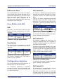
1
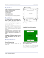
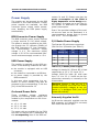
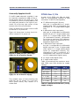
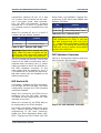
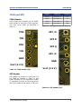
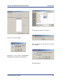
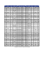
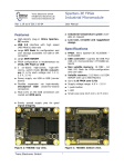
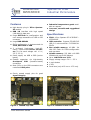
Spartan-3E FPGA
Industrial Micromodule
Trenz Electronic GmbH
[email protected]
www.trenz-electronic.de
Rev 1.14 as of 2009-09-03
User Manual
Features
■ Industrial temperature grade available on request
■ Low-cost, versatile and ruggedized
design
■ High-density plug-in Xilinx Spartan3E module
■ USB 2.0 interface with high speed
(480 Mbit/s) data rate
■ Large SPI flash for configuration and
user storage accessible via USB or SPI
connector
■ Large DDR-SDRAM
■ FPGA configuration is implemented via
JTAG, SPI Flash or USB
■ 3 on-board high-power, high-efficiency, switch-mode DC-DC converters (1 A for each voltage rail: 1.2 V,
2.5 V, 3.3 V)
■ Power supply via USB or B2B (carrier
board)
■ Flexible expansion via high-density
shockproof B2B (board-to-board)
connectors
■ Most I/O's on the B2B connectors are
routed as LVDS pairs
Specifications
■ FPGA: Xilinx Spartan-3E XC3S500E –
XC3S1600E
■ USB controller: Cypress EZ-USB FX2
USB 2.0 microcontroller CY7C68013A56LFX
■ Non volatile memory: 16 MBit - 64
Mbit SPI Flash for FPGA-configuration
and user data
■ Volatile memory: 512 Mbit x 16 DDR
SDRAM with up to 666 Mbyte/s
■ Up to 110 FPGA user I/Os
■ Supply voltage range: 4.0 V – 5.5 V
■ 1 push-button
■ 1 LED
■ Small size (only 40.5 mm x 47.5 mm)
■ Evenly spread supply pins for good
signal integrity
Figure 1: TE0300: top view.
Trenz Electronic GmbH
Figure 2: TE0300: bottom view.
1
Spartan-3E FPGA Industrial Micromodule
User Manual
Applications
■
■
■
■
■
■
■
IP (intellectual property) development
Digital signal processing
Image processing
Cryptography
Industrial control
Low-power design
General-purpose prototyping platform
Description
The FPGA industrial micromodule integrates a leading edge Xilinx Spartan-3E
FPGA, an USB 2.0 microcontroller, configuration Flash, DDR SDRAM and power
supplies on a tiny footprint. A large number of configurable I/Os are provided via
B2B mini-connectors.
Figure 3: module dimensions in mm
(top view).
The module is intended to be used as an
OEM board, or to be combined with our
carrier boards. It is a powerful system
widely used for educational and research
activities.
Board-to-Board Connectors
Boards with other configurations, larger
FPGA's or equipped with industrial temperature grade parts are available on request.
Software for SPI flash programming over
USB as well as reference designs for high
speed data transfer over USB are included.
Physical Features
Board Dimensions
The module measures 40.50 mm by
47.50 mm.
Trenz Electronic GmbH
Figure 4: connector receptacles J4
and J5 (bottom view).
The module has two B2B (board-toboard) receptacle connectors (J4 and J5)
for a total of 160 contacts (Figure 5).
2
Spartan-3E FPGA Industrial Micromodule
User Manual
supplier
header
Digikey
H2407CT-ND
Hirose
DF17(4.0)-80DP-0.5V(51)
Trenz Electronic
22938
Table 2: equivalent part numbers of
the mating connectors.
Figure 5: micromodule receptacle.
Figure 7 shows the definition of stacking
height featured by the combination of the
TE0300 receptacle with its corresponding
header.
The ordering numbers of the connector
receptacles are given in Table 1.
supplier
header
Digikey
H2373CT-ND
Hirose
DF17(3.0)-080DS-0.5V(51)
Trenz Electronic
22684
Table 1: equivalent part numbers of
the receptacle connectors J4 and J5.
The on-board receptacles mate with their
corresponding headers on the carrier
board (Figure 6).
Figure 7: stacking height (h).
The stacking height of the TE0300 B2B
connectors is 7 (seven) mm. The stacking
height does not include the solder paste
thickness.
USB Connector
The micromodule uses a mini-USB (B
type) receptacle connector.
Figure 6: mating header.
Figure 8: mini-USB (B type) receptacle connector.
The ordering number of the headers is
given in Table 2.
Trenz Electronic GmbH
3
Spartan-3E FPGA Industrial Micromodule
Power Supply
The module can be powered by the B2B
connector or the USB connector. If both
power supplies are available, the B2B
connector power supply takes precedence, disabling the USB power supply
automatically.
B2B Connector Power Supply
The B2B connector power supply requires
a single nominal 5 V DC power supply.
The power is usually supplied to the module through the 5 V contacts (5Vb2b) of
the B2B connectors J5 (see Appendix).
The recommended minimum supply
voltage is 4 V. The maximum supply
voltage is 5.5 V.The recommended maximum continuous supply current is 1.5 A.
User Manual
nectors J4 and J5. Please note that the
power consumption of the FPGA is
highly dependent on the design actually loaded. So please use a tool like Xilinx Xpower to determine the expected
power consumption.
Even if the provided voltages of the module are not used on the baseboard, it is
recommended to bypass them to ground
with 10 nF - 100 nF capacitors.
I/O Banks Power Supply
The Spartan-3E architecture organizes
I/Os into four I/O banks (see Table 3).
Bank
Supply
Voltage (V)
Min
(V)
Max
(V)
B0
VccIO
1.2
3.3
B1
2,5
-
-
USB Power Supply
B2
3,3
-
-
The module is powered by the USB connector if the following conditions are met:
B3
3,3
-
-
■ the module is equipped with an USB
connector,
■ the module is connected to a USB bus,
■ no power supply is provided by the
B2B connectors.
In this case, other components (e.g. extension or carrier boards) may also be
powered by the corresponding 5 Volt line
(5V) of the B2B connector J5.
On-board Power Rails
Three
on-board
voltage
regulators
provide the following power supply rails
needed by the components on the micromodule:
■ 1.2 V, 1 A max
■ 2.5 V, 1 A max
■ 3.3 V, 1 A max
The power rails are available for the FPGA
and can be shared with a baseboard by
the corresponding lines of the B2B con-
Trenz Electronic GmbH
Table 3: I/O banks power supply.
Voltage for banks B1, B2 and B3 is fixed
respectively to 2,5 V, 3,3 V and 3,3 V.
Voltage VccIO for bank B0 shall span
from 1.2 V to 3.3 V. VccIO can be supplied either externally or internally to the
micromodule.
Warning! Spartan-3 I/Os are not 5 V
tolerant. Applying more than the recommended operating voltages at any pin,
results in a damaged FPGA (see Xilinx
Answer AR#19146).
Externally Supplied VccIO
VccIO can be externally supplied over the
B2B connector J4. If bank B0 is not used,
then VccIO can be left open.
4
Spartan-3E FPGA Industrial Micromodule
User Manual
Internally Supplied VccIO
FPGA User I/Os
If VccIO is not externally supplied, it can
be internally supplied by one of the internal power rails of 2.5 V and 3.3 V. This
is possible by short-circuiting one of the
two pad pairs placed on the right of connector J4 at the top right corner of the
bottom side of the micromodule.
A total of 110 FPGA user I/Os are available on corresponding contacts of B2B
connectors J4 and J5 (see Appedix).
Figure 9 shows how to short-circuit VccIO
to internal 3.3 V power rail.
Figure 10 shows how to short-circuit VccIO to internal 2.5 V power rail.
Figure 9: R102 pad pair (blue highlight) for 3.3 V internal supply.
Figure 10: R103 pad pair (blue highlight) for 2.5 V internal supply.
Two suitable ways of shirt-circuiting the
paid pair are by means of a zero-ohm
0603 (1608 metric) chip resistor or a
solder blob.
Trenz Electronic GmbH
■ 37 differential digital I/O pairs:
each pair is configurable as 2 singleended digital I/Os, corresponding to a
maximum of 74 single-ended digital
I/Os;
■ 4 differential clock input pairs:
each pair is configurable as differential
digital I/O pair or 2 single-ended clock
inputs or 2 single-ended digital I/Os
(or combination thereof), corresponding to from a maximum of 8 independent clock inputs to a maximum of 8 independent digital I/Os;
■ 1 differential clock input pair:
the pair is configurable as differential
digital input pair or as 2 single-ended
clock inputs or 2 single-ended digital
inputs (or combination thereof), corresponding to from a maximum of 2
independent clock inputs to a maximum of 2 independent digital inputs;
■ 21 single-ended digital I/Os;
■ 5 single-ended inputs.
Table 4 summarizes the maximum available FPGA user I/Os divided by supply
voltage.
type
VccIO
3.3 V
diff. I/O pairs
≤ 18
≤ 23
diff inputs
≤1
none
diff. clocks
≤4
≤1
s. e. I/Os
≤ 46
≤ 58
s. e. inputs
≤2
≤4
s. e. cloks
≤8
≤3
Table 4: maximum FPGA user I/Os by
supply voltage.
5
Spartan-3E FPGA Industrial Micromodule
User Manual
Differential Pairs
DIP Switch S1
The micromodule has a total of 42 differential signal pairs routed pairwise with a
differential impedance of 100 ohm to adjacent connector pins. These lines can be
used for high speed signaling up to
666 Mbit/s per differential pair (see Xilinx
Application Note XAPP485).
S1 enables / disables the communication
between the Cypress EZ-USB FX2 microcontroller and the I2C CMOS Serial EEPROM.
User Button and LED
LED
The LED is lit when the U_LED line (pin
R10) is set high as detailed in the following table.
Signal
FPGA pin
FPGA ball
U_LED
IO_L15P_2
(bank 2)
R10
Tabelle 5: user led signal details.
Push Button
The push button is connected to the PB
input (pin V16). as detailed in the following table.
Signal
FPGA pin
FPGA ball
PB
IP
(bank 2)
V16
Tabelle 6: user button signal details.
The input is normally low. The input is
pulled up when pressed.
Turn S1 off when programming the USB
EEPROM storing the USB vendor ID and
device ID. This will force the USB microcontroller to provide its default vendor ID
and device ID.
S1
position
EEPROM (on)*
EEPROM enabled
Off (off)
EEPROM disabled
Table 7: S1 (* default: EEPROM).
For further information, please read paragraph “Software Configuration”.
DIP Switch S2
S2 enables / disables the reset line. The
reset line (available also on 2 contacts of
the B2B connector) resets the USB microcontroller and the FPGA.
S2 has to be turned off (Reset) if the user
wants to program the SPI Flash memory
in direct mode. For programming the SPI
Flash memory in indirect mode over
JTAG, S2 has to be turned on (Run).
S2
position
Run (on)*
system running
Reset (off)
system reset
Table 8: S2 (*default: Run).
Configuration Switches
The micromodule hosts 4 DIP switches on
the top side: S1; S2, S3 and S4.
For customers requesting a sufficient
amount of units, the micromodules can
be manufactured replacing the switches
by fixed connections.
Trenz Electronic GmbH
For further information, please read paragraph “Software Configuration”.
DIP Switch S3
S3 conditionally / unconditionally enables
the 1.2 V and 2.5 V power rails.
When S3 is turned on, the 1.2 V and 2.5
V power rails are controlled by the USB
microcontroller. At start-up, the USB mi-
6
Spartan-3E FPGA Industrial Micromodule
crocontroller switches off the 1.2 V and
2.5 V power rails and starts up the module in low-power mode. After enumeration, the USB microcontroller firmware
switches the 1.2 V and 2.5 V power rails
on, if enough current is available from the
USB bus.
When S3 is turned off, the 1.2 V and 2.5
V power rails are always enabled.
S3
position
FX2 PON (on)*
rails controlled by FX2
PON (off)
rails always enabled
Table 9: S3 (* default: FX2 PON).
Warning! When S3 is turned on (FX2
PON), make sure that no signals are applied to the input pins when power-rails
are disabled by the USB microcontroller.
The 3.3 V power-rail though is out of the
control of the USB-microcontroller and is
supplied down-converting the 5 V power
supply provided by either the USB-bus or
the B2B receptacle connector. In this
case, signals that are applied to the 3.3
V I/O banks do not need to be disconnected when power-rails are disabled by the
USB microcontroller.
User Manual
Serial Flash" and XAPP974 "Indirect Programming of SPI Serial Flash PROMs with
Spartan-3A FPGAs".
S4
position
SPI (on)*
FPGA configuration: JTAG + SPI
JTAG (off)
FPGA configuration: JTAG
Table 10: S4 (* default: SPI).
Warning! When downloading via parallel
JTAG programmer to FPGA, it can happen that programming fails with Error:
"'1' : Programming terminated. DONE did
not go high." Try setting DIP switch S4 to
JTAG-only. A bug in certain Xilinx iMPACT
versions can cause this.
DIP Switches Overview
Figure 11 summarizes functions and location of the four DIP switches.
DIP Switch S4
S4 enables / disables the FPGA configuration through the SPI interface. The FPGA
configuration through the JTAG interface
cannot be disabled.
When S4 is turned on, the FPGA tries to
configure from the SPI Flash memory.
The FPGA can be configured by the JTAG
interface at any time.
When S4 is turned off, the FPGA waits to
be configured by the JTAG interface.
Figure 11: DIP switches overview.
For further information about direct (pure
SPI) / indirect (SPI over JTAG) in-system
programming of SPI flash memories,
please see Xilinx Application Notes XAPP951 "Configuring Xilinx FPGAs with SPI
Trenz Electronic GmbH
7
Spartan-3E FPGA Industrial Micromodule
JTAG and SPI
User Manual
Signal
FPGA pin
FPGA ball
SPI /S
IO_L01P_2
U3
JTAG Header
SPI D
IO_L03N_2
T4
JTAG signals are available on the dedicated header J2 through a JTAG programmer with flying leads as described in
Table 11.
SPI Q
IO_L16N_2
N10
SPI /C
IO_L26N_2
U16
Table 12: SPI signal details (bank 2).
TMS
SPI /S
TDI
SPI D
TDO
TCK
SPI Q
SPI /C
GND
GND
Vref (3.3 V)
Table 11: JTAG header (J2).
Vref (3.3 V)
SPI Header
SPI signals are routed to / from bank 2 of
the FPGA as detailed in Table 12 and
made available on the dedicated header
J3 accessible through an SPI programmer
with flying leads as described in Table 13.
Table 13: SPI header (J3).
Trenz Electronic GmbH
8
Spartan-3E FPGA Industrial Micromodule
Clock Networks
24 MHz Clock Oscillator
The module has a 24 MHz SMD clock oscillator providing a clock source for both
the USB microcontroller and the FPGA as
detailed in Table 14.
Signal
FPGA pin
FPGA ball
24MHZ1
IO_L12P_2
(bank 2)
N9
Table 14: 24 MHz clock signal details.
Main Clock Oscillator
The module has a main SMD clock oscillator providing a clock source for the
FPGA as detailed in Table 15.
Signal
FPGA pin
FPGA ball
100MHZ
125MHZ
GCLK0
(bank 2)
U10
Table 15: main clock signal details.
Standard frequencies are 100 MHz and
125 MHz (please visit Trenz Electronic
website for current ordering information).
The lower the main clock frequency, the
lower the module power consumption.
Moreover, as the main clock is preferably
used as DDR SDRAM clock, a lower clock
frequency makes easier for the development tools to meet the timing requirements (particularly for DDR SDRAM). For
customized boards, this clock can be
changed according to user requirements.
User Manual
Signal
FPGA pin
FPGA ball
IFCLK
LHCLK5
(bank 3)
K4
Table 16: interface clock signal details (bank 3).
Digital Clock Manager (DCM)
The DCMs of the FPGA can be used to
synthesize arbitrary clock frequencies
from any on-board clock network, differential clock input pair or single-ended
clock input. For further reference, please
read Xilinx data sheet DS485 "Digital
Clock
Manager
(DCM)
Module"
(dcm_module.pdf) and Xilinx application
note XAPP462 "Using Digital Clock Managers (DCMs) in Spartan-3 FPGAs" (xapp462.pdf).
On-board Memories
The TE0300 has three on-board memories:
■ DDR SDRAM
■ SPI Flash
■ serial EEPROM
DDR SDRAM
TE0300 modules have a 512Mb DDR
SDRAM component for operation (code
and data) accessible through the FPGA.
Commercial-grade modules mount the
following component:
Micron Technology MT46V32M16BN-6
Interface Clock (IFCLK)
The IFCLK line synchronizes the communication between the USB microcontroller
and bank3 of the FPGA as detailed in
Table 16.
Trenz Electronic GmbH
Industrial-grade modules mount the following component:
Micron Technology MT46V32M16BN-6 IT
You can get the exact part number of the
component mounted on your module
from the Micron FBGA decoder:
http://www.micron.com/support/part_inf
o/fbga/decoder
9
Spartan-3E FPGA Industrial Micromodule
When developing DDR SDRAM designs
with Xilinx tools (e.g. MIG, MPMC, ...),
you should select the following product
type:
MT46V32M16-6.
Should it be not available, you can use
one of the following product types:
■ MT46V32M16-5
■ MT46V32M16XX-5B
■ MT46V32M16BN-5B
■ MT46V32M16FN-5B
■ MT46V32M16P-5B
■ MT46V32M16TG-5B
TE0300 modules with the following part
numbers
■ TE0300-00
■ TE0300-00-4I5C
■ TE0300-00B
■ TE0300-01
■ TE0300-01B
■ TE0300-01BLP
were assembled with
Qimonda HYB25DC512160CF-6
512Mb DDR SDRAM components. When
developing DDR SDRAM designs with Xilinx tools, you should select the following
product type:
HYB25D512160BF-6.
SPI Flah
TE0300 modules have a
STMicroelectronics M25P32
32-Mbit, low voltage, serial Flash memory
with 75 MHz SPI bus interface for configuration and operating storage accessible
through USB or SPI.
Serial EEPROM
TE0300 modules have a
Micron Technology 24LC128
Trenz Electronic GmbH
User Manual
128K I2C CMOS Serial EEPROM for EZUSB FX2 firmware, vendor ID and device
ID storage accessible through the EZ-USB
FX2 microcontroller.
Module Configuration
This section describes how to configure
the TE0300 module and access some of
its resources.
The JTAG interface allows a fast, frequent
but volatile configuration of the TE0300
module. However, only through the JTAG
interface it is possible to develop and debug with Xilinx tools (e.g. Xilinx ChipScope, Xilinx Microprocessor Debugger.
The SPI interface allows a fast, frequent
and non-volatile configuration of the
TE0300 module.
Configuration of the TE0300 module
through a USB host is recommended for
occasional, non-volatile on-site operations such as firmware upgrade.
System Requirements
TE0300 modules can be configured
through a host computer with the following system requirements:
■ Operating system: Microsoft Windows
2000, Microsoft Windows XP, Microsoft
Vista;
■ Xilinx ISE 10.1 or later for indirect SPI
in-system programming (see Xilinx Answer AR #25377);
■ Xilinx EDK for some reference designs;
■ Interface: USB host;
■ JTAG/SPI USB cable with flying leads.
EZ-USB FX2 Microcontroller
Firmware
If the EEPROM has never been programmed before (virgin board), S1 can
be switched to EEPROM. The USB micro-
10
Spartan-3E FPGA Industrial Micromodule
controller will detect an empty EEPROM
and will provide its default vendor ID and
device ID to the USB host.
User Manual
■ wait until the operating system detects
new hardware and starts the hardware
assistant;
DIP
switch
on (left)
off (right)
■ if S1 is not already switched to EEPROM, do it now;
S1
EEPROM
-
S2
Run
-
S3
X
X
■ answer the hardware assistant questions as shown in the following example.
S4
X
X
If the EEPROM has been programmed before (EEPROM not empty), S1 must be
switched to Off. The USB microcontroller
will detect a missing EEPROM and will
provide its default vendor ID and device
ID to the USB host.
DIP
switch
on (left)
off (right)
S1
-
Off
S2
Run
-
S3
X
X
S4
X
X
Generic USB Microcontroller
Driver installation
If the USB microcontroller (Cypress EZESB FX2) driver is not installed on the
host computer, then the easiest way to
do it is the following:
■ disconnect the micromobule or leave
the micromodule unconnected;
■ configure the micromodule such that
the USB microcontroller will provide its
default vendor ID and device ID to the
USB host (i.e. S1 = OFF -- see paragraph “EZ-USB FX2 Microcontroller
Firmware”);
■ connect the micromodule to the host
computer through the USB interface;
Trenz Electronic GmbH
11
Spartan-3E FPGA Industrial Micromodule
User Manual
EZ-USB FX2 EEPROM
Programming
First of all, check that S1 is actually
switched to EEPROM.
The USB EEPROM can be programmed by
opening the dedicated software “Cypress
USB Console” (double click the “CyConsole.exe” file in the “1st_program\CyConsole” folder).
Check that in the “Device Manager” under
“USB-Controller” the “Cypress Generic
USB Device” has been added.
Click “Options > EZ-USB Interface” to
Open EZ-USB Interface window.
Now the USB microcontroller can be accessed from the host computer through
dedicated software.
Trenz Electronic GmbH
12
Spartan-3E FPGA Industrial Micromodule
“S EEPROM” button refers to the small
EEPROM (256 bytes) whereas the “Lg EEPROM” refers to the large EEPROM (64
kB). Press the “Lg_EEPROM” button, select the “USB.iic” file and press the
“Open” button to start writing to EEPROM.
Upgrade progress is displayed in status
window and is completed when “Download Successful” text is displayed.
Trenz Electronic GmbH
User Manual
Disconnect the USB cable.
Dedicated USB Firmware Driver
Installation
Check the configuration switches against
the following table:
DIP
switch
on (left)
off (right)
S1
EEPROM
-
S2
Run
-
S3
FX2 PON
-
S4
X
X
Reconnect the USB cable to run the newly
uploaded firmware in the USB microcontroller. Under the default switch configuration, the USB microcontroller is now
ready to provide dedicated vendor ID and
device ID. Wait until the operating system detects new hardware and starts the
hardware assistant and answer the hardware assistant questions as shown in the
following example.
13
Spartan-3E FPGA Industrial Micromodule
User Manual
Check that in the “Device Manager” under
“USB-Controller” the “DEWESoft USB
Device 0” has been added.
FWU File Generation
The TE0300 micromodule can be configured by means of a firmware-upgrade
(FWU) file (see next section "Micromodule
Configuration" for further reference). The
first step in generating the FWU file is to
generate the fpga.bin file corresponding
to a given FPGA design.
Trenz Electronic GmbH
14
Spartan-3E FPGA Industrial Micromodule
User Manual
The TE0300 reference projects provide a
way to generate the fpga.bin file in an
automatic way, i.e. by executing the following batch file:
#XilinxEdkReferenceProject#\
PREPARE_FW\TE0300_usb_fw.bat
where #XilinxEdkReferenceProject# is
the base directory of the corresponding
reference project.
Alternatively you can use Xilinx IMPACT
from Start / Programs / Xilinx ISE / Accessories / Impact
Select “create new project”.
Select “BIN” as output.
Select “prepare PROM file”.
Set "PROM File Name" to "fpga" and
change "Location" to a suitable name and
location.
Trenz Electronic GmbH
15
Spartan-3E FPGA Industrial Micromodule
User Manual
The following warning is normal :).
Check “Auto Select PROM”.
This is probably the one and only file with
your design.
Navigate to your project’s IMPLEMENTATION folder and select "download.bit".
Congratulations!
Trenz Electronic GmbH
16
Spartan-3E FPGA Industrial Micromodule
User Manual
Click GENERATE FILE or select from menu
Operations / Generate file.
Don’t forget to save your project for further use
Once you have got your fpga.in file, you
can proceed and generate your FWU file.
The FWU file is a ZIP file containing 3
files:
You are done.
■ Bootload.ini – booting settings
■ fpga.bin – FPGA programming file
■ usb.bin – FX2 firmware
To create your FWU file, you need to
■ replace
the
existing
USBFWUTool\FWUs\fpga.bin with the
latest fpga.bin (Bootload.ini and usb.bin are always unchanged)
■ zip the 3 files
■ change the .zip file extension to .fwu
■ upload the file as explained in the next
section (Micromodule Configuration).
Trenz Electronic GmbH
17
Spartan-3E FPGA Industrial Micromodule
Warning! file and path names are given
and must NOT be changed!
User Manual
Press the “Upload” button to upload the
micromodule firmware and check the
“FPGA uploading...” progress bar.
Micromodule Configuration
The micromodule can now be programmed with its dedicated firmware upload tool. Turn S1, S2, S3 and S4 on.
Open the dedicated firmware upgrade
tool “USB Firmware Upgrade Tool”
(double click the “USBFirmwareUpgradeTool.exe” file in the “USBFWUTool”
folder).
Press the “...” button corresponding to
the “File name” field and select for instance the sample firmware upload file
“TE0300_v1012.fwu”
in
the
“USBFWUTool\FWUs” folder.
After successful completion of the firmware upload procedure, the following
message should pop up.
Reboot the micromodule with the new
firmware by disconnecting and reconnecting the USB cable. You may want to test
the sample application “TE0300_API_Example.exe”
in
the
“TE0300_API_Example\Debug” folder.
To generate your own firmware upload
file, please read the document “Generating_FWU_file.doc” in the “USBFWUTool”
folder.
SPI Direct In-System
Programming (ISP)
Make sure S2 is switched to “Reset“(off)
during programming.
Connect the host computer to the micromodule through both the SPI flying leads
cable and the USB cable.
Start Xilinx ISE iMPACT. The following example shows the case of iMPACT 9.2. If
the “iMPACT Project” window pops up,
press the “Cancel” button.
Trenz Electronic GmbH
18
Spartan-3E FPGA Industrial Micromodule
User Manual
You can now select the file corresponding
to your device. In the following example,
we will show how to select the micromodule reference device “blinking.mcs” in the
“TE0300” folder.
Double click the “Direct SPI Configuration” option in the “Modes” panel.
Select the part name corresponding to
the SPI flash present on the module
(STMicroelectronics M25P32, a 32 Mbit
(4M x 8) Serial Flash memory).
Right click the “Direct SPI Configuration”
panel to add a device and select “Add SPI
Device”.
iMPACT should now look like this.
Trenz Electronic GmbH
19
Spartan-3E FPGA Industrial Micromodule
User Manual
iMPACT will first erase the memory (notice the mismatch between the two progress indicators)
Right click the SPI PROM device and select the “Program” operation.
In the “Programming Properties” window,
just leave the default settings and press
the “OK” button.
Trenz Electronic GmbH
and then write it (notice the match
between the two progress indicators).
After successful programming, you should
read the message “Program Succeeded”
popping up for a few seconds in the “Direct SPI Configuration” panel.
20
Spartan-3E FPGA Industrial Micromodule
User Manual
Switch S2 back to the “Run” position. In
case you uploaded the test design, you
should see the on-board led blinking at
0.5 Hz.
For further information about direct (pure
SPI) in-system programming of SPI Flash
memories, please see Xilinx Application
Note XAPP951 "Configuring Xilinx FPGAs
with SPI Serial Flash".
SPI Indirect In-System
Programming (ISP)
Check the configuration switches against
the following table:
DIP
switch
on (left)
off (right)
S1
X
X
S2
Run
S3
-
PON
S4
X
X
Right click the “Boundary Scan” to initialize the chain and select “Initialize Chain”.
Connect the host computer to the micromodule through both the SPI flying leads
cable and the USB cable.
Start Xilinx ISE iMPACT. The following example shows the case of iMPACT 10.1. If
the “iMPACT Project” window pops up,
press the “Cancel” button.
An “Assign New Configuration File” dialog
window should pop up automatically. You
can now select the file corresponding to
your design. In the following example, we
will show how to select the micromodule
reference design “blinking.bit” in the
“TE0300” folder. Do not forget to select
the “Enable Programming of SPI Flash
Device Attached to this FPGA” option in
the same window.
Double click the “Boundary Scan” option
in the “Modes” panel.
Trenz Electronic GmbH
21
Spartan-3E FPGA Industrial Micromodule
User Manual
iMPACT should now look like this.
An “Add PROM File” dialog window should
pop up automatically. You can now select
the file corresponding to your design. In
the following example, we will show how
to select the micromodule reference
design “blinking.mcs” in the “TE0300”
folder.
Right click the “Flash” device and select
the “Program” operation.
Select now the SPI Flash corresponding to
the one present on the module (STMicroelectronics M25P32 in the example, a 32
Mbit (4M x 8) Serial Flash memory).
In the “Device Programming Properties”
window, just leave the default settings
and press the “OK” button.
Trenz Electronic GmbH
22
Spartan-3E FPGA Industrial Micromodule
User Manual
iMPACT will first erase the memory
Switch S3 back to the “FX PON” position.
In case you uploaded the reference
design, you should see the on-board led
blinking at 0.5 Hz.
For further information about indirect
(SPI over JTAG) in-system programming
of SPI Flash memories, please see Xilinx
Application Note XAPP974 "Indirect Programming of SPI Serial Flash PROMs with
Spartan-3A FPGAs".
and then write it.
Changes from TE0300-00
to TE0300-01
Clocks
TE0300-00 has a 50MHz secondary clock,
whereas TE0300-01 has a 125MHz secondary clock.
Volatile Memory Interface
TE0300-00 could access the DDR SDRAM
only with Xilinx OPB (on-chip peripheral
bus) cores.
After successful programming, you should
read the message “Program Succeeded”
popping up for a few seconds in the
“Boundary Scan” panel.
Trenz Electronic GmbH
TE0300-01 can also access the DDR
SDRAM through the dedicated Xilinx MIG
(memory interface generator) memory interface.
23
Spartan-3E FPGA Industrial Micromodule
User Manual
B2B Connectors
Rev
Contact 14 of connector J5 has been extended from an input in TE0300-00 to an
I/O in TE0300-01. Therefore hardware
designs developed for the TE0300-00 are
compatible with the TE0300-01 whereas
those developed for the TE0300-01 are
compatible with the TE0300-00 if that
contact is configured as input.
Contact 76 of connector J5 has mistakenly been described as I/O in TE030000, but it has always been an input-only
contact as documented for TE0300-01.
Connector J4 has not been changed.
LED
With TE0300-00, the LED is lit when the
U_LED line on pin T15 is set high whereas
with TE0300-01 the LED is lit when the
U_LED line on pin R10 is set high.
Ordering Information
For the latest product details and available options, please visit:
www.trenz-electronic.de
shop.trenz-electronic.de
Revision History
Rev
Date
Who
Description
0.1
2008-04-24
FDR
created
1.0
2008-08-01
FDR
completed
1.01 2008-08-08
TT
50MHz to 125MHz
clock
1.02 2008-10-17
FDR
U_LED for
TE0300-00
1.03 2008-10-17
FDR
updated FUT from
1.9 to 2.6
1.04 2008-10-27
FDR
DIP switches
overview
1.05 2008-10-29
FDR
stacking height
Trenz Electronic GmbH
Date
Who
Description
1.06 2008-12-08
FDR
DIP switches
revised
1.07 2009-02-16
FDR
fixed DIP switches
overview picture
1.08 2009-03-09
FDR
clarified warning
regarding 3.3 V
power-rail
1.09 2009-03-16
FDR
fixed and improved
switch settings
1.10 2009-06-03
FDR
added "FWU File
Generation" section
1.11 2009-07-23
FDR
clarified
changes/LED
section
1.12 2009-08-24
FDR
added FPGA signal
details for main
user signals
1.13 2009-09-01
FDR
improved "Onboard Memories"
chapter
1.14 2009-09-03
FDR
improved clock,
memory and configuration chapters
Table 17: revision history.
Appendix
The following tables reports pin-out information of B2B (board-to-board) receptacle connectors J4 and J5 respectively.
24
1
3
5
7
9
B2B
name
VccIO
VccIO
B3_L01_P
B3_L01_N
B3_L02_P
11
B3_L02_N
13
15
GND
B0_IO_C3
17
B0_L24_N
B4
19
21
23
B0_L24_P
B0_IO_C4
GND
A4
C4
25
B0_L23_N
D5
27
29
31
33
35
B0_L23_P
B0_L20_P
B0_L20_N
3.3 V
B0_IO_A7
C5
B6
A6
IO_L23N
/ VREF
IO_L23P
IO_L20P
IO_L20N
A7
IO
0 IO VccIO N N VccIO IO 0
37
B0_IO_G9
G9
IO
0 IO VccIO N Y VccIO IO 0
pin
FPGA FPGA ba
sup di di
dir
pin
name nk
ply ff ff
VccO
0 I
- VccO
0 I
- C1
IO_L01P 3 IO 3.3 V Y Y
C2
IO_L01N 3 IO 3.3 V Y Y
D1
IO_L02P 3 IO 3.3 V Y Y
IO_L02N
D2
3 IO 3.3 V Y Y
/ VREF
C3
39 GCLK_L13_P
B8
41 GCLK_L13_N
B9
43
dir
I
I
IO
IO
IO
ba FPGA FPGA
nk name
pin
0
VccO
0
VccO
3 IO_L07P
G6
3 IO_L07N G5
3 IO_L03N
E1
3.3 V IO 3
0 IO VccIO N Y VccIO IO 0 IO_L19_P
IO_L19N
IO_L24_N 0 IO VccIO Y Y VccIO IO 0
/ VREF
IO_L24P 0 IO VccIO Y Y VccIO IO 0 IO_L21N
IO
0 IO VccIO N Y VccIO IO 0 IO_L21P
IP_L13P
/ GCLK8
IP_L13N
/ GCLK9
0 IO VccIO Y Y VccIO IO 0
0 IO VccIO Y Y VccIO IO 0
0 IO VccIO Y Y VccIO IO 0
0 IO VccIO Y Y VccIO IO 0
0
I VccIO Y Y VccIO IO 0
0
I VccIO Y Y VccIO IO 0
Y VccIO IO 0
B10
47 GCLK_L12_N A10
E9
F9
IO_L03P
IO_L25P
GND
45 GCLK_L12_P
sup
ply
3.3 V
3.3 V
3.3 V
IO_L12P
/ GCLK6
IO_L12N
/ GCLK7
IO_L15P
IO_L15N
IO_L18N
/ VREF
IO_L18P
IO_L17N
IO_L17P
B2B
name
VccIO
VccIO
B3_L07_P
B3_L07_N
B3_L03_N
pin
2
4
6
8
10
E2
B3_L03_P
12
F7
GND
B0_L19_P
14
16
E7
B0_L19_N
18
E6
D6
B0_L21_N
B0_L21_P
GND
20
22
24
D7
B0_L18_N
26
C7
F8
E8
B0_L18_P
B0_L17_N
B0_L17_P
3.3 V
B0_IO_A8
28
30
32
34
36
IO
A8
IO_L14N
D9
/ GCLK11
IO_L14P
C9
/ GCLK10
IO_L11N
E10
/ GCLK5
IO_L11P
D10
/ GCLK4
0 IO VccIO Y
GCLK_L14_N 38
GCLK_L14_P 40
GCLK_L11_N 42
GCLK_L11_P 44
GND
46
0 IO VccIO Y Y VccIO IO 0
IO_L09N
D11
B0_L09_N
48
0 IO VccIO Y Y VccIO IO 0
0 IO VccIO Y N VccIO IO 0
IO_L09P
IO
C11
A11
IO_L08P
IO_L08P
IO_L05P
IO_L05N
/ VREF
0 IO VccIO Y N VccIO IO 0
0 IO VccIO Y N VccIO IO 0
0 IO VccIO Y Y VccIO IO 0
IO/VREF
IO
IO_L06P
B11
A12
F12
B0_L09_P
B0_I0_A11
2.5 V
B0_IO_B11
B0_IO_A12
B0_L06_P
50
52
54
56
58
60
0 IO VccIO Y Y VccIO IO 0
IO_L06N
E12
B0_L06_N
62
0 IO VccIO Y N VccIO IO 0
0 IO VccIO Y N VccIO IO 0
IO
IO
D13
E13
GND
B0_IO_D13
B0_IO_E13
64
66
68
0 IO VccIO Y
3.3 V
I
2
TDI
A2
TDI
70
0 IO VccIO Y
3.3 V O
2
TDO
C16
0 IO VccIO Y
0 IO VccIO Y
3.3 V
3.3 V
2
2
TCK
TMS
A17
D15
TDO
1.2 V
TCK
TMS
GND
72
74
76
78
80
49
51
53
55
57
59
B0_L15_P
B0_L15_N
2.5 V
B0_L08_P
B0_L08_N
B0_L05_P
E11
F11
A13
61
B0_L05_N
B13
63
65
67
GND
B0_L04_N
B0_L04_P
A14
B14
69
B0_L03_N
C14
71
73
75
77
79
B0_L03_P
1.2 V
B0_L01_N
B0_L01_P
GND
D14
IO_L04N
IO_L04P
IO_L03N
/ VREF
IO_L03P
A16
B16
IO_L01N
IO_L01P
I
I
receptacle connector J4 pinout information
FPGA
pin
1
3
5
7
9
11
13
15
17
19
21
23
25
B2B
name
5Vb2b
5Vb2b
5V
B2B_D_P
B2B_D_N
GND
B3_L22_P
B3_L22_N
B2_IP_V4
B3_L20_P
B3_L20_N
GND
B2_L04_N
27
B2_L04_P
R5
29
B2_L05_P
R6
31
B2_L05_N
P6
33
B2_IO_V7
V7
35
37
3.3 V
B2_L07_N
P7
39
B2_L07_P
N7
41
B2_GCLK12
M9
43
45
47
GND
B2_L10_N
B2_L10_P
T8
R8
pin
P3
P4
V4
N4
N5
IO_L22P
IO_L22N
IP_L02P
IO_L20P
IO_L20N
IO_L24P
IO_L21N
IO_L21P
IO_L23N
IO_L23P
T2
P1
P2
R2
R3
T5
IO_L04N 2 IO 3.3 V Y N 3.3 V IO 3 IO_L18N
IO_L03P
IO_L04P 2 IO 3.3 V Y N 3.3 V IO 2 / DOUT /
BUSY
IO
IO_L05P 2 IO 3.3 V Y N 3.3 V IO 2
/ VREF
IO_L05N 2 IO 3.3 V Y Y 3.3 V IO 2 IO_L06P
IO_L06N
IO
2 IO 3.3 V N Y 3.3 V IO 2
/ VREF
M3
B2B
name
5Vb2b
5Vb2b
/MR
/RESET
RESET
GND
B3_IO_T2
B3_L21_N
B3_L21_P
B3_L23_N
B3_L23_P
GND
B3_IO_L18N
U4
B2_IO_L03
28
U5
B2_IO_U5
30
V5
B2_L06_P
32
V6
B2_L06_N
34
IO_L07N 2 IO 3.3 V Y N 3.3 V IO 2
IO
IO_L17N
IO_L07P 2 IO 3.3 V Y Y 3.3 V IO 3
/ VREF
IO_L12N
/ D6 /
2 I 3.3 V N Y 3.3 V IO 3 IO_L17P
GCLK12
U6
3.3 V
B2_IO_U6
36
38
L5
B3_L17_N
40
L6
B3_L17_P
42
IO_L10N
IO_L10P
IO_L13N
/ D3 /
GCLK15
IO_L13P
/ D4 /
GCLK14
2 IO 3.3 V Y N 3.3 V I
2 IO 3.3 V Y N 3.3 V I
2 IP_L08P
2 IP_L11P
T7
U8
GND
B2_IP_T7
B2_IP_U8
44
46
48
2 IO 3.3 V Y Y 3.3 V IO 3 IO_L19P
M5
B3_L19_P
50
2 IO 3.3 V Y Y 3.3 V IO 3 IO_L19N
M6
B3_L19_N
52
IO_L18N
IO_L18P
IO_L20N
IO_L20P
2
2
2
2
2.5 V
B2_L09_P
B2_L09_N
B2_IO_P9
B2_IO_R11
GND
54
56
58
60
62
64
B2_IO_P10
66
B2_IO_R9
68
B2_L21_N
70
B2_L21_P
72
1.2 V
74
V14
B2_IP_V14
76
U13
B2_IO_U13 78
49 B2_GCLK_L13_N
V9
51 B2_GCLK_L13_P
U9
53
55
57
59
61
63
2.5 V
B2_L18_N
B2_L18_P
B2_L20_N
B2_L20_P
GND
65
B2_L19_N
67
B2_L19_P
69
B2_L22_N
71
B2_L22_P
73
1.2 V
75
B2_L24_P
77
B2_L24_N
79
GND
N11
P11
R12
T12
FPGA
name
ba
sup
dir
nk
ply
I
I
O
IO
IO
3
3
2
3
3
IO
IO
I
IO
IO
IO
IO
IO
IO
3.3
3.3
3.3
3.3
3.3
3.3
3.3
3.3
3.3
3.3
V
V
V
V
V
V
V
V
V
V
di di sup
ba
dir
ff ff ply
nk
I
I
I
Y
O
Y
O
Y
Y
N
Y
Y
Y
Y
Y
Y
N
Y
Y
Y
Y
Y
Y
N
N
3.3
3.3
3.3
3.3
3.3
3.3
3.3
3.3
3.3
V
V
V
V
V
V
V
V
V
IO
IO
IO
IO
IO
IO
IO
IO
IO
3
3
3
3
3
FPGA
name
FPGA
pin
2 IO_L09P P8
2 IO_L09N N8
2
IO
P9
2
IO
R11
IO_L15N
/ D1 /
P10
GCLK3
IO
V12 IO_L19P 2 IO 3.3 V Y N 3.3 V IO 2
R9
/ D5
IO_L22N
R13
2 IO 3.3 V Y Y 3.3 V IO 2 IO_L21N P12
/ A22
IO_L22P
P13
2 IO 3.3 V Y Y 3.3 V IO 2 IO_L21P N12
/ A23
V13
IO_L19N
2 IO 3.3 V Y N 3.3 V IO 2
/ VREF
IO_L24P
T14
2 IO 3.3 V Y N 3.3 V I 2 IP_L23P
/ A21
IO_L24N
R14
2 IO 3.3 V Y N 3.3 V IO 2
IO
/ A20
receptacle connector J5 pinout information
GND
pin
2
4
6
8
10
12
14
16
18
20
22
24
26
80