1
MEMScAP
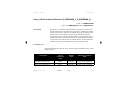
Table Of Contents
Table Of Contents
Introduction
.................................................... i
........................................................................1
MEMS Pro System .............................................................2
Total Solution ..............................................................................3
Tool Flow .....................................................................................5
Schematic Capture (S-Edit) .....................................................6
MEMS Pro User Guide
Contents
Index
i
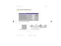
Table Of Contents
Simulator (T-Spice Pro) ...........................................................6
Layout Editor (L-Edit) ..............................................................7
User-programmable Interface .................................................8
Layout vs. Schematic (LVS) ...................................................9
3D Modeler ..................................................................................9
MEMS Block Place and Route ...............................................9
MEMS Library (MEMSLib) .................................................10
Foundry Support .......................................................................10
Embedded features in ANSYS .............................................10
Reduced Order Modeling (Macro-Model Generation) 10
Automatic mask layout generation (3D to Layout) ...11
What’s New in Version 3.0 ........................................12
Documentation Conventions ....................................13
MEMS Pro User Guide
Contents
Index
Help
ii
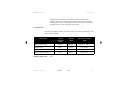
Table Of Contents
MEMS Pro Tutorial ............................................16
Introduction ............................................................................17
The Design Example ...............................................................18
Creating a Schematic
.....................................................19
Launching S-Edit .....................................................................19
Opening the File .......................................................................20
Creating a New Module ..........................................................22
Instantiating Components ......................................................23
Instantiating a Plate ..........................................................23
Instantiating Comb-drives ...............................................24
Instantiating Folded Springs ...........................................25
Wiring Objects ..........................................................................26
Zooming the View ...............................................................26
Instantiating Voltage Sources ...............................................29
MEMS Pro User Guide
Contents
Index
Help
iii
Table Of Contents
Placing Global Nodes ..............................................................29
Editing Object Properties .......................................................32
Labeling Nodes .........................................................................34
Adding Simulation Commands ............................................35
Exporting a Netlist ............................................................40
Tutorial Breakpoint ..................................................................40
Simulating from a Netlist ............................................42
Simulating with T-Spice .........................................................42
Probing a Waveform ......................................................45
Viewing a Waveform ......................................................47
Chart Setups ..............................................................................47
Trace Manipulation ..................................................................48
Generating a Layout .......................................................56
Tutorial Breakpoint ..................................................................56
Launching L-Edit .....................................................................56
MEMS Pro User Guide
Contents
Index
Help
iv
Table Of Contents
Opening the File .......................................................................57
Creating Components ..............................................................57
Using the MEMS Library Palette ...................................58
Generating the Plate .........................................................59
Generating the Comb-drives ...........................................60
Editing an Already Generated Component .................61
Attaching Components ......................................................63
Generating the Folded Springs .......................................65
Generating the Ground Plate ..........................................66
Generating the Bonding Pads .........................................67
Viewing Properties ..................................................................70
Viewing a 3D Model
........................................................73
Tutorial Breakpoint ..................................................................73
Launching L-Edit and Opening a File ................................73
Process Definition ....................................................................74
MEMS Pro User Guide
Contents
Index
Help
v
Table Of Contents
Importing the Process Definition ...................................74
3D Model View ........................................................................78
Generating the 3D Model ................................................78
Manipulating the 3D Model View ..................................78
Multiple Views ....................................................................80
Viewing the 3D Model ......................................................82
3D Cross-section ......................................................................82
Drawing Tools .......................................................................86
Tutorial Breakpoint ..................................................................86
Drawing a Wire ........................................................................88
Drawing a Torus .......................................................................89
Drawing a Curved Polygon ...................................................91
Drawing a Circle ......................................................................95
Drawing a Box ..........................................................................95
MEMS Pro User Guide
Contents
Index
Help
vi
Table Of Contents
MEMS Pro Toolbar .............................................97
Introduction ............................................................................98
Library Menu ......................................................................103
Library Palette .........................................................................103
Edit Component ......................................................................105
3D Tools Menu ...................................................................109
Editing a Process Definition ................................................109
Viewing a 3D Model .............................................................111
Deleting a 3D Model .............................................................112
Exporting a 3D Model ..........................................................113
Easy MEMS Menu
.........................................................114
Creating holes in a plate .......................................................114
Copying objects ......................................................................116
Splines ........................................................................................118
MEMS Pro User Guide
Contents
Index
Help
vii
Table Of Contents
Creating Splines .....................................................................118
Editing Splines ........................................................................120
Tools
............................................................................................121
Viewing Vertex Coordinates ...............................................121
Viewing Vertex Angles ........................................................122
Viewing Vertex Information ...............................................122
Clearing Vertex Information ...............................................123
Help ..............................................................................................124
MEMS Pro User Guide .........................................................124
About MEMS Pro ..................................................................124
Splines
.......................................................................................126
Introduction ..........................................................................127
MEMS Pro User Guide
Contents
Index
Help
viii
Table Of Contents
Understanding Splines ..........................................................127
Create Spline Dialog Box ..........................................129
Creating Splines ................................................................132
Creating Splines from Angled Wires ................................132
Interpolation ......................................................................134
Approximation ..................................................................137
Re-creating Angled Wires ...................................................139
Creating Splines from Polygons .........................................141
Editing Splines ....................................................................146
MEMS Pro Utilities
...........................................147
Introduction ..........................................................................148
Running Macros in L-Edit ......................................149
MEMS Pro User Guide
Contents
Index
Help
ix
Table Of Contents
Loading the Macros ...............................................................149
Generating Polar Arrays
..........................................150
Description ...............................................................................150
Accessing the Function .........................................................150
Parameters ................................................................................152
Generating Holes in a Plate ....................................154
Viewing Vertex Coordinates and Angles ....157
Viewing Vertex Coodinates ................................................157
Viewing Vertex Angles .......................................................159
Viewing Vertex Information ...............................................161
Clearing Vertex Information ...............................................163
Approximating All-angle Objects .....................164
Description ...............................................................................164
Accessing the Macro .............................................................164
Parameters ................................................................................167
MEMS Pro User Guide
Contents
Index
Help
x
Table Of Contents
Generating Concentric Circles ............................168
Location ....................................................................................168
Description ...............................................................................168
Accessing the Macro .............................................................169
Parameters ................................................................................169
Input File Format ....................................................................169
Syntax ..................................................................................170
Example ..............................................................................170
Parameters ................................................................................171
3D Modeler .......................................................................172
Introduction ..........................................................................173
MCNC MUMPs Thermal Actuator ...................................173
MEMS Pro User Guide
Contents
Index
Help
xi
Table Of Contents
MCNC MUMPs Rotary Motor ...........................................175
Analog Devices iMEMS ADXL Accelerometer ............177
Bulk Micromachined Diaphragm .......................................180
Accessing 3D Models
....................................................182
3D Model Input ......................................................................182
3D Modeler Output ................................................................182
Accessing the 3D Tools ........................................................184
Defining Colors for 3D Models ............................186
Viewing 3D Models from Layout ......................188
3D Model View User Interface .............................190
Application Elements ............................................................190
Title Bar ....................................................................................191
Menu Bar ..................................................................................192
File Menu ...........................................................................192
View Menu .........................................................................195
MEMS Pro User Guide
Contents
Index
Help
xii
Table Of Contents
Tools Menu ........................................................................204
Setup Menu ........................................................................205
Window Menu ...................................................................206
Help Menu ..........................................................................207
3D Model Tool Bar ................................................................209
Palette .......................................................................................210
Status Bar .................................................................................213
Viewing a Cross-section .............................................215
Deleting 3D Models ........................................................218
Exporting 3D Models ...................................................220
Linking to ANSYS ..........................................................223
Editing the Process Definition ..............................225
Importing the Process Definition .......................................226
Process Identification ............................................................228
Editing the Process Steps List .............................................228
MEMS Pro User Guide
Contents
Index
Help
xiii
Table Of Contents
Enable .................................................................................229
Display 3D model for this step .....................................229
Move Step ...........................................................................229
Add Step ..............................................................................230
Delete Step .........................................................................230
Editing Individual Process Steps ........................................230
Wafer .........................................................................................231
Deposit ......................................................................................234
DepositType = CONFORMAL .....................................235
DepositType = SNOWFALL ..........................................237
DepositType = FILL ........................................................239
Etch ............................................................................................241
Orientation Considerations ...........................................242
EtchType = SURFACE ...................................................244
EtchType = BULK ...........................................................246
MEMS Pro User Guide
Contents
Index
Help
xiv
Table Of Contents
EtchType = SACRIFICIAL ............................................248
MechanicalPolish ...................................................................249
3D Modeler Error Checks
.......................................252
Checking if the 3D Model is Out-of-Date ..................253
Checking if a Process Definition is used ....................253
Checking for Process with Derived Layers ...............254
Checking for the Existence of all Required Layers .254
Checking for Wires or Self-Intersecting Polygons ..254
ANSYS Tutorial .......................................................256
Introduction ..........................................................................257
Launching L-Edit ...................................................................257
Opening the File .....................................................................257
MEMS Pro User Guide
Contents
Index
Help
xv
Table Of Contents
Viewing the 3D Model .........................................................258
Exporting the 3D Model .......................................................259
Reading the 3D Model in ANSYS
.....................261
Viewing the 3D Model in ANSYS ....................................261
Setting Material Properties ..................................................263
Adding an Element Type .....................................................264
Setting Boundary Conditions ................................265
Meshing the Model .........................................................269
Running the Analysis ...................................................272
Displaying the Results .................................................273
Computing the Spring Constant ........................276
Entering Models under Windows NT ...........277
ANSYS to Layout Generator .............278
MEMS Pro User Guide
Contents
Index
Help
xvi
Table Of Contents
Introduction ..........................................................................279
3-D to Layout Tools .......................................................281
Overview ..................................................................................281
Import Mems ...........................................................................285
Creation of Volumes .............................................................287
Deletion of Volumes .............................................................291
Addition of Volumes .............................................................292
Component Names .................................................................292
Saving Mems ...........................................................................295
Unit ............................................................................................296
Exporting a CIF File ..............................................................297
The LAYOUT Menu Item ...................................................298
The Layout Generator Program ........................299
Definition of a Technology File ...........................303
Limitations .............................................................................315
MEMS Pro User Guide
Contents
Index
Help
xvii
Table Of Contents
Negative Mask Without Hole .............................................315
Substrate ...................................................................................315
Splines .......................................................................................315
Boolean Operations on Layers ............................................315
Tutorial .....................................................................................316
Import Mems ...........................................................................316
3D Modifications ...................................................................323
The Layout Generator Program ..........................................326
Reduced Order Modeling
........................334
User Manual .........................................................................335
Introduction .............................................................................335
R.O.M. Menu ..........................................................................337
MEMS Pro User Guide
Contents
Index
Help
xviii
Table Of Contents
Condensation Algorithm ......................................................340
Fundamentals ....................................................................340
Running the Condensation .............................................341
Reduction of Electrostatically Coupled Structural Systems 348
Fundamentals ....................................................................349
Running the Reduction Algorithm ................................353
ROM Tutorial .....................................................................370
Condensation: Reduction with Single DOF & Load Cases 370
Model Generation ............................................................372
Performing Reduction .....................................................374
Condensation: Reduction with Multiple DOFs & Load Cases
380
Model Generation ............................................................382
Performing Reduction .....................................................385
Simulating a reduced model using the SPICE simulator 392
MEMS Pro User Guide
Contents
Index
Help
xix
Table Of Contents
Reduction of Electrostatically Coupled Structural Systems 408
Model Generation ............................................................410
Performing Reduction .....................................................411
Simulating a reduced model using the SPICE simulator 422
Optimization Tutorial ....................................436
Introduction ..........................................................................437
Setting up the Optimization ...................................439
Running the Optimization .......................................453
Examining the Output .................................................454
MEMS Pro User Guide
Contents
Index
Help
xx
Table Of Contents
Verification .......................................................................457
Introduction ..........................................................................458
Adding Connection Ports .........................................459
Extracting Layout ...........................................................463
Extracting Schematic for LVS .............................468
Comparing Netlists .........................................................471
Command Tool
..........................................................474
Introduction ..........................................................................475
Usage in S-Edit .......................................................................475
Schematic Mode ................................................................475
Symbol Mode .....................................................................476
MEMS Pro User Guide
Contents
Index
Help
xxi
Table Of Contents
Property Creation ............................................................476
Accessing the Command Tool
..............................477
Schematic Tools Toolbar .....................................................477
Module Menu ..........................................................................478
Command Tool Dialog ................................................479
Schematic Object Creation .....................................482
Template Module ..............................................................482
Symbol Mode .......................................................................483
Schematic Object in Symbol Mode ...................................483
Create Property Dialog .........................................................484
Block Place and Route Tutorial ....486
Initializing the Design ..................................................488
MEMS Pro User Guide
Contents
Index
Help
xxii
Table Of Contents
Routing the Design
.........................................................499
Extending the MEMS Library ........506
Introduction ..........................................................................507
Schematic Symbols .........................................................508
SPICE Models .....................................................................511
Application Example .............................................................512
Layout Generators ..........................................................514
Sample Layout Generator ....................................................514
MEMSLib Reference
MEMS Pro User Guide
Contents
Index
......................................518
Help
xxiii
Table Of Contents
Introduction ..........................................................................519
Acknowledgment ...................................................................522
Using the MEMS Library ........................................524
Accessing the MEMS Library Palette ...........526
Show Details Button ..............................................................528
Editing the Generated Layout Parameters .......................530
Active Elements .................................................................532
Linear Electrostatic Comb Drive Elements (S_LCOMB_1,
S_LCOMB_2) 532
Linear Electrostatic Comb Drive Elements .....................534
Linear Side Drive Elements (S_LSDM_1, S_LSDM_2)) 535
Linear Side Drive Elements .................................................537
Unidirectional Rotary Comb Drive Elements - Type 1
(S_RCOMBU_1, S_RCOMBU_2) 538
Unidirectional Rotary Comb Drive Elements-Type1 ...541
MEMS Pro User Guide
Contents
Index
Help
xxiv
Table Of Contents
Unidirectional Rotary Comb Drive Elements - Type 2
(S_RCOMBUA_1, S_RCOMBUA_2) 542
Unidirectional Rotary Comb Drive Elements - Type2 .545
Bidirectional Rotary Comb Drive Elements (S_RCOMBD_1,
S_RCOMBD_2) 546
Bidirectional Rotary Comb Drive Elements ...................549
Rotary Comb Drive Elements (S_RCDM_1, S_RCDM_2) 550
Rotary Comb Drive Elements .............................................553
Rotary Side Drive Elements (S_RSDM_1, S_RSDM_2) 554
Rotary Side Drive Elements ................................................556
Harmonic Side Drive Elements (S_HSDM_1, S_HSDM_2) 557
Harmonic Side Drive Elements ..........................................559
Passive Elements ...............................................................560
Journal Bearing Elements 1 (S_JBEARG_1) .................560
Journal Bearing Elements 1 .................................................562
MEMS Pro User Guide
Contents
Index
Help
xxv
Table Of Contents
Journal Bearing Elements 2 (S_JBEARG_2) .................563
Journal Bearing Elements 2 .................................................565
Linear Crab Leg Suspension Elements - Type 1 (S_LCLS_1,
S_LCLS_2) 566
Linear Crab Leg Suspension Elements - Type 1 ............568
Linear Crab Leg Suspension Elements - Type 2 (S_LCLSB_1,
S_LCLSB_2) 569
Linear Crab Leg Suspension Elements - Type 2 ............571
Linear Folded Beam Suspension Elements (S_LFBS_1,
S_LFBS_2) 572
Linear Folded Beam Suspension Elements .....................574
Dual Archimedean Spiral Spring Elements (S_SPIRAL_1,
S_SPIRAL_2) 575
Dual Archimedean Spiral Spring Elements .....................577
Test Elements
MEMS Pro User Guide
......................................................................578
Contents
Index
Help
xxvi
Table Of Contents
Area-Perimeter Dielectric Isolation Test Structure Element
(S_APTEST_1) 578
Area-Perimeter Dielectric Isolation Test Structure Element 580
Crossover Test Structure Element - Type 1 (S_COTEST_1) 581
Crossover Test Structure Element - Type 1 ....................583
Crossover Test Structure Element - Type 2 (S_COTEST_2) 584
Crossover Test Structure Element - Type 2 ....................586
Euler Column (Doubly Supported Beam) Elements
(S_EUBEAM_1, S_EUBEAM_2) 587
Euler Column (Doubly Supported Beam) Elements .....589
Array of Euler Column Elements (S_EUBEAMS_1,
S_EUBEAMS_2) 590
Array of Euler Column Elements .......................................592
Guckel Ring Test Structure Elements (S_GURING_1,
S_GURING_2) 593
MEMS Pro User Guide
Contents
Index
Help
xxvii
Table Of Contents
Guckel Ring Test Structure Elements ...............................595
Array of Guckel Ring Elements (S_GURINGS_1) .......596
Array of Guckel Ring Elements .........................................598
Multilayer Pad Element (S_PAD_1) .................................599
Multilayer Pad Element ........................................................600
Resonator Elements .......................................................601
Plate (S_PLATE_1) ...............................................................601
Plate ...........................................................................................603
Comb Drive (S_LCOMB_3) ...............................................604
Comb Drive (comb) ...............................................................606
Folded Spring (S_LFBS_3) .................................................607
Folded Spring ..........................................................................609
Ground Plate (S_GDPLATE_1...................................) 610
Ground Plate ............................................................................611
Bonding Pad (S_PAD_2) .....................................................612
MEMS Pro User Guide
Contents
Index
Help
xxviii
Table Of Contents
Bonding Pad ............................................................................613
Technology Setup
..................................................614
Introduction ..........................................................................615
MCNC MUMPs .................................................................616
Device Examples ....................................................................618
Analog Devices/MCNC iMEMS .........................619
Sandia ITT .............................................................................620
MOSIS/CMU .......................................................................621
MOSIS/NIST .......................................................................622
MEMS Pro User Guide
Contents
Index
Help
xxix
Table Of Contents
Process Definition
.................................................623
Introduction ..........................................................................624
Process Steps ........................................................................628
ProcessInfo ..............................................................................628
Syntax ..................................................................................628
Example ..............................................................................629
Description ........................................................................629
Wafer .........................................................................................630
Syntax ..................................................................................630
Example ..............................................................................630
Description ........................................................................631
Deposit ......................................................................................634
Syntax ..................................................................................634
Example ..............................................................................634
MEMS Pro User Guide
Contents
Index
Help
xxx
Table Of Contents
Description ........................................................................635
DepositType = CONFORMAL .....................................636
Thickness and Scf .............................................................639
DepositType = SNOWFALL ..........................................642
DepositType = FILL ........................................................644
Etch ............................................................................................647
Syntax ..................................................................................647
Example ..............................................................................647
Description ........................................................................648
Orientation Considerations ...........................................649
EtchType = SURFACE ...................................................651
EtchType = BULK ...........................................................654
EtchType = SACRIFICIAL ............................................657
MechanicalPolish ...................................................................659
Syntax ..................................................................................659
MEMS Pro User Guide
Contents
Index
Help
xxxi
Table Of Contents
Example ..............................................................................659
Description ........................................................................660
ImplantDiffuse ........................................................................664
Syntax ..................................................................................664
Example ..............................................................................664
Description ........................................................................665
Orientation Considerations ...........................................666
Grow ..........................................................................................669
Syntax ..................................................................................669
Example ..............................................................................669
Description ........................................................................670
Editing the Process Definition ..............................675
Process Definition Example: MUMPs ...........676
MEMS Pro User Guide
Contents
Index
Help
xxxii
Table Of Contents
INDEX ......................................................................................683
MEMS Pro User Guide
Contents
Index
Help
xxxiii
MEMScAP
1
Introduction
MEMS Pro System
2
Tool Flow
5
What’s New in Version 3.0
12
Documentation Conventions
13
MEMS Pro User Guide
Contents
Index
1
Introduction
MEMS Pro System
MEMS Pro System
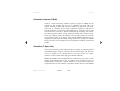
The interdisciplinary nature of Micro-Electro-Mechanical Systems (MEMS) and
the expertise required to develop the technology is a significant bottleneck in the
timely design of new products incorporating MEMS technology.
This issue calls for a new generation of design tools that combines aspects of
EDA and mechanical / thermal / fluidic / optical / magnetic CAD.
MEMSCAP approach to solving this design bottleneck is based on the following
principles and features:
Supporting multiple flows: for the component engineer, multi-physics circuit
designer and for the system engineer;
Allowing data exchange between the different description levels: the
structural level (FEM/BEM), the system/behavioral level (SPICE, HDL-A,
VHDL-AMS, Verilog-AMS), and the physical level (mask layout);
Targeting key features for MEMS specific design.
MEMS Pro, in combination with ANSYS Multiphysics or other 3D analysis
programs, enables system designers, MEMS circuit designers, IC designers,
process engineers, MEMS specialists, and packaging engineers to share critical
design and process information in the most relevant language for each
contributor.
MEMS Pro User Guide
Contents
Index
2
Introduction
MEMS Pro System
The MEMS Pro package includes a schematic entry tool, an analog and mixed
analog / digital circuit level behavioral simulator, a statistical analyzer, an
optimizer, a waveform viewer, a full-custom mask-level layout editing tool, an
automatic layout generator, an automatic standard cell placement and routing
tool, a design rule checking feature, an automatic netlist extraction tool (from
layout or schematic), a comparison tool between netlists extracted from layout
and schematics (Layout Versus Schematic), and libraries of MEMS examples.
MEMS specific key features also available in MEMS Pro encompass a 3D solid
model generator using mask layout and process information, a 3D solid model
viewer with cross-section capability, a process description editor, true curved
drawing tools and automation of time consuming tasks using the MEMS Pro
Easy MEMS features.
Embedded features within ANSYS 5.6 allow automatic mask layout generation
from an ANSYS 3D Model and process description (3D to Layout), as well as
automatic MEMS behavioral Model generation in hardware description
languages (Reduced Order Modeling).
Total Solution
S-Edit schematics are easily transferred to EDIF, SPICE and VHDL industry
formats. L-Edit layout exports to standard formats accepted by mask makers and
foundries including GDS II, CIF and DXF (through an optional converter). 3D
MEMS Pro User Guide
Contents
Index
3
Introduction
MEMS Pro System
models also can be generated from layout and process definition and viewed in
the L-Edit environment. These 3D models may also be exported in SAT format
and directly used with third party tools such as AutoCAD, ANSYS, Ansoft
HFSS, Maxwell 3D, ABAQUS, and MSC/NASTRAN and those from CFDRC
and Coyote Systems. Now, Version 3.00 offers the possibility to generate CIF
format layouts from 3D models. The Reduced Order Modeling feature generates
MEMS behavioral models in SPICE and HDL-A for fast and accurate system
level simulations.
MEMS Pro User Guide
Contents
Index
4
Introduction
Tool Flow
Tool Flow
Each stage of the MEMS design process is addressed by a different component of
the MEMS Pro tool suite.
MEMS Pro User Guide
Contents
Index
5
Introduction
Tool Flow
Schematic Capture (S-Edit)
S-Edit is a fully hierarchical schematic capture program for MEMS and IC
applications. The program also serves as a schematic entry front end to the
T-Spice simulator, L-Edit/ SPR automatic standard cell placement and router,
and layout vs. schematic (LVS) netlist comparison programs. S-Edit and its
associated libraries are technology independent; that is, the design may be built
and tested before choosing a specific manufacturing technology and vendor.
User-defined global symbols convey connection among nodes without wiring.
S-Edit also supports global node naming so that a single symbol can represent
several distinct nodes in the design. Using S-Edit, MEMS schematics can be
designed to include signals in multiple energy domains. For example, the MEMS
Library includes a set of examples of electro-mechanical schematic symbols and
models.
Simulator (T-Spice Pro)
The T-Spice simulator provides full-chip analysis of analog, mixed analog/digital
and MEMS designs using an extremely fast simulation engine that has been
proven in designs of over 300,000 devices. For large circuits, the T-Spice
simulator can be ten times faster than typical SPICE simulators.
MEMS macromodels can be implemented in 3 different ways in T-Spice. In the
simplest form, MEMS devices may be modeled using equivalent circuits of
standard SPICE components. Another method is to create table models from
experimental data or finite element or boundary element analysis of the MEMS
MEMS Pro User Guide
Contents
Index
6
Introduction
Tool Flow
devices. A third method is to use the external functional model interface. This
last method allows quick and easy prototyping of custom MEMS macromodels
using a C code interface.
The program includes standard SPICE models, BSIM3 models, and the advanced
Maher/Mead charge-controlled MOSFET model that is ideally suited to submicron design. The W-Edit graphical waveform viewer, embedded within
T-Spice, displays analysis results, and automatically updates its display each time
T-Spice simulates a circuit.
Powerful optimization algorithms automatically determine device or process
parameters that will optimize the performance of your design. Defining
parameters to be varied, setting up optimization criteria, and choosing
optimization algorithms is a cinch using the new Optimization Wizard. The
Wizard prompts you for the optimization criteria the program will need.
Monte Carlo analysis generates “random” variations in parameter values by
drawing them probabilistically from a defined distribution. This type of statistical
analysis may be used to discover what effects process variation will have on
system performance.
Layout Editor (L-Edit)
L-Edit is an interactive, graphical layout editor for MEMS and IC design. This
full-custom editor is fast, easy-to-use, and fully hierarchical. Primitives include
boxes, polygons, circles, lines, wires, labels, arcs, splines, and tori. Drawing
MEMS Pro User Guide
Contents
Index
7
Introduction
Tool Flow
modes include 90°, 45°, and all-angle layout. Shortcuts are also available for
quickly laying out circles, tori, pie slices, splines, and “curved polygons” with
true curved edges. Designs created in L-Edit are foundry ready. The new MEMS
Pro Toolbar in Version 3.00 gives access to MEMS specific design features.
They gather the creation of splines, the display of vertex information, and the use
of Easy MEMS features like the polar array feature and the plate release feature.
It also includes access to the process definition graphical interface, 3D modeler
and viewer, MEMS specific DRC, and MEMSLib (the MEMS library).
User-programmable Interface
L-Edit/UPI is a powerful tool for automating, customizing, and extending
L-Edit’s command and function set. The heart of L-Edit/UPI is the macro
interface. Macros are user-programmed routines, written in the C language, that
describe automated actions or sets of actions. Macros can be recognized by their
.dll file extension. Complex, parameterized cell generation (for example, comb
drives, rotary motors, gears, etc.) as well as simple but often used geometry (for
example, bonding pads) can be implemented with a single key stroke. L-Edit/UPI
includes a C language interpreter for reading macro code, eliminating the need
for a system compiler. The program reads .dll files produced by the user, or from
MEMSCAP or Tanner libraries, or libraries supplied by third party vendors. The
UPI provides user access to L-Edit’s Design Rule Checker and netlist extraction
modules, and may be used to integrate L-Edit with other third-party applications.
MEMS Pro User Guide
Contents
Index
8
Introduction
Tool Flow
Layout vs. Schematic (LVS)
LVS compares the SPICE netlist generated from S-Edit or another schematic
editor with the netlist generated from layout by L-Edit⁄Extract. LVS is a check to
ensure that both netlists represent the same multiphysics "circuit". Should any
inconsistencies be found between the two lists, LVS can be used to identify and
resolve the ambiguity.
3D Modeler
Accurate three-dimensional (3D) visualization of your design-in-progress is
crucial to successful fabrication. You can create 3D models of your MEMS
device layout geometry directly in L-Edit using one of the many foundry
fabrication process descriptions we support, or by specifying your own custom
process. The 3D Solid Modeler permits views of surface and bulk micromaching
steps including deposit, etch, and mechanical polishing. You can easily
customize your view with features such as panning, zooming, cross-section
modeling, and other viewing controls. 3D solid model geometry can be exported
in a SAT format.
MEMS Block Place and Route
The block place and route feature will save you time and prevent wiring
mistakes. Routing may be done automatically or manually. The MEMS block
place and route enables you to connect component level blocks of MEMS and IC
MEMS Pro User Guide
Contents
Index
9
Introduction
Tool Flow
devices. Efficiency enhancing features include hierarchical block placement,
block level floor planning, an EDIF netlist reader, and on-line signal integrity
analysis.
MEMS Library (MEMSLib)
MEMSLib provides MEMS designers with schematics, simulation models, and
parameterized layout generators for a set of MEMS components. MEMSLib
includes several types of suspension elements, electro-mechanical transducers,
and test structures for extracting material properties. Various example elements
can be assembled to produce a single MEMS device.
Foundry Support
We’ve included examples of process setup information for design rules, layer
definitions, extraction rules, process definitions, model parameter values, and
macros from the most popular foundries. Processes examples include MCNC
(MUMPs), Sandia (M3M), ADI (iMEMS), and MOSIS (NIST).
Embedded features in ANSYS
Reduced Order Modeling (Macro-Model Generation)
Powered by ANSYS Multiphysics, MEMS Modeler offers automatic generation
of behavioral models for fast and accurate system level simulation. It captures the
MEMS Pro User Guide
Contents
Index
10
Introduction
Tool Flow
essential behavior for mechanical devices, and coupled electrostatics-mechanics
MEMS components. Transient simulations, "what if" analysis and very accurate
system simulation are then easily and quickly performed.
Automatic mask layout generation (3D to Layout)
FEM-to-layout automatically generates mask layout in CIF format from FEM
models developed from a target process definition.
MEMS Pro User Guide
Contents
Index
11
Introduction
What’s New in Version 3.0
What’s New in Version 3.0
MEMS Pro has been enhanced to simplify design flow and boost your
productivity. We have incorporated technology that will let you optimize your
designs before you submit them to the foundry, and thereby shorten your design
cycle. For more information about
The new MEMS-specific Graphical User Interface, refer to MEMS Pro
Toolbar on page 97
Easy MEMS including the plate release feature, the polar array feature, and
the vertex information viewer, refer to MEMS Pro Utilities on page 147
Automatic spline generator, refer to Splines on page 126
3D to Layout generator, refer to ANSYS to Layout Generator on page 278
Reduced Order Modeling, refer to Reduced Order Modeling on page 334
MEMS Pro User Guide
Contents
Index
12
Introduction
Documentation Conventions
Documentation Conventions
This section contains information about the typographical and stylistic
conventions employed by this user guide.
In-line references to menu and simulation commands, device statements, special
characters, and examples of user input and program output are represented by a
bold font. For example: .print tran v(out).
Elements in hierarchical menu paths are separated by a > sign. For example,
File > Open means the Open command in the File menu.
Tabs in dialog boxes are set off from the command name or dialog box title by a
dash. For example, Setup > Layers—General and Setup Layers—General both
refer to the General tab of the Setup Layers dialog.
Freestanding quotations of input examples, file listings, and output messages are
represented by a constant-width font—for example:
.ac DEC 5 1MEG 100MEG
Variables for which context-specific substitutions should be made are
represented by bold italics—for example, myfile.tdb.
MEMS Pro User Guide
Contents
Index
13
Introduction
Documentation Conventions
Sequential steps in a tutorial are set off with a check-box dingbat (ã) in the
margin.
References to keyboard-mouse button combinations are given in boldface, with
the first letter capitalized—for example, Alt + Left. The terms left-click, rightclick, and center-click all assume default mappings for mouse buttons.
Text omitted for clarity or brevity is indicated by an ellipsis (…).
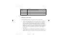
Special keys are represented by abbreviations, as follows.
Key
Abbreviation
Shift
Shift
Enter
Enter
Control
Ctrl
Alternate
Alt
Backspace
Back
Delete
Del
Escape
Esc
Insert
Ins
Tab
Tab
MEMS Pro User Guide
Contents
Index
14
Introduction
Documentation Conventions
Key
Abbreviation
Home
Home
End
End
Page Up
PgUp
Page Down
PgDn
Function Keys
F1 F2 F3 …
Arrow Keys
↓ , ← , →, ↑
When certain keys are to be pressed simultaneously, their abbreviations are
adjoined by a plus sign (+). For example, Ctrl + R means that the Ctrl and R keys
are pressed at the same time.
When certain keys are to be pressed in sequence, their abbreviations are
separated by a space ( ). For example, Alt + E R means that the Alt and E keys
are pressed at the same time and then released, immediately after which the R
key is pressed.
Abbreviations for alternative key-presses are separated by a slash (/). For
example, Shift + ↑ / ↓ means that the Shift key can be pressed together with
either the up (↑) arrow key or the down (↓) arrow key.
MEMS Pro User Guide
Contents
Index
15
MEMScAP
2
MEMS Pro Tutorial
Introduction
17
Creating a Schematic
19
Exporting a Netlist
40
Simulating from a Netlist
42
Probing a Waveform
45
Viewing a Waveform
47
Generating a Layout
56
Viewing a 3D Model
73
Drawing Tools
86
MEMS Pro User Guide
Contents
Index
16
MEMS Pro Tutorial
Introduction
Introduction
In the MEMS Pro tutorial, you will follow the complete design of a MEMS
resonator. The ANSYS Tutorial on page 176, the ROM Tutorial on page 370, the
ANSYS to layout Tutorial on page 316, the Block Place and Route Tutorial on
page 486, and the Optimization Tutorial on page 435 are targeted to special
features of MEMS Pro. The advanced portion of this tutorial includes a
demonstration of layout extraction and netlist comparison using L-Edit/Extract
and LVS. Those chapters assume that the user is completely familiar with the
material covered in this general tutorial.
In this tutorial, you will create a schematic design, analyze system behavior, and
generate device layout with the MEMS Pro tools S-Edit, T-Spice, W-Edit, and
L-Edit. You will draw mask layout manually and automatically, and generate and
view 3D models and cross-sections in L-Edit.
All files mentioned in this chapter are located in the tutorial subdirectory of the
main MEMS Pro installation directory. We recommend that you follow the
tutorial from the beginning; however, you may enter and exit the tutorial at
several points during the design. Tutorial breakpoints occur at Simulating from a
Netlist on page 42, Generating a Layout on page 56, Viewing a 3D Model on
page 73, and at Drawing Tools on page 86.
MEMS Pro User Guide
Contents
Index
17
MEMS Pro Tutorial
Introduction
The Design Example
The design example, appearing throughout the MEMS Pro User Guide, is an
electrostatic lateral comb-drive resonator. A resonator is a MEMS transducer that
can be used as a sensor by exploiting the high sensitivity of its resonant
frequency to various physical parameters. The resonator was chosen for your
review because it is an easily understood coupled electro-mechanical system.
The resonator will be designed using the MEMSLib library components
including comb-drives, a plate and folded springs.
MEMS Pro User Guide
Contents
Index
18
MEMS Pro Tutorial
Creating a Schematic
Creating a Schematic
In this section, you will learn how to navigate and manipulate designs using the
S-Edit schematic editor.
Launching S-Edit
ã
Launch S-Edit by double-clicking the S-Edit icon
directory.
in the installation
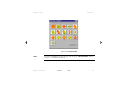
The S-Edit user interface consists of five areas:
The title bar (at the very top of the application window) contains the file
name, module name, page name, and mode.
The menu bar (at the top) contains commands
The palette bar (on the left) contains tool icons
The status bar (at the bottom) contains runtime information
The display area (in the center) contains the schematic
The standard commands toolbar (below the menu bar) contains often used
commands
MEMS Pro User Guide
Contents
Index
19
MEMS Pro Tutorial
Creating a Schematic
Designs are contained in files, each of which consists of one or more modules.
Modules are viewed in either of two modes:
Symbol Mode: a graphical representation of the module showing the
module’s connections.
Schematic Mode: shows the composition and connectivity of the module.
The schematic may contain one or more pages which consist largely of two
component types:
Note
Primitives: geometrical objects, wires, ports, annotation objects, and labels;
all created with the S-Edit drawing tools.
Instances: “copies” of other modules, dynamically linked to their originals.
Instances are displayed in a design using the module’s symbol page.
For more information on instancing modules, see Working with Modules on page
97 of the S-Edit User Guide and Reference.
Opening the File
As part of this section of the tutorial, you will place the components of an
electrostatic lateral comb-drive resonator, connect those components, and run an
AC analysis on your design.
MEMS Pro User Guide
Contents
Index
20
MEMS Pro Tutorial
Creating a Schematic
The schematic symbols for these components have two pins for each connecting
side: one carrying the electrical signal (denoted with the subscript _e), and the
other carrying the mechanical signal (denoted with the subscript _m). These
symbols are assembled to form the resonator design and a frequency sweep (AC
analysis) of the system is performed to discover the resonant frequency and the
magnitude of displacement. The electro-mechanical behavior of the components
are modeled by expressing the mechanical behavior in terms of electrical
analogs. These models can then be used to solve for the electrical and mechanical
behavior of the system as well as the coupling between the two energy domains.
The completed design is provided for your reference in the reson.sdb file in the
tutorial directory.
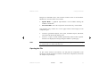
ã
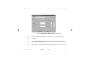
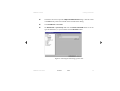
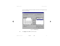
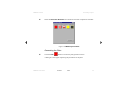
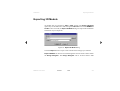
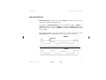
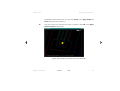
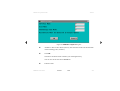
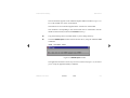
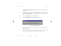
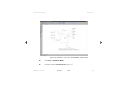
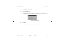
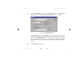
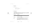
Select File > Open to open this file.
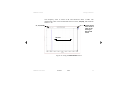
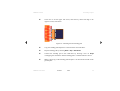
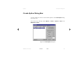
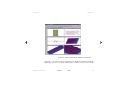
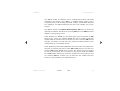
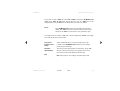
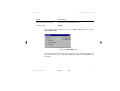
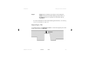
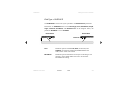
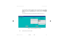
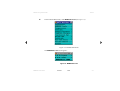
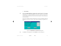
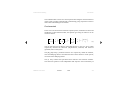
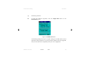
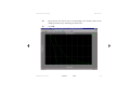
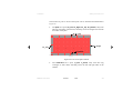
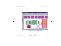
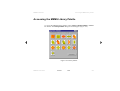
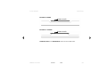
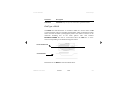
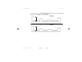
The current (visible) file, module, page, and mode are named at the top of the
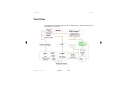
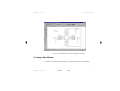
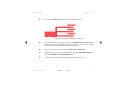
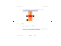
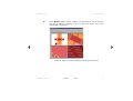
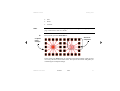
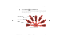
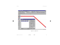
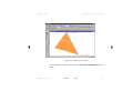
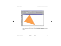
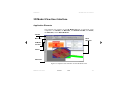
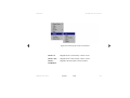
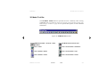
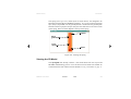
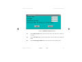
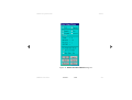
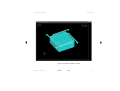
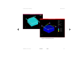
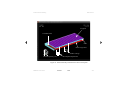
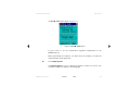
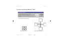
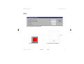
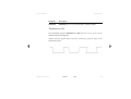
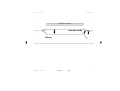
title bar. The schematic view of the resonator appears in Figure 1.
Note
For more information, see Working with Files on page 92, Working with
Modules on page 97, Working with Schematic Pages on page 116, Levels of
Design on page 31 and Viewing Modes on page 33 of the S-Edit User Guide and
Reference.
MEMS Pro User Guide
Contents
Index
21
MEMS Pro Tutorial
Creating a Schematic
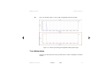
Figure 1: Schematic view of the complete resonator
Creating a New Module
To initiate your new resonator design, you must first create a new module.
MEMS Pro User Guide
Contents
Index
22
MEMS Pro Tutorial
Creating a Schematic
ã
Select Module > New to create a module.
ã
In the Module Name edit field, enter MyResonator and click OK.
Now would be a good time to save a copy of the file.
ã
Select File > Save As to invoke the Save As dialog.
ã
Select the tutorial directory, enter myreson.sdb as the filename, and click the
Save button.
You can compare your work to the reference design at any time by using the
Module > Open command and choosing Resonator as the module to open. Use
Module > Open again to return to your design, this time selecting MyResonator
as the module to be opened.
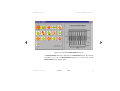
Instantiating Components
Instantiating a Plate
ã
Select Module > Instance to invoke the Instance Module dialog.
ã
Select plate4 as the Module to Instance and click OK.
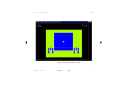
Plate4, a four-sided plate with eight points of connection (pins), will appear at
the center of the schematic page.
MEMS Pro User Guide
Contents
Index
23
MEMS Pro Tutorial
ã
Creating a Schematic
Home the view by selecting View > Home or by pressing the Home key. The
view of the plate will be resized so that the plate fills the contents of the window.
Instantiating Comb-drives
ã
Instantiate the comb module as you instantiated the plate.
The newly instantiated comb will appear on top of plate4 in the middle of the
schematic window. You will have to move it to a new location using the S-Edit
click and drag feature.
Note
Objects in S-Edit can be moved by selecting with the left or right mouse button
and dragging with the center mouse button. For two-button mice, press the Alt
key and left-click to drag objects.
ã
Place the comb-drive to the right side of the previously instantiated plate.
ã
Place a second comb-drive into the design by copying the instance. With the first
comb instance selected, select Edit > Copy, then Edit > Paste.
ã
Select the left comb and then flip it by choosing Edit > Flip > Horizontal.
MEMS Pro User Guide
Contents
Index
24
MEMS Pro Tutorial
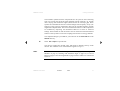
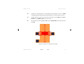
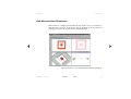
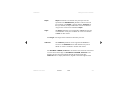
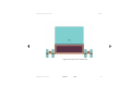
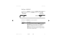
ã
Creating a Schematic
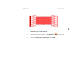
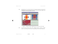
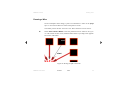
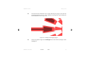
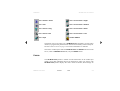
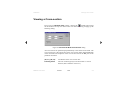
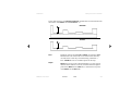
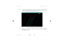
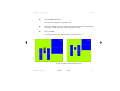
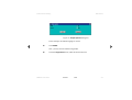
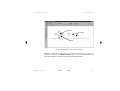
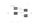
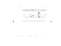
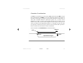
Move the comb-drives so that their connection pins, represented by circles, line
up with the pins on the plate4 instance (Figure 2) (see Pins on page 180 of the
S-Edit User Guide and Reference).
Figure 2: Aligning the comb-drives to the plate
Instantiating Folded Springs
ã
Instantiate the fspring module and place it above the plate.
ã
Create a copy of the folded spring and place it below the plate.
ã
Flip this second instance of fspring by selecting Edit > Flip > Vertical.
MEMS Pro User Guide
Contents
Index
25
MEMS Pro Tutorial
Creating a Schematic
Wiring Objects
Wires are drawn using the Wire tool
.
First time, users of S-Edit may confuse the Wire tool with the Line tool. Lines are
used to graphically represent components; they are non-electrical objects used to
annotate your schematic. Wires are electrical and are used to connect objects.
Note
For more information on wiring your schematic, see Wires on page 175 of the
S-Edit User Guide and Reference.
Zooming the View
Sensitive operations such as wiring nodes require a closer view for accuracy.
ã
Select View > Zoom > Mouse.
ã
Drag a box around the plate with the left mouse button. Allow enough room to
see the areas between the comb-drives and the folded springs.
If you find you have zoomed in too much or too little, use the plus and minus
keys to Zoom in and out. The arrow keys can be used to pan the view.
MEMS Pro User Guide
Contents
Index
26
MEMS Pro Tutorial
Note
Creating a Schematic
For more information on zooming, see Panning and Zooming on page 134 of the
S-Edit User Guide and Reference.
You will now create connections between the plate and other schematic
components with wires.
ã
Select the Wire tool from the schematic toolbar.
ã
Initiate the wire placement by left-clicking on plate4 at the bottom_m pin. The
pin is shown as an open circle on the bottom left of the plate4 instance.
Vertices can be placed on wires by clicking the left mouse button while placing a
wire.
Note
For more information on making connections, see Nodes on page 184, Pins on
page 180, and Wires on page 175 of the S-Edit User Guide and Reference.
ã
Move the cursor down and end the wire placement by right-clicking at the pin
called free_m on the bottom fspring. This pin is shown as an open circle on the
top left of the bottom fspring instance.
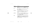
ã
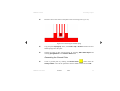
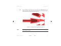
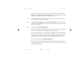
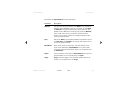
Repeat this process to wire the plate with the other components (see Figure 3).
MEMS Pro User Guide
Contents
Index
27
MEMS Pro Tutorial
ã
Creating a Schematic
Home the view by pressing the Home key.
Figure 3: Schematic view of the wired elements
Next, you will add stimuli and commands to set up this schematic for simulation.
MEMS Pro User Guide
Contents
Index
28
MEMS Pro Tutorial
Creating a Schematic
Instantiating Voltage Sources
ã
Instantiate the Source_v_ac module.
ã
Place it to the left of the left comb.
ã
Instantiate the Source_v_dc module.
ã
Place it to the right of the right comb.
ã
Copy the instance of Source_v_dc and place it to the right of the top fspring.
ã
Wire the positive terminals of the voltage sources to the fix_e pins of the right
comb, left comb, and top fspring. The positive terminals are on the top of the
voltage source, in this example.
ã
Compare your design to the finished design in Figure 1 to make sure you have
placed the voltage sources correctly.
Placing Global Nodes
Global nodes simplify the drawing and maintenance of schematics. They allow
nodes throughout a design to be connected to each other without the need to draw
or delete wires. Global nodes are especially useful for power, ground, anchor,
clock, reset, and other system-wide nodes that require routing throughout the
hierarchy of the design.
MEMS Pro User Guide
Contents
Index
29
MEMS Pro Tutorial
Note
Creating a Schematic
For more information on global nodes, see Global Nodes on page 191 of the
S-Edit User Guide and Reference.
To create a global node, you must place a global symbol on the design with the
Global Symbol tool. Global symbols are special instances that function as
wireless connectors. When you attach a node to a global symbol, you connect
that node to all other nodes on every page and module in the design file that are
attached to the same global symbol. Such nodes then become global nodes.
You will add six global ground symbols to the schematic. Three of them will be
connected to the negative terminals of the voltage sources to set electrical
grounds. The other three will be connected to the fixed mechanical terminals to
signify mechanical anchors.
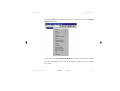
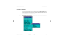
ã
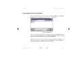
To place a ground symbol onto the design, click the Global Symbol tool on the
left side of the schematic window
.
MEMS Pro User Guide
Contents
Index
30
MEMS Pro Tutorial
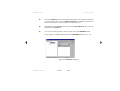
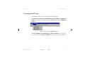
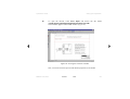
ã
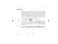
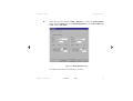
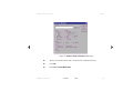
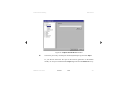
Creating a Schematic
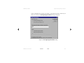
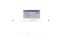
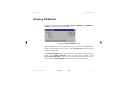
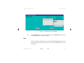
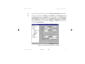
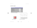
Left-click on the schematic page. The Instance Module browse box will appear,
with a list of the available global nodes and the ground (Gnd) symbol will be
preselected.
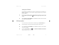
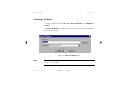
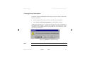
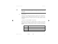
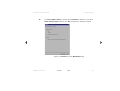
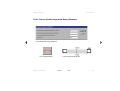
Figure 4: Instance Module browse box
ã
Click OK.
The ground symbol will be placed where you left-clicked in the previous step.
ã
Copy and paste the ground symbol five times. Move two ground symbols to a
place on the schematic near each voltage source.
ã
Now wire the negative (lower) terminal of each of the three voltage sources to a
ground symbol.
MEMS Pro User Guide
Contents
Index
31
MEMS Pro Tutorial
Creating a Schematic
ã
Of the remaining three ground symbols, one should be connected to the fix_m pin
of the top spring, and the other two should be connected to the fix_m pins of the
two comb-drives.
ã
Compare your wiring to the completed schematic presented in Figure 1.
ã
Pins fix_e (fixed electrical) and fix_m (fixed mechanical) of the bottom fspring
should be the only pins left unconnected at this point. Connect them to the fix_e
and fix_m pins, respectively, of the top fspring.
ã
Compare your design to the finished design presented in Figure 1 to make sure
the resonator has been wired correctly.
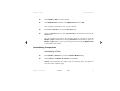
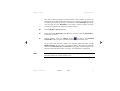
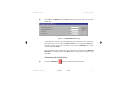
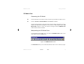
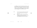
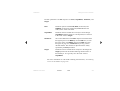
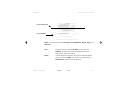
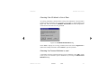
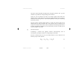
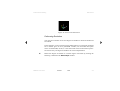
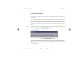
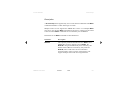
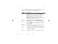
Editing Object Properties
Now, you will edit the properties of one of the voltage sources in the schematic to
set up the design for simulation.
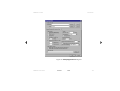
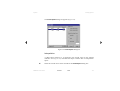
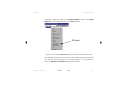
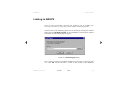
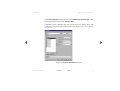
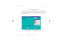
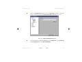
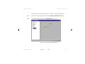
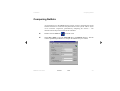
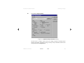
ã
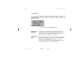
Select the voltage source next to the left comb by right-clicking it. Invoke the
Edit Instance of Module Source_v_ac dialog by selecting Edit > Edit Object.
MEMS Pro User Guide
Contents
Index
32
MEMS Pro Tutorial
Creating a Schematic
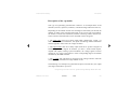
Figure 5: Edit Instance of Module Source_v_ac dialog
ã
Enter 1 for mag, 0 for phase, and 0 for Vdc in the corresponding edit fields.
ã
Click OK.
ã
Give the voltage source for the right comb-drive a DC value of 0 volts. Do this by
choosing Edit > Edit Object with this source selected. Enter 0 in the V field.
ã
Similarly, give the voltage source for the folded springs a DC value of 50 Volts.
MEMS Pro User Guide
Contents
Index
33
MEMS Pro Tutorial
Creating a Schematic
Labeling Nodes
In S-Edit, connectivity is defined in terms of nodes. A node is a point on the
schematic to which one or more pins or wires are connected. Nodes are defined
by their name, and the scope of a node is normally the collection of schematic
pages in a module. That is, if a node-name appears twice within a single module,
both names refer to the same point of connection. If the same node-name appears
within two different modules, the nodes refer to completely different points of
connection. S-Edit automatically assigns names to each node, but you may also
manually name nodes. User-assigned node labels are helpful for annotating
S-Edit schematics and producing more readable netlists.
ã
Select the Node Label tool
ã
Label the two wires connecting plate4 to the right comb, rtm, and rte. To label a
node, click it and enter the new node name in the Place Node Label dialog box.
The rtm node label should be placed on the wire between right_m and free_m
pins, and the rte node label should be placed on the wire between right_e and
free_e pins.
ã
To change the orientation of the node label, click the Selection button, click the
node label, and select Edit > Edit Object. From the Edit Node Label dialog box,
click one of the eight radio buttons representing the location of the label origin.
MEMS Pro User Guide
Contents
from the schematic toolbar.
Index
34
MEMS Pro Tutorial
ã
Creating a Schematic
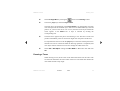
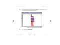
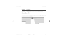
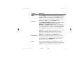
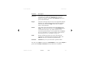
Edit the node label orientations to look somewhat like the layout in Figure 6.
Figure 6: rtm and rte nodes
ã
You may rename the rest of the nodes in your diagram to match the names we
have given ours in the Resonator module in reson.sdb, if you wish. This is an
optional step. S-Edit will automatically assign names to unlabeled nodes.
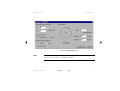
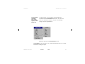
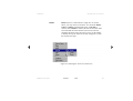
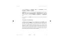
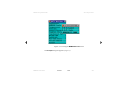
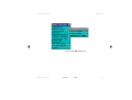
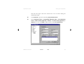
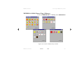
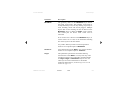
Adding Simulation Commands
The Command tool provides an easy, convenient means of entering device and
model statements, stimuli, simulation commands, and simulation options within
the S-Edit environment.
We will use the Command tool to add two SPICE commands. One instructs the
simulator to run an AC simulation. The other instructs the simulator to include a
file in the simulation netlist that contains fabrication process parameters for the
resonator components.
MEMS Pro User Guide
Contents
Index
35
MEMS Pro Tutorial
Creating a Schematic
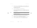
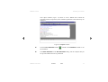
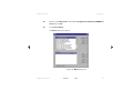
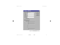
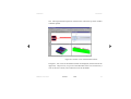
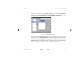
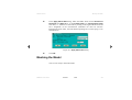
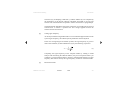
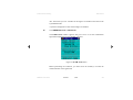
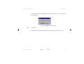
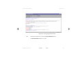
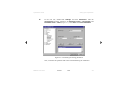
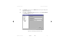
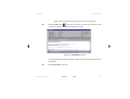
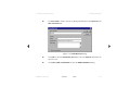
ã
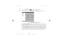
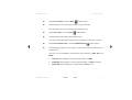
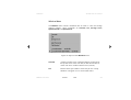
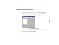
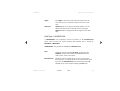
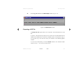
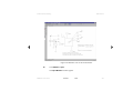
Select the Command tool
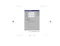
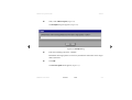
ã
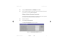
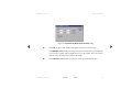
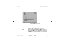
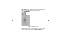
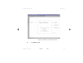
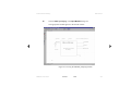
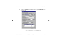
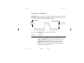
Click the work area to invoke the T-Spice Command Tool dialog (Figure 7).
from the schematic toolbar.
Figure 7: T-Spice Command Tool dialog
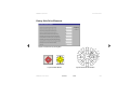
The T-Spice Command Tool dialog lists command categories on the left. By
default, the Analysis category is selected and the right side of the dialog contains
buttons listing the commands within that category. This command list may also
be viewed by clicking the + sign next to each category. For example, clicking the
+ sign next to Analysis category will expand this category and show the same list
of commands as those on the buttons. When a command is selected, the right side
of the dialog changes to contain the parameters for the selected command.
MEMS Pro User Guide
Contents
Index
36
MEMS Pro Tutorial
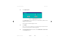
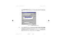
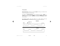
ã
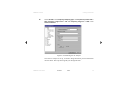
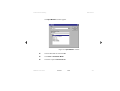
Creating a Schematic
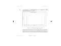
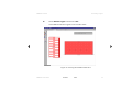
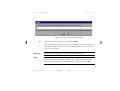
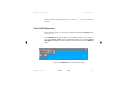
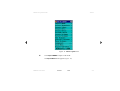
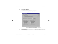
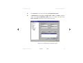
Add an AC analysis command by clicking the AC button on the right side of the
T-Spice Command Tool dialog.
The directory tree on the left side of the T-Spice Command Tool dialog will
open up to list the commands available under Analysis. The right side of the
T-Spice Command Tool dialog will contain parameters specific to the AC
Analysis command.
MEMS Pro User Guide
Contents
Index
37
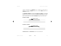
MEMS Pro Tutorial
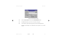
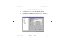
ã
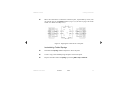
Creating a Schematic
Select decade as the Frequency sampling type, set Frequencies per decade to
500, Frequency range From to 10k and Frequency range To to 100k. Click
Insert Command.
Figure 8: Customizing the AC analysis
Once the AC analysis is set up, we need to bring fabrication process information
into the netlist. The steps below guide you through this task.
MEMS Pro User Guide
Contents
Index
38
MEMS Pro Tutorial
Creating a Schematic
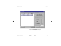
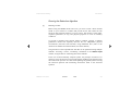
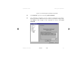
ã
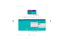
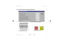
Click the work area to open the T-Spice Command Tool dialog. Click the + next
to the Files entry of the tree located on the left side of the dialog.
ã
Click Include file under Files.
ã
Set Include file to process.sp and click the Insert Command button. You can
type the filename in, or you can find it with the Browse button.
Figure 9: Selecting the technology process file
MEMS Pro User Guide
Contents
Index
39
MEMS Pro Tutorial
Exporting a Netlist
Exporting a Netlist
An S-Edit schematic can be exported to a SPICE netlist by performing one of the
following operations:
Using the Export Netlist dialog box accessed via File > Export.
Clicking the T-Spice button on the Standard Commands toolbar.
The netlist can be used to test the performance characteristics of the system using
T-Spice or other SPICE programs.
The next few instructions ask you to invoke T-Spice from S-Edit to export a
netlist and to run a simulation. When you invoke T-Spice, a new, active
application window will appear. The current S-Edit window will become
inactive, but do not close it. You will be returning to S-Edit to analyze your
simulation results.
Tutorial Breakpoint
You will now use T-Spice to simulate a circuit. If you are starting the tutorial
here, double click the S-Edit icon and select File > Open to open the reson.sdb
file in the tutorial directory.
MEMS Pro User Guide
Contents
Index
40
MEMS Pro Tutorial
Exporting a Netlist
Note that we have provided a working module of the resonator for you to use
through the rest of the tutorial if the resonator you created is incomplete, or if you
are entering the tutorial at this step. Our module is called Resonator. Follow the
next two steps to access Resonator. If you want to use the resonator you have
created, move ahead to the third step “Launch T-Spice.”
ã
Use the Module > Open command.
ã
Select the module Resonator, click OK. Click the page containing Resonator to
ensure that it is active.
ã
Launch T-Spice. Click the T-Spice button
located in the Standard
Commands toolbar. T-Spice will launch with the exported netlist open.
If you chose your resonator module, the exported netlist file name will be
MyResonator.sp. If you chose our resonator module, the exported netlist file
name will be Resonator.sp in the tutorial directory. This name will appear in the
title bar of the input file window of T-Spice. You should leave S-Edit open.
Note
For more information on exporting schematics, see Exporting a Netlist on page
228 of the S-Edit User Guide and Reference.
MEMS Pro User Guide
Contents
Index
41
MEMS Pro Tutorial
Simulating from a Netlist
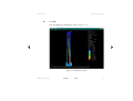
Simulating from a Netlist
Using T-Spice and W-Edit, SPICE netlists can be simulated, and the simulation
results can be displayed graphically. In this example, the coupled electromechanical behavior of the resonator is simulated using SPICE.
Simulating with T-Spice
T-Spice contains a full featured editor that includes search and replace of strings
and regular expressions, incremental find, and the Command tool for SPICE
syntax assistance. There are four areas on the T-Spice user interface:
The menu bar (at the top) contains menu commands
The toolbar (beneath the menu bar) contains tool icons
The status bar (at the bottom) contains runtime information
The work area (in the center) contains input file and runtime information
windows
MEMS Pro User Guide
Contents
Index
42
MEMS Pro Tutorial
Simulating from a Netlist
The T-Spice window (Figure 10) allows to view a SPICE file in which the
exported resonator components, their simulation parameters and connectivity are
displayed.
Figure 10: T-Spice window
ã
Click the Run Simulation button
the simulation.
ã
Click Start Simulation in the Run Simulation dialog. The AC analysis that you
set up from S-Edit will now be performed.
MEMS Pro User Guide
Contents
located in the Simulation toolbar to run
Index
43
MEMS Pro Tutorial
Simulating from a Netlist
The Simulation Output window will appear, displaying simulation statistics and
progress information, as well as any warning or error messages.
During the AC analysis, simulation results are recorded. Once the simulation is
complete, you may examine the analysis results using the S-Edit Probe tool.
MEMS Pro User Guide
Contents
Index
44
MEMS Pro Tutorial
Probing a Waveform
Probing a Waveform
The waveform probe is used to browse through an S-Edit design and probe nodes
to examine circuit simulation results for the specified node. When a node is
probed, S-Edit invokes W-Edit, which automatically displays the waveform
corresponding to the simulation results for that node. W-Edit can also be
launched from T-Spice by selecting Window > Show Waveform Viewer or by
clicking the W-Edit button from the T-Spice toolbar. In this tutorial, we will
invoke W-Edit from S-Edit using the probing feature.
Note
For more information on waveform probing, see Waveform Probing on page 243
of the S-Edit User Guide and Reference.
ã
Click somewhere in the S-Edit schematic window that contains the resonator
schematic to re-activate S-Edit.
ã
Click the Probe tool
located on the Schematic toolbar. The cursor now
has the shape of the Probe tool.
ã
Left-click with the Probe tool on the rtm node.
During waveform probing, W-Edit is launched, graphically displaying the results
of the T-Spice simulation.
MEMS Pro User Guide
Contents
Index
45
MEMS Pro Tutorial
Probing a Waveform
The W-Edit window should display a chart containing the magnitude and phase
of the displacement of node rtm for the performed AC analysis.
MEMS Pro User Guide
Contents
Index
46
MEMS Pro Tutorial
Viewing a Waveform
Viewing a Waveform
The W-Edit application window can contain many child windows, each
containing one or more charts.
ã
Maximize the window containing your results by clicking the
upper right corner of the window.
button on the
Chart Setups
W-Edit allows the expansion of charts with more than one trace into separate
charts, each containing a single trace. Collapsing the chart causes W-Edit to show
all the visible traces in one chart.
ã
Select Chart > Expand Chart.
There should now be two charts (Figure 11), one with amplitude information for
node rtm, vm(rtm), and one showing the phase angle, vp(rtm) plotted versus
frequency.
MEMS Pro User Guide
Contents
Index
47
MEMS Pro Tutorial
ã
Viewing a Waveform
Now you should be able to view a peak in amplitude at around 13 kHz.
Figure 11: Charts representing the amplitude and the phase angle
Trace Manipulation
At times, you may find it necessary to hide traces in order to simplify a waveform
window.
MEMS Pro User Guide
Contents
Index
48
MEMS Pro Tutorial
Viewing a Waveform
ã
Select both charts by choosing Edit > Select All.
ã
Choose Chart > Collapse Charts.
ã
With the (now single) chart selected, choose Chart > Traces.
ã
In the Traces dialog, select vp(rtm).
ã
Click the box beneath the Show label to unselect vp(rtm). The checkmark will
disappear.
MEMS Pro User Guide
Contents
Index
49
MEMS Pro Tutorial
Viewing a Waveform
The trace information will still be available, but the trace will not appear the next
time you view the chart.
Figure 12: Traces dialog
ã
Click Apply and then OK to return to the chart.
MEMS Pro User Guide
Contents
Index
50
MEMS Pro Tutorial
Viewing a Waveform
Notice that the displayed unit for vm(rtm) is Volts. The mechanical behavior of
this system is modeled with electrical analogs of mechanical components; the
mechanical displacement maps to voltage. Therefore, vm(rtm) represents the
displacement at the rtm node. Let’s change the label on the dependent variable
axis from Volts to Displacement. The new Y-axis units will be meters.
MEMS Pro User Guide
Contents
Index
51
MEMS Pro Tutorial
ã
Viewing a Waveform
Select the top chart. Choose Chart > Options to invoke the Chart Options
dialog. Click the Axes tab. Enter Displacement(rtm) in the Y-axis Label field
and m as the Y-axis Units.
Figure 13: Chart Options dialog
The chart title can also be customized, if you wish.
MEMS Pro User Guide
Contents
Index
52
MEMS Pro Tutorial
ã
Viewing a Waveform
In the General tab of the Chart Options dialog, set the Chart title to Lateral
Comb-drive Resonator and click OK.
Figure 14: Customizing the amplitude wave form
You may want to measure specific values on the chart. Cursors are vertical lines,
horizontal lines, or + points that can be used to identify locations on the trace for
measuring. The vertical and horizontal line cursors extend to the full height or
length of the chart. As the line cursors are moved around the chart, their
MEMS Pro User Guide
Contents
Index
53
MEMS Pro Tutorial
Viewing a Waveform
coordinates appear at the margins of the chart window. We demonstrate the use
of Vertical Bar cursors below.
ã
Select Chart > Cursors > Vertical Bars.
Two vertical cursors should appear on the chart. They can be dragged with the
left mouse button. Their X axis locations (x1 and x2) and the difference in X axis
locations (dx) are displayed on the top left corner of the chart window. The Y
axis location of the moving or last moved cursor is displayed under the trace
name on the right side of the chart.
ã
Position the left bar so that it lines up with the tip of the trace peak.
ã
Select View > Mouse Zoom. Click and drag a box around the tip of the peak in
vm(rtm). Make sure your drag box is within the chart window.
W-Edit will change the magnification of the chart so that the area outlined by the
box fills an entire window. The smaller the box is drawn, the closer W-Edit will
zoom into the chart. Continue magnifying your view until you have a clear view
of the peak.
If you have zoomed-in too closely, you can retreat. Be sure that your mouse is in
the window you want to adjust, then select View > Zoom Out.
ã
Position the left cursor so that it lines up with the tip of the trace peak.
MEMS Pro User Guide
Contents
Index
54
MEMS Pro Tutorial
Viewing a Waveform
The frequency value is shown as x1 and should be about 13 kHz. The
displacement value can be found under the trace name, vm(rtm), and should be
about 5.1 µm.
y-value of the
curve at the x
value of the
moving or
last moved
cursor
x1, x2, and dx
Cursors
Figure 15: Using the Vertical Bars cursor
MEMS Pro User Guide
Contents
Index
55
MEMS Pro Tutorial
Generating a Layout
Generating a Layout
ã
You may now exit S-Edit, T-Spice and W-Edit, if you like, using File > Exit.
Now, you will learn how to create, from MEMS layout components, the plate,
comb-drives and springs used in the resonator.
Tutorial Breakpoint
You will now generate the layout of a resonator using the MEMS Layout Palette.
Launching L-Edit
ã
Launch L-Edit by double-clicking the L-Edit icon
in the installation
directory. A default file named Layout1 should be visible in the work area.
The L-Edit user interface is similar in appearance to the S-Edit user interface. In
addition to the menu, palette, and status bars, there is a shortcut bar that contains
buttons for the most commonly-used menu commands.
As in S-Edit, L-Edit files are assembled hierarchically from discrete, usually
functionally distinct, units called cells, which can be edited and instantiated.
The current file and cell are named at the top of the application window.
MEMS Pro User Guide
Contents
Index
56
MEMS Pro Tutorial
Generating a Layout
Opening the File
ã
Select File > Open to open the reson.tdb file. The Resonator cell should appear
as the active cell. Use this view of the Resonator cell of the reson.tdb file as a
reference while you work through this section.
ã
Make the Layout1 file active by selecting the window containing Cell0 of
Layout1 from the list of windows under the Window menu.
Creating Components
The mask layout for MEMS components can be created using the Library Palette
accessed via the Library option of the MEMS Pro Toolbar.
The MEMS Library Palette contains active elements, passive elements, test
elements and resonator elements. The resonator element collection contains all
the parts you will need to create a resonator. All of these parts can be created
manually, using the drawing primitives available in MEMS Pro, but that task
would be tedious and time consuming.
The MEMS Library Palette should have been loaded as part of your installation
setup.
ã
Check that the MEMS Pro Toolbar has automatically appeared in the L-Edit
window.
MEMS Pro User Guide
Contents
Index
57
MEMS Pro Tutorial
Generating a Layout
If the MEMS Pro Toolbar is not automatically loaded, you will need to load it
manually. Refer to the introduction of Chapter 3 - MEMS Pro Toolbar.
Using the MEMS Library Palette
ã
Select Library > Library Palette in the MEMS Pro Toolbar to invoke the Library
Palette dialog box.
The MEMS Library Palette dialog box contains four tabs: Active Elements,
Passive Elements, Test Elements, and Resonator Elements. You will use the
Resonator Elements in this tutorial.
MEMS Pro User Guide
Contents
Index
58
MEMS Pro Tutorial
ã
Generating a Layout
Select the Resonator Elements tab to make the resonator components available.
Figure 16: MEMS Layout Palette
Generating the Plate
ã
Click the Plate
button to invoke the plate generation macro.
A dialog box will appear requesting the parameters of the plate.
MEMS Pro User Guide
Contents
Index
59
MEMS Pro Tutorial
ã
Generating a Layout
Enter 100 as the Width and click OK, accepting the default values for the other
parameters.
Figure 17: Plate Parameters dialog
L-Edit ⁄UPI now creates a plate matching the input parameters. To see the entire
plate, home the view by selecting View > Home or by pressing the Home key.
The plate shown in the active window is an instance (PlateInst) of a newly
created cell named Plate.
Each cell name must be unique in a file. Therefore, you should set the Name of
Plate Cell to something other than Plate when running the macro again in the
same file.
Generating the Comb-drives
ã
Click the comb-drive
MEMS Pro User Guide
Contents
button to create a lateral comb-drive.
Index
60
MEMS Pro Tutorial
Generating a Layout
ã
Change the Name of Instance to CombRight and click OK.
ã
Once a comb-drive appears on the screen, zoom out by pressing the minus key
several times or by selecting View > Zoom Out.
Editing an Already Generated Component
You will now learn to edit a component once you have created it. The component
you will edit is the comb-drive you have just instantiated.
ã
Select the comb drive
ã
Select Library > Edit Component.
The Linear Comb Parameters dialog box appears.
Figure 18: Linear Comb Parameters dialog box
MEMS Pro User Guide
Contents
Index
61
MEMS Pro Tutorial
ã
Generating a Layout
Set the Number of gaps to 21 and click OK.
The modified comb drive appears in the L-Edit window.
Figure 19: Viewing the modified comb-drive
MEMS Pro User Guide
Contents
Index
62
MEMS Pro Tutorial
Generating a Layout
This editing possibility is quite useful. Indeed, if you instantiate a component and
then decide that it should be larger or longer, you can just modify one of its
parameters and the newly edited component is automatically instantiated.
Attaching Components
ã
Drag the comb-drive to the right side of the plate so that the two objects slightly
overlap.
Recall that an object can be dragged to new locations by selecting it with a click,
and then holding down the center mouse button while moving it to the desired
location on the page. For two-button mice, left-click on the object while holding
down the Alt key to accomplish the move.
ã
Zoom in with the plus key. Use the arrow keys to pan the view to where the
comb-drive overlaps the plate.
MEMS Pro User Guide
Contents
Index
63
MEMS Pro Tutorial
ã
Generating a Layout
Re-align the comb-drive so that it looks like the figure below.
Figure 20: Aligning the comb-drive to the plate
ã
Copy the comb-drive by clicking it and choosing Edit > Copy, then Edit > Paste.
The new comb-drive will appear in the center of the page, on top of your existing
drawing. Move it to the side of the other layout objects.
ã
Flip the second comb-drive by selecting Draw > Flip > Horizontal.
ã
Change the name of this copied instance by selecting Edit > Edit Object and
entering CombLeft in the Instance Name field.
ã
Attach the second comb-drive to the left side of the plate (Figure 21).
MEMS Pro User Guide
Contents
Index
64
MEMS Pro Tutorial
Generating a Layout
Figure 21: Viewing the uncomplete design
Generating the Folded Springs
ã
Create a folded spring by clicking the Folded Spring
Library Palette.
ã
Change the Name of Instance to SpringTop and click OK.
MEMS Pro User Guide
Contents
Index
button from the
65
MEMS Pro Tutorial
ã
Generating a Layout
Position it above the center of the plate so that it overlaps (see Figure 22).
Figure 22: Positioning the folded spring
ã
Copy and paste SpringTop. Then, select Edit > Flip > Vertical. Position the new
folded spring below the plate.
ã
Change the name of this copied instance by selecting Edit > Edit Object and
entering SpringBottom in the Instance Name field.
Generating the Ground Plate
ã
Create a ground plate by clicking the Ground Plate
button from the
Library Palette. Leave all the parameters at their default values and click OK.
MEMS Pro User Guide
Contents
Index
66
MEMS Pro Tutorial
ã
Generating a Layout
Home the view, then move the ground plate so that it covers all the moving parts
of the resonator (refer to Figure 24).
Generating the Bonding Pads
ã
Create a bonding pad by clicking the Bonding Pad
button. Leave all
parameters for the bonding pad at their default values. Click OK.
ã
Position the bonding pad slightly to the right of the right comb-drive (Figure 23).
Now, you must connect the bonding pad to the comb-drive by drawing a box on
Poly0 overlapping the two components.
ã
Choose the Box tool
by clicking it and select the Poly0 layer from the
Layers Palette by clicking on the first item in the first row of the Layers Palette.
As your mouse is moved over the Poly0 button, a tool tip will appear displaying
the layer name. Poly0 will also appear in the list box at the top of the Layers
Palette.
MEMS Pro User Guide
Contents
Index
67
MEMS Pro Tutorial
ã
Generating a Layout
Click once to set the upper left corner, hold the key down and drag to the
opposite corner, and release.
1
2
Figure 23: Attaching the first bonding pad
ã
Copy the bonding pad and place it to the left of the left comb-drive.
ã
Flip the bonding pad by selecting Draw > Flip > Horizontal.
ã
Connect the bonding pad to the comb-drive by drawing a box on Poly0
overlapping the comb-drive and the bonding pad in a similar fashion as above.
ã
Make a third copy of the bonding pad and place it to the bottom left side of the
ground plate.
MEMS Pro User Guide
Contents
Index
68
MEMS Pro Tutorial
Generating a Layout
ã
Connect the ground plate to the bonding pad by drawing a box on Poly0
overlapping the bonding pad and the ground plate in a similar fashion as above.
ã
Change the name of the cell you have been working on from Cell0. Select Cell >
Rename. Enter MyResonator as the cell name.
ã
Save the file by choosing File > Save. Enter myreson.tdb as the file name and
click OK.
Figure 24: Final view of the lateral resonator
MEMS Pro User Guide
Contents
Index
69
MEMS Pro Tutorial
Generating a Layout
If you are interested in performing layout netlist extraction and layout vs.
schematic comparison, refer to Chapter 11 - Verification and use the
myreson.tdb file.
Viewing Properties
Properties can be attached to any L-Edit object including boxes, polygons, wires,
circles, ports, rulers, instances, cells, and files. Properties can contain
supplementary but necessary information about an object, such as what color it
will appear when modeled, or what its constituent material is.
MEMS Pro library components have a properties category called Extract
Properties. This category provides a link between a design layout and its netlist
description. Extract Properties are accessed via the Cell Info dialog box or the
Edit Instance dialog box.
Note
For more information on properties and extraction, see Properties on page 1-66
and Extracting Layout on page 3-48 of the L-Edit User Guide.
Properties were applied to each part of the resonator as it was constructed. You
will look at those properties now.
ã
Select the instance of the Plate and choose Edit > Edit Object.
MEMS Pro User Guide
Contents
Index
70
MEMS Pro Tutorial
Generating a Layout
ã
Click the Properties button. This instance should have no properties attached to
it. If the instance does not have Extract Properties, L-Edit⁄Extract pursues the
hierarchy and looks for extract properties on the parent cell.
ã
Select Cell from the Parent list box and click the View Parent button to view the
properties for the Plate cell.
ã
To view the extract properties, click the + sign next to the EXTRACT folder.
Three properties should be displayed under the EXTRACT folder (Figure 25).
Figure 25: Properties dialog box
MEMS Pro User Guide
Contents
Index
71
MEMS Pro Tutorial
Generating a Layout
Try selecting different properties to view their types and values on the right side
of the display.
ã
Click the L property. The value that you entered to represent the plate length is
shown as the Value on the right side of the dialog.
To return to the layout, perform the following operations:
ã
Click Cancel to exit this Properties dialog box.
ã
Click Cancel to exit the main Properties dialog box.
ã
Click Cancel to exit the Edit Object(s) dialog box.
MEMS Pro User Guide
Contents
Index
72
MEMS Pro Tutorial
Viewing a 3D Model
Viewing a 3D Model
The 3D Model Viewer automatically generates a 3D model from a layout and a
process definition.
Tutorial Breakpoint
You will now create and view a solid model. If you are beginning the tutorial
now, follow the next section on Launching L-Edit and Opening a File to open the
design file you have been provided with. If you are continuing from the previous
section, you may use your own design and skip to Process Definition on page 74.
Launching L-Edit and Opening a File
ã
Launch L-Edit by double-clicking the L-Edit icon
in the installation
directory. A default file named Layout1 should be visible in the work area.
ã
Close the Layout1 file by selecting File > Close.
MEMS Pro User Guide
Contents
Index
73
MEMS Pro Tutorial
ã
Viewing a 3D Model
Using the File > Open command, open the reson.tdb file (Figure 26) .
Figure 26: Layout view of the resonator
Process Definition
Importing the Process Definition
In addition to layout or mask data, the 3D Modeler needs the fabrication process
description to generate 3D models. This information may already be saved with
the layout, if not, it must be imported into the design file.
MEMS Pro User Guide
Contents
Index
74
MEMS Pro Tutorial
Viewing a 3D Model
The following setup procedure loads the process information into the design file.
Once imported, the process definition information is saved with the design file; it
need not be re-imported when the file is re-opened.
Note
ã
Choose 3D Tools > Edit Process Definition in the MEMS Pro Palette. In the
Process Definition dialog, click the Import button.
ã
In the Open dialog box, select mumps_i.pdt and click the Open button.
For more information on process definitions, see Process Definition on page 352
of the MEMS Pro User Guide.
MEMS Pro User Guide
Contents
Index
75
MEMS Pro Tutorial
Viewing a 3D Model
Information describing the MCNC MUMPs process is imported into the dialog
box. This information, in conjunction with the open layout, is used to build a 3D
model.
Figure 27: Process Definition dialog box
The top of the dialog box contains identifying information for the process
definition. The left side of the dialog contains a list of the process steps. Beneath
MEMS Pro User Guide
Contents
Index
76
MEMS Pro Tutorial
Viewing a 3D Model
it and to its side are the controls for adding, deleting, moving, enabling, and
displaying 3D models for intermediate steps. The right side of the dialog contains
the parameters of the selected step in the process steps list.
Note
For more information on editing process definitions, see Editing the Process
Definition on page 149 and Process Steps on page 357 of the MEMS Pro User
Guide.
Mumps_i.pdt is an abridged version of the MUMPS process definition. It
includes the steps up to the patterning of the second polysilicon layer. (A
simplified process is used for the tutorial in the interest of saving computation
time.) You do not lose any important information because the linear resonator
structure is defined by the process steps up to the patterning of the second
polysilicon layer. Note though, that the bonding pads are composed of the
stacking of the first polysilicon layer, third polysilicon layer, and the metal layer,
so the 3D representation of the bonding pads will be incomplete.
ã
To attach the MUMPs process information to the design database, click OK to
close the Process Definition dialog.
MEMS Pro User Guide
Contents
Index
77
MEMS Pro Tutorial
Viewing a 3D Model
3D Model View
Generating the 3D Model
ã
Click somewhere in the title bar of the resonator layout window to make it active.
ã
Choose 3D Tools > View 3D Model in the MEMS Pro Palette.
The 3D model generation will begin and a progress dialog will appear. In a few
minutes, the 3D model will appear in a new, active, L-Edit window. When a 3D
Model View window is active, the menu bar changes and the 3D Model View
toolbar buttons become enabled.
Manipulating the 3D Model View
To manipulate the 3D model view, use either the 3D Model View toolbar or the
menu options under the View menu.
Figure 28: 3D Model View Toolbar
The Orbit View allows you to rotate the model in order to view it from any angle.
MEMS Pro User Guide
Contents
Index
78
MEMS Pro Tutorial
Viewing a 3D Model
ã
Select View > Orbit or click the Orbit
ã
Click and drag over the 3D model window to orbit the model.
toolbar button.
The 3D model view may be translated by panning the view.
ã
Select View > Pan or click the Pan
ã
Click and drag over the 3D model window to pan.
toolbar button.
You may examine the details of the model by zooming in to the area of interest.
ã
Select View > Zoom > Box or click the Window Zoom
ã
Click and drag the pointer to the opposite corner of the zoom box and release the
mouse button.
toolbar button.
You may also use the Ctrl key and the three mouse buttons to Orbit, Pan, and
Zoom:
Ctrl+Left click and drag over the 3D model window to Orbit.
Ctrl+Right click and drag over the 3D model window to Zoom in and out.
Ctrl+Center click and drag over the 3D model to Pan the view.
MEMS Pro User Guide
Contents
Index
79
MEMS Pro Tutorial
Note
Viewing a 3D Model
For more information on changing your point of view of the solid model, see
Accessing 3D Models on page 110 of the MEMS Pro User Guide.
Multiple Views
Multiple views of the generated 3D model may be viewed simultaneously.
ã
Click somewhere in the title bar of the layout window to make it active.
ã
In the MEMS Pro Palette, select 3D Tools > View 3D Model twice to create two
more views of the 3D model.
MEMS Pro User Guide
Contents
Index
80
MEMS Pro Tutorial
ã
Viewing a 3D Model
Select Window > Tile to tile the windows. All open windows will be resized so
that they fit without overlapping (Figure 29). Each 3D model view may be
manipulated independently.
Figure 29: Tiling the windows displaying the 3D generation steps
MEMS Pro User Guide
Contents
Index
81
MEMS Pro Tutorial
Viewing a 3D Model
Viewing the 3D Model
Once generated, 3D models do not need to be regenerated to be viewed again. In
addition, 3D models are saved with the design information into the Tanner
Database .tdb file.
ã
Keep the layout window with the original design open and active; close all 3D
model windows by clicking the
button in the upper right corner of each
window.
ã
Select 3D Tools > View 3D Model in the MEMS Pro Palette and the 3D model
will reopen without generating.
3D Cross-section
Cross-sections may be taken from the 3D model using the Cross-section tool.
ã
Click somewhere in the title bar of the layout window to make it active.
ã
Select 3D Tools > View 3D Model in the MEMS Pro Palette to create another
view of the 3D model.
ã
Click the Cross-section tool
dialog will appear (Figure 30).
MEMS Pro User Guide
Contents
. The Generate 3D Model Cross-Section
Index
82
MEMS Pro Tutorial
Viewing a 3D Model
Figure 30: Generate 3D Model Cross Section dialog
ã
Click OK. A new L-Edit window will appear with a cross-section view.
The 3D Model View window will snap to the top view and a line representing the
cross-section cut plane will be displayed on top of the model. The cross-section
plane is always normal to the surface of the wafer.
ã
Select Window > Tile so that you can view all the open windows at once.
MEMS Pro User Guide
Contents
Index
83
MEMS Pro Tutorial
ã
Viewing a 3D Model
Manipulate the cross-section plane line to the desired location by using the left
mouse button to move the end points of the line. The cross-section window will
be updated with each manipulation of the line.
Figure 31: Tiling the windows displaying the various cross-section steps
ã
To exit the cross-section mode, select a different mode by clicking a toolbar
button or by selecting the menu item corresponding to the next desired function.
MEMS Pro User Guide
Contents
Index
84
MEMS Pro Tutorial
Note
Viewing a 3D Model
For more information on cross-sections, see Viewing a Cross-section on page
141.
MEMS Pro User Guide
Contents
Index
85
MEMS Pro Tutorial
Drawing Tools
Drawing Tools
In this section of the tutorial, we will explore the drawing tools available with
MEMS Pro. MEMS Pro supports objects such as all-angle wires and polygons,
arcs, tori, circles, splines, and curved polygons. We will use some of these to
draw a rotary side-drive motor.
A special tutorial to use splines is given in Chapter 4 - Splines.
Tutorial Breakpoint
ã
If you are starting the tutorial here, double-click the L-Edit icon.
Ten object types are supported:
Box
Polygon
Wire
Circle
Arc
Torus
Splines
MEMS Pro User Guide
Contents
Index
86
MEMS Pro Tutorial
Note
Drawing Tools
Port
Ruler
Instance
For more information on drawing objects, see Drawing and Editing Objects on
page 1-240 of the L-Edit User Guide.
ã
From L-Edit, open the motor.tdb file.
Area to be
completed
complete
motor
example
In the visible cell, Demo, there are complete (left) and incomplete (right) layouts
of a rotary side drive electrostatic motor. This part of the tutorial will guide you
in finishing the incomplete design.
MEMS Pro User Guide
Contents
Index
87
MEMS Pro Tutorial
Drawing Tools
Drawing a Wire
On the incomplete motor design, a pad is not attached to a stator on the poly1
layer. A wire must be drawn to connect this pad to its stator.
The anchor point is the first vertex of a wire. Wires can have several vertices.
ã
Select View > Zoom > Mouse so that the pad and torus are visible as in Figure
32. Left-click at one box corner, hold the button down as you drag to the opposite
box corner, and release.
end
start
Figure 32: Wiring the pad to the stator
MEMS Pro User Guide
Contents
Index
88
MEMS Pro Tutorial
Drawing Tools
ã
Select All Angle Wire by clicking the
ã
Choose the poly1 layer from the Layer Palette.
button in the Drawing toolbar.
The mask layers are displayed in the Layer Palette as an arrangement of square
icons that represent the available layers. The icons are differentiated by color and
pattern. As you move the cursor over an icon, the name of the layer beneath the
cursor appears in the Status bar. A layer is selected by clicking the
corresponding icon.
ã
Click the stator opposite the pad to start drawing a wire. Successive clicks will
produce intermediate points of connection. Right-click the pad to end the wire.
It is important that the wire touch the poly1 layer of the torus and the pad or these
elements will not be connected. When the drawing operation is completed, that
new object remains selected. You will now change the width of the wire.
ã
Select Edit > Edit Object. Change the Wire Width to 15 locator units and click
OK.
Drawing a Torus
When drawing a torus, the first click of the left mouse button sets the center. The
second click determines the inner radius of the torus. The third click decides the
outer radius and the sweep angle.
MEMS Pro User Guide
Contents
Index
89
MEMS Pro Tutorial
Drawing Tools
ã
Select the Torus tool
ã
Left-click the center of the incomplete motor to begin drawing the torus. Leftclick at the inner radius point, then complete the torus by right-clicking at the
outer radius point (Figure 33).
from the Drawing toolbar.
outer radius point
inner radius point
center
Figure 33: Creating a torus
MEMS Pro User Guide
Contents
Index
90
MEMS Pro Tutorial
Drawing Tools
Drawing a Curved Polygon
To create a curved polygon, a straight edged polygon must be drawn first. The
straight edges can then be converted to curved edges by selecting a given edge
with a Ctrl+Right click and then dragging out the desired curve with the center
mouse button.
You will used a curved polygon to draw a stator like the one you drew with the
torus tool.
ã
Select the Window Zoom tool to arrange the view in such a way that the leftmost stator is visible (Figure 34).
ã
Select the All Angle Polygon tool
MEMS Pro User Guide
Contents
from the Drawing toolbar.
Index
91
MEMS Pro Tutorial
ã
Drawing Tools
Left-click the first numbered vertex to begin drawing the polygon. Left-click the
second and the third vertices, then complete the polygon by right-clicking the
fourth numbered vertex (Figure 34).
Figure 34: Creating the all angle polygon
ã
Select the rightmost edge with a Ctrl+Right click. Once selected, the edge will be
highlighted.
MEMS Pro User Guide
Contents
Index
92
MEMS Pro Tutorial
ã
Drawing Tools
Press the Ctrl key, hold and drag the center mouse button (Alt+Left hold for two
button mice) to the left to convert the straight edge into a curved edge as shown
below. Release the mouse button to complete this action.
Figure 35: Curving the rightmost edge of the polygon
ã
Similarly, select the left edge with a Ctrl+Right click. Once selected, the edge
will be highlighted.
MEMS Pro User Guide
Contents
Index
93
MEMS Pro Tutorial
ã
Drawing Tools
Press the Ctrl key, hold and drag the center mouse button (Alt+Left hold for two
button mice) to the left to convert the straight edge into a curved edge. Release
the mouse button to complete this action (Figure 36). .
Figure 36: Curving the leftmost edge of the polygon
Note
For more information on drawing and editing curves, see Curves on page 1-254
of the L-Edit User Guide.
MEMS Pro User Guide
Contents
Index
94
MEMS Pro Tutorial
Drawing Tools
Drawing a Circle
ã
Select the Circle tool
ã
Place a circle at the center of the incomplete design so that it matches the
completed design. Left-click to anchor the center of the circle; drag the mouse to
set the radius of the circle and release.
and select the poly0 layer.
Drawing a Box
Close inspection of the rotor reveals there are three dimples positioned at 90º
intervals near the center of the rotor. A fourth dimple must be placed on the
dimple layer to complete the pattern.
ã
Choose the Box tool
and select the dimple layer.
The box may be constructed anywhere on the layer. We will move it to the proper
location after it is complete.
ã
Left-click to anchor the first corner of the box, drag away from the anchor point
to determine the opposite corner of the box three grid units away, and release.
ã
Left-click the newly drawn dimple box to select it.
ã
Move the dimple into place with a center-click (Alt+Left click for two button
mice) and hold, drag and release at the desired location. The dimple should be
MEMS Pro User Guide
Contents
Index
95
MEMS Pro Tutorial
Drawing Tools
placed to the right side of the rotor so that it is approximately 90º from the next
nearest dimple (Figure 37).
new dimple
Figure 37: Creating a dimple
This concludes the basic tutorial of MEMS Pro.
MEMS Pro User Guide
Contents
Index
96
MEMScAP
3
MEMS Pro Toolbar
Introduction
Library Menu
103
3D Tools Menu
109
Easy MEMS Menu
114
Splines
118
Tools
121
Help
124
MEMS Pro User Guide
98
Contents
Index
97
MEMS Pro Toolbar
Introduction
Introduction
The new MEMS Pro Toolbar (see Figure 38) offers the opportunity to access
relevant MEMS-specific features. These features are either former options that
were previously accessible from the Tools menu of the L-Edit menu bar (Library
Palette, 3D Tools menu and Polar Array option) or new created features (Plate
Release option, Splines menu, and Tools menu) that facilitate the designer’s
tasks.
The MEMS Pro Toolbar can be launched automatically at the opening of the LEdit session. Its purpose is to better expose all the MEMS Pro features to the
user.
Figure 38: MEMS Pro Toolbar
If the MEMS Pro Toolbar is not automatically loaded, perform the following
operations:
MEMS Pro User Guide
Contents
Index
98
MEMS Pro Toolbar
Introduction
ã
Select Tools > Macro to invoke the Macro dialog.
ã
Click the Add button to bring up the Open dialog. Select MEMSPhysical.dll in
the memslibs directory.
The MEMS Pro Toolbar appears.
ã
Click the Close button to exit the Macro dialog.
ã
Then, select Setup > Application.
The Setup Application dialog box appears.
MEMS Pro User Guide
Contents
Index
99
MEMS Pro Toolbar
Introduction
Figure 39: Setup Application dialog box
MEMS Pro User Guide
Contents
Index
100
MEMS Pro Toolbar
Introduction
ã
Browse to the ledit.ini file located under Program Files / Memscap / MEMS Pro
v3.00 and click OK.
ã
Click Tools > Macro.
The Macro dialog box appears.
Figure 40: Macro dialog box
MEMS Pro User Guide
Contents
Index
101
MEMS Pro Toolbar
Introduction
ã
Select the MEMSPhysical.dll in the bottom area and click the Load at startup
check box.
ã
Click Close.
Your MEMS Pro Toolbar will now appear automatically.
MEMS Pro User Guide
Contents
Index
102
MEMS Pro Toolbar
Library Menu
Library Menu
The Library menu offers two possibilities:
Accessing the Library Palette
Editing components created using the Library Palette
Library Palette
The Library Palette contains a variety of components that can be assembled to
create a full MEMS device. It allows the instantiation of active, passive and test
elements but also resonator elements.
ã
Access the Library Palette (see Figure 41) by selecting Library > Library
Palette in the MEMS Pro Toolbar.
MEMS Pro User Guide
Contents
Index
103
MEMS Pro Toolbar
Library Menu
Figure 41: Library Palette
Note
For more information on discovering and using the Library Palette, refer to
Chapter 15 - MEMSLib Reference.
MEMS Pro User Guide
Contents
Index
104
MEMS Pro Toolbar
Library Menu
Edit Component
You have now the possibility to modify the components that you have previously
created using the Library Palette.
To edit components, perform the following steps:
ã
Select the component you want to edit.
In this example, consider a harmonic side drive (refer to Figure 42).
MEMS Pro User Guide
Contents
Index
105
MEMS Pro Toolbar
Library Menu
Figure 42: Default harmonic side drive
ã
Select Library > Edit Component.
A dialog box displaying the parameters of the selected component appears
(Figure 43).
MEMS Pro User Guide
Contents
Index
106
MEMS Pro Toolbar
Library Menu
Figure 43: Parameters dialog box of the harmonic side drive
ã
Modify the parameters values and click OK.
MEMS Pro User Guide
Contents
Index
107
MEMS Pro Toolbar
Library Menu
The component has been edited (Figure 44).
Figure 44: Edited harmonic side drive
MEMS Pro User Guide
Contents
Index
108
MEMS Pro Toolbar
3D Tools Menu
3D Tools Menu
The 3D Tools menu gathers all the options related to the 3D model generation
and viewing. You can perform the following operations:
Edit a process definition
View a 3D model
Delete a 3D model
Export a 3D model
Editing a Process Definition
ã
To edit a process definition, select 3D Tools > Edit Process Definition.
The Process Definition dialog box appears allowing you to browse for the
desired process definition file (.pdt) and to edit the various steps of the 3D
generation (see Figure 45).
MEMS Pro User Guide
Contents
Index
109
MEMS Pro Toolbar
3D Tools Menu
Figure 45: Process Definition dialog box
MEMS Pro User Guide
Contents
Index
110
MEMS Pro Toolbar
Note
3D Tools Menu
For more information on editing process definitions, refer to Editing the Process
Definition in Chapter 17 - Process Definition.
Viewing a 3D Model
To view the 3D model of a layout, a process definition has to be previously
determined (refer to Editing a Process Definition in the present document, for
more information)
To view the 3D model of a layout, the layout has to be displayed in the L-Edit
main window.
ã
Then, select 3D Tools > View 3D Model in the MEMS Pro Toolbar.
A progress bar called Generating 3D Model appears indicating which step is
currently performed. At the end of the 3D generation, the 3D model appears in a
new window.
Note
For more information on viewing a 3D model, refer to Viewing 3D Models from
Layout of Chapter 6 - 3D Modeler.
MEMS Pro User Guide
Contents
Index
111
MEMS Pro Toolbar
3D Tools Menu
Deleting a 3D Model
To delete a 3D model, select 3D Tools > Delete 3D Model in the MEMS Pro
Toolbar.
The Delete 3D Models dialog box appears (Figure 46). You can choose to delete
one cell, one file or all open files.
Figure 46: Delete 3D Models dialog box
Note
For more information on deleting 3D models, refer to Deleting 3D Models of
Chapter 6 - 3D Modeler.
MEMS Pro User Guide
Contents
Index
112
MEMS Pro Toolbar
3D Tools Menu
Exporting a 3D Model
To export a 3D model, select 3D Tools > Export 3D Model in the MEMS Pro
Toolbar.
The Export 3D Model dialog appears (Figure 47). You can export your 3D model
into a .sat or a .anf file.
Figure 47: Export 3D Model dialog
Note
For more information on exporting 3D models, refer to Exporting 3D Models of
Chapter 6 - 3D Modeler.
MEMS Pro User Guide
Contents
Index
113
MEMS Pro Toolbar
Easy MEMS Menu
Easy MEMS Menu
The Easy MEMS menu offers two useful features that allow you to perform the
following operations:
Creating holes in a plate
Customizing the duplication of elements
Creating holes in a plate
To create holes in a plate, perform the following operations:
ã
On your layout, select the plate in which you want to create holes.
ã
Choose Easy MEMS > Plate Release in the MEMS Pro Toolbar.
The Plate Release dialog appears (Figure 48). You can define the width, length
and spacing of the holes that will be created. You can also determine whether you
want to create dimples or not. And, you can define not only the width and length
of the dimples but also the ratio of dimples per hole.
MEMS Pro User Guide
Contents
Index
114
MEMS Pro Toolbar
Easy MEMS Menu
Figure 48: Plate Release dialog
MEMS Pro User Guide
Contents
Index
115
MEMS Pro Toolbar
Note
Easy MEMS Menu
For more information on creating holes in a plate, refer to Generating Holes in a
Plate in Chapter 5 - MEMS Pro Utilities.
Copying objects
The Polar Array feature allows you to copy objects around a reference point and
to keep a regular angle between each object.
ã
To use the Polar Array feature, select the element you want to duplicate and
choose Easy MEMS > Polar Array in the MEMS Pro Toolbar.
The Polar Array dialog box appears (Figure 49). This feature depends on three
parameters:
The number of copies you want to create
The angle for the copies
The center of the array
MEMS Pro User Guide
Contents
Index
116
MEMS Pro Toolbar
Easy MEMS Menu
Figure 49: Polar Array dialog
Note
For more information on using the Polar Array function, refer to Generating
Polar Arrays in Chapter 5 - MEMS Pro Utilities.
MEMS Pro User Guide
Contents
Index
117
MEMS Pro Toolbar
Splines
Splines
The Splines feature is a new feature of MEMS Pro Version 3.0. It consists of the
possibility of creating and editing splines.
Note
For more information on the creation and edition of splines, refer to Chapter 4 Splines.
Creating Splines
To create splines, perform the following operations:
ã
Select the reference wire or the object for which you would like to create splineedge.
ã
Select Splines > Create in the MEMS Pro Toolbar.
The Create Splines dialog box appears (Figure 50). You have the possibility to
extrapolate or approximate the reference object.
MEMS Pro User Guide
Contents
Index
118
MEMS Pro Toolbar
Splines
Figure 50: Create Spline dialog box
MEMS Pro User Guide
Contents
Index
119
MEMS Pro Toolbar
Splines
Editing Splines
To edit a spline, perform the following steps:
ã
Select the spline you want to edit.
ã
Select Splines > Edit in the MEMS Pro Toolbar.
The same Create Spline dialog box (see Figure 50), in which you can modify the
operation of creating a spline, appears.
Note
This option also allows you to undo the spline creation, that is to re-create the
original reference wire.
MEMS Pro User Guide
Contents
Index
120
MEMS Pro Toolbar
Tools
Tools
The Tools menu gives you access to options related to the vertex coordinates,
angles and information. You now have the possibility to view the coordinates,
angles and information related to a vertex.
Note
For more information on how to use these features related to vertices, refer to
Viewing Vertex Coordinates and Angles in Chapter 5 - MEMS Pro Utilities.
Viewing Vertex Coordinates
The View Vertex Coordinates feature of MEMS Pro V3.0 allows you to view
the coordinates of selected elements.
To view the coordinates of a particular element, perform the following steps:
ã
Select the desired element.
ã
Choose Tools > View Vertex Coordinates in the MEMS Pro Toolbar.
The vertex number and coordinates of the selected element are displayed in the
layout window.
MEMS Pro User Guide
Contents
Index
121
MEMS Pro Toolbar
Tools
Viewing Vertex Angles
The View Vertex Angles feature allows you to view the angle values of selected
elements.
To view the angle values of a particular element, perform the following
operations:
ã
Select the desired element.
ã
Choose Tools > View Vertex Coordinates in the MEMS Pro Toolbar.
The vertex number and the angle values of the selected element are displayed in
the layout window.
Viewing Vertex Information
The View Vertex Information feature allows you to view the coordinates, the
angle values and the number of the vertices of a selected element.
ã
To access that feature, select the element for which you want to view the
information.
ã
Select Tools > View Vertex Information in the MEMS Pro Toolbar.
The information concerning the vertices of the selected element are displayed.
MEMS Pro User Guide
Contents
Index
122
MEMS Pro Toolbar
Tools
Clearing Vertex Information
Once you have viewed the vertex information of a selected element, you can
remove them from the design by selecting Tools > Clear Vertex Information.
MEMS Pro User Guide
Contents
Index
123
MEMS Pro Toolbar
Help
Help
The Help menu gives access to the MEMS Pro User Guide and to various
information concerning MEMS Pro.
MEMS Pro User Guide
To access the MEMS Pro User Guide, select Help > MEMS Pro User Guide.
About MEMS Pro
To access information on MEMS Pro and its current version, select Help > About
MEMS Pro.
The About MEMS Pro dialog box appears (Figure 51).
MEMS Pro User Guide
Contents
Index
124
MEMS Pro Toolbar
Help
Figure 51: About MEMS Pro dialog box
MEMS Pro User Guide
Contents
Index
125
MEMScAP
4
Splines
Introduction
127
Create Spline Dialog Box
129
Creating Splines
132
Editing Splines
146
MEMS Pro User Guide
Contents
Index
126
Splines
Introduction
Introduction
A spline generator (refer to the paper on Software Fragments, section on XSplines, web page link http://www.gk.dtu.dk/home/jab/software.html) has been
added to MEMS Pro to aid in fluidics device layout. This is an adaptation based
on the lack of a spline primitive in MEMS L-Edit. Please read the web site to
understand how the generator has been implemented. The beauty of the X-spline
is that the user will have an intuitive way of dialing in spline behavior at each
control point and it can be shown to go smoothly between the extreme of an
interpolated curve to an approximated curve, passing through the "angled" curve
(the original wire).
Understanding Splines
A spline is defined by a set of vertices and shape factors. To each vertex is
assigned a shape factor. The shape factors lie in the [1, -1] interval.
If the shape factor lies between [-1, 0[ (where 0 does not belong to the set),
the curve is interpolated in a geometrically continuous way.
If the shape factor is 0, the vertices of the curve become angles. This shape
factor allows one to recreate angled segments from curved elements.
If the shape factor lies between ]0, 1] (where 0 does not belong to the set),
the created curve approximates the vertex.
MEMS Pro User Guide
Contents
Index
127
Splines
Introduction
The Splines option allows you to perform one of the following operations:
Creating a spline
Editing a spline
MEMS Pro User Guide
Contents
Index
128
Splines
Create Spline Dialog Box
Create Spline Dialog Box
The only dialog box used to create and edit splines is the Create Spline dialog
box (Figure 52).
You access it by selecting either Splines > Create or Splines > Edit in the
MEMS Pro Toolbar.
Figure 52: Create Spline dialog box
MEMS Pro User Guide
Contents
Index
129
Splines
Create Spline Dialog Box
On the left side of the dialog box, the coordinates (in locator units) and the shape
factor are displayed for each vertex (also called a control point) of the reference
wire.
Note
The vertices are displayed in a specific order depending on their numbers. You
can view the numbers of the vertices by choosing Tools > View Vertex
Coordinates in the MEMS Pro Toolbar. For more informations on this viewing
feature, refer to Viewing Vertex Coordinates and Angles in Chapter 5 - MEMS
Pro Utilities.
On the right side, the behavior of the curve at each control point can be
manipulated either using the slide bar or the radio buttons. Whether using the
slide bar or the rado buttons, one can change the behavior at a control point to be
an approximate, angled or interpolated spline.
The parameters of the Create Spline dialog box are described in the following
table:
Parameter
Default Value
Interpolate
-1.00
Allows interpolation of a reference segment (the
value ranges from -1 to 0)
Angle
0.00
Allows creation of angles on a curved object (the only
available value is 0)
MEMS Pro User Guide
Description
Contents
Index
130
Splines
Create Spline Dialog Box
Parameter
Default Value
Approximate
1.00
Description
Allows approximation of the angle of a reference
segment (the value ranges from 0 to 1)
You also have the possibility to decide whether you want to overlay the original
object with the spline or replace the original object by the spline using the
Overlay original object and Replace original object radio buttons of the Spline
Curve area.
Note
The shape factor values range from [-1, +1].
MEMS Pro User Guide
Contents
Index
131
Splines
Creating Splines
Creating Splines
Creating Splines from Angled Wires
To create a spline from an angled wire, perform the following operations:
ã
Choose the Selection icon of the Drawing toolbar of MEMS Pro.
ã
Select the angled wire (often referred to as the "reference wire") (Figure 53) by
clicking on it.
MEMS Pro User Guide
Contents
Index
132
Splines
Creating Splines
Figure 53: Selecting the reference wire
ã
Choose Splines > Create in the MEMS Pro Palette.
MEMS Pro User Guide
Contents
Index
133
Splines
Creating Splines
The Create Spline dialog box appears (Figure 54).
Figure 54: Create Spline dialog box
Interpolation
A shape factor between [-1, 0[ applied to the second vertex of the selected
reference wire (Figure 53) will cause the shape to behave like an interpolation
spline.
ã
Select the second vertex on the left side of the Create Spline dialog box.
MEMS Pro User Guide
Contents
Index
134
Splines
Creating Splines
ã
Select the Interpolate radio button in the Control Point Shape Factor box.
ã
Choose whether you want to replace the original object with the new one or not.
ã
Click OK.
The interpolated spline appears in the L-Edit window (Figure 55). It goes through
all the control points, even the second one.
MEMS Pro User Guide
Contents
Index
135
Splines
Creating Splines
Figure 55: Interpolation spline
MEMS Pro User Guide
Contents
Index
136
Splines
Creating Splines
Approximation
A shape factor between ]0,1] applied to the second vertex results in an
approximation spline. The created curve approximates the second vertex of the
reference wire.
ã
Select the second vertex on the left side of the Create Spline dialog box.
ã
Select the Approximate radio button in the Control Point Shape Factor box.
ã
Choose whether you want to replace the original object with the new one or not.
ã
Click OK.
The approximated spline appears in the L-Edit window (Figure 56). It does not
go through the second vertex.
MEMS Pro User Guide
Contents
Index
137
Splines
Creating Splines
Figure 56: Creating an approximated spline
MEMS Pro User Guide
Contents
Index
138
Splines
Creating Splines
Re-creating Angled Wires
A shape factor of 0 applied to the second vertex of a spline may be used to create
(or re-create) an angled vertex. Thus, you can re-create the reference wire from
the approximated or interpolated curve.
Perform the following operations:
ã
Select the spline.
ã
Choose Splines > Create in the MEMS Pro Toolbar.
ã
Select the Angle radio button of the Control Point Shape Factor box.
ã
Click OK.
The angled wire is created (or re-created) from the spline (Figure 57).
MEMS Pro User Guide
Contents
Index
139
Splines
Creating Splines
Figure 57: Angled wire
MEMS Pro User Guide
Contents
Index
140
Splines
Creating Splines
Warning
The resultant curved wire is realized with a polygon since L-Edit does not
implement a spline primitive. This has the downside of forcing you to start over if
you click OK and then change your mind.
Creating Splines from Polygons
A more impressive possibility is that splines can be generated from polygons.
To view the advantages of this feature, perform the following steps:
ã
Create a five vertex polygon (Figure 58).
MEMS Pro User Guide
Contents
Index
141
Splines
Creating Splines
Figure 58: Polygon
MEMS Pro User Guide
Contents
Index
142
Splines
Creating Splines
ã
Select the polygon.
ã
Select Splines > Create in the MEMS Pro Toolbar.
The Create Spline dialog box appears.
ã
Modify the shape factors of all the vertices so that the curve approximates each
vertex (Figure 59).
Figure 59: Modifying the vertex shape factors
ã
Click OK.
MEMS Pro User Guide
Contents
Index
143
Splines
Creating Splines
The created rounded shape of the polygon appears (Figure 60).
Figure 60: Rounded shape of the polygon
MEMS Pro User Guide
Contents
Index
144
Splines
Creating Splines
You can choose to either interpolate or approximate the vertices of the polygon.
In the case of an interpolation, the curved resulting shape goes through all the
vertices of the polygons. In the case of an approximation, the curved resulting
shape does not go through any vertex of the original polygon.
MEMS Pro User Guide
Contents
Index
145
Splines
Editing Splines
Editing Splines
A spline editor has been added to MEMS Pro to help in fluidics device layout.
To edit a spline, perform the following operations:
ã
Select the spline you want to modify.
ã
Choose Splines > Edit in the MEMS Pro Palette.
The Create Spline dialog box (Figure 52) appears. Follow the same method as
the one used to create splines.
Note
It is the same dialog as the one used for the creation of splines.
Using the dialog box radio buttons and/or slide bar, you can change the behavior
of the existing spline to come back to the original shape (an angled wire) or to
apply the opposite shape factor.
MEMS Pro User Guide
Contents
Index
146
MEMS Pro Utilities
5
MEMS Pro Utilities
Introduction
148
Running Macros in L-Edit
149
Generating Polar Arrays
150
Generating Holes in a Plate
154
Viewing Vertex Coordinates and Angles
157
Approximating All-angle Objects
164
Generating Concentric Circles
168
MEMS Pro User Guide
Contents
Index
147
MEMS Pro Utilities
Introduction
Introduction
The MEMS Library contains a host of macros that facilitate the MEMS layout
design process. In this chapter, we describe where these macros are located and
how to use them.
MEMS Pro User Guide
Contents
Index
148
MEMS Pro Utilities
Running Macros in L-Edit
Running Macros in L-Edit
The macros described in this chapter should have been loaded automatically at
start-up and bound to the Tools > menu in the MEMS Pro Toolbar. You may
confirm whether the macros have been loaded by starting L-Edit, selecting the
Tools > menu and looking for them.
Loading the Macros
If the macros have not been loaded automatically, you may load them manually
using the procedure below:
ã
Start L-Edit.
ã
Select Tools > Macro in the main L-Edit menu bar to access the Macro dialog.
ã
Click Add and load
MEMSPhysical.dll.
ã
To run a macro, either select the macro from the Macros list and click Run.
Alternatively, you may access the macro from the Tools menu.
MEMS Pro User Guide
the
Contents
macro
file
Index
<install
directory>\memslibs\
149
MEMS Pro Utilities
Generating Polar Arrays
Generating Polar Arrays
Description
The Polar Array function allows you to generate multiple instances of a selected
cell and to place them in an arc.
The Polar Array function depends on three parameters:
The center of the polar array
The number of desired copies
The total angle for the copies
Accessing the Function
ã
To access this function, select Easy MEMS > Polar Array in the MEMS Pro
Palette.
MEMS Pro User Guide
Contents
Index
150
MEMS Pro Utilities
Generating Polar Arrays
The Polar Array dialog box opens.
Figure 61: Polar Array dialog
MEMS Pro User Guide
Contents
Index
151
MEMS Pro Utilities
Generating Polar Arrays
Parameters
The following table provides a description of the Polar Array dialog box options
Parameter
Default Value
Copies
1
Center of array
X = 0, Y = 0
Center of the polar array (in locator units).
You may enter the X and Y values in the edit fields or
click the Pick button to select the center by clicking in
the layout window. Picking a center displays a center
mark in the layout.
Total Angle
360
Total angle according to which the polar array will be
performed.
You may choose between specifying the Total Angle
or the Gap Angle.
Gap Angle
180
Angle separating the various occurences of the device
to copy.
You may choose between specifying the Total Angle
or the Gap Angle.
MEMS Pro User Guide
Description
Number of copies in the polar array. This number
does not include the original.
Contents
Index
152
MEMS Pro Utilities
Parameter
Pick Angle
MEMS Pro User Guide
Generating Polar Arrays
Default Value
Description
Clicking the Pick Angle button allows you to select
the angle by selecting two points in the layout
window. The angle is calculated between the 2 points
and the center point. Picking an angle displays the
center and angle text marks with a pie wedge
sweeping out the angle.
Contents
Index
153
MEMS Pro Utilities
Generating Holes in a Plate
Generating Holes in a Plate
The Plate Release feature is a new MEMS Pro feature. To ensure the complete
release of wide plates, holes must be cut out of the plate to allow the etching of
the sacrificial oxide layer placed underneath the plate. Placing these holes can be
a very time-consuming task that adds no significant value to the design; however,
it is a necessary step to ensure manufacturability. The Plate Release utility
dramatically shortens the process of adding these holes to plates by automatically
generating them according to your options settings. You can use this tool to add
dimples as well.
ã
Note
To use the Plate Release function, select one shape (either on the poly1 or on the
poly2 layer).
You have to select either a poly1 or a poly2 layer. If no shape is selected, an error
message appears.
ã
Then, select Easy MEMS > Plate Release in the MEMS Pro Palette.
The Plate Release dialog box appears.
MEMS Pro User Guide
Contents
Index
154
MEMS Pro Utilities
Generating Holes in a Plate
Figure 62: Plate Release dialog box
MEMS Pro User Guide
Contents
Index
155
MEMS Pro Utilities
Generating Holes in a Plate
The following table explains the parameters used in the Plate Release dialog box
and their explanation.
Parameter
Default Value
Width
5
Width of the created holes
Length
5
Length of the created holes
Spacing
20
Space between the created holes
Extract Holes
Create Dimples
MEMS Pro User Guide
Description
Extract the holes from the shape
The Create Dimples checkbox allows you to create
dimples in addition to the holes
Contents
Index
156
MEMS Pro Utilities
Viewing Vertex Coordinates and Angles
Viewing Vertex Coordinates and Angles
Four new MEMS Pro features allow you to view the coordinates and angles of
the vertices of selected objects:
Note
View Vertex Coordinates
View Vertex Angles
View Vertex Information
Clear Vertex Information
These features are quite useful for the creation and edition of splines (refer to
Chapter 4 - Splines).
Viewing Vertex Coodinates
To view the vertex coordinates of a flat object (box, polygon, wire), perform the
following operations:
Select the object for which you want to view the vertex coordinates.
Select Tools > View Vertex Coordinates in the MEMS Pro Palette.
MEMS Pro User Guide
Contents
Index
157
MEMS Pro Utilities
Viewing Vertex Coordinates and Angles
The number and coordinates (in locator units) of each vertex are displayed on the
layout as port text on the ruler layer at the corresponding vertices. The size of the
port text is the default port text size of the Ruler layer. The text is displayed
according to the following format:
vertex-number (X_coordinate, Y_coordinate)
Figure 63: Viewing vertex coordinates
MEMS Pro User Guide
Contents
Index
158
MEMS Pro Utilities
Viewing Vertex Coordinates and Angles
This information remains visible until the Clear Vertex Information option is
issued.
Viewing Vertex Angles
To view the vertex angles of a flat object (box, polygon, wire), perform the
following operations:
Select the object for which you want to view the vertex angles.
Select Tools > View Vertex Angles in the MEMS Pro Toolbar.
The number and angle (in degrees) of each vertex are displayed on the layout as
port text on the Ruler layer at the corresponding vertices. The size of the port text
is the default port text size of the Ruler layer. The text is displayed according to
the following format:
vertex_number (vertex_angle)
MEMS Pro User Guide
Contents
Index
159
MEMS Pro Utilities
Viewing Vertex Coordinates and Angles
Figure 64: Viewing vertex angles
These information remain visible until the Clear Vertex Information option is
issued.
MEMS Pro User Guide
Contents
Index
160
MEMS Pro Utilities
Viewing Vertex Coordinates and Angles
Viewing Vertex Information
To view the vertex information (number, coordinates, and angle) of a flat object
(box, polygon, wire), perform the following operations:
Select the object for which you want to view the vertices angles.
Select Tools > View Vertex Information in the MEMS Pro Palette.
The number, coordinates (in locator units) and angle (in degrees) of each vertex
are displayed on the layout as port text on the Ruler layer at the corresponding
vertices. The size of the port text is the default port text size of the Ruler layer.
The text is displayed according to the following format:
vertex_number (X_coordinate, Y_coordinate) (vertex_angle)
MEMS Pro User Guide
Contents
Index
161
MEMS Pro Utilities
Viewing Vertex Coordinates and Angles
Figure 65: Viewing vertex information
These information remain visible until the Clear Vertex Information option is
issued.
MEMS Pro User Guide
Contents
Index
162
MEMS Pro Utilities
Viewing Vertex Coordinates and Angles
Clearing Vertex Information
To remove the vertex information from the layout view of an object, perform the
following operations:
Select the object for which you want to clear the vertex information
Select Tools > Clear Vertex Information on the MEMS Pro Palette.
A dialog box prompting you to confirm the removal of the vertex information of
the selected object appears. Confirm your intention of removing the vertex
information of the selected object by clicking OK. The vertex information of the
selected object disappears.
Figure 66: VertexInfo Confirmation dialog
Note
If you click No, the vertex information of all the objects is cleared.
MEMS Pro User Guide
Contents
Index
163
MEMS Pro Utilities
Approximating All-angle Objects
Approximating All-angle Objects
Description
Approx.dll generates 90° and 45° approximated polygons for all-angle objects
within a cell. The macro operates on the entire hierarchy of the design. The user
may choose to perform approximation, approximation and cross-section view,
approximation and design rule check, or approximation and extract.
Accessing the Macro
To access this macro, select any of the following commands: Tools > MEMS
Approx, Tools > MEMS CSV, Tools > MEMS DRC, or Tools > MEMS Extract.
Parameter
MEMS Approx
MEMS CSV
MEMS Pro User Guide
Default Value
Description
Available approximation types are Manhattanize and
Bostonize. Manhattanize generates 90° polygon
approximations. Bostonize generates 90° and 45°
polygon approximations.
Generates a cross-section view after a Bostonize
approximation.
Contents
Index
164
MEMS Pro Utilities
Parameter
MEMS DRC
MEMS Extract
MEMS Pro User Guide
Approximating All-angle Objects
Default Value
Description
Initiates a design rule check after a Bostonize
approximation.
Extracts the layout after a Bostonize approximation.
Contents
Index
165
MEMS Pro Utilities
Approximating All-angle Objects
These commands must already be loaded, as described previously. Once any of
them are invoked, the All Angle Approximation dialog will appear.
Figure 67: All Angle Approximation dialog
MEMS Pro User Guide
Contents
Index
166
MEMS Pro Utilities
Approximating All-angle Objects
Parameters
Parameters
Default Value
Description
Approximation
Type
Choose between Manhattanize (90° only) and
Bostonize (90° and 45°). This parameter only applies
to the MEMS Approx action.
Approximation
Grid
Grid for approximation in number of internal units.
The default grid is 100 since most technology files
use 1000 internal units per locator unit. Choosing 1/10
of the technology unit for this setting is sufficient for
most layouts. Finer grid selections will adversely
affect execution time.
Overlay
There are three overlay options: Overlay
Approximation Geometry, Replace Approximated
Geometry, or Delete Approximation Geometry after
Action. The first option overlays the approximated
objects on top of the existing all-angle objects. The
second option replaces the existing all-angle objects
with the approximated objects. The third option is
enabled only for DRC and Extract; it deletes
approximated objects when the action is complete.
MEMS Pro User Guide
Contents
Index
167
MEMS Pro Utilities
Generating Concentric Circles
Generating Concentric Circles
Location
The ccircle .dll library is located under the following directory:
<install directory>\memslibs\ccircle.dll
Description
ccircle.dll generates concentric circles on the current layer in L-Edit.
Dimensions and the fill-type of the circles must be submitted in an ASCII file.
MEMS Pro User Guide
Contents
Index
168
MEMS Pro Utilities
Generating Concentric Circles
Accessing the Macro
To access this macro, select Tools > Concentric Circles.
Figure 68: Concentric Circle Generator dialog
Parameters
Parameters
Default Value
Input File
Description
Input file name.
Input File Format
Ccircle.inp is a sample input file.
MEMS Pro User Guide
Contents
Index
169
MEMS Pro Utilities
Generating Concentric Circles
Syntax
.group <groupname> CCIRCS
<circlename> <radius> <filltype>
.
.
.
.endg <groupname>
Comment lines begin with the * character.
Example
.group AGroup CCIRCS
circ 10000 1
circ2 20000 0
circ3 35000 1
.endg AGroup
MEMS Pro User Guide
Contents
Index
170
MEMS Pro Utilities
Generating Concentric Circles
Parameters
Parameters
groupname
Default Value
Description
Any sequence of characters is allowed for the
groupname except \\ and white space.
radius
The radius of circle in Internal Units. The radii of
circles found in a group block must be of increasing
size. See the example above.
filltype
The value of the first circle’s fill type indicates
whether the circle is to be filled or left blank. If fill
type of the first circle is the value 1, then the circle is
filled. That is, the space between the center and the
circumference of the circle will be assigned a layer;
outside the circle’s circumference, the region will be
left blank. Circles of greater radius will be drawn, as
defined in the following geometry definition
statements. The fill types of these circles will be
ignored; alternating between filling and not filling the
areas between the subsequent circles in the group. If
the first circle has a fill type of value zero, 0, then the
area between the center and the circumference of the
circle will be left blank. The area between subsequent
circles will be alternately filled and left blank.
MEMS Pro User Guide
Contents
Index
171
MEMScAP
6
3D Modeler
Introduction
173
Accessing 3D Models
182
Defining Colors for 3D Models
186
Viewing 3D Models from Layout
188
3D Model View User Interface
190
Viewing a Cross-section
215
Deleting 3D Models
218
Exporting 3D Models
220
Linking to ANSYS
223
Editing the Process Definition
225
3D Modeler Error Checks
252
MEMS Pro User Guide
Contents
Index
172
3D Modeler
Introduction
Introduction
The 3D Modeler emulates the geometric effects of the fabrication process on a
wafer from its mask layout and process definition. Once created, the 3D model is
displayed in an L-Edit window. Additional views of the model in separate
windows may also be created. These views can then be rotated, translated and
scaled.
The 3D Modeler may be used to catch errors in the layout and fabrication process
before submitting a design to a foundry. It is an essential tool for generating input
files for 3D device analysis. 3D models created in the MEMS Pro 3D Modeler
may be exported for direct use with third party finite element and boundary
element analysis tools, including those available from ANSYS, CFDRC, Coyote
Systems and Hewlett Packard.
Four examples of 3D models of MEMS devices (a thermal actuator, a rotary
motor, an accelerometer, and a diaphragm) are presented on the following pages.
MCNC MUMPs Thermal Actuator
The model below is of a thermal actuator designed for the MCNC MUMPs 3
layer polysilicon surface micromachining process. The thin arm has greater
resistance than the thick arm. Therefore, when a voltage is applied to the contact
pads, the thin arm heats more rapidly and to a higher temperature than the thick
MEMS Pro User Guide
Contents
Index
173
3D Modeler
Introduction
arm. The larger thermal expansion of the thin arm causes the tip of the actuator
to deflect upward.
Figure 69: Various views of the thermal actuator
In Figure 1, four views of the thermal actuator are displayed (clockwise from the
upper left): a layout view, a top view of the 3D model with a cross-section line, a
view of the cross-section, and a rotated view of the 3D model.
MEMS Pro User Guide
Contents
Index
174
3D Modeler
Introduction
The .tdb file containing the example of this thermal actuator is <install
directory>\Examples\3DModel\mumps\heat\heat.tdb.
MCNC MUMPs Rotary Motor
The device modeled below is a rotary side drive motor designed for the MCNC
MUMPs 3 layer polysilicon surface micromachining process. The motor has
twelve stators and eight rotors. Tangential electrostatic forces tending to align the
rotor poles with the excited stator poles cause the hub to rotate.
MEMS Pro User Guide
Contents
Index
175
3D Modeler
Introduction
Figure 70: Various views of the rotary motor
In Figure 2, four views of the rotary side drive motor are displayed (clockwise
from the upper left): a layout view, a top view of the 3D model with a crosssection line, a view of the cross-section, and a rotated close-up view of the 3D
model.
MEMS Pro User Guide
Contents
Index
176
3D Modeler
Introduction
The .tdb file containing the rotary side drive motor example is <install
directory>\Examples\3DModel\mumps\RotMotor\motor.tdb.
Analog Devices iMEMS ADXL Accelerometer
Shown below is an accelerometer designed using Analog Devices’ iMEMS
process. The iMEMS process is a surface-micromachining process that enables
the fabrication of a polysilicon MEMS device and BiCMOS interface circuitry on
a single chip. The accelerometer is a center plate that is suspended between a pair
of springs. Comb fingers attached to the two sides of the plate create a
differential capacitor with the set of fixed outer fingers. The interface circuitry
(not shown) creates a feedback control system that applies sufficient electrostatic
force to balance the effects of acceleration. The feedback is used to measure the
acceleration.
MEMS Pro User Guide
Contents
Index
177
3D Modeler
Introduction
Figure 71: Various views of the ADXL accelerometer
In Figure 3, six views of the accelerometer are displayed (clockwise from the
upper left): a layout view of the entire sensor, a layout view of a set of comb
MEMS Pro User Guide
Contents
Index
178
3D Modeler
Introduction
fingers, two views of the 3D model of the comb fingers, a 3D model of one of the
springs, and a layout view of a spring.
The .tdb file containing the example of this accelerometer is <install
directory>\Examples\3DModel\adimems\ adimems.tdb.
MEMS Pro User Guide
Contents
Index
179
3D Modeler
Introduction
Bulk Micromachined Diaphragm
Shown below is a diaphragm suspended by four beams over a pit created by a
backside etch of a wafer. Such devices may be designed to sense pressure by
placing piezoresistors at the center of the diaphragm edges.
Figure 72: Various views of the bulk micromachined diagram
MEMS Pro User Guide
Contents
Index
180
3D Modeler
Introduction
In Figure 4, four views of the diaphragm are displayed (clockwise from the upper
left): a layout view, a top view with cross-section line, a cross-section view, and a
rotated view of the 3D model from beneath.
The .tdb file containing the example of the bulk micromachined diagram is
<install directory>\Examples\3DModel\bulk\bulk.tdb.
MEMS Pro User Guide
Contents
Index
181
3D Modeler
Accessing 3D Models
Accessing 3D Models
3D Model Input
3D models of MEMS devices can be created, viewed, and manipulated within
L-Edit. Both L-Edit mask layout and a process definition are required to
accomplish this task. Process definitions summarize the geometric effect of the
fabrication steps used to construct a device. These definitions are parameterized
in geometric terms (such as etch depths and etch angles), and not in processing
terms (such as time of immersion or ambient temperature).
The 3D Modeler can view models stored in SAT (.sat) format but it cannot edit
them.
Process definitions can be read from a text (.pdt) file or they can be entered
manually through the Edit Process Definition dialog. For more information
about defining processes, see Process Definition on page 352.
3D Modeler Output
The 3D model may be stored with mask layout in an L-Edit .tdb file. The 3D
model may also be exported as a SAT (sat) or ANF (.anf) file.
MEMS Pro User Guide
Contents
Index
182
3D Modeler
Accessing 3D Models
The .sat file format is commonly used to exchange data between 3D model
visualization and analysis tools. SAT is a standard industry format, and is
accepted by many tools including AutoCAD, ANSYS, Ansoft HFSS, Maxwell
3D, ABAQUS, and MSC/NASTRAN and those from CFDRC and Coyote
Systems.
The .anf file format is the ANSYS Neutral Format. ANF files can be directly
imported into ANSYS. The details of converting SAT files to the ANF file format
depend on your operating system.
Under Windows 95, MEMS Pro users must export their solid models in ANF
format if they wish to use ANSYS. MEMS Pro uses the ANSYS connection
module called The ANSYS Connection Product for SAT to write the ANF file that
describes your model. You must have this connection module installed in your
ANSYS directory to accomplish this task.
Under Windows NT and UNIX, MEMS Pro users who wish to use ANSYS have
the option of exporting their files in either ANF or SAT format. If you choose to
export to ANF format, MEMS Pro will invoke The ANSYS Connection Product
for SAT as you export the file. If you choose to export your model from MEMS
Pro in SAT format, ANSYS will invoke The ANSYS Connection Product for SAT
as it reads the SAT file. In either case, you must have The ANSYS Connection
Product for SAT installed in your ANSYS directory.
MEMS Pro User Guide
Contents
Index
183
3D Modeler
Accessing 3D Models
Accessing the 3D Tools
3D model tools may be accessed from the L-Edit layout menu.
The Edit Process Definition, View 3D Model, Delete 3D Model, and Export 3D
Model options may be accessed through the 3D Tools button of the MEMS Pro
Toolbar.
Figure 73: Accessing the 3D Tools option
The View 3D Model, Delete 3D Model, and Export 3D Model options may also
be accessed from the Design Navigator’s context-sensitive menu, which is
MEMS Pro User Guide
Contents
Index
184
3D Modeler
Accessing 3D Models
reached by a right-click while in the Design Navigator window. The Design
Navigator, can be reached from the L-Edit View submenu.
3D tools
Figure 74: Accessing the 3D Tools options using the context-sensitive menu
All commands available from the context-sensitive menu operate on the selected
cell. Since the process definition is a file-wide property, it is not possible to
access the Edit Process Definition dialog from this menu.
MEMS Pro User Guide
Contents
Index
185
3D Modeler
Defining Colors for 3D Models
Defining Colors for 3D Models
The setups for the standard fabrication processes have preset colors for the solid
bodies that result from fabrication process steps; these colors are related to the
mask layout color for the 3D models. It is not necessary to specially assign colors
for the 3D models, but if you wish to define colors you may do so.
The color corresponding to each of the layer materials is determined by
parameters set in L-Edit Setup Layers dialog.
The layout window must be active for you to access the color setup. If the layout
is active, the standard L-Edit layout menu bar will appear at the top of the
window. If this is not the case, move the cursor to a layout window, and left-click
to activate it.
MEMS Pro User Guide
Contents
Index
186
3D Modeler
Defining Colors for 3D Models
From the L-Edit layout menu, Setup > Layers will invoke the Setup Layers
dialog box. Click the Rendering tab. Select 3D Model in the Pass List to show
the current color settings for models generated from the selected layer.
Figure 75: Setup Layers dialog
By default, the Use Custom Color check box is unchecked. To customize the 3D
model colors, check Use Custom Color. The interface highlights the color of the
first pass on the object Pass List, but you may choose alternate colors from the
Color sample bar. You can select colors for each layer in your 3D model. Solid
colors are available in MEMS Pro Version 3. Stipple patterns are not.
MEMS Pro User Guide
Contents
Index
187
3D Modeler
Viewing 3D Models from Layout
Viewing 3D Models from Layout
Model viewing is launched by selecting 3D Tools > View 3D Model in the MEMS
Pro Toolbar. If the model is up-to-date, you may immediately view it. If the
model is new, or needs to be updated, the model is generated when the View 3D
Model command is selected. You will be warned if the model is out-of-date. For
more information on warnings and error messages, see 3D Modeler Error Checks
on page 252.
During model generation, a progress bar will display the Label and Process
Step number associated to each command as it is processed by the 3D Modeler.
For more information on Labels and Process Step numbers, see Editing the
Process Definition on page 225.
Figure 76: Generating 3D Model progress bar
An estimate of the time remaining to complete each step is reported below the
progress bar. To abort 3D model generation, press the Esc key.
MEMS Pro User Guide
Contents
Index
188
3D Modeler
Viewing 3D Models from Layout
The model is displayed in an L-Edit 3D Model View window with the
icon in
the left corner followed by Cellname [3D Model] Filename. The initial view of
the 3D model will be Isometric (that is, with equal X, Y, and Z-scales and the X,
Y, and Z-axes drawn 120 degrees apart).
Note
For more information on viewing the 3D models, see 3D Model View User
Interface on page 190.
MEMS Pro User Guide
Contents
Index
189
3D Modeler
3D Model View User Interface
3D Model View User Interface
Application Elements
The graphical user interface for the 3D Model View has six important screen
components: the Title Bar, the Menu Bar, the 3D Model Tool Bar, the Palette,
the Status Bar, and the Work Windows.
Title Bar
Menu Bar
Work
Windows
3D Model
Tool Bar
Palette
Status Bar
Figure 77: Graphical User Interface for the 3D Model View
MEMS Pro User Guide
Contents
Index
190
3D Modeler
3D Model View User Interface
The L-Edit Locator and Mouse Button Bar are inactive while in a 3D Model
View.
While in 3D Model View mode, the left, center, and right mouse buttons offer
shortcuts to three view commands:
Note
Ctrl+Left activates the Orbit View
Ctrl+Center activates the Pan View
Ctrl+Right activates the Drag-Zoom View.
For two-button mice, the Pan View may be accessed by clicking the
Ctrl+Alt+Left combination.
See View Menu on page 195 for more information.
Title Bar
When a 3D Model View is active, the L-Edit application title bar indicates the
current cell name, active window type in square brackets, and the file name:
Cellname [3D Model] Filename. Further, the application window can be reduced
to an icon, zoomed, resized, moved, or closed from this title bar.
MEMS Pro User Guide
Contents
Index
191
3D Modeler
3D Model View User Interface
Menu Bar
The Menu Bar refers to six 3D Model View menus. The menus can be opened to
show available commands by clicking the menu bar or by pressing the keyboard
shortcuts indicated below:
File
Alt+F
Commands for creating, opening, saving, and printing
files.
View
Alt+V
Commands for expanding, contracting, and shifting the
view.
Tools
Alt+T
Commands for viewing, deleting, and exporting 3D
models and editing process definitions.
Setup
Alt+S
Commands for customizing interface elements and
program functions.
Window
Alt+W
Commands for manipulating windows.
Help
Alt+H
Commands for invoking Tanner EDA help
documentation.
File Menu
The File menu contains commands for opening, saving, and printing files.
MEMS Pro User Guide
Contents
Index
192
3D Modeler
3D Model View User Interface
Figure 78: File menu options
New
Invokes a dialog to create a new text or layout file.
Open
Opens an existing Tanner Database (.tdb) file, text files, or a
solid model in SAT format. If a 3D model has been saved to
this TDB file, the model can be brought up in a window with
the View 3D Model command.
MEMS Pro User Guide
Contents
Index
193
3D Modeler
3D Model View User Interface
If you wish to open a SAT file, select File > Open, and choose 3D Model Files
(.sat) in the Files of type field. Recall that the view of a SAT file can be
manipulated by the 3D Modeler, but the model itself cannot be edited.
Close
If the 3D Model View contains an internally generated 3D
model, then Close will close all the windows for the model
and leave the .tdb file, from which it was generated, open.
If a model from an external (.sat) file is under examination, Close will simply
close that file and close the window.
Print, Print
Preview, Print
Setup
These commands allow you to print and preview the
contents of the 3D Model View window, and to change
printer and print settings.
Recently
Opened Files
The most recently opened files are listed here. If any .sat
files have been accessed, they will appear on the list as
well as the Tanner EDA database and text files.
Exit
Exit will prompt to save changes and then quit L-Edit.
MEMS Pro User Guide
Contents
Index
194
3D Modeler
3D Model View User Interface
View Menu
The View menu contains seven Preset Views and five interactive viewing
options, namely, Spin, Orbit, Rotate, Pan, and Zoom.
There are also options for determining the look and content of the Toolbars and
Status Bars.
Figure 79: View menu options
Preset Views >
Isometric,
Top, Front,
Right, Bottom,
Back, Left
MEMS Pro User Guide
As shown below, seven common viewing angles are
available with the Preset View menu item. As you move
from one command to another, only the viewing angle
changes, not the magnification.
Contents
Index
195
3D Modeler
3D Model View User Interface
Preset Views >
Isometric,
Top, Front,
Right, Bottom,
Back, Left
As shown below, seven common viewing angles are
available with the Preset View menu item. As you move
from one command to another, only the viewing angle
changes, not the magnification.
Figure 80: Options of the Preset Views menu
The Isometric view has equal X, Y, and Z-scales and has the X, Y, and Zaxes drawn 120 degrees apart.
MEMS Pro User Guide
Contents
Index
196
3D Modeler
3D Model View User Interface
For the View tools, the center of the 3D model is the origin of the X, Y, and
Z-axes, the Top view is from above the object, parallel to the X-Y plane. The
Front view is from the positive X direction looking back at the object and
parallel to the Y-Z plane. The Right view is from the positive Y direction
looking back at the object parallel to the X-Z plane. Likewise, the Left view
is from the negative Y direction, the Bottom view is from the negative Z
direction, and the Back view is from the negative X direction.
Spin
This selection will cause the 3D model to rotate around the
Z-axis for one complete revolution. Note that if your 3D
object is symmetrical about the Z-axis, it will appear to
revolve twice.
Orbit
Orbit gives you an arbitrary view of the 3D model. This
command causes the model to rotate around its center (thus
accomplishing angular motion along all three axes
simultaneously) as you drag the mouse, and can be accessed
through a Ctrl+Left click keyboard-mouse combination.
MEMS Pro User Guide
Contents
Index
197
3D Modeler
3D Model View User Interface
Rotate
Rotate refers to a motion about a single axis. As shown
below, you may choose to rotate the view about the X-axis,
Y-axis, or Z-axis. In the diagram below, the X-axis is
selected. Once Rotate is selected, the left mouse button must
be clicked and the mouse must be moved to activate the
command. Note that since the point of view, not the model,
is shifted, moving the mouse to the left will appear to rotate
the model to the right.
Figure 81: Selecting the X-axis as rotation axis
MEMS Pro User Guide
Contents
Index
198
3D Modeler
3D Model View User Interface
Pan
Pan translates your view of the object while maintaining its
orientation and magnification. If you move the mouse to the
left, the window will follow and your view will move to the
left. If you move the mouse to the top of the screen, your
view will follow to the top of the screen.
Pan can be accessed through a Ctrl+Center click keyboard-mouse combination.
For two-button mice, the combination Ctrl+Alt+Left click will access Pan.
Zoom
MEMS Pro User Guide
As shown below, the Zoom command varies the
magnification of the 3D model.
Contents
Index
199
3D Modeler
3D Model View User Interface
Figure 82: Selecting the zoom-in command
Zoom > In
Magnification is increased by a factor of two.
Zoom > Out
Magnification is decreased by a factor of two.
Zoom >
Fit Window
Magnifies the 3D model to fit the window.
MEMS Pro User Guide
Contents
Index
200
3D Modeler
3D Model View User Interface
Zoom > Box
Left-click once to set one corner of the box, left click again
to select the opposite corner of the box. The area bounded by
the box will fill the entire 3D Model View window.
Zoom > Drag
Once you are in drag mode, you can smoothly zoom towards
and away from the model by holding down the left mouse
button and dragging the mouse forwards and backwards.
Zooming towards the model increases the magnification;
zooming away decreases the magnification.
Toolbars
As shown below, the 3D Model View toolbar may be shown
or hidden. This same dialog box may be reached with L-Edit
View > Tools > Toolbars command. Any of the toolbars
shown below may be hidden by unchecking the box next to
its name. Click Close to exit the dialog.
MEMS Pro User Guide
Contents
Index
201
3D Modeler
3D Model View User Interface
Figure 83: Toolbars dialog
Status Bars
MEMS Pro User Guide
As shown below, you may show or hide the Status Bar
while viewing 3D models. Note that the Mouse Button Bar
and Locator Bar are not active while in 3D Model View.
You may remove a bar by unchecking the box to its left.
Click Close to exit the Status Bars dialog.
Contents
Index
202
3D Modeler
3D Model View User Interface
Figure 84: Status Bars dialog
For more information on the Status Bar, see Status Bar on page 213.
MEMS Pro User Guide
Contents
Index
203
3D Modeler
3D Model View User Interface
Tools Menu
The Edit Process Definition, Regenerate 3D Model, Delete 3D Model, and
Export 3D Model commands can all be accessed from the 3D Tools button of the
MEMS Pro Palette.
Figure 85: Options of the 3D Tools menu
Edit Process
Definition
You may import and edit process definitions through this
command. This menu command performs the same action as
Tools > 3D Tools > Edit Process Definition described in
Editing the Process Definition on page 225.
Regenerate 3D
Model
This menu command overwrites the current 3D model with a
newly generated one. It performs the same action as Tools >
3D Tools > View 3D Model described in Viewing 3D
Models from Layout on page 188, assuming that the model
is not up-to-date and you chose to regenerate it.
MEMS Pro User Guide
Contents
Index
204
3D Modeler
3D Model View User Interface
Delete 3D
Model
This command deletes the currently viewed 3D model and
removes all of its open views.
Export 3D
Model
This menu command allows you to export files in SAT or
ANF format. It performs the same action as Tools > 3D
Tools > Export 3D Model described in Exporting 3D
Models on page 220.
Setup Menu
The Setup Application dialog can be reached through the Setup menu item on
the 3D Model View menu bar.
MEMS Pro User Guide
Contents
Index
205
3D Modeler
3D Model View User Interface
Window Menu
The Window menu contains commands that are used to create and arrange
multiple windows. These commands are Cascade, Tile, Arrange Icons,
Split Horizontal, and Split Vertical.
Figure 86: Options of the Windows menu
Cascade
Arranges windows in an overlapping fashion, starting from
the top left corner of the work area, so that the title bars are
visible. The active window remains active (in front).
Tile
Resizes all the open windows so that they do not overlap.
Windows will appear in a row and column matrix.
MEMS Pro User Guide
Contents
Index
206
3D Modeler
3D Model View User Interface
Arrange Icons
Arranges any minimized window icons presenting rows
starting at the bottom left of the work area.
Split
Horizontal
Splits the active window horizontally and copies the 3D
model view onto both panels. The 3D model or cross-section
views may be independently manipulated.
Split Vertical
Splits the current window vertically and copies the 3D model
view onto both panels. The 3D model view or cross-section
views may be manipulated independently.
Currently
open files
The last items on the Windows menu vary. Names of all the
currently opened windows appear below the Split Vertical
choice.
Help Menu
Online versions of the standard L-Edit manuals as well as the MEMS Pro User
Manual can be directly accessed from the Help menu. Information about the
installation of L-Edit on your machine, including installed modules, version
MEMS Pro User Guide
Contents
Index
207
3D Modeler
3D Model View User Interface
number, memory allocation and how to contact technical support can be found by
selecting About L-Edit.
Figure 87: Options of the Help menu
MEMS Pro User Guide
Contents
Index
208
3D Modeler
3D Model View User Interface
3D Model Tool Bar
The 3D Model Toolbar buttons represent the most commonly used viewing
commands. See View Menu on page 195, Viewing a Cross-section on page 215,
and Linking to ANSYS on page 223 for specific descriptions of each command
listed below.
Figure 88: 3D Model View Toolbar
MEMS Pro Palette > 3D Tools > View
3D Model
3D Model Cross-section View
View > Orbit
View > Preset Views > Isometric
View > Rotate > X-axis
View > Preset Views > Top
View > Rotate > Y-axis
View > Preset Views > Front
MEMS Pro User Guide
Contents
Index
209
3D Modeler
3D Model View User Interface
View > Rotate > Z-axis
View > Preset Views > Right
View > Pan
View > Preset Views > Bottom
View > Zoom > Drag
View > Preset Views > Back
View > Zoom > Box
View > Preset Views > Left
View > Spin
Invokes ANSYS
The bottom icon on the right is not a 3D Model View command. It is a hot link to
ANSYS, a program that performs finite element and boundary element analyses.
See the ANSYS Tutorial on page 176 for more information on ANSYS.
Note that in L-Edit layout mode the 3D Model View and ANSYS buttons are both
active, while in 3D Model View mode, only the ANSYS button.
Palette
The 3D Model View palette is similar in look and function to the L-Edit layer
palette, except that individual choices are displayed as cubes, not squares. The
3D Model View palette displays the colors of the 3D bodies; these settings are
MEMS Pro User Guide
Contents
Index
210
3D Modeler
3D Model View User Interface
related to the mask layer of the same name. The palette contains only the 3D
bodies present in the active 3D model.
Figure 89: 3D Model View Palette
Hiding layers is particularly useful for obtaining a view of the interior of a 3D
model. Layers may be hidden or shown using the 3D Model View palette. To
toggle between hide and show, center-click on the desired layer (for two-button
mice, Alt+Left click).
MEMS Pro User Guide
Contents
Index
211
3D Modeler
3D Model View User Interface
Hide or Show layers is also available from a context-sensitive menu. Right-click
on the icon corresponding to the layer you want to hide or show.
Figure 90: Context-sensitive menu
If the body is currently hidden, as in the diagram above, the icon corresponding
to that layer will appear with hash marks. The context-sensitive menu will offer
the option to Show that layer, followed by Show All and Hide All layers.
MEMS Pro User Guide
Contents
Index
212
3D Modeler
3D Model View User Interface
If the body is currently displayed, the icon will appear as solid color, and the
context-sensitive menu will display the option to hide the layer, followed by
Show All and Hide All layers.
This control is similar to the hide/show feature of L-Edit. For more information
on this feature, refer to Showing and Hiding Layers on page 1-221 of the L-Edit
User Guide. For more information on setting up colors, refer to Color Parameters
on page 1-103 of the L-Edit User Guide.
Status Bar
The Status Bar, located at the bottom of the L-Edit window, displays
context-sensitive information on items in the interface. The status bar contains
two panes. The right pane usually displays the L-Edit mode for layout views.
The left pane displays the status of the 3D Model View as indicated in the
following table.
Action
Description
The pointer is in the 3D Model
View palette
The name of the identified layer. If a layer is generated,
this will be the Boolean formula for that layer.
A menu item is highlighted
A list of the menu’s commands.
MEMS Pro User Guide
Contents
Index
213
3D Modeler
3D Model View User Interface
Action
Description
The pointer is in the tool bar
The function of the identified tool.
All other times
Ready.
The status bar may be displayed or not. To Show or Hide a status bar, select
View > Status Bars.
Figure 91: Status Bars dialog
The checked status bars will appear as part of the viewer interface. Uncheck the
bars you do not wish to see. They will immediately disappear. Click Close to exit
the dialog.
MEMS Pro User Guide
Contents
Index
214
3D Modeler
Viewing a Cross-section
Viewing a Cross-section
From an active 3D Model View window, clicking the
toolbar button snaps
the 3D model to the top view and invokes cross-section viewing, bringing up the
following dialog:
Figure 92: Generate 3D Model Cross-Section dialog
All cross-sections are performed perpendicularly to the surface of the wafer. The
cross-section line is the intersection of the cross-section plane and the X-Y plane
of the 3D model. The endpoints of the cross-section line are the X-Y pairs in the
parameter list below.
(X1, Y1), (X2, Y2)
Z-Scaling Factor
MEMS Pro User Guide
Coordinates of the cross-section line.
The ratio of the height (Z) to the horizontal or vertical
baseline (Not available in Version 3).
Contents
Index
215
3D Modeler
Viewing a Cross-section
The orientation of the cross-section line along the width or length of the substrate
may be set with the Horizontal or Vertical buttons. Choosing the Horizontal
button will set Y2 to the same value as Y1. Choosing the Vertical button will set
X2 to the same value as X1.
The cross-section line will appear in the 3D model window; the cross-section
view itself will appear in a new window.
Figure 93: Performing the cross-section of a torsional mirror
MEMS Pro User Guide
Contents
Index
216
3D Modeler
Viewing a Cross-section
In Figure 24, the various steps of the cross-section of a torsional mirror are
displayed (clockwise from the upper left): the 3D model, the top view with the
cross-section line, and the cross-section view. Note that the windows are tiled.
The cross-section line may be graphically modified by dragging its ends. As the
cross-section line is moved, the cross-section view will automatically be updated.
Simultaneous views of different cross-sections are not possible, since each time
the cross-section line is moved, the cross-section is redrawn in the 3D crosssection window.
CellName [3D Model CrossThe title of the 3D cross-section view reads
Section] Filename. Multiple cross-section views of a single 3D model view
cannot be made.
MEMS Pro User Guide
Contents
Index
217
3D Modeler
Deleting 3D Models
Deleting 3D Models
To delete a 3D model, select 3D Tools > Delete 3D Model in the MEMS Pro
Toolbar. The following dialog will appear.
Figure 94: Delete 3D Models dialog
Select This cell to remove the 3D model in the active cell. Select This file to
remove all 3D models in the active file. Select All open files to remove all 3D
models in all open files.
The Delete 3D Models dialog can also be accessed from the context-sensitive
menu of the Design Navigator. From an active layout window, select
View > Design Navigator. To activate the context-sensitive menu, right-click on
a cell. Select the Delete 3D Model command to invoke the dialog above.
MEMS Pro User Guide
Contents
Index
218
3D Modeler
Warning
Deleting 3D Models
This operation cannot be undone.
MEMS Pro User Guide
Contents
Index
219
3D Modeler
Exporting 3D Models
Exporting 3D Models
3D models may be exported to SAT or ANF formats. The Export 3D Model
option may be reached from L-Edit through the 3D Tools menu of the MEMS Pro
Toolbar. Once accessed, the Export 3D Model dialog will request the destination
and format of your output file.
Figure 95: Export 3D Model dialog
Click the Export button to export a file with the name and type you selected.
Export 3D Model can also be accessed through the context-sensitive menu within
the Design Navigator. The Design Navigator can be accessed from L-Edit
MEMS Pro User Guide
Contents
Index
220
3D Modeler
Exporting 3D Models
through the View menu. Right-click on the cell of interest to access the Export
3D Model command.
Figure 96: Accessing the Export 3D Model option via the context-sensitive menu
For more information, refer to Design Navigator on page 1-353 of the L-Edit
User Guide.
MEMS Pro User Guide
Contents
Index
221
3D Modeler
Exporting 3D Models
If you plan to view the model in another graphics program, then exporting the file
in SAT format, a general interchange format for solid models, is sufficient. If you
plan to use ANSYS to analyze your model, the decision to export in SAT or ANF
format will depend on your preferences and on your operating system.
ANSYS is able to import ANF files under any operating system, and it is always
possible to write directly to ANF format from MEMS Pro. Under Windows NT
and UNIX, MEMS Pro users also have the option of writing to SAT format.
Both MEMS Pro and ANSYS use an ANSYS module called The ANSYS
Connection Product for SAT to convert SAT files to ANF format. You must have
this connection module in your ANSYS directory both to export ANF files from
MEMS Pro, and to read SAT files into ANSYS.
MEMS Pro User Guide
Contents
Index
222
3D Modeler
Linking to ANSYS
Linking to ANSYS
Once you have successfully exported your model for use by ANSYS (see
Exporting 3D Models on page 220), you are ready to invoke the program.
The direct link to the ANSYS program can be accessed by clicking the ANSYS
button from the 3D Model Toolbar. If the 3D Modeler cannot find the ANSYS
executable, the following dialog will appear.
Figure 97: Locate Program dialog
Once you have located your ANSYS installation by browsing or typing the path
to it, click OK. L-Edit will make a record of this location in the Windows
MEMS Pro User Guide
Contents
Index
223
3D Modeler
Linking to ANSYS
registry. You will not see this query again unless you move the ANSYS
executable.
MEMS Pro User Guide
Contents
Index
224
3D Modeler
Editing the Process Definition
Editing the Process Definition
Process definitions may be imported, exported, and edited from the Process
Definition dialog. This dialog can be accessed from the MEMS Pro Toolbar
selecting 3D Tools > Edit Process Definition. Note that if the design file does
not contain a process definition, the dialog will appear empty, as shown below.
Figure 98: Process Definition dialog
To construct a 3D model, process definition information must either already be
present in the design, entered manually through the Process Definition dialog,
or imported from a process definition (.pdt) file.
MEMS Pro User Guide
Contents
Index
225
3D Modeler
Editing the Process Definition
Importing the Process Definition
The process definition may be imported by clicking Import in the Process
Definition dialog. An Open dialog will appear, as shown below.
Figure 99: Open dialog
After locating and selecting the process definition file, click the Open button to
populate the Process Steps list in the Process Definition dialog. Click OK
again to import the process information into the 3D Modeler.
When the file is saved, the process definition will be attached to the .tdb file. The
next time the layout is opened, the process information will be available to
construct a 3D model; it will not have to be re-entered.
MEMS Pro User Guide
Contents
Index
226
3D Modeler
Editing the Process Definition
The Process Definition dialog may be used to Add Steps, Delete Steps, and to
edit the parameters of an existing Process Step.
A MUMPs process definition has been imported into the dialog below. The
commands correspond to the example used in the chapter on Process Definition
on page 352.
Figure 100: Process Definition dialog box
MEMS Pro User Guide
Contents
Index
227
3D Modeler
Editing the Process Definition
Process identification information appears at the top of the dialog. A Process
Step may be edited in the body of the dialog. A Comment for each Process
Step may be entered at the base of the dialog.
Process Identification
At the top of the process definition dialog, you may enter identifying
information.
Name
The name of the process definition.
Version
The version string of the process definition.
Units
Browse options for units are microns, millimeters,
centimeters, mils, inches, lambda, and other.
Editing the Process Steps List
The process definition editor has several useful features. Steps may be added,
removed, rearranged or disabled (that is, commented out). 3D models of
intermediate processing steps can be displayed at points set in the Process Steps
list.
Each Process Step is identified by an order number and by a label. Below the
Process Steps list are two check boxes: Enable and Display 3D model for this
MEMS Pro User Guide
Contents
Index
228
3D Modeler
Editing the Process Definition
step. These check-boxes select options to be applied to the selected Process
Step.
Enable
Process Steps are enabled by default. If you would like to see the 3D model that
is created by omitting a given step, highlight the step and uncheck the Enable
box. The disabled step will appear gray in the Process Steps list.
Display 3D model for this step
By default, the entire fabrication process is emulated to produce a 3D model.
Intermediate models can be displayed by checking the Display 3D model for
this step box. When the 3D Modeler begins a checked step, a new window will
open to display the model as it exists at the conclusion of that step. A separate
window, titled cellname [3D Model Step #] filename, will open for each step
marked by Display 3D model for this step.
Move Step
To the right of the Process Steps list are two arrows. These arrows allow you to
or down
within the
move a selected (highlighted) Process Step up
Process Steps list.
MEMS Pro User Guide
Contents
Index
229
3D Modeler
Editing the Process Definition
Add Step
The Add Step button will insert a step below the currently selected step, and
label it New Step #. The default step type is Deposit. Once the new step has been
added, you can redefine the Command in the editing area to the right of the
Process Steps list. Commands available in MEMS Pro Version 3 include
Deposit, Etch, Wafer, and MechanicalPolish.
Delete Step
You may delete steps from the process definition by selecting the step and
clicking the Delete Step button.
Editing Individual Process Steps
All Process Steps have three parameters in common: the WaferID, Label, and
Comment.
WaferID
MEMS Pro User Guide
This parameter identifies the wafer you will be working on.
MEMS Pro Version 3 supports just one Wafer, so this value
is set to a default value of w1 and cannot be edited. Future
versions of the software will support multiple wafers and
user-assigned names.
Contents
Index
230
3D Modeler
Editing the Process Definition
Label
This string appears in the progress dialog while the step is
interpreted during 3D model generation. Short, descriptive
terms are best for labels.
Comment
A note describing each Process Step or Command in more
detail may be entered here.
The first Process Step is automatically selected in the Process Steps list that
appears on the left side of the Process Definition dialog when the process
definition file is opened. It is usually the Wafer step.
Wafer
Wafer is selected in the Process Steps list on the left side of the Process
Definition dialog below. Wafer also appears in the Command browse box on the
right side of the dialog. The WaferID appears below it. Since MEMS Pro Version
3 only supports one Wafer, the WaferID is assigned automatically. It appears in
gray and cannot be edited.
MEMS Pro User Guide
Contents
Index
231
3D Modeler
Editing the Process Definition
Figure 101: Characteristics of the Wafer step
MEMS Pro User Guide
Contents
Index
232
3D Modeler
Editing the Process Definition
Other parameters for the Wafer command are MaskName, Thickness, and
Target.
MaskName
MaskName choices include the list of layers in the design
file. The geometry drawn on this layer defines the extent of
the wafer. The boundary of the mask is usually defined by a
box, but any drawing object may be used, including circles
and curved polygons. Multiple objects that are not touching
can also be drawn on the MaskName layer to define the
Wafer extent. If there are objects drawn on other layers
whose boundaries extend beyond the drawn Wafer extent,
those objects will be truncated as the 3D model is built. If no
closed curve is drawn on the MaskName layer, its extent will
be set to 110% of the minimum bounding box of the layout
on all other masks.
Thickness
Any positive value is acceptable for the vertical height of the
Wafer.
Target
Target choices include the list of layers in the design file.
This parameter specifies the 3D model rendering
characteristics of the Wafer. Target and MaskName are
typically set to the same layer. For more information on 3D
model rendering characteristics, see Defining Colors for 3D
Models on page 186.
MEMS Pro User Guide
Contents
Index
233
3D Modeler
Editing the Process Definition
Deposit
If the process Command is set to Deposit, a new set of parameters will appear to
the right of the Process Steps list. These parameters are DepositType, Face,
LayerName, Thickness, Scf, and Target.
Figure 102: Characteristics of the Deposit Nitride step
MEMS Pro User Guide
Contents
Index
234
3D Modeler
Editing the Process Definition
The three possible values of DepositType are CONFORMAL, SNOWFALL, and
FILL.
CONFORMAL deposit adds a layer that follows the contour of the processed
wafer. SNOWFALL covers only those surfaces that are not shadowed by other
surfaces on the wafer. FILL is a maskless Process Step that makes the surface of
the wafer a plane. Each DepositType has unique parameter requirements.
DepositType = CONFORMAL
A CONFORMAL deposit is illustrated below.
Thickness
Scf*Thickness
t
MEMS Pro User Guide
Contents
Index
235
3D Modeler
Editing the Process Definition
Parameters for CONFORMAL deposits are Face, LayerName, Thickness, Scf,
and Target.
Face
Parameter options include TOP, BOT (for bottom), and
TOPBOT (for both top and bottom). Face identifies the
side(s) of the wafer to receive the deposit.
LayerName
Parameter choices include the list of layers for the design.
LayerName identifies the layer to be deposited; it is
typically set to the same value as Target.
Thickness
Any positive number can be entered for the vertical
dimension of the CONFORMAL deposit. This thickness is
deposited on the side(s) specified by the Face parameter.
Scf
The Scf parameter is not supported in MEMS Pro Version 3
and therefore it may not be edited. Its value is assumed to be
1.0 or c for this release.
The Scf (Sidewall coverage factor) is the height of the material deposited on
vertical sidewalls divided by the Thickness of the material deposited on
horizontal surfaces of a CONFORMAL deposit. The material coverage t on
walls at intermediate angles depends on the angle of inclination of the
sidewall according to the relationship described in the section on Thickness
and Scf on page 368. Entries for Scf can be a decimal number between 0 and
1, or the letter c. An Scf of c is equivalent to an Scf of 1.0, which is a
MEMS Pro User Guide
Contents
Index
236
3D Modeler
Editing the Process Definition
completely conformal deposit, that is, a deposit with uniform thickness along
the wafer contour.
Target
Parameter choices include the list of layers in the design file.
Target specifies the 3D model rendering characteristics of
the deposited layer. Target and LayerName are typically set
to the same value.
For more information on 3D model rendering characteristics, see Defining
Colors for 3D Models on page 186.
DepositType = SNOWFALL
SNOWFALL deposits no material on vertical and shadowed surfaces, as shown
below. Horizontal surfaces have the deepest coverage. Inclined surfaces have an
intermediate amount of material deposited upon them.
MEMS Pro User Guide
Contents
Index
237
3D Modeler
Editing the Process Definition
flat surface
inclined surface
Possible parameters for SNOWFALL deposits are Face, LayerName, Thickness,
and Target.
Face
Parameter options include TOP, BOT (for bottom) and
TOPBOT (for both top and bottom). Face identifies the
side(s) of the wafer to receive the deposit.
LayerName
Parameter choices include the list of layers for the design.
LayerName identifies the layer to be deposited; it is often set
to the same value as Target.
Thickness
Any positive decimal number may be entered for the vertical
dimension of the SNOWFALL deposit. This thickness is
deposited on the side(s) specified by the Face parameter.
MEMS Pro User Guide
Contents
Index
238
3D Modeler
Editing the Process Definition
Target
Target choices include the list of layers in the design file.
Target specifies the 3D model rendering characteristics of
the deposited layer. It is typically set to the same value as
LayerName.
For more information on 3D model rendering characteristics, see Defining
Colors for 3D Models on page 186.
DepositType = FILL
As illustrated below, the Thickness of FILL is set from the highest point of the
model at that step for the TOP Face.
Thickness
MEMS Pro User Guide
Contents
Index
239
3D Modeler
Editing the Process Definition
Possible parameters for FILL deposits are Face, LayerName, Thickness, and
Target.
Face
Parameter options include TOP, BOT (for bottom) and
TOPBOT (for both top and bottom). Face identifies the
side(s) of the wafer to be filled.
LayerName
Parameter choices include the list of layers for the design.
LayerName identifies the layer to be deposited; it is often set
to the same value as Target.
Thickness
The vertical dimension of the FILL deposit as measured from
the highest point on the Wafer up for the TOP face, or from
the lowest point of the Wafer down for the BOT face (See
the figure on page 377). Thickness may be any positive
decimal number. The material is deposited on the side(s)
specified by the Face parameter.
Target
Parameter choices include the list of layers in the design file.
Target specifies the 3D model rendering characteristics of
the filled layer. It is typically set to the same value as
LayerName.
For more information on 3D model rendering characteristics, see Defining
Colors for 3D Models on page 186.
MEMS Pro User Guide
Contents
Index
240
3D Modeler
Editing the Process Definition
Etch
Etch is used to sculpt the terrain of the Wafer. If the process Command is set to
Etch, new parameters will appear on the right side of the Process Steps list. The
specific parameters required to define this step depend on the selected
combination of EtchType and EtchMask.
Figure 103: Process Definition dialog box
MEMS Pro User Guide
Contents
Index
241
3D Modeler
Editing the Process Definition
Possible EtchTypes are SURFACE, BULK, and SACRIFICIAL. Possible
EtchMasks are INSIDE and OUTSIDE.
SURFACE etches remove material that has been deposited during previous steps.
BULK etches remove parts of the Wafer. A SACRIFICIAL etch completely
removes all bodies on the EtchRemoves layers. It does not require masking, and
therefore there is no setting for EtchMask or MaskName for a SACRIFICIAL
etch.
The orientation of the Wafer must be taken into account when setting these
parameters.
Orientation Considerations
The Face to be etched may be the top face (TOP), the bottom face (BOT), or both
faces simultaneously (TOPBOT). If you are designing masks for processing on
both faces of the wafer, you must be careful of the orientation of the masks. As
Alan Nutt of Kodak Research Laboratories points out, to ensure correct
alignment (as drawn in layout) of the masks designed for processing on the
bottom of the wafer with the masks designed for processing on the top of the
wafer, the former must be flipped horizontally (i.e., left-right reversed). You may
be required to perform the reversal yourself or have the mask maker perform it.
Please consult your mask maker for further information.
MEMS Pro User Guide
Contents
Index
242
3D Modeler
Editing the Process Definition
Another consideration for SURFACE etch is whether the mask setting is
inclusive or exclusive. EtchMask may be set to either INSIDE (inclusive) or
OUTSIDE (exclusive).
For EtchMask = INSIDE, areas beneath the mask layer geometry are removed
(generally used for insulator masks). For EtchMask = OUTSIDE, areas beneath
the mask layer geometry are protected (generally used for conductor masks).
Below, identical masks with different EtchMask settings illustrate this effect:
EtchMask = INSIDE
drawn mask
EtchMask = OUTSIDE
drawn mask
SURFACE, BULK, and SACRIFICIAL etches are described below.
MEMS Pro User Guide
Contents
Index
243
3D Modeler
Editing the Process Definition
EtchType = SURFACE
The SURFACE etch removes layers specified in the EtchRemoves parameter.
Parameters for SURFACE etches include EtchType, Face, MaskName, Depth,
Angle, Undercut, EtchMask, and EtchRemoves. In the diagram below, the
parameter EtchMask is set to OUTSIDE.
Drawn Mask
Depth
Drawn Mask
Undercut
Angle
Face
Parameter options include TOP, BOT (for bottom) and
TOPBOT (for both top and bottom). Face identifies the
side(s) of the wafer to be etched.
MaskName
Parameter options include the list of layers in the design. The
geometry on this mask defines the area to be etched or
excluded from etching.
MEMS Pro User Guide
Contents
Index
244
3D Modeler
Editing the Process Definition
Depth
Depth of material to be etched. Only the layers that are
specified in the EtchRemoves parameter will be removed.
For example, if the Depth is greater than the Thickness of
the layer etched, the layer underneath will not be affected.
Any positive value can be entered for Depth.
Angle
The Angle parameter is not supported in MEMS Pro Version
3 and therefore it may not be edited. Its value is assumed to
be 90.0° for this release.
Etch Angle is the angle of the sidewalls achieved by the etch.
Undercut
The Undercut parameter is not supported in MEMS Pro
Version 3 for SURFACE etches and therefore may not be
edited. Its value is assumed to be 0 for this release.
For EtchMask = INSIDE, Undercut is the distance the etch front will extend
over the drawn mask edge. For EtchMask = OUTSIDE, Undercut is the
distance the etch front will intrude beneath the drawn mask edge.
Undercut = 0 is a sharply defined cut, aligned to the mask edge for both
MEMS Pro User Guide
Contents
Index
245
3D Modeler
Editing the Process Definition
cases.
EtchMask
Parameter options are INSIDE or OUTSIDE. This parameter
sets the mask orientation, that is whether the material to be
removed is INSIDE or OUTSIDE of the drawn layout.
EtchRemoves
Parameter options include the list of layers in the design;
these appear in a scrolling checklist. Click on the name(s) of
the layer(s) in the EtchRemoves list to mark them with an
X. Marked layers will be removed during this Etch step.
EtchType = BULK
The BULK etch sketched below is of KOH or EDP on a silicon wafer of 100
crystal orientation. The pit is bound by the 111 plane, which is attacked at a much
slower rate than all other crystallographic planes. The outline of the box is the
minimum bounding box of the mask pattern. This etch assumes
EtchMask = INSIDE. The etch is viewed from above the TOP face. A crosssection corresponding to the dashed line appears below.
MEMS Pro User Guide
Contents
Index
246
3D Modeler
Editing the Process Definition
cross-section line
cross-section
BULK etch parameters include EtchType, Face, MaskName, Depth, Angle, and
Undercut.
Face
Parameter options include TOP, BOT (for bottom) and
TOPBOT (for both top and bottom). Face identifies the
side(s) of the wafer to be etched.
Depth
Vertical dimension of the etch. Any positive decimal number
may be entered for Depth. Only the layers identified by the
EtchRemoves parameter will be attacked.
MEMS Pro User Guide
Contents
Index
247
3D Modeler
Editing the Process Definition
Angle
Etch Angle is the angle of the sidewalls achieved by the
etch, and is given as a decimal value between 45.0° and
90.0°.
Undercut
Undercut may be any positive decimal number. It is the
distance the etch front will extend over the mask edge.
Undercut = 0 is a sharply defined cut, aligned to the mask
edge.
EtchType = SACRIFICIAL
A SACRIFICIAL etch completely removes all bodies on the EtchRemoves
layers. This etch does not require masking and therefore has no setting for
EtchMask or MaskName.
SACRIFICIAL etch parameters are Face and EtchRemoves.
Face
Parameter options include TOP, BOT (for bottom) and
TOPBOT (for both top and bottom). Face identifies the
side(s) of the wafer to be etched.
EtchRemoves
Parameter options include the list of layers in the design;
these appear in a scrolling checklist. Click the name(s) of the
layer(s) in the EtchRemoves list to mark them with an X.
Marked layers will be removed during this Etch step.
MEMS Pro User Guide
Contents
Index
248
3D Modeler
Editing the Process Definition
MechanicalPolish
MechanicalPolish truncates the specified Depth off the top or bottom of the
entire wafer, regardless of material type.
The effects of MechanicalPolish can be specified by either a Depth or a
Thickness, but not both. When a Depth is specified, that Depth is truncated off
the face of the wafer. When a Thickness is specified, that Thickness remains
after polishing.
The drawing below gives the profile of a wafer before and after
MechanicalPolish. The depth d has been sliced off the top of the wafer.
BEFORE
Depth = d
AFTER
MEMS Pro User Guide
Contents
Index
249
3D Modeler
Editing the Process Definition
In the drawing below, the MechanicalPolish command has sliced material from
the bottom of the Wafer and left Thickness = t.
BEFORE
t
AFTER
t
Face
Parameter options include TOP and BOT (for bottom). Face
identifies the side of the wafer to be etched. Note that only
one side of the wafer may be mechanically polished at a
time. TOPBOT is not an available option for this step.
Depth
Depth may be any positive decimal number. It is the vertical
measure of the material removed, measured from the highest
point of the Wafer for the TOP side, or from the lowest point
of the Wafer for the BOT side.
MEMS Pro User Guide
Contents
Index
250
3D Modeler
Editing the Process Definition
Thickness
Thickness may be any positive decimal number. It is the
vertical measure of the material that remains after the polish.
It is measured from the lowest point of the Wafer for the
TOP side and from the highest point of the Wafer for the
BOT side.
MEMS Pro User Guide
Contents
Index
251
3D Modeler
3D Modeler Error Checks
3D Modeler Error Checks
The 3D Modeler performs several checks before presenting or generating the 3D
model for view. These checks are the following:
Is the 3D model out-of-date?
Does the process definition exist?
Are there derived layers in the process definition?
Do all the required mask layers exist?
Are there any visible wires or self-intersecting/ambiguous polygons in the
mask layout?
These checks are described on the following pages.
MEMS Pro User Guide
Contents
Index
252
3D Modeler
3D Modeler Error Checks
Checking if the 3D Model is Out-of-Date
An existing 3D model is made obsolete if the process definition or layout used to
generate it has been altered. If a 3D model is out-of-date, a warning dialog will
appear that states the situation (3D Model Out-Of-Date) and what changes have
occurred since the model was last generated.
Figure 104: 3D Model Out-Of-Date dialog
Select View to display the existing (outdated) 3D model. Select Regenerate to
replace the existing 3D model. Select Cancel to quit the operation.
Checking if a Process Definition is used
A 3D model cannot be generated without a process definition. Click OK to return
to the layout view and add a process definition by accessing the Edit Process
Definition dialog.
MEMS Pro User Guide
Contents
Index
253
3D Modeler
3D Modeler Error Checks
Checking for Process with Derived Layers
If the process file refers to a derived layer, a note reminds you to use the L-Edit
command Generate Layers before continuing. Click Yes to proceed with the
generation of the 3D model. Click No to abort the operation.
Note
For more information on generating layers and derived layers, see Introduction
to Generated Layers on page 1-403 of the L-Edit User Guide.
Checking for the Existence of all Required Layers
All layers specified in the process definition file must be present in the layer
setup. If any of the layers referred to in the process definition does not exist in the
layer setup, a warning is issued specifying the missing layers. Click OK to return
to the layout view. Once in layout view, the missing layers can be added.
Checking for Wires or Self-Intersecting Polygons
Wires and self-intersecting polygons are not currently supported by the 3D
Modeler. If these objects exist in the layout a warning is issued that the objects
will be ignored. The warning will list the cells that contain the unsupported
objects. Click OK to ignore the unsupported objects and proceed with model
generation.
MEMS Pro User Guide
Contents
Index
254
3D Modeler
Note
3D Modeler Error Checks
For more information, see Polygons and Wires on page 1-248 of the L-Edit User
Guide.
MEMS Pro User Guide
Contents
Index
255
MEMScAP
7
ANSYS Tutorial
u
Introduction
257
Reading the 3D Model in ANSYS
261
Setting Boundary Conditions
265
Meshing the Model
269
Running the Analysis
272
Displaying the Results
273
Computing the Spring Constant
276
Entering Models under Windows NT
277
MEMS Pro User Guide
Contents
Index
256
ANSYS Tutorial
Introduction
Introduction
Files created by the 3D Modeler can be read into the ANSYS program. Once the
3D model is entered, it can be analyzed using any ANSYS finite element module.
In this tutorial, you will perform a simple structural analysis of the spring
mechanism on a lateral comb resonator. You will apply a small force on one end
of the device model. ANSYS will compute the resulting deflection. You will then
calculate the spring constant using Hooke’s law.
Launching L-Edit
ã
Launch L-Edit by double-clicking the L-Edit icon
located in the
installation directory. A default file named Layout1 should be visible in the work
area.
ã
Close the Layout1 file by selecting File > Close.
Opening the File
ã
Use File > Open to open the file named spring.tdb in the <install
directory>\tutorial\ansys directory.
MEMS Pro User Guide
Contents
Index
257
ANSYS Tutorial
Introduction
The spring (see Figure 105) whose layout is shown below, was designed to be
fabricated with the MCNC MUMPS technology. It is on the second polysilicon
layer (Poly1) suspended over the ground plane. It is anchored to the ground plane
formed on the first polysilicon layer (Poly0) at the small area on the lower center
of the spring. There are three dimples at the top of the spring.
dimples
Poly0
ground plate
Poly1
spring
anchor
Figure 105: Viewing the spring
Viewing the 3D Model
The spring.tdb file already contains a 3D model built from the layout and
MUMPS manufacturing process. You can find out more about how models are
constructed in the main tutorial section entitled Viewing a 3D Model on page 71.
MEMS Pro User Guide
Contents
Index
258
ANSYS Tutorial
ã
Introduction
In the MEMS Pro Palette, choose 3D Tools > View 3D Model to view the model.
Figure 106: Viewing the 3D model of the spring
Exporting the 3D Model
Two file formats used in MEMS Pro to describe 3D models are ANF (ANSYS
Neutral Format) and SAT (Save As Text). MEMS Pro can write SAT files
directly under all operating systems.
Under Windows 95, you must export your 3D model in ANF format to use with
ANSYS. MEMS Pro uses the ANSYS connection module called The ANSYS
MEMS Pro User Guide
Contents
Index
259
ANSYS Tutorial
Introduction
Connection Product for SAT to write the ANF file that describes your model. You
must have this connection module installed in your ANSYS directory to
accomplish this task.
Under Windows NT and UNIX, MEMS Pro users who wish to use ANSYS can
export their files in either ANF or SAT format. If you choose to export to ANF
format, MEMS Pro will invoke The ANSYS Connection Product for SAT as you
export the file. If you choose to export your model from MEMS Pro in SAT
format, ANSYS will invoke The ANSYS Connection Product for SAT as it reads
the SAT file. In either case, you must have The ANSYS Connection Product for
SAT installed in your ANSYS directory.
In this tutorial, you will export the 3D model as an ANF file for analysis in
ANSYS.
ã
Choose Tools > Export 3D Model.
ã
Set the file type to ANF, and the file name to spring.anf, and click Export.
Refer to <install directory>\ToAnsys\ansys.wri for details on connecting
MEMS Pro output to ANSYS input.
MEMS Pro User Guide
Contents
Index
260
ANSYS Tutorial
Reading the 3D Model in ANSYS
Reading the 3D Model in ANSYS
ã
Launch ANSYS by clicking the ANSYS button
toolbar.
on the 3D Model View
The location of ANSYS depends on your individual system; you may have to
browse your file system to find the ANSYS executable. The default location is
c:\ansys55\bin\Intel\ansysir.exe.
ã
In the ANSYS Utility menu, choose File > Read Input from and browse for the
spring.anf file.
Viewing the 3D Model in ANSYS
Once the 3D model has been read, it may be viewed in several ways.
ã
In the ANSYS Utility menu, choose Plot > Volumes to show the edges of the 3D
model. To view the model with shaded surfaces, from the ANSYS Utility menu,
choose PlotCtrls > Reset Plot Ctrls, then choose Plot > Volumes again.
ã
In the ANSYS Utility menu, choose PlotCtrls > Pan-Zoom-Rotate.
ã
In the Pan–Zoom–Rotate menu, check the box labeled Dynamic Mode. The left
mouse button now controls panning and the right mouse button controls rotation.
MEMS Pro User Guide
Contents
Index
261
ANSYS Tutorial
Reading the 3D Model in ANSYS
Figure 107: 3D model of the spring displayed in ANSYS
MEMS Pro User Guide
Contents
Index
262
ANSYS Tutorial
Reading the 3D Model in ANSYS
Setting Material Properties
Our example assumes that the spring mechanism is made of polysilicon that has a
Young’s modulus of 150 GigaPascals and a Poisson’s ratio of 0.2. The 3D
model, however, is defined in microns and not meters. Instead of converting the
3D model to meters we will perform all the calculations in this tutorial in a
system of units consisting of microns, kilograms, and seconds. In these units the
Young’s modulus has the value of 1.5 x 10⁵ (the Poisson’s ratio is dimensionless,
so it is unchanged).
You will now enter these material properties for polysilicon into your model.
ã
In the ANSYS Main menu, choose Preprocessor > Material Props > Constant–
Isotropic.
ã
In the Isotropic Material Properties dialog, verify that the material number is set
to 1 and click OK.
ã
In the Isotropic Material Properties dialog, enter 1.5e5 for Young’s modulus
(EX) and 0.2 for Poisson’s ratio (NUXY).
ã
Click OK.
MEMS Pro User Guide
Contents
Index
263
ANSYS Tutorial
Reading the 3D Model in ANSYS
Adding an Element Type
The element type specifies the mesh element shape. It must be declared for the
finite element before boundary conditions are set.
ã
In the ANSYS Main menu, choose Preprocessor > Element Type > Add/Edit/
Delete.
ã
In the Element Types dialog, click Add.
ã
In the Library of Element Types dialog, choose Structural Solid in the left box.
ã
In the right box, scroll to the Tet 10node 92 entry. Select Tet 10node 92. Click
OK.
Figure 108: Library of Element Types dialog
ã
Click Close in the Element Types dialog.
MEMS Pro User Guide
Contents
Index
264
ANSYS Tutorial
Setting Boundary Conditions
Setting Boundary Conditions
You will anchor the spring to the surface it shares with the layer below it (this is
surface number 59 in the 3D model) and apply a small, leftward pointing force to
the two keypoints (numbers 41 and 42) on the upper right corner of the model.
This will cause the spring to bend slightly to the left.
First, anchor the spring.
ã
Picking the correct area will be easier if only the edges of the 3D model are
displayed. Choose Plot > Lines from the ANSYS Utility menu and then
PlotCtrls > Pan–Zoom–Rotate. Zoom in on the area near the anchor using either
one of the zooming tools in the Pan–Zoom–Rotate menu. It will be helpful in
picking the correct area to rotate the 3D model so that the viewing angle is not
directly from above.
ã
In the ANSYS Main menu, choose Preprocessor > Loads > Loads–Apply >
Structural–Displacement > On Areas. The Apply U,ROT on Areas picking
menu will appear.
ã
Now hold the left mouse button down and drag the pointer around the display.
Notice that different areas are highlighted while the pointer is over them. Drag
the pointer over the anchor area until it is highlighted, as in Figure 109. Releasing
the mouse button will pick this area (which should be number 59). If you
MEMS Pro User Guide
Contents
Index
265
ANSYS Tutorial
Setting Boundary Conditions
accidentally select another area, you can click Reset in the Apply U,ROT on
Areas picking menu to unselect it.
ã
Once the correct area (and only this area) is selected, click OK in the Apply
U,ROT on Areas picking menu.
Figure 109: Selecting a particular area of the 3D model
MEMS Pro User Guide
Contents
Index
266
ANSYS Tutorial
ã
Setting Boundary Conditions
In the Apply U,ROT on Areas dialog, verify that DOFs to be constrained is All
DOF and Apply as is Constant value. Type 0.0 for Displacement value. Click
OK.
Next, locate the keypoints, where the testing force will be applied.
ã
Click Fit in the Pan–Zoom–Rotate menu. Now zoom in on the opposite end of
the model, near the dimples.
ã
In the ANSYS Main menu, choose Preprocessor > Loads > Loads–Apply >
Structural–Force/Moment > On KeyPoints. The Apply F/M on KPs picking
menu will appear.
MEMS Pro User Guide
Contents
Index
267
ANSYS Tutorial
ã
Setting Boundary Conditions
Using the same technique as above, select the two keypoints on the upper right
end of the spring. These should be numbers 41 and 42. Refer to Figure 110 to
check if you have selected the appropriate keypoints.
Figure 110: Selecting two keypoints on the spring
ã
Making sure that only these two keypoints are selected, click OK in the Apply F/
M on KPs picking menu.
MEMS Pro User Guide
Contents
Index
268
ANSYS Tutorial
ã
Meshing the Model
In the Apply F/M on KPs dialog, make sure FX is shown for the Direction of
force/mom and Apply as is set to Constant value. For Force/moment value
enter -1.0 , i.e., the force on each node is pointing in the negative X direction and
has a magnitude of one microNewton (remember our units are microns/
kilograms/seconds). Thus, the total leftward pointing force on the spring is two
microNewtons.
Figure 111: Apply F/M on KPs dialog
ã
Click OK.
Meshing the Model
You are now ready to mesh the model.
MEMS Pro User Guide
Contents
Index
269
ANSYS Tutorial
Meshing the Model
ã
In the ANSYS Main menu, choose Preprocessor >
MeshTool.
ã
In the MeshTool dialog, check the SmartSize box.
ã
Position the slider so that smartsizing is set to 8.
ã
Verify that Volumes is selected for Mesh, that
Shape is set to Tet and that Mesher is set to Free.
ã
Click Mesh.
Figure 112: Mesh Tool dialog
MEMS Pro User Guide
Contents
Index
270
ANSYS Tutorial
Meshing the Model
ã
The Mesh Volumes picking menu will appear. Specify the volume for meshing
by its number, rather than selecting it with the mouse.
ã
Select the spring by typing 4 in the ANSYS Input window, then press Return.
ã
Click OK in the Mesh Volumes picking menu.
The mesher will take a short time to mesh the spring. When the mesh is
completed the elements are displayed. This display can be manipulated by the
Pan-Zoom-Rotate menu in the same way as that of the 3D model.
Figure 113: Meshed view of the spring
MEMS Pro User Guide
Contents
Index
271
ANSYS Tutorial
Running the Analysis
Running the Analysis
Now that you have set material properties, applied boundary conditions, and
meshed the model, you are ready to perform a linear structural analysis.
ã
In the ANSYS Main menu, choose Solution > Solve–Current LS.
ã
Take a moment to review the information in the /STAT Command window.
Close this window by clicking the Close icon in the upper right corner.
ã
In the Solve Current Load Step dialog, click OK. Depending on CPU speed and
memory allocation, the analysis may take several minutes.
ã
When the analysis is finished, an Information dialog will appear stating Solution
is done!. Click Close.
MEMS Pro User Guide
Contents
Index
272
ANSYS Tutorial
Displaying the Results
Displaying the Results
The results of the analysis are not immediately displayed. You must identify the
results you want to display, and specify how you want them to be displayed.
ã
In the ANSYS Main menu, choose General Postproc > Read Results–First Set.
ã
In the ANSYS Main menu, choose General Postproc > Plot Results >Contour
Plot–Nodal Solution.
ã
In the Contour Nodal Solution Data dialog, verify that DOF solution is selected
in the left box and Translation UX in the right box for Item to be contoured.
ANSYS will use the relative displacement in the X direction for the color scale on
the contour plot.
MEMS Pro User Guide
Contents
Index
273
ANSYS Tutorial
ã
Displaying the Results
Choose Def shape only for Items to be plotted.
Figure 114: Contour Nodal Solution Data dialog
ã
Click OK.
ã
Choose Front from the Pan–Zoom–Rotate menu to view your results.
ã
Note that the deflection is not to scale. From the ANSYS Utility menu, choose
PlotCtrls > Style > Displacement Scaling.
ã
In the Displacement Display Scaling dialog, select 1.0 (true scale) as the
DMULT Displacement scale factor.
MEMS Pro User Guide
Contents
Index
274
ANSYS Tutorial
ã
Displaying the Results
Click OK.
Now, the deflection is displayed to scale as in Figure 115.
Figure 115: Deflection results
MEMS Pro User Guide
Contents
Index
275
ANSYS Tutorial
Computing the Spring Constant
Computing the Spring Constant
On the right side of the display window, notice that the maximum deflection is
3.9 microns. Thus, the spring constant for this device is approximately 2
microNewtons / 3.9 microns = 0.5 Newtons/meter. By varying the applied load it
can be verified that the relationship between the load and the maximum
deflection is linear.
MEMS Pro User Guide
Contents
Index
276
ANSYS Tutorial
Entering Models under Windows NT
Entering Models under Windows NT
On Windows NT and UNIX systems, the SAT file may be read directly into
ANSYS without the need to export it in ANF format. However, to use this
capability you must have The ANSYS Connection product for SAT module
installed.
ã
In the ANSYS utility menu, choose File > Import > SAT and browse for the
spring.sat file.
You may also export your model from MEMS Pro in ANF format as described in
Exporting the 3D Model on page 259.
MEMS Pro User Guide
Contents
Index
277
MEMScAP
8
ANSYS to Layout Generator
Introduction
279
3-D to Layout Tools
281
The Layout Generator Program
299
Definition of a Technology File
303
Limitations
315
Tutorial
316
Layout view of the mirror
333
MEMS Pro User Guide
Contents
Index
278
ANSYS to Layout Generator
Introduction
Introduction
The ANSYS 3D-Model to Layout Generator allows you to project an ANSYS
database into a CIF file that can be read by almost all Electronic Design
Automation tools.
Figure 1: Horizontal heat actuator (3D and 2D views)
A palette of utilities, often used to create 3D structures, has been added to the
MEMSCAP palette, in the 3D to Layout menu. The utilities help you create
keypoints, lines, arcs, areas and volumes by using the same method as the
MEMS Pro User Guide
Contents
Index
279
ANSYS to Layout Generator
Introduction
standard ANSYS commands. But these utilities are necessary to the generation of
a layout from a 3D model. Indeed, they associate to the created volumes a
component name relating those volumes to the material it represents (i.e. to the
layer). These component names are necessary to the 3D to Layout translator.
Options for editing volumes by moving them, subtracting or adding them have
also been added to the palette. These modifications maintain the component
name.
MEMS Pro User Guide
Contents
Index
280
ANSYS to Layout Generator
3-D to Layout Tools
3-D to Layout Tools
Overview
The 3-D to Layout menu gathers frequently used commands, defined in several
locations in ANSYS, with functions developed by MEMSCAP for the ANSYS to
Layout translator.
ã
You can access the 3-D to Layout menu through the ANSYS Main Menu by
selecting MEMSCAP Tools > 3-D to Layout (Figure 2).
MEMS Pro User Guide
Contents
Index
281
ANSYS to Layout Generator
3-D to Layout Tools
Figure 2: Accessing the MEMSCAP Tools menu
The Prompt dialog box appears (Figure 3).
MEMS Pro User Guide
Contents
Index
282
ANSYS to Layout Generator
3-D to Layout Tools
Figure 3: Setting up the technology file name
ã
Enter the technology file name and press OK or Return.
This file defines the component names for the materials of the 3D model, and
links them to mask layer names in the corresponding CIF file. See Component
Names, for more details.
Warning
The name of the technology file must be enclosed in single quotes.
Note
ANSYS restricts variable name lengths to 8 characters. If you enter a component
name of more than 8 characters, ANSYS only takes into account the first 8
characters. For example, if you enter “Bulketch1”, ANSYS reads “Bulketch”.
MEMS Pro User Guide
Contents
Index
283
ANSYS to Layout Generator
3-D to Layout Tools
Once the techno name is entered, the 3-D To Layout menu appears.
Figure 4: 3-D to Layout menu
This menu (see Figure 4) helps you work with the 3D model before its translation
to layout.
MEMS Pro User Guide
Contents
Index
284
ANSYS to Layout Generator
3-D to Layout Tools
Import Mems
ã
You can import a 3D model by clicking Import MEMS (Figure 5).
Figure 5: Reading the 3D Solid model
MEMS Pro User Guide
Contents
Index
285
ANSYS to Layout Generator
3-D to Layout Tools
You can choose to read an input file (.inp), a log file (.log) or an ANSYS
database file (.db). These commands are also available through the Read Input
From (for ASCII files) or Resume From (for a database) buttons in the ANSYS
File menu.
Any of these choices brings up the same following dialog box (Figure 6).
Figure 6: Reading a MEMS file in ANSYS
ã
Select the file you want to import.
MEMS Pro User Guide
Contents
Index
286
ANSYS to Layout Generator
3-D to Layout Tools
Creation of Volumes
You can create keypoints, lines, arcs and areas using the 3-D to Layout palette.
These commands are exactly the same as ANSYS commands but with some extra
book-keeping related to the materials used.
ã
By clicking the Create Volumes button, you can create blocks, cylinders, prisms
and volumes by areas (Figure 7).
MEMS Pro User Guide
Contents
Index
287
ANSYS to Layout Generator
3-D to Layout Tools
Figure 7: Create Volumesbutton
Once the volume is created, a new dialog box (see Figure 8) prompts you to
select a component name for the volume. This component name is related to the
name of the mask layer on which the 2D projection of the volume will reside
after translation.
Figure 8: Attaching a component name to the created volume
MEMS Pro User Guide
Contents
Index
288
ANSYS to Layout Generator
3-D to Layout Tools
If a volume has no component name, it cannot appear in the CIF file created by
the ANSYS to Layout translator. If a volume has more than one component
name, the program generates an error message.
If all the previously created volumes have valid component names, the Volume
Number field is automatically filled with the next available number.
Warning
If your solid model contains volumes that are not attached to component names,
the dialog box loads the smallest number of volumes. If you do not change the
volume number, this volume is associated to the selected component name. The
volume you first intended to create will not be attached to a component. You must
fill the dialog box with the correct volume number.
A scrolling list appears containing component names defined for the technology.
ã
Enter the component name in the appropriate field.
ã
Click OK to record the component name.
Warning
When entering a component name, you must enclose the name in single quotes.
MEMS Pro User Guide
Contents
Index
289
ANSYS to Layout Generator
Warning
3-D to Layout Tools
In the layout, you cannot select hole layers because they correspond to nothing in
ANSYS. For example, you cannot choose HOLMETAL or HOLPOLY1.
The volume is the same color as the component name. You can choose another
volume number if this one has no component.
If you make a mistake (forget the single quotes, for instance) or if you want to
attach a volume to a component without creating a volume, you can click Define
Component in the 3-D to Layout palette and the same dialog box appears
(Figure 8).
Once a component name is attached to a volume, you can modify it by deleting
the component name associated with the selected volume and redefining it using
the Define Component command in the 3-D to Layout palette.
Warning
If you remove a component name, this component is deleted in every volume
containing this name.
Note
ANSYS restricts variable name lengths to 8 characters. If you enter a component
name including more than 8 characters, ANSYS only takes into account the first
8 characters. For example, if you enter "CONTACT_POLY", ANSYS creates a
MEMS Pro User Guide
Contents
Index
290
ANSYS to Layout Generator
3-D to Layout Tools
volume which component name is CONTACT_. Since this name does not exist
in the component list, and the volume will not appear in the layout.
Deletion of Volumes
This is a standard ANSYS command.
ã
To delete volumes, click Delete Volumes in the 3-D to Layout palette. Two
options are available: Volumes Only and Volumes & Below. To delete the
volumes and all the areas, lines and keypoints created with the volumes, click
Volumes & Below.
ã
Then, select the volumes you want to delete by using the Pick radio button.
Warning
If you delete all the volumes attached to the same component, this component is
also deleted and no longer appears in the component list.
MEMS Pro User Guide
Contents
Index
291
ANSYS to Layout Generator
3-D to Layout Tools
Addition of Volumes
ã
To add volumes, click Add Volumes in the 3-D to Layout palette.
After the addition of volumes, a dialog box appears indicating that ANSYS will
add the areas of the new volumes. This is specific to MEMSCAP’s
implementation.
You can also subtract or move volumes by using the Subtract Volumes and
Move Volumes options of the 3-D To Layout menu.
These boolean operations delete the component of the added or subtracted
volumes. After the addition or the subtraction, the dialog box (see Figure 8)
appears in order to define a component name for the new volume.
If you move a volume with non-circular arcs and circular arcs, ANSYS loses the
information about the arcs. For instance, if you create a sphere and move it, all
the arcs of the sphere become straight lines.
Component Names
When you click Define Component, the dialog box (Figure 8) appears to allow
you to define the component name of the smallest volume which is not attached
to a component.
MEMS Pro User Guide
Contents
Index
292
ANSYS to Layout Generator
3-D to Layout Tools
Each component in ANSYS corresponds to the name of the layer in the resulting
CIF file. Geometry on each CIF layer is made from projections of connected
volumes of several components.
The relation between the name of the component in ANSYS and the name of the
layer in the resulting layout for a specific example technology is shown in the
following table.
For the technologies, some layers representing holes (HOLPOLY and
HOLMETAL for example in the surfmic technology) are defined. Those layers
are not used in the 3D models. They are in the components list, but you must not
associate them with volumes.
MEMS Pro User Guide
Contents
Index
293
ANSYS to Layout Generator
3-D to Layout Tools
The surface micromachining process
&20321(17
1$0(
MEMS Pro User Guide
/$<(51$0(
SUBSTRAT
-
POLY
poly
ANCHOR
anchor
DIMPLE
dimple
METAL
metal
CONTACT
contact
HOLPOLY
holpoly
HOLMETAL
holmetal
Contents
Index
294
ANSYS to Layout Generator
3-D to Layout Tools
Saving Mems
If you made some modifications to the 3D Solid Model, you can save them as a
database (see Figure 9) with the Save MEMS option. It is exactly the same as the
Save as... option in ANSYS.
ã
Select MEMSCAP Tools > 3-D To Layout > Save MEMS in the ANSYS Main
Menu.
The Save Database of your MEMS dialog box appears (Figure 9).
MEMS Pro User Guide
Contents
Index
295
ANSYS to Layout Generator
3-D to Layout Tools
Figure 9: Save Database of your MEMS
ã
In the Directories list, choose the directory and in the File Name field, enter the
name of the database (.db), then click OK.
Unit
Before converting a database into a CIF file, define the mcp_unit variable. If the
3D model loaded in the ANSYS session comes from the 3D Modeler, the unit is
the micron.
MEMS Pro User Guide
Contents
Index
296
ANSYS to Layout Generator
ã
3-D to Layout Tools
Enter mcp_unit=1.0e-6 in the ANSYS Input window (Figure 10).
Figure 10: ANSYS Input window
Exporting a CIF File
The Export CIF file option allows you to transfer a 3D solid model into a CIF
file.
It creates a CIF file that any EDA tool can read. The 3D solid model must be
loaded in the ANSYS active session as a database (.db), as an input file (.inp), or
as a log file (.log). You can also create your volumes in the ANSYS graphics
window.
To access this functionality, click the LAYOUT button in the ANSYS toolbar
(refer to Section - The LAYOUT Menu Item).
MEMS Pro User Guide
Contents
Index
297
ANSYS to Layout Generator
3-D to Layout Tools
For more details on this function, refer to Section - The Layout Generator
Program.
The LAYOUT Menu Item
In the ANSYS Toolbar, you can export a CIF file by clicking the LAYOUT button
(see Figure 11).
If the LAYOUT button does not appear in the ANSYS toolbar, you can recover it
by clicking 3-D to Layout in the ANSYS Main Menu or by clicking Clear &
Start New in the File menu of the ANSYS Utility Menu and choose the Read file
option.
Figure 11: LAYOUT button in the ANSYS Toolbar
MEMS Pro User Guide
Contents
Index
298
ANSYS to Layout Generator
The Layout Generator Program
The Layout Generator Program
Before exporting a CIF file, a 3D model must be represented in the active session
of ANSYS.
In the layout (CIF file), the program creates all the layers of the 3D solid model
defined in the previously specified technology file. If you do not want to load all
the layers, refer to Definition of a Technology File.
If you click LAYOUT in the ANSYS Toolbar or Export CIF File in the 3D to
Layout palette, the ANSYS to Layout dialog box (Figure 12) prompts you to
enter the appropriate information.
MEMS Pro User Guide
Contents
Index
299
ANSYS to Layout Generator
The Layout Generator Program
Figure 12: ANSYS to Layout dialog box
ã
In the CIF File Name field, enter the name of the CIF output file without its
extension.
ã
In the Cell Name field, enter the name of the layout cell that will contain the
layout.
ã
In the Technology File Name field, enter the name of the technology file.
MEMS Pro User Guide
Contents
Index
300
ANSYS to Layout Generator
The Layout Generator Program
Note
The technology file name should not be longer than 8 characters and should
match the one you used when you started the session.
Note
All the entries must be between single quotes. These single quotes are already
loaded in the dialog box. The CIF name and the cell name cannot contain more
than 8 characters. If you enter a name including more than 8 characters, ANSYS
only takes into account the first 8 characters. If the name contains a dot, the
Layout Generator only takes into account the characters placed before the dot.
For example, if the cell name is “demo.1”, the resulting cell name is “demo”.
The CIF file is created under the working directory you defined after launching
ANSYS.
To import the CIF file in MEMS Pro, use the Import Mask Data options of the
File menu in L-Edit.
ã
Select File > Import Mask Data.
The Import Mask Data dialog box appears (Figure 13).
MEMS Pro User Guide
Contents
Index
301
ANSYS to Layout Generator
The Layout Generator Program
Figure 13: Import Mask Data dialog box
ã
You have the possibility to import a CIF or GDSII file. Make sure you chose
CIF. By cliking Import, you open the layout view of the 3D model.
MEMS Pro User Guide
Contents
Index
302
ANSYS to Layout Generator
Definition of a Technology File
Definition of a Technology File
This section provides information on how to create and use a technology file.
First of all, a technology file is used to attribute a CIF code to a volume which
has a component name in ANSYS. A technology file is also used to detect
negative masks and substrate, to get the layer name for the layout back and to
define a component color in ANSYS.
To create a technology file, you need to know the layer name in the layout and if
these layers are a negative mask or not. Then you have to define a component
name, a CIF code and a color for each layer. Some layers do not appear in the
layout but are important in the 3D-Model in ANSYS like OXIDE.
To create a technology file, first steps are:
[1]
Defining the layer name in the layout
[2]
Determining if the mask is negative or not
[3]
Choosing a CIF code for this particular mask.
MEMS Pro User Guide
Contents
Index
303
ANSYS to Layout Generator
Definition of a Technology File
The general syntax of a line in a technology file is the following:
Type Name
"CIF code"
"CIF hole code"
LAYOUT "Layout layer" END
COLOR "Color Code"
The possibilities are the following:
Type
SU for substrate,
NEG for a negative mask,
* for a special layer,
A blank space or a tabulation should be used if it is a structural layer (associated
to a positive mask).
Name
Name of the component in ANSYS (max 8 characters).
CIF code
A 3-letter abbreviation for the CIF file.
MEMS Pro User Guide
Contents
Index
304
ANSYS to Layout Generator
Definition of a Technology File
CIF hole code
CIF code for the layer’s holes.
COLOR
Keyword / string for Color declaration in ANSYS (component rendering).
Color Code
Color code for the layer. For holes, use a blank space.
LAYOUT
Keyword for a Layout Layer. Specifies if the layer in 3D should be associated to
a mask layer.
Layout layer
The name of the layer in the layout.
END
End of the line.
MEMS Pro User Guide
Contents
Index
305
ANSYS to Layout Generator
Definition of a Technology File
Substrate
Within ANSYS, an ANSYS component called SUBSTRAT should exist.
It helps you detect what is not covered by the negative mask.
In the technology file, place the "SU" string at the beginning of the line
describing this layer (we recommend you to start each technology file by this
layer).
SU SUBSTRAT COLOR CYAN
END
Positive Mask
"Normal", (positive), layers do not have specific declaration.
If these layers contain holes, you must define a "hole layer" (associated to this
positive layer) in the technology file. This layer should also have a layer name in
the layout setup.
There is a specific declaration for this "hole layer". The "*" character should be
located at the beginning of the line describing this layer.
The following example shows you how the couple "positive layer / hole layer" is
declared:
MEMS Pro User Guide
Contents
Index
306
ANSYS to Layout Generator
Definition of a Technology File
The structural layer with ANSYS component name POLY1, and CIF code CPS is
RED in ANSYS and its layout layer name is POL1. Holes in this layer are
mapped in a layout layer named HOLE1 which CIF code is CHO. Holes do not
appear in the 3D view.
POLY1
CPS CHO COLOR RED
* HOLE1_WP CHO CPS
LAYOUT POL1
END
LAYOUT HOLE1
END
If a mask is not in the layout, and if it has no holes, you must not write it in the
technology file.
Considering a layer whose holes are not defined. If the program detects a hole,
the layer name that is considered is the name of the layer containing the hole.
Negative Mask
This is a mask whose holes correspond to a layer in the layout.
Holes in this type of layer can be mapped to layers such as ANCHOR, VIA ...
Example: holes in an OXIDE layer can appear as CONTACT in the layout.
Place "NEG" to declare the negative mask before the ANSYS component name.
MEMS Pro User Guide
Contents
Index
307
ANSYS to Layout Generator
Definition of a Technology File
The following example represents an oxide component called OXI1 in ANSYS,
with a CIF code AAA, and holes in the oxide mapped to the layer with CIF code
COF. The ANSYS component is Yellow in ANSYS. This negative mask has no
mask name in the layout:
NEG OXI1
AAA COF COLOR YELL
END
Special Layers
Anchors, dimples, contact and via layers / components are commonly declared as
special layers in the technology file. They are part of other structural layers such
as Poly or Metal but at different heights.
In the technology file, enter the “*” character at the beginning of the lines
describing these layers.
N diffusion, P diffusion
These are “normal” layers, except for those defined by combination of layers
(example for act-area crossing poly to perform transistor).
MEMS Pro User Guide
Contents
Index
308
ANSYS to Layout Generator
Definition of a Technology File
The following is a technology file of the front side bulk etching process for
ANSYS:
SU
SUBSTRAT
COLOR
CYAN
*
ANCHOR
BAN
POLY1
END
BPO
COLOR
RED
LAYOUT
anchor
END
BPO
BHO
COLOR
RED
LAYOUT
poly1
END
METAL1
BME
BHM
COLOR
BLUE
LAYOUT
metal1
END
*
CONTACT
BCO
BME
COLOR
GREE
LAYOUT
contact
END
NEG
PASS
BPA
BPA
COLOR
YGRE
LAYOUT
pass
END
*
HOLPOLY1
BHO
BPO
LAYOUT
holpoly1
END
*
HOLMETAL BHM
BME
LAYOUT
holmetal1
END
NEG
LOCOS
BLO
BAN
COLOR
WHIT
END
NEG
OXIDE
BOX
BCO
COLOR
DGRA
END
Hereafter is a technology file of the backetch process:
SU
SUBSTRAT
COLOR
CYAN
END
POLY1
PO1
HP1
COLOR
RED
LAYOUT
poly1
END
POLY2
PO2
HP2
COLOR
MAGE
LAYOUT
poly2
END
MEMS Pro User Guide
Contents
Index
309
ANSYS to Layout Generator
Definition of a Technology File
METAL1
ME1
HM1
COLOR
BLUE
LAYOUT
metal1
END
METAL2
ME2
HM2
COLOR
CBLU
LAYOUT
metal2
END
METAL3
ME3
HM3
COLOR
BMAG
LAYOUT
metal3
END
*
CONT_P12
CNT
PO2
COLOR
MAGE
LAYOUT
cont_p1p2
END
*
VIA1
VI1
ME1
COLOR
BLUE
LAYOUT
via1
END
*
VIA2
VI2
ME2
COLOR
CBLU
LAYOUT
via2
END
*
VIA3
VI3
ME3
COLOR
BMAG
LAYOUT
via3
END
NEG
OXIDE2
OX2
CNT
COLOR
YELL
END
NEG
OXIDE3
OX3
VI1
COLOR
ORAN
END
NEG
OXIDE4
OX4
VI2
COLOR
GREE
END
NEG
OXIDE5
OX5
VI3
COLOR
YELL
END
NEG
PASSIV
PAS
PAS
COLOR
YGRE
NEG
LOCOS
LOC
LOC
COLOR
WHIT
PWELL
PWE
PWE
COLOR
LFRA
LAYOUT
pwell
END
ACTIVE-N
NPN
NPN
COLOR
DGRA
LAYOUT
nplus
END
NPLUS
NPP
NPP
COLOR
DGRA
LAYOUT
nplus
END
PPLUS
PPN
PPN
COLOR
MRED
LAYOUT
pplus
END
ACTIVE-P
PPP
PPP
COLOR
MRED
LAYOUT
pplus
END
MEMS Pro User Guide
Contents
LAYOUT
passiv
END
END
Index
310
ANSYS to Layout Generator
Definition of a Technology File
*
HOLE_P1
HP1
PO1
LAYOUT
holepoly1
END
*
HOLE_P2
HP2
PO2
LAYOUT
holepoly2
END
*
HOLE-M1
HM1
ME1
LAYOUT
holemetal1
END
*
HOLE_M2
HM2
ME2
LAYOUT
holemetal2
END
*
HOLE_M3
HM3
ME3
LAYOUT
holemetal3
END
The following is a technology file of the Surfmic process for ANSYS:
SU
SUBSTRAT
COLOR
CYAN
END
POLY
POL
HPO
COLOR
RED
LAYOUT
poly
END
*
ANCHOR
ANC
POL
COLOR
RED
LAYOUT
anchor
END
*
DIMPLE
DMP
MET
COLOR
BLUE
LAYOUT
dimple
END
METAL
MET
HME
COLOR
BLUE
LAYOUT
metal
END
*
CONTACT
CNT
MET
COLOR
GREE
LAYOUT
contact
END
*
HOLPOLY
HPO
POL
LAYOUT
holpoly
END
*
HOLMETAL HME
MET
LAYOUT
holmetal
END
MEMS Pro User Guide
Contents
Index
311
ANSYS to Layout Generator
Definition of a Technology File
Some requirements:
1
Place “SU” before the substrate, “NEG” before the negative mask
or OXIDE, and “*” before particular layers.
There should be a space or a tabulation before the other layers.
2)
Name of the component in ANSYS should not be longer than 8
characters.
3)
Except for the substrate that has no CIF code, the name of the CIF
code should not be longer than 3 characters.
4)
For the negative mask: indicate the CIF code of its hole.
5)
For special layers: indicate the CIF code of the layer they belong to.
In this example, for the ANCHOR layer, you have to indicate the
CIF code of POLY1.
6)
For the substrate: enter either a space or a tabulation.
7)
The “COLOR” string
MEMS Pro User Guide
Contents
Index
312
ANSYS to Layout Generator
8)
Definition of a Technology File
The ANSYS color code, except for hole layers and substrate, is the
following:
MRED: Magenta-Red
CBLU: Cyan-Blue
YGRE: Yellow-Green
DGRA: Dark-Gray
MAGE: Magenta
CYAN: Cyan
YELL: Yellow
LGRA: Light Gray
BMAG: Blue-Magenta
GCYA: Green-Cyan
ORAN: Orange
WHIT: White
MEMS Pro User Guide
Contents
Index
313
ANSYS to Layout Generator
Definition of a Technology File
BLUE: Blue
GREE: Green
RED: Red
BLAC: Black
9)
The “LAYOUT” string
If the layer does not appear in the layout, enter either a space or a tabulation.
10)
Indicate the name of the layer in the layout, except if the layer does
not appear in the layout.
11)
Enter the “END” string to indicate the end of the line.
MEMS Pro User Guide
Contents
Index
314
ANSYS to Layout Generator
Limitations
Limitations
Negative Mask Without Hole
For the time being, if a negative mask contains no holes, the resulting layout is
not correct.
Substrate
A substrate must appear in the 3D solid model of your active session.
Splines
If the 3D is defined with splines instead of lines, the layout generator considers
splines as straight lines.
Boolean Operations on Layers
The tool does not handle boolean operations on layers.
MEMS Pro User Guide
Contents
Index
315
ANSYS to Layout Generator
Tutorial
Tutorial
This tutorial illustrates how to use the ANSYS 3D-Model to Layout Generator
tools.
For this tutorial, you will start from an existing model stored in an APDL file,
import it in to ANSYS, modify it by adding volumes and deleting others, then
generate the corresponding CIF file. The model you want to import is a micro
mirror designed with the Surfmic technology.
Meshing and analyzing of the model is out of the scope of this tutorial.
Import Mems
ã
Note
Launch ANSYS 5.7 and select your working directory.
You can save all the necessary files under the same working directory. But, this
is not mandatory.
MEMS Pro User Guide
Contents
Index
316
ANSYS to Layout Generator
ã
Tutorial
In the ANSYS Main menu, click MEMSCAP Tools (see Figure 14).
Figure 14: ANSYS Main menu
The MEMSCAP Tools menu appears:
Figure 15: MEMSCAP Tools
MEMS Pro User Guide
Contents
Index
317
ANSYS to Layout Generator
ã
Tutorial
Then, click 3-D To Layout (Figure 15).
The Prompt dialog box appears (Figure 16).
Figure 16: Prompt dialog
ã
Enter the technology file name, ‘Surfmic’.
Remember that single quotes are necessary and that the name must not be longer
than 8 characters.
ã
Click OK.
The 3-D To Layout menu appears (Figure 17).
MEMS Pro User Guide
Contents
Index
318
ANSYS to Layout Generator
Tutorial
Figure 17: 3-D To Layout menu
ã
Click Import MEMS to import a 3D model.
The Import Mems menu appears (Figure 18).
MEMS Pro User Guide
Contents
Index
319
ANSYS to Layout Generator
Tutorial
Figure 18: Import MEMS menu
ã
Click Inp File, and the following dialog box opens (Figure 19).
Figure 19: Import Your INP File dialog box
MEMS Pro User Guide
Contents
Index
320
ANSYS to Layout Generator
Tutorial
ã
Select the mirror.inp file under the appropriate directory.
ã
Click OK.
ANSYS warnings appear.
ã
Click OK to close the warning messages.
The 3D model mirror appears in ANSYS Graphics (Figure 20).
MEMS Pro User Guide
Contents
Index
321
ANSYS to Layout Generator
Tutorial
Figure 20: ANSYS Graphics window
MEMS Pro User Guide
Contents
Index
322
ANSYS to Layout Generator
Tutorial
3D Modifications
You will now delete parts of the mirror. These parts are blocks of the levers.
ã
Click Delete Volumes > Volume & Below in the 3-D To Layout menu.
The Delete Volume & Below dialog box appears (Figure 21).
MEMS Pro User Guide
Contents
Index
323
ANSYS to Layout Generator
Tutorial
Figure 21: Delete Volumes & Below dialog box
MEMS Pro User Guide
Contents
Index
324
ANSYS to Layout Generator
ã
Tutorial
Click the Pick radio button.
The cursor has changed to an upward arrow.
ã
Select the volumes you want to delete (two blocks for each lever of the hinges)
by clicking on them. The color of the selected part changes.
ã
Then, click OK.
The model appears in the ANSYS Graphics window (Figure 22).
Figure 22: Mirror with and without levers
MEMS Pro User Guide
Contents
Index
325
ANSYS to Layout Generator
Tutorial
The hinges of the mirror now have smaller levers.
ã
Save the new mems file as a database (.db) using the Save MEMS menu item (see
Figure 9), and then click OK.
The Layout Generator Program
Before exporting a CIF file, define the mcp_unit variable in order to indicate the
unit of the 3D Model.
ã
As the unit of the 3D model imported from MEMSCAP 3D Modeler is the
micron, enter mcp_unit=1e-6 in the ANSYS Input window (see Figure 23).
Figure 23: ANSYS Input window
MEMS Pro User Guide
Contents
Index
326
ANSYS to Layout Generator
Tutorial
In the layout (CIF file), the program creates all the layers defined in the
corresponding technology file.
ã
Click LAYOUT in the ANSYS Toolbar (Figure 24), or Export CIF Files in the 3D To Layout menu.
Figure 24: ANSYS Toolbar menu
The ANSYS to Layout dialog box opens (Figure 25). The first field refers to the
name of the CIF file without extension, the second one to the name of the cell
containing the layout, and the last field to the technology file name.
MEMS Pro User Guide
Contents
Index
327
ANSYS to Layout Generator
Tutorial
Figure 25: ANSYS to Layout dialog box
ã
Attribute a name to the CIF file (mirror), enter the name of the cell and the name
of the technology file (’Surfmic’)
ã
Click OK.
The mirror.cif file has been created in your working directory.
You can now access this file in MEMS Pro.
ã
Launch L-Edit.
MEMS Pro User Guide
Contents
Index
328
ANSYS to Layout Generator
ã
Tutorial
Select File > New to create a new file.
The New File dialog box appears (Figure 26).
Figure 26: New File dialog box
ã
Choose Layout as File Type and <empty> in the Copy TDB setup from file.
ã
Click OK.
ã
Select File > Replace Setup.
The Replace Setup Information dialog box appears (Figure 27).
MEMS Pro User Guide
Contents
Index
329
ANSYS to Layout Generator
Tutorial
Figure 27: Replace Setup Information dialog box
ã
Browse for the ledit.tdb file that is located in the installation directory.
ã
Click OK.
ã
Select File > Import Mask Data.
MEMS Pro User Guide
Contents
Index
330
ANSYS to Layout Generator
Tutorial
The Import Mask Data dialog box appears (Figure 28).
Figure 28: Import Mask Data dialog box
ã
Indicate the appropriate file type (CIF) in the Import file type field and browse
for the mirror.cif file you have previously generated in ANSYS.
ã
Click Import.
MEMS Pro User Guide
Contents
Index
331
ANSYS to Layout Generator
Tutorial
ã
The Layout of the mirror appears in the L-Edit window.
MEMS Pro User Guide
Contents
Index
332
ANSYS to Layout Generator
Tutorial
Figure 29: Layout view of the mirror
MEMS Pro User Guide
Contents
Index
333
MEMScAP
9
Reduced Order Modeling
User Manual
335
ROM Tutorial
370
MEMS Pro User Guide
Contents
Index
334
Reduced Order Modeling
User Manual
User Manual
Introduction
The ROM (Reduced Order Modeling) tool is a MEMSCAP customized ANSYS
feature. It allows you to automatically generate behavioral models describing 3D
structures reduced to a few master degrees of freedom. The resulting models
describe the behavior of the considered degrees of freedom (e.g. displacement of
nodes) according to variations of the applied loads (e.g. accelerations, voltages).
The behavioral models are written in SPICE and/or HDL-ATM* languages.
Additional formats will be implemented in further releases.
Finite element models may involve a large number of degrees of freedom so that
full simulation, especially in the case of transient analyses, can be prohibitively
expensive. As a consequence, designers really have to simplify models or limit
the available results in order to obtain accurate but fast solutions. The solution is
to create reduced order models from finite element models in a form that captures
the essential physical behavior of a component and that is directly compatible
with a system-level description.
*HDLA is a trademark of Mentor Graphics Corporation
MEMS Pro User Guide
Contents
Index
335
Reduced Order Modeling
User Manual
You can describe the dynamic behavior of a finite element model (assumed to be
linear) using the following matricial equation:
··
·
[ M] { x } + [ C ]{ x } + [ K ] { x } = { f }
(1)
The variables contained in the {x} arrays are called degrees of freedom. They
entirely describe the state of the system. The number of DOFs can be very high
(104 to 106).
The [K], [M] and [C] matrices are respectively called the stiffness, mass and
damping matrices and characterize the elastic behavior of the system, its inertia
and damping effects.
The {f} array contains the equivalent forces related to structural variables.
One reduced order modeling approach, called reduction or condensation, consists
in describing the behavior of the model by the following reduced set of
equations:
ˆ ] { x·· } + [ C
ˆ ] { x· } + [ K
ˆ ] { x } = { f̂ }
[M
R
R
R
MEMS Pro User Guide
Contents
Index
(2)
336
Reduced Order Modeling
User Manual
R.O.M. Menu
When running the MEMSCAP customized ANSYS software, the following
windows appear. They are the typical ANSYS windows. You can find help or
information on them in the ANSYS help or in the ANSYS User Manual.
In the MEMSCAP customized release of ANSYS, the ANSYS Main menu has
been updated to give access to MEMSCAP additional features via the MEMSCAP
Tools button.
Figure 30: ANSYS Main menu
MEMS Pro User Guide
Contents
Index
337
Reduced Order Modeling
ã
User Manual
To access the MEMSCAP Tools menu, click the MEMSCAP Tools option of the
ANSYS Main menu.
A new window containing the MEMSCAP Tools menu opens.
Figure 31: MEMSCAP Tools menu
ã
Click R.O.M Tools to access the Reduced Order Modeling main menu.
MEMS Pro User Guide
Contents
Index
338
Reduced Order Modeling
User Manual
Figure 32: R.O.M. Tools menu
This menu gives you access to the reduction algorithms available in the
MEMSCAP tool. Algorithms that are greyed in the above window are not
available at this time.
The first button, Output options, gives you access to a dialog box (Figure 33)
allowing you to select the format(s) under which the reduced models will be
generated.
Figure 33: Output options dialog box
At this time, two formats are available: HDLATM and SPICE. The options can be
independently checked or unchecked.
MEMS Pro User Guide
Contents
Index
339
Reduced Order Modeling
User Manual
Condensation Algorithm
The Condensation part of the R.O.M. Tools menu gives access to a classical
reduction algorithm. It can deal with a single field as well as strongly coupled
equations. For example, structural linear systems can be reduced according to
this condensation algorithm.
Fundamentals
The principle of this condensation method, usually known as the static or Guyan
method, consists in selecting a reduced set of degrees of freedom that are
assumed to be representative of the complete model behavior (selected degrees of
freedom) and in eliminating the remaining degrees of freedom (condensed
degrees of freedom) from the initial set of equations.
This condensation algorithm introduces the approximation that consists in
assuming that the set of condensed degrees of freedom are related to the selected
ones by the means of the static behavior equation.
In practice, the reduced model can only be connected to the external world using
the set of selected degrees of freedom. In the same way, explicit forces can be
applied to them, eventually combined with a linear combination of equivalent
loads computed in accordance with the condensation algorithm.
This reduction method leads to an overestimation of the system eigen
frequencies.
MEMS Pro User Guide
Contents
Index
340
Reduced Order Modeling
User Manual
Running the Condensation
[1]
Defining a model
Before using the MEMSCAP R.O.M. tools, you have to load the finite element
model of a structure in ANSYS. That means at least nodes, cells (possibly
generated upon geometrical entities), requested parameters (if any) and physical
properties as well as boundary conditions that are not included in the load
case(s). There exist multiple methods to load a finite element model: executing a
macro, introducing commands in the ANSYS Input window, using the GUI or
combining the three previous methods.
[2]
Introducing loads
Regarding the theoretical basis of the algorithm, multiple load cases can be
independently taken into account during the condensation process. Any given
load case obtained by linear combination of the initial load cases can then be
introduced in the reduced equations by combination of the reduced load arrays.
[3]
Selecting master degrees of freedom
You have to define one or more degrees of freedom to which the model will be
reduced. In practice, these degrees of freedom are often those you want to
concentrate on. Nevertheless, running the condensation algorithm introduces an
approximation to the model behavior that is related to the choice of the master
MEMS Pro User Guide
Contents
Index
341
Reduced Order Modeling
User Manual
degrees of freedom. You have to make sure that the selected master degrees of
freedom are representative of the structural behavior of interest.
You can select the degrees of freedom (called master degrees of freedom in
ANSYS) using the ANSYS M command that can also be accessed through the
GUI (refer to the ANSYS documentation, for more information).
[4]
Performing reduction
To easily manage the load cases, two buttons are available in the R.O.M Tools
menu under the Condensation option: Current LS and From LS file. The
Current LS option allows you to perform a condensation reduction with only one
MEMS Pro User Guide
Contents
Index
342
Reduced Order Modeling
User Manual
load case and one degree of freedom. The From LS file allows you to perform a
condensation reduction with multiple degrees of freedom and load cases.
Figure 34: R.O.M. Tools menu
MEMS Pro User Guide
Contents
Index
343
Reduced Order Modeling
ã
User Manual
Current LS
If you click Current LS, the algorithm applies the currently defined load case, if
any. In this case, a dialog box opens and prompts you to enter the output file
name.
Figure 35: Condensation - Current LS dialog box
ã
Note
Click OK to run the algorithm or select Cancel to close the dialog box.
For more information on performing the condensation reduction with one single
DOF, refer to Condensation: Reduction with Single DOF & Load Cases in this
chapter.
MEMS Pro User Guide
Contents
Index
344
Reduced Order Modeling
ã
User Manual
From LS files
If you click From LS files, the algorithm applies multiple load cases. These load
cases have to be previously defined in LS files (refer to the ANSYS
documentation, for further information). The name of these files must be the
current ANSYS jobname and the extension must contain the s letter followed by
the LS file number.
In this case, a dialog box opens, prompting you to enter the output file name and
a selection of LS files to process. This is done by defining the arguments of a
loop.
Figure 36: Condensation - From LS files dialog box
ã
Click OK to run the algorithm or select Cancel to close the dialog box.
MEMS Pro User Guide
Contents
Index
345
Reduced Order Modeling
Note
User Manual
For more information on performing the condensation reduction with multiple
DOFs, refer to Condensation: Reduction with Multiple DOFs & Load Cases in
this chapter.
[5]
Generated files
In both cases, when running the algorithm, the ANSYS solver is called and as a
consequence, classical ANSYS results and temporary files are created in your
current working directory. During this process, the ANSYS jobname remains
unchanged.
A temporary file named scratch is also generated.
Result files associated with the reduced model are created in your current
working directory by adding the appropriate suffix to the output file prefix you
previously entered. The following table provides the meaning of the different
suffixes.
MEMS Pro User Guide
Suffix
Description
.sub
ANSYS substructure file
.hdla
Reduced model, described in HDLATM
.sp
Reduced model, described in SPICE
Contents
Index
346
Reduced Order Modeling
User Manual
'HVFULSWLRQRIWKHVSPRGHOV
This type of (optionally) generated file contains a set of lumped basic circuit
elements (resistors, capacitors, inductors, controlled voltage and current sources).
Depending on the number of load cases and degrees of freedom you entered, the
number of nodes in the generated equivalent circuit can be high. Nevertheless,
the number of nodes for simulation (external connecting nodes) remains low.
These external connected nodes can be classified in three categories:
1. The input nodes: there are as many input nodes (called input1, input2...) as
load cases. For SPICE simulations, the inputs used during ANSYS simulation
must be applied to these entries as voltage excitation.
2. The output nodes: there are as many output nodes in an .sp files as degrees of
freedom (e.g: with 3 degrees of freedom, you have 3 nodes called output1,
output2 and ouput3). During system simulation, the voltage signals on these
outputs are very close to the behavior of the corresponding degrees of freedom
calculated by the FEM simulator.
3. The ‘0’ node: this node must be connected to the voltage reference when the
circuit model is instantiated in a larger SPICE circuit.
The following is an example of a generated one input (one load case), one output
(one degree of freedom) .sp circuit:
* T-Spice equivalent netlist generated by Memscap Model Builder
MEMS Pro User Guide
Contents
Index
347
Reduced Order Modeling
User Manual
.param
.param
.param
.param
m11
d11
k11
l11
=
=
=
=
1.151887e-06
1.151887e-03
4.116023e+01
1.150145e-06
GM11 output1 0 output1_d2t 0 ’m11’
GL11 0 output1 0 input1 ’l11’
RK11 output1 0 ’1/k11’
C_output1 N11 N12 1
E_output1 N11 0 output1 0 1
V_output1 N12 0 0
Vdamp_output1 output1 N13 0
FD11 N13 0 V_output1 ’d11’
Hvel_output1 output1_dt 0 V_output1 1
L_output1 output1_d2t 0 1
Fvel_output1 0 output1_d2t V_output1 1
Reduction of Electrostatically Coupled Structural Systems
The Electrostatic part of the R.O.M. Tools menu gives you access to an
algorithm for the reduction of electrostatically coupled structural systems. In this
algorithm, the system can only be reduced in terms of a single structural degree
of freedom.
MEMS Pro User Guide
Contents
Index
348
Reduced Order Modeling
User Manual
The reduced model consists of a scalar equation describing the transient behavior
of the system, possibly combined with a relationship giving capacitance values in
terms of the selected degree of freedom.
Fundamentals
In the case of an electrostatic-structural coupled system, assumed to be linear and
modeled by a finite element model, the equation governing its behavior can be
written as follow:
··
M 0 x +
0 0 V
·
C 0 x +
0 0 V
K 0 x
= f (x,V)
ν V
q
0 K
(3)
You can split the array of degrees of freedom into the {x} and {V} arrays which
respectively describe the structural (displacements, rotations) and electrical
(potential) state of the system.
The [K], [M] and [C] structural matrices are respectively called the stiffness,
mass and damping matrices and characterize the elastic behavior of the system,
its inertia and its damping effects.
The {f} array contains the equivalent forces related to the structural variables.
The electrical equation is time-independent and expresses the irrotationality of
MEMS Pro User Guide
Contents
Index
349
Reduced Order Modeling
User Manual
the electric field combined with Maxwell’s divergence equation. The {q} array
introduces a possible free charge loading of the structure.
These two sets of equations are said to be weakly coupled. That means offdiagonal terms of the matrices are null and coupling between the two physics
arises from the load expressions. This kind of equations can only be solved using
an iterative process.
Once the electric potential field equation is solved, the electric field can be
deduced from the scalar potential and, on the external areas of conductors, the
expression of electrostatic pressure can be evaluated. Structural equivalent forces
are then computed by integration of the electrostatic pressure according to the
structural degrees of freedom.
[1]
Structural behavior
Considering a structure that globally interacts electrostatically with its
environment, the output of interest is a single degree of freedom.
From the structural point of view, the model behavior can be reduced to the
following single scalar equation:
mx··R + cx· R + kx R = f (x R,V)
MEMS Pro User Guide
Contents
Index
(4)
350
Reduced Order Modeling
User Manual
The mass (m), the damping coefficient (c) and the stiffness (k) are computed by
the application of the Guyan reduction algorithm, described in the previous
section. This reduced model corresponds to a mass connected to a spring-damper.
The displacement dependent electrostatic interaction is included into the term of
external force in which V represents the bias voltage applied between the
structure and the environment.
[2]
Tuning eigen frequency
As the Guyan reduction algorithm leads to an overestimated approximation of the
system eigen frequency, the reduced system parameters must be adjusted.
In the case of single degree of freedom systems, the eigen frequency is given in
terms of the stiffness (k) and reduced mass (m) by the following expression:
1 k
ν = ------ ---2π m
(5)
Computing the eigen frequency of the complete model by running a modal
analysis and considering the reduced stiffness, the previous equation allows you
to define a corrected reduced mass to obtain a reduced model that has an eigen
frequency that matches exactly the eigen frequency of interest of the full model.
[3]
Electrostatic loads
MEMS Pro User Guide
Contents
Index
351
Reduced Order Modeling
User Manual
The idea of this approach is to generate a numerical approximation of the
external force term.
In order to obtain an expression of the last term of equation (4), representing the
force versus displacement dependency, a numerical fitting is performed.
The procedure consists in generating a set of deformed configurations of the
complete model. For each of them, the electrostatic loads acting on the structure
are computed and condensed in accordance with the structural reduction
algorithm.
In order to obtain an analytical expression of the previous result, a polynomial
fitting is performed.
[4]
Capacitance evaluation
The previous reduction method allows you to compute the structural system
behavior taking into account the electrostatic coupling. Nevertheless, the output
value of interest may be an electrical result, depending on the structural
configuration.
To match this requirement, the generation of a capacitance expression in terms of
the selected degree of freedom was added to the structural reduction procedure.
This generation is based on the same fitting procedure as the loads.
MEMS Pro User Guide
Contents
Index
352
Reduced Order Modeling
User Manual
Running the Reduction Algorithm
[1]
Defining a model
Before using the MEMSCAP R.O.M. tools, you have to load a finite element
model of your structure in ANSYS and provide all the data related to both
electrical and structural behaviors of your system. That means at least nodes,
requested parameters (if any) and physical properties as well as boundary
conditions.
To provide a complete finite element model in ANSYS, generate a common
geometrical model and separately describe the two independent physical
environments (electrical and structural) using PHYSICS files (refer to the
ANSYS User Manual and documentation, for further details).
The generation of the requested files and data can be performed using multiple
methods: executing a macro, introducing commands in the ANSYS Input
window, using the GUI or combining those three methods.
In the case of electrostatically coupled systems, the principle of solution is to
iteratively solve the electrical or structural equation updating each equation using
the results of the previous one. That means updating the geometry before solving
the electrical equation and introducing electrostatic loads in the structural
equation.
MEMS Pro User Guide
Contents
Index
353
Reduced Order Modeling
User Manual
In practice, structural components are separated by gaps most often filled with
air, that is a material that does not contribute to the structural stiffness
calculation. So, it is not mandatory to take into account gap elements when
solving the structural equation if it is possible to extrapolate displacement fields
into the gaps in order to update the mesh of these zones. Such features are
available in ANSYS but are not managed by the reduction algorithm.
As a consequence, to use the reduction tool, you must model gaps as structural
components (possibly associated with negligible structural material properties).
The structural fields are thus solved in the entire space. And the mesh update in
gap zones occurs naturally with a greater efficiency than the one obtained using
ANSYS mesh management features.
In the case of an electrical model featuring an open infinite boundary, it is
convenient to model the far field behavior using a Trefftz domain (refer to the
ANSYS documentation, for more information). When using such a feature, you
have to carefully generate the model and PHYSICS files. Indeed, in the structural
environment, the superelement associated with the Trefftz domain must be
canceled (element type set to 0) and the associated constraint equations deleted,
as well as infinite flags that become meaningless.
Furthermore, as the Trefftz domain includes a substructure that has a file name
that is based on the current ANSYS jobname, it is strictly forbidden to use this
jobname as an output file name.
MEMS Pro User Guide
Contents
Index
354
Reduced Order Modeling
[2]
User Manual
Selecting Master Degrees of freedom
You have to define a single degree of freedom to which the model will be
reduced. In practice, it is often the degree of freedom you want to concentrate on.
Nevertheless, running the condensation algorithm introduces an approximation
of the model behavior that is related to the choice of the master degrees of
freedom. You have to make sure that the selected master degrees of freedom are
representative of the structural behavior of interest.
You can select the master degree of freedom using the ANSYS M command that
can also be accessed through the GUI (refer to the ANSYS documentation, for
more information).
MEMS Pro User Guide
Contents
Index
355
Reduced Order Modeling
User Manual
[3]
Performing reduction
ã
To start the reduction algorithm, click the Single DOF button of the
Electrostatic option.
Figure 37: R.O.M. Tools menu
The following dialog box (Figure 38) opens, asking you to define data as well as
algorithm control parameters. For some parameters, default values are suggested,
but you must check their compatibility with your own configuration.
MEMS Pro User Guide
Contents
Index
356
Reduced Order Modeling
Note
User Manual
Character strings must be in single quotes and must not be longer than 8
characters.
Figure 38: Electrostatic - structure reduction to single DOF dialog box
MEMS Pro User Guide
Contents
Index
357
Reduced Order Modeling
User Manual
The output file radical is a prefix used to create result files (see generated files).
ANSYS Physics files are defined by a title, a file radical (prefix) and a file
extension.
In accordance with your own model generation procedure, you have to define
these three character strings for both the structural and electrical environments.
The reduction algorithm generates a scalar equation governing the transient
response of the system in terms of the master degree of freedom. If required, a
capacitance versus master degree of freedom relationship can also be generated.
The capacitance values you extract are the lumped capacitances that are
presented as matrix results. The size of the matrix depends on the number of
conductors and the ground definition.
The generated capacitance relationship is time-independent. Transient
capacitance values can be obtained by solving the reduced coupled structural
equation and applying the capacitance relationship to the resulting master
degrees of freedom values.
To activate or disable this relationship generation, check the Compute
capacitance box.
From the electrical point of view, the system can be divided into conductors that
electrostatically interact. To allow the algorithm to access them, a component of
nodes must be associated to each conductor. The name of the component is the
MEMS Pro User Guide
Contents
Index
358
Reduced Order Modeling
User Manual
Conductors component name defined in the dialog box followed by the
Number of conductors. Component names must not be longer than 8 characters.
You must specify the Number of conductors. It is restricted to 2.
In an electrical system, a ground (bias voltage reference) must be defined. It may
be associated with a modeled conductor or may be assumed to be at infinity. In
the first case, the ground is assumed to be the last defined conductor (greatest
conductor number).
Choose Last conductor or At infinity in the Ground Key field to specify the
appropriate configuration.
To perform the reduction of the coupled system, the algorithm needs to apply
electrical excitation to the system and evaluate the resulting electrostatic forces.
This excitation is applied using the component of nodes specified in the dialog
box as the Excitation component name. This component may be a conductor
component.
It has been explained in the theoretical presentation of the algorithm that force
and capacitance relationships are numerically computed point by point. An
analytical expression is then extracted from these numerical values according to a
mean square fitting method. This analytical expression is a polynomial in terms
of the reduced degree of freedom, or its inverse, with a maximum degree
(Degree of fitting) you can define in the dialog box.
MEMS Pro User Guide
Contents
Index
359
Reduced Order Modeling
User Manual
The principle of the coupled system reduction algorithm is to analyze its
electrical behavior in a set of structural configurations that covers the range of
use. You must define this interval in terms of the master degree of freedom by
giving its Minimal and Maximal fitting values. The number of configurations
used for the sweeping range must also be specified (Number of fitting points).
Note
The Degree of fitting must always be smaller than the Number of fitting points.
The Reference bias voltage is a control parameter that theoretically has no
effect on the results but has been introduced to deal with possible numerical
troubles. This value is used as the bias voltage applied to the excitation
component to perform the coupled system analysis.
The Maximum number of eigen modes is an advanced parameter related to the
reduced model frequency response tuning process.
The theoretical presentation of the Guyan condensation algorithm explained that
this method introduces an approximation on the mass matrix that leads to an
overestimated approximation of the eigen frequencies. To overcome this
behavior, a modal analysis of the structural system has been performed and a
corrected reduced mass value has been computed to match a given eigen
frequency.
As an upper limit of the eigen frequencies is of interest (initial reduced eigen
frequency), the modal analysis is performed by imposing a maximum number of
MEMS Pro User Guide
Contents
Index
360
Reduced Order Modeling
User Manual
modes to compute (the default is 10) as well as the upper limit of the frequencies.
This works correctly in the average case, but the procedure could nevertheless
fail in some particular cases.
Regarding the procedure, it is obvious that the maximum number of eigen modes
to compute must be greater or equal to the structural eigen mode of interest
(related to the master degree of freedom).
A second case of failure is a system in which the frequency gap between the
mode of interest and the following one is less than the error on the eigen
frequency induced by the condensation algorithm. In this case, you must indicate
the number of the mode to be considered in the tuning process. Nevertheless, in
such a case, the reduced structural model will probably be unable to accurately
represent the transient response of the real system.
ã
Once you have completed the previous dialog box, click OK to run the algorithm
or select Cancel to close the dialog box.
[4]
Algorithm output
When the reduction algorithm is running, information is printed in the ANSYS
Output window. The display is related to the algorithm status as well as results
and accuracy estimation.
Hereafter, is an example of display during the execution of the algorithm.
MEMS Pro User Guide
Contents
Index
361
Reduced Order Modeling
User Manual
The first information displayed is the title of the algorithm and a summary of the
data you entered in the previous dialog box.
*******************************************************************
Electrostatic reduction (single degree of freedom)
*******************************************************************
Structure PHYSICS:
File
= "structu.phy"
Title
= ""
Electrostatic PHYSICS:
File
= "electric.phy"
Title
= ""
Conductors name
Number of conductors
Ground key
Capacitance matrix dimension
Excitation component
=
=
=
=
=
"cond"
2
0
1
"cond2"
The next display is related to the structural condensation algorithm.
The name of the ANSYS substructure file is printed as well as the reduced values
of mass, damping and stiffness.
==============================
Run structural substructuring
MEMS Pro User Guide
Contents
Index
362
Reduced Order Modeling
User Manual
==============================
ANSYS substructure file = "tmp.sub"
Waiting for ANSYS solution ... Done
Structural reduced parameters:
Stiffness
Mass
Damping
(k) = 1.1646848e+00
(m) = 4.9866184e-12
(c) = 0.0000000e+00
Then, comes the modal analysis and the frequency response tuning procedure.
Structural eigen frequencies computed on the complete model appear, followed
by a comparison between the estimated eigen frequencies and mass values.
The comparison of the values gives an indication on the representation of the
mode by the selected master degree of freedom.
==============================
Run structural Modal analysis
==============================
Waiting for ANSYS solution ...Done
-----------------------------Mode Frequency
------------------------------
MEMS Pro User Guide
Contents
Index
363
Reduced Order Modeling
User Manual
1 7.6670774e+04
-----------------------------Tuning transient response:
Expected
eigen frequency = 7.6670774e+04
Approximated eigen frequency = 7.6916812e+04 (0.3209 % shift)
Reduced
mass
= 4.9866184e-12
Corrected mass
= 5.0186740e-12 (0.6428 % shift)
The next output indicates the sweeping parameters for coupled effects
evaluation.
During these analyses, a status is printed after each set of analyses.
=============================
Perform coupled analyses
=============================
Number of analyses
Degree of fitting
Minimum DOF value
Maximum DOF value
Reference bias voltage
-->
-->
-->
-->
MEMS Pro User Guide
Performing
Performing
Performing
Performing
set
set
set
set
of
of
of
of
=
=
=
=
=
10
4
-2.0000000e-06
1.0000000e-06
1.0000000e+00
coupled
coupled
coupled
coupled
Contents
analyses
analyses
analyses
analyses
Index
number
number
number
number
1/10
2/10
3/10
4/10
364
Reduced Order Modeling
-->
-->
-->
-->
-->
-->
User Manual
Performing
Performing
Performing
Performing
Performing
Performing
set
set
set
set
set
set
of
of
of
of
of
of
coupled
coupled
coupled
coupled
coupled
coupled
analyses
analyses
analyses
analyses
analyses
analyses
number
number
number
number
number
number
5/10
6/10
7/10
8/10
9/10
10/10
At the end of the coupled effect evaluations, a summary of analysis points is
printed.
If the capacitance relationship is requested, the mutual capacitance value
between first and second conductors (Capa[1,2]) is printed in the result table, or
the capacitance between the conductor and the ground (Capa[1,1]) if a single
conductor is modeled.
----------------------------------------------------Point Master DOF
Reduced FMAG
Capa[1,1]
----------------------------------------------------1
-2.0000000e-06
-2.5765530e-09
1.2358000e-14
2
-1.6666667e-06
-1.8065974e-09
1.0862294e-14
3
-1.3333333e-06
-1.3646935e-09
9.7759145e-15
4
-1.0000000e-06
-1.0811644e-09
8.9370341e-15
5
-6.6666667e-07
-8.8548790e-10
8.2623515e-15
6
-3.3333333e-07
-7.4327955e-10
7.7036706e-15
7
4.2351647e-22
-6.3585629e-10
7.2307667e-15
8
3.3333333e-07
-5.5223359e-10
6.8235294e-15
9
6.6666667e-07
-4.8555243e-10
6.4679561e-15
10
1.0000000e-06
-4.3132108e-10
6.1539385e-15
----------------------------------------------------
MEMS Pro User Guide
Contents
Index
365
Reduced Order Modeling
User Manual
Once the numerical values of reduced forces and capacitance (if requested) have
been approximated by an analytical expression, an accuracy estimation of the
fitting process is performed on each fitted value.
This evaluation consists in comparing, at each fitting point, the numerical value
with the analytical expression.
A summary of the greatest absolute difference is also printed and compared with
the absolute mean value of the numerical values in order to obtain a relative data.
[5]
Generated files
In both cases, when running the algorithm, ANSYS solvers are called and as a
consequence, files are created in your current working directory. During this
step, the ANSYS jobname remains unchanged.
While result files are created, “scratch”, “cmatrix.out” and “jobname.s_db” files
are generated.
Result files associated to the reduced model are created in your current working
directory by adding the appropriate suffix to the output file radical prefix you
entered. The following table provides the meaning of the different suffixes.
Suffix
Description
.sub
ANSYS substructure file
MEMS Pro User Guide
Contents
Index
366
Reduced Order Modeling
[6]
User Manual
.hdla
Reduced model, described in HDLATM
_capa.hdla
Capacitance relationship, described in HDLATM
.sp
Reduced model, described in SPICE
_capa.sp
Capacitance relationship, described in SPICE
Behavioral model
'HVFULSWLRQRIWKHVSILOHV
When the SPICE output option is active, two .sp files can be generated.
The first .sp file is created by default. The file name prefix is the name you
entered or the ANSYS jobname if no file radical prefix is specified. It
contains a circuit of lumped elementary elements used to model the Master
Degree Of Freedom as a function of the applied voltage. The connection to a
global circuit of this model has to be performed through three nodes: input1,
output1 and 0. The signal connected to the input1 node must be the applied
voltage. The voltage at the ouput1 node models the master degree of
freedom behavior. The 0 node must be connected to the voltage reference in
the circuit.
The second .sp file is generated only if the capacitance output option is
toggled to Yes. The file name prefix consists of two parts separated by an
underscore. The first part is identical to the previous file prefix and the
MEMS Pro User Guide
Contents
Index
367
Reduced Order Modeling
User Manual
second part is the “capa” string. The connection to an external global circuit
is similar to the MDOF behavior connection. There is only one difference:
instead of having only one output node in the MDOF model case (output1),
you can have up to NM output nodes in the capacitance model (output1, ...,
outputNM), NM being the number of mutual capacitance interaction
coefficients. In this release, NM=1.
The following provides an example of a capacitance output:
* Spice equivalent netlist generated by Memscap MEMS Modeler
.param force_polynome0 = -1.538212e+10
.param force_polynome1 = -3.855341e+15
.param force_polynome2 = -1.216000e+20
.param force_polynome3 = 3.139320e+24
.param force_polynome4 = -2.171035e+29
.param m11 = 5.468008e-13
.param d11 = 0.000000e+00
.param k11 = 4.947165e-01
RK11 output_f1 0 ’1/k11’
C_output_f1 N11 N12 1
E_output_f1 N11 0 output_f1 0 1
V_output_f1 N12 0 0
Vdamp_output_f1 output_f1 N13 0
FD11 N13 0 V_output_f1 ’d11’
Hvel_output_f1 output_f1_dt 0 V_output_f1 1
L_output_f1 output_f1_d2t 0 1
Fvel_output_f1 0 output_f1_d2t V_output_f1 1
GM11 output_f1 0 output_f1_d2t 0 ’m11’
MEMS Pro User Guide
Contents
Index
368
Reduced Order Modeling
User Manual
Goutput_f1 0 output_f1 VALUE = {(v(input1)*v(input1))/((1.538212e+10)+(3.855341e+15)*v(output_f1)+(1.216000e+20)*v(output_f1)*v(output_f1)+(3.139320e+24)*v(output_f1)
*v(output_f1)*v(output_f1)+(2.171035e+29)*v(output_f1)*v(output_f1)*v(output_f1)*v(output_f1))}
Eoutput1 output1 0 VALUE = {1.0/
((5.647164e+14)+(4.949925e+19)*v(output_f1)+(1.915843e+24)*v(output_f1)*v(output_f1)+(2.133310e+29)*v(output_f1)
*v(output_f1)*v(output_f1)+(2.785264e+34)*v(output_f1)*v(output_f1)*v(output_f1)*v(output_f1))}
MEMS Pro User Guide
Contents
Index
369
Reduced Order Modeling
ROM Tutorial
ROM Tutorial
This tutorial aims at briefly explaining how to use the R.O.M. (Reduced Order
Modeling) tool.
Finite element models may involve a large number of degrees of freedom so that
full simulation, especially in case of transient analyses, can be prohibitively
expensive. The aim of the R.O.M. tool is to make model simplifications or limit
the available results in order to obtain accurate, but fast solution during
simulations.
The following parts indicate how to perform a reduction with two different
examples: condensation of an accelerometer model and reduction of an
electrostatic-structural coupled system.
Condensation: Reduction with Single DOF & Load Cases
Before using the R.O.M tool, you first have to provide a finite element model in
ANSYS. For the following examples, use an inertial accelerometer model, that
consists of a structural mass supported by four thin beams clamped at their
extremities, as shown in Figure 39.
MEMS Pro User Guide
Contents
Index
370
Reduced Order Modeling
ROM Tutorial
Figure 39: ANSYS Graphics window
MEMS Pro User Guide
Contents
Index
371
Reduced Order Modeling
ROM Tutorial
The first example is the most simple. A single load case is taken into account and
the accelerometer model is condensed in terms of a single degree of freedom.
Model Generation
First, provide a finite element model of your structure. In that example, all the
information is gathered in two macros; you only have to execute them. This can
be done using multiple tools.
All the information concerning the model (geometry, mesh and boundary
conditions) is gathered in the file called accelman.mdl (located under the tutorial
directory).
ã
Copy accelman.mdl to your working directory.
ã
In the ANSYS Input window, enter the following command (see ANSYS
documentation, for further details):
*USE,accelman.mdl (Figure 40)
Figure 40: ANSYS Input window
MEMS Pro User Guide
Contents
Index
372
Reduced Order Modeling
ROM Tutorial
The accelerometer appears in the ANSYS Graphics EPLOT window (Figure 39).
It is a 3D meshed view of the accelerometer.
The load case is an acceleration applied to the vertical axis of the model.
The conditions corresponding to the chosen load case are contained in the file
called accelman.load1 (located in the tutorial directory).
ã
Copy the following macro accelman.load1 to your working directory.
ã
Click the ANSYS Input window and execute the macro, using the ANSYS *USE
command:
*USE, accelman.load1
Figure 41: ANSYS Input window
The applied acceleration is shown by an arrow on the triad (Figure 42). It allows
you to verify the applied boundary conditions.
MEMS Pro User Guide
Contents
Index
373
Reduced Order Modeling
ROM Tutorial
Figure 42: Arrow in the Z direction
Performing Reduction
You now have to define one or more degrees of freedom to which the model will
be reduced.
In this example, you are interested in the model behavior at a particular node that
has a number given to the N_MASTER variable (see the model description
macro: accelman.mdl). In fact, it is the center node of the accelerometer top face.
We will use only one degree of freedom: the vertical displacement.
ã
Define this degree of freedom as a master degree of freedom by entering the
following command in the ANSYS Input window:
MEMS Pro User Guide
Contents
Index
374
Reduced Order Modeling
ROM Tutorial
M, N_MASTER,UZ.
Figure 43: ANSYS Input window
A symbol appears on the selected node to indicate the selected degree of
freedom.
ã
Select MEMSCAP tools > R.O.M Tools (Figure 44) in the ANSYS Main menu.
MEMS Pro User Guide
Contents
Index
375
Reduced Order Modeling
ROM Tutorial
Figure 44: R.O.M. Tools menu
MEMS Pro User Guide
Contents
Index
376
Reduced Order Modeling
ROM Tutorial
The R.O.M. Tools window appears and gives access to all the condensation
algorithms implemented in the MEMSCAP R.O.M. tool.
Figure 45: R.O.M Tools menu
Before performing the reduction, you must select the format(s) for which the
reduced models will be generated.
MEMS Pro User Guide
Contents
Index
377
Reduced Order Modeling
ã
ROM Tutorial
Click Output options.
Figure 46: Output options dialog box
The Output options dialog box allows you to save your model in SPICE,
HDLATM, or both languages.
As an example, the SPICE language is chosen.
ã
Click SPICE.
Now, you may run the condensation. The condensation part of the R.O.M. tool
gives access to the Guyan-Irons reduction algorithm.
ã
In the R.O.M Tools menu, click Condensation > Current LS, to work on the
current load case.
The Condensation - Current LS window appears (Figure 47).
MEMS Pro User Guide
Contents
Index
378
Reduced Order Modeling
ROM Tutorial
Figure 47: Condensation - Current LS dialog box
The algorithm applies the currently defined load case. The above dialog box asks
you to enter the output file name. For example, call it ’MyExample1’.
Warning
ã
Be careful to enclose the output file name in single quotes.
Click OK to run the algorithm.
During the execution of the algorithm, the ANSYS Process status progress bar
indicates to you which action the software is performing. Moreover, information
is printed in the ANSYS Output window, informing you about the currently
performed task and its results.
*****************************************************
Guyan-Irons condensation
*****************************************************
Ansys substructure file = "MyExample1.sub"
MEMS Pro User Guide
Contents
Index
379
Reduced Order Modeling
ROM Tutorial
Run substructuring with current load step
----------------------------------------Waiting for ANSYS solution ... Done
Number of selected DOF = 1
Number of load steps = 1
*********************************************
Reduced model successfully generated !
******************************
After the execution, results files are created in your working directory. They
contain the behavioral model (reduced equation) written in the selected format.
In this case, the output file is MyExample1.sp.
Another file, called MyExample1.sub, has been created. It is the ANSYS
substructure file.
Condensation: Reduction with Multiple DOFs & Load Cases
The second example uses the same model (the accelerometer). It is more
complex than the first example. The aim is to apply three load cases to the model,
and select multiple degrees of freedom. The loads are accelerations along the
three axes (X, Y and Z).
You will model the displacement of one node (located in the middle of the proof
mass) in the X, Y and Z directions resulting from an acceleration in an unknown
direction.
MEMS Pro User Guide
Contents
Index
380
Reduced Order Modeling
ROM Tutorial
Figure 48: Model description
MEMS Pro User Guide
Contents
Index
381
Reduced Order Modeling
ROM Tutorial
Model Generation
First, provide a finite element model of your structure. In that example, all the
information is gathered in two macros; you only have to execute them. This can
be done using multiple tools.
All the information concerning the model (geometry, mesh and boundary
conditions) is in the file called “accelman.mdl” located under the tutorial
directory.
ã
Copy accelman.mdl under your working directory.
ã
Click the ANSYS Input window and enter the following command (see ANSYS
documentation, for further details).
*USE, accelman.mdl
Figure 49: ANSYS Input window
MEMS Pro User Guide
Contents
Index
382
Reduced Order Modeling
ROM Tutorial
The following window appears:
Figure 50: ANSYS Graphics EPLOT window
MEMS Pro User Guide
Contents
Index
383
Reduced Order Modeling
ROM Tutorial
The ANSYS Graphics EPLOT window shows the 3D view of the accelerometer,
and its mesh.
The conditions corresponding to the chosen load cases are contained in the macro
called accelman.load3 (located under the tutorial directory). It generates three LS
files in the working directory.
ã
Copy accelman.load3 under your working directory.
ã
Click on the ANSYS Input window, and execute the macro.
Figure 51: ANSYS Input window
The macro generates three load cases and, for each of them, loads the
configuration to a file.
After execution, the last load case remains defined in ANSYS. In this case, an
acceleration in the Z direction is symbolized by an arrow on the triad.
MEMS Pro User Guide
Contents
Index
384
Reduced Order Modeling
ROM Tutorial
Performing Reduction
You now have to define one or more degrees of freedom to which the model will
be reduced.
In this example, you are interested in the model behavior at a particular node that
has a number attributed to the N_MASTER variable (see the model description
macro, accelman.mdl). In fact, it is the center node of the accelerometer top face.
Choose three degrees of freedom, which are the displacements along the three
axes.
ã
Define these degrees of freedom as master degrees of freedom by entering the
following command in the ANSYS Input window.
M,N_MASTER,ALL
Figure 52: ANSYS Input window
As the degrees of freedom associated with the nodes are the displacements in the
three directions of the space, you can select the three degrees of freedom using a
single command.
MEMS Pro User Guide
Contents
Index
385
Reduced Order Modeling
ROM Tutorial
ALL means that you now consider all the degrees of freedom associated to the
N_MASTER node.
A symbol is displayed on each selected degree of freedom.
ã
Click MEMSCAP Tools > R.O.M Tools.
The R.O.M. Tools window appears and gives access to all the condensation
algorithms implemented in the MEMSCAP Tools.
Figure 53: R.O.M. Tools menu
Before performing the reduction, you must select the format(s) in which the
reduced models will be generated.
MEMS Pro User Guide
Contents
Index
386
Reduced Order Modeling
ã
ROM Tutorial
Click Output options.
Figure 54: Output options dialog box
The Output options dialog box allows you to select HDLATM, SPICE or both
languages for the results file.
In this example, the SPICE language is chosen.
ã
Click SPICE.
Now, you may run the condensation. The condensation part of the R.O.M. tool
gives access to the Guyan-Irons reduction algorithm.
ã
As you are working with three load cases, click Condensation > From LS files
in the R.O.M Tools menu.
MEMS Pro User Guide
Contents
Index
387
Reduced Order Modeling
ROM Tutorial
Figure 55: Selecting the Condensation from LS files option
The Condensation - From LS files dialog box appears.
Figure 56: Condensation - From LS files dialog box
MEMS Pro User Guide
Contents
Index
388
Reduced Order Modeling
ã
Warning
ROM Tutorial
Set the output file radical prefix to ’MyExample3’.
Do not forget to enclose the output file radical prefix in single quotes.
ã
Set the Ending LS file number to 3.
ã
The algorithm applies three load cases. These load cases have been previously
defined in LS files. The name of these files are the current ANSYS jobname,
followed by the number of the LS file.
The created LS files are called <working_directory_name>.s01,
<working_directory_name>.s02 and <working_directory_name>.s03.
ã
Click OK to run the algorithm.
During the execution, information is printed in the ANSYS Output window,
informing you about the currently performed tasks and their results.
***************************************************
Guyan-Irons condensation
***************************************************
Ansys substructure file = "MyExample3.sub"
Run Substructuring with LS files
-------------------------------
MEMS Pro User Guide
Contents
Index
389
Reduced Order Modeling
LS files
ROM Tutorial
FROM
TO
INC
1
3
1
Waiting for ANSYS solution ... Done
Number of selected DOF = 3
Number of load steps
= 3
***************************************************
Reduced model successfully generated !
***************************************************
After execution, result files are created in your working directory. They contain
the behavioral model (reduced equation), written in the selected format. In this
case, the output file is MyExample3.sp.
MEMS Pro User Guide
Contents
Index
390
Reduced Order Modeling
ROM Tutorial
The following figure gives an explanation of the model.
Figure 57: Model explanation
Load cases pins are input pins. You get as many input pins as the number of Load
Steps you defined (in this case 3, for 3 possible different directions for the
acceleration). You get as many output pins as the number of Master DOFs you
defined (in this case 3, for 3 possible different directions of movement for the
specified node (1))
There is no correlation between the number of output pins and the number of
input pins.
MEMS Pro User Guide
Contents
Index
391
Reduced Order Modeling
ROM Tutorial
Simulating a reduced model using the SPICE simulator
Once you have created your SPICE model, you can simulate it using T-Spice.
ã
Launch S-Edit by selecting Programs > Tanner MEMS Pro > S-Edit.
ã
Click File > Open and browse for the accel3.sdb file.
The schematic view of the accelerotor appears in the S-Edit window (Figure 58).
MEMS Pro User Guide
Contents
Index
392
Reduced Order Modeling
ROM Tutorial
Figure 58: Shematic view of the accelerometer
ã
Click Module > Open.
The Open Module window appears.
MEMS Pro User Guide
Contents
Index
393
Reduced Order Modeling
ROM Tutorial
Figure 59: Open Module window
ã
Choose Accelerometer_3by3 as the Module to Open and click OK.
The module appears in the S-Edit window.
MEMS Pro User Guide
Contents
Index
394
Reduced Order Modeling
ROM Tutorial
Figure 60: Schematic view of the Accelerometer_3by3 module
ã
Click View > Schematic Mode.
ã
Click the T-Spice Command Tool (Figure 61).
MEMS Pro User Guide
Contents
Index
395
Reduced Order Modeling
ROM Tutorial
Figure 61: T-Spice Command Tool
The T-Spice Command Tool window appears.
ã
Left-click anywhere in the blank design sheet.
ã
Select Files > Include Files and click Browse in the right part of the window.
The T-Spice Command Tool window appears.
MEMS Pro User Guide
Contents
Index
396
Reduced Order Modeling
ROM Tutorial
Figure 62: T-Spice Command Tool window
ã
Choose the previously created spice model (MyExample3.sp) and click Open.
If you did not follow the first part of the tutorial (generation of the SPICE
model), use our spice model named example3.sp located in the tutorial directory.
MEMS Pro User Guide
Contents
Index
397
Reduced Order Modeling
ã
ROM Tutorial
Click Insert Command.
A T-Spice command line that loads the generated model is then instantiated
within the schematic view of the module.
Figure 63: Viewing the command line
MEMS Pro User Guide
Contents
Index
398
Reduced Order Modeling
ã
ROM Tutorial
Click View > Symbol Mode.
You can check that pin names match the names described in the model
description.
ã
Click Module > Open and set accel3 as Files and Transient_Accel_3by3 as
Module to Open.
ã
Click OK.
The new module opens in the S-Edit window.
ã
Select Setup > Probing.
The Waveform Probing Setup dialog box appears.
MEMS Pro User Guide
Contents
Index
399
Reduced Order Modeling
ROM Tutorial
Figure 64: Waveform Probing Setup dialog box
ã
Click the Browse button and browse for the accel3.dat file.
ã
Click Open and then click OK.
ã
Click the T-Spice button.
MEMS Pro User Guide
Contents
Index
400
Reduced Order Modeling
ROM Tutorial
An S-Edit warning message appears asking you whether you want to overwrite
the existing file.
Figure 65: S-Edit warning message
ã
Click Yes.
The netlist generated by S-Edit shows up in the T-Spice window (Figure 66).
MEMS Pro User Guide
Contents
Index
401
Reduced Order Modeling
ROM Tutorial
Figure 66: Viewing the generated netlist in T-Spice
ã
Launch the simulation by clicking the Run Simulation button.
The Run Smulation dialog box appears.
MEMS Pro User Guide
Contents
Index
402
Reduced Order Modeling
ROM Tutorial
Figure 67: Run Simulation dialog box
ã
Check the Do not show box and click the Start Simulation button.
ã
Click Yes when asked if you want to overwrite the existing file.
A Simulation Output window opens presenting the results of the simulation.
ã
Click the Probe button.
Figure 68: Probe button
MEMS Pro User Guide
Contents
Index
403
Reduced Order Modeling
ã
ROM Tutorial
Probe the Az node by clicking on it.
A W-Edit window opens. It contains the chart representing the result of the
simulation performed on the Az node (Figure 69). This chart shows the excitation
results.
MEMS Pro User Guide
Contents
Index
404
Reduced Order Modeling
ROM Tutorial
Figure 69: Viewing the results of the excitation simulation
MEMS Pro User Guide
Contents
Index
405
Reduced Order Modeling
ã
ROM Tutorial
Access back the S-Edit window and probe for the Uz node.
A new chart appears in the W-Edit window.
ã
To view only the results of the last simulation, click Chart > Traces and unselect
the excitation chart in the right part of the Traces dialog box.
ã
Then, select Chart > Expand Chart to obtain an expanded view of the chart
(Figure 70).
MEMS Pro User Guide
Contents
Index
406
Reduced Order Modeling
ROM Tutorial
Figure 70: Viewing the results of the Uz simulation
MEMS Pro User Guide
Contents
Index
407
Reduced Order Modeling
ROM Tutorial
Reduction of Electrostatically Coupled Structural Systems
The electrostatic part of the R.O.M. tool gives access to an algorithm for the
reduction of electrostatically coupled structural system. In this algorithm, the
system can only be reduced in terms of a single structural degree of freedom.
Before using the R.O.M. tool, you first have to load in ANSYS a finite element
model and provide all the data related to both electrical and structural behavior of
your system.
The method used to provide a complete finite element model is the generation of
a common geometrical model and the separate description of an electrical and
structural environment, using “Physics Files”.
In this example, use the model of an electrostatically actuated micro mirror.
It consists of a plate connected at one end to a square beam that behaves as a
torsional spring. The lower side of the plate is separated from the electrical
ground by an air gap. The electrostatic interaction between the structure and the
ground is assumed to be restrained to the space located under the plate and
boundary effects are neglected. As the model is symmetric, only one part of the
structure is modeled and appropriate boundary conditions applied to the
symmetry plane.
MEMS Pro User Guide
Contents
Index
408
Reduced Order Modeling
ROM Tutorial
Top plate
Torsianal beam
Plate
Electrical ground
~
Bias voltage
Plane of symetry (xz)
Computed capacitance
Figure 71: Electrostatically actuated micro mirror description
MEMS Pro User Guide
Contents
Index
409
Reduced Order Modeling
ROM Tutorial
Model Generation
First, provide a finite element model of your structure. In this example, run a
macro. You can use other tools (the GUI, for example) to do this.
ã
Copy the following files to your working directory:
gen_esman.macro, esman.mdl, esman.elec, esman.str.
They are all located under the same tutorial directory:
ã
In the ANSYS Input window, execute the macro that generates the model of the
electrostatically actuated micro mirror and related “Physics Files”.
*USE,gen_esman.macro
Figure 72: ANSYS Input window
The ANSYS Graphics EPLOT window shows the 3D view of the model, and its
meshing (Figure 71).
MEMS Pro User Guide
Contents
Index
410
Reduced Order Modeling
ROM Tutorial
Performing Reduction
You now have to define a single degree of freedom to which the model will be
reduced.
In this example, you are interested in the model behavior at a particular node that
has a number attributed to the N_MASTER variable (see the model description
macro). It is the node located at the end of the top face, in the symmetry plane. In
this example, you chose to use the vertical displacement as master degree of
freedom.
ã
Set the degree of freedom to Master Dof by entering the following command in
the ANSYS Input window (Figure 73):
M,N_MASTER,UZ
Figure 73: ANSYS Input window
ã
Click MEMSCAP Tools > R.O.M Tools.
MEMS Pro User Guide
Contents
Index
411
Reduced Order Modeling
ROM Tutorial
The R.O.M. Tools menu appears (Figure 74).
Figure 74: R.O.M. Tools menu
It gives access to all the condensation algorithms implemented in the
MEMSCAP tool.
Before performing the reduction, you must select the format(s) in which the
reduced models will be generated.
ã
Click Output options
The Output options (Figure 75) dialog box appears. It allows you to save your
result file in HDLATM, SPICE or both languages.
MEMS Pro User Guide
Contents
Index
412
Reduced Order Modeling
ROM Tutorial
.
Figure 75: Output options dialog box
In this example, the SPICE language is chosen.
ã
Click SPICE.
Now, you may start the reduction algorithm.
ã
Click the Single DOF button, under the electrostatic title.
MEMS Pro User Guide
Contents
Index
413
Reduced Order Modeling
ROM Tutorial
Figure 76: Data dialog box
MEMS Pro User Guide
Contents
Index
414
Reduced Order Modeling
ROM Tutorial
The above dialog box opens, prompting you to define data and algorithm control
parameters. For some parameters, default values are suggested, but you must
check their compatibility with your own configuration.
ã
First, indicate the radical prefix of the file name used to generate the results. In
this example, the name is “MyExample”.
ã
Under structure PHYSICS and electrostatic PHYSICS, accept the default
parameters. These definitions must be in accordance with your generated files
(see gen_esman.macro).
ã
Then, define the Electrical parameters.
In this example, the relationship between the capacitance and the selected degree
of freedom is modeled by selecting Yes in the appropriate field.
In this model, conductors are associated to components of nodes respectively
called “cond1” and “cond2”. Then, the conductor name is “cond” and the number
of conductors is 2. The “cond2” conductor is assumed to represent the electrical
ground. The first conductor (“cond1”) is used to apply electrical excitation.
You now have to define the algorithm parameters.
In this example, to generate the reduced model, assume that the master degree of
freedom varies between -2 microns and 1 micron. These values are the minimal
and maximal fitting values.
MEMS Pro User Guide
Contents
Index
415
Reduced Order Modeling
ROM Tutorial
In this range, take 10 points, and the resulting polynomial is of the 4th order.
The last two boxes keep their default values in this example. They are advanced
parameters.
During the execution of the reduction algorithm, information is printed in the
ANSYS Output window. The display is related to the algorithm status, results
and accuracy estimation.
The first information displayed is the title of the algorithm and the summary of
the data you entered in the previous dialog box.
*******************************************************
Electrostatic reduction (single degree of freedom)
*******************************************************
Structure PHYSICS:
File
= "structu.phy"
Title
= ""
Electrostatic PHYSICS:
File
= "electric.phy"
Title
= ""
Conductors name
Number of conductors
Ground key
Capacitance matrix dimension
Excitation component
MEMS Pro User Guide
Contents
=
=
=
=
=
"cond"
2
0
1
"cond2"
Index
416
Reduced Order Modeling
ROM Tutorial
The next display is related to the structural condensation algorithm. The name of
the ANSYS substructure file is printed as well as the reduced values of mass,
damping and stiffness.
==============================
Run structural substructuring
==============================
Ansys substructure file = "tmp.sub"
Waiting for ANSYS solution ... Done
Structural reduced parameters:
Stiffness(k) = 1.1646848e+00
Mass
(m) = 4.9866184e-12
Damping (c) = 0.0000000e+00
Then comes the modal analysis and the frequency response tuning procedure.
Structural eigen frequencies computed with the complete model are printed,
followed by a comparison between the estimated eigen frequencies and mass
values.
The comparison of the values gives an indication on the representation of the
mode by the selected master degree of freedom.
MEMS Pro User Guide
Contents
Index
417
Reduced Order Modeling
ROM Tutorial
===============================
Run structural Modal analysis
===============================
Waiting for ANSYS solution ... Done
---------------------Mode
Frequency
---------------------1
7.6670774e+04
---------------------Tuning transient response:
Expected
Approximated
Reduced
Corrected
eigen frequency = 7.6670774e+04
eigen frequency = 7.6916812e+04 (0.3209 % shift)
mass
= 4.9866184e-12
mass
= 5.0186740e-12 (0.6428 % shift)
The next output indicates the sweeping parameters for coupled effects
evaluation. A status is printed after each set of analyses.
=============================
Perform coupled analyses
=============================
Number of analyses
Degree of fitting
Minimum DOF value
Maximum DOF value
Reference bias voltage
MEMS Pro User Guide
=
=
=
=
=
Contents
10
4
-2.0000000e-06
1.0000000e-06
1.0000000e+00
Index
418
Reduced Order Modeling
-->
-->
-->
-->
-->
-->
-->
-->
-->
-->
ROM Tutorial
Performing
Performing
Performing
Performing
Performing
Performing
Performing
Performing
Performing
Performing
set
set
set
set
set
set
set
set
set
set
of
of
of
of
of
of
of
of
of
of
coupled
coupled
coupled
coupled
coupled
coupled
coupled
coupled
coupled
coupled
analyses
analyses
analyses
analyses
analyses
analyses
analyses
analyses
analyses
analyses
number
number
number
number
number
number
number
number
number
number
1/10
2/10
3/10
4/10
5/10
6/10
7/10
8/10
9/10
10/10
At the end of the coupled effect evaluations, a summary of analysis points is
printed.
As a single conductor is modeled, there is only one capacitance value, between
this conductor and ground.
----------------------------------------------------Point Master DOF
Reduced FMAG
Capa[1,1]
----------------------------------------------------1
-2.0000000e-06
-2.5765530e-09
1.2358000e-14
2
-1.6666667e-06
-1.8065974e-09
1.0862294e-14
3
-1.3333333e-06
-1.3646935e-09
9.7759145e-15
4
-1.0000000e-06
-1.0811644e-09
8.9370341e-15
5
-6.6666667e-07
-8.8548790e-10
8.2623515e-15
6
-3.3333333e-07
-7.4327955e-10
7.7036706e-15
7
4.2351647e-22
-6.3585629e-10
7.2307667e-15
8
3.3333333e-07
-5.5223359e-10
6.8235294e-15
9
6.6666667e-07
-4.8555243e-10
6.4679561e-15
10
1.0000000e-06
-4.3132108e-10
6.1539385e-15
----------------------------------------------------
MEMS Pro User Guide
Contents
Index
419
Reduced Order Modeling
ROM Tutorial
Once the numerical values of reduced forces and capacitance (if requested) have
been approximated by an analytical expression, an accuracy estimation of the
fitting process is performed on each fitted value.
This evaluation consists in the comparison, at each fitting point, of the numerical
value with the analytical expression.
A summary of the greatest absolute difference is also printed and compared with
the absolute mean value of the numerical values in order to obtain a relative data.
=================================
Process coupled analyses results
=================================
FMAG accuracy estimation:
-------------------------------------------------------Point
Reference
Approximation Difference
-------------------------------------------------------1
-2.5765530e-09-2.5766599e-09
1.0695196e-13
2
-1.8065974e-09-1.8064695e-09 -1.2799081e-13
3
-1.3646935e-09-1.3647061e-09
1.2506981e-14
4
-1.0811644e-09-1.0811986e-09
3.4230521e-14
5
-8.8548790e-10-8.8549709e-10
9.1917686e-15
6
-7.4327955e-10-7.4326989e-10 -9.6567069e-15
7
-6.3585629e-10-6.3584617e-10 -1.0119246e-14
8
-5.5223359e-10-5.5223378e-10
1.8783152e-16
9
-4.8555243e-10-4.8555978e-10
7.3576808e-15
10
-4.3132108e-10-4.3131849e-10 -2.5912165e-15
--------------------------------------------------------
MEMS Pro User Guide
Contents
Index
420
Reduced Order Modeling
ROM Tutorial
Mean
absolute value
Maximum absolute difference
= 1.0562739e-09
= 1.2799081e-13 (0.0121 %)
Capa [1,1] accuracy estimation:
-------------------------------------------------------Point
Reference
Approximation Difference
-------------------------------------------------------1
1.2358000e-14 1.2356427e-14
1.5729220e-18
2
1.0862294e-14 1.0865342e-14 -3.0473488e-18
3
9.7759145e-15 9.7753145e-15
5.9910553e-19
4
8.9370341e-15 8.9355797e-15
1.4543140e-18
5
8.2623515e-15 8.2619657e-15
3.8578644e-19
6
7.7036706e-15 7.7043433e-15 -6.7263844e-19
7
7.2307667e-15 7.2315074e-15 -7.4077217e-19
8
6.8235294e-15 6.8234690e-15
6.0393615e-20
9
6.4679561e-15 6.4672164e-15
7.3966534e-19
10
6.1539385e-15 6.1542450e-15 -3.0649302e-19
-------------------------------------------------------Mean
aboslute value
Maximum absolute difference
= 8.4575456e-15
= 3.0473488e-18 (0.0360 %)
***********************************************************
Reduced model successfully generated !
***********************************************************
After execution, results files are created in your working directory. They contain
the behavioral model, written in the selected format. In this case, the output file is
MyExample.sp.
MEMS Pro User Guide
Contents
Index
421
Reduced Order Modeling
ROM Tutorial
Simulating a reduced model using the SPICE simulator
Once you have created your SPICE model, you can simulate it using T-Spice.
ã
Launch S-Edit by selecting Programs > Tanner MEMS Pro > S-Edit.
ã
Click File > Open and browse for the MicroMirror.sdb file.
The schematic view of the micro mirror appears in the S-Edit window (Figure
77).
MEMS Pro User Guide
Contents
Index
422
Reduced Order Modeling
ROM Tutorial
Figure 77: Shematic view of the micro mirror
ã
Click Module > Open.
MEMS Pro User Guide
Contents
Index
423
Reduced Order Modeling
ROM Tutorial
The Open Module window appears .
Figure 78: Open Module window
ã
Choose MicroMirror and click OK.
ã
Click View > Schematic Mode.
ã
Click the T-Spice Command Tool.
MEMS Pro User Guide
Contents
Index
424
Reduced Order Modeling
ROM Tutorial
Figure 79: T-Spice Command Tool
ã
Click somewhere in the blank window.
The T-Spice Command Tool window appears.
MEMS Pro User Guide
Contents
Index
425
Reduced Order Modeling
ROM Tutorial
Figure 80: T-Spice Command Tool window
ã
Left-click anywhere in the blank design sheet.
ã
Select Files > Include file and click Browse in the right part of the window.
ã
Choose the previously created SPICE model (MyExample.sp) and click Open.
MEMS Pro User Guide
Contents
Index
426
Reduced Order Modeling
ROM Tutorial
If you did not follow the first part of the tutorial (generation of the spice model),
use our SPICE model named example.sp located in the tutorial directory.
ã
Click Insert Command.
A T-Spice command line that loads the generated model is then instantiated
within the schematic view of the module.
ã
Click View > Symbol Mode.
You can check that the pin names match the names described in the model
description of the previous part. In this case, the ground pin name is 0.
We created the symbol view of the device. It can be re-used as such since the
generated model uses a fixed template. We added some commands to declare d11
as the damping parameter we want to sweep.
Now, you will study the influence of damping on the chosen device.
You will perform a step excitation and look at the response of the device with
various damping parameters.
You will sweep the damping parameter between typical values for MEMS: 1e-7
to 1e-3 N.s.m-1.
ã
Select Module > Open.
MEMS Pro User Guide
Contents
Index
427
Reduced Order Modeling
ã
ROM Tutorial
Choose SWEEP_Damping in the Open Module dialog box.
The appropriate module appears in the S-Edit window.
Figure 81: Viewing the SWEEP_Damping module
MEMS Pro User Guide
Contents
Index
428
Reduced Order Modeling
ã
ROM Tutorial
Select Setup > Probing.
The Waveform Probing Setup dialog box appears.
Figure 82: Waveform Probing Setup dialog box
ã
Click the Browse button and browse for the MicroMirror.dat file located in the
tutorial directory.
MEMS Pro User Guide
Contents
Index
429
Reduced Order Modeling
ROM Tutorial
ã
Click Open and then click OK.
ã
Click the T-Spice button.
An S-Edit warning appears asking you whether you want to overwrite the
existing file or not.
Figure 83: S-Edit warning
ã
Click Yes.
The netlist generated by S-Edit opens in the T-Spice window.
MEMS Pro User Guide
Contents
Index
430
Reduced Order Modeling
ROM Tutorial
Figure 84: Viewing the generated netlist
ã
Launch the simulation by clicking the Run Simulation button.
The Run Simulation dialog box opens.
MEMS Pro User Guide
Contents
Index
431
Reduced Order Modeling
ROM Tutorial
Figure 85: Run Simulation dialog
ã
Check the Do not Show box and click the Start Simulation button.
ã
Click Yes when asked if you want to overwrite the existing file.
ã
Access back the S-Edit window and probe for the node called displacement.
The chart corresponding to the displacement results appears in the W-Edit
window.
MEMS Pro User Guide
Contents
Index
432
Reduced Order Modeling
ROM Tutorial
Figure 86: Viewing the 5 displacement values
ã
In the W-Edit window, select Chart > Traces.
MEMS Pro User Guide
Contents
Index
433
Reduced Order Modeling
ROM Tutorial
ã
Keep only the first and last traces (corresponding to the extreme values for the
damping coefficient) by unchecking the other boxes.
ã
Click OK.
MEMS Pro User Guide
Contents
Index
434
Reduced Order Modeling
ROM Tutorial
Figure 87: Viewing the extreme values for the displacement
ã
You can now close S-Edit.
MEMS Pro User Guide
Contents
Index
435
MEMScAP
10
Optimization Tutorial
Introduction
437
Setting up the Optimization
439
Running the Optimization
453
Examining the Output
454
MEMS Pro User Guide
Contents
Index
436
Optimization Tutorial
Introduction
Introduction
Optimization is a critical tool for the MEMS engineer. The MEMS Pro
optimization engine lets you tune the parameters of your system to achieve its
best possible performance. Optimization is achieved by running iterative
simulations over a constrained set of selected parameters. In order to specify an
optimization, you must supply a list of parameters, the optimization goal or
goals, and your choice among the analysis and the optimization algorithms we
provide. Further, you decide which measurements will be used to determine if the
optimization has been successful.
Once you have successfully run an optimization, the optimized parameter values
can be used in subsequent analyses of the same model. This allows for
incremental optimization: some parameters can be optimized while others are
held fixed; later, other parameters can be optimized based on the results of the
earlier optimization. If multiple analyses are requested, DC analyses will be
performed first, then AC analyses and then transient analyses. Multiple analyses
of the same type are performed in the order they appear in the input file.
The optimization process is most easily explained by walking through some
examples. Our first example is a simple optimization with just one parameter,
measure, analysis and goal.
MEMS Pro User Guide
Contents
Index
437
Optimization Tutorial
Note
Introduction
For more information on optimizing your design, see Optimization on page 130
of the T-Spice Pro User Guide.
MEMS Pro User Guide
Contents
Index
438
Optimization Tutorial
Setting up the Optimization
Setting up the Optimization
If you recall the MEMS Pro Tutorial on page 14, we explored the construction
and behavior of a resonator. Here, we explore that model further. The MEMS Pro
optimizer will help you find the value of the springlength parameter that will
most closely achieve the optimization goal: a resonant frequency of 40 kHz.
ã
Launch S-Edit by double-clicking the S-Edit icon
MEMS Pro User Guide
Contents
Index
.
439
Optimization Tutorial
ã
Setting up the Optimization
To open the tutorial, select File > Open and choose the file called
<install directory>\Examples\optimize\resonator\reson.sdb.
The schematic appears in the S-Edit window (Figure 88).
Figure 88: Viewing the resonator in S-Edit
Now, we need to associate process and material properties to the model.
MEMS Pro User Guide
Contents
Index
440
Optimization Tutorial
ã
Setting up the Optimization
Select the Command Tool button to enter the Command tool mode, or, left-click
on the work area to invoke the T-Spice Command Tool dialog (Figure 89).
Figure 89: T-Spice Command Tool dialog
ã
In the left-hand tree, double-click Files and then Include file. Type process.sp
in the Include file field. Click Insert Command
MEMS Pro User Guide
Contents
Index
441
Optimization Tutorial
Setting up the Optimization
The optimization engine needs to know what analysis we will use to determine
whether we have reached our optimization goal.
ã
Click somewhere in the work area to invoke the T-Spice Command Tool dialog
again.
ã
In the left-hand tree, double-click Analysis and then AC.
ã
Choose decade for Frequency sampling type, set Frequencies per decade to
500, Frequency range From to 10k and Frequency Range To to 100k (Figure
90).
ã
Click Insert Command.
MEMS Pro User Guide
Contents
Index
442
Optimization Tutorial
Setting up the Optimization
Figure 90: Customizing the AC analysis
Next, we need to select the parameters of interest in our model.
ã
Left-click into the work area to invoke the T-Spice Command Tool dialog again.
MEMS Pro User Guide
Contents
Index
443
Optimization Tutorial
ã
Setting up the Optimization
In the left tree, double-click Settings and then Parameters. Add the
springlength parameter statement. Set Parameter name to springlength, and
Parameter value to 100e-6 (Figure 91). Click Add. Click Insert Command.
Figure 91: Customizing the setting parameters
Now, we define the quantities that will be measured during the simulation.
MEMS Pro User Guide
Contents
Index
444
Optimization Tutorial
Setting up the Optimization
ã
Left-click into the work area to invoke the T-Spice Command Tool dialog again.
ã
In the left tree, double-click Output and then Measure. Set Analysis type to AC
and Measurement type to Find-when. Enter res_freq into the Measurement
result name field. Under Find, click the x-value radio button. Under When,
click the Signal radio button, and enter vp(rtm). Set equals value to 90. From
the drop-down menu next to on select crossing. For number, select 1 (Figure
92). Click Insert Command.
Figure 92: Customizing the quantities to measure
MEMS Pro User Guide
Contents
Index
445
Optimization Tutorial
Setting up the Optimization
Now that we have set up the model, we are ready to set up the optimization.
ã
Left-click into the work area to invoke the T-Spice Command Tool dialog.
ã
In the left-hand tree, double-click Optimization (Figure 93).
Figure 93: Customizing the optimization
MEMS Pro User Guide
Contents
Index
446
Optimization Tutorial
Setting up the Optimization
ã
Click Wizard in the left tree or the Wizard button on the right to bring up the
Optimization setup dialog.
ã
Enter opt1 in the Optimization name field and type or select First AC Analysis
as the Analysis name (Figure 94).
Figure 94: Customizing the optimization setup
MEMS Pro User Guide
Contents
Index
447
Optimization Tutorial
Setting up the Optimization
ã
Click Continue to access the next dialog, Set optimization goals.
ã
Set Measurement to res_freq and Target value to 40e3. Click Add to add these
values to the List of optimization goals (Figure 95). When you finish, the TSpice Command tool dialog will look like the following:
Figure 95: Customizing the optimization goals
MEMS Pro User Guide
Contents
Index
448
Optimization Tutorial
Setting up the Optimization
Note that this target value will overwrite the one set earlier during the
measurement setup.
ã
Click Continue to go to the next dialog, Set parameter limits.
ã
Set the Parameter name to springlength, Minimum value to 10e-6, Maximum
value to 200e-6, Delta (Optional) to 0.25e-6, and Guess value (Optional) to
100e-6 (Figure 96). Click Add to add the values to the List of parameters.
MEMS Pro User Guide
Contents
Index
449
Optimization Tutorial
Setting up the Optimization
Figure 96: Customizing the parameters limits
ã
Click Continue to go to the next dialog, Set optimization algorithm.
ã
In the Name field, type optmod. For all other values, accept the defaults (Figure
97). When you are finished, the T-Spice Command tool dialog will look like the
following:
MEMS Pro User Guide
Contents
Index
450
Optimization Tutorial
Setting up the Optimization
Figure 97: Customizing the optimization algorithm
ã
Click Continue to go to the next dialog, Insert command.
ã
The optimization commands you have created are displayed in the dialog.
Review your entries; make sure they are correct. If you need to change a line,
click Back to make changes. If the commands are correct, click Insert
Command.
MEMS Pro User Guide
Contents
Index
451
Optimization Tutorial
Setting up the Optimization
Figure 98: Finalizing the optimization customization
MEMS Pro User Guide
Contents
Index
452
Optimization Tutorial
Running the Optimization
Running the Optimization
ã
Clicking the T-Spice icon
the exported netlist open.
ã
Run the optimization by selecting Simulation > Run Simulation.
MEMS Pro User Guide
Contents
located in the toolbar will launch T-Spice with
Index
453
Optimization Tutorial
Examining the Output
Examining the Output
The optimization engine output file contains the results of each simulation
iteration. The value of each optimization parameter (submitted for a given run)
appears followed by the gradient of the objective function at that parameter
value. In the example, we had just one parameter, springlength. The next line
contains the residual, or the difference between the output measure and your
goal. The Levenberg-Marquardt algorithm is used for the optimization; the
OPTIMAL Marquardt value is an artifact of that algorithm.
VALUES
Once the optimization engine produces a result that falls within the tolerance you
have set, it desists. The final parameter estimate, optimized parameter values:
springlength = 1.1775e-004 and the goal measure Measurement result
summary - OPTIMIZE=opt1 res_freq = 3.9922e+004 are written to the output
file.
The output file for the optimization set up in our first example appears below.
Optimization parameters:
springlength = 0.0001
Optimization initialization:
Marquardt=0.001
Optimization parameters:
springlength = 0.00011275
MEMS Pro User Guide
Contents
Index
derivative = -3.73793
resid=0.278656 grad=3.73793
derivative = -0.640763
454
Optimization Tutorial
Examining the Output
Optimization iteration 1: resid=0.067675 grad=0.640763
Marquardt=0.0005
Optimization parameters:
springlength = 0.00011725
derivative = -0.0522022
Optimization iteration 2: resid=0.00669069 grad=0.0522022
Marquardt=0.00025
Optimization parameters:
springlength = 0.0001175
derivative = -0.00137331
Optimization iteration 3: resid=0.00221041 grad=0.00137331
Marquardt=0.000125
Optimization iteration 4: resid=0.00221041 grad=0.00137331
Marquardt=0.0005
Optimization iteration 5: resid=0.00221041 grad=0.00137331
Marquardt=0.002
Optimization iteration 6: resid=0.00221041 grad=0.00137331
Marquardt=0.008
Optimization iteration 7: resid=0.00221041 grad=0.00137331
Marquardt=0.032
Optimization iteration 8: resid=0.00221041 grad=0.00137331
Marquardt=0.128
MEMS Pro User Guide
Contents
Index
455
Optimization Tutorial
Examining the Output
Optimization iteration 9: resid=0.00221041 grad=0.00137331
Marquardt=0.512
Optimization iteration 10: resid=0.00221041 grad=0.00137331
Marquardt=2.048
Optimization parameters:
springlength = 0.00011775
derivative = 0.00389856
Optimization iteration 11: resid=0.00195898 grad=0.00389856
Marquardt=1.024
Optimization iteration 12: resid=0.00195898 grad=0.00389856
Marquardt=4.096
Optimization parameters:
springlength = 0.00011775
derivative = 0.00389856
Optimization iteration 13: resid=0.00195898 grad=0.00389856
Marquardt=2.048
Optimized parameter values:
springlength = 1.1775e-004
Measurement result summary - OPTIMIZE=opt1
res_freq =
3.9922e+004
MEMS Pro User Guide
Contents
Index
456
MEMScAP
11
Verification
Introduction
458
Adding Connection Ports
459
Extracting Layout
463
Extracting Schematic for LVS
468
Comparing Netlists
471
MEMS Pro User Guide
Contents
Index
457
Verification
Introduction
Introduction
This chapter explains how to verify a mixed technology layout by showing the
processes of layout extraction and layout vs. schematic comparison. This chapter
contains a tutorial on these important design steps. The tutorial is a continuation
of the main MEMS Pro tutorial from Chapter 2 - MEMS Pro Tutorial.
MEMS Pro User Guide
Contents
Index
458
Verification
Adding Connection Ports
Adding Connection Ports
We will begin the tutorial with the design you completed in Chapter 2 - MEMS
Pro Tutorial. Please, open it in L-Edit.
ã
Launch L-Edit by double clicking the L-Edit icon and select File > Open to load
the design file we have provided you, reson.tdb.
As long as geometrical objects on the same layers touch or overlap, they will be
fabricated as connected, however, for SPICE netlist extraction to work correctly,
the connection must be explicitly stated. These connections are called ports, and
they define connectivity for a cell. Ports are objects drawn with the Port tool on a
layer used specifically for interconnection.
Note
For more information on connecting ports, see Drawing Objects on page 1-246,
and Subcircuit Recongnition on page 3-73 of the L-Edit User Guide.
Ports allow L-Edit’s Extract command to recognize connectivity at a block or
circuit level. The cells that were generated automatically for this design (the
plate, comb-drive, folded spring, ground plate, and bonding pad) already
have properly drawn ports in place. You can examine the port connections in the
example Resonator by choosing Edit > Find to find objects of type port.
MEMS Pro User Guide
Contents
Index
459
Verification
Adding Connection Ports
The location of ports in each of the layout cells is described and illustrated in
Figure 99.
The plate has 4 ports (PL_Left, PL_Right, PL_Top, PL_Bottom). They look
like long rectangles (2 units thick) stretching across the length of each of the
four sides of the plate.
PL_Top
PL_Right
PL_Left
PL_Bottom
Figure 99: Ports of the plate element
MEMS Pro User Guide
The comb-drive has 2 ports (C_Free, C_Fixed). They look like long
rectangles (2 units thick) stretching across the left and right sides of the
element.
Contents
Index
460
Verification
Adding Connection Ports
The folded spring has 2 ports (FS_Free, FS_Fixed). FS_Free looks like a
rectangle stretching across the bottom of the element. FS_Fixed looks like a
rectangle attached to the right side of the element overlapping the anchor
point.
The ground plate has 1 port (GP_GND). It looks like a rectangle
overlapping the entire ground plate.
The bonding pad has 2 ports (P_GND, P_MTL). P_GND looks like a long
rectangle (2 units thick) stretching across the left side of the pad. P_MTL
looks like a long rectangle stretching across the right side of the pad.
Begin by connecting he PL_Left and PL_Right ports of PlateInst to the C_Free
ports of CombLeft and CombRight.
ã
Choose the Box tool
and select the Poly1 layer from the Layer Palette by
clicking it. Poly1 should be the first item in the fourth row from the top of the
Layer Palette. As you cover Poly1, the tool tip will read the layer name. Poly1
will also appear in the list box at the top of the Layer Palette.
ã
Draw a box covering the PL_Right port of PlateInst and the C_Free port of
CombRight. Click once to set the lower left corner, hold the key down and drag
to the opposite corner, and release.
ã
Draw a box covering the PL_Left port of PlateInst and the C_Free port of
CombLeft.
MEMS Pro User Guide
Contents
Index
461
Verification
Adding Connection Ports
We will now connect the PL_Top and PL_Bottom ports of PlateInst to the
FS_Free ports of SpringTop and SpringBottom.
ã
Connect the top folded spring to the plate by drawing a box on Poly1 covering
the FS_Free port of SpringTop and the PL_Top port of PlateInst.
ã
Connect the bottom folded spring to the plate by drawing a box on Poly1
covering the FS_Free port of SpringBottom and the PL_Bottom port of
PlateInst.
Finally, we will connect the FS_Free ports of SpringTop and SpringBottom to
the GP_GND port of GroundPlateInst.
ã
Connect the ports of the two folded springs to the ground plate by drawing a box
on the Poly0 layer covering the GP_GND port of GroundPlateInst. This box
should cover all of GroundPlateInst.
Now all the connections will be properly recognized by L-Edit⁄Extract.
MEMS Pro User Guide
Contents
Index
462
Verification
Extracting Layout
Extracting Layout
Layout extraction produces a SPICE netlist consisting of device and connectivity
information used for comparing layout vs. schematic (LVS) or SPICE
simulations. Design rule checking (DRC) ensures that a layout conforms to
fabrication process requirements, but it does not verify that the layout actually
implements what was intended; nor does it assist in determining whether the
system will perform to your specifications.
Extracting MEMS designs involves the use of the MEMS Pro feature called
subcircuit extract. Subcircuit extract involves the extraction of subcircuit cells as
“black boxes” with connection ports and cell properties.
Note
For more information see Subcircuit Recognition on page 3-73 and Extracting
Layout on page 3-48 of the L-Edit User Guide.
ã
Select Tools > Extract to invoke the Extract tabbed dialog box.
An extract definition file must be loaded to provide technology information
about your design. It contains a list of the connections and devices to be
extracted.
MEMS Pro User Guide
Contents
Index
463
Verification
ã
Extracting Layout
Click the Browse button and use the windows browser to select mumps.ext
from the tutorial directory and enter Layout.spc as the output name.
Figure 100: Selecting the extract definition file
MEMS Pro User Guide
Contents
Index
464
Verification
ã
Extracting Layout
Click the Subcircuit tab.
Figure 101: Subcircuit tab of the Extract dialog box
ã
Check the Recognize Subcircuit Instances checkbox.
ã
Select SubCktID as the Subcircuit Recognition Layer, uncheck the Flag
Improper Overlaps checkbox.
MEMS Pro User Guide
Contents
Index
465
Verification
ã
Extracting Layout
Click the Run button to begin the layout extraction.
Note that clicking OK will save the setup information but will not run the
extraction. After clicking Run, a netlist file called Layout.spc will be created.
This is a text file in SPICE format containing the devices extracted, their
connectivity, and device geometrical parameter information. The netlist file can
be used to run T-Spice simulations or to perform layout versus schematic
verification (LVS).
ã
When the L-Edit Warning dialog appears, click the Ignore All button.
ã
Open the Layout.spc file selecting File > Open. In the Open dialog box, change
the File Type to Spice Files (*.sp, *.spc), select Layout.spc from the file list,
and click OK. A text window is brought up in L-Edit containing the file. Examine
the extracted file by using the scroll bar on the text window.
MEMS Pro User Guide
Contents
Index
466
Verification
Extracting Layout
Figure 102: Viewing the extracted file
ã
Select File > Exit to exit L-Edit.
MEMS Pro User Guide
Contents
Index
467
Verification
Extracting Schematic for LVS
Extracting Schematic for LVS
To export a schematic netlist for use in LVS, the schematic must contain only the
device components and be free of all stimuli and simulation commands. You will
now re-open the tutorial file.
ã
Open S-Edit.
ã
Select File > Open to open the reson.sdb file.
MEMS Pro User Guide
Contents
Index
468
Verification
ã
Extracting Schematic for LVS
Select Module > Open to open the SchemLVS module.
Figure 103: Schematic view of the resonator
ã
Select File > Export to invoke the Export Netlist dialog.
MEMS Pro User Guide
Contents
Index
469
Verification
ã
Extracting Schematic for LVS
In the Export Netlist dialog, choose Pin number order for the Netlist Port
Order and uncheck the Enable waveform probing checkbox. Click OK.
Figure 104: Export Netlist dialog
Clicking OK will save the setup information, run the extraction, and create an
output netlist file that is preloaded with the module name. In this case, the file
name will be SchemLVS.sp. This is a text file in SPICE format that contains
device descriptions, their connectivity, and geometrical parameter information.
The netlist file can be used to perform layout versus schematic verification
(LVS).
ã
Select File > Exit to exit S-Edit.
MEMS Pro User Guide
Contents
Index
470
Verification
Comparing Netlists
Comparing Netlists
An important step in the MEMS design process involves comparing the layout
and the schematic to ensure that they describe the same system. This is layout
versus schematic comparison, performed by comparing two netlists — one
derived from the layout and one from the schematic.
ã
Double-click the LVS icon
ã
Select File > Open to open the reson.vdb file in the tutorial directory. The file
contains predefined parameters to compare the SPICE files you created.
MEMS Pro User Guide
Contents
to launch LVS.
Index
471
Verification
Comparing Netlists
Figure 105: Viewing the preset parameters of the reson.vdb file
ã
Click the Run button
located on the toolbar to launch the comparison. The
verification window will appear displaying the results.
Figure 106: Verification window
The netlist generated from the schematic and the netlist generated from the layout
are identical.
ã
Select File > Exit to exit LVS.
MEMS Pro User Guide
Contents
Index
472
Verification
Note
Comparing Netlists
For more information on netlist comparison, see Netlist Comparison on page 3139 and Resolving Discrepancies on page 3-157 of the L-Edit User Guide.
MEMS Pro User Guide
Contents
Index
473
MEMScAP
12
Command Tool
Introduction
475
Accessing the Command Tool
477
Command Tool Dialog
479
MEMS Pro User Guide
Contents
Index
474
Command Tool
Introduction
Introduction
The Command Tool provides a graphical interface for entering device and
model statements, simulation stimuli, commands, and options in SPICE syntax.
The Command Tool is accessible from both T-Spice and S-Edit.
In S-Edit, the Command Tool forms the grammatically correct SPICE
commands for use in Schematic mode, Symbol mode or in output property
strings.
In T-Spice, the Command Tool can also be used to insert grammatically correct
SPICE commands into your netlist. For more information on accessing the
Command Tool in T-Spice see Simulation Commands on page 168 of the
T-Spice User Guide and Reference.
Usage in S-Edit
Schematic Mode
In Schematic mode, the Command Tool is used to add SPICE commands which
can be passed, via netlist export, to the T-Spice simulator. This simplifies the task
of entering complex simulation commands such as those for parameter sweeps
and optimization. It also allows the user to maintain, within the schematic
database, symbols, schematics, and simulation parameters.
MEMS Pro User Guide
Contents
Index
475
Command Tool
Introduction
Symbol Mode
In Symbol mode, the Command Tool can be used to associate a SPICE
command with a symbol. This capability is of use to library designers who might
want to associate an often used SPICE command with a symbol.
Property Creation
The Command Tool can be used to set the value of an arbitrary property for use
in a schematic symbol. With this use, the name of property is not limited to
SPICE OUTPUT.
MEMS Pro User Guide
Contents
Index
476
Command Tool
Accessing the Command Tool
Accessing the Command Tool
Schematic Tools Toolbar
In the Schematic mode of S-Edit, the Command Tool is activated by clicking the
Command Tool button on the Schematic Tools toolbar. Once the button is
clicked, it remains depressed until another tool is activated by clicking any of the
other buttons on the same toolbar.
Command Tool
When the Command tool is active, the mouse cursor becomes a cross-hair as it is
dragged over the work space. A left-click on the work space will invoke the TSpice Command Tool dialog.
MEMS Pro User Guide
Contents
Index
477
Command Tool
Accessing the Command Tool
Module Menu
In the Schematic mode of S-Edit, the Command Tool may also be activated by
selecting Module > Command Tool.
Figure 107: Selecting the Command Tool Option of the Module Menu
Selecting Module > Command Tool will invoke the T-Spice Command Tool
dialog.
MEMS Pro User Guide
Contents
Index
478
Command Tool
Command Tool Dialog
Command Tool Dialog
The graphical interface for the Command Tool is the T-Spice Command Tool
dialog (Figure 108).
Figure 108: T-Spice Command Tool dialog
The left side of the dialog displays a hierarchical list of command categories.
Double-clicking on a category (or clicking the plus or minus sign next to the
category name) expands or collapses the list of specific commands. The right
side of the dialog displays the list of commands corresponding to the selected
MEMS Pro User Guide
Contents
Index
479
Command Tool
Command Tool Dialog
category. When a specific command is highlighted on the left side, or a command
is selected from the command list on the right hand side, the right side of the
dialog contains a field for each of the variables required by the command. The
T-Spice command is generated from your dialog entry for the command
variables.
The following example is a T-Spice Command Tool dialog for a transient
analysis (Figure 109). This is done by clicking the plus sign in front of the
Analysis category to expand the command list and selecting Transient. The
command options dialog will replace the category list on the right side of the
dialog. In the example, the transient analysis command options have been filled
in.
Figure 109: Customizing the transient analysis
MEMS Pro User Guide
Contents
Index
480
Command Tool
Command Tool Dialog
Once the command parameters are set, clicking the Insert Command button will
create a grammatically correct SPICE command string and a schematic object is
created that contains the SPICE command string.
MEMS Pro User Guide
Contents
Index
481
Command Tool
Schematic Object Creation
Schematic Object Creation
As described in Command Tool Dialog on page 479, a SPICE command string
will be formulated from your entries to the T-Spice Command Tool dialog box.
In the Schematic mode, an instance of a template module, described in Template
Module on page 482, will be created and placed at the cursor location if the
Command Tool was accessed from the Schematic Toolbar or at the origin of
the schematic window if the Command Tool was accessed from the Module
menu. The command you specified using the T-Spice Command Tool dialog
will be inserted as the Value of the SPICE OUTPUT property of the new instance.
Template Module
The template module is provided as a part of the schematic library and is named
TSPICE COMMAND. If this module does not exist within the current design
space, a browse dialog will prompt you to enter the name of the module to use as
the template. If the chosen template module does not contain a SPICE OUTPUT
property, one will be created and placed at the origin of the symbol page with the
Value set to ““.
MEMS Pro User Guide
Contents
Index
482
Command Tool
Symbol Mode
Symbol Mode
The method of access and the result of the Command Tool is similar for both
Schematic and Symbol modes. The exception is that in the Schematic mode, an
instance is created as the schematic object and in the Symbol mode, a property is
created instead.
The Command Tool is activated by clicking the Command Tool button on the
Schematic Tools toolbar as before.
The Command Tool may also be accessed by selecting Module > Command
Tool.
Schematic Object in Symbol Mode
As described in Command Tool Dialog on page 479, a SPICE command string
will be formulated from your entries to the dialog box and a property named
SPICE OUTPUT of type Text will be created and placed at the cursor location if
the Command Tool was accessed from the Schematic Toolbar or at the origin if
the Command Tool was accessed from the Module menu. The Text Size is set to
the Default Port Text Size and the Show Format is set to None. The Value of
this property is defined by your entry into the T-Spice Command Tool dialog.
Any existing entry in the Value field will be overwritten by the formulated
command string.
MEMS Pro User Guide
Contents
Index
483
Command Tool
Symbol Mode
If the SPICE OUTPUT property already exists, an error message will be
displayed and the operation will be terminated.
Create Property Dialog
In the symbol view mode of S-Edit, you may also access the Command Tool
while creating a new property. To create a new property, the Properties tool
must be activated by clicking the Properties button on the Schematic Tools
toolbar. Once the button is clicked, it remains depressed until another tool is
activated by clicking any of the other buttons on the same toolbar. When the
Properties tool is active, the mouse cursor becomes a cross-hair. Clicking
somewhere in the work space will invoke the Create Property dialog.
Tool Tip
Command
Tool
Figure 110: Create Property dialog
MEMS Pro User Guide
Contents
Index
484
Command Tool
Symbol Mode
Pressing the Command Tool button in the Create Property dialog will invoke
the T-Spice Command Tool dialog.
As described in Command Tool Dialog on page 479, a SPICE command string
will be formulated from your entries to the dialog box and it will be inserted into
the Value field, replacing the previous content. Clicking OK will create a
property placed at the cursor location.
MEMS Pro User Guide
Contents
Index
485
MEMScAP
13
Block Place and Route
Tutorial
Initializing the Design
488
Routing the Design
499
This tutorial demonstrates some key steps in the Block Place and Route (BPR)
design flow for use with MEMS.
BPR assists in the design of systems by providing an automated means of placing
and routing the blocks that compose them. Blocks may contain the layout of
MEMS sensors, amplifiers, demodulators, oscillators, A-D converters, and so
forth. BPR enables you to focus on the design issues of individual blocks, and
when those designs are functional, helps you gather the pieces and connect them
MEMS Pro User Guide
Contents
Index
486
Block Place and Route Tutorial
in the configuration you desire. Some features of BPR, including timing analysis,
signal integrity analysis, and layout verification will help you optimize your
entire design to an overall system performance goal.
The BPR process consists of four stages: design preparation, initialization,
placement, and routing. Optional steps include timing analysis, signal integrity
analysis and layout verification.
Placing and Routing Block Designs on page 2-144 of the L-Edit User Guide
gives a detailed description of the BPR design process and terminology,
including a tutorial based on a CMOS adder circuit that demonstrates BPR
initialization, routing, moving vias and routing wires, the netlist navigator, and
assisted manual routing.
In this tutorial, you will be placing and routing the blocks that compose a Qcontrolled resonator system. This system consists of a MEMS linear resonator
and interface circuitry that includes several transistors, a resistor, and a capacitor.
Two example files are located at <install directory>\Examples\Bpr. The first
file, mems.tbd, is a source for setup information as you create your own tutorial
file. The second file, mems_placed.tbd, is used to demonstrate automatic
routing.
MEMS Pro User Guide
Contents
Index
487
Block Place and Route Tutorial
Initializing the Design
Initializing the Design
During BPR initialization, L-Edit reads a netlist, places the cells in the design in
a special top-level BPR cell, and displays their connectivity as routing guides.
You must first specify the netlist that L-Edit will read for connectivity
information. All the cells appearing within the netlist must be present in your
design file.
In this part of the tutorial you will:
ã
Use the design navigator to copy cells into a design
Enter initialization values
Set a top-level BPR cell
Launch L-Edit.
L-Edit opens with Cell0 of a new empty file called Layout1. You will add cell
information to Layout1 as part of the initialization process.
MEMS Pro User Guide
Contents
Index
488
Block Place and Route Tutorial
ã
Initializing the Design
Select File > Replace Setup.
Figure 111: Replace Setup Information dialog
All the boxes to import values from your design should be checked, these
describe the palette, application, design, and layer setup information that will be
incorporated into the Layout1 file.
MEMS Pro User Guide
Contents
Index
489
Block Place and Route Tutorial
Initializing the Design
ã
Browse to <install directory>\Examples\Bpr and select the file mems.tdb.
ã
Click OK to close the Replace Setup Information dialog. The setup information
has been transferred to your file.
ã
Use File > Save to save your file in the <install directory>\Examples\Bpr
subdirectory as tutorial.tdb.
Figure 112: Saving the setup information
In order to initialize a design for BPR, all the cells referenced in the netlist must
exist in the active layout file. You will copy the cells that you will need for
MEMS Pro User Guide
Contents
Index
490
Block Place and Route Tutorial
Initializing the Design
initialization into the tutorial.tdb file using L-Edit’s Design Navigator. The
Design Navigator lists all the cells included within a single design, and allows
you to browse among them.
ã
Use View > Design Navigator to open the Design Navigator for tutorial.tdb.
MEMS Pro User Guide
Contents
Index
491
Block Place and Route Tutorial
ã
Initializing the Design
Use
File >
Open
to
open
the
mems.tdb
file
in
the
<install directory>\Examples\Bpr subdirectory. The Design Navigator for
mems.tdb should appear.
tutorial
design
navigator
mems
design
navigator
Figure 113: Tutorial design navigator and mems design navigator
MEMS Pro User Guide
Contents
Index
492
Block Place and Route Tutorial
ã
Initializing the Design
From the mems.tdb file’s Design Navigator, select the Capacitor and drag and
drop it into the tutorial.tdb file’s Design Navigator.
Figure 114: Copying cells from a database to another
ã
Likewise, drag and drop the cells N_100_2, N_400_2, N_500_2, P_100_2,
P_800_2, pad, resistor, resonator, and Via into tutorial.tdb.
MEMS Pro User Guide
Contents
Index
493
Block Place and Route Tutorial
Initializing the Design
Warning
Do not copy the main cell.
Note
Since the Spring is referenced by the resonator, it is automatically copied.
ã
The cells you copied include a capacitor, three NMOS transistors, two PMOS
transistors, a pad, a resistor, a resonator, and a via.
ã
Use Ctrl+S to save your tutorial.tdb file.
ã
Close both Design Navigator windows by clicking the
right corner of the windows.
MEMS Pro User Guide
Contents
Index
button on the upper
494
Block Place and Route Tutorial
ã
Initializing the Design
Use Cell > New to create a cell for use during initialization. Enter top-level in the
New cell name field.
Figure 115: Create New Cell dialog
ã
Click OK to close the Create New Cell dialog. The cell top-level should now be
the active cell.
ã
Use Tools > BPR > Initialization to open the BPR Initialization dialog.
MEMS Pro User Guide
Contents
Index
495
Block Place and Route Tutorial
Initializing the Design
In the BPR Initialization dialog, you will enter a netlist, assign the default signal
type, specify a top-level I/O cell, set a routing pitch and pick a routing guide
layer.
Figure 116: BPR Initialization dialog
ã
In the Netlist file group, browse to the <install directory>\Examples\Bpr
subdirectory and select the memsdemo.tpr netlist. Confirm that the BPR
Initialization of cell top-level fields appear as shown above. Select Signal as the
Default Signal Type. Select Connectivity from the layers in the Routing guide
layer pull-down list. Enter a routing pitch of 7. Click Initialize.
MEMS Pro User Guide
Contents
Index
496
Block Place and Route Tutorial
ã
Initializing the Design
Maximize the active window and press the Home key to center the image. The
initialized design should look like the following:
Figure 117: Layout view of the initialized design
ã
Save and close the tutorial.tdb file.
MEMS Pro User Guide
Contents
Index
497
Block Place and Route Tutorial
Initializing the Design
You’ve successfully initialized your BPR cell. BPR has placed the blocks listed
in the netlist file. The connectivity is displayed as a network of routing guides for
pin-to-pin connections, and will update interactively as you move the blocks.
MEMS Pro User Guide
Contents
Index
498
Block Place and Route Tutorial
Routing the Design
Routing the Design
After initialization, you can manually or automatically move and connect the
blocks in your design to the positions you desire. In this tutorial, we demonstrate
automatic routing of a placed file (mems_placed.tdb).
The autorouter can route all the nets in a design or a restricted set of selected nets.
Assisted manual routing tools are useful for hand-routing nets when you need
more control over their exact placement; for example, when you want to reduce
parasitic capacitances and resistances around a MEMS sensor and its interface
circuitry.
In this portion of the tutorial, you will:
Define routing layers and via cells, set wire widths, select keep-out and
subcircuit recognition layers, set the routing pitch, and define any excluded
signals
Use the automatic router to route an entire design
MEMS Pro User Guide
Contents
Index
499
Block Place and Route Tutorial
ã
Routing the Design
Use
File > Open
to open the mems_placed.tdb file in the
<install directory>\Examples\Bpr subdirectory. Maximize the window and
press the Home key so the design fills the window as shown below.
Figure 118: Layout view of the mems_placed.tdb file
MEMS Pro User Guide
Contents
Index
500
Block Place and Route Tutorial
ã
Routing the Design
Use Tools > BPR > Setup to confirm that the General tab fields are set as below.
Route selection type should be set to Net, and the boxes should be checked.
Figure 119: General tab of the BPR Setup dialog
MEMS Pro User Guide
Contents
Index
501
Block Place and Route Tutorial
ã
Routing the Design
Select the Autorouter tab to confirm that fields in that tab of BPR Setup are set
as shown below.
Figure 120: Autorouter tab of the BPR Setup dialog
MEMS Pro User Guide
Contents
Index
502
Block Place and Route Tutorial
Routing the Design
ã
Click OK to close the BPR Setup dialog.
ã
Use Tools > BPR > Route All to automatically route all nets in the design.
ã
The following BPR - Automatic Routing Report appears when the router has
completed its attempt. Note that 11 nets were completely routed, no nets were
partially routed or not routed at all.
Figure 121: BPR - Automatic Routing Report dialog
ã
Click OK to close the routing report.
MEMS Pro User Guide
Contents
Index
503
Block Place and Route Tutorial
Routing the Design
The routed design should look like the figure below. You have successfully
completed the BPR tutorial.
Figure 122: Layout view of the routed design
MEMS Pro User Guide
Contents
Index
504
Block Place and Route Tutorial
Routing the Design
You may continue experimenting with BPR by removing the routed connections
of the design (Tools > BPR > Unroute All), moving the blocks around, and then
routing again.
MEMS Pro User Guide
Contents
Index
505
MEMScAP
14
Extending the MEMS Library
Introduction
507
Schematic Symbols
508
SPICE Models
511
Layout Generators
514
MEMS Pro User Guide
Contents
Index
506
Extending the MEMS Library
Introduction
Introduction
The MEMS library (MEMSLib) contains a variety of elements, also called
primitives, that can be combined to create MEMS devices. These building blocks
are listed in the chapter MEMSLib Reference on page 280 of the MEMS Pro
User Guide. MEMSLib is continually updated to make available the widest
possible selection of parts for generating MEMS devices. However, the
possibilities of MEMS design are too broad for MEMSLib to completely
represent all components of all possible devices. Our priority is to construct those
components most often required for MEMS design.
A powerful feature of MEMS Pro is that our design library can be easily
extended. We outline the process for adding new elements to the MEMS library
in this chapter.
MEMS Pro User Guide
Contents
Index
507
Extending the MEMS Library
Schematic Symbols
Schematic Symbols
Note
We frequently refer to S-Edit concepts, operations, and commands, all of which
are more fully described in the S-Edit User Guide and Reference.
This section offers step-by-step instructions for creating the schematic symbol
that you will use to reference the MEMS element you will design. To understand
how you will produce the symbol, let’s look at a symbol from our existing
library.
ã
Double-click the S-Edit icon
ã
Select File > Open. Open the reson.sdb file in the tutorial directory (Figure
123).
ã
Select Module > Open. Select module Plate4.
MEMS Pro User Guide
Contents
to launch S-Edit.
Index
508
Extending the MEMS Library
Schematic Symbols
Symbol
Properties
Ports
Figure 123: Symbolic view of the resonator
Plate4 is composed of three parts: the symbol representing the element, its
properties, and ports. The SPICE OUTPUT property (shown across the bottom of
the S-Edit window) is essential for exporting to a SPICE netlist.
MEMS Pro User Guide
Contents
Index
509
Extending the MEMS Library
Schematic Symbols
Perform the following steps to create a new symbol:
ã
Select Module > New.
ã
In the Module Name field, enter the name of your new symbol.
ã
Ensure that the current view is in symbol mode by selecting View > Symbol
Mode.
ã
Draw your symbol with the Annotation tools.
ã
Place input and output ports on your symbols with the Port tool.
ã
Add properties to your symbol with the Properties tool.
ã
Switch to Schematic mode to complete the schematic for your symbol.
MEMS Pro User Guide
Contents
Index
510
Extending the MEMS Library
SPICE Models
SPICE Models
Note
We frequently refer to T-Spice concepts, operations, and commands, all of which
are more fully described in the T-Spice User Guide and Reference.
SPICE can, of course, be used to simulate electrical circuits. SPICE can also be
used to simulate multiple domain systems if the non-electrical system can be
characterized by differential equations. This section offers instructions for
creating a behavioral model under a multiple domain system.
ã
Find the appropriate mapping between SPICE’s electrical variables and the
variables in the other domain. For example, to model behavior in the mechanical
domain, force can be mapped to current and position to voltage.
ã
Find the differential equation that best describes the element.
ã
Create a subcircuit model that captures the differential equation. The subcircuit
may contain external functional models and/or a network of electrical primitive
components.
ã
Test your model. Verify that you have captured the behavior as you intended.
MEMS Pro User Guide
Contents
Index
511
Extending the MEMS Library
SPICE Models
Application Example
A simple, one-dimensional linear spring may be modeled by a network of
electrical primitives:
ã
Map force to current and position to voltage.
ã
The mechanical equation F = k*x can be mapped to the electrical equation I = k*V
where the spring constant, k, is a function of the geometry of the spring.
Electrically, the element is a resistor whose resistance is a function of the spring
geometry.
ã
Mapped to the electrical domain, k becomes 1/R, I represents force F, and V
represents position x. Therefore, the subcircuit model is:
.subckt LinearSpring n1e n2e n1m n2m k=1 Re=1k
Rmech n1m n2m ‘1/k’
Relect n1e n2e ‘Re’
.ends
To use this model in a SPICE file, reference it by:
Xspring n1e n2e n1m n2m LinearSpring k=.5 Re=2k
The external model feature can model behavior that cannot be described in terms
of electrical primitives, for instance, the behavior of a controlled source that
depends on arbitrary functions of state variables.
MEMS Pro User Guide
Contents
Index
512
Extending the MEMS Library
Note
SPICE Models
The External Model feature is fully described in the chapter entitled UserDefined External Model on page 634 of the T-Spice User Guide and Reference.
MEMS Pro User Guide
Contents
Index
513
Extending the MEMS Library
Layout Generators
Layout Generators
Note
We frequently refer to L-Edit concepts, operations, and commands, all of which
are more fully described in the L-Edit User Guide. For more detailed information
on writing UPI code, see Programming the User Interface on page 4-10 of the
L-Edit User Guide.
To learn how to create a new layout generator, follow the instructions in the
L-Edit ⁄ UPI On-Line Tutorial. Here, we describe an existing layout generator.
Sample Layout Generator
The following code generates a rectangular plate drawn on the Poly1 layer from
values supplied by the user. The plate is parameterized by its length and width.
The macro is bound to the F1 hot key. This source code can also be found in
<install directory>\Examples\lupi\plate.c.
#include
#include
#include
#include
<stdlib.h>
<string.h>
"ldata.h"
"lupi_usr.h"
struct Plate_Struct {
MEMS Pro User Guide
Contents
Index
514
Extending the MEMS Library
Layout Generators
char name[20];
char instname[20];
int width;
int length;
};
int
Get_Parameters_Plate ( struct Plate_Struct *Structure
);
int Create_Plate ( struct Plate_Struct plate );
void Generate_Plate ( void );
int
{
UPI_Entry_Point( void )
LMacro_BindToHotKey ( KEY_F1, "Generate, PLATE",
"Generate_Plate" );
return 1;
}
void
{
Generate_Plate ( void )
struct Plate_Struct Plate;
if ( !Get_Parameters_Plate ( &Plate ) ) return;
if ( !Create_Plate ( Plate ) ) return;
return;
}
int
Get_Parameters_Plate ( struct Plate_Struct
*Structure
)
MEMS Pro User Guide
Contents
Index
515
Extending the MEMS Library
Layout Generators
{
LDialogItem
Dialog_Items [ 3 ] =
{ { "name", "name" },
{ "width", "200" },
{ "length", "100 " }};
if ( !LDialog_MultiLineInputBox ( "Plate Parameters",
Dialog_Items, 3 ) )
return 0;
strcpy ( Structure->name, Dialog_Items[0].value );
Structure->width = atoi ( Dialog_Items[1].value );
Structure->length = atoi ( Dialog_Items[2].value );
return 1;
}
int
{
Create_Plate ( struct Plate_Struct plate )
LCell
Cell_Original = LCell_GetVisible ( );
LFile
File_Now
= LCell_GetFile (
Cell_Original );
LLayer Layer_Poly1
= LLayer_Find ( File_Now,
"Poly1" );
LPoint Point_Cursor
= LCursor_GetPosition ( );
LCell
Cell_Now;
LTransform
Plate_Xform;
LInstance
Plate_Inst;
LMagnification
NoMag;
if ( LCell_Find(File_Now, plate.name) ) {
MEMS Pro User Guide
Contents
Index
516
Extending the MEMS Library
Layout Generators
LDialog_AlertBox( "Cell with that name exists!
EXITING!" );
return 0;
}
Cell_Now = LCell_New( File_Now, plate.name );
/* draw the plate */
LBox_New ( Cell_Now, Layer_Poly1,
0, 0, plate.length, plate.width);
/* instance plate cell into current cell */
NoMag.num = (LLen) 1;
NoMag.denom = NoMag.num;
Plate_Xform = LTransform_Set(Point_Cursor.x,
Point_Cursor.y, LNormalOrientation, NoMag);
Plate_Inst = LInstance_New(Cell_Original, Cell_Now,
Plate_Xform, LPoint_Set(1,1) , LPoint_Set(0,0));
LInstance_SetName( Cell_Original, Plate_Inst,
plate.instname );
LCell_MakeVisible(Cell_Original);
return 1;
}
MEMS Pro User Guide
Contents
Index
517
MEMScAP
15
MEMSLib Reference
Introduction
519
Using the MEMS Library
524
Active Elements
532
Passive Elements
560
Test Elements
578
Resonator Elements
601
MEMS Pro User Guide
Contents
Index
518
MEMSLib Reference
Introduction
Introduction
MEMSLib provides a library of components from which full MEMS devices can
be built. The library provides schematic symbols, export to SPICE capability,
SPICE models and parameterized layout generators. The layout generation part
of this library is largely based on creating a graphical user interface to the
Consolidated Micromechanical Elements Library (CaMEL) developed at
MCNC.
The layouts for the library elements are automatically generated based on some
user input parameters using the MEMS parameterized layout generator macro.
The layout generators assume a two-layer surface micromachined process with
two structural layers, two sacrificial layers, and two electrical connect layers. The
default technology setting is for MUMPS. Macro usage information can be found
in MEMSLib Layout Macros on page 257. Schematic designs are created using
MEMSLib by instantiating the MEMSLib symbol modules. Simulations results
can be viewed directly from the schematic they model using the waveform
probing feature. Further instruction on usage of the library elements appear in
Using the MEMS Library on page 524 of this chapter.
This library reference provides descriptions, file locations, and parameter lists
(including default parameter values) for each library element. The corresponding
layout palette button, the L-Edit/UPI parameter input dialog box, and illustrated
geometry for each element are also shown. The layout library example cell for
each element was generated using default parameter values.
MEMS Pro User Guide
Contents
Index
519
MEMSLib Reference
Introduction
Element
Description
Library
Accessing the MEMS Library Palette on page 526
Active Elements
S_LCOMB
Linear Electrostatic Comb Drive Elements (S_LCOMB_1, S_LCOMB_2) on page 532
S_LSDM
Linear Side Drive Elements (S_LSDM_1, S_LSDM_2)) on page 535
S_RCOMBU
Unidirectional Rotary Comb Drive Elements - Type 1 (S_RCOMBU_1, S_RCOMBU_2) on page
538
S_RCOMBUA
Unidirectional Rotary Comb Drive Elements - Type 2 (S_RCOMBUA_1, S_RCOMBUA_2) on
page 542
S_RCOMBD
Bidirectional Rotary Comb Drive Elements (S_RCOMBD_1, S_RCOMBD_2) on page 546
S_RCDM
Rotary Comb Drive Elements (S_RCDM_1, S_RCDM_2) on page 550
S_RSDM
Rotary Side Drive Elements (S_RSDM_1, S_RSDM_2) on page 554
S_HSDM
Harmonic Side Drive Elements (S_HSDM_1, S_HSDM_2) on page 557
Passive Elements
S_JBEARG_1
Journal Bearing Elements 1 (S_JBEARG_1) on page 560
S_JBEARG_2
Journal Bearing Elements 2 (S_JBEARG_2) on page 563
MEMS Pro User Guide
Contents
Index
520
MEMSLib Reference
Introduction
Element
Description
S_LCLS
Linear Crab Leg Suspension Elements - Type 1 (S_LCLS_1, S_LCLS_2) on page 566
S_LCLSB
Linear Crab Leg Suspension Elements - Type 2 (S_LCLSB_1, S_LCLSB_2) on page 569
S_LFBS
Linear Folded Beam Suspension Elements (S_LFBS_1, S_LFBS_2) on page 572
S_SPIRAL
Dual Archimedean Spiral Spring Elements (S_SPIRAL_1, S_SPIRAL_2) on page 575
Test Elements
S_APTEST
Area-Perimeter Dielectric Isolation Test Structure Element (S_APTEST_1) on page 578
S_COTEST_1
Crossover Test Structure Element - Type 1 (S_COTEST_1) on page 581
S_COTEST_2
Crossover Test Structure Element - Type 2 (S_COTEST_2) on page 584
S_EUBEAM
Euler Column (Doubly Supported Beam) Elements (S_EUBEAM_1, S_EUBEAM_2) on page 587
S_EUBEAMS
Array of Euler Column Elements (S_EUBEAMS_1, S_EUBEAMS_2) on page 590
S_GRING
Guckel Ring Test Structure Elements (S_GURING_1, S_GURING_2) on page 593
S_GRINGS
Array of Guckel Ring Elements (S_GURINGS_1) on page 596
S_PAD
Multilayer Pad Element (S_PAD_1) on page 599
Resonator Elements
S_PLATE_1
Plate (S_PLATE_1) on page 601
S_LCOMB_1
Comb Drive (S_LCOMB_3) on page 604
MEMS Pro User Guide
Contents
Index
521
MEMSLib Reference
Introduction
Element
Description
S_LFBS_3
Folded Spring (S_LFBS_3) on page 607
S_GDPLATE_1 Ground Plate (S_GDPLATE_1 ) on page 610
S_PAD_2
Bonding Pad (S_PAD_2) on page 612
Acknowledgment
The layout generation portion of the MEMSLib library is based on the
Consolidated Micromechanical Element Library, CaMEL, developed at MCNC
and funded by the Defence Advanced Projects Agency contract DABT 63-93-C0051. The CaMEL software and associated manual, “CaMEL User’s Guide,” by
Ramaswamy Mahadevan & Allen Cowen are Copyright ©1994, 1997 by MCNC.
The CaMEL software and portions of the CaMEL manual are reproduced here
and distributed with permission from MCNC. Please read the attached CaMEL
license and copyright.
For more information on MCNC or CaMEL, please refer to the following URLs:
http://www.mcnc.org/
http://mems.mcnc.org/
http://mems.mcnc.org/camel.html
MEMS Pro User Guide
Contents
Index
522
MEMSLib Reference
Introduction
Copyright © 1994, 1996 by MCNC. All rights reserved.
By using the software, you, the Licensee, indicate that you have read,
understood, and will comply with the terms listed below.
Permission to use, copy, and modify for internal, noncommercial purposes is
hereby granted. Any distribution of this program or any part thereof is strictly
prohibited without the prior written consent of MCNC.
Title to copyright to this software and to any associated documentation shall at
all times remain with MCNC and Licensee agrees to preserve the same. Licensee
agrees not to make any copies, in whole or part, except for the Licensee’s internal
noncommercial use. Licensee also agrees to place this copyright notice on any
such copies.
MCNC makes no representation or warranties, express or implied. By way of
example, but not limitation, MCNC makes no representation or warranties of
merchantability or fitness for any particular purpose or that the use of the
licensed software components or documentation will not infringe any patents,
copyrights, trademarks or other rights. MCNC shall not be held liable for any
liability nor for any direct, indirect, or consequential damages with respect to any
claim by Licensee or any third party on account of or arising from this
Agreement or use of this software.
PostScript® is a registered trademark of Adobe Systems Inc. GDSII is a
trademark of Calma, Valid, Cadence. SUN and SunOS are trademarks of Sun
Microsystems, Inc. UNIX is a trademark of AT&T Bell Laboratories.
MEMS Pro User Guide
Contents
Index
523
MEMSLib Reference
Using the MEMS Library
Using the MEMS Library
New users of the MEMS Library should first run through the MEMS Pro Tutorial
on page 14. Listed below are high-level descriptions of the steps a user should
take to use the MEMS Library to create a MEMS design.
ã
Create an S-Edit schematic design using symbols from the MEMS symbol
library.
ã
Customize the properties of the symbols to meet the design requirements.
ã
Add stimulus and simulation conditions to the schematic.
ã
Import the process parameters for MUMPS by adding a “.include process.sp”
statement to the schematic. Examining the test schematics in the memslib.sdb
file may help illustrate the setting up of simulations using S-Edit.
ã
Export to SPICE netlist and run a T-Spice simulation.
ã
If the simulation results do not match the design requirements, iterate the process
of modifying symbol properties and running simulations until the two match.
ã
Generate layout using the MEMS Layout Palette.
ã
Verify design.
MEMS Pro User Guide
Contents
Index
524
MEMSLib Reference
Using the MEMS Library
The simulation model for each library element is documented in the schematic
view of the symbol. The documentation of these models should be examined
before use in order to fully understand the behavior of the element and to check
for usage information. Note that some schematic elements (such as the side drive
motor) must be built from composable elements. To simulate these elements, you
may have to specify some external parameters.
Note
Review the release notes and the MEMS Application Notes for more information
on the library elements and their use.
MEMS Pro User Guide
Contents
Index
525
MEMSLib Reference
Accessing the MEMS Library Palette
Accessing the MEMS Library Palette
To access the MEMS Library Palette, select Tools > Library Palette in MEMS
Pro Palette. The Library Palette dialog box should appear (Figure 124).
Figure 124: Library Palette
MEMS Pro User Guide
Contents
Index
526
MEMSLib Reference
Accessing the MEMS Library Palette
The Library Palette is a dialog box. Each tab corresponds to a set of MEMS
elements. Categories include active, passive, and test elements, and resonators.
The layout generator for a particular element is executed by clicking the palette
button corresponding to the desired element in the library palette. A parameters
dialog box appears in which you can modify the parameters of the element. For
instance, if you want to create a Harmonic Side Drive Motor, click the
corresponding button and the following dialog box appears:
Figure 125: Harmonic Side Drive Parameters dialog box
MEMS Pro User Guide
Contents
Index
527
MEMSLib Reference
Accessing the MEMS Library Palette
Once the parameters have been set, click OK to create the device layout in a new
cell and instantiate it in the current cell.
Show Details Button
The Library Palette dialog box contains a new button (the Show Details button).
This button allows you to enlarge the Library Palette dialog box and displays the
layout illustration for the selected element. If, for instance, you wish to view the
layout illustration of the Harmonic Side Drive Motor (an active element), click
the Show Details button and the Library Palette will be expanded (Figure 126).
MEMS Pro User Guide
Contents
Index
528
MEMSLib Reference
Accessing the MEMS Library Palette
Figure 126: Enlarged Library Palette dialog box
The Show Details button has changed to the Hide Details button. By selecting
this button, you revert the Library Palette dialog box to its initial size and the
Show Details button appears again.
MEMS Pro User Guide
Contents
Index
529
MEMSLib Reference
Accessing the MEMS Library Palette
Editing the Generated Layout Parameters
To edit a generated layout, select it and choose Tools > Edit Component in the
MEMS Pro Palette. The device parameters dialog box (Figure 127) appears with
the parameters values filled in. Change these values and click OK. The layout is
automatically updated.
Figure 127: Parameters dialog box for the array of Guckel rings
MEMS Pro User Guide
Contents
Index
530
MEMSLib Reference
Accessing the MEMS Library Palette
MEMSLib L-Edit Library Page (Library)
L-Edit: File MEMSLIB.TDB / Cell Library / Macro MEMSLIB.DLL
Figure 128: Various available library elements
MEMS Pro User Guide
Contents
Index
531
MEMSLib Reference
Active Elements
Active Elements
Linear Electrostatic Comb Drive Elements (S_LCOMB_1,
S_LCOMB_2)
S-Edit: File MEMSLIB.SDB
L-Edit: File MEMSLIB.TDB / Macro MEMSLIB.DLL
Description
Generates a linear comb drive on the first (poly1) or second (poly2) structural
layer.
The linear electrostatic comb drive that is designed on the first structural layer
(S_LCOMB_1) has a corresponding schematic named S_LCOMB_1_M_X. The
linear electrostatic comb drive designed on the second structural layer
(S_LCOMB_2) has a corresponding schematic named S_LCOMB_2_M_X.
Parameter List
MEMS Pro User Guide
Contents
Index
532
MEMSLib Reference
Active Elements
The following table provides the electrostatic comb drive parameters, their
values and descriptions.
Description
Layout
Parameter
Name
Default
Value
Schematic parameter
name
Active rotor comb width
arwidth
98 µm
Rotor yoke width
rywidth
12 µm
Stator yoke width
sywidth
14 µm
Length of comb fingers
flength
60 µm
finger_length
Width of comb fingers
fwidth
4 µm
finger_width
Air gap between fingers
airgap
3 µm
finger_gap
rsoverlap
30 µm
finger_overlap
Direction of comb
1
DIR
S-Edit Symbol Name
S_LCOMB_1_M_X (for poly1 layer), S_LCOMB_2_M_X (for poly2
layer)
Stator-rotor finger overlap
MEMS Pro User Guide
Contents
Index
533
MEMSLib Reference
Active Elements
Linear Electrostatic Comb Drive Elements
Layout Parameter Entry Dialog Box
Layout Palette Buttons
Layout Parameter Illustration
MEMS Pro User Guide
Contents
Index
534
MEMSLib Reference
Active Elements
Linear Side Drive Elements (S_LSDM_1, S_LSDM_2))
S-Edit: File MEMSLIB.SDB
L-Edit: File MEMSLIB.TDB / Macro MEMSLIB.DLL
Description
Generates a linear side drive on the first or second structural layer.
Parameter List
The following table provides the linear side drive parameters, their values and
.descriptions
The linear side drive designed on the first structural layer (S_LSDM_1) has a
corresponding schematic named S_LSDM_1_M_PHI. The linear side drive
designed on the second structural layer (S_LSDM_2) has a corresponding
schematic named S_LSDM_2_M_PHI..
Description
Layout
Parameter
Name
Default
Value
Schematic parameter
name
Active length of motor
mlength
120 µm
motor_active_length
Stator electrode width
swidth
12 µm
stator_pole_width
MEMS Pro User Guide
Contents
Index
535
MEMSLib Reference
Active Elements
Description
Layout
Parameter
Name
Default
Value
Schematic parameter
name
Stator electrode pitch
spitch
20 µm
stator_pole_pitch
Stator electrode length
slength
40 µm
stator_pole_length
Rotor tooth width
rwidth
12 µm
rotor_pole_width
Rotor tooth pitch
rpitch
30 µm
rotor_pole_pitch
Rotor tooth height
rheight
20 µm
rotor_pole_height
Rotor yoke width
yokewidth
20 µm
Air gap between stator and
rotor
airgap
2 µm
Rotor offset with respect to
stator
roffset
0 µm
Number of gaps
S-Edit Symbol Name
MEMS Pro User Guide
3
rotor_stator_gap
number_of_gaps
S_LSDM_1_M_X (for poly1 layer), S_LSDM_2_M_X (for poly2 layer)
Contents
Index
536
MEMSLib Reference
Active Elements
Linear Side Drive Elements
Layout Parameter Entry Dialog Box
Layout Palette Button
MEMS Pro User Guide
Layout Parameter Illustration
Contents
Index
537
MEMSLib Reference
Active Elements
Unidirectional Rotary Comb Drive Elements - Type 1 (S_RCOMBU_1,
S_RCOMBU_2)
S-Edit: File MEMSLIB.SDB
L-Edit: File MEMSLIB.TDB / Macro MEMSLIB.DLL
Description
Generates a unidirectional rotary comb drive on the first or second
structural layer.
The unidirectional rotary comb drive of type 1 designed on the first
structural layer (S_RCOMBU_1) has a corresponding symbol
(S_RCOMBU_1_M_PHI_S) and a corresponding behavioral model
(S_RCOMBU_1_M_PHI_B). The unidirectional rotary comb drive of
type 1 designed on the second structural layer (S_RCOMBU_2) has a
corresponding schematic (S_RCOMBU_2_M_PHI_S) and a
corresponding behavioral model (S_RCOMBU_2_M_PHI_B).
MEMS Pro User Guide
Contents
Index
538
MEMSLib Reference
Active Elements
Parameter List
The following table provides the unidirectional rotary comb drive (type 1)
parameters, their values and descriptions.
Description
Active angular comb length
Layout
Parameter
Name
Default
Value
Schematic parameter
name
aclength
60 degrees
active_angular_length
Inner radius of rotor
rri
50 µm
rotor_inner_radius
Inner radius of stator comb
rsi
60 µm
stator_inner_radius
Outer radius of stator comb
rso
150 µm
stator_outer_radius
Rotor spoke width
rspokew
12 µm
rotor_spoke_width
Stator spoke width
sspokew
15 µm
stator_spoke_width
Width of comb fingers
fwidth
5 µm
finger_width
Air gap between adjacent
comb fingers
airgap
5 µm
finger_gap
Angular finger overlap
trsovlp
30 degrees
finger_overlap
1
DIR
Direction of comb
MEMS Pro User Guide
Contents
Index
539
MEMSLib Reference
S-Edit Symbol Name
MEMS Pro User Guide
Active Elements
S_RCOMBU_1_M_PHI_S and S_RCOMBU_1_M_PHI_B (for poly1
layer), S_RCOMBU_2_M_PHI_S and S_RCOMBU_2_M_PHI_B (for
poly2 layer)
Contents
Index
540
MEMSLib Reference
Active Elements
Unidirectional Rotary Comb Drive Elements-Type1
Layout Parameter Entry Dialog Box
Layout Palette Button
MEMS Pro User Guide
Layout Parameter Illustration
Contents
Index
541
MEMSLib Reference
Active Elements
Unidirectional Rotary Comb Drive Elements - Type 2 (S_RCOMBUA_1,
S_RCOMBUA_2)
S-Edit: File MEMSLIB.SDB
L-Edit: File MEMSLIB.TDB / Macro MEMSLIB.DLL
Description
MEMS Pro User Guide
Generates a unidirectional rotary comb drive on the first or second
structural layer. This element is similar to rcombu. The difference is in
the design of the spoke. The center of the circular fingers is at (X-center,
Y-center) and the rotor spoke is aligned with the X-axis.
The unidirectional rotary comb drive of type 2 designed on the first
structural layer (S_RCOMBUA_1) has a corresponding symbol
(S_RCOMBUA_1_M_PHI_S) and a corresponding behavioral model
(S_RCOMBUA_1_M_PHI_B). The unidirectional rotary comb drive of
type 2 designed on the second structural layer (S_RCOMBUA_2) has a
corresponding schematic (S_RCOMBUA_2_M_PHI_S) and a
corresponding behavioral model (S_RCOMBUA_2_M_PHI_B).
Contents
Index
542
MEMSLib Reference
Active Elements
Parameter List
The following table provides the unidirectional rotary side drive (type 2)
parameters, their values and descriptions.
Description
Layout
Parameter
Name
Default
Value
Schematic parameter
name
X location of center of comb
fingers
xcenter
0
center_x_location
Y location of center of comb
fingers
ycenter
0
center_y_location
Active angular comb length
aclength
60 degrees
active_angular_length
Inner radius of rotor
rri
50 µm
rotor_inner_radius
Inner radius of stator comb
rsi
60 µm
stator_inner_radius
Outer radius of stator comb
rso
150 µm
stator_outer_radius
Rotor spoke width
rspokew
12 µm
rotor_spoke_width
Stator spoke width
sspokew
15 µm
stator_spoke_width
fwidth
5 µm
finger_width
Width of comb fingers
MEMS Pro User Guide
Contents
Index
543
MEMSLib Reference
Active Elements
Description
Layout
Parameter
Name
Default
Value
Schematic parameter
name
Air gap between adjacent
comb fingers
airgap
5 µm
finger_gap
Angular finger overlap
trsfovlp
30 degrees
finger_overlap
1
DIR
Direction of comb drive
S-Edit Symbol Name
MEMS Pro User Guide
S_RCOMBUA_1_M_PHI_S and S_RCOMBUA_1_M_PHI_B (for
poly1 layer), S_RCOMBUA_2_M_PHI_S and
S_RCOMBUA_2_M_PHI_B (for poly2 layer)
Contents
Index
544
MEMSLib Reference
Active Elements
Unidirectional Rotary Comb Drive Elements - Type2
Layout Parameter Entry Dialog Box
Layout Palette Button
MEMS Pro User Guide
Layout Parameter Illustration
Contents
Index
545
MEMSLib Reference
Active Elements
Bidirectional Rotary Comb Drive Elements (S_RCOMBD_1,
S_RCOMBD_2)
S-Edit: File MEMSLIB.SDB
L-Edit: File MEMSLIB.TDB / Macro MEMSLIB.DLL
Description
Generates a bidirectional rotary comb drive on the first or second
structural layer.
The bidirectional rotary comb drive designed on the first structural layer
(S_RCOMBD_1) has a corresponding symbol
(S_RCOMBD_1_M_PHI_S) and a corresponding behavioral model
(S_RCOMBD_1_M_PHI_B). The bidirectional rotary comb drive
designed on the second structural layer (S_RCOMBD_2) has a
corresponding schematic (S_RCOMBD_2_M_PHI_S) and a
corresponding behavioral model (S_RCOMBD_2_M_PHI_B).
Parameter List
MEMS Pro User Guide
Contents
Index
546
MEMSLib Reference
Active Elements
The following table provides the bidirectional rotary comb drive parameters,
their values and descriptions.
Description
Layout
Parameter
Name
Active angular comb length
Default
Value
Schematic parameter
name
aclength
120 degrees
active_comb_length
Inner radius of rotor
rri
50 µm
rotor_inner_radius
Inner radius of stator comb
rsi
60 µm
stator_inner_radius
Outer radius of stator comb
rso
150 µm
stator_outer_radius
Rotor spoke width
rspokew
12 µm
rotor_spoke_width
Stator spoke width
sspokew
15 µm
stator_spoke_width
Width of comb fingers
fwidth
5 µm
finger_width
Airgap between adjacent
comb fingers
airgap
5 µm
finger_gap
Angular finger overlap
afovlp
30 degrees
finger_overlap
1
DIR
Direction of combdrive
S-Edit Symbol Name
MEMS Pro User Guide
S_RCOMBD_1_M_PHI_S and S_RCOMBD_1_M_PHI_B (for poly1
Contents
Index
547
MEMSLib Reference
Active Elements
layers), S_RCOMBD_2_M_PHI_S and S_RCOMBD_2_M_PHI_B (for
poly2 layers)
MEMS Pro User Guide
Contents
Index
548
MEMSLib Reference
Active Elements
Bidirectional Rotary Comb Drive Elements
Layout Parameter Entry Dialog Box
Layout Palette Button
MEMS Pro User Guide
Layout Parameter Illustration
Contents
Index
549
MEMSLib Reference
Active Elements
Rotary Comb Drive Elements (S_RCDM_1, S_RCDM_2)
S-Edit: File MEMSLIB.SDB
L-Edit: File MEMSLIB.TDB / Macro MEMSLIB.DLL
Description
Generates a rotary comb drive on the first or second structural layer.
The rotary comb drive designed on the first structural layer
(S_RCDM_1) has a corresponding symbol (S_RCDM_1_M_PHI_S)
and a corresponding behavioral model (S_RCDM_1_M_PHI_B). The
rotary comb drive designed on the second structural layer (S_RCDM_2)
has a corresponding schematic (S_RCDM_2_M_PHI_S) and a
corresponding behavioral model (S_RCDM_2_M_PHI_B).
Parameter List
MEMS Pro User Guide
Contents
Index
550
MEMSLib Reference
Active Elements
The following table provides the rotary comb drive parameters, their values and
descriptions.
Description
Layout
Parameter
Name
Default
Value
Schematic parameter
name
Inner radius of rotor ring
rringi
38 µm
rotor_inner_radius
Outer radius of rotor ring
rringo
44 µm
rotor_outer_radius
Inner radius of stator comb
rsi
50 µm
stator_inner_radius
Outer radius of stator comb
rso
150 µm
stator_outer_radius
Width of comb fingers
fwidth
3 µm
finger_width
Airgap between adjacent
comb fingers
airgap
3 µm
finger_gap
Rotor spoke width
rspokew
12 µm
rotor_spoke_width
Stator spoke width
sspokew
14 µm
stator_spoke_width
Gap between stator spokes at
radius
sspokeg
5 µm
stator_spoke_gap
Stator overlap as a fraction of
length
rsovlp
0.3
finger_overlap
MEMS Pro User Guide
Contents
Index
551
MEMSLib Reference
S-Edit Symbol Name
MEMS Pro User Guide
Active Elements
S_RCDM_1_M_PHI_S and S_RCDM_1_M_PHI_B (for poly1 layer),
S_RCDM_2_M_PHI_S and S_RCDM_2_M_PHI_B (for poly2 layer)
Contents
Index
552
MEMSLib Reference
Active Elements
Rotary Comb Drive Elements
Layout Parameter Entry Dialog Box
Layout Palette Button
MEMS Pro User Guide
Layout Parameter Illustration
Contents
Index
553
MEMSLib Reference
Active Elements
Rotary Side Drive Elements (S_RSDM_1, S_RSDM_2)
S-Edit: File MEMSLIB.SDB
L-Edit: File MEMSLIB.TDB / Macro MEMSLIB.DLL
Description
Generates a rotary side drive on the first or second structural layer. If the
offset is set to zero, the first rotor tooth will be aligned with the first stator
electrodes.
The rotary side drive designed on the first structural layer (S_RSDM_1)
has a corresponding symbol (S_RSDM_1_M_PHI) . The rotary side
drive designed on the second structural layer (S_RSDM_2) has a
corresponding schematic (S_RSDM_2_M_PHI).
Parameter List
The following table provides the rotary side drive parameters, their values and
descriptions.
Description
Layout
Parameter
Name
Default
Value
Schematic parameter
name
Inner radius of rotor ring
rring
50 µm
rotor_ring_inner_radius
Inner radius of rotor tooth
rri
60 µm
rotor_pole_inner_radius
MEMS Pro User Guide
Contents
Index
554
MEMSLib Reference
Active Elements
Description
Layout
Parameter
Name
Default
Value
Schematic parameter
name
Outer radius of rotor tooth
rro
150 µm
rotor_pole_outer_radius
Inner radius of stator
electrode
rsi
155 µm
stator_pole_inner_radius
Outer radius of stator
electrode
rso
200 µm
stator_pole_outer_radius
Angular width of rotor pole
phirp
18 degrees
rotor_pole_angular_width
Angular gap between
adjacent rotor teeth
phirg
27 degrees
rotor_poles_angular_gap
Angular widh of stator pole
phisp
18 degrees
stator_pole_angular_width
Angular gap between
adjacent stator poles
phisg
12 degrees
stator_poles_angular_gap
Angular offset of rotor
roffset
0 degrees
rotor_stator_angular_offset
S-Edit Symbol Name
MEMS Pro User Guide
S_RSDM_1_M_PHI (for poly1 layer), S_RSDM_2_M_PHI (for poly2
layer)
Contents
Index
555
MEMSLib Reference
Active Elements
Rotary Side Drive Elements
Layout Parameter Entry Dialog Box
Layout Palette Button
MEMS Pro User Guide
Layout Parameter Illustration
Contents
Index
556
MEMSLib Reference
Active Elements
Harmonic Side Drive Elements (S_HSDM_1, S_HSDM_2)
S-Edit: File MEMSLIB.SDB
L-Edit: File MEMSLIB.TDB / Macro MEMSLIB.DLL
Description
Generates a harmonic side drive on the first or second structural layer. A
central bearing (bearing1, bearing2) has to be added to complete the
harmonic or wobble motor.
The rotary side drive designed on the first structural layer (S_HSDM_1)
has a corresponding symbol (S_HSDM_1_M_PHI) . The rotary side
drive designed on the second structural layer (S_HSDM_2) has a
corresponding schematic (S_HSDM_2_M_PHI).
Parameter List
The following table provides the harmonic side drive parameters, their values
and descriptions.
Description
Layout
Parameter
Name
Default
Value
Schematic parameter
name
Inner rotor radius
rri
5 µm
rotor_inner_radius
Outer rotor radius
rro
60 µm
rotor_outer_radius
MEMS Pro User Guide
Contents
Index
557
MEMSLib Reference
Active Elements
Description
Layout
Parameter
Name
Rotor ring width
Default
Value
Schematic parameter
name
rwidth
10 µm
rotor_ring_width
Stator inner radius
rsi
65 µm
stator_inner_radius
Stator outer radius
rso
125 µm
stator_outer_radius
Stator pole angle
phisp
18 degrees
stator_pole_angle
Angular gap between poles
phisg
12 degrees
stator_poles_angular_gap
S-Edit Symbol Name
MEMS Pro User Guide
S_HSDM_1_M_PHI (for poly1 layer), S_HSDM_2_M_PHI (for poly2
layer)
Contents
Index
558
MEMSLib Reference
Active Elements
Harmonic Side Drive Elements
Layout Parameter Entry Dialog Box
Layout Palette Button
MEMS Pro User Guide
Layout Parameter Illustration
Contents
Index
559
MEMSLib Reference
Passive Elements
Passive Elements
Journal Bearing Elements 1 (S_JBEARG_1)
S-Edit: File MEMSLIB.SDB
L-Edit: File MEMSLIB.TDB / Macro MEMSLIB.DLL
Description
MEMS Pro User Guide
Generates a journal bearing intended to connect with a rotary element on
the first structural layer. The shaft is anchored to the substrate, and the
retaining cap on top of the shaft central to the bearing is formed on the
second structural layer. The outside of the shaft on structural layer2 is
one bearing surface while the inside of the rotor on structural layer1 is
the second-bearing surface. The clearance between the two bearing
surfaces is determined by the thickness of the second sacrificial layer
used in the surface micromachining fabrication process. The radius of the
shaft is set by the inner radius of the journal rotor and the second
sacrificial layer thickness used in the process.
Contents
Index
560
MEMSLib Reference
Passive Elements
Parameter List
The following table provides the journal bearing 1 parameters, their values and
descriptions.
Description
Layout
Parameter
Name
Default
Value
Schematic parameter
name
Radius of cap of central shaft
rcap
8.5 µm
cap_radius
Inner radius of journal rotor
rinner
4.5 µm
rotor_inner_radius
Outer radius of journal rotor
router
15 µm
rotor_outer_radius
S-Edit Symbol Name
S_JBEARG_1
S-Edit Test Schematic
N/A
MEMS Pro User Guide
Contents
Index
561
MEMSLib Reference
Passive Elements
Journal Bearing Elements 1
Layout Parameter Entry Dialog Box
Layout Parameter Illustration
Layout Palette Button
MEMS Pro User Guide
Contents
Index
562
MEMSLib Reference
Passive Elements
Journal Bearing Elements 2 (S_JBEARG_2)
S-Edit: File MEMSLIB.SDB
L-Edit: File MEMSLIB.TDB / Macro MEMSLIB.DLL
Description
Generates a journal bearing intended to connect with a rotary element on
the second structural layer. The outside of the shaft on structural layer2
is one bearing surface while the inside of the rotor on structural layer1 is
the second bearing surface. The clearance between the two bearing
surfaces is determined by the thickness of the second sacrificial layer.
The radius of the shaft is set by the inner radius of the journal rotor and
the second sacrificial layer thickness used in the process. The rotor has
an outer ring on structural layer2 that is mechanically connected to the
rotary part of the bearing on structural layer1.
Parameter List
The following table provides the journal bearing 2 parameters, their values and
descriptions.
Description
Layout
Parameter
Name
Default
Value
Schematic parameter
name
Radius of cap of central shaft
rcap
8.5 µm
cap_rafius
Inner radius of journal rotor
rinner
4.5 µm
rotor_inner_radius
MEMS Pro User Guide
Contents
Index
563
MEMSLib Reference
Passive Elements
Description
Layout
Parameter
Name
Outer radius of journal rotor
router
S-Edit Symbol Name
S_JBEARG_2
S-Edit Test Schematic
N/A
MEMS Pro User Guide
Contents
Default
Value
15 µm
Index
Schematic parameter
name
rotor_outer_radius
564
MEMSLib Reference
Passive Elements
Journal Bearing Elements 2
Layout Parameter Entry Dialog Box
Layout Parameter Illustration
Layout Palette Button
MEMS Pro User Guide
Contents
Index
565
MEMSLib Reference
Passive Elements
Linear Crab Leg Suspension Elements - Type 1 (S_LCLS_1,
S_LCLS_2)
S-Edit: File MEMSLIB.SDB
L-Edit: File MEMSLIB.TDB / Macro MEMSLIB.DLL
Description
Generates a linear crab leg suspension on the first or second structural
layer. The local origin of the element is at the center of the shuttle mass.
Actuators can be connected to the yokes on the shuttle mass.
Parameter List
The following table provides linear crab leg suspension parameters, their values
and descriptions.
Description
Layout
Parameter
Name
Default
Value
Schematic parameter
name
Length of beam1
lbeam1
30 µm
beam1_length
Width of beam1
wbeam1
20 µm
beam1_width
Length of beam2
lbeam2
75 µm
beam2_length
Width of beam2
wbeam2
8 µm
beam2_width
MEMS Pro User Guide
Contents
Index
566
MEMSLib Reference
Passive Elements
Description
Layout
Parameter
Name
Default
Value
beam1sep
70 µm
beams_separation
Width of shuttle
swidth
30 µm
shuttle_width
Length of shuttle
slength
100 µm
shuttle_lendth
Width of anchor support
wanchor
25 µm
anchor_width
Width of shuttle yoke
wsyoke
12 µm
shuttle_yoke_width
Length of shuttle yoke
lsyoke
98 µm
shuttle_yoke_length
Seperation between type 1
beams
S-Edit Symbol Name
MEMS Pro User Guide
Schematic parameter
name
S_LCLS_1_M_X, S_LCLS_2_M_X
Contents
Index
567
MEMSLib Reference
Passive Elements
Linear Crab Leg Suspension Elements - Type 1
Layout Parameter Entry Dialog Box
Layout Palette Button
MEMS Pro User Guide
Layout Parameter Illustration
Contents
Index
568
MEMSLib Reference
Passive Elements
Linear Crab Leg Suspension Elements - Type 2 (S_LCLSB_1,
S_LCLSB_2)
S-Edit: File MEMSLIB.SDB
L-Edit: File MEMSLIB.TDB / Macro MEMSLIB.DLL
Description
Generates a linear crab leg suspension on the first or second structural
layer. The local origin of the element is at the center of the shuttle mass.
Actuators can be connected to the yokes on the shuttle mass. Unlike lcls,
this element is anchored at 4 points.
Parameter List
The following table provides the linear crab leg suspension parameters, their
values and descriptions.
Description
Layout
Parameter
Name
Default
Value
Schematic parameter
name
Length of beam1
lbeam1
30 µm
beam1_length
Width of beam1
wbeam1
20 µm
beam1_width
Length of beam2
lbeam2
75 µm
beam2_length
MEMS Pro User Guide
Contents
Index
569
MEMSLib Reference
Passive Elements
Description
Layout
Parameter
Name
Default
Value
Width of beam2
wbeam2
8 µm
beam2_width
Seperation between type 1
beams
beam1sep
70 µm
beams_separation
Width of shuttle
swidth
30 µm
shuttle_width
Length of shuttle
slength
100 µm
shuttle_length
Width of anchor support
wanchor
25 µm
anchor_width
Width of shuttle yoke
wsyoke
12 µm
shuttle_yoke_width
Length of shuttle yoke
lsyoke
98 µm
shuttle_yoke_length
S-Edit Symbol Name
MEMS Pro User Guide
Schematic parameter
name
S_LCLSB_1_M_X, S_LCLSB_2_M_X
Contents
Index
570
MEMSLib Reference
Passive Elements
Linear Crab Leg Suspension Elements - Type 2
Layout Parameter Entry Dialog Box
Layout Palette Button
MEMS Pro User Guide
Layout Parameter Illustration
Contents
Index
571
MEMSLib Reference
Passive Elements
Linear Folded Beam Suspension Elements (S_LFBS_1, S_LFBS_2)
S-Edit: File MEMSLIB.SDB
L-Edit: File MEMSLIB.TDB / Macro MEMSLIB.DLL
Description
Generates a linear folded beam suspension on the first or second
structural layer. Actuators or other mechanical elements can be
connected to the yokes at the ends of the shuttle mass.
Parameter List
The following table provides the linear folded beam suspension parameters, their
values and descritpions.
Description
Layout
Parameter
Name
Default
Value
Schematic parameter
name
Length of beam
lbeam
150 µm
flexure_length
Width of beam
wbeam
4 µm
flexure_width
Seperation between beams
beamsep
50 µm
beams_separation
wbar
12 µm
truss_width
swidth
30 µm
shuttle_width
Width of connecting bar
Width of shuttle
MEMS Pro User Guide
Contents
Index
572
MEMSLib Reference
Description
Passive Elements
Layout
Parameter
Name
Default
Value
Width of anchor support
wanchor
25 µm
anchor_width
Width of shuttle yoke
wsyoke
12 µm
shuttle_yoke_width
Length of shuttle yoke
lsyoke
98 µm
shuttle_yoke_length
S-Edit Symbol Name
MEMS Pro User Guide
Schematic parameter
name
S_LFBS_1_M_X, S_LFBS_2_M_X
Contents
Index
573
MEMSLib Reference
Passive Elements
Linear Folded Beam Suspension Elements
Layout Parameter Entry Dialog Box
Layout Palette Button
MEMS Pro User Guide
Layout Parameter Illustration
Contents
Index
574
MEMSLib Reference
Passive Elements
Dual Archimedean Spiral Spring Elements (S_SPIRAL_1,
S_SPIRAL_2)
S-Edit: File MEMSLIB.SDB
L-Edit: File MEMSLIB.TDB / Macro MEMSLIB.DLL
Description
Generates dual archimedean spiral springs on the first or second
structural layer. A possible application of the spiral spring is in a
torsional suspension system. Actuators or other mechanical elements can
be connected to the rotor supports at the ends of the spiral spring. The
length parameter of the spiral beam corresponds to the length of the
central axis of the beam. The element parameters can be selected to
obtain the electrical connect layer on the dielectric properties of the
isolation layer.
Parameter List
The following table provides the dual archimedean spiral spring parameters, their
values and descriptions.
Description
Radius of support shaft
MEMS Pro User Guide
Layout
Parameter
Name
rshaft
Contents
Default
Value
Schematic parameter
name
10 µm
support_shaft_radius
Index
575
MEMSLib Reference
Passive Elements
Description
Layout
Parameter
Name
Default
Value
Schematic parameter
name
Starting radius of spiral beam
rinner
15 µm
spiral_initial_radius
Final radius of spiral beam
router
65 µm
spiral_final_radius
Length of each spiral beam
length
300 µm
spiral_length
Width of the spiral beam
width
2 µm
spiral_width
Outer radius of rotor support
rrotor
80 µm
rotor_outer_radius
S-Edit Symbol Name
MEMS Pro User Guide
S_SPIRAL_1_M_PHI, S_SPIRAL_2_M_PHI
Contents
Index
576
MEMSLib Reference
Passive Elements
Dual Archimedean Spiral Spring Elements
Layout Parameter Entry Dialog Box
Layout Parameter Illustration
Layout Palette Button
MEMS Pro User Guide
Contents
Index
577
MEMSLib Reference
Test Elements
Test Elements
Area-Perimeter Dielectric Isolation Test Structure Element
(S_APTEST_1)
S-Edit: File MEMSLIB.SDB
L-Edit: File MEMSLIB.TDB / Macro MEMSLIB.DLL
Description
Generates an area-perimeter test structure that can be used to test the
dielectric properties of the isolation layer between the first electrical
connect layer and the substrate. It can also be used to measure the
resistance of the first electrical contact layer. Probe pads are included in
the structure to allow electrical probing for measurements. An electrical
connection to the conductive substrate is required for dielectric
measurements.
Parameter List
MEMS Pro User Guide
Contents
Index
578
MEMSLib Reference
Test Elements
The following table provides the area-perimeter dielectric isolation test structure
parameters, their values and descriptions.
Description
Layout
Parameter
Name
Default
Value
Schematic parameter
name
Width of electrical connect
wire
width
50 µm
anchor_width
Serpentine height
heigth
940 µm
serpentine_height
Serpentine wavelength
length
60 µm
serpentine_half_wavelength
Number of wavelengths
nw
10 µm
number_of_wavelengths
S-Edit Symbol Name
MEMS Pro User Guide
N/A
Contents
Index
579
MEMSLib Reference
Test Elements
Area-Perimeter Dielectric Isolation Test Structure Element
Layout Parameter entry dialog
Layout Palette Button
MEMS Pro User Guide
Layout Parameter Illustration
Contents
Index
580
MEMSLib Reference
Test Elements
Crossover Test Structure Element - Type 1 (S_COTEST_1)
S-Edit: File MEMSLIB.SDB
L-Edit: File MEMSLIB.TDB / Macro MEMSLIB.DLL
Description
Generates a crossover test structure that can be used to test electrical
interconnection using bridges on structural layers 1 and 2 to cross over
lines on the first electrical interconnect layer. The wires are anchored to
the substrate except at the bridges.
Parameter List
The following table provides the crossover test structure (type 1) parameters,
their values and descriptions.
Description
Wire width of electrical
connect layer
MEMS Pro User Guide
Layout
Parameter
Name
Default
Value
Schematic parameter
name
p0width
10 µm
elec_layer_line_width
Contents
Index
581
MEMSLib Reference
Test Elements
Description
Layout
Parameter
Name
Default
Value
Wire width of first structural
layer
p1width
12 µm
first_struct_layer_line_width
Wire width of second
structural layer
p2width
12 µm
second_struct_layer_line_wid
th
S-Edit Symbol Name
MEMS Pro User Guide
Schematic parameter
name
N/A
Contents
Index
582
MEMSLib Reference
Test Elements
Crossover Test Structure Element - Type 1
Layout Parameter Entry Dialog Box
Layout Palette Button
MEMS Pro User Guide
Layout Parameter Illustration
Contents
Index
583
MEMSLib Reference
Test Elements
Crossover Test Structure Element - Type 2 (S_COTEST_2)
S-Edit: File MEMSLIB.SDB
L-Edit: File MEMSLIB.TDB / Macro MEMSLIB.DLL
Description
Generates a crossover test structure that can be used to test electrical
interconnection using bridges on structural layer2 to cross over lines on
the first electrical interconnect layer. The wires are anchored to the
substrate except at the bridges.
Parameter List
The following table provides the crossover test structure (type 2) parameters,
their values and descriptions.
Description
Layout
Parameter
Name
Default
Value
Wire width of first structural
layer
p1width
10 µm
first_struct_layer_line_width
Wire width of second
structural layer
p2width
12 µm
second_struct_layer_line_width
MEMS Pro User Guide
Contents
Index
Schematic parameter name
584
MEMSLib Reference
S-Edit Symbol Name
MEMS Pro User Guide
Test Elements
N/A
Contents
Index
585
MEMSLib Reference
Test Elements
Crossover Test Structure Element - Type 2
Layout Parameter Entry Dialog Box
Layout Palette Button
MEMS Pro User Guide
Layout Parameter Illustration
Contents
Index
586
MEMSLib Reference
Test Elements
Euler Column (Doubly Supported Beam) Elements (S_EUBEAM_1,
S_EUBEAM_2)
S-Edit: File MEMSLIB.SDB
L-Edit: File MEMSLIB.TDB / Macro MEMSLIB.DLL
Description
Generates a doubly supported beam test structure on the first or second
structural layer. This element can be used to estimate the residual strain
in a film with a compressive residual strain. Generally, an array of beams
with varying lengths is used to determine the critical buckling length for
the residual strain in the structural layer of interest. Hence, the name,
Euler columns, for these test structures. The beam parameters are chosen
to set the critical buckling strain of the beam and hence the residual
compressive strain that it would detect. If the thickness of the structural
layer used is larger than the width of the beam, lateral buckling will
occur; i.e., buckling in the plane of the wafer. Otherwise, buckling will
occur out of the plane of the wafer.
Parameter List
MEMS Pro User Guide
Contents
Index
587
MEMSLib Reference
Test Elements
The following table provides the Euler column parameters, their values and
descriptions.
Description
Layout
Parameter
Name
Default
Value
Schematic parameter
name
Length of doubly supported
beam
blength
200 µm
beam_length
Width of doubly supported
beam
bwidth
20 µm
beam_width
asize
30 µm
anchor_size
Size of anchor supports
S-Edit Symbol Name
MEMS Pro User Guide
N/A
Contents
Index
588
MEMSLib Reference
Test Elements
Euler Column (Doubly Supported Beam) Elements
Layout Parameter Entry Dialog Box
Layout Palette Button
MEMS Pro User Guide
Layout Parameter Illustration
Contents
Index
589
MEMSLib Reference
Test Elements
Array of Euler Column Elements (S_EUBEAMS_1, S_EUBEAMS_2)
S-Edit: File MEMSLIB.SDB
L-Edit: File MEMSLIB.TDB / Macro MEMSLIB.DLL
Description
Generates a set of doubly supported beam test structures on the first or
second structural layer. This element can be used to estimate the residual
strain in a film with a compressive residual strain. The element uses the
residual strain range and step size specified to determine the beam
lengths of the array of doubly supported beams. The lengths are chosen
such that the critical strain that the beams can support before buckling
corresponds to the desired value of residual strain to be detected. Euler
buckling criterion for the compressive strain in the film is used.
Parameter List
The following table provides the array of Euler column parameters, their values
and descriptions.
Description
Layout
Parameter
Name
Default
Value
Schematic parameter
name
Minimum residual strain
e0min
0.0005 µm
residual_strain_minimum
Maximum residual strain
e0max
0.0025 µm
residual_strain_maximum
MEMS Pro User Guide
Contents
Index
590
MEMSLib Reference
Test Elements
Description
Layout
Parameter
Name
Default
Value
Schematic parameter
name
Residual strain by step
dele0
0.00025 µm
residual_strain_step
Width of doubly supported
beam
bwidth
20 µm
beams_width
Size of anchor supports
asize
30 µm
anchor_size
Thickness of beam structural
layer
heigth
2 µm
beam_thickness
S-Edit Symbol Name
MEMS Pro User Guide
N/A
Contents
Index
591
MEMSLib Reference
Test Elements
Array of Euler Column Elements
Layout Parameter Entry Dialog Box
Layout Palette Button
MEMS Pro User Guide
Layout Parameter Illustration
Contents
Index
592
MEMSLib Reference
Test Elements
The array of Euler columns depend on the following equation:
2 2
x h
G c = ---------2
3L
where L is the length, and h is the height of the beam (the minimum of width and
height parameters specified). The anchored ends of the beam are considered ideal
clamped ends and the elasticity of the supports is not modeled. The beam
parameters are chosen to set the critical buckling strain of the beam and hence the
residual compressive strain that it would detect. If the thickness of the structural
layer used is larger than the width of the beam, lateral buckling will occur.
Guckel Ring Test Structure Elements (S_GURING_1, S_GURING_2)
S-Edit: File MEMSLIB.SDB
L-Edit: File MEMSLIB.TDB / Macro MEMSLIB.DLL
Description
MEMS Pro User Guide
Generates a single “Guckel” ring test structure on the first or second
structural layer. These ring structures can be used to estimate the residual
strain in a film with tensile residual strain. An array of rings with
different radii are used to estimate the critical radius at which buckling
occurs in the cross beam of the test structure and hence infer the tensile
residual stress present in the structural film. The ring parameters are
chosen to set the critical buckling strain of the cross beam and hence the
Contents
Index
593
MEMSLib Reference
Test Elements
residual tensile strain that it would detect. If the thickness of the
structural layer used is larger than the width of the cross beam, lateral
buckling will occur; i.e., buckling in the plane of the wafer. Otherwise,
buckling will occur out of the plane of the wafer.
Parameter List
The following table provides the Guckel ring test structure parameters, their
values and descriptions.
Description
Layout
Parameter
Name
Default
Value
Schematic parameter
name
Mean radius of ring
radius
200 µm
ring_mean_radius
Width of ring
bring
20 µm
ring_width
Width of cross beam
bbeam
10 µm
cross_beam_width
asize
30 µm
anchor_size
Size of anchor supports
S-Edit Symbol Name
MEMS Pro User Guide
N/A
Contents
Index
594
MEMSLib Reference
Test Elements
Guckel Ring Test Structure Elements
Layout Parameter Entry Dialog Box
Layout Parameter Illustration
Layout Palette Button
MEMS Pro User Guide
Contents
Index
595
MEMSLib Reference
Test Elements
Array of Guckel Ring Elements (S_GURINGS_1)
S-Edit: File MEMSLIB.SDB
L-Edit: File MEMSLIB.TDB / Macro MEMSLIB.DLL
Description
Generates an array of “Guckel” ring test structures on the first or second
structural layer.These ring structures can be used to estimate the residual
strain in a film with tensile residual strain. The ring parameters are
calculated for the critical strain values desired using a mechanical model
of the test structure. If the thickness of the structural layer used is larger
than the width of the cross beam, lateral buckling will occur; i.e.,
buckling in the plane of the wafer. Otherwise, buckling will occur out of
the plane of the wafer.
Parameter List
The following table provides the array of Guckel ring parameters, their values
and descriptions.
Description
Layout
Parameter
Name
Default
Value
Schematic parameter
name
Minimum residual strain
e0min
0.0005
residual_strain_minimum
Maximum residual strain
e0max
0.0025
residual_strain_maximum
MEMS Pro User Guide
Contents
Index
596
MEMSLib Reference
Test Elements
Description
Layout
Parameter
Name
Default
Value
Schematic parameter
name
Residual strain step size
dele0
0.00025
residual_strain_step
Width of ring
bring
20 µm
ring_width
Width of cross beam
bbeam
10 µm
cross_beam_width
Size of anchor supports
asize
40 µm
anchor_size
Thickness of structural layer
heigth
2 µm
ring_thickness
Poisson’s ratio for structural
film
nu
0.23
poissons_ratio
S-Edit Symbol Name
MEMS Pro User Guide
N/A
Contents
Index
597
MEMSLib Reference
Test Elements
Array of Guckel Ring Elements
Layout Parameter Entry Dialog Box
Layout Palette Button
MEMS Pro User Guide
Layout Parameter Illustration
Contents
Index
598
MEMSLib Reference
Test Elements
Multilayer Pad Element (S_PAD_1)
S-Edit: File MEMSLIB.SDB
L-Edit: File MEMSLIB.TDB / Macro MEMSLIB.DLL
Description
Generates a pad for wafer probe or wire bond purposes. It has a stack of
layers electrically connecting the first electrical connect layer, first
structural layer, first structural layer, second structural layer, and the
second (and final) electrical layer.
Parameter List
The following table provides the multilayer pad parameters, their values and
descriptions.
Description
Layout
Parameter
Name
Pad width
S-Edit Symbol Name
MEMS Pro User Guide
padw
Default
Value
100 µm
Schematic parameter
name
pad_width
N/A
Contents
Index
599
MEMSLib Reference
Test Elements
Multilayer Pad Element
Layout Parameter Entry Dialog Box
Layout Parameter Illustration
Layout Palette Button
MEMS Pro User Guide
Contents
Index
600
MEMSLib Reference
Resonator Elements
Resonator Elements
Plate (S_PLATE_1)
S-Edit: File MEMSLIB.SDB
L-Edit: File MEMSLIB.TDB / Macro MEMSLIB.DLL
Description
Generates a plate on the Poly1 layer.
Parameter List
The following table provides the plate parameters, their values and descriptions.
Description
Layout
Parameter
Name
Default
Value
Schematic parameter
name
Plate width
width
200 µm
plate_width
Plate length
length
200 µm
plate_length
S-Edit Symbol Name
MEMS Pro User Guide
S_PLATE_1_M_X
Contents
Index
601
MEMSLib Reference
MEMS Pro User Guide
Resonator Elements
Contents
Index
602
MEMSLib Reference
Resonator Elements
Plate
Layout Parameter Entry Dialog Box
Layout Parameter Illustration
Layout Palette Button
MEMS Pro User Guide
Contents
Index
603
MEMSLib Reference
Resonator Elements
Comb Drive (S_LCOMB_3)
S-Edit: File MEMSLIB.SDB
L-Edit: File MEMSLIB.TDB / Cell comb / Macro MEMSLIB.DLL
Description
Generates a comb drive on the Poly1 layer.
Parameter List
The following table provides the comb drive parameters, their values and
descriptions.
Description
Layout
Parameter
Name
Default
Value
Schematic parameter
name
Finger width
width
4 µm
width
Finger length
length
40 µm
length
gap
3 µm
gap
Finger overlap
overlap
15 µm
overlap
Number of gaps
ng
20
number_of_gaps
Finger gap
MEMS Pro User Guide
Contents
Index
604
MEMSLib Reference
S-Edit Symbol Name
MEMS Pro User Guide
Resonator Elements
S_LCOMB_3_M_X
Contents
Index
605
MEMSLib Reference
Resonator Elements
Comb Drive (comb)
Layout Parameter Entry Dialog Box
Layout Palette Button
MEMS Pro User Guide
Layout Parameter Illustration
Contents
Index
606
MEMSLib Reference
Resonator Elements
Folded Spring (S_LFBS_3)
S-Edit: File MEMSLIB.SDB
L-Edit: File MEMSLIB.TDB / Cell fspring / Macro MEMSLIB.DLL
Description
Generates a folded spring on the Poly1 layer.
Parameter List
The following table provides the folded springs parameters, their values and
descriptions.
Description
Layout
Parameter
Name
Default
Value
Schematic parameter
name
Beam width
width
2 µm
flexure_width
Beam length
length
200 µm
flexure_length
Outer gap
inner gap
10 µm
flexure_outer_gap
Inner gap
outer gap
10 µm
flexure_inner_gap
S-Edit Symbol Name
MEMS Pro User Guide
S_LFBS_3_M_X
Contents
Index
607
MEMSLib Reference
MEMS Pro User Guide
Resonator Elements
Contents
Index
608
MEMSLib Reference
Resonator Elements
Folded Spring
Layout Parameter Entry Dialog Box
Layout Palette Button
MEMS Pro User Guide
Layout Parameter Illustration
Contents
Index
609
MEMSLib Reference
Resonator Elements
Ground Plate (S_GDPLATE_1)
S-Edit: File MEMSLIB.SDB
L-Edit: File MEMSLIB.TDB / Cell groundplate / Macro MEMSLIB.DLL
Description
Generates a ground plate on the Poly0 layer.
Parameter List
The following table provides the ground plate parameters, their values and
descriptions.
Description
Layout
Parameter
Name
Default
Value
Schematic parameter
name
Ground plate width
width
300 µm
plate_width
Ground plate length
length
600 µm
plate_length
S-Edit Symbol Name
S_GDPLATE_1
S-Edit Test Schematic
N/A
MEMS Pro User Guide
Contents
Index
610
MEMSLib Reference
Resonator Elements
Ground Plate
Layout Parameter Entry Dialog Box
Layout Palette Button
MEMS Pro User Guide
Layout Parameter Illustration
Contents
Index
611
MEMSLib Reference
Resonator Elements
Bonding Pad (S_PAD_2)
S-Edit: File MEMSLIB.SDB
L-Edit: File MEMSLIB.TDB / Cell bpad / Macro MEMSLIB.DLL
Description
Generates a bonding pad.
Parameter List
The following table provides the bonding pad parameters, their values and
descriptions.
Description
Layout
Parameter
Name
Default
Value
Schematic parameter
name
Pad width
width
100 µm
pad_width
Pad length
length
100 µm
pad_length
S-Edit Symbol Name
S_PAD_2
S-Edit Test Schematic
N/A
MEMS Pro User Guide
Contents
Index
612
MEMSLib Reference
Resonator Elements
Bonding Pad
Layout Parameter Entry Dialog Box
Layout Palette Button
MEMS Pro User Guide
Layout Parameter Illustration
Contents
Index
613
MEMScAP
16
Technology Setup
Introduction
615
MCNC MUMPs
616
Analog Devices/MCNC iMEMS
619
Sandia ITT
620
MOSIS/CMU
621
MOSIS/NIST
622
MEMS Pro User Guide
Contents
Index
614
Technology Setup
Introduction
Introduction
For your convenience, we have included technology setup information for
several processes: MCNC(MUMPS), Sandia(ITT), ADI/MCNC (iMEMS),
MOSIS/CMU and MOSIS/NIST (SCNAMEMS). The process setup information
includes design rules, layer definitions, extraction rules, process definitions,
model parameter values, and macros.
MEMS Pro User Guide
Contents
Index
615
Technology Setup
MCNC MUMPs
MCNC MUMPs
Note
See http://mems.mcnc.org/mumps.html for the most up-to-date information.
The Multi-User MEMS Processes (MUMPs) is a program designed to provide
low-cost access to MEMS technology. Hundreds of users from the domestic
industry, government and academic communities have used MUMPs to access
MEMS. And beginning with MUMPs run #26, access was made available
worldwide to the international MEMS community.
MUMPs provides low-risk opportunities for small business and industry to
access the prototype-to-commercialization pathway. Past participants have
created a wide range of devices using MUMPs, including accelerometers, micro
optical components, actuators, motors and many others.
MUMPs is a three-layer polysilicon surface micro-machining process designed
to be as general as possible to provide maximum user flexibility. Polysilicon is
used as the structural material, deposited oxide (PSG) as the sacrificial material,
and silicon nitride for electrical isolation from the substrate. The process is
derived from work performed by the Berkeley Sensors and Actuators Center at
the University of California, Berkeley.
MEMS Pro User Guide
Contents
Index
616
Technology Setup
MCNC MUMPs
The process is different from most customized surface micromachining processes
in that it is designed to be as general as possible, and to be capable of supporting
many designs on a single silicon wafer. Since the process was not optimized with
the purpose of fabricating any one specific device, the thicknesses of the
structural and sacrificial layers were chosen to suit most users, and the layout
design rules were chosen conservatively to guarantee the highest possible yield.
3URFHVV&URVV6HFWLRQ
Figure 129: Cross-Section of the MUMPs process
MEMS Pro User Guide
Contents
Index
617
Technology Setup
MCNC MUMPs
Device Examples
Rotary Side-drive Motor
Rotary Comb-drive
Linear Comb-drive Resonator
Hinge
MEMS Pro User Guide
Contents
Index
618
Technology Setup
Analog Devices/MCNC iMEMS
Analog Devices/MCNC iMEMS
Note
See http://imems.mcnc.org/ for the most up-to-date information.
MEMS stands for Integrated Micro machined-mechanical Systems. This process
supports BiCMOS with MEMS surface micromachining with polysilicon as the
structural layer. Please refer to the website for more details.
MEMS Pro User Guide
Contents
Index
619
Technology Setup
Sandia ITT
Sandia ITT
Note
See http://www.mdl.sandia.gov/micromachine/integrated.html for the most
up-to-date information.
EXPLANATIONS TO BE ADDED
MEMS Pro User Guide
Contents
Index
620
Technology Setup
MOSIS/CMU
MOSIS/CMU
Note
See http://www.ece.cmu.edu/~mems/cmos-mems.html for the most up-to-date
information.
EXPLANATIONS TO BE ADDED
MEMS Pro User Guide
Contents
Index
621
Technology Setup
MOSIS/NIST
MOSIS/NIST
Note
See http://www.mosis.org/New/Technical/Designsupport/nist-mems-1.html
for the most up-to-date information.
This process enables the fabrication of MEMS structures using standard CMOS
technology and a maskless post processing step. Please refer to the website for
more details.
MEMS Pro User Guide
Contents
Index
622
MEMScAP
17
Process Definition
Introduction
624
Process Steps
628
ProcessInfo
628
Wafer
630
Deposit
634
Etch
647
MechanicalPolish
659
ImplantDiffuse
664
Grow
669
Process Definition Example: MUMPs
676
MEMS Pro User Guide
Contents
Index
623
Process Definition
Introduction
Introduction
The 3D Modeler ascertains the three dimensional (3D) characteristics of the
designed device from fabrication process definition information in combination
with L-Edit mask layout. The process information is contained in a process
definition (.pdt) file.
The process definition file is a text file that describes, in sequence, the geometric
effect of the fabrication steps used to build a device. Process definitions are
parameterized in geometric terms, that is, in terms such as etch depths and etch
angles, not in processing terms, such as time of immersion or ambient
temperature.
Process information can be entered into a process definition file and imported
into L-Edit, or manually entered using the MEMS Pro Edit Process Definition
dialog. From the Edit Process Definition dialog, the information can be stored
in a process definition file and/or stored as part of the layout in the Tanner
Database (.tdb) file.
Many designs use standard foundry processes for which process definition files
have already been written. MEMS Pro includes complete process definition files
in design kits for major MEMS foundries, including MCNC (MUMPS), Sandia
(M3S), ADI (IMEMS), and MOSIS (NIST). Details about design kits can be
found in chapter Technology Setup on page 343.
MEMS Pro User Guide
Contents
Index
624
Process Definition
Introduction
Process definitions sequentially list process commands and their parameters. All
process parameters must appear between curly braces {}. The style for each entry
appears in the sample code below.
Command={
Parameter=setting
Parameter=setting
Parameter=”text”
Parameter=real number
Parameter=setting
Parameter=”text”
Label=”label text”
Comment=”comment text”
}
Although the parameters order may vary, the parameters list must be complete.
An actual process definition file appears in its entirety at the end of this chapter
in the section entitled Process Definition Example: MUMPs on page 676.
As you read the process command descriptions that appear later in the chapter,
you will note that parameters require specific inputs, such as text, numbers, or
switches. Parameter types and the values that may be entered for them are listed
in the table below. In general, character strings (for example, S and layer) must
be enclosed in quotation marks. Parameter types are case-sensitive. The 3D
Modeler will not recognize top as TOP. In general, numbers (for example, I and
P) do not require quotation marks. Switches (for example, TOP, BOT, and
microns), do not require quotation marks, and they must be entered exactly as
they are given in the reference table. The numeric parameters of type I, P and R
MEMS Pro User Guide
Contents
Index
625
Process Definition
Introduction
are in the units specified in the ProcessInfo step. Do not enter the unit when
setting these parameters’ values. For details on specifying units, see ProcessInfo
on page 628.
Permissible Values for Process Parameter Types
Type
Permissible Value(s)
A
Angle in degrees. Any value between 0 and 90.
I
An integer. A whole number between -2147483648 and 2147483648.
P
A positive real number. Any positive decimal number.
R
A real number. Any decimal number.
S
A string. Text that must be enclosed in quotation marks.
percent
A decimal number between 0 and 100.
layer
Any valid L-Edit layer name. Text enclosed in quotation marks.
unit
Any of the following units of length: microns | millimeters |
centimeters | mils | inches | lambda | other.
face
Any of the following three options: TOP | BOT | TOPBOT. Do not
enclose in quotation marks.
dtype
Any of the following three options: CONFORMAL | SNOWFALL | FILL.
Do not enclose in quotation marks.
MEMS Pro User Guide
Contents
Index
626
Process Definition
Introduction
Type
Permissible Value(s)
scf
The scf type characterizes the Scf parameter. It accepts any decimal
fraction (a real number from 0.0 to 1.0) enclosed in quotation marks.
The character value c, enclosed in quotation marks, is also an acceptable
input for scf type.
etype
Any of the following three options: SURFACE | BULK | SACRIFICIAL.
Do not enclose in quotation marks.
emask
Any of the following two options: INSIDE | OUTSIDE. Do not enclose in
quotation marks.
In the following pages, the parameters for each step and the options available for
the designer are described in details.
MEMS Pro User Guide
Contents
Index
627
Process Definition
Process Steps
Process Steps
Process definitions are concatenated from strings of Process Steps. These steps,
or commands, appear in the file in the same order as they occur in the actual
fabrication processing.
Below, the syntax of each Process Step is described, followed by a description
of the step, its uses, and its parameters.
ProcessInfo
The syntax for the ProcessInfo step is presented below, followed by an example
containing valid entries for its parameters.
Syntax
ProcessInfo={
Name=S
Version=S
Unit=unit
}
MEMS Pro User Guide
Contents
Index
628
Process Definition
Process Steps
Example
ProcessInfo = {
Name = ”MUMPS”
Version = ”1.0beta”
Unit = microns
}
Description
The ProcessInfo command identifies the emulated fabrication process by Name,
Version, and Unit. It must be the first block of your process definition file.
Parameters for ProcessInfo are described below.
Parameter
Description
Name
Any valid process name enclosed in quotation marks is an
acceptable entry for Name.
Version
Any valid version number enclosed in quotation marks is an
acceptable entry for Version.
Unit
Any of the following length units may be entered for Unit:
microns | millimeters | centimeters | mils | inches |
lambda | other. Do not enclose the entry in quotation marks.
MEMS Pro User Guide
Contents
Index
629
Process Definition
Process Steps
Wafer
The syntax for the Wafer command is presented below, followed by an example
containing valid entries for its parameters.
Syntax
Wafer={
WaferID=S
MaskName=layer
Thickness=P
Target=layer
Label=S
Comment=S
}
Example
Wafer={
MaskName=”substrate”
Thickness=5
WaferID=”w1”
Target=”substrate”
Label=”Wafer”
Comment=”Wafer”
}
MEMS Pro User Guide
Contents
Index
630
Process Definition
Process Steps
Description
A Process Step can be applied only once a wafer has been identified. The Wafer
command establishes a wafer and assigns it a name.
Multiple wafers are not supported in MEMS Pro Version 3. If multiple Wafer
steps exist, only the first Wafer command will be used. A warning will be issued
as the extraneous Wafer commands are encountered by the 3D Modeler.
Parameters for the Wafer command are described below.
Parameter
Description
WaferID
This optional parameter identifies the new Wafer. Since
MEMS Pro Version 3 supports just one Wafer, the
WaferID is assigned automatically and is read-only. The
default value of w1 will override any entry made for
WaferID, where valid entries are text enclosed in
quotation marks. Future versions of the software will
support multiple wafers and user-assigned names.
MEMS Pro User Guide
Contents
Index
631
Process Definition
Process Steps
Parameter
Description
MaskName
The geometry drawn on the MaskName layer defines
the extent of the wafer. The boundary of the mask is
usually defined by a box, but any drawing object may be
used, including circles and curved polygons. Multiple
objects that are not touching can also be drawn on the
MaskName layer to define the Wafer extent. Objects
that extend past the drawn wafer extent will be
truncated.
If no closed curve is drawn on the MaskName layer, its
extent will be set to 110% of the minimum bounding
box of the layout on all other masks.
Any valid L-Edit layer name enclosed in quotation
marks is an acceptable input for MaskName.
Thickness
Vertical dimension of the Wafer. Any positive decimal
number is an acceptable input for Thickness.
Target
This parameter specifies the 3D model rendering
characteristics of the Wafer. You may enter any valid
L-Edit layer name as text enclosed in quotation marks
for Target. Target and Maskname may be set to the
same layer. For more information on 3D model
rendering characteristics, see Defining Colors for 3D
Models on page 114.
MEMS Pro User Guide
Contents
Index
632
Process Definition
Process Steps
Parameter
Description
Label
During 3D model generation, this string, describing the
ongoing step, will be displayed in the progress dialog.
The Label may be any text enclosed in quotation marks.
Comment
Comment may be any text enclosed in quotation marks.
MEMS Pro User Guide
Contents
Index
633
Process Definition
Process Steps
Deposit
The syntax for the Deposit command is presented below, followed by an
example containing valid entries for its parameters.
Syntax
Deposit={
WaferID=S
DepositType=dtype
Face=face
LayerName=layer
Thickness=P
Scf=scf
Target=layer
Label=S
Comment=S
}
Example
Deposit={
DepositType=CONFORMAL
Face=TOP
LayerName=”Poly0”
Thickness=.5
Scf=”c”
MEMS Pro User Guide
Contents
Index
634
Process Definition
Process Steps
WaferID=”w1”
Target=”Poly0”
Label=”Deposit Poly0”
Comment=”Deposit Poly0”
}
Description
Deposit types include CONFORMAL, SNOWFALL, and FILL:
CONFORMAL deposit adds a layer that follows the contour of the processed
wafer.
SNOWFALL covers only those surfaces that are not shadowed by other
surfaces on the wafer.
FILL is a maskless Process Step that makes the surface of the wafer plane.
Each DepositType has unique parameter requirements.
MEMS Pro User Guide
Contents
Index
635
Process Definition
Process Steps
DepositType = CONFORMAL
A CONFORMAL deposit is illustrated below.
Thickness
Scf*Thickness
t
Parameters for CONFORMAL deposits are described below.
Parameter
Description
WaferID
This optional parameter identifies the Wafer that will receive
the deposit. Since MEMS Pro Version 3 supports just one
Wafer, the WaferID is assigned automatically and is read-only.
The default value of w1 will override any entry made for
WaferID, where valid entries are text enclosed in quotation
marks. Future versions of the software will support multiple
wafers and user-assigned names.
MEMS Pro User Guide
Contents
Index
636
Process Definition
Process Steps
Parameter
Description
DepositType
Type of deposit. Parameter options are CONFORMAL,
SNOWFALL, and FILL. The value is set to CONFORMAL for a
conformal deposit.
Face
Side of the Wafer that will receive the deposit. Parameter
options are TOP, BOT, and TOPBOT, for both top and bottom.
Do not enclose in quotation marks.
LayerName
Name of the layer to be deposited. Any valid L-Edit layer
name enclosed in quotation marks is an acceptable entry for
LayerName. LayerName and Target are typically set to the
same value.
Thickness
You may enter any positive value for the vertical dimension of
the CONFORMAL deposit. This thickness is deposited on the
sides(s) specified by the Face parameter.
MEMS Pro User Guide
Contents
Index
637
Process Definition
Process Steps
Parameter
Description
Scf
The Scf (Sidewall coverage factor) parameter is the height of the
material deposited on vertical sidewalls divided by the
Thickness of the material deposited on horizontal surfaces of a
CONFORMAL deposit. Material coverage (t) on intermediate
slopes depends on the angle of the wall according to the
relationship described in the section on Thickness and Scf on
page 639. Entries for Scf can be a decimal number between 0
and 1, or the letter c, and, whether numeral or character, must
be enclosed in quotation marks. An Scf of c is equivalent to an
Scf of 1.0, which is a completely conformal deposit, that is, a
deposit with uniform thickness along the wafer contour. (The
Scf parameter is not supported in MEMS Pro Version 3 and
therefore not required. The value of this parameter is assumed
to be 1.0 or c for this release.).
Target
This parameter specifies the 3D model rendering
characteristics of the deposited layer. You may enter any valid
L-Edit layer name as text enclosed in quotation marks for
Target. Target and LayerName are typically set to the same
value. For more information on 3D model rendering
characteristics, see Defining Colors for 3D Models on page
114.
Label
During 3D model generation, this string, describing the
ongoing step, will be displayed in the progress dialog. The
Label may be any text enclosed in quotation marks.
MEMS Pro User Guide
Contents
Index
638
Process Definition
Process Steps
Parameter
Description
Comment
Comment may be any text enclosed in quotation marks.
Thickness and Scf
The relationship between Thickness and Scf (Sidewall coverage factor) can be
clarified using some diagrams.
Assume that the profile below has been created by previous steps in the
fabrication process.
MEMS Pro User Guide
Contents
Index
639
Process Definition
Process Steps
Setting DepositType = CONFORMAL, Scf = 1.0 = c, and Thickness = to (for
example, MUMPS deposition of Poly1), the profile becomes the following:
to
to
Material has been evenly deposited across the entire surface of the wafer.
MEMS Pro User Guide
Contents
Index
640
Process Definition
Process Steps
If, however, Scf is set to a value between 0 and 1, the coverage will depend on
the existing geometry, as the following diagram illuminates.
Scf*Thickness
Thickness
θ
t
The thickness t on sidewalls at intermediate angles depends on the angle of
inclination θ of the sidewall and CONFORMAL parameters Scf and Thickness
according to the following expression:
2
2
2
t = Thickness cos ( θ ) + Scf sin ( θ )
When the angle θ is 90°, the expression for t reduces to Scf*Thickness, as it
must, by the definition of Scf. Setting Scf to 0.5 deposits half as much material
on the sides of a 90° wall as on the top.
MEMS Pro User Guide
Contents
Index
641
Process Definition
Process Steps
DepositType = SNOWFALL
SNOWFALL deposits no material on vertical and shadowed surfaces, as shown
below. Horizontal surfaces have the deepest coverage. Inclined surfaces have an
intermediate amount of material deposited upon them.
flat surface
inclined surface
Parameters for SNOWFALL deposits are described below.
Parameter
Description
WaferID
This optional parameter identifies the Wafer that will receive
the deposit. Since MEMS Pro Version 3 supports just one
Wafer, the WaferID is assigned automatically and is read-only.
The default value of w1 will override any entry made for
WaferID, where valid entries are text enclosed in quotation
marks. Future versions of the software will support multiple
wafers and user-assigned names.
MEMS Pro User Guide
Contents
Index
642
Process Definition
Process Steps
Parameter
Description
DepositType
Type of deposit. Parameter options are CONFORMAL,
SNOWFALL, and FILL. The value is set to SNOWFALL for a
snowfall deposit.
Face
Side of the Wafer to receive the deposit. Parameter options are
TOP, BOT, and TOPBOT, for both top and bottom. Do not
enclose in quotation marks.
LayerName
Name of the layer to be deposited. Any valid L-Edit layer
name enclosed in quotation marks is an acceptable entry for
LayerName. LayerName is often set to the same value as
Target.
Target
Target specifies the 3D model rendering characteristics of the
deposited layer. You may enter any valid L-Edit layer name as
text enclosed in quotation marks for Target. Target is often set
to the same value as Layername. For more information on 3D
model rendering characteristics, see Defining Colors for 3D
Models on page 114.
Thickness
Any positive decimal number may be entered for the vertical
dimension of the SNOWFALL deposit. This thickness is
deposited on the side(s) specified by the Face parameter.
Label
During 3D model generation, this string, describing the
ongoing step, will be displayed in the progress dialog. The
Label may be any text enclosed in quotation marks.
MEMS Pro User Guide
Contents
Index
643
Process Definition
Process Steps
Parameter
Description
Comment
Comment may be any text enclosed in quotation marks.
DepositType = FILL
As illustrated below, the Thickness of FILL is set from the highest point on the
model at that step for the TOP Face.
Thickness
MEMS Pro User Guide
Contents
Index
644
Process Definition
Process Steps
Parameters for FILL deposits are described below.
Parameter
Description
WaferID
Identifies the Wafer to be filled. Since MEMS Pro Version 3
supports just one Wafer, the WaferID is assigned automatically
and is read-only. The default value of w1 will override any
entry made for WaferID, where valid entries are text enclosed
in quotation marks. Future versions of the software will
support multiple wafers and user-assigned names.
DepositType
Type of deposit. Parameter options are CONFORMAL,
SNOWFALL, and FILL. The value is set to FILL for a fill
deposit.
Face
Side of the Wafer to be filled. Parameter options are TOP,
BOT, and TOPBOT, for both top and bottom. Do not enclose in
quotation marks.
LayerName
Name of the layer to be deposited. Any valid L-Edit layer
name enclosed in quotation marks is an acceptable entry for
LayerName. Layername is often set to the same value as
Target.
MEMS Pro User Guide
Contents
Index
645
Process Definition
Process Steps
Parameter
Description
Target
This parameter specifies the 3D model rendering
characteristics of the filled layer. You may enter any valid
L-Edit layer name as text enclosed in quotation marks for
Target. Target is often set to the same value as LayerName.
For more information on 3D model rendering characteristics,
see Defining Colors for 3D Models on page 114.
Thickness
The vertical dimension of the FILL deposit as measured from
the highest point on the Wafer up for the TOP face, or from the
lowest point of the Wafer down for the BOT face (See the
figure on page 377). Thickness may be any positive decimal
number. The material is deposited on the side(s) specified by
the Face parameter.
Label
During 3D model generation, this string, describing the
ongoing step, will be displayed in the progress dialog. The
Label may be any text enclosed in quotation marks.
Comment
Comment may be any text enclosed in quotation marks.
MEMS Pro User Guide
Contents
Index
646
Process Definition
Process Steps
Etch
The syntax for the Etch command is presented below, followed by an example
containing valid entries for its parameters.
Syntax
Etch={
WaferID=S
EtchType=etype
Face=face
MaskName=layer
EtchMask=emask
Depth=P
Angle=A
Undercut=R
EtchRemoves=layer
EtchRemoves=layer
Label=S
Comment=S
}
Example
Etch={
EtchType=SURFACE
Face=TOP
MEMS Pro User Guide
Contents
Index
647
Process Definition
Process Steps
MaskName = ”Anchor1”
EtchMask=INSIDE
Depth = 2.5
Angle = 87
Undercut = 0
EtchRemoves = ”ox1”
WaferID=”w1”
Label = ”Etch Anchor1”
Comment = ”Etch Anchor1”
}
Description
There are three types of etches: SURFACE, BULK, and SACRIFICIAL:
SURFACE etches remove material that has been deposited during previous
steps.
BULK etches remove parts of the Wafer.
SACRIFICIAL etches completely remove all bodies on the EtchRemoves
layers. This etch does not require masking, and therefore has no setting for
the EtchMask or MaskName parameter.
The orientation of the Wafer must be taken into account when setting these
parameters.
MEMS Pro User Guide
Contents
Index
648
Process Definition
Process Steps
Orientation Considerations
The Face to be etched may be the top face (TOP), the bottom face (BOT), or both
faces simultaneously (TOPBOT). If you are designing masks for processing on
both faces of the wafer, you must be careful of the orientation of the masks. As
Alan Nutt of Kodak Research Laboratories points out, to ensure correct
alignment (as drawn in layout) of the masks designed for processing on the
bottom of the wafer with the masks designed for processing on the top of the
wafer, the former must be flipped horizontally (i.e., left-right reversed). You may
be required to perform the reversal yourself or have the mask maker perform it.
Please consult your mask maker for further information.
Another consideration for SURFACE etch is whether the mask setting is
inclusive or exclusive. EtchMask may be set to either INSIDE (inclusive) or
OUTSIDE (exclusive).
For EtchMask = INSIDE, areas beneath the mask layer geometry are removed
(generally used for insulator masks). For EtchMask = OUTSIDE, areas beneath
the mask layer geometry are protected (generally used for conductor masks).
Below, identical masks with differing EtchMask settings illustrate this effect:
MEMS Pro User Guide
Contents
Index
649
Process Definition
Process Steps
EtchMask = INSIDE
drawn mask
EtchMask = OUTSIDE
drawn mask
SURFACE, BULK, and SACRIFICIAL etches are described below.
MEMS Pro User Guide
Contents
Index
650
Process Definition
Process Steps
EtchType = SURFACE
The outcome of a SURFACE etch depends on EtchMask, Angle, Undercut, and
Depth. In the diagram below, the EtchMask parameter is set to OUTSIDE.
Drawn Mask
Depth
Drawn Mask
Undercut
Angle
Parameters for a SURFACE etch are described below.
Parameter
Description
WaferID
This optional parameter identifies the Wafer to be etched.
Since MEMS Pro Version 3 supports just one Wafer, the
WaferID is assigned automatically and is read-only. The
default value of w1 will override any entry made for
WaferID, where valid entries are text enclosed in quotation
marks. Future versions of the software will support multiple
wafers and user-assigned names.
MEMS Pro User Guide
Contents
Index
651
Process Definition
Process Steps
Parameter
Description
EtchType
Type of etch. Parameter options are SURFACE, BULK, and
SACRIFICIAL. The value is set to SURFACE for a surface
etch.
Face
Side of the Wafer to be etched. Parameter options are TOP,
BOT, and TOPBOT, for both top and bottom. Do not
enclose in quotation marks.
MaskName
Any valid L-Edit layer name enclosed in quotation marks is
an acceptable input for MaskName. The geometry on this
mask defines the area to be etched or excluded from
etching.
EtchMask
Parameter options are INSIDE or OUTSIDE. This parameter
sets the mask orientation, that is whether the material to be
removed is INSIDE or OUTSIDE of the drawn layout. Do
not enclose in quotation marks.
Depth
Vertical dimension of the etch. Only the layers specified in
the EtchRemoves parameter will be affected by the etch. If
the Depth is greater than the Thickness of the etched layer,
the layer beneath will not be removed. Depth may be any
positive decimal number.
MEMS Pro User Guide
Contents
Index
652
Process Definition
Process Steps
Parameter
Description
Angle
The etch Angle is determined in decimal degrees between
45 and 90. Angle is not supported for SURFACE etch under
MEMS Pro Version 3 and therefore not required. In the
current version of the program, the 3D Modeler assumes
that the etch Angle is 90° for SURFACE etches.
Undercut
For EtchMask = INSIDE, Undercut is the distance the etch
front will extend over the drawn mask edge. For
EtchMask = OUTSIDE, Undercut is the distance the etch
front will intrude under the drawn mask edge. Undercut = 0
is a sharply defined cut, aligned to the mask edge for both
cases. Undercut may be any positive decimal number.
Undercut is not supported under MEMS Pro Version 3 and
therefore not required. In the current version of the
program, the 3D Modeler assumes that there will be no
Undercut, i.e., Undercut = 0 for SURFACE etches.
EtchRemoves
Name of the layer that will be removed by this etch step.
Any valid L-Edit layer name enclosed in quotation marks is
an acceptable entry for EtchRemoves. There may be
multiple entries of this parameter.
Label
During 3D model generation, this string, describing the
ongoing step, will be displayed in the progress dialog. The
Label may be any text enclosed in quotation marks.
MEMS Pro User Guide
Contents
Index
653
Process Definition
Process Steps
Parameter
Description
Comment
Comment may be any text enclosed in quotation marks.
EtchType = BULK
The BULK etch sketched below is of KOH or EDP on a silicon wafer of 100
crystal orientation. The pit is bound by the 111 plane, which is attacked at a much
slower rate than all other crystallographic planes. The outline of the box is the
minimum bounding box of the mask pattern. This etch assumes
EtchMask = INSIDE. The etch is viewed from above the TOP face. A crosssection corresponding to the dashed line appears below.
cross-section line
cross-section
Parameters for the BULK etch are described below.
MEMS Pro User Guide
Contents
Index
654
Process Definition
Process Steps
Recall that the BULK etch is designed to remove the Wafer material only. There
is no need to identify the Wafer with the EtchRemoves parameter.
Parameter
Description
WaferID
This optional parameter identifies the Wafer to be etched.
Since MEMS Pro Version 3 supports just one Wafer, the
WaferID is assigned automatically and is read-only. The
default value of w1 will override any entry made for
WaferID, where valid entries are any text enclosed in
quotation marks. Future versions of the software will support
multiple wafers and user-assigned names.
EtchType
Type of etch. Parameter options are SURFACE, BULK, and
SACRIFICIAL. The value is set to BULK for a bulk etch.
Face
Side of the Wafer to be etched. Parameter options are TOP,
BOT, and TOPBOT, for both top and bottom. Do not enclose
in quotation marks.
MaskName
Any valid L-Edit layer name enclosed in quotation marks is
an acceptable input for MaskName. The geometry on this
mask defines the area to be etched or excluded from etching.
Depth
Vertical dimension of the etch. Any positive decimal number
may be entered for Depth.
Angle
Etch Angle is given in decimal degrees between 45 and 90.
MEMS Pro User Guide
Contents
Index
655
Process Definition
Process Steps
Parameter
Description
Undercut
The distance the etching material will extend over the mask
edge. Undercut may be any positive decimal number.
Undercut = 0 is a sharply defined cut, aligned to the mask
edge.
Label
During 3D model generation, this string, describing the
ongoing step, will be displayed in the progress dialog. The
Label may be any text enclosed in quotation marks.
Comment
Comment may be any text enclosed in quotation marks.
Note that Angle and Undercut are supported for Bulk etches in MEMS Pro
Version 3.
MEMS Pro User Guide
Contents
Index
656
Process Definition
Process Steps
EtchType = SACRIFICIAL
Parameters for a SACRIFICIAL etch are illustrated below.
Parameter
Description
WaferID
This optional parameter identifies the Wafer to be etched.
Since MEMS Pro Version 3 supports just one Wafer, the
WaferID is assigned automatically and is read-only. The
default value of w1 will override any entry made for
WaferID, where valid entries are text enclosed in quotation
marks. Future versions of the software will support multiple
wafers and user-assigned names.
EtchType
Type of etch. Parameter options are SURFACE, BULK, and
SACRIFICIAL. The value is set to SACRIFICIAL for a
sacrificial etch.
Face
Side of the Wafer to be etched. Parameter options are TOP,
BOT, and TOPBOT, for both top and bottom. Do not enclose
in quotation marks.
EtchRemoves
Name of layer to be removed by this etch. Any valid L-Edit
layer name enclosed in quotation marks is an acceptable
entry for EtchRemoves. There may be multiple entries of
this parameter.
MEMS Pro User Guide
Contents
Index
657
Process Definition
Process Steps
Parameter
Description
Label
During 3D model generation, this string, describing the
ongoing step, will be displayed in the progress dialog. The
Label may be any text enclosed in quotation marks.
Comment
Comment may be any text enclosed in quotation marks.
MEMS Pro User Guide
Contents
Index
658
Process Definition
Process Steps
MechanicalPolish
The syntax for the MechanicalPolish command is given below, followed by an
example containing valid entries for its parameters.
Syntax
MechanicalPolish={
WaferID=S
Face=face
Depth=P
Thickness=P
Label=S
Comment=S
}
Example
MechanicalPolish={
WaferID=”w1”
Face=TOP
Depth=23.0
Label=”Mechanical Polish”
Comment=”Mechanical Polish”
}
MEMS Pro User Guide
Contents
Index
659
Process Definition
Process Steps
Description
MechanicalPolish truncates the specified Depth off the top or bottom of the
entire wafer regardless of material type.
The effects of MechanicalPolish can be specified by either a Depth or a
Thickness, but not both. When a Depth is specified, that Depth is truncated off
the face of the wafer. When a Thickness is specified, that Thickness remains
after polishing.
The drawing below gives the profile of a wafer before and after
MechanicalPolish. The depth d has been sliced off the top of the wafer.
BEFORE
Depth = d
AFTER
MEMS Pro User Guide
Contents
Index
660
Process Definition
Process Steps
In the drawing below, the MechanicalPolish command has sliced material from
the bottom of the Wafer and left Thickness = t.
BEFORE
t
AFTER
t
MEMS Pro User Guide
Contents
Index
661
Process Definition
Process Steps
Parameters for MechanicalPolish are described below.
Parameter
Description
WaferID
This optional parameter identifies the Wafer to be polished. Since
MEMS Pro Version 3 supports just one Wafer, the WaferID is
assigned automatically and is read-only. The default value of w1
will override any entry made for WaferID, where valid entries are
text enclosed in quotation marks. Future versions of the software
will support multiple wafers and user-assigned names.
Face
Side of the Wafer to be polished. Parameter options are TOP or
BOT. Only one face may be polished at a time in Version 3. Do
not enclose in quotation marks.
Depth
Vertical measure of the material removed, measured from the
highest point of the Wafer for the TOP face, or from the lowest
point of the Wafer for the BOT face. Depth may be any positive
decimal number.
Thickness
Vertical measure of the material that remains after the polish. It is
measured from the lowest point of the Wafer for the TOP face
and from the highest point of the Wafer for the BOT face. Any
positive decimal number may be entered for Thickness.
Label
During 3D model generation, this string, describing the ongoing
step, will be displayed in the progress dialog. The Label may be
any text enclosed in quotation marks.
MEMS Pro User Guide
Contents
Index
662
Process Definition
Process Steps
Parameter
Description
Comment
Comment may be any text enclosed in quotation marks.
MEMS Pro User Guide
Contents
Index
663
Process Definition
Process Steps
ImplantDiffuse
ImplantDiffuse is not supported in MEMS Pro Version 3.
The syntax for the ImplantDiffuse command is given below, followed by an
example containing valid entries for its parameters.
Syntax
ImplantDiffuse={
WaferID=S
Face=face
MaskName=layer
Depth=P
Angle=A
Undercut=P
Target=layer
Source=layer
Label=S
Comment=S
}
Example
ImplantDiffuse={
WaferID=”w1”
Face=TOP
MEMS Pro User Guide
Contents
Index
664
Process Definition
Process Steps
MaskName=”NOxide 1”
Depth=4
Angle=90
Undercut=0
Target= “Poly1”
Source=”NOxide”
Label= “ImplantDiffuse”
Comment=”Nwell Source for Implant”
}
Description
This step models the implantation and diffusion of impurities into a material. The
result of this step is similar to the EtchType = SURFACE, EtchMask = INSIDE
step except that the etched part is replaced, not removed. The Depth, Undercut,
and Angle parameters model the geometric effects of the ImplantDiffuse step.
The Depth parameter represents the vertical junction depth. The Undercut and
Angle parameters model the lateral diffusion effect. The Undercut sets the extent
to which the impurities spread over the edge of the mask. Notice that the actual
mask used during fabrication is the boolean negative of the drawn mask (shown
in the diagram). The Angle parameter models the curved profile of the diffusion
region as a straight line.
MEMS Pro User Guide
Contents
Index
665
Process Definition
Process Steps
Orientation Considerations
The Face to be etched may be the top face (TOP), the bottom face (BOT), or both
faces simultaneously (TOPBOT). If you are designing masks for processing on
both faces of the wafer, you must be careful of the orientation of the masks. As
Alan Nutt of Kodak Research Laboratories points out, to ensure correct
alignment (as drawn in layout) of the masks designed for processing on the
bottom of the wafer with the masks designed for processing on the top of the
wafer, the former must be flipped horizontally (i.e., left-right reversed). You may
be required to perform the reversal yourself or have the mask maker perform it.
Please consult your mask maker for further information.
Some parameters for ImplantDiffuse are illustrated below.
Undercut
mask
Depth
Angle
ImplantDiffuse Region
MEMS Pro User Guide
Contents
Index
666
Process Definition
Process Steps
Parameters for ImplantDiffuse are described below.
Parameter
Description
WaferID
This optional parameter identifies the Wafer to be implanted/
diffused. Since MEMS Pro Version 3 supports just one Wafer,
the WaferID is assigned automatically and is read-only. The
default value of w1 will override any entry made for WaferID,
where valid entries are text enclosed in quotation marks.
Future versions of the software will support multiple wafers
and user-assigned names.
Face
Side of the Wafer to be implanted /diffused. Parameter options
are TOP, BOT, and TOPBOT, for both top and bottom. Do not
enclose in quotation marks.
MaskName
Name of the inclusive mask layer. The areas drawn on this
layer will be affected by ImplantDiffuse. Any valid L-Edit
layer name enclosed in quotation marks is an acceptable entry
for MaskName.
Depth
Vertical measure of the extent of ImplantDiffuse. Any positive
decimal number is an acceptable entry for Depth.
Angle
Angle in decimal degrees. Any decimal number between 45
and 90 is an acceptable entry for Angle.
MEMS Pro User Guide
Contents
Index
667
Process Definition
Process Steps
Parameter
Description
Undercut
The distance the implanted/diffused material will extend
outward from the mask edge. Undercut = 0 is a sharply
defined cut, aligned to the mask edge. Undercut may be any
positive decimal number.
Target
The name of the layer that will receive the implanted/ diffused
material. Any valid L-Edit layer name enclosed in quotation
marks may be entered for Target. There may be multiple
entries of this parameter.
Source
Layer name of the material that is being introduced into the
Target. 3D rendering information for the ImplantDiffuse step
is derived from this layer. Any valid L-Edit layer name
enclosed in quotation marks is an acceptable entry for Source.
For more information on 3D model rendering characteristics,
see Defining Colors for 3D Models on page 114.
Label
During 3D model generation, this string, describing the
ongoing step, will be displayed in the progress dialog. The
Label may be any text enclosed in quotation marks.
Comment
Comment may be any text enclosed in quotation marks.
Note that only Target is affected by ImplantDiffuse. If the targeted Depth is
greater than the Target’s Thickness, the layer beneath is not affected.
MEMS Pro User Guide
Contents
Index
668
Process Definition
Process Steps
Grow
Grow is not supported in MEMS Pro Version 3.
The syntax for the Grow command is presented below, followed by an example
containing valid entries for its parameters.
Syntax
Grow={
WaferID=S
Face=face
MaskName=layer
Thickness=P
Depth=percent
Undercut=P
Target=layer
Source=layer
Label=S
Comment=S
}
Example
Grow={
WaferID=”w1”
Face=TOP
MEMS Pro User Guide
Contents
Index
669
Process Definition
Process Steps
MaskName=”Grow”
Thickness=7.0
Depth=40
Undercut=5
Target=”Silicon 1”
Source=”Silicon Dioxide”
Label=”Grow”
Comment=”Grow”
}
Description
Grow consolidates the processes of nitride deposition, nitride etch, oxide growth,
and nitride removal into a single command. A typical Grow step might be
localized oxidation of silicon (LOCOS). The Depth, Thickness, and Undercut
parameters model the geometric effects of the Grow step. The effect of this step
with Depth = d, Thickness = t, and Undercut = u is shown in the following
diagram.
MEMS Pro User Guide
Contents
Index
670
Process Definition
Process Steps
nitride mask
thermal oxide
t
silicon
MEMS Pro User Guide
d*t
u
Contents
Index
671
Process Definition
Process Steps
Parameters for Grow are described below.
Parameters
Description
WaferID
This optional parameter identifies the Wafer to be grown.
Since MEMS Pro Version 3 supports just one Wafer, the
WaferID is assigned automatically and is read-only. The
default value of w1 will override any entry made for WaferID,
where valid entries will be text enclosed in quotation marks.
Future versions of the software will support multiple wafers
and user-assigned names.
Face
Side of the Wafer to be grown. Parameter options are TOP,
BOT, and TOPBOT, for both top and bottom. Do not enclose in
quotation marks.
MaskName
Name of the inclusive mask layer. The areas drawn on this
layer will be affected by Grow. Any valid L-Edit layer name
enclosed in quotation marks is an acceptable entry for
MaskName.
Thickness
Any positive decimal number may be entered for the vertical
height of the growth.
MEMS Pro User Guide
Contents
Index
672
Process Definition
Process Steps
Parameters
Description
Depth
Maximum intrusion of the source material into the target as a
percentage of the total Thickness. Depth = 50 implies that
growth embeds itself (or, alternatively, expands) within the
Target to half of the total Thickness. Depth must be a positive
decimal number between 0 and 100.
Undercut
The distance the growth will extrude outward from the mask
edge. Undercut = 0 is aligned to the mask edge. Any positive
decimal number may be entered for Undercut.
Target
The Target is the material that is reduced or consumed by the
chemical process that produces the Source. Any valid L-Edit
layer name may be entered as text enclosed in quotation marks
to identify the Target. There may be multiple entries for
Target.
Source
Layer name of the material constructed on the Target. It is the
primary reference for 3D rendering information for the Grow
step. For example, silicon dioxide is the Source for thermal
oxide growth on exposed silicon.
Any valid L-Edit layer name enclosed in quotation marks is an
acceptable entry for Source. For more information on 3D
model rendering characteristics, see Defining Colors for 3D
Models on page 114.
MEMS Pro User Guide
Contents
Index
673
Process Definition
Process Steps
Parameters
Description
Label
During 3D model generation, this string, describing the
ongoing step, will be displayed in the progress dialog. The
Label may be any text enclosed in quotation marks.
Comment
Comment may be any text enclosed in quotation marks.
MEMS Pro User Guide
Contents
Index
674
Process Definition
Editing the Process Definition
Editing the Process Definition
You may graphically edit the process definition. To do this, access the Process
Definition dialog by selecting 3D Tools > Edit Process Definition in the MEMS
Pro Palette. For detailed instructions, see Editing the Process Definition on page
149.
MEMS Pro User Guide
Contents
Index
675
Process Definition
Process Definition Example: MUMPs
Process Definition Example: MUMPs
The following process definition file describes the MCNC MUMPs 3 polysilicon
layer process. The form of a particular 3D model created using this process
definition depends on its specific mask layouts.
ProcessInfo = {
Name = ”MUMPS”
Version = ”1.0beta”
Unit = microns
}
Wafer={
MaskName=”substrate”
Thickness=5
WaferID=”w1”
Target=”substrate”
Label=”Wafer”
Comment=”Wafer”
}
Deposit={
DepositType=CONFORMAL
Face=TOP
LayerName=”nitride”
Thickness=.6
Scf=”c”
WaferID=”w1”
Target=”nitride”
MEMS Pro User Guide
Contents
Index
676
Process Definition
Process Definition Example: MUMPs
Label = ”Deposit Nitride”
Comment = ”Deposit Nitride”
}
Deposit={
DepositType=CONFORMAL
Face=TOP
LayerName=”Poly0”
Thickness=.5
Scf=”c”
WaferID=”w1”
Target=”Poly0”
Label=”Deposit Poly0”
Comment=”Deposit Poly0”
}
Deposit={
DepositType=CONFORMAL
Face=TOP
LayerName=”ox1”
Thickness=2
Scf=”.5”
WaferID=”w1”
Target=”ox1”
Label=”Deposit Ox1”
Comment=”Deposit Ox1”
}
Etch={
EtchType=SURFACE
Face = TOP
MaskName = ”Dimple”
MEMS Pro User Guide
Contents
Index
677
Process Definition
Process Definition Example: MUMPs
EtchMask=INSIDE
Depth = .75
Angle = 87
Undercut = 0
EtchRemoves = ”ox1”
WaferID=”w1”
Label = ”Etch Dimple”
Comment = ”Etch Dimple”
}
Deposit = {
DepositType=CONFORMAL
Face=TOP
LayerName=”Poly1”
Thickness=2
Scf=”c”
WaferID=”w1”
Target=”Poly1”
Label=”Deposit Poly1”
Comment=”Deposit Poly1”
}
Etch={
EtchType=SURFACE
Face=TOP
MaskName=”Poly1”
EtchMask=OUTSIDE
Depth=4.5
Angle=90
Undercut=0
EtchRemoves=”Poly1”
MEMS Pro User Guide
Contents
Index
678
Process Definition
Process Definition Example: MUMPs
WaferID=”w1”
Label = ”Etch Poly1”
Comment = ”Etch Poly1”
}
Deposit = {
DepositType=CONFORMAL
Face=TOP
LayerName=”ox2”
Thickness=.75
Scf = ”.5”
WaferID=”w1”
Target=”ox2”
Label = ”Deposit Ox2”
Comment = ”Deposit Ox2”
}
Etch = {
EtchType=SURFACE
Face=TOP
MaskName = ”Poly1-Poly2 Via”
EtchMask = INSIDE
Depth = 1.5
Angle = 87
Undercut = 0
EtchRemoves = ”ox2”
EtchRemoves = ”ox1”
WaferID=”w1”
Label = ”Etch Poly1-Poly2 Via”
Comment = ”Etch Poly1-Poly2 Via”
}
MEMS Pro User Guide
Contents
Index
679
Process Definition
Process Definition Example: MUMPs
Etch= {
EtchType=SURFACE
Face=TOP
MaskName = ”Anchor2”
EtchMask=INSIDE
Depth = 5.25
Angle = 87
Undercut = 0
EtchRemoves = ”ox2”
EtchRemoves = ”ox1”
WaferID=”w1”
Label =”Etch Anchor2”
Comment = ”Etch Anchor2”
}
Deposit = {
DepositType=CONFORMAL
Face = TOP
LayerName = ”Poly2”
Thickness = 1.5
Scf=”c”
WaferID=”w1”
Target = ”Poly2”
Label = ”Deposit Poly2”
Comment = ”Deposit Poly2”
}
Etch = {
EtchType=SURFACE
Face = TOP
MaskName = ”Poly2”
MEMS Pro User Guide
Contents
Index
680
Process Definition
Process Definition Example: MUMPs
EtchMask=OUTSIDE
Depth = 6.75
Angle = 90
Undercut = 0
EtchRemoves = ”Poly2”
WaferID=”w1”
Label = ”Etch Poly2”
Comment = ”Etch Poly2”
}
Deposit = {
DepositType=SNOWFALL
Face =TOP
LayerName = ”Metal”
Thickness = .52
WaferID=”w1”
Target = “Metal”
Label = ”Sputter Metal”
Comment = ”Sputter Metal”
}
Etch= {
EtchType=SURFACE
Face =TOP
MaskName = ”Metal”
EtchMask=OUTSIDE
Depth = .52
Angle = 90
Undercut = 0
EtchRemoves = ”Metal”
WaferID=”w1”
MEMS Pro User Guide
Contents
Index
681
Process Definition
Process Definition Example: MUMPs
Label = ”Metal Liftoff”
Comment = ”Metal Liftoff”
}
Etch = {
EtchType=SACRIFICIAL
Face=TOP
EtchRemoves = ”ox1”
EtchRemoves = ”ox2”
WaferID=”w1”
Label = ”Sacrificial Etch”
Comment = ”Sacrificial Etch”
}
MEMS Pro User Guide
Contents
Index
682
INDEX
INDEX
Numerics
3D model
deletion, 119, 178
edition, 353
export, 120, 180, 378
generation, 77
importing to ANSYS, 380
meshing in ANSYS, 388
view, 72, 81, 118, 149
viewing in ANSYS, 380
3D Model View toolbar, 169
3D Modeler
accelerometer, 138
cross-section, 175
defining colors for models, 147
MEMS Pro User Guide
Contents
Index
683
INDEX
deleting a model, 178
diaphragm, 141
error checking, 212
exporting 3D models, 180
input formats, 143
menu bar
File menu, 153
Help menu, 167
Setup menu, 165
Tools menu, 164
View menu, 156
Window menu, 166
menu bar, 153
multiple views, 79
output formats, 143
palette, 170
rotary motor, 136
status bar, 173
thermal actuator, 134
title bar, 152
toolbar, 169
user interface, 151
viewing 3D models, 149
MEMS Pro User Guide
Contents
Index
684
INDEX
3D Modeler, 7
3D To Layout
Add Volumes, 310
Create Volumes, 305
Delete Volumes, 309
Export CIF File, 319
Import MEMS, 302, 345
Save MEMS, 317
3D To Layout menu, 298
3D Tools
Delete 3D Model, 178
Edit Process Definition, 185, 663
3D Tools menu
Delete 3D Model, 119
Edit Process Definition, 116
Export 3D Model, 120
View 3D Model, 118
3D Tools menu, 116, 145
A
Accelerometer, 138
MEMS Pro User Guide
Contents
Index
685
INDEX
Add Volumes, 310
Adding
volumes, 310, 356
Alignment macro, 577
All angle wire, 88
Analog Devices/MCNC iMEMS, 607
Analysis
running, 391
viewing the results, 392
ANF file format, 144
ANSYS
accessing the R.O.M menu, 218
adding an element type, 383
ANSYS Neutral Format (.anf), 144
connection product for SAT 144, 182, 378, 379
importing 3D models, 380
linear structural analysis, 391
links to, 8
meshing a model, 388
running an analysis, 391
setting boundary conditions, 384
setting material properties, 382
viewing a 3D model, 380
MEMS Pro User Guide
Contents
Index
686
INDEX
viewing the results, 392
ANSYS to layout
editing a 3D model, 353
limitations, 339
ANSYS to Layout dialog box, 323
ANSYS toolbar
LAYOUT, 320
Approximation, 420
Area-perimeter dielectric isolation test structure, 538
Array
Euler colums, 548
Guckel ring, 554
B
Beam
doubly supported (Euler column), 545
linear folded, 532
Bidirectional rotary comb-drive, 508
Block place and route
Voir BPR
Bonding Pad
MEMS Pro User Guide
Contents
Index
687
INDEX
generation, 63
Bonding pad, 568
Boundary conditions
setting in ANSYS, 384
Box
drawing, 94
BPR
initialization, 432
routing a design, 443
BPR, 7, 430
BULK etch type, 202, 206
C
Checking
errors in 3D model, 212
CIF file
export, 319
Circle
drawing, 94
Clearing Vertex Information, 130
Comb-drive
MEMS Pro User Guide
Contents
Index
688
INDEX
bidirectional rotary, 508
generation, 59
instantiation, 22
linear electrostatic, 496
rotary, 511
unidirectional rotary (1), 502
unidirectional rotary (2), 505
Comb-drive, 561
Command tool
accessing, 400
resulting schematic object, 405
Command Tool dialog 402
Command tool, 398
Components
definition, 310
Condensation algorithm, 222
CONFORMAL deposit, 195, 624
Connecting
global nodes, 27
Crab-leg
linear (1), 526
linear (2), 529
Create Property dialog box, 407
MEMS Pro User Guide
Contents
Index
689
INDEX
Create Spline dialog box, 412
Create Volumes, 305
Creating
a hole, 121
a module, 20
a new property, 407
a schematic symbol, 472
a schematic, 17
splines, 125, 415
volumes, 305, 353
Crossover test structure
type 1, 541
type 2, 543
Cross-section
view, 175
Cross-section, 81
D
Defining
components, 310
Delete 3D Model, 119
MEMS Pro User Guide
Contents
Index
690
INDEX
Delete Volumes, 309
Deleting
a 3D model, 119, 178
volumes, 309, 360
Deposit type
CONFORMAL, 195, 624
FILL, 199, 632
SNOWFALL, 197, 630
Deposit, 194, 622
Design
optimization, 450
Diaphragm, 141
Drawing
a box, 94
a circle, 94
a curved polygon, 90
a spline, 95
a torus, 88
a wire, 87
Drawing, 85
Dual archimedean spiral spring, 535
MEMS Pro User Guide
Contents
Index
691
INDEX
E
Easy MEMS menu
Plate Release, 121
Polar Array, 123
Easy MEMS menu, 121
Edit component, 112
Edit Process Definition, 116, 663
Editing
a 3D model, 353
a process definition, 116, 185
a process, 663
a spline, 127
generated layout parameters, 494
object properties, 30
process steps parameters, 190
process steps, 186, 188
splines, 429
Element type
addition in ANSYS, 383
Etch type
BULK, 202, 206
SACRIFICIAL, 202, 208
MEMS Pro User Guide
Contents
Index
692
INDEX
SURFACE, 202
SURFACE,SURFACE etch type, 203
Etch, 201, 635
Euler column
array, 548
Euler Column, 545
Export 3D Model, 120
Export CIF File, 319
Exporting
a 3D model, 120, 180, 378
a CIF file, 319
a netlist, 38
Extracting
a netlist, 70
F
FILL deposit, 199, 632
Folded spring
generation, 61
instantiation, 23
Folded spring, 564
MEMS Pro User Guide
Contents
Index
693
INDEX
Foundry Support, 8
G
Generated layout parameters
edition, 494
Generating
a 3D model, 77
a comb-drive, 59
a ground plate, 62
a plate, 58
bonding pads, 63
folded springs, 61
Global nodes
connection, 27
Ground plate
generation, 62
Ground plate, 566
Grow, 657
Guckel ring
array, 554
Guckel ring test structure, 551
MEMS Pro User Guide
Contents
Index
694
INDEX
H
Harmonic side drive, 517
Help menu, 131
Holes
creation, 121
I
ImplantDiffuse, 652
Import MEMS, 302, 345
Importing
a 3D model in ANSYS, 380
MEMS, 302, 345
process definition, 186
Instantiating
a plate, 21
comb-drives, 22
components, 21
folded springs 23
voltage sources, 27
Interpolation, 417
MEMS Pro User Guide
Contents
Index
695
INDEX
J
Journal bearing
type 1, 520
type 2, 523
L
Layout
extraction, 97
LAYOUT button, 320
Layout Versus Schematic
Voir LVS
L-Edit, 5
L-Edit/UPI, 55
Library menu
Edit component, 112
library palette, 110
Library menu, 110
Library palette
editing parameters, 494
Library palette, 110
MEMS Pro User Guide
Contents
Index
696
INDEX
Library, 8
Linear crab-leg
type 1, 526
type 2, 529
Linear Electrostatic comb-drive, 496
Linear folded beam, 532
Linear side drive, 499
LVS
extracting schematic, 102
launching 105
LVS, 6, 105
M
Macros
alignment functions, 577
all angle objects approximation, 594
concentric circles generation, 598
logo generator, 574
plate release, 584
polar array, 580
viewing vertex coordinates and angles, 587
MEMS Pro User Guide
Contents
Index
697
INDEX
Material properties
setting in ANSYS, 382
MCNC MUMPs
cross-section, 605
MCNC MUMPs, 604
MechanicalPolish, 209, 647
MEMS
import, 302, 345
MEMS Layout Palette
using, 57
MEMS layout palette 56
Active Elements tab, 55
Passive Elements tab, 55
Resonator Elements tab, 55
Test Elements tab, 55
MEMS Library, 8
MEMS Pro
tool flow, 3
Meshing
3D model in ANSYS, 388
Module
creation, 20
MOSIS/CMU, 609
MEMS Pro User Guide
Contents
Index
698
INDEX
MOSIS/NIST, 610
Multilayer pad, 557
N
Netlist
comparison, 105
export, 38
extraction, 70
simulating from, 40
Nodes
labeling, 32
O
Object properties
edition, 30
Optimization
examining the output, 467
running, 466
setting up, 453
MEMS Pro User Guide
Contents
Index
699
INDEX
Optimization, 450
Optimizing
a design, 450
P
Pad
bonding, 568
multilayer, 557
Plate
generation, 58
ground, 566
instantiation, 21
Plate Release, 121
Plate, 559
Polar Array, 123
Polygon
drawing (curved), 90
Ports
about, 66
Process
edition, 663
MEMS Pro User Guide
Contents
Index
700
INDEX
Process definition
edition, 116, 185
import, 73, 186
process steps, 616
Process definition, 611
Process step parameter
Deposit, 194, 622
Etch, 201, 635
Grow, 657
ImplantDiffuse, 652
MechanicalPolish, 209, 647
ProcessInfo, 616
Wafer, 191, 618
Process steps
edition of parameters, 190
edition, 186, 188
Properties
view, 69
Property
creation, 407
MEMS Pro User Guide
Contents
Index
701
INDEX
R
R.O.M menu
3D To Layout menu, 298
R.O.M menu, 218
Reduced Order Modeling
Voir ROM
Reduction algorithm, 235, 281
Results
viewing in ANSYS, 392
ROM
condensation algorithm, 222
reduction algorithm, 235
ROM, 216
Rotary comb-drive, 511
Rotary motor, 136
Rotary side drive, 514
Routing
a design, 443
MEMS Pro User Guide
Contents
Index
702
INDEX
S
SACRIFICIAL etch type, 202, 208
SAT file format, 144
Save MEMS, 317
Saving
MEMS, 317
Schematic
creation, 17
extraction, 102
Schematic symbol
creation, 472
Schematic tools
Command tool, 400
S-Edit, 4
Show Details button, 492
Side drive
harmonic, 517
linear, 499
rotary, 514
Simulation
from a netlist, 40
using T-Spice, 40
MEMS Pro User Guide
Contents
Index
703
INDEX
Simulation, 33
SNOWFALL deposit, 197, 630
Spice models, 475
Splines
approximation, 420
creation, 125, 415
drawing, 95
edition, 127, 429
interpolation, 417
understanding, 410
Splines menu 125
Create, 125
Edit, 127
Spring
dual archimedean spiral, 535
folded, 564
Spring, 377
SURFACE etch type, 202
T
Technology
MEMS Pro User Guide
Contents
Index
704
INDEX
Analog Devices/MCNC iMEMS, 607
MCNC MUMPs, 604
MOSIS/CMU, 609
MOSIS/NIST, 610
Sandia ITT, 608
Technology file, 328
Technology setup, 602
Test structure
area-perimeter dielectric isolation, 538
crossover (1), 541
crossover (2), 543
Guckel ring, 551
Thermal actuator, 134
Tool Flow 3
Tools menu
Clearing Vertex Information, 130
Viewing Vertex Angles, 129
Viewing Vertex Coordinates, 128
Viewing Vertex Information, 129
Tools menu, 128
Torus
drawing, 88
T-Spice
MEMS Pro User Guide
Contents
Index
705
INDEX
launching 39
simulation, 40
user interface, 40
T-Spice Pro, 4
U
Unidirectional rotary comb-drive
type 1, 502
type 2, 505
UPI, 6
Utilities, 570
V
Vertex
clearing information, 130
viewing angles, 129
viewing coordinates, 128
viewing information, 129
View 3D Model, 118
MEMS Pro User Guide
Contents
Index
706
INDEX
Viewing
a 3D model in ANSYS, 380
a 3D model, 72, 81, 118, 149
a cross-section, 175
analysis results, 392
properties, 69
vertex angles, 129
vertex coordinates, 128
vertex information, 129
waveform, 45
Viewing Vertex Angles, 129
Viewing Vertex Coordinates, 128
Viewing Vertex Information, 129
Voltage sources
instantiation, 27
Volumes
addition, 310, 356
creation, 305, 353
deletion, 309, 360
MEMS Pro User Guide
Contents
Index
707
INDEX
W
Wafer, 191, 618
Waveform
probing, 43
viewing, 45
Wire
drawing, 87
Wire tool, 24
MEMS Pro User Guide
Contents
Index
708