1
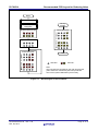
APPLICATION NOTE
RL78/G14
Recommended PCB Layout for Reducing Noise
R01AN1876EC0100
Rev. 1.00
Feb. 28, 2014
Introduction
The purpose of this document is to help the user understand how to design a good PCB layout with high reducing noise
performance. A thorough system evaluation is necessary after taking the countermeasures mentioned in this document.
This document provides an explanation using RL78/G14 sample boards.
Target Device
RL78/G14
The test results are applied to the following conditions:
• MCU:
• PCB type:
RL78/G14 64-pin
Single-side printed board without a polygon
R01AN1876EC0100 Rev. 1.00
Feb. 28, 2014
Page 1 of 14
RL78/G14
Recommended PCB Layout for Reducing Noise
Contents
1.
Preface .............................................................................................................................. 3
2.
Recommended PCB Layout ............................................................................................ 4
2.1
Wiring of VDD and VSS .............................................................................................................. 4
2.2
Oscillator Concerns .................................................................................................................... 4
2.3
Bypass Capacitor........................................................................................................................ 4
2.4
Wiring of RESET Pin ................................................................................................................... 4
2.5
Wiring of REGC Pin..................................................................................................................... 4
2.6
Wiring of TOOL0 Pin ................................................................................................................... 4
3.
Description of the Test Board......................................................................................... 5
3.1
Schematics of the Test Board ................................................................................................... 5
3.2
PCB Layout of the Two Test Boards......................................................................................... 5
3.3
Differences between Recommended Layout and Non-recommended Layout ..................... 6
3.3.1
Wiring of VDD and VSS .......................................................................................................... 6
3.3.2
Oscillator Concerns................................................................................................................. 6
3.3.3
Bypass Capacitor.................................................................................................................... 6
3.3.4
Wiring of RESET Pin............................................................................................................... 7
3.3.5
Wiring of REGC Pin ................................................................................................................ 7
3.3.6
Wiring of TOOL0 Pin............................................................................................................... 7
3.4
4.
Block Diagram of the Test Board .............................................................................................. 7
Reducing Noise Test of Different Layout....................................................................... 9
4.1
Test Description .......................................................................................................................... 9
4.2
Test Conditions ........................................................................................................................... 9
4.3
Test Results............................................................................................................................... 10
4.4
Test Conclusions ...................................................................................................................... 11
5.
Improve the Non-recommended Board........................................................................ 12
5.1
Modification of the Non-recommended Board....................................................................... 12
5.2
Test Results of the Modified Board......................................................................................... 13
5.3
Recommendations for PCB Board Improvement .................................................................. 13
6.
Documents for Reference ............................................................................................. 14
R01AN1876EC0100 Rev. 1.00
Feb. 28, 2014
Page 2 of 14
RL78/G14
1.
Recommended PCB Layout for Reducing Noise
Preface
This application note describes how to design PCB layout to achieve high reducing noise performance. The
countermeasures of recommended PCB layout are shown in this application note. And the AC line noise contrast test
with two types of PCB layout boards is introduced to verify these countermeasures. Subsequently, the improvement test
which is based on the non-recommended board is also introduced in this application note.
R01AN1876EC0100 Rev. 1.00
Feb. 28, 2014
Page 3 of 14
RL78/G14
2.
Recommended PCB Layout for Reducing Noise
Recommended PCB Layout
Good PCB layout is very important in reducing noise design. Some countermeasures of improving reducing noise
performance are shown below.
2.1
•
•
•
•
Wiring of VDD and VSS
Connect the MCU and main power supply with the shortest possible wiring.
Make the VDD and VSS wiring equal in length.
Make the wiring for the VDD and VSS wider than other signal wiring.
Separate the wiring for the VDD and VSS on the MCU from the wiring for the peripheral function power supply.
And try to separate them at the entrance of the main power supply.
2.2
Oscillator Concerns
• Place the oscillator circuit close to the MCU.
• Connect the MCU and oscillator circuit with the shortest possible wiring.
• Separate the VSS wiring between the MCU and the oscillator from the VSS wiring for the other peripherals.
2.3
Bypass Capacitor
• Place the bypass capacitor between VSS wiring and VDD wiring close to the MCU. And make power supply wiring
connect to the MCU via the bypass capacitor leads.
• Make the wiring length between the bypass capacitor and VDD pin or VSS pin equal and as short as possible.
2.4
Wiring of RESET Pin
• Place the reset circuit close to the MCU.
• Connect the MCU and reset circuit with the shortest possible wiring.
• Separate the VDD wiring and VSS wiring of reset circuit from the VSS and VDD wiring for the other peripherals.
2.5
Wiring of REGC Pin
• Connect the REGC pin to VSS via a 0.47 to 1 μF (default: 0.47 μF) capacitor as the MCU user’s manual
recommends.
• Place the REGC circuit close to the MCU.
• Connect the MCU and REGC circuit with the shortest possible wiring.
2.6
Wiring of TOOL0 Pin
• Connect the TOOL0 pin to VDD via a 1 kΩ resistor as the MCU user’s manual recommends.
• Place the TOOL0 circuit close to the MCU.
• Connect the MCU and TOOL0 circuit with the shortest possible wiring.
R01AN1876EC0100 Rev. 1.00
Feb. 28, 2014
Page 4 of 14
RL78/G14
3.
Recommended PCB Layout for Reducing Noise
Description of the Test Board
This section shows examples of the recommended layout and non-recommended layout. Both the recommended board
and non-recommended board are made with the same schematics and components. Only the PCB layouts are different.
With the recommended methods, the recommended PCB board can achieve higher reducing noise performance.
3.1
Schematics of the Test Board
The recommended layout and the non-recommended one are designed with the same schematics.
Figure 3.1 shows the schematics of the circuits around the MCU.
Figure 3.1
3.2
Schematics of the Circuits around the MCU
PCB Layout of the Two Test Boards
This section shows examples of the recommended layout and non-recommended layout. The PCB layout should be
designed in accordance with recommended one to achieve higher reducing noise performance. The reasons why the
PCB layout on the left in Figure 3.2 is recommended are explained in next section.
Figure 3.2 shows the PCB layout around the MCU of two test boards.
R01AN1876EC0100 Rev. 1.00
Feb. 28, 2014
Page 5 of 14
RL78/G14
Figure 3.2
3.3
Recommended PCB Layout for Reducing Noise
Recommended Layout (Left) and Non-recommended Layout (Right)
Differences between Recommended Layout and Non-recommended Layout
This section introduces the main differences between the recommended layout and the non-recommended layout.
3.3.1
Wiring of VDD and VSS
The VDD and VSS wiring of the recommended board are separated from peripheral power supply wiring at the
entrance of the main power supply. And the VDD wiring and VSS wiring of the recommended board are closer to each
other than the non-recommended board. Especially on the non-recommended board, the VDD wiring of the MCU is
connected to main power supply through jumper J1 before filter capacitor C9.
Reason: It is better to separate the MCU power supply wiring and peripheral power supply wiring. In this way, it can
avoid the noise into the MCU through peripherals. The MCU power supply wiring should be connected to main power
supply after connecting to filter capacitors. Otherwise, the filter capacitors will not work effectively.
3.3.2
Oscillator Concerns
Oscillator circuits X1, C1, and C2 on the recommended board are closer to the MCU than the non-recommended one.
The wiring from oscillator circuit to the MCU on the recommended board is shorter than the non-recommended one.
On the non-recommended board, the oscillator circuit is not at the terminal of VSS wiring and not separated from other
VSS wiring.
Reason: Long wiring may have an antenna effect to catch noise. If noise enters the clock pins, clock waveform may be
deformed. This may cause program failure or runaway. Also if the potential difference is caused by the noise between
the oscillator VSS level and the MCU VSS level, the correct clock will not be input to the MCU.
3.3.3
Bypass Capacitor
Bypass capacitor C4 on the recommend board is closer to the MCU than the non-recommended one. And the wiring
from the bypass capacitor to the MCU is shorter than the non-recommended one. Especially on the non-recommended
board, the leads of C4 are not directly connected to the VDD and VSS trunk wiring.
Reason: Longer wiring will generate larger impedance for noise signal. Longer wiring may resist the noise current
through the noise return circuit. Also long wiring between the bypass capacitor and the MCU may become a noise
antenna.
R01AN1876EC0100 Rev. 1.00
Feb. 28, 2014
Page 6 of 14
RL78/G14
3.3.4
Recommended PCB Layout for Reducing Noise
Wiring of RESET Pin
Reset circuits R1, D1, and C6 on the recommend board are closer to the MCU than the non-recommended one. And the
wiring from the reset circuit to the MCU is shorter than the non-recommended one. On the non-recommended board,
the leads of R1, D1, and C6 are not directly connected to the MCU VDD and VSS wiring, but connected to the main
power supply VDD and VSS wiring.
Reason: The reset signal initializes the internal MCU state. If fine noise-like pulses pass through the reset signal wiring,
the MCU may not completely initialize (partially initialize). It is better to shorten the wiring of the reset circuit to
reduce the noise effect.
3.3.5
Wiring of REGC Pin
The REGC circuit C3 on the recommend board is closer to the MCU than the non-recommended one. And the wiring
from the REGC circuit to the MCU is shorter than the non-recommended one. On the non-recommended board, the
VSS of C3 is connected to VSS lines before the MCU bypass capacitor C4.
Reason: The long wiring between C3 and the MCU REGC pin may become a noise antenna. The REGC should be
connected to VSS wiring after the bypass capacitor, otherwise the bypass capacitor effect will be weakened.
3.3.6
Wiring of TOOL0 Pin
The TOOL0 circuit R2 on the recommend board is closer to the MCU than the non-recommended one. And the wiring
from the TOOL0 circuit to the MCU is shorter than the non-recommended one. On the non-recommended board, the
VDD of R2 is not connected to the MCU VDD, but connected to the main power VDD wiring.
Reason: The long wiring between R2 and the MCU TOOL0 pin may become a noise antenna. If the potential difference
is caused by noise between TOOL0 VDD and MCU VDD level, it may affect the MCU working status.
3.4
Block Diagram of the Test Board
The test board will perform some sample functions under noise test. The MCU operation status can be shown by the
two groups of LEDs (Red and Yellow).
After the MCU resets, all LEDs will blink for 5 seconds. Then the two groups of LEDs will light from “00002” to
“11112” by “12”. One group is controlled by the main loop; the other group is controlled by timer interrupt routine.
These two groups of LEDs will blink synchronously.
Figure 3.3 shows the block diagram of the test board.
R01AN1876EC0100 Rev. 1.00
Feb. 28, 2014
Page 7 of 14
RL78/G14
Recommended PCB Layout for Reducing Noise
Reset
System initialization
Interrupt
handler
Interrupt
initialization
All LEDs ON for 5 sec.
0.5 sec. change
All LEDs OFF
Illuminated LEDs
......
Illuminated LEDs
RTI
0.5 sec. change
......
LED OFF
LED ON
Note:
The red LEDs are controlled by the main loop and the
yellow LEDs are controlled by the interrupt handler.
The red and yellow LEDs blink synchronously.
Figure 3.3
R01AN1876EC0100 Rev. 1.00
Feb. 28, 2014
Block Diagram of the Test Board
Page 8 of 14
RL78/G14
4.
4.1
Recommended PCB Layout for Reducing Noise
Reducing Noise Test of Different Layout
Test Description
In this test, two types of PCB were used. One is designed according to the countermeasures. The other is designed
without the countermeasures. The PCB layouts around the MCU are shown as Figure 3.2. The peripheral circuits on the
two boards are same. Same noise interference is input to the two test boards through the power supply for 1 minute.
The peak value of noise interference steps up in 100 V increments from 100 V to 4000 V in every test.
On the target boards, there are two groups of LEDs that blink to show the MCU status. All LEDs will be ON for 5
seconds after the MCU resets. Then the two groups of LEDs will blink from “00002” to “11112” by “12”. One group is
controlled by the main loop; the other group is controlled by timer interrupt. These two groups of LEDs will blink
synchronously.
The MCU status can be evaluated by observing these LEDs.
• If the MCU operates normally within 1 minute, the result is considered good and the table is filled with a “ ”.
• If the MCU generates an abnormal phenomena (reset, program runaway, or LEDs blink asynchronously) within 1
minute, the result is considered not good and the table is filled with a “ ”.
Figure 4.1 shows the diagram of test environment.
1:1
AC220V
Power supply for
test circuit
Isolated
transformer
AC220V
AC220V
Power supply for
noise generator
Figure 4.1
4.2
LEDs
Noise Generator
Output
Power
input
Source
input
Power
AC220V + Noise circuit
MCU
DC5V
Diagram of Test Environment
Test Conditions
• Test tools:
⎯ Noise generator: NoiseKen INS-4040
⎯ Target board: Recommended board and non-recommended board
• Test conditions:
⎯ Target board power: 220 V 50 Hz
⎯ MCU type: R5F104LEAFA
⎯ Oscillation frequency: 20 MHz
⎯ MCU power source: 5 V
⎯ MCU bypass capacitor: 0.1 μF
⎯ Noise period: 16 ms
⎯ Noise pulse width: 50 ns
⎯ Noise polarity: plus and minus
⎯ Noise peak value: 100 to 4000 V
⎯ Test time: 1 minute
R01AN1876EC0100 Rev. 1.00
Feb. 28, 2014
Page 9 of 14
RL78/G14
4.3
Recommended PCB Layout for Reducing Noise
Test Results
Table 4.1
Test Results of Recommended Board and Non-recommended Board
Layout
Recommended Board Test Results
Polarity
Non-recommended Board Test Results
+
−
+
Voltage
4000
(2)
3900
(2)
3800
(2)
3700
(3)
3600
(3)
3500
(3)
3400
(3)
3300
(3)
3200
(3)
3100
(3)
3000
(3)
2900
(3)
2800
(3)
2700
(3)
2600
(3)
2500
(3)
2400
(3)
2300
(3)
2200
2100
2000
Note:
Voltage: Noise value (Unit: V, higher value shows higher reducing noise capability)
Polarity: Noise polarity added to target board power source
: Normal MCU operation
(1): Reset cannot be released; (2): Reset → Rerun → Reset; (3): Main loop error or runaway
R01AN1876EC0100 Rev. 1.00
Feb. 28, 2014
−
(3)
(3)
(3)
(3)
(3)
(3)
(3)
(3)
(3)
(3)
(3)
(3)
(3)
(3)
(3)
(3)
Page 10 of 14
RL78/G14
4.4
Recommended PCB Layout for Reducing Noise
Test Conclusions
The test results only show the reducing noise performance of the tested boards. As is shown in Table 4.1, the result of
noise interference test on the recommended board is about 4000 V (the maxim value of test condition), and the
non-recommended one is below 2500 V.
Conclusions from this test are as follows:
• Higher reducing noise performance can be achieved by designing a PCB layout according to the recommendations.
• Due to the high reducing noise performance of the MCU, the worst phenomenon (reset can not be released) did not
occur even in the non-recommended board noise test.
Note: Keep the MCU away from high voltage noise, even if it is designed with the recommended PCB layout. The
test results are available only to distinguish the noise effects on different layouts and do not represent the MCU
performance.
R01AN1876EC0100 Rev. 1.00
Feb. 28, 2014
Page 11 of 14
RL78/G14
5.
Recommended PCB Layout for Reducing Noise
Improve the Non-recommended Board
After the above test, modifications were made on the non-recommended board and retested under the same conditions.
In this test, the non-recommended PCB board was modified provisionally to improve reducing noise performance.
When developing a product, the PCB layout should be redesigned according to the recommended layout for high
performance.
5.1
Modification of the Non-recommended Board
Modified items are listed below:
• VDD and VSS: Remove J1 and connect the MCU VDD to C9 with a jumper line to modify the VDD wiring
connection. Cutoff the VSS wiring of oscillator circuit and reset circuit to modify the VSS connection. Refer to the
red section in Figure 5.1.
• Oscillator concerns: Cutoff the original wiring which connects the VSS of oscillator circuit to the MCU VSS pin.
Connect them with a jumper to shorten the VSS wiring of the oscillator circuit. Refer to the orange section in the
Figure 5.1.
• Bypass capacitor: Move C4 close to the MCU. Refer to the violet section in the Figure 5.1.
• Reset circuit: Cutoff the original wiring of reset circuit which connects to the VDD and VSS. Connect these
components (R1, D1, C6) to the MCU VDD and VSS with jumper lines. Refer to the blue section in the Figure 5.1.
• REGC circuit: Move C3 close to the MCU. Refer to the gold section in the Figure 5.1.
• TOOL0 circuit: Move R2 close to the MCU. Refer to the green section in the Figure 5.1.
Figure 5.1
R01AN1876EC0100 Rev. 1.00
Feb. 28, 2014
Improving the Non-recommended Board
Page 12 of 14
RL78/G14
5.2
Recommended PCB Layout for Reducing Noise
Test Results of the Modified Board
Table 5.1
Test Results of Non-recommended Board Improvement
Non-recommended
Layout
Polarity
After Modification
Before Modification
+
−
+
−
Voltage
4000
(2)
(3)
3900
(2)
(3)
3800
(2)
(3)
3700
(3)
(3)
3600
(3)
(3)
3500
(3)
(3)
3400
(3)
(3)
3300
(3)
(3)
3200
(3)
(3)
3100
(3)
(3)
3000
(3)
(3)
2900
(3)
(3)
2800
(3)
(3)
2700
(3)
(3)
2600
(3)
(3)
2500
(3)
(3)
2400
(3)
2300
(3)
2200
2100
2000
Note:
Voltage: Noise Value (Unit: V, Higher value shows higher reducing noise capability)
Polarity: Noise polarity added to target board power source
: Normal MCU operation
(1): Reset can not be released; (2): Reset → Rerun → Reset; (3): Main loop error or runaway
5.3
Recommendations for PCB Board Improvement
After modifications are made on the non-recommended board, the results of reducing noise performance improved
drastically. But when developing a product, the PCB should be redesigned according to the recommended layout.
Note the following precautions for designing the PCB layout.
• VDD and VSS: Separate the MCU VDD and VSS wiring from peripherals’ VDD and VSS wiring. Connect to the
main power supply after the filter capacitors.
• Oscillator concerns: Use the shortest possible wiring to connect the oscillator, capacitor and MCU. Separate
oscillator’s VSS from other peripherals’ VSS wiring.
• Bypass capacitor: Place the bypass capacitor as close to the MCU as possible. Make sure the leads of the bypass
capacitor are set on the VDD and VSS trunk wiring.
• Reset circuit: Use the shortest wiring pattern to connect resistor, capacitor and diode.
• REGC and TOOL0: Place the capacitor and resistor as close to the MCU as possible.
R01AN1876EC0100 Rev. 1.00
Feb. 28, 2014
Page 13 of 14
RL78/G14
6.
Recommended PCB Layout for Reducing Noise
Documents for Reference
User’s Manual:
RL78/G14 User's Manual: Hardware (R01UH0186EJ)
RL78 Family User's Manual: Software (R01US0015EJ)
The latest versions can be downloaded from the Renesas Electronics website.
Technical Updates/Technical News
The latest information can be downloaded from the Renesas Electronics website.
Website and Support
Renesas Electronics Website
http://www.renesas.com/index.jsp
Inquiries
http://www.renesas.com/contact/
All trademarks and registered trademarks are the property of their respective owners.
R01AN1876EC0100 Rev. 1.00
Feb. 28, 2014
Page 14 of 14
Revision History
Rev.
1.00
Date
Feb. 28, 2014
Description
Page
Summary
—
First edition issued
A-1
General Precautions in the Handling of MPU/MCU Products
The following usage notes are applicable to all MPU/MCU products from Renesas. For detailed usage notes on the
products covered by this document, refer to the relevant sections of the document as well as any technical updates that
have been issued for the products.
1. Handling of Unused Pins
Handle unused pins in accordance with the directions given under Handling of Unused Pins in the
manual.
⎯ The input pins of CMOS products are generally in the high-impedance state. In operation with an
unused pin in the open-circuit state, extra electromagnetic noise is induced in the vicinity of LSI, an
associated shoot-through current flows internally, and malfunctions occur due to the false
recognition of the pin state as an input signal become possible. Unused pins should be handled as
described under Handling of Unused Pins in the manual.
2. Processing at Power-on
The state of the product is undefined at the moment when power is supplied.
⎯ The states of internal circuits in the LSI are indeterminate and the states of register settings and
pins are undefined at the moment when power is supplied.
In a finished product where the reset signal is applied to the external reset pin, the states of pins
are not guaranteed from the moment when power is supplied until the reset process is completed.
In a similar way, the states of pins in a product that is reset by an on-chip power-on reset function
are not guaranteed from the moment when power is supplied until the power reaches the level at
which resetting has been specified.
3. Prohibition of Access to Reserved Addresses
Access to reserved addresses is prohibited.
⎯ The reserved addresses are provided for the possible future expansion of functions. Do not access
these addresses; the correct operation of LSI is not guaranteed if they are accessed.
4. Clock Signals
After applying a reset, only release the reset line after the operating clock signal has become stable.
When switching the clock signal during program execution, wait until the target clock signal has
stabilized.
⎯ When the clock signal is generated with an external resonator (or from an external oscillator)
during a reset, ensure that the reset line is only released after full stabilization of the clock signal.
Moreover, when switching to a clock signal produced with an external resonator (or by an external
oscillator) while program execution is in progress, wait until the target clock signal is stable.
5. Differences between Products
Before changing from one product to another, i.e. to a product with a different part number, confirm
that the change will not lead to problems.
⎯ The characteristics of an MPU or MCU in the same group but having a different part number may
differ in terms of the internal memory capacity, layout pattern, and other factors, which can affect
the ranges of electrical characteristics, such as characteristic values, operating margins, immunity
to noise, and amount of radiated noise. When changing to a product with a different part number,
implement a system-evaluation test for the given product.
Notice
1.
Descriptions of circuits, software and other related information in this document are provided only to illustrate the operation of semiconductor products and application examples. You are fully responsible for
the incorporation of these circuits, software, and information in the design of your equipment. Renesas Electronics assumes no responsibility for any losses incurred by you or third parties arising from the
use of these circuits, software, or information.
2.
Renesas Electronics has used reasonable care in preparing the information included in this document, but Renesas Electronics does not warrant that such information is error free. Renesas Electronics
assumes no liability whatsoever for any damages incurred by you resulting from errors in or omissions from the information included herein.
3.
Renesas Electronics does not assume any liability for infringement of patents, copyrights, or other intellectual property rights of third parties by or arising from the use of Renesas Electronics products or
technical information described in this document. No license, express, implied or otherwise, is granted hereby under any patents, copyrights or other intellectual property rights of Renesas Electronics or
others.
4.
You should not alter, modify, copy, or otherwise misappropriate any Renesas Electronics product, whether in whole or in part. Renesas Electronics assumes no responsibility for any losses incurred by you or
third parties arising from such alteration, modification, copy or otherwise misappropriation of Renesas Electronics product.
5.
Renesas Electronics products are classified according to the following two quality grades: "Standard" and "High Quality". The recommended applications for each Renesas Electronics product depends on
the product's quality grade, as indicated below.
"Standard": Computers; office equipment; communications equipment; test and measurement equipment; audio and visual equipment; home electronic appliances; machine tools; personal electronic
equipment; and industrial robots etc.
"High Quality": Transportation equipment (automobiles, trains, ships, etc.); traffic control systems; anti-disaster systems; anti-crime systems; and safety equipment etc.
Renesas Electronics products are neither intended nor authorized for use in products or systems that may pose a direct threat to human life or bodily injury (artificial life support devices or systems, surgical
implantations etc.), or may cause serious property damages (nuclear reactor control systems, military equipment etc.). You must check the quality grade of each Renesas Electronics product before using it
in a particular application. You may not use any Renesas Electronics product for any application for which it is not intended. Renesas Electronics shall not be in any way liable for any damages or losses
incurred by you or third parties arising from the use of any Renesas Electronics product for which the product is not intended by Renesas Electronics.
6.
You should use the Renesas Electronics products described in this document within the range specified by Renesas Electronics, especially with respect to the maximum rating, operating supply voltage
range, movement power voltage range, heat radiation characteristics, installation and other product characteristics. Renesas Electronics shall have no liability for malfunctions or damages arising out of the
use of Renesas Electronics products beyond such specified ranges.
7.
Although Renesas Electronics endeavors to improve the quality and reliability of its products, semiconductor products have specific characteristics such as the occurrence of failure at a certain rate and
malfunctions under certain use conditions. Further, Renesas Electronics products are not subject to radiation resistance design. Please be sure to implement safety measures to guard them against the
possibility of physical injury, and injury or damage caused by fire in the event of the failure of a Renesas Electronics product, such as safety design for hardware and software including but not limited to
redundancy, fire control and malfunction prevention, appropriate treatment for aging degradation or any other appropriate measures. Because the evaluation of microcomputer software alone is very difficult,
please evaluate the safety of the final products or systems manufactured by you.
8.
Please contact a Renesas Electronics sales office for details as to environmental matters such as the environmental compatibility of each Renesas Electronics product. Please use Renesas Electronics
products in compliance with all applicable laws and regulations that regulate the inclusion or use of controlled substances, including without limitation, the EU RoHS Directive. Renesas Electronics assumes
no liability for damages or losses occurring as a result of your noncompliance with applicable laws and regulations.
9.
Renesas Electronics products and technology may not be used for or incorporated into any products or systems whose manufacture, use, or sale is prohibited under any applicable domestic or foreign laws or
regulations. You should not use Renesas Electronics products or technology described in this document for any purpose relating to military applications or use by the military, including but not limited to the
development of weapons of mass destruction. When exporting the Renesas Electronics products or technology described in this document, you should comply with the applicable export control laws and
regulations and follow the procedures required by such laws and regulations.
10. It is the responsibility of the buyer or distributor of Renesas Electronics products, who distributes, disposes of, or otherwise places the product with a third party, to notify such third party in advance of the
contents and conditions set forth in this document, Renesas Electronics assumes no responsibility for any losses incurred by you or third parties as a result of unauthorized use of Renesas Electronics
products.
11. This document may not be reproduced or duplicated in any form, in whole or in part, without prior written consent of Renesas Electronics.
12. Please contact a Renesas Electronics sales office if you have any questions regarding the information contained in this document or Renesas Electronics products, or if you have any other inquiries.
(Note 1)
"Renesas Electronics" as used in this document means Renesas Electronics Corporation and also includes its majority-owned subsidiaries.
(Note 2)
"Renesas Electronics product(s)" means any product developed or manufactured by or for Renesas Electronics.
SALES OFFICES
http://www.renesas.com
Refer to "http://www.renesas.com/" for the latest and detailed information.
Renesas Electronics America Inc.
2880 Scott Boulevard Santa Clara, CA 95050-2554, U.S.A.
Tel: +1-408-588-6000, Fax: +1-408-588-6130
Renesas Electronics Canada Limited
1101 Nicholson Road, Newmarket, Ontario L3Y 9C3, Canada
Tel: +1-905-898-5441, Fax: +1-905-898-3220
Renesas Electronics Europe Limited
Dukes Meadow, Millboard Road, Bourne End, Buckinghamshire, SL8 5FH, U.K
Tel: +44-1628-651-700, Fax: +44-1628-651-804
Renesas Electronics Europe GmbH
Arcadiastrasse 10, 40472 Düsseldorf, Germany
Tel: +49-211-65030, Fax: +49-211-6503-1327
Renesas Electronics (China) Co., Ltd.
7th Floor, Quantum Plaza, No.27 ZhiChunLu Haidian District, Beijing 100083, P.R.China
Tel: +86-10-8235-1155, Fax: +86-10-8235-7679
Renesas Electronics (Shanghai) Co., Ltd.
Unit 301, Tower A, Central Towers, 555 LanGao Rd., Putuo District, Shanghai, China
Tel: +86-21-2226-0888, Fax: +86-21-2226-0999
Renesas Electronics Hong Kong Limited
Unit 1601-1613, 16/F., Tower 2, Grand Century Place, 193 Prince Edward Road West, Mongkok, Kowloon, Hong Kong
Tel: +852-2886-9318, Fax: +852 2886-9022/9044
Renesas Electronics Taiwan Co., Ltd.
13F, No. 363, Fu Shing North Road, Taipei, Taiwan
Tel: +886-2-8175-9600, Fax: +886 2-8175-9670
Renesas Electronics Singapore Pte. Ltd.
80 Bendemeer Road, Unit #06-02 Hyflux Innovation Centre Singapore 339949
Tel: +65-6213-0200, Fax: +65-6213-0300
Renesas Electronics Malaysia Sdn.Bhd.
Unit 906, Block B, Menara Amcorp, Amcorp Trade Centre, No. 18, Jln Persiaran Barat, 46050 Petaling Jaya, Selangor Darul Ehsan, Malaysia
Tel: +60-3-7955-9390, Fax: +60-3-7955-9510
Renesas Electronics Korea Co., Ltd.
12F., 234 Teheran-ro, Gangnam-Gu, Seoul, 135-080, Korea
Tel: +82-2-558-3737, Fax: +82-2-558-5141
© 2014 Renesas Electronics Corporation. All rights reserved.
Colophon 3.0


![[e 2 studio] Renesas Starter Kit for RL78/G14 User`s Manual](http://vs1.manualzilla.com/store/data/005759786_1-25eb95ad780cf22f415f84b4d3ed0c87-150x150.png)