1
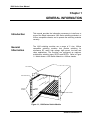
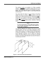
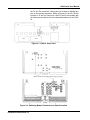
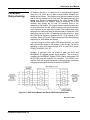
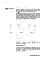
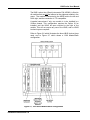
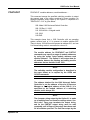
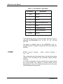
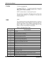
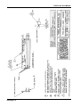
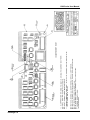
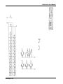
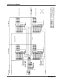
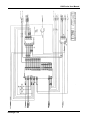
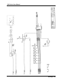
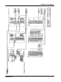
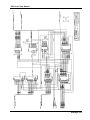
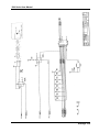
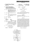
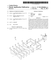
USER MANUAL
SERIES 1260
VXI SWITCHING CARDS
PUBLICATION NO. 980673-999
RACAL INSTRUMENTS
Racal Instruments, Inc.
4 Goodyear St., Irvine, CA 92618-2002
Tel: (800) RACAL-ATE, (800) 722-2528, (949) 859-8999; FAX: (949) 859-7139
Racal Instruments, Ltd.
480 Bath Road, Slough, Berkshire, SL1 6BE, United Kingdom
Tel: +44 (0) 1628 604455; FAX: +44 (0) 1628 662017
Racal Systems Electronique S.A.
18 Avenue Dutartre, 78150 LeChesnay, France
Tel: +33 (1) 3923 2222; FAX: +33 (1) 3923 2225
Racal Systems Elettronica s.r.l.
Strada 2-Palazzo C4, 20090 Milanofiori Assago, Milan, Italy
Tel: +39 (0)2 5750 1796; FAX +39 (0)2 5750 1828
Racal Elektronik System GmbH.
Technologiepark Bergisch Gladbach, Friedrich-Ebert-Strasse, D-51429 Bergisch Gladbach, Germany
Tel.: +49 2204 8442 00; FAX: +49 2204 8442 19
Racal Instruments, Ltd.
Unit 5, 25F., Mega Trade Center, No 1, Mei Wan Road, Tsuen Wan, Hong Kong, PRC
Tel: +852 2405 5500, FAX: +852 2416 4335
http://www.racalinstruments.com
PUBLICATION DATE: FEBRUARY 24, 2003
Copyright 2001 by Racal Instruments, Inc. Printed in the United States of America. All rights reserved.
This book or parts there of may not be reproduced in any form without written permission of the publisher.
Thank you for purchasing this Racal Instruments product.
For this product, or any other Racal Instruments product that incorporates software drivers, you
may access our web site to verify and/or download the latest driver versions. The web address for
driver downloads is:
http://www.racalinstruments.com/downloads
You will be asked to register one time only to gain access to the driver and product manual
downloads sections. At registration a cookie will be placed on your computer if you choose to
accept it. This is done to facilitate your use of these sections on future visits. You may refuse to accept the
cookie and still have complete access to the software driver database but will have to re-register every time
you visit. This cookie is for ease of use only and no information is gathered for, sold, or reported to, any third
party organization.
If you have any questions about software driver downloads or our privacy policy, please contact us at
[email protected].
WARRANTY STATEMENT
All Racal Instruments, Inc. products are designed and manufactured to exacting standards and in
full conformance to Racal’s ISO 9001 procedures.
This warranty does not apply to defects resulting from any modification(s) of any product or part
without Racal’s express written consent, or misuse of any product or part. The warranty also does
not apply to fuses, software, non-rechargeable batteries, damage from battery leakage, or problems
arising from normal wear, such as mechanical relay life, or failure to follow instructions.
This warranty is in lieu of all other warranties, expressed or implied, including any implied warranty
of merchantability or fitness for a particular use. The remedies provided herein are buyer’s sole and
exclusive remedies.
For the specific terms of your standard warranty, or optional extended warranty or service
agreement, contact your Racal customer service advisor. Please have the following information
available to facilitate service.
1. Product serial number
2. Product model number
3. Your company and contact information
You may contact your customer service advisor by:
E-Mail:
[email protected]
Telephone:
+1 800 722 3262
+44(0) 8706 080134
+852 2405 5500
(USA)
(UK)
(Hong Kong)
Fax:
+1 949 859 7309
(USA)
+44(0) 1628 662017
(UK)
+852 2416 4335
(Hong Kong)
RETURN of PRODUCT
Authorization is required from Racal Instruments before you send us your product for service or
calibration. Call your nearest Racal Instruments support facility. A list is located on the last page of
this manual. If you are unsure where to call, contact Racal Instruments, Inc. Customer Support
Department in Irvine, California, USA at 1-800-722-3262 or 1-949-859-8999 or via fax at 1-949-8597139. We can be reached at: [email protected].
PROPRIETARY NOTICE
This document and the technical data herein disclosed, are proprietary to Racal Instruments, and
shall not, without express written permission of Racal Instruments, be used, in whole or in part to
solicit quotations from a competitive source or used for manufacture by anyone other than Racal
Instruments. The information herein has been developed at private expense, and may only be used
for operation and maintenance reference purposes or for purposes of engineering evaluation and
incorporation into technical specifications and other documents which specify procurement of
products from Racal Instruments.
DISCLAIMER
Buyer acknowledges and agrees that it is responsible for the operation of the goods purchased
and should ensure that they are used properly and in accordance with this handbook and any
other instructions provided by Seller. RII products are not specifically designed, manufactured or
intended to be used as parts, assemblies or components in planning, construction, maintenance or
operation of a nuclear facility, or in life support or safety critical applications in which the failure of
the RII product could create a situation where personal injury or death could occur. Should Buyer
purchase RII product for such unintended application, Buyer shall indemnify and hold RII, its
officers, employees, subsidiaries, affiliates and distributors harmless against all claims arising out
of a claim for personal injury or death associated with such unintended use.
FOR YOUR SAFETY
Before undertaking any troubleshooting, maintenance or exploratory procedure, read carefully the
WARNINGS and CAUTION notices.
This equipment contains voltage hazardous to human life and safety, and is capable of inflicting
personal injury.
If this instrument is to be powered from the AC line (mains) through an autotransformer, ensure the
common connector is connected to the neutral (earth pole) of the power supply.
Before operating the unit, ensure the conductor (green wire) is connected to the ground (earth)
conductor of the power outlet. Do not use a two-conductor extension cord or a three-prong/twoprong adapter. This will defeat the protective feature of the third conductor in the power cord.
Maintenance and calibration procedures sometimes call for operation of the unit with power applied
and protective covers removed. Read the procedures and heed warnings to avoid “live” circuit
points.
Before operating this instrument:
1. Ensure the instrument is configured to operate on the voltage at the power source. See
Installation Section.
2. Ensure the proper fuse is in place for the power source to operate.
3. Ensure all other devices connected to or in proximity to this instrument are properly grounded or
connected to the protective third-wire earth ground.
If the instrument:
-
fails to operate satisfactorily
shows visible damage
has been stored under unfavorable conditions
has sustained stress
Do not operate until performance is checked by qualified personnel.
This page was left intentionally blank.
1260 Series User Manual
Table of Contents
Chapter 1
GENERAL INFORMATION ........................................................................................................... 1-1
Introduction ............................................................................................................................... 1-1
General Information................................................................................................................... 1-1
Options...................................................................................................................................... 1-3
Option 01 ............................................................................................................................... 1-3
Chapter 2
INSTALLATION INSTRUCTIONS ................................................................................................. 2-1
Introduction ............................................................................................................................... 2-1
Unpacking and Inspection ......................................................................................................... 2-1
Reshipment Instructions ............................................................................................................ 2-1
Option 01 Installation................................................................................................................. 2-1
Interrupt Level and Logical Address Setting (1260-01 - Equipped Modules Only) .................. 2-4
Switching Module Address Setting (All Modules) ................................................................... 2-5
Local Bus Daisychaining ........................................................................................................ 2-6
LBUS Lockout Keys ............................................................................................................... 2-7
Switching Module Chassis Installation ................................................................................... 2-9
Chapter 3
OPERATION................................................................................................................................. 3-1
Introduction ............................................................................................................................... 3-1
Input Format .............................................................................................................................. 3-1
Output Format ........................................................................................................................... 3-1
1260-01 Device Dependant Command Codes ....................................................................... 3-3
CLOSE ............................................................................................................................... 3-3
CNF.................................................................................................................................... 3-3
DLY .................................................................................................................................... 3-3
EOI..................................................................................................................................... 3-4
EQU ................................................................................................................................... 3-5
EXCL.................................................................................................................................. 3-6
OPEN................................................................................................................................. 3-6
PDATAOUT........................................................................................................................ 3-8
PSETUP........................................................................................................................... 3-10
PUPRCL........................................................................................................................... 3-11
READ ............................................................................................................................... 3-11
RECALL ........................................................................................................................... 3-11
i
1260 Series User Manual
RESET ............................................................................................................................. 3-11
SCAN............................................................................................................................... 3-12
SETUP............................................................................................................................. 3-12
SLIST............................................................................................................................... 3-13
SRQMASK ....................................................................................................................... 3-14
STORE ............................................................................................................................ 3-15
SYNC............................................................................................................................... 3-16
TEST................................................................................................................................ 3-16
TTLTRG ........................................................................................................................... 3-17
YERR............................................................................................................................... 3-17
Chapter 4
THEORY OF OPERATION........................................................................................................... 4-1
Introduction ............................................................................................................................... 4-1
Functional Blocks ...................................................................................................................... 4-1
Theory of Operation .................................................................................................................. 4-3
Power Suppliers .................................................................................................................... 4-3
Microprocessor Block ............................................................................................................ 4-3
The Reset Circuits ................................................................................................................. 4-4
VXI Interface.......................................................................................................................... 4-5
The Lbus Interface .................................................................................................................... 4-6
Chapter 5
DRAWINGS.................................................................................................................................. 5-1
Chapter 6
PARTS LISTS............................................................................................................................... 6-1
Chapter 7
Product Support ........................................................................................................................ 7-1
Reshipment Instructions............................................................................................................ 7-1
Support Offices ......................................................................................................................... 7-2
ii
1260 Series User Manual
List of Figures
Figure 1-1, 1260 Series Switch Module......................................................................................... 1-1
Figure 1-2, 1260 Series Smart Card and Slaves ........................................................................... 1-2
Figure 2-1, 1260-01 Smart Card ................................................................................................... 2-2
Figure 2-2, Switching Module Connector and Switch Location ...................................................... 2-2
Figure 2-3, 1260-40 Switch, Connector and Jumper Location ....................................................... 2-3
Figure 2-4, S1 Switch Function ..................................................................................................... 2-5
Figure 2-5, 1260 Series Master and Slave LBUS Interconnections ............................................... 2-6
Figure 2-6 LBUS Lockout Keys ..................................................................................................... 2-7
Figure 2-7, 1260 Series Master/Slave Configuration ..................................................................... 2-8
Table 3-1, 1260 Option 01 Status Byte ....................................................................................... 3-15
Table 3-2, 1260 Series Error Codes............................................................................................ 3-17
Figure 4-1, 1260 Smart Card Block Diagram................................................................................. 4-2
Figure 4-2, 1260 Microprocessor Block Diagram........................................................................... 4-2
iii
1260 Series User Manual
iv
1260 Series User Manual
Chapter 1
GENERAL INFORMATION
Introduction
This manual provides the information necessary to install one or
more of the Racal Instruments 1260 Series switching modules in a
VXIbus compatible chassis, and to operate the switching modules
correctly.
General
Information
The 1260 switching modules are a range of C size, VXIbus
compatible switching modules that provide switching for
microwave, RF, audio, high voltage, high current, low level and
video applications. The modules are configured as matrices,
multiplexers, switching trees, SPDTs and DPDTs. Refer to Figure
1-1 which shows a 1260 Switch Module in a VXIbus chassis.
VXI CHASSIS
SWITCH MODULE
R
TO
EC
N
N
CO
P1
R
TO
EC
N
N
CO
P2
CAPTIVE
SCREWS
FRONT
PANEL
CARD GUIDES
Figure 1-1, 1260 Series Switch Module
General Information 1-1
1260 Series User Manual
The switching modules are installed in a VXIbus compatible
chassis in a continuous set of adjacent chassis slots. One of the
modules to be fitted to the chassis must be designated the system
Master, and must be fitted with Option 01. All other modules are
slaved to the master. Refer to Figure 1-2 which shows the smart
card and slaves.
The module fitted with Option 01 must be fitted in the leftmost
chassis slot that is to contain a switching module. If only one
module is to be fitted to the chassis, several jumper wires must be
removed from, or DIP switches opened on, the switching module.
If more than one module is to be fitted to the chassis, these
jumpers must be removed from (or the DIP switches opened) the
module in the rightmost chassis position containing a switching
module.
NOTE
If you are using seven or more 1260 series modules,
you must add a termination jumper to the module on
the far right See Chapter 2.
Two separate addresses are required in the use of a 1260
switching system. The first is the VXIbus specification defined
logical address used by the chassis Resource Manager and the
second, the card address, is an address used by the 1260 Master
to control the cards slaved to it. The card address is used in the
device dependant commands used to control the switching
modules. The logical address is set by a DIP switch on the 126001 Smart Card, and the card addresses are set by a DIP switch on
the switching module PCB.
SMART CARD
P1
VXIBUS
BACKPLANE
P2
LBUS
1260 SERIES
MASTER
SLAVE
SLAVE
Figure 1-2, 1260 Series Smart Card and Slaves
General Information 1-2
1260 Series User Manual
Options
Option 01
The Option 01 Smart Card (Master) is required for use in all 1260
switching systems. This option acts as the switching system
master, and all other switching modules are slaved to it. It turns
any number of modules into a message-based VXIbus switching
system.
The smart card is addressed over the VXIbus, and all other
modules resident in the VXIbus chassis are controlled by this card.
Option 01 uses the local bus on the VXI P2 connector to provide
scanning, delay and exclude capabilities.
The built-in-test features in the smart card include confidence
checking which monitors the state of each relay. It monitors a
spare set of contacts or sensing coil current to ensure the
switching system configuration is as programmed.
Refer to Section 2 for software installation procedures for the
1260-01, and to Section 3 for the software command set used to
control the switching modules. The sections on individual modules
describe the device specific installation and programming for each
module.
General Information 1-3
1260 Series User Manual
This page was left intentionally blank.
General Information 1-4
1260 Series User Manual
Chapter 2
INSTALLATION INSTRUCTIONS
Introduction
This section describes the unpacking and inspection, reshipment,
installation and environmental requirements of the 1260 Series
switching modules.
Unpacking and
Inspection
Prior to unpacking the switching module, check the exterior of the
shipping carton for any signs of damage. All irregularities should
be noted on the shipping bill. Remove the instrument from the
carton, preserving the factory packaging as much as possible.
Inspect the switching module for any defect or damage.
Immediately notify the carrier if any damage is apparent. Before
use, have qualified personnel perform a safety check.
Reshipment
Instructions
Use the original packaging when returning the switching module to
Racal Instruments for calibration or servicing. The shipping carton
and packaging will provide the necessary support for safe
reshipment. If the original packaging is unavailable, wrap the
switching module in plastic sheeting and use plastic spray foam to
surround and protect the instrument. Reship in the original or a
new shipping carton.
Option 01
Installation
To install Option 01 to a 1260 switching module, carry out the
following procedure.
Remove the module top and bottom covers.
Remove the jumper board (Racal Instruments P/N 401951) fitted to
connector J4 on the switching module. Note the 1260-40 has
jumpers installed in the J4 connector that must be removed.
Remove the jumper board (Racal Instruments P/N 401951-003)
fitted to connector J3 on the switching module.
Align the 1260-01 card with the switching module, P3 to J3, P4 to
J4, and press the 1260-01 and the module firmly together to mate
Installation Instructions 2-1
1260 Series User Manual
the P3 and P4 connectors, taking care not to bend or damage any
pins on the mating connectors. Refer to Figures 2-2 and 2-3 for the
location of J3 and J4. Secure the 1260-01 card to the module with
the fasteners provided at the three standoff positions on the 126001.
Figure 2-1, 1260-01 Smart Card
Figure 2-2, Switching Module Connector and Switch Location
Installation Instructions 2-2
1260 Series User Manual
Figure 2-3, 1260-40 Switch, Connector and Jumper Location
The 1260 Master is fitted with the VXIbus defined SYSFAIL LED.
To install the LED, connect the cable supplied to the 3-pin plug in
the Option 01 PCB. The cable and plug are configured to achieve
correct operation either way the cable is connected at the end. The
LED is inserted into the hole marked FAIL at the top of the module
front panel from the outside of the module so the LED pins point
into the module. The cable supplied is fitted with a 2-pin connector
at the LED end, and is polarized to ensure correct installation.
Proceed to Subsection 2.5 to set the interrupt level and logical
address of the Option 01.
Installation Instructions 2-3
1260 Series User Manual
Interrupt Level
and Logical
Address Setting
(1260-01 Equipped
Modules Only)
If not previously done, remove the module's top cover. To set the
1260-01 logical address, set switch SW1 on the 1260-01 board to
the binary equivalent of the logical address selected. For SW1, a
switch in the OFF position corresponds to binary 1, and the ON
position corresponds to binary 0. Switch 1 on SW1 corresponds to
the most significant digit, and switch 8 corresponds to the least
significant digit. Logical addresses in the range 0 to 255 are
permitted. Refer to Figure 2-1 for the location of SW1.
NOTE
The 1260-01 logical address is set to 15 by Racal
Instruments before shipment.
All switching modules resident in a VXIbus chassis must have
unique addresses. Incorrect operation of the system will result if
two or more modules are set to the same module address.
To set the 1260-01 interrupt level, set switches 1, 2 and 3 on SW2
on the 1260-01 board to the binary equivalent of the interrupt level
selected. For SW2, a switch in the OFF position corresponds to
binary 1, and the ON position corresponds to binary 0. Switch 1 on
SW2 corresponds to the least significant bit, and switch 3
corresponds to the most significant bit. Interrupt levels in the range
0 to 7 are permitted. Switch 4 is not used. Refer to Figure 2-1 for
the location of SW2.
NOTE
The 1260-01 interrupt level is set to 2 by Racal
Instruments before shipment.
Replace the module covers. Replacement is the reverse of the
removal procedure.
NOTE
Any 1260 switching card may have Option 01 fitted
and be designated as the Master.
Installation Instructions 2-4
1260 Series User Manual
Switching Module
Address Setting
(All Modules)
To set a module address, carry out the following procedure.
For the 1260-40 only, remove the module covers.
Set switch SW1 on the module to the binary equivalent of the
address. Switches 1 to 4 are used to set the module address, with
switch 4 the least significant bit, and switch 1 the most significant.
The OFF positions for SW1 correspond to binary 0, and ON
positions correspond to binary 1. Addresses in the range 1 to 12
are permitted. Refer to Figure 2-2 for the location of SW1 on the
switching module PCB, or to Figure 2-3 for the location of SW1 on
the 1260-40. The functions of the various S1 switches are shown
in Figure 2-4.
Figure 2-4, S1 Switch Function
NOTE
The address set at switch SW1 on the switching
module controls the value of the card address the
switching module will respond to. The OPEN and
CLOSE statements using the card address are
specified in Section 4.4. Example: For a module to
respond to the command CLOSE 5.1205, the address
of the module must be set to 5.
Several modules are capable of more than one configuration, and
respond to different command codes in their various
configurations. Switches 5 and 6 on SW1 are used to select the
command code sets these modules respond to. Refer to the
module specific sections for the procedure to set the switches for
each module.
For the 1260-40 only, replace the switching module covers.
Replacement is the reverse of the removal procedure.
Installation Instructions 2-5
1260 Series User Manual
Local Bus
Daisychaining
All modules slaved to a master must be daisychained together
along the VXI Local bus to allow communication between the
Master and its Slaves. The modules must also be isolated from the
rest of the VXI modules on the local bus. The daisychaining of the
Master and Slaves is implemented by the LBus Jumper PCBA
(Racal Instruments P/N 405951) fitted to connector J4 on the
modules and closing the S2 and S3 switches fitted to the
underside of the module. The jumper board connects the local bus
to the module from the left, and the switches connect the module
to the local bus on the right of the module. The module fitted to the
rightmost slot used must have all switches open to isolate the 1260
group from the rest of the VXI modules using the local bus. Note
the 1260-40 has jumpers in positions E126 - E136 instead of DIP
switches. Refer to Figure 2-5 which shows the LBus daisychaining
required by a 1260 Master and Slaves.
If you are using more than eight 1260 series modules, you must
add a termination jumper to the module on the far right. Do this by
soldering a short wire jumper across W22 on the LBUS jumper
PCBA (P/N 401951, Rev. E).
Similarly, a provision must be made to pass the IACK and
BUSGRANT 0-3 signals through Slave modules. This is done by
installing the BUSGRANT Bypass PCBA (Racal Instruments P/N
401951-003) onto the modules' J3 connector. This PCBA is not
required if the VXI chassis backplane contains jumpers or switches
to bypass these signals and the switches are CLOSED
Figure 2-5, 1260 Series Master and Slave LBUS Interconnections
Revised 11/19/01
Installation Instructions 2-6
1260 Series User Manual
LBUS Lockout
Keys
The VXIbus defined LBUS lockout keys are designed to prevent
the connection together of incompatible logic families. They are
attached to the exterior of the module at the top of the front panel.
Note: The 1260 Master must occupy the leftmost slot in the series.
It is not required to occupy the leftmost slot in the chassis.
Note all modules shipped from the factory are supplied with three
keys. Because their use is application dependent, it is the users
responsibility to configure each module with the correct lockout key
unless they are ordered specifying the modules that are to be the
leftmost (Master) module, the rightmost module in the group, and
the modules between the leftmost and rightmost modules.
Refer to Figure 2-6 which illustrates the three LBUS Lockout keys
used, and to Figure 2-7 which shows a 1260 Master/Slave
configuration.
Figure 2-6 LBUS Lockout Keys
Racal Instruments implements the LBUS lockout scheme in one of
three ways for each module as follows:
VXIbus Defined "C" Key
The LBUS Lockout key (Racal Instruments P/N 455541) is fitted to
the leftmost module in the group, i.e., the 1260 Master. It is
connected to the LBUS to the right of the module, and the
connection is TTL-compatible.
VXIbus Defined "A" Key
The LBUS Lockout key (Racal Instruments P/N 455542) is fitted to
the rightmost of the modules installed in a VXIbus chassis. It is
connected to the LBUS to the left of the module, and the
connection is TTL-compatible.
VXIbus Defined "A/C" Key
Installation Instructions 2-7
1260 Series User Manual
The BUS Lockout key (Racal Instruments P/N 455540) is fitted to
all modules that are not the leftmost or the rightmost module in the
group. The module is connected to the LBUS both to the left and
to the right, and the connection is TTL-compatible.
A special case arises if only one module is to be installed in a
VXIbus chassis. This configuration requires the Option 01 be
installed, and the LBUS be open circuited to the right of the
module. This will not require any use of the LBUS, and no LBUS
Lockout keys are required.
Refer to Figure 2-6 which illustrates the three LBUS Lockout keys
used, and to Figure 2-7 which shows a 1260 Master/Slave
configuration.
Figure 2-7, 1260 Series Master/Slave Configuration
Installation Instructions 2-8
1260 Series User Manual
LBUS Lockout Key Installation
In order to accomodate the VXIbus specification defined minimum
thickness of the LBUS Lockout keys and the clearance provided
around the module ejector handle, two LBUS Lockout keys must
be fitted on top of each other to each module.
To install the A and C keys on a module, align the screw holes in
the Lockout keys with the appropriate holes in the module front
panel. Fit the two screws required, and secure the Lockout keys to
the module front panel.
To install A/C Lockout keys to the module, the module ejector
handle must be in the unejected position. The first key may be
pushed around the ejector handle and aligned with the front panel
screw holes. This takes up most of the clearance under the ejector
handle, preventing the second Lockout key from being installed. To
provide the necessary clearance, move the first Lockout key away
from the module body, and slide the second key underneath the
first key and around the ejector handle.
To secure the A/C Lockout keys to the module, align the Lockout
keys screw holes with the holes in the module front panel. Install
two screws in the holes at the top of the module front panel and
tighten the screws. Move the ejector handle to the ejected position,
and install a third screw in the hole now made accessible.
Switching Module
Chassis
Installation
Before installation of the switching module, visually inspect it to
ensure there are no bent, damaged or missing pins. Pay particular
attention to connectors P1 and P2 on the rear of the module.
Repair any damage to the module before proceeding.
Before installing the switching system Master, the VXIbus
specification defined IACKIN/IACKOUT, daisychain connection for
the chassis slot the Master will be resident in, must be open
circuited. This is accomplished in the Racal-Dana Model 1261 or
1262 chassis by opening the switch fitted on the daisychain. (Note:
In later revisions of the 1261 and 1262 chassis, open circuiting is
accomplished automatically when a module is installed into the
chassis.
See the appropriate chassis manual for more
information.) The switch used is the higher of the two switches on
the lower switchbank to the left of the slot the Master is to be fitted
to. Note that other vendors may choose to implement the
daisychain with either switches or jumpers.
If more than one switching module is to be installed in the VXIbus
chassis, the module with the 1260-01 card installed must be fitted
at the leftmost position of all modules being installed in the
chassis. The rightmost module must have the twelve jumpers
Installation Instructions 2-9
1260 Series User Manual
mounted on the jumper PCB (installed) removed from positions
E125 to E136 on the switching module PCB, or all DIP switches S2
and S3 opened, as described in Chapter 2.
To install the switching module in a C size, VXI mainframe, ensure
the module has rear connector P1 oriented to mate with the
corresponding connector on the mainframe backplane. Align the
module with the guides for the slot selected, and slide the module
into the mainframe. Push the module home to connect it to the
mainframe. Secure the module to the mainframe with the captive
screws provided at the top and bottom edges of the module.
Power up the mainframe. Ensure the SYSFAIL LED on the Master
switching module front panel lights and extinguishes after a few
seconds to show the switching module has passed its power up
self-test. The switching module is now ready for use.
To remove the switching module, release the captive screws that
secure the module to the mainframe. Use the plastic levers
provided on the top and bottom edges to eject the module. Pull
the switching module along the guides provided and out of the
mainframe.
Installation Instructions 2-10
1260 Series User Manual
Chapter 3
operation
Introduction
This Chapter supplies the information necessary to operate 1260
Series switching modules housed in a VXIbus chassis. It describes
the command codes and module specific syntax needed to control
the 1260 Option 01 and switching modules, and the formats for the
character strings output by the switching modules.
Input Format
The Option 01 is capable of recognizing any of the device
dependant commands given in this chapter from the first two
characters of the command, with the exception of the READ,
RESET and RECALL commands which may be recognized from
the first three characters of the command. The Option 01 will
interpret a command in the same way if a command string supplies
the first two or three or more characters of the command string.
The Option 01 will respond to the following terminators:
line feed
carriage return, line feed
carriage return, line feed with EOI asserted
GPIB line EOI asserted (when used with a GPIB/VXI
Resource Manager)
Output Format
The Option 01 switching module will output character strings in
response to the PDATAOUT, PSETUP and YERR commands.
These character strings consist of one or more lines of information
that will be terminated by the carriage return, line feed pair with the
GPIB EOI line asserted as determined by the EOI <0|1>
command. This means the character string output by the Option 01
may be required to be read repeatedly until the final line of the
output is read for PDATAOUT and PSETUP commands. The final
character string output by the Option 01 is <module
address>.END, where <module address> is the address of the last
module to be described. The character string output in response to
Operation 3-1
1260 Series User Manual
the YERR command is a single line.
The character strings output in response to the PDATAOUT and
PSETUP commands consist of multiple lines of the form:
<module address>.<header>
specific syntax>
or
<module
address>.<module
where <module address> is the address set on switch SW1 on the
switching module PCB, value 1 through 12. The value of
<module address> and the decimal equivalent of the binary
value set on SW1 must be the same for the switching
module to respond correctly to any device dependant
commands addressed to it. Note that no two switching
modules are permitted to have the same value of <module
address> in a VXIbus chassis.
<header> describes the switching module type.
<module specific syntax> describes the closed relay paths
of the present configuration of the switching modules, or the
syncronous port data on the digital card.
NOTE
The PSETUP command returns information on the
configuration of the 1260 Option 01. The Option 01
will return a value of 000 for <module address>. This
does not correspond to the address of the VXI
Resource Manager card resident in Slot 0 of the VXI
chassis, or the Option 01 logical address.
When outputting a character string to the VXI Controller, the
Option 01 will output a carriage return, line feed pair. If the
Resource Manager is a VXI/GPIB interface, the Resource
Manager will output a carriage return, line feed with GPIB EOI
asserted. Note that in the case of the output string consisting of
multiple lines, the EOI line may be asserted at the end of each line
or at the end of the character string, as determined by the EOI
<1|0> command.
Operation 3-2
1260 Series User Manual
1260-01 Device
Dependant
Command Codes
CLOSE
NOTE
For any command that causes relays to be operated
(e.g., CLOSE, OPEN, or RESET), allow 40msec to
3msec per relay operated relay settling time or
monitor the READY bit of the status byte waiting till
the 1260 reports that it is ready.
CLOSE <module address>.<module specific syntax> [;<module
address>.<module specific syntax>]....
This command causes one or more connections on a switching
module to close. Any number of connections in more than one slot
may be closed in one CLOSE statement if the <module
address>.<module specific syntax> sections are concatenated
using a semi-colon (;). Refer to the individual module sections for
the <module specific syntax> to be used for each switching
module.
CNF
CNF <ON|OFF>
This command turns the 1260 Confidence Test On or Off. The
Confidence Test checks that the state of all relays is as
programmed, and causes the Option 01 to assert the VXI Request
True exception after each OPEN or CLOSE command is
processed if an error is detected. A character string detailing the
failure may be obtained from the 1260-01 in response to the YERR
command. The character string the Confidence test causes the
Option 01 to generate is <module address>.51. <module address>
is a three digit number that is the address of the module slaved to
the 1260-01. 51 is the error code associated with a Confidence
Test failure. A GPIB/VXI Resource Manager will cause the
assertion of the GPIB SRQ line in response to the Request True
assertion. The default (power-up) state for the Confidence Test is
OFF.
DLY
DLY <value>
Command is used to cause a delay between the last relay closure
after a command string is processed, and the SYNC OUT pulse.
<value> may be 0-655 ms, and is set to zero at power up.
Operation 3-3
1260 Series User Manual
EOI
EOI <0|1>
EOI 0 causes the GPIB EOI line to be asserted by the VXI
Resource Manager at the end of each line of a multi-line data
output by the Option 01 if a VXI/GPIB Resource Manager is in use.
EOI 0 is the default (power-up) state.
EOI 1 causes the GPIB EOI line to be asserted by the VXI
Resource Manager only at the last character of a data string output
by the Option 01 if a VXI/GPIB Resource Manager is in use.
Operation 3-4
1260 Series User Manual
EQU
EQU <equate list>
This command causes any OPEN, CLOSE or TRIG/SCAN
commands addressed to any switching module on the <equate
list> to be carried out for all modules on the <equate list>. All
modules on the list are required to be identical.
The <equate list> is made up of the slot numbers of the switching
modules that are to be equated separated by a semi-colon (;).
Continuous groups of modules may be entered onto the <equate
list> by entering the first and last modules to appear on the list
joined by a hyphen (-). More than one equate group may be set up
in a single EQU statement by separating the equate groups with a
comma (,).
Example:
EQU 1;3-6,2;9-11
This command will equate slots 1, 3, 4, 5 and 6 as one equate
group and slots 2, 9, 10 and 11 as another.
NOTE
All switching modules must be of the same type to be
accepted in the same equate list or the Option 01 will
generate an error.
NOTE
Use of the EQU command will overwrite all previously
entered <equate list>s. An <equate list> of 0 may be
used to clear all equate groups.
NOTE
When an <equate list> is entered, all switching
modules on the list adopt the state of the first module
to appear on the list.
Operation 3-5
1260 Series User Manual
EXCL
EXCL <exclude list>
This command causes the Option 01 to regard the channel
closures specified in the <exclude list> as mutually exclusive. A
channel is described in the <exclude list> by the slot number of a
switching module and module specific syntax to describe the relay
closures in a channel. Refer to the individual module sections for
the module specific syntax of the various switching modules
available. More than one <exclude list> may be specified in an
EXCL statement by separating the Exclude groups with the letter E
and a semi-colon (E;). Continuous groups of modules may be
entered onto the <exclude list> by entering the first and last
modules to appear on the list joined by a hyphen (-).
NOTE
Use of the EXCL command will overwrite all
previously entered <exclude list>s. An <exclude list>
of 0 may be used to clear all exclude groups.
OPEN
OPEN <module address>.<module specific syntax> [;<module
address>
.<module specific syntax>].....
This command causes one or more connections on a switching
module to open. Any number of connections in more than one slot
may be opened in one OPEN statement if the <module
address>.<module specific syntax> sections are concatenated
using a semi-colon (;). Refer to the individual module sections for
the <module specific syntax> to be used for each switching
module.
Operation 3-6
1260 Series User Manual
Operation 3-7
1260 Series User Manual
PDATAOUT
PDATAOUT <module address>;<module address>.....
This command causes the specified switching modules to output
the present state of the relays contained in those modules. An
example character string output by the Option 01 response to a
"PDATAOUT 0-12" is given below.
000. Model 1260 Universal Switch Controller
000. OS Rev 1.2 1260
012 1260-40A 4 x 24 signal matrix
012. 0219
012.END
This example shows that a 1260 Controller with an operating
system revision level of 1.2 is present at module address 000.
There is also a 1260-40A module present at address 012, and row
2 of the switching matrix is connected to column 19.
NOTE
The module address for PDATAOUT and PSETUP
commands may specify a range of module addresses
by using the syntax <start module address>-<end
module address>. The Option 01 will output data for
all modules between the starting and ending module
addresses that are installed in the 1260.
NOTE
The switching module configuration is described in
the same format as is required by the OPEN and
CLOSE commands.
NOTE
The address obtained for the 1260 Universal Switch
Controller is not the address of the slot 0 Resource
Manager or the logical address of the 1260-01. It is
equivalent to the module address of a switching
module, and is always 000.
NOTE
The character string output by the Option 01 is made
up of multiple lines and contains carriage-return, linefeed pairs. These may terminate the output string,
and so the PSETUP output string must be read
repeatedly until all lines of the output have been read
for all modules specified. The final line output by the
Operation 3-8
1260 Series User Manual
1260 Option 01 is <module address>.END where
<module address> is the VXI chassis slot that the last
1260 module described is resident.
Operation 3-9
1260 Series User Manual
PSETUP
PSETUP <module address>[;<module address>]....
This command causes the Option 01 to output a character string
describing the setup of the switching system Option 01 and
switching modules. An example of a character string obtained in
response to a "PSETUP 0-12" command is given below.
000. Model 1260 Universal Switch Controller
000. OS Rev 1.2 1260
000. CNF OFF
000. DLY 0
000. EOI 0
000. EQU
000. EXCL
000. SCAN ON
000. SLIST 0
000. SRQMASK 40
000. SYNC 8
000. TTLTRG 0
000. PUPRCL OFF
012. 1260-40A 4 x 24 Signal Matrix
012. BBM
012.END
NOTE
The character string output by the 1260 Option 01 is
made up of multiple lines and contains carriagereturn, line-feed pairs. These will terminate the output
string. The PSETUP output string must be read
repeatedly until all lines of the output have been read
for all modules specified. The final line output by the
Option 01 is <module address>.END where <module
address> is the VXI chassis slot that the highest
module address present in the VXI chassis.
NOTE
The module address for PDATAOUT and PSETUP
commands may specify a range of module addresses
by using the syntax <start module address>-<end
module address>. The Option 01 will output data for
all modules between the starting and ending module
addresses that are installed in the 1260.
Operation 3-10
1260 Series User Manual
PUPRCL
PUPRCL <ON|OFF>
This command enables and disables the automatic recall of nonvolatile memory location 1 at power up. The configuration in nonvol location 1 is stored by the use of the STORE command. Refer
to the appropriate paragraph for details of the STORE command.
NOTE
If non-volatile location 1 is cleared and PUPRCL is
ON, no recall will take place at power up.
READ
READ <module address>.<module specific syntax>
This command is supported by digital cards only. Refer to the
individual module sections for a description of the syntax and
functions performed.
RECALL
RECALL <non-vol location>
where <non-vol location> = 1|2|.......|50
This command will set all switching modules in the VXI chassis to
the configuration stored in the non-volatile location specified. The
physical location of the modules in the chassis slots is unimportant
as long as the same type modules are at the same module
addresses as when the switching system configuration was stored,
and the rules governing module locations are observed. Note that
an error will be generated if an attempt is made to RECALL a
memory setting into a switching system configuration that differs
from the configuration present when the memory setting was
stored. An error will also be generated if an attempt is made to
RECALL a memory setting from an empty location.
RESET
RESET
NOTE
A delay of at least 100 msec may be required after a
RESET command before issuing the next command.
This command causes all switching modules to be set to their deenergized states.
Operation 3-11
1260 Series User Manual
SCAN
SCAN <ON|OFF|CONT>
The SCAN ON command enables the Option 01 to open and close
the channels as specified in the scan list in turn. Each channel is
closed on receipt of a trigger signal from one of the VXIbus
TTLTRG lines or the VXIbus trigger command is received. The
Option 01 will scan the channels until it reaches a break point or
the SCAN OFF command is received. Refer to Section 3.4.16 for
further information on the scan list.
The SCAN CONT command causes the Option 01 to resume
scanning the channels on the scan list after pausing at a break
point in the scan list. The Option 01 will continue to scan until it
reaches a break point on the scan list, or it receives the SCAN
OFF command.
SCAN OFF causes the 1260 Series to stop scanning. Scanning
may only be resumed by the use of the SCAN ON command.
NOTE
The SCAN command may also be used to recall nonvolatile memory settings in turn.
SETUP
SETUP <module address>.<seqmode>
This command is used to control the sequence in which switching
modules relays are opened and closed. The sequence modes
(<seqmode>s) are IMM (Immediate), BBM (Break-Before-Make)
and MBB (Make-Before-Break).
The Immediate (IMM) sequence mode will cause the opening and
closing of switching module channels as quickly as possible, and
the sequence of opening and closing is indeterminate. Care must
be taken to avoid damaging connections while the switching
module is in a state of transition, i.e., short circuiting power
supplies to ground, connecting high power outputs together, or
applying excessive power to low impedance inputs.
The Break-Before-Make (BBM) sequence mode causes existing
channel closures to be opened before new channel closures are
made. BBM is the default (power up) state.
The Make-Before-Break (MBB) sequence mode causes new
channel closures to be executed before existing channel closures
are opened.
Operation 3-12
1260 Series User Manual
SLIST
SLIST <scan list>
where <scan list> is <module address>.<channel> [;<module
address>. <channel>];....
This command enters the slot and channel information to be used
in the scan list while in the SCAN mode.
NOTE
Non-volatile memory locations may be specified
instead of a <module address>. <channel>. It should
be noted that if a non-volatile location is used, all
relays closed as a result will stay closed when the
next scan entry is executed, unless the next scan
entry is another non-volatile recall location. With the
normal <module address>.<channel > entry, the
current scan entry is opened before the next is
closed.
The range of values of <module address> is from 1 to 12.
Switching channels are closed if <channel> is a module specific
statement. If a non-volatile memory setting is used, it must be an
integer value between 1 and 50.
A break point in the scan list will cause the Option 01 to stop
scanning after opening the previous channel. A break point in the
scan list is defined as the character zero (0), delimited by semicolons (;0;). Scanning is resumed only after receipt of the SCAN
CONT or SCAN ON commands. SCAN CONT will cause the
Option 01 to resume scanning from the scan list break point it was
paused at and the SCAN ON command will cause the Option 01 to
resume scanning from the beginning of the scan list.
If the Option 01 pauses at a scan list break point, bit 4 of the GPIB
status byte, Scan list at break point, is asserted and SRQ asserted
if the SRQMASK permits. Refer to Section 3.4.17 for further
information on the SRQMASK command.
Operation 3-13
1260 Series User Manual
SRQMASK
SRQMASK <32|33......254|255>
This command controls the circumstances under which the Option
01 will cause a VXI/GPIB Resource Manager to assert SRQ by
masking the Option 01 status byte. The mask value, <integer> is
the decimal equivalent of the binary eight bit byte ANDED with the
GPIB status byte, i.e., if a bit in the mask is a logic 1, the assertion
of the corresponding bit in the status byte will cause the Option 01
to assert SRQ. Refer to Table 3-1 for the bit assignments of the
GPIB Status byte. SRQ is asserted by raising the VXI Request
True exception to the VXI Resource Manager. Note the status byte
also details the possible responses of the 1260-01 to a GPIB serial
poll.
NOTE
Service Requested (bit 7) is cleared by a VXI Status
Request command (or by sending a serial poll to a
VXI/GPIB Resource Manager. This will also raise a
VXI Request False exception which will cause a
VXI/GPIB Resource Manager to de-assert SRQ.
NOTE
Programming Error (bit 6) is cleared when the YERR
command is received.
NOTE
Scan List at Break Point (bit 4) is cleared when a
SCAN ON, SCAN OFF or SCAN CONT command is
received.
Operation 3-14
1260 Series User Manual
Table 3-1, 1260 Option 01 Status Byte
Bit Number
Description
1 (lsb)
Unused
2
Unused
3
Unused
4
Scan List At Break Point
5
Ready
6
Programming Error
7
Service Requested
8 (msb)
Unused
The Programming error bit cannot be masked, and so the range of
values for valid SRQMASKs is 32 - 63, 96 - 127, 160 - 191 and
223 - 255.
The power up (default) value of the SRQMASK is 40, i.e.,
programming error or Scanlist at break point will cause SRQ to be
asserted.
STORE
STORE <non-vol
1|2|.......|50
location>
where
<non-vol
location>
=
This command will store the present state of all switching modules
resident in the VXI chassis in the non-volatile memory location
specified.
A STORED configuration must be recalled into the same module
set as was stored. Any changes in module location will be
disregarded as long as the same module types are at the same
module addresses as were stored.
Operation 3-15
1260 Series User Manual
SYNC
SYNC <0|1|2|3|4|5|6|7|8>
The commands SYNC <0|1|2|3|4|5|6|7> connect the selected
SYNC output to the corresponding TTLTRG line. SYNC 8
disconnects the SYNC output from the TTLTRG lines and is the
default (power up) state.
TEST
TEST 0.<testnumber> where <testnumber>::=1|2|3
This command causes the Option 01 to carry out a self test. The
possible tests are:
Non-Destructive RAM Test
EPROM Checksum Test
Non-Destructive Non-Volatile Memory Test
NOTE
IF non-vol memory initialization is required, use the
TEST 0.3 command to accomplish the initialization.
Non-vol initialization will only be accomplished in the
event of a firmware revision change, or if corruption
of the non-vol is detected. If these conditions have
not occurred, the TEST 0.3 command will be executed
without reinitializing the non-vol memory. If non-vol
memory initialization is required, the contents od the
non-vol are invalid and will be erased during
initialization.
On commencing a test, the Ready bit of the status byte is reset
until the test is completed.
If self-test passes, the 1260-01 will return a hexadecimal 7F. If it
fails, an SRQ is generated, and the operator must send a YERR
command to determine the actual error.
Operation 3-16
1260 Series User Manual
TTLTRG <0|1|2|3|4|5|6|7|8>
TTLTRG
Commands TTLTRG <0.....7> cause the connection of one of the
eight TTLTRG lines to a selected switching card. TTLTRG 8
deselects the TTLTRG line selected.
WRITE <module address>.<module specific syntax>
This command is supported by 1260 digital cards only. Refer to the
individual module sections for a description of the syntax and
functions performed.
YERR
YERR
This command causes the master switching module in a system to
transmit the location (<module address>) of the most recent error
and a two digit number (<error number>) that describes the error.
Refer to Table 3-2 for a listing of all possible values of <error
number> and the corresponding error descriptions.
Table 3-2, 1260 Series Error Codes
<error number>
0
1
2
3
4
5
6
7
8
9
20
21
22
23
24
25
26
27
31
40
Error Description
No error
Invalid module number specified
Specified module not installed
Invalid channel number specified
Invalid port number specified
Command syntax error
Read value larger than expected
Function not supported by module
Expected line terminator not found
Valid command not found
Exclude list too long
Channel entered on exclude list twice
Module doesn't allow exclude function
Scan list too long
Module doesn't allow scan
Equate list too long
Module entered on scan list twice
Incompatible modules equated or digital modules invalid
SRQMASK invalid
Number invalid as a test number
Operation 3-17
1260 Series User Manual
41 *
42 *
43 *
44 *
45 *
46 *
47 *
48 *
49 *
50 *
51
55
56
57
58
59
60
61
62
63
64
65
70
RAM test failure
ROM test failure
Non-vol memory test failure
Incompatible operating system EPROMS, software revisions
Self-test CPU or related circuitry failure
Self-test 24 V supply failure
Self-test timer chip failure
Insufficient RAM for option module
Checksum error reading from option module EPROM
Option module EPROM incompatible with CPU EPROM
Failed confidence test
Error STOREing to non-vol memory
Error RECALLing from non-vol memory
Non-vol storage location number out of range
RECALLing from an empty non-vol location not allowed
Non-vol memory initialization required (See description of TEST
command for instructions on how to accomplished initialization.)
INCLUDE list too long
Channel entered on INCLUDED list twice
INCLUDE feature not supported by this module
Maximum number of INCLUDE lists exceeded
All relays on INCLUDE list must be in same module
Cannot INCLUDE previously EXCLUDED relays and vice versa
Improper or missed handshake on digital I/O
Note: * Denotes a fatal error
Operation 3-18
1260 Series User Manual
This page was left intentionally blank.
Operation 3-19
1260 Series User Manual
Chapter 4
Theory of operation
Introduction
This section describes the theory of operation of a 1260 Series
switching system as configured from a 1260-01 Smart Card, and
a 1260 Series switching module. The 1260-40 switching module
is used as an example, and the reference designators for that
card are used in the circuit descriptions given in this section.
This section begins with a block diagram description of the
switching system, and extends the description to a discussion of
the circuit action that takes place in the 1260-01 and 1260-40 at
the component level.
Functional Blocks
The 1260-01 Switch Controller board consists of the following
functional blocks:
a.
The Microprocessor Block
b.
The VXIbus Interface Block
c.
The Lbus Interface Block
The functional relationships between the blocks of the 1260-01 is
illustrated in Figure 4-1. Switch configuration information is
received from the VXIbus via the VXIbus interface, and routed to
the microprocessor block.
The commands received are
interpreted by the microprocessor block, and the corresponding
switch control information is transmitted to the appropriate switch
module via the Lbus interface.
Theory of Operation 4-1
1260 Series User Manual
Figure 4-1, 1260 Smart Card Block Diagram
Figure 4-2, 1260 Microprocessor Block Diagram
Theory of Operation 4-2
1260 Series User Manual
Theory of
Operation
Power Suppliers
DC power for the 1260-01 is derived from the VXI backplane via
its host switch card. A +5V supply is used to operate all of the
logic on the Master and Slave boards. A +24V supply is used to
supply relay coil drive, and the +24V supply is monitored by
U11b on the 1260-01 to ensure the relay coil drive voltage is
available.
Microprocessor
Block
The microprocessor block accepts commands from the VXIbus,
interprets the commands and sends the required data to the
appropriate relay card via the Lbus interface. A simplified block
diagram is given in Figure 4-2. The microprocessor is a Motorola
MC68000 operating at 8 MHz. This block also contains ROM,
RAM, EEPROM, address decoding, interrupt logic, a
counter/timer and general purpose input and output ports.
The program memory consists of two devices, U33 and U34.
These devices provide 64K by 16 (optionally 128K by 16) of
program memory as selected by W2. The OE\ of U33 and U34
is controlled by a PAL, U2, and programmed as follows:
MLOE\ goes low when R/W\ is high and LDS\ is low .
MHOE\ goes low when R/W\ is high and UDS\ is low.
The system RAM consists of U114 and U115. These devices
provide 32K by 16 of memory. The OE\ of U114 and U115 is
also derived from U24 in addition to their WR\ signals. U24 is
programmed as follows:
MLWE\ goes low when R/W\ and LDS\ are low .
MUWE\ goes low when R/W\ and UDS\ are low.
The EEPROM is an 8K by 8 device and is configured for 6800
peripheral timing. PWE\ goes low when R/W\ is low and the
clock E is high. The non-volatile memory's CE\ is qualified by
U21a with NVENB\ which is generated by the reset circuitry.
This prevents false writes to the EEPROM during power up and
power down sequences ensuring memory integrity. The time
delay between writes to the EEPROM is controlled by the system
software.
Address decoding is performed by a PAL, U23. This device
provides the necessary logic to map the other devices into the
Theory of Operation 4-3
1260 Series User Manual
microprocessors memory map. This device also provides the
necessary DTACK\ or VPA\ signals for the microprocessor
depending on whether the selected device is a 16 bit device or a
6800 peripheral. LDTACK\ is an input to U23, and is used to
insert wait states when an Lbus cycle is accessed. The fourth
and final function provided by U23 is to detect an interrupt cycle
from the states of FC0\ and FC1\ and dropping the VPA\ line.
The microprocessor is configured to support up to seven
interrupts without requiring the polling of devices to determine
the interrupt. These seven sources are encoded onto three lines
by U108 which in turn drives the IPL0 - 2 lines of the
microprocessor.
All time dependent tasks are controlled by a counter\timer which
is a Motorola 6840 CTC. This is mapped as a 6800 peripheral.
The timer is configured by the microprocessor, and generates
interrupts at a programmed interval. During normal operation,
the timer is programmed to interrupt the microprocessor every 10
mS. Note the interrupt response latency of the microprocessor is
expected to vary by some small amount.
The microprocessor system has one general purpose input port,
and two general purpose output ports of 8 lines each. These
ports are mapped as part of the VXIbus interface and use 6800
timing. The input port, U110, is used to read the status of the
VXIbus interface state machine, and the status of the +24V on
the backplane in conjunction with U11b. This port also reads the
status of the VXIbus chassis receiver mechanism safety
switches, if fitted, and the checkin signal used to put the
microprocessor in self test mode. The safety switch input is
protected by R111, Q3 and Q4, while R112 acts as a pullup
when the switches are not used. U106 is an output port which is
used along with U1, U2 and U3 to select which VXIbus defined
TTLTRG line will be used to trigger the switching system. U109
is an output port to the VXIbus state machine that clears the
trigger input latch, the trigger output, and the check output used
in self-test mode.
The Reset Circuits
Theory of Operation 4-4
The reset circuit provides a reliable signal under the most difficult
situations. The circuit consists of a voltage reference, VR1, which
provides a nominal 1.23 voltage level, U11d, which senses when
the +5V supply drops below 4.5 volts and discharges the reset
timing capacitor, C2, via Q2. As the +5V supply is applied to the
board, the output of U11d is held low until the supply reaches a
nominal 4.75 volts, at which time it goes high. This signal is
inverted by U11c which in turn drives Q2. As long as the +5V
line is below +4.75 volts, the gate of Q2 is held high and prevents
C2 from charging. If, at any time the +5V supply drops below 4.5
volts due to the hysteresis provided by Z4d, the gate of Q2 is
1260 Series User Manual
again pulled high, and the transistor discharges C2 restarting a
reset cycle. CR1 holds the voltage across C2 to 0.6 volts above
the reference voltage to reduce the time required to discharge
the capacitor. U11a senses the voltage across the reset timing
capacitor C2, and drives the HALT\ line from which all other reset
signals are derived. This comparator also provides hysteresis
due to Z4c to prevent oscillation as the capacitor voltage crosses
the reference voltage. The HALT\ signal is the hardwired logicalOR of three signals. Q1 buffers the reset signal from the VXIbus
backplane and drives HALT\. U111d buffers the low +5V sense
signal from U11d and also drives HALT\. U111a inverts HALT\
to provide the non-inverted RESET signal while U111c buffers
HALT\ to provide the board's inverted RESET\ signal. U111b
and Q100 provide a high powered BPRST\ signal for the
switching cards in the 1260 Series switching system via the
Lbus. The +24V supply from the backplane is divided by Z2b,
Z2c and R102 and compared to the reference voltage by U11b.
This comparator drives the general purpose input port which is
read by the microprocessor.
VXI Interface
The 1260-01 implements a VXI message-based device protocol.
The VXI Interface contains the circuitry necessary to pass
commands, data, and TTLTRG synchronization signals between
the VXI bus and the 68000 microprocessor.
The VXI interface is accomplished using three busses; the
external VXI bus, an internal replica of the VXI bus, and the
microprocessor's bus. The data lines for the two VXI busses are
connected using U10 and U100 for the data lines. Similarly, U8
and U17 buffer the address and control signals. Data bus
transfers are controlled by sequencer U26. S1 is used to select
the logical address for the module, while U7 and U103 decode
the external address and address modify lines.
The internal VXI bus is connected to the microprocessor's bus
through several registers, as defined in the VXI specifications.
Actual interfacing of the registers to the 68000's bus is
accomplished using U23 to control the handshake, U113 as an
address decoder, and U109 as a general purpose register. The
other VXI-defined registers are implemented as follows:
ID and Device Type Registers
U19
Status and Control Register
U28
Protocol Register
U19
Response Register
U29
Theory of Operation 4-5
1260 Series User Manual
Data Low Register
U9 and U101
Event Register
U20
Logical Address Register
U102
TTLTRG lines are used by external devices to open and close
the signal paths, as specified by previously received SLIST
commands from the Slot 0 controller. Each of the TTLTRG lines
corresponds to a different "channel" number.
The microprocessor selects TTLTRG lines through address
decoder U113, register 4106, and multiplexers U1 and U3. U1 is
used for output, while U3 is used for input. U2 is a buffer which
drives the selected output TTLTRG lines.
The Lbus Interface
The Lbus interface is the vehicle through which the
microprocessor controls the relay cards in the system. It is a
state machine which transmits the microprocessor's address and
data serially through the Lbus to the switching modules in the
switching system. The state machine makes the transfer of data
to and from the relay latches look as though they are memory
mapped in the microprocessors address space, and because of
the ability to add wait states to the microprocessors's bus cycle,
this process is entirely transparent to the user.
The Lbus interface state machine is implemented in a master
and slave configuration, where the master is part of the
microprocessor card and slaves are part of each relay card. The
master state machine is implemented in two 22V10 PALs, three
shift registers and three differential line drivers. U14 is the
primary state machine and controls the state transitions for all
data transfer activities. The master state machine has 27 states,
where state S0 is the dormant state. When the state machine
detects that its select line (LBUS\) and AS\ input are both low, it
will proceed to state S1; otherwise it will remain at state S0.
During state S1, LD/SH\ is lowered and the 13 lowest address
lines are loaded into U22 and U112. During states S2 and S14,
the address data is shifted through a multiplexer, U13, and line
driver U4 onto the Lbus. This data is received by all relay cards
in the system, and the four most significant bits of the 13 are
used to select a specific card.
If the microprocessor was executing a write cycle, the data would
be loaded into data shift register U12 during state S1. This
register would be held in its hold mode until state S18 where it is
allowed to shift its contents out via the multiplexer, U13, and line
driver U4 to the Lbus. Alternatively, if the microprocessor was
executing a read cycle, then data shift register U12 would shift in
Theory of Operation 4-6
1260 Series User Manual
the data from the slave state machine during states S17 through
S24, and hold the data for states S25 and S26 to allow the
microprocessor to read the data back. In both cases, the state
machine generates the LDTACK\ signal for the microprocessor,
which is combined with the other DTACK\ signals in the address
decoder PAL U23, making data transfers to the slaves
transparent to the microprocessor program.
Each slave relay card has a slave state machine. These state
machines track the master state machine during the address
transfer portion of a data transfer cycle. The slaves receive five
signals from the master which are:
a.
Clock, which only toggles during a transfer cycle to
reduce noise induced into the relay cards.
b.
A/D, which distinguishes between address and data
transfers.
c.
R/W, which distinguishes between read and write cycles.
d.
STROBE, which transfers the newly written data into the
relay latches at the end of a write cycle.
e.
DATA, which is a bi-directional line for transferring
address and data between master and slaves.
The slave state machines in the system remain dormant until the
master needs to transfer data to or from one of them. The
master applies a clock signal to the Lbus, and raises the A/D line
to indicate the start of a transfer. As a result, the slave state
machines will lag the master by one state, and has only 26
states. Note that the following description of the slave state
machines use the 1260-40 switching module as an example, and
the reference designators referred to apply to this assembly only.
The principles of operation are, however, identical for all relay
assemblies within the 1260 Series.
The slave state machine is implemented in a 22V10 PAL, U52,
and it tracks the states and provides the control signals for the
switching module. When U52 receives a clock signal and A/D is
high, it proceeds from state S0 to S1 through to S13 and starts
clocking the address data into shift registers U62 and U61 using
the CLKADDR signal. From state S14 to the end of the transfer,
CLKADDR remains high, maintaining the address data at the
shift register's outputs. The four highest address bits transferred
to the slave are routed to a comparator, U56, and compared to
the board address as set by SW1. If there is a match,
BOARDENA goes high indicating that the data to be read or
written pertains to this card. BOARDENA is read by the state
machine U52, and if it is high during state S14, the state machine
Theory of Operation 4-7
1260 Series User Manual
will proceed to state S15. If it is not, then it will return to state S0.
If the state machine proceeds to state S15 and a write cycle is
being executed, then CLKDENA goes high from state S16 until
S21 and U53 gates its CLOCK input on and drives the CLKIN
signal. CLKIN is gated to the correct input shift register through
U54 and U55, as determined by the lower order address bits
from U62 and U61. A9 is used to split the address space on the
board between the relay space and the identification byte space.
During the slave's state S24, the master will raise the STROBE
line for one state, transferring the shift register's data into the
relay latch. The relay latch then drives a sinking current driver to
control the relay coil.
If a read cycle is being executed and applies to the relay board,
CLKDENA goes high from state S15 to S21, and U53 gates its
CLOCK input on and drives the CLKOUT signal. CLKOUT
drives all of the read back shift registers. During state S15,
SH/LD\ goes low and the data at the parallel inputs of the shift
registers is loaded in. The relay data is derived from the relay
coil drive voltage, and is divided by a 220K and 47K resistor set.
The identification byte register is also loaded and shifted out, but
its inputs are wired to a specific value used by the system to
identify the type of card being accessed. Each read back shift
register's output is routed to a multiplexer, U70, U71 and U72.
The required output is selected by the address as presented by
U62 and U61. This data is routed to the line driver U51 which is
enabled by U53's DIN/OUT\ signal which goes low when
CLKDENA is high and RD/WR\ is high.
Theory of Operation 4-8
1260 Series User Manual
Chapter 5
Drawings
401951, -003 PCB Assy, L-Bus Jumper ........................................................................... 5-2
431951
Schematic, L-Bus Jumper .......................................................................... 5-3
401901
PCB Assy, 1260 Master CPU (VXI Rev. 1.2).............................................. 5-4
431901
Schematic, 1260 Master CPU (VXI Rev. 1.2) ............................................. 5-6
401901-003
PCB Assy, 1260 Master CPU (Ver. 1, VXI Rev. 1.3) ................................ 5-19
431901-003
Schematic, 1260 Master CPU (Ver. 1, VXI Rev. 1.3) ................................ 5-21
401901-005
PCB Assy, 1260 Smart CPU, Rev. 1.3 ..................................................... 5-34
431901-005
Schematic, 1260 Smart CPU, Rev. 1.3..................................................... 5-35
Drawings 5-1
1260 Series User Manual
Drawings 5-2
1260 Series User Manual
Drawings 5-3
1260 Series User Manual
Drawings 5-4
1260 Series User Manual
Drawings 5-5
1260 Series User Manual
Drawings 5-6
1260 Series User Manual
Drawings 5-7
1260 Series User Manual
Drawings 5-8
1260 Series User Manual
Drawings 5-9
1260 Series User Manual
Drawings 5-10
1260 Series User Manual
Drawings 5-11
1260 Series User Manual
Drawings 5-12
1260 Series User Manual
Drawings 5-13
1260 Series User Manual
Drawings 5-14
1260 Series User Manual
Drawings 5-15
1260 Series User Manual
Drawings 5-16
1260 Series User Manual
Drawings 5-17
1260 Series User Manual
Drawings 5-18
1260 Series User Manual
Drawings 5-19
1260 Series User Manual
Drawings 5-20
1260 Series User Manual
Drawings 5-21
1260 Series User Manual
Drawings 5-22
1260 Series User Manual
Drawings 5-23
1260 Series User Manual
Drawings 5-24
1260 Series User Manual
Drawings 5-25
1260 Series User Manual
Drawings 5-26
1260 Series User Manual
Drawings 5-27
1260 Series User Manual
Drawings 5-28
1260 Series User Manual
Drawings 5-29
1260 Series User Manual
Drawings 5-30
1260 Series User Manual
Drawings 5-31
1260 Series User Manual
Drawings 5-32
1260 Series User Manual
Drawings 5-33
1260 Series User Manual
Drawings 5-34
1260 Series User Manual
Drawings 5-35
1260 Series User Manual
Drawings 5-36
1260 Series User Manual
Drawings 5-37
1260 Series User Manual
Drawings 5-38
1260 Series User Manual
Drawings 5-39
1260 Series User Manual
Drawings 5-40
1260 Series User Manual
Drawings 5-41
1260 Series User Manual
Drawings 5-42
1260 Series User Manual
Drawings 5-43
1260 Series User Manual
Drawings 5-44
1260 Series User Manual
Drawings 5-45
1260 Series User Manual
Drawings 5-46
1260 Series User Manual
Drawings 5-47
1260 Series User Manual
This page was left intentionally blank.
Drawings 5-48
1260 Series User Manual
Chapter 6
Parts Lists
401951
PCB Assy, L-Bus Jumper, P4..................................................................... 6-2
401951-003
401901
PCB Assy, L-Bus Jumper, P3..................................................................... 6-2
PCB Assy, 1260 Master CPU .................................................................... 6-3
401901-001
401901-005
PCB Assy, 1260 Master CPU .................................................................... 6-5
PCB Assy, 1260 Master CPU .................................................................... 6-7
List of Suppliers.......................................................................................... 6-9
Parts Lists 6-1
1260 Series User Manual
Parts Lists 6-2
1260 Series User Manual
Parts Lists 6-3
1260 Series User Manual
Parts Lists 6-4
1260 Series User Manual
Parts Lists 6-5
1260 Series User Manual
Parts Lists 6-6
1260 Series User Manual
Parts Lists 6-7
1260 Series User Manual
Parts Lists 6-8
1260 Series User Manual
Parts Lists 6-9
1260 Series User Manual
Parts Lists 6-10
1260 Series User Manual
Chapter 7
PRODUCT SUPPORT
Product Support
Racal Instruments has a complete Service and Parts Department.
If you need technical assistance or should it be necessary to return
your product for repair or calibration, call 1-800-722-3262. If parts
are required to repair the product at your facility, call 1-949-8598999 and ask for the Parts Department.
When sending your instrument in for repair, complete the form in
the back of this manual.
For worldwide support and the office closes to your facility, refer to
the Support Offices section on the following page.
Reshipment
Instructions
Use the original packing material when returning the 1260 to Racal
Instruments for calibration or servicing. The original shipping crate
and associated packaging material will provide the necessary
protection for safe reshipment.
If the original packing material is unavailable, contact Racal
Instruments Customer Service for information.
Product Support 7-1
1260 Series User Manual
Support Offices
Racal Instruments, Inc.
4 Goodyear St., Irvine, CA 92618-2002
Tel: (800) RACAL-ATE, (800) 722-2528,
(949) 859-8999; FAX: (949) 859-7139
Racal Instruments, Ltd.
480 Bath Road, Slough, Berkshire, SL1 6BE, United Kingdom
Tel: +44 (0) 1628 604455; FAX: +44 (0) 1628 662017
Racal Systems Electronique S.A.
18 Avenue Dutartre, 78150 LeChesnay, France
Tel: +33 (1) 3923 2222; FAX: +33 (1) 3923 2225
Racal Systems Elettronica s.r.l.
Strada 2-Palazzo C4, 20090 Milanofiori Assago, Milan, Italy
Tel: +39 (0)2 5750 1796; FAX +39 (0)2 5750 1828
Racal Elektronik System GmbH.
Technologiepark Bergisch Gladbach, Friedrich-Ebert-Strasse,
D-51429 Bergisch Gladbach, Germany
Tel.: +49 2204 8442 00; FAX: +49 2204 8442 19
Racal Instruments, Ltd.
Unit 5, 25F., Mega Trade Center, No 1, Mei Wan Road, Tsuen
Wan, Hong Kong, PRC
Tel: +852 2405 5500, FAX: +852 2416 4335
Product Support 7-2
1260 Series User Manual
REPAIR AND CALIBRATION REQUEST FORM
To allow us to better understand your repair requests, we suggest you use
the following outline when calling and include a copy with your instrument to
be sent to the Racal Repair Facility.
Model
Serial No.
Date
Company Name
Purchase Order #
Billing Address
City
State/Province
Zip/Postal Code
Country
Shipping Address
City
State/Province
Technical Contact
Purchasing Contact
Zip/Postal Code
Phone Number (
Phone Number (
Country
)
)
1. Describe, in detail, the problem and symptoms you are having. Please include all set up
details, such as input/output levels, frequencies, waveform details, etc.
2. If problem is occurring when unit is in remote, please list the program strings used and
the controller type.
3. Please give any additional information you feel would be beneficial in facilitating a faster
repair time (i.e., modifications, etc.)
4. Is calibration data required?
Call before shipping
Note: We do not accept
“collect” shipments.
Yes No
(please circle one)
Ship instruments to nearest support office
Iisted on back.
Product Support 7-3