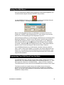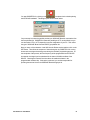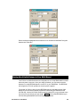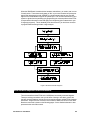
1
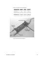
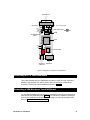
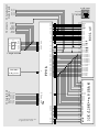
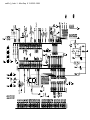
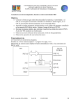
2608 Sweetgum Drive Apex NC 27502 Toll-free: 800-549-9377 International: 919-387-0076 FAX: 919-387-1302 XS40, XSP Board V1.4 User Manual How to install, test, and use your new XS40 or XSP Board RELEASE DATE: 9/21/2001 Copyright ©1997-2001 by X Engineering Software Systems Corporation. All XS-prefix product designations are trademarks of XESS Corp. All XC-prefix product designations are trademarks of Xilinx. All rights reserved. No part of this publication may be reproduced, stored in a retrieval system, or transmitted, in any form or by any means, electronic, mechanical, photocopying, recording, or otherwise, without the prior written permission of the publisher. Printed in the United States of America. XS40 BOARD V1.4 USER MANUAL 1 1 Preliminaries Getting Help! Here are some places to get help if you encounter problems: If you can't get the XS40 Board hardware to work, send an e-mail message describing your problem to [email protected] or submit a problem report at http://www.xess.com/reqhelp.html. Our web site also has answers to frequently-asked-questions, example designs for the XS Boards, application notes, a place to sign-up for our email forum where you can post questions to other XS Board users. If you can't get your XILINX Foundation software tools installed properly, send an email message describing your problem to [email protected] or check their web site at http://support.xilinx.com. Take notice!! The XS40 Board requires an external power supply to operate! It does not draw power through the downloading cable from the PC parallel port. If you are connecting a 9VDC power supply to your XS40 Board, please make sure the center terminal of the plug is positive and the outer sleeve is negative. The V1.4 version of the XS40 Board now uses a programmable oscillator with a default frequency of 50 MHz. You must reprogram the oscillator if you want to use another frequency. The procedure for doing this is described on page 8. XS40 BOARD V1.4 USER MANUAL 2 Packing List Here is what you should have received in your package: an XS40 or XSP Board (note that your XSP Board will be labeled as an XS40 but the socket will contain a Xilinx Spartan FPGA with an "XCS" prefix); a 6' cable with a 25-pin male connector on each end; an XSTOOLs CDROM with software utilities and documentation for using the XS40 Board. XS40 BOARD V1.4 USER MANUAL 3 2 Installation Installing the XSTOOLs Utilities and Documentation XILINX currently provides the Foundation tools for programming their FPGAs and CPLDs. Any recent version of XILINX software should generate bitstream configuration files that are compatible with your XS40 Board. Follow the directions XILINX provides for installing their software. You can get additional help at http://xup.msu.edu/license/index.htm. XESS Corp. provides the additional XSTOOLs utilities for interfacing a PC to your XS40 Board. Run the SETUP.EXE program on the XSTOOLs CDROM to install these utilities. Applying Power to Your XS40 Board You can use your XS40 Board in two ways, distinguished by the method you use to apply power to the board. Using a 9VDC wall-mount You can use your XS40 Board all by itself to experiment with logic and microcontroller designs. Just place the XS40 Board on a non-conducting surface as shown in Figure 1. Then apply power to jack J9 of the XS40 Board from a 9V DC wall transformer with a 2.1 mm female, center-positive plug. (See Figure 2 for the location of jack J9 on your XS40 Board.) The on-board voltage regulation circuitry will create the voltages required by the rest of the XS40 Board circuitry. Solderless Breadboard Installation The two rows of pins from your XS40 Board can be plugged into a solderless breadboard with holes spaced at 0.1" intervals. (One of the A.C.E. protoboards from 3M is a good choice.) Once plugged in, all the pins of the FPGA and microcontroller, and SRAM are accessible to other circuits on the breadboard. (The numbers printed next to the rows of pins on your XS40 Board correspond to the pin numbers of the FPGA.) Power can still be supplied to your XS40 Board though jack J9, or power can be applied directly through several pins on the underside of the board. Just connect +5V, +3.3V, and ground to the following pins for your particular type of XS40 Board. (You will need +3.3V only if your XS40 Board contains an XC4000XL type of FPGA.) XS40 BOARD V1.4 USER MANUAL 4 • Table 1: Power supply pins for the various XS40 Boards. XS40 Board Type GND Pin +5V Pin +3.3V Pin XS40-005E V1.4 52 2, 54 none XS40-005XL V1.4 52 2 54 XS40-010E V1.4 52 2, 54 none XS40-010XL V1.4 52 2 54 XSP-010 V1.4 52 2,54 none • Figure 1: External connections to the XS40 Board. XS40 BOARD V1.4 USER MANUAL 5 PC Parallel Port J1 100 MHz Osc. J12 J6 J4 J11 Serial EEPROM Socket U5 U3 U4 J8 (not installed) U7 U9 9VDC Power Supply J9 U15 SRAM FPGA U1 J10 J7 U10 Microcontroller J5 J2 PS/2 Mouse VGA Monitor or Keyboard • Figure 2: Arrangement of components on the XS40 Board. Connecting a PC to Your XS40 Board The 6' cable included with your XS40 Board connects it to a PC. One end of the cable attaches to the parallel port on the PC and the other connects to the female DB-25 connector (J1) at the top of the XS40 Board as shown in Figure 1. Connecting a VGA Monitor to Your XS40 Board You can display images on a VGA monitor by connecting it to the 15-pin J2 connector at the bottom of your XS40 Board (see Figure 1). You will have to download a VGA driver circuit to your XS40 Board to actually display an image. You can find an example VGA driver at http://www.xess.com/ho03000.html. XS40 BOARD V1.4 USER MANUAL 6 Connecting a Mouse or Keyboard to Your XS40 Board You can accept inputs from a keyboard or mouse by connecting it to the J5 PS/2 connector at the bottom of your XS40 Board (see Figure 1). You can find an example keyboard driver at http://www.xess.com/ho03000.html. Setting the Jumpers on Your XS40 Board The default jumper settings shown in Table 2 configure your XS40 Board for use in a logic design environment. You will need to change the jumper settings only if you are: using your XS40 in a stand-alone mode where it is unconnected from the PC parallel port (see page 12), reprogramming the clock frequency on your XS40 Board (see page 8), executing microcontroller code from internal ROM instead of the external SRAM on the XS40 Board. (You will have to replace the ROMless microcontroller on the XS40 Board with a ROM version to use this feature.) • Table 2: Jumper settings for XS40 and XSP Boards. Jumper Setting Purpose J4 On (default) A shunt should be installed if you are downloading the XS40 or XSP Board through the parallel port. Off The shunt should be removed if the XS40 or XSP Board is being configured from the on-board serial EEPROM (U7). On The shunt should be installed when the on-board serial EEPROM (U7) is being programmed. Off (default) The shunt should be removed during normal board use. 1-2 (ext) (default) The shunt should be installed on pins 1 and 2 (ext) if the 8031 microcontroller program is stored in the external 32 KByte SRAM (U8) of the XS40 Board. 2-3 (int) The shunt should be installed on pins 2 and 3 (int) if the program is stored internally in the microcontroller. On The shunt should be installed in XS40 or XSP Boards which use the 3.3V XC4000XL type of FPGAs. Off The shunt should be removed on XS40 or XSP Boards which use the 5V XC4000E type of FPGAs. On The shunt should be installed if the XS40 or XSP Board is being configured from the on-board serial EEPROM. Off (default) The shunt should be removed if the XS40 or XSP Board is being downloaded from the PC parallel port. On (default) The shunt should be installed if the XS40 or XSP Board is being downloaded from the PC parallel port. Off The shunt should be removed if the XS40 or XSP Board is being configured from the on-board serial EEPROM. 1-2 (osc) (default) The shunt should be installed on pins 1 and 2 (osc) during normal operations when the programmable oscillator is generating a clock signal. 2-3 (set) The shunt should be installed on pins 2 and 3 (set) when the programmable oscillator frequency is being set. J6 J7 J8 J10 J11 J12 XS40 BOARD V1.4 USER MANUAL 7 Testing Your XS40 Board Once your XS40 Board is installed and the jumpers are in their default configuration, you can test the board using the GUI-based GXSTEST utility as follows. You start GXSTEST by clicking on the icon placed on the desktop during the XSTOOLS installation. This brings up the window shown below. Next you select the parallel port that your XS40 Board is connected to from the Port pulldown list. GXSTEST starts with parallel port LPT1 as the default, but you can also select LPT2 or LPT3 depending upon the configuration of your PC. After selecting the parallel port, you select the type of XS40 Board you are testing from the Board Type pulldown list. Then click on the TEST button to start the testing procedure. GXSTEST will configure the FPGA to perform a test procedure on your XS40 Board. After several seconds you will see a O displayed on the LED digit if the test completes successfully. Otherwise an E will be displayed if the test fails. A status window will also appear on your PC screen informing you of the success or failure of the test. If your XS40 Board fails the test, you will be shown a checklist of common causes for failure. If none of these causes applies to your situation, then test the XS40 Board using another PC. In our experience, 99.9% of all problems are due to the parallel port. If you cannot get your board to pass the test even after taking these steps, then contact XESS Corp for further assistance. Programming Your XS40 Board Clock Oscillator The XS40/XSP Board has a 100 MHz programmable oscillator (a Dallas Semiconductor DS1075Z-100). The 100 MHz master frequency can be divided by factors of 1, 2, ... up to 2052 to get clock frequencies of 100 MHz, 50 MHz, ... down to 48.7 KHz, respectively. The divided frequency is sent to the rest of the XS40/XSP Board circuitry as a clock signal. The divisor is stored in non-volatile memory in the oscillator chip so it will resume operation at its programmed frequency whenever power is applied to the XS40/XSP Board. You can store a particular divisor into the oscillator chip by using the GUI-based GXSSETCLK utility as follows. XS40 BOARD V1.4 USER MANUAL 8 You start GXSSETCLK by clicking on the icon placed on the desktop during the XSTOOLS installation. This brings up the window shown below. Your next step is to select the parallel port that your XS40/XSP Board is connected to from the Port pulldown list. GXSSETCLK starts with parallel port LPT1 as the default, but you can also select LPT2 or LPT3 depending upon the configuration of your PC. Then select the type of XS40/XSP Board from the Board Type pulldown list. Next you enter a divisor between 1 and 2052 into the Divisor text box and then click on the SET button. Then follow the sequence of instructions given by GXSSETCLK for moving shunts and removing and restoring power during the oscillator programming process. At the completion of the process, the new frequency will be programmed into the DS1075. An external clock signal can be substituted for the internal 100 MHz oscillator of the DS1075. Checking the External Clock checkbox will enable this feature in the programmable oscillator chip. If this option is selected, you are then responsible for providing the external clock to the XS40/XSP Board through pin 64. XS40 BOARD V1.4 USER MANUAL 9 3 Programming This section will show you how to download a logic design from a PC into your XS40 Board and how to store a design in its optional serial EEPROM that will become active when power is applied. Downloading Designs into Your XS40 Board During the development and testing phases, you will usually connect your XS40 Board to the parallel port of a PC and download your circuit each time you make changes to it. You can download an FPGA design into your XS40 Board using the GXSLOAD utility as follows. You start GXSLOAD by clicking on the icon placed on the desktop during the XSTOOLS installation. This brings up the window shown below. Next you select the parallel port that your XS40 Board is connected to from the Port pulldown list. GXSTEST starts with parallel port LPT1 as the default, but you can also select LPT2 or LPT3 depending upon the configuration of your PC. Then select the type of XS40 Board you are using from the Board Type pulldown list. XS40 BOARD V1.4 USER MANUAL 10 After setting the board type and parallel port, you can download .BIT files to the FPGA on your XS40 Board simply by dragging them to the FPGA/CPLD area of the GXSLOAD window as shown below. Once you release the left mouse button and drop the file, the highlighted file name appears in the FPGA/CPLD area and the Load button in the GXSLOAD window is enabled. Clicking on the Load button will begin sending the highlighted file to the XS40 Board through the parallel port connection. .BIT files contain configuration bitstreams that are loaded into the FPGA. GXSLOAD will reject any non-downloadable files (ones with a suffix other than .BIT or .SVF). During the downloading process, GXSLOAD will display the name of the file and the progress of the current download. You can drag & drop multiple files into the FPGA/CPLD area. Clicking your mouse on a filename will highlight the name and select it for downloading. Only one file at a time can be selected for downloading. XS40 BOARD V1.4 USER MANUAL 11 Double-clicking the highlighted file will deselect it so no file will be downloaded Doing this disables the Load button. Storing Non-Volatile Designs in Your XS40 Board The FPGA on an XS40 Board stores its configuration in an on-chip SRAM which is erased whenever power is removed. Once your design is finished, you may want to store the bitstream in a serial EEPROM placed in socket U7 on your XS40 Board. The EEPROM will configure the FPGA for operation as soon as power is applied. The XILINX XC1700 is a series of serial EEPROMs that are compatible with the XS40 Board, but you will need an external programmer to download your bitstream into the XC1700 chip. Also the XC1700 is one-time programmable (OTP), so you will need a new chip every time you change your logic design. Table 3 lists the serial EEPROM chip you need for storing the bitstream files for each type of XS40 Board. XS40 BOARD V1.4 USER MANUAL 12 • Table 3: Recommended XILINX serial EEPROMS for various types of XS40 Boards. XS40 Board Type Bitstream Size XILINX EEPROM XS40-005E 95,008 XC17128E XS40-005XL 151,960 XC17256E XS40-010E 178,144 XC17256E XS40-010XL 283,424 XC1701 95,008 XC17S10 XSP-010 You also have the option of storing your design into an AT17C256 Atmel reprogrammable serial EEPROM if you have an XS40-005E, XS40-005XL, or XS40-010E Boards. The XS40 Board can directly program the Atmel chip, and the FPGAs on these boards have bitstream files which are small enough to fit in the AT17C256. You can load your design into the Atmel EEPROM by dragging the .BIT into the Flash/EEPROM area and clicking on the Load button. This activates the following sequence of steps: 1. The entire EEPROM is erased. 2. This FPGA on the XS40 Board is programmed to create an interface between the EEPROM and the PC parallel port. 3. The contents of the .BIT file are downloaded into the EEPROM through the parallel port. Once your design is loaded into the EEPROM, the following steps will make the XS40 Board configure itself from the EEPROM upon power-on: 1. Remove the downloading cable from connector J1 of the XS40 Board. (As an alternative, you can use the command XSPORT 0 to make sure the upper two data bits of the parallel port are at logic 0. These bits are connected to the mode pins of the FPGA and must be at logic 0 or the FPGA will not power-up in the active-serial mode.) 2. Place a shunt on jumper J10. This sets the FPGA into the active-serial mode so it will provide a clock signal to the EEPROM which sequences the loading of the configuration from the EEPROM into the FPGA. 3. Remove the shunts on jumpers J4 and J11. This prevents the PC interface circuitry on the XS40 Board from interfering with the clock and data signals from the FPGA. 4. Apply power to the XS40 Board. The FPGA will be configured from the serial EEPROM. You may reattach the downloading cable if you need to inject test signals into your design using the XSPORT program. Downloading and Uploading Data to/from the RAM in Your XS40 Board The XS40 Board contains 32 or 128 KBytes of RAM whose contents can be downloaded and uploaded by GXSLOAD. This is useful for initializing the RAM with data for use by the FPGA and then reading the RAM contents after the FPGA has operated upon it. The RAM is loaded with data by dragging & dropping one or more .EXO, .MCS, .HEX, and/or XS40 BOARD V1.4 USER MANUAL 13 .XES files into the RAM area of the GXSLOAD window and then clicking on the Load button. This activates the following sequence of steps: 1. The FPGA on the XS40 Board is reprogrammed to create an interface between the RAM device and the PC parallel port. 2. The contents of the .EXO, .MCS, .HEX or .XES files are downloaded into the RAM through the parallel port. The data in the files will overwrite each other if their address ranges overlap. 3. After the data is downloaded to the RAM, any highlighted bitstream file in the FPGA/CPLD area is downloaded into the FPGA on the XS40 Board. Otherwise the FPGA remains configured as an interface to the RAM. You can also examine the contents of the RAM device by uploading it to the PC. To upload data from an address range in the RAM, type the upper and lower bounds of the range into the High Address and Low Address fields below the RAM area, and select the format in which you would like to store the data using the Upload Format pulldown list. Then click on the file icon and drag & drop it into any folder. This activates the following sequence of steps: 1. The FPGA on the XS40 Board is reprogrammed to create an interface between the RAM device and the PC parallel port. 2. The RAM data between the high and low addresses (inclusive) is uploaded through the parallel port. 3. The uploaded data is stored in a file named RAMUPLD with an extension that reflects the file format. XS40 BOARD V1.4 USER MANUAL 14 4 Programmer's Models This section discusses the organization of components on the XS40 Board and introduces the concepts required to create applications that use both the microcontroller and the FPGA. Building FPGA-based designs is covered in detail in the Pragmatic Logic Design online text found at http://www.xess.com/pragmatic-2_1.html. Designs that couple the operations of the FPGA with the microcontroller are discussed in the online document http://www.xess.com/appnotes/an-103100-ucfpga.pdf. Microcontroller + FPGA Design Flow The basic design flow for building microcontroller+FPGA applications is shown in Figure 3. Initially you have to get the specifications for the system you are trying to design. Then you have to determine what inputs are available to your system and what outputs it will generate. At this point, you have to partition the functions of your system between the microcontroller and the FPGA. Some of the input signals will go to the microcontroller, some will go to the FPGA, and some will go to both. Likewise, some of the outputs will be computed by the microcontroller and some by the FPGA. There will also be some new intra-system inputs and outputs created by the need for the microcontroller and the FPGA to cooperate. In general, the FPGA will be used mainly for low-level functions where signal transitions occur more frequently and the control logic is simpler. A specialized serial transmitter/receiver would be a good example. Conversely, the microcontroller will be used for higher-level functions where the responses occur less quickly and the control logic is more complex. Reacting to commands passed in by the receiver is a good example. Once the design has been partitioned and you have assigned the various inputs, outputs, and functions to the microcontroller and the FPGA, then you can begin doing detailed design of the software and hardware. For the software, you can use your favorite editor to create a .ASM assembly-language file and assemble it with ASM51 to create a .HEX file for the microcontroller on the XS40 Board. For the FPGA hardware portion, you will enter truth-tables and logic equations into a .ABL or .VHDL file and compile it into an .BIT bitstream file using the XILINX Foundation software. You can download the .HEX program file and the .BIT bitstream file to the XS40 Board using the XSLOAD program. XSLOAD stores the contents of the .HEX file into the SRAM on the XS40 Board and then it reconfigures the FPGA by loading it with the bitstream file. XS40 BOARD V1.4 USER MANUAL 15 When the XS40 Board is loaded with the hardware and software, you need to test it to see if it really works. The answer usually starts as "No" so you need a method of injecting test signals and observing the results. XSPORT is a simple program that lets you send test signals to the XS40 Board through the PC parallel port. You can trace the reaction of your system to signals from the parallel port by programming the microcontroller and the FPGA to output status information on the LED digit (much like placing "printf" statements in your C language programs). This is admittedly crude but will serve if you don't have access to a programmable stimulus generator or logic analyzer. • Figure 3: FPLD+microcontroller design flow. XS40 Board Component Interconnections The microcontroller and the FPGA on the XS40 Board are already connected together. These pre-existing connections save you the effort of having to wire them yourself, but they also impose limitations on how your microcontroller program and the FPGA hardware will interact. A high-level view of how the microcontroller, SRAM, and FPGA on the XS40 Board are connected is shown on the following pages. A more detailed schematic is also presented at the end of this manual. XS40 BOARD V1.4 USER MANUAL 16 The programmable oscillator output goes directly to a synchronous clock input of the FPGA. The FPGA uses this clock to generate a clock that it sends to the XTAL1 clock input of the microcontroller. The microcontroller multiplexes the lower eight bits of a memory address with eight bits of data and outputs this on its P0 port. Both the SRAM data lines and the FPGA are connected to P0. The SRAM uses this connection to send and receive data to and from the microcontroller. The FPGA is programmed to latch the address output on P0 under control of the ALE signal and send the latched address bits to the lower eight address lines of the SRAM. Meanwhile, the upper eight bits of the address are output on the P2 port of the microcontroller. The 32 Kbyte SRAM on the XS40 Board uses the lower seven of these address bits while the 128 KByte SRAM on the XS40+ Board gets all eight address bits. The FPGA also receives the upper eight address bits and decodes these along with the PSENB and read/write control line (from pin P3.6 of port P3 ) from the microcontroller to generate the CEB and OEB signals that enable the SRAM and its output drivers, respectively. Either of the CEB or OEB signals can be pulled high to disable the SRAM and prevent it from having any effect on the rest of the XS40 Board circuitry. One of the outputs of the FPGA controls the reset line of the microcontroller. The microcontroller can be prevented from having any effect on the rest of the circuitry by forcing the RST pin high through the FPGA. (When RST is active, the microcontroller pins are weakly pulled high.) Many of the I/O pins of ports P1 and P3 of the microcontroller connect to the FPGA and can be used for general-purpose I/O between the microcontroller and the FPGA. In addition to being general-purpose I/O, the P3 pins also have special functions such as serial transmitters, receivers, interrupt inputs, timer inputs, and external SRAM read/write control signals. If you aren't using a particular special function, then you can use the associated pin for general-purpose I/O between the microcontroller and the FPGA. In many cases, however, you will program the FPGA to make use of the special-purpose microcontroller pins. (For example, the FPGA could generate microcontroller interrupts.) If you want to drive the special-purpose pin from an external circuit, then the FPGA I/O pin connected to it must be tristated. A seven-segment LED digit connects directly to the FPGA. (These same FPGA pins can also drive a VGA monitor.) The FPGA can be programmed so the microcontroller can control the LEDs either through P1 or P3 or by memory-mapping a latch for the LED into the memory space of the microcontroller. The PC can transmit signals to the XS40 Board through the eight data output bits of the parallel port. The FPGA has direct access to these signals. The microcontroller can also access these signals if you program the FPGA to pass them onto the FPGA I/O pins connected to the microcontroller. Communication from the XS40 Board back to the PC also occurs through the parallel port. The parallel port status pins are connected to pins of microcontroller ports P1 and P3 . Either the microcontroller or the FPGA can drive the status pins. The PC can read the status pins to fetch data from the XS40 Board. The FPGA also has access to the clock and data lines of a keyboard or mouse attached to the PS/2 port of the board. XS40 BOARD V1.4 USER MANUAL 17 • Table 4: XS40 Board pin descriptions. XS40 Pin 25 26 24 20 23 18 19 13 44 45 46 47 48 49 32 34 37 36 29 14 7 8 9 6 77 70 66 67 69 68 62 27 41 40 39 38 35 81 80 10 59 57 51 56 50 58 60 28 16 3 4 5 78 79 82 83 84 61 65 75 Connects to… S0 BLUE0 S1 BLUE1 S2 GREEN0 S3 GREEN1 S4 RED0 S5 RED1 S6 HSYNCB CLK PC D0 PC D1 PC D2 PC D3 PC D4 PC D5 PC D6 PC D7 XTAL1 RST ALEB PSENB P1 0 P1 1 P1 2 P1 3 P1 4 PC S4 P1 5 PC S3 P1 6 PC S5 P1 7 VSYNCB P3 1(TXD) PC S6 P3 4(T0) PS/2 CLK P3 6(WRB) WEB P3 7(RDB) P0 0(AD0) D0 P0 1(AD1) D1 P0 2(AD2) D2 P0 3(AD3) D3 P0 4(AD4) D4 P0 5(AD5) D5 P0 6(AD6) D6 P0 7(AD7) D7 P2 0(A8) A8 P2 0(A9) A9 P2 0(A10) A10 P2 0(A11) A11 P2 0(A12) A12 P2 0(A13) A13 P2 0(A14) A14 P2 0(A15) A15 A16 A0 A1 A2 A3 A4 A5 A6 A7 OEB CEB PC S7 XS40 BOARD V1.4 USER MANUAL Description These pins drive the individual segments of the LED display (S0-S6). They also drive the color and horizontal sync signals for a VGA monitor. An input driven by the 100 MHz programmable oscillator These pins are driven by the data output pins of the PC parallel port. Clocking signals can only be reliably applied through pins 44 and 45 since these have additional hysterisis circuitry. Pins 32 and 34 are mode signals for the FPGA so you must adjust your design to account for the way that the Foundation tools handle these pins. pins 32 and 34 are not usable as general-purpose I/O on the Spartan FPGA on the XSP Board. Pin that drives the uC clock input Pin that drives the uC reset input Pin that monitors the uC address latch enable Pin that monitors the uC program store enable These pins connect to the pins of Port 1 of the uC. Some of the pins are also connected to the status input pins of the PC parallel port. Pin 67 drives the vertical sync signal for a VGA monitor. These pins connect to some of the pins of Port 3 of the uC. The uC has specialized functions for each of the port pins indicated in parentheses. Pin 62 connects to the data write pin of the uC and the write-enable pin of the SRAM. Pin 69 connects to a status input pin of the PC parallel port and the PS/2 data line. Pin 68 connects to the PS/2 clock line These pins connect to Port 0 of the uC which is also a multiplexed address/data port. These pins also connect to the data pins of the SRAM. These pins connect to Port 2 of the uC which also outputs the upper address byte. These pins also connect to the upper address bits of the SRAM. Pins 28 and 16 are connected to the 128 KB SRAM address pins only on the XS40+ Board. Pins 28 and 16 do not connect to the 32 KB SRAM on the XS40 Board. These pins drive the 8 lower address bits of the SRAM. Pin that drives the SRAM output enable Pin that drives the SRAM chip enable Pin that drives a status input pin of the PC parallel port 18 P C P a ra lle l P o rt S tatu s In p u ts K B _D A TA V SYN C H SYN C RED 1 RED 0 G REEN 1 G REEN 0 B LU E 1 B LU E 0 S6 S5 S3 S2 S0 S6 S4 S5 S4 S3 S1 S2 S1 S0 19 18 23 20 24 26 25 37 36 29 14 67 66 70 77 6 9 8 7 21 10 33 32 9 8 7 6 5 4 3 2 X TA L 1 RST A LE PSEN P 1 .7 P 1 .6 P 1 .5 P 1 .4 P 1 .3 P 1 .2 P 1 .1 P 1 .0 27 19 18 17 16 15 14 13 11 36 37 38 39 40 41 42 43 31 30 29 28 27 26 25 24 P 3 .7 P 3 .6 P 3 .5 P 3 .4 P 3 .3 P 3 .2 P 3 .1 P 3 .0 P 0 .7 P 0 .6 P 0 .5 P 0 .4 P 0 .3 P 0 .2 P 0 .1 P 0 .0 P 2 .7 P 2 .6 P 2 .5 P 2 .4 P 2 .3 P 2 .2 P 2 .1 P 2 .0 13 14 15 21 20 19 18 17 D7 D6 D5 D4 D3 D2 D1 D0 84 83 82 79 78 5 4 3 2 31 6 27 4 5 3 28 26 9 23 10 11 12 7 25 8 A 1 6 ** A 1 5 ** A 14 A 13 A 12 A 11 A 10 A9 A8 A7 A6 A5 A4 A3 A2 A1 A0 62 61 65 29 24 22 W E OE C19 E 68 75 69 P C P a ra lle l P o rt D a ta O u tp u ts 100 M H z P ro g . O sc. 13 34* 32* 49 48 47 46 45 44 P C _D 7 * P C _D 6 * P C _D 5 P C _D 4 P C _D 3 P C _D 2 P C _D 1 P C _D 0 * = n o t c o n n e c te d o n X S P B o a rd ** = ap p lie s to X S 4 0 + B o a rd XS40 BOARD V1.4 USER MANUAL FP G A 7 -S e g m e n t L E D 10 80 81 35 38 39 40 41 28 60 58 50 56 51 57 59 16 8031 uC K B _C L K (R D ) (W R ) (T 1) (T 0) (IN T 1 ) (IN T 0 ) (T X D ) (R X D ) (A 7/D 7 ) (A 6/D 6 ) (A 5/D 5 ) (A 4/D 4 ) (A 3/D 3 ) (A 2/D 2 ) (A 1/D 1 ) (A 0/D 0 ) (A 15 ) (A 14 ) (A 13 ) (A 12 ) (A 11 ) (A 10 ) (A 9) (A 8) 3 2 K /1 2 8 K ** x 8 S R A M V G A In p u ts P S /2 P o rt P C _S 7 P C _S 6 P C _S 5 P C _S 4 P C _S 3 XS40 BOARD V1.4 USER MANUAL 20 XS40 BOARD V1.4 USER MANUAL 21 xs40v1_4.sch-1 - Mon Sep 6 13:53:50 1999