1
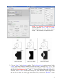
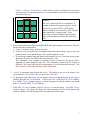
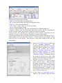
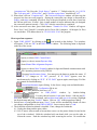
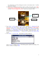
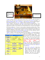
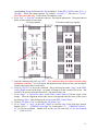
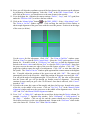
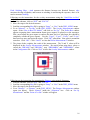
Operating instructions for DWL66 laser writer
Things to remember:
1. The DWL66 runs a 405-nm semiconductor laser. The laser beam path is covered and you
must not remove any of the covers. To assure that the user is not accidentally exposed to
the laser light, the laser writer exposes only if the coverlid is closed. Do not open the
coverlid when running a job. The exposure will stop and you won’t be able to resume it.
2. The laser writer is equipped with an interferometric system to measure the stage position.
Touching the mirrors located on the stage with bare hands will damage them beyond
repair.
3. You need to wait for ~ 30 minutes after the system is turned on.
4. The pattern should be ~ 5 mm away from any edge of the mask / sample. The maximum
write area for 6-inch mask is ~ 5.5 inch by 5.5-inch.
5. A “smart UPS” supplies power to the laser writer and the laser (not the Windows computer).
Therefore, your writing job should not be affected in a case of a short power outage.
Login / logout procedure:
1. We have to computers: Dell with Windows XP OS and writing software; HP with Linux OS
and conversion software. Login as “User” to Windows XP. The password was given to you
during the authorization. Conversion computer always on, there are no passwords on it.
Computers use the same mouse, keyboard and monitor. To toggle between the computers
you have to double click “Scroll Lock” button.
2. Logout from Windows XP after you are done. Leave the system on. Turn off the laser.
The lifetime of the laser diode is limited and the laser replacement is expensive.
3. Always move the substrate holder to the home (center) position before you exit the
“DWL_MENU” software and logout.
4. If the laser writer is shut down for any reason, turn it on by pressing the green button on the
front panel. Wait for ~ 30 minutes for the system to warm up. Next, you need to reestablish
the communication between the Windows and OS-9 computers. Open DWL_MENU
program. “DWL does not respond” window appears. Click “OK”. Open the Mini-Terminal
window in the DWL_MENU. Using the keyboard hit “Enter” twice and type “dwl” as
username and password. Close the Mini-Terminal window after “DWL:” appears. Finally,
reset the interferometer and the stage (see below).
How to perform the file conversion:
After you design the pattern in L-Edit Pro or AutoCAD LT, you must convert your gdsii, cif or
dxf file into lic files that are used by the laser writer. Switch to the HP computer with Linux OS
for the conversion.
1. Insert a floppy, USB memory stick, or a CD, open home directory (“little house” icon in the
toolbar at the bottom of the screen) and copy your file to appropriate folder (CIF, DXF, or
GDSII). Remove the storage media. Start conversion program clicking on the icon located
on the desktop (“smiling sun” at the center of the screen).
2. Load your previous conversion job by selecting File-load job, or start new job using File-new
job. Click on “Add”. Select the appropriate design type (DXF, GSII, or CIF). The Options
window will open. The window will automatically reflect the number of layers in your
design. You need to select every layer that should become part of your conversion
1
design by checking corresponding box.
You may perform “CUT”, “OR”, or “XOR”
function between any two layers in your
design. Their meaning is explained below:
3. Click on “Step #” in the Options window. The Step Layers for # window appears. Under
“Array” enter how many dies should be written in x and y directions, e.g., 3 X 5. The
example bellow shows 1 X 3 array (selected in red rectangular). Under “Step Size”, enter
the step size (in nanometers) in “x” and “y”. If you are creating one stripe of dies in ydirection, select “0” for x and the desired step for y (this should be slightly bigger than
the die size to allow for some gap between the dies). Choose the “Rotation” and/or
2
“Mirror”. Click on “Create default”. Job file will be created. To minimize the conversion
and write times for repeating patterns, it is recommended tocreate the conversion pattern
in the following way:
Example:
The view of the mask after it is completed. It
contains 9 identical dies (green squares). Each
die carries your AutoCAD or L-Edit design.
When creating the conversion file, make a design
that contains one “complete stripe” in the
y-direction (as shown within the red rectangle).
That would dramatically reduce the conversion
time.
y
x
4. There are three basic rules that you should follow when performing the conversion. They are
listed in the order of importance.
a. Create a “complete stripe” in the y-direction.
b. If the area of your pattern has rectangular rather than square shape, always rotate the
pattern in such a way, that the longer side is parallel with the y-axes.
c. If your design contains long lines that run preferentially in x or y direction, always rotate
the pattern in such a way, that the lines run along the y-axes.
The orientation of the machine’s coordinate system is shown in the picture below.
Remember it when setting the write job. (The coordinate system on the PC display is
different. The X-axis runs from left to right and the Y-axis from bottom to the top.) The
laser writes in y-direction and steps in the x-direction.
5. “Arcres” is important when drawing the circles. The smaller is the arcres the longer is the
conversion time. If your file is dxf, you must enter “Dxf units”.
6. To display the individual layers of your design, select the required layer(s) in the Options
window, then click on “Create default”. Click on “Preview” in the DWL 66-Covert window.
Two “HIMT Viewer” windows appear. Look at the pattern and decide whether you should
rotate it. Close the HIMT Viewer windows.
7. In the DWL 66-Convert window, click on “Preview” to view the design. Two HIMT Viewer
windows appear. One shows the image, the other announces the size of the pattern and
contains a number of useful functions for the manipulation of the image.
3
Following are some of these functions:
“XOR”: to view XOR image as explained above.
“Fill”: to view the areas that will be filled (as opposed to lines).
“Polarity”: to view the inverted pattern.
“Left”, “Right”, “Down”, and “Up”: to move the image.
“All”: to view the complete design.
“Measure”: measurement tool. The value (in millimeters) is displayed under “D:”.
“Snapshot”: creates a “jpg” file of the design shown on the screen. The file is automatically
saved as “image#” in the “home\convert” directory of the Linux partition.
Always use the “Fill” function to see which areas will be exposed. (The black areas are
exposed.) Use the “Polarity” function if you plan to create an inverted image.
If you are not satisfied with your design, return to the Options window and click on “Step #”.
Make changes to the array and click “Redraw”. Continue until you are satisfied. Write
down the size of your design. You will need it later when setting up the write job
environment.
8. Return to GUI HIMT Convert window and
set the remaining parameters.
We
recommend that you ignore the “Rotation”
(you have done it already in the “Step#”
window), and “X-offset” and “Y-offset”.
Keep the “Calculate exposed area” “off”
and the “Automatic centering” “on”. (When
doing the overlay exposures, do not use
“Automatic centering”. Define the origin of
the designs in AutoCAD or L-Edit. This
origin is preserved during the conversion by
choosing “Automatic centering” “off”.)
9. Choose noninverted or inverted design
under “Exposure mode”. When inverting
the design, you must select a “Frame size”
around the pattern. The entered number
determines how far from any edge of the
pattern the photoresist is exposed. If you
are using the noninverted design, you must
enter “0” in the “Frame size”.
10. In the “Spot size corrections x and y”
windows, enter numbers from the latest
4
“parameters.txt” file. Keep the “Scale factor x” equal to “1”. Default value for y is 1.01138.
The “Left optic path”, “Scale offset”, and “Calculate exposed area” should be all “off”.
11. When done, click on “Complete task”. The Conversion Progress window will show up (the
progress bar does not work properly). During the conversion your design is dissected into
stripes, each stripe containing 100 pixels. Size of the pixel depends on write lens (4 mm lens
has 200 nm pixel size, 20 mm-1 µm) A small number of stripes indicates that you designed
the conversion pattern correctly. Click “OK” after the conversion is completed.
12. After conversion was done, press finish button. “Transfer Lic Files” window will appear.
Press “Save” and “Transfer” to transfer the lic files to OS-9 computer. All designs (lic files)
are stored there. FTP address has to be 170.168.10.98. “Exit” the program.
How to perform exposure:
1. Open “DWL_MENU” by clicking on the
icon located on the desktop. Two windows
will appear. Click on “OK” in the DWL MENU window. The following menu is displayed
at the top of the screen:
Opens (or closes) DWL Control Panel.
Opens (or closes) current Exposure Map.
Starts Manual Plate Alignment Sequence.
Opens (or closes) Mini-Terminal window for login and limited communication with
OS-9 operating system used by DWL66.
Requests Interferometer Status. You must press the button to update the status. If
label “IF ???” changes to “IF: OK”, proceed. If “IF: FAIL” appears, reset the
interferometer by clicking on “IF R”. If “IF: FAIL” appears again, consult page 38 of the
user manual for troubleshooting.
Resets Interferometer upon clicking. It also forces a stage reset and initialization.
Configuration file in use.
Laser status indicator (shown as “off”).
2. Change
the
configuration
in
DWL_MENU
window
by
double-clicking
. You may choose between 4-mm (min. feature ~ 800 nm) and 20mm (min. feature ~ 4 µm) writehead, and uni-directional and gray scale writing. Highlight
the desired setup and press “Load it!” button. Click on “OK” in the popped-up window.
3. Switch laser on using pulldown menu “Laser”. Laser will be automatically turned off when
you change configuration or close DWL66 MENU. Laser worm up time is 3 min.
4. Check that the required writehead is installed. If not, change the writeheads.
4.1. Unplug the motor and the piezo cables.
4.2. Use #3 metric Allen wrench to loosen three screws (see the picture below) located on the
top of the writehead. Hold the writehead with one hand while you use the other to
loosen the screws. Push the writehead up while removing the screws. Be careful that
5
the writehead does not fall and damage the nozzle or the substrate chuck. Carefully
remove the writehead.
4.3. Place the new writehead into the holder. Push it up while you insert the screws. Don’t
let the nozzle to touch the chuck. Tighten the screws X-wise while pushing up on the
writehead. Do not overtighten the screws. Plug the motor and piezo cables.
Loosen these
screws.
Piezo cable
Motor cable
5. Go to “Setup” → “New” in the DWL_MENU menu. Highlight “C:\…\vbmenu\wafer” and
click on the “Create Map” button. Input a project name consisting of no more than 8
characters. Click on “Yes” to set the Environment. Return to New Exposure Map window
and under “C:\…\vbmenu\wafer” double-click on the folder that you just created. In the
right window, the corresponding fa, map, and wa files appear. Double-click on the “.map”
file and click on “Set Environment to…”. Click on “Exit” to close the New Exposure Map
window.
6. Go to “Setup” → “Exposure Map”. The default Map setting is displayed:
Click on “Draw” to display the Map. The following picture explains the meaning of the
different variables for setting the Map.
6
All sizes and distances are in micrometers. The “Field Zero =”, shown by the large cross in
the Map, determines the reference field, resp. the origin of the coordinate system. When
setting up the fields, remember that the origin of the design is placed in the center of the
field.
After you make all desired changes in the “Exposure Map Design”, click on “Draw” to apply
the changes. Click “Exit” and save the Map if it is not saved automatically.
7. Go to “Job” → “Make Job” to input the exposure parameters. The following spreadsheet
appears:
Design
The meaning of the columns in the spreadsheet is as follows:
“do” column: enter “-1” if the field should be written, enter “0” (or leave empty) if the field
is skipped.
“Ali” column: determines the alignment method. Empty field or “0”means no alignment, “1”
is one-site alignment, “2” is two-site alignment, etc (“4” is the maximum). Make sure that
the alignment sites were entered earlier in the Exposure Map Design window.
“Xoff” and “Yoff” columns: the value entered here (in microns) determines the X-offset,
resp. Y-offset, of the starting point of the exposure from the point that is set by the big cross
in the Map geometry. Keep in mind the coordinate system of the sample stage. The
orientation of the machine’s coordinate system is shown in the picture below. Remember it
when setting the write job. (The coordinate system on the PC display is different. The Xaxis runs from left to right and the Y-axis from bottom to the top.) The laser writes in ydirection and steps in the x-direction.
7
x
Switches for
turning on/off
certain vacuum
holes.
y
Switch for turning
the vacuum on and
off.
“Design” column: contains the path and the name of the lic directory where the pattern is
stored. First, click on the Design field that you wish to select in the Edit Job spreadsheet. In
the DWL_MENU select “File” → “Designs”. Click “Refresh” if your file does not appear.
Select the file and click on “To Job”. Continue with the remaining Design fields.
“Defoc” column: a value between 0 and 4095 can be used as an autofocus offset. If the
column is left empty, the defocus value of the previous exposure is used. The 4095 steps
approximately equal ± 10 µm, therefore one unit equals about 5 nm. Since the focal depth of
the 20-mm writehead is ~ 50 µm, it is not necessary to adjust the autofocus offset. When
choosing the Defoc value for the 4-mm writehead, keep in mind that the focal depth is 1.8
µm and the autofocus is stable within ~100 nm. If you are using the Cr plates coated with
5300Å of AZ1500 series resist from Nanofilm, Defoc value and other important exposure
settings are stored in the file “parameters.txt” on the desktop.
“Energy” column: sets the laser beam intensity for the exposure. 100 sets the energy to
100%, 90 to 90%, etc. Use values from 10 to 100 in the increment of 10. We recommend
that you use higher energy values.
If a
value lower than 30 is needed, insert neutral
density filter(s) into the laser beam path.
(1%, 10%, and 31.62% neutral density filters
are available. The filters can be combined.
Always put the filter at the end of the
railing
and
tighten
it
with Allen wrench.) The recommended
Energy and the filter configuration for
AZ1500-coated Cr plates can be found in the
file “parameters.txt”. Go to “File” and “Exit”
to save the Job.
8. Go to “Job” → “Run Job”. Select from
option menu what the system has to do
after writing will be finished: Auto
Unload will put stage into unload
position, Job Log will save writing
parameters into log file (always
checked), Laser OFF (recommended).
8
9. Click on the “LOAD”. The writehead moves up and the stage moves to the load position.
Check that the appropriate chuck is loaded. The solid chuck is used for the standard frontside exposures and/or metrology. The chucks with holes are used for the backside alignment.
When loading different chuck, push it all the way in and to the left. Be careful, that the
long o-ring in the back does not slip out from the groove. Do not bump into the
writehead, you may destroy the piezo crystal. Load the sample on the chuck. The resistcovered side should face up. Center the sample on the chuck. Turn the vacuum switch in
front of the chuck. All vacuum holes must be covered by the sample. Turn the white
‘switches’ located in front of the stage to open or close certain vacuum holes.
The following settings apply to the solid chuck:
always
open
all holes are open
outer holes are closed
two outer rows of
holes are closed
three outer rows
are closed
10. To avoid the damage of the writehead, check that the substrate is completely underneath.
Click on “FOCUS” to lower the writehead. Make sure that the nitrogen is on, otherwise
the nozzle will crash into the sample. Click on “Yes” to set the Defoc value.
11. To find the center of the sample, go to “Stage” → “Find plate center” in the DWL Control
Panel. Click on “Start” in the popped-up window. Click “Yes” after the procedure is
finished. (This procedure assumes that your sample is square or standard rounded wafer.)
12. Click on ”Expose” to start the exposure. The laser writer estimates the write time as it
proceeds with the exposure. If you hit the “Enter” key on the keyboard now, the writing will
terminate. Therefore, open another window over the Expose - … window to avoid this kind
of accident. After the exposure is finished, the written fields turn green in the Map and a
popped-up window notifies you that the exposure is finished. If any of the fields remain red,
it indicates an error during the exposure. Click on “Edit Report” in the Expose - … window
to get the report. Click on “Unload” to remove your sample, then hit “Exit”. Click on
“INIT” in the DWL Control Panel to return the stage to the home (center) position.
9
13. Develop the photoresist. Mix AZ400K with DI water (1:4 ratio) if you have the standard
mask plate from Nanofilm. It takes about from 30 seconds to 1 minute to develop.
How to perform the front-side overlay exposure:
If the writehead has been moved/exchanged since the last overlay exposure, perform the overlay
accuracy test. Use the designs created by Heidelberg located under “File” → “Designs” in the
DWL_MENU. The files are called “Overlay…”. The names are self-explanatory, e.g.,
“Overlay4_1” and “Overlay4_2” is the first and the second layer for the 4-mm writehead,
respectively. To perform the test, use a mask plate that is at least 2.5 inch by 2.5 inch in size.
Use the standard mode (not HQ) when writing these designs.
1. Make a mark in one corner of the substrate. Load it, click on “INIT” and “FOCUS”. Go
to “Setup”→“New” in the DWL_MENU and double-click on “C:\…\VBMENU\wafer\align”
for the 4-mm writehead or “C:\…\VBMENU\wafer\ali_20” for the 20-mm head. Double
click on the “.map” file and click on “Set Environment to …”. “Exit”. The following
pictures show the default map setting for the 4-mm and 20-mm writeheads. Do not change
these map settings.
Map settings for the overlay using 4-mm writehead
Map settings for the overlay using 20-mm writehead
2. Use the “Stage” → “Find plate center” in the DWL Control Panel to set the origin of x,y
coordinate system to the center of the plate.
3. Go to “Job” → “Make Job” to prepare the job for the first layer pattern. We suggest that you
always use the uni-directional writing mode. To load the test pattern, click on the
10
corresponding Design field in the Edit Job spreadsheet. In the DWL_MENU select “File” →
“Designs”. Select the required pattern, for example, “Overlay4_1”, and click on “To Job”.
Write the center die only. It takes about 30 minutes to write.
4. Go to “Job” → “Run Job” to start the exposure. Develop the photoresist. The pattern shown
below will be written on your mask.
First layer pattern
First and second layer together
5. Load the substrate and click on “INIT”. The substrate must be loaded with the same
orientation as before. You will expose the photoresist layer that you have just developed.
Usually, this can be done several times.
6. Click on “FOCUS” to lower the writehead. Move the lamp bar under “Lmp” in the DWL
Control Panel to turn on the lamp. An image will appear on the second LCD screen. The
second LCD screen is normally turned off – you need to turn it on.
7. Go to “Stage” → “Find plate center” in the DWL Control Panel to find the center of the
sample. Place the alignment feature (the corner of the pattern) into the center of the screen
by selecting “Move” and clicking on the arrows in the DWL Control Panel.
8. Click on “FS Macro Cam” to switch to the “FS Micro Cam”.
9. Go to “Setup” → “New” in the DWL_MENU to load the Map of the first-layer pattern.
Double-click “C:\…\VBMENU\wafer\align” for 4-mm head or “C:\…\VBMENU\wafer\ali_20” for 20-mm writehead. Double-click on the map file and click on “Set Environment
to…”. Click on “Exit”.
11
10. Next, you will align the coordinate system of the laser beam to the structures on the substrate
by performing a manual alignment. Select the “Field” in the DWL Control Panel. If you
now click on the arrows, you should move to the same feature in the next die.
11. Go to the highest die. Optimize the camera settings (“DeFoc”, “Lmp”, and “Gn” (gain) bars
under the “FS Micro Cam”) to achieve the best contrast.
12. Click on the “Manual Align” button
in the DWL_MENU. Select “Align along Y-axis”.
The “Point to 1st Site” window appears. Click and drag the small dot in this window to
obtain rough alignment of the green cross with the cross-like pattern. Position it on the edges
of the cross (see below).
Use the arrows for fine adjustment. Click “OK”. The “Point to 2nd Site” window opens.
Click on “Panel” to open the DWL Control Panel. Select the “Field” option and move to the
bottom die. If needed, switch to “FS Macro Cam” and move to find the alignment mark.
Switch to the micro camera and click on “Exit” to close the DWL Control Panel. Now place
the green cross on the same two edges of the cross-like feature as before. Click “OK”. The
popped-up window reports the angle of misalignment. Click “OK” to write that value into
the system. The “Point of 1st site” window opens again and the camera returns to the highest
die. If needed, adjust the position of the green cross and click “OK”. The camera will
automatically move to the lowest die. Adjust the position of the green cross and click “OK”.
You will get the angle of misalignment again. If you click on “OK” the value will be written
into the system and you will go through yet another round of alignment. You should
continue to correct until you get a value ≤ 0.002 mrad. Once that is achieved, click “Cancel”
instead of “OK”.
13. Go back to the center die (center of the sample) and place the big cross, located in the center
of the die, to the middle of the screen. Click on “Set X=0, Y=0” in the Manual Global
Alignment window and move the green cross to the middle of the alignment cross. Click on
“OK” and “Exit” the Manual Global Alignment window.
14. Go to “Job” → “Make Job”, and enter the second-layer design into the Design column, for
example, “overlay4_2”. Open the Map window. Go to “Commands” → “Jump position” in
the “Map-…” window. Click on any die and the camera should move to that position.
Check that you always see the cross alignment mark. Return to the “Field zero” which in this
case is the center die. Click on “Exit” in the Edit Job window.
12
15. Go to “Job” → “Run Job”, click on “Expose” and “Yes”. Write one die only. The other
dies can later be used for additional 2nd layer writing, resp. verification of the achieved
alignment. Remove your sample and develop (recipe as before).
16. Load the sample and determine the x and y shifts between the first and the second layer by
measuring the distance or the small box-in-box structures (see the section on “How to
perform metrology” below).
17. Enter the numbers gained from the measurement into the configuration file by adding or
subtracting the absolute values from the values given for “XBEAM#” and “YBEAM#”. In
the DWL_MENU go to “Service” → “Edit Configuration File” to open the configuration file.
Add the absolute values if you need to move the laser beam in the positive direction, and
subtract them if you need to move the beam in the negative direction. Click on “OK” to save
the change. After you change the configuration file, you must load it again.
18. You may repeat the writing of the second layer into the developed photoresist again. The
ultimate goal is to achieve < 200 nm misalignment for the 4-mm writehead, and < 500 nm for
the 20-mm head. This finishes the overlay calibration and you may now proceed with
writing of your sample.
19. Your pattern may not be completely symmetric in x and y and most likely there will be no
center cross in your design. Therefore, define the origin of your design (the same for all
layers) in AutoCAD or L-Edit and do not use “Automatic centering” during the file
conversion. This origin will be placed in the center of the field(s) in your map during
writing.
20. There are other designs that can be used for the calibration of the overlay alignment. For
example, “nec_20_L1.cif” and “nec_20_L2.cif” are designed for the 20-mm writehead.
These designs were not centered and their origin is in the middle of the cross-like alignment
mark numbered “1”.
How to perform the back-side alignment:
If the writehead has been moved/exchanged since the last backside exposure, perform the
calibration of the backside exposure. Performing the backside exposure is very similar to the
front-side overlay exposure. Follow the same procedure with the following changes/additions:
1. Keep in mind, that you always expose the top surface of your sample.
2. You will use the top cameras (macro and micro) as explained in the previous section. To
turn the bottom camera on, you need to select “BS Check” in the DWL Control Panel. By
deselecting the “BS Check”, you will return to top cameras. The menu listed under “BS
Focus” allows you to control the movement of the bottom camera. Click on “Focus” and the
bottom surface of the substrate should be in focus. Fine adjustment of the camera position,
e.g., “Up 1 step”, “Up 10 steps”, and “Down”, is also possible but we recommend not to use
it, since it will affect your back-side calibration.
3. For the second layer exposure, select the appropriate chuck with a hole.
4. Check that the “BS Check” in the ”Expose - …” window is selected, then click on “Expose”.
5. The ultimate goal is to achieve less than 400 nm misalignment for both writeheads.
6. The backside alignment design is called “rkbs.cif” and one can find it in the Linux partition.
This pattern was designed for 20-mm writehead and converted as “RKBS_L1”, “RKBS_L2”,
and “RKBS_L3”. There are three layers in this design (L1, L2, and L3) and the design is
symmetric. The map folder is “C:\…\VBMENU\wafer\RKBS”.
13
7. Use a 4-inch x 4-inch mask plate from Nanofilm. Write the first layer pattern into the
photoresits. Develop and etch the Cr. Spin AZ1505 on the backside of the mask (4000 rpm,
40 seconds). Soft-bake it in the oven for 20 minutes @ 90°C. Load the mask into the laser
writer, flip long y-axes. The Cr pattern should be on the bottom, the photoresist layer on the
top. Use the bottom camera for alignment. Write the second layer pattern into the
photoresist and develop. Spin AZ1505 on the side of the mask that carries the Cr pattern and
soft-bake it. Load the mask into the laser writer (same orientation as for the first layer). The
Cr pattern with the layer of photoresist should be on the top. Center the front image and set
. Turn on the back-side camera, move to X=80 and Y=-680, center, and set
.
Perform manual alignment using the bottom camera, check the position with the alignment
field method, and set
. Write the third layer pattern into the photoresist (one field only).
This would give you twice the y-error. Rotate the substrate by 180° and write the same
pattern into a different field. This would give you twice the x-error. Develop. Load the
substrate and measure the Box-in-box structures (the misalignment between the 1st and 3rd
layers). Enter the numbers gained from the measurement into the configuration file by
correcting the values “XBEAMBS#” and “YBEAMBS#”. Take the x-error including the
sign and add to the existing “XBEAMBS#”. Take the y-error, change its sign, and add it to
the existing “YBEAMBS#”.
How to calibrate the laser energy and focus for other photoresists:
If you are using the Cr plates coated with 5300Å of AZ1518, all necessary information for the
proper exposure (Energy, Defoc value, and the filter configuration) can be found in the file
“parameters.txt” on the desktop. When using different photoresist, you need to perform the
calibration of the laser energy and focus. The patterns developed by Heidelberg for this purpose
can be found under “File” → “Designs” in the DWL_MENU. The files are called “Pfm…” and
their names are self-explanatory.
1. First, perform the laser energy test. Write the same pattern 10 times, using different laser
energy. The laser energy should vary from “10” to “100” in steps of 10. Develop. To select
the best energy, investigate the pattern under the microscope. (Investigate the patterns going
from the lowest to the highest energy. If the energy is low, the last two rectangles will be
separated. Look for the first image where the last two rectangles became connected. That is
the right energy.)
2. You need to perform the focus calibration only for the 4-mm writehead. Use the optimum
laser energy as “Energy” and perform the focus calibration. Pick “2047” as the middle Defoc
value and move in steps of 100 up and down. Expose multiple patterns by changing the
Defoc value only, develop and investigate under the microscope.
Optimum laser energy
Optimum focus
14
How to perform the gray-scale exposure:
1. DWL66 has an additional feature that allows the users to perform a 32-level grey-scale
exposure. In the grey-scale mode, the photoresist can be exposed into different depths, thus
allowing to create the multiple-step structures in the photoresist. The patterns designed by
Heidelberg can be found under “File” → “Designs” in the DWL_MENU. Two different
patterns exist and the files are called “Pyra…” and “Grey…”. The map folders have similar
names.
2. One must use “dxf” files for the grey-scale exposure. The design must contain several
layers, each layer representing one grey-scale level. The laser Energy can be chosen with
the filters only. Instead of a number ranging from 10 to 100, enter “g” in the “Energy”
column of the job spreadsheet. The grey-scale writing takes about 8 times longer than the
regular writing.
3. When calibrating the grey-scale, create a design with 32 squares and vary the layer weight
from 1 to 32, then write the design and develop. Next, check the linearity with the Tencor
profiler. The layer weight 1 should be barely exposed, while the layer weight 32 should be
exposed all the way. There should be a linear depth dependence as a function of the layer
weight. If not, adjust the laser energy by choosing a different filter and repeat. After the
energy is optimized, work on the spot size correction.
How to perform metrology:
The measurement procedures are listed under “Measure” in the DWL_MENU. The automatic
feature detection requires good contrast of the measured features on the LCD screen.
Optimize “DeFoc”, “Lmp”, and “Gn” in the DWL Control Panel for the best contrast. To
achieve the best results, always use the micro camera during the measurement. There is no
alignment of the sample with respect to the camera. Therefore, you must place the sample
properly on the substrate holder. The following measurements are possible:
Overlay – measures the relative position of two features.
Distance – measures the distances between two features.
Positions – measures die-to-die alignment to ensure that the machine coordinate system is linear
and orthogonal.
Linewidth – measures the width of lines.
15
Pitch, Stitching, Edge – pitch measures the distance between two identical features; edge
measures the edge roughness, and because no stitching is used during the exposure, there is no
need to measure stitching.
Following are the instructions for the overlay measurement using the “Small Box in Box”
method:
1. Load the substrate, click on “INIT” and “FOCUS”.
2. Move the stage to the desired structure.
3. Load the corresponding Map file by going to “Setup” → “New” in the DWL_MENU menu.
4. Go to “Measure” → “Overlay” in the DWL_MENU. The Overlay Measurements window
opens. Select “Box in Box-XY Model1” and click on “Set Up”. The Define Box window
appears requesting that a measurement frame (green square) be placed over the structures.
First, move/adjust the green square to enclose the inner box in it (the larger box should be
completely outside the green square). Use the “X-pos”, “Y-pos”, “X-size”, and “Y-size”
bars/arrows to move and resize the square. Click “OK” when done. Next, place it around the
outer box. Click “OK”. Click “Cancel” to close the Define Measurement #2 window.
5. The picture below explains the result of the measurement. The X and Y values will be
displayed in the Overlay Measurements window. Be careful when using these values to
correct the “XBEAM#” and “YBEAM#”, resp. “XBEAMBS#” and “YBEAMBS#”, values
in the Configuration file. Click on “Exit” to leave the Overlay Measurements window.
Following are the instructions for measuring the Distance using manual alignment:
1. Load the substrate, click on “INIT” and “FOCUS”.
2. Load the corresponding Map file by going to “Setup” → “New” in the DWL_MENU menu.
3. Move the stage to the desired structure.
4. Go to “Measure” → “Distance” in the DWL_MENU. The Distance Measurements window
opens (see below). Check “Manual” inside the “Alignment” box. Click on “Set Up
Measurement” and the “Point of 1st Site” window will appear.
16
5. Put the green cross on the first measured site. Click “OK”. If the second site is not in the
camera field, click on “Panel” to open the DWL Control Panel window. Move the stage to
the second site. “Exit” the DWL Control Panel window. Position the green cross on the
second site and click “OK”. The distance and the corresponding X, Y distances between the
measured sites are displayed in the Distance Measurements window. To view the chosen
two sites again, click on the “Goto Site 1” or “Goto Site 2” buttons.
6. If you would like to perform multiple measurements and obtain the average distance, set
“Repeat Measurement # times” to the desired number. Click on “Repeat Measurement” to
start the measurement. Since you are in the manual mode, every time the camera moves, you
need to click “OK”. After the measurement is finished, the average distance between two
sites and the standard deviation will be shown, as depicted in the picture below.
Following are the instructions for setting up a template for the automated measurement:
1. Load the substrate, click on “INIT” and “FOCUS”.
2. Load the corresponding Map file by going to “Setup” → “New” in the DWL_MENU menu.
3. Find the desired structure in the “Field zero” die.
4. Let’s assume that we want to setup a measurement for measuring the line width of multiple
lines. Go to “Measure” → “Linewidth” in the DWL_MENU. The Line Width
Measurements window opens. Click on “Relative to”. The Point to Reference Site window
opens. Place the green cross on the reference site. Click on “OK”. Enter the description of
your reference site and click “OK”. In the Line Width Measurements window select “Line
Width-X” or “Line Width-Y”. Click on “Set Up”. The Define Box window opens. Click on
“Panel” and move to the first feature (line) that you wish to measure. Place the green box
over the line. Click “OK”. Click on “OK” when the Define Measurement #2 window
appears. Click on “Panel”, move to the next line and place the green box over it. Continue
17
with the rest of the lines. When done, click on “Cancel” in the Define Measurement #n
window. In the Line Width Measurements window go to “File” → “Save Measurement”.
Type the file name (maximum 8 characters) and click on “OK”. Now you may set up other
measurements. If done, click on “Exit”.
5. Go to “Job” → “Make Job”. The Map - … and Edit Job - … windows open. The “do”
column should be set to “-1” for every die that should be measured. “Ali” column should be
empty. Open the “VBMENU” folder located on the desktop. In the “measure” folder find
your measurement file and enter that name into the Design window in the Edit Job - …. The
name must look like this “M: filename.msr”. Close the window. Click “Yes” to overwrite.
6. Go to “Job” → “Run Job”. You must be in the “Field zero” die before you start the
measurement. Go to “Commands” → “Jump position” in the “Map-…” window to verify
that. Click on “Measure” in the Expose - … window. Click “Yes” to overwrite. After the
die is measured, it will turn green in the Map field. A window pops up to inform you that
the measurement is finished. Click “OK”. To see the results, click on “Edit Report” in the
Expose - … window. Go to “File” → “Save As” if you wish to save it.
How to setup the field alignment method:
1. Load the substrate, click on “INIT”, and “FOCUS”.
2. Load the appropriate map folder.
3. Perform manual alignment.
4. Open “DWL Control Panel” and move to the alignment mark in Field 0.
5. To teach the feature, go to “Setup” → “Simple Cross Alignment” → “Using PosXY”.
Follow the instructions, click “OK”. Click “Yes” to overwrite.
6. Go to “Setup” → “Field Alignment Method”. “Field Alignment Macros” window will
open. Click on “Execute live” to verify that the software can detect the feature. Click
“Exit” to close the window.
7. You may use the automatic feature detection when doing the alignment. Click on
“Alignment” → “Align Along Y-Axis”. When the “Point of 1st Site” appears, click on
“Auto” to find the feature automatically.
8. You may also use the automatic feature detection when writing multiple layers or for the
back-side alignment. However, the alignment marks must be defined (up to 4) in your
map. Teach the feature and then set up your write job. Before starting the exposure, go
to “Job” → “Run Job”. Click on “Test Align”. Each field will be measured separately
and a correction in the starting position is made. However, there is no correction to the
coordinate system, only temporary X,Y-offset correction.
18