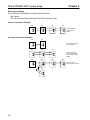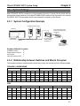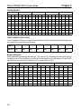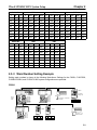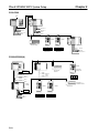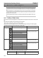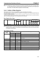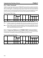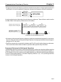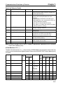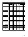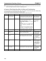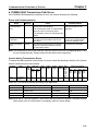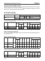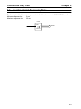
1
USER’S MANUAL 3G3IV-PSIG Wired SYSMAC BUS Interface Card for SYSDRIVE 3G3FV Inverter Notice: OMRON products are manufactured for use according to proper procedures by a qualified operator and only for the purposes described in this manual. The following conventions are used to indicate and classify precautions in this manual. Always heed the information provided with them. Failure to heed precautions can result in injury to people or damage to the product. ! DANGER Indicates information that, if not heeded, is likely to result in loss of life or serious injury. ! WARNING Indicates information that, if not heeded, could possibly result in loss of life or serious injury. ! Caution Indicates information that, if not heeded, could result in relatively serious or minor injury, damage to the product, or faulty operation. OMRON Product References All OMRON products are capitalized in this manual. The word “Unit” is also capitalized when it refers to an OMRON product, regardless of whether or not it appears in the proper name of the product. The abbreviation “Ch,” which appears in some displays and on some OMRON products, often means “word” and is abbreviated “Wd” in documentation in this sense. The abbreviation “PC” means Programmable Controller and is not used as an abbreviation for anything else. Visual Aids The following headings appear in the left column of the manual to help you locate different types of information. Note Indicates information of particular interest for efficient and convenient operation of the product. OMRON, 1997 $OO ULJKWV UHVHUYHG1 1R SDUW RI WKLV SXEOLFDWLRQ PD\ EH UHSURGXFHG/ VWRUHG LQ D UHWULHYDO V\VWHP/ RU WUDQVPLWWHG/ LQ DQ\ IRUP/ RU E\ DQ\ PHDQV/ PHFKDQLFDO/ HOHFWURQLF/ SKRWRFRS\LQJ/ UHFRUGLQJ/ RU RWKHUZLVH/ ZLWKRXW WKH SULRU ZULWWHQ SHUPLVVLRQ RI 205211 1R SDWHQW OLDELOLW\ LV DVVXPHG ZLWK UHVSHFW WR WKH XVH RI WKH LQIRUPDWLRQ FRQWDLQHG KHUHLQ1 0RUHRYHU/ EHFDXVH 20521 LV FRQVWDQWO\ VWULYLQJ WR LPSURYH LWV KLJK0TXDOLW\ SURGXFWV/ WKH LQIRUPDWLRQ FRQWDLQHG LQ WKLV PDQXDO LV VXEMHFW WR FKDQJH ZLWKRXW QRWLFH1 (YHU\ SUHFDXWLRQ KDV EHHQ WDNHQ LQ WKH SUHSDUDWLRQ RI WKLV PDQXDO1 1HYHU0 WKHOHVV/ 20521 DVVXPHV QR UHVSRQVLELOLW\ IRU HUURUV RU RPLVVLRQV1 1HLWKHU LV DQ\ OLDELOLW\ DVVXPHG IRU GDP0 DJHV UHVXOWLQJ IURP WKH XVH RI WKH LQIRUPDWLRQ FRQWDLQHG LQ WKLV SXEOLFDWLRQ1 Thank you for choosing the high-function, general-purpose SYSDRIVE 3G3FV-series Inverter and the dedicated 3G3IV-PSIG Interface Card. This manual provides information on the specifications and operation of the Interface Card used in the wired SYSMAC BUS system to exchange data between the Inverter and a SYSMAC Programmable Controller. Refer to the following manuals for the SYSDRIVE 3G3FV-series Inverter and SYSMAC BUS wired system in detail. : SYSDRIVE 3G3FV High-function General-purpose Inverter User’s Manual (I516-E1-P) : SYSMAC C-series Rack PCs Wired Remote I/O System Manual (W120-E1-P) NOTICE 1. This manual describes the functions of the product and relations with other products. You should assume that anything not described in this manual is not possible. 2. Although care has been given in documenting the product, please contact your OMRON representative if you have any suggestions on improving this manual. 3. The product contains potentially dangerous parts under the cover. Do not attempt to open the cover under any circumstances. Doing so may result in injury or death and may damage the product. Never attempt to repair or disassemble the product. 4. We recommend that you add the following precautions to any instruction manuals you prepare for the system into which the product is being installed. : Precautions on the dangers of high-voltage equipment. : Precautions on touching the terminals of the product even after power has been turned off. (These terminals are live even with the power turned off.) 5. Specifications and functions may be changed without notice in order to improve product performance. Items to Check when Unpacking Check the following items when removing the product from the package: : Has the correct product been delivered (i.e., the correct model number and specifications)? : Has the product been damaged in shipping? 7DEOH RI &RQWHQWV &KDSWHU 41 )HDWXUHV DQG 6\VWHP &RQILJXUDWLRQ1 1 1 1 1 1 1 1 1 1 1 1 1 1 1 1 1 1 404 404 )HDWXUHV 1 1 1 1 1 1 1 1 1 1 1 1 1 1 1 1 1 1 1 1 1 1 1 1 1 1 1 1 1 1 1 1 1 1 1 1 1 1 1 1 1 1 1 1 1 1 1 1 1 1 1 1 1 1 1 1 1 1 1 1 1 1 1 1 1 1 1 405 6\VWHP &RQILJXUDWLRQ 1 1 1 1 1 1 1 1 1 1 1 1 1 1 1 1 1 1 1 1 1 1 1 1 1 1 1 1 1 1 1 1 1 1 1 1 1 1 1 1 1 1 1 1 1 1 1 1 1 1 1 1 1 1 1 1 40504 6<60$& %86 :LUHG 6\VWHP 1 1 1 1 1 1 1 1 1 1 1 1 1 1 1 1 1 1 1 1 1 1 1 1 1 1 1 1 1 1 1 1 1 1 1 1 1 1 1 1 1 1 1 405 406 406 &KDSWHU 51 :LUHG 6<60$& %86 6\VWHP 6HWXS 1 1 1 1 1 1 1 1 1 1 1 1 1 1 1 1 1 504 504 1RPHQFODWXUH DQG 6HWWLQJV 1 1 1 1 1 1 1 1 1 1 1 1 1 1 1 1 1 1 1 1 1 1 1 1 1 1 1 1 1 1 1 1 1 1 1 1 1 1 1 1 1 1 1 1 1 1 1 1 1 1 1 1 505 505 ,QVWDOODWLRQ DQG :LULQJ 1 1 1 1 1 1 1 1 1 1 1 1 1 1 1 1 1 1 1 1 1 1 1 1 1 1 1 1 1 1 1 1 1 1 1 1 1 1 1 1 1 1 1 1 1 1 1 1 1 1 1 1 1 1 1 506 50504 0RXQWLQJ 3UHFDXWLRQV 1 1 1 1 1 1 1 1 1 1 1 1 1 1 1 1 1 1 1 1 1 1 1 1 1 1 1 1 1 1 1 1 1 1 1 1 1 1 1 1 1 1 1 1 1 1 1 1 1 1 506 50505 &RQQHFWLQJ DQG 6HWWLQJ 3UHFDXWLRQV 1 1 1 1 1 1 1 1 1 1 1 1 1 1 1 1 1 1 1 1 1 1 1 1 1 1 1 1 1 1 1 1 1 1 1 1 1 1 1 506 50506 0RXQWLQJ 3URFHGXUH 1 1 1 1 1 1 1 1 1 1 1 1 1 1 1 1 1 1 1 1 1 1 1 1 1 1 1 1 1 1 1 1 1 1 1 1 1 1 1 1 1 1 1 1 1 1 1 1 1 1 1 507 50507 ,QWHUQDO :LULQJ 1 1 1 1 1 1 1 1 1 1 1 1 1 1 1 1 1 1 1 1 1 1 1 1 1 1 1 1 1 1 1 1 1 1 1 1 1 1 1 1 1 1 1 1 1 1 1 1 1 1 1 1 1 1 1 508 50508 6\VWHP :LULQJ 1 1 1 1 1 1 1 1 1 1 1 1 1 1 1 1 1 1 1 1 1 1 1 1 1 1 1 1 1 1 1 1 1 1 1 1 1 1 1 1 1 1 1 1 1 1 1 1 1 1 1 1 1 1 1 1 508 506 6\VWHP 6HWWLQJV 1 1 1 1 1 1 1 1 1 1 1 1 1 1 1 1 1 1 1 1 1 1 1 1 1 1 1 1 1 1 1 1 1 1 1 1 1 1 1 1 1 1 1 1 1 1 1 1 1 1 1 1 1 1 1 1 1 1 1 1 1 50: 50604 6\VWHP &RQILJXUDWLRQ ([DPSOH 1 1 1 1 1 1 1 1 1 1 1 1 1 1 1 1 1 1 1 1 1 1 1 1 1 1 1 1 1 1 1 1 1 1 1 1 1 1 1 1 1 1 50: 50605 5HODWLRQVKLS EHWZHHQ 6ZLWFKHV DQG :RUGV 2FFXSLHG 1 1 1 1 1 1 1 1 1 1 1 1 1 1 1 1 1 1 1 1 1 1 1 1 1 50: 50606 :RUG 1XPEHU 6HWWLQJ ([DPSOH 1 1 1 1 1 1 1 1 1 1 1 1 1 1 1 1 1 1 1 1 1 1 1 1 1 1 1 1 1 1 1 1 1 1 1 1 1 1 1 1 1 1 50< 50607 6<6'5,9( 6HWWLQJV 1 1 1 1 1 1 1 1 1 1 1 1 1 1 1 1 1 1 1 1 1 1 1 1 1 1 1 1 1 1 1 1 1 1 1 1 1 1 1 1 1 1 1 1 1 1 1 1 1 1 1 5044 507 3RZHU 6XSSO\ 2SHUDWLRQ 3URFHGXUH 1 1 1 1 1 1 1 1 1 1 1 1 1 1 1 1 1 1 1 1 1 1 1 1 1 1 1 1 1 1 1 1 1 1 1 1 1 1 1 1 1 1 1 1 1 5046 &KDSWHU 61 &RPPXQLFDWLRQV )XQFWLRQV RI ,QYHUWHU1 1 1 1 1 1 1 1 1 1 1 1 1 1 1 604 604 6<6'5,9( &RPPXQLFDWLRQV 'DWD 1 1 1 1 1 1 1 1 1 1 1 1 1 1 1 1 1 1 1 1 1 1 1 1 1 1 1 1 1 1 1 1 1 1 1 1 1 1 1 1 1 1 1 1 1 1 60404 2XWOLQH RI 6<60$& %86 &RPPXQLFDWLRQV 'DWD 1 1 1 1 1 1 1 1 1 1 1 1 1 1 1 1 1 1 1 1 1 1 1 1 1 1 1 1 60405 %DVLF 6<60$& %86 &RPPXQLFDWLRQV 1 1 1 1 1 1 1 1 1 1 1 1 1 1 1 1 1 1 1 1 1 1 1 1 1 1 1 1 1 1 1 1 1 1 1 1 60406 :ULWLQJ 3DUDPHWHUV 1 1 1 1 1 1 1 1 1 1 1 1 1 1 1 1 1 1 1 1 1 1 1 1 1 1 1 1 1 1 1 1 1 1 1 1 1 1 1 1 1 1 1 1 1 1 1 1 1 1 1 1 60407 5HDGLQJ 3DUDPHWHUV 1 1 1 1 1 1 1 1 1 1 1 1 1 1 1 1 1 1 1 1 1 1 1 1 1 1 1 1 1 1 1 1 1 1 1 1 1 1 1 1 1 1 1 1 1 1 1 1 1 1 1 605 'DWD &RGHV DQG %DVH 5HJLVWHUV 1 1 1 1 1 1 1 1 1 1 1 1 1 1 1 1 1 1 1 1 1 1 1 1 1 1 1 1 1 1 1 1 1 1 1 1 1 1 1 1 1 1 1 1 1 1 1 1 1 60504 2XWOLQH RI 'DWD &RGHV 1 1 1 1 1 1 1 1 1 1 1 1 1 1 1 1 1 1 1 1 1 1 1 1 1 1 1 1 1 1 1 1 1 1 1 1 1 1 1 1 1 1 1 1 1 1 1 1 1 60505 2XWOLQH RI %DVH 5HJLVWHU 1 1 1 1 1 1 1 1 1 1 1 1 1 1 1 1 1 1 1 1 1 1 1 1 1 1 1 1 1 1 1 1 1 1 1 1 1 1 1 1 1 1 1 1 1 1 1 1 60506 (QWHU &RPPDQG 1 1 1 1 1 1 1 1 1 1 1 1 1 1 1 1 1 1 1 1 1 1 1 1 1 1 1 1 1 1 1 1 1 1 1 1 1 1 1 1 1 1 1 1 1 1 1 1 1 1 1 1 1 1 60507 )UHTXHQF\ 5HIHUHQFH LQ 6<60$& %86 &RPPXQLFDWLRQV 1 1 1 1 1 1 1 1 1 1 1 1 1 1 1 1 1 1 1 1 1 60508 ,QYHUWHU 0RQLWRULQJ 1 1 1 1 1 1 1 1 1 1 1 1 1 1 1 1 1 1 1 1 1 1 1 1 1 1 1 1 1 1 1 1 1 1 1 1 1 1 1 1 1 1 1 1 1 1 1 1 1 1 1 1 60509 6HWWLQJV LQ 0XOWL0IXQFWLRQ 2XWSXW DQG 0XOWL0IXQFWLRQ $QDORJ 2XWSXW 'DWD 1 1 1 1 1 1 1 1 6050: 8VHU &RQVWDQWV DQG 6HWWLQJV 1 1 1 1 1 1 1 1 1 1 1 1 1 1 1 1 1 1 1 1 1 1 1 1 1 1 1 1 1 1 1 1 1 1 1 1 1 1 1 1 1 1 1 1 1 6050; &RQVWDQWV 1 1 1 1 1 1 1 1 1 1 1 1 1 1 1 1 1 1 1 1 1 1 1 1 1 1 1 1 1 1 1 1 1 1 1 1 1 1 1 1 1 1 1 1 1 1 1 1 1 1 1 1 1 1 1 1 1 1 1 1 606 (UURUV LQ &RPPXQLFDWLRQV 1 1 1 1 1 1 1 1 1 1 1 1 1 1 1 1 1 1 1 1 1 1 1 1 1 1 1 1 1 1 1 1 1 1 1 1 1 1 1 1 1 1 1 1 1 1 1 1 1 1 1 1 1 605 605 606 609 60; 6043 6043 6044 6045 6045 6047 6055 6056 6057 606< &KDSWHU 71 &RPPXQLFDWLRQV 3URJUDP 1 1 1 1 1 1 1 1 1 1 1 1 1 1 1 1 1 1 1 1 1 1 1 1 1 704 704 705 706 707 708 )UHTXHQF\ 5HIHUHQFH 6HWWLQJV 1 1 1 1 1 1 1 1 1 1 1 1 1 1 1 1 1 1 1 1 1 1 1 1 1 1 1 1 1 1 1 1 1 1 1 1 1 1 1 1 1 1 1 1 1 1 1 1 1 1 705 ,QYHUWHU 0RQLWRU 1 1 1 1 1 1 1 1 1 1 1 1 1 1 1 1 1 1 1 1 1 1 1 1 1 1 1 1 1 1 1 1 1 1 1 1 1 1 1 1 1 1 1 1 1 1 1 1 1 1 1 1 1 1 1 1 1 1 1 1 1 709 ,QYHUWHU )DXOW 3URFHVVLQJ 1 1 1 1 1 1 1 1 1 1 1 1 1 1 1 1 1 1 1 1 1 1 1 1 1 1 1 1 1 1 1 1 1 1 1 1 1 1 1 1 1 1 1 1 1 1 1 1 1 1 1 1 1 1 7043 :ULWLQJ &RQVWDQWV 1 1 1 1 1 1 1 1 1 1 1 1 1 1 1 1 1 1 1 1 1 1 1 1 1 1 1 1 1 1 1 1 1 1 1 1 1 1 1 1 1 1 1 1 1 1 1 1 1 1 1 1 1 1 1 1 1 1 1 7048 5HDGLQJ &RQVWDQWV 1 1 1 1 1 1 1 1 1 1 1 1 1 1 1 1 1 1 1 1 1 1 1 1 1 1 1 1 1 1 1 1 1 1 1 1 1 1 1 1 1 1 1 1 1 1 1 1 1 1 1 1 1 1 1 1 1 1 1 7053 &KDSWHU 81 7UDQVPLVVLRQ 'HOD\ 7LPH 1 1 1 1 1 1 1 1 1 1 1 1 1 1 1 1 1 1 1 1 1 1 1 1 1 1 804 804 &RQILJXUDWLRQ ([DPSOH 1 1 1 1 1 1 1 1 1 1 1 1 1 1 1 1 1 1 1 1 1 1 1 1 1 1 1 1 1 1 1 1 1 1 1 1 1 1 1 1 1 1 1 1 1 1 1 1 1 1 1 1 1 1 1 805 ,QYHUWHU ,QWHUQDO 3URFHVVLQJ 7LPH 1 1 1 1 1 1 1 1 1 1 1 1 1 1 1 1 1 1 1 1 1 1 1 1 1 1 1 1 1 1 1 1 1 1 1 1 1 1 1 1 1 1 1 1 1 1 1 806 5HVSRQVH 7LPH IRU :LUHG 6<60$& %86 6\VWHP 1 1 1 1 1 1 1 1 1 1 1 1 1 1 1 1 1 1 1 1 1 1 1 1 1 1 1 1 1 1 1 1 1 1 805 806 807 7DEOH RI &RQWHQWV ,QGH[ 1 1 1 1 1 1 1 1 1 1 1 1 1 1 1 1 1 1 1 1 1 1 1 1 1 1 1 1 1 1 1 1 1 1 1 1 1 1 1 1 1 1 5HYLVLRQ +LVWRU\ 1 1 1 1 1 1 1 1 1 1 1 1 1 1 1 1 1 1 1 1 1 1 1 1 1 1 1 1 1 1 1 1 1 ,04 504 1 &KDSWHU 4 )HDWXUHV DQG 6\VWHP &RQILJXUDWLRQ 404 405 )HDWXUHV 6\VWHP &RQILJXUDWLRQ )HDWXUHV DQG 6\VWHP &RQILJXUDWLRQ Chapter 1 Abbreviations The following abbreviations are used in this manual. SYSDRIVE 3G3FV: SYSDRIVE 3G3FV-series High-function General-purpose Inverter PC: SYSMAC C/CV-series Programmable Controller (not including C-series models that cannot be linked with the SYSMAC BUS System) PSIG: 3G3IV-PSIG SYSMAC BUS (Wired) Interface Card 1-1 Features The 3G3IV-PSIG (for SYSMAC BUS) is a dedicated communications interface card which makes it possible for the SYSDRIVE 3G3FV to communicate with SYSMAC Programmable Controllers. Installing these interface cards in the SYSDRIVE 3G3FV permits a Programmable Controller to monitor RUN/ STOP and operating conditions, and to make changes in set values. 3G3IV-PSIG Wired SYSMAC BUS Interface Card Program-less Data Exchange Communications between a Programmable Controller and the SYSDRIVE 3G3FV take place within four words of the PC’s IR area, so no special communications program is required. For data communications to be executed automatically, it is only necessary to set the data and the codes for reading and writing in the fixed data area. Communications with SYSMAC C/CV-series PCs SYSMAC BUS Wired Remote I/O Systems can be used with either SYSMAC C-series or CV-series Programmable Controllers. C-series: C200H/HS, C200HX/HG/HE, C500, C1000H, and C2000H CV-series: CV500, CV1000, CV2000, and CVM1 Ample Functions • The Interface Card makes it possible to make use of all the functions of the Inverter through communications. • The ample monitoring capability of the Interface Card makes it possible to monitor the operating status and conditions of the Inverter including current, voltage, frequency, power conditions, and errors in detail through communications. 405 )HDWXUHV DQG 6\VWHP &RQILJXUDWLRQ 1-2 Chapter 1 System Configuration 1-2-1 SYSMAC BUS Wired System When a PSIG Interface Card is installed, the SYSDRIVE 3G3FV can communicate with Programmable Controllers through 2-wire cable. Master Programmable Controller (CPU Rack or Expansion I/O Rack) 2-conductor cable (total length 200 m) Programmable Terminal 3G3FV I/O Relay Terminal Valve wire-saving Sensor Controller device 3G3FV Number of Connectible Inverters SYSMAC CPU Rack Master No. of Inverters per Master No. of Inverters per CPU Rack SYSMAC BUS I/O points per CPU Rack C200H/HS C200HX/HG/HE C200H-RM201 8 max. (32 words) 8 max. 512 max. (32 words: 200 to 231) C500 C500-RM201 8 max. 512 max. (32 words) 32 max. (4 Masters) 2,048 max. (128 words) CV500 8 max. 512 max. (32 words) CV1000/2000 CVM1-CPU11-EV2 16 max. (2 Masters) 1,024 max. (64 words) CVM1-CPU21-EV2 32 max. (4 Masters) 2,048 max. (128 words) 8 max. (32 words) C1000H C2000H C2000 Note A single SYSDRIVE 3G3FV uses four words. Communications Specifications Item Specifications Transmission path 2-conductor cable (VCTF0.75 x 2C recommended) Transmission speed 187.5 kbps Transmission distance 200 m (total) Communications method Two-wire system, half duplex Synchronization method Start/stop synchronization 406 2 &KDSWHU 5 :LUHG 6<60$& %86 6\VWHP 6HWXS 504 505 506 507 1RPHQFODWXUH DQG 6HWWLQJV ,QVWDOODWLRQ DQG :LULQJ 6\VWHP 6HWWLQJV 3RZHU 6XSSO\ 2SHUDWLRQ 3URFHGXUH :LUHG 6<60$& %86 6\VWHP 6HWXS 2-1 Chapter 2 Nomenclature and Settings - Nomenclature Terminator switch 3G3IV-PSIG Wired SYSMAC BUS Interface Card + -- ON 1 2 3 Word address setting switch Operation indicator Terminator Switch OFF Note If the end terminator is not set or if two or more end terminators are provided, the Master will detect an “END RS” and will not operate. ON Other than terminator (termination resistance off) Terminator (termination resistance on) The terminator switch also serves as the termination resistance switch. Set this switch to ON for the Unit connected farthest in line from the Master. (The terminator switch is factory set to OFF.) Operation Indicators Display Function RUN (green) T/R ERR Transmitting/Error (red) Lit Lit when power is on and PC is in RUN or Monitor Mode. Not lit Transmission error or when PC is in Program Mode. Blinking Blinks during normal transmission. Lit Lit while waiting or at time of transmission error. Not lit Off at time of communications CPU Unit error (watchdog timer monitoring error). Word Number Setting Switch With the settings for switches 1 to 3, the SYSDRIVE 3G3FV will occupy four words (from n to n+3) as a Slave. Switch No. 1 (20) 2 (21) 3 Words occupied (22) n n+1 n+2 Switch No. n+3 1 (20) 2 (21) 3 Words occupied (22) n n+1 n+2 n+3 OFF OFF OFF 0 1 2 3 OFF OFF ON 16 17 18 19 ON OFF OFF 4 5 6 7 ON OFF ON 20 21 22 23 OFF ON OFF 8 9 10 11 OFF ON ON 24 25 26 27 ON ON OFF 12 13 14 15 ON ON ON 28 29 30 31 505 :LUHG 6<60$& %86 6\VWHP 6HWXS 2-2 Chapter 2 Installation and Wiring ! Caution When installing and wiring a SYSMAC BUS Interface Card, be sure to first turn off the power to the SYSDRIVE 3G3FV and wait for the CHARGE lamp to turn off. 2-2-1 Mounting Precautions ! WARNING Do not touch the internal parts of the Inverter, otherwise an electric shock may be received. ! WARNING Mount or dismount the Interface Card from the Inverter only after turning off the Inverter, checking that all the indicators of the Inverter are off, and the time specified on the front cover of the has Inverter elapsed, otherwise an electric shock may be received. ! WARNING Be sure that the cable is free from damage and excessive force, no heavy objects are placed on the cable, and that the cable is not seized by anything; otherwise an electric shock may be received. ! Caution Do not touch the parts of the Interface Card by hand; otherwise generated static electricity may damage the Interface Card. ! Caution Be sure that the connector of the Interface Card is securely connected to the Inverter. Improper connection may cause injury, product malfunction or product damage. 2-2-2 Connecting and Setting Precautions ! Caution Pay utmost attention when changing settings in the Inverter; otherwise injury or product damage may result. ! Caution Do not mount or dismount the Interface Card to or from the Inverter unless the Inverter is turned off; otherwise product damage may result. ! Caution The GND line of the Interface Card must be grounded; otherwise noise may be generated and product damage may result. 506 :LUHG 6<60$& %86 6\VWHP 6HWXS Chapter 2 2-2-3 Mounting Procedure 1. Turn off the Inverter, wait for at least one minute (or at least three minutes if the Inverter has an output capacity of 30 kW or more), remove the front cover of the Inverter, and check that the CHARGE indicator is not lit. 2. Mount the Interface Card to the option C area. 3. Insert the provided spacers into the spacer holes on the mounting base of the Inverter. 4. After properly engaging the connectors of the Interface Card and control circuit board, insert the spacers to the spacer holes of the Interface Card, and press the Interface Card until the spacers click. 5. Press the top of the connector 2CN and check that the apexes of the black triangular marks on the side match. 6. Connect the GND wire of the Interface Card to FG terminal 12 (E) on the control circuit board of the Inverter. Connector 4CN for option A area Make sure that the apexes of the black triangular marks match. Option A Connector 2CN for option C area Control circuit board Option C Connector 3CN for option D area Option D Front view Side View Note When the SYSMAC BUS Interface Card is mounted, other Optional Cards cannot be mounted in the C or D area. 507 :LUHG 6<60$& %86 6\VWHP 6HWXS Chapter 2 2-2-4 Internal Wiring Keep the SYSMAC BUS wiring separated from the main circuit wiring as much as possible. Do not wire them together. Side panel of Inverter SYSMAC BUS wiring Wired SYSMAC BUS Interface Card Operator Pass the SYSMAC BUS wiring by breaking off this portion. Main circuit wiring Control wiring Pass the SYSMAC BUS wiring through the casing by breaking open the side portion of the Inverter casing. 2-2-5 System Wiring When wiring a SYSMAC BUS Wired System, wire the Slaves in order from the Master of Programmable Controller with 2-conductor cable. Master Slave 3G3FV (-V1) CPU Rack or Expansion I/O Rack Terminator setting: OFF Slave + -- System END terminator: ON 3G3FV (-V1) + -- + -- Total length: 200 m max. Master 1. Use 0.75 mm2 x 2C VCTF (vinyl cabtire cable) for Wired SYSMAC BUS Systems. 2. When connecting terminals, be sure to connect plus to plus and minus to minus. 3. Wire the Slaves in order from the Master, and set the last one as the terminator. 4. The maximum overall cable length is 200 meters. 5. It is all right to mix ordinary I/O wiring with power lines, but do not place high-voltage lines or lines with strong current in close proximity to, or parallel with, the SYSDRIVE 3G3FV output wiring. Note Use shielded cable if transmission errors occur due to noise. It is recommended that the shield of the shielded cable be grounded at a single point on the Master side. 508 :LUHG 6<60$& %86 6\VWHP 6HWXS Chapter 2 Slave Connections Wire C500 and C200H Masters to Slaves as shown below. RM: Master RS: Slave or Slave Rack (including 3G3IV-PSIG Interface Card) Correct Connection Example RM + -- RS RS RS + + + -- -- -- Connect Slaves in order from the Master. Incorrect Connection Examples RM RS + + -- RS + -- RM Do not cross plus and minus terminals. -RM RS + + -- -- RS RS RS + + + -- -- -- + -- RS + -- 509 No more than one Slave can be directly connected to a single Master. There can be no branching from a Slave. :LUHG 6<60$& %86 6\VWHP 6HWXS 2-3 Chapter 2 System Settings Each SYSDRIVE 3G3FV occupies four Programmable Controller I/O words. Set the words with the word number setting switches on the Wired SYSMAC BUS Interface Card. Be careful not to overlap SYSDRIVE 3G3FV word numbers with the word numbers occupied by other Slaves. 2-3-1 System Configuration Example SYSDRIVE 3G3FV Inverter C200H PC G72C-OD16 (output type) or G72C-ID16 (input type) I/O Terminal RUN C200H Master C200H-RM201 SYSMAC BUS (Wired) Wd 200 to 203 Wd 204 to 207 Wd 212 NT-series Programmable Terminal Wd 208 to 211 Valve wire-saving device. Word 213 is the terminator. Number of Words Occupied SYSDRIVE 3G3FV: Programmable Terminal: I/O Terminal: Valve wire-saving device: 4 4 1 1 2-3-2 Relationship between Switches and Words Occupied The correlation between switches and the words they occupy are summarized in the following tables. C200H/HS, C200HX/HG/HE Switch No. 1 2 Words occupied 3 n n+1 n+2 Switch No. n+3 1 2 Words occupied 3 n n+1 n+2 n+3 OFF OFF OFF 200 201 202 203 OFF OFF ON 216 217 218 219 ON OFF OFF 204 205 206 207 ON OFF ON 220 221 222 223 OFF ON OFF 208 209 210 211 OFF ON ON 224 225 226 227 ON ON OFF 212 213 214 215 ON ON ON 228 229 230 231 C500 Switch No. 1 2 Words occupied 3 n n+1 n+2 Switch No. n+3 1 2 Words occupied 3 n n+1 n+2 n+3 OFF OFF OFF 0 1 2 3 OFF OFF ON 16 17 18 19 ON OFF OFF 4 5 6 7 ON OFF ON 20 21 22 23 OFF ON OFF 8 9 10 11 OFF ON ON 24 25 26 27 ON ON OFF 12 13 14 15 ON ON ON 28 29 30 31 50: :LUHG 6<60$& %86 6\VWHP 6HWXS Chapter 2 C1000H/C2000H Switch No. 1 2 Base No. 0 3 n Base No. 1 n+1 n+2 n+3 OFF OFF OFF 0 1 2 3 ON 5 6 OFF OFF 4 n Base No. 2 n+1 n+2 n+3 32 33 34 35 7 36 37 38 n Base No. 3 n n+1 n+2 n+3 n+1 n+2 n+3 64 65 66 67 96 97 98 99 39 68 69 70 71 100 101 102 103 OFF ON OFF 8 9 10 11 40 41 42 43 72 73 74 75 104 105 106 107 ON OFF 12 13 14 15 44 45 46 47 76 77 78 79 108 109 110 111 ON OFF OFF ON 16 17 18 19 48 49 50 51 80 81 82 83 112 113 114 115 ON 20 21 22 23 52 53 54 55 84 85 86 87 116 117 118 119 OFF ON OFF ON ON 24 25 26 27 56 57 58 59 88 89 90 91 120 121 122 123 ON ON 28 29 30 31 60 61 62 63 92 93 94 95 124 125 126 127 ON CVM1/CV500/CV1000/CV2000 In the SYSMAC BUS Remote I/O Relay Area, each Master (#0 to #7) is allocated 32 words, beginning with word 2300, as the default (initial value). Master address RM0 RM1 RM2 RM3 RM4 RM5 RM6 RM7 Words allocated 2300 to 2331 2332 to 2363 2364 to 2395 2396 to 2427 2428 to 2459 2460 to 2491 2492 to 2523 2524 to 2555 Master Addresses Master addresses are assigned automatically, in the order in which the Masters are mounted (including the setting order of Rack numbers), at the time of I/O table creation or I/O table editing. For the CV500, addresses are only allocated for Masters #0 to #3 (words 2300 to 2427). Switch No. RM0 1 2 3 OFF OFF ON n+1 n+2 n+3 OFF 2300 2301 2302 OFF OFF 2304 2305 OFF ON OFF ON ON OFF n RM2 n+1 n+2 n+3 2303 2332 2333 2334 2306 2307 2336 2337 2308 2309 2310 2311 OFF 2312 2313 2314 OFF ON 2316 2317 ON OFF ON OFF ON ON ON 50; n RM1 n n+1 n+2 n+3 2335 2364 2365 2366 2367 2338 2339 2368 2369 2370 2371 2340 2341 2342 2343 2372 2373 2374 2375 2315 2344 2345 2346 2347 2376 2377 2378 2379 2318 2319 2348 2349 2350 2351 2380 2381 2382 2383 2320 2321 2322 2323 2352 2353 2354 2355 2384 2385 2386 2387 ON 2324 2325 2326 2327 2356 2357 2358 2359 2388 2389 2390 2391 ON 2328 2329 2330 2331 2360 2361 2362 2363 2392 2393 2394 2395 :LUHG 6<60$& %86 6\VWHP 6HWXS Switch No. Chapter 2 RM3 1 2 3 OFF OFF ON n RM4 n+1 n+2 n+3 OFF 2396 2397 2398 OFF OFF 2400 2401 OFF ON OFF ON ON OFF n+1 n+2 n+3 n+1 n+2 n+3 2399 2428 2429 2430 2431 2460 2461 2462 2463 2402 2403 2432 2433 2434 2435 2464 2465 2466 2467 2404 2405 2406 2407 2436 2437 2438 2439 2468 2469 2470 2471 OFF 2408 2409 2410 2411 2440 2441 2442 2443 2472 2473 2474 2475 OFF ON 2412 2413 2414 2415 2444 2445 2446 2447 2476 2477 2478 2479 ON OFF ON 2416 2417 2418 2419 2448 2449 2450 2451 2480 2481 2482 2483 OFF ON ON 2420 2421 2422 2423 2452 2453 2454 2455 2484 2485 2486 2487 ON ON ON 2424 2425 2426 2427 2456 2457 2458 2459 2488 2489 2490 2491 Switch No. n RM5 RM6 1 2 3 OFF OFF ON n n RM7 n+1 n+2 n+3 OFF 2492 2493 2494 OFF OFF 2496 2497 OFF ON OFF ON ON OFF n n+1 n+2 n+3 2495 2524 2525 2526 2527 2498 2499 2528 2529 2530 2531 2500 2501 2502 2503 2532 2533 2534 2535 OFF 2504 2505 2506 2507 2536 2537 2538 2539 OFF ON 2508 2509 2510 2511 2540 2541 2542 2543 ON OFF ON 2512 2513 2514 2515 2544 2545 2546 2547 OFF ON ON 2516 2517 2518 2519 2548 2549 2550 2551 ON ON ON 2520 2521 2522 2523 2552 2553 2554 2555 2-3-3 Word Number Setting Example Setting word numbers is shown in the following illustrations. Settings for the C200H, C120/C500, C1000H/C2000H, and CV500/CV1000 system configurations are provided. C200H C200H CPU Rack Slave 3G3FV Terminator setting: ON I/O Terminal RT #0 I/O connecting cable Wd 007 Wd 006 Wd 005 RM #0 Wd 003 Wd 002 Wd 001 Wd 054 Wd 053 Wd 052 Wd 051 Wd 050 Set word 00 → Allocated word 200 1 2 3 ON OFF OFF Wd 204 to 207 Expansion I/O Rack 3G3FV 3G3FV I/O Terminal RM #1 Wd 013 Wd 012 Wd 011 Wd 010 Set word 31 → Allocated word 231 1 2 3 1 2 3 ON OFF ON OFF ON ON Wd 220 to 223 Wd 224 to 227 50< :LUHG 6<60$& %86 6\VWHP 6HWXS Chapter 2 C120/C500 RM RT #0 CPU Rack 16 pts. 32 pts. 64 pts. 16 pts. Slave Rack 32 pts. Wd 7 32 pts. Wd 5, 6 16 pts. Wd 1, to 4 16 pts. Wd 0 Wd 12, 13 Wd 10, 11 Wd 9 Wd 8 3G3FV 3G3FV I/O Terminal Word 23 setting Slave Rack RT #1 1 2 3 1 2 3 16 pts. OFF ON ON ON ON ON 16 pts. Wd 24 to 27 64 pts. Wd 28 to 31 Wd 19 Wd 18 Wd 14, to 17 C1000H/C2000(H) C1000H/C2000H/C2000 3G3FV RM 16 pts. 16 pts. 32 pts. 16 pts. 16 pts Base No. 0 Wd 5 32 pts. 16 pts. Wd 4 16 pts. 16 pts. 16 pts. 16 pts. 5043 Wd 8, 9 Wd 7 Wd 6 1 2 3 ON ON ON Wd 2, 3 Wd 28 to 31 Wd 1 Wd 0 Set word 31 → Allocated word 63 C500/ CV2000 RM Terminator setting: ON I/O Terminal Word 27 RT #0 3G3FV 3G3FV Base No. 1 Wd 12 Wd 11 Wd 10 1 2 3 1 2 3 ON OFF ON OFF ON ON Wd 52 to 55 Wd 56 to 59 I/O Terminal :LUHG 6<60$& %86 6\VWHP 6HWXS Chapter 2 CV500/CV1000 C500/CV1000 3G3FV RM 16 pts. 16 pts. 32 pts. 16 pts. 16 pts RM0 RT #0 Wd 5 Wd 4 Wd 2, 3 Terminator setting: ON I/O Terminal Word 2327 32 pts. 16 pts. Wd 2302, 2303 16 pts. Wd 2301 Wd 2300 Wd 1 1 2 3 ON ON ON Wd 2328 to 2331 Wd 0 3G3FV Terminator setting: ON 3G3FV I/O Terminal Word 2363 RM 16 pts. 16 pts. 16 pts. RM1 Wd 8 1 2 3 1 2 3 Wd 7 ON OFF ON OFF ON ON Wd 6 Wd 2352 to 2355 Wd 2356 to 2359 2-3-4 SYSDRIVE Settings Set the following constants according to the application before the Inverter is in SYSMAC BUS communications. Note Shaded part in the table indicates the default setting. 1 Frequency Reference Selection Constant No. B1-01 Content 0 1 D1-01 External terminals 2 3 Do not set (not used) Interface Card Frequency reference from D1-01 Frequency reference from external input Frequency reference from Optional Card (3G3IV-PSIG) REF indicator of Digital Operator Not lit Lit Lit Set the frequency reference 1 input method. • B1-01 = 0 Frequency reference 1 (D1-01) is enabled. Frequency reference 1 can be set to D1-01 through communications. • B1-01 = 1 Control circuit analog input terminal is enabled. Frequency reference 1 is not set through communications and D1-01 is disabled. 5044 :LUHG 6<60$& %86 6\VWHP 6HWXS Chapter 2 • B1-01 = 3 Frequency reference is set only through communications. (Data codes 65/E5 and 66/E6 are enabled. However, D1-01 is disabled.) • B1-01 = 2 Not used. Note This setting enables frequency reference 1 only. Frequency reference can be set for frequency references 2 to 8 through communications and Digital Operator without B1-01. 1 Inverter Run Command Selection Constant No. B1-02 Run Source Sel Sel. Content 0 1 Digital Operator External terminals 2 3 Do not set (not used) Communications Operation command from Digital Operator Operation command from external input Operation command through communications SEQ indicator of Digital Operator Not lit Lit Lit Select the Digital Operator, external input, or communications as the input means of operation commands. Relationship between B1-02 and Communications B1-02 constant Function FWD RUN/STOP (on: FWD RUN) REV RUN/STOP (on: REV RUN) Multi-function inputs 1 to 6 (see note) Read monitor (U1-01 to U1-28) Read constant Write constant 0 Disabled Disabled Enabled Enabled Enabled Enabled 1 Disabled Disabled Enabled Enabled Enabled Enabled 2 ------------- 3 Enabled Enabled Enabled Enabled Enabled Enabled Note There is a logical OR relationship between multi-function inputs 1 to 6 of communications and external inputs 3 to 8. 1 Operation Detected Communications Error This is a new constant for the SYSMAC BUS and “E-15 Det Sel” is displayed. Constant No. F8-01 0 1 2 3 Content Deceleration stop using C1-02 time Coast to stop Deceleration stop using C1-09 time Continue operation (see note) Inverter condition Error Error Error Minor error Fault output Yes Yes Yes No Take the appropriate action according to the application to remedy the error. Note When set to “Continue operation,” the Inverter itself will continue to operate. Therefore, provide other means such as a limit switch or emergency switch to secure safety. 5045 :LUHG 6<60$& %86 6\VWHP 6HWXS 2-4 Chapter 2 Power Supply Operation Procedure 1. Turn on the power to the SYSDRIVE 3G3FV and other Slaves. 2. Turn on the power at the CPU Rack where the Master is mounted. 3. Create the I/O table at the Programmable Controller. For C1000H and C2000(H) PCs, set the base numbers. 4. Confirming Data Reception and CALL Message After turning the Inverter on, transmit a data code other than “00” to the Inverter so that the Inverter can check the readiness of the transmission line and that of the host control equipment. The Inverter will continue to display the message “CALL” and the user will not be able to control the Inverter if no data code is transmitted. CALL Message After the Inverter is turned on, the Inverter waits for a data code other than “00” in order to prepare for proper communications with the host control equipment. During this period, the Inverter displays the message “CALL” and is on stand-by. Upon receipt of a data code other than “00”, the Inverter will automatically cancel the CALL status and the frequency reference will be displayed. Note 1. If any constant of the Inverter is changed from the Digital Operator, be sure to press the Menu Key and then the Enter Key to reset the Inverter to drive mode. The Inverter will not operate unless the Inverter is in Drive mode. Note 2. Creation of the I/O table or setting of the base numbers will become necessary only when the SYSMAC BUS system is used for the first time. 5046 3 &KDSWHU 6 &RPPXQLFDWLRQV )XQFWLRQV RI ,QYHUWHU 604 605 606 6<6'5,9( &RPPXQLFDWLRQV 'DWD 'DWD &RGHV DQG %DVH 5HJLVWHUV (UURUV LQ &RPPXQLFDWLRQV &RPPXQLFDWLRQV )XQFWLRQV RI ,QYHUWHU 3-1 Chapter 3 SYSDRIVE Communications Data The following provides information on data to be exchanged between the Inverter and SYSMAC Programmable Controller (PC). 3-1-1 Outline of SYSMAC BUS Communications Data 1 Words Occupied by the Inverter The Inverter as a Slave occupies four I/O words of the PC in the wired SYSMAC BUS system. I/O Output: PC C to Inverter n n+1 n+2 n+3 Input: Inverter to PC C Bit Word 15 to 8 Run command Write data Inverter status Read data 7 to 0 Data code Data code Note The word number setting switch of the Interface Card is used for setting words n through n+3. Refer to page 2-2, Word Number Setting Switch, for details. 1 Inverter Run Commands (PC to 3G3FV) By turning each bit of the allocated word of the PC on and off, each Run command of the Inverter can be transmitted. Word Wd n Bit 15 14 13 12 11 10 9 8 Multi-function input 6 Multi-function input 5 Multi-function input 4 Multi-function input 3 Multi-function input 2 Multi-function input 1 REV RUN/STOP FWD RUN/STOP Description (Default: Baseblock NO by H1-06) (see note 1) (Default: Jog frequency ref. by H1-05) (see note 1) (Default: Multi-step speed ref. 2 by H1-04) (see note 1) (Default: Multi-step speed ref. 1 by H1-03) (see note 1) (Default: Fault reset by H1-02) (see note 1) (Default: External fault by H1-01) (see note 1) 1: REV RUN 0: STOP (see note 2) 1: FWD RUN 0: STOP (see note 2) Note 1. There is an OR relationship between multi-function inputs 1 through 6 via the communications and external control terminals 3 though 8. Note 2. Settings in bits 9 and 8 will be valid if B1-02 for Run command selection is set to 3. 605 &RPPXQLFDWLRQV )XQFWLRQV RI ,QYHUWHU Chapter 3 1 Inverter Status (3G3FV to PC) Inverter status transmitted from the Inverter can be checked with the PC through the on/off condition of each allocated bit. Word Wd n+2 Bit 15 14 13 12 11 10 9 8 Multi-function output 2 Multi-function output 1 Multi-function contact output Data setting error Fault Inverter ready FWD/REV RUN RUN/STOP Description (Default: Desired freq. agree 1 by H2-03) (Default: Zero speed by H2-02) (Default: During RUN by H2-01) (ON: Data link status error) (see note 1) 1: Fault 0: Normal 1: Ready to operate 0: Not ready to operate (see note 2) 1: Forward operation 0: Reverse operation 1: Running 0: Not operating Note 1. A data setting error will result if one of data link status bits 1 thorough 5 is set to 1. Note 2. The Inverter is not ready to operate in the following cases. : The Inverter is in initial processing operation after the Inverter is turned ON. : The Inverter is set to program mode or any mode other than drive mode through the Digital Operator. : The Inverter is in receipt of a constant other than one that can be changed while the Inverter is in operation and the Inverter has not finished writing the constant internally with the Enter command. 3-1-2 Basic SYSMAC BUS Communications The Inverter’s Run command (i.e., eight leftmost bits of word n) and Inverter status (i.e., eight leftmost bits of word n+2) can be transmitted or received by turning each of these bits ON and OFF. The handshake procedure with data codes is, however, required for the transmission and reception of data, such as frequency references, and parameters. The following provides information on data codes and base registers as well as the handshake procedure used for the transmission and reception of data and parameters. 1 Data Codes A data code is used for writing and reading the data and parameter. The data code used depends on the type of data or parameter and whether such data or parameter is written or read. Example of C1-01 Acceleration Time 1 Constant C1-01 Name Acceleration Time 1 Setting g unit i 0.1 s Base regg i ister 03 Data code Reading 00 Writing 80 Register g number b 0200 Note 1. To set data in acceleration time 1, set the data code 80 in the eight rightmost bits of word n. Word number n n+1 15 to 8 7 to 0 XX 80 Data to be set 606 &RPPXQLFDWLRQV )XQFWLRQV RI ,QYHUWHU Chapter 3 Note 2. To read the data of acceleration time 1, set the data code 00. Note 3. Refer to 3-2 Data Codes and Base Registers for the data codes of other parameters. 1 Base Registers Data and parameters are classified into groups according to the function. The base register function makes it possible to select and set these groups. A parameter written or read with a data code will not be processed as desired if the base register is wrong. Before writing or reading a parameter, it is necessary to set the base register of the group to which the parameter belongs. Example of C1-01 Acceleration Time 1 Constant C1-01 Name Setting g unit i Acceleration Time 1 0.1 s Base regg i ister 03 Data code Reading 00 Writing 80 Register g number b 0200 Note 1. Acceleration time 1 belongs to group CP. The base register of group CP is 03. Note 2. To set the base register, use the write data code FE. Word number n n+1 15 to 8 7 to 0 XX FE 0003 Set the write data code in the eight rightmost bits. Set the base register number 0003. Note 3. Refer to 3-2 Data Codes and Base Registers for the data codes of other parameters. Note 4. No base register setting is required for writing or reading any frequency reference, frequency reference (substitute), or base register, and also not required for reading the data link status or writing the ENTER command. Note 5. If the parameter to be written or read belongs to the base register that has been set, there will be no need to set the base register again. 1 Handshake If data is written to I/O words n and n+1, the data will be transmitted to the Inverter through the SYSMAC BUS communications path. When the Inverter receives the data, the Inverter will return the same data to I/O words n+2 and n+3. The data code returned to the eight rightmost bits of word n+2 is the same as the data code written to the eight rightmost bits of word n. Therefore, by comparing these data codes, proper data transmission and reception can be confirmed. The data code set in word n is called the output data code and the data code returned to word n+2 is called the input data code. Write a sequence not to go to the next process until the input data code coincides with the output data code. Data Written from PC to Inverter I/O Output: PC C to Inverter Input: Inverter to PC C 607 Bit Word n n+1 n+2 n+3 15 to 8 Run command Write data Inverter status Read data 7 to 0 Data code Data code &RPPXQLFDWLRQV )XQFWLRQV RI ,QYHUWHU Chapter 3 Response from Inverter to PC I/O Output: PC C to Inverter Input: Inverter to PC C Bit Word 15 to 8 Run command Write data Inverter status Data received n n+1 n+2 n+3 7 to 0 Data code Data code 1 Writing/Reading Data Data items, such as parameter set values, are expressed in hexadecimal with a minimum setting unit of 1. Therefore, the following data conversion is required. - Conversion of Data to Be Written The set value divided by the minimum setting unit of the data must be set in hexadecimal. Example: 5.0 is set for C1-01 acceleration time 1 with a minimum setting unit of 0.1 s. 5.0 ÷ 0.1 = 50 → 0032 (hexadecimal) - Conversion of Data to Be Read The read value must be converted into a decimal value to be multiplied by the minimum setting unit of the data. Example: The read data of d1-01 frequency reference 1 with a minimum setting unit of 0.01 Hz is 1770 (hexadecimal). 1770 (hexadecimal) → 6000 × 0.01 = 60 Note If the set value is a negative value, the two’s complement must be taken. Example: --50% is set for d5-04 speed limit with a minimum setting unit of 1%. 50 to 0032 (hexadecimal): Convert 50 into a hexadecimal value. Add 1 after inverting each bit. Inversion 0 0 0 0 0 0 0 0 0 0 1 1 0 0 1 0 FFCD (hexadecimal) 1 1 1 1 1 1 1 1 1 1 0 0 1 1 0 1 Add 1. FFCE (hexadecimal) 1 1 1 1 1 1 1 1 1 1 0 0 1 1 1 0 --50% set. 608 &RPPXQLFDWLRQV )XQFWLRQV RI ,QYHUWHU Chapter 3 3-1-3 Writing Parameters To write a parameter from the SYSMAC PC to the Inverter, transmit corresponding data using the following three steps. 1. Transmit a corresponding base register. 2. Transmit the write data code of the parameter and the corresponding data to be written. 3. Transmit the Enter command. At each step, check that the output data code and input data code coincide with each other before going to the next step. 1 Parameter Writing Procedure 1. Base Register Setting a) Registers for parameters are classified into groups according to the function. Before setting a parameter, it is necessary to set the base register of the group to which the parameter belongs. b) The base register can be set by writing the data code FE and the base register value to words n and n+1 respectively. c) When the Inverter receives the data code FE, the same data code is returned to word n+2. d) Check that the output data code and input data code coincide with each other. 2. Data Setting a) Set the write data code of the parameter and the corresponding data to be written to word n and word n+1 respectively. The data to be written must be set in hexadecimal on condition that the minimum setting unit is 1. b) When the Inverter receives the data code and the data to be written, the Inverter returns the same data code and data to words n+2 and n+3. c) Check that the output data code and input data code coincide with each other. 3. Enter Command a) Set word n to the data code FD for the Enter command and word n+1 to 0000. b) When the Inverter receives the Enter command, the Inverter will return the data code FD to word n+2. c) Check that the output data code and input data code coincide with each other. 4. End Note 1. If the parameter to be written belongs to the base register that has been set, there will be no need to set the base register again. Note 2. The base register value will be set to 00 when the Inverter is turned ON. Therefore, a parameter can be written with no base register setting if the base register of the parameter is 00. Note 3. The Enter command must be transmitted whenever a parameter is written. The Inverter cannot use the parameter unless the Inverter receives the Enter command. An ENTFLAG error will result if the Inverter does not receive the Enter command within five seconds after receiving the last data item. If more than one parameter is written, the Enter command can be transmitted once after transmitting all the data codes and the corresponding data to be written. 609 &RPPXQLFDWLRQV )XQFWLRQV RI ,QYHUWHU Chapter 3 Example of Acceleration Time 1: V1-01 set to 5.0 s Constant C1-01 Name Setting g unit i Acceleration Time 1 0.1 s Base regg i ister 03 Data code Reading 00 Writing 80 Register g number b 0200 1. Set 03 in the base register. Word number n n+1 15 to 8 7 to 0 XX FE 0003 Set the write data code in the eight rightmost bits. Set the base register number 0003. 2. Response from Inverter. The data code received is returned to the eight rightmost bits. The set value is returned. Word number n+2 n+3 15 to 8 7 to 0 XX FE 0003 3. Acceleration Time 1: Set C1-01 to 5.0 s. Word number n n+1 15 to 8 7 to 0 XX 80 0032 Set the write data code in the eight rightmost bits. Set the writing data 0032. 5.0 s/0.1 s = 50 (32 hexadecimal) 4. Response from Inverter. The data code received is returned to the eight rightmost bits. The set value is returned. Word number n+2 n+3 15 to 8 7 to 0 XX 80 0032 5. Enter command transmission. Word number n n+1 15 to 8 7 to 0 XX FD 0000 Set the data code in the eight rightmost bits. Be sure to set 0000. Note An error will result if 0000 is not set. 6. Response from Inverter (data writing completion). The data code received is returned to the eight rightmost bits. The set value is returned. Word number n+2 n+3 15 to 8 7 to 0 XX FD 0000 60: &RPPXQLFDWLRQV )XQFWLRQV RI ,QYHUWHU Chapter 3 3-1-4 Reading Parameters To read a parameter from the Inverter, transmit data using the following two steps. 1. Transmit a corresponding base register. 2. Transmit the read data code of the parameter and receive the parameter value. At each step, check that the output data code and input data code coincide with each other before going to the next step. 1 Parameter Reading Procedure 1. Base Register Setting a) Registers for parameters are classified into groups according to the function. Before setting a parameter, it is necessary to set the base register of the group to which the parameter belongs. b) The base register can be set by writing the data code FE and the base register value to words n and n+1 respectively. c) When the Inverter receives the data code FE, the same data code will be returned to word n+2. d) Check that the output data code and input data code coincide with each other. 2. Parameter Setting a) Set the read data code of the parameter in word n. b) When the Inverter receives the read data code, the Inverter will return the same data code and reading data to words n+2 and n+3. c) Check that the output data code and input data code coincide with each other. 3. End Note 1. If the parameter to be read belongs to the base register that has been set, there will be no need to set the base register again. Note 2. The base register value will be set to 00 when the Inverter is turned ON. Therefore, a parameter can be read with no further base register setting if the base register of the parameter is 00. Example of Output Frequency: The data 60.0 Hz is read from U1-02. Constant U1-02 Name Frequency Reference Setting g unit i 0.01 Hz Base regg i ister 00 Data code Reading 21 Writing --- Register g number b 0021 1. Set 00 in the base register. Word number n n+1 15 to 8 7 to 0 XX FE 0000 Set the write data code in the eight rightmost bits. Set the base register number 0000. 2. Response from Inverter. The data code received is returned to the eight rightmost bits. The set value is returned. 60; Word number n+2 n+3 15 to 8 7 to 0 XX FE 0000 &RPPXQLFDWLRQV )XQFWLRQV RI ,QYHUWHU Chapter 3 3. Output Frequency: Read data from U1-02. Word number n n+1 15 to 8 7 to 0 XX 21 XXXX Set the write data code in the eight rightmost bits. 4. Response from Inverter. The data code received is returned to the eight rightmost bits. The set value is returned. Word number n+2 n+3 15 to 8 7 to 0 XX 21 1770 5. Hexadecimal Data Conversion 1770 Hex → 6,000 x 0.01 = 60.00 Hz 60< &RPPXQLFDWLRQV )XQFWLRQV RI ,QYHUWHU 3-2 Chapter 3 Data Codes and Base Registers The registers of the Inverter in communication with the PC are classified into groups according to the function and write and read data codes are set in each group independently. Before writing data to or reading data from the Inverter in communication, it is necessary to select the group with settings in the base register according to the data and the specified data code must be used. The following provides information on the data codes and the base register of the Inverter. 3-2-1 Outline of Data Codes Data codes are used for writing data to or reading data from the registers of the Inverter in communication. Data codes are classified into the following two main groups. • Data codes not affected by settings in the base register. • Data codes that select registers to write or read data according to settings in the base register. The following table provides brief information on data codes. Data code Reading g data 0 to 6 to 6 6 to 6 to 7 to Writing g data 8 to E to E E to F F to 0 Description Read data codes for each register g Influence of base register Registers g are selected according g to settings in the base register. Not used Frequency reference Frequency reference (substitute) Not used Data link status Not used Base register Not used Write data codes for each register g The data codes are not affected by settings in the base register. Not used Frequency reference Frequency reference (substitute) Not used Enter command (written to EEPROM) Base register Not used The data codes are not affected by settings in the base register. 3 5 6 9 E 0 Registers g are selected according g to settings in the base register. 3 5 6 D E Note 1. The MSB of a data code indicates data writing or reading. Bit No. Description 6043 07 0: Read 1: Write 06 to 00 A code indicating the register. &RPPXQLFDWLRQV )XQFWLRQV RI ,QYHUWHU Chapter 3 Note 2. The frequency reference and frequency reference (substitute) are written to the same register. The previous frequency reference data in the register is overwritten by new frequency reference data. Two data codes are prepared for data handling. 3-2-2 Outline of Base Register The registers of the Inverter are classified into groups according to the function. Before writing data to or reading data from a register, it is necessary to set in the base register the group to which the register belongs. The base register keeps the data unless the data is overwritten. Therefore, there is no need to write the data of the same group again until a new group must be selected. Base Register Data Codes Constant --- Name Base register Basic Register --- Data code Reading Writing 7E FE Setting unit 1 Setting range 00 to 09 Default setting 00 Control mode setting Changes during operation V/f control V/f with PG Open loop vector Flux vector Yes Yes Yes Yes Yes Note The base register is a dedicated register used for SYSMAC BUS communications, and the data setting of the base register is not possible with the Digital Operator. Be sure to set the base register through communications. Base Register Settings Base register g setting i 00 01 02 03 04 05 06 07 08 09 XX Data code Reading 00 to 0F 10 to 1F 20 to 3F 40 5F Writing 80 to 8F 90 to 9F A0 to BF C0 to DF 00 to 63 00 to 63 00 to 63 00 to 63 00 to 63 00 to 63 00 to 63 00 to 63 00 to 63 64 to 7F 80 to E3 80 to E3 80 to E3 80 to E3 80 to E3 80 to E3 80 to E3 80 to E3 80 to E3 E4 to FF Meaning g Command Status Monitor User constants (Constants set in A2-01 through A2-32 by the user). Environment setting constants: AX-XX Application constants: BX-XX Tuning constants: CX-XX Reference constants: DX-XX Motor constants: EX-XX Options constant: FX-XX Remote terminal function constants: HX-XX Protective function constants: LX-XX Operator constants: OX-XX Data codes not affected by settings in the base register. 6044 &RPPXQLFDWLRQV )XQFWLRQV RI ,QYHUWHU Chapter 3 3-2-3 Enter Command The Enter command instructs the Inverter in SYSMAC BUS communications to use data received from the PC as operation data. The transmission of the Enter command is not required by any frequency reference, base register, or command group of base register number 00. Be sure to transmit the Enter command, however, for any data that requires the Enter command. If more than one data item is written, the Enter command can be transmitted once at the end of the transmission of all data items. Enter Command Data Codes Constant --- Name Enter Command (Written to EEPROM) Base register --- Data code Reading Writing --- FD Setting unit --- Setting range 0000 Default setting --- Control mode setting Changes during operation V/f control V/f with PG Open loop vector Flux vector Yes Yes Yes Yes Yes Note 1. Be sure to set the writing data 0000 for the transmission of the Enter command. Note 2. The Enter command can be transmitted while the Inverter is running. An error, however, will result if the set data is a type of data that must not be transmitted while the Inverter is running. Note 3. When the Enter command is transmitted, the 3G3FV will write data to the EEPROM. Since the number of writing operations is limited to 100,000 times, it is recommended that the number of Enter command transmissions be minimized. 3-2-4 Frequency Reference in SYSMAC BUS Communications A frequency reference is used with the PC in SYSMAC BUS communications to set the output frequency of the Inverter. The frequency reference will be available only if B1-01 is set to 3. Frequency Reference Data Codes Constant Name Base register Data code Reading Writing --- Frequency Reference --- 65 E5 --- Frequency Reference (Sub) --- 66 E6 Setting unit 0.01 Hz ( (see note) Setting range 0.00 to max. fref quency Default setting Control mode setting Changes during operation V/f control V/f with PG Open loop vector Flux vector 0.00 Yes Yes Yes Yes Yes 0.00 Yes Yes Yes Yes Yes Note The setting unit of the frequency reference can be changed in o1-03. The default value is 0.01 Hz. 6045 &RPPXQLFDWLRQV )XQFWLRQV RI ,QYHUWHU Chapter 3 • A frequency reference and frequency reference (substitute) are written to a single register and there is no difference in function between the frequency reference and frequency reference (substitute). Data code 65 Reading data Writing data Data code E5 Data code 66 Data code E6 Reading data Writing data Frequency reference register for SYSMAC BUS communications A single register has two data codes to handle frequency references. There will be no need to use the two data codes if the frequency references are not handled. Frequency reference data code Frequency reference writing data “ E5 ” Frequency reference 10 Hz “ E6 ” Frequency reference 20 Hz “ E5 ” Frequency reference 30 Hz Transmission completion signal for data codes in conformity (Comparison signal, such as CMP) ... ... Time Note If there is only one data code, the frequency references can be handled only once. • A frequency reference and frequency reference (substitute) are dedicated registers for communications use. They cannot be set through the Digital Operator or analog input terminal unless changes in settings in B1-01 are made. • The Enter command is not required for the data code E5 or E6 used for writing frequency references. The Inverter takes these codes and data as operation data right after they are written. Frequency References for Multi-speed Operations The dedicated register of frequency references and frequency references (substitute) will be treated as frequency reference 1 if the Inverter is in multi-speed operation. Frequency references 2 through 8 (i.e., d1-02 through d1-08) of the Inverter in multi-speed operation are valid and work like those used by the Inverter in single-speed operation. The data in frequency reference 1 (i.e., d1-01) will be ignored if the Inverter is in multi-speed operation. 6046 &RPPXQLFDWLRQV )XQFWLRQV RI ,QYHUWHU Chapter 3 Frequency Reference Setting from Digital Operator (with B1-01 set to 0) Even if B1-01 is set to 0 in the Inverter controlled by the Digital Operator, the frequency reference control of the Inverter will be possible by setting frequency reference 1 (i.e., d1-01) to appropriate data through SYSMAC BUS communications. The transmission of the Enter command is required to write data in frequency reference 1 (i.e., d1-01). Constant d1-01 Name Frequency Reference 1 Base register 04 Data code Reading Writing 00 80 Setting unit 0.01 Hz (see note) Setting range 0.00 to max. frequency Default setting 6.00 Control mode setting Changes during operation V/f control V/f with PG Open loop vector Flux vector Yes Yes Yes Yes Yes Note 1. The setting unit of frequency references can be changed in o1-03. The default value is 0.01 Hz. Note 2. When frequently changing the frequency reference, it is recommended that the E5 frequency reference or E6 frequency reference (sub) be used. If “di-01”is changed, an Enter command will need to be transmitted. Since the Enter command is written to the EEPROM each time, repeated transmission of the Enter command will cause the EEPROM to reach its writing limit of 100,000 times. 3-2-5 Inverter Monitoring The Inverter has registers for a variety of monitor items, such as the Inverter’s SYSMAC BUS communications, I/O status, I/O data, and details of errors. Monitor them whenever required according to the application. - Data Link Status Monitor The data link status monitor is used for monitoring the condition of the SYSMAC BUS communications between the Inverter and PC, and also displays communications errors. Consta nt --- Name Data Link Status Base register --- Data code Reading data Writing data 69 --- Setting unit --- Setting range --- Control mode setting Defa ult setting Changes during operation V/f control --- Yes Yes V/f with PG Yes Open loop vector Flux vector Yes Yes Note The data link status is a dedicated monitor used for monitoring communications, which is not available to the Digital Operator except for displaying communications errors. 6047 &RPPXQLFDWLRQV )XQFWLRQV RI ,QYHUWHU Chapter 3 Data Link Status in Details Bit No. Name 0 During data write processing Display BUSY 1 Write Mode Error WRITE ERR 2 Data Code Error DADR ERR 3 Setting Range Error A DATA ERR 4 Setting Range Error B OPE ERR 5 EEPROM Write Error EEP ERR 6 Enter Command Not Received ENTFLAG 7 to 15 Not Used --- Description Turns ON by attempting to write the next data when the previous data, such as a constant, has not been processed yet. Turns ON by attempting to write data when the Inverter cannot accept the data due to the following: • Undervoltage is detected on the main circuit. • EEPROM failure has resulted with CPF03 detected (initialization possible). • The data is a write-prohibited constant. • The data is a constant that cannot be written while the Inverter is running. Turns ON if an unregistered data code for data writing or reading is received. Turns ON if writing data is received outside of the setting range. Turns ON if writing data causing one of the operational errors OPE01 through OPE11 (adjustment error) is received (see note). Turns ON if the EEPROM of the Inverter has an fault with CPF03 resulting. Turns ON if the Enter command is not received within 5 s after data is written. The data 0 is output. Note For OPE01 through OPE11, refer to Chapter 8 Maintenance Operations of the SYSDRIVE 3G3FV User’s Manual (I516). - Data Monitors: U1-PP The data of the data monitor U1-PP of the Inverter in SYSMAC BUS communications can be read. This monitor can be checked with the Digital Operator. Refer to the SYSDRIVE 3G3FV User’s Manual (I516) for details. Constant Name U1-01 Frequency Reference U1-02 Base register 00 Data code Reading Unit Writing Data reading during operation Control mode setting V/f control V/f with PG Open loop vector Flux vector 20 --- 0.01 Hz (set in o1-03) Yes Yes Yes Yes Yes Output Frequency 21 --- 0.01 Hz (set in o1-03) Yes Yes Yes Yes Yes U1-03 Output Current 22 --- 2000 hexadecimal (8192 decimal) Rated output current of Inverter Yes Yes Yes Yes Yes U1-04 Control Method 23 --- 1 (set in A1-02) Yes Yes Yes Yes Yes U1-05 Motor Speed 24 --- 0.01 Hz (set in o1-03) Yes No Yes Yes Yes U1-06 Output Voltage 25 --- 0.1 V Yes Yes Yes Yes Yes U1-07 Main Circuit DC Voltage 26 --- 1V Yes Yes Yes Yes Yes U1-08 Output Power 27 --- 0.1 kW Yes Yes Yes Yes Yes 6048 &RPPXQLFDWLRQV )XQFWLRQV RI ,QYHUWHU Constant Name U1-09 Torque Reference U1-10 U1-11 Base register 00 Chapter 3 Data code Reading Unit Writing Data reading during operation Control mode setting V/f control V/f with PG Open loop vector Flux vector 28 --- 0.1% (100%: Motor rated torque) Yes No No Yes Yes Input Terminal Status 29 --- See note 2 Yes Yes Yes Yes Yes Output Terminal Status 2A --- See note 3 Yes Yes Yes Yes Yes U1-12 Internal control status 2B --- See note 4 Yes Yes Yes Yes Yes U1-13 Elapsed Time 2C --- 1 hour Yes Yes Yes Yes Yes U1-14 FLASH ID Software No. 2D --- 1 Yes Yes Yes Yes Yes U1-15 Terminal 13 Level 2E --- 0.1% (100%: 10-V input) Yes Yes Yes Yes Yes U1-16 Terminal 14 Level 2F --- 0.1% (100%: 20-mA input) Yes Yes Yes Yes Yes U1-17 Terminal 16 Level 30 --- 0.1% (100%: 10-V input) Yes Yes Yes Yes Yes U1-18 Motor Secondary Current 31 --- 0.1% (100%: Motor rated current) Yes No No Yes Yes U1-19 Motor excitation current 32 --- 0.1% (100%: Motor rated current) Yes No No Yes Yes U1-20 Output Frequency After a Soft Start 33 --- 0.01 Hz (set in o1-03) Yes Yes Yes Yes Yes U1-21 Input to speed control loop 34 --- 0.01% (100%: Maximum frequency) Yes No Yes No Yes U1-22 Output from Speed Control Loop 35 --- 0.1% (100%: Motor rated current) Yes No Yes No Yes U1-23 Speed Deviation 36 --- 0.01% (100%: Maximum frequency) Yes No Yes No Yes U1-24 PID Feedback 37 --- 0.01% (100%: Maximum frequency) Yes Yes Yes Yes Yes U1-25 Command Value from 3G3VF-PDI16H2 38 --- Each corresponding bit displayed as it is. Yes Yes Yes Yes Yes U1-26 Voltage Reference for Secondary Current 39 --- 0.1 V Yes No No Yes Yes U1-27 Voltage Reference for Excitation Current 3A --- 0.1 V Yes No No Yes Yes U1-28 CPU ID 3B --- 1 Yes Yes Yes Yes Yes 6049 &RPPXQLFDWLRQV )XQFWLRQV RI ,QYHUWHU Chapter 3 Note 1. The transmission of the Enter command is not required to read the monitor data of the Inverter. Note 2. I/O Terminal Status Monitor: U1-10 Bit No. 0 1 2 3 4 5 6 7 8 to 15 Content FWD RUN/STOP (1: Input) REV RUN/STOP (1: Input) Multi-function input 1 (1: Input) Multi-function input 2 (1: Input) Multi-function input 3 (1: Input) Multi-function input 4 (1: Input) Multi-function input 5 (1: Input) Multi-function input 6 (1: Input) Not used Note 3. Output Terminal Status Monitor: U1-11 Bit No. 0 1 2 3 4 5 6 7 8 to 15 Content 1: Terminal 9 and 10 short 1: Terminal 25 and 27 short 1: Terminal 26 and 27 short Not used 1: Terminal 18 and 20 short Not used Note 4. Operating Status Monitor: U1-12 Bit No. 0 1 2 3 4 5 6 7 8 to 15 Content 1: During RUN 1: Zero speed FWD/REV RUN (ON: REV) 1: During fault reset input 1: Frequency agree 1 1: Operation ready 1: Minor fault 1: Fault Not used 604: &RPPXQLFDWLRQV )XQFWLRQV RI ,QYHUWHU Chapter 3 - Status Monitors A variety of status monitors are available to the Inverter in SYSMAC BUS communications, which make it possible to monitor the operation status of the Inverter, the status of the Digital Operator, and operation errors. Constant Name --- Inverter Status ----- Base register 00 Data code Reading Unit Writing Each bit allocation Control mode setting Data reading during operation V/f control V/f with PG Open loop vector Flux vector Yes Yes Yes Yes Yes 10 --- Operator Status 11 --- Yes Yes Yes Yes Yes Operator Error 12 --- OPE number Yes Yes Yes Yes Yes --- Fault 1 14 --- Each bit allocation Yes Yes Yes Yes Yes --- Fault 2 15 --- Yes Yes Yes Yes Yes --- Fault 3 16 --- Yes Yes Yes Yes Yes --- CPF Error 1 17 --- Yes Yes Yes Yes Yes --- CPF Error 2 18 --- Yes Yes Yes Yes Yes --- Minor Fault 1 19 --- Yes Yes Yes Yes Yes --- Minor Fault 2 1A --- Yes Yes Yes Yes Yes Inverter Status Bit No. 0 1 2 3 4 5 6 7 8 to 15 Content During RUN Zero speed FWD/REV RUN (ON: REV) During fault reset input Frequency agree 1 Operation ready Minor fault Fault Not used Operator Status Bit No. 0 1 2 3 4 5 6 7 8 to 15 604; Content 1: Operation error 1: EEPROM error 1: Program mode 00: Operator connecting g 11: Operator O disconnecting di i Not used &RPPXQLFDWLRQV )XQFWLRQV RI ,QYHUWHU Chapter 3 Fault 1 Bit No. 0 1 2 3 4 5 6 7 8 9 10 11 12 13 14 15 Display PUF UV1 UV2 UV3 SC GF OC OV OH OH1 OL1 OL2 OL3 OL4 RR RH Content Fuse open Undervoltage (main) Undervoltage (CTL) Undervoltage (MC) Short-circuit Ground fault Overcurrent Overvoltage Overheat Overheat 1 Motor overload Inverter overload Overtorque detection 1 Overtorque detection 2 Braking transistor Braking resistor Fault 2 Bit No. 0 1 2 3 4 5 6 7 8 9 10 11 12 13 14 15 Display EF3 EF4 EF5 EF6 EF7 EF8 --OS DEV PGO PF LF --OPR ERR --- Content External fault (3) External fault (4) External fault (5) External fault (6) External fault (7) External fault (8) Not used Overspeed Speed deviation PG is disconnected Input phase loss Output phase loss Not used OPE disconnected EEPROM error Not used 604< &RPPXQLFDWLRQV )XQFWLRQV RI ,QYHUWHU Chapter 3 Fault 3 Bit No. 0 1 2 3 4 5 6 7 8 9 10 11 12 13 14 15 Display ----E-15 E-10 ------------------------- Content Not used SYSMAC BUS communications error SYSMAC BUS card fault Not used CPF Error 1 Bit No. 0 1 2 3 4 5 6 7 Display ----CPF02 CPF03 CPF04 CPF05 CPF06 --- Content Not used Baseblock circuit error EEPROM error Internal A/D error External A/D error Option connect error Not used CPF Error 2 Bit No. 0 1 2 3 4 5 6 7 6053 Display CPF20 --------------- Content Optional Card A/D error Not used &RPPXQLFDWLRQV )XQFWLRQV RI ,QYHUWHU Chapter 3 Minor Fault 1 Bit No. 0 1 2 3 4 5 6 7 8 9 10 11 12 13 14 15 Display UV OV OH OH2 OL3 OL4 EF BB EF3 EF4 EF5 EF6 EF7 EF8 --OS Content Undervoltage (main) Overvoltage Overheat External overheat 2 Overtorque detection 1 Overtorque detection 2 ----External fault (3) External fault (4) External fault (5) External fault (6) External fault (7) External fault (8) Not used Overspeed Minor Fault 2 Bit No. 0 1 2 3 4 5 6 7 8 9 10 11 12 13 14 15 Display DEV PGO ----------------------------- Content Speed deviation PG is disconnected Not used 6054 &RPPXQLFDWLRQV )XQFWLRQV RI ,QYHUWHU Chapter 3 3-2-6 Settings in Multi-function Output and Multi-function Analog Output Data Controlling the status of the multi-function output and multi-function analog output of the Inverter in SYSMAC BUS communications is possible provided that 0F is set in H2-01 through H2-03 for multifunction output settings and 1F is set in H4-01 and H4-04 for multi-function analog output settings. Constant Name Base regisregis ter Data code Reading Setting method Writing Control mode setting Changes during operation Yes Yes V/f control V/f with PG Open loop vector Flux vector Yes Yes Yes 07 87 ±11 V = ±2D6 hexadecimal (±726 decimal) (see note 1, 3) Multi-function Analog Output 1 08 88 ±11 V = ±2D6 hexadecimal (±726 decimal) (see note 2, 3) Yes Yes Yes Yes Yes Multi-function Output 09 89 Allocated to each bit. (see note 3) Yes Yes Yes Yes Yes --- Multi-function Analog Output 1 --- --- 00 Note 1. These settings will be valid only if 1F is set in H4-01 for monitoring multi-function analog output 1 through terminal 21. Note 2. These settings will be valid only if 1F is set in H4-04 for monitoring multi-function analog output 2 through terminal 23. Note 3. For outputting negative values, set the H4-07 to “1”. Set the setting value to the complement of 2. Note 4. Settings are made with multi-function output. Bit No. 0 1 2 3 to 15 6055 Multi-function contact output: Terminals 9 and 10 (1: ON) Multi-function output 1: Terminal 25 (1: ON) Multi-function output 2: Terminal 26 (1: ON) Not used Content Valid if H2-01 is set to 0F. Valid if H2-02 is set to 0F. Valid if H2-03 is set to 0F. &RPPXQLFDWLRQV )XQFWLRQV RI ,QYHUWHU Chapter 3 3-2-7 User Constants and Settings The Inverter incorporates a user constant function, which makes it possible to simplify constant settings. A maximum of 32 user constants can be selected and allocated to base register 00. All these constants are allocated to base register 00, thus eliminating the necessity for setting the base register for each operation independently. User Constants Constant Name Data code Base regisi ter Reading Writing 01 06 86 Setting g unit it 1 Hex Setting g range 0100 to 050D Control mode setting Default setting tti Changes during operation Not set No Yes Yes Yes Yes V/f control V/f with PG Open loop vector Flux vector A2-01 Setting the User Constant 1 A2-02 Setting the User Constant 1 07 87 No Yes Yes Yes Yes A2-03 Setting the User Constant 1 08 88 No Yes Yes Yes Yes A2-04 Setting the User Constant 1 09 89 No Yes Yes Yes Yes A2-05 Setting the User Constant 1 0A 8A No Yes Yes Yes Yes A2-06 Setting the User Constant 1 0B 8B No Yes Yes Yes Yes A2-07 Setting the User Constant 1 0C 8C No Yes Yes Yes Yes A2-08 Setting the User Constant 1 0D 8D No Yes Yes Yes Yes A2-09 Setting the User Constant 1 E0 8E No Yes Yes Yes Yes A2-10 Setting the User Constant 1 0F 8F No Yes Yes Yes Yes A2-11 Setting the User Constant 1 10 90 No Yes Yes Yes Yes See note See note No Yes Yes Yes Yes to A2-31 Setting the User Constant 1 24 A4 No Yes Yes Yes Yes A2-32 Setting the User Constant 1 25 A5 No Yes Yes Yes Yes Note Write data and read data codes are allocated in hexadecimal in numerical order according to the constant number. • A2-01 through A2-32 are set to register numbers used for user constants. Refer to page 3-25 for the register number of each user constant. 6056 &RPPXQLFDWLRQV )XQFWLRQV RI ,QYHUWHU Chapter 3 Write Data and Read Data Codes for User Constants Constant Name --- User Constant 1 ----- Base register 00 Data code Reading Writing 40 C0 User Constant 2 41 C1 User Constant 3 42 C2 --- User Constant 4 43 C3 --- User Constant 5 44 C4 --- User Constant 6 45 C5 --- User Constant 7 46 C6 --- User Constant 8 47 C7 --- User Constant 9 48 C8 --- User Constant 10 49 C9 --- User Constant 11 4A CA See note See note to --- User Constant 31 5E DE --- User Constant 32 5F DF Setting unit Setting range Default setting Changes during operation The same as the constants set. Control mode setting V/f control V/f with PG Open loop vector Flux vector Note Write data and read data codes are set in hexadecimal and numerical order according to the constant number. 3-2-8 Constants Writing constants to and reading constants from the Inverter through SYSMAC BUS communications is possible. • After setting the base register, write constants to or read constants from the Inverter by using the corresponding data codes. • After the constants have been written, be sure to transmit the Enter command, otherwise an ENTFLAG error will result. If more than one data item is written, the Enter command can be transmitted once at the end of the transmission of all the data items. • There are constants that cannot be written while the Inverter is in operation. Before writing constants to the Inverter in operation, refer to the list on page 3-25 and make sure that the constants can be written to the Inverter during operation. Do not attempt to write improper constants to the Inverter during operation, otherwise a WRITE ERR will result. • There are constants that can be set subject to the A1-02 settings for control method selection. Refer to the list on page 3-25 for such constants. • Set the parameter setting value as a hexadecimal value in units of 1. If the setting value is negative, set to the complement of 2 (reverse the bit and add 1.) Note To initialize the Inverter, write the data of initialization (i.e., base register: 01, data code: 83, and data: 08AC) and transmit the Enter command. If the Enter command is written after transmitting other data, other data transmission will become invalid by initialization. 6057 &RPPXQLFDWLRQV )XQFWLRQV RI ,QYHUWHU Chapter 3 - Constants for Initialize Mode Constant Name Base register 01 Data code Register number Setting unit Setting range Default setting Control mode setting Changes during operation V/f control V/f with PG Open loop vector Flux vector Reading data Writing data 00 80 0100 1 0, 1 1 Yes Yes Yes Yes Yes A1-00 Display Language A1-01 Access Level 01 81 0101 1 0 to 4 2 Yes Yes Yes Yes Yes A1-02 Select Control Method 02 82 0102 1 0 to 3 2 No Yes Yes Yes Yes A1-03 Initialize 03 83 0103 1 0 to 3330 0 No Yes Yes Yes Yes A1-04 Password 04 84 0104 1 0 to 9999 0 No Yes Yes Yes Yes A1-05 Setting the Password 05 85 0105 1 0 to 9999 0 No Yes Yes Yes Yes Setting range Default setting Changes during operation V/f control V/f with PG Open loop vector Flux vector - Constants for Program Mode No need to change if the setting value is a hexadecimal value. Constant Name Base register 02 Data code Register number Setting unit Control mode setting Reading data Writing data 00 80 0180 1 0 to 3 1 No Yes Yes Yes Yes b1-01 Frequency Reference Selection b1-02 Run Source Selection 01 81 0181 1 0 to 3 1 No Yes Yes Yes Yes b1-03 Stopping Method Selection 02 82 0182 1 0 to 3 0 No Yes Yes Yes Yes b1-04 Disabling Reverse Operation 03 83 0183 1 0, 1 0 No Yes Yes Yes Yes b1-05 Operation Selection for Minimum Frequency (E1-09 or less) 04 84 0184 1 0 to 3 0 No No No No Yes b1-06 Setting Control Input Responsiveness 05 85 0185 1 0, 1 1 No Yes Yes Yes Yes b1-07 Operation Selection After Switching to Remote Mode 06 86 0186 1 0, 1 0 No Yes Yes Yes Yes b2-01 Excitation level (DC injection starting frequency) 07 87 0187 0.1 0.0 to 10.0 0.5 No Yes Yes Yes Yes b2-02 DC injection braking current 08 88 0188 1 0 to 100 50 No Yes Yes Yes No b2-03 DC injection braking time at start. 09 89 0189 0.01 0.00 to 10.00 0.00 No Yes Yes Yes Yes b2-04 DC injection braking time at stop. 0A 8A 018A 0.01 0.00 to 10.00 0.50 No Yes Yes Yes Yes b3-01 Speed search selection at start 0E 8E 018E 1 0, 1 0 (see note) No Yes Yes Yes Yes b3-02 Speed search operation current 0F 8F 018F 1 0 to 200 150 No Yes No Yes No 6058 &RPPXQLFDWLRQV )XQFWLRQV RI ,QYHUWHU Constant Name Base register 02 Data code Chapter 3 Setting unit Register number Setting range Default setting Changes during operation Control mode setting V/f control V/f with PG Open loop vector Flux vector Reading data Writing data 10 90 0190 0.1 0.0 to 10.0 2.0 No Yes No Yes No b3-03 Speed search deceleration time b4-01 Timer function ONdelay time 12 92 0192 0.1 0.0 to 300.0 0.0 No Yes Yes Yes Yes b4-02 Timer function OFF-delay time 13 93 0193 0.1 0.0 to 300.0 0.0 No Yes Yes Yes Yes b5-01 PID control selection 14 94 0194 1 0 to 2 0 No Yes Yes Yes Yes b5-02 Proportional gain (P) 15 95 0195 0.01 0.00 to 10.00 1.00 No Yes Yes Yes Yes b5-03 Integral time (I) 16 96 0196 0.1 0.0 to 360.0 1.0 No Yes Yes Yes Yes b5-04 Integral limit (I) 17 97 0197 0.1 0.0 to 100.0 100.0 No Yes Yes Yes Yes b5-05 Differential time (D) 18 98 0198 0.01 0.00 to 10.00 0.00 No Yes Yes Yes Yes b5-06 PID limit 19 99 0199 0.1 0.0 to 100.0 100.0 No Yes Yes Yes Yes b5-07 PID offset adjustment 1A 9A 019A 0.1 --100.0 to 100.0 0.0 No Yes Yes Yes Yes b5-08 PID primary delay time constant 1B 9B 019B 0.01 0.00 to 10.00 0.00 No Yes Yes Yes Yes b6-01 Dwell frequency at start 1C 9C 019C 0.1 0.0 to 400.0 0.0 No Yes Yes Yes Yes b6-02 Dwell time at start 1D 9D 019D 0.1 0.0 to 10.0 0.0 No Yes Yes Yes Yes b6-03 Dwell frequency at stop 1E 9E 019E 0.1 0.0 to 400.0 0.0 No Yes Yes Yes Yes b6-04 Dwell time at stop 1F 9F 019F 0.1 0.0 to 10.0 0.0 No Yes Yes Yes Yes b7-01 Droop control gain 20 A0 01A0 0.1 0.0 to 100.0 0.0 No No No No Yes b7-02 Droop control delay time 21 A1 01A1 0.01 0.00 to 1.00 0.00 No No No No Yes b8-01 Energy-saving gain 22 A2 01A2 1 0 to 100 80 No Yes Yes No No b8-02 Energy-saving frequency 23 A3 01A3 0.1 0.0 to 400.0 0.0 No Yes Yes No No b9-01 Zero-servo gain 24 A4 01A4 1 0 to 100 5 No No No No Yes b9-02 Zero-servo completion width 25 A5 01A5 1 0 to 16383 10 No No No No Yes Note When the control mode is changed, the Inverter will revert to default settings. (The open loop vector control default setting will be displayed.) 6059 &RPPXQLFDWLRQV )XQFWLRQV RI ,QYHUWHU Constant Name Base register 03 Data code Reading data Writing data Chapter 3 Register number Setting unit Setting range Default setting 0.1 ( (see note 1) 0.00 to 6000 0 6000.0 (see note 1) Control mode setting Changes during operation V/f control V/f with PG Open loop vector Flux vector 10.0 Yes Yes Yes Yes Yes 10.0 Yes Yes Yes Yes Yes C1-01 Acceleration time 1 00 80 0200 C1-02 Deceleration time 1 01 81 0201 C1-03 Acceleration time 2 02 82 0202 10.0 Yes Yes Yes Yes Yes C1-04 Deceleration time 2 03 83 0203 10.0 Yes Yes Yes Yes Yes C1-05 Acceleration time 3 04 84 0204 10.0 No Yes Yes Yes Yes C1-06 Deceleration time 3 05 85 0205 10.0 No Yes Yes Yes Yes C1-07 Acceleration time 4 06 86 0206 10.0 No Yes Yes Yes Yes C1-08 Deceleration time 4 07 87 0207 10.0 No Yes Yes Yes Yes C1-09 Emergency stop time 08 88 0208 10.0 Yes Yes Yes Yes Yes C1-10 Acceleration/deceleration time units 09 89 0209 1 0, 1 1 No Yes Yes Yes Yes C1-11 Acceleration/deceleration switching frequency 0A 8A 020A 0.1 0.0 to 400.0 0.0 No Yes Yes Yes Yes C2-01 S-curve characteristic time at acceleration start. 0B 8B 020B 0.01 0.00 to 2.50 0.20 No Yes Yes Yes Yes C2-02 S-curve characteristic time at acceleration end. 0C 8C 020C 0.01 0.00 to 2.50 0.20 No Yes Yes Yes Yes C2-03 S-curve characteristic time at deceleration start. 0D 8D 020D 0.01 0.00 to 2.50 0.20 No Yes Yes Yes Yes C2-04 S-curve characteristic time at deceleration end. 0E 8E 020E 0.01 0.00 to 2.50 0.00 No Yes Yes Yes Yes C3-01 Slip compensation gain. 0F 8F 020F 0.1 0.0 to 2.5 1.0 (see note 2) Yes Yes No Yes Yes C3-02 Slip compensation primary delay time. 10 90 0210 1 0 to 10000 200 (see note 2) No Yes No Yes No C3-03 Slip compensation limit. 11 91 0211 1 0 to 250 200 No Yes No Yes No C3-04 Slip compensation during regeneration. 12 92 0212 1 0, 1 0 No Yes Yes Yes No C3-05 Flux Calculation Method 42 C2 0242 1 0, 1 0 No No No Yes No Note 1. The setting range and setting unit for acceleration/deceleration times will differ according to the setting for C1-10 (the unit for acceleration/deceleration time). Note 2. When the control mode is changed, the Inverter will revert to default settings. (The open loop vector control default settings will be displayed.) 605: &RPPXQLFDWLRQV )XQFWLRQV RI ,QYHUWHU Constant Name Base register 03 Data code Chapter 3 Register number Setting unit Setting range Default setting Control mode setting Changes during operation V/f control V/f with PG Open loop vector Flux vector Reading data Writing data 13 93 0213 0.01 0.00 to 2.50 1.00 Yes Yes Yes Yes No C4-01 Torque compensation gain. C4-02 Torque compensation delay time. 14 94 0214 1 0 to 10000 20 (see note 1) No Yes Yes Yes No C5-01 ASR Proportional (P) gain 1 15 95 0215 0.01 0.00 to 300.00 20.0 (see note 2) Yes No Yes No Yes C5-02 ASR Integral (I) time 1 16 96 0216 0.001 0.000 to 10.000 0.500 (see note 2) Yes No Yes No Yes C5-03 ASR Proportional Gain (P) 2 17 97 0217 0.01 0.00 to 300.00 20.0 (see note 2) Yes No Yes No Yes C5-04 ASR Integral (I) time 2 18 98 0218 0.001 0.000 to 10.000 0.500 (see note 2) Yes No Yes No Yes C5-05 ASR Limit 19 99 0219 0.1 0.0 to 20.0 5.0 No No Yes No No C5-06 ASR Primary delay time 1A 9A 021A 0.001 0.000 to 0.500 0.004 No No No No Yes C5-07 ASR Switching frequency 1B 9B 021B 0.1 0.0 to 400.0 0.0 No No No No Yes C5-08 ASR Integral (I) Limit 41 C1 0241 1 0 to 400 400 No No No No Yes C6-01 Carrier frequency upper limit. 1C 9C 021C 0.1 2.0 to 15.0 (see note 3) 15.0 (see note 3) No Yes Yes Yes Yes C6-02 Carrier frequency lower limit. 1D 9D 021D 0.1 0.4 to 15.0 15.0 (see note 3) No Yes Yes No No C6-03 Carrier frequency proportional gain. 1E 9E 021E 1 0 to 99 0 No Yes Yes No No C7-01 Hunting prevention selection 1F 9F 021F 1 0, 1 1 No Yes Yes No No C7-02 Hunting prevention gain 20 A0 0220 0.01 0.00 to 2.50 1.00 No Yes Yes No No C8-08 AFR Gain 2A AA 022A 0.01 0.00 to 10.00 1.00 No No No Yes No C8-30 Carrier Frequency Selection During Auto-tuning 40 C0 0240 1 0, 1 0 No No No Yes Yes Note 1. When the control mode is changed, the Inverter will revert to default settings. (The open loop vector control default settings will be displayed.) Note 2. When the control mode is changed, the Inverter will revert to default settings. (The flux vector control default settings will be displayed.) Note 3. The setting range and the default setting of the Inverter will differ depending on its capacity and control mode. (The value for the 200-V-class 0.4 kW Inverter in open loop vector control mode will be displayed.) 605; &RPPXQLFDWLRQV )XQFWLRQV RI ,QYHUWHU Constant Name Base register 04 Data code Chapter 3 Register number Reading data Writing data 00 80 0280 Setting unit 0.01 ((see note) t ) Setting range Default setting Control mode setting Changes during operation V/f control V/f with PG Open loop vector Flux vector Yes Yes Yes Yes Yes Yes Yes Yes Yes Yes Yes Yes Yes Yes Yes d1-01 Frequency reference 1 d1-02 Frequency reference 2 01 81 0281 d1-03 Frequency reference 3 02 82 0282 0.00 to 6.00 max. f fre0.00 quency (see 0.00 note) d1-04 Frequency reference 4 03 83 0283 0.00 Yes Yes Yes Yes Yes d1-05 Frequency reference 5 04 84 0284 0.00 Yes Yes Yes Yes Yes d1-06 Frequency reference 6 05 85 0285 0.00 Yes Yes Yes Yes Yes d1-07 Frequency reference 7 06 86 0286 0.00 Yes Yes Yes Yes Yes d1-08 Frequency reference 8 07 87 0287 0.00 Yes Yes Yes Yes Yes d1-09 Jog frequency reference 08 88 0288 6.00 Yes Yes Yes Yes Yes d2-01 Reference frequency upper limit 09 89 0289 0.1 0.0 to 110.0 100.0 No Yes Yes Yes Yes d2-02 Reference frequency lower limit 0A 8A 028A 0.1 0.0 to 109.0 0.0 No Yes Yes Yes Yes d3-01 Jump frequency 1 0B 8B 028B 0.1 0.0 to 400.0 0.0 No Yes Yes Yes Yes d3-02 Jump frequency 2 0C 8C 028C 0.1 0.0 to 400.0 0.0 No Yes Yes Yes Yes d3-03 Jump frequency 3 0D 8D 028D 0.1 0.0 to 400.0 0.0 No Yes Yes Yes Yes d3-04 Jump frequency width 0E 8E 028E 0.1 0.0 to 20.0 1.0 No Yes Yes Yes Yes d4-01 Reference frequency hold function selection 0F 8F 028F 1 0, 1 0 No Yes Yes Yes Yes d4-02 Trim control level 10 90 0290 1 0 to 100 25 No Yes Yes Yes Yes d5-01 Torque control selection 11 91 0291 1 0, 1 0 No No No No Yes d5-02 Torque reference delay time 12 92 0292 1 0 to 1000 0 No No No No Yes d5-03 Speed limit selection 13 93 0293 1 1, 2 1 No No No No Yes d5-04 Speed limit 14 94 0294 1 --120 to +120 0 No No No No Yes d5-05 Speed limit bias 15 95 0295 1 0 to 120 10 No No No No Yes d5-06 Speed/torque control switching timer. 16 96 0296 1 0 to 1000 0 No No No No Yes Note The setting unit and setting range of the frequency reference can be changed using O1-03 (frequency reference setting and display units). Refer to the default setting of O1-03. 605< &RPPXQLFDWLRQV )XQFWLRQV RI ,QYHUWHU Constant Name Base register 05 Data code Chapter 3 Register number Setting unit Setting range Default setting Control mode setting Changes during operation V/f control V/f with PG Open loop vector Flux vector Reading data Writing data 00 80 0300 1 155 to 255 (see note 1) 200 (see note 1) No Yes Yes Yes Yes E1-01 Input voltage setting E1-02 Motor selection 01 81 0301 1 0, 1 0 No Yes Yes Yes Yes E1-03 V/f pattern selection 02 82 0302 Hexadecimal 0 to F F No Yes Yes No No E1-04 Maximum frequency (FMAX) 03 83 0303 0.1 50.0 to 400.0 60.0 No Yes Yes Yes Yes E1-05 Maximum voltage (VMAX) 04 84 0304 0.1 0.0 to 255.0 (see note 1) 200.0 (see note 1) No Yes Yes Yes Yes E1-06 Maximum voltage frequency (FA) 05 85 0305 0.1 0.0 to 400.0 60.0 No Yes Yes Yes Yes E1-07 Intermediate frequency (FB) 06 86 0306 0.1 0.0 to 400.0 3.0 (see note 2) No Yes Yes Yes No E1-08 Intermediate voltage (VC) 07 87 0307 0.1 0.0 to 255.0 (see note 1) 11.0 (see note 1, 2) No Yes Yes Yes No E1-09 Minimum frequency (FMIN) 08 88 0308 0.1 0.0 to 400.0 0.5 (see note 2) No Yes Yes Yes Yes E1-10 Minimum voltage (VMIN) 09 89 0309 0.1 0.0 to 255.0 (see note 1) 2.0 (see note 1, 2) No Yes Yes Yes No E1-11 Mid. Output Frequency B 0A 8A 030A 0.1 0.0 to 400.0 0.0 No Yes Yes Yes Yes E1-12 Mid. Output Frequency Voltage B 0B 8B 030B 0.1 0.0 to 255.0 (see note 1) 0.0 No Yes Yes Yes Yes E1-13 Base Voltage 0C 8C 030C 0.1 0.0 to 255.0 (see note 1) 200.0 (see note 1) No Yes Yes Yes Yes Note 1. These are values for a 200-V-class Inverter. Values for the 400-V-class Inverter are double. Note 2. When the control mode is changed, the Inverter will revert to default settings. (The open loop vector control default settings will be displayed.) 6063 &RPPXQLFDWLRQV )XQFWLRQV RI ,QYHUWHU Constant Name Base register 05 Data code Chapter 3 Register number Setting unit Setting range Default setting Control mode setting Changes during operation V/f control V/f with PG Open loop vector Flux vector Reading data Writing data 0E 8E 030E 0.01 (see note 1) 0.32 to 6.40 (see note 2) 1.90 (see note 3) No Yes Yes Yes Yes E2-01 Motor rated current E2-02 Motor rated slip 0F 8F 030F 0.01 0.00 to 20.00 2.90 (see note 3) No Yes Yes Yes Yes E2-03 Motor no-load current 10 90 0310 0.01 (see note 1) 0.32 to 6.40 (see note 2) 1.20 (see note 3) No Yes Yes Yes Yes E2-04 Number of motor poles 11 91 0311 1 2 to 48 4 No No Yes No Yes E2-05 Motor phase-tophase resistance 12 92 0312 0.001 0.000 to 65.000 9.842 (see note 3) No Yes Yes Yes Yes E2-06 Motor leakage inductance 13 93 0313 0.1 0.0 to 30.0 18.2 (see note 3) No No No Yes Yes E2-07 Motor iron-core saturation coefficient 1 14 94 0314 0.01 0.00 to 0.50 0.50 No No No Yes Yes E2-08 Motor iron-core saturation coefficient 2 15 95 0315 0.01 0.00 to 0.75 0.75 No No No Yes Yes E2-09 Mechanical loss 16 96 0316 0.1 0.0 to 10.0 0.0 No No No No Yes Note 1. Units of 0.01 A are used for a capacity of 7.5 kW or below and units of 0.1 A are used for a capacity of 11 kW or over. Note 2. The setting range is 10% to 200% of the Inverter’s rated output current. The values for a 200-V-class 0.4 kW Inverter will be displayed. Note 3. The default setting depends upon the type of Inverter. The value for a 200-V-class 0.4 kW Inverter will be displayed. 6064 &RPPXQLFDWLRQV )XQFWLRQV RI ,QYHUWHU Constant Name Base register 05 Data code Chapter 3 Register n mnumber Setting unit nit Setting range Default setting Reading data Writing data 17 97 0317 1 0, 2 2 Changes d rduring operation Control mode setting (see note 4) V/f control V/f with PG Open loop vector Flux vector No Yes Yes Yes Yes E3-01 Select control method of motor 2 E4-01 Motor 2 maximum frequency 18 98 0318 0.1 40.0 to 400.0 60.0 No Yes No Yes No E4-02 Motor 2 maximum voltage 19 99 0319 0.1 0.0 to 255.0 (see note 1) 200.0 (see note 1) No Yes No Yes No E4-03 Motor 2 maximum voltage frequency 1A 9A 031A 0.1 0.0 to 400.0 60.0 No Yes No Yes No E4-04 Motor 2 intermediate frequency 1B 9B 031B 0.1 0.0 to 400.0 3.0 (see note 2) No Yes No Yes No E4-05 Motor 2 intermediate voltage 1C 9C 031C 0.1 0.0 to 255.0 (see note 1) 11.0 (see note 1, 2) No Yes No Yes No E4-06 Motor 2 minimum frequency 1D 9D 031D 0.1 0.0 to 400.0 0.5 (see note 2) No Yes No Yes No E4-07 Motor 2 minimum voltage 1E 9E 031E 0.1 0.0 to 255.0 (see note 1) 2.0 (see note 1, 2) No Yes No Yes No E5-01 Motor 2 rated current 1F 9F 031F 0.01 (see note 5) 0.32 to 6.40 (see note 6) 1.90 (see note 3) No Yes No Yes No E5-02 Motor 2 rated slip 20 A0 0320 0.01 0.00 to 20.00 2.90 (see note 3) No Yes No Yes No E5-03 Motor 2 no-load current 21 A1 0321 0.01 (see note 5) 0.32 to 6.40 (see note 6) 1.20 (see note 3) No Yes No Yes No E5-04 Motor 2 number of motor poles 22 A2 0322 1 2 to 48 4 No Yes No Yes No E5-05 Motor 2 phase-tophase resistance 23 A3 0323 0.001 0.000 to 65.000 9.842 (see note 3) No Yes No Yes No E5-06 Motor 2 leakage inductance 24 A4 0324 0.1 0.0 to 30.0 18.2 (see note 3) No Yes No Yes No Note 1. These are values for a 200-V-class Inverter. Values for the 400-V-class Inverter are double. Note 2. When the control mode is changed, the Inverter will revert to default settings. (The open loop vector control default settings will be displayed.) Note 3. The default setting depends upon the type of Inverter. The value for a 200-V-class 0.4 kW Inverter will be displayed. Note 4. Settings for E4-01 to E5-06 depend on the control mode settings for E3-01. Note 5. Units of 0.01 A are used for a capacity of 7.5 kW or below and units of 0.1 A are used for a capacity of 11 kW or over. Note 6. The setting range is 10% to 200% of the Inverter’s rated output current. The values for a 200-V-class 0.4 kW Inverter will be displayed. 6065 &RPPXQLFDWLRQV )XQFWLRQV RI ,QYHUWHU Constant Name Base register 06 Data code Chapter 3 Register number Setting unit Setting range Default setting Control mode setting Changes during operation V/f control V/f with PG Open loop vector Flux vector Reading data Writing data 00 80 0380 1 0 to 60000 1000 No No Yes No Yes F1-01 Number of PG pulses F1-02 PG disconnection stopping method (PGO) 01 81 0381 1 0 to 3 1 No No Yes No Yes F1-03 PG overspeed stopping method 02 82 0382 1 0 to 3 1 No No Yes No Yes F1-04 PG speed deviation stopping method 03 83 0383 1 0 to 3 3 No No Yes No Yes F1-05 PG rotation setting 04 84 0384 1 0, 1 0 No No Yes No Yes F1-06 PG output ratio 05 85 0385 1 1 to 132 1 No No Yes No Yes F1-07 Selecting integral control during accel/decel. 06 86 0386 1 0, 1 0 No No Yes No No F1-08 Overspeed (OS) detection level. 07 87 0387 1 0 to 120 115 No No Yes No Yes F1-09 Overspeed (OS) detection time 08 88 0388 0.1 0.0 to 2.0 0.0 (see note) No No Yes No Yes F1-10 PG speed deviation detection level (DEV) 09 89 0389 1 0 to 50 10 No No Yes No Yes F1-11 PG speed deviation detection time (DEV) 0A 8A 038A 0.1 0.0 to 10.0 0.5 No No Yes No Yes F1-12 Number of PG gear teeth 1 0B 8B 038B 1 0 to 1000 0 No No Yes No No F1-13 Number of PG gear teeth 2 0C 8C 038C 1 0 to 1000 0 No No Yes No No F1-14 PG Disconnection Detection Time 17 97 0397 0.1 0.0 to 10.0 2.0 No No Yes No Yes F2-01 Analog Reference Card selection 0D 8D 038D 1 0, 1 0 No Yes Yes Yes Yes F3-01 Digital Reference Card input selection 0E 8E 038E 1 0 to 7 0 No Yes Yes Yes Yes F4-01 Channel 1 output monitor selection 0F 8F 038F 1 1 to 31 2 No Yes Yes Yes Yes F4-02 Channel 1 gain 10 90 0390 0.01 0.00 to 2.50 1.00 Yes Yes Yes Yes Yes F4-03 Channel 2 output monitor selection 11 91 0391 1 1 to 31 3 No Yes Yes Yes Yes F4-04 Channel 2 gain 12 92 0392 0.01 0.00 to 2.50 0.50 Yes Yes Yes Yes Yes F5-01 Not used 13 93 0393 1 --- 0 --- --- --- --- --- F5-02 Not used 14 94 0394 1 --- 1 --- --- --- --- --- Note When the control mode is changed, the Inverter will revert to default settings. (The flux vector control default settings will be displayed.) 6066 &RPPXQLFDWLRQV )XQFWLRQV RI ,QYHUWHU Constant Name Base register 06 Data code Reading data Writing data Chapter 3 Register number Setting unit Setting range Default setting Control mode setting Changes during operation V/f control V/f with PG Open loop vector Flux vector F6-01 Not used 15 95 0395 1 --- 0 --- --- --- --- --- F7-01 Output pulse multiple selection 16 96 0396 1 0 to 4 1 No Yes Yes Yes Yes F8-01 Not used 18 98 0398 1 0 to 3 1 No Yes Yes Yes Yes F9-01 Not used 19 99 0399 1 --- 0 --- --- --- --- --- F9-02 Not used 1A 9A 039A 1 --- 0 --- --- --- --- --- F9-03 Not used 1B 9B 039B 1 --- 1 --- --- --- --- --- F9-04 Not used 1C 9C 039C 1 --- 0 --- --- --- --- --- 00 80 0400 Hexadecimal 0 to 77 24 No Yes Yes Yes Yes 07 H1-01 Multi-function input 1: Terminal 3 selection H1-02 Multi-function input 2: Terminal 4 selection 01 81 0401 Hexadecimal 0 to 77 14 No Yes Yes Yes Yes H1-03 Multi-function input 3: Terminal 5 selection 02 82 0402 Hexadecimal 0 to 77 3 (0) (see note) No Yes Yes Yes Yes H1-04 Multi-function input 4: Terminal 6 selection 03 83 0403 Hexadecimal 0 to 77 4 (3) (see note) No Yes Yes Yes Yes H1-05 Multi-function input 5: Terminal 7 selection 04 84 0404 Hexadecimal 0 to 77 6 (4) (see note) No Yes Yes Yes Yes H1-06 Multi-function input 6: Terminal 8 selection 05 85 0405 Hexadecimal 0 to 77 8 (6) (see note) No Yes Yes Yes Yes H2-01 Multi-function contact output: terminal 9 to 10. 06 86 0406 Hexadecimal 0 to 37 0 No Yes Yes Yes Yes H2-02 Multi-function output 1: terminal 25. 07 87 0407 Hexadecimal 0 to 37 1 No Yes Yes Yes Yes H2-03 Multi-function output 2: terminal 26. 08 88 0408 Hexadecimal 0 to 37 2 No Yes Yes Yes Yes H3-01 Signal selection: terminal 13 (Voltage) 09 89 0409 1 0, 1 0 No Yes Yes Yes Yes H3-02 Gain: terminal 13 0A 8A 040A 0.1 0.0 to 1000.0 100.0 Yes Yes Yes Yes Yes H3-03 Bias: terminal 13 0B 8B 040B 0.1 --100.0 to +100.0 0.0 Yes Yes Yes Yes Yes H3-04 Multi-function analog input signal selection: terminal 16 0C 8C 040C 1 0, 1 0 No Yes Yes Yes Yes Note The values in parentheses indicate initial values when initialized in 3-wire sequence. 6067 &RPPXQLFDWLRQV )XQFWLRQV RI ,QYHUWHU Constant Name Base register 07 Data code Chapter 3 Register number Setting unit Setting range Default setting Control mode setting Changes during operation V/f control V/f with PG Open loop vector Flux vector Reading data Writing data 0D 8D 040D Hexadecimal 0 to 1F 1F No Yes Yes Yes Yes H3-05 Selection: Terminal 16 H3-06 Gain: terminal 16 0E 8E 040E 0.1 0.0 to 1000.0 100.0 Yes Yes Yes Yes Yes H3-07 Bias: terminal 16 0F 8F 040F 0.1 --100.0 to +100.0 0.0 Yes Yes Yes Yes Yes H3-08 Signal selection: terminal 14 10 90 0410 1 0 to 2 2 No Yes Yes Yes Yes H3-09 Selection: Terminal 14 11 91 0411 Hexadecimal 1 to 1F 1F No Yes Yes Yes Yes H3-10 Gain: Terminal 14 12 92 0412 0.1 0.0 to 1000.0 100.0 Yes Yes Yes Yes Yes H3-11 Bias: Terminal 14 13 93 0413 0.1 --100.0 to +100.0 0.0 Yes Yes Yes Yes Yes H3-12 Analog input filter time constant 14 94 0414 0.01 0.00 to 2.00 0.00 No Yes Yes Yes Yes H4-01 Multi-function analog output 1 selection: terminal 21 15 95 0415 1 1 to 31 2 No Yes Yes Yes Yes H4-02 Gain terminal 21 16 96 0416 0.01 0.00 to 2.50 1.00 Yes Yes Yes Yes Yes H4-03 Bias terminal 21 17 97 0417 0.1 --10.0 to +10.0 0.0 Yes Yes Yes Yes Yes H4-04 Multi-function analog output 2 selection: terminal 23 18 98 0418 1 1 to 31 3 No Yes Yes Yes Yes H4-05 Gain terminal 23 19 99 0419 0.01 0.00 to 2.50 0.50 Yes Yes Yes Yes Yes H4-06 Bias terminal 23 1A 9A 041A 0.1 --10.0 to +10.0 0.0 Yes Yes Yes Yes Yes H4-07 Analog output signal level selection 1B 9B 041B 1 0, 1 0 No Yes Yes Yes Yes H5-01 Not used 1C 9C 041C 1 --- 1F --- --- --- --- --- H5-02 Not used 1D 9D 041D 1 --- 3 --- --- --- --- --- H5-03 Not used 1E 9E 041E 1 --- 0 --- --- --- --- --- H5-04 Not used 1F 9F 041F 1 --- 3 --- --- --- --- --- H5-05 Not used 20 A0 0420 1 --- 1 --- --- --- --- --- L1-01 Motor protection selection 00 80 0480 1 0, 1 1 No Yes Yes Yes Yes L1-02 Motor protection time constant 01 81 0481 0.1 0.1 to 5.0 1.0 No Yes Yes Yes Yes 08 6068 &RPPXQLFDWLRQV )XQFWLRQV RI ,QYHUWHU Constant Name Base register 08 Data code Chapter 3 Setting unit Register number Setting range Default setting Changes during operation Control mode setting V/f control V/f with PG Open loop vector Flux vector Reading data Writing data 02 82 0482 1 0 to 2 0 No Yes Yes Yes Yes L2-01 Momentary power loss selection L2-02 Momentary power loss ridethru 03 83 0483 0.1 0.0 to 2.0 0.7 (see note 1) No Yes Yes Yes Yes L2-03 Minimum baseblock time (BB) 04 84 0484 0.1 0.0 to 5.0 0.5 (see note 1) No Yes Yes Yes Yes L2-04 Voltage restart time 05 85 0485 0.1 0.0 to 2.0 0.3 No Yes Yes Yes Yes L2-05 Under voltage detection level (UV) 06 86 0486 1 150 to 210 (see note 2) 190 (see note 2) No Yes Yes Yes Yes L2-06 Not used 07 87 0487 0.1 --- 0.0 --- --- --- --- --- L3-01 Stall prevention during acceleration 08 88 0488 1 0 to 2 1 No Yes Yes Yes No L3-02 Stall prevention level during acceleration 09 89 0489 1 0 to 200 150 No Yes Yes Yes No L3-03 Stall prevention level during acceleration 0A 8A 048A 1 0 to 100 100 (see note 3) No Yes Yes Yes No L3-04 Stall prevention during deceleration 0B 8B 048B 1 0 to 2 1 No Yes Yes Yes Yes L3-05 Stall prevention during run 0C 8C 048C 1 0 to 2 1 No Yes Yes No No L3-06 Stall prevention level during run 0D 8D 048D 10 30 to 200 160 No Yes Yes No No L4-01 Frequency detection level 10 90 0490 0.1 0.0 to 400.0 0.0 No Yes Yes Yes Yes L4-02 Frequency detection width 11 91 0491 0.1 0.0 to 20.0 2.0 No Yes Yes Yes Yes L4-03 Frequency detection level (+/--) 12 92 0492 0.1 --400.0 to 400.0 0.0 No Yes Yes Yes Yes L4-04 Frequency detection width (+/--) 13 93 0493 0.1 0.0 to 20.0 2.0 No Yes Yes Yes Yes L4-05 Operation when frequency reference is lost 14 94 0494 1 0, 1 0 No Yes Yes Yes Yes L5-01 Number of auto restart attempts 15 95 0495 1 0 to 10 0 No Yes Yes Yes Yes L5-02 Auto restart operation selection 16 96 0496 1 0, 1 0 No Yes Yes Yes Yes Note 1. The default setting depends upon the type of Inverter. The value for a 200-V-class 0.4 kW Inverter will be displayed. Note 2. These are values for a 200-V-class Inverter. Values for 400-V-class Inverter are double. Note 3. When the control mode is changed, the Inverter will revert to default settings. (The open loop vector control default settings will be displayed.) 6069 &RPPXQLFDWLRQV )XQFWLRQV RI ,QYHUWHU Constant Name Base register 08 Data code Chapter 3 Register number Setting unit Setting range Default setting Control mode setting Changes during operation V/f control V/f with PG Open loop vector Flux vector Reading data Writing data 18 98 0498 1 0 to 4 0 No Yes Yes Yes Yes L6-01 Torque detection selection 1 L6-02 Torque detection level1 19 99 0499 1 0 to 300 150 No Yes Yes Yes Yes L6-03 Torque detection time 1 1A 9A 049A 0.1 0.0 to 10.0 0.1 No Yes Yes Yes Yes L6-04 Torque detection selection 2 1B 9B 049B 1 0 to 4 0 No Yes Yes Yes Yes L6-05 Torque detection level 2 1C 9C 049C 1 0 to 300 150 No Yes Yes Yes Yes L6-06 Torque detection time 2 1D 9D 049D 0.1 0.0 to 10.0 0.1 No Yes Yes Yes Yes L7-01 Forward torque limit 1E 9E 049E 1 0 to 300 200 No No No Yes Yes L7-02 Reverse torque limit 1F 9F 049F 1 0 to 300 200 No No No Yes Yes L7-03 Forward regenerative torque limit 20 A0 04A0 1 0 to 300 200 No No No Yes Yes L7-04 Reverse regenerative torque limit 21 A1 04A1 1 0 to 300 200 No No No Yes Yes L8-01 DB resistor protection 24 A4 04A4 1 0, 1 0 No Yes Yes Yes Yes L8-02 Inverter overheat detection pre-alarm level 25 A5 04A5 1 50 to 110 95 No Yes Yes Yes Yes L8-03 Operation after Inverter overheat prealarm 26 A6 04A6 1 0 to 3 3 No Yes Yes Yes Yes L8-05 Input open-phase protection selection 28 A8 04A8 1 0, 1 0 No Yes Yes Yes Yes L8-07 Output open-phase protection selection 2A AA 04AA 1 0, 1 0 No Yes Yes Yes Yes 606: &RPPXQLFDWLRQV )XQFWLRQV RI ,QYHUWHU Constant Name Base register 09 Data code Reading data Writing data Chapter 3 Setting unit Register number Setting range Default setting Changes during operation Control mode setting V/f control V/f with PG Open loop vector Flux vector O1-01 Monitor selection 00 80 0500 1 4 to 28 6 Yes Yes Yes Yes Yes O1-02 Monitor selection after power-on 01 81 0501 1 1 to 4 1 Yes Yes Yes Yes Yes O1-03 Frequency reference setting and display units 02 82 0502 1 0 to 39999 0 No Yes Yes Yes Yes O1-04 V/f pattern setting units 03 83 0503 1 0, 1 0 No No No No Yes O1-05 Not used 04 84 0504 1 --- 0 --- --- --- --- --- O2-01 Local/Remote Key 05 85 0505 1 0, 1 1 No Yes Yes Yes Yes O2-02 Stop Key 06 86 0506 1 0, 1 1 No Yes Yes Yes Yes O2-03 User constant initial values 07 87 0507 1 0 to 2 0 No Yes Yes Yes Yes O2-04 Inverter capacity selection 08 88 0508 Hexadecimal 0 to FF (see note) 0 (see note) No Yes Yes Yes Yes O2-05 Frequency reference setting method 09 89 0509 1 0, 1 0 No Yes Yes Yes Yes O2-06 Operation selection when Digital Operator is disconnected 0A 8A 050A 1 0, 1 0 No Yes Yes Yes Yes O2-07 Cumulative operation time setting 0B 8B 050B 1 0 to 65535 0 No Yes Yes Yes Yes O2-08 Cumulative operation time selection 0C 8C 050C 1 0, 1 0 No Yes Yes Yes Yes O2-09 Factory use 0D 8D 050D 1 --- 0 --- --- --- --- --- Note The default setting and setting range depend upon the type of Inverter. The values and ranges for a 200-V-class 0.4 kW Inverter will be displayed. 606; &RPPXQLFDWLRQV )XQFWLRQV RI ,QYHUWHU 3-3 Chapter 3 Errors in Communications 1 CALL Message After the Inverter is turned ON, the Inverter waits for a data code to be transmitted in order to check the readiness of the transmission line and host control equipment. The Inverter continues to display the message “CALL” and the user will not be able to control the Inverter if no data code is transmitted. On receipt of a data code other than “00”, the Inverter automatically cancels the CALL status and the frequency reference is displayed. Write a program making it possible for a data code other than “00” to be transmitted whenever the Inverter is turned ON. Note Due to the above reason, transmit a data code regardless of whether the application requires only the operation of bits with no data code transmission. 1 Data Setting Errors A data setting error will be detected if no data is written properly from the PC due to a failure in the data code, data to be written, or Inverter in SYSMAC BUS communications. If a data setting error results, the contents of the error will be indicated as a data link status in the reading data to be returned to the PC with the data code FF. - Data Transmission and Response between PC and Inverter with Data Setting Error Data Not Written from PC to Inverter I/O Bit Word Output: PC C to Inverter 15 to 8 Run command Write data Inverter status Read data n n+1 n+2 n+3 Input: Inverter to PC C 7 to 0 Data code Data code Response from Inverter to PC I/O Bit Word Output: PC C to Inverter 15 12 11 to 8 Run command Write data ON Data link status n n+1 n+2 n+3 Input: Inverter to PC C 7 to 0 Data code F F - Reading Data Link Status When an error occurs, information on data setting error and data link status will be attached to the data to be read. The information can be read anytime by using the following data code. Data Code Constant --- Name Data Link Status Base register --- Data code Reading data Writing data 69 --- Setting unit --- Setting range --- Default setting --- Control mode setting Changes during operation V/f control V/f with PG Open loop vector Flux vector Yes Yes Yes Yes Yes 606< &RPPXQLFDWLRQV )XQFWLRQV RI ,QYHUWHU Chapter 3 Note The data link status is a dedicated monitor used for monitoring communications, and is not available to the Digital Operator except for displaying errors. - Contents of Data Setting Errors/Data Link Status and Troubleshooting If communications are handled with data codes, the program will be interrupted when a data setting error results due to the nonconformity of the data codes. In such a case, check the data link status and remedy the data setting error. Bit No. 0 Name Display During data BUSY write processing 1 Write mode error WRITE ERR 2 Data code error DADR ERR 3 Setting range error A DATA ERR 4 Setting range error B OPE ERR Turns ON if writing data causing one of the operational errors OPE01 through OPE11 (adjustment error) is received. 5 EEPROM write error EEP ERR Turns ON if the EEPROM of the Inverter has a fault with CPF03 resulting. 6 Enter command not received ENTFLAG Turns ON if the Enter command is not received within 5 s after data is written. 7 to 15 Not used --- The data 0 is output. 6073 Cause Turns ON by attempting to write the next data when the previous data, such as a constant, has not been processed yet. Turns ON by attempting to write data when the Inverter cannot accept the data due to the following: • Undervoltage is detected on the main circuit. • EEPROM failure has resulted with CPF03 detected (initialization possible). • The data is a write-prohibited constant. • The data is a constant that cannot be written while the Inverter is operating. Turns ON if an unregistered data code for data writing or reading is received. Turns ON if writing data is received outside of the setting range. Countermeasures Use the Timer to control the timing of data transmission. Correct the program to eliminate the occurrence of the causes. Correct the data code. Correct the data so that it will be within the setting range. Check the operational error and correct the data according to the SYSDRIVE 3G3FV User’s Manual (I516). Turn the Inverter on and off for initialization. If the same error results again after initializing the Inverter, replace the Inverter. Correct the program so that the Enter command can be transmitted. --- &RPPXQLFDWLRQV )XQFWLRQV RI ,QYHUWHU Chapter 3 1 SYSMAC BUS Transmission Path Errors If the SYSMAC BUS transmission path has an error, the Inverter will detect the following. Errors and Countermeasures Name SYSMAC BUS Communication Error Display E-15 SYSMAC BUS Card Fault E-10 Option Connection Error CPF06 Cause Turns ON if no communications are possible due to the following: • The transmission path is disconnected, short-circuited, or incorrectly wired. • The hardware of the host equipment has failed. Turns ON if the Interface Card has an error and is not connected to the CPU of the Inverter. Turns ON if the connectors of the Inverter control circuit and the Interface Card are not connected properly. Countermeasures Check and repair the transmission path or host equipment. Turn the Inverter on and off. If the error is not restored then, replace the Interface Card. Reconnect the connectors. Note The connectors of the Inverter Interface Card and control circuit will not engage properly if they are not coupled securely. Visually check the connection when connecting. Inverter during Transmission Errors To ensure the safety operation of the system, be sure to check the operating condition of the Inverter when a transmission error has resulted. Constant F8-01 Name Base register E-15 Detected Selection 06 Data code Reading Writing 18 98 Register No. 0398 Setting unit 1 Setting range 0 to 3 Default setting 1 Control mode setting Changes during operation V/f control V/f with PG Open loop vector Flux vector No Yes Yes Yes Yes Make one of the following settings according to the application. Set value 0 1 2 3 Operation C1-02 deceleration stop Coast to stop C1-09 deceleration stop Continue operation (see note) Inverter status Error status Error status Error status Warning status Error output ON ON ON OFF Note When set to “Continue operation,” the Inverter itself will continue to operate. Therefore, provide other means such as a limit switch or emergency switch to secure safety. 6074 &RPPXQLFDWLRQV )XQFWLRQV RI ,QYHUWHU Chapter 3 1 Inverter Faults and Minor Faults The faults and minor faults of the Inverter can be checked through SYSMAC BUS communications. Take the necessary countermeasures according to Section 8 Maintenance Operations of the SYSDRIVE 3G3FV User’s Manual (I516) after checking them. - Fault Outputs and Details Bit 11 in word n+3 has fault output. I/O Bit Word 15 Input: Inverter to PC C n+2 n+3 11 ON 10 to 8 7 to 0 Data code Reading data Check the contents of faults from the following data codes. These data codes can also be displayed and checked with the Digital Operator. Constant Name Base regisregis ter 00 Data code Reading Writing --- Fault 1 14 --- --- Fault 2 15 --- --- Fault 3 16 --- Setting unit nit Allocated t each to h bit Control mode setting Changes during operation Yes Yes Yes Yes Yes Yes V/f control V/f with PG Open loop vector Flux vector Yes Yes Yes Yes Yes Yes Yes Yes Yes - Minor Fault Outputs and Details Set 10 in H2-01 to H2-03 for multi-function output. If a minor fault results, the corresponding multi-function output will turn ON. Minor Fault Output Settings Constant Name Base register 07 Data code Register No. Setting unit Setting range Default setting Control mode setting Changes during operation V/f control V/f with PG Open loop vector Flux vector Reading Writing 06 86 0406 1 0 to 37 0 No Yes Yes Yes Yes H2-01 Multi-function Contact Output H2-02 Multi-function Output 1 07 87 0407 1 0 to 37 1 No Yes Yes Yes Yes H2-03 Multi-function Output 2 08 88 0408 1 0 to 37 2 No Yes Yes Yes Yes Check the contents of minor faults from the following data codes. These data codes can also be displayed and checked with the Digital Operator. Constant Name --- Minor Fault 1 --- Minor Fault 2 6075 Base regisregis ter --- Data code Reading Writing 19 --- 1A --- Setting unit nit --- Control mode setting Changes during operation Yes Yes Yes Yes V/f control V/f with PG Open loop vector Flux vector Yes Yes Yes Yes Yes Yes &RPPXQLFDWLRQV )XQFWLRQV RI ,QYHUWHU Chapter 3 1 Memory Data Backup The SYSMAC BUS 3G3FV uses an EEPROM for backing up data. When parameters are changed or when the power is turned OFF, data will be written to the EEPROM. • The maximum number of data write operations to the EEPROM is approximately 100,000 times. • During SYSMAC BUS communications, every Enter command will be written to the EEPROM whenever it is transmitted. It is recommended that transmission of the Enter command be minimized. • Data settings such as frequency references that do not require any Enter command are not written to the EEPROM. When the power is turned ON, these data settings will be reset to “0.” 6076 4 &KDSWHU 7 &RPPXQLFDWLRQV 3URJUDP 704 705 706 707 708 )UHTXHQF\ 5HIHUHQFH 6HWWLQJV ,QYHUWHU 0RQLWRU ,QYHUWHU )DXOW 3URFHVVLQJ :ULWLQJ &RQVWDQWV 5HDGLQJ &RQVWDQWV &RPPXQLFDWLRQV 3URJUDP Chapter 4 This section provides information on example programs for the SYSMAC Programmable Controller (PC) controlling the SYSDRIVE 3G3FV-series Inverter mounted with the Interface Card. Each function of the program is explained individually. When using the program for actual applications, however, be sure to prepare interlocks so that the functions will not cause errors due to improper, duplicated use. Also be sure to set all input bits, IR bits, and data memory areas so that they will not cause errors due to improper, duplicated use. 4-1 Frequency Reference Settings The following information is used for writing the frequency reference set in the DM area of the PC to the Inverter repeatedly while the Frequency Reference Bit 00000 is ON. In this example, the frequency reference set in DM 0030 is handled and set. The operation is monitored by transmitting the frequency reference with data code E5 and frequency reference (substitute) with data code E6 and checking the input data codes returned from the Inverter. 1 Allocation Bit 00000 Frequency Reference Bit 03000 03001 Frequency reference setting start trigger Bit 705 Conformity of transmission and reception data codes DM 0000 DM 0001 Output data code storage (word n) Input data code storage (word n+2) DM 0010 Indirect DM for data code designation DM 0020 DM 0021 Frequency reference E5 data code DM 0030 Frequency reference value Frequency reference (substitute) E6 data code IR bit &RPPXQLFDWLRQV 3URJUDP Chapter 4 1 Timing Chart 00000 (Frequency Reference) 03000 03001 E5 code Wd n Wd n+1 Transmission Wd n+2 Wd n+3 Data E6 code Data E5 code Reception Data E5 code Data E6 code Data E5 code Code Data Data E5 code Code Data Data 1 Operation 1. When the Frequency Reference Bit is turned ON, the following default values will be set in the DM. DM 0010: #0020 DM 0020: #00E5 DM 0021: #00E6 E5 is the data code for writing the frequency reference and E6 is the data code for writing the frequency reference (substitute). 2. The two rightmost bits of the contents of the indirect DM set in DM 0010 (i.e., the value 00E5 set in DM 0020) are transferred to the two rightmost bits of word n. The output data code is set. Simultaneously, the frequency reference data in DM 0030 is transferred to word n+1. The writing data is set. 3. The two leftmost bits of word n are masked and only the two rightmost bits of the output data code are stored in DM 0000. Similarly, the two leftmost bits of the data returned from the Inverter to word n+2 are masked and only the two rightmost bits of the input data code are stored in DM 0001. This is always performed. 4. The output data code in DM 0000 and the input data code in DM 0001 are compared. Bit 03001 will be turned ON if they coincide. 5. When bit 03001 is turned ON, the processing method will be switched over according to the output data code in DM 0000 as described below. : DM 0000 = #00E5 DM 0010 is set to #0021 (preparation for frequency reference (substitute) transmission) : DM 0000 = #00E6 DM 0010 is set to #0020 (preparation for frequency reference transmission) 6. Repeat steps 2 through 5 until the Frequency Reference Bit is turned OFF. 706 &RPPXQLFDWLRQV 3URJUDP Chapter 4 1 Ladder Program 00000 (Frequency Reference) @MOV(21) #0020 DM0010 @MOV(21) #00E5 DM0020 @MOV(21) #00E6 DM0021 00000 DIFU(13) 03000 03000 MOVD(83) 03001 *DM0010 #0010 n MOVD(83) DM0030 n+1 00000 ANDW(34) n #00FF DM0000 ANDW(34) n+2 #00FF DM0001 CMP(20) DM0000 DM0021 25506(=) 03001 707 &RPPXQLFDWLRQV 3URJUDP Chapter 4 03001 CMP(20) DM0000 #00E5 25506(=) MOV(21) #0021 DM0010 CMP(20) DM0000 #00E6 25506(=) MOV(21) #0020 DM0010 708 &RPPXQLFDWLRQV 3URJUDP 4-2 Chapter 4 Inverter Monitor The following information is used for reading a single item of monitor data only once from the Inverter when the Monitor Input Bit is ON. To read the item, transmit the write data code FE and base register 00 first. Then transmit the read data code corresponding to the item. In this example, the item is stored in DM 0200. 1 Allocation Bit 00000 Monitor Input Bit Monitor Flag Bit 03000 03001 03002 Wd Wd 031 Shift register DM 0001 DM 0002 DM 0003 DM 0004 Data code Base register Output data code Input data code DM 0200 Monitor data Bit Monitor start trigger Start signal with conformity of data codes IR bit 1 Timing Chart 00000 (Monitor Input) 03000 (Monitor Flag) 03001 03100 03101 03102 03002 Wd n Wd n+1 Transmission Wd n+2 Wd n+3 709 Reception FE code 00** code 0000 data (Base register) FE code 00** code 0000 data Data &RPPXQLFDWLRQV 3URJUDP Chapter 4 1 Operation 1. When the Monitor Input Bit is turned ON, the status of Monitor Flag 03000 will be held and Differentiation Bit 03001 will be turned ON. Then the shift register in word 031 will be turned ON to execute the instructions in sequence. 2. First, bit 03100 is turned ON. Then the following default values are set in the DM area. DM 0001: #00FE DM 0002: #0000 The two rightmost bits of DM 0001 are transferred to the two rightmost bits of word n and the data in DM 0002 is transferred to word n+1. The write data code FE and base register 00 are transmitted to the Inverter. 3. The two leftmost bits of word n are masked and only the two rightmost bits of the output data code are stored in DM 0003. Similarly, the two leftmost bits of the data returned from the Inverter to word n+2 are masked and only the two rightmost bits of the input data code are stored in DM 0004. 4. The output data code in DM 0003 and the input data code in DM 0004 are compared. Bit 03002 will be turned ON if they coincide. 5. When bit 03002 is turned ON, Shift Register Bit 03100 will be turned OFF and bit 03101 will be turned ON. 6. When bit 03101 is turned ON, the following will be set in the DM area. DM 0001 = #00** Set ** to the corresponding data code (00 through 3B). For example, set DM 0001 to #0022 for reading the output current. The two rightmost bits of DM 0001 are transferred to the two rightmost bits of word n. 7. Like the operations in steps 3 and 4, the output data code and the input data code are compared. If they coincide, bit 03002 will be turned ON. 8. When bit 03002 is turned ON, Shift Register Bit 03101 will be turned OFF and bit 03102 will be turned ON. 9. When bit 03102 is turned ON, the monitor data returned from the Inverter to word n+3 will be stored in DM 0200 and the shift register will be cleared. Simultaneously, bit 03000 that has been on hold will be reset. 70: &RPPXQLFDWLRQV 3URJUDP Chapter 4 1 Ladder Program 00000 (Monitor Input) 03102 03000 03000 03000 DIFU(13) 03001 03001 03002 SFT(10) 031 03001 031 03102 03100 @MOV(21) #00FE DM0001 @MOV(21) #0000 DM0002 @MOVD(83) DM0001 #0010 n @MOV(21) DM0002 n+1 03101 @MOV(21) #00** DM0001 @MOVD(83) DM0001 #0010 n 03102 @MOV(21) n+3 DM0200 70; &RPPXQLFDWLRQV 3URJUDP Chapter 4 03000 ANDW(34) n #00FF DM0003 ANDW(34) n+2 #00FF DM0004 CMP(20) DM0003 DM0004 25506(=) 03002 70< &RPPXQLFDWLRQV 3URJUDP 4-3 Chapter 4 Inverter Fault Processing If the Inverter has a fault, bit 11 of word n+2 for the Inverter fault output via SYSMAC BUS communications will be turned ON. If the fault output is turned ON, turn OFF the Run command of the Inverter with bits 8 and 9 of word n, and interrupt the operation of the host controller. The following is used for reading the contents of the fault after performing the above. In this example, faults 1, 2, and 3 are stored in DM 0202, DM 0201, and DM 0200 respectively. After checking the contents of the faults, take countermeasures according to information provided in the SYSDRIVE 3G3FV User’s Manual (I516). 1 Allocation Bit 00000 Fault Read Input Bit Bit Bit 03000 03001 03002 Fault Read Flag Fault read start trigger Shift signal with conformity of data codes Wd Wd 031 Shift register DM 0001 DM 0002 DM 0003 DM 0004 Data code Base register Output data code Input data code DM 0200 7043 DM 0201 DM 0202 Error output data IR bit &RPPXQLFDWLRQV 3URJUDP Chapter 4 1 Timing Chart Fault output (bit 11 of word n+2) 00000 (Fault Read Input) 03000 (Fault Read Flag) 03001 03100 03101 03102 03103 03104 03002 FE code Wd n 14 code 15 code 16 code Transmission 0000 data Wd n+1 FE code Wd n+2 14 code 15 code 16 code Fault 1 data Fault 2 data Fault 3 data Reception Wd n+3 0000 data 1 Operation 1. When the Inverter has a fault, bit 11 of word n+2 for fault output will be turned ON. 2. If data is being exchanged, the Fault Read Input Bit will be turned ON after the data exchange completes. When Fault Read Input Bit is turned ON, the status of the Fault Read Flag 03000 will be held and Differentiation Bit 03001 will be turned ON. Then the shift register in word 031 will be turned ON to execute the instructions in sequence. 3. First, bit 03100 is turned ON. Then the following default values are set in the DM area. DM 0001: #00FE DM 0002: #0000 The two rightmost bits of DM 0001 are transferred to the two rightmost bits of word n and the data in DM 0002 is transferred to word n+1. The write data code FE and base register 00 are transmitted to the Inverter. 4. The two leftmost bits of word n are masked and only the two rightmost bits of the output data code are stored in DM 0003. Similarly, the two leftmost bits of the data returned from the Inverter to word n+2 are masked and only the two rightmost bits of the input data code are stored in DM 0004. 5. The output data code in DM 0003 and the input data code in DM 0004 are compared. Bit 03002 will be turned ON if they coincide. 7044 &RPPXQLFDWLRQV 3URJUDP Chapter 4 6. When bit 03002 is turned ON, Shift Register Bit 03100 will be turned OFF and bit 03101 will be turned ON. 7. When bit 03101 is turned ON, the data code 0014 will be set in DM 0001 to read fault 1. Then the two rightmost bits of DM 0001 will be transferred to word n. 8. Like the operations in steps 4 and 5, the output data code and the input data code are compared. If they coincide, fault 1 will have been returned to word n+3. This data is stored in DM 0200. Simultaneously, bit 03002 will be turned ON. 9. When bit 03002 is turned ON, Shift Register Bit 03101 will be turned OFF and bit 03102 will be turned ON. 10. When bit 03102 is turned ON, the data code 0015 will be set in DM 0001 to read fault 2. Then the two rightmost bits of DM 0001 will be transferred to word n. Simultaneously, the contents of DM 0200 will be shifted to DM 0201. 11. Like the operations in steps 4 and 5, the output data code and the input data code are compared. If they coincide, fault 2 will have been returned to word n+3. This data is stored in DM 0200. Simultaneously, bit 03002 is turned ON. 12. When bit 03002 is turned ON, Shift Register Bit 03102 will be turned OFF and bit 03103 will be turned ON. 13. When bit 03103 is turned ON, the data code 0016 will be set in DM 0001 to read fault 3. Then the two rightmost bits of DM 0001 will be transferred to word n. Simultaneously, the contents of DM 0201 will be shifted to DM 0202 and the contents of DM 0200 will be shifted to DM 0201. 14. Like the operations in steps 4 and 5, the output data code and the input data code are compared. If they coincide, fault 3 will have been returned to word n+3. This data is stored in DM 0200. Simultaneously, bit 03002 is turned ON. 15. When bit 03002 is turned ON, the shift register will be reset and bit 03000 that has been on hold will be reset. Note From the above operations, fault 1 is stored in DM 0202, fault 2 is stored in DM 0201, and fault 3 is stored in DM 0200. If a fault should result, remedy the fault according to content of the fault and transmit the Fault Reset Signal. The Inverter or motor may be damaged if the Fault Reset Signal Is transmitted without remedying the fault. 7045 &RPPXQLFDWLRQV 3URJUDP Chapter 4 1 Ladder Program 00000 (Fault read input) 03104 03000 03000 03000 DIFU(13) 03001 03001 03002 SFT(10) 031 03001 031 03104 03100 @MOV(21) #00FE DM0001 @MOV(21) #0000 DM0002 @MOVD(83) DM0001 #0010 n @MOV(21) DM0002 n+1 03101 @MOV(21) #0014 DM0001 @MOVD(83) DM0001 #0010 n 03102 @MOV(21) #0015 DM0001 @MOVD(83) DM0001 #0010 n @WSFT(16) DM0200 DM0202 7046 &RPPXQLFDWLRQV 3URJUDP Chapter 4 03103 @MOV(21) #0016 DM0001 @MOVD(83) DM0001 #0010 n @WSFT(16) DM0200 DM0202 03000 ANDW(34) n #00FF DM0003 ANDW(34) n+2 #00FF DM0004 CMP(20) DM0003 DM0004 25506(=) @MOV(21) n+3 DM0200 03002 7047 &RPPXQLFDWLRQV 3URJUDP 4-4 Chapter 4 Writing Constants The following information is used for writing constants to the Inverter by transmitting the corresponding data in the following three steps. 1. Transmit the base register of the constant to be written. 2. Transmit the write data code of the constant and the write data. 3. Transmit the Enter command. If the previous base register can be used as is, there will be no need to transmit the base register. 1 Allocation Bit 00000 Write Input Bit Bit Bit 03000 03001 03002 Write Input Flag Write Input Trigger Shift signal with conformity of data codes Wd Wd 031 Shift register DM 0000 DM 0001 Output data code storage (word n) Input data code storage (word n+2) DM 0020 DM 0021 Data code Set data IR bit 7048 &RPPXQLFDWLRQV 3URJUDP Chapter 4 1 Timing Chart 00000 (Write Input) 03000 03001 03100 03101 03102 03103 03002 Wd n FE code ** code FD code 000* data **** data 0000 data FE code ** code FD code 000* data **** data 0000 data Transmission Wd n+1 Wd n+2 Reception Wd n+3 1 Operation 1. When the Write Input Bit is turned ON, the status of the Write Input Flag 03000 will be held and Differentiation Bit 03001 will be turned ON. Then the shift register in word 031 will be turned ON to execute the instructions in sequence. 2. First, bit 03100 is turned ON. Then the following default values are set in the DM area. DM 0020: #00FE DM 0021: #000* Set * to the base register of the corresponding group that includes the constant. For example, set DM 0021 to #0003 for writing C1-01 (i.e., acceleration time 1). The two rightmost bits of DM 0020 are transferred to the two rightmost bits of word n and the contents of DM 0021 are transferred to word n+1. The write data code FE and base register 0û are transmitted to the Inverter. 3. The two leftmost bits of word n are masked and only the two rightmost bits of the output data code are stored in DM 0000. Similarly, the two leftmost bits of the data returned from the Inverter to word n+2 are masked and only the two rightmost bits of the input data code are stored in DM 0001. 4. The output data code in DM 0000 and the input data code in DM 0001 are compared. Bit 03002 will turned ON if they coincide. 5. When bit 03002 is ON, Shift Register Bit 03100 will be turned OFF and bit 03101 will be turned ON. 7049 &RPPXQLFDWLRQV 3URJUDP Chapter 4 6. When bit 03101 is turned ON, the data code 00** will be set in DM 0020 for writing the constant. Then the two rightmost bits of DM 0020 will be transferred to word n. Set ** to the write data code of the corresponding constant. For example, set DM 0020 to #0080 for writing C1-01 (i.e., acceleration time 1). Simultaneously, set the value to be written to DM 0021 and the value is transferred to word n+1. The write data code and set value are transmitted to the Inverter. 7. Like the operations in steps 3 and 4, the output data code and the input data code are compared. If they coincide, bit 03002 will be turned ON. 8. When bit 03002 is turned ON, Shift Register Bit 03101 will be turned OFF and bit 03102 will be turned ON. 9. When bit 03102 is turned ON, the data code 00FD will be set in DM 0020. Then the two rightmost bits of DM 0020 will be transferred to word n. Simultaneously, DM 0021 will be set to #0000 and this value will be transferred to word n+1. The Enter command is transmitted. 10. Like the operations in steps 3 and 4, the output data code and the input data code are compared. If they coincide, bit 03002 will be turned ON. 11. When bit 03002 is turned ON, Shift Register Bit 03102 will be turned OFF and bit 03103 will be turned ON. This will reset the shift register and bit 03000 that has been on hold will be reset. Note 1. If more than one constant is written, the Enter command can be transmitted once at the end of the transmission of all the constants. An ENTFLAG error will result if the Inverter does not receive the Enter command within five seconds after receiving the last data item. The Inverter uses constants that have been received for operation purposes after the reception of the Enter command. Note 2. Be sure to set 0000 as write data when transmitting the Enter command. 704: &RPPXQLFDWLRQV 3URJUDP Chapter 4 1 Ladder Program 00000 (Write input) 03103 03000 03000 03000 DIFU(13) 03001 03001 03002 SFT(10) 031 03001 031 03103 03100 @MOV(21) #00FE DM0020 @MOV(21) #000* DM0021 @MOVD(83) DM0020 #0010 n @MOV(21) DM0021 n+1 03101 @MOV(21) #00** DM0020 @MOV(21) #**** DM0021 @MOVD(83) DM0020 #0010 n @MOV(21) DM0021 n+1 704; &RPPXQLFDWLRQV 3URJUDP Chapter 4 03102 @MOV(21) #00FD DM0020 @MOV(21) #0000 DM0021 @MOVD(83) DM0020 #0010 n @MOV(21) DM0021 n+1 03000 ANDW(34) n #00FF DM0000 ANDW(34) n+2 #00FF DM0001 CMP(20) DM0000 DM0001 25506(=) 03002 704< &RPPXQLFDWLRQV 3URJUDP 4-5 Chapter 4 Reading Constants The following information is used for reading constants from the Inverter by transmitting the corresponding data in the following two steps. 1. Transmit the base register of the constant to be read. 2. Transmit the read data code of the constant and receive the command value. In this program example, the constant read is stored in DM 0200. 1 Allocation 7053 Bit 00000 Read Input Bit Bit Bit 03000 03001 03002 Read Input Flag Wd Wd 031 Shift register DM 0001 DM 0002 DM 0003 DM 0004 Data code Base register Output data code Input data code DM 0200 Read data Read Input Trigger Shift signal with conformity of data codes IR bit &RPPXQLFDWLRQV 3URJUDP Chapter 4 1 Timing Chart 00000 (Read Input) 03000 (Read Input Flag) 03001 03100 03101 03102 03002 Wd n FE code ** code 000* data (Base register) Transmission Wd n+1 Wd n+2 FE code ** code 000* data Data Reception Wd n+3 1 Operation 1. When the Read Input Bit is turned ON, the status of Read Input Flag 03000 will be held and Differentiation Bit 03001 will be turned ON. Then the shift register in word 031 will be turned ON to execute the instructions in sequence. 2. First, bit 03100 is turned ON. Then the following default values are set in the DM area. DM 0001: #00FE DM 0002: #000* Set * to the base register of the corresponding group that includes the constant. For example, set DM 0002 to #0003 for reading C1-01 (i.e., acceleration time 1). The two rightmost bits of DM 0001 are transferred to the two rightmost bits of word n and the contents of DM 0002 are transferred to word n+1. The write data code FE and base register 0* are transmitted to the Inverter. 3. The two leftmost bits of word n are masked and only the two rightmost bits of the output data code are stored in DM 0003. Similarly, the two leftmost bits of the data returned from the Inverter to word n+2 are masked and only the two rightmost bits of the input data code are stored in DM 0004. 4. The output data code in DM 0003 and the input data code in DM 0004 are compared. Bit 03002 will be turned ON if they coincide. 5. When bit 03002 is turned ON, Shift Register Bit 03100 will be turned OFF and bit 03101 will be turned ON. 7054 &RPPXQLFDWLRQV 3URJUDP Chapter 4 6. When bit 03101 is turned ON, the data code 00** will be set in DM 0001 for reading the constant. Then the two rightmost bits of DM 0001 will be transferred to word n. Set ** to the read data code of the corresponding constant. For example, set DM 0001 to #0000 for reading C1-01 (i.e., acceleration time 1). The read data code is transmitted to the Inverter. 7. Like the operations in steps 3 and 4, the output data code and the input data code are compared. If they coincide, the constant value will have been returned to word n+3. Then store this value in DM 0200. Simultaneously, bit 03002 is turned ON. 8. When bit 03002 is turned ON, Shift Register Bit 03101 is turned OFF and bit 03102 is turned ON. This resets the shift register and bit 03000 that has been on hold is reset. 7055 &RPPXQLFDWLRQV 3URJUDP Chapter 4 1 Ladder Program 00000 (Read input) 03102 03000 03000 03000 DIFU(13) 03001 03001 03002 SFT(10) 031 03001 031 03102 03100 @MOV(21) #00FE DM0001 @MOV(21) #000* DM0002 @MOVD(83) DM0001 #0010 n @MOV(21) DM0002 n+1 03101 @MOV(21) #00** DM0001 @MOVD(83) DM0001 #0010 n 7056 &RPPXQLFDWLRQV 3URJUDP Chapter 4 03000 ANDW(34) n #00FF DM0003 ANDW(34) n+2 #00FF DM0004 CMP(20) DM0003 DM0004 25506(=) @MOV(21) n+3 DM0200 03002 7057 5 &KDSWHU 8 7UDQVPLVVLRQ 'HOD\ 7LPH 804 805 806 &RQILJXUDWLRQ ([DPSOH ,QYHUWHU ,QWHUQDO 3URFHVVLQJ 7LPH 5HVSRQVH 7LPH IRU :LUHG 6<60$& %86 6\VWHP 7UDQVPLVVLRQ 'HOD\ 7LPH 5-1 Chapter 5 Configuration Example 3G3FV Output Master Slave Rack CPU Rack Motor M Input Circuit Example Input Output (number of point occupied by Inverter) X Transmission time to the Inverter is the same for contact output by Inverter commands or data code transfer by MOV(21). The calculation of the response time from the time the input turns ON at the Slave to the time the Inverter output changes is shown in the following sections. 805 7UDQVPLVVLRQ 'HOD\ 7LPH 5-2 Chapter 5 Inverter Internal Processing Time The time required for the Inverter to process data after it has been sent via SYSMAC BUS is as follows, Minimum response time: 5 ms Maximum response time: 25 ms Inverter Communications Data processing Execution M Monitor 5 to 25 ms 806 7UDQVPLVVLRQ 'HOD\ 7LPH 5-3 Chapter 5 Response Time for Wired SYSMAC BUS System CPU Rack Minimum response time Maximum response time C1000H/C2000H Input ON response time + (cycle time x 2) + (TRT or TTT) + Inverter output minimum response time (5 ms) Input ON response time + (cycle time x 3) + (TRM x 2) + (TRT or TTT) + Inverter output maximum response time (25 ms) C500 Input ON response time + cycle time + 2 ms + Inverter output minimum response time (5 ms) Input ON response time + (cycle time x 2) + (TRM x 2) + Inverter output maximum response time (25 ms) C200H/HS C200HX/HG/HE Input ON response time + (cycle time x 3) + Inverter output minimum response time (5 ms) (Given that the remote transmission time is less than the scan time.) Input ON response time + (cycle time x 4) + Inverter output maximum response time (25 ms) (Given that the remote transmission time is less than the scan time.) CVM1/CV500/ CV1000/CV2000 (Asynchronous processing) Input ON response time + 5N + TRM + Inverter output minimum response time (5 ms) (N: Number of Masters on SYSMAC BUS) Input ON response time + (cycle time + 10N) + (TRM x 2) + (TRT or TTT) + Inverter output maximum response time (25 ms) (N: Number of Masters on SYSMAC BUS) CVM1/CV500/ CV1000/CV2000 (Synchronous processing) Input ON response time + cycle time + (TRT or TTT) + Inverter output minimum response time (5 ms) Input ON response time + (cycle time x 2) + (TRM x 2) + 2(TRT or TTT) + Inverter output maximum response time (25 ms) TRM = Total Slave transmission time per Master (communications cycle time) = ΣTRT + TTT TRT = Transmission time per Slave (RI) = 1.4 ms + (0.2 ms x n) TTT = Transmission time per Unit I/O Terminal = 2 ms x m (m: Total number of words for transmission I/O) (n: Total number of words for relevant Slave I/O) Note The SYSDRIVE 3G3FV Inverter is a kind of Unit I/O Terminal. Total number of words for relevant Slave I/O is four words. 807 Index A---B E---F DEEUHYLDWLRQV/ H[SODQDWLRQ RI/ 405 (QWHU +FRPPDQG,/ 6045²606< EDVH UHJLVWHUV/ 6043²606; GDWD FRGHV/ 6044 VHWWLQJV/ 6044 HUURUV/ WUDQVPLVVLRQ SDWK/ 6074 EDXG UDWH/ 406 )DXOW 6/ 6053 IDXOWV/ 604< IHDWXUHV/ 405 &$// PHVVDJHV/ 606< IUHTXHQF\ UHIHUHQFH FKDQJLQJ VHWWLQJ XQLW/ 6045 GDWD/ 6044 IRU PXOWL00VSHHG RSHUDWLRQV/ 6046 LQ 6<60$& %86 FRPPXQLFDWLRQV/ 6045²606< ODGGHU SURJUDP/ 707 VHOHFWLRQ/ 5044²5045 VHWWLQJ IURP 'LJLWDO 2SHUDWRU/ 6047 VHWWLQJV/ 705²708 FRPPDQGV/ (QWHU/ 6045²606< )UHTXHQF\ 5HIHUHQFH %LW/ 706 C FDEOH/ 406 IRU :LUHG 6<60$& %86 6\VWHPV/ 508 IRU ZLULQJ 0DVWHUV/ 508 PD[LPXP RYHUDOO OHQJWK/ 508 FRPPXQLFDWLRQV HUURUV/ 606< WURXEOHVKRRWLQJ/ 6073r6075 IDXOW SURFHVVLQJ/ 7043²7047 PHWKRG/ 406 VSHFLILFDWLRQV/ 406 6<60$& %86/ 6045²606< ZLWK &2&900VHULHV 3&V/ 405/ 406 I ,22 ZRUGV/ RFFXSLHG E\ ,QYHUWHU/ 50:/ 605 LQGLFDWRUV/ RSHUDWLRQ/ 505 FRPPXQLFDWLRQV/ HUURUV/ RSHUDWLRQ GHWHFWHG/ 5045 ,QWHUIDFH &DUG JURXQGLQJ/ 506/ 507 LQVWDOOLQJ/ 506 FRQQHFWLEOH LQYHUWHUV/ 406 LQWHUQDO SURFHVVLQJ WLPH/ 806 FRQQHFWLQJ WHUPLQDOV/ 508 ,QYHUWHU IDXOW DQG PLQRU IDXOW/ 6075 IDXOW SURFHVVLQJ/ 7043²7047 LQWHUQDO SURFHVVLQJ WLPH/ 806 PRQLWRULQJ/ 6047²606</ 709²70< FRQVWDQWV/ 6044/ 6056²606< IRU LQLWLDOL]H PRGH/ 6058²606; IRU SURJUDP PRGH/ 6058²606; UHDGLQJ/ 7053²7057 UHDGLQJ DQG ZULWLQJ/ 6057²606< ZULWLQJ/ 7048²704< &3) HUURUV/ 6053 D GDWD FRGHV/ 6043²606; EDVH UHJLVWHU/ 6044 (QWHU FRPPDQG/ 6045 IRU XVHU FRQVWDQWV/ 6057 IUHTXHQF\ UHIHUHQFH/ 6045r6046 RXWOLQH/ 6043 GDWD VHWWLQJ HUURUV/ 606<²6073 H[FKDQJLQJ/ 405/ 605 PRQLWRULQJ/ 6048²604: ODGGHU SURJUDP/ 70; UXQ FRPPDQGV/ 5045/ 605 VWDWXV/ 606/ 604; M PLQRU IDXOWV/ 6054 0RQLWRU ,QSXW %LW/ 709/ 70: PRQLWRULQJ/ 405/ 6047²606< GDWD/ 6048²604: GDWD OLQN VWDWXV/ 6047²6048 RSHUDWLRQ HUURUV/ 604; VWDWXV/ 604;²6057 PRXQWLQJ SUHFDXWLRQV/ 506 SURFHGXUH/ 507 GDWD OLQN VWDWXV/ UHDGLQJ/ 606<²6073 PXOWL00IXQFWLRQ DQDORJ RXWSXW/ VHWWLQJV/ 6055²606< GDWD OLQN VWDWXV PRQLWRU/ 6047²6048 PXOWL00IXQFWLRQ RXWSXW/ VHWWLQJV/ 6055²606< ,04 Index QRPHQFODWXUH/ 505 VZLWFKHV UHODWLRQ WR ZRUGV RFFXSLHG/ 50:²50< WHUPLQDWRU/ 505 ZRUG QXPEHU/ 505 2SHUDWRU/ VWDWXV/ 604; V\QFKURQL]DWLRQ PHWKRG/ 406 N ---R SRZHU VXSSO\/ 5046 UHJLVWHUV/ 6043²606; UHVSRQVH WLPH/ IRU :LUHG 6<60$& %86 6\VWHP/ 807 S 6KLIW 5HJLVWHU %LW/ 70: 6ODYHV/ FRQQHFWLQJ WR 0DVWHUV/ 509 VWDWXV &3) HUURUV/ 6053 IDXOWV/ 604< ,QYHUWHU/ 604; PLQRU IDXOWV/ 6054 PRQLWRULQJ/ 604;²6057 2SHUDWRU/ 604; ,05 V\VWHP FRQILJXUDWLRQ/ H[DPSOH/ 50: V\VWHP VHWWLQJV/ 50:²5045 T WHUPLQDWLRQ UHVLVWDQFH/ 505 WHUPLQDWRU VZLWFK/ 505 WURXEOHVKRRWLQJ/ FRPPXQLFDWLRQV HUURUV/ 6073²6074 U---W XVHU FRQVWDQWV/ 6056 ZLULQJ LQWHUQDO/ 508 V\VWHP/ 508 ZRUG QXPEHUV/ H[DPSOH RI VHWWLQJV/ 50<²5044 Revision History A manual revision code appears as a suffix to the catalog number on the front cover of the manual. Cat. No. I523-E1-1 Revision code The following table outlines the changes made to the manual during each revision. Page numbers refer to the previous version. Revision code 1 Date July 1997 Revised content Original production 504