1
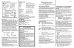
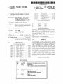
US006859862B1
(12) United States Patent
(10) Patent N0.:
(45) Date of Patent:
Liao et al.
(54)
METHOD AND APPARATUS FOR
SOFTWARE MANAGEMENT OF ()N_CHIP
5,604,909 A
5,632,025 A
CACHE
5,638,500 A
5,694,567
Inventors: Yu-Chung
(Us);
Peter A.
Howard
Sandon,
CI Lia‘),
Cheng,
Essex
Austin,
Redmond,
Junction, WA
VT
,
,
A
2
(US); Peter Hsu, Fremont, CA (US)
( )
,
_
Notice:
_
2/1997 Joshi et al. ............... .. 712/208
5/1997 Bratt et al. ..... ..
711/152
6/1997 Donovan et a1.
12/1997
j//
Bourekas et al.
345/625
.....
. . . . ..
Van
gurgartetlal'
ra HOOk
e a . et...............
a1.
..
711/3
/
FOREIGN PATENT DOCUMENTS
_
_
JP
62197842
9/1987
SubJect to any disclaimer, the term of this
JP
63086048
4/1988
patent is extended or adjusted under 35
JP
4080844
3/1992
U.S.C. 154(b) by 0 days.
JP
5120134
5/1993
OTHER PUBLICATIONS
(21) Appl. N0.: 09/545,184
_
Feb. 22, 2005
(List continued on next page.)
(73) Assignee: Nintendo Co., Ltd., Kyoto (JP)
*
A
US 6,859,862 B1
_
Motorola Inc., “PoWerPC Microprocessor Family: The Pro
(22) Flled'
Apr‘ 7’ 2000
gramming Environments”, 1994.
(Under 37 CFR 147)
IBM, “PoWerPC 740 and PoWerPC 750 RISC Microproces
7
(51)
Int. Cl. .............................................. .. G06F 12/08
(52)
US. Cl. ..................... .. 711/129; 711/130; 711/133;
(58) Field of Search
711 153' 711 152
"""""""""""""""" "
911/130 ’ /129 ’
711/133, 170, 123, 217, 214, 215, 220,
219, 173, 163, 152, 153; 712/35, 36, 22,
222, 4
(56)
References Cited
US PATENT DOCUMENTS
5,170,474 A
12/1992 Sakamura et a1, ,_
*
A microprocessor including a control unit and a cache
locked Cache Portion and a normal Cache Portion The
normal Cache Portion is Controlled by a hardware imple
______ __ 707/6
mented automatic replacement process. The locked cache
portion is locked so that the automatic replacement process
2/ 1996
cannot modify the contents of the locked cache. An instruc
Huck et al- - - - - -
4/1996 Brennan et a1
5,526,504 A
6/1996
2
HS“ et a1‘ ' ' ' ' ' ' '
- - - -- 711/125
711/119
' ' ' " 711/207
glitz“: a1‘ "
7/1996 Reiningérme't";1' ' ' ' '
5,572,704 A
11/1996
Bratt et a1.
5,588,138 A
12/1996
Bai et al.
5,594,886 A
ABSTRACT
2/1993 Keith et al. ............ .. 712/225
5510934 A
5’539’892 A
(57)
either a single cache or as a partitioned cache having a
4/1978 Appell et a1. ............. .. 709/100
12/1979 Appell et a1. .......... .. 711/163
5,493,667 A
Primary
Examiner—Pierre-Michel Bataille
(74) Attorney, Agent, or Firm—Nixon & Vanderhye P.C.
connected With the control unit for storing data to be used by
the control, Wherein the cache is selectively con?gurable as
4 084 224 A
4,177,510 A
5,187,793 A
sor Family User Manual”, 1998.
Byte Magazine, “Zen and the Art of Cache Maintenance”,
1997.
.....
.....
tion is provided in the instruction set that enables softWare
to selectively allocate lines in the locked cache portion to
correspond to locations in an external memory, thereby
' ' ' " 711/207
enabling the locked cache portion to be completely managed
. . . .. 711/161
by Softwam
. . . ..
711/173
1/1997 Smith et al. .............. .. 711/136
2 Claims, 4 Drawing Sheets
DMA_L bit settings
Bit(s)
Name
Description
0-26
LC_ADDR
27
DMA_LD
High order bits of the starting address in locked cache.
Load command
0 Store - transfer from locked cache to external memory
1 Load - transfer from external memory to locked cache
28-29
DMA_LEN_L
30
DMA_T
. Low order bits of transfer length in cache lines
Trigger bit.
_
I
0 DMA command Inactive
1 DMA command is ready to be queued.
31
DMA_F
Flush bit.
_
0 Normal DMA operation
1 Flush the DMA queue.
US 6,859,862 B1
Page 2
US. PATENT DOCUMENTS
5,974,507 A
10/1999 Arimilli et a1. ........... .. 711/133
4/1998 Gossett et a1. ............ .. 345/611
5,974,508 A
5,978,888 A
10/1999
11/1999
27232245‘ 2 * 18/1332 gubgy ------ --1-------------- ~~ iii/i2;
5,982,939 A
11/1999 Van Hook ................ .. 382/255
6,000,014 A
12/1999
6,014,728 A
1/2000
Baror .... ..
3/2000
Green
Jacobs ...................... .. 711/133
5,742,277 A
7
7
/
at age eta'
"
'
/
5,864,703 A
5,875,464 A
1/1999 Van Hook et a1. .......... .. 712/22
.
2/1999 Klrk ......................... .. 711/129
5,875,465 A
2/1999 Kllpatnck et a1.
5,898,854 A
5,931,945 A
4/1999 Abramson et a1. ........ .. 712/218
8/1999 Yung et a1. ............... .. 712/300
5,933,157 A
5,933,650 A
8/1999 Van Hook et a1.
345/563
8/1999 Van Hook et a1. ............ .. 712/2
5,938,756 A
8/1999
5,954,815 A
5,966,734 A
.
.
711/134
Van Hook et a1. .......... .. 712/23
9/1999 Joshi et a1. ........ ..
6,044,478 A
*
6,047,358 A
*
4/2000
6,205,548 B1 *
3/2001
6,438,655 B1 * 8/2002
6,493,800 B1 * 12/2002
6681 296 B2 *
7
7
712/237
10/1999 Mohamed et a1. ........ .. 711/173
* cited by examiner
Maheshwari .............. .. 711/133
Arim?li et a1‘ ___________ " 711/128
Arimilli et a1. ........... .. 711/128
. 711/142
...................... .. 711/141
Hasbun
. 711/170
.
Nlcol et a1. ............... .. 711/136
.
Blumnch .................. .. 711/129
H2004 L.
t 1
‘a0 e a‘ """""""" "
711/129
U.S. Patent
Feb. 22,2005
Sheet 1 0f 4
US 6,859,862 B1
Fig. 1
18
10
i
(
i
_
:
Control Unit
Instruction Fetch :
:
Branch Unit
1
v
:
System
:
Unit
i
_
_
_
.
'
> _
v
32K lCache
i
i
BHT/
BTIC
Dispatch
:
}
ii
| _
32
:
i
'
:
5
_
_
-
_
_
_
_
_
_
_
v
_
-
_
-
_
_
_
_
-."-
-
V
-
-
-
_
_
_
_
_
_
_
_
2.2
l
2
=E
:
GPRs
;
FXU1
FXU2
‘
_
_
_
_
_
_
V
FPRs
‘
;
+ Rename _
_
_
_2_§
LSU
_
_
V
202
Buffers
_
Rename k
V
Buffers
_»
‘
_
A
M
v
34
3A2 : 3Q
l
V
)
l
32‘? Dcache/
L2 Tags
<
opt'ma' L°°a'
Memory Partition
38
I
I
40
‘
:' 'is'sk' ':
60X
!L2 Cache:
BlU/DMA
V _____ _ _
_
'—
36 j
“
“
V
7i‘ ‘
i
i
:
‘V C
14
16
>
External Memory
d2
U.S. Patent
Feb. 22, 2005
US 6,859,862 B1
Sheet 2 0f 4
HlD2 register bit settings
Bit(s)
Name
0
LSQE
Description
Load/Store quantized enable (non-indexed format)
0 psq_l[u] and psq_st[u] instructions are illegal
1 psq_l[u] and psq_st[u] instructions can be used
1
WBE
2
PSE
Write buffer enable
0 write buffer is disabled
1 write buffer enabled to gather non-cacheable data
Paired singles enabled
1
0 paired singles instructions are illegal
1 paired singles instructions can be used
3
LCE
Locked cache enable
0 Cache is not partitioned - 32 kB of normal cache
1 Cache is partitioned - 16 kB of normal cache and
16 kB of locked cache available
4-7
DMAQL
DMA queue length (read only)
the number of used queue positions in the DMA
from O (queue empty) to 15 (queue full)
8-31
-
Reserved
Fry. 2
dcbz_l
Data Cache Block Set to Zero Locked
dcbz__l
F
0
rA, rB
4
00000
56
A
1011
B
1516
Fig. 3
1014
2021
0
3031
U.S. Patent
Feb. 22, 2005
Sheet 4 0f 4
US 6,859,862 B1
DMA_U bit settings
Bit(s)
Name
Description
0-26
MEM_ADDR
High order address bits of starting address in
main memory
27-31
DMA_LEN_U
High order bits of transfer length in cache lines
Fig. 5
DMA_L bit settings
Bit(s)
Name
Description
0-26
LC_ADDR
27
DMA_LD
High order bits of the starting address in locked cache.
Load command
0 Store - transfer from locked cache to external memory
1 Load - transfer from external memory to locked cache
28-29
DMA_LEN_L
. Low order bits of transfer length in cache lines
30
DMA_T
Trigger bit.
31
DMA_F
Flush bit.
0 Normal DMA operation
0 DMA command inactive
1 DMA command is ready to be queued.
1 Flush the DMA queue.
Fig. 6
US 6,859,862 B1
1
2
METHOD AND APPARATUS FOR
SOFTWARE MANAGEMENT OF ON-CHIP
CACHE
effective use of the cache can be a critical factor in obtaining
optimal performance for applications running on a micro
processor. The drastic time difference betWeen loading
desired code or data from an on-chip cache as compared to
loading from the main memory is so great (an order of
magnitude or more) that effective cache management can be
a dominant factor in determining the speed of an application
executed by the microprocessor, or even the speed of the
CROSS-REFERENCE TO RELATED
APPLICATIONS
This application is related to US. application Ser. No.
09/545,182, entitled “METHOD AND APPARATUS FOR
OBTAINING A SCALAR VALUE DIRECTLY FROM A
VECTOR REGISTER” and US. application Ser. No.
09/545,183, entitled “METHOD AND APPARATUS FOR
EFFICIENT LOADING AND STORING OF VECTORS”,
10
?led by the same inventors on the same date as the instant
application. Both of these related cases are hereby incorpo
rated by reference in their entirety.
15
FIELD OF THE INVENTION
This invention relates to microprocessors, and, more
particularly, to a method and apparatus Which improves the
entire system built around the microprocessor.
Generally speaking, a cache operates by storing data
and/or instructions that have been previously requested by
the control unit and retrieved from main memory in the
on-chip cache for possible use again by the control unit at a
later time. If a second request is made by the control unit for
that same data, the data can be quickly retrieved from the
cache rather than having to again retrieve the data from the
off-chip main memory. In this manner, the speed of the
application can be increased by minimiZing the need to
access the relatively sloW main memory.
One limitation, hoWever, regarding the use of cache is that
operational efficiency of microprocessors having on-chip
siZe and cost factors limit the cache to a siZe that is
cache by enabling softWare management of at least a portion
signi?cantly small relative to the siZe of the main memory.
As a result, the cache quickly becomes full With data that has
been retrieved from main memory or elseWhere, thereby
of the cache.
BACKGROUND OF THE INVENTION
25
The electronic industry is in a state of evolution spurred
by the seemingly unquenchable desire of the consumer for
better, faster, smaller, cheaper and more functional elec
tronic devices. In their attempt to satisfy these demands, the
electronic industry must constantly strive to increase the
speed at Which functions are performed by microprocessors.
Trademark) family of microprocessors (hereafter
“PoWerPC”), includes a 32 kilobyte (32 k) on-chip level one
(L1) instruction (I) cache and a 32 K L1 data (D) cache
(Harvard Architecture), as Well as a level tWo (L2) cache
providing additional on-chip cache functionality. For more
Videogame consoles are one primary example of an elec
information on the PoWerPC microprocessors see PowerPC
tronic device that constantly demands greater speed and
740 and PowerPC 750 RISC Microprocessor Family User
Manual, IBM 1998 and PowerPC Microprocessor Family:
The Programming Environments, Motorola Inc. 1994, both
of Which are hereby incorporated by reference in their
reduced cost. These consoles must be high in performance
and loW in cost to satisfy the ever increasing demands
associated thereWith. The instant invention is directed to
increasing the speed at Which microprocessors can process
information by improving the efficiency at Which data and/or
instructions can be loaded for processing.
A cache is a high speed memory that is provided on the
entirety.
In vieW of the siZe limitation on caches, the micropro
40
microprocessor chip for the purpose reducing the number of
times that data required for executing commands must be
retrieved from main memory. Cache devices provide a close
and convenient place for storing data and/or instructions to
be used by the control unit of the microprocessor in a fast
and efficient manner. Today, all high-performance micro
processors incorporate at least one on-chip level one (L1)
preventing additional data required by the control unit from
being stored in the cache. Typically, a microprocessor, such
as the microprocessors in IBM’s PoWerPC (IBM
45
cache for storing previously used data and/or instructions.
Main memory is external to the microprocessor and
access thereto is provided through a bus Which connects the
cessor includes hardWare that manages the cache in accor
dance With an algorithm that attempts to predict Which data
read from main memory is likely to be needed again in the
near future by the processing unit. In other Words, the cache
control hardWare is designed according to an algorithm that
tries to predict in advance What data from main memory to
maintain in the limited amount of storage space available in
the cache for later use by the processing unit. Thus, every
microprocessor having such a cache incorporates some type
of hardWare implemented algorithm for managing the con
tents of the cache. An example of such an automatic replace
ment algorithm used in the PoWerPC is a pseudo least
recently-used (PLRU) replacement algorithm
microprocessor to the main memory. The bus connecting the
microprocessor and the main memory is controlled by a Bus
Interface Unit (BUI). Due to the fact that the main memory
accesses must go through the BUI and bus to obtain the 55
requested data from the off-chip memory, accessing this
The automatic replacement algorithm used in a particular
microprocessor to manage the contents of the cache,
hoWever, is not necessarily optimal or even effective for
certain applications run by the microprocessor. In other
memory is relatively inconvenient and sloW as compared to
Words, the algorithm implemented by cache control hard
accessing the on-chip cache.
With today’s technology, accessing the off-chip main
Ware does not alWays result in efficient cache management
for all applications designed for the microprocessor. For
example, in certain applications the hardWare may drop data
memory can take anyWhere from ten to hundreds of CPU
clock cycles (a time unit by Which the microprocessor or
central processing unit (CPU) operates). In contrast, access
from the cache right before it is needed a second time,
ing on-chip memory, such as a memory designed to operate
from main memory, even though the desired data Was in the
thereby requiring the processor to obtain the dropped data
as an on-chip cache, can take as feW as only one or tWo CPU
clock cycles. Thus, data can be retrieved from a cache at
least about ten times faster than the time that it Would take
to retrieve that same data from main memory. As a result,
65
cache moments earlier. This problem results from the fact
that one cannot predict in advance the needs of every
application that may be implemented using the micropro
cessor. As a result, some applications Will not be able to use
US 6,859,862 B1
3
4
the cache in an ef?cient manner, thereby preventing such
applications from running as fast as they otherwise could
With ef?cient cache management. In fact, for some
modi?es data in the cache. This instruction can be a useful
tool for boosting performance When Zeroing a large block of
applications, the automatic replacement algorithms perform
poorly, thereby preventing the desired loW-latency memory
data. Again, these three instructions have only a limited
ability to provide softWare assistance to the cache manage
ment hardWare, because the hardWare is still in control of the
accesses for Which the cache is designed.
One strategy that has been used in the past in connection
cache in accordance With the hardWare algorithm.
data in the cache and Will continue to operate on the entire
With caches to improve application performance is to pro
Thus, While some tools are available for programmers to
vide in the instruction set of the microprocessor a mecha
nism that enables softWare assisted cache management.
use in order to try and help their particular application utiliZe
the cache in an ef?cient manner, the cache is still ultimately
controlled by the cache management hardWare. As a result,
Most modern microprocessors provide instructions in the
instruction set Which enable softWare to assist the cache
if the replacement algorithm implemented by the hardWare
management hardWare to some degree in managing the
cache. For example, the PoWerPC architecture contains
several user-accessible instructions in the instruction set for
does not perform Well for a particular application, the
application Will not run in an optimal manner on the
15
manipulating the data cache that can signi?cantly improve
overall application performance. These instructions are:
“block touch” (dcbt); “block touch for store” (dcbtst);
“block ?ush” (dcbf); “block store” (dcbst); and “block set to
Zero” (dcbZ) see Zen and the Art of Cache Maintenance,
Byte Magazine, March 1997.
that can be provided by instructions such as those described
above. In other Words, the programmer cannot completely
control the contents of any portion of the cache With these
or similar softWare techniques. Thus, many applications do
not run as fast as they otherWise could if the cache could be
managed in a more ef?cient manner for the particular
In order to understand the operation of these or similar
instructions, it is important to de?ne What a “block” is in this
conteXt. A block is the fundamental unit of memory on
Which the cache operates. The cache handles all memory
25
load and store operations using blocks. The particular block
memory (SPM), i.e. an on-chip memory that does not
eXample, the PoWerPC 601 uses 64-byte blocks, While the
perform demand-driven, automatic replacement of memory
PoWerPC 603 and 604 user 32-byte blocks.
Each of the above-identi?ed instructions operates on a
blocks. An SPM can be used by the application to store, for
eXample, data from a contiguous portion (memory block) of
pair of general purpose register (GPR) operands Whose sum
the main memory, Wherein a base address of the contiguous
memory block is de?ned in a speci?c register created for this
purpose or is de?ned using the memory management facili
ties that eXist for accessing other parts of the memory
35
a cache. Some microprocessors have enabled a certain
contiguous range of the available address space to be
allocated to the SPM. While use of on-chip SMP can
40
secondary cache) into the primary data cache, thereby help
SUMMARY OF THE INVENTION
The instant invention enables more ef?cient use of
on-chip cache, such as a level one data cache in the IBM
PoWerPC or the like, by enabling the cache to be partitioned
into a ?rst portion that operates in a conventional manner
under hardWare control, and a second portion Which can be
lar implementation in the PoWerPC family. The dcbtst
completely controlled and managed by softWare.
instruction behaves in a similar manner eXcept that it pro
In a preferred embodiment of the invention, the entire
vides the additional hint that the corresponding memory
location is going to be overWritten soon. Thus, these tWo
identi?ed block, the automatic replacement algorithm may
overWrite that data in the cache before it can be used. As a
result, these instructions have limited ability to help manage
improve the performance of the microprocessor for certain
applications, it does not solve the problem of cache man
agement described in detail above.
ing to avoid a cache miss, i.e. not ?nding the desired data in
the cache When needed by the processor. It is noted that these
instructions only provide “hints” to the processor and do not
require that the processor actually load the data block
identi?ed by the instructions. In other Words, the hints are
taken under advisement by the processor Which then decides
based on other needs Whether the data block Will be loaded.
These hints are treated differently depending on the particu
instructions do not provide direct control over the contents
of the cache. Moreover, even if the processor does load the
system. HoWever, SPM is a memory, not a cache, and
therefore does not provide the advantages or functionality of
from memory, the dcbt instruction can be used to request
that the processor bring data from memory (or from a
application. Accordingly, a need eXists for improving the use
of cache in a microprocessor on an application speci?c basis.
The instant invention satis?es this need.
It is noted that, in addition to cache, some microproces
sors have on-chip memory that can be used as a scratch pad
siZe can vary from one microprocessor to another. For
forms the effective address of the memory location(s) to be
affected by the instruction. The dcbt and dcbtst instructions
provide “hints” to the processor that the addressed data
block may be needed by the application in the near future,
thereby giving the processor the option of loading, or at least
allocating, the memory block in the cache. Thus, When
placed appropriately ahead of the anticipated need for data
microprocessor, regardless of the limited softWare assistance
cache can be used as a conventional cache, or the cache can
be recon?gured so as to de?ne part of the cache as a locked
55
softWare controlled cache, referred to herein as a “locked
cache” or “scratch pad cache”. What is meant by “locked”
in this conteXt is that the contents of the locked portion of the
cache cannot be altered by the hardWare cache management
the cache in an ef?cient manner for a particular application.
The dcbf and dcbst instructions in the PoWerPC instruc
system. By locking the portion of the cache designed for
tion set force modi?ed (or dirty) data out of the cache and
back into memory. The primary difference betWeen these
tWo instructions is that dcbf not only copies data back to
of the hardWare cache management system. As a result, poor
performance can be avoided even if the hardWare algorithm
does not Work Well for the needs of a particular application.
The locking of the cache can be done by, for eXample,
memory (like dcbst), but it also marks the corresponding
softWare control, the cache can be managed independently
cache block as invalid. The dcbZ instruction in the PoWerPC 65 providing a special purpose register (e.g. HID2) having a bit
instruction set allocates a block of data in the cache and then
(e.g. 4th bit) Which controls Whether the cache is to function
as a single hardWare controlled cache or a partitioned cache
initialiZes the block to a series of Zeros. Thus, this instruction
US 6,859,862 B1
5
6
including a locked software controlled portion. Other bits in
the special purpose register can be used, for example, to
control other enhancement options that may be available on
FIG. 3 shoWs an exemplary instruction de?nition for
addition to an instruction set of the microprocessor of FIG.
1 that may be used to allocate blocks in the locked cache, in
accordance With one embodiment of the instant invention.
FIG. 4 is a partial and more detailed vieW of the micro
processor of FIG. 1, Wherein a preferred embodiment of a
direct memory access (DMA) engine is shoWn for use in
bringing data into and out of the locked cache, in accordance
With one embodiment of the instant invention; and
FIGS. 5 and 6 are tables shoWing an exemplary bit
the microprocessor.
In order to allocate blocks of memory in the locked cache,
at least one additional instruction (e.g. dcbzil) is preferably
provided in the instruction set of the microprocessor that
implements this invention. This additional instruction is
used to control on a block-by-block basis exactly What data
is contained in the locked portion of the cache, thereby
giving the application programmer complete freedom to
10
keep or remove blocks of data from the cache as required for
de?nition for tWo exemplary special purpose registers used
ef?cient processing of his application. In this Way, the
in the DMA engine of FIG. 4, in accordance With the one
embodiment of the instant invention.
utiliZation of the cache can be maximiZed regardless of the
particular hardWare algorithm used to manage the normal or
DETAILED DESCRIPTION OF THE
PREFERRED EMBODIMENTS
non-locked portion of the cache. Moreover, by enabling
selective partitioning of the cache into a locked and regular
cache, the entire cache can still be used in the conventional
manner if it is determined that the hardWare algorithm Will
Work satisfactorily for a particular application. On the other
hand, if it is determined that the particular application Would
perform better using a portion of the cache as a softWare
controlled cache, the cache may be partitioned and locked so
that the locked portion can be managed exclusively by the
softWare.
The locked portion of the cache is basically a scratch pad
25
memory (SPM) but Which operates as a cache instead of a
memory. Thus, the invention provides a locked cache or
scratch pad cache (SPC) that can be used and managed
solely by the application, Without interference from the
hardWare cache management system, to increase the effi
ciency of the application on a particular microprocessor.
A major advantage of the locked cache as compared to a
convention scratch pad memory is that the locked cache
alloWs ?exibility of softWare management for data that does
not exhibit the spatial and temporal locality for Which
nection and operation, are Well knoWn to one skilled in the
art. Thus, in order not to obscure the instant invention With
35
instant invention for a person skilled in the art.
normally managed cache, and then continually replace itself,
different characteristics, is high usage instruction libraries or
data tables Which do not ?t in the cache, but have access
patterns that Would cause thrashing if they are managed by
hardWare. The invention overcomes these and other prob
lems by alloWing 100% softWare control of a portion of the
cache.
In accordance With a preferred embodiment of the
invention, a direct memory access (DMA) engine is pro
vided in the microprocessor and is used to transfer data
betWeen the locked data cache and the external memory. The
details regarding knoWn elements, the draWings and descrip
tion herein are presented in a simpli?ed form and only to the
extent necessary to provide a full understanding of the
normal caches are designed. One example is a multimedia
data stream that is larger than the cache, and is used once and
then discarded. Such data Would replace all other data in a
yielding very loW cache hit rates. Another example, having
In the folloWing description, numerous speci?c details are
set forth regarding a preferred embodiment of the instant
invention. HoWever, the speci?c details are meant to be
exemplary only and are not meant to limit the invention to
the particular embodiment described herein. In other Words,
numerous changes and modi?cations may be made to the
described embodiment Without deviating from the true scope
and spirit of the instant invention, as a person skilled in the
art Will readily understand from revieW of the description
herein.
FIG. 1 is a diagram of a single-chip microprocessor 10 in
Which the present invention has been implemented. It is
noted that FIG. 1 only shoWs a simpli?ed representation of
a microprocessor, due to that fact that the majority of the
elements in the microprocessor, as Well as their intercon
The microprocessor 10 is connected, in a knoWn manner,
40
to an off-chip (external) memory 12 or main memory via an
address bus 14 and data bus 16. The external memory 12
contains data and/or instructions, such as 3D graphics
instructions, needed by the microprocessor 10 in order
perform desired functions. It is noted that the microproces
45
sor 10 and external memory 12 may be implemented in a
larger overall information processing system (not shoWn).
The microprocessor includes a control unit 18, ?xed point
units 20a and 20b, general purpose registers (GPRs) 22, a
load and store unit 24, ?oating point unit 28, paired single
unit (vector processing unit) 30 and ?oating point registers
pose registers (SPR) used respectively to control one DMA
26, all of Which generally interconnect and operate in a
knoWn manner. In addition, the microprocessor 10 includes
transfer into and out of the locked cache.
a level one instruction cache 32, a level one data cache 34,
DMA engine’s operation is controlled by tWo special pur
BRIEF DESCRIPTION OF THE DRAWINGS
a level tWo cache 36 With associated tags 38, and bus
55
Other objects, features and advantages of the instant
invention Will become apparent upon revieW of the detailed
description beloW When read in conjunction With the accom
interface unit/direct memory access engine (BIU/DMA) 40.
In this embodiment, the instruction cache 32, level tWo
cache 36 and level tWo cache tags 38 generally operate in a
conventional manner. HoWever, as Will be explained in
detail beloW, the data cache 34 and the direct memory access
panying draWings, in Which:
unit have special operations and features in accordance With
FIG. 1 is a general block diagram of an exemplary
microprocessor and external memory illustrating a preferred
embodiment of the instant invention;
the instant invention.
FIG. 2 is a table shoWing an exemplary special purpose
register used to control the partitioning of the cache and
other optional enhancements to the microprocessor of FIG.
1, in accordance With one embodiment of the instant inven
cessor 10 is similar to IBM’s PoWerPC microprocessors,
tion;
The structure and operation of this exemplary micropro
65
With certain modi?cations to implement the instant inven
tion. Details regarding the operation of most of the elements
of this exemplary microprocessor are found in the folloWing
publications: PowerPC 740 and PowerPC 750 RISC Micro
US 6,859,862 B1
7
8
processor Family User Manual, IBM 1998 and PowerPC
from memory that are loaded from an eight-Word boundary
Microprocessor Family: The Programming Environments,
(i.e., bits A(27—31) of the logical (effective) addresses are
Motorola Inc. 1994. It is noted, however, that the instant
invention may be implemented on any suitable micropro
cessor or information processing system to improve the
management of cache.
In the exemplary embodiment of FIG. 1, the micropro
cessor includes separate 32-Kbyte, eight-Way associative
instruction and data caches (32 and 34) to alloW the various
Zero). As a result, cache blocks are aligned With page
boundaries. Address bits A(20—26) provide the index to
select a cache set. Bits A(27—31) select a byte Within a block.
The on-chip data cache tags are single ported, and load or
store operations must be arbitrated With snoop accesses to
the data cache tags. Load and store operations can be
performed to the cache on the clock cycle immediately
of relatively sloW accesses to the external memory 12. The
folloWing a snoop access if the snoop misses. Snoop hits
may block the data cache for tWo or more cycles, depending
on Whether a copy-back to main memory 12 is required.
caches preferably implement a pseudo least-recently-used
(PLRU) replacement algorithm for managing the contents of
The level one (L1) caches (32 and 34) are preferably
controlled by programming speci?c bits in a ?rst special
execution units (18, 20a, 20b, 28 and 30) and registers rapid
10
access to instructions and data, thereby reducing the number
the caches. The cache directories are physically addressed,
15
purpose register (HIDO—not shoWn) and by issuing dedi
the physical (real) address tag being stored in the cache
directory. Both the instruction and data caches have 32-byte
register preferably contains several bits that invalidate,
cache block siZe, Wherein a cache block is the block of
memory that a coherency state describes (also referred to as
cache 34 is automatically invalidated When the micropro
cated cache control instructions. The HIDO special purpose
disable, and lock the instructions and data caches. The data
a cache line). TWo coherency state bits for each data cache
cessor 10 is poWered up and during a hard reset. HoWever,
a soft reset does not automatically invalidate the data cache.
SoftWare uses the HIDO data cache ?ash invalidate bit
(HIDO(DCFI)) if the cache invalidation is desired after a soft
block alloW encoding for three states—Modi?ed (exclusive)
(M), Exclusive (unmodi?ed) (E), and Invalid (I)—thereby
de?ning an MEI three-state cache coherency protocol. A
single coherency state bit for each instruction cache block
alloWs encoding for tWo possible states: invalid (INV) or
Valid
In accordance With the instant invention, each
cache can be invalidated or locked by setting the appropriate
bits in a hardWare implementation-dependent register (a
reset. Once the HIDO(DCFI) is set through move-to-special
25
matically clears this bit in the next clock cycle (provided that
the data cache is enabled in the HIDO register).
The data cache may be enabled or disabled by using the
data cache enable bit (HIDO(DCE)) Which is cleared on
poWer-up, disabling the data cache. When the data cache is
in the disabled state (HIDO(DCE)=0), the cache tag state bits
are ignored, and all accesses are propagated to the L2 cache
special purpose register described in detail beloW).
The microprocessor 10 preferably supports a fully
coherent 4-Gbyte physical address space. Bus snooping is
used to drive the MEI three-state cache coherency protocol
that ensures the coherency of global memory With respect to
the processor’s data cache. The data cache 34 coherency
protocol is a coherent subset of the standard MESI four-state
cache protocol that omits the shared state. The data cache 34
characteriZes each 32-byte block it contains as being in one
of three MEI states. Addresses presented to the cache are
indexed into the cache directory With bits A(20—26), and the
upper-order 20 bits from the physical address translation
(PA(0—19)) are compared against the indexed cache direc
tory tags. If neither of the indexed tags matches, the result
36 or 60x bus as single beat transactions. The contents of the
data cache can be locked by setting the data cache lock bit
35
(HIDO(DLOCK)). A data access that hits in a locked data
cache is serviced by the cache. HoWever, all accesses that
miss in the locked cache are propagated to the L2 cache 36
or 60x bus as single-beat transactions. The microprocessor
40
snoop hits in an unlocked data cache. HoWever, any cache
block invalidated by a snoop remains invalid until the cache
is unlocked. The instruction cache 32 operates in a similar
manner as the data cache described above, except that
different bits are used in the HIDO register for invalidation
10 treats snoop hits in the locked data cache the same as
is a cache miss (required data not found in cache). On a
cache miss, the microprocessor cache blocks are ?lled in
four beats of 64 bits each. The burst ?ll is performed as a
45
critical-double-Word-?rst operation—the critical double
and locking, i.e. instruction cache ?ash invalidate bit HIDO
(ICFI) and instruction cache lock bit HIDO(ILOCK).
The microprocessor preferably includes another hardWare
Word is simultaneously Written to the cache and forWarded
to the requesting unit, thus minimiZing stalls due to cache ?ll
latency. If a tag matches, a cache hit occurred and the
directory indicates that state of the cache block through tWo
implementation-dependent special purpose register (HID2)
that, in accordance With the instant invention, is used to
modify hoW the data cache 34 is con?gured and used.
Speci?cally, the HID2 register contains a lock cache enable
state bits kept With the tag. The microprocessor 10 prefer
ably has dedicated hardWare to provide memory coherency
bit (LCE) that controls Whether the data cache 34 is con
by snooping bus transactions.
?gured as 32 kB of normal (hardWare managed) cache
Both caches 32 and 34 are preferably tightly coupled into
the bus interface unit (BUI) 40 to alloW ef?cient access to
the system memory controller and other potential bus mas
ters. The BUI 40 receives requests for bus operations from
the instruction and data caches, and executes operations per
the 60x bus protocol. The BUI 40 provides address queues,
purpose-register (mtspr) operation, the microprocessor auto
(LCE=0) or is partitioned into a 16 kB of normal cache 34a
55
and a 16 kB of locked cache 34b that can be controlled
exclusively by softWare (LCE=1). Speci?cally, at poWer-up
or reset, HID2(LCE) is set to be 0. Thus, at this time, the L1
data cache 34 is a 32 kB 8-Way set-associative cache.
HoWever, When a move-to-special-register (mtspr) instruc
prioritiZing logic and bus control logic. The BUI also
tion sets HID2(LCE)=1, the data cache is con?gured as tWo
captures snoop addresses for data cache, address queue and
memory reservation operations. The data cache is preferably
partitions. The ?rst partition 34a, consisting of Ways 0—3, is
organiZed as 128 sets of eight Ways, Wherein each Way
consists of 32 bytes, tWo state bits and an address tag. In
accordance With the instant invention, an additional bit may
be added to each cache block to indicate that the block is
locked. Each cache block contains eight contiguous Words
then a 16 kB normal cache. The second partition 34b,
consisting of Ways 4—7, is then a 16 kB locked cache. The
normal cache portion 34a operates like the unpartitioned
65
cache 34, except that it behaves as a four-Way set-associative
cache. The operation of the locked cache partition 34b is
described beloW.
US 6,859,862 B1
10
An example de?nition for the HID2 register is shown in
FIG. 2, Wherein bit number 3 is the LCE bit for controlling
hoW the data cache 34 is con?gured. The other bits in the
In accordance With a preferred embodiment of the instant
invention, the microprocessor implements a DMA engine
40b, as shoWn in FIG. 4, to transfer data betWeen the locked
L1 data cache 34b and the external memory 12. The DMA
engine 40b has a 15-entry FIFO queue for DMA commands
HID2 register are used to control other enhanced features
that may be provided in the microprocessor 10, such as data
quantization, Write buffering, paired singles operations, and
DMA queue length as shoWn on FIG. 2. It is noted that,
While FIG. 2 shoWs that bits 8—31 of the HID2 register are
reserved, these bits may be used to indicate, for example,
cache instruction hit error, DMA access to normal cache
10
error, DMA cache miss error, DMA queue length over?oW
error, instruction cache hit error enable, DMA cache miss
15
for example, instructions generally corresponding to the
dcbt, dcbst, dcbZ, dcbst, dcbf, dcbi and icbi instructions in
the PoWerPC instruction set. The ?rst six of these instruc
tions have similar operation as described above With respect
to the PoWerPC instruction set, except that they noW, in
As shoWn in FIG. 5, the DMAiU register is a 32-bit
register containing bits 0 through 31, Wherein bits 0 through
error enable, and DMA queue over?oW error enable.
The microprocessor includes cache control instructions
for controlling both the instruction and data caches, such as,
and processes the commands sequentially. The operation of
the DMA engine 40b is controlled by tWo special purpose
registers: DMAU and DMAL. The exemplary de?nitions of
the special purpose registers, DMAU and DMAL, are shoWn
in FIGS. 5 and 6, respectively.
20
26 comprise 27-bit high order address bits representing a
starting address in main memory and bits 27—31 comprise 5
high order bits representing transfer length in cache lines. As
shoWn in FIG. 6, the DMAiL register is a 32-bit register
including bits 0 through 31, Wherein bits 0 through 26
comprise 27 high order bits representing a starting address
in the locked cache portion, bit 27 comprises a one-bit load
command that encodes Whether direct memory access trans
fer is from the locked cache to external memory or from
accordance With the instant invention, can be used in con
external memory to locked cache, bits 28 through 29 com
nection With both the locked portion 34b and the normal
portion 34a of the data cache 34. The data cache block
invalidate (dcbi) instruction is provided for invalidating a
line in the locked portion 34b or the normal portion 34a of
the data cache 34. The instruction cache block invalidate
(icbi) instruction operates on the instruction cache 32 in
prise tWo loW order bits representing the transfer length in
cache lines, bit 30 comprises a trigger bit representing
Whether to activate or deactivate direct memory access, and
25
access operation or ?ush of a queued direct memory access
command.
The DMA engine is disabled at poWer-up With HID2
generally the same manner as this same instruction operates
in the PoWerPC.
In accordance With an important aspect of the instant
invention, a neW instruction is provided in the instruction set
(LCE)=0. Setting HID2(LCE)=1 partitions the L1 data
30
latches values in DMAU and DMAL to form a DMA
command, enqueues the command in the DMA queue and
sets DMAL(T)=0. HID2(DMAQL) indicates the number of
locked portion as a result of changing the lock cache enable
35
empty, i.e. HID2(DMALQ)=0, the DMA engine processes
the commands sequentially. The starting address of the
transfer in the data cache is DMAL(LCiADDR)||0b0000.
FIG. 3, a data-cache-block-set-to-Zero-locked (dcbzil)
40
to allocate on a block-by-block basis any block in the
available memory address space. In other Words, the allo
cation does not have to be linear, ie does not need to
correspond to a contiguous block of memory, in contrast to
a typical scratch pad memory. Moreover, due to the fact that
45
softWare has complete control over the contents of the cache
Without interference from the replacement algorithm (Which
50
algorithm, such a pseudo-LRU algorithm).
As can be seen in FIG. 2, the dcbzil instruction bit
pattern includes bits 0 through 32, Wherein bits 0 through 5
For a DMA store command, i.e. DMAL(LD)=0, the DMA
engine performs a data cache look-up for each of the cache
lines equentially from the starting address. For a look-up hit
in the locked cache, the DMA engine initiates a 60x bus
Write-With-?ush transaction to transfer the 32 byte data from
load command, i.e. DMAL(LD)=1, the DMA engine per
forms a data cache lookup for each of the cache lines
register, bits 16 through 20 designate a second register, the
60
allocated, bits 21 through 30 encode a secondary op code of
“1014”, and bit 31 encodes a reserved ?eld of “0”.
The dcbzil instruction is preferably the only mechanism
available to allocate a tag for a 32 byte block in the locked
cache 34b to be associated With a particular address in
memory. The dcbi and dcbf instructions are operable to
deallocate cache lines in the locked cache 34b.
the transfer is determined by DMAL(LD). DMAL(LD)=0
the locked cache 34b to the external memory 12. For a DMA
55
encode a primary op code of 4, bits 6 through 10 encode a
reserved ?eld of “00000”, bits 11 through 15 designate a ?rst
content of Which is to be added to the content of the ?rst
register to provide a cache block address to be cleared or
The starting address of the transfer in the external memory
is DMAU(MEMiADDR)||0b0000. The number of cache
lines to be transferred by the command is DMAU(DMAi
LENiU)||DMAL(DMAiLENiL), except that a value of
Zero speci?es a length of 128 cache lines. The direction of
means a transfer from the locked cache to the external cache,
While DMAL(LD)=1 means a transfer from the external
memory to the locked cache.
the locked portion 34b of the cache is actually locked, the
controls the normal portion 34a of the cache 34 When
partitioned, and controls the entire cache 34 When the cache
is not partitioned, in accordance With a replacement
DMA commands in the DMA queue, including the com
mand in progress (if any). When the DMA queue is not
FIG. 3 shoWs an exemplary de?nition for an instruction
that can be used for this purpose. Speci?cally, as shoWn in
instruction can be used for allocating lines or blocks in the
locked cache. Preferably, the dcbzil instruction can be used
cache 32 and enables the engine 40b. When a mtspr instruc
tion sets DMAL(T)=1 and DMAL(F)=0, the DMA engine
of the microprocessor 10 for allocating lines in the locked
portion 34b of the data cache 34 When the cache includes the
bit in the HID2 register to 1, ie HID2(LCE)=1.
bit 31 comprises a ?ush bit encoding normal direct memory
65
sequentially from the starting address. For a look-up hit in
the locked cache, the DMA engine initiates a 60x bus burst
read transaction to transfer the data from the external
memory 12 to the locked cache 34b. For all but the last read
transaction associated With the DMA load command, the
burst read transaction type is 0b01011. The last burst read
transaction has a transaction type 0b01010. The micropro
cessor 10 initiates the bust transaction type 0b01011 only for
the DMA load commands. Preferably, the memory controller
can use the information to pre-fetch the next cache line to
improve the performance.
US 6,859,862 B1
11
12
The DMA access to the cache, both DMA loads and DMA
stores, Will result in a psuedo-LRU state transition Within the
four-Way set associated With the cache line, but does not
affect the MEI state. If the look-up misses the locked cache,
ment of the invention described herein is preferred because
both static and dynamic data can be managed, in large or
small blocks, With very little additional hardWare beyond
that Which is found in a normal cache. In fact, the invention
the DMA engine transfers no data and continues to the next
can be implemented simply by, for example, adding an
cache line. Preferably, the only Way to ?ush the DMA engine
additional bit to each cache line intended for locking Which
enables the cache line to be locked, thereby enabling each of
is to issue a mtspr instruction to set DMAL(f)=1. In this
situation, the DMA engine ?ushes all the commands in the
DMA queue, including the command in progress, and sets
both DMAL(f)=DMAL(t)=0. Such an instruction should be
folloWed by a sync instruction to ensure that the pending bus
transaction associated With the discarded command, if any,
complete before the DMA is engine accepts the next DMA
command.
It is noted that the microprocessor 10 is considered to be
a decoder and executor for the particular instructions
described herein. Thus, part of the instant invention involves
the locked cache lines to be advantageously used as softWare
controlled cache. It is noted that the instant invention is
particularly advantageous When implemented in loW cost,
high performance microprocessors, such as microprocessors
designed and intended for use in videogame consoles for
household use or the like.
15
While the preferred forms and embodiments have been
illustrated and described herein, various changes and modi
?cation may be made to the exemplary embodiment Without
deviating from the scope of the invention, as one skilled in
providing an instruction decoder and executor for the neW
instructions de?ned in the above description of the inven
the art Will readily understand from the description herein.
Thus, the above description is not meant to limit the scope
tion. The invention, hoWever, is not limited to a hardWare
of the appended claims beyond the true scope and sprit of the
decoder or executor, such as a microprocessor, but also
instant invention as de?ned herein.
covers softWare decoders and executors provided by, for
What is claimed is:
1. A microprocessor, comprising a control unit and a
cache connected With the control unit for storing data to be
example, a virtual machine, such as a softWare emulator of
the instant microprocessor. In other Words, the invention
also relates to softWare emulators that emulate the operation
25
of the instant microprocessor by decoding and executing the
con?gurable as either a single cache or as a partitioned cache
particular instructions described herein. The invention fur
having a locked cache portion and a normal cache portion,
the normal cache portion being controlled by a hardWare
ther relates to a storage medium, such as a compact disk
Which stores any or all of the unique instructions described
implemented automatic replacement process, and further
herein, thereby enabling a microprocessor or virtual
Wherein the locked cache portion is locked so that the
machine to operate in accordance With the invention
described herein.
As can be seen from the description above, the instant
invention enables 100% softWare control of the locked
automatic replacement process cannot modify the contents
of the locked cache portion,
an instruction that enables softWare to selectively allocate
lines in the locked cache portion to correspond to
portion of the cache, thereby enabling an application to
locations in an external memory, and
a direct memory access engine that controls transfer of
control the contents of the locked cache in a manner that can
boost performance as compared to normal cache operation.
In other Words, the invention provides an improvement to
the softWare assist cache management strategies that are
available on, for example, the PoWerPC family of micro
processors as described above, by enabling complete soft
Ware control of a portion of the cache. By enabling complete
softWare control of the locked cache, the invention provides
a scratch pad cache for advantageous use by the applications
programmer. In accordance With the invention, the is cache
data betWeen the locked cache portion and the external
memory, Wherein the direct memory access engine
includes ?rst and second special purpose registers,
Wherein the ?rst special purpose register controls trans
fer of data from the external memory into the locked
cache potion and the second special purpose register
controls transfer of data from the locked cache portion
to the external memory.
2. A microprocessor, comprising a control unit and a
cache connected With the control unit for storing data to be
may be partitioned to any suitable siZe and is not limited to
equal partitions as described herein. Moreover, the instant
used by the control unit, Wherein the cache is selectively
invention may be implemented in one or more caches other
than a level one data cache.
con?gurable as either a single cache or as a partitioned cache
having a locked cache portion and a normal cache portion,
the normal cache portion being controlled by a hardWare
Other approaches to managing memory as a scratch pad
include locking the entire cache once data has been locked,
adding a lock bit to the status line bits, and using a
contiguous block of memory. The ?rst approach is appro
priate for applications Where a static block of data is
frequently accessed, such as ?xed data tables. HoWever, this
approach does not Work Well if the data to be managed is
changing, because there is signi?cant overhead in unlocking,
changing data and relocking the cache. The second approach
provides similar functionality to the instant invention, as
used by the control unit, Wherein the cache is selectively
implemented automatic replacement process, and further
Wherein the locked cache portion is locked so that the
automatic replacement process cannot modify the contents
55
of the locked cache portion, and
an instruction that enables softWare to selectively allocate
lines in the locked cache portion to correspond to
locations in an external memory,
Wherein the microprocessor further includes a hardWare
described above, but requires additional hardWare support
implementation dependent special purpose register
beyond that Which is found in a normal cache. The third
approach is less ?exible than the above described embodi
ment of the instant invention, in that it constrains the data in
the SPM to reside in a single large block. Thus, the embodi
Which determines Whether the cache is con?gured as
the single normal cache or the partitioned cache.
*
*
*
*
*