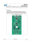
1
UM1690
User manual
Discovery kit for STM32 F0 series - with STM32F072RB MCU
Introduction
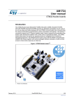
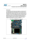
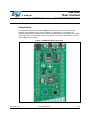
The STM32F072 Discovery kit (32F072BDISCOVERY) helps you to discover the full
features of the STM32F0 series and to develop your applications. It is based on an
STM32F072RBT6 and includes an ST-LINK/V2 embedded debug tool interface, ST MEMS
Gyroscope, LEDs, Push buttons, Linear Touch Sensor, Touch keys, RF EEprom connector
and a USB mini-B connector.
Figure 1. STM32F072 Discovery board
December 2013
DocID025474 Rev 1
1/25
www.st.com
Contents
UM1690
Contents
1
Conventions . . . . . . . . . . . . . . . . . . . . . . . . . . . . . . . . . . . . . . . . . . . . . . . . 3
2
Ordering and product information . . . . . . . . . . . . . . . . . . . . . . . . . . . . . . 4
3
Features . . . . . . . . . . . . . . . . . . . . . . . . . . . . . . . . . . . . . . . . . . . . . . . . . . . 5
4
Hardware layout . . . . . . . . . . . . . . . . . . . . . . . . . . . . . . . . . . . . . . . . . . . . 6
4.1
Embedded ST-LINK/V2 . . . . . . . . . . . . . . . . . . . . . . . . . . . . . . . . . . . . . . . 9
4.1.1
Using ST-LINK/V2 to program/debug the STM32F072 on board . . . . . . 9
4.1.2
Using ST-LINK/V2 to program/debug an external STM32 application . . 10
4.2
Power supply and power selection . . . . . . . . . . . . . . . . . . . . . . . . . . . . . . .11
4.3
LEDs . . . . . . . . . . . . . . . . . . . . . . . . . . . . . . . . . . . . . . . . . . . . . . . . . . . . .11
4.4
Push buttons . . . . . . . . . . . . . . . . . . . . . . . . . . . . . . . . . . . . . . . . . . . . . . .11
4.5
Linear Touch Sensor / Touch Keys . . . . . . . . . . . . . . . . . . . . . . . . . . . . . . 12
4.6
USB device support . . . . . . . . . . . . . . . . . . . . . . . . . . . . . . . . . . . . . . . . . 12
4.7
Gyroscope MEMS (ST MEMS L3GD20) . . . . . . . . . . . . . . . . . . . . . . . . . 12
4.8
JP2 (Idd) . . . . . . . . . . . . . . . . . . . . . . . . . . . . . . . . . . . . . . . . . . . . . . . . . . 13
4.9
Extension and RF EEprom connector . . . . . . . . . . . . . . . . . . . . . . . . . . . 13
4.10
OSC clock . . . . . . . . . . . . . . . . . . . . . . . . . . . . . . . . . . . . . . . . . . . . . . . . 14
4.10.1
OSC clock supply . . . . . . . . . . . . . . . . . . . . . . . . . . . . . . . . . . . . . . . . . 14
4.10.2
OSC 32 KHz clock supply . . . . . . . . . . . . . . . . . . . . . . . . . . . . . . . . . . . 14
4.11
Solder bridges . . . . . . . . . . . . . . . . . . . . . . . . . . . . . . . . . . . . . . . . . . . . . 15
4.12
Extension connectors . . . . . . . . . . . . . . . . . . . . . . . . . . . . . . . . . . . . . . . . 16
5
Mechanical drawing . . . . . . . . . . . . . . . . . . . . . . . . . . . . . . . . . . . . . . . . 20
6
Electrical schematics . . . . . . . . . . . . . . . . . . . . . . . . . . . . . . . . . . . . . . . 21
7
Revision history . . . . . . . . . . . . . . . . . . . . . . . . . . . . . . . . . . . . . . . . . . . 24
2/25
DocID025474 Rev 1
UM1690
1
Conventions
Conventions
Table 1 provides the definition of some conventions used in the present document.
Table 1. ON/OFF conventions
Convention
Definition
Jumper JPx ON
Jumper fitted
Jumper JPx OFF
Jumper not fitted
Solder bridge SBx ON
SBx connections closed by solder
Solder bridge SBx OFF SBx connections left open
DocID025474 Rev 1
3/25
25
Ordering and product information
2
UM1690
Ordering and product information
The STM32F072 Discovery is a low-cost and easy-to-use development kit to quickly
evaluate and start a development with an STM32F0 series microcontroller.
Before installing and using the product, please accept the Evaluation Product License
Agreement from www.st.com/epla.
For more information on the STM32F072 Discovery board and for demonstration software,
visit www.st.com/stm32f0-discovery.
To order the Discovery kit for the STM32 F0 series, use the STM32F072B-DISCO order
code.
4/25
DocID025474 Rev 1
UM1690
3
Features
Features
The STM32F072 Discovery board offers the following features:
•
STM32F072RBT6 microcontroller featuring 128 KB of Flash memory, 16 KB of SRAM
in an LQFP64 package
•
On-board ST-LINK/V2 with selection mode switch to use the kit as a standalone STLINK/V2 (with SWD connector for programming and debugging)
•
Board power supply: through USB bus or from an external 5 V supply voltage
•
External application power supply: 3 V and 5 V
•
L3GD20, ST MEMS motion sensor, 3-axis digital output gyroscope
•
One Linear Touch Sensor or four Touch Keys
•
Six LEDs:
–
LD1 (red/green) for USB communication
–
LD2 (red) for 3.3 V power on
–
Four user LEDs: LD3 (orange), LD4 (green), LD5 (red) and LD6 (blue)
•
Two push buttons (user and reset)
•
USB USER with Mini-B connector
•
RF EEprom daughter board connector
•
Extension header for LQFP64 I/Os for a quick connection to the prototyping board and
easy probing
DocID025474 Rev 1
5/25
25
Hardware layout
4
UM1690
Hardware layout
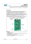
The STM32F072 Discovery board has been designed around the STM32F072RBT6
microcontroller in a 64-pin LQFP package.
Figure 2 illustrates the connections between the STM32F072RBT6 and its peripherals (STLINK/V2, ST MEMS Gyroscope L3GD20, LEDs, Push buttons, Linear Touch Sensor, Touch
keys, RF EEprom connector and a USB mini-B connector).
Figure 3 and Figure 4 help you to locate these features on the STM32F072 Discovery
board.
Figure 2. Hardware block diagram
DŝŶŝͲh^
^t
ŵďĞĚĚĞĚ
^dͲ>/E<ͬsϮ
^dDϯϮ&ϬϳϮZdϲ
/ͬK
/ͬK
>Ɛ
>ϯƚŽ>ϲ
,ĞĂĚĞƌ
,ĞĂĚĞƌ
/ͬK
Z^d
Ϯ
Z^d
ϭ
h^Z
>ϯ'ϮϬ
>ŝŶĞĂƌdŽƵĐŚ
^ĞŶƐŽƌ
DŝŶŝͲh^
ydͬZ&ͲW
D^ϯϯϮϲϳsϭ
6/25
DocID025474 Rev 1
UM1690
Hardware layout
Figure 3. Top layout
34,).+6
86%67/,1.
,$
86%86(5
,$
072
#/#.EXTENSIONOR
2&%%PROMCONNECTOR
6POWER
SUPPLYINPUTOUTPUT
6POWER
SUPPLYINPUTOUTPUT
#.
34,).+$)3#/6%29
SELECTOR
#.
37$CONNECTOR
,$/RANGE,%$
,$
'REEN,%$
*0
)$$MEASUREMENT
,$2ED,%$
,$"LUE,%$
34-&2"4
"
RESETBUTTON
"
USERBUTTON
,INEARTOUCHSENSOR
TOUCHKEYS
-36
DocID025474 Rev 1
7/25
25
Hardware layout
UM1690
Figure 4. Bottom layout
3FRQQHFWRU
3FRQQHFWRU
6%
5HVHUYHG
6%
'HIDXOW
6%670B567
6%1567
5;7;6%
-3
6%9%$7
9'',26%
86%86(56%
6%;&U\VWDO
6%;&U\VWDO
0&26%
%5(6(76%
6%%86(5
6%*1'9''
6%9''$
6%7RXFKVHQVRU
069
8/25
DocID025474 Rev 1
UM1690
4.1
Hardware layout
Embedded ST-LINK/V2
The ST-LINK/V2 programming and debugging tool is integrated on the STM32F072
Discovery board. The embedded ST-LINK/V2 can be used in 2 different ways according to
the jumper states (see Table 2):
•
Program/debug the MCU on board,
•
Program/debug an MCU in an external application board using a cable connected to
SWD connector CN4.
The embedded ST-LINK/V2 supports only SWD for STM32 devices. For information about
debugging and programming features, refer to user manual UM1075 (ST-LINK/V2 in-circuit
debugger/programmer for STM8 and STM32) which describes in detail all the ST-LINK/V2
features.
Table 2. Jumper states
4.1.1
Jumper state
Description
Both CN5 jumpers ON
ST-LINK/V2 functions enabled for on board programming (default)
Both CN5 jumpers OFF
ST-LINK/V2 functions enabled for application through external CN4
connector (SWD supported)
Using ST-LINK/V2 to program/debug the STM32F072 on board
To program the STM32F072 on board, simply plug in the two jumpers on CN5, as shown in
Figure 5 in red, but do not use the CN4 connector as that could disturb communication with
the STM32F072RBT6 of the STM32F072 Discovery board.
Figure 5. STM32F072 Discovery board connections
DocID025474 Rev 1
9/25
25
Hardware layout
4.1.2
UM1690
Using ST-LINK/V2 to program/debug an external STM32 application
It is very easy to use the ST-LINK/V2 to program the STM32 on an external application.
Simply remove the 2 jumpers from CN5 as shown in Figure 6, and connect your application
to the CN4 debug connector according to Table 3.
Note:
SB10 must be OFF if you use CN4 pin 5 in your external application.
Table 3. Debug connector CN2 (SWD)
Pin
CN2
Designation
1
VDD_TARGET
VDD from application
2
SWCLK
SWD clock
3
GND
Ground
4
SWDIO
SWD data input/output
5
NRST
RESET of target MCU
6
SWO
Reserved
Figure 6. ST-Link connections
10/25
DocID025474 Rev 1
UM1690
4.2
Hardware layout
Power supply and power selection
The power supply is provided either by the host PC through the USB ST-LINK or USB
USER connector, or by an external 5 V power supply.
The D1 and D2 diodes protect the 5 V and 3 V pins from external power supplies:
4.3
4.4
•
5 V and 3 V can be used as output power supplies when another application board is
connected to pins P1 and P2.
In this case, the 5 V and 3 V pins deliver a 5 V or 3 V power supply and the power
consumption must be lower than 100 mA.
•
5 V can also be used as input power supplies, e.g. when the USB connector is not
connected to the PC.
In this case, the STM32F072 Discovery board must be powered by a power supply unit
or by an auxiliary equipment complying with standard EN-60950-1: 2006+A11/2009,
and must be Safety Extra Low Voltage (SELV) with limited power capability.
LEDs
•
LD1 COM: LD1 default status is red. LD1 turns to green to indicate that
communications are in progress between the PC and the ST-LINK/V2.
•
LD2 PWR: This red LED indicates that the board is powered.
•
User LD3: This orange user LED is connected to the I/O PC8 of the STM32F072RBT6.
•
User LD4: This green user LED is connected to the I/O PC9 of the STM32F072RBT6.
•
User LD5: This red user LED is connected to the I/O PC6 of the STM32F072RBT6.
•
User LD6: This blue user LED is connected to the I/O PC7 of the STM32F072RBT6.
Push buttons
B1 USER: User and Wake-Up button connected to the I/O PA0 of the STM32F072RBT6.
B2 RESET: The push button connected to NRST is used to RESET the STM32F072RBT6.
DocID025474 Rev 1
11/25
25
Hardware layout
4.5
UM1690
Linear Touch Sensor / Touch Keys
To demonstrate touch sensing capabilities, the STM32F072 Discovery includes a linear
touch sensor which can be used either as a 3-position linear touch sensor or as 4 touch
keys. Both functions are illustrated in the demonstration software.
3 pairs of I/O ports are assigned to the linear touch sensor / touch keys. Each pair must
belong to the same analog switch group:
•
PA2, PA3 (group 1)
•
PA6, PA7 (group 2)
•
PB0, PB1 (group 3)
To minimize the noise, these pairs are dedicated to the linear touch sensor and the touch
keys and are not connected to external headers. To design a touch sensing application,
refer to the following documentation and firmware:
4.6
•
For details concerning I/O ports, refer to the STM32F072RBT6 datasheet.
•
For information on software development, see DISCOVER application software on
http://www.st.com/stm32f0-discovery.
•
For more detail concerning touch sensing application design and layout, refer to
AN2869 -Guidelines for designing touch sensing applications.
•
STM32 touch sensing library available from http://www.st.com/stm32f0-discovery.
USB device support
The STM32F072RBT6 MCU is also used to drive the second USB mini-B connector (USB
USER) which allows the board to be used as a USB Device. The STM32F072 Discovery
can then act as a USB joystick, mouse, or other similar device. If both USBs are connected,
diodes D1 and D2 protect the board and use the power from the USB ST-LINK.
The board can be powered through this USB USER connector, in which case LED2 PWR
lights up, LED1 COM blinks and it can run an application in standalone mode.
The STM32F072RBT6 MCU controls the USB USER through PA11 and PA12.
4.7
Gyroscope MEMS (ST MEMS L3GD20)
The L3GD20 is an ultra-compact, low-power, three-axis angular rate sensor. It includes a
sensing element and an IC interface able to provide the measured angular rate to the
external world through the I2C/SPI serial interface.
The L3GD20 has dynamically user-selectable full scales of ± 250 dps/ 500 dps/ ±2000 dps
and is capable of measuring rates.
The STM32F072RBT6 MCU controls this motion sensor through the SPI interface.
12/25
DocID025474 Rev 1
UM1690
4.8
Hardware layout
JP2 (Idd)
Jumper JP2, labeled Idd, allows the consumption of STM32F072RBT6 to be measured by
removing the jumper and connecting an ammeter.
4.9
•
Jumper on: STM32F072RBT6 is powered (default).
•
Jumper off: an ammeter must be connected to measure the STM32F072RBT6 current,
(if there is no ammeter, the STM32F072RBT6 is not powered).
Extension and RF EEprom connector
This connector is able to accept an Extension board or the RF EEprom board ANT7M24LR-A (see AN2972 for more details).
Figure 7. Extension and RF EEprom connector
Table 4. Extension and RF EEprom connector (CN3)
Pin
CN3
Designation
1
I2C SDA
Data signal for I2C
2
NC
Not Connected
3
I2C SCL
Clock signal for I2C
4
EXT_RESET
RESET signal for Extension board
5
3V
3 Volts power supply
6
NC
Not Connected
7
GND
Ground
8
5V
5 Volts power supply
DocID025474 Rev 1
13/25
25
Hardware layout
4.10
UM1690
OSC clock
By default, the STM32F072RBT6 clock source is the High-speed internal (HSI) RC
oscillator. Other clock sources are described hereunder.
4.10.1
OSC clock supply
If PF0 and PF1 are only used as GPIOs instead of as a clock, then SB17 and SB18 are
CLOSED and R36 and R37 are removed (SB19 must be OPEN).
•
•
•
4.10.2
MCO from ST-LINK (from MCO of the STM32F103). This frequency cannot be
changed, it is fixed at 8 MHz and connected to PF0-OSC_IN of the STM32F072RBT6.
The required configuration is:
–
SB19 CLOSED and SB17 OPEN
–
R36 removed
Oscillator onboard (from X3 crystal, not provided). For typical frequencies and its
capacitors and resistors, please refer to the STM32F072RBT6 Datasheet.
The required configuration is:
–
SB17, SB18, SB19 OPEN
–
X3, R36, R37, C22, C23 soldered
Oscillator from external PF0 (from external oscillator through pin 7 of the P1
connector).
The required configuration is:
–
SB17 CLOSED
–
SB19 OPEN
–
R36 removed
OSC 32 KHz clock supply
If PC14 and PC15 are only used as GPIOs instead of as a clock, then SB13 and SB14 are
CLOSED, and R34 and R35 are removed.
•
•
14/25
Oscillator onboard (from X2 Crystal, not provided).
The required configuration is:
–
SB13, SB14 OPEN
–
X2, C19, C20, R21, R34, R35 soldered
Oscillator from external PC14 (from external oscillator trough the pin 5 of P1
connector).
The required configuration is:
–
SB14 CLOSED
–
R35 removed
DocID025474 Rev 1
UM1690
4.11
Hardware layout
Solder bridges
Table 5. Solder bridges
Bridge
State
Description
ON
PF0, PF1 are connected to P1 (R36, R37 must not be fitted and SB19 must be
OFF).
OFF
X3, C22, C23, R36 and R37 provide a clock. PF0, PF1 are disconnected from P1.
ON
PC14, PC15 are only connected to P1. Remove only R34, R35
OFF
X2, C19, C20, R34 and R35 deliver a 32 KHz clock. PC14, PC15 are not
connected to P1.
OFF
MCO signal of STM32F103C8T6 is not used.
ON
MCO clock signal from STM32F103C8T6 is connected to OSC_IN of
STM32F072RBT6. (SB17 must be OFF).
SB2,4,7,9 (Default)
ON
Reserved, do not modify.
SB1,3,6,8 (Reserved)
OFF
Reserved, do not modify.
SB24,25 (GND,VDD)
ON
Reserved, do not modify.
SB11,12 (RX,TX)
OFF
Reserved, do not modify
OFF
Reserved to the Linear Touch Sensor. PA2,3,6,7 and PB0,1 are not available.
ON
PA2,3,6,7 and PB0,1 are available then remove R38,39,40 and C26,27,28. (the
Linear Touch Sensor is not available)
OFF
Reserved to the USB USER CN2. PA11,12 are not available.
ON
PA11,12 are available then remove R12,13. (the USB USER CN2)
ON
B1 pushbutton is connected to PA0.
OFF
B1 pushbutton is not connected to PA0.
ON
B2 pushbutton is connected to the NRST pin of the STM32F072RBT6 MCU.
OFF
B2 pushbutton is not connected the NRST pin of the STM32F072RBT6 MCU.
ON
T_NRST pin of the STM32F103C8T6 (ST-LINK/V2) and CN4.5 are connected to
the NRST pin of the STM32F072RBT6 MCU.
OFF
T_NRST pin of the STM32F103C8T6 (ST-LINK/V2) and CN4.5 are not connected
to the NRST pin of the STM32F072RBT6 MCU.
OFF
No incidence on STM32F103C8T6 (ST-LINK/V2) NRST signal.
ON
STM32F103C8T6 (ST-LINK/V2) NRST signal is connected to GND.
ON
VBAT Power is supplied by VDD
OFF
VBAT Power is supplied by P1.3 connector
ON
VDDIO2 Power is supplied by VDD
OFF
VDDIO2 Power is supplied by P2.18 connector
ON
VDDA Power is supplied by VDD through L1 inductance.
OFF
VDDA Power is supplied by P2.19 connector
SB17,18 (X3 crystal)
SB13,14 (X2 crystal)
SB19 (MCO)
SB27,28,29,30,31,32
(Touch Sensor)
SB20,23 (USB-USER)
SB21 (B1-USER)
SB22 (B2-RESET)
SB10 (NRST)
SB5 (STM_RST)
SB15 (VBAT)
SB16 (VDDIO2)
SB26 (VDDA)
DocID025474 Rev 1
15/25
25
Hardware layout
4.12
UM1690
Extension connectors
The male headers P1 and P2 can connect the STM32F072 Discovery board to a standard
prototyping/wrapping board. STM32F072RBT6 GPI/Os are available on these connectors.
P1 and P2 can also be probed by an oscilloscope, logical analyzer or voltmeter.
Table 6. MCU pin description versus board function
16/25
PA4
20
21
PA5
21
22
PA6
22
PA7
23
PA8
41
25
PA9
42
24
PA10
43
23
P2
17
P1
PA3
CN4
16
CN3
PA2
Power supply
15
Free I/O
PA1
USB USER
14
LED
PA0
Push button
7
EXT/ RF-E2P
NRST
L3GD20
LQFP64 pin num.
60
USER RESET
6
NRST
BOOT0 System
Main function
BOOT0
SBx(1)
Board function
Linear Touch sensor
MCU pin
5
10
15
TS_G2_IO4 TS_G2_IO3
TS_G1_IO4 TS_G1_IO3
16
DocID025474 Rev 1
17
SB27
18
SB28
23
SB29
24
SB30
UM1690
Hardware layout
Table 6. MCU pin description versus board function (continued)
Board function
PB1
27
PB2
28
PB3
55
11
PB4
56
10
PB5
57
9
PB6
58
8
PB7
59
7
PB8
61
4
PB9
62
3
PB10
29
PB11
30
PB12
33
PB13
34
PB14
35
SWCLK SWDIO
SBx(1)
26
P2
PB0
P1
50
CN4
PA15
CN3
49
Power supply
PA14
Free I/O
46
DP DM USB USER
PA13
LED
45
Push button
PA12
EXT/ RF-E2P
44
L3GD20
LQFP64 pin num.
PA11
System
Main function
Linear Touch sensor
MCU pin
22
SB23
21
SB20
4
20
2
17
TS_G3_IO3 TS_G3_IO2
16
27
SB31
28
SB32
SDA SCL
29
3
30
1
31
SDO SCL/
SPC
32
32
31
DocID025474 Rev 1
17/25
25
Hardware layout
UM1690
Table 6. MCU pin description versus board function (continued)
18/25
24
25
PC5
25
PC6
37
PC7
38
PC8
39
PC9
40
PC10
51
15
PC11
52
14
PC12
53
13
PC13
2
PC14
3
P2
PC4
P1
14
CN4
11
CN3
PC3
Power supply
10
Free I/O
PC2
USB USER
9
LED
PC1
Push button
8
EXT/ RF-E2P
PC0
30
11
12
13
EXT_RESET
INT2 INT1 CS_I2C/ SDA/ L3GD20
SPI
SDI/
LQFP64 pin num.
36
System
Main function
PB15
SBx(1)
Board function
Linear Touch sensor
MCU pin
26
GREEN ORANGE BLUE RED
4
29
28
27
26
OSC32_IN
4
5
DocID025474 Rev 1
SB14
UM1690
Hardware layout
Table 6. MCU pin description versus board function (continued)
6
SBx(1)
P2
P1
CN4
CN3
Power supply
Free I/O
USB USER
LED
Push button
EXT/ RF-E2P
L3GD20
Linear Touch sensor
Board function
OSC32_OUT System
LQFP64 pin num.
Main function
MCU pin
PC15
4
SB13
PD2
54
PF0
5
PF1
6
VBAT
1
VDD
VDDA
13
VDD
19
SB26
VDDIO2 48
VDD
18
SB16
OSC_OUT OSC_IN
12
VDD
7
SB17
8
SB18
3
SB15
20
5V
8
3V
5
GND 7
5
1
1
3
2
GND
9
GND
19
GND
33
2
33
1. Depending on SBx, connected to STM32F072RBT6 MCU pin or board function. (See Schematics for more
detail)
DocID025474 Rev 1
19/25
25
Mechanical drawing
5
UM1690
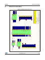
Mechanical drawing
Figure 8. STM32F072 Discovery board mechanical drawing
20/25
DocID025474 Rev 1
DocID025474 Rev 1
ϭ
Ϯ
ϯ
ϰ
ϱ
ϲ
ϳ
ϴ
ϵ
ϭϬ
ϭϭ
ϭϮ
ϭϯ
ϭϰ
ϭϱ
ϭϲ
ϭϳ
ϭϴ
ϭϵ
ϮϬ
Ϯϭ
ϮϮ
Ϯϯ
Ϯϰ
Ϯϱ
Ϯϲ
Ϯϳ
Ϯϴ
Ϯϵ
ϯϬ
ϯϭ
ϯϮ
ϯϯ
ϭ
,ĞĂĚĞƌ ϯϯ
Wϭ
ͺ h^Z
EZ^d
^dDϯϮ&Ϭͺ h^Zdϭͺ Zy
^dDϯϮ&Ϭͺ h^Zdϭͺ dy
Wϭ Ϭ
W ϵ
EZ^d
DK
Wϭ ϰ
Wϭ ϯ
hͺ^dͺ> /E<
^dͺ>/ E<ͺ sϮ ͘^,K W ϭϯ
W ϭϰ
W ϭϱ
W&Ϭ
W&ϭ
'E
EZ^d
WϬ
Wϭ
WϮ
Wϯ
W Ϭ
W ϭ
W Ϯ
W ϯ
s^^ϯ
s ϯ
W ϰ
W ϱ
W ϲ
W ϳ
Wϰ
Wϱ
WϬ
Wϭ
WϮ
W ϭϬ
W ϭϭ
W ϭϮ
'E
'E
ϯs
ͺ h^Z
EZ^d
'E
s
sd
d^ͺ 'ϯͺ/ KϮ
d^ͺ 'ϯͺ/ Kϯ
d^ͺ 'Ϯͺ/ Kϯ
d^ͺ 'Ϯͺ/ Kϰ
d^ͺ 'ϭͺ/ Kϯ
d^ͺ 'ϭͺ/ Kϰ
hͺ^E^ KZͺ W
^E^KZ ͺ W͘^ ĐŚŽĐ
Wϭ Ϭ
W ϵ
dͺ EZ ^d
EZ^d
d^ͺ 'ϯͺ/ KϮ
d^ͺ 'ϯͺ/ Kϯ
d^ͺ 'Ϯͺ/ Kϯ
d^ͺ 'Ϯͺ/ Kϰ
d^ͺ 'ϭͺ/ Kϯ
d^ͺ 'ϭͺ/ Kϰ
d<ͬ^t ><
dD^ ͬ^t/K
DK
Wϭ ϰ
Wϭ ϯ
Ϯ
Ϯ
EZ^d
KKd Ϭ
s^^ϯ
s ϯ
W&Ϭ
W&ϭ
WϮ
WϬ
Wϭ
WϮ
Wϯ
Wϰ
Wϱ
Wϲ
Wϳ
Wϴ
Wϵ
W ϭϬ
W ϭϭ
W ϭϮ
W ϭϯ
W ϭϰ
W ϭϱ
W Ϭ
W ϭ
W Ϯ
W ϯ
W ϰ
W ϱ
W ϲ
W ϳ
W ϴ
W ϵ
Wϭ Ϭ
Wϭ ϭ
Wϭ Ϯ
Wϭ ϯ
Wϭ ϰ
Wϭ ϱ
EZ^d
KKd Ϭ
s^^ϯ
s ϯ
W&Ϭ
W&ϭ
WϮ
WϬ
Wϭ
WϮ
Wϯ
Wϰ
Wϱ
Wϲ
Wϳ
Wϴ
Wϵ
W ϭϬ
W ϭϭ
W ϭϮ
W ϭϯ
W ϭϰ
W ϭϱ
W Ϭ
W ϭ
W Ϯ
W ϯ
W ϰ
W ϱ
W ϲ
W ϳ
W ϴ
W ϵ
Wϭ Ϭ
Wϭ ϭ
Wϭ Ϯ
Wϭ ϯ
Wϭ ϰ
Wϭ ϱ
ydͺ Z^ d
/ϮϮͺ^
/ϮϮͺ^>
>ͺh
> ͺ
>ͺ>
>ͺZ
WϬ
Wϭ
WϮ
Wϯ
Wϰ
Wϱ
Wϲ
Wϳ
Wϴ
Wϵ
W ϭϬ
W ϭϭ
W ϭϮ
W ϭϯ
W ϭϰ
W ϭϱ
DK
ͺ h^Z
d^ͺ 'ϭͺ/ Kϯ
d^ͺ 'ϭͺ/ Kϰ
d^ͺ 'Ϯͺ/ Kϯ
d^ͺ 'Ϯͺ/ Kϰ
d^ͺ 'ϯͺ/ KϮ
d^ͺ 'ϯͺ/ Kϯ
h^&ϰ ͺD
h^&ϰ ͺW
^W/ Ϯͺ^<
^W/ ϮͺD/ ^K
^W/ ϮͺDK^/
E^ ͺ DD^ͺ ^W/
DD^ͺ/ Edϭ
DD^ͺ/ EdϮ
hͺ^dDϯ Ϯ&dž
^dDϯϮ&dž ͘^ĐŚŽĐ
DK
ͺ h^Z
d^ͺ 'ϭͺ/ Kϯ
d^ͺ 'ϭͺ/ Kϰ
d^ͺ 'Ϯͺ/ Kϯ
d^ͺ 'Ϯͺ/ Kϰ
d^ͺ 'ϯͺ/ KϮ
d^ͺ 'ϯͺ/ Kϯ
h^&ϰ ͺD
h^&ϰ ͺW
^W/ Ϯͺ^<
^W/ ϮͺD/ ^K
^W/ ϮͺDK^/
E^ ͺ DD^ͺ ^W/
DD^ͺ/ Edϭ
DD^ͺ/ EdϮ
ydͺ Z^ d
/ϮϮͺ^
/ϮϮͺ^>
>ͺh
> ͺ
>ͺ>
>ͺZ
WϬ
Wϭ
WϮ
Wϯ
Wϰ
Wϱ
Wϲ
Wϳ
Wϴ
Wϵ
W ϭϬ
W ϭϭ
W ϭϮ
W ϭϯ
W ϭϰ
W ϭϱ
ϯ
ϯ
ϱs
Wϭ ϯ
Wϭ Ϯ
Wϭ ϭ
Wϭ Ϭ
W ϵ
W ϴ
Wϵ
Wϴ
Wϳ
Wϲ
W ϭϱ
W ϭϰ
W ϭϯ
'E
,ĞĂĚĞƌ ϯϯ
ϭ
Ϯ
ϯ
ϰ
ϱ
ϲ
ϳ
ϴ
ϵ
ϭϬ
ϭϭ
ϭϮ
ϭϯ
ϭϰ
ϭϱ
ϭϲ
ϭϳ
ϭϴ
ϭϵ
ϮϬ
Ϯϭ
ϮϮ
Ϯϯ
Ϯϰ
Ϯϱ
Ϯϲ
Ϯϳ
Ϯϴ
Ϯϵ
ϯϬ
ϯϭ
ϯϮ
ϯϯ
h^&ϰ ͺD
h^&ϰ ͺW
^W/ Ϯͺ^<
^W/ ϮͺD/ ^K
^W/ ϮͺDK^/
E^ ͺ DD^ͺ ^W/
DD^ͺ/ Edϭ
DD^ͺ/ EdϮ
^dDϯϮ&ϬϳϮͲ/^K
EƵŵďĞƌ͗ DϭϬϳϲ ZĞǀ͗ ͘ϭ ;W͘^, Ϳ
dŝƚůĞ͗
^dDŝĐƌŽĞůĞĐƚƌŽŶŝĐ Ɛ
ϰ
ĂƚĞ͗ϭϬͬϮϴͬϮϬϭϯ
^ŚĞĞƚ ϭ
ŽĨ
ϱ
ZĞǀ ͘Ϭ ͲͲх W ůĂď Ğů DϭϬϳϲ ͲϬϬ
ZĞǀ ͘ϭͲͲх W ůĂďĞů DϭϬϳϲ ͲϬϭ͕ ^ŝůŬƐĐƌĞĞ Ŷ ŵŽĚŝĨŝĐĂƚŝŽŶĂŶĚǀĂůƵĞƐŽĨZϮϵ ͕ϯϬ͕ϯϭ͕ϯϮ͘
ZĞǀ ͘ϭͲͲх W ůĂďĞů DϭϬϳϲ ͲϬϭ͕ ZĞƉůĂĐĞ ^dDϯϮ&Ϭ ϱϮ ďLJ ^dDϯϮ&ϬϳϮ ŽŶ^ŝůŬƐĐƌĞĞŶ
sͺh^ s
Wϵ
Wϴ
s
KKd Ϭ
Wϳ
Wϲ
Wϱ
Wϰ
Wϯ
WϮ
W ϭϮ
W ϭϭ
W ϭϬ
Wϭ ϱ
Wϭ ϰ
s/ KϮ
WϮ
^W/ Ϯͺ^<
^W/ ϮͺD/ ^K
^W/ ϮͺDK^/
E^ ͺ DD^ͺ ^W/
DD^ͺ/ Edϭ
ydͺ Z^ d
DD^ͺ/ EdϮ
/ϮϮͺ^
/ϮϮͺ^>
h^&ϰ ͺD
h^&ϰ ͺW
>ͺh
> ͺ
>ͺ>
>ͺZ
hͺDD^ͺ h^
DD^ͺ h^͘^ĐŚ ŽĐ
s
ydͺ Z^ d
/ϮϮͺ^
/ϮϮͺ^>
>ͺh
> ͺ
>ͺ>
>ͺZ
ϰ
6
ϭ
UM1690
Electrical schematics
Electrical schematics
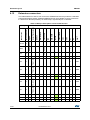
Figure 9. STM32F072 Discovery board
21/25
25
ϭϭ
ϭϬϬŶ&
ϯs
ϭ
Ϯ
ϭ
h^ͲD/ E/ ͲƚLJƉĞ
ϭ
Ϯ
ϯ
ϰ
ϱ
ϲ
hϱs
Ϭ
ϯs
ϬϬ<
sd
W ϭϯ
W ϭϰ
W ϭϱ
K^/E
K^Khd
EZ^d
s^^
s
WϬ
Wϭ
WϮ
86%B'0
86%B'3
ϵϬϭϯͲ^KdϮϯ
EŽƚ &ŝƚƚĞĚ
^d>/ E<ͺ Zy
ϭ
Ϯ
ϯ
ϰ
ϱ
ϲ
ϳ
ϴ
ϵ
ϭϬ
ϭϭ
ϭϮ
<ϱ
:Wϭ
$,1B
Z
ϴ
Z
ZϭϬ
ϭ
Z
ϵ
ϳ
Ϭ
ϭ
^ ϭϮ
h^ ^dͲ>/E<
s
Ͳ
н
/
'E
^,>>
Eϭ
ϰ <ϳ
ZϮϳ
^ ϭϭ
dy
Zy
ϰ <ϳ
ZϮϲ
26&B,1
26&B287
670B567
E
ϵ
ϮϬƉ&
ůŽƐĞ ƚŽ :W
EŽƚ &ŝƚƚĞĚ
^dDϯϮ&Ϭͺ h^Zdϭͺ dy
Wϵ
WϭϬ
ZϮϯ
ϴD,nj
yϭ
^dDϯϮ&Ϭͺ h^Zdϭͺ Zy
^ϱ
ZϮϱ
ϭϬϬ<
ϯs
ϭϬ
ϮϬƉ&
%RDUG ,GHQW 3& ϭϬϬ<
6:,0B,1
6:,0
Zϭϵ
ϯs
dϭ
ϭ
Zϭϳ
ϯϲ<
Zϭϲ
ϭϬ<
hϱs
dͺ:Z^d
ϭ Ϭ<
6:,0B,1
6:,0B567
6:,0B567B ,1
7B-7&.
7B-7'2
7B-7',
7B1567
ϯ
6:,0B,1
6:,0
ZϮϮ
^d>/E<ͺdy
670B-7&.
ϰϴ
ϰϳ
ϰϲ
ϰϱ
ϰϰ
ϰϯ
ϰϮ
ϰϭ
ϰϬ
ϯϵ
ϯϴ
ϯϳ
Ϯ
Ϯ
ϯs
sͺϮ
s^^ͺϮ
:dD^ͬ^t /K
WϭϮ
Wϭϭ
WϭϬ
Wϵ
Wϴ
W ϭϱ
W ϭϰ
W ϭϯ
W ϭϮ
sͺϯ
s^^ͺϯ
Wϵ
Wϴ
KKdϬ
Wϳ
Wϲ
Wϱ
Wϰͬ:EdZ^d
Wϯͬ:dK
Wϭϱ ͬ:d/
:d< ͬ^t><
Wϯ
Wϰ
Wϱ
Wϲ
Wϳ
WϬ
Wϭ
WϮ ͬKKdϭ
WϭϬ
Wϭϭ
s^^ͺϭ
sͺϭ
ϭϯ
ϭϰ
ϭϱ
ϭϲ
ϭϳ
ϭϴ
ϭϵ
ϮϬ
Ϯϭ
ϮϮ
Ϯϯ
Ϯϰ
Ϯ
ϯϲ
ϯϱ
ϯϰ
ϯϯ
ϯϮ
ϯϭ
ϯϬ
Ϯϵ
Ϯϴ
Ϯϳ
Ϯϲ
Ϯϱ
/ĚĚ
ϯs
:WϮ
>Ϯ
> ͕ƌĞĚ
ϭ<
Zϯ
ϯs
7B6:',2B,1
7B-706
7B-7&.
670B-706
86%B'3
86%B'0
7B6:2
/('B67/,1.
ϯs
hϮ
^dDϯϮ&ϭϬ ϯ ϴdϲ
ϭϬ<
Zϭϱ
ϮϮ
ϮϮ
ZϮϰ
ZϮϴ
ϮϮ
ϮϮ
ZϮϭ
ZϮϬ
dϲ Ϭ:& />D
ϰ
7B6:2
7B1567
7B-706
7B-7&.
E $,1B
ϴ
ϭϬϬŶ&
ϱ
ϭϬϬŶ&
EŽƚ &ŝƚƚĞĚ
DK
hϱs
ϯ
dϲ Ϭ:& />D
ϭ
ydͺϱs͕ /ŶƉƵƚ Žƌ KƵƚƉƵƚ
ϳ
ϭϬϬŶ&
ϯϮ
ϮϬƉ&
0&2
ϱs
ϱs
ϭ
sŝŶ
hϭ
Eϱ
ϱ
ϭϬϬ
Zϱ
ϭϬϬ
Zϲ
670B-706
670B-7&.
^ ϭϬ
ϯ
Ϯ
Wϭϰ
Wϭϯ
EZ^d
ϰ Zϰ
ϭ
Ϭ
ϯ
ĂƚĞ͗ ϰ
^t
Ϯ
^ŚĞĞƚ ŽĨ
ϱ
ydͺϯs͕ /ŶƉƵƚ Žƌ KƵƚƉƵƚ
^dDϯϮ&ϬϳϮͲ/^K ^dͲ>/E<ͬsϮ ;^t ŽŶůLJͿ
Ϯ
ϭϬϬŶ&
ϯs
ϯs
^t/K
^t><
ϯs
>ͺ / K> KZͺ D^
ͺ'ƌĞĞŶ
Z ĞĚ
> ϭ
dϲ Ϭ:& />D
ϲ
ϭђ&ͺ yϱZ ͺϬϲϬϯ
EƵŵďĞƌ͗ DϭϬϳϲ ZĞ ǀ͗ &3&%6&+
dŝƚůĞ͗
^ϴ
^ϲ
^ϯ
^ϭ
ϭ
ϭϬŶ&ͺyϳ Zͺ ϬϲϬϯ
zW^^
sŽ Ƶƚ
>ϯ ϵϴϱDϯϯZ
WtZ
7B1567
ϰ
:ƵŵƉĞ ƌƐ KE ͲͲ х /^KsZz^ĞůĞĐƚĞĚ
:ƵŵƉĞ ƌƐ K&& Ͳ Ͳх ^dͲ>/E<^ĞůĞĐƚĞĚ
KD
^ϵ
^ϳ
^ϰ
^Ϯ
^dDŝĐƌŽĞůĞĐƚƌŽŶŝĐƐ
ϯ
ϭϬϬŶ&
d<ͬ^t ><
dD^ ͬ^t/K
&h>d
/('B67/,1.
ϯ
/E,
ϰ
'E
ϭђ&ͺ yϱZ ͺϬϲϬϯ
Z DƵƐƚ ďĞ ǀĞƌLJ ĐůŽƐĞ ƚŽ ^dDϯϮ&ϭϬϯ ƉŝŶ Ϯϵ
ϭϮ
ϭϬϬŶ&
s
ϭϬϬ
Zϭϰ
Zϰϰ
ϭϬϬ
ϭ
Ϯ
ϯ
ϰ
ϱ
ϲ
,ĞĂĚĞƌ ϲ
Eϰ
^t
Zϭϴ
ϯ
Ϯ
DocID025474 Rev 1
ϰ
Z^Zs
22/25
ϭ
Ϯ
ϯ
ϰ
ϭ
Electrical schematics
UM1690
Figure 10. ST-LINK/V2 (SWD only)
DocID025474 Rev 1
W ϭϱ
W ϭϰ
W&ϭ
W&Ϭ
DK
^ ϭϵ
W ϭϰͲK^ ϯϮͺ/E
W& ϭͲK^ ͺ Khd
W& ϬͲK^ ͺ/E
W ϭϱͲK^ ϯϮͺKhd
Zϯϰ
Zϯϱ
Ϭ
Ϭ
Zϯϳ
Zϯϲ
EŽƚ &ŝƚƚĞĚ
ϭ
^ Ϯϲ
ϭϴ
ϭϬϬŶ&
ĨĐŵϭϲϬϴͲϬϲϬϯ
>ϭ
Ϯϵ
ϭϬϬŶ&
s
^ ϭϱ
s
Ϯϱ
ϭƵ&
Ϯϯ
ϮϬƉ&
ϮϮ
ϮϬƉ&
ϭϳ
ϭϬϬŶ&
Ϯϰ
ϭϬϬŶ&
^ ϭϲ
s/KϮ
ϭϲ
ϭƵ&
Ϯϭ
Ϯ
s^^
s^^ͺϮ
s^^ͺϰ
s^^ͺ h^
ϭϬϬŶ&
^dDϯϮ&Ϭϳ ϮZ dϲ
sd
s
sͺϮ
sͺϰ
Ϯ
ϭϮ
ϯϭ
ϲϯ
ϰϳ
WϬ
Wϭ
Wϭϭ
WϭϮ
Wϲ
Wϳ
WϮ
Wϯ
WϬ
Wϭ
^ ϯϭ
^ Ϯϯ
^ Ϯϵ
Wϲ
Wϳ
Wϭϭ
WϭϮ
^ Ϯϳ
WϮ
Wϯ
^ ϯϮ
^ ϮϬ
^ ϯϬ
^ Ϯϴ
^dž DƵƐƚ ďĞ ǀĞƌLJ ĐůŽƐĞ ƚŽ ƚŚĞ ^dDϯϮ&ϬϳϮ
sͺh^
hϰ
sd
ϭ
ϭϯ
ϯϮ
ϲϰ
ϰϴ
sͺh^
ϲ͘ϴƉ&
yϮ
D ϯϬϲͲ'ͲϬ ϲYͲϯϮ͘ϳϲϴ
ϭϵ
ϲ͘ϴƉ&
ϮϬ
yϯ
ϴD,nj
EŽƚ &ŝƚƚĞĚ
Ϯ ϮϬ
Ϭ
ůů ƚŚŝƐ ďůŽĐŬ ŵƵƐƚ ďĞ ǀĞƌLJ ĐůŽƐĞ ƚŽ ƚŚĞ ^dDϯϮ&ϬϳϮ
^ ϭϯ
DƵƐƚ ďĞ ĐůŽƐĞ ƚŽ ƚŚĞ ƌLJƐƚĂů
^ ϭϰ
^ ϭϴ
^ ϭϳ
DK
ϭ
ϰ
DƵƐƚ ďĞ ĐůŽƐĞ ƚŽ ƚŚĞ ƌLJƐƚĂů
Ϯ
ϭ
Ϯ
ϯ
ϭ
W ϭϯ
W ϭϱ
W ϭϰ
WϬ
WϮ
Wϭ
W ϭϬ
W ϭϭ
Wϱ
Wϲ
Wϳ
Wϴ
Wϵ
WϬ
WϮ
Wϯ
Wϰ
Wϱ
Wϲ
Wϳ
Wϴ
Wϵ
W ϭϬ
W ϭϭ
W ϭϮ
W ϭϯ
W ϭϰ
W ϭϱ
Wϭϯ
Wϭϰ
Wϭϱ
Wϴ
Wϵ
WϭϬ
Wϰ
Wϱ
WϬ
Wϭ
Ϯϲ
Ϯϳ
Ϯϴ
ϱϱ
ϱϲ
ϱϳ
ϱϴ
ϱϵ
ϲϭ
ϲϮ
Ϯϵ
ϯϬ
ϯϯ
ϯϰ
ϯϱ
ϯϲ
ϭϰ
ϭϱ
ϭϲ
ϭϳ
ϮϬ
Ϯϭ
ϮϮ
Ϯϯ
ϰϭ
ϰϮ
ϰϯ
ϰϰ
ϰϱ
ϰϲ
ϰϵ
ϱϬ
ϯ
KKdϬ
ϲϬ
ϰ
Zϯϯ
h^&ϰ ͺD
h^&ϰ ͺW
ϰ
ĂƚĞ͗ ϯ
^ŚĞĞƚ ŽĨ
ϱ
^dDϯϮ&ϬϳϮͲ/^K Ͳ ^dD ϯϮ&ϬϳϮdϲ Dh
86%)B'0
86%)B'3
d^ͺ 'ϭͺ/ Kϯ
d^ͺ 'ϭͺ/ Kϰ
d^ͺ 'Ϯͺ/ Kϯ
d^ͺ 'Ϯͺ/ Kϰ
d^ͺ 'ϯͺ/ KϮ
d^ͺ 'ϯͺ/ Kϯ
s
DƵƐƚ ď Ğ ǀĞƌLJ ĐůŽƐĞ ƚŽ
ƚŚĞ ^ dDϯϮ&ϬϳϮ
ϱ ϭϬ
^ Ϯϱ
^ Ϯϰ
KKdϬ
EZ^d
sϯ
ϯϯ
ϭϬϬŶ&
s^^ϯ
WϮ
d^ͺ 'ϭͺ/ Kϯ
d^ͺ 'ϭͺ/ Kϰ
d^ͺ 'Ϯͺ/ Kϯ
d^ͺ 'Ϯͺ/ Kϰ
d^ͺ 'ϯͺ/ KϮ
d^ͺ 'ϯͺ/ Kϯ
EZ^d
EƵŵďĞƌ͗ DϭϬϳϲ ZĞ ǀ͗ &3&%6&+
dŝƚůĞ͗
ϯϮͺKhd
ϯϮͺ/E
W ϭϯ
W ϭϮ
W ϭϭ
W ϭϬ
Wϵ
Wϴ
Wϳ
Wϲ
Wϱ
Wϰ
Wϯ
WϮ
Wϭ
WϬ
W& ϬͲK^ ͺ/E
W& ϭͲK^ ͺ Khd
sϯ
s^^ϯ
WϮ
W ϭϱͲK^
W ϭϰͲK^
W ϭϯ
W ϭϮ
W ϭϭ
W ϭϬ
Wϵ
Wϴ
Wϳ
Wϲ
Wϱ
Wϰ
Wϯ
WϮ
Wϭ
WϬ
ϳ
ϱ
ϲ
ϭϵ
ϭϴ
ϱϰ
ϰ
ϯ
Ϯ
ϱϯ
ϱϮ
ϱϭ
ϰϬ
ϯϵ
ϯϴ
ϯϳ
Ϯϱ
Ϯϰ
ϭϭ
ϭϬ
ϵ
ϴ
^dDŝĐƌŽĞůĞĐƚƌŽŶŝĐƐ
KKdϬ
EZ^d
W& ϬͲK^ ͺ/E
W& ϭͲK^ ͺ Khd
sͺϯ
s^^ͺϯ
WϮ
W ϭϱͲK^ ϯϮͺKhd
W ϭϰͲK^ ϯϮͺ/E
W ϭϯ
W ϭϮ
W ϭϭ
W ϭϬ
Wϵ
Wϴ
Wϳ
Wϲ
Wϱ
Wϰ
Wϯ
WϮ
Wϭ
WϬ
^W/ Ϯͺ^<
^W/ ϮͺDK^/
^W/ ϮͺD/ ^K
E^ͺ DD^ͺ ^W/
DD^ͺ/ EdϮ
DD^ͺ/ Edϭ
/ϮϮͺ ^>
/ϮϮͺ ^
ydͺ Z^ d
>ͺh
>ͺ
>ͺ>
>ͺZ
ͺ h^Z
^dDϯϮ&Ϭϳ ϮZ dϲ
WϬ
Wϭ
WϮ
Wϯ
Wϰ
Wϱ
Wϲ
Wϳ
Wϴ
Wϵ
W ϭϬ
W ϭϭ
W ϭϮ
W ϭϯ
W ϭϰ
W ϭϱ
WϬ ͬt<hWϭ
Wϭ
WϮ
Wϯ
Wϰ
Wϱ
Wϲ
Wϳ
Wϴ
Wϵ
WϭϬ
Wϭϭ
WϭϮ
Wϭϯ
Wϭϰ
Wϭϱ
hϰ
^W/ Ϯͺ^<
^W/ ϮͺDK^/
^W/ ϮͺD/ ^K
E^ͺ DD^ͺ ^W/
DD^ͺ/ EdϮ
DD^ͺ/ Edϭ
/ϮϮͺ ^>
/ϮϮͺ ^
ydͺ Z^ d
>ͺh
> ͺ
>ͺ>
>ͺZ
ͺ h^Z
d^ͺ 'ϯͺ/ KϮ
d^ͺ 'ϯͺ/ Kϯ
WϮ
Wϯ
Wϰ
Wϱ
Wϲ
Wϳ
Wϴ
Wϵ
W ϭϬ
W ϭϭ
W ϭϮ
W ϭϯ
W ϭϰ
W ϭϱ
Wϭϯ
Wϭϰ
Wϭϱ
86%)B'0
86%)B'3
WϬ
Wϭ
d^ͺ 'ϭͺ/ Kϯ
d^ͺ 'ϭͺ/ Kϰ
Wϰ
Wϱ
d^ͺ 'Ϯͺ/ Kϯ
d^ͺ 'Ϯͺ/ Kϰ
Wϴ
Wϵ
WϭϬ
ϯ
UM1690
Electrical schematics
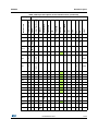
Figure 11. STM32F072RBT6 MCU
23/25
25
Revision history
7
UM1690
Revision history
Table 7. Document revision history
24/25
Date
Revision
18-Dec-2013
1
Changes
Initial release.
DocID025474 Rev 1
UM1690
Please Read Carefully:
Information in this document is provided solely in connection with ST products. STMicroelectronics NV and its subsidiaries (“ST”) reserve the
right to make changes, corrections, modifications or improvements, to this document, and the products and services described herein at any
time, without notice.
All ST products are sold pursuant to ST’s terms and conditions of sale.
Purchasers are solely responsible for the choice, selection and use of the ST products and services described herein, and ST assumes no
liability whatsoever relating to the choice, selection or use of the ST products and services described herein.
No license, express or implied, by estoppel or otherwise, to any intellectual property rights is granted under this document. If any part of this
document refers to any third party products or services it shall not be deemed a license grant by ST for the use of such third party products
or services, or any intellectual property contained therein or considered as a warranty covering the use in any manner whatsoever of such
third party products or services or any intellectual property contained therein.
UNLESS OTHERWISE SET FORTH IN ST’S TERMS AND CONDITIONS OF SALE ST DISCLAIMS ANY EXPRESS OR IMPLIED
WARRANTY WITH RESPECT TO THE USE AND/OR SALE OF ST PRODUCTS INCLUDING WITHOUT LIMITATION IMPLIED
WARRANTIES OF MERCHANTABILITY, FITNESS FOR A PARTICULAR PURPOSE (AND THEIR EQUIVALENTS UNDER THE LAWS
OF ANY JURISDICTION), OR INFRINGEMENT OF ANY PATENT, COPYRIGHT OR OTHER INTELLECTUAL PROPERTY RIGHT.
ST PRODUCTS ARE NOT DESIGNED OR AUTHORIZED FOR USE IN: (A) SAFETY CRITICAL APPLICATIONS SUCH AS LIFE
SUPPORTING, ACTIVE IMPLANTED DEVICES OR SYSTEMS WITH PRODUCT FUNCTIONAL SAFETY REQUIREMENTS; (B)
AERONAUTIC APPLICATIONS; (C) AUTOMOTIVE APPLICATIONS OR ENVIRONMENTS, AND/OR (D) AEROSPACE APPLICATIONS
OR ENVIRONMENTS. WHERE ST PRODUCTS ARE NOT DESIGNED FOR SUCH USE, THE PURCHASER SHALL USE PRODUCTS AT
PURCHASER’S SOLE RISK, EVEN IF ST HAS BEEN INFORMED IN WRITING OF SUCH USAGE, UNLESS A PRODUCT IS
EXPRESSLY DESIGNATED BY ST AS BEING INTENDED FOR “AUTOMOTIVE, AUTOMOTIVE SAFETY OR MEDICAL” INDUSTRY
DOMAINS ACCORDING TO ST PRODUCT DESIGN SPECIFICATIONS. PRODUCTS FORMALLY ESCC, QML OR JAN QUALIFIED ARE
DEEMED SUITABLE FOR USE IN AEROSPACE BY THE CORRESPONDING GOVERNMENTAL AGENCY.
Resale of ST products with provisions different from the statements and/or technical features set forth in this document shall immediately void
any warranty granted by ST for the ST product or service described herein and shall not create or extend in any manner whatsoever, any
liability of ST.
ST and the ST logo are trademarks or registered trademarks of ST in various countries.
Information in this document supersedes and replaces all information previously supplied.
The ST logo is a registered trademark of STMicroelectronics. All other names are the property of their respective owners.
© 2013 STMicroelectronics - All rights reserved
STMicroelectronics group of companies
Australia - Belgium - Brazil - Canada - China - Czech Republic - Finland - France - Germany - Hong Kong - India - Israel - Italy - Japan Malaysia - Malta - Morocco - Philippines - Singapore - Spain - Sweden - Switzerland - United Kingdom - United States of America
www.st.com
DocID025474 Rev 1
25/25
25