1
Instruction
Manual
Table of Contents
1
ACKNOWLEDGEMENTS 4
2
INTRODUCTION 5
3
INSTRUCTIONS FOR USE
6
4
SYSTEM REQUIREMENTS
7
5
TECHNICAL SPECIFICATIONS 7
6
7
Overview
7
VGA Connector
8
DEVELOPER INFORMATION
9
General information
9
Video processor
9
Audio processor
9
Game controller
10
Memory mapper
10
Conversion tool
10
Modifying MSX Bios to reroute VDP output to Franky
14
VDP DOCUMENTATION 15
Introduction
15
VDP ports
15
VDP Programming
16
Control port
16
VDP register write
17
Data port
17
Status flags
18
Color RAM
19
Display modes
19
Register reference
21
Patterns
25
Background
25
Horizontal scrolling
25
Vertical scrolling
26
Sprites
Table parsing
27
28
2
Display timing
29
Display details
30
H counter
31
Interrupts
32
Frame interrupts
33
Line interrupts
33
Miscellaneous
8
PROGRAMMABLE SOUND GENERATOR DOCUMENTATION
34
35
Accessing the SN76489 from software
35
SN76489 registers
35
Volume registers
36
Tone registers
36
Noise register
36
Example program
37
SN76489 register writes
37
How the SN76489 makes sound
39
Tone channels
40
Noise channel
40
The Linear Feedback Shift Register
41
The external Linear Feedback Shift Register
41
Volume/attenuation
42
The imperfect SN76489
43
Playing samples on the PSG
44
Pulse Code Modulation
44
Advanced PCM
45
Pulse Width Modulation
45
3
Acknowledgements
SuperSoniqs would like to thank the following people first, because without them this
card wouldn’t be a reality:
Ronnie van der Kolk – www.rklok.nl , for providing us with broken Sega Mark
III consoles so we could build our first prototypes. Luckely the VDP’s still worked.
Rob Hiep – www.msx.ch , he provided us with cartridge cases so we could
actually give the Franky PCB a place to live in.
Lino Lampers - members.chello.nl/mlampers/ , for providing us with the vga
connectors and video memory ic’s. My backyard looked like Zombieland
afterwards.
Bas Kornalijnslijper – www.bas-ditta.info , for arranging the assembly of our
first batch.
Maxim Zhao – www.smspower.org , for helping out in general and for giving us
permission to use his texts about the audio part of the Sega A/V processors and
modify them.
Charles MacDonald - http://cgfm2.emuviews.com/, for giving us permission to
use his VDP documentation and modify them.
Albert Beevendorp - www.bifi.msxnet.org , for testing and writing programs
4
Introduction
First of all: congratulations with your new purchase. Franky is a powerful new video and
audio extension card for MSX computers. The core component on this hardware is a
combined video and audio processor that is also used by the Sega Mark III and Sega
Master System game consoles. It has his own video memory, a volume output adjuster
(on the PCB) and the output connector is a standard 15 pin VGA connector that has been
made pin compatible with the One Chip MSX, so you can use existing OCM cables to
connect Franky to your monitor or TV with RGB input support. Franky also features a
PAL/NTSC encoder that can ensure compatibly with the CVBS (composite video) standard
in your country. This might be convenient if your monitor or TV has support for CVBS
only. Please see chapter ‘Technical Specifications’ for more details.
Franky is not a Sega console on its own. Although it can potentially run most programs
made for the 8-bit Sega consoles mentioned, Franky still needs an MSX computer to
operate. Franky uses his own addresses for accessing the video/audio processor.
Therefore, existing Sega homebrew software needs to be converted with our software
converter. Testing shows that about 75% of programs tested will run without problems
after using the converter, without any further adjustments. This number surely will rise
in time when more developers start using Franky. We expect more tools, useful programs
and new games in the near future. If you start a new project with Franky, please let us
know!
If you need support while developing for Franky these places are a great start:
supersoniqs.wordpress.com Our website where we will post new information on our
products, keep our technical documentation and tools up to date and inform you about
new developments.
www.smspower.org Great site about the Sega Master System and Mark III. It has a lot of
developer information on Sega hardware. It features an active community with extensive
forum and some great people with a lot of technical knowledge about Sega software and
hardware.
www.msx.org Biggest MSX community site on the internet with more than 5000
members. Please check the forum and post your questions and remarks in the cross
development section.
5
Also, there are IRC channels where MSX developers and users meet. These are:
#MSXdev on Rizon (irc.rizon.net)
#MSX on Undernet (eu.undernet.org)
#MSX on Rizon (irc.rizon.net)
To connect to IRC channels you need a dedicated IRC client like mIRC for windows.
More information on IRC can be found at Wikipedia: http://en.wikipedia.org/wiki/Irc
Have great fun with your new hardware and thank you for exploring new possibilities on
MSX with Franky!
Instructions for use
Franky, like most cartridges for your MSX computer, does not like being inserted in your
MSX cartridge slot when the MSX is powered on. Please make sure that your MSX is
powered off when inserting or removing Franky. Else you might irreversibly damage
Franky and / or your MSX computer.
Franky consist out of more than 45 assembled electronic components. So please be
gentle when you move or store Franky.
Besides an MSX, Franky also needs a cable to hook up the shared video / audio out
connector to your monitor or TV. This cable is not part of your purchased product
package because there are different standards for RGB and CVBS connectors. Please
check the chapter “Technical specifications’ to examine the pin layout diagram of
Franky’s output connector to build your own cable. You can also order a custom made
cable online at www.bas-ditta.info, if your input connectors are not too exotic.
When Franky is connected to your MSX and everything is powered on, you can start
using Franky with the software converter, program your own programs or adjust your
existing code for use on the Franky hardware. Please see chapter ‘Developer information’
for more information how to program for Franky.
Please note that when using the software converter to load programs your
joystick needs to be in joystick port 2. MSX game port 2 is port 1 in Sega programs.
6
System requirements
Franky works on any MSX, with or without disk drive. Still, if you want to use the
software converter and load converted Sega programs we recommend using an MSX with
at least a connected disk drive. For converted Sega programs the same rule apply as
when using MSX programs that are converted from cartridge: you need more memory
than the original size of the program. We recommend using a MSX with disk drive and
512KB or more. Of course, if you are programming your own software you are not bound
to any requirements, except those you really need for your program.
If you want to use both the RGB output of your MSX computer and the RGB output
possibility of the VGA connector on Franky at the same time, two monitors (or a monitor
and a TV) or switch box are needed. However, if your monitor or TV supports selectable
RGB and CVBS input, you can choose to connect the MSX to your RGB input, and Franky
to the CVBS input (or vice versa, depending on which output possibilities your MSX
provides), thus eliminating the need for a dual monitor setup.
Technical specifications
Overview
Sega A/V Processor: model 315-5124 or 315-5246
Graphics: VDP (Video Display Processor) derived from Texas Instruments TMS9918
32 simultaneous colors available (two separate palettes with 16 colors out of 64)
Screen resolutions 256×192 and 256×224. PAL also supports 256×240
3.546893 MHz for PAL/B/G (through 4-pin DIP crystal oscillator)
3.579545 MHz for NTSC (clock provided by MSX)
3.575611 MHz for PAL-M (by replacing the 4-pin DIP oscillator, not included)
8×8 pixel characters, max 463
8×8 or 8×16 pixel sprites, max 64
Horizontal, vertical, and partial screen scrolling
Sound (PSG): Texas Instruments SN76489 (Build in VDP)
4 channel mono sound (3 Square Waves, 1 White Noise)
3 tone generators, 10 octaves each, 1 white noise generator
Video RAM: 128kb
Build in PAL/NTSC encoder: model Analog Devices AD722, AD724 or AD725
7
VGA Connector
The connector used for the video and sound output of Franky is a 15 pin standard VGA
connector
The pin layout (seen as looking towards the connector) is as follows:
Pin 1
Red
Pin 2
Green
Pin 3
Blue
Pin 4
Not connected
Pin 5
Ground
Pin 6
Red ground
Pin 7
Green ground
Pin 8
Blue ground
Pin 9
Not connected
Pin 10
Ground
Pin 11
Not connected
Pin 12
Not connected
Pin 13
CVBS (Composite) output
Pin 14
Audio
Pin 15
Not connected
Please note that although we used a VGA connector for durability, you can not use this
connector to connect the Franky VDP card to a VGA monitor.
8
Developer information
General information
The Sega and MSX systems have a lot in common and this makes it possible to convert
software from Sega to MSX (and vice versa). Both systems use a Z80 CPU and have the
same kind of memory mapping. Even the VDP is partly compatible to the MSX1 VDP, but
with more options. The original Sega Audio / Video processor is used in Franky. MSX
needs to handle the remaining parts. This being the game controller; sound and memory
mapping.
Originally the I/O addresses used in the Sega system are occupied in the MSX system;
therefore the Sega VDP places data on different addresses which are unused in the MSX
system. The VDP and PSG of the Sega are in the same chip, in a way that the difference
between the I/O of PSG and VDP is &H40 by hardware. This reduced our choices of
assigning I/O addresses while designing Franky. To maintain MSX compatibility we have
chosen an I/O address of &H88 for the VDP and &H48 for PSG.
The Franky card itself uses the I/O addresses &H88, &H89, &H48 and &H49. In the Sega
system the game controller uses I/O &HDC and &HDD and if an FM-Pac is available it
uses &HF0 to &HF2. All these I/O addresses must be changed to run a Sega program on
MSX, this is also the case for the memory mapping which is done at memory addresses
in the Sega system and I/O addresses in the MSX system
Video processor
The Sega VDP is located at &H88 and &H89 in Franky, this used to be &HBE and &HBF in
the Sega Master System console. This means all OUT, IN, OUTI, OTIR, INI and INIR
instructions to &HBE or &HBF must be changed to &H88 and &H89.
Audio processor
The same counts for the audio processor. All OUT, IN, OUTI, OTIR, INI and INIR
instructions accessing &H7E or &H7F (the original Sega addresses), must be changed to
&H48 and &H49.
9
Game controller
The Sega game controller is located at I/O &HDC for game pad 1 and I/O &HDD for game
pad 2. It turns out that all bits of game pad 1 are compatible with MSX joystick 1. Game
pad 2 requires some computations and bit shifting to make it working on MSX joystick
port 2. If the MSX PSG is set up for register 14, a read from I/O &HA2 returns the same
data as a read from &HDC in the Sega system. So all IN, INI and INIR instructions
accessing &HDC, should be changed to &HA2 and before executing the game, OUT
&HA0,14 to set up the MSX PSG.
Memory mapper
The Sega rom is mapped by writing the page number to memory address &HFFFD,
&HFFFE and &HFFFF, this indicates which 16k part of the rom should be readable at
address &H0000, &H4000 and &H8000. In the MSX system the ram memory is mapped
the same way, but instead of writing the page number to memory, the page number is
written to I/O addresses &HFC, &HFD and &HFE.
Conversion tool
This conversion tool loads the ROM image into the MSX memory starting from the first
page and replaces the following:
POKE &HFFFD OUT &HFC
POKE &HFFFE OUT &HFD
POKE &HFFFF OUT &HFE
OUT &HBE
OUT &H88
OUT &HBF
OUT &H89
OUT &H7E
OUT &H48
OUT &H7F
OUT &H49
OUT &HDC
OUT &HA2
OUT &HF0
OUT &H7C
OUT &HF1
OUT &H7D
OUT &HF2
OUT &H7E
Load Sega into RAM, find & replace:
32 FF FF -> 00 D3 FE
32 FE FF -> 00 D3 FD
32 FD FF -> 00 D3 FC
32 FC FF -> Switch to empty RAM page, no replace
10
Search for
INI, OUTI, OTIR, I/O (C)
ED A2 / ED A3 / ED B3
/ ED 41
Step back 32 bytes, find & replace:
0E 7E -> 0E 48
0E 7F -> 0E 49
0E BE -> 0E 88
0E BF -> 0E 89
0E DE -> No replace
0E DF -> No replace
0E F0 -> 0E 7C
0E F1 -> 0E 7D
01 7E -> 01 48
01 7F -> 01 49
01 BE -> 01 88
01 BF -> 01 89
01 DE -> No replace
01 DF -> No replace
01 F0 -> 01 7C
01 F1 -> 01 7D
Search for OUT:
D3 7E -> D3 48
D3 7F -> D3 49
D3 BE -> D3 88
D3 BF -> D3 89
D3 DE -> No replace
D3 DF -> No replace
D3 F0 -> D3 7C
D3 F1 -> D3 7D
11
Search for IN:
DB 7E -> DB 48
DB 7F -> DB 49
DB BE -> DB 88
DB BF -> DB 89
DB DC -> DB A2
DB DD -> Read from Gamepad2, no replace
DB DE -> No replace
DB DF -> No replace
DB F2 -> No replace
After the ROM is loaded, the upper 16k of the Z80 memory space is set to the highest
page in the mapper (OUT &HFF,&HFF). This part acts like the RAM of the Sega system.
Then the memory is initialized by switching the right pages to the Z80 memory (OUT
&HFC,0:OUT &HFD,1:OUT &HFE,2), finally a jump to address &H0000 reinitializes all
hardware and executes the game.
This is a very quick and simple conversion tool and due to the find and replace to the
program some display data or table might be damaged (that’s probably also the reason
that not all games are working as they should). The best results are achieved by
manually converting, disassembling, visual recognizing the difference between code and
data and understanding the meaning of the found OUT instructions.
To get full compatibility, some points should be implemented as well, e.g. if bit 3 of
&HFFFC is set, an SRAM is mapped at &H8000-&HBFFF. The second game pad needs a
subroutine to give the right values when the program reads I/O &HDD and the detection
of the availability of the FM chip is not in the converter as well.
Code example for disabling the MSX VDP interrupts and adding support for joystick port 1
If you want to load manually converted Sega binary programs, you need to disable the
MSX VDP interrupts.
By only setting OUT &HA0,14 before executing the program and replacing IN (&HDC) by
IN (&HA2) inside the binary, joysticks on joystick port 1 works fine. The example code
below is quick and dirty code and only works on MSX computers where the RAM is
located in slot 3-2:
12
10 IF PEEK(&HF677)<>&HC0 THEN POKE &HF677,&HC0:POKE &HC000,0:RUN
"HOMEBREW.BAS"
20 OUT &HFE,4:BLOAD "HOMEBR1.BIN"
30 OUT &HFE,5:BLOAD "HOMEBR2.BIN"
35 OUT &HA0,14
36 VDP(0)=VDP(0) AND 207
37 VDP(1)=VDP(1) AND 219
40 A=&HC800
50 DEF USR=&HC800
60 READ D$:IF D$="*" THEN A=USR(0)
70 POKE A,VAL("&H"+D$):A=A+1:GOTO 60
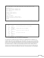
80 DATA
F3,3E,FF,D3,A8,3E,AA,32,FF,FF,3E,04,D3,FC,3E,05,D3,FD,D3,FE,C3,00,00,*
DI
LD
A,&HFF
OUT
(&HA8),A
LD
A,(&HAA)
LD
(&HFFFF),A
LD
A,4
OUT
(&HFC),A
LD
A,5
OUT
(&HFD),A
OUT
(&HFE),A
JP
&H0000
;All Z80 memory space to the mapper
;Choose sub slot for mapper
;Start of 1st part of 32k rom
;2nd part of 32k rom
;Start program
This is the disassembled code in the data lines disassembled:
The instruction to disable interrupts is different for V9938/58 than for TMS9918. The
hardware Z80 interrupt acknowledge is not used in MSX, and, to our current knowledge,
neither in SMS. The 'normal' Z80 application will listen to the IORQ and M1 signals, when
both are low, the Z80 indicates that the interrupt is heard and will be processed as soon
the software allows it. In MSX the interrupt flag of the VDP must be cleared when an
interrupt occurs otherwise the VDP will keep the INT line low so when the Z80 exits the
interrupt service routine and enables the interrupt, it will jump directly to the ISR again.
13
Modifying MSX Bios to reroute VDP output to Franky
It is possible to modify an existing first generation MSX Bios to use the Franky VDP card
as the default for MSX VDP output. The Sega VDP is for a large part TMS9919
compatible. On MSX1 and MSX2 computers this means that you have to replace the
existing MSX Bios (e)proms in your computer.
You have to modify an existing bios so that every I/O to the VDP at &H98 or &H99 is set
to &H88 and &H89. Fortunately most MSX games are programmed a very descent way,
almost everything is done via the BIOS or the actual VDP address is read out from
address 6 and 7.
If you have a MSX Turbo R things are a lot easier. The BIOS of the TR is very easy to
modify and it remains modified until you give a hard reset. The trick here is to put the TR
in R800 mode, overwrite rampage 28 and 29 with the modified BIOS and switch to
R800D mode or Z80D. As you might know a TR has 64k less memory in DRAM mode
because it uses 64k for BIOS, in fact the BIOS is mirrored to DRAM while DRAM is much
faster. This mirror seems to be copied at startup only, later on while switching between
R800 and R800D only some hardware routes are changed inside the S1990. If we in the
meantime update the mirror, we get an updated BIOS in R800D mode.
A very nice feature of the TR is that there is also a Z80D mode, not supported by the
default BIOS but it is very easy. Just try in BASIC, when the TR is in Z80 mode (by
default Z80 ROM mode) you will find the BIOS at address &H8000 if you give an OUT
&HFE,12. This is now 'free memory' and in ROM mode the full 256k is available:
For an TR ST the mirror starts at 12 (OUT &HFE,12), for an GT it is 28.
? PEEK(0)
'Read the first byte of the BIOS
243
Ok
OUT &HFE,12:? PEEK(&H8000)
'Switch BIOS mirror to address &H8000
243
Ok
POKE &H8000,123
'Change BIOS mirror
Ok
OUT &HE4,6:OUT &HE5,32
'Switch to unsupported Z80 DRAM mode
Ok
? PEEK(0)
123
Ok
14
VDP documentation
Introduction
The Video Display Processor (VDP) is a graphics chip derived from the Texas Instruments
TMS9918, used by Sega in their video game consoles and arcade hardware.
There are four versions of the VDP, the ones below are used for Franky:
315-5124 - Used in the Mark III and Sega Master System .
315-5246 - Used in the Sega Master System, SMS 2 and later versions .
Just for simplicity, we refer to these in order as the 315-5124 and the 315-5246. All
versions of the VDP also have a Texas Instruments SN76489 sound chip built in. It is
identical to the stand-alone version of the same chip.
VDP ports
On MSX the Sega VDP in Franky is commonly accessed at the following
Z80 I/O ports:
$48 = V counter (read) / SN76489 data (write)
$49 = H counter (read) / SN76489 data (write, mirror)
$88 = Data port (r/w)
$89 = Control port (r/w)
The address decoding for the I/O ports is done by the VPD/PSG chip with A7, A6, and A0
of the Z80. In Franky the remaining address lines are decoded by another chip to prevent
mirrors. This is because there are not many addresses free in the MSX system that aren’t
already used by other hardware extensions.
The H and V counters are described in the display timing section. The control and data
ports are described in the VDP programming section.
15
VDP Programming
Control port
The VDP is programmed by sending a two-byte sequence to the control port, which we
call a command word. The command word is used to define an offset into VRAM or CRAM
for subsequent data port I/O, and also to write to the internal VDP registers.
In order for the VDP to know if it is receiving the first or second byte of the command
word, it has a flag which is set after the first one is sent, and cleared when the second
byte is written. The flag is also cleared when the control port is read, and when the data
port is read or written. This is primarily used to initialize the flag to zero after it has been
modified unpredictably, such as after an interrupt routine has executed.
The VDP has two components that are used for accessing CRAM and VRAM, the address
register and the code register. The address register is 14 bits and defines the address
into VRAM for reads and writes, and the address into CRAM for writes. The code register
is 2 bits and selects four different operations: VRAM write, VRAM read, CRAM write, and
VDP register write.
The command word has the following format:
MSB
LSB
CD1 CD0 A13 A12 A11 A10 A09 A08
Second byte written
A07 A06 A05 A04 A03 A02 A01 A00
First byte written
CDx : Code register
Axx : Address register
When the first byte is written, the lower 8 bits of the address register are updated. When
the second byte is written, the upper 6 bits of the address register and the code register
are updated, and the VDP may carry out additional processing based on the value of the
code register:
16
Code value
Actions taken
0
A byte of VRAM is read from the location defined by the
address register and is stored in the read buffer. The address
register is incremented by one. Writes to the data port go to
VRAM
1
Writes to the data port go to VRAM.
2
This value signifies a VDP register write, explained below.
Writes to the data port go to VRAM.
3
Writes to the data port go to CRAM.
When accessing CRAM, the upper bits of the address register are ignored as CRAM is
smaller than 16K (either 32 or 64 bytes depending on the VDP). The address register will
wrap when it exceeds $3FFF.
VDP register write
While the address and code register are updated like normal when a VDP register write is
done, the command word sent can be viewed as having a different format to the
programmer:
MSB
LSB
D07 D06 D05 D04 D03 D02 D01 D00
First byte written
1
Second byte written
0
?
?
R03 R02 R01 R00
Rxx : VDP register number
Dxx : VDP register data
?
: Ignored
The VDP selects a register using bits 3-0 of the second byte, and writes the data from the
first byte to the register in question. There are only 10 registers, values 11 through 15
have no effect when written to.
OUT &H89,&B10000001:OUT &H89,5
Example: Writing &H5 to register 1
Data port
Depending on the code register, data written to the data port is sent to either VRAM or
CRAM. After each write, the address register is incremented by one, and will wrap past
$3FFF.
17
Reads from VRAM are buffered. Every time the data port is read (regardless of the code
register) the contents of a buffer are returned. The VDP will then read a byte from VRAM
at the current address, and increment the address register. In this way data for the next
data port read is ready with no delay while the VDP reads VRAM. An additional quirk is
that writing to the data port will also load the buffer with the value written.
A07 A06 A05 A04 A03 A02 A01 A00
First byte written
0
Second byte written
1
A13 A12 A11 A10 A09 A08
Example: Writing 11,12,13 to VRAM addresses 3,4,5:
OUT &H89,3:OUT &H89,&B01000000
OUT &H88,11:OUT &H88,12:OUT &H88,13
Status flags
Reading the control port returns a byte containing status flags:
MSB
LSB
INT OVR COL --- --- --- --- --INT - Frame interrupt pending
This flag is set on the first line after the end of the active display period. It is cleared
when the control port is read. For more details, see the interrupts section.
OVR - Sprite overflow
This flag is set if there are more than eight sprites that are positioned on a single
scanline. It is cleared when the control port is read. For more information see the sprites
section.
COL - Sprite collision
This flag is set if an opaque pixel from any two sprites overlap. It is cleared when the
control port is read. For more information see the sprites section. The remaining bits are
not set by the VDP, and return garbage values for the 315-5124 and 315-5246.
18
Color RAM
The color palette used by sprites and backgrounds is arranged as two 16-color palettes.
Background patterns can use either palette, while sprite patterns can only use the second
one. These color palettes do not apply to the MSX compatible display modes.
The palette is defined by 32 bytes of color RAM (CRAM). This memory is internal to the
VDP, and is write-only. Each byte has the following format:
MSB LSB
- = Unused
--BBGGRR
R = Red component
G = Green component
B = Blue component
Up to 64 possible colors can be used, and up to 32 can be displayed on screen at any
given time.
A07 A06 A05 A04 A03 A02 A01 A00
First byte written
1
Second byte written
1
A13 A12 A11 A10 A09 A08
Example: Set color 4 to red:
OUT &H89,4:OUT &H89,&HC0
OUT &H88,&B00000011
Display modes
The TMS9918 has three bits which select different display modes called M1, M2, and M3.
However, only four combinations of these bits are documented in the TMS9918 manual:
Mode 0 - Graphics I
Mode 1 - Text
Mode 2 - Graphics II
Mode 3 - Multicolor
The other four undocumented modes are simply variations of the above, they are no
unique. The SMS VDP added another mode select bit that enabled mode 4, which is
specific to the SMS. The 5246 changed the function of the TMS9918 mode select bits to
pick different resolutions for a standard mode 4 screen.
19
Here's a list of all possible display modes:
M4 M3 M2 M1
315-5124
315-5246
-- -- -- --
----------
-------------------------
0
0
0
0
Graphic I
Graphic I
0
0
0
1
Text
Text
0
0
1
0
Graphic 2
Graphic 2
0
0
1
1
Mode 1+2
Mode 1+2
0
1
0
0
Multicolor
Multicolor
0
1
0
1
Mode 1+3
Mode 1+3
0
1
1
0
Mode 2+3
Mode 2+3
0
1
1
1
Mode 1+2+3
Mode 1+2+3
1
0
0
0
Mode 4
Mode 4
1
0
0
1
Invalid text mode
Invalid text mode
1
0
1
0
Mode 4
Mode 4
1
0
1
1
Invalid text mode
Mode 4 (224-line display)
1
1
0
0
Mode 4
Mode 4
1
1
0
1
Invalid text mode
Invalid text mode
1
1
1
0
Mode 4
Mode 4 (240-line display)
1
1
1
1
Invalid text mode
Mode 4
To summarize from the above chart, for the 315-5246 only, the M1 and M3 bits select
the display resolution only when M2 is set. If both bits are set, the regular 192-line
display is used. If M2 is cleared, then M3 has no effect and M1 will select the invalid text
mode.
The invalid text mode is identical to TMS9918 text mode. It uses CRAM for colors instead
of using a fixed palette and register #7 for selecting the text color. Each tile is repeated
four times on the display, which limits the usefulness of this mode. Scrolling only moves
the tile graphics around within their 6x8 cells, the actual position in the name table is not
changed. If bit 7 of register #0 is set, columns 0-23, 32-39 can scroll vertically while
columns 24-31 do not. If bit 6 of register #1 is set, rows 0 and 1 will not scroll
horizontally. Finally, setting the horizontal scroll to values of 6 or 7 will cause each tile to
be filled with the backdrop color.
20
Register reference
The following information only applies to mode 4. When using the TMS9918 modes, some
registers cannot be used and others have different purposes.
Register $00
Mode Control No. 1
D7
1= Disable vertical scrolling for columns 24-31
D6
1= Disable horizontal scrolling for rows 0-1
D5
1= Mask column 0 with over scan color from register #7
D4
IE1) 1= Line interrupt enable
D3
(EC) 1= Shift sprites left by 8 pixels
D2
(M4) 1= Use Mode 4, 0= Use TMS9918 modes (selected with M1,
M2, M3)
D1
(M2) Must be 1 for M1/M3 to change screen height in Mode 4
Otherwise has no effect
D0
1= No sync, display is monochrome, 0= Normal display
Setting bit 1 cause the sync information to be lost and gradually the color and picture
brightness fade until the display is off.
Register $01
Mode Control No. 2
D7
No effect
D6
(BLK) 1= Display visible, 0= display blanked
D5
(IE0) 1= Frame interrupt enable
D4
(M1) Selects 224-line screen for Mode 4 if M2=1, else has
no effect
D3
(M3) Selects 240-line screen for Mode 4 if M2=1, else has
no effect
D2
No effect
D1
Sprites are 1=16x16,0=8x8 (TMS9918), Sprites are
1=8x16,0=8x8 (Mode 4)
D0
Sprite pixels are doubled in size.
Even though some games set bit 7, it does nothing.
21
Register $02
Name Table Base Address
D7
No effect
D6
No effect
D5
No effect
D4
No effect
D3
Bit 13 of the table address
D2
Bit 12 of the table address
D1
Bit 11 of the table address
D0
No effect
If the 224 or 240-line displays are being used, only bits 3 and 2 select the table address
like so:
D3 D2
Address
-- --
-------
0
0
$0700
0
1
$1700
1
0
$2700
1
1
$3700
MSB
LSB
--bbbrrrrrcccccw
Address bus
--xxxx----------
Contents of register #2 shifted to the left
The contents of this register are handled differently. In order to explain, here is a layout
of the VRAM address bus when the VDP fetches name table data:
b = Bits 3-1 of register #2
r = Name table row
c = Name table column
w = Low or high byte of name table word
x = Bits 3-0 of register #2
In all other versions of the VDP, bit 0 of register #2 is ignored. However, the SMS VDP
will logically AND bit 0 with the VDP address, meaning if bit 0 is cleared, bit 4 of the
name table row is forced to zero.
When the screen is displayed, this causes the lower 8 rows to mirror the top 16 rows.
The only game that utilizes this feature is the Japanese version of Y's.
The original TMS9918 has a similar problem with other table registers, however this is
not apparent in the TMS9918 modes of the 315-5246.
22
Register $03
Color Table Base Address
D7
No effect
D6
No effect
D5
No effect
D4
No effect
D3
No effect
D2
No effect
D1
No effect
D0
No effect
All bits should be set. Otherwise the VDP will fetch pattern data and name table data
incorrectly.
Register $04
Background Pattern Generator Base Address
D7
No effect
D6
No effect
D5
No effect
D4
No effect
D3
No effect
D2
No effect
D1
No effect
D0
No effect
Bits 2-0 should be set. Otherwise the VDP will fetch pattern data and name table data
incorrectly.
Register $05
Sprite Attribute Table Base Address
D7
No effect
D6
Bit 13 of the table base address
D5
Bit 12 of the table base address
D4
Bit 11 of the table base address
D3
Bit 10 of the table base address
D2
Bit 9 of the table base address
D1
Bit
D0
No effect
8 of the table base address
If bit 0 is cleared the sprite X position and tile index will be fetched from the lower 128
bytes of the sprite attribute table instead of the upper 128 bytes. It should be set for
normal operation.
23
Register $06
Sprite Pattern Generator Base Address
D7
No effect
D6
No effect
D5
No effect
D4
No effect
D3
No effect
D2
Bit 13 of the table base address
D1
No effect
D0
No effect
Bits 1 and 0 act as an AND mask over bits 8 and 6 of the tile index if cleared. They
should be set for normal operation.
Register $07
Overscan/Backdrop Color
D7
No effect
D6
No effect
D5
No effect
D4
No effect
D3
Bit 3 of the overscan color
D2
Bit 2 of the overscan color
D1
Bit 1 of the overscan color
D0
Bit 0 of the overscan color
The backdrop color is taken from the sprite palette.
Register $08
Background X Scroll
All eight bits define the horizontal scroll value. See the background
section for more details
Register $09
Background Y Scroll
All eight bits define the vertical scroll value.See the background section
for more details
Register $0A
Line Counter
All eight bits define the line counter value. See the interrupts section
for more details
24
Patterns
The background and sprites are made out of 8x8-pixel patterns. Each pattern is
composed of four bitplanes, so individual pixels can be one of 16 colors. Pattern data is
stored in VRAM. There is enough memory for 512 patterns, though some of the available
VRAM is used by the sprite attribute table and name table. Each pattern uses 32 bytes.
The first four bytes are bitplanes 0 through 3 for line 0, the next four bytes are bitplanes
0 through 3 for line 1, etc., up to line 7. For more information about how patterns are
used, see the background and sprite sections.
Background
The background is made up of 8x8 tiles that can use 16 colors from either palette. The
background is defined by the name table, which is a 32x28 matrix of words stored in
VRAM. If using the 224 or 240-line displays, the size of the name table is 32x32 instead.
Each word in the name table has the following layout:
MSB
LSB
---pcvhnnnnnnnnn
- = Unused. Some games use these bits as flags for collision and damage zones (such as
Wonderboy in Monster Land, Zillion 2)
p = Priority flag. When set, sprites will be displayed underneath the background pattern
in question
c = Palette select
v = Vertical flip flag
h = Horizontal flip flag
n = Pattern index, any one of 512 patterns in VRAM can be selected
Horizontal scrolling
Register $08 can be divided into two parts, the upper five bits are the starting column,
and the lower three bits are the fine scroll value.
On each scanline, the VDP has a column counter that goes from 0 to 31. The exact pixel
on which the VDP starts rendering columns is offset to the right by the fine scroll value.
For example, if the fine scroll value is set to 7, then 31 columns are fully visible and the
first pixel of the 32nd column is shown at the far right edge of the display.
25
The starting column value gives the first column in the name table to use, calculated by
subtracting it from the value 32. So if the starting column value was $1D, the difference
of it from 32 would be $02, hence the first column drawn is number 2 from the name
table. After each column is drawn, the starting column value is incremented by one. It
wraps at 32. When bit 7 of register #1 is set, it is the column counter, not the starting
column value, which is checked to see when the vertical scroll value will be set to zero on
columns 24 to 31.
Most video display hardware will show part of the column that appears in the left 1-7
pixels of the display as the fine scroll value is increased (such as the NES, Genesis,
TurboGrafx-16). However, the SMS VDP does not, and instead this area is filled with the
backdrop color (and sometimes pattern data from sprite #0, but exactly how this is
selected is unknown).
For example, if the fine scroll value was set to $07, instead of normally seeing 7 pixels of
column 32 in pixels 0-7, that area would be filled with the backdrop color and/or sprite
pattern data.
If bit #6 of VDP register $00 is set, horizontal scrolling will be fixed at zero for scanlines
zero through 15. This is commonly used to create a fixed status bar at the top of the
screen for horizontally scrolling games.
Vertical scrolling
Register $09 can be divided into two parts, the upper five bits are the starting row, and
the lower three bits are the fine scroll value.
In the regular 192-line display mode, the name table is 32x28 so the vertical scroll
register wraps past 223. Values larger than 223 are treated as if the scroll range was
between 0 and 31.
In the 224 and 240-line display modes, the name table is 32x32 so the vertical scroll
register wraps past 255.
The vertical scroll value cannot be changed during the active display period, any changes
made will be stored in a temporary location and used only when the active display period
ends (prematurely blanking the screen with bit #6 of register #1 doesn't count).
If bit 7 of register $00 is set, the vertical scroll value will be fixed to zero when columns
24 to 31 are rendered. This is commonly used to create a fixed status bar at the right
edge of the screen for vertically scrolling games.
26
Sprites
Each sprite is defined in the sprite attribute table (SAT), a 256-byte table located in
VRAM. The SAT has the following layout:
00: yyyyyyyyyyyyyyyy
10: yyyyyyyyyyyyyyyy
20: yyyyyyyyyyyyyyyy
30: yyyyyyyyyyyyyyyy
40: ????????????????
50: ????????????????
60: ????????????????
70: ????????????????
80: xnxnxnxnxnxnxnxn
90: xnxnxnxnxnxnxnxn
A0: xnxnxnxnxnxnxnxn
B0: xnxnxnxnxnxnxnxn
C0: xnxnxnxnxnxnxnxn
D0: xnxnxnxnxnxnxnxn
E0: xnxnxnxnxnxnxnxn
F0: xnxnxnxnxnxnxnxn
y = Y coordinate + 1
x = X coordinate
n = Pattern index
? = Unused
The 64-byte unused area in the middle of the table can be used for anything, like pattern
data.
The Y coordinate is treated as being plus one, so a value of zero would place a sprite on
scanline 1 and not scanline zero.
If the Y coordinate is set to $D0, then the sprite in question and all remaining sprites of
the 64 available will not be drawn. This only works in the 192-line display mode, in the
224 and 240-line modes a Y coordinate of $D0 has no special meaning.
Sprites that are partially off-screen when the X coordinate is greater than 248 do not
wrap around to the other side of the screen. If bit 3 of register $00 is set, the X
coordinate is treated as being minus eight. Sprites that are partially displayed on the left
edge of the screen do not wrap, either.
27
The pattern index selects one of 256 patterns to use. Bit 2 of register #6 acts like a
global bit 8 in addition to this value, allowing sprite patterns to be taken from the first
256 or last 256 of the 512 available patterns.
When bit 1 of register #1 is set, bit 0 of the pattern index is ignored. The pattern index
selects the pattern to be used for the top of the 8x16 sprite, and the same pattern index
plus one is used for the bottom half of the sprite.
When bit 0 of register #1 is set, sprite pixels are zoomed to double their size.
8x8 sprites are 16x16, 8x16 sprites become 16x32. There is a bug in how the 315-5124
SMS VDP processes zoomed sprites compared to the 315-5246; it will only allow the first
four sprites of the eight shown on a scanline to be zoomed horizontally and vertically,
and the remaining four will be zoomed vertically. The SMS 2 and GG allow all eight
sprites to be zoomed in both directions.
This problem might come from the original TMS9918 which also supported zoomed
sprites but only allowed four sprites to be shown per scanline. Perhaps the designers of
the SMS VDP forgot to add 'horizontal zoom' flags to the extra four sprites they added,
which is why only four of the eight sprites are affected.
Table parsing
On each scanline, the VDP parses the SAT to find which sprites will be displayed on the
next line. It goes through each Y coordinate and checks the position along with the sprite
height (controlled by bit 1 of register #1) to see if the sprite falls on the next line. If it
does, the sprite is added to an internal 8-entry buffer.
The VDP stops parsing sprites under the following conditions:
All 64 sprites have been checked.
All eight buffer entries have been filled.
A sprite Y coordinate of 208 is found (in 192-line mode)
If all eight buffer entries have been used and there are more sprites that fall on the same
line, bit 6 of the status flags is set, indicating a sprite overflow condition occurred. The
bit remains set until the control port is read. Note that this is regardless of the sprite X
coordinate or pattern data, so eight transparent sprites that were off-screen would count
towards a sprite overflow.
On the next scanline, the VDP uses the X coordinate as a counter that is decremented
each time the H counter is incremented. (1) When the counter expires, the bitplanes for
28
the current line of the sprite are shifted out one bit at a time to form a 4-bit pixel. The
inter-sprite priority is defined by the order of the sprites in the internal buffer. An opaque
pixel from a lower-entry sprite is displayed over any opaque pixel from a higher-entry
sprite.
For example: Out of the eight possible sprites, 5 are used. Sprites 1,2,3 have
transparent pixels. Sprites 4 and 5 have opaque pixels. Only the pixel from sprite 4 will
be shown since it comes before sprite 5.
In the situation where any two sprites from any of the eight positions have opaque pixels
that overlap, the VDP will set bit 6 of the status flags indicating a sprite collision has
occurred. This bit remains set until the status flags are read.
The resulting sprite pixel is printed over any low priority background tile. Or, for high
priority background tiles, only where there is a transparent pixel.
Note:
1. This is how the TMS9918 describes it's sprite hardware. Though it's not actually
important from an emulation standpoint, I assume the SMS also uses the X coordinate as
a down-counter.
Display timing
The two basic elements of the VDP are the H and V counters. The H counter is
incremented with each dot clock. Different video-related events happen when the H
counter reaches certain points. At the end of each scanline, the V counter is incremented
by one, and this continues until an entire frame has been generated.
The H and V counters can be read by the Z80 (see the VDP ports section for details). The
counter is free-running and can be read at any time. The H counter can only be read
when the state of the TH pin of either joystick port changes, which is used for the
lightgun peripheral. When this happens, the value of the H counter at the time TH
changed is returned when the H counter is read, and remains frozen until TH is changed
again.
The V counter section shows which values will be read on each of the 262 or 313 lines
from the V counter. The V counter counts up linearly, but at certain points the value will
change on the next scanline, and this change is indicated by a comma in the range of
numbers. All V counter values are printed in hexadecimal.
29
Display details
A NTSC machine displays 60 frames per second, each frame has 262 scanlines.
A PAL machine displays 50 frames per second, each frame has 313 scanlines.
The following is a list is a breakdown of the components for each type of display mode for
PAL and NTSC machines.
NTSC
256x192
Lines
Description
192
Active display
24
Bottom border
3
Bottom blanking
3
Vertical blanking
13
Top blanking
27
Top border
V counter values 00-DA, D5-FF
NTSC
256x224
Lines
Description
224
Active display
8
Bottom border
3
Bottom blanking
3
Vertical blanking
13
Top blanking
11
Top border
V counter values 00-EA, E5-FF
NTSC
256x240
This mode does not work on NTSC machines. All 30 rows of the name table
are displayed, there is no border, blanking, or retrace period, and the
next frame starts after the 30th row. The display rolls continuously
though it can be stabilized by adjusting the vertical hold.
V counter values 00-FF, 00-06
PAL
256x192
Lines
Description
192
Active display
48
Bottom border
3
Bottom blanking
3
Vertical blanking
13
Top blanking
30
54
Top border
V counter values 00-F2, BA-FF
PAL
256x224
Lines
Description
224
Active display
32
Bottom border
3
Bottom blanking
3
Vertical blanking
13
Top blanking
38
Top border
V counter values 00-FF, 00-02, CA-FF
PAL
256x240
Lines
Description
240
Active display
24
Bottom border
3
Bottom blanking
3
Vertical blanking
13
Top blanking
30
Top border
V counter values 00-FF, 00-0A, D2-FF
Here are some details about what the different screen areas look like, useful if you are
emulating overscan or if you want to have a 'virtual' vertical hold control in your
emulator.
Active display
Where the display generated by the VDP goes
Bottom border
Filled with border color from VDP register #7
Bottom blanking
Filled with a light black color. (like display was
blanked)
Vertical sync
Filled with a pure black color. (like display was turned
off)
Top blanking
Filled with a light black color. (like display was
blanked)
Top border
Filled with the border color from VDP register #7
H counter
Additional information on the horizontal aspects of the display. From the TMS9918
manual and tests.
31
The H counter is 9 bits, and reading it returns the upper 8 bits. This is because a scanline
consists of 342 pixels, which couldn't be represented with an 8-bit counter. Each scanline
is divided up as follows:
Pixels
H counter
Description
256
00-7F
Active display
15
80-87
Right border
8
87-8B
Right blanking
26
8B-ED
Horizontal sync
2
ED-EE
Left blanking
14
EE-F5
Color burst
8
F5-F9
Left blanking
13
F9-FF
Left border
Here's a description of what these areas look like:
Active display
Where the display generated by the VDP goes
Right border
Filled with border color from VDP register $07
Right blanking
Filled with a light black color. (like display was
blanked)
Horizontal sync
Filled with a pure black color. (like display was turned
off)
Left blanking
Filled with border color from VDP register $07
Color burst
Filled with a dark brown/ orange color
Left blanking
Filled with a light black color. (like display was
blanked)
Left border
Filled with border color from VDP register $07
Currently we don't have information about where events occur within a single scanline.
These events would include the following:
- When a line interrupt is generated.
- When a frame interrupt is generated.
- When the V counter is incremented.
Interrupts
The VDP can generate an interrupt relating to two conditions; when the vertical blanking
period has started (frame interrupt), and when the line interrupt counter has expired
(line interrupt).
32
Frame interrupts
Depending on the height of the display, the VDP will attempt to generate a frame
interrupt on the following lines:
Height
Line
192
$C1
224
$E1
240
$F1
On the line in question, the VDP will set bit 7 of the status flags. This bit will remain set
until the control port is read.
Bit 5 of register $01 acts like a on/off switch for the VDP's IRQ line. As long as bit 7 of
the status flags is set, the VDP will assert the IRQ line if bit 5 of register $01 is set, and it
will de-assert the IRQ line if the same bit is cleared.
Line interrupts
The VDP has a counter that is loaded with the contents of register $0A on every line
outside of the active display period excluding the line after the last line of the active
display period. It is decremented on every line within the active display period including
the line after the last line of the active display period.
To help you understand how this works, here is an example for a 192-line display on an
NTSC machine that has 262 scanlines per frame:
Out of lines 0-261:
The counter is decremented on lines 0-191 and 192
The counter is reloaded on lines 193-261
When the counter underflows from $00 to $FF, it is reloaded with the last value written
to register $0A. Writing to register $0A will not immediately change the contents of the
counter, this only occurs when the counter is reloaded (meaning outside of the active
display period as described above, or when the counter has underflows).
When the counter underflows, the VDP sets an internal flag which I will call the line
interrupt pending flag. This flag remains set until the control port is read.
Bit 4 of register $00 acts like a on/off switch for the VDP's IRQ line. As long as the line
interrupt pending flag is set, the VDP will assert the IRQ line if bit 4 of register $00 is set,
and it will de-assert the IRQ line if the same bit is cleared.
33
Miscellaneous
When writing to CRAM rapidly during the active display, we found that sometimes data is
written to the wrong address or that the data isn't written altogether. We think the cause
is that the VDP can only allow so many CPU accesses to VRAM and CRAM during a
scanline, and if you write when the VDP is busy processing a previous write, the data is
simply gone. I assume for mode 4 the VDP's faster clock rate allows it to give more time
to the Z80.
Bit 3 of register $00 (early clock) also affects sprites in the TMS9918 modes, by the
same amount of 8 pixels.
In Sean Young's TMS9918 document, he describes a problem where the unused bits in
some VDP registers that define a table address work like an AND mask over the high
order address bits of a pattern index. This is the exact same problem that causes the
name table mirroring as described in the register reference section. Note that this does
not occur in 315-5246, the unused bits of any register will not change the address the
VDP forms, in mode 4 or any of the TMS9918 modes.
34
Programmable Sound Generator documentation
The following pages describe the SN76489 Programmable Sound Generator that is build
in the Sega processor used in Franky.
Accessing the SN76489 from software
The SN76489 has an 8-bit write-only data bus, so it is controlled in software by writing
bytes to it. How this is done depends on the system.
The SN76489 can be accessed by writing to I/O port 0x49.
SN76489 registers
The SN76489 has 8 "registers" - 4 volume registers with each 4 bits, 3 tone registers
consisting of 10 bits and a noise register of 3 bits wide. Of course, for hardware reasons
these may internally be wider.
The difference between registers is determined by the highest 4 bits:
SMS PSG
7
6
5
4
Byte 0
1
0
0
0
Byte 1
0
0
Byte 2
1
0
1
0
Byte 3
0
0
Byte 4
1
1
0
0
Byte
Byte
Byte
Byte
Byte
Byte
10
0
1
1
1
1
0
0
0
1
1
0
1
0
1
1
1
1
0
1
1
1
1
5
6
7
8
9
3
2
1
Tune tone A
fine
Tune tone A
coarse
Tune tone B
fine
Tune tone B
coarse
Tune tone C
fine
Tune tone C
coarse
Volume A
Volume B
Volume C
0
Noise
0
Noise vol
Frequency A: 1000XXXX 00XXXXXX
Frequency B: 1010XXXX 00XXXXXX
Frequency C: 1100XXXX 00XXXXXX
Volume A:
1001XXXX
35
Volume B:
1011XXXX
Volume C:
1101XXXX
Noise:
11100XXX
Noise vol.:
1111XXXX
Volume registers
The value represents the attenuation of the output. %0000 is full volume and %1111 is
silence. The number is inverted compared to the MSX PSG.
Tone registers
Writing to the 10 bits tone register must be done in two cycles. For setting the desired
frequency for tone A, first write 1000XXXX to I/O address &H49 with the 4 lowest bits in
X, then write 00XXXXXX where X are the 6 highest bits for the tone.
These 10 bits are calculated as follows:
X = (3579545 / 32) / Desired frequency
The CPU clock is internally divided by 32, compared to the MSX PSG the highest 2 bits of
the tone are not available. The lowest frequency the SMS PSG can make is 109Hz with all
10 bits high.
Noise register
Bit 2 selects the mode "periodic" or "white". The lowest 2 bits of the noise register
determines the frequency:
00 = Clock/512
01 = Clock/1024
10 = Clock/2048
11 = Output frequency of tone 3 (byte 4 and 5 in example)
In this case the clock is the 3.579545MHz input.
36
Example program
This program generates a tone on both MSX VDP and SMS VDP:
10 INPUT "Frequentie in Hz";F
15 FR=INT((3579545#/32)/F)
20 OUT &HA0,0:OUT &HA1,FR AND 255
30 OUT &HA0,1:OUT &HA1,FR\256
40 OUT &HA0,8:OUT &HA1,9:’Volume PSG
50 OUT &H49,&H80+(FR AND 15)
60 OUT &H49,(FR\16) AND 63
70 OUT &H49,&H90:’Volume A max
80 OUT &H49,&HBF:’Volume B off
90 OUT &H49,&HDF:’Volume C off
SN76489 register writes
When a byte is written to the SN76489, it processes it as follows:
If bit 7 is 1 then the byte is a LATCH/DATA byte.
%1cctdddd
|||````-- Data
||`------ Type
``------- Channel
Bits 6 and 5 (cc) give the channel to be latched, ALWAYS. This selects the row in the
above table - %00 is channel 0, %01 is channel 1, %10 is channel 2, %11 is channel 3
as you might expect.
Bit 4 (t) determines whether to latch volume (1) or tone/noise (0) data - this gives the
column.
The remaining 4 bits (dddd) are placed into the low 4 bits of the relevant register. For
the three-bit noise register, the highest bit is discarded.
The latched register is NEVER cleared by a data byte.
If bit 7 is 0 then the byte is a DATA byte.
%0-DDDDDD
|``````-- Data
`-------- Unused
37
If the currently latched register is a tone register then the low 6 bits of the byte
(DDDDDD) are placed into the high 6 bits of the latched register. If the latched register is
less than 6 bits wide (ie. not one of the tone registers), instead the low bits are placed
into the corresponding bits of the register, and any extra high bits are discarded.
The data have the following meanings (described more fully later):
Tone registers: ddddDDDDDD = cccccccccc
ddddDDDDDD gives the 10-bit half-wave counter reset value.
Volume registers: dddd(DDDDDD) = vvvv(--vvvv)
dddd gives the 4-bit volume value.
If a data byte is written, the low 4 bits of DDDDDD update the 4-bit volume value.
However, this is unnecessary.
Noise register: dddd(DDDDDD) = -trr(---trr)
The low 2 bits of dddd select the shift rate and the next highest bit (bit 2) selects the
mode (white (1) or "periodic" (0)).
If a data byte is written, its low 3 bits update the shift rate and mode in the same way.
This means that the following data will have the following effect (spacing added for
clarity, hopefully):
%1 00 0 1110
Latch, channel 0, tone, data %1110
%0 0
Data %001111
001111
Set channel 0 tone to %0011111110 = 0xfe (440Hz @ 3579545Hz clock)
%1 01 1 1111
Latch, channel 1, volume, data %1111
Set channel 1 volume to %1111 = 0xf (silent)
%1 10 1 1111
Latch, channel 2, volume, data %1111
%0 0
Data %000000
000000
Set channel 2 volume to %1111 = 0xf (silent) THEN update it to %0000 = 0x0 (full) The
data byte is NOT ignored.
%1 11 0 0101
Latch, channel 3, noise, data %0101
38
Set noise register to %101 (white noise, medium shift rate)
%1 11 0 0101
Latch, channel 3, noise, data %0101
%0 0
Data %000100
000100
Set noise register to %101 (white noise, medium shift rate) THEN update it to %100
(white noise, high shift rate) The data byte is NOT ignored.
Numbers 1, 2 and 4 above are the same as is described in the various existing docs.
Number 3 IS USED - when pausing between text boxes in SMS Alex Kidd in Miracle
World, it is used to silence the sound. Emulators not supporting this output a constant
tone instead.
Number 5 IS USED by some SMS Codemasters games (Micro Machines, Excellent Dizzy,
possibly others). They were written without official documentation so they always latch
the noise channel with the data bits set to 0, which gives high shift rate "periodic noise",
and write the wanted settings as a data byte. Emulators which then ignore the data byte
will produce the "periodic noise" which sounds like a high-pitched "eek" instead of a drum
beat.
Many games also produce the above two unusual behaviours but not repeatedly (often
when a SFX is first played, for example).
Also of note is that the tone registers update immediately when a byte is written; they do
not wait until all 10 bits are written.
Data written Tone0 contents
1 00 0 0000
------0000
0 0 000000
0000000000
1 00 0 1111
0000001111
0 0 111111
1111111111
- signifies an unknown bit (whatever was previously in the register)
How the SN76489 makes sound
The SN76489 is connected to a clock signal, which is 3579545Hz for NTSC systems and
3546893Hz for PAL systems (these are based on the associated TV colour subcarrier
frequencies, and are common master clock speeds for many systems). It divides this
clock by 16 to get its internal clock. The datasheets specify a maximum of 4MHz.
39
Some versions (specified as the SN76489N in the datasheets) instead have a divider of 2
and a maximum clock of 500kHz, giving an equivalent post-divide clock rate.
For each channel (all 4) there is a 10 bit counter, and an output bit. Each clock cycle, the
counter is decremented (if it is non-zero). If, after being decremented, it is zero, the
following happens:
Tone channels
The counter is reset to the value currently in the corresponding register (eg. Tone0 for
channel 0). The output bit is flipped - if it is currently outputting 1, it changes to 0, and
vice versa. This output is passed to the mixer (see below). The initial output value may
be arbitrarily set.
So, it produces a square wave output with wavelength twice the value in the
corresponding register (measured in clock ticks). The frequency of this can be calculated
by
Input clock (Hz) (3579545)
Frequency (Hz) = ---------------------------------2 x register value x divider (16)
Example values for an NTSC-clocked chip are given and are generally assumed
throughout. Thus, for example, 0x0fe gives 440.4Hz.
If the register value is zero or one then the output is a constant value of +1. This is often
used for sample playback on the SN76489.
Tone range
The lowest possible tone, using register value $3ff, is 109Hz (assuming an input clock of
3579545Hz), which corresponds to MIDI note A2 -10 cents.
The highest possible tone, using register value $001, is 111861Hz, which corresponds to
MIDI note D10 -14 cents. However, in practice, smoothing capacitors and other, perhaps
less deliberate, imperfections in the output mean that such a high note is not audible; in
tests on an SMS2, the highest note that gave any audible output was register value
$006, giving frequency 18643Hz (MIDI note A12 -12 cents). Thus, there is effectively a
range of 10 octaves.
Noise channel
The counter is reset according to the low 2 bits of the noise register as follows:
40
Low 2 bits of register Value counter is reset to
00 0x10
01 0x20
10 0x40
11 Tone2
As with the tone channels, the output bit is toggled between 0 and 1. However, this is
not sent to the mixer, but to a "linear feedback shift register" (LFSR), which can generate
noise or act as a divider.
The Linear Feedback Shift Register
The LFSR is an array of either 15 or 16 bits, depending on the chip version; a 16-bit
version can give the same output as a 15-bit one with adjustment of parameters.
When its input changes from 0 to 1 (ie. only once for every two times the related counter
reaches zero), the array is shifted by one bit; the direction doesn't matter, it just
changes what numbers you use, so I will arbitrarily say it shifts right. The bit that is
shifted off the end (either 0 or 1) is output to the mixer.
The input bit is determined by an XOR feedback network. There are two types: an
external network, where the XOR gates are external to the shift register, and internal,
where they are between bits. Both are discussed below. Certain bits are used as inputs to
the XOR gates; these are the "tapped" bits. An n-bit shift register can generate pseudorandom sequences with periodicity up to 2n - 1, depending on the tapped bits.
The external Linear Feedback Shift Register
For white noise (Noise register bit 2 = 1):
For the SMS (1 and 2) and Franky, the tapped bits are bits 0 and 3 ($0009), fed back
into bit 15.
For "periodic noise" (Noise register bit 2 = 0):
For all variants, only bit 0 is tapped, ie. the output bit is also the input bit. The effect of
this is to output the contents of the shift register in loop of the same length (16 bits for
the SMS/ Franky (1 and 2), Genesis and Game Gear
When the noise register is written to, the shift register is reset, such that all bits are zero
except for the highest bit. This will make the "periodic noise" output a 1/16th (or 1/15th)
duty cycle, and is important as it also affects the sound of white noise.
41
Thus, the output in "periodic noise" mode will also be at a fraction of the frequency of the
underlying driving signal (discussed above). For a 16-bit shift register and a 3759545Hz
input clock, this gives "periodic noise" a frequency range of 6.8Hz to 6991Hz (when using
tone channel 2 as the driving signal, with register values $3ff and $001 respectively), a
range of 10 octaves (MIDI notes A-2 to A8), shifted 4 octaves down from the regular
tone range.
Note that this "periodic noise", as it is called in the original chip's documentation, is in
fact not periodic noise as it is defined elsewhere (white noise with a configurable
periodicity); it is a duty cycle modifier. For this reason, throughout this document it is
always referred to with quotes.
Volume/attenuation
The mixer then multiplies each channel's output by the corresponding volume (or,
equivalently, applies the corresponding attenuation), and sums them. The result is
output to an amplifier which outputs them at suitable levels for audio.
The SN76489 attenuates the volume by 2dB for each step in the volume register. This is
almost completely meaningless to most people, so here's an explanation.
The decibel scale is a logarithmic comparative scale of power. One bel is defined as
power 1
log ------power 2
Whether it's positive or negative depends on which way around you put power 1 and
power 2. The log is to base 10.
However, this tends to give values that are small and fiddly to deal with, so the standard
is to quote values as decibels (1 decibel = 10 bels). Thus,
power 1
decibels = 10 log ------power 2
One decibel is just above the threshold at which most people will notice a change in
volume.
42
In most cases we are not dealing with power, we are instead dealing with voltages in the
form of the output voltage being used to drive a speaker. You may remember from
school that power is proportional to the square of the voltage. Thus, applying a little
mathematical knowledge:
(voltage 1)2
voltage 1
decibels = 10 log ------------ = 20 log --------(voltage 2)2
voltage 2
Rearranging:
voltage 1
(decibels / 20)
--------- = 10
voltage 2
Thus, a drop of 2dB will correspond to a ratio of 10-0.1 = 0.79432823 between the
current and previous output values. This can be used to build an output table, for
example:
int volume_table[16]={
32767, 26028, 20675, 16422, 13045, 10362,
5193,
4125,
3277,
2603,
2067,
1642,
8231,
1304,
6568,
0
};
These correspond to volume register values 0x0 to 0xf, in that order.
The last value is fixed to zero, regardless of what the previous value was, to allow silence
to be output.
Depending on later hardware in the chain between the SN76489 and your ears, there
may be some distortion introduced. My tests with an SMS and a TV card found the
highest three volume levels to be clipped, for example.
The imperfect SN76489
Real components aren't perfect. The output of the SN76489 in its various
implementations can be severely affected by this.
Wherever a voltage (output) is artificially held away from zero, there will be leakage and
the actual output will decay towards zero at a rate proportional to the offset from zero:
dV
-- = -kV
dt
43
where k is a constant
This affects the output from the SN76489 both internally (for the outputs from the wave
generators to the mixer) and externally (for the output of the mixer).
If the tone register value is large enough, they will decay close to zero.
If the tone register value is zero, the constant offset output will just decay to zero.
However, whenever the volume of the output is changed, the constant offset is restored.
This allows speech effects.
Playing samples on the PSG
This is for the reference of those wishing to put sample playback in their demos, and for
those whose sound core doesn't do voices. Emulator authors may wish to add
implementation suggestions.
Sample playback is possible on the PSG (SN76489) but not the YM2413 FM chip.
It is possible to play samples in two ways:
Pulse Code Modulation
This is the usual way to store, process and output waves. The data is in the form of
voltages (corresponding to the desired speaker position which in turn gives
corresponding pressure waves in the air) which are stored digitally, often as 16-bit or 8bit signed numbers.
On the SN76489, this is *usually* done by:
Setting all 3 tone channels to frequency 0x000
At rapid, closely timed intervals, setting the output volume of all 3 to values stored in
ROM.
In other words, the volume setting is used as a 4-bit DAC. All three tone channels are
usually used together to get maximum volume.
The problem is that the output levels of the SN76489 are not linearly scaled:
44
|
|
|
|
| ||||| | | |
|
|
|
|
|
|
|
|
|
|
|
|
|
|
|
|
|
|Linear
|SN76489
The source wave could be prepared with this in mind, using some specialised software.
However, ignoring this and outputting "normal" linear 4-bit data will generally sound
good, but significantly quieter than it would be on a linear scale.
The quality depends on the rate at which data is sent to the chip; on most systems, the
limit is more likely to be memory space than CPU speed (8kHz 4-bit audio will fit 4.1
seconds into 16KB).
Advanced PCM
Instead of setting the volumes on all three tone channels in unison, it is possible to
instead set the levels on all three independently. In theory this allows for 816 unique
output levels, although they are not distributed regularly or linearly, and are
concentrated in the lower half of the waveform; this is equivalent to about 9.7 bits of
resolution (but "costs" 12 bits per sample for storage).
If only two channels are used (so the source can be 8 bits per sample rather than 12, to
save ROM space), 136 unique levels are possible (7.1 bits of resolution), which seems to
be a better trade-off. By outputting 4 bits to two channels and the other 4 bits to the
third, the volume range for this 8-bit variation can be boosted at the expense of the
uniformity of coverage.
No known software uses this technique.
Pulse Width Modulation
This works by outputting pulses at constant volume whose pattern gives the effect of
different frequencies and volumes. This is also how samples are played on PC internal
speakers and some CD players. On the SN76489, this is done by:
Setting all 3 tone channels to frequency 0x000
At rapid, closely timed intervals, setting the output volume of all 3 to either 0xf (off) or
0x0 (full) depending on values stored in ROM.
All three channels are used to get maximum volume.
This is equivalent to dithering the sound to one bit per sample instead of however many
bits per sample are in the input data. Thus, an 8kHz 8-bit sample can be output as a
64kHz 1-bit sample and it will sound much the same. It is somewhat dependent on the
output frequency being above the range of hearing.
45
The advantage of this is that it allows for a sample based on a linear PCM scale to be
output accurately on the SN76489 (allowing for louder sounds) and it can potentially
output any bitdepth source audio. The disadvantage is that, with a limited output rate,
one is forced to trade off between the bitdepth and sampling rate of the input sample:
with a maximum output rate of 20kHz, for example, one may choose a 6.67kHz 3-bit
source sample, a 5kHz 4-bit source sample, etc. This can be severely limiting for the
quality. (Note: the output limit, 20kHz in this example, has yet to be determined for the
SMS and will vary depending on how the data is encoded and the playback efficiency.)
On the Master System, PWM is not very good quality (often the sound is unintelligible, for
example Alex Kidd: the Lost Stars' "Find/I'm the Miracle Ball" and Shooting Gallery's
"Perfect"), but it is the loudest way to play samples.
46