1
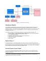
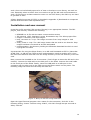
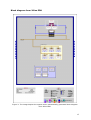
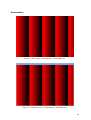
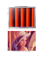
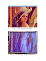
Digital photo frame
2009-10-19
Project group members
Martin Olsson ([email protected])
Samuel Skånberg ([email protected])
Thomas Eriksson ([email protected])
Mentor: Flavius Gruian and Per Andersson (Dept. of computer science, LTH)
Course: EDA385 - Design of Embedded Systems Advanced Course, LP1 Ht09
1
Abstract
This has been a project performed in the course EDA385, Design of Embedded Systems
Advanced Course.
The goal with the project was (after revision) to create a digital photo frame, using an
FPGA board, a VGA monitor, the on board push buttons and an SD card reader-module
plugged in to the FPGA board. The final product could read a specially formatted image
file from an SD card, put it in the SDRAM on the FPGA board and from there transfer it
row by row to a BRAM row-buffer. The VGA controller then read the rows from the BRAM
and showed them on the VGA monitor.
The project was rather successful. Even so, some features weren't fully functional in the
final product. There was a vertical synchronization error which resulted in wrapping of
the output image. The push buttons were supposed to be used for changing image but
this was also never implemented.
All in all the product did work but wasn't perfect. Given another week and some more
hands on consulting from our mentors we are quite convinced the project would've
become fully functional.
In the report, the reader is given a description of the hardware and software used to
realize the project. The problems encountered during the project is also presented as
well as the result, conclusions and lessons learned.
2
Table of contents
Abstract ............................................................................................... 2
Introduction......................................................................................... 4
Hardware Details ................................................................................ 5
Digilent Nexys 2 ................................................................................ 5
General Purpose Input/Output .......................................................... 5
Push buttons ................................................................................. 6
PmodSD ........................................................................................ 6
VGA controller with on board BRAM................................................. 6
VGA signal generator .................................................................... 6
BRAM row buffer ........................................................................... 7
VGA monitor...................................................................................... 7
Memory occupancy ........................................................................... 7
The software on the FPGA ............................................................... 8
Image converter ................................................................................ 8
Image viewer..................................................................................... 9
Fat32 and Fat12................................................................................ 9
BMP converter ................................................................................ 11
DED viewer ..................................................................................... 11
Problems during work...................................................................... 12
Setting up the system ..................................................................... 12
Creating the VGA controller IP core ............................................ 12
Setting up the BRAM ................................................................... 12
Read/write synchronization in the BRAM .................................... 12
Fat32 and Fat12 library ................................................................... 12
Lessons learned ............................................................................... 14
Contributions .................................................................................... 14
Eye-candy and Extras ...................................................................... 16
Download the project ...................................................................... 16
Block diagram from Xilinx EDK ....................................................... 17
Screenshots .................................................................................... 18
Reference .......................................................................................... 22
3
Introduction
The project started off with a quite tricky learning period where we spent most of the
working hours understanding the development environment, Xilinx EDK, and the
interaction between the hardware modules and the software on the MicroBlaze
processor. After the learning phase the work was divided into one software and one
hardware branch where Samuel took on the software while Martin and Thomas started
working with the hardware.
The initial project plan was to create the picture frame by reading an image from an SD
card to a BRAM space on the VGA controller - graphics memory - using a synthesized
core and using a VGA monitor for image display. There were also plans to let the user
change the image by pressing keys on a PS/2 keyboard.
One of the changes from the original plan was the PS/2 keyboard controller, which was
removed due to it adding unneeded complexity to the project.
Instead we used the push buttons on the Nexys 2 board, readable by polling the GPIO
ports. Due to time constraints we only implemented the reset button, not any
navigational buttons.
Another change was the loading from the SD card which subsequently came to not being
written in VHDL as initially thought, but instead came to use GPIO in software for its
communication. This was changed due to the fact that SD cards don't need very precise
timings and it was much simpler to implement the reading in software.
The final change from the initial plan was the use of a part-image buffer on the VGA
controller instead of keeping the entire graphics buffer on the VGA synthesized core. This
was made due to size constraints on the FPGA we used. There simply wasn't room to
hold the entire image of 300 Kbytes (640 x 480 x 1 byte), so instead we used the
SDRAM memory to hold the VGA buffer contents.
Thus when the project ended the design worked as follows (also see Figure 1): the
software running on the MicroBlaze CPU would load a predefined image from the SD card
and write it to the 16 MByte Micron SDRAM. After image loading has completed, the CPU
just runs an idle loop and waits for interrupts from the VGA controller.
At each interrupt received from the VGA controller, the interrupt routine fetches one row
from the SDRAM and writes it to the BRAM buffer in the VGA controller.
At the VGA controller side, interrupts are sent when the end of the visible scan line is
reached.
Using the "Create and Import Peripheral" wizard in EDK, we instantiated the VGA
controller as an IP core with a BRAM block and interrupt handling into the project. The
dual-port BRAM instantiation was taken from the ISE code examples.
4
Figure 1: Architecture overview
Hardware Details
The hardware components in the system were not too many. However most of them
were quite complex and demanded a lot of thought, development not to mention
extensive testing. The component that without a doubt occupied our time the most was
the VGA controller with its on board BRAM. It is also the component which has been
redesigned the most.
1
The system consists of the following hardware components (also see Figure 3) :
• Digilent Nexys 2 1200 FPGA board with a Xilinx Spartan 3E FPGA with 16MB of
Micron SDRAM & 16MB of Intel StrataFlash ROM
• 4 on board push buttons
• PmodSD - SD card reader module for the FPGA board
• VGA controller with on board BRAM
• Interrupt controller
• VGA monitor
Digilent Nexys 2
The Digilent Nexys 2 1200 FPGA board was used to host the synthesized project and
provide I/O ports to the VGA and the SD card reader (below). The key features that that
were utilized on the board were the MicroBlaze processor, the 16 Mb of Micron SDRAM,
the push buttons, the VGA port and one expansion slot.
General Purpose Input/Output
The General Purpose Input/Output (GPIO) core was used to connect both the push
buttons as well as the PmodSD (SD card reader module) to the MicroBlaze processor
through the PLB bus.
1. A hardware components can be both a physical component and to a component
implemented as an IP core on the FPGA.
5
Push buttons
The four on board push buttons are rather easy to implement and use since the Xilinx
EDK offers the user to automatically add them when creating a new project using the
project wizard. The buttons were involved in the project at an early stage and the first
button function implemented was a standard reset-button which simply resets the entire
board. Sadly the reset-button was the only button function implemented since the VGAcontroller turned out to be more complex and time consuming than predicted. The
original plan was to also implement a play/pause button to start or stop a slide show of
the images on the SD card as well as one forward and one backward button.
PmodSD
PmodSD is an extension module for the Digilent board used for reading and writing to an
SD card. It was connected to the board via the Pmod JA connector on the board (see
page 15 in the Nexys2 Reference Manual). We used the xps_gpio to connect to the pins
of the Pmod JA connector. The PmodSD has 12 pins but since we used SPI mode we only
connected 4 pins, namely JA1, JA2, JA3 and JA4. We then had to decrease the data
width of the xps_gpio from 32 to 4 otherwise the data wouldn't map to the correct pins
(JA1 through JA4).
Pierre from the group FPGA-pod was kind enough to help us out with the setup. He sent
us some code in C (SD_Driver.h and SD_Driver.c in the project) that used the xps_gpio
instance to communicate to the PmodSD using the SPI mode of the SD card. Pierre had
done a tremendous work with the SD card and was very helpful. Without his help we
wouldn't have had time to include the PmodSD in our project. However, this was also
because there was only one PmodSD module (which the FPGA-pod group started to use
from the start of the projects). If there would have been more, we would of course have
started with the PmodSD before implementing a FAT library.
We later learned from the other groups (in their presentation) that Xilinx had an SPI
interface IP core that we could have used (xps_spi). If we would have used that IP core
and written the specific SD card commands in C, that would have made the loading of
the image from the SD card a great deal faster. Now it takes around 25 seconds to read
a 300 KB .ded image file to SDRAM which gives a transfer rate at 12 KB / s.
VGA controller with on board BRAM
The VGA controller consists of two parts.
• VGA signal generator which generates a VGA drawing area of 640x480 pixels at
60 MHz.
• BRAM row buffer which holds the row to be printed to the VGA monitor.
We decided to use the standard VGA resolution of 640x480 pixels with an 8 bit color
representation (3 bits for red, 3 bits for green and 2 bits for blue). This was the highest
resolution and bit depth the Nexys 2 could handle. Sadly it also resulted in the fact that
we couldn't fit an entire image in the BRAM. Instead we had to settle with storing one of
the 480 rows at the time in the BRAM. Hence the titling "BRAM row buffer".
VGA signal generator
The primary purpose of the VGA controller was to output the row stored in the built in
BRAM row buffer and display it on the VGA monitor connected to the VGA port on the
6
FPGA board. In order to get this to work the VGA controller with it's BRAM was created
as a new IP core in the Xilinx EDK and added to the project as well as connected to the
PLB bus. The VGA controller and its helping processes were instantiated using VHDL and
based on example designs from the Xilinx ISE and input from other groups.
The signal generator contained two counters to generate the vertical and horizontal sync
pulses needed for the VGA pulse. The two counters kept track of when a row ended and
it was time to change to the next one as well as when the last row had been reached and
it was time to restart from pixel one on row one. After a row had been displayed on the
monitor (in other words when the horizontal pixel counter had reached it's "end-screenvalue") the VGA controller sent an interrupt to the PLB bus which then was captured by
the Interrupt controller on the MicroBlaze and handled accordingly.
BRAM row buffer
The BRAM row buffer is instantiated from within the VHDL code of the VGA controller and
is specified as a dual port, one read and one write, memory. The BRAM has a size of
256x32 bits which corresponds to 1024 ((256x32)/8) pixels. This means that it holds
more than enough room to store one row of pixels.
Interrupt controller
The system utilizes one interrupt source, the VGA controller. The VGA controller sends
an interrupt after it has finished reading a row from the memory and displaying it on the
monitor. This is to trigger an interrupt handler in the C-code on the MicroBlaze which
then writes the next row from the SDRAM to the BRAM row buffer.
An interrupt controller and a, to the interrupt corresponding, interrupt handler was used
to take care of the interrupt. This design was originally designed to be able to handle
multiple interrupts and can therefore be considered unnecessarily complex. The reason
for this is that we were uncertain whether we would need multiple interrupts or not later
on in the project and thought it best to cover for possible future changes.
VGA monitor
The VGA monitor is probably the most simple component in the system and is simply
any available monitor capable of recieving a VGA video signal. During the development
both an ancient CRT monitor as well as a more modern TFT monitor has been used.
There is no significant difference in how the two monitor types display the VGA data.
Memory occupancy
Selected Device : 3s1200efg320-4
Number of Slices:
1732
out of
8672
19%
Number of Slice Flip Flops:
2118
out of
17344
12%
Number of 4 input LUTs:
2686
out of
17344
15%
out of
250
27%
Number used as logic:
2301
Number used as Shift registers:
129
Number used as RAMs:
256
Number of IOs:
69
Number of bonded IOBs:
69
IOB Flip Flops:
32
7
Number of BRAMs:
20
out of
28
71%
Number of MULT18X18SIOs:
3  out of
28
10%
Number of GCLKs:
2
out of
24
8%
Number of DCMs:
1
out of
8
12%
Software solution
A lot of things were done in software. The following was done in software, programmed
in C.
• The software on the FPGA
• Image converter: .bmp to .ded image converter (.ded is our own 8 bit depth
bitmap file format)
• Image viewer: a .ded viewer using the graphics library SDL
• FAT32 and FAT16 library
The image converter and the image viewer is actually never used on the FPGA but used
to get some pictures which we later on can display on our system.
The software on the FPGA
The software on the FPGA do a lot of things:
•
•
•
•
Initializes interrupts, adds interrupts handler
Initializes SD card
Reads MBR and VBR for the FAT12 library
Generates a list of all the directory table entries (with corresponding first cluster
number, filename and size) in the root directory and its subdirectories
• Loads an image to the SDRAM
• Waits for interrupts
When everything has been set up, the program waits for interrupts from the VGA
controller. When the VGA controller has finished displaying a row on screen, it then
generates an interrupt. What happens then is the following:
• The interrupt handler will be called
• A new row will be read from the SDRAM
• The row will be copied to the BRAM buffer in the VGA controller
The previous steps will be repeated forever. During the idle time, the main program just
waits for new interrupts. The image is actually interlaced, meaning that during odd
numbered frames, we only display odd numbered rows, and on even numbered frames
we only display even numbered rows. In the interrupt function, if we are not supposed to
display the row in question, then we just exit the interrupt handler. We did this so that
the interrupt handler would not lag behind interrupts received from the VGA controller.
Image converter
We decided early that we would display bitmap files with 8 bit in depth. We tried to find
an already existing file format for that, Martin came up with the Netpbm file format. It
looked good but it didn't use 8 bit depth. It used 8 bit depth per color. Alas, the bit
depth was actually 24. So we constructed out own, which was a combination of netpbm
and bmp. The layout of our file format is really simple:
8
First 4 byte: 0xdead1337
Next 4 bytes: width in pixels
Next 4 bytes: height in pixel
After that follows width*height number of bytes where each byte represents the color of
the pixel in the following format:
First 3 bits: Red (1st bit being the msb)
Next 3 bits: Green (1st bit being the msb)
Next 2 bits: Blue (1st bit being the msb)
What is strange about this format is that it starts with the bottom row and works itself
up. That's because the bmp file format is constructed in the same way. The reason is
according to wikipedia:
"This block of bytes describes the image, pixel by pixel. Pixels are stored "upside-down"
with respect to normal image raster scan order, starting in the lower left corner, going
from left to right, and then row by row from the bottom to the top of the image."
We simply did it the same way, because it was easier to build the image converter. To
see the change from .bmp to .ded see figure 4, figure 5, figure 7 and figure 8.
Image viewer
So that we could test that the .ded images were constructed the way we wanted them
to, we developed a simple image viewer that would in principle emulate our FPGA with
monitor. It was a simple program, written in C using the SDL graphics library. This
program was easy to write because we had some experience of SDL from before and
because the tutorials at libsdl.org are really good and there are a lot of tutorials on the
web as well. SDL is also convenient since it is cross platform compatible.
The image viewer showed us how the .ded file should look like, if rendered correctly on
the monitor. Figure 5 and figure 8 (under the sections Eye-candy and Extras) are
screenshots of the image viewer in actions. One can see that with the reds.ded file the
actual output on the VGA monitor (figure 6) was equal to the anticipated output (figure
5). However, with the lenna.ded file, the actual output on the VGA monitor (figure 9) is
not equal to the anticipated output (figure 8).
Fat32 and Fat12
The FAT32 library was never used on the FPGA since we found out that the SD card we
use has a FAT12 filesystem on it.
The FAT12 library does the following:
• Reads the master boot record (MBR) and read the first partition entry in it
• Takes the start sector for the first parition entry, jumps to that sector and reads
it (512) bytes
• Takes out necessary information about the file system (sectors per cluster, max
root directory entries, etc.)
• Jumps to the address for the root directory
• Reads all the table directory entries in the root directory and its sub directories.
There is actually already a free and open source FAT12/16/32 library called fatfs. We
tried a bit to get it to work but didn't succeed. However, we heard that Pierre got it to
9
work. Since we had already spent a lot of time to develop our own library, we used our
own. Especially when we didn't do a lot ourselves to get the SD card communication to
work, we felt like we at least wanted to write our own FAT library. We didn't try too hard
to get fatfs to work.
A fairly detailed overview of FAT12 is described in appendix A (distributed as a seperate
pdf-file because Flavius had requested that).
Installation and user manual
Unzip the zip file provided (IDY-project_files.zip) in an appropriate location. The IDYproject_files directory contains the following:
•
•
•
•
README.txt: A file with the same content as this section
IDY-091016_1223_Interlaced_Lenna_Presentation.zip: The Xilinx project files
images: A directory with test images
bmp_converter-0.1.1.zip: The image converter from .bmp images to .ded
images
• dead_viewer-0.1.zip: The .ded image viewer that we used to see that the .bmp
images had been converted as we had anticipated
• implementation: the directory holding the bitstream download.bit which is used
to program the FPGA
A prerequisite for using the Photo Frame, is an SD card formatted as FAT12. (Note that
all SD card > 4 GB will use FAT32 so this implementation needs a smaller card). Copy
the files lenna.ded and reds.ded from the image directory to the root directory of the SD
card.
Next, connect the PmodSD to the JA connector. (Don't forget to insert the SD card in the
module). Connect the VGA cable to the VGA port on the FPGA. Connect the serial cable
to the serial port of the FPGA. Finally, insert the USB cable to a USB port on the
computer and the other end to the USB port on the FPGA. Switch on the power. The
following image will show how the setup will look like.
Figure 2: Nexys 2 with all strings attached.
Open the HyperTerminal program. Set a name for the connection, click OK. In the
following dialog, choose "Connect using: COM1", click OK. Change bits per seconds to
9600, click OK.
10
Unzip the file IDY-091016_1223_Interlaced_Lenna_Presentation.zip in an appropriate
location.
tm
To install the software on the board, open the Digilent
ExPort utility, check the "AutoDetect USB" check box, click the "Initialize Chain" button, then click the "Browse" button
for the FPGA and navigate to the folder
IDY-091016_1223_Interlaced_Lenna_Presentation\implementation, select the
download.bit and click OK.
Next, download the hardware description bit onto the board by clicking the "Program
Chain" button.
The HyperTerminal program should now output some information about the FAT12
filesystem on the SD card.. After loading has completed (which it has after sector count
has reached 600), the VGA controller will render the image on the screen.
The default image to be shown is lenna.ded. To display other .ded images, open the file
TestApp_Memory.c (located in IDY-091016_1223_Interlaced_Lenna_Presentation/
TestApp_Memory/src), change the line
if (it->filename[0] == 'L') {
to
if (it->filename[0] == 'R') {
Then do an "Update bitstream" (located under the "Device Configuration" menu in Xilinx
EDK), and finally a "Program chain" again.
BMP converter
To use an arbitrary BMP image, first convert it to a 640*480 pixels sized .bmp file (with
24-bit depth). Then, on a Linux/Unix machine, unzip the bmp_converter-0.1.1.zip, enter
the directory bmp_converter-0.1.1 and type:
$ make converter
To convert a file, type:
$ ./converter input-file.bmp output-file.ded
where input-file.bmp is the name of the .bmp file.
DED viewer
To view the .ded file in software on a Linux/Unix machine with SDL installed, unzip
dead_viewer-0.1.zip, enter the directory dead_viewer-0.1 and type
$ make
To view a .ded image, type:
$ ./dead_viewer output-file.ded
where output-file.ded is the .ded file.
11
Problems during work
Setting up the system
Thomas and Martin in the hardware group have had quite a lot of obstacles to overcome
during the process of setting up the system and adding and configuring all the correct IP
cores. The most significant problems have been described below.
Creating the VGA controller IP core
During the project the VGA controller has gone through several revisions. The reason for
this has been that we've wanted to try out different architectures. For instance we've
tried both dual and single BRAMs. We've also tried architectures both with and without
registers in the VGA controller IP core. Interrupts have also been in and out of the
architecture a couple of times. This has been a problem since the easiest way of making
these changes was to create an entirely new IP core using the IP core wizard and then
port the old VHDL code and functionality to the new core. This way of working has been
very time consuming and has resulted in a lot of extra work.
Setting up the BRAM
How to set up the BRAM was in no way obvious. We tried many different configurations
before we came up with the final "Dual port, one read, one write"-configuration. The
main issue is that it generally is really hard to find examples, tutorials, reference
manuals etc. that are actually useful.
Read/write synchronization in the BRAM
The only issue left at the end of the project was the incorrect vertical synchronization.
The horizontal synchronization worked fine as is shown in figure 6. There it is shown that
the original .bmp image (Figure 4) converted to a .ded image (Figure 5) is correctly
shown on the VGA monitor. The reason it was correctly displayed was that it had a
vertically constant pattern, hence it only changed along the horizontal axis.
The read/write synchronization issue first appeared when we decided to try to use an
image that wasn't vertically constant. For this test we used the classical "Lenna" image
(Figure 7). Its predicted output is shown in Figure 8, and the actual output is shown in
Figure 9. In the last mentioned figure it is obvious that we output the "Lenna" image to
the VGA monitor. However it is also obvious that there is something wrong with the
vertical synchronization since the image is both vertically displaced as well as vertically
stretched out.
We have put a lot (!) of time into finding and correcting this error but we were unable to
solve it. The solution is probably associated to one of the following:
• Incorrect addressing when reading from BRAM to VGA controller
• Insufficient synchronization between the VGA controller and the MicroBlaze.
Fat32 and Fat12 library
Since we didn't have access to the real physical card, we had to do a faked device on
disk. We used the tool dd in Linux to do a small file and then used mkdosfs to get a
FAT32 file system on it. We also did a dump of an USB memory stick which we thought
12
would have the same layout as an SD card. What we didn't think of was that we didn't
dump the whole device, but only the partition where the file system was located on. This
caused us some trouble later on.
The problems we ran into was the following.
• We couldn't find a MBR on the dumped file (which was because we only had
dumped the partition, hence no MBR). Then we found the Volume Boot Record,
which is the first 512 bytes of a file system. So we just assumed that there was
no partition scheme on the SD card.
• When we tried to read the first directory table entry in the root directory, we
didn't get what we expected. That was because we didn't read the entire
wikipedia article. Further down the article it was stated that before each table
entry there could be multiples of fake entries, used to support long file names.
When we tried to interpret them as normal entries, it didn't work obviously. That
cost us 1-2 days. Really annoying!
So the major problems was that we had mistaken the VBR for the MBR and that was
because we hadn't dumped the device correctly. They are quite similar, both ending with
a 2-byte signature of 0x55aa. The other was that we had mistaken the fake table entries
(used for long filename support) for the real ones.
The porting of the FAT12 library was done after we had written a functional FAT32
(functional if only the partition is dumped). We did a dump of the SD card we were going
to use. It turned out that the SD card we used was formatted as FAT12. We thought all
those kind of devices (SD cards, USB stick, etc.) used FAT32. We could probably had
reformatted the SD card with FAT32 but we decided to change the library instead since
FAT12 is very similar to FAT32.
Later on we also found out that we only had dumped the partition, not the whole device.
That is an easy mistake to do in Linux since normally only the partition is mounted.
To find out the partition used, enter "mount" in the terminal, following is a typical output
from the mount command:
/dev/sdb1 on /media/NOLIMIT type vfat
To dump the content of the mounted device, type:
dd if=/dev/sdb1 of=dump.img
But that only dumps the partition. To dump the whole device, remove the 1:
dd if=/dev/sdb of=dump_whole_device.img
If the command above is issued, the entire device will be dumped, with MBR and
everything. So we did that and changed the library so that it would work. When we ere
going to port it to the microblaze and use the real SD card (via the SPI mode interface)
instead of a file from disk, we didn't have enough space. We thought that was really
strange since it was a very small program. The program and library consists the
following files:
•
•
•
•
fat12.h and fat12.c
list.h and list.c
io.h and io.c
main.c
13
We tried to remove some IP cores and other stuff but it still wouldn't work. What we did
then was to add each file one by one, compile and see if it fitted. When we did it like that
(as opposed to add all the files at once), it worked.
So most things were going well except for one strange thing, we couldn't access the
memory byte by byte. It was all very strange but Flavius pointed out that we had to use
the built in macros XIo_In8 and XIo_Out8 to read and write from within the microblaze.
We looked at the macro and the only thing that differed was a "volatile". Anyhow, it
made all the difference. Afterwards that, it was all quite easy.
Lessons learned
We learned a lot during this project, both regarding the technical aspects of VHDL and
Xilinx but also we learned things that can be applied to other group projects.
In retrospect it would have been advantagous, had we learned to simulate our VHDL
code. Then we probably would have found the syncing problem which might have been
the reason why figure 9 doesn't look like figure 8 (under the section Eye-candy and
Extras). We learned that "coding before thinking" doesn't work when synthesizing VHDL
because it takes too much time to synthesize.
Another thing we learned was that the time plan of a project doesn't always go as
planned. We had planned to have the VGA controller fully functional by week 4 but it
ended up that we were still working to get the interrupt/writing to BRAM buffer sync
working at the very end of the project.
However, we realized early that it would be useless that we all worked with the same
thing, especially if we were on a stall. So while Martin and Thomas sometimes got stuck
at the VGA controller, Samuel could still keep on working with the FAT library, and vice
versa.
Another thing we probably would have done different is using a version control system
(like cvs or git). We used our public_html directories to copy files among ourselves. It
worked quite okay but still it was a bit messy. But since we weren't used to working in
Xilinx and in Windows, we didn't want to waste time to learn those Windows/Xilinx
specific tools first.
Contributions
Samuel:
• Image converter and image viewer program
• FAT12 library
• Communication with the PmodSD
• Interrupt handler
Martin and Thomas:
• Created the system in Xilinx EDK
• Implemented the VGA controller and the BRAM row buffer
Contributions from other groups
• Pierre from the group FPGA-pod helped us with the PmodSD module and gave us
the files SD_driver.h and SD_driver.c and helped ut to get it to work.
• Hints and tips regarding the VGA controller by Per from the FGPA-Invaders
group.
14
15
Eye-candy and Extras
Download the project
The project can be downloaded from:
http://users.student.lth.se/dt05ss5/EDA385/IDY-project_files.zip
16
Block diagram from Xilinx EDK
Figure 3: The image depicts the system as an automatically generated block diagram
from Xilinx EDK.
17
Screenshots
Figure 4: The original "red gradients" .bmp image file.
Figure 5: A preview of the "red gradients" .ded image file.
18
Figure 6: The VGA monitor output of the "red gradients" .ded image file.
Figure 7: The original "Lenna" .bmp-image file.
19
20
Figure 8: A preview of the "Lenna" .ded image file.
Figure 9: The VGA monitor output of the "Lenna" .ded-image file.
21
Reference
[1] Digilent, inc - Nexys2 board Reference Manual, 2008
[2] Xilinx, Inc – Xilinx ISE 10.1 Design Suite Software Manuals and Helps-PDF collection,
2008
[3] http://cs.lth.se/EDA385/
22