1
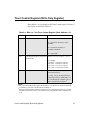
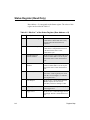
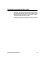
PCIP-CNTR USER’S GUIDE PCIP-CNTR User’s Guide Revision C - October 1996 Part Number: 74190 New Contact Information Keithley Instruments, Inc. 28775 Aurora Road Cleveland, OH 44139 Technical Support: 1-888-KEITHLEY Monday – Friday 8:00 a.m. to 5:00 p.m (EST) Fax: (440) 248-6168 Visit our website at http://www.keithley.com The information contained in this manual is believed to be accurate and reliable. However, Keithley Instruments, Inc., assumes no responsibility for its use or for any infringements of patents or other rights of third parties that may result from its use. No license is granted by implication or otherwise under any patent rights of Keithley Instruments, Inc. KEITHLEY INSTRUMENTS, INC., SHALL NOT BE LIABLE FOR ANY SPECIAL, INCIDENTAL, OR CONSEQUENTIAL DAMAGES RELATED TO THE USE OF THIS PRODUCT. THIS PRODUCT IS NOT DESIGNED WITH COMPONENTS OF A LEVEL OF RELIABILITY SUITABLE FOR USE IN LIFE SUPPORT OR CRITICAL APPLICATIONS. Refer to your Keithley Instruments license agreement document for specific warranty and liability information. All brand and product names are trademarks or registered trademarks of their respective companies. © Copyright Keithley Instruments, Inc., 1989, 1992, 1996 All rights reserved. Reproduction or adaptation of any part of this documentation beyond that permitted by Section 117 of the 1976 United States Copyright Act without permission of the Copyright owner is unlawful. Keithley MetraByte Division Keithley Instruments, Inc. 440 Myles Standish Blvd. Taunton, MA 02780 Telephone: (508) 880-3000 ● FAX: (508) 880-0179 Preface This manual is designed for users responsible for setting up, installing, and using the PCIP-CNTR board. The information in this manual assumes that you are familiar with your computer and its operation and that you are familiar with data acquisition principles. This manual is organized as follows: ● Chapter 1 provides an introduction to the features of the PCIP-CNTR board, supported software, and accessories. ● Chapter 2 describes how to unpack and inspect the board, set the base address, install the board, and connect signals to the board. ● Chapter 3 provides a functional description of the board. ● Chapter 4 describes how to calibrate the board. ● Chapter 5 describes how to troubleshoot the board and how to return the board should it be necessary. ● Chapter 6 describes the register map for the board. ● Appendix A lists the specifications for the board. ● Appendix B describes the built-in transfer functions and resolutions available on the board. ● An index completes this manual. v Table of Contents Preface 1 Introduction Features . . . . . . . . . . . . . . . . . . . . . . . . . . . . . . . . . . . . . . . . . . . .1-1 Supported Software . . . . . . . . . . . . . . . . . . . . . . . . . . . . . . . . . . .1-2 Accessories. . . . . . . . . . . . . . . . . . . . . . . . . . . . . . . . . . . . . . . . . .1-3 2 Setup and Installation Unpacking and Inspecting the Board . . . . . . . . . . . . . . . . . . . . . .2-1 Setting the Base Address . . . . . . . . . . . . . . . . . . . . . . . . . . . . . . .2-2 Installing the Board . . . . . . . . . . . . . . . . . . . . . . . . . . . . . . . . . . .2-3 Connecting Signals . . . . . . . . . . . . . . . . . . . . . . . . . . . . . . . . . . .2-4 3 Functional Description Summary of Operating Modes . . . . . . . . . . . . . . . . . . . . . . . . . . .3-1 Configurable Channel Settings. . . . . . . . . . . . . . . . . . . . . . . . . . .3-3 Frequency Measurements. . . . . . . . . . . . . . . . . . . . . . . . . . . . . . .3-3 Average Period Measurements. . . . . . . . . . . . . . . . . . . . . . . . . . .3-5 Single Period Measurements . . . . . . . . . . . . . . . . . . . . . . . . . . . .3-6 Pulse Width Measurement . . . . . . . . . . . . . . . . . . . . . . . . . . . . . .3-6 Event Counting Measurements . . . . . . . . . . . . . . . . . . . . . . . . . .3-7 4 Calibration 5 Troubleshooting Problem Isolation . . . . . . . . . . . . . . . . . . . . . . . . . . . . . . . . . . . . .5-1 Identifying Symptoms and Possible Causes . . . . . . . . . . . . . .5-1 Testing the Board and Host Computer . . . . . . . . . . . . . . . . . .5-3 Testing the Accessory Slot and I/O Connections . . . . . . . . . .5-4 Technical Support. . . . . . . . . . . . . . . . . . . . . . . . . . . . . . . . . . . . .5-5 6 Register Map Register Map Summary . . . . . . . . . . . . . . . . . . . . . . . . . . . . . . . .6-1 Measurement Count Out Register (Read Only) . . . . . . . . . . . . .6-2 Time Count Out Register (Read Only) . . . . . . . . . . . . . . . . . . . .6-3 iii Mode Selection Register (Write Only) . . . . . . . . . . . . . . . . . . . .6-4 Input Configuration Register (Write Only) . . . . . . . . . . . . . . . . .6-5 Channel A: DC-Coupled Trigger Level Register (Write Only) . . . . . . . . . . . . . . . . . . . . . . . . . . . . . . . . . . . . . . . .6-6 Channel B: DC-Coupled Trigger Level Register (Write Only) . . . . . . . . . . . . . . . . . . . . . . . . . . . . . . . . . . . . . . . .6-6 Timer Control Register (Write Only Register). . . . . . . . . . . . . . .6-7 Status Register (Read Only). . . . . . . . . . . . . . . . . . . . . . . . . . . . .6-8 Channel B Divide Register (Write Only). . . . . . . . . . . . . . . . . . .6-9 A Specifications B Built-in Transfer Functions and Available Resolutions Transfer Functions . . . . . . . . . . . . . . . . . . . . . . . . . . . . . . . . . . . B-1 Available Resolutions. . . . . . . . . . . . . . . . . . . . . . . . . . . . . . . . . B-2 Index List of Figures Figure 2-1. The Base Address Switch (Default Base Address of 320h Shown) . . . . . . . . . . . . . . . . . . . .2-3 Figure 2-2. The Board I/O Connectors . . . . . . . . . . . . . . . . . . .2-4 Figure 2-3. Pin Assignments of the 9-Pin "D" Connector . . . .2-5 Figure 3-1. Frequency Measurement Timing Diagram . . . . . .3-5 List of Tables Table 3-1. Operating Mode Summary. . . . . . . . . . . . . . . . . . .3-2 Table 5-1. Troubleshooting Information . . . . . . . . . . . . . . . . .5-2 Table 6-1. Register Summary . . . . . . . . . . . . . . . . . . . . . . . . .6-2 Table 6-2. Bits 0 to 6 of the Mode Selection Register (Base Address +8) . . . . . . . . . . . . . . . . . . . . . . . . .6-4 Table 6-3. Bits 0 to 7 of the Input Configuration Register (Base Address +9) . . . . . . . . . . . . . . . . . . . . . . . . .6-5 Table 6-4. Bits 0 to 7 the Timer Control Register (Base Address +12) . . . . . . . . . . . . . . . . . . . . . . . .6-7 Table 6-5. Bits 0 to 7 of the Status Register (Base Address +13) . . . . . . . . . . . . . . . . . . . . . . . .6-8 Table A-1. PCIP-CNTR Specifications . . . . . . . . . . . . . . . . . A-1 Table B-1. Scaling Selections for Frequency and Period Measurements. . . . . . . . . . . . . . . . . . . . . . B-2 iv 1 Introduction The PCIP-CNTR is a two channel, 8-digit, universal counter board that plugs directly into any I/O slot of an IBM PC/XT or PC ATcompatible computer. The PCIP-CNTR is available in two versions: ● The standard PCIP-CNTR provides .01% (100 PPM) accuracy and is targeted towards low to middle accuracy applications. ● The PCIP-CNTR/TCXO is available for users who require 1 PPM accuracy. Unless a feature applies to a particular board, the name PCIP-CNTR is used to refer to both the standard PCIP-CNTR and PCIP-CNTR/TCXO boards. This chapter describes the following aspects of the board: ● Major features ● Supported software ● Available accessories Features The major features of the PCIP-CNTR board are as follows: Features ● Operates up to 80 MHz on each channel ● Measures frequency on Channel A, Channel B, or the ratio of Channels A and B ● Measures the average period on Channel A, Channel B, or the ratio of Channels A and B 1-1 ● Measures a single period on Channel A or Channel B ● Measures the pulse width on Channel A ● Measures counts on Channel A, on Channel A gated by Channel B, or on Channel A started and stopped by Channel B ● Plugs directly into any IBM PC/XT, IBM AT, or compatible computer; no IEEE-488 or GPIB interface is required ● Supports a wide variety of input configurations ● Operates in two modes: – As a standard bench instrument - In this mode, the board functions like a standard bench-top instrument, except that the readings are displayed on the computer screen, not on LEDs or LCDs, and the operating mode, channel selected, trigger level, and so on, are selected using the keyboard or mouse. – Under program control - This mode allows you to write programs that control the board directly, which is useful when using the board in automated tests or experiments. ● Provides BNC plugs for all connections to Channels A and B on the board. ● Provides a 9-pin "D" connector to connect all other signals, such as an external clock. Supported Software The PCIP-CNTR OCX software provided for the PCIP-CNTR board is a 32-bit ActiveX custom control for developing Windows 95 and Windows NT applications. The PCIP-CNTR OCX supports application development in C/C++, Visual Basic , and Delphi. This software package is described in a separate manual, shipped with the software. 1-2 Introduction Note: For those users who have purchased previous versions of the PCIP-CNTR board, this revision of the board contains all the features of the previous versions of the board while providing a greater operating range for Channel B (0 MHz to 80 MHz). DOS software provided with previous versions will work with the new revision of the PCIP-CNTR board. However, to take advantage of the new features, you must use the PCIP-CNTR OCX software. Accessories The following accessories are optional for the PCIP-CNTR board: Accessories ● C-BMM-5 cable - 5-foot BNC-to-BNC cable. ● C-BMM-15 cable - 15-foot BNC-to-BNC cable. ● SMC-9 connector - 9-pin, male solder cup connector. 1-3 2 Setup and Installation This chapter describes how to set up and install the PCIP-CNTR board. The following procedures are provided: ● Unpacking and inspecting ● Setting the base address ● Installing the board ● Connecting signals Unpacking and Inspecting the Board After you remove the wrapped board from its outer shipping carton, proceed as follows: 1. Your board is packaged at the factory in an anti-static wrapper that must not be removed until you have discharged any static electricity by either of the following methods: – If you are equipped with a grounded wrist strap, you discharge static electricity as soon as you hold the wrapped board. – If you are not equipped with a grounded wrist strap, discharge static electricity by holding the wrapped board in one hand while placing your other hand firmly on a metal portion of the computer chassis (your computer must be turned off but grounded). 2. Carefully unwrap your board from its anti-static wrapping material. (You may wish to store the wrapping material for future use.) 3. Inspect the board for signs of damage. If damage is apparent, arrange to return the board to the factory (see page 5-5). Unpacking and Inspecting the Board 2-1 4. Check the remaining contents of your package against the packing list to be sure your order is complete. Report any missing items, immediately. 5. When you are satisfied with the inspection, proceed with setting the base address. Note: The PCIP-CNTR board is factory calibrated; it requires no further adjustment prior to installation. If at a later time you decide to recalibrate the board, refer to page 4-1 for instructions. Setting the Base Address The PCIP-CNTR uses a block of 16 non-overlapping I/O addresses. A DIP switch on the board selects where in the computer’s I/O space the board resides. The PCIP-CNTR has a default base address setting of 320h; this address is typically free in most computers. However, no two boards can use the same I/O addresses or base address. If you are using more than one instrument, you must assign each a unique base address. Base addresses range from 100h to 3FFh (512 to 1023 decimal). The base address switch is a six-position, DIP switch located in the lower right-hand corner of the board. To specify a base address, move the individual switches to the ON or OFF position. Figure 2-1 shows the address values corresponding to each of the six switches. 2-2 Setup and Installation Address Line A9 Decimal Equivalent = 512 Address Line A8 Decimal Equivalent = 256 Address Line A7 Decimal Equivalent = 128 Address Line A6 Decimal Equivalent = 64 Address Line A5 Decimal Equivalent = 32 Address Line A4 Decimal Equivalent = 16 O N 9 8 7 6 5 4 Switches have the decimal values shown above when in the OFF position. In the ON position, the decimal value is 0. Figure 2-1. The Base Address Switch (Default Base Address of 320h Shown) Installing the Board This section provides general instructions for installing the PCIP-CNTR board. For more detailed information on installing peripheral boards, consult the documentation provided with your computer. Caution: Do not insert or remove any peripheral board with the computer power on. This could cause damage to your computer. Installing the Board 2-3 Use the following steps to install the PCIP-CNTR board in an accessory slot of your computer: 1. Turn off power to the computer and all attached equipment. 2. Remove the computer chassis cover. 3. Select an unoccupied accessory slot, and remove the corresponding blank plate from the I/O connector panel. 4. Make sure the setting of the base address switch is correct for your board. 5. Insert and secure the board in the selected slot. 6. Replace the computer cover. 7. Turn on power to the computer. You are now ready to connect signals to the board, as described in the following section. Connecting Signals BNC plugs are provided to connect signals to Channels A and B on the PCIP-CNTR board. A 9-pin "D" connector provides connections for all other signals (such as an external clock). Figure 2-2 shows the location of the BNC and 9-pin connectors. Figure 2-3 shows the pin assignments of the 9-pin connector. 9-pin D BNC BNC Reset, Ext Clk, Clk Out Channel A Channel B Figure 2-2. The Board I/O Connectors 2-4 Setup and Installation 1 - Reset 2 - Ground 6 - Ground 3 - Ext Clk In 7 - Ground 4 - Ground 8 - Ground 5 - Clk Out 9 - Ground Figure 2-3. Pin Assignments of the 9-Pin "D" Connector Connecting Signals 2-5 3 Functional Description This chapter describes the functionality of the PCIP-CNTR board. Many users of the PCIP-CNTR will not need to refer to this chapter. However, in certain circumstances it may be important to know the technical details of the board’s operation. This chapter describes the following: ● Summary of operating modes ● Configurable channel settings ● Frequency measurements ● Average period measurements ● Single period measurements ● Pulse width measurements ● Event counting measurements Summary of Operating Modes Table 3-1 summarizes the operating modes supported by the PCIP-CNTR board. Summary of Operating Modes 3-1 Table 3-1. Operating Mode Summary Operating Mode Range Method Timebase Range Frequency A 0.1 Hz to 80 MHz Synchronized input, multiple period, averaging 13 ms to 107 s Frequency B 0.1 Hz to 80 MHz Synchronized input, multiple period, averaging 13 ms to 107 s Frequency A/B Freq A = Freq B = 0 to 80 MHz Frequency A as input with 13 ms to 107 s Frequency B as system clock Frequency Test − The frequency test mode loops the 10 MHz reference oscillator back into an input channel to test overall board operation. − Average Period A 20 ns to 400 s Reciprocal frequency measurement 13 ms to 107 s Average Period B 100 ns to 400 s Reciprocal frequency measurement 13 ms to 107 s Average Period A/B Period A = Period B = 100 ns to 400 s Period A as input with Period B as system clock 13 ms to 107 s Single Period A 400 ns to 400 s Single period count of 100 ns system clock − Single Period B 400 ns to 400 s Single period count of 100 ns system clock − Pulse Width A 100 ns to 400 s Count of 100 ns system clock − Count A 1 to 999,999,999 Manual: Started and stopped by Start button/ command. Counting accumulates until a Reset occurs. Minimum pulse width: 250 ns Minimum time between pulses: External: Controlled by input 250 ns B, either gated during the duration of the B pulse, or started and stopped by separate B pulses. Single count or accumulating count is also selectable. 3-2 Functional Description Configurable Channel Settings Independent of the operating mode selected, you can specify the following channel settings for the PCIP-CNTR board: ● Coupling - AC or DC coupling is provided for each channel. ● Attenuation - A divide-by-ten attenuator is provided. Installing the divide-by-ten attenuator changes the input range from a standard 300 mV to 5 V peak-to-peak range to a 3 V to 50 V peak-to-peak range. ● Analog Input Filter - For lower frequency applications, you can add a 50 kHz low pass filter to the analog front-end. ● External or Internal Clock - For most applications, the 10 MHz internal clock provided on the PCIP-CNTR board is acceptable. However, if you want to synchronize the PCIP-CNTR board to an external clock or use a more accurate external clock source than that provided, you can use an external clock with the PCIP-CNTR board. Note: All PCIP-CNTR software assumes a 10 MHz system clock. If the external clock used does not use a 10 MHz timebase, then all frequency, period, and pulse width data must be scaled accordingly. However, the frequency ratio of A/B operation provides a pure ratio and works correctly without scaling. Frequency Measurements Four frequency measurements are supported by the PCIP-CNTR board: ● Frequency of Channel A ● Frequency of Channel B ● Board test ● Frequency Ratio of A/B Configurable Channel Settings 3-3 The PCIP-CNTR performs frequency measurement according to the following formula: Frequency = (Number of cycles) / Time Using software, you select the desired timebase for the frequency measurement according to the resolution required for the result. Note that the timebase selects the minimum time to sample. The counter always waits for the completion of the last cycle before calculating the frequency measurement (number of cycles per second). Figure 3-1 shows the technique that is used for frequency as well as period measurements (described in the following section). The counting is gated by the input signal so that only completed input cycles are counted. This avoids a ±1 input cycle count error. The 10 MHz system clock is also counted during the gate time. The counting is continued until the end of an input cycle. This technique results in a measurement error of ±1 clock pulse (100 ns); the resolution of the measurement depends only on the measuring time. For example, the resolution for a 1 second measuring time is 0.1 PPM (100 ns/1 s) and is independent of frequency. The frequency ratio A/B measurement is done in a similar manner. The difference is that Channel B is substituted for the 10 MHz system clock; the result is obtained by dividing the count from Channel A by the count from Channel B. 3-4 Functional Description 10 MHz Clock U11-8 CH A Input (J2) CMP TP (U7-7) Measure U12-5 Gate TP (U12-9) IMC TP (U23-6) SCC TP (U23-8) Figure 3-1. Frequency Measurement Timing Diagram Average Period Measurements The average period measurement provides the reciprocal of a frequency measurement. Thus, the PCIP-CNTR performs average period measurements according to this formula: Period = Time / (Number of cycles) The following average period measurements are supported: ● Period of Channel A ● Period of Channel B ● Board test Refer to Figure 3-1 for more information. Average Period Measurements 3-5 Single Period Measurements A single period measurement determines the period of a single cycle of the incoming waveform from either Channel A or Channel B. The PCIP-CNTR board can measure a single period having a minimum duration of 400 ns by counting 100 ns cycles of the system clock. You can set the trigger polarity for a single period measurement as positive or negative. When the trigger polarity is positive, the period is measured between two consecutive rising edges. When the trigger polarity is negative, the period is measured between two consecutive falling edges. Pulse Width Measurement The PCIP-CNTR board can measure the pulse width of an incoming waveform from Channel A only. The pulse widths can be as long as 400 s, determined by counting 100 ns cycles of the system clock. You can set the trigger polarity for a single period measurement as positive or negative. When the trigger polarity is positive, the pulse width is measured from rising edge to falling edge. When the trigger polarity is negative, the pulse width is measured from falling edge to rising edge. Note: A pulse width measurement is different than single period measurement in that it measures the time between a rising and falling (or vice versa) edge. A single period measurement, in contrast, measures the time between consecutive rising or consecutive falling edges. 3-6 Functional Description Event Counting Measurements You can use the PCIP-CNTR board to count either single or accumulated events on Channel A, described as follows: ● Single count operations - The counter is reset at the start of each event. Each time the counter is triggered (by a trigger from Channel B or software control), the count is reset to zero. ● Accumulated count operations - The counter is not reset; each new count is added to the total count. The only way to reset the counter in accumulated count mode is by issuing a reset command. You can perform event counting in the following configurations: ● No external gating or triggering - A software command enables the counter; the counts are accumulated until a stop or reset command is issued. ● Channel A gated by Channel B - This mode (sometimes called level triggering) allows the input of Channel A to be gated by the level of the input at Channel B. When the trigger polarity of the input at Channel B is positive, the counter is enabled when the input at Channel B is high and disabled when the input at Channel B is low. When the trigger polarity of the input at Channel B is negative, the counter is enabled when the input at Channel B is low and enabled when the input at Channel B is high. Note: When controlling the gate with logic level signals, it is recommended that you use the following input configuration for Channel B: DC-coupled, x1 Attenuation, Filter Out, and 1.4 V trigger level. ● Channel A started and stopped by Channel B - This mode (sometimes called edge triggering) allows counting to be started by an edge from the input at Channel B. Counting is stopped by the next valid edge of the input at Channel B. Rising edges are counted when the trigger polarity of the input at Channel B is set to positive; falling edges are counted when the trigger polarity of the input at Channel B is set to negative. Event Counting Measurements 3-7 4 Calibration The standard PCIP-CNTR board requires no periodic calibration and contains no potentiometers. The accuracy of the board depends on the output frequency of the crystal oscillator. The PCIP-CNTR/TXCO board can be calibrated. To perform this calibration, perform the following steps: 1. Input a known frequency from a high quality frequency standard. 2. Adjust the screw on the PCIP-CNTR/TXCO board for the correct frequency reading. 4-1 5 Troubleshooting If your PCIP-CNTR board is not operating properly, use the information in this chapter to isolate the problem. If the problem appears serious enough to warrant technical support, refer to page 5-5 for information on how to contact an applications engineer. Problem Isolation If you encounter a problem with a PCIP-CNTR board, use the instructions in this section to isolate the cause of the problem before calling for technical support. Identifying Symptoms and Possible Causes Use the troubleshooting information in Table 5-1 to try to isolate the problem. Table 5-1 lists general symptoms and possible solutions for problems with PCIP-CNTR boards. Problem Isolation 5-1 Table 5-1. Troubleshooting Information Symptom Possible Cause Possible Solution Board does not respond Base address is incorrect or not consistent with what the software is addressing. Check the base address switch setting on the board. If the base address is set correctly, make sure no other computer device is using any 16 of the I/O locations beginning at the specified base address. If necessary, reconfigure the base address. Refer to page 2-2 for instructions on setting the base address. The board is incorrectly aligned in the accessory slot. Check the board for proper seating. The board is damaged. Contact Keithley MetraByte for technical support; see page 5-5. The most common cause of this problem is that the I/O bus speed is in excess of 8 MHz. Reduce I/O bus speed to a maximum of 8 MHz (to change the I/O bus speed, run BIOS setup). See your computer documentation for instructions on running BIOS setup. Vibrations or loose connections exist. Cushion source of vibration and tighten connections. The board is overheating. Check environmental and ambient temperature. See the documentation for your computer. Electrical noise exists. Provide better shielding or reroute unshielded wiring. The most common cause of this problem is that the I/O bus speed is in excess of 8 MHz. Reduce I/O bus speed to a maximum of 8 MHz (to change the I/O bus speed, run BIOS setup). See the documentation for your computer for instructions on running BIOS setup. An open connection exists. Check wiring. Another system resource is using the specified base address. Reconfigure the base address of the PCIP-CNTR board; refer to page 2-2 for more information. Check the I/O assignments of other system resources and reconfigure, if necessary. Intermittent operation Data appears to be invalid 5-2 Troubleshooting Table 5-1. Troubleshooting Information (cont.) Symptom Possible Cause Possible Solution Computer does not boot. Board not seated properly. Check the installation of the board. The base address setting of the PCIP-CNTR board conflicts with that of another system resource. Check the base address settings of your system resources; each address must be unique. The power supply of the host computer is too small to handle all the system resources. Check the needs of all system resources and obtain a larger power supply. A timing error occurred. Press Ctrl + Break. System lockup If your board is not operating properly after using the information in Table 5-1, continue with the next two sections to further isolate the problem. Testing the Board and Host Computer To isolate the problem to the PCIP-CNTR board or to the host computer, use the following steps: Caution: Removing a board with the power ON can cause damage to your board and/or computer. 1. Turn the power to the host computer off, and remove power connections to the computer. 2. While keeping connections to accessories intact, unplug the cables to the PCIP-CNTR board. 3. Remove the board from the computer and visually check for damage. If a board is obviously damaged, refer to page 5-5 for information on returning the board. 4. With the PCIP-CNTR board out of the computer, check the computer for proper operation. Power up the computer and perform any necessary diagnostics. Problem Isolation 5-3 At this point, if you have another PCIP-CNTR board that you know is functional, you can test the slot and I/O connections using the instructions in the next section. If you do not have another board, refer to the instructions on page 5-5 before calling Keithley MetraByte for technical support. Testing the Accessory Slot and I/O Connections When you are sure that the computer is operating properly, test the computer accessory slot and I/O connections using another PCIP-CNTR board that you know is functional. To test the computer accessory slot and the I/O connections, follow these steps: 1. Remove computer power again and install a PCIP-CNTR board that you know is functional. Do not make any I/O connections. 2. Turn computer power on and check operation with the functional board in place. This test checks the computer accessory slot. If you were using more than one board when the problem occurred, use the functional board to test the other slot, as well. 3. If the accessory slots are functional, use the functional board to check the I/O connections. Reconnect and check the operation of the I/O connections, one at a time. 4. If operation fails for an I/O connection, check the individual inputs one at a time for shorts and opens. 5. If operation remains normal to this point, the problem is in the PCIP-CNTR board(s) originally in the computer. If you were using more than one board, try each board one at a time in the computer to determine which is faulty. 6. If you cannot isolate the problem, refer to the next section for instructions on obtaining assistance. 5-4 Troubleshooting Technical Support Before returning any equipment for repair, call Keithley MetraByte for technical support at: (508) 880-3000 Monday - Friday, 8:00 A.M. - 6:00 P.M., Eastern Time An applications engineer will help you diagnose and resolve your problem over the telephone. Please make sure that you have the following information available before you call: Technical Support PCIP-CNTR Board Configuration Model Serial # Revision code Base address setting ___________________ ___________________ ___________________ ___________________ ____ Computer Manufacturer CPU type Clock speed (MHz) KB of RAM Video system BIOS type ___________________ ___________________ ___________________ ___________________ ___________________ ___________________ ______ Operating System DOS version Windows version ___________________ ___________________ __ Software Package Name Serial # Version Invoice/Order # ___________________ ___________________ ___________________ ___________________ ____ 5-5 Compiler (if applicable) Language Manufacturer Version ___________________ ___________________ ___________________ ___ Accessories Type Type Type Type ___________________ ___________________ ___________________ ___________________ ____ If a telephone resolution is not possible, the applications engineer will issue you a Return Material Authorization (RMA) number and ask you to return the equipment. Include the RMA number with any documentation regarding the equipment. When returning equipment for repair, include the following information: ● Your name, address, and telephone number. ● The invoice or order number and date of equipment purchase. ● A description of the problem or its symptoms. ● The RMA number on the outside of the package. Repackage the equipment, using the original anti-static wrapping, if possible, and handling it with ground protection. Ship the equipment to: ATTN: RMA #_______ Repair Department Keithley MetraByte 440 Myles Standish Boulevard Taunton, Massachusetts 02780 Telephone (508) 880-3000 FAX 508/824-5517 Notes: If you are submitting your equipment for repair under warranty, you must include the invoice number and date of purchase. 5-6 Troubleshooting To enable Keithley MetraByte to respond as quickly as possible, you must include the RMA number on the outside of the package. Technical Support 5-7 6 Register Map For those who require more specific control over the PCIP-CNTR than their software provides, this chapter describes the register map of the PCIP-CNTR board. The sections of this chapter are as follows: ● Register map summary ● Measurement Count Out register ● Time Count Out register ● Mode Selection register ● Input Configuration register ● Channel A: DC-Coupled Trigger Level register ● Channel B: DC-Coupled Trigger Level register ● Timer Control register ● Status register ● Channel B Divide register Register Map Summary Table 6-1 summarizes the register map of the PCIP-CNTR board. Register Map Summary 6-1 Table 6-1. Register Summary Location Register Read/Write Type Base Address + 0 Measurement Count Out - Byte 0 (LSB) Read Base Address + 1 Measurement Count Out - Byte 1 Read Base Address + 2 Measurement Count Out - Byte 2 Read Base Address+ 3 Measurement Count Out - Byte 3 (MSB) Read Base Address + 4 Time Count Out - Byte 0 (LSB) Read Base Address + 5 Time Count Out - Byte 1 Read Base Address + 6 Time Count Out - Byte 2 Read Base Address + 7 Time Count Out - Byte 3 (MSB) Read Base Address + 8 Mode Selection Write Base Address + 9 Input Configuration Write Base Address + 10 Channel A: DC-Coupled Trigger Level Write Base Address + 11 Channel B: DC-Coupled Trigger Level Write Base Address + 12 Timer Control Write Base Address + 13 Status Read Base Address + 14 Channel B Divide Write Measurement Count Out Register (Read Only) Base Addresses +0 through +3 correspond to the Measurement Count Out register. This register contains the number of cycles of the input that was counted during the synchronized gate period. Byte 0 (Base Address +0) contains the eight lowest-order bits of the 28-bit (8-digit) output. Reading this byte causes both the measurement count and the time count to be latched into their respective output registers. Therefore, this byte must be the first byte read. Byte 1 (Base Address +1) contains the second eight low-order bits of the 28-bit (8-digit) output. 6-2 Register Map Byte 2 (Base Address +2) contains the third eight bits of the 28-bit (8-digit) output. Byte 3 (Base Address +3) contains the four highest-order bits of the 28-bit (8-digit) output. The four bits are right justified and zero-filled. Time Count Out Register (Read Only) Base Addresses +4 through +7 correspond to the Time Count Out register. The Time Count Out register contains the number of cycles of one of the following signals, depending on the configuration: ● the 10 MHz system clock that was counted during the synchronized gate period ● the external clock if set in external mode, or ● Channel B if set in A:B mode. Byte 0 (Base Address +4) contains the eight lowest-order bits of the 31-bit output. Byte 1 (Base Address +5) contains the second eight low-order bits of the 31-bit output. Byte 2 (Base Address +6) contains the third eight bits of the 31-bit output. Byte 3 (Base Address +7) contains the seven highest-order bits of the 31-bit output. The leading bit is 0 because the result must be positive. Time Count Out Register (Read Only) 6-3 Mode Selection Register (Write Only) Base Address +8 corresponds to the Mode Selection register. The values of bits 0 to 6 of this 8-bit register are described in Table 6-2. Table 6-2. Bits 0 to 6 of the Mode Selection Register (Base Address +8) Bit Values Description 0001010 Frequency: Channel A or B 0101010 Frequency: Channel A/B 0001010 Period: Channel A or B1 0001001 Pulse Width: Channel A or B2 0001100 Count: Channel A or B 0000100 Count: A gated by B - Single 1000100 Count: A gated by B - Accumulating 0010100 Count: A started and stopped by B - Single 1010100 Count: A started and stopped by B - Accumulating Notes a single period measurement, a measurement count output not equal to 2 indicates an input pulse width of less than 400 ns, which is the minimum resolution of the PCIP-CNTR. 2 For a repetitive signal, a measurement count output not equal to 2 indicates an input pulse width of less than 100 ns, which is the minimum resolution of the PCIP-CNTR. 1 For The values for bit 7 of this register are defined as follows: 6-4 ● 0 = Internal ● 1 = External Register Map Input Configuration Register (Write Only) Base Address +9 corresponds to the input configuration register. Bits 0 to 7 of this 8-bit register are defined in Table 6-3. Table 6-3. Bits 0 to 7 of the Input Configuration Register (Base Address +9) Bit Description Values 0 Input Coupling - Channel A 0 = DC 1 = AC 1 Input Attenuation - Channel A 0 = x1 1 = x10 2 50 kHz Input Filter Channel A 0 = Out 1 = In 3 Polarity - Channel A or B 0 = Negative (depending on mode selection) 1 = Positive 4 Input Coupling - Channel B 0 = DC 1 = AC 5 Input Attenuation - Channel B 0 = x1 1 = x10 6 50 kHz Input Filter Channel B 0 = Out 1 = In 7 Polarity - Channel B (when used as a gate for counting) 0 = Negative 1 = Positive Input Configuration Register (Write Only) 6-5 Channel A: DC-Coupled Trigger Level Register (Write Only) Base Address +10 corresponds to the Channel A: DC-Coupled Trigger Level register. This register loads the 8-bit DAC data for the Channel A, DC-coupled trigger level. The DAC provides a 256-step trim resolution covering −2.5 V to +2.5 V. Channel B: DC-Coupled Trigger Level Register (Write Only) Base Address +11 corresponds to the Channel B: DC-Coupled Trigger Level register. This register loads the 8-bit DAC data for the Channel B, DC-coupled trigger level. The DAC provides a 256-step trim resolution covering −2.5 V to +2.5 V. 6-6 Register Map Timer Control Register (Write Only Register) Base Address +12 corresponds to the Timer Control register. The bits of this register are defined in Table 6-4. Table 6-4. Bits 0 to 7 the Timer Control Register (Base Address +12) Bits Description Values 0 to 1 Use of 10 MHz clock 00 = 10 MHz test mode 01 = Channel A divided by 1 (up to 10 MHz) 10 = Channel A divided by 8 (10 MHz to 80 MHz) 11 = Channel B1 2 to 6 Timer data for frequency and period measurements Interval = 2n-1/107, where n = 2 to 31 For example, bits 10010 = 0.0131072 s interval bits 10101 = 0.1048576 s interval bits 11001 = 1.6777216 s interval bits 11100 = 13.4217728 s interval 7 Start/stop measurement 1 = Start; set by the computer’s bus to start a measurement 0 = Stop; reset by the board when the measurement is done; additionally, can be reset through the computer’s bus to stop a measurement in progress2 Notes The 1-bit Channel B Divide register (Base Address + 14) determines whether Channel B is divided by 1 (the power-up default) or divided by 8. 2 If a previous measurement is already in progress (bit 1 of the Status register is 0), you must stop that measurement (set bit 7 to 0) before a new measurement can be started (set bit 7 to 1). 1 Timer Control Register (Write Only Register) 6-7 Status Register (Read Only) Base Address +13 corresponds to the Status register. The values of this register are described in Table 6-5. Table 6-5. Bits 0 to 7 of the Status Register (Base Address +13) 6-8 Bit Description Values 0 Measurement in Progress This bit is set to 1 by the board when the measurement is started and reset to 0 by the board when the measurement is completed. 1 Measurement Completed This bit is set to 1 by the board once the measurement is completed and reset to 0 by the board at the start of a new measurement cycle. 2 Input Measurement Counter Overflow This bit is set to 1 by the board if the 32-bit counter overflows and is reset to 0 by the board at the start of a new measurement cycle. 3 System Clock Counter Overflow This bit is set to 1 by the board if the 32-bit counter overflows and is reset to 0 by the board at the start of a new measurement cycle. 4 Gate Status (Channel B) This bit reflects the level of Channel B when in the "Count A gated by B" mode. When B is at a TTL high, a "1" indicates that A is gated "On." 5 Reset Request This bit is set to 1 by the board when the −RESET input is low. The reset is particularly useful for clearing a Count. 6 Triggering This bit is set to 1 when you have properly set the trigger level. 7 Trigger Level This bit is set to 1 when the trigger level is set too high. This bit is valid when bit 6 is reset. Register Map Channel B Divide Register (Write Only) Base Address +14 corresponds to the Channel B Divide register. Only the least significant bit of this register is used. At power-up, this bit is cleared and the input to Channel B is used directly for all operations (divided by 1); the input frequency ranges from 0 to 10 MHz. Setting the least significant bit causes the input frequency of Channel B to be divided by 8 (10 MHz to 80 MHz range). Channel B Divide Register (Write Only) 6-9 A Specifications This appendix lists the specifications for the PCIP-CNTR board. Table A-1. PCIP-CNTR Specifications Feature Specification Number of Channels 2 Input Modes Frequency of Channel A Frequency of Channel B Frequency Ratio of Channels A/B Period of Channel A Period of Channel B Average Period of Channel A Average Period of Channel B Pulse Width of Channel A Totalizer/Event Counter: Channel A, Channel B, Channel A started/stopped by Channel B, Channel A gated by Channel B Counter Digits 8 Frequency Range of each Channel 0 to 80 MHz Pulse Width Range 100 ns to 400 s Maximum Event Counting Frequency 2 MHz Input Impedance 1 MΩ/18 pF Inputs AC or DC Triggering + or − Edge Sensitivity (Channel A) AC coupled: 160 mVrms (450 mVpp) sine wave (50 Hz to 80 MHz) DC coupled: 160 mVrms (450 mVpp) sine wave (0 Hz to 80 MHz) A-1 Table A-1. PCIP-CNTR Specifications (cont.) Feature Specification Sensitivity (Channel B) AC coupled: 160 mVrms (450 mVpp) sine wave (50 Hz to 80 MHz) DC coupled: 160 mVrms (450 mVpp) sine wave (0 Hz to 80 MHz) Input Range 450 mVpp to 5 Vpp 4.5 Vpp to 50 Vpp Attenuator x10 Trigger Thresholds AC coupled: 100 mV Hysteresis DC coupled: ±2.5 V set with an 8-bit DAC ±25 V set with an 8-bit DAC Accuracy Standard PCIP-CNTR board: 0.01% (100 PPM), 0 to 70°C PCIP-CNTR/TCXO board: 1.0 PPM, 0 to 70°C, (1 PPM/year after 30 days) Clock Selection Internal or External Noise Filter Switchable 50 kHz low-pass filter on Channels A and B Maximum Input Voltage Channel A and Channel B: 100 Vdc Reset: −10 Vdc to +15 Vdc Clock In: 25 Vrms External Clock Input Frequency: 10 MHz Sensitivity: 500 mVrms Input Impedance: Approximately 2 kΩ Coupling: AC Reset Input Input Levels: TTL Reset Active: Less than 0.8 V (internal 10 kΩ pull-up disables Reset when not connected) Minimum Pulse: 100 ns Clock Output Frequency: 10 MHz Output Level: TTL Output Impedance: 150 Ω Coupling: DC Protection: Short-circuit proof Power Requirement +5 V Supply: 420 mA typical −12 V Supply: 42 mA typical I/O Connections BNC: Channel A, Channel B 9-Pin D connector: Reset, Clock Output, External Clock Input A-2 Specifications B Built-in Transfer Functions and Available Resolutions This appendix describes the built-in transfer functions used by and resolutions available with the PCIP-CNTR board. Transfer Functions The following transfer function is used by the PCIP-CNTR for frequency measurements: Frequency = (Measurement Count −1) / ((Time Count −1) x 107 s) The following transfer function is used by the PCIP-CNTR for period measurements: Period = ((Time Count −1) x 107 s) / (Measurement Count − 1) The following transfer function is used by the PCIP-CNTR for pulse width measurements: Pulse Width = (Time Count −1) x 107 s Transfer Functions B-1 Available Resolutions Table B-1 demonstrates the resolution that can be obtained with various combinations of prescaler and interval selections for frequency and period measurements. Table B-1. Scaling Selections for Frequency and Period Measurements Maximum Input Frequency Prescale Divider Interval (s) Resolution (Digits) 12 MHz None 0.0131072 6 0.2097152 7 1.6777216 8 0.0131072 6 0.2097152 7 1.6777216 8 80 MHz B-2 8 Built-in Transfer Functions and Available Reso- Index Numerics 9-pin D connector 1-2, 2-4 pin assignments 2-5 A AC coupling 3-3 accessories 1-3 C-BMM-15 cable 1-3 C-BMM-5 cable 1-3 SMC-9 connector 1-3 accumulated count operations 3-7 address 2-2 analog input filter 3-3 attenuation 3-3 average period measurement 1-1, 3-5 average period measurement formula 3-5 B base address 2-2 base address switch 2-3 BNC plugs 1-2, 2-4 board I/O connectors 2-4 board test 3-3, 3-5 built-in transfer functions B-1 C cables C-BMM-15 1-3 C-BMM-5 1-3 calibrating the board 4-1 C-BMM-15 cable 1-3 C-BMM-5 cable 1-3 Channel A DC-Coupled Trigger Level register 6-6 Channel B DC-Coupled Trigger Level register 6-6 Channel B Divide register 6-9 channel settings 3-3 clock 3-3 configurable channel settings 3-3 connecting signals 2-4 connector, SMC-9 1-3 connectors 2-4 counting measurements 1-2, 3-7 coupling, AC and DC 3-3 custom control software 1-2 D DC coupling 3-3 diagram, timing 3-5 E event counting measurement 1-2, 3-7 external clock 3-3 F features 1-1 filter, analog input 3-3 formula average period measurement 3-5 frequency 3-4 frequency formula 3-4 frequency measurement 1-1, 3-3 frequency ratio 3-3 frequency transfer functions B-1 X-1 functional description 3-1 functions, built-in transfer B-1 G gating 3-7 getting help 5-5 I I/O connectors 2-4 Input Configuration register 6-5 input filter 3-3 inspecting the board 2-1 installing the board 2-3 internal clock 3-3 isolating a problem 5-1 P period measurement average 1-1, 3-5 single 1-2, 3-6 period transfer functions B-1 pin assignments, 9-pin D connector 2-5 polarity event counting 3-7 pulse width 3-6 single period 3-6 problem isolation 5-1 pulse width measurement 1-2, 3-6 pulse width transfer functions B-1 R ratio 3-3 register Channel A DC-Coupled Trigger Level 6-6 M Measurement Count Out register 6-2 Mode Selection register 6-4 O OCX software 1-2 operation modes average period 1-1, 3-5 event counting 1-2, 3-7 frequency 1-1, 3-3 pulse width 1-2, 3-6 single period 1-2, 3-6 X-2 Channel B DC-Coupled Trigger Level 6-6 Channel B Divide 6-9 Input Configuration 6-5 Measurement Count Out 6-2 Mode Selection 6-4 Status 6-8 Time Count Out 6-3 Timer Control 6-7 register map 6-1 repairing equipment 5-5 resolution B-2 returning equipment 5-5, 5-6 RMA 5-6 Index S setting the base address 2-2 setting up the channels 3-3 signals, connecting 2-4 single count operations 3-7 single period measurement 1-2, 3-6 SMC-9 connector 1-3 software 1-2 specifications A-1 starting and stopping 3-7 Status register 6-8 supported software 1-2 switch, base address 2-3 T technical support 5-5 Time Count Out register 6-3 timebase 3-4 Timer Control register 6-7 timing diagram 3-5 transfer functions B-1 trigger polarity event counting 3-7 pulse width 3-6 single period 3-6 triggers 3-6, 3-7 troubleshooting the board 5-1 U unpacking the board 2-1 W warranty repairs 5-5 X-3