1
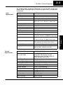
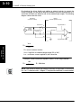
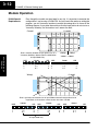
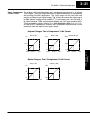
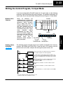
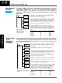
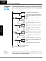
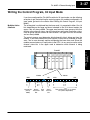
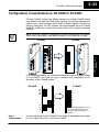
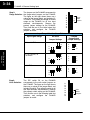
F4–04AD
4-Channel
Analog Input
In This Chapter. . . .
3
Ċ Module Specifications
Ċ Setting the Module Jumpers
Ċ Connecting the Field Wiring
Ċ Module Operation
Ċ Writing the Control Program, 16 Input Mode
Ċ Writing the Control Program, 32 Input Mode
Ċ Scaling and Converting the Input Data
Ċ Configuration CrossĆReference, D4-04AD to F4-04AD
3–2
F4–04AD 4-Channel Analog Input
F4–04AD
4-Ch. Analog Input
Module Specifications
The F4-04AD Analog Input module
provides several features and benefits.
S It is a direct replacement for the
popular D4-04AD module, when
properly configured.
S It accepts four differential voltage or
current inputs.
S Analog inputs are optically isolated
from PLC logic components.
S The module has a removable
terminal block, so the module can
be easily removed or changed
without disconnecting the wiring.
S All four analog inputs may be read
in one CPU scan (DL440/450 CPUs
only).
S Broken transmitter detection is
provided for current inputs.
ANALOG
INPUT
TB
1
2
4
8
24V
DATA
16
32
64
128
RUN NEG
256
512
1024
2048
CH1
CH2
CH3
CH4
F4–04AD
DISPLAY
CH
V
C
CH1
I
OV
V
C
CH2
I
OV
V
C
CH3
I
OV
V
C
CH4
I
OV
0–10VDC
1–5VDC
–10–+10VDC
4mA–20mA
24VDC 0.1A
CLASS 2
F4–04AD
NOTE: If you are replacing a D4–04AD with a F4–04AD in an existing application,
make sure to read the last section in this chapter, “Configuration Cross-Reference,
D4–04AD to F4–04AD.”
Analog Input
Configuration
Requirements
The F4–04AD Analog Input module requires either 16 or 32 discrete input points,
depending on its operating mode (jumper selectable). The module can be installed
in any slot of a DL405 system, including remote bases. The limitations on the
number of analog modules are:
S For local and expansion systems, the available power budget and
discrete I/O points are the limiting factors.
S For remote I/O systems, the available power budget and number of
remote I/O points are the limiting factors.
Check the user manual for your particular model of CPU for more information
regarding power budget and number of local or remote I/O points.
F4–04AD 4 Channel Analog Input
3–3
The following tables provide the specifications for the F4-04AD Analog Input
Module. Review these specifications to ensure the module meets your application
requirements.
Input
Specifications
4
Input Type
Single-ended or differential
Input Ranges
0–5, 1–5, 0–10, $5, $10 VDC, 0–20, 4–20 mA.
Resolution
12 bit (0 to 4095), unipolar 13 bit ($4095), bipolar
Input Impedance
20 MΩ minimum, voltage input
250 Ω, 1/2W, $0.1%, 25 ppm/_ C current input
Max. Continuous Overload
$50 VDC, voltage input, $45 mA, current input
Recommended External Fuse
0.032A, Series 217 fast acting, current inputs
Common Mode Voltage Range
$10V maximum
Linearity
$0.025% of span ($1 count maximum, unipolar)
Input Stability
$1/2 count
Cross Talk
–80 dB, 1/2 count maximum
Full Scale Calibration Error
$12 counts maximum, voltage input
$16 counts maximum, at 20.000 mA current input
Offset Calibration Error
$1 count maximum, voltage input
$2 counts maximum, at 4.000 mA current input
Maximum Inaccuracy
0.4% maximum @ 25_C (77° F)
0.55% maximum @ 0 to 60_C (32 to 140° F)
Conversion Time
< 6 mS per selected channel
Noise Rejection Ratio
Normal mode: –3 dB @ 50 Hz, –6 dB / octave
Common mode: –70 dB, DC to 12 kHz
PLC Update Rate
4 channel per scan max.
Digital Input Points Required
16 or 32-bit mode
16 or 32 (X) input points
12 data bits, 4 bits optional for two’s
complement mode, 4 channel select bits,
12 bits unused in 32 bit mode
Power Budget Requirement
85 mA (power from base)
External Power Supply
24 VDC, $10%, 100 mA, class 2
Operating Temperature
0 to 60_C (32° to 140° F)
Storage Temperature
–20 to 70_C (–4° to 158° F)
Relative Humidity
5 to 95% (non-condensing)
Environmental air
No corrosive gases permitted
Vibration
MIL STD 810C 514.2
Shock
MIL STD 810C 516.2
Insulation Resistance
10 MΩ, 500 VDC
Noise Immunity
NEMA ICS3-304
F4–04AD
4-Ch. Analog Input
General
Specifications
Number of Channels
3–4
F4–04AD 4-Channel Analog Input
Setting the Module Jumpers
Jumper
Locations
The module has several options that you can select by installing or removing
jumpers. At the rear of the module is a bank of eight jumpers. They may be
configured to select either 16 Input Mode or 32 Input Mode operation, input range
selection, units of measurement selection and the number of channels enabled.
Jumper Descriptions
(located below jumper
on PC board)
Functional Descriptions
2
16 or 32 Input Mode
on=32
1
0
Range
2
1
0
1
0
Units
1
CHN
1 0
F4–04AD
4-Ch. Analog Input
Range
0
1
0
Units
Active Channels
Jumper Descriptions
NOTE: If you are replacing a D4–04AD module with the F4–04AD in an existing
application, skip to the special section at the end of this chapter, “Configuration
Cross-Reference, D4–04AD to F4–04AD”.
Factory Default
Settings
By default, the module arrives from the factory with all jumpers installed. With all
jumpers installed, the module has four active channels, is in 32 Input Mode, has 4 to
20 mA. input range, and the units of the data are 12-bit (0 to 4095) BCD numbers.
Selecting the
Number of Active
Channels
The F4-04AD module accepts from one
to four analog inputs and converts the
signal(s) to a desired format to send to
the CPU. The bottom two jumpers (J7
and J8) select the number of channels
enabled. The module only converts
signals on channels that are enabled. If
your application requires less than four
signal inputs from this module, selecting
fewer channels results in faster update
times.
Use the following table to set jumpers.
= jumper removed
= jumper installed
1
0
Number of
Active
Channels
3–5
F4–04AD 4 Channel Analog Input
Channel(s) Selected
Selecting 16
Input or 32
Input Modes
Jumper Settings
Channel 1
1
0
Channel 1, Channel 2
1
0
Channel 1, Channel 2, Channel 3
1
0
Channel 1, Channel 2, Channel 3, Channel 4
1
0
The top jumper selects either 16 Input (remove
jumper) or 32 Input (install jumper) operating
modes. This is the number of X inputs the module
requires in the PLC memory map. The module can
interface to the CPU in two different ways,
depending on the setting of this jumper. Use 32
Input mode if you want to maintain compatibility
with PLC software written for the D4-04AD, or to
use features not available in 16 Input mode, and to
simplify supporting ladder logic. However, use 16
Input Mode if you must consume fewer X inputs.
The feature chart on the next page can help you
choose the mode for your application.
Jumper
Remove
Install
F4–04AD
4-Ch. Analog Input
Mode
16 Input
32 Input
Mode
Select
Jumper
I/O Points Consumed
X0 – X17
X0 – X37
Features
16 Input
Mode
32 Input
Mode
Number of X Input Bits Required From CPU
16
32
Input Value, 12-Bit, Plus Sign Bit
Yes
Yes
Input Value, 2’s Complement,12 Bits
No
Yes
Input Value, 2’s Complement, 13 Bits
No
Yes
Input Value, 12-bit
Yes
Yes
Input Value, Binary-Coded Decimal, 16 bits
(for bipolar voltage ranges only)
No
Yes
Active Channel Indicator Inputs
Yes
Yes
Broken Transmitter Detection
1 bit
(combined)
4 bits
(individual)
Sign Bit(s), indicates negative analog value
1 bit
(combined)
4 bits
(individual)
Based on this jumper selection, the module can behave as two different modules
from the CPU point of view. This chapter covers both modes, so only the CPU
program examples labeled for the mode you choose will apply.
3–6
F4–04AD 4-Channel Analog Input
Operating Range
Selection
16 Input Mode
These three jumpers select the voltage
or current range for all four input
channels simultaneously. The type of
input (voltage or current) is actually
determined by user wiring to specific
terminals on the front connector. Along
with proper wiring, set these jumpers for
the desired voltage or current signal
range. The three jumpers are binary
encoded to offer eight possible settings.
2
1
0
Range
Select
Jumpers
More input ranges are available for the module’s 32 Input mode than for 16 Input
mode. The following tables list the ranges for each of the modes.
Input Range Selection, 16 Input Mode
Input Signal Range
F4–04AD
4-Ch. Analog Input
(not used in 16 Input
Mode)
(not used in 16 Input
Mode)
–10 VDC to +10 VDC
–5 VDC to +5 VDC
0 VDC to +10 VDC
0 mA to 20 mA, or
0 VDC to +5 VDC
4 mA to 20 mA (with broken transmitter detection)
4 mA to 20 mA (without
broken transmitter
detection), or
+1 VDC to +5 VDC
Jumper Settings
Data Type and Range
2
1
0
2
1
0
2
1
0
2
1
0
2
1
0
2
1
0
2
1
0
2
1
0
12-Bit Magnitude Plus Sign
Bit, (–4095 to +4095)
12-Bit Magnitude Plus Sign
Bit, (–4095 to +4095)
12-Bit Magnitude,
(0 to 4095)
12-Bit Magnitude,
(0 to 4095)
12-Bit Magnitude,
(0 to 4095)
12-Bit Magnitude,
(0 to 4095)
F4–04AD 4 Channel Analog Input
Operating Range
Selection
32 Input Mode
3–7
The module’s 32 Input mode provides eight possible input range and data type
combinations. Two of the bipolar ranges are dedicated to BCD data type. The other
six input signal ranges convert to various data types and ranges (selected by the
units select jumpers).
Input Range Selection, 32 Input Mode
Input Signal Range
–10 VDC to +10 VDC
–5 VDC to +5 VDC
–10 VDC to +10 VDC
–5 VDC to +5 VDC
0 mA to 20 mA, or
0 VDC to +5 VDC
4 mA to 20 mA (with broken transmitter detection)
4 mA to 20 mA (without
broken transmitter
detection), or
+1 VDC to +5 VDC
2
1
0
2
1
0
2
1
0
2
1
0
2
1
0
2
1
0
2
1
0
2
1
0
Data Type and Range
Binary-Coded Decimal,
(–9999 to +9999)
Binary-Coded Decimal,
(–5000 to +5000)
Set by Units Select
jumpers
Set by Units Select
jumpers
Set by Units Select
jumpers
Set by Units Select
jumpers
Set by Units Select
jumpers
Set by Units Select
jumpers
F4–04AD
4-Ch. Analog Input
0 VDC to +10 VDC
Jumper Settings
3–8
F4–04AD 4-Channel Analog Input
F4–04AD
4-Ch. Analog Input
Units Selection for
32 Input Mode
The two jumpers for units selection
determine the data format of the digital
values of the channel inputs. They only
apply to 32 Input mode operation, so the
module ignores the position of these
jumpers during 16 Input mode
operation. The two jumpers are binary
encoded to offer four possible settings.
The units selection programmed by
these jumpers applies simultaneously to
all four input channels, and to all 32 Input
Mode input signal ranges except the two
bipolar BCD ranges. In those ranges, the
module ignores the units select jumper
settings.
1
0
Units
Select
Jumpers
The first two selections in the table offer more resolution than the last two
selections, which are included for compatibility with previous application software.
Accordingly, they are not recommended for new applications. After setting the
configuration jumpers, you are ready to install the module in the base and connect
the field wiring.
When you power up the module for the first time, if the jumper configuration is
invalid the RUN light on the module’s faceplate will NOT turn on and the Channel 1
LED will flash quickly. If this occurs, review this section and verify that the jumper
settings are correct.
NOTE: If you are replacing a D4-04AD module with the F4-04AD in an existing
application, skip to the special section at the end of this chapter, “Configuration
Cross-Reference, D4-04AD to F4-04AD”.
Units Selection for 32 Input Mode
Jumper
Settings
Notes
12-Bit Magnitude Plus Sign, 13 Bit
Format,
–4095 to +4095
1
0
Recommended for
most applications
2’s Complement, 13-Bit Format
1
0
Recommended two’s
complement format
2’s Complement, 12-Bit Format
1
0
Not recommended for
new applications
12-Bit Magnitude, 0 to 4095
1
0
Not recommended for
new applications
F4–04AD 4 Channel Analog Input
3–9
Connecting the Field Wiring
Your company may have guidelines for wiring and cable installation. If so, you
should check those before you begin the installation. Here are some general things
to consider.
S Use the shortest wiring route whenever possible.
S Use shielded wiring and ground the shield at the transmitter source. Do
not ground the shield at both the module and the source.
S Don’t run the signal wiring next to large motors, high current switches,
or transformers. This may cause noise problems.
S Route the wiring through an approved cable housing to minimize the
risk of accidental damage. Check local and national codes to choose
the correct method for your application.
S Unused inputs must be shorted to help reduce the effects of electrical
noise (see the wiring diagram for an example).
User Power
Supply
Requirements
The F4-04AD requires a separate power supply for the isolated (field) side of the
module. The Series DL405 CPUs, D4-RS Remote I/O Controller, and D4-EX
Expansion Units have built-in 24 VDC power supplies that provide up to 400mA of
current. If you only have a couple of analog modules, you can use this power source
instead of a separate supply. If you have more than four analog modules, or you
would rather use a separate supply, choose one that meets the following
requirements: 24 VDC $10%, Class 2, 100 mA current (per module).
Using Current or
Voltage Wiring
Even though you cannot select different ranges or units for each channel, you can
still wire each individual channel for voltage or current signals. For example, even
though you select a 1 to 5V range with the jumpers, you can still use a transmitter
that provides a 4-20 mA signal.
The module uses a 250 ohm precision resistor to convert the current signals to
voltage for you (4mA x 250 ohms = 1V, 20mA x 250 ohms = 5V). The following
diagram shows how this works. Notice that the voltage (V) and (I) input terminals
are connected together.
Module
(internal equivalent circuit)
Field wiring
(external to module)
V
I
+
Current
transmitter
(4 to 20mA)
Generated
voltage
(1 to 5V)
Current flow
High impedance
250 ohms
C
–
0V
0V
High impedance
F4–04AD
4-Ch. Analog Input
Wiring
Guidelines
3–10
F4–04AD 4-Channel Analog Input
By changing the wiring slightly and adding an external resistor to convert the
current to voltage, you can easily adapt this module to meet the specifications for a
transmitter that does not adhere to one of the standard input ranges. The following
diagram shows how this works.
Module
(internal equivalent circuit)
Field wiring
(external to module)
High impedance
Current flow V
+
50mA
Current
transmitter
–
Generated
voltage
I
R
250 ohms
C
0V
0V
High impedance
F4–04AD
4-Ch. Analog Input
R=
Vmax
Imax
R = value of external resistor
Vmax = high limit of selected voltage range (5V or 10V)
Imax = maximum current supplied by the transmitter
Example: current transmitter capable of 50mA, 0-10V range selected.
R=
10V
R = 200 ohms
50mA
NOTE: Your choice of resistor can affect the accuracy of the module. A resistor that
has $0.1% tolerance and a $50ppm/_C temperature coefficient is recommended.
3–11
F4–04AD 4 Channel Analog Input
Current Loop
Transmitter
Impedance
Standard 4 to 20 mA transmitters and transducers can operate from a wide variety
of power supplies. Not all transmitters are alike and the manufacturers often specify
a minimum loop or load resistance that must be used with the transmitter.
The F4-04AD provides 250 ohm resistance for each channel. If your transmitter
requires a load resistance below 250 ohms, you do not have to make any
adjustments. However, if your transmitter requires a load resistance higher than
250 ohms, you need to add a resistor in series with the module.
Consider the following example for a transmitter being operated from a 36 VDC
supply with a recommended minimum load resistance of 750 ohms. Since the
module has a 250 ohm resistor, you need to add an additional resistor.
R – resistor to add
Tr – Transmitter Requirement
Mr – Module resistance (internal 250 ohms)
R = Tr – Mr
R = 750 – 250
R 500
Two-wire Transmitter
+
–
Module Channel 1
+36V
0V
V
C
I
0V
250 ohms
The F4-04AD module has a removable connector to make wiring easier. Simply
remove the retaining screws and gently pull the connector from the module.
Wiring Diagram
NOTE 1: Shields should be grounded at the signal source.
NOTE 2: Unused channels should be shorted for best noise immunity.
NOTE 3: When a differential input is not used, 0V should be connected to C of the channel.
See NOTE 1
CH1
+
Single-ended Voltage
Transmitter –
CH3
Differential Current
Transmitter
+
–
I
OV
250 ohms
V
C
OV
I
OV
250 ohms
V
+
–
C
I
OV
OV
250 ohms
Analog Switch
CH2
Differential Voltage
Transmitter
V
24V
DATA
1 16
2 32
4 64
8 128
F4–04AD
DISPLAY
CH
V
C
CH1
+
–
User Supply 21.6 – 26.4 VDC
Class 2
I
OV
+
–
V
C
CH2
I
OV
OV
V
C
CH3
V
CH4
Not Used
See NOTE 2
I
OV
V
C
C
I
OV
INPUT
TB
Internal
Module
Wiring
(front end)
A to D
Convertor
C
See
NOTE 3
ANALOG
CH4
250 ohms
I
OV
0–10VDC
1–5VDC
–10–+10VDC
4mA–20mA
User
Supply
Return
Channel select
OV
24VDC 0.1A
CLASS 2
F4–04AD
RUN NEG
256
512
1024
2048
CH1
CH2
CH3
CH4
F4–04AD
4-Ch. Analog Input
R
DC Supply
3–12
F4–04AD 4-Channel Analog Input
Module Operation
DL430 Special
Requirements
Even though the module can be placed in any slot, it is important to examine the
configuration if you’re using a DL430 CPU. As you’ll see in the section on writing the
program, you use V-memory locations to extract the analog data. As shown in the
following diagram, if you place the module so that the input points do not start on a
V-memory boundary, the instructions can’t access the data.
F4–04AD
Correct!
16pt
Output
8pt
Output
Slot 0
Slot 1 Slot 2 Slot 3 Slot 4 Slot 5
Y0
–
Y17
Y20 X0 X20 X60 X70
–
–
–
–
–
Y27 X17 X57 X67 X77
F4–04AD
4-Ch. Analog Input
V40402
XX
5 4
0 7
X
5
7
LSB
X
4
0
32pt
Input
V40400
Data is correctly entered so input points start on a
V-memory boundary address from the table below.
32 Input Mode Only
MSB
16pt
Input
8pt
Input
8pt
Input
V40403
V40401 – V40402
MSB
LSB
V40401
X
3
7
XX
3 2
0 7
X
2
0
F4–04AD
Wrong!
16pt
Output
8pt
Output
16pt
Input
8pt
Input
32pt
Input
8pt
Input
Slot 0
Slot 1 Slot 2 Slot 3 Slot 4 Slot 5
Y0
–
Y17
Y20 X0 X20 X30 X70
–
–
–
–
–
Y27 X17 X27 X67 X77
Data is split over two locations for 16 Input Mode and over three locations for 32
Input Mode, so instructions cannot access data from a DL430.
MSB
X
7
7
V40403
XX
7 6
0 7
LSB
X
6
0
MSB
X
5
7
32 Input Mode Only
V40402
XX
5 4
0 7
LSB
X
4
0
MSB
X
3
7
V40401
XX
3 2
0 7
LSB
X
2
0
F4–04AD 4 Channel Analog Input
Channel
Scanning
Sequence
3–13
Before you begin writing the control program, it is important to take a few minutes to
understand how the module processes and represents the analog signals.
The F4-04AD module supplies one channel of data per each CPU scan. This is true
for both 16 Input and 32 Input Modes. Since there are four channels, it can take up
to four scans to get data for all channels. Once all channels have been scanned the
process starts over with channel 1.
Unused channels are not processed, so if you select only two channels, then each
channel will be updated every other scan.
Scan
Read Inputs
Channel 1
Read the data
Scan N+1
Channel 2
Scan N+2
Channel 3
Store data
Scan N+3
Channel 4
Scan N+4
Channel 1
Write to Outputs
Even though channel updates to the CPU are synchronous with the CPU scan, the
module asynchronously monitors the analog transmitter signal and converts the
signal to a 12-bit binary representation. This enables the module to continuously
provide accurate measurements without slowing down the discrete control logic in
the RLL program.
Displaying
Diagnostic
Data
At the top of the module’s faceplate, LED indicators display information for the
selected channel. The top row of LEDs display diagnostic information. The TB
indicator turns on when the module senses a loose terminal block. The 24V
indicator turns on when the external 24V supply voltage is low or not connected.
The RUN LED flashes on and off only if the jumper configuration is valid, and the
module’s internal diagnostics have passed. If the jumper configuration is incorrect
the RUN LED remains off. During normal operation, the RUN indicator flashes on
and off continuously at approximately a one second rate. The NEG light turns on if
the voltage or current input to the selected channel is negative.
F4–04AD
4-Ch. Analog Input
Scan N
Execute Application Program
3–14
F4–04AD 4-Channel Analog Input
Displaying
Channel Data
By removing the connector cover you can access the push-button ”DISPLAY CH”,
to select which channel’s data is currently being displayed. The CH1 through CH4
indicators correspond to the selected channel. The input value data corresponding
to the channel is shown by the 12 data bit indicators. They are numbered from 1 to
2048 to indicate the binary weight. The bit is on (1) if the indicator is illuminated.
Push button
to select
channel for
viewing
ANALOG
INPUT
TB
1
2
4
8
24V
RUN NEG
DATA
16
256 CH1
32
512 CH2
64
1024 CH3
2048 CH4
128
LEDs indicate
values as shown
F4–04AD
DISPLAY
CH
V
C
CH1
I
OV
F4–04AD
4-Ch. Analog Input
The next two sections describe the input bit assignments for both 16 Input and 32
Input operating modes. You need to read only the section that matches your
selection in the jumper configuration.
Input
Assignments
for 16 Input
Mode
In this mode, the F4-04AD module requires 16 discrete input points. These inputs
provide:
S
an indication of which channel is active.
S
a digital representation of the analog signal (12 bit plus sign).
S
broken transmitter detection for current signal inputs.
Since all input points are automatically mapped into V-memory, it is very easy to
determine the location of the data word that will be assigned to the module.
F4-04AD
8pt
Input
X0
–
X7
8pt
Input
16pt
Input
16pt
Input
X10 X20
–
–
X17 X37
V40400
16pt
Output
16pt
Output
X40
–
X57
V40402
V40401
MSB
Bit 15 14 13 12 11 10 9
X
3
7
LSB
8
7
X X
3 2
0 7
6
5
4
3
2
1
0
X
2
0
Within this data word location, the individual bits represent specific information
about the analog signal.
3–15
F4–04AD 4 Channel Analog Input
Active Channel
Indicator Inputs,
16 Input Mode
Analog Data Bits,
16 Input Mode
Broken Transmitter
Bit, 16 Input Mode
The first twelve bits of the first V-memory
location represent the analog data in
binary format. All input ranges use these
bits.
Bit
Value
Bit
Value
0
1
6
64
1
2
7
128
2
4
8
256
3
8
9
512
4
16
10
1024
5
32
11
2048
Bipolar input ranges use the twelve
analog data bits as shown above, plus
an additional sign bit. Bit 15 in the input
word is the sign bit, and is a 1 when the
polarity of the active channel is negative.
If a unipolar mode is selected, the input
value is assumed to be greater than or
equal to zero, so this bit is always 0.
One of the 4–20 mA current ranges
features broken transmitter detection.
Bit 14 in the input word is set to 1 if the
current on the active channel is at 1.25
mA or less. This is useful for diagnostics
or troubleshooting logic built in to your
RLL program.
V40401
MSB
LSB
1 1 1 1 11 9 8 7 6 5 4 3 2 1 0
5 4 3 2 10
– active channel inputs
V40401
MSB
LSB
1 1 1 1 11 9 8 7 6 5 4 3 2 1 0
5 4 3 2 10
– data bits
V40401
MSB
LSB
1 1 1 1 1 1 9 8 7 6 5 4 3 2 1 0
5 4 3 2 1 0
– sign bit
V40401
MSB
LSB
1 1 1 1 11 9 8 7 6 5 4 3 2 1 0
5 4 3 2 10
– broken transmitter bit
F4–04AD
4-Ch. Analog Input
Sign Bit,
16 Input Mode
The two bits 12 and 13 (inputs) of the
upper V-memory location indicate the
active channel. They are binary
encoded to indicate up to four active
channels. Only the enabled channels
are updated. The module automatically
turns these inputs on and off to indicate
the active channel for each scan.
Bits
Active
Scan
13 12
Channel
N
0 0
1
N+1
0 1
2
N+2
1 0
3
N+3
1 1
4
N+4
0 0
1
3–16
F4–04AD 4-Channel Analog Input
Input Assignments In this mode, the F4–04AD module requires 32-point discrete input points. These
for 32 Input Mode inputs provide:
S individual active channel bits for each channel.
S a digital representation of the analog signal in various data formats.
S individual sign bits for each channel.
S individual broken transmitter detection bits for each channel.
Since all input points are automatically mapped into V-memory, it is very easy to
determine the location of the two data words that will be assigned to the module.
F4–04AD
8pt
Input
X0
–
X7
8pt
Input
32pt
Input
X10 X20
–
–
X17 X57
F4–04AD
4-Ch. Analog Input
V40400
MSB
V40402
Bit 15 14 13 12 11 10 9
7
6
5
4
3
2
X X
5 4
0 7
X
5
7
Active Channel
Indicator Inputs,
32 Input Mode
8
LSB
1
X
4
0
16pt
Output
16pt
Output
X60
–
X77
V40403
MSB
0
16pt
Input
V40401
Bit 15 14 13 12 11 10 9
X
3
7
8
7
X X
3 2
0 7
LSB
6
5
4
3
2
1
0
X
2
0
Within these data word locations, the individual bits represent specific information
about the analog signal.
The first four input bits (0–3) of the upper
V40401
V-memory location indicate the active
MSB
LSB
channel. Each bit corresponds to a
single channel to indicate four possible
1 1 1 1 1 1 9 8 7 6 5 4 3 2 1 0
active
channels.
The
module
5 4 3 2 1 0
automatically turns these bits on and off
each scan to indicate the active channel
V40402
for that scan.
MSB
Scan
N
N+1
N+2
N+3
N+4
Bits
3 2
0 0
0 0
0 1
1 0
0 0
1
0
1
0
0
0
0
1
0
0
0
1
Active
Channel
1
2
3
4
1
LSB
1 1 1 1 11 9 8 7 6 5 4 3 2 1
5 4 3 2 10
– active channel inputs
0
3–17
F4–04AD 4 Channel Analog Input
Analog Data Bits,
32 Input Mode
In 32 Input Mode the four possible data
formats are 12-bit magnitude plus sign,
two’s complement 13-bit format, two’s
complement 12-bit format, and 12-bit
magnitude. In the two 12-bit magnitude
modes, the first twelve bits of the lower
word represent the analog value’s
magnitude
Bit
0
1
2
3
4
5
Value
1
2
4
8
16
32
Bit
6
7
8
9
10
11
Value
64
128
256
512
1024
2048
Bit
0
1
2
3
4
5
6
7
Value
1
2
4
8
16
32
64
128
Bit
8
9
10
11
12
13
14
15
Value
256
512
1024
2048
4096
8192
16384
32768
The BCD formats use 16 bits of the lower
word to represent four binary-coded
decimal digits, from 0000 to 9999. Digit 1
is the LSD, Digit 4 is the MSD.
Bit
0
1
2
3
4
5
6
7
(digit
(digit
(digit
(digit
(digit
(digit
(digit
(digit
Value
1), 1
1), 2
1), 4
1), 8
2), 1
2), 2
2), 4
2), 8
Bit
8
9
10
11
12
13
14
15
(digit
(digit
(digit
(digit
(digit
(digit
(digit
(digit
Value
3), 1
3), 2
3), 4
3), 8
4), 1
4), 2
4), 4
4), 8
V40401
MSB
LSB
1 1 1 1 11 9 8 7 6 5 4 3 2 1 0
5 4 3 2 10
V40402
MSB
LSB
1 1 1 1 11 9 8 7 6 5 4 3 2 1 0
5 4 3 2 10
– data bits
Two’s Complement Format
V40401
LSB
MSB
1 1 1 1 11 9 8 7 6 5 4 3 2 1 0
5 4 3 2 10
V40402
LSB
MSB
1 1 1 1 11 9 8 7 6 5 4 3 2 1 0
5 4 3 2 10
– data bits
BCD Format
V40401
LSB
MSB
1 1 1 1 11 9 8 7 6 5 4 3 2 1 0
5 4 3 2 10
Digit 4 Digit 3 Digit 2 Digit 1
V40402
LSB
MSB
1 1 1 1 11 9 8 7 6 5 4 3 21 0
5 4 3 2 10
– data bits
F4–04AD
4-Ch. Analog Input
The two’s complement formats are for
bipolar inputs. Each range uses 16 data
bits, and embeds the sign bit information
in the data (no sign bit is required in
these ranges). Each range is centered at
0, counting upward for positive numbers.
Negative numbers start at 65535 (for
count= –1), and count downward.
12-bit Magnitude Format
3–18
F4–04AD 4-Channel Analog Input
Sign Bits,
32 Input Mode
Four bits (4 to 7) of the upper word are
dedicated for use as sign bits. These are
individually assigned to each of the four
channels. When an input bit is on, the
data for the corresponding channel
represents a negative value. When the
bit is off, the data is positive.
V40401
MSB
LSB
1 1 1 1 11 9 8 7 6 5 4 3 2 1
5 4 3 2 10
0
V40402
F4–04AD
4-Ch. Analog Input
Bit
4
5
6
7
Channel
1
2
3
4
Broken Transmitter Four bits (8 to 11) of the upper word are
bits, 32 Input Mode dedicated for use as broken transmitter
indications. They are only operational for
the 4 to 20 mA. input range. When an
input bit is on, the current for the
corresponding channel is at or below
1.25 mA. When the condition ends, the
bit automatically turns off.
MSB
1 1 1 1 11 9 8 7 6 5 4 3 2 1
5 4 3 2 10
Channel
1
2
3
4
0
– sign bits
V40401
MSB
LSB
1 1 1 1 11 9 8 7 6 5 4 3 2 1 0
5 4 3 2 10
V40402
MSB
Bit
8
9
10
11
LSB
LSB
1 1 1 1 11 9 8 7 6 5 4 3 2 1 0
5 4 3 2 10
– broken transmitter bits
3–19
F4–04AD 4 Channel Analog Input
12-Bit Magnitude
Plus Sign Format,
(All Modes)
The 12-Bit Plus Sign conversion range is available in either 16 Input or 32 Input
Modes, but it’s the only data conversion format available in 16 Input mode. Unipolar
signal ranges use 12-bit resolution. Bipolar ranges have 13-bit resolution because
of the additional sign bit. The 12 data bits convert the analog signal to 4096 “pieces”
ranging from 0 to 4095 (212). For example, with a 0 to 5V scale, a 0V signal would be
0, and a 5V signal would be 4095. This is equivalent to a binary value of
0000 0000 0000 to 1111 1111 1111, or 000 to FFF hexadecimal.
Unipolar Ranges
0V – 5V
Bipolar Ranges
0V – 10V
5V
–5V to +5V
10V
0V
0V
0
4095
0
1V – 5V
+5V
+10V
0V
0V
–5V
–4095
0
+4095
–10V
–4095
0
+4095
4 – 20mA
20mA
1V
4mA
4095
0
4095
0 – 20mA
20mA
0mA
0
Two’s Complement
Format, 13-Bit
4095
The 32 Input Mode offers two’s complement data formats in 12-bit and 13-bit
ranges. The 13-bit range is recommended for new applications, while the 12-bit
range is recommended only for compatibility with D4-04AD applications. The 13-bit
format is for bipolar voltage input ranges only. Depending on your application, two’s
complement format can be very useful. Some operator interfaces or other
peripheral devices may require two’s complement format. If you need to add
positive and negative values together (as in calculating an average), this format can
simplify your RLL program. Two’s complement representation imbeds the sign bit
information in the data. It allows CPU instructions to add numbers together without
specific logic to handle the sign bit for negative numbers. The 13-bit two’s
complement format actually uses 16 binary data bits. The following diagram shows
how this works.
F4–04AD
4-Ch. Analog Input
5V
0
4095
–10V to +10V
3–20
F4–04AD 4-Channel Analog Input
Two’s Complement 13-bit Format
–5V to +5V
–10V to +10V
+5V
+10V
0V
0V
–5V
61440
65535, 0
4095
–10V
61440
65535, 0
4095
F4–04AD
4-Ch. Analog Input
In the left graph above, zero volts converts to a count of zero. Positive voltages up to
+5 volts convert to counts of up to decimal +4095. A few millivolts less than zero
converts to 65535, the equivalent to -1 count. At -5V, the conversion is to 61440
counts. The conversion method translates positive polarity signals per normal
binary scaling. It’s negative values that include an additional step. In this case,we
start at the top of the 16-bit binary range (65535), and count downward. With zero
count point at mid-range,negative numbers transition to positive numbers.
As an example, suppose the module
sends the counts of –6 and +15 in
successive scans to the CPU. The RLL
program is going to sum the input
values. When the module is configured
for two’s complement format, negative
numbers are specially formatted. It takes
the –6 in binary and takes a one’s
complement by inverting all the bits.
Then, it adds 1 to the LSB to get a two’s
complement representation. The 16-bit
result the module sends to the CPU is
decimal 65530, or FFFA hex,
A
representing –6.
In the ladder program, you can add +15
to this number. By ignoring all end
B
carries, we have the correct answer of
+9. The ladder program is simplified
because it does not need to examine a
A+B=C
sign bit to do a subtract instruction.
V40401
MSB
LSB
Example: In the module, we
start with the number “6”.
0000000000000110
Take one’s complement by
inverting all the bits.
1111111111111001
Add 1 to the LSB, for two’s complement representation of “–6”.
This number is sent to the CPU.
1111111111111010
In the CPU, we add the number ”+15
0000000000001111
The sum of “–6” and “+15” is “9”.
0 0 0 0 0 0 0 0 0 0 0 0 1 0 01
F4–04AD 4 Channel Analog Input
3–21
Two’s Complement The module’s 32 Input Mode offers two’s complement data formats in 12-bit and
13-bit ranges. The 12-bit range shown here is recommended only for compatibility
Format, 12-Bit
with existing D4–04AD applications. The 12-bit range may be used with both
unipolar and bipolar input signal ranges. The 12 data bits convert the analog signal
to 4096 “pieces” ranging from 0 to 4095 (212). For example, with a 0 to 5V scale, a
0V signal would be –2048, represented as 63488, and a 5V signal would be 2047.
This is equivalent to a binary value of 1111 1000 0000 0000 to 0000 1111 1111 1111,
or F800 to 0FFF hexadecimal. However, two’s complement representation is more
commonly used with bipolar input signal ranges.
Unipolar Ranges, Two’s Complement 12-bit Format
0V to +5V
0V to +10V
4mA to 20 mA
+5V
+10V
20mA
+2.5V
+5V
12mA
0V
63488
65535, 0
2047
0V
63488
65535, 0
2047
4mA
63488
–5V to +5V
–10V to +10V
+5V
+10V
0V
0V
–5V
63488
65535, 0
2047
–10V
63488
65535, 0
2047
2047
F4–04AD
4-Ch. Analog Input
Bipolar Ranges, Two’s Complement 12-bit Format
65535, 0
3–22
F4–04AD 4-Channel Analog Input
Unipolar
Resolution
Each count can also be expressed in
terms of the signal level by using the
equation shown. Unipolar ranges have
12 bits of resolution, which divides the
signal span into 4095 counts. The
following table shows the smallest signal
change that will result in a single LSB
change in the data value for each signal
input range.
F4–04AD
4-Ch. Analog Input
Range
Unipolar resolution + H–L
4095
H = High limit of the input signal
L = Low limit of the input signal
Signal Span
(H – L)
Divide By
Smallest Detectable
Change
0 to 5V
5V
4095
1.22 mV
0 to 10V
10 V
4095
2.44 mV
1 to 5V
4V
4095
0.98 mV
4 to 20mA
16 mA
4095
3.91 mA
0 to 20mA
20 mA
4095
4.88 mA
Bipolar Resolution Bipolar ranges have 13 bits of resolution,
(the additional sign bit adds an
additional bit of resolution). This divides
the signal span into 8191 counts. The
following table shows the smallest signal
change that will result in a single LSB
change in the data value for each signal
input range.
Range
Bipolar resolution + H–L
8191
H = High limit of the input signal
L = Low limit of the input signal
Signal Span
(H – L)
Divide By
Smallest Detectable
Change
–5 to +5V
10 V
8191
1.22 mV
–10 to +10V
20 V
8191
2.44 mV
Now that you understand how the module and CPU work together to collect and
store the information, you’re ready to write the control program.
F4–04AD 4 Channel Analog Input
3–23
Writing the Control Program, 16 Input Mode
If you have configured the F4-04AD module for 16 Input mode, use the following
examples to get started writing the control program. For modules configured in 32
Input mode, skip to the section titled “Writing the Control Program, 32 Input Mode”.
Multiple Active
Channels
The following program example shows how to read the analog data into V-memory
locations with DL440 and DL450 CPUs. Once the data is in V memory, you can
perform math on the data, compare the data against preset values, etc.
430 440 450
SP1
LDF
K12
BCD
X34
X35
X34
X35
X34
X35
X34
X35
OUT
V3000
OUT
V3001
OUT
V3002
OUT
V3003
X20
Loads the first 12 bits of the data word into the accumulator.
The X address depends on the I/O configuration.
It’s usually easier to perform math operations in BCD, so it is
best to convert the data to BCD immediately. You can omit this
instruction if your application does not require it (such as PID
loops).
When X34 and X35 are off, channel 1 data is being sent to the
CPU. The OUT instruction moves the data from the
accumulator to V3000.
When X34 is on and X35 is off, channel 2 data is stored in
V3001.
When X34 is off and X35 is on, channel 3 data is stored in
V3002.
When X34 and X35 are on, channel 4 data is stored in V3003.
Note, this example uses SP1, which is always on. You
could also use an X, C, etc. permissive contact.
F4–04AD
4-Ch. Analog Input
Reading Values,
DL440/450
5 4 4
Since
all
channels
are
F4-04AD
multiplexed into a single data
8pt
8pt
16pt 16pt
16pt
16pt
word, the control program must
Input Input Input Input Output Output
determine which channel’s
X0 X10 X20 X40
data is being sent from the
–
–
–
–
module during each scan. If
X7 X17 X37 X57
you have enabled only one
channel, then its data will be
available on every scan. Two or
V40402
V40400
more
channels
require
multiplexing the data word.
V40401
Since the module requires 16
MSB
LSB
input points from the CPU, it is
very easy to use the active
channel
status
bits
to
determine which channel is Sign Bit
Data Bits
being monitored.
Broken
Active
Transmitter Bit Channel Bits
3–24
F4–04AD 4-Channel Analog Input
Optional Method,
DL440/450
5 4 4
430 440 450
The previous example used the OUT instruction to store channel data in V memory,
requiring four ladder rungs. The OUTX (Out Indexed) instruction in the next
example does much of that work for you. It uses the first stack location to
temporarily hold the data to be stored at an address modified by an offset in the
accumulator.
SP1
LDF
K12
X20
Since the DL405 CPUs perform math operations in BCD, it is usually
best to convert the data to BCD immediately. You can leave out this
instruction if your application does not require it (such as PID loops).
BCD
LDF
K2
X34
OUTX
V3000
F4–04AD
4-Ch. Analog Input
Note: This example
uses SP1, which is
always on. You could
also use an X, C, etc.
permissive contact.
Reading Values,
DL430
4 4 4
430 440 450
Loads the first 12 bits of the data word into the accumulator. The X
address depends on the I/O configuration.
This LDF instruction loads the two channel indicator bits into the
accumulator. The channel data is pushed onto a stack.
The OUTX (out indexed) instruction stores the channel data,
currently the first item on stack, to an address that starts at V3000
plus the channel offset (0–3) located in the accumulator. For
example, when channel 3 is read, the data is stored in V3002 (V3000
+ 2).
Module Reading
Acc. Bits
Offset
Data Stored in ...
Channel 1
00
0
V3000
Channel 2
01
1
V3001
Channel 3
10
2
V3002
Channel 4
11
3
V3003
The following program example shows how to read the analog data into V-memory
locations with DL430 CPUs. Since the DL430 does not support the LDF instruction,
you can use the LD instruction instead as shown. You can also use this method with
DL440 and DL450 CPUs.
SP1
LD
V40401
ANDD
KFFF
Loads the complete data word into the accumulator. The V-memory
location depends on the I/O configuration. See Appendix A for the
memory map.
Mask off active channel bits, etc. above the 12 bits of data.
BCD
It’s usually easier to perform math operations in BCD, so it is best to
convert the data to BCD immediately. You can omit this instruction if
your application does not require it (such as PID loops).
LD
V40401
The load instruction reads the data into the accmulator again. This
pushes the channel data onto a stack.
ANDD
K3000
This instruction masks the analog data values, sign bit, and broken
transmitter bit, to leave the active channel bits in the accumulator.
SHFR
K12
OUTX
V3000
Note: This example uses SP1,
which is always on. You could
also use an X, C, etc. permissive
contact.
Now you have to shift the active channel bits to the right so the result
has a value from 0 to 3 (inclusive) in binary format.
The OUTX (out indexed) instruction stores the channel data, currently
the first item on stack, to an address that starts at V3000 plus the
channel offset (0–3) located in the accumulator. For example, when
channel 3 is read, the data is stored in V3002 (V3000 + 2).
Module Reading
Acc. Bits
Offset
Data Stored in ...
Channel 1
00
0
V3000
Channel 2
01
1
V3001
Channel 3
10
2
V3002
Channel 4
11
3
V3003
F4–04AD 4 Channel Analog Input
Single Active
Channel
4 4 4
3–25
If the module is configured for only one input channel, you can omit the channel
selection logic which simplifies the program.
430 440 450
SP1
LD or LDF
BCD
OUT
V3000
Channel 1 data is always being sent to the CPU. Use LD or LDF,
depending on the type of CPU you are using.
The BCD instruction converts the data from binary to BCD. This
instruction may be optional for your application (do not use with
PID loops).
The OUT instruction stores the data in V3000.
Note: This example uses SP1, which is always on. You can also use an X, C, etc. permissive contact. Also,
the DL430 requires an additional instruction to mask off the most significant four bits that are brought in with
the LD instruction, before the BCD instruction is executed. This method is shown in the previous example.
430 440 450
The following program example shows how to read all four channels in one scan by
using a FOR/NEXT loop. Before choosing this technique, do consider its impact on
the scan time. Remember the FOR/NEXT routine shown here will add about 5 ms
(1.25 ms/loop) to the overall scan time. If you don’t need to read the analog data on
every scan, change SP1 to a permissive contact (such as an X input, CR ,or stage
bit) to only enable the FOR/NEXT loop when it is required.
NOTE: This FOR/NEXT loop program will not work in a remote/slave arrangement;
use one of the programs shown that reads one channel per scan.
K4
SP1
FOR
Starts the FOR/NEXT loop. The constant (K4) specifies how many
times the loop will execute, equal to the number of channels you are
using. For example, enter K3 if you’re using 3 channels.
LDIF X20
K16
Immediately loads all 16 bits of the data word into the accumulator.
The LDIF instruction retreives the I/O points without waiting on the
CPU to finish the scan.
OUT
V40401
Save the new input status which is in the accumulator to the image
register (V memory). Remember, the FOR–NEXT loop will do this
four times before the CPU’s normal scan updates V40401 again.
This ANDD instruction masks off the upper four bits, leaving just the
12-bit analog value in the accumulator.
ANDD
KFFF
Since the DL405 CPUs perform math operations in BCD, it is usually
best to convert the data to BCD immediately. You can leave out this
instruction if your application does not require it (such as PID loops).
BCD
X34
LDF
K2
OUTX
V3000
This LDF instruction loads the two active channel bits into the
accumulator. The OUT instruction above updated the V-memory
image which makes this possible during a scan. X34 = X20 + 14.
The OUTX instruction stores the channel data to an address that
starts at V3001 plus the channel offset (0–3). For example, if channel
3 was being read, the data would be stored in V3002 (V3000 + 2).
Module Reading
NEXT
Note: This example uses SP1,
which is always on. You could also
use an X, C, etc. permissive contact.
Acc. Bits
Offset
Data Stored in ...
Channel 1
000
0
V3000
Channel 2
001
1
V3001
Channel 3
010
2
V3002
Channel 4
011
3
V3003
F4–04AD
4-Ch. Analog Input
Reading Four
Channels in
One Scan,
DL440/450
5 4 4
3–26
F4–04AD 4-Channel Analog Input
Reading Values
With Sign Bits,
DL440/450
5 4 4
In 16 Input Mode, the most significant bit (bit 15) is the sign bit for the active channel
of the current scan. Because it is multiplexed (shared) among the four channels,
you may need to separate it into four individual sign bits. The following example
gives a method to do this, giving the resulting sign bits as internal contacts C0 to C3.
430 440 450
SP1
LDF
K12
X20
It’s usually easier to perform math operations in BCD, so it is
best to convert the data to BCD immediately. You can omit
this instruction if your application does not require it (such as
PID loops).
Channel 1 data is being sent when X34 and X35 are off. The
out instruction moves the data from the accumulator to
V3000.
BCD
X34
X35
Loads the first 12 bits of the data word into the accumulator.
The X address depends on the I/O configuration.
OUT
V3000
C0
RST
X37
C0
SET
X34
X35
Turn off sign bit (C0) for channel 1. It will remain off for
positive numbers.
When the module’s sign bit (X37) is on the data is negative,
C0 turns on.
Channel 2 data is being sent when X34 is on and X35 is off.
The out instruction moves the data from the accumulator to
V3001.
OUT
V3001
F4–04AD
4-Ch. Analog Input
C1
RST
X37
C1
SET
X34
X35
Turn off sign bit (C1) for channel 2. It will remain off for
positive numbers.
When the module’s sign bit (X37) is on the data is negative,
C1 turns on.
Channel 3 data is being sent when X34 is off and X35 is on.
The out instruction moves the data from the accumulator to
V3002.
OUT
V3002
C2
RST
X37
C2
SET
X34
X35
Turn off sign bit (C2) for channel 3. It will remain off for
positive numbers.
When the module’s sign bit (X37) is on the data is negative,
C2 turns on.
Channel 4 data is being sent when X34 and X35 are on. The
out instruction moves the data from the accumulator to
V3003.
OUT
V3003
C3
RST
X37
Turn off sign bit (C3) for channel 4. It will remain off for
positive numbers.
C3
SET
When the module’s sign bit (X37) is on the data is negative,
C3 turns on.
Note: This example uses SP1, which is always on.
You could also use an X, C, etc. permissive contact.
Broken
Transmitter
Detection
When the 4–20 mA range is selected, the bit next to the most significant bit (bit 14) is
on when the current for the active channel is less than 1.25 mA. You can use the
method in the previous example to generate four independent broken transmitter
bits. Just replace X37 with X36 in the example.
3–27
F4–04AD 4 Channel Analog Input
Writing the Control Program, 32 Input Mode
Multiple Active
Channels
If you have configured the F4–04AD module for 32 Input mode, use the following
examples to get started writing the control program (for modules configured in 16
Input mode, go back to the section titled “Writing the Control Program, 16 Input
Mode”).
The analog data is multiplexed into the lower word. It is presented in either 12 or 16
bits, depending on the range and format selected. In the 12-bit format modes, the
upper 4 bits are always 0000. The upper word contains three groups of bits that
contain active channel status, sign bit information, and broken transmitter status.
Each bit group contains one bit for each channel. The upper four bits are unused,
and are always 0000.
The control program must determine which channel’s data is being sent from the
module. If you have enabled only one channel, its data will be available on every
scan. Two or more channels require multiplexing the lower data word. Since the
module communicates as X input points to the CPU, it is very easy to use the active
channel status bits in the upper word to determine which channel is being
monitored.
F4-04AD
X0
–
X7
8pt
Input
32pt
Input
X10 X20
–
–
X17 X57
V40400
16pt
Output
X60
–
X77
V40401
LSB
X X
5 4
0 7
Unused Bits
Broken
(always
Transmitter
0000)
Bits
16pt
Output
V40403
V40402
MSB
X
5
7
16pt
Input
F4–04AD
4-Ch. Analog Input
8pt
Input
X
4
0
Sign
Bits
Active
Channel
bits
MSB
X
3
7
LSB
X X
3 2
0 7
X
2
0
Data word contains 12 or 16 data
bits (format-dependent)
3–28
F4–04AD 4-Channel Analog Input
Reading Values,
DL440/450
5 4 4
The following program example shows how to read the analog data into V-memory
locations with the DL440 and DL450 CPUs. Once the data is in V-memory, you can
perform math on the data, compare the data against preset values, etc.
430 440 450
SP1
LDF
K12
X20
BCD
X40
X41
X42
F4–04AD
4-Ch. Analog Input
X43
OUT
V3000
OUT
V3001
OUT
V3002
OUT
V3003
Loads the first 12 bits of the data word into the accumulator. The X
address depends on the I/O configuration. If using a two’s complement
mode, use the constant K16 in the box.
It’s usually easier to perform math operations in BCD, so it is best to
convert the data to BCD immediately. Note that you can configure the
module to send bipolar voltage input data in BCD format, making this
step unnecessary.
When X40 is on, channel 1 data is being sent to the CPU. The out
instruction moves the data from the accumulator to V3000.
When X41 is on, channel 2 data is stored in V3001.
When X42 is on, channel 3 data is stored in V3002.
When X43 is on, channel 4 data is stored in V3003.
Note: This example uses SP1, which is always on. You
could also use an X, C, etc. permissive contact.
Reading Values,
DL430
4 4 4
430 440 450
The following program example shows how to read the analog data into V-memory
locations with the DL430 CPU. Since the DL430 does not support the LDF
instruction, you can use the LD instruction instead as shown. You can also use this
method with DL440 and DL450 CPUs.
SP1
LD
V40401
Loads all 16 bits of the data word into the accumulator. The X address
depends on the I/O configuration. If the module is configured for one of
the 12 bit ranges, the upper for bits are returned as 0000.
ANDD
KFFF
ANDDS the value in the accumulator with the constant KFFF, which
masks the channel ID bits, and stores the value in the accumulator.
Without this, the values will not be correct, so do not forget to include it.
BCD
X40
X41
X42
X43
OUT
V3000
OUT
V3001
OUT
V3002
OUT
V3003
It’s usually easier to perform math operations in BCD, so it is best to
convert the data to BCD immediately. Note that you can configure the
module to send bipolar voltage input data in BCD format, making this
step unnecessary.
When X40 is on, channel 1 data is being sent to the CPU. The out
instruction moves the data from the accumulator to V3000.
When X41 is on, channel 2 data is stored in V3001.
When X42 is on, channel 3 data is stored in V3002.
When X43 is on, channel 4 data is stored in V3003.
Note: This example uses SP1, which is always on. You could also use an X, C, etc. permissive contact.
F4–04AD 4 Channel Analog Input
Single Active
Channel
4 4 4
3–29
If the module is configured for only one input channel you can omit the channel
selection logic; this simplifies the program.
SP1
430 440 450
LD or LDF
BCD
OUT
V3000
Channel 1 data is always being sent to the CPU. Use LD
or LDF, depending on the type of CPU you are using.
The BCD instruction converts the data from binary to
BCD. This instruction may be optional for your
application. Do not use with PID loops.
The OUT instruction stores the data in V3000.
Note: This example uses SP1, which is always on. You can also use an X, C, etc. permissive
contact. Also, the DL430 requires an additional instruction to mask off the most significant four
bits that are brought in with the LD instruction, before the BCD instruction is executed. This
method is shown in the previous example using an ANDD instruction.
Reading Four
Channels in
One Scan,
DL440/450
5 4 4
430 440 450
The following program example shows how to read all four channels in one scan by
using a FOR/NEXT loop. Remember, the FOR/NEXT routine shown here will add
about 5 ms (1.25 ms/loop) to the overall scan time. If you don’t need to read the
analog data on every scan, change SP1 to a permissive contact (such as an X
input, CR, or stage bit) to only enable the FOR/NEXT loop when it is required. This
FOR/NEXT loop program will not work in a remote/slave arrangement; use one of
the programs shown that reads one channel per scan.
FOR
LDIF X20
K32
Immediately loads all 32 bits of the data word into the accumulator.
The LDIF instruction retreives the I/O points without waiting on the
CPU to finish the scan.
OUTD
V40401
Save the new input status which is in the accumulator to the image
register (V memory). Remember, the FOR–NEXT loop will do this
four times before the CPU’s normal scan updates V40401 and 40402
again.
ANDD
KFFFF
X41
X42
X43
This ANDD instruction masks off the upper sixteen bits, leaving just
the lower 16 bits which contain the 12 or 16 bit analog value in the
accumulator.
Since the DL405 CPUs perform math operations in BCD, it is usually
best to convert the data to BCD immediately. You can leave out this
instruction if your application does not require it.
BCD
X40
Starts the FOR/NEXT loop. The constant (K4) specifies how many
times the loop will execute, equal to the number of channels you are
using. For example, enter K3 if you’re using 3 channels.
OUT
V3001
One of the four active channel bits will be on each time through the
FOR–NEXT loop, indicating the active channel. The corresponding
OUT instruction places the 12 or 16-bit value in the accumulator in
the proper V memory location.
OUT
V3002
OUT
V3003
OUT
V3004
NEXT
Note: This example uses SP1, which is always on.
You could also use an X, C, etc. permissive contact.
F4–04AD
4-Ch. Analog Input
K4
SP1
3–30
F4–04AD 4-Channel Analog Input
Reading Values
With Sign Bits
If the 13-bit magnitude plus sign format is selected, the sign bits (X44 to X47 in our
example) will be on when the corresponding analog input channel(s) send negative
data. The bits are always off (0000) in the 12-bit magnitude and two’s complement
formats.
Broken Transmitter When the 4 to 20mA with broken transmitter detection range is selected, the four
Broken Transmitter bits (X50 to X53 in our example) will be on when the current on
Detection
the corresponding analog input channel(s) is below the normal 4 mA bottom end of
the range. The threshold at which these bits turn on is +1.25 mA.
Scaling and Converting the Input Data
The following examples show you how to scale and convert the input data, for both
16 Input and 32 Input modes.
F4–04AD
4-Ch. Analog Input
Scaling the
Input Data
Most applications usually require
measurements in engineering units,
which provide more meaningful data.
This is accomplished by using the
conversion formula shown.
You may have to make adjustments to
the formula depending on the scale you
choose for the engineering units.
Units + A H * L
4095
H = high limit of the engineering
unit range
L = low limit of the engineering
unit range
A = analog value (0 – 4095)
For example, if you wanted to measure pressure (PSI) from 0.0 to 99.9 then you
would have to multiply the analog value by 10 in order to imply a decimal place when
you view the value with the programming software or a handheld programmer.
Notice how the calculations differ when you use the multiplier.
Analog Value of 2024, slightly less than half scale, should yield 49.4 PSI
Example without multiplier
Example with multiplier
Units + A H * L
4095
Units + 10A H * L
4095
Units + 2024 100 * 0
4095
Units + 20240 100 * 0
4095
Units + 49
Units + 494
Handheld Display
V 3101 V 3100
V MON 0000 0049
Handheld Display
V 3101 V 3100
V MON 0000 0494
This value is more accurate
F4–04AD 4 Channel Analog Input
3–31
Here’s how you would write the program to perform the engineering unit
conversion.
16 Input Mode
Example
SP1
LD
V40401
ANDD
KFFF
BCD
X34
X1
X35
Channel 1 data is being sent to the CPU when X34 and X35 are off.
The OUT instruction moves the data from the accumulator to V3000.
LD
V3000
When X1 is on, load channel 1 data into the accumulator.
MUL
K1000
Multiply the accumulator by 1000 (to start the conversion). We have
a range of 0 to 100, and also need to see tenths of a unit. So, 100
times 10 is 1000.
DIV
K4095
Divide the accumulator value by 4095.
LD
V40401
BCD
X40
X1
OUT
V3000
Store the result in V3100.
Loads the data word into the accumulator. The V-memory location
depends on the I/O configuration. See Appendix A for the memory
map. Note: This example uses SP1, which is always on. You could
also use an X, C, etc. permissive contact.
Since we are going to perform some math operations in BCD, this
instruction converts the data format. You may have already
converted the data in the previous examples. If so, leave out this
instruction.
Channel 1 data is being sent to the CPU when X40 is on. The OUT
instruction moves the data from the accumulator to V3000.
LD
V3000
When X1 is on, load channel 1 data to the accumulator.
MUL
K1000
Multiply the accumulator by 1000 (to start the conversion). We have
a range of 0 to 100, and also need to see tenths of a unit. So, 100
times 10 is 1000.
DIV
K4095
Divide the accumulator by 4095.
OUT
V3100
Store the result in V3100.
F4–04AD
4-Ch. Analog Input
SP1
Mask off the upper four bits. If you have a DL440 or DL450 CPU you
can use LDF with K12 for the first rung, making this instruction
unnecessary.
Since we are going to perform some math operations in BCD, this
instruction converts the data format. You may have already
converted the data in the previous examples. If so, leave out this
instruction.
OUT
V3000
OUT
V3100
32 Input Mode
Example
Loads the data word into the accumulator. The V-memory location
depends on the I/O configuration. See Appendix A for the memory
map. Note: This example uses SP1, which is always on. You could
also use an X, C, etc. permissive contact.
3–32
F4–04AD 4-Channel Analog Input
Analog and Digital
Value Conversions
Sometimes it is helpful to be able to quickly convert between the signal levels and
the digital values. This is especially useful during machine startup or
troubleshooting. The following table provides formulas to make this conversion
easier.
Range
If you know the analog signal level
...
0 to 5V
A+
5(D)
4095
D + 4095 (A)
5
0 to 10V
A+
10(D)
4095
D + 4095 (A)
10
1 to 5V
A+
4(D)
)1
4095
D + 4095 (A * 1)
4
4 to 20mA
A+
16(D)
)4
4095
D + 4095 (A * 4)
16
0 to 20mA
A+
20(D)
4095
D + 4095 (A)
20
A+
5(D)
4095
D+
4095(A)
5
A+
10(D)
4095
D+
4095(A)
10
$5V
F4–04AD
4-Ch. Analog Input
If you know the digital value
...
$ 10V
For example, suppose you are using the
4 to 20 mA input range. If you know the
input signal measures 9 mA, just use the
appropriate formula from the table. It will
give you the the digital value the module
sends to the CPU.
As a bipolar example, suppose you are
using the $ 10V range. If you know the
CPU receives 2893 counts and the sign
bit is set, just insert –2893 into the
appropriate formula from the table. It will
give you the analog voltage that is
present at the connector for the
corresponding channel.
D + 4095 (9–4)
16
D + 256 (5)
D + 1280 counts
A+
10 (–2893)
4095
A + –28930
4095
A + –7.06 Volts
F4–04AD 4 Channel Analog Input
3–33
Configuration Cross-Reference, D4-04AD to F4-04AD
The new F4-04AD Analog Input Module replaces the existing D4-04AD Analog
Input Module, plus adds new functionality. However, for existing installations this
section shows how to configure the F4-04AD to directly replace a D4-04AD as
presently configured. The RLL program that communicated with the D4-04AD
needs no modifications to perform the same function with a properly configured
F4-04AD!
NOTE: When the F4-04AD is configured for D4-04AD compatibility, the module’s
output word bit descriptions and ladder examples in this chapter do not apply.
F4-04AD
D4-04AD
F4–04AD
4-Ch. Analog Input
In the following procedure, we will examine the present switch and jumper settings
on the D4-04AD. Just follow the steps to translate that configuration into its
equivalent on the F4-04AD module.
D4-04AD
F4-04AD
S1
S2
S3
S4
J1
J2
J3
Step 1:
32-Input Mode
J4
J5
J6
J1
J2
J3
J4
J5
J6
J7
J8
NOTE: The designations J1 thru
J8 are for reference only; they
are not visible on the actual
module.
Install the top jumper J1, on the F4-04AD. This selects 32 Input Mode so the module
has 32 X inputs to the CPU, as does the D4-04AD.
3–34
F4–04AD 4-Channel Analog Input
Step 2:
The jumpers on the D4-04AD correspond to
Range Selection the range select jumpers on the F4-04AD,
The figure on the right shows these are a
subset of the jumper block, and includes J2,
J3, and J4. They select the voltage or current
range on the F4-04AD for all four input
channels simultaneously. Observe the
present jumper settings on the D4-04AD.
Then find the row in the table below that
matches, and configure the F4-04AD
jumpers to match.
J1
J2
J3
J4
J5
J6
J7
J8
2
1
0
Range
Select
Jumpers
Input Range Selection Cross-Reference
Input Signal Range
D4-04AD
F4-04AD
Range Select
Jumper Settings
Jumper Settings
0 V to +10 VDC
F4–04AD
4-Ch. Analog Input
J1
J2
J3
+1 V to +5 VDC, or
4 to 20 mA
J1
J2
J3
$10 VDC
J1
J2
J3
Step 3:
Units Selection
The DIP switch S3 on the D4-04AD
corresponds to the units select jumpers on
the F4-04AD. The figure on the right shows
these are a subset of the jumper block, and
include J5 and J6. They select the units for all
four input channels simultaneously. Observe
the present switch setting on the D4-04AD.
Then find the row in the following table that
matches, and configure the F4-04AD
jumpers to match.
J4
J5
J6
J4
J5
J6
J4
J5
J6
J1
J2
J3
J4
J5
J6
J7
J8
J2
J3
J4
2
1
0
J2
J3
J4
2
1
0
J2
J3
J4
2
1
0
1
0
Units
Select
Jumpers
3–35
F4–04AD 4 Channel Analog Input
Units Select Cross-Reference
Units or Format
D4-04AD
Switch Setting
F4-04AD
Jumper Settings
Standard Binary
SW3=ON
1
0
SW3=OFF
1
0
Two’s Complement
Step 4:
Number of
Active Channels
Selection
J1
J2
J3
J4
J5
J6
J7
J8
1
0
Number
of Active
Channels
Number of Active Channels Cross-Reference
Channels Enabled
Channel 1
Channels 1 and 2
Channels 1, 2 and 3
Channels 1 ,2 ,3 and 4
D4-04AD
Switch Settings
SW1=ON
SW2=ON
SW1=ON
SW2=OFF
SW1=OFF
SW2=ON
SW1=OFF
SW2=OFF
F4-04AD
Jumper Settings
1
0
1
0
1
0
1
0
Now you have all the necessary information to get your analog module installed and
operating correctly.
F4–04AD
4-Ch. Analog Input
The DIP switches S1 and S2 on the D4-04AD
correspond to the number of active channels
jumpers on the F4-04AD. The figure on the
right shows that these are a subset of the
jumper block, and include J7 and J8. Observe
the present switch setting on the D4-04AD.
Then find the row in the table below that
matches, and configure the F4-04AD
jumpers to match.