1
ChipScope Pro 11.4
Software and Cores
User Guide
UG029 (v11.4) December 2, 2009
Xilinx is disclosing this user guide, manual, release note, and/or specification (the "Documentation") to you solely for use in the development
of designs to operate with Xilinx hardware devices. You may not reproduce, distribute, republish, download, display, post, or transmit the
Documentation in any form or by any means including, but not limited to, electronic, mechanical, photocopying, recording, or otherwise,
without the prior written consent of Xilinx. Xilinx expressly disclaims any liability arising out of your use of the Documentation. Xilinx reserves
the right, at its sole discretion, to change the Documentation without notice at any time. Xilinx assumes no obligation to correct any errors
contained in the Documentation, or to advise you of any corrections or updates. Xilinx expressly disclaims any liability in connection with
technical support or assistance that may be provided to you in connection with the Information.
THE DOCUMENTATION IS DISCLOSED TO YOU “AS-IS” WITH NO WARRANTY OF ANY KIND. XILINX MAKES NO OTHER
WARRANTIES, WHETHER EXPRESS, IMPLIED, OR STATUTORY, REGARDING THE DOCUMENTATION, INCLUDING ANY
WARRANTIES OF MERCHANTABILITY, FITNESS FOR A PARTICULAR PURPOSE, OR NONINFRINGEMENT OF THIRD-PARTY
RIGHTS. IN NO EVENT WILL XILINX BE LIABLE FOR ANY CONSEQUENTIAL, INDIRECT, EXEMPLARY, SPECIAL, OR INCIDENTAL
DAMAGES, INCLUDING ANY LOSS OF DATA OR LOST PROFITS, ARISING FROM YOUR USE OF THE DOCUMENTATION.
© 2002-2009 Xilinx, Inc. XILINX, the Xilinx logo, Virtex, Spartan, ISE, and other designated brands included herein are trademarks of Xilinx
in the United States and other countries. The PowerPC name and logo are registered trademarks of IBM Corp. and used under license. All
other trademarks are the property of their respective owners.
Revision History
The following table shows the revision history for this document.
Date
Version
Revision
04/09/02
1.0
Initial Xilinx release.
10/29/02
5.1
Added new Chapter 3, “Using the ChipScope Pro Core Inserter”;
Old Chapter 3 is new Chapter 4, “Using the ChipScope Pro Analyzer”;
Updated all chapters to be compatible with 5.1i tools;
Revised version number to be in sync with version of tools.
03/06/03
5.2
Updated all chapters to be compatible with 5.2i tools;
Updated version number to reflect version number of tools.
Chapter 1: Added the “Choice of Match Unit Counter” section to Table 1-3;
Chapter 2: Added the “Selecting Match Unit Counter Width” section; updated several
“trigger” screen shots;
Chapter 3: Added “Selecting Match Unit Counter Width” section;
Chapter 4: Updated screen shots in the “Configuring the Target Device(s)” section;
Added “Displaying Configuration Status Information” section;
Updated “Counter” section;
Added notes to the “Depth” and “Samples Per Trigger” sections;
Updated “VIO Console Window” section and most of its screen shots.
05/15/03
5.2.2
8/29/03
6.1
Updated all chapters to be compatible with 6.1i tools;
Updated version number to reflect version number of tools;
Added Chapter 5, “ChipScope Engine Tcl Interface”
6.2
Updated all chapters to be compatible with 6.2i tools;
Updated version number to reflect version number of tools;
Chapter 2: Added the “Generating the ATC2 Core” section;
Updated all chapters to reflect ATC2 compatibility;
Miscellaneous edits for clarity or continuity.
02/13/04
ChipScope Pro 11.4 Software and Cores
www.xilinx.com
UG029 (v11.4) December 2, 2009
Date
Version
06/30/04
6.3
10/04/04
6.3.1
Revision
Updated all chapters to be compatible with 6.3i tools;
Updated version number to reflect version number of tools;
Miscellaneous edits for clarity or continuity;
Added MultiPRO cable information.
Minor text corrections.
7.1
Updated all chapters to be compatible with 7.1i tools;
Updated version number to reflect version number of tools;
Updated ATC2 core description to include the new auto-setup and “always on” features;
Added information regarding Analyzer support on Linux and Solaris;
Added information on the client/server remote debug feature;
Added Platform Cable USB cable information;
Miscellaneous edits for clarity or continuity.
10/18/05
8.1
Updated all chapters to be compatible with 8.1i tools;
Updated version number to reflect version number of tools;
Removed support for the MultiLINX and Agilent E5904B cables;
Removed support for the ILA/ATC core.
09/18/06
8.2
Updated all chapters to be compatible with 8.2i tools;
Updated version number to reflect version number of tools.
12/01/06
9.1
Updated all chapters to be compatible with 9.1i tools;
Updated version number to reflect version number of tools.
02/16/05
01/10/07
05/30/07
9.1.01
9.2
Updated all chapters to be compatible with 9.1.01i tools;
Updated version number to reflect version number of tools;
Added “Using the Core Inserter with Command Line Implementation” in Chapter 3;
Added “System Monitor” in Chapter 4
Expanded Chapter 5, “ChipScope Engine Tcl Interface.”
Updated all chapters to be compatible with 9.2i tools;
Updated version numbers to reflect version number of tools;
Edits throughout to increase clarity and eliminate redundancy;
Removed Windows 2000 support;
Converted Arguments sections to tables in Chapter 5, “ChipScope Engine Tcl Interface.”
Updated all chapters to be compatible with 10.1 tools.
Updated version numbers to reflect version number of tools.
Replaced the ChipScope Core Generator tool with the Xilinx CORE Generator tool.
03/24/08
10.1
Chapter 1, “Introduction”: Added Xilinx CORE Generator tool to Table 1-1, page 22;
Updated PC and Linux system requirements in Table 1-9, page 43 and Table 1-10,
page 43, respectively, removed “Host System Requirements for Solaris.” Chapter 4,
“Using the ChipScope Pro Analyzer”: Added “Using Multiple Platform Cable USB
Connections,” page 117 and “External Input,” page 133. Chapter 5, “ChipScope Engine
Tcl Interface”: Updated “Requirements,” page 161 and
“::chipscope::csefpga_get_config_reg,” page 210.
UG029 (v11.4) December 2, 2009
www.xilinx.com
ChipScope Pro 11.4 Software and Cores
Date
Version
Revision
Updated all chapters to be compatible with 11.1 tools.
Added ChipScope Pro IBERT support.
Chapter 1, “Introduction”: Expanded “IBERT Core,” page 44.
04/24/09
11.1
Chapter 4, “Using the ChipScope Pro Analyzer”: Added “IBERT Console Window for
Virtex-4 FPGA GT11 Transceivers,” page 134 and “IBERT Console Window for Virtex-5
FPGA GTP and GTX Transceivers,” page 139.
Chapter 5, “ChipScope Engine Tcl Interface”: Expanded “CSE/Tcl Command
Summary,” page 162: Added commands in “CseFpga Command Details,” page 208,
“CseCore Command Details,” page 219, and “CseVIO Command Details,” page 222.
Added Appendix A, “References.”
11.2
Updated all chapters to be compatible with 11.2 tools. Added Support for Virtex-6
LXT/SXT/CXT families.
Updated:
“IBERT Design Flow,” page 44 and “::chipscope::csevio_write_values,” page 230,
“::chipscope::csevio_read_values,” page 232, and Appendix A, “References”.
Added:
“IBERT Feature Descriptions,” page 45, Table 1-9, page 48 “Generating IBERT Cores for
Virtex-6 FPGA GTX Transceivers,” page 80, “IBERT Console Window for Virtex-6 FPGA
GTX Transceivers,” page 147.
09/16/09
11.3
11.3 updates. Added support for Spartan-6 FPGAs. Added IBERT Core for the
Spartan-6 FPGA GTP transceivers section in “IBERT Feature Descriptions,” page 45
and Table 1-11, page 50, “Generating IBERT Cores for Virtex-6 FPGA GTH Transceivers,”
page 82, “Sweep Test Settings Panel,” page 151, “IBERT Console Window for Spartan-6
FPGA GTP Transceivers,” page 153, and Appendix B, “ChipScope Pro Tools
Troubleshooting Guide.”
12/02/09
11.4
Updated all chapters to be compatible with 11.4 tools. Added support for Virtex-6 FPGA
HXT devices. Updated “IBERT Feature Descriptions,” page 45 and Table 1-10, page 49.
Added “Generating IBERT Cores for Virtex-6 FPGA GTH Transceivers,” page 82.
06/24/09
ChipScope Pro 11.4 Software and Cores
www.xilinx.com
UG029 (v11.4) December 2, 2009
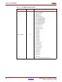
Table of Contents
Revision History . . . . . . . . . . . . . . . . . . . . . . . . . . . . . . . . . . . . . . . . . . . . . . . . . . . . . . . . . . . . . 2
Schedule of Tables . . . . . . . . . . . . . . . . . . . . . . . . . . . . . . . . . . . . . . . . . . . . . . . . . . . . . . . . . .
11
Schedule of Figures . . . . . . . . . . . . . . . . . . . . . . . . . . . . . . . . . . . . . . . . . . . . . . . . . . . . . . . . .
15
Preface: About This User Guide
User Guide Contents . . . . . . . . . . . . . . . . . . . . . . . . . . . . . . . . . . . . . . . . . . . . . . . . . . . . . . . . 17
Additional Resources . . . . . . . . . . . . . . . . . . . . . . . . . . . . . . . . . . . . . . . . . . . . . . . . . . . . . . . 18
Conventions . . . . . . . . . . . . . . . . . . . . . . . . . . . . . . . . . . . . . . . . . . . . . . . . . . . . . . . . . . . . . . . . 18
Typographical . . . . . . . . . . . . . . . . . . . . . . . . . . . . . . . . . . . . . . . . . . . . . . . . . . . . . . . . . . . . 18
Online Document . . . . . . . . . . . . . . . . . . . . . . . . . . . . . . . . . . . . . . . . . . . . . . . . . . . . . . . . . 20
Chapter 1: Introduction
ChipScope Pro Tools Overview. . . . . . . . . . . . . . . . . . . . . . . . . . . . . . . . . . . . . . . . . . . . . . 21
ChipScope Pro Tools Description . . . . . . . . . . . . . . . . . . . . . . . . . . . . . . . . . . . . . . . . . . . . 22
Design Flow . . . . . . . . . . . . . . . . . . . . . . . . . . . . . . . . . . . . . . . . . . . . . . . . . . . . . . . . . . . . . 25
Using ChipScope Pro Cores in Embedded Processor and DSP Tool Flows . . . . . . . . 25
ChipScope Pro Cores Description . . . . . . . . . . . . . . . . . . . . . . . . . . . . . . . . . . . . . . . . . . . 26
ICON Core . . . . . . . . . . . . . . . . . . . . . . . . . . . . . . . . . . . . . . . . . . . . . . . . . . . . . . . . . . . . . .
ILA Core . . . . . . . . . . . . . . . . . . . . . . . . . . . . . . . . . . . . . . . . . . . . . . . . . . . . . . . . . . . . . . . .
IBA/OPB Core . . . . . . . . . . . . . . . . . . . . . . . . . . . . . . . . . . . . . . . . . . . . . . . . . . . . . . . . . . .
IBA/PLB Core . . . . . . . . . . . . . . . . . . . . . . . . . . . . . . . . . . . . . . . . . . . . . . . . . . . . . . . . . . .
VIO Core . . . . . . . . . . . . . . . . . . . . . . . . . . . . . . . . . . . . . . . . . . . . . . . . . . . . . . . . . . . . . . . .
ATC2 Core . . . . . . . . . . . . . . . . . . . . . . . . . . . . . . . . . . . . . . . . . . . . . . . . . . . . . . . . . . . . . . .
IBERT Core . . . . . . . . . . . . . . . . . . . . . . . . . . . . . . . . . . . . . . . . . . . . . . . . . . . . . . . . . . . . . .
26
26
33
38
42
43
44
System Requirements . . . . . . . . . . . . . . . . . . . . . . . . . . . . . . . . . . . . . . . . . . . . . . . . . . . . . . . 51
Operating System Requirements . . . . . . . . . . . . . . . . . . . . . . . . . . . . . . . . . . . . . . . . . . . .
Software Tools Requirements . . . . . . . . . . . . . . . . . . . . . . . . . . . . . . . . . . . . . . . . . . . . . .
Communications Requirements . . . . . . . . . . . . . . . . . . . . . . . . . . . . . . . . . . . . . . . . . . . .
Board Requirements . . . . . . . . . . . . . . . . . . . . . . . . . . . . . . . . . . . . . . . . . . . . . . . . . . . . . .
51
51
52
53
Software Installation and Licensing . . . . . . . . . . . . . . . . . . . . . . . . . . . . . . . . . . . . . . . . . 53
Chapter 2: Using the Core Generator Tools
Overview . . . . . . . . . . . . . . . . . . . . . . . . . . . . . . . . . . . . . . . . . . . . . . . . . . . . . . . . . . . . . . . . . . . 55
Using the Xilinx CORE Generator Tool with ChipScope Pro Cores . . . . . . . . . . . 56
Generating an ICON Core . . . . . . . . . . . . . . . . . . . . . . . . . . . . . . . . . . . . . . . . . . . . . . . . . . . 57
General ICON Core Parameters . . . . . . . . . . . . . . . . . . . . . . . . . . . . . . . . . . . . . . . . . . . . 57
Generating the Core . . . . . . . . . . . . . . . . . . . . . . . . . . . . . . . . . . . . . . . . . . . . . . . . . . . . . . . 58
Using the ICON Core . . . . . . . . . . . . . . . . . . . . . . . . . . . . . . . . . . . . . . . . . . . . . . . . . . . . . 59
Generating an ILA Core . . . . . . . . . . . . . . . . . . . . . . . . . . . . . . . . . . . . . . . . . . . . . . . . . . . . . 60
ILA Core Trigger and Storage Parameters . . . . . . . . . . . . . . . . . . . . . . . . . . . . . . . . . . . . 60
ILA Core Trigger Port Parameters . . . . . . . . . . . . . . . . . . . . . . . . . . . . . . . . . . . . . . . . . . . 63
ChipScope Pro 11.4 Software and Cores
UG029 (v11.4) December 2, 2009
www.xilinx.com
5
Generating the Core . . . . . . . . . . . . . . . . . . . . . . . . . . . . . . . . . . . . . . . . . . . . . . . . . . . . . . . 65
Using the ILA Core . . . . . . . . . . . . . . . . . . . . . . . . . . . . . . . . . . . . . . . . . . . . . . . . . . . . . . . 65
Generating the VIO Core . . . . . . . . . . . . . . . . . . . . . . . . . . . . . . . . . . . . . . . . . . . . . . . . . . . . 66
General VIO Core Options . . . . . . . . . . . . . . . . . . . . . . . . . . . . . . . . . . . . . . . . . . . . . . . . . 66
Generating the Core . . . . . . . . . . . . . . . . . . . . . . . . . . . . . . . . . . . . . . . . . . . . . . . . . . . . . . . 67
Using the VIO Core . . . . . . . . . . . . . . . . . . . . . . . . . . . . . . . . . . . . . . . . . . . . . . . . . . . . . . . 67
Generating the ATC2 Core . . . . . . . . . . . . . . . . . . . . . . . . . . . . . . . . . . . . . . . . . . . . . . . . . . 68
ATC2 Core Acquisition and State Parameters . . . . . . . . . . . . . . . . . . . . . . . . . . . . . . . . .
ATC2 Core Pin and Signal Parameters . . . . . . . . . . . . . . . . . . . . . . . . . . . . . . . . . . . . . . .
ATC2 Core ATCK and ATD Pin Parameters . . . . . . . . . . . . . . . . . . . . . . . . . . . . . . . . . .
Generating the Core . . . . . . . . . . . . . . . . . . . . . . . . . . . . . . . . . . . . . . . . . . . . . . . . . . . . . . .
Using the ATC2 Core. . . . . . . . . . . . . . . . . . . . . . . . . . . . . . . . . . . . . . . . . . . . . . . . . . . . . .
68
69
70
71
71
Generating IBERT Cores for Virtex-4 and Virtex-5 FPGAs. . . . . . . . . . . . . . . . . . . . 72
General IBERT Options . . . . . . . . . . . . . . . . . . . . . . . . . . . . . . . . . . . . . . . . . . . . . . . . . . . .
Selecting the IBERT Clocking Options . . . . . . . . . . . . . . . . . . . . . . . . . . . . . . . . . . . . . . .
Selecting the MGT Options . . . . . . . . . . . . . . . . . . . . . . . . . . . . . . . . . . . . . . . . . . . . . . . . .
Selecting the General Purpose I/O (GPIO) Options . . . . . . . . . . . . . . . . . . . . . . . . . . . .
Selecting the Example and Template Options . . . . . . . . . . . . . . . . . . . . . . . . . . . . . . . . .
Generating the Design . . . . . . . . . . . . . . . . . . . . . . . . . . . . . . . . . . . . . . . . . . . . . . . . . . . . .
72
74
75
77
78
79
Generating IBERT Cores for Virtex-6 FPGA GTX Transceivers . . . . . . . . . . . . . . . 80
General IBERT Options . . . . . . . . . . . . . . . . . . . . . . . . . . . . . . . . . . . . . . . . . . . . . . . . . . . .
Selecting the GTX Transceivers and Reference Clocks . . . . . . . . . . . . . . . . . . . . . . . . . .
Enabling RXRECCLK Probes . . . . . . . . . . . . . . . . . . . . . . . . . . . . . . . . . . . . . . . . . . . . . . .
Choosing the System Clock Source . . . . . . . . . . . . . . . . . . . . . . . . . . . . . . . . . . . . . . . . . .
Generating the Design . . . . . . . . . . . . . . . . . . . . . . . . . . . . . . . . . . . . . . . . . . . . . . . . . . . . .
80
81
81
81
81
Generating IBERT Cores for Virtex-6 FPGA GTH Transceivers . . . . . . . . . . . . . . 82
General IBERT Options . . . . . . . . . . . . . . . . . . . . . . . . . . . . . . . . . . . . . . . . . . . . . . . . . . . .
Selecting the GTHE1_QUADs and Reference Clocks . . . . . . . . . . . . . . . . . . . . . . . . . . .
Enabling RXUSERCLKOUT Probes . . . . . . . . . . . . . . . . . . . . . . . . . . . . . . . . . . . . . . . . .
Choosing the System Clock Source . . . . . . . . . . . . . . . . . . . . . . . . . . . . . . . . . . . . . . . . . .
Generating the Design . . . . . . . . . . . . . . . . . . . . . . . . . . . . . . . . . . . . . . . . . . . . . . . . . . . . .
82
82
83
83
83
Generating IBERT Cores for Spartan-6 FPGA GTP Transceivers . . . . . . . . . . . . . 86
General IBERT Options . . . . . . . . . . . . . . . . . . . . . . . . . . . . . . . . . . . . . . . . . . . . . . . . . . . .
Selecting the GTPA1_DUALs and Reference Clocks . . . . . . . . . . . . . . . . . . . . . . . . . . .
Enabling RXRECCLK Probes . . . . . . . . . . . . . . . . . . . . . . . . . . . . . . . . . . . . . . . . . . . . . . .
Choosing the System Clock Source . . . . . . . . . . . . . . . . . . . . . . . . . . . . . . . . . . . . . . . . . .
Generating the Design . . . . . . . . . . . . . . . . . . . . . . . . . . . . . . . . . . . . . . . . . . . . . . . . . . . . .
86
87
87
87
87
Chapter 3: Using the ChipScope Pro Core Inserter
Core Inserter Overview. . . . . . . . . . . . . . . . . . . . . . . . . . . . . . . . . . . . . . . . . . . . . . . . . . . . . . 89
Using the Core Inserter with ISE Project Navigator . . . . . . . . . . . . . . . . . . . . . . . . . . 89
ChipScope Definition and Connection Source File . . . . . . . . . . . . . . . . . . . . . . . . . . . . . 89
Useful Project Navigator Settings . . . . . . . . . . . . . . . . . . . . . . . . . . . . . . . . . . . . . . . . . . . 90
Using the Core Inserter with Command Line Implementation . . . . . . . . . . . . . . . . 91
Command Line Flow Overview . . . . . . . . . . . . . . . . . . . . . . . . . . . . . . . . . . . . . . . . . . . .
Create CDC Project Step . . . . . . . . . . . . . . . . . . . . . . . . . . . . . . . . . . . . . . . . . . . . . . . . . . .
Edit CDC Project Step . . . . . . . . . . . . . . . . . . . . . . . . . . . . . . . . . . . . . . . . . . . . . . . . . . . . .
Insert Cores Step . . . . . . . . . . . . . . . . . . . . . . . . . . . . . . . . . . . . . . . . . . . . . . . . . . . . . . . . .
91
92
92
93
ChipScope Pro Core Inserter Features . . . . . . . . . . . . . . . . . . . . . . . . . . . . . . . . . . . . . . . 94
Working with Projects . . . . . . . . . . . . . . . . . . . . . . . . . . . . . . . . . . . . . . . . . . . . . . . . . . . . . 94
Specifying Input and Output Files . . . . . . . . . . . . . . . . . . . . . . . . . . . . . . . . . . . . . . . . . . 95
6
www.xilinx.com
ChipScope Pro 11.4 Software and Cores
UG029 (v11.4) December 2, 2009
Project Level Parameters . . . . . . . . . . . . . . . . . . . . . . . . . . . . . . . . . . . . . . . . . . . . . . . . . . . 95
Core Utilization . . . . . . . . . . . . . . . . . . . . . . . . . . . . . . . . . . . . . . . . . . . . . . . . . . . . . . . . . . 95
Choosing ICON Options . . . . . . . . . . . . . . . . . . . . . . . . . . . . . . . . . . . . . . . . . . . . . . . . . . . 96
Choosing ILA Trigger Options and Parameters . . . . . . . . . . . . . . . . . . . . . . . . . . . . . . . 96
Choosing ILA Core Capture Parameters . . . . . . . . . . . . . . . . . . . . . . . . . . . . . . . . . . . . 100
Choosing ATC2 Data Capture Settings . . . . . . . . . . . . . . . . . . . . . . . . . . . . . . . . . . . . . 101
Choosing Net Connections for ILA Signals . . . . . . . . . . . . . . . . . . . . . . . . . . . . . . . . . . 104
Adding Units . . . . . . . . . . . . . . . . . . . . . . . . . . . . . . . . . . . . . . . . . . . . . . . . . . . . . . . . . . . 105
Inserting Cores into Netlist . . . . . . . . . . . . . . . . . . . . . . . . . . . . . . . . . . . . . . . . . . . . . . . . 105
Managing Project Preferences . . . . . . . . . . . . . . . . . . . . . . . . . . . . . . . . . . . . . . . . . . . . . 106
Chapter 4: Using the ChipScope Pro Analyzer
Analyzer Overview . . . . . . . . . . . . . . . . . . . . . . . . . . . . . . . . . . . . . . . . . . . . . . . . . . . . . . . . 107
Analyzer Server Interface . . . . . . . . . . . . . . . . . . . . . . . . . . . . . . . . . . . . . . . . . . . . . . . . . . 108
Analyzer Client Interface . . . . . . . . . . . . . . . . . . . . . . . . . . . . . . . . . . . . . . . . . . . . . . . . . . . 109
Project Tree . . . . . . . . . . . . . . . . . . . . . . . . . . . . . . . . . . . . . . . . . . . . . . . . . . . . . . . . . . . . .
Signal Browser . . . . . . . . . . . . . . . . . . . . . . . . . . . . . . . . . . . . . . . . . . . . . . . . . . . . . . . . . .
Message Pane . . . . . . . . . . . . . . . . . . . . . . . . . . . . . . . . . . . . . . . . . . . . . . . . . . . . . . . . . . .
Main Window Area . . . . . . . . . . . . . . . . . . . . . . . . . . . . . . . . . . . . . . . . . . . . . . . . . . . . . .
109
109
112
112
Analyzer Features . . . . . . . . . . . . . . . . . . . . . . . . . . . . . . . . . . . . . . . . . . . . . . . . . . . . . . . . . . 112
Working with Projects . . . . . . . . . . . . . . . . . . . . . . . . . . . . . . . . . . . . . . . . . . . . . . . . . . . .
Printing Waveforms. . . . . . . . . . . . . . . . . . . . . . . . . . . . . . . . . . . . . . . . . . . . . . . . . . . . . .
Importing Signal Names . . . . . . . . . . . . . . . . . . . . . . . . . . . . . . . . . . . . . . . . . . . . . . . . . .
Exporting Data . . . . . . . . . . . . . . . . . . . . . . . . . . . . . . . . . . . . . . . . . . . . . . . . . . . . . . . . . .
Closing and Exiting the Analyzer . . . . . . . . . . . . . . . . . . . . . . . . . . . . . . . . . . . . . . . . . .
Viewing Options . . . . . . . . . . . . . . . . . . . . . . . . . . . . . . . . . . . . . . . . . . . . . . . . . . . . . . . .
Setting up a Server Host Connection . . . . . . . . . . . . . . . . . . . . . . . . . . . . . . . . . . . . . . .
Opening a Parallel Cable Connection . . . . . . . . . . . . . . . . . . . . . . . . . . . . . . . . . . . . . . .
Opening a Platform Cable USB Connection . . . . . . . . . . . . . . . . . . . . . . . . . . . . . . . . .
Using Multiple Platform Cable USB Connections . . . . . . . . . . . . . . . . . . . . . . . . . . . .
........................................................................
Polling the Auto Core Status . . . . . . . . . . . . . . . . . . . . . . . . . . . . . . . . . . . . . . . . . . . . . .
Configuring the Target Device(s) . . . . . . . . . . . . . . . . . . . . . . . . . . . . . . . . . . . . . . . . . .
Trigger Setup Window . . . . . . . . . . . . . . . . . . . . . . . . . . . . . . . . . . . . . . . . . . . . . . . . . . .
Waveform Window . . . . . . . . . . . . . . . . . . . . . . . . . . . . . . . . . . . . . . . . . . . . . . . . . . . . . .
Listing Window . . . . . . . . . . . . . . . . . . . . . . . . . . . . . . . . . . . . . . . . . . . . . . . . . . . . . . . . .
Bus Plot Window . . . . . . . . . . . . . . . . . . . . . . . . . . . . . . . . . . . . . . . . . . . . . . . . . . . . . . . .
VIO Console Window . . . . . . . . . . . . . . . . . . . . . . . . . . . . . . . . . . . . . . . . . . . . . . . . . . . .
System Monitor . . . . . . . . . . . . . . . . . . . . . . . . . . . . . . . . . . . . . . . . . . . . . . . . . . . . . . . . .
IBERT Console Window for Virtex-4 FPGA GT11 Transceivers . . . . . . . . . . . . . . . .
IBERT Console Window for Virtex-5 FPGA GTP and GTX Transceivers . . . . . . . . .
IBERT Console Window for Virtex-6 FPGA GTX Transceivers . . . . . . . . . . . . . . . . .
IBERT Console Window for Spartan-6 FPGA GTP Transceivers . . . . . . . . . . . . . . . .
Help . . . . . . . . . . . . . . . . . . . . . . . . . . . . . . . . . . . . . . . . . . . . . . . . . . . . . . . . . . . . . . . . . . .
112
112
115
115
116
116
116
116
117
117
118
118
118
120
126
127
128
129
132
134
139
147
153
157
ChipScope Pro ILA Waveform Toolbar Features . . . . . . . . . . . . . . . . . . . . . . . . . . . . 158
ChipScope Pro Analyzer Command Line Options. . . . . . . . . . . . . . . . . . . . . . . . . . . 159
Chapter 5: ChipScope Engine Tcl Interface
Overview . . . . . . . . . . . . . . . . . . . . . . . . . . . . . . . . . . . . . . . . . . . . . . . . . . . . . . . . . . . . . . . . . . 161
Requirements . . . . . . . . . . . . . . . . . . . . . . . . . . . . . . . . . . . . . . . . . . . . . . . . . . . . . . . . . . . 161
Limitations . . . . . . . . . . . . . . . . . . . . . . . . . . . . . . . . . . . . . . . . . . . . . . . . . . . . . . . . . . . . . 161
ChipScope Pro 11.4 Software and Cores
UG029 (v11.4) December 2, 2009
www.xilinx.com
7
CSE/Tcl Command Summary . . . . . . . . . . . . . . . . . . . . . . . . . . . . . . . . . . . . . . . . . . . . . . . 162
CseJtag Tcl Commands . . . . . . . . . . . . . . . . . . . . . . . . . . . . . . . . . . . . . . . . . . . . . . . . . . .
CseFpga Tcl Commands . . . . . . . . . . . . . . . . . . . . . . . . . . . . . . . . . . . . . . . . . . . . . . . . . .
CseCore Tcl Commands . . . . . . . . . . . . . . . . . . . . . . . . . . . . . . . . . . . . . . . . . . . . . . . . . .
CseVIO Tcl Commands . . . . . . . . . . . . . . . . . . . . . . . . . . . . . . . . . . . . . . . . . . . . . . . . . . .
162
165
165
166
CseJtag Tcl Command Details . . . . . . . . . . . . . . . . . . . . . . . . . . . . . . . . . . . . . . . . . . . . . . 167
::chipscope::csejtag_session create . . . . . . . . . . . . . . . . . . . . . . . . . . . . . . . . . . . . . . . . . .
::chipscope::csejtag_session destroy . . . . . . . . . . . . . . . . . . . . . . . . . . . . . . . . . . . . . . . .
::chipscope::csejtag_session get_api_version . . . . . . . . . . . . . . . . . . . . . . . . . . . . . . . . .
::chipscope::csejtag_session send_message . . . . . . . . . . . . . . . . . . . . . . . . . . . . . . . . . .
::chipscope::csejtag_target open . . . . . . . . . . . . . . . . . . . . . . . . . . . . . . . . . . . . . . . . . . . .
::chipscope::csejtag_target close . . . . . . . . . . . . . . . . . . . . . . . . . . . . . . . . . . . . . . . . . . . .
::chipscope::csejtag_target lock . . . . . . . . . . . . . . . . . . . . . . . . . . . . . . . . . . . . . . . . . . . .
::chipscope::csejtag_target unlock . . . . . . . . . . . . . . . . . . . . . . . . . . . . . . . . . . . . . . . . . .
::chipscope::csejtag_target get_lock_status. . . . . . . . . . . . . . . . . . . . . . . . . . . . . . . . . . .
::chipscope::csejtag_target clean_locks . . . . . . . . . . . . . . . . . . . . . . . . . . . . . . . . . . . . . .
::chipscope::csejtag_target flush . . . . . . . . . . . . . . . . . . . . . . . . . . . . . . . . . . . . . . . . . . . .
::chipscope::csejtag_target set_pin . . . . . . . . . . . . . . . . . . . . . . . . . . . . . . . . . . . . . . . . . .
::chipscope::csejtag_target get_pin . . . . . . . . . . . . . . . . . . . . . . . . . . . . . . . . . . . . . . . . .
::chipscope::csejtag_target pulse_pin . . . . . . . . . . . . . . . . . . . . . . . . . . . . . . . . . . . . . . .
::chipscope::csejtag_target wait_time . . . . . . . . . . . . . . . . . . . . . . . . . . . . . . . . . . . . . . .
::chipscope::csejtag_target get_info . . . . . . . . . . . . . . . . . . . . . . . . . . . . . . . . . . . . . . . . .
::chipscope::csejtag_tap autodetect_chain . . . . . . . . . . . . . . . . . . . . . . . . . . . . . . . . . . .
::chipscope::csejtag_tap interrogate_chain . . . . . . . . . . . . . . . . . . . . . . . . . . . . . . . . . . .
::chipscope::csejtag_tap get_device_count . . . . . . . . . . . . . . . . . . . . . . . . . . . . . . . . . . .
::chipscope::csejtag_tap set_device_count . . . . . . . . . . . . . . . . . . . . . . . . . . . . . . . . . . .
::chipscope::csejtag_tap get_irlength . . . . . . . . . . . . . . . . . . . . . . . . . . . . . . . . . . . . . . . .
::chipscope::csejtag_tap set_irlength . . . . . . . . . . . . . . . . . . . . . . . . . . . . . . . . . . . . . . . .
::chipscope::csejtag_tap get_device_idcode . . . . . . . . . . . . . . . . . . . . . . . . . . . . . . . . . .
::chipscope::csejtag_tap set_device_idcode . . . . . . . . . . . . . . . . . . . . . . . . . . . . . . . . . .
::chipscope::csejtag_tap navigate . . . . . . . . . . . . . . . . . . . . . . . . . . . . . . . . . . . . . . . . . . .
::chipscope::csejtag_tap shift_chain_ir . . . . . . . . . . . . . . . . . . . . . . . . . . . . . . . . . . . . . .
::chipscope::csejtag_tap shift_device_ir . . . . . . . . . . . . . . . . . . . . . . . . . . . . . . . . . . . . .
::chipscope::csejtag_tap shift_chain_dr . . . . . . . . . . . . . . . . . . . . . . . . . . . . . . . . . . . . . .
::chipscope::csejtag_tap shift_device_dr . . . . . . . . . . . . . . . . . . . . . . . . . . . . . . . . . . . . .
::chipscope::csejtag_db add_device_data . . . . . . . . . . . . . . . . . . . . . . . . . . . . . . . . . . . .
::chipscope::csejtag_db lookup_device . . . . . . . . . . . . . . . . . . . . . . . . . . . . . . . . . . . . . .
::chipscope::csejtag_db get_device_name_for_idcode . . . . . . . . . . . . . . . . . . . . . . . . .
::chipscope::csejtag_db get_irlength_for_idcode . . . . . . . . . . . . . . . . . . . . . . . . . . . . . .
::chipscope::csejtag_db parse_bsdl . . . . . . . . . . . . . . . . . . . . . . . . . . . . . . . . . . . . . . . . .
::chipscope::csejtag_db parse_bsdl_file . . . . . . . . . . . . . . . . . . . . . . . . . . . . . . . . . . . . . .
167
168
169
170
171
173
174
175
176
177
178
179
180
181
182
183
185
186
187
188
189
190
191
192
193
194
196
198
200
202
203
204
205
206
207
CseFpga Command Details . . . . . . . . . . . . . . . . . . . . . . . . . . . . . . . . . . . . . . . . . . . . . . . . . 208
::chipscope::csefpga_configure_device . . . . . . . . . . . . . . . . . . . . . . . . . . . . . . . . . . . . . .
::chipscope::csefpga_get_config_reg . . . . . . . . . . . . . . . . . . . . . . . . . . . . . . . . . . . . . . . .
::chipscope::csefpga_get_instruction_reg . . . . . . . . . . . . . . . . . . . . . . . . . . . . . . . . . . . .
::chipscope::csefpga_get_usercode . . . . . . . . . . . . . . . . . . . . . . . . . . . . . . . . . . . . . . . . .
::chipscope::csefpga_get_user_chain_count . . . . . . . . . . . . . . . . . . . . . . . . . . . . . . . . . .
::chipscope::csefpga_is_config_supported . . . . . . . . . . . . . . . . . . . . . . . . . . . . . . . . . . .
::chipscope::csefpga_is_sys_mon_supported . . . . . . . . . . . . . . . . . . . . . . . . . . . . . . . . .
::chipscope::csefpga_run_sys_mon_command_sequence . . . . . . . . . . . . . . . . . . . . . .
::chipscope::csefpga_get_sys_mon_reg . . . . . . . . . . . . . . . . . . . . . . . . . . . . . . . . . . . . . .
::chipscope::csefpga_set_sys_mon_reg . . . . . . . . . . . . . . . . . . . . . . . . . . . . . . . . . . . . . .
208
210
210
212
213
214
215
216
217
218
CseCore Command Details . . . . . . . . . . . . . . . . . . . . . . . . . . . . . . . . . . . . . . . . . . . . . . . . . 219
8
www.xilinx.com
ChipScope Pro 11.4 Software and Cores
UG029 (v11.4) December 2, 2009
::chipscope::csecore_get_core_count . . . . . . . . . . . . . . . . . . . . . . . . . . . . . . . . . . . . . . . . 219
::chipscope::csecore_get_core_status . . . . . . . . . . . . . . . . . . . . . . . . . . . . . . . . . . . . . . . . 220
::chipscope::csecore_is_cores_supported . . . . . . . . . . . . . . . . . . . . . . . . . . . . . . . . . . . . 221
CseVIO Command Details . . . . . . . . . . . . . . . . . . . . . . . . . . . . . . . . . . . . . . . . . . . . . . . . . 222
::chipscope::csevio_get_core_info . . . . . . . . . . . . . . . . . . . . . . . . . . . . . . . . . . . . . . . . . .
::chipscope::csevio_is_vio_core . . . . . . . . . . . . . . . . . . . . . . . . . . . . . . . . . . . . . . . . . . . .
::chipscope::csevio_init_core . . . . . . . . . . . . . . . . . . . . . . . . . . . . . . . . . . . . . . . . . . . . . .
::chipscope::csevio_terminate_core . . . . . . . . . . . . . . . . . . . . . . . . . . . . . . . . . . . . . . . . .
::chipscope::csevio_define_signal . . . . . . . . . . . . . . . . . . . . . . . . . . . . . . . . . . . . . . . . . .
::chipscope::csevio_define_bus . . . . . . . . . . . . . . . . . . . . . . . . . . . . . . . . . . . . . . . . . . . .
::chipscope::csevio_undefine_name . . . . . . . . . . . . . . . . . . . . . . . . . . . . . . . . . . . . . . . .
::chipscope::csevio_write_values . . . . . . . . . . . . . . . . . . . . . . . . . . . . . . . . . . . . . . . . . . .
::chipscope::csevio_read_values. . . . . . . . . . . . . . . . . . . . . . . . . . . . . . . . . . . . . . . . . . . .
222
224
225
226
227
228
229
230
232
CSE/Tcl Examples . . . . . . . . . . . . . . . . . . . . . . . . . . . . . . . . . . . . . . . . . . . . . . . . . . . . . . . . . . 234
Appendix A: References
Appendix B: ChipScope Pro Tools Troubleshooting Guide
Overview . . . . . . . . . . . . . . . . . . . . . . . . . . . . . . . . . . . . . . . . . . . . . . . . . . . . . . . . . . . . . . . . . .
ChipScope Pro Tools Installation Troubleshooting . . . . . . . . . . . . . . . . . . . . . . . . .
Xilinx JTAG Programming Cable Troubleshooting . . . . . . . . . . . . . . . . . . . . . . . . .
ChipScope Pro Analyzer Core Troubleshooting . . . . . . . . . . . . . . . . . . . . . . . . . . . . .
Gathering Information for Xilinx Technical Support . . . . . . . . . . . . . . . . . . . . . . . .
Obtaining Xinfo Information . . . . . . . . . . . . . . . . . . . . . . . . . . . . . . . . . . . . . . . . . . . . . .
Obtaining ChipScope Pro Analyzer Log File Information . . . . . . . . . . . . . . . . . . . . .
Obtaining ChipScope Pro Core Inserter Tool Log File Information . . . . . . . . . . . . . .
Obtaining an Archived ISE Tool Project . . . . . . . . . . . . . . . . . . . . . . . . . . . . . . . . . . . . .
ChipScope Pro 11.4 Software and Cores
UG029 (v11.4) December 2, 2009
www.xilinx.com
237
238
239
248
254
254
254
254
254
9
10
www.xilinx.com
ChipScope Pro 11.4 Software and Cores
UG029 (v11.4) December 2, 2009
Schedule of Tables
Chapter 1: Introduction
Table 1-1: ChipScope Pro Tools Description. . . . . . . . . . . . . . . . . . . . . . . . . . . . . . . . . . . . . . 22
Table 1-2: ChipScope Pro Logic Debug Features and Benefits . . . . . . . . . . . . . . . . . . . . . . 23
Table 1-3: Trigger Features of the ILA Core . . . . . . . . . . . . . . . . . . . . . . . . . . . . . . . . . . . . . . 27
Table 1-4: CoreConnect OPB Protocol Violation Error Description(1) . . . . . . . . . . . . . . . 33
Table 1-5: OPB Signal Groups . . . . . . . . . . . . . . . . . . . . . . . . . . . . . . . . . . . . . . . . . . . . . . . . . . 36
Table 1-6: PLB Signal Groups . . . . . . . . . . . . . . . . . . . . . . . . . . . . . . . . . . . . . . . . . . . . . . . . . . 39
Table 1-7: IBERT Core for the Virtex-4 FPGA GT11 Transceiver . . . . . . . . . . . . . . . . . . . . 46
Table 1-8: IBERT Core for the Virtex-5 FPGA GTP and GTX Transceivers . . . . . . . . . . . 47
Table 1-9: IBERT Core for the Virtex-6 FPGA GTX Transceivers . . . . . . . . . . . . . . . . . . . . 48
Table 1-10: IBERT Core for the Virtex-6 FPGA GTH Transceivers . . . . . . . . . . . . . . . . . . 49
Table 1-11: IBERT Core for the Spartan-6 FPGA GTP Transceivers . . . . . . . . . . . . . . . . . 50
Table 1-12: Design Parameter Changes Requiring Resynthesis . . . . . . . . . . . . . . . . . . . . . 51
Table 1-13: ChipScope Pro Download Cable Support . . . . . . . . . . . . . . . . . . . . . . . . . . . . . 52
Chapter 2: Using the Core Generator Tools
Table 2-1: ILA Trigger Match Unit Types . . . . . . . . . . . . . . . . . . . . . . . . . . . . . . . . . . . . . . . . 64
Table 2-2: Silicon Revision (Stepping Level) of Virtex-4 FX Family . . . . . . . . . . . . . . . . . 73
Table 2-3: Silicon Revision (Stepping Level) of Virtex-5 LXT/SXT/FXT Families. . . . . . 73
Chapter 3: Using the ChipScope Pro Core Inserter
Table 3-1: ILA Trigger Match Unit Types . . . . . . . . . . . . . . . . . . . . . . . . . . . . . . . . . . . . . . . . 98
Chapter 4: Using the ChipScope Pro Analyzer
Table 4-1: ChipScope Pro Analyzer Server Command Line Options. . . . . . . . . . . . . . . . 108
Table 4-2: Configuration of Multiple Client Instances . . . . . . . . . . . . . . . . . . . . . . . . . . . . 118
Table 4-3: MGT Link Status . . . . . . . . . . . . . . . . . . . . . . . . . . . . . . . . . . . . . . . . . . . . . . . . . . . 134
Chapter 5: ChipScope Engine Tcl Interface
Table 5-1: CSE/Tcl Command Categories . . . . . . . . . . . . . . . . . . . . . . . . . . . . . . . . . . . . . . . 162
Table 5-2: CseJtag Tcl Commands . . . . . . . . . . . . . . . . . . . . . . . . . . . . . . . . . . . . . . . . . . . . . . 162
Table 5-3: Summary of ::chipscope::csejtag_session Subcommands . . . . . . . . . . . . . . . . 163
Table 5-4: Summary of ::chipscope::csejtag_db Subcommands . . . . . . . . . . . . . . . . . . . . 163
Table 5-5: Summary of ::chipscope::csejtag_target Subcommands. . . . . . . . . . . . . . . . . . 163
Table 5-6: Summary of ::chipscope::csejtag_tap Subcommands . . . . . . . . . . . . . . . . . . . . 164
Table 5-7: CseFpga Tcl Commands . . . . . . . . . . . . . . . . . . . . . . . . . . . . . . . . . . . . . . . . . . . . . 165
Table 5-8: CseCore Tcl Commands . . . . . . . . . . . . . . . . . . . . . . . . . . . . . . . . . . . . . . . . . . . . . 165
Table 5-9: CseVIO Tcl Commands . . . . . . . . . . . . . . . . . . . . . . . . . . . . . . . . . . . . . . . . . . . . . 166
ChipScope Pro 11.4 Software and Cores
UG029 (v11.4) December 2, 2009
www.xilinx.com
11
Table 5-10: Arguments for Subcommand ::chipscope::csejtag_session create . . . . . . . . 167
Table 5-11: Arguments for Subcommand ::chipscope::csejtag_session create . . . . . . . . 168
Table 5-12: Arguments for Subcommand ::chipscope::csejtag_session send_message. 170
Table 5-13: Arguments for Subcommand ::chipscope::csejtag_target open . . . . . . . . . . 171
Table 5-14: Argument targetName and [optional args...] combinations . . . . . . . . . . . . . 171
Table 5-15: Arguments for Subcommand ::chipscope::csejtag_target close . . . . . . . . . . 173
Table 5-16: Arguments for Subcommand ::chipscope::csejtag_target lock . . . . . . . . . . . 174
Table 5-17: Arguments for Subcommand ::chipscope::csejtag_target unlock. . . . . . . . . 175
Table 5-18: Arguments for Subcommand ::chipscope::csejtag_target get_lock_status . 176
Table 5-19: Arguments for Subcommand ::chipscope::csejtag_target clean_locks . . . . 177
Table 5-20: Arguments for Subcommand ::chipscope::csejtag_target flush . . . . . . . . . . 178
Table 5-21: Arguments for Subcommand ::chipscope::csejtag_target set_pin . . . . . . . . 179
Table 5-22: Arguments for Subcommand ::chipscope::csejtag_target get_pin . . . . . . . . 180
Table 5-23: Arguments for Subcommand ::chipscope::csejtag_target pulse_pin . . . . . . 181
Table 5-24: Arguments for Subcommand ::chipscope::csejtag_target wait_time . . . . . . 182
Table 5-25: Arguments for Subcommand ::chipscope::csejtag_target get_info . . . . . . . 183
Table 5-26: Arguments for Subcommand ::chipscope::csejtag_tap autodetect_chain . . 185
Table 5-27: Arguments for Subcommand ::chipscope::csejtag_tap interrogate_chain . 186
Table 5-28: Arguments for Subcommand ::chipscope::csejtag_tap get_device_count. . 187
Table 5-29: Arguments for Subcommand ::chipscope::csejtag_tap set_device_count . . 188
Table 5-30: Arguments for Subcommand ::chipscope::csejtag_tap get_irlength . . . . . . 189
Table 5-31: Arguments for Subcommand ::chipscope::csejtag_tap set_irlength . . . . . . 190
Table 5-32: Arguments for Subcommand ::chipscope::csejtag_tap get_device_idcode. 191
Table 5-33: Arguments for Subcommand ::chipscope::csejtag_tap set_device_idcode . 192
Table 5-34: Arguments for Subcommand ::chipscope::csejtag_tap navigate. . . . . . . . . . 193
Table 5-35: Arguments for Subcommand ::chipscope::csejtag_tap shift_chain_ir. . . . . 194
Table 5-36: Arguments for Subcommand ::chipscope::csejtag_tap shift_device_ir . . . . 196
Table 5-37: Arguments for Subcommand ::chipscope::csejtag_tap shift_chain_dr . . . . 198
Table 5-38: Arguments for Subcommand ::chipscope::csejtag_tap shift_device_dr . . . 200
Table 5-39: Arguments for Subcommand ::chipscope::csejtag_db add_device_data. . . 202
Table 5-40: Arguments for Subcommand ::chipscope::csejtag_db lookup_device . . . . 203
Table 5-41: Arguments for Subcommand ::chipscope::csejtag_db get_device_name_for_idcode
204
Table 5-42: Arguments for Subcommand ::chipscope::csejtag_db get_irlength_for_idcode 205
Table 5-43: Arguments for Subcommand ::chipscope::csejtag_db parse_bsdl . . . . . . . . 206
Table 5-44: Arguments for Subcommand ::chipscope::csejtag_db parse_bsdl_file . . . . 207
Table 5-45: Arguments for Subcommand ::chipscope::csefpga_configure_device . . . . 208
Table 5-46: Arguments for Subcommand ::chipscope::csefpga_get_config_reg. . . . . . . 210
Table 5-47: Arguments for Subcommand ::chipscope::csefpga_get_instruction_reg . . 211
Table 5-48: Arguments for Subcommand ::chipscope::csefpga_get_usercode . . . . . . . . 212
Table 5-49: Arguments for Subcommand ::chipscope::csefpga_get_user_chain_count 213
Table 5-50: Arguments for Subcommand ::chipscope::csefpga_is_config_supported . 214
Table 5-51: Arguments for Subcommand ::chipscope::csefpga_is_sys_mon_supported 215
12
www.xilinx.com
ChipScope Pro 11.4 Software and Cores
UG029 (v11.4) December 2, 2009
Table 5-52: Arguments for Subcommand ::chipscope::csefpga_run_sys_mon_command_sequence
216
Table 5-53: Arguments for Subcommand ::chipscope::csefpga_get_sys_mon_reg . . . . 217
Table 5-54: Arguments for Subcommand ::chipscope::csefpga_set_sys_mon_reg. . . . . 218
Table 5-55: Arguments for Subcommand ::chipscope::csecore_get_core_count. . . . . . . 219
Table 5-56: Arguments for Subcommand ::chipscope::csecore_get_core_status . . . . . . 220
Table 5-57: Arguments for Subcommand ::chipscope::csecore_is_cores_supported . . . 221
Table 5-58: Arguments for Subcommand ::chipscope::csevio_get_core_info . . . . . . . . . 222
Table 5-59: Arguments for Subcommand ::chipscope::csevio_is_vio_core . . . . . . . . . . . 224
Table 5-60: Arguments for Subcommand ::chipscope::csevio_init_core . . . . . . . . . . . . . 225
Table 5-61: Arguments for Subcommand ::chipscope::csevio_terminate_core. . . . . . . . 226
Table 5-62: Arguments for Subcommand ::chipscope::csevio_define_signal . . . . . . . . . 227
Table 5-63: Arguments for Subcommand ::chipscope::csevio_define_bus . . . . . . . . . . . 228
Table 5-64: Arguments for Subcommand ::chipscope::csevio_undefine_name . . . . . . . 229
Table 5-65: Arguments for Subcommand ::chipscope::csevio_write_values. . . . . . . . . . 230
Table 5-66: Arguments for Subcommand ::chipscope::csevio_read_values . . . . . . . . . . 232
Appendix A: References
Appendix B: ChipScope Pro Tools Troubleshooting Guide
Table B-1: Troubleshooting ChipScope Pro Tools Installation Issues. . . . . . . . . . . . . . . 238
Table B-2: Verifying Correct JTAG Cable Connections . . . . . . . . . . . . . . . . . . . . . . . . . . . 240
Table B-3: Troubleshooting Platform Cable USB Connection Issues . . . . . . . . . . . . . . . 242
Table B-4: Troubleshooting Cable Reference Voltage Issues . . . . . . . . . . . . . . . . . . . . . . 244
Table B-5: Troubleshooting JTAG Device Detection Issues . . . . . . . . . . . . . . . . . . . . . . . 245
Table B-6: Troubleshooting Server Host Connection Issues . . . . . . . . . . . . . . . . . . . . . . . 247
Table B-7: Troubleshooting Core Detection Issues . . . . . . . . . . . . . . . . . . . . . . . . . . . . . . . 248
Table B-8: Troubleshooting ILA Core Triggering Issues . . . . . . . . . . . . . . . . . . . . . . . . . . 251
Table B-9: Troubleshooting Corrupt ILA Core Data Buffer Issues . . . . . . . . . . . . . . . . . 253
ChipScope Pro 11.4 Software and Cores
UG029 (v11.4) December 2, 2009
www.xilinx.com
13
14
www.xilinx.com
ChipScope Pro 11.4 Software and Cores
UG029 (v11.4) December 2, 2009
Schedule of Figures
Chapter 1: Introduction
Figure 1-1: ChipScope Pro System Block Diagram . . . . . . . . . . . . . . . . . . . . . . . . . . . . . . . . 23
Figure 1-2: ChipScope Pro Tools Design Flow . . . . . . . . . . . . . . . . . . . . . . . . . . . . . . . . . . . . 25
Figure 1-3: ILA Core Connection Example . . . . . . . . . . . . . . . . . . . . . . . . . . . . . . . . . . . . . . . 30
Figure 1-4: ATC2 Core and System Block Diagram. . . . . . . . . . . . . . . . . . . . . . . . . . . . . . . . 43
Chapter 2: Using the Core Generator Tools
Figure 2-1: Trigger Sequencer Block Diagram (with 16 levels and 16 match units) . . . . 60
Figure 2-2: Virtex-5 LXT/SXT/FXT Families IBERT Clock Structure for Each
GTP_DUAL/GTX_DUAL Tile. . . . . . . . . . . . . . . . . . . . . . . . . . . . . . . . . . . . . . . . . . . . . . . . 75
Chapter 3: Using the ChipScope Pro Core Inserter
Figure 3-1: Command Line Core Inserter Flow . . . . . . . . . . . . . . . . . . . . . . . . . . . . . . . . . . . 91
Figure 3-2: Create CDC Project Step. . . . . . . . . . . . . . . . . . . . . . . . . . . . . . . . . . . . . . . . . . . . . 92
Figure 3-3: Edit CDC Project Step . . . . . . . . . . . . . . . . . . . . . . . . . . . . . . . . . . . . . . . . . . . . . . . 92
Figure 3-4: Insert Cores Step . . . . . . . . . . . . . . . . . . . . . . . . . . . . . . . . . . . . . . . . . . . . . . . . . . . 93
Figure 3-5: Trigger Sequencer Block Diagram with 16 Levels and 16 Match Units . . . . 99
Chapter 4: Using the ChipScope Pro Analyzer
Chapter 5: ChipScope Engine Tcl Interface
Appendix A: References
Appendix B: ChipScope Pro Tools Troubleshooting Guide
ChipScope Pro 11.4 Software and Cores
UG029 (v11.4) December 2, 2009
www.xilinx.com
15
16
www.xilinx.com
ChipScope Pro 11.4 Software and Cores
UG029 (v11.4) December 2, 2009
Preface
About This User Guide
This user guide provides users with information for using the LogiCORE™ IP
ChipScope™ Pro cores and tools:
•
Integrated Controller core (ICON)
•
Integrated Logic Analyzer core (ILA)
•
Virtual Input/Output core (VIO)
•
Integrated Bit Error Ratio Test core (IBERT)
•
Agilent Trace Core 2 (ATC2)
•
Integrated Bus Analyzer cores (IBA)
•
Core generator tools (including Xilinx® CORE Generator™ and IBERT Core
Generator)
•
Core Inserter tool
•
Analyzer tool
The tools integrate the IP core and key hardware components with the target design inside
Xilinx FPGA devices. For a list of supported devices, see
http://www.xilinx.com/chipscopepro.
User Guide Contents
This user guide contains the following chapters:
•
Chapter 1, “Introduction” describes the ChipScope Pro tools and IP cores. These tools
integrate key logic analyzer hardware components with the target design inside the
supported devices. The tools communicate with these components and provide the
designer with a complete logic analyzer. This chapter also describes the IBERT core
and related software of the ChipScope Pro Serial I/O Toolkit.
•
Chapter 2, “Using the Core Generator Tools” explains how to use the Xilinx CORE
Generator tool and the IBERT Core Generator tool.
The Xilinx CORE Generator too is used to generate the following ChipScope Pro cores:
♦
Integrated Controller core (ICON)
♦
Integrated Logic Analyzer core (ILA)
♦
Virtual Input/Output core (VIO)
♦
Agilent Trace Core 2 (ATC2)
♦
Integrated Bit Error Ratio Test core (IBERT) v2.0 and above for Virtex®-6 and
Spartan®-6 FPGAs
ChipScope Pro 11.4 Software and Cores
UG029 (v11.4) December 2, 2009
www.xilinx.com
17
Preface: About This User Guide
After generating the cores, you can use the instantiation templates (that are provided)
to quickly and easily insert the cores into VHDL or Verilog designs. After completing
the instantiation and running synthesis, you can implement the design using the
ISE® 11.4 design tools.
The IBERT Core Generator tool is used to customize and generate the IBERT core
design for use in your system.
•
Chapter 3, “Using the ChipScope Pro Core Inserter” explains how to use this postsynthesis tool to generate a netlist that includes the user design as well as ICON, ILA,
and ATC2 cores as needed, parameterized accordingly. The Core Inserter gives you
the flexibility to quickly and easily use the debug functionality to analyze an already
synthesized design, and without any HDL instantiation.
•
Chapter 4, “Using the ChipScope Pro Analyzer” explains how to use this tool which
interfaces directly to the ICON, ILA, IBA/OPB, IBA/PLB, VIO, IBERT, and ATC2
cores (collectively called the ChipScope Pro cores). You can configure your device,
choose triggers, setup the console, and view the results of the capture on the fly. The
data views and triggers can be manipulated in many ways, providing an easy and
intuitive interface to determine the functionality of the design. This chapter also
provides information on how to interact with the IBERT core in your device-undertest (DUT).
•
Chapter 5, “ChipScope Engine Tcl Interface” explains how to use the ChipScope
Engine Tcl (CSE/Tcl) scripting interface to access to basic JTAG chain functions, FPGA
device registers, and VIO cores in a FPGA design. In a few lines of Tcl script, you
should be able to scan and manipulate the JTAG chain through standard Xilinx JTAG
cables.
•
Appendix A, “References” is a collection of references used throughout this
document.
•
Appendix B, “ChipScope Pro Tools Troubleshooting Guide” provides instructions to
validate your ChipScope Pro tools install and ISE software integration.
Additional Resources
To find additional documentation, see the Xilinx website at:
http://www.xilinx.com/support/documentation/index.htm.
To search the Answer Database of silicon, software, and IP questions and answers, or to
create a technical support WebCase, see the Xilinx website at:
http://www.xilinx.com/support/mysupport.htm.
Conventions
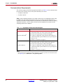
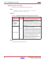
This document uses the following conventions. An example illustrates each convention.
Typographical
The following typographical conventions are used in this document:
18
www.xilinx.com
ChipScope Pro 11.4 Software and Cores
UG029 (v11.4) December 2, 2009
Conventions
Convention
Meaning or Use
Example
Courier font
Messages, prompts, and
program files that the system
displays
speed grade: - 100
Courier bold
Literal commands that you enter
in a syntactical statement
ngdbuild design_name
Commands that you select from
a menu
File → Open
Keyboard shortcuts
Ctrl+C
Variables in a syntax statement
for which you must supply
values
ngdbuild design_name
References to other manuals
See the User Guide for more
information.
Emphasis in text
If a wire is drawn so that it
overlaps the pin of a symbol, the
two nets are not connected.
Dark Shading
Items that are not supported or
reserved
This feature is not supported
Square brackets
An optional entry or parameter.
However, in bus specifications,
such as bus[7:0], they are
required.
ngdbuild [option_name]
design_name
A list of items from which you
must choose one or more
lowpwr ={on|off}
Separates items in a list of
choices
lowpwr ={on|off}
User-defined variable or in code
samples
<directory name>
Vertical ellipsis
.
.
.
Repetitive material that has
been omitted
IOB #1: Name = QOUT’
IOB #2: Name = CLKIN’
.
.
.
Horizontal ellipsis . . .
Repetitive material that has
been omitted
allow block block_name loc1
loc2 ... locn;
The prefix ‘0x’ or the suffix ‘h’
indicate hexadecimal notation
A read of address 0x00112975
returned 45524943h.
An ‘_n’ means the signal is
active low
usr_teof_n is active low.
Helvetica bold
Italic font
Braces
[ ]
{ }
Vertical bar
|
Angle brackets < >
Notations
ChipScope Pro 11.4 Software and Cores
UG029 (v11.4) December 2, 2009
www.xilinx.com
19
Preface: About This User Guide
Online Document
The following conventions are used in this document:
Convention
20
Meaning or Use
Example
Blue text
Cross-reference link to a location
in the current document
Blue, underlined text
Hyperlink to a website (URL)
www.xilinx.com
See the section “Additional
Resources” for details.
Refer to “Title Formats” in
Chapter 1 for details.
Go to http://www.xilinx.com
for the latest speed files.
ChipScope Pro 11.4 Software and Cores
UG029 (v11.4) December 2, 2009
Chapter 1
Introduction
ChipScope Pro Tools Overview
As the density of FPGA devices increases, so does the impracticality of attaching test
equipment probes to these devices under test. The ChipScope™ Pro tools integrate key
logic analyzer and other test and measurement hardware components with the target
design inside the supported Xilinx® FPGA devices listed in the ISE® Design Suite Product
Table [Ref 21]. The tools communicate with these components and provide the designer
with a robust logic analyzer solution.
The ChipScope Pro 11.4 Serial I/O Toolkit provides features and capabilities specific to the
exploration and debug of designs that use the high-speed serial transceiver I/O capability
of Xilinx FPGAs. The internal bit error ratio tester (IBERT) core and related software
provides access to the high-speed serial transceivers (referred to as MGTs in this
document) and perform bit error ratio analysis on channels composed of these MGTs. The
IBERT core supports the high-speed serial transceivers found in the Xilinx Virtex®-4,
Virtex-5, Virtex-6, and Spartan®-6 FPGA devices listed in the ISE Design Suite Product
Table [Ref 21].
ChipScope Pro 11.4 Software and Cores
UG029 (v11.4) December 2, 2009
www.xilinx.com
21
Chapter 1: Introduction
ChipScope Pro Tools Description
Table 1-1 gives a brief description of the various ChipScope Pro software tools and cores.
Table 1-1:
ChipScope Pro Tools Description
Tool
Description
Xilinx CORE Generator Tool
Provides core generation capability for the ICON, ILA, VIO, and ATC2 cores
targeting all supported FPGA device families, and IBERT cores. Also provides core
generation capability for the IBERT core targeting the Virtex-5, Virtex-6, and
Spartan-6 FPGA families.The Xilinx CORE Generator™ tool is part of the Xilinx ISE
Design Suite software tool installation.
IBERT Core Generator
Provides full design generation capability for the IBERT core targeting the Virtex-4
and Virtex-5 devices. The user chooses the MGTs and parameters governing the
design, and the Core Generator uses the ISE design suite to produce a configuration
file.
Core Inserter
Automatically inserts the ICON, ILA, and ATC2 cores into the user’s synthesized
design.
PlanAhead Design Analysis Tool
Automatically inserts the ICON and ILA cores into the design netlist. For more
information on this feature, go to PlanAhead™ Design Analysis Tool [Ref 22].
Analyzer
Provides device configuration, trigger setup, and trace display for the ILA,
IBA/OPB, IBA/PLB, VIO, and IBERT cores. The various cores provide the trigger,
control, and trace capture capability. The ICON core communicates to the dedicated
Boundary Scan pins. The Analyzer tool also provides device configuration, project
management, and control over the IBERT core, including monitoring status and
controlling variables.
ChipScope Engine Tcl (CSE/Tcl)
Scripting Interface
The scriptable CSE/Tcl command interface makes it possible to interact with
devices in a JTAG chain from a Tcl shell (1).
Notes:
1. Tcl stands for Tool Command Language. The CSE/Tcl interface requires the Tcl shell program (called xtclsh) that is included in the
ChipScope Pro and ISE 11.4 tool installations or in the ActiveTcl 8.4 shell available from ActiveState [Ref 16].
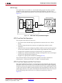
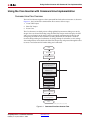
Figure 1-1 shows a block diagram of a system containing debug cores added using the
ChipScope Pro tools. Users can place the ICON, ILA, VIO, and ATC2 cores (collectively
called the ChipScope Pro cores) into their design by generating the cores with the Core
Generator and instantiating them into the HDL source code. You can also insert the ICON,
ILA, and ATC2 cores directly into the synthesized design netlist using the Core Inserter or
PlanAhead tools. The design is then placed and routed using the ISE 11.4 implementation
tools. Next, the user downloads the bitstream into the device under test and analyzes the
design with the Analyzer software.
22
www.xilinx.com
ChipScope Pro 11.4 Software and Cores
UG029 (v11.4) December 2, 2009
ChipScope Pro Tools Description
X-Ref Target - Figure 1-1
Target Device Under Test
User
Function
User
Function
Host Computer with
ChipScope Pro Software
ILA Pro
ILA Pro
ChipScope
Pro
User
Function
ICON Pro
Parallel
Cable
ILA Pro
JTAG
Connections
Board-Under-Test
Figure 1-1:
cs_pro_sys_blk_diag
ChipScope Pro System Block Diagram
The Analyzer tool supports the following download cables for communication between
the PC and the devices in the JTAG Boundary Scan chain:
•
Platform Cable USB
•
Parallel Cable IV
The Analyzer and cores contain many features that FPGA designers need for thoroughly
verifying their logic (Table 1-2). User-selectable data channels range from 1 to 4,096 and the
sample buffer sizes range from 256 to 131,072 samples. Users can change the triggers in real
time without affecting their logic. The Analyzer leads designers through the process of
modifying triggers and analyzing the captured data.
Table 1-2:
ChipScope Pro Logic Debug Features and Benefits
Feature
Benefit
1 to 4,096 user-selectable data channels
Accurately captures wide data bus
functionality.
User-selectable sample buffers ranging in
size from 256 to 131,072 samples
Large sample size increases accuracy and
probability of capturing infrequent events.
Up to 16 separate trigger ports, each with a
user-selectable width of 1 to 256 channels (for
a total of up to 4096 trigger channels)
Multiple separate trigger ports increase the
flexibility of event detection and reduce the
need for sample storage.
ChipScope Pro 11.4 Software and Cores
UG029 (v11.4) December 2, 2009
www.xilinx.com
23
Chapter 1: Introduction
Table 1-2:
ChipScope Pro Logic Debug Features and Benefits
Feature
24
Benefit
Up to 16 separate match units per trigger
port (up to 16 total match units) for a total of
16 different comparisons per trigger
condition
Multiple match units per trigger ports
increase the flexibility of event detection
while conserving valuable resources.
All data and trigger operations are
synchronous to the user clock at rates up to
500 MHz
Capable of high-speed trigger event
detection and data capture.
Trigger conditions implement either a
boolean equation or a trigger sequence of up
to 16 match functions
Can combine up to 16 trigger port match
functions using a boolean equation or a
16-level trigger sequencer.
Data storage qualification condition
implements a boolean equation of up to 16
match functions
Can combine up to 16 trigger port match
functions using a boolean equation to
determine which data samples will be
captured and stored in on-chip memory.
Trigger and storage qualification conditions
are in-system changeable without affecting
the user logic
No need to single step or stop a design for
logic analysis.
Easy-to-use graphical interface
Guides users through selecting the correct
options.
Up to 15 independent ILA, IBA/OPB,
IBA/PLB, VIO or ATC2 cores per device
Can segment logic and test smaller sections
of a large design for greater accuracy.
Multiple trigger settings
Records duration and number of events
along with matches and ranges for greater
accuracy and flexibility.
Downloadable from the Xilinx Web site
Tools are easily accessible from the
ChipScope Suite [Ref 23].
www.xilinx.com
ChipScope Pro 11.4 Software and Cores
UG029 (v11.4) December 2, 2009
ChipScope Pro Tools Description
Design Flow
The tools design flow (Figure 1-2) merges easily with any standard FPGA design flow that
uses a standard HDL synthesis tool and the ISE 11.4 implementation tools.
X-Ref Target - Figure 1-2
CORE Generator
Tool
Generate...
Instantiate...
ICON, ILA,
IBA/OPB,
IBA/PLB,
VIO, or
ATC2 cores
Synthesize...
cores into HDL
source
design without
instantiating
ChipScope cores
or...
Synthesize...
Connect...
design with
cores in it
PlanAhead Tool
or Core Inserter
Insert...
buses and
internal signals
to cores
ICON, ILA, and/or
ATC2 cores into
synthesized design
(.ngc or EDIF netlist)
ISE
Implement...
design
Select...
bitstream
Set...
trigger
View...
waveform
Figure 1-2:
cspro_tools_design_flow_120908
ChipScope Pro Tools Design Flow
Using ChipScope Pro Cores in Embedded Processor and DSP Tool Flows
The cores (ICON, ILA, IBA, VIO, and ATC2) can also be used in the EDK and System
Generator for DSP tool flows for embedded processor and DSP designs, respectively. For
information on how to use the ChipScope Pro cores, see the EDK Platform Studio [Ref 20]
and System Generator for DSP[Ref 24] documentation.
ChipScope Pro 11.4 Software and Cores
UG029 (v11.4) December 2, 2009
www.xilinx.com
25
Chapter 1: Introduction
ChipScope Pro Cores Description
ICON Core
All of the cores use the JTAG Boundary Scan port to communicate to the host computer via
a JTAG download cable. The ICON core provides a communications path between the
JTAG Boundary Scan port of the target FPGA and up to 15 ILA, IBA, VIO, and/or ATC2
cores (as shown in Figure 1-1, page 23).
For devices of the Spartan®-3, Spartan-3E, Spartan-3A, and Spartan-3A DSP families, the
ICON core uses either the USER1 or USER2 JTAG Boundary Scan instructions for
communication via the BSCAN primitive. The unused USER1 or USER2 scan chain of the
BSCAN primitive can also be exported for use in your application, if needed.
For all other supported devices, the ICON core uses any one of the USER1, USER2, USER3
or USER4 scan chains available via the BSCAN primitives. It is not necessary to export
unused USER scan chains because each BSCAN primitive implements a single scan chain.
ILA Core
The ILA core is a customizable logic analyzer core that can be used to monitor any internal
signal of your design. Since the ILA core is synchronous to the design being monitored, all
design clock constraints that are applied to your design are also applied to the components
inside the ILA core. The ILA core consists of three major components:
•
•
Trigger input and output logic:
♦
Trigger input logic detects elaborate trigger events
♦
Trigger output logic triggers external test equipment and other logic
Data capture logic:
♦
•
Control and status logic:
♦
26
ILA cores capture and store trace data information using on-chip block RAM
resources
Manages the operation of the ILA core
www.xilinx.com
ChipScope Pro 11.4 Software and Cores
UG029 (v11.4) December 2, 2009
ChipScope Pro Cores Description
ILA Trigger Input Logic
The triggering capabilities of the ILA core include many features that are necessary for
detecting elaborate trigger events. These features are described in Table 1-3 (which spans
multiple pages).
Table 1-3:
Trigger Features of the ILA Core
Feature
Description
Wide Trigger Ports
Each trigger port can be 1 to 256 bits wide.
Multiple Trigger Ports
Each ILA core can have up to 16 trigger ports. The ability to
support multiple trigger ports is necessary in complex systems
where different types of signals or buses need to be monitored
using separate match units.
Multiple Match Units per
Trigger Port
Each trigger port can be connected to up to 16 match units.
This feature enables multiple comparisons to be performed on
the trigger port signals.
Boolean Equation Trigger
Condition
The trigger condition can consist of a Boolean AND or OR
equation of up to 16 match unit functions.
Multi-Level Trigger
Sequencer
The trigger condition can consist of a multi-level trigger
sequencer of up to 16 match unit functions.
Boolean Equation Storage
Qualification Condition
The storage qualification condition can consist of a Boolean
AND or OR equation of up to 16 match unit functions.
ChipScope Pro 11.4 Software and Cores
UG029 (v11.4) December 2, 2009
www.xilinx.com
27
Chapter 1: Introduction
Table 1-3:
Trigger Features of the ILA Core (Cont’d)
Feature
Description
The match unit connected to each trigger port can be one of the
following types:
Choice of Match Unit Types
• Basic comparator:
♦ Performs ‘=’ and ‘<>’ comparisons.
♦ Compares up to 8 bits per slice in LUT4-baseda devices.
♦ Compares up to 19 bits per slice in Virtex-5 and
Spartan-6 devices.
♦ Compares up to 20 bits per slice in all other LUT6b-based
devices.
• Basic comparator w/edges:
♦ Performs ‘=’ and ‘<>’ comparisons.
♦ Detects high-to-low and low-to-high bit-wise transitions.
♦ Compares up to 4 bits per slice in LUT4-based devices.
♦ Compares up to 8 bits per slice in LUT6-based devices.
• Extended comparator:
♦ Performs ‘=’, ‘<>’, ‘>’, ‘>=’, ‘<‘, and ‘<=’ comparisons.
♦ Compares up to 2 bits per slice in LUT4-based devices.
♦ Compares up to 8 bits per slice in LUT6-based devices.
• Extended comparator w/edges:
♦ Performs ‘=’, ‘<>’, ‘>’, ‘>=’, ‘<‘, and ‘<=’ comparisons.
♦ Detects high-to-low and low-to-high bit-wise transitions.
♦ Compares up to 2 bits per slice in LUT4-based devices.
♦ Compares up to 8 bits per slice in LUT6-based devices.
• Range comparator:
♦ Performs ‘=’, ‘<>’, ‘>’, ‘>=’, ‘<‘, ‘<=’, ‘in range’, and ‘not
in range’ comparisons.
♦ Compares up to 1 bit per slice in LUT4-based devices.
♦ Compares up to 4 bits per slice in LUT6-based devices.
• Range comparator w/edges:
♦ Performs ‘=’, ‘<>’, ‘>’, ‘>=’, ‘<‘, ‘<=’, ‘in range’, and ‘not
in range’ comparisons.
♦ Detects high-to-low and low-to-high bit-wise transitions.
♦ Compares up to 1bit per slice in LUT4-based devices.
♦ Compares up to 4 bits per slice in LUT6-based devices.
All match units connected to a given trigger port are the same
type.
28
www.xilinx.com
ChipScope Pro 11.4 Software and Cores
UG029 (v11.4) December 2, 2009
ChipScope Pro Cores Description
Table 1-3:
Trigger Features of the ILA Core (Cont’d)
Feature
Description
All the match units of a trigger port can be configured with an
event counter, with a selectable size of 1 to 32 bits. This counter
can be configured at run time to count events in the following
ways:
•
Exactly n occurrences
♦
Choice of Match Function
Event Counter
•
At least n occurrences
♦
•
Matches only when exactly n consecutive or nonconsecutive events occur
Matches and stays asserted once n consecutive or
non-consecutive events occur
At least n consecutive occurrences
♦
Matches once n consecutive events occur, and
stays asserted until the match function is not
satisfied.
The internal trigger condition of the ILA core can be accessed
using the optional trigger output port. This signal can be used
as a trigger for external test equipment by attaching the signal
to an output pin.
However, it can also be used by internal logic as an interrupt,
a trigger, or to cascade multiple ILA cores together.
Trigger Output Port
The trigger output port will have a determined amount of
latency depending on the core type:
• ILA core = 10 clock cycles
• IBA/OPB core = 15 clock cycles
• IBA/PLB core = 10 clock cycles
The shape (level or pulse) and sense (active-High or
active-Low) of the trigger output can be controlled at runtime.
a. LUT4-based device families are Spartan-3, Spartan-3E, Spartan-3A, Spartan-3A DSP, and Virtex-4 (and
the variants of these families).
b. LUT6-based device families includes Virtex-,5 Virtex-6, and Spartan-6 (and the variants of these
families).
ChipScope Pro 11.4 Software and Cores
UG029 (v11.4) December 2, 2009
www.xilinx.com
29
Chapter 1: Introduction
Using Multiple Trigger Ports
The ability to monitor different kinds of signals and buses in the design requires the use of
multiple trigger ports. For example, if you are instrumenting an internal system bus in
your design that is made up of control, address, and data signals, then you could assign a
separate trigger port to monitor each signal group (as shown in Figure 1-3).
If you connected all of these different signals and buses to a single trigger port, you would
not be able to monitor for individual bit transitions on the CE, WE, and OE signals while
looking for the Address bus to be in a specified range. The flexibility of being able to
choose from different types of match units allows you to customize the ILA cores to your
triggering needs while keeping resource usage to a minimum.
X-Ref Target - Figure 1-3
ILA Core
Clock
TRIG_OUT
Interrupt
Match Unit M0
(Basic w/edges)
CE, WE, OE
3
TRIG0
Trigger
Condition
Match Unit M1
(Basic w/edges)
Match Unit M2
(Basic)
Address
24
TRIG1
Match Unit M3
(Basic)
32
TRIG2
Match Unit M4
(Range)
Data
Capture
Control
n
Data
Ext. Trigger
1
TRIG3
Storage
Qualification
Condition
Match Unit M5
(Basic w/edges)
Data
Capture
Memory
60
ila_pro_connection_example_070704
Figure 1-3:
30
ILA Core Connection Example
www.xilinx.com
ChipScope Pro 11.4 Software and Cores
UG029 (v11.4) December 2, 2009
ChipScope Pro Cores Description
Using Trigger and Storage Qualification Conditions
The ILA, IBA/OPB, and IBA/PLB cores implement both trigger and storage qualification
condition logic. The trigger condition is a Boolean or sequential combination of events that
is detected by match unit comparators that are attached to the trigger ports of the core. The
trigger condition is used to mark a distinct point of origin in the data capture window and
can be located at the beginning, the end, or anywhere within the data capture window.
Similarly, the storage qualification condition is also a Boolean combination of events that is
detected by match unit comparators that are subsequently attached to the trigger ports of
the core. However, the storage qualification condition differs from the trigger condition in
that it evaluates trigger port match unit events to decide whether or not to capture and
store each individual data sample. The trigger and storage qualification conditions can be
used together to define when to start the capture process and what data is captured.
In the ILA core example shown in Figure 1-3, page 30, suppose you want to do the
following:
•
Trigger on the first memory write cycle (CE = rising edge, WE = 1, OE = 0) to Address
= 0xFF0000;
•
Capture only memory read cycles (CE = rising edge, WE = 0, OE = 1) from Address =
0x23AACC where the Data values are between 0x00000000 and 0x1000FFFF;
To implement these conditions successfully, you would need to make sure that both the
TRIG0 and TRIG1 trigger ports each have two match units attached to them: one for the
trigger condition and one for the storage qualification condition. Here is how you would
set up the trigger and storage qualification equations and each individual match unit to
satisfy the conditions above:
•
•
Trigger Condition = M0 && M2, where:
♦
M0[2:0] = CE, WE, OE = “R10” (where ‘R’ means “rising edge”)
♦
M2[23:0] = Address = “FF0000”
Storage Qualification Condition = M1 && M3 && M4, where:
♦
M1[2:0] = CE, WE, OE = “R10” (where ‘R’ means “rising edge”)
♦
M3[23:0] = Address = “23AACC”
♦
M4[31:0] = Data = in the range of 0x00000000 through 0x1000FFFF
The triggering and storage qualification capabilities of the ILA, IBA/OPB and IBA/PLB
cores allow you to locate and capture exactly the information that you want without
wasting valuable on-chip memory resources.
ILA Trigger Output Logic
The ILA core implements a trigger output port called TRIG_OUT. The TRIG_OUT port is
the output of the trigger condition that is set up at run-time using the Analyzer. The shape
(level or pulse) and sense (active-High or active-Low) of the trigger output can also be
controlled at run-time. The latency of the TRIG_OUT port relative to the input trigger ports
is 10 clock cycles.
The TRIG_OUT port is very flexible and has many uses. You can connect the TRIG_OUT
port to a device pin in order to trigger external test equipment such as oscilloscopes and
logic analyzers. Connecting the TRIG_OUT port to an interrupt line of an embedded
PowerPC™ or MicroBlaze™ processor can be used to cause a software event to occur. You
can also connect the TRIG_OUT port of one core to a trigger input port of another core in
order to expand the trigger and data capture capabilities of your on-chip debug solution.
ChipScope Pro 11.4 Software and Cores
UG029 (v11.4) December 2, 2009
www.xilinx.com
31
Chapter 1: Introduction
ILA Data Capture Logic
Each ILA core can capture data using on-chip block RAM resources independently from all
other cores in the design. Each ILA core can also capture data using one of two capture
modes: Window and N samples.
Window Capture Mode
In Window capture mode, the sample buffer can be divided into one or more equal-sized
sample windows. The window capture mode uses a single trigger condition event (i.e., a
Boolean combination of the individual trigger match unit events) to collect enough data to
fill a sample window.
In the case where the depth of the sample windows is a power of 2 up to 131,072 samples,
the trigger position can be set to the beginning of the sample window (trigger first, then
collect), the end of the sample window (collect until the trigger event), or anywhere in
between.
In the other case where the window depth is not a power of 2, the trigger position can only
be set to the beginning of the sample window.
Once a sample window has been filled, the trigger condition of the ILA core is
automatically re-armed and continues to monitor for trigger condition events. This process
is repeated until all sample windows of the sample buffer are filled or the user halts the
ILA core.
N Samples Capture Mode
The N Samples capture mode is similar to the Window capture mode except for two major
differences:
•
The number of samples per window can be any integer N from 1 to the sample buffer
size minus 1
•
The trigger position must always be at position 0 in the window
The N sample capture mode is useful for capturing the exact number of samples needed
per trigger without wasting valuable capture storage resources.
Trigger Marks
The data sample in the sample window that coincides with a trigger event is tagged with
a trigger mark. This trigger mark tells the Analyzer the position of the trigger within the
window. This trigger mark consumes one extra bit per sample in the sample buffer.
Data Port
The ILA core provides the capability to capture data on a port that is separate from the
trigger ports that are used to perform trigger functions. This feature is useful for limiting
the amount of data to be captured to a relatively small amount since it is not always useful
to capture and view the same information that is used to trigger the core.
However, in many cases it is useful to capture and view the same data that is used to
trigger the core. In this case, you can choose for the data to consist of one or more of the
trigger ports. This feature allows you to conserve resources while providing the flexibility
to choose what trigger information is interesting enough to capture.
32
www.xilinx.com
ChipScope Pro 11.4 Software and Cores
UG029 (v11.4) December 2, 2009
ChipScope Pro Cores Description
ILA Control and Status Logic
The ILA contains a modest amount of control and status logic that is used to maintain the
normal operation of the core. All logic necessary to properly identify and communicate
with the ILA core is implemented by this control and status logic.
IBA/OPB Core
The Integrated Bus Analyzer for the CoreConnect On-Chip Peripheral bus (IBA/OPB) core
is a specialized logic analyzer core specifically designed to debug embedded systems that
contain the IBM CoreConnect On-Chip Peripheral Bus (OPB). The IBA/OPB core consists
of four major components:
•
A protocol violation monitor:
♦
•
•
Trigger input and output logic:
♦
Trigger input logic detects OPB bus and other user-defined events
♦
Trigger output logic triggers external test equipment and other logic
Data capture logic:
♦
•
Detects and reports up to 32 violations of the IBM CoreConnect OPB bus protocol
Captures and stores trace data information using on-chip block RAM resources
Control and status logic:
♦
Manages the operation of the IBA/OPB core
Note: A description on how to generate and use the IBA/OPB core in an embedded processor
design can be found in the ChipScope OPB IBA data sheet [Ref 2] and the EDK Platform Studio
online help [Ref 20].
IBA/OPB Protocol Violation Monitor Logic
The IBA/OPB core includes a protocol violation monitor that can detect up to 32 different
IBM CoreConnect OPB protocol violation errors. The protocol violations that can be
detected by the IBA/OPB core are shown in Table 1-4 (which spans multiple pages).
Table 1-4:
CoreConnect OPB Protocol Violation Error Description (1)
Priority
Bit Encoding
Error
1
011010
1.19.2
OPB_DBus changed state during a write
operation before receipt of OPB_xferAck.
2
011001
1.19.1
OPB_ABus changed state during an operation
before receipt of OPB_xferAck.
3
001100
1.6.1
OPB_ABus: No Mx_Select signal active and non
zero OPB_ABus.
4
001101
1.7.1
OPB_DBus: No Mx_Select signal active and non
zero OPB_DBus.
5
010101
1.13.1
OPB_xferAck: OPB_xferAck active with no
Mx_select.
6
010110
1.13.2
OPB_xferAck: OPB_xferAck did not activate
within 16 cycles of OPB_select.
7
010111
1.15.1
OPB_errAck: OPB_errAck active with no
Mx_select.
ChipScope Pro 11.4 Software and Cores
UG029 (v11.4) December 2, 2009
www.xilinx.com
Description
33
Chapter 1: Introduction
Table 1-4:
34
CoreConnect OPB Protocol Violation Error Description (1) (Cont’d)
Priority
Bit Encoding
Error
Description
8
000100
1.4.0
OPB_retry: OPB_retry and OPB_xferAck active in
the same cycle.
9
000111
1.4.3
OPB_retry: OPB_retry active for more than a
single cycle.
10
000000
1.2.1
OPB_MxGrant: More than 1 OPB_MxGrant
signals active in same cycle.
11
000001
1.2.2
OPB_MxGrant: An OPB_MxGrant signal is active
for a non-owning master.
12
000010
1.3.1
OPB_BusLock: OPB_BusLock asserted without a
grant in the previous cycle and without
OPB_select.
13
000011
1.3.2
OPB_BusLock: Bus is locked and a master other
than bus owner has been granted the bus.
14
001000
1.4.4
OPB_retry: OPB_select remained active after a
retry cycle.
15
001001
1.4.5
OPB_retry: OPB_retry active with no Mx_select.
16
001110
1.8.1
OPB_Select: Mx_Select signal active without
having control of the bus via OPB_MxGrant or
OPB_busLock.
17
001111
1.8.2
OPB_Select: More than one Mx_Select signals
active in the same cycle.
18
010000
1.9.1
OPB_RNW: OPB_RNW high with no Mx_select.
19
011011
1.19.3
OPB_RNW changed state during an operation
before receipt of OPB_xferAck.
20
011100
1.19.4
OPB_select changed state during an operation
before receipt of OPB_xferAck.
21
011101
1.19.5
OPB_BEBus changed state during a write or read
operation before receipt of OPB_xferAck.
22
011110
1.20.3
Byte enable transfer not aligned with address
offset.
23
011111
1.20.4
Byte enable transfer initiated with non
contiguous byte enables.
24
000110
1.4.2
OPB_retry: Mx_Request from retried master
remained active after a retry cycle.
25
000101
1.4.1
OPB_retry: OPB_BusLock remained active after a
retry cycle.
26
010001
1.11.1
OPB_seqAddr: OPB_seqAddr active with no
OPB_BusLock.
27
010010
1.11.2
OPB_seqAddr: OPB_seqAddr active with no
Mx_select.
www.xilinx.com
ChipScope Pro 11.4 Software and Cores
UG029 (v11.4) December 2, 2009
ChipScope Pro Cores Description
Table 1-4:
CoreConnect OPB Protocol Violation Error Description (1) (Cont’d)
Priority
Bit Encoding
Error
Description
28
010011
1.11.3
OPB_seqAddr: OPB_ABUS did not increment
properly during OPB_seqAddr.
29
010100
1.11.4
OPB_seqAddr: OPB_seqAddr was asserted
without a transaction boundary.
30
011000
1.16.1
OPB_ToutSup: OPB_ToutSup active with no
Mx_select.
31
001010
1.5.1
OPB_Timeout: Arbiter failed to signal
OPB_Timeout after 16 non-responding cycles.
32
001011
1.5.2
OPB_Timeout: OPB_Timeout active with no
Mx_select.
33
111111
–
No errors.
Notes:
1. Refer to the OPB Bus Functional Model Toolkit User’s Manual document from IBM for more information
on these CoreConnect OPB errors.
The protocol violation monitor detects and reports any errors that occur on the OPB bus.
The error is reported as a 6-bit priority-encoded value that can be used as both trigger and
data to the IBA/OPB core. Priority 1 is the highest priority error and masks any other
lower priority errors, etc.
IBA/OPB Trigger Input Logic
The IBA core for the IBM CoreConnect On-Chip Peripheral Bus (IBA/OPB) is used to
monitor the CoreConnect OPB bus of embedded MicroBlaze soft processor or Virtex-4 FX
and Virtex-5 FXT families PowerPC hard processor systems. Up to 16 different trigger
groups can be monitored by the IBA/OPB core at any given time. The OPB signal groups
that can be monitored are described in Table 1-5, page 36 (which spans multiple pages).
The IBA/OPB core can also implement the same trigger and storage qualification
condition equations as the ILA core. These features are described in the section called “ILA
Trigger Input Logic,” page 27.
IBA/OPB Trigger Output Logic
The IBA/OPB core implements a trigger output port called TRIG_OUT. The TRIG_OUT
port is the output of the trigger condition that is set up at run-time using the Analyzer. The
latency of the TRIG_OUT port relative to the input trigger ports is 15 clock cycles.
The TRIG_OUT port is very flexible and has many uses. For example, you can:
•
Connect the TRIG_OUT port to a device pin in order to trigger external test
equipment such as oscilloscopes and logic analyzers
•
Connect the TRIG_OUT port to an interrupt line of an embedded PowerPC or
MicroBlaze processor to cause a software event to occur
•
Connect the TRIG_OUT port of one core to a trigger input port of another core in
order to expand the trigger and data capture capabilities of your on-chip debug
solution
ChipScope Pro 11.4 Software and Cores
UG029 (v11.4) December 2, 2009
www.xilinx.com
35
Chapter 1: Introduction
Table 1-5:
OPB Signal Groups
Trigger Group Name
Width
Description
OPB combined control signals, including:
•
•
•
•
•
•
•
•
•
•
•
•
•
•
•
•
•
SYS_Rst
Debug_SYS_Rst
WDT_Rst
OPB_Rst
OPB_BE[3]
OPB_BE[2]
OPB_BE[1]
OPB_BE[0]
OPB_select
OPB_xferAck
OPB_RNW
OPB_errAck
OPB_timeout
OPB_toutSup
OPB_retry
OPB_seqAddr
OPB_busLock
OPB_CTRL
17
OPB_ABUS
32
OPB address bus
OPB_DBUS
32
OPB combined data bus (logical OR of read and
write data buses)
OPB_RDDBUS
32
OPB read data bus (from slaves)
OPB_WRDBUS
32
OPB write data bus (to slaves)
OPB control signals for master n, including:
OPB_Mn_CTRL
11
•
•
•
•
•
•
•
•
•
•
•
Mn_request
OPB_MnGrant
OPB_pendReqn
Mn_busLock
Mn_BE[3]
Mn_BE[2]
Mn_BE[1]
Mn_BE[0]
Mn_select
Mn_RNW
Mn_seqAddr
where n is the master number (0 to 15)
36
www.xilinx.com
ChipScope Pro 11.4 Software and Cores
UG029 (v11.4) December 2, 2009
ChipScope Pro Cores Description
Table 1-5:
OPB Signal Groups (Cont’d)
Trigger Group Name
Width
Description
OPB control signals slave m, including:
OPB_SLm_CTRL
4
•
•
•
•
Slm_xferAck
Slm_errAck
Slm_toutSup
Slm_retry
where m is the slave number (0 to 63)
OPB_PV
6
TRIG_IN
User-defined
OPB protocol violation signals
Generic trigger input
The IBA/OPB core can monitor not only CoreConnect OPB bus signals, but can also
monitor generic design signals (using the TRIG_IN trigger group). This capability allows
the user to correlate events that are occurring on the CoreConnect OPB bus with events
elsewhere in the design. The IBA/OPB core can also be connected to other capture cores
using the TRIG_IN and TRIG_OUT port signals to perform cross-triggering operations
while monitoring different parts of the design.
IBA/OPB Data Capture Logic
The data capture logic capabilities of the IBA/OPB core are identical to those of the ILA
core. These features are described in “ILA Data Capture Logic,” page 32.
IBA/OPB Control and Status Logic
The IBA/OPB contains a modest amount of control and status logic that is used to
maintain the normal operation of the core. All logic necessary to properly identify and
communicate with the IBA/OPB core is implemented by this control and status logic.
ChipScope Pro 11.4 Software and Cores
UG029 (v11.4) December 2, 2009
www.xilinx.com
37
Chapter 1: Introduction
IBA/PLB Core
The Integrated Bus Analyzer for the CoreConnect Processor Local Bus v3.4 (IBA/PLB) core
is a specialized logic analyzer core specifically designed to debug embedded systems that
contain the IBM CoreConnect Processor Local Bus (PLB).
Note: The IBA/PLB core is used only for PLB versions prior to PLB v46. For PLB v46 buses, a
customized ILA core (chipscope_plbv46_iba) is attached to the PLB v46 bus using the Xilinx Platform
Studio tool.
The IBA/PLB core consists of three major parts components:
•
•
Trigger input and output logic:
♦
Trigger input logic detects PLB bus and other user-defined events
♦
Trigger output logic triggers external test equipment and other logic
Data capture logic:
♦
•
Captures and stores trace data information using on-chip block RAM resources
Control and status logic:
♦
Manages the operation of the IBA/PLB core
Note: A description on how to generate and use the IBA/PLB core in an embedded processor
design can be found in ChipScope PLB IBA data sheet [Ref 3] and the EDK Platform Studio online
help [Ref 20].
IBA/PLB Trigger Input Logic
The IBA core for the IBM CoreConnect Processor Local Bus (IBA/PLB) is used to monitor
the PLB bus of embedded MicroBlaze soft processor or Virtex-4 FX and Virtex-5 FXT
families PowerPC hard processor systems. Up to 16 different trigger groups can be
monitored by the IBA/PLB core at any given time. The types of PLB signal groups that can
be monitored are described in Table 1-6, page 39 (which spans multiple pages).
The IBA/PLB core can also monitor other generic design signals (using the TRIG_IN
trigger group) in addition to the PLB bus signals. This capability allows the user to
correlate events that are occurring on the PLB bus with events elsewhere in the design. The
IBA/PLB core can also be connected to other capture cores using the TRIG_IN and
TRIG_OUT port signals to perform cross-triggering operations while monitoring different
parts of the design.
The IBA/PLB core is also able to implement the same trigger and storage qualification
condition equations as the ILA core. These features are described in the section called “ILA
Trigger Input Logic,” page 27.
38
www.xilinx.com
ChipScope Pro 11.4 Software and Cores
UG029 (v11.4) December 2, 2009
ChipScope Pro Cores Description
Table 1-6:
PLB Signal Groups
Trigger Group Name
Width
Description
PLB bus control signals, including:
•
•
•
•
•
•
•
•
•
•
•
•
•
•
•
•
•
•
•
•
•
•
•
•
•
•
SYS_plbReset
PLB_abort
PLB_BE(0)
PLB_BE(1)
PLB_BE(2)
PLB_BE(3)
PLB_BE(4)
PLB_BE(5)
PLB_BE(6)
PLB_BE(7)
PLB_busLock
PLB_masterID(0)
PLB_masterID(1)
PLB_masterID(2)
PLB_masterID(3)
PLB_Msize(0)
PLB_Msize(1)
PLB_PAValid
PLB_SAValid
PLB_rdPrim
PLB_RNW
PLB_size(0)
PLB_size(1)
PLB_size(2)
PLB_size(3)
PLB_wrPrim
PLB_CTRL
26
PLB_ABUS
32
PLB address bus
PLB_RDDBUS
64
PLB read data bus (from slaves)
PLB_WRDBUS
64
PLB write data bus (to slaves)
ChipScope Pro 11.4 Software and Cores
UG029 (v11.4) December 2, 2009
www.xilinx.com
39
Chapter 1: Introduction
Table 1-6:
PLB Signal Groups (Cont’d)
Trigger Group Name
Width
Description
PLB control signals for master n, including:
PLB_Mn_CTRL
32
•
•
•
•
•
•
•
•
•
•
•
•
•
•
•
•
•
•
•
•
•
•
•
•
•
•
•
•
•
•
•
•
PLB_MnAddrAck
PLB_Mn_Busy
PLB_Mn_Err
PLB_MnRdDAck
PLB_MnRdWdAddr(0)
PLB_MnRdWdAddr(1)
PLB_MnRdWdAddr(2)
PLB_MnRdWdAddr(3)
PLB_MnRearbitrate
PLB_MnSSize(0)
PLB_MnSSize(1)
PLB_Mn_WrDAck
Mn_abort
Mn_BE(0)
Mn_BE(1)
Mn_BE(2)
Mn_BE(3)
Mn_BE(4)
Mn_BE(5)
Mn_BE(6)
Mn_BE(7)
Mn_busLock
Mn_MSize(0)
Mn_MSize(1)
Mn_priority(0)
Mn_priority(1)
Mn_request
Mn_RNW
Mn_size(0)
Mn_size(1)
Mn_size(2)
Mn_size(3)
where n is the master number (0 to 15)
40
www.xilinx.com
ChipScope Pro 11.4 Software and Cores
UG029 (v11.4) December 2, 2009
ChipScope Pro Cores Description
Table 1-6:
PLB Signal Groups (Cont’d)
Trigger Group Name
Width
Description
PLB control signals slave m, including:
PLB_SLm_CTRL
12
•
•
•
•
•
•
•
•
•
•
•
•
Slm_addrAck
Slm_rdDAck
Slm_rdWdAddr(0)
Slm_rdWdAddr(1)
Slm_rdWdAddr(2)
Slm_rdWdAddr(3)
Slm_rearbitrate
Slm_SSize(0)
Slm_SSize(1)
Slm_wait
Slm_wrComp
Slm_wrDAck
where m is the slave number (0 to 15)
TRIG_IN
User-defined
Generic trigger input
IBA/PLB Trigger Output Logic
The IBA/PLB core implements a trigger output port called TRIG_OUT. The TRIG_OUT
port is the output of the trigger condition that is set up at run-time using the Analyzer. The
latency of the TRIG_OUT port relative to the input trigger ports is 10 clock cycles.
The TRIG_OUT port is very flexible and has many uses. You can connect the TRIG_OUT
port to a device pin in order to trigger external test equipment such as oscilloscopes and
logic analyzers. Connecting the TRIG_OUT to an interrupt line of an embedded
PowerPC or MicroBlaze processor can be used to cause a software event to occur. You can
also connect the TRIG_OUT port of one core to a trigger input port of another core in order
to expand the trigger and data capture capabilities of your on-chip debug solution.
IBA/PLB Data Capture Logic
The data capture capabilities of the IBA/PLB core are identical to those of the ILA core.
These features are described in “ILA Data Capture Logic,” page 32.
IBA/PLB Control and Status Logic
The IBA/PLB core contains a modest amount of control and status logic that is used to
maintain the normal operation of the core. All logic necessary to properly identify and
communicate with the IBA/PLB core is implemented by this control and status logic.
ChipScope Pro 11.4 Software and Cores
UG029 (v11.4) December 2, 2009
www.xilinx.com
41
Chapter 1: Introduction
VIO Core
The Virtual Input/Output (VIO) core is a customizable core that can both monitor and
drive internal FPGA signals in real time. Unlike the ILA and IBA cores, no on- or off-chip
RAM is required. Four kinds of signals are available in a the VIO core:
•
•
•
•
Asynchronous inputs:
♦
These are sampled using the JTAG clock signal that is driven from the JTAG cable.
♦
The input values are read back periodically and displayed in the Analyzer.
Synchronous inputs:
♦
These are sampled using the design clock.
♦
The input values are read back periodically and displayed in the Analyzer.
Asynchronous outputs:
♦
These are defined by the user in the Analyzer and driven out of the core to the
surrounding design.
♦
A logical 1 or 0 value can be defined for individual asynchronous outputs.
Synchronous outputs:
♦
These are defined by the user in the Analyzer, synchronized to the design clock and
driven out of the core to the surrounding design.
♦
A logical 1 or 0 can be defined for individual synchronous outputs. Pulse trains of
16 clock cycles worth of 1’s and/or 0’s can also be defined for synchronous
outputs.
Activity Detectors
Every VIO core input has additional cells to capture the presence of transitions on the
input. Since the design clock will most likely be much faster than the sample period of the
Analyzer, it's possible for the signal being monitored to transition many times between
successive samples. The activity detectors capture this behavior and the results are
displayed along with the value in the Analyzer.
In the case of a synchronous input, activity cells capable of monitoring for asynchronous
and synchronous events are used. This feature can be used to detect glitches as well as
synchronous transitions on the synchronous input signal.
Pulse Trains
Every VIO synchronous output has the ability to output a static 1, a static 0, or a pulse train
of successive values. A pulse train is a 16-clock cycle sequence of 1's and 0's that drive out
of the core on successive design clock cycles. The pulse train sequence is defined in the
Analyzer and is executed only one time after it is loaded into the core.
42
www.xilinx.com
ChipScope Pro 11.4 Software and Cores
UG029 (v11.4) December 2, 2009
ChipScope Pro Cores Description
ATC2 Core
The Agilent Trace Core 2 (ATC2) is a customizable debug capture core that is specially
designed to work with the latest generation Agilent logic analyzers. The ATC2 core
provides external Agilent logic analyzers access to internal FPGA design nets (as shown in
Figure 1-4).
X-Ref Target - Figure 1-4
PCB
Agilent Logic Analyzer
FPGA
ATC2 Core
256
256
Probe
Connector
256
1x or 2x TDM
256
1 to 32 Banks
User
Design
128
Probes
LPT or USB
ICON Core
JTAG
JTAG Cable
UG029_atc2_block_diagram_020904
Figure 1-4:
ATC2 Core and System Block Diagram
ATC2 Core Data Path Description
The data path of the ATC2 core consists of:
•
Up to 64 run-time selectable input signal banks that connect to the user’s FPGA
design
•
Up to 128 output data pins that connect to an Agilent logic analyzer’s probe
connectors
•
Optional 2x time-division multiplexing (TDM) available on each output data pin that
can be used to double the width of each individual signal bank from 128 to 256 bits
•
Supports both asynchronous timing and synchronous state capture modes
•
Supports any valid I/O standard, drive strength, and output slew rate on each output
data pin on an individual pin-by-pin basis
•
Supports any Agilent probe connection technology [Ref 17]
The maximum number of data probe points available at run time is calculated as:
(64 data ports) * (128 bits per data port) * (2x TDM) = 16,384 probe points.
ATC2 Core Data Capture and Run-Time Control
The external Agilent logic analyzer is used to trigger on and capture the data that passes
through the ATC2 core. This allows you to take full advantage of the complex triggering,
deep trace memory, and system-level data correlation features of the Agilent logic analyzer
as well as the increased visibility of internal design nodes provided by the ATC2 core. The
Agilent logic analyzer is also used to control the run-time selection of the active data port
by communicating with the ATC2 core via a JTAG port connection (as shown in
Figure 1-4).
ChipScope Pro 11.4 Software and Cores
UG029 (v11.4) December 2, 2009
www.xilinx.com
43
Chapter 1: Introduction
IBERT Core
The IBERT core has all the logic to control, monitor, and change transceiver parameters and
perform bit error ratio tests. The IBERT core has three major components:
•
BERT Logic
♦
•
Dynamic Reconfiguration Port (DRP) Logic
♦
•
The BERT logic instantiated the actual transceiver component, and contains the
pattern generators and checkers. A variety of patterns are available, from simple
clock-type patterns to full PRBS patterns to framed counter patterns utilizing
commas and comma detection.
Each transceiver has a Dynamic Reconfiguration Port (DRP) on it, so that
transceiver attributes can be changed in system. All attributes and DRP addresses
are readable and writable in the IBERT core. Each transceiver’s DRP can be
accessed individually.
Control and status logic
♦
Manages the operation of the IBERT core.
IBERT Design Flow
Because the IBERT is a self-contained design, the design flow is very simple. When using
the ChipScope IBERT Core Generator to generate IBERT core designs for Virtex-4 and
Virtex-5 devices, the design directory and bit file name are specified, options are chosen,
and the Generator runs the entire implementation flow, including bitstream creation, in
one step.
The design flow for generating IBERT core designs for Virtex-6 and Spartan-6 devices are
very similar except the Xilinx CORE Generator tool is used. The main difference is that the
design directory and device information is specified in the Xilinx CORE Generator project.
In both cases, you are not required to explicitly run any other Xilinx software to generate
an IBERT core design bit file.
44
www.xilinx.com
ChipScope Pro 11.4 Software and Cores
UG029 (v11.4) December 2, 2009
ChipScope Pro Cores Description
IBERT Feature Descriptions
The features of the IBERT core vary according to the FPGA device architecture that is
targeted. The MGT features that are supported are as follows:
•
•
•
•
•
Virtex-4 FPGA GT11 transceivers (Table 1-7, page 46)
♦
Full PMA control, including differential swing, emphasis, and RX equalization
♦
Ability to change line rates and reference clock source at run-time
♦
Limited PCS support, including loopback, and enabling/disabling 8B/10B
encoding. Clock correction and channel bonding are not supported
Virtex-5 FPGA GTP and GTX transceivers (Table 1-8, page 47)
♦
Full PMA control, including differential swing, emphasis, RX equalization, and
DFE
♦
Ability to change line rates and reference clock source at runtime
♦
Limited PCS support, including loopback, and enabling/disabling 8B/10B
encoding. Clock correction and channel bonding are not supported
♦
2-byte fabric width only for GTP transceivers, 4-byte fabric width only for GTX
transceivers
Virtex-6 FPGA GTX transceivers (Table 1-9, page 48)
♦
Full PMA control, including differential swing, emphasis, RX equalization, and
DFE
♦
Ability to change line rates at run-time
♦
Ability to set reference clock sources at generate time
♦
Limited PCS support, including loopback. Pattern encoding, clock correction and
channel bonding are not supported
Virtex-6 FPGA GTH transceivers (Table 1-10, page 49)
♦
Full PMA control, including differential swing, emphasis, RX equalization, and
DFE
♦
Ability to set reference clock sources at generate time
♦
Limited PCS support, including loopback. Pattern encoding, clock correction, and
channel bonding are not supported
♦
TX Diff Swing
♦
TX Pre-Emphasis and Post-Emphasis
Spartan-6 FPGA GTP transceivers (Table 1-11, page 50)
♦
Full PMA control, including differential swing, emphasis, RX equalization, and
DFE
♦
Ability to change line rates at run-time
♦
Ability to set reference clock sources at generate time
♦
Limited PCS support, including loopback. Pattern encoding, clock correction and
channel bonding are not supported
♦
TX Diff Swing
♦
TX Pre-Emphasis
ChipScope Pro 11.4 Software and Cores
UG029 (v11.4) December 2, 2009
www.xilinx.com
45
Chapter 1: Introduction
Table 1-7:
IBERT Core for the Virtex-4 FPGA GT11 Transceiver
Feature
46
Description
Multiple Multi-Gigabit
Transceivers
Any number of transceivers from 1 up to the number of
transceivers available in the device can be selected.
Pattern Generator
One pattern generator per selected transceiver is used. If the
basic pattern generator is chosen, Clk patterns 1/2X, 1/10X, and
1/20X are used with PRBS 7. If the full pattern generator is used,
the above patterns are included, along with PRBS 9, 11, 13, 15, 20,
29, and 31. An idle pattern (+K28.5, -K28.5) is available. The
pattern can be chosen individually for each transceiver at
runtime.
Pattern Checker
One pattern checker per selected transceiver is used. The same
pattern set is available as the pattern generator. The pattern can
be chosen individually for each transceiver at runtime.
Fabric Width
The FPGA fabric width to the transceiver is customizable on a
per-transceiver basis at generate time. Choices are 16, 20, 32, and
40 bits.
BERT Parameters
Number of bits received in error and total number of words
received are gathered on the fly and read out by the Analyzer
Polarity
The polarity of the TX or RX side of each transceiver can be
changed at runtime.
8B/10B
Encoding/Decoding
Support
8B/10B encoding or decoding can be enabled at run time on a
per transceiver basis. TX encoding and RX decoding can be
chosen independently. Only fabric widths of 16 and 32 bits can
use 8B/10B encoding.
Reset
Each transceiver’s PCS/PMA can be reset independently, and
each transceiver’s BER counters can be reset independently as
well. A global reset is also available to reset all counters, PCSs,
and PMAs at once.
Link and Lock Status
Link status, TX PLL lock status, and RX PLL lock status are
gathered for each transceiver in the core. An activity bit is also
available, indicating if the status bit has changed state since the
last time it was read.
DRP Read
The contents of each transceiver’s dynamic reconfiguration port
(DRP) can be read independently of all others.
DRP Write
The contents of each transceiver’s DRP can be changed at run
time, with single-bit granularity
Status
The entire core’s dynamic status information can be read out of
the core at run time.
www.xilinx.com
ChipScope Pro 11.4 Software and Cores
UG029 (v11.4) December 2, 2009
ChipScope Pro Cores Description
Table 1-8:
IBERT Core for the Virtex-5 FPGA GTP and GTX Transceivers
Feature
Description
Multiple Multi-Gigabit
Transceivers
Up to eight transceivers can be selected per design.
Pattern Generator
One pattern generator per selected transceiver is used. If the
basic pattern generator is chosen, the PRBS 7-bit, PRBS 23-bit,
PRBS 31-bit, and User-defined patterns are enabled. If the full
pattern generator is used, the above patterns are included, along
with Alternate PRBS 7-bit, PRBS 9-bit, PRBS 11-bit, PRBS 15-bit,
PRBS 20-bit, PRBS 29-bit, Framed Counter, and Idle patterns.
While the set of patterns available for all transceivers is selected
once at compile time, the particular pattern from that set can be
chosen individually for each transceiver at runtime.
Pattern Checker
One pattern checker per selected transceiver is used. The same
pattern set is available as the pattern generator. The pattern can
be chosen for each transceiver at runtime.
Fabric Width
The FPGA fabric interface to the GTP transceiver is fixed in 2byte mode. The FPGA fabric interface to the GTX transceiver is
fixed in 4-byte mode.
BERT Parameters
Number of bits received in error and total number of words
received are gathered dynamically and read out by the Analyzer.
Polarity
The polarity of the TX or RX side of each transceiver can be
changed at runtime.
8B/10B
Encoding/Decoding
Support
8B/10B encoding or decoding can be enabled at run time on a
per dual-transceiver (GTP_DUAL or GTX_DUAL tile) basis. TX
encoding and RX decoding are selected together.
Note: If 8B/10B coding is enabled, the only valid patterns that can
be used are the Framed Counter and Idle Patterns.
Reset
Each transceiver and each transceiver’s BER counters can be
reset independently. A global reset is also available to reset all
transceivers and BER counters at once.
Link and Lock Status
Link, DCM, and PLL lock status are gathered for each
transceiver in the core.
DRP Read
The contents of each transceiver’s DRP space can be read
independently of all others.
DRP Write
The contents of each transceiver’s DRP can be changed at run
time, with single-bit granularity
Status
The entire core’s dynamic status information can be read out of
the core at run time.
ChipScope Pro 11.4 Software and Cores
UG029 (v11.4) December 2, 2009
www.xilinx.com
47
Chapter 1: Introduction
Table 1-9:
IBERT Core for the Virtex-6 FPGA GTX Transceivers
Feature
48
Description
Multiple GTX
Transceivers
Up to eight transceivers can be selected per design.
Pattern Generator
One pattern generator per selected GTX transceiver is used.
PRBS 7-bit, PRBS 15-bit PRBS 23-bit, PRBS 31-bit, Clk 2x, and Clk
10x patterns are available. The desired pattern from that set can
be selected individually for each GTX transceiver at runtime.
Pattern Checker
One pattern checker per selected GTX transceiver is used. The
same pattern set is available as the pattern generator. The pattern
can be chosen for each GTX transceiver at runtime.
Fabric Width
The FPGA fabric interface to the GTX transceiver can be either
16- or 20-bits wide and selectable at generate time.
BERT Parameters
Number of bits received in error and total number of words
received are gathered dynamically and read out by the Analyzer.
Polarity
The polarity of the TX or RX side of each GTX transceiver can be
changed at runtime.
Reset
Each GTX transceiver and its BER counters can be reset
independently. A reset is also available to reset the entire MGT,
including PLLs.
Link and Lock Status
Link, DCM, and PLL lock status are gathered for each GTX
transceiver in the core.
DRP Read
The contents of each GTX transceiver’s DRP space can be read
independently of all others.
DRP Write
The contents of each GTX transceiver’s DRP can be changed at
run time, with single-bit granularity.
Ports Read
The contents of the registers that monitor the GTX ports can be
read independently of others.
Ports Write
The contents of the registers that control the GTX transceiver's
ports can be changed at run time.
Status
The entire core’s dynamic status information can be read out of
the core at run time.
www.xilinx.com
ChipScope Pro 11.4 Software and Cores
UG029 (v11.4) December 2, 2009
ChipScope Pro Cores Description
Table 1-10:
IBERT Core for the Virtex-6 FPGA GTH Transceivers
Feature
Description
Multiple GTH Transceivers
Up to sixteen transceivers can be selected per design
Pattern Generator
One pattern generator per selected GTH transceiver (four
per QUAD) is used. PRBS 7-bit, PRBS 15-bit PRBS 23-bit,
PRBS 31-bit, Clk 2x, and Clk 10x patterns are available. The
desired pattern from that set can be selected individually
for each GTH transceiver at runtime.
Pattern Checker
One pattern checker per selected GTH transceiver is used
(four per QUAD). The same pattern set is available as the
pattern generator. The pattern can be chosen for each GTH
transceiver at runtime.
Fabric Width
The FPGA fabric interface to the GTH transceiver is 40 bits.
BERT Parameters
Number of bits received in error and total number of words
received are gathered dynamically and read out by the
Analyzer.
Polarity
The polarity of the TX or RX side of each GTH transceiver
can be changed at runtime.
Reset
Each GTH transceiver and its BER counters can be reset
independently. A reset is also available to reset the entire
GTH transceiver, including PLLs.
Link and Lock Status
Link, DCM, and PLL lock status are gathered for each GTH
transceiver in the core.
DRP Read
The contents of each GTH transceiver’s DRP space can be
read independently of all others.
DRP Write
The contents of each GTH transceiver’s DRP can be
changed at runtime, with single-bit granularity.
Ports Read
The contents of the registers that monitor the GTH
transceiver’s ports can be read independently of others.
Ports Write
The contents of the registers that control the GTH
transceiver's ports can be changed at runtime.
Status
The entire core’s dynamic status information can be read
out of the core at runtime.
ChipScope Pro 11.4 Software and Cores
UG029 (v11.4) December 2, 2009
www.xilinx.com
49
Chapter 1: Introduction
Table 1-11:
IBERT Core for the Spartan-6 FPGA GTP Transceivers
Feature
50
Description
Multiple GTP Transceivers
Up to eight transceivers can be selected per design.
Pattern Generator
One pattern generator per selected GTP transceiver (two
per DUAL) is used. PRBS 7-bit, PRBS 15-bit PRBS 23-bit,
PRBS 31-bit, Clk 2x, and Clk 10x patterns are available. The
desired pattern from that set can be selected individually
for each GTP transceiver at runtime.
Pattern Checker
One pattern checker per selected GTP transceiver is used
(two per DUAL). The same pattern set is available as the
pattern generator. The pattern can be chosen for each GTP
transceiver at runtime.
Fabric Width
The FPGA fabric interface to the GTP transceiver is 20 bits.
BERT Parameters
Number of bits received in error and total number of words
received are gathered dynamically and read out by the
Analyzer.
Polarity
The polarity of the TX or RX side of each GTP transceiver
can be changed at runtime.
Reset
Each GTP transceiver and its BER counters can be reset
independently. A reset is also available to reset the entire
GTP transceiver, including PLLs.
Link and Lock Status
Link, DCM, and PLL lock status are gathered for each GTP
transceiver in the core.
DRP Read
The contents of each GTP transceiver’s DRP space can be
read independently of all others.
DRP Write
The contents of each GTP transceiver’s DRP can be changed
at run time, with single-bit granularity.
Ports Read
The contents of the registers that monitor the GTP
transceiver’s ports can be read independently of others.
Ports Write
The contents of the registers that control the GTP
transceiver's ports can be changed at run time.
Status
The entire core’s dynamic status information can be read
out of the core at run time.
www.xilinx.com
ChipScope Pro 11.4 Software and Cores
UG029 (v11.4) December 2, 2009
System Requirements
Users can modify many options in the ILA, IBA, VIO, and ATC2 cores without
resynthesizing. However, after changing selectable parameters (such as width of the data
port or the depth of the sample buffer), the design must be resynthesized with new cores.
Table 1-12 shows which design changes require resynthesizing.
Table 1-12:
Design Parameter Changes Requiring Resynthesis
Design Parameter Change
Resynthesis Required
Change trigger pattern
No
Running and stopping the trigger
No
Enabling the external triggers
No
Changing the trigger signal source
No (1)
Changing the data signal source
No (1)
Changing the ILA clock signal
Yes
Changing the sample buffer depth
Yes
Notes:
1. The ability to change existing trigger and/or data signal source is supported by the ISE 11.4 FPGA
Editor.
System Requirements
Operating System Requirements
The ChipScope Pro 11.4 operating system requirements are described in the ISE Design
Suite 11.4 Release Notes and Installation Guide [Ref 19].
Software Tools Requirements
The Xilinx CORE Generator, Core Inserter, IBERT Core Generator, and CSE/Tcl tools
require that ISE 11.4 implementation tools be installed on your system. (Tcl stands for Tool
Command Language and a Tcl shell is a shell program that is used to run Tcl scripts.)
CSE/Tcl requires the Tcl shell (called xtclsh) that is included in the ChipScope Pro and
ISE 11.4 tool installations.
Note: The version (including update revision) of the ChipScope Pro tools should match the version
(including update revision) of the ISE tools that is used to implement the design that contains the
ChipScope Pro cores.
ChipScope Pro 11.4 Software and Cores
UG029 (v11.4) December 2, 2009
www.xilinx.com
51
Chapter 1: Introduction
Communications Requirements
The Analyzer supports the following download cables (see Table 1-13) for communication
between the PC and the devices in the JTAG Boundary Scan chain:
•
Platform Cable USB
•
Parallel Cable IV
Note: Certain competing operations on the cable or device (such as configuring the device using
the iMPACT tool while communicating with the ILA core in the device using the ChipScope Pro
Analyzer) may render the design-under-test unusable. When in doubt about the results of competing
cable/device operations, close the cable connection from the ChipScope Pro Analyzer until the
competing operation has completed.
Table 1-13:
ChipScope Pro Download Cable Support
Download Cable
Features
Platform Cable USB (1)
• Uses the USB port (USB 2.0 or USB 1.1) to communicate
with the Boundary Scan chain of the board-under-test
• Downloads at speeds up to 24 Mb/s throughput
• Contains an adjustable voltage interface that enables it to
communicate with systems and device I/Os operating at 5V
down to 1.5V
• Windows and Linux OS support
Parallel Cable IV (1)
• Uses the parallel port (i.e., printer port) to communicate
with the Boundary Scan chain of the board-under-test
• Downloads at speeds up to 5 Mb/s throughput
• Contains an adjustable voltage interface that enables it to
communicate with systems and device I/Os operating at 5V
down to 1.5V
• Windows and Linux OS support
Notes:
1. The Parallel Cable IV and Platform Cable USB cables are available for purchase from the Xilinx Online
Store [Ref 25] (choose Online Store → Programming Cables).
52
www.xilinx.com
ChipScope Pro 11.4 Software and Cores
UG029 (v11.4) December 2, 2009
Software Installation and Licensing
Board Requirements
For the Analyzer and download cable to work properly with the board-under-test, the
following board-level requirements must be met:
•
One or more supported devices must be connected to a JTAG header that contains the
TDI, TMS, TCK, and TDO pins
•
If another device would normally drive the TDI, TMS, or TDI pins of the JTAG chain
containing the target device(s), then jumpers on these signals are required to disable
these sources, preventing contention with the download cable
•
If using the Parallel Cable IV, MultiPRO, or Platform Cable USB download cable, then
VREF (1.5-5.0V) and GND headers must be available for connecting to the Parallel
Cable IV cable
Software Installation and Licensing
The ChipScope Pro software can be installed both as a standalone product (for example, in
a lab environment where only the Analyzer tool is needed) or along with the rest of the ISE
11.4 Design Suite tools. For ChipScope Pro software installation and licensing instructions,
refer to the ISE 11.4 Design Suite Release Notes and Installation Guide available in the ISE
Documentation [Ref 19].
ChipScope Pro 11.4 Software and Cores
UG029 (v11.4) December 2, 2009
www.xilinx.com
53
Chapter 1: Introduction
54
www.xilinx.com
ChipScope Pro 11.4 Software and Cores
UG029 (v11.4) December 2, 2009
Chapter 2
Using the Core Generator Tools
Overview
This chapter provides instructions to generate ChipScope™ Pro cores.
The Xilinx® CORE Generator™ tool is used to generate the following cores:
•
Integrated Controller (ICON)
•
Integrated Logic Analyzer (ILA)
•
Virtual Input/Output (VIO)
•
Agilent Trace Core 2 (ATC2)
•
Integrated Bit Error Ratio Test (IBERT) core for Virtex®-6 LXT/SXT families
As a group, these cores are called the ChipScope Pro logic debug cores. After generating
the cores, you can use the instantiation templates that are generated by the CORE
Generator™ tool to quickly and easily insert the cores into their VHDL or Verilog design.
After completing the instantiation and running synthesis, you can implement the design
using the ISE® 11.4 implementation tools.
The IBERT Core Generator tool is used to generate the following cores:
•
Integrated Bit Error Ratio Test (IBERT) core for Virtex-4 FX family
•
Integrated Bit Error Ratio Test (IBERT) core for Virtex-5 LXT/SXT/FXT families
For more information on generating and using the:
•
IBA/OPB core in an imbedded processor design, see ChipScope OPB IBA Data Sheet
[Ref 2] and the EDK Platform Studio online help [Ref 20].
•
IBA/PLB core in an embedded processor design, see ChipScope PLB IBA Data Sheet
[Ref 3] and the EDK Platform Studio online help.
ChipScope Pro 11.4 Software and Cores
UG029 (v11.4) December 2, 2009
www.xilinx.com
55
Chapter 2: Using the Core Generator Tools
Using the Xilinx CORE Generator Tool with ChipScope Pro Cores
Before you can select the ChipScope Pro cores for generation, you first need to set up a
project CORE Generator tool. After setting up your project with the appropriate settings,
you can find the ChipScope Pro cores in the CORE Generator tool by first clicking on the
View by Function tab in the upper left panel, then by expanding the Debug & Verification
and ChipScope Pro core sections of the browser. You can also find the ChipScope Pro
cores by using the View by Name tab.
Note: Core instantiation templates for the ChipScope Pro cores are found in the .vho file (for VHDL
language flows) and .veo file (for Verilog language flows) that are created as part of the core
generation process. Refer to the CORE Generator tool user guide for more details.
Note: Due to the nature of the ChipScope Pro cores, core simulation files created by the Xilinx
CORE Generator tool for the ChipScope Pro cores are not valid for simulation. Empty black box entity
architectures (for VHDL) or modules (Verilog) should be used for the ChipScope Pro cores when
simulating designs that contain these cores.
56
www.xilinx.com
ChipScope Pro 11.4 Software and Cores
UG029 (v11.4) December 2, 2009
Generating an ICON Core
Generating an ICON Core
The CORE Generator tool provides the ability to define and generate a customized ICON
core to use with one or more ILA, IBA/OPB, IBA/PLB, VIO, or ATC2 capture cores in HDL
designs. You can customize control ports (that is, the number of cores to be connected to
the ICON core) and customize the use of the Boundary Scan primitive component (for
example, BSCAN_VIRTEX5) that is used for JTAG communication.
After the CORE Generator tool validates the user-defined parameters, it generates a XST
netlist (*.ngc) and other files specific to the HDL language and synthesis tool associated
with the CORE Generator project. You can easily generate the netlist and code examples
for use in normal FPGA design flows.
The CORE Generator tool offers the choice to generate either an ICON, ILA, VIO, or ATC2
core. Select ICON (ChipScope Pro - Integrated Controller) core, and click the Customize
link in the right side of the window.
General ICON Core Parameters
The CORE Generator tool is used to set up the ICON core parameters.
Entering the Component Name
The Component Name field can consist of any combination of alpha-numeric characters in
addition to the underscore symbol. However, the underscore symbol cannot be the first
character in the component name.
Entering the Number of Control Ports
The ICON core can communicate with up to 15 ILA, IBA, VIO, and ATC2 capture core
units at any given time. However, individual capture core units cannot share their control
ports with any other unit. Therefore, the ICON core needs up to 15 distinct control ports to
handle this requirement. You can select the number of control ports from the Number of
Control Ports pull-down list.
Disabling the Boundary Scan Component Instance
The Boundary Scan primitive component (for example, BSCAN_VIRTEX5) is used to
communicate with the JTAG Boundary Scan logic of the target FPGA device. The
Boundary Scan component extends the JTAG test access port (TAP) interface of the FPGA
device so that up to four internal scan chains can be created. The Analyzer communicates
with the cores by using one of the internal scan chains (USER1, USER2, USER3, or USER4,
depending on the device family) provided by the Boundary Scan component.
Since cores do not use both internal scan chains of the Boundary Scan component, it is
possible to share the Boundary Scan component with other elements in the user’s design.
The Boundary Scan component can be shared with other parts of the design by using one
of two methods:
•
Instantiate the Boundary Scan component inside the ICON core and include the
unused Boundary Scan scan chain signals as port signals on the ICON core interface.
•
Instantiate the Boundary Scan component somewhere else in the design and attach
either the USER1 or USER2 scan chain signals to corresponding port signals the ICON
core interface.
Note: This feature is only available for Spartan®-3, Spartan-3E, Spartan-3A, and Spartan-3A DSP
devices.
ChipScope Pro 11.4 Software and Cores
UG029 (v11.4) December 2, 2009
www.xilinx.com
57
Chapter 2: Using the Core Generator Tools
The Boundary Scan component is instantiated inside the ICON core by default. Use the
Disable Boundary Scan Component Instance checkbox to disable the instantiation of the
Boundary Scan component.
Selecting the Boundary Scan Chain
The Analyzer can communicate with the cores using either the USER1, USER2, USER3, or
USER4 boundary scan chains. If the Boundary Scan component is instantiated inside the
ICON core, then you can select the desired scan chain from the Boundary Scan Chain pulldown list.
Disabling JTAG Clock BUFG Insertion
If the Boundary Scan component is instantiated inside the ICON core, then it is possible to
disable the insertion of a BUFG component on the JTAG clock signal. Disabling the JTAG
clock BUFG insertion causes the implementation tools to route the JTAG clock using
normal routing resources instead of global clock routing resources. By default, this clock is
placed on a global clock resource (BUFG). To disable this BUFG insertion, set the core
parameter “CSET enable_jtag_bufg=false” in the .xco file for the ICON core. This option is
not available through the customize core GUI, so you must generate the core once and then
edit the .xco file.
Note: This should only be done if global resources are very scarce; placing the JTAG clock on
regular routing, even high-speed backbone routing, introduces skew. Make sure the design is
adequately constrained to minimize this skew. Disabling global clock buffers may result in undesired
timing results and unpredictable behavior (such as a “Found 0 cores in device” error message in the
Analyzer tool (see “ChipScope Pro Analyzer Core Troubleshooting,” page 248).
Enabling Unused Boundary Scan Ports
The Boundary Scan primitive for Spartan-3, Spartan-3E, Spartan-3A, and Spartan-3A DSP
devices (including the variants of these families) always has two sets of ports: USER1 and
USER2.
The Boundary Scan primitive for Virtex-4, Virtex-5, Virtex-6, and Spartan-6 devices
(including the variants of these families) can have only one of four sets of ports enabled at
any given time: USER1, USER2, USER3, and USER4. These ports provide an interface to
the Boundary Scan TAP controller of the FPGA device.
The ICON core uses only one of the USER* scan chain ports for communication purposes,
therefore, the unused USER* port signals are available for use by other design elements,
respectively. If the Boundary Scan component is instantiated inside the ICON core, then
selecting the Enable Unused Boundary Scan Ports checkbox provides access to the
unused USER* scan chain interfaces of the Boundary Scan component.
Note: The Boundary Scan ports should be included only if the design needs them. If they are
included and not used, some synthesis tools do not connect the ICON core properly, causing errors
during the synthesis and implementation stages of development.
Note: This feature is only available for Spartan-3, Spartan-3E, Spartan-3A, and Spartan-3A DSP
devices.
Generating the Core
After entering the ICON core parameters, click Finish to create the ICON core files. While
the ICON core is being generated, a progress indicator will appear. Depending on the host
computer system, it may take several minutes for the ICON core generation to complete.
58
www.xilinx.com
ChipScope Pro 11.4 Software and Cores
UG029 (v11.4) December 2, 2009
Generating an ICON Core
After the ICON core has been generated, a list of files that are generated will appear in a
separate window called “Readme File”.
Using the ICON Core
To instantiate the example ICON core HDL files into your design, use the following
guidelines to connect the ICON core port signals to various signals in your design:
•
Connect one of the ICON core’s unused CONTROL* port signals to a control port of
only one ILA, IBA/OPB, IBA/PLB, VIO, or ATC2 core instance in the design
•
Do not leave any unused CONTROL* ports of the ICON core unconnected as this will
cause the implementation tools to report an error. Instead, use an ICON core with the
same number of CONTROL* ports as you have ILA, IBA/OPB, IBA/PLB, VIO or
ATC2 cores
ChipScope Pro 11.4 Software and Cores
UG029 (v11.4) December 2, 2009
www.xilinx.com
59
Chapter 2: Using the Core Generator Tools
Generating an ILA Core
The CORE Generator tool provides the ability to define and generate a customized ILA
capture core to use with HDL designs. You can customize the number, width, and
capabilities of the trigger ports. You can also customize the maximum number of data
samples stored by the ILA core, and the width of the data samples (if different from the
trigger ports).
After the CORE Generator tool validates the user-defined parameters, it generates a XST
netlist (*.ngc) and other files specific to the HDL language and synthesis tool associated
with the CORE Generator project. You can easily generate the netlist and code examples
for use in normal FPGA design flows.
The CORE Generator offers the choice to generate either an ICON, ILA, VIO, or ATC2 core.
Select ILA (ChipScope Pro - Integrated Logic Analyzer), and click the Customize link on
the right side of the window.
ILA Core Trigger and Storage Parameters
The CORE Generator tool is used to set up the ILA core parameters, including the general
trigger and storage parameters and the trigger port parameters.
Entering the Component Name
The Component Name field is can consist of any combination of alpha-numeric characters
in addition to the underscore symbol. However, the underscore symbol cannot be the first
character in the component name.
Selecting the Number of Trigger Ports
Each ILA core can have up to 16 separate trigger ports that can be set up independently.
After you choose a number from the Number of Trigger Ports pull-down list, a group of
options appears for each trigger port. The group of options associated with each trigger
port is labeled with TRIGn, where n is the trigger port number 0 to 15. The trigger port
options include trigger width, number of match units connected to the trigger port, and the
type of these match units.
Enabling the Trigger Condition Sequencer
The trigger condition sequencer can be either a Boolean equation, or an optional trigger
sequencer that is controlled by the Max Sequence Levels pull-down list. A block diagram
of the trigger sequencer is shown in Figure 2-1.
X-Ref Target - Figure 2-1
Match Unit 0
Match Unit 0
Match Unit 1
Match Unit 1
Match Unit 2
Match Unit 15
Figure 2-1:
Level
1
Match Unit 2
Match Unit 15
Match Unit 0
Match Unit 1
Level
2
Match Unit 2
Level
16
Trigg
Match Unit 15
Trigger Sequencer Block Diagram (with 16 levels and 16 match units)
The trigger sequencer is implemented as a simple cyclical state machine and can transition
through up to 16 states or levels before the trigger condition is satisfied. The transition
60
www.xilinx.com
ChipScope Pro 11.4 Software and Cores
UG029 (v11.4) December 2, 2009
Generating an ILA Core
from one level to the next is caused by an event on one of the match units that is connected
to the trigger sequencer. Any match unit can be selected at run time on a per level basis to
transition from one level to the next. The trigger sequencer can be configured at run time to
transition from one level to the next on either contiguous or non-contiguous sequences of
match function events.
Using RPMs
The ILA core normally uses relationally placed macros (RPMs) to increase the performance
of the core. The usage of RPMs by the ILA core can be disabled by deselecting the Use
RPMs checkbox. It is recommended that the Use RPMs checkbox remain enabled.
Enabling the Trigger Output Port
The output of the ILA trigger condition module can be brought out to a port signal by
checking the Enable Trigger Output Port checkbox. The trigger output port is used to
trigger external test equipment by attaching the port signal to a device pin in the HDL
design. The trigger output port can also be attached to other logic or cores in the design to
be used as a trigger, an interrupt, or another control signal. The shape (level or pulse) and
sense (active-High or active-Low) of the trigger output can also be controlled at run-time
using the Analyzer tool. The clock latency of the ILA trigger output port is 10 clock (CLK)
cycles with respect to the trigger input ports. The Trigger Output port is reset upon
successful uploading of ILA data and/or the re-arming of the ILA core trigger logic.
Selecting the Clock Edge
The ILA unit can use either the rising or falling edges of the CLK signal to trigger and
capture data. The Sample On pull-down list is used to select either the rising or falling
edge of the CLK signal as the clock source for the ILA core.
Selecting the Sample Data Depth
The maximum number of data sample words that the ILA core can store in the sample
buffer is controlled by the Sample Data Depth pull-down list. The sample data depth
determines the number of data width bits contributed by each block RAM unit used by the
ILA unit.
Enabling the Storage Qualification Condition
In addition to the trigger condition, the ILA core can also implement a storage qualification
condition. The storage qualification condition is a Boolean combination of match function
events. These match function events are detected by the match unit comparators that are
subsequently attached to the trigger ports of the core. The storage qualification condition
differs from the trigger condition in that it evaluates trigger port match unit events to
decide whether or not to capture and store each individual data sample. The trigger and
storage qualification conditions can be used together to define when to start the capture
process and what data to capture. The storage qualification condition can be enabled by
checking the Enable Storage Qualification checkbox.
ChipScope Pro 11.4 Software and Cores
UG029 (v11.4) December 2, 2009
www.xilinx.com
61
Chapter 2: Using the Core Generator Tools
Selecting the Data Type
The data captured by the ILA trigger port can come from two different source types and is
controlled by the Data Same as Trigger checkbox:
•
•
Data Same as Trigger (checked ON)
♦
The data and trigger ports are identical. This mode is very common in most logic
analyzers, since you can capture and collect any data used to trigger the core.
♦
Individual trigger ports can be selected to be excluded from the data port. If this
selection is made, then the DATA input port will not be included in the port map
of the ILA core.
♦
This mode conserves CLB and routing resources in the ILA core, but is limited to
a maximum aggregate data sample word width of 4,096 bits (or 256 bits for
Spartan-3, Spartan-3E, Spartan-3A, Spartan-3A DSP, and Virtex-4 devices).
Data Not Same as Trigger (checked OFF)
♦
The data port is completely independent of the trigger ports.
♦
This mode is useful when you want to limit the amount of data being captured.
♦
In the case of data not same as trigger, the Data Port Width parameter needs to be
specified.
Entering the Data Port Width
The width of each data sample word stored by the ILA core is called the data width. If the
data and trigger words are independent from each other, then the maximum allowable
data width depends on the target device type and data depth. However, regardless of these
factors, the maximum allowable data width is 4,096 bits (or 256 bits for Spartan-3,
Spartan-3E, Spartan-3A, Spartan-3A DSP, and Virtex-4 devices).
62
www.xilinx.com
ChipScope Pro 11.4 Software and Cores
UG029 (v11.4) December 2, 2009
Generating an ILA Core
ILA Core Trigger Port Parameters
After you have set up the trigger and storage ILA core options, click Next. This takes you
to the screen in the ILA core CORE Generator tool that is used to set up the trigger port
options. A separate panel is used to specify the parameters for trigger port enabled using
the Number of Trigger Ports pull-down list shown in.
Entering the Width of the Trigger Ports
The individual trigger ports are buses that are made up of individual signals or bits. The
number of bits used to compose a trigger port is called the trigger width. The width of each
trigger port can be set independently using the Trigger Port Width field. The range of
values that can be used for trigger port widths is 1 to 256.
Selecting the Number of Trigger Match Units
A match unit is a comparator that is connected to a trigger port and is used to detect events
on that trigger port. The results of one or more match units are combined together to form
what is called the overall trigger condition event that is used to control the capturing of
data. Each trigger port TRIGn can be connected to 1 to 16 match units by using the Match
Units pull-down list.
Selecting one match unit conserves resources while still allowing some flexibility in
detecting trigger events. Selecting two or more trigger match units allows a more flexible
trigger condition equation to be a combination of multiple match units. However,
increasing the number of match units per trigger port also increases the usage of logic
resources accordingly.
Note: The aggregate number of match units used in a single ILA core cannot exceed 16, regardless
of the number of trigger ports used.
ChipScope Pro 11.4 Software and Cores
UG029 (v11.4) December 2, 2009
www.xilinx.com
63
Chapter 2: Using the Core Generator Tools
Selecting Match Unit Counter Width
The match unit counter is a configurable counter on the output of the each match unit in a
trigger port. This counter can be configured at run time to count a specific number of
match unit events. To include a match counter on each match unit in the trigger port, select
a counter width from 1 to 32. The match counter will not be included on each match unit if
the Counter Width pull-down list is set to Disabled. The default counter width setting is
Disabled.
Selecting the Match Unit Type
The different comparisons or match functions that can be performed by the trigger port
match units depend on the type of the match unit. Six types of match units are supported
by the ILA cores (Table 2-1, which spans multiple pages).
Table 2-1:
Type
ILA Trigger Match Unit Types
Bit Values (1)
Match Function
Bits Per Slice (2)
Description
LUT4-based: 8
Basic
0, 1, X
‘=’, ‘<>’
Virtex-5, Spartan-6:
19
Other LUT6-based:
20
Basic
w/edges
0, 1, X, R, F, B
‘=’, ‘<>’
Extended
0, 1, X
‘=’, ‘<>’, ‘>’,
‘>=’, ‘<‘, ‘<=’
Extended
w/edges
0, 1, X, R, F, B
‘=’, ‘<>’, ‘>’,
‘>=’, ‘<‘, ‘<=’
0, 1, X
‘=’, ‘<>’, ‘>’,
‘>=’, ‘<‘, ‘<=’,
‘in range’,
‘not in range’
0, 1, X, R, F, B
‘=’, ‘<>’, ‘>’,
‘>=’, ‘<‘, ‘<=’,
‘in range’,
‘not in range’
Range
Range
w/edges
LUT4-based: 4
LUT6-based: 8
LUT4-based: 2
LUT6-based: 16
LUT4-based: 2
LUT6-based: 8
LUT4-based: 1
LUT6-based: 8
LUT4-based: 1
LUT6-based: 4
Can be used for comparing data signals where
transition detection is not important. This is the
most bit-wise economical type of match unit.
Can be used for comparing control signals
where transition detection (e.g., low-to-high,
high-to-low, etc.) is important.
Can be used for comparing address or data
signals where magnitude is important.
Can be used for comparing address or data
signals where a magnitude and transition
detection are important.
Can be used for comparing address or data
signals where a range of values is important.
Can be used for comparing address or data
signals where a range of values and transition
detection are important.
Notes:
1. Bit values: ’0’ means “logical 0”, ‘1’ means “logical 1”, ‘X’ means “don’t care”, ‘R’ means “0-to-1 transition”, ‘F’ means “1-to-0
transition”, and ‘B’ means “any transition”
2. The Bits Per Slice value is only an approximation that is used to illustrate the relative resource utilization of the different match unit
types. It should not be used as a hard estimate of resource utilization. LUT4-based device families are Spartan-3, Spartan-3E,
Spartan-3A, Spartan-3A DSP, and Virtex-4 (and the variants of these families). LUT6-based device families are Virtex-5, Virtex-6,
Spartan-6, and the variants of these families).
Use the Match Type pull-down list to select the type of match unit that applies to all match
units connected to the trigger port. However, as the functionality of the match unit
increases, so does the amount of resources necessary to implement that functionality. This
flexibility allows you to customize the functionality of the trigger module while keeping
resource usage in check.
64
www.xilinx.com
ChipScope Pro 11.4 Software and Cores
UG029 (v11.4) December 2, 2009
Generating an ILA Core
Selecting the Data-Same-As-Trigger Ports
If the Data Same As Trigger checkbox is selected, then a checkbox called Exclude Trigger
Port from Data Storage appears in the trigger port options screen. Putting a checkmark in
this checkbox will cause the trigger port to be excluded from the aggregate data port. By
default, this checkbox is unchecked and the trigger port is included in the aggregate data
port. A maximum data width of 4,096 bits (or 256 bits for Spartan-3, Spartan-3E,
Spartan-3A, Spartan-3A DSP, and Virtex-4 devices) applies to the aggregate selection of
trigger ports.
Generating the Core
After entering the ILA core parameters, click Finish to create the ILA core files. While the
ILA core is being generated, a progress indicator will appear. Depending on the host
computer system, it may take several minutes for the ILA core generation to complete.
After the ILA core has been generated, a list of files that are generated will appear in a
separate window called “Readme File”.
Using the ILA Core
To instantiate the example ILA core HDL files into your design, use the following
guidelines to connect the ILA core port signals to various signals in your design:
•
Connect the ILA core’s CONTROL port signal to an unused control port of the ICON
core instance in the design
•
Connect all unused bits of the ILA core’s data and trigger port signals to “0”. This
prevents the mapper from removing the unused trigger and/or data signals and also
avoids any DRC errors during the implementation process
•
Make sure the data and trigger source signals are synchronous to the ILA clock signal
(CLK)
ChipScope Pro 11.4 Software and Cores
UG029 (v11.4) December 2, 2009
www.xilinx.com
65
Chapter 2: Using the Core Generator Tools
Generating the VIO Core
The CORE Generator tool provides the ability to define and generate a customized VIO
core for adding virtual inputs and outputs to your HDL designs. You can customize the
virtual inputs and outputs to be synchronous to a particular clock in your design or to be
completely asynchronous with respect to any clock domain in your design. You can also
customize the number of input and output signals used by the VIO core.
After the CORE Generator tool validates the user-defined parameters, it generates an XST
netlist (*.ngc) and other files specific to the HDL language and synthesis tool associated
with the CORE Generator project. You can easily generate the netlist and code examples
for use in normal FPGA design flows.
The CORE Generator tool offers the choice to generate either an ICON, ILA, VIO, or ATC2
core. Select VIO (ChipScope Pro - Virtual Input/Output) and click the Customize link on
the right side of the window.
General VIO Core Options
The second screen is used to set up the general VIO core options.
Entering the Component Name
The Component Name field is can consist of any combination of alpha-numeric characters
in addition to the underscore symbol. However, the underscore symbol cannot be the first
character in the component name.
Asynchronous Input Signals
The VIO core will include asynchronous inputs when the Enable Asynchronous Input
Signals checkbox is enabled. When enabled, you can specify that up to 256 asynchronous
input signals should be used by entering a value in the Width text field. Asynchronous
input signals are inputs to the VIO core and can be used as outputs from your design,
regardless of the clock domain.
Asynchronous Output Signals
The VIO core will include asynchronous outputs when the Enable Asynchronous Output
Signals checkbox is enabled. When enabled, you can specify that up to 256 asynchronous
output signals should be used by entering a value in the Width text field. Asynchronous
output signals are outputs from the VIO core and can be used as inputs to your design,
regardless of the clock domain.
Synchronous Input Signals
The VIO core will include synchronous inputs when the Enable Synchronous Input
Signals checkbox is enabled. When enabled, you can specify that up to 256 synchronous
input signals should be used by entering a value in the Width text field. Synchronous input
signals are inputs to the VIO core and can be used as outputs from your design, as long as
those design signals are synchronous to the CLK signal of the VIO core.
66
www.xilinx.com
ChipScope Pro 11.4 Software and Cores
UG029 (v11.4) December 2, 2009
Generating the VIO Core
Synchronous Output Signals
The VIO core will include synchronous outputs when the Enable Synchronous Output
Signals checkbox is enabled. When enabled, you can specify that up to 256 synchronous
output signals should be used by entering a value in the Width text field. Synchronous
output signals are outputs from the VIO core and can be used as inputs to your design, as
long as those design signals are synchronous to the CLK signal of the VIO core.
Inverting the Clock Edge
The VIO core can use either a non-inverted or inverted CLK signal to capture and generate
data on the synchronous input and output signals, respectively. The Invert Clock Edge
checkbox is used to invert the CLK signal that is coming into the VIO core.
Note: The clock can only be inverted if synchronous inputs and/or outputs are used.
Generating the Core
After entering the VIO core parameters, click Finish to create the VIO core files. While the
VIO core is being generated, a progress indicator will appear. Depending on the host
computer system, it may take several minutes for the VIO core generation to complete.
After the VIO core has been generated, a list of files that are generated will appear in a
separate window called “Readme File”.
Using the VIO Core
To instantiate the example VIO core HDL files into your design, use the following
guidelines to connect the VIO core port signals to various signals in your design:
•
Connect the VIO core’s CONTROL port signal to an unused control port of the ICON
core instance in the design
•
Connect all unused bits of the VIO core’s asynchronous and synchronous input
signals to a “0”. This prevents the mapper from removing the unused trigger and/or
data signals and also avoids any DRC errors during the implementation process
•
For best results, make sure the synchronous input source signals are synchronous to
the VIO clock signal (CLK); also make sure the synchronous output sink signals are
synchronous to the VIO clock signal (CLK)
ChipScope Pro 11.4 Software and Cores
UG029 (v11.4) December 2, 2009
www.xilinx.com
67
Chapter 2: Using the Core Generator Tools
Generating the ATC2 Core
The CORE Generator tool provides the ability to define and generate a customized ATC2
core for adding external Agilent logic analyzer capture capabilities to your HDL designs.
You can customize the number of pins (and their characteristics) to be used for external
capture as well as how many input data ports you need. You can also customize the type of
capture mode (state or timing) to be used as well as the TDM compression mode (1x or 2x).
After the CORE Generator tool validates the user-defined parameters, it generates an XST
netlist (*.ngc) and other files specific to the HDL language and synthesis tool associated
with the CORE Generator project. You can easily generate the netlist and code examples
for use in normal FPGA design flows.
The CORE Generator tool offers the choice to generate either an ICON, ILA, VIO, or ATC2
core. Select ATC2 (ChipScope Pro - Agilent Trace Core 2) and click the Customize link
in the right side of the window.
ATC2 Core Acquisition and State Parameters
The CORE Generator tool is used to set up the ATC2 core acquisition and state parameters.
Entering the Component Name
The Component Name field is can consist of any combination of alpha-numeric characters
in addition to the underscore symbol. However, the underscore symbol cannot be the first
character in the component name.
Selecting the Acquisition Mode
The acquisition mode of the ATC2 core can be set to either to Timing - Asynchronous
Sampling mode for asynchronous data capture or State - Synchronous Sampling mode for
synchronous data capture to the CLK input signal. In State mode, the data path through the
ATC2 core uses pipeline flip-flops that are clocked on the CLK input port signal. In Timing
mode, the data path through the ATC2 core is composed purely of combinational logic all
the way to the output pins. Also, in Timing mode, the ATCK pin is used as an extra data
pin.
Max Frequency Range
The Max Frequency Range parameter is used to specify the maximum frequency range in
which you expect to operate the ATC2 core. The implementation of the ATC2 core will be
optimized for the maximum frequency range selection. The valid maximum frequency
ranges are 0-100 MHz, 101-200 MHz, 201-300 MHz, and 301-500 MHz. The maximum
frequency range selection only has an affect on core implementation when the acquisition
mode is set to State - Synchronous Sampling.
TDM Rate
The ATC2 core does not use on-chip memory resources to store the captured trace data.
Instead, it transmits the data to be captured by an Agilent logic analyzer that is attached to
the FPGA pins using a special probe connector. The data can be transmitted out the device
pins at the same rate as the incoming DATA port (TDM Rate = 1x) or twice the rate as the
DATA port (TDM Rate = 2x). The TDM rate can be set to “2x” only when the acquisition
mode is set to State - Synchronous Sampling.
68
www.xilinx.com
ChipScope Pro 11.4 Software and Cores
UG029 (v11.4) December 2, 2009
Generating the ATC2 Core
ATC2 Core Pin and Signal Parameters
After you have set up the ATC2 core acquisition and state parameters, click Next. This
takes you to the screen in the CORE Generator tool that is used to set up the ATC2 pin and
signal parameters.
Enable Auto Setup
The Enable Auto Setup option is used to enable a feature that allows the Agilent Logic
Analyzer to automatically set up the appropriate ATC2 pin to Logic Analyzer pod
connections. This feature also allows the Agilent Logic Analyzer to automatically
determine the optimal phase and voltage sampling offsets for each ATC2 pin. This feature
is enabled by default.
Enable Always On Mode
The Enable Always On Mode parameter is used to force an ATC2 core to always enable its
internal logic and output buffers. The "Always On" mode will also force the selection of
signal bank 0 upon FPGA device configuration. This mode makes it possible to capture
events that immediately follow device configuration without having to first set up the
ATC2 core manually. This feature is disabled by default and is only available when the
acquisition mode is set to Timing mode.
ATD Pin Count
The ATC2 core can implement any number of ATD output pins in the range of 4 through
128.
Driver Endpoint Type
The Driver Endpoint Type setting is used to control whether single-ended or differential
output drivers are used on the ATCK and ATD output pins. All ATCK and ATD pins must
use the same driver endpoint type.
Pin Edit Mode
The pin edit mode is a time saving feature that allows you to change the IO Standard, Drive
and Slew Rate pin parameters on individual pins or together as a group of pins. Selecting
ATD drivers same as ATCK allows you to change the ATCK pin parameters and forces all
ATD pins to the same settings. Selecting ATD drivers different than ATCK allows you to
edit the parameters of each pin independently from one another. You need to set unique
pin locations for each individual pin regardless of the Pin Edit Mode parameter setting.
Signal Bank Count
The ATC2 core contains an internal, run-time selectable data signal bank multiplexer. The
Signal Bank Count setting is used to denote the number of data input ports or signal banks
the multiplexer will implement. The valid Signal Bank Count values are 1, 2, 4, 8, 16, 32,
and 64.
Signal Bank Width
The width of each input signal bank data port of the ATC2 core depends on the capture
mode and the TDM rate. In State mode, the width of each signal bank data port is equal to
ChipScope Pro 11.4 Software and Cores
UG029 (v11.4) December 2, 2009
www.xilinx.com
69
Chapter 2: Using the Core Generator Tools
(ATD pin count) * (TDM rate). In Timing mode, the width of each signal bank data port is
equal to (ATD pin count + 1) * (TDM rate) since the ATCK pin is used as an extra data pin.
ATC2 Core ATCK and ATD Pin Parameters
After you have set up the ATC2 core pin and signal parameters, click Next. This takes you
to the screen in the CORE Generator tool that is used to set up the ATCK and ATD pin
parameters.
The output clock (ATCK) and data (ATD) pins are instantiated inside the ATC2 core for
your convenience. This means that although you do not have to manually bring the ATCK
and ATD pins through every level of hierarchy to the top-level of your design, you do need
to specify the location and other characteristics of these pins in the Core Generator. These
pin attributes are then added to the *.ncf file of the ATC2 core. Using the settings in the
Pin Parameters table, you can control the location, I/O standard, output drive and slew
rate of each individual ATCK and ATD pin.
Pin Name
The ATC2 core has two types of output pins: ATCK and ATD. The ATCK pin is used as a
clock pin when the capture mode is set to State and is used as a data pin when the capture
mode is set to Timing. The ATD pins are always used as data pins. The names of the pins
cannot be changed.
Pin Loc
The Pin Loc column is used to set the location of the ATCK or ATD pin.
IO Standard
The IO Standard column is used to set the I/O standard of each individual ATCK or ATD
pin. The I/O standards that are available for selection depend on the device family and
driver endpoint type. The names of the I/O standards are the same as those in the
IOSTANDARD section of the Constraints Guide in the Xilinx Software Manual [Ref 23].
Drive
The Drive column setting denotes the maximum output drive current of the pin driver and
ranges from 2 to 24 mA, depending on the IO Standard selection.
Slew Rate
The Slew Rate column can be set to either FAST or SLOW for each individual ATCK or
ATD pin.
70
www.xilinx.com
ChipScope Pro 11.4 Software and Cores
UG029 (v11.4) December 2, 2009
Generating the ATC2 Core
Generating the Core
After entering the ATC2 core parameters, click Finish to create the ATC2 core files. While
the ATC2 core is being generated, a progress indicator will appear. Depending on the host
computer system, it may take several minutes for the ATC2 core generation to complete.
After the ATC2 core has been generated, a list of files that are generated will appear in a
separate window called Readme File.
Using the ATC2 Core
To instantiate the example ATC2 core HDL files into your design, use the following
guidelines to connect the ATC2 core port signals to various signals in your design:
•
Connect the ATC2 core’s CONTROL port signal to an unused control port of the ICON
core instance in the design
•
Connect all unused bits of the ATC2 core’s asynchronous and synchronous input
signals to a “0”. This prevents the mapper from removing the unused trigger and/or
data signals and also avoids any DRC errors during the implementation process
•
For best results, make sure the State mode input data port signals are synchronous to
the ATC2 clock signal (CLK); this is not important for Timing mode input data port
signals
ChipScope Pro 11.4 Software and Cores
UG029 (v11.4) December 2, 2009
www.xilinx.com
71
Chapter 2: Using the Core Generator Tools
Generating IBERT Cores for Virtex-4 and Virtex-5 FPGAs
The IBERT Core Generator tool provides the ability to define and generate a customized
IBERT design for Virtex-4 FPGA GT11 transceivers and Virtex-5 FPGA GTP and GTX
transceivers. When all of the IBERT parameters have been chosen, a full design is
generated, including a bitstream. The IBERT core cannot be included in a user’s design; it
can only be generated in its own stand-alone design.The ISE tools are invoked by the
IBERT Core Generator to generate a bitstream file (.bit) rather than a design netlist file (.ngc
or .edn).
The first screen in the IBERT Core Generator only allows the selection of the IBERT core.
Select IBERT (Integrated Bit Error Ratio Tester) core, and click Next.
General IBERT Options
The second screen in the IBERT Core Generator is used to set up the of the general IBERT
options.
Choosing the File Destination
The destination for the IBERT bitstream file (ibert.bit) is displayed in the Output
Bitstream field. The default directory is the IBERT Core Generator install path. To change
it, you can either type a new path in the field, or click Browse to navigate to a new
destination. After the design is generated, all of the implementation files automatically
appear in this same directory.
Selecting the Target Device
When generating the IBERT core, selection of the applicable device, package, and speed
grade are required because the design will be fully implemented in the ISE tools during the
course of the generation. The Virtex-4 FX and Virtex-5 LXT/SXT/FXT families are
supported by the ChipScope Pro IBERT Core Generator tool.
Selecting the Silicon Revision (Stepping Level)
In addition to selecting the device, package, and speed grade information, it is also
important for you to select the appropriate silicon revision of your Virtex-4 FX family (see
Table 2-2, page 73). The silicon revision selection is used to determine the type of
calibration block that will be included in the Virtex-4 FX family IBERT core. The available
silicon revisions for the Virtex-5 LXT/SXT/FXT families are shown in Table 2-3, page 73.
For more information about finding out what Virtex-4 family stepping level you have,
consult Silicon Stepping [Ref 26] and navigate through the answer records to locate the
Virtex-4 family stepping level information.
72
www.xilinx.com
ChipScope Pro 11.4 Software and Cores
UG029 (v11.4) December 2, 2009
Generating IBERT Cores for Virtex-4 and Virtex-5 FPGAs
Table 2-2:
Silicon Revision (Stepping Level) of Virtex-4 FX Family
Silicon Device Revision
Software Silicon Revision
Selection
CES2
CES2L
CES2R
CES3
CES3L
CES3R
CES2* or CES3*
CES2V2
CES2L2
CES2R2
CES3V2
CES3L2
CES3R2
CES4
Production or CES4
Production
Table 2-3:
Silicon Revision (Stepping Level) of Virtex-5 LXT/SXT/FXT Families
Silicon Device Revision
Software Silicon Revision
Selection
All engineering sample (ES)
revisions
CES
All production revisions
Production
ChipScope Pro 11.4 Software and Cores
UG029 (v11.4) December 2, 2009
www.xilinx.com
73
Chapter 2: Using the Core Generator Tools
Selecting the IBERT Clocking Options
After selecting the general options for the IBERT core, click Next to view the IBERT Clock
Options. The Clock Options panel settings depend on the device family that is being
targeted: Virtex-4 FX or Virtex-5 LXT/SXT/FXT families.
Virtex-4 FX IBERT Clock Options
The Virtex-4 FX family MGT Clock Source Settings panel is split vertically into two
MGTCLK columns:
♦
The left column is the X coordinate 0
♦
The right column is the X coordinate 1
If no MGTCLK is enabled for a given side, then the MGTs on that side are unavailable for
use.
Choosing MGTCLKs
For Virtex-4 FX families, four MGTCLKs are available: MGTCLK105 and MGTCLK102 are
on one side of the device, and MGTCLK110 and MGTCLK113 on the other. To enable a
clock, check the checkbox next to it. Each clock must have a valid clock frequency (between
106 MHz and 644 MHz).
To use an MGT (see “Selecting the MGT Options,” page 75), at least one MGTCLK on a
given side must be enabled.
System Clock Settings
The IBERT core requires a free-running system clock between 32 MHz and 210 MHz for
Virtex-4 devices and between 50 MHz and 100 MHz for Virtex-5 devices. The clock is
divided or multiplied internally, resulting in a range of 50 - 100 MHz. To select the clock
options:
1.
Go to the System Clock Settings section.
2.
Specify the I/O Standard from a drop down list of the standards available.
3.
Enter the system clock pin location into the P Source Pin text field.
Note: For differential system clock inputs, only type in the P pin location. The ISE
implementation tools automatically determine the N pin location.
4.
Enter the system clock frequency in MHz in the Frequency text field.
Note: The system clock frequency must be accurate for the IBERT design to function properly.
74
www.xilinx.com
ChipScope Pro 11.4 Software and Cores
UG029 (v11.4) December 2, 2009
Generating IBERT Cores for Virtex-4 and Virtex-5 FPGAs
Virtex-5 LXT/SXT/FXT Families IBERT Clock Options
The Virtex-5 LXT/SXT/FXT families IBERT Clock Options panel is much simpler than the
Virtex-4 FX family version. The only clock options that are required for the Virtex-5
LXT/SXT/FXT families IBERT core design are the System Clock Setting described in
“System Clock Settings,” page 74.
The Virtex-5 LXT/SXT/FXT families GTP transceiver clock structure is currently fixed as
shown in Figure 2-2. The clock structure is duplicated for each GTP_DUAL/GTX_DUAL
tile enabled in the Virtex-5 LXT/SXT/FXT families IBERT core design.
X-Ref Target - Figure 2-2
Figure 2-2:
Virtex-5 LXT/SXT/FXT Families IBERT Clock Structure for Each
GTP_DUAL/GTX_DUAL Tile
Selecting the MGT Options
After selecting the clock options for the IBERT core, click Next to view the IBERT MGT
Options. The MGT Options panel settings depend on the device family that is being
targeted: Virtex-4 FX or Virtex-5 LXT/SXT/FXT families.
Virtex-4 FX Family IBERT MGT Options
The Virtex-4 FX family IBERT MGT Options panel is split vertically into two MGT
columns:
♦
The left column is the X coordinate 0
♦
The right column is the X coordinate 1
The IBERT core can be configured to include any combination of the MGTs in the device.
To enable an MGT, check the checkbox next to the desired MGT. The various information
and parameters for that particular MGT will then be enabled (black). If one of the MGTs in
a pair is enabled, the other MGT in the pair must be included, even if it is not enabled. If the
checkbox next to it is not checked, that MGT will be included in the design as an idle MGT,
that is, with no pattern generator or checker logic included.
ChipScope Pro 11.4 Software and Cores
UG029 (v11.4) December 2, 2009
www.xilinx.com
75
Chapter 2: Using the Core Generator Tools
MGTCLK Source
There are two MGTCLKs for each column of MGTs, and each MGT pair can choose which
clock to use for transmitting and receiving data. Both MGTs in an MGT pair must have the
same clock settings. This MGTCLK source and multiplier value can be changed at runtime
in the ChipScope Pro Analyzer.
Max Line Rate
The line rate of an MGT is a multiple of the frequency of the MGTCLK source, expressed in
megabits per second (Mb/s). That multiple is either 8, 10, 16, 20, 32, or 40. For example, if
the given MGT chooses MGTCLK102 as its clock source, and MGTCLK102 has a specified
frequency of 312.5 MHz, then the line rates in the Max Line Rate combo box is 2500, 3125,
5000, 6250, and 10000.
Max VCO Rate
Some line rates can have multiple Voltage Controlled Oscillator settings. This combo box is
populated with the choices available. Many line rates have only one valid VCO setting.
TX User CLK Source
Each active MGT in the IBERT core has logic connected to it that implements the PRBS
pattern generators and checkers, as well as other logic. The RX side logic is always clocked
by the recovered clock (from the RXRECCLK1 pin of the GT11 component). This recovered
clock goes through a global buffer (BUFG) and then to the pattern checker logic. On the TX
side, the clock comes from the TXOUTCLK1 pin. However, if the application calls for
multiple MGTs to operate at the same clock rate, BUFGs can be conserved by clocking the
TX logic of one MGT from a different MGT’s TXOUTCLK1 source. The user can choose
which MGT’s TXOUTCLK1 will clock the pattern generator logic. Only MGTs on the same
side of the device are available.
Fabric Data Width
Each MGT has a data interface to the FPGA logic, where the pattern generator and checker
logic is implemented. This data interface can be 16, 20, 32, or 40 bits wide. Only 16 and 32
bit widths support 8B/10B encoding.
Note: 16 and 20-bit fabric widths are not supported at line rates greater than 6.25 Gb/s.
Pattern Type
The Pattern Type dictates which patterns are available for generating and detecting for a
given MGT. If the Basic type is chosen, only CLK1/2X, CLK1/10X, CLK1/20X, and PRBS 7
(X7 + X6 + 1) are available. If the Full type is chosen, all of the Basic patterns are available,
in addition to PRBS 9, 11, 15, 20, 23, 29, 31, an alternative PRBS 7 pattern (X7 + X + 1), an Idle
pattern, and a Counter pattern. Choosing the Full pattern type makes the design
considerably larger, and lengthens generate time.
Resource Usage
The current resource usage of the IBERT core is displayed at the top of the IBERT Options
panel. Each time an MGT is checked in the table, an additional MGT is added to the usage.
The current number of BUFGs (global clock buffers) is also displayed. The number of
BUFGs used cannot exceed 32.
76
www.xilinx.com
ChipScope Pro 11.4 Software and Cores
UG029 (v11.4) December 2, 2009
Generating IBERT Cores for Virtex-4 and Virtex-5 FPGAs
Virtex-5 LXT/SXT/FXT Family IBERT MGT Options
The Virtex-5 LXT/SXT/FXT families IBERT MGT Options panel is divided into three
sections:
•
Resource Usage
•
Pattern Settings
•
GTP/GTX Transceiver Settings
Resource Usage
The current resource usage of the IBERT core is displayed at the top of the IBERT Options
panel. Each time an GTP_DUAL/GTX_DUAL tile is checked in the table, an additional
GTP_DUAL/GTX_DUAL tile is added to the total number used. The current number of
digital clock managers (DCMs) is also displayed. The number of DCMs used cannot
exceed the maximum number of DCMs for the selected FPGA device.
Pattern Settings
The Pattern Type dictates which patterns are available for generation and detection for all
GTP_DUAL/GTX_DUAL tiles. The available pattern types are PRBS 7-bit (X7 + X6 + 1),
PRBS 7-bit Alt (X7 + X + 1), PRBS 9-bit, PRBS 11-bit, PRBS 15-bit, PRBS 20-bit, PRBS 23-bit,
PRBS 29-bit, PRBS 31-bit, User Pattern (which can be used to generate any 20-bit data
pattern, including clock patterns), Framed Counter, and Idle Pattern. The default patterns
are PRBS 7-bit, PRBS 23-bit, PRBS 31-bit, and User Pattern.
GTP/GTX Transceiver Settings
In the GTP/GTX Transceiver Settings section, each GTP_DUAL/GTX_DUAL tile of the
Virtex-5 LXT/SXT/FXT families device can be enabled and configured independently
from one another. If a GTP_DUAL/GTX_DUAL tile is enabled, the maximum line rate and
appropriate reference clock frequency needs to be specified. Only valid reference clock
frequencies, FB, REF, and DIVSEL PLL settings are allowed for a given maximum line rate.
Selecting the General Purpose I/O (GPIO) Options
After selecting the MGT options for the IBERT core, click Next to view the GPIO Options.
The GPIO options currently only include VIO core-controlled synchronous output pins
that can be used to control devices outside of the FPGA (such as SFP optical modules).
These outputs are synchronous to the IBERT system clock.
Adding VIO Controlled Output Pins
You can add the VIO controlled output pins to your IBERT design by checking the Add
VIO Controlled Output Pins checkbox. This enables the other GPIO output pin settings
on this panel.
Specifying the Number of Output Pins
You can add 1 to 256 VIO controlled synchronous output pins to the design by typing a
value into the Number of Output Pins text field.
ChipScope Pro 11.4 Software and Cores
UG029 (v11.4) December 2, 2009
www.xilinx.com
77
Chapter 2: Using the Core Generator Tools
Editing the Output Pin Parameters
You need to specify the location and other characteristics of the GPIO output pins in the
Core Generator. Using the Edit Output Pin Types Individually checkbox, you can control
the location, I/O standard, output drive and slew rate of each individual GPIO_OUT pin.
Leaving the Edit Output Pin Types Individually checkbox empty allows you to specify the
IO Standard, VCCO, Drive and Slew Rate as a group of pins.
Pin Name
The IBERT core currently only supports GPIO output pins that are called GPIO_OUT[n]
(where n is the bit index into the bus called GPIO_OUT). The names of the pins cannot be
changed.
Pin Loc
The Pin Loc column is used to set the location of the GPIO_OUT pin.
IO Standard
The IO Standard column is used to set the I/O standard of each individual GPIO_OUT pin.
The IO standards that are available for selection depend on the device family. Currently,
only single-ended IO standards are supported by the IBERT GPIO output pin feature. The
names of the IO standards are the same as those in the IOSTANDARD section of the
Constraints Guide in the Xilinx Software Manual [Ref 23].
VCCO
The VCCO column setting denotes the output voltage of the pin driver and depends on the
IO Standard selection.
Drive
The Drive column setting denotes the maximum output drive current of the pin driver and
ranges from 2 to 24 mA, depending on the IO Standard selection.
Slew Rate
The Slew Rate column can be set to either FAST or SLOW for each individual GPIO_OUT
pin.
Selecting the Example and Template Options
After selecting the GPIO options for the IBERT core, click Next to view the IBERT Example
and Template Options.
You can also create a batch mode argument example file (for example, ibert.arg) by
selecting the Generate Batch Mode Argument Example File (.arg) checkbox. The
ibert.arg file is used with the command line program called generate. The icon.arg
file contains all of the arguments necessary for generating the IBERT design without
having to use the Core Generator GUI tool.
An IBERT core can be generated by running ibertgenerate.exe <ibert_type> f=ibert.arg at the command prompt on Windows systems or by running
ibertgenerate.sh <ibert_type> -f=ibert.arg at the UNIX shell prompt on
Linux. Replace <ibert_type> with ibert, ibertgtp, or ibertgtx, depending on the device
family you are targeting.
78
www.xilinx.com
ChipScope Pro 11.4 Software and Cores
UG029 (v11.4) December 2, 2009
Generating IBERT Cores for Virtex-4 and Virtex-5 FPGAs
The Output Log File Settings determine whether a output log file is created. In addition to
this output log file, each of the ISE implementation tools (ngdbuild, map, par) create their
own individual report files. The settings are:
•
•
Generate Output Log:
♦
If this box is checked, an output log called <design name>.log is created. This file
includes all messages printed to the message pane during the IBERT design
generation process.
♦
If this box is unchecked, then the output log file is not generated.
Verbose Log File:
♦
If this box is checked, then all the output from the ISE implementation tools prints
to the message pane during the generation process.
♦
If this box is unchecked, the tool output is suppressed, which generally decreases
the generation runtime.
Generating the Design
After entering the IBERT core parameters, click Generate Design to generate and run all
the files necessary to create a fully customized FPGA design. A message window opens,
the progress information appears, and the IBERT Design Generation Completed
message signals the end of the process. You can select to either go back and specify
different options or click Start Over to generate new cores.
Note: IBERT generation entails a full run through the ISE tool suite, resulting in a substantially
longer time to generate than required by other ChipScope cores. For designs that use many MGTs,
the generate time could be many hours, depending on the speed of the computer used.
ChipScope Pro 11.4 Software and Cores
UG029 (v11.4) December 2, 2009
www.xilinx.com
79
Chapter 2: Using the Core Generator Tools
Generating IBERT Cores for Virtex-6 FPGA GTX Transceivers
The Xilinx CORE Generator tool provides the ability to define and generate a customized
IBERT design for Virtex-6 LXT/SXT/CXT/HXT families. When all of the IBERT
parameters have been chosen, a full design is generated, including a bitstream. The IBERT
core cannot be included in a user’s design; it can only be generated in its own stand-alone
design.The ISE tools are invoked by the Xilinx CORE Generator tool to generate a
bitstream file (.bit) rather than a design netlist file (.ngc or .edn).
The CORE Generator tool offers the choice to generate either an ICON, ILA, VIO, ATC2, or
IBERT core. Select IBERT Virtex6 GTX (ChipScope Pro - IBERT) core, and click the
Customize link in the right side of the window. This action opens the IBERT core
customization wizard.
General IBERT Options
The first screen in the IBERT core customization wizard is used to set up the of the general
IBERT options.
Choosing the Component Name
The Component Name field is can consist of any combination of alpha-numeric characters
in addition to the underscore symbol. However, the underscore symbol cannot be the first
character in the component name.
Selecting the Number of Line Rates (Protocols)
The IBERT core can have multiple MGTs present, and those MGTs do not have to operate
at the same line rate, or use the same reference clock. Choose the number of distinct line
rate/reference clock rate combinations needed from the Number of Line Rates
(protocols) combo box.
Choosing the Line Rate Settings
For each line rate setting desired, choose between a custom setting (“Start from scratch”) or
a pre-defined protocol setting from the Protocol combo box. If a named protocol is selected,
the fields for Max Rate, Data Width, and REFCLK will be automatically filled in according
to the protocol. If specifying a custom protocol, type in the desired values.
80
www.xilinx.com
ChipScope Pro 11.4 Software and Cores
UG029 (v11.4) December 2, 2009
Generating IBERT Cores for Virtex-6 FPGA GTX Transceivers
Selecting the GTX Transceivers and Reference Clocks
After selecting the protocol options for the IBERT core, click Next to view the GTX
transceiver and Reference Clock Options for Line Rate 1. Once Line Rate 1 is complete,
click Next to set up Line Rate 2. Repeat these steps until all line desired rates are set up.
Choosing MGTs
Each MGT available in the is listed with its location and a checkbox next to it. If the
checkbox is greyed out, that means that MGT is already configured with a different line
rate. Use the checkboxes to select the MGTs that will use the given line rate.
Choosing REFCLK Sources
From the combo box, choose the reference clock desired to clock the MGT. Two reference
clocks are available from the MGT’s own QUAD tile. Reference clocks are also available
from neighboring QUAD tiles. Refer to the Virtex-6 FPGA GTX Transceivers User Guide
[Ref 7] for more information on the clocking topology.
Enabling RXRECCLK Probes
After selecting the GTX transceiver and REFCLK options for the IBERT core for all the line
rates, click Next to view the RXRECCLK (RX recovered clock) options.
For each of the MGTs used, it is possible to drive the RXRECCLK out to a pin for use in
external measurement. To enable this, check the Enable checkbox next to the desired
recovered clock. Then specify the pin location in the Location text field, and choose the
I/O Standard from the IO Standard combo box. For differential standards, specify the P
pin location (the N pin location is inferred).
Choosing the System Clock Source
After selecting the RXRECCLK probing options, click Next to view the System Clock
options.
IBERT needs a clock for the internal communication logic. This can come from an external
pin or from the TXOUTCLK of one of the MGTs enabled in the IBERT design. To use a clock
from a pin, enable the Use External Clock source radio button, type the frequency in the
Frequency (MHz) field, type the pin location in the Location field, and choose the Input
Standard. For differential standards, specify the P pin location (the N pin location is
inferred).
To specify an internal clock, enable the Use internal REFCLK radio button, and specify the
GTX transceiver in the Use REFCLK from combo box.
Generating the Design
After entering the IBERT core parameters, click Next to view the IBERT Core Summary.
This includes the GTX transceiver used, system clock, and the details of the global clock
resources used. To generate the design, click the Generate button.
ChipScope Pro 11.4 Software and Cores
UG029 (v11.4) December 2, 2009
www.xilinx.com
81
Chapter 2: Using the Core Generator Tools
Generating IBERT Cores for Virtex-6 FPGA GTH Transceivers
The Xilinx CORE Generator™ tool provides the ability to define and generate a
customized IBERT design for Virtex-6 FPGA HXT devices. At this time, an IBERT design
can be generated for either GTX transceivers or GTH transceivers contained within the
Virtex-6 FGPA HXT device. When all of the IBERT parameters have been chosen, a full
design is generated, including a bitstream. The IBERT core cannot be included in a user’s
design; it can only be generated in its own stand-alone design.The ISE tools are invoked by
the IBERT Core Generator to generate a bitstream file (.bit) rather than a design netlist file
(.ngc or .edn).
The CORE Generator tool offers the choice to generate either an ICON, ILA, VIO, ATC2, or
IBERT core. Select IBERT Virtex6 GTH(ChipScope Pro - IBERT) core, and click the
Customize link in the right side of the window.
General IBERT Options
The first screen in the IBERT Core Generator is used to set up the of the general IBERT
options.
Choosing the Component Name
The Component Name field is can consist of any combination of alpha-numeric characters
in addition to the underscore symbol. However, the underscore symbol cannot be the first
character in the component name.
Selecting the Number of Line Rates (Protocols)
The IBERT Core can have multiple MGTs present, and those MGTs do not have to operate
at the same line rate, or use the same reference clock. Choose the number of distinct line
rate/reference clock rate combinations needed from the Number of Line Rates
(protocols) combo box.
Choosing the Line Rate Settings
For each line rate setting desired, choose between a custom setting (“Start from scratch”) or
a pre-defined protocol setting from the Protocol combo box. If a named protocol is chosen,
the fields for Max Rate, Data Width, and REFCLK will be automatically filled out
according to the protocol. If specifying a custom protocol, type in the values desired.
Selecting the GTHE1_QUADs and Reference Clocks
After selecting the protocol options for the IBERT core, click Next to view the GTH and
Reference Clock Options for Line Rate 1 Once Line Rate 1 is complete, click Next to go on
to Line Rate 2, etc. until all the line rates are completed.
Choosing GTHE1_QUADs
Each GTHE1_QUAD (also referred to as “QUAD” in this section) available is listed with its
location, and the 4 GTH transceivers that make up the QUAD, each with a checkbox beside
it. If the checkbox is greyed out, that means that transceiver is already configured with a
different line rate. Check the transceivers that will use the given line rate. At generate time,
transceivers within a QUAD must be configured at the same line rate, but that can be
altered at run time.
82
www.xilinx.com
ChipScope Pro 11.4 Software and Cores
UG029 (v11.4) December 2, 2009
Generating IBERT Cores for Virtex-6 FPGA GTH Transceivers
Choosing REFCLK Sources
From the combo box, choose the reference clock desired to clock the MGT. One reference
clock is available from the QUAD, and reference clocks are also available from neighboring
QUADs. See the Virtex-6 FPGA GTH Transceivers User Guide [Ref 8] for more information on
the clocking topology.
Enabling RXUSERCLKOUT Probes
After selecting the GTH transceivers and REFCLK options for the IBERT core for all the
line rates, click Next to view the RXRECCLK options.
For each of the GTH transceivers used, it’s possible to drive the RXRECCLK (recovered
clock) out to a pin for use in external measurement. To enable this, check the Enable
checkbox next to the desired recovered clock. Then specify the pin location in the Location
text field, and choose the I/O Standard from the IO Standard combo box. For differential
standards, specify the P pin location.
Choosing the System Clock Source
After selecting the RXUSERCLKOUT probing options, click Next to view the System Clock
options.
IBERT needs a clock for the internal communication logic. This must come from an
external pin. To use a clock from a pin, enable the Use External Clock source radio
button, type the frequency in the Frequency (MHz) field, type the pin location in the
Location field, and choose the Input Standard. For differential standards, specify the P
pin location.
Because a free running clock is required for GTH DRCK port, it’s not possible to clock the
IBERT design from a internally generated clock like TXUSERCLKOUT.
Generating the Design
After entering the IBERT core parameters, click Next to view the IBERT Core Summary.
This includes the GTH transceivers used, system clock, and the details of the global clock
resources used. To generate the design, click the Generate button.
Sweep Test Settings Panel
The Sweep Test Settings panel is used to set up a channel test that sweeps through various
transceiver settings. The TX and RX settings are for the same GTP transceiver. Sweeping
through both TX and RX settings will only work if the transceiver is set to one of the nearend or external loopback modes. Sweeping through RX parameters only can be performed
when the corresponding TX endpoint for the link resides in a different device or a different
transceiver in the same device.
The Sweep Test Settings tabbed panel consists of four sections: the Parameter Settings
section, the Sampling Point Region Section, the Test Controls section, and the Test Results
Section.
Parameter Settings
Setting up the sweep test first involves setting up the sweep parameters
The GTP transceiver parameters that are available for sweep default to the following:
ChipScope Pro 11.4 Software and Cores
UG029 (v11.4) December 2, 2009
www.xilinx.com
83
Chapter 2: Using the Core Generator Tools
•
TX Diff Swing
•
TX Pre-Emphasis
•
RX EQ
The sweep parameters can be initialized in one of two ways:
•
Click the Clear All Parameters button to clear all parameters to the Select… option.
•
Click the Set Parameters to Current Values button to set the parameters to their
current values on the MGT/BERT Settings panel.
The order of the parameters in the Sweep Parameter table dictates how the parameters will
be swept. The values of the parameters near the top of the table are swept less frequently
than the parameters near the bottom of the table. In other words, the parameters near the
top of the table are in the outer loops of the sweep algorithm while the parameters near the
bottom of the table are in the inner loops of the sweep algorithm.
Each parameter must be set up with a start and end value. The order of the parameter
values cannot be changed. Once you select the start value, the end values available for
selection will change automatically to include only valid selections. If you do not want to
sweep through a parameter, set the start and end values for that parameter to the same
value. The Sweep Value Count column indicates how many values will be swept through
for a particular parameter. Once all sweep parameters have valid start and end values, the
total number of sweep iterations are shown in the Total Iterations field.
To add or remove items in the table, click the Add/Remove Parameters button. This opens
a dialog box with all available ports/attributes on the left, and the ones to sweep on the
right. To add new parameters to sweep, click it in the left hand list, and click the > arrow
button. To remove a parameter to sweep, click it in the right-hand list, and click the < arrow
button. To specify the sweep order of the parameters, click it in the right hand list, and then
the Up or Down buttons. To revert the sweep attributes and their order to the default
setting, click the Reset to Default button. Click OK to apply the settings, or Cancel to exit
without saving.
Sampling Point Region
The sampling point is the horizontal point within the eye to sample. Visualize on transition
region at the far left, and the next at the far right. The RX Sampling Point is one of 128
discrete sampling positions. In the Sampling Point Region section, choose the left and right
edges of the sampling region.
Test Controls
After the sweep test has been set up, the test can be started by clicking the Start button.
Once the Start button is clicked, the sweep parameter table will be disabled and the test
will start running.
As the sweep test runs, the current sweep result file, current iteration, elapsed time, and
estimated time remaining status indicators are displayed. The sweep results are shown in
the text area near the bottom of the screen. The sweep test can be paused by clicking on the
Pause button or stopped completely by clicking on the Reset button.
The results from a sweep test are displayed in the Test Results panel and are also sent to a
sweep test result file. Clicking on the Log File Settings button brings up the dialog
window.
The location of the file and the number of sweep iterations stored in each file can both be
set by the user. If the total number of sweep iterations exceeds the file limit, multiple files
84
www.xilinx.com
ChipScope Pro 11.4 Software and Cores
UG029 (v11.4) December 2, 2009
Generating IBERT Cores for Virtex-6 FPGA GTH Transceivers
with starting iteration number appended to the base file name will be created in the same
directory as the initial result file.
Test Results
The Test Results panel shows which is the current run, the elapsed time, and the estimated
time remaining. Below this status information is a running log of the sweep test results.
These results are also saved to the Log File.
ChipScope Pro 11.4 Software and Cores
UG029 (v11.4) December 2, 2009
www.xilinx.com
85
Chapter 2: Using the Core Generator Tools
Generating IBERT Cores for Spartan-6 FPGA GTP Transceivers
The Xilinx CORE Generator™ tool provides the ability to define and generate a
customized IBERT design for Spartan-6 FPGA GTP transceivers. When all of the IBERT
parameters have been chosen, a full design is generated, including a bitstream. The IBERT
core cannot be included in a user’s design; it can only be generated in its own stand-alone
design. The ISE tools are invoked by the IBERT Core Generator to generate a bitstream file
(.bit) rather than a design netlist file (.ngc or .edn).
The CORE Generator tool offers the choice to generate either an ICON, ILA, VIO, ATC2, or
IBERT core. Select IBERT Spartan6 GTP (ChipScope Pro - IBERT) core, and click the
Customize link in the right side of the window.
General IBERT Options
The first screen in the IBERT Core Generator is used to set up the of the general IBERT
options.
Choosing the Component Name
The Component Name field is can consist of any combination of alpha-numeric characters
in addition to the underscore symbol. However, the underscore symbol cannot be the first
character in the component name.
Selecting the Number of Line Rates (Protocols)
The IBERT Core can have multiple MGTs present, and those MGTs do not have to operate
at the same line rate, or use the same reference clock. Choose the number of distinct line
rate/reference clock rate combinations needed from the Number of Line Rates
(protocols) combo box.
Choosing the Line Rate Settings
For each line rate setting desired, choose between a custom setting (“Start from scratch”) or
a pre-defined protocol setting from the Protocol combo box. If a named protocol is chosen,
the fields for Max Rate, Data Width, and REFCLK will be automatically filled out
according to the protocol. If specifying a custom protocol, type in the values desired.
86
www.xilinx.com
ChipScope Pro 11.4 Software and Cores
UG029 (v11.4) December 2, 2009
Generating IBERT Cores for Spartan-6 FPGA GTP Transceivers
Selecting the GTPA1_DUALs and Reference Clocks
After selecting the protocol options for the IBERT core, click Next to view the GTP Duals
and Reference Clock Options for Line Rate 1 Once Line Rate 1 is complete, click Next to go
on to Line Rate 2, etc. until all the line rates are completed.
Choosing GTPA1_DUALs
Each GTPA1_DUAL (also referred to as “DUAL” in this section) available is listed with its
location and a checkbox next to it. It is not possible to select a single transceiver within the
DUAL: both transceivers must be used. If the checkbox is greyed out, that means that
transceiver is already configured with a different line rate. Check the DUALs that will use
the given line rate. At generate time, both DUALs must be configured at the same line rate,
but that can be altered at run time.
Choosing REFCLK Sources
From the combo box, choose the reference clock desired to clock the MGT. One reference
clock is available from the DUAL, and reference clocks are also available from neighboring
DUALs. See the Spartan-6 FPGA GTP Transceivers User Guide [Ref 9] for more information
on the clocking topology.
Enabling RXRECCLK Probes
After selecting the GTP transceivers and REFCLK options for the IBERT core for all the line
rates, click Next to view the RXRECCLK options.
For each of the GTP transceivers used, it’s possible to drive the RXRECCLK (recovered
clock) out to a pin for use in external measurement. To enable this, check the Enable
checkbox next to the desired recovered clock. Then specify the pin location in the Location
text field, and choose the I/O Standard from the IO Standard combo box. For differential
standards, specify the P pin location.
Choosing the System Clock Source
After selecting the RXRECCLK probing options, click Next to view the System Clock
options.
IBERT needs a clock for the internal communication logic. This can come from an external
pin, or from the TXOUTCLK of one of the GTP transceivers enabled in the IBERT design.
To use a clock from a pin, enable the Use External Clock source radio button, type the
frequency in the Frequency (MHz) field, type the pin location in the Location field, and
choose the Input Standard. For differential standards, specify the P pin location.
To specify an internal clock, enable the Use internal REFCLK radio button, and specify the
GTP transceiver in the Use REFCLK from combo box.
Generating the Design
After entering the IBERT core parameters, click Next to view the IBERT Core Summary.
This includes the GTP transceivers used, system clock, and the details of the global clock
resources used. To generate the design, click the Generate button.
ChipScope Pro 11.4 Software and Cores
UG029 (v11.4) December 2, 2009
www.xilinx.com
87
Chapter 2: Using the Core Generator Tools
88
www.xilinx.com
ChipScope Pro 11.4 Software and Cores
UG029 (v11.4) December 2, 2009
Chapter 3
Using the ChipScope Pro Core Inserter
Core Inserter Overview
The ChipScope™ Pro Core Inserter is a post-synthesis tool used to generate a netlist that
includes the user design as well as parameterized ICON, ILA, and ATC2 cores as needed.
The Core Inserter gives you the flexibility to quickly and easily use the debug functionality
to analyze an already synthesized design, and without any HDL instantiation.
Note: The IBA, VIO, and IBERT cores are currently not supported in the Core Inserter tool.
Using the Core Inserter with ISE Project Navigator
This section is provided for users of the Windows or Linux versions of ChipScope Pro 11.4
and ISE® 11.4 tools.
The Core Inserter .cdc file can be added as a new source file to the Project Navigator source
file list. In addition to this, the Project Navigator tool will also recognize and invoke the
Core Inserter tool during the appropriate steps in the implementation flow. For more
information on how the Project Navigator and the Core Inserter are integrated, refer to the
Project Navigator section of the ISE Software Manuals [Ref 19].
ChipScope Definition and Connection Source File
To use the Core Inserter tool to insert cores into a design processed by the ISE 11.4 Project
Navigator tool, follow these steps:
1.
Add the definition and connection file (.cdc) to the project and associate it with the
appropriate design module.
a.
To create a new .cdc file, select Project → New Source, then select ChipScope
Definition and Connection File and give the file a name. Click through the
remaining dialog boxes using the default settings, as needed.
Note: The ChipScope Definition and Connection File source type is only listed if Project
Navigator 11.4 detects a ChipScope Pro 11.4 installation (the respective versions must match).
b.
To add an existing .cdc file, select Project → Add Source or Project → Add Copy
of Source, then browse for the existing .cdc file.
When prompted, associate the .cdc file with the appropriate top-level design
module. The .cdc file should now be displayed in the Sources in Project window
underneath the associated design module.
2.
To create the cores and complete the signal connections, double-click the .cdc file in the
Sources in Project window. This runs the Synthesis (if applicable) and Translate
processes, as necessary, and then opens the .cdc file in the Core Inserter tool.
ChipScope Pro 11.4 Software and Cores
UG029 (v11.4) December 2, 2009
www.xilinx.com
89
Chapter 3: Using the ChipScope Pro Core Inserter
3.
Modify the cores and connections in the Core Inserter tool as necessary (as shown in
the section called “ChipScope Pro Core Inserter Features,” page 94), then close the
Core Inserter tool.
4.
When the associated top-level design is implemented in Project Navigator, the cores
are automatically inserted into the design netlist as part of the Translate phase of the
flow. There is no need to set any properties to enable this to happen. The .cdc is in the
project and associated with the design module being implemented and causes the
cores to be inserted automatically.
Useful Project Navigator Settings
The following are useful Project Navigator settings to help you implement a design with
cores:
1.
If you use the XST synthesis tool, set the Keep Hierarchy option to Yes or Soft to
preserve the design hierarchy and prevent the XST tool from optimizing across all
levels of hierarchy in your design. Using the Keep Hierarchy option preserves the
names of nets and other recognizable components during the core insertion stage of
the flow. If you do not use the Keep Hierarchy option, some of your nets and/or
components can be combined with other logic into new components or otherwise
optimized away. To keep the design hierarchy:
a.
Select Edit → Preferences to bring up the Preferences dialog box.
b.
Select the Processes tab.
c.
Set the Property Display Level combo box dropdown to Advanced and click OK.
d. Right-click on the Synthesize process and select the Properties... option.
e.
2.
90
Make sure the Keep Hierarchy option is set to Yes or Soft and click OK.
Prior to using the Analyzer to download your bitstream into your device, make sure
the bitstream generation options are set properly:
a.
In the Project Navigator, right-click on the Generate Programming File process
and select the Properties... option.
b.
Select the Startup options tab.
c.
Set the FPGA Start-Up Clock dropdown to JTAG Clock.
www.xilinx.com
ChipScope Pro 11.4 Software and Cores
UG029 (v11.4) December 2, 2009
Using the Core Inserter with Command Line Implementation
Using the Core Inserter with Command Line Implementation
Command Line Flow Overview
The 11.4 Core Inserter supports a basic command line for batch core insertion. As shown in
Figure 3-1, the Core Inserter command line flow consists of three steps:
1.
Create CDC Project
2.
Edit CDC Project
3.
Insert Cores
The Core Inserter is invoked prior to calling ngdbuild to instantiate debug cores in the
design. Nets are selected for debug using the Edit CDC Project mode to display the GUI
and save net selections to the project. After successfully implementing the design and
configuring the Xilinx® device with the resulting bitstream, the Analyzer is used for
in-circuit design debug and verification. To change debug net selections or core settings
after configuration, iterate back to the Edit CDC Project step and proceed through the flow
to create a new bitstream for further debug and verification.
X-Ref Target - Figure 3-1
Start
Design Entry
Design Synthesis
Design Implementation
ChipScope Pro Core Inserter
Create CDC Project
ChipScope Pro Core Inserter
Edit CDC Project
ChipScope Pro Core Inserter
Insert Cores
ngdbuild
map
par
bitgen
Device Programming
ChipScope Pro Core
In-Circuit Verification
Done
inserter_cmd_line_flow_ch3_03_121306
Figure 3-1:
ChipScope Pro 11.4 Software and Cores
UG029 (v11.4) December 2, 2009
Command Line Core Inserter Flow
www.xilinx.com
91
Chapter 3: Using the ChipScope Pro Core Inserter
Create CDC Project Step
The Create CDC Project step of the command line Core Inserter flow is used to create an
empty skeleton CDC project file, as shown in Figure 3-2. The command line signature for
this step is:
inserter -create <project.cdc>
Note: This step does not bring up the Core Inserter graphical user interface (GUI).
X-Ref Target - Figure 3-2
ChipScope Pro
Core Inserter
Project.cdc
inserter_create_mode_ch3_04_121306
Figure 3-2:
Create CDC Project Step
Edit CDC Project Step
The Edit CDC Project step of the command line Core Inserter flow is used to bring up the
Core Inserter GUI to edit an existing CDC project (see Figure 3-3). The ngcbuild tool is
called during this step with the specified arguments following the -ngcbuild argument.
The ngcbuild tool combines all netlists associated with the design into a single complete
NGC netlist file. This allows the Core Inserter tool to provide full debug access to all levels
and nodes in the design.
The command line signature for this step is:
inserter -edit <project.cdc> -ngcbuild [-p <partname>] [{-sd
<source_dir>}] [-dd <output_dir>] [-i] <inputdesign.{edn|ngc}>
<outputdesign.ngc>
X-Ref Target - Figure 3-3
Project.cdc
ChipScope Pro
Core Inserter
InputDesign
Project.cdc
ngcbuild
OutputDesign
Cores
Project.cdc
Cores
Project.cdc
inserter_edit_mode_ch3_05_121306
Figure 3-3:
92
www.xilinx.com
Edit CDC Project Step
ChipScope Pro 11.4 Software and Cores
UG029 (v11.4) December 2, 2009
Using the Core Inserter with Command Line Implementation
Insert Cores Step
The Insert Cores step of the command line Core Inserter flow is used to insert cores into a
design based on an existing CDC project (see Figure 3-4). The ngcbuild tool is called during
this step with the specified arguments following the -ngcbuild argument. The ngcbuild
tool combines all netlists associated with the design into a single complete NGC netlist file.
The cores are inserted into this single complete netlist.
The command line signature for this step is:
inserter -insert <project.cdc> -ngcbuild [-p <partname>] [{-sd
<source_dir>}] [-dd <output_dir>] [-i] <inputdesign.{edn|ngc}>
<outputdesign.ngc>
X-Ref Target - Figure 3-4
Project.cdc
ChipScope Pro
Core Inserter
InputDesign
Project.cdc
OutputDesign
+
Cores
+
ChipScope
Cores
Cores
Project.cdc
inserter_insert_mode_ch3_06_121306
Figure 3-4:
ChipScope Pro 11.4 Software and Cores
UG029 (v11.4) December 2, 2009
www.xilinx.com
Insert Cores Step
93
Chapter 3: Using the ChipScope Pro Core Inserter
ChipScope Pro Core Inserter Features
Working with Projects
Projects saved in the Core Inserter hold all relevant information about source files,
destination files, core parameters, and core settings. This allows you to store and retrieve
information about core insertion between sessions. The project file (.cdc extension) can
also be used as an input to the Analyzer to import signal names.
When the ChipScope Core Inserter is first opened, all the relevant fields are completely
blank. Using the command File → New also results in this condition.
Opening an Existing Project
To open an existing project, select it from the list of recently opened projects, or select
File → Open Project, and Browse to the project location. After you locate the project, you
can either double-click on it or click Open.
Saving Projects
If a project has changed during the course of a session, you will be prompted to save the
project upon exiting the Core Inserter. You can also save a project by selecting File → Save.
To rename the current project or save it to another filename, select File → Save As, type in
the new name, and click Save.
Refreshing the Netlist
The Core Inserter automatically reloads the design netlist if it detects that the netlist has
changed since the last time it was loaded. However, you can force the Core Inserter to
refresh the netlist by selecting File → Refresh Netlist.
Inserting and Removing Units
You can insert new units into the project by selecting Edit → New ILA Unit or Edit → New
ATC2 Unit. You can remove a unit by selecting Edit → Remove Unit after choosing which
unit to delete.
Setting Preferences
You can set the ChipScope Core Inserter project preferences by selecting Edit →
Preferences. They are organized into three categories: Tools, ISE Integration, and
Miscellaneous. Refer to “Managing Project Preferences,” page 106 for more information
about setting these preferences.
Inserting the Cores
ICON, ILA, and ATC2 cores are inserted when the flow is completed, or by selecting
Insert →Insert Core. If all channels of all the capture cores are not connected to valid
signals, an error message results.
Exiting the Core Inserter
To exit the ChipScope Core Inserter, select File → Exit.
94
www.xilinx.com
ChipScope Pro 11.4 Software and Cores
UG029 (v11.4) December 2, 2009
ChipScope Pro Core Inserter Features
Specifying Input and Output Files
The ChipScope Core Inserter works in a step-by-step process.
1.
Specify the Input Design Netlist.
2.
Click Browse to navigate to the directory where the netlist resides.
3.
Modify the Output Design Netlist and Output Directory fields as needed. (These fields
are automatically filled in initially.)
Note: When the Core Inserter is invoked from the Project Navigator tool, the Input Design Netlist,
Output Design Netlist, Output Directory and Device Family fields are automatically filled in. In this
case, these fields can only be changed by the Project Navigator tool and cannot be modified directly
in the Core Inserter.
Project Level Parameters
Three project level parameters (device family, SRL16 usage, and RPM usage) must be
specified for each project.
Selecting the Target Device Family
The target FPGA device family is displayed in the Device Family field. The structure of the
ICON and capture cores are optimized for the selected device family. Use the pull-down
selection to change the device family to the desired architecture.
The default target device family is Virtex®-4.
Using SRL16s
The Use SRL16s checkbox is used to select whether or not the cores will be generated
using SRL16 and SRL16E components. If the checkbox is not selected, the SRL16
components are replaced with flip-flops and multiplexers, which affects the size and
performance of the generated cores.
The Use SRL16s checkbox is checked by default to generate cores that use the optimized
SRL16 technology.
Using RPMs
The Use RPMs checkbox is used to select whether the individual cores should be
relationally placed macros (RPMs). This option places restraints on the place-and-route tool
to optimize placement of all the logic for the core in one area. If your design uses most of
the resources in the device, these placement constraints might not be met. The Use RPMs
checkbox is checked by default in order to generate cores that are optimized for placement.
When this step is completed, click Next.
Core Utilization
The Core Utilization panel on the left side of the Core Inserter tool main window displays
an estimated count of the look-up table (LUT), flip-flop (FF), and block RAM (BRAM)
resources that are consumed by the ChipScope cores that are being inserted into the design
netlist. The core resource utilization counts are updated based on the selection of various
core parameters that affect the makeup of the cores being inserted into the design netlist.
Note: Note: The core utilization feature is only available for the Spartan®-3, Spartan-3E,
Spartan-3A, Spartan-3A DSP and Virtex-4 device families (and the variants of these families).
ChipScope Pro 11.4 Software and Cores
UG029 (v11.4) December 2, 2009
www.xilinx.com
95
Chapter 3: Using the ChipScope Pro Core Inserter
Choosing ICON Options
The first options that need to be specified are for the ICON core. The ICON core is the
controller core that connects all ILA and ATC2 cores to the JTAG boundary scan chain.
Disabling JTAG Clock BUFG Insertion
If the Boundary Scan component is instantiated inside the ICON core, then it is possible to
disable the insertion of a BUFG component on the JTAG clock signal. Disabling the JTAG
clock BUFG insertion causes the implementation tools to route the JTAG clock using
normal routing resources instead of global clock routing resources. By default, this clock is
placed on a global clock resource (BUFG). To disable this BUFG insertion, first open the
Edit Preferences dialog by selecting the Edit → Preferences menu option. Next, enable
JTAG global clock buffer control in the ICON parameters panel by checking the Show
Manual JTAG Global Clock Buffer Control in ICON Panel check box in the
Miscellaneous section of the Edit Preferences dialog window. Lastly, disable the use of a
BUFG on the JTAG clock by unchecking the Put JTAG Clock on a Global Clock Buffer
check box.
Note: This should only be done if global resources are very scarce; placing the JTAG clock on
regular routing, even high-speed backbone routing, introduces skew. Make sure the design is
adequately constrained to minimize this skew. Disabling global clock buffers may result in undesired
timing results and unpredictable behavior (such as a “Found 0 cores in device” error message in the
Analyzer tool).
Selecting the Boundary Scan Chain
The Analyzer can communicate with the cores using either the USER1, USER2, USER3, or
USER4 boundary scan chains. You can select the desired scan chain from the Boundary
Scan Chain pull-down list. This option is not available when targeting the Spartan-3,
Spartan-3E, Spartan-3A, or Spartan-3A DSP device families (or the variants of these
families).
Choosing ILA Trigger Options and Parameters
A new ILA unit is created in the device hierarchy on the left when the New ILA Unit button
is clicked. The next step is to set up the ILA unit. The first ILA core tab panel sets up the
trigger options for the ILA core.
Selecting the Number of Trigger Ports
Each ILA core can have up to 16 separate trigger ports that can be set up independently.
After you select the number of trigger ports from the Number of Trigger Ports pull-down
list, a group of options appears for each of these ports. The group of options associated
with each trigger port is labeled with TRIGn, where n is the trigger port number 0 to 15.
The trigger port options include trigger width, number of match units connected to the
trigger port, and the type of these match units.
Entering the Width of the Trigger Ports
The individual trigger ports are buses that are made up of individual signals or bits. The
number of bits used to compose a trigger port is called the trigger width. The width of each
trigger port can be set independently using the TRIGn Trigger Width field. The range of
values that can be used for trigger port widths is 1 to 256.
96
www.xilinx.com
ChipScope Pro 11.4 Software and Cores
UG029 (v11.4) December 2, 2009
ChipScope Pro Core Inserter Features
Selecting the Number of Trigger Match Units
A match unit is a comparator that is connected to a trigger port and is used to detect events
on that trigger port. The results of one or more match units are combined together to form
the overall trigger condition event that is used to control data capture. Each trigger port
TRIGn can be connected to 1 to 16 match units by using the # Match Units pull-down list.
Selecting one match unit conserves resources while still allowing some flexibility in
detecting trigger events. Selecting two or more trigger match units allows a more flexible
trigger condition equation to be a combination of multiple match units. However,
increasing the number of match units per trigger port also increases the usage of logic
resources accordingly.
Note: The aggregate number of match units used in a single ILA core cannot exceed 16, regardless
of the number of trigger ports used.
ChipScope Pro 11.4 Software and Cores
UG029 (v11.4) December 2, 2009
www.xilinx.com
97
Chapter 3: Using the ChipScope Pro Core Inserter
Selecting the Match Unit Type
The different comparisons or match functions that can be performed by the trigger port
match units depend on the type of the match unit. Six types of match units are supported
by the ILA core (Table 3-1).
Table 3-1:
Type
Basic
ILA Trigger Match Unit Types
Bit Values1
0, 1, X
Match
Function
‘=’, ‘<>’
Bits Per Slice2
Description
LUT4-based: 8
Can be used for comparing data signals where
transition detection is not important. This is
the most bit-wise economical type of match
unit.
Virtex-5, Spartan-6: 19
Other LUT6-based: 20
Basic
w/edges
0, 1, X, R, F, B
‘=’, ‘<>’
Extended
0, 1, X
‘=’, ‘<>’, ‘>’,
‘>=’, ‘<‘, ‘<=’
Extended
w/edges
0, 1, X, R, F, B
‘=’, ‘<>’, ‘>’,
‘>=’, ‘<‘, ‘<=’
0, 1, X
‘=’, ‘<>’, ‘>’,
‘>=’, ‘<‘, ‘<=’,
‘in range’,
‘not in range’
0, 1, X, R, F, B
‘=’, ‘<>’, ‘>’,
‘>=’, ‘<‘, ‘<=’,
‘in range’,
‘not in range’
Range
Range
w/edges
LUT4-based: 4
LUT6-based: 8
LUT4-based: 2
LUT6-based: 16
LUT4-based: 2
LUT6-based: 8
LUT4-based: 1
LUT6-based: 8
LUT4-based: 1
LUT6-based: 4
Can be used for comparing control signals
where transition detection (e.g., low-to-high,
high-to-low, etc.) is important.
Can be used for comparing address or data
signals where magnitude is important.
Can be used for comparing address or data
signals where a magnitude and transition
detection are important.
Can be used for comparing address or data
signals where a range of values is important.
Can be used for comparing address or data
signals where a range of values and transition
detection are important.
Notes:
1. Bit values: ’0’ means “logical 0”, ‘1’ means “logical 1”, ‘X’ means “don’t care”, ‘R’ means “0-to-1 transition”, ‘F’ means “1-to-0
transition”, and ‘B’ means “any transition”.
2. The Bits Per Slice value is only an approximation that is used to illustrate the relative resource utilization of the different match unit
types. It should not be used as a hard estimate of resource utilization. LUT4-based device families are Spartan-3, Spartan-3E,
Spartan-3A, Spartan-3A DSP, and Virtex-4 (and the variants of these families). LUT6-based device families are Virtex-5, Virtex-6,
and Spartan-6 FPGAs.
Use the TRIGn Match Type pull-down list to select the type of match unit that will apply to
all match units connected to the trigger port. However, as the functionality of the match
unit increases, so does the amount of resources necessary to implement that functionality.
This flexibility allows you to customize the functionality of the trigger module while
keeping resource usage in check.
98
www.xilinx.com
ChipScope Pro 11.4 Software and Cores
UG029 (v11.4) December 2, 2009
ChipScope Pro Core Inserter Features
Selecting Match Unit Counter Width
The match unit counter is a configurable counter on the output of the each match unit in a
trigger port. This counter can be configured at run time to count a specific number of
match unit events. To include a match counter on each match unit in the trigger port, select
a counter width from 1 to 32. The match counter will not be included on each match unit if
the Counter Width combo box is set to Disabled. The default Counter Width setting is
Disabled.
Enabling the Trigger Condition Sequencer
The trigger condition sequencer is a standard Boolean equation trigger condition that can be
augmented with an optional trigger sequencer by checking the Enable Trigger
Sequencer checkbox. A block diagram of the trigger sequencer is shown in Figure 3-5.
X-Ref Target - Figure 3-5
Match Unit 0
Match Unit 0
Match Unit 1
Match Unit 1
Match Unit 2
Match Unit 15
Level
1
Match Unit 2
Match Unit 15
Match Unit 0
Match Unit 1
Level
2
Match Unit 2
Level
16
Trigger
Match Unit 15
UG029_trig_seq_blk_diag_081903
Figure 3-5:
Trigger Sequencer Block Diagram with 16 Levels and 16 Match Units
The trigger sequencer is implemented as a simple cyclical state machine and can transition
through up to 16 states or levels before the trigger condition is satisfied. The transition
from one level to the next is caused by an event on one of the match units that is connected
to the trigger sequencer. Any match unit can be selected at run time on a per level basis to
transition from one level to the next. The trigger sequencer can be configured at run time to
transition from one level to the next on either contiguous or non-contiguous sequences of
match function events.
Enabling the Storage Qualification Condition
In addition to the trigger condition, the ILA core can also implement a storage qualification
condition. The storage qualification condition is a Boolean combination of match function
events. These match function events are detected by the match unit comparators that are
subsequently attached to the trigger ports of the core. The storage qualification condition
differs from the trigger condition in that it evaluates trigger port match unit events to
decide whether or not to capture and store each individual data sample. The trigger and
storage qualification conditions can be used together to define when to start the capture
process and what data to capture. The storage qualification condition can be enabled by
checking the Enable Storage Qualification checkbox.
Enabling the Trigger Output Port
The trigger output port of the ILA core trigger condition module cannot be enabled in the
Core Inserter tool. It can only be enabled by using the Core Generator tool (see “Generating
an ILA Core,” page 60).
ChipScope Pro 11.4 Software and Cores
UG029 (v11.4) December 2, 2009
www.xilinx.com
99
Chapter 3: Using the ChipScope Pro Core Inserter
Choosing ILA Core Capture Parameters
The second tab in the Core Inserter is used to set up the capture parameters of the ILA core.
Selecting the Data Depth
The maximum number of data sample words that the ILA core can store in the sample
buffer is called the data depth. The data depth determines the number of data width bits
contributed by each block RAM unit used by the ILA unit. The Core Generator and Core
Inserter have a resource utilization estimator feature that indicates exactly how many
block RAM resources are used for a given combination of data width and data depth
parameters.
Entering the Data Width
The width of each data sample word stored by the ILA core is called the data width. If the
data and trigger words are independent from each other, then the maximum allowable
data width depends on the target device type and data depth. However, regardless of these
factors, the maximum allowable data width is 4,096 bits (or 256 bits for Spartan-3,
Spartan-3E, Spartan-3A, Spartan-3A DSP, and Virtex-4 devices).
Selecting the Data Type
The data captured by the ILA trigger port can come from two source types:
•
•
Data Separate from Trigger
♦
The data port is completely independent of the trigger ports
♦
This mode is useful when you want to limit the amount of data being captured
Data Same as Trigger
♦
The data and trigger ports are identical. This mode is very common in most logic
analyzers, since you can capture and collect any data that is used to trigger the
core.
♦
Individual trigger ports can be selected to be included in the data port. If this
selection is made, then the DATA input port will not be included in the port map
of the ILA core.
♦
This mode conserves CLB and routing resources in the ILA core, but is limited to
a maximum aggregate data sample word width of 4,096 bits (or 256 bits for
Spartan-3, Spartan-3E, Spartan-3A, Spartan-3A DSP, and Virtex-4 devices).
Selecting the Data-Same-As-Trigger Ports
If the Data Same As Trigger checkbox is selected, then a checkbox for each TRIGn port
appears in the data options screen. These checkboxes should be used to select the
individual trigger ports that will be included in the aggregate data port. Note that selecting
the individual trigger ports automatically updates the Aggregate Data Width field
accordingly. A maximum data width of 4,096 bits (or 256 bits for Spartan-3, Spartan-3E,
Spartan-3A, Spartan-3A DSP, and Virtex-4 devices) applies to the aggregate selection of
trigger ports.
100
www.xilinx.com
ChipScope Pro 11.4 Software and Cores
UG029 (v11.4) December 2, 2009
ChipScope Pro Core Inserter Features
Choosing ATC2 Data Capture Settings
If you are inserting an ATC2 core, the following sections describe the ATC2 data capture
settings.
Capture Mode
The Capture Mode setting of the ATC2 core can be set to either STATE mode for
synchronous data capture to the CLK input signal or to TIMING mode for asynchronous
data capture. In STATE mode, the data path through the ATC2 core uses pipeline flip-flops
that are clocked on the CLK input port signal. In TIMING mode, the data path through the
ATC2 core is composed purely of combinational logic all the way to the output pins. Also,
in TIMING mode, the ATCK pin is used as an extra data pin.
Max Frequency Range
The Max Frequency Range parameter is used to specify the maximum frequency range in
which you expect to operate the ATC2 core. The implementation of the ATC2 core will be
optimized for the maximum frequency range selection. The valid maximum frequency
ranges are 0-100 MHz, 101-250 MHz, 251-300 MHz, and 301-500 MHz. The maximum
frequency range selection only has an affect on core implementation when the Capture
Mode is set to STATE mode.
Enable Auto Setup
The Enable Auto Setup option is used to enable a feature that allows the Agilent Logic
Analyzer to automatically set up the appropriate ATC2 pin to Logic Analyzer pod
connections. This feature also allows the Agilent Logic Analyzer to automatically
determine the optimal phase and voltage sampling offsets for each ATC2 pin. This feature
is enabled by default.
Enable "Always On" Mode
The Enable "Always On" Mode option is used to force an ATC2 core to always enable its
internal logic and output buffers. The "Always On" mode will also force the selection of
signal bank 0 upon FPGA device configuration. This mode makes it possible to capture
events that immediately follow device configuration without having to first set up the
ATC2 core manually. This feature is disabled by default and is only available when the
capture mode is set to TIMING mode.
Pin Edit Mode
The Pin Edit Mode parameter is a time saving feature that allows you to change the IO
Standard, Drive, and Slew Rate pin parameters on individual pins or together as a group of
pins. Setting the Pin Edit Mode to Individual allows you to edit the parameters of each pin
independently from one another. Setting the mode to Same as ATCK will allow you to
change the ATCK pin parameters and will force all ATD pins to the same settings. You
need to set unique pin locations for each individual pin regardless of the Pin Edit Mode.
ATD Pin Count
The ATC2 core can implement any number of ATD output pins in the range of 4 through
128.
ChipScope Pro 11.4 Software and Cores
UG029 (v11.4) December 2, 2009
www.xilinx.com
101
Chapter 3: Using the ChipScope Pro Core Inserter
Endpoint Type
The Endpoint Type setting is used to control whether single-ended or differential output
drivers are used on the ATCK and ATD output pins. All ATCK and ATD pins must use the
same driver endpoint type.
Signal Bank Count
The ATC2 core contains an internal, run-time selectable data signal bank multiplexer. The
Signal Bank Count setting is used to denote the number of data input ports or signal banks
the multiplexer will implement. The valid Signal Bank Count values are 1, 2, 4, 8, 16, 32,
or 64.
TDM Rate
The time division multiplexing (TDM) rate is used to increase the amount of data transmitted
over each data pin by as much as 200 percent. The ATC2 core does not use on-chip memory
resources to store the captured trace data. Instead, it transmits the data to be captured by
an Agilent logic analyzer that is attached to the FPGA pins using a special probe connector.
The data can be transmitted out the device pins at the same rate as the incoming DATA
port (TDM rate = 1x) or twice the rate as the DATA port (TDM rate = 2x). The TDM rate can
be set to “2x” only when the capture mode is set to STATE.
Data Width
The width of each input data port of the ATC2 core depends on the capture mode and the
TDM rate. In STATE mode, the width of each data port is equal to (ATD pin count) * (TDM
rate). In TIMING mode, the width of each data port is equal to (ATD pin count + 1) * (TDM
rate) since the ATCK pin is used as an extra data pin.
Pin Parameters
The settings in the Individual Pin Settings table control the location, I/O standard, output
drive and slew rate of each individual ATCK and ATD pin. The output clock (ATCK) and
data (ATD) pins are instantiated inside the ATC2 core for your convenience. This means
that although you do not have to manually bring the ATCK and ATD pins through every
level of hierarchy to the top-level of your design, you do need to specify the location and
other characteristics of these pins in the Core Generator. These pin attributes are then
added to the *.ncf file of the ATC2 core.
Pin Name
The ATC2 core has two types of output pins: ATCK and ATD. The ATCK pin is used as a
clock pin when the capture mode is set to STATE and is used as a data pin when the
capture mode is set to TIMING. The ATD pins are always used as data pins. The names of
the pins cannot be changed.
Pin Loc
The Pin Loc column is used to set the location of the ATCK or ATD pin.
IO Standard
The IO Standard column is used to set the I/O standard of each individual ATCK or ATD
pin. The I/O standards that are available for selection depend on the device family and
102
www.xilinx.com
ChipScope Pro 11.4 Software and Cores
UG029 (v11.4) December 2, 2009
ChipScope Pro Core Inserter Features
driver endpoint type. The names of the I/O standards are the same as those in the
IOSTANDARD section of the Constraints Guide in the Xilinx Software Manual [Ref 23].
VCCO
The VCCO column setting denotes the output voltage of the pin driver and depends on the
IO Standard selection.
Drive
The Drive column setting denotes the maximum output current drive of the pin driver and
ranges from 2 to 24 mA, depending on the IO Standard selection.
Slew Rate
The Slew Rate column can be set to either FAST or SLOW for each individual ATCK or
ATD pin.
Core Utilization
The ATC2 core generator has a core resource utilization monitor that estimates the number
of look-up tables (LUTs) and flip-flops (FF) used by the ATC2 core, depending on the
parameters used. The ATC2 core never uses block RAM or additional clock resources (for
example, BUFG or DCM components).
ChipScope Pro 11.4 Software and Cores
UG029 (v11.4) December 2, 2009
www.xilinx.com
103
Chapter 3: Using the ChipScope Pro Core Inserter
Choosing Net Connections for ILA Signals
The Net Connections tab allows you to choose the signals to connect to the ILA core. If
trigger is separate from data, then the clock, trigger, and data ports must be specified. When
trigger equals data, only the clock and trigger/data ports must be specified. Double-click
on the CLOCK PORT label or click on the plus sign (+) next to it to expand. No connection
has been made, so the connection appears in red.
The ATC2 Net Connections tab allows you to choose the signals to connect to the ATC2
core. The clock and data ports must be specified. Double-click on the Clock Net label or
click on the plus sign (+) next to it to expand. No connection has been made, so the
connection appears in red.
To change any core connection, select Modify Connections. The Select Net dialog box now
appears.This dialog box provides an easy interface to choose nets to connect to the ILA or
ATC2 cores. The hierarchical structure of the design can be traversed using the
Structure/Nets pane on the upper left of the Select Net dialog box. All the design’s nets of
the selected structure hierarchy level appear in the table on the lower left pane of the Select
Net dialog box. The following net information is displayed in this table:
•
Net Name: The name of the net as it appears in the EDIF netlist. The net name might
be different than the corresponding signal name in the HDL source due to renaming
and other optimizations during synthesis.
•
Source Instance: The instance name of the lower-level hierarchical component from
which the net at the current level of hierarchy is driven. The source instance does not
necessarily describe the originating driver of the net.
•
Source Component: The type of the component described by the Source Instance.
•
Base Type: The type of the lowest level driving component of the net. The base type is
either a primitive or black box component.
All of the net identifiers described above can be filtered for key phrases using the Pattern
text box and Filter button. Also, nets can be sorted in ascending and descending order
based on the various net identifiers by selecting the appropriate net identifier button in the
column headers of the net selection table.
Note: The net names are sorted in alpha-numeric or “bus element” order whenever possible.
Common delimiters such as “[“, “(“, etc., are used to identify possible bus element nets.
The tabs for clock, data, and trigger inputs of the ILA core appear in the pane at the upper
right of the Select Net dialog box. If you are selecting nets for an ATC2 core, then only the
Clock and Data input port categories will appear at the upper right of the Select Net dialog
box. If multiple trigger or data ports exist, there will be multiple sub-tabs on the bottom of
the Net Selections pane, respectively. Nets that are selected at a given level of hierarchy can
be connected to inputs of the ILA or ATC2 capture cores by following these steps:
1.
In the lower-left table of the Select Net dialog box, select the net(s) that you want to
connect to the capture core.
Note: You can select multiple nets to connect to an equivalent number of capture core input
connections. Hold down the Shift key and use the left mouse button to select contiguous nets.
Use a combination of the Ctrl key and left mouse button to select non-contiguous nets. You can
also connect a single net to multiple capture core input signals by selecting a single net and
multiple capture core port signals.
2.
104
In the upper-right tabbed panel of the Select Net dialog box, select the desired capture
core input category: Clock Signals, Trigger Signals (trigger port tab if applicable), Data
Signals (or Trigger/Data Signals, if trigger is same as data).
www.xilinx.com
ChipScope Pro 11.4 Software and Cores
UG029 (v11.4) December 2, 2009
ChipScope Pro Core Inserter Features
3.
In the right-hand table of capture core inputs, select the channel(s) that you want to
connect to the selected net(s).
Note: You can select multiple capture core inputs to connect to an equivalent number of nets.
Hold down the Shift key and use the left mouse button to select contiguous ILA core inputs. Use
a combination of the Ctrl key and left mouse button to select non-contiguous ILA core inputs. You
can also connect a single net to multiple capture core input signals by selecting a single net and
multiple capture core port signals.
4.
In the lower-right part of the Select Net dialog box, click the Make Connections
button to make a connection between the selected nets and capture core inputs.
Use the Remove Connections button to remove any existing connections. Use the Move
Nets Up and Move Nets Down buttons to reorder the position of any selected connection.
Once the desired net connections have been made, click OK to return to the main Core
Inserter window.
All the trigger and data nets must be chosen in this fashion. After you have chosen all the
nets for a given bus, the ILA or ATC2 bus name changes from red to black.
After specifying the clock, trigger, and data nets, click Next.
If you are using the Core Inserter in stand-along mode, a dialog box appears asking if you
want to proceed with Core Insertion. If Yes, the cores are generated, inserted into the
netlist, and an NGO file is created with the EDIF2NGD tool. Details of this process can be
viewed in the Messages pane at the bottom of the window. A Core Generation
Complete message in the Messages pane indicates successful insertion of ChipScope
cores.
If you are using the Core Inserter as part of the Project Navigator mode, a dialog box
appears asking if you want to return to Project Navigator. If Yes, the Core Inserter settings
are saved and you are returned to the Project Navigator tool. The actual core generation
and insertion processes take place in the proper sequence as deemed necessary by the
Project Navigator tool.
Adding Units
Each device can support up to 15 ILA or ATC2 units, depending on block RAM availability
and unit parameters.
•
To add another ILA unit to the project, select Edit → New ILA Unit, or go to the ICON
Options window by clicking on ICON in the tree on the left pane and clicking the New
ILA Unit button.
•
To add another ATC2 unit to the project, select Edit → New ATC2 Unit, or go to the
ICON Options window by clicking on ICON in the tree on the left pane and clicking
the New ATC2 Unit button.
You can set up the parameters for the additional units by using the same procedure as
described above.
Inserting Cores into Netlist
The core insertion step can be invoked by selecting the Insert → Insert Core menu option
or by clicking Insert Core on the toolbar.
Note: If you are using the Core Inserter flow in the ISE 11.4 Project Navigator tool, click Return to
Project Navigator instead of selecting the Insert → Insert Core option. The insertion of the
cores will happen automatically as part of the Translate process in the Project Navigator tool. Refer
to “Using the Core Inserter with ISE Project Navigator,” page 89 for details.
ChipScope Pro 11.4 Software and Cores
UG029 (v11.4) December 2, 2009
www.xilinx.com
105
Chapter 3: Using the ChipScope Pro Core Inserter
Managing Project Preferences
The preference settings are organized into three categories: Tools, ISE Integration, and
Miscellaneous.
The Tools section contains settings for the command line arguments used by the Core
Inserter to launch the EDIF2NGD tool.
The ISE Integration section contains settings that affect how the Core Inserter integrates
with the ISE Project Navigator tool. When ISE integration is enabled (the default), the Core
Inserter automatically searches the current working directory for ISE temporary netlist
directory called _ngo. If a valid ISE _ngo directory is found, the Core Inserter project is
automatically set up to overwrite the intermediate NGD files of the ISE project with those
produced by the Core Inserter. The ISE Integration preferences can be set by the user to
prompt the user before overwriting any intermediate NGD files.
The Miscellaneous preferences section contains other settings that affect how the Core
Inserter operates. For example, the Core Inserter can be set up by the user to display the
ports in the Select Net dialog box. This might be desired if the cores are being inserted into
a lower-level EDIF netlist, instead of the top level. These port nets are shown in gray in the
Select Net dialog box. The Core Inserter can also be set up to display nets that are illegal for
connection in the Select Net dialog box. When this preference option is enabled, any illegal
nets are shown in red in the Select Net dialog box.
Also, the Core Inserter can be set up by the user to disable the display of source component
instance names, source component types, and base net driver types in the Select Net dialog
box. You can reset the Core Inserter project preferences to the installation defaults by
clicking on the Reset button.
Note: The Show Manual JTAG Global Clock Buffer Control in ICON Panel selection should only
be used if no global clock buffer resources are available in the device. Enabling this selection may
result in undesired timing results and unpredictable behavior (such as a “Found 0 cores in device”
error message in the Analyzer tool).
106
www.xilinx.com
ChipScope Pro 11.4 Software and Cores
UG029 (v11.4) December 2, 2009
Chapter 4
Using the ChipScope Pro Analyzer
Analyzer Overview
The Chipscope™ Pro Analyzer tool interfaces directly to the ICON, ILA, IBA, VIO, and
IBERT cores (collectively called the ChipScope Pro cores).
Note: Even though the Analyzer tool detects the presence of an ATC2 core, an Agilent Logic
Analyzer attached to a JTAG cable is required to control and communicate with the ATC2 core.
You can configure your device, choose triggers, setup the console, and view the results of
the capture on the fly. The data views and triggers can be manipulated in many ways,
providing an easy and intuitive interface to determine the functionality of the design.
The Analyzer tool is made up of two distinct applications: the server and the client. The
Analyzer server is a command line application that connects to the JTAG chain of the target
system using any of the supported JTAG download cables shown in Table 1-13, page 52.
The Analyzer client is a graphical user interface (GUI) application that allows you to
interact with the devices in the JTAG chain and the cores that are found in those devices.
The Analyzer server and client can be running on the same machine (local host mode) or
on different machines (remote mode). Remote mode is useful when you need to:
•
Debug a system that is in a different location
•
Share a single system resource with other team members
•
Demonstrate a problem or feature to someone who is not at your location
ChipScope Pro 11.4 Software and Cores
UG029 (v11.4) December 2, 2009
www.xilinx.com
107
Chapter 4: Using the ChipScope Pro Analyzer
Analyzer Server Interface
If you desire to debug a target system that is connected directly to your local machine via
a JTAG download cable, then you do not need to start the server manually. You only need
to start the server application manually when you desire to interact with the server from a
remote client.
Note: The Analyzer server application can handle only one client connection at a time.
The server can be started as follows:
•
The Analyzer server is started on Windows machines by executing
$CHIPSCOPE/cs_server.bat <command line options>
•
The Analyzer server is started on Linux machines by executing
$CHIPSCOPE/bin/lin/cs_server.sh <command line options>
where the $CHIPSCOPE environment variable points to the ChipScope Pro 11.4 installation
directory. The Analyzer server application has several <command line options> that
are described in Table 4-1. You can customize the server scripts as needed.
Table 4-1:
ChipScope Pro Analyzer Server Command Line Options
Command Line Option
Description
-port <portnumber>
Used to specify the TCP/IP port number that is used by the client
and server to establish a connection. The default port number is
50001.
-password <password>
Used to protect the server from unauthorized access. No
password is set by default.
Used to specify the location of the log file. The default log file
location is:
-l <logfile>
$HOME/.chipscope/cs_analyzer_<portnumber>.log
where $HOME is the users home directory and <portnumber> is
the TCP/IP port number used by the server.
See “Setting up a Server Host Connection,” page 116 for more information on how to
connect to the server application from the Analyzer client application.
108
www.xilinx.com
ChipScope Pro 11.4 Software and Cores
UG029 (v11.4) December 2, 2009
Analyzer Client Interface
Analyzer Client Interface
The Analyzer client interface consists of four parts:
•
Project tree in the upper part of the split pane on the left side of the window
•
Signal browser in the lower part of the split pane on the left side of the window
•
Message pane at the bottom of the window
•
Main window area
Both the project tree/signal browser split pane and the Message pane can be hidden by
deselecting those options in the View menu. Additionally, the size of each pane can be
adjusted by dragging the bar located between the panes to a new location. Each pane can
be maximized or minimized by clicking on the arrow buttons on the pane separator bars.
Project Tree
The project tree is a graphical representation of the JTAG chain and the cores in the devices
in the chain. Although all devices in the chain are displayed in the tree, only valid target
devices cores and can be operated upon. Leaf nodes in the tree appear when further
operations are available. For instance, a leaf node for each unit appears when that device is
configured with a core-enabled bitstream. Context-sensitive menus are available for each
level of hierarchy in the tree. To access the context-sensitive menu, right-click on the node
in the tree. Device and unit renaming, child window opening, device configuration, and
project operations can all be done through these menus.
To rename a device or core unit node in the project tree, right-click on the node and select
Rename. To end the editing, press Enter or the up or down arrow key, or click on another
node in the tree.
Signal Browser
The signal browser displays all the signals for the ILA, IBA, or VIO core selected in the
project tree. Signals can be renamed, grouped into buses, and added to the various data
views using context-sensitive menus in the signal browser.
Renaming Signals, Buses, and Triggers Ports
To rename a signal, bus, or trigger port name in the signal browser, double-click on it, or
right-click and select Rename. To end the editing, press Enter or the up or down arrow
key, or click on another node in the tree.
Adding/Removing Signals from Views
To remove all the signals from either the waveform or listing view, right-click on any data
signal or bus in the signal browser and select Clear All → Waveform or Clear All →
Listing. In the case of a VIO core, to remove all the signals from the VIO console, right-click
on any signal or bus, and select Clear All → Console. Similarly, all signals and buses can
be added to the views through the Add All to View menu options. Selected signals and
buses can be added through the Add to View menu options.
To select a contiguous group of signals and buses, click on the first signal, hold down the
Shift key, and click on the last signal in the group. To select a non-contiguous group of
signals and buses, click on each of the signals/buses in turn while holding down the Ctrl
key. When you use this method, the order of the signals in the bus are in the order in which
you select them.
ChipScope Pro 11.4 Software and Cores
UG029 (v11.4) December 2, 2009
www.xilinx.com
109
Chapter 4: Using the ChipScope Pro Analyzer
Combining and Adding Signals Into Buses
For ILA and IBA cores, only data signals can be combined into buses. For VIO cores,
signals of a particular type can be grouped together to form buses. To combine signals into
buses, select the signals using the Shift or Ctrl keys as described above. When the Shift key
is used, the uppermost signal in the tree will be the LSB once the bus is created. If the Ctrl
key is used, the signals will be in ordered in the bus the same order that they are clicked,
the first signal being the LSB.
After you have selected the signals, right click on any selected signal and select Move to
Bus → New Bus. A new bus will be created at the top of the Data Signals and Buses subtree (in the case of ILA and IBA cores), or at the top of that particular sub-tree (in the case
of VIO). To add a signal or signals into an existing bus, select the signals and select Move to
Bus, and then the bus name in the following submenu. Added signals always go on the
MSB-end of the bus. The Move to Bus operation removes the signal(s) from the list of
individual signals when they are combined into the bus. The Copy to Bus operation is the
same as Move to Bus except the signals remain as individual signals in the list.
Reverse Bus Ordering
To reverse the order of the bits in a bus (i.e. make the LSB the MSB), right click on the bus
and select Reverse Bus Order. The signal browser and all data views that contain that bus
will be immediately updated, and the bus values recalculated.
Bus Radices
Each bus can be displayed in the data views in any one of the following radices:
•
ASCII
•
Binary
•
Hexadecimal
•
Octal
•
Signed decimal
•
Token
•
Unsigned decimal
ASCII is only available if the number of bits in the bus is evenly divisible by 8. Changing
the radix will change the bus radix in every data view it is resident.
Signed and Unsigned
When either signed or unsigned is chosen as a bus radix, a small dialog box appears for you
to enter three additional parameters: scale factor, offset and precision.
110
•
Scale factor is a multiplier value to use when calculating bus values. For instance, if the
LSB of a 4-bit bus is 0010, and the scale factor is set to 2.0, the actual displayed bus
value will be 4 (given a precision of 0). If the scale factor is set to 0.1, then the actual
displayed bus value will be 0.2 (given a precision of 1). The default scale factor is 1.0.
•
Offset is a constant value that will be added to the scaled bus value. The default offset
is 0.
•
Precision is the number of decimal places to display after the decimal point. The
default precision is 0.
www.xilinx.com
ChipScope Pro 11.4 Software and Cores
UG029 (v11.4) December 2, 2009
Analyzer Client Interface
Token
Tokens are string labels that are defined in a separate ASCII file and can be assigned to a
particular bus value. These labels can be useful in applications such as address decoding
and state machines. The token file (.tok extension) has a very simple format, and can be
created or edited in any text editor. Tokens are in the form NAME=VALUE where NAME
is the token name and VALUE is the token value (hex, binary, or decimal). Values are hex
by default. To specify a radix for the value, append \b (binary), \u (unsigned decimal), \h
(hex) to the value.
A default token can be used to set a default token value when no other VALUE matches are
found. The @DEFAULT_TOKEN key can be used to set the default token name. The token
name "HEX" is used if no @DEFAULT_TOKEN line is used. The comment character in a
token file is "#". The first non-comment line of the token file must be
"@FILE_VERSION=1.0.0".
Note: The "=" sign is a reserved character and cannot be part of the TOKEN string.
Below is an example token file:
#File version
@FILE_VERSION=1.0.0
# Default token value
@DEFAULT_TOKEN=ERROR
# Explicit token values
ZERO=00
ONE=01
TWO=02
THREE=11\b
FOUR=4\h
FIVE=101\b
SIX=6
SEVEN=111\b
EIGHT=1000\b
NINE=9\h
TEN=A\h
Tokens are chosen by selecting a bus, then choosing Bus Radix → Token from the
right-click menu. A dialog box opens and you can choose the token file. If the bus is wider
than the tokens specify (such as choosing 4-bit tokens for an 8-bit bus) the upper bits are
assumed 0 for the tokens to apply.
Deleting Buses
To delete a bus, right click on it and select Delete Bus. The bus is immediately deleted in
every data view it is resident.
Type and Persistence (VIO only)
VIO signals have two additional properties: Type and Persistence. See “VIO Bus/Signal
Activity Persistence,” page 130 for explanations of these properties.
ChipScope Pro 11.4 Software and Cores
UG029 (v11.4) December 2, 2009
www.xilinx.com
111
Chapter 4: Using the ChipScope Pro Analyzer
Message Pane
The Message pane displays a scroll list of status messages. Error messages appear in red.
The Message pane can be resized by dragging the split bar above it to a new location. This
also changes the height of the project tree/signal browser split pane.
Main Window Area
The main window area can display multiple child windows (such as Trigger, Waveform,
Listing, Plot windows) at the same time. Each window can be resized, minimized,
maximized, and moved as needed.
Analyzer Features
Working with Projects
Projects hold important information about the Analyzer program state, such as signal
naming, signal ordering, bus configurations, and trigger conditions. They allow you to
conveniently store and retrieve this information between Analyzer sessions
When you first run the Analyzer tool, a new project is automatically created and is titled
new project. To open an existing project, select File → Open Project, or select one of the
recently used projects in the File menu. The title bar of the Analyzer and the project tree
displays the project name. If the new project is not saved during the course of the session,
a dialog box appears when the Analyzer is about to exit, asking you if you wish to save the
project.
Creating and Saving A New Project
To create a new project, select File → New Project. A new project called new project is
created and made active in the Analyzer. To save the new project under a different name,
select File → Save Project. The project file will have a .cpj extension.
Saving Projects
To rename the current project, or to save a copy to another filename, select File → Save
Project As, type the new name in the File name dialog box, and click Save.
Printing Waveforms
One of the features of ChipScope Pro is the ability to print a captured data waveform by
using the File → Print menu option. Selecting the File → Print menu option starts the Print
Wizard.
The Print Wizard consists of three consecutive windows:
112
1.
(1 of 3) is the Print options and settings window
2.
(2 of 3) is the Print waveform printout preview navigator window
3.
(3 of 3) is the Print confirmation window
www.xilinx.com
ChipScope Pro 11.4 Software and Cores
UG029 (v11.4) December 2, 2009
Analyzer Features
Print Wizard (1 of 3) Window
The first Print Wizard window is used to set up various waveform printing options. The
following sections describe these waveform printing options in more detail.
Horizontal Scaling
You can control the amount of waveform data that prints to each column of pages using
one of two methods:
•
Fit To: Fit the waveform to one or more columns of pages
•
Fixed: Fit a specific number of waveform samples on each column of pages
The default fits the entire waveform printout to a single column of pages wide.
Signal/Bus Selection
You can control which signals and buses will be present in the waveform printout using
one of three methods:
•
Current View: Print waveform data for all of the signals and buses in the current view
of the waveform window
•
All: Print waveform data for all of the signals and buses available in the entire core
unit
•
Selected: Print waveform data for only those signals and buses that are currently
selected in the waveform window
The default prints waveform data using the Current View method.
Time/Sample Range
You can control the range of time units or number of samples printed using one of four
methods:
•
Current View: Print waveform data using the same range of samples that is present in
the current waveform view
•
Full Range: Print waveform data using a range of samples consisting of all samples in
the entire sample buffer
•
Between X/O Cursors: Print waveform data using a range of samples starting with the
X cursor and ending with the O cursor (or vice versa)
•
Custom View: Print waveform data using a range of samples defined by a starting
window and sample number and an ending window and sample number
The default prints waveform data using the Current View method.
Print Signal Names
You can choose to print the signal names (and X/O cursor values) on each page or only on
the first page. Printing the X/O cursor values on the first page only is useful when you
assemble multiple printed pages together to form a larger multi-dimensional plot.
X/O Cursor Values
You can also choose whether or not to include the X/O cursor values in the waveform
printout. If you choose to display the X/O cursor values in the waveform printout, then
they will either appear on each page or only on the first page, depending on the Print
Signal Names setting (see “Print Signal Names”).
ChipScope Pro 11.4 Software and Cores
UG029 (v11.4) December 2, 2009
www.xilinx.com
113
Chapter 4: Using the ChipScope Pro Analyzer
Footer
You can enable or disable the inclusion of a footer at the bottom of each page by selecting
the Show Footer checkbox. The footer contains useful information including the Analyzer
project name, waveform settings, print settings, and page numbers.
Navigation Buttons
The buttons at the bottom of the Print Wizard (1 of 3) window are defined as follows:
•
Page Setup: Opens the page setup window
•
Next: Opens the Print Wizard (2 of 3) window
•
Cancel: Closes the Print Wizard window without printing
Clicking on the Next button takes you to the Print Wizard (2 of 3) window.
Print Wizard (2 of 3) Window
The second Print Wizard window shows a preview of the waveform printout.
Page Preview Buttons
The buttons at the top of the page control which page of the waveform printout is being
previewed as follow:
•
The << and >> buttons go to the first and last preview pages, respectively
•
The < and > buttons go to the previous and next preview pages, respectively
•
The text box in the middle can be used to go to a specific preview page
Navigation Buttons
The buttons at the bottom of the Print Wizard (2 of 3) window are defined as follows:
•
Back: Returns to the Print Wizard (1 of 3) window
•
Send to PDF: Opens the Print Wizard (3 of 3) window for writing directly to a PDF File
•
Send to Printer: Opens the Print Wizard (3 of 3) window for sending to a printer
•
Close: Closes the Print Wizard window without printing
Bus Expansion and Contraction
You can manipulate the waveform by expanding and contracting the buses in the print
preview window. For example, if you expand a bus in such that it pushes other
signals/buses to another page, the total print preview page count at the top will change
accordingly.
Print Wizard (3 of 3) Window
In the Print Wizard (2 of 3) window, clicking on the Send to PDF button goes to the Print
Wizard (3 of 3) PDF confirmation window. Clicking on the Yes button causes the
waveform printout to be written to the specified PDF file while clicking on the No button
returns you to the Print Wizard (2 of 3) window. Clicking on Change File opens a file
browser window that allows you to select or create a new PDF file.
In the Print Wizard (2 of 3) window, clicking on the Send to Printer button goes to the Print
Wizard (3 of 3) Printer confirmation window. Clicking on the Yes button causes the
waveform printout to be sent to the printer while clicking on the No button returns you to
the Print Wizard (2 of 3) window.
114
www.xilinx.com
ChipScope Pro 11.4 Software and Cores
UG029 (v11.4) December 2, 2009
Analyzer Features
Page Setup
The Page Setup window can be invoked either from the Print Wizard (1 of 3) window or by
using the File → Page Setup menu option.
Note: In the ChipScope Pro Analyzer program, you can print only to the default system printer.
Changing the target printer in the print setup window does not have any effect. To change printers,
you must close the Analyzer program, change your default system printer, and restart the Analyzer
program.
Importing Signal Names
At the start of a project, all of the signals in every core have generic names. You can rename
the signals individually as described in “Renaming Signals, Buses, and Triggers Ports,”
page 109 or import a file that contains all the names of all the signals in one or more cores.
The Core Generator, Core Inserter, Synplicity Certify, and the FPGA Editor tools can create
such files. To import signal names from a file, select File → Import. A Signal Import dialog
box appears.
To select the signal import file, select Select New File. A file dialog box will appear for you
to navigate and specify the signal import file. After you choose the file, the Unit/Device
combo box will be populated, according to the core types specified in the signal import file.
If the signal import file contains signal names for more than one core, the combo box will
contain device numbers for all devices that contain only ChipScope Pro capture cores.
If the signal import file contains signal names for only one core, the combo box will be
populated with names of the individual cores that match the type specified in the signal
import file. If the import file is a file from Synplicity Certify, you will also have the option
of choosing a device name from the Certify file as well as the device in the JTAG chain.
To import the signal names, click OK. If the parameters in the file do not match the
parameters of the target core or cores, a warning message will be displayed. If you choose
to proceed, the signal names will be applied to the cores as applicable.
Exporting Data
Captured data from an ILA or IBA core can be exported to a file, for future viewing or
processing. To export data, select File → Export. The Export Signals dialog box appears.
Three formats are available: value change dump (VCD) format, tab-delimited ASCII format, or
the Agilent Technologies Fast Binary Data Format (FBDF). To select a format, click its radio
button. To select the target core to export, select it from the core combo box.
Different sets of signals and buses are available for export. Use the Signals to Export combo
box to select:
•
All the signals and buses for that particular core, or
•
All the signals and buses present in the core’s waveform viewer, or
•
All the signals and buses in the core’s listing viewer, or
•
All the signals and buses in the core’s bus plot viewer
To export the signals, click Export. A file dialog box will appear from which you can
specify the target directory and filename.
ChipScope Pro 11.4 Software and Cores
UG029 (v11.4) December 2, 2009
www.xilinx.com
115
Chapter 4: Using the ChipScope Pro Analyzer
Closing and Exiting the Analyzer
To exit the Analyzer, select File → Exit. The current active project is automatically saved
upon exit.
Viewing Options
The split pane on the left of the Analyzer window and the Message pane at the bottom of
the window can both be hidden or displayed per the user’s choice. Both are displayed the
first time the Analyzer is launched. To hide the project tree/signal browser split pane,
uncheck it under View → Project Tree. To hide the Message pane, uncheck it under
View → Messages.
Setting up a Server Host Connection
The Analyzer client GUI application requires a connection to the Analyzer server
application that is running on either the local or a remote system. Select the JTAG Chain
JTAG Chain → Server Host Setting. This pops up the server settings dialog.
For local mode operation, the server Host setting should always be set to localhost. The
Port setting can be set to any unused TCP/IP port number. The default Port number is
50001. In local mode, the Password setting is not necessary in local mode.
Note: In local mode, the server is started automatically.
For remote mode operation, the server Host setting should be set to an IP address or
appropriate system name. The Port and Password settings should be set to the same port
that was used when the server was started on the remote system. In remote mode, the
connection is not actually established until you open a connection to a JTAG download
cable, as described in the subsequent sections of this document.
Note: In remote mode, the server needs to be started manually, as described in “Analyzer Server
Interface,” page 108.
Opening a Parallel Cable Connection
To open a connection to the Parallel Cable (including the MultiPRO cable), make sure the
cable is connected to one of the computer’s parallel ports. Select JTAG Chain → Xilinx
Parallel Cable. This pops up the Parallel Cable Selection configuration dialog box. You can
choose the Parallel Cable III, Parallel Cable IV, or have the Analyzer autodetect the cable
type.
If the Parallel Cable IV or Auto Detect Cable Type option is selected, you can choose the
speed of the cable; the choices are 10 MHz, 5 MHz, 2.5 MHz (default), 1.25 MHz, or
625 kHz. Choose the speed that makes the most sense for the board under test. Type the
printer port name in the Port selection box (usually the default LPT1 is correct) and click
OK. If successful, the Analyzer queries the Boundary Scan chain to determine its
composition (see “Setting Up the Boundary Scan (JTAG) Chain,” page 118).
If the Analyzer returns the error message Failed to Open Communication Port,
verify that the cable is connected to the correct LPT port. If you have not installed the
Parallel Cable driver, follow the instructions in the ChipScope Pro software installation
program to install the required device driver software.
116
www.xilinx.com
ChipScope Pro 11.4 Software and Cores
UG029 (v11.4) December 2, 2009
Analyzer Features
Opening a Platform Cable USB Connection
To open a connection to the Parallel Cable (including the MultiPRO cable), make sure the
cable is connected to one of the computer’s parallel ports. Selecting the JTAG Chain →
Xilinx Platform USB Cable menu option pops up a dialog window.
Platform Cable USB Clock Speeds
You can choose the speed of the cable from any of the settings: 12 MHz, 6 MHz, 3 MHz
(default), 1.5 MHz, or 750 kHz. Choose the speed that makes the most sense for the board
under test.
Platform Cable USB Port Number
You can also choose the USB port from a selection of port enumerations in the range of
USB2<n>, where <n> is an integer value is 1 through 127. The default port setting is
USB21. The USB port enumeration number is based on the order in which the Platform
Cable USB download cables are plugged into USB ports of the system. For instance, the
first Platform Cable USB download cable plugged into the system is assigned the port
enumeration of USB21, the second cable is assigned USB22, and so on.
Note: The enumerations are not necessarily preserved when the system is power cycled. Also,
there is currently no way to identify a particular Platform Cable USB other than by physically plugging
the cables into the system in a particular order.
Using Multiple Platform Cable USB Connections
To use the ChipScope Pro Analyzer with multiple cables, you need three things:
1.
Multiple Xilinx® JTAG cables connected to one machine
2.
Multiple instances of the cs_server application running on one machine, each one
listening to a different port
3.
Multiple instances of ChipScope Pro Analyzer running on that same machine, or a
different machine (via the remote server feature)
1. Multiple Xilinx JTAG Cables Connected to One Machine
To interact with multiple JTAG cables connected to the same machine, you first need to be
able to connect multiple Platform Cable USB, Parallel Cable III, or Parallel Cable IV cables
to the machine. For Platform Cable USB cables, you might need to use one or more USB
hubs depending on how many cables you need. For PC3/PC4, you may need one or more
parallel port extender cards.
Note: Currently, enumerations are not associated with a particular physical Platform Cable USB
cable. This means that rebooting your machine might result in different associations between
enumerations and physical cables. One work-around is to unplug all cables and re-plug them in the
order you wish for them to be enumerated.
2. Multiple Instances of cs_server
Set up the ChipScope Pro Analyzer to use multiple cables first by starting multiple
instances of the cs_server.exe Windows application or cs_server.sh Linux
application on the same machine using different ports. For example, to start up two servers
on different ports on Linux, use:
# cs_server.sh -port 50001
# cs_server.sh -port 50002
ChipScope Pro 11.4 Software and Cores
UG029 (v11.4) December 2, 2009
www.xilinx.com
117
Chapter 4: Using the ChipScope Pro Analyzer
3. Multiple Instances of the ChipScope Pro Analyzer
Start and configure multiple ChipScope Pro Analyzer client instances (see Table 4-2). Each
instance of the Analyzer connects to a different cs_server and cable enumeration.
Table 4-2:
Configuration of Multiple Client Instances
Analyzer
Instance #
Server Host Setting
Platform Cable
USB Port #
1
<IP Address>:50001
USB21
2
<IP Address>:50002
USB22
Polling the Auto Core Status
When the cores are armed, the interface cable queries the cores on a regular basis to
determine the status of the capture. If other programs are using the cable at the same time
as the Analyzer, it can often be beneficial to turn this polling off. This can be done in the
JTAG Chain menu by un-checking JTAG Chain → Auto Core Status Poll. If this option
is unchecked, when the Run or Trigger Immediate operation is performed, the Analyzer
will not query the cores automatically to determine the status.
Note that this does not completely disable communication with the cable; it will only
disable the periodic polling when cores are armed. If one or more cores trigger after the
polling has been turned off, the capture buffer will not be downloaded from the device and
displayed in any of the data viewer(s) until the Auto Core Status Poll option is turned on
again.
Configuring the Target Device(s)
You can use the Analyzer software with one or more valid target devices. The first step is
to set up all of the devices in the Boundary Scan chain.
Setting Up the Boundary Scan (JTAG) Chain
After the Analyzer has successfully communicated with a download cable, it
automatically queries the Boundary Scan (JTAG) chain to find its composition. All Xilinx
FPGA, CPLD, PROM, and System ACE ™ devices are automatically detected. The entire
IDCODE can be verified for valid target devices. To view the chain composition, select
JTAG Chain → JTAG Chain Setup. A dialog box appears with all detected devices in
order.
For devices that are not automatically detected, you must specify the IR (Instruction
Register) length to insure proper communication to the cores. This information can be
found in the device’s BSDL file. USERCODEs can be read out of the ChipScope Pro target
FPGA devices by selecting Read USERCODEs.
The Analyzer tool automatically keeps track of the test access port (TAP) state of the
devices in the JTAG chain, by default. If the Analyzer is used in conjunction with other
JTAG controllers (such as the System ACE CF controller or processor debug tools), then the
actual TAP state of the target devices can differ from the tracking copy of the Analyzer. In
this case, the Analyzer should always put the TAP controllers into a known state (for
example, the Run-Test/Idle state) before starting any JTAG transaction sequences. Clicking
118
www.xilinx.com
ChipScope Pro 11.4 Software and Cores
UG029 (v11.4) December 2, 2009
Analyzer Features
on the Advanced button on the JTAG Chain Device Order dialog box reveals the
parameters that control the start and end states of JTAG transactions. Use the Start
transactions in Test-Logic/Reset, End in Run-Test/Idle selection if the JTAG chain is
shared with other JTAG controllers.
Device Configuration
The Analyzer can configure target FPGA devices using the following download cables in
JTAG mode only: Platform Cable USB, Parallel Cable III, Parallel Cable IV.
If the target device is to be programmed using a download cable by way of the JTAG port,
select the Device menu, select the device you wish to configure, and select the Configure
menu option. Only valid target devices can be configured and are, therefore, the only
devices that have the Configure option available. Alternatively, you can right-click on the
device in the project tree to get the same menu as Device.
After selecting the configuration mode, the JTAG Configuration dialog box opens. This
dialog box has two sections: the first for selection of the JTAG device configuration file and
the second for selection of a design-level CDC file. To select the configuration file to
download into the device, click on Select New File in the JTAG Configuration section. The
Open Configuration File dialog box opens. Using the browser, select the device
configuration file you want to use to configure the target device. Once you locate and select
the proper BIT file, click Open to return to the JTAG Configuration dialog box.
Note: It is important to select a BIT file generated with the proper BitGen settings. Specifically, make
sure the -g StartupClk:JtagClk option is used in BitGen for JTAG configuration to be successful.
To select a design-level CDC file that was generated either by the Core Inserter or
PlanAhead™ tools, click on the Import Design-level CDC File check box, then click on
Select New File in the Design-level CDC File section. The Open CDC File dialog box
opens. Using the browser, select the CDC file you want to use with the target device. Once
you locate and select the proper CDC file, click Open to return to the JTAG Configuration
dialog box.
Note: The CDC file is automatically selected if a design-level CDC file is found in the same directory
as the configuration BIT file.
Once the BIT and CDC files have been selected, click OK to configure the device.
Observing Configuration Progress
While the device is being configured, the status of the configuration is displayed at the
bottom of the Analyzer window. If the DONE status is not displayed, a dialog box opens,
explaining the problem encountered during configuration. If the download is successful,
the target device is automatically queried for ChipScope Pro cores, and the project tree is
updated with the number of cores present. A folder is created for each core unit found and
Trigger Setup, Waveform, and Listing leaf nodes appear under each ChipScope Pro unit.
A Bus Plot leaf node will appear only if the core unit is determined to be an ILA core.
Displaying JTAG User and ID Codes
One method of verifying that the target device was configured correctly is to upload the
device and user-defined ID codes from the target device. The user-defined ID code is the
8-digit hexadecimal code that can be set using the BitGen option -g UserID.
To upload and display the user-defined ID code for a particular device, select the Show
USERCODE option from the Device menu for a particular device. Select the Show
IDCODE option from the Device menu to display the fixed device ID code for a particular
ChipScope Pro 11.4 Software and Cores
UG029 (v11.4) December 2, 2009
www.xilinx.com
119
Chapter 4: Using the ChipScope Pro Analyzer
device. The results of these queries are displayed in the Messages window. The IDCODE
and USERCODE can also be displayed in the JTAG Chain Setup dialog box, JTAG Chain
→ JTAG Chain Setup.
Displaying Configuration Status Information
The 32-bit configuration status register contains information such as status of the
configuration pins and other internal signals. If configuration problems occur, select Show
Configuration Status from the Device menu for a particular target device to display this
information in the messages window.
Note: All target devices contain two internal registers that contain status information: 1) the
Configuration Status register (32 bits) and 2) the JTAG Instruction register (variable length,
depending on the device). Only valid target devices have a Configuration Status register. Although all
devices have a JTAG Instruction register that can be read, the implementation of that particular
device determines whether any status information is present. Refer to the configuration
documentation for the particular FPGA device for information on the definition of each specific
configuration status bit.
For some devices, the JTAG Instruction register also contains status information. Use
Device → Show Instruction Register to display this information in the messages
window for any device in the JTAG chain.
Trigger Setup Window
To set up the trigger for an ILA or IBA core, select Window → New Unit Windows and the
core desired. A dialog box will be displayed for that core, and you can select the Trigger
Setup, Waveform, Listing, Bus Plot and/or Console window(s) in any combination.
Windows cannot be closed from this dialog box.
The same operation can by achieved by double-clicking on the Trigger Setup leaf node in
the project tree, or by right-clicking on the Trigger Setup leaf node and selecting Open
Trigger Setup.
Each ILA and IBA core has its own Trigger Setup window which provides a graphical
interface for the user to set up triggers. The trigger mechanism inside each core can be
modified at run-time without having to re-compile the design. The following sections
describe how to modify the trigger mechanism’s three components:
•
Match Functions: Defines the match or comparison value for each match unit
•
Trigger Conditions: Defines the overall trigger condition based on a binary equation or
sequence of one or more match functions
•
Capture Settings: Defines how many samples to capture, how many capture windows,
and the position of the trigger in those windows
Each component is expandable and collapsible in the Trigger Setup window. To expand,
click on the desired tab/button at the bottom of the window. To collapse, click on the
tab/button to the left of the expanded section you wish to collapse.
120
www.xilinx.com
ChipScope Pro 11.4 Software and Cores
UG029 (v11.4) December 2, 2009
Analyzer Features
Capture Settings
The capture settings section of the Trigger Setup window defines the number of windows,
and where the trigger event occur in each of those windows. A window is a contiguous
sequence of samples containing one (and only one) trigger event. If an invalid number is
entered for any parameter, the text field turns red, and an error is displayed in the
Messages pane.
Type
The Type combo box in the capture settings defines the type of windows to use. If Window
is selected, the number of samples in each window must be a power of two. However, the
trigger can be in any position in the window. If N Samples is selected, the buffer will have
as many windows as possible with the defined samples per trigger. The trigger will always
be the first sample in the window if N Samples is selected.
Windows
The Windows text field is only available when Window is selected in the Type combo box.
The number of windows is specified in this field and can be any positive integer from 1 to
the depth of the capture buffer.
Depth
The Depth combo box is only available when Window is selected in the Type combo box.
The Depth combo box defines the depth of each capture window. It is automatically
populated with valid selections when values are typed into the Windows text field. Only
powers of two are available.
Note: When the overall trigger condition consists of at least one match unit function that has a
counter that is set to either Occurring in at least n cycles or Lasting for at least n consecutive
cycles, the Window Depth or Samples Per Trigger setting cannot be less than eight samples. This is
due to the pipelined nature of the trigger logic inside the ILA, IBA/OPB and IBA/PLB cores.
Position
The Position text field is only available when Window is selected in the Type combo box.
The Position field defines the position of the trigger in each window. Valid values are
integers from 0 to the depth of the capture buffer minus 1.
Samples Per Trigger
The Sample Per Trigger text field is only available when N Samples is selected in the Type
combo box. Samples per trigger defines how many samples to capture once the trigger
condition occurs. Valid values are any positive integer from 1 to the depth of the capture
buffer. The trigger mark will always appear as sample 0 in the window. There will be as
many sample windows as possible captured, given the overall sample depth.
Note: When occurring in at least n cycles or occurring for at least n consecutive cycles is selected
for a match unit, and that match unit is a part of the overall trigger condition, the Window Depth or
Samples Per Trigger cannot be less than 8. This is due to pipeline effects inside the ILA or IBA core.
Storage Qualification Condition
The storage qualification condition is a Boolean combination of events that are detected by the
match unit comparators that are subsequently attached to the trigger ports of the core. The
storage qualification condition evaluates trigger port match unit events to decide whether
or not to capture and store each individual data sample. The trigger and storage
ChipScope Pro 11.4 Software and Cores
UG029 (v11.4) December 2, 2009
www.xilinx.com
121
Chapter 4: Using the ChipScope Pro Analyzer
qualification conditions can be used together to define when to start (or finish) the capture
process and what data is captured, respectively.
The Storage Condition dialog box has a table of all the match units. Each match unit
occupies a row in the table. The Enable column indicates if that match unit is part of the
trigger condition. The Negate column indicates if that match unit should be individually
negated (Boolean NOT) in the trigger condition.
The storage qualification condition can be configured to capture all data, or it can be set up
to capture data that satisfies a Boolean AND or OR combination of all the enabled match
units. The overall Boolean equation can also be negated, selectable using the Negate
Whole Equation checkbox above the table. The resulting equation appears in the Storage
Condition Equation pane at the bottom of the window.
Match Functions
A match function is a definition of a trigger value for a single match unit. All the match
functions are defined in the Match Functions section of the Trigger Setup window. One or
more match functions can be defined in an equation or sequence in the Trigger Conditions
section to specify the overall trigger condition of the core.
Match Unit
The Match Unit field indicates which match unit the function applies to. Clicking on the
+ symbol next to the match unit number (or double clicking on the field) will expand that
match unit so it is displayed as individual trigger port bits in at tree structure. Individual
values for each bit can then be viewed and set.
Function
The Function combo box selects which type of comparison is done. Only those
comparators that are allowed for that match unit are listed.
Value
The Value field selects exactly which trigger value to apply to that match unit. It is
displayed according to the Radix field. Double-clicking on the field will make it editable.
Place the cursor before the value you want to change, and typing a valid trigger character
will overwrite that character. Or, select the field by single-clicking, then proceed by typing
the trigger characters. Valid characters for the different radices are:
•
Hex: X, 0-9, and A-F. X indicates that all four bits of that nibble are don’t cares. The “?”
character indicates that the nibble consists of a mixture of 1s, 0s, Xs, Rs, Fs, and Bs
(where appropriate)
•
Octal: X, ?, 0-7
•
Binary: X (don’t care), 0, 1, R (rising), F (falling), and B (either transition). R, F, and B
are only available if the match unit can detect transitions (Basic w/edges, Extended
w/edges, Range w/edges)
•
Unsigned: 0-9 (0 to 2n-1 for an n-bit bus)
•
Signed: 0-9 (-2n-1 to 2n-1 - 1 for an n-bit bus)
Also, when Bin is chosen as the radix, positioning the mouse pointer over a specific
character will display a tool-tip, indicating the name and position of that bit.
122
www.xilinx.com
ChipScope Pro 11.4 Software and Cores
UG029 (v11.4) December 2, 2009
Analyzer Features
Radix
The Radix combo box selects which radix to display in the Value field. Values are Hex,
Octal, Bin, Signed (not allowed for In Range and Out of Range comparisons), and
Unsigned.
Counter
The Counter field selects how many match function events must occur for the function to
be satisfied. If the match counter is present for a particular match unit, the text in the
Counter column will be in black text. If the counter is not present in the core, the text in that
column will be grayed out. To change the value of the match counter, click on the counter
cell, which will bring up the match unit counter dialog box.
The Counter field selects how many match function events must occur for the function to
be satisfied.
•
If occurring in exactly n clock cycles is selected, then n contiguous or n noncontiguous
events will satisfy the match function counter condition.
•
If occurring in at least n clock cycles is selected, then n contiguous or n noncontiguous
events will satisfy the match function counter condition and will remain satisfied
until the overall trigger condition is met.
•
If occurring for at least n consecutive cycles is selected, then n contiguous events will
satisfy the match function counter condition and will remain satisfied until the overall
trigger condition is met or the match function value is no longer satisfied.
Note: When the overall trigger condition consists of at least one match unit function that has a
counter set to either Occurring in at least n cycles or Lasting for at least n consecutive cycles,
the Window Depth or Samples Per Trigger setting cannot be less than eight samples. This is due to
the pipelined nature of the trigger logic inside the ILA or IBA cores.
Trigger Conditions
A trigger condition is a Boolean equation or sequence of one or more match functions. The
core will capture data based on the trigger condition. More than one trigger condition can
be defined. To add a new trigger condition, click the Add button. To delete a trigger
condition, highlight any cell in the row and click Del. Although many trigger conditions
can be defined for a single core, only one trigger condition can be chosen (active) at any one
time.
Active
The Active field is a radio button that indicates which trigger condition is the currently
active one.
Trigger Condition Name Field
The Trigger Condition Name field provides a mnemonic for a particular trigger condition.
Trigger Condition n is used by default.
Trigger Condition Equation
The Condition Equation field displays the current Boolean equation or state sequence of
match functions that make up the overall trigger condition. By default, a logical AND of all
the match functions present (one match function for each match unit) is the trigger
condition. To change the trigger condition, click on the Condition Equation field, which
brings up the Trigger Condition dialog box.
ChipScope Pro 11.4 Software and Cores
UG029 (v11.4) December 2, 2009
www.xilinx.com
123
Chapter 4: Using the ChipScope Pro Analyzer
Trigger Condition Editor Dialog Box
If a trigger sequencer is present in the core, the Trigger Condition dialog will have two tabs:
Boolean and Sequencer. When the Boolean tab is active, the trigger condition of a Boolean
equation of the available match units. When the sequencer tab is active, the trigger
condition is a state machine, where each state transition is triggered by a match function
being satisfied.
The Boolean tab of the Trigger Condition dialog box has a table of all the match units. Each
match unit occupies a row in the table. The Enable column indicates if that match unit is
part of the trigger condition. The Negate column indicates if that match unit should be
individually negated (Boolean NOT) in the trigger condition.
All the enabled match units can be combined in a Boolean AND or OR operation,
selectable using the radio buttons below the match unit table. The overall equation can also
be negated, selectable using the Negate checkbox below the table. The resulting equation
appears in the Trigger Condition Equation pane at the bottom of the window.
The Sequencer tab of the Trigger Condition dialog box has a combo box from which you
can select the number of levels in the trigger sequence and a table listing all the levels. The
sequencer begins at Level 1 and proceeds to Level 2 when the match unit specified in
Level 1 has been satisfied. The number of levels available is a parameter of the core, up to
a maximum of 16 levels. Each level can look for a match unit being satisfied or not satisfied.
To negate a level (for instance, to look for the absence of a particular match function) check
the Negate cell for that level. A representation of the sequence appears in the Trigger
Condition Equation pane at the bottom of the window.
A trigger sequence defined as “M0 => M1 => M3” can be satisfied by the eventual
occurrence of match unit events M0 followed by M1 followed by M3 (with any occurrence
or non-occurrence of events in between). Enable the Use Contiguous Match Events Only
checkbox if you desire the trigger sequence to be satisfied only upon contiguous
transitions from M0 to M1 to M3 (and not, for instance, the transitions of M0 followed by
M1 followed by !M1 followed by M3).
Output Enable
If the trigger output is present in the core, a column named Output Enable becomes
available. This cell is a combo box that allows the user to select which type of signal will be
driven by the trig_out port of the ILA or IBA core.
124
•
Disabled: The output is a constant 0.
•
Pulse (High): The output is a single clock cycle pulse of logic 1, 10 cycles after the
actual trigger event.
•
Pulse (Low): The output is a single clock cycle pulse of logic 0, 10 cycles after the actual
trigger event.
•
Level (High): The output transitions from a 0 to a 1, 10 cycles after the actual trigger
event.
•
Level (Low): The output transitions from a 1 to a 0, 10 cycles after the actual trigger
event.
www.xilinx.com
ChipScope Pro 11.4 Software and Cores
UG029 (v11.4) December 2, 2009
Analyzer Features
Saving and Recalling Trigger Setups
All the information in the Trigger Setup window can be saved to a file for recall later with
the current project or other projects. To save the current trigger settings, select Trigger
Setup → Save Trigger Setup. A Save Trigger Setup As File dialog box will open, and the
trigger settings can be saved in any location, with a .ctj extension. To load a trigger settings
file into the current project, select Trigger Setup → Read Trigger Setup. A Read Trigger
Setup file dialog box will open, and you can navigate to the folder where the trigger
settings file (with a.ctj extension) exists. Once the trigger setting file is chosen, select
Open, and those settings will be loaded into the Trigger Settings window.
Running/Arming the Trigger
After setting up the trigger, select Trigger Setup → Run to arm it. The trigger stays armed
until the trigger condition is satisfied or you disarm the trigger. Once the trigger condition
is satisfied, the core captures data according to the capture settings. When the sample
buffer is full, the core stops capturing data. The data is then uploaded from the core and is
displayed in the Waveform and/or Listing windows.
To force the trigger, select Trigger Setup → Trigger Immediate. This causes the unit to
ignore the trigger and storage qualification conditions and trigger immediately using a
single sample window with the trigger position set to sample 0. After the sample buffer
fills with data, the trigger disarms and the captured data appears in the Waveform and/or
Listing window(s).
Stopping/Disarming the Trigger
To disarm the trigger, select Trigger Setup → Stop Acquisition. Subsequent selections of
Trigger Setup → Run cause the trigger to re-arm.
Note: Stopping the data acquisition disarms the active trigger and any data captured up to that point
in time is lost.
ChipScope Pro 11.4 Software and Cores
UG029 (v11.4) December 2, 2009
www.xilinx.com
125
Chapter 4: Using the ChipScope Pro Analyzer
Waveform Window
To view the waveform for a particular ILA or IBA core, select Window → New Unit
Windows, and the core desired. A dialog box appears for that ChipScope Pro Unit, and the
user can select the Trigger Setup, Waveform, Listing, and/or Bus Plot window, or any
combination. Windows cannot be closed from this dialog box. The same operation can be
achieved by double-clicking on the Waveform leaf node in the project tree, or rightclicking on the Waveform leaf node and selecting Open Waveform.
The Waveform window displays the sample buffer as a waveform display, similar to many
modern simulators and logic analyzers. All signal browser operations can also be
performed in the waveform window, such as bus creation, radix selection, and renaming.
To perform a signal operation, right-click on a signal or bus in the Bus/Signal column.
Bus and Signal Reordering
Buses and signals can be reordered in the Waveform window. Select one or more signals
and buses, and drag it to its new location. A ghost image of the signal or signals appears
with the cursor, and a red line shows the potential drop location.
Note: Signals can be moved within a bus by first selecting one or more signals within the bus, then
by using the Alt-UpArrow and Alt-DownArrow keystroke combinations.
Cut/Copy/Paste/Delete Signals and Buses
Signals and buses can be cut, copied, pasted, or deleted using right-click menus. Select one
or more signals and/or buses, right click on a selected signal or bus, and select the
operation desired. Alternatively, the standard Windows key combinations are available
(Ctrl+X for cut, Ctrl+C for copy, Ctrl+V for paste, Del for delete).
Zooming In and Out
Select Waveform → Zoom → Zoom In to zoom in to the center of the waveform display, or
right-click in the waveform section and select Zoom → Zoom In. To zoom out from a
waveform, use Waveform → Zoom → Zoom Out, or right-click in the waveform and
select Zoom → Zoom Out.
To view the entire waveform display select Waveform → Zoom → Zoom Fit, or right click
in the waveform and select Zoom → Zoom Fit.
To zoom into a specific area, just use the left mouse button to drag a rectangle in the
waveform display. Once the drag is complete, a popup appears. Select Zoom Area to
perform the zoom.
To zoom in to the space marked by the X and O cursors, select Waveform → Zoom →
Zoom X, O, or right-click in the waveform and select Zoom → Zoom X, O. Other zoom
features include zooming to the previous zoom factor by selecting Zoom → Zoom
Previous, zooming to the next zoom factor by selecting Zoom → Zoom Forward, and
zoom to a specific range of samples by selecting Zoom → Zoom Sample.
Centering the Waveform
Center the waveform display around a specific point in the waveform by selecting
Waveform → Go To, then centering the waveform display around the X and O markers, as
well as the previous or next trigger position, or right-click in the waveform and select
Go To.
126
www.xilinx.com
ChipScope Pro 11.4 Software and Cores
UG029 (v11.4) December 2, 2009
Analyzer Features
Cursors
Two cursors are available in the Waveform window: X and O. To place a cursor, right-click
anywhere in the waveform section, and select Place X Cursor or Place O Cursor. A
colored vertical line will appear indicating the cursor’s position. Additionally, the status of
all the signals and buses at that point will be displayed in the X or O column. The position
of both cursors, and the difference in position of the cursors appears at the bottom of the
Waveform window. Both cursors are initially placed at sample 0.
To move a cursor, either right-click in a new location in the waveform, or drag the cursor
using the handles (X or O labels) in the waveform header, or drag the cursor-line itself in
the waveform. Special drag icons will appear when the mouse pointer is over the cursor.
Sample Display Numbering
The horizontal axis of the waveform can be displayed as the sample number relative to the
sample window (default) or by the overall sample number in the buffer. To display the
sample number starting over at 0 for each window, select Ruler → Sample # in Window
in the right-click menu. To display the sample number as an overall sample count in the
buffer, select Ruler → Sample # in Buffer in the right-click menu. You can also select
toggle the way that the samples that occur before the trigger marker are shown in the ruler
(either negative or positive) by selecting Ruler → Negative Time/Samples in the
right-click menu.
Displaying Markers
A static red vertical bar is displayed at each trigger position. A static black bar is displayed
between two windows to indicate a period of time where no samples were captured. To not
display either of these markers, un-check them on the right-click menu under Markers →
Window Markers or Markers → Trigger Markers.
Listing Window
To view the Listing window for a particular ILA or IBA core, select Window → New Unit
Windows, and the core desired. A dialog box will be displayed for that ChipScope Pro
Unit, and the user can select the Trigger Setup, Waveform, Listing, and/or Bus Plot
window, or any combination. Windows cannot be closed from this dialog box. The same
operation can be achieved by double-clicking on the Listing leaf node in the project tree, or
right-clicking on the Listing leaf node and selecting Open Listing.
The Listing window displays the sample buffer as a list of values in a table. Individual
signals and buses are columns in the table. All signal browser operations can also be
performed in the listing window, such as bus creation, radix selection, and renaming. To
perform a signal operation, right-click on a signal or bus in the column heading.
Bus and Signal Reordering
Buses and signals can be reordered in the Listing window. Simply click on a signal or bus
heading in the table, and drag it to a new location.
Removing Signals/Buses
Individual signals and buses can be removed from the Listing window by right-clicking
anywhere in the signal’s column and selecting Remove. If Remove All is selected, all
signals and buses will be removed.
ChipScope Pro 11.4 Software and Cores
UG029 (v11.4) December 2, 2009
www.xilinx.com
127
Chapter 4: Using the ChipScope Pro Analyzer
Cursors
Cursors are available in the Listing window the same way as in the Waveform window. To
place a cursor, right-click in the data section of the Listing window, and select either Place
X Cursor or Place O Cursor. That line in the table will be colored the same as the cursor
color. To move the cursor to a different position in the table, either right-click in the new
location and do the same operation as before, or right-click on the cursor handle in the first
column, and drag it to the new location.
Goto Cursors
To automatically scroll the listing view to a cursor, right-click and select Go To → Go To X
Cursor or Go To → Go To O Cursor.
Bus Plot Window
To view the Bus Plot window for a particular set of ILA or IBA buses, select Window →
New Unit Windows and the core desired. A dialog box will be displayed for that
ChipScope Pro Unit, and the user can select the Trigger Setup, Waveform, Listing, and /or
Bus Plot window, or any combination. Windows cannot be closed from this dialog box. The
same operation can be achieved by double-clicking on the Bus Plot in the project tree, or
right-clicking on Bus Plot and selecting Open Bus Plot.
Any buses for a particular core can be displayed in the Bus Plot window. The Bus Plot
window displays buses as a graph of a bus’s values over time, or one bus’s values vs.
another’s.
Plot Type
Plot types are chosen in the upper left group of radio buttons. There are two plot types:
data vs. time and data vs. data. When data vs. time is chosen, any number of buses can be
displayed at one. When data vs. data is chosen, two buses need to be selected, and each
point in the plot’s x coordinate will be the value of one of the buses at a particular time, and
the y coordinate will the value of the other bus at the same time.
Each bus will have its own color, and will be displayed according to its radix (hexadecimal,
binary, octal, token and ASCII radices are displayed as unsigned decimal values with scale
factor = 1.0, precision = 0).
Display Type
The bus plot can be displayed using lines, points, or lines and points. The display type
affects all bus values being displayed.
Bus Selection
The bus selection control allows you to select the individual buses to plot (in data vs. time
mode) or the buses to plot against one another (in data vs. data mode). The color of each
bus can be changed by clicking on the colored button next to the bus name.
Min/Max
The Min/Max display is used to show the maximum and minimum values of the axis in
the current view of the bus plot.
128
www.xilinx.com
ChipScope Pro 11.4 Software and Cores
UG029 (v11.4) December 2, 2009
Analyzer Features
Cursor Tracking
The X: and Y: displays at the bottom of the bus plot indicate the current X and Y
coordinates of the mouse cursor when it is present in the bus plot view.
VIO Console Window
To open the Console window for a VIO core, select Window → New Unit Windows, and
the core desired. A dialog box will be displayed for that ChipScope Pro Unit, and the user
can select the Console window. (Windows cannot be closed from this dialog box.)
The Console window is for VIO cores only. The Console allows users to see the status and
activity of the VIO core input signals and modify the status of the VIO core output signals.
To open the Console for a particular VIO core, double-click on the Console leaf node in the
project tree.
All signal browser operations can also be performed in the VIO Console window, such as
bus creation, radix selection, and renaming. To perform a signal operation, right-click on a
signal or bus in the column heading. The VIO Console window has a table with two
columns: Bus/Signal and Value.
Bus/Signal Column
The Bus/Signal column contains the name of the bus or signal in the VIO core. If it is a bus,
it can be expanded or contracted to view or hide the constituent signals in the bus. In
addition to all the operations available in the signal manager, two additional parameters
can be set through the right-click menus: type and activity persistence.
VIO Bus/Signal Type
The signal’s type determines how that signal is displayed in the Value column of the VIO
Console. Different types are available depending on the type of VIO signal:
•
•
VIO input signals have the following display types:
♦
Text: ASCII characters
♦
LEDs
-
Either active-High or active-Low
Text
VIO output signals have the following control types:
♦
♦
♦
♦
♦
•
Choose between red, blue, and green LEDs
VIO input buses have only one valid display type:
♦
•
-
Text: ASCII text field
Push button (either active-High or active-Low)
Toggle button
Pulse train (synchronous outputs only)
Single pulse (synchronous outputs only)
VIO output buses have two valid control types:
♦
Text
♦
Pulse train (synchronous output buses only)
ChipScope Pro 11.4 Software and Cores
UG029 (v11.4) December 2, 2009
www.xilinx.com
129
Chapter 4: Using the ChipScope Pro Analyzer
VIO Bus/Signal Activity Persistence
The persistence of a signal indicates how long the activity is displayed in the Value column
(see “Value Column,” page 130 for a description of signal activity).
If the persistence is:
•
Infinite: The activity is displayed in the column forever.
•
Long: The activity is displayed in the column for 80 times the sample period
•
Short: The activity is displayed in the column for 8 times the sample period
When the time limit on the persistence expires, a new activity is displayed. If no activity
occurred in the last sample cycle, no activity is displayed in the Value column.
Bus and Signal Reordering
Buses and signals can be reordered in the Waveform window. Click on a signal or bus, and
drag it to its new location. A red line then appears in the Bus/Signal column indicating the
potential drop location.
Cut/Copy/Paste/Delete Signals and Buses
Individual signals and buses can be cut, copied, pasted, or deleted using right-click menus.
Either right-click on a signal or bus and select the operation desired, or use the standard
Windows key combinations (Ctrl+X for cut, Ctrl+C for copy, Ctrl+V for paste, Del for
delete).
Value Column
The Value column displays the current value of each of the signals in the console. In the
case of VIO core inputs, those cells are non-editable. Buses are displayed according to their
selected radix. The VIO core inputs are updated periodically by default, according to a
drop down combo box at the bottom of the console. Each of the VIO core inputs captures,
along with the current value of the signal, activity information about the signal since the
last time the input was queried. At high design speeds, it is possible for a signal to be
sampled as a 0, then have the signal transition from a 0 to a 1, then back to a 0 again before
the signal is sampled again.
In the case of synchronous inputs, the activity is also detected with respect to the design
clock. This can be useful in detecting glitches. If a 0 to 1 transition is detected, an up arrow
appears alongside the value. If a 1 to 0 transition is detected, a down arrow appears. If both
are detected, a two-headed arrow is displayed. The length of time the activity is displayed
in the table is called the persistence. The persistence is also individually selectable via the
right-click menu.
Note: The activity arrow is displayed in black if the activity is synchronous and red if it is
asynchronous.
You can choose the VIO signal/bus value type by right-clicking on the signal or bus and
selecting the Type menu choice.
130
www.xilinx.com
ChipScope Pro 11.4 Software and Cores
UG029 (v11.4) December 2, 2009
Analyzer Features
Text Field
When the Text Field type is selected, a text field is available for input using only the
following valid characters:
•
0 and 1 for individual signals and binary buses
•
0-9, A-F for hex buses
•
0-7 for octal buses
•
Valid signed and unsigned integers
Push Button
The Push Button type simulates an actual push button on a PCB. The inactive value is set
when the button is not pressed in (0 for active-High, 1 for active-Low). As long as the
button is pressed in, the active value will be output from the VIO core.
Toggle Button
The Toggle Button type switches between a 1 and a 0 with a single click.
Pulse Train (Synchronous outputs only)
The Pulse Train output type provides a control for synchronous outputs. A pulse train is
a 16-cycle train of 1’s and 0’s, defined by the user. To edit the pulse train, click Edit. This
brings up the Pulse Train dialog box. One text field is available for each cycle in the pulse
train. The text fields are populated by default according to the last value of the bus or
signal. For buses, the fields are always displayed in binary to allow explicit control over
each of the individual signals.
When Run is clicked, the pulse train is executed one time. This allows fine control over the
output with respect to the design clock.
Single Pulse (Synchronous Outputs Only)
The Signal Pulse control is a special kind of push button. When the button is pressed,
instead of the core driving a constant active value for the duration of the button being
pressed, a pulse train with a single high cycle is executed exactly once.
VIO Core Menu and Toolbar Controls
When the VIO console is in focus, the VIO core-specific menu and toolbar controls can be
used to change the behavior of the VIO core inputs or outputs, as applicable. The toolbar
controls are described from left-to-right in the following sections.
JTAG Scan Rate
The JTAG Scan Rate at which the VIO core inputs are read is selectable via a combo box.
The default scan rate is 250 ms. You can also set the sample period to 500 ms, 1s, 2s, or
Manual Scan. When Manual Scan is chosen, the Sample Once (S!) button becomes
enabled. At that point, the VIO core inputs are only read by pressing the Sample Once
toolbar button or by selecting the VIO → Sample Once menu option.
Update Static Outputs
By default, when one VIO core output is changed, information is immediately sent to the
VIO core to set up that particular output. To update all non-pulse train outputs at once,
click Update Static Outputs (U!) toolbar button or select the VIO → Update Static
Outputs menu option.
ChipScope Pro 11.4 Software and Cores
UG029 (v11.4) December 2, 2009
www.xilinx.com
131
Chapter 4: Using the ChipScope Pro Analyzer
Reset All Outputs
To reset all outputs to their default state (0 for text fields and toggle buttons, all 0 pulse
train for pulse trains) click the Reset All Outputs toolbar button or select the VIO → Reset
All Outputs menu option.
Clear All Activity
At some point, it might be desirable to reset the activity display for all VIO core inputs. To
do so, press the Clear All Activity toolbar button or select the VIO → Clear All Activity
menu option. All input activity will be reset, regardless of the selected persistence.
System Monitor
The Virtex®-5 and Virtex-6 devices include a feature called a System Monitor. The System
Monitor function is built around a 10-bit, 200-kSPS (kilo samples per second) analog-todigital converter (ADC). When combined with a number of on-chip sensors, the ADC can
measure FPGA physical operating parameters including on-chip power supply voltages
and die temperature. For additional information, see Virtex-5 FPGA System Monitor User
Guide [Ref 27] and Virtex-6 FPGA System Monitor User Guide [Ref 28].
The Analyzer provides real-time JTAG access to the on-chip voltage and temperature
sensors of the System Monitor primitive. All of the on-chip sensors are available before and
after the Virtex-5 or Virtex-6 device has been configured with a valid bitstream. The System
Monitor functionality does not require that you instantiate a System Monitor primitive
block into your design. The only requirement is that the System Monitor-specific pins of
the Virtex-5 device are properly connected on the system board.
In the Analyzer project tree, each Virtex-5 and Virtex-6 device in the JTAG chain will have
a System Monitor Console node. Right-clicking on the System Monitor node in the project
tree will show an option for opening the System Monitor viewer. Left-clicking on the
System Monitor node in the project tree will show the various sensors in the signal
browser. In the signal (or sensor) browser, you can rename or change the display units of
the various sensors.
System Monitor Console
Each System Monitor sensor value can be displayed in a System Monitor Console history
window or written to a log file. The following display values can be enabled for each
sensor:
•
Current value that is read directly from the System Monitor sensor
•
Device maximum and minimum values that are read directly from the System
Monitor sensor peak detectors
•
Sampled maximum and minimum values that are derived from all sensor values that
have been collected by the Analyzer since opening a JTAG cable connection (or the
last System Monitor reset)
•
Windowed average, maximum, and minimum values that are calculated over a
sliding window of sensor values that have been collected by the Analyzer since
opening a JTAG cable connection (or the last System Monitor reset)
The sampled and windowed values that are calculated by the System Monitor viewer can be
reset by clicking on the Reset button on the toolbar.
Note: If the System Monitor is not reporting valid sensor data, the System Monitor Console displays
an Invalid Data banner message across the window.
132
www.xilinx.com
ChipScope Pro 11.4 Software and Cores
UG029 (v11.4) December 2, 2009
Analyzer Features
System Monitor Console Toolbar
The System Monitor Console toolbar and right-click menu options provide a means to
customize and interact with the System Monitor Console.
JTAG Scan Rate
The JTAG Scan Rate at which the System Monitor sensor data is read is selectable via a
combo box. The default scan rate is 1s. You can also set the sample period to 1s, 2s, 5s, 10s,
30s, 1min, or Manual Scan. When Manual Scan is chosen, the Sample Once (S!) button
becomes enabled. At that point, the System Monitor data is only read by pressing the
Sample Once toolbar button or by selecting the System Monitor → Sample Once menu
option.
Window Depth
The depth of the window used in the sliding window calculations in the System Monitor
viewer can be set using the Window Depth combobox on the toolbar or in the System
Monitor → Window Depth menu. The depth of the sampling window can be set to 2, 4, 8,
16, 32, 64, or 128 samples.
External Input
The System Monitor component monitors voltage levels on external sensors. You can view
any external sensor input one at a time by using the External Input option. Valid External
Input selections include:
•
Any of the 16 user-defined VAUXP/VAUXN external sensors
•
The V_P/V_N dedicated external sensors
•
The V_REFP reference voltage input
•
The V_REFN reference voltage input
Select No Input to disable the viewing of the external input (default).
Reset
The Reset button resets the System Monitor Console display.
Enable Logging
The Enable Logging toolbar button and System Monitor → Enable Logging menu
option enables the file logging feature that saves the System Monitor sensor data in a text
file for use in offline analysis.
System Monitor Data Logging
The System Monitor → Setup Logging menu option opens the dialog window. The
settings in this window are used to customize the logging feature.
Log File
The Browse button is used to select the location of the System Monitor log file. The default
location is <CHIPSCOPE_INSTALL>/bin/<PLATFORM>/system_monitor.log,
where <CHIPSCOPE_INSTALL> is the installation directory and <PLATFORM> is the
operating system platform (nt, nt64, lin, lin64, or sol).
ChipScope Pro 11.4 Software and Cores
UG029 (v11.4) December 2, 2009
www.xilinx.com
133
Chapter 4: Using the ChipScope Pro Analyzer
Log File Format
The System Monitor log file is a text file that can be formatted in two different ways:
comma-separated value (CSV) file for machine processing or as a human-readable
formatted file.
Log File Limit
The System Monitor logging system can generate a lot of data that consumes a large
amount of disk space. To alleviate the problem, the log data can be split across multiple
separate files based on a log file limit. The log file limit can be based on a specific number
of samples or by file size (in kilobytes).
IBERT Console Window for Virtex-4 FPGA GT11 Transceivers
To open the console for a IBERT core for Virtex-4 FPGA GT11 transceivers, select Window
→ New Unit Windows and the core desired. A dialog box displays for that core, and you
can select the IBERT Console. Windows cannot be closed from this dialog box. The same
operation can by achieved by double-clicking on the IBERT Console leaf node in the
project tree, or by right-clicking on the IBERT Console leaf node and selecting Open
IBERT Console.
The IBERT Console is made up of vertical columns and horizontal sections. Each column
represents a specific active multi-gigabit transceiver (MGT) in the devices. Columns and
rows in the table can be reordered by dragging and dropping them. Rows can only be
reordered within their own section, they cannot be dragged to other sections.
The horizontal sections are “MGT Settings”, “BERT Settings,” page 136, “TX Settings,”
page 137, and “RX Settings,” page 137. Click on each section heading to collapse or expand
that section. The column header title is the MGT number (for example, MGT105B), and the
color of the column header reflects the link status (see Table 4-3).
Table 4-3:
MGT Link Status
Color
Link Status
Green
The MGT is linked (receiving valid data).
Yellow
The link is unstable and is rapidly transitioning
between linked and not linked status.
Red
There is no link.
MGT Settings
The MGT Settings section contains basic control and status information about the given
MGT.
MGT Alias
The MGT Alias is a user-definable name for an MGT. It defaults to the MGT number, but
clicking on the alias itself allows the user to change the alias into something else.
MGT Location
The MGT Location gives the X and Y coordinates of the MGT in the devices, which cannot
be changed. The X-Y location is the location used to constrain an MGT design in a UCF file.
134
www.xilinx.com
ChipScope Pro 11.4 Software and Cores
UG029 (v11.4) December 2, 2009
Analyzer Features
MGT Link Status
The MGT Link Status is only a reflection of the receive-side logic. The link status indicates
whether the receive logic of the MGT is receiving data that it expects, at the expected data
rate. Green means that the link is solid, yellow means that the link is unstable, and red
means there is no link at all.
TX Lock and RX Lock
The TX Lock and RX Lock are status lights indicating the lock status of the TX and RX
PLLs. Green means it is locked, yellow means the lock status is changing, and red means
the PLL is not locked.
MGT Loopback Mode
The MGT Loopback Mode is a control to change the MGT loopback setting. The design is
initialized when this control is set to Serial. Serial sets the MGT to do an internal loopback
of both the PCS and PMA. The Fabric loopback setting acts as a mirror; that is, the MGT
transmits whatever it has received. A link is seen with the Fabric setting only when
external text equipment is used.
MGT Channel Reset
The MGT Channel Reset performs a PCS and PMA reset of the given MGT, including the
PLLs. Because the TX PLL is shared between both MGTs in the tile (for example, MGT103A
and MGT103B), performing an MGT Channel Reset affects both MGTs in the tile.
Edit DRP
All the attributes for an MGT can be viewed or changed via the DRP. Click on the Edit DRP
button to bring up that MGT’s Edit DRP dialog.
In the Attribute tab, you can choose the attribute you wish to view or change using the
DRP Attribute combo box. The attributes are organized alphabetically. After an attribute is
chosen, the DRP is read at that moment, and the current value for that attribute is
displayed in the Current Value field. The radio buttons on the bottom right of the dialog
indicate the radix of the two value fields. To enter in a new value, type it into the Hex or
Binary Value field, and click the Apply button. If you want to modify a specific DRP
address, and not a specific attribute, click the DRP Address tab. This tab is recommended
for advanced users.
Choose the address you want to modify in the Address combobox. The current value
displays in Hex or Binary, according to the radio buttons. To change the value, type in a
new value in the Value field, and a mask in the Mask field. Any combination of bits is
masked out. A mask bit of 1 changes the bit; a mask bit of 0 leaves the bit unchanged. Once
the value and mask have been entered, click Apply to enter the changes. To dismiss the
dialog, click Cancel.
Dump DRP
The attributes of each MGT can be controlled through the Dynamic Reconfiguration Port
(DRP). Clicking on the Dump DRP button will read that MGT’s DRP, parse the results into
the various attributes, and print the results to the Messages pane. The results of the DRP
read also appear in the cs_analyzer log file.
ChipScope Pro 11.4 Software and Cores
UG029 (v11.4) December 2, 2009
www.xilinx.com
135
Chapter 4: Using the ChipScope Pro Analyzer
Export UCF
When the Dump DRP function is used, all the attributes for the MGT are printed to the
screen. However, they are printed in binary format, and not all attributes are applicable for
a user design. When the Export UCF button is clicked, the user is prompted to specify a
file location, and a UCF file is written that adheres to the formatting required.
Edit Clock Settings
The line rate settings for each MGT can be changed in-system at runtime. The Edit Clock
Settings dialog is used for this task. It’s called the Edit Clock Settings dialog because the
setting for all the PLL clock dividers are affected when the line rate is changed. Click on the
Edit... button to bring up the Edit Clock dialog.
In the first field, type the new line rate in MHz, and click the Set button. The Preferred
VCO and REFCLK Freq dialogs will be populated with values. Choose the VCO rate
(many times there is only one valid VCO rate), and the REFCLK Frequency. The REFCLK
Frequency is the external clock on the board going to the MGTCLK component you chose
above. For a given line rate, up to six REFCLK frequencies are available. If your frequency
is not listed, see the Virtex-4 FPGA RocketIO Multi-Gigabit Transceiver User Guide [Ref 4] for
information on valid line rate and divider settings.
After all the fields are filled out, click Apply to automatically apply the new settings to
both the TX and RX PLLs. Because the TX PLL is shared among the two MGTs in a pair,
changing the line rate can affect the link status of the other MGT in the pair.
Fabric Width
This is a status field, indicating the width of the data interface between the MGT and the
FPGA fabric around it. This is also the width of the pattern generators. The Fabric Width
can be either 16, 20, 32, or 40 bits. Line rates of 6 Gb/s or greater are not supported for
fabric widths of 16 or 20 bits.
BERT Settings
The BERT Settings section contains rows governing the bit error ratio tester (BERT).
RX Bit Error Ratio
The RX Bit Error Ratio field contains the currently calculated bit error ratio for that MGT.
It is expressed as an exponent. For instance, 1.000E-12 means that one bit error happens (on
average) for every trillion bits received.
RX Line Rate
The RX Line Rate is the calculated line rate for the MGT. It uses the userclk to time the
design, so an inaccurate or unstable userclk causes this number to be inaccurate or
fluctuate. If there is no link, the RX Line Rate field displays N/A.
RX Received Words
The RX Received Words field contains a running tally of the number of words received.
The word size is the same as the Fabric Width. This count resets when the BERT Counter
Reset button is pushed.
RX Total Bit Errors
The RX Total Bit Errors field contains a running tally of the number of bit errors detected.
This count resets when the BERT Counter Reset button is pushed.
136
www.xilinx.com
ChipScope Pro 11.4 Software and Cores
UG029 (v11.4) December 2, 2009
Analyzer Features
BERT Reset
The BERT Reset button resets the bit error and received words counters. It is appropriate
to reset the BERT counters after the MGT is linked and stable.
TX Settings
The TX Settings section controls and displays information about the transmit side of the
MGT.
TX User Clock Source
The TX User Clock Source field shows which clock is driving the TX logic, for example,
the pattern generator. If the TX User Clock Source is not the same MGT as the column
indicates, those two MGTs must have the same TX clock settings.
TX PMA Clock Select
The TX PMA Clock Select combos show which MGTCLK component is clocking the TX
PLLs. Only two MGTCLK components are available on each side of the device, so only two
choices are available.
TX Data Pattern
The TX Data Pattern combo box controls which patterns are sent (TX). The choices for the
Basic pattern generator (chosen at Generate time) are 1/2X Clock, 1/10X Clock, 1/20X
Clock, and 7 Bit PRBS (using the X7 + X6 + 1 polynomial). The Full pattern generator
contains all the Basic patterns, plus 9-, 11-, 15-, 20-, 23-, 29-, and 31-bit PRBS patterns, an
alternative 7-bit PRBS pattern (using the X7 + X + 1 polynomial), an Idle (K28.5 ±) pattern,
and a framed counter pattern.
TX Encoding
If the Fabric Width of an MGT is either 16 or 32 bits and the MGT has been linked, then
8B/10B encoding/decoding is available. Select 8B/10B in the TX Encoding combo box to
turn on encoding.
Invert TX Polarity
The MGT has a port that controls the polarity of all the data sent and received. To flip the
polarity of the TX side of the MGT, check the Invert TX Polarity box.
Inject TX Error
The Inject button flips the polarity of only one bit in only one transmitted word. The MGT
receiver that is connected to this MGT transmitter should detect a single bit error.
RX Settings
The RX Settings section controls and displays information about the receive side of the
MGT.
RX User Clock Source
The RX User clock is always driven by the RXRECCLK1 pin from the MGT. This clock is
the recovered clock from the received data.
ChipScope Pro 11.4 Software and Cores
UG029 (v11.4) December 2, 2009
www.xilinx.com
137
Chapter 4: Using the ChipScope Pro Analyzer
RX PMA Clock Select
The RX PMA Clock Select combos show which MGTCLK component is clocking the TX
PLLs. Only two MGTCLK components are available on each side of the device, so only two
choices are available.
RX Data Pattern
The RX Data Pattern combo box controls which patterns are received and checked for by
the receiver (RX). The choices for the Basic pattern generator (chosen at Generate time) are
1/2X Clock, 1/10X Clock, 1/20X Clock, and 7 Bit PRBS (using the X7 + X6 + 1
polynomial). The Full pattern generator contains all the Basic patterns, plus 9-, 11-, 15-, 20-,
23-, 29-, and 31-bit PRBS patterns, an alternative 7-bit PRBS pattern (using the X7 + X + 1
polynomial), an Idle (K28.5 ±) pattern, and a framed counter pattern.
RX Decoding
If the Fabric Width of an MGT is either 16 or 32 bits and the MGT has been linked, then
8B/10B encoding/decoding is available. Select 8B/10B in the RX Decoding combo box to
turn on decoding.
Invert RX Polarity
The MGT has a port that controls the polarity of all the data sent and received. To flip the
polarity of the RX side, check the Invert RX Polarity box.
IBERT Toolbar and Menu Options
Reset All
To reset all the channels in the IBERT core, use IBERT → Reset All or click the Reset All
button in the toolbar.
IBERT Console Options
To open the IBERT Console Options window, use IBERT → IBERT Console Options or
click the IBERT Console Options button in the toolbar.
JTAG Scan Rate and Scan Now
The JTAG Scan Rate toolbar and IBERT → JTAG Scan Rate menu options are used to
select how frequently the Analyzer software queries the IBERT core for status information.
The default is 1s between queries, but it can be set to 250 ms, 500 ms, 1s, 2s, 5s, or Manual
Scan. When Manual Scan is selected, use IBERT → Scan Now or the Scan Now (or S!)
toolbar button to query the IBERT core.
138
www.xilinx.com
ChipScope Pro 11.4 Software and Cores
UG029 (v11.4) December 2, 2009
Analyzer Features
IBERT Options Dialog
To open the IBERT Options dialog, either choose IBERT → IBERT Console Options from
the menu, or click on the IBERT Console Options button on the toolbar.
MGT On/Off Options
Each MGT column can be hidden by unchecking the box next to the corresponding
column. Idle channels appear in this list, but cannot be enabled. Click the All button to
check all MGTs, or None to uncheck all MGTs.
Parameter On/Off Options
Each individual row can also be hidden or displayed by unchecking or checking the box
next to the corresponding row. Click the All button to check all the parameters, or None to
uncheck all of them. To disable all the parameters for a particular sections, uncheck the box
next to the section title. All of the parameters within that section will be unchecked. To
enable all the parameters for a particular section, uncheck the box next to the section title,
then re-check the box.
IBERT Console Window for Virtex-5 FPGA GTP and GTX Transceivers
To open the console for a ChipScope Pro IBERT core for Virtex-5 FPGA GTP and GTX
transceivers, select Window → New Unit Windows and the core desired. A dialog box
displays for that core, and you can select the IBERT Console. Windows cannot be closed
from this dialog box.
The same operation can by achieved by double-clicking on the IBERT Console leaf node
in the project tree, or by right-clicking on the IBERT Console leaf node and selecting Open
IBERT Console.
The IBERT Console for Virtex-5 FPGA GTP and GTX transceivers is composed of: “Clock
Settings Panel”, “MGT/BERT Settings Panel,” page 142, and “Sweep Test Settings Panel,”
page 145.
Clock Settings Panel
The Clock Settings panel contains a table that is made up of one or more vertical columns
and horizontal rows. Each column represents a specific active GTP_DUAL/GTX_DUAL.
Each row represents a specific GTP_DUAL/GTX_DUAL control or status setting.
CLKP/CLKN Settings
The CLKP/CLKN settings are related to the reference clock pins of a particular
GTP_DUAL/GTX_DUAL.
The GTP_DUAL/GTX_DUAL Alias setting is initially set to the MGT number of the
GTP_DUAL/GTX_DUAL, but can be changed by selecting the field and typing in a new
value.
The GTP_DUAL/GTX_DUAL Location setting denotes the X/Y coordinate of the
GTP_DUAL/GTX_DUAL in the device.
ChipScope Pro 11.4 Software and Cores
UG029 (v11.4) December 2, 2009
www.xilinx.com
139
Chapter 4: Using the ChipScope Pro Analyzer
The GTP_DUAL/GTX_DUAL Power setting is used to control the power of the reference
clock circuitry of the GTP_DUAL/GTX_DUAL. This power control needs to be set to On to
enable any GTP_DUAL/GTX_DUAL functionality. Also, this power control needs to be
On for any GTP_DUAL/GTX_DUAL that is participating in reference clock sharing (either
as a reference clock source or an intermediate pass-through tile).
The CLKP/CLKN Coupling setting controls the type of coupling used by the
GTP_DUAL/GTX_DUAL reference clock pins. The valid settings are AC or DC.
The CLKP/CLKN Freq (MHz) denotes the frequency of the reference clock source that is
connected to the CLKP and CLKN pins of the particular GTP_DUAL/GTX_DUAL
component. The default value is the reference clock frequency that was specified during
IBERT core generation. The frequency value can be changed by selecting the cell in the
table and typing in a new value.
REFCLK Settings
The REFCLK settings are related to the reference clock input source and other related
parameters of a particular GTP_DUAL/GTX_DUAL.
The REFCLK Input setting allows you to select the reference clock source for a particular
GTP_DUAL/GTX_DUAL from any of the valid GTP_DUALs/GTX_DUALs in the system.
The following rules apply when selecting reference clock inputs:
1.
The reference clock source needs to originate from a GTP_DUAL/GTX_DUAL that is
no more than three tiles above or below the destination GTP_DUAL/GTX_DUAL. For
instance, the reference clock for GTP_DUAL_X0Y5 can be GTP_DUAL_X0Y2 (which is
three tiles away), but cannot be GTP_DUAL_X0Y1 (which is four tiles away).
2.
The reference clock source GTP_DUAL/GTX_DUAL, destination
GTP_DUAL/GTX_DUAL, and all GTP_DUALs/GTX_DUALs in between must use
the same REFCLK Input selection. For instance, in order for GTP_DUAL_X0Y2 to use
GTP_DUAL_X0Y0 as the reference clock input source, GTP_DUAL_X0Y1 must also
use GTP_DUAL_X0Y0 as the reference clock input source.
3.
The GTP_DUAL/GTX_DUAL Power setting for the reference clock source
GTP_DUAL/GTX_DUAL, destination GTP_DUAL/GTX_DUAL, and all
GTP_DUALs/GTX_DUALs in between must be set to On.
The GTP_DUAL/GTX_DUAL PLL Status indicator shows the lock status of the PLL that is
inside of the GTP_DUAL/GTX_DUAL component. The valid states of this status indicator
are LOCKED (green) or NOT LOCKED (red).
The REFCLKOUT Freq (MHz) indicator shows the approximate clocking frequency (in
MHz) of the REFCLKOUT port of the GTP_DUAL/GTX_DUAL. The accuracy of this
status indicator depends on the frequency of the system clock that was specified at
compile-time.
CH0 Clock Status
The CH0 Clock Status indicators are related to the status of the various TX and RX clock
outputs of channel 0 of a particular GTP_DUAL/GTX_DUAL.
The TXOUTCLK0 DCM Status indicator shows the lock status of the DCM that is
connected to the TXOUTCLK0 port of the GTP_DUAL/GTX_DUAL. The valid states of
this status indicator are LOCKED (green) or NOT LOCKED (red).
140
www.xilinx.com
ChipScope Pro 11.4 Software and Cores
UG029 (v11.4) December 2, 2009
Analyzer Features
The TXOUTCLK0 Freq (MHz) indicator shows the approximate clocking frequency (in
MHz) of the TXOUTCLK0 port of the GTP_DUAL/GTX_DUAL. The accuracy of this
status indicator depends on the frequency of the system clock that was specified at
compile-time.
The TXUSRCLK0 Freq (MHz) indicator shows the approximate clocking frequency (in
MHz) of the TXUSRCLK0 port of the GTP_DUAL/GTX_DUAL. The accuracy of this
status indicator depends on the frequency of the system clock that was specified at
compile-time.
The TXUSRCLK20 Freq (MHz) indicator shows the approximate clocking frequency (in
MHz) of the TXUSRCLK20 port of the GTP_DUAL/GTX_DUAL. The accuracy of this
status indicator depends on the frequency of the system clock that was specified at
compile-time.
The RXRECCLK0 DCM Status indicator shows the lock status of the DCM that is
connected to the RXRECCLK0 port of the GTP_DUAL/GTX_DUAL. The valid states of
this status indicator are LOCKED (green) or NOT LOCKED (red).
The RXRECCLK0 Freq (MHz) indicator shows the approximate clocking frequency (in
MHz) of the RXRECCLK0 port of the GTP_DUAL/GTX_DUAL. The accuracy of this
status indicator depends on the frequency of the system clock that was specified at
compile-time.
The RXUSRCLK0 Freq (MHz) indicator shows the approximate clocking frequency (in
MHz) of the RXUSRCLK0 port of the GTP_DUAL/GTX_DUAL. The accuracy of this
status indicator depends on the frequency of the system clock that was specified at
compile-time.
The RXUSRCLK20 Freq (MHz) indicator shows the approximate clocking frequency (in
MHz) of the RXUSRCLK20 port of the GTP_DUAL/GTX_DUAL. The accuracy of this
status indicator depends on the frequency of the system clock that was specified at
compile-time.
CH1 Clock Status
The CH1 Clock Status indicators are related to the status of the various RX clock outputs
of channel 1 of a particular GTP_DUAL/GTX_DUAL.
The RXRECCLK1 DCM Status indicator shows the lock status of the DCM that is
connected to the RXRECCLK1 port of the GTP_DUAL/GTX_DUAL. The valid states of
this status indicator are LOCKED (green) or NOT LOCKED (red).
The RXRECCLK1 Freq (MHz) indicator shows the approximate clocking frequency (in
MHz) of the RXRECCLK1 port of the GTP_DUAL/GTX_DUAL. The accuracy of this
status indicator depends on the frequency of the system clock that was specified at
compile-time.
The RXUSRCLK1 Freq (MHz) indicator shows the approximate clocking frequency (in
MHz) of the RXUSRCLK1 port of the GTP_DUAL/GTX_DUAL. The accuracy of this
status indicator depends on the frequency of the system clock that was specified at
compile-time.
The RXUSRCLK21 Freq (MHz) indicator shows the approximate clocking frequency (in
MHz) of the RXUSRCLK21 port of the GTP_DUAL/GTX_DUAL. The accuracy of this
status indicator depends on the frequency of the system clock that was specified at
compile-time.
ChipScope Pro 11.4 Software and Cores
UG029 (v11.4) December 2, 2009
www.xilinx.com
141
Chapter 4: Using the ChipScope Pro Analyzer
MGT/BERT Settings Panel
The MGT/BERT Settings panel contains a table that is made up of one or more vertical
columns and horizontal rows. Each column represents a specific active GTP/GTX
transceiver channel. Each row represents a specific GTP/GTX or
GTP_DUAL/GTX_DUAL control or status setting.
MGT Settings
The MGT Settings control and status indicators are related to the various settings for a
particular GTP_DUAL/GTX_DUAL channel.
The MGT Alias setting is initially set to the MGT and channel number of the GTP/GTX
transceiver channel, but can be changed by selecting the field and typing in a new value.
The GTP_DUAL/GTX_DUAL Location setting denotes the X/Y coordinate of the
GTP_DUAL/GTX_DUAL in the device.
The MGT Link Status indicator is displays the status of the link detection logic that is
connected to the receiver of a particular GTP/GTX transceiver channel. The valid states of
this status indicator are LOCKED (green) and NOT LOCKED (red).
The REFCLKOUT PLL Status indicator shows the lock status of the PLL that is connected
to the REFCLKOUT port of the GTP_DUAL/GTX_DUAL. The valid states of this status
indicator are LOCKED (green) or NOT LOCKED (red).
The Loopback Mode setting is used to control the loopback mode of a particular
GTP/GTX transceiver channel. The valid choices for loopback mode are:
•
None: No feedback path is used.
•
Near-End PCS: The circuit is wholly contained within the near-end GTP/GTX
transceiver channel. It starts at the TX fabric interface, passes through the PCS, and
returns immediately to the RX fabric interface without ever passing through the PMA
side of the GTP/GTX transceiver channel.
•
Near-End PMA: The circuit is wholly contained within the near-end GTP/GTX
transceiver channel. It starts at the TX fabric interface, passes through the PCS,
through the PMA, back through the PCS, and returns to the RX fabric interface.
•
Far-End PMA: The circuit originates and ends at some external channel endpoint (for
example, a piece of test equipment or another device) but passes through the part of
the GTP/GTX transceiver channel. For this GTP/GTX transceiver loopback mode, the
signal comes into the RX pins, passes through the PMA circuitry, and returns
immediately to the TX pins.
•
Far-End PCS: The circuit originates and ends at some external channel endpoint (for
example, a piece of test equipment or another device) but passes through part of the
GTP/GTX transceiver channel. For this GTP/GTX transceiver loopback mode, the
signal comes into the RX pins, passes through the PMA, through the PCS, back
through the PMA, and returns to the TX pins.
•
Far-End Fabric: The circuit originates and ends at some external channel endpoint (for
example, a piece of test equipment or another device) but passes through the entire
GTP/GTX transceiver channel and related fabric logic. For this GTP/GTX transceiver
loopback mode, the signal comes into the RX pins, passes through the PMA and PCS,
through a shallow fabric-based FIFO, back through the PCS and PMA, and finally
returns to the TX pins.
The Channel Reset button resets the GTP/GTX transceiver channel by clearing and
resetting all internal PMA and PCS circuitry as well as the related fabric interfaces.
142
www.xilinx.com
ChipScope Pro 11.4 Software and Cores
UG029 (v11.4) December 2, 2009
Analyzer Features
All the attributes for an MGT can be viewed or changed via the Dynamic Reconfiguration
Port (DRP). Click on the Edit DRP button to bring up that GTP_DUAL/GTX_DUAL Edit
DRP dialog.
In the By Attribute Name tab, you can choose the attribute you wish to view or change
using the Attribute Name combo box. The attributes are organized alphabetically. After an
attribute is chosen, the DRP is read at that moment, and the current value for that attribute
is displayed in the Current Value field. The radio buttons near the bottom of the dialog
indicate the radix of the two value fields. To specify a new value, select the radix type
(Binary Value, Hex Value, or UCF Value), enter text into the New Value field, and click the
Apply button.
To modify a specific DRP address, and not a specific attribute, click the By DRP Address
tab. This tab is recommended for advanced users.
Choose the address you want to modify in the Address combobox. The current value
displays in Hex or Binary, according to the radio buttons. To change the value, type in a
new value in the New Value field, and click Apply to enter the changes. To dismiss the
dialog, click Close.
The Show Settings button displays the current settings of all pertinent GTP/GTX
transceiver channel ports and DRP attribute settings. The Export Settings button allows
you to export these settings to a file.
The TX/RX Termination setting is used to select the termination of the GTP channel. The
valid settings are 50Ω and 75Ω. The TX/RX Termination setting is only available for the
Virtex-5 LXT/SXT family GTP component. It is not available for the Virtex-5 FXT family
GTX transceiver component.
The Edit Line Rate button is used to specify the various parameters that relate to the line
rate and various PLL settings for the GTP_DUAL/GTX_DUAL. When editing the line rate,
the settings are applied to both of the channels within the GTP_DUAL/GTX_DUAL
component. The GTP_DUAL/GTX_DUAL combobox is used to select the
GTP_DUAL/GTX_DUAL component. The REFCLK Input Freq (MHz) is a read-only field
that indicates the frequency of the input reference clock. The Internal Data Width field is
currently fixed at 10 bit for the GTP_DUAL component and 20 bit for the GTX_DUAL
component. The Target Line Rate (Mb/s) combobox contains all valid line rates and related
PLL settings (FB, REF, and DIVSEL) that are derived from the REFCLK input frequency.
The PLL VCO Freq (MHz) field shows the output frequency of the PLL’s voltagecontrolled oscillator (VCO). The table at the bottom of the Edit Line Rate window shows all
line rate-related attributes for the GTP_DUAL/GTX_DUAL.
The Coding combobox is used to select the type of encoding and decoding used by the TX
and RX sides of the GTP/GTX transceiver channel, respectively. The valid selections are
None and 8B/10B.
Note: If 8B/10B coding is enabled, the only valid patterns that can be used are the Framed Counter
and Idle Patterns.
TX Settings
The TX Settings control and status indicators are related to the various TX settings for a
particular GTP/GTX transceiver channel.
The TXOUTCLK DCM Status indicator shows the lock status of the DCM that is connected
to the TXOUTCLK0 port of the GTP_DUAL/GTX_DUAL. The valid states of this status
indicator are LOCKED (green) or NOT LOCKED (red).
ChipScope Pro 11.4 Software and Cores
UG029 (v11.4) December 2, 2009
www.xilinx.com
143
Chapter 4: Using the ChipScope Pro Analyzer
The Invert TX Polarity setting controls the polarity of the data sent out of the TX pins of the
GTP/GTX transceiver channel. To flip the polarity of the TX side of the GTP/GTX
transceiver, check the Invert TX Polarity box.
The Inject TX Bit Error button inverts the polarity of a single bit in a single transmitted
word. The receiver endpoint of the channel that is connected to this transmitter should
detect a single bit error.
The TX Diff Boost combobox controls the state of the TX_DIFF_BOOST attribute that is
used to enhance the TX Diff Output Swing (also known as the transmitter differential
output swing controlled by the TXDIFFCTRL and TXBUFDIFFCTRL ports) and TX PreEmphasis (also known as the transmitter pre-emphasis controlled by the
TXPREEMPHASIS ports) port settings of the GTP/GTX transceiver channel. The TX Diff
Boost control is only available for the Virtex-5 LXT/SXT family GTP transceiver
component. It is not available for the Virtex-5 FXT family GTX transceiver component. For
valid combinations of values for these settings, refer to the Virtex-5 FPGA RocketIO GTP
Transceiver User Guide [Ref 5] or the Virtex-5 FPGA RocketIO GTX Transceiver User Guide
[Ref 6].
RX Settings
The TX Settings control and status indicators are related to the various TX settings for a
particular GTP/GTX transceiver channel.
The RXOUTCLK DCM Status indicator shows the lock status of the DCM that is
connected to the RXOUTCLK port of the GTP/GTX transceiver channel. The valid states of
this status indicator are LOCKED (green) or NOT LOCKED (red).
The Invert RX Polarity setting controls the polarity of the data received from the RX pins
of the GTP/GTX channel. To flip the polarity of the RX side of the GTP/GTX, check the
Invert RX Polarity box.
The RX Coupling and RX Termination Voltage settings work together to control the
coupling and termination networks of the GTP/GTX channel receiver. For valid
combinations of values for these two settings, refer to the Virtex-5 FPGA RocketIO GTP
Transceiver User Guide [Ref 5] or the Virtex-5 FPGA RocketIO GTX Transceiver User Guide
[Ref 6].
The Enable RX EQ check box enables the receiver equalization of the GTP/GTX channel.
If receive equalization is enabled, then you can use the RX EQ WB/HP Ratio and RX EQ
HP Pole Loc settings to control the wide-band/high-pass filter ratio and high-pass filter
pole location of the GTP/GTX channel receiver, respectively. For valid combinations of
values for these two settings, refer to the Virtex-5 FPGA RocketIO GTP Transceiver User
Guide [Ref 5] or the Virtex-5 FPGA RocketIO GTX Transceiver User Guide [Ref 6].
The RX Sampling Point slider controls horizontal sampling point of the clock/data
recovery (CDR) unit of the transceiver by changing the PMA_CDR_SCAN attribute. The
integer value on the slider control represents the current setting and can have a value of 0
to 127, where 0 represents the left-most sample position in the unit interval (UI) and 127
represents the right-most sample position in the UI. The position in the UI is also displayed
to the right of the slider control.
Note: The RX Sampling Point control is only enabled when the PLL_RXDIVSEL_OUT attribute for
the GTP_DUAL/GTX_DUAL channel is set to 1. Use the Edit Line Rate control to view the
PLL_RXDIVSEL_OUT attribute setting.
144
www.xilinx.com
ChipScope Pro 11.4 Software and Cores
UG029 (v11.4) December 2, 2009
Analyzer Features
BERT Settings
The BERT Settings control and status indicators are related to the various bit-error ratio
settings for a particular GTP/GTX transceiver channel.
The TX/RX Data Pattern setting is used to select the data pattern that is used by the
transmit pattern generator and receive pattern checker for the GTP/GTX transceiver
channel. The available pattern types depend on what patterns were enabled during IBERT
core generation, but may include PRBS 7-bit (X7 + X6 + 1), PRBS 7-bit Alt (X7 + X + 1), PRBS
9-bit, PRBS 11-bit, PRBS 15-bit, PRBS 20-bit, PRBS 23-bit, PRBS 29-bit, PRBS 31-bit, User
Pattern (which can be used to generate any 20-bit data pattern, including clock patterns),
Framed Counter, and Idle Pattern.
Note: If 8B/10B coding is enabled, the only valid patterns that can be used are the Framed Counter
and Idle Patterns.
The RX Bit Error Ratio field contains the currently calculated bit error ratio for the
GTP/GTX transceiver channel. It is expressed as an exponent. For instance, 1.000E-12
means that one bit error happens (on average) for every trillion bits received.
The RX Line Rate status is the calculated line rate for the GTP/GTX transceiver channel. It
uses the system clock to time the design, so an inaccurate or unstable system clock causes
this number to be inaccurate or fluctuate. If there is no link, the RX Line Rate field displays
N/A.
The RX Received Bit Count field contains a running tally of the number of bits received.
This count resets when the BERT Reset button is pushed.
The RX Bit Error Count field contains a running tally of the number of bit errors detected.
This count resets when the BERT Reset button is pushed.
The BERT Reset button resets the bit error and received bit counters. It is appropriate to
reset the BERT counters after the GTP/GTX transceiver channel is linked and stable.
Sweep Test Settings Panel
The Sweep Test Settings panel is used to set up a channel test that sweeps through various
Virtex-5 FPGA GTP and GTX transceiver settings. This feature is not available for Virtex-4
FPGA FX transceivers. The TX and RX settings are for the same transceiver. Sweeping
through both TX and RX settings will only work if the transceiver is set to one of the nearend or external loopback modes. Sweeping through RX parameters only can be performed
when the corresponding TX endpoint for the link resides in a different device or a different
transceiver in the same device.
The Sweep Test Settings tabbed panel consists of two sections: the Sweep Test Setup and
Sweep Test Results sub-panels.
Sweep Test Setup
Setting up the sweep test involves selecting parameters to sweep through, setting up the
sweep test result file, and selecting the time per sweep iteration.
ChipScope Pro 11.4 Software and Cores
UG029 (v11.4) December 2, 2009
www.xilinx.com
145
Chapter 4: Using the ChipScope Pro Analyzer
Setting Up Sweep Parameters
The transceiver parameters that are available for sweep include the following:
•
TX Diff Boost (available for GTP only)
•
TX Diff Output Swing
•
TX Pre-Emphasis
•
RX EQ Enable
•
RX EQ WB/HP Ratio
•
RX EQ HP Pole Loc
•
RX Sampling Point
The sweep parameters can be initialized in one of two ways:
•
Click the Clear All Parameters button to clear all parameters to the Select… option.
•
Click the Set Parameters to Current Values button to set the parameters to their
current values on the MGT/BERT Settings panel.
The order of the parameters in the Sweep Parameter table dictates how the parameters will
be swept. The values of the parameters near the top of the table are swept less frequently
than the parameters near the bottom of the table. In other words, the parameters near the
top of the table are in the outer loops of the sweep algorithm while the parameters near the
bottom of the table are in the inner loops of the sweep algorithm. The order of the
parameters in the table cannot be changed.
Each parameter must be set up with a start and end value. The order of the parameter
values cannot be changed. Once you select the start value, the end values available for
selection will change automatically to include only valid selections. If you do not want to
sweep through a parameter, set the start and end values for that parameter to the same
value. The Sweep Value Count column indicates how many values will be swept through
for a particular parameter. Once all sweep parameters have valid start and end values, the
total number of sweep iterations are shown in the Total Iterations field.
Setting Up Sweep Test Result File
The results from a sweep test are displayed in the Sweep Test Status panel and are also sent
to a sweep test result file. Clicking on the Sweep Test Result File Settings button brings
up the dialog window.
The location of the file and the number of sweep iterations stored in each file can both be
set by the user. If the total number of sweep iterations exceeds the file limit, multiple files
with starting iteration number appended to the base file name will be created in the same
directory as the initial result file.
Sweep Test Results
After the sweep test has been set up, the test can be started by clicking the Start button.
Once the Start button is clicked, the sweep parameter table will be disabled and the test
will start running.
As the sweep test runs, the current sweep result file, current iteration, elapsed time, and
estimated time remaining status indicators are displayed. The sweep results are shown in
the text area near the bottom of the screen. The sweep test can be paused by clicking on the
Pause button or stopped completely by clicking on the Reset button.
146
www.xilinx.com
ChipScope Pro 11.4 Software and Cores
UG029 (v11.4) December 2, 2009
Analyzer Features
IBERT Toolbar and Menu Options
Reset All
To reset all the channels in the IBERT core, use IBERT_V5GTP/GTX → Reset All or click
the Reset All button in the toolbar.
JTAG Scan Rate and Scan Now
The JTAG Scan Rate toolbar and IBERT_V5GTP/GTX → JTAG Scan Rate menu options
are used to select how frequently the Analyzer software queries the IBERT core for status
information. The default is 1s between queries, but it can be set to 250 ms, 500 ms, 1s, 2s, 5s,
or Manual Scan. When Manual Scan is selected, use IBERT_V5GTP/GTX → Scan Now or
the Scan Now (or S!) toolbar button to query the IBERT core.
IBERT Console Window for Virtex-6 FPGA GTX Transceivers
To open the console for a ChipScope Pro IBERT core for Virtex-6 LXT/SXT/CXT families,
select Window → New Unit Windows and the core desired. A dialog box displays for that
core, and you can select the IBERT V6 GTX Console. Windows cannot be closed from this
dialog box.
The same operation can by achieved by double-clicking on the IBERT V6 GTX Console
leaf node in the project tree, or by right-clicking on the IBERT V6 GTX Console leaf node
and selecting Open IBERT V6 GTX Console.
The IBERT Console for Virtex-6 LXT/SXT/CXT families GTX transceivers is composed of:
“MGT/BERT Settings Panel”, “DRP Settings Panel,” page 150, “Port Settings Panel,”
page 150, and “IBERT Virtex-6 FPGA GTX Transceiver Toolbar and Menu Options,”
page 152.
MGT/BERT Settings Panel
The MGT/BERT Settings panel contains a table that is made up of one or more vertical
columns and horizontal rows. Each column represents a specific active GTX transceiver.
Each row represents a specific control or status setting.
MGT Settings
The MGT Alias setting is initially set to the MGT number of the GTX transceiver, but can be
changed by selecting the field and typing in a new value.
The Tile Location setting denotes the X/Y coordinate of the GTX transceiver in the device.
The MGT Link Status indicator is displays the status of the link detection logic that is
connected to the receiver of a particular GTX transceiver channel. If the channel is linked
(green), the measured line rate is displayed. If the channel isn’t linked, it will display NOT
LOCKED (red).
The Edit Line Rate button is used to specify the various parameters that relate to the line
rate and various PLL settings for the GTX transceiver, and is label with the current settings,
given the known REFCLK frequency and internal PLL divider settings. When editing the
line rate, the settings are applied to both TX and RX of the MGT. The MGT combobox is
used to select the GTX transceiver component. The REFCLK Input Freq (MHz) is a readonly field that indicates the frequency of the input reference clock. The Target Line Rate
(Mbps) combobox contains all valid line rates and related PLL settings (FB, REF, and
DIVSEL) that are derived from the REFCLK input frequency. The table at the bottom of the
Edit Line Rate window shows all line rate-related attributes for the GTX transceiver.
ChipScope Pro 11.4 Software and Cores
UG029 (v11.4) December 2, 2009
www.xilinx.com
147
Chapter 4: Using the ChipScope Pro Analyzer
The TX PLL Status indicator shows the lock status of the TX PLL that is connected to the
GTX transceiver. The valid states of this status indicator are LOCKED (green) or NOT
LOCKED (red).
The RX PLL Status indicator shows the lock status of the RX PLL that is connected to the
GTX transceiver. The valid states of this status indicator are LOCKED (green) or NOT
LOCKED (red).
The Loopback Mode setting is used to control the loopback mode of a particular GTX
transceiver channel. The valid choices for loopback mode are:
•
None: No feedback path is used.
•
Near-End PCS: The circuit is wholly contained within the near-end GTX transceiver
channel. It starts at the TX fabric interface, passes through the PCS, and returns
immediately to the RX fabric interface without ever passing through the PMA side of
the GTX channel.
•
Near-End PMA: The circuit is wholly contained within the near-end GTX transceiver
channel. It starts at the TX fabric interface, passes through the PCS, through the PMA,
back through the PCS, and returns to the RX fabric interface.
•
Far-End PMA: The circuit originates and ends at some external channel endpoint (for
example, external test equipment or another device) but passes through the part of the
GTX transceiver channel. For this GTX transceiver loopback mode, the signal comes
into the RX pins, passes through the PMA circuitry, and returns immediately to the TX
pins.
•
Far-End PCS: The circuit originates and ends at some external channel endpoint (for
example, external test equipment or another device) but passes through part of the
GTX transceiver channel. For this GTX loopback mode, the signal comes into the RX
pins, passes through the PMA, through the PCS, back through the PMA, and returns
to the TX pins.
•
Far-End Fabric: The circuit originates and ends at some external channel endpoint (for
example, external test equipment or another device) but passes through the entire
GTX transceiver channel and related fabric logic. For this GTX transceiver loopback
mode, the signal comes into the RX pins, passes through the PMA and PCS, through a
shallow fabric-based FIFO, back through the PCS and PMA, and finally returns to the
TX pins.
The Channel Reset button resets the GTX transceiver channel by clearing and resetting all
internal PMA and PCS circuitry as well as the related fabric interfaces.
The TX Polarity Invert setting controls the polarity of the data sent out of the TX pins of the
GTX transceiver channel. To change the polarity of the TX side of the GTX transceiver,
check the TX Polarity Invert box.
The TX Bit Error Inject button inverts the polarity of a single bit in a single transmitted
word. The receiver endpoint of the channel that is connected to this transmitter should
detect a single bit error.
The TX Diff Output Swing combobox controls the differential swing of the transmitter.
Change the value in the combo box to change the swing.
The TX Pre-Emphasis combobox controls the amount of pre-emphasis on the transmitted
signal. Change the value in the combo to change the emphasis.
The RX Polarity Invert setting controls the polarity of the data received by the RX pins of
the GTX channel. To change the polarity of the RX side of the GTX transceiver, check the
RX Polarity Invert box.
148
www.xilinx.com
ChipScope Pro 11.4 Software and Cores
UG029 (v11.4) December 2, 2009
Analyzer Features
The RX AC Coupling Enabled setting controls whether the built-in AC coupling
capacitors are enabled or not.
The RX Termination Voltage setting controls which supply is used in the RX termination
network.
The RX Equalization setting controls the internal rx equalization circuit.
BERT Settings
The TX/RX Data Pattern settings are used to select the data pattern that is used by the
transmit pattern generator and receive pattern checker, respectively. These patterns
include PRBS 7, 15, 23, and 31, and Clk 2x and 10x.
The RX Bit Error Ratio field contains the currently calculated bit error ratio for the GTX
transceiver channel. It is expressed as an exponent. For instance, 1.000E-12 means that one
bit error happens (on average) for every trillion bits received.
The RX Received Bit Count field contains a running tally of the number of bits received.
This count resets when the BERT Reset button is clicked.
The RX Bit Error Count field contains a running tally of the number of bit errors detected.
This count resets when the BERT Reset button is clicked.
The BERT Reset button resets the bit error and received bit counters. It is appropriate to
reset the BERT counters after the GTX channel is linked and stable.
Clocking Settings
The TXOUTCLK Freq (MHz) indicator shows the approximate clocking frequency (in
MHz) of the TXOUTCLK0 port of the GTX transceiver. The accuracy of this status indicator
depends on the frequency of the system clock that was specified at compile-time.
The TXUSRCLK Freq (MHz) indicator shows the approximate clocking frequency (in
MHz) of the TXUSRCLK port of the GTX transceiver. The accuracy of this status indicator
depends on the frequency of the system clock that was specified at compile-time.
The TXUSRCLK2 Freq (MHz) indicator shows the approximate clocking frequency (in
MHz) of the TXUSRCLK2 port of the GTX transceiver. The accuracy of this status indicator
depends on the frequency of the system clock that was specified at compile-time.
The RXUSRCLK Freq (MHz) indicator shows the approximate clocking frequency (in
MHz) of the RXUSRCLK port of the GTX transceiver. The accuracy of this status indicator
depends on the frequency of the system clock that was specified at compile-time.
The RXUSRCLK2 Freq (MHz) indicator shows the approximate clocking frequency (in
MHz) of the RXUSRCLK2 port of the GTX transceiver. The accuracy of this status indicator
depends on the frequency of the system clock that was specified at compile-time.
ChipScope Pro 11.4 Software and Cores
UG029 (v11.4) December 2, 2009
www.xilinx.com
149
Chapter 4: Using the ChipScope Pro Analyzer
DRP Settings Panel
The DRP Settings panel contains a table that is made up of one or more vertical columns
and horizontal rows. Each column represents a specific active GTX transceiver. Each row
represents a specific DRP attribute or address.
When the radio button at the bottom of the panel is set to View By Attribute Name, all the
DRP attributes are displayed in alphabetical order. The Radix combo lets you choose
between Hex (hexadecimal) and Bin (binary). To change a value, just click in the text field
where the value is, type in a new value, and press Enter. The new value will be
immediately set in the MGT.
When the radio button at the bottom of the panel is set to View By Address, the raw
address are displayed in numerical order with their contents. The Radix combo lets you
choose between Hex (hexadecimal) and Bin (binary). To change a value, just click in the
text field where the value is, type in a new value, and press Enter. The new value will be
immediately set in the MGT.
Port Settings Panel
The Port Settings panel contains a table that is made up of one or more vertical columns
and horizontal rows. Each column represents a specific active GTX transceiver. Each row
represents a specific MGT port. Not all ports will be displayed, because some are used in
the IBERT design to send and receive data.
The Radix combo lets you choose to display the value in either Hex (hexadecimal) or Bin
(binary). Some ports are read-only, and not editable. Those cells in the table will look like
labels. The ports in the table that are editable will look like text-fields, and placing the
cursor in those fields, typing a new value, and pressing Enter will write the new value to
the MGT immediately.
150
www.xilinx.com
ChipScope Pro 11.4 Software and Cores
UG029 (v11.4) December 2, 2009
Analyzer Features
Sweep Test Settings Panel
The Sweep Test Settings panel is used to set up a channel test that sweeps through various
transceiver settings. The TX and RX settings are for the same GTX transceiver. Sweeping
through both TX and RX settings will only work if the transceiver is set to one of the nearend or external loopback modes. Sweeping through RX parameters only can be performed
when the corresponding TX endpoint for the link resides in a different device or a different
transceiver in the same device.
The Sweep Test Settings tabbed panel consists of four sections: the Parameter Settings
section, the Sampling Point Region Section, the Test Controls section, and the Test Results
Section.
Parameter Settings
Setting up the sweep test first involves setting up the sweep parameters
The GTX transceiver parameters that are available for sweep default to the following:
•
TX Diff Swing
•
TX Pre-Emphasis
•
TX Post-Emphasis
•
RX EQ
The sweep parameters can be initialized in one of two ways:
•
Click the Clear All Parameters button to clear all parameters to the Select… option.
•
Click the Set Parameters to Current Values button to set the parameters to their
current values on the MGT/BERT Settings panel.
The order of the parameters in the Sweep Parameter table dictates how the parameters will
be swept. The values of the parameters near the top of the table are swept less frequently
than the parameters near the bottom of the table. In other words, the parameters near the
top of the table are in the outer loops of the sweep algorithm while the parameters near the
bottom of the table are in the inner loops of the sweep algorithm.
Each parameter must be set up with a start and end value. The order of the parameter
values cannot be changed. Once you select the start value, the end values available for
selection will change automatically to include only valid selections. If you do not want to
sweep through a parameter, set the start and end values for that parameter to the same
value. The Sweep Value Count column indicates how many values will be swept through
for a particular parameter. Once all sweep parameters have valid start and end values, the
total number of sweep iterations are shown in the Total Iterations field.
To add or remove items in the table, click the Add/Remove Parameters button. This opens
a dialog box with all available ports/attributes on the left, and the ones to sweep on the
right. To add new parameters to sweep, click it in the left hand list, and click the > arrow
button. To remove a parameter to sweep, click it in the right-hand list, and click the < arrow
button. To specify the sweep order of the parameters, click it in the right hand list, and then
the Up or Down buttons. To revert the sweep attributes and their order to the default
setting, click the Reset to Default button. Click OK to apply the settings, or Cancel to exit
without saving.
ChipScope Pro 11.4 Software and Cores
UG029 (v11.4) December 2, 2009
www.xilinx.com
151
Chapter 4: Using the ChipScope Pro Analyzer
Sampling Point Region
The sampling point is the horizontal point within the eye to sample. Visualize on transition
region at the far left, and the next at the far right. The RX Sampling Point is one of 128
discrete sampling positions. In the Sampling Point Region section, choose the left and right
edges of the sampling region.
Test Controls
After the sweep test has been set up, the test can be started by clicking the Start button.
Once the Start button is clicked, the sweep parameter table will be disabled and the test
will start running.
As the sweep test runs, the current sweep result file, current iteration, elapsed time, and
estimated time remaining status indicators are displayed. The sweep results are shown in
the text area near the bottom of the screen. The sweep test can be paused by clicking on the
Pause button or stopped completely by clicking on the Reset button.
The results from a sweep test are displayed in the Test Results panel and are also sent to a
sweep test result file. Clicking on the Log File Settings button brings up the dialog
window.
The location of the file and the number of sweep iterations stored in each file can both be
set by the user. If the total number of sweep iterations exceeds the file limit, multiple files
with starting iteration number appended to the base file name will be created in the same
directory as the initial result file.
Test Results
The Test Results panel shows which is the current run, the elapsed time, and the estimated
time remaining. Below this status information is a running log of the sweep test results.
These results are also saved to the Log File.
IBERT Virtex-6 FPGA GTX Transceiver Toolbar and Menu Options
IBERT Console Options
The IBERT Console Options dialog allows the user to select which columns and rows to
display in the IBERT Console. The left-hand panel selects the MGTs by location. Use the
Check All and Uncheck All buttons to select all or none of the MGTs.
The right-hand panel selects which rows are displayed in the MGT/BERT settings. Use the
Check All and Uncheck All buttons to select all or none of the rows. The Default button
will set up the Console to display the basic set of rows needed to determine the health of
the channels. The Default rows are Tile Location, TX PLL Status, RX PLL Status, Loopback
Mode, Channel Reset, TX Error Inject, Rx Sampling Point, TX Data Pattern, RX Data
pattern, Rx Bit Error Ratio, Rx Received Bit Count, Rx Bit Error Count, BERT Reset,
TXUSRCLK2 Freq, and RXUSRCLK2 Freq.
Import/Export Dialog
The Import/Export Dialog allows the user to save and recall settings from a specific MGT,
or apply the setting of one MGT to others in the design. To import or export settings, ese
IBERT_V6GTX → Import/Export Wizard or click the Import/Export Wizard button in the
toolbar.
The first screen of the wizard chooses the source of the MGT settings- either MGT or File.
If MGT is selected, choose among the available MGTs in the combo box. For File, click
Browse and navigate to the settings file. Click Next to go to the next screen.
152
www.xilinx.com
ChipScope Pro 11.4 Software and Cores
UG029 (v11.4) December 2, 2009
Analyzer Features
The second screen is the destination screen. Any combination of the MGTs in the IBERT
design and a file are available. If File is enabled, click Browse to specify the file
destination.
The third screen is the confirmation screen, summarizing the source and destination(s) for
the settings. Click Apply to execute the import or export. This operation cannot be undone.
Reset All
To reset all the channels in the IBERT core, use IBERT_V6GTX → Reset All or click the
Reset All button in the toolbar.
JTAG Scan Rate and Scan Now
The JTAG Scan Rate toolbar and IBERT_V6GTX → JTAG Scan Rate menu options are
used to select how frequently the Analyzer software queries the IBERT core for status
information. The default is 1s between queries, but it can be set to 250 ms, 500 ms, 1s, 2s, 5s,
or Manual Scan. When Manual Scan is selected, use IBERT_V6GTX → Scan Now or the
Scan Now (or S!) toolbar button to query the IBERT core.
IBERT Console Window for Spartan-6 FPGA GTP Transceivers
To open the console for a ChipScope Pro IBERT core for Spartan-6 LXT devices, select
Window → New Unit Windows and the core desired. A dialog box displays for that core,
and you can select the IBERT S6 GTP Console. Windows cannot be closed from this
dialog box.
The same operation can by achieved by double-clicking on the IBERT S6 GTP Console
leaf node in the project tree, or by right-clicking on the IBERT S6 GTP Console leaf node
and selecting Open IBERT S6 GTP Console.
The IBERT Console for Spartan-6 LXT platforms is composed of: “MGT/BERT Settings
Panel”, “DRP Settings Panel,” page 150, “Port Settings Panel,” page 150,
MGT/BERT Settings Panel
The MGT/BERT Settings panel contains a table that is made up of one or more vertical
columns and horizontal rows. Each column represents a specific active GTP Transceiver.
Each row represents a specific control or status setting.
MGT Settings
The MGT Alias setting is initially set to the MGT number of the GTP transceiver, but can be
changed by selecting the field and typing in a new value.
The Tile Location setting denotes the X/Y coordinate of the GTP transceiver in the device.
The MGT Link Status indicator is displays the status of the link detection logic that is
connected to the receiver of a particular GTP transceiver channel. If the channel is linked
(green), the measured line rate is displayed. If the channel isn’t linked, it will display NOT
LOCKED (red).
The Edit Line Rate button is used to specify the various parameters that relate to the line
rate and various PLL settings for the GTP transceiver, and is label with the current settings,
given the known REFCLK frequency and internal PLL divider settings. When editing the
line rate, the settings are applied to both TX and RX of the transceiver. The MGT combobox
is used to select the GTP transceiver component. The REFCLK Input Freq (MHz) is a readonly field that indicates the frequency of the input reference clock. The Target Line Rate
ChipScope Pro 11.4 Software and Cores
UG029 (v11.4) December 2, 2009
www.xilinx.com
153
Chapter 4: Using the ChipScope Pro Analyzer
(Mbps) combobox contains all valid line rates and related PLL settings (FB, REF, and
DIVSEL) that are derived from the REFCLK input frequency. The table at the bottom of the
Edit Line Rate window shows all line rate-related attributes for the GTP transceiver.
The PLL Status indicator shows the lock status of the PLL that is connected to the GTP.
The valid states of this status indicator are LOCKED (green) or NOT LOCKED (red).
The Loopback Mode setting is used to control the loopback mode of a particular GTP
transceiver channel. The valid choices for loopback mode are:
•
None: No feedback path is used.
•
Near-End PCS: The circuit is wholly contained within the near-end GTP channel. It
starts at the TX fabric interface, passes through the PCS, and returns immediately to
the RX fabric interface without ever passing through the PMA side of the GTP
channel.
•
Near-End PMA: The circuit is wholly contained within the near-end GTP channel. It
starts at the TX fabric interface, passes through the PCS, through the PMA, back
through the PCS, and returns to the RX fabric interface.
•
Far-End PMA: The circuit originates and ends at some external channel endpoint (for
example, a piece of test equipment or another device) but passes through the part of
the GTP channel. For this GTP loopback mode, the signal comes into the RX pins,
passes through the PMA circuitry, and returns immediately to the TX pins.
•
Far-End PCS: The circuit originates and ends at some external channel endpoint (for
example, a piece of test equipment or another device) but passes through part of the
GTP channel. For this GTP loopback mode, the signal comes into the RX pins, passes
through the PMA, through the PCS, back through the PMA, and returns to the TX
pins.
•
Far-End Fabric: The circuit originates and ends at some external channel endpoint (for
example, a piece of test equipment or another device) but passes through the entire
GTP channel and related fabric logic. For this GTP loopback mode, the signal comes
into the RX pins, passes through the PMA and PCS, through a shallow fabric-based
FIFO, back through the PCS and PMA, and finally returns to the TX pins.
The Channel Reset button resets the GTP channel by clearing and resetting all internal
PMA and PCS circuitry as well as the related fabric interfaces.
The TX Polarity Invert setting controls the polarity of the data sent out of the TX pins of the
GTP transceiver channel. To flip the polarity of the TX side of the GTP transceiver, check
the TX Polarity Invert box.
The TX Bit Error Inject button inverts the polarity of a single bit in a single transmitted
word. The receiver endpoint of the channel that is connected to this transmitter should
detect a single bit error.
The TX Diff Output Swing combo box controls the differential swing of the transmitter.
Change the value in the combo box to change the swing.
The TX Pre-Emphasis combobox controls the amount of pre-emphasis on the transmitted
signal. Change the value in the combo to change the emphasis.
The RX Polarity Invert setting controls the polarity of the data received by the RX pins of
the GTP transceiver channel. To flip the polarity of the RX side of the GTP transceiver,
check the RX Polarity Invert box.
The RX AC Coupling Enabled setting controls whether the built-in AC coupling
capacitors are enabled or not.
154
www.xilinx.com
ChipScope Pro 11.4 Software and Cores
UG029 (v11.4) December 2, 2009
Analyzer Features
The RX Termination Voltage setting controls which supply is used in the RX termination
network.
The RX Equalization setting controls the internal rx equalization circuit.
BERT Settings
The TX/RX Data Pattern settings are used to select the data pattern that is used by the
transmit pattern generator and receive pattern checker, respectively. These patterns
include PRBS 7, 15, 23, and 31, and Clk 2x and 10x.
The RX Bit Error Ratio field contains the currently calculated bit error ratio for the GTP
transceiver channel. It is expressed as an exponent. For instance, 1.000E-12 means that one
bit error happens (on average) for every trillion bits received.
The RX Received Bit Count field contains a running tally of the number of bits received.
This count resets when the BERT Reset button is pushed.
The RX Bit Error Count field contains a running tally of the number of bit errors detected.
This count resets when the BERT Reset button is pushed.
The BERT Reset button resets the bit error and received bit counters. It is appropriate to
reset the BERT counters after the GTP transceiver channel is linked and stable.
Clocking Settings
The TXUSRCLK Freq (MHz) indicator shows the approximate clocking frequency (in
MHz) of the TXUSRCLK port of the GTP transceiver. The accuracy of this status indicator
depends on the frequency of the system clock that was specified at compile-time.
The TXUSRCLK2 Freq (MHz) indicator shows the approximate clocking frequency (in
MHz) of the TXUSRCLK2 port of the GTP transceiver. The accuracy of this status indicator
depends on the frequency of the system clock that was specified at compile-time.
The RXUSRCLK Freq (MHz) indicator shows the approximate clocking frequency (in
MHz) of the RXUSRCLK port of the GTP transceiver. The accuracy of this status indicator
depends on the frequency of the system clock that was specified at compile-time.
The RXUSRCLK2 Freq (MHz) indicator shows the approximate clocking frequency (in
MHz) of the RXUSRCLK2 port of the GTP transceiver. The accuracy of this status indicator
depends on the frequency of the system clock that was specified at compile-time.
DRP Settings Panel
The DRP Settings panel contains a table that is made up of one or more vertical columns
and horizontal rows. Each column represents a specific active GTP transceiver. Each row
represents a specific DRP attribute or address.
When the radio button at the bottom of the panel is set to View By Attribute Name, all the
DRP attributes are displayed in alphabetical order. The Radix combo lets you choose
between Hex and Bin (binary). To change a value, just click in the text field where the value
is, type in a new value, and press Enter. The new value will be immediately set in the MGT.
When the radio button at the bottom of the panel is set to View By Address, the raw
address are displayed in numerical order with their contents. The Radix combo lets you
choose between Hex and Bin (binary). To change a value, just click in the text field where
the value is, type in a new value, and press Enter. The new value will be immediately set in
the MGT.
ChipScope Pro 11.4 Software and Cores
UG029 (v11.4) December 2, 2009
www.xilinx.com
155
Chapter 4: Using the ChipScope Pro Analyzer
Port Settings Panel
The Port Settings panel contains a table that is made up of one or more vertical columns
and horizontal rows. Each column represents a specific active GTP transceiver. Each row
represents a specific MGT port. Not all ports will be displayed, because some are used in
the IBERT design to send and receive data.
The Radix combo lets you choose to display the value in either Hex or Bin (binary). Some
ports are read-only, and not editable. Those cells in the table will look like labels. The ports
in the table that are editable will look like text-fields, and placing the cursor in those fields,
typing a new value, and pressing return will write the new value to the MGT immediately.
IBERT S6 GTP Toolbar and Menu Options
IBERT Console Options
The IBERT Console Options dialog allows the user to select which columns and rows to
display in the IBERT Console. The left-hand panel selects the MGTs by location. Use the
Check All and Uncheck All buttons to select all or none of the MGTs.
The right-hand panel selects which rows are displayed in the MGT/BERT settings. Use the
Check All and Uncheck All buttons to select all or none of the rows. The Default button
will set up the Console to display the basic set of rows needed to determine the health of
the channels. The Default rows are Tile Location, TX PLL Status, RX PLL Status, Loopback
Mode, Channel Reset, TX Error Inject, Rx Sampling Point, TX Data Pattern, RX Data
pattern, Rx Bit Error Ratio, Rx Received Bit Count, Rx Bit Error Count, BERT Reset,
TXUSRCLK2 Freq, and RXUSRCLK2 Freq.
Import/Export Dialog
The Import/Export Dialog allows the user to save and recall settings from a specific MGT,
or apply the setting of one MGT to others in the design. To import or export settings, use
IBERT_S6GTP → Import/Export Wizard or click the Import/Export Wizard button in the
toolbar.
The first screen of the wizard chooses the source of the MGT settings- either MGT or File.
If MGT is selected, choose among the available MGTs in the combo box. For File, click
Browse and navigate to the settings file. Click Next to go to the next screen.
The second screen is the destination screen. Any combination of the MGTs in the IBERT
design and a file are available. If File is enabled, click Browse to specify the file destination.
The third screen is the confirmation screen, summarizing the source and destination(s) for
the settings. Click Apply to execute the import or export. This operation cannot be undone.
Reset All
To reset all the channels in the IBERT core, use IBERT_S6GTP → Reset All or click the
Reset All button in the toolbar.
JTAG Scan Rate and Scan Now
The JTAG Scan Rate toolbar and IBERT_S6GTP → JTAG Scan Rate menu options are
used to select how frequently the Analyzer software queries the IBERT core for status
information. The default is 1s between queries, but it can be set to 250 ms, 500 ms, 1s, 2s, 5s,
or Manual Scan. When Manual Scan is selected, use IBERT_S6GTP → Scan Now or the
Scan Now (or S!) toolbar button to query the IBERT core.
156
www.xilinx.com
ChipScope Pro 11.4 Software and Cores
UG029 (v11.4) December 2, 2009
Analyzer Features
Help
Viewing the Help Pages
The Analyzer help pages contain information for only the currently opened versions of the
software and each of the core units. Selecting Help → About: ChipScope Software
displays the version of the software. Selecting Help → About: Cores displays detailed
core parameters for every detected core. Individual core parameters can be displayed by
right-clicking on the unit in the project tree and selecting Show Core Info.
You do not need to reinstall the ChipScope Pro tools to convert your evaluation version to
a full version. You can launch the Xilinx License Configuration Manager by selecting the
Help → Manage Software Licenses menu option.
ChipScope Pro 11.4 Software and Cores
UG029 (v11.4) December 2, 2009
www.xilinx.com
157
Chapter 4: Using the ChipScope Pro Analyzer
ChipScope Pro ILA Waveform Toolbar Features
In addition to the menu options, other Analyzer ILA waveform commands are available
on a toolbar residing directly below the Analyzer menu. The second set of toolbar buttons
is available only when the Trigger Setup window is open. The third and fourth sets of
toolbar buttons are only available when the Waveform window is active.
The toolbar buttons correspond to the following equivalent menu options:
158
•
Open Cable/Search JTAG Chain: Automatically detects the cable, and queries the
JTAG chain to find its composition
•
Turn On/Off Auto Core Status Polling: Green icon means polling is on, red icon
means polling is off. Same as JTAG Chain → Auto Core Status Poll
•
Run: Same as Trigger Setup → Run (F5)
•
Stop: Same as Trigger Setup → Stop Acquisition (F9)
•
Trigger Immediate: Same as Trigger Setup → Trigger Immediate (Ctrl+F5)
•
Go To X Marker: Same as Waveform → Go To → Go To X Marker
•
Go To O Marker: Same as Waveform → Go To → Go To O Marker
•
Go To Previous Trigger: Same as Waveform → Go To → Trigger → Previous
•
Go To Next Trigger: Same as Waveform → Go To → Trigger → Next
•
Zoom In: Same as Waveform → Zoom → Zoom In
•
Zoom Out: Same as Waveform → Zoom → Zoom Out
•
Fit Window: Same as Waveform → Zoom → Zoom Fit
www.xilinx.com
ChipScope Pro 11.4 Software and Cores
UG029 (v11.4) December 2, 2009
ChipScope Pro Analyzer Command Line Options
ChipScope Pro Analyzer Command Line Options
On Windows systems, the Analyzer can be started either from the command line or from
the Start menu.
•
On Windows systems, you can invoke the analyzer from the command line by
running:
♦
•
On Linux systems, you can invoke the analyzer from the command line by running:
♦
•
$CHIPSCOPE\analzyer.exe
$CHIPSCOPE/bin/lin/analzyer.sh
On Solaris systems, you can invoke the analyzer from the command line by running:
♦
$CHIPSCOPE/bin/sol/analzyer.sh
where $CHIPSCOPE is the installation location.
Optional Arguments
The following command line options are available, if run from the command line:
-geometry <width>x<height>+<left edge x coord>+<top edge y coord>
Set location, width and height of the Analyzer program window.
-project <path and filename>
Reads in specified project file at start. Default is not to read a project file at start up.
-init <path and filename>
Read specified init file at start up and write to the same file when the Analyzer exits.
The default is: %userprofile%\.chipscope\cs_analyzer.ini
-log <path and filename>
-log stdout
Write log messages to the specified file. Specifying stdout will write to standard
output. The default is: $HOME/.chipscope/cs_analyzer.log
Windows Command Line Example
C:\Xilinx\10.1\ChipScope\analyzer.exe -log c:\proj\t\t.log -init
C:\proj\t\t.ini -project c:\proj\t\t.cpj -geometry 1000x300+30+600
ChipScope Pro 11.4 Software and Cores
UG029 (v11.4) December 2, 2009
www.xilinx.com
159
Chapter 4: Using the ChipScope Pro Analyzer
160
www.xilinx.com
ChipScope Pro 11.4 Software and Cores
UG029 (v11.4) December 2, 2009
Chapter 5
ChipScope Engine Tcl Interface
Overview
This interface provides Tcl scripting access to JTAG download cables via the ChipScope™
Engine communication library. The purpose of the CSE/Tcl interface is to provide a simple
scripting system to access basic JTAG, FPGA, and VIO core functions. In a few lines of Tcl
script, you can scan and manipulate devices in the JTAG chain (and VIO cores in those
devices) through standard Xilinx® JTAG cables.
For further information on JTAG, see Configuration and Readback of Virtex® FPGAs Using
(JTAG) Boundary Scan [Ref 15]. For information about Tcl, see Tcl Developer Xchange
[Ref 18].
Requirements
•
A computer system running one of the supported operating systems described in the
ISE® Design Suite 11.4 Release Notes and Installation Guide [Ref 23].
•
A supported JTAG cable such as Platform Cable USB, Parallel Cable IV, or Parallel
Cable III.
•
A Tcl shell (xtclsh is provided in the ChipScope Pro and ISE 11.4 tool installations)
or the ActiveTcl 8.4 shell [Ref 16].
•
The required environment variables are set up by using the cs_xtclsh.bat script
(on Windows) or cs_xtclsh.sh script (on Linux). These scripts also open the xtclsh
shell with any arguments provided after the script name.
Limitations
The ChipScope Engine Tcl interface package favors simplicity over performance. Some
commands such as ::chipscope::csejtag_tap_shift_chain_ir and
::chipscope::csejtag_tap_shift_chain_dr transfer bits as hexadecimal strings
(for example, "30010A7") instead of as packed binary data structures. The extra overhead
in converting particularly large data strings does result in some loss of performance;
however, the simple design of the application programming interface (API) and the use of
the Tcl scripting language makes CSE/Tcl an easy-to-use means to interact with devices
and cores in the JTAG chain.
Note: The CSE/Tcl interface is only compatible with software that uses the CSE/Tcl interface to the
JTAG cable communication device (such as the Analyzer software tool and the Embedded
Development Kit (EDK) XMD software debugger tool). Tools such as iMPACT do not use the CSE
interface and therefore are not compatible for use with CSE/Tcl scripts or programs.
ChipScope Pro 11.4 Software and Cores
UG029 (v11.4) December 2, 2009
www.xilinx.com
161
Chapter 5: ChipScope Engine Tcl Interface
CSE/Tcl Command Summary
The CSE/Tcl interface commands belong to a namespace called ::chipscope::. The
CSE/Tcl interface is comprised of four categories of commands (see Table 5-1).
Table 5-1:
CSE/Tcl Command Categories
Category
Description
CseJtag
JTAG interface status and control commands (see “CseJtag Tcl Commands”).
CseFpga
FPGA status and configuration commands (see “CseFpga Tcl Commands,”
page 165).
CseCore
ChipScope Pro core status commands (see “CseCore Tcl Commands,”
page 165).
CseVIO
ChipScope Pro VIO core status and control commands (see “CseVIO Tcl
Commands,” page 166).
CseJtag Tcl Commands
The CseJtag Tcl command category consists of four commands (see Table 5-2), each having
one or more subcommands.
Table 5-2:
CseJtag Tcl Commands
Command
Description
::chipscope::csejtag_session
Manages CseJtag sessions. A session is used to
maintain all data and messaging associated with a
JTAG target. See Table 5-3 for a summary of all
subcommands for this command.
::chipscope::csejtag_db
Interacts with the CseJtag JTAG database. The
CseJtag JTAG database contains all data associated
with known JTAG devices. See Table 5-4 for a
summary of all subcommands for this command.
::chipscope::csejtag_target
Manages connections to CseJtag targets, such as
JTAG download cables, JTAG emulators, and other
JTAG devices. See Table 5-5, page 163 for a
summary of all subcommands for this command.
::chipscope::csejtag_tap
Interacts with the JTAG Test Access Port (TAP) of
CseJtag targets. Operations include navigating the
TAP state machine and shifting data into and out of
the TAP. See Table 5-6, page 164 for a summary of all
subcommands for this command.
A summary of the CseJtag Tcl subcommands is shown in Table 5-3. See “CseJtag Tcl
Command Details,” page 167 for additional information about these commands.
Note: Refer to the file csejtagglobals.tcl in the ChipScope Pro tool installation for all CseJtag Tcl
global variable declarations.
162
www.xilinx.com
ChipScope Pro 11.4 Software and Cores
UG029 (v11.4) December 2, 2009
CSE/Tcl Command Summary
Table 5-3:
Summary of ::chipscope::csejtag_session Subcommands
Subcommand
Description
create
Creates and initializes a session.
destroy
Destroys and frees up memory resources used by an existing session.
get_api_version
Gets the CseJtag API library version information.
send_message
Sends a message using the session message router function.
Table 5-4:
Summary of ::chipscope::csejtag_db Subcommands
Subcommand
Description
add_device_data
Adds device records to the JTAG database.
lookup_device
Looks up device information in the JTAG database.
get_device_name_for_idcode
Gets the name of a device from the JTAG database by
using an IDCODE.
parse_bsdl
Extracts device data for a JTAG device by parsing a
Boundary Scan Description Language (BSDL) buffer.
parse_bsdl_file
Extracts device data for a JTAG device by parsing a
Boundary Scan Description Language (BSDL) file.
Table 5-5:
Summary of ::chipscope::csejtag_target Subcommands
Subcommand
Description
open
Opens a connection to a JTAG target and associate it with a session.
close
Closes the connection to an open JTAG target and remove it from the
session.
lock
Attempts to obtain an exclusive lock on a JTAG target.
unlock
Releases an exclusive lock on a JTAG target.
get_lock_status
Gets the lock status of a JTAG target.
clean_locks
Releases all cable locks and cleans up lock-related resources.
flush
Flushes the data buffer of a JTAG target.
set_pin
Sets the value of a JTAG target TAP pin.
get_pin
Gets the value of a JTAG target TAP pin.
pulse_pin
Pulses a JTAG target TAP pin.
wait_time
Waits for a specified amount of time.
get_info
Gets information associated with a JTAG target.
ChipScope Pro 11.4 Software and Cores
UG029 (v11.4) December 2, 2009
www.xilinx.com
163
Chapter 5: ChipScope Engine Tcl Interface
Table 5-6:
Summary of ::chipscope::csejtag_tap Subcommands
Subcommand
164
Description
autodetect_chain
Attempts to automatically detect all information pertaining
to the JTAG chain currently connected to the target.
interrogate_chain
Scans the JTAG chain to determine the length of the chain and
the IDCODE information of each device in the chain.
get_device_count
Gets the number of devices in the JTAG chain.
set_device_count
Sets the number of devices in the JTAG chain.
get_irlength
Gets the instruction register (IR) length of a device.
set_irlength
Sets the instruction register (IR) length of a device.
get_device_idcode
Gets the IDCODE of a device.
set_device_idcode
Sets the IDCODE of a device.
navigate
Navigates to a JTAG TAP state.
shift_chain_ir
Shifts a stream of bits into and out of the instruction register
of the JTAG chain.
shift_chain_dr
Shifts a stream of bits into and out of the data register of the
JTAG chain.
shift_device_ir
Shifts a stream of bits into and out of the instruction register
of a particular device in the JTAG chain.
shift_device_dr
Shifts a stream of bits into and out of the data register of a
particular device in the JTAG chain.
www.xilinx.com
ChipScope Pro 11.4 Software and Cores
UG029 (v11.4) December 2, 2009
CSE/Tcl Command Summary
CseFpga Tcl Commands
The CseFpga Tcl command category consists of several commands (see Table 5-7).
Note: Refer to the file csefpgaglobals.tcl in the ChipScope Pro tool installation for all CseFpga Tcl
global variable declarations.
Table 5-7:
CseFpga Tcl Commands
Command
Description
Configures a FPGA device with the
contents of a .bit, .rbt or .mcs file.
::chipscope::
csefpga_configure_device
::chipscope::csefpga_get_config_reg
Reads the configuration register bits of
the target FPGA device.
::chipscope::
Reads the instruction register of the
target FPGA device and format the
configuration-specific status bits.
csefpga_get_instruction_reg
::chipscope::csefpga_get_usercode
Reads the USERCODE register of the
target FPGA device.
::chipscope::
Determines the number of USER scan
chain registers in the target FPGA
device.
csefpga_get_user_chain_count
Tests if configuration is supported for
the target FPGA device.
::chipscope::
csefpga_is_config_supported
Tests if a System Monitor commands are
supported for the target FPGA device.
::chipscope::
csefpga_is_sys_mon_supported
csefpga_run_sys_mon_command_sequence
Executes a sequence of reads and writes
from/to System Monitor registers.
::chipscope::csefpga_get_sys_mon_reg
Reads from a System Monitor register.
::chipscope::csefpga_set_sys_mon_reg
Writes to a System Monitor register.
::chipscope::
CseCore Tcl Commands
The CseCore Tcl command category consists of several commands (see Table 5-8).
Note: Refer to the file csecoreglobals.tcl in the ChipScope Pro tool installation for all CseCore Tcl
global variable declarations.
Table 5-8:
CseCore Tcl Commands
Command
Description
::chipscope::
csecore_get_core_count
::chipscope::
csecore_get_core_status
::chipscope::
csecore_is_cores_supported
ChipScope Pro 11.4 Software and Cores
UG029 (v11.4) December 2, 2009
www.xilinx.com
Gets the number of cores attached to an ICON core
that is in the target FPGA device and attached to a
particular USER scan chain register.
Retrieves the static status word from the target
ChipScope Pro core.
Tests if a the target FPGA device supports
ChipScope Pro cores.
165
Chapter 5: ChipScope Engine Tcl Interface
CseVIO Tcl Commands
The CseVIO Tcl command category consists of several commands (see Table 5-9).
Note: Refer to the file csevioglobals.tcl in the ChipScope Pro tool installation for all CseVIO Tcl
global variable declarations.
Table 5-9:
CseVIO Tcl Commands
Command
166
Description
::chipscope::csevio_get_core_info
Reads the status word from the target VIO
core.
::chipscope::csevio_is_vio_core
Determines whether the target core is a VIO
core.
::chipscope::csevio_init_core
Initializes global variables associated with
the target VIO core.
::chipscope::csevio_terminate_core
Removes global variables and releases
memory associated with the target VIO
core.
::chipscope::csevio_define_signal
Defines a name for a specified VIO signal
bit.
::chipscope::csevio_define_bus
Defines a name for a grouping of VIO signal
bits (called a “bus”).
::chipscope::csevio_undefine_name
Removes a VIO signal/bus name and all
associated information.
::chipscope::csevio_write_values
Writes values to the specified signal/bus of
the target VIO core.
::chipscope::csevio_read_values
Reads values from the specified signal/bus
of the target VIO core.
www.xilinx.com
ChipScope Pro 11.4 Software and Cores
UG029 (v11.4) December 2, 2009
CseJtag Tcl Command Details
CseJtag Tcl Command Details
::chipscope::csejtag_session create
This is typically the first subcommand call made to the ChipScope Engine. The session
handle that is returned by this command allows you to open and control JTAG targets. This
command also initializes the session with data obtained from various data files located in
the default directory called <LIBCSEJTAG_DLL_PATH>/../../data/chipscope, where
<LIBCSEJTAG_DLL_PATH> denotes the absolute path location of the libCseJtag.dll
file.
Syntax
::chipscope::csejtag_session create messageRouterFn [opt_args...]
Arguments
Table 5-10:
Arguments for Subcommand ::chipscope::csejtag_session create
Argument
Type
Description
Message router function name. Use a value of 0 to route
all messages to stdout. Sample function declaration:
proc messageRouterFn {handle msgFlags
msg} { ... }
msgFlags will return one of the following:
messageRouterFn
Required
$CSE_MSG_ERROR
$CSE_MSG_WARNING
$CSE_MSG_STATUS
$CSE_MSG_INFO
$CSE_MSG_NOISE
$CSE_MSG_DEBUG
-server <host>
Optional
Creates a session associated with the ChipScope server
host name denoted by <cs_server_host_name>.
-port <portnum>
Optional
Creates a session associated with the ChipScope server
port number denoted by <cs_server_port_number>.
Returns
A session handle.
An exception is thrown if the command fails.
Example
1.
Create a new session with no optional arguments.
%set handle [::chipscope::csejtag_session create messageRouterFn]
2.
Create a new session using the client/server libraries to a server called “lab_machine”
at port “50001”.
%set handle [::chipscope::csejtag_session create messageRouterFn
-server “lab_machine” -port “50001”]
ChipScope Pro 11.4 Software and Cores
UG029 (v11.4) December 2, 2009
www.xilinx.com
167
Chapter 5: ChipScope Engine Tcl Interface
::chipscope::csejtag_session destroy
This command destroys an existing session and free all resources previously used by that
session.
Syntax
::chipscope::csejtag_session destroy handle
Arguments
Table 5-11:
Arguments for Subcommand ::chipscope::csejtag_session create
Argument
Type
handle
Required
Description
Handle to the session that is returned by
::chipscope::csejtag_session create.
Returns
An exception is thrown if the command fails.
Example
1.
Destroy the specified session
%::chipscope::csejtag_session destroy $handle
168
www.xilinx.com
ChipScope Pro 11.4 Software and Cores
UG029 (v11.4) December 2, 2009
CseJtag Tcl Command Details
::chipscope::csejtag_session get_api_version
This command retrieves the version of the CseJtag API library.
Syntax
::chipscope::csejtag_session get_api_version
Arguments
There are no arguments for this command.
Returns
A Tcl list containing API version information. List elements are in the format:
{apiVersion versionString}
The apiVersion is the API version number and versionString is the build version
number. An exception is thrown if command fails.
Example
1.
Obtain a list containing the API version number and the build number version string
%set api_info [::chipscope::csejtag_session get_api_version]
ChipScope Pro 11.4 Software and Cores
UG029 (v11.4) December 2, 2009
www.xilinx.com
169
Chapter 5: ChipScope Engine Tcl Interface
::chipscope::csejtag_session send_message
This subcommand sends a message to the message router function of the CseJtag library.
Syntax
::chipscope::csejtag_session send_message handle msgType msg
Arguments
Table 5-12: Arguments for Subcommand ::chipscope::csejtag_session
send_message
Argument
Type
Description
Handle to the session that is returned by
::chipscope::csejtag_session create.
handle
The type of message that must be set to one of the following:
msgType
msg
Required
•
•
•
•
•
•
$CSE_MSG_ERROR
$CSE_MSG_WARNING
$CSE_MSG_STATUS
$CSE_MSG_INFO
$CSE_MSG_NOISE
$CSE_MSG_DEBUG
The message string.
Returns
An exception is thrown if the command fails.
Example
1.
Send the message "Hello World!" to the message router function
%::chipscope::csejtag_session send_message $handle $CSE_MSG_INFO
"Hello World!"
170
www.xilinx.com
ChipScope Pro 11.4 Software and Cores
UG029 (v11.4) December 2, 2009
CseJtag Tcl Command Details
::chipscope::csejtag_target open
This subcommand opens a JTAG target device and associates it with a session.
Note: Currently, only one JTAG target can be opened per session.
Syntax
::chipscope::csejtag_target open handle targetName
progressCallbackFunc [optional args...]
Arguments
Table 5-13:
Arguments for Subcommand ::chipscope::csejtag_target open
Argument
Type
Description
Handle to the session that is returned by
::chipscope::csejtag_session create.
handle
Name of the JTAG target to open. See Table 5-14 for
available targetName and [optional args...]
combinations. If targetName is set to
$CSEJTAG_TARGET_AUTO, then the first available JTAG
cable target will be opened.
targetName
Required
Progress callback function that can be used to monitor
progress of JTAG target operations. The format of the
progress callback function is:
proc progressCallbackFunc (handle
totalCount CurrentCount progressStatus)
{...}
progressCallback
Func
The progress callback function must return either
$CSE_STOP or $CSE_CONTINUE. If no progress
callback function is necessary, a 0 should be passed into
this argument position.
Table 5-14 shows valid combinations of targetName argument values and their optional
arguments.
Table 5-14:
Argument targetName and [optional args...] combinations
targetName
[optional args...]
$CSEJTAG_TARGET_AUTO
N/A
$CSEJTAG_TARGET_PARALLEL
"port={LPT1 | LPT2 | LPT3}"
"frequency={5000000 | 2500000 | 200000}"
$CSEJTAG_TARGET_PLATFORMUSB
"port=USB2"
"frequency={24000000 | 12000000 | 6000000 |
3000000 | 1500000 | 750000}"
$CSEJTAG_TARGET_SVFFILE
ChipScope Pro 11.4 Software and Cores
UG029 (v11.4) December 2, 2009
www.xilinx.com
"fname=<svf filename with full path>"
171
Chapter 5: ChipScope Engine Tcl Interface
Returns
A list in the format:
{target_name plugin_name fw_ver driver_ver plugin_ver vendor frequency
port full_name target_uid rawinfo target_flags}
Where:
target_name
Same as the targetName string
plugin_name
The plugin library name string
fw_ver
The firmware version string
driver_ver
The driver version string
plugin_ver
The plugin version string
vendor
The vendor string
frequency
The frequency string
port
The port string
full_name
The full target name string
target_uid
The target unique ID string
rawinfo
The raw target info string
target_flags
The integer containing target-specific flags
An exception is thrown if the subcommand fails.
Example
1.
Try to autodetect and open the target cable. Returns information on the opened target.
%set targetInfo [::chipscope::csejtag_target open $handle
$CSEJTAG_TARGET_AUTO progressFunc]
2.
Try to open a Parallel cable in the port LPT1 with a frequency of 200000. Returns
information on the opened target.
%set targetInfo [::chipscope::csejtag_target open $handle
$CSEJTAG_TARGET_PARALLEL progressFunc “port=LPT1” “frequency=200000”]
172
www.xilinx.com
ChipScope Pro 11.4 Software and Cores
UG029 (v11.4) December 2, 2009
CseJtag Tcl Command Details
::chipscope::csejtag_target close
This subcommand closes a previously opened JTAG target device.
Syntax
::chipscope::csejtag_target close handle
Arguments
Table 5-15:
Arguments for Subcommand ::chipscope::csejtag_target close
Argument
Type
handle
Required
Description
Handle to the session that is returned by
::chipscope::csejtag_session create.
Returns
An exception is thrown if the subcommand fails.
Example
1.
Close the current target in the specified session.
%::chipscope::csejtag_target close $handle
ChipScope Pro 11.4 Software and Cores
UG029 (v11.4) December 2, 2009
www.xilinx.com
173
Chapter 5: ChipScope Engine Tcl Interface
::chipscope::csejtag_target lock
This subcommand attempts to obtain an exclusive lock on a previously opened JTAG
target device.
Syntax
::chipscope::csejtag_target lock handle msWait
Arguments
Table 5-16:
Arguments for Subcommand ::chipscope::csejtag_target lock
Argument
Type
Description
Handle to the session that is returned by
::chipscope::csejtag_session create.
handle
Required
msWait
Wait time in milliseconds before giving up (-1 means
wait until lock is gained)
Returns
The lock status in the form of one of the following:
-
$CSEJTAG_LOCKED_ME
-
$CSEJTAG_LOCKED_OTHER
-
$CSEJTAG_UNKNOWN
An exception is thrown if the subcommand fails.
Example
1.
Attempt to obtain an exclusive target lock and wait at least 1000 milliseconds. Obtains
the status of the lock.
%set lockStatus [::chipscope::csejtag_target lock $handle 1000]
174
www.xilinx.com
ChipScope Pro 11.4 Software and Cores
UG029 (v11.4) December 2, 2009
CseJtag Tcl Command Details
::chipscope::csejtag_target unlock
This subcommand releases an exclusive lock on a previously opened and locked JTAG
target device.
Syntax
::chipscope::csejtag_target unlock handle
Arguments
Table 5-17:
Arguments for Subcommand ::chipscope::csejtag_target unlock
Argument
Type
handle
Required
Description
Handle to the session that is returned by
::chipscope::csejtag_session create.
Returns
An exception is thrown if the subcommand fails.
Example
1.
Unlock the target in the specified session.
%::chipscope::csejtag_target unlock $handle
ChipScope Pro 11.4 Software and Cores
UG029 (v11.4) December 2, 2009
www.xilinx.com
175
Chapter 5: ChipScope Engine Tcl Interface
::chipscope::csejtag_target get_lock_status
This subcommand retrieves the lock status for the target device.
Syntax
::chipscope::csejtag_target get_lock_status handle
Arguments
Table 5-18: Arguments for Subcommand ::chipscope::csejtag_target
get_lock_status
Argument
Type
handle
Required
Description
Handle to the session that is returned by
::chipscope::csejtag_session create.
Returns
Status of the lock in the form of one of the following:
-
$CSEJTAG_LOCKED_ME
-
$CSEJTAG_LOCKED_OTHER
-
$CSEJTAG_UNKNOWN
An exception is thrown if the subcommand fails.
Example
1.
Obtain the current lock status
%set lockStatus [::chipscope::csejtag_target get_lock_status $handle]
176
www.xilinx.com
ChipScope Pro 11.4 Software and Cores
UG029 (v11.4) December 2, 2009
CseJtag Tcl Command Details
::chipscope::csejtag_target clean_locks
This subcommand cleans up all JTAG target locks.
Note: This subcommand should only be used as a last resort. The subcommand kills all sharing
semaphores, including those used by other processes and applications. It currently only cleans up
locks for JTAG cable targets.
Syntax
::chipscope::csejtag_target clean_locks handle
Arguments
Table 5-19:
Arguments for Subcommand ::chipscope::csejtag_target clean_locks
Argument
Type
handle
Required
Description
Handle to the session that is returned by
::chipscope::csejtag_session create.
Returns
An exception is thrown if the subcommand fails.
Example
1.
Clean locks as a last resort because the application closed unexpectedly and
::chipscope::csejtag_target open will not open the target successfully.
%::chipscope::csejtag_target clean_locks $handle
ChipScope Pro 11.4 Software and Cores
UG029 (v11.4) December 2, 2009
www.xilinx.com
177
Chapter 5: ChipScope Engine Tcl Interface
::chipscope::csejtag_target flush
This subcommand flushes the buffer associated with a previously opened and locked
JTAG target device.
Note: The JTAG target must be locked by using the ::chipscope::csejtag_target lock
subcommand before calling this subcommand.
Syntax
::chipscope::csejtag_target flush handle
Arguments
Table 5-20:
Arguments for Subcommand ::chipscope::csejtag_target flush
Argument
Type
handle
Required
Description
Handle to the session that is returned by
::chipscope::csejtag_session create.
Returns
An exception is thrown if the subcommand fails.
Example
1.
Attempt to flush an opened and locked JTAG target’s buffer to make data writes occur
immediately
%::chipscope::csejtag_target flush $handle
178
www.xilinx.com
ChipScope Pro 11.4 Software and Cores
UG029 (v11.4) December 2, 2009
CseJtag Tcl Command Details
::chipscope::csejtag_target set_pin
This subcommand sets the value of a JTAG TAP pin for a previously opened and locked
JTAG target device.
Note: The JTAG target must be locked by using the ::chipscope::csejtag_target lock
subcommand before calling this subcommand.
If using this function to change the JTAG TAP state, please be aware that the CseJtag Tcl
library will not keep track of the JTAG TAP state. Before using any of the
::chipscope::csejtag_tap subcommands, use the ::chipscope::csejtag_tap
navigate subcommand to set the JTAG TAP state machine to the
$CSEJTAG_TEST_LOGIC_RESET state.
Syntax
::chipscope::csejtag_target set_pin handle pin value
Arguments
Table 5-21:
Arguments for Subcommand ::chipscope::csejtag_target set_pin
Argument
Type
Description
Handle to the session that is returned by
::chipscope::csejtag_session create.
handle
pin
Required
value
JTAG TAP pin identifier {$CSEJTAG_TMS | $CSEJTAG_TCK |
$CSEJTAG_TDI}.
JTAG TAP pin value {1=set, 0=clear}
Returns
An exception is thrown if the subcommand fails.
Example
1.
Set the TMS pin to 1
%::chipscope::csejtag_target set_pin $handle $CSEJTAG_TMS 1
ChipScope Pro 11.4 Software and Cores
UG029 (v11.4) December 2, 2009
www.xilinx.com
179
Chapter 5: ChipScope Engine Tcl Interface
::chipscope::csejtag_target get_pin
This subcommand retrieves the value of a JTAG TAP pin for a previously opened and
locked JTAG target device.
Note: The JTAG target must be locked by using the ::chipscope::csejtag_target lock
subcommand before calling this subcommand.
Syntax
::chipscope::csejtag_target get_pin handle pin
Arguments
Table 5-22:
Argument
Arguments for Subcommand ::chipscope::csejtag_target get_pin
Type
Description
Handle to the session that is returned by
::chipscope::csejtag_session create.
handle
Required
pin
JTAG TAP pin identifier {$CSEJTAG_TMS | $CSEJTAG_TCK |
$CSEJTAG_TDI | $CSEJTAG_TDO}.
Returns
JTAG TAP pin value {1=set, 0=clear}
An exception is thrown if the subcommand fails.
Example
1.
Get the current value of the TDO pin
%set value [::chipscope::csejtag_target set_pin $handle $CSEJTAG_TDO]
180
www.xilinx.com
ChipScope Pro 11.4 Software and Cores
UG029 (v11.4) December 2, 2009
CseJtag Tcl Command Details
::chipscope::csejtag_target pulse_pin
This subcommand pulses the value of a JTAG TAP pin for a previously opened and locked
JTAG target device.
Note: The JTAG target must be locked by using the ::chipscope::csejtag_target lock
subcommand before calling this subcommand.
If using this function to change the JTAG TAP state, please be aware that the CseJtag Tcl
library will not keep track of the JTAG TAP state. Before using any of the
::chipscope::csejtag_tap subcommands, use the ::chipscope::csejtag_tap
navigate subcommand to set the JTAG TAP state machine to the
$CSEJTAG_TEST_LOGIC_RESET state.
Syntax
::chipscope::csejtag_target pulse_pin handle pin count
Arguments
Table 5-23:
Arguments for Subcommand ::chipscope::csejtag_target pulse_pin
Argument
Type
Handle to the session that is returned by
::chipscope::csejtag_session create.
handle
pin
count
Description
Required
JTAG TAP pin identifier {$CSEJTAG_TMS |
$CSEJTAG_TCK | $CSEJTAG_TDI}.
Number of times to pulse the JTAG TAP pin (pulse means
driving a 0, then a 1, then a 0 on the pin).
Returns
An exception is thrown if the subcommand fails.
Example
1.
Pulse the TCK pin five times
%::chipscope::csejtag_target pulse_pin $handle $CSEJTAG_TCK 5
ChipScope Pro 11.4 Software and Cores
UG029 (v11.4) December 2, 2009
www.xilinx.com
181
Chapter 5: ChipScope Engine Tcl Interface
::chipscope::csejtag_target wait_time
This subcommand waits for a specified amount of time (in microseconds).
Note: The JTAG target must be locked by using the ::chipscope::csejtag_target lock
subcommand before calling this subcommand.
Syntax
::chipscope::csejtag_target wait_time handle usecs
Arguments
Table 5-24:
Argument
handle
usecs
Arguments for Subcommand ::chipscope::csejtag_target wait_time
Type
Required
Description
Handle to the session that is returned by
::chipscope::csejtag_session create.
Number of microseconds to wait.
Returns
An exception is thrown if the subcommand fails.
Example
1.
Instruct the JTAG target to wait 1000 microseconds before performing another
operation
%::chipscope::csejtag_target wait_time $handle 1000
182
www.xilinx.com
ChipScope Pro 11.4 Software and Cores
UG029 (v11.4) December 2, 2009
CseJtag Tcl Command Details
::chipscope::csejtag_target get_info
This subcommand retrieves information from a previously opened JTAG target.
Note: A JTAG target lock does not need to be obtained prior to calling this function.
Syntax
::chipscope::csejtag_target get_info handle
Arguments
Table 5-25:
Arguments for Subcommand ::chipscope::csejtag_target get_info
Argument
Type
handle
Required
Description
Handle to the session that is returned by
::chipscope::csejtag_session create.
Returns
A list in the format:
{target_name plugin_name fw_ver driver_ver plugin_ver vendor frequency
port full_name target_uid rawinfo target_flags}
Where:
target_name
Name of the JTAG target
plugin_name
The plugin library name string
fw_ver
The firmware version string
driver_ver
The driver version string
plugin_ver
The plugin version string
vendor
The vendor string
frequency
The frequency string
port
The port string
full_name
The full target name string
target_uid
The target unique ID string
ChipScope Pro 11.4 Software and Cores
UG029 (v11.4) December 2, 2009
www.xilinx.com
183
Chapter 5: ChipScope Engine Tcl Interface
rawinfo
The raw target info string
target_flags
The integer containing target-specific flags
An exception is thrown if the subcommand fails.
Example
1.
Obtain information about the current JTAG target
%set targetInfo [::chipscope::csejtag_target get_info $handle]
184
www.xilinx.com
ChipScope Pro 11.4 Software and Cores
UG029 (v11.4) December 2, 2009
CseJtag Tcl Command Details
::chipscope::csejtag_tap autodetect_chain
This subcommand attempts to automatically detect the composition of the JTAG chain.
The subcommand first obtains the number of devices and IDCODE values for devices in
the JTAG chain. The IR lengths are then determined for the devices in the JTAG chain that
have an IDCODE. The IR lengths for devices that do not have corresponding IDCODEs
must be assigned manually. Upon success, all pertinent device information is determined
and set in the session. Some IEEE 1149.1 non-compliant devices might not be compatible
with this subcommand and might cause the entire chain to be detected incorrectly or not at
all.
Note: The JTAG target must be locked by using the ::chipscope::csejtag_target lock
subcommand before calling this subcommand.
Syntax
::chipscope::csejtag_tap autodetect_chain handle algorithm
Arguments
Table 5-26: Arguments for Subcommand ::chipscope::csejtag_tap
autodetect_chain
Argument
Type
Description
Handle to the session that is returned by
::chipscope::csejtag_session create.
handle
Algorithm used to determine the composition of the JTAG
chain. Can be set to one of {$CSEJTAG_SCAN_DEFAULT |
$CSEJTAG_SCAN_TLRSHIFT |
$CSEJTAG_SCAN_WALKING_ONES}
The CSEJTAG_SCAN_WALKING_ONES algorithm is:
Required
algorithm
• Set each device into BYPASS by shifting long stream of 1's
into IR
• Shift DR pattern into TDI and wait for pattern on TDO. The
number of shifts determines the number of devices in the
JTAG chain.
• Perform the CSEJTAG_SCAN_TLRSHIFT algorithm to get
IDCODEs for each device.
The CSEJTAG_SCAN_TLRSHIFT algorithm is:
• Navigate to TLR
Shift out bits until all IDCODEs (or BYPASS bits) are read.
Returns
An exception is thrown if the subcommand fails to detect the chain completely. In the case
of such an error, the devices in the JTAG chain must be detected and assigned manually.
Example
1.
Attempt to automatically detect the chain using the default algorithm
%::chipscope::csejtag_tap autodetect_chain $handle
$CSEJTAG_SCAN_DEFAULT
ChipScope Pro 11.4 Software and Cores
UG029 (v11.4) December 2, 2009
www.xilinx.com
185
Chapter 5: ChipScope Engine Tcl Interface
::chipscope::csejtag_tap interrogate_chain
This subcommand scans the JTAG chain to obtain the IDCODE and number of devices in
the chain. Some IEEE 1149.1 non-compliant devices might not be compatible with this
subcommand and can cause the entire chain to be detected incorrectly or not at all. This
command does not update the instruction register (IR) lengths of each device.
Note: The JTAG target must be locked by using the ::chipscope::csejtag_target lock
subcommand before calling this subcommand.
Syntax
::chipscope::csejtag_tap interrogate_chain handle algorithm
Arguments
Table 5-27: Arguments for Subcommand ::chipscope::csejtag_tap
interrogate_chain
Argument
Type
Description
Handle to the session that is returned by
::chipscope::csejtag_session create.
handle
Algorithm used to determine the composition of the JTAG
chain. Can be set to one of {$CSEJTAG_SCAN_DEFAULT |
$CSEJTAG_SCAN_TLRSHIFT |
$CSEJTAG_SCAN_WALKING_ONES}
The CSEJTAG_SCAN_WALKING_ONES algorithm is:
Required
algorithm
• Set each device into BYPASS by shifting long stream of 1's
into IR
• Shift DR pattern into TDI and wait for pattern on TDO. The
number of shifts determines the number of devices in the
JTAG chain.
• Perform the CSEJTAG_SCAN_TLRSHIFT algorithm to get
IDCODEs for each device.
The CSEJTAG_SCAN_TLRSHIFT algorithm is:
• Navigate to TLR
• Shift out bits until all IDCODEs (or BYPASS bits) are read
Returns
An exception is thrown if the subcommand fails.
Example
1.
Attempt to interrogate the chain using the default algorithm
%::chipscope::csejtag_tap interrogate_chain $handle
$CSEJTAG_SCAN_DEFAULT
186
www.xilinx.com
ChipScope Pro 11.4 Software and Cores
UG029 (v11.4) December 2, 2009
CseJtag Tcl Command Details
::chipscope::csejtag_tap get_device_count
This subcommand is used to get the number of devices in the current JTAG chain.
Note: The JTAG target must be locked by using the ::chipscope::csejtag_target lock
subcommand before calling this subcommand.
Syntax
::chipscope::csejtag_tap get_device_count handle
Arguments
Table 5-28: Arguments for Subcommand ::chipscope::csejtag_tap
get_device_count
Argument
Type
handle
Required
Description
Handle to the session that is returned by
::chipscope::csejtag_session create.
Returns
The number of devices in the chain.
An exception is thrown if the subcommand fails.
Example
1.
Obtain the number of devices in the JTAG chain.
%set deviceCount [::chipscope::csejtag_tap get_device_count $handle]
ChipScope Pro 11.4 Software and Cores
UG029 (v11.4) December 2, 2009
www.xilinx.com
187
Chapter 5: ChipScope Engine Tcl Interface
::chipscope::csejtag_tap set_device_count
This subcommand is used to set the number of devices in the current JTAG chain.
Note: The JTAG target must be locked by using the ::chipscope::csejtag_target lock
subcommand before calling this subcommand.
Syntax
::chipscope::csejtag_tap set_device_count handle count
Arguments
Table 5-29: Arguments for Subcommand ::chipscope::csejtag_tap
set_device_count
Argument
handle
count
Type
Required
Description
Handle to the session that is returned by
::chipscope::csejtag_session create.
Number of devices in the JTAG chain.
Returns
An exception is thrown if the subcommand fails.
Example
1.
Set the number of devices in the JTAG chain to four.
%::chipscope::csejtag_tap set_device_count $handle 4
188
www.xilinx.com
ChipScope Pro 11.4 Software and Cores
UG029 (v11.4) December 2, 2009
CseJtag Tcl Command Details
::chipscope::csejtag_tap get_irlength
This subcommand retrieves the instruction register (IR) length of a device in the current
JTAG chain. The IR length is used to determine the amount of padding required to shift an
instruction into a device register. TAP shift and navigate operations will not work until all
devices have the IR lengths set up correctly. The ::chipscope::csejtag_tap
autodetect_chain subcommand automatically sets up IR lengths for all devices in the
chain that support the IDCODE command.
Note: The JTAG target must be locked by using the ::chipscope::csejtag_target lock
subcommand before calling this subcommand. Also, the device count must be set prior to calling this
subcommand using the ::chipscope::csejtag_tap set_device_count.
Syntax
::chipscope::csejtag_tap get_irlength handle deviceIndex
Arguments
Table 5-30:
Arguments for Subcommand ::chipscope::csejtag_tap get_irlength
Argument
handle
deviceIndex
Type
Required
Description
Handle to the session that is returned by
::chipscope::csejtag_session create.
Device index (0 to n-1) in the n-length JTAG chain.
Returns
The length of the IR for the device.
An exception is thrown if the subcommand fails.
Example
1.
Get the IR length of the device at index 0.
%set irLength [::chipscope::csejtag_tap get_irlength $handle 0]
ChipScope Pro 11.4 Software and Cores
UG029 (v11.4) December 2, 2009
www.xilinx.com
189
Chapter 5: ChipScope Engine Tcl Interface
::chipscope::csejtag_tap set_irlength
This subcommand sets the instruction register (IR) length of a single device in the current
JTAG chain. The IR length is used to determine the amount of padding required to shift an
instruction into a device register. TAP shift and navigate operations will not work until all
devices have the IR lengths set up correctly. The ::chipscope::csejtag_tap
autodetect_chain subcommand automatically sets up IR lengths for all devices in the
chain that support the IDCODE command.
Note: The JTAG target must be locked by using the ::chipscope::csejtag_target lock
subcommand before calling this subcommand. Also, the device count must be set prior to calling this
subcommand using the ::chipscope::csejtag_tap set_device_count.
Syntax
::chipscope::csejtag_tap set_irlength handle deviceIndex irLength
Arguments
Table 5-31:
Arguments for Subcommand ::chipscope::csejtag_tap set_irlength
Argument
Type
Handle to the session that is returned by
::chipscope::csejtag_session create.
handle
deviceIndex
irLength
Description
Required
Device index (0 to n-1) in the n-length JTAG chain.
Length of the IR (in bits)
Returns
An exception is thrown if the subcommand fails.
Example
1.
Set the IR length of the device at index 0 to 11 bits.
%::chipscope::csejtag_tap set_irlength $handle 0 11
190
www.xilinx.com
ChipScope Pro 11.4 Software and Cores
UG029 (v11.4) December 2, 2009
CseJtag Tcl Command Details
::chipscope::csejtag_tap get_device_idcode
This subcommand returns the 32-bit IDCODE for a given device in the current JTAG chain.
If the device does not support the IDCODE instruction, a null string is returned.
Note: The JTAG target must be locked by using the ::chipscope::csejtag_target lock
subcommand before calling this subcommand. Also, the device count must be set prior to calling this
subcommand using the ::chipscope::csejtag_tap set_device_count.
Syntax
::chipscope::csejtag_tap get_device_idcode handle deviceIndex
Arguments
Table 5-32: Arguments for Subcommand ::chipscope::csejtag_tap
get_device_idcode
Argument
handle
deviceIndex
Type
Required
Description
Handle to the session that is returned by
::chipscope::csejtag_session create.
Device index (0 to n-1) in the n-length JTAG chain.
Returns
A 32-character string of ones and zeros representing the 32-bit IDCODE of the device.
An exception is thrown if the subcommand fails.
Example
1.
Get the IDCODE of the device at index 0
%set idcode [::chipscope::csejtag_tap get_device_idcode $handle 0]
ChipScope Pro 11.4 Software and Cores
UG029 (v11.4) December 2, 2009
www.xilinx.com
191
Chapter 5: ChipScope Engine Tcl Interface
::chipscope::csejtag_tap set_device_idcode
This subcommand sets the IDCODE for a given device in the current JTAG chain. Passing
a null string indicates the device does not support the IDCODE instruction.
Note: The JTAG target must be locked by using the ::chipscope::csejtag_target lock
subcommand before calling this subcommand. Also, the device count must be set prior to calling this
subcommand using the ::chipscope::csejtag_tap set_device_count.
Syntax
::chipscope::csejtag_tap set_device_idcode handle deviceIndex idcode
Arguments
Table 5-33: Arguments for Subcommand ::chipscope::csejtag_tap
set_device_idcode
Argument
Type
Handle to the session that is returned by
::chipscope::csejtag_session create.
handle
deviceIndex
idcode
Description
Required
Device index (0 to n-1) in the n-length JTAG chain.
A 32-character string of ones and zeros
representing the 32-bit IDCODE of the device.
Returns
An exception is thrown if the subcommand fails.
Example
1.
Set the IDCODE of the device at index 0 to
01010101010101010101010101010101.
%::chipscope::csejtag_tap set_device_idcode $handle 0
“01010101010101010101010101010101”
192
www.xilinx.com
ChipScope Pro 11.4 Software and Cores
UG029 (v11.4) December 2, 2009
CseJtag Tcl Command Details
::chipscope::csejtag_tap navigate
This subcommand is used to change the state of the TAP of a device in the JTAG chain.
Note: The JTAG target must be locked by using the ::chipscope::csejtag_target lock
subcommand before calling this subcommand.
Syntax
::chipscope::csejtag_tap navigate handle newState clockRepeat
microseconds
Arguments
Table 5-34:
Arguments for Subcommand ::chipscope::csejtag_tap navigate
Argument
Type
Handle to the session that is returned by
::chipscope::csejtag_session create.
handle
newState
clockRepeat
microseconds
Description
New state to navigate into.
Required
Number of additional times to pulse the TCK pin
after entering the new state.
Number of microseconds to sleep after
navigating to the new state.
Returns
An exception is thrown if the subcommand fails.
Example
1.
Navigate the TAP state to Test Logic Reset and keep it in this state for five additional
clock cycles.
%::chipscope::csejtag_tap navigate $handle $CSEJTAG_TEST_LOGIC_RESET 5
0
ChipScope Pro 11.4 Software and Cores
UG029 (v11.4) December 2, 2009
www.xilinx.com
193
Chapter 5: ChipScope Engine Tcl Interface
::chipscope::csejtag_tap shift_chain_ir
This subcommand is used to shift a stream of bits into and out of the instruction register of
the JTAG chain. No device padding is performed by this subcommand. For device-indexed
IR shifting, see ::chipscope::csejtag_tap shift_device_ir.
Note: The JTAG target must be locked by using the ::chipscope::csejtag_target lock
subcommand before calling this subcommand.
Syntax
::chipscope::csejtag_tap shift_chain_ir handle shiftMode exitState
progressCallbackFunc bitCount hextdibuf [-hextdimask hextdimaskval] [hextdomask hextdomaskval]
Arguments
Table 5-35:
Arguments for Subcommand ::chipscope::csejtag_tap shift_chain_ir
Argument
Type
Description
Handle to the session that is returned by
::chipscope::csejtag_session create.
handle
{CSJTAG_SHIFT_READ | CSJTAG_SHIFT_WRITE |
CSJTAG_SHIFT_READWRITE)
shiftMode
State to end in after shift is complete (CSEJTAG_SHIFT_IR
if no state change is desired).
exitState
Required
progressCallback
Func
Progress callback function that can be used to monitor
progress of JTAG target operations. The format of the
progress callback function is:
proc progressCallbackFunc (handle totalCount
CurrentCount progressStatus) {...}
The progress callback function must return either
$CSE_STOP or $CSE_CONTINUE. If no progress callback
function is necessary, a 0 should be passed into this
argument position.
bitCount
Number of bits to shift.
hextdibuf
Data buffer that holds the data bits to be written into TDI.
The least-significant bit is shifted into TDI first.
-hextdimask
hextdimaskval
Optional
-hextdomask
hextdomaskval
Specifies that a mask word hextdimaskval should be
applied to the data buffer bits before the data is shifted into
the TDI pin of the JTAG TAP.
Specifies that a mask word hextdomaskval should be
applied to the data buffer bits after the data is shifted out of
the TDO pin of the JTAG TAP.
Returns
A buffer that is full of the data that is shifted out of the TDO pin of the JTAG TAP.
An exception is thrown if the subcommand fails.
194
www.xilinx.com
ChipScope Pro 11.4 Software and Cores
UG029 (v11.4) December 2, 2009
CseJtag Tcl Command Details
Example
1.
This function shifts in 64 ones into the instruction register, captures the 64 bits of
received data, and navigates to the Run Test Idle state when finished.
%set hextdobuf [::chipscope::csejtag_tap shift_chain_ir $handle
$CSEJTAG_SHIFT_READWRITE $CSEJTAG_RUN_TEST_IDLE progressFunc 64
“FFFFFFFFFFFFFFFF”]
ChipScope Pro 11.4 Software and Cores
UG029 (v11.4) December 2, 2009
www.xilinx.com
195
Chapter 5: ChipScope Engine Tcl Interface
::chipscope::csejtag_tap shift_device_ir
This subcommand is used to shift a stream of bits into and out of the instruction register of
a particular device the JTAG chain. Device padding is performed by this subcommand by
putting all other devices into BYPASS mode. This subcommand should be called before
::chipscope::csejtag_tap shift_device_dr to ensure all non-target devices as
in BYPASS mode, otherwise unexpected and unintended results can occur. For raw data
shifting into the chain IR, see ::chipscope::csejtag_tap shift_chain_ir.
Note: The JTAG target must be locked by using the ::chipscope::csejtag_target lock
subcommand before calling this subcommand. Also, the number of bits shifted into the device IR
must be exactly equal to the IR length of the device otherwise the subcommand will fail.
Syntax
::chipscope::csejtag_tap shift_device_ir handle deviceIndex shiftMode
exitState progressCallbackFunc bitCount hextdibuf [-hextdimask
hextdimaskval] [-hextdomask hextdomaskval]
Arguments
Table 5-36:
Arguments for Subcommand ::chipscope::csejtag_tap shift_device_ir
Argument
Type
Handle to the session that is returned by
::chipscope::csejtag_session create.
handle
deviceIndex
Device index (0 to n-1) in the n-length JTAG chain.
shiftMode
{CSJTAG_SHIFT_READ | CSJTAG_SHIFT_WRITE |
CSJTAG_SHIFT_READWRITE)
exitState
State to end in after shift is complete
(CSEJTAG_SHIFT_IR if no state change is desired).
Required
Progress callback function that can be used to monitor
progress of JTAG target operations. The format of the
progress callback function is:
proc progressCallbackFunc (handle totalCount
CurrentCount progressStatus) {...}
progressCallback
Func
The progress callback function must return either
$CSE_STOP or $CSE_CONTINUE. If no progress callback
function is necessary, a 0 should be passed into this
argument position.
bitCount
Number of bits to shift.
hextdibuf
Data buffer that holds the data bits to be written into TDI.
The least-significant bit is shifted into TDI first.
-hextdimask
hextdimaskval
Optional
-hextdomask
hextdomaskval
196
Description
Specifies that a mask word hextdimaskval should be
applied to the data buffer bits before the data is shifted into
the TDI pin of the JTAG TAP.
Specifies that a mask word hextdomaskval should be
applied to the data buffer bits after the data is shifted out of
the TDO pin of the JTAG TAP.
www.xilinx.com
ChipScope Pro 11.4 Software and Cores
UG029 (v11.4) December 2, 2009
CseJtag Tcl Command Details
Returns
A buffer that is full of the data that is shifted out of the TDO pin of the JTAG TAP.
An exception is thrown if the subcommand fails.
Example
1.
This function shifts in 11 ones into the instruction register of the device at index 1,
captures the 11 bits of received data, and navigates to the Run Test Idle state when
finished.
%set hextdobuf [::chipscope::csejtag_tap shift_device_ir $handle 1
$CSEJTAG_SHIFT_READWRITE $CSEJTAG_RUN_TEST_IDLE progressFunc 11 “7FF”]
ChipScope Pro 11.4 Software and Cores
UG029 (v11.4) December 2, 2009
www.xilinx.com
197
Chapter 5: ChipScope Engine Tcl Interface
::chipscope::csejtag_tap shift_chain_dr
This subcommand is used to shift a stream of bits into and out of the data register (DR) of
the JTAG chain. No device padding is performed by this subcommand. For device-indexed
DR shifting, see ::chipscope::csejtag_tap shift_device_dr.
Note: The JTAG target must be locked by using the ::chipscope::csejtag_target lock
subcommand before calling this subcommand.
Syntax
::chipscope::csejtag_tap shift_chain_dr handle shiftMode exitState
progressCallbackFunc bitCount hextdibuf [-hextdimask hextdimaskval] [hextdomask hextdomaskval]
Arguments
Table 5-37:
Arguments for Subcommand ::chipscope::csejtag_tap shift_chain_dr
Argument
Type
Description
Handle to the session that is returned by
::chipscope::csejtag_session create.
handle
{CSJTAG_SHIFT_READ | CSJTAG_SHIFT_WRITE |
CSJTAG_SHIFT_READWRITE)
shiftMode
State to end in after shift is complete
(CSEJTAG_SHIFT_DR if no state change is desired).
exitState
Required
progressCallback
Func
Progress callback function that can be used to monitor
progress of JTAG target operations. The format of the
progress callback function is:
proc progressCallbackFunc (handle totalCount
CurrentCount progressStatus) {...}
The progress callback function must return either
$CSE_STOP or $CSE_CONTINUE. If no progress callback
function is necessary, a 0 should be passed into this
argument position.
bitCount
Number of bits to shift.
hextdibuf
Data buffer that holds the data bits to be written into TDI.
The least-significant bit is shifted into TDI first.
-hextdimask
hextdimaskval
Optional
-hextdomask
hextdomaskval
Specifies that a mask word hextdimaskval should be
applied to the data buffer bits before the data is shifted into
the TDI pin of the JTAG TAP.
Specifies that a mask word hextdomaskval should be
applied to the data buffer bits after the data is shifted out of
the TDO pin of the JTAG TAP.
Returns
A buffer that is full of the data that is shifted out of the TDO pin of the JTAG TAP.
An exception is thrown if the subcommand fails.
198
www.xilinx.com
ChipScope Pro 11.4 Software and Cores
UG029 (v11.4) December 2, 2009
CseJtag Tcl Command Details
Example
1.
This function shifts in 64 ones into the instruction register, captures the 64 bits of
received data, and navigates to the Run Test Idle state when finished.
%set hextdobuf [::chipscope::csejtag_tap shift_chain_dr $handle
$CSEJTAG_SHIFT_READWRITE $CSEJTAG_RUN_TEST_IDLE progressFunc 64
“FFFFFFFFFFFFFFFF”]
ChipScope Pro 11.4 Software and Cores
UG029 (v11.4) December 2, 2009
www.xilinx.com
199
Chapter 5: ChipScope Engine Tcl Interface
::chipscope::csejtag_tap shift_device_dr
This subcommand is used to shift a stream of bits into and out of the data register of a
particular device the JTAG chain. Device padding is performed by this subcommand by
assuming all non-target devices are in BYPASS mode, then adding the necessary heading
and trailing bits to accommodate for the position of the target device in the chain. For raw
data shifting into the chain DR, see ::chipscope::csejtag_tap shift_chain_dr.
Note: The JTAG target must be locked by using the ::chipscope::csejtag_target lock
subcommand before calling this subcommand. This subcommand should be called before
::chipscope::csejtag_tap shift_device_dr to ensure all non-target devices as in
BYPASS mode, otherwise unexpected and unintended results can occur.
Syntax
::chipscope::csejtag_tap shift_device_dr handle deviceIndex shiftMode
exitState progressCallbackFunc bitCount hextdibuf [-hextdimask
hextdimaskval] [-hextdomask hextdomaskval]
Arguments
Table 5-38:
Arguments for Subcommand ::chipscope::csejtag_tap shift_device_dr
Argument
Type
Handle to the session that is returned by
::chipscope::csejtag_session create.
handle
deviceIndex
Device index (0 to n-1) in the n-length JTAG chain.
shiftMode
{CSJTAG_SHIFT_READ | CSJTAG_SHIFT_WRITE |
CSJTAG_SHIFT_READWRITE)
exitState
State to end in after shift is complete
(CSEJTAG_SHIFT_DR if no state change is desired).
Required
Progress callback function that can be used to monitor
progress of JTAG target operations. The format of the
progress callback function is:
proc progressCallbackFunc (handle totalCount
CurrentCount progressStatus) {...}
progressCallback
Func
The progress callback function must return either
$CSE_STOP or $CSE_CONTINUE. If no progress callback
function is necessary, a 0 should be passed into this
argument position.
bitCount
Number of bits to shift.
hextdibuf
Data buffer that holds the data bits to be written into TDI.
The least-significant bit is shifted into TDI first.
-hextdimask
hextdimaskval
Optional
-hextdomask
hextdomaskval
200
Description
Specifies that a mask word hextdimaskval should be
applied to the data buffer bits before the data is shifted into
the TDI pin of the JTAG TAP.
Specifies that a mask word hextdomaskval should be
applied to the data buffer bits after the data is shifted out
of the TDO pin of the JTAG TAP.
www.xilinx.com
ChipScope Pro 11.4 Software and Cores
UG029 (v11.4) December 2, 2009
CseJtag Tcl Command Details
Returns
A buffer that is full of the data that is shifted out of the TDO pin of the JTAG TAP.
An exception is thrown if the subcommand fails.
Example
1.
This function shifts in 11 ones into the data register of the device at index 1, captures
the 11 bits of received data, and navigates to the Run Test Idle state when finished.
%set hextdobuf [::chipscope::csejtag_tap shift_device_dr $handle 1
$CSEJTAG_SHIFT_READWRITE $CSEJTAG_RUN_TEST_IDLE progressFunc 11 “7FF”]
ChipScope Pro 11.4 Software and Cores
UG029 (v11.4) December 2, 2009
www.xilinx.com
201
Chapter 5: ChipScope Engine Tcl Interface
::chipscope::csejtag_db add_device_data
This subcommand is used to read device records from a file and add it to the memorybased lookup table inside the CseJtag library.
Note: The file format and device record structure is the same as the idcode.lst file.
Syntax
::chipscope::csejtag_db add_device_data handle filename buf bufLen
Arguments
Table 5-39:
Argument
Arguments for Subcommand ::chipscope::csejtag_db add_device_data
Type
Handle to the session that is returned by
::chipscope::csejtag_session create.
handle
filename
buf
bufLen
Description
Required
String containing filename from which device records are
read
String containing device records in the same format and
structure as the idcode.lst file.
Size of the buffer (in bytes or characters)
Returns
An exception is thrown if the subcommand fails.
Example
1.
Adding data from the file my_idcode.lst to the internal device database. Also, store
the data record buffer and buffer size in local variables.
%::chipscope::csejtag_db add_device_data $handle “my_idcode.lst”
$my_idcode_buf $my_idcode_bufLen
202
www.xilinx.com
ChipScope Pro 11.4 Software and Cores
UG029 (v11.4) December 2, 2009
CseJtag Tcl Command Details
::chipscope::csejtag_db lookup_device
This subcommand is used to look up a device in the database using the device IDCODE.
Syntax
::chipscope::csejtag_db lookup_device handle idcode
Arguments
Table 5-40:
Arguments for Subcommand ::chipscope::csejtag_db lookup_device
Argument
handle
idcode
Type
Required
Description
Handle to the session that is returned by
::chipscope::csejtag_session create.
IDCODE for the desired device.
Returns
A list in the format:
{deviceName irlen cmd_bypass}
where
deviceName
String containing the name of the device
irlen
Number of bits in the IR of the device
cmd_bypass
String containing the BYPASS instruction for the device (usually all ones)
An exception is thrown if the subcommand fails.
Example
1.
Look in the database for the device information belonging to IDCODE
01010101010101010101010101010101.
%set deviceInfo [::chipscope::csejtag_db lookup_device $handle
“01010101010101010101010101010101”]
ChipScope Pro 11.4 Software and Cores
UG029 (v11.4) December 2, 2009
www.xilinx.com
203
Chapter 5: ChipScope Engine Tcl Interface
::chipscope::csejtag_db get_device_name_for_idcode
This subcommand is used to get the name of a device in the database using the device
IDCODE.
Syntax
::chipscope::csejtag_db get_device_name_for_idcode handle idcode
Arguments
Table 5-41: Arguments for Subcommand ::chipscope::csejtag_db
get_device_name_for_idcode
Argument
handle
Type
Required
idcode
Description
Handle to the session that is returned by
::chipscope::csejtag_session create.
IDCODE for the desired device.
Returns
A string containing the device name.
An exception is thrown if the subcommand fails.
Example
1.
Look in the database for the name of the device belonging to IDCODE
01010101010101010101010101010101.
%set deviceName [::chipscope::csejtag_db get_device_name_for_idcode
$handle “01010101010101010101010101010101”]
204
www.xilinx.com
ChipScope Pro 11.4 Software and Cores
UG029 (v11.4) December 2, 2009
CseJtag Tcl Command Details
::chipscope::csejtag_db get_irlength_for_idcode
This subcommand is used to get the IR length of a device in the database using the device
IDCODE.
Syntax
::chipscope::csejtag_db get_irlength_for_idcode handle idcode
Arguments
Table 5-42: Arguments for Subcommand ::chipscope::csejtag_db
get_irlength_for_idcode
Argument
handle
idcode
Type
Required
Description
Handle to the session that is returned by
::chipscope::csejtag_session create.
IDCODE for the desired device.
Returns
A string containing the size of the IR (in bits).
An exception is thrown if the subcommand fails.
Example
1.
Look in the database for the IR length of the device belonging to IDCODE
01010101010101010101010101010101.
%set irlen [::chipscope::csejtag_db get_irlength_for_idcode $handle
“01010101010101010101010101010101”]
ChipScope Pro 11.4 Software and Cores
UG029 (v11.4) December 2, 2009
www.xilinx.com
205
Chapter 5: ChipScope Engine Tcl Interface
::chipscope::csejtag_db parse_bsdl
This subcommand is used to extract device information from a Boundary Scan Description
Language (BSDL) buffer.
Syntax
::chipscope::csejtag_db parse_bsdl handle filename buf bufLen
Arguments
Table 5-43:
Arguments for Subcommand ::chipscope::csejtag_db parse_bsdl
Argument
Type
Handle to the session that is returned by
::chipscope::csejtag_session create.
handle
filename
Description
Required
buf
Filename of local BSDL file (for debugging only)
Buffer containing the contents of the entire BSDL file
bufLen
Size of the buffer buf (in bytes or characters)
Returns
A list in the format:
{deviceName irlen idcode cmd_bypass}
Where:
deviceName
String containing the name of the device
irlen
Number of bits in the IR of the device
idcode
IDCODE of the device
cmd_bypass
String containing the BYPASS instruction for the device (usually all ones)
An exception is thrown if the subcommand fails.
Example
1.
Extract device information from the file “device.bsd” that was placed in the buffer
bsdl_buf of size bsdl_bufLen.
%::chipscope::csejtag_db parse_bsdl $handle “device.bsd” $bsdl_buf
$bsdl_bufLen
206
www.xilinx.com
ChipScope Pro 11.4 Software and Cores
UG029 (v11.4) December 2, 2009
CseJtag Tcl Command Details
::chipscope::csejtag_db parse_bsdl_file
This subcommand is used to extract device information from a Boundary Scan Description
Language (BSDL) file.
Syntax
::chipscope::csejtag_db parse_bsdl_file handle filename
Arguments
Table 5-44:
Arguments for Subcommand ::chipscope::csejtag_db parse_bsdl_file
Argument
handle
Type
Required
filename
Description
Handle to the session that is returned by
::chipscope::csejtag_session create.
Filename of local BSDL file.
Returns
A list in the format:
{deviceName irlen idcode cmd_bypass}
Where:
deviceName
String containing the name of the device
irlen
Number of bits in the IR of the device
idcode
IDCODE of the device
cmd_bypass
String containing the BYPASS instruction for the device (usually all ones)
An exception is thrown if the subcommand fails.
Example
1.
Extract device information from the file device.bsd.
%::chipscope::csejtag_db parse_bsdl_file $handle “device.bsd”
ChipScope Pro 11.4 Software and Cores
UG029 (v11.4) December 2, 2009
www.xilinx.com
207
Chapter 5: ChipScope Engine Tcl Interface
CseFpga Command Details
::chipscope::csefpga_configure_device
Configures a FPGA device with the contents of a .bit, .rbt or .mcs file.
Syntax
::chipscope::csefpga_configure_device handle deviceIndex format
options fileData fileDataByteLen progressFunc
Arguments
Table 5-45:
Arguments for Subcommand ::chipscope::csefpga_configure_device
Argument
Type
Description
handle
Handle to the session that is returned by
::chipscope::csejtag_session create
deviceIndex
Device index (0 to n-1) in the n-length JTAG chain.
format
Format of the configuration file. Valid choices are “bit”,
“rbt”, and “mcs.
Use one or more of the following flags:
$CSE_RESET_DEVICE |
$CSE_SHUTDOWN_SEQUENCE |
$CSE_VERIFY_INTERNAL_DONE |
options
$CSE_VERIFY_EXTERNAL_DONE |
$CSE_VERIFY_CRC |
$CSE_DEFAULT_OPTIONS
The recommended option is $CSE_DEFAULT_OPTIONS.
Required
fileData
Contents of configuration file in an array of bytes. The
"bit" file must be read in "binary mode". Other formats
may be read in "binary mode" or "text mode". Do not
remove Windows/unix end-of-line characters from
fileData.
fileDataByteLen
Length of fileData byte array (in bytes).
Function to show progress while shifting in
configuration data into the device. The format of the
progress callback function is:
proc progressFunc (handle totalCount
progressFunc
CurrentCount progressStatus) {...}
The progress callback function must return either
$CSE_STOP or $CSE_CONTINUE. If no progress callback
function is necessary, a 0 should be passed into this
argument position.
208
www.xilinx.com
ChipScope Pro 11.4 Software and Cores
UG029 (v11.4) December 2, 2009
CseFpga Command Details
Returns
Resulting status of the configuration. Can be one of the following values:
$CSE_INTERNAL_DONE_HIGH_STATUS
$CSE_EXTERNAL_DONE_HIGH_STATUS
$CSE_CRC_ERROR_STATUS
$CSE_BITSTREAM_READ_ENABLED
$CSE_BITSTREAM_WRITE_ENABLED
An exception is thrown if the command fails.
Example
1.
Configure the 3rd device in the JTAG Chain with the file mydesign.bit
%set filename "mydesign.bit"
%set fp [open $filename r]
%fconfigure $fp -translation binary -blocking 1
%set fileData [read $fp]
%close $fp
%set configStatus [::chipscope::csefpga_configure_device $handle 2
"bit" $CSE_DEFAULT_OPTIONS $fileData [file size $filename]
"progressCallBack"]
ChipScope Pro 11.4 Software and Cores
UG029 (v11.4) December 2, 2009
www.xilinx.com
209
Chapter 5: ChipScope Engine Tcl Interface
::chipscope::csefpga_get_config_reg
Reads the configuration register bits of the target FPGA device.
Syntax
::chipscope::csefpga_get_config_reg handle deviceIndex bitCount
Arguments
Table 5-46:
Arguments for Subcommand ::chipscope::csefpga_get_config_reg
Argument
Type
Handle to the session that is returned by
::chipscope::csejtag_session create
handle
deviceIndex
Description
Required
bitCount
Device index (0 to n-1) in the n-length JTAG chain.
Length of the configuration register (in bits)
Returns
A list in the format:
{hexReg bitNameBuf}
where:
hexReg
String containing the register value (in hexadecimal).
bitNameBuf
A comma separated list of strings that represent configuration register bit names.
An exception is thrown if the command fails.
Example
1.
Read the contents of the configuration register of the 3rd device in the JTAG chain
%set ConfigReg [csefpga_get_config_reg $handle 2 $DeviceBitCount]
::chipscope::csefpga_get_instruction_reg
Reads the instruction register of the target FPGA device and format the configurationspecific status bits.
Syntax
::chipscope::csefpga_get_instruction_reg handle deviceIndex bitCount
210
www.xilinx.com
ChipScope Pro 11.4 Software and Cores
UG029 (v11.4) December 2, 2009
CseFpga Command Details
Arguments
Table 5-47: Arguments for Subcommand
::chipscope::csefpga_get_instruction_reg
Argument
Type
Handle to the session that is returned by
::chipscope::csejtag_session create
handle
deviceIndex
Description
Required
bitCount
Device index (0 to n-1) in the n-length JTAG chain.
Length of the configuration register (in bits)
Returns
A list in the format:
{hexReg bitNameBuf}
where:
hexReg
String containing the register value (in hexadecimal).
bitNameBuf
A comma separated list of strings that represent configuration register bit names.
An exception is thrown if the command fails.
Example
1.
Read the contents of the configuration register of the 3rd device in the JTAG chain
%set InstReg [csefpga_get_instruction_reg $handle 2 $DeviceBitCount]
ChipScope Pro 11.4 Software and Cores
UG029 (v11.4) December 2, 2009
www.xilinx.com
211
Chapter 5: ChipScope Engine Tcl Interface
::chipscope::csefpga_get_usercode
Reads the USERCODE register of the target FPGA device.
Syntax
::chipscope::csefpga_get_usercode handle deviceIndex
Arguments
Table 5-48:
Arguments for Subcommand ::chipscope::csefpga_get_usercode
Argument
Type
handle
Required
deviceIndex
Description
Handle to the session that is returned by
::chipscope::csejtag_session create
Device index (0 to n-1) in the n-length JTAG chain.
Returns
The contents of the USERCODE register (in hexadecimal).
An exception is thrown if the command fails.
Example
1.
Read the contents of the USERCODE register of the third device in the JTAG chain
%set usercode [csefpga_get_usercode $handle 2]
212
www.xilinx.com
ChipScope Pro 11.4 Software and Cores
UG029 (v11.4) December 2, 2009
CseFpga Command Details
::chipscope::csefpga_get_user_chain_count
Determines the number of USER scan chain registers in the target FPGA device.
Syntax
::chipscope::csefpga_get_user_chain_count handle idcode
Arguments
Table 5-49: Arguments for Subcommand
::chipscope::csefpga_get_user_chain_count
Argument
handle
idcode
Type
Required
Description
Handle to the session that is returned by
::chipscope::csejtag_session create.
IDCODE for the desired device.
Returns
The number of USER scan chain registers in the device (0 if the device does not have any
USER scan chain registers).
An exception is thrown if the command fails.
Example
1.
Get the number of USER scan chain registers supported by the device referred to by
$idcode
%set numUserRegs [csefpga_get_user_chain_count $handle $idcode]
ChipScope Pro 11.4 Software and Cores
UG029 (v11.4) December 2, 2009
www.xilinx.com
213
Chapter 5: ChipScope Engine Tcl Interface
::chipscope::csefpga_is_config_supported
Tests if configuration is supported for the target FPGA device.
Syntax
::chipscope::csefpga_is_config_supported handle idcode
Arguments
Table 5-50: Arguments for Subcommand
::chipscope::csefpga_is_config_supported
Argument
handle
idcode
Type
Required
Description
Handle to the session that is returned by
::chipscope::csejtag_session create.
IDCODE for the desired device.
Returns
Returns 1 if configuration of the device referred to by idcode is supported by the
csefpga_configure_device command, otherwise returns 0.
An exception is thrown if the command fails.
Example
1.
Determine if the device referred to by $idcode can be configured
%set isConfigurable [csefpga_is_config_supported $handle $idcode]
214
www.xilinx.com
ChipScope Pro 11.4 Software and Cores
UG029 (v11.4) December 2, 2009
CseFpga Command Details
::chipscope::csefpga_is_sys_mon_supported
Tests if a System Monitor commands are supported for the target FPGA device.
Syntax
::chipscope::csefpga_is_sys_mon_supported handle idcode
Arguments
Table 5-51: Arguments for Subcommand
::chipscope::csefpga_is_sys_mon_supported
Argument
handle
idcode
Type
Required
Description
Handle to the session that is returned by
::chipscope::csejtag_session create.
IDCODE for the desired device.
Returns
Returns 1 if the device referred to by idcode contains a System Monitor block, otherwise
returns 0
An exception is thrown if the command fails.
Example
1.
Determine if the device referred to by $idcode contains a System Monitor block
%set hasSysMon [csefpga_is_sys_mon_supported $handle $idcode]
ChipScope Pro 11.4 Software and Cores
UG029 (v11.4) December 2, 2009
www.xilinx.com
215
Chapter 5: ChipScope Engine Tcl Interface
::chipscope::csefpga_run_sys_mon_command_sequence
Executes a sequence of reads and writes from/to System Monitor registers.
Syntax
::chipscope::csefpga_run_sys_mon_command_sequence handle deviceIndex
[list hexAddresses...] [list hexInData...] [list setModes...]
commandCount
Arguments
Table 5-52: Arguments for Subcommand
::chipscope::csefpga_run_sys_mon_command_sequence
Argument
Type
Description
handle
Handle to the session that is returned by
::chipscope::csejtag_session create
deviceIndex
Device index (0 to n-1) in the n-length JTAG chain.
[list hexAddresses...]
List of System Monitor DRP register addresses (in
hexadecimal) to be accessed. This number of elements in
this list is dictated by commandCount.
[list hexInData...]
List of data to be written to System Monitor DRP
registers specified by the list of hexAddresses. The
hexInData element will only be written if the
corresponding setModes element is non-zero. This
number of elements in this list is dictated by
commandCount.
Required
[list setModes...]
List of setMode flags. Zero indicates read data from
register, non-zero indicates write. This number of
elements in this list is dictated by commandCount.
commandCount
Number of commands (and number of elements in each
list argument)
Returns
A list containing commandCount elements each of which represents a register read value.
Note that the data element is valid if the corresponding setModes element is zero.
An exception is thrown if the command fails.
Example
1.
For the second device in the JTAG chain, write 0x55AA to system monitor DRP register
address 0x10 and read from DRP register address 0x11.
%set hexOutData [csefpga_run_sys_mon_command_sequence $handle 1 [list
10 11] [list 55AA 0000] [list 1 0] 2]
216
www.xilinx.com
ChipScope Pro 11.4 Software and Cores
UG029 (v11.4) December 2, 2009
CseFpga Command Details
::chipscope::csefpga_get_sys_mon_reg
Reads from a System Monitor register.
Syntax
::chipscope::csefpga_get_sys_mon_reg handle deviceIndex hexAddress
Arguments
Table 5-53:
Arguments for Subcommand ::chipscope::csefpga_get_sys_mon_reg
Argument
Type
Handle to the session that is returned by
::chipscope::csejtag_session create
handle
deviceIndex
hexAddress
Description
Required
Device index (0 to n-1) in the n-length JTAG chain.
System Monitor DRP register address (in hexadecimal) to
be read from.
Returns
A data value (in hexadecimal) read from the System Monitor DRP register at address
hexAddress.
An exception is thrown if the command fails.
Example
1.
For the second device in the JTAG chain, read the System Monitor register at address
0x07.
%set hexOutData [csefpga_get_sys_mon_reg $handle 1 7]
ChipScope Pro 11.4 Software and Cores
UG029 (v11.4) December 2, 2009
www.xilinx.com
217
Chapter 5: ChipScope Engine Tcl Interface
::chipscope::csefpga_set_sys_mon_reg
Writes to a System Monitor register.
Syntax
::chipscope::csefpga_set_sys_mon_reg handle deviceIndex hexAddress
hexInData
Arguments
Table 5-54:
Arguments for Subcommand ::chipscope::csefpga_set_sys_mon_reg
Argument
Type
Description
handle
Handle to the session that is returned by
::chipscope::csejtag_session create
deviceIndex
Device index (0 to n-1) in the n-length JTAG chain.
Required
hexAddress
System Monitor DRP register address (in hexadecimal) to
be written to.
hexInData
Data value (in hexadecimal) to be written to the System
Monitor DRP register.
Returns
An exception is thrown if the command fails.
Example
1.
For the second device in the JTAG chain, write 0xABCD to the System Monitor register
at address 0x09
%csefpga_set_sys_mon_reg $handle 1 9 abcd
218
www.xilinx.com
ChipScope Pro 11.4 Software and Cores
UG029 (v11.4) December 2, 2009
CseCore Command Details
CseCore Command Details
::chipscope::csecore_get_core_count
Gets the number of cores attached to an ICON core that is in the target FPGA device and
attached to a particular USER scan chain register.
Syntax
::chipscope::csecore_get_core_count handle deviceIndex userRegNumber
Arguments
Table 5-55:
Arguments for Subcommand ::chipscope::csecore_get_core_count
Argument
Type
Handle to the session that is returned by
::chipscope::csejtag_session create
handle
deviceIndex
userRegNumber
Description
Required
Device index (0 to n-1) in the n-length JTAG chain.
BSCAN block USER register number (starting with 1)
Returns
The number of cores.
An exception is thrown if the command fails.
Example
1.
Get the number of cores attached to the ICON core in the USER3 register of the third
device in the JTAG chain.
%set coreCount [csecore_get_core_count $handle 2 3]
ChipScope Pro 11.4 Software and Cores
UG029 (v11.4) December 2, 2009
www.xilinx.com
219
Chapter 5: ChipScope Engine Tcl Interface
::chipscope::csecore_get_core_status
Retrieves the static status word from the target ChipScope Pro core.
Syntax
::chipscope::csecore_get_core_status handle [list deviceIndex
userRegNumber coreIndex] bitCount
Arguments
Table 5-56:
Arguments for Subcommand ::chipscope::csecore_get_core_status
Argument
Type
Description
Handle to the session that is returned by
::chipscope::csejtag_session create
handle
A list containing three elements:
[list
deviceIndex
userRegNumber
coreIndex]
Required
bitCount
• Device index (0 to n-1) in the n-length JTAG chain
• BSCAN block USER register number (starting with 1)
• Index for core unit. First core unit connected to ICON
has index 0.
Length of status word (in number of bits)
Returns
A nested list. The outer list contains two elements: an inner list and a string representing
the core status (in hexadecimal). The inner list contains the following elements:
manufacturerId
Manufacturer ID (integer)
coreType
Core type (integer)
coreMajorVersion
Core major version (integer)
coreMinorVersion
Core minor version (integer)
coreRevision
Core revision (integer)
An exception is thrown if the command fails.
Example
1.
Get core status of first core connected to ICON core inside fourth device on second
USER register
%set coreRef [list 3 2 0]
%set coreStatus [csecore_get_core_status $handle $coreRef]
220
www.xilinx.com
ChipScope Pro 11.4 Software and Cores
UG029 (v11.4) December 2, 2009
CseCore Command Details
::chipscope::csecore_is_cores_supported
Tests if a the target FPGA device supports ChipScope Pro cores.
Syntax
::chipscope::csecore_is_cores_supported handle idcode
Arguments
Table 5-57: Arguments for Subcommand
::chipscope::csecore_is_cores_supported
Argument
handle
idcode
Type
Required
Description
Handle to the session that is returned by
::chipscope::csejtag_session create.
IDCODE for the desired device.
Returns
Returns 1 if the device referred to by idcode supports ChipScope Pro cores, otherwise
returns 0.
An exception is thrown if the command fails.
Example
1.
Determine if device referred to by $idcode supports ChipScope Pro cores
%set supportsCores [csecore_is_cores_supported $handle $idcode]
ChipScope Pro 11.4 Software and Cores
UG029 (v11.4) December 2, 2009
www.xilinx.com
221
Chapter 5: ChipScope Engine Tcl Interface
CseVIO Command Details
::chipscope::csevio_get_core_info
Reads the status word from the target VIO core.
Syntax
::chipscope::csevio_get_core_info handle [list deviceIndex
userRegNumber coreIndex] coreInfoTclArray
Arguments
Table 5-58:
Arguments for Subcommand ::chipscope::csevio_get_core_info
Argument
Type
Description
Handle to the session that is returned by
::chipscope::csejtag_session create
handle
A list containing three elements:
[list
deviceIndex
userRegNumber
coreIndex]
coreInfoTclArray
222
Required
• Device index (0 to n-1) in the n-length JTAG chain
• BSCAN block USER register number (starting with 1)
• Index for core unit. First core unit connected to ICON
has index 0.
Tcl array name. After the command is executed
successfully, the array contains information described in
the Returns section below.
www.xilinx.com
ChipScope Pro 11.4 Software and Cores
UG029 (v11.4) December 2, 2009
CseVIO Command Details
Returns
Returns core information through the coreInfoTclArray argument including the following
elements:
$CSEVIO_MANUFACTURER_ID
Manufacturer's ID, 1 for Xilinx.
$CSEVIO_CORE_TYPE
Core Type field, different for each ChipScope Core, VIO should be 9.
$CSEVIO_CORE_MAJOR_VERSION
Major release version.
$CSEVIO_CORE_MINOR_VERSION
Minor release version.
$CSEVIO_CORE_REVISION
Revision.
$CSEVIO_CG_MAJOR_VERSION
CoreGen specific field (for cores generated 10.1 and later).
$CSEVIO_CG_MINOR_VERSION
CoreGen specific field (for cores generated 10.1 and later).
$CSEVIO_CG_MINOR_VERSION_ALPHA
CoreGen specific field (for cores generated 10.1 and later).
$CSEVIO_ASYNC_INPUT_COUNT
Number of Asynchronous Inputs signals used.
$CSEVIO_SYNC_INPUT_COUNT
Number of Synchronous Inputs signals used.
$CSEVIO_ASYNC_OUTPUT_COUNT
Number of Asynchronous Outputs signals used.
$CSEVIO_SYNC_OUTPUT_COUNT
Number of Synchronous Outputs signals used.
An exception is thrown if the command fails.
Example
1.
Get core info of the VIO core that is connected to the first control port of the ICON core
inside fourth device on second USER register. Print out the number of asynchronous
inputs that the VIO core has.
%set coreRef [list 3 2 0]
%csevio_get_core_info $handle $coreRef coreInfoTclArray
%puts stdout “$coreInfoTclArray($CSEVIO_ASYNC_INPUT_COUNT)”
ChipScope Pro 11.4 Software and Cores
UG029 (v11.4) December 2, 2009
www.xilinx.com
223
Chapter 5: ChipScope Engine Tcl Interface
::chipscope::csevio_is_vio_core
Determines whether the target core is a VIO core.
Syntax
::chipscope::csevio_is_vio_core handle [list deviceIndex userRegNumber
coreIndex]
Arguments
Table 5-59:
Arguments for Subcommand ::chipscope::csevio_is_vio_core
Argument
Type
Description
Handle to the session that is returned by
::chipscope::csejtag_session create
handle
A list containing three elements:
[list
deviceIndex
userRegNumber
coreIndex]
Required
• Device index (0 to n-1) in the n-length JTAG chain
• BSCAN block USER register number (starting with 1)
• Index for core unit. First core unit connected to ICON
has index 0.
Returns
Returns 1 if the core is a VIO core, otherwise returns 0.
An exception is thrown if the command fails.
Example
1.
Determine if the first core connected to ICON core inside fourth device on second
USER register is a VIO core
%set coreRef [list 3 2 0]
%set isVIO [csevio_is_vio_core $handle $coreRef]
224
www.xilinx.com
ChipScope Pro 11.4 Software and Cores
UG029 (v11.4) December 2, 2009
CseVIO Command Details
::chipscope::csevio_init_core
Initializes global variables associated with the target VIO core.
Syntax
::chipscope::csevio_init_core handle [list deviceIndex userRegNumber
coreIndex]
Arguments
Table 5-60:
Arguments for Subcommand ::chipscope::csevio_init_core
Argument
Type
Description
Handle to the session that is returned by
::chipscope::csejtag_session create
handle
A list containing three elements:
[list
deviceIndex
userRegNumber
coreIndex]
Required
• Device index (0 to n-1) in the n-length JTAG chain
• BSCAN block USER register number (starting with 1)
• Index for core unit. First core unit connected to ICON
has index 0.
Returns
An exception is thrown if the command fails.
Example
1.
Initialize the VIO core connected to ICON core inside fourth device on second USER
register is a VIO core
%set coreRef [list 3 2 0]
%csevio_init_core $handle $coreRef
ChipScope Pro 11.4 Software and Cores
UG029 (v11.4) December 2, 2009
www.xilinx.com
225
Chapter 5: ChipScope Engine Tcl Interface
::chipscope::csevio_terminate_core
Removes global variables and releases memory associated with the target VIO core.
Syntax
::chipscope::csevio_terminate_core handle [list deviceIndex
userRegNumber coreIndex]
Arguments
Table 5-61:
Arguments for Subcommand ::chipscope::csevio_terminate_core
Argument
Type
Description
Handle to the session that is returned by
::chipscope::csejtag_session create
handle
A list containing three elements:
[list
deviceIndex
userRegNumber
coreIndex]
Required
• Device index (0 to n-1) in the n-length JTAG chain
• BSCAN block USER register number (starting with 1)
• Index for core unit. First core unit connected to ICON
has index 0.
Returns
An exception is thrown if the command fails.
Example
1.
Terminates the VIO core connected to ICON core inside fourth device on second USER
register is a VIO core
%set coreRef [list 3 2 0]
%csevio_terminate_core $handle $coreRef
226
www.xilinx.com
ChipScope Pro 11.4 Software and Cores
UG029 (v11.4) December 2, 2009
CseVIO Command Details
::chipscope::csevio_define_signal
Defines a name for a specified VIO signal bit. Requires that csevio_init_core be called
first.
Syntax
::chipscope::csevio_define_signal handle [list deviceIndex
userRegNumber coreIndex] name flags bitIndex
Arguments
Table 5-62:
Arguments for Subcommand ::chipscope::csevio_define_signal
Argument
Type
Description
Handle to the session that is returned by
::chipscope::csejtag_session create
handle
A list containing three elements:
[list
deviceIndex
userRegNumber
coreIndex]
name
• Device index (0 to n-1) in the n-length JTAG chain
• BSCAN block USER register number (starting with 1)
• Index for core unit. First core unit connected to ICON
has index 0.
Required
Name to be given to the signal. All input signal names
must be unique with respect to other input signals. All
output signal names must be unique with respect to
other output signals.
Flags used to determine the port type to which the signal
belongs. Possible flag values include:
•
•
•
•
flags
$CSEVIO_SYNC_OUTPUT
$CSEVIO_SYNC_INPUT
$CSEVIO_ASYNC_OUTPUT
$CSEVIO_ASYNC_INPUT
Bit index into the port. Used to determine what port
signal to assign to the name.
bitIndex
Returns
An exception is thrown if the command fails.
Example
1.
For the VIO core connected to ICON core inside fourth device on second USER
register, define a signal called “status_bit” that is assigned to bit 0 of the
ASYNC_INPUT port:
%set coreRef [list 3 2 0]
%set csevio_define_signal $handle $coreRef “status_bit”
$CSEVIO_ASYNC_INPUT 0
ChipScope Pro 11.4 Software and Cores
UG029 (v11.4) December 2, 2009
www.xilinx.com
227
Chapter 5: ChipScope Engine Tcl Interface
::chipscope::csevio_define_bus
Defines a name for a grouping of VIO signal bits (called a “bus”). Requires that
csevio_init_core be called first.
Syntax
::chipscope::csevio_define_bus handle [list deviceIndex userRegNumber
coreIndex] name flags bitIndexArray arrayLen
Arguments
Table 5-63:
Arguments for Subcommand ::chipscope::csevio_define_bus
Argument
Type
Description
Handle to the session that is returned by
::chipscope::csejtag_session create
handle
A list containing three elements:
[list
deviceIndex
userRegNumber
coreIndex]
name
• Device index (0 to n-1) in the n-length JTAG chain
• BSCAN block USER register number (starting with 1)
• Index for core unit. First core unit connected to ICON
has index 0.
Required
Name to be given to the bus. All input bus names must
be unique with respect to other input buses. All output
bus names must be unique with respect to other output
buses.
Flags used to determine the port type to which the bus
belongs. Possible flag values include:
•
•
•
•
flags
$CSEVIO_SYNC_OUTPUT
$CSEVIO_SYNC_INPUT
$CSEVIO_ASYNC_OUTPUT
$CSEVIO_ASYNC_INPUT
List containing the bit indices of the signals in the bus.
Left-most element in the list is the LSB.
[list bitIndicies...]
Returns
An exception is thrown if the command fails.
Example
1.
For the VIO core connected to ICON core inside fourth device on second USER
register, define a bus called “control_bus” that is assigned to bits 3:0 of the
SYNC_OUTPUT port:
%set coreRef [list 3 2 0]
%set csevio_define_bus $handle $coreRef “control_bus”
$CSEVIO_SYNC_OUTPUT [list 0 1 2 3]
228
www.xilinx.com
ChipScope Pro 11.4 Software and Cores
UG029 (v11.4) December 2, 2009
CseVIO Command Details
::chipscope::csevio_undefine_name
Removes a VIO signal/bus name and all associated information.
Syntax
::chipscope::csevio_undefine_name handle [list deviceIndex
userRegNumber coreIndex] name flags
Arguments
Table 5-64:
Arguments for Subcommand ::chipscope::csevio_undefine_name
Argument
Type
Description
Handle to the session that is returned by
::chipscope::csejtag_session create
handle
A list containing three elements:
[list
deviceIndex
userRegNumber
coreIndex]
name
• Device index (0 to n-1) in the n-length JTAG chain
• BSCAN block USER register number (starting with 1)
• Index for core unit. First core unit connected to ICON
has index 0.
Required
Name of the signal or bus to be removed.
Flags used to determine the port type to which the signal
or bus belongs. Possible flag values include:
•
•
•
•
flags
$CSEVIO_SYNC_OUTPUT
$CSEVIO_SYNC_INPUT
$CSEVIO_ASYNC_OUTPUT
$CSEVIO_ASYNC_INPUT
Returns
An exception is thrown if the command fails.
Example
1.
For the VIO core connected to ICON core inside fourth device on second USER
register, undefine a bus called “control_bus” that is assigned to bits of the
SYNC_OUTPUT port:
%set coreRef [list 3 2 0]
%set csevio_undefine_name $handle $coreRef “control_bus”
$CSEVIO_SYNC_OUTPUT
ChipScope Pro 11.4 Software and Cores
UG029 (v11.4) December 2, 2009
www.xilinx.com
229
Chapter 5: ChipScope Engine Tcl Interface
::chipscope::csevio_write_values
Writes values to the specified signal/bus of the target VIO core.
Syntax
::chipscope::csevio_write_values handle [list deviceIndex
userRegNumber coreIndex] outputTclArray
Arguments
Table 5-65:
Arguments for Subcommand ::chipscope::csevio_write_values
Argument
Type
Description
Handle to the session that is returned by
::chipscope::csejtag_session create
handle
A list containing three elements:
[list
deviceIndex
userRegNumber
coreIndex]
• Device index (0 to n-1) in the n-length JTAG chain
• BSCAN block USER register number (starting with 1)
• Index for core unit. First core unit connected to ICON
has index 0.
Required
outputTclArray
Name of a Tcl array. The index into the array is the name
of an output signal or bus defined by
csevio_define_signal or csevio_define_bus, respectively.
For signals that belong to the SYNC_OUTPUT port, the
postfix ".pulsetrain" can be appended to the name and a
string hexadecimal values can be specified (LSB is rightmost character). In order to use the pulse train, 16 values
must be passed in, with the first value sent in to the right.
Each value must be byte aligned. This means that a single
signal requires two hexadecimal characters for each
value. If the value is greater than 8 bits, then two
additional characters are required per value, and so on.
Each element of the array must be unset manually after
this command is called to reuse the array.
Returns
An exception is thrown if the command fails.
230
www.xilinx.com
ChipScope Pro 11.4 Software and Cores
UG029 (v11.4) December 2, 2009
CseVIO Command Details
Example
Assumptions for these examples:
•
coreRef has already been set to the VIO core
•
a signal called “reset” is defined as a bit in the SYNC_OUTPUT port
•
a bus called “instruction” is defined as an 8-bit bus in the ASYNC_OUTPUT port
1.
Set the “reset” signal to 0 and set the “instruction” bus to FF
%set outputTclArray(reset) 0
%set outputTclArray(instruction) FF
%csevio_write_values $handle $coreRef outputTclArray
2.
Send a single clock cycle pulse of 1 to the “reset” signal
%set outputTclArray(reset.pulsetrain) 00000000000000000000000000000001
%csevio_write_values $handle $coreRef outputTclArray
ChipScope Pro 11.4 Software and Cores
UG029 (v11.4) December 2, 2009
www.xilinx.com
231
Chapter 5: ChipScope Engine Tcl Interface
::chipscope::csevio_read_values
Reads values from the specified signal/bus of the target VIO core.
Syntax
::chipscope::csevio_read_values handle [list deviceIndex userRegNumber
coreIndex] inputTclArray
Arguments
Table 5-66:
Arguments for Subcommand ::chipscope::csevio_read_values
Argument
Type
Description
Handle to the session that is returned by
::chipscope::csejtag_session create
handle
A list containing three elements:
[list
deviceIndex
userRegNumber
coreIndex]
• Device index (0 to n-1) in the n-length JTAG chain
• BSCAN block USER register number (starting with 1)
• Index for core unit. First core unit connected to ICON
has index 0.
Required
inputTclArray
Name of a Tcl array. The index into the array is the name
of an input signal or bus defined by
csevio_define_signal or csevio_define_bus,
respectively. Special postfixes can be used to specify
various states of the input signal or buses:
• “.value” specifies the signal/bus value (same as no
postfix)
• “.activity_up” specifies the asynchronous low-to-high
activity
• “.activity_down” specifies the asynchronous high-tolow activity
• “.sync_activity_up” specifies the synchronous low-tohigh activity (only valid for SYNC_INPUT
signals/buses)
• “.sync_activity_down” specifies the synchronous
high-to-low activity (only valid for SYNC_INPUT
signals/buses)
Returns
An exception is thrown if the command fails.
232
www.xilinx.com
ChipScope Pro 11.4 Software and Cores
UG029 (v11.4) December 2, 2009
CseVIO Command Details
Example
Assumptions for this example:
•
coreRef has already been set to the VIO core
•
a signal called “status” is defined as a bit in the SYNC_INPUT port
•
a bus called “data_bus” is defined as an 8-bit bus in the ASYNC_INPUT port
1.
Get the values of “status” and “data_bus” and print them to stdout
%csevio_read_values $handle $coreRef inputTclArray
% puts stdout “status = $inputTclArray(status.value)”
% puts stdout “data_bus = $inputTclArray(data_bus)”
2.
Get the various activity states of the “status” signal and print them to stdout:
%csevio_read_values $handle $coreRef inputTclArray
% puts stdout “up = $inputTclArray(status.activity_up)”
% puts stdout “dn = $inputTclArray(status.activity_down)”
% puts stdout “sup = $inputTclArray(status.sync_activity_up)”
% puts stdout “sdn = $inputTclArray(status.sync_activity_down)”
ChipScope Pro 11.4 Software and Cores
UG029 (v11.4) December 2, 2009
www.xilinx.com
233
Chapter 5: ChipScope Engine Tcl Interface
CSE/Tcl Examples
The ChipScope Pro 11.4 installation includes an example Tcl script that uses the CseJtag Tcl
interface. This example opens a Xilinx Parallel cable or Xilinx Platform USB cable and
scans the JTAG chain and returns information about the devices found in the chain. The
example script is located in the following location:
•
On 32-bit Windows operating systems
♦
•
On 64-bit Windows operating systems
♦
•
<CHIPSCOPE_INSTALL>\bin\nt64\csejtag_example1.tcl
On 32-bit Linux operating systems
♦
•
<CHIPSCOPE_INSTALL>\bin\nt\csejtag_example1.tcl
<CHIPSCOPE_INSTALL>/bin/lin/csejtag_example1.tcl
On 64-bit Linux operating systems
♦
<CHIPSCOPE_INSTALL>/bin/lin64/csejtag_example1.tcl
The script can be run in the Tcl shell that is included with ChipScope Pro software (xtclsh
that is invoked using the cs_xtclsh.bat/sh scripts) or in the ActiveTcl 8.4 Tcl shell (tclsh)
from ActiveState Software Inc. ([Ref 16]). To run the tcl example in a command line shell,
change to the directory where csejtag_example1.tcl is located (see above). Next,
follow these instructions for the particular operating system:
•
On 32-bit and 64-bit Windows operating systems:
♦
To use a Xilinx Parallel Cable, type:
cs_xtclsh.bat csejtag_example1.tcl -par
♦
To use a Xilinx Platform Cable USB, type:
cs_xtclsh.bat csejtag_example1.tcl -usb
•
On 32-bit and 64-bit Linux operating systems:
♦
To use a Xilinx Parallel Cable, type:
cs_xtclsh.sh csejtag_example1.tcl -par
♦
To use a Xilinx Platform Cable USB, type:
cs_xtclsh.sh csejtag_example1.tcl -usb
Other example Tcl scripts (such as the CSE VIO example Tcl script called
csevio_example1.tcl) can be found in the same directory as csejtag_example1.tcl. These
scripts offer examples of other CSE/Tcl function calls.
234
www.xilinx.com
ChipScope Pro 11.4 Software and Cores
UG029 (v11.4) December 2, 2009
Appendix A
References
Documents specific to ChipScope™ Pro software and cores:
1.
UG029,ChipScope Pro 11.4 Software and Cores User Guide
2.
DS282, ChipScope OPB IBA Data Sheet
3.
DS283, ChipScope PLB IBA Data Sheet
Documents specific to multi-gigabit serial transceivers:
4.
UG076, Virtex-4 FPGA RocketIO Multi-Gigabit Transceiver User Guide
5.
UG196, Virtex-5 FPGA RocketIO GTP Transceiver User Guide
6.
UG198, Virtex-5 FPGA RocketIO GTX Transceiver User Guide
7.
UG366, Virtex-6 FPGA GTX Transceivers User Guide
8.
UG371, Virtex-6 FPGA GTH Transceivers User Guide
9.
UG386, Spartan-6 FPGA GTP Transceivers User Guide
Xilinx Virtex® FPGA and Spartan® FPGA references:
10. UG332, Spartan-3 Generation Configuration User Guide
11. Documentation: Spartan-6 FPGA Configuration User Guide
12. UG071, Virtex-4 FPGA Configuration User Guide
13. UG191, Virtex-5 FPGA Configuration User Guide
14. Documentation: Virtex-6 FPGA Configuration User Guide
15. XAPP139 Configuration and Readback of Virtex FPGAs Using (JTAG) Boundary Scan
Other references:
16. ActiveState
17. Agilent Technologies
18. Tcl Developer Xchange
Xilinx® Tools and Solutions
19. ISE® Software Manuals
20. EDK Platform Studio Online Help
21. ISE Design Suite Software Matrix
22. PlanAhead™ Design Analysis Tool
23. Xilinx Support
24. System Generator for DSP
25. Xilinx Online Store
26. Silicon Stepping
27. UG192, Virtex-5 System Monitor User Guide
28. UG370, Virtex-6 System Monitor User Guide
ChipScope Pro 11.4 Software and Cores
UG029 (v11.4) December 2, 2009
www.xilinx.com
235
Appendix A: References
236
www.xilinx.com
ChipScope Pro 11.4 Software and Cores
UG029 (v11.4) December 2, 2009
Appendix B
ChipScope Pro Tools Troubleshooting
Guide
Overview
This guide provides instructions to validate your ChipScope™ Pro tools install and ISE®
software integration. The purpose of this guide is to assist ChipScope Pro tools users with
common errors and issues they face when using the Chipscope Pro tools. In addition, this
guide provides a general practices for troubleshooting your ChipScope Pro and Xilinx
JTAG-based programming cable installation. Each problem description has one or more of
the following sections:
•
Issue(s): This section lists ways to verify whether the problem described is the same as
the problem at hand generally in the form of an Error Message or Warning.
•
Solution(s) or Work-Around(s): This section lists ways to resolve the problem at hand.
ChipScope Pro 11.4 Software and Cores
UG029 (v11.4) December 2, 2009
www.xilinx.com
237
Appendix B: ChipScope Pro Tools Troubleshooting Guide
ChipScope Pro Tools Installation Troubleshooting
Common Error Messages/problems that point to issues with a ChipScope Pro tools install
are shown in Table B-1.
Table B-1:
Troubleshooting ChipScope Pro Tools Installation Issues
Issue(s)
Solution(s) or Work-Around(s)
On either Windows or Linux systems, double clicking 1.
on a <filename>.cdc file in the ISE tool does not
launch the inserter and the following error appears in
the console:
Check that your environment is set up correctly by
ensuring that the following three parameters are set
correctly:
♦
ERROR: Unable to find the Chipscope Exe at
NotHere/inserterlauncher.exe
On Windows systems, when running the inserter
from the Start menu you see a splash screen but the
Core Inserter tool does not start up.
On Windows systems, when running inserter from
the command line you see a pop-up dialog box with
the following message:
inserter.exe - entry point not found
On Linux systems, after running the inserter.sh
script to launch the core inserter you see the
following errors:
♦
ERROR: Unable to locate Xilinx ISE 11.1 tools in
path!
ERROR: You must set the CHIPSCOPE
environment variable before running this tool
2.
238
The CHIPSCOPE environment variable needs to be
set to a valid Xilinx ChipScope Pro tools installation
to operate correctly.
-
On Windows systems, select Start > Settings >
Control Panel > System > Advanced > System
Variables. Set the environment variable
CHIPSCOPE to point to your installation.
Typically this would be
C:\Xilinx\11.1\ChipScope
-
On Linux systems, set and environment variable
CHIPSCOPE to point to your installation. For
example: setenv CHIPSCOPE
/tools/xilinx/11.1/chipscope
The XILINX environment variable needs to be set to
a valid Xilinx ISE tool installation directory for
ChipScope Pro tools to operate correctly.
-
On Windows systems, select Start > Settings >
Control Panel > System > Advanced > System
Variables. Set the environment variable XILINX
to point to your installation. Typically this would
be C:\Xilinx\11.1\ISE
-
On Linux systems, at the completion of the
installation process, the installation program
creates an environment variables file for you. Go
to your Xilinx ISE software installation directory
and source <settings file> (where <settings file>
is settings32.sh, settings32.csh, settings64.sh, or
settings64.csh, depending on your OS and shell
type).
From inside the ISE tool, check and make sure that the
Edit > Preferences > ISE General > Integrated Tools is set
to <install>/bin/<platform>
♦
<install> is the ChipScope Pro tools installation
location
♦
<platform> is lin, lin64, nt, nt64 for 32-bit Linux OS,
64-bit Linux OS, 32-bit Windows OS, and 64-bit
Windows OS, respectively. Note that <platform> for
ChipScope Pro tools should match that of the ISE
tools.
www.xilinx.com
ChipScope Pro 11.4 Software and Cores
UG029 (v11.4) December 2, 2009
Xilinx JTAG Programming Cable Troubleshooting
Xilinx JTAG Programming Cable Troubleshooting
This section describes how to determine if your Xilinx JTAG programming cable is
connected correctly and how to troubleshoot common Xilinx JTAG cable connection issues.
Here is a list of issues that are covered in this section:
•
For verifying correct cable connections, see Table B-2, page 240.
•
For troubleshooting issues related to “INFO: Cable connection failed” messages, see
Table B-3, page 242
•
For troubleshooting issues related to “ERROR:iMPACT:2246 - A reference voltage has
not been detected...” messages, see Table B-4, page 244.
•
For troubleshooting issues related to “ERROR: No devices detected while scanning
the JTAG chain”, “ERROR: Failed detecting JTAG device chain”, or “ERROR: Opened
Xilinx Platform USB Cable but failed to detect JTAG Chain” messages, see Table B-5,
page 245.
•
For troubleshooting issues related to “ERROR: Socket Open Failed.
localhost/127.0.0.1:50001” messages, see Table B-6, page 247.
ChipScope Pro 11.4 Software and Cores
UG029 (v11.4) December 2, 2009
www.xilinx.com
239
Appendix B: ChipScope Pro Tools Troubleshooting Guide
Table B-2:
Verifying Correct JTAG Cable Connections
Issue(s)
Solution(s) or Work-Around(s)
How can I tell if I am
1.
connecting to the Platform 2.
Cable USB correctly?
3.
Start the ChipScope Pro Analyzer tool
Select the JTAG Chain menu option
Select the Platform Cable USB... option
4.
Make sure the Speed and Port options are set correctly
5.
Click OK
6.
Look for messages similar to the following:
COMMAND: open_platform_usb_cable FREQUENCY=3000000 PORT=USB21
INFO: Started ChipScope host (localhost:50001)
INFO: Opened socket connection: localhost 50001 localhost/127.0.0.1
INFO: Connecting to cable (Usb Port - USB21).
INFO: Checking cable driver.
INFO: Driver file xusbdfwu.sys found.
INFO: Driver version: src=1027, dest=1027.
INFO: Driver windrvr6.sys version = 8.1.1.0.
INFO: WinDriver v8.11 Jungo (c) 1997 - 2006 Build Date: Oct 16 2006
X86 32bit SYS 12:35:07, version = 811.
INFO: Cable PID = 0008.
INFO: Max current requested during enumeration is 300 mA.
INFO: Type = 0x0005.
INFO: Cable Type = 3, Revision = 0.
INFO: Setting cable speed to 3 MHz.
INFO: Cable connection established.
INFO: Firmware version = 2301.
INFO: File version of
C:/Xilinx/11.1/ChipScope/xilinx/data/xusb_xp2.hex = 2401.
INFO: Firmware hex file version = 2401.
INFO: Downloading
C:/Xilinx/11.1/ChipScope/xilinx/data/xusb_xp2.hex.
INFO: Downloaded firmware version = 2401.
INFO: PLD file version = 200Dh.
INFO: PLD version = 200Dh..
240
www.xilinx.com
ChipScope Pro 11.4 Software and Cores
UG029 (v11.4) December 2, 2009
Xilinx JTAG Programming Cable Troubleshooting
Table B-2:
Verifying Correct JTAG Cable Connections (Cont’d)
Issue(s)
Solution(s) or Work-Around(s)
How can I tell if I am
1.
connecting to the Parallel 2.
Cable IV correctly?
3.
Start the ChipScope Pro Analyzer tool
Select the JTAG Chain menu option
Select the Platform Cable USB... option
4.
Make sure the Speed and Port options are set correctly
5.
Click OK
6.
Look for messages similar to the following:
COMMAND: open_parallel_cable FREQUENCY=5000000 PORT=LPT1
INFO: Started ChipScope host (localhost:50001)
INFO: Opened socket connection: localhost 50001 localhost/127.0.0.1
INFO: Connecting to cable (Parallel Port - LPT1).
INFO: Checking cable driver.
INFO: Driver windrvr6.sys version = 8.1.1.0.
INFO: WinDriver v8.11 Jungo (c) 1997 - 2006 Build Date: Oct 16 2006
X86 32bit SYS 12:35:07, version = 811.
INFO: LPT base address = 0378h.
INFO: ECP base address = 0778h.
INFO: ECP hardware is detected.
INFO: Cable connection established.
INFO: Connecting to cable (Parallel Port - LPT1) in ECP mode.
INFO: Checking cable driver.
INFO: Driver xpc4drvr.sys version = 1.0.4.0.
INFO: LPT base address = 0378h.
INFO: Cable Type = 1, Revision = 10.
INFO: Setting cable speed to 5 MHz.
INFO: Cable connection established.
ChipScope Pro 11.4 Software and Cores
UG029 (v11.4) December 2, 2009
www.xilinx.com
241
Appendix B: ChipScope Pro Tools Troubleshooting Guide
Table B-3:
Troubleshooting Platform Cable USB Connection Issues
Issue(s)
1.
Solution(s) or Work-Around(s)
On attempting to connect to the cable You should first check to see if the cable is connected. Go to Issue #2.
you see the following messages in
the console.
INFO: Cable connection failed.
ERROR: Failed to open Xilinx
Platform USB Cable. See
message(s) above.
You will see this issue when your
cable is installed but not connected. If
the cable is connected and you still
see this issue it might be damaged or
require a firmware update.
2.
3.
Is your cable is plugged into the
appropriate USB port?
If NO: Connect the cable and attempt to connect in the Analyzer.
Has the correct cable been specified
at connection?
If NO or NOT SURE: In the Analyzer tool, check that the correct cable has
been selected in the JTAG Chain menu. Select the correct cable and retry
connection.
If YES: Go to Issue #3.
If YES: Go to Issue #4.
4.
Are the Server Host Settings set
correctly?
If NO or NOT SURE: In the Analyzer tool, select JTAG Chain > Server Host
Settings. In the dialog box, check to make sure that the correct server
hostname (or IP address) and port are used. For connecting to cables on the
local system, use localhost:50001.
If YES: Go to Issue #5.
242
www.xilinx.com
ChipScope Pro 11.4 Software and Cores
UG029 (v11.4) December 2, 2009
Xilinx JTAG Programming Cable Troubleshooting
Table B-3:
Troubleshooting Platform Cable USB Connection Issues (Cont’d)
Issue(s)
Solution(s) or Work-Around(s)
5.
If you are trying to connect to a
If NO or NOT SURE: In the Analyzer tool, select JTAG Chain > Platform
particular Platform Cable USB, is the Cable USB. In the dialog box, check to make sure that the Port setting is set
correct Port setting selected?
to the correct port enumeration for the desired cable. For instance, for the
first enumerated cable, select port USB21.
If YES: Go to Issue #6.
6.
A firmware update might be
required.
To update the firmware:
1.
Open a DOS shell and set the environment variable by entering:
SET XIL_IMPACT_ENV_USB2_FORCE_CPLD_UPDATE=TRUE
2.
Start iMPACT by entering impact in the DOS shell.
3.
Select Xilinx USB Cable from the Cable Communication Setup
dialog box and wait for the update to be completed.
4.
Exit iMPACT.
5.
Clear the environment variable in the DOS shell by entering:
SET XIL_IMPACT_ENV_USB2_FORCE_CPLD_UPDATE=
For additional details on setting environment variables and for setting
environment variables in Linux-based operating systems, see (Xilinx
Answer 11630).
If this does not work, then you should open a case with Xilinx Technical
Support including the following information:
ChipScope Pro 11.4 Software and Cores
UG029 (v11.4) December 2, 2009
•
Xinfo
•
cs_analyzer.log
www.xilinx.com
243
Appendix B: ChipScope Pro Tools Troubleshooting Guide
Table B-4:
Troubleshooting Cable Reference Voltage Issues
Issue(s)
1.
Solution(s) or Work-Around(s)
On attempting to connect to the cable The issue here is usually an incorrect voltage on the VCC. Go to Issue #2.
you see that the LED on the cable will
be orange (and not green) and the
following messages in the console:
ERROR: ERROR:iMPACT:2246 A reference voltage has not been
detected on the ribbon cable
interface to the target system
(pin 2). Check that power is
applied to the target system and
that the ribbon cable is properly
seated at both ends. The status
LED on Platform Cable USB will
be GREEN if target voltage is in
the proper range and applied to
the correct pin.
2.
Is the target board powered on?
If NO: Check that the board is powered on correctly.
If YES: Go to Issue #3.
3.
4.
244
Is the ribbon cable firmly plugged
into the target board connector and
the Platform Cable USB connector?
If NO: Re-seat the ribbon cable in both connectors.
If YES: Go to Issue #4.
Is the VCC voltage on the cable
If NO or NOT SURE: Use a test instrument to probe the voltage on the
connection at the appropriate voltage board to make sure it is in the appropriate range.
level?
If YES: then open a case with Xilinx Technical Support including the
following information:
•
Xinfo
•
cs_analyzer.log
•
If possible, a screen shot of voltage level on VCC of the cable at
the target board’s cable connection.
www.xilinx.com
ChipScope Pro 11.4 Software and Cores
UG029 (v11.4) December 2, 2009
Xilinx JTAG Programming Cable Troubleshooting
Table B-5:
Troubleshooting JTAG Device Detection Issues
Issue(s)
1.
On attempting to connect to the
cable you see one or more of the
following messages in the
console:
Solution(s) or Work-Around(s)
Go to Issue #2.
ERROR: No devices
detected while scanning the
JTAG chain
ERROR: Failed detecting
JTAG device chain
ERROR: Opened Xilinx
Platform USB Cable but
failed to detect JTAG Chain.
This is often due to JTAG chain
problem where TDI or TDO are
disconnected or pulled high or
low. This generally indicates
board-related issues.
2.
Are the Cable TDI and TDO
If NO or NOT SURE: If possible, try using a different board, cable, or cable
connected correctly at the cable connector to locate the fault. Modify connections so that you have a valid
header?
chain. A different ribbon cable or fly leads for connection might help.
Alternatively, a different board might not have the issue.
If YES: Go to Issue #3.
3.
Is switching noise elsewhere on If YES or NOT SURE: If possible, use a board-level reset to put other devices
the board causing the failure to into their reset state and try to detect the JTAG chain again. Asserting this
detect the JTAG chain?
reset might reduce noise on the board during JTAG operations.
If NO: Go to Issue #4.
4.
Are non-Xilinx devices in the
JTAG chain?
If YES: Check to make sure that any active-low TRST# pins of these non-Xilinx
devices are pulled high, then try to detect the JTAG chain again.
If NO: Go to Issue #5.
5.
Is the active-low PROG# pin of
any Virtex-4, Virtex, Virtex-E or
Spartan-II/-E devices in the
JTAG chain being held low?
If YES: Make sure the PROG# pins of these devices are pulled high. A low
pulse on PROG# will reset the JTAG TAP controller for these devices and
prevent any operation on the chain.
If NO: Go to Issue #6.
ChipScope Pro 11.4 Software and Cores
UG029 (v11.4) December 2, 2009
www.xilinx.com
245
Appendix B: ChipScope Pro Tools Troubleshooting Guide
Table B-5:
Troubleshooting JTAG Device Detection Issues (Cont’d)
Issue(s)
6.
Do you have more than five
devices in your JTAG chain and
use un-buffered TCK and TMS
nets?
Solution(s) or Work-Around(s)
If YES: You might need to buffer your TCK and TMS signals. A general rule of
thumb is that for chains over five devices you should use buffers. The LS244 is
an example of a buffer that has been used successfully with Xilinx devices. As
specified by the IEEE 1149.1 standard, the TMS and TDI pins both have internal
pull-up resistors. These internal pull-up resistors of 50-150k are active,
regardless of the mode selected. Please refer to the appropriate FPGA device
family’s Configuration User Guide for the resistor value.
Spartan-3:
http://www.xilinx.com/support/documentation/user_guides/ug332.pdf
Virtex-4:
http://www.xilinx.com/support/documentation/user_guides/ug071.pdf
Virtex-5:
http://www.xilinx.com/support/documentation/user_guides/ug191.pdf
Spartan-6:
http://www.xilinx.com/support/documentation/user_guides/ug380.pdf
Virtex-6:
http://www.xilinx.com/support/documentation/user_guides/ug360.pdf
If NO: Go to Issue #7
7.
Are you running TCK to fast?
If YES or NOT SURE: Reduce the speed of the cable using the JTAG Chain >
Xilinx Platform USB Cable... > Speed option to slow the frequency of the TCK pin
to the lowest setting.
If NO: Open a case with Xilinx Technical Support including the following
information:
246
•
Xinfo
•
cs_analyzer.log
•
Screenshots of the JTAG lines (TDI, TDO, TCK and TMS) during a JTAG
operation. Preferably the screen shot will be close to the target FPGA
and focussed in on one rising edge of TCK.
www.xilinx.com
ChipScope Pro 11.4 Software and Cores
UG029 (v11.4) December 2, 2009
Xilinx JTAG Programming Cable Troubleshooting
Table B-6:
Troubleshooting Server Host Connection Issues
Issue(s)
1.
Solution(s) or Work-Around(s)
On attempting to connect to the cable Go to Issue #2.
you see one or more of the following
messages in the console:
ERROR: Socket Open Failed.
localhost/127.0.0.1:50001
java.net.ConnectException:
Connection refused
These messages can appear in cases
where another application had
control of the cable (for example, the
iMPACT software tool).
Alternatively, it is possible that
another device or application on
your system is denying access to the
port/socket.
2.
3.
Are you running any firewall
applications that might prevent the
ChipScope Pro Analyzer tool from
connecting to a TCP/IP socket?
If YES: Disable any applications that might be denying the access to the
TCP/IP socket and try to reconnect to the cable.
If NO: Go to Issue #3.
Have you been using any other
If YES: It is possible that the other application has not released the cable
Xilinx software application to access lock. This situation can often be worked around by closing down the other
the cable?
application. If this does not help, try running the following commands in
iMPACT batch mode to clean the stale cable locks:
> impact -batch
# cleancablelock
# exit
If NO: Open a case with Xilinx Technical Support including the
following information:
ChipScope Pro 11.4 Software and Cores
UG029 (v11.4) December 2, 2009
•
Xinfo
•
cs_analyzer.log
www.xilinx.com
247
Appendix B: ChipScope Pro Tools Troubleshooting Guide
ChipScope Pro Analyzer Core Troubleshooting
This section deals with issues where the ChipScope Pro Analyzer tool can access the cable
and the JTAG chain but is either not detecting any debug cores in the Xilinx FPGAs or is
having trouble triggering an ILA core or displaying captured ILA core data.
Table B-7:
•
For troubleshooting issues related to “INFO: Found 0 Core Units in the JTAG device
Chain" messages, see Table B-7.
•
For troubleshooting issues related to “Waiting for upload" messages, see Table B-8,
page 251.
•
For troubleshooting issues related to "ERROR: Fatal - Did not find trigger mark in
buffer. Data buffer may be corrupt!” messages, see Table B-9, page 253.
Troubleshooting Core Detection Issues
Issue(s)
1.
Solution(s) or Work-Around(s)
On attempting to connect to the cable Go to Issue #2.
you see the following message in the
console:
INFO: Found 0 Core Units in the
JTAG device Chain
There are a number of reasons why
the ChipScope Pro Analyzer tool
might not be able to detect the core
units. The Analyzer tool polls the
JTAG chain for a status word that
indicates the number and type(s) of
core(s) in the device. The reading of
the status word can result in corrupt
date either by noise on the JTAG TAP
signals or a timing issue in the design
that affects the core.
2.
Are the ChipScope Pro ICON, ILA,
VIO, and/or ATC2 debug cores
implemented correctly or even
present in the design?
If NO or NOT SURE: Verify that the cores are in the design by performing
the following steps:
1.
Open the FPGA Editor to edit the placed-and-routed NCD file of
your design.
2.
Go to "Tools" and "ILA." A window is displayed that lists all of the
probed signals. If an error message appears specifying, "There is
no ILA Core," your design does not contain an ILA debug core.
If no cores are detected, you have to go back to your design and determine
why the core was not implemented. The synthesis and translate reports
can tell you if all of the netlists are correctly implemented, including the
ILA Core and the ICON Core. Also check that the NCF file associated with
the core was applied. If the core netlist file (*.ngc/ngo) was moved during
implementation the associated constraint file (*.ncf) might not have been
moved accordingly.
If YES: Go to Issue #3.
248
www.xilinx.com
ChipScope Pro 11.4 Software and Cores
UG029 (v11.4) December 2, 2009
ChipScope Pro Analyzer Core Troubleshooting
Table B-7:
Troubleshooting Core Detection Issues (Cont’d)
Issue(s)
3.
Solution(s) or Work-Around(s)
Has the JTAG logic been released by If NO or NOT SURE: Programming the FPGA with the iMPACT tool
the programming tool?
instead of the Analyzer tool can solve this problem. Try performing the
following steps:
1.
Run iMPACT, to program the FPGA.
2.
Exit iMPACT.
3.
Run ChipScope Pro Analyzer tool.
If YES: Go to Issue #4.
4.
Is there a Xilinx System ACE MPM
device in the JTAG Chain?
If YES: There is a known issue when the JTAG chain contains a System Ace
MPM. The core unit might not be found. To work around the problem, put
the following line in the ChipScope Pro Analyzer tool project file (.cpj) and
read it in before opening the cable:
avoidUserRegDeviceX=1,2
Replace the "X" with the position index number of the V50E device.
Use index 0 for the first device in the chain. Information messages
about skipping scanning on the V50E device are placed in the
cs_analyzer.log file.
To use the updated .cpj file, follow the steps listed above. Be sure to
load the .cpj file immediately after ChipScope Pro Analyzer tool
launches before any other action.
If NO: Go to Issue #5.
5.
Are there any non-Xilinx devices in
the JTAG chain?
If YES: You will need to enter the instruction register length for any nonXilinx devices in the chain in the Analyzer GUI. To find this, you can
examine the BSDL file corresponding to the device. There will be an entry
similar to below:
attribute INSTRUCTION_LENGTH of <entity name> : entity is
XX;
If you do not enter correct instruction register lengths, the Analyzer
tool cannot set the JTAG device offsets correctly and will not be able to
identify the devices or debug cores.
If NO: Go to Issue #6.
6.
Has the device correctly exited from If NO: The Analyzer tool might not be able to find the core because the
the device start-up sequence?
configuration options are not set correctly. If the bitgen option LCK_cycle
(or Release DLL in Project Navigator) is not set to "Nowait," the Analyzer
tool might not be able to detect the core because the ChipScope Pro core
must be initialized with the release of GWE. Setting this option to "Nowait"
(which is the default option) might solve this problem.
If YES: Go to Issue #7.
ChipScope Pro 11.4 Software and Cores
UG029 (v11.4) December 2, 2009
www.xilinx.com
249
Appendix B: ChipScope Pro Tools Troubleshooting Guide
Table B-7:
Troubleshooting Core Detection Issues (Cont’d)
Issue(s)
7.
8.
Solution(s) or Work-Around(s)
Is the DONE pin of the FPGA device If YES: To work around this issue, ensure that all FPGAs on the board are
being held low on the board?
configured or that the DriveDONE bitgen option is set for the target
device.
If there are multiple FPGAs on the
board with the DONE pins tied
together, this error might occur in a
situation where DONE is held Low
by unconfigured devices and
configuration does not fully
complete.
If NO: Go to Issue #8.
Have the core constraints being
applied correctly?
If NO or NOT SURE: Check that a PERIOD constraint has been added to
the clock used as the Clock for your ILA. If there is no constraint on this net
in the ISE project, the ChipScope constraints will not be applied correctly
and might result in the cores not being recognized. Also check that the
NCF file associated with the core was applied. If the core netlist file
(*.ngc/ngo) was moved during implementation the associated constraint
file (*.ncf) might not have been moved.
If YES: Open a case with Xilinx Technical Support including the
following information:
250
•
cs_analyzer.log
•
Archived ISE software project including inserter project
(<project_name>.cdc)
www.xilinx.com
ChipScope Pro 11.4 Software and Cores
UG029 (v11.4) December 2, 2009
ChipScope Pro Analyzer Core Troubleshooting
Table B-8:
Troubleshooting ILA Core Triggering Issues
Issue(s)
1.
After arming the trigger of the ILA
core, you see the following message
in the status bar:
Solution(s) or Work-Around(s)
Go to Issue #2.
Waiting for upload
but nothing happens. Possible reasons
for this problem:
•
The trigger condition is never met
•
The trigger clock (clock mapped to
the ILA Core) is stopped
•
BUFG is not being used on JTAG
CLK (for the ICON).
2.
Is the trigger condition ever met?
If NO or NOT SURE: Check the message at the bottom of the ChipScope
Pro Analyzer tool window. If it is similar to "Waiting for trigger, Sample
buffer has 0 samples(0%)," proceed as follows:
Go to "Trigger Setup" and "Trigger Immediate." If the ChipScope Pro
Analyzer tool starts the acquisition and shows the samples (the waveform
appears), your design is fine; the clock is running, but your trigger condition
never occurs.
In the "Trigger Setup windows, ensure that you have set the condition
correctly if you are sure that this event (the trigger condition) happens
in your design.
If YES: Go to Issue #3.
3.
Is the clock that is connected to the
ILA core running?
4.
Have you used a BUFG on the ICON If NO: If the JTAG clock does not use a BUFG, the "Waiting for upload"
JTAG clock?
message can appear. You should re-implement your design ensuring
that this attribute is set for your ICON generation.
If YES: Go to Issue #5.
ChipScope Pro 11.4 Software and Cores
UG029 (v11.4) December 2, 2009
If NO or NOT SURE: If the message at the bottom of the window is
similar to "Waiting for Core to be armed, slow or stopped clock," the
trigger condition is not the problem -- the ILA Core does not have a
valid clock and is not able to start the acquisition.
To fix this, ensure that you have mapped a valid clock using either the
ChipScope Pro Core Inserter tool or in your RTL code (if manually using
generated cores). If you are not sure if the clock mapped to the ILA core is
running, try to connect your system clock instead (or a clock that you are
sure is running).
If YES: Go to Issue #4.
www.xilinx.com
251
Appendix B: ChipScope Pro Tools Troubleshooting Guide
Table B-8:
Troubleshooting ILA Core Triggering Issues (Cont’d)
Issue(s)
Solution(s) or Work-Around(s)
5.
Have the core constraints been
applied correctly?
If NO or NOT SURE: Check that a PERIOD constraint has been added
to the clock used as the CLK input to the ILA core. If there is no
constraint on this net in the ISE software project, the timing constraints
will not be applied correctly and might result in the cores not being
recognized. Also check that the NCF file associated with the core was
applied. If the core netlist file (*.ngc/ngo) was moved during
implementation the associated constraint file (*.ncf) might not have
been moved accordingly.
If YES: Go to Issue #6.
6.
Is the JTAG TCK clock running too
fast?
If YES or NOT SURE: Reduce the speed of the cable using the JTAG Chain
> Xilinx Platform USB Cable... > Speed option to slow the frequency of the
TCK pin to the lowest setting.
If NO: Open a case with Xilinx Technical Support including the
following information:
252
•
cs_analyzer.log
•
Archived ISE software project including inserter project
(<filename>.cdc)
www.xilinx.com
ChipScope Pro 11.4 Software and Cores
UG029 (v11.4) December 2, 2009
ChipScope Pro Analyzer Core Troubleshooting
Table B-9:
Troubleshooting Corrupt ILA Core Data Buffer Issues
Issue(s)
1.
After arming the trigger of the ILA
core, you see the following message
in the console:
Solution(s) or Work-Around(s)
Go to Issue #2.
ERROR: Fatal - Did not find
trigger mark in buffer. Data
buffer may be corrupt!
This is likely to a timing issue in the
design or core that is affecting the
data being sampled, thus corrupting
the data in the buffer.
2.
Have you applied offset in/out and
period constraints?
If YES: Be sure to apply these to all applicable signals to ensure timing
issues are not causing this issue.
If NO: Go to Issue #3.
3.
Have you used a BUFG on the ICON If NO: If the JTAG clock does not use a BUFG, the "ERROR: Fatal - Did
JTAG clock?
not find trigger mark in buffer. Data buffer may be corrupt!" message
can appear. You should re-implement your design ensuring that this
attribute is set for your ICON generation.
If YES: Go to Issue #4.
4.
Have the core constraints been
applied correctly?
If NO or NOT SURE: Check that a PERIOD constraint has been added
to the clock used as the CLK input to the ILA core. If there is no
constraint on this net in the ISE software project, the timing constraints
will not be applied correctly and might result in the ILA core control
logic not working correctly. Also check that the NCF file associated
with the core was applied. If the core netlist file (*.ngc/ngo) was
moved during implementation the associated constraint file (*.ncf)
might not have been moved accordingly.
If YES: Go to Issue #5.
5.
Is the design and core meeting
timing?
If NO: Simplify the ILA core by reducing the number of trigger ports,
number of trigger bits per port, data width, and/or data depth in order
to get this design to meet timing again.
If YES: Open a case with Xilinx Technical Support including the
following information:
ChipScope Pro 11.4 Software and Cores
UG029 (v11.4) December 2, 2009
•
cs_analyzer.log
•
Archived ISE software project including inserter project
(<filename>.cdc)
www.xilinx.com
253
Appendix B: ChipScope Pro Tools Troubleshooting Guide
Gathering Information for Xilinx Technical Support
Obtaining Xinfo Information
The Xinfo application is used to collect system info used by Xilinx tools which gives
installation logs and environment details that are useful for debug.
On Windows
1.
Run Start > Run > Xinfo
2.
In the Xinfo application, select File > Export > Save as Text file.
On Linux
1.
Run xinfo from a shell prompt
2.
In the Xinfo application, select File > Export > Save as Text file.
Obtaining ChipScope Pro Analyzer Log File Information
The cs_analyzer.log file contains a log of console messages from your last Analyzer tool
session.
On Windows
The cs_analyzer.log file is stored in your %homepath%/.chipscope directory. This location
is typically the same as C:/Documents and Settings/<username>/.chipscope.
On Linux
The cs_analyzer.log file is stored in your $HOME/.chipscope directory.
Obtaining ChipScope Pro Core Inserter Tool Log File Information
The cs_inserter.log file contains a log of console messages from your last Core Inserter tool
session.
On Windows
The cs_analyzer.log file is stored in your %homepath%/.chipscope directory. This location
is typically the same as C:/Documents and Settings/<username>/.chipscope.
On Linux
The cs_analyzer.log file is stored in your $HOME/.chipscope directory.
Obtaining an Archived ISE Tool Project
254
1.
In the ISE Project Navigator tool, select Project > Archive
2.
This will create a <project_name>.zip file with all project files. If you are using the Core
Inserter tool with your project, make sure that the <filename>.cdc is part of the project
before archiving.
www.xilinx.com
ChipScope Pro 11.4 Software and Cores
UG029 (v11.4) December 2, 2009