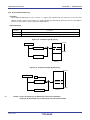
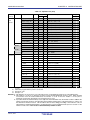
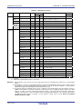
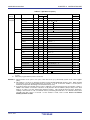
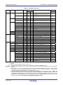
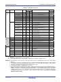
1
User’s Manual
16
78K0R Microcontrollers
User’s Manual: Instructions
16-Bit Single-Chip Microcontrollers
All information contained in these materials, including products and product specifications,
represents information on the product at the time of publication and is subject to change by
Renesas Electronics Corp. without notice. Please review the latest information published by
Renesas Electronics Corp. through various means, including the Renesas Electronics Corp.
website (http://www.renesas.com).
www.renesas.com
Rev.6.00
Jan 2011
Notice
1.
2.
3.
4.
5.
6.
7.
All information included in this document is current as of the date this document is issued. Such information, however, is
subject to change without any prior notice. Before purchasing or using any Renesas Electronics products listed herein, please
confirm the latest product information with a Renesas Electronics sales office. Also, please pay regular and careful attention to
additional and different information to be disclosed by Renesas Electronics such as that disclosed through our website.
Renesas Electronics does not assume any liability for infringement of patents, copyrights, or other intellectual property rights
of third parties by or arising from the use of Renesas Electronics products or technical information described in this document.
No license, express, implied or otherwise, is granted hereby under any patents, copyrights or other intellectual property rights
of Renesas Electronics or others.
You should not alter, modify, copy, or otherwise misappropriate any Renesas Electronics product, whether in whole or in part.
Descriptions of circuits, software and other related information in this document are provided only to illustrate the operation of
semiconductor products and application examples. You are fully responsible for the incorporation of these circuits, software,
and information in the design of your equipment. Renesas Electronics assumes no responsibility for any losses incurred by
you or third parties arising from the use of these circuits, software, or information.
When exporting the products or technology described in this document, you should comply with the applicable export control
laws and regulations and follow the procedures required by such laws and regulations. You should not use Renesas
Electronics products or the technology described in this document for any purpose relating to military applications or use by
the military, including but not limited to the development of weapons of mass destruction. Renesas Electronics products and
technology may not be used for or incorporated into any products or systems whose manufacture, use, or sale is prohibited
under any applicable domestic or foreign laws or regulations.
Renesas Electronics has used reasonable care in preparing the information included in this document, but Renesas Electronics
does not warrant that such information is error free. Renesas Electronics assumes no liability whatsoever for any damages
incurred by you resulting from errors in or omissions from the information included herein.
Renesas Electronics products are classified according to the following three quality grades: “Standard”, “High Quality”, and
“Specific”. The recommended applications for each Renesas Electronics product depends on the product’s quality grade, as
indicated below. You must check the quality grade of each Renesas Electronics product before using it in a particular
application. You may not use any Renesas Electronics product for any application categorized as “Specific” without the prior
written consent of Renesas Electronics. Further, you may not use any Renesas Electronics product for any application for
which it is not intended without the prior written consent of Renesas Electronics. Renesas Electronics shall not be in any way
liable for any damages or losses incurred by you or third parties arising from the use of any Renesas Electronics product for an
application categorized as “Specific” or for which the product is not intended where you have failed to obtain the prior written
consent of Renesas Electronics. The quality grade of each Renesas Electronics product is “Standard” unless otherwise
expressly specified in a Renesas Electronics data sheets or data books, etc.
“Standard”:
8.
9.
10.
11.
12.
Computers; office equipment; communications equipment; test and measurement equipment; audio and visual
equipment; home electronic appliances; machine tools; personal electronic equipment; and industrial robots.
“High Quality”: Transportation equipment (automobiles, trains, ships, etc.); traffic control systems; anti-disaster systems; anticrime systems; safety equipment; and medical equipment not specifically designed for life support.
“Specific”:
Aircraft; aerospace equipment; submersible repeaters; nuclear reactor control systems; medical equipment or
systems for life support (e.g. artificial life support devices or systems), surgical implantations, or healthcare
intervention (e.g. excision, etc.), and any other applications or purposes that pose a direct threat to human life.
You should use the Renesas Electronics products described in this document within the range specified by Renesas Electronics,
especially with respect to the maximum rating, operating supply voltage range, movement power voltage range, heat radiation
characteristics, installation and other product characteristics. Renesas Electronics shall have no liability for malfunctions or
damages arising out of the use of Renesas Electronics products beyond such specified ranges.
Although Renesas Electronics endeavors to improve the quality and reliability of its products, semiconductor products have
specific characteristics such as the occurrence of failure at a certain rate and malfunctions under certain use conditions. Further,
Renesas Electronics products are not subject to radiation resistance design. Please be sure to implement safety measures to
guard them against the possibility of physical injury, and injury or damage caused by fire in the event of the failure of a
Renesas Electronics product, such as safety design for hardware and software including but not limited to redundancy, fire
control and malfunction prevention, appropriate treatment for aging degradation or any other appropriate measures. Because
the evaluation of microcomputer software alone is very difficult, please evaluate the safety of the final products or system
manufactured by you.
Please contact a Renesas Electronics sales office for details as to environmental matters such as the environmental
compatibility of each Renesas Electronics product. Please use Renesas Electronics products in compliance with all applicable
laws and regulations that regulate the inclusion or use of controlled substances, including without limitation, the EU RoHS
Directive. Renesas Electronics assumes no liability for damages or losses occurring as a result of your noncompliance with
applicable laws and regulations.
This document may not be reproduced or duplicated, in any form, in whole or in part, without prior written consent of Renesas
Electronics.
Please contact a Renesas Electronics sales office if you have any questions regarding the information contained in this
document or Renesas Electronics products, or if you have any other inquiries.
(Note 1) “Renesas Electronics” as used in this document means Renesas Electronics Corporation and also includes its majorityowned subsidiaries.
(Note 2) “Renesas Electronics product(s)” means any product developed or manufactured by or for Renesas Electronics.
NOTES FOR CMOS DEVICES
(1) VOLTAGE APPLICATION WAVEFORM AT INPUT PIN: Waveform distortion due to input noise or a
reflected wave may cause malfunction. If the input of the CMOS device stays in the area between VIL
(MAX) and VIH (MIN) due to noise, etc., the device may malfunction. Take care to prevent chattering noise
from entering the device when the input level is fixed, and also in the transition period when the input level
passes through the area between VIL (MAX) and VIH (MIN).
(2) HANDLING OF UNUSED INPUT PINS: Unconnected CMOS device inputs can be cause of malfunction.
If an input pin is unconnected, it is possible that an internal input level may be generated due to noise, etc.,
causing malfunction. CMOS devices behave differently than Bipolar or NMOS devices. Input levels of
CMOS devices must be fixed high or low by using pull-up or pull-down circuitry. Each unused pin should be
connected to VDD or GND via a resistor if there is a possibility that it will be an output pin. All handling
related to unused pins must be judged separately for each device and according to related specifications
governing the device.
(3) PRECAUTION AGAINST ESD: A strong electric field, when exposed to a MOS device, can cause
destruction of the gate oxide and ultimately degrade the device operation. Steps must be taken to stop
generation of static electricity as much as possible, and quickly dissipate it when it has occurred.
Environmental control must be adequate. When it is dry, a humidifier should be used. It is recommended
to avoid using insulators that easily build up static electricity. Semiconductor devices must be stored and
transported in an anti-static container, static shielding bag or conductive material. All test and measurement
tools including work benches and floors should be grounded. The operator should be grounded using a
wrist strap. Semiconductor devices must not be touched with bare hands. Similar precautions need to be
taken for PW boards with mounted semiconductor devices.
(4) STATUS BEFORE INITIALIZATION: Power-on does not necessarily define the initial status of a MOS
device. Immediately after the power source is turned ON, devices with reset functions have not yet been
initialized. Hence, power-on does not guarantee output pin levels, I/O settings or contents of registers. A
device is not initialized until the reset signal is received. A reset operation must be executed immediately
after power-on for devices with reset functions.
(5) POWER ON/OFF SEQUENCE: In the case of a device that uses different power supplies for the internal
operation and external interface, as a rule, switch on the external power supply after switching on the internal
power supply. When switching the power supply off, as a rule, switch off the external power supply and then
the internal power supply. Use of the reverse power on/off sequences may result in the application of an
overvoltage to the internal elements of the device, causing malfunction and degradation of internal elements
due to the passage of an abnormal current. The correct power on/off sequence must be judged separately
for each device and according to related specifications governing the device.
(6) INPUT OF SIGNAL DURING POWER OFF STATE : Do not input signals or an I/O pull-up power supply
while the device is not powered. The current injection that results from input of such a signal or I/O pull-up
power supply may cause malfunction and the abnormal current that passes in the device at this time may
cause degradation of internal elements. Input of signals during the power off state must be judged
separately for each device and according to related specifications governing the device.
How to Use This Manual
Target Readers
This manual is intended for users who wish to understand the functions of 78K0R
microcontrollers and to design and develop its application systems and programs.
Purpose
This manual is intended to give users an understanding of the various kinds of instruction
functions of 78K0R microcontrollers.
Organization
This manual is broadly divided into the following sections.
• CPU functions
• Instruction set
• Explanation of instructions
How to Read This Manual
It is assumed that readers of this manual have general knowledge in the fields of electrical
engineering, logic circuits, and microcontrollers.
• To check the details of the functions of an instruction whose mnemonic is known:
→ Refer to APPENDICES A and B.
• To check an instruction whose mnemonic is not known but whose general function is
known:
→ Find the mnemonic in CHAPTER 5 INSTRUCTION SET and then check the
detailed functions in CHAPTER 6 EXPLANATION OF INSTRUCTIONS.
• To learn about the various kinds of 78K0R microcontroller instructions in general:
→Read this manual in the order of CONTENTS.
• To learn about the hardware functions of 78K0R microcontrollers:
→ See the user’s manual for each microcontroller.
Conventions
Data significance:
Higher digits on the left and lower digits on the right
Note:
Footnote for item marked with Note in the text
Caution:
Information requiring particular attention
Remark:
Supplementary information
Numeric representation:
Binary …………. XXXX or XXXXB
Decimal ………..XXXX
Hexadecimal …. XXXXH
CONTENTS
CHAPTER 1 OVERVIEW ......................................................................................................................... 7
1.1
Differences from 78K0 Microcontrollers (for Assembler Users) ........................................... 7
CHAPTER 2 MEMORY SPACE............................................................................................................... 9
2.1
2.2
Memory Space ............................................................................................................................ 9
Internal Program Memory Space ............................................................................................ 10
2.2.1 Mirror area...................................................................................................................................... 10
2.2.2 Vector table area............................................................................................................................ 11
2.2.3 CALLT instruction table area.......................................................................................................... 11
2.3
2.4
2.5
2.6
Internal Data Memory (Internal RAM) Space ......................................................................... 12
Special Function Register (SFR) Area ................................................................................... 12
Extended SFR (Second SFR) Area ......................................................................................... 12
External Memory Space........................................................................................................... 13
CHAPTER 3 REGISTERS ..................................................................................................................... 14
3.1
Control Registers ..................................................................................................................... 14
3.1.1 Program counter (PC) .................................................................................................................... 14
3.1.2 Program status word (PSW)........................................................................................................... 14
3.1.3 Stack pointer (SP) .......................................................................................................................... 15
3.2
3.3
3.4
General-Purpose Registers..................................................................................................... 17
ES and CS Registers................................................................................................................ 19
Special Function Registers (SFRs) ........................................................................................ 20
3.4.1 Processor mode control register (PMC) ......................................................................................... 20
CHAPTER 4 ADDRESSING .................................................................................................................. 21
4.1
Instruction Address Addressing ............................................................................................ 21
4.1.1 Relative addressing........................................................................................................................ 21
4.1.2 Immediate addressing .................................................................................................................... 22
4.1.3 Table indirect addressing ............................................................................................................... 22
4.1.4 Register direct addressing ............................................................................................................. 23
4.2
Addressing for Processing Data Addresses ......................................................................... 24
4.2.1 Implied addressing ......................................................................................................................... 24
4.2.2 Register addressing ....................................................................................................................... 24
4.2.3 Direct addressing ........................................................................................................................... 25
4.2.4 Short direct addressing .................................................................................................................. 26
4.2.5 SFR addressing ............................................................................................................................. 27
4.2.6 Register indirect addressing........................................................................................................... 28
4.2.7 Based addressing .......................................................................................................................... 29
4.2.8 Based indexed addressing ............................................................................................................. 32
4.2.9 Stack addressing............................................................................................................................ 33
R01US0029EJ0600 Rev.6.00
Jan 31, 2011
5
CHAPTER 5 INSTRUCTION SET.......................................................................................................... 34
5.1
5.2
5.3
5.4
5.5
5.6
5.7
Operand Identifiers and Description Methods......................................................................... 34
Symbols in “Operation” Column............................................................................................... 36
Symbols in “Flag” Column ........................................................................................................ 37
PREFIX Instruction ..................................................................................................................... 37
Operation List.............................................................................................................................. 38
Instruction Format ...................................................................................................................... 55
Instruction Maps ......................................................................................................................... 85
CHAPTER 6 EXPLANATION OF INSTRUCTIONS .............................................................................. 90
6.1 8-bit Data Transfer Instructions ................................................................................................ 92
6.2 16-bit Data Transfer Instructions .............................................................................................. 99
6.3 8-bit Operation Instructions..................................................................................................... 105
6.4 16-bit Operation Instructions................................................................................................... 116
6.5 Multiply Instruction................................................................................................................... 120
6.6 Increment/Decrement Instructions ......................................................................................... 122
6.7 Shift Instructions ...................................................................................................................... 127
6.8 Rotate Instructions ................................................................................................................... 134
6.9 Bit Manipulation Instructions .................................................................................................. 140
6.10 Call Return Instructions ......................................................................................................... 148
6.11 Stack Manipulation Instructions ........................................................................................... 155
6.12 Unconditional Branch Instruction......................................................................................... 161
6.13 Conditional Branch Instructions ........................................................................................... 163
6.14 Conditional Skip Instructions................................................................................................ 173
6.15 CPU Control Instructions....................................................................................................... 180
CHAPTER 7 PIPELINE ........................................................................................................................ 187
7.1
7.2
Features .................................................................................................................................. 187
Number of Operation Clocks ................................................................................................ 188
7.2.1 Access to flash memory contents as data .................................................................................... 188
7.2.2 Access to external memory contents as data............................................................................... 188
7.2.3 Instruction fetch from RAM........................................................................................................... 188
7.2.4 Instruction fetch from external memory ........................................................................................ 189
7.2.5 Hazards related to combined instructions .................................................................................... 190
APPENDIX A INSTRUCTION INDEX (MNEMONIC: BY FUNCTION) ........................................... 191
APPENDIX B INSTRUCTION INDEX (MNEMONIC: IN ALPHABETICAL ORDER) ..................... 193
R01US0029EJ0600 Rev.6.00
Jan 31, 2011
6
R01US0029EJ0600
Rev.6.00
Jan 31, 2011
78K0R Microcontrollers
RENESAS MCU
CHAPTER 1 OVERVIEW
1.1
Differences from 78K0 Microcontrollers (for Assembler Users)
(1) Use of pipeline processing reduces the number of processing clock cycles for all instructions. Existing programs
must be re-evaluated.
(2) All instruction code maps have been modified. Reassemble them using the assembler. When reassembling, the
code size is likely to increase as new instructions are added, but in some cases the overall code size may shrink if
old instructions are replaced with new ones.
(3) The memory space was changed from 64 KB to 1 MB, and the total stack area was also increased. Within the
assembler's program, the address must be changed whenever RAM contents within the stack pointer are
manipulated. The stack size should be increased slightly to accommodate the depth of multiple CALLs or multiple
interrupts.
(4) The CALLT table's address range has been changed from "0040H to 007FH" to "0080H to 00BFH".
Consequently, the CALLT table's address should be changed.
(5) Among the programs used for the 78K0 microcontroller's bank switching, the assembler program must be
rewritten.
(6) Address changes are made when using the expansion RAM. Be sure to change these addresses.
(7) If instructions are executed from expansion RAM, since memory space addresses have been changed, change
BR !addr16 to BR !!addr20, and CALL !addr16 to CALL !!addr20.
(8) There are no IMS or IXS registers (registers used to set memory space). The programs that use these registers
should be deleted if external memory is not being used. If external memory is being used, the specifications for
the MM/MEM register (external memory setting register) have been changed, so check the user’s manual for
each product and change the settings accordingly.
R01US0029EJ0600 Rev.6.00
Jan 31, 2011
7
78K0R Microcontrollers
CHAPTER 1 OUTLINE
(9) The following instructions are deleted and the alternative code is output, resulting in code size increases. Even
when these instructions are used, they are automatically replaced during assembly.
Instruction
DIVUW
Operand
C
Remarks
The alternative instruction executes a division with shifting, so the execution time is
longer than DIVUW. It is recommended to change this instruction to the added shift
instruction.
ROR4
[HL]
The execution time of the alternative instruction is longer than ROR4. It is
recommended to change this instruction to the added shift instruction.
ROL4
[HL]
The execution time of the alternative instruction is longer than ROL4. It is
recommended to change this instruction to the added shift instruction.
ADJBA
None
The execution time of the alternative instruction is longer than ADJBA. No instruction
is added for substitution.
ADJBS
None
The execution time of the alternative instruction is longer than ADJBS. No instruction
is added for substitution.
CALLF
!addr11
CALLF is automatically changed to a 3-byte instruction CALL !addr16.
This can be used without modification.
DBNZ
<R>
B, $addr16
This instruction is divided into two: DEC B/DEC C/DEC saddr and BNZ $addr20.
C, $addr16
saddr, $addr16
These can be used without modification.
(10) Memory space has changed from 64KB to 1MB, and addressing by using ES register and addressing of word [BC],
etc. are added. Be sure not to assign any address over maximum memory space. Especially in based addressing
and based indexed addressing, an added value must not exceed FFFFH (without ES register) or FFFFFH (with ES
register).
R01US0029EJ0600 Rev.6.00
Jan 31, 2011
8
78K0R Microcontrollers
CHAPTER 2 MEMORY SPACE
CHAPTER 2 MEMORY SPACE
2.1
Memory Space
While the 78K0 microcontroller’s memory space is only 64 KB, this has been expanded to 1 MB in the 78K0R
microcontroller.
Figure 2-1. Memory Maps of 78K0 Microcontrollers and 78K0R Microcontrollers
(78K0 microcontrollers)
FFFFH
(78K0R microcontrollers)
FFFFFH
SFR addressing
FF20H
FF1FH
FF00H
FEFFH
FEE0H
FEDFH
FE20H
FE1FH
Special-function register (SFR)
General-purpose register
32 × 8 bits
FFF00H
FFEFFH
Special-function register (SFR)
256 × 8 bits
General-purpose register
32 × 8 bits
Short direct addressing
FFEE0H
FFEDFH
Internal high-speed RAM
FFE20H
FFE1FH
1024 × 8 bits
FB00H
FAFFH
SFR addressing
FFF20H
FFF1FH
256 × 8 bits
Short direct addressing
RAM
61.75 K × 8 bits (max.)
Area 1
FA00H
F9FFH
F0800H
F07FFH
Area 2
F900H
F8FFH
Area 3
Special-function register (2nd SFR)
2 K × 8 bits (max.)
F800H
F7FFH
F0000H
EFFFFH
Internal expansion RAM
14 K × 8 bits (max.)
EE000H
EDFFFH
Supporting external expansion memory
Supporting external expansion memory
Flash memory
60 K × 8 bits (max.)
Flash memory
960 K × 8 bits (max.)
0000H
00000H
• Program memory space is 60 KB (max.).
• Program memory space is 960 KB (max.).
• Internal high-speed RAM area is 1 KB (max.) (stack
• RAM space is 61.75 KB (max.) (stack enabled, fetch
enabled).
Internal expansion RAM area is 14 KB (max.) (fetch
enabled).
• Area 1, area 2, and area 3 are from F800H to
FAFFH (fixed).
• Supports external expansion memory.
enabled).
• Second SFR area (name changed) is 2 KB (max.),
from F0000H to F07FFH.
• Supports external expansion memory.
The external expansion memory space can be
allocated from the product-mounted flash memory
area to EDFFFH.
R01US0029EJ0600 Rev.6.00
Jan 31, 2011
9
78K0R Microcontrollers
2.2
CHAPTER 2 MEMORY SPACE
Internal Program Memory Space
In the 78K0R microcontrollers, the program memory space’s address range is from 00000H to EFFFFH.
For description of the internal ROM (flash memory) maximum size, refer to the user’s manual for each product.
<R>
Caution Do not use relative addressing in branch instructions from internal program memory space to
RAM space or external memory space.
2.2.1 Mirror area
In the 78K0R microcontrollers, the data flash areas from 00000H to 0FFFFH (when MAA = 0) and from 10000H to
1FFFFH (when MAA = 1) are mirrored to the addresses from F0000H to FFFFFH. By reading data from F0000H to
FFFFFH, an instruction that does not have the ES registers as an operand can be used, and thus the contents of the data
flash can be read with the shorter code. However, in this case the data flash area is not mirrored to the SFR, extended
SFR (second SFR), RAM, and use prohibited areas.
Mirror areas can only be read, and instruction fetch is not enabled.
The following show examples. Specifications vary for each product, so refer to the user’s manual for each product.
Example 1 (Flash memory: 32 KB, RAM: 1.5 KB)
Example 2 (Flash memory: 512 KB, RAM: 30 KB)
Setting MAA = 0
Setting MAA = 1
FFFFFH
FFFFFH
Special-function register (SFR)
256 bytes
Special-function register (SFR)
256 bytes
FFF00H
FFEFFH
FFEE0H
FFEDFH
FF900H
FF8FFH
FFF00H
FFEFFH
General-purpose register
32 bytes
FFEE0H
FFEDFH
RAM
1.5 KB
General-purpose register
32 bytes
RAM
30 KB
Reserved
F8000H
F7FFFH
F1000H
F0FFFH
F0800H
F07FFH
F8700H
F86FFH
Flash memory
(same data as 01000H to 07FFFH)
F1000H
F0FFFH
Reserved
F0800H
F07FFH
Special-function register (2nd SFR)
2 KB
Flash memory
(same data as 11000H to 186FFH)
Reserved
Special-function register (2nd SFR)
2 KB
F0000H
EFFFFH
F0000H
EFFFFH
Mirror
Mirror
80000H
7FFFFH
Flash memory
For example, 02345H is mirrored
to F2345H. Data can therefore be
read by MOV A, !2345H, instead
of MOV ES, #00H and MOV A,
ES:!2345H.
For example, 15432H is mirrored
to F5432H. Data can therefore be
read by MOV A, !5432H, instead
of MOV ES, #01H and MOV A,
ES:!5432H.
18700H
186FFH
Flash memory
11000H
10FFFH
08000H
07FFFH
Flash memory
Flash memory
01000H
00FFFH
Flash memory
00000H
Remark
00000H
MAA: Bit 0 of the processor mode control register (PMC) (for details, refer to 3.4.1 Processor mode
control register (PMC)).
R01US0029EJ0600 Rev.6.00
Jan 31, 2011
10
78K0R Microcontrollers
CHAPTER 2 MEMORY SPACE
2.2.2 Vector table area
In the 78K0R microcontrollers, the 128-byte area from 0000H to 007FH is reserved as the vector table area. The
number of interrupts is calculated as 61 (maximum) + RESET vector + on-chip debugging vector + software break vector.
Since there are only 2 bytes of vector code, the interrupt branch destination start address is 64 KB from 00000H to
0FFFFH. While in the 78K0 microcontrollers, addresses from 0040H to 007FH are used for the CALLT table, in the
78K0R microcontrollers, these have been changed to vector addresses.
2.2.3 CALLT instruction table area
In the 78K0R microcontrollers, the 64-byte area from 0080H to 00BFH is reserved as the CALLT instruction table area.
While single-byte CALL instructions are used in the 78K0 microcontrollers, the 78K0R microcontrollers use 2-byte
CALL instructions. Addresses have also been changed accordingly.
Since the address code is only 2 bytes long, the interrupt branch destination start address is 64 KB from 00000H to
0FFFFH.
2.3
Internal Data Memory (Internal RAM) Space
The 78K0 microcontrollers include internal high-speed RAM and internal expansion RAM, whereby the internal highspeed RAM is stack-enabled while the internal expansion RAM is fetch-enabled. By contrast, the 78K0R microcontrollers
have just one RAM area that enables both stack and fetch.
The higher limit of the address range is fixed to FFEFFH, and the range can be extended downward according to the
product’s mounted RAM size. The maximum size is 61.75 KB. For a description of the range’s lower limit, refer to the
user’s manual for each product.
The saddr space and general-purpose register area (from FFEE0H to FFEFFH) have the same addresses in the 78K0
microcontrollers.
Cautions 1.
Specify the address other than the general-purpose register area address as a stack area. It
is prohibited to use the general-purpose register area for fetching instructions or as a stack
area.
<R>
2. Do not use relative addressing in branch instructions from RAM space to internal program
memory space or external memory space.
R01US0029EJ0600 Rev.6.00
Jan 31, 2011
11
78K0R Microcontrollers
2.4
CHAPTER 2 MEMORY SPACE
Special Function Register (SFR) Area
SFRs have specific functions, unlike general-purpose registers.
The SFR space is allocated to the area from FFF00H to FFFFFH.
SFRs can be manipulated like general-purpose registers, using operation, transfer, and bit manipulation instructions.
The manipulable bit units, 1, 8, and 16, depend on the SFR type.
Each manipulation bit unit can be specified as follows.
• 1-bit manipulation
Describe the symbol reserved by the assembler for the 1-bit manipulation instruction operand (sfr.bit). This
manipulation can also be specified with an address.
• 8-bit manipulation
Describe the symbol reserved by the assembler for the 8-bit manipulation instruction operand (sfr). This
manipulation can also be specified with an address.
• 16-bit manipulation
Describe the symbol reserved by the assembler for the 16-bit manipulation instruction operand (sfrp). When
specifying an address, describe an even address.
Although the 78K0R microcontrollers’ SFR has the same specifications as in the 78K0 microcontrollers, some registers
differ from the 78K0 in cases where addresses are fixed. Refer to the user’s manual for each product for details.
2.5
Extended SFR (Second SFR) Area
Unlike a general-purpose register, each extended SFR (2nd SFR) has a special function.
Extended SFRs are allocated to the F0000H to F07FFH area. SFRs other than those in the SFR area (FFF00H to
FFFFFH) are allocated to this area. An instruction that accesses the extended SFR area, however, is 1 byte longer than
an instruction that accesses the SFR area.
Extended SFRs can be manipulated like general-purpose registers, using operation, transfer, and bit manipulation
instructions. The manipulable bit units, 1, 8, and 16, depend on the SFR type.
Each manipulation bit unit can be specified as follows..
• 1-bit manipulation
Describe the symbol reserved by the assembler for the 1-bit manipulation instruction operand (!addr16.bit). This
manipulation can also be specified with an address.
• 8-bit manipulation
Describe the symbol reserved by the assembler for the 8-bit manipulation instruction operand (!addr16). This
manipulation can also be specified with an address.
• 16-bit manipulation
Describe the symbol reserved by the assembler for the 16-bit manipulation instruction operand (!addr16). When
specifying an address, describe an even address.
R01US0029EJ0600 Rev.6.00
Jan 31, 2011
12
78K0R Microcontrollers
2.6
CHAPTER 2 MEMORY SPACE
External Memory Space
The external memory space that can be accessed by setting the memory expansion mode register. This memory
space is allocated from flash memory to EDFFFH.
As the external pins in separate mode, 28 pins (A19 to A0 and D7 to D0) are available. In multiplexed mode, 20 pins
(A19 to A8 and AD7 to AD0) are available.
For pin settings when using external memory, refer to the chapter describing port functions in the user’s manual for
each product.
Cautions 1.
When fetching the instructions in an external memory area, start the execution by the
branch instructions (CALL or BR) in flash memory or RAM memory areas and end the
execution by return instructions (RET, RETB or RETI) in an external memory area.
While flash memory area is adjacent to an external memory area, serial program can not be
executed.
<R>
2. Do not use relative addressing in branch instructions from external memory space to flash
memory space or RAM space.
R01US0029EJ0600 Rev.6.00
Jan 31, 2011
13
78K0R Microcontrollers
CHAPTER 3 REGISTERS
CHAPTER 3 REGISTERS
3.1
Control Registers
The control registers control the program sequence, statuses and stack memory. A program counter (PC), a program
status word (PSW), and a stack pointer (SP) are the control registers.
3.1.1 Program counter (PC)
The program counter is a 20-bit register that holds the address information of the next program to be executed.
Figure 3-1. Program Counter Configuration
19
0
PC
PC
3.1.2 Program status word (PSW)
The program status word is an 8-bit register consisting of various flags to be set/reset by instruction execution.
The ISP1 flag is added as bit 2 in products that support interrupt level 4.
The contents of the program status word are automatically stacked when an interrupt request occurs and a PUSH PSW
instruction is executed, and are automatically restored when an RETB or RETI instruction and a POP PSW instruction is
executed.
The PSW value becomes 06H when a reset signal is input.
Figure 3-2. Program Status Word Configuration
PSW
<7>
<6>
<5>
<4>
<3>
<2>
<1>
0
IE
Z
RBS1
AC
RBS0
ISP1
ISP0
CY
(1) Interrupt enable flag (IE)
This flag controls the interrupt request acknowledgement operations of the CPU.
When IE = 0, the IE flag is set to interrupt disable (DI), and interrupts other than non-maskable interrupts are all
disabled.
When IE = 1, the IE flag is set to interrupt enable (EI), and interrupt request acknowledgement is controlled by an
interrupt mask flag for various interrupt sources, and a priority specification flag.
This flag is reset (0) upon DI instruction execution or interrupt request acknowledgment and is set (1) upon
execution of the EI instruction.
(2) Zero flag (Z)
When the operation result is zero, this flag is set (1). It is reset (0) in all other cases.
R01US0029EJ0600 Rev.6.00
Jan 31, 2011
14
78K0R Microcontrollers
CHAPTER 3 REGISTERS
(3) Register bank select flags (RBS0 and RBS1)
These are 2-bit flags used to select one of the four register banks.
In these flags, the 2-bit information that indicates the register bank selected by SBL RBn instruction execution is
stored.
(4) Auxiliary carry flag (AC)
If the operation result has a carry from bit 3 or a borrow at bit 3, this flag is set (1). It is reset (0) in all other cases.
(5) In-service priority flags (ISP0 and ISP1)
This flag manages the priority of acknowledgeable maskable vectored interrupts. The vectored interrupt requests
specified as lower than the ISP0 and ISP1 values by the priority specification flag register (PR) are disabled for
acknowledgment. Actual acknowledgment for interrupt requests is controlled by the state of the interrupt enable
flag (IE).
(6) Carry flag (CY)
This flag stores an overflow or underflow upon add/subtract instruction execution. It stores the shift-out value
upon rotate instruction execution and functions as a bit accumulator during bit manipulation instruction execution.
3.1.3 Stack pointer (SP)
This is a 16-bit register that holds the start address of the memory stack area. Only the internal RAM area can be set
as the stack area.
Figure 3-3. Stack Pointer Configuration
1
15
SP
SP
0
0
The SP is decremented ahead of write (save) to the stack memory and is incremented after read (restored) from the
stack memory.
Since reset signal generation makes the SP contents undefined, be sure to initialize the SP before using the stack. In
addition, the values of the stack pointer must be set to even numbers. If odd numbers are specified, the least significant
bit is automatically cleared to 0.
In the 78K0R microcontrollers, since the memory space is expanded, the stack address used for a CALL instruction or
interrupt is 1 byte longer, and 2-byte or 4-byte stack size is used because the RAM for the stack is 16 bits long (refer to
Table 3-1).
Caution
It is prohibited to use the general-purpose register (FFEE0H to FFEFFH) space as a stack area.
R01US0029EJ0600 Rev.6.00
Jan 31, 2011
15
78K0R Microcontrollers
CHAPTER 3 REGISTERS
Table 3-1. Stack Size Differences Between 78K0 Microcontrollers and 78K0R Microcontrollers
Save Instruction
Restore
Stack Size of 78K0
Stack Size of 78K0R
Instruction
Microcontrollers
Microcontrollers
PUSH rp
POP rp
2 bytes
2 bytes
PUSH PSW
POP PSW
1 byte
2 bytes
CALL, CALLT
RET
2 bytes
4 bytes
Interrupt
RETI
3 bytes
4 bytes
BRK
RETB
3 bytes
4 bytes
Figure 3-4 shows the data saved by various stack operations in the 78K0R microcontrollers.
Figure 3-4. Data to Be Saved to Stack Memory
PUSH PSW
instruction
(2-byte stack)
PUSH rp
instruction
(2-byte stack)
SP ← SP−2
↑
SP−2
↑
SP−1
↑
SP →
Lower half
register pairs
Upper half
register pairs
SP ← SP−2
↑
SP−2
↑
SP−1
↑
SP →
PC7-PC0
PC15-PC8
PC19-PC16
00H
PSW
Interrupt and
BRK instructions
(4-byte stack)
CALL and CALLT instructions
(4-byte stack)
SP ← SP−4
↑
SP−4
↑
SP−3
↑
SP−2
↑
SP−1
↑
SP →
00H
SP ← SP−4
↑
SP−4
↑
SP−3
↑
SP−2
↑
SP−1
↑
SP →
PC7-PC0
PC15-PC8
PC19-PC16
PSW
Stack pointers can be specified only within internal RAM. The target address range is from F0000H to FFFFFH; be
sure not to exceed the internal RAM space. If an address outside the internal RAM space is specified, write operations to
that address will be ignored and read operations will return undefined values.
R01US0029EJ0600 Rev.6.00
Jan 31, 2011
16
78K0R Microcontrollers
3.2
CHAPTER 3 REGISTERS
General-Purpose Registers
On-chip general-purpose registers are mapped at addresses FFEE0H to FFEFFH of the RAM. These registers consist
of 4 banks, each bank consisting of eight 8-bit registers (X, A, C, B, E, D, L and H). The bank to be used when an
instruction is executed is set by the CPU control instruction “SEL RBn”.
In addition that each register can be used as an 8-bit register, two 8-bit registers in pairs can be used as a 16-bit
register.
In programming, general-purpose registers can be described in terms of functional names (X, A, C, B, E, D, L, H, AX,
BC, DE and HL) and absolute names (R0 to R7 and RP0 to RP3).
Caution
Use of the general-purpose register space (FFEE0H to FFEFFH) as the instruction fetch area or stack
area is prohibited.
R01US0029EJ0600 Rev.6.00
Jan 31, 2011
17
78K0R Microcontrollers
CHAPTER 3 REGISTERS
Table 3-2. List of General-Purpose Registers (Common to 78K0 Microcontrollers)
Register
Bank Name
Functional Name
Absolute Address
Absolute Name
16-bit Processing
8-bit Processing
16-bit Processing
8-bit Processing
HL
H
RP3
R7
FFEFFH
R6
FFEFEH
R5
FFEFDH
R4
FFEFCH
R3
FFEFBH
R2
FFEFAH
R1
FFEF9H
R0
FFEF8H
R7
FFEF7H
R6
FFEF6H
R5
FFEF5H
R4
FFEF4H
R3
FFEF3H
R2
FFEF2H
R1
FFEF1H
R0
FFEF0H
R7
FFEEFH
R6
FFEEEH
R5
FFEEDH
R4
FFEECH
R3
FFEEBH
R2
FFEEAH
R1
FFEE9H
R0
FFEE8H
R7
FFEE7H
R6
FFEE6H
R5
FFEE5H
R4
FFEE4H
R3
FFEE3H
R2
FFEE2H
R1
FFEE1H
R0
FFEE0H
BANK0
L
DE
D
RP2
E
BC
B
RP1
C
AX
A
RP0
X
BANK1
HL
H
RP3
L
DE
D
RP2
E
BC
B
RP1
C
AX
A
RP0
X
BANK2
HL
H
RP3
L
DE
D
RP2
E
BC
B
RP1
C
AX
A
RP0
X
BANK3
HL
H
RP3
L
DE
D
RP2
E
BC
B
RP1
C
AX
A
X
R01US0029EJ0600 Rev.6.00
Jan 31, 2011
RP0
18
78K0R Microcontrollers
3.3
CHAPTER 3 REGISTERS
ES and CS Registers
The 78K0R microcontrollers have additional ES and CS registers. Data access can be specified via the ES register
and higher addresses for execution of branch instructions can be specified via the CS register. For description of how
these registers are used, refer to CHAPTER 4 ADDRESSING.
After reset, the initial value of ES is 0FH and the initial value of CS is 00H.
Figure 3-5. Configuration of ES and CS Registers
ES
CS
R01US0029EJ0600 Rev.6.00
Jan 31, 2011
7
6
5
4
3
2
1
0
0
0
0
0
ES3
ES2
ES1
ES0
7
6
5
4
3
2
1
0
0
0
0
0
CS3
CP2
CP1
CP0
19
78K0R Microcontrollers
3.4
CHAPTER 3 REGISTERS
Special Function Registers (SFRs)
Table 3-3 describes fixed-address SFRs in the 78K0R microcontrollers.
Table 3-3. List of Fixed SFRs
Address
Register Name
FFFF8H
SPL
FFFF9H
SPH
FFFFAH
PSW
FFFFBH
Reserve
FFFFCH
CS
FFFFDH
ES
FFFFEH
PMC
FFFFFH
MEM
3.4.1 Processor mode control register (PMC)
This is an 8-bit register that is used to control the processor modes. For details, refer to 2.2 Internal Program
Memory Space.
PMC’s initial value after reset is 00H.
Figure 3-6. Configuration of Processor Mode Control Register
Address: FFFFEH After reset: 00H R/W
Symbol
7
6
5
4
3
2
1
<0>
PMC
0
0
0
0
0
0
0
MAA
MAA
Selection of flash memory space for mirroring to area from F0000H to FFFFFHNote
0
00000H to 0FFFFH is mirrored to F0000H to FFFFFH
1
10000H to 1FFFFH is mirrored to F0000H to FFFFFH
Note SFR and RAM areas are also allocated to the range from F0000H to FFFFFH, and take
priority over other items for the overlapping areas.
Cautions 1. Set the PMC register only once for initial settings. Rewriting PMC is prohibited except for
initial settings.
2. After setting PMC, wait for at least one instruction and access the mirror area.
R01US0029EJ0600 Rev.6.00
Jan 31, 2011
20
78K0R Microcontrollers
CHAPTER 4 ADDRESSING
CHAPTER 4 ADDRESSING
Addressing is divided into two types: addressing for processing data addresses and addressing for program addresses.
The addressing modes corresponding to each type are described below.
4.1
Instruction Address Addressing
4.1.1 Relative addressing
[Function]
Relative addressing stores in the program counter (PC) the result of adding a displacement value included in the
instruction word (signed complement data: −128 to +127 or −32768 to +32767) to the program counter (PC)’s value
(the start address of the next instruction), and specifies the program address to be used as the branch destination.
Relative addressing is applied only to branch instructions.
Figure 4-1. Outline of Relative Addressing
PC
OP code
DISPLACE
<R>
8/16 bits
Caution Do not use relative addressing in the following branch instructions:
- Branching from internal program memory space to RAM space or external memory space
- Branching from RAM space to internal program memory space or external memory space
- Branching from external memory space to internal program memory space or RAM space
R01US0029EJ0600 Rev.6.00
Jan 31, 2011
21
78K0R Microcontrollers
CHAPTER 4 ADDRESSING
4.1.2 Immediate addressing
[Function]
Immediate addressing stores immediate data of the instruction word in the program counter, and specifies the
program address to be used as the branch destination.
For immediate addressing, CALL !!addr20 or BR !!addr20 is used to specify 20-bit addresses and CALL !addr16 or
BR !addr16 is used to specify 16-bit addresses. 0000 is set to the higher 4 bits when specifying 16-bit addresses.
Figure 4-2. Example of CALL !!addr20/BR !!addr20
PC
OP code
Low Addr.
High Addr.
Seg Addr.
Figure 4-3. Example of CALL !addr16/BR !addr16
PCS
PC
PCH
PCL
OP code
Low Addr.
0000
High Addr.
4.1.3 Table indirect addressing
[Function]
Table indirect addressing specifies a table address in the CALLT table area (0080H to 00BFH) with the 5-bit
immediate data in the instruction word, stores the contents at that table address and the next address in the program
counter (PC) as 16-bit data, and specifies the program address. Table indirect addressing is applied only for CALLT
instructions.
In the 78K0R microcontrollers, branching is enabled only to the 64 KB space from 00000H to 0FFFFH.
Figure 4-4. Outline of Table Indirect Addressing
OP code
Low Addr.
00000000
10
0
High Addr.
Table address
Memory
0000
PC
R01US0029EJ0600 Rev.6.00
Jan 31, 2011
PCS
PCH
PCL
22
78K0R Microcontrollers
CHAPTER 4 ADDRESSING
4.1.4 Register direct addressing
[Function]
Register direct addressing stores in the program counter (PC) the contents of a general-purpose register pair
(AX/BC/DE/HL) and CS register of the current register bank specified with the instruction word as 20-bit data, and
specifies the program address. Register direct addressing can be applied only to the CALL AX, BC, DE, HL, and BR
AX instructions.
Figure 4-5. Outline of Register Direct Addressing
OP code
rp
CS
PC
R01US0029EJ0600 Rev.6.00
Jan 31, 2011
PCS
PCH
PCL
23
78K0R Microcontrollers
4.2
CHAPTER 4 ADDRESSING
Addressing for Processing Data Addresses
4.2.1 Implied addressing
[Function]
Instructions for accessing registers (such as accumulators) that have special functions are directly specified with the
instruction word, without using any register specification field in the instruction word.
[Operand format]
Because implied addressing can be automatically employed with an instruction, no particular operand format
is necessary.
Implied addressing can be applied only to MULU X.
Figure 4-6. Outline of Implied Addressing
OP code
A register
Memory
4.2.2 Register addressing
[Function]
Register addressing accesses a general-purpose register as an operand. The instruction word of 3-bit long is used
to select an 8-bit register and the instruction word of 2-bit long is used to select a 16-bit register.
[Operand format]
Identifier
Description
r
X, A, C, B, E, D, L, H
rp
AX, BC, DE, HL
Figure 4-7. Outline of Register Addressing
OP code
Register
Memory
R01US0029EJ0600 Rev.6.00
Jan 31, 2011
24
78K0R Microcontrollers
CHAPTER 4 ADDRESSING
4.2.3 Direct addressing
[Function]
Direct addressing uses immediate data in the instruction word as an operand address to directly specify the target
address.
[Operand format]
Identifier
Description
ADDR16
Label or 16-bit immediate data (only the space from F0000H to FFFFFH is specifiable)
ES: ADDR16
Label or 16-bit immediate data (higher 4-bit addresses are specified by the ES register)
Figure 4-8. Example of ADDR16
FFFFFH
OP code
Low Addr.
Target memory
High Addr.
F0000H
Memory
Figure 4-9. Example of ES:ADDR16
FFFFFH
ES
OP code
Low Addr.
Target memory
High Addr.
00000H
Memory
R01US0029EJ0600 Rev.6.00
Jan 31, 2011
25
78K0R Microcontrollers
CHAPTER 4 ADDRESSING
4.2.4 Short direct addressing
[Function]
Short direct addressing directly specifies the target addresses using 8-bit data in the instruction word. This type of
addressing is applied only to the space from FFE20H to FFF1FH.
[Operand format]
Identifier
SADDR
Description
Label, FFE20H to FFF1FH immediate data or 0FE20H to 0FF1FH immediate data
(only the space from FFE20H to FFF1FH is specifiable)
SADDRP
Label, FFE20H to FFF1FH immediate data or 0FE20H to 0FF1FH immediate data (even address only)
(only the space from FFE20H to FFF1FH is specifiable)
Figure 4-10. Outline of Short Direct Addressing
OP code
FFF1FH
saddr
saddr
FFE20H
Memory
Remark SADDR and SADDRP are used to describe the values of addresses FE20H to FF1FH with 16-bit immediate
data (higher 4 bits of actual address are omitted), and the values of addresses FFE20H to FFF1FH with 20bit immediate data.
Regardless of whether SADDR or SADDRP is used, addresses within the space from FFE20H to FFF1FH
are specified for the memory.
R01US0029EJ0600 Rev.6.00
Jan 31, 2011
26
78K0R Microcontrollers
CHAPTER 4 ADDRESSING
4.2.5 SFR addressing
[Function]
SFR addressing directly specifies the target SFR addresses using 8-bit data in the instruction word. This type of
addressing is applied only to the space from FFF00H to FFFFFH.
[Operand format]
Identifier
SFR
SFRP
Description
SFR name
16-bit-manipulatable SFR name (even address only)
Figure 4-11. Outline of SFR Addressing
FFFFFH
OP code
SFR
FFF00H
SFR
Memory
R01US0029EJ0600 Rev.6.00
Jan 31, 2011
27
78K0R Microcontrollers
CHAPTER 4 ADDRESSING
4.2.6 Register indirect addressing
[Function]
Register indirect addressing directly specifies the target addresses using the contents of the register pair specified
with the instruction word as an operand address.
[Operand format]
Identifier
Description
−
[DE], [HL] (only the space from F0000H to FFFFFH is specifiable)
−
ES:[DE], ES:[HL] (higher 4-bit addresses are specified by the ES register)
Figure 4-12. Example of [DE], [HL]
FFFFFH
OP code
rp
Target memory
F0000H
Memory
Figure 4-13. Example of ES:[DE], ES:[HL]
FFFFFH
ES
OP code
rp
Target memory
00000H
Memory
R01US0029EJ0600 Rev.6.00
Jan 31, 2011
28
78K0R Microcontrollers
CHAPTER 4 ADDRESSING
4.2.7 Based addressing
[Function]
Based addressing uses the contents of a register pair specified with the instruction word as a base address, and 8bit immediate data or 16-bit immediate data as offset data. The sum of these values is used to specify the target
address.
[Operand format]
Identifier
Description
−
[HL + byte], [DE + byte], [SP + byte] (only the space from F0000H to FFFFFH is specifiable)
−
word[B], word[C] (only the space from F0000H to FFFFFH is specifiable)
−
word[BC] (only the space from F0000H to FFFFFH is specifiable)
−
ES:[HL + byte], ES:[DE + byte] (higher 4-bit addresses are specified by the ES register)
−
ES:word[B], ES:word[C] (higher 4-bit addresses are specified by the ES register)
−
ES:word[BC] (higher 4-bit addresses are specified by the ES register)
Figure 4-14. Example of [SP+byte]
FFFFFH
SP
Target memory
F0000H
OP code
byte
Memory
<R>
Caution In [HL+byte], [DE+byte], word[B], word[C], and word[BC], an added value must not exceed
FFFFH.
In ES:[HL+byte], ES:[DE+byte], ES:word[B], ES:word[C], and ES:word[BC], an added value
must not exceed FFFFFH.
For [SP+byte], an SP value must be within RAM space and the added value of SP+byte must be
FFEDFH or less in RAM space.
R01US0029EJ0600 Rev.6.00
Jan 31, 2011
29
78K0R Microcontrollers
CHAPTER 4 ADDRESSING
Figure 4-15. Example of [HL + byte], [DE + byte]
FFFFFH
rp (HL/DE)
Target memory
F0000H
OP code
byte
Memory
Figure 4-16. Example of word[B], word[C]
FFFFFH
r (B/C)
Target memory
F0000H
OP code
Low Addr.
High Addr.
Memory
Figure 4-17. Example of word[BC]
FFFFFH
rp (BC)
Target memory
F0000H
OP code
Low Addr.
High Addr.
Memory
R01US0029EJ0600 Rev.6.00
Jan 31, 2011
30
78K0R Microcontrollers
CHAPTER 4 ADDRESSING
Figure 4-18. Example of ES:[HL + byte], ES:[DE + byte]
FFFFFH
ES
rp (HL/DE)
Target memory
OP code
00000H
byte
Memory
Figure 4-19. Example of ES:word[B], ES:word[C]
FFFFFH
ES
r (B/C)
Target memory
OP code
00000H
Low Addr.
Memory
High Addr.
Figure 4-20. Example of ES:word[BC]
FFFFFH
ES
rp (BC)
Target memory
OP code
00000H
Low Addr.
Memory
High Addr.
R01US0029EJ0600 Rev.6.00
Jan 31, 2011
31
78K0R Microcontrollers
CHAPTER 4 ADDRESSING
4.2.8 Based indexed addressing
[Function]
Based indexed addressing uses the contents of a register pair specified with the instruction word as the base
address, and the content of the B register or C register similarly specified with the instruction word as offset address.
The sum of these values is used to specify the target address.
[Operand format]
Identifier
Description
−
[HL+B], [HL+C] (only the space from F0000H to FFFFFH is specifiable)
−
ES:[HL+B], ES:[HL+C] (higher 4-bit addresses are specified by the ES register)
Figure 4-21. Example of [HL+B], [HL+C]
FFFFFH
OP code
rp (HL)
Target memory
F0000H
r (B/C)
Memory
Figure 4-22. Example of ES:[HL+B], ES:[HL+C]
FFFFFH
OP code
ES
rp (HL)
Target memory
00000H
r (B/C)
<R>
Memory
Caution In [HL+ B] and [HL+C], an added value must not exceed FFFFH.
In ES:[HL+ B] and ES:[HL+C], an added value must not exceed FFFFFH.
R01US0029EJ0600 Rev.6.00
Jan 31, 2011
32
78K0R Microcontrollers
CHAPTER 4 ADDRESSING
4.2.9 Stack addressing
[Function]
The stack area is indirectly addressed with the stack pointer (SP) contents.
This addressing is automatically
employed when the PUSH, POP, subroutine call, and return instructions are executed or the register is
saved/restored upon generation of an interrupt request.
Stack addressing is applied only to the internal RAM area.
[Operand format]
Identifier
−
Description
PUSH AX/BC/DE/HL
POP AX/BC/DE/HL
CALL/CALLT
RET
BRK
RETB
(Interrupt request generated)
RETI
R01US0029EJ0600 Rev.6.00
Jan 31, 2011
33
78K0R Microcontrollers
CHAPTER 5 INSTRUCTION SET
CHAPTER 5 INSTRUCTION SET
This chapter lists the instructions in the 78K0R microcontroller instruction set. The instructions are common to all
78K0R microcontrollers.
Remark
The shaded parts of the tables in 5.5 List of Operations and 5.6 List of Instruction Formats indicate the
operation or instruction format that is newly added for the 78K0R microcontrollers.
5.1 Operand Identifiers and Description Methods
Operands are described in the “Operand” column of each instruction in accordance with the description method of the
instruction operand identifier (refer to the assembler specifications for details). When there are two or more description
methods, select one of them. Alphabetic letters in capitals and the symbols, #, !, !!, $, $!, [ ], and ES: are keywords and
are described as they are. Each symbol has the following meaning.
• #:
Immediate data specification
• !:
16-bit absolute address specification
• !!:
20-bit absolute address specification
• $:
8-bit relative address specification
• $!:
16-bit relative address specification
• [ ]:
Indirect address specification
• ES:: Extension address specification
In the case of immediate data, describe an appropriate numeric value or a label. When using a label, be sure to
describe the #, !, !!, $, $!, [ ], and ES: symbols.
For operand register identifiers, r and rp, either function names (X, A, C, etc.) or absolute names (names in
parentheses in the table below, R0, R1, R2, etc.) can be used for description.
R01US0029EJ0600 Rev.6.00
Jan 31, 2011
34
78K0R Microcontrollers
CHAPTER 5 INSTRUCTION SET
Table 5-1. Operand Identifiers and Description Methods
Identifier
Description Method
r
X (R0), A (R1), C (R2), B (R3), E (R4), D (R5), L (R6), H (R7)
rp
AX (RP0), BC (RP1), DE (RP2), HL (RP3)
sfr
Special-function register symbol (SFR symbol) FFF00H to FFFFFH
sfrp
Special-function register symbols (16-bit manipulatable SFR symbol. Even addresses only
Note
) FFF00H to
FFFFFH
saddr
FFE20H to FFF1FH Immediate data or labels
saddrp
FFE20H to FF1FH Immediate data or labels (even addresses only
addr20
00000H to FFFFFH Immediate data or labels
addr16
0000H to FFFFH Immediate data or labels (only even addresses for 16-bit data transfer instructions
addr5
0080H to 00BFH Immediate data or labels (even addresses only)
word
16-bit immediate data or label
byte
8-bit immediate data or label
bit
3-bit immediate data or label
RBn
RB0 to RB3
Note
Note
)
Note
)
Bit 0 = 0 when an odd address is specified.
Remark
The special function registers can be described to operand sfr as symbols.
The extended special function registers can be described to operand !addr16 as symbols.
R01US0029EJ0600 Rev.6.00
Jan 31, 2011
35
78K0R Microcontrollers
CHAPTER 5 INSTRUCTION SET
5.2 Symbols in “Operation” Column
The operation when the instruction is executed is shown in the “Operation” column using the following symbols.
Table 5-2. Symbols in “Operation” Column
Symbol
Function
A
A register; 8-bit accumulator
X
X register
B
B register
C
C register
D
D register
E
E register
H
H register
L
L register
ES
ES register
CS
CS register
AX
AX register pair; 16-bit accumulator
BC
BC register pair
DE
DE register pair
HL
HL register pair
PC
Program counter
SP
Stack pointer
PSW
Program status word
CY
Carry flag
AC
Auxiliary carry flag
Z
Zero flag
RBS
Register bank select flag
IE
Interrupt request enable flag
()
Memory contents indicated by address or register contents in parentheses
X H, X L
16-bit registers: XH = higher 8 bits, XL = lower 8 bits
XS, XH, XL
20-bit registers: XS = (bits 19 to 16), XH = (bits 15 to 8), XL = (bits 7 to 0)
∧
Logical product (AND)
∨
Logical sum (OR)
∨
Exclusive logical sum (exclusive OR)
−
Inverted data
addr5
16-bit immediate data (even addresses only in 0080H to 00BFH)
addr16
16-bit immediate data
addr20
20-bit immediate data
jdisp8
Signed 8-bit data (displacement value)
jdisp16
Signed 16-bit data (displacement value)
R01US0029EJ0600 Rev.6.00
Jan 31, 2011
36
78K0R Microcontrollers
CHAPTER 5 INSTRUCTION SET
5.3 Symbols in “Flag” Column
The change of the flag value when the instruction is executed is shown in the “Flag” column using the following
symbols.
Table 5-3. Symbols in “Flag” Column
Symbol
Change of Flag Value
(Blank)
Unchanged
0
Cleared to 0
1
Set to 1
×
R
Set/cleared according to the result
Previously saved value is restored
5.4 PREFIX Instruction
Instructions with “ES:” have a PREFIX operation code as a prefix to extend the accessible data area to the 1 MB space
(00000H to FFFFFH), by adding the ES register value to the 64 KB space from F0000H to FFFFFH. When a PREFIX
operation code is attached as a prefix to the target instruction, only one instruction immediately after the PREFIX operation
code is executed as the addresses with the ES register value added.
A interrupt and DMA transfer are not acknowledged between a PREFIX instruction code and the instruction
immediately after.
Table 5-4. Use Example of PREFIX Operation Code
Instruction
Opcode
1
2
3
!addr16
4
5
#byte
−
MOV !addr16, #byte
CFH
MOV ES:!addr16, #byte
11H
CFH
MOV A, [HL]
8BH
−
−
−
−
MOV A, ES:[HL]
11H
8BH
−
−
−
!addr16
#byte
Caution Set the ES register value with MOV ES, A, etc., before executing the PREFIX instruction.
R01US0029EJ0600 Rev.6.00
Jan 31, 2011
37
78K0R Microcontrollers
CHAPTER 5 INSTRUCTION SET
5.5 Operation List
Table 5-5. Operation List (1/17)
Instruction Mnemonic
Operands
Bytes
Group
8-bit data
transfer
Operation
Clocks
Note 1 Note 2
MOV
Flag
Z
r, #byte
2
1
−
r ← byte
saddr, #byte
3
1
−
(saddr) ← byte
sfr, #byte
3
1
−
sfr ← byte
!addr16, #byte
4
1
−
(addr16) ← byte
A, r
Note 3
1
1
−
A←r
r, A
Note 3
1
1
−
r←A
A, saddr
2
1
−
A ← (saddr)
saddr, A
2
1
−
(saddr) ← A
A, sfr
2
1
−
A ← sfr
sfr, A
2
1
−
sfr ← A
A, !addr16
3
1
4
A ← (addr16)
!addr16, A
3
1
−
(addr16) ← A
PSW, #byte
3
3
−
PSW ← byte
A, PSW
2
1
−
A ← PSW
PSW, A
2
3
−
PSW ← A
ES, #byte
2
1
−
ES ← byte
ES, saddr
3
1
−
ES ← (saddr)
A, ES
2
1
−
A ← ES
ES, A
2
1
−
ES ← A
CS, #byte
3
1
−
CS ← byte
A, CS
2
1
−
A ← CS
CS, A
2
1
−
CS ← A
A, [DE]
1
1
4
A ← (DE)
[DE], A
1
1
−
(DE) ← A
[DE + byte], #byte
3
1
−
(DE + byte) ← byte
A, [DE + byte]
2
1
4
A ← (DE + byte)
[DE + byte], A
2
1
−
(DE + byte) ← A
A, [HL]
1
1
4
A ← (HL)
[HL], A
1
1
−
(HL) ← A
[HL + byte], #byte
3
1
−
(HL + byte) ← byte
AC CY
×
×
×
×
×
×
Notes 1.
When the internal RAM area, SFR area, or extended SFR area is accessed, or for an instruction with no data
access.
2. When the program memory area is accessed.
3. Except r = A
Remarks 1. One instruction clock cycle is one cycle of the CPU clock (fCLK) selected by the system clock control register
(CKC).
2. This number of clocks is for when the program is in the internal ROM (flash memory) area. When
fetching an instruction from the internal RAM area, the number of clocks is twice the number of clocks plus
3, maximum (except when branching to the external memory area).
3. In products where the external memory area is adjacent to the internal flash area, the number of waits is added to the
number of instruction execution clocks placed in the last address (16-byte max.) in the flash memory, in order to use
the external bus interface function. This should be done because, during pre-reading of the instruction code, an
external memory wait being inserted due to an external memory area exceeding the flash space is accessed. For the
number of waits, refer to 7.2.2 Access to external memory contents as data.
R01US0029EJ0600 Rev.6.00
Jan 31, 2011
38
78K0R Microcontrollers
CHAPTER 5 INSTRUCTION SET
Table 5-5. Operation List (2/17)
Instruction Mnemonic
Group
8-bit data
transfer
MOV
Operands
Clocks
Bytes
Flag
Operation
Note 1 Note 2
Z
A, [HL + byte]
2
1
4
A ← (HL + byte)
[HL + byte], A
2
1
−
(HL + byte) ← A
A, [HL + B]
2
1
4
A ← (HL + B)
[HL + B], A
2
1
−
(HL + B) ← A
A, [HL + C]
2
1
4
A ← (HL + C)
[HL + C], A
2
1
−
(HL + C) ← A
word[B], #byte
4
1
−
(B + word) ← byte
A, word[B]
3
1
4
A ← (B + word)
word[B], A
3
1
−
(B + word) ← A
word[C], #byte
4
1
−
(C + word) ← byte
A, word[C]
3
1
4
A ← (C + word)
word[C], A
3
1
−
(C + word) ← A
word[BC], #byte
4
1
−
(BC + word) ← byte
A, word[BC]
3
1
4
A ← (BC + word)
word[BC], A
3
1
−
(BC + word) ← A
[SP + byte], #byte
3
1
−
(SP + byte) ← byte
A, [SP + byte]
2
1
−
A ← (SP + byte)
[SP + byte], A
2
1
−
(SP + byte) ← A
B, saddr
2
1
−
B ← (saddr)
B, !addr16
3
1
4
B ← (addr16)
C, saddr
2
1
−
C ← (saddr)
C, !addr16
3
1
4
C ← (addr16)
X, saddr
2
1
−
X ← (saddr)
X, !addr16
3
1
4
X ← (addr16)
ES:!addr16, #byte
5
2
−
(ES, addr16) ← byte
A, ES:!addr16
4
2
5
A ← (ES, addr16)
ES:!addr16, A
4
2
−
(ES, addr16) ← A
A, ES:[DE]
2
2
5
A ← (ES, DE)
ES:[DE], A
2
2
−
(ES, DE) ← A
ES:[DE + byte],#byte
4
2
−
((ES, DE) + byte) ← byte
A, ES:[DE + byte]
3
2
5
A ← ((ES, DE) + byte)
ES:[DE + byte], A
3
2
−
((ES, DE) + byte) ← A
AC CY
Notes 1.
When the internal RAM area, SFR area, or extended SFR area is accessed, or for an instruction with no data
access.
2. When the program memory area is accessed.
Remarks 1. One instruction clock cycle is one cycle of the CPU clock (fCLK) selected by the system clock control register
(CKC).
2. This number of clocks is for when the program is in the internal ROM (flash memory) area. When fetching
an instruction from the internal RAM area, the number of clocks is twice the number of clocks plus 3,
maximum (except when branching to the external memory area).
3. In products where the external memory area is adjacent to the internal flash area, the number of waits is added to the
number of instruction execution clocks placed in the last address (16-byte max.) in the flash memory, in order to use
the external bus interface function. This should be done because, during pre-reading of the instruction code, an
external memory wait being inserted due to an external memory area exceeding the flash space is accessed. For the
number of waits, refer to 7.2.2 Access to external memory contents as data.
R01US0029EJ0600 Rev.6.00
Jan 31, 2011
39
78K0R Microcontrollers
CHAPTER 5 INSTRUCTION SET
Table 5-5. Operation List (3/17)
Instruction Mnemonic
Group
8-bit data
MOV
transfer
Operands
Z
A, ES:[HL]
2
2
5
A ← (ES, HL)
ES:[HL], A
2
2
−
(ES, HL) ← A
ES:[HL + byte],#byte
4
2
−
((ES, HL) + byte) ← byte
A, ES:[HL + byte]
3
2
5
A ← ((ES, HL) + byte)
ES:[HL + byte], A
3
2
−
((ES, HL) + byte) ← A
A, ES:[HL + B]
3
2
5
A ← ((ES, HL) + B)
ES:[HL + B], A
3
2
−
((ES, HL) + B) ← A
A, ES:[HL + C]
3
2
5
A ← ((ES, HL) + C)
ES:[HL + C], A
3
2
−
((ES, HL) + C) ← A
ES:word[B], #byte
5
2
−
((ES, B) + word) ← byte
A, ES:word[B]
4
2
5
A ← ((ES, B) + word)
ES:word[B], A
4
2
−
((ES, B) + word) ← A
ES:word[C], #byte
5
2
−
((ES, C) + word) ← byte
A, ES:word[C]
4
2
5
A ← ((ES, C) + word)
ES:word[C], A
4
2
−
((ES, C) + word) ← A
ES:word[BC], #byte
5
2
−
((ES, BC) + word) ← byte
A, ES:word[BC]
4
2
5
A ← ((ES, BC) + word)
ES:word[BC], A
4
2
−
((ES, BC) + word) ← A
B, ES:!addr16
4
2
5
B ← (ES, addr16)
C, ES:!addr16
4
2
5
C ← (ES, addr16)
4
2
5
X ← (ES, addr16)
1 (r = X)
2 (other
than r = X)
1
−
A ←→ r
A, saddr
3
2
−
A ←→ (saddr)
A, sfr
3
2
−
A ←→ sfr
A, !addr16
4
2
−
A ←→ (addr16)
A, [DE]
2
2
−
A ←→ (DE)
A, [DE + byte]
3
2
−
A ←→ (DE + byte)
A, [HL]
2
2
−
A ←→ (HL)
A, [HL + byte]
3
2
−
A ←→ (HL + byte)
A, [HL + B]
2
2
−
A ←→ (HL + B)
A, [HL + C]
2
2
−
A ←→ (HL + C)
A, r
Note 3
Flag
Operation
Note 1 Note 2
X, ES:!addr16
XCH
Clocks
Bytes
AC CY
Notes 1. When the internal RAM area, SFR area, or extended SFR area is accessed, or for an instruction with no data access.
2. When the program memory area is accessed.
3. Except r = A
Remarks 1. One instruction clock cycle is one cycle of the CPU clock (fCLK) selected by the system clock control register (CKC).
2. This number of clocks is for when the program is in the internal ROM (flash memory) area. When fetching
an instruction from the internal RAM area, the number of clocks is twice the number of clocks plus 3,
maximum (except when branching to the external memory area).
3. In products where the external memory area is adjacent to the internal flash area, the number of waits is added to the
number of instruction execution clocks placed in the last address (16-byte max.) in the flash memory, in order to use
the external bus interface function. This should be done because, during pre-reading of the instruction code, an
external memory wait being inserted due to an external memory area exceeding the flash space is accessed. For the
number of waits, refer to 7.2.2 Access to external memory contents as data.
R01US0029EJ0600 Rev.6.00
Jan 31, 2011
40
78K0R Microcontrollers
CHAPTER 5 INSTRUCTION SET
Table 5-5. Operation List (4/17)
Instruction Mnemonic
Group
8-bit data
XCH
transfer
ONEB
CLRB
MOVS
16-bit
data
transfer
MOVW
Operands
Clocks
Bytes
Flag
Operation
Note 1 Note 2
Z
AC CY
A, ES:!addr16
5
3
−
A ←→ (ES, addr16)
A, ES:[DE]
3
3
−
A ←→ (ES, DE)
A, ES:[DE + byte]
4
3
−
A ←→ ((ES, DE) + byte)
A, ES:[HL]
3
3
−
A ←→ (ES, HL)
A, ES:[HL + byte]
4
3
−
A ←→ ((ES, HL) + byte)
A, ES:[HL + B]
3
3
−
A ←→ ((ES, HL) + B)
A, ES:[HL + C]
3
3
−
A ←→ ((ES, HL) + C)
A
1
1
−
A ← 01H
X
1
1
−
X ← 01H
B
1
1
−
B ← 01H
C
1
1
−
C ← 01H
saddr
2
1
−
(saddr) ← 01H
!addr16
3
1
−
(addr16) ← 01H
ES:!addr16
4
2
−
(ES, addr16) ← 01H
A
1
1
−
A ← 00H
X
1
1
−
X ← 00H
B
1
1
−
B ← 00H
C
1
1
−
C ← 00H
saddr
2
1
−
(saddr) ← 00H
!addr16
3
1
−
(addr16) ← 00H
ES:!addr16
4
2
−
(ES,addr16) ← 00H
[HL + byte], X
3
1
−
(HL + byte) ← X
×
×
ES:[HL + byte], X
4
2
−
(ES, HL + byte) ← X
×
×
rp, #word
3
1
−
rp ← word
saddrp, #word
4
1
−
(saddrp) ← word
sfrp, #word
4
1
−
sfrp ← word
AX, saddrp
2
1
−
AX ← (saddrp)
saddrp, AX
2
1
−
(saddrp) ← AX
AX, sfrp
2
1
−
AX ← sfrp
2
1
−
sfrp ← AX
AX, rp
Note 3
1
1
−
AX ← rp
rp, AX
Note 3
1
1
−
rp ← AX
sfrp, AX
Notes 1.
When the internal RAM area, SFR area, or extended SFR area is accessed, or for an instruction with no data
access.
2. When the program memory area is accessed.
3. Except rp = AX
Remarks 1. One instruction clock cycle is one cycle of the CPU clock (fCLK) selected by the system clock control register (CKC).
2. This number of clocks is for when the program is in the internal ROM (flash memory) area. When fetching
an instruction from the internal RAM area, the number of clocks is twice the number of clocks plus 3,
maximum (except when branching to the external memory area).
3. In products where the external memory area is adjacent to the internal flash area, the number of waits is added to the
number of instruction execution clocks placed in the last address (16-byte max.) in the flash memory, in order to use
the external bus interface function. This should be done because, during pre-reading of the instruction code, an
external memory wait being inserted due to an external memory area exceeding the flash space is accessed. For the
number of waits, refer to 7.2.2 Access to external memory contents as data.
R01US0029EJ0600 Rev.6.00
Jan 31, 2011
41
78K0R Microcontrollers
CHAPTER 5 INSTRUCTION SET
Table 5-5. Operation List (5/17)
Instruction Mnemonic
Group
16-bit
data
transfer
MOVW
Operands
Clocks
Bytes
Flag
Operation
Note 1 Note 2
Z
AX, !addr16
3
1
4
AX ← (addr16)
!addr16, AX
3
1
−
(addr16) ← AX
AX, [DE]
1
1
4
AX ← (DE)
[DE], AX
1
1
−
(DE) ← AX
AX, [DE + byte]
2
1
4
AX ← (DE + byte)
[DE + byte], AX
2
1
−
(DE + byte) ← AX
AX, [HL]
1
1
4
AX ← (HL)
[HL], AX
1
1
−
(HL) ← AX
AX, [HL + byte]
2
1
4
AX ← (HL + byte)
[HL + byte], AX
2
1
−
(HL + byte) ← AX
AX, word[B]
3
1
4
AX ← (B + word)
word[B], AX
3
1
−
(B + word) ← AX
AX, word[C]
3
1
4
AX ← (C + word)
word[C], AX
3
1
−
(C + word) ← AX
AX, word[BC]
3
1
4
AX ← (BC + word)
word[BC], AX
3
1
−
(BC + word) ← AX
AX, [SP + byte]
2
1
−
AX ← (SP + byte)
[SP + byte], AX
2
1
−
(SP + byte) ← AX
BC, saddrp
2
1
−
BC ← (saddrp)
BC, !addr16
3
1
4
BC ← (addr16)
DE, saddrp
2
1
−
DE ← (saddrp)
DE, !addr16
3
1
4
DE ← (addr16)
HL, saddrp
2
1
−
HL ← (saddrp)
HL, !addr16
3
1
4
HL ← (addr16)
AX, ES:!addr16
4
2
5
AX ← (ES, addr16)
ES:!addr16, AX
4
2
−
(ES, addr16) ← AX
AX, ES:[DE]
2
2
5
AX ← (ES, DE)
ES:[DE], AX
2
2
−
(ES, DE) ← AX
AX, ES:[DE + byte]
3
2
5
AX ← ((ES, DE) + byte)
ES:[DE + byte], AX
3
2
−
((ES, DE) + byte) ← AX
AX, ES:[HL]
2
2
5
AX ← (ES, HL)
ES:[HL], AX
2
2
−
(ES, HL) ← AX
AC CY
Notes 1.
When the internal RAM area, SFR area, or extended SFR area is accessed, or for an instruction with no data
access.
2. When the program memory area is accessed.
Remarks 1. One instruction clock cycle is one cycle of the CPU clock (fCLK) selected by the system clock control register
(CKC).
2. This number of clocks is for when the program is in the internal ROM (flash memory) area. When fetching
an instruction from the internal RAM area, the number of clocks is twice the number of clocks plus 3,
maximum (except when branching to the external memory area).
3. In products where the external memory area is adjacent to the internal flash area, the number of waits is added to the
number of instruction execution clocks placed in the last address (16-byte max.) in the flash memory, in order to use
the external bus interface function. This should be done because, during pre-reading of the instruction code, an
external memory wait being inserted due to an external memory area exceeding the flash space is accessed. For the
number of waits, refer to 7.2.2 Access to external memory contents as data.
R01US0029EJ0600 Rev.6.00
Jan 31, 2011
42
78K0R Microcontrollers
CHAPTER 5 INSTRUCTION SET
Table 5-5. Operation List (6/17)
Instruction Mnemonic
Group
16-bit
MOVW
data
transfer
Operands
3
2
5
AX ← ((ES, HL) + byte)
ES:[HL + byte], AX
3
2
−
((ES, HL) + byte) ← AX
AX, ES:word[B]
4
2
5
AX ← ((ES, B) + word)
ES:word[B], AX
4
2
−
((ES, B) + word) ← AX
AX, ES:word[C]
4
2
5
AX ← ((ES, C) + word)
ES:word[C], AX
4
2
−
((ES, C) + word) ← AX
AX, ES:word[BC]
4
2
5
AX ← ((ES, BC) + word)
ES:word[BC], AX
4
2
−
((ES, BC) + word) ← AX
BC, ES:!addr16
4
2
5
BC ← (ES, addr16)
DE, ES:!addr16
4
2
5
DE ← (ES, addr16)
4
2
5
HL ← (ES, addr16)
1
1
−
AX ←→ rp
AX, rp
ONEW
AX
1
1
−
AX ← 0001H
BC
1
1
−
BC ← 0001H
AX
1
1
−
AX ← 0000H
BC
1
1
−
BC ← 0000H
A, #byte
2
1
−
A, CY ← A + byte
×
×
×
3
2
−
(saddr), CY ← (saddr) + byte
×
×
×
2
1
−
A, CY ← A + r
×
×
×
r, A
2
1
−
r, CY ← r + A
×
×
×
A, saddr
2
1
−
A, CY ← A + (saddr)
×
×
×
A, !addr16
3
1
4
A, CY ← A + (addr16)
×
×
×
A, [HL]
1
1
4
A, CY ← A + (HL)
×
×
×
ADD
saddr, #byte
A, r
Notes 1.
2.
3.
4.
Remarks
AC CY
XCHW
CLRW
operation
Z
AX, ES:[HL + byte]
Note 3
Flag
Operation
Note 1 Note 2
HL, ES:!addr16
8-bit
Clocks
Bytes
Note 4
A, [HL + byte]
2
1
4
A, CY ← A + (HL + byte)
×
×
×
A, [HL + B]
2
1
4
A, CY ← A + (HL + B)
×
×
×
A, [HL + C]
2
1
4
A, CY ← A + (HL + C)
×
×
×
A, ES:!addr16
4
2
5
A, CY ← A + (ES, addr16)
×
×
×
A, ES:[HL]
2
2
5
A,CY ← A + (ES, HL)
×
×
×
A, ES:[HL + byte]
3
2
5
A,CY ← A + ((ES, HL) + byte)
×
×
×
A, ES:[HL + B]
3
2
5
A,CY ← A + ((ES, HL) + B)
×
×
×
A, ES:[HL + C]
3
2
5
A,CY ← A + ((ES, HL) + C)
×
×
×
When the internal RAM area, SFR area, or extended SFR area is accessed, or for an instruction with no data
access.
When the program memory area is accessed.
Except rp = AX
Except r = A
1. One instruction clock cycle is one cycle of the CPU clock (fCLK) selected by the system clock control register (CKC).
2. This number of clocks is for when the program is in the internal ROM (flash memory) area. When fetching
an instruction from the internal RAM area, the number of clocks is twice the number of clocks plus 3,
maximum (except when branching to the external memory area).
3. In products where the external memory area is adjacent to the internal flash area, the number of waits is added to the
number of instruction execution clocks placed in the last address (16-byte max.) in the flash memory, in order to use
the external bus interface function. This should be done because, during pre-reading of the instruction code, an
external memory wait being inserted due to an external memory area exceeding the flash space is accessed. For the
number of waits, refer to 7.2.2 Access to external memory contents as data.
R01US0029EJ0600 Rev.6.00
Jan 31, 2011
43
78K0R Microcontrollers
CHAPTER 5 INSTRUCTION SET
Table 5-5. Operation List (7/17)
Instruction Mnemonic
Group
8-bit
ADDC
operation
Operands
AC CY
1
−
A, CY ← A + byte + CY
×
×
×
3
2
−
(saddr), CY ← (saddr) + byte + CY
×
×
×
2
1
−
A, CY ← A + r + CY
×
×
×
r, A
2
1
−
r, CY ← r + A + CY
×
×
×
A, saddr
2
1
−
A, CY ← A + (saddr) + CY
×
×
×
A, !addr16
3
1
4
A, CY ← A + (addr16) + CY
×
×
×
A, [HL]
1
1
4
A, CY ← A + (HL) + CY
×
×
×
Note 3
A, [HL + byte]
2
1
4
A, CY ← A + (HL + byte) + CY
×
×
×
A, [HL + B]
2
1
4
A, CY ← A + (HL + B) + CY
×
×
×
A, [HL + C]
2
1
4
A, CY ← A + (HL + C) + CY
×
×
×
A, ES:!addr16
4
2
5
A, CY ← A + (ES, addr16) + CY
×
×
×
A, ES:[HL]
2
2
5
A, CY ← A + (ES, HL) + CY
×
×
×
A, ES:[HL + byte]
3
2
5
A, CY ← A + ((ES, HL) + byte) + CY
×
×
×
A, ES:[HL + B]
3
2
5
A, CY ← A + ((ES, HL) + B) + CY
×
×
×
A, ES:[HL + C]
3
2
5
A, CY ← A + ((ES, HL) + C) + CY
×
×
×
A, #byte
2
1
−
A, CY ← A − byte
×
×
×
saddr, #byte
3
2
−
(saddr), CY ← (saddr) − byte
×
×
×
2
1
−
A, CY ← A − r
×
×
×
r, A
2
1
−
r, CY ← r − A
×
×
×
A, saddr
2
1
−
A, CY ← A − (saddr)
×
×
×
A, !addr16
3
1
4
A, CY ← A − (addr16)
×
×
×
A, [HL]
1
1
4
A, CY ← A − (HL)
×
×
×
A, [HL + byte]
2
1
4
A, CY ← A − (HL + byte)
×
×
×
A, [HL + B]
2
1
4
A, CY ← A − (HL + B)
×
×
×
A, [HL + C]
2
1
4
A, CY ← A − (HL + C)
×
×
×
A, ES:!addr16
4
2
5
A, CY ← A − (ES:addr16)
×
×
×
A, ES:[HL]
2
2
5
A, CY ← A − (ES:HL)
×
×
×
A, ES:[HL + byte]
3
2
5
A, CY ← A − ((ES:HL) + byte)
×
×
×
A, ES:[HL + B]
3
2
5
A, CY ← A − ((ES:HL) + B)
×
×
×
A, ES:[HL + C]
3
2
5
A, CY ← A − ((ES:HL) + C)
×
×
×
A, r
2.
3.
Z
2
A, #byte
A, r
Notes 1.
Flag
Operation
Note 1 Note 2
saddr, #byte
SUB
Clocks
Bytes
Note 3
When the internal RAM area, SFR area, or extended SFR area is accessed, or for an instruction with no data
access.
When the program memory area is accessed.
Except r = A
Remarks 1. One instruction clock cycle is one cycle of the CPU clock (fCLK) selected by the system clock control register
(CKC).
2. This number of clocks is for when the program is in the internal ROM (flash memory) area. When fetching
an instruction from the internal RAM area, the number of clocks is twice the number of clocks plus 3,
maximum (except when branching to the external memory area).
3. In products where the external memory area is adjacent to the internal flash area, the number of waits is
added to the number of instruction execution clocks placed in the last address (16-byte max.) in the flash
memory, in order to use the external bus interface function. This should be done because, during prereading of the instruction code, an external memory wait being inserted due to an external memory area
exceeding the flash space is accessed. For the number of waits, refer to 7.2.2 Access to external
memory contents as data.
R01US0029EJ0600 Rev.6.00
Jan 31, 2011
44
78K0R Microcontrollers
CHAPTER 5 INSTRUCTION SET
Table 5-5. Operation List (8/17)
Instruction Mnemonic
Group
8-bit
SUBC
operation
Operands
AC CY
1
−
A, CY ← A − byte − CY
×
×
×
3
2
−
(saddr), CY ← (saddr) − byte − CY
×
×
×
2
1
−
A, CY ← A − r − CY
×
×
×
r, A
2
1
−
r, CY ← r − A − CY
×
×
×
A, saddr
2
1
−
A, CY ← A − (saddr) − CY
×
×
×
A, !addr16
3
1
4
A, CY ← A − (addr16) − CY
×
×
×
A, [HL]
1
1
4
A, CY ← A − (HL) − CY
×
×
×
Note 3
A, [HL + byte]
2
1
4
A, CY ← A − (HL + byte) − CY
×
×
×
A, [HL + B]
2
1
4
A, CY ← A − (HL + B) − CY
×
×
×
A, [HL + C]
2
1
4
A, CY ← A − (HL + C) − CY
×
×
×
A, ES:!addr16
4
2
5
A, CY ← A − (ES:addr16) − CY
×
×
×
A, ES:[HL]
2
2
5
A, CY ← A − (ES:HL) − CY
×
×
×
A, ES:[HL + byte]
3
2
5
A, CY ← A − ((ES:HL) + byte) − CY
×
×
×
A, ES:[HL + B]
3
2
5
A, CY ← A − ((ES:HL) + B) − CY
×
×
×
A, ES:[HL + C]
3
2
5
A, CY ← A − ((ES:HL) + C) − CY
×
×
×
A, #byte
2
1
−
A ← A ∧ byte
×
saddr, #byte
3
2
−
(saddr) ← (saddr) ∧ byte
×
2
1
−
A←A∧r
×
r, A
2
1
−
r←r∧A
×
A, saddr
2
1
−
A ← A ∧ (saddr)
×
A, !addr16
3
1
4
A ← A ∧ (addr16)
×
A, [HL]
1
1
4
A ← A ∧ (HL)
×
A, [HL + byte]
2
1
4
A ← A ∧ (HL + byte)
×
A, [HL + B]
2
1
4
A ← A ∧ (HL + B)
×
A, [HL + C]
2
1
4
A ← A ∧ (HL + C)
×
A, ES:!addr16
4
2
5
A ← A ∧ (ES:addr16)
×
A, ES:[HL]
2
2
5
A ← A ∧ (ES:HL)
×
A, ES:[HL + byte]
3
2
5
A ← A ∧ ((ES:HL) + byte)
×
A, ES:[HL + B]
3
2
5
A ← A ∧ ((ES:HL) + B)
×
A, ES:[HL + C]
3
2
5
A ← A ∧ ((ES:HL) + C)
×
A, r
2.
3.
Z
2
A, #byte
A, r
Notes 1.
Flag
Operation
Note 1 Note 2
saddr, #byte
AND
Clocks
Bytes
Note 3
When the internal RAM area, SFR area, or extended SFR area is accessed, or for an instruction with no data
access.
When the program memory area is accessed.
Except r = A
Remarks 1. One instruction clock cycle is one cycle of the CPU clock (fCLK) selected by the system clock control register
(CKC).
2. This number of clocks is for when the program is in the internal ROM (flash memory) area. When fetching
an instruction from the internal RAM area, the number of clocks is twice the number of clocks plus 3,
maximum (except when branching to the external memory area).
3. In products where the external memory area is adjacent to the internal flash area, the number of waits is
added to the number of instruction execution clocks placed in the last address (16-byte max.) in the flash
memory, in order to use the external bus interface function. This should be done because, during prereading of the instruction code, an external memory wait being inserted due to an external memory area
exceeding the flash space is accessed. For the number of waits, refer to 7.2.2 Access to external
memory contents as data.
R01US0029EJ0600 Rev.6.00
Jan 31, 2011
45
78K0R Microcontrollers
CHAPTER 5 INSTRUCTION SET
Table 5-5. Operation List (9/17)
Instruction Mnemonic
Group
8-bit
OR
operation
Operands
1
−
A ← A ∨ byte
×
3
2
−
(saddr) ← (saddr) ∨ byte
×
2
1
−
A←A∨r
×
r, A
2
1
−
r←r∨A
×
A, saddr
2
1
−
A ← A ∨ (saddr)
×
A, !addr16
3
1
4
A ← A ∨ (addr16)
×
A, [HL]
1
1
4
A ← A ∨ (HL)
×
Note 3
A, [HL + byte]
2
1
4
A ← A ∨ (HL + byte)
×
A, [HL + B]
2
1
4
A ← A ∨ (HL + B)
×
A, [HL + C]
2
1
4
A ← A ∨ (HL + C)
×
A, ES:!addr16
4
2
5
A ← A ∨ (ES:addr16)
×
A, ES:[HL]
2
2
5
A ← A ∨ (ES:HL)
×
A, ES:[HL + byte]
3
2
5
A ← A ∨ ((ES:HL) + byte)
×
A, ES:[HL + B]
3
2
5
A ← A ∨ ((ES:HL) + B)
×
A, ES:[HL + C]
3
2
5
A ← A ∨ ((ES:HL) + C)
×
A, #byte
2
1
−
A ← A ∨ byte
×
saddr, #byte
3
2
−
(saddr) ← (saddr) ∨ byte
×
2
1
−
A←A∨r
×
r, A
2
1
−
r←r∨A
×
A, saddr
2
1
−
A ← A ∨ (saddr)
×
A, !addr16
3
1
4
A ← A ∨ (addr16)
×
A, [HL]
1
1
4
A ← A ∨ (HL)
×
A, [HL + byte]
2
1
4
A ← A ∨ (HL + byte)
×
A, [HL + B]
2
1
4
A ← A ∨ (HL + B)
×
A, [HL + C]
2
1
4
A ← A ∨ (HL + C)
×
A, ES:!addr16
4
2
5
A ← A ∨ (ES:addr16)
×
A, ES:[HL]
2
2
5
A ← A ∨ (ES:HL)
×
A, ES:[HL + byte]
3
2
5
A ← A ∨ ((ES:HL) + byte)
×
A, ES:[HL + B]
3
2
5
A ← A ∨ ((ES:HL) + B)
×
A, ES:[HL + C]
3
2
5
A ← A ∨ ((ES:HL) + C)
×
A, r
2.
3.
Z
2
A, #byte
A, r
Notes 1.
Flag
Operation
Note 1 Note 2
saddr, #byte
XOR
Clocks
Bytes
Note 3
AC CY
When the internal RAM area, SFR area, or extended SFR area is accessed, or for an instruction with no data
access.
When the program memory area is accessed.
Except r = A
Remarks 1. One instruction clock cycle is one cycle of the CPU clock (fCLK) selected by the system clock control register
(CKC).
2. This number of clocks is for when the program is in the internal ROM (flash memory) area. When fetching
an instruction from the internal RAM area, the number of clocks is twice the number of clocks plus 3,
maximum (except when branching to the external memory area).
3. In products where the external memory area is adjacent to the internal flash area, the number of waits is
added to the number of instruction execution clocks placed in the last address (16-byte max.) in the flash
memory, in order to use the external bus interface function. This should be done because, during prereading of the instruction code, an external memory wait being inserted due to an external memory area
exceeding the flash space is accessed. For the number of waits, refer to 7.2.2 Access to external
memory contents as data.
R01US0029EJ0600 Rev.6.00
Jan 31, 2011
46
78K0R Microcontrollers
CHAPTER 5 INSTRUCTION SET
Table 5-5. Operation List (10/17)
Instruction Mnemonic
Group
8-bit
CMP
operation
Operands
Notes 1.
2.
3.
Z
AC CY
2
1
−
A − byte
×
×
×
3
1
−
(saddr) − byte
×
×
×
2
1
−
A−r
×
×
×
r, A
2
1
−
r−A
×
×
×
A, saddr
2
1
−
A − (saddr)
×
×
×
A, !addr16
3
1
4
A − (addr16)
×
×
×
A, [HL]
1
1
4
A − (HL)
×
×
×
A, #byte
A, r
CMPS
Flag
Operation
Note 1 Note 2
saddr, #byte
CMP0
Clocks
Bytes
Note 3
A, [HL + byte]
2
1
4
A − (HL + byte)
×
×
×
A, [HL + B]
2
1
4
A − (HL + B)
×
×
×
A, [HL + C]
2
1
4
A − (HL + C)
×
×
×
!addr16, #byte
4
1
4
(addr16) − byte
×
×
×
A, ES:!addr16
4
2
5
A − (ES:addr16)
×
×
×
A, ES:[HL]
2
2
5
A − (ES:HL)
×
×
×
A, ES:[HL + byte]
3
2
5
A − ((ES:HL) + byte)
×
×
×
A, ES:[HL + B]
3
2
5
A − ((ES:HL) + B)
×
×
×
A, ES:[HL + C]
3
2
5
A − ((ES:HL) + C)
×
×
×
ES:!addr16, #byte
5
2
5
(ES:addr16) − byte
×
×
×
A
1
1
−
A − 00H
×
×
×
X
1
1
−
X − 00H
×
×
×
B
1
1
−
B − 00H
×
×
×
C
1
1
−
C − 00H
×
×
×
saddr
2
1
−
(saddr) − 00H
×
×
×
!addr16
3
1
4
(addr16) − 00H
×
×
×
ES:!addr16
4
2
5
(ES:addr16) − 00H
×
×
×
X, [HL + byte]
3
1
4
X − (HL + byte)
×
×
×
X, ES:[HL + byte]
4
2
5
X − ((ES:HL) + byte)
×
×
×
When the internal RAM area, SFR area, or extended SFR area is accessed, or for an instruction with no data
access.
When the program memory area is accessed.
Except r = A
Remarks 1. One instruction clock cycle is one cycle of the CPU clock (fCLK) selected by the system clock control register
(CKC).
2. This number of clocks is for when the program is in the internal ROM (flash memory) area. When fetching
an instruction from the internal RAM area, the number of clocks is twice the number of clocks plus 3,
maximum (except when branching to the external memory area).
3. In products where the external memory area is adjacent to the internal flash area, the number of waits is
added to the number of instruction execution clocks placed in the last address (16-byte max.) in the flash
memory, in order to use the external bus interface function. This should be done because, during prereading of the instruction code, an external memory wait being inserted due to an external memory area
exceeding the flash space is accessed. For the number of waits, refer to 7.2.2 Access to external
memory contents as data.
R01US0029EJ0600 Rev.6.00
Jan 31, 2011
47
78K0R Microcontrollers
CHAPTER 5 INSTRUCTION SET
Table 5-5. Operation List (11/17)
Instruction Mnemonic
Group
16-bit
ADDW
operation
SUBW
CMPW
Multiply
Notes 1.
2.
MULU
Operands
Clocks
Bytes
Flag
Operation
Note 1 Note 2
Z
AC CY
AX, #word
3
1
−
AX, CY ← AX + word
×
×
×
AX, AX
1
1
−
AX, CY ← AX + AX
×
×
×
AX, BC
1
1
−
AX, CY ← AX + BC
×
×
×
AX, DE
1
1
−
AX, CY ← AX + DE
×
×
×
AX, HL
1
1
−
AX, CY ← AX + HL
×
×
×
AX, saddrp
2
1
−
AX, CY ← AX + (saddrp)
×
×
×
AX, !addr16
3
1
4
AX, CY ← AX + (addr16)
×
×
×
AX, [HL+byte]
3
1
4
AX, CY ← AX + (HL + byte)
×
×
×
AX, ES:!addr16
4
2
5
AX, CY ← AX + (ES:addr16)
×
×
×
AX, ES: [HL+byte]
4
2
5
AX, CY ← AX + ((ES:HL) + byte)
×
×
×
AX, #word
3
1
−
AX, CY ← AX − word
×
×
×
AX, BC
1
1
−
AX, CY ← AX − BC
×
×
×
AX, DE
1
1
−
AX, CY ← AX − DE
×
×
×
AX, HL
1
1
−
AX, CY ← AX − HL
×
×
×
AX, saddrp
2
1
−
AX, CY ← AX − (saddrp)
×
×
×
AX, !addr16
3
1
4
AX, CY ← AX − (addr16)
×
×
×
AX, [HL+byte]
3
1
4
AX, CY ← AX − (HL + byte)
×
×
×
AX, ES:!addr16
4
2
5
AX, CY ← AX − (ES:addr16)
×
×
×
AX, ES: [HL+byte]
4
2
5
AX, CY ← AX − ((ES:HL) + byte)
×
×
×
AX, #word
3
1
−
AX − word
×
×
×
AX, BC
1
1
−
AX − BC
×
×
×
AX, DE
1
1
−
AX − DE
×
×
×
AX, HL
1
1
−
AX − HL
×
×
×
AX, saddrp
2
1
−
AX − (saddrp)
×
×
×
AX, !addr16
3
1
4
AX − (addr16)
×
×
×
AX, [HL+byte]
3
1
4
AX − (HL + byte)
×
×
×
AX, ES:!addr16
4
2
5
AX − (ES:addr16)
×
×
×
AX, ES: [HL+byte]
4
2
5
AX − ((ES:HL) + byte)
×
×
×
X
1
1
−
AX ← A × X
When the internal RAM area, SFR area, or extended SFR area is accessed, or for an instruction with no data
access.
When the program memory area is accessed.
Remarks 1. One instruction clock cycle is one cycle of the CPU clock (fCLK) selected by the system clock control register
(CKC).
2. This number of clocks is for when the program is in the internal ROM (flash memory) area. When fetching
an instruction from the internal RAM area, the number of clocks is twice the number of clocks plus 3,
maximum (except when branching to the external memory area).
3. In products where the external memory area is adjacent to the internal flash area, the number of waits is
added to the number of instruction execution clocks placed in the last address (16-byte max.) in the flash
memory, in order to use the external bus interface function. This should be done because, during prereading of the instruction code, an external memory wait being inserted due to an external memory area
exceeding the flash space is accessed. For the number of waits, refer to 7.2.2 Access to external
memory contents as data.
R01US0029EJ0600 Rev.6.00
Jan 31, 2011
48
78K0R Microcontrollers
CHAPTER 5 INSTRUCTION SET
Table 5-5. Operation List (12/17)
Instruction Mnemonic
Group
Increment/ INC
decrement
DEC
INCW
DECW
Shift
2.
Clocks
Bytes
Flag
Operation
Note 1 Note 2
Z
AC CY
r
1
1
−
r←r+1
×
×
saddr
2
2
−
(saddr) ← (saddr) + 1
×
×
!addr16
3
2
−
(addr16) ← (addr16) + 1
×
×
(HL+byte) ← (HL+byte) + 1
×
×
[HL+byte]
3
2
−
ES:!addr16
4
3
−
(ES, addr16) ← (ES, addr16) + 1
×
×
ES: [HL+byte]
4
3
−
((ES:HL)+byte) ← ((ES:HL) + byte) + 1
×
×
r
1
1
−
r←r−1
×
×
saddr
2
2
−
(saddr) ← (saddr) − 1
×
×
!addr16
3
2
−
(addr16) ← (addr16) − 1
×
×
[HL+byte]
3
2
−
(HL+byte) ← (HL+byte) − 1
×
×
ES:!addr16
4
3
−
(ES, addr16) ← (ES, addr16) − 1
×
×
ES: [HL+byte]
4
3
−
((ES:HL)+byte) ← ((ES:HL) + byte) − 1
×
×
rp
1
1
−
rp ← rp + 1
saddrp
2
2
−
(saddrp) ← (saddrp) + 1
!addr16
3
2
−
(addr16) ← (addr16) + 1
[HL+byte]
3
2
−
(HL+byte) ← (HL+byte) + 1
ES:!addr16
4
3
−
(ES, addr16) ← (ES, addr16) + 1
ES: [HL+byte]
4
3
−
((ES:HL)+byte) ← ((ES:HL) + byte) + 1
rp
1
1
−
rp ← rp − 1
saddrp
2
2
−
(saddrp) ← (saddrp) − 1
!addr16
3
2
−
(addr16) ← (addr16) − 1
[HL+byte]
3
2
−
(HL+byte) ← (HL+byte) − 1
ES:!addr16
4
3
−
(ES, addr16) ← (ES, addr16) − 1
ES: [HL+byte]
4
3
−
((ES:HL)+byte) ← ((ES:HL) + byte) − 1
SHR
A, cnt
2
1
−
(CY ← A0, Am−1 ← Am, A7 ← 0) × cnt
×
SHRW
AX, cnt
2
1
−
(CY ← AX0, AXm−1 ← AXm, AX15 ← 0) × cnt
×
SHL
A, cnt
2
1
−
(CY ← A7, Am ← Am−1, A0 ← 0) × cnt
×
B, cnt
2
1
−
(CY ← B7, Bm ← Bm−1, B0 ← 0) × cnt
×
C, cnt
2
1
−
(CY ← C7, Cm ← Cm−1, C0 ← 0) × cnt
×
AX, cnt
2
1
−
(CY ← AX15, AXm ← AXm−1, AX0 ← 0) × cnt
×
BC, cnt
2
1
−
(CY ← BC15, BCm ← BCm−1, BC0 ← 0) × cnt
×
SAR
A, cnt
2
1
−
(CY ← A0, Am−1 ← Am, A7 ← A7) × cnt
×
SARW
AX, cnt
2
1
−
(CY ← AX0, AXm−1 ← AXm, AX15 ← AX15) × cnt
×
SHLW
Notes 1.
Operands
When the internal RAM area, SFR area, or extended SFR area is accessed, or for an instruction with no data
access.
When the program memory area is accessed.
Remarks 1. One instruction clock cycle is one cycle of the CPU clock (fCLK) selected by the system clock control register (CKC).
2. This number of clocks is for when the program is in the internal ROM (flash memory) area. When fetching
an instruction from the internal RAM area, the number of clocks is twice the number of clocks plus 3,
maximum (except when branching to the external memory area).
3. cnt indicates the bit shift count.
4. In products where the external memory area is adjacent to the internal flash area, the number of waits is added to the
number of instruction execution clocks placed in the last address (16-byte max.) in the flash memory, in order to use
the external bus interface function. This should be done because, during pre-reading of the instruction code, an
external memory wait being inserted due to an external memory area exceeding the flash space is accessed. For the
number of waits, refer to 7.2.2 Access to external memory contents as data.
R01US0029EJ0600 Rev.6.00
Jan 31, 2011
49
78K0R Microcontrollers
CHAPTER 5 INSTRUCTION SET
Table 5-5. Operation List (13/17)
Instruction Mnemonic
Group
Rotate
Bit
Flag
Operation
Note 1 Note 2
Z
AC CY
A, 1
2
1
−
(CY, A7 ← A0, Am−1 ← Am) × 1
×
ROL
A, 1
2
1
−
(CY, A0 ← A7, Am + 1 ← Am) × 1
×
RORC
A, 1
2
1
−
(CY ← A0, A7 ← CY, Am−1 ← Am) × 1
×
ROLC
A, 1
2
1
−
(CY ← A7, A0 ← CY, Am + 1 ← Am) × 1
×
ROLWC
AX,1
2
1
−
(CY ← AX15, AX0 ← CY, AXm + 1 ← AXm) × 1
×
BC,1
2
1
−
(CY ← BC15, BC0 ← CY, BCm + 1 ← BCm) × 1
×
CY, saddr.bit
3
1
−
CY ← (saddr).bit
×
CY, sfr.bit
3
1
−
CY ← sfr.bit
×
CY, A.bit
2
1
−
CY ← A.bit
×
CY, PSW.bit
3
1
−
CY ← PSW.bit
×
CY,[HL].bit
2
1
4
CY ← (HL).bit
×
saddr.bit, CY
3
2
−
(saddr).bit ← CY
sfr.bit, CY
3
2
−
sfr.bit ← CY
A.bit, CY
2
1
−
A.bit ← CY
PSW.bit, CY
3
4
−
PSW.bit ← CY
[HL].bit, CY
2
2
−
(HL).bit ← CY
CY, ES:[HL].bit
3
2
5
CY ← (ES, HL).bit
ES:[HL].bit, CY
3
3
−
(ES, HL).bit ← CY
CY, saddr.bit
3
1
−
CY ← CY ∧ (saddr).bit
×
CY, sfr.bit
3
1
−
CY ← CY ∧ sfr.bit
×
CY, A.bit
2
1
−
CY ← CY ∧ A.bit
×
CY, PSW.bit
3
1
−
CY ← CY ∧ PSW.bit
×
CY,[HL].bit
2
1
4
CY ← CY ∧ (HL).bit
×
CY, ES:[HL].bit
3
2
5
CY ← CY ∧ (ES, HL).bit
×
CY, saddr.bit
3
1
−
CY ← CY ∨ (saddr).bit
×
CY, sfr.bit
3
1
−
CY ← CY ∨ sfr.bit
×
CY, A.bit
2
1
−
CY ← CY ∨ A.bit
×
CY, PSW.bit
3
1
−
CY ← CY ∨ PSW.bit
×
CY, [HL].bit
2
1
4
CY ← CY ∨ (HL).bit
×
CY, ES:[HL].bit
3
2
5
CY ← CY ∨ (ES, HL).bit
×
MOV1
AND1
OR1
2.
Clocks
Bytes
ROR
manipulate
Notes 1.
Operands
×
×
×
When the internal RAM area, SFR area, or extended SFR area is accessed, or for an instruction with no data
access.
When the program memory area is accessed.
Remarks 1. One instruction clock cycle is one cycle of the CPU clock (fCLK) selected by the system clock control register
(CKC).
2. This number of clocks is for when the program is in the internal ROM (flash memory) area. When fetching
an instruction from the internal RAM area, the number of clocks is twice the number of clocks plus 3,
maximum (except when branching to the external memory area).
3. In products where the external memory area is adjacent to the internal flash area, the number of waits is
added to the number of instruction execution clocks placed in the last address (16-byte max.) in the flash
memory, in order to use the external bus interface function. This should be done because, during prereading of the instruction code, an external memory wait being inserted due to an external memory area
exceeding the flash space is accessed. For the number of waits, refer to 7.2.2 Access to external
memory contents as data.
R01US0029EJ0600 Rev.6.00
Jan 31, 2011
50
78K0R Microcontrollers
CHAPTER 5 INSTRUCTION SET
Table 5-5. Operation List (14/17)
Instruction Mnemonic
Group
Bit
XOR1
manipulate
SET1
CLR1
Notes 1.
2.
Operands
Clocks
Bytes
Flag
Operation
Note 1 Note 2
Z
AC CY
CY, saddr.bit
3
1
−
CY ← CY ∨ (saddr).bit
×
CY, sfr.bit
3
1
−
CY ← CY ∨ sfr.bit
×
CY, A.bit
2
1
−
CY ← CY ∨ A.bit
×
CY, PSW.bit
3
1
−
CY ← CY ∨ PSW.bit
×
CY, [HL].bit
2
1
4
CY ← CY ∨ (HL).bit
×
CY, ES:[HL].bit
3
2
5
CY ← CY ∨ (ES, HL).bit
×
saddr.bit
3
2
−
(saddr).bit ← 1
sfr.bit
3
2
−
sfr.bit ← 1
A.bit
2
1
−
A.bit ← 1
!addr16.bit
4
2
−
(addr16).bit ← 1
PSW.bit
3
4
−
PSW.bit ← 1
[HL].bit
2
2
−
(HL).bit ← 1
ES:!addr16.bit
5
3
−
(ES, addr16).bit ← 1
ES:[HL].bit
3
3
−
(ES, HL).bit ← 1
saddr.bit
3
2
−
(saddr.bit) ← 0
×
×
×
×
×
×
sfr.bit
3
2
−
sfr.bit ← 0
A.bit
2
1
−
A.bit ← 0
!addr16.bit
4
2
−
(addr16).bit ← 0
PSW.bit
3
4
−
PSW.bit ← 0
[HL].bit
2
2
−
(HL).bit ← 0
ES:!addr16.bit
5
3
−
(ES, addr16).bit ← 0
ES:[HL].bit
3
3
−
(ES, HL).bit ← 0
SET1
CY
2
1
−
CY ← 1
CLR1
CY
2
1
−
CY ← 0
0
NOT1
CY
2
1
−
CY ← CY
×
1
When the internal RAM area, SFR area, or extended SFR area is accessed, or for an instruction with no data
access.
When the program memory area is accessed.
Remarks 1. One instruction clock cycle is one cycle of the CPU clock (fCLK) selected by system clock control register
(CKC).
2. This number of clocks is for when the program is in the internal ROM (flash memory) area. When fetching
an instruction from the internal RAM area, the number of clocks is twice the number of clocks plus 3,
maximum (except when branching to the external memory area).
3. In products where the external memory area is adjacent to the internal flash area, the number of waits is
added to the number of instruction execution clocks placed in the last address (16-byte max.) in the flash
memory, in order to use the external bus interface function. This should be done because, during prereading of the instruction code, an external memory wait being inserted due to an external memory area
exceeding the flash space is accessed. For the number of waits, refer to 7.2.2 Access to external
memory contents as data.
R01US0029EJ0600 Rev.6.00
Jan 31, 2011
51
78K0R Microcontrollers
CHAPTER 5 INSTRUCTION SET
Table 5-5. Operation List (15/17)
Instruction Mnemonic
Group
Call/
CALL
Operands
Clocks
Bytes
rp
2
3
Flag
Operation
Note 1 Note 2
−
Z
AC CY
(SP − 2) ← (PC + 2)S, (SP − 3) ← (PC + 2)H,
(SP − 4) ← (PC + 2)L, PC ← CS, rp,
return
SP ← SP − 4
$!addr20
3
3
−
(SP − 2) ← (PC + 3)S, (SP − 3) ← (PC + 3)H,
(SP − 4) ← (PC + 3)L, PC ← PC + 3 + jdisp16,
SP ← SP − 4
!addr16
3
3
−
(SP − 2) ← (PC + 3)S, (SP − 3) ← (PC + 3)H,
(SP − 4) ← (PC + 3)L, PC ← 0000, addr16,
SP ← SP − 4
!!addr20
4
3
−
(SP − 2) ← (PC + 4)S, (SP − 3) ← (PC + 4)H,
(SP − 4) ← (PC + 4)L, PC ← addr20,
SP ← SP − 4
CALLT
[addr5]
2
5
−
(SP − 2) ← (PC + 2)S, (SP − 3) ← (PC + 2)H,
(SP − 4) ← (PC + 2)L , PCS ← 0000,
PCH ← (0000, addr5 + 1),
PCL ← (0000, addr5),
SP ← SP − 4
BRK
−
2
5
−
(SP − 1) ← PSW, (SP − 2) ← (PC + 2)S,
(SP − 3) ← (PC + 2)H, (SP − 4) ← (PC + 2)L,
PCS ← 0000,
PCH ← (0007FH), PCL ← (0007EH),
SP ← SP − 4, IE ← 0
RET
−
1
6
−
PCL ← (SP), PCH ← (SP + 1),
PCS ← (SP + 2), SP ← SP + 4
RETI
−
2
6
−
PCL ← (SP), PCH ← (SP + 1),
R
R
R
R
R
R
PCS ← (SP + 2), PSW ← (SP + 3),
SP ← SP + 4
RETB
−
2
6
−
PCL ← (SP), PCH ← (SP + 1),
PCS ← (SP + 2), PSW ← (SP + 3),
SP ← SP + 4
Notes 1.
2.
When the internal RAM area, SFR area, or extended SFR area is accessed, or for an instruction with no data
access.
When the program memory area is accessed.
Remarks 1. One instruction clock cycle is one cycle of the CPU clock (fCLK) selected by the system clock control register
(CKC).
2. This number of clocks is for when the program is in the internal ROM (flash memory) area. When fetching
an instruction from the internal RAM area, the number of clocks is twice the number of clocks plus 3,
maximum (except when branching to the external memory area).
3. In products where the external memory area is adjacent to the internal flash area, the number of waits is
added to the number of instruction execution clocks placed in the last address (16-byte max.) in the flash
memory, in order to use the external bus interface function. This should be done because, during prereading of the instruction code, an external memory wait being inserted due to an external memory area
exceeding the flash space is accessed. For the number of waits, refer to 7.2.2 Access to external
memory contents as data.
R01US0029EJ0600 Rev.6.00
Jan 31, 2011
52
78K0R Microcontrollers
CHAPTER 5 INSTRUCTION SET
Table 5-5. Operation List (16/17)
Instruction Mnemonic
Group
Stack
PUSH
Operands
Clocks
Bytes
PSW
2
1
Flag
Operation
Note 1 Note 2
−
Z
AC CY
(SP − 1) ← PSW, (SP − 2) ← 00H,
SP ← SP − 2
manipulate
rp
1
1
−
(SP − 1) ← rpH, (SP − 2)← rpL,
SP ← SP − 2
PSW
2
3
−
PSW ← (SP + 1), SP ← SP + 2
rp
1
1
−
rpL ← (SP), rpH ← (SP + 1), SP ← SP + 2
SP, #word
4
1
−
SP ← word
SP, AX
2
1
−
SP ← AX
AX, SP
2
1
−
AX ← SP
HL, SP
3
1
−
HL ← SP
BC, SP
3
1
−
BC ← SP
DE, SP
3
1
−
DE ← SP
ADDW
SP, #byte
2
1
−
SP ← SP + byte
SUBW
SP, #byte
2
1
−
SP ← SP − byte
BR
AX
2
3
−
PC ← CS, AX
$addr20
2
3
−
PC ← PC + 2 + jdisp8
$!addr20
3
3
−
PC ← PC + 3 + jdisp16
!addr16
3
3
−
PC ← 0000, addr16
!!addr20
4
3
−
PC ← addr20
2/4
Note 3
−
PC ← PC + 2 + jdisp8 if CY = 1
2/4
Note 3
−
PC ← PC + 2 + jdisp8 if CY = 0
2/4
Note 3
−
PC ← PC + 2 + jdisp8 if Z = 1
2/4
Note 3
−
PC ← PC + 2 + jdisp8 if Z = 0
2/4
Note 3
−
PC ← PC+3+jdisp8 if (Z ∨ CY) =0
2/4
Note 3
−
PC ← PC+3+jdisp8 if (Z ∨ CY) =1
POP
MOVW
Unconditio
nal branch
Conditional BC
branch
BNC
BZ
BNZ
BH
BNH
BT
$addr20
$addr20
$addr20
$addr20
$addr20
$addr20
2
2
2
2
3
3
saddr.bit, $addr20
4
3/5
Note 3
−
PC ← PC + 4 + jdisp8 if (saddr).bit = 1
sfr.bit, $addr20
4
3/5
Note 3
−
PC ← PC + 4 + jdisp8 if sfr.bit = 1
3/5
Note 3
−
PC ← PC + 3 + jdisp8 if A.bit = 1
3/5
Note 3
−
PC ← PC + 4 + jdisp8 if PSW.bit = 1
3/5
Note 3
6/7
PC ← PC + 3 + jdisp8 if (HL).bit = 1
4/6
Note 3
7/8
PC ← PC + 4 + jdisp8
A.bit, $addr20
PSW.bit, $addr20
[HL].bit, $addr20
ES:[HL].bit, $addr20
3
4
3
4
R
R
R
if (ES, HL).bit = 1
Notes 1.
When the internal RAM area, SFR area, or extended SFR area is accessed, or for an instruction with no data
access.
2. When the program memory area is accessed.
3. This indicates the number of clocks “when condition is not met/when condition is met”.
Remarks 1. One instruction clock cycle is one cycle of the CPU clock (fCLK) selected by the system clock control register
(CKC).
2. This number of clocks is for when the program is in the internal ROM (flash memory) area. When fetching
an instruction from the internal RAM area, the number of clocks is twice the number of clocks plus 3,
maximum (except when branching to the external memory area).
3. In products where the external memory area is adjacent to the internal flash area, the number of waits is added to the
number of instruction execution clocks placed in the last address (16-byte max.) in the flash memory, in order to use
the external bus interface function. This should be done because, during pre-reading of the instruction code, an
external memory wait being inserted due to an external memory area exceeding the flash space is accessed. For the
number of waits, refer to 7.2.2 Access to external memory contents as data.
R01US0029EJ0600 Rev.6.00
Jan 31, 2011
53
78K0R Microcontrollers
CHAPTER 5 INSTRUCTION SET
Table 5-5. Operation List (17/17)
Instruction Mnemonic
Group
Conditional BF
branch
Operands
saddr.bit, $addr20
sfr.bit, $addr20
PSW.bit, $addr20
[HL].bit, $addr20
ES:[HL].bit, $addr20
saddr.bit, $addr20
4
4
3
4
3
4
4
Flag
Operation
Note 1 Note 2
A.bit, $addr20
BTCLR
Clocks
Bytes
Z
3/5
Note 3
−
PC ← PC + 4 + jdisp8 if (saddr).bit = 0
3/5
Note 3
−
PC ← PC + 4 + jdisp8 if sfr.bit = 0
3/5
Note 3
−
PC ← PC + 3 + jdisp8 if A.bit = 0
3/5
Note 3
−
PC ← PC + 4 + jdisp8 if PSW.bit = 0
3/5
Note 3
6/7
PC ← PC + 3 + jdisp8 if (HL).bit = 0
4/6
Note 3
7/8
PC ← PC + 4 + jdisp8 if (ES, HL).bit = 0
3/5
Note 3
−
−
−
AC CY
PC ← PC + 4 + jdisp8 if (saddr).bit = 1
then reset (saddr).bit
sfr.bit, $addr20
4
3/5
Note 3
A.bit, $addr20
3
3/5
Note 3
3/5
Note 3
PC ← PC + 4 + jdisp8 if sfr.bit = 1
then reset sfr.bit
PC ← PC + 3 + jdisp8 if A.bit = 1
then reset A.bit
PSW.bit, $addr20
4
−
PC ← PC + 4 + jdisp8 if PSW.bit = 1
×
×
×
then reset PSW.bit
[HL].bit, $addr20
3
3/5
Note 3
4/6
Note 3
−
PC ← PC + 3 + jdisp8 if (HL).bit = 1
then reset (HL).bit
ES:[HL].bit, $addr20
4
−
PC ← PC + 4 + jdisp8 if (ES, HL).bit = 1
then reset (ES, HL).bit
Conditional SKC
−
2
1
−
Next instruction skip if CY = 1
skip
SKNC
−
2
1
−
Next instruction skip if CY = 0
SKZ
−
2
1
−
Next instruction skip if Z = 1
SKNZ
−
2
1
−
Next instruction skip if Z = 0
SKH
−
2
1
−
Next instruction skip if (Z ∨ CY) = 0
SKNH
−
2
1
−
Next instruction skip if (Z ∨ CY) = 1
2
1
−
RBS[1:0] ← n
CPU
SEL
control
NOP
−
1
1
−
No Operation
EI
−
3
4
−
IE ← 1(Enable Interrupt)
DI
−
3
4
−
IE ← 0(Disable Interrupt)
HALT
−
2
3
−
Set HALT Mode
STOP
−
2
3
−
Set STOP Mode
Notes 1.
2.
3.
RBn
When the internal RAM area, SFR area, or extended SFR area is accessed, or for an instruction with no data
access.
When the program memory area is accessed.
This indicates the number of clocks “when condition is not met/when condition is met”.
Remarks 1. One instruction clock cycle is one cycle of the CPU clock (fCLK) selected by the system clock control register
(CKC).
2. This number of clocks is for when the program is in the internal ROM (flash memory) area. When fetching
an instruction from the internal RAM area, the number of clocks is twice the number of clocks plus 3,
maximum (except when branching to the external memory area).
3. n indicates the number of register banks (n = 0 to 3)
4. In products where the external memory area is adjacent to the internal flash area, the number of waits is
added to the number of instruction execution clocks placed in the last address (16-byte max.) in the flash
memory, in order to use the external bus interface function. This should be done because, during prereading of the instruction code, an external memory wait being inserted due to an external memory area
exceeding the flash space is accessed. For the number of waits, refer to 7.2.2 Access to external
memory contents as data.
R01US0029EJ0600 Rev.6.00
Jan 31, 2011
54
78K0R Microcontrollers
CHAPTER 5 INSTRUCTION SET
5.6 Instruction Format
Instructions consist of fixed opcodes followed by operands. Their formats are listed below.
Table 5-6. List of Instruction Formats (1/30)
Mnemonic
MOV
Operands
Opcode
1st
2nd
3rd
4th
5th
X, #byte
50
data
−
−
−
A, #byte
51
data
−
−
−
C, #byte
52
data
−
−
−
B, #byte
53
data
−
−
−
E, #byte
54
data
−
−
−
D, #byte
55
data
−
−
−
L, #byte
56
data
−
−
−
H, #byte
57
data
−
−
−
saddr, #byte
CD
saddr
data
−
−
sfr, #byte
CE
sfr
data
−
−
!addr16,#byte
CF
adrl
adrh
data
−
A, X
60
−
−
−
−
A, C
62
−
−
−
−
A, B
63
−
−
−
−
A, E
64
−
−
−
−
A, D
65
−
−
−
−
A, L
66
−
−
−
−
A, H
67
−
−
−
−
X, A
70
−
−
−
−
C, A
72
−
−
−
−
B, A
73
−
−
−
−
E, A
74
−
−
−
−
D, A
75
−
−
−
−
L, A
76
−
−
−
−
H, A
77
−
−
−
−
A, saddr
8D
saddr
−
−
−
saddr, A
9D
saddr
−
−
−
A, sfr
8E
sfr
−
−
−
sfr, A
9E
sfr
−
−
−
A, !addr16
8F
adrl
adrh
−
−
!addr16, A
9F
adrl
adrh
−
−
PSW, #byte
CE
FA
data
−
−
A, PSW
8E
FA
−
−
−
PSW, A
9E
FA
−
−
−
ES, #byte
41
data
−
−
−
ES, saddr
61
B8
saddr
−
−
A, ES
8E
FD
−
−
−
ES, A
9E
FD
−
−
−
CS, #byte
CE
FC
data
−
−
R01US0029EJ0600 Rev.6.00
Jan 31, 2011
55
78K0R Microcontrollers
CHAPTER 5 INSTRUCTION SET
Table 5-6. List of Instruction Formats (2/30)
Mnemonic
MOV
Operands
Opcode
1st
2nd
3rd
4th
5th
A, CS
8E
FC
−
−
−
CS, A
9E
FC
−
−
−
A, [DE]
89
−
−
−
−
[DE], A
99
−
−
−
−
[DE+byte],#byte
CA
adr
data
−
−
A, [DE+byte]
8A
adr
−
−
−
[DE+byte], A
9A
adr
−
−
−
A, [HL]
8B
−
−
−
−
[HL], A
9B
−
−
−
−
[HL+byte],#byte
CC
adr
data
−
−
A, [HL+byte]
8C
adr
−
−
−
[HL+byte], A
9C
adr
−
−
−
A, [HL+B]
61
C9
−
−
−
[HL+B], A
61
D9
−
−
−
A, [HL+C]
61
E9
−
−
−
[HL+C], A
61
F9
−
−
−
word[B], #byte
19
adrl
adrh
data
−
A, word[B]
09
adrl
adrh
−
−
word[B], A
18
adrl
adrh
−
−
word[C], #byte
38
adrl
adrh
data
−
A, word[C]
29
adrl
adrh
−
−
word[C], A
28
adrl
adrh
−
−
word[BC], #byte
39
adrl
adrh
data
−
A, word[BC]
49
adrl
adrh
−
−
word[BC], A
48
adrl
adrh
−
−
[SP+byte], #byte
C8
adr
data
−
−
A, [SP+byte]
88
adr
−
−
−
[SP+byte], A
98
adr
−
−
−
B, saddr
E8
saddr
−
−
−
B, !addr16
E9
adrl
adrh
−
−
C, saddr
F8
saddr
−
−
−
C, !addr16
F9
adrl
adrh
−
−
X, saddr
D8
saddr
−
−
−
X, !addr16
D9
adrl
adrh
−
−
ES:!addr16, #byte
11
CF
adrl
adrh
data
A, ES:!addr16
11
8F
adrl
adrh
−
ES:!addr16, A
11
9F
adrl
adrh
−
A, ES:[DE]
11
89
−
−
−
ES:[DE], A
11
99
−
−
−
ES:[DE+byte], #byte
11
CA
adr
data
−
A, ES:[DE+byte]
11
8A
adr
−
−
ES:[DE+byte], A
11
9A
adr
−
−
A, ES:[HL]
11
8B
−
−
−
R01US0029EJ0600 Rev.6.00
Jan 31, 2011
56
78K0R Microcontrollers
CHAPTER 5 INSTRUCTION SET
Table 5-6. List of Instruction Formats (3/30)
Mnemonic
Operands
Opcode
1st
MOV
XCH
2nd
3rd
4th
5th
ES:[HL], A
11
9B
−
−
−
ES:[HL+byte], #byte
11
CC
adr
data
−
A, ES:[HL+byte]
11
8C
adr
−
−
ES:[HL+byte], A
11
9C
adr
−
−
A, ES:[HL+B]
11
61
C9
−
−
ES:[HL+B], A
11
61
D9
−
−
A, ES:[HL+C]
11
61
E9
−
−
ES:[HL+C], A
11
61
F9
−
−
ES:word[B], #byte
11
19
adrl
adrh
data
A, ES:word[B]
11
09
adrl
adrh
−
ES:word[B], A
11
18
adrl
adrh
−
ES:word[C], #byte
11
38
adrl
adrh
data
A, ES:word[C]
11
29
adrl
adrh
−
ES:word[C], A
11
28
adrl
adrh
−
ES:word[BC], #byte
11
39
adrl
adrh
data
A, ES:word[BC]
11
49
adrl
adrh
−
ES:word[BC], A
11
48
adrl
adrh
−
B, ES:!addr16
11
E9
adrl
adrh
−
C, ES:!addr16
11
F9
adrl
adrh
−
X, ES:!addr16
11
D9
adrl
adrh
−
A, X
08
−
−
−
−
A, C
61
8A
−
−
−
A, B
61
8B
−
−
−
A, E
61
8C
−
−
−
A, D
61
8D
−
−
−
A, L
61
8E
−
−
−
A, H
61
8F
−
−
−
A, saddr
61
A8
saddr
−
−
A, sfr
61
AB
sfr
−
−
−
A, !addr16
61
AA
adrl
adrh
A, [DE]
61
AE
−
−
−
A, [DE+byte]
61
AF
adr
−
−
−
A, [HL]
61
AC
−
−
A, [HL+byte]
61
AD
adr
−
−
A, [HL+B]
61
B9
−
−
−
A, [HL+C]
61
A9
−
−
−
A, ES:!addr16
11
61
AA
adrl
adrh
A, ES: [DE]
11
61
AE
−
−
A, ES: [DE+byte]
11
61
AF
adr
−
A, ES: [HL]
11
61
AC
−
−
A, ES: [HL+byte]
11
61
AD
adr
−
A, ES: [HL+B]
11
61
B9
−
−
A, ES: [HL+C]
11
61
A9
−
−
R01US0029EJ0600 Rev.6.00
Jan 31, 2011
57
78K0R Microcontrollers
CHAPTER 5 INSTRUCTION SET
Table 5-6. List of Instruction Formats (4/30)
Mnemonic
ONEB
CLRB
MOVS
MOVW
Opcode
Operands
1st
2nd
3rd
4th
5th
A
E1
−
−
−
−
X
E0
−
−
−
−
B
E3
−
−
−
−
C
E2
−
−
−
−
saddr
E4
saddr
−
−
−
!addr16
E5
adrl
adrh
−
−
ES:!addr16
11
E5
adrl
adrh
−
A
F1
−
−
−
−
X
F0
−
−
−
−
B
F3
−
−
−
−
C
F2
−
−
−
−
saddr
F4
saddr
−
−
−
!addr16
F5
adr1
adrh
−
−
ES:!addr16
11
F5
adr1
adrh
−
[HL+byte], X
61
CE
adr
−
−
ES: [HL+byte], X
11
61
CE
adr
−
AX, #word
30
datal
datah
−
−
BC, #word
32
datal
datah
−
−
DE, #word
34
datal
datah
−
−
HL, #word
36
datal
datah
−
−
saddrp,#word
C9
saddr
datal
datah
−
sfrp,#word
CB
sfr
datal
datah
−
AX, saddrp
AD
saddr
−
−
−
saddrp, AX
BD
saddr
−
−
−
AX, sfrp
AE
sfr
−
−
−
sfrp, AX
BE
sfr
−
−
−
AX, BC
13
−
−
−
−
AX, DE
15
−
−
−
−
AX, HL
17
−
−
−
−
BC, AX
12
−
−
−
−
DE, AX
14
−
−
−
−
HL, AX
16
−
−
−
−
AX, !addr16
AF
adrl
adrh
−
−
!addr16, AX
BF
adrl
adrh
−
−
AX, [DE]
A9
−
−
−
−
[DE], AX
B9
−
−
−
−
AX, [DE+byte]
AA
adr
−
−
−
[DE+byte], AX
BA
adr
−
−
−
AX, [HL]
AB
−
−
−
−
[HL], AX
BB
−
−
−
−
AX, [HL+byte]
AC
adr
−
−
−
[HL+byte], AX
BC
adr
−
−
−
AX,word[B]
59
adrl
adrh
−
−
R01US0029EJ0600 Rev.6.00
Jan 31, 2011
58
78K0R Microcontrollers
CHAPTER 5 INSTRUCTION SET
Table 5-6. List of Instruction Formats (5/30)
Mnemonic
MOVW
XCHW
ONEW
CLRW
Opcode
Operands
1st
2nd
3rd
4th
5th
word[B], AX
58
adrl
adrh
−
−
AX,word[C]
69
adrl
adrh
−
−
word[C], AX
68
adrl
adrh
−
−
AX,word[BC]
79
adrl
adrh
−
−
word[BC], AX
78
adrl
adrh
−
−
AX, [SP+byte]
A8
adr
−
−
−
[SP+byte], AX
B8
adr
−
−
−
BC, saddrp
DA
saddr
−
−
−
BC, !addr16
DB
adrl
adrh
−
−
DE, saddrp
EA
saddr
−
−
−
DE, !addr16
EB
adrl
adrh
−
−
HL, saddrp
FA
saddr
−
−
−
HL, !addr16
FB
adrl
adrh
−
−
AX, ES:!addr16
11
AF
adrl
adrh
−
ES:!addr16, AX
11
BF
adrl
adrh
−
AX, ES:[DE]
11
A9
−
−
−
ES:[DE], AX
11
B9
−
−
−
AX, ES:[DE+byte]
11
A4
adr
−
−
ES:[DE+byte], AX
11
BA
adr
−
−
AX, ES:[HL]
11
AB
−
−
−
ES:[HL], AX
11
BB
−
−
−
AX, ES:[HL+byte]
11
AC
adr
−
−
ES:[HL+byte], AX
11
BC
adr
−
−
AX, ES:word[B]
11
59
adrl
adrh
−
ES:word[B], AX
11
58
adrl
adrh
−
AX, ES:word[C]
11
69
adrl
adrh
−
ES:word[C], AX
11
68
adrl
adrh
−
AX, ES:word[BC]
11
79
adrl
adrh
−
ES:word[BC], AX
11
78
adrl
adrh
−
BC, ES:!addr16
11
DB
adrl
adrh
−
DE, ES:!addr16
11
EB
adrl
adrh
−
HL, ES:!addr16
11
FB
adrl
adrh
−
AX, BC
33
−
−
−
−
AX, DE
35
−
−
−
−
AX, HL
37
−
−
−
−
AX
E6
−
−
−
−
BC
E7
−
−
−
−
AX
F6
−
−
−
−
BC
F7
−
−
−
−
R01US0029EJ0600 Rev.6.00
Jan 31, 2011
59
78K0R Microcontrollers
CHAPTER 5 INSTRUCTION SET
Table 5-6. List of Instruction Formats (6/30)
Mnemonic
ADD
ADDC
Opcode
Operands
1st
2nd
3rd
4th
5th
A, #byte
0C
data
−
−
−
saddr, #byte
0A
saddr
data
−
−
A, X
61
08
−
−
−
A, C
61
0A
−
−
−
A, B
61
0B
−
−
−
A, E
61
0C
−
−
−
A, D
61
0D
−
−
−
A, L
61
0E
−
−
−
A, H
61
0F
−
−
−
X, A
61
00
−
−
−
A, A
61
01
−
−
−
C, A
61
02
−
−
−
B, A
61
03
−
−
−
E, A
61
04
−
−
−
D, A
61
05
−
−
−
L, A
61
06
−
−
−
H, A
61
07
−
−
−
A, saddr
0B
saddr
−
−
−
A, !addr16
0F
adrl
adrh
−
−
A, [HL]
0D
−
−
−
−
A, [HL+byte]
0E
adr
−
−
−
A, [HL+B]
61
80
−
−
−
A, [HL+C]
61
82
−
−
−
A, ES:!addr16
11
0F
adrl
adrh
−
A, ES:[HL]
11
0D
−
−
−
A, ES:[HL+byte]
11
0E
adr
−
−
A, ES:[HL+B]
11
61
80
−
−
A, ES:[HL+C]
11
61
82
−
−
A, #byte
1C
data
−
−
−
saddr, #byte
1A
saddr
data
−
−
A, X
61
18
−
−
−
A, C
61
1A
−
−
−
A, B
61
1B
−
−
−
A, E
61
1C
−
−
−
A, D
61
1D
−
−
−
A, L
61
1E
−
−
−
A, H
61
1F
−
−
−
X, A
61
10
−
−
−
A, A
61
11
−
−
−
C, A
61
12
−
−
−
B, A
61
13
−
−
−
E, A
61
14
−
−
−
D, A
61
15
−
−
−
R01US0029EJ0600 Rev.6.00
Jan 31, 2011
60
78K0R Microcontrollers
CHAPTER 5 INSTRUCTION SET
Table 5-6. List of Instruction Formats (7/30)
Mnemonic
ADDC
SUB
Opcode
Operands
L, A
1st
2nd
3rd
4th
5th
61
16
−
−
−
H, A
61
17
−
−
−
A, saddr
1B
saddr
−
−
−
A, !addr16
1F
adrl
adrh
−
−
A, [HL]
1D
−
−
−
−
A, [HL+byte]
1E
adr
−
−
−
A, [HL+B]
61
90
−
−
−
A, [HL+C]
61
92
−
−
−
A, ES:!addr16
11
1F
adrl
adrh
−
A, ES:[HL]
11
1D
−
−
−
A, ES:[HL+byte]
11
1E
adr
−
−
A, ES:[HL+B]
11
61
90
−
−
A, ES:[HL+C]
11
61
92
−
−
A, #byte
2C
data
−
−
−
saddr, #byte
2A
saddr
data
−
−
A, X
61
28
−
−
−
A, C
61
2A
−
−
−
A, B
61
2B
−
−
−
A, E
61
2C
−
−
−
A, D
61
2D
−
−
−
A, L
61
2E
−
−
−
A, H
61
2F
−
−
−
X, A
61
20
−
−
−
A, A
61
21
−
−
−
C, A
61
30
−
−
−
B, A
61
23
−
−
−
E, A
61
24
−
−
−
D, A
61
25
−
−
−
L, A
61
26
−
−
−
H, A
61
27
−
−
−
A, saddr
2B
saddr
−
−
−
A, !addr16
2F
adrl
adrh
−
−
A, [HL]
2D
−
−
−
−
A, [HL+byte]
2E
adr
−
−
−
A, [HL+B]
61
A0
−
−
−
A, [HL+C]
61
A2
−
−
−
A, ES:!addr16
11
2F
adrl
adrh
−
A, ES:[HL]
11
2D
−
−
−
A, ES:[HL+byte]
11
2E
adr
−
−
A, ES:[HL+B]
11
61
A0
−
−
A, ES:[HL+C]
11
61
A2
−
−
R01US0029EJ0600 Rev.6.00
Jan 31, 2011
61
78K0R Microcontrollers
CHAPTER 5 INSTRUCTION SET
Table 5-6. List of Instruction Formats (8/30)
Mnemonic
SUBC
AND
Opcode
Operands
1st
2nd
3rd
4th
5th
A, #byte
3C
data
−
−
−
saddr, #byte
3A
saddr
data
−
−
A, X
61
38
−
−
−
A, C
61
3A
−
−
−
A, B
61
3B
−
−
−
A, E
61
3C
−
−
−
A, D
61
3D
−
−
−
A, L
61
3E
−
−
−
A, H
61
3F
−
−
−
X, A
61
30
−
−
−
A, A
61
31
−
−
−
C, A
61
32
−
−
−
B, A
61
33
−
−
−
E, A
61
34
−
−
−
D, A
61
35
−
−
−
L, A
61
36
−
−
−
H, A
61
37
−
−
−
A, saddr
3B
saddr
−
−
−
A, !addr16
3F
adrl
adrh
−
−
A, [HL]
3D
−
−
−
−
A, [HL+byte]
3E
adr
−
−
−
A, [HL+B]
61
B0
−
−
−
A, [HL+C]
61
B2
−
−
−
A, ES:!addr16
11
3F
adrl
adrh
−
A, ES:[HL]
11
3D
−
−
−
A, ES:[HL+byte]
11
3E
adr
−
−
A, ES:[HL+B]
11
61
B0
−
−
B2
−
−
A, ES:[HL+C]
11
61
A, #byte
5C
data
−
−
−
saddr, #byte
5A
saddr
data
−
−
A, X
61
58
−
−
−
A, C
61
5A
−
−
−
A, B
61
5B
−
−
−
A, E
61
5C
−
−
−
A, D
61
5D
−
−
−
A, L
61
5E
−
−
−
A, H
61
5F
−
−
−
X, A
61
50
−
−
−
A, A
61
51
−
−
−
C, A
61
52
−
−
−
B, A
61
53
−
−
−
E, A
61
54
−
−
−
D, A
61
55
−
−
−
R01US0029EJ0600 Rev.6.00
Jan 31, 2011
62
78K0R Microcontrollers
CHAPTER 5 INSTRUCTION SET
Table 5-6. List of Instruction Formats (9/30)
Mnemonic
AND
OR
Opcode
Operands
L, A
1st
2nd
3rd
4th
5th
61
56
−
−
−
H, A
61
57
−
−
−
A, saddr
5B
saddr
−
−
−
A, !addr16
5F
adrl
adrh
−
−
A, [HL]
5D
−
−
−
−
A, [HL+byte]
5E
adr
−
−
−
A, [HL+B]
61
D0
−
−
−
A, [HL+C]
61
D2
−
−
−
A, ES:!addr16
11
5F
adrl
adrh
−
A, ES:[HL]
11
5D
−
−
−
A, ES:[HL+byte]
11
5E
adr
−
−
A, ES:[HL+B]
11
61
D0
−
−
A, ES:[HL+C]
11
61
D2
−
−
A, #byte
6C
data
−
−
−
saddr, #byte
6A
saddr
data
−
−
A, X
61
68
−
−
−
A, C
61
6A
−
−
−
A, B
61
6B
−
−
−
A, E
61
6C
−
−
−
A, D
61
6D
−
−
−
A, L
61
6E
−
−
−
A, H
61
6F
−
−
−
X, A
61
60
−
−
−
A, A
61
61
−
−
−
C, A
61
62
−
−
−
B, A
61
63
−
−
−
E, A
61
64
−
−
−
D, A
61
65
−
−
−
L, A
61
66
−
−
−
H, A
61
67
−
−
−
A, saddr
6B
saddr
−
−
−
A, !addr16
6F
adrl
adrh
−
−
A, [HL]
6D
−
−
−
−
A, [HL+byte]
6E
adr
−
−
−
A, [HL+B]
61
E0
−
−
−
A, [HL+C]
61
E2
−
−
−
A, ES:!addr16
11
6F
adrl
adrh
−
A, ES:[HL]
11
6D
−
−
−
A, ES:[HL+byte]
11
6E
adr
−
−
A, ES:[HL+B]
11
61
E0
−
−
A, ES:[HL+C]
11
61
E2
−
−
R01US0029EJ0600 Rev.6.00
Jan 31, 2011
63
78K0R Microcontrollers
CHAPTER 5 INSTRUCTION SET
Table 5-6. List of Instruction Formats (10/30)
Mnemonic
XOR
CMP
Opcode
Operands
1st
2nd
3rd
4th
5th
A, #byte
7C
data
−
−
−
saddr, #byte
7A
saddr
data
−
−
A, X
61
78
−
−
−
A, C
61
7A
−
−
−
A, B
61
7B
−
−
−
A, E
61
7C
−
−
−
A, D
61
7D
−
−
−
A, L
61
7E
−
−
−
A, H
61
7F
−
−
−
X, A
61
70
−
−
−
A, A
61
71
−
−
−
C, A
61
72
−
−
−
B, A
61
73
−
−
−
E, A
61
74
−
−
−
D, A
61
75
−
−
−
L, A
61
76
−
−
−
H, A
61
77
−
−
−
A, saddr
7B
saddr
−
−
−
A, !addr16
7F
adrl
adrh
−
−
A, [HL]
7D
−
−
−
−
A, [HL+byte]
7E
adr
−
−
−
A, [HL+B]
61
F0
−
−
−
A, [HL+C]
61
F2
−
−
−
A, ES:!addr16
11
7F
adrl
adrh
−
A, ES:[HL]
11
7D
−
−
−
A, ES:[HL+byte]
11
7E
adr
−
−
A, ES:[HL+B]
11
61
F0
−
−
F2
−
−
A, ES:[HL+C]
11
61
A, #byte
4C
data
−
−
−
saddr, #byte
4A
saddr
data
−
−
A, X
61
48
−
−
−
A, C
61
4A
−
−
−
A, B
61
4B
−
−
−
A, E
61
4C
−
−
−
A, D
61
4D
−
−
−
A, L
61
4E
−
−
−
A, H
61
4F
−
−
−
X, A
61
40
−
−
−
A, A
61
41
−
−
−
C, A
61
42
−
−
−
B, A
61
43
−
−
−
E, A
61
44
−
−
−
D, A
61
45
−
−
−
R01US0029EJ0600 Rev.6.00
Jan 31, 2011
64
78K0R Microcontrollers
CHAPTER 5 INSTRUCTION SET
Table 5-6. List of Instruction Formats (11/30)
Mnemonic
CMP
CMP0
CMPS
ADDW
SUBW
Opcode
Operands
L, A
1st
2nd
3rd
4th
5th
61
46
−
−
−
H, A
61
47
−
−
−
A, saddr
4B
saddr
−
−
−
A, !addr16
4F
adrl
adrh
−
−
A, [HL]
4D
−
−
−
−
A, [HL+byte]
4E
adr
−
−
−
A, [HL+B]
61
C0
−
−
−
A, [HL+C]
61
C2
−
−
−
!addr16, #byte
40
adrl
adrh
data
−
A, ES:!addr16
11
4F
adrl
adrh
−
A, ES:[HL]
11
4D
−
−
−
A, ES:[HL+byte]
11
4E
adr
−
−
A, ES:[HL+B]
11
61
C0
−
−
A, ES:[HL+C]
11
61
C2
−
−
ES:!addr16, #byte
11
40
adrl
adrh
data
A
D1
−
−
−
−
X
D0
−
−
−
−
B
D3
−
−
−
−
C
D2
−
−
−
−
saddr
D4
saddr
−
−
−
!addr16
D5
adrl
adrh
−
−
ES:!addr16
11
D5
adrl
adrh
−
X, [HL+byte]
61
DE
adr
−
−
X, ES:[HL+byte]
11
61
DE
adr
−
AX, #word
04
datal
datah
−
−
AX, AX
01
−
−
−
−
AX, BC
03
−
−
−
−
AX, DE
05
−
−
−
−
AX, HL
07
−
−
−
−
AX, saddrp
06
saddr
−
−
−
AX, !addr16
02
adrl
adrh
−
−
AX, [HL+byte]
61
09
adr
−
−
AX, ES:!addr16
11
02
adrl
adrh
−
AX, ES:[HL+byte]
11
61
09
adr
−
AX, #word
24
datal
datah
−
−
AX, BC
23
−
−
−
−
AX, DE
25
−
−
−
−
AX, HL
27
−
−
−
−
AX, saddrp
26
saddr
−
−
−
AX, !addr16
22
adrl
adrh
−
−
AX, [HL+byte]
61
29
adr
−
−
AX, ES:!addr16
11
22
adrl
adrh
−
AX, ES:[HL+byte]
11
61
29
adr
−
R01US0029EJ0600 Rev.6.00
Jan 31, 2011
65
78K0R Microcontrollers
CHAPTER 5 INSTRUCTION SET
Table 5-6. List of Instruction Formats (12/30)
Mnemonic
Opcode
Operands
1st
2nd
3rd
4th
5th
AX, #word
44
datal
datah
−
−
AX, BC
43
−
−
−
−
AX, DE
45
−
−
−
−
AX, HL
47
−
−
−
−
AX, saddrp
46
saddr
−
−
−
AX, !addr16
42
adrl
adrh
−
−
AX, [HL+byte]
61
49
adr
−
−
AX, ES:!addr16
11
42
adrl
adrh
−
AX, ES:[HL+byte]
11
61
49
adr
−
MULU
X
D6
−
−
−
−
INC
X
80
−
−
−
−
A
81
−
−
−
−
C
82
−
−
−
−
B
83
−
−
−
−
E
84
−
−
−
−
D
85
−
−
−
−
L
86
−
−
−
−
CMPW
DEC
H
87
−
−
−
−
saddr
A4
saddr
−
−
−
!addr16
A0
adrl
adrh
−
−
[HL+byte]
61
59
adr
−
−
ES:!addr16
11
A0
adrl
adrh
−
ES:[HL+byte]
11
61
59
adr
−
X
90
−
−
−
−
A
91
−
−
−
−
C
92
−
−
−
−
B
93
−
−
−
−
E
94
−
−
−
−
D
95
−
−
−
−
L
96
−
−
−
−
−
−
−
H
97
−
saddr
B4
saddr
−
−
−
!addr16
B0
adrl
adrh
−
−
[HL+byte]
61
69
adr
−
−
ES:!addr16
11
B0
adrl
adrh
−
ES:[HL+byte]
11
61
69
adr
−
R01US0029EJ0600 Rev.6.00
Jan 31, 2011
66
78K0R Microcontrollers
CHAPTER 5 INSTRUCTION SET
Table 5-6. List of Instruction Formats (13/30)
Mnemonic
INCW
DECW
SHR
SHRW
Opcode
Operands
1st
2nd
3rd
4th
5th
AX
A1
−
−
−
−
BC
A3
−
−
−
−
DE
A5
−
−
−
−
HL
A7
−
−
−
−
saddrp
A6
saddr
−
−
−
!addr16
A2
adrl
adrh
−
−
[HL+byte]
61
79
adr
−
−
ES:!addr16
11
A2
adrl
adrh
−
ES:[HL+byte]
11
61
79
adr
−
AX
B1
−
−
−
−
BC
B3
−
−
−
−
DE
B5
−
−
−
−
HL
B7
−
−
−
−
saddrp
B6
saddr
−
−
−
!addr16
B2
adrl
adrh
−
−
[HL+byte]
61
89
adr
−
−
ES:!addr16
11
B2
adrl
adrh
−
ES:[HL+byte]
11
61
89
adr
−
A, 1
31
1A
−
−
−
A, 2
31
2A
−
−
−
A, 3
31
3A
−
−
−
A, 4
31
4A
−
−
−
A, 5
31
5A
−
−
−
A, 6
31
6A
−
−
−
A, 7
31
7A
−
−
−
AX, 1
31
1E
−
−
−
AX, 2
31
2E
−
−
−
AX, 3
31
3E
−
−
−
AX, 4
31
4E
−
−
−
AX, 5
31
5E
−
−
−
AX, 6
31
6E
−
−
−
AX, 7
31
7E
−
−
−
AX, 8
31
8E
−
−
−
AX, 9
31
9E
−
−
−
AX, 10
31
AE
−
−
−
AX, 11
31
BE
−
−
−
AX, 12
31
CE
−
−
−
AX, 13
31
DE
−
−
−
AX, 14
31
EE
−
−
−
AX, 15
31
FE
−
−
−
R01US0029EJ0600 Rev.6.00
Jan 31, 2011
67
78K0R Microcontrollers
CHAPTER 5 INSTRUCTION SET
Table 5-6. List of Instruction Formats (14/30)
Mnemonic
SHL
SHLW
Opcode
Operands
1st
2nd
3rd
4th
5th
A, 1
31
19
−
−
−
A, 2
31
29
−
−
−
A, 3
31
39
−
−
−
A, 4
31
49
−
−
−
A, 5
31
59
−
−
−
A, 6
31
69
−
−
−
A, 7
31
79
−
−
−
B, 1
31
18
−
−
−
B, 2
31
28
−
−
−
B, 3
31
38
−
−
−
B, 4
31
48
−
−
−
B, 5
31
58
−
−
−
B, 6
31
68
−
−
−
B, 7
31
78
−
−
−
C, 1
31
17
−
−
−
C, 2
31
27
−
−
−
C, 3
31
37
−
−
−
C, 4
31
47
−
−
−
C, 5
31
57
−
−
−
C, 6
31
67
−
−
−
C, 7
31
77
−
−
−
AX, 1
31
1D
−
−
−
AX, 2
31
2D
−
−
−
AX, 3
31
3D
−
−
−
AX, 4
31
4D
−
−
−
AX, 5
31
5D
−
−
−
AX, 6
31
6D
−
−
−
AX, 7
31
7D
−
−
−
AX, 8
31
8D
−
−
−
AX, 9
31
9D
−
−
−
AX, 10
31
AD
−
−
−
AX, 11
31
BD
−
−
−
AX, 12
31
CD
−
−
−
AX, 13
31
DD
−
−
−
AX, 14
31
ED
−
−
−
AX, 15
31
FD
−
−
−
BC, 1
31
1C
−
−
−
BC, 2
31
2C
−
−
−
BC, 3
31
3C
−
−
−
BC, 4
31
4C
−
−
−
BC, 5
31
5C
−
−
−
BC, 6
31
6C
−
−
−
BC, 7
31
7C
−
−
−
R01US0029EJ0600 Rev.6.00
Jan 31, 2011
68
78K0R Microcontrollers
CHAPTER 5 INSTRUCTION SET
Table 5-6. List of Instruction Formats (15/30)
Mnemonic
Opcode
Operands
1st
2nd
3rd
4th
5th
BC, 8
31
8C
−
−
−
BC, 9
31
9C
−
−
−
BC, 10
31
AC
−
−
−
BC, 11
31
BC
−
−
−
BC, 12
31
CC
−
−
−
BC, 13
31
DC
−
−
−
BC, 14
31
EC
−
−
−
BC, 15
31
FC
−
−
−
A, 1
31
1B
−
−
−
A, 2
31
2B
−
−
−
A, 3
31
3B
−
−
−
A, 4
31
4B
−
−
−
A, 5
31
5B
−
−
−
A, 6
31
6B
−
−
−
A, 7
31
7B
−
−
−
AX, 1
31
1F
−
−
−
AX, 2
31
2F
−
−
−
AX, 3
31
3F
−
−
−
AX, 4
31
4F
−
−
−
AX, 5
31
5F
−
−
−
AX, 6
31
6F
−
−
−
AX, 7
31
7F
−
−
−
AX, 8
31
8F
−
−
−
AX, 9
31
9F
−
−
−
AX, 10
31
AF
−
−
−
AX, 11
31
BF
−
−
−
AX, 12
31
CF
−
−
−
AX, 13
31
DF
−
−
−
AX, 14
31
EF
−
−
−
AX, 15
31
FF
−
−
−
ROR
A, 1
61
DB
−
−
−
ROL
A, 1
61
EB
−
−
−
RORC
A, 1
61
FB
−
−
−
SHLW
SAR
SARW
ROLC
A, 1
61
DC
−
−
−
ROLWC
AX, 1
61
EE
−
−
−
BC, 1
61
FE
−
−
−
CY, saddr.0
71
04
saddr
−
−
CY, saddr.1
71
14
saddr
−
−
CY, saddr.2
71
24
saddr
−
−
CY, saddr.3
71
34
saddr
−
−
CY, saddr.4
71
44
saddr
−
−
CY, saddr.5
71
54
saddr
−
−
CY, saddr.6
71
64
saddr
−
−
MOV1
R01US0029EJ0600 Rev.6.00
Jan 31, 2011
69
78K0R Microcontrollers
CHAPTER 5 INSTRUCTION SET
Table 5-6. List of Instruction Formats (16/30)
Mnemonic
MOV1
Opcode
Operands
1st
2nd
3rd
4th
5th
CY, saddr.7
71
74
saddr
−
−
CY, sfr.0
71
0C
sfr
−
−
CY, sfr.1
71
1C
sfr
−
−
CY, sfr.2
71
2C
sfr
−
−
CY, sfr.3
71
3C
sfr
−
−
CY, sfr.4
71
4C
sfr
−
−
CY, sfr.5
71
5C
sfr
−
−
CY, sfr.6
71
6C
sfr
−
−
CY, sfr.7
71
7C
sfr
−
−
CY, A.0
71
8C
−
−
−
CY, A.1
71
9C
−
−
−
CY, A.2
71
AC
−
−
−
CY, A.3
71
BC
−
−
−
CY, A.4
71
CC
−
−
−
CY, A.5
71
DC
−
−
−
CY, A.6
71
EC
−
−
−
CY, A.7
71
FC
−
−
−
CY, PSW.0
71
0C
FA
−
−
CY, PSW.1
71
1C
FA
−
−
CY, PSW.2
71
2C
FA
−
−
CY, PSW.3
71
3C
FA
−
−
CY, PSW.4
71
4C
FA
−
−
CY, PSW.5
71
5C
FA
−
−
CY, PSW.6
71
6C
FA
−
−
CY, PSW.7
71
7C
FA
−
−
CY, [HL].0
71
84
−
−
−
CY, [HL].1
71
94
−
−
−
CY, [HL].2
71
A4
−
−
−
CY, [HL].3
71
B4
−
−
−
CY, [HL].4
71
C4
−
−
−
CY, [HL].5
71
D4
−
−
−
CY, [HL].6
71
E4
−
−
−
CY, [HL].7
71
F4
−
−
−
saddr.0, CY
71
01
saddr
−
−
saddr.1, CY
71
11
saddr
−
−
saddr.2, CY
71
21
saddr
−
−
saddr.3, CY
71
31
saddr
−
−
saddr.4, CY
71
41
saddr
−
−
saddr.5, CY
71
51
saddr
−
−
saddr.6, CY
71
61
saddr
−
−
saddr.7, CY
71
71
saddr
−
−
R01US0029EJ0600 Rev.6.00
Jan 31, 2011
70
78K0R Microcontrollers
CHAPTER 5 INSTRUCTION SET
Table 5-6. List of Instruction Formats (17/30)
Mnemonic
MOV1
Opcode
Operands
1st
2nd
3rd
4th
5th
sfr.0. CY
71
09
sfr
−
−
sfr.1. CY
71
19
sfr
−
−
sfr.2. CY
71
29
sfr
−
−
sfr.3. CY
71
39
sfr
−
−
sfr.4. CY
71
49
sfr
−
−
sfr.5. CY
71
59
sfr
−
−
sfr.6. CY
71
69
sfr
−
−
sfr.7. CY
71
79
sfr
−
−
A.0, CY
71
89
−
−
−
A.1, CY
71
99
−
−
−
A.2, CY
71
A9
−
−
−
A.3, CY
71
B9
−
−
−
A.4, CY
71
C9
−
−
−
A.5, CY
71
D9
−
−
−
A.6, CY
71
E9
−
−
−
A.7, CY
71
F9
−
−
−
PSW.0, CY
71
09
FA
−
−
PSW.1, CY
71
19
FA
−
−
PSW.2, CY
71
29
FA
−
−
PSW.3, CY
71
39
FA
−
−
PSW.4, CY
71
49
FA
−
−
PSW.5, CY
71
59
FA
−
−
PSW.6, CY
71
69
FA
−
−
PSW.7, CY
71
79
FA
−
−
[HL].0, CY
71
81
−
−
−
[HL].1, CY
71
91
−
−
−
[HL].2, CY
71
A1
−
−
−
[HL].3, CY
71
B1
−
−
−
[HL].4, CY
71
C1
−
−
−
[HL].5, CY
71
D1
−
−
−
[HL].6, CY
71
E1
−
−
−
[HL].7, CY
71
F1
−
−
−
CY, ES:[HL].0
11
71
84
−
−
CY, ES:[HL].1
11
71
94
−
−
CY, ES:[HL].2
11
71
A4
−
−
CY, ES:[HL].3
11
71
B4
−
−
CY, ES:[HL].4
11
71
C4
−
−
CY, ES:[HL].5
11
71
D4
−
−
CY, ES:[HL].6
11
71
E4
−
−
CY, ES:[HL].7
11
71
F4
−
−
R01US0029EJ0600 Rev.6.00
Jan 31, 2011
71
78K0R Microcontrollers
CHAPTER 5 INSTRUCTION SET
Table 5-6. List of Instruction Formats (18/30)
Mnemonic
MOV1
AND1
Opcode
Operands
1st
2nd
3rd
4th
5th
ES:[HL].0, CY
11
71
81
−
−
ES:[HL].1, CY
11
71
91
−
−
ES:[HL].2, CY
11
71
A1
−
−
ES:[HL].3, CY
11
71
B1
−
−
ES:[HL].4, CY
11
71
C1
−
−
ES:[HL].5, CY
11
71
D1
−
−
ES:[HL].6, CY
11
71
E1
−
−
ES:[HL].7, CY
11
71
F1
−
−
CY, saddr.0
71
05
saddr
−
−
CY, saddr.1
71
15
saddr
−
−
CY, saddr.2
71
25
saddr
−
−
CY, saddr.3
71
35
saddr
−
−
CY, saddr.4
71
45
saddr
−
−
CY, saddr.5
71
55
saddr
−
−
CY, saddr.6
71
65
saddr
−
−
CY, saddr.7
71
75
saddr
−
−
CY, sfr.0
71
0D
sfr
−
−
CY, sfr.1
71
1D
sfr
−
−
CY, sfr.2
71
2D
sfr
−
−
CY, sfr.3
71
3D
sfr
−
−
CY, sfr.4
71
4D
sfr
−
−
CY, sfr.5
71
5D
sfr
−
−
CY, sfr.6
71
6D
sfr
−
−
CY, sfr.7
71
7D
sfr
−
−
CY, A.0
71
8D
−
−
−
CY, A.1
71
9D
−
−
−
CY, A.2
71
AD
−
−
−
CY, A.3
71
BD
−
−
−
CY, A.4
71
CD
−
−
−
CY, A.5
71
DD
−
−
−
CY, A.6
71
ED
−
−
−
CY, A.7
71
FD
−
−
−
CY, PSW.0
71
0D
FA
−
−
CY, PSW.1
71
1D
FA
−
−
CY, PSW.2
71
2D
FA
−
−
CY, PSW.3
71
3D
FA
−
−
CY, PSW.4
71
4D
FA
−
−
CY, PSW.5
71
5D
FA
−
−
CY, PSW.6
71
6D
FA
−
−
CY, PSW.7
71
7D
FA
−
−
R01US0029EJ0600 Rev.6.00
Jan 31, 2011
72
78K0R Microcontrollers
CHAPTER 5 INSTRUCTION SET
Table 5-6. List of Instruction Formats (19/30)
Mnemonic
AND1
OR1
Opcode
Operands
1st
2nd
3rd
4th
5th
CY, [HL].0
71
85
−
−
−
CY, [HL].1
71
95
−
−
−
CY, [HL].2
71
A5
−
−
−
CY, [HL].3
71
B5
−
−
−
CY, [HL].4
71
C5
−
−
−
CY, [HL].5
71
D5
−
−
−
CY, [HL].6
71
E5
−
−
−
CY, [HL].7
71
F5
−
−
−
CY, ES:[HL].0
11
71
85
−
−
CY, ES:[HL].1
11
71
95
−
−
CY, ES:[HL].2
11
71
A5
−
−
CY, ES:[HL].3
11
71
B5
−
−
CY, ES:[HL].4
11
71
C5
−
−
CY, ES:[HL].5
11
71
D5
−
−
CY, ES:[HL].6
11
71
E5
−
−
CY, ES:[HL].7
11
71
F5
−
−
CY, saddr.0
71
06
saddr
−
−
CY, saddr.1
71
16
saddr
−
−
CY, saddr.2
71
26
saddr
−
−
CY, saddr.3
71
36
saddr
−
−
CY, saddr.4
71
46
saddr
−
−
CY, saddr.5
71
56
saddr
−
−
CY, saddr.6
71
66
saddr
−
−
CY, saddr.7
71
76
saddr
−
−
CY, sfr.0
71
0E
sfr
−
−
CY, sfr.1
71
1E
sfr
−
−
CY, sfr.2
71
2E
sfr
−
−
CY, sfr.3
71
3E
sfr
−
−
CY, sfr.4
71
4E
sfr
−
−
CY, sfr.5
71
5E
sfr
−
−
CY, sfr.6
71
6E
sfr
−
−
CY, sfr.7
71
7E
sfr
−
−
CY, A.0
71
8E
−
−
−
CY, A.1
71
9E
−
−
−
CY, A.2
71
AE
−
−
−
CY, A.3
71
BE
−
−
−
CY, A.4
71
CE
−
−
−
CY, A.5
71
DE
−
−
−
CY, A.6
71
EE
−
−
−
CY, A.7
71
FE
−
−
−
R01US0029EJ0600 Rev.6.00
Jan 31, 2011
73
78K0R Microcontrollers
CHAPTER 5 INSTRUCTION SET
Table 5-6. List of Instruction Formats (20/30)
Mnemonic
OR1
XOR1
Opcode
Operands
1st
2nd
3rd
4th
5th
CY, PSW.0
71
0E
FA
−
−
CY, PSW.1
71
1E
FA
−
−
CY, PSW.2
71
2E
FA
−
−
CY, PSW.3
71
3E
FA
−
−
CY, PSW.4
71
4E
FA
−
−
CY, PSW.5
71
5E
FA
−
−
CY, PSW.6
71
6E
FA
−
−
CY, PSW.7
71
7E
FA
−
−
CY, [HL].0
71
86
−
−
−
CY, [HL].1
71
96
−
−
−
CY, [HL].2
71
A6
−
−
−
CY, [HL].3
71
B6
−
−
−
CY, [HL].4
71
C6
−
−
−
CY, [HL].5
71
D6
−
−
−
CY, [HL].6
71
E6
−
−
−
CY, [HL].7
71
F6
−
−
−
CY, ES:[HL].0
11
71
86
−
−
CY, ES:[HL].1
11
71
96
−
−
CY, ES:[HL].2
11
71
A6
−
−
CY, ES:[HL].3
11
71
B6
−
−
CY, ES:[HL].4
11
71
C6
−
−
CY, ES:[HL].5
11
71
D6
−
−
CY, ES:[HL].6
11
71
E6
−
−
CY, ES:[HL].7
11
71
F6
−
−
CY, saddr.0
71
07
saddr
−
−
CY, saddr.1
71
17
saddr
−
−
CY, saddr.2
71
27
saddr
−
−
CY, saddr.3
71
37
saddr
−
−
CY, saddr.4
71
47
saddr
−
−
CY, saddr.5
71
57
saddr
−
−
CY, saddr.6
71
67
saddr
−
−
CY, saddr.7
71
77
saddr
−
−
CY, sfr.0
71
0F
sfr
−
−
CY, sfr.1
71
1F
sfr
−
−
CY, sfr.2
71
2F
sfr
−
−
CY, sfr.3
71
3F
sfr
−
−
CY, sfr.4
71
4F
sfr
−
−
CY, sfr.5
71
5F
sfr
−
−
CY, sfr.6
71
6F
sfr
−
−
CY, sfr.7
71
7F
sfr
−
−
R01US0029EJ0600 Rev.6.00
Jan 31, 2011
74
78K0R Microcontrollers
CHAPTER 5 INSTRUCTION SET
Table 5-6. List of Instruction Formats (21/30)
Mnemonic
XOR1
SET1
Opcode
Operands
1st
2nd
3rd
4th
5th
CY, A.0
71
8F
−
−
−
CY, A.1
71
9F
−
−
−
CY, A.2
71
AF
−
−
−
CY, A.3
71
BF
−
−
−
CY, A.4
71
CF
−
−
−
CY, A.5
71
DF
−
−
−
CY, A.6
71
EF
−
−
−
CY, A.7
71
FF
−
−
−
CY, PSW.0
71
0F
FA
−
−
CY, PSW.1
71
1F
FA
−
−
CY, PSW.2
71
2F
FA
−
−
CY, PSW.3
71
3F
FA
−
−
CY, PSW.4
71
4F
FA
−
−
CY, PSW.5
71
5F
FA
−
−
CY, PSW.6
71
6F
FA
−
−
CY, PSW.7
71
7F
FA
−
−
CY, [HL].0
71
87
−
−
−
CY, [HL].1
71
97
−
−
−
CY, [HL].2
71
A7
−
−
−
CY, [HL].3
71
B7
−
−
−
CY, [HL].4
71
C7
−
−
−
CY, [HL].5
71
D7
−
−
−
CY, [HL].6
71
E7
−
−
−
CY, [HL].7
71
F7
−
−
−
CY, ES:[HL].0
11
71
87
−
−
CY, ES:[HL].1
11
71
97
−
−
CY, ES:[HL].2
11
71
A7
−
−
CY, ES:[HL].3
11
71
B7
−
−
CY, ES:[HL].4
11
71
C7
−
−
CY, ES:[HL].5
11
71
D7
−
−
CY, ES:[HL].6
11
71
E7
−
−
CY, ES:[HL].7
11
71
F7
−
−
saddr.0
71
02
saddr
−
−
saddr.1
71
12
saddr
−
−
saddr.2
71
22
saddr
−
−
saddr.3
71
32
saddr
−
−
saddr.4
71
42
saddr
−
−
saddr.5
71
52
saddr
−
−
saddr.6
71
62
saddr
−
−
saddr.7
71
72
saddr
−
−
R01US0029EJ0600 Rev.6.00
Jan 31, 2011
75
78K0R Microcontrollers
CHAPTER 5 INSTRUCTION SET
Table 5-6. List of Instruction Formats (22/30)
Mnemonic
SET1
Opcode
Operands
1st
2nd
3rd
4th
5th
sfr.0
71
0A
sfr
−
−
sfr.1
71
1A
sfr
−
−
sfr.2
71
2A
sfr
−
−
sfr.3
71
3A
sfr
−
−
sfr.4
71
4A
sfr
−
−
sfr.5
71
5A
sfr
−
−
sfr.6
71
6A
sfr
−
−
sfr.7
71
7A
sfr
−
−
A.0
71
8A
−
−
−
A.1
71
9A
−
−
−
A.2
71
AA
−
−
−
A.3
71
BA
−
−
−
A.4
71
CA
−
−
−
A.5
71
DA
−
−
−
A.6
71
EA
−
−
−
A.7
71
FA
−
−
−
!addr16.0
71
00
adrl
adrh
−
!addr16.1
71
10
adrl
adrh
−
!addr16.2
71
20
adrl
adrh
−
!addr16.3
71
30
adrl
adrh
−
!addr16.4
71
40
adrl
adrh
−
!addr16.5
71
50
adrl
adrh
−
!addr16.6
71
60
adrl
adrh
−
!addr16.7
71
70
adrl
adrh
−
PSW.0
71
0A
FA
−
−
PSW.1
71
1A
FA
−
−
PSW.2
71
2A
FA
−
−
PSW.3
71
3A
FA
−
−
PSW.4
71
4A
FA
−
−
PSW.5
71
5A
FA
−
−
PSW.6
71
6A
FA
−
−
PSW.7
71
7A
FA
−
−
[HL].0
71
82
−
−
−
[HL].1
71
92
−
−
−
[HL].2
71
A2
−
−
−
[HL].3
71
B2
−
−
−
[HL].4
71
C2
−
−
−
[HL].5
71
D2
−
−
−
[HL].6
71
E2
−
−
−
[HL].7
71
F2
−
−
−
R01US0029EJ0600 Rev.6.00
Jan 31, 2011
76
78K0R Microcontrollers
CHAPTER 5 INSTRUCTION SET
Table 5-6. List of Instruction Formats (23/30)
Mnemonic
SET1
CLR1
Opcode
Operands
1st
2nd
3rd
4th
5th
ES:!addr16.0
11
71
00
adrl
adrh
ES:!addr16.1
11
71
10
adrl
adrh
ES:!addr16.2
11
71
20
adrl
adrh
ES:!addr16.3
11
71
30
adrl
adrh
ES:!addr16.4
11
71
40
adrl
adrh
ES:!addr16.5
11
71
50
adrl
adrh
ES:!addr16.6
11
71
60
adrl
adrh
ES:!addr16.7
11
71
70
adrl
adrh
ES:[HL].0
11
71
82
−
−
ES:[HL].1
11
71
92
−
−
ES:[HL].2
11
71
A2
−
−
ES:[HL].3
11
71
B2
−
−
ES:[HL].4
11
71
C2
−
−
ES:[HL].5
11
71
D2
−
−
ES:[HL].6
11
71
E2
−
−
ES:[HL].7
11
71
F2
−
−
saddr.0
71
03
saddr
−
−
saddr.1
71
13
saddr
−
−
saddr.2
71
23
saddr
−
−
saddr.3
71
33
saddr
−
−
saddr.4
71
43
saddr
−
−
saddr.5
71
53
saddr
−
−
saddr.6
71
63
saddr
−
−
saddr.7
71
73
saddr
−
−
sfr.0
71
0B
sfr
−
−
sfr.1
71
1B
sfr
−
−
sfr.2
71
2B
sfr
−
−
sfr.3
71
3B
sfr
−
−
sfr.4
71
4B
sfr
−
−
sfr.5
71
5B
sfr
−
−
sfr.6
71
6B
sfr
−
−
sfr.7
71
7B
sfr
−
−
A.0
71
8B
−
−
−
A.1
71
9B
−
−
−
A.2
71
AB
−
−
−
A.3
71
BB
−
−
−
A.4
71
CB
−
−
−
A.5
71
DB
−
−
−
A.6
71
EB
−
−
−
A.7
71
FB
−
−
−
R01US0029EJ0600 Rev.6.00
Jan 31, 2011
77
78K0R Microcontrollers
CHAPTER 5 INSTRUCTION SET
Table 5-6. List of Instruction Formats (24/30)
Mnemonic
CLR1
Opcode
Operands
1st
2nd
3rd
4th
5th
!addr16.0
71
08
adrl
adrh
−
!addr16.1
71
18
adrl
adrh
−
!addr16.2
71
28
adrl
adrh
−
!addr16.3
71
38
adrl
adrh
−
!addr16.4
71
48
adrl
adrh
−
!addr16.5
71
58
adrl
adrh
−
!addr16.6
71
68
adrl
adrh
−
!addr16.7
71
78
adrl
adrh
−
PSW.0
71
0B
FA
−
−
PSW.1
71
1B
FA
−
−
PSW.2
71
2B
FA
−
−
PSW.3
71
3B
FA
−
−
PSW.4
71
4B
FA
−
−
PSW.5
71
5B
FA
−
−
PSW.6
71
6B
FA
−
−
PSW.7
71
7B
FA
−
−
[HL].0
71
83
−
−
−
[HL].1
71
93
−
−
−
[HL].2
71
A3
−
−
−
[HL].3
71
B3
−
−
−
[HL].4
71
C3
−
−
−
[HL].5
71
D3
−
−
−
[HL].6
71
E3
−
−
−
[HL].7
71
F3
−
−
−
ES:!addr16.0
11
71
08
adrl
adrh
ES:!addr16.1
11
71
18
adrl
adrh
ES:!addr16.2
11
71
28
adrl
adrh
ES:!addr16.3
11
71
38
adrl
adrh
ES:!addr16.4
11
71
48
adrl
adrh
ES:!addr16.5
11
71
58
adrl
adrh
ES:!addr16.6
11
71
68
adrl
adrh
ES:!addr16.7
11
71
78
adrl
adrh
ES:[HL].0
11
71
83
−
−
ES:[HL].1
11
71
93
−
−
ES:[HL].2
11
71
A3
−
−
ES:[HL].3
11
71
B3
−
−
ES:[HL].4
11
71
C3
−
−
ES:[HL].5
11
71
D3
−
−
ES:[HL].6
11
71
E3
−
−
ES:[HL].7
11
71
F3
−
−
SET1
CY
71
80
−
−
−
CLR1
CY
71
88
−
−
−
NOT1
CY
71
C0
−
−
−
R01US0029EJ0600 Rev.6.00
Jan 31, 2011
78
78K0R Microcontrollers
CHAPTER 5 INSTRUCTION SET
Table 5-6. List of Instruction Formats (25/30)
Mnemonic
CALL
CALLT
Opcode
Operands
1st
2nd
3rd
4th
5th
AX
61
CA
−
−
−
BC
61
DA
−
−
−
DE
61
EA
−
−
−
HL
61
FA
−
−
−
$!addr20
FE
adrl
adrh
−
−
!addr16
FD
adrl
adrh
−
−
!!addr20
FC
adrl
adrh
adrs
−
[0080h]
61
84
−
−
−
[0082h]
61
94
−
−
−
[0084h]
61
A4
−
−
−
[0086h]
61
B4
−
−
−
[0088h]
61
C4
−
−
−
[008Ah]
61
D4
−
−
−
[008Ch]
61
E4
−
−
−
[008Eh]
61
F4
−
−
−
[0090h]
61
85
−
−
−
[0092h]
61
95
−
−
−
[0094h]
61
A5
−
−
−
[0096h]
61
B5
−
−
−
[0098h]
61
C5
−
−
−
[009Ah]
61
D5
−
−
−
[009Ch]
61
E5
−
−
−
[009Eh]
61
F5
−
−
−
[00A0h]
61
86
−
−
−
[00A2h]
61
96
−
−
−
[00A4h]
61
A6
−
−
−
[00A6h]
61
B6
−
−
−
[00A8h]
61
C6
−
−
−
[00AAh]
61
D6
−
−
−
[00ACh]
61
E6
−
−
−
[00AEh]
61
F6
−
−
−
[00B0h]
61
87
−
−
−
[00B2h]
61
97
−
−
−
[00B4h]
61
A7
−
−
−
[00B6h]
61
B7
−
−
−
[00B8h]
61
C7
−
−
−
[00BAh]
61
D7
−
−
−
[00BCh]
61
E7
−
−
−
[00BEh]
61
F7
−
−
−
CC
−
−
−
−
−
−
−
BRK
−
61
RET
−
D7
RETI
−
61
FC
−
−
−
RETB
−
61
EC
−
−
−
R01US0029EJ0600 Rev.6.00
Jan 31, 2011
79
78K0R Microcontrollers
CHAPTER 5 INSTRUCTION SET
Table 5-6. List of Instruction Formats (26/30)
Mnemonic
PUSH
POP
Opcode
Operands
1st
2nd
3rd
4th
5th
PSW
61
DD
−
−
−
AX
C1
−
−
−
−
BC
C3
−
−
−
−
DE
C5
−
−
−
−
HL
C7
−
−
−
−
PSW
61
CD
−
−
−
AX
C0
−
−
−
−
BC
C2
−
−
−
−
DE
C4
−
−
−
−
HL
C6
−
−
−
−
SP, #word
CB
F8
datal
datah
−
SP, AX
BE
F8
−
−
−
AX, SP
AE
F8
−
−
−
BC, SP
DB
adrl
adrh
−
−
DE, SP
EB
adrl
adrh
−
−
HL, SP
FB
adrl
adrh
−
−
ADDW
SP, #byte
10
data
−
−
−
SUBW
SP, #byte
20
data
−
−
−
BR
AX
61
CB
−
−
−
MOVW
$addr20
EF
adr
−
−
−
$!addr20
EE
adrl
adrh
−
−
!addr16
ED
adrl
adrh
−
−
!!addr20
EC
adrl
adrh
adrs
−
BC
$addr20
DC
adr
−
−
−
BNC
$addr20
DE
adr
−
−
−
BZ
$addr20
DD
adr
−
−
−
BNZ
$addr20
DF
adr
−
−
−
BH
$addr20
61
C3
adr
−
−
BNH
$addr20
61
D3
adr
−
−
BT
saddr.0, $addr20
31
02
saddr
adr
−
saddr.1, $addr20
31
12
saddr
adr
−
saddr.2, $addr20
31
22
saddr
adr
−
saddr.3, $addr20
31
32
saddr
adr
−
saddr.4, $addr20
31
42
saddr
adr
−
saddr.5, $addr20
31
52
saddr
adr
−
saddr.6, $addr20
31
62
saddr
adr
−
saddr.7, $addr20
31
72
saddr
adr
−
sfr.0, $addr20
31
82
sfr
adr
−
sfr.1, $addr20
31
92
sfr
adr
−
sfr.2, $addr20
31
A2
sfr
adr
−
sfr.3, $addr20
31
B2
sfr
adr
−
sfr.4, $addr20
31
C2
sfr
adr
−
R01US0029EJ0600 Rev.6.00
Jan 31, 2011
80
78K0R Microcontrollers
CHAPTER 5 INSTRUCTION SET
Table 5-6. List of Instruction Formats (27/30)
Mnemonic
BT
BF
Opcode
Operands
1st
2nd
3rd
4th
5th
sfr.5, $addr20
31
D2
sfr
adr
−
sfr.6, $addr20
31
E2
sfr
adr
−
sfr.7, $addr20
31
F2
sfr
adr
−
A.0, $addr20
31
03
adr
−
−
A.1, $addr20
31
13
adr
−
−
A.2, $addr20
31
23
adr
−
−
A.3, $addr20
31
33
adr
−
−
A.4, $addr20
31
43
adr
−
−
A.5, $addr20
31
53
adr
−
−
A.6, $addr20
31
63
adr
−
−
A.7, $addr20
31
73
adr
−
−
PSW.0, $addr20
31
82
FA
adr
−
PSW.1, $addr20
31
92
FA
adr
−
PSW.2, $addr20
31
A2
FA
adr
−
PSW.3, $addr20
31
B2
FA
adr
−
PSW.4, $addr20
31
C2
FA
adr
−
PSW.5, $addr20
31
D2
FA
adr
−
PSW.6, $addr20
31
E2
FA
adr
−
PSW.7, $addr20
31
F2
FA
adr
−
[HL].0, $addr20
31
83
adr
−
−
[HL].1, $addr20
31
93
adr
−
−
[HL].2, $addr20
31
A3
adr
−
−
[HL].3, $addr20
31
B3
adr
−
−
[HL].4, $addr20
31
C3
adr
−
−
[HL].5, $addr20
31
D3
adr
−
−
[HL].6, $addr20
31
E3
adr
−
−
[HL].7, $addr20
31
F3
adr
−
−
ES:[HL].0, $addr20
11
31
83
adr
−
ES:[HL].1, $addr20
11
31
93
adr
−
ES:[HL].2, $addr20
11
31
A3
adr
−
ES:[HL].3, $addr20
11
31
B3
adr
−
ES:[HL].4, $addr20
11
31
C3
adr
−
ES:[HL].5, $addr20
11
31
D3
adr
−
ES:[HL].6, $addr20
11
31
E3
adr
−
ES:[HL].7, $addr20
11
31
F3
adr
−
saddr.0, $addr20
31
04
saddr
adr
−
saddr.1, $addr20
31
14
saddr
adr
−
saddr.2, $addr20
31
24
saddr
adr
−
saddr.3, $addr20
31
34
saddr
adr
−
saddr.4, $addr20
31
44
saddr
adr
−
saddr.5, $addr20
31
54
saddr
adr
−
saddr.6, $addr20
31
64
saddr
adr
−
saddr.7,$addr20
31
74
saddr
adr
−
R01US0029EJ0600 Rev.6.00
Jan 31, 2011
81
78K0R Microcontrollers
CHAPTER 5 INSTRUCTION SET
Table 5-6. List of Instruction Formats (28/30)
Mnemonic
BF
Opcode
Operands
1st
2nd
3rd
4th
5th
sfr.0, $addr20
31
84
sfr
adr
−
sfr.1, $addr20
31
94
sfr
adr
−
sfr.2, $addr20
31
A4
sfr
adr
−
sfr.3,$addr20
31
B4
sfr
adr
−
sfr.4, $addr20
31
C4
sfr
adr
−
sfr.5, $addr20
31
D4
sfr
adr
−
sfr.6,$addr20
31
E4
sfr
adr
−
sfr.7, $addr20
31
F4
sfr
adr
−
A.0, $addr20
31
05
adr
−
−
A.1, $addr20
31
15
adr
−
−
A.2, $addr20
31
25
adr
−
−
A.3, $addr20
31
35
adr
−
−
A.4, $addr20
31
45
adr
−
−
A.5, $addr20
31
55
adr
−
−
A.6, $addr20
31
65
adr
−
−
A.7, $addr20
31
75
adr
−
−
PSW.0, $addr20
31
84
FA
adr
−
PSW.1, $addr20
31
94
FA
adr
−
PSW.2, $addr20
31
A4
FA
adr
−
PSW.3, $addr20
31
B4
FA
adr
−
PSW.4, $addr20
31
C4
FA
adr
−
PSW.5, $addr20
31
D4
FA
adr
−
PSW.6, $addr20
31
E4
FA
adr
−
PSW.7, $addr20
31
F4
FA
adr
−
[HL].0, $addr20
31
85
adr
−
−
[HL].1, $addr20
31
95
adr
−
−
[HL].2, $addr20
31
A5
adr
−
−
[HL].3, $addr20
31
B5
adr
−
−
[HL].4, $addr20
31
C5
adr
−
−
[HL].5, $addr20
31
D5
adr
−
−
[HL].6, $addr20
31
E5
adr
−
−
[HL].7, $addr20
31
F5
adr
−
−
ES:[HL].0, $addr20
11
31
85
adr
−
ES:[HL].1, $addr20
11
31
95
adr
−
ES:[HL].2, $addr20
11
31
A5
adr
−
ES:[HL].3, $addr20
11
31
B5
adr
−
ES:[HL].4, $addr20
11
31
C5
adr
−
ES:[HL].5, $addr20
11
31
D5
adr
−
ES:[HL].6, $addr20
11
31
E5
adr
−
ES:[HL].7, $addr20
11
31
F5
adr
−
R01US0029EJ0600 Rev.6.00
Jan 31, 2011
82
78K0R Microcontrollers
CHAPTER 5 INSTRUCTION SET
Table 5-6. List of Instruction Formats (29/30)
Mnemonic
BTCLR
Opcode
Operands
1st
2nd
3rd
4th
5th
saddr.0, $addr20
31
00
saddr
adr
−
saddr.1, $addr20
31
10
saddr
adr
−
saddr.2, $addr20
31
20
saddr
adr
−
saddr.3, $addr20
31
30
saddr
adr
−
saddr.4, $addr20
31
40
saddr
adr
−
saddr.5, $addr20
31
50
saddr
adr
−
saddr.6, $addr20
31
60
saddr
adr
−
saddr.7, $addr20
31
70
saddr
adr
−
sfr.0, $addr20
31
80
sfr
adr
−
sfr.1, $addr20
31
90
sfr
adr
−
sfr.2, $addr20
31
A0
sfr
adr
−
sfr.3, $addr20
31
B0
sfr
adr
−
sfr.4, $addr20
31
C0
sfr
adr
−
sfr.5, $addr20
31
D0
sfr
adr
−
sfr.6, $addr20
31
E0
sfr
adr
−
sfr.7, $addr20
31
F0
sfr
adr
−
A.0, $addr20
31
01
adr
−
−
A.1, $addr20
31
11
adr
−
−
A.2, $addr20
31
21
adr
−
−
A.3, $addr20
31
31
adr
−
−
A.4, $addr20
31
41
adr
−
−
A.5, $addr20
31
51
adr
−
−
A.6, $addr20
31
61
adr
−
−
A.7, $addr20
31
71
adr
−
−
PSW.0, $addr20
31
80
FA
adr
−
PSW.1, $addr20
31
90
FA
adr
−
PSW.2, $addr20
31
A0
FA
adr
−
PSW.3, $addr20
31
B0
FA
adr
−
PSW.4, $addr20
31
C0
FA
adr
−
PSW.5, $addr20
31
D0
FA
adr
−
PSW.6, $addr20
31
E0
FA
adr
−
PSW.7, $addr20
31
F0
FA
adr
−
[HL].0, $addr20
31
81
adr
−
−
[HL].1, $addr20
31
91
adr
−
−
[HL].2, $addr20
31
A1
adr
−
−
[HL].3, $addr20
31
B1
adr
−
−
[HL].4, $addr20
31
C1
adr
−
−
[HL].5, $addr20
31
D1
adr
−
−
[HL].6, $addr20
31
E1
adr
−
−
[HL].7, $addr20
31
F1
adr
−
−
R01US0029EJ0600 Rev.6.00
Jan 31, 2011
83
78K0R Microcontrollers
CHAPTER 5 INSTRUCTION SET
Table 5-6. List of Instruction Formats (30/30)
Mnemonic
BTCLR
Opcode
Operands
1st
2nd
3rd
4th
5th
ES:[HL].0, $addr20
11
31
81
adr
−
ES:[HL].1, $addr20
11
31
91
adr
−
ES:[HL].2, $addr20
11
31
A1
adr
−
ES:[HL].3, $addr20
11
31
B1
adr
−
ES:[HL].4, $addr20
11
31
C1
adr
−
ES:[HL].5, $addr20
11
31
D1
adr
−
ES:[HL].6, $addr20
11
31
E1
adr
−
ES:[HL].7, $addr20
11
31
F1
adr
−
SKC
−
61
C8
−
−
−
SKNC
−
61
D8
−
−
−
SKZ
−
61
E8
−
−
−
SKNZ
−
61
F8
−
−
−
SKH
−
61
E3
−
−
−
SKNH
−
61
F3
−
−
−
RB0
61
CF
−
−
−
RB1
61
DF
−
−
−
RB2
61
EF
−
−
−
SEL
61
FF
−
−
−
NOP
−
00
−
−
−
−
EI
−
71
7A
FA
−
−
DI
−
71
7B
FA
−
−
HALT
−
61
ED
−
−
−
STOP
−
61
FD
−
−
−
PREFIX
−
11
−
−
−
−
RB3
R01US0029EJ0600 Rev.6.00
Jan 31, 2011
84
78K0R Microcontrollers
CHAPTER 5 INSTRUCTION SET
5.7 Instruction Maps
Tables 5-7 to 5-10 show instruction maps.
R01US0029EJ0600 Rev.6.00
Jan 31, 2011
85
0(low)
0
1
2
3
4
5
6
7
8
9
a
b
d
e
f
ADDW
SP,#byte
2(low)
3(low)
ADDW
ADDW
AX,AX
AX,!addr16
PREFIX
4(low)
5(low)
6(low)
7(low)
8(low)
ADDW
ADDW
AX,BC
AX,#word
MOVW
MOVW
BC,AX
AX,BC
9(low)
a(low)
b(low)
c(low)
d(low)
e(low)
f(low)
ADDW
ADDW
ADDW
XCH
MOV
ADD
ADD
ADD
ADD
ADD
ADD
AX,DE
AX,saddrp
AX,HL
A,X
A,word[B]
saddr,#byte
A,saddr
A,#byte
A,[HL]
A,[HL+byte]
A,!addr16
MOVW
MOVW
MOVW
MOVW
MOV
MOV
ADDC
ADDC
ADDC
ADDC
ADDC
ADDC
DE,AX
AX,DE
HL,AX
AX,HL
word[B],A
word[B],#byte
saddr,#byte
A,saddr
A,#byte
A,[HL]
A,[HL+byte]
A,!addr16
SUBW
SUBW
SUBW
SUBW
SUBW
SUBW
SUBW
MOV
MOV
SUB
SUB
SUB
SUB
SUB
SUB
SP,#byte
AX,!addr16
AX,BC
AX,#word
AX,DE
AX,saddrp
AX,HL
word[C],A
A,word[C]
saddr,#byte
A,saddr
A,#byte
A,[HL]
A,[HL+byte]
A,!addr16
MOVW
4th
MOVW
XCHW
MOVW
XCHW
MOVW
XCHW
MOV
MOV
SUBC
SUBC
SUBC
SUBC
SUBC
SUBC
AX,#word
MAP
BC,#word
AX,BC
DE,#word
AX,DE
HL,#word
AX,HL
word[C],#byte
word[BC],#byte
saddr,#byte
A,saddr
A,#byte
A,[HL]
A,[HL+byte]
A,!addr16
CMP
MOV
CMPW
CMPW
CMPW
CMPW
CMPW
CMPW
MOV
MOV
CMP
CMP
CMP
CMP
CMP
CMP
AX,BC
AX,#word
AX,DE
AX,saddrp
AX,HL
word[BC],A
A,word[BC]
saddr,#byte
A,saddr
A,#byte
A,[HL]
A,[HL+byte]
A,!addr16
!addr16,#byte ES,#byte AX,!addr16
MOV
MOV
MOV
MOV
MOV
MOV
MOV
MOV
MOVW
MOVW
AND
AND
AND
AND
AND
AND
X,#byte
A,#byte
C,#byte
B,#byte
E,#byte
D,#byte
L,#byte
H,#byte
word[B],AX
AX,word[B]
saddr,#byte
A,saddr
A,#byte
A,[HL]
A,[HL+byte]
A,!addr16
MOV
2nd
MOV
MOV
MOV
MOV
MOV
MOV
MOVW
MOVW
OR
OR
OR
OR
OR
OR
A,X
MAP
A,C
A,B
A,E
A,D
A,L
A,H
word[C],AX
AX,word[C]
saddr,#byte
A,saddr
A,#byte
A,[HL]
A,[HL+byte]
A,!addr16
MOV
3rd
MOV
MOV
MOV
MOV
MOV
MOV
MOVW
MOVW
XOR
XOR
XOR
XOR
XOR
XOR
X,A
MAP
C,A
B,A
E,A
D,A
L,A
H,A
word[BC],AX
AX,word[BC]
saddr,#byte
A,saddr
A,#byte
A,[HL]
A,[HL+byte]
A,!addr16
INC
INC
INC
INC
INC
INC
INC
INC
MOV
MOV
MOV
MOV
MOV
MOV
MOV
MOV
X
A
C
B
E
D
L
H
A,[SP+byte]
A,[DE]
A,[DE+byte]
A,[HL]
A,[HL+byte]
A,saddr
A,sfr
A,!addr16
DEC
DEC
DEC
DEC
DEC
DEC
DEC
DEC
MOV
MOV
MOV
MOV
MOV
MOV
MOV
MOV
X
A
C
B
E
D
L
H
[SP+byte],A
[DE],A
[DE+byte],A
[HL],A
[HL+byte],A
saddr,A
sfr,A
!addr16,A
INC
INCW
INCW
INCW
INC
INCW
INCW
INCW
MOVW
MOVW
MOVW
MOVW
MOVW
MOVW
MOVW
MOVW
!addr16
AX
!addr16
BC
saddr
DE
saddrp
HL
AX,[SP+byte]
AX,[DE]
AX,[DE+byte]
AX,[HL]
AX,[HL+byte]
AX,saddrp
AX,sfrp
AX,!addr16
DEC
DECW
DECW
DECW
DEC
DECW
DECW
DECW
MOVW
MOVW
MOVW
MOVW
MOVW
MOVW
MOVW
MOVW
!addr16
AX
!addr16
BC
saddr
DE
saddrp
HL
[SP+byte],AX
[DE],AX
[DE+byte],AX
[HL],AX
[HL+byte],AX
saddrp,AX
sfrp,AX
!addr16,AX
POP
PUSH
POP
PUSH
POP
PUSH
POP
PUSH
MOV
MOVW
MOV
MOVW
MOV
MOV
AX
AX
BC
BC
DE
DE
HL
HL
[SP+byte],#byte
CMP0
CMP0
CMP0
CMP0
CMP0
CMP0
MULU
X
A
C
B
saddr
!addr16
X
ONEB
ONEB
ONEB
ONEB
ONEB
ONEB
ONEW
ONEW
MOV
MOV
MOVW
MOVW
BR
BR
BR
BR
X
A
C
B
saddr
!addr16
AX
BC
B,saddr
B,!addr16
DE,saddrp
DE,!addr16
!!addr20
!addr16
$!addr20
$addr20
CLRB
CLRB
CLRB
CLRB
CLRB
CLRB
CLRW
CLRW
MOV
MOV
MOVW
MOVW
CALL
CALL
CALL
X
A
C
B
saddr
!addr16
AX
BC
C,saddr
C,!addr16
HL,saddrp
HL,!addr16
!!addr20
!addr16
$!addr20
RET
saddrp,#word [DE+byte],#byte sfrp,#word [HL+byte],#byte saddr,#byte
MOV
MOV
sfr,#byte
!addr16,#byte
MOV
MOV
MOVW
MOVW
BC
BZ
BNC
BNZ
X,saddr
X,!addr16
BC,saddrp
BC,!addr16
$addr20
$addr20
$addr20
$addr20
CHAPTER 5 INSTRUCTION SET
c
NOP
1(low)
78K0R Microcontrollers
R01US0029EJ0600 Rev.6.00
Jan 31, 2011
Table 5-7. Instruction Map (1st MAP)
86
0
1
2
3
4
5
6
7
8
9
a
b
d
e
f
1(low)
2(low)
3(low)
4(low)
5(low)
6(low)
7(low)
8(low)
9(low)
a(low)
b(low)
c(low)
d(low)
e(low)
f(low)
ADD
ADD
ADD
ADD
ADD
ADD
ADD
ADD
X,A
A,A
C,A
B,A
E,A
D,A
L,A
H,A
ADD
ADDW
ADD
ADD
ADD
ADD
ADD
ADD
A,X
AX,[HL+byte]
A,C
A,B
A,E
A,D
A,L
ADDC
ADDC
ADDC
ADDC
ADDC
ADDC
ADDC
ADDC
ADDC
A,H
ADDC
ADDC
ADDC
ADDC
ADDC
ADDC
X,A
A,A
C,A
B,A
E,A
D,A
L,A
H,A
A,X
SUB
SUB
SUB
SUB
SUB
SUB
SUB
SUB
SUB
SUBW
AX,[HL+byte]
X,A
A,A
C,A
B,A
E,A
D,A
L,A
H,A
A,X
SUBC
SUBC
SUBC
SUBC
SUBC
SUBC
SUBC
SUBC
SUBC
X,A
A,A
C,A
B,A
E,A
D,A
L,A
H,A
A,X
CMP
CMP
CMP
CMP
CMP
CMP
CMP
CMP
CMP
CMPW
A,C
A,B
A,E
A,D
A,L
A,H
SUB
SUB
SUB
SUB
SUB
SUB
A,C
A,B
A,E
A,D
A,L
A,H
SUBC
SUBC
SUBC
SUBC
SUBC
SUBC
A,C
A,B
A,E
A,D
A,L
A,H
CMP
CMP
CMP
CMP
CMP
CMP
X,A
A,A
C,A
B,A
E,A
D,A
L,A
H,A
A,X
AX,[HL+byte]
A,C
A,B
A,E
A,D
A,L
A,H
AND
AND
AND
AND
AND
AND
AND
AND
AND
INC
AND
AND
AND
AND
AND
AND
X,A
A,A
C,A
B,A
E,A
D,A
L,A
H,A
A,X
[HL+byte]
A,C
A,B
A,E
A,D
A,L
A,H
OR
OR
OR
OR
OR
OR
OR
OR
OR
DEC
OR
OR
OR
OR
OR
OR
X,A
A,A
C,A
B,A
E,A
D,A
L,A
H,A
A,X
[HL+byte]
A,C
A,B
A,E
A,D
A,L
A,H
XOR
XOR
XOR
XOR
XOR
XOR
XOR
XOR
XOR
INCW
XOR
XOR
XOR
XOR
XOR
XOR
X,A
A,A
C,A
B,A
E,A
D,A
L,A
H,A
A,X
[HL+byte]
A,C
A,B
A,E
A,D
A,L
A,H
ADD
ADD
CALLT
CALLT
CALLT
CALLT
DECW
XCH
XCH
XCH
XCH
XCH
XCH
A,[HL+B]
A,[HL+C]
[0080h]
[0090h]
[00A0h]
[00B0h]
[HL+byte]
A,C
A,B
A,E
A,D
A,L
A,H
ADDC
ADDC
CALLT
CALLT
CALLT
CALLT
A,[HL+B]
A,[HL+C]
[0082h]
[0092h]
[00A2h]
[00B2h]
SUB
SUB
CALLT
CALLT
CALLT
CALLT
XCH
XCH
XCH
XCH
XCH
XCH
XCH
XCH
A,[HL+B]
A,[HL+C]
[0084h]
[0094h]
[00A4h]
[00B4h]
A,saddr
A,[HL+C]
A,!addr16
A,sfr
A,[HL]
A,[HL+byte]
A,[DE]
A,[DE+byte]
SUBC
SUBC
CALLT
CALLT
CALLT
CALLT
MOV
XCH
A,[HL+B]
A,[HL+C]
[0086h]
[0096h]
[00A6h]
[00B6h]
ES,saddr
A,[HL+B]
CMP
CMP
BH
CALLT
CALLT
CALLT
CALLT
A,[HL+B]
A,[HL+C]
$addr20
[0088h]
[0098h]
[00A8h]
[00B8h]
AND
AND
BNH
CALLT
CALLT
CALLT
CALLT
A,[HL+B]
A,[HL+C]
$addr20
[008Ah]
[009Ah]
[00AAh]
[00BAh]
OR
OR
A,[HL+B]
A,[HL+C]
XOR
XOR
A,[HL+B]
A,[HL+C]
SKH
SKNH
CALLT
CALLT
CALLT
CALLT
[008Ch]
[009Ch]
[00ACh]
[00BCh]
CALLT
CALLT
CALLT
CALLT
[008Eh]
[009Eh]
[00AEh]
[00BEh]
SKC
SKNC
SKZ
SKNZ
MOV
CALL
BR
A,[HL+B]
AX
AX
BRK
POP
MOVS
SEL
PSW
[HL+byte],X
RB0
MOV
CALL
ROR
ROLC
PUSH
CMPS
SEL
[HL+B],A
BC
A,1
A,1
PSW
X,[HL+byte]
RB1
RETB
HALT
RETI
STOP
MOV
CALL
ROL
A,[HL+C]
DE
A,1
MOV
CALL
RORC
[HL+C],A
HL
A,1
ROLWC
SEL
AX,1
RB2
ROLWC
SEL
BC,1
RB3
CHAPTER 5 INSTRUCTION SET
c
0(low)
78K0R Microcontrollers
R01US0029EJ0600 Rev.6.00
Jan 31, 2011
Table 5-8. Instruction Map (2nd MAP)
87
0(low)
0
1
2
3
4
5
6
7
8
MOV1
SET1
CLR1
saddr.0,CY
saddr.0
saddr.0
SET1
MOV1
SET1
CLR1
!addr16.1
saddr.1,CY
saddr.1
saddr.1
SET1
MOV1
SET1
CLR1
!addr16.2
saddr.2,CY
saddr.2
saddr.2
SET1
MOV1
SET1
CLR1
!addr16.3
saddr.3,CY
saddr.3
saddr.3
SET1
MOV1
SET1
CLR1
!addr16.4
saddr.4,CY
saddr.4
saddr.4
SET1
MOV1
SET1
CLR1
!addr16.5
saddr.5,CY
saddr.5
saddr.5
SET1
MOV1
SET1
CLR1
!addr16.6
saddr.6,CY
saddr.6
saddr.6
SET1
MOV1
SET1
CLR1
!addr16.7
saddr.7,CY
saddr.7
saddr.7
5(low)
6(low)
7(low)
MOV1
AND1
OR1
XOR1
CY,saddr.0 CY,saddr.0 CY,saddr.0 CY,saddr.0
MOV1
AND1
OR1
XOR1
CY,saddr.1 CY,saddr.1 CY,saddr.1 CY,saddr.1
MOV1
AND1
OR1
XOR1
CY,saddr.2 CY,saddr.2 CY,saddr.2 CY,saddr.2
MOV1
AND1
OR1
XOR1
CY,saddr.3 CY,saddr.3 CY,saddr.3 CY,saddr.3
MOV1
AND1
OR1
XOR1
CY,saddr.4 CY,saddr.4 CY,saddr.4 CY,saddr.4
MOV1
AND1
OR1
XOR1
CY,saddr.5 CY,saddr.5 CY,saddr.5 CY,saddr.5
MOV1
AND1
OR1
XOR1
CY,saddr.6 CY,saddr.6 CY,saddr.6 CY,saddr.6
MOV1
AND1
OR1
XOR1
CY,saddr.7 CY,saddr.7 CY,saddr.7 CY,saddr.7
8(low)
9(low)
a(low)
b(low)
c(low)
d(low)
e(low)
f(low)
CLR1
MOV1
SET1
CLR1
MOV1
AND1
OR1
XOR1
!addr16.0
sfr.0,CY
sfr.0
sfr.0
CY,sfr.0
CY,sfr.0
CY,sfr.0
CY,sfr.0
CLR1
MOV1
SET1
CLR1
MOV1
AND1
OR1
XOR1
!addr16.1
sfr.1,CY
sfr.1
sfr.1
CY,sfr.1
CY,sfr.1
CY,sfr.1
CY,sfr.1
CLR1
MOV1
SET1
CLR1
MOV1
AND1
OR1
XOR1
!addr16.2
sfr.2,CY
sfr.2
sfr.2
CY,sfr.2
CY,sfr.2
CY,sfr.2
CY,sfr.2
CLR1
MOV1
SET1
CLR1
MOV1
AND1
OR1
XOR1
!addr16.3
sfr.3,CY
sfr.3
sfr.3
CY,sfr.3
CY,sfr.3
CY,sfr.3
CY,sfr.3
CLR1
MOV1
SET1
CLR1
MOV1
AND1
OR1
XOR1
!addr16.4
sfr.4,CY
sfr.4
sfr.4
CY,sfr.4
CY,sfr.4
CY,sfr.4
CY,sfr.4
CLR1
MOV1
SET1
CLR1
MOV1
AND1
OR1
XOR1
!addr16.5
sfr.5,CY
sfr.5
sfr.5
CY,sfr.5
CY,sfr.5
CY,sfr.5
CY,sfr.5
CLR1
MOV1
SET1
CLR1
MOV1
AND1
OR1
XOR1
!addr16.6
sfr.6,CY
sfr.6
sfr.6
CY,sfr.6
CY,sfr.6
CY,sfr.6
CY,sfr.6
CLR1
MOV1
SET1
CLR1
MOV1
AND1
OR1
XOR1
!addr16.7
sfr.7,CY
sfr.7
sfr.7
CY,sfr.7
CY,sfr.7
CY,sfr.7
CY,sfr.7
MOV1
SET1
CLR1
MOV1
AND1
OR1
XOR1
CLR1
MOV1
SET1
CLR1
MOV1
AND1
OR1
XOR1
CY
[HL].0,CY
[HL].0
[HL].0
CY,[HL].0
CY,[HL].0
CY,[HL].0
CY,[HL].0
CY
A.0,CY
A.0
A.0
CY,A.0
CY,A.0
CY,A.0
CY,A.0
MOV1
SET1
CLR1
MOV1
AND1
OR1
XOR1
MOV1
SET1
CLR1
MOV1
AND1
OR1
XOR1
[HL].1,CY
[HL].1
[HL].1
CY,[HL].1
CY,[HL].1
CY,[HL].1
CY,[HL].1
A.1,CY
A.1
A.1
CY,A.1
CY,A.1
CY,A.1
CY,A.1
MOV1
SET1
CLR1
MOV1
AND1
OR1
XOR1
MOV1
SET1
CLR1
MOV1
AND1
OR1
XOR1
[HL].2,CY
[HL].2
[HL].2
CY,[HL].2
CY,[HL].2
CY,[HL].2
CY,[HL].2
A.2,CY
A.2
A.2
CY,A.2
CY,A.2
CY,A.2
CY,A.2
MOV1
SET1
CLR1
MOV1
AND1
OR1
XOR1
MOV1
SET1
CLR1
MOV1
AND1
OR1
XOR1
[HL].3,CY
[HL].3
[HL].3
CY,[HL].3
CY,[HL].3
CY,[HL].3
CY,[HL].3
A.3,CY
A.3
A.3
CY,A.3
CY,A.3
CY,A.3
CY,A.3
NOT1
MOV1
SET1
CLR1
MOV1
AND1
OR1
XOR1
MOV1
SET1
CLR1
MOV1
AND1
OR1
XOR1
CY
[HL].4,CY
[HL].4
[HL].4
CY,[HL].4
CY,[HL].4
CY,[HL].4
CY,[HL].4
A.4,CY
A.4
A.4
CY,A.4
CY,A.4
CY,A.4
CY,A.4
MOV1
SET1
CLR1
MOV1
AND1
OR1
XOR1
MOV1
SET1
CLR1
MOV1
AND1
OR1
XOR1
[HL].5,CY
[HL].5
[HL].5
CY,[HL].5
CY,[HL].5
CY,[HL].5
CY,[HL].5
A.5,CY
A.5
A.5
CY,A.5
CY,A.5
CY,A.5
CY,A.5
MOV1
SET1
CLR1
MOV1
AND1
OR1
XOR1
MOV1
SET1
CLR1
MOV1
AND1
OR1
XOR1
[HL].6,CY
[HL].6
[HL].6
CY,[HL].6
CY,[HL].6
CY,[HL].6
CY,[HL].6
A.6,CY
A.6
A.6
CY,A.6
CY,A.6
CY,A.6
CY,A.6
MOV1
SET1
CLR1
MOV1
AND1
OR1
XOR1
MOV1
SET1
CLR1
MOV1
AND1
OR1
XOR1
[HL].7,CY
[HL].7
[HL].7
CY,[HL].7
CY,[HL].7
CY,[HL].7
CY,[HL].7
A.7,CY
A.7
A.7
CY,A.7
CY,A.7
CY,A.7
CY,A.7
CHAPTER 5 INSTRUCTION SET
f
4(low)
SET1
b
e
3(low)
SET1
a
d
2(low)
!addr16.0
9
c
1(low)
78K0R Microcontrollers
R01US0029EJ0600 Rev.6.00
Jan 31, 2011
Table 5-9. Instruction Map (3rd MAP)
88
0(low)
0
1
2
3
4
5
6
7
8
9
a
b
d
e
f
2(low)
3(low)
4(low)
5(low)
BTCLR
BTCLR
BT
BT
BF
BF
saddr.0,$addr20
A.0,$addr20
saddr.0,$addr20
A.0,$addr20
saddr.0,$addr20
A.0,$addr20
6(low)
7(low)
8(low)
9(low)
a(low)
b(low)
c(low)
d(low)
e(low)
f(low)
SARW
BTCLR
BTCLR
BT
BT
BF
BF
SHL
SHL
SHL
SHR
SAR
SHLW
SHLW
SHRW
saddr.1,$addr20
A.1,$addr20
saddr.1,$addr20
A.1,$addr20
saddr.1,$addr20
A.1,$addr20
C,1
B,1
A,1
A,1
A,1
BC,1
AX,1
AX,1
AX,1
BTCLR
BTCLR
BT
BT
BF
BF
SHL
SHL
SHL
SHR
SAR
SHLW
SHLW
SHRW
SARW
saddr.2,$addr20
A.2,$addr20
saddr.2,$addr20
A.2,$addr20
saddr.2,$addr20
A.2,$addr20
C,2
B,2
A,2
A,2
A,2
BC,2
AX,2
AX,2
AX,2
BTCLR
BTCLR
BT
BT
BF
BF
SHL
SHL
SHL
SHR
SAR
SHLW
SHLW
SHRW
SARW
saddr.3,$addr20
A.3,$addr20
saddr.3,$addr20
A.3,$addr20
saddr.3,$addr20
A.3,$addr20
C,3
B,3
A,3
A,3
A,3
BC,3
AX,3
AX,3
AX,3
BTCLR
BTCLR
BT
BT
BF
BF
SHL
SHL
SHL
SHR
SAR
SHLW
SHLW
SHRW
SARW
saddr.4,$addr20
A.4,$addr20
saddr.4,$addr20
A.4,$addr20
saddr.4,$addr20
A.4,$addr20
C,4
B,4
A,4
A,4
A,4
BC,4
AX,4
AX,4
AX,4
BTCLR
BTCLR
BT
BT
BF
BF
SHL
SHL
SHL
SHR
SAR
SHLW
SHLW
SHRW
SARW
saddr.5,$addr20
A.5,$addr20
saddr.5,$addr20
A.5,$addr20
saddr.5,$addr20
A.5,$addr20
C,5
B,5
A,5
A,5
A,5
BC,5
AX,5
AX,5
AX,5
BTCLR
BTCLR
BT
BT
BF
BF
SHL
SHL
SHL
SHR
SAR
SHLW
SHLW
SHRW
SARW
saddr.6,$addr20
A.6,$addr20
saddr.6,$addr20
A.6,$addr20
saddr.6,$addr20
A.6,$addr20
C,6
B,6
A,6
A,6
A,6
BC,6
AX,6
AX,6
AX,6
BTCLR
BTCLR
BT
BT
BF
BF
SHL
SHL
SHL
SHR
SAR
SHLW
SHLW
SHRW
SARW
saddr.7,$addr20
A.7,$addr20
saddr.7,$addr20
A.7,$addr20
saddr.7,$addr20
A.7,$addr20
C,7
B,7
A,7
A,7
A,7
BC,7
AX,7
AX,7
AX,7
SARW
BTCLR
BTCLR
BT
BT
BF
BF
SHLW
SHLW
SHRW
sfr.0,$addr20
[HL].0,$addr20
sfr.0,$addr20
[HL].0,$addr20
sfr.0,$addr20
[HL].0,$addr20
BC,8
AX,8
AX,8
AX,8
BTCLR
BTCLR
BT
BT
BF
BF
SHLW
SHLW
SHRW
SARW
sfr.1,$addr20
[HL].1,$addr20
sfr.1,$addr20
[HL].1,$addr20
sfr.1,$addr20
[HL].1,$addr20
BC,9
AX,9
AX,9
AX,9
BTCLR
BTCLR
BT
BT
BF
BF
SHLW
SHLW
SHRW
SARW
sfr.2,$addr20
[HL].2,$addr20
sfr.2,$addr20
[HL].2,$addr20
sfr.2,$addr20
[HL].2,$addr20
BC,10
AX,10
AX,10
AX,10
BTCLR
BTCLR
BT
BT
BF
BF
SHLW
SHLW
SHRW
SARW
sfr.3,$addr20
[HL].3,$addr20
sfr.3,$addr20
[HL].3,$addr20
sfr.3,$addr20
[HL].3,$addr20
BC,11
AX,11
AX,11
AX,11
BTCLR
BTCLR
BT
BT
BF
BF
SHLW
SHLW
SHRW
SARW
sfr.4,$addr20
[HL].4,$addr20
sfr.4,$addr20
[HL].4,$addr20
sfr.4,$addr20
[HL].4,$addr20
BC,12
AX,12
AX,12
AX,12
BTCLR
BTCLR
BT
BT
BF
BF
SHLW
SHLW
SHRW
SARW
sfr.5,$addr20
[HL].5,$addr20
sfr.5,$addr20
[HL].5,$addr20
sfr.5,$addr20
[HL].5,$addr20
BC,13
AX,13
AX,13
AX,13
BTCLR
BTCLR
BT
BT
BF
BF
SHLW
SHLW
SHRW
SARW
sfr.6,$addr20
[HL].6,$addr20
sfr.6,$addr20
[HL].6,$addr20
sfr.6,$addr20
[HL].6,$addr20
BC,14
AX,14
AX,14
AX,14
BTCLR
BTCLR
BT
BT
BF
BF
SHLW
SHLW
SHRW
SARW
sfr.7,$addr20
[HL].7,$addr20
sfr.7,$addr20
[HL].7,$addr20
sfr.7,$addr20
[HL].7,$addr20
BC,15
AX,15
AX,15
AX,15
CHAPTER 5 INSTRUCTION SET
c
1(low)
78K0R Microcontrollers
R01US0029EJ0600 Rev.6.00
Jan 31, 2011
Table 5-10. Instruction Map (4th MAP)
89
78K0R Microcontrollers
CHAPTER 6 EXPLANATION OF INSTRUCTIONS
CHAPTER 6 EXPLANATION OF INSTRUCTIONS
This chapter explains the instructions of 78K0R microcontrollers.
R01US0029EJ0600 Rev.6.00
Jan 31, 2011
90
78K0R Microcontrollers
CHAPTER 6 EXPLANATION OF INSTRUCTIONS
DESCRIPTION EXAMPLE
Full name
Mnemonic
Move
MOV
Byte Data Transfer
Meaning of instruction
[Instruction format]
MOV dst, src: Indicates the basic description format of the instruction.
[Operation]
dst ← src: Indicates instruction operation using symbols.
[Operand]
Indicates operands that can be specified by this instruction.
Refer to 5.2 Symbols in
“Operation” Column for the description of each operand symbol.
Mnemonic
MOV
Operand (dst, src)
Mnemonic
r, #byte
MOV
Operand (dst, src)
A, PSW
A, saddr
[HL], A
saddr, A
A, [HL+byte]
PSW, #byte
[HL+C], A
[Flag]
Indicates the flag operation that changes by instruction execution.
Each flag operation symbol is shown in the conventions.
Z
AC
CY
Conventions
Symbol
Description
Blank
Unchanged
0
Cleared to 0
1
Set to 1
×
Set or cleared according to the result
R
Previously saved value is restored
[Description]: Describes the instruction operation in detail.
• The contents of the source operand (src) specified by the 2nd operand are transferred to the destination operand
(dst) specified by the 1st operand.
[Description example]
MOV A, #4DH; 4DH is transferred to the A register.
R01US0029EJ0600 Rev.6.00
Jan 31, 2011
91
78K0R Microcontrollers
CHAPTER 6 EXPLANATION OF INSTRUCTIONS
6.1 8-bit Data Transfer Instructions
The following instructions are 8-bit data transfer instructions.
MOV ... 93
XCH ... 95
ONEB … 96
CLRB … 97
MOVS … 98
R01US0029EJ0600 Rev.6.00
Jan 31, 2011
92
78K0R Microcontrollers
CHAPTER 6 EXPLANATION OF INSTRUCTIONS
Move
MOV
Byte Data Transfer
[Instruction format]
MOV dst, src
[Operation]
dst ← src
[Operand]
Mnemonic
MOV
Operand (dst, src)
r, #byte
MOV
saddr, #byte
Note
Mnemonic
Operand (dst, src)
[HL], A
Mnemonic
MOV
Operand (dst, src)
ES:!addr16, A
[HL+byte], #byte
A, ES:[DE]
sfr, #byte
A, [HL+byte]
ES:[DE], A
!addr16, #byte
[HL+byte], A
ES:[DE+byte], #byte
A, r
Note
A, [HL+B]
A, ES:[DE+byte]
r, A
Note
[HL+B], A
ES:[DE+byte], A
A, saddr
A, [HL+C]
A, ES:[HL]
saddr, A
[HL+C], A
ES:[HL], A
A, sfr
word[B], #byte
ES:[HL+byte], #byte
sfr, A
A, word[B]
A, ES:[HL+byte]
A, !addr16
word[B], A
ES:[HL+byte], A
!addr16, A
word[C], #byte
A, ES:[HL+B]
PSW, #byte
A, word[C]
ES:[HL+B], A
A, PSW
word[C], A
A, ES:[HL+C]
PSW, A
word[BC], #byte
ES:[HL+C], A
ES, #byte
A, word[BC]
ES:word[B], #byte
ES, saddr
word[BC], A
A, ES:word[B]
A, ES
[SP+byte], #byte
ES:word[B], A
ES, A
A, [SP+byte]
ES:word[C], #byte
CS, #byte
[SP+byte], A
A, ES:word[C]
A, CS
B, saddr
ES:word[C], A
CS, A
B, !addr16
ES:word[BC], #byte
A, [DE]
C, saddr
A, ES:word[BC]
[DE], A
C, !addr16
ES:word[BC], A
[DE+byte], #byte
X, saddr
B, ES:!addr16
A, [DE+byte]
X, !addr16
C, ES:!addr16
[DE+byte], A
ES:!addr16, #byte
X, ES:!addr16
A, [HL]
A, ES:!addr16
Except r = A
R01US0029EJ0600 Rev.6.00
Jan 31, 2011
93
78K0R Microcontrollers
CHAPTER 6 EXPLANATION OF INSTRUCTIONS
[Flag]
PSW, #byte and PSW,
A operands
All other operand combinations
Z
AC
CY
×
×
×
Z
AC
CY
[Description]
• The contents of the source operand (src) specified by the 2nd operand are transferred to the destination operand
(dst) specified by the 1st operand.
• No interrupts are acknowledged between the MOV PSW, #byte instruction/MOV PSW, A instruction and the next
instruction.
[Description example]
MOV A, #4DH; 4DH is transferred to the A register.
R01US0029EJ0600 Rev.6.00
Jan 31, 2011
94
78K0R Microcontrollers
CHAPTER 6 EXPLANATION OF INSTRUCTIONS
Exchange
XCH
Byte Data Transfer
[Instruction format]
XCH dst, src
[Operation]
dst ↔ src
[Operand]
Mnemonic
XCH
Operand (dst, src)
Mnemonic
Note
A, r
XCH
Operand (dst, src)
A, [HL+C]
A, saddr
A, ES:!addr16
A, sfr
A, ES:[DE]
A, !addr16
A, ES:[DE+byte]
A, [DE]
A, ES:[HL]
A, [DE+byte]
A, ES:[HL+byte]
A, [HL]
A, ES:[HL+B]
A, [HL+byte]
A, ES:[HL+C]
A, [HL+B]
Note
Except r = A
[Flag]
Z
AC
CY
[Description]
• The 1st and 2nd operand contents are exchanged.
[Description example]
XCH A, FFEBCH; The A register contents and address FFEBCH contents are exchanged.
R01US0029EJ0600 Rev.6.00
Jan 31, 2011
95
78K0R Microcontrollers
CHAPTER 6 EXPLANATION OF INSTRUCTIONS
One byte
ONEB
Byte Data 01H Set
[Instruction format]
ONEB dst
[Operation]
dst ← 01H
[Operand]
Mnemonic
Operand (dst)
ONEB
A
X
B
C
saddr
!addr16
ES:!addr16
[Flag]
Z
AC
CY
[Description]
• 01H is transferred to the destination operand (dst) specified by the first operand.
[Description example]
ONEB A; Transfers 01H to the A register.
R01US0029EJ0600 Rev.6.00
Jan 31, 2011
96
78K0R Microcontrollers
CHAPTER 6 EXPLANATION OF INSTRUCTIONS
Clear byte
CLRB
Byte Data Clear
[Instruction format]
CLRB dst
[Operation]
dst ← 00H
[Operand]
Mnemonic
Operand (dst)
CLRB
A
X
B
C
saddr
!addr16
ES:!addr16
[Flag]
Z
AC
CY
[Description]
• 00H is transferred to the destination operand (dst) specified by the first operand.
[Description example]
CLRB A; Transfers 00H to the A register.
R01US0029EJ0600 Rev.6.00
Jan 31, 2011
97
78K0R Microcontrollers
CHAPTER 6 EXPLANATION OF INSTRUCTIONS
Move and change PSW
MOVS
Byte Data Transfer and PSW Change
[Instruction format]
MOVS dst, src
[Operation]
dst ← src
[Operand]
Mnemonic
MOVS
Operand (dst, src)
[HL+byte], X
ES:[HL+byte], X
[Flag]
Z
AC
×
CY
×
[Description]
• The contents of the source operand specified by the second operand is transferred to the destination operand (dst)
specified by the first operand.
• If the src value is 0, the Z flag is set (1). In all other cases, the Z flag is cleared (0).
• If the register A value is 0 or if the src value is 0, the CY flag is set (1). In all other cases, the CY flag is cleared (0).
[Description example]
MOVS [HL+2H], X; When HL = FE00H, X = 55H, A = 0H
“X = 55H” is stored at address FE02H.
Z flag = 0
CY flag = 1 (since A register = 0)
R01US0029EJ0600 Rev.6.00
Jan 31, 2011
98
78K0R Microcontrollers
CHAPTER 6 EXPLANATION OF INSTRUCTIONS
6.2 16-bit Data Transfer Instructions
The following instructions are 16-bit data transfer instructions.
MOVW ... 100
XCHW ... 102
ONEW … 103
CLRW … 104
R01US0029EJ0600 Rev.6.00
Jan 31, 2011
99
78K0R Microcontrollers
CHAPTER 6 EXPLANATION OF INSTRUCTIONS
Move Word
MOVW
Word Data Transfer
[Instruction format]
MOVW dst, src
[Operation]
dst ← src
[Operand]
Mnemonic
MOVW
Operand (dst, src)
Mnemonic
MOVW
rp, #word
[SP+byte], AX
saddrp, #word
BC, saddrp
sfrp, #word
BC, !addr16
AX, saddrp
DE, saddrp
saddrp, AX
DE, !addr16
AX, sfrp
HL, saddrp
sfrp, AX
AX, rp
rp, AX
Note
Operand (dst, src)
HL, !addr16
Note
Note
AX, ES:!addr16
ES:!addr16, AX
AX, !addr16
AX, ES:[DE]
!addr16, AX
ES:[DE], AX
AX, [DE]
AX, ES:[DE+byte]
[DE], AX
ES:[DE+byte], AX
AX, [DE+byte]
AX, ES:[HL]
[DE+byte], AX
ES:[HL], AX
AX, [HL]
AX, ES:[HL+byte]
[HL], AX
ES:[HL+byte], AX
AX, [HL+byte]
AX, ES:word[B]
[HL+byte], AX
ES:word[B], AX
AX, word[B]
AX, ES:word[C]
word[B], AX
ES:word[C], AX
AX, word[C]
AX, ES:word[BC]
word[C], AX
ES:word[BC], AX
AX, word[BC]
BC, ES:!addr16
word[BC], AX
DE, ES:!addr16
AX, [SP+byte]
HL, ES:!addr16
Only when rp = BC, DE or HL
R01US0029EJ0600 Rev.6.00
Jan 31, 2011
100
78K0R Microcontrollers
CHAPTER 6 EXPLANATION OF INSTRUCTIONS
[Flag]
Z
AC
CY
[Description]
• The contents of the source operand (src) specified by the 2nd operand are transferred to the destination operand
(dst) specified by the 1st operand.
[Description example]
MOVW AX, HL; The HL register contents are transferred to the AX register.
[Caution]
Only an even address can be specified. An odd address cannot be specified.
R01US0029EJ0600 Rev.6.00
Jan 31, 2011
101
78K0R Microcontrollers
CHAPTER 6 EXPLANATION OF INSTRUCTIONS
Exchange Word
XCHW
Word Data Exchange
[Instruction format]
XCHW dst, src
[Operation]
dst ↔ src
[Operand]
Mnemonic
Operand (dst, src)
XCHW
Note
Note
AX, rp
Only when rp = BC, DE or HL
[Flag]
Z
AC
CY
[Description]
• The 1st and 2nd operand contents are exchanged.
[Description example]
XCHW AX, BC; The memory contents of the AX register are exchanged with those of the BC register.
R01US0029EJ0600 Rev.6.00
Jan 31, 2011
102
78K0R Microcontrollers
CHAPTER 6 EXPLANATION OF INSTRUCTIONS
One Word
ONEW
Word Data 0001 Set
[Instruction format]
ONEW dst
[Operation]
dst ← 0001H
[Operand]
Mnemonic
Operand (dst)
ONEW
AX
BC
[Flag]
Z
AC
CY
[Description]
• 0001H is transferred to the destination operand (dst) specified by the first operand.
[Description example]
ONEW AX; 0001H is transferred to the AX register.
R01US0029EJ0600 Rev.6.00
Jan 31, 2011
103
78K0R Microcontrollers
CHAPTER 6 EXPLANATION OF INSTRUCTIONS
Clear Word
CLRW
Word Data Clear
[Instruction format]
CLRW dst
[Operation]
dst ← 0000H
[Operand]
Mnemonic
Operand (dst)
CLRW
AX
BC
[Flag]
Z
AC
CY
[Description]
• 0000H is transferred to the destination operand (dst) specified by the first operand.
[Description example]
CLRW AX; 0000H is transferred to the AX register.
R01US0029EJ0600 Rev.6.00
Jan 31, 2011
104
78K0R Microcontrollers
CHAPTER 6 EXPLANATION OF INSTRUCTIONS
6.3 8-bit Operation Instructions
The following instructions are 8-bit operation instructions.
ADD ... 106
ADDC ... 107
SUB ... 108
SUBC ... 1090
AND ... 110
OR ... 111
XOR ... 112
CMP ... 113
CMP0 … 114
CMPS … 115
R01US0029EJ0600 Rev.6.00
Jan 31, 2011
105
78K0R Microcontrollers
CHAPTER 6 EXPLANATION OF INSTRUCTIONS
Add
ADD
Byte Data Addition
[Instruction format]
ADD dst, src
[Operation]
dst, CY ← dst + src
[Operand]
Mnemonic
ADD
Operand (dst, src)
Mnemonic
A, #byte
ADD
saddr, #byte
A, [HL+B]
A, [HL+C]
Note
A, r
Operand (dst, src)
A, ES:!addr16
r, A
A, ES:[HL]
A, saddr
A, ES:[HL+byte]
A, !addr16
A, ES:[HL+B]
A, [HL]
A, ES:[HL+C]
A, [HL+byte]
Note
Except r = A
[Flag]
Z
AC
CY
×
×
×
[Description]
• The destination operand (dst) specified by the 1st operand is added to the source operand (src) specified by the 2nd
operand and the result is stored in the CY flag and the destination operand (dst).
• If the addition result shows that dst is 0, the Z flag is set (1). In all other cases, the Z flag is cleared (0).
• If the addition generates a carry out of bit 7, the CY flag is set (1). In all other cases, the CY flag is cleared (0).
• If the addition generates a carry for bit 4 out of bit 3, the AC flag is set (1). In all other cases, the AC flag is cleared
(0).
[Description example]
ADD CR10, #56H; 56H is added to the CR10 register and the result is stored in the CR10 register.
R01US0029EJ0600 Rev.6.00
Jan 31, 2011
106
78K0R Microcontrollers
CHAPTER 6 EXPLANATION OF INSTRUCTIONS
Add with Carry
ADDC
Addition of Byte Data with Carry
[Instruction format]
ADDC dst, src
[Operation]
dst, CY ← dst + src + CY
[Operand]
Mnemonic
Operand (dst, src)
ADDC
Mnemonic
A, #byte
ADDC
saddr, #byte
A, [HL+B]
A, [HL+C]
Note
A, r
Operand (dst, src)
A, ES:!addr16
r, A
A, ES:[HL]
A, saddr
A, ES:[HL+byte]
A, !addr16
A, ES:[HL+B]
A, [HL]
A, ES:[HL+C]
A, [HL+byte]
Note
Except r = A
[Flag]
Z
AC
CY
×
×
×
[Description]
• The destination operand (dst) specified by the 1st operand, the source operand (src) specified by the 2nd operand
and the CY flag are added and the result is stored in the destination operand (dst) and the CY flag.
The CY flag is added to the least significant bit. This instruction is mainly used to add two or more bytes.
• If the addition result shows that dst is 0, the Z flag is set (1). In all other cases, the Z flag is cleared (0).
• If the addition generates a carry out of bit 7, the CY flag is set (1). In all other cases, the CY flag is cleared (0).
• If the addition generates a carry for bit 4 out of bit 3, the AC flag is set (1). In all other cases, the AC flag is cleared
(0).
[Description example]
ADDC A, [HL+B]; The A register contents and the contents at address (HL register + (B register)) and the CY
flag are added and the result is stored in the A register.
R01US0029EJ0600 Rev.6.00
Jan 31, 2011
107
78K0R Microcontrollers
CHAPTER 6 EXPLANATION OF INSTRUCTIONS
Subtract
SUB
Byte Data Subtraction
[Instruction format]
SUB dst, src
[Operation]
dst, CY ← dst – src
[Operand]
Mnemonic
SUB
Operand (dst, src)
Mnemonic
A, #byte
SUB
saddr, #byte
A, [HL+B]
A, [HL+C]
Note
A, r
Operand (dst, src)
A, ES:!addr16
r, A
A, ES:[HL]
A, saddr
A, ES:[HL+byte]
A, !addr16
A, ES:[HL+B]
A, [HL]
A, ES:[HL+C]
A, [HL+byte]
Note
Except r = A
[Flag]
Z
AC
CY
×
×
×
[Description]
• The source operand (src) specified by the 2nd operand is subtracted from the destination operand (dst) specified by
the 1st operand and the result is stored in the destination operand (dst) and the CY flag.
The destination operand can be cleared to 0 by equalizing the source operand (src) and the destination operand (dst).
• If the subtraction shows that dst is 0, the Z flag is set (1). In all other cases, the Z flag is cleared (0).
• If the subtraction generates a borrow out of bit 7, the CY flag is set (1). In all other cases, the CY flag is cleared (0).
• If the subtraction generates a borrow for bit 3 out of bit 4, the AC flag is set (1). In all other cases, the AC flag is
cleared (0).
[Description example]
SUB D, A; The A register is subtracted from the D register and the result is stored in the D register.
R01US0029EJ0600 Rev.6.00
Jan 31, 2011
108
78K0R Microcontrollers
CHAPTER 6 EXPLANATION OF INSTRUCTIONS
Subtract with Carry
SUBC
Subtraction of Byte Data with Carry
[Instruction format]
SUBC dst, src
[Operation]
dst, CY ← dst – src – CY
[Operand]
Mnemonic
SUBC
Operand (dst, src)
Mnemonic
A, #byte
SUBC
saddr, #byte
A, [HL+B]
A, [HL+C]
Note
A, r
Operand (dst, src)
A, ES:!addr16
r, A
A, ES:[HL]
A, saddr
A, ES:[HL+byte]
A, !addr16
A, ES:[HL+B]
A, [HL]
A, ES:[HL+C]
A, [HL+byte]
Note
Except r = A
[Flag]
Z
AC
CY
×
×
×
[Description]
• The source operand (src) specified by the 2nd operand and the CY flag are subtracted from the destination operand
(dst) specified by the 1st operand and the result is stored in the destination operand (dst).
The CY flag is subtracted from the least significant bit. This instruction is mainly used for subtraction of two or more
bytes.
• If the subtraction shows that dst is 0, the Z flag is set (1). In all other cases, the Z flag is cleared (0).
• If the subtraction generates a borrow out of bit 7, the CY flag is set (1). In all other cases, the CY flag is cleared (0).
• If the subtraction generates a borrow for bit 3 out of bit 4, the AC flag is set (1). In all other cases, the AC flag is
cleared (0).
[Description example]
SUBC A, [HL]; The (HL register) address contents and the CY flag are subtracted from the A register and the
result is stored in the A register.
R01US0029EJ0600 Rev.6.00
Jan 31, 2011
109
78K0R Microcontrollers
CHAPTER 6 EXPLANATION OF INSTRUCTIONS
And
AND
Logical Product of Byte Data
[Instruction format]
AND dst, src
[Operation]
dst ← dst ∧ src
[Operand]
Mnemonic
AND
Operand (dst, src)
Mnemonic
A, #byte
AND
saddr, #byte
A, [HL+B]
A, [HL+C]
Note
A, r
Operand (dst, src)
A, ES:!addr16
r, A
A, ES:[HL]
A, saddr
A, ES:[HL+byte]
A, !addr16
A, ES:[HL+B]
A, [HL]
A, ES: [HL+C]
A, [HL+byte]
Note
Except r = A
[Flag]
Z
AC
CY
×
[Description]
• Bit-wise logical product is obtained from the destination operand (dst) specified by the 1st operand and the source
operand (src) specified by the 2nd operand and the result is stored in the destination operand (dst).
• If the logical product shows that all bits are 0, the Z flag is set (1). In all other cases, the Z flag is cleared (0).
[Description example]
AND FFEBAH, #11011100B; Bit-wise logical product of FFEBAH contents and 11011100B is obtained and the
result is stored at FFEBAH.
R01US0029EJ0600 Rev.6.00
Jan 31, 2011
110
78K0R Microcontrollers
CHAPTER 6 EXPLANATION OF INSTRUCTIONS
Or
OR
Logical Sum of Byte Data
[Instruction format]
OR dst, src
[Operation]
dst ← dst ∨ src
[Operand]
Mnemonic
OR
Operand (dst, src)
Mnemonic
A, #byte
OR
saddr, #byte
A, [HL+B]
A, [HL+C]
Note
A, r
Operand (dst, src)
A, ES:!addr16
r, A
A, ES:[HL]
A, saddr
A, ES:[HL+byte]
A, !addr16
A, ES:[HL+B]
A, [HL]
A, ES:[HL+C]
A, [HL+byte]
Note
Except r = A
[Flag]
Z
AC
CY
×
[Description]
• The bit-wise logical sum is obtained from the destination operand (dst) specified by the 1st operand and the source
operand (src) specified by the 2nd operand and the result is stored in the destination operand (dst).
• If the logical sum shows that all bits are 0, the Z flag is set (1). In all other cases, the Z flag is cleared (0).
[Description example]
OR A, FFE98H; The bit-wise logical sum of the A register and FFE98H is obtained and the result is stored in the A
register.
R01US0029EJ0600 Rev.6.00
Jan 31, 2011
111
78K0R Microcontrollers
CHAPTER 6 EXPLANATION OF INSTRUCTIONS
Exclusive Or
XOR
Exclusive Logical Sum of Byte Data
[Instruction format]
XOR dst, src
[Operation]
dst ← dst ∨ src
[Operand]
Mnemonic
XOR
Operand (dst, src)
Mnemonic
A, #byte
XOR
saddr, #byte
A, [HL+B]
A, [HL+C]
Note
A, r
Operand (dst, src)
A, ES:!addr16
r, A
A, ES:[HL]
A, saddr
A, ES:[HL+byte]
A, !addr16
A, ES:[HL+B]
A, [HL]
A, ES:[HL+C]
A, [HL+byte]
Note
Except r = A
[Flag]
Z
AC
CY
×
[Description]
• The bit-wise exclusive logical sum is obtained from the destination operand (dst) specified by the 1st operand and the
source operand (src) specified by the 2nd operand and the result is stored in the destination operand (dst).
Logical negation of all bits of the destination operand (dst) is possible by selecting #0FFH for the source operand
(src) with this instruction.
• If the exclusive logical sum shows that all bits are 0, the Z flag is set (1). In all other cases, the Z flag is cleared (0).
[Description example]
XOR A, L; The bit-wise exclusive logical sum of the A and L registers is obtained and the result is stored in the A
register.
R01US0029EJ0600 Rev.6.00
Jan 31, 2011
112
78K0R Microcontrollers
CHAPTER 6 EXPLANATION OF INSTRUCTIONS
Compare
CMP
Byte Data Comparison
[Instruction format]
CMP dst, src
[Operation]
dst – src
[Operand]
Mnemonic
CMP
Operand (dst, src)
Mnemonic
CMP
A, #byte
saddr, #byte
A, [HL+C]
!addr16, #byte
Note
A, r
Operand (dst, src)
A, ES:!addr16
r, A
A, ES:[HL]
A, saddr
A, ES:[HL+byte]
A, !addr16
A, ES:[HL+B]
A, [HL]
A, ES:[HL+C]
A, [HL+byte]
ES:!addr16, #byte
A, [HL+B]
Note
Except r = A
[Flag]
Z
AC
CY
×
×
×
[Description]
• The source operand (src) specified by the 2nd operand is subtracted from the destination operand (dst) specified by
the 1st operand.
The subtraction result is not stored anywhere and only the Z, AC and CY flags are changed.
• If the subtraction result is 0, the Z flag is set (1). In all other cases, the Z flag is cleared (0).
• If the subtraction generates a borrow out of bit 7, the CY flag is set (1). In all other cases, the CY flag is cleared (0).
• If the subtraction generates a borrow for bit 3 out of bit 4, the AC flag is set (1). In all other cases, the AC flag is
cleared (0).
[Description example]
CMP FFE38H, #38H; 38H is subtracted from the contents at address FFE38H and only the flags are changed
(comparison of contents at address FFE38H and the immediate data).
R01US0029EJ0600 Rev.6.00
Jan 31, 2011
113
78K0R Microcontrollers
CHAPTER 6 EXPLANATION OF INSTRUCTIONS
Compare 00H
CMP0
Byte Data Zero Comparison
[Instruction format]
CMP0 dst
[Operation]
dst – 00H
[Operand]
Mnemonic
CMP0
Operand (dst)
A
X
B
C
saddr
!addr16
ES:!addr16
[Flag]
Z
AC
CY
×
×
×
[Description]
• 00H is subtracted from the destination operand (dst) specified by the first operand.
• The subtraction result is not stored anywhere and only the Z, AC and CY flags are changed.
• If the dst value is already 00H, the Z flag is set (1). In all other cases, the Z flag is cleared (0).
• The AC and CY flags are always cleared (0).
[Description example]
CMP0 A; The Z flag is set if the A register value is 0.
R01US0029EJ0600 Rev.6.00
Jan 31, 2011
114
78K0R Microcontrollers
CHAPTER 6 EXPLANATION OF INSTRUCTIONS
Compare
CMPS
Byte Data Comparison
[Instruction format]
CMPS dst, src
[Operation]
dst – src
[Operand]
Mnemonic
Operand (dst, src)
CMPS
X, [HL+byte]
X, ES:[HL+byte]
[Flag]
Z
AC
CY
×
×
×
[Description]
• The source operand (src) specified by the 2nd operand is subtracted from the destination operand (dst) specified by
the 1st operand.
The subtraction result is not stored anywhere and only the Z, AC and CY flags are changed.
• If the subtraction result is 0, the Z flag is set (1). In all other cases, the Z flag is cleared (0).
• When the calculation result is not 0 or when the value of either register A or dst is 0, then the CY flag is set (1). In all
other cases, the CY flag is cleared (0).
• If the subtraction generates a borrow out of bit 4 to bit 3, the AC flag is set (1). In all other cases, the AC flag is
cleared (0).
[Description example]
CMPS X, [HL+F0H]; When HL = FD12H
The value of X is compared with the contents of address FFE02H, and the Z flag is set if the two
values match.
The value of X is compared with the contents of address FFE02H, and the CY flag is set if the two
values do not match.
The CY flag is set when the value of register A is 0.
The CY flag is set when the value of register X is 0.
The AC flag is set by borrowing from bit 4 to bit 3, similar to the CMP instruction.
R01US0029EJ0600 Rev.6.00
Jan 31, 2011
115
78K0R Microcontrollers
CHAPTER 6 EXPLANATION OF INSTRUCTIONS
6.4 16-bit Operation Instructions
The following instructions are 16-bit operation instructions.
ADDW ... 117
SUBW ... 118
CMPW ... 119
R01US0029EJ0600 Rev.6.00
Jan 31, 2011
116
78K0R Microcontrollers
CHAPTER 6 EXPLANATION OF INSTRUCTIONS
Add Word
ADDW
Word Data Addition
[Instruction format]
ADDW dst, src
[Operation]
dst, CY ← dst + src
[Operand]
Mnemonic
Operand (dst, src)
ADDW
AX, #word
AX, AX
AX, BC
AX, DE
AX, HL
AX, saddrp
AX, !addr16
AX, [HL+byte]
AX, ES:!addr16
AX, ES:[HL+byte]
[Flag]
Z
AC
CY
×
×
×
[Description]
• The destination operand (dst) specified by the 1st operand is added to the source operand (src) specified by the 2nd
operand and the result is stored in the destination operand (dst).
• If the addition result shows that dst is 0, the Z flag is set (1). In all other cases, the Z flag is cleared (0).
• If the addition generates a carry out of bit 15, the CY flag is set (1). In all other cases, the CY flag is cleared (0).
• As a result of addition, the AC flag becomes undefined.
[Description example]
ADDW AX, #ABCDH; ABCDH is added to the AX register and the result is stored in the AX register.
R01US0029EJ0600 Rev.6.00
Jan 31, 2011
117
78K0R Microcontrollers
CHAPTER 6 EXPLANATION OF INSTRUCTIONS
Subtract Word
SUBW
Word Data Subtraction
[Instruction format]
SUBW dst, src
[Operation]
dst, CY ← dst − src
[Operand]
Mnemonic
Operand (dst, src)
SUBW
AX, #word
AX, BC
AX, DE
AX, HL
AX, saddrp
AX, !addr16
AX, [HL+byte]
AX, ES:!addr16
AX, ES:[HL+byte]
[Flag]
Z
AC
CY
×
×
×
[Description]
• The source operand (src) specified by the 2nd operand is subtracted from the destination operand (dst) specified by
the 1st operand and the result is stored in the destination operand (dst) and the CY flag.
• If the subtraction shows that dst is 0, the Z flag is set (1). In all other cases, the Z flag is cleared (0).
• If the subtraction generates a borrow out of bit 15, the CY flag is set (1). In all other cases, the CY flag is cleared (0).
• As a result of subtraction, the AC flag becomes undefined.
[Description example]
SUBW AX, #ABCDH; ABCDH is subtracted from the AX register contents and the result is stored in the AX
register.
R01US0029EJ0600 Rev.6.00
Jan 31, 2011
118
78K0R Microcontrollers
CHAPTER 6 EXPLANATION OF INSTRUCTIONS
Compare Word
CMPW
Word Data Comparison
[Instruction format]
CMPW dst, src
[Operation]
dst – src
[Operand]
Mnemonic
Operand (dst, src)
CMPW
AX, #word
AX, BC
AX, DE
AX, HL
AX, saddrp
AX, !addr16
AX, [HL+byte]
AX, ES:!addr16
AX, ES:[HL+byte]
[Flag]
Z
AC
CY
×
×
×
[Description]
• The source operand (src) specified by the 2nd operand is subtracted from the destination operand (dst) specified by
the 1st operand.
The subtraction result is not stored anywhere and only the Z, AC and CY flags are changed.
• If the subtraction result is 0, the Z flag is set (1). In all other cases, the Z flag is cleared (0).
• If the subtraction generates a borrow out of bit 15, the CY flag is set (1). In all other cases, the CY flag is cleared (0).
• As a result of subtraction, the AC flag becomes undefined.
[Description example]
CMPW AX, #ABCDH; ABCDH is subtracted from the AX register and only the flags are changed (comparison of
the AX register and the immediate data).
R01US0029EJ0600 Rev.6.00
Jan 31, 2011
119
78K0R Microcontrollers
CHAPTER 6 EXPLANATION OF INSTRUCTIONS
6.5 Multiply Instruction
The following instruction is multiply instruction.
MULU ... 121
R01US0029EJ0600 Rev.6.00
Jan 31, 2011
120
78K0R Microcontrollers
CHAPTER 6 EXPLANATION OF INSTRUCTIONS
Multiply Unsigned
MULU
Unsigned Multiplication of Data
[Instruction format]
MULU src
[Operation]
AX ← A × src
[Operand]
Mnemonic
Operand (src)
MULU
X
[Flag]
Z
AC
CY
[Description]
• The A register contents and the source operand (src) data are multiplied as unsigned data and the result is stored in
the AX register.
[Description example]
MULU X; The A register contents and the X register contents are multiplied and the result is stored in the AX
register.
R01US0029EJ0600 Rev.6.00
Jan 31, 2011
121
78K0R Microcontrollers
CHAPTER 6 EXPLANATION OF INSTRUCTIONS
6.6 Increment/Decrement Instructions
The following instructions are increment/decrement instructions.
INC ... 123
DEC ... 124
INCW ... 125
DECW ... 126
R01US0029EJ0600 Rev.6.00
Jan 31, 2011
122
78K0R Microcontrollers
CHAPTER 6 EXPLANATION OF INSTRUCTIONS
Increment
INC
Byte Data Increment
[Instruction format]
INC dst
[Operation]
dst ← dst + 1
[Operand]
Mnemonic
INC
Operand (dst)
r
saddr
!addr16
[HL+byte]
ES:!addr16
ES:[HL+byte]
[Flag]
Z
AC
×
×
CY
[Description]
• The destination operand (dst) contents are incremented by only one.
• If the increment result is 0, the Z flag is set (1). In all other cases, the Z flag is cleared (0).
• If the increment generates a carry for bit 4 out of bit 3, the AC flag is set (1). In all other cases, the AC flag is cleared
(0).
• Because this instruction is frequently used for increment of a counter for repeated operations and an indexed
addressing offset register, the CY flag contents are not changed (to hold the CY flag contents in multiple-byte
operation).
[Description example]
INC B; The B register is incremented.
R01US0029EJ0600 Rev.6.00
Jan 31, 2011
123
78K0R Microcontrollers
CHAPTER 6 EXPLANATION OF INSTRUCTIONS
Decrement
DEC
Byte Data Decrement
[Instruction format]
DEC dst
[Operation]
dst ← dst – 1
[Operand]
Mnemonic
Operand (dst)
DEC
r
saddr
!addr16
[HL+byte]
ES:!addr16
ES:[HL+byte]
[Flag]
Z
AC
×
×
CY
[Description]
• The destination operand (dst) contents are decremented by only one.
• If the decrement result is 0, the Z flag is set (1). In all other cases, the Z flag is cleared (0).
• If the decrement generates a carry for bit 3 out of bit 4, the AC flag is set (1). In all other cases, the AC flag is cleared
(0).
• Because this instruction is frequently used for a counter for repeated operations, the CY flag contents are not
changed (to hold the CY flag contents in multiple-byte operation).
• If dst is the B or C register or saddr, and it is not desired to change the AC and CY flag contents, the DBNZ
instruction can be used.
[Description example]
DEC FFE92H; The contents at address FFE92H are decremented.
R01US0029EJ0600 Rev.6.00
Jan 31, 2011
124
78K0R Microcontrollers
CHAPTER 6 EXPLANATION OF INSTRUCTIONS
Increment Word
INCW
Word Data Increment
[Instruction format]
INCW dst
[Operation]
dst ← dst + 1
[Operand]
Mnemonic
INCW
Operand (dst)
rp
saddrp
!addr16
[HL+byte]
ES:!addr16
ES:[HL+byte]
[Flag]
Z
AC
CY
[Description]
• The destination operand (dst) contents are incremented by only one.
• Because this instruction is frequently used for increment of a register (pointer) used for addressing, the Z, AC and CY
flag contents are not changed.
[Description example]
INCW HL; The HL register is incremented.
R01US0029EJ0600 Rev.6.00
Jan 31, 2011
125
78K0R Microcontrollers
CHAPTER 6 EXPLANATION OF INSTRUCTIONS
Decrement Word
DECW
Word Data Decrement
[Instruction format]
DECW dst
[Operation]
dst ← dst – 1
[Operand]
Mnemonic
DECW
Operand (dst)
rp
saddrp
!addr16
[HL+byte]
ES:!addr16
ES:[HL+byte]
[Flag]
Z
AC
CY
[Description]
• The destination operand (dst) contents are decremented by only one.
• Because this instruction is frequently used for decrement of a register (pointer) used for addressing, the Z, AC and
CY flag contents are not changed.
[Description example]
DECW DE; The DE register is decremented.
R01US0029EJ0600 Rev.6.00
Jan 31, 2011
126
78K0R Microcontrollers
CHAPTER 6 EXPLANATION OF INSTRUCTIONS
6.7 Shift Instructions
The following instructions are shift instructions.
SHR ... 128
SHRW... 129
SHL ... 130
SHLW ... 131
SAR ... 132
SARW ... 133
R01US0029EJ0600 Rev.6.00
Jan 31, 2011
127
78K0R Microcontrollers
CHAPTER 6 EXPLANATION OF INSTRUCTIONS
Shift Right
SHR
Logical Shift to the Right
[Instruction format]
SHR dst, cnt
[Operation]
(CY ← dst0, dstm-1 ← dstm, dst7 ← 0) × cnt
[Operand]
Mnemonic
SHR
Operand (dst, cnt)
A, cnt
[Flag]
Z
AC
CY
×
[Description]
• The destination operand (dst) specified by the first operand is shifted to the right the number of times specified by cnt.
• “0” is entered to the MSB (bit 7) and the value shifted last from bit 0 is entered to CY.
• cnt can be specified as any value from 1 to 7.
7
0
CY
0
[Description example]
SHR A, 3; When the A register's value is F5H, A = 1EH and CY = 1.
A = 1111_0101B
CY = 0
A = 0111_1010B
CY = 1 1 time
A = 0011_1101B
CY = 0 2 times
A = 0001_1110B
CY = 1 3 times
R01US0029EJ0600 Rev.6.00
Jan 31, 2011
128
78K0R Microcontrollers
CHAPTER 6 EXPLANATION OF INSTRUCTIONS
Shift Right Word
SHRW
Logical Shift to the Right
[Instruction format]
SHRW dst, cnt
[Operation]
(CY ← dst0, dstm-1 ← dstm, dst15 ← 0) × cnt
[Operand]
Mnemonic
SHRW
Operand (dst, cnt)
AX, cnt
[Flag]
Z
AC
CY
×
[Description]
• The destination operand (dst) specified by the first operand is shifted to the right the number of times specified by cnt.
• “0” is entered to the MSB (bit 15) and the value shifted last from bit 0 is entered to CY.
• cnt can be specified as any value from 1 to 15.
15
0
CY
0
[Description example]
SHRW AX 3; When the AX register's value is AAF5H, AX = 155EH and CY = 1.
AX = 1010_1010_1111_0101B CY = 0
AX = 0101_0101_0111_1010B CY = 1 1 time
AX = 0010_1010_1011_1101B CY = 0 2 times
AX = 0001_0101_0101_1110B CY = 1 3 times
R01US0029EJ0600 Rev.6.00
Jan 31, 2011
129
78K0R Microcontrollers
CHAPTER 6 EXPLANATION OF INSTRUCTIONS
Shift Left
SHL
Logical Shift to the Left
[Instruction format]
SHL dst, cnt
[Operation]
(CY ← dst7, dstm ← dstm-1, dst0 ← 0) × cnt
[Operand]
Mnemonic
SHL
Operand (dst, cnt)
A, cnt
B, cnt
C, cnt
[Flag]
Z
AC
CY
×
[Description]
• The destination operand (dst) specified by the first operand is shifted to the left the number of times specified by cnt.
• “0” is entered to the LSB (bit 0) and the value shifted last from bit 7 is entered to CY.
• cnt can be specified as any value from 1 to 7.
CY
7
0
0
[Description example]
SHL A, 3; When the A register's value is 5DH, A = E8H and CY = 0.
CY = 0
A = 0101_1101B
CY = 0
A = 1011_1010B
1 time
CY = 1
A = 0111_0100B
2 times
CY = 0
A = 0110_1000B
3 times
R01US0029EJ0600 Rev.6.00
Jan 31, 2011
130
78K0R Microcontrollers
CHAPTER 6 EXPLANATION OF INSTRUCTIONS
Shift Left Word
SHLW
Logical Shift to the Left
[Instruction format]
SHLW dst, cnt
[Operation]
(CY ← dst15, dstm ← dstm-1, dst0 ← 0) × cnt
[Operand]
Mnemonic
SHLW
Operand (dst, cnt)
AX, cnt
BC, cnt
[Flag]
Z
AC
CY
×
[Description]
• The destination operand (dst) specified by the first operand is shifted to the left the number of times specified by cnt.
• “0” is entered to the LSB (bit 0) and the value shifted last from bit 15 is entered to CY.
• cnt can be specified as any value from 1 to 15.
CY
15
0
0
[Description example]
SHLW BC, 3; When the BC register's value is C35DH, BC = 1AE8H and CY = 0.
CY = 0 BC = 1100_0011_0101_1101B
CY = 1 BC = 1000_0110_1011_1010B
1 time
CY = 1 BC = 0000_1101_0111_0100B
2 times
CY = 0 BC = 0001_1010_1110_1000B
3 times
R01US0029EJ0600 Rev.6.00
Jan 31, 2011
131
78K0R Microcontrollers
CHAPTER 6 EXPLANATION OF INSTRUCTIONS
Shift Arithmetic Right
SAR
Arithmetic Shift to the Right
[Instruction format]
SAR dst, cnt
[Operation]
(CY ← dst0, dstm-1 ← dstm, dst7 ← dst7) × cnt
[Operand]
Mnemonic
SHR
Operand (dst, cnt)
A, cnt
[Flag]
Z
AC
CY
×
[Description]
• The destination operand (dst) specified by the first operand is shifted to the right the number of times specified by cnt.
• The same value is retained in the MSB (bit 7), and the value shifted last from bit 0 is entered to CY.
• cnt can be specified as any value from 1 to 7.
7
0
CY
[Description example]
SAR A, 4; When the A register’s value is 8CH, A = F8H and CY = 1.
A = 1000_1100B CY = 0
A = 1100_0110B CY = 0
1 time
A = 1110_0011B CY = 0
2 times
A = 1111_0001B CY = 1
3 times
A = 1111_1000B CY = 1
4 times
R01US0029EJ0600 Rev.6.00
Jan 31, 2011
132
78K0R Microcontrollers
CHAPTER 6 EXPLANATION OF INSTRUCTIONS
Shift Arithmetic Right Word
SARW
Arithmetic Shift to the Right
[Instruction format]
SARW dst, cnt
[Operation]
(CY ← dst0, dstm-1 ← dstm, dst15 ← dst15) × cnt
[Operand]
Mnemonic
SARW
Operand (dst, cnt)
AX, cnt
[Flag]
Z
AC
CY
×
[Description]
• The destination operand (dst) specified by the first operand is shifted to the right the number of times specified by cnt.
• The same value is retained in the MSB (bit 15), and the value shifted last from bit 0 is entered to CY.
• cnt can be specified as any value from 1 to 15.
15
0
CY
[Description example]
SAR AX, 4; When the AX register’s value is A28CH, AX = FA28H and CY = 1.
AX = 1010_0010_1000_1100B CY = 0
AX = 1101_0001_0100_0110B CY = 0 1 time
AX = 1110_1000_1010_0011B CY = 0 2 times
AX = 1111_0100_0101_0001B CY = 1 3 times
AX = 1111_1010_0010_1000B CY = 1 4 times
R01US0029EJ0600 Rev.6.00
Jan 31, 2011
133
78K0R Microcontrollers
CHAPTER 6 EXPLANATION OF INSTRUCTIONS
6.8 Rotate Instructions
The following instructions are rotate instructions.
ROR … 135
ROL … 136
RORC … 137
ROLC … 138
ROLWC … 139
R01US0029EJ0600 Rev.6.00
Jan 31, 2011
134
78K0R Microcontrollers
CHAPTER 6 EXPLANATION OF INSTRUCTIONS
Rotate Right
ROR
Byte Data Rotation to the Right
[Instruction format]
ROR dst, cnt
[Operation]
(CY, dst7 ← dst0, dstm–1 ← dstm) × one time
[Operand]
Mnemonic
ROR
Operand (dst, cnt)
A, 1
[Flag]
Z
AC
CY
×
[Description]
• The destination operand (dst) contents specified by the 1st operand are rotated to the right just once.
• The LSB (bit 0) contents are simultaneously rotated to the MSB (bit 7) and transferred to the CY flag.
CY
7
0
[Description example]
ROR A, 1; The A register contents are rotated to the right by one bit.
R01US0029EJ0600 Rev.6.00
Jan 31, 2011
135
78K0R Microcontrollers
CHAPTER 6 EXPLANATION OF INSTRUCTIONS
Rotate Left
ROL
Byte Data Rotation to the Left
[Instruction format]
ROL dst, cnt
[Operation]
(CY, dst0 ← dst0, dstm+1 ← dstm) × one time
[Operand]
Mnemonic
ROL
Operand (dst, cnt)
A, 1
[Flag]
Z
AC
CY
×
[Description]
• The destination operand (dst) contents specified by the 1st operand are rotated to the left just once.
• The MSB (bit 7) contents are simultaneously rotated to the LSB (bit 0) and transferred to the CY flag.
CY
7
0
[Description example]
ROL A, 1; The A register contents are rotated to the left by one bit.
R01US0029EJ0600 Rev.6.00
Jan 31, 2011
136
78K0R Microcontrollers
CHAPTER 6 EXPLANATION OF INSTRUCTIONS
Rotate Right with Carry
RORC
Byte Data Rotation to the Right with Carry
[Instruction format]
RORC dst, cnt
[Operation]
(CY ← dst0, dst7 ← CY, dstm–1 ← dstm) × one time
[Operand]
Mnemonic
RORC
Operand (dst, cnt)
A, 1
[Flag]
Z
AC
CY
×
[Description]
• The destination operand (dst) contents specified by the 1st operand are rotated just once to the right with carry.
CY
7
0
[Description example]
RORC A, 1; The A register contents are rotated to the right by one bit including the CY flag.
R01US0029EJ0600 Rev.6.00
Jan 31, 2011
137
78K0R Microcontrollers
CHAPTER 6 EXPLANATION OF INSTRUCTIONS
Rotate Left with Carry
ROLC
Byte Data Rotation to the Left with Carry
[Instruction format]
ROLC dst, cnt
[Operation]
(CY ← dst7, dst0 ← CY, dstm+1 ← dstm) × one time
[Operand]
Mnemonic
ROLC
Operand (dst, cnt)
A, 1
[Flag]
Z
AC
CY
×
[Description]
• The destination operand (dst) contents specified by the 1st operand are rotated just once to the left with carry.
CY
7
0
[Description example]
ROLC A, 1; The A register contents are rotated to the left by one bit including the CY flag.
R01US0029EJ0600 Rev.6.00
Jan 31, 2011
138
78K0R Microcontrollers
CHAPTER 6 EXPLANATION OF INSTRUCTIONS
Rotate Left word with Carry
ROLWC
Word Data Rotation to the Left with Carry
[Instruction format]
ROLWC dst, cnt
[Operation]
(CY ← dst15, dst0 ← CY, dstm+1 ← dstm) × one time
[Operand]
Mnemonic
ROLWC
Operand (dst, cnt)
AX, 1
BC, 1
[Flag]
Z
AC
CY
×
[Description]
• The destination operand (dst) contents specified by the 1st operand are rotated just once to the left with carry.
CY
15
0
[Description example]
ROLWC BC, 1; The BC register contents are rotated to the left by one bit including the CY flag.
R01US0029EJ0600 Rev.6.00
Jan 31, 2011
139
78K0R Microcontrollers
CHAPTER 6 EXPLANATION OF INSTRUCTIONS
6.9 Bit Manipulation Instructions
The following instructions are bit manipulation instructions.
MOV1 ... 141
AND1 ... 142
OR1 ... 143
XOR1 ... 144
SET1 ... 145
CLR1 ... 146
NOT1 ... 147
R01US0029EJ0600 Rev.6.00
Jan 31, 2011
140
78K0R Microcontrollers
CHAPTER 6 EXPLANATION OF INSTRUCTIONS
Move Single Bit
MOV1
1 Bit Data Transfer
[Instruction format]
MOV1 dst, src
[Operation]
dst ← src
[Operand]
Mnemonic
MOV1
Operand (dst, src)
Mnemonic
CY, saddr.bit
MOV1
Operand (dst, src)
sfr.bit, CY
CY, sfr.bit
A.bit, CY
CY, A.bit
PSW.bit, CY
CY, PSW.bit
[HL].bit, CY
CY, [HL].bit
CY, ES:[HL].bit
saddr.bit, CY
ES:[HL].bit, CY
[Flag]
dst = CY
Z
dst = PSW.bit
AC
CY
Z
AC
×
×
×
In all other cases
CY
Z
AC
CY
[Description]
• Bit data of the source operand (src) specified by the 2nd operand is transferred to the destination operand (dst)
specified by the 1st operand.
• When the destination operand (dst) is CY or PSW.bit, only the corresponding flag is changed.
• All interrupt requests are not acknowledged between the MOV1 PSW.bit, CY instruction and the next instruction.
[Description example]
MOV1 P3.4, CY; The CY flag contents are transferred to bit 4 of port 3.
R01US0029EJ0600 Rev.6.00
Jan 31, 2011
141
78K0R Microcontrollers
CHAPTER 6 EXPLANATION OF INSTRUCTIONS
And Single Bit
AND1
1 Bit Data Logical Product
[Instruction format]
AND1 dst, src
[Operation]
dst ← dst ∧ src
[Operand]
Mnemonic
AND1
Operand (dst, src)
CY, saddr.bit
CY, sfr.bit
CY, A.bit
CY, PSW.bit
CY, [HL].bit
CY, ES:[HL].bit
[Flag]
Z
AC
CY
×
[Description]
• Logical product of bit data of the destination operand (dst) specified by the 1st operand and the source operand (src)
specified by the 2nd operand is obtained and the result is stored in the destination operand (dst).
• The operation result is stored in the CY flag (because of the destination operand (dst)).
[Description example]
AND1 CY, FFE7FH.3; Logical product of FFE7FH bit 3 and the CY flag is obtained and the result is stored in the
CY flag.
R01US0029EJ0600 Rev.6.00
Jan 31, 2011
142
78K0R Microcontrollers
CHAPTER 6 EXPLANATION OF INSTRUCTIONS
Or Single Bit
OR1
1 Bit Data Logical Sum
[Instruction format]
OR1 dst, src
[Operation]
dst ← dst ∨ src
[Operand]
Mnemonic
OR1
Operand (dst, src)
CY, saddr.bit
CY, sfr.bit
CY, A.bit
CY, PSW.bit
CY, [HL].bit
CY, ES:[HL].bit
[Flag]
Z
AC
CY
×
[Description]
• The logical sum of bit data of the destination operand (dst) specified by the 1st operand and the source operand (src)
specified by the 2nd operand is obtained and the result is stored in the destination operand (dst).
• The operation result is stored in the CY flag (because of the destination operand (dst)).
[Description example]
OR1 CY, P2.5; The logical sum of port 2 bit 5 and the CY flag is obtained and the result is stored in the CY flag.
R01US0029EJ0600 Rev.6.00
Jan 31, 2011
143
78K0R Microcontrollers
CHAPTER 6 EXPLANATION OF INSTRUCTIONS
Exclusive Or Single Bit
XOR1
1 Bit Data Exclusive Logical Sum
[Instruction format]
XOR1 dst, src
[Operation]
dst ← dst ∨ src
[Operand]
Mnemonic
XOR1
Operand (dst, src)
CY, saddr.bit
CY, sfr.bit
CY, A.bit
CY, PSW.bit
CY, [HL].bit
CY, ES:[HL].bit
[Flag]
Z
AC
CY
×
[Description]
• The exclusive logical sum of bit data of the destination operand (dst) specified by the 1st operand and the source
operand (src) specified by the 2nd operand is obtained and the result is stored in the destination operand (dst).
• The operation result is stored in the CY flag (because of the destination operand (dst)).
[Description example]
XOR1 CY, A.7; The exclusive logical sum of the A register bit 7 and the CY flag is obtained and the result is
stored in the CY flag.
R01US0029EJ0600 Rev.6.00
Jan 31, 2011
144
78K0R Microcontrollers
CHAPTER 6 EXPLANATION OF INSTRUCTIONS
Set Single Bit (Carry Flag)
SET1
1 Bit Data Set
[Instruction format]
SET1 dst
[Operation]
dst ← 1
[Operand]
Mnemonic
Operand (dst)
SET1
saddr.bit
sfr.bit
A.bit
!addr16.bit
PSW.bit
[HL].bit
ES:!addr16.bit
ES:[HL].bit
CY
[Flag]
dst = PSW.bit
dst = CY
Z
AC
CY
×
×
×
Z
In all other cases
AC
CY
Z
AC
CY
1
[Description]
• The destination operand (dst) is set (1).
• When the destination operand (dst) is CY or PSW.bit, only the corresponding flag is set (1).
• All interrupt requests are not acknowledged between the SET1 PSW.bit instruction and the next instruction.
[Description example]
SET1 FFE55H.1; Bit 1 of FFE55H is set (1).
R01US0029EJ0600 Rev.6.00
Jan 31, 2011
145
78K0R Microcontrollers
CHAPTER 6 EXPLANATION OF INSTRUCTIONS
Clear Single Bit (Carry Flag)
CLR1
1 Bit Data Clear
[Instruction format]
CLR1 dst
[Operation]
dst ← 0
[Operand]
Mnemonic
Operand (dst)
CLR1
saddr.bit
sfr.bit
A.bit
!addr16.bit
PSW.bit
[HL].bit
ES:!addr16.bit
ES:[HL].bit
CY
[Flag]
dst = PSW.bit
dst = CY
Z
AC
CY
×
×
×
Z
In all other cases
AC
CY
Z
AC
CY
0
[Description]
• The destination operand (dst) is cleared (0).
• When the destination operand (dst) is CY or PSW.bit, only the corresponding flag is cleared (0).
• All interrupt requests are not acknowledged between the CLR1 PSW.bit instruction and the next instruction.
[Description example]
CLR1 P3.7; Bit 7 of port 3 is cleared (0).
R01US0029EJ0600 Rev.6.00
Jan 31, 2011
146
78K0R Microcontrollers
CHAPTER 6 EXPLANATION OF INSTRUCTIONS
Not Single Bit (Carry Flag)
NOT1
1 Bit Data Logical Negation
[Instruction format]
NOT1 dst
[Operation]
dst ← dst
[Operand]
Mnemonic
NOT1
Operand (dst)
CY
[Flag]
Z
AC
CY
×
[Description]
• The CY flag is inverted.
[Description example]
NOT1 CY; The CY flag is inverted.
R01US0029EJ0600 Rev.6.00
Jan 31, 2011
147
78K0R Microcontrollers
CHAPTER 6 EXPLANATION OF INSTRUCTIONS
6.10 Call Return Instructions
The following instructions are call return instructions.
CALL ... 149
CALLT ... 150
BRK ... 151
RET ... 152
RETI ... 153
RETB ... 154
R01US0029EJ0600 Rev.6.00
Jan 31, 2011
148
78K0R Microcontrollers
CHAPTER 6 EXPLANATION OF INSTRUCTIONS
Call
CALL
Subroutine Call
[Instruction format]
CALL target
[Operation]
(SP−2) ← (PC+n)S,
(SP−3) ← (PC+n)H,
(SP−4) ← (PC+n)L,
Remark
SP
← SP−4
PC
← target
n is 4 when using !!addr20, 3 when using !addr16 or $!addr20, and 2 when using AX, BC, DE, or HL.
[Operand]
Mnemonic
CALL
Operand (target)
AX
BC
DE
HL
$!addr20
!addr16
!!addr20
[Flag]
Z
AC
CY
[Description]
• This is a subroutine call with a 20/16-bit absolute address or a register indirect address.
• The start address (PC+n) of the next instruction is saved in the stack and is branched to the address specified by the
target operand (target).
[Description example]
CALL !!3E000H; Subroutine call to 3E000H
R01US0029EJ0600 Rev.6.00
Jan 31, 2011
149
78K0R Microcontrollers
CHAPTER 6 EXPLANATION OF INSTRUCTIONS
Call Table
CALLT
Subroutine Call (Refer to the Call Table)
[Instruction format]
CALLT [addr5]
[Operation]
(SP−2) ← (PC+2)S,
(SP−3) ← (PC+2)H,
(SP−4) ← (PC+2)L,
PCS
← 0000,
PCH
← (0000, addr5+1),
PCL
← (0000, addr5)
SP
← SP−4
[Operand]
Mnemonic
Operand ([addr5])
CALLT
[addr5]
[Flag]
Z
AC
CY
[Description]
• This is a subroutine call for call table reference.
• The start address (PC+2) of the next instruction is saved in the stack and is branched to the address indicated with
the word data of a call table (specify the even addresses of 00080H to 000BFH, with the higher 4 bits of the address
fixed to 0000B, and the lower 16 bits indicated with addr5).
[Description example]
CALLT [80H]; Subroutine call to the word data addresses 00080H and 00081H.
[Remark]
Only even-numbered addresses can be specified (odd-numbered addresses cannot be specified).
addr5: Immediate data or label from 0080H to 00BFH (even-numbered addresses only)
(16-bit even addresses of 0080H to 00BFH, with bits 15 to 6 fixed to 0000000010B, bit 0 fixed to 0B, and the five bits of
bits 5 to 1 varied)
R01US0029EJ0600 Rev.6.00
Jan 31, 2011
150
78K0R Microcontrollers
CHAPTER 6 EXPLANATION OF INSTRUCTIONS
Break
BRK
Software Vectored Interrupt
[Instruction format]
BRK
[Operation]
(SP−1) ← PSW,
(SP−2) ← (PC+2)s,
(SP−3) ← (PC+2)H,
(SP−4) ← (PC+2)L,
PCS
← 0000,
PCH
← (0007FH),
PCL
← (0007FH),
SP
← SP−4,
IE
←0
[Operand]
None
[Flag]
Z
AC
CY
[Description]
• This is a software interrupt instruction.
• PSW and the next instruction address (PC+2) are saved to the stack. After that, the IE flag is cleared (0) and the
saved data is branched to the address indicated with the word data at the vector address (0007EH, 0007FH).
Because the IE flag is cleared (0), the subsequent maskable vectored interrupts are disabled.
• The RETB instruction is used to return from the software vectored interrupt generated with this instruction.
R01US0029EJ0600 Rev.6.00
Jan 31, 2011
151
78K0R Microcontrollers
CHAPTER 6 EXPLANATION OF INSTRUCTIONS
Return
RET
Return from Subroutine
[Instruction format]
RET
[Operation]
PCL ← (SP),
PCH ← (SP+1),
PCS ← (SP+2),
SP ← SP+4
[Operand]
None
[Flag]
Z
AC
CY
[Description]
• This is a return instruction from the subroutine call made with the CALL and CALLT instructions.
• The word data saved to the stack returns to the PC, and the program returns from the subroutine.
R01US0029EJ0600 Rev.6.00
Jan 31, 2011
152
78K0R Microcontrollers
CHAPTER 6 EXPLANATION OF INSTRUCTIONS
Return from Interrupt
RETI
Return from Hardware Vectored Interrupt
[Instruction format]
RETI
[Operation]
PCL
← (SP),
PCH ← (SP+1),
PCS
← (SP+2),
PSW ← (SP+3),
SP
← SP+4,
[Operand]
None
[Flag]
Z
AC
CY
R
R
R
[Description]
• This is a return instruction from the vectored interrupt.
• The data saved to the stack returns to the PC and the PSW, and the program returns from the interrupt servicing
routine.
• This instruction cannot be used for return from the software interrupt with the BRK instruction.
• None of interrupts are acknowledged between this instruction and the next instruction to be executed.
[Caution]
Be sure to use the RETI instruction for restoring from the non-maskable interrupt.
R01US0029EJ0600 Rev.6.00
Jan 31, 2011
153
78K0R Microcontrollers
CHAPTER 6 EXPLANATION OF INSTRUCTIONS
Return from Break
RETB
Return from Software Vectored Interrupt
[Instruction format]
RETB
[Operation]
PCL
← (SP),
PCH ← (SP+1),
PCS
← (SP+2),
PSW ← (SP+3),
SP
← SP+4
[Operand]
None
[Flag]
Z
AC
CY
R
R
R
[Description]
• This is a return instruction from the software interrupt generated with the BRK instruction.
• The data saved in the stack returns to the PC and the PSW, and the program returns from the interrupt servicing
routine.
• None of interrupts are acknowledged between this instruction and the next instruction to be executed.
R01US0029EJ0600 Rev.6.00
Jan 31, 2011
154
78K0R Microcontrollers
CHAPTER 6 EXPLANATION OF INSTRUCTIONS
6.11 Stack Manipulation Instructions
The following instructions are stack manipulation instructions.
PUSH ... 156
POP ... 157
MOVW SP, src ... 158
MOVW AX, SP … 158
ADDW SP, #byte … 159
SUBW SP, #byte … 160
R01US0029EJ0600 Rev.6.00
Jan 31, 2011
155
78K0R Microcontrollers
CHAPTER 6 EXPLANATION OF INSTRUCTIONS
Push
PUSH
Push
[Instruction format]
PUSH src
[Operation]
When src = rp
When src = PSW
(SP−1) ← rpH,
(SP−1) ← PSW
(SP−2) ← rpL,
(SP−2) ← 00H
SP
← SP−2
SP
← SP−2
[Operand]
Mnemonic
PUSH
Operand (src)
PSW
rp
[Flag]
Z
AC
CY
[Description]
• The data of the register specified by the source operand (src) is saved to the stack.
[Description example]
PUSH AX; AX register contents are saved to the stack.
R01US0029EJ0600 Rev.6.00
Jan 31, 2011
156
78K0R Microcontrollers
CHAPTER 6 EXPLANATION OF INSTRUCTIONS
Pop
POP
Pop
[Instruction format]
POP dst
[Operation]
When dst = rp
When dst = PSW
rpL ← (SP),
PSW ← (SP+1)
rpH ← (SP+1),
SP ← SP+2
SP ← SP+2
[Operand]
Mnemonic
POP
Operand (dst)
PSW
rp
[Flag]
dst = rp
Z
dst = PSW
AC
CY
Z
AC
CY
R
R
R
[Description]
• Data is returned from the stack to the register specified by the destination operand (dst).
• When the operand is PSW, each flag is replaced with stack data.
• None of interrupts are acknowledged between the POP PSW instruction and the subsequent instruction.
[Description example]
POP AX; The stack data is returned to the AX register.
R01US0029EJ0600 Rev.6.00
Jan 31, 2011
157
78K0R Microcontrollers
CHAPTER 6 EXPLANATION OF INSTRUCTIONS
MOVW SP, src
MOVW AX, SP
Move Word
Word Data Transfer with Stack Pointer
[Instruction format]
MOVW dst, src
[Operation]
dst ← src
[Operand]
Mnemonic
MOVW
Operand (dst, src)
SP, #word
SP, AX
AX, SP
HL, SP
BC, SP
DE, SP
[Flag]
Z
AC
CY
[Description]
• This is an instruction to manipulate the stack pointer contents.
• The source operand (src) specified by the 2nd operand is stored in the destination operand (dst) specified by the 1st
operand.
[Description example]
MOVW SP, #FE20H; FE20H is stored in the stack pointer.
R01US0029EJ0600 Rev.6.00
Jan 31, 2011
158
78K0R Microcontrollers
CHAPTER 6 EXPLANATION OF INSTRUCTIONS
ADDW SP, #byte
[Instruction format]
ADDW SP, src
[Operation]
SP ← SP+src
Add stack pointer
Addition of Stack Pointer
[Operand]
Mnemonic
ADDW
Operand (src)
SP, #byte
[Flag]
Z
AC
CY
[Description]
• The stack pointer specified by the first operand and the source operand (src) specified by the second operand are
added and the result is stored in the stack pointer.
[Description example]
ADDW SP, #12H; Stack pointer and 12H are added, and the result is stored in the stack pointer.
R01US0029EJ0600 Rev.6.00
Jan 31, 2011
159
78K0R Microcontrollers
CHAPTER 6 EXPLANATION OF INSTRUCTIONS
SUBW SP, #byte
[Instruction format]
SUBW SP, src
[Operation]
SP ← SP−src
Sub stack pointer
Subtraction of Stack Pointer
[Operand]
Mnemonic
SUBW
Operand (src)
SP, #byte
[Flag]
Z
AC
CY
[Description]
• Source operand (src) specified by the second operand is subtracted from the stack pointer specified by the first
operand, and the result is stored in the stack pointer.
[Description example]
SUBW SP, #12H; 12H is subtracted from the stack pointer, and the result is stored in the stack pointer.
R01US0029EJ0600 Rev.6.00
Jan 31, 2011
160
78K0R Microcontrollers
CHAPTER 6 EXPLANATION OF INSTRUCTIONS
6.12 Unconditional Branch Instruction
The following instruction is an unconditional branch instruction.
BR ... 162
R01US0029EJ0600 Rev.6.00
Jan 31, 2011
161
78K0R Microcontrollers
CHAPTER 6 EXPLANATION OF INSTRUCTIONS
Branch
BR
Unconditional Branch
[Instruction format]
BR target
[Operation]
PC ← target
[Operand]
Mnemonic
BR
Operand (target)
AX
$addr20
$!addr20
!addr16
!!addr20
[Flag]
Z
AC
CY
[Description]
• This is an instruction to branch unconditionally.
• The word data of the target address operand (target) is transferred to PC and branched.
[Description example]
BR !!12345H; Branch to address 12345H.
R01US0029EJ0600 Rev.6.00
Jan 31, 2011
162
78K0R Microcontrollers
CHAPTER 6 EXPLANATION OF INSTRUCTIONS
6.13 Conditional Branch Instructions
The following instructions are conditional branch instructions.
BC ... 164
BNC ... 165
BZ ... 166
BNZ ... 167
BH ... 168
BNH ... 169
BT ... 170
BF ... 171
BTCLR ... 172
R01US0029EJ0600 Rev.6.00
Jan 31, 2011
163
78K0R Microcontrollers
CHAPTER 6 EXPLANATION OF INSTRUCTIONS
Branch if Carry
BC
Conditional Branch with Carry Flag (CY = 1)
[Instruction format]
BC $addr20
[Operation]
PC ← PC+2+jdisp8 if CY = 1
[Operand]
Mnemonic
BC
Operand ($addr20)
$addr20
[Flag]
Z
AC
CY
[Description]
• When CY = 1, data is branched to the address specified by the operand.
When CY = 0, no processing is carried out and the subsequent instruction is executed.
[Description example]
BC $00300H; When CY = 1, data is branched to 00300H (with the start of this instruction set in the range of
addresses 0027FH to 0037EH).
R01US0029EJ0600 Rev.6.00
Jan 31, 2011
164
78K0R Microcontrollers
CHAPTER 6 EXPLANATION OF INSTRUCTIONS
Branch if Not Carry
BNC
Conditional Branch with Carry Flag (CY = 0)
[Instruction format]
BNC $addr20
[Operation]
PC ← PC+2+jdisp8 if CY = 0
[Operand]
Mnemonic
BNC
Operand ($addr20)
$addr20
[Flag]
Z
AC
CY
[Description]
• When CY = 0, data is branched to the address specified by the operand.
When CY = 1, no processing is carried out and the subsequent instruction is executed.
[Description example]
BNC $00300H; When CY = 0, data is branched to 00300H (with the start of this instruction set in the range of
addresses 0027FH to 0037EH).
R01US0029EJ0600 Rev.6.00
Jan 31, 2011
165
78K0R Microcontrollers
CHAPTER 6 EXPLANATION OF INSTRUCTIONS
Branch if Zero
BZ
Conditional Branch with Zero Flag (Z = 1)
[Instruction format]
BZ $addr20
[Operation]
PC ← PC+2+jdisp8 if Z = 1
[Operand]
Mnemonic
BZ
Operand ($addr20)
$addr20
[Flag]
Z
AC
CY
[Description]
• When Z = 1, data is branched to the address specified by the operand.
When Z = 0, no processing is carried out and the subsequent instruction is executed.
[Description example]
DEC B
BZ $003C5H; When the B register is 0, data is branched to 003C5H (with the start of this instruction set in the
range of addresses 00344H to 00443H).
R01US0029EJ0600 Rev.6.00
Jan 31, 2011
166
78K0R Microcontrollers
CHAPTER 6 EXPLANATION OF INSTRUCTIONS
Branch if Not Zero
BNZ
Conditional Branch with Zero Flag (Z = 0)
[Instruction format]
BNZ $addr20
[Operation]
PC ← PC+2+jdisp8 if Z = 0
[Operand]
Mnemonic
BNZ
Operand ($addr20)
$addr20
[Flag]
Z
AC
CY
[Description]
• When Z = 0, data is branched to the address specified by the operand.
When Z = 1, no processing is carried out and the subsequent instruction is executed.
[Description example]
CMP A, #55H
BNZ $00A39H; If the A register is not 55H, data is branched to 00A39H (with the start of this instruction set in the
range of addresses 009B8H to 00AB7H).
R01US0029EJ0600 Rev.6.00
Jan 31, 2011
167
78K0R Microcontrollers
CHAPTER 6 EXPLANATION OF INSTRUCTIONS
Branch if Higher than
BH
Conditional branch by numeric value comparison ((Z ∨ CY) = 0)
[Instruction format]
BH $addr20
[Operation]
PC ← PC+3+jdisp8 if (Z ∨ CY) = 0
[Operand]
Mnemonic
BH
Operand ($addr20)
$addr20
[Flag]
Z
AC
CY
[Description]
• When (Z ∨ CY) = 0, data is branched to the address specified by the operand.
When (Z ∨ CY) = 1, no processing is carried out and the subsequent instruction is executed.
• This instruction is used to judge which of the unsigned data values is higher. It is detected whether the first operand
is higher than the second operand in the CMP instruction immediately before this instruction.
[Description example]
CMP A, C
BH $00356H; Branch to address 00356H when the A register contents are greater than the C register contents (start
of the BH instruction, however, is in addresses 002D4H to 003D3H).
R01US0029EJ0600 Rev.6.00
Jan 31, 2011
168
78K0R Microcontrollers
CHAPTER 6 EXPLANATION OF INSTRUCTIONS
Branch if Not Higher than
BNH
Conditional branch by numeric value comparison ((Z ∨ CY) = 1)
[Instruction format]
BNH $addr20
[Operation]
PC ← PC+3+jdisp8 if (Z ∨ CY) = 1
[Operand]
Mnemonic
BNH
Operand ($addr20)
$addr20
[Flag]
Z
AC
CY
[Description]
• When (Z ∨ CY) = 1, data is branched to the address specified by the operand.
When (Z ∨ CY) = 0, no processing is carried out and the subsequent instruction is executed.
• This instruction is used to judge which of the unsigned data values is higher. It is detected whether the first operand
is not higher than the second operand (the first operand is equal to or lower than the second operand) in the CMP
instruction immediately before this instruction.
[Description example]
CMP A, C
BNH $00356H; Branch to address 00356H when the A register contents are equal to or lower than the C register
contents (start of the BNH instruction, however, is in addresses 002D4H to 003D3H).
R01US0029EJ0600 Rev.6.00
Jan 31, 2011
169
78K0R Microcontrollers
CHAPTER 6 EXPLANATION OF INSTRUCTIONS
Branch if True
BT
Conditional Branch by Bit Test (Byte Data Bit = 1)
[Instruction format]
BT bit, $addr20
[Operation]
PC ← PC+b+jdisp8 if bit = 1
[Operand]
Mnemonic
BT
Operand (bit, $addr20)
b (Number of bytes)
saddr.bit, $addr20
4
sfr.bit, $addr20
4
A.bit, $addr20
3
PSW.bit, $addr20
4
[HL].bit, $addr20
3
ES:[HL].bit, $addr20
4
[Flag]
Z
AC
CY
[Description]
• If the 1st operand (bit) contents have been set (1), data is branched to the address specified by the 2nd operand
($addr20).
If the 1st operand (bit) contents have not been set (1), no processing is carried out and the subsequent instruction is
executed.
[Description example]
BT FFE47H.3, $0055CH; When bit 3 at address FFE47H is 1, data is branched to 0055CH (with the start of this
instruction set in the range of addresses 004DAH to 005D9H).
R01US0029EJ0600 Rev.6.00
Jan 31, 2011
170
78K0R Microcontrollers
CHAPTER 6 EXPLANATION OF INSTRUCTIONS
Branch if False
BF
Conditional Branch by Bit Test (Byte Data Bit = 0)
[Instruction format]
BF bit, $addr20
[Operation]
PC ← PC+b+jdisp8 if bit = 0
[Operand]
Mnemonic
BF
Operand (bit, $addr20)
b (Number of bytes)
saddr.bit, $addr20
4
sfr.bit, $addr20
4
A.bit, $addr20
3
PSW.bit, $addr20
4
[HL].bit, $addr20
3
ES:[HL].bit, $addr20
4
[Flag]
Z
AC
CY
[Description]
• If the 1st operand (bit) contents have been cleared (0), data is branched to the address specified by the 2nd operand
($addr20).
If the 1st operand (bit) contents have not been cleared (0), no processing is carried out and the subsequent
instruction is executed.
[Description example]
BF P2.2, $01549H; When bit 2 of port 2 is 0, data is branched to address 01549H (with the start of this instruction
set in the range of addresses 014C6H to 015C5H).
R01US0029EJ0600 Rev.6.00
Jan 31, 2011
171
78K0R Microcontrollers
CHAPTER 6 EXPLANATION OF INSTRUCTIONS
Branch if True and Clear
BTCLR
Conditional Branch and Clear by Bit Test (Byte Data Bit =1)
[Instruction format]
BTCLR bit, $addr20
[Operation]
PC ← PC+b+jdisp8 if bit = 1, then bit ← 0
[Operand]
Mnemonic
Operand (bit, $addr20)
BTCLR
b (Number of bytes)
saddr.bit, $addr20
4
sfr.bit, $addr20
4
A.bit, $addr20
3
PSW.bit, $addr20
4
[HL].bit, $addr20
3
ES:[HL].bit, $addr20
4
[Flag]
bit = PSW.bit
In all other cases
Z
AC
CY
×
×
×
Z
AC
CY
[Description]
• If the 1st operand (bit) contents have been set (1), they are cleared (0) and branched to the address specified by the
2nd operand.
If the 1st operand (bit) contents have not been set (1), no processing is carried out and the subsequent instruction is
executed.
• When the 1st operand (bit) is PSW.bit, the corresponding flag contents are cleared (0).
• All interrupt requests are not acknowledged between the BTCLR PSW.bit, $addr20 instruction and the next
instruction.
[Description example]
BTCLR PSW.0, $00356H; When bit 0 (CY flag) of PSW is 1, the CY flag is cleared to 0 and branched to address
00356H (with the start of this instruction set in the range of addresses 002D4H to
003D3H).
R01US0029EJ0600 Rev.6.00
Jan 31, 2011
172
78K0R Microcontrollers
CHAPTER 6 EXPLANATION OF INSTRUCTIONS
6.14 Conditional Skip Instructions
The following instructions are conditional skip instructions.
SKC ... 174
SKNC ... 1752
SKZ ... 176
SKNZ ... 177
SKH ... 178
SKNH ... 179
R01US0029EJ0600 Rev.6.00
Jan 31, 2011
173
78K0R Microcontrollers
CHAPTER 6 EXPLANATION OF INSTRUCTIONS
Skip if CY
SKC
Skip with Carry Flag (CY = 1)
[Instruction format]
SKC
[Operation]
Next instruction skip if CY = 1
[Operand]
None
[Flag]
Z
AC
CY
[Description]
• When CY = 1, the next instruction is skipped. The subsequent instruction is a NOP and one clock of execution time
is consumed. However, if the next instruction is a PREFIX instruction (indicated by "ES:"), two clocks of execution
time are consumed.
• When CY = 0, the next instruction is executed.
• All interrupt requests are not acknowledged between this instruction and the next instruction.
[Description example]
MOV A, #55H
SKC
ADD A, #55H; The A register’s value = AAH when CY = 0, and 55H when CY = 1.
R01US0029EJ0600 Rev.6.00
Jan 31, 2011
174
78K0R Microcontrollers
CHAPTER 6 EXPLANATION OF INSTRUCTIONS
Skip if not CY
SKNC
Skip with Carry Flag (CY = 0)
[Instruction format]
SKNC
[Operation]
Next instruction skip if CY = 0
[Operand]
None
[Flag]
Z
AC
CY
[Description]
• When CY = 0, the next instruction is skipped. The subsequent instruction is a NOP and one clock of execution time
is consumed. However, if the next instruction is a PREFIX instruction (indicated by "ES:"), two clocks of execution
time are consumed.
• When CY = 1, the next instruction is executed.
• All interrupt requests are not acknowledged between this instruction and the next instruction.
[Description example]
MOV A, #55H
SKNC
ADD A, #55H; The A register’s value = AAH when CY = 1, and 55H when CY = 0.
R01US0029EJ0600 Rev.6.00
Jan 31, 2011
175
78K0R Microcontrollers
CHAPTER 6 EXPLANATION OF INSTRUCTIONS
Skip if Z
SKZ
Skip with Zero Flag (Z = 1)
[Instruction format]
SKZ
[Operation]
Next instruction skip if Z = 1
[Operand]
None
[Flag]
Z
AC
CY
[Description]
• When Z = 1, the next instruction is skipped. The subsequent instruction is a NOP and one clock of execution time is
consumed. However, if the next instruction is a PREFIX instruction (indicated by "ES:"), two clocks of execution time
are consumed.
• When Z = 0, the next instruction is executed.
• All interrupt requests are not acknowledged between this instruction and the next instruction.
[Description example]
MOV A, #55H
SKZ
ADD A, #55H; The A register’s value = AAH when Z = 0, and 55H when Z = 1.
R01US0029EJ0600 Rev.6.00
Jan 31, 2011
176
78K0R Microcontrollers
CHAPTER 6 EXPLANATION OF INSTRUCTIONS
Skip if not Z
SKNZ
Skip with Zero Flag (Z = 0)
[Instruction format]
SKNZ
[Operation]
Next instruction skip if Z = 0
[Operand]
None
[Flag]
Z
AC
CY
[Description]
• When Z = 0, the next instruction is skipped. The subsequent instruction is a NOP and one clock of execution time is
consumed. However, if the next instruction is a PREFIX instruction (indicated by “ES:”), two clocks of execution time
are consumed.
• When Z = 1, the next instruction is executed.
• All interrupt requests are not acknowledged between this instruction and the next instruction.
[Description example]
MOV A, #55H
SKNZ
ADD A, #55H; The A register’s value = AAH when Z = 1, and 55H when Z = 0.
R01US0029EJ0600 Rev.6.00
Jan 31, 2011
177
78K0R Microcontrollers
CHAPTER 6 EXPLANATION OF INSTRUCTIONS
Skip if Higher than
SKH
Skip with numeric value comparison ((Z ∨ CY) = 0)
[Instruction format]
SKH
[Operation]
Next instruction skip if (Z ∨ CY) = 0
[Operand]
None
[Flag]
Z
AC
CY
[Description]
• When (Z ∨ CY) = 0, the next instruction is skipped. The subsequent instruction is a NOP and one clock of execution
time is consumed. However, if the next instruction is a PREFIX instruction (indicated by "ES:"), two clocks of
execution time are consumed.
• When (Z ∨ CY) = 1, the next instruction is executed.
• All interrupt requests are not acknowledged between this instruction and the next instruction.
[Description example]
CMP A, #80H
SKH
CALL !!TARGET; When the A register contents are higher than 80H, the CALL instruction is skipped and the next
instruction is executed.
When the A register contents are 80H or lower, the next CALL instruction is executed and
execution is branched to the target address.
R01US0029EJ0600 Rev.6.00
Jan 31, 2011
178
78K0R Microcontrollers
CHAPTER 6 EXPLANATION OF INSTRUCTIONS
Skip if not Higher than
SKNH
Skip with numeric value comparison ((Z ∨ CY) = 1)
[Instruction format]
SKNH
[Operation]
Next instruction skip if (Z ∨ CY) = 1
[Operand]
None
[Flag]
Z
AC
CY
[Description]
• When (Z ∨ CY) = 1, the next instruction is skipped. The subsequent instruction is a NOP and one clock of execution
time is consumed. However, if the next instruction is a PREFIX instruction (indicated by “ES:”), two clocks of
execution time are consumed.
• When (Z ∨ CY) = 0, the next instruction is executed.
• All interrupt requests are not acknowledged between this instruction and the next instruction.
[Description example]
CMP A, #80H
SKNH
CALL !!TARGET; When the A register contents are 80H or lower, the CALL instruction is skipped and the next
instruction is executed.
When the A register contents are higher than 80H, the next CALL instruction is executed and
execution is branched to the target address.
R01US0029EJ0600 Rev.6.00
Jan 31, 2011
179
78K0R Microcontrollers
CHAPTER 6 EXPLANATION OF INSTRUCTIONS
6.15 CPU Control Instructions
The following instructions are CPU control instructions.
SEL RBn ... 181
NOP ... 182
EI ... 183
DI ... 184
HALT ... 185
STOP... 186
R01US0029EJ0600 Rev.6.00
Jan 31, 2011
180
78K0R Microcontrollers
CHAPTER 6 EXPLANATION OF INSTRUCTIONS
Select Register Bank
SEL RBn
Register Bank Selection
[Instruction format]
SEL RBn
[Operation]
RBS0, RBS1 ← n; (n = 0 to 3)
[Operand]
Mnemonic
SEL
Operand (RBn)
RBn
[Flag]
Z
AC
CY
[Description]
• The register bank specified by the operand (RBn) is made a register bank for use by the next and subsequent
instructions.
• RBn ranges from RB0 to RB3.
[Description example]
SEL RB2; Register bank 2 is selected as the register bank for use by the next and subsequent instructions.
R01US0029EJ0600 Rev.6.00
Jan 31, 2011
181
78K0R Microcontrollers
CHAPTER 6 EXPLANATION OF INSTRUCTIONS
No Operation
NOP
No Operation
[Instruction format]
NOP
[Operation]
no operation
[Operand]
None
[Flag]
Z
AC
CY
[Description]
• Only the time is consumed without processing.
R01US0029EJ0600 Rev.6.00
Jan 31, 2011
182
78K0R Microcontrollers
CHAPTER 6 EXPLANATION OF INSTRUCTIONS
Enable Interrupt
EI
Interrupt Enabled
[Instruction format]
EI
[Operation]
IE ← 1
[Operand]
None
[Flag]
Z
AC
CY
[Description]
• The maskable interrupt acknowledgeable status is set (by setting the interrupt enable flag (IE) to (1)).
• No interrupts are acknowledged between this instruction and the next instruction.
• If this instruction is executed, vectored interrupt acknowledgment from another source can be disabled. For details,
refer to the description of interrupt functions in the user’s manual for each product.
R01US0029EJ0600 Rev.6.00
Jan 31, 2011
183
78K0R Microcontrollers
CHAPTER 6 EXPLANATION OF INSTRUCTIONS
Disable Interrupt
DI
Interrupt Disabled
[Instruction format]
DI
[Operation]
IE ← 0
[Operand]
None
[Flag]
Z
AC
CY
[Description]
• Maskable interrupt acknowledgment by vectored interrupt is disabled (with the interrupt enable flag (IE) cleared (0)).
• No interrupts are acknowledged between this instruction and the next instruction.
• For details of interrupt servicing, refer to the description of interrupt functions in the user’s manual for each product.
R01US0029EJ0600 Rev.6.00
Jan 31, 2011
184
78K0R Microcontrollers
CHAPTER 6 EXPLANATION OF INSTRUCTIONS
Halt
HALT
HALT Mode Set
[Instruction format]
HALT
[Operation]
Set HALT Mode
[Operand]
None
[Flag]
Z
AC
CY
[Description]
• This instruction is used to set the HALT mode to stop the CPU operation clock. The total power consumption of the
system can be decreased with intermittent operation by combining this mode with the normal operation mode.
R01US0029EJ0600 Rev.6.00
Jan 31, 2011
185
78K0R Microcontrollers
CHAPTER 6 EXPLANATION OF INSTRUCTIONS
Stop
STOP
Stop Mode Set
[Instruction format]
STOP
[Operation]
Set STOP Mode
[Operand]
None
[Flag]
Z
AC
CY
[Description]
• This instruction is used to set the STOP mode to stop the main system clock oscillator and to stop the whole system.
Power consumption can be minimized to only leakage current.
R01US0029EJ0600 Rev.6.00
Jan 31, 2011
186
78K0R Microcontrollers
CHAPTER 7 PIPELINE
CHAPTER 7 PIPELINE
7.1
Features
The 78K0R microcontroller uses three-stage pipeline control to enable single-cycle execution of almost all instructions.
Instructions are executed in three stages: instruction fetch (IF), instruction decode (ID), and memory access (MEM).
Figure 7-1. Pipeline Execution of Five Typical Instructions (Example)
Elapsed time (state)
Internal system clock
Concurrent processing by CPU
Instruction 1
Instruction 2
Instruction 3
<1>
<2>
<3>
IF
ID
MEM
IF
ID
MEM
IF
ID
MEM
IF
ID
MEM
IF
ID
Instruction 4
<4>
<5>
Instruction 5
End of
instruction 1
End of End of
instruc- instruction 3
tion 2
<6>
<7>
MEM
End of End of
instruc- instruction 5
tion 4
• IF (instruction fetch):
Instruction is fetched and fetch pointer is incremented.
• ID (instruction decode):
Instruction is decoded and address is calculated.
• MEM (memory access):
Decoded instruction is executed and memory at target address is accessed.
R01US0029EJ0600 Rev.6.00
Jan 31, 2011
187
78K0R Microcontrollers
7.2
CHAPTER 7 PIPELINE
Number of Operation Clocks
Although a problem in which the count clocks cannot be counted occurs in some other pipeline microcontrollers, the
78K0R microcontroller solves this problem by maintaining operation at the same number of clocks, and thus stable
programs can be provided.
These numbers of clocks are listed in 5.5 Operation List.
7.2.1 Access to flash memory contents as data
When the content of the flash memory is accessed as data, the pipeline operation is stopped at the MEM stage.
Therefore, the number of operation clocks is increased from the listed number of clocks.
For details, refer to 5.5
Operation List.
7.2.2 Access to external memory contents as data
When the content of the external memory is accessed as data, the CPU is set to wait mode. Therefore, the number of
operation clocks is increased from the listed number of clocks.
For the number of increased clocks, refer to Table 7-1 below.
Table 7-1. CPU Wait During Read/Write from/to External Memory
Clock for Selecting External Extension Clock Output (CLKOUT)
Wait Cycles
fCLK
3 clocks
fCLK/2
5 or 6 clocks
fCLK/3
7 to 9 clocks
fCLK/4
9 to 12 clocks
Remark 1 clock: 1/fCLK (fCLK: CPU clock)
7.2.3 Instruction fetch from RAM
When data is fetched from RAM, the instruction queue becomes empty because reading from RAM is late. So the CPU
waits until the data is set to the instruction queue. During fetch from RAM, the CPU also waits if there is RAM access.
The number of clocks when instructions are fetched from the internal RAM area is twice the number of clocks plus 3,
maximum (except when branching to the external memory area) when fetching an instruction from the internal ROM (flash
memory) area.
R01US0029EJ0600 Rev.6.00
Jan 31, 2011
188
78K0R Microcontrollers
CHAPTER 7 PIPELINE
7.2.4 Instruction fetch from external memory
When data is fetched from the external memory, the instruction queue becomes empty because reading from the
external memory is late. So the CPU waits until the data is set to the instruction queue. During fetch from the external
memory, the CPU also waits if there is external memory access.
The minimum and maximum numbers of execution clocks of each instruction when fetching instructions from the
external memory are as follows, for the number of clocks when instructions are fetched from the flash memory area.
No. of Instruction Execution Clocks
When Fetching Instructions from
When Fetching Instructions from External Memory
Minimum No. of
Maximum No. of
Execution Clocks
Execution Clocks
1
2 + 2 × Wait
5 + 3 × Wait
2
6 + 2 × Wait
7 + 6 × Wait
3
4 + 2 × Wait
8 + 8 × Wait
4
8 + 2 × Wait
10 + 10 × Wait
5
6 + 2 × Wait
12 + 9 × Wait
6
10 + 5 × Wait
14 + 11 × Wait
flash memory Area
Note
Note Number of clocks when the internal RAM area, SFR area, or expanded SFR area has been
accessed, or when an instruction that does not access data is executed
Furthermore, the number of waits is as follows, depending on the clock selected for the CLKOUT pin.
Table 7-2. CPU Wait When Fetching Data from External Memory
<R>
Caution
Clock for Selecting External Extension Clock Output (CLKOUT)
Wait Cycles
fCLK
3 clocks
fCLK/2
5 or 6 clocks
fCLK/3
7 to 9 clocks
fCLK/4
9 to 12 clocks
The flash memory and external memory are located in consecutive spaces, but start fetching in
the external memory space by using a branch instruction (CALL or BR excluding the relative
addressing) in the flash memory or RAM memory.
Remark
1 clock: 1/fCLK (fCLK: CPU clock)
R01US0029EJ0600 Rev.6.00
Jan 31, 2011
189
78K0R Microcontrollers
CHAPTER 7 PIPELINE
7.2.5 Hazards related to combined instructions
If the data of the register contents is indirectly accessed immediately after the writing to the register that is to be used
for the indirect access, a one-clock wait is inserted.
Register Name
DE
Previous Instruction
Write instruction to D register
Note
Next Instruction Operand (or Instruction)
[DE], [DE+byte]
Note
Write instruction to E register
Write instruction to DE register
SEL RBn
HL
Write instruction to H register
Write instruction to L register
Note
Note
[HL], [HL+byte], [HL+B], [HL+C], [HL].bit
Note
Note
Write instruction to HL register
SEL RBn
B
Note
Word[B], [HL+B]
Note
Word[C], [HL+C]
Note
Word[BC], [HL+B], [HL+C]
Write instruction to B register
SEL RBn
C
Write instruction to C register
SEL RBn
BC
Write instruction to B register
Write instruction to C register
Note
Write instruction to BC register
SEL RBn
SP
CS
Note
MOVW SP, #word
[SP+byte]
MOVW SP, AX
CALL instruction, CALLT instruction, BRK
ADDW SP, #byte
SUBW SP, #byte
instruction, SOFT instruction, RET instruction,
MOV CS, #byte
CALL rp
MOV CS, A
BR AX
RETI instruction, RETB instruction, interrupt,
PUSH instruction, POP instruction
Note
AX
Write instruction to A register
BR AX
Note
Write instruction to X register
Note
Write instruction to AX register
SEL RBn
Note
AX
Write instruction to A register
BC
Write instruction to X register
DE
HL
Write instruction to B register
CALL rp
Note
Note
Write instruction to C register
Note
Write instruction to D register
Note
Note
Write instruction to E register
Write instruction to H register
Write instruction to L register
Note
Note
Note
Write instruction to AX register
Write instruction to BC register
Note
Write instruction to DE register
Note
Note
Write instruction to HL register
SEL RBn
Note Register write instructions also require wait insertions when overwriting the target register values during direct
addressing, short direct addressing, register indirect addressing, based addressing, or based indexed
addressing.
R01US0029EJ0600 Rev.6.00
Jan 31, 2011
190
78K0R Microcontrollers
APPENDIX A INSTRUCTION INDEX (MNEMONIC: BY FUNCTION)
APPENDIX A INSTRUCTION INDEX (MNEMONIC: BY FUNCTION)
[8-bit data transfer instructions]
[Multiply instruction]
MOV ... 93
MULU ... 121
XCH ... 95
ONEB ... 96
[Increment/decrement instructions]
CLRB ... 97
MOVS ... 98
INC ... 123
DEC ... 124
[16-bit data transfer instructions]
INCW ... 125
DECW ... 126
MOVW ...100
XCHW ... 102
[Shift instructions]
ONEW ... 103
CLRW ... 104
SHR ... 128
SHRW ... 129
[8-bit operation instructions]
SHL ... 130
SHLW ... 131
ADD ... 106
SAR ... 132
ADDC ... 107
SARW ... 133
SUB ... 108
SUBC ... 109
[Rotate Instructions]
AND ... 110
OR ... 111
ROR ... 135
XOR ... 112
ROL ... 136
CMP ... 113
RORC ... 137
CMP0... 114
ROLC ... 138
CMPS... 115
ROLWC ... 139
[16-bit operation instructions]
[Bit manipulation instructions]
ADDW ... 117
MOV1 ... 141
SUBW ... 118
AND1 ... 142
CMPW ... 119
OR1 ... 143
XOR1 ... 144
SET1 ... 145
CLR1 ... 146
NOT1 ... 147
[Call return instructions]
CALL ... 149
CALLT ... 150
BRK ... 151
RET ... 152
RETI ... 153
RETB ... 154
R01US0029EJ0600 Rev.6.00
Jan 31, 2011
191
78K0R Microcontrollers
APPENDIX A INSTRUCTION INDEX (MNEMONIC: BY FUNCTION)
[Stack manipulation instructions]
PUSH ... 156
POP ... 157
MOVW SP, src ... 158
MOVW AX, SP ... 158
ADDW SP, #byte ... 159
SUBW SP, #byte ... 160
[Unconditional branch instruction]
BR ... 162
[Conditional branch instructions]
BC ... 164
BNC ... 165
BZ ... 166
BNZ ... 167
BH ... 168
BNH ... 169
BT ... 170
BF ... 171
BTCLR ... 172
[Conditional skip instructions]
SKC ... 174
SKNC ... 175
SKZ ... 176
SKNZ ... 177
SKH ... 178
SKNH ... 179
[CPU control instructions]
SEL RBn ... 181
NOP ... 182
EI ... 183
DI ... 184
HALT ... 185
STOP ... 186
R01US0029EJ0600 Rev.6.00
Jan 31, 2011
192
78K0R Microcontrollers APPENDIX B INSTRUCTION INDEX (MNEMONIC: IN ALPHABETICAL ORDER)
APPENDIX B INSTRUCTION INDEX (MNEMONIC: IN ALPHABETICAL ORDER)
[A]
[H]
ADD ... 106
ADDC ... 107
HALT ... 185
ADDW ... 117
ADDW SP, #byte ... 159
[I]
AND ... 110
AND1 ... 142
INC ... 123
INCW ... 125
[B]
[M]
BC ... 164
BF ... 171
MOV ... 93
BH ... 168
MOV1 ... 141
BNC ... 165
MOVS ... 98
BNH ... 169
MOVW ... 100
BNZ ... 167
MOVW AX, SP ... 158
BR ... 162
MOVW SP, src ... 158
BRK ... 151
MULU ... 121
BT ... 170
BTCLR ... 172
[N]
BZ ... 166
NOP ... 182
[C]
NOT1 ... 144
CALL ... 149
[O]
CALLT ... 150
CLR1 ... 146
ONEB ... 96
CLRB ... 97
ONEW ... 103
CLRW ... 104
OR ... 111
CMP ... 113
OR1 ... 143
CMP0 ... 114
CMPS ... 115
[P]
CMPW ... 119
POP ... 157
[D]
PUSH ... 156
DEC ... 124
[R]
DECW ... 126
DI ... 184
RET ... 152
RETB ... 154
[E]
RETI ... 153
ROL ... 136
EI ... 183
ROLC ... 138
ROLWC ... 139
R01US0029EJ0600 Rev.6.00
Jan 31, 2011
193
78K0R Microcontrollers APPENDIX B INSTRUCTION INDEX (MNEMONIC: IN ALPHABETICAL ORDER)
ROR ... 142
RORC ... 137
[S]
SAR ... 132
SARW ... 133
SEL RBn ... 181
SET1 ... 145
SHR ... 128
SHRW ... 129
SHL ... 130
SHLW ... 131
SKC ... 174
SKH ... 178
SKNC ... 175
SKNH ... 179
SKNZ ... 177
SKZ … 176
STOP ... 186
SUB ... 108
SUBC ... 109
SUBW ... 118
SUBW SP, #byte ... 160
[X]
XCH ... 95
XCHW ... 102
XOR ... 112
XOR1 ... 144
R01US0029EJ0600 Rev.6.00
Jan 31, 2011
194
78K0R Microcontrollers
APPENDIX C REVISION HISTORY
APPENDIX C REVISION HISTORY
C.1 Major Revisions in This Edition
Page
Description
Classification
CHAPTER 1 OVERVIEW
p.8
Addition of explanation to 1.1 Differences from 78K0 Microcontrollers
(c)
CHAPTER 2 MEMORY SPACE
p.10
Addition of Caution to 2.2 Internal Program Memory Space
(c)
p.11
Addition of Caution to 2.3 Internal Data Memory (Internal RAM) Space
(c)
p.13
Addition of Caution to 2.6 External Memory Space
(c)
CHAPTER 4 ADDRESSING
p.21
Addition of Caution to 4.1.1 Relative addressing
(c)
p.29
Addition of Caution to 4.2.7 Based addressing
(c)
p.32
Addition of Caution to 4.2.8 Based indexed addressing
(c)
CHAPTER 7 PIPELINE
p.189
Remark
Change of Caution in 7.2.4 Instruction fetch from external memory
(c)
“Classification” in the above table classifies revisions as follows.
(a): Error correction, (b): Addition/change of specifications, (c): Addition/change of description or note, (d):
Addition/change of package, part number, or management division, (e): Addition/change of related documents
R01US0029EJ0600 Rev.6.00
Jan 31, 2011
195
78K0R Microcontrollers
APPENDIX C REVISION HISTORY
C.2 Revision History of Preceding Editions
Here is the revision history of the preceding editions. Chapter indicates the chapter of each edition.
Edition
2nd edition
Description
Addition of Caution to 2.6 External Memory Space
Chapter
CHAPTER 2
MEMORY SPACE
Addition of description method and Remark in 4.2.4 Short direct addressing
CHAPTER 4
ADDRESSING
Addition of Remark in Table 5-5 Operation List
CHAPTER 5
Addition of operands ADDW, SUBW, CMPW, INC, DEC, INCW, and DECW in Table
5-5 Operation List
INSTRUCTION SET
Addition of BH and BNH instructions of conditional branch in Table 5-5 Operation
List
Addition of SKH and SKNH instructions of conditional skip in Table 5-5 Operation
List
Addition of operands MOV, ADDW, SUBW, CMPW, INC, DEC, INCW, and DECW in
Table 5-6 List of Instruction Formats
Addition of BH, BNH, SKH, and SKNH instructions in Table 5-6 List of Instruction
Formats
Addition of operands ADDW, SUBW, CMPW, INC, DEC, INCW, and DECW in Table
5-8 Instruction Map (2nd MAP)
Addition of operands MOV, ADDW, SUBW, CMPW, INC, INCW, and DECW in
CHAPTER 6 EXPLANATION OF INSTRUCTIONS
Addition of BH and BNH instructions in 6.13 Conditional Branch Instructions
CHAPTER 6
EXPLANATION OF
INSTRUCTIONS
Addition of SKH and SKNH instructions in 6.14 Conditional Skip Instructions
Addition of APPENDIX C REVISION HISTORY
APPENDIX C
REVISION HISTORY
3rd edition
Modification of Example 1, 2 in 2.2.1 Mirror area
CHAPTER 2
MEMORY SPACE
Modification of Note in Table 5-5 Operation List
CHAPTER 5
INSTRUCTION SET
Modification of operand description order of CALL and BR instructions in Table 5-5
Operation List
Addition of operands to DEC instruction in CHAPTER 6 EXPLANATION OF
INSTRUCTIONS
Modification of operand description order of CALL and BR instructions in CHAPTER 6
EXPLANATION OF INSTRUCTIONS
CHAPTER 6
EXPLANATION OF
INSTRUCTIONS
Modification of [Instruction format] of BR instruction in CHAPTER 6
EXPLANATION OF INSTRUCTIONS
4th edition
Addition of description to 2.4 Special Function Register (SFR) Area
CHAPTER 2
Addition of description to 2.5 Extended SFR (Second SFR) Area
MEMORY SPACE
Addition of addr5 to Table 5-2. Symbols in “Operation” Column
CHAPTER 5
INSTRUCTION SET
Modification of Remarks 1 in Table 5-5. Operation List
Change of operation in CALLT instruction
Change of [Operation], [Description], and [Remark] in CALLT instruction
CHAPTER 6
Change of [Description] and [Caution] in RETI instruction
EXPLANATION OF
INSTRUCTIONS
R01US0029EJ0600 Rev.6.00
Jan 31, 2011
196
78K0R Microcontrollers
Edition
5th edition
APPENDIX C REVISION HISTORY
Description
Chapter
Change of 2.2.1 Mirror area
CHAPTER 2
Change of description in 2.3 Internal Data Memory (Internal RAM) Space
MEMORY SPACE
Change of description in 2.5 Extended SFR (Second SFR) Area
Addition of Caution to 3.1.3 Stack pointer (SP)
CHAPTER 3
REGISTERS
Addition of Remark in Table 5-1. Operand Identifiers and Description Methods
Addition of description to 5.4 PREFIX Instruction
CHAPTER 5
INSTRUCTION SET
Change of Remarks 2 in Table 5-5. Operation List
Change of Clocks of BT instruction in Table 5-5. Operation List (16/17)
Change of Clocks of BF instruction in Table 5-5. Operation List (17/17)
Change of Clocks of BTCLR instruction in Table 5-5. Operation List (17/17)
Addition of [Description] to MOV1 instruction
CHAPTER 6
Addition of [Description] to SET1 instruction
EXPLANATION OF
INSTRUCTIONS
Addition of [Description] to CLR1 instruction
Modification of [Description example] to MOVW SP, src and MOVW AX, SP
instruction
Addition of [Description] to BTCLR instruction
Addition of [Description] to SKC instruction
Addition of [Description] to SKNC instruction
Addition of [Description] to SKZ instruction
Addition of [Description] to SKNZ instruction
Addition of [Description] to SKH instruction
Addition of [Description] to SKNH instruction
Addition of 7.2.3 Instruction fetch from RAM
CHAPTER 7 PIPELINE
Change of 7.2.4 Instruction fetch from external memory
R01US0029EJ0600 Rev.6.00
Jan 31, 2011
197
78K0R Microcontrollers User’s Manual: Instructions
Publication Date:
Rev.6.00
Jan 31, 2011
Published by:
Renesas Electronics Corporation
http://www.renesas.com
SALES OFFICES
Refer to "http://www.renesas.com/" for the latest and detailed information.
Renesas Electronics America Inc.
2880 Scott Boulevard Santa Clara, CA 95050-2554, U.S.A.
Tel: +1-408-588-6000, Fax: +1-408-588-6130
Renesas Electronics Canada Limited
1101 Nicholson Road, Newmarket, Ontario L3Y 9C3, Canada
Tel: +1-905-898-5441, Fax: +1-905-898-3220
Renesas Electronics Europe Limited
Dukes Meadow, Millboard Road, Bourne End, Buckinghamshire, SL8 5FH, U.K
Tel: +44-1628-585-100, Fax: +44-1628-585-900
Renesas Electronics Europe GmbH
Arcadiastrasse 10, 40472 Düsseldorf, Germany
Tel: +49-211-65030, Fax: +49-211-6503-1327
Renesas Electronics (China) Co., Ltd.
7th Floor, Quantum Plaza, No.27 ZhiChunLu Haidian District, Beijing 100083, P.R.China
Tel: +86-10-8235-1155, Fax: +86-10-8235-7679
Renesas Electronics (Shanghai) Co., Ltd.
Unit 204, 205, AZIA Center, No.1233 Lujiazui Ring Rd., Pudong District, Shanghai 200120, China
Tel: +86-21-5877-1818, Fax: +86-21-6887-7858 / -7898
Renesas Electronics Hong Kong Limited
Unit 1601-1613, 16/F., Tower 2, Grand Century Place, 193 Prince Edward Road West, Mongkok, Kowloon, Hong Kong
Tel: +852-2886-9318, Fax: +852 2886-9022/9044
Renesas Electronics Taiwan Co., Ltd.
7F, No. 363 Fu Shing North Road Taipei, Taiwan
Tel: +886-2-8175-9600, Fax: +886 2-8175-9670
Renesas Electronics Singapore Pte. Ltd.
1 harbourFront Avenue, #06-10, keppel Bay Tower, Singapore 098632
Tel: +65-6213-0200, Fax: +65-6278-8001
Renesas Electronics Malaysia Sdn.Bhd.
Unit 906, Block B, Menara Amcorp, Amcorp Trade Centre, No. 18, Jln Persiaran Barat, 46050 Petaling Jaya, Selangor Darul Ehsan, Malaysia
Tel: +60-3-7955-9390, Fax: +60-3-7955-9510
Renesas Electronics Korea Co., Ltd.
11F., Samik Lavied' or Bldg., 720-2 Yeoksam-Dong, Kangnam-Ku, Seoul 135-080, Korea
Tel: +82-2-558-3737, Fax: +82-2-558-5141
© 2011 Renesas Electronics Corporation. All rights reserved.
Colophon 1.0
78K0R Microcontrollers
R01US0029EJ0600
(Previous Number: U17792EJ5V0UM00)