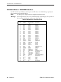
1
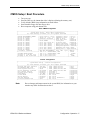
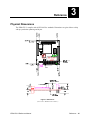
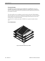
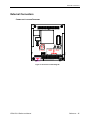
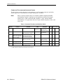
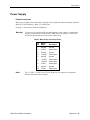
Reference
Manual
DOC. REV. 12/14/2007
EPM-CPU-3
AMD ÉlanSC520 processor
module with 10/100 Ethernet,
and PC/104-Plus interface.
EPM-CPU-3
AMD ÉlanSC520 processor
module with 10/100 Ethernet,
and PC/104-Plus interface
MEPMCPU3r4
Product Release Notes
This page includes recent changes or improvements that have been made to this
product. These changes may affect its operation or physical installation in your
application. Please read the following information.
Rev 4 Release
•
Component changes.
•
Discontinuance of part numbers EPM-CPU-3c, f, and m. Introduction of part numbers EPM-CPU-3p, r,
and s.
Rev 3 Release
•
Initial public release.
Rev 2 Release
•
Beta public release.
Support Page
The EPM-CPU-3 Support Page, at http://www.VersaLogic.com/private/bobcatsupport.asp contains
additional information and resources for this product including:
•
•
•
•
•
Reference Manual (PDF format)
Operating system information and software drivers
Data sheets and manufacturers’ links for chips used in this product
BIOS information and upgrades
Utility routines and benchmark software
Note: This is a private page for EPM-CPU-3 users only. It cannot be reached through our web site. You
must enter this address directly to find the support page.
Model EPM-CPU-3
AMD Élan processor module with 10/100 Ethernet,
and PC/104-Plus interface
REFERENCE MANUAL
VERSALOGIC CORPORATION
WWW.VERSALOGIC.COM
3888 Stewart Road
Eugene, OR 97402
(541) 485-8575
Fax (541) 485-5712
Contents Copyright ©2007
All Rights Reserved
Notice:
Although every effort has been made to ensure this document is error-free, VersaLogic makes no
representations or warranties with respect to this product and specifically disclaims any implied
warranties of merchantability or fitness for any particular purpose.
VersaLogic reserves the right to revise this product and associated documentation at any time
without obligation to notify anyone of such changes.
PC/104 and the PC/104 logo are trademarks of the PC/104 Consortium.
Table of Contents
Introduction ..................................................................................................................... 1
Description.......................................................................................................................... 1
Technical Specifications ..................................................................................................... 2
Technical Support ............................................................................................................... 3
Repair Service........................................................................................................ 3
Configuration / Operation............................................................................................... 5
Overview............................................................................................................................. 5
Electrostatic Discharge .......................................................................................... 5
Lithium Battery...................................................................................................... 5
Initial Configuration and Setup........................................................................................... 6
Recommended Components .................................................................................. 6
CMOS Setup / Boot Procedure ........................................................................................... 7
Console Redirection............................................................................................................ 8
CMOS Setup / IDE Configuration...................................................................................... 9
IDE......................................................................................................................... 9
IDE setup ............................................................................................................... 9
CMOS Setup / Advanced Configuration .......................................................................... 11
D0000h 64k page function................................................................................... 11
DiskOnChip 8kb page.......................................................................................... 11
PLD register base I/O .......................................................................................... 11
Force Ethernet 10-BaseT ..................................................................................... 12
PS/2 Mouse (IRQ12) ........................................................................................... 12
Floppy Drive (IRQ6) ........................................................................................... 12
CPU Speed........................................................................................................... 12
Cache Mode ......................................................................................................... 12
Write Buffer......................................................................................................... 12
GP Bus Timings................................................................................................... 12
COM1 (03F8) RS-232 ......................................................................................... 13
COM2 (02F8) RS-232 ......................................................................................... 13
COM3 (03E8) RS-422/485.................................................................................. 13
COM4 (02E8) RS-422/485.................................................................................. 13
GP Timer 0, GP Timer 1, Watchdog Timer......................................................... 13
PCI Interrupt A, B, C, and D ............................................................................... 13
Using Custom CMOS Defaults......................................................................................... 14
Creating a Bootable DOS DiskOnChip ............................................................................ 14
Reference....................................................................................................................... 15
Physical Dimensions......................................................................................................... 15
Hardware Assembly............................................................................................. 16
Stack Arrangement .............................................................................................. 16
External Connectors.......................................................................................................... 17
Connector Location Diagrams ............................................................................. 17
Connector Functions and Interface Cables .......................................................... 18
Jumper Block Locations ................................................................................................... 19
iii
Table of Contents
Jumper Summary ................................................................................................. 20
Power Supply.................................................................................................................... 21
Power Connectors ................................................................................................ 21
Power Requirements ............................................................................................ 22
Lithium Battery.................................................................................................... 22
CPU................................................................................................................................... 23
System RAM..................................................................................................................... 23
Memory................................................................................................................ 23
CMOS RAM ..................................................................................................................... 23
Clearing CMOS RAM ......................................................................................... 23
Default CMOS RAM Setup Values..................................................................... 23
Real Time Clock ............................................................................................................... 24
Setting the Clock.................................................................................................. 24
Battery Backed Static RAM.............................................................................................. 24
Disk on Chip ..................................................................................................................... 24
Base Memory Address......................................................................................... 24
Compatible Devices ............................................................................................. 24
Installing the DOC Chip ...................................................................................... 24
CMOS Setup ........................................................................................................ 25
Serial Ports........................................................................................................................ 26
COM Port Configuration ..................................................................................... 26
COM3 and COM4 RS-485 Mode Line Driver Control ....................................... 26
Serial Port Connectors ......................................................................................... 27
IDE Hard Drive / CD-ROM Interface............................................................................... 28
Utility Connector .............................................................................................................. 29
Keyboard/Mouse Interface .................................................................................. 29
Programmable LED ............................................................................................. 29
External Speaker .................................................................................................. 30
Push-Button Reset................................................................................................ 30
General-Purpose Timer Inputs............................................................................. 30
Floppy Drive Interface...................................................................................................... 30
Ethernet Interface.............................................................................................................. 31
BIOS Configuration............................................................................................. 31
Status LED........................................................................................................... 31
Ethernet Connector .............................................................................................. 31
Watchdog Timer ............................................................................................................... 32
Expansion Bus .................................................................................................................. 33
PC/104-Plus (PCI Bus)....................................................................................... 33
PC/104 (ISA Bus) ................................................................................................ 33
I/O Configuration................................................................................................. 33
Memory and I/O Map ....................................................................................................... 34
ElanSC520 Memory Mapped Configuration Region (MMCR) Registers........... 34
Memory Map ....................................................................................................... 34
I/O Map................................................................................................................ 35
Interrupt Configuration ..................................................................................................... 36
Special Control Register ................................................................................................... 37
Revision Indicator Register............................................................................................... 38
Map and Paging Control Register..................................................................................... 39
Appendix A — Other References................................................................................. 41
iv
Introduction
1
Description
The EPM-CPU-3 (Bobcat) is a 486-based processor board in a compact PC/104-Plus format. It is
specifically designed for OEM control projects requiring compact size, high reliability, and long
product lifespan / availability. Its features include:
•
AMD ÉlanSC520 microcontroller
•
Keyboard, mouse, AT motherboard
peripherals
•
4 COM ports
• 133 MHz
•
64 MB system RAM
•
10 / 100 dual-speed Ethernet
•
Battery Backed SRAM Option
•
Floppy Interface
•
Real time clock
•
Vcc sensing reset circuit
•
32-PIN DiskOnChip® socket
•
Flash BIOS with OEM enhancements
•
•
PC/104, PC/104-Plus expansion interface •
IDE controller
•
Two general purpose timer inputs
•
Single supply (+5V) operation
•
Watchdog timer
•
Fanless Operation
•
Reconfigurable BIOS defaults
•
Customizing available
•
Console redirected to COM port if no
VGA (jumper selectable)
•
Batteryless operation (possible)
•
Extended temperature option (100MHz)
• 2 RS-232
• 2 RS-422/485
Ethernet Remote boot capability
3rd party boot code not included
The EPM-CPU-3 is a complete computer system in one board. It may be used alone or with
expansion modules. It features a PC/104-Plus expansion interface for fast PCI-based interface to
a wide variety of PC/104 and PC/104-Plus stacking modules. This card is designed to be used
primarily as an Ethernet node processor card.
It is fully compatible with popular operating systems including Windows 95/98/NT/NTE/, CE,
QNX, Linux, RT-Linux, and other Real Time Operating Systems.
On-board I/O includes 10/100 Mbit Ethernet, IDE, four COM ports, floppy and two generalpurpose timer inputs.
64 MB of system RAM is provided on board. Bootable DiskOnChip Flash space is supported for
non-volatile program and data file storage without the use of mechanical disk drives.
This exceptional processor card was designed from the ground up for OEM applications with
longevity and reliability as the main focus. It is fully supported by the VersaLogic design team.
Both hardware and software (BIOS) customization are available in quantities as low as 25 pieces.
Each board is subjected to 100% functional testing and is backed by a limited two-year warranty.
EPM-CPU-3 Reference Manual
Introduction – 1
Technical Specifications
Technical Specifications
Specifications are typical at 25°C with 5.0V supply unless otherwise noted.
Board Size:
3.55" x 3.775" (PC/104 standard).
Storage Temperature:
–40° C to 85° C
Operating Temperature:
EPM-CPU-3p,r 0° C to +50° C (free air, no airflow)
EPM-CPU-3p,r 0° C to +60° C (100 FPM airflow)
EPM-CPU-3s-40° C to +75° C (free air, extended temperature version)
EPM-CPU-3s-40° C to +85° C (100 FPM airflow, extended temperature version)
Power Requirements: (with keyboard, mouse, and hard drive running DOS)
EPM-CPU-3p,r 133 MHz +5V ±5% @ 0.96 A (4.8 W) typ.
EPM-CPU-3s 100 MHz +5V ±5% @ 0.86 A (4.3 W) typ.
+3.3V or ±12V may be required by some expansion modules
System Reset:
Vcc sensing, resets below 4.70V typ.
Watchdog timeout
SDRAM: 64MB soldered on the board
Flash / BBSRAM Interface:
One 32-pin JEDEC DIP socket.
Accepts one DiskOnChip device or battery-backed static RAM chip (up to 512K).
Chip height limit of 0.330”.
IDE Interface:
Supports up to two IDE devices. PIO mode 0 only. 2.5 MB/sec max.
Floppy Interface:
Supports one floppy drive.
Ethernet Interface:
Autodetect 10BaseT/100BaseTX based on Intel 82551ER. 12K transmit/receive buffer.
COM1 and COM2 Interface:
RS-232, 16C550 compatible, 115K baud max.
COM3 and COM4 Interface:
RS-422/485, 16C550 compatible, 460K baud max.
Connectors:
BIOS:
Utility:
2mm 50-pin shrouded
IDE:
2mm 44-pin
Ethernet: 2mm 8-pin
Floppy: 2mm 15-pin
Power: 0.1” 10-pin
General Software embedded BIOS with OEM enhancements
Field upgradeable with Flash BIOS Upgrade Utility
Bus Speed:
SDRAM:
66 MHz
PCI, PC/104-Plus: 33 MHz
PC/104:
8 MHz
Compatibility:
PC/104 – Fully functional with most PC/104 devices. See the Expansion Bus section for details.
Embedded-PCI (PC/104-Plus) – Full compliance, 3.3V or 5V modules
Board Weight:
EPM-CPU-3p
EPM-CPU-3r
EPM-CPU-3s
86 grams
100 grams
110 grams
Specifications are subject to change without notice.
2 – Introduction
EPM-CPU-3 Reference Manual
Technical Support
Technical Support
If you have problems that this manual can’t help you solve, first visit the EPM-CPU-3 Product
Support web page at http://www.VersaLogic.com/private/bobcatsupport.asp. If you have
further questions, contact VersaLogic for technical support at (541) 485-8575. You can also reach
our technical support engineers via e-mail at [email protected].
EPM-CPU-3 Support Website
http://www.VersaLogic.com/private/bobcatsupport.asp
REPAIR SERVICE
If your product requires service, you must obtain a Returned Material Authorization (RMA)
number by calling (541) 485-8575.
Please provide the following information:
•
Your name, the name of your company, and your phone number
•
The name of a technician or engineer who we can contact if we have questions
•
Quantity of items being returned
•
The model and serial number (bar code) of each item.
•
A description of the problem
•
Steps you have taken to resolve or repeat the problem
•
The return shipping address
Warranty Repair
All parts and labor charges are covered, including return shipping
charges for UPS Ground delivery to United States addresses.
Non-warranty Repair All non-warranty repairs are subject to diagnosis and labor charges,
parts charges, and return shipping fees. We will need to know what
shipping method you prefer for return back to your facility, and we
will need to secure a purchase order number for invoicing the repair.
Note:
EPM-CPU-3 Reference Manual
Please mark the RMA number clearly on the outside of the box before
returning. Failure to do so can delay the processing of your return.
Introduction – 3
Configuration / Operation
2
Overview
ELECTROSTATIC DISCHARGE
Warning!
Electrostatic discharge (ESD) can damage boards, disk drives, and other
components. The circuit board must only be handled at an ESD workstation. If an
approved station is not available, some measure of protection can be provided by
wearing a grounded anti-static wrist strap. Keep all plastic away from the board,
and do not slide the board over any surface.
After removing the board from its protective wrapper, place the board on a
grounded, static-free surface, component side up. Use an anti-static foam pad if
available.
The board should also be protected during shipment or storage by keeping inside a
closed metallic anti-static envelope.
Note:
The exterior coating on some metallic anti-static bags is sufficiently conductive to
cause excessive battery drain if the bag comes in contact with the bottom side of
the EPM-CPU-3.
LITHIUM BATTERY
Warning!
To prevent shorting, premature failure, or damage to the lithium battery, do not
place the board on a conductive surface such as metal, black conductive foam, or
the outside surface of a metalized ESD protective pouch. The lithium battery may
explode if mistreated. Do not recharge, disassemble, or dispose of in fire. Dispose
of used batteries promptly.
EPM-CPU-3 Reference Manual
Configuration / Operation – 5
Initial Configuration and Setup
Initial Configuration and Setup
The following list describes the components recommended for setting up a typical development
system.
RECOMMENDED COMPONENTS
•
•
•
•
•
•
•
EPM-CPU-3 Board and cable kit
ATX Power Supply
EPM-SVGA-2 for video support
Keyboard with PS/2 connector, mouse
Ethernet Network
IDE Hard Drive
Floppy Drive
6 – Configuration / Operation
EPM-CPU-3 Reference Manual
CMOS Setup / Boot Procedure
CMOS Setup / Boot Procedure
•
•
•
•
•
Turn power on.
Press the DEL key the instant that video is displayed (during the memory test).
Verify default CMOS Setup information as shown below.
Insert bootable floppy disk into floppy drive.
Reset computer using push button reset.
Basic CMOS Configuration
+------------------------------------------------------------------------------+
|
System Bios Setup - Basic CMOS Configuration
|
|
(C) 2002 General Software, Inc. All rights reserved
|
+---------------------------+--------------------+-----------------------------+
| DRIVE ASSIGNMENT ORDER:
| Date:>OCT 11, 2004 | Typematic Delay : 250 ms
|
| Drive A: Floppy 0
| Time: 00 : 00 : 00 | Typematic Rate
: 30 cps
|
| Drive B: (None)
| NumLock: Disabled | Seek at Boot
: None
|
| Drive C: (None)
+--------------------+ Show "Hit Del"
: Enabled |
| Drive D: (None)
| BOOT ORDER:
| Config Box
: Enabled |
| Drive E: (None)
| Boot 1st: Drive A: | F1 Error Wait
: Enabled |
| Drive F: (None)
| Boot 2nd: (None)
| Parity Checking : (Unused) |
| Drive G: (None)
| Boot 3rd: (None)
| Memory Test Tick : Enabled |
| Drive H: (None)
| Boot 4th: (None)
| Debug Breakpoints: (Unused) |
| Drive I: (None)
| Boot 5th: (None)
| Debugger Hex Case: Upper
|
| Drive J: (None)
| Boot 6th: (None)
| Memory Test : StdLo FastHi |
| Drive K: (None)
+--------------------+-----------------+-----------+
| (Loader): (Unused)
| ATA DRV ASSIGNMENT: Sect Hds Cyls | Memory
|
+---------------------------+ Ide 0: 3 = AUTOCONFIG, LBA
| Base:
|
| FLOPPY DRIVE TYPES:
| Ide 1: 3 = AUTOCONFIG, LBA
|
633KB
|
| Floppy 0: 1.44 MB, 3.5"
| Ide 2: Not installed
| Ext:
|
| Floppy 1: Not installed
| Ide 3: Not installed
|
63MB
|
+---------------------------+--------------------------------------+-----------+
Custom Configuration
+------------------------------------------------------------------------------+
|
System BIOS Setup - Custom Configuration
|
|
(C) 2002 General Software, Inc. All rights reserved
|
+---------------------------------------+--------------------------------------+
| D0000h 64k page function : ISA bus
| COM1 (3F8h) RS-232
: IRQ4
|
| DiskOnChip 8kb page
: Disabled | COM2 (2F8h) RS-232
: IRQ3
|
| PLD register base I/O
: 0E0h
| COM3 (3E8h) RS-422/485
: Disabled |
| Force Ethernet 10-BaseT
: Disabled | COM4 (2E8h) RS-422/485
: Disabled |
| PS/2 Mouse (IRQ12)
: Enabled
| GP Timer 0
: Disabled |
| Floppy Drive (IRQ6)
: Enabled
| GP Timer 1
: Disabled |
| CPU Speed
: 133 MHz
| Watchdog Timer
: Disabled |
| Cache Mode
: Wr-back
| PCI Int A
: IRQ11
|
| Write Buffer
: Enabled
| PCI Int B
: IRQ11
|
| GP Bus Timings
: Normal
| PCI Int C (Ethernet)
: IRQ11
|
| Console Redirection
: Auto
| PCI Int D
: IRQ11
|
+---------------------------------------+--------------------------------------+
Note:
Due to changes and improvements in the system BIOS, the information on your
monitor may differ from that shown above.
EPM-CPU-3 Reference Manual
Configuration / Operation – 7
Console Redirection
Console Redirection
If there is no video device detected during boot up, BIOS keyboard and screen I/O can be
redirected to the COM2 RS-232 serial port. CMOS configuration can be modified over this
redirected console. ANSI or VT102 terminal emulation is recommended.
When console redirection is enabled, press CTRL-C on the terminal emulator to enter CMOS
Setup; the BIOS ignores DEL DEL DEL from a PS/2 keyboard. This is normal operation of the
Bobcat.
COM2 is configured for standard serial port communication:
•
9600 Baud
•
Parity: None
•
Flow Control: None
•
Data Bits: 8
•
Stop Bits: 1
Console redirection remains active when POST completes and the operating system boots. Textbased operating systems such as DOS and Linux can be controlled over this connection.
To enable console redirection, there must be no video device detected, the console redirection
option in Custom Configuration must be set to Auto, and there must be a terminal (such as
Windows HyperTerm) detected at COM2.
8 – Configuration / Operation
EPM-CPU-3 Reference Manual
CMOS Setup / IDE Configuration
CMOS Setup / IDE Configuration
IDE
The Bobcat has a single IDE channel to connect up to two hard disks or CD-ROM drives.
Connector J1 is the primary IDE channel. This basic IDE interface operates using PIO mode
0, resides on the ISA bus, and does not support the drive address register at I/O address 3F7h.
It has been tested successfully on a wide variety of operating systems.
IDE SETUP
IDE devices include hard disk drives, CD-ROM drives, DiskOnChip modules, and some
CompactFlash modules.
There are 3 fields in the Basic CMOS Configuration screen that are relevant to IDE setup:
IDE Drive Geometry, Drive Assignment Order, and Boot Order.
IDE Drive Geometry
Most desktop PCs have two IDE channels, each capable of supporting two IDE devices
in a slave/master configuration or a single IDE device in a single (or master only)
configuration.
In the IDE Drive Geometry list:
IDE 0 corresponds to primary channel, master/single drive.
IDE 1 corresponds to primary channel, slave drive.
IDE 2 corresponds to secondary channel, master/single drive.
IDE 3 corresponds to secondary channel, slave drive.
The Bobcat uses the first IDE channel only. IDE 2 and IDE 3 are disabled.
All modern IDE devices use LBA mode. When setting up an IDE device, leave the drive
geometry set to LBA mode unless your hard drive requires a different mode.
CD-ROM drives that will be used as boot devices should be set accordingly in the Drive
Geometry list. DiskOnChip modules do not reside on an IDE channel, and should not be
declared here.
Drive Assignment Order
After a hard drive has been declared in the IDE Drive Geometry field, it must be
assigned a DOS drive letter, even if you are not using the DOS operating system.
Normally, "Drive C:" will be assigned to the IDE device that you wish to boot from.
Do not attempt to assign a drive letter to a CD-ROM drive or DiskOnChip. The drivers
required to use these devices will automatically assign a drive letter to the device when
loaded.
EPM-CPU-3 Reference Manual
Configuration / Operation – 9
CMOS Setup / IDE Configuration
Boot Order
This field allows you to specify the order in which the BIOS looks for boot devices.
Usually, the drive you specify here corresponds to the declaration in the Drive
Assignment Order field. The DiskOnChip is an exception to this, however.
By default, the DiskOnChip will automatically insert itself at the end of the Drive
Assignment Order. For example, if you have a hard drive set up as Drive C:, the
DiskOnChip will show up as Drive D: at boot time, even though Drive D: is declared as
"(None)" in the Drive Assignment Order field. Therefore, in this scenario, if you wish to
boot to the DiskOnChip first, you would set "Boot 1st:" to "Drive D:".
A CD-ROM drive can be inserted into the boot order by selecting “CDROM” at the
desired boot order position.
10 – Configuration / Operation
EPM-CPU-3 Reference Manual
CMOS Setup / Advanced Configuration
CMOS Setup / Advanced Configuration
D0000H 64K PAGE FUNCTION
Default: ISA bus.
ISA bus
Memory accesses to the D0000h page will be sent to the ISA bus for use by PC/104 expansion
modules. This setting is required when flashing the BIOS with the FBU utility.
BIOS Ext
The D0000h page is mapped to sector 1 in the flash chip, which may contain 3rd party Ethernet
boot code or any other BIOS extension (not included). If there is a such an extension present, it
will be called by the BIOS. The BIOS extension can be programmed into the flash chip with the
FBU utility. For remote booting via Ethernet, the recommended boot ROM is Managed PC Boot
Agent from Argon Technology Corporation.
Battery-Backed Static RAM
The D0000h page is mapped to the 32-pin socket (U13), which is expected to have a batterybacked static (BBS) RAM chip of up to 512K installed (as opposed to a DiskOnChip). If the BBS
RAM chip contains a BIOS extension, it will be called by the BIOS.
RAM
System RAM is exposed in the D0000h page.
DISKONCHIP 8KB PAGE
Default: Disabled
To enable use of a M-Systems DiskOnChip, this option must be set to the desired base memory
address. Available locations are CE000h, D0000h, and D8000h. CE000h is the recommended
location, as this location is least likely to conflict with other devices. When set to disabled, the
DiskOnChip will not be recognized even if it is plugged in.
PLD REGISTER BASE I/O
Default: 0E0h
Specifies the location of the PLD register in I/O space. It can be moved to 1E0h in case of an
address conflict.
EPM-CPU-3 Reference Manual
Configuration / Operation – 11
CMOS Setup / Advanced Configuration
FORCE ETHERNET 10-BASET
Default: Disabled
When enabled, this will disable the Ethernet media data rate auto-negotiation and force it to 10BaseT mode.
Note: Some drivers will put the Ethernet back into auto-negotiation mode.
PS/2 MOUSE (IRQ12)
Default: Enabled
When disabled, IRQ12 is freed for other devices.
FLOPPY DRIVE (IRQ6)
Default: Enabled
When disabled, FDC I/O space will be freed, and IRQ6 can be reassigned to an internal
ElanSC520 device.
CPU SPEED
Default: 133 MHz
The maximum clock rate for the ÉlanSC520 Microcontroller is 133 MHz. It can optionally be set
to 100 MHz for a slight power savings. If an extended temperature board version is detected, the
default will change to 100 MHz.
CACHE MODE
Default: Write-Back
The 16 kb L1 cache can be configured for either write-through or write-back mode. This option
controls the CACHE_WR_MODE in the CPUCTL register (MMCR offset 02h).
WRITE BUFFER
Default: Enabled
When the write buffer is enabled, it buffers all write activity from the CPU, PCI bus, or GP bus.
This option controls the WB_ENB bit in the DBCTL register (MMCR offset 40h).
GP BUS TIMINGS
Default: Normal
The GP (ISA) bus timings may need to be slowed to accommodate ISA Plug-n-Play cards. This
option modifies registers in the GP Bus Controller, MMCR offsets C08h through C10h.
12 – Configuration / Operation
EPM-CPU-3 Reference Manual
CMOS Setup / Advanced Configuration
COM1 (03F8) RS-232
Default: IRQ4
Allows you to disable or specify the IRQ used by internal UART1 on the ÉlanSC520
Microcontroller. When disabled, the IRQ and I/O space are freed.
COM2 (02F8) RS-232
Default: IRQ3
Allows you to disable or specify the IRQ used by internal UART2 on the ÉlanSC520
Microcontroller. When disabled, the IRQ and I/O space are freed.
COM3 (03E8) RS-422/485
Default: Disabled
Allows you to disable or specify the IRQ used by UART1 on the SMSC FDC37B727 Super I/O.
When disabled, the IRQ and I/O space are freed.
COM4 (02E8) RS-422/485
Default: Disabled
Allows you to disable or specify the IRQ used by UART2 on the SMSC FDC37B727 Super I/O.
When disabled, the IRQ and I/O space are freed.
GP TIMER 0, GP TIMER 1, WATCHDOG TIMER
Default: Disabled
These internal SC520 devices can be disabled or enabled by assigning an IRQ. Enabling these
devices only sets up the IRQ assignment; it is up to the user to set up device operation. Refer to
the ÉlanSC520 Microcontroller User's Manual for details.
PCI INTERRUPT A, B, C, AND D
Default: IRQ11
These options allow manual IRQ routing of PCI devices.
PCI devices can share an interrupt. In most cases, the cost of doing this is slightly decreased
system performance and slightly increased interrupt response time.
Note:
EPM-CPU-3 Reference Manual
Configuration / Operation – 13
Using Custom CMOS Defaults
Using Custom CMOS Defaults
The Bobcat BIOS version 5.1.106 and later has the capability to store CMOS defaults in the onboard flash chip. This storage area is non-volatile, enabling the Bobcat to run with user-specified
CMOS defaults without a battery installed.
If custom defaults are specified, they will be used instead of the factory defaults any time CMOS
memory needs to be reset. CMOS is reset when any of the following occur:
•
CMOS memory is found to be corrupt or uninitialized at boot time
•
CMOS contents are erased by FBU during a BIOS upgrade
•
The Bobcat was powered on without a battery, or without a sufficiently charged battery
There are 4 options on the main BIOS setup screen that control CMOS defaults.
•
Save CMOS as custom defaults
Saves the current CMOS settings to the custom defaults. These settings will be used any
time CMOS is reset. If there are already custom defaults specified, they will be
overwritten.
•
Reset CMOS to custom defaults
Discards the current CMOS settings and uses the saved custom defaults. This operation
will fail if no custom defaults have been previously saved.
•
Clear custom defaults (use factory defaults)
Deletes custom CMOS settings stored in flash. Factory default settings will be used any
time CMOS is reset.
•
Reset CMOS to factory defaults
Discards the current CMOS settings and uses factory defaults, even if custom
defaults have been specified. If CMOS is later reset, custom defaults will be used if
available.
Warning!
Take care in saving custom CMOS defaults, as you must be able to get back to the
main BIOS setup screen to undo any mistakes. For example, it would be a mistake
to disable a COM port that is required for console redirection when there is no
video device available.
Creating a Bootable DOS DiskOnChip
The DiskOnChip is shipped pre-formatted, non-bootable, without any files on it. The
DiskOnChip will appear as Drive D in systems with an installed hard drive. If a hard drive is not
installed, the DOC will appear as Drive C:
1. Boot your system under DOS or Windows 95/98/ME, you can’t use NT or 2000 (if using
Windows, start a DOS session)
2. Type SYS C: (or SYS D: if appropriate)
14 – Configuration / Operation
EPM-CPU-3 Reference Manual
Reference
3
Physical Dimensions
The EPM-CPU-3 complies with all PC/104-Plus standards. Dimensions are given below to help
with pre-production planning and layout.
Figure 1. Dimensions
(Not to scale. All dimensions in inches.)
EPM-CPU-3 Reference Manual
Reference – 15
Physical Dimensions
HARDWARE ASSEMBLY
The EPM-CPU-3p must be the bottom card. The EPM-CPU-3r and EPM-CPU-3s use passthrough PC/104 connectors so that expansion modules can be added to the top or bottom of the
stack. PC/104 (ISA) modules must NOT be positioned between the Bobcat and any PC/104-Plus
(PCI) modules on the stack.
The entire assembly can sit on a tabletop or it can be secured to a base plate. When bolting the
unit down, make sure to secure all four standoffs to the mounting surface to prevent circuit board
flexing. Standoffs are secured to the top circuit board using four pan head screws. Refer to the
drawing on page 15 for dimensional details.
An extractor tool is available (part number VL-HDW-201) to separate the modules from the
stack.
STACK ARRANGEMENT
Figure 2. PC/104 Card Added to Top of Stack
16 – Reference
EPM-CPU-3 Reference Manual
External Connectors
External Connectors
CONNECTOR LOCATION DIAGRAMS
Figure 3. Connector Location Diagram
EPM-CPU-3 Reference Manual
Reference – 17
External Connectors
CONNECTOR FUNCTIONS AND INTERFACE CABLES
The table below notes the function of each connector, as well as mating connectors and cables,
and the page where a detailed pinout or further information is available.
Note:
Many VersaLogic adapter cables are available in RoHS compliant and RoHS
noncompliant versions. Compliance or noncompliance is indicated by the part
number prefix. “CBR” indicates RoHS compliance. “CBL” indicates RoHS
noncompliance. For applications that do not require RoHS compliance, either cable
can be used.
Table 1: Connector Functions and Interface Cables
Connector
J1
IDE Interface
J2
Mating
Connector
Function
Ethernet
FCI 89947-144 (IDC)
Molex 51110-0860 (housing)
Transition
Cable
CBL/CBR-4404
CBL/CBR-4405
Cable
Description
‡Pin 1 Location
Page
X Coord. Y Coord.
28
-.050
1.405
Standard Cable
Development Cable
CBL-0802
8-pin crimp housing
to CAT5 RJ-45
31
.465
1.465
CBL-5008
IDC breakout cable
29
3.195
2.480
Molex 50394-8051 (crimps)
COM Ports, Keyboard,
Mouse, GP Timer inputs,
Power LED, Push-button
reset, PC speaker,
FCI 89361-350 (IDC) or
J4
Main Power Input
Berg 69176-010 (Housing) +
Berg 47715-000 (Pins)
CBL/CBR-1008
Interface from
industry standard
ATX power supply
21
.0250
-0.050
J5
PLD Reprogramming
Port (Factory use Only)
__
__
__
__
.880
.510
J6
Floppy Drive Interface
FCI 69305-015 (Housing)
FCI 77138-101 (pins)
CBL-1501
15-pin to floppy 34pin
30
1.120
-0.110
J3
‡
FCI 69307-050 (housing)
FCI 77138-001 (crimp pins)
Note: Relative to lower left hand mounting hole. See page 15.
18 – Reference
EPM-CPU-3 Reference Manual
Jumper Block Locations
Jumper Block Locations
Note:
Jumpers shown in as-shipped configuration.
Figure 4. Jumper Block Locations
EPM-CPU-3 Reference Manual
Reference – 19
Jumper Block Locations
JUMPER SUMMARY
Table 2: Jumper Summary
Jumper
Block
V1
Battery Power Jumper
Standard
Operation
V2
RS-485
Intermediate
RS-485
Intermediate
Page
Standard
Operation
23
RS-485
Endpoint
26
RS-485
Endpoint
26
In
—
In
—
RS-422
COM4 configuration
RS-485
Endpoint
V4[1-2]
Discharge
CMOS Memory
COM3 configuration
RS-485
Endpoint
V3
As
Shipped
Description
RS-422
System BIOS Selector
In
— Primary System BIOS occupies E0000h to FFFFFh
Out — Secondary System BIOS occupies E0000h to FFFFFh
Note: The secondary System BIOS is field upgradeable using the BIOS upgrade
utility.
See www.VersaLogic.com/private/bobcatsupport.asp for further information.
V4[3-4]
20 – Reference
General Purpose Input Bit
In
— Bit D0 in SCR register reads as 1
Out — Bit D0 in SCR register reads as 0
EPM-CPU-3 Reference Manual
Power Supply
Power Supply
POWER CONNECTORS
Main power is applied to the EPM-CPU-3 through a 10-pin polarized connector. Mating connector
Berg 69176-010 (Housing) + Berg 47715-000 (Pins).
See page 17 for connector location information.
Warning!
To prevent severe and possibly irreparable damage to the system, it is critical that
the power connectors be wired correctly. Make sure to use all three +5VDC pins
and all four ground pins to prevent excess voltage drop.
Table 3: Main Power Connector Pinout
Note:
J4
Pin
Signal
Name
Description
1
Ground
Ground
2
+5VDC
Power Input
3
Ground
Ground
4
+12VDC
Power Input
5
Ground
Ground
6
–12VDC
Power Input
7
+3.3VDC
Power Input
8
+5VDC
Power Input
9
Ground
Ground
10
+5VDC
Power Input
The +3.3VDC, +12VDC, and –12VDC inputs are only required for expansion
modules that require these voltages.
EPM-CPU-3 Reference Manual
Reference – 21
Power Supply
POWER REQUIREMENTS
The EPM-CPU-3 only requires +5 volts (±5%) for proper operation. The voltage required for the
RS-232 ports is generated with an on-board DC/DC converter. A variable low-voltage supply
circuit provides power to the CPU and other on-board devices.
The exact power requirement of the EPM-CPU-3 depends on several factors peripheral
connections, type and number of expansion modules, and attached devices. For example, AT
keyboards typically draw their power directly from the EPM-CPU-3, and driving long RS-232
lines at high speed can increase power demand. Reducing the CPU speed from 133 MHz to 100
MHz via the BIOS settings will save approximately 0.5 W.
LITHIUM BATTERY
Warning!
To prevent shorting, premature failure, or damage to the lithium battery, do not
place the unit on a conductive surface such as metal, black conductive foam, or the
outside surface of a metalized ESD protective pouch. The lithium battery may
explode if mistreated. Do not recharge, disassemble, or dispose of in fire. Dispose
of used batteries promptly.
Normal battery voltage should be at least 3.0V. If the voltage drops below 3.0V, contact the
factory for a replacement (part number T-HB3/5-3). Life expectancy under normal use is
approximately 10 years.
22 – Reference
EPM-CPU-3 Reference Manual
CPU
CPU
The ÉlanSC520 Microcontroller has a 32-bit, low-voltage AMD Am5x86 microprocessor at its
core. The maximum clock rate is 133 MHz. The Am5x86 has 16 kb of unified cache that supports
write-back and write-through policies. It is a high-performance 486 CPU achieving performance
results equal to a Pentium 75.
System RAM
MEMORY
The EPM-CPU-3 has 64MB of SDRAM soldered on board.
•
•
•
•
•
Storage Capacity
Voltage
Error Detection Code
Error Correction
Type
64 MB
3.3 Volt
Not supported
Not supported
66 MHz, 60 ns or SDRAM
CMOS RAM
CLEARING CMOS RAM
Jumper V1 can be moved to position [1-2] for 30 seconds to erase the contents of the CMOS
RAM. Be sure to move the jumper back to position [2-3] for normal operation.
Note:
Operation of the board with jumper V1 in the erase position [1-2] is not supported
or recommended.
DEFAULT CMOS RAM SETUP VALUES
After the CMOS RAM is cleared, the system will load default CMOS RAM parameters the next
time the board is powered on. The default CMOS RAM setup values will be used in order to boot
the system whenever the main CMOS RAM values are blank, or when the system battery is dead
or has been removed from the board.
EPM-CPU-3 Reference Manual
Reference – 23
Real Time Clock
Real Time Clock
The EPM-CPU-3 features a year 2000 compliant, battery-backed 146818 compatible real time
clock/calendar chip. Under normal battery conditions, the clock will maintain accurate
timekeeping functions during periods when the board is powered off.
SETTING THE CLOCK
The CMOS Setup utility (accessed by pressing the [DEL] key during a system boot) can be used
to set the time/date of the real time clock.
Battery Backed Static RAM
A 32-pin socket (U13) will accept a battery-backed static RAM chip for non-volatile storage. We
recommend using the Dallas 128Kx8 DS1645 series or the 512Kx8 DS1650/DS1250 series
memory devices. They need to be a 32-pin, 0.6" DIP, 200nS or faster part.
Disk on Chip
A 32-pin socket (U13) will accept an M-Systems DiskOnChip (DOC) Flash Disk for non-volatile,
read/write data storage. The DOC can be configured as a boot device.
BASE MEMORY ADDRESS
When enabled, the DOC appears in the upper memory region as an 8K page frame starting at
CE000h, D0000h, or D8000h, depending on the user-selected setting in the Custom
Configuration BIOS setup screen.
When disabled, this memory range is freed up for other devices to use.
COMPATIBLE DEVICES
®
Any 5 Volt, M-Systems DiskOnChip 2000 and DOC Millennium device will work.
Note:
To add expansion modules on top of the Bobcat, low profile DOC chips must be
used.
INSTALLING THE DOC CHIP
1. Align pin 1 on the DOC with pin 1 of socket U13.
2. Push the DOC into the socket carefully until it is fully seated.
Warning!
24 – Reference
The DOC will be permanently damaged if installed incorrectly! When installing
or removing the DOC, be sure to align pin-1 on the chip with pin-1 on the socket.
To prevent electrostatic damage, first touch a grounded surface to discharge any
static electricity from your body.
EPM-CPU-3 Reference Manual
Disk on Chip
CMOS SETUP
To enable the DOC as drive C on a system without a hard disk, set the CMOS setup of “IDE
DRIVE GEOMETRY” to “Not installed”, and “DRIVE ASSIGNMENT ORDER” to “None”,
then save the CMOS changes.
Note:
The DOC needs to be formatted with the DOS System files or other operating
system in order for it to be a bootable drive. Refer to the M-Systems web site
(www.m-sys.com) for documentation on the DOC 2000 and details on making it a
bootable device.
EPM-CPU-3 Reference Manual
Reference – 25
Serial Ports
Serial Ports
The EPM-CPU-3 features two on-board 16550 based serial channels located at standard PC I/O
addresses. COM1 and COM2 are RS-232 (115.2K baud) serial ports.
COM3 and COM4 can be operated in RS-422 or RS-485 modes. Two additional non-standard
baud rates are also available (programmable in the normal baud rate registers), up to 460K baud.
Interrupt assignment for each COM port is handled in CMOS Setup, and each port can be
independently enabled or disabled.
COM PORT CONFIGURATION
There are no configuration jumpers for COM1 and COM2 because it only operates in RS-232
mode.
Jumpers V2 and V3 are used to configure COM3 and COM4 for RS-422/485 operation. See page
20 for jumper configuration details.
COM3 AND COM4 RS-485 MODE LINE DRIVER CONTROL
The TxD+/TxD– differential line driver can be turned on and off by manipulating the DTR
handshaking line.
The following code example shows how to turn the line driver for COM3 on and off:
mov
in
and
out
dx,03ECh
al,dx
al,0FEh
dx,al
;
;
;
;
in
or
out
al,dx
al,01h
dx,al
; Fetch existing value
; Set bit D0
; Turn DTR off (disables line driver)
26 – Reference
Point to COM3 Modem Control register
Fetch existing value
Clear bit D0
Turn DTR on (enables line driver)
EPM-CPU-3 Reference Manual
Serial Ports
SERIAL PORT CONNECTORS
See the Connector Location Diagram on page 17 for connector location information. The pinout
of the DB9 connector applies to use of the VersaLogic transition cable CBL-5008.
Table 4: Connectors JA - JD — Serial Port Pinout
COM1 COM2
J3
J3
Pin
Pin
RS-232
COM3
J3
Pin
COM4
J3
Pin RS-422 RS-485
1
10
DCD
—
—
—
2
11
DSR
19
26
Ground Ground
6
3
12
RXD*
20
27
TxD+
—
2
4
13
RTS
21
28
TxD–
—
7
5
14
TXD*
—
—
—
—
3
6
15
CTS
22
29
Ground Ground
8
7
16
DTR
23
30
RxD–
TxD/RxD–
4
8
17
RI
24
31
RxD+
TxD/RxD+
9
18
Ground
25
32
Ground Ground
EPM-CPU-3 Reference Manual
—
JA-JD
DB9
Pin
1
9
5
Reference – 27
IDE Hard Drive / CD-ROM Interface
IDE Hard Drive / CD-ROM Interface
One IDE interface is available to connect up to two IDE drives. Use CMOS Setup to specify the
drive parameters of the attached drives.
Note:
The IDE port is a simple interface compatible with PIO mode 0.
Warning!
Cable length must be 18" or less to maintain proper signal integrity. The grounds in
this connector should not be used to carry motor current.
Table 5: IDE Hard Drive Connector Pinout
28 – Reference
J1
Pin
Signal
Name
IDE
Signal Name
Function
1
2
3
4
5
6
7
8
9
10
11
12
13
14
15
16
17
18
19
20
21
22
23
24
25
26
27
28
29
30
31
32
33
34
35
36
37
38
39
40
41
42
43
44
HRST*
Ground
IDE7
HD8
HD6
HD9
HD5
HD10
HD4
HD11
HD3
HD12
HD2
HD13
HD1
HD14
HD0
HD15
Ground
NC
IDEDRQ
Ground
HWR*
Ground
HRD*
Ground
RDY
HAEN
IDEACK
Ground
HINT
XI16*
HA1
NC
HA0
HA2
HCS0*
HCS1*
NC
Ground
5V
5V
Ground
NC
Host Reset
Ground
DATA 7
DATA 8
DATA 6
DATA 9
DATA 5
DATA 10
DATA 4
DATA 11
DATA 3
DATA 12
DATA 2
DATA 13
DATA 1
DATA 14
DATA 0
DATA 15
Ground
NC
IDEDRQ
Ground
HOST IOW*
Ground
HOST IOR*
Ground
Ready
ALE
IDEACK
Ground
HOST IRQ10
HOST IOCS16*
HOST ADDR1
NC
HOST ADDR0
HOST ADDR2
HOST CS0*
HOST CS1*
NC
Ground
Power
Power
Ground
NC
Reset signal from CPU
Ground
Data bit 7
Data bit 8
Data bit 6
Data bit 9
Data bit 5
Data bit 10
Data bit 4
Data bit 11
Data bit 3
Data bit 12
Data bit 2
Data bit 13
Data bit 1
Data bit 14
Data bit 0
Data bit 15
Ground
No connection
DMA/Request
Ground
I/O write
Ground
I/O read
Ground
Wait control
Address latch enable
DMA/Ack.
Ground
IRQ10
Drive register enabled
Address bit 1
No connection
Address bit 0
Address bit 2
Reg. Access chip select 0
Reg. Access chip select 1
No connection
Ground
Power
Power
Ground
No connection
EPM-CPU-3 Reference Manual
Utility Connector
Utility Connector
The 50-pin utility connector (J3) incorporates the COM ports, keyboard and mouse, generalpurpose inputs, and the reset button and speaker. Table 6 illustrates the function of each pin.
Table 6: Utility Connector Pinout
J3
Pin
External
Connector
1
2
3
4
5
6
7
8
COM1
JA
J3
Pin
Pin
Signal
1
6
2
7
3
8
4
9
Data Carrier Detect
Data Set Ready
Receive Data
Request to Send
Transmit Data
Clear to Send
Data Terminal Ready
Ring Indicator
26
27
28
29
30
31
32
5
1
6
2
Ground
Data Carrier Detect
Data Set Ready
Receive Data
33
34
35
36
13
14
7
3
Request to Send
Transmit Data
15
16
17
18
8
4
9
5
9
10
11
12
COM2
JB
COM3
19
JC
External
Connector
Pin
Signal
6
2
7
8
4
9
5
RS-422
Ground
TxD+
TxD–
Ground
RxD–
RxD+
Ground
Mouse
JE
4
1
3
5
+5V (Protected)
Mouse Data
Ground
Mouse Clock
37
38
PBRESET
1
2
Pushbutton Reset
Ground
Clear to Send
Data Terminal Ready
Ring Indicator
Ground
39
40
41
42
GP Timer
Inputs
JF
1
2
3
4
Ground
GP Timer Input 1
Ground
GP Timer Input 0
RS-422
RS-485
43
Keyboard
4
+5V (Protected)
JG
6
Ground
Ground
44
20
2
TxD+
(note 1)
45
21
7
TxD–
(note 1)
46
22
8
Ground
Ground
47
23
4
RxD–
TxD/RxD–
48
24
9
RxD+
TxD/RxD+
49
25
5
Ground
Ground
50
COM4
JD
LED
Speaker
RS-485
Ground
(note 1)
(note 1)
Ground
TxD/RxD–
TxD/RxD+
Ground
1
Keyboard Data
3
Ground
5
Keyboard Clock
1
+5V (Protected)
2
Programmable LED
1
+5V (Protected)
2
Speaker Drive
Note1: Do not connect to these pins in RS-485 mode.
KEYBOARD/MOUSE INTERFACE
A standard PS/2 keyboard and mouse interface is accessible through connector J3.
PROGRAMMABLE LED
The high-density I/O connector J3 includes an output signal for attaching a software controlled
LED. Connect the cathode of the LED to J3[48]; anode to J3[47]. An on-board resistor limits the
current to 15 mA when the circuit is turned on.
The programmable LED is controlled by the PIO24 pin on the ElanSC520 microcontroller. It can
be turned on and off by writing the word 0100h to MMCR offsets OC3Ah and OC36h,
respectively.
The MMCR base address defaults to DF00:0 (segment : offset address).
Note:
The LED is turned on by the BIOS during system startup. This causes the light to
function as a "power on" indicator if it is not otherwise controlled by user code.
EPM-CPU-3 Reference Manual
Reference – 29
Floppy Drive Interface
EXTERNAL SPEAKER
A miniature 8 ohm speaker can be connected between J3[49] and J3[50].
PUSH-BUTTON RESET
A normally open, momentary action push-button reset switch can be connected between J3[37]
and J3[38]. Shorting J3[37] to ground will cause the EPM-CPU-3 to reboot.
GENERAL-PURPOSE TIMER INPUTS
Two flexible general-purpose timer inputs can be used for timing and counting applications. Each
timer is capable of generating an interrupt, selectable via the BIOS Custom Configuration screen.
For more information, see chapter 17 in the ÉlanSC520 Microcontroller User’s Manual.
Floppy Drive Interface
The EPM-CPU-3 supports one standard floppy disk via a 15-pin connector, J6. A special
interface cable (CBL-1501) is needed to convert the 15-pin connector on the EPM-CPU-3 to a
standard 34-pin floppy disk drive connector. CMOS Setup can be used to enable or disable the
floppy disk interface.
Table 7: Floppy Disk Connector
J6
pin
(15-pin)
1
2
3
4
5
6
7
8
9
10
11
12
13
14
15
Warning!
30 – Reference
Signal
Name
RPM
Ground
INDEX*
DR0*
Ground
MTR0*
FDIR
STEP*
WDATA*
WGATE*
TRK0*
WRTPRT*
RDATA*
HDSEL
DSKCHG
Standard
34-pin Floppy
pinout
2
15
18
12
13
16
18
20
22
24
26
28
30
32
34
Use extreme care when attaching cable, misalignment will cause damage. The red
line indicates pin 1 on the cable.
EPM-CPU-3 Reference Manual
Ethernet Interface
Ethernet Interface
The EPM-CPU-3 features an industry-standard 10baseT/100baseTX Ethernet interface based on
the Intel 82551ER Ethernet controller. This PCI based interface chip is widely supported. Drivers
are readily available to support a variety of operating systems such as QNX, VxWorks and other
RTOS vendors.
BIOS CONFIGURATION
The Ethernet interface shares PC/104-Plus interrupt “INTC”. The CMOS Setup screen is used to
select the IRQ line routed to INTC*.
STATUS LED
Two colored LEDs (D1) located next to the RJ-45 connector provide an indication of the Ethernet
status as follows:
Green LED (Link / Activity)
•
ON
Active Ethernet cable plugged into J2.
No Tx/Rx data activity.
•
OFF
Cable not plugged into J2
Cable not plugged into active hub
•
BLINKING
Active Ethernet cable plugged into J2.
Tx or Rx data activity detected on the cable
Yellow LED (Speed)
•
ON
100baseTx (Fast) detected on Ethernet cable.
•
OFF
10BaseTx (Slow) detected on Ethernet cable.
ETHERNET CONNECTOR
An 8-pin 2mm header is provided for the Ethernet connection. An adapter cable, CBL-0802,
converts this connector to a standard RJ-45 Ethernet jack. The Ethernet controller will auto-detect
10BaseT/100BaseTX connections.
Table 8: RJ45 Ethernet Connector
J2
Pin
1
2
3
4
5
6
7
8
EPM-CPU-3 Reference Manual
RJ-45
Pin
4
5
6
3
7
8
2
1
Signal
Name
IGND
IGND
R–
R+
IGND
IGND
T–
T+
Function
Isolated Ground
Isolated Ground
Receive Data –
Receive Data +
Isolated Ground
Isolated Ground
Transmit Data –
Transmit Data +
Reference – 31
Watchdog Timer
Watchdog Timer
There is a flexible watchdog timer integrated into the ÉlanSC520 Microcontroller. It supports a
time-out period up to 30 seconds, and can generate an interrupt, NMI, or system reset when timeout occurs. The watchdog registers are protected by write key sequences.
See the following pseudo code as a simple example of watchdog operation.
MMCR_base = DF00:0h
; segment:offset address
WDTMRCTL = MMCR_base + 0CB0h
MemWrite WDTMRCTL, 03333h ; Key sequence to allow write access to
; control
MemWrite WDTMRCTL, 0CCCCh ; register. These are 16-bit memory writes.
MemWrite WDTMRCTL, 0C010h ; Enable watchdog timer. 4 second timer.
; Reset on timeout.
Begin program loop
; perform useful instructions here that
; will never take more than 4
; seconds to complete.
MemWrite WDTMRCTL, 0AAAAh
; Key sequence to reset the timer
; countdown
MemWrite WDTMRCTL, 05555h
; These are 16-bit memory writes.
End program loop
For detailed programming instructions for the integrated watchdog timer, see chapter 19 of the
ÉlanSC520 Microcontroller User's Manual, and chapter 16 of the Register Set Manual.
32 – Reference
EPM-CPU-3 Reference Manual
Expansion Bus
Expansion Bus
The EPM-CPU-3 will accept up to seven expansion modules, up to three of which can be
PC/104-Plus (PCI) expansion modules. Both 3.3V and 5.0V modules are supported.
PC/104-PLUS (PCI BUS)
PC/104-Plus modules can be secured directly to the top of the EPM-CPU-3. Make sure to
correctly configure the "slot position" jumpers on each PC/104-Plus module appropriately.
The BIOS automatically allocates I/O and memory resources. However, manual PCI Interrupt
routing will be used.
PC/104 (ISA BUS)
PC/104 modules are stacked on top the EPM-CPU-3 (on top of any PC/104-Plus modules); 16-bit
modules first followed by 8-bit PC/104 modules. If necessary, a 40-pin and 64-pin ISA
feedthrough connector "extender", and long standoffs may need to be used to provide adequate
clearance between the PCI connector and the components on the top side of the PC/104 module.
The ÉlanSC520 Microcontroller uses a General-Purpose (GP) bus that is implemented as the ISA
bus on the Bobcat. The GP bus is similar in function to the ISA bus, but not functionally
identical. Nearly all PC/104 devices in use today will work on the Bobcat without modification.
Here is a summary of the differences between a legacy ISA bus and the GP bus implementation
on the Bobcat.
•
Only DMA channels 5 and 6 are available to PC/104 devices
•
IRQ15 is not available to PC/104 devices
•
PC/104 bus devices cannot initiate bus access cycles. The ÉlanSC520 Microcontroller is
always the master of the ISA bus.
•
Address pipelining is not supported.
•
IOCHK, REFRESH, and NOWS signals are not supported.
•
MEMR and SMEMR are tied together. MEMW and SMEMW are tied together.
For a more detailed description of the GP bus and its differences from a standard ISA bus, see
chapter 13 in the ÉlanSC520 Microcontroller User's Manual.
I/O CONFIGURATION
PC/104–Plus Modules
No hardware configuration is necessary except to jumper the expansion module for the correct
slot number.
PC/104 Modules
PC/104 I/O modules should be addressed in the 104h – 3FFh address range. Care must be taken
to avoid the I/O addresses shown in the On-Board I/O Devices table on page 35. These ports are
used by on-board peripherals and video devices.
EPM-CPU-3 Reference Manual
Reference – 33
Memory and I/O Map
Memory and I/O Map
ELANSC520 MEMORY MAPPED CONFIGURATION REGION (MMCR) REGISTERS
Much of the functionality incorporated into the ElanSC520 Microcontroller, such as the
watchdog timer, CPU speed control, and general-purpose timer, can be controlled and monitored
through the Memory Mapped Configuration Region (MMCR) registers. The MMCR registers
occupy 4kb of memory space. For convenience, these registers are made available at boot time in
the first megabyte of system RAM.
In CMOS setup, if the D0000h page function is set to ISA bus, BIOS Ext, or RAM, then the
MMCR base address will be DF000h. Thus, the MMCR will occupy DF000h through DFFFFh. If
the D0000h page function is set to BBSRAM, then the full D000h segment needs to be made
available, so the MMCR base address is moved down to CF000h.
Wherever the MMCR is located, its 4kb footprint will cover and take precedence over the
underlying memory space function. For example, when the D0000h page function is set to ISA
bus, DF000h through DFFFFh will instead by occupied by the MMCR. For this reason, the
maximum BIOS extension size is reduced from 64kb to 60kb.
In the event of an address conflict, the MMCR base address can be moved at any time with an I/O
write to the Configuration Base Address Register (CBAR), located at I/O address FFFCh. Refer
to the ElanSC520 Register Set Manual for further details.
MEMORY MAP
The lower 1 MB memory map of the EPM-CPU-3 is arranged as shown in the following table.
Table 9: Memory Map
Note:
34 – Reference
Start
Address
End
Address
Comment
E0000h
D0000h
CE000h
C0000h
A0000h
00000h
FFFFFh
DFFFFh
CFFFFh
CDFFFh
BFFFFh
9FFFFh
System BIOS
ISA memory, BIOS extension, BBSRAM, or SDRAM
DOC (movable to D0000h or D8000h)
Reserved for Video BIOS
Reserved for Video RAM
System DRAM
The D0000h page function is controlled in CMOS setup.
EPM-CPU-3 Reference Manual
Memory and I/O Map
I/O MAP
The following table lists the common I/O devices in the EPM-CPU-3 I/O map. User I/O devices
should be added in the 104h – 3FFh range, using care to avoid the devices already in the map as
shown below.
Table 10: On-Board I/O Devices
Note:
I/O Device
Standard
I/O Addresses
See ÉlanSC520 register set manual
Special Control Register
Revision Indicator Register
Map and Paging Control Register
Primary IDE Controller
COM 4 Serial Port
COM 2 Serial Port
COM 3 Serial Port
Floppy Disk Controller
COM1 Serial Port
CBAR
000h-0FFh
0E0h
0E1h
0E3h
1F0h – 1F6h
2E8h – 2EFh
2F8h – 2FFh
3E8h – 3EFh
3F0h – 3F7h
3F8h – 3FFh
FFFCh
I/O ports occupied by on-board devices are freed up when the device is disabled in
CMOS Setup.
EPM-CPU-3 Reference Manual
Reference – 35
Interrupt Configuration
Interrupt Configuration
Default interrupt settings on the Bobcat have been selected to maintain PC/AT compatibility.
They can be re-routed to satisfy customer constraints. Use the custom configuration screen in
BIOS setup to configure IRQs on the Bobcat. Not all devices can use all IRQs. Refer to Figure 5
for a description of allowable IRQ assignments for each device.
Figure 5. Interrupt Circuit Diagram
Components Group:
B
COM1, COM2, GP Timers, Watchdog,
PCI Interrupts.
COM3, COM4
C
Available on PC/104 (ISA) bus
A
Default IRQ assignments:
0
1
2
3
4
5
6
7
8
9
10
11
12
13
14
15
36 – Reference
Timer 0
Keyboard
Slave PIC cascade
COM2
COM1
Unused
Floppy drive
Unused
Real-Time Clock
Unused
Unused
PCI Interrupt A,B,C,D
PS/2 Mouse
Math Co-processor
IDE controller
Unused
EPM-CPU-3 Reference Manual
Special Control Register
Special Control Register
SCR (READ/WRITE) 00E0h
D7
D6
D5
D4
D3
D2
D1
D0
Reserved
Reserved
SB-SEL
Reserved
Reserved
Reserved
Reserved
GPI
Table 11: Special Control Register Bit Assignments
Bit
Mnemonic
D7-D6
—
D5
SB-SEL
D4-D1
—
D0
GPI
Description
Reserved — These bits have no function.
BIOS Selector Input — Indicates the status of jumper V4[1-2]
SB-SEL = 0
Jumper V4 [1-2] = Out (Secondary BIOS)
SB-SEL = 1
Jumper V4 [1-2] = In (Primary BIOS)
Note: This general purpose bit is read-only.
Reserved — These bits have no function.
General Purpose Input — Indicates the status of TTL input
GPI = 0
Jumper V4 [3-4] = Out
GPI = 1
Jumper V4 [3-4] = In
Note: This bit is a read-only bit.
EPM-CPU-3 Reference Manual
Reference – 37
Revision Indicator Register
Revision Indicator Register
REVIND (READ ONLY) 00E1h
D7
D6
D5
D4
D3
D2
D1
D0
PC4
PC3
PC2
PC1
PC0
REV2
REV1
REV0
This register is used to indicate the revision level of the EPM-CPU3 product.
Bit
Mnemonic
D7-D3
PC4-PC0
Description
Product Code — These bits are hard coded to represent the product type. The
EPM-CPU-3 will always read as 01011. Other codes are reserved for future
products.
PC4 PC3 PC2 PC1 PC0
Product Code
0
1
0
1
1
EPM-CPU-3
Note: These bits are read-only.
D2-D0
REV2-REV0
Revision Level — These bits are represent the EPM-CPU-3 circuit revision level.
REV2 REV1 REV0
Revision Level
0
0
0
Rev 3 (Initial product release)
0
0
1
Rev 3, extended temperature
0
1
0
Rev 4 (Initial product release)(p,r)
0
1
1
Rev 4, extended temperature (s)
1
0
0
Reserved
1
0
1
Reserved
1
1
0
Reserved
1
1
1
Reserved
Note: These bits are read-only.
38 – Reference
EPM-CPU-3 Reference Manual
Map and Paging Control Register
Map and Paging Control Register
MPCR (READ/WRITE) 00E3H
D7
D6
D5
D4
D3
D2
D1
D0
FPGEN
Reserved
SPGEN
Reserved
Reserved
PG2
PG1
PG0
Table 12: Map and Paging Control Register Bit Assignments
Bit
Mnemonic
D7
FPGEN
Description
FLASH Paging Enable — Enables a 64K page frame from E0000h to
EFFFFh. Used to gain access to the on-board FLASH memory.
FPGEN = 0
FLASH page frame disabled.
FPGEN = 1
FLASH page frame enabled.
Note: When FPGEN = 1, the Page Select bits are used to access various blocks within
the FLASH. The "D0000h 64k page function" in CMOS Setup must be set to "ISA Bus".
D6
—
D5
SPGEN
Reserved — This bit has no function.
32-pin DIP socket function selector —
SPGEN = 0
BBSRAM function disabled. 32-pin socket may be used for
DiskOnChip.
SPGEN = 1
Page frame enabled for BBSRAM use (*)
Note: When SPGEN = 1, the Page Select bits are used to access various 64K blocks
within the BBSRAM chip.
D4-D3
—
D2-D0
PG2-PG0
Reserved — These bits have no function.
Page Select — Selects which 64K block of FLASH or BBSRAM will be mapped
into the page frame.
Memory Range within
PG2
PG1 PG0
FLASH or BBSRAM
0
0
0
000000h to 00FFFFh
0
0
1
010000h to 01FFFFh
0
1
0
020000h to 02FFFFh
0
1
1
030000h to 03FFFFh
1
0
0
040000h to 04FFFFh
1
0
1
050000h to 05FFFFh
1
1
0
060000h to 06FFFFh
1
1
1
070000h to 07FFFFh
* The BBSRAM page frame is located at E0000h to EFFFFh if using BIOS version 5.1.105 and below, and
at D0000H to DFFFFh if using BIOS version 5.1.106 and above.
EPM-CPU-3 Reference Manual
Reference – 39
Appendix A — Other References
A
Integrated 32-bit CPU
ÉlanSC520
Advanced Micro Devices, (www.amd.com/epd)
Ethernet Controller
82551ER
Intel Corporation, (www.developer.intel.com)
Disk On Chip
DOC2000
M-Systems Inc., (www.m-sys.com)
PC/104 Specification
PC/104 Resource Guide
PC/104 Consortium, (www.pc104.org)
PC/104-Plus Specification
PC/104 Resource Guide
VersaLogic Corp., (www.VersaLogic.com)
General PC Documentation
The Programmer’s
PC Sourcebook
Microsoft Press (www.microsoft.com/learning/books)
General PC Documentation
The Undocumented PC
Powell's Books (www.powells.com)
EPM-CPU-3 Reference Manual
Appendix A — Other References – 41