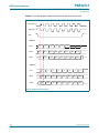
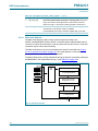
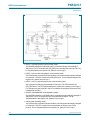
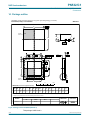
1
PN532/C1
Near Field Communication (NFC) controller
Rev. 3.2 — 3 December 2007
115432
Product data sheet
CONFIDENTIAL
1. General description
The PN532 is a highly integrated transceiver module for contactless communication at
13.56 MHz based on the 80C51 microcontroller core. It supports 6 different operating
modes:
•
•
•
•
•
•
ISO/IEC 14443A/MIFARE Reader/Writer
FeliCa Reader/Writer
ISO/IEC 14443B Reader/Writer
ISO/IEC 14443A/MIFARE Card MIFARE 1 KB or MIFARE 4 KB emulation
FeliCa Card emulation
ISO/IEC 18092, ECMA 340 Peer-to-Peer
The PN532 implements a demodulator and decoder for signals from
ISO/IEC 14443A/MIFARE compatible cards and transponders. The PN532 handles the
complete ISO/IEC 14443A framing and error detection (Parity & CRC).
The PN532 supports MIFARE 1 KB or MIFARE 4 KB emulation products. The PN532
supports contactless communication using MIFARE Higher transfer speeds up to
424 kbit/s in both directions.
The PN532 can demodulate and decode FeliCa coded signals. The PN532 handles the
FeliCa framing and error detection. The PN532 supports contactless communication
using FeliCa Higher transfer speeds up to 424 kbit/s in both directions.
The PN532 supports layers 2 and 3 of the ISO/IEC 14443 B Reader/Writer
communication scheme, except anticollision. This must be implemented in firmware as
well as upper layers.
In card emulation mode, the PN532 is able to answer to a Reader/Writer command either
according to the FeliCa or ISO/IEC 14443A/MIFARE card interface scheme. The PN532
generates the load modulation signals, either from its transmitter or from the LOADMOD
pin driving an external active circuit. A complete secure card functionality is only possible
in combination with a secure IC using the NFC-WI/S2C interface.
Compliant to ECMA 340 and ISO/IEC 18092 NFCIP-1 Passive and Active communication
modes, the PN532 offers the possibility to communicate to another NFCIP-1 compliant
device, at transfer speeds up to 424 kbit/s.The PN532 handles the complete NFCIP-1
framing and error detection.
The PN532 transceiver can be connected to an external antenna for Reader/Writer or
Card/PICC modes, without any additional active component.
PN532/C1
NXP Semiconductors
Near Field Communication (NFC) controller
CONFIDENTIAL
The PN532 supports the following host interfaces:
• SPI
• I2C
• High Speed UART (HSU)
An embedded low-dropout voltage regulator allows the device to be connected directly to
a battery. In addition, a power switch is included to supply power to a secure IC.
115432
Product data sheet
© NXP B.V. 2007. All rights reserved.
Rev. 3.2 — 3 December 2007
2 of 224
PN532/C1
NXP Semiconductors
Near Field Communication (NFC) controller
CONFIDENTIAL
2. Features
■ 80C51 microcontroller core with 40 KB ROM and 1 KB RAM
■ Highly integrated demodulator and decoder
■ Buffered output drivers to connect an antenna with minimum number of external
components
■ Integrated RF level detector
■ Integrated data mode detector
■ Supports ISO/IEC 14443A/MIFARE
■ Supports ISO/IEC 14443B (Reader/Writer mode only)
■ Typical operating distance in Reader/Writer mode for communication to
ISO/IEC 14443A/MIFARE, ISO/IEC 14443B or FeliCa cards up to 50 mm depending
on antenna size and tuning
■ Typical operating distance in NFCIP-1 mode up to 50 mm depending on antenna size,
tuning and power supply
■ Typical operating distance in ISO/IEC 14443A/MIFARE or FeliCa card emulation mode
of approximately 100 mm depending on antenna size, tuning and external field
strength
■ Supports MIFARE 1 KB or MIFARE 4 KB emulation encryption in Reader/Writer mode
and MIFARE higher transfer speed communication at 212 kbit/s and 424 kbit/s
■ Supports contactless communication according to the FeliCa protocol at 212 kbit/s and
424 kbit/s
■ Integrated RF interface for NFCIP-1 up to 424 kbit/s
■ Possibility to communicate on the RF interface above 424 kbit/s using external analog
components
■ Supported host interfaces
◆ SPI interface
◆ I2C interface
◆ High-speed UART
■ Dedicated host interrupts
■ Low power modes
◆ Hard-Power-Down mode (1 µA typical)
◆ Soft-Power-Down mode (22 µA typical)
■ Automatic wake-up on I2C, HSU and SPI interfaces when device is in Power-down
mode
■ Programmable timers
■ Crystal oscillator
■ 2.7 to 5.5 V power supply operating range
■ Power switch for external secure companion chip
■ Dedicated IO ports for external device control
■ Integrated antenna detector for production tests
■ ECMA 373 NFC-WI interface to connect an external secure IC
115432
Product data sheet
© NXP B.V. 2007. All rights reserved.
Rev. 3.2 — 3 December 2007
3 of 224
PN532/C1
NXP Semiconductors
Near Field Communication (NFC) controller
CONFIDENTIAL
3. Applications
■ Mobile and portable devices
■ Consumer applications
4. Quick reference data
Table 1.
Quick reference data
Symbol Parameter
Conditions
Typ Max
2.7
Unit
VBAT
Battery supply voltage
ICVDD
LDO output voltage
VBAT > 3.4 V
VSS = 0 V
PVDD
Supply voltage
for host interface
VSS = 0 V
SVDD
Output voltage
for secure IC interface
VSS = 0 V
(SVDD Switch Enabled)
IHPD
Hard-Power-Down
current consumption
VBAT = 5 V
2
µA
ISPD
Soft-Power-Down
current consumption
VBAT = 5 V,
RF level detector on
45
µA
IDVDD
Digital supply current
VBAT = 5 V,
SVDD switch off
ISVDD
SVDD load current
VBAT = 5 V,
SVDD switch on
IAVDD
Analog supply current
VBAT = 5 V
ITVDD
Transmitter supply current During RF transmission,
VBAT = 5 V
Ptot
Continuous total
power dissipation
Tamb
Operating
temperature range
Tamb = -30 to +85 °C
[1]
5.5
V
3.4
V
1.6
3.6
V
DVDD -0.5
DVDD V
2.7
[1]
3
25
mA
30
mA
6
60[3]
[2]
-30
mA
150[4]
mA
0.5
W
+85
°C
[1]
DVDD, AVDD and TVDD must always be at the same supply voltage.
[2]
The total current consumption depends on the firmware version (different internal IC clock speed)
[3]
With an antenna tuned at 50 Ω at 13.56 MHz
[4]
The antenna should be tuned not to exceed this current limit (the detuning effect when coupling with
another device must be taken into account)
115432
Product data sheet
Min
© NXP B.V. 2007. All rights reserved.
Rev. 3.2 — 3 December 2007
4 of 224
PN532/C1
NXP Semiconductors
Near Field Communication (NFC) controller
CONFIDENTIAL
5. Ordering information
Table 2.
Ordering information
Type number
Package
Name
Description
HVQFN40 Heatsink Very thin Quad Flat package;
40 pins, plastic, body 6 x 6 x 0.85 mm;
leadless; MSL level 2[3].
SOT618-1
PN5321A3HN/C1xx[1][2][4]
HVQFN40 Heatsink Very thin Quad Flat package;
40 pins, plastic, body 6 x 6 x 0.85 mm;
leadless; MSL level 2[3].
SOT618-1
[1]
xx refers to the ROM code version. The ROM code functionalities are described in the User-Manual
document. Each ROM code has its own User-Manual.
[2]
Type B software enabled. This NXP IC is licensed under Innovatron’s ISO/IEC 14443 Type B patent license.
[3]
This is tested according the joint IPC/JEDEC standard J-STD-020C of July 2004.
[4]
Purchase of an NXP Semiconductors IC that complies with one of the NFC Standards (ISO/IEC18.092;
ISO/IEC21.481) does not convey an implied license under any patent right on that standards. A license for
the portfolio of the NFC Standards patents of NXP B.V. needs to be obtained at Via Licensing, the pool
agent of the NFC Patent Pool, e-mail: [email protected].
115432
Product data sheet
Version
PN5320A3HN/C1xx[1][4]
© NXP B.V. 2007. All rights reserved.
Rev. 3.2 — 3 December 2007
5 of 224
PN532/C1
NXP Semiconductors
Near Field Communication (NFC) controller
CONFIDENTIAL
6. Block diagram
VBAT
P35
I0
I1
LoadMod
DVDD
SVDD
SIGIN
Power Distribution
80C51
P34
ROM
RAM
Host
TX1
interfaces
Contactless Interface Unit
TX2
IRQ P30 P31 P32 P33
(PCR)
RAM
(CIU)
PVDD
NSS MOSI MISO SCK
SIGOUT
Power Clock Reset
controller
TVDD
RSTOUT_N RSTPD_N
PN532
Oscin Oscout
AVDD
RX
VMID
AUX1
AUX2
Fig 1. Block diagram of PN532
115432
Product data sheet
© NXP B.V. 2007. All rights reserved.
Rev. 3.2 — 3 December 2007
6 of 224
PN532/C1
NXP Semiconductors
Near Field Communication (NFC) controller
CONFIDENTIAL
7. Pinning information
7.1 Pinning
Fig 2. Pin configuration for HVQFN 40 (SOT618-1)
115432
Product data sheet
© NXP B.V. 2007. All rights reserved.
Rev. 3.2 — 3 December 2007
7 of 224
PN532/C1
NXP Semiconductors
Near Field Communication (NFC) controller
CONFIDENTIAL
7.2 Pin description
Table 3.
PN532 Pin description
Symbol
Pin Type Ref
Description
Voltage
DVSS
1
PWR
LOADMOD
2
O
TVSS1
3
PWR
TX1
4
O
TVDD
5
PWR
TX2
6
O
TVSS2
7
PWR
Transmitter ground.
AVDD
8
PWR
Analog power supply.
VMID
9
O
AVDD
Internally generated reference voltage to bias the receiving
path
RX
10
I
AVDD
Receiver input.
AVSS
11
PWR
AUX1
12
O
AVDD
Auxiliary output 1: analog and digital test signals.
AUX2
13
O
AVDD
Auxiliary output 2: analog and digital test signals.
OSCIN
14
I
AVDD
Crystal oscillator input: to oscillator inverting amplifier.
OSCOUT
15
O
AVDD
Crystal oscillator output: from oscillator inverting amplifier.
I0
16
I
DVDD
Host interface selector 0.
I1
17
I
DVDD
Host interface selector 1.
Digital ground.
DVDD
Load modulation signal.
Transmitter ground.
TVDD
Transmitter output 1: transmits modulated 13.56 MHz energy
carrier.
Transmitter power supply.
TVDD
Transmitter output 2: transmits modulated 13.56 MHz energy
carrier.
Analog ground.
TESTEN
18
I
DVDD
Reserved for test: connect to ground for normal operation.
P35
19
IO
DVDD
General purpose IO.
N.C.
20
Not connected.
N.C.
21
Not connected.
N.C.
22
PVDD
23
PWR
P30 /
UART_RX
24
IO
P70_IRQ
Not connected.
Pad power supply.
PVDD
General purpose IO / Debug UART receive input.
25
IO
PVDD
General purpose IO. Can be used as Interrupt request to host.
RSTOUT_N 26
O
PVDD
Reset indicator: when low, circuit is in reset state.
NSS /
P50_SCL /
HSU_RX
27
IO
PVDD
Host interface pin: SPI Not Slave Selected (NSS) or I2C clock
(SCL) or HSU receive (HSU_RX). Refer to Table 72 on
page 48 for details.
MOSI /
SDA /
HSU_TX
28
IO
PVDD
Host interface pin: SPI Master Out Slave In (MOSI) or I2C
data (SDA) or HSU transmit (HSU_TX). Refer to Table 72 on
page 48 for details.
MISO / P71
29
IO
PVDD
Host interface pin: SPI Master In Slave Out (MISO). Refer to
Table 72 on page 48 for details.
Can be used as general purpose IO.
115432
Product data sheet
© NXP B.V. 2007. All rights reserved.
Rev. 3.2 — 3 December 2007
8 of 224
PN532/C1
NXP Semiconductors
Near Field Communication (NFC) controller
CONFIDENTIAL
Table 3.
PN532 Pin description …continued
Symbol
Pin Type Ref
Description
Voltage
SCK /
P72
30
IO
PVDD
Host interface pin: SPI serial clock. Refer to Table 72 on
page 48 for details.
Can be used as general purpose IO.
P31 /
UART_TX
31
IO
PVDD
General purpose IO/ Debug UART TX.
P32_INT0
32
IO
PVDD
General purpose IO / Interrupt source INT0.
P33_INT1
33
IO
PVDD
General purpose IO / Interrupt source INT1.
P34 /
SIC_CLK
34
IO
SVDD
General purpose IO / Secure IC clock.
SIGOUT
35
O
SVDD
Contactless communication interface output: delivers a serial
data stream according to NFCIP-1 to a secure IC.
SIGIN
36
I
SVDD
Contactless communication interface input: accepts a serial
data stream according to NFCIP-1 and from a secure IC.
SVDD
37
O
RSTPD_N
38
I
DVDD
39
O
Internal digital power supply.
VBAT
40
PWR
Main external power supply.
Switchable output power for secure IC power supply with
overload detection. Used as a reference voltage for secure IC
communication.
PVDD
Reset and Power-Down: When low, internal current sources
are switched off, the oscillator is disabled, and input pads are
disconnected from the outside world. The internal reset phase
starts on the negative edge on this pin.
115432
Product data sheet
© NXP B.V. 2007. All rights reserved.
Rev. 3.2 — 3 December 2007
9 of 224
PN532/C1
NXP Semiconductors
Near Field Communication (NFC) controller
CONFIDENTIAL
8. Functional description
8.1 80C51
The PN532 is controlled via an embedded 80C51 microcontroller core (for more details
http://www.standardics.nxp.com/support/documents/microcontrollers/?scope=80C51). Its
principle features are listed below:
• 6-clock cycle CPU. One machine cycle comprises 6 clock cycles or states (S1 to S6).
An instruction needs at least one machine cycle.
•
•
•
•
•
•
•
•
•
ROM interface
RAM interface to embedded IDATA and XRAM memories (see Figure 4 on page 11)
Peripheral interface (PIF)
Power control module to manage the CPU power consumption
Clock module to control CPU clock during Shutdown and Wake-up modes
Port module interface to configure I/O pads
Interrupt controller
Three timers
Debug UART
The block diagram describes the main blocks described in this 80C51 section.
Fig 3. PN532 80C51 block description
115432
Product data sheet
© NXP B.V. 2007. All rights reserved.
Rev. 3.2 — 3 December 2007
10 of 224
PN532/C1
NXP Semiconductors
Near Field Communication (NFC) controller
CONFIDENTIAL
8.1.1 PN532 memory map
The memory map of PN532 is composed of 2 main memory spaces: data memory and
program memory. The following figure illustrates the structure.
XRAM
FFFFH
ROM
RE
RE
SE
SE
RV
E
RV
E
D
D
FFFFH
A000H
9FFFH
8000H
7FFFH
PERIPHERAL
AREA
PIF
D
6000H
5FFFH
RV
E
RAM
SFR
00H
128 BYTES RAM
DIRECT
&
INDIRECT
ADDRESSING
RE
128 BYTES RAM
INDIRECT
ADDRESSING
ONLY
7FH
ROM
SE
FFH
Special Function
Registers
DIRECT
ADDRESSING
40 KBYTES
02FFH
768 BYTES
XRAM
0000H
0000H
IDATA
Data Memory Area
Program Memory Area
Fig 4. PN532 memory map overview
115432
Product data sheet
© NXP B.V. 2007. All rights reserved.
Rev. 3.2 — 3 December 2007
11 of 224
PN532/C1
NXP Semiconductors
Near Field Communication (NFC) controller
CONFIDENTIAL
8.1.2 Data memory
Data memory is itself divided into 2 spaces:
• 384-byte IDATA with byte-wide addressing
– 258-byte RAM
– 128-byte SFR
• 1 bank of 64 KB extended RAM (XRAM) with 2-byte-wide addressing
8.1.2.1 IDATA memory
The IDATA memory is mapped into 3 blocks, which are referred as Lower IDATA RAM,
Upper IDATA RAM, and SFR. Addresses to these blocks are byte-wide, which implies an
address space of only 256 bytes. However, 384 bytes can be addressed within IDATA
memory through the use of direct and indirect address mechanisms.
• Direct addressing: the operand is specified by an 8-bit address field in the instruction.
• Indirect addressing: the instruction specifies a register where the address of the
operand is stored.
For the range 80h to FFh, direct addressing will access the SFR space; indirect
addressing accesses Upper IDATA RAM. For the range 0h0 to 7Fh, Lower IDATA RAM is
accessed, regardless of addressing mode. This behavior is summarized in the table
below:
Table 4.
Address
IDATA memory addressing
Addressing mode
Direct
Indirect
00h to 7Fh
Lower IDATA RAM
Lower IDATA RAM
80h to FFh
SFRs
Upper IDATA RAM
The SFRs and their addresses are described in the Table 5:
115432
Product data sheet
© NXP B.V. 2007. All rights reserved.
Rev. 3.2 — 3 December 2007
12 of 224
xxxxxxxxxxxxxxxxxxxxx xxxxxxxxxxxxxxxxxxxxxxxxxx xxxxxxx x x x xxxxxxxxxxxxxxxxxxxxxxxxxxxxxx xxxxxxxxxxxxxxxxxxx xx xx
xxxxx xxxxxxxxxxxxxxxxxxxxxxxxxxx xxxxxxxxxxxxxxxxxxx xxxxxx xxxxxxxxxxxxxxxxxxxxxxxxxxxxxxxxxxx xxxxxxxxxxxx x x
xxxxxxxxxxxxxxxxxxxxx xxxxxxxxxxxxxxxxxxxxxxxxxxxxxx xxxxx xxxxxxxxxxxxxxxxxxxxxxxxxxxxxxxxxxxxxxxxxxxxxxxxxx xxxxxxxx
xxxxxxxxxxxxxxxxxxxxxxxxx xxxxxxxxxxxxxxxxxxxx xxx
Address
F8h
F0h
E8h
E0h
D8h
SFR map of NFC controller
Bitaddressable
IP1
B
IE1
ACC
I2CC0N
PSW
T2CON
IP0
P3
IE0
S0CON
T01CON
Byte-addressable
XRAMP
CIU_Status2
CIU_FIFOData
CIU_FIFOLevel
I2CSTA
CIU_Command
T2MOD
I2CDAT
CIU_CommIEn
RCAP2L
I2CADR
CIU_DivIEn
RCAP2H
SPIcontrol
FITEN
SBUF
SPIstatus
FDATA
RWL
T01MOD
SP
T0L
DPL
P3CFGA
P7CFGA
CIU_WaterLevel
Address
P3CFGB
P7CFGB
CIU_Control
CIU_BitFraming
P7
CIU_Coll
CIU_Status1
CIU_CommIrq
T2L
CIU_DivIrq
T2H
CIU_Error
HSU_STA
FSIZE
TWL
HSU_CTR
HSU_PRE
HSU_CNT
FIFOFS
FIFOFF
SFF
T1L
DPH
T0H
T1H
FIT
PCON
FFh
F7h
EFh
E7h
DFh
D7h
CFh
C7h
BFh
B7h
AFh
A7h
9Fh
97h
8Fh
87h
PN532/C1
CONFIDENTIAL
13 of 224
© NXP B.V. 2007. All rights reserved.
Near Field Communication (NFC) controller
Rev. 3.2 — 3 December 2007
D0h
C8h
C0h
B8h
B0h
A8h
A0h
98h
90h
88h
80h
NXP Semiconductors
115432
Product data sheet
Table 5.
PN532/C1
NXP Semiconductors
Near Field Communication (NFC) controller
CONFIDENTIAL
8.1.2.2 XRAM memory
The XRAM memory is divided into 2 memory spaces:
• 0000h to 5FFFh: reserved for addressing embedded RAM. For the PN532, only
accesses between 0000h and 02FF are valid.
• 6000h to 7FFFh: reserved for addressing embedded peripherals. This space is
divided into 32 regions of 256 bytes each. Addressing can be performed using R0 or
R1 and the XRAMP SFR.
The Table 6 depicts the mapping of internal peripherals into XRAM.
Table 6.
Peripheral mapping into XRAM memory space
Base
Address
End
Address
Description
6000h
60FFh
Reserved.
6100h
61FFh
IOs and miscellaneous registers configuration
Refer to Section 8.2 “General purpose IOs configurations” on page 38
6200h
62FFh
Power Clock and Reset controller
Refer to Section 8.5.7 “PCR extension registers” on page 92
6300h
633Fh
Contactless Unit Interface
Refer to Section 8.6 “Contactless Interface Unit (CIU)” on page 98
6340h
FFFFh
Reserved
XRAM is accessed via the dedicated MOVX instructions. There are two access modes:
• 16-bit data pointer (DPTR): the full XRAM address space can be accessed.
• paging mechanism: the upper address byte is stored in the SFR register XRAMP; the
lower byte is stored in either R1 or R0.
The Figure 5 illustrates both mechanisms.
115432
Product data sheet
© NXP B.V. 2007. All rights reserved.
Rev. 3.2 — 3 December 2007
14 of 224
PN532/C1
NXP Semiconductors
Near Field Communication (NFC) controller
CONFIDENTIAL
XRAM
FFFFH
XRAMP = FFh
XRAMP = FFh
FFh
00h
FFh
00h
40 kB
Reserved
XRAMP = 82h
XRAMP = 81h
XRAMP = 80h
XRAMP = 7Fh
XRAMP = 7Eh
MOVX @DPTR,A
MOVX A,@DPTR
XRAMP = 62h
XRAMP = 61h
8000H
7FFFH
XRAMP = 60h
XRAMP = 5Fh Peripheral 32
XRAMP = 5Eh Peripheral 31
FFh
00h
FFh
00h
FFh
00h
FFh
00h
FFh
00h
FFh
00h
FFh
00h
FFh
00h
FFh
00h
FFh
00h
MOVX @Ri,A
MOVX A,@Ri
PERIPHERAL
AREA
XRAMP = 42h Peripheral 3
XRAMP = 41h Peripheral 2
6000H
5FFFH
XRAMP = 40h Peripheral 1
XRAMP = 3Fh
XRAMP = 3Eh
FFh
00h
FFh
00h
FFh
00h
FFh
00h
FFh
00h
XRAM
XRAMP = 02h
XRAMP = 01h
0000H
XRAMP = 00h
FFh
00h
FFh
00h
FFh
00h
Fig 5. Indirect addressing of XRAM memory space
8.1.3 Program memory
PN532 program memory ranges from 0000h to 9FFFh, which is physically mapped to the
40 KB ROM.
115432
Product data sheet
© NXP B.V. 2007. All rights reserved.
Rev. 3.2 — 3 December 2007
15 of 224
PN532/C1
NXP Semiconductors
Near Field Communication (NFC) controller
CONFIDENTIAL
8.1.4 PCON module
The Power Control (PCON) module is configured using the PCON SFR register.
Table 7.
PCON register (SFR: address 87h) bit allocation
Bit
7
Symbol
6
5
4
0
0
0
R/W
R
R
SMOD
Reset
Access
Table 8.
3
2
CPU_PD
-
0
0
0
0
0
R
R
R
R/W
R/W
-
1
0
Description of PCON bits
Bit
Symbol
Description
7
SMOD
Serial MODe:
When set to logic 1, the baud rate of the Debug UART is doubled
6 to 3
-
Reserved.
1
CPU_PD
Power-down:
When set to logic 1, the microcontroller goes in Power-down mode
0
Reserved
This bit should only ever contain logic 0.
8.1.5 Interrupt Controller
The interrupt controller has the following features:
•
•
•
•
13 interrupt sources
Interrupt enable registers IE0 and IE1
Interrupt priority registers IP0 and IP1
Wake-up from Power-Down state
8.1.5.1 Interrupt vectors
The mapping between interrupt sources and interrupt vectors is shown in Table 9.
Table 9.
Interrupt vector
Interrupt
number
Interrupt
vector
Interrupt sources
Incremental priority level
(conflict resolution level)
0
0003h
External P32_INT0
Highest
1
000Bh
Timer0 interrupt
2
0013h
External P33_INT1
3
001Bh
Timer1 interrupt
4
0023h
Debug UART interrupt
5
002Bh
Timer2 interrupt
6
0033h
NFC-WI interrupt
7
003Bh
LDO overcurrent interrupt
8
0043h
Reserved
9
004Bh
CIU interrupt 1
10
0053h
CIU interrupt 0
11
005Bh
I2C interrupt
12
0063h
SPI, FIFO, or HSU interrupts
13
006Bh
Reserved
14
0073h
General Purpose IRQ
115432
Product data sheet
Lowest
© NXP B.V. 2007. All rights reserved.
Rev. 3.2 — 3 December 2007
16 of 224
PN532/C1
NXP Semiconductors
Near Field Communication (NFC) controller
CONFIDENTIAL
8.1.5.2 Interrupt enable: IE0 and IE1 registers
Each interrupt source can be individually enabled or disabled by setting a bit in IE0 or IE1.
In register IE0, a global interrupt enable bit can be set to logic 0 to disable all interrupts at
once.
The 2 following tables describe IE0.
Table 10.
Interrupt controller IE0 register (SFR: address A8h) bit allocation
Bit
Symbol
7
6
5
4
3
2
1
0
IE0_7
IE0_6
IE0_5
IE0_4
IE0_3
IE0_2
IE0_1
IE0_0
0
0
0
0
0
0
0
0
R/W
R/W
R/W
R/W
R/W
R/W
R/W
R/W
Reset
Access
Table 11.
Description of IE0 bits
Bit
Symbol
Description
7
IE0_7
Global interrupt enable
When set to logic 1, the interrupts can be enabled.
When set to logic 0, all the interrupts are disabled.
6
IE0_6
NFC-WI counter interrupt enable
When set to logic 1, NFC-WI interrupt is enabled. See Table 164 on page 125.
5
IE0_5
Timer2 interrupt enable
When set to logic 1, Timer2 interrupt is enabled. See Table 36 on page 28.
4
IE0_4
Debug UART interrupt enable
When set to logic 1, Debug UART interrupt is enabled. See Table 49 on
page 33.
3
IE0_3
Timer1 interrupt enable
When set to logic 1, Timer1 interrupt is enabled. See Table 23 on page 23.
2
IE0_2
P33_INT1 interrupt enable
When set to logic 1, P33_INT1 pin interrupt is enabled. See Table 23 on
page 23.
The polarity of P33_INT1 can be inverted (see Table 73 on page 49).
1
IE0_1
Timer0 interrupt enable
When set to logic 1, Timer0 interrupt is enabled. See Table 23 on page 23.
0
IE0_0
P32_INT0 interrupt enable
When set to logic 1, P32_INT0 pin interrupt is enabled. See Table 23 on
page 23.
115432
Product data sheet
© NXP B.V. 2007. All rights reserved.
Rev. 3.2 — 3 December 2007
17 of 224
PN532/C1
NXP Semiconductors
Near Field Communication (NFC) controller
CONFIDENTIAL
The 2 following tables describe IE1.
Table 12.
Interrupt controller IE1 register (SFR: address E8h) bit allocation
Bit
Symbol
7
6
5
4
3
2
1
0
IE1_7
-
IE1_5
IE1_4
IE1_3
IE1_2
-
IE1_0
Reset
Access
Table 13.
0
0
0
0
0
0
0
0
R/W
R/W
R/W
R/W
R/W
R/W
R/W
R/W
Description of IE1 bits
Bit
Symbol
Description
7
IE1_7
General purpose IRQ interrupt enable.
When set to logic 1, enables interrupt function of P34, P35, P50_SCL and P71
according to their respective enable and level control bits. See Table 19 on
page 20, Table 137 on page 94 and Table 143 on page 96.
6
-
Reserved. This bit must be set to logic 0
5
IE1_5
FIFO, SPI and HSU interrupt enable.
When set to logic 1, enables FIFO interrupts, SPI interrupts, HSU interrupt.
In HSU mode, the interrupt is when NSS is at logic 0.
For the FIFO interrupts, see Table 112 on page 75.
For the SPI interrupts, see Table 122 on page 80.
4
IE1_4
I2C interrupt enable.
When set to logic 1, enables I2C interrupt. See Table 77 on page 54.
3
IE1_3
CIU interrupt 0 enable.
When set to logic 1, enables CIU interrupt 0: CIU_IRQ_0. See Table 190 on
page 150.
2
IE1_2
CIU interrupt 1 enable.
When set to logic 1, enables the CIU interrupt 1: CIU_IRQ_1. See Table 190
on page 150.
1
-
Reserved. This bit must be set to logic 0.
0
IE1_0
LDO overcurrent interrupt enable.
When set to logic 1, enables the LDO overcurrent detection interrupt. See
Table 127 on page 87.
8.1.5.3 Interrupt prioritization: IP0 and IP1 registers
Each interrupt source can be individually programmed to be one of two priority levels by
setting or clearing a bit in the interrupt priority registers IP0 and IP1. If two interrupt
requests of different priority levels are received simultaneously, the request with the high
priority is serviced first. On the other hand, if the interrupts are of the same priority,
precedence is resolved by comparing their respective conflict resolution levels (see
Table 9 on page 16 for details). The processing of a low priority interrupt can be
interrupted by one with a high priority.
A RETI (Return From Interrupt) instruction jumps to the address immediately succeeding
the point at which the interrupt was serviced. The instruction found at the return address
will be executed, prior to servicing any pending interrupts.
115432
Product data sheet
© NXP B.V. 2007. All rights reserved.
Rev. 3.2 — 3 December 2007
18 of 224
PN532/C1
NXP Semiconductors
Near Field Communication (NFC) controller
CONFIDENTIAL
The 2 following tables describe IP0.
Table 14.
Interrupt controller IP0 register (SFR: address B8h) bit allocation
Bit
Symbol
Reset
Access
Table 15.
7
6
5
4
3
2
1
0
IP0_7
IP0_6
IP0_5
IP0_4
IP0_3
IP0_2
IP0_1
IP0_0
0
0
0
0
0
0
0
0
R/W
R/W
R/W
R/W
R/W
R/W
R/W
R/W
Description of IP0 bits
Bit
Symbol
Description
7
IP0_7
Reserved
6
IP0_6
When set to logic 1, NFC-WI interrupt is set to high priority.
5
IP0_5
When set to logic 1, Timer2 interrupt is set to high priority.
4
IP0_4
When set to logic 1, Debug UART interrupt is set to high priority.
3
IP0_3
When set to logic 1, Timer1 interrupt is set to high priority.
2
IP0_2
When set to logic 1, external P33_INT1 pin is set to high priority.
1
IP0_1
When set to logic 1, Timer0 interrupt is set to high priority.
0
IP0_0
When set to logic 1, external P32_INT0 pin is set to high priority.
The 2 following tables describe IP1.
Table 16.
Interrupt controller IP1 register (SFR: address F8h) bit allocation
Bit
Symbol
Reset
Access
Table 17.
7
6
5
4
3
2
IP1_7
-
IP1_5
IP1_4
IP1_3
IP1_2
-
0
0
0
0
0
0
00
R/W
R/W
R/W
R/W
R/W
R/W
R/W
0
Description of IP1 bits
Bit
Symbol
Description
7
IP1_7
When set to logic 1, General Purpose IRQ interrupt is set to high priority.
6
-
Reserved. This bit must be set to logic 0.
5
IP1_5
When set to logic 1, combined SPI, FIFO and HSU interrupt is set to high
priority.
4
IP1_4
When set to logic 1, I2C interrupt is set to high priority.
3
IP1_3
When set to logic 1, CIU interrupt 0 is set to high priority.
2
IP1_2
When set to logic 1, CIU interrupt 1 is set to high priority.
1
-
Reserved. This bit must be set to logic 0.
0
IP1_0
When set to logic 1, interrupt number 7 is set to high priority.
115432
Product data sheet
1
© NXP B.V. 2007. All rights reserved.
Rev. 3.2 — 3 December 2007
19 of 224
PN532/C1
NXP Semiconductors
Near Field Communication (NFC) controller
CONFIDENTIAL
8.1.5.4 General purpose IRQ control
The general purpose interrupts are controlled by register GPIRQ.
NOTE: this is not a standard feature of the 8051.
Table 18.
GPIRQ register (address 6107h) bit allocation
Bit
Symbol
7
6
5
4
3
2
1
0
gpirq_
level_
P71
gpirq_
level_
P50
gpirq_
level_
P35
gpirq_
level_
P34
gpirq_
enable
_P71
gpirq_
enable_
P50
gpirq_
enable_
P35
gpirq_
enable_
P34
0
0
0
0
0
0
0
0
R/W
R/W
R/W
R/W
R/W
R/W
R/W
R/W
Reset
Access
Table 19.
Description of GPIRQ bits
Bit Symbol
Description
7
Configures the polarity of signal on P71 to generate a GPIRQ
interrupt event (assuming gpirq_enable_P71 is set).
gpirq_level_P71
When set to logic 0, an interrupt will be generated if P71 is at logic 0.
When set to logic 1, an interrupt will be generated if P71 is at logic 1.
6
gpirq_level_P50
Configures the polarity of signal on P50 to generate a GPIRQ
interrupt event (assuming gpirq_enable_P50 is set).
When set to logic 0, an interrupt will be generated if P50_SCL is at
logic 0.
When set to logic 1, an interrupt will be generated if P50_SCL is at
logic 1.
5
gpirq_level_P35
Configures the polarity of signal on P35 to generate a GPIRQ
interrupt event (assuming gpirq_enable_P35 is set).
When set to logic 0, an interrupt will be generated if P35 is at logic 0.
When set to logic 1, an interrupt will be generated if P35 is at logic 1.
4
gpirq_level_P34
Configures the polarity of signal on P34 to generate a GPIRQ
interrupt event (assuming gpirq_enable_P34 is set).
When set to logic 0, an interrupt will be generated if P34 is at logic 0.
When set to logic 1, an interrupt will be generated if P34 is at logic 1.
Remark: If hide_svdd_sig of the register control_rngpower is set and
gpirq_enable_P34 is also set then this bit will be asserted independently
of the level on the pad P34.
3
gpirq_enable_P71 When set to logic 1, enables pad P71 to generate a GPIRQ interrupt
event.[1]
2
gpirq_enable_P50 When set to logic 1, enables pad P50_SCL to generate a GPIRQ interrupt
event.[1]
1
gpirq_enable_P35 When set to logic 1, enables pad P35 to generate a GPIRQ interrupt
event.[1]
0
gpirq_enable_P34 When set to logic 1, enables pad P34 to generate a GPIRQ interrupt
event.[1]
[1]
The bit IE1_7 of register IE1 (see Table 13 on page 18) has also to be set to logic 1 to enable the
corresponding CPU interrupt.
115432
Product data sheet
© NXP B.V. 2007. All rights reserved.
Rev. 3.2 — 3 December 2007
20 of 224
PN532/C1
NXP Semiconductors
Near Field Communication (NFC) controller
CONFIDENTIAL
8.1.6 Timer0/1 description
Timer0/1 are general purpose timer/counters. Timer0/1 has the following functionality:
•
•
•
•
Configurable edge or level detection interrupts
Timer or counter operation
4 timer/counter modes
Baud rate generation for Debug UART
Timer0/1 comprises two 16-bit timer/counters: Timer0 and Timer1. Both can be
configured as either a timer or an event counter.
Each of the timers can operate in one of four modes:
•
•
•
•
Mode 0: 13-bit timer/counter
Mode 1: 16-bit timer/counter
Mode 2: 8-bit timer/counter with programmable preload value
Mode 3: two individual 8-bit timer/counters (Timer0 only)
In the ‘timer’ function, the timer/counter is incremented every machine cycle. The count
rate is 1/6 of the CPU clock frequency (CPU_CLK).
In the ‘counter’ function, the timer/counter is incremented in response to a 1-to-0 transition
on the input pins P34 / SIC_CLK (Timer0) or P35 (Timer1). In this mode, the external input
is sampled during state S5 of every machine cycle. If the associated pin is at logic 1 for a
machine cycle, followed by logic 0 on the next machine cycle, the count is incremented.
The new count value appears in the timer/counter in state S3 of the machine cycle
following the one in which the transition was detected. The maximum count rate is 1/12 of
the CPU_CLK frequency. There are no restrictions on the duty cycle of the external input
signal but to ensure that a given level is sampled at least once before it changes, it should
be held for at least one full machine cycle.
The overflow output ‘t1_ovf’ of Timer1 can be used as a baud rate generator for the Debug
UART. The Timer1 interrupt should be disabled in this case. For most applications which
drive the Debug UART, Timer1 is configured for ‘timer’ operation and in auto-reload mode.
8.1.6.1 Timer0/1 registers
The Timer0/1 module contains six Special Function Registers (SFRs) which can be
accessed by the CPU.
Table 20.
Timer0/1 Special Function registers list
Name
Size
[bytes]
Address
Offset
Description
Access
T01CON
1
88h
Timer0/1 control register
R/W
T01MOD
1
89h
Timer0/1 mode register
R/W
T0L
1
8Ah
Timer0 timer/counter lower byte
R/W
T1L
1
8Bh
Timer1 timer/counter lower byte
R/W
T0H
1
8Ch
Timer0 timer/counter upper byte
R/W
T1H
1
8Dh
Timer1 timer/counter upper byte
R/W
115432
Product data sheet
© NXP B.V. 2007. All rights reserved.
Rev. 3.2 — 3 December 2007
21 of 224
PN532/C1
NXP Semiconductors
Near Field Communication (NFC) controller
CONFIDENTIAL
The firmware performs a register read in state S5 and a register write in state S6. The
hardware loads bits TF0 and TF1 of the register T01CON during state S2 and state S4
respectively. The hardware loads bits IE0 and IE1 of the register T01CON during state S1
and reset these bits during state S2. The registers T0L, T0H, T1L, T1H are updated by the
hardware during states S1, S2, S3 and S4 respectively. At the end of a machine cycle, the
firmware load has overridden the hardware load as the firmware writes in state S6.
Table 21.
Timer0/1 SFR registers CPU state access
CPU STATE
Register
Bit
T01CON
TF0
S1
S2
S3
HW read
TF1
IE0 / IE1
TOL
TOH
T1L
HW read
HW write
HW reset
HW write
HW write
HW write
T1H
HW write
115432
Product data sheet
S4
S5
S6
SW read
SW write
SW read
SW write
SW read
SW write
SW read
SW write
SW read
SW write
SW read
SW write
SW read
SW write
© NXP B.V. 2007. All rights reserved.
Rev. 3.2 — 3 December 2007
22 of 224
PN532/C1
NXP Semiconductors
Near Field Communication (NFC) controller
CONFIDENTIAL
8.1.6.2 T01CON register
The register is used to control Timer0/1 and report its status.
Table 22.
Timer0/1 T01CON register (SFR address 88h), bit allocation
Bit
Symbol
Reset
Access
Table 23.
7
6
5
4
3
2
1
0
TF1
TR1
TF0
TR0
IE1
IT1
IE0
IT0
0
0
0
0
0
0
0
0
R/W
R/W
R/W
R/W
R/W
R/W
R/W
R/W
Description of Timer0/1 T01CON register bits
Bit
Symbol
Description
7
TF1
Timer1 overflow.
Set to logic 1 by hardware on a Timer1 overflow. The flag is set to logic 0
by the CPU after 2 machine cycles.
The bit IE0_3 of register IE0 (see Table 11 on page 17) has to be set to
logic 1 to enable the corresponding CPU interrupt.
6
TR1
Timer1 run control. Set by firmware only.
When set to logic 1, Timer1 is enabled.
5
TF0
Timer0 overflow.
Set by hardware on a Timer0 overflow. The flag is set to logic 0 by the
CPU after 2 machine cycles.
The bit IE0_1 of register IE0 (see Table 11 on page 17) has to be set to
logic 1 to enable the corresponding CPU interrupt.
4
TR0
Timer0 run control. Set by firmware only.
When set to logic 1, Timer0 is enabled.
3
IE1
External Interrupt1 event.
Set to logic 1 by hardware when an external interrupt is detected on
P33_INT1.
The bit IE0_2 of register IE0 (see Table 11 on page 17) has to be set to
logic 1 to enable the corresponding CPU interrupt.
2
IT1
External Interrupt1 control. Set by firmware only.
When set to logic 1, Interrupt1 triggers on a falling edge of P33_INT1.
When set to logic 0, Interrupt1 triggers on a low level of P33_INT1.
1
IE0
External Interrupt0 event.
Set to logic 1 by hardware when an external interrupt is detected on
P32_INT0.
The bit IE0_0 of register IE0 (see Table 11 on page 17) has to be set to
logic 1 to enable the corresponding CPU interrupt.
0
IT0
External Interrupt0 control. Set by firmware only.
When set to logic 1, Interrupt0 triggered by a falling edge on P32_INT0.
When set to logic 0, Interrupt0 triggered by a low level on P32_INT0.
115432
Product data sheet
© NXP B.V. 2007. All rights reserved.
Rev. 3.2 — 3 December 2007
23 of 224
PN532/C1
NXP Semiconductors
Near Field Communication (NFC) controller
CONFIDENTIAL
8.1.6.3 T01MOD register
This register is used to configure Timer0/1.
Table 24.
Timer 0/1 T01MOD register (SFR address 89h), bit allocation
Bit
Symbol
7
6
5
4
3
2
1
0
GATE1
C/T1
M11
M10
GATE0
C/T0
M01
M00
Reset
Access
Table 25.
0
0
0
0
0
0
0
0
R/W
R/W
R/W
R/W
R/W
R/W
R/W
R/W
Description of T01MOD bits
Bit
Symbol
Description
7
GATE1
Timer1 gate control. Set by firmware only.
When set to logic 1, Timer1 is enabled only when P33_INT1 is high and bit
TR1 of register T01CON is set.
When set to logic 0, Timer1 is enabled.
6
C/T1
Timer1 timer/counter selector. Set by firmware only.
When set to logic 1, Timer1 is set to counter operation.
When set to logic 0, Timer1 is set to timer operation.
5 to 4
M[11:10]
Timer1 mode. Set by firmware only.
•
Mode 0: M11 = 0 and M10 = 0
– 8192 counter
– T1L serves as a 5-bit prescaler
•
Mode 1: M11 = 0 and M10 = 1
–
16-bit timer/counter
– T1H and T1L are cascaded
•
Mode 2: M11 = 1 and M10 = 0
– 8-bit auto-reload timer/counter.
– T1H stores value to be reloaded into T1L each time T1L overflows.
•
Mode 3: M11 = 1 and M10 = 1
– Timer1 is stopped (count frozen).
115432
Product data sheet
© NXP B.V. 2007. All rights reserved.
Rev. 3.2 — 3 December 2007
24 of 224
PN532/C1
NXP Semiconductors
Near Field Communication (NFC) controller
CONFIDENTIAL
Table 25.
Description of T01MOD bits …continued
Bit
Symbol
Description
3
GATE0
Timer0 gate control. Set by firmware only.
When set to logic 1, Timer0 is enabled only when P32_INT0 is high and bit
TR0 of register T01CON is set.
When set to logic 0, Timer0 is enabled.
2
C/T0
Timer0 timer/counter selector. Set by firmware only.
When set to logic 1, Timer0 is set to counter operation.
When set to logic 0, Timer0 is set to timer operation.
1 to 0
M[01:00]
Timer0 mode. Set by firmware only.
•
Mode 0: M01 = 0 and M00 = 0
– 8192 timer
– T0L acts as a 5-bit prescaler.
•
Mode 1: M01 = 0 and M00 = 1
– 16-bit timer/counter
– T0H and T0L are cascaded.
•
Mode 2: M01 = 1 and M00 = 0
– 8-bit auto-reload timer/counter
– T0H stores value to be reloaded into T0L each time T0L overflows.
•
Mode 3: M01 = 1 and M00 = 1
– Timer0 split into two 8-bit timer/counters T0H and T0L
– T0H is controlled by the control bit of Timer1: bit TR1 of register
T01CON
– T0L is controlled by standard Timer0 control: “{P32_INT0 OR
(NOT GATE0)} AND bit TR0”.
8.1.6.4 T0L and T0H registers
These are the actual timer/counter bytes for Timer0: T0L is the lower byte; T0H is the
upper byte.
Table 26.
Bit
Symbol
Reset
Access
Table 27.
Timer0/1 T0L register (SFR address 8Ah), bit allocation
7
6
5
4
3
2
1
0
T0L.7
T0L.6
T0L.5
T0L.4
T0L.3
T0L.2
T0L.1
T0L.0
0
0
0
0
0
0
0
0
R/W
R/W
R/W
R/W
R/W
R/W
R/W
R/W
Description of T0L bits
Bit
Symbol
7:0
T0L.7 to T0L.0 Timer0 timer/counter lower byte
Table 28.
Bit
Symbol
Reset
Access
Table 29.
Description
Timer0/1 T0H register (SFR address 8Ch), bit allocation
7
6
5
4
3
2
1
0
T0H.7
T0H.6
T0H.5
T0H.4
T0H.3
T0H.2
T0H.1
T0H.0
0
0
0
0
0
0
0
0
R/W
R/W
R/W
R/W
R/W
R/W
R/W
R/W
Description of T0H bits
Bit
Symbol
7 to 0
T0H.7 to T0H.0 Timer0 timer/counter upper byte
Description
115432
Product data sheet
© NXP B.V. 2007. All rights reserved.
Rev. 3.2 — 3 December 2007
25 of 224
PN532/C1
NXP Semiconductors
Near Field Communication (NFC) controller
CONFIDENTIAL
8.1.6.5 T1L and T1H registers
These are the actual timer/counter bytes for Timer1. T1L is the lower byte, T1H is the
upper byte.
Table 30.
Timer0/1 T1L register (SFR address 8Bh), bit allocation
Bit
Symbol
7
6
5
4
3
2
1
0
T1L.7
T1L.6
T1L.5
T1L.4
T1L.3
T1L.2
T1L.1
T1L.0
Reset
Access
Table 31.
0
0
0
0
0
0
0
0
R/W
R/W
R/W
R/W
R/W
R/W
R/W
R/W
Description of T1L bits
Bit
Symbol
7 to 0
T1L.7 to T1L.0 Timer1 timer/counter lower byte
Table 32.
Timer0/1 T1H register (SFR address 8Dh), bit allocation
Bit
Symbol
7
6
5
4
3
2
1
0
T1H.7
T1H.6
T1H.5
T1H.4
T1H.3
T1H.2
T1H.1
T1H.0
Reset
Access
Table 33.
Description
0
0
0
0
0
0
0
0
R/W
R/W
R/W
R/W
R/W
R/W
R/W
R/W
Description of T1H bits
Bit
Symbol
7 to 0
T1H.7 to T1H.0 Timer1 timer/counter upper byte
Description
8.1.6.6 Incrementer
The two 16-bit timer/counters are built around an 8-bit incrementer. The Timer0/1 are
incremented in the CPU states S1 to S4; the overflow flags are set in CPU states S2 and
S4.
• CPU state S1: TOL is incremented if Timer0 is set to:
– timer operation
– counter operation and when a 1-to-0 transition is detected on P34 / SIC_CLK input.
• CPU state S2: TOH is incremented if:
– T0L overflows. The overflow flag TF0 in register T01CON is updated.
• CPU state S3: T1L is incremented if Timer1 is set to:
– timer operation or
– counter operation and when a 1-to-0 transition is detected on P35 input.
• CPU state S4: T1H is incremented if:
– T1L overflows. The overflow flag TF1 in register T01CON is updated.
115432
Product data sheet
© NXP B.V. 2007. All rights reserved.
Rev. 3.2 — 3 December 2007
26 of 224
PN532/C1
NXP Semiconductors
Near Field Communication (NFC) controller
CONFIDENTIAL
8.1.6.7 Overflow detection
For both the upper and lower bytes of the Timer0/1, an overflow is detected by comparing
the incremented value of the most significant bit with its previous value. An overflow
occurs when this bit changes from logic 1 to logic 0. An overflow event in the lower byte is
clocked into a flip-flop and is used in the next state as the increment enable for the upper
byte. An overflow event in the upper byte will set the corresponding overflow bit in the
T01CON register to logic 1. The upper byte overflow is also clocked into a flip-flop to
generate the output signals ‘t0_ovf’ and ‘t1_ovf’.
The overflow flags TF0 and TF1, found in register T01CON, are loaded during states S2
and S4 respectively. The interrupt controller of the 80C51 scans all requests at state S2.
Thus, an overflow of Timer0 or Timer1 is detected one machine cycle after it occurred.
When the request is serviced, the interrupt routine sets the overflow flag to logic 0.
Execution of the interrupt routine starts on the fourth machine cycles following the timer
overflow. When Timer0/1 receives the acknowledge from the CPU:
• the overflow flag TF0 in register T01CON is set to logic 0
• two machine cycles later, the overflow flag TF1 in register T01CON is set to logic 0
If during the same machine cycle, an overflow flag is set to logic 0 due to a CPU
acknowledge and set to logic 1 due to an overflow, the set to logic 1 is the strongest.
8.1.7 Timer2 description
Timer2 supports a subset of the standard Timer2 found in the 8052 microcontroller.
Timer2 can be configured into 2 functional modes via the T2CON and T2MOD registers:
• Mode1: Auto-reload up/down counting
• Mode2: Baud rate generation for Debug UART
Timer2 can operate either as a timer or as an event counter.
8.1.7.1 Timer2 registers
Timer2 contains six Special Function Registers (SFRs) which can be accessed by the
CPU.
Table 34.
Timer2 SFR register List
Name
Size
[bytes]
SFR
address
Description
Access
T2CON
1
C8h
Timer2 control register
R/W
T2MOD
1
C9h
Timer2 mode register
R/W
RCAP2L
1
CAh
Timer2 reload lower byte
R/W
RCAP2H
1
CBh
Timer2 reload upper byte
R/W
T2L
1
CCh
Timer2 timer/counter lower byte
R/W
T2H
1
CDh
Timer2 timer/counter upper byte
R/W
Timer2 registers can be written to by either hardware or firmware. If both the hardware
and firmware attempt to update the registers T2H, T2L, RCAP2H or RCAP2L during the
same machine cycle, the firmware write takes precedence. A firmware write occurs in
state S6 of the machine cycle.
115432
Product data sheet
© NXP B.V. 2007. All rights reserved.
Rev. 3.2 — 3 December 2007
27 of 224
PN532/C1
NXP Semiconductors
Near Field Communication (NFC) controller
CONFIDENTIAL
Each increment or decrement of Timer2 occurs in state S1 except when in baud rate
generation mode and configured as a counter. In this mode, Timer2 increments on each
clock cycle. When configured as a timer, Timer2 is incremented every machine cycle.
Since a machine cycle consists of 6 clock periods, the count rate is 1/6 of the CPU clock
frequency.
8.1.7.2 T2CON register
The register is used to control Timer2 and report its status.
Table 35.
Timer2 T2CON register (SFR address C8h) bit allocation
Bit
Symbol
7
6
5
4
3
2
1
0
TF2
-
RCLK0
TCLK0
-
TR2
C/T2
-
Reset
0
0
0
0
0
0
0
0
Access
R
R/W
R/W
R/W
R/W
R/W
R/W
R/W
Table 36.
Description of T2CON bits
Bit
Symbol
Description
7
TF2
Timer2 overflow
Set to logic 1 by a Timer2 overflow.
Set to logic 0 by firmware. TF2 is not set when in baud rate generation mode.
The bit IE0_5 of register IE0 (see Table 11 on page 17) has to be set to logic
1 to enable the corresponding CPU interrupt.
6
-
Reserved.
5
RCLK0
Timer2 Debug UART Receive Clock selector. Set by firmware only.
When set to logic 1, Debug UART uses Timer2 overflow pulses.
When set to logic 0, Debug UART uses overflow pulses from another source
(e.g. Timer1 in a standard configuration).
4
TCLK0
Timer2 Debug UART Transmit Clock selector. Set by firmware only.
When set to logic 1, Debug UART uses Timer2 overflow pulses.
When set to logic 0, Debug UART uses overflow pulses from another source
(e.g. Timer1 in a standard configuration).
3
-
Reserved.
2
TR2
Timer2 Run control. Set by firmware only.
When set to logic 1, Timer2 is started.
When set to logic 0, Timer2 is stopped.
1
C/T2
Timer2 Counter/Timer selector. Set by firmware only.
When set to logic 1, Timer2 is set to counter operation.
When set to logic0, Timer2 is set to timer operation.
0
-
Reserved. This bit must be set to logic 0 by firmware.
115432
Product data sheet
© NXP B.V. 2007. All rights reserved.
Rev. 3.2 — 3 December 2007
28 of 224
PN532/C1
NXP Semiconductors
Near Field Communication (NFC) controller
CONFIDENTIAL
8.1.7.3 T2MOD register
This Special Function Register is used to configure Timer2.
Table 37.
Timer2 T2MOD register (SFR address C9h) bit allocation
Bit
7
6
5
4
3
2
1
0
Symbol
-
-
-
-
-
T2RD
-
DCEN
Reset
0
0
0
0
0
0
0
0
Access
R
R
R
R
R
R
R/W
R/W
Table 38.
Description of TMOD bits
Bit
Symbol
Description
7 to 3
-
Reserved.
2
T2RD
Timer2 ReaD flag. Set by hardware and firmware.
This bit is set to logic 1 by hardware, if T2H is incremented between reading
T2L and reading T2H. This bit is set to logic 0, on the trailing edge of next
T2L read.
This bit is used to indicate that the16 bit Timer2 register is not read properly
since the T2H part was incremented by hardware before it was read.
1
-
Reserved
0
DCEN
Timer2 Down Count ENable. Set by firmware only.
When this bit is set, Timer2 can be configured (in auto_reload mode) as an
up-counter.
When this bit is reset, Timer2 can be configured (in auto-reload mode) as a
down-counter.
115432
Product data sheet
© NXP B.V. 2007. All rights reserved.
Rev. 3.2 — 3 December 2007
29 of 224
PN532/C1
NXP Semiconductors
Near Field Communication (NFC) controller
CONFIDENTIAL
8.1.7.4 T2L, T2H registers
These are the actual timer/counter bytes. T2L is the lower byte, T2H the upper byte.
On the fly reading can give a wrong value since T2H can be changed after T2L is read
and before T2H is read. This situation is indicated by flag T2RD in T2MOD.
These two 8-bit registers are always combined to operate as one 16-bit timer/counter.
Table 39.
Bit
Symbol
Reset
Access
Timer2 T2L register (SFR address CCh) bit allocation
7
6
5
4
3
2
1
0
T2L.7
T2L.6
T2L.5
T2L.4
T2L.3
T2L.2
T2L.1
T2L.0
0
0
0
0
0
0
0
0
R/W
R/W
R/W
R/W
R/W
R/W
R/W
R/W
Table 40.
Description of T2L bits
Bit
Symbol
Description
7 to 0
T2L.7 to T2L.0
Timer2 timer/counter lower byte
Table 41.
Timer2 T2H register (SFR address CDh) bit allocation
Bit
Symbol
Reset
Access
7
6
5
4
3
2
1
0
T2H.7
T2H.6
T2H.5
T2H.4
T2H.3
T2H.2
T2H.1
T2H.0
0
0
0
0
0
0
0
0
R/W
R/W
R/W
R/W
R/W
R/W
R/W
R/W
Table 42.
Description of T2H bits
Bit
Symbol
Description
7 to 0
T2H.7 to T2H.0
Timer2 timer/counter upper byte
8.1.7.5 RCAP2L, RCAP2H registers
These are the reload bytes. In the reload mode the T2H/T2L counters are loaded with the
values found in the RCAP2H/RCAP2L registers respectively.
Table 43.
Bit
Symbol
Reset
Access
Timer2 RCAP2L register (SFR address CAh) bit allocation
7
6
5
4
3
2
1
0
R2L.7
R2L.6
R2L.5
R2L.4
R2L.3
R2L.2
R2L.1
R2L.0
0
0
0
0
0
0
0
0
R/W
R/W
R/W
R/W
R/W
R/W
R/W
R/W
Table 44.
Description of RCAP2L bits
Bit
Symbol
Description
7 to 0
R2L.7 to R2L.0
Timer2 lower reload byte
Table 45.
Timer2 RCAP2H register (SFR address CBh) bit allocation
Bit
Symbol
Reset
Access
7
6
5
4
3
2
1
0
R2H.7
R2H.6
R2H.5
R2H.4
R2H.3
R2H.2
R2H.1
R2H.0
0
0
0
0
0
0
0
0
R/W
R/W
R/W
R/W
R/W
R/W
R/W
R/W
Table 46.
Description of RCAP2H bits
Bit
Symbol
Description
7 to 0
R2H.7 to R2H.0
Timer2 upper reload byte
115432
Product data sheet
© NXP B.V. 2007. All rights reserved.
Rev. 3.2 — 3 December 2007
30 of 224
PN532/C1
NXP Semiconductors
Near Field Communication (NFC) controller
CONFIDENTIAL
8.1.8 Debug UART
The Debug UART is implemented to assist debug using UART_RX and UART_TX pins.
8.1.8.1 Feature list
The Debug UART has the following characteristics:
• Full duplex serial port
• Receive buffer to allow reception of a second byte while the first byte is being read out
by the CPU
• Four modes of operation which support 8-bit and 9-bit data transfer at various baud
rates
• Supports multi-processor communication
• Baud rate can be controlled through Timer1 or Timer2 baud rate generator
8.1.8.2 Debug UART functional description
The serial port has a receive buffer: a second byte can be stored while the previous one is
read out of the buffer by the CPU. However, if the first byte has still not been read by the
time reception of the second byte is complete, one of the bytes will be lost.
The receive and transmit data registers of the serial port are both accessed by firmware
via the Special Function Register S0BUF. Writing to S0BUF loads the transmit register;
reading from S0BUF accesses a physically separate receive register.
The serial port can operate in 4 modes. These modes are selected by programming bits
SM0 and SM1 in S0CON:
• Mode 0:
– Serial data are received and transmitted through UART_RX. UART_TX outputs the
shift clock. 8 bits are transmitted/received (LSB first)
Baud rate: fixed at 1/6 of the frequency of the CPU clock
• Mode 1:
– 10 bits are transmitted through UART_TX or received through UART_RX: a start
bit (0), 8 data bits (LSB first), and a stop bit (1)
– Receive: The received stop bit is stored into bit RB8 of register S0CON
– Baud rate: variable (depends on overflow of Timer1 or Timer2)
• Mode 2:
– 11 bits are transmitted through UART_TX or received through UART_RX: start bit
(0), 8 data bits (LSB first), a 9th data bit, and a stop bit (1)
– Transmit: the 9th data bit is taken from bit TB8 of S0CON. For example, the parity
bit could be loaded into TB8.
– Receive: the 9th data bit is stored into RB8 of S0CON, while the stop bit is ignored
– Baud rate: programmable to either 1/16 or 1/32 the frequency of the CPU clock
115432
Product data sheet
© NXP B.V. 2007. All rights reserved.
Rev. 3.2 — 3 December 2007
31 of 224
PN532/C1
NXP Semiconductors
Near Field Communication (NFC) controller
CONFIDENTIAL
• Mode 3:
– 11 bits are transmitted through UART_TX or received through UART_RX: a start
bit (0), 8 data bits (LSB first), a 9th data bit, and a stop bit (1). In fact, mode 3 is the
same as mode 2 in all aspects except the baud rate
– Transmit: as mode 2, the 9th data bit is taken from TB8 of S0CON
– Receive: as mode 2, the 9th data bit is stored into RB8 of S0CON
– Baud rate: depends on overflows of Timer1 or Timer2
The Debug UART initiates transmission and/or reception as follows.
• Transmission is initiated, in modes 0, 1, 2, 3, by any instruction that uses S0BUF as
destination
• Reception is initiated, in mode 0, if RI and REN in S0CON are set to logic 0 and 1
respectively
• Reception is initiated in modes 1, 2, 3 by the incoming start bit if REN in S0CON is set
to a logic 1
The Debug UART contains 2 SFRs:
Table 47.
Debug UART SFR register list
Name
Size [bytes]
SFR address
Description
Access
S0CON
1
0098h
Control and status register
R/W
S0BUF
1
0099h
Transmit and receive buffer
R/W
115432
Product data sheet
© NXP B.V. 2007. All rights reserved.
Rev. 3.2 — 3 December 2007
32 of 224
PN532/C1
NXP Semiconductors
Near Field Communication (NFC) controller
CONFIDENTIAL
8.1.8.3 S0CON register
The Special Function Register S0CON is the control and status register of the Debug
UART. This register contains the mode selection bits (SM2, SM1, SM0), the 9th data bit for
transmit and receive (TB8 and RB8), and the serial port interrupt bits (TI and RI).
Table 48.
Debug UART S0CON register (SFR: address 98h) bit allocation
Bit
Symbol
Reset
Access
Table 49.
Bit
7
6
5
4
3
2
1
0
SM0
SM1
SM2
REN
TB8
RB8
TI
RI
0
0
0
0
0
0
0
0
R/W
R/W
R/W
R/W
R/W
R/W
R/W
R/W
Description of S0CON bits
Symbol Description
7 to 6 SM (0:1) Mode selection bit 0 and 1. Set by firmware only. The Debug UART has 4
modes (Table 50 “Debug UART modes” on page 34).
5
SM2
Multi-processor communication enable.
Enables the multi-processor communication feature. Set by firmware only.
In mode 2 and 3:
if SM2 is set to logic 1, then RI will not be activated and RB8 and S0BUF will
not be loaded if the 9th data bit received is a logic 0
if SM2 is set to logic 0, it has no influence on the activation of RI and RB8
In mode 1:
if SM2 is set to logic 1, then RI will not be activated and RB8 and S0BUF will
not be loaded if no valid stop bit was received
if SM2 is set to logic 0, it has no influence on the activation of RI and RB8
In mode 0, SM2 has no influence
4
REN
Serial reception enable. Set by firmware only.
When set to logic 1, enables reception.
3
TB8
Transmit data bit. Set by firmware only.
In modes 2 and 3, the value of TB8 is transmitted as the 9th data bit
In modes 0 and 1, the TB8 bit is not used
115432
Product data sheet
© NXP B.V. 2007. All rights reserved.
Rev. 3.2 — 3 December 2007
33 of 224
PN532/C1
NXP Semiconductors
Near Field Communication (NFC) controller
CONFIDENTIAL
Table 49.
Description of S0CON bits …continued
Bit
Symbol Description
2
RB8
Receive data bit. Set by hardware and by firmware.[1]
When set to logic 1:
In modes 2 or 3, the hardware stores the 9th data bit that was received in RB8
In mode 1, the hardware stores the stop bit that was received in RB8
In mode 0, the hardware does not change RB8.
1
Transmit interrupt flag [3]. TI must be set to logic 0 by firmware.
TI
In modes 2 or 3, when transmitting, the hardware sets to logic 1 the transmit
interrupt flag TI at the end of the 9th bit time
In modes 0 or 1, when transmitting, the hardware sets to logic 1 the transmit
interrupt flag TI at the end of the 8th bit time.
0
Receive interrupt flag [3]. RI must be set to logic 0 by firmware.
RI
In modes 2 or 3, when receiving, the hardware sets to logic 1 the receive
interrupt flag 1 clock period after sampling the 9th data bit (if SM2=1 setting RI
can be blocked, see bit description of SM2 above)
In mode 1, when receiving, the hardware sets to logic 1 the receive interrupt
flag 1 clock period after sampling the stop bit [2]
In mode 0, when receiving, the hardware sets to logic 1 RI at the end of the
CPU state 1 of the 9th machine cycle after the machine cycle where the data
reception started by a write to S0CON.
[1]
If SM2 is set to logic 1, loading RB8 can be blocked, see bit description of SM2 above.
[2]
If SM2 is set to logic 1, setting RI can be blocked, see bit description of SM2 above.
[3]
The bit IE0_4 of register IE0 (see Table 13 on page 18) has to be set to logic 1 to enable the corresponding
CPU interrupt.
Remark: The S0CON register supports a locking mechanism to prevent firmware
read-modify-write instructions to overwrite the contents while hardware is modifying the
contents of the register.
Table 50.
Debug UART modes
Mode
SM0
SM1
Description
Baud rate
0
0
0
Shift register
fclk/6
1
0
1
8 bits Debug UART
Variable
2
1
0
9 bits Debug UART
fclk/64 or fclk/32
3
1
1
9 bits Debug UART
Variable
115432
Product data sheet
© NXP B.V. 2007. All rights reserved.
Rev. 3.2 — 3 December 2007
34 of 224
PN532/C1
NXP Semiconductors
Near Field Communication (NFC) controller
CONFIDENTIAL
8.1.8.4 S0BUF register
This register is implemented twice. Writing to S0BUF writes to the transmit buffer. Reading
from S0BUF reads from the receive buffer. Only hardware can read from the transmit
buffer and write to the receive buffer.
Table 51.
Debug UART S0BUF Register (SFR: address 99h) bit allocation
Bit
7
6
5
Symbol
3
2
1
0
S0BUF[7:0]
Reset
Access
Table 52.
4
0
0
0
0
0
0
0
0
R/W
R/W
R/W
R/W
R/W
R/W
R/W
R/W
Description of S0BUF bits
Bit
Symbol
7 to 0
S0BUF[7:0]
Description
Writing to S0BUF writes to the transmit buffer.
Reading from S0BUF reads from the receive buffer.
8.1.8.5 Mode 0 baud rate
In mode 0, the baud rate is derived from the CPU states signals and thus:
Baud rate in mode 0
(1)
clk
------6
The next table lists the baud rates in Debug UART mode 0.
Table 53.
Baud rates in mode 0
Conditions
Min
Typ
Max
Unit
fCLK
6.78
13.56
27.12
MHz
Baud rate
1.13
2.26
4.52
Mb/s
8.1.8.6 Mode 2 baud rate
In mode 2, the baud rate depends on the value of bit SMOD from the SFR register PCON.
Baud Rate using mode 2
(2)
SMOD
2
---------------- × f clk
32
The next table lists the baud rates in Debug UART mode 2.
Table 54.
Baud rates in mode 2
Conditions
Min
Typ
Max
Unit
fCLK
6.78
13.56
27.12
MHz
Baud rate (SMOD=0)
212
424
847.5
kb/s
Baud rate (SMOD=1)
424
847.5
1695
kb/s
115432
Product data sheet
© NXP B.V. 2007. All rights reserved.
Rev. 3.2 — 3 December 2007
35 of 224
PN532/C1
NXP Semiconductors
Near Field Communication (NFC) controller
CONFIDENTIAL
8.1.8.7 Mode 1 and 3 baud rates
In modes 1 and 3, the baud rates are determined by the rate of timer1 and timer2 overflow
bits: ‘t1_ovf’ and ‘t2_ovf’. The register bit TCLK0 from the register T2CON selects if
‘t1_ovf’ or ‘t2_ovf’ should be used as a source when transmitting. The register bit RCLK0
from the register T2CON selects if ‘t1_ovf’ or ‘t2_ovf’ should be used as a source when
receiving. The timers interrupt should be disabled when used to define the Debug UART
baud rates.
The data rate is also dependant on the value of the bit SMOD from the SFR register
PCON.
If over1rate is the equivalent ‘t1_ovf’ frequency and over2rate is the equivalent ‘t2_ovf’
frequency then:
Baud rate in mode 1 and 3 when related to timer1 overflow
(3)
SMOD
2
---------------- ⋅ over1rate
32
See also Section 8.1.8.8 “Baud rates using Timer1 (Debug UART mode 1 and 3)”
Baud rate in mode 1 and 3 when related to timer2 overflow
(4)
1
------ ⋅ over2rate
16
See also Section 8.1.8.9 “Baud rates using Timer2 (Debug UART mode 1 and 3)”
The next table shows the trigger select:
Table 55.
Trigger select
RCLK0
TCLK0
SMOD
receive trigger rate
transmit trigger rate
0
-
0
over1rate/32
-
0
-
1
over1rate/16
-
1
-
-
over2rate/16
-
-
0
0
-
over1rate/32
-
0
1
-
over1rate/16
-
1
-
-
over2rate/16
8.1.8.8 Baud rates using Timer1 (Debug UART mode 1 and 3)
The Timer1 interrupt should be disabled in this application. The Timer1 itself can be
configured for either ‘timer’ or ‘counter’ operation, and in any of its 3 running modes. In the
most typical applications, it is configured for ‘timer’ operation, in the auto-reload mode
(Timer1 mode 2: high nibble of T01MOD = 0010b). In that case the baud rate is given by
the formula:
Baud rate
(5)
SMOD
f clk
2
---------------- × ----------------------------------------6 × ( 256 – T 1H )
32
115432
Product data sheet
© NXP B.V. 2007. All rights reserved.
Rev. 3.2 — 3 December 2007
36 of 224
PN532/C1
NXP Semiconductors
Near Field Communication (NFC) controller
CONFIDENTIAL
When rewriting this formula, the value for the Timer1 reload value T1H is calculated from
the desired baud rate as follows:
Timer1 reload value T1H
(6)
SMOD
2
× f clk
256 – --------------------------------------------32 × 6 × Baudrate
One can achieve very low baud rates with Timer1 by leaving the Timer1 interrupt enabled,
and configuring the timer to run as a 16-bit timer (high nibble of T01MOD = 0001b), and
using the Timer1 interrupt to do a 16-bit firmware reload. Note: the frequency fclk is the
internal microcontroller frequency. If there is no clock divider then fclk = fosc.
For details on programming Timer1 to function as baud rate generator for the Debug
UART see Section 8.1.6 “Timer0/1 description” on page 21.
The next table lists the maximum baud rates for using mode 2 of Timer1.
Table 56.
Maximum baud rates using mode 2 of Timer1
Reload value
FF
fCLK divided by SMOD
96
1
Baud rate at fCLK
Unit
6.78
13.56
27.12
MHz
70.6
141.2
282.5
kb/s
The next table shows commonly used baud rates using mode 2 of Timer1 and a CLK
frequency of 27.12 MHz.
Table 57.
Baud rates using mode 2 of Timer1 with fCLK = 27.12 MHz
Reload value
fCLK divided by SMOD
Baud rate at fCLK
Unit
FC
706
0
38.4
kb/s
F9
1412
0
19.2
kb/s
F1
2825
0
9.6
kb/s
E3
5650
0
4.8
kb/s
C5
11300
0
2.4
kb/s
8A
22600
0
1.2
kb/s
115432
Product data sheet
© NXP B.V. 2007. All rights reserved.
Rev. 3.2 — 3 December 2007
37 of 224
PN532/C1
NXP Semiconductors
Near Field Communication (NFC) controller
CONFIDENTIAL
8.1.8.9 Baud rates using Timer2 (Debug UART mode 1 and 3)
Timer2 has a programming mode to function as baud rate generator for the Debug UART.
In this mode the baud rate is given by formula:
Baud rate using Timer2
(7)
f clk
----------------------------------------------------------------------------------16 × [ 65536 – (T 2RCH ,T 2RCL) ]
When rewriting this formula, the value for the Timer2 reload values T2RCH/L is calculated
from the desired baud rate as follows:
Reload value T2RCH/L
(8)
f clk
65536 – -----------------------------------16 × Baudrate
For details on programming Timer2 to function as baud rate generator for the Debug
UART (see Section 8.1.7 “Timer2 description” on page 27).
Note: the frequency fclk is the internal microcontroller frequency. If there is no clock divider
then fclk = fosc.
The next table lists the maximum baud rates when using Timer2.
Table 58.
Maximum baud rates using Timer2
Reload value T2RCH/L fCLK divided by
FFFF
16
Baud rate
Unit
6.78
13.56
27.12
MHz
424
847.5
1695
kb/s
8.2 General purpose IOs configurations
This chapter describes the different configurations for the IO pads:
P72, alternate function SCK
P71, alternate function MISO
P70_IRQ
P35
P34, alternate function SIC_CLK
P33_INT1
P32_INT0
P31, alternate function UART_TX
P30, alternate function UART_RX
Note that in Hard Power Down mode, these ports are disconnected from their supply rail.
For a given port x, there are three configuration registers:
PxCFGA[n]
PxCFGB[n]
Px[n]
115432
Product data sheet
© NXP B.V. 2007. All rights reserved.
Rev. 3.2 — 3 December 2007
38 of 224
PN532/C1
NXP Semiconductors
Near Field Communication (NFC) controller
CONFIDENTIAL
where x is 3 or 7 and n is the bit index.
At maximum 4 different controllable modes can be supported. These modes are defined
with the following bits:
•
•
•
•
PxCFGA[n]=0 and PxCFGB[n]=0: Open drain
PxCFGA[n]=1 and PxCFGB[n]=0: Quasi Bidirectional (Reset mode)
PxCFGA[n]=0 and PxCFGB[n]=1: input (High Impedance)
PxCFGA[n]=1 and PxCFGB[n]=1: Push/pull output
Px[n] is used to write or read the port value.
Here is the list of the registers used for these GPIO configuration
Table 59.
Timer0/1 Special Function registers List
Name
Size
[bytes]
SFR address
Description
Access
P3CFGA
1
FCh
Port 3 configuration
R/W
P3CFGB
1
FDh
Port 3 configuration
R/W
P3
1
B0h
Port 3 value
R/W
P7CFGA
1
F4h
Port 7configuration
R/W
P7CFGB
1
F5h
Port 7 configuration
R/W
P7
1
F7h
Port 7 value
R/W
115432
Product data sheet
© NXP B.V. 2007. All rights reserved.
Rev. 3.2 — 3 December 2007
39 of 224
PN532/C1
NXP Semiconductors
Near Field Communication (NFC) controller
CONFIDENTIAL
8.2.1 Pad configurations description
8.2.1.1 Open-drain
DVDD
“0”
xVDD
e_pu
e_hd
PxCFGA[n] = “0”
e_p
PxCFGB[n] = “0”
1
Control
2
3
GPIO pad
en_n
Px[n]
zi
GND
GND
CPU_CLK
output mode
input mode
CPU_CLK
CPU_CLK
Write Px[n]
GPIO pad
en_n
en_n
GPIO pad
zi
Read Px[n]
zi
Fig 6. Open-drain
In open drain configuration, an external pull-up resistor is required to output or read a
logic 1. When writing polarity Px[n] to logic 0, the GPIO pad is pulled down to logic 0.
When writing polarity Px[n] to logic 1 the GPIO pad is in High Impedance.
115432
Product data sheet
© NXP B.V. 2007. All rights reserved.
Rev. 3.2 — 3 December 2007
40 of 224
PN532/C1
NXP Semiconductors
Near Field Communication (NFC) controller
CONFIDENTIAL
8.2.1.2 Quasi Bidirectional
DVDD
Control
xVDD
e_pu
e_hd
PxCFGA[n] = “1”
e_p
1
PxCFGB[n] = “0”
2
3
GPIO pad
en_n
Px[n]
zi
GND
GND
CPU_CLK
output mode
input mode
CPU_CLK
CPU_CLK
Write Px[n]
GPIO pad
“1”
en_n
en_n
tpushpull
e_p
“0”
e_p
e_hd
e_hd
“1”
e_pu
e_pu
GPIO pad
zi
zi
Read Px[n]
Fig 7. Quasi Bidirectional
In Quasi Bidirectional configuration, e_p is driven to logic 1 for only one CPU_CLK period
when writing Px[n]. During the tpushpull time the pad drives a strong logic 1 at its output.
While zi (GPIO) is logic 1, the weak hold transistor (e_hd) is ON, which implements a latch
function. Because of the weaker nature of this hold transistor, the pad cell can now act as
an input as well.
A third very weak pull-up transistor (e_pu) ensures that an high impedance input is read
as logic 1. e_pu is clocked and is at logic 1 while Px[n] is at logic 1.
On a transition from logic 0 to logic 1 externally driven on GPIO pad, when the voltage on
the pad is at the supply voltage divided by 2, zi goes to logic 1, the pull-up e_hd is ON.
e_hd is an asynchronous signal.
The maximum currents that can be sourced by the e_pu transistor is 80 mA and 500 mA
by e_hd transistor.
115432
Product data sheet
© NXP B.V. 2007. All rights reserved.
Rev. 3.2 — 3 December 2007
41 of 224
PN532/C1
NXP Semiconductors
Near Field Communication (NFC) controller
CONFIDENTIAL
8.2.1.3 Input
DVDD
“0”
xVDD
e_pu
e_hd
PxCFGA[n] = “0”
e_p
PxCFGB[n] = “1”
1
Control
3
GPIO pad
en_n
“1”
Px[n]
2
zi
GND
GND
CPU_CLK
input mode
CPU_CLK
GPIO pad
zi
Read Px[n]
Fig 8. Input
In input configuration, no pull up or hold resistor are internally connected to the pad.
115432
Product data sheet
© NXP B.V. 2007. All rights reserved.
Rev. 3.2 — 3 December 2007
42 of 224
PN532/C1
NXP Semiconductors
Near Field Communication (NFC) controller
CONFIDENTIAL
8.2.1.4 Push-pull output
DVDD
Control
“0”
xVDD
e_pu
e_hd
PxCFGA[n] =
“1”
PxCFGB[n] =
“1”
e_p
2
3
GPIO pad
en_n
Data
Px[n]
1
zi
GND
GND
CPU_CLK
output mode
CPU_CLK
Write Px[n]
en_n
e_p
GPIO pad
zi
Fig 9. Push-pull output
In push-pull output, the output pin drives a strong logic 0 or a logic 1 continuously. It is
possible to read back the pin output value.
115432
Product data sheet
© NXP B.V. 2007. All rights reserved.
Rev. 3.2 — 3 December 2007
43 of 224
PN532/C1
NXP Semiconductors
Near Field Communication (NFC) controller
CONFIDENTIAL
8.2.2 GPIO registers description
8.2.2.1 P7CFGA register
Table 60.
P7CFGA register (SFR: address F4h) bit allocation
Bit
7
6
5
4
3
2
1
0
Symbol
-
-
-
-
-
P7CFGA[2]
P7CFGA[1]
P7CFGA[0]
Reset
1
1
1
1
1
1
1
1
Access
R
R
R
R
R
R/W
R/W
R/W
Table 61.
Description of P7CFGA bits
Bit
Symbol
Description
7 to 3
-
Reserved.
2
P7CFGA[2]
Out of SPI mode, and in conjuction with P7CFGB[2], it configures the
functional mode of the P72 pin.
1
P7CFGA[1]
Out of SPI mode, and in conjuction with P7CFGB[1], it configures the
functional mode of the P71 pin.
0
P7CFGA[0]
In conjuction with P7CFGB[0], it configures the functional mode of
P70_IRQ pin.
Remark: When in Hard power down mode, the P72 to P70_IRQ pins are forced in quasi
bidirectional mode. Referring to Figure 7, en_n = e_pu = “1”, e_p = “0”. And e_hd = “1” if
P7x pin value is “1” and e_hd = “0” if P7x pin value is “0”.
8.2.2.2 P7CFGB register
Table 62.
P7CFGB register (SFR: address F5h) bit allocation
Bit
7
6
5
4
3
2
1
0
Symbol
-
-
-
-
-
P7CFGB[2]
P7CFGB[1]
P7CFGB[0]
Reset
0
0
0
0
0
0
0
0
Access
R
R
R
R
R
R/W
R/W
R/W
Table 63.
Description of P7CFGB bits
Bit
Symbol
Description
7 to 3
-
Reserved.
2
P7CFGB[2] Out of SPI mode, and in conjuction with P7CFGA[2], it configures the
functional mode of the P72 pin.
1
P7CFGB[1] Out of SPI mode, and in conjuction with P7CFGA[1], it configures the
functional mode of the P71 pin.
0
P7CFGB[0] In conjuction with P7CFGA[0], it configures the functional mode of P70_
IRQ pin.
Remark: When in Hard power down mode, the P72 to P70_IRQ pins are forced in quasi
bidirectional mode. Referring to Figure 7, en_n = e_pu = “1”, e_p = “0”. And e_hd = “1” if
P7x pin value is “1” and e_hd = “0” if P7x pin value is “0”.
115432
Product data sheet
© NXP B.V. 2007. All rights reserved.
Rev. 3.2 — 3 December 2007
44 of 224
PN532/C1
NXP Semiconductors
Near Field Communication (NFC) controller
CONFIDENTIAL
8.2.2.3 P7 register
Table 64.
P7 register (SFR: address F7h) bit allocation
Bit
7
6
5
4
3
2
1
0
Symbol
-
-
-
-
-
P7[2]
P7[1]
P7[0]
Reset
1
1
1
1
1
1
1
1
Access
R
R
R
R
R
R/W
R/W
R/W
Table 65.
Description of P7 bits
Bit
Symbol
Description
7 to 3
-
Reserved.
2
P7[2]
Out of SPI mode: Writing to P7[2] writes the corresponding value to the
P72 pin according to the configuration mode defined by P7CFGA[2] and
P7CFGB[2].
Reading from P7[2] reads the state of P72 pin.
1
P7[1]
0
P7[0]
Out of SPI mode: Writing to P7[1] writes the corresponding value to the
P71 pin according to the configuration mode defined by P7CFGA[1] and
P7CFGB[1].
Reading from P7[1] reads the state of P71 pin.
Writing to P7[0] writes the corresponding value to the P70_IRQ pin
according to the configuration mode defined by P7CFGA[0] and
P7CFGB[0].
Reading from P7[0] reads the state of P70_IRQ pin.
8.2.2.4 P3CFGA register
Table 66.
P3CFGA register (SFR: address FCh) bit allocation
Bit
7
6
5
4
3
2
1
0
Symbol
-
-
P3CFGA[
5]
P3CFGA[
4]
P3CFGA[
3]
P3CFGA[
2]
P3CFGA[
1]
P3CFGA[
0]
Reset
1
1
1
1
1
1
1
1
Access
R
R
R/W
R/W
R/W
R/W
R/W
R/W
Table 67.
Bit
Description of P3CFGA bits
Symbol
7 to 6
Description
Reserved.
5
P3CFGA[5] In conjuction with P3CFGB[5], it configures the functional mode of P35.
4
P3CFGA[4] In conjuction with P3CFGB[4], it configures the functional mode of P34.
3
P3CFGA[3] In conjuction with P3CFGB[3], it configures the functional mode of P33_INT1.
2
P3CFGA[2] In conjuction with P3CFGB[2], it configures the functional mode of
P32_INT0[1]
1
P3CFGA[1] In conjuction with P3CFGB[1], it configures the functional mode of P31
0
P3CFGA[0] In conjuction with P3CFGB[0], it configures the functional mode of P30
[1]
When CPU_PD is set to logic 1(see Table 7 on page 16), for P32_INT0 and referring to Section 8.2.1, e_hd
is forced to logic 1.
Remark: When in Hard power down mode, the P35 to P30 pins are forced in quasi
bidirectional mode. Referring to Figure 7, en_n = e_pu = “1”, e_p = “0”. And e_hd = “1” if
P3x pin value is “1” and e_hd = “0” if P3x pin value is “0”.
115432
Product data sheet
© NXP B.V. 2007. All rights reserved.
Rev. 3.2 — 3 December 2007
45 of 224
PN532/C1
NXP Semiconductors
Near Field Communication (NFC) controller
CONFIDENTIAL
8.2.2.5 P3CFGB register
Table 68.
P3CFGB register (SFR: address FDh) bit allocation
Bit
7
6
5
4
3
2
1
0
Symbol
-
-
P3CFGB[
5]
P3CFGB[
4]
P3CFGB[
3]
P3CFGB[
2]
P3CFGB[
1]
P3CFGB[
0]
Reset
0
0
0
0
0
0
0
0
Access
R
R
R/W
R/W
R/W
R/W
R/W
R/W
Table 69.
Bit
Description of P3CFGB bits
Symbol
7 to 6
Description
Reserved.
5
P3CFGB[5] In conjuction with P3CFGA[5], it configures the functional mode of P35.
4
P3CFGB[4] In conjuction with P3CFGA[4], it configures the functional mode of P34.
3
P3CFGB[3] In conjuction with P3CFGA[3], it configures the functional mode of
P33_INT1.
2
P3CFGB[2] In conjuction with P3CFGA[2], it configures the functional mode of
P32_INT0.[1]
1
P3CFGB[1] In conjuction with P3CFGA[1], it configures the functional mode of P31.
0
P3CFGB[0] In conjuction with P3CFGA[0], it configures the functional mode of P30.
[1]
When CPU_PD is set to logic 1(see Table 7 on page 16), for P32_INT0 and referring to Section 8.2.1, e_hd
is forced to logic 1.
Remark: When in Hard power down mode, the P35 to P30 pins are forced in quasi
bidirectional mode. Referring to Figure 7, en_n = e_pu = “1”, e_p = “0”. And e_hd = “1” if
P3x pin value is “1” and e_hd = “0” if P3x pin value is “0”.
115432
Product data sheet
© NXP B.V. 2007. All rights reserved.
Rev. 3.2 — 3 December 2007
46 of 224
PN532/C1
NXP Semiconductors
Near Field Communication (NFC) controller
CONFIDENTIAL
8.2.2.6 P3 register
Table 70.
P3 register (SFR: address B0h) bit allocation
Bit
7
6
5
4
3
2
1
0
Symbol
-
-
P3[5]
P3[4]
P3[3]
P3[2]
P3[1]
P3[0]
Reset
1
1
1
1
1
1
1
1
Access
R
R
R/W
R/W
R/W
R/W
R/W
R/W
Table 71.
Description of P3 bits
Bit
Symbol
Description
7 to 6
-
Reserved.
5
P3[5]
Writing to P3[5] writes the corresponding value to P35 pin according to the
configuration mode defined by P3CFGA[5] and P3CFGB[5].
Reading from P3[5] reads the state of P35 pin.
4
P3[4]
When P34 alternate function SIC_CLK is not used, writing to P3[4] writes the
corresponding value to P34 pin according to the configuration mode defined by
P3CFGA[4] and P3CFGB[4].
Reading from P3[4] reads the state of P34 pin.
3
P3[3]
Writing to P3[3] writes the corresponding value to P33_INT1 pin according to
the configuration mode defined by P3CFGA[3] and P3CFGB[3].
Reading from P3[3] reads the state of P33_INT1 pin.
2
P3[2]
Writing to P3[2] writes the corresponding value to P32_INT0 pin according to
the configuration mode defined by P3CFGA[2] and P3CFGB[2].
Reading from P3[2] reads the state of P32_INT0 pin.
1
P3[1]
0
P3[0]
When the P31 pin alternate function UART_TX is not used, writing to P3[1]
writes the corresponding value to P31 pin according to the configuration mode
defined by P3CFGA[1] and P3CFGB[1].
Reading from P3[1] reads the state of P31 pin.
When the P30 pin alternate function UART_RX is not used, writing to P3[0]
writes the corresponding value to P30 pin according to the configuration mode
defined by P3CFGA[0] and P3CFGB[0].
Reading from P3[0] reads the state of P30 pin.
115432
Product data sheet
© NXP B.V. 2007. All rights reserved.
Rev. 3.2 — 3 December 2007
47 of 224
PN532/C1
NXP Semiconductors
Near Field Communication (NFC) controller
CONFIDENTIAL
8.3 Host interfaces
PN532 must be able to support different kind of interfaces to communicate with the HOST.
All the interfaces that have to be supported are exclusive.
• SPI interface
• I2C interface: Standard and Fast modes
• High Speed UART (HSU): supporting specific high baud rates
PN532
selif(1:0)
I 2C
M
I
F
SPI
CPU
HSU
FIFO
Manager
HOST
RAM
Host Interfaces
Fig 10. Host interface block diagram
8.3.1 Multi-InterFace (MIF) description
The Multi-InterFace (MIF) manages the configuration of the host interface pins, supplied
by PVDD, according to the selected links with the bits selif[1:0] of register Config_I0_I1
(see Table 74 on page 49):
The firmware must copy the value of the pads I0 and I1 to respectively selif[0] and selif[1].
Table 72.
HOST interface selection
Selif [1:0]
00
Host interface selected HSU
01
10
11
SPI
I2C
Reserved
Pin number
27
HSU_RX
NSS
P50_SCL
-
28
HSU_TX
MOSI
SDA
-
29
P71
MISO
P71
-
30
P72
SCK
P72
-
115432
Product data sheet
© NXP B.V. 2007. All rights reserved.
Rev. 3.2 — 3 December 2007
48 of 224
PN532/C1
NXP Semiconductors
Near Field Communication (NFC) controller
CONFIDENTIAL
8.3.1.1 MIF register
The Config I0_I1 register is used to select the host interface. It manages also the polarity
of P33_INT1.
Table 73.
Config I0_I1 register (address 6103h) bit allocation
Bit
7
Symbol
6
5
int1_pol
-
0
0
R/W
R
Reset
Access
Table 74.
4
3
2
1
0
pad_I1
-
pad_I0
enselif
X
0
X
0
0
0
R/W
R
R/W
R/W
R/W
R/W
Selif[1:0]
Description of Config I0_I1 bits
Bit Symbol
Description
7
int1_pol
When set to logic 1, the value of the P33_INT1 pin is inverted.
6
-
Reserved.
5
pad_I1
When read this bit gives the state of the I1 pin.
4
-
Reserved.
3
pad_I0
When read this bit gives the state of the I0 pin.
2
enselif
When set to logic 1, this bit indicates that the selif bits are valid and that the
selected interface on the MIF can drive the pins.
The firmware must copy the value of the pads I0 and I1 to respectively selif[0]
and selif[1]
When set to logic 0, the MIF cannot drive the IO lines.
1:0 Selif[1:0]
These bits are used by the firmware to select the host interface communication
link, see Table 72 on page 48.
8.3.1.2 Configuration modes of the host interface pins.
In I2C mode, P50_SCL and SDA are configured in Open Drain mode.
In HSU mode, HSU_RX is in input mode and HSU_TX is in push-pull mode.
In SPI mode, NSS, MOSI and SCK are in inputs mode. MISO is in push-pull mode.
115432
Product data sheet
© NXP B.V. 2007. All rights reserved.
Rev. 3.2 — 3 December 2007
49 of 224
PN532/C1
NXP Semiconductors
Near Field Communication (NFC) controller
CONFIDENTIAL
8.3.2 I2C interface
It is recommended to refer the I2C standard for more information.
The I2C interface implements a Master/Slave I2C bus interface with integrated shift
register, shift timing generation and Slave address recognition. I2C Standard mode (100
kHz SCLK) and Fast mode (400 kHz SCLK) are supported.
General Call +W is supported, not hardware General Call (GC +R).
The mains characteristics of the I2C module are:
•
•
•
•
Support Master/Slave I2C bus
Standard and Fast mode supported
Wake-up of the PN532 on its own address
Wake-up on General Call +W (GC +W)
The I2C module is control through 5 registers:
Table 75.
I2C register list
Name
Size
Address
[bytes]
Description
Access
I2CCON
1
D8h (SFR) Control register
R/W
I2CSTA
1
D9h (SFR) Status register
R/W
I2CDAT
1
DAh (SFR) Data register
R/W
I2CADR
1
DBh (SFR) Slave Address register
R/W
i2c_wu_control
1
610Ah
Control register for the I2C wake-up conditions R/W
8.3.2.1 I2C functional description
The I2C interface may operate in any of the following four modes:
•
•
•
•
Master Transmitter
Master Receiver
Slave Receiver
Slave Transmitter
Two types of data transfers are possible on the I2C bus:
• Data transfer from a Master transmitter to a Slave receiver. The first byte transmitted
by the Master is the Slave address. Next follows a number of data bytes. The Slave
returns an acknowledge bit after each received byte.
• Data transfer from a Slave transmitter to a Master receiver. The first byte (the Slave
address) is transmitted by the Master. The Slave then returns an acknowledge bit.
Next follows the data bytes transmitted by the Slave to the Master. The Master returns
an acknowledge bit after each received byte except the last byte. At the end of the last
received byte, a “not acknowledge” is returned.
In a given application, the I2C interface may operate as a Master or as a Slave.
In the PN532, the I2C is typically configured as a Slave, because the host is Master.
115432
Product data sheet
© NXP B.V. 2007. All rights reserved.
Rev. 3.2 — 3 December 2007
50 of 224
PN532/C1
NXP Semiconductors
Near Field Communication (NFC) controller
CONFIDENTIAL
In the Slave mode, the I2C interface hardware looks for its own Slave address and the
general call address. If one of these addresses is detected, an interrupt is requested.
When the PN532 microcontroller wishes to become the bus Master, the hardware waits
until the bus is free before the Master mode is entered so that a possible Slave action is
not interrupted. If bus arbitration is lost in the Master mode, the I2C interface switches to
the Slave mode immediately and can detect its own Slave address in the same serial
transfer.
8.3.2.2 Master transmitter mode
As a Master, the I2C logic will generate all of the serial clock pulses and the START and
STOP conditions. A transfer is ended with a STOP condition or with a repeated START
condition. Since a repeated START condition is also the beginning of the next serial
transfer, the I2C bus will not be released.
I2C data are output through SDA while P50_SCL outputs the serial clock. The first byte
transmitted contains the Slave address of the receiving device (7-bit SLA) and the data
direction bit. In this case the data direction bit (R/W) will be a logic ‘0’ (W). I2C data are
transmitted 8 bits at a time. After each byte is transmitted, an acknowledge bit is received.
START and STOP conditions are output to indicate the beginning and the end of a serial
transfer.
In the Master transmitter mode, a number of data bytes can be transmitted to the Slave
receiver. Before the Master transmitter mode can be entered, I2CCON must be initialized
with the ENS1 bit set to logic 1 and the STA, STO and SI bits set to logic 0. ENS1 must be
set to logic 1 to enable the I2C interface. If the AA bit is set to logic 0, the I2C interface will
not acknowledge its own Slave address or the general call address if they are present on
the bus. This will prevent the I2C interface from entering a Slave mode.
The Master transmitter mode may now be entered by setting the STA bit. The I2C interface
logic will then test the I2C bus and generate a start condition as soon as the bus becomes
free. When a START condition is transmitted, the serial interrupt flag (SI) is set to logic 1,
and the status code in the status register (I2CSTA) will be 08h. This status code must be
used to vector to an interrupt service routine that loads I2CDAT with the Slave address and
the data direction bit (SLA+W). The SI bit in I2CCON must then be set to logic 0 before the
serial transfer can continue.
When the Slave address and the direction bit have been transmitted and an
acknowledgment bit has been received, the serial interrupt flag (SI) is set to logic 1 again,
and a number of status codes in I2CSTA are possible. The appropriate action to be taken
for any of the status codes is detailed in Table 80 on page 58. After a repeated start
condition (state 10h), the I2C interface may switch to the Master receiver mode by loading
I2CDAT with SLA+R.
8.3.2.3 Master receiver mode
As a Master, the I2C logic will generate all of the serial clock pulses and the START and
STOP conditions. A transfer is ended with a STOP condition or with a repeated START
condition. Since a repeated START condition is also the beginning of the next serial
transfer, the I2C bus will not be released.
115432
Product data sheet
© NXP B.V. 2007. All rights reserved.
Rev. 3.2 — 3 December 2007
51 of 224
PN532/C1
NXP Semiconductors
Near Field Communication (NFC) controller
CONFIDENTIAL
The first byte transmitted contains the Slave address of the transmitting device (7-bit SLA)
and the data direction bit. In this case the data direction bit (R/W) will be logic 1 (R). I2C
data are received via SDA while P50_SCL outputs the serial clock. I2C data are received 8
bits at a time. After each byte is received, an acknowledge bit is transmitted. START and
STOP conditions are output to indicate the beginning and end of a serial transfer.
In the Master receiver mode, a number of data bytes are received from a Slave
transmitter. The transfer is initialized as in the Master transmitter mode. When the START
condition has been transmitted, the interrupt service routine must load I2CDAT with the
7-bit Slave address and the data direction bit (SLA+R). The SI bit in I2CCON must then be
set to logic 0 before the serial transfer can continue.
When the Slave address and the data direction bit have been transmitted and an
acknowledgment bit has been received, the serial interrupt flag (SI) is set to logic 1 again,
and a number of status codes are possible in I2CSTA. The appropriate action to be taken
for each of the status codes is detailed in Table 81 on page 59. After a repeated start
condition (state 10h), the I2C interface may switch to the Master transmitter mode by
loading I2CDAT with SLA+W.
8.3.2.4 Slave receiver mode
I2C data and the serial clock are received through SDA and P50_SCL. After each byte is
received, an acknowledge bit is transmitted. START and STOP conditions are recognized
as the beginning and end of a serial transfer. Address recognition is performed by
hardware after reception of the Slave address and direction bit.
In the Slave receiver mode, a number of data bytes are received from a Master
transmitter. To initiate the Slave receiver mode, I2CADR must be loaded with the 7-bit
Slave address to which the I2C interface will respond when addressed by a Master. Also
the least significant bit of I2CADR should be set to logic 1 if the interface should respond
to the general call address (00h). The control register, I2CCON, should be initialized with
ENS1 and AA set to logic 1 and STA, STO, and SI set to logic 0 in order to enter the Slave
receiver mode. Setting the AA bit will enable the logic to acknowledge its own Slave
address or the general call address and ENS1 will enable the interface.
When I2CADR and I2CCON have been initialized, the I2C interface waits until it is
addressed by its own Slave address followed by the data direction bit which must be ‘0’
(W) for the I2C interface to operate in the Slave receiver mode. After its own Slave address
and the W bit have been received, the serial interrupt flag (SI) is set to logic 1 and a valid
status code can be read from I2CDAT. This status code should be used to vector to an
interrupt service routine, and the appropriate action to be taken for each of the status
codes is detailed in Table 82 on page 60. The Slave receiver mode may also be entered if
arbitration is lost while the I2C interface is in the Master mode.
If the AA bit is set to logic 0 during a transfer, the I2C interface will return a not
acknowledge (logic 1) to SDA after the next received data byte. While AA is set to logic 0,
the I2C interface does not respond to its own Slave address or a general call address.
However, the I2C bus is still monitored and address recognition may be resumed at any
time by setting AA. This means that the AA bit may be used to temporarily isolate the I2C
interface from the I2C bus.
115432
Product data sheet
© NXP B.V. 2007. All rights reserved.
Rev. 3.2 — 3 December 2007
52 of 224
PN532/C1
NXP Semiconductors
Near Field Communication (NFC) controller
CONFIDENTIAL
8.3.2.5 Slave transmitter mode
The first byte is received and handled as in the Slave receiver mode. However, in this
mode, the direction bit will indicate that the transfer direction is reversed. I2C data are
transmitted via SDA while the serial clock is input through P50_SCL. START and STOP
conditions are recognized as the beginning and end of a serial transfer.
In the Slave transmitter mode, a number of data bytes are transmitted to a Master
receiver. Data transfer is initialized as in the Slave receiver mode. When I2CADR and
I2CCON have been initialized, the I2C interface waits until it is addressed by its own Slave
address followed by the data direction bit which must be ‘1’ (R) for the I2C interface to
operate in the Slave transmitter mode. After its own Slave address and the R bit have
been received, the serial interrupt flag (SI) is set to logic 1 and a valid status code can be
read from I2CSTA. This status code is used to vector to an interrupt service routine, and
the appropriate action to be taken for each of these status codes is detailed in Table 83 on
page 61. The Slave transmitter mode may also be entered if arbitration is lost while the
I2C interface is in the Master mode.
If the AA bit is set to logic 0 during a transfer, the I2C interface will transmit the last byte of
the transfer and enter state C0h or C8h. the I2C interface is switched to the not addressed
Slave mode and will ignore the Master receiver if it continues the transfer. Thus the Master
receiver receives all ‘1’s as I2C data. While AA is set to logic 0, the I2C interface does not
respond to its own Slave address or a general call address. However, the I2C bus is still
monitored, and address recognition may be resumed at any time by setting AA. This
means that the AA bit may be used to temporarily isolate the I2C interface from the I2C
bus.
8.3.2.6 I2C wake-up mode
The wake up block can only be used when I2C is configured as a Slave.
It is a dedicated circuitry, separated from the main I2C peripheral which functionality is to
wake-up the PN532 from Soft-Power-Down mode.
Before entering the Soft-Power-Down mode, the following actions must be taken:
• Enable the block and select the wake-up conditions (see Table 90 on page 64).
• Enable the I2C wake-up event in the PCR (see Table 143 on page 96)
Once in Soft-Power-Down mode, the wake up block will monitor the I2C bus. If it
recognizes its own address and the command type is valid (read only, write only, or both
depending of settings in register i2c_wu_control, see Table 90 on page 64), the wake up
block will generate an acknowledge, stretch P50_SCL, configure the I2C interface in Slave
Transmitter or Slave Receiver mode depending on the command. Finally, i2c_on is set to
logic 1, which initiates the wake-up sequence (see Section 8.5 “Power clock and reset
controller” on page 89).
When the microcontroller has been woken up, the firmware must identify the wake up
source and must disable the wake up block (see Table 90 on page 64) to use I2C. It is now
the I2C peripheral which stretches P50_SCL.
To enable wake up on GC +W, the LSB bit of I2CADR should be set to logic 1 (see
Table 88 on page 64). The wake-up block and the wake-up on a write command should be
enabled before entering in Soft-Power-Down mode. When the wake up on GC +W
condition is recognized, the behavior is the same as described above.
115432
Product data sheet
© NXP B.V. 2007. All rights reserved.
Rev. 3.2 — 3 December 2007
53 of 224
PN532/C1
NXP Semiconductors
Near Field Communication (NFC) controller
CONFIDENTIAL
8.3.2.7 I2CCON register
The CPU can read from and write to this 8-bit SFR. Two bits are affected by the Serial IO
(the I2C interface) hardware: the SI bit is set to logic 1 when a serial interrupt is requested,
and the STO bit is set to logic 0 when a STOP condition is present on the I2C bus. The
STO bit is also set to logic 0 when ENS1 = ‘0’.
Table 76.
I2CCON register (SFR: address D8h) bit allocation
Bit
Symbol
7
6
5
4
3
2
CR[2]
ENS1
STA
STO
SI
AA
0
0
0
0
0
0
0
0
R/W
R/W
R/W
R/W
R/W
R/W
R/W
R/W
Reset
Access
Table 77.
1
0
CR[1:0]
Description of I2CCON bits
Bit
Symbol Description
7
CR[2]
Serial clock frequency selection in Master mode. Together with CR[1:0], this
bit determines the clock rate (serial clock frequency) when the I2C interface is in
a Master mode. Special attention has to be made on the I2C bit frequency in case
of dynamic switching of the CPU clock frequency.
6
ENS1
Serial IO enable. When ENS1 bit is to logic 0, SDA and P50_SCL are in high
impedance. The state of SDA and P50_SCL is ignored, the I2C interface is in the
“not addressed” Slave state, and the STO bit in I2CCON is forced to logic 0. No
other bits are affected.
When ENS1 is logic 1, the I2C interface is enabled, assuming selif[1:0] bits are
10b (see Table 72 on page 48).
ENS1 should not be used to temporarily release the I2C interface from the I2C
bus since, when ENS1 is set to logic 0, the I2C bus status is lost. The AA flag
should be used instead.
5
STA
START control. When the STA bit is set to logic 1 to enter Master mode, the I2C
interface hardware checks the status of the I2C bus and generates a START
condition if the bus is free. If the bus is not free, then the I2C interface waits for a
STOP condition (which will free the bus) and generates a START condition after a
delay of a half clock period of the internal serial clock generator.
If STA is set to logic 1, while the I2C interface is already in a Master mode and
one or more bytes are transmitted or received, the I2C interface transmits a
repeated START condition.
STA may be set to logic 1 at any time. This includes the case when the I2C
interface is the addressed Slave.
When the STA bit is set to logic 0, no START condition or repeated START
condition will be generated.
115432
Product data sheet
© NXP B.V. 2007. All rights reserved.
Rev. 3.2 — 3 December 2007
54 of 224
PN532/C1
NXP Semiconductors
Near Field Communication (NFC) controller
CONFIDENTIAL
Table 77.
Description of I2CCON bits …continued
Bit
Symbol Description
4
STO
STOP control. When the STO bit is set to logic 1, while the I2C interface is in
Master mode, a STOP condition is transmitted to the I2C bus. When the STOP
condition is detected on the bus, the I2C interface hardware automatically sets
STO to logic 0.
In Slave mode, STO may be set to logic 1 to recover from an error condition. In
this case, no STOP condition is transmitted to the I2C bus. However, the I2C
interface hardware behaves as if a STOP condition has been received and
switches to the defined “not addressed” Slave Receiver mode.
If the STA and STO bits are both set to logic 1, the STOP condition is transmitted
to the I2C bus if the I2C interface is in Master mode (in Slave mode, the I2C
interface generates an internal STOP condition which is not transmitted). The I2C
interface then transmits a START condition.
When the STO bit is set to logic 0, no STOP condition will be generated.
3
SI
Serial interrupt flag. When SI is set to logic 1, then if the serial interrupt from the
I2C interface port is enabled, the CPU will receive an interrupt. SI is set by
hardware when any one of 25 of the possible 26 states of the I2C interface are
entered. The only state that does not cause SI to be set to logic 1 is state F8h,
which indicates that no relevant state information is available.
While SI is set by hardware to logic 1, P50_SCL is held in logic 0 when the SCL
line is logic 0, and P50_SCL is held in high impedance when the SCL line is
logic 1.
SI must be set to logic 0 by firmware.
When the SI flag is set to logic 0, no serial interrupt is requested, and there is no
stretching of the SCL line via P50_SCL.
The bit IE1_4 of register IE1 (see Table 13 on page 18) has also to be set to
logic 1 to enable the corresponding I2C interrupt to the CPU.
2
AA
Assert Acknowledge flag. If AA is set to logic 1, an acknowledge (low level to
SDA) will be returned during the acknowledge clock pulse on the P50_SCL line
when:
•
•
The “own Slave address” has been received.
The general call address has been received while the general call bit (GC) in
I2CADR is set.
•
A data byte has been received while the I2C interface is in Master Receiver
mode.
•
A data byte has been received while the I2C interface is in the addressed
Slave Receiver mode.
When the I2C interface is in the addressed Slave Transmitter mode, state C8h will
be entered after the last serial bit is transmitted. When SI is set to logic 0, the I2C
interface leaves state C8h, enters the Not-addressed Slave Receiver mode, and
the SDA line remains at logic 1. In state C8h, AA can be set to logic 1 again for
future address recognition.
When the I2C interface is in the Not-addressed Slave mode, its own Slave
address and the general call address are ignored. Consequently, no
acknowledge is returned, and a serial interrupt is not requested. Thus, the I2C
interface can be temporarily released from the I2C bus while the bus status is
monitored. While the I2C interface is released from the bus, START and STOP
conditions are detected, and I2C data are shifted in. Address recognition can be
resumed at any time by setting AA to logic 1.
If AA is set to logic 1 when the I2C own Slave address or the general call address
has been partly received, the address will be recognized at the end of the byte
transmission.
115432
Product data sheet
© NXP B.V. 2007. All rights reserved.
Rev. 3.2 — 3 December 2007
55 of 224
PN532/C1
NXP Semiconductors
Near Field Communication (NFC) controller
CONFIDENTIAL
Table 77.
Bit
Description of I2CCON bits …continued
Symbol Description
1 to 0 CR[1:0] Serial clock frequency selection in Master mode.
CR2 CR1 CR0 CPU_CLK division factor
I2C bit frequency
0
0
0
10
CPU_CLK/10
0
0
1
20
CPU_CLK/20
0
1
0
30
CPU_CLK/30
0
1
1
40
CPU_CLK/40
1
0
0
80
CPU_CLK/80
1
0
1
120
CPU_CLK/120
1
1
0
160
CPU_CLK/160
1
1
1
(256-T1 reload value)*12
24...3072
CPU_CLK/3072...CPU_CLK/24
115432
Product data sheet
© NXP B.V. 2007. All rights reserved.
Rev. 3.2 — 3 December 2007
56 of 224
PN532/C1
NXP Semiconductors
Near Field Communication (NFC) controller
CONFIDENTIAL
8.3.2.8 I2CSTA register
I2CSTA is an 8-bit read-only special function register. The three least significant bits are
always at logic 0. The five most significant bits contain the status code. There are 26
possible status codes. When I2CSTA contains F8h, no relevant state information is
available and no serial interrupt is requested. Reset initializes I2CSTA to F8h. All other
I2CSTA values correspond to defined I2C interface states. When each of these states is
entered, a serial interrupt is requested (SI = ‘1’), this can happen in any CPU cycle, and a
valid status code will be present in I2CSTA. This status code will remain present in I2CSTA
until SI is set to logic 0 by firmware.
Note that I2CSTA changes one CPU_CLK clock cycle after SI changes, so the new status
can be visible in the same machine cycle SI changes or possibly (in one out of six CPU
states) the machine cycle after that. This should not be a problem since you should not
read I2CSTA before either polling SI or entry of the interrupt handler (which in itself takes
several machine cycles).
Table 78.
Bit
I2CSTA register (SFR: address D9h) bit allocation
7
6
5
4
3
2
1
0
Reset
1
1
1
1
1
0
0
0
Access
R
R
R
R
R
R
R
R
Symbol
Table 79.
ST[7:0]
Description of I2CSTA bits
Bit
Symbol
Description
7 to 0
ST[7:0]
Encoded status bit for the different functional mode. Several Status
codes are returned in a certain mode (Master Transmitter, Master
Receiver, Slave Transmitter, Slave Receiver) plus some miscellaneous
status codes that can be returned at any time.
SI=0 =>ST[7:0] = F8
SI=1 => ST[7:0] = status
INTERRUPT/
STATUS
AVAILABLE
IDLE
SI=1
SI=0 => ST[7:0] = F8
Fig 11. I2C state machine of status behavior
115432
Product data sheet
© NXP B.V. 2007. All rights reserved.
Rev. 3.2 — 3 December 2007
57 of 224
xxxxxxxxxxxxxxxxxxxxx xxxxxxxxxxxxxxxxxxxxxxxxxx xxxxxxx x x x xxxxxxxxxxxxxxxxxxxxxxxxxxxxxx xxxxxxxxxxxxxxxxxxx xx xx
xxxxx xxxxxxxxxxxxxxxxxxxxxxxxxxx xxxxxxxxxxxxxxxxxxx xxxxxx xxxxxxxxxxxxxxxxxxxxxxxxxxxxxxxxxxx xxxxxxxxxxxx x x
xxxxxxxxxxxxxxxxxxxxx xxxxxxxxxxxxxxxxxxxxxxxxxxxxxx xxxxx xxxxxxxxxxxxxxxxxxxxxxxxxxxxxxxxxxxxxxxxxxxxxxxxxx xxxxxxxx
xxxxxxxxxxxxxxxxxxxxxxxxx xxxxxxxxxxxxxxxxxxxx xxx
I2C Master Transmitter Mode status code
Status Status of the I2C Bus
Code and of the
ST[7:0] I2C interface Hardware
Application firmware Response
08h
A START condition has been
transmitted
10h
18h
To/from I2CDAT
30h
AA
Load SLA+W
X
0
0
X
SLA+W will be transmitted ACK will be received
A repeated START condition
has been transmitted
Load SLA+W
X
0
0
X
As above
Load SLA+R
X
0
0
X
SLA+W will be transmitted;
the I2C interface will be switched to MST/(TRX or REC) mode
SLA+W has been transmitted;
ACK has been received
Load data byte
0
0
0
X
Data byte will be transmitted; ACK bit will be received
SLA+W has been transmitted;
NOT ACK has been received
Write data byte in I2CDAT has
been transmitted;
ACK has been received
action 1
0
0
X
Repeated START will be transmitted
No I2CDAT action 0
1
0
X
STOP condition will be transmitted
STO flag will be set to logic 0
No I2CDAT action 1
1
0
X
STOP condition followed by a START condition will be transmitted
STO flag will be set to logic 0
Load data byte
0
0
0
X
Data byte will be transmitted
ACK bit will be received
No I2CDAT action 1
0
0
X
Repeated START will be transmitted
action 0
1
0
X
STOP condition will be transmitted
STO flag will be set to logic 0
No I2CDAT action 1
1
0
X
STOP condition followed by a START condition will be transmitted
STO flag will be set to logic 0
No
Arbitration lost in SLA+R/W or
Data bytes
I2CDAT
0
0
0
X
Data byte will be transmitted; ACK bit will be received
No I2CDAT action 1
Load data byte
0
0
X
Repeated START will be transmitted
No I2CDAT action 0
1
0
X
STOP condition will be transmitted
STO flag will be set to logic 0
No I2CDAT action 1
1
0
X
STOP condition followed by a START condition will be transmitted
STO flag will be set to logic 0
Load data byte
0
0
0
X
Data byte will be transmitted; ACK bit will be received
No
I2CDAT
action 1
0
0
X
Repeated START will be transmitted
No
I2CDAT
action 0
1
0
X
STOP condition will be transmitted
STO flag will be set to logic 0
No I2CDAT action 1
1
0
X
STOP condition followed by a START condition will be transmitted
STO flag will be set to logic 0
No I2CDAT action 0
0
0
X
I2C bus will be released; a Slave mode will be entered
No I2CDAT action 1
0
0
X
A START condition will be transmitted when the bus becomes free
PN532/C1
Write data byte in I2CDAT has
been transmitted;
NOT ACK has been received
I2CDAT
CONFIDENTIAL
58 of 224
© NXP B.V. 2007. All rights reserved.
38h
TO I2CCON
STA STO SI
No
28h
Next Action Taken By the I2C interface Hardware
Near Field Communication (NFC) controller
Rev. 3.2 — 3 December 2007
20h
NXP Semiconductors
115432
Product data sheet
Table 80.
xxxxxxxxxxxxxxxxxxxxx xxxxxxxxxxxxxxxxxxxxxxxxxx xxxxxxx x x x xxxxxxxxxxxxxxxxxxxxxxxxxxxxxx xxxxxxxxxxxxxxxxxxx xx xx
xxxxx xxxxxxxxxxxxxxxxxxxxxxxxxxx xxxxxxxxxxxxxxxxxxx xxxxxx xxxxxxxxxxxxxxxxxxxxxxxxxxxxxxxxxxx xxxxxxxxxxxx x x
xxxxxxxxxxxxxxxxxxxxx xxxxxxxxxxxxxxxxxxxxxxxxxxxxxx xxxxx xxxxxxxxxxxxxxxxxxxxxxxxxxxxxxxxxxxxxxxxxxxxxxxxxx xxxxxxxx
xxxxxxxxxxxxxxxxxxxxxxxxx xxxxxxxxxxxxxxxxxxxx xxx
I2C Master Receiver Mode status codes
Status Status of the I2C Bus and
Code the I2C interface Hardware
ST[7:0]
Application firmware Response
08h
A START condition has been
transmitted
10h
38h
40h
50h
58h
To /from I2CDAT
Next Action Taken By the I2C interface Hardware
TO I2CCON
STA STO SI
AA
Load SLA+W
X
0
0
X
SLA+W will be transmitted, ACK will be received
A repeated START condition
has been transmitted
Load SLA+W
X
0
0
X
As above
Load SL+R
X
0
0
X
SLA+W will be transmitted; the I2C interface will be switched to MST/(TRX
or REC) mode
Arbitration lost in SLA+R/W or
Data bytes
No I2CDAT action 0
0
0
X
I2C bus will be released; a Slave mode will be entered
No I2CDAT action 1
0
0
X
A START condition will be transmitted when the bus becomes free
No I2CDAT action 0
0
0
0
Data byte will be received;
NOT ACK bit will be returned
No I2CDAT action 0
0
0
1
Data byte will be received;
ACK bit will be returned
No I2CDAT action 1
0
0
X
Repeated START condition will be transmitted
action 0
1
0
X
STOP condition will be transmitted;
STO flag will be set to logic 0
No I2CDAT action 1
1
0
X
STOP condition followed by a START condition will be transmitted;
STO flag will be set to logic 0
Read data byte has been
received; ACK has been
returned
Read data byte or 0
0
0
0
Data byte will be received;
NOT ACK bit will be returned
Read data byte
0
0
0
1
Data byte will be received;
ACK bit will be returned
Read data byte has been
received; NOT ACK has been
returned
Read data byte
1
0
0
X
Repeated START condition will be transmitted
Read data byte
0
1
0
X
STOP condition will be transmitted;
STO flag will be set to logic 0
Read data byte
1
1
0
X
STOP condition followed by a START condition will be transmitted;
STO flag will be set to logic 0
SLA+R has been transmitted;
ACK has been received
SLA+R has been transmitted;
NOT ACK has been received
No
I2CDAT
PN532/C1
CONFIDENTIAL
59 of 224
© NXP B.V. 2007. All rights reserved.
Near Field Communication (NFC) controller
Rev. 3.2 — 3 December 2007
48h
NXP Semiconductors
115432
Product data sheet
Table 81.
xxxxxxxxxxxxxxxxxxxxx xxxxxxxxxxxxxxxxxxxxxxxxxx xxxxxxx x x x xxxxxxxxxxxxxxxxxxxxxxxxxxxxxx xxxxxxxxxxxxxxxxxxx xx xx
xxxxx xxxxxxxxxxxxxxxxxxxxxxxxxxx xxxxxxxxxxxxxxxxxxx xxxxxx xxxxxxxxxxxxxxxxxxxxxxxxxxxxxxxxxxx xxxxxxxxxxxx x x
xxxxxxxxxxxxxxxxxxxxx xxxxxxxxxxxxxxxxxxxxxxxxxxxxxx xxxxx xxxxxxxxxxxxxxxxxxxxxxxxxxxxxxxxxxxxxxxxxxxxxxxxxx xxxxxxxx
xxxxxxxxxxxxxxxxxxxxxxxxx xxxxxxxxxxxxxxxxxxxx xxx
I2C Slave Receiver Mode status codes
Status Status of the I2C Bus and
Code the I2C interface Hardware
ST[7:0]
60h
68h
70h
78h
88h
To /from I2CDAT
TO I2CCON
STA STO SI
AA
action X
0
0
0
Data byte will be received an NOT ACK will be returned
No
I2CDAT
action X
0
0
1
Data bye will be received and ACK will be returned
Arbitration lost in SLA+R/W as No I2CDAT action X
Master; Own SLA+W has been No I2CDAT action x
received, ACK returned
0
0
0
Data byte will be received an NOT ACK will be returned
0
0
1
Data byte will be received and ACK will be returned
General call address (00h) has
been received; ACK has been
returned
No I2CDAT action X
0
0
0
Data byte will be received and NOT ACK will be returned
No I2CDAT action X
0
0
1
Data byte will be received and ACK will be returned
Arbitration lost in SLA+R/W as
Master; General call address
has been received, ACK has
been returned
No I2CDAT action X
0
0
0
Data byte will be received an NOT ACK will be returned
0
0
1
Data byte will be received and ACK will be returned
X
0
0
0
Data byte will be received an NOT ACK will be returned
X
0
0
1
Data byte will be received and ACK will be returned
Previously addressed with own Read data byte
SLA; Write data byte has been
received; NOT ACK has been
Read data byte
returned
0
0
0
0
Switched to not addressed SLV mode; No recognition of own SLA or
General call address
0
0
0
1
Switched to not addressed SLV mode; Own SLA will be recognized;
General call address will be recognized if I2CADR[0] is set to logic 1.
Read data byte
1
0
0
0
Switched to not addressed SLV mode; No recognition of own SLA or
General call address. A START condition will be transmitted when the bus
becomes free
Read data byte
1
0
0
1
Switched to not addressed SLV mode; Own SLA will be recognized;
General call address will be recognized if I2CADR[0] is set to logic 1. A
START condition will be transmitted when the bus becomes free
Read data byte
X
0
0
0
Data byte will be received and NOT ACK will be returned
Read data byte
X
0
0
1
Data byte will be received and ACK will be returned
Own SLA+W has been
received; ACK has been
returned
No
I2CDAT
action X
Previously addressed with own Read data byte
SLA; Write data byte has been Read data byte
received; ACK has been
returned
Previously addressed with
General Call; Write data byte
has been received; ACK has
been returned
CONFIDENTIAL
60 of 224
© NXP B.V. 2007. All rights reserved.
No
I2CDAT
PN532/C1
90h
Next Action Taken By the I2C interface Hardware
Application firmware Response
Near Field Communication (NFC) controller
Rev. 3.2 — 3 December 2007
80h
NXP Semiconductors
115432
Product data sheet
Table 82.
xxxxxxxxxxxxxxxxxxxxx xxxxxxxxxxxxxxxxxxxxxxxxxx xxxxxxx x x x xxxxxxxxxxxxxxxxxxxxxxxxxxxxxx xxxxxxxxxxxxxxxxxxx xx xx
xxxxx xxxxxxxxxxxxxxxxxxxxxxxxxxx xxxxxxxxxxxxxxxxxxx xxxxxx xxxxxxxxxxxxxxxxxxxxxxxxxxxxxxxxxxx xxxxxxxxxxxx x x
xxxxxxxxxxxxxxxxxxxxx xxxxxxxxxxxxxxxxxxxxxxxxxxxxxx xxxxx xxxxxxxxxxxxxxxxxxxxxxxxxxxxxxxxxxxxxxxxxxxxxxxxxx xxxxxxxx
xxxxxxxxxxxxxxxxxxxxxxxxx xxxxxxxxxxxxxxxxxxxx xxx
I2C Slave Receiver Mode status codes …continued
Status Status of the I2C Bus and
Code the I2C interface Hardware
ST[7:0]
Application firmware Response
98h
TO
Next Action Taken By the I2C interface Hardware
I2CCON
STA STO SI
AA
Read data byte
0
0
0
0
Switched to not addressed SLV mode; no recognition of own SLA or
General call address
Read data byte
0
0
0
1
Switched to not addressed SLV mode; own SLA will be recognized;
General call address will be recognized if I2CADR[0] is set to logic 1.
Read data byte
1
0
0
0
Switched to not addressed SLV mode; no recognition of own SLA or
General call address.
A START condition will be transmitted when the bus becomes free
Read data byte
1
0
0
1
Switched to not addressed SLV mode;
Own SLA will be recognized;
General call address will be recognized if I2CADR[0] is set to logic 1. A
START condition will be transmitted when the bus becomes free
A STOP condition or repeated Read data byte
START condition has been
received while still addressed as Read data byte
SLV/(REC or TRX)
0
0
0
0
Switched to not addressed SLV mode; no recognition of own SLA or
General call address
0
0
0
1
Switched to not addressed SLV mode;
Own SLA will be recognized;
General call address will be recognized if I2CADR[0] is set to logic 1.
Read data byte
1
0
0
0
Switched to not addressed SLV mode;
No recognition of own SLA or General call address.
A START condition will be transmitted when the bus becomes free
Read data byte
1
0
0
1
Switched to not addressed SLV mode;
Own SLA will be recognized;
General call address will be recognized if I2CADR[0] is set to logic 1.
A START condition will be transmitted when the bus becomes free
Previously addressed with
General Call; Write data byte
has been received; NOT ACK
has been returned
Table 83.
I2C Slave Transmitter Mode status codes
Status Status of the I2C Bus and
Code the I2C interface Hardware
ST[7:0]
Next Action Taken By the I2C interface Hardware
Application firmware Response
To /from I2CDAT
TO I2CCON
0
A8h
Own SLA+R has been received; Load data byte
ACK has been returned
Load data byte
X
0
0
Last data byte will be transmitted and ACK bit will be received
X
0
0
1
Data byte will be transmitted; ACK will be received
B0h
Arbitration lost in SLA+R/W as
Master; Own SLA+R has been
received. ACK has been
returned
Load data byte
X
0
0
0
Last data byte will be transmitted and ACK bit will be received
Load data byte
X
0
0
1
Data byte will be transmitted; ACK will be received
PN532/C1
AA
CONFIDENTIAL
61 of 224
© NXP B.V. 2007. All rights reserved.
STA STO SI
Near Field Communication (NFC) controller
Rev. 3.2 — 3 December 2007
A0h
To /from
I2CDAT
NXP Semiconductors
115432
Product data sheet
Table 82.
xxxxxxxxxxxxxxxxxxxxx xxxxxxxxxxxxxxxxxxxxxxxxxx xxxxxxx x x x xxxxxxxxxxxxxxxxxxxxxxxxxxxxxx xxxxxxxxxxxxxxxxxxx xx xx
xxxxx xxxxxxxxxxxxxxxxxxxxxxxxxxx xxxxxxxxxxxxxxxxxxx xxxxxx xxxxxxxxxxxxxxxxxxxxxxxxxxxxxxxxxxx xxxxxxxxxxxx x x
xxxxxxxxxxxxxxxxxxxxx xxxxxxxxxxxxxxxxxxxxxxxxxxxxxx xxxxx xxxxxxxxxxxxxxxxxxxxxxxxxxxxxxxxxxxxxxxxxxxxxxxxxx xxxxxxxx
xxxxxxxxxxxxxxxxxxxxxxxxx xxxxxxxxxxxxxxxxxxxx xxx
I2C Slave Transmitter Mode status codes …continued
Status Status of the I2C Bus and
Code the I2C interface Hardware
ST[7:0]
B8h
C0h
AA
Load data byte
X
0
0
0
Last data byte will be transmitted and ACK bit will be received
Load data byte
X
0
0
1
Data byte will be transmitted; ACK will be received
Read data byte in I2CDAT has No I2CDAT action 0
been transmitted; NOT ACK has
been received
No I2CDAT action 0
0
0
0
Switched to not addressed SLV mode; no recognition of own SLA or
General call address
0
0
1
Switched to not addressed SLV mode; Own SLA will be recognized;
General call address will be recognized if I2CADR[0] is set to logic 1.
No I2CDAT action 1
0
0
0
Switched to not addressed SLV mode; no recognition of own SLA or
General call address. A START condition will be transmitted when the bus
becomes free
No I2CDAT action 1
0
0
1
Switched to not addressed SLV mode; Own SLA will be recognized;
General call address will be recognized if I2CADR[0] is set to logic1. A
START condition will be transmitted when the bus becomes free
No I2CDAT action 0
Last read data byte in I2CDAT
has been transmitted (AA is set
to logic 0); ACK has been
No I2CDAT action 0
received
0
0
0
Switched to not addressed SLV mode; no recognition of own SLA or
General call address
0
0
1
Switched to not addressed SLV mode; Own SLA will be recognized;
General call address will be recognized if I2CADR[0] is set to logic 1.
No I2CDAT action 1
0
0
0
Switched to not addressed SLV mode; no recognition of own SLA or
General call address. A START condition will be transmitted when the bus
becomes free
No I2CDAT action 1
0
0
1
Switched to not addressed SLV mode; Own SLA will be recognized;
General call address will be recognized if I2CADR[0] is set to logic 1. A
START condition will be transmitted when the bus becomes free
Read data bye in
has
been transmitted; ACK has
been received
I2C Miscellaneous status codes
No information available
To /from I2CDAT
TO I2CCON
STA STO SI
AA
No
I2CDAT
action X
1
0
X
Hardware will enter the “not addressed” Slave mode
No
I2CDAT
action --
--
--
--
--
CONFIDENTIAL
62 of 224
© NXP B.V. 2007. All rights reserved.
Bus error
Next Action Taken By the I2C interface Hardware
Application firmware Response
PN532/C1
Status Status of the I2C Bus and
Code the I2C interface Hardware
I2CSTA
F8h
TO
STA STO SI
I2CDAT
Table 84.
00h
To /from
I2CCON
Near Field Communication (NFC) controller
Rev. 3.2 — 3 December 2007
C8h
Next Action Taken By the I2C interface Hardware
Application firmware Response
I2CDAT
NXP Semiconductors
115432
Product data sheet
Table 83.
PN532/C1
NXP Semiconductors
Near Field Communication (NFC) controller
CONFIDENTIAL
8.3.2.9 I2CDAT register
I2CDAT contains a byte of I2C data to be transmitted or a byte which has just been
received. The CPU can read from and write to this 8-bit SFR while it is not in the process
of shifting a byte. This occurs when the I2C interface is in a defined state and the serial
interrupt flag SI is set to logic 1. Data in I2CDAT remains stable as long as SI is set to logic
1. The first bit to be transmitted is the MSB (bit 7), and, after a byte has been received, the
first bit of received data is located at the MSB of I2CDAT. While data is being shifted out,
data on the bus is simultaneously being shifted in; I2CDAT always contains the last data
byte present on the bus. Thus, in the event of lost arbitration, the transition from Master
Transmitter to Slave Receiver is made with the correct data in I2CDAT.
Table 85.
Bit
I2CDAT register (SFR: address DAh) bit allocation
7
6
5
Access
Table 86.
3
2
1
0
I2CDAT[7:0]
Symbol
Reset
4
0
0
0
0
0
0
0
0
R/W
R/W
R/W
R/W
R/W
R/W
R/W
R/W
Description of I2CDAT bits
Bit
Symbol
Description
7 to 0
I2CDAT[7:0]
I2C data. Eight bits to be transmitted or just received. A logic 1 in
I2CDAT corresponds to a logic 1 on the I2C bus, and a logic 0
corresponds to a logic 0 on the bus. I2C data shift through I2CDAT
from right to left.
I2CDAT[7:0] and the ACK flag form a 9-bit shift register which shifts in or shifts out an 8-bit
byte, followed by an acknowledge bit. The ACK flag is controlled by the I2C interface
hardware and cannot be accessed by the CPU. I2C data are shifted through the ACK flag
into I2CDAT on the rising edges of clock pulses on P50_SCL. When a byte has been
shifted into I2CDAT, the I2C data are available in I2CDAT, and the acknowledge bit is
returned by the control logic during the ninth clock pulse. I2C data are shifted out from
I2CDAT via a buffer on the falling edges of clock pulses on P50_SCL.
When the CPU writes to I2CDAT, the buffer is loaded with the contents of I2CDAT[7] which
is the first bit to be transmitted to the SDA line. After nine serial clock pulses, the eight bits
in I2CDAT will have been transmitted to the SDA line, and the acknowledge bit will be
present in ACK. Note that the eight transmitted bits are shifted back into I2CDAT.
115432
Product data sheet
© NXP B.V. 2007. All rights reserved.
Rev. 3.2 — 3 December 2007
63 of 224
PN532/C1
NXP Semiconductors
Near Field Communication (NFC) controller
CONFIDENTIAL
8.3.2.10 I2CADR register
The CPU can read from and write to this 8-bit SFR. I2CADR is not affected by the I2C
interface hardware. The content of this register is irrelevant when the I2C interface is in a
Master mode. In the Slave modes, the seven most significant bits must be loaded with the
microcontroller’s own Slave address, and, if the least significant bit is set to logic 1, the
general call address (00h) is recognized; otherwise it is ignored.
I2CADR register (SFR: address DBh) bit allocation
Table 87.
Bit
7
6
5
4
Symbol
3
2
1
0
SA[6:0]
Reset
Access
GC
0
0
0
0
0
0
0
0
R/W
R/W
R/W
R/W
R/W
R/W
R/W
R/W
Table 88.
Description of I2CADR bits
Bit
Symbol
Description
7 to 1
SA[6:0]
Slave address. These bits correspond to the 7-bit Slave address which
will be recognized on the incoming data stream from the I2C bus. When
the Slave address is detected and the interface is enabled, a serial
interrupt SI will be generated to the CPU.
0
GC
General call. When set to logic 1, will cause the I2C logic to watch for
the general call address to be transmitted on the I2C bus. If a general
call address is detected and this bit is set to logic 1, SI will be set to
logic 1.
8.3.2.11 I2C_wu_control register
The wake up block has to be enabled before the whole chip enters in Soft-Power-Down
mode. The choice of the wake-up conditions is made within the register I2C_wu_control.
Read and Write conditions can be set together.
I2C_wu_control register (address 610Ah) bit allocation
Table 89.
Bit
7
6
5
4
3
2
1
0
Symbol
-
-
-
-
-
i2c_wu_en_wr
i2c_wu_en_rd
i2c_wu_en
Reset
0
0
0
0
0
0
0
0
Access
R
R
R
R
R
R/W
R/W
R/W
Description of I2C_wu_control bits
Table 90.
Bit
Symbol
Description
7 to 3
-
Reserved.
2
i2c_wu_en_wr
When set to logic 1, the wake-up is valid for write commands
1
i2c_wu_en_rd
When set to logic 1, the wake-up is valid for read commands
0
i2c_wu_en
When set to logic 1, enable the I2C wake-up conditions.
The bit i2c_wu_en of register PCR Wakeupen (see Table 144 on
page 96) has also to be set to logic 1 to enable the corresponding
PN532 wake-up.
115432
Product data sheet
© NXP B.V. 2007. All rights reserved.
Rev. 3.2 — 3 December 2007
64 of 224
PN532/C1
NXP Semiconductors
Near Field Communication (NFC) controller
CONFIDENTIAL
8.3.3 FIFO manager
This block is designed to manage a RAM as a FIFO in order to optimize the data
exchange between the CPU and the HOST.
8.3.3.1 FIFO manager functional description
The RAM used for the FIFO is shared between the SPI and HSU interfaces. Indeed,
these interfaces cannot be used simultaneously. The selection of the interface used is
done by firmware. The FIFO manager block is the common part between the SPI and
the HSU interfaces. It consists of a Data register, a Status register and also some
registers to define the characteristics of the FIFO. These registers are addressed by the
CPU as SFRs.
The RAM used as a FIFO is divided into two part: a receive part and a transmit part.
This block also manages the possible conflicts existing around the FIFO between the
CPU and the interfaces. Indeed, a request coming from the interface (TR_req or
RCV_req) can be simultaneous with a request to access to the data register coming
from the CPU.
SPI
SPI_DATA
CONTROL
CPU
DATA
FIFO
Manager
HIGH
SPEED
Irq
A D Q
UART
Control
HSU_DATA
RAM
Fig 12. FIFO manager block diagram
9 SFR registers are needed to manage the FIFO manager.
115432
Product data sheet
© NXP B.V. 2007. All rights reserved.
Rev. 3.2 — 3 December 2007
65 of 224
PN532/C1
NXP Semiconductors
Near Field Communication (NFC) controller
CONFIDENTIAL
Table 91.
Fifo manager SFR register list
Name
Size
[bytes]
SFR
Description
Address
Access
RWL
1
9Ah
FIFO Receive Waterlevel: Controls the threshold of the
FIFO in reception
R/W
TWL
1
9Bh
FIFO Transmit Waterlevel: Controls the threshold of the
FIFO in transmission
R/W
FIFOFS 1
9Ch
FIFO Transmit FreeSpace: Status of the number of
characters which can still be loaded in the FIFO
R/W
FIFOFF 1
9Dh
FIFO Receive Fullness: Status of the number of
received characters in the FIFO
R/W
SFF
1
9Eh
Global Status/Error messages
R
FIT
1
9Fh
Interrupt Source
R/W
FITEN
1
A1h
Interrupt Enable and Reset FIFO
R
FDATA
1
A2h
Data reception/transmission buffer
R/W
FSIZE
1
A3h
Control the size of the FIFO in Reception
R/W
8.3.3.2 RWL register
This register defines the warning level of the Receive FIFO for the CPU. It implies a FIFO
buffer overflow.
Table 92.
Bit
RWL register (SFR: address 9Ah) bit allocation
7
6
5
Symbol
Reset
Access
Table 93.
4
3
2
1
0
RWaterlevel[7:0]
0
0
0
0
0
0
0
0
R/W
R/W
R/W
R/W
R/W
R/W
R/W
R/W
Description of RWL bits
Bit
Symbol
Description
7 to 0
RWaterlevel[7:0]
Overflow threshold of the Receive FIFO to set a warning
8.3.3.3 TWL register
This register defines the warning level of the Transmit FIFO for the CPU. It implies a FIFO
buffer underflow.
Table 94.
Bit
TWL register (SFR: address 9Bh) bit allocation
7
6
5
Symbol
Reset
Access
Table 95.
4
2
1
0
TWaterlevel[7:0]
0
0
0
0
0
0
0
0
R/W
R/W
R/W
R/W
R/W
R/W
R/W
R/W
Description of TWL bits
Bit
Symbol
Description
7 to 0
TWaterlevel[7:0]
Underflow threshold of the Transmit FIFO to set a warning
115432
Product data sheet
3
© NXP B.V. 2007. All rights reserved.
Rev. 3.2 — 3 December 2007
66 of 224
PN532/C1
NXP Semiconductors
Near Field Communication (NFC) controller
CONFIDENTIAL
8.3.3.4 FIFOFS register
This register indicates the number of bytes that the CPU can still load into the FIFO until
the Transmit FIFO is full.
Table 96.
Bit
FIFOFS register (SFR: address 9Ch) bit allocation
7
6
5
Symbol
3
2
1
0
TransmitFreespace[7:0]
Reset
Access
Table 97.
Bit
4
0
0
0
0
0
0
0
0
R/W
R/W
R/W
R/W
R/W
R/W
R/W
R/W
Description of FIFOFS register bits
Symbol
Description
7 to 0 TransmitFreespace[7:0]
Freespace into the FIFO
8.3.3.5 FIFOFF register
This register indicates the number of bytes already received and loaded into the Receive
FIFO.
Table 98.
Bit
FIFOFF register (SFR: address 9Dh) bit allocation
7
6
5
0
0
0
0
R/W
R/W
R/W
R/W
Symbol
4
2
1
0
0
0
0
0
R/W
R/W
R/W
R/W
ReceiveFullness[7:0]
Reset
Access
Table 99.
Description of FIFOFF bits
Bit
Symbol
Description
7 to 0
ReceiveFullness[7:0]
Number of bytes received in the FIFO
115432
Product data sheet
3
© NXP B.V. 2007. All rights reserved.
Rev. 3.2 — 3 December 2007
67 of 224
PN532/C1
NXP Semiconductors
Near Field Communication (NFC) controller
CONFIDENTIAL
8.3.3.6 SFF register
The register bits are used to allow the CPU to monitor the status of the FIFO. The primary
purpose is to detect completion of data transfers.
Table 100. SFF register (SFR: address 9Eh) bit allocation
Bit
Symbol
7
6
5
4
3
2
1
0
FIFO_EN
-
TWLL
TFF
TFE
RWLH
RFF
RFE
Reset
Access
0
0
1
0
1
0
0
1
R/W
R
R
R
R
R
R
R
Table 101. Description of SFF bits
Bit
Symbol
Description
7
FIFO_EN
Fifo Enable: Set to logic 1 this bit enables the FIFO manager clock
(CPU_CLK).
Set to logic 0 the clock remains low.
6
-
Reserved.
5
TWLL
Transmit WaterlLevelLow: This bit is set to logic 1 when the number
of bytes stored into the Transmit FIFO is equal or smaller than the
threshold TWaterlevel.
4
TFF
Transmit FIFO Full: This is set to logic 1 if the transmit part of the
FIFO is full. It is set to logic 0 when a transfer is completed.
3
TFE
Transmit FIFO Empty: This bit indicates when the transmit part of the
FIFO is empty.
It is set to logic 0 when the CPU writes a character in the data register.
2
RWLH
Receive WaterLevel High: This bit is set to logic 1 when the number
of bytes stored into the Receive FIFO is greater or equal to the
threshold RWaterlevel.
1
RFF
Receive FIFO Full: This bit is set to logic 1 if the receive part of the
FIFO is full. It is set to logic 0 by reading the FDATA register.
0
RFE
Receive FIFO Empty: This bit indicates when the receive part of the
FIFO is empty.
Set to logic 1, when the Receive FIFO is empty.
Set to logic 0, when the Receive FIFO contains at least 1 byte.
115432
Product data sheet
© NXP B.V. 2007. All rights reserved.
Rev. 3.2 — 3 December 2007
68 of 224
PN532/C1
NXP Semiconductors
Near Field Communication (NFC) controller
CONFIDENTIAL
8.3.3.7 FIT register
The FIT register contains 6 read-write bits which are logically OR-ed to generate an
interrupt going to the CPU.
Table 102. FIT register (SFR: address 9Fh) bit allocation
Bit
7
6
5
4
3
2
1
0
Reset
-
WCOL_
IRQ
TWLL_
IRQ
TFF_
IRQ
RWLH_
IRQ
ROVR_
IRQ
RFF_
IRQ
Reset
0
0
0
0
0
0
0
0
Access
W
R
R/W
R/W
R/W
R/W
R/W
R/W
Symbol
Table 103. Description of FIT bits
Bit Symbol
Description
7
Reset
Reset: Set to logic 1, Reset defines that the bits set to logic 1 in the write
command are set to logic 0 in the register.
6
-
Reserved
5
WCOL_IRQ Write COLlision IRQ: This bit is set to logic 1 when the transmitted part of the
FIFO is already full (TFF is set to logic 1) and a new character is written by the
CPU in the data register.
4
TWLL_IRQ
Transmit WaterlLevelLow IRQ: This bit is set to logic 1 when the number of
bytes stored into the Transmit FIFO is equal or smaller than the threshold
TWaterlevel.
3
TFF_IRQ
Transmit FIFO Full IRQ: This is set to logic 1 if the transmitted part of the FIFO
is full.
2
RWLH_IRQ Receive WaterLevel High IRQ: This bit is set to logic 1 when the number of
bytes stored into the Receive FIFO is greater or equal to the threshold
RWaterlevel.
1
ROVR_IRQ Read OVeRrun IRQ: This bit indicates that a read overrun has occured.It
occurs when the receiver part of the FIFO is full and a new data transfer is
completed. Then the new received data is lost and ROVR_IRQ is set.
0
RFF_IRQ
Receive FIFO Full IRQ: This bit is set to logic 1 if the received part of the FIFO
is full.
115432
Product data sheet
© NXP B.V. 2007. All rights reserved.
Rev. 3.2 — 3 December 2007
69 of 224
PN532/C1
NXP Semiconductors
Near Field Communication (NFC) controller
CONFIDENTIAL
8.3.3.8 FITEN register
The FITEN register enables or disables the interrupt requests to the CPU. It is also used
to reset the content of the Receive and Transmit FIFO.
Table 104. FITEN register (SFR: address A1h) bit allocation
Bit
7
Symbol
6
TFLUSH RFLUSH
Reset
Access
5
4
3
2
1
0
EN_
WCOL_
IRQ
EN_
TWLL_
IRQ
EN_
TFF_
IRQ
EN_
RWLH_
IRQ
EN_
ROVR_
IRQ
EN_
RFF_
IRQ
0
0
0
0
0
0
0
0
R/W
R/W
R/W
R/W
R/W
R/W
R/W
R/W
Table 105. Description of FITEN bits
Bit Symbol
Description
7
TFLUSH
When set to logic level 1, the pointer of the Transmit FIFO is reset. This bit
and RFLUSH must not be set at the same time.
6
RFLUSH
When set to logic level 1, the pointer of the Receive FIFO is reset. This bit
and TFLUSH must not be set at the same time but one after the other.
5
EN_WCOL_IRQ ENable Write COLlision IRQ: When set to logic 1, the WCOL_IRQ is
enabled.
The bit IE1_5 of register IE1 (see Table 13 on page 18) has also to be set
to logic 1 to enable the corresponding CPU interrupt.
4
EN_TWLL_IRQ
ENable Transmit WaterlLevelLow IRQ: When set to logic 1, the
TWLL_IRQ is enabled.
The bit IE1_5 of register IE1 (see Table 13 on page 18) has also to be set
to logic 1 to enable the corresponding CPU interrupt.
3
EN_TFF_IRQ
ENable Transmit FIFO Full IRQ: When set to logic level 1, the TFF_IRQ is
enabled.
The bit IE1_5 of register IE1 (see Table 13 on page 18) has also to be set
to logic 1 to enable the corresponding CPU interrupt.
2
EN_RWLH_IRQ ENable Receive WaterLevel High IRQ: When set to logic 1, the
RWLH_IRQ is enabled.
The bit IE1_5 of register IE1 (see Table 13 on page 18) has also to be set
to logic 1 to enable the corresponding CPU interrupt.
1
EN_ROVR_IRQ ENable Read OVeRrun IRQ: When set to logic 1, the ROVR_IRQ is
enabled.
The bit IE1_5 of register IE1 (see Table 13 on page 18) has also to be set
to logic 1 to enable the corresponding CPU interrupt.
0
EN_RFF_IRQ
ENable Receive FIFO Full IRQ: When set to logic 1, the RFF_IRQ is
enabled.
The bit IE1_5 of register IE1 (see Table 13 on page 18) has also to be set
to logic 1 to enable the corresponding CPU interrupt.
115432
Product data sheet
© NXP B.V. 2007. All rights reserved.
Rev. 3.2 — 3 December 2007
70 of 224
PN532/C1
NXP Semiconductors
Near Field Communication (NFC) controller
CONFIDENTIAL
8.3.3.9 FDATA register
The FDATA register is used to provide the transmitted and received data bytes. Each data
written in the data register is pushed into the Transmit FIFO. Each data read from the data
register is popped from the Receive FIFO.
Table 106. FDATA register (SFR: address A2h) bit allocation
Bit
7
6
5
4
Symbol
Reset
Access
3
2
1
0
FDATA[7:0]
0
0
0
0
0
0
0
0
R/W
R/W
R/W
R/W
R/W
R/W
R/W
R/W
Table 107. Description of FDATA bits
Bit
Symbol
Description
7 to 0
FDATA[7:0]
Writing to FDATA writes to the transmit buffer.
Reading from FDATA reads from the receive buffer.
8.3.3.10 FSIZE register
This register defines the size of the Receive FIFO. The maximum size is 182 bytes. The
free space not used by the Receive FIFO in the RAM will be allocated to Transmit FIFO.
Table 108. FSIZE register (SFR: address A3h) bit allocation
Bit
7
6
5
Symbol
Reset
Access
4
3
2
1
0
ReceiveSize[7:0]
0
0
0
0
0
0
0
0
R/W
R/W
R/W
R/W
R/W
R/W
R/W
R/W
Table 109. Description of FSIZE bits
Bit
Symbol
Description
7 to 0 ReceiveSize[7:0]
Size of the Receive FIFO
115432
Product data sheet
© NXP B.V. 2007. All rights reserved.
Rev. 3.2 — 3 December 2007
71 of 224
PN532/C1
NXP Semiconductors
Near Field Communication (NFC) controller
CONFIDENTIAL
8.3.4 HIGH SPEED UART (HSU)
The High Speed UART (HSU) provides a high speed link to the host (up to 1.288 Mbit/s).
The HSU is a full duplex serial port. The serial port has a Receive-buffer: in conjunction
with the FIFO manager, the reception of several bytes can be performed without strong
CPU real time constraints. However, if the Receive FIFO still has not been read by the
CPU, and the number of receive bytes is greater than the Receive FIFO size then the new
incoming bytes will be lost.
The HSU receive and transmit data registers are both accessed by firmware in the FIFO
manager FDATA register. Writing to FDATA loads the transmit register, reading from
FDATA accesses the separate receive register.
The characteristics of the UART are the following:
• Full duplex serial port
• Receive buffer to allow reception of byte while the previous bytes are stored into the
FIFO manager
•
•
•
•
•
8-bit data transfers
Programmable baud rate generator using prescaler for transmission and reception
Based on 27.12 MHz clock frequency
Dedicated protocol preamble filter
Wake-up generator
115432
Product data sheet
© NXP B.V. 2007. All rights reserved.
Rev. 3.2 — 3 December 2007
72 of 224
PN532/C1
NXP Semiconductors
Near Field Communication (NFC) controller
CONFIDENTIAL
tx_data
hsu_txout
Shift Register
tx_shift
tr_req
TX Control
tr_ack
tx_clk
Prescaler
FIFO manager
CPU Interface
hsu_tx_control
hsu_tx_status
Baud rate
Generator
HSU_STA
HSU_CTR
Baud rate_control
HSU_PRE
hsu_rcv_status
hsu_rcv_control
rcv_req_o
Preamble
rcv_req_i
Filter 00 00 FF
rcv_ack
rx_clk
HSU_CNT
rx_irq
hsu_irq
RX Control
1-to-0
Transition
Detector
rx_start
Bit Detector
1FFH rx_shift
Input Shift Register
rx_data
hsu_on
wake-up
generator
hsu_rxin
Fig 13. HSU block diagram
The HSU contains 4 SFRs:
Table 110. HSU SFR register list
Name
Size [bytes] SFR Address Description
Access
HSU_STA
1
ABh
HSU STAtus register
R/W
HSU_CTR
1
ACh
HSU ConTRol register
R/W
HSU_PRE
1
ADh
HSU PREscaler for baud rate generator
R/W
HSU_CNT
1
AEh
HSU CouNTer for baud rate generator
R/W
115432
Product data sheet
© NXP B.V. 2007. All rights reserved.
Rev. 3.2 — 3 December 2007
73 of 224
PN532/C1
NXP Semiconductors
Near Field Communication (NFC) controller
CONFIDENTIAL
8.3.4.1 Mode of operation
The HSU supports only one operational mode, which has the following characteristics:
• Start bit:
– Start bit is detected when a logic 0 is asserted on the HSU_RX line.
• 8 data bits:
– The data bits are sent or received LSB first.
• Stop bit:
– During reception, the Stop bit(s) is detected when all the data bits are received and
when Stop bit(s) is sampled to logic 1. The number of Stop bits is programmable. It
can be 1 or 2.
– During Transmission, after the complete data bit transmission, a variable number of
Stop bit(s) is transmitted. This number is programmable from 1 to 4.
8.3.4.2 HSU Baud rate generator
To reach the high speed transfer rate, the HSU has it own baud rate generator. The baud
rate generator comprises a prescaler and a counter. The prescaler is located before the
counter. The purpose of the prescaler is to divide the frequency of the count signal to
enlarge the range of the counter (at the cost of a lower resolution). The division factor of
the prescaler is equal to 2 to the power HSU_PRE[8:0] (Table 113 on page 76), resulting
in division factors ranging from 1 (20) to 256 (28). The combination of these 2 blocks
defines the bit duration and the bit sampling.
8.3.4.3 HSU preamble filter
Received characters are sent to the FIFO manager after three consecutive characters
have been received: 00 00 FF. When the frame is finished, and before a new frame
arrives, firmware shall write a logic 1 in the start_frame bit of the HSU_CTR register to
re-activate the preamble filter. If firmware does not write a logic 1 then all characters of the
frame are sent to the FIFO manager (including the preamble).
115432
Product data sheet
© NXP B.V. 2007. All rights reserved.
Rev. 3.2 — 3 December 2007
74 of 224
PN532/C1
NXP Semiconductors
Near Field Communication (NFC) controller
CONFIDENTIAL
8.3.4.4 HSU wake-up generator
The wake-up generator is a 3-bit counter which counts on every rising edge of the
HSU_RX pin. When the counter reaches 5, the hsu_on signal is set to logic 1 in order to
wake up the PN532. This block is useful in Soft-Power-Down mode. The firmware shall
reset this counter just before going in Soft-Power-Down by writing a logic 1 in the
hsu_wu_en bit into the HSU_CTR register.
8.3.4.5 HSU_STA register
The SFR HSU_STA is the status register of the HSU.
Table 111. HSU_STA register (SFR: address ABh) bit allocation
Bit
Symbol
7
6
5
4
3
2
1
0
set_bit
-
-
disable_
preamb
irq_rx_
over_en
irq_rx_fer
_ en
irq_rx_
over
irq_rx_fer
Reset
Access
0
0
0
0
0
0
0
0
R/W
R
R
R/W
R/W
R/W
R/W
R/W
Table 112. Description of HSU_STA bits
Bit
Symbol
Description
7
set_bit
When set to logic 0 during write operation, the bits set to logic 1 in the
write command are written to logic 0 in the register.
When set to logic 1 during write operation, the bits set to logic 1 in the
write command are written to logic 1 in the register.
6 to 5 -
Reserved
4
disable_preamb Preamble filter disable. When set to logic 1, this bit disables the
preamble filtering, it means that HSU_RX line transmit any received
bytes to the FIFO manager.
3
irq_rx_over_en
FIFO overflow interrupt enable. When set to logic 1, this bit enables the
interrupt generation when the bit irq_rx_over is set to logic 1.
The bit IE1_5 of register IE1 (see Table 13 on page 18) has also to be set
to logic 1 to enable the corresponding CPU interrupt.
2
irq_rx_fer_en
Framing error interrupt enable. When set to logic 1, this bit enables the
interrupt generation when the bit irq_rx_fer is set to logic 1.
The bit IE1_5 of register IE1 (see Table 13 on page 18) has also to be set
to logic 1 to enable the corresponding CPU interrupt.
1
irq_rx_over
Receive FIFO overflow interrupt. Set to logic 1 when the FIFO
manager is full (rcv_ack is set to logic 0) and when HSU shift register is
ready to send another byte to the FIFO manager.
0
irq_rx_fer
Framing error interrupt. Set to logic 1 when a framing error has been
detected. Framing error detection is based on Stop bit sampling.
When Stop bit is expected at logic 1 but is sampled at logic 0, this bit is
set to logic 1.
115432
Product data sheet
© NXP B.V. 2007. All rights reserved.
Rev. 3.2 — 3 December 2007
75 of 224
PN532/C1
NXP Semiconductors
Near Field Communication (NFC) controller
CONFIDENTIAL
8.3.4.6 HSU_CTR register
This register controls the configuration of the HSU.
Table 113. HSU_CTR register (SFR: address ACh) bit allocation
Bit
Symbol
7
6
hsu_wu_
en
start_frame
0
0
0
R/W
R/W
R/W
Reset
Access
5
4
3
2
1
0
rx_stopbit
tx_en
rx_en
soft_reset_n
0
0
0
0
1
R/W
R/W
R/W
R/W
R/W
tx_stopbit[1:0]
Table 114. Description of HSU_CTR bits
Bit Symbol
Description
7
HSU wake-up enable. When set to logic 1 this bit re-activates the NSS / SCL
/ HSU_RX rising-edge counter. When the counter is 5 then a signal hsu_on is
activated. This signal is one of the possible wake-up events from
Soft-Power-Down mode in the PCR block.
hsu_wu_en
The firmware shall set this bit to logic 1 just before requesting a
Soft-Power-Down mode.
The bit HSU_on_en of register PCR Wakeupen (see Table 144 on page 96)
has also to be set to logic 1 to enable the corresponding PN532 wake-up.
6
start_frame
Enables the preamble filter for next frame. When set to logic 1 this bit
indicates that a new frame is coming. This re-activates the preamble filter
(when enabled), meaning that the first “00 00 FF” characters will not be sent
to the FIFO manager.
5:4 tx_stopbit[1:0] Defines the number of stop bit during transmission. These 2 bits define
the number of Stop bit(s) inserted at the end of the transmitted frame.
The number of Stop bit(s) transmitted is equal to tx_stopbit +1.
3
rx_stopbit
Defines the number of stop bit during reception. This bit defines the
number of Stop bit(s) inserted at the end of the received frame.
The number of Stop bit(s) expected in reception is equal to rx_stopbit +1.
2
tx_en
Enables the transmission of HSU. When set to logic 1 this bit enables the
transmission of characters.
When set to logic 0, the transmission is disabled only after the completion of
the current transmission.
1
rx_en
Enables the reception of the HSU. When set to logic 1 this bit enables the
reception of characters.
When set to logic 0, the reception is disabled only after the completion of the
current reception.
0
soft_reset_n
HSU Reset. When set to logic 0, this bit disables the clock of the HSU_RX
control, HSU_TX control and baud rate generator modules.
115432
Product data sheet
© NXP B.V. 2007. All rights reserved.
Rev. 3.2 — 3 December 2007
76 of 224
PN532/C1
NXP Semiconductors
Near Field Communication (NFC) controller
CONFIDENTIAL
8.3.4.7 HSU_PRE register
This register is used to configure the baud rate generator prescaler.The prescaler
enlarges the range of the counter (at the cost of a lower resolution). The division factor of
the prescaler ranges from 1 (20) to 256 (28).
Table 115. HSU_PRE register (SFR: address ADh) bit allocation
Bit
7
6
5
Symbol
3
2
1
0
hsu_prescaler[7:0]
Reset
Access
4
0
0
0
1
1
0
0
0
R/W
R/W
R/W
R/W
R/W
R/W
R/W
R/W
Table 116. Description of HSU_PRE bits
Bit
Symbol
Description
7 to 0 hsu_prescaler[7:0]
In conjunction with HSU_CNT, defines the HSU baud rate.
Baud rate = fclk / ((hsu_prescaler +1) * hsu_counter)
8.3.4.8 HSU_CNT register
This register is used to configure the baud rate generator counter.
Table 117. HSU_CNT register (SFR: address AEh) bit allocation
Bit
7
6
5
Symbol
3
2
1
0
hsu_counter[7:0]
Reset
Access
4
0
1
1
1
0
0
0
0
R/W
R/W
R/W
R/W
R/W
R/W
R/W
R/W
Table 118. Description of HSU_CNT bits
Bit
Symbol
Description
7 to 0 hsu_counter[7:0]
In conjunction with HSU_PRE, defines the HSU baud rate.
Baud rate = fclk / ((hsu_prescaler +1) * hsu_counter)
Here is a table of recommendation for some data rates:
Table 119. Recommendation for HSU data rates
Targeted data
rate
HSU_CNT
value
HSU_PRE
value
Real HSU
freq
Min
recommended
Host HSU freq
Max
recommended
Host HSU freq
9 600
0x71
0x18
9 516
9 326
9 706
19 200
0x9D
0x08
19 193
18 810
19 576
38 400
0x65
0x06
38 359
37 592
39 126
57 600
0x9D
0x02
57 579
56 428
58 730
115 200
0xEB
0x00
115 404
113 096
117 712
230 400
0x76
0x00
229 831
225 234
234 427
460 800
0x3B
0x00
459 661
450 467
468 854
921 600
0x1D
0x00
935 172
916 468
953 875
1 288 000
0x15
0x00
1 291 429
1 265 600
1 317 257
115432
Product data sheet
© NXP B.V. 2007. All rights reserved.
Rev. 3.2 — 3 December 2007
77 of 224
PN532/C1
NXP Semiconductors
Near Field Communication (NFC) controller
CONFIDENTIAL
8.3.5 Serial Parallel Interface (SPI)
The SPI has the following features:
•
•
•
•
Compliant with Motorola de-facto Serial Peripheral Interface (SPI) standard
Synchronous, Serial, Half-Duplex communication, 5 MHz max
Slave configuration
8 bits bus interface
Through the SPI interface, the host can either access the FIFO manager (acting as data
buffer) or the SPI status register. This selection is made through the hereafter described
protocol.
The SPI interface is managed by 2 SFRs.
Table 120. SPI SFR register list
Name
Size
[bytes]
SFR
address
Description
R/W
SPIcontrol
1
A9h
SPI control bits
R/W
SPIstatus
1
AAh
SPI Status/Error bits
R
8.3.5.1 Shift register pointer
A shift register is used to address the SPI interface. The value loaded in this register is
either the first byte of the FIFO manager or the SPI status register.
The first byte received from the host will contain the address of the register to access (SPI
status or FIFO manager FDATA) and also whether it is a SPI write or read. This character
is managed by hardware.
The bits used to define these operations are the 2 LSBs of the first byte.
Table 121. SPI operation
Bit 1
Bit 0
Operation
0
0
No effect
0
1
FIFO manager write access
1
0
SPI Status register read access
1
1
FIFO manager read access
STATUS or DATA
(Decoded output of First byte)
SHIFT REGISTER
FIFO manager
FDATA
SPI Status
Fig 14. Memory manager shift register management
115432
Product data sheet
© NXP B.V. 2007. All rights reserved.
Rev. 3.2 — 3 December 2007
78 of 224
PN532/C1
NXP Semiconductors
Near Field Communication (NFC) controller
CONFIDENTIAL
8.3.5.2 Protocol
Once the FIFO is full enough (see FIFO manager thresholds in Table 91 on page 66), the
CPU sets bit READY in the SPI Status register to logic 1. Polling the SPI Status register,
the host is informed of the READY flag and can start the data transfer.
The protocol used is based on:
• ADDRESS / DATA protocol for status data exchanges
• ADDRESS / DATA / DATA / DATA... for data transfers
An exchange starts on the falling edge of NSS and follows the diagram described below.
8.3.5.3 SPI status register read
There is in that case no read request going to the FIFO manager.
The content of the status register is loaded in the SPI shift register.
SPI Status register read access:
MOSI
STATUS
Read
MISO
N/A
N/A
Status DATA
NSS
Fig 15. SPI Status register read access
8.3.5.4 FIFO manager read access
Bytes are loaded from the FIFO manager into the SPI shift register and sent back to the
host.
Remark: for proper operation, the firmware should write an additional byte in the FIFO
manager (FDATA). This byte will not be transmitted.
FIFO manager read access
MOSI
MISO
DATA
N/A
Read
N/A
DATA
DATA
DATA
DATA
NSS
Fig 16. SPI FIFO manager read access
115432
Product data sheet
© NXP B.V. 2007. All rights reserved.
Rev. 3.2 — 3 December 2007
79 of 224
PN532/C1
NXP Semiconductors
Near Field Communication (NFC) controller
CONFIDENTIAL
8.3.5.5 FIFO manager write access
MISO is maintained at logic 0. Once a byte is received, a write request is sent to the FIFO
manager and the byte is loaded from SPI shift register into Receive FIFO of the FIFO
manager.
FIFO manager write access
DATA
Write
MOSI
DATA
N/A
MISO
00000000
DATA
DATA
DATA
00000000
00000000
00000000
NSS
Fig 17. SPI FIFO manager write access
8.3.5.6 SPIcontrol register
SPIcontrol register contains programmable bits used to control the function of the SPI
block. This register has to be set prior to any data transfer.
Table 122. SPIcontrol register (SFR: address A9h) bit allocation
Bit
7
6
5
4
3
2
1
0
Symbol
-
-
Enable
-
CPHA
CPOL
IE1
IE0
Reset
0
0
0
0
0
0
0
0
Access
R
R
R/W
R
R/W
R/W
R/W
R/W
Table 123. Description of SPIcontrol bits
Bit
Symbol
Description
7 to 6 -
Reserved.
5
Enable
SPI enable: When set to logic 1, enables the SPI interface assuming that
selif[1:0] are set to 01b.
4
-
Reserved.
3
CPHA
Clock PHAse: This bit controls the relationship between the data and the
clock on SPI transfers.
When set to logic 0: Data is always sampled on the first clock edge of SCK.
When set to logic 1: Data is always sampled on the second clock edge of SCK.
2
CPOL
Clock POLarity: This bit controls the polarity of SCK clock.
When set to logic 1, SCK starts from logic 0 else starts from logic 1.
1
IE1
Interrupt Enable 1: When set to logic 1, the hardware interrupt generated by
TR_FE in SPIstatus register is enabled.
The bit IE1_5 of register IE1 (see Table 13 on page 18) has also to be set to
logic 1 to enable the corresponding CPU interrupt.
0
IE0
Interrupt Enable 0: When set to logic 1, the hardware interrupt generated by
RCV_OVR in SPIstatus register is enabled.
The bit IE1_5 of register IE1 (see Table 13 on page 18) has also to be set to
logic 1 to enable the corresponding CPU interrupt.
115432
Product data sheet
© NXP B.V. 2007. All rights reserved.
Rev. 3.2 — 3 December 2007
80 of 224
PN532/C1
NXP Semiconductors
Near Field Communication (NFC) controller
CONFIDENTIAL
Remark: The following figure explains how bits CPOL and CPHA can be used.
SCK (CPOL=0)
SCK (CPOL =1)
NSS
CPHA = 0
Cycle
1
MOSI
Bit 1
MISO
2
Bit 2
Bit 1
Bit 2
3
4
5
6
Bit 3
Bit 4
Bit 5
Bit 3
Bit 4
Bit 5
8
7
Bit 6
Bit 6
Bit 7
Bit 8
Bit 7
Bit 8
CPHA = 1
Cycle
1
2
3
4
MOSI
Bit 1
Bit 2
Bit 3
Bit 4
MISO
Bit 1
Bit 2
Bit 3
Bit 4
6
7
8
Bit 5
Bit 6
Bit 7
Bit 8
Bit 5
Bit 6
Bit 7
Bit 8
5
Fig 18. SPI Data transfer format
115432
Product data sheet
© NXP B.V. 2007. All rights reserved.
Rev. 3.2 — 3 December 2007
81 of 224
PN532/C1
NXP Semiconductors
Near Field Communication (NFC) controller
CONFIDENTIAL
8.3.5.7 SPIstatus register
The SPIstatus register is byte addressable. It contains bits which are used to monitor the
status of the SPI interface, including normal functions, and exception conditions. The
primary purpose of this register is to detect completion of a data transfer. The remaining
bits in this register are exception condition indicators.
Table 124. SPIstatus register (SFR: address AAh) bit allocation
Bit
7
6
5
4
3
2
1
0
Symbol
-
-
-
-
TR_FE
RCV_OVR
-
READY
Reset
0
0
0
0
0
0
0
0
Access
R
R
R
R
R/W
R/W
R/W
R/W
Table 125. Description of SPIstatus bits
Bit
Symbol
Description
7 to 4
-
Reserved.
3
TR_FE
Transmit FIFO Empty: Set to logic 1 when the host attempts to read a new
byte and FIFO manager is empty. An interrupt can be generated if enabled
(see IE1 bit in register SPIcontrol).
2
RCV_OVR
Receive Overrun: Set to logic 1 when the host attempts to write a new byte
and FIFO manager is full, or has not yet processed the previous byte. An
interrupt can be generated if enabled (see IE0 bit in register SPIcontrol)
It is set to logic 0 by firmware.
1
-
Reserved. This bit must be set to logic 0.
0
READY
Ready flag. The firmware set READY to logic 1 to inform the host when
PN532 is ready to send data.
It is set to logic 0 by firmware.
115432
Product data sheet
© NXP B.V. 2007. All rights reserved.
Rev. 3.2 — 3 December 2007
82 of 224
PN532/C1
NXP Semiconductors
Near Field Communication (NFC) controller
CONFIDENTIAL
8.4 Power management
Figure 19 “Power management scheme” depicts the internal and external power
distribution management. Power is supplied to the PN532 via pins VBAT and PVDD. VBAT
is driven by the battery and is used to supply the all blocks excluding the host interface.
PVDD is connected to the host’s power supply and powers the PN532’s host interface. No
specific sequencing is required between the two supply rails: VBAT can be present
without PVDD and vice versa.
An internal low drop-out (LDO) voltage regulator generates DVDD and SVDD, which are
used to supply the internal digital logic and the secure IC respectively. DVDD is also
routed externally to supply AVDD (analog power) and TVDD (transmit power). DVDD,
AVDD and TVDD must be separately decoupled.
When another host interface than SPI is used, the PN532 can be used with reduced
functionalities; all functionalities, except those related to the PVDD supplied pins (like host
interfaces) when:
PVDD < 0.4V
5.5V > VBAT > 2.7V
3.6V > RSTPD_N > VBAT * 0.65
VBAT PN532 (2.7V -> 5.5V)
RSTPD_N
VBAT
DVDD
PN532
VDDHOST (1.6V -> 3.6V)
PVDD
4.7µF 100nF
LDO
Low DropOut
regulator
AVDD
100nF
internal DVDD
VDD
TVDD
HOST
4.7µF 100nF
SVDD
SVDD switch
Secure
IC
Power distribution
Fig 19. Power management scheme
115432
Product data sheet
© NXP B.V. 2007. All rights reserved.
Rev. 3.2 — 3 December 2007
83 of 224
PN532/C1
NXP Semiconductors
Near Field Communication (NFC) controller
CONFIDENTIAL
8.4.1 Low drop-out voltage regulator
8.4.1.1 LDO block diagram
The regulator is used to reduce the VBAT voltage to the typical voltage rating of the
PN532. It acts as a 3.0 V linear regulator with resistive feed-back, as long as the VBAT
voltage is above 3.4 V. It is designed to cope with a maximum fluctuation of 400 mV on the
VBAT line (due to voltage bursts exhibited by the battery).
If VBAT falls below 3.4 V, the output of the regulator tracks VBAT with a variable delta. It
continues to reject any noise on the VBAT line via the use of an internal band-gap
reference.
PVDD
VBAT
DVDD
Analog
Regulator
High or Low Speed
RF detected
“Logic”
RSTPD_N
Command
Level shifter
VREF
<2.4V
<2.0V
Bandgap
to PCR
SuperVisor
Fig 20. LDO block diagram
115432
Product data sheet
© NXP B.V. 2007. All rights reserved.
Rev. 3.2 — 3 December 2007
84 of 224
PN532/C1
NXP Semiconductors
Near Field Communication (NFC) controller
CONFIDENTIAL
8.4.1.2 LDO with offset
The LDO generates DVDD. When RSTPD_N is high, and PVDD is above 1.6 V, this
voltage is defined by:
• VBAT > 3.4V: DVDD is fixed at 3V and bursts on VBAT up to 400 mV are suppressed.
• 3.4V > VBAT > 2.5V: DVDD follows VBAT with an offset, which decreases with VBAT
from 400mV at 3.4V to 0mV at 2.5V.
• 2.5V > VBAT > 2.35V: DVDD=VBAT.
• 2.35V > VBAT=DVDD and the PN532 is in reset.
VBAT
5.5V
3.4V
3.0V
DVDD
2.5V
2.35V
few mA
LDO current consumption
<5 uA
Fig 21. Graph of DVDD versus VBAT with offset
When the PN532 is in Soft-Power-Down mode, bursts rejection is no longer present and
the behavior then becomes:
VBAT
5.5V
3.3V
3.0V
DVDD
2.35V
<20uA
LDO current consumption
<7 uA
<5 uA
Fig 22. Graph of DVDD versus VBAT in Soft-Power-Down mode with offset
115432
Product data sheet
© NXP B.V. 2007. All rights reserved.
Rev. 3.2 — 3 December 2007
85 of 224
PN532/C1
NXP Semiconductors
Near Field Communication (NFC) controller
CONFIDENTIAL
8.4.1.3 LDO without offset
The LDO generates DVDD but any voltage fluctuation on VBAT is not compensated for.
When RSTPD_N is high and PVDD is above 1.6 V, this voltage is defined by:
• VBAT > 3.0V: DVDD = 3 V.
• 3.0V > VBAT > 2.35V: DVDD = VBAT.
• 2.35V > VBAT=DVDD and the PN532 is in reset.
VBAT
5.5V
3.3V
3.0V
DVDD
2.35V
LDO current consumption
few mA
<5 uA
Fig 23. Graph of DVDD versus VBAT without offset
When in Soft-Power-Down mode, the behavior is the same as that with offset. See
Figure 22 on page 85.
8.4.1.4 LDO overcurrent detection
The LDO integrates an overcurrent detector. When the current on VBAT exceeds a
programmable threshold, an error bit is set. See Table 126 on page 87. If IE1_0 is set to
logic 1 (see Table 13 on page 18), an 80C51 interrupt will be asserted when an
overcurrent is detected.
115432
Product data sheet
© NXP B.V. 2007. All rights reserved.
Rev. 3.2 — 3 December 2007
86 of 224
PN532/C1
NXP Semiconductors
Near Field Communication (NFC) controller
CONFIDENTIAL
8.4.1.5 LDO register
Table 126. LDO register- (address 6109h) bit allocation
Bit
7
6
5
Symbol
-
-
overcurrent_
status
4
3
sel_overcurrent[1:0]
2
1
0
enoffset
soft_
highspeedreg
control_
highspeedreg
-
Reset
0
0
0
0
0
1
0
0
Access
R
R
R
R/W
R/W
R/W
R/W
R/W
Table 127. Description of LDO bits
Bit
Symbol
Description
7 to 6 -
Reserved
5
Set to logic 1 by PN532 when overcurrent is detected.
overcurrent_status
The bit IE1_0 of register IE1 (see Table 13 on page 18) has also to
be set to logic 1 to enable the corresponding CPU interrupt.
4 to 3 sel_overcurrent[1:0]
Select overcurrent threshold.
00: 300 mA
01: 210 mA
10: 180 mA
11: 150 mA
2
enoffset
Enable of the LDO offset. When set to logic 1, offset is present.
1
soft_highspeedreg
Control the LDO regulation speed. When set to logic 0, the
bandwidth of LDO is reduced to filter bursts on VBAT.
When set to logic 1, the bandwidth is increased to establish DVDD
supply quickly.
0
control_highspeedreg Select the control source of the LDO regulation speed. When
set to logic 1, LDO bandwidth controlled by soft_highspeedreg.
When set to logic 0, LDO bandwidth controlled by output of RF
level detector. When RF is detected, bandwidth is reduced.
115432
Product data sheet
© NXP B.V. 2007. All rights reserved.
Rev. 3.2 — 3 December 2007
87 of 224
PN532/C1
NXP Semiconductors
Near Field Communication (NFC) controller
CONFIDENTIAL
8.4.2 SVDD switch
The SVDD switch is used to control power to the secure IC. The switch is controlled by
register Control_switch_rng (address 6106h). The switch is enabled with bit
sic_switch_en. When disabled, the SVDD pin is tied to ground. A current limiter is
incorporated into the switch. Current consumption exceeding 40 mA triggers the limiter
and the status bit sic_switch_overload is set.
Register Control_switch_rng also controls the random generator within the Contactless
Interface Unit (CIU).
Table 128. Control_switch_rng register (address 6106h) bit allocation
Bit
7
6
5
4
3
2
1
0
Symbol
-
hide_svdd_
sig
sic_switch_
overload
sic_switch_
en
-
cpu_need_
rng
random_
dataready
-
Reset
0
1
0
0
0
0
0
1
Access
R
R/W
R
R/W
R
R/W
R/W
R
Table 129. Description of Control_switch_rng bits
Bit Symbol
Description
7
-
Reserved.
6
hide_svdd_sig
Configures internal state of input signals SIGIN and P34 when
idle. This bit can be used to avoid spikes on SIGIN and P34 when the
SVDD switch is enabled or disabled.
When set to logic 0, internal state of SIGIN and P34 are driven by pads
SIGIN and P34 respectively.
When set to logic 1, internal state of SIGIN is set to logic 0 and internal
state of P34 is set to logic 1.
5
sic_switch_overload Indicates state of SVDD switch current limiter. When set to logic 0,
indicates that current consumption through SVDD switch does not
exceed limit (40mA).
4
sic_switch_en
When set to logic 1, the SVDD switch current limiter is activated.
Enables or disables power to SVDD switch. When set to logic 0,
SVDD switch is disabled and SVDD output is tied to the ground.
When set to logic 1, the SVDD switch is enabled and the SVDD output
delivers power to secure IC and internal pads (SIGIN, SIGOUT and
P34).
3
-
Reserved.
2
cpu_need_rng
Forces random number generator into running mode. When set to
logic 0, random number generator is under control of Contactless
Interface Unit.
1
random_dataready
Indicates availability of random number. When set to logic 1, a new
random number is available.
When set to logic 1, random number generator is forced to run.
Automatically set to logic 0 when register data_rng (address 6105h) is
read.
0
-
Reserved.
115432
Product data sheet
© NXP B.V. 2007. All rights reserved.
Rev. 3.2 — 3 December 2007
88 of 224
PN532/C1
NXP Semiconductors
Near Field Communication (NFC) controller
CONFIDENTIAL
8.5 Power clock and reset controller
The PCR controller is responsible for the clock generation, power management and reset
mechanism within the PN532.
8.5.1 PCR block diagram
The block diagram shows the relationship between the PCR, other embedded blocks and
external signals.
PN532
CLOCK_CLK
80C51
PCR_int0
CPU_CLK
PCR
OSC 27.12
CLK27_GEN
STATUS & CONTROL
registers
P32_INT0
P33_INT1
POWER_SEQUENCER
OSC_CLK27
GPIRQ
state machine
RSTOUT_N
HSU_CLK
Host
interfaces
RSTPD_N
Reset
HSU_ON / SPI_ON / I2C_ON
Power On
Reset (POR)
DVDD
RF_DETECT
Contactless Interface Unit
Power management
PCR block diagram
Table 130. PN532 clock source characteristics
Clock name
Frequency MHz
Tolerance
Clock source
Comments
OSC_CLK27
27.12
± 14 kHz
OSC 27.12
Output of OSC 27
Default is 6.78 MHz
CPU_CLK
27.12/13.56/6.78
± 500 ppm
OSC 27.12
HSU_CLK
27.12
± 14 kHz
OSC 27.12
115432
Product data sheet
© NXP B.V. 2007. All rights reserved.
Rev. 3.2 — 3 December 2007
89 of 224
PN532/C1
NXP Semiconductors
Near Field Communication (NFC) controller
CONFIDENTIAL
8.5.2 27.12 MHz crystal oscillator
The 27.12 MHz clock applied to the PN532 is the time reference for the embedded
microcontroller. Therefore stability of the clock frequency is an important factor for reliable
operation. It is recommended to adopt the circuit shown in Figure 24.
OSCIN
OSCOUT
PN532
Crystal
27.12 MHz
C
C
Fig 24. 27.12 MHz crystal oscillator connection
8.5.3 Reset modes
The possible reset mechanisms are listed below:
• Supply rail variation
When DVDD falls below 2.4 V , the POR (Power-On-Reset) asserts an internal reset
signal. The Power Sequencer disables all clocks. When DVDD rises above 2.4V, the
POR deasserts the internal reset signal and the Power Sequencer starts the
power-up sequence. Once the PN532 is out of reset, the RSTOUT_N pin is driven
high.
• Glitch on DVDD
When DVDD falls below 2.35 V for more than 1 ms, the POR asserts an internal reset
signal. The power sequencer starts the Power-down sequence. The PN532 goes into
reset and the RSTOUT_N signal is driven low.
• Hard Power Down mode (HPD)
When RSTPD_N is set to logic 0, the PN532 goes into Hard Power Down (HPD)
mode. The PN532 goes into reset and the RSTOUT_N signal is driven low. The power
consumption is at the minimum. DVDD is tied to ground and ports are disconnected
from their supply rails.
When in Hard Power Down mode, the GPIO pins are forced in quasi bidirectional
mode. Referring to Figure 7 on page 41, en_n = e_pu = “1”, e_p = “0”. e_hd = “1” if
GPIO pin value is “1” and e_hd = “0” if GPIO pin value is “0”.
115432
Product data sheet
© NXP B.V. 2007. All rights reserved.
Rev. 3.2 — 3 December 2007
90 of 224
PN532/C1
NXP Semiconductors
Near Field Communication (NFC) controller
CONFIDENTIAL
8.5.4 Soft-Power-Down mode (SPD)
In order to initiate the Soft-Power-Down mode with minimal power consumption, the
firmware should:
• Configure I/Os to minimize power consumption. Be careful that for P32_INT0,
referring to Section 8.2.1 “Pad configurations description” on page 40, e_hd is forced
to logic 1.
• Shut down unused functions
– Contactless Interface Unit with bit Power-down of SFR register D1h, see Table 179
on page 145.
– Disable the SVDD switch, see Table 129 on page 88
– Power down the RF level detector if RF wake up is not enabled, see Table 287 on
page 187.
• Enable relevant wake-up sources
• Disable unwanted interrupts
• Assert bit CPU_PD in register PCON, see Table 7 on page 16
When bit CPU_PD is set, all clocks are stopped and the LDO is put into Soft-Power-Down
mode. Finally, the Power Sequencer goes into Stopped state.
8.5.5 Low power modes
There are 2 different low power modes.
• Hard-Power-Down mode (HPD): controlled by the pin RSTPD_N. The PN532 goes
into reset and power consumption is at a minimum, see Section 8.5.3 “Reset modes”.
• Soft-Power-Down mode (SPD): controlled by firmware. See Section 8.5.4
“Soft-Power-Down mode (SPD)” to optimize the power consumption in this mode.
Table 131. Current consumption in low power modes
Mode
Conditions
Maximum current consumption
Hard-Power-Down
RSTPD_N is set to logic 0
2 µA
Soft-Power-Down
with no RF detector
Sequence of Section 8.5.4 is applied 40 µA
Soft-Power-Down
Sequence of Section 8.5.4 is applied 45 µA
with RF detector active
115432
Product data sheet
© NXP B.V. 2007. All rights reserved.
Rev. 3.2 — 3 December 2007
91 of 224
PN532/C1
NXP Semiconductors
Near Field Communication (NFC) controller
CONFIDENTIAL
8.5.6 Remote wake-up from SPD
The PN532 can be woken up from a Soft-Power-Down mode when an event occurs on
one of the wake up sources, which has been enabled. There are eight wake-up sources:
•
•
•
•
•
•
•
•
P32_INT0
P33_INT1
RF field detected (RF_DETECT)
HSU wake-up (HSU_ON)
I2C wake-up (I2C_ON)
SPI wake-up (SPI_ON)
NFC_WI counters
GPIRQ: P34, P35, P50_SCL, P71.
When one of these signals is asserted, if its corresponding enable bit is set (see Table 144
on page 96), the Power Sequencer starts the wake-up sequence. The wake up event can
only be serviced if the Power Sequencer is in the Stopped state, which means the PN532
is fully entered in Soft-Power-Down mode.
Figure 25 illustrates the wake-up mechanism, using an event on P33_INT1 as an
example. CPU_CLK is active T1 after the falling edge of P33_INT1 and the PN532 is
ready. T1 depends on the choice of crystal oscillator and its layout. For devices such as
TAS-3225A, TAS-7 or KSS2F, T1 is a maximum of 2ms. Exit from the Power-down mode is
signaled by CPU_PD going low one clock cycle later.
P33_INT1
(if active low)
OSC27_CLK
CPU_CLK
T1
CPU_PD
Fig 25. Remote wake-up from Power-down with P33 as wake-up source
8.5.7 PCR extension registers
The PCR is controlled via several registers given in Table 132:
Table 132. PCR registers
Name
Size [bytes] Address offset
Description
Reset
R/W
CFR
1
6200h
Clock Frequency Register
02
R/W
CER
1
6201h
Clock Enable Register
0E
R/W
ILR
1
6202h
Interrupt Level Register
40
R/W
Control
1
6203h
Control
C0
R/W
Status
1
6204h
Status
00
R
Wakeupen
1
6205h
Wake-up Enable
00
R/W
115432
Product data sheet
© NXP B.V. 2007. All rights reserved.
Rev. 3.2 — 3 December 2007
92 of 224
PN532/C1
NXP Semiconductors
Near Field Communication (NFC) controller
CONFIDENTIAL
8.5.8 PCR register description
8.5.8.1 CFR register
The Clock Frequency Register is used to select the frequency of the CPU and its
associated peripherals. The clock frequency can be changed dynamically by writing to this
register at any time.
Table 133. PCR CFR register- (address 6200h) bit allocation
Bit
7
6
5
4
3
2
1
0
Symbol
-
-
-
-
-
-
cpu_freq[1:0]
Reset
0
0
0
0
0
0
1
0
Access
R
R
R
R
R
R
R/W
R/W
Table 134. Description of PCR CFR bits
Bit
Symbol
Description
7 to 2
-
Reserved
1 to 0
cpu_frq[1:0]
Select CPU clock frequency.
cpu_frq[1:0]
CPU clock frequency
00
27.12 MHz
01
13.56 MHz
10
6.78 MHz
11
27.12 MHz
8.5.8.2 CER register
The Clock Enable Register is used to enable or disable the clock of the HSU (frequency is
fixed at 27.12 MHz). The clock can be switched on or off at any time.
Table 135. PCR CER register (address 6201h) bit allocation
Bit
7
6
5
4
3
2
1
0
Symbol
-
-
-
-
hsu_enable
-
-
-
Reset
0
0
0
0
1
1
1
0
Access
R
R
R
R
R/W
R
R
R
Table 136. Description of PCR CER bits
Bit
Symbol
Description
7 to 4
-
Reserved.
3
hsu_enable Enable HSU clock. When 1, HSU is enabled. When 0, HSU is disabled.
2 to 0
-
Reserved.
115432
Product data sheet
© NXP B.V. 2007. All rights reserved.
Rev. 3.2 — 3 December 2007
93 of 224
PN532/C1
NXP Semiconductors
Near Field Communication (NFC) controller
CONFIDENTIAL
8.5.8.3 ILR register
The Interrupt Level Register is used to program the level of the external interrupts.
Firmware can write to this register at any time.
Table 137. PCR ILR register (address 6202h) bit allocation
Bit
7
6
5
4
3
2
1
0
Symbol
-
porpulse_
-
enable_pdselif
-
gpirq_level
int1_level
int0_level
latched
Reset
0
1
0
0
0
0
0
0
Access
R
R/W
R
R/W
R
R/W
R/W
R/W
Table 138. Description of PCR ILR bits
Bit Symbol
Description
7
-
Reserved
6
porpulse_latched Indicates that a reset has been generated. When set to logic 1,
indicates that the system has been reset. The firmware can write a “0”
during the firmware reset sequence.
5
-
Reserved
4
enable_pdselif
Indicates that a reset has been generated. When set to logic 1,
P33_INT1 directly controls state of host interface pins:
•
If P33_INT1 is set to logic 1, host interface output pins are driven
according to selected interface protocol
•
If P33_INT1 is set to logic 0, host interface output pins are set into
high-impedance state
When set to logic 0, P33_INT1 does not control host interface pins. Their
state is determined by selected interface protocol.
enable_pdselif P33_INT1
State of host interface pins
0
x
Active
1
0
High Impedance
1
1
Active
3
-
Reserved.
2
gpirq_level
Selects gpirq interrupt level. When set to logic 1, wake-up condition is
true when gpirq is high.
When set to logic 0, wake-up condition is true when gpirq is low.
1
int1_level
Selects P33_INT1 interrupt level. When set to logic 1, wake-up condition
is true when P33_INT1 is low.
When set to logic 0, wake-up condition is true when P33_INT1 is high.
0
int0_level
Selects P32_INT0 interrupt level. When set to logic 1, wake-up condition
is true when P32_INT0 is high.
When set to logic 0, wake-up condition is true when P32_INT0 is low.
115432
Product data sheet
© NXP B.V. 2007. All rights reserved.
Rev. 3.2 — 3 December 2007
94 of 224
PN532/C1
NXP Semiconductors
Near Field Communication (NFC) controller
CONFIDENTIAL
8.5.8.4 PCR Control register
The Control register is used to perform a firmware reset and clear wake-up conditions in
the Status register.
Table 139. PCR Control register (address 6203h) bit allocation
Bit
7
6
5
4
3
2
1
0
Symbol
-
-
-
-
-
-
clear_wakeup_cond
soft_reset
Reset
1
1
0
0
0
0
0
0
Access
R
R
R
R
R
R
R/W
R/W
Table 140. Description of PCR Control bits
Bit
Symbol
Description
7 to 2 -
Reserved.
1
clear_wakeup_cond Clears value of wakeupcond in Status register. When set to
logic 1, wake-up conditions stored in PCR Status register are set to
logic 0. Bit is set to logic 0 automatically by hardware.
0
soft_reset
Initiates a firmware reset. When set to logic 1, system goes into
firmware reset mode. Bit is set to logic 0 automatically by hardware
after performing firmware reset sequence.
8.5.8.5 PCR Status register
The PCR Status register stores the state of the 8 wake-up events, reported within 7 flags.
Remark: The following status bits are not masked by the corresponding enable bit of the
PCR Wakeupen register (see Table 143). But if not enabled, the event does not wake-up
the PN532.
Remark: Be careful when handling the status register, not all the status events are
latched. Therefore it be possible that the status register does not indicate any wake-up
event when reading this register after wake-up.
Remark: There is no priority management. More than one wake-up event may be
signalled in the register. Therefore it may not be possible to detect the source of the
wake-up event by reading this register.
Table 141. PCR Status register (address 6204h) bit allocation
Bit
Symbol
7
6
5
4
3
2
1
0
i2c_wu
gpirq_wu
SPI_wu
HSU_wu
CIU_wu
-
int1_wu
int0_wu
Reset
0
0
0
0
0
0
0
0
Access
R
R
R
R
R
R
R
R
An event on a given wake-up condition is flagged by a logic 1 in the associated bit field.
115432
Product data sheet
© NXP B.V. 2007. All rights reserved.
Rev. 3.2 — 3 December 2007
95 of 224
PN532/C1
NXP Semiconductors
Near Field Communication (NFC) controller
CONFIDENTIAL
Table 142. Description of PCR Status bits
Bit Symbol
Description
7
i2c_wu
I2C wake-up event (on its own address). Set to logic 1, when PN532 woke up
due to recognition of its own I2C address appearing on I2C interface[1].
6
gpirq_wu
gpirq wake-up event (or function of P34, P35, P50_SCL and P71 signals
when enabled and level-controlled). Set to logic 1, when PN532 woke up from
a GIRQ event (GPIRQ at logic 0)[2].
5
SPI_wu
SPI wake-up event (spi_on signal). Set to logic 1, when PN532 woke up from a
SPI event (NSS at logic 0)[2].
4
HSU_wu
HSU wake-up event (hsu_on signal). Set to logic 1, when PN532 woke up
from a HSU event (5 rising edges on HSU_RX) [1].
3
CIU_wu
Contactless wake-up event. RF detected signal[2] or NFC-WI event[1]). Set to
logic 1, when PN532 woke up from a Contactless interrupt.
-
-
Reserved.
1
int1_wu
P33_INT1 wake-up event. Set to logic 1, when the system woke up from a
P33_INT1 interrupt [2].
0
int0_wu
P32_INT0 wake-up event. Set to logic 1, when the system woke up from a
P32_INT0 interrupt.[2].
[1]
This wake-up event is latched. The firmware must set the status byte to logic 0 after reading it (by writing a
logic 1 to bit clear_wakeup_cond in register PCR Control)
[2]
If this wake-up event does not last up to the CPU clock is available, it will not be available within the status
register; it is not latched when no CPU clock is available and it directly reflects the state of the event.
8.5.8.6 PCR Wakeupen register
Register Wakeupen allows the selection of different wake-up events.
Table 143. PCR Wakeupen register (address 6205h) bit allocation
Bit
Symbol
7
6
5
4
3
2
1
0
i2c_wu_
en
GPIRQ_
wu_en
SPI_on_
en
HSU_on_
en
CIU_wu_
en
-
int1_en
int0_en
Reset
Access
0
0
0
0
0
0
0
0
R/W
R/W
R/W
R/W
R/W
R
R/W
R/W
Table 144. Description of PCR Wakeupen bits
Bit Symbol
7
i2c_wu_en
Description
I2C wake-up source enable. When set to logic 1, I2C event (recognition
of its own address) can wake up PN532.
See Table 90 on page 64 to enable the corresponding event.
6
GPIRQ_wu_en
General Purpose IRQ wake-up source enable. When set to logic 1, a
GPIRQ event can wake up PN532.
5
SPI_on_en
SPI wake-up source enable. When set to logic 1, a SPI event can wake
up PN532.
4
HSU_on_en
HSU wake-up source enable. When set to logic 1, an HSU event can
wake up PN532.
See Table 114 on page 76 to enable the corresponding event.
3
CIU_wu_en
Contactless Interface Unit wake-up source enable. When set to
logic 1, a CIU event (RF detected or NFC-WI event) can wake up PN532.
115432
Product data sheet
© NXP B.V. 2007. All rights reserved.
Rev. 3.2 — 3 December 2007
96 of 224
PN532/C1
NXP Semiconductors
Near Field Communication (NFC) controller
CONFIDENTIAL
Table 144. Description of PCR Wakeupen bits …continued
Bit Symbol
Description
2
-
Reserved.
1
int1_en
P33_INT1 wake-up source enable. When set to logic 1, a P33_INT1
event can wake up PN532.
0
int0_en
P32_INT0 wake-up source enable. When set to logic 1, a P32_INT0
event can wake up PN532.
115432
Product data sheet
© NXP B.V. 2007. All rights reserved.
Rev. 3.2 — 3 December 2007
97 of 224
PN532/C1
NXP Semiconductors
Near Field Communication (NFC) controller
CONFIDENTIAL
8.6 Contactless Interface Unit (CIU)
The PN532 CIU is a modem for contactless communication at 13.56 MHz. It supports 6
different operating modes
•
•
•
•
•
•
ISO/IEC 14443A/MIFARE Reader/Writer.
FeliCa Reader/Writer.
ISO/IEC 14443B Reader/Writer
ISO/IEC 14443A/MIFARE Card 1 KB or MIFARE 4 KB emulation
FeliCa Card emulation
ISO/IEC 18092, ECMA 340 NFCIP-1 Peer-to-Peer
The CIU implements a demodulator and decoder for signals from
ISO/IEC 14443A/MIFARE compatible cards and transponders. The CIU handles the
complete ISO/IEC 14443A framing and error detection (Parity & CRC).
The CIU supports MIFARE 1 KB or MIFARE 4 KB emulation (e.g. MIFARE 1 KB or
MIFARE 4 KB emulation) products. The CIU supports contactless communication using
MIFARE Higher transfer speeds up to 424 kbit/s in both directions.
The CIU can demodulate and decode FeliCa coded signals. The CIU digital part handles
the FeliCa framing and error detection. The CIU supports contactless communication
using FeliCa Higher transfer speeds up to 424 kbit/s in both directions.
The CIU supports layers 2 and 3 of the ISO/IEC 14443 B Reader/Writer communication
scheme, except anticollision which must be implemented in firmware as well as upper
layers.
In card emulation mode, the CIU is able to answer to a Reader/Writer command either
according to the FeliCa or ISO/IEC 14443A/MIFARE card interface scheme. The CIU
generates the load modulation signals, either from its transmitter or from the LOADMOD
pin driving an external active circuit. A complete secure card functionality is only possible
in combination with a secure IC using the NFC-WI/S2C interface.
Compliant to ECMA 340 and ISO/IEC 18092 NFCIP-1 Passive and Active communication
modes, the CIU offers the possibility to communicate to another NFCIP-1 compliant
device, at transfer speeds up to 424 kbit/s.The CIU handles the complete NFCIP-1
framing and error detection.
The CIU transceiver can be connected to an external antenna for Reader/Writer or
Card/PICC modes, without any additional active component.
115432
Product data sheet
© NXP B.V. 2007. All rights reserved.
Rev. 3.2 — 3 December 2007
98 of 224
PN532/C1
NXP Semiconductors
Near Field Communication (NFC) controller
CONFIDENTIAL
8.6.1 Feature list
•
•
•
•
•
•
Frequently accessed registers placed in SFR space
Highly integrated analog circuitry to demodulate and decode received data
Buffered transmitter drivers to minimize external components to connect an antenna.
Integrated RF level detector
Integrated data mode detector
Typical operating distance of 50 mm in ISO/IEC 14443A/MIFARE or FeliCa in
Reader/Writer mode depending on the antenna size, tuning and power supply
• Typical operating distance of 50 mm in NFCIP-1 mode depending on the antenna
size, tuning and power supply
• Typical operating distance in ISO/IEC 14443A/MIFARE card or FeliCa card operation
mode of about 100 mm depending on the antenna size, tuning and the external field
strength
• Supports MIFARE 1 KB or MIFARE 4 KB emulation encryption in Reader/Writer mode
• Supports MIFARE higher data rate at 212 kbit/s and 424 kbit/s
• Supports contactless communication according to the FeliCa scheme at 212 kbit/s
and 424 kbit/s
•
•
•
•
•
•
•
Support of the NFC-WI/S2C interface
64 byte send and receive FIFO-buffer
Programmable timer
CRC Co-processor
Internal self test and antenna presence detector
2 interrupt sources
Adjustable parameters to optimize the transceiver performance according to the
antenna characteristics
115432
Product data sheet
© NXP B.V. 2007. All rights reserved.
Rev. 3.2 — 3 December 2007
99 of 224
PN532/C1
NXP Semiconductors
Near Field Communication (NFC) controller
CONFIDENTIAL
8.6.2 Simplified block diagram
PN532
80C51
Data
Mode
Detector
Serial
Data
Switch
CL UART
RF
Level
Detector
Analog
Interface
Antenna
FIFO
Contactless Interface Unit
Fig 26. Simplify Contactless Interface Unit (CIU) block diagram
The Analog Interface handles the modulation and demodulation of the analog signals
according to the Card emulation mode, Reader/Writer mode and NFCIP-1 mode
communication scheme.
The RF level detector detects the presence of an external RF-field delivered by the
antenna to the RX pin.
The data mode detector detects a ISO/IEC 14443-A MIFARE, FeliCa or NFCIP-1 mode in
order to prepare the internal receiver to demodulate signals, which are sent to the PN532.
The NFC-WI/S2C interface supports communication to secure IC. It also supports digital
signals for transfer speeds above 424 kbit/s.
The CL UART handles the protocol requirements for the communication schemes in
co-operation with the appropriate firmware. The FIFO buffer allows a convenient data
transfer from the 80C51 to the CIU and vice versa.
115432
Product data sheet
© NXP B.V. 2007. All rights reserved.
Rev. 3.2 — 3 December 2007
100 of 224
PN532/C1
NXP Semiconductors
Near Field Communication (NFC) controller
CONFIDENTIAL
8.6.3 Reader/Writer modes
All indicated modulation indices and modes in this chapter are system parameters. This
means that beside the IC settings a suitable antenna tuning is required to achieve the
optimal performance.
8.6.3.1 ISO/IEC 14443A Reader/Writer
The following diagram describes the communication on a physical level, the
communication overview in the Table 145 describes the physical parameters.
1. PCD to PICC 100% ASK,
Miller Coded,
Transfer speed 106 to 424 kbit/s
Battery
ISO/IEC 14443A
Card / PICC
PN532
HOST
2. PICC to PCD, Subcarrier Load modulation,
Manchester Coded or BPSK,
Transfer speed 106 to 424 kbit/s
Reader/Writer
Fig 27. ISO/IEC 14443A/MIFARE Reader/Writer communication diagram
Table 145. Communication overview for ISO/IEC 14443A/MIFARE Reader/Writer
Communication scheme
ISO/IEC 14443A
MIFARE
MIFARE Higher Baud Rate
Baud rate
106 kbit/s
212 kbit/s
Bit length
128
-------------------------- ≈ 9.44µs
13.56MHz
64
-------------------------- ≈ 4.72µs
13.56MHz
424 kbit/s
32
-------------------------- ≈ 2.36µs
13.56MHz
PN532 to
PICC/Card
Modulation
100% ASK
100% ASK
100% ASK
Bit coding
Modified Miller
coding
Modified
Miller coding
Modified
Miller coding
PICC/Card to
PN532
Modulation
Subcarrier load
modulation
Subcarrier load
modulation
Subcarrier load
modulation
Subcarrier
frequency
13.56 MHz⁄
13.56 MHz⁄
13.56 MHz⁄
16
Bit coding
Manchester coding
16
BPSK
16
BPSK
The internal CRC co-processor calculates the CRC value according the data coding and
framing defined in the ISO/IEC 14443A part 3, and handles parity generation internally
according to the transfer speed.
With appropriate firmware, the PN532 can handle the complete ISO/IEC 14443A/MIFARE
protocol.
115432
Product data sheet
© NXP B.V. 2007. All rights reserved.
Rev. 3.2 — 3 December 2007
101 of 224
PN532/C1
NXP Semiconductors
Near Field Communication (NFC) controller
CONFIDENTIAL
Fig 28. Data coding and framing according to ISO/IEC 14443A
115432
Product data sheet
© NXP B.V. 2007. All rights reserved.
Rev. 3.2 — 3 December 2007
102 of 224
PN532/C1
NXP Semiconductors
Near Field Communication (NFC) controller
CONFIDENTIAL
8.6.3.2 FeliCa Reader/Writer
The following diagram describes the communication at the physical level. Table 146
describes the physical parameters.
1. Reader/Writer to Card 8 - 30% ASK,
Manchester Coded,
Baud rate 212 to 424 kbit/s
Battery
FeliCa
Card
PN532
HOST
2. Card to Reader/Writer, >12% ASK load modulation,
Manchester Coded,
Baud rate 212 to 424 kbit/s
Reader/Writer
Fig 29. FeliCa Reader/Writer communication diagram
Table 146. Communication overview for FeliCa Reader/Writer
Communication scheme
FeliCa
FeliCa higher baud rate
Baud rate
212 kbit/s
424 kbit/s
Bit length
64
-------------------------- ≈ 4.72µs
13.56MHz
8 - 30% ASK
32
-------------------------- ≈ 2.36µs
13.56MHz
PN532 to
PICC/Card
Modulation
8 - 30% ASK
Bit coding
Manchester coding
Manchester coding
PICC/Card to
PN532
Modulation
>12% ASK
>12% ASK
Bit coding
Manchester coding
Manchester coding
With appropriate firmware, the PN532 can handle the FeliCa protocol.
The FeliCa Framing and coding must comply with the following table:
Table 147. FeliCa Framing and Coding
Preamble
00h
00h
SYNC
00h
00h
00h
00h
B2h
LEN n-Data
CRC
4Dh
To enable the FeliCa communication a 6-byte preamble (00h, 00h, 00h, 00h, 00h, 00h)
and 2-byte SYNC bytes (B2h, 4Dh) are sent to synchronize the receiver.
The following LEN byte indicates the length of the sent data bytes plus the LEN byte itself.
The CRC calculation is done according to the FeliCa definitions with the MSB first.
To transmit data on the RF interface, the 80C51 has to send the LEN and data bytes to the
CIU. The Preamble and SYNC bytes are generated by the CIU automatically and must not
be written to the FIFO. The CIU performs internally the CRC calculation and adds the
result to the frame.
The starting value for the CRC Polynomial is 2 null bytes: (00h), (00h)
Example of frame:
Table 148. FeliCa framing and coding
Preamble
00
00
SYNC
00
00
00
00
B2
115432
Product data sheet
4D
LEN
2 Data Bytes
CRC
03
AB
90
CD
35
© NXP B.V. 2007. All rights reserved.
Rev. 3.2 — 3 December 2007
103 of 224
PN532/C1
NXP Semiconductors
Near Field Communication (NFC) controller
CONFIDENTIAL
8.6.3.3 ISO/IEC 14443B Reader/Writer
The CIU supports layers 2 and 3 of the ISO/IEC 14443 B Reader/Writer communication
scheme, except anticollision which must be implemented in firmware as well as upper
layers.
The following diagram describes the communication at the physical level. Table 149
describes the physical parameters.
1. PCD to PICC, 8 - 14% ASK,
NRZ-L Coded,
Transfer speed 106 to 424 kbit/s
Battery
ISO/IEC 14443B
Card / PICC
PN532
HOST
2. PICC to PCD, Subcarrier Load modulation,
BPSK,
Transfer speed 106 to 424kbit/s
Reader/Writer
Fig 30. ISO/IEC 14443B Reader/Writer communication diagram
With appropriate firmware, the PN532 can handle the ISO/IEC 14443B protocol.
Table 149. Communication overview for ISO/IEC 14443B Reader/Writer
Communication scheme
ISO/IEC 14443B
Type B higher baud rate
Baud rate
106 kbit/s
212 kbit/s
Bit length
128
-------------------------- ≈ 9.44µs
13.56MHz
PN532 to
PICC/Card
PICC/Card to
PN532
32
-------------------------- ≈ 2.36µs
13.56MHz
Modulation
8 -14% ASK
8 -14% ASK
8 -14% ASK
Bit coding
NRZ-L
NRZ-L
NRZ-L
Modulation
Subcarrier load
modulation
Subcarrier load
modulation
Subcarrier load
modulation
Subcarrier
frequency
13.56 MHz⁄
16
13.56 MHz⁄
16
13.56 MHz⁄
Bit coding
BPSK
BPSK
BPSK
115432
Product data sheet
64
-------------------------- ≈ 4.72µs
13.56MHz
424 kbit/s
16
© NXP B.V. 2007. All rights reserved.
Rev. 3.2 — 3 December 2007
104 of 224
PN532/C1
NXP Semiconductors
Near Field Communication (NFC) controller
CONFIDENTIAL
8.6.4 ISO/IEC 18092, ECMA 340 NFCIP-1 operating mode
A NFCIP-1 communication takes place between 2 devices:
• Initiator: generates RF field at 13.56 MHz and starts the NFCIP-1 communication.
• Target: responds to initiator command either in a load modulation scheme in Passive
Communication mode or using a self generated and self modulated RF field for Active
Communication mode.
The NFCIP-1 communication differentiates between Active and Passive communication
modes.
• Active Communication mode means both the initiator and the target are using their
own RF field to transmit data
• Passive Communication mode means that the Target answers to an Initiator
command in a load modulation scheme. The Initiator is active in terms of generating
the RF field.
In order to fully support the NFCIP-1 standard the PN532 supports the Active and Passive
Communications mode at the transfer speeds 106 kbit/s, 212 kbit/s and 424 kbit/s as
defined in the NFCIP-1 standard
Battery
Battery
PN532
PN532
HOST
HOST
Initiator: Active
Target: Passive or Active
Fig 31. NFCIP-1 mode
With appropriate firmware, the PN532 can handle the NFCIP-1 protocol, for all
communication modes and data rates, for both Initiator and Target.
115432
Product data sheet
© NXP B.V. 2007. All rights reserved.
Rev. 3.2 — 3 December 2007
105 of 224
PN532/C1
NXP Semiconductors
Near Field Communication (NFC) controller
CONFIDENTIAL
8.6.4.1 ACTIVE Communication mode
Active Communication Mode means both the Initiator and the Target are using their own
RF field to transmit data.
Host
PN532
NFC Initiator
1. Initiator starts the communication
at selected transfer speed
PN532
NFC Target
Power to generate
the field
Host
Powered for Digital
Communication
2. Target answers
at the same transfer speed
PN532
NFC Initiator
Host
PN532
NFC Target
Powered for Digital
Communication
Host
Power to generate
the field
Fig 32. Active NFC mode
The following table gives an overview of the active communication modes:
Table 150. Communication overview for NFC Active Communication mode
Communication scheme
ISO/IEC 18092, ECMA 340, NFCIP-1
Baud rate
106 kbit/s
Bit length
128
-------------------------- ≈ 9.44µs
13.56MHz
Initiator to Target Modulation 100% ASK
Bit coding
Miller Coded
Target to Initiator Modulation 100% ASK
Bit coding
Miller Coded
115432
Product data sheet
212 kbit/s
64
-------------------------- ≈ 4.72µs
13.56MHz
424 kbit/s
32
-------------------------- ≈ 2.36µs
13.56MHz
8-30%ASK
8-30%ASK
Manchester Coded
Manchester Coded
8-30%ASK
8-30%ASK
Manchester Coded
Manchester Coded
© NXP B.V. 2007. All rights reserved.
Rev. 3.2 — 3 December 2007
106 of 224
PN532/C1
NXP Semiconductors
Near Field Communication (NFC) controller
CONFIDENTIAL
8.6.4.2 PASSIVE Communication mode
Passive Communication Mode means that the target answers to an Initiator command in a
load modulation scheme.
Host
PN532
NFC Initiator
1. Initiator starts communication
at selected transfer speed
PN532
NFC Target
Power for digital
processing
Power to generate
the field
Host
2. Targets answers using load modulation
at the same transfer speed
PN532
NFC Initiator
Host
Power to generate
the field
PN532
NFC Target
Host
Power for digital
processing
Fig 33. Passive NFC mode
The following table gives an overview of the active communication modes:
Table 151. Communication overview for NFC Passive Communication mode
Communication scheme
ISO/IEC 18092, ECMA 340, NFCIP-1
Baud rate
106 kbit/s
Bit length
128
-------------------------- ≈ 9.44µs
13.56MHz
64
-------------------------- ≈ 4.72µs
13.56MHz
424 kbit/s
32
-------------------------- ≈ 2.36µs
13.56MHz
PN532 to
PICC/Card
Modulation 100% ASK
100% ASK
100% ASK
Bit coding
Modified
Miller coding
Modified
Miller coding
PICC/Card to
PN532
Modulation Subcarrier load
modulation
>12% ASK
>12% ASK
Modified Miller
coding
Subcarrier
frequency
13.56 MHz⁄
16
No subcarrier
No subcarrier
Bit coding
Manchester coding
Manchester coding
Manchester coding
115432
Product data sheet
212 kbit/s
© NXP B.V. 2007. All rights reserved.
Rev. 3.2 — 3 December 2007
107 of 224
PN532/C1
NXP Semiconductors
Near Field Communication (NFC) controller
CONFIDENTIAL
8.6.4.3 NFCIP-1 framing and coding
The NFCIP-1 framing and coding in Active and Passive communication modes are
defined in the NFCIP-1 standard: ISO/IEC 18092 or ECMA 340.
8.6.4.4 NFCIP-1 protocol support
The NFCIP-1 protocol is not completely described in this document. For detailed
explanation of the protocol refer to the ISO/IEC 18092 / ECMA340 NFCIP-1 standard.
However the datalink layer is according to the following policy:
• Transaction includes initialization, anticollision methods and data transfer. This
sequence must not be interrupted by another transaction.
• Speed should not be changed during a data transfer
In order not to disturb current infrastructure based on 13.56 MHz general rules to start
NFC communication are defined in the following way:
•
•
•
•
Per default NFCIP-1 device is in target mode, meaning its RF field is switched off.
The RF level detector is active.
Only if application requires the NFCIP-1 device shall switch to Initiator mode.
Initiator shall only switch on its RF field if no external RF field is detected by RF Level
detector during a time of TIDT.
• The initiator performs initialization according to the selected mode.
115432
Product data sheet
© NXP B.V. 2007. All rights reserved.
Rev. 3.2 — 3 December 2007
108 of 224
PN532/C1
NXP Semiconductors
Near Field Communication (NFC) controller
CONFIDENTIAL
8.6.5 Card operating modes
The PN532 can be addressed like a FeliCa or ISO/IEC 14443A/MIFARE card. This means
that the PN532 can generate an answer in a load modulation scheme according to the
ISO/IEC 14443A/MIFARE or FeliCa interface description.
Remark: The PN532 does not support a secure storage of data. This has to be handled
by a dedicated secure IC or a host. The secure IC is optional.
Remark: The PN532 can not be powered by the field in this mode and needs a power
supply.
8.6.5.1 ISO/IEC 14443A/MIFARE card operating mode
With appropriate firmware, the PN532 can handle the ISO/IEC 14443A including the level
4, and the MIFARE protocols.
The following diagram describes the communication at the physical level. Table 152
describes the physical parameters.
1. PCD to PICC, 100% ASK,
Modified Miller Coded,
Transfer speed 106 to 424 kbit/s
ISO/IEC 14443A
Reader/Writer
Battery
PN532
HOST
2. PICC to PCD, Subcarrier Load modulation,
Manchester Coded or BPSK,
Transfer speed 106 to 424kbit/s
Card operating mode
Fig 34. ISO/IEC 14443A/MIFARE card operating mode communication diagram
Table 152. Communication overview for ISO/IEC 14443A/MIFARE Card operating mode
Communication scheme
ISO/IEC 14443A
MIFARE
MIFARE higher baud rate
Baud rate
106 kbit/s
212 kbit/s
Bit length
128
-------------------------- ≈ 9.44µs
13.56MHz
32
-------------------------- ≈ 2.36µs
13.56MHz
Reader/Writer
to PN532
Modulation
100% ASK
100% ASK
100% ASK
Bit coding
Modified Miller
coding
Modified
Miller coding
Modified
Miller coding
PN532 to
Reader/Writer
Modulation
Subcarrier load
modulation
Subcarrier load
modulation
Subcarrier load
modulation
Subcarrier
frequency
13.56 MHz⁄
16
13.56 MHz⁄
16
13.56 MHz⁄
16
Bit coding
Manchester coding
BPSK
BPSK
115432
Product data sheet
64
-------------------------- ≈ 4.72µs
13.56MHz
424 kbit/s
© NXP B.V. 2007. All rights reserved.
Rev. 3.2 — 3 December 2007
109 of 224
PN532/C1
NXP Semiconductors
Near Field Communication (NFC) controller
CONFIDENTIAL
8.6.5.2 FeliCa Card operating mode
With appropriate firmware, the PN532 can handle the FeliCa protocol.
The following diagram describes the communication at the physical level. Table 153
describes the physical parameters.
1. Reader/Writer to Card 8 - 30% ASK,
Manchester Coded,
Baud rate 212 to 424 kbit/s
Battery
FeliCa
Reader/Writer
PN532
HOST
2. Card to Reader/Writer, >12% ASK load modulation,
Manchester Coded,
Baud rate 212 to 424 kbit/s
Card operating mode
Fig 35. FeliCa card operating mode communication diagram
Table 153. Communication overview for FeliCa Card operating mode
Communication scheme
FeliCa
FeliCa higher baud rate
Baud rate
212 kbit/s
424 kbit/s
Bit length
64
-------------------------- ≈ 4.72µs
13.56MHz
32
-------------------------- ≈ 2.36µs
13.56MHz
Reader/Writer to
PN532
Modulation
8 - 30% ASK
8 - 30% ASK
Bit coding
Manchester coding
Manchester coding
PN532 to
Reader/Writer
Modulation
>12% ASK
>12% ASK
Bit coding
Manchester coding
Manchester coding
8.6.6 Overall CIU block diagram
The PN532 supports different contactless communication modes. The CIU supports the
internal 80C51 for the different selected communication schemes such as Card Operation
mode, Reader/Writer Operating mode or NFCIP-1 mode up to 424 kbit/s. The CIU
generates bit- and byte-oriented framing and handles error detection according to these
different contactless protocols.
Higher transfer speeds up to 3.39 Mbit/s can be handled by the digital part of the CIU. To
modulate and demodulate the data an external circuit has to be connected to the
communication interface pins SIGIN/SIGOUT.
Remark: The size and tuning of the antenna have an important impact on the achievable
operating distance.
115432
Product data sheet
© NXP B.V. 2007. All rights reserved.
Rev. 3.2 — 3 December 2007
110 of 224
PN532/C1
NXP Semiconductors
Near Field Communication (NFC) controller
CONFIDENTIAL
PN532
80C51
CIU
State Machine
CIU_Command register
Control Register bank
Programmable timer
CIU FIFO control
CIU FIFO control
CIU interrupt control
CIU 64-byte FIFO
CRC16 generation & check
MIFARE Classic unit
Parallel/Serial Converter
Random Number Generator
Bit Counter
Antenna presence Self Test
Parity Generation & Check
Frame Generation & Check
Bit
Bit decoding
decoding
Card Mode Detector
Clock generation
Filtering
Distribution
LOADMOD
SIGIN
Serial Data Switch
Amplitude
Amplitude
Rating
rating
Analog-to-Digital Converter
Reference
Voltage
VMID
Bit coding
Temperature
sensor
RF clock
recovery
I-channel
Amplifier(LNA)
Q-channel
Amplifier(LNA)
I-channel
Demodulator
Q-channel
Demodulator
RF level
Detector
RX
SIGOUT
Transmitter control
TX1 driver
TX2 driver
TX1
TX2
Fig 36. CIU detailed block diagram
115432
Product data sheet
© NXP B.V. 2007. All rights reserved.
Rev. 3.2 — 3 December 2007
111 of 224
PN532/C1
NXP Semiconductors
Near Field Communication (NFC) controller
CONFIDENTIAL
8.6.7 Transmitter control
The signals delivered by the transmitter are on pins TX1 and pin TX2. The supply and
grounds of the transmitter drivers are TVDD, TVSS1 and TVSS2.
The signals delivered are the 13.56 MHz energy carrier modulated by an envelope signal.
It can be used to drive an antenna directly, using a few passive components for matching
and filtering, see Section 13 “Application information” on page 212. The signals on TX1
and TX2 can be configured by the register CIU_TxControl, see Table 212 on page 159.
The modulation index can be set by adjusting the impedance of the drivers. The
impedance of the p-driver can be configured by the registers CIU_CWGsP and
CIU_ModGsP. The impedance of the n-driver can be configured by the registers
CIU_GsNOn and CIU_GsNOff. Furthermore, the modulation index depends on the
antenna design and tuning.
Remark: It is recommended to use a modulation index in the range of 8% for the FeliCa
and NFCIP-1 communication scheme at 212 and 424 kbit/s.
The registers CIU_TxMode and CIU_TxAuto control the data rate and framing during the
transmission and the setting of the antenna driver to support the different requirements at
the different modes and transfer speeds.
In the following tables, these abbreviations are used:
•
•
•
•
•
RF: 13. 56 MHz clock derived from 27.12 MHz quartz divided by 2
RF_n: inverted 13.56 MHz clock
GsPMos: Conductance of the transmitter PMOS
GsNMos: Conductance of the transmitter NMOS
CWGsP: PMOS conductance value for Continuous Wave (see Table 249 on
page 176)
• ModGsP: refers to ModGsP[5:0], PMOS conductance value for Modulation (see
Table 250 on page 176)
• CWGsNOn: refers to CWGsP[5:0], NMOS conductance value for Continuous Wave
(see Table 247 on page 175)
• ModGsNOn: NMOS conductance value for Modulation when generating RF field (see
Table 247 on page 175)
• CWGsNOff: NMOS conductance value for Continuous Wave when no RF is
generated by the PN532 itself (see Table 239 on page 171)
• ModGsNOff: NMOS conductance value for modulation when load Modulation (see
Table 239 on page 171)
Remark: If only 1 driver is switched on, the values for ModGsNOn and CWGsNOn are
used for both drivers.
115432
Product data sheet
© NXP B.V. 2007. All rights reserved.
Rev. 3.2 — 3 December 2007
112 of 224
xxxxxxxxxxxxxxxxxxxxx xxxxxxxxxxxxxxxxxxxxxxxxxx xxxxxxx x x x xxxxxxxxxxxxxxxxxxxxxxxxxxxxxx xxxxxxxxxxxxxxxxxxx xx xx
xxxxx xxxxxxxxxxxxxxxxxxxxxxxxxxx xxxxxxxxxxxxxxxxxxx xxxxxx xxxxxxxxxxxxxxxxxxxxxxxxxxxxxxxxxxx xxxxxxxxxxxx x x
xxxxxxxxxxxxxxxxxxxxx xxxxxxxxxxxxxxxxxxxxxxxxxxxxxx xxxxx xxxxxxxxxxxxxxxxxxxxxxxxxxxxxxxxxxxxxxxxxxxxxxxxxx xxxxxxxx
xxxxxxxxxxxxxxxxxxxxxxxxx xxxxxxxxxxxxxxxxxxxx xxx
NXP Semiconductors
115432
Product data sheet
Table 154. Settings for TX1
TX1
Force
InvTx1 InvTx1 Envelope TX1
RFEn 100ASK RFON RFOFF
0
1
X
0
X
0
0
Rev. 3.2 — 3 December 2007
0
ModGsNOff
1
0
CWGsNOff
1
0
1
1
1
CWGsP
X
0
RF
ModGsP
1
RF
CWGsP
0
RF_n ModGsP
ModGsNON If TX1RFEN is set to logic 1, the RF phase of TX1 is depending on
CWGsNON InvTx1RFON. The bit Force100ASK has effect; when Envelope is set to
logic 0, TX1 is pulled to ground.
ModGsNON
1
RF_n CWGsP
CWGsNON
0
0
ModGsNON
1
RF
0
0
ModGsNON
1
RF_n CWGsP
CWGsNON
1
X
1
0
X
1
Remarks
0
0
1
GsPMos GsNMos
X
ModGsP
CWGsP
If TX1RFEN is set to logic 0, the pin TX1 is set to logic 0 or 1 depending on
InvTx1RFOFF. The bit Force 100ASK has no effect. Envelope modulates the
transconductance value.
CWGsNON
Table 155. Settings for TX2
TX2 Force
TX2CW InVTx2 InvTx2 Envelope TX2
RFEn 100ASK
RFON RFOFF
0
X
0
X
0
1
X
0
1
0
0
1
0
0
1
ModGsP
1
1
CWGsP
0
0
1
0
0
1
CWGsP
1
1
CWGsP
Remarks
ModGsNOff If Tx2RFEn is set to logic 0, the pin TX2 is forced to 0 or 1 depending on
CWGsNOff the InvTx2RFOFF bit. The bit ForceASK100 has no effect. The signal
Envelope modulates the transconductance value
CWGsNOff When Tx2CW bit is set, the transconductance values are always
CWGsNOff CWGsP or CWGsNOff
PN532/C1
CONFIDENTIAL
113 of 224
© NXP B.V. 2007. All rights reserved.
Near Field Communication (NFC) controller
1
GsPMos GsNMos
xxxxxxxxxxxxxxxxxxxxx xxxxxxxxxxxxxxxxxxxxxxxxxx xxxxxxx x x x xxxxxxxxxxxxxxxxxxxxxxxxxxxxxx xxxxxxxxxxxxxxxxxxx xx xx
xxxxx xxxxxxxxxxxxxxxxxxxxxxxxxxx xxxxxxxxxxxxxxxxxxx xxxxxx xxxxxxxxxxxxxxxxxxxxxxxxxxxxxxxxxxx xxxxxxxxxxxx x x
xxxxxxxxxxxxxxxxxxxxx xxxxxxxxxxxxxxxxxxxxxxxxxxxxxx xxxxx xxxxxxxxxxxxxxxxxxxxxxxxxxxxxxxxxxxxxxxxxxxxxxxxxx xxxxxxxx
xxxxxxxxxxxxxxxxxxxxxxxxx xxxxxxxxxxxxxxxxxxxx xxx
TX2 Force
TX2CW InVTx2 InvTx2 Envelope TX2
RFEn 100ASK
RFON RFOFF
GsPMos GsNMos
1
0
0
1
1
0
X
1
X
Remarks
0
RF
1
RF
0
RF_n
1
RF_n
ModGsP ModGsNOn When TX2RFEn is set to logic 1 and Force100ASK set to logic 0, the
CWGsP CWGsNOn phase of TX2 is depending on InvTx2RFON. If Tx2CW bit is set to
logic 1, the transconductance values are always CWGsP or CWGsNOn,
ModGsP ModGsNOn independent of Envelope.
CWGsP CWGsNOn
0
X
X
RF
CWGsP
CWGsNOn
1
X
X
RF_n
CWGsP
CWGsNOn
0
X
0
0
1
RF
CWGsP
ModGsNOn If TX2RFEn is set to logic 1 and TX2CW to logic 0, the bit Force100ASK
CWGsNOn has effect; when Envelope is set to logic 0, TX2 is pulled to ground.
0
1
X
0
ModGsNOn
1
RF_n
CWGsP
CWGsNOn
0
X
X
RF
CWGsP
CWGsNOn
1
X
X
RF_n
CWGsP
CWGsNOn
PN532/C1
CONFIDENTIAL
114 of 224
© NXP B.V. 2007. All rights reserved.
Near Field Communication (NFC) controller
Rev. 3.2 — 3 December 2007
1
0
NXP Semiconductors
115432
Product data sheet
Table 155. Settings for TX2 …continued
PN532/C1
NXP Semiconductors
Near Field Communication (NFC) controller
CONFIDENTIAL
8.6.8 RF level detector
The RF level detector is integrated to fulfill NFCIP-1 protocol requirements (e.g. RF
collision avoidance).
Furthermore the RF level detector can be used to wake up the PN532 and to generate an
interrupt.
The sensitivity of the RF level detector is adjustable in a 4-bit range using the bits RFLevel
in register CIU_RFCfg (see Table 245 on page 174). The sensitivity itself depends on the
antenna configuration and tuning.
Possible sensitivity levels at the RX pin are listed below:
Table 156. Setting of the RF level detector
VRx typical [Vpp]
CIU Power-Down bit set to logic
CIU_RFCfg setting
with additional amplifier
1
0
2
1.9
1111b
1.35
1.3
1110b
0.95
0.9
1101b
0.6
0.57
1100b
0.41
0.40
1011b
0.28
0.27
1010b
0.17
0.17
1001b
0.12
0.12
1000b
1xxx1111b
-
0111b[1]
1xxx1110b
0.055
-
0110b[1]
1xxx1101b
0.040
-
0101b[1]
1xxx1100b
-
-
0100b[1]
1xxx1011b[1]
-
-
0011b[1]
1xxx1010b[1]
-
-
0010b[1]
1xxx1001b[1]
-
-
0001b[1]
1xxx1000b[1]
-
0000b[1]
1xxx0111b[1]
0.085
[1]
CIU_RFCfg setting
see Remark
Due to noise, it is recommended not to use this setting to avoid misleading results.
To increase the sensitivity of the RF level detector an amplifier can be activated by setting
the bit RFLevelAmp in register CIU_RFCfg to logic 1 (see Table 245 on page 174).
Remark: With typical antenna, lower sensitivity levels without the additional amplifier set
(below 1000b) can provoke misleading results because of intrinsic noise in the
environment.
Remark: For the same reasons than above, it is recommended to use the RFLevelAmp
only with upper RF level settings (above 1001b).
Remark: During the CIU Power-down mode the additional amplifier of the RF level
detector is automatically switched off to ensure that the power consumption is minimal.
115432
Product data sheet
© NXP B.V. 2007. All rights reserved.
Rev. 3.2 — 3 December 2007
115 of 224
PN532/C1
NXP Semiconductors
Near Field Communication (NFC) controller
CONFIDENTIAL
8.6.9 Antenna presence self test
The goal of the Antenna Presence Self Test is to facilitate at assembly phase the detection
of the absence of the antenna and/or antenna matching components. Such a detection is
done by mean of measuring the current consumption.
Therefore the functionality is guaranteed within a restricted temperature and supply
voltage range:
• VBAT voltage is above 5 V
• Ambient temperature is between 0 and 40 °C
8.6.9.1 Principle
The principle is explained with typical antenna tuning and matching components.
CRx
RX
R1
R2
VMID
Cvmid
PN532
L0
RQ
C1
TX1
C0
TVSS1
TVSS2
C2
Antenna
C0
C2
TX2
L0
RQ
C1
3
2
1
Fig 37. Disconnection localization for the antenna detection
The testing operation can be managed via a dedicated register Table 158 on page 117
and requires the transmitter to be activated. When activated by asserting bit 0, the
detector will monitor the current consumption through the internal low dropout voltage
regulator. Any violation to the current limits will be reported via bits 7 and 6 of the register.
115432
Product data sheet
© NXP B.V. 2007. All rights reserved.
Rev. 3.2 — 3 December 2007
116 of 224
PN532/C1
NXP Semiconductors
Near Field Communication (NFC) controller
CONFIDENTIAL
Several levels of detection can be programmed through the register to offer a large panel
of compatibility to different type of antennas. The high current threshold can be
programmed from 40 mA to 150 mA with 15 mA steps (total current consumption of the
IC). The low current threshold can be programmed from 5mA to 35 mA with 10 mA step
(total current consumption of the IC).
There is no dedicated pin for the output of the detector. The result of the detection is to be
read out from the antenna test register.
• Cases 1 and 2: If the antenna and/or the tuning network are not connected, the TVDD
current is higher than the nominal one. The antenna detector detects this higher
consumption and the andet_up bit in andet_control register is set to high
• Case 3: If the EMC filter is not correctly connected, the current within TVDD is lower
than the nominal one. The antenna detector detects this lower consumption and the
andet_bot bit in andet_control register is set to high.
To have this functionality working properly it is needed to have the transmitter generating
some RF in the antenna.
8.6.9.2 Antenna presence detector register
Table 157. andet_control register (address 610Ch) bit allocation
Bit
Symbol
7
6
5
4
3
andet_ithl[1:0]
2
1
andet_ithh[2:0]
0
andet_bot
andet_up
Reset
0
0
0
0
0
0
0
andet_en
0
Access
R
R
R/W
R/W
R/W
R/W
R/W
R/W
Table 158. Description of andet_control bits
Bit
Symbol
Description
7
andet_bot
A too low power consumption has been detected
6
andet_up
A too high power consumption has been detected
5 to 4
andet_ithl[1:0
Set the low current consumption threshold to be detected
Define the overcurrent threshold
00: do not use
01: do not use
10: 25 mA
11: 35 mA
3 to 1
andet_ithh[2:0]
Set the high current consumption threshold to be detected
000: 45 mA
001: 60 mA
010: 75 mA
011: 90 mA
100: 105 mA
101: 120 mA
110: 130 mA
111: 150 mA
0
andet_en
Enable the detection of the antenna presence detector functionality.
115432
Product data sheet
© NXP B.V. 2007. All rights reserved.
Rev. 3.2 — 3 December 2007
117 of 224
PN532/C1
NXP Semiconductors
Near Field Communication (NFC) controller
CONFIDENTIAL
8.6.10 Random generator
The random generator is used to generate various random number needed for the
NFCIP-1 protocol, as well as for MIFARE security.
It can also be used for test purpose, by generating random data through the field.
Table 159. Data_rng register (address 6105h) bit allocation
Bit
7
6
5
4
Symbol
3
2
1
0
data_rng
Reset
Access
X
X
X
X
X
X
X
X
R/W
R/W
R/W
R/W
R/W
R/W
R/W
R/W
Table 160. Description of Data_rng bits
Bit
Symbol
Description
7 to 0
data_rng
Random number data register.
The Control_switch_rng register can also be used to control the behavior of the SVDD
switch.
Table 161. Control_switch_rng register (address 6106h) bit allocation
Bit
7
6
Symbol
-
hide_svdd
_sig
5
4
sic_switch_ sic_switch_
overload
en
3
2
1
0
-
cpu_need_
rng
random_
dataready
-
Reset
0
1
0
0
0
0
0
1
Access
R
R/W
R
R/W
R
R/W
R/W
R
Table 162. Description of Control_switch_rng bits
Bit Symbol
Description
7
-
Reserved.
6
hide_svdd_sig
Configure the internal state of SIGIN and P34 in an idle state. This
bit can be used to avoid spikes on SIGIN and P34 when the SVDD
switch becomes enabled or disabled.
When set to logic 0, the internal state of SIGIN and P34 signals are
driven by respectively the pads SIGIN and P34.
When set to logic 1, the internal state of SIGIN is fixed to 0 and the
internal state of P34 is fixed set to logic 1.
5
sic_switch_overload
State of the current limitation of the SVDD switch. When set to
logic 0, it indicates that the current consumption into the SVDD switch
does no exceed the limit.
When set to logic 1, the current limitation of the SVDD switch is
activated by the switch.
4
sic_switch_en
Enable of the SVDD switch. When set to logic 0, the SVDD switch is
disabled and the SVDD output power is tied to the ground.
When set to logic 1, the SVDD switch is enabled and the SVDD output
deliver power to the secure IC and to the internal pads (SIGIN,
SIGOUT and P34).
3
-
Reserved
115432
Product data sheet
© NXP B.V. 2007. All rights reserved.
Rev. 3.2 — 3 December 2007
118 of 224
PN532/C1
NXP Semiconductors
Near Field Communication (NFC) controller
CONFIDENTIAL
Table 162. Description of Control_switch_rng bits …continued
Bit Symbol
Description
2
Force the random number generator in running mode. When set to
logic 0, the random number generator is under control of the CIU.
cpu_need_rng
When set to logic 1, the random number generator is forced to run.
1
random_dataready
Indicates availability of random number. When set to logic 1, it
indicates that a new random number is available.
0
-
Reserved.
It is automatically set to logic 0 when the register data_rng is read.
8.6.11 Data mode detector
The data mode detector is able to detect received signals according to the
ISO/IEC 14443A/MIFARE, FeliCa or NFCIP-1 schemes and the standard baud rates for
106 kbit/s, 212 kbit/s and 424 kbit/s in order to prepare the internal receiver in a fast and
convenient way for further data processing.
The data mode detector can only be activated by the AutoColl command (see Section
8.6.20.12 “AutoColl command” on page 136). The mode detector is reset, when no
external RF field is detected by the RF level detector.
sfr_rd
sfr_wr
host_rd
host_wr
Address
Data_in
Data_out
cluart_clk
cluart_reset
CPU access interface
The data mode detector could be switched off during the Autocoll command by setting the
bit ModeDetOff in the register Mode to logic 1 (see Table 207 on page 156).
CL UART
and
FIFO
test_control
Registers
Register settings
for the detected mode
NFC @ 106 kbit/s / ISO/IEC 14443A
NFC @ 212 kbit/s / FeliCa
NFC @ 424 kbit/s / FeliCa
Data Mode Detector
Receiver
RX
I / Q Demodulator
Fig 38. Data mode detector
115432
Product data sheet
© NXP B.V. 2007. All rights reserved.
Rev. 3.2 — 3 December 2007
119 of 224
PN532/C1
NXP Semiconductors
Near Field Communication (NFC) controller
CONFIDENTIAL
8.6.12 Serial data switch
Two main blocks are implemented in the CIU. A digital block comprising state machines,
coder and decoder logic and an analog block with the modulator and antenna drivers,
receiver and amplifier. The Serial Data Switch is the interface between these two blocks.
The Serial Data Switch can route the interfacing signals to the pins SIGIN and SIGOUT.
SIGOUT and SIGIN are mainly used to enable the NFC-WI/S2C interface in the secure IC
to emulate card functionality with the PN532. SIGIN is capable of processing a digital
signal on transfer speeds above 424 kbit/s. SIGOUT pin can also provide a digital signal
that can be used with an additional external circuit to generate transfer speeds at
106 kbit/s, 212 kbit/s, 424 kbit/s and above.
Load modulation is usually performed internally by the CIU, via TX1 and TX2. However, it
is possible to use LOADMOD to drive an external circuitry performing load modulation at
the antenna (see optional circuitry of Figure 51 on page 212).
The Serial Data Switch is controlled by the registers CIU_TxSel (see Table 217 on
page 161) and CIU_RxSel (see Table 219 on page 162).
8.6.12.1 Serial data switch for driver and loadmod
The following figure shows the serial data switch for pins TX1 and TX2.
DriverSel
Internal
coder
invert if
INVMOD=1
Tristate
TxMIX
0
AND
SIGIN
1
00
01
10
11
To driver TX1 and TX2
0- -> ModGsN/P
1 -->CWGsN/P
Envelope
1
invert if
POLSIGN=0
Fig 39. Serial data switch for TX1 and TX2
SIGIN is in general only used for secure IC communication. If TxMix is set to logic 1 (see
Table 217 on page 161), the driver pins are simultaneously controlled by SIGIN and the
internal coder.
The following figure shows the serial data switch for the LOADMOD pin.
115432
Product data sheet
© NXP B.V. 2007. All rights reserved.
Rev. 3.2 — 3 December 2007
120 of 224
PN532/C1
NXP Semiconductors
Near Field Communication (NFC) controller
CONFIDENTIAL
LoadModSel
Internal
coder
invert if
INVMOD=1
Tristate
TxMIX
0
LOADMOD
Envelope
1
AND
SIGIN
00
01
10
11
invert if
POLSIGN=0
LoadModTst
0
1
RFU
TstBusbit
00
01
10
11
Fig 40. Serial data switch for LOADMOD pin
115432
Product data sheet
© NXP B.V. 2007. All rights reserved.
Rev. 3.2 — 3 December 2007
121 of 224
PN532/C1
NXP Semiconductors
Near Field Communication (NFC) controller
CONFIDENTIAL
8.6.13 NFC-WI/S2C interface support
The NFC-WI/S2C provides the possibility to directly connect a secure IC to the PN532 in
order to act as a contactless smart card IC via the PN532. The interfacing signals can be
routed to the pins SIGIN and SIGOUT. SIGIN can receive either a digital FeliCa or digital
ISO/IEC 14443A signal sent by the secure IC. The SIGOUT pin can provide a digital
signal and a clock to communicate to the secure IC. A secure IC can be a smart card IC
provided by NXP Semiconductors.
The PN532 generates the supply SVDD to the secure IC. The pins SIGIN and SIGOUT
are referred to this supply, as well as pin P34 / SIC_CLK, which can be used as an extra
pin for the connection to a secure IC.
The following figure outlines the supported communication flows via the PN532 to the
secure core IC.
Host
1. Wired Card mode
PN532
Host Interfaces
80C51
P34
FIFO and state machine
CIU
SIGOUT
secure IC
Serial Data Switch
SIGIN
Analog + CL UART
2. Card emulation mode
(Virtual Card mode)
Fig 41. Communication flows supported by the NFC-WI interface
Configured in the Wired Card mode the host controller can directly communicate to the
secure IC via SIGIN/SIGOUT. In this mode the PN532 generates the RF clock and
performs the communication on the SIGOUT line. To enable the Wired Card mode the
clock has to be derived by the internal oscillator of the PN532 (see bits sic_clock_sel in
Table 265 on page 180.)
Configured in Card emulation mode the secure IC can act as contactless smart card IC
via the PN532. In this mode the signal on the SIGOUT line is provided by the RF field of
the external Reader/Writer. To enable the Virtual Card mode the clock derived by the
external RF field has to be used.
The configuration of the NFC-WI/S2C interface differs for the FeliCa and MIFARE scheme
as outlined in the following chapters.
115432
Product data sheet
© NXP B.V. 2007. All rights reserved.
Rev. 3.2 — 3 December 2007
122 of 224
PN532/C1
NXP Semiconductors
Near Field Communication (NFC) controller
CONFIDENTIAL
8.6.13.1 Signal shape for FeliCa NFC-WI/S2C interface support
The FeliCa secure IC is connected to the PN532 via the pins SIGOUT and SIGIN.
The signal at SIGOUT contains the information of the 13.56 MHz clock and the digitized
demodulated signal. The clock and the demodulated signal are combined by using the
logical function exclusive OR; XOR.
To ensure that this signal is free of spikes, the demodulated signal is digitally filtered first.
The time delay for the digital filtering is in the range of one bit length. The demodulated
signal changes only at a positive edge of the clock.
The register CIU_TxSel (see Table 217 on page 161) controls the setting at SIGOUT
clock
demodulated
signal
signal on
SIGOUT
Fig 42. Signal shape for SIGOUT in FeliCa secure IC mode
Remark: The PN532 differs from the ECMA 373 specification, by the fact that when in
FeliCa card emulation mode, the PN532 does send preamble bytes at 212kbps on
SIGOUT as soon as the PN532 detects RF field.
Remark: In FeliCa card emulation mode, when the PN532 mode detector is activated, the
data sent on SIGOUT are clocked at the received data rate only after the SYNC bytes are
received. If per default the FeliCa card emulation mode is expected at 212kpbs, the
424kbps may need specific implementation at application level: the PN532 will sent
beginning of first received frame (preamble+SYNC bytes) at 212kbps.
Remark: To properly work in FeliCa wired card mode, the SIGIN signal generated by the
FeliCa secure element must be synchronous with the received SIGOUT bit clock, and the
bit RCVOFF in the register 6331h (or SFR register D1h) must be set to logic level 1. The
phase relationship of the SIGIN and SIGOUT bit clocks must respect a modulo[4]
13.56MHz clock cycles.
The response from the FeliCa secure IC is transferred from SIGIN directly to the antenna
driver. The modulation is done according to the register setting of the antenna drivers.
The 13.56MHz clock can be switched to P34 / SIC_CLK (see sic_clk_p34_en bit in
Table 177 on page 144).
clock
signal on
SIGIN
signal on
antenna
Fig 43. Signal shape for SIGIN in FeliCa secure IC mode
Remark: The signal on antenna is shown in principle only. This signal is sinusoidal. The
clock for SIGIN is the same as the clock for SIGOUT.
115432
Product data sheet
© NXP B.V. 2007. All rights reserved.
Rev. 3.2 — 3 December 2007
123 of 224
PN532/C1
NXP Semiconductors
Near Field Communication (NFC) controller
CONFIDENTIAL
8.6.13.2 Signal shape for ISO/IEC14443A and MIFARE NFC-WI/S2C support
The secure IC, e.g. the SmartMX is connected to the PN532 via the pins SIGOUT, SIGIN
and P34 / SIC_CLK.
The signal at SIGOUT is a digital 13.56 MHz Miller coded signal between PVSS and
SVDD. It is either derived from the external 13.56 MHz carrier signal when in Virtual Card
Mode or internally generated when in Wired Card mode.
The register CIU_TxSel controls the setting at SIGOUT.
Note: The clock settings for the Wired Card mode and the Virtual Card mode differ. Refer
to the description of the bit SicClockSel in register CIU_TestSel1.
Fig 44. Signal shape for SIGOUT in NFC-WI mode
The signal at SIGIN is a digital Manchester coded signal compliant with ISO/IEC 14443A
with a subcarrier frequency of 847.5 kHz generated by the secure IC.
Fig 45. Signal shape for SIGIN in NFC-WI mode
115432
Product data sheet
© NXP B.V. 2007. All rights reserved.
Rev. 3.2 — 3 December 2007
124 of 224
PN532/C1
NXP Semiconductors
Near Field Communication (NFC) controller
CONFIDENTIAL
8.6.13.3 NFC-WI/S2C initiator mode
The PN532 includes 2 counters of 127 and 31, with digital filtering, to enable activation
from the secure IC (ACT_REQ_Si), or the command to go from data to command mode
(ESC_REQ).
Table 163. NFC_WI_control register (address 610Eh) bit allocation
Bit
7
6
5
4
3
2
1
0
Symbol
-
-
-
-
nfc_wi_status
-
nfc_wi_en_
act_req_im
nfc_wi_en_
clk
Reset
0
0
0
0
0
0
0
0
Access
R
R
R
R
R
R/W
R/W
R/W
Table 164. Description of NFC_WI_control bits
Bit
Symbol
Description
7 to 4
-
Reserved.
3
nfc_wi_status
Indicates a NFC-WI counter has reached its limit. Set to logic 1,
when the counter has reached its limit. It can also be used as an
interrupt for the 80C51 if the IE0_6 bit is set to logic 1 (see
Table 10 on page 17).
2
-
Reserved.
1
nfc_wi_en_act_req_im Selection of the NFC-WI counter. This bit is used to select the
31 or 127 counter.
When set to logic 0, the 31 counter is selected.
When set to logic 1, the 127 counter is selected.
0
nfc_wi_en_clk
Enable the NFC-WI counters on SIGIN. When set to logic 1, the
counters can run and count the clock cycles within 2 and
12 MHz.
8.6.14 Hardware support for FeliCa and NFC polling
8.6.14.1 Polling sequence functionality for initiator
1. Timer: The CIU has a timer, which can be programmed to generate an interrupt at the
end of each timeslot, or if required at the end of the last timeslot only.
2. The receiver can be configured to receive frames continuously. The receiver is ready
to receive immediately after the last frame has been transmitted. This mode is
activated by setting to logic 1 the bit RxMultiple in the register CIU_RxMode. It has to
be set to logic 0 by firmware.
3. The CIU adds one byte at the end of every received frame, before it is transferred into
the FIFO buffer. This byte indicates whether the received frame is correct (see register
Err). The first byte of each frame contains the length byte of the frame.
4. The length of one frame is 18 or 20 bytes (+1 byte error Info). The size of the FIFO is
64 bytes. This means 3 frames can be stored in the FIFO at the same time. If more
than 3 frames are expected, the 80C51 has to read out data from the FIFO, before the
FIFO is filled completely. In the case that the FIFO overflows, data is lost. (See error
flag BufferOvfl).
115432
Product data sheet
© NXP B.V. 2007. All rights reserved.
Rev. 3.2 — 3 December 2007
125 of 224
PN532/C1
NXP Semiconductors
Near Field Communication (NFC) controller
CONFIDENTIAL
8.6.14.2 Polling sequence functionality for target
1. The 80C51 has to configure the CIU with the correct polling response parameters for
the Polling command.
2. To activate the automatic polling in target mode, the AutoColl Command has to be
activated.
3. The CIU receives the polling command send out by an initiator and answers with the
polling response. The timeslot is selected automatically (The timeslot itself is
randomly generated, but in the range 0 to TSN, which is defined by the polling
command). The CIU compares the system code, stored in byte 17 and 18 of the
Config Command with the system code received with the polling command by an
initiator. If the system code is equal, the CIU answers according to the configured
polling response. The system code FF(hex) acts as a wildcard for the system code
bytes (i.e. a target of a system code 1234(hex) answers to the polling command with
one of the following system codes 1234(hex), 12FF(hex), FF34 (hex) or FFFF(hex)). If
the system code does not match no answer is sent back by the PN532. If a valid
command, which is not a Polling command, is received by the CIU, no answer is sent
back and the command AutoColl is stopped. The received frame is stored in the FIFO.
8.6.14.3 Additional hardware support for FeliCa and NFC
Additionally to the polling sequence support for the FeliCa mode, the PN532 supports the
check of the LEN-byte.
The received LEN-byte is checked by the registers CIU_FelNFC1 and CIU_FelNFC2:
DataLenMin in register CIU_FelNFC1 defines the minimum length of the accepted frame
length. This register is 6 bits long. Each value represents a length of 4.
DataLenMax in register CIU_FelNFC2 defines the maximum length of the accepted
frame. This register is 6 bits long. Each value represents a length of 4. If set to logic 0 this
limit is switched off. If the length is not in the supposed area, the packed is not transferred
to the FIFO and receiving is kept active.
Example 1:
• DataLenMin = 4
– The length shall be greater or equal 16.
• DataLenMax = 5
– The length shall be smaller than 20. Valid area: 16, 17, 18, 19
Example 2:
• DataLenMin = 9
– The length shall be greater or equal 36.
• DataLenMax = 0
– The length shall be smaller than 256. Valid area: 36 to 255
115432
Product data sheet
© NXP B.V. 2007. All rights reserved.
Rev. 3.2 — 3 December 2007
126 of 224
PN532/C1
NXP Semiconductors
Near Field Communication (NFC) controller
CONFIDENTIAL
8.6.15 CRC co-processor
The CRC preset value of the CRC co-processor can be configured to 0000h, 6363h,
A671h or FFFFh depending of the bits CRCPreset in the register Mode.This is only valid
when using CalcCRC command (see Section 8.6.20.7 “CalcCRC command” on page
134)
During a communication, the preset value of the CRC coprocessor is set according to the
bits CIU_RxMode and CIU_TxMode.
The CRC polynomial for the 16-bit CRC is fixed to x16 + x12 + x5 + 1.
The CRC co-processor is configurable to handle the different MSB and LSB requirements
for the different protocols.The bit MSBFirst in the register CIU_Mode indicates that the
data will be loaded with MSB first
The registers CRCResult-Hi and CRCResult-Lo indicate the result of the CRC calculation.
8.6.16 FIFO buffer
An 64*8 bits FIFO buffer is implemented in the CIU. It buffers the input and output data
stream between the 80C51 and the internal state machine of the CIU. Thus, it is possible
to handle data streams with lengths of up to 64 bytes without taking timing constraints into
account.
8.6.16.1 Accessing the FIFO buffer
The FIFO-buffer input and output data bus is connected to the register CIU_FIFOData.
Writing to this register stores one byte in the FIFO-buffer and increments the internal
FIFO-buffer write-pointer. Reading from this register shows the FIFO-buffer contents
stored at the FIFO-buffer read-pointer and decrements the FIFO-buffer read-pointer. The
distance between the write- and read-pointer can be obtained by reading the register
CIU_FIFOLevel.
When the 80C51 starts a command, the CIU may, while the command is in progress,
access the FIFO-buffer according to that command. Physically only one FIFO-buffer is
implemented, which can be used in input- and output direction. Therefore the 80C51 has
to take care, not to access the FIFO-buffer in an unintended way.
8.6.16.2 Controlling the FIFO buffer
Besides writing to and reading from the FIFO-buffer, the FIFO-buffer pointers might be
reset by setting the bit FlushBuffer in the register CIU_FIFOLevel. Consequently, the
FIFOLevel[6:0] bits are set to logic 0, the bit BufferOvfl in the register CIU_Error is set to
logic 0, the actually stored bytes are not accessible anymore and the FIFO-buffer can be
filled with another 64 bytes again.
115432
Product data sheet
© NXP B.V. 2007. All rights reserved.
Rev. 3.2 — 3 December 2007
127 of 224
PN532/C1
NXP Semiconductors
Near Field Communication (NFC) controller
CONFIDENTIAL
8.6.16.3 Status information about the FIFO buffer
The 80C51may obtain the following data about the FIFO-buffers status:
• Number of bytes already stored in the FIFO-buffer: FIFOLevel[6:0] in register
CIU_FIFOLevel
• Warning, that the FIFO-buffer is quite full: HiAlert in register CIU_Status1
• Warning, that the FIFO-buffer is quite empty: LoAlert in register CIU_Status1
• Indication, that bytes were written to the FIFO-buffer although it was already full:
BufferOvfl in register CIU_Error.
BufferOvfl can be set to logic 0 only by setting to logic 1 bit FlushBuffer in the register
CIU_FIFOLevel.
The CIU can generate an interrupt signal
• If LoAlertIEn in register CIU_CommIEn is set to logic 1, it will set to logic 1
CIU_IRQ_0 in the register CIU_Status1, when LoAlert in the same register changes
to logic 1.
• If HiAlertIEN in register CIU_CommIEn is set to logic 1, it will set to logic 1
CIU_IRQ_0 in the register CIU_Status1, when HiAlert in the same register changes to
logic 1.
The flag HiAlert is set to logic 1 if only WaterLevel[5:0] bits (as set in register
CIU_WaterLevel) or less can be stored in the FIFO-buffer. It is generated by the following
equation:
HiAlert = ( 64 – FIFOLenght ) ≤ WaterLevel
The flag LoAlert is set to logic 1 if WaterLevel[5:0] bits (as set in register CIU_WaterLevel)
or less are actually stored in the FIFO-buffer. It is generated by the following equation:
LoAlert = FIFOLenght ≤ WaterLevel
115432
Product data sheet
© NXP B.V. 2007. All rights reserved.
Rev. 3.2 — 3 December 2007
128 of 224
PN532/C1
NXP Semiconductors
Near Field Communication (NFC) controller
CONFIDENTIAL
8.6.17 CIU_timer
A timer unit is implemented in the CIU: CIU_timer. The 80C51 use CIU_timer to manage
timing relevant tasks for contactless communication. CIU_timer may be used in one of the
following configurations:
•
•
•
•
•
Timeout-Counter
Watch-Dog Counter
Stop Watch
Programmable One-Shot
Periodical Trigger
CIU_timer can be used to measure the time interval between two events or to indicate that
a specific event occurred after a specific time. CIU_timer can be triggered by events which
will be explained in the following, but it does not itself influence any internal event (e.g. A
timeout during data reception does not influence the reception process automatically).
Furthermore, several timer related bits are set and these bits can be used to generate an
interrupt.
CIU_timer has a input clock of 6.78 MHz (derived from the 27.12 MHz quartz). CIU_timer
consists of 2 stages: 1 prescaler and 1 counter.
The prescaler is a 12 bits counter. The reload value for the prescaler can be defined
between 0 and 4095 in register CIU_TMode and CIU_TPrescaler. This decimal value is
called TPrescaler.
The reload value TReloadVal for the counter is defined with 16 bits in a range from 0 to
65535 in the registers CIU_TReloadVal_Lo and CIU_TReloadVal_Hi.
The current value of CIU_timer is indicated by the registers CIU_TCounterVal_lo and
CIU_TCounterVal_hi.
If the counter reaches 0 an interrupt will be generated automatically indicated by setting
the TimerIRq flag in the register CommonIRq. If enabled, it will set to logic 1 CIU_IRQ_1 in
the register CIU_Status1. TimerIRq flag can be set to logic 1 or to logic 0 by the 80C51.
Depending on the configuration, CIU_timer will stop at 0 or restart with the value of the
registers CIU_TReloadVal_Lo and CIU_TReloadVal_Hi.
Status of CIU_timer is indicated by the bit TRunning in the register CIU_Status1.
CIU_timer can be manually started by TStartNow in register Control or manually stopped
by TStopNow in register Control.
Furthermore CIU_timer can be activated automatically by setting the bit TAuto in the
register CIU_TMode to fulfill dedicated protocol requirements automatically.
The time delay of a timer stage is the reload value +1.
Maximum time:
TPrescaler = 4095, TReloadVal = 65535 => 4096*65536/6.78 MHz = 39.59 s
Example:
To indicate 100 ms it is required to count 678 clock cycles. This means the value for
TPrescaler has to be set to TPrescaler = 677.The timer has now an input clock of
100 us. The timer can count up to 65535 timeslots of 100 ms.
115432
Product data sheet
© NXP B.V. 2007. All rights reserved.
Rev. 3.2 — 3 December 2007
129 of 224
PN532/C1
NXP Semiconductors
Near Field Communication (NFC) controller
CONFIDENTIAL
8.6.18 Interrupt request system
The CIU indicates certain events by setting interrupt bits in the register CIU_Status1 and,
in addition it will set to logic 1 CIU_IRQ_1 or CIU_IRQ_0. If this interrupt is enabled (see
Table 12 on page 18) the 80C51 will be interrupted. This allows the implementation of
efficient interrupt-driven firmware.
8.6.18.1 Interrupt sources
The following table shows the integrated interrupt flags, the corresponding source and the
condition for its activation.
The interrupt flag TimerIRq in the register CIU_CommIrq indicates an interrupt set by the
timer unit. The setting is done when the timer decrements from logic 1 down to logic 0.
The TxIRq bit in the register CIU_CommIrq indicates that the transmitter has finished. If
the state changes from sending data to transmitting the end of frame pattern, the
transmitter unit sets automatically the interrupt bit to logic 1.
The CRC coprocessor sets the flag CRCIRq in the register CIU_DivIrq after having
processed all data from the FIFO buffer. This is indicated by the flag CRCReady set to
logic 1.
The RxIRq flag in the register CIU_CommIrq indicates an interrupt when the end of the
received data is detected.
The flag IdleIRq in the register CIU_CommIrq is set to logic 1 if a command finishes and
the content of the CIU_Command register changes to idle.
The flag HiAlertIRq in the register CIU_CommIrq is set to logic 1 if the HiAlert bit is set to
logic 1, that means the Contactless FIFO buffer has reached the level indicated by the bits
WaterLevel[5:0].
The flag LoAlertIRq in the register CIU_CommIrq is set to logic 1 if the LoAlert bit is set to
logic 1, that means the Contactless FIFO buffer has reached the level indicated by the bits
WaterLevel[5:0].
The flag RFOnIRq in the register CIU_DivIrq is set to logic 1, when the RF level detector
detects an external RF field.
The flag RFOffIRq in the register CIU_DivIrq is set to logic 1, when a present external RF
field is switched off.
The flag ErrIRq in the register CIU_CommIrq indicates an error detected by the CIU
during sending or receiving. This is indicated by any bit set to logic 1 in register CIU_Error.
The flag ModeIRq in the register CIU_DivIrq indicates that the data mode detector has
detected the current mode.
These flags are summarized with 2 interrupt bits within the register CIU_Status1:
• the high priority interrupt sources are summarized with CIU_IRQ_0.
• the low priority interrupt sources are summarized with CIU_IRQ_1.
See the register Table 190 on page 150.
115432
Product data sheet
© NXP B.V. 2007. All rights reserved.
Rev. 3.2 — 3 December 2007
130 of 224
PN532/C1
NXP Semiconductors
Near Field Communication (NFC) controller
CONFIDENTIAL
Table 165. High priority interrupt sources (CIU_IRQ_0)
Interrupt Flag
Interrupt source
Set automatically, WHEN
TxIRq
Transmitter
a transmitted data stream ends
RxIRq
Receiver
a received data stream ends
HiAlertIRq
FIFO-buffer
the FIFO-buffer is getting full
LoAlertIRq
FIFO-buffer
the FIFO-buffer is getting empty
Table 166. Low priority interrupt sources (CIU_IRQ_1)
Interrupt Flag
Interrupt source
Set automatically, WHEN
TimerIRq
Timer Unit
the timer counts from 1 to 0
CRCIRq
CRC-Coprocessor
all data from the FIFO buffer have been processed
IdleIRq
CIU_Command
Register
a command execution finishes
RFOnIRq
RF Level Detector
an external RF field is detected
RFOffIRq
RF Level Detector
a present external RF field is switched off
ErrIRq
CIU
an error is detected
ModeIRq
data mode detector
the mode has been detected
8.6.19 CIU Power Reduction Modes
8.6.19.1 Hard-Power-Down
A Hard-Power-Down is enabled when RSTPD_N is low. None of the CIU blocks are
running, even the RF level detector.
8.6.19.2 CIU Power-down
The CIU Power-down mode is entered immediately by setting the Power-down bit in the
register CIU_Command. All CIU blocks are switched off, except the 27.12 MHz oscillator
and the RF level detector.
All registers and the FIFO will keep the content during CIU Power-down.
If the bit AutoWakeUp in the register CIU_TxAuto is set and an external RF field is
detected, the CIU Power-down mode is left automatically.
After setting bit Power-down to logic 0 in the register CIU_Command, it needs 1024 clocks
cycle until the CIU Power-down mode is left indicated by the Power-down bit itself. Setting
it to logic 0 does not immediately set it to logic 0. It is automatically set to logic 0 by the
CIU when the CIU Power-down mode is left.
When in CIU Power-down mode and DriverSel[1:0] is no set to 00b (see Table 217 on
page 161), to ensure a minimum impedance at the transmitter outputs, the CWGsNOn[3],
CWGsNOff[3], ModGsNOn[3], ModGsNOff[3], CWGsP[5], ModGsP[5] bits are set to logic
1, but it is not readable in the registers.
115432
Product data sheet
© NXP B.V. 2007. All rights reserved.
Rev. 3.2 — 3 December 2007
131 of 224
PN532/C1
NXP Semiconductors
Near Field Communication (NFC) controller
CONFIDENTIAL
8.6.19.3 Transmitter Power-down
The Transmitter Power-down mode switches off the internal antenna drivers to turn off the
RF field by setting the bits Tx1RFEn and Tx2RFEn in the register CIU_TxControl to logic
0. The receiver is still switched on, meaning the CIU can be accessed by a second NFC
device as a NFCIP-1 target.
Note: In case the bit InitialRFOn has been set to logic 1, when the drivers were already
switched on, it is needed either to set InitialRFOn to logic 0, before setting the bits
Tx1RFEn and Tx2RFEn in the register CIU_TxControl to logic 0, or to set also the bits
Tx1RFAutoEn and Tx2RFAutoEn in the register CIU_TxAuto to logic 0.
8.6.20 CIU command set
8.6.20.1 General description
The CIU behavior is determined by an internal state machine capable to perform a certain
set of commands. Writing the according command code to the CIU_Command register
starts the commands.
Arguments and/or data necessary to process a command are mainly exchanged via the
FIFO buffer.
8.6.20.2 General behavior
• Each command, that needs a data stream (or data byte stream) as input will
immediately process the data it finds in the FIFO buffer. An exception to this rule is the
Transceive command. Using this command the transmission is started with the
StartSend bit in CIU_BitFraming register.
• Each command that needs a certain number of arguments will start processing only
when it has received the correct number of arguments via the FIFO buffer.
• The FIFO buffer is not cleared automatically at command start. Therefore, it is also
possible to write the command arguments and/or the data bytes into the FIFO buffer
and start the command afterwards.
• Each command may be interrupted by the 80C51 by writing a new command code
into the CIU_Command register e.g.: the Idle command.
115432
Product data sheet
© NXP B.V. 2007. All rights reserved.
Rev. 3.2 — 3 December 2007
132 of 224
PN532/C1
NXP Semiconductors
Near Field Communication (NFC) controller
CONFIDENTIAL
8.6.20.3 Commands overview
Table 167. Command overview
Command
Command code
Action
Idle
0000
No action; cancels current command execution.
Config
0001
Configures the CIU for FeliCa, MIFARE and NFCIP-1
communication.
Generate
RandomID
0010
Generates 10-byte random ID number
CalcCRC
0011
Activates the CRC co-processor or perform self-test.
Transmit
0100
Transmits data from the FIFO buffer.
NoCmdChange 0111
No command change. This command can be used to modify
different bits in the CIU_Command register without touching
the command. e.g. Power-down bit.
Receive
Activates the receiver circuitry.
1000
SelfTest
1001
Activates the self-test. Not described in this chapter.
Transceive
1100
If bit Initiator in the register CIU_Control is set to logic 1:
Transmits data from FIFO buffer to the antenna and activates
automatically the receiver after transmission is finished.
If bit Initiator in the register CIU_Control is set to logic 0:
Receives data from antenna and activates automatically the
transmitter after reception.
AutoColl
1101
Handles FeliCa polling (Card operating mode only) and
MIFARE anticollision (Card operating mode only)
MFAuthent
1110
Performs the MIFARE 1 KB or MIFARE 4 KB emulation
authentication in MIFARE Reader/Writer mode only.
Soft Reset
1111
Resets the CIU.
8.6.20.4 Idle command
The CIU is in idle mode. This command is also used to terminate the actual command.
8.6.20.5 Config command
To configure the automatic MIFARE Anticollision, FeliCa Polling and NFCID3, the data
used for these transactions have to be stored internally. All the following data have to be
written to the FIFO in this order:
• SENS_RES (2 bytes): in order byte0, byte1
• NFCID1 (3 Bytes): in order byte0, byte1, byte 2; the first NFCID1 byte if fixed to 08h
and the check byte is calculated automatically
• SEL_RES (1 byte)
• Polling response (2 bytes (shall be 01h, FEh)+ 6 bytes NFCID2 + 8 bytes Pad +
2 bytes system code)
• NFCID3 (1 byte)
In total 25 bytes which are transferred into an internal buffer with the Config command.
The complete NFCID3 is 10 bytes long and consist of the 3 NFCID1 bytes, the 6 NFCID2
bytes and the NFCID3 byte listed above.
115432
Product data sheet
© NXP B.V. 2007. All rights reserved.
Rev. 3.2 — 3 December 2007
133 of 224
PN532/C1
NXP Semiconductors
Near Field Communication (NFC) controller
CONFIDENTIAL
To read out this configuration (after it has been loaded), the command Config with an
empty FIFO buffer has to be started. In this case the 25 bytes are transferred from the
internal buffer to the FIFO.
The CIU has to be configured after each power up, before using the automatic
Anticollision/Polling function (AutoColl command). During a Hard-Power-Down (RSTPD_N
set to logic 0) this configuration remains unchanged.
This command terminates automatically when finished and the active command is Idle.
8.6.20.6 Generate RandomID command
This command generates a 10-byte random number stored in the internal 25 bytes buffer
and overwrites the 10 NFCID3 bytes. This random number might be used for fast
generation of all necessary ID bytes for the automatic Anticollision / Polling function.
Note: To configure the CIU, Config command has to be used first.
This command terminates automatically when finished and the active command is Idle
8.6.20.7 CalcCRC command
The content of the FIFO is transferred to the CRC co-processor and a CRC calculation is
started. The result is stored in the CRCResult register. The CRC calculation is not limited
to a dedicated number of bytes. The calculation is not stopped when the FIFO gets empty
during the data stream. The next byte written to the FIFO is added to the calculation.
The preset value of the CRC is defined by the CRCPreset bits of the register CIU_Mode,
and the chosen value is loaded to the CRC co-processor when the command is started.
This command has to be terminated by firmware by writing any command to the
CIU_Command register e.g. the Idle command.
If SelfTest in register CIU_AutoTest is set to logic 1, the CRC co-processor is in Self Test
mode and performs a digital self-test. The result of the self-test is written in the FIFO.
8.6.20.8 Transmit command
The content of the FIFO is transmitted immediately after starting the command. Before
transmitting FIFO content, all relevant register settings have to be set to transmit data in
the selected mode.
This command terminates automatically when the FIFO gets empty and the active
command is Idle. It can be terminated by any other command written to the
CIU_Command register.
8.6.20.9 NoCmdChange command
This command does not influence any ongoing command in the CIU_Command register.
It can be used to manipulate any bit except the command bits in the CIU_Command
register, e.g. the bits RcvOff or Power-down.
115432
Product data sheet
© NXP B.V. 2007. All rights reserved.
Rev. 3.2 — 3 December 2007
134 of 224
PN532/C1
NXP Semiconductors
Near Field Communication (NFC) controller
CONFIDENTIAL
8.6.20.10 Receive command
The CIU activates the receiver path and waits for any data stream to be received. The
correct settings for the expected mode have to be set before starting this command.
This command terminates automatically when the reception ends and the active
command is Idle.
In case of data rates at 212 kbps or 424 kbps with NFC or FeliCa framing, the reception
ends when the number of bytes indicated by the LEN byte (received) are received. If less
bytes than indicated by LEN are received from the RF, the CIU will sample noise to add
the missing bytes. If more bytes than indicated by LEN are received from the RF, the last
bytes will be ignored. When LEN is 0, the frame is ignored, and the PN532 waits for a new
frame.
In case of data rate at 106 kbps in NFC communication mode, the reception ends when
the CIU detects an end of frame, except if the CIU detects more bytes than indicated by
the received LEN byte. In that case, after receiving LEN bytes, a new reception restarts
and the CIU timer starts (if Tauto in register CIU_TMode Table 252 is set to logic 1). The
end of reception is then seen if a new valid frame is received or the firmware has to end
the reception phase on time-out.
In all other cases, the end of the reception is detected by the end of frame.
In case no frame is received and Tauto in register CIU_TMode Table 252 is set to logic 1,
then TimerIRQ in register CommIRQ is set to logic 1. The firmware has to end the
reception phase.
Note: If the bit RxMultiple in the register CIU_RxMode is set to logic 1, the Receive
command does not terminate automatically. It has to be terminated by setting any other
command in the CIU_Command register.
8.6.20.11 Transceive command
This circular command repeats transmitting data from the FIFO and receiving data from
the RF field continuously. If the bit Initiator in the register CIU_Control is set to logic 1, it
indicates that the first action is transmitting and after having finished transmission the
receiver is activated to receive data. If the bit Initiator in the CIU_Control register is set to
logic 0, the first action is receiving and after having received a data stream, the transmitter
is activated to transmit data. In the second configuration the PN532 first acts as a receiver
and if a data stream is received it switches to the Transmit mode.
The end of the reception phase is detected in the same way than for the receive command
and also when the RF field is cut.
The transceive command always take into account the presence or absence of the RF
field. No transmission or reception can be done when no RF field.
Table 168. Transceive command scenario
Communication step
Initiator =1
Initiator=0
1
Send
Receive
2
Receive
Send
3
Send
Receive
4
Receive
Send
115432
Product data sheet
© NXP B.V. 2007. All rights reserved.
Rev. 3.2 — 3 December 2007
135 of 224
PN532/C1
NXP Semiconductors
Near Field Communication (NFC) controller
CONFIDENTIAL
Each transmission process has to be started with setting bit StartSend in the register
CIU_BitFraming. This command has to be cleared by firmware by writing any command to
the CIU_Command register e.g. the command idle.
Note: If the bit RxMultiple in register CIU_RxMode is set, this command will never leave
the receiving state, because the receiving will not be cancelled automatically.
8.6.20.12 AutoColl command
This command automatically handles the MIFARE activation and the FeliCa polling in the
Card Operation mode. The bit Initiator in the CIU_Control register has to be set to logic 0
for correct operation. During this command, Mode Detector is active if not deactivated by
setting the bit ModeDetOff in the CIU_Mode register. After Mode Detector detects a mode,
the mode dependent registers are set according to the received data. In case of no
external RF field this command resets the internal state machine and returns to the initial
state but it will not be terminated.
When the Autocoll command terminates the Transceive command gets active.
During Autocoll command:
• The CIU interrupt bits, except RfOnIRq, RfOffIRq and SIGINActIRq (see Table 187 on
page 148), are not supported. Only the last received frame will serve the CIU
interrupts.
• During ISO/IEC 14443A activation, TxCRCEn and RxCRCEn bits are defined by the
AutoColl command. The changes cannot be observed at the CIU_TxMode and
CIU_RxMode registers. When the Transceive command is active, the value of the bits
is relevant.
• During Felica activation (polling), TxCRCEn and RxCRCEn bits are always relevant
and are not overruled by the Autocoll command. Their value must be set to logic 1
according the FeliCa protocol.
Note: Pay attention, that the FIFO will also receive the two CRC check bytes of the last
command, even if they are already checked and correct, and if the state machine
(Anticollision and Select routine) has not been executed, and 106 kbit is detected.
This command can be cleared by firmware by writing any other command to the
CIU_Command register, e.g. the Idle command. Writing the same content again to the
CIU_Command register resets the state machine.
115432
Product data sheet
© NXP B.V. 2007. All rights reserved.
Rev. 3.2 — 3 December 2007
136 of 224
PN532/C1
NXP Semiconductors
Near Field Communication (NFC) controller
CONFIDENTIAL
Fig 46. AutoColl command
• NFCIP-1 106 kbps passive communication mode:
The MIFARE anticollision is finished and the command changes automatically to
Transceive. The FIFO contains the ATR_REQ frame including the start byte F0h. The
bit TargetActivated in the register CIU_Status2 is set to logic 1
• NFCIP-1 212 and 424 kbps passive communication mode:
The FeliCa polling command is finished and the command has automatically changed
to Transceive. The FIFO contains the ATR_REQ frame. The bit TargetActivated in the
register CIU_Status2 is set to logic 1.
• NFCIP-1 106, 212 and 424 kbps active communication mode:
This command is changing automatically to Transceive. The FIFO contains the
ATR_REQ frame. The bit TargetActivated in the register CIU_Status2 is set to logic 0.
For 106 kbps only, the first byte in the FIFO indicates the start byte F0h and the CRC
is added into the FIFO.
• ISO/IEC 14443A/MIFARE (Card Operating mode):
The MIFARE anticollision is finished and the command has automatically changed to
Transceive. The FIFO contains the first command after the Select. The bit
TargetActivated in the register CIU_Status2 is set to logic 1.
• FeliCa (Card Operating mode):
The FeliCa polling command is finished and the command has automatically changed
to Transceive. The FIFO contains the command after the Polling in the FeliCa
protocol. The bit TargetActivated in the register CIU_Status2 is set to logic 1.
115432
Product data sheet
© NXP B.V. 2007. All rights reserved.
Rev. 3.2 — 3 December 2007
137 of 224
PN532/C1
NXP Semiconductors
Near Field Communication (NFC) controller
CONFIDENTIAL
8.6.20.13 MFAuthent command
This command handles the MIFARE authentication in Reader/Writer mode to enable a
secure communication to any MIFARE 1 KB and MIFARE 4 KB emulation card. The
following data shall be written to the FIFO before the command can be activated:
•
•
•
•
•
•
•
•
•
•
•
•
Authentication command code (60h for key A, 61h for key B)
Block address
Sector key byte 0
Sector key byte 1
Sector key byte 2
Sector key byte 3
Sector key byte 4
Sector key byte 5
Card serial number byte 0
Card serial number byte 1
Card serial number byte 2
Card serial number byte 3
In total 12 bytes shall be written to the FIFO.
Note: When the MFAuthent command is active, any FIFO access is blocked. Anyhow if
there is an access to the FIFO, the bit WrErr in the register CIU_Error is set to logic 1.
This command terminates automatically when the MIFARE 1KB or MIFARE 4 KB
emulation card is authenticated. The bit MFCrypto1On in the register CIU_Status2 is set
to logic 1.
This command does not terminate automatically when the card does not answer,
therefore CIU timer should be initialized to automatic mode. In this case, beside the bit
IdleIRq, the bit TimerIRq can be used as termination criteria. During authentication
processing, the bits RxIRq and TxIRq of CIU_CommIrq register are blocked.
The Crypto1On bit is only valid after termination of the MFAuthent command (either after
processing the authentication or after writing the Idle command in the register
CIU_Command).
In case there is an error during the MIFARE authentication, the ProtocolErr bit in the
CIU_Error register is set to logic 1 and the Crypto1On bit in CIU_Status2 register is set to
logic 0.
8.6.20.14 SoftReset command
This command performs a reset of the CIU. The configuration data of the internal buffer
remains unchanged. All registers are set to the reset values.
When SoftReset is finished, the active command switches to Idle.
115432
Product data sheet
© NXP B.V. 2007. All rights reserved.
Rev. 3.2 — 3 December 2007
138 of 224
PN532/C1
NXP Semiconductors
Near Field Communication (NFC) controller
CONFIDENTIAL
8.6.21 CIU tests signals
8.6.21.1 CIU self-test
The CIU has the capability to perform a self-test. To start the self-test the following
procedure has to be performed:
1. Perform a SoftReset.
2. Clear the internal buffer by writing 25 bytes of 00h and perform the Config command.
3. Enable the self-test by writing the value 09h to the register CIU_AutoTest.
4. Write 00h to the FIFO.
5. Start the self-test with the CalcCRC command.
6. The self-test will be performed.
7. When the self-test is finished, the FIFO is contains the following bytes:
– Correct answer for VersionReg equal to 80h:
0x00, 0xaa, 0xe3, 0x29, 0x0c, 0x10, 0x29, 0x6b
0x76, 0x8d, 0xaf, 0x4b, 0xa2, 0xda, 0x76, 0x99
0xc7, 0x5e, 0x24, 0x69, 0xd2, 0xba, 0xfa, 0xbc
0x3e, 0xda, 0x96, 0xb5, 0xf5, 0x94, 0xb0, 0x3a
0x4e, 0xc3, 0x9d, 0x94, 0x76, 0x4c, 0xea, 0x5e
0x38, 0x10, 0x8f, 0x2d, 0x21, 0x4b, 0x52, 0xbf
0xfb, 0xf4, 0x19, 0x94, 0x82, 0x5a, 0x72, 0x9d
0xba, 0x0d, 0x1f, 0x17, 0x56, 0x22, 0xb9, 0x08
115432
Product data sheet
© NXP B.V. 2007. All rights reserved.
Rev. 3.2 — 3 December 2007
139 of 224
PN532/C1
NXP Semiconductors
Near Field Communication (NFC) controller
CONFIDENTIAL
8.6.21.2 CIU test bus
The test bus is implemented for production test purposes. The following configuration can
be used to improve the design of a system using the PN532. The test bus allows to route
internal signals to output pins.
The Observe_testbus register is used to enable this functionality.
Table 169. Observe_testbus register (address 6104h) bit allocation
Bit
7
6
5
4
3
2
1
0
Symbol
-
-
-
-
-
-
-
observe_ciu
Reset
0
0
0
0
0
0
0
0
Access
R
R
R
R
R
R
R
R/W
Table 170. Description of Observe_testbus bits
Bit
Symbol
Description
7 to 1
-
Reserved.
0
observe_ciu
Configure the pads P3x (P30 to P35), RSTOUT_N and P70_IRQ to
observe internal CIU data bus.
When set to logic 1, the pads are configured in output mode and show
the internal data bus D0 to D6 of the CIU. P70_IRQ is the 13.56 MHz
digital clock of CIU (generated from field or crystal).
The test bus signals are selected by accessing TestBusSel in register CIU_TestSel2.
Table 171. TstBusBitSel set to 07h
Test bus bit
Test signal
Comments
D6
sdata
shows the actual received data value.
D5
scoll
shows if in the actual bit a collision has been detected
(106 kbit/s only)
D4
svalid
shows if sdata and scoll are valid
D3
sover
shows that the receiver has detected a stop bit
(ISO/IEC 14443A/MIFARE mode only)
D2
RCV_reset
shows if the receiver is reset
D1
RFon filtered
shows the value of the internal RF level detector
D0
Envelope
shows the output of the internal coder
Table 172. TstBusBitSel set to 0Dh
Test bus bit
Test signal
Comments
D6
clkstable
shows if the oscillator delivers a stable signal
D5
clk27/8
shows the output signal of the oscillator divided by 8
D4
clk27rf/8
shows the clk27rf signal divided by 8
D3
clk13/4
shows the clk13rf divided by 4
D2
clk27
shows the output signal of the oscillator
D1
clk27rf
shows the RF clock multiplied by 2
D0
clk13rf
shows the RF clock of 13.56 MHz
115432
Product data sheet
© NXP B.V. 2007. All rights reserved.
Rev. 3.2 — 3 December 2007
140 of 224
PN532/C1
NXP Semiconductors
Near Field Communication (NFC) controller
CONFIDENTIAL
8.6.21.3 Test signals at pin AUX
Each signal can be switched to pin AUX1 or AUX2 by setting SelAux1 or SelAux2 in the
register CIU_AnalogTest. See Table 279 on page 184
8.6.21.4 PRBS
Enables the Pseudo Random Bit Stream of 9-bit or 15-bit length sequence, PRBS9 or
PRBS15, according to ITU-TO150. To start the transmission of the defined datastream,
Transmit command has to be activated. The preamble/Sync byte/start bit/parity bit are
generated automatically depending on the selected mode.
Note: All relevant registers to transmit data have to be configured before entering PRBS
mode according ITU-TO150.
115432
Product data sheet
© NXP B.V. 2007. All rights reserved.
Rev. 3.2 — 3 December 2007
141 of 224
PN532/C1
NXP Semiconductors
Near Field Communication (NFC) controller
CONFIDENTIAL
8.6.22 CIU memory map
The registers of the CIU are either map into the SFR or into the XRAM memory space.
Table 173. Contactless Interface Unit SFR memory map
ADDR Byte Register name
size
Description
D1h
1
CIU_Command
Starts and stops the command execution
D2h
1
CIU_CommlEn
Control bits to enable and disable the passing of interrupt
requests
D3h
1
CIU_DivlEn
Control bits to enable and disable the passing of interrupt
requests
D4h
1
CIU_CommIrq
Contains common Interrupt Request flags
D5h
1
CIU_DivIrq
Contains diverse Interrupt Request flags
D6h
1
CIU_Error
Error flags showing the error status of the last command
executed
DFh
1
CIU_Status1
Contains status flags of the CRC, Interrupt Request System and
FIFO buffer
E9h
1
CIU_Status2
Contain status flags of the Receiver, Transmitter and Data Mode
Detector
EAh
1
CIU_FIFOData
in- and output of 64 bytes FIFO buffer
EBh
1
CIU_FIFOLevel
Indicates the number of bytes stored in the FIFO
ECh
1
CIU_WaterLevel Defines the thresholds for FIFO under- and overflow warning
EDh
1
CIU_Control
Contains miscellaneous Control bits
EEh
1
CIU_BitFraming Adjustments for bit oriented frames
EFh
1
CIU_Coll
Bit position of the first bit collision detected on the RF-interface
Table 174. Contactless Interface Unit extension memory map
ADDR Byte Register name
size
Description
6301h 1
CIU_Mode
Defines general modes for transmitting and receiving
6302h 1
CIU_TxMode
Defines the transmission data rate and framing during
transmission
6303h 1
CIU_RxMode
Defines the transmission data rate and framing during
receiving
6304h 1
CIU_TxControl
Controls the logical behavior of the antenna driver pins TX1
and TX2
6305h 1
CIU_TxAuto
Controls the settings of the antenna driver
6306h 1
CIU_TxSel
Selects the internal sources for the antenna driver
1
CIU_RxSel
Selects internal receiver settings
6308h 1
CIU_RxThreshold
Selects thresholds for the bit decoder
6309h 1
CIU_Demod
Defines demodulator settings
630Ah 1
CIU_FelNFC1
Defines the length of the valid range for the received frame
630Bh 1
CIU_FelNFC2
Defines the length of the valid range for the received frame
630Ch 1
CIU_MifNFC
Controls the communication in ISO/IEC 14443/MIFARE and
NFC target mode at 106 kbit/s
630Dh 1
CIU_ManualRCV
Allows manual fine tuning of the internal receiver
115432
Product data sheet
© NXP B.V. 2007. All rights reserved.
Rev. 3.2 — 3 December 2007
142 of 224
PN532/C1
NXP Semiconductors
Near Field Communication (NFC) controller
CONFIDENTIAL
Table 174. Contactless Interface Unit extension memory map …continued
ADDR Byte Register name
size
Description
630Eh 1
CIU_TypeB
Configure the ISO/IEC 14443 type B
630Fh 1
-
Reserved
6310h 1
-
Reserved
6311h 1
CIU_CRCResultMSB Shows the actual MSB values of the CRC calculation
6312h 1
CIU_CRCResultLSB Shows the actual LSB values of the CRC calculation
6313h 1
CIU_GsNOff
Selects the conductance of the antenna driver pins TX1 and
TX2 for load modulation when own RF field is switched OFF
6314h 1
CIU_ModWidth
Controls the setting of the width of the Miller pause
6315h 1
CIU_TxBitPhase
Bit synchronization at 106 kbit/s
6316h 1
CIU_RFCfg
Configures the receiver gain and RF level
6317h 1
CIU_GsNOn
Selects the conductance of the antenna driver pins TX1 and
TX2 for modulation, when own RF field is switched ON
6318h 1
CIU_CWGsP
Selects the conductance of the antenna driver pins TX1 and
TX2 when not in modulation phase
6319h 1
CIU_ModGsP
Selects the conductance of the antenna driver pins TX1 and
TX2 when in modulation phase
631Ah 1
Defines settings for the internal timer
631Bh 1
CIU_TMode
CIU_TPrescaler
631Ch 1
CIU_TReloadVal_hi
Describes the 16-bit long timer reload value (Higher 8 bits)
631Dh 1
CIU_TReloadVal_lo
Describes the 16-bit long timer reload value (Lower 8 bits)
631Eh 1
CIU_TCounterVal_hi Describes the 16-bit long timer actual value (Higher 8 bits)
631Fh 1
CIU_TCounterVal_lo Describes the 16-bit long timer actual value (Lower 8 bits)
6320h 1
-
Reserved
6321h 1
CIU_TestSel1
General test signals configuration
6322h 1
CIU_TestSel2
General test signals configuration and PRBS control
6323h 1
CIU_TestPinEn
Enables test signals output on pins.
6324h 1
CIU_TestPinValue
Defines the values for the 8-bit parallel bus when it is used
as I/O bus
6325h 1
CIU_TestBus
Shows the status of the internal test bus
6326h 1
CIU_AutoTest
Controls the digital self-test
6327h 1
CIU_Version
Shows the CIU version
6328h 1
CIU_AnalogTest
Controls the pins AUX1 and AUX2
6329h 1
CIU_TestDAC1
Defines the test value for the TestDAC1
632Ah 1
CIU_TestDAC2
Defines the test value for the TestDAC2
632Bh 1
CIU_TestADC
Show the actual value of ADC I and Q
632Ch 1
-
Reserved for tests
632Dh 1
-
Reserved for tests
632Eh 1
-
Reserved for tests
632Fh 1
CIU_RFlevelDet
Power down of the RF level detector
6330h 1
CIU_SIC_CLK_en
Enables the use of secure IC clock on P34 / SIC_CLK.
115432
Product data sheet
© NXP B.V. 2007. All rights reserved.
Rev. 3.2 — 3 December 2007
143 of 224
PN532/C1
NXP Semiconductors
Near Field Communication (NFC) controller
CONFIDENTIAL
8.6.23 CIU register description
8.6.23.1 CIU register bit behavior
Depending of the functionality of a register, the access condition to the bits can vary. The
following table describes the access conditions:
Table 175. Behavior of register bits
Abbreviation Behavior
R/W
Read and
Write
DY
DYnamic
R
Read only
W
Write only
Description
These bits can be written and read by the 80C51. Since they are used
only for control means, there content is not influenced by internal
state machines, e.g. CIU_CommIEn may be written and read by the
CPU. It will also be read by internal state machines, but never
changed by them.
These bits can be written and read by the 80C51. Nevertheless, they
may also be written automatically by CIU internal state machines, e.g.
the commands in the CIU_Command register change their values
automatically after their execution.
These registers hold flags, which value is determined by CIU internal
states only, e.g. the CRCReady register can not be written from
external but shows CIU internal states.
These registers are used for control means only. They may be written
by the 80C51 but can not be read. Reading these registers returns
always logic 0.
These registers are not implemented or reserved for NXP testing use.
Reserved
8.6.23.2 CIU_SIC_CLK_en register (6330h)
Enables the use of P34 / SIC_CLK as secure IC clock.
Table 176. CIU_SIC_CLK_en register (address 6330h) bit allocation
Bit
Symbol
Reset
Access
7
sic_clk_p34_en
0
R/W
6
0
R
5
0
R
4
0
R
3
Errorbusbitenable
0
R/W
2
1
0
Errorbusbitsel[2:0]
0
0
0
R/W
R/W
R/W
Table 177. Description of CIU_SIC_CLK_en bits
Bit
7
Symbol
sic_clk_p34_en
Description
Set to logic 1, this bit configures P34 / SIC_CLK to be used as secure
IC clock: SIC_CLK.
Set to logic 0, P34 / SIC_CLK is in normal mode: P34.
6 to 4 Reserved
3
Errorbusbitenable Set to logic 1, enable the error source selected by Errorbusbitsel on
AUX pads according to SelAux1 and SelAux2 bits (code 1010b).
2 to 0 Errorbusbitsel[2:0] Define the error source on ErrorBusBit:
Value
000
001
010
011
100
101
110
111
Description
selects ProtocollErr on test bus
selects ParityErr on test bus
selects CRCErr on test bus
selects CollErr on test bus
selects BufferOvfl on test bus
selects RFErr on test bus
selects TempErr on test bus
selects WrErr on test bus
115432
Product data sheet
© NXP B.V. 2007. All rights reserved.
Rev. 3.2 — 3 December 2007
144 of 224
PN532/C1
NXP Semiconductors
Near Field Communication (NFC) controller
CONFIDENTIAL
8.6.23.3 CIU_Command register (D1h or 6331h)
Starts and stops the command execution.
Table 178. CIU_Command register (address D1h or 6331h) bit allocation
Bit
7
6
5
4
Symbol
-
-
RcvOff
Power-down
3
2
1
0
Command
Reset
0
0
1
0
0
0
0
0
Access
R
R
R/W
DY
DY
DY
DY
DY
Table 179. Description of CIU_Command bits
Bit
Symbol
Description
7 to 6
-
Reserved
5
RcvOff
Set to logic 1, the analog part of the receiver is switched off.
4
Power-down Set to logic 1, the CIU Power-down mode is entered. This means, internal
current consuming blocks of the contactless analog module are switched
off, except for the RF level detector.
Set to logic 0, the PN532 starts the wake up procedure. During this
procedure this bit still shows a logic 1. A logic 0 indicates that the PN532 is
ready for operations; see Section 8.6.19.2 “CIU Power-down” on page 131.
Note: The Power-down bit can not be set, when the SoftReset command
has been activated.
3 to 0
Command
Activates a command according the Command Code.
Reading this register shows, which command is actually executed. See
Section 8.6.20 “CIU command set” on page 132
115432
Product data sheet
© NXP B.V. 2007. All rights reserved.
Rev. 3.2 — 3 December 2007
145 of 224
PN532/C1
NXP Semiconductors
Near Field Communication (NFC) controller
CONFIDENTIAL
8.6.23.4 CIU_CommIEn register (D2h or 6332h)
Control bits to enable and disable the passing of interrupt requests.
Table 180. CIU_CommIEn register (address D2h or 6332h) bit allocation
Bit
7
6
5
4
3
2
1
0
Symbol
-
TxIEn
RXIEn
IdleIEn
HiAlertIEn
LoAlertIEn
ErrIEn
TimerIEn
Reset
0
0
0
0
0
0
0
0
Access
R
R/W
R/W
R/W
R/W
R/W
R/W
R/W
Table 181. Description of CIU_CommIEn bits
Bit
Symbol
Description
7
-
Reserved.
6
TxIEn
When set to logic 1, allows the transmitter interrupt request (indicated by
bit TxIRq) to be propagated to CIU_IRQ_1.
5
RxIEn
When set to logic 1, allows the receiver interrupt request (indicated by bit
RxIRq) to be propagated to CIU_IRQ_1.
4
IdleIEn
When set to logic 1, allows the idle interrupt request (indicated by bit
IdleIRq) to be propagated to CIU_IRQ_0.
3
HiAlertIEn
When set to logic 1, allows the high alert interrupt request (indicated by bit
HiAlertIRq) to be propagated to CIU_IRQ_1.
2
LoAlertIEn
When set to logic 1, allows the low alert interrupt request (indicated by bit
LoAlertIRq) to be propagated to CIU_IRQ_1.
1
ErrIEn
When set to logic 1, allows the error interrupt request (indicated by bit
ErrIRq) to be propagated to CIU_IRQ_0.
0
TimerIEn
When set to logic 1, allows the timer interrupt request (indicated by bit
TimerIRq) to be propagated to CIU_IRQ_0.
8.6.23.5 CIU_DivIEn register (D3h or 6333h)
Controls bits to enable and disable the passing of interrupt requests.
Table 182. CIU_DivIEn register (address D3h or 6333h) bit allocation
Bit
7
6
5
4
3
2
1
0
Symbol
-
-
-
SiginAct IEn
ModeIEn
CRCIEn
RfOnIEn
RfOffIEn
Reset
0
0
0
0
0
0
0
0
Access
R
R
R
R/W
R/W
R/W
R/W
R/W
Table 183. Description of CIU_DivIEn bits
Bit
Symbol
7 to 5 -
Description
Reserved.
4
SiginAct IEn
Allows the SIGIN active interrupt request to be propagated to CIU_IRQ_0.
3
ModeIEn
When set to logic 1, allows the mode interrupt request (indicated by bit
ModeIRq) to be propagated to CIU_IRQ_0.
2
CRCIEn
When set to logic 1, allows the CRC interrupt request (indicated by bit
CRCIRq) to be propagated to CIU_IRQ_0.
1
RfOnIEn
When set to logic 1, allows the RF field on interrupt request (indicated by
bit RfOnIRq) to be propagated to CIU_IRQ_0.
0
RfOffIEn
When set to logic 1, allows the RF field off interrupt request (indicated by
bit RfOffIRq) to be propagated to CIU_IRQ_0.
115432
Product data sheet
© NXP B.V. 2007. All rights reserved.
Rev. 3.2 — 3 December 2007
146 of 224
PN532/C1
NXP Semiconductors
Near Field Communication (NFC) controller
CONFIDENTIAL
8.6.23.6 CIU_CommIrq register (D4h or 6334h)
Contains common CIU interrupt request flags.
Table 184. CIU_CommIrq register (address D4h or 6334h) bit allocation
Bit
Symbol
7
6
5
4
Set1
TxIRq
RxIRq
IdleIrq
3
2
HiAltertIRq LoAlertIRq
1
0
ErrIRq
TimerIRq
Reset
0
0
0
1
0
1
0
0
Access
W
DY
DY
DY
DY
DY
DY
DY
Table 185. Description of CIU_CommIRQ bits
Bit Symbol
Description
7
When set to logic 0 during write operation, the bit set to logic 1 in the write
command are written to logic 0 in the register.
Set1
When set to logic 1 during write operation, the bit set to logic 1 in the write
command are written to logic 1 in the register.
6
TxIRq
Set to logic 1, immediately after the last bit of the transmitted data was sent out.
5
RxIRq
Set to logic 1 when the receiver detects the end of a valid datastream.
If the RxNoErr bit in CIU_RxMode register is set to logic 1, RxIRQ is only set to
logic 1 when data bytes are available in the FIFO.
4
IdleIrq
Set to logic 1, when a command terminates by itself e.g. when the
CIU_Command register changes its value from any command to the Idle
command.
If an unknown command is started, the CIU_Command register changes its value
to the Idle command and the IdleIRq bit is set.
Starting the Idle Command by the 80C51 does not set IdleIRq bit.
3
HiAltertIRq Set to logic 1, when HiAlert bit in CIU_Status1 register is set to logic 1. In
opposition to HiAlert, HiAlertIRq stores this event and can only be reset by Set1
bit.
2
LoAlertIRq Set to logic 1, when LoAlert bit in CIU_Status1 register is set. In opposition to
LoAlert, LoAlertIRq stores this event and can only be reset by Set1 bit.
1
ErrIRq
Set to logic 1, if any error flag in the CIU_Error register is set.
0
TimerIRq
Set to logic 1, when the timer decrements the TimerValue register to zero.
[1]
Remark: All bits in the register CIU_CommIrq shall be set to logic 0 by firmware.
115432
Product data sheet
© NXP B.V. 2007. All rights reserved.
Rev. 3.2 — 3 December 2007
147 of 224
PN532/C1
NXP Semiconductors
Near Field Communication (NFC) controller
CONFIDENTIAL
8.6.23.7 CIU_DivIrq register (D5h or 6335h)
Contains miscellaneous interrupt request flags. These bits are latched.
Table 186. CIU_DivIrq register (address D5h or 6335h) bit allocation
Bit
Symbol
7
6
5
4
3
2
1
0
Set2
-
-
SiginActIrq
ModeIRq
CRCIRq
RfOnIRq
RfOffIRq
Reset
0
0
0
X
0
0
X
X
Access
W
R
R
DY
DY
DY
DY
DY
Table 187. Description of CIU_DivIrq bits
Bit
Symbol
Description
7
Set2
When set to logic level 0 during write operation, the bit set to logic 1 in the
write command are written to logic 0 in the register.
When set to logic level 1 during write operation, the bit set to logic 1 in the
write command are written to logic 1 in the register.
6 to 5
-
Reserved.
4
SiginActIrq Set to logic 1, when SIGIN is active. See Section 8.6.13 “NFC-WI/S2C
interface support” on page 122. This interrupt is set to logic 1 when either a
rising or falling edge is detected on SIGIN.[1]
3
ModeIRq
Set to logic level 1, when the mode has been detected by the Data Mode
Detector.
Note: The Data Mode Detector can only be activated by the AutoColl
command and is terminated automatically having the detected the
communication mode.
Note: The Data Mode Detector is automatically restarted after each RF
reset.
2
CRCIRq
Set to logic level 1, when the CRC command is active and all data are
processed.
1
RfOnIRq
Set to logic level 1, when an external RF field is detected.[1][2]
0
RfOffIRq
Set to logic level 1, when an present external RF field is switched off.[1][2]
[1]
At power-up, after reset modes (including Hard Power Down), the logical value of this bit is undefined.
[2]
After Power-Down bit of Table 181 on page 146 goes from logic 1 to logic 0, after pd_rfleveldet bit of
Table 286 on page 187 goes from logic 1 to logic 0, the logical value of this bit is undefined.
115432
Product data sheet
© NXP B.V. 2007. All rights reserved.
Rev. 3.2 — 3 December 2007
148 of 224
PN532/C1
NXP Semiconductors
Near Field Communication (NFC) controller
CONFIDENTIAL
8.6.23.8 CIU_Error register (D6h or 6336h)
Error flags showing the error status of the last command executed.
Table 188. CIU_Error register (address D6h or 6336h) bit allocation
Bit
Symbol
7
6
5
4
3
2
1
0
WrErr
TempErr
RFErr
BufferOvfl
CollErr
CRCErr
ParityErr
ProtocollErr
Reset
0
0
0
0
0
0
0
0
Access
R
R
R
R
R
R
R
R
Table 189. Description of CIU_Error bits
Bit Symbol
Description
7
WrErr
Set to logic 1, when data is written into the FIFO by the 80C51 during the
AutoColl command or MFAuthent command or if data is written into the FIFO by
the 80C51 during the time between sending the last bit on the RF interface and
receiving the last bit on the RF interface.
6
TempErr[1]
Set to logic 1, if the internal temperature sensor detects overheating. In this
case the antenna drivers are switched off automatically.
5
RFErr
Set to logic 1, if in active communication mode the counterpart does not switch
on the RF field in time as defined in NFCIP-1 standard.
Note: RFErr is only used in active communication mode. The bit RxFraming or
the bit TxFraming has to be set to 01h to enable this functionality.
4
BufferOvfl
Set to logic 1, if the 80C51 or if the internal state machine (e.g. receiver) tries to
write data into the FIFO buffer although the FIFO buffer is already full.
3
CollErr
Set to logic 1, if a bit-collision is detected. It is set to logic 0 automatically at
receiver start phase. This flag is only valid during the bitwise anticollision at 106
kbit/s. During communication schemes at 212 and 424 kbit/s this flag is always
set to logic 0.
2
CRCErr
Set to logic 1, if RxCRCEn in CIU_RxMode register is set to logic 1 and the
CRC calculation fails. It is set to logic 0 automatically at receiver start-up phase.
1
ParityErr
Set to logic 1, if the parity check has failed. It is set to logic 0 automatically at
receiver start-up phase. Only valid for ISO/IEC 14443A/MIFARE or NFCIP-1
communication at 106 kbit/s.
0
ProtocollErr
Set to logic 1, if one out of the following cases occurs:
[1]
•
Set to logic 1 if the SOF is incorrect. It is set to logic 0 automatically at
receiver start-up phase. The bit is only valid for 106 kbit in Active and
Passive Communication mode.
•
If bit DetectSync in CIU_Mode register is set to logic 1 during FeliCa
communication or Active Communication with transfer speeds higher than
106 kbit, ProtocolErr is set to logic 1 in case of a byte length violation.
•
During the AutoColl command, ProtocolErr is set to logic 1, if the Initiator
bit in CIU_Control register is set to logic 1.
•
During the MFAuthent Command, ProtocolErr is set to logic 1, if the
number of bytes received in one data stream is incorrect.
•
Set to logic 1, if the Miller Decoder detects 2 pauses below the minimum
time according to the ISO/IEC 14443A definitions.
Command execution will clear all error flags except for bit TempErr. A setting by firmware is impossible.
115432
Product data sheet
© NXP B.V. 2007. All rights reserved.
Rev. 3.2 — 3 December 2007
149 of 224
PN532/C1
NXP Semiconductors
Near Field Communication (NFC) controller
CONFIDENTIAL
8.6.23.9 CIU_Status1 register (DFh or 6337h)
Contains status flags of the CRC, Interrupt Request System and FIFO buffer.
Table 190. CIU_Status1 register (address DFh or 6337h) bit allocation
Bit
7
Symbol
6
5
CIU_IRQ_ CRCOk CRCReady
1
4
3
2
1
0
CIU_IRQ
_0
TRunning
RFOn
HiAlert
LoAlert
Reset
0
0
1
0
0
X
0
1
Access
R
R
R
R
R
R
R
R
Table 191. Description of CIU_Status1 bits
Bit Symbol
7
Description
CIU_IRQ_1 This bit shows, if any CIU_IRQ_1 source requests attention (with respect to the
setting of the interrupt enable flags, see CIU_CommIEn and CIU_DivIEn
registers).
The bit IE1_2 of register IE1 (see Table 13 on page 18) has to be set to logic 1 to
enable the corresponding CPU interrupt.
6
CRCOk
Set to logic 1, the CRC result is zero. For data transmission and reception the bit
CRCOk is undefined (use CRCErr in CIU_Error register). CRCok indicates the
status of the CRC coprocessor, during calculation the value changes to logic 0,
when the calculation is done correctly, the value changes to logic 1.
5
CRCReady Set to logic 1, when the CRC calculation has finished. This bit is only valid for the
CRC co-processor calculation using the CalcCRC command.
4
CIU_IRQ_0 This bit shows, if any CIU_IRQ_0 source requests attention (with respect to the
setting of the interrupt enable flags, see CIU_CommIEn and CIU_DivIEn
registers).
The bit IE1_3 of register IE1 (see Table 13 on page 18) has to be set to logic 1 to
enable the corresponding CPU interrupt.
3
TRunning
Set to logic 1, the CIU_timer is running, e.g. the CIU_timer will decrement the
CIU_TCounterVal_lo with the next timer clock.
Note: In the gated mode TRunning is set to logic 1, when the CIU_timer is
enabled by the register bits. This bit is not influenced by the gated signal.
2
RFOn
Set to logic 1, if an external RF field is detected. This bit does not store the state
of the RF field.
1
HiAlert
Set to logic 1, when the number of bytes stored in the FIFO buffer fulfils the
following equation:
HiAlert = ( 64 – FIFOLength ) ≤ WaterLevel
FIFOLenght = 60, WaterLevel = 4 → HiAlert = 1
Example:
FIFOLenght = 59, WaterLevel = 4 → HiAlert = 0
0
LoAlert
Set to logic 1, when the number of bytes stored in the FIFO buffer fulfills the
following equation:
LoAlert = FIFOLength ≤ WaterLevel
Example:
FIFOLenght = 4, WaterLevel = 4 → LoAlert = 1
FIFOLenght = 5, WaterLevel = 4 → LoAlert = 0
115432
Product data sheet
© NXP B.V. 2007. All rights reserved.
Rev. 3.2 — 3 December 2007
150 of 224
PN532/C1
NXP Semiconductors
Near Field Communication (NFC) controller
CONFIDENTIAL
8.6.23.10 CIU_Status2 register (E9h or 6338h)
Contain status flags of the receiver, transmitter and Data Mode Detector.
Table 192. CIU_Status2 register (address E9h or 6338h) bit allocation
Bit
Symbol
7
6
5
4
3
TempSensClear
-
RFFreqOK
TgActivated
MFCrypto1On
Reset
Access
2
1
0
ModemState[2:0]
0
0
0
0
0
0
0
0
R/W
R
R
DY
DY
R
R
R
Table 193. Description of CIU_Status2 bits
Bit
Symbol
Description
7
TempSensClear
Set to logic 1, this bit clears the temperature error, if the temperature is
below the alarm limit of 125 °C.
6
-
Reserved
5
RFFreqOK
Indicates if the frequency detected at the RX pin is in the range of
13.56 MHz.
Set to logic 1, if the frequency at the RX pin is in the range 12 MHz <
RX pin frequency < 15 MHz.
Note: The value of RFFreqOK is not defined if the external RF
frequency is in the range of 9 to 12 MHz or in the range of 15 to
19 MHz.
4
TgActivated
Set to logic 1 if the Select command is received correctly or if the
Polling command was answered.
Note: This bit can only be set during the AutoColl command in Passive
Communication mode or Card operating modes.
Note: This bit is set to logic 0 automatically by switching off the RF
field.
3
MFCrypto1On
Set to logic 1, MIFARE Crypto1 unit is switched on and therefore all
data communication with the card is encrypted.
This bit can only be set to logic 1 by a successful execution of the
MFAuthent command. This is only valid in Reader/Writer mode for
MIFARE 1 KB or MIFARE 4 KB emulation cards.
This bit shall be set to logic 0 by firmware.
2 to 0
ModemState[2:0] ModemState shows the state of the transmitter and receiver state
machines.
Value Description
000 Idle
001 Wait for StartSend in CIU_BitFraming register
010 TxWait: Wait until RF field is present, if TxWaitRF is set to
logic 1. The minimum time for TxWait is defined by the TxWait
register.
011 Transmitting
100 RxWait: Wait until RF field is present, if the bit RxWaitRF is set
to logic 1. The minimum time for RxWait is defined by the
RxWait register
101 Wait for data
110 Receiving
115432
Product data sheet
© NXP B.V. 2007. All rights reserved.
Rev. 3.2 — 3 December 2007
151 of 224
PN532/C1
NXP Semiconductors
Near Field Communication (NFC) controller
CONFIDENTIAL
8.6.23.11 CIU_FIFOData register (EAh or 6339h)
In- and output of 64 byte FIFO buffer.
Table 194. CIU_FIFOData register (address EAh or 6339h) bit allocation
Bit
7
6
5
4
Symbol
Reset
Access
3
2
1
0
FIFOData[7:0]
X
X
X
X
X
X
X
X
DY
DY
DY
DY
DY
DY
DY
DY
Table 195. Description of CIU_FIFOData bits
Bit
Symbol
Description
7 to 0
FIFOData[7:0] Data input and output port for the internal 64 bytes FIFO buffer. The FIFO
buffer acts as parallel in/parallel out converter for all data stream in- and
outputs
8.6.23.12 CIU_FIFOLevel register (EBh or 633Ah)
Indicates the number of bytes stored in the FIFO.
Table 196. CIU_FIFOLevel register (address EBh or 633Ah) bit allocation
Bit
7
Symbol
6
5
4
FlushBuffer
3
2
1
0
FIFOLevel[6:0]
Reset
0
0
0
0
0
0
0
0
Access
W
R
R
R
R
R
R
R
Table 197. Description of CIU_FIFOLevel bits
Bit
Symbol
Description
7
FlushBuffer
Set to logic 1, this bit clears the internal FIFO-buffer’s read- and
write-pointer and the bit BufferOvfl in the CIU_Error register immediately.
Reading this bit will always return logic 0.
6 to 0 FIFOLevel[6:0]
Indicates the number of bytes stored in the FIFO buffer. Writing to the
CIU_FIFOData Register increments, reading decrements FIFOLevel.
115432
Product data sheet
© NXP B.V. 2007. All rights reserved.
Rev. 3.2 — 3 December 2007
152 of 224
PN532/C1
NXP Semiconductors
Near Field Communication (NFC) controller
CONFIDENTIAL
8.6.23.13 CIU_WaterLevel register (ECh or 633Bh)
Defines the thresholds for FIFO under- and overflow warning.
Table 198. CIU_WaterLevel register (address ECh or 633Bh) bit allocation
Bit
7
6
Symbol
-
-
5
4
3
2
1
0
WaterLevel[6:0]
Reset
0
0
0
0
1
0
0
0
Access
R
R
R/W
R/W
R/W
R/W
R/W
R/W
Table 199. Description of CIU_WaterLevel bits
Bit
Symbol
Description
7 to 6
-
Reserved.
5 to 0
WaterLevel[5:0] This register defines a threshold to indicate a FIFO buffer over- or
underflow to the 80C51:
The HiAlert bit in CIU_Status1 register is set to logic 1, if the remaining
number of bytes in the FIFO-buffer space is equal or less than the
defined WaterLevel[5:0] bits.
The LoAlert bit in CIU_Status1 register is set to logic 1, if equal or less
than WaterLevel[5:0] bits are in the FIFO.
Remark: For the calculation of the HiAlert and LoAlert see Table 191
on page 150.
8.6.23.14 CIU_Control register (EDh or 633Ch)
Contains miscellaneous control bits.
Table 200. CIU_Control register (address EDh or 633Ch) bit allocation
Bit
7
Symbol
6
5
4
3
2
-
RxLastBits[2:0]
TStopNow TStartNow WrNFCIP-1IDtoFIFO Initiator
1
0
Reset
0
0
0
0
0
0
0
0
Access
W
W
DY
R/W
R
R
R
R
Table 201. Description of CIU_Control bits
Bit
Symbol
7
TStopNow
Description
Set to logic 1, the timer stops immediately.
Reading this bit will always return logic 0.
6
TStartNow
Set to logic 1, the timer starts immediately.
Reading this bit will always return logic 0.
5
WrNFCIP-1IDtoFIFO Set to logic 1, the internal stored NFCID3 (10 bytes) is copied into
the FIFO.
Afterwards the bit is set to logic 0 automatically
4
Initiator
Set to logic 1, the PN532 acts as Initiator or Reader/Writer,
otherwise it acts as Target. or a Card.
3
-
Reserved.
2 to 0 RxLastBits[2:0]
Shows the number of valid bits in the last received byte. If set to
000b, the whole byte is valid.
115432
Product data sheet
© NXP B.V. 2007. All rights reserved.
Rev. 3.2 — 3 December 2007
153 of 224
PN532/C1
NXP Semiconductors
Near Field Communication (NFC) controller
CONFIDENTIAL
8.6.23.15 CIU_BitFraming register (EEh or 633Dh)
Adjustments for bit oriented frames.
Table 202. CIU_BitFraming register (address EEh or 633Dh) bit allocation
Bit
7
Symbol
6
StartSend
5
4
RxAlign[2:0]
3
2
-
1
0
TxLastBits[2:0]
Reset
0
0
0
0
0
0
0
0
Access
W
R/W
R/W
R/W
R
R/W
R/W
R/W
Table 203. Description of CIU_BitFraming bits
Bit
Symbol
Description
7
StartSend
Set to logic 1, the transmission of data starts.
6 to 4
RxAlign[2:0]
This bit is only valid in combination with the Transceive command.
Used for reception of bit oriented frames: RxAlign[2:0] defines the bit
position for the first received bit to be stored in the FIFO. Further
received bits are stored in the following bit positions.
Example:
RxAlign[2:0] = 0: The LSB of the received bit is stored at bit 0, the
second received bit is stored at bit position 1.
RxAlign[2:0] = 1: The LSB of the received bit is stored at bit 1, the
second received bit is stored at bit position 2
RxAlign[2:0] = 7: The LSB of the received bit is stored at bit 7, the
second received bit is stored in the following byte
at bit position 0.
These bits shall only be used for bitwise anticollision at 106 kbit/s in
Passive Communication or Reader/Writer mode. In all other modes it
shall be set to logic 0.
3
-
Reserved.
2 to 0
TxLastBits[2:0] Used for transmission of bit oriented frames: TxLastBits defines the
number of bits of the last byte that shall be transmitted. A 000b indicates
that all bits of the last byte shall be transmitted.
115432
Product data sheet
© NXP B.V. 2007. All rights reserved.
Rev. 3.2 — 3 December 2007
154 of 224
PN532/C1
NXP Semiconductors
Near Field Communication (NFC) controller
CONFIDENTIAL
8.6.23.16 CIU_Coll register (EFh or 633Eh)
Defines the first bit collision detected on the RF interface.
Table 204. CIU_Coll register (address EFh or 633Eh) bit allocation
Bit
Symbol
7
6
5
ValuesAfterColl
-
CollPosNotValid
Reset
Access
4
3
2
1
0
CollPos
1
0
1
X
X
X
X
X
R/W
R
R
R
R
R
R
R
Table 205. Description of CIU_Coll bits
Bit
Symbol
Description
7
ValuesAfterColl
If this bit is set to logic 0, all receiving bits will be cleared after a
collision.
This bit shall only be used during bitwise anticollision at 106 kbit/s,
otherwise it shall be set to logic 1.
6
-
Reserved
5
CollPosNotValid Set to logic 1, if no Collision is detected or the Position of the collision is
out of range of the CollPos[4:0] bits.
This bit shall only be interpreted in Passive Communication mode at
106 kbit/s or ISO/IEC 14443A/MIFARE Reader/Writer mode.
4 to 0
CollPos
These bits show the bit position of the first detected collision in a
received frame, only data bits are interpreted.
Example:
00h indicates a bit collision in the 32nd bit.
01h indicates a bit collision in the 1st bit
08h indicates a bit collision in the 8th bit
This bit shall only be interpreted in Passive Communication mode at
106 kbit/s or ISO/IEC 14443A/MIFARE Reader/Writer mode if
CollPosNotValid is set to logic 0.
115432
Product data sheet
© NXP B.V. 2007. All rights reserved.
Rev. 3.2 — 3 December 2007
155 of 224
PN532/C1
NXP Semiconductors
Near Field Communication (NFC) controller
CONFIDENTIAL
8.6.23.17 CIU_Mode register (6301h)
Defines general modes for transmitting and receiving.
Table 206. CIU_Mode register (address 6301h) bit allocation
Bit
7
Symbol
Reset
Access
6
MSBFirst DetectSync
5
TXWaitRF
4
3
RxWaitRF PolSigin
2
1
ModeDet
Off
0
CRCPreset
[1:0]
0
0
1
1
1
0
1
1
R/W
R/W
R/W
R/W
R/W
R/W
R/W
R/W
Table 207. Description of CIU_Mode bits
Bit
Symbol
Description
7
MSBFirst
Set to logic 1, the CRC co-processor calculates the CRC with MSB first.
The bit order in the registers CRCResultMSB and the
CIU_CRCResultLSB is reversed.
Note: During RF communication this bit is ignored.
6
DetectSync
If set to logic 1, the CIU waits for the F0h byte before the receiver is
activated and F0h byte is added as a Sync-byte for transmission.
This bit is only valid for 106 kbit/s during NFCIP-1 data exchange
protocol.
In all other modes it shall be set to logic 0.
5
TXWaitRF
Set to logic 1 the transmitter in Reader/Writer or Initiator mode for
NFCIP-1 can only be started, if an own RF field is generated (i.e.
Tx1RFEn and/or Tx2RFen is set to logic 1).
4
RxWaitRF
Set to logic 1, the counter for RxWait starts only, if an external RF field is
detected in Target mode for NFCIP-1 or in Card Operating mode
3
PolSigin
PolSigin defines the polarity of the SIGIN pin.
Set to logic 1, the polarity of SIGIN pin is active high.
Set to logic 0 the polarity of SIGIN pin is active low.
Note: The internal envelope signal is coded active low.
Note: Changing this bit will generate a SiginActIrq event.
2
ModeDetOff
Set to logic 1, the internal Data Mode Detector is switched off.
Note: The Data Mode Detector is only active during the AutoColl
command.
1 to 0 CRCPreset[1:0] Defines the preset value for the CRC co-processor for the CalCRC
command.
Note: During any communication, the preset values is selected
automatically according to the mode definition in the CIU_RxMode and
CIU_TxMode registers.
Value
Description
00
00 00
01
63 63
10
A6 71
11
FF FF
115432
Product data sheet
© NXP B.V. 2007. All rights reserved.
Rev. 3.2 — 3 December 2007
156 of 224
PN532/C1
NXP Semiconductors
Near Field Communication (NFC) controller
CONFIDENTIAL
8.6.23.18 CIU_TxMode register (6302h)
Defines the transmission data rate and framing during transmission.
Table 208. CIU_TxMode register (address 6302h) bit allocation
Bit
7
Symbol
6
TxCRCEn
Reset
Access
5
4
TxSpeed[2:0]
3
2
InvMod
TxMix
1
0
TxFraming[1:0]
0
0
0
0
0
0
0
0
R/W
DY
DY
DY
R/W
R/W
DY
DY
Table 209. Description of CIU_TxMode bits
Bit
Symbol
Description
7
TxCRCEn
Set to logic 1, this bit enables the CRC generation during data
transmission.
Note: This bit shall only set to logic 0 at 106 kbit/s.
6 to 4
TxSpeed[2:0]
Defines bit rate while data transmission.
Value
Description
000
106 kbit/s
001
212 kbit/s
010
424 kbit/s
011
848 kbit/s
100
1696 kbit/s
101
3392 kbit/s
110 - 111
Reserved
Note: The bit coding for transfer speeds above 424 kbit/s is equivalent
to the bit coding of the Active Communication mode of the 424 kbit/s of
the ISO/IEC18092 / ECMA340.
3
InvMod
Set to logic 1, the modulation for transmitting data is inverted.
2
TxMix
Set to logic 1, the signal at SIGIN is mixed with the internal coder. See
Section 8.6.12 “Serial data switch” on page 120.
1 to 0
TxFraming[1:0]
Defines the framing used for data transmission.
Value
Description
00
ISO/IEC 14443A/MIFARE and Passive Communication
mode 106 kbit/s
01
Active Communication mode
10
FeliCa and Passive Communication mode at 212 kbit/s
and 424 kbit/s
11
ISO/IEC 14443B
115432
Product data sheet
© NXP B.V. 2007. All rights reserved.
Rev. 3.2 — 3 December 2007
157 of 224
PN532/C1
NXP Semiconductors
Near Field Communication (NFC) controller
CONFIDENTIAL
8.6.23.19 CIU_RxMode register (6303h)
Defines the reception data rate and framing during receiving.
Table 210. CIU_RxMode register (address 6303h) bit allocation
Bit
7
Symbol
6
RXCRCEn
Reset
Access
5
4
RxSpeed[2:0]
3
2
RxNoErr
RxMultiple
1
0
RxFraming[1:0]
0
0
0
0
0
0
0
0
R/W
DY
DY
DY
R/W
R/W
DY
DY
Table 211. Description of CIU_RxMode bits
Bit
Symbol
Description
7
RxCRCEn
Set to logic 1, this bit enables the CRC calculation during reception. The
CRC bytes will not be written within the CIU FIFO.
Note: This bit shall only set to logic 0 at 106 kbit/s.
6 to 4 RxSpeed[2:0]
Defines the bit rate while data receiving.
The analog part of the CIU handles only transfer speeds up to 424 kbit/s
internally, the digital part of the CIU handles the higher transfer speeds as
well.
Value
Description
000
106 kbit/s
001
212 kbit/s
010
424 kbit/s
011
848 kbit/s
100
1696 kbit/s
101
3392 kbit/s
110 - 111
Reserved
Note: The bit coding for transfer speeds above 424 kbit/s is equivalent to
the bit coding of the active communication mode of the 424 kbit/s of the of
the ISO/IEC18092 / ECMA340.
3
RxNoErr
2
RxMultiple
If set to logic 1, a not valid received data stream (less than 4 bits received)
will be ignored. The receiver will remain active.
Set to logic 0, the receiver is deactivated after receiving a data frame.
Set to logic 1, it is possible to receive more than one data frame. This bit
is only valid for 212 and 424 kbit/s to handle the Polling command. Having
set this bit, the receive and transceive commands will not end
automatically. In this case the multiple receiving can only be deactivated
by writing the Idle command to the CIU_Command register or clearing
this bit by the 80C51.
If set to logic 1, at the end of a received data stream an error byte is
added to the FIFO. The error byte is a copy of the CIU_Error register.
1 to 0 RxFraming[1:0] Defines the expected framing for data reception.
Value
Description
00
ISO/IEC 14443A/MIFARE and Passive Communication
mode 106 kbit/s
01
Active communication mode
10
FeliCa and Passive Communication mode at 212 kbit/s
and 424 kbit/s
11
ISO/IEC 14443B
115432
Product data sheet
© NXP B.V. 2007. All rights reserved.
Rev. 3.2 — 3 December 2007
158 of 224
PN532/C1
NXP Semiconductors
Near Field Communication (NFC) controller
CONFIDENTIAL
8.6.23.20 CIU_TxControl register (6304h)
Controls the logical behavior of the antenna driver pins TX1 and TX2. See alsoTable 154
on page 113 and Table 155 on page 113.
Table 212. CIU_TxControl register (address 6304h) bit allocation
Bit
Symbol
7
6
5
4
3
2
1
0
InvTx2
RFon
InvTx1
RFon
InvTx2
RFoff
InvTx1
RFoff
Tx2
CW
CheckRF
Tx2
RFEn
Tx1
RFEn
1
0
0
0
0
0
0
0
R/W
R/W
R/W
R/W
R/W
W
R/W
R/W
Reset
Access
Table 213. Description of CIU_TxControl bits
Bit Symbol
Description
7
InvTx2RFon Set to logic1 and Tx2RFEn set to logic 1, TX2 output signal is inverted.
6
InvTx1RFon Set to logic1 and Tx1RFEn set to logic 1, TX1 output signal is inverted.
5
InvTx2RFoff Set to logic1 and Tx2RFEn set to logic 0, TX2 output signal is inverted.
4
InvTx1RFoff Set to logic1 and Tx1RFEn set to logic 0, TX1 output signal is inverted.
3
Tx2CW
2
CheckRF
Set to logic 1, the output signal on pin TX2 will deliver continuously the
un-modulated 13.56 MHz energy carrier.
Set to logic 0, Tx2CW is enabled to modulate of the 13.56 MHz energy carrier.
Set to logic 1, Tx2RFEn and Tx1RFEn can not be set if an external RF field is
detected.
Only valid when using in combination with Tx2RFAutoEn and TX1RFAutoEn
bits in CIU_TxAuto register.
1
Tx2RFEn
Set to logic 1, the output signal on pin TX2 will deliver the 13.56 MHz energy
carrier modulated by the transmission data.
0
Tx1RFEn
Set to logic 1, the output signal on pin TX1 will deliver the 13.56 MHz energy
carrier modulated by the transmission data.
115432
Product data sheet
© NXP B.V. 2007. All rights reserved.
Rev. 3.2 — 3 December 2007
159 of 224
PN532/C1
NXP Semiconductors
Near Field Communication (NFC) controller
CONFIDENTIAL
8.6.23.21 CIU_TxAuto register (6305h)
Controls the setting of the antenna driver.
Table 214. CIU_TxAuto register (address 6305h) bit allocation
Bit
7
Symbol
5
Auto
Force
AutoWakeUp
RFOFF 100ASK
Reset
Access
6
4
-
3
2
CAOn InitialRFOn
1
0
Tx2
RFAutoEn
Tx1
RFAutoEn
0
0
0
0
0
0
0
0
R/W
R/W
R/W
R
R/W
W
R/W
R/W
Table 215. Description of CIU_TxAuto bits
Bit Symbol
Description
7
AutoRFOff
Set to logic 1, own RF field is switched off after the last data bit has been
transmitted as defined in the NFCIP-1 standard.
6
Force100ASK Set to logic 1, Force100ASK forces a 100% ASK modulation independent of
the setting in CIU_ModGsP register.
5
AutoWakeUp
4
Set to logic 1, the PN532 in CIU Power-down mode can be woken up by the
RF level detector.
Reserved
3
CAOn
Set to logic 1, the collision avoidance is activated and internally the value n is
set in accordance to the ISO/IEC 18092 / ECMA340 NFCIP-1 standards.
2
InitialRFOn
Set to logic 1, the initial RF collision avoidance is performed and the bit
InitialRFOn is set to logic 0 automatically, if the RF is switched ON.
Note: The driver(s) which should be switched on, have to enabled by
Tx2RFAutoEn and/or Tx1RFAutoEn bits.
Note: If the own RF field is already ON when the bit InitialRFOn is set, it is not
set to logic 0.
1
Tx2RFAutoEn Set to logic 1, RF is switched on at TX2 (i.e. Tx2RFEn is set to logic 1) after
the external RF field is switched off according to the time TADT. If the
InitialRFOn and Tx2RFAutoEn bits are set to logic 1, RF is switched on at TX2
if no external RF field is detected during the time TIDT.
Note: The times TADT and TIDT are in accordance to the ISO/IEC 18092 /
ECMA340 NFCIP-1 standards.
0
Tx1RFAutoEn Set to logic 1, RF is switched on at TX1(i.e. Tx1RFEn is set to logic 1) after
the external RF field is switched off according to the time TADT. If the
InitialRFOn and Tx1RFAutoEn bits are set to logic 1, RF is switched on at TX1
if no external RF field is detected during the time TIDT.
Note: The times TADT and TIDT are in accordance to the ISO/IEC 18092 /
ECMA340 NFCIP-1 standards.
115432
Product data sheet
© NXP B.V. 2007. All rights reserved.
Rev. 3.2 — 3 December 2007
160 of 224
PN532/C1
NXP Semiconductors
Near Field Communication (NFC) controller
CONFIDENTIAL
8.6.23.22 CIU_TxSel register (6306h)
Selects the sources for the analogue transmitter part
Table 216. CIU_TxSel register (address 6306h) bit allocation
Bit
7
Symbol
Reset
Access
6
5
LoadModSel[1:0]
4
3
DriverSel[1:0]
2
1
0
SigOutSel[3:0]
0
0
0
1
0
0
0
0
R/W
R/W
R/W
R/W
R/W
R/W
R/W
R/W
Table 217. Description of CIU_TxSel bits
Bit
Symbol
Description
7 to 6 LoadModSel[1:0] Selects the signal to be output on LOADMOD
5 to 4 DriverSel[1:0]
Value
Description
00
Tristate
01
Modulation signal (envelope) from the internal coder
10
Modulation signal (envelope) from SIGIN
11
Test signal defined by LoadModtest in register
CIU_TestSel1
Selects the signals to be output on Tx1 and Tx2.
Value
Description
00
Tristate
01
Modulation signal (envelope) from the internal coder
10
Modulation signal (envelope) from SIGIN
11
HIGH
Note: The HIGH level depends on the setting of
InvTx1RFON/InvTx1RFOff and InvTx2RFON/InvTx2RFOff.
3 to 0 SigOutSel[3:0]
Select the signal to be output on SIGOUT
0000
Tristate
0001
Low
0010
High
0011
Test bus signal as defined by TestBusBitSel in
CIU_TestSel1.
0100
Modulation signal (envelope) from the internal coder
0101
Serial data stream to be transmitted
0110
Output signal of the receiver circuit (card modulation signal
regenerated and delayed). This signal is used as data
output signal for secure IC interface connection using 3
lines.
Note: To have a valid signal the CIU has to be set to the
receiving mode by either the Transceive or Receive
command. The RxMultiple bit can be used to keep the CIU
in receiving mode.
Note: Do not use this setting in ISO/IEC 14443A/MIFARE
mode. Data collisions will not be transmitted on SIGOUT
when using Manchester coding.
0111
Serial data stream received.
Note: Do not use this setting in ISO/IEC 14443A/MIFARE
mode. Miller coding parameters as the bitlength can vary
115432
Product data sheet
© NXP B.V. 2007. All rights reserved.
Rev. 3.2 — 3 December 2007
161 of 224
PN532/C1
NXP Semiconductors
Near Field Communication (NFC) controller
CONFIDENTIAL
Table 217. Description of CIU_TxSel bits …continued
Bit
Symbol
Description
1000-1011
FeliCa secure IC modulation
1000 RX*
1001 TX
1010 Demodulator comparator output
1011 Reserved
Note: * To have a valid signal the CIU has to be set to the
receiving mode by either the Transceive or Receive
commands. The bit RxMultiple can be used to keep the
CIU in receiving mode
1000-1011
MIFARE secure IC modulation
1100 RX* with RF carrier
1101 TX with RF carrier
1110 RX with RF carrier unfiltered
1111 RX envelope unfiltered
Note: * To have a valid signal the CIU has to be set to the
receiving mode by either the Transceive or Receive
commands. The bit RxMultiple can be used to keep the
CIU in receiving mode
8.6.23.23 CIU_RxSel register (6307h)
Selects internal receiver settings.
Table 218. CIU_RxSel register (address 6307h) bit allocation
Bit
7
Symbol
UartSel[1:0]
Reset
1
0
0
0
0
R/W
R/W
R/W
R/W
R/W
Access
6
5
4
3
2
1
0
1
0
0
R/W
R/W
R/W
RxWait[5:0]
Table 219. Description of CIU_RxSel bits
Bit
Symbol
7 to 6
UartSel[1:0] Selects the input of the digital part (CL UART) of the CIU
5 to 0
Description
Value
Description
00
Constant Low
01
Envelope signal at SIGIN
10
Modulation signal from the internal analog part
11
Modulation signal from SIGIN pin. Only valid for transfer
speeds above 424 kbit/s
RxWait[5:0] After data transmission, the activation of the receiver is delayed for RxWait
bit-clocks. During this ‘frame guard time’ any signal at pin Rx is ignored.
This parameter is ignored by the Receive command. All other commands
(e.g. Transceive, Autocoll, MFAuthent) use this parameter. Depending on
the mode of the CIU, the counter starts differently. In Passive
Communication mode the counters starts with the last modulation of the
transmitted data stream. In Active Communication mode the counter starts
immediately after the external RF field is switched on.
115432
Product data sheet
© NXP B.V. 2007. All rights reserved.
Rev. 3.2 — 3 December 2007
162 of 224
PN532/C1
NXP Semiconductors
Near Field Communication (NFC) controller
CONFIDENTIAL
8.6.23.24 CIU_RxThreshold register (6308h)
Selects thresholds for the bit decoder.
Table 220. CIU_RxThreshold register (address 6308h) bit allocation
Bit
7
6
Symbol
5
4
3
MinLevel[3:0]
Reset
Access
2
-
1
0
Collevel[2:0]
1
0
0
0
0
1
0
0
R/W
R/W
R/W
R/W
R
R/W
R/W
R/W
Table 221. Description of CIU_RxThreshold bits
Bit
Symbol
Description
7 to 4
MinLevel[3:0] Defines the minimum signal strength at the decoder input that shall be
accepted. If the signal strength is below this level, it is not evaluated.
3
-
Reserved
2 to 0
Collevel[2:0]
Defines the minimum signal strength at the decoder input that has to be
reached by the weaker half-bit of the Manchester-coded signal to generate
a bit-collision relatively to the amplitude of the stronger half-bit.
8.6.23.25 CIU_Demod register (6309h)
Defines demodulator settings.
Table 222. CIU_Demod register (address 6309h) bit allocation
Bit
7
Symbol
6
AddIQ[1:0]
Reset
Access
5
4
3
2
1
0
FixIQ
-
TauRcv[1:0]
TauSync[1:0]
0
1
0
0
1
1
0
1
R/W
R/W
R/W
R
R/W
R/W
R/W
R/W
Table 223. Description of CIU_Demod bits
Bit
Symbol
Description
7 to 6
AddIQ[1:0]
Defines the use of I and Q channel during reception.
Note: FixIQ has to be set to logic 0 to enable the following settings.
ValueDescription
00Select the stronger channel
01Select the stronger and freeze the selected during communication
10Combines the I and Q channel
11RFU
5
FixIQ
If set to logic 1 and AddIQ[0] is set to logic 0, the reception is fixed to I
channel.
If set to logic 1 and AddIQ[0] is set to logic 1, the reception is fixed to Q
channel.
4
-
Reserved
3 to 2
TauRcv[1:0]
Changes time-constant of internal PLL during data receiving.
1 to 0
TauSync[1:0] Changes time-constant of internal PLL during burst (out of data reception)
Note: If set to 00h, the PLL is frozen during data receiving.
115432
Product data sheet
© NXP B.V. 2007. All rights reserved.
Rev. 3.2 — 3 December 2007
163 of 224
PN532/C1
NXP Semiconductors
Near Field Communication (NFC) controller
CONFIDENTIAL
8.6.23.26 CIU_FelNFC1 register (630Ah)
Defines the length of the FeliCa Sync bytes and the minimum length of the received
frame.
Table 224. CIU_FelNFC1 register (address 630Ah) bit allocation
Bit
Symbol
Reset
Access
7
6
5
4
FelSyncLen[1:0]
3
2
1
0
DataLenMin[5:0]
0
0
0
0
0
0
0
0
R/W
R/W
R/W
R/W
R/W
R/W
R/W
R/W
Table 225. Description of CIU_FelNFC1 bits
Bit
Symbol
Description
7 to 6 FelSyncLen[1:0]] Defines the length of the Sync bytes.
Value
Description
00
B2 4D
01
00 B2 4D
10
00 00 B2 4D
11
00 00 00 B2 4D
5 to 0 DataLenMin[5:0] These bits define the minimum length of the accepted frame length.
DataLenMin × 4 ≤ DataPacketLenght
This parameter is ignored at 106 kbit/s if the DetectSync bit in
CIU_Mode register is set to logic 0. If a received frame is shorter as the
defined DataLenMin value, the frame will be ignored.
115432
Product data sheet
© NXP B.V. 2007. All rights reserved.
Rev. 3.2 — 3 December 2007
164 of 224
PN532/C1
NXP Semiconductors
Near Field Communication (NFC) controller
CONFIDENTIAL
8.6.23.27 CIU_FelNFC2 register (630Bh)
Defines the maximum length of the received frame.
Table 226. CIU_FelNFC2 register (address 630Bh) bit allocation
Bit
Symbol
7
6
WaitForSelected
ShortTimeSlot
Reset
Access
5
4
3
2
1
0
DataLenMax[5:0]
0
0
0
0
0
0
0
0
R/W
R/W
R/W
R/W
R/W
R/W
R/W
R/W
Table 227. Description of CIU_FelNFC2 bits
Bit
Symbol
Description
7
WaitForSelected
Set to logic 1, the AutoColl command is automatically ended only
when:
1. A valid command has been received after performing a valid
Select procedure according to ISO/IEC 14443A.
2. A valid command has been received after performing a valid
Polling procedure according to the FeliCa specification.
Note: If this bit is set, no Active Communication is possible.
Note: Setting this bit reduces the 80C51 interaction in case of a
communication to another device in the same RF field during Passive
Communication mode.
6
ShortTimeSlot
Defines the time slot length for Active Communication mode at
424 kbit/s.
Set to logic 1 a short time slot is used (half of the timeslot
at 212 kbit/s).
Set to logic 0 a long timeslot is used (equal to the timeslot for
212 kbit/s).
5 to 0
DataLenMax[5:0] These bits define the maximum length of the accepted frame length:
DataLenMax × 4 ≥ DataPacketLenght
Note: If set to logic 0 the maximum data length is 256 bytes.
This parameter is ignored at 106 kbit/s if the bit DetectSync in register
CIU_Mode is set to logic 0.
If a received frame is larger as the defined DataLenMax value, the
frame will be ignored.
115432
Product data sheet
© NXP B.V. 2007. All rights reserved.
Rev. 3.2 — 3 December 2007
165 of 224
PN532/C1
NXP Semiconductors
Near Field Communication (NFC) controller
CONFIDENTIAL
8.6.23.28 CIU_MifNFC register (630Ch)
Defines ISO/IEC 14443A/MIFARE/NFC specific settings in target or card operating mode.
Table 228. CIU_MifNFC register (address 630Ch) bit allocation
Bit
7
Symbol
Reset
Access
6
5
SensMiller[2:0]
4
3
TauMiller[1:0]
2
1
MFHalted
0
TxWait[1:0]
0
1
1
0
0
0
1
0
R/W
R/W
R/W
R/W
R/W
DY
R/W
R/W
Table 229. Description of CIU_MifNFC bits
Bit
Symbol
Description
7 to 5
SensMiller[2:0] This bit defines the sensitivity of the Miller decoder.
4 to 3
TauMiller[1:0]
This bit defines the time constant of the Miller decoder.
2
MFHalted
Set to logic 1, this bit indicates that the CIU is set to HALT mode in
Card Operating mode at 106 kbit/s. This bit is either set by the 80C51
or by the internal state machine and indicates that only the code 52h is
accepted as a Request command.
This bit is automatically set to logic 0 by RF reset.
1 to 0
TxWait[1:0]
In combination with TxBitPhase[6:0] in CIU_TxBitPhase register,
defines the additional response time for the target at 106 kbit/s in
Passive Communication mode and during the AutoColl command. See
CIU_TxBitPhase register.
115432
Product data sheet
© NXP B.V. 2007. All rights reserved.
Rev. 3.2 — 3 December 2007
166 of 224
PN532/C1
NXP Semiconductors
Near Field Communication (NFC) controller
CONFIDENTIAL
8.6.23.29 CIU_ManualRCV register (630Dh)
Allows manual fine tuning of the internal receiver.
IMPORTANT NOTE: For standard application it is not recommended to change this
register settings.
Table 230. CIU_ManualRCV register (address 630Dh) bit allocation
Bit
7
Symbol
-
6
5
Reset
0
0
0
0
0
0
0
0
Access
R
R/W
R/W
R/W
R/W
R/W
R/W
R/W
FastFilt Delay
MF_SO MF_SO
4
ParityDisable
3
2
1
LargeBWPLL ManualHPCF
0
HPCF[1:0]
Table 231. Description of CIU_ManualRCV bits
Bit
Symbol
Description
7
-
Reserved
6
FastFiltMF_SO If this bit is set to logic 1, the internal filter for the Miller-Delay circuit is
set to Fast-Mode
Note: This bit should only be set to logic 1, if the Miller pauses length
expected are less than 400 ns. At 106 kbit/s, the Miller pauses duration
is around 3 µs.
5
DelayMF_SO
If this bit is set to logic 1, when SigoutSel=1100b (register 6306h), the
Signal at SIGOUT-pin is delayed according the delay defined by
TxBitPhase[6:0] (register 6315h) and TxWait bits (register 630Ch).
Note: In ISO/IEC 14443A/MIFARE Card MIFARE 1 KB or MIFARE 4 KB
emulation (Virtual Card) mode (DriverSel = 10b and SigoutSel=1110b),
the Signal at SIGIN must then be 128 /fc faster compared to the
ISO/IEC 14443A restrictions on the RF-Field for the Frame Delay Time.
Note: This delay shall only be activated for setting bits SigOutSel to
(1110b) or (1111b) in register CIU_TxSel.
If this bit is set to logic 0, the SIGOUT-pin delay is not adjustable.
Note: In ISO/IEC 14443A/MIFARE Card MIFARE 1 KB or MIFARE 4 KB
emulation (Virtual Card) mode (DriverSel = 10b and SigoutSel=1110b),
the ISO/IEC 14443A restrictions on the RF-Field for the Frame Delay
Time should be adjusted on the secure IC side
4
ParityDisable
If this bit is set to logic 1, the generation of the Parity bit for transmission
and the parity check for receiving is switched off. The received parity bit
is handled like a data bit.
115432
Product data sheet
© NXP B.V. 2007. All rights reserved.
Rev. 3.2 — 3 December 2007
167 of 224
PN532/C1
NXP Semiconductors
Near Field Communication (NFC) controller
CONFIDENTIAL
Table 231. Description of CIU_ManualRCV bits …continued
Bit
Symbol
Description
3
LargeBWPLL
Set to logic 1, the bandwidth of the internal PLL for clock recovery is
extended.
Note: As the bandwidth is extended, the PLL filtering effect is weaker
and the performance of the communication may be affected.
2
ManualHPCF
Set to logic 0, the HPCF[1:0] bits are ignored and the HPCF[1:0]
settings are adapted automatically to the receiving mode.
1 to 0
HPCF[1:0]
Selects the High Pass Corner Frequency (HPCF) of the filter in the
internal receiver chain
Value
Description
00
For signals with frequency spectrum down to 106 kHz
01
For signals with frequency spectrum down to 212 kHz
10
For signals with frequency spectrum down to 424 kHz
11
For signals with frequency spectrum down to 848 kHz
115432
Product data sheet
© NXP B.V. 2007. All rights reserved.
Rev. 3.2 — 3 December 2007
168 of 224
PN532/C1
NXP Semiconductors
Near Field Communication (NFC) controller
CONFIDENTIAL
8.6.23.30 CIU_TypeB register (630Eh)
Selects the specific settings for the ISO/IEC 14443B
Table 232. CIU_TypeB register (address 630Eh) bit allocation
Bit
7
Symbol
Reset
Access
6
Rx
Rx
SOFReq EOFReq
5
4
3
2
-
EOFSOF
Width
NoTx
SOF
NoTx
EOF
1
0
TxEGT[1:0]
0
0
0
0
0
0
0
0
R/W
R/W
R
R/W
R/W
R/W
R/W
R/W
Table 233. Description of CIU_TypeB bits
Bit
Symbol
Description
7
RxSOFReq
If this bit is set to logic 1, the SOF is required. A datastream starting
without SOF is ignored.
If this bit is set to logic 0, a datastream with and without SOF is accepted.
The SOF will be removed and not written into the FIFO.
6
RxEOFReq
If this bit is set to logic 1, the EOF is required. A datastream ending
without EOF will generate a protocol error: ProtocollErr in the CIU_Error
register will be set to logic 1.
If this bit is set to logic 0, a datastream with and without EOF is accepted.
The EOF will be removed and not written into the FIFO.
5
-
4
EOFSOFWidth If this bit is set to logic 1, the SOF and EOF will have the maximum length
defined in the ISO/IEC 14443B.
Reserved.
If this bit is set to logic 0, the SOF and EOF will have the minimum length
defined in the ISO/IEC 14443B.
3
NoTxSOF
If this bit is set to logic 1, the generation of the SOF is suppressed.
2
NoTxEOF
If this bit is set to logic 1, the generation of the EOF is suppressed.
1 to 0 TxEGT[1:0]
These bits define the length of the EGT, as defined in the
ISO/IEC 14443B
Value
Description
00
0 bit
01
1 bit
10
2 bits
11
3 bits
115432
Product data sheet
© NXP B.V. 2007. All rights reserved.
Rev. 3.2 — 3 December 2007
169 of 224
PN532/C1
NXP Semiconductors
Near Field Communication (NFC) controller
CONFIDENTIAL
8.6.23.31 CIU_CRCResultMSB register (6311h)
Shows the actual MSB values of the CRC calculation.
Note: The CRC is split into two 8-bit registers. See also the CIU_CRCResultLSB register.
Note: Setting the bit MSBFirst in CIU_Mode register reverses the bit order, the byte order
is not changed
Table 234. CIU_CRCResultMSB register (address 6311h) bit allocation
Bit
7
6
5
Reset
1
1
1
1
Access
R
R
R
R
Symbol
4
3
2
1
0
1
1
1
1
R
R
R
R
CRCResultMSB[7:0]
Table 235. Description of CIU_CRCResultMSB bits
Bit
Symbol
Description
7 to 0 CRCResultMSB[7:0] This register shows the actual value of the most significant byte of
the CRC calculation. It is valid only if CRCReady bit in CIU_Status1
register is set to logic 1.
8.6.23.32 CIU_CRCResultLSB register (6312h)
Shows the actual LSB values of the CRC calculation.
Note: The CRC is split into two 8-bit registers. See also the CIU_CRCResultMSB register.
Note: Setting the bit MSBFirst in CIU_Mode register reverses the bit order, the byte order
is not changed
Table 236. CIU_CRCResultLSB register (address 6312h) bit allocation
Bit
7
6
5
Reset
1
1
1
1
Access
R
R
R
R
Symbol
4
3
2
1
0
1
1
1
1
R
R
R
R
CRCResultLSB[7:0]
Table 237. Description of CIU_CRCResultLSB bits
Bit
Symbol
Description
7 to 0 CRCResultLSB[7:0] This register shows the actual value of the most significant byte of
the CRC register. It is valid only if CRCReady bit in CIU_Status1
register is set to logic 1.
115432
Product data sheet
© NXP B.V. 2007. All rights reserved.
Rev. 3.2 — 3 December 2007
170 of 224
PN532/C1
NXP Semiconductors
Near Field Communication (NFC) controller
CONFIDENTIAL
8.6.23.33 CIU_GsNOff register (6313h)
Selects the conductance for the N-driver of the antenna driver pins TX1 and TX2 when
there is no RF generated by the PN532.
Table 238. CIU_GsNOff register (address 6313h) bit allocation
Bit
7
Symbol
Reset
Access
6
5
4
3
CWGsNOff[3:0]
2
1
0
ModGsNOff[3:0]
1
0
0
0
1
0
0
0
R/W
R/W
R/W
R/W
R/W
R/W
R/W
R/W
Table 239. Description of CIU_GsNOff bits
Bit
Symbol
Description
7 to 4
CWGsNOff[3:0]
The value of this register defines the conductance of the output
N-driver during the time of no modulation and when there is no RF
generated by the PN532 (neither Tx1RFEn nor Tx2RFEn is set to
logic 1).
Note: The conductance value is binary weighted.
Note: During CIU Power-down mode, if DriverSel[1:0] is not equal to
01b, CWGsNOff[3] is set to logic 1. This is not readable in the
register.
Note: The value of the register is only used if no RF is generated by
the driver, otherwise the value CWGsNOn in the CIU_GsNOn
register is used.
3 to 0
ModGsNOff[3:0] The value of this register defines the conductance of the output
N-driver for the time of modulation and when there is no RF
generated by the PN532 (neither Tx1RFEn nor Tx2RFEn is set to
logic 1).
This may be used to regulate the modulation index when doing load
modulation.
Note: The conductance value is binary weighted.
Note: During CIU Power-down, if DriverSel[1:0] is not equal to 01b,
ModGsNOff[3] is set to logic 1. This is not readable in the register.
Note: The value of the register is only used if no RF is generated by
the driver, otherwise the value ModGsNOn in the CIU_GsNOn
register is used.
115432
Product data sheet
© NXP B.V. 2007. All rights reserved.
Rev. 3.2 — 3 December 2007
171 of 224
PN532/C1
NXP Semiconductors
Near Field Communication (NFC) controller
CONFIDENTIAL
8.6.23.34 CIU_ModWidth register (6314h)
Controls the setting of the modulation width.
Table 240. CIU_ModWidth register (address 6314h) bit allocation
Bit
7
6
5
Symbol
Reset
Access
4
3
2
1
0
ModWidth[7:0]
0
0
1
0
0
1
1
0
R/W
R/W
R/W
R/W
R/W
R/W
R/W
R/W
Table 241. Description of CIU_ModWidth bits
Bit
Symbol
Description
7 to 0
ModWidth[7:0] These bits define the width of the Miller modulation as initiator in Active
and Passive Communication mode as multiples of the carrier frequency
(ModWidth+1 / fc). The maximum value is half the bit period.
Acting as a target in Passive Communication mode at 106 kbit/s or in
Card Operating mode for ISO/IEC 14443A/MIFARE these bits are used
to change the duty cycle of the subcarrier frequency.
Number of cycles with low value: NCLV = (Modwidth modulo 8)+1
Number of cycles with high value: NCHV = 16 - NCLV
115432
Product data sheet
© NXP B.V. 2007. All rights reserved.
Rev. 3.2 — 3 December 2007
172 of 224
PN532/C1
NXP Semiconductors
Near Field Communication (NFC) controller
CONFIDENTIAL
8.6.23.35 CIU_TxBitPhase register (6315h)
Adjust the bit phase at 106 kbit/s during transmission.
Table 242. CIU_TxBitPhase register (address 6315h) bit allocation
Bit
Symbol
7
6
5
4
RcvClkChange
Reset
Access
3
2
1
0
TxBitPhase[6:0]
1
0
0
0
0
1
1
1
R/W
R/W
R/W
R/W
R/W
R/W
R/W
R/W
Table 243. Description of CIU_TxBitPhase bits
Bit
Symbol
Description
7
RcvClkChange
Set to logic 1, the demodulator’s clock is derived from the external RF
field.
6 to 0
TxBitPhase[6:0] TXBitPhase[6:0] in addition with TxWait bits (register 63 0Ch), define a
delay to adjust the bit synchronization during Passive Communication
mode at 106 kbit/s and in ISO/IEC 14443A/MIFARE Reader/Writer
mode. TxBitphase[6:0] are representing a delay in number of carrier
frequency clock cycles.
Note: The ranges to be used for TxWait[1:0] and TxBitPhase[6:0] are
between:
TXWait=01b and TxBitPhase = 1Bh (equivalent to an added delay of
20 clock cycles) and TXWait=01b and TxBitPhase = 7Fh (equivalent to
an added delay of 120 clock cycles)
TxWait=10b and TxBitPhase = 00h (equivalent to an added delay of
121 clock cycles) and TxWait=10b and TxBitPhase = 0Fh (equivalent
to an added delay of 136 clock cycles)
Note: The delay can vary depending of antenna circuits.
Note: When DriverSel = 01b (the transmitter modulation input is
coming from the internal coder), this delay is added to the waiting
period before transmitting data in all communication modes.
Note: When SigoutSel=1110b (CIU_TxSel register), and DelayMF_SO
=1b (CIU_ManualRCV register), this delay is added on SIGOUT.
Note: II the Signal at SIGIN is 128/fc faster compared to the ISO/IEC
14443A restrictions on the RF-Field for the Frame Delay Time, this
delay is made so that if the FDT is correct when DriverSel = 01b, the
same values of TxWait[1:0] and TxBitPhase[6:0] are also correct for
this configuration when DriverSel = 10b (the transmitter modulation
input is coming from SIGIN).
115432
Product data sheet
© NXP B.V. 2007. All rights reserved.
Rev. 3.2 — 3 December 2007
173 of 224
PN532/C1
NXP Semiconductors
Near Field Communication (NFC) controller
CONFIDENTIAL
8.6.23.36
CIU_RFCfg register (6316h)
Configures the receiver gain and RF level detector sensitivity.
Table 244. CIU_RFCfg register (address 6316h) bit allocation
Bit
Symbol
7
Reset
Access
6
RFLevelAmp
5
4
3
RxGain[2:0]
2
1
0
RFLevel[3:0]
0
1
0
0
1
0
0
0
R/W
R/W
R/W
R/W
R/W
R/W
R/W
R/W
Table 245. Description of CIU_RFCfg bits
Bit
Symbol
7
RFLevelAmp Set to logic 1, this bit activates the RF level detector’s amplifier, see
Section 8.6.8 “RF level detector” on page 115.
6 to 4
RxGain[2:0]
3 to 0
RFLevel[3:0]
Descrip
tion
This register defines the receivers signal voltage gain factor:
Value
Description
000
18 dB
001
23 dB
010
18 dB
011
23 dB
100
33 dB
101
38 dB
110
43 dB
111
48 dB
Defines the sensitivity of the RF level detector, for description see Section
8.6.8 “RF level detector” on page 115.
115432
Product data sheet
© NXP B.V. 2007. All rights reserved.
Rev. 3.2 — 3 December 2007
174 of 224
PN532/C1
NXP Semiconductors
Near Field Communication (NFC) controller
CONFIDENTIAL
8.6.23.37 CIU_GsNOn register (6317h)
Selects the conductance for the N-driver of the antenna driver pins TX1 and TX2 when
generating RF.
Table 246. CIU_GsNOn register (address 6317h) bit allocation
Bit
7
6
Symbol
Reset
Access
5
4
3
CWGsNOn[3:0]
2
1
0
ModGsNOn[3:0]
1
0
0
0
1
0
0
0
R/W
R/W
R/W
R/W
R/W
R/W
R/W
R/W
Table 247. Description of CIU_GsNOn bits
Bit
Symbol
Description
7 to 4
CWGsNOn[3:0]
The value of this register defines the conductance of the output
N-driver. during times of no modulation and when the PN532
generates the RF field.
This may be used to regulate the output power and subsequently
current consumption and operating distance.
Note: The conductance value is binary weighted.
Note: During CIU Power-down mode, if DriverSel[1:0] is not equal to
01b, CWGsNOn[3] is set to logic 1. This is not readable in the register.
Note: The value of the register is only used if RF is generated by the
driver (either Tx1RFEn or Tx2RFEn is set to logic 1), otherwise the
value CWGsNOff in the register CIU_GsNOff is used.
3 to 0
ModGsNOn[3:0]
The value of this register defines the conductance of the output
N-driver for the time of modulation and when the PN532 generates the
RF field.
This may be used to regulate the modulation index.
Note: The conductance value is binary weighted.
Note: During CIU Power-down mode, if DriverSel[1:0] is not equal to
01b, ModGsNOn[3] is set to logic 1. This is not readable in the register.
Note: The value of the register is only used if RF is generated by the
driver (either Tx1RFEn or Tx2RFEn is set to logic 1), otherwise the
value ModGsNOff in the register CIU_GsNOff is used.
115432
Product data sheet
© NXP B.V. 2007. All rights reserved.
Rev. 3.2 — 3 December 2007
175 of 224
PN532/C1
NXP Semiconductors
Near Field Communication (NFC) controller
CONFIDENTIAL
8.6.23.38 CIU_CWGsP register (6318h)
Defines the conductance of the P-driver.
Table 248. CIU_CWGsP register (address 6318h) bit allocation
Bit
7
6
Symbol
-
-
5
4
3
2
1
0
CWGsP[5:0]
Reset
0
0
1
0
0
0
0
0
Access
R
R
R/W
R/W
R/W
R/W
R/W
R/W
Table 249. Description of CIU_CWGsP bits
Bit
Symbol
Description
7 to 6
-
Reserved.
5 to 0
CWGsP[5:0]
The value of this register defines the conductance of the output P-driver,
during times of no modulation.
This may be used to regulate the output power and subsequently current
consumption and operating distance.
Note: The conductance value is binary weighted.
Note: During CIU Power-down mode, if DriverSel[1:0] is not equal to 01b,
CWGsP[5] is set to logic 1. This is not readable in the register.
8.6.23.39 CIU_ModGsP register (6319h)
Defines the driver P-output conductance for the time of modulation.
Table 250. CIU_ModGsP register (address 6319h) bit allocation
Bit
7
6
Symbol
-
-
5
4
3
2
1
0
ModGsP[5:0]
Reset
0
0
1
0
0
0
0
0
Access
R
R
R/W
R/W
R/W
R/W
R/W
R/W
Table 251. Description of CIU_ModGsP bits
Bit
Symbol
7 to 6 -
Description
Reserved.
5 to 0 ModGsP[5:0] The value of this register defines the conductance of the output P-driver for
the time of modulation.
This may be used to regulate the modulation index.
Note: The conductance value is binary weighted.
Note: During CIU Power-down mode, if DriverSel[1:0] is not equal to 01b,
ModGsP[5] is set to logic 1. This is not readable in the register.
Note: If Force100ASK in CIU_TxAuto register is set to logic 1, the
ModGsP[5:0] setting has no effect.
115432
Product data sheet
© NXP B.V. 2007. All rights reserved.
Rev. 3.2 — 3 December 2007
176 of 224
PN532/C1
NXP Semiconductors
Near Field Communication (NFC) controller
CONFIDENTIAL
8.6.23.40 CIU_TMode register (631Ah)
Defines settings for the internal timer.
Table 252. CIU_TMode register (address 631Ah) bit allocation
Bit
7
Symbol
Reset
Access
TAuto
6
5
TGated[1:0]
4
3
TAutoRestart
2
1
0
TPrescaler_Hi[3:0]
0
0
0
0
0
0
0
0
R/W
R/W
R/W
R/W
R/W
R/W
R/W
R/W
Table 253. Description of CIU_TMode bits
Bit
Symbol
Description
7
TAuto
Set to logic 1, the timer starts automatically at the end of the
transmission in all communication modes at all speed, or when
InitialRFOn (in CIU_TxAuto) is set to logic 1 and the external RF field
is switched on. The timer stops immediately after receiving the first
data bit if RxMultiple in the CIU_RxMode register is set to logic 0.
If RxMultiple is set to logic 1, the timer never stops. In this case the
timer can be stopped by setting the bit TStopNow in register
CIU_Control to 1.
Set to logic 0 indicates, that the timer is not influenced by the
protocol.
6 to 5
TGated[1:0]
The internal timer is running in gated mode.
Note: In the gated mode, the bit TRunning is logic 1 when the timer is
enabled by the register bits. This bit does not influence the gating
signal
4
TAutoRestart
Value
Description
00
No gated mode
01
Gated by SIGIN
10
Gated by AUX1
11
Reserved
Set to logic 1 the timer automatically restart its count-down from
TReloadValue defined within when reaches zero.
Set to logic 0 the timer decrements to zero and the bit TimerIRq is set
to logic 1.
3 to 0
TPrescaler_Hi[3:0] Defines higher 4 bits for the TPrescaler.
The following formula is used to calculate fTimer:
f Timer = 6.78MHz ⁄ T PreScaler
For detailed description see Section 8.6.17 “CIU_timer” on page 129.
Note: TPreScaler is defined with TPreScaler_Hi[3:0] in this register
and TPreScaler_LO[7:0] in CIU_TPrescaler.
115432
Product data sheet
© NXP B.V. 2007. All rights reserved.
Rev. 3.2 — 3 December 2007
177 of 224
PN532/C1
NXP Semiconductors
Near Field Communication (NFC) controller
CONFIDENTIAL
8.6.23.41 CIU_TPrescaler register (631Bh)
Define the LSB of the Timer-Prescaler.
Table 254. CIU_TPrescaler register (address 631Bh) bit allocation
Bit
7
6
5
Symbol
Reset
Access
4
3
2
1
0
TPrescaler_LO[7:0]
0
0
0
0
0
0
0
0
R/W
R/W
R/W
R/W
R/W
R/W
R/W
R/W
Table 255. Description of CIU_TPrescaler bits
Bit
Symbol
Description
7 to 0
TPrescaler_LO[7:0] Defines lower 8 bits for TPrescaler.
The following formula is used to calculate fTimer
f Timer = 6.78MHz ⁄ T PreScaler
For detailed description see Section 8.6.17 “CIU_timer” on page
129.
Note: The TPreScaler time is defined with TPreScaler_Hi[3:0] in
CIU_TMode and TPreScaler_LO[7:0] in this register.
8.6.23.42 CIU_TReload_hi register (631Ch)
Defines the MSB of the 16-bit long timer reload value.
Table 256. CIU_TReloadVal_hi register (address 631Ch) bit allocation
Bit
7
6
5
0
0
0
0
R/W
R/W
R/W
R/W
Symbol
Reset
Access
4
3
2
1
0
0
0
0
0
R/W
R/W
R/W
R/W
TReloadVal_Hi[7:0]
Table 257. Description of CIU_TReloadVal_hi bits
Bit
Symbol
7 to 0
TReloadVal_Hi[7:0] Defines the higher 8 bits for the TReloadValue.
Description
With a start event the timer loads with the TReloadValue. Changing
this register affects the timer only with the next start event.
Note: The reload value is defined with TReloadVal_Hi[7:0] in this
register and TReloadVal_Lo[7:0] in CIU_TReloadVal_lo
115432
Product data sheet
© NXP B.V. 2007. All rights reserved.
Rev. 3.2 — 3 December 2007
178 of 224
PN532/C1
NXP Semiconductors
Near Field Communication (NFC) controller
CONFIDENTIAL
8.6.23.43 CIU_TReloadVal_lo register (631Dh)
Defines the LSB of the 16 bit long timer reload value.
Table 258. CIU_TReload_lo register (address 631Dh) bit allocation
Bit
7
6
5
Symbol
3
2
1
0
TReloadVal_Lo[7:0]
Reset
Access
4
0
0
0
0
0
0
0
0
R/W
R/W
R/W
R/W
R/W
R/W
R/W
R/W
Table 259. Description of CIU_TReload_lo bits
Bit
Symbol
Description
7 to 0 TReloadVal_Lo[7:0] Defines the lower 8 bits for the TReloadValue.
With a start event the timer loads with the TReloadValue. Changing
this register affects the timer only with the next start event.
Note: The reload value is defined with TReloadVal_Lo[7:0] in this
register and TReloadVal_Hi[7:0] in CIU_TReload_Hi.
8.6.23.44 CIU_TCounterVal_hi register (631Eh)
Defines the MSB byte of the current value of the timer.
Table 260. CIU_TCounterVal_hi register (address 631Eh) bit allocation
Bit
7
6
5
Symbol
4
3
2
1
0
TCounterVal_Hi[7:0]
Reset
x
x
x
x
x
x
x
x
Access
R
R
R
R
R
R
R
R
Table 261. Description of CIU_TCounterVal_hi bits
Bit
Symbol
Description
7 to 0 TCounterVal_Hi[7:0]
MSB of the current value of the timer (Higher 8 bits).
8.6.23.45 Register CIU_TCounterVal_lo (631Fh)
Defines the LSB byte of the current value of the timer.
Table 262. CIU_TCounterVal_lo register (address 631Fh) bit allocation
Bit
7
6
5
Reset
x
x
x
x
Access
R
R
R
R
Symbol
4
3
2
1
0
x
x
x
x
R
R
R
R
TCounterVal_LO[7:0]
Table 263. Description of CIU_TCounterVal_lo bits
Bit
Symbol
Description
7 to 0 TCounterVal_LO[7:0]
LSB of the current value of the timer (Lower 8 bits).
115432
Product data sheet
© NXP B.V. 2007. All rights reserved.
Rev. 3.2 — 3 December 2007
179 of 224
PN532/C1
NXP Semiconductors
Near Field Communication (NFC) controller
CONFIDENTIAL
8.6.23.46 CIU_TestSel1 register (6321h)
General test signal configuration.
Table 264. CIU_TestSel1 register (address 6321h) bit allocation
Bit
7
Symbol
Reset
Access
6
LoadModTst[1:0]
5
4
SICclksel[1:0]
3
2
SICClkD1
1
0
TstBusBitSel[2:0]
0
0
0
0
0
0
0
0
R/W
R/W
R/W
R/W
R/W
R/W
R/W
R/W
Table 265. Description of CIU_TestSel1 bits
Bit
Symbol
7 to 6
LoadModTst[1:0] Defines the test signal for the LOADMOD pin
Description
Note: The bits LoadModSel in register CIU_TxSel has to be set to
logic 1 to enable LoadModTst:
5 to 4
SICclksel[1:0]
Value
Description
00
Low
01
High
10
RFU
11
TstBusBit as defined by the TestBusBitSel bit of this
register
Defines the source for the 13.56 MHz secure IC clock
Value
Description
00
GND - secure IC clock is switched off
01
Clock derivated by the internal oscillator
10
Internal CIU clock
11
Clock derivated from the RF Field
3
SICClkD1
Set to logic 1, the secure IC clock is delivered to P31 / UART_TX if the
observe_ciu bit is set to logic 1.
2 to 0
TstBusBitSel(2:0] Select the TstBusBit from the test bus.
115432
Product data sheet
© NXP B.V. 2007. All rights reserved.
Rev. 3.2 — 3 December 2007
180 of 224
PN532/C1
NXP Semiconductors
Near Field Communication (NFC) controller
CONFIDENTIAL
8.6.23.47 CIU_TestSel2 register (6322h)
General test signal configuration and PRBS control.
Table 266. CIU_TestSel2 register (address 6322h) bit allocation
Bit
Symbol
7
6
5
TstBusFlip
PRBS9
PRBS15
Reset
Access
4
3
2
1
0
TstBusSel[4:0]
0
0
0
0
0
0
0
0
R/W
R/W
R/W
R/W
R/W
R/W
R/W
R/W
Table 267. Description of CIU_TestSel2 bits
Bit
Symbol
Description
7
TstBusFlip
If set to logic 1, the internal test bus(D6-D0) is mapped to the external
test bus pins by the following order: D4,D3, D2,D6,D5, D0, D1. See
Section 8.6.21.2 “CIU test bus” on page 140.
6
PRBS9
Starts and enables the PRBS9 sequence according ITU-TO150.
Note: All relevant register to transmit data have to be configured before
entering PRBS9 mode.
Note: The data transmission of the defined sequence is started by the
Transmit command.
5
PRBS15
Starts and enables the PRBS15 sequence according ITU-TO150.
Note: All relevant register to transmit data have to be configured before
entering PRBS15 mode.
Note: The data transmission of the defined sequence is started by the
Transmit command.
4 to 0
TstBusSel[4:0]
Selects the test bus source. See Section 8.6.21.2 “CIU test bus” on
page 140.
8.6.23.48 CIU_TestPinEn register (6323h)
Enable the output drivers for the test pins.
Table 268. CIU_TestPinEn register (address 6323h) bit allocation
Bit
7
6
5
0
0
0
0
R/W
R/W
R/W
R/W
Symbol
Reset
Access
4
3
2
1
0
0
0
0
0
R/W
R/W
R/W
R/W
TestPinEn[7:0]
Table 269. Description of CIU_TestPinEn bits
Bit
Symbol
7 to 0
TestPinEn[7:0] Each of the bit enables the output driver for an internal test pin: P70_IRQ
(MSB), RSTOUT_N, P35, P34 / SIC_CLK, P33_INT1, P32_INT0, P31 /
UART_TX, P30 / UART_RX (LSB). DataEn[7] enables P70_IRQ,
DataEn[0] enables P30 / UART_RX.
Description
Note: The data transmission of the defined sequence is started by the
Transmit command.
115432
Product data sheet
© NXP B.V. 2007. All rights reserved.
Rev. 3.2 — 3 December 2007
181 of 224
PN532/C1
NXP Semiconductors
Near Field Communication (NFC) controller
CONFIDENTIAL
8.6.23.49 CIU_TestPinValue register (6324h)
Defines the values for the 7 bit test bus signals to be I/O on P70_IRQ, RSTOUT_N, P35,
P34 / SIC_CLK, P33_INT1, P32_INT0, P31 / UART_TX and P30 / UART_RX pins.
Table 270. CIU_TestPinValue register (address 6324h) bit allocation
Bit
Symbol
7
5
4
useio
Reset
Access
6
3
2
1
0
TestPinValue[6:0]
0
0
0
0
0
0
0
0
R/W
R/W
R/W
R/W
R/W
R/W
R/W
R/W
Table 271. Description of CIU_TestPinValue bits
Bit
Symbol
Description
7
useio
Set to logic 1, this bit enables the I/O functionality for the internal test
bus on the pins P70_IRQ (MSB), RSTOUT, P35, P34 / SIC_CLK,
P33_INT1, P32_INT0, P31 / UART_TX, P30 / UART_RX (LSB)
Note: Before using P34 / SIC_CLK as a test output, the SVDD switch
should be closed. See register address 6106h.
6 to 0
TestPinValue[6:0]
UseIO set to logic 1, Read or write the value of the test bus.
UseIO set to logic 0, Read 000_0000. No write.
8.6.23.50 CIU_TestBus register (6325h)
Shows the status of the internal test bus.
Table 272. CIU_TestBus register (address 6325h) bit allocation
Bit
7
6
5
Reset
x
x
x
x
Access
R
R
R
R
Symbol
4
3
2
1
0
x
x
x
x
R
R
R
R
TestBus[7:0]
Table 273. Description of CIU_TestBus bits
Bit
Symbol
Description
7 to 0
TestBus[7:0]
Shows the status of the internal test bus. The test bus is selected by the
register CIU_TestSel2.
See Section 8.6.21.2 “CIU test bus” on page 140.
115432
Product data sheet
© NXP B.V. 2007. All rights reserved.
Rev. 3.2 — 3 December 2007
182 of 224
PN532/C1
NXP Semiconductors
Near Field Communication (NFC) controller
CONFIDENTIAL
8.6.23.51 CIU_AutoTest register (6326h)
Controls the digital self-test.
Table 274. CIU_AutoTest register (address 6326h) bit allocation
Bit
7
6
5
4
Symbol
-
AmpRcv
-
-
3
2
1
0
SelfTest[3:0]
Reset
0
1
0
0
0
0
0
0
Access
R
R
R
R
R/W
R/W
R/W
R/W
Table 275. Description of CIU_AutoTest bits
Bit
Symbol
Description
7
-
Reserved.
6
AmpRcv
Set to logic 1 the internal signal processing in the receiver chain is
performed non-linear. This increases the operating distance in
communication modes at 106 kbit/s.
Note: Due to non linearity the effects of MinLevel and CollLevel in
CIU_RxThreshold register are as well non linear.
5 to 4 -
Reserved
3 to 0 SelfTest[3:0] Enables the digital Self Test. The self-test can be started by the Selftest
command in the CIU_Command register. The self-test is enabled by 1001.
Note: For default operation the self-test has to be disabled (0000).
8.6.23.52 CIU_Version register (6327h)
Shows the version of the CIU.
Table 276. CIU_Version register (address 6327h) bit allocation
Bit
7
6
Reset
1
0
Access
R
R
Symbol
5
4
3
0
0
0
0
0
0
R
R
R
R
R
R
Product[3:0]
2
1
0
Version[3:0]
Table 277. Description of CIU_Version bits
Bit
Symbol
Description
7 to 4 Product
Product 1000 (PN532)
3 to 0 Version
Version 0000
115432
Product data sheet
© NXP B.V. 2007. All rights reserved.
Rev. 3.2 — 3 December 2007
183 of 224
PN532/C1
NXP Semiconductors
Near Field Communication (NFC) controller
CONFIDENTIAL
8.6.23.53 CIU_AnalogTest register (6328h)
Controls the pins AUX1 and AUX2.
Table 278. CIU_AnalogTest register (address 6328h) bit allocation
Bit
7
Symbol
Reset
Access
6
5
4
3
AnalogSelAux1[3:0]
2
1
0
AnalogSelAux2[3:0]
0
0
0
0
0
0
0
0
R/W
R/W
R/W
R/W
R/W
R/W
R/W
R/W
Table 279. Description of CIU_AnalogTest bits
Bit
Symbol
Description
7 to 4
AnalogSelAux1[3:0] Controls the AUX1 pin. Note: All test signals are described in
Section 8.6.21.3 “Test signals at pin AUX” on page 141.
0000 Tristate
0001 DAC output: register CIU_TestDAC1[1]
0010 DAC output: test signal corr1[1]
0011 DAC output: test signal corr2[1]
0100 DAC output: test signal MinLevel[1]
0101 DAC output: ADC_I[1]
0110 DAC output: ADC_Q[1]
0111 DAC output: ADC_I combined with ADC_Q[1]
1000 Test signal for production test
1001 secure IC clock
1010 ErrorBusBit as described in Table 177 on page 144
1011 Low
1100 TxActive
At 106 kbit/s: High during Start bit, Data bits, Parity and
CRC
At 212 kbit/s and 424 kbit/s: High during Preamble, Sync,
Data bits and CRC
1101 RxActive
At 106 kbit/s: High during Data bits, Parity and CRC
At 212 kbit/s and 424 kbit/s: High during Data bits and CRC
1110 Subcarrier detected
At 106 kbit/s: not applicable
At 212 kbit/s and 424 kbit/s: High during last part of
preamble, Sync, Data bits and CRC.
1111 Test bus bit as defined by the TstBusBitSel in Table 265 on
page 180
115432
Product data sheet
© NXP B.V. 2007. All rights reserved.
Rev. 3.2 — 3 December 2007
184 of 224
PN532/C1
NXP Semiconductors
Near Field Communication (NFC) controller
CONFIDENTIAL
Table 279. Description of CIU_AnalogTest bits …continued
Bit
Symbol
Description
3 to 0
AnalogSelAux2[3:0] Controls the AUX2 pin. Note: All test signals are described in
Section 8.6.21.3 “Test signals at pin AUX” on page 141.
0000 Tristate
0001 DAC output: register CIU_TestDAC2[2]
0010 DAC output: test signal corr1[2]
0011 DAC output: test signal corr2[2]
0100 DAC output: test signal MinLevel[2]
0101 DAC output: ADC_I[2]
0110 DAC output: ADC_Q[2]
0111 DAC output: ADC_I combined with ADC_Q[2]
1000 Test signal for production test
1001 secure IC clock
1010 ErrorBusBit as described in Table 177 on page 144
1011 Low
1100 TxActive
At 106 kbit/s: High during Start bit, Data bits, Parity and
CRC
At 212 kbit/s and 424 kbit/s: High during Preamble, Sync,
Data bits and CRC
1101 RxActive
At 106 kbit/s: High during Data bits, Parity and CRC
At 212 kbit/s and 424 kbit/s: High during Data bits and CRC
1110 Subcarrier detected
At 106 kbit/s: not applicable
At 212 kbit/s and 424 kbit/s: High during last part of
preamble, Sync, Data bits and CRC.
1111 Test bus bit as defined by the TstBusBitSel in Table 264 on
page 180
[1]
Current output. The use of 1 kΩ pull down resistor on AUX1 is recommended.
[2]
Current output. The use of 1 kΩ pull down resistor on AUX2 is recommended.
115432
Product data sheet
© NXP B.V. 2007. All rights reserved.
Rev. 3.2 — 3 December 2007
185 of 224
PN532/C1
NXP Semiconductors
Near Field Communication (NFC) controller
CONFIDENTIAL
8.6.23.54 CIU_TestDAC1 register (6329h)
Defines the test value for TestDAC1.
Table 280. CIU_TestDAC1 register (address 6329h) bit allocation
Bit
7
6
Symbol
-
-
5
4
3
2
1
0
TestDAC1[5:0]
Reset
0
0
X
X
X
X
X
X
Access
R
R
R/W
R/W
R/W
R/W
R/W
R/W
Table 281. Description of CIU_TestDAC1 bits
Bit
Symbol
Description
7 to 6 -
Reserved.
5 to 0 TestDAC1[5:0] Defines the test value for TestDAC1. The output of the DAC1 can be
switched to AUX1 by setting AnalogSelAux1 to 0001 in the
CIU_AnalogTest register.
8.6.23.55 CIU_TestDAC2 register (632Ah)
Defines the test value for TestDAC2.
Table 282. CIU_TestDAC2 register (address 632Ah) bit allocation
Bit
7
6
Symbol
-
-
5
4
3
2
1
0
TestDAC2[6:0]
Reset
0
0
X
X
X
X
X
X
Access
R
R
R/W
R/W
R/W
R/W
R/W
R/W
Table 283. Description of CIU_TestDAC2 bits
Bit
Symbol
Description
7 to 6
-
Reserved.
5 to 0
TestDAC2[6:0] Defines the test value for TestDAC2. The output of the DAC2 can be
switched to AUX2 by setting AnalogSelAux2 to 0001 in the
CIU_AnalogTest register.
8.6.23.56 CIU_TestADC register (632Bh)
Shows the actual value of ADC I and Q channel.
Table 284. CIU_TestADC register (address 632Bh) bit allocation
Bit
7
Symbol
6
5
4
3
ADC_I[3:0]
2
1
0
ADC_Q[3:0]
Reset
X
X
X
X
X
X
X
X
Access
R
R
R
R
R
R
R
R
Table 285. Description of CIU_TestADC bits
Bit
Symbol
Description
7 to 4
ADC_I[3:0]
Shows the actual value of ADC I channel.
3 to 0
ADC_Q[3:0]
Shows the actual value of ADC Q channel.
115432
Product data sheet
© NXP B.V. 2007. All rights reserved.
Rev. 3.2 — 3 December 2007
186 of 224
PN532/C1
NXP Semiconductors
Near Field Communication (NFC) controller
CONFIDENTIAL
8.6.23.57 CIU_RFlevelDet register (632Fh)
Power down of the RF level detector.
Table 286. CIU_RFlevelDet register (address 632Fh) bit allocation
Bit
7
6
5
4
3
2
1
0
Symbol
-
-
-
pd_rflvldet
-
-
-
-
Reset
Access
0
0
0
0
0
0
0
0
R/W
R/W
R/W
R/W
R/W
R/W
R/W
R/W
Table 287. Description of CIU_RFlevelDet bits
Bit
Symbol
Description
7 to 5 -
Reserved. These bits must be set to logic 0.
4
Power down of the RF level detector.
pd_rfleveldet
When set to logic 1, the RF level detector is in power down mode.
3 to 0 -
Reserved. These bits must be set to logic 0.
8.7 Registers map
115432
Product data sheet
© NXP B.V. 2007. All rights reserved.
Rev. 3.2 — 3 December 2007
187 of 224
xxxx xxxxxxxxxxxxxxxxxxxxxxxxxxxxxx x xxxxxxxxxxxxxx xxxxxxxxxx xxx xxxxxx xxxxxxxxxxxxxxxxxxxxxxx xxxxxxxxxxxxxxxxxxxxxx
xxxxx xxxxxx xx xxxxxxxxxxxxxxxxxxxxxxxxxxxxx xxxxxxxxxxxxxxxxxxxxxx xxxxxxxxxxx xxxxxxx xxxxxxxxxxxxxxxxxxx
xxxxxxxxxxxxxxxx xxxxxxxxxxxxxx xxxxxx xx xxxxxxxxxxxxxxxxxxxxxxxxxxxxxxxx xxxxxxxxxxxxxxxxxxxxxxxx xxxxxxx
xxxxxxxxxxxxxxxxxxxxxxxxxxxxxxxxxxxxxxxxxxxxxx xxxxxxxxxxx xxxxx x x
Register
name
6000h to
6102h
Reserved
6103h
Config I0_I1
6104h
Observe_testbus
6105h
Data_rng
6106h
Control_switch_rng
6107h
GPIRQ
6108h
Reserved
6109h
LDO
610Ah
i2c_wu_control
Reserved
Andet_control
610Dh
Reserved
610Eh
NFC_WI_control
610Fh to
61FFh
Reserved
6200h
PCR CFR
6201h
PCR CER
6202h
PCR ILR
6203h
PCR Control
6204h
PCR Status
6205h
PCR Wakeupen
6206h to
6300h
Reserved
Bit6
int1_pol
Bit5
Bit4
Reserved
pad_I1
Bit3
Reserved
Bit2
Bit1
pad_I0
Bit0
enselif
Selif[1:0]
Reserved
observe_ciu
data_rng
Reserved
hide_svdd_sig
sic_switch_overload
gpirq_level_P71
gpirq_level_P50
gpirq_level_P35
gpirq_level_P34 gpirq_enable_P71
overcurrent_status
sel_overcurrent[1:0]
Reserved
sic_switch_en
Reserved
Reserved
andet_bot
andet_up
andet_ithl[1:0]
cpu_need_rng
random_dataready
Reserved
gpirq_enable_P50
gpirq_enable_P35
gpirq_enable_P34
enoffset
soft_highspeedreg
control_highspeedreg
i2c_wu_en_wr
i2c_wu_en_rd
i2c_wu_en
andet_ithh[2:0]
Reserved
nfc_wi_status
Reserved
andet_en
nfc_wi_en_act_req_im
Reserved
cpu_freq[1:0]
Reserved
hsu_enable
Reserved
porpulse_latched
Reserved
i2c_wu
gpirq_wu
SPI_wu
i2c_wu_en
GPIRQ_wu_en
DetectSync
nfc_wi_en_clk
enable_pdselif
Reserved
Reserved
gpirq_level
HSU_wu
CIU_wu
Reserved
SPI_on_en
HSU_on_en
CIU_wu_en
Reserved
TXWaitRF
RxWaitRF
Reserved
int1_level
int0_level
clear_wakeup_cond
soft_reset
int1_wu
int0_wu
int1_en
int0_en
6301h
CIU_Mode
MSBFirst
PolSigin
ModeDetOff
6302h
CIU_TxMode
TxCRCEn
TxSpeed[2:0]
InvMod
TxMix
TxFraming[1:0]
6303h
CIU_RxMode
RXCRCEn
RxSpeed[2:0]
RxNoErr
RxMultiple
RxFraming[1:0]
6304h
CIU_TxControl
InvTx2RFon
InvTx1RFon
InvTx2RFoff
InvTx1RFoff
Tx2CW
CheckRF
AutoRFOFF
Force100ASK
AutoWakeUp
Reserved
CAOn
InitialRFOn
LoadModSel[1:0]
6307h
CIU_RxSel
UartSel[1:0]
6308h
CIU_RxThreshold
6309h
CIU_Demod
630Ah
CIU_FelNFC1
630Bh
CIU_FelNFC2
630Ch
CIU_MifNFC
DriverSel[1:0]
Tx2RFAutoEn
Tx1RFAutoEn
SigOutSel[3:0]
RxWait[5:0]
MinLevel[3:0]
AddIQ[1:0]
Reserved
FixIQ
Reserved
FelSyncLen[1:0]
WaitForSelected
Tx1RFEn
TauRcv[1:0]
TauSync[1:0]
DataLenMin[5:0]
ShortTimeSlot
SensMiller[2:0]
Collevel[2:0]
DataLenMax[5:0]
TauMiller[1:0]
MFHalted
TxWait[1:0]
PN532/C1
CIU_TxAuto
CIU_TxSel
Tx2RFEn
CONFIDENTIAL
188 of 224
© NXP B.V. 2007. All rights reserved.
6305h
6306h
CRCPreset[1:0]
Near Field Communication (NFC) controller
Rev. 3.2 — 3 December 2007
610Bh
610Ch
Bit7
8.7.1 Standard registers
Register
address
NXP Semiconductors
115432
Product data sheet
Table 288. Standard registers mapping
xxxxxxxxxxxxxxxxxxxxx xxxxxxxxxxxxxxxxxxxxxxxxxx xxxxxxx x x x xxxxxxxxxxxxxxxxxxxxxxxxxxxxxx xxxxxxxxxxxxxxxxxxx xx xx
xxxxx xxxxxxxxxxxxxxxxxxxxxxxxxxx xxxxxxxxxxxxxxxxxxx xxxxxx xxxxxxxxxxxxxxxxxxxxxxxxxxxxxxxxxxx xxxxxxxxxxxx x x
xxxxxxxxxxxxxxxxxxxxx xxxxxxxxxxxxxxxxxxxxxxxxxxxxxx xxxxx xxxxxxxxxxxxxxxxxxxxxxxxxxxxxxxxxxxxxxxxxxxxxxxxxx xxxxxxxx
xxxxxxxxxxxxxxxxxxxxxxxxx xxxxxxxxxxxxxxxxxxxx xxx
Register
address
Register
name
630Dh
CIU_ManualRCV
630Eh
CIU_TypeB
630Fh to
6310h
Reserved
Bit7
Bit6
Bit5
Bit4
Bit3
Bit2
FastFiltMF_SO
DelayMF_SO
ParityDisable
LargeBWPLL
ManualHPCF
HPCF[1:0]
RxSOFReq
RxEOFReq
Reserved
EOFSOFWidth
NoTxSOF
NoTxEOF
TxEGT[1:0]
6311h
CIU_CRCResultMSB
CRCResultMSB[7:0]
CIU_CRCResultLSB
CRCResultLSB[7:0]
6313h
CIU_GsNOff
CIU_ModWidth
6315h
CIU_TxBitPhase
6316h
CIU_RFCfg
6317h
CIU_GsNOn
6318h
CIU_CWGsP
Bit0
Reserved
6312h
6314h
Bit1
CWGsNOff[3:0]
NXP Semiconductors
115432
Product data sheet
Table 288. Standard registers mapping …continued
ModGsNOff[3:0]
ModWidth[7:0]
RcvClkChange
TxBitPhase[6:0]
RFLevelAmp
RxGain[2:0]
RFLevel[3:0]
CWGsNOn[3:0]
ModGsNOn[3:0]
Reserved
CWGsP[5:0]
CIU_ModGsP
CIU_TMode
Reserved
ModGsP[5:0]
631Bh
CIU_TPrescaler
631Ch
CIU_TReloadVal_Hi
TReloadVal_Hi[7:0]
631Dh
CIU_TReloadVal_Lo
TReloadVal_Lo[7:0]
631Eh
CIU_TCounterVal_hi
TCounterVal_Hi[7:0]
631Fh
CIU_TCounterVal_lo
TCounterVal_LO[7:0]
6320h
Reserved
TAuto
TGated[1:0]
TAutoRestart
TPrescaler_Hi[3:0]
TPrescaler_LO[7:0]
LoadModTst[1:0]
6323h
CIU_TestPinEn
6324h
CIU_TestPinValue
6325h
CIU_TestBus
6326h
CIU_AutoTest
6327h
CIU_Version
6328h
CIU_AnalogTest
6329h
CIU_TestDAC1
Reserved
TestDAC1[5:0]
632Ah
CIU_TestDAC2
Reserved
TestDAC2[5:0]
TstBusFlip
SICclksel[1:0]
PRBS9
SICClkD1
TstBusBitSel[2:0]
PRBS15
TstBusSel[4:0]
TestPinEn[7:0]
useio
TestPinValue[6:0]
TestBus[7:0]
Reserved
AmpRcv
632Bh
CIU_TestADC
632Ch to
632Eh
Reserved
632Fh
CIU_RFlevelDet
Reserved
6330h
SIC_CLK
sic_clk_p34_en
6331h
CIU_Command
Reserved
SelfTest[3:0]
Product
Version
AnalogSelAux1[3:0]
AnalogSelAux2[3:0]
ADC_I[3:0]
ADC_Q[3:0]
pd_rfleveldet
Reserved
RcvOff
Reserved
Errorbusbitenable
Power-down
Errorbusbitsel[2:0]
Command
PN532/C1
CIU_TestSel1
CIU_TestSel2
CONFIDENTIAL
189 of 224
© NXP B.V. 2007. All rights reserved.
6321h
6322h
Near Field Communication (NFC) controller
Rev. 3.2 — 3 December 2007
6319h
631Ah
xxxxxxxxxxxxxxxxxxxxx xxxxxxxxxxxxxxxxxxxxxxxxxx xxxxxxx x x x xxxxxxxxxxxxxxxxxxxxxxxxxxxxxx xxxxxxxxxxxxxxxxxxx xx xx
xxxxx xxxxxxxxxxxxxxxxxxxxxxxxxxx xxxxxxxxxxxxxxxxxxx xxxxxx xxxxxxxxxxxxxxxxxxxxxxxxxxxxxxxxxxx xxxxxxxxxxxx x x
xxxxxxxxxxxxxxxxxxxxx xxxxxxxxxxxxxxxxxxxxxxxxxxxxxx xxxxx xxxxxxxxxxxxxxxxxxxxxxxxxxxxxxxxxxxxxxxxxxxxxxxxxx xxxxxxxx
xxxxxxxxxxxxxxxxxxxxxxxxx xxxxxxxxxxxxxxxxxxxx xxx
Register
address
Register
name
6332h
CIU_CommIEn
6333h
CIU_DivIEn
6334h
CIU_CommIrq
Bit7
Bit6
Bit5
Reserved
TxIEn
Set1
TxIRq
Bit4
RXIEn
Reserved
6335h
CIU_DivIrq
Set2
6336h
CIU_Error
WrErr
RxIRq
Reserved
TempErr
RFErr
Bit3
IdleIEn
Bit2
HiAlertIEn
Bit1
Bit0
LoAlertIEn
ErrIEn
TimerIEn
SiginAct IEn
ModeIEn
CRCIEn
RfOnIEn
RfOffIEn
IdleIrq
HiAltertIRq
LoAlertIRq
ErrIRq
TimerIRq
SiginActIrq
ModeIRq
CRCIRq
RfOnIRq
RfOffIRq
BufferOvfl
CollErr
CRCErr
ParityErr
ProtocollErr
RFOn
HiAlert
LoAlert
CIU_Status1
CIU_IRQ_1
CRCOk
CRCReady
CIU_IRQ_0
TRunning
CIU_Status2
TempSensClear
Reserved
RFFreqOK
TgActivated
MFCrypto1On
6339h
CIU_FIFOData
633Ah
CIU_FIFOLevel
633Bh
CIU_WaterLevel
633Ch
CIU_Control
TStopNow
633Dh
CIU_BitFraming
StartSend
633Eh
CIU_Coll
633Fh to
FFFFh
Reserved
ModemState[2:0]
FIFOData[7:0]
FlushBuffer
FIFOLevel[6:0]
Reserved
ValuesAfterColl
TStartNow
WaterLevel[5:0]
WrNFCIP-1IDtoFIFO
RxAlign[2:0]
Reserved
CollPosNotValid
Initiator
Reserved
RxLastBits[2:0]
Reserved
TxLastBits[2:0]
CollPos
PN532/C1
CONFIDENTIAL
190 of 224
© NXP B.V. 2007. All rights reserved.
Near Field Communication (NFC) controller
Rev. 3.2 — 3 December 2007
6337h
6338h
NXP Semiconductors
115432
Product data sheet
Table 288. Standard registers mapping …continued
xxxx xxxxxxxxxxxxxxxxxxxxxxxxxxxxxx x xxxxxxxxxxxxxx xxxxxxxxxx xxx xxxxxx xxxxxxxxxxxxxxxxxxxxxxx xxxxxxxxxxxxxxxxxxxxxx
xxxxx xxxxxx xx xxxxxxxxxxxxxxxxxxxxxxxxxxxxx xxxxxxxxxxxxxxxxxxxxxx xxxxxxxxxxx xxxxxxx xxxxxxxxxxxxxxxxxxx
xxxxxxxxxxxxxxxx xxxxxxxxxxxxxx xxxxxx xx xxxxxxxxxxxxxxxxxxxxxxxxxxxxxxxx xxxxxxxxxxxxxxxxxxxxxxxx xxxxxxx
xxxxxxxxxxxxxxxxxxxxxxxxxxxxxxxxxxxxxxxxxxxxxx xxxxxxxxxxx xxxxx x x
SFR
address
Register name
Bit7
Bit6
Bit5
Bit4
80h
Bit3
Bit2
Bit1
NXP Semiconductors
115432
Bit0
Reserved
SP Stack Pointer
82h[1]
83h[1]
DPL Data Pointer Low
DPL[7:0]
DPH Data Pointer High
DPLH7:0]
84h to 86h
Reserved
87h
PCON
88h
T01CON
TF1
TR1
TF0
TR0
IE1
IT1
IE0
IT0
89h
T01MOD
GATE1
C/T1
M11
M10
GATE0
C/T0
M01
M00
8Ah
T0L
T0L.7
T0L.6
T0L.5
T0L.4
T0L.3
T0L.2
T0L.1
T0L.0
8Bh
T1L
T1L.7
T1L.6
T1L.5
T1L.4
T1L.3
T1L.2
T1L.1
T1L.0
8Ch
T0H
T0H.7
T0H.6
T0H.5
T0H.4
T0H.3
T0H.2
T0H.1
T0H.0
8Dh
T1H
T1H.7
T1H.6
T1H.5
T1H.4
T1H.3
T1H.2
T1H.1
T1H.0
8Eh to 97h
Reserved
SM0
SM1
SM2
REN
TB8
RB8
TI
RI
SP[7:0]
SMOD
Reserved
CPU_PD
Reserved
98h
S0CON
99h
S0BUF
9Ah
RWL
RWaterlevel[7:0]
9Bh
TWL
TWaterlevel[7:0]
9Ch
FIFOFS
9Dh
FIFOFF
9Eh
SFF
FIFO_EN
Reserved
TWLL
TFF
TFE
RWLH
RFF
RFE
9Fh
FIT
Reset
Reserved
WCOL_IRQ
TWLL_IRQ
TFF_IRQ
RWLH_IRQ
ROVR_IRQ
RFF_IRQ
TFLUSH
RFLUSH
EN_WCOL_IRQ
EN_TWLL_IRQ
EN_TFF_ IRQ
EN_RWLH_IRQ
EN_ROVR_IRQ
EN_RFF_ IRQ
IE0_0
S0BUF[7:0]
TransmitFreespace[7:0]
ReceiveFullness[7:0]
A0h
Reserved
A1h
FITEN
A2h
FDATA
FDATA[7:0]
A3h
FSIZE
ReceiveSize[7:0]
Reserved
A8h
IE0
A9h
SPIcontrol
AAh
SPIstatus
IE0_7
IE0_6
Reserved
IE0_4
IE0_3
IE0_2
IE0_1
Reserved
CPHA
CPOL
IE1
IE0
TR_FE
RCV_OVR
Reserved
READY
irq_rx_over_en
irq_rx_fer_en
irq_rx_over
irq_rx_fer
rx_stopbit
tx_en
rx_en
soft_reset_n
P3[2]
P3[1]
P3[0]
Reserved
ABh
HSU_STA
set_bit
ACh
HSU_CTR
hsu_wu_en
ADh
HSU_PRE
hsu_prescaler[7:0]
AEh
HSU_CNT
hsu_counter[7:0]
AFh
Reserved
B0h
P3
Reserved
start_frame
Reserved
disable_preamb
tx_stopbit[1:0]
P3[5]
P3[4]
P3[3]
CONFIDENTIAL
191 of 224
© NXP B.V. 2007. All rights reserved.
IE0_5
Enable
PN532/C1
A4h to A7h
Near Field Communication (NFC) controller
Rev. 3.2 — 3 December 2007
81h[1]
8.7.2 SFR registers
Product data sheet
Table 289. SFR registers mapping
xxxxxxxxxxxxxxxxxxxxx xxxxxxxxxxxxxxxxxxxxxxxxxx xxxxxxx x x x xxxxxxxxxxxxxxxxxxxxxxxxxxxxxx xxxxxxxxxxxxxxxxxxx xx xx
xxxxx xxxxxxxxxxxxxxxxxxxxxxxxxxx xxxxxxxxxxxxxxxxxxx xxxxxx xxxxxxxxxxxxxxxxxxxxxxxxxxxxxxxxxxx xxxxxxxxxxxx x x
xxxxxxxxxxxxxxxxxxxxx xxxxxxxxxxxxxxxxxxxxxxxxxxxxxx xxxxx xxxxxxxxxxxxxxxxxxxxxxxxxxxxxxxxxxxxxxxxxxxxxxxxxx xxxxxxxx
xxxxxxxxxxxxxxxxxxxxxxxxx xxxxxxxxxxxxxxxxxxxx xxx
SFR
address
Register name
Bit7
Bit6
Bit5
Bit4
B1h to B7h
B8h
Bit3
Bit2
Bit1
Bit0
Reserved
IP0
IP0_7
IP0_6
IP0_5
B9h to C7h
IP0_4
IP0_3
IP0_2
IP0_1
IP0_0
TR2
C/T2
CP/RL2
Reserved
C8h
T2CON
C9h
T2MOD
CAh
RCAP2L
R2L.7
R2L.6
R2L.5
R2L.4
R2L.3
R2L.2
R2L.1
R2L.0
CBh
RCAP2H
R2H.7
R2H.6
R2H.5
R2H.4
R2H.3
R2H.2
R2H.1
R2H.0
TF2
Reserved
RCLK0
TCLK0
Reserved
Reserved
T2RD
DCEN
CCh
T2L
T2L.7
T2L.6
T2L.5
T2L.4
T2L.3
T2L.2
T2L.1
T2L.0
CDh
T2H
T2H.7
T2H.6
T2H.5
T2H.4
T2H.3
T2H.2
T2H.1
T2H.0
HiAlertIEn
LoAlertIEn
ErrIEn
TimerIEn
CEh to CFh
Reserved
PSW Program Status Word PSW[7:0]
D1h
CIU_Command
D2h
CIU_CommIEn
D3h
CIU_DivIEn
D4h
CIU_CommIrq
Reserved
TxIEn
RcvOff
Power-down
RXIEn
IdleIEn
Reserved
Set1
TxIRq
RxIRq
Reserved
Command
SiginAct IEn
ModeIEn
CRCIEn
RfOnIEn
RfOffIEn
IdleIrq
HiAltertIRq
LoAlertIRq
ErrIRq
TimerIRq
D5h
CIU_DivIrq
Set2
SiginActIrq
ModeIRq
CRCIRq
RfOnIRq
RfOffIRq
D6h
CIU_Error
WrErr
TempErr
RFErr
BufferOvfl
CollErr
CRCErr
ParityErr
ProtocollErr
CR[2]
ENS1
STA
STO
SI
AA
D7h
Reserved
D8h
I2CCON
D9h
I2CSTA
ST[7:0]
DAh
I2CDAT
I2CDAT[7:0]
DBh
I2CADR
CR[1:0]
SA[6:0]
DCh to DEh
GC
Reserved
CIU_Status1
ACC Accumulator
CIU_IRQ_1
CRCReady
CIU_IRQ_0
TRunning
RFOn
IE1_2
HiAlert
LoAlert
IE1
E9h
CIU_Status2
EAh
CIU_FIFOData
EBh
CIU_FIFOLevel
ECh
CIU_WaterLevel
EDh
CIU_Control
TStopNow
EEh
CIU_BitFraming
StartSend
EFh
F0h[1]
B register
IE1_7
Reserved
IE1_5
IE1_4
IE1_3
TempSensClear
Reserved
RFFreqOK
TgActivated
MFCrypto1On
Reserved
IE1_0
ModemState[2:0]
FIFOData[7:0]
FlushBuffer
FIFOLevel[6:0]
WaterLevel[5:0]
ValuesAfterColl
TStartNow
WrNFCIP-1ID to
FIFO
RxAlign[2:0]
Initiator
Reserved
RxLastBits[2:0]
Reserved
TxLastBits[2:0]
CollPosNotValid
CollPos
B[7:0]
PN532/C1
Reserved
E8h
CONFIDENTIAL
192 of 224
© NXP B.V. 2007. All rights reserved.
E1h to E7h
CIU_Coll
CRCOk
ACC[7:0]
Near Field Communication (NFC) controller
Rev. 3.2 — 3 December 2007
D0h[1]
DFh
E0h[1]
NXP Semiconductors
115432
Product data sheet
Table 289. SFR registers mapping …continued
xxxxxxxxxxxxxxxxxxxxx xxxxxxxxxxxxxxxxxxxxxxxxxx xxxxxxx x x x xxxxxxxxxxxxxxxxxxxxxxxxxxxxxx xxxxxxxxxxxxxxxxxxx xx xx
xxxxx xxxxxxxxxxxxxxxxxxxxxxxxxxx xxxxxxxxxxxxxxxxxxx xxxxxx xxxxxxxxxxxxxxxxxxxxxxxxxxxxxxxxxxx xxxxxxxxxxxx x x
xxxxxxxxxxxxxxxxxxxxx xxxxxxxxxxxxxxxxxxxxxxxxxxxxxx xxxxx xxxxxxxxxxxxxxxxxxxxxxxxxxxxxxxxxxxxxxxxxxxxxxxxxx xxxxxxxx
xxxxxxxxxxxxxxxxxxxxxxxxx xxxxxxxxxxxxxxxxxxxx xxx
SFR
address
Register name
Bit7
Bit6
Bit5
Bit4
F1h to F3h
Bit3
Bit2
Bit1
Bit0
Reserved
F4h
P7FGA
P7CFGA[2]
P7CFGA[1]
P7CFGA[0]
F5h
P7FGB
P7CFGB[2]
P7CFGB[1]
P7CFGB[0]
F6h
Reserved
F7h
P7
P7[2]
P7[1]
P7[0]
F8h
IP1
IP1_7
IP1_5
F9h
IP1_4
IP1_3
IP1_2
Reserved
FAh[1]
XRAMP
FBh
Reserved
FCh
P3FGA
P3CFGA[5]
P3CFGA[4]
P3CFGA[3]
P3CFGA[2]
P3CFGA[1]
P3CFGA[0]
FDh
P3FGB
P3CFGB[5]
P3CFGB[4]
P3CFGB[3]
P3CFGB[2]
P3CFGB[1]
P3CFGB[0]
XRAMP[4:0]
FEh to FFh
Reserved
This register is not described in this document as it is a standard 80C51 register.
PN532/C1
CONFIDENTIAL
193 of 224
© NXP B.V. 2007. All rights reserved.
Near Field Communication (NFC) controller
Rev. 3.2 — 3 December 2007
[1]
NXP Semiconductors
115432
Product data sheet
Table 289. SFR registers mapping …continued
PN532/C1
NXP Semiconductors
Near Field Communication (NFC) controller
CONFIDENTIAL
9. Limiting values
Table 290. Limiting values
In accordance with the Absolute Maximum Rating System (IEC 60134).
Symbol Parameter
Conditions
Min Max Unit
PVDD
Supply Voltage
-0.5 4
V
VBAT
Power Supply Voltage
-0.5 6.0
V
Ptot
Total power dissipation
ITVDD
[1]
Maximum current in TVDD
500
mW
150
mA
30
mA
ISVDD
Maximum current in SVDD switch
VESD
Electrostatic discharge voltage
VESDH
ESD Susceptibility (Human Body model)
1500 Ω, 100pF;
EIA/JESD22-A114-D
± 2.0 kV
VESDM
ESD Susceptibility (Machine model)
0.75 mH, 200 pF;
EIA/JESD22-A115-A
200
VESDC
ESD Susceptibility (Charge Device model) Field induced model;
EIA/JESC22-C101-C
V
± 1.0 kV
Tstg
Storage temperature
-55
150
°C
Tj
Junction temperature
-40
125
°C
[1]
The antenna should be tuned not to exceed this current limit (the detuning effect when coupling with
another device must be taken into account)
10. Recommended operating conditions
Table 291. Operating conditions
Symbol
Parameter
Tamb
Ambient Temperature
VBAT
Conditions
VSS = 0 V
Power Supply Voltage
[1]
Min
Typ
Max
Unit
-30
+25
+85
°C
2.7
5.5
V
1.6
1.8 to 3.3 3.6
V
[2]
PVDD
Supply Voltage for host interface
VSS = 0 V
[3]
[1]
VSS represents DVSS, TVSS1, TVSS2, AVSS.
[2]
Supply voltage of VBAT below 3.3 V reduces the performance (e.g. the achievable operating distance).
[3]
It is possible to supply PVDD=0V and to use the PN532 with reduced functionality (see Section 8.4 “Power
management” on page 83)
11. Thermal characteristics
Table 292. Thermal characteristics
Symbol Parameter
Rthj-a
Conditions
thermal resistance
from junction to ambient
in free air
with exposed pad soldered on a
4 layer Jedec PCB-0.5
115432
Product data sheet
Min Typ Max Unit
37
41.1 K/W
© NXP B.V. 2007. All rights reserved.
Rev. 3.2 — 3 December 2007
194 of 224
PN532/C1
NXP Semiconductors
Near Field Communication (NFC) controller
CONFIDENTIAL
12. Characteristics
Unless otherwise specified, the limits are given for the full operating conditions. The
typical value is given for 25°C, VBAT = 3.4 V and PVDD = 3 V.
Timings are only given from characterization results.
12.1 Power management characteristics
Table 293. Power management characteristics
Symbol Parameter
Conditions
Min Typ Max Unit
VBAT
Battery power supply range
VSS = 0 V
2.7
VDVDD
LDO output
VBAT > 3.4 V
IDVDD = 150 mA
2.7
VBAT = 3.4 V
IDVDD=150 mA Offset
enabled
300
LDOOFF LDO offset
5.5
V
3
3.4
V
400
700
mV
Vth1
Reset threshold on DVDD falling
Vhys1
Vth1 hysteresis
Cdec
DVDD decoupling capacitor
Low ESR, like X7R or
X5R ceramic capacitor
PSR
Power supply rejection on DVDD
LDO offset enabled.
F <10 kHz. Cdec = 10 µF
-46
dB
FcPSR
PSR -3dB cut-off frequency
Standard LDO mode.
Cdec = 10 µF
10
kHz
SVDD
SVDD output voltage
VBAT > 3.4 V
ISVDD = 30 mA
[1]
2.04 2.32 2.6
V
40
mV
90
µF
10
2.7
3.3
VV
[1]
Decreasing the decoupling capacitance can decrease the power supply bursts rejection.
[2]
The capacitance should be placed closed to the pins, and can be splitted (see Figure 51 on page 212)
12.2 Overcurrent detection
The following values are guaranteed by design. Only functional testing is done in
production for case Sel_overcurrent1 = Sel_overcurrent0 =1.
Table 294. Overcurrent detection characteristics
Symbol
Parameter
Conditions
IOvercurrent IDVDD threshold for overcurrent detection Sel_overcurrent1=0
Sel_overcurrent0=0
300
mA
Sel_overcurrent1=0
Sel_overcurrent0=1
210
mA
Sel_overcurrent1=1
Sel_overcurrent0=0
180
mA
Sel_overcurrent1=1
Sel_overcurrent0=1
150
mA
115432
Product data sheet
Min Typ Max Unit
© NXP B.V. 2007. All rights reserved.
Rev. 3.2 — 3 December 2007
195 of 224
PN532/C1
NXP Semiconductors
Near Field Communication (NFC) controller
CONFIDENTIAL
12.3 Current consumption characteristics
Table 295. Current consumption characteristics
Symbol
Parameter
Conditions
2
µA
25
45
µA
18
40
µA
3
10
mA
[2]
0.5
45
mA
Switch closed
[3]
3
30
mA
60
100
mA
150
mA
IHPD
Hard-Power-Down current
VBAT = 3.4 V
PVDD = 3 V
ISPD
Soft-Power-Down current
VBAT = 3.6 V
PVDD = 3 V
RF level detector ON
[5][7]
ISPD
Soft-Power-Down current
VBAT = 3.6 V
PVDD = 3 V
RF level detector OFF
[5][7]
IAVDD
Analog supply current
VBAT = 3.4 V
PVDD = 3 V
IPVDD
Pad supply current
Secure IC supply current
ISVDD
ITVDD
Transmitter supply current
Continuous wave,
VBAT = 3.4 V
[1]
IVBAT
Total supply current
Continuous wave,
VBAT = 3.4 V
[4][6]
[1]
Typical value using a complementary driver configuration and an antenna matched to 40 Ω between TX1
and TX2 at 13.56 MHz.
[2]
IPVDD depends on the overall load at the pins. The maximum is given assuming 4mA output current for the
I/O or output pads.
[3]
ISVDD depends on the overall load on SVDD pad.
[4]
During operation with recommended antenna tuning circuitry the overall current is below 100 mA.
[5]
ISPD and IHPD are the total currents across all supplies with the PN532xA3HN/C104 and
PN532xA3HN/C105.
[6]
The antenna should be tuned not to exceed this current limit (the detuning effect when coupling with
another device must be taken into account)
[7]
These values are valid when applied the Soft-Power-Down sequence described in Section 8.5.4 on
page 91, and with TESTEN pin connected to DVSS.
115432
Product data sheet
Min Typ Max Unit
[5]
© NXP B.V. 2007. All rights reserved.
Rev. 3.2 — 3 December 2007
196 of 224
PN532/C1
NXP Semiconductors
Near Field Communication (NFC) controller
CONFIDENTIAL
12.4 Antenna presence self test thresholds
The following values are guaranteed by design. Testing is done in production for cases
andet_ithl[1:0]=10b and for andet_ithh[2:0]=011b.
The operating range is:
• VBAT voltage above 5V
• Ambient temperature between 0 and 40˚C
Table 296. Antenna presence detection lower levels characteristics
Symbol
Parameter
Conditions
Min Typ Max Unit
IAndetH
IDVDD lower current threshold for
antenna presence detection
andet_ithl[1:0] = 10b
20
37
mA
andet_ithl[1:0] = 11b
27
49
mA
Table 297. Antenna Presence Detection Upper Levels characteristics
Symbol
Parameter
Conditions
Min Typ Max Unit
IAndetH
IDVDD upper current threshold for
antenna presence detection
andet_ithh[2:0] = 000b
31
56
mA
andet_ithh[2:0] = 001b
42
74
mA
andet_ithh[2:0] = 010b
52
92
mA
andet_ithh[2:0] = 011b
63
110
mA
andet_ithh[2:0] = 100b
73
128
mA
andet_ithh[2:0] = 101b
84
146
mA
andet_ithh[2:0] = 110b
94
164
mA
andet_ithh[2:0] = 111b
105
182
mA
12.5 Typical 27.12 MHz Crystal requirements
Table 298. Crystal requirements
Symbol Parameter
Conditions
27.107
Typ
Max
27.12
27.133
Unit
fXTAL
XTAL frequency
ESR
Equivalent series
resistance
50
Ω
CLOAD
Load capacitance
10
pF
PXTAL
Drive level
100
115432
Product data sheet
Min
MHz
µW
© NXP B.V. 2007. All rights reserved.
Rev. 3.2 — 3 December 2007
197 of 224
PN532/C1
NXP Semiconductors
Near Field Communication (NFC) controller
CONFIDENTIAL
12.6 Pin characteristics for 27.12 MHz XTAL Oscillator (OSCIN, OSCOUT)
Table 299. Pin characteristics for 27.12 MHz XTAL Oscillator (OSCIN, OSCOUT)
Symbol
Parameter
Conditions
CinOSCIN
OSCIN Input Capacitance
AVDD = 2.8 V,
VDC = 0.65 V,
VAC = 0.9 Vpp
Min Typ
Max Unit
2
pF
VOHOSCOUT High level output voltage
1.1
V
VOLOSCOUT Low level output voltage
0.2
V
CinOSCOUT
OSCOUT Input Capacitance
fOSCIN
Clock Frequency
with appropriate
quartz and
capacitances
values
[1]
DFEC
Duty Cycle of Clock Frequency with appropriate
quartz and
capacitances
values
[1]
tjitter
Jitter of Clock Edges
[1]
[1]
with appropriate
quartz and
capacitances
values
45
2
pF
27.12
MHz
50
55
%
10
ps RMS
See the Figure 51 on page 212 for example of appropriate connected components. The layout should
ensure minimum distance between the pins and the components
12.7 RSTPD_N input pin characteristics
Table 300. RSTPD_N input pin characteristics
Symbol Parameter
Conditions
Typ Max
Unit
High level input voltage PVDD > 1.6 V
0.9 × PVDD
3.6
V
VIH
High level input voltage PVDD < 0.4 V
(see Section 8.4 on
page 83)
0.65 × VBAT
3.6
V
VIL
Low level input voltage
PVDD > 1.6 V
0
0.4
V
VIL
Low level input voltage
PVDD < 0.4 V
(see Section 8.4 on
page 83)
0
0.4
V
IIH
High level input current VI = PVDD
-1
1
µA
IIL
Low level input current
-1
1
µA
Cin
Input capacitance
VI = 0 V
115432
Product data sheet
Min
VIH
2.5
pF
© NXP B.V. 2007. All rights reserved.
Rev. 3.2 — 3 December 2007
198 of 224
PN532/C1
NXP Semiconductors
Near Field Communication (NFC) controller
CONFIDENTIAL
12.8 Input pin characteristics for I0 and I1
Table 301. Input pin characteristics for I0, I1 and TESTEN
Symbol
VIH
Parameter
Conditions
Min
Typ Max
Unit
High level input voltage
[1]
0.7 × DVDD
DVDD
V
[2]
VIL
Low level input voltage
0
0.3 × DVDD
V
IIH
High level input current
I0 and I1
VI = DVDD
-1
1
µA
IIL
Low level input current
VI = 0 V
-1
1
µA
Cin
Input capacitance
2.5
pF
[1]
To minimize power consumption when in Soft-Power-Down mode, the limit is DVDD - 0.4 V.
[2]
To minimize power consumption when in Soft-Power-Down mode, the limit is 0.4 V.
12.9 RSTOUT_N output pin characteristics
Table 302. RSTOUT_N output pin characteristics
Symbol Parameter
VOH
High level output voltage
Conditions
Min
Max
Unit
PVDD = 3 V,
IOH = -4 mA
0.7 × PVDD
PVDD
V
0.7 × PVDD
PVDD
V
0
0.3 × PVDD V
0
0.3 × PVDD V
PVDD = 1.8 V,
IOH= -2 mA
Low level output voltage
VOL
[2]
PVDD = 3 V,
IOL = 4 mA
PVDD = 1.8 V,
IOL = 2 mA
[2]
PVDD = 3 V,
VOH = 0.8 × PVDD,
VOL = 0.2 × PVDD,
Cout = 30 pF
[1]
Load capacitance
Cout
trise,fall
Rise and fall times
30
PVDD = 1.8 V,
VOH = 0.7 × PVDD,
VOL = 0.3 × PVDD,
Cout = 30 pF
pF
13.5
ns
10.8
ns
[1]
IOH and IOL give the output drive capability from which the rise and fall times may be calculated as a function
of the load capacitance.
[2]
Data at PVDD= 1.8V are only given from characterization results.
115432
Product data sheet
Typ
© NXP B.V. 2007. All rights reserved.
Rev. 3.2 — 3 December 2007
199 of 224
PN532/C1
NXP Semiconductors
Near Field Communication (NFC) controller
CONFIDENTIAL
12.10 Input/output characteristics for pin P70_IRQ
Table 303. Input/output pin characteristics for pin P70_IRQ
Symbol Parameter
Conditions
Typ Max
Unit
High level input voltage
0.7 × PVDD
PVDD
VIL
Low level input voltage
[2]
0
0.3 × PVDD V
VOH
Push-pull mode high
level output voltage
0.7 × PVDD
PVDD
V
0.7 × PVDD
PVDD
V
0
0.3 × PVDD V
0
0.3 × PVDD V
VIH
PVDD = 3 V,
IOH = -4 mA
PVDD = 1.8 V,
IOH = -2 mA
Push-pull mode low
level output voltage
VOL
[3]
PVDD = 3 V,
IOL = 4 mA
PVDD = 1.8 V,
IOL = 2 mA
[3]
V
IIH
Input mode high level
input current
VI = DVDD
-1
1
µA
IIL
Input mode low level
input current
VI = 0 V
-1
1
µA
ILeak
Input leakage current
RSTPD_N = 0.4 V
-1
1
µA
Cin
Input capacitance
Cout
Load capacitance
trise,fall
Rise and fall times
2.5
pF
30
pF
PVDD = 3 V,
VOH = 0.8 × PVDD,
VOL = 0.2 × PVDD,
Cout= 30 pF
13.5
ns
PVDD = 1.8 V,
VOH = 0.7 × PVDD,
VOL = 0.3 × PVDD,
Cout = 30 pF
10.8
ns
[1]
To minimize power consumption when in Soft-Power-Down mode, the limit is PVDD - 0.4 V.
[2]
To minimize power consumption when in Soft-Power-Down mode, the limit is 0.4 V
[3]
Data at PVDD= 1.8V are only given from characterization results.
115432
Product data sheet
Min
[1]
© NXP B.V. 2007. All rights reserved.
Rev. 3.2 — 3 December 2007
200 of 224
PN532/C1
NXP Semiconductors
Near Field Communication (NFC) controller
CONFIDENTIAL
12.11 Input/output pin characteristics for P30 / UART_RX, P31 / UART_TX,
P32_INT0, P33_INT1
Table 304. Input/output pin characteristics for P30 / UART_RX, P31 / UART_TX, P32_INT0,
P33_INT1
Symbol Parameter
Conditions
Typ Max
Unit
High level input voltage
0.7 × PVDD
PVDD
VIL
Low level input voltage
[2]
0
0.3 × PVDD V
VOH
Push-pull mode high
level output voltage
PVDD - 0.4
PVDD
V
PVDD - 0.4
PVDD
V
0
0.4
V
0
0.4
V
VIH
PVDD = 3 V,
IOH = -4 mA
PVDD = 1.8 V,
IOH = -2 mA
[3]
Push-pull mode low level PVDD = 3 V,
output voltage
IOL = 4 mA
VOL
PVDD = 1.8 V,
IOL = 2 mA
[3]
V
IIH
Input mode high level
input current
VI = PVDD
-1
1
µA
IIL
Input mode low level
input current
VI = 0 V
-1
1
µA
RSTPD_N = 0.4 V
-1
1
µA
ILeak
Input leakage current
Cin
Input capacitance
Cout
Load capacitance
trise,fall
Rise and fall times
2.5
pF
30
pF
PVDD = 3 V,
VOH = 0.8 × PVDD,
VOL = 0.2 × PVDD,
Cout = 30 pF
13.5
ns
PVDD = 1.8 V,
VOH = 0.7 PVDD,
VOL = 0.3 × PVDD,
Cout = 30 pF
10.8
ns
[1]
To minimize power consumption when in Soft-Power-Down mode, the limit is PVDD - 0.4 V.
[2]
To minimize power consumption when in Soft-Power-Down mode, the limit is 0.4 V
[3]
Data at PVDD= 1.8V are only given from characterization results.
115432
Product data sheet
Min
[1]
© NXP B.V. 2007. All rights reserved.
Rev. 3.2 — 3 December 2007
201 of 224
PN532/C1
NXP Semiconductors
Near Field Communication (NFC) controller
CONFIDENTIAL
12.12 Input/output pin characteristics for P34 / SIC_CLK
Table 305. Input/output pin characteristics for P34 / SIC_CLK
Symbol Parameter
VIH
Conditions
Min
Typ Max
High level input voltage
[1]
0.7 × SVDD
SVDD
[2]
Unit
V
VIL
Low level input voltage
0
0.3× SVDD V
VOH
Push-pull mode high level VBAT = 3.4 V,
output voltage
IOH = -4 mA
SVDD - 0.4
SVDD
V
VOL
Push_pull mode low level VBAT = 3.4 V,
output voltage
IOL = 4 mA
0
0.4
V
IIH
Input mode high level
input current
-1
1
µA
IIL
Input mode low level input VI = 0 V
current
-1
1
µA
ILeak
Input leakage current
-1
1
µA
Cin
Input Capacitance
Cout
Load Capacitance
trise,fall
Rise and fall times
VI = SVDD
RSTPD_N = 0.4 V
2.5
pF
30
VBAT = 3.4 V,
VOH = 0.8 × SVDD,
VOL = 0.2 × SVDD,
Cou t = 30 pF
13.5
pF
ns
[1]
To minimize power consumption when in Soft-Power-Down mode, the limit is SVDD - 0.4 V.
[2]
To minimize power consumption when in Soft-Power-Down mode, the limit is 0.4 V.
12.13 Input/output pin characteristics for P35
Table 306. Input/output pin characteristics for P35
Symbol Parameter
Conditions
Typ Max
Unit
0.7 × DVDD
DVDD
0
0.3 × DVDD V
VIH
High level Input voltage
VIL
Low level Input voltage
[2]
VOH
High level output voltage
VBAT = 3.4 V,
IOH = -4 mA
DVDD - 0.4
DVDD
V
VOL
Low level output voltage
VBAT = 3.4 V,
IOL = 4 mA
0
0.4
V
IIH
High level input current
VI = DVDD
-1
1
µA
IIL
Low level input current
VI = 0 V
-1
1
µA
RSTPD_N = 0.4 V
-1
ILeak
Input leakage current
Cin
Input Capacitance
Cout
Load Capacitance
trise,fall
Rise and fall times
1
2.5
VBAT = 3.4 V,
VOH = DVDD - 0.4,
VOL = 0.4,
Cou t = 30 pF
V
µA
pF
30
16.5
[1]
To minimize power consumption when in Soft-Power-Down mode, the limit is DVDD - 0.4 V.
[2]
To minimize power consumption when in Soft-Power-Down mode, the limit is 0.4 V.
115432
Product data sheet
Min
[1]
pF
ns
© NXP B.V. 2007. All rights reserved.
Rev. 3.2 — 3 December 2007
202 of 224
PN532/C1
NXP Semiconductors
Near Field Communication (NFC) controller
CONFIDENTIAL
12.14 Input pin characteristics for NSS / P50_SCL / HSU_RX
Table 307. Input pin characteristics for NSS / HSU_RX for HSU / SPI interfaces
Symbol Parameter
Conditions
High level Input voltage
VIH
PVDD > 1.6V
Min
[1]
Typ Max
Unit
0.7 × PVDD
PVDD
0
0.3 × PVDD V
V
[3]
[2]
VIL
Low level Input voltage
PVDD > 1.6V
IIH
High level input current
VI = DVDD
-1
1
µA
IIL
Low level input current
VI = 0 V
-1
1
µA
RSTPD_N = 0.4 V
-1
1
µA
ILeak
Input leakage current
Cin
Input Capacitance
2.5
pF
TSP
Width of suppressed
spikes
20
ns
[1]
To minimize power consumption when in Soft-Power-Down mode, the limit is PVDD - 0.4 V.
[2]
To minimize power consumption when in Soft-Power-Down mode, the limit is 0.4 V.
[3]
When PVDD is not present, it is not possible to define a high level on NSS. When using SPI host interface,
a wake-up condition can not be avoided if PVDD is absent.
Table 308. Input/open drain output pin characteristics for P50_SCL for I2C interface
Symbol Parameter
Conditions
VIH
High level Input voltage
VIL
Low level Input voltage
[2]
VOL
Low level output voltage
PVDD = 3 V,
IOL = 4 mA
PVDD = 1.8 V,
IOL = 2 mA
[3]
Typ Max
Unit
0.7 × PVDD
PVDD
0
0.3 × PVDD V
0
0.3
V
0
0.3
V
V
IIH
High level input current
VI = DVDD
-1
1
µA
IIL
Low level input current
VI = 0 V
-1
1
µA
RSTPD_N = 0.4 V
-1
1
µA
ILeak
Input leakage current
Cin
Input Capacitance
Cout
Load Capacitance
TSP
Width of suppressed
spikes
Out of SPD mode
20
ns
TSP
Width of suppressed
spikes
In SPD mode
120
ns
2.5
pF
30
[1]
To minimize power consumption when in Soft-Power-Down mode, the limit is PVDD - 0.4 V.
[2]
To minimize power consumption when in Soft-Power-Down mode, the limit is 0.4 V.
[3]
Data at PVDD= 1.8V are only given from characterization results.
115432
Product data sheet
Min
[1]
pF
© NXP B.V. 2007. All rights reserved.
Rev. 3.2 — 3 December 2007
203 of 224
PN532/C1
NXP Semiconductors
Near Field Communication (NFC) controller
CONFIDENTIAL
12.15 Input/output pin characteristics for MOSI / SDA / HSU_TX
Table 309. Input/output pin characteristics for MOSI / HSU_TX for HSU and SPI Interfaces
Symbol Parameter
Conditions
High level Input voltage
VIH
Min
[1]
Typ Max
0.7 × PVD
Unit
PVDD
V
0
0.3 × PVD
V
PVDD - 0.4
PVDD
V
PVDD - 0.4
PVDD
V
D
VIL
Low level Input voltage
VOH
HSU_TX high level output
voltage
[2]
D
PVDD = 3 V,
IOH = -4 mA
PVDD =1.8 V,
IOH = -2 mA
[3]
VOL
HSU_TX low level output
voltage
PVDD = 3 V,
IOL = 3 mA
0
0.3
V
IIH
MOSI high level input
current
VI = DVDD
-1
1
µA
IIL
MOSI low level input
current
VI = 0 V
-1
1
µA
ILeak
Input leakage current
RSTPD_N = 0.4 V
-1
1
µA
Cin
Input Capacitance
Cout
Load Capacitance
TSP
Width of suppressed spikes
2.5
pF
30
20
pF
ns
[1]
To minimize power consumption when in Soft-Power-Down mode, the limit is PVDD - 0.4 V.
[2]
To minimize power consumption when in Soft-Power-Down mode, the limit is 0.4 V.
[3]
Data at PVDD= 1.8V are only given from characterization results.
Table 310. Input/open drain output pin characteristics for SDA for I2C interface
Symbol Parameter
Conditions
High level Input voltage
VIL
Low level Input voltage
[2]
VOL
Low level output voltage
VIH
PVDD = 3 V,
IOL = -4 mA
PVDD =1.8 V,
IOL = -2 mA
[3]
Typ Max
0.7 × PVDD
PVDD
Unit
V
0
0.3 × PVDD V
0
0.3
V
0
0.3
V
IIH
High level input current
VI = DVDD
-1
1
µA
IIL
Low level input current
VI = 0 V
-1
1
µA
ILeak
Input leakage current
RSTPD_N = 0.4 V
-1
1
µA
30
pF
Cin
Input Capacitance
Cout
Load Capacitance
TSP
Width of suppressed
spikes
2.5
pF
Out of SPD mode
20
ns
In SPD mode
150
ns
[1]
To minimize power consumption when in Soft-Power-Down mode, the limit is PVDD - 0.4 V.
[2]
To minimize power consumption when in Soft-Power-Down mode, the limit is 0.4 V.
[3]
Data at PVDD= 1.8V are only given from characterization results.
115432
Product data sheet
Min
[1]
© NXP B.V. 2007. All rights reserved.
Rev. 3.2 — 3 December 2007
204 of 224
PN532/C1
NXP Semiconductors
Near Field Communication (NFC) controller
CONFIDENTIAL
12.16 Input/output pin characteristics for MISO / P71 and SCK / P72
Table 311. Input/output pin characteristics for MISO / P71 and SCK / P72
Symbol Parameter
Conditions
Min
Typ Max
Unit
High level Input voltage
[1]
0.7 × PVDD
VIL
Low level Input voltage
[2]
0
0.3 × PVDD V
VOH
Push_pull / MISO mode
high level output voltage
PVDD - 0.4
PVDD
V
PVDD - 0.4
PVDD
V
0
0.4
V
0
0.4
V
VIH
PVDD = 3 V,
IOH = -4 mA
PVDD =1.8 V,
IOH = -2 mA
Push_pull / MISO mode
low level output voltage
VOL
[3]
PVDD = 3 V,
IOL = -4 mA
PVDD =1.8 V,
IOL = -2 mA
[3]
PVDD
V
IIH
Input mode high level input VI = DVDD
current
-1
1
µA
IIL
Input mode low level input
current
VI = 0 V
-1
1
µA
ILeak
Input leakage current
RSTPD_N = 0.4 V
-1
1
µA
Cin
Input Capacitance
Cout
Load Capacitance
TSP
Width of suppressed
spikes
2.5
pF
30
Only valid for SCK
15
pF
ns
[1]
To minimize power consumption when in Soft-Power-Down mode, the limit is PVDD - 0.4 V.
[2]
To minimize power consumption when in Soft-Power-Down mode, the limit is 0.4 V.
[3]
Data at PVDD= 1.8 V are only given from characterization results.
12.17 Input pin characteristics for SIGIN
Table 312. Input/output pin characteristics for SIGIN
Symbol Parameter
Conditions
Typ Max
Unit
0.7 × SVDD
SVDD
0
0.3 × SVDD V
VIH
High level Input voltage
VIL
Low level Input voltage
[2]
IIH
High level input current
VI = SVDD
-1
1
µA
IIL
Low level input current
VI = 0 V
-1
1
µA
ILeak
Input leakage current
RSTPD_N = 0.4 V
-1
1
µA
Cin
Input Capacitance
2.5
V
pF
[1]
To minimize power consumption when in Soft-Power-Down mode, the limit is SVDD - 0.4 V.
[2]
To minimize power consumption when in Soft-Power-Down mode, the limit is 0.4 V.
115432
Product data sheet
Min
[1]
© NXP B.V. 2007. All rights reserved.
Rev. 3.2 — 3 December 2007
205 of 224
PN532/C1
NXP Semiconductors
Near Field Communication (NFC) controller
CONFIDENTIAL
12.18 Output pin characteristics for SIGOUT
Table 313. Output pin characteristics for SIGOUT
Symbol Parameter
Conditions
Min
Typ Max
Unit
VOH
High level output voltage DVDD - 0.1 < SVDD < DVDD
IOH = -4 mA
SVDD - 0.4
SVDD V
VOL
Low level output voltage
DVDD - 0.1 < SVDD < DVDD
IOL = +4 mA
0
0.4
V
ILeak
Input leakage current
RSTPD_N = 0.4 V
-1
1
µA
30
pF
Cin
Input Capacitance
Cout
Load Capacitance
trise,fall
Rise and fall times
2.5
VBAT = 3.4 V,
VOH = 0.8 × SVDD,
VOL = 0.2 × SVDD,
Cout = 30 pF
pF
9
ns
12.19 Output pin characteristics for LOADMOD
Table 314. Output pin characteristics for LOADMOD
Symbol
Parameter
Conditions
Min
VOH
High level output voltage
VBAT = 3.4 V,
IOH = -4 mA
DVDD - 0.4
DVDD
V
VOL
Low level output voltage
VBAT = 3.4 V,
IOL = 4 mA
0
0.4
V
10
pF
Cout
Load Capacitance
trise,fall
Rise and fall times
VBAT = 3.4 V,
VOH = 0.8 × DVDD,
VOL × = 0.2 × DVDD,
Cout = 10 pF
115432
Product data sheet
Typ Max
4.5
Unit
ns
© NXP B.V. 2007. All rights reserved.
Rev. 3.2 — 3 December 2007
206 of 224
PN532/C1
NXP Semiconductors
Near Field Communication (NFC) controller
CONFIDENTIAL
12.20 Input pin characteristics for RX
Table 315. Input pin characteristics for RX
Symbol
Parameter
Conditions
Min
VINRX
Dynamic Input voltage
Range
VBAT = 3.4 V
-1
Cinrx
RX Input Capacitance
Rinrx
RX Input Series
resistance
VRX,MinIV,Mill
Minimum Dynamic Input
voltage, Miller coded
Unit
AVDD +1 V
10
pF
VBAT = 3.4 V,
Receiver active,
VRX = 1 Vpp,
1.5 V DC offset
350
Ω
VBAT = 3.4 V,
106 kbit/s
150 500
mVpp
VRX,MinIV,Man Minimum Dynamic Input
voltage, Manchester
Coded
VBAT = 3.4 V,
212 and 424 kbit/s
100 200
mVpp
VRX,MaxIV,Mill
VBAT = 3.4 V,
106 kbit/s
AVDD +1
Vpp
VRX,MaxIV,Man Maximum Dynamic Input
voltage, Manchester
Coded
VBAT = 3.4 V,
212 and 424 kbit/s
AVDD +1
Vpp
VmRX,Mill
Minimum Modulation
index,
Miller coded
VBAT = 3.4 V,
106 kbit/s
VRX = 1.5 Vpp,
SensMiller = 3
VRXMod,Man
Minimum modulation
voltage
VBAT = 3.4 V,
RxGain = 6 and 7
[1]
6
mV
VRXMod,Man
Minimum modulation
voltage
VBAT = 3.4 V,
RxGain = 4 and 5
[1]
18
mV
VRXMod,Man
Minimum modulation
voltage
VBAT = 3.4 V,
RxGain = 0 to 3
[1]
120
mV
[1]
Maximum Dynamic Input
voltage, Miller coded
33
%
The minimum modulation voltage is valid for all modulation schemes except Miller coded signals.
115432
Product data sheet
Typ Max
© NXP B.V. 2007. All rights reserved.
Rev. 3.2 — 3 December 2007
207 of 224
PN532/C1
NXP Semiconductors
Near Field Communication (NFC) controller
CONFIDENTIAL
Fig 47. RX Voltage definitions
12.21 Output pin characteristics for AUX1/AUX2
Table 316. Output pin characteristics for AUX1/AUX2
Symbol
Parameter
Conditions
Min
Typ Max
Unit
VOH
High level output voltage
VBAT = 3.4 V,
IOH = -4 mA
DVDD - 0.4
DVDD
V
VOL
Low level output voltage
VBAT = 3.4 V,
IOL = 4 mA
DVSS
DVSS +0.4
V
ILeak
Input leakage current
RSTPD_N = 0 V
-1
1
µA
Cin
Input Capacitance
Cout
Load Capacitance
15
pF
2.5
pF
12.22 Output pin characteristics for TX1/TX2
Table 317. Output pin characteristics for TX1/TX2
Symbol
Parameter
Conditions
Typ Max Unit
VOH, C32, 3 V High level output voltage VBAT = 3.4 V,
ITX1/2 = 32 mA,
CWGsP[5:0] = 3Fh
TVDD - 150
mV
VOH, C80, 3 V High level output voltage VBAT =3.4 V,
ITX1/2 = 80 mA,
CWGsP[5:0] = 3Fh
TVDD - 400
mV
VOL, C32, 3 V Low level output voltage
VBAT = 3.4 V,
ITX1/2 = 32 mA,
CWGsN[3:0] = Fh
150
mV
VOL, C80, 3 V Low level output voltage
VBAT = 3.4 V,
ITX1/2 = 80 mA,
CWGsN[3:0] = Fh
400
mV
115432
Product data sheet
Min
© NXP B.V. 2007. All rights reserved.
Rev. 3.2 — 3 December 2007
208 of 224
PN532/C1
NXP Semiconductors
Near Field Communication (NFC) controller
CONFIDENTIAL
12.23 Timing for Reset and Hard-Power-Down
VBAT
DVDD
2.4 V
60 mV
RSTPD_N
Tresetpon
Thpd
Tresetrstpd
RSTOUT_N
Fig 48. Timings for reset overview
Table 318. Reset duration time
Symbol
Parameter
Tresetpon
Reset time at power on
THPD
Hard Power-Down time
TresetRSTPD_N
[1]
Conditions
[1]
User dependent
Reset time
when RSTPD_N is released
Typ
Max
Unit
0.1
0.4
2
ms
20
[1]
0.1
ns
0.4
2
ms
27.12 MHz quartz starts in less than 800 µs. For example, quartz like TAS-3225A, TAS-7 or KSS2F with
appropriate layout.
115432
Product data sheet
Min
© NXP B.V. 2007. All rights reserved.
Rev. 3.2 — 3 December 2007
209 of 224
PN532/C1
NXP Semiconductors
Near Field Communication (NFC) controller
CONFIDENTIAL
12.24 Timing for the SPI compatible interface
Table 319. SPI timing specification
Symbol
Parameter
tSCKL
SCK low pulse width
Conditions
Min
Typ
Max
50
Unit
ns
tSCKH
SCK high pulse width
50
ns
tSHDX
SCK high to data changes
25
ns
tDXSH
data changes to SCK high
25
ns
tSLDX
SCK low to data changes
tSLNH
SCK low to NSS high
25
0
ns
ns
Fig 49. SPI timing diagram
115432
Product data sheet
© NXP B.V. 2007. All rights reserved.
Rev. 3.2 — 3 December 2007
210 of 224
PN532/C1
NXP Semiconductors
Near Field Communication (NFC) controller
CONFIDENTIAL
12.25 Timing for the I2C interface
Table 320. I2C timing specification
Symbol
Parameter
Conditions
fSCL
SCL clock frequency
tHD; STA
Hold time
(repeated) START condition.
tSU; STA
Min
Typ Max
Unit
400
kHz
0
After this period,
the first clock
pulse is generated
600
ns
Set-up time
for a repeated START condition
600
ns
tSU; STO
Set-up time for STOP condition
600
ns
tLOW
LOW period
of the P50_SCL clock
1300
ns
tHIGH
HIGH period
of the P50_SCL clock
600
ns
tHD; DAT
Data hold time
0
tSU; DAT
Data set-up time
900
100
tr
Rise time
P50_SCL and SDA
[1]
tf
Fall time
P50_SCL and SDA
[1]
tBUF
Bus free time between
a STOP and START condition
tStrWuSpd
Stretching time
on P50_SCL
when woken-up
on its own address
tHDSDA
Internal hold time
for SDA
tHDSDA
Internal hold time
for SDA in SPD mode
ns
20
1000 ns
20
300
1.3
ns
ms
[2]
330
[3]
ns
270
1
ms
590
ns
ns
[1]
The PN532 has a slope control according to the I2C specification for the Fast mode. The slope control is
always present and not dependant of the I2C speed.
[2]
27.12 MHz quartz starts in less than 800 µs. For example, quartz like TAS-3225A, TAS-7 or KSS2F with
appropriate layout.
[3]
The PN532 has an internal hold time of around 270ns for the SDA signal to bridge the undefined region of
the falling edge of P50_SCL.
Fig 50. I2C timing diagram
115432
Product data sheet
© NXP B.V. 2007. All rights reserved.
Rev. 3.2 — 3 December 2007
211 of 224
PN532/C1
NXP Semiconductors
Near Field Communication (NFC) controller
CONFIDENTIAL
13. Application information
Battery
SVDD
PMU
Secure
SIGOUT
VBAT
Core
SIGIN
DVDD
4.7uF
P34 / SIC_CLK
X7R
or
X5R
100nF
PN532
RX
AVDD
R1
1 kΩ
100nF
100nF
CRx
1nF
R2
2.7 kΩ
VMID
Cvmid
100nF
TVDD
4.7uF
C1 and C2 are matching cap (10 to 300pF)
Rq is the damping resistor (several ohms)
100nF
X7R
560nH
or
L0
X5R
C1
RQ
TX1
100nF
220pF
PVDD
TVSS1
TVSS2
Host - Processor
RTSPD_N
C0
C2
C0
C2
Antenna
220pF
Host Interface
TX2
L0
P70_IRQ
560nH
C1
RQ
Optional
LOADMOD
TESTEN
AVSS
DVSS
OSCIN
22pF
OSCOUT
27.12
MHz
R3
1 kΩ
R4
1 kΩ
22 pF
Fig 51. Application diagram of PN532
115432
Product data sheet
© NXP B.V. 2007. All rights reserved.
Rev. 3.2 — 3 December 2007
212 of 224
PN532/C1
NXP Semiconductors
Near Field Communication (NFC) controller
CONFIDENTIAL
14. Package outline
HVQFN40: plastic thermal enhanced very thin quad flat package; no leads;
40 terminals; body 6 x 6 x 0.85 mm
A
B
D
SOT618-1
terminal 1
index area
A
E
A1
c
detail X
C
e1
1/2 e
e
20
y
y1 C
v M C A B
w M C
b
11
L
21
10
e
e2
Eh
1/2 e
1
30
terminal 1
index area
40
31
Dh
X
0
2.5
5 mm
scale
DIMENSIONS (mm are the original dimensions)
UNIT
A(1)
max.
A1
b
c
D(1)
Dh
E(1)
Eh
e
e1
e2
L
v
w
y
y1
mm
1
0.05
0.00
0.30
0.18
0.2
6.1
5.9
4.25
3.95
6.1
5.9
4.25
3.95
0.5
4.5
4.5
0.5
0.3
0.1
0.05
0.05
0.1
Note
1. Plastic or metal protrusions of 0.075 mm maximum per side are not included.
REFERENCES
OUTLINE
VERSION
IEC
JEDEC
JEITA
SOT618-1
---
MO-220
---
EUROPEAN
PROJECTION
ISSUE DATE
01-08-08
02-10-22
Fig 52. Package outline HVQFN40 (SOT618-1)
This package is MSL level 2.
115432
Product data sheet
© NXP B.V. 2007. All rights reserved.
Rev. 3.2 — 3 December 2007
213 of 224
PN532/C1
NXP Semiconductors
Near Field Communication (NFC) controller
CONFIDENTIAL
15. Abbreviations
Table 321. Abbreviations
Acronym
Description
ASK
Amplitude Shift keying
BPSK
Bit Phase Shift Keying
CIU
Contactless Interface Unit
CRC
Cyclic Redundancy Check
ECMA
European Computer Manufacturers Association organization
GPIO
General Purpose Input Output
GPIRQ
General Purpose Interrupt ReQuest
HPD
Hard Power Down (see Section 8.5.3 on page 90)
HSU
High Speed UART
Initiator
Generates RF field at 13.56 MHz and starts the NFCIP-1
communication.
LDO
Low Drop-Out regulator
Load modulation Index
The load modulation index is defined as the card’s voltage ratio (Vmax Vmin) / (Vmax + Vmin) measured at the card’s coil.
MIF
Multi InterFace block
Modulation Index
The modulation index is defined as the voltage ratio (Vmax - Vmin) /
(Vmax + Vmin).
MSL
Moisture Sensitivity Level
NFCIP
NFC Interface and Protocol
NFC-WI
NFC Wired Interface to connect NFC front end to a SIC
PCD
Proximity Coupling Device. Definition for a Card Reader/ Writer
according to the ISO/IEC 14443 Specification
PCR
Power Clock Reset controller
PICC
Proximity Cards. Definition for a contactless Smart Card according to the
ISO/IEC 14443 specification
SIC
Secure Integrated Circuit (can be a Smart Card IC, a Secure Access
Module (SAM),...)
SPI
Serial Parallel Interface
SPD
Soft Power Down mode (see Section 8.5.4 on page 91)
Target
Responds to initiator command either using load modulation scheme (RF
field generated by Initiator) or using modulation of self-generated RF field
(no RF field generated by initiator during target answer).
UART
Universal Asynchronous Receive Transmit
115432
Product data sheet
© NXP B.V. 2007. All rights reserved.
Rev. 3.2 — 3 December 2007
214 of 224
PN532/C1
NXP Semiconductors
Near Field Communication (NFC) controller
CONFIDENTIAL
16. Revision history
Table 322. Revision history
Document ID
Release date
Data sheet status
Change notice
Supersedes
115410
17 October 2005
Objective data sheet
Initial version
-
115411
24 October 2005
Objective data sheet
Revision 1.0
115412
21 December 2005 Objective data sheet
Revision 1.1
115420
11 May 2006
Preliminary data sheet
Revision 1.2
115421
2 June 2006
Preliminary data sheet
Revision 2.0
115422
16 June 2006
Preliminary data sheet update for rev1.3
Revision 2.1
115423
17 August 2006
Preliminary data sheet update for rev1.3 after spec review
Revision 2.2
115430
17 October 2006
Product data sheet
Revision 2.3
115431
3 April 2007
Product data sheet
Revision 3.0
115432
3 December 2007
Product data sheet
Revision 3.1
Modifications:
Apart from typo corrections:
•
•
•
•
•
•
•
•
complete review of the specification
General rewording of Mifare designation (e.g. “MIFARE”)
Within the Section 1 “General description” on page 1, Section 8.6 “Contactless
Interface Unit (CIU)” on page 98, Section 8.6.3.3 “ISO/IEC 14443B Reader/Writer” on
page 104, the text related to patent (The use of this NXP IC according to
ISO/IEC 14443 B might infringe third party patent rights. A purchaser of this NXP IC
has to take care for appropriate third party patent licenses.) has been removed. It is
replaced with the Table 2 “Ordering information” on page 5 notes, and the Section 17.4
“Trademarks” on page 216.
Table 2 “Ordering information” on page 5, notes have been modified.
P70_IRQ pin description in Table 3 on page 8 has been changed
Reduced functionality not working in SPI mode added in Section 8.4 on page 83
Table 142 on page 96 Table note 2 has been modified
Remark for the Wired Card mode FeliCa added in Section 8.6.13.1 on page 123
VIH of RSTPD_N when PVDD<0.4V aligned between Section 8.4 on page 83 and
Section 12.7 on page 198
•
•
Table 156 on page 115 for RF level detector has been modified
•
Table 158 on page 117, Table 296 on page 197 and Table 297 on page 197 have been
modified and aligned
•
•
•
•
2 remarks have been added in Section 8.6.13.1 on page 123
Functional conditions have been added in Section 8.6.9 on page 116 and in
Section 12.4 on page 197.
Table 293 on page 195 modified the VBAT condition for VDVDD to 3.4V instead of 3.7V.
Table 307 on page 203 has been modified and a note has been added.
Table 315 on page 207 for RX characteristics has been modified.
115432
Product data sheet
© NXP B.V. 2007. All rights reserved.
Rev. 3.2 — 3 December 2007
215 of 224
PN532/C1
NXP Semiconductors
Near Field Communication (NFC) controller
CONFIDENTIAL
17. Legal information
17.1 Data sheet status
Document status[1][2]
Product status[3]
Definition
Objective [short] data sheet
Development
This document contains data from the objective specification for product development.
Preliminary [short] data sheet
Qualification
This document contains data from the preliminary specification.
Product [short] data sheet
Production
This document contains the product specification.
[1]
Please consult the most recently issued document before initiating or completing a design.
[2]
The term ‘short data sheet’ is explained in section “Definitions”.
[3]
The product status of device(s) described in this document may have changed since this document was published and may differ in case of multiple devices. The latest product status
information is available on the Internet at URL http://www.nxp.com.
17.2 Definitions
Draft — The document is a draft version only. The content is still under
internal review and subject to formal approval, which may result in
modifications or additions. NXP Semiconductors does not give any
representations or warranties as to the accuracy or completeness of
information included herein and shall have no liability for the consequences of
use of such information.
Short data sheet — A short data sheet is an extract from a full data sheet
with the same product type number(s) and title. A short data sheet is intended
for quick reference only and should not be relied upon to contain detailed and
full information. For detailed and full information see the relevant full data
sheet, which is available on request via the local NXP Semiconductors sales
office. In case of any inconsistency or conflict with the short data sheet, the
full data sheet shall prevail.
17.3 Disclaimers
General — Information in this document is believed to be accurate and
reliable. However, NXP Semiconductors does not give any representations or
warranties, expressed or implied, as to the accuracy or completeness of such
information and shall have no liability for the consequences of use of such
information.
Right to make changes — NXP Semiconductors reserves the right to make
changes to information published in this document, including without
limitation specifications and product descriptions, at any time and without
notice. This document supersedes and replaces all information supplied prior
to the publication hereof.
Suitability for use — NXP Semiconductors products are not designed,
authorized or warranted to be suitable for use in medical, military, aircraft,
space or life support equipment, nor in applications where failure or
malfunction of an NXP Semiconductors product can reasonably be expected
to result in personal injury, death or severe property or environmental
damage. NXP Semiconductors accepts no liability for inclusion and/or use of
NXP Semiconductors products in such equipment or applications and
therefore such inclusion and/or use is at the customer’s own risk.
Applications — Applications that are described herein for any of these
products are for illustrative purposes only. NXP Semiconductors makes no
representation or warranty that such applications will be suitable for the
specified use without further testing or modification.
Limiting values — Stress above one or more limiting values (as defined in
the Absolute Maximum Ratings System of IEC 60134) may cause permanent
damage to the device. Limiting values are stress ratings only and operation of
the device at these or any other conditions above those given in the
Characteristics sections of this document is not implied. Exposure to limiting
values for extended periods may affect device reliability.
Terms and conditions of sale — NXP Semiconductors products are sold
subject to the general terms and conditions of commercial sale, as published
at http://www.nxp.com/profile/terms, including those pertaining to warranty,
intellectual property rights infringement and limitation of liability, unless
explicitly otherwise agreed to in writing by NXP Semiconductors. In case of
any inconsistency or conflict between information in this document and such
terms and conditions, the latter will prevail.
No offer to sell or license — Nothing in this document may be interpreted
or construed as an offer to sell products that is open for acceptance or the
grant, conveyance or implication of any license under any copyrights, patents
or other industrial or intellectual property rights.
Quick reference data — The Quick reference data is an extract of the
product data given in the Limiting values and Characteristics sections of this
document, and as such is not complete, exhaustive or legally binding.
17.4 Trademarks
Notice: All referenced brands, product names, service names and trademarks
are the property of their respective owners.
MIFARE — is a trademark of NXP B.V.
18. Contact information
For additional information, please visit: http://www.nxp.com
For sales office addresses, send an email to: [email protected]
115432
Product data sheet
© NXP B.V. 2007. All rights reserved.
Rev. 3.2 — 3 December 2007
216 of 224
PN532/C1
NXP Semiconductors
Near Field Communication (NFC) controller
CONFIDENTIAL
19. Tables
Table 1.
Table 2.
Table 3.
Table 4.
Table 5.
Table 6.
Table 7.
Table 8.
Table 9.
Table 10.
Table 11.
Table 12.
Table 13.
Table 14.
Table 15.
Table 16.
Table 17.
Table 18.
Table 19.
Table 20.
Table 21.
Table 22.
Table 23.
Table 24.
Table 25.
Table 26.
Table 27.
Table 28.
Table 29.
Table 30.
Table 31.
Table 32.
Table 33.
Table 34.
Table 35.
Table 36.
Table 37.
Table 38.
Table 39.
Table 40.
Quick reference data . . . . . . . . . . . . . . . . . . . . .4
Ordering information . . . . . . . . . . . . . . . . . . . . .5
PN532 Pin description . . . . . . . . . . . . . . . . . . . .8
IDATA memory addressing . . . . . . . . . . . . . . . .12
SFR map of NFC controller . . . . . . . . . . . . . . .13
Peripheral mapping into XRAM memory
space . . . . . . . . . . . . . . . . . . . . . . . . . . . . . . . .14
PCON register (SFR: address 87h)
bit allocation . . . . . . . . . . . . . . . . . . . . . . . . . . .16
Description of PCON bits . . . . . . . . . . . . . . . . .16
Interrupt vector . . . . . . . . . . . . . . . . . . . . . . . . .16
Interrupt controller IE0 register (SFR:
address A8h) bit allocation . . . . . . . . . . . . . . . .17
Description of IE0 bits . . . . . . . . . . . . . . . . . . .17
Interrupt controller IE1 register
(SFR: address E8h) bit allocation . . . . . . . . . . .18
Description of IE1 bits . . . . . . . . . . . . . . . . . . .18
Interrupt controller IP0 register
(SFR: address B8h) bit allocation . . . . . . . . . . .19
Description of IP0 bits . . . . . . . . . . . . . . . . . . .19
Interrupt controller IP1 register
(SFR: address F8h) bit allocation . . . . . . . . . . .19
Description of IP1 bits . . . . . . . . . . . . . . . . . . .19
GPIRQ register (address 6107h) bit
allocation. . . . . . . . . . . . . . . . . . . . . . . . . . . . . .20
Description of GPIRQ bits . . . . . . . . . . . . . . . .20
Timer0/1 Special Function registers list . . . . . .21
Timer0/1 SFR registers CPU state access . . . .22
Timer0/1 T01CON register (SFR address 88h),
bit allocation . . . . . . . . . . . . . . . . . . . . . . . . . . .23
Description of Timer0/1 T01CON register bits .23
Timer 0/1 T01MOD register (SFR address 89h),
bit allocation . . . . . . . . . . . . . . . . . . . . . . . . . . .24
Description of T01MOD bits . . . . . . . . . . . . . .24
Timer0/1 T0L register (SFR address 8Ah),
bit allocation. . . . . . . . . . . . . . . . . . . . . . . . . . .25
Description of T0L bits . . . . . . . . . . . . . . . . . . .25
Timer0/1 T0H register (SFR address 8Ch),
bit allocation . . . . . . . . . . . . . . . . . . . . . . . . . . .25
Description of T0H bits . . . . . . . . . . . . . . . . . .25
Timer0/1 T1L register (SFR address 8Bh),
bit allocation . . . . . . . . . . . . . . . . . . . . . . . . . . .26
Description of T1L bits . . . . . . . . . . . . . . . . . . .26
Timer0/1 T1H register (SFR address 8Dh),
bit allocation . . . . . . . . . . . . . . . . . . . . . . . . . . .26
Description of T1H bits . . . . . . . . . . . . . . . . . .26
Timer2 SFR register List. . . . . . . . . . . . . . . . . .27
Timer2 T2CON register (SFR address C8h)
bit allocation . . . . . . . . . . . . . . . . . . . . . . . . . . .28
Description of T2CON bits . . . . . . . . . . . . . . . .28
Timer2 T2MOD register (SFR address C9h)
bit allocation . . . . . . . . . . . . . . . . . . . . . . . . . . .29
Description of TMOD bits . . . . . . . . . . . . . . . .29
Timer2 T2L register (SFR address CCh)
bit allocation . . . . . . . . . . . . . . . . . . . . . . . . . . .30
Description of T2L bits . . . . . . . . . . . . . . . . . . .30
Table 41. Timer2 T2H register (SFR address CDh) bit
allocation . . . . . . . . . . . . . . . . . . . . . . . . . . . . . 30
Table 42. Description of T2H bits . . . . . . . . . . . . . . . . . . 30
Table 43. Timer2 RCAP2L register (SFR address CAh)
bit allocation . . . . . . . . . . . . . . . . . . . . . . . . . . . 30
Table 44. Description of RCAP2L bits . . . . . . . . . . . . . . . 30
Table 45. Timer2 RCAP2H register (SFR address CBh)
bit allocation . . . . . . . . . . . . . . . . . . . . . . . . . . . 30
Table 46. Description of RCAP2H bits . . . . . . . . . . . . . . 30
Table 47. Debug UART SFR register list . . . . . . . . . . . . . 32
Table 48. Debug UART S0CON register (SFR: address 98h)
bit allocation . . . . . . . . . . . . . . . . . . . . . . . . . . . 33
Table 49. Description of S0CON bits . . . . . . . . . . . . . . . 33
Table 50. Debug UART modes . . . . . . . . . . . . . . . . . . . . 34
Table 51. Debug UART S0BUF Register
(SFR: address 99h) bit allocation. . . . . . . . . . . 35
Table 52. Description of S0BUF bits . . . . . . . . . . . . . . . . 35
Table 53. Baud rates in mode 0 . . . . . . . . . . . . . . . . . . . . 35
Table 54. Baud rates in mode 2 . . . . . . . . . . . . . . . . . . . . 35
Table 55. Trigger select . . . . . . . . . . . . . . . . . . . . . . . . . . 36
Table 56. Maximum baud rates using mode 2 of Timer1 . 37
Table 57. Baud rates using mode 2 of Timer1 with fCLK =
27.12 MHz . . . . . . . . . . . . . . . . . . . . . . . . . . . . 37
Table 58. Maximum baud rates using Timer2 . . . . . . . . . 38
Table 59. Timer0/1 Special Function registers List . . . . . 39
Table 60. P7CFGA register (SFR: address F4h) bit
allocation . . . . . . . . . . . . . . . . . . . . . . . . . . . . . 44
Table 61. Description of P7CFGA bits . . . . . . . . . . . . . . 44
Table 62. P7CFGB register (SFR: address F5h) bit
allocation . . . . . . . . . . . . . . . . . . . . . . . . . . . . . 44
Table 63. Description of P7CFGB bits . . . . . . . . . . . . . . 44
Table 64. P7 register (SFR: address F7h) bit allocation . 45
Table 65. Description of P7 bits . . . . . . . . . . . . . . . . . . . 45
Table 66. P3CFGA register (SFR: address FCh) bit
allocation . . . . . . . . . . . . . . . . . . . . . . . . . . . . . 45
Table 67. Description of P3CFGA bits . . . . . . . . . . . . . . 45
Table 68. P3CFGB register (SFR: address FDh) bit
allocation . . . . . . . . . . . . . . . . . . . . . . . . . . . . . 46
Table 69. Description of P3CFGB bits . . . . . . . . . . . . . . 46
Table 70. P3 register (SFR: address B0h) bit allocation . 47
Table 71. Description of P3 bits . . . . . . . . . . . . . . . . . . . 47
Table 72. HOST interface selection . . . . . . . . . . . . . . . . . 48
Table 73. Config I0_I1 register (address 6103h) bit
allocation . . . . . . . . . . . . . . . . . . . . . . . . . . . . . 49
Table 74. Description of Config I0_I1 bits . . . . . . . . . . . . 49
Table 75. I2C register list . . . . . . . . . . . . . . . . . . . . . . . . . 50
Table 76. I2CCON register (SFR: address D8h) bit
allocation . . . . . . . . . . . . . . . . . . . . . . . . . . . . . 54
Table 77. Description of I2CCON bits . . . . . . . . . . . . . . . 54
Table 78. I2CSTA register (SFR: address D9h) bit
allocation . . . . . . . . . . . . . . . . . . . . . . . . . . . . . 57
Table 79. Description of I2CSTA bits . . . . . . . . . . . . . . . . 57
Table 80. I2C Master Transmitter Mode status code . . . . 58
Table 81. I2C Master Receiver Mode status codes . . . . . 59
Table 82. I2C Slave Receiver Mode status codes . . . . . . 60
Table 83. I2C Slave Transmitter Mode status codes . . . . 61
115432
Product data sheet
© NXP B.V. 2007. All rights reserved.
Rev. 3.2 — 3 December 2007
217 of 224
PN532/C1
NXP Semiconductors
Near Field Communication (NFC) controller
CONFIDENTIAL
Table 84. I2C Miscellaneous status codes . . . . . . . . . . . .62
Table 85. I2CDAT register (SFR: address DAh) bit
allocation. . . . . . . . . . . . . . . . . . . . . . . . . . . . . .63
Table 86. Description of I2CDAT bits . . . . . . . . . . . . . . . .63
Table 87. I2CADR register (SFR: address DBh) bit
allocation. . . . . . . . . . . . . . . . . . . . . . . . . . . . . .64
Table 88. Description of I2CADR bits . . . . . . . . . . . . . . .64
Table 89. I2C_wu_control register (address 610Ah) bit
allocation. . . . . . . . . . . . . . . . . . . . . . . . . . . . . .64
Table 90. Description of I2C_wu_control bits . . . . . . . . . .64
Table 91. Fifo manager SFR register list . . . . . . . . . . . . .66
Table 92. RWL register (SFR: address 9Ah) bit
allocation. . . . . . . . . . . . . . . . . . . . . . . . . . . . . .66
Table 93. Description of RWL bits . . . . . . . . . . . . . . . . . .66
Table 94. TWL register (SFR: address 9Bh) bit allocation66
Table 95. Description of TWL bits . . . . . . . . . . . . . . . . . .66
Table 96. FIFOFS register (SFR: address 9Ch) bit
allocation. . . . . . . . . . . . . . . . . . . . . . . . . . . . . .67
Table 97. Description of FIFOFS register bits . . . . . . . . .67
Table 98. FIFOFF register (SFR: address 9Dh) bit
allocation. . . . . . . . . . . . . . . . . . . . . . . . . . . . . .67
Table 99. Description of FIFOFF bits . . . . . . . . . . . . . . .67
Table 100.SFF register (SFR: address 9Eh) bit
allocation. . . . . . . . . . . . . . . . . . . . . . . . . . . . . .68
Table 101.Description of SFF bits . . . . . . . . . . . . . . . . . .68
Table 102.FIT register (SFR: address 9Fh) bit
allocation. . . . . . . . . . . . . . . . . . . . . . . . . . . . . .69
Table 103.Description of FIT bits . . . . . . . . . . . . . . . . . . .69
Table 104.FITEN register (SFR: address A1h) bit
allocation. . . . . . . . . . . . . . . . . . . . . . . . . . . . . .70
Table 105.Description of FITEN bits . . . . . . . . . . . . . . . . .70
Table 106.FDATA register (SFR: address A2h) bit
allocation. . . . . . . . . . . . . . . . . . . . . . . . . . . . . .71
Table 107.Description of FDATA bits . . . . . . . . . . . . . . . .71
Table 108.FSIZE register (SFR: address A3h) bit
allocation. . . . . . . . . . . . . . . . . . . . . . . . . . . . . .71
Table 109.Description of FSIZE bits . . . . . . . . . . . . . . . . .71
Table 110.HSU SFR register list . . . . . . . . . . . . . . . . . . . .73
Table 111.HSU_STA register (SFR: address ABh) bit
allocation. . . . . . . . . . . . . . . . . . . . . . . . . . . . . .75
Table 112.Description of HSU_STA bits . . . . . . . . . . . . . .75
Table 113.HSU_CTR register (SFR: address ACh) bit
allocation. . . . . . . . . . . . . . . . . . . . . . . . . . . . . .76
Table 114.Description of HSU_CTR bits . . . . . . . . . . . . .76
Table 115.HSU_PRE register (SFR: address ADh) bit
allocation. . . . . . . . . . . . . . . . . . . . . . . . . . . . . .77
Table 116.Description of HSU_PRE bits . . . . . . . . . . . . .77
Table 117.HSU_CNT register (SFR: address AEh) bit
allocation. . . . . . . . . . . . . . . . . . . . . . . . . . . . . .77
Table 118.Description of HSU_CNT bits . . . . . . . . . . . . .77
Table 119.Recommendation for HSU data rates . . . . . . . .77
Table 120.SPI SFR register list . . . . . . . . . . . . . . . . . . . . .78
Table 121.SPI operation . . . . . . . . . . . . . . . . . . . . . . . . . .78
Table 122.SPIcontrol register (SFR: address A9h) bit
allocation. . . . . . . . . . . . . . . . . . . . . . . . . . . . . .80
Table 123.Description of SPIcontrol bits . . . . . . . . . . . . .80
Table 124.SPIstatus register (SFR: address AAh) bit
allocation. . . . . . . . . . . . . . . . . . . . . . . . . . . . . .82
Table 125.Description of SPIstatus bits . . . . . . . . . . . . . . 82
Table 126.LDO register- (address 6109h) bit allocation . . 87
Table 127.Description of LDO bits . . . . . . . . . . . . . . . . . . 87
Table 128.Control_switch_rng register (address 6106h) bit
allocation . . . . . . . . . . . . . . . . . . . . . . . . . . . . . 88
Table 129.Description of Control_switch_rng bits . . . . . . 88
Table 130.PN532 clock source characteristics . . . . . . . . 89
Table 131.Current consumption in low power modes . . . . 91
Table 132.PCR registers. . . . . . . . . . . . . . . . . . . . . . . . . . 92
Table 133.PCR CFR register- (address 6200h) bit
allocation . . . . . . . . . . . . . . . . . . . . . . . . . . . . . 93
Table 134.Description of PCR CFR bits . . . . . . . . . . . . . . 93
Table 135.PCR CER register (address 6201h) bit
allocation . . . . . . . . . . . . . . . . . . . . . . . . . . . . . 93
Table 136.Description of PCR CER bits . . . . . . . . . . . . . . 93
Table 137.PCR ILR register (address 6202h) bit
allocation . . . . . . . . . . . . . . . . . . . . . . . . . . . . . 94
Table 138.Description of PCR ILR bits . . . . . . . . . . . . . . 94
Table 139.PCR Control register (address 6203h) bit
allocation . . . . . . . . . . . . . . . . . . . . . . . . . . . . . 95
Table 140.Description of PCR Control bits . . . . . . . . . . . 95
Table 141.PCR Status register (address 6204h) bit
allocation . . . . . . . . . . . . . . . . . . . . . . . . . . . . . 95
Table 142.Description of PCR Status bits . . . . . . . . . . . . 96
Table 143.PCR Wakeupen register (address 6205h) bit
allocation . . . . . . . . . . . . . . . . . . . . . . . . . . . . . 96
Table 144.Description of PCR Wakeupen bits . . . . . . . . . 96
Table 145.Communication overview for
ISO/IEC 14443A/MIFARE Reader/Writer . . . . 101
Table 146.Communication overview for FeliCa
Reader/Writer. . . . . . . . . . . . . . . . . . . . . . . . . 103
Table 147.FeliCa Framing and Coding . . . . . . . . . . . . . . 103
Table 148.FeliCa framing and coding . . . . . . . . . . . . . . . 103
Table 149.Communication overview for ISO/IEC 14443B
Reader/Writer. . . . . . . . . . . . . . . . . . . . . . . . . 104
Table 150.Communication overview for NFC Active
Communication mode . . . . . . . . . . . . . . . . . . 106
Table 151.Communication overview for NFC Passive
Communication mode . . . . . . . . . . . . . . . . . . 107
Table 152.Communication overview for ISO/IEC 14443A/
MIFARE Card operating mode . . . . . . . . . . . . 109
Table 153.Communication overview for FeliCa Card
operating mode . . . . . . . . . . . . . . . . . . . . . . . 110
Table 154.Settings for TX1 . . . . . . . . . . . . . . . . . . . . . . . 113
Table 155.Settings for TX2 . . . . . . . . . . . . . . . . . . . . . . . 113
Table 156.Setting of the RF level detector . . . . . . . . . . . 115
Table 157.andet_control register (address 610Ch) bit
allocation . . . . . . . . . . . . . . . . . . . . . . . . . . . . 117
Table 158.Description of andet_control bits . . . . . . . . . . 117
Table 159.Data_rng register (address 6105h) bit
allocation . . . . . . . . . . . . . . . . . . . . . . . . . . . . 118
Table 160.Description of Data_rng bits . . . . . . . . . . . . . 118
Table 161.Control_switch_rng register (address 6106h)
bit allocation . . . . . . . . . . . . . . . . . . . . . . . . . . 118
Table 162.Description of Control_switch_rng bits . . . . . 118
Table 163.NFC_WI_control register (address 610Eh) bit
allocation . . . . . . . . . . . . . . . . . . . . . . . . . . . . 125
Table 164.Description of NFC_WI_control bits . . . . . . . 125
115432
Product data sheet
© NXP B.V. 2007. All rights reserved.
Rev. 3.2 — 3 December 2007
218 of 224
PN532/C1
NXP Semiconductors
Near Field Communication (NFC) controller
CONFIDENTIAL
Table 165.High priority interrupt sources (CIU_IRQ_0). .131
Table 166.Low priority interrupt sources (CIU_IRQ_1) . .131
Table 167.Command overview . . . . . . . . . . . . . . . . . . . .133
Table 168.Transceive command scenario . . . . . . . . . . . .135
Table 169.Observe_testbus register (address 6104h) bit
allocation. . . . . . . . . . . . . . . . . . . . . . . . . . . . .140
Table 170.Description of Observe_testbus bits . . . . . . .140
Table 171.TstBusBitSel set to 07h . . . . . . . . . . . . . . . . .140
Table 172.TstBusBitSel set to 0Dh . . . . . . . . . . . . . . . . .140
Table 173.Contactless Interface Unit SFR memory map 142
Table 174.Contactless Interface Unit extension memory
map . . . . . . . . . . . . . . . . . . . . . . . . . . . . . . . .142
Table 175.Behavior of register bits . . . . . . . . . . . . . . . . .144
Table 176.CIU_SIC_CLK_en register (address 6330h) bit
allocation. . . . . . . . . . . . . . . . . . . . . . . . . . . . .144
Table 177.Description of CIU_SIC_CLK_en bits . . . . . .144
Table 178.CIU_Command register (address D1h or 6331h)
bit allocation . . . . . . . . . . . . . . . . . . . . . . . . . .145
Table 179.Description of CIU_Command bits . . . . . . . .145
Table 180.CIU_CommIEn register (address D2h or 6332h)
bit allocation . . . . . . . . . . . . . . . . . . . . . . . . . .146
Table 181.Description of CIU_CommIEn bits . . . . . . . . .146
Table 182.CIU_DivIEn register (address D3h or 6333h) bit
allocation. . . . . . . . . . . . . . . . . . . . . . . . . . . . .146
Table 183.Description of CIU_DivIEn bits . . . . . . . . . . .146
Table 184.CIU_CommIrq register (address D4h or 6334h)
bit allocation . . . . . . . . . . . . . . . . . . . . . . . . . .147
Table 185.Description of CIU_CommIRQ bits . . . . . . . .147
Table 186.CIU_DivIrq register (address D5h or 6335h) bit
allocation. . . . . . . . . . . . . . . . . . . . . . . . . . . . .148
Table 187.Description of CIU_DivIrq bits . . . . . . . . . . . .148
Table 188.CIU_Error register (address D6h or 6336h) bit
allocation. . . . . . . . . . . . . . . . . . . . . . . . . . . . .149
Table 189.Description of CIU_Error bits . . . . . . . . . . . . .149
Table 190.CIU_Status1 register (address DFh or 6337h)
bit allocation . . . . . . . . . . . . . . . . . . . . . . . . . .150
Table 191.Description of CIU_Status1 bits . . . . . . . . . . .150
Table 192.CIU_Status2 register (address E9h or 6338h)
bit allocation . . . . . . . . . . . . . . . . . . . . . . . . . .151
Table 193.Description of CIU_Status2 bits . . . . . . . . . . .151
Table 194.CIU_FIFOData register (address EAh or 6339h)
bit allocation . . . . . . . . . . . . . . . . . . . . . . . . . .152
Table 195.Description of CIU_FIFOData bits . . . . . . . . .152
Table 196.CIU_FIFOLevel register (address EBh or 633Ah)
bit allocation . . . . . . . . . . . . . . . . . . . . . . . . . .152
Table 197.Description of CIU_FIFOLevel bits . . . . . . . .152
Table 198.CIU_WaterLevel register (address ECh or 633Bh)
bit allocation . . . . . . . . . . . . . . . . . . . . . . . . . .153
Table 199.Description of CIU_WaterLevel bits . . . . . . . .153
Table 200.CIU_Control register (address EDh or 633Ch)
bit allocation . . . . . . . . . . . . . . . . . . . . . . . . . .153
Table 201.Description of CIU_Control bits . . . . . . . . . . .153
Table 202.CIU_BitFraming register (address EEh or 633Dh)
bit allocation . . . . . . . . . . . . . . . . . . . . . . . . . .154
Table 203.Description of CIU_BitFraming bits . . . . . . . .154
Table 204.CIU_Coll register (address EFh or 633Eh) bit
allocation. . . . . . . . . . . . . . . . . . . . . . . . . . . . .155
Table 205.Description of CIU_Coll bits . . . . . . . . . . . . . .155
Table 206.CIU_Mode register (address 6301h) bit
allocation . . . . . . . . . . . . . . . . . . . . . . . . . . . . 156
Table 207.Description of CIU_Mode bits . . . . . . . . . . . . 156
Table 208.CIU_TxMode register (address 6302h) bit
allocation . . . . . . . . . . . . . . . . . . . . . . . . . . . . 157
Table 209.Description of CIU_TxMode bits . . . . . . . . . . 157
Table 210.CIU_RxMode register (address 6303h) bit
allocation . . . . . . . . . . . . . . . . . . . . . . . . . . . . 158
Table 211.Description of CIU_RxMode bits . . . . . . . . . . 158
Table 212.CIU_TxControl register (address 6304h) bit
allocation . . . . . . . . . . . . . . . . . . . . . . . . . . . . 159
Table 213.Description of CIU_TxControl bits . . . . . . . . . 159
Table 214.CIU_TxAuto register (address 6305h) bit
allocation . . . . . . . . . . . . . . . . . . . . . . . . . . . . 160
Table 215.Description of CIU_TxAuto bits . . . . . . . . . . . 160
Table 216.CIU_TxSel register (address 6306h) bit
allocation . . . . . . . . . . . . . . . . . . . . . . . . . . . . 161
Table 217.Description of CIU_TxSel bits . . . . . . . . . . . . 161
Table 218.CIU_RxSel register (address 6307h) bit
allocation . . . . . . . . . . . . . . . . . . . . . . . . . . . . 162
Table 219.Description of CIU_RxSel bits . . . . . . . . . . . . 162
Table 220.CIU_RxThreshold register (address 6308h) bit
allocation . . . . . . . . . . . . . . . . . . . . . . . . . . . . 163
Table 221.Description of CIU_RxThreshold bits . . . . . . 163
Table 222.CIU_Demod register (address 6309h) bit
allocation . . . . . . . . . . . . . . . . . . . . . . . . . . . . 163
Table 223.Description of CIU_Demod bits . . . . . . . . . . . 163
Table 224.CIU_FelNFC1 register (address 630Ah) bit
allocation . . . . . . . . . . . . . . . . . . . . . . . . . . . . 164
Table 225.Description of CIU_FelNFC1 bits . . . . . . . . . 164
Table 226.CIU_FelNFC2 register (address 630Bh) bit
allocation . . . . . . . . . . . . . . . . . . . . . . . . . . . . 165
Table 227.Description of CIU_FelNFC2 bits . . . . . . . . . 165
Table 228.CIU_MifNFC register (address 630Ch) bit
allocation . . . . . . . . . . . . . . . . . . . . . . . . . . . . 166
Table 229.Description of CIU_MifNFC bits . . . . . . . . . . 166
Table 230.CIU_ManualRCV register (address 630Dh) bit
allocation . . . . . . . . . . . . . . . . . . . . . . . . . . . . 167
Table 231.Description of CIU_ManualRCV bits . . . . . . . 167
Table 232.CIU_TypeB register (address 630Eh) bit
allocation . . . . . . . . . . . . . . . . . . . . . . . . . . . . 169
Table 233.Description of CIU_TypeB bits . . . . . . . . . . . 169
Table 234.CIU_CRCResultMSB register (address 6311h) bit
allocation . . . . . . . . . . . . . . . . . . . . . . . . . . . . 170
Table 235.Description of CIU_CRCResultMSB bits . . . . 170
Table 236.CIU_CRCResultLSB register (address 6312h) bit
allocation . . . . . . . . . . . . . . . . . . . . . . . . . . . . 170
Table 237.Description of CIU_CRCResultLSB bits . . . . 170
Table 238.CIU_GsNOff register (address 6313h) bit
allocation . . . . . . . . . . . . . . . . . . . . . . . . . . . . 171
Table 239.Description of CIU_GsNOff bits . . . . . . . . . . 171
Table 240.CIU_ModWidth register (address 6314h) bit
allocation . . . . . . . . . . . . . . . . . . . . . . . . . . . . 172
Table 241.Description of CIU_ModWidth bits . . . . . . . . 172
Table 242.CIU_TxBitPhase register (address 6315h) bit
allocation . . . . . . . . . . . . . . . . . . . . . . . . . . . . 173
Table 243.Description of CIU_TxBitPhase bits . . . . . . . 173
115432
Product data sheet
© NXP B.V. 2007. All rights reserved.
Rev. 3.2 — 3 December 2007
219 of 224
PN532/C1
NXP Semiconductors
Near Field Communication (NFC) controller
CONFIDENTIAL
Table 244.CIU_RFCfg register (address 6316h) bit
allocation. . . . . . . . . . . . . . . . . . . . . . . . . . . . .174
Table 245.Description of CIU_RFCfg bits . . . . . . . . . . . .174
Table 246.CIU_GsNOn register (address 6317h) bit
allocation. . . . . . . . . . . . . . . . . . . . . . . . . . . . .175
Table 247.Description of CIU_GsNOn bits . . . . . . . . . . .175
Table 248.CIU_CWGsP register (address 6318h) bit
allocation. . . . . . . . . . . . . . . . . . . . . . . . . . . . .176
Table 249.Description of CIU_CWGsP bits . . . . . . . . . .176
Table 250.CIU_ModGsP register (address 6319h) bit
allocation. . . . . . . . . . . . . . . . . . . . . . . . . . . . .176
Table 251.Description of CIU_ModGsP bits . . . . . . . . . .176
Table 252.CIU_TMode register (address 631Ah) bit
allocation. . . . . . . . . . . . . . . . . . . . . . . . . . . . .177
Table 253.Description of CIU_TMode bits . . . . . . . . . . .177
Table 254.CIU_TPrescaler register (address 631Bh) bit
allocation. . . . . . . . . . . . . . . . . . . . . . . . . . . . .178
Table 255.Description of CIU_TPrescaler bits . . . . . . . .178
Table 256.CIU_TReloadVal_hi register (address 631Ch) bit
allocation. . . . . . . . . . . . . . . . . . . . . . . . . . . . .178
Table 257.Description of CIU_TReloadVal_hi bits . . . . .178
Table 258.CIU_TReload_lo register (address 631Dh) bit
allocation. . . . . . . . . . . . . . . . . . . . . . . . . . . . .179
Table 259.Description of CIU_TReload_lo bits . . . . . . . .179
Table 260.CIU_TCounterVal_hi register (address 631Eh) bit
allocation. . . . . . . . . . . . . . . . . . . . . . . . . . . . .179
Table 261.Description of CIU_TCounterVal_hi bits . . . .179
Table 262.CIU_TCounterVal_lo register (address 631Fh) bit
allocation. . . . . . . . . . . . . . . . . . . . . . . . . . . . .179
Table 263.Description of CIU_TCounterVal_lo bits . . . .179
Table 264.CIU_TestSel1 register (address 6321h) bit
allocation. . . . . . . . . . . . . . . . . . . . . . . . . . . . .180
Table 265.Description of CIU_TestSel1 bits . . . . . . . . . .180
Table 266.CIU_TestSel2 register (address 6322h) bit
allocation. . . . . . . . . . . . . . . . . . . . . . . . . . . . .181
Table 267.Description of CIU_TestSel2 bits . . . . . . . . . .181
Table 268.CIU_TestPinEn register (address 6323h) bit
allocation. . . . . . . . . . . . . . . . . . . . . . . . . . . . .181
Table 269.Description of CIU_TestPinEn bits . . . . . . . . .181
Table 270.CIU_TestPinValue register (address 6324h) bit
allocation. . . . . . . . . . . . . . . . . . . . . . . . . . . . .182
Table 271.Description of CIU_TestPinValue bits . . . . . .182
Table 272.CIU_TestBus register (address 6325h) bit
allocation. . . . . . . . . . . . . . . . . . . . . . . . . . . . .182
Table 273.Description of CIU_TestBus bits . . . . . . . . . .182
Table 274.CIU_AutoTest register (address 6326h) bit
allocation. . . . . . . . . . . . . . . . . . . . . . . . . . . . .183
Table 275.Description of CIU_AutoTest bits . . . . . . . . . .183
Table 276.CIU_Version register (address 6327h) bit
allocation. . . . . . . . . . . . . . . . . . . . . . . . . . . . .183
Table 277.Description of CIU_Version bits . . . . . . . . . . .183
Table 278.CIU_AnalogTest register (address 6328h) bit
allocation. . . . . . . . . . . . . . . . . . . . . . . . . . . . .184
Table 279.Description of CIU_AnalogTest bits . . . . . . . .184
Table 280.CIU_TestDAC1 register (address 6329h) bit
allocation. . . . . . . . . . . . . . . . . . . . . . . . . . . . .186
Table 281.Description of CIU_TestDAC1 bits . . . . . . . . .186
Table 282.CIU_TestDAC2 register (address 632Ah) bit
allocation . . . . . . . . . . . . . . . . . . . . . . . . . . . . 186
Table 283.Description of CIU_TestDAC2 bits . . . . . . . . 186
Table 284.CIU_TestADC register (address 632Bh) bit
allocation . . . . . . . . . . . . . . . . . . . . . . . . . . . . 186
Table 285.Description of CIU_TestADC bits . . . . . . . . . 186
Table 286.CIU_RFlevelDet register (address 632Fh) bit
allocation . . . . . . . . . . . . . . . . . . . . . . . . . . . . 187
Table 287.Description of CIU_RFlevelDet bits . . . . . . . . 187
Table 288.Standard registers mapping . . . . . . . . . . . . . 188
Table 289.SFR registers mapping . . . . . . . . . . . . . . . . . 191
Table 290.Limiting values . . . . . . . . . . . . . . . . . . . . . . . . 194
Table 291.Operating conditions . . . . . . . . . . . . . . . . . . . 194
Table 292.Thermal characteristics . . . . . . . . . . . . . . . . . 194
Table 293.Power management characteristics . . . . . . . . 195
Table 294.Overcurrent detection characteristics. . . . . . . 195
Table 295.Current consumption characteristics . . . . . . . 196
Table 296.Antenna presence detection lower levels
characteristics . . . . . . . . . . . . . . . . . . . . . . . . 197
Table 297.Antenna Presence Detection Upper Levels
characteristics . . . . . . . . . . . . . . . . . . . . . . . . 197
Table 298.Crystal requirements . . . . . . . . . . . . . . . . . . . 197
Table 299.Pin characteristics for 27.12 MHz XTAL
Oscillator (OSCIN, OSCOUT) . . . . . . . . . . . . 198
Table 300.RSTPD_N input pin characteristics . . . . . . . . 198
Table 301.Input pin characteristics for I0, I1 and
TESTEN . . . . . . . . . . . . . . . . . . . . . . . . . . . . 199
Table 302.RSTOUT_N output pin characteristics . . . . . . 199
Table 303.Input/output pin characteristics for pin
P70_IRQ . . . . . . . . . . . . . . . . . . . . . . . . . . . . 200
Table 304.Input/output pin characteristics for P30 /
UART_RX, P31 / UART_TX, P32_INT0,
P33_INT1 . . . . . . . . . . . . . . . . . . . . . . . . . . . . 201
Table 305.Input/output pin characteristics for P34 /
SIC_CLK . . . . . . . . . . . . . . . . . . . . . . . . . . . . 202
Table 306.Input/output pin characteristics for P35 . . . . . 202
Table 307.Input pin characteristics for NSS / HSU_RX for
HSU / SPI interfaces . . . . . . . . . . . . . . . . . . . 203
Table 308.Input/open drain output pin characteristics for
P50_SCL for I2C interface . . . . . . . . . . . . . . . 203
Table 309.Input/output pin characteristics for MOSI /
HSU_TX for HSU and SPI Interfaces. . . . . . . 204
Table 310.Input/open drain output pin characteristics for
SDA for I2C interface . . . . . . . . . . . . . . . . . . . 204
Table 311.Input/output pin characteristics for MISO / P71
and SCK / P72 . . . . . . . . . . . . . . . . . . . . . . . . 205
Table 312.Input/output pin characteristics for SIGIN. . . . 205
Table 313.Output pin characteristics for SIGOUT. . . . . . 206
Table 314.Output pin characteristics for LOADMOD . . . 206
Table 315.Input pin characteristics for RX . . . . . . . . . . . 207
Table 316.Output pin characteristics for AUX1/AUX2 . . . 208
Table 317.Output pin characteristics for TX1/TX2 . . . . . 208
Table 318.Reset duration time . . . . . . . . . . . . . . . . . . . . 209
Table 319.SPI timing specification . . . . . . . . . . . . . . . . . 210
Table 320.I2C timing specification. . . . . . . . . . . . . . . . . . 211
Table 321.Abbreviations . . . . . . . . . . . . . . . . . . . . . . . . . 214
Table 322.Revision history . . . . . . . . . . . . . . . . . . . . . . . 215
115432
Product data sheet
© NXP B.V. 2007. All rights reserved.
Rev. 3.2 — 3 December 2007
220 of 224
PN532/C1
NXP Semiconductors
Near Field Communication (NFC) controller
CONFIDENTIAL
20. Figures
Fig 1.
Fig 2.
Fig 3.
Fig 4.
Fig 5.
Fig 6.
Fig 7.
Fig 8.
Fig 9.
Fig 10.
Fig 11.
Fig 12.
Fig 13.
Fig 14.
Fig 15.
Fig 16.
Fig 17.
Fig 18.
Fig 19.
Fig 20.
Fig 21.
Fig 22.
Fig 23.
Fig 24.
Fig 25.
Fig 26.
Fig 27.
Fig 28.
Fig 29.
Fig 30.
Fig 31.
Fig 32.
Fig 33.
Fig 34.
Fig 35.
Fig 36.
Fig 37.
Fig 38.
Fig 39.
Fig 40.
Fig 41.
Fig 42.
Fig 43.
Fig 44.
Block diagram of PN532 . . . . . . . . . . . . . . . . . . . .6
Pin configuration for HVQFN 40 (SOT618-1). . . . .7
PN532 80C51 block description. . . . . . . . . . . . . .10
PN532 memory map overview. . . . . . . . . . . . . . .11
Indirect addressing of XRAM memory space . . .15
Open-drain . . . . . . . . . . . . . . . . . . . . . . . . . . . . . .40
Quasi Bidirectional . . . . . . . . . . . . . . . . . . . . . . . .41
Input . . . . . . . . . . . . . . . . . . . . . . . . . . . . . . . . . . .42
Push-pull output . . . . . . . . . . . . . . . . . . . . . . . . . .43
Host interface block diagram . . . . . . . . . . . . . . . .48
I2C state machine of status behavior . . . . . . . . . .57
FIFO manager block diagram . . . . . . . . . . . . . . .65
HSU block diagram . . . . . . . . . . . . . . . . . . . . . . .73
Memory manager shift register management . . .78
SPI Status register read access. . . . . . . . . . . . . .79
SPI FIFO manager read access . . . . . . . . . . . . .79
SPI FIFO manager write access . . . . . . . . . . . . .80
SPI Data transfer format . . . . . . . . . . . . . . . . . . .81
Power management scheme . . . . . . . . . . . . . . . .83
LDO block diagram . . . . . . . . . . . . . . . . . . . . . . .84
Graph of DVDD versus VBAT with offset . . . . . . .85
Graph of DVDD versus VBAT in Soft-Power-Down
mode with offset. . . . . . . . . . . . . . . . . . . . . . . . . .85
Graph of DVDD versus VBAT without offset . . . .86
27.12 MHz crystal oscillator connection . . . . . . .90
Remote wake-up from Power-down with P33 as
wake-up source . . . . . . . . . . . . . . . . . . . . . . . . . .92
Simplify Contactless Interface Unit (CIU) block
diagram . . . . . . . . . . . . . . . . . . . . . . . . . . . . . . .100
ISO/IEC 14443A/MIFARE Reader/Writer
communication diagram. . . . . . . . . . . . . . . . . . .101
Data coding and framing according to
ISO/IEC 14443A . . . . . . . . . . . . . . . . . . . . . . . .102
FeliCa Reader/Writer communication diagram .103
ISO/IEC 14443B Reader/Writer communication
diagram . . . . . . . . . . . . . . . . . . . . . . . . . . . . . . .104
NFCIP-1 mode . . . . . . . . . . . . . . . . . . . . . . . . . .105
Active NFC mode. . . . . . . . . . . . . . . . . . . . . . . .106
Passive NFC mode . . . . . . . . . . . . . . . . . . . . . .107
ISO/IEC 14443A/MIFARE card operating mode
communication diagram. . . . . . . . . . . . . . . . . . .109
FeliCa card operating mode communication
diagram . . . . . . . . . . . . . . . . . . . . . . . . . . . . . . .110
CIU detailed block diagram . . . . . . . . . . . . . . . .111
Disconnection localization for the antenna
detection . . . . . . . . . . . . . . . . . . . . . . . . . . . . . .116
Data mode detector . . . . . . . . . . . . . . . . . . . . . .119
Serial data switch for TX1 and TX2 . . . . . . . . . .120
Serial data switch for LOADMOD pin. . . . . . . . .121
Communication flows supported by the NFC-WI
interface . . . . . . . . . . . . . . . . . . . . . . . . . . . . . . .122
Signal shape for SIGOUT in FeliCa secure
IC mode . . . . . . . . . . . . . . . . . . . . . . . . . . . . . . .123
Signal shape for SIGIN in FeliCa secure
IC mode . . . . . . . . . . . . . . . . . . . . . . . . . . . . . . .123
Signal shape for SIGOUT in NFC-WI mode . . .124
Fig 45.
Fig 46.
Fig 47.
Fig 48.
Fig 49.
Fig 50.
Fig 51.
Fig 52.
Signal shape for SIGIN in NFC-WI mode . . . . . 124
AutoColl command . . . . . . . . . . . . . . . . . . . . . . 137
RX Voltage definitions . . . . . . . . . . . . . . . . . . . . 208
Timings for reset overview. . . . . . . . . . . . . . . . . 209
SPI timing diagram . . . . . . . . . . . . . . . . . . . . . . 210
I2C timing diagram. . . . . . . . . . . . . . . . . . . . . . . 211
Application diagram of PN532 . . . . . . . . . . . . . . 212
Package outline HVQFN40 (SOT618-1) . . . . . . 213
115432
Product data sheet
© NXP B.V. 2007. All rights reserved.
Rev. 3.2 — 3 December 2007
221 of 224
PN532/C1
NXP Semiconductors
Near Field Communication (NFC) controller
CONFIDENTIAL
21. Contents
1
2
3
4
5
6
7
7.1
7.2
8
8.1
8.1.1
8.1.2
8.1.2.1
8.1.2.2
8.1.3
8.1.4
8.1.5
8.1.5.1
8.1.5.2
8.1.5.3
8.1.5.4
8.1.6
8.1.6.1
8.1.6.2
8.1.6.3
8.1.6.4
8.1.6.5
8.1.6.6
8.1.6.7
8.1.7
8.1.7.1
8.1.7.2
8.1.7.3
8.1.7.4
8.1.7.5
8.1.8
8.1.8.1
8.1.8.2
8.1.8.3
8.1.8.4
8.1.8.5
8.1.8.6
8.1.8.7
8.1.8.8
8.1.8.9
8.2
8.2.1
8.2.1.1
8.2.1.2
8.2.1.3
8.2.1.4
General description . . . . . . . . . . . . . . . . . . . . . . 1
Features . . . . . . . . . . . . . . . . . . . . . . . . . . . . . . . 3
Applications . . . . . . . . . . . . . . . . . . . . . . . . . . . . 4
Quick reference data . . . . . . . . . . . . . . . . . . . . . 4
Ordering information . . . . . . . . . . . . . . . . . . . . . 5
Block diagram . . . . . . . . . . . . . . . . . . . . . . . . . . 6
Pinning information . . . . . . . . . . . . . . . . . . . . . . 7
Pinning . . . . . . . . . . . . . . . . . . . . . . . . . . . . . . . 7
Pin description . . . . . . . . . . . . . . . . . . . . . . . . . 8
Functional description . . . . . . . . . . . . . . . . . . 10
80C51 . . . . . . . . . . . . . . . . . . . . . . . . . . . . . . 10
PN532 memory map. . . . . . . . . . . . . . . . . . . . 11
Data memory . . . . . . . . . . . . . . . . . . . . . . . . . 12
IDATA memory . . . . . . . . . . . . . . . . . . . . . . . . 12
XRAM memory . . . . . . . . . . . . . . . . . . . . . . . . 14
Program memory . . . . . . . . . . . . . . . . . . . . . . 15
PCON module. . . . . . . . . . . . . . . . . . . . . . . . . 16
Interrupt Controller . . . . . . . . . . . . . . . . . . . . . 16
Interrupt vectors . . . . . . . . . . . . . . . . . . . . . . . 16
Interrupt enable: IE0 and IE1 registers . . . . . . 17
Interrupt prioritization: IP0 and IP1 registers . 18
General purpose IRQ control . . . . . . . . . . . . . 20
Timer0/1 description . . . . . . . . . . . . . . . . . . . . 21
Timer0/1 registers. . . . . . . . . . . . . . . . . . . . . . 21
T01CON register. . . . . . . . . . . . . . . . . . . . . . . 23
T01MOD register . . . . . . . . . . . . . . . . . . . . . . 24
T0L and T0H registers . . . . . . . . . . . . . . . . . . 25
T1L and T1H registers . . . . . . . . . . . . . . . . . . 26
Incrementer. . . . . . . . . . . . . . . . . . . . . . . . . . . 26
Overflow detection . . . . . . . . . . . . . . . . . . . . . 27
Timer2 description . . . . . . . . . . . . . . . . . . . . . 27
Timer2 registers . . . . . . . . . . . . . . . . . . . . . . . 27
T2CON register. . . . . . . . . . . . . . . . . . . . . . . . 28
T2MOD register . . . . . . . . . . . . . . . . . . . . . . . 29
T2L, T2H registers . . . . . . . . . . . . . . . . . . . . . 30
RCAP2L, RCAP2H registers . . . . . . . . . . . . . 30
Debug UART . . . . . . . . . . . . . . . . . . . . . . . . . 31
Feature list . . . . . . . . . . . . . . . . . . . . . . . . . . . 31
Debug UART functional description . . . . . . . . 31
S0CON register . . . . . . . . . . . . . . . . . . . . . . . 33
S0BUF register . . . . . . . . . . . . . . . . . . . . . . . . 35
Mode 0 baud rate . . . . . . . . . . . . . . . . . . . . . . 35
Mode 2 baud rate . . . . . . . . . . . . . . . . . . . . . . 35
Mode 1 and 3 baud rates . . . . . . . . . . . . . . . . 36
Baud rates using Timer1 (Debug UART mode 1
and 3) . . . . . . . . . . . . . . . . . . . . . . . . . . . . . . . 36
Baud rates using Timer2 (Debug UART mode 1
and 3) . . . . . . . . . . . . . . . . . . . . . . . . . . . . . . . 38
General purpose IOs configurations . . . . . . . . 38
Pad configurations description . . . . . . . . . . . . 40
Open-drain . . . . . . . . . . . . . . . . . . . . . . . . . . . 40
Quasi Bidirectional . . . . . . . . . . . . . . . . . . . . . 41
Input . . . . . . . . . . . . . . . . . . . . . . . . . . . . . . . . 42
Push-pull output . . . . . . . . . . . . . . . . . . . . . . . 43
8.2.2
8.2.2.1
8.2.2.2
8.2.2.3
8.2.2.4
8.2.2.5
8.2.2.6
8.3
8.3.1
8.3.1.1
8.3.1.2
8.3.2
8.3.2.1
8.3.2.2
8.3.2.3
8.3.2.4
8.3.2.5
8.3.2.6
8.3.2.7
8.3.2.8
8.3.2.9
8.3.2.10
8.3.2.11
8.3.3
8.3.3.1
8.3.3.2
8.3.3.3
8.3.3.4
8.3.3.5
8.3.3.6
8.3.3.7
8.3.3.8
8.3.3.9
8.3.3.10
8.3.4
8.3.4.1
8.3.4.2
8.3.4.3
8.3.4.4
8.3.4.5
8.3.4.6
8.3.4.7
8.3.4.8
8.3.5
8.3.5.1
8.3.5.2
8.3.5.3
8.3.5.4
8.3.5.5
8.3.5.6
8.3.5.7
8.4
8.4.1
8.4.1.1
8.4.1.2
GPIO registers description . . . . . . . . . . . . . . .
P7CFGA register . . . . . . . . . . . . . . . . . . . . . .
P7CFGB register . . . . . . . . . . . . . . . . . . . . . .
P7 register . . . . . . . . . . . . . . . . . . . . . . . . . . .
P3CFGA register . . . . . . . . . . . . . . . . . . . . . .
P3CFGB register . . . . . . . . . . . . . . . . . . . . . .
P3 register . . . . . . . . . . . . . . . . . . . . . . . . . . .
Host interfaces . . . . . . . . . . . . . . . . . . . . . . . .
Multi-InterFace (MIF) description . . . . . . . . . .
MIF register . . . . . . . . . . . . . . . . . . . . . . . . . .
Configuration modes of the host interface
pins. . . . . . . . . . . . . . . . . . . . . . . . . . . . . . . . .
I2C interface . . . . . . . . . . . . . . . . . . . . . . . . . .
I2C functional description . . . . . . . . . . . . . . . .
Master transmitter mode . . . . . . . . . . . . . . . .
Master receiver mode. . . . . . . . . . . . . . . . . . .
Slave receiver mode. . . . . . . . . . . . . . . . . . . .
Slave transmitter mode . . . . . . . . . . . . . . . . .
I2C wake-up mode . . . . . . . . . . . . . . . . . . . . .
I2CCON register . . . . . . . . . . . . . . . . . . . . . . .
I2CSTA register. . . . . . . . . . . . . . . . . . . . . . . .
I2CDAT register. . . . . . . . . . . . . . . . . . . . . . . .
I2CADR register . . . . . . . . . . . . . . . . . . . . . . .
I2C_wu_control register . . . . . . . . . . . . . . . . .
FIFO manager . . . . . . . . . . . . . . . . . . . . . . . .
FIFO manager functional description . . . . . . .
RWL register . . . . . . . . . . . . . . . . . . . . . . . . .
TWL register. . . . . . . . . . . . . . . . . . . . . . . . . .
FIFOFS register . . . . . . . . . . . . . . . . . . . . . . .
FIFOFF register . . . . . . . . . . . . . . . . . . . . . . .
SFF register . . . . . . . . . . . . . . . . . . . . . . . . . .
FIT register. . . . . . . . . . . . . . . . . . . . . . . . . . .
FITEN register . . . . . . . . . . . . . . . . . . . . . . . .
FDATA register . . . . . . . . . . . . . . . . . . . . . . . .
FSIZE register . . . . . . . . . . . . . . . . . . . . . . . .
HIGH SPEED UART (HSU) . . . . . . . . . . . . . .
Mode of operation . . . . . . . . . . . . . . . . . . . . .
HSU Baud rate generator. . . . . . . . . . . . . . . .
HSU preamble filter . . . . . . . . . . . . . . . . . . . .
HSU wake-up generator. . . . . . . . . . . . . . . . .
HSU_STA register . . . . . . . . . . . . . . . . . . . . .
HSU_CTR register . . . . . . . . . . . . . . . . . . . . .
HSU_PRE register . . . . . . . . . . . . . . . . . . . . .
HSU_CNT register . . . . . . . . . . . . . . . . . . . . .
Serial Parallel Interface (SPI) . . . . . . . . . . . . .
Shift register pointer . . . . . . . . . . . . . . . . . . . .
Protocol . . . . . . . . . . . . . . . . . . . . . . . . . . . . .
SPI status register read . . . . . . . . . . . . . . . . .
FIFO manager read access . . . . . . . . . . . . . .
FIFO manager write access . . . . . . . . . . . . . .
SPIcontrol register . . . . . . . . . . . . . . . . . . . . .
SPIstatus register. . . . . . . . . . . . . . . . . . . . . .
Power management . . . . . . . . . . . . . . . . . . . .
Low drop-out voltage regulator. . . . . . . . . . . .
LDO block diagram. . . . . . . . . . . . . . . . . . . . .
LDO with offset. . . . . . . . . . . . . . . . . . . . . . . .
115432
Product data sheet
44
44
44
45
45
46
47
48
48
49
49
50
50
51
51
52
53
53
54
57
63
64
64
65
65
66
66
67
67
68
69
70
71
71
72
74
74
74
75
75
76
77
77
78
78
79
79
79
80
80
82
83
84
84
85
© NXP B.V. 2007. All rights reserved.
Rev. 3.2 — 3 December 2007
222 of 224
PN532/C1
NXP Semiconductors
Near Field Communication (NFC) controller
CONFIDENTIAL
8.4.1.3
8.4.1.4
8.4.1.5
8.4.2
8.5
8.5.1
8.5.2
8.5.3
8.5.4
8.5.5
8.5.6
8.5.7
8.5.8
8.5.8.1
8.5.8.2
8.5.8.3
8.5.8.4
8.5.8.5
8.5.8.6
8.6
8.6.1
8.6.2
8.6.3
8.6.3.1
8.6.3.2
8.6.3.3
8.6.4
8.6.4.1
8.6.4.2
8.6.4.3
8.6.4.4
8.6.5
8.6.5.1
8.6.5.2
8.6.6
8.6.7
8.6.8
8.6.9
8.6.9.1
8.6.9.2
8.6.10
8.6.11
8.6.12
8.6.12.1
8.6.13
8.6.13.1
8.6.13.2
8.6.13.3
8.6.14
8.6.14.1
8.6.14.2
8.6.14.3
LDO without offset . . . . . . . . . . . . . . . . . . . . . 86
LDO overcurrent detection . . . . . . . . . . . . . . . 86
LDO register . . . . . . . . . . . . . . . . . . . . . . . . . . 87
SVDD switch. . . . . . . . . . . . . . . . . . . . . . . . . . 88
Power clock and reset controller . . . . . . . . . . . 89
PCR block diagram . . . . . . . . . . . . . . . . . . . . . 89
27.12 MHz crystal oscillator . . . . . . . . . . . . . . 90
Reset modes. . . . . . . . . . . . . . . . . . . . . . . . . . 90
Soft-Power-Down mode (SPD) . . . . . . . . . . . . 91
Low power modes. . . . . . . . . . . . . . . . . . . . . . 91
Remote wake-up from SPD . . . . . . . . . . . . . . 92
PCR extension registers . . . . . . . . . . . . . . . . 92
PCR register description. . . . . . . . . . . . . . . . . 93
CFR register . . . . . . . . . . . . . . . . . . . . . . . . . . 93
CER register . . . . . . . . . . . . . . . . . . . . . . . . . . 93
ILR register . . . . . . . . . . . . . . . . . . . . . . . . . . . 94
PCR Control register . . . . . . . . . . . . . . . . . . . 95
PCR Status register . . . . . . . . . . . . . . . . . . . . 95
PCR Wakeupen register . . . . . . . . . . . . . . . . 96
Contactless Interface Unit (CIU) . . . . . . . . . . . 98
Feature list . . . . . . . . . . . . . . . . . . . . . . . . . . . 99
Simplified block diagram . . . . . . . . . . . . . . . . 100
Reader/Writer modes . . . . . . . . . . . . . . . . . . 101
ISO/IEC 14443A Reader/Writer . . . . . . . . . . 101
FeliCa Reader/Writer . . . . . . . . . . . . . . . . . . 103
ISO/IEC 14443B Reader/Writer . . . . . . . . . . 104
ISO/IEC 18092, ECMA 340 NFCIP-1 operating
mode. . . . . . . . . . . . . . . . . . . . . . . . . . . . . . . 105
ACTIVE Communication mode . . . . . . . . . . . 106
PASSIVE Communication mode. . . . . . . . . . 107
NFCIP-1 framing and coding . . . . . . . . . . . . 108
NFCIP-1 protocol support. . . . . . . . . . . . . . . 108
Card operating modes . . . . . . . . . . . . . . . . . 109
ISO/IEC 14443A/MIFARE card operating
mode. . . . . . . . . . . . . . . . . . . . . . . . . . . . . . . 109
FeliCa Card operating mode. . . . . . . . . . . . . 110
Overall CIU block diagram . . . . . . . . . . . . . . 110
Transmitter control . . . . . . . . . . . . . . . . . . . . 112
RF level detector. . . . . . . . . . . . . . . . . . . . . . 115
Antenna presence self test . . . . . . . . . . . . . . 116
Principle . . . . . . . . . . . . . . . . . . . . . . . . . . . . 116
Antenna presence detector register . . . . . . . 117
Random generator . . . . . . . . . . . . . . . . . . . . 118
Data mode detector . . . . . . . . . . . . . . . . . . . 119
Serial data switch . . . . . . . . . . . . . . . . . . . . . 120
Serial data switch for driver and loadmod. . . 120
NFC-WI/S2C interface support . . . . . . . . . . . 122
Signal shape for FeliCa NFC-WI/S2C interface
support . . . . . . . . . . . . . . . . . . . . . . . . . . . . . 123
Signal shape for ISO/IEC14443A and MIFARE
NFC-WI/S2C support . . . . . . . . . . . . . . . . . . 124
NFC-WI/S2C initiator mode. . . . . . . . . . . . . . 125
Hardware support for FeliCa and NFC
polling . . . . . . . . . . . . . . . . . . . . . . . . . . . . . . 125
Polling sequence functionality for initiator. . . 125
Polling sequence functionality for target . . . . 126
Additional hardware support for FeliCa and
NFC . . . . . . . . . . . . . . . . . . . . . . . . . . . . . . . 126
8.6.15
8.6.16
8.6.16.1
8.6.16.2
8.6.16.3
8.6.17
8.6.18
8.6.18.1
8.6.19
8.6.19.1
8.6.19.2
8.6.19.3
8.6.20
8.6.20.1
8.6.20.2
8.6.20.3
8.6.20.4
8.6.20.5
8.6.20.6
8.6.20.7
8.6.20.8
8.6.20.9
8.6.20.10
8.6.20.11
8.6.20.12
8.6.20.13
8.6.20.14
8.6.21
8.6.21.1
8.6.21.2
8.6.21.3
8.6.21.4
8.6.22
8.6.23
8.6.23.1
8.6.23.2
8.6.23.3
8.6.23.4
8.6.23.5
8.6.23.6
8.6.23.7
8.6.23.8
8.6.23.9
8.6.23.10
8.6.23.11
8.6.23.12
8.6.23.13
8.6.23.14
8.6.23.15
8.6.23.16
8.6.23.17
8.6.23.18
8.6.23.19
8.6.23.20
8.6.23.21
8.6.23.22
8.6.23.23
8.6.23.24
CRC co-processor . . . . . . . . . . . . . . . . . . . .
FIFO buffer . . . . . . . . . . . . . . . . . . . . . . . . . .
Accessing the FIFO buffer . . . . . . . . . . . . . .
Controlling the FIFO buffer. . . . . . . . . . . . . .
Status information about the FIFO buffer . . .
CIU_timer . . . . . . . . . . . . . . . . . . . . . . . . . .
Interrupt request system . . . . . . . . . . . . . . .
Interrupt sources . . . . . . . . . . . . . . . . . . . . .
CIU Power Reduction Modes . . . . . . . . . . . .
Hard-Power-Down . . . . . . . . . . . . . . . . . . . .
CIU Power-down . . . . . . . . . . . . . . . . . . . . .
Transmitter Power-down. . . . . . . . . . . . . . . .
CIU command set . . . . . . . . . . . . . . . . . . . .
General description . . . . . . . . . . . . . . . . . . .
General behavior . . . . . . . . . . . . . . . . . . . . .
Commands overview . . . . . . . . . . . . . . . . . .
Idle command. . . . . . . . . . . . . . . . . . . . . . . .
Config command . . . . . . . . . . . . . . . . . . . . .
Generate RandomID command . . . . . . . . . .
CalcCRC command . . . . . . . . . . . . . . . . . . .
Transmit command . . . . . . . . . . . . . . . . . . . .
NoCmdChange command . . . . . . . . . . . . . .
Receive command . . . . . . . . . . . . . . . . . . . .
Transceive command . . . . . . . . . . . . . . . . . .
AutoColl command . . . . . . . . . . . . . . . . . . . .
MFAuthent command . . . . . . . . . . . . . . . . . .
SoftReset command. . . . . . . . . . . . . . . . . . .
CIU tests signals . . . . . . . . . . . . . . . . . . . . .
CIU self-test . . . . . . . . . . . . . . . . . . . . . . . . .
CIU test bus . . . . . . . . . . . . . . . . . . . . . . . . .
Test signals at pin AUX . . . . . . . . . . . . . . . .
PRBS . . . . . . . . . . . . . . . . . . . . . . . . . . . . . .
CIU memory map . . . . . . . . . . . . . . . . . . . . .
CIU register description . . . . . . . . . . . . . . . .
CIU register bit behavior. . . . . . . . . . . . . . . .
CIU_SIC_CLK_en register (6330h) . . . . . . .
CIU_Command register (D1h or 6331h) . . .
CIU_CommIEn register (D2h or 6332h). . . .
CIU_DivIEn register (D3h or 6333h) . . . . . .
CIU_CommIrq register (D4h or 6334h) . . . .
CIU_DivIrq register (D5h or 6335h) . . . . . . .
CIU_Error register (D6h or 6336h). . . . . . . .
CIU_Status1 register (DFh or 6337h) . . . . .
CIU_Status2 register (E9h or 6338h). . . . . .
CIU_FIFOData register (EAh or 6339h). . . .
CIU_FIFOLevel register (EBh or 633Ah) . . .
CIU_WaterLevel register (ECh or 633Bh) . .
CIU_Control register (EDh or 633Ch) . . . . .
CIU_BitFraming register (EEh or 633Dh). . .
CIU_Coll register (EFh or 633Eh) . . . . . . . .
CIU_Mode register (6301h) . . . . . . . . . . . . .
CIU_TxMode register (6302h) . . . . . . . . . . .
CIU_RxMode register (6303h) . . . . . . . . . . .
CIU_TxControl register (6304h) . . . . . . . . . .
CIU_TxAuto register (6305h) . . . . . . . . . . . .
CIU_TxSel register (6306h) . . . . . . . . . . . . .
CIU_RxSel register (6307h) . . . . . . . . . . . . .
CIU_RxThreshold register (6308h) . . . . . . .
115432
Product data sheet
127
127
127
127
128
129
130
130
131
131
131
132
132
132
132
133
133
133
134
134
134
134
135
135
136
138
138
139
139
140
141
141
142
144
144
144
145
146
146
147
148
149
150
151
152
152
153
153
154
155
156
157
158
159
160
161
162
163
© NXP B.V. 2007. All rights reserved.
Rev. 3.2 — 3 December 2007
223 of 224
PN532/C1
NXP Semiconductors
Near Field Communication (NFC) controller
CONFIDENTIAL
8.6.23.25 CIU_Demod register (6309h) . . . . . . . . . . . . 163
8.6.23.26 CIU_FelNFC1 register (630Ah) . . . . . . . . . . 164
8.6.23.27 CIU_FelNFC2 register (630Bh) . . . . . . . . . . 165
8.6.23.28 CIU_MifNFC register (630Ch) . . . . . . . . . . . 166
8.6.23.29 CIU_ManualRCV register (630Dh) . . . . . . . . 167
8.6.23.30 CIU_TypeB register (630Eh). . . . . . . . . . . . . 169
8.6.23.31 CIU_CRCResultMSB register (6311h) . . . . . 170
8.6.23.32 CIU_CRCResultLSB register (6312h) . . . . . 170
8.6.23.33 CIU_GsNOff register (6313h) . . . . . . . . . . . . 171
8.6.23.34 CIU_ModWidth register (6314h) . . . . . . . . . . 172
8.6.23.35 CIU_TxBitPhase register (6315h). . . . . . . . . 173
8.6.23.36 CIU_RFCfg register (6316h) . . . . . . . . . . . . 174
8.6.23.37 CIU_GsNOn register (6317h) . . . . . . . . . . . . 175
8.6.23.38 CIU_CWGsP register (6318h) . . . . . . . . . . . 176
8.6.23.39 CIU_ModGsP register (6319h) . . . . . . . . . . . 176
8.6.23.40 CIU_TMode register (631Ah) . . . . . . . . . . . . 177
8.6.23.41 CIU_TPrescaler register (631Bh) . . . . . . . . . 178
8.6.23.42 CIU_TReload_hi register (631Ch) . . . . . . . . 178
8.6.23.43 CIU_TReloadVal_lo register (631Dh) . . . . . . 179
8.6.23.44 CIU_TCounterVal_hi register (631Eh) . . . . . 179
8.6.23.45 Register CIU_TCounterVal_lo (631Fh). . . . . 179
8.6.23.46 CIU_TestSel1 register (6321h) . . . . . . . . . . . 180
8.6.23.47 CIU_TestSel2 register (6322h) . . . . . . . . . . . 181
8.6.23.48 CIU_TestPinEn register (6323h) . . . . . . . . . . 181
8.6.23.49 CIU_TestPinValue register (6324h) . . . . . . . 182
8.6.23.50 CIU_TestBus register (6325h) . . . . . . . . . . . 182
8.6.23.51 CIU_AutoTest register (6326h) . . . . . . . . . . . 183
8.6.23.52 CIU_Version register (6327h) . . . . . . . . . . . . 183
8.6.23.53 CIU_AnalogTest register (6328h) . . . . . . . . . 184
8.6.23.54 CIU_TestDAC1 register (6329h) . . . . . . . . . . 186
8.6.23.55 CIU_TestDAC2 register (632Ah). . . . . . . . . . 186
8.6.23.56 CIU_TestADC register (632Bh). . . . . . . . . . . 186
8.6.23.57 CIU_RFlevelDet register (632Fh) . . . . . . . . . 187
8.7
Registers map. . . . . . . . . . . . . . . . . . . . . . . . 187
8.7.1
Standard registers . . . . . . . . . . . . . . . . . . . . 188
8.7.2
SFR registers . . . . . . . . . . . . . . . . . . . . . . . . 191
9
Limiting values. . . . . . . . . . . . . . . . . . . . . . . . 194
10
Recommended operating conditions. . . . . . 194
11
Thermal characteristics. . . . . . . . . . . . . . . . . 194
12
Characteristics . . . . . . . . . . . . . . . . . . . . . . . . 195
12.1
Power management characteristics . . . . . . . 195
12.2
Overcurrent detection . . . . . . . . . . . . . . . . . . 195
12.3
Current consumption characteristics . . . . . . 196
12.4
Antenna presence self test thresholds . . . . . 197
12.5
Typical 27.12 MHz Crystal requirements . . . 197
12.6
Pin characteristics for 27.12 MHz XTAL Oscillator
(OSCIN, OSCOUT). . . . . . . . . . . . . . . . . . . . 198
12.7
RSTPD_N input pin characteristics . . . . . . . 198
12.8
Input pin characteristics for I0 and I1 . . . . . . 199
12.9
RSTOUT_N output pin characteristics . . . . . 199
12.10
12.11
12.12
12.13
12.14
12.15
12.16
12.17
12.18
12.19
12.20
12.21
12.22
12.23
12.24
12.25
13
14
15
16
17
17.1
17.2
17.3
17.4
18
19
20
21
Input/output characteristics for pin P70_IRQ 200
Input/output pin characteristics for P30 /
UART_RX, P31 / UART_TX, P32_INT0,
P33_INT1 . . . . . . . . . . . . . . . . . . . . . . . . . . . 201
Input/output pin characteristics for P34 /
SIC_CLK . . . . . . . . . . . . . . . . . . . . . . . . . . . 202
Input/output pin characteristics for P35 . . . . 202
Input pin characteristics for NSS / P50_SCL /
HSU_RX. . . . . . . . . . . . . . . . . . . . . . . . . . . . 203
Input/output pin characteristics for MOSI / SDA /
HSU_TX . . . . . . . . . . . . . . . . . . . . . . . . . . . . 204
Input/output pin characteristics for MISO / P71
and SCK / P72 . . . . . . . . . . . . . . . . . . . . . . . 205
Input pin characteristics for SIGIN . . . . . . . . 205
Output pin characteristics for SIGOUT. . . . . 206
Output pin characteristics for LOADMOD . . 206
Input pin characteristics for RX . . . . . . . . . . 207
Output pin characteristics for AUX1/AUX2 . . 208
Output pin characteristics for TX1/TX2 . . . . 208
Timing for Reset and Hard-Power-Down . . . 209
Timing for the SPI compatible interface . . . . 210
Timing for the I2C interface. . . . . . . . . . . . . . 211
Application information . . . . . . . . . . . . . . . . 212
Package outline . . . . . . . . . . . . . . . . . . . . . . . 213
Abbreviations . . . . . . . . . . . . . . . . . . . . . . . . 214
Revision history . . . . . . . . . . . . . . . . . . . . . . 215
Legal information . . . . . . . . . . . . . . . . . . . . . 216
Data sheet status . . . . . . . . . . . . . . . . . . . . . 216
Definitions . . . . . . . . . . . . . . . . . . . . . . . . . . 216
Disclaimers. . . . . . . . . . . . . . . . . . . . . . . . . . 216
Trademarks . . . . . . . . . . . . . . . . . . . . . . . . . 216
Contact information . . . . . . . . . . . . . . . . . . . 216
Tables . . . . . . . . . . . . . . . . . . . . . . . . . . . . . . . 217
Figures . . . . . . . . . . . . . . . . . . . . . . . . . . . . . . 221
Contents. . . . . . . . . . . . . . . . . . . . . . . . . . . . . 222
Please be aware that important notices concerning this document and the product(s)
described herein, have been included in section ‘Legal information’.
© NXP B.V. 2007.
All rights reserved.
For more information, please visit: http://www.nxp.com
For sales office addresses, please send an email to: [email protected]
Date of release: 3 December 2007
Document identifier: 115432