1
System
Generator for
DSP
Reference Guide
UG638 (v11.4) December 2, 2009
Xilinx is disclosing this user guide, manual, release note, and/or specification (the "Documentation") to you solely for use in the development
of designs to operate with Xilinx hardware devices. You may not reproduce, distribute, republish, download, display, post, or transmit the
Documentation in any form or by any means including, but not limited to, electronic, mechanical, photocopying, recording, or otherwise,
without the prior written consent of Xilinx. Xilinx expressly disclaims any liability arising out of your use of the Documentation. Xilinx reserves
the right, at its sole discretion, to change the Documentation without notice at any time. Xilinx assumes no obligation to correct any errors
contained in the Documentation, or to advise you of any corrections or updates. Xilinx expressly disclaims any liability in connection with
technical support or assistance that may be provided to you in connection with the Information.
THE DOCUMENTATION IS DISCLOSED TO YOU “AS-IS” WITH NO WARRANTY OF ANY KIND. XILINX MAKES NO OTHER
WARRANTIES, WHETHER EXPRESS, IMPLIED, OR STATUTORY, REGARDING THE DOCUMENTATION, INCLUDING ANY
WARRANTIES OF MERCHANTABILITY, FITNESS FOR A PARTICULAR PURPOSE, OR NONINFRINGEMENT OF THIRD-PARTY
RIGHTS. IN NO EVENT WILL XILINX BE LIABLE FOR ANY CONSEQUENTIAL, INDIRECT, EXEMPLARY, SPECIAL, OR INCIDENTAL
DAMAGES, INCLUDING ANY LOSS OF DATA OR LOST PROFITS, ARISING FROM YOUR USE OF THE DOCUMENTATION.
© 2009 Xilinx, Inc. XILINX, the Xilinx logo, Virtex, Spartan, ISE, and other designated brands included herein are trademarks of Xilinx in the
United States and other countries. All other trademarks are the property of their respective owners.
System Generator for DSP Reference Guide
www.xilinx.com
UG638 (v11.4) December 2, 2009
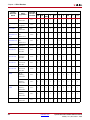
Table of Contents
Preface: About This Guide
Guide Contents . . . . . . . . . . . . . . . . . . . . . . . . . . . . . . . . . . . . . . . . . . . . . . . . . . . . . . . . . . . . .
System Generator PDF Doc Set . . . . . . . . . . . . . . . . . . . . . . . . . . . . . . . . . . . . . . . . . . . . . .
Additional Resources . . . . . . . . . . . . . . . . . . . . . . . . . . . . . . . . . . . . . . . . . . . . . . . . . . . . . . .
Conventions . . . . . . . . . . . . . . . . . . . . . . . . . . . . . . . . . . . . . . . . . . . . . . . . . . . . . . . . . . . . . . . .
17
17
17
18
Typographical . . . . . . . . . . . . . . . . . . . . . . . . . . . . . . . . . . . . . . . . . . . . . . . . . . . . . . . . . . . . 18
Online Document . . . . . . . . . . . . . . . . . . . . . . . . . . . . . . . . . . . . . . . . . . . . . . . . . . . . . . . . . 18
Chapter 1: Xilinx Blockset
Organization of Blockset Libraries . . . . . . . . . . . . . . . . . . . . . . . . . . . . . . . . . . . . . . . . . . 22
Basic Element Blocks . . . . . . . . . . . . . . . . . . . . . . . . . . . . . . . . . . . . . . . . . . . . . . . . . . . . . .
Communication Blocks . . . . . . . . . . . . . . . . . . . . . . . . . . . . . . . . . . . . . . . . . . . . . . . . . . . .
Control Logic Blocks . . . . . . . . . . . . . . . . . . . . . . . . . . . . . . . . . . . . . . . . . . . . . . . . . . . . . .
Data Type Blocks . . . . . . . . . . . . . . . . . . . . . . . . . . . . . . . . . . . . . . . . . . . . . . . . . . . . . . . . .
DSP Blocks . . . . . . . . . . . . . . . . . . . . . . . . . . . . . . . . . . . . . . . . . . . . . . . . . . . . . . . . . . . . . .
Index Blocks . . . . . . . . . . . . . . . . . . . . . . . . . . . . . . . . . . . . . . . . . . . . . . . . . . . . . . . . . . . . .
Math Blocks . . . . . . . . . . . . . . . . . . . . . . . . . . . . . . . . . . . . . . . . . . . . . . . . . . . . . . . . . . . . . .
Memory Blocks . . . . . . . . . . . . . . . . . . . . . . . . . . . . . . . . . . . . . . . . . . . . . . . . . . . . . . . . . . .
Shared Memory Blocks . . . . . . . . . . . . . . . . . . . . . . . . . . . . . . . . . . . . . . . . . . . . . . . . . . . .
Tool Blocks . . . . . . . . . . . . . . . . . . . . . . . . . . . . . . . . . . . . . . . . . . . . . . . . . . . . . . . . . . . . . .
Simulink Blocks Supported by System Generator . . . . . . . . . . . . . . . . . . . . . . . . . . . . .
22
25
26
27
28
30
38
39
40
41
43
Common Options in Block Parameter Dialog Boxes . . . . . . . . . . . . . . . . . . . . . . . . . . 44
Precision . . . . . . . . . . . . . . . . . . . . . . . . . . . . . . . . . . . . . . . . . . . . . . . . . . . . . . . . . . . . . . . . 44
Arithmetic Type . . . . . . . . . . . . . . . . . . . . . . . . . . . . . . . . . . . . . . . . . . . . . . . . . . . . . . . . . . 44
Number of Bits . . . . . . . . . . . . . . . . . . . . . . . . . . . . . . . . . . . . . . . . . . . . . . . . . . . . . . . . . . . 44
Binary Point . . . . . . . . . . . . . . . . . . . . . . . . . . . . . . . . . . . . . . . . . . . . . . . . . . . . . . . . . . . . . 44
Overflow and Quantization . . . . . . . . . . . . . . . . . . . . . . . . . . . . . . . . . . . . . . . . . . . . . . . . 44
Latency . . . . . . . . . . . . . . . . . . . . . . . . . . . . . . . . . . . . . . . . . . . . . . . . . . . . . . . . . . . . . . . . . . 45
Provide Synchronous Reset Port . . . . . . . . . . . . . . . . . . . . . . . . . . . . . . . . . . . . . . . . . . . . 45
Provide Enable Port . . . . . . . . . . . . . . . . . . . . . . . . . . . . . . . . . . . . . . . . . . . . . . . . . . . . . . . 45
Sample Period . . . . . . . . . . . . . . . . . . . . . . . . . . . . . . . . . . . . . . . . . . . . . . . . . . . . . . . . . . . . 46
Use Behavioral HDL (otherwise use core) . . . . . . . . . . . . . . . . . . . . . . . . . . . . . . . . . . . . 46
Use Core Placement Information . . . . . . . . . . . . . . . . . . . . . . . . . . . . . . . . . . . . . . . . . . . . 46
Use XtremeDSP Slice . . . . . . . . . . . . . . . . . . . . . . . . . . . . . . . . . . . . . . . . . . . . . . . . . . . . . . 46
Placement . . . . . . . . . . . . . . . . . . . . . . . . . . . . . . . . . . . . . . . . . . . . . . . . . . . . . . . . . . . . . . . 46
FPGA Area (Slices, FFs, LUTs, IOBs, Embedded Mults, TBUFs) / Use Area Above For
Estimation . . . . . . . . . . . . . . . . . . . . . . . . . . . . . . . . . . . . . . . . . . . . . . . . . . . . . . . . . . . . . 47
Block Reference Pages . . . . . . . . . . . . . . . . . . . . . . . . . . . . . . . . . . . . . . . . . . . . . . . . . . . . . . 48
Accumulator . . . . . . . . . . . . . . . . . . . . . . . . . . . . . . . . . . . . . . . . . . . . . . . . . . . . . . . . . . . . . . . . 49
Block Interface . . . . . . . . . . . . . . . . . . . . . . . . . . . . . . . . . . . . . . . . . . . . . . . . . . . . . . . . . . . 49
Block Parameters . . . . . . . . . . . . . . . . . . . . . . . . . . . . . . . . . . . . . . . . . . . . . . . . . . . . . . . . . 49
Xilinx LogiCORE . . . . . . . . . . . . . . . . . . . . . . . . . . . . . . . . . . . . . . . . . . . . . . . . . . . . . . . . . 50
Addressable Shift Register . . . . . . . . . . . . . . . . . . . . . . . . . . . . . . . . . . . . . . . . . . . . . . . . . . 51
Block Interface . . . . . . . . . . . . . . . . . . . . . . . . . . . . . . . . . . . . . . . . . . . . . . . . . . . . . . . . . . . 51
Block Parameters . . . . . . . . . . . . . . . . . . . . . . . . . . . . . . . . . . . . . . . . . . . . . . . . . . . . . . . . . 52
System Generator for DSP Reference Guide
UG638 (v11.4) December 2, 2009
www.xilinx.com
3
Xilinx LogiCORE . . . . . . . . . . . . . . . . . . . . . . . . . . . . . . . . . . . . . . . . . . . . . . . . . . . . . . . . . 52
AddSub . . . . . . . . . . . . . . . . . . . . . . . . . . . . . . . . . . . . . . . . . . . . . . . . . . . . . . . . . . . . . . . . . . . . . 53
Block Parameters . . . . . . . . . . . . . . . . . . . . . . . . . . . . . . . . . . . . . . . . . . . . . . . . . . . . . . . . . 53
Xilinx LogiCORE . . . . . . . . . . . . . . . . . . . . . . . . . . . . . . . . . . . . . . . . . . . . . . . . . . . . . . . . . 54
Assert . . . . . . . . . . . . . . . . . . . . . . . . . . . . . . . . . . . . . . . . . . . . . . . . . . . . . . . . . . . . . . . . . . . . . . . 55
Block Parameters . . . . . . . . . . . . . . . . . . . . . . . . . . . . . . . . . . . . . . . . . . . . . . . . . . . . . . . . . 55
Using the Assert block to Resolve Rates and Types . . . . . . . . . . . . . . . . . . . . . . . . . . . . 55
BitBasher . . . . . . . . . . . . . . . . . . . . . . . . . . . . . . . . . . . . . . . . . . . . . . . . . . . . . . . . . . . . . . . . . . . 57
Block Parameters . . . . . . . . . . . . . . . . . . . . . . . . . . . . . . . . . . . . . . . . . . . . . . . . . . . . . . . . . 57
Supported Verilog Constructs . . . . . . . . . . . . . . . . . . . . . . . . . . . . . . . . . . . . . . . . . . . . . . 57
Limitations . . . . . . . . . . . . . . . . . . . . . . . . . . . . . . . . . . . . . . . . . . . . . . . . . . . . . . . . . . . . . . 59
Black Box . . . . . . . . . . . . . . . . . . . . . . . . . . . . . . . . . . . . . . . . . . . . . . . . . . . . . . . . . . . . . . . . . . . 60
Requirements on HDL for Black Boxes . . . . . . . . . . . . . . . . . . . . . . . . . . . . . . . . . . . . . .
The Black Box Configuration Wizard . . . . . . . . . . . . . . . . . . . . . . . . . . . . . . . . . . . . . . . .
The Black Box Configuration M-Function . . . . . . . . . . . . . . . . . . . . . . . . . . . . . . . . . . . .
Sample Periods . . . . . . . . . . . . . . . . . . . . . . . . . . . . . . . . . . . . . . . . . . . . . . . . . . . . . . . . . . .
Block Parameters . . . . . . . . . . . . . . . . . . . . . . . . . . . . . . . . . . . . . . . . . . . . . . . . . . . . . . . . .
Data Type Translation for HDL Co-Simulation . . . . . . . . . . . . . . . . . . . . . . . . . . . . . . .
An Example . . . . . . . . . . . . . . . . . . . . . . . . . . . . . . . . . . . . . . . . . . . . . . . . . . . . . . . . . . . . . .
See Also . . . . . . . . . . . . . . . . . . . . . . . . . . . . . . . . . . . . . . . . . . . . . . . . . . . . . . . . . . . . . . . . .
60
61
62
63
64
65
66
66
ChipScope . . . . . . . . . . . . . . . . . . . . . . . . . . . . . . . . . . . . . . . . . . . . . . . . . . . . . . . . . . . . . . . . . . 67
Hardware and Software Requirements . . . . . . . . . . . . . . . . . . . . . . . . . . . . . . . . . . . . . .
Block Parameters . . . . . . . . . . . . . . . . . . . . . . . . . . . . . . . . . . . . . . . . . . . . . . . . . . . . . . . . .
ChipScope Project File . . . . . . . . . . . . . . . . . . . . . . . . . . . . . . . . . . . . . . . . . . . . . . . . . . . . .
Importing Data Into MATLAB Workspace From ChipScope . . . . . . . . . . . . . . . . . . . .
Known Issues . . . . . . . . . . . . . . . . . . . . . . . . . . . . . . . . . . . . . . . . . . . . . . . . . . . . . . . . . . . .
More Information . . . . . . . . . . . . . . . . . . . . . . . . . . . . . . . . . . . . . . . . . . . . . . . . . . . . . . . . .
67
68
69
69
70
70
CIC Compiler 1.2 . . . . . . . . . . . . . . . . . . . . . . . . . . . . . . . . . . . . . . . . . . . . . . . . . . . . . . . . . . . . 71
Block Parameters Dialog Box . . . . . . . . . . . . . . . . . . . . . . . . . . . . . . . . . . . . . . . . . . . . . . . 71
Xilinx LogiCORE . . . . . . . . . . . . . . . . . . . . . . . . . . . . . . . . . . . . . . . . . . . . . . . . . . . . . . . . . 73
CIC Compiler 1.3 . . . . . . . . . . . . . . . . . . . . . . . . . . . . . . . . . . . . . . . . . . . . . . . . . . . . . . . . . . . . 74
Block Parameters Dialog Box . . . . . . . . . . . . . . . . . . . . . . . . . . . . . . . . . . . . . . . . . . . . . . . 74
Xilinx LogiCORE . . . . . . . . . . . . . . . . . . . . . . . . . . . . . . . . . . . . . . . . . . . . . . . . . . . . . . . . . 75
Clock Enable Probe . . . . . . . . . . . . . . . . . . . . . . . . . . . . . . . . . . . . . . . . . . . . . . . . . . . . . . . . . 76
Clock Probe . . . . . . . . . . . . . . . . . . . . . . . . . . . . . . . . . . . . . . . . . . . . . . . . . . . . . . . . . . . . . . . . . 78
CMult . . . . . . . . . . . . . . . . . . . . . . . . . . . . . . . . . . . . . . . . . . . . . . . . . . . . . . . . . . . . . . . . . . . . . . 79
Block Parameters . . . . . . . . . . . . . . . . . . . . . . . . . . . . . . . . . . . . . . . . . . . . . . . . . . . . . . . . . 79
Xilinx LogiCORE . . . . . . . . . . . . . . . . . . . . . . . . . . . . . . . . . . . . . . . . . . . . . . . . . . . . . . . . . 80
Complex Multiplier 3.0 . . . . . . . . . . . . . . . . . . . . . . . . . . . . . . . . . . . . . . . . . . . . . . . . . . . . . . 81
Block Parameters Dialog Box . . . . . . . . . . . . . . . . . . . . . . . . . . . . . . . . . . . . . . . . . . . . . . . 81
Xilinx LogiCORE . . . . . . . . . . . . . . . . . . . . . . . . . . . . . . . . . . . . . . . . . . . . . . . . . . . . . . . . . 82
Complex Multiplier 3.1 . . . . . . . . . . . . . . . . . . . . . . . . . . . . . . . . . . . . . . . . . . . . . . . . . . . . . . 83
Block Parameters Dialog Box . . . . . . . . . . . . . . . . . . . . . . . . . . . . . . . . . . . . . . . . . . . . . . . 83
Xilinx LogiCORE . . . . . . . . . . . . . . . . . . . . . . . . . . . . . . . . . . . . . . . . . . . . . . . . . . . . . . . . . 84
Concat . . . . . . . . . . . . . . . . . . . . . . . . . . . . . . . . . . . . . . . . . . . . . . . . . . . . . . . . . . . . . . . . . . . . . . 85
Block Interface . . . . . . . . . . . . . . . . . . . . . . . . . . . . . . . . . . . . . . . . . . . . . . . . . . . . . . . . . . . 85
Block Parameters . . . . . . . . . . . . . . . . . . . . . . . . . . . . . . . . . . . . . . . . . . . . . . . . . . . . . . . . . 85
Configurable Subsystem Manager . . . . . . . . . . . . . . . . . . . . . . . . . . . . . . . . . . . . . . . . . . . 86
Block Parameters . . . . . . . . . . . . . . . . . . . . . . . . . . . . . . . . . . . . . . . . . . . . . . . . . . . . . . . . . 87
Constant . . . . . . . . . . . . . . . . . . . . . . . . . . . . . . . . . . . . . . . . . . . . . . . . . . . . . . . . . . . . . . . . . . . . 88
4
www.xilinx.com
System Generator for DSP Reference Guide
UG638 (v11.4) December 2, 2009
Block Parameters . . . . . . . . . . . . . . . . . . . . . . . . . . . . . . . . . . . . . . . . . . . . . . . . . . . . . . . . . 88
Appendix: DSP48 Control Instruction Format . . . . . . . . . . . . . . . . . . . . . . . . . . . . . . . . 89
Convert . . . . . . . . . . . . . . . . . . . . . . . . . . . . . . . . . . . . . . . . . . . . . . . . . . . . . . . . . . . . . . . . . . . . . 91
Block Parameters . . . . . . . . . . . . . . . . . . . . . . . . . . . . . . . . . . . . . . . . . . . . . . . . . . . . . . . . . 91
Convolutional Encoder v6_1 . . . . . . . . . . . . . . . . . . . . . . . . . . . . . . . . . . . . . . . . . . . . . . . . . 93
Block Interface . . . . . . . . . . . . . . . . . . . . . . . . . . . . . . . . . . . . . . . . . . . . . . . . . . . . . . . . . . . 93
Block Parameters Dialog Box . . . . . . . . . . . . . . . . . . . . . . . . . . . . . . . . . . . . . . . . . . . . . . . 93
Xilinx LogiCORE . . . . . . . . . . . . . . . . . . . . . . . . . . . . . . . . . . . . . . . . . . . . . . . . . . . . . . . . . 94
Convolution Encoder 7.0 . . . . . . . . . . . . . . . . . . . . . . . . . . . . . . . . . . . . . . . . . . . . . . . . . . . . 95
Block Parameters Dialog Box . . . . . . . . . . . . . . . . . . . . . . . . . . . . . . . . . . . . . . . . . . . . . . . 95
Xilinx LogiCORE . . . . . . . . . . . . . . . . . . . . . . . . . . . . . . . . . . . . . . . . . . . . . . . . . . . . . . . . . 96
CORDIC 4.0. . . . . . . . . . . . . . . . . . . . . . . . . . . . . . . . . . . . . . . . . . . . . . . . . . . . . . . . . . . . . . . . . 97
Block Parameters Dialog Box . . . . . . . . . . . . . . . . . . . . . . . . . . . . . . . . . . . . . . . . . . . . . . . 97
Xilinx LogiCORE . . . . . . . . . . . . . . . . . . . . . . . . . . . . . . . . . . . . . . . . . . . . . . . . . . . . . . . . 100
Counter . . . . . . . . . . . . . . . . . . . . . . . . . . . . . . . . . . . . . . . . . . . . . . . . . . . . . . . . . . . . . . . . . . . . 101
Block Parameters . . . . . . . . . . . . . . . . . . . . . . . . . . . . . . . . . . . . . . . . . . . . . . . . . . . . . . . . 102
Xilinx LogiCORE . . . . . . . . . . . . . . . . . . . . . . . . . . . . . . . . . . . . . . . . . . . . . . . . . . . . . . . . 103
DAFIR v9_0 . . . . . . . . . . . . . . . . . . . . . . . . . . . . . . . . . . . . . . . . . . . . . . . . . . . . . . . . . . . . . . . . 104
Block Interface . . . . . . . . . . . . . . . . . . . . . . . . . . . . . . . . . . . . . . . . . . . . . . . . . . . . . . . . . .
Reloading Coefficients . . . . . . . . . . . . . . . . . . . . . . . . . . . . . . . . . . . . . . . . . . . . . . . . . . .
Optional Ports for Reloading Coefficients . . . . . . . . . . . . . . . . . . . . . . . . . . . . . . . . . . .
Block Parameters Dialog Box . . . . . . . . . . . . . . . . . . . . . . . . . . . . . . . . . . . . . . . . . . . . . .
Xilinx LogiCORE . . . . . . . . . . . . . . . . . . . . . . . . . . . . . . . . . . . . . . . . . . . . . . . . . . . . . . . .
104
105
105
106
107
DDS Compiler 2.1 . . . . . . . . . . . . . . . . . . . . . . . . . . . . . . . . . . . . . . . . . . . . . . . . . . . . . . . . . . 108
Block Interface . . . . . . . . . . . . . . . . . . . . . . . . . . . . . . . . . . . . . . . . . . . . . . . . . . . . . . . . . . 109
Block Parameters . . . . . . . . . . . . . . . . . . . . . . . . . . . . . . . . . . . . . . . . . . . . . . . . . . . . . . . . 110
Xilinx LogiCORE . . . . . . . . . . . . . . . . . . . . . . . . . . . . . . . . . . . . . . . . . . . . . . . . . . . . . . . . 111
DDS Compiler 3.0 . . . . . . . . . . . . . . . . . . . . . . . . . . . . . . . . . . . . . . . . . . . . . . . . . . . . . . . . . . 112
Block Interface . . . . . . . . . . . . . . . . . . . . . . . . . . . . . . . . . . . . . . . . . . . . . . . . . . . . . . . . . . 113
Block Parameters . . . . . . . . . . . . . . . . . . . . . . . . . . . . . . . . . . . . . . . . . . . . . . . . . . . . . . . . 114
Xilinx LogiCORE . . . . . . . . . . . . . . . . . . . . . . . . . . . . . . . . . . . . . . . . . . . . . . . . . . . . . . . . 115
DDS Compiler 4.0 . . . . . . . . . . . . . . . . . . . . . . . . . . . . . . . . . . . . . . . . . . . . . . . . . . . . . . . . . . 116
Architecture Overview . . . . . . . . . . . . . . . . . . . . . . . . . . . . . . . . . . . . . . . . . . . . . . . . . . .
Block Interface . . . . . . . . . . . . . . . . . . . . . . . . . . . . . . . . . . . . . . . . . . . . . . . . . . . . . . . . . .
Block Parameters . . . . . . . . . . . . . . . . . . . . . . . . . . . . . . . . . . . . . . . . . . . . . . . . . . . . . . . .
Xilinx LogiCORE . . . . . . . . . . . . . . . . . . . . . . . . . . . . . . . . . . . . . . . . . . . . . . . . . . . . . . . .
116
117
118
121
Delay . . . . . . . . . . . . . . . . . . . . . . . . . . . . . . . . . . . . . . . . . . . . . . . . . . . . . . . . . . . . . . . . . . . . . . 122
Block Parameters . . . . . . . . . . . . . . . . . . . . . . . . . . . . . . . . . . . . . . . . . . . . . . . . . . . . . . . .
Logic Synthesis using Behavioral HDL . . . . . . . . . . . . . . . . . . . . . . . . . . . . . . . . . . . . .
Logic Synthesis using Structural HDL . . . . . . . . . . . . . . . . . . . . . . . . . . . . . . . . . . . . . .
Implementing Long Delays . . . . . . . . . . . . . . . . . . . . . . . . . . . . . . . . . . . . . . . . . . . . . . .
Re-settable Delays and Initial Values . . . . . . . . . . . . . . . . . . . . . . . . . . . . . . . . . . . . . . .
Xilinx LogiCORE . . . . . . . . . . . . . . . . . . . . . . . . . . . . . . . . . . . . . . . . . . . . . . . . . . . . . . . .
122
123
123
125
125
125
Depuncture . . . . . . . . . . . . . . . . . . . . . . . . . . . . . . . . . . . . . . . . . . . . . . . . . . . . . . . . . . . . . . . . 126
Block Parameters . . . . . . . . . . . . . . . . . . . . . . . . . . . . . . . . . . . . . . . . . . . . . . . . . . . . . . . . 127
Disregard Subsystem. . . . . . . . . . . . . . . . . . . . . . . . . . . . . . . . . . . . . . . . . . . . . . . . . . . . . . . 128
Divider Generator 2.0 . . . . . . . . . . . . . . . . . . . . . . . . . . . . . . . . . . . . . . . . . . . . . . . . . . . . . . 129
Block Parameters . . . . . . . . . . . . . . . . . . . . . . . . . . . . . . . . . . . . . . . . . . . . . . . . . . . . . . . . 129
Xilinx LogiCORE . . . . . . . . . . . . . . . . . . . . . . . . . . . . . . . . . . . . . . . . . . . . . . . . . . . . . . . . 130
Divider Generator 3.0 . . . . . . . . . . . . . . . . . . . . . . . . . . . . . . . . . . . . . . . . . . . . . . . . . . . . . . 131
System Generator for DSP Reference Guide
UG638 (v11.4) December 2, 2009
www.xilinx.com
5
Block Parameters . . . . . . . . . . . . . . . . . . . . . . . . . . . . . . . . . . . . . . . . . . . . . . . . . . . . . . . . 131
Xilinx LogiCORE . . . . . . . . . . . . . . . . . . . . . . . . . . . . . . . . . . . . . . . . . . . . . . . . . . . . . . . . 132
Down Sample . . . . . . . . . . . . . . . . . . . . . . . . . . . . . . . . . . . . . . . . . . . . . . . . . . . . . . . . . . . . . . 133
Zero Latency Down Sample . . . . . . . . . . . . . . . . . . . . . . . . . . . . . . . . . . . . . . . . . . . . . . .
Down Sample with Latency . . . . . . . . . . . . . . . . . . . . . . . . . . . . . . . . . . . . . . . . . . . . . . .
Block Parameters . . . . . . . . . . . . . . . . . . . . . . . . . . . . . . . . . . . . . . . . . . . . . . . . . . . . . . . .
Xilinx LogiCORE . . . . . . . . . . . . . . . . . . . . . . . . . . . . . . . . . . . . . . . . . . . . . . . . . . . . . . . .
133
134
135
135
DSP48 . . . . . . . . . . . . . . . . . . . . . . . . . . . . . . . . . . . . . . . . . . . . . . . . . . . . . . . . . . . . . . . . . . . . . 136
Block Parameters . . . . . . . . . . . . . . . . . . . . . . . . . . . . . . . . . . . . . . . . . . . . . . . . . . . . . . . . 136
See Also . . . . . . . . . . . . . . . . . . . . . . . . . . . . . . . . . . . . . . . . . . . . . . . . . . . . . . . . . . . . . . . . 138
DSP48 Macro . . . . . . . . . . . . . . . . . . . . . . . . . . . . . . . . . . . . . . . . . . . . . . . . . . . . . . . . . . . . . . 139
Block Interface . . . . . . . . . . . . . . . . . . . . . . . . . . . . . . . . . . . . . . . . . . . . . . . . . . . . . . . . . .
Block Parameters . . . . . . . . . . . . . . . . . . . . . . . . . . . . . . . . . . . . . . . . . . . . . . . . . . . . . . . .
Entering Opmodes in the DSP48 Macro Block . . . . . . . . . . . . . . . . . . . . . . . . . . . . . . .
Entering Pipeline Options and Editing Custom Pipeline Options . . . . . . . . . . . . . . .
DSP48 Macro Limitations . . . . . . . . . . . . . . . . . . . . . . . . . . . . . . . . . . . . . . . . . . . . . . . . .
See Also . . . . . . . . . . . . . . . . . . . . . . . . . . . . . . . . . . . . . . . . . . . . . . . . . . . . . . . . . . . . . . . .
139
139
140
146
147
147
DSP48 macro 2.0 . . . . . . . . . . . . . . . . . . . . . . . . . . . . . . . . . . . . . . . . . . . . . . . . . . . . . . . . . . . 148
Block Parameters . . . . . . . . . . . . . . . . . . . . . . . . . . . . . . . . . . . . . . . . . . . . . . . . . . . . . . . . 148
Xilinx LogiCORE . . . . . . . . . . . . . . . . . . . . . . . . . . . . . . . . . . . . . . . . . . . . . . . . . . . . . . . . 152
See Also . . . . . . . . . . . . . . . . . . . . . . . . . . . . . . . . . . . . . . . . . . . . . . . . . . . . . . . . . . . . . . . . 152
DSP48A . . . . . . . . . . . . . . . . . . . . . . . . . . . . . . . . . . . . . . . . . . . . . . . . . . . . . . . . . . . . . . . . . . . . 153
Block Parameters . . . . . . . . . . . . . . . . . . . . . . . . . . . . . . . . . . . . . . . . . . . . . . . . . . . . . . . . 153
See Also . . . . . . . . . . . . . . . . . . . . . . . . . . . . . . . . . . . . . . . . . . . . . . . . . . . . . . . . . . . . . . . . 155
DSP48E . . . . . . . . . . . . . . . . . . . . . . . . . . . . . . . . . . . . . . . . . . . . . . . . . . . . . . . . . . . . . . . . . . . . 156
Block Parameters . . . . . . . . . . . . . . . . . . . . . . . . . . . . . . . . . . . . . . . . . . . . . . . . . . . . . . . . 156
See Also . . . . . . . . . . . . . . . . . . . . . . . . . . . . . . . . . . . . . . . . . . . . . . . . . . . . . . . . . . . . . . . . 160
Dual Port RAM . . . . . . . . . . . . . . . . . . . . . . . . . . . . . . . . . . . . . . . . . . . . . . . . . . . . . . . . . . . . 161
Block Interface . . . . . . . . . . . . . . . . . . . . . . . . . . . . . . . . . . . . . . . . . . . . . . . . . . . . . . . . . . 161
Block Parameters . . . . . . . . . . . . . . . . . . . . . . . . . . . . . . . . . . . . . . . . . . . . . . . . . . . . . . . . 163
Xilinx LogiCORE . . . . . . . . . . . . . . . . . . . . . . . . . . . . . . . . . . . . . . . . . . . . . . . . . . . . . . . . 165
EDK Processor . . . . . . . . . . . . . . . . . . . . . . . . . . . . . . . . . . . . . . . . . . . . . . . . . . . . . . . . . . . . . 167
Memory Map Interface . . . . . . . . . . . . . . . . . . . . . . . . . . . . . . . . . . . . . . . . . . . . . . . . . . .
Block Parameters . . . . . . . . . . . . . . . . . . . . . . . . . . . . . . . . . . . . . . . . . . . . . . . . . . . . . . . .
Known Issues . . . . . . . . . . . . . . . . . . . . . . . . . . . . . . . . . . . . . . . . . . . . . . . . . . . . . . . . . . .
Online Documentation for the MicroBlaze Processor . . . . . . . . . . . . . . . . . . . . . . . . .
167
168
170
170
Expression . . . . . . . . . . . . . . . . . . . . . . . . . . . . . . . . . . . . . . . . . . . . . . . . . . . . . . . . . . . . . . . . . 171
Block Parameters . . . . . . . . . . . . . . . . . . . . . . . . . . . . . . . . . . . . . . . . . . . . . . . . . . . . . . . . 171
Fast Fourier Transform 6.0 . . . . . . . . . . . . . . . . . . . . . . . . . . . . . . . . . . . . . . . . . . . . . . . . . . 172
Theory of Operation . . . . . . . . . . . . . . . . . . . . . . . . . . . . . . . . . . . . . . . . . . . . . . . . . . . . .
Block Interface . . . . . . . . . . . . . . . . . . . . . . . . . . . . . . . . . . . . . . . . . . . . . . . . . . . . . . . . . .
Block Parameters . . . . . . . . . . . . . . . . . . . . . . . . . . . . . . . . . . . . . . . . . . . . . . . . . . . . . . . .
Block Timing . . . . . . . . . . . . . . . . . . . . . . . . . . . . . . . . . . . . . . . . . . . . . . . . . . . . . . . . . . . .
Xilinx LogiCORE . . . . . . . . . . . . . . . . . . . . . . . . . . . . . . . . . . . . . . . . . . . . . . . . . . . . . . . .
172
172
175
176
176
Fast Fourier Transform 7.0 . . . . . . . . . . . . . . . . . . . . . . . . . . . . . . . . . . . . . . . . . . . . . . . . . . 177
Theory of Operation . . . . . . . . . . . . . . . . . . . . . . . . . . . . . . . . . . . . . . . . . . . . . . . . . . . . .
Block Interface . . . . . . . . . . . . . . . . . . . . . . . . . . . . . . . . . . . . . . . . . . . . . . . . . . . . . . . . . .
Block Parameters . . . . . . . . . . . . . . . . . . . . . . . . . . . . . . . . . . . . . . . . . . . . . . . . . . . . . . . .
Block Timing . . . . . . . . . . . . . . . . . . . . . . . . . . . . . . . . . . . . . . . . . . . . . . . . . . . . . . . . . . . .
Xilinx LogiCORE . . . . . . . . . . . . . . . . . . . . . . . . . . . . . . . . . . . . . . . . . . . . . . . . . . . . . . . .
177
177
180
182
182
FDATool . . . . . . . . . . . . . . . . . . . . . . . . . . . . . . . . . . . . . . . . . . . . . . . . . . . . . . . . . . . . . . . . . . . 183
6
www.xilinx.com
System Generator for DSP Reference Guide
UG638 (v11.4) December 2, 2009
Example of Use . . . . . . . . . . . . . . . . . . . . . . . . . . . . . . . . . . . . . . . . . . . . . . . . . . . . . . . . . . 183
FDA Tool Interface . . . . . . . . . . . . . . . . . . . . . . . . . . . . . . . . . . . . . . . . . . . . . . . . . . . . . . . 183
FIFO . . . . . . . . . . . . . . . . . . . . . . . . . . . . . . . . . . . . . . . . . . . . . . . . . . . . . . . . . . . . . . . . . . . . . . . 184
Block Parameters . . . . . . . . . . . . . . . . . . . . . . . . . . . . . . . . . . . . . . . . . . . . . . . . . . . . . . . . 184
Xilinx LogiCORE . . . . . . . . . . . . . . . . . . . . . . . . . . . . . . . . . . . . . . . . . . . . . . . . . . . . . . . . 184
FIR Compiler 4.0 . . . . . . . . . . . . . . . . . . . . . . . . . . . . . . . . . . . . . . . . . . . . . . . . . . . . . . . . . . . 185
Block Interface . . . . . . . . . . . . . . . . . . . . . . . . . . . . . . . . . . . . . . . . . . . . . . . . . . . . . . . . . .
Block Parameters . . . . . . . . . . . . . . . . . . . . . . . . . . . . . . . . . . . . . . . . . . . . . . . . . . . . . . . .
Xilinx LogiCORE . . . . . . . . . . . . . . . . . . . . . . . . . . . . . . . . . . . . . . . . . . . . . . . . . . . . . . . .
Known Issues . . . . . . . . . . . . . . . . . . . . . . . . . . . . . . . . . . . . . . . . . . . . . . . . . . . . . . . . . . .
185
186
191
191
FIR Compiler 5.0 . . . . . . . . . . . . . . . . . . . . . . . . . . . . . . . . . . . . . . . . . . . . . . . . . . . . . . . . . . . 193
Block Interface . . . . . . . . . . . . . . . . . . . . . . . . . . . . . . . . . . . . . . . . . . . . . . . . . . . . . . . . . . 193
Block Parameters . . . . . . . . . . . . . . . . . . . . . . . . . . . . . . . . . . . . . . . . . . . . . . . . . . . . . . . . 194
Xilinx LogiCORE . . . . . . . . . . . . . . . . . . . . . . . . . . . . . . . . . . . . . . . . . . . . . . . . . . . . . . . . 200
From FIFO . . . . . . . . . . . . . . . . . . . . . . . . . . . . . . . . . . . . . . . . . . . . . . . . . . . . . . . . . . . . . . . . . 201
Block Parameters . . . . . . . . . . . . . . . . . . . . . . . . . . . . . . . . . . . . . . . . . . . . . . . . . . . . . . . . 201
Xilinx LogiCORE . . . . . . . . . . . . . . . . . . . . . . . . . . . . . . . . . . . . . . . . . . . . . . . . . . . . . . . . 202
See Also . . . . . . . . . . . . . . . . . . . . . . . . . . . . . . . . . . . . . . . . . . . . . . . . . . . . . . . . . . . . . . . . 202
From Register . . . . . . . . . . . . . . . . . . . . . . . . . . . . . . . . . . . . . . . . . . . . . . . . . . . . . . . . . . . . . . 203
Block Parameters . . . . . . . . . . . . . . . . . . . . . . . . . . . . . . . . . . . . . . . . . . . . . . . . . . . . . . . . 203
Crossing Clock Domain . . . . . . . . . . . . . . . . . . . . . . . . . . . . . . . . . . . . . . . . . . . . . . . . . . 203
See Also . . . . . . . . . . . . . . . . . . . . . . . . . . . . . . . . . . . . . . . . . . . . . . . . . . . . . . . . . . . . . . . . 204
Gateway In . . . . . . . . . . . . . . . . . . . . . . . . . . . . . . . . . . . . . . . . . . . . . . . . . . . . . . . . . . . . . . . . 205
Gateway Blocks . . . . . . . . . . . . . . . . . . . . . . . . . . . . . . . . . . . . . . . . . . . . . . . . . . . . . . . . . 205
Block Parameters . . . . . . . . . . . . . . . . . . . . . . . . . . . . . . . . . . . . . . . . . . . . . . . . . . . . . . . . 205
Gateway Out . . . . . . . . . . . . . . . . . . . . . . . . . . . . . . . . . . . . . . . . . . . . . . . . . . . . . . . . . . . . . . . 207
Gateway Blocks . . . . . . . . . . . . . . . . . . . . . . . . . . . . . . . . . . . . . . . . . . . . . . . . . . . . . . . . . 207
Block Parameters . . . . . . . . . . . . . . . . . . . . . . . . . . . . . . . . . . . . . . . . . . . . . . . . . . . . . . . . 207
Indeterminate Probe . . . . . . . . . . . . . . . . . . . . . . . . . . . . . . . . . . . . . . . . . . . . . . . . . . . . . . . 209
Interleaver Deinterleaver v5_0 . . . . . . . . . . . . . . . . . . . . . . . . . . . . . . . . . . . . . . . . . . . . . . 210
Block Interface . . . . . . . . . . . . . . . . . . . . . . . . . . . . . . . . . . . . . . . . . . . . . . . . . . . . . . . . . . 211
Block Parameters . . . . . . . . . . . . . . . . . . . . . . . . . . . . . . . . . . . . . . . . . . . . . . . . . . . . . . . . 211
Xilinx LogiCORE . . . . . . . . . . . . . . . . . . . . . . . . . . . . . . . . . . . . . . . . . . . . . . . . . . . . . . . . 211
Interleaver Deinterleaver 5.1 . . . . . . . . . . . . . . . . . . . . . . . . . . . . . . . . . . . . . . . . . . . . . . . 212
Block Interface . . . . . . . . . . . . . . . . . . . . . . . . . . . . . . . . . . . . . . . . . . . . . . . . . . . . . . . . . . 213
Block Parameters . . . . . . . . . . . . . . . . . . . . . . . . . . . . . . . . . . . . . . . . . . . . . . . . . . . . . . . . 213
Xilinx LogiCORE . . . . . . . . . . . . . . . . . . . . . . . . . . . . . . . . . . . . . . . . . . . . . . . . . . . . . . . . 214
Inverter . . . . . . . . . . . . . . . . . . . . . . . . . . . . . . . . . . . . . . . . . . . . . . . . . . . . . . . . . . . . . . . . . . . . 215
Block Parameters . . . . . . . . . . . . . . . . . . . . . . . . . . . . . . . . . . . . . . . . . . . . . . . . . . . . . . . . 215
JTAG Co-Simulation . . . . . . . . . . . . . . . . . . . . . . . . . . . . . . . . . . . . . . . . . . . . . . . . . . . . . . . 216
Block Parameters . . . . . . . . . . . . . . . . . . . . . . . . . . . . . . . . . . . . . . . . . . . . . . . . . . . . . . . . 216
LFSR . . . . . . . . . . . . . . . . . . . . . . . . . . . . . . . . . . . . . . . . . . . . . . . . . . . . . . . . . . . . . . . . . . . . . . . 218
Block Interface . . . . . . . . . . . . . . . . . . . . . . . . . . . . . . . . . . . . . . . . . . . . . . . . . . . . . . . . . . 218
Block Parameters . . . . . . . . . . . . . . . . . . . . . . . . . . . . . . . . . . . . . . . . . . . . . . . . . . . . . . . . 218
Logical . . . . . . . . . . . . . . . . . . . . . . . . . . . . . . . . . . . . . . . . . . . . . . . . . . . . . . . . . . . . . . . . . . . . . 220
Block Parameters . . . . . . . . . . . . . . . . . . . . . . . . . . . . . . . . . . . . . . . . . . . . . . . . . . . . . . . . 220
Xilinx LogiCORE . . . . . . . . . . . . . . . . . . . . . . . . . . . . . . . . . . . . . . . . . . . . . . . . . . . . . . . . 220
MCode . . . . . . . . . . . . . . . . . . . . . . . . . . . . . . . . . . . . . . . . . . . . . . . . . . . . . . . . . . . . . . . . . . . . . 221
Configuring an MCode Block . . . . . . . . . . . . . . . . . . . . . . . . . . . . . . . . . . . . . . . . . . . . . 221
MATLAB Language Support . . . . . . . . . . . . . . . . . . . . . . . . . . . . . . . . . . . . . . . . . . . . . . 222
System Generator for DSP Reference Guide
UG638 (v11.4) December 2, 2009
www.xilinx.com
7
Block Parameters Dialog Box . . . . . . . . . . . . . . . . . . . . . . . . . . . . . . . . . . . . . . . . . . . . . . 241
MicroBlaze Processor. . . . . . . . . . . . . . . . . . . . . . . . . . . . . . . . . . . . . . . . . . . . . . . . . . . . . . . 242
Block Interface . . . . . . . . . . . . . . . . . . . . . . . . . . . . . . . . . . . . . . . . . . . . . . . . . . . . . . . . . .
Block Parameters . . . . . . . . . . . . . . . . . . . . . . . . . . . . . . . . . . . . . . . . . . . . . . . . . . . . . . . .
MicroBlaze Software Issues . . . . . . . . . . . . . . . . . . . . . . . . . . . . . . . . . . . . . . . . . . . . . . .
Known Issues . . . . . . . . . . . . . . . . . . . . . . . . . . . . . . . . . . . . . . . . . . . . . . . . . . . . . . . . . . .
Online Documentation for the MicroBlaze Processor . . . . . . . . . . . . . . . . . . . . . . . . .
See Also . . . . . . . . . . . . . . . . . . . . . . . . . . . . . . . . . . . . . . . . . . . . . . . . . . . . . . . . . . . . . . . .
242
245
247
249
250
250
ModelSim . . . . . . . . . . . . . . . . . . . . . . . . . . . . . . . . . . . . . . . . . . . . . . . . . . . . . . . . . . . . . . . . . 251
Block Parameters . . . . . . . . . . . . . . . . . . . . . . . . . . . . . . . . . . . . . . . . . . . . . . . . . . . . . . . . 251
Fine Points . . . . . . . . . . . . . . . . . . . . . . . . . . . . . . . . . . . . . . . . . . . . . . . . . . . . . . . . . . . . . . 253
Mult . . . . . . . . . . . . . . . . . . . . . . . . . . . . . . . . . . . . . . . . . . . . . . . . . . . . . . . . . . . . . . . . . . . . . . . 256
Block Parameters . . . . . . . . . . . . . . . . . . . . . . . . . . . . . . . . . . . . . . . . . . . . . . . . . . . . . . . . 256
Xilinx LogiCORE . . . . . . . . . . . . . . . . . . . . . . . . . . . . . . . . . . . . . . . . . . . . . . . . . . . . . . . . 257
Multiple Subsystem Generator . . . . . . . . . . . . . . . . . . . . . . . . . . . . . . . . . . . . . . . . . . . . . 258
Block Parameters . . . . . . . . . . . . . . . . . . . . . . . . . . . . . . . . . . . . . . . . . . . . . . . . . . . . . . . .
Design Generation . . . . . . . . . . . . . . . . . . . . . . . . . . . . . . . . . . . . . . . . . . . . . . . . . . . . . . .
Multiple Clock Support . . . . . . . . . . . . . . . . . . . . . . . . . . . . . . . . . . . . . . . . . . . . . . . . . . .
Files Generated . . . . . . . . . . . . . . . . . . . . . . . . . . . . . . . . . . . . . . . . . . . . . . . . . . . . . . . . . .
258
258
261
261
Mux . . . . . . . . . . . . . . . . . . . . . . . . . . . . . . . . . . . . . . . . . . . . . . . . . . . . . . . . . . . . . . . . . . . . . . . 263
Block Parameters . . . . . . . . . . . . . . . . . . . . . . . . . . . . . . . . . . . . . . . . . . . . . . . . . . . . . . . . 263
Negate . . . . . . . . . . . . . . . . . . . . . . . . . . . . . . . . . . . . . . . . . . . . . . . . . . . . . . . . . . . . . . . . . . . . . 264
Block Parameters . . . . . . . . . . . . . . . . . . . . . . . . . . . . . . . . . . . . . . . . . . . . . . . . . . . . . . . . 264
Network-based Ethernet Co-Simulation . . . . . . . . . . . . . . . . . . . . . . . . . . . . . . . . . . . . 265
Block Parameters . . . . . . . . . . . . . . . . . . . . . . . . . . . . . . . . . . . . . . . . . . . . . . . . . . . . . . . . 265
See Also . . . . . . . . . . . . . . . . . . . . . . . . . . . . . . . . . . . . . . . . . . . . . . . . . . . . . . . . . . . . . . . . 266
Opmode . . . . . . . . . . . . . . . . . . . . . . . . . . . . . . . . . . . . . . . . . . . . . . . . . . . . . . . . . . . . . . . . . . . 267
Block Parameters . . . . . . . . . . . . . . . . . . . . . . . . . . . . . . . . . . . . . . . . . . . . . . . . . . . . . . . .
Xilinx LogiCORE . . . . . . . . . . . . . . . . . . . . . . . . . . . . . . . . . . . . . . . . . . . . . . . . . . . . . . . .
DSP48 Control Instruction Format . . . . . . . . . . . . . . . . . . . . . . . . . . . . . . . . . . . . . . . . .
DSP48E Control Instruction Format . . . . . . . . . . . . . . . . . . . . . . . . . . . . . . . . . . . . . . . .
267
268
268
269
Parallel to Serial . . . . . . . . . . . . . . . . . . . . . . . . . . . . . . . . . . . . . . . . . . . . . . . . . . . . . . . . . . . 270
Block Interface . . . . . . . . . . . . . . . . . . . . . . . . . . . . . . . . . . . . . . . . . . . . . . . . . . . . . . . . . . 270
Block Parameters . . . . . . . . . . . . . . . . . . . . . . . . . . . . . . . . . . . . . . . . . . . . . . . . . . . . . . . . 270
Pause Simulation . . . . . . . . . . . . . . . . . . . . . . . . . . . . . . . . . . . . . . . . . . . . . . . . . . . . . . . . . . 271
Block Parameters . . . . . . . . . . . . . . . . . . . . . . . . . . . . . . . . . . . . . . . . . . . . . . . . . . . . . . . . 271
PicoBlaze Instruction Display . . . . . . . . . . . . . . . . . . . . . . . . . . . . . . . . . . . . . . . . . . . . . . 272
Block Interface . . . . . . . . . . . . . . . . . . . . . . . . . . . . . . . . . . . . . . . . . . . . . . . . . . . . . . . . . . 272
Block Parameters . . . . . . . . . . . . . . . . . . . . . . . . . . . . . . . . . . . . . . . . . . . . . . . . . . . . . . . . 272
Xilinx LogiCORE . . . . . . . . . . . . . . . . . . . . . . . . . . . . . . . . . . . . . . . . . . . . . . . . . . . . . . . . 272
PicoBlaze Microcontroller . . . . . . . . . . . . . . . . . . . . . . . . . . . . . . . . . . . . . . . . . . . . . . . . . . 273
Block Interface . . . . . . . . . . . . . . . . . . . . . . . . . . . . . . . . . . . . . . . . . . . . . . . . . . . . . . . . . .
Block Parameters . . . . . . . . . . . . . . . . . . . . . . . . . . . . . . . . . . . . . . . . . . . . . . . . . . . . . . . .
How to Use the PicoBlaze Assembler . . . . . . . . . . . . . . . . . . . . . . . . . . . . . . . . . . . . . . .
Known Issues . . . . . . . . . . . . . . . . . . . . . . . . . . . . . . . . . . . . . . . . . . . . . . . . . . . . . . . . . . .
PicoBlaze Microprocessor Online Documentation . . . . . . . . . . . . . . . . . . . . . . . . . . . .
273
273
274
274
274
Point-to-point Ethernet Co-Simulation . . . . . . . . . . . . . . . . . . . . . . . . . . . . . . . . . . . . . 275
Block Parameters . . . . . . . . . . . . . . . . . . . . . . . . . . . . . . . . . . . . . . . . . . . . . . . . . . . . . . . . 275
See Also . . . . . . . . . . . . . . . . . . . . . . . . . . . . . . . . . . . . . . . . . . . . . . . . . . . . . . . . . . . . . . . . 276
Puncture . . . . . . . . . . . . . . . . . . . . . . . . . . . . . . . . . . . . . . . . . . . . . . . . . . . . . . . . . . . . . . . . . . . 277
8
www.xilinx.com
System Generator for DSP Reference Guide
UG638 (v11.4) December 2, 2009
Block Parameters . . . . . . . . . . . . . . . . . . . . . . . . . . . . . . . . . . . . . . . . . . . . . . . . . . . . . . . . 277
Reed-Solomon Decoder 6.1 . . . . . . . . . . . . . . . . . . . . . . . . . . . . . . . . . . . . . . . . . . . . . . . . . 278
Block Interface . . . . . . . . . . . . . . . . . . . . . . . . . . . . . . . . . . . . . . . . . . . . . . . . . . . . . . . . . . 278
Block Parameters . . . . . . . . . . . . . . . . . . . . . . . . . . . . . . . . . . . . . . . . . . . . . . . . . . . . . . . . 279
Xilinx LogiCore . . . . . . . . . . . . . . . . . . . . . . . . . . . . . . . . . . . . . . . . . . . . . . . . . . . . . . . . . 281
Reed-Solomon Decoder 7.0 . . . . . . . . . . . . . . . . . . . . . . . . . . . . . . . . . . . . . . . . . . . . . . . . . 282
Block Interface . . . . . . . . . . . . . . . . . . . . . . . . . . . . . . . . . . . . . . . . . . . . . . . . . . . . . . . . . . 282
Block Parameters . . . . . . . . . . . . . . . . . . . . . . . . . . . . . . . . . . . . . . . . . . . . . . . . . . . . . . . . 283
Xilinx LogiCore . . . . . . . . . . . . . . . . . . . . . . . . . . . . . . . . . . . . . . . . . . . . . . . . . . . . . . . . . 286
Reed-Solomon Encoder 6.1 . . . . . . . . . . . . . . . . . . . . . . . . . . . . . . . . . . . . . . . . . . . . . . . . . 287
Block Interface . . . . . . . . . . . . . . . . . . . . . . . . . . . . . . . . . . . . . . . . . . . . . . . . . . . . . . . . . . 288
Block Parameters . . . . . . . . . . . . . . . . . . . . . . . . . . . . . . . . . . . . . . . . . . . . . . . . . . . . . . . . 288
Xilinx LogiCore . . . . . . . . . . . . . . . . . . . . . . . . . . . . . . . . . . . . . . . . . . . . . . . . . . . . . . . . . 290
Reed-Solomon Encoder 7.0 . . . . . . . . . . . . . . . . . . . . . . . . . . . . . . . . . . . . . . . . . . . . . . . . . 291
Block Interface . . . . . . . . . . . . . . . . . . . . . . . . . . . . . . . . . . . . . . . . . . . . . . . . . . . . . . . . . . 292
Block Parameters . . . . . . . . . . . . . . . . . . . . . . . . . . . . . . . . . . . . . . . . . . . . . . . . . . . . . . . . 293
Xilinx LogiCore . . . . . . . . . . . . . . . . . . . . . . . . . . . . . . . . . . . . . . . . . . . . . . . . . . . . . . . . . 295
Register . . . . . . . . . . . . . . . . . . . . . . . . . . . . . . . . . . . . . . . . . . . . . . . . . . . . . . . . . . . . . . . . . . . . 296
Block Interface . . . . . . . . . . . . . . . . . . . . . . . . . . . . . . . . . . . . . . . . . . . . . . . . . . . . . . . . . . 296
Block Parameters . . . . . . . . . . . . . . . . . . . . . . . . . . . . . . . . . . . . . . . . . . . . . . . . . . . . . . . . 296
Xilinx LogiCORE . . . . . . . . . . . . . . . . . . . . . . . . . . . . . . . . . . . . . . . . . . . . . . . . . . . . . . . . 296
Reinterpret . . . . . . . . . . . . . . . . . . . . . . . . . . . . . . . . . . . . . . . . . . . . . . . . . . . . . . . . . . . . . . . . . 297
Block Parameters . . . . . . . . . . . . . . . . . . . . . . . . . . . . . . . . . . . . . . . . . . . . . . . . . . . . . . . . 297
Relational . . . . . . . . . . . . . . . . . . . . . . . . . . . . . . . . . . . . . . . . . . . . . . . . . . . . . . . . . . . . . . . . . . 298
Block Parameters . . . . . . . . . . . . . . . . . . . . . . . . . . . . . . . . . . . . . . . . . . . . . . . . . . . . . . . . 298
Xilinx LogiCORE . . . . . . . . . . . . . . . . . . . . . . . . . . . . . . . . . . . . . . . . . . . . . . . . . . . . . . . . 298
Reset Generator . . . . . . . . . . . . . . . . . . . . . . . . . . . . . . . . . . . . . . . . . . . . . . . . . . . . . . . . . . . . 299
Block Parameters . . . . . . . . . . . . . . . . . . . . . . . . . . . . . . . . . . . . . . . . . . . . . . . . . . . . . . . . 299
Resource Estimator . . . . . . . . . . . . . . . . . . . . . . . . . . . . . . . . . . . . . . . . . . . . . . . . . . . . . . . . . 300
Block Parameters . . . . . . . . . . . . . . . . . . . . . . . . . . . . . . . . . . . . . . . . . . . . . . . . . . . . . . . .
Perform Resource Estimation Buttons . . . . . . . . . . . . . . . . . . . . . . . . . . . . . . . . . . . . . .
Blocks Supported by Resource Estimation . . . . . . . . . . . . . . . . . . . . . . . . . . . . . . . . . . .
Viewing ISE Reports . . . . . . . . . . . . . . . . . . . . . . . . . . . . . . . . . . . . . . . . . . . . . . . . . . . . .
Known Issues for Resource Estimation . . . . . . . . . . . . . . . . . . . . . . . . . . . . . . . . . . . . .
300
301
301
302
303
ROM . . . . . . . . . . . . . . . . . . . . . . . . . . . . . . . . . . . . . . . . . . . . . . . . . . . . . . . . . . . . . . . . . . . . . . 304
Block Parameters . . . . . . . . . . . . . . . . . . . . . . . . . . . . . . . . . . . . . . . . . . . . . . . . . . . . . . . . 304
Xilinx LogiCORE . . . . . . . . . . . . . . . . . . . . . . . . . . . . . . . . . . . . . . . . . . . . . . . . . . . . . . . . 305
Sample Time . . . . . . . . . . . . . . . . . . . . . . . . . . . . . . . . . . . . . . . . . . . . . . . . . . . . . . . . . . . . . . . 307
Scale . . . . . . . . . . . . . . . . . . . . . . . . . . . . . . . . . . . . . . . . . . . . . . . . . . . . . . . . . . . . . . . . . . . . . . . 308
Block Parameters . . . . . . . . . . . . . . . . . . . . . . . . . . . . . . . . . . . . . . . . . . . . . . . . . . . . . . . . 308
Xilinx LogiCore . . . . . . . . . . . . . . . . . . . . . . . . . . . . . . . . . . . . . . . . . . . . . . . . . . . . . . . . . 308
Serial to Parallel . . . . . . . . . . . . . . . . . . . . . . . . . . . . . . . . . . . . . . . . . . . . . . . . . . . . . . . . . . . 309
Block Interface . . . . . . . . . . . . . . . . . . . . . . . . . . . . . . . . . . . . . . . . . . . . . . . . . . . . . . . . . . 309
Block Parameters . . . . . . . . . . . . . . . . . . . . . . . . . . . . . . . . . . . . . . . . . . . . . . . . . . . . . . . . 309
Shared Memory . . . . . . . . . . . . . . . . . . . . . . . . . . . . . . . . . . . . . . . . . . . . . . . . . . . . . . . . . . . . 310
Block Interface . . . . . . . . . . . . . . . . . . . . . . . . . . . . . . . . . . . . . . . . . . . . . . . . . . . . . . . . . .
Block Parameters . . . . . . . . . . . . . . . . . . . . . . . . . . . . . . . . . . . . . . . . . . . . . . . . . . . . . . . .
Xilinx LogiCORE . . . . . . . . . . . . . . . . . . . . . . . . . . . . . . . . . . . . . . . . . . . . . . . . . . . . . . . .
See Also . . . . . . . . . . . . . . . . . . . . . . . . . . . . . . . . . . . . . . . . . . . . . . . . . . . . . . . . . . . . . . . .
310
312
313
313
Shared Memory Read . . . . . . . . . . . . . . . . . . . . . . . . . . . . . . . . . . . . . . . . . . . . . . . . . . . . . . 314
System Generator for DSP Reference Guide
UG638 (v11.4) December 2, 2009
www.xilinx.com
9
FIFO Transactions . . . . . . . . . . . . . . . . . . . . . . . . . . . . . . . . . . . . . . . . . . . . . . . . . . . . . . .
Lockable Memory Transactions . . . . . . . . . . . . . . . . . . . . . . . . . . . . . . . . . . . . . . . . . . . .
Block Parameters . . . . . . . . . . . . . . . . . . . . . . . . . . . . . . . . . . . . . . . . . . . . . . . . . . . . . . . .
See Also . . . . . . . . . . . . . . . . . . . . . . . . . . . . . . . . . . . . . . . . . . . . . . . . . . . . . . . . . . . . . . . .
314
314
315
315
Shared Memory Write . . . . . . . . . . . . . . . . . . . . . . . . . . . . . . . . . . . . . . . . . . . . . . . . . . . . . . 316
FIFO Transactions . . . . . . . . . . . . . . . . . . . . . . . . . . . . . . . . . . . . . . . . . . . . . . . . . . . . . . .
Lockable Memory Transactions . . . . . . . . . . . . . . . . . . . . . . . . . . . . . . . . . . . . . . . . . . . .
Block Parameters . . . . . . . . . . . . . . . . . . . . . . . . . . . . . . . . . . . . . . . . . . . . . . . . . . . . . . . .
See Also . . . . . . . . . . . . . . . . . . . . . . . . . . . . . . . . . . . . . . . . . . . . . . . . . . . . . . . . . . . . . . . .
316
316
317
317
Shift . . . . . . . . . . . . . . . . . . . . . . . . . . . . . . . . . . . . . . . . . . . . . . . . . . . . . . . . . . . . . . . . . . . . . . . 318
Block Parameters . . . . . . . . . . . . . . . . . . . . . . . . . . . . . . . . . . . . . . . . . . . . . . . . . . . . . . . . 318
Xilinx LogiCORE . . . . . . . . . . . . . . . . . . . . . . . . . . . . . . . . . . . . . . . . . . . . . . . . . . . . . . . . 318
Simulation Multiplexer . . . . . . . . . . . . . . . . . . . . . . . . . . . . . . . . . . . . . . . . . . . . . . . . . . . . 319
Using Subsystem for Simulation and Black Box for Hardware . . . . . . . . . . . . . . . . . 319
Block Parameters . . . . . . . . . . . . . . . . . . . . . . . . . . . . . . . . . . . . . . . . . . . . . . . . . . . . . . . . 320
Single Port RAM . . . . . . . . . . . . . . . . . . . . . . . . . . . . . . . . . . . . . . . . . . . . . . . . . . . . . . . . . . . 321
Block Interface . . . . . . . . . . . . . . . . . . . . . . . . . . . . . . . . . . . . . . . . . . . . . . . . . . . . . . . . . .
Block Parameters . . . . . . . . . . . . . . . . . . . . . . . . . . . . . . . . . . . . . . . . . . . . . . . . . . . . . . . .
Write Modes . . . . . . . . . . . . . . . . . . . . . . . . . . . . . . . . . . . . . . . . . . . . . . . . . . . . . . . . . . . .
Hardware Notes . . . . . . . . . . . . . . . . . . . . . . . . . . . . . . . . . . . . . . . . . . . . . . . . . . . . . . . . .
Xilinx LogiCORE . . . . . . . . . . . . . . . . . . . . . . . . . . . . . . . . . . . . . . . . . . . . . . . . . . . . . . . .
321
321
322
323
324
Single-Step Simulation . . . . . . . . . . . . . . . . . . . . . . . . . . . . . . . . . . . . . . . . . . . . . . . . . . . . . 326
Block Parameters . . . . . . . . . . . . . . . . . . . . . . . . . . . . . . . . . . . . . . . . . . . . . . . . . . . . . . . . 326
Slice . . . . . . . . . . . . . . . . . . . . . . . . . . . . . . . . . . . . . . . . . . . . . . . . . . . . . . . . . . . . . . . . . . . . . . . 327
Block Parameters . . . . . . . . . . . . . . . . . . . . . . . . . . . . . . . . . . . . . . . . . . . . . . . . . . . . . . . . 327
System Generator . . . . . . . . . . . . . . . . . . . . . . . . . . . . . . . . . . . . . . . . . . . . . . . . . . . . . . . . . . 328
Block Parameters. . . . . . . . . . . . . . . . . . . . . . . . . . . . . . . . . . . . . . . . . . . . . . . . . . . . . . . . . 328
Threshold . . . . . . . . . . . . . . . . . . . . . . . . . . . . . . . . . . . . . . . . . . . . . . . . . . . . . . . . . . . . . . . . . . 334
Block Parameters . . . . . . . . . . . . . . . . . . . . . . . . . . . . . . . . . . . . . . . . . . . . . . . . . . . . . . . . 334
Xilinx LogiCORE . . . . . . . . . . . . . . . . . . . . . . . . . . . . . . . . . . . . . . . . . . . . . . . . . . . . . . . . 334
Time Division Demultiplexer . . . . . . . . . . . . . . . . . . . . . . . . . . . . . . . . . . . . . . . . . . . . . . 335
Block Interface . . . . . . . . . . . . . . . . . . . . . . . . . . . . . . . . . . . . . . . . . . . . . . . . . . . . . . . . . . 335
Block Parameters . . . . . . . . . . . . . . . . . . . . . . . . . . . . . . . . . . . . . . . . . . . . . . . . . . . . . . . . 336
Time Division Multiplexer . . . . . . . . . . . . . . . . . . . . . . . . . . . . . . . . . . . . . . . . . . . . . . . . . 337
Block Interface . . . . . . . . . . . . . . . . . . . . . . . . . . . . . . . . . . . . . . . . . . . . . . . . . . . . . . . . . . 337
Block Parameters . . . . . . . . . . . . . . . . . . . . . . . . . . . . . . . . . . . . . . . . . . . . . . . . . . . . . . . . 337
To FIFO . . . . . . . . . . . . . . . . . . . . . . . . . . . . . . . . . . . . . . . . . . . . . . . . . . . . . . . . . . . . . . . . . . . . 338
Block Parameters . . . . . . . . . . . . . . . . . . . . . . . . . . . . . . . . . . . . . . . . . . . . . . . . . . . . . . . . 338
Xilinx LogiCORE . . . . . . . . . . . . . . . . . . . . . . . . . . . . . . . . . . . . . . . . . . . . . . . . . . . . . . . . 339
See Also . . . . . . . . . . . . . . . . . . . . . . . . . . . . . . . . . . . . . . . . . . . . . . . . . . . . . . . . . . . . . . . . 339
To Register . . . . . . . . . . . . . . . . . . . . . . . . . . . . . . . . . . . . . . . . . . . . . . . . . . . . . . . . . . . . . . . . . 340
Block Parameters . . . . . . . . . . . . . . . . . . . . . . . . . . . . . . . . . . . . . . . . . . . . . . . . . . . . . . . .
Xilinx LogiCORE . . . . . . . . . . . . . . . . . . . . . . . . . . . . . . . . . . . . . . . . . . . . . . . . . . . . . . . .
Crossing Clock Domains . . . . . . . . . . . . . . . . . . . . . . . . . . . . . . . . . . . . . . . . . . . . . . . . . .
See Also . . . . . . . . . . . . . . . . . . . . . . . . . . . . . . . . . . . . . . . . . . . . . . . . . . . . . . . . . . . . . . . .
340
340
341
341
Toolbar . . . . . . . . . . . . . . . . . . . . . . . . . . . . . . . . . . . . . . . . . . . . . . . . . . . . . . . . . . . . . . . . . . . . 342
Block Interface . . . . . . . . . . . . . . . . . . . . . . . . . . . . . . . . . . . . . . . . . . . . . . . . . . . . . . . . . .
Toolbar Menus . . . . . . . . . . . . . . . . . . . . . . . . . . . . . . . . . . . . . . . . . . . . . . . . . . . . . . . . . .
References . . . . . . . . . . . . . . . . . . . . . . . . . . . . . . . . . . . . . . . . . . . . . . . . . . . . . . . . . . . . . .
See Also . . . . . . . . . . . . . . . . . . . . . . . . . . . . . . . . . . . . . . . . . . . . . . . . . . . . . . . . . . . . . . . .
10
www.xilinx.com
342
343
343
343
System Generator for DSP Reference Guide
UG638 (v11.4) December 2, 2009
Up Sample . . . . . . . . . . . . . . . . . . . . . . . . . . . . . . . . . . . . . . . . . . . . . . . . . . . . . . . . . . . . . . . . . 344
Block Interface . . . . . . . . . . . . . . . . . . . . . . . . . . . . . . . . . . . . . . . . . . . . . . . . . . . . . . . . . . 344
Block Parameters . . . . . . . . . . . . . . . . . . . . . . . . . . . . . . . . . . . . . . . . . . . . . . . . . . . . . . . . 345
Viterbi Decoder v6_1 . . . . . . . . . . . . . . . . . . . . . . . . . . . . . . . . . . . . . . . . . . . . . . . . . . . . . . . 346
Block Interface . . . . . . . . . . . . . . . . . . . . . . . . . . . . . . . . . . . . . . . . . . . . . . . . . . . . . . . . . . 346
Block Parameters . . . . . . . . . . . . . . . . . . . . . . . . . . . . . . . . . . . . . . . . . . . . . . . . . . . . . . . . 347
Xilinx LogiCore . . . . . . . . . . . . . . . . . . . . . . . . . . . . . . . . . . . . . . . . . . . . . . . . . . . . . . . . . 348
Viterbi Decoder 7.0 . . . . . . . . . . . . . . . . . . . . . . . . . . . . . . . . . . . . . . . . . . . . . . . . . . . . . . . . . 349
Block Interface . . . . . . . . . . . . . . . . . . . . . . . . . . . . . . . . . . . . . . . . . . . . . . . . . . . . . . . . . . 349
Block Parameters . . . . . . . . . . . . . . . . . . . . . . . . . . . . . . . . . . . . . . . . . . . . . . . . . . . . . . . . 350
Xilinx LogiCore . . . . . . . . . . . . . . . . . . . . . . . . . . . . . . . . . . . . . . . . . . . . . . . . . . . . . . . . . 353
WaveScope . . . . . . . . . . . . . . . . . . . . . . . . . . . . . . . . . . . . . . . . . . . . . . . . . . . . . . . . . . . . . . . . 354
Quick Tutorial . . . . . . . . . . . . . . . . . . . . . . . . . . . . . . . . . . . . . . . . . . . . . . . . . . . . . . . . . . . 354
Block Interface . . . . . . . . . . . . . . . . . . . . . . . . . . . . . . . . . . . . . . . . . . . . . . . . . . . . . . . . . . 357
Xilinx LogiCORE Versions . . . . . . . . . . . . . . . . . . . . . . . . . . . . . . . . . . . . . . . . . . . . . . . . . 365
Chapter 2: Xilinx Reference Blockset
Communication . . . . . . . . . . . . . . . . . . . . . . . . . . . . . . . . . . . . . . . . . . . . . . . . . . . . . . . . .
Control Logic . . . . . . . . . . . . . . . . . . . . . . . . . . . . . . . . . . . . . . . . . . . . . . . . . . . . . . . . . . .
DSP . . . . . . . . . . . . . . . . . . . . . . . . . . . . . . . . . . . . . . . . . . . . . . . . . . . . . . . . . . . . . . . . . . . .
Imaging . . . . . . . . . . . . . . . . . . . . . . . . . . . . . . . . . . . . . . . . . . . . . . . . . . . . . . . . . . . . . . . .
Math . . . . . . . . . . . . . . . . . . . . . . . . . . . . . . . . . . . . . . . . . . . . . . . . . . . . . . . . . . . . . . . . . . .
369
369
369
370
370
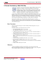
2 Channel Decimate by 2 MAC FIR Filter . . . . . . . . . . . . . . . . . . . . . . . . . . . . . . . . . . . 371
Block Parameters . . . . . . . . . . . . . . . . . . . . . . . . . . . . . . . . . . . . . . . . . . . . . . . . . . . . . . . . 371
Reference . . . . . . . . . . . . . . . . . . . . . . . . . . . . . . . . . . . . . . . . . . . . . . . . . . . . . . . . . . . . . . . 371
2n+1-tap Linear Phase MAC FIR Filter . . . . . . . . . . . . . . . . . . . . . . . . . . . . . . . . . . . . . . 372
Block Parameters . . . . . . . . . . . . . . . . . . . . . . . . . . . . . . . . . . . . . . . . . . . . . . . . . . . . . . . . 372
Reference . . . . . . . . . . . . . . . . . . . . . . . . . . . . . . . . . . . . . . . . . . . . . . . . . . . . . . . . . . . . . . . 372
2n-tap Linear Phase MAC FIR Filter . . . . . . . . . . . . . . . . . . . . . . . . . . . . . . . . . . . . . . . . 373
Block Parameters . . . . . . . . . . . . . . . . . . . . . . . . . . . . . . . . . . . . . . . . . . . . . . . . . . . . . . . . 373
Reference . . . . . . . . . . . . . . . . . . . . . . . . . . . . . . . . . . . . . . . . . . . . . . . . . . . . . . . . . . . . . . . 373
2n-tap MAC FIR Filter . . . . . . . . . . . . . . . . . . . . . . . . . . . . . . . . . . . . . . . . . . . . . . . . . . . . . . 374
Block Parameters . . . . . . . . . . . . . . . . . . . . . . . . . . . . . . . . . . . . . . . . . . . . . . . . . . . . . . . . 374
Reference . . . . . . . . . . . . . . . . . . . . . . . . . . . . . . . . . . . . . . . . . . . . . . . . . . . . . . . . . . . . . . . 374
4-channel 8-tap Transpose FIR Filter . . . . . . . . . . . . . . . . . . . . . . . . . . . . . . . . . . . . . . . . 375
Block Parameters . . . . . . . . . . . . . . . . . . . . . . . . . . . . . . . . . . . . . . . . . . . . . . . . . . . . . . . . 375
4n-tap MAC FIR Filter . . . . . . . . . . . . . . . . . . . . . . . . . . . . . . . . . . . . . . . . . . . . . . . . . . . . . . 376
Block Parameters . . . . . . . . . . . . . . . . . . . . . . . . . . . . . . . . . . . . . . . . . . . . . . . . . . . . . . . . 376
Reference . . . . . . . . . . . . . . . . . . . . . . . . . . . . . . . . . . . . . . . . . . . . . . . . . . . . . . . . . . . . . . . 376
5x5Filter . . . . . . . . . . . . . . . . . . . . . . . . . . . . . . . . . . . . . . . . . . . . . . . . . . . . . . . . . . . . . . . . . . . 377
Block Parameters . . . . . . . . . . . . . . . . . . . . . . . . . . . . . . . . . . . . . . . . . . . . . . . . . . . . . . . . 378
BPSK AWGN Channel . . . . . . . . . . . . . . . . . . . . . . . . . . . . . . . . . . . . . . . . . . . . . . . . . . . . . 379
Block Parameters . . . . . . . . . . . . . . . . . . . . . . . . . . . . . . . . . . . . . . . . . . . . . . . . . . . . . . . . 379
Reference . . . . . . . . . . . . . . . . . . . . . . . . . . . . . . . . . . . . . . . . . . . . . . . . . . . . . . . . . . . . . . . 379
CIC Filter . . . . . . . . . . . . . . . . . . . . . . . . . . . . . . . . . . . . . . . . . . . . . . . . . . . . . . . . . . . . . . . . . . 380
Block Interface . . . . . . . . . . . . . . . . . . . . . . . . . . . . . . . . . . . . . . . . . . . . . . . . . . . . . . . . . . 380
Block Parameters . . . . . . . . . . . . . . . . . . . . . . . . . . . . . . . . . . . . . . . . . . . . . . . . . . . . . . . . 381
Reference . . . . . . . . . . . . . . . . . . . . . . . . . . . . . . . . . . . . . . . . . . . . . . . . . . . . . . . . . . . . . . . 381
Convolutional Encoder . . . . . . . . . . . . . . . . . . . . . . . . . . . . . . . . . . . . . . . . . . . . . . . . . . . . . 382
System Generator for DSP Reference Guide
UG638 (v11.4) December 2, 2009
www.xilinx.com
11
Implementation . . . . . . . . . . . . . . . . . . . . . . . . . . . . . . . . . . . . . . . . . . . . . . . . . . . . . . . . . 382
Block Interface . . . . . . . . . . . . . . . . . . . . . . . . . . . . . . . . . . . . . . . . . . . . . . . . . . . . . . . . . . 383
Block Parameters . . . . . . . . . . . . . . . . . . . . . . . . . . . . . . . . . . . . . . . . . . . . . . . . . . . . . . . . 383
CORDIC ATAN. . . . . . . . . . . . . . . . . . . . . . . . . . . . . . . . . . . . . . . . . . . . . . . . . . . . . . . . . . . . 384
Block Parameters . . . . . . . . . . . . . . . . . . . . . . . . . . . . . . . . . . . . . . . . . . . . . . . . . . . . . . . . 384
Reference . . . . . . . . . . . . . . . . . . . . . . . . . . . . . . . . . . . . . . . . . . . . . . . . . . . . . . . . . . . . . . . 384
CORDIC DIVIDER . . . . . . . . . . . . . . . . . . . . . . . . . . . . . . . . . . . . . . . . . . . . . . . . . . . . . . . . 385
Block Parameters . . . . . . . . . . . . . . . . . . . . . . . . . . . . . . . . . . . . . . . . . . . . . . . . . . . . . . . . 385
Reference . . . . . . . . . . . . . . . . . . . . . . . . . . . . . . . . . . . . . . . . . . . . . . . . . . . . . . . . . . . . . . . 385
CORDIC LOG . . . . . . . . . . . . . . . . . . . . . . . . . . . . . . . . . . . . . . . . . . . . . . . . . . . . . . . . . . . . . 386
Block Parameters . . . . . . . . . . . . . . . . . . . . . . . . . . . . . . . . . . . . . . . . . . . . . . . . . . . . . . . . 386
Reference . . . . . . . . . . . . . . . . . . . . . . . . . . . . . . . . . . . . . . . . . . . . . . . . . . . . . . . . . . . . . . . 387
CORDIC SINCOS . . . . . . . . . . . . . . . . . . . . . . . . . . . . . . . . . . . . . . . . . . . . . . . . . . . . . . . . . 388
Block Parameters . . . . . . . . . . . . . . . . . . . . . . . . . . . . . . . . . . . . . . . . . . . . . . . . . . . . . . . . 388
Reference . . . . . . . . . . . . . . . . . . . . . . . . . . . . . . . . . . . . . . . . . . . . . . . . . . . . . . . . . . . . . . . 388
CORDIC SQRT . . . . . . . . . . . . . . . . . . . . . . . . . . . . . . . . . . . . . . . . . . . . . . . . . . . . . . . . . . . . 389
Block Parameters . . . . . . . . . . . . . . . . . . . . . . . . . . . . . . . . . . . . . . . . . . . . . . . . . . . . . . . . 389
Reference . . . . . . . . . . . . . . . . . . . . . . . . . . . . . . . . . . . . . . . . . . . . . . . . . . . . . . . . . . . . . . . 390
Dual Port Memory Interpolation MAC FIR Filter . . . . . . . . . . . . . . . . . . . . . . . . . . . 391
Block Parameters . . . . . . . . . . . . . . . . . . . . . . . . . . . . . . . . . . . . . . . . . . . . . . . . . . . . . . . . 391
Reference . . . . . . . . . . . . . . . . . . . . . . . . . . . . . . . . . . . . . . . . . . . . . . . . . . . . . . . . . . . . . . . 391
Interpolation Filter . . . . . . . . . . . . . . . . . . . . . . . . . . . . . . . . . . . . . . . . . . . . . . . . . . . . . . . . . 392
Block Parameters . . . . . . . . . . . . . . . . . . . . . . . . . . . . . . . . . . . . . . . . . . . . . . . . . . . . . . . . 392
Reference . . . . . . . . . . . . . . . . . . . . . . . . . . . . . . . . . . . . . . . . . . . . . . . . . . . . . . . . . . . . . . . 392
m-channel n-tap Transpose FIR Filter . . . . . . . . . . . . . . . . . . . . . . . . . . . . . . . . . . . . . . . 393
Block Parameters . . . . . . . . . . . . . . . . . . . . . . . . . . . . . . . . . . . . . . . . . . . . . . . . . . . . . . . . 393
Mealy State Machine . . . . . . . . . . . . . . . . . . . . . . . . . . . . . . . . . . . . . . . . . . . . . . . . . . . . . . . 394
Example . . . . . . . . . . . . . . . . . . . . . . . . . . . . . . . . . . . . . . . . . . . . . . . . . . . . . . . . . . . . . . . . 395
Block Parameters . . . . . . . . . . . . . . . . . . . . . . . . . . . . . . . . . . . . . . . . . . . . . . . . . . . . . . . . 396
Moore State Machine . . . . . . . . . . . . . . . . . . . . . . . . . . . . . . . . . . . . . . . . . . . . . . . . . . . . . . . 398
Example . . . . . . . . . . . . . . . . . . . . . . . . . . . . . . . . . . . . . . . . . . . . . . . . . . . . . . . . . . . . . . . . 399
Block Parameters . . . . . . . . . . . . . . . . . . . . . . . . . . . . . . . . . . . . . . . . . . . . . . . . . . . . . . . . 400
Multipath Fading Channel Model . . . . . . . . . . . . . . . . . . . . . . . . . . . . . . . . . . . . . . . . . . 401
Theory . . . . . . . . . . . . . . . . . . . . . . . . . . . . . . . . . . . . . . . . . . . . . . . . . . . . . . . . . . . . . . . . .
Implementation . . . . . . . . . . . . . . . . . . . . . . . . . . . . . . . . . . . . . . . . . . . . . . . . . . . . . . . . .
Block Parameters . . . . . . . . . . . . . . . . . . . . . . . . . . . . . . . . . . . . . . . . . . . . . . . . . . . . . . . .
Functions . . . . . . . . . . . . . . . . . . . . . . . . . . . . . . . . . . . . . . . . . . . . . . . . . . . . . . . . . . . . . . .
Data Format . . . . . . . . . . . . . . . . . . . . . . . . . . . . . . . . . . . . . . . . . . . . . . . . . . . . . . . . . . . .
Input . . . . . . . . . . . . . . . . . . . . . . . . . . . . . . . . . . . . . . . . . . . . . . . . . . . . . . . . . . . . . . . . . . .
Output . . . . . . . . . . . . . . . . . . . . . . . . . . . . . . . . . . . . . . . . . . . . . . . . . . . . . . . . . . . . . . . . .
Timing . . . . . . . . . . . . . . . . . . . . . . . . . . . . . . . . . . . . . . . . . . . . . . . . . . . . . . . . . . . . . . . . .
Initialization . . . . . . . . . . . . . . . . . . . . . . . . . . . . . . . . . . . . . . . . . . . . . . . . . . . . . . . . . . . .
Demonstrations . . . . . . . . . . . . . . . . . . . . . . . . . . . . . . . . . . . . . . . . . . . . . . . . . . . . . . . . .
Hardware Co-Simulation Example . . . . . . . . . . . . . . . . . . . . . . . . . . . . . . . . . . . . . . . . .
Reference . . . . . . . . . . . . . . . . . . . . . . . . . . . . . . . . . . . . . . . . . . . . . . . . . . . . . . . . . . . . . . .
401
402
402
403
404
405
406
406
406
406
407
407
n-tap Dual Port Memory MAC FIR Filter . . . . . . . . . . . . . . . . . . . . . . . . . . . . . . . . . . . 408
Block Parameters . . . . . . . . . . . . . . . . . . . . . . . . . . . . . . . . . . . . . . . . . . . . . . . . . . . . . . . . 408
Reference . . . . . . . . . . . . . . . . . . . . . . . . . . . . . . . . . . . . . . . . . . . . . . . . . . . . . . . . . . . . . . . 408
n-tap MAC FIR Filter . . . . . . . . . . . . . . . . . . . . . . . . . . . . . . . . . . . . . . . . . . . . . . . . . . . . . . . 409
Block Parameters . . . . . . . . . . . . . . . . . . . . . . . . . . . . . . . . . . . . . . . . . . . . . . . . . . . . . . . . 409
12
www.xilinx.com
System Generator for DSP Reference Guide
UG638 (v11.4) December 2, 2009
Reference . . . . . . . . . . . . . . . . . . . . . . . . . . . . . . . . . . . . . . . . . . . . . . . . . . . . . . . . . . . . . . . 409
Registered Mealy State Machine. . . . . . . . . . . . . . . . . . . . . . . . . . . . . . . . . . . . . . . . . . . . 410
Example . . . . . . . . . . . . . . . . . . . . . . . . . . . . . . . . . . . . . . . . . . . . . . . . . . . . . . . . . . . . . . . . 411
Block Parameters . . . . . . . . . . . . . . . . . . . . . . . . . . . . . . . . . . . . . . . . . . . . . . . . . . . . . . . . 412
Registered Moore State Machine . . . . . . . . . . . . . . . . . . . . . . . . . . . . . . . . . . . . . . . . . . . 413
Example . . . . . . . . . . . . . . . . . . . . . . . . . . . . . . . . . . . . . . . . . . . . . . . . . . . . . . . . . . . . . . . . 414
Block Parameters . . . . . . . . . . . . . . . . . . . . . . . . . . . . . . . . . . . . . . . . . . . . . . . . . . . . . . . . 415
Virtex Line Buffer . . . . . . . . . . . . . . . . . . . . . . . . . . . . . . . . . . . . . . . . . . . . . . . . . . . . . . . . . . 416
Block Parameters . . . . . . . . . . . . . . . . . . . . . . . . . . . . . . . . . . . . . . . . . . . . . . . . . . . . . . . . 416
Virtex2 Line Buffer . . . . . . . . . . . . . . . . . . . . . . . . . . . . . . . . . . . . . . . . . . . . . . . . . . . . . . . . . 417
Block Parameters . . . . . . . . . . . . . . . . . . . . . . . . . . . . . . . . . . . . . . . . . . . . . . . . . . . . . . . . 417
Virtex2 5 Line Buffer . . . . . . . . . . . . . . . . . . . . . . . . . . . . . . . . . . . . . . . . . . . . . . . . . . . . . . . 418
Block Parameters . . . . . . . . . . . . . . . . . . . . . . . . . . . . . . . . . . . . . . . . . . . . . . . . . . . . . . . . 418
White Gaussian Noise Generator . . . . . . . . . . . . . . . . . . . . . . . . . . . . . . . . . . . . . . . . . . . 419
4-bit Leap-Forward LFSR . . . . . . . . . . . . . . . . . . . . . . . . . . . . . . . . . . . . . . . . . . . . . . . . .
Box-Muller Method . . . . . . . . . . . . . . . . . . . . . . . . . . . . . . . . . . . . . . . . . . . . . . . . . . . . . .
Block Parameters . . . . . . . . . . . . . . . . . . . . . . . . . . . . . . . . . . . . . . . . . . . . . . . . . . . . . . . .
Reference . . . . . . . . . . . . . . . . . . . . . . . . . . . . . . . . . . . . . . . . . . . . . . . . . . . . . . . . . . . . . . .
419
420
420
420
Chapter 3: Xilinx XtremeDSP Kit Blockset
XtremeDSP Analog to Digital Converter . . . . . . . . . . . . . . . . . . . . . . . . . . . . . . . . . . . . 422
Block Parameters . . . . . . . . . . . . . . . . . . . . . . . . . . . . . . . . . . . . . . . . . . . . . . . . . . . . . . . . 422
Data Sheet . . . . . . . . . . . . . . . . . . . . . . . . . . . . . . . . . . . . . . . . . . . . . . . . . . . . . . . . . . . . . . 422
XtremeDSP Co-Simulation . . . . . . . . . . . . . . . . . . . . . . . . . . . . . . . . . . . . . . . . . . . . . . . . . 423
Block Parameters . . . . . . . . . . . . . . . . . . . . . . . . . . . . . . . . . . . . . . . . . . . . . . . . . . . . . . . . 423
XtremeDSP Digital to Analog Converter . . . . . . . . . . . . . . . . . . . . . . . . . . . . . . . . . . . . 425
Block Parameters . . . . . . . . . . . . . . . . . . . . . . . . . . . . . . . . . . . . . . . . . . . . . . . . . . . . . . . . 425
Data Sheet . . . . . . . . . . . . . . . . . . . . . . . . . . . . . . . . . . . . . . . . . . . . . . . . . . . . . . . . . . . . . . 425
XtremeDSP External RAM . . . . . . . . . . . . . . . . . . . . . . . . . . . . . . . . . . . . . . . . . . . . . . . . . 426
Block Parameters . . . . . . . . . . . . . . . . . . . . . . . . . . . . . . . . . . . . . . . . . . . . . . . . . . . . . . . . 426
XtremeDSP LED Flasher . . . . . . . . . . . . . . . . . . . . . . . . . . . . . . . . . . . . . . . . . . . . . . . . . . . 427
Block Parameters . . . . . . . . . . . . . . . . . . . . . . . . . . . . . . . . . . . . . . . . . . . . . . . . . . . . . . . . 427
Chapter 4: System Generator Utilities
xlAddTerms. . . . . . . . . . . . . . . . . . . . . . . . . . . . . . . . . . . . . . . . . . . . . . . . . . . . . . . . . . . . . . . . 431
Syntax . . . . . . . . . . . . . . . . . . . . . . . . . . . . . . . . . . . . . . . . . . . . . . . . . . . . . . . . . . . . . . . . . .
Description . . . . . . . . . . . . . . . . . . . . . . . . . . . . . . . . . . . . . . . . . . . . . . . . . . . . . . . . . . . . .
Examples . . . . . . . . . . . . . . . . . . . . . . . . . . . . . . . . . . . . . . . . . . . . . . . . . . . . . . . . . . . . . . .
Remarks . . . . . . . . . . . . . . . . . . . . . . . . . . . . . . . . . . . . . . . . . . . . . . . . . . . . . . . . . . . . . . . .
See Also . . . . . . . . . . . . . . . . . . . . . . . . . . . . . . . . . . . . . . . . . . . . . . . . . . . . . . . . . . . . . . . .
431
431
433
433
433
xlCache . . . . . . . . . . . . . . . . . . . . . . . . . . . . . . . . . . . . . . . . . . . . . . . . . . . . . . . . . . . . . . . . . . . . 434
Syntax . . . . . . . . . . . . . . . . . . . . . . . . . . . . . . . . . . . . . . . . . . . . . . . . . . . . . . . . . . . . . . . . . . 434
Description . . . . . . . . . . . . . . . . . . . . . . . . . . . . . . . . . . . . . . . . . . . . . . . . . . . . . . . . . . . . . 434
See Also . . . . . . . . . . . . . . . . . . . . . . . . . . . . . . . . . . . . . . . . . . . . . . . . . . . . . . . . . . . . . . . . 435
xlConfigureSolver. . . . . . . . . . . . . . . . . . . . . . . . . . . . . . . . . . . . . . . . . . . . . . . . . . . . . . . . . . 436
Syntax . . . . . . . . . . . . . . . . . . . . . . . . . . . . . . . . . . . . . . . . . . . . . . . . . . . . . . . . . . . . . . . . . . 436
Description . . . . . . . . . . . . . . . . . . . . . . . . . . . . . . . . . . . . . . . . . . . . . . . . . . . . . . . . . . . . . 436
Examples . . . . . . . . . . . . . . . . . . . . . . . . . . . . . . . . . . . . . . . . . . . . . . . . . . . . . . . . . . . . . . . 436
xlfda_denominator . . . . . . . . . . . . . . . . . . . . . . . . . . . . . . . . . . . . . . . . . . . . . . . . . . . . . . . . . 437
System Generator for DSP Reference Guide
UG638 (v11.4) December 2, 2009
www.xilinx.com
13
Syntax . . . . . . . . . . . . . . . . . . . . . . . . . . . . . . . . . . . . . . . . . . . . . . . . . . . . . . . . . . . . . . . . . . 437
Description . . . . . . . . . . . . . . . . . . . . . . . . . . . . . . . . . . . . . . . . . . . . . . . . . . . . . . . . . . . . . 437
See Also . . . . . . . . . . . . . . . . . . . . . . . . . . . . . . . . . . . . . . . . . . . . . . . . . . . . . . . . . . . . . . . . 437
xlfda_numerator . . . . . . . . . . . . . . . . . . . . . . . . . . . . . . . . . . . . . . . . . . . . . . . . . . . . . . . . . . . 438
Syntax . . . . . . . . . . . . . . . . . . . . . . . . . . . . . . . . . . . . . . . . . . . . . . . . . . . . . . . . . . . . . . . . . . 438
Description . . . . . . . . . . . . . . . . . . . . . . . . . . . . . . . . . . . . . . . . . . . . . . . . . . . . . . . . . . . . . 438
See Also . . . . . . . . . . . . . . . . . . . . . . . . . . . . . . . . . . . . . . . . . . . . . . . . . . . . . . . . . . . . . . . . 438
xlGenerateButton . . . . . . . . . . . . . . . . . . . . . . . . . . . . . . . . . . . . . . . . . . . . . . . . . . . . . . . . . . 439
Syntax . . . . . . . . . . . . . . . . . . . . . . . . . . . . . . . . . . . . . . . . . . . . . . . . . . . . . . . . . . . . . . . . . . 439
Description . . . . . . . . . . . . . . . . . . . . . . . . . . . . . . . . . . . . . . . . . . . . . . . . . . . . . . . . . . . . . 439
See Also . . . . . . . . . . . . . . . . . . . . . . . . . . . . . . . . . . . . . . . . . . . . . . . . . . . . . . . . . . . . . . . . 439
xlgetparam and xlsetparam . . . . . . . . . . . . . . . . . . . . . . . . . . . . . . . . . . . . . . . . . . . . . . . . . 440
Syntax . . . . . . . . . . . . . . . . . . . . . . . . . . . . . . . . . . . . . . . . . . . . . . . . . . . . . . . . . . . . . . . . . .
Description . . . . . . . . . . . . . . . . . . . . . . . . . . . . . . . . . . . . . . . . . . . . . . . . . . . . . . . . . . . . .
Examples . . . . . . . . . . . . . . . . . . . . . . . . . . . . . . . . . . . . . . . . . . . . . . . . . . . . . . . . . . . . . . .
See Also . . . . . . . . . . . . . . . . . . . . . . . . . . . . . . . . . . . . . . . . . . . . . . . . . . . . . . . . . . . . . . . .
440
440
441
441
xlgetparams . . . . . . . . . . . . . . . . . . . . . . . . . . . . . . . . . . . . . . . . . . . . . . . . . . . . . . . . . . . . . . . . 442
Syntax . . . . . . . . . . . . . . . . . . . . . . . . . . . . . . . . . . . . . . . . . . . . . . . . . . . . . . . . . . . . . . . . . .
Description . . . . . . . . . . . . . . . . . . . . . . . . . . . . . . . . . . . . . . . . . . . . . . . . . . . . . . . . . . . . .
Examples . . . . . . . . . . . . . . . . . . . . . . . . . . . . . . . . . . . . . . . . . . . . . . . . . . . . . . . . . . . . . . .
See Also . . . . . . . . . . . . . . . . . . . . . . . . . . . . . . . . . . . . . . . . . . . . . . . . . . . . . . . . . . . . . . . .
442
442
442
443
xlGetReloadOrder. . . . . . . . . . . . . . . . . . . . . . . . . . . . . . . . . . . . . . . . . . . . . . . . . . . . . . . . . . 444
Syntax . . . . . . . . . . . . . . . . . . . . . . . . . . . . . . . . . . . . . . . . . . . . . . . . . . . . . . . . . . . . . . . . . . 444
Description . . . . . . . . . . . . . . . . . . . . . . . . . . . . . . . . . . . . . . . . . . . . . . . . . . . . . . . . . . . . . 444
See Also . . . . . . . . . . . . . . . . . . . . . . . . . . . . . . . . . . . . . . . . . . . . . . . . . . . . . . . . . . . . . . . . 445
xlInstallPlugin . . . . . . . . . . . . . . . . . . . . . . . . . . . . . . . . . . . . . . . . . . . . . . . . . . . . . . . . . . . . . 446
Syntax . . . . . . . . . . . . . . . . . . . . . . . . . . . . . . . . . . . . . . . . . . . . . . . . . . . . . . . . . . . . . . . . . .
Description . . . . . . . . . . . . . . . . . . . . . . . . . . . . . . . . . . . . . . . . . . . . . . . . . . . . . . . . . . . . .
Examples . . . . . . . . . . . . . . . . . . . . . . . . . . . . . . . . . . . . . . . . . . . . . . . . . . . . . . . . . . . . . . .
See Also . . . . . . . . . . . . . . . . . . . . . . . . . . . . . . . . . . . . . . . . . . . . . . . . . . . . . . . . . . . . . . . .
446
446
446
446
xlLoadChipScopeData . . . . . . . . . . . . . . . . . . . . . . . . . . . . . . . . . . . . . . . . . . . . . . . . . . . . . 447
Syntax . . . . . . . . . . . . . . . . . . . . . . . . . . . . . . . . . . . . . . . . . . . . . . . . . . . . . . . . . . . . . . . . . .
Description . . . . . . . . . . . . . . . . . . . . . . . . . . . . . . . . . . . . . . . . . . . . . . . . . . . . . . . . . . . . .
Examples . . . . . . . . . . . . . . . . . . . . . . . . . . . . . . . . . . . . . . . . . . . . . . . . . . . . . . . . . . . . . . .
See Also . . . . . . . . . . . . . . . . . . . . . . . . . . . . . . . . . . . . . . . . . . . . . . . . . . . . . . . . . . . . . . . .
447
447
447
447
xlSBDBuilder . . . . . . . . . . . . . . . . . . . . . . . . . . . . . . . . . . . . . . . . . . . . . . . . . . . . . . . . . . . . . . 448
Syntax . . . . . . . . . . . . . . . . . . . . . . . . . . . . . . . . . . . . . . . . . . . . . . . . . . . . . . . . . . . . . . . . . . 448
Description . . . . . . . . . . . . . . . . . . . . . . . . . . . . . . . . . . . . . . . . . . . . . . . . . . . . . . . . . . . . . 448
See Also . . . . . . . . . . . . . . . . . . . . . . . . . . . . . . . . . . . . . . . . . . . . . . . . . . . . . . . . . . . . . . . . 450
xlSetNonMemMap . . . . . . . . . . . . . . . . . . . . . . . . . . . . . . . . . . . . . . . . . . . . . . . . . . . . . . . . . 451
Syntax . . . . . . . . . . . . . . . . . . . . . . . . . . . . . . . . . . . . . . . . . . . . . . . . . . . . . . . . . . . . . . . . . .
Description . . . . . . . . . . . . . . . . . . . . . . . . . . . . . . . . . . . . . . . . . . . . . . . . . . . . . . . . . . . . .
Examples . . . . . . . . . . . . . . . . . . . . . . . . . . . . . . . . . . . . . . . . . . . . . . . . . . . . . . . . . . . . . . .
See Also . . . . . . . . . . . . . . . . . . . . . . . . . . . . . . . . . . . . . . . . . . . . . . . . . . . . . . . . . . . . . . . .
451
451
451
451
xlSetUseHDL . . . . . . . . . . . . . . . . . . . . . . . . . . . . . . . . . . . . . . . . . . . . . . . . . . . . . . . . . . . . . . 452
Syntax . . . . . . . . . . . . . . . . . . . . . . . . . . . . . . . . . . . . . . . . . . . . . . . . . . . . . . . . . . . . . . . . . .
Description . . . . . . . . . . . . . . . . . . . . . . . . . . . . . . . . . . . . . . . . . . . . . . . . . . . . . . . . . . . . .
Examples . . . . . . . . . . . . . . . . . . . . . . . . . . . . . . . . . . . . . . . . . . . . . . . . . . . . . . . . . . . . . . .
See Also . . . . . . . . . . . . . . . . . . . . . . . . . . . . . . . . . . . . . . . . . . . . . . . . . . . . . . . . . . . . . . . .
452
452
452
452
xlSwitchLibrary . . . . . . . . . . . . . . . . . . . . . . . . . . . . . . . . . . . . . . . . . . . . . . . . . . . . . . . . . . . . 453
Syntax . . . . . . . . . . . . . . . . . . . . . . . . . . . . . . . . . . . . . . . . . . . . . . . . . . . . . . . . . . . . . . . . . . 453
14
www.xilinx.com
System Generator for DSP Reference Guide
UG638 (v11.4) December 2, 2009
Description . . . . . . . . . . . . . . . . . . . . . . . . . . . . . . . . . . . . . . . . . . . . . . . . . . . . . . . . . . . . . 453
Examples . . . . . . . . . . . . . . . . . . . . . . . . . . . . . . . . . . . . . . . . . . . . . . . . . . . . . . . . . . . . . . . 453
xlTBUtils . . . . . . . . . . . . . . . . . . . . . . . . . . . . . . . . . . . . . . . . . . . . . . . . . . . . . . . . . . . . . . . . . . 454
Syntax . . . . . . . . . . . . . . . . . . . . . . . . . . . . . . . . . . . . . . . . . . . . . . . . . . . . . . . . . . . . . . . . . .
Description . . . . . . . . . . . . . . . . . . . . . . . . . . . . . . . . . . . . . . . . . . . . . . . . . . . . . . . . . . . . .
Examples . . . . . . . . . . . . . . . . . . . . . . . . . . . . . . . . . . . . . . . . . . . . . . . . . . . . . . . . . . . . . . .
Remarks . . . . . . . . . . . . . . . . . . . . . . . . . . . . . . . . . . . . . . . . . . . . . . . . . . . . . . . . . . . . . . . .
See Also . . . . . . . . . . . . . . . . . . . . . . . . . . . . . . . . . . . . . . . . . . . . . . . . . . . . . . . . . . . . . . . .
454
454
456
457
457
xlTimingAnalysis . . . . . . . . . . . . . . . . . . . . . . . . . . . . . . . . . . . . . . . . . . . . . . . . . . . . . . . . . . 458
Syntax . . . . . . . . . . . . . . . . . . . . . . . . . . . . . . . . . . . . . . . . . . . . . . . . . . . . . . . . . . . . . . . . . . 458
Description . . . . . . . . . . . . . . . . . . . . . . . . . . . . . . . . . . . . . . . . . . . . . . . . . . . . . . . . . . . . . 458
Example . . . . . . . . . . . . . . . . . . . . . . . . . . . . . . . . . . . . . . . . . . . . . . . . . . . . . . . . . . . . . . . . 458
xlUpdateModel . . . . . . . . . . . . . . . . . . . . . . . . . . . . . . . . . . . . . . . . . . . . . . . . . . . . . . . . . . . . 459
Syntax . . . . . . . . . . . . . . . . . . . . . . . . . . . . . . . . . . . . . . . . . . . . . . . . . . . . . . . . . . . . . . . . . . 459
Description . . . . . . . . . . . . . . . . . . . . . . . . . . . . . . . . . . . . . . . . . . . . . . . . . . . . . . . . . . . . . 459
Examples . . . . . . . . . . . . . . . . . . . . . . . . . . . . . . . . . . . . . . . . . . . . . . . . . . . . . . . . . . . . . . . 461
xlVersion . . . . . . . . . . . . . . . . . . . . . . . . . . . . . . . . . . . . . . . . . . . . . . . . . . . . . . . . . . . . . . . . . . 462
Syntax . . . . . . . . . . . . . . . . . . . . . . . . . . . . . . . . . . . . . . . . . . . . . . . . . . . . . . . . . . . . . . . . . . 462
Description . . . . . . . . . . . . . . . . . . . . . . . . . . . . . . . . . . . . . . . . . . . . . . . . . . . . . . . . . . . . . 462
See Also . . . . . . . . . . . . . . . . . . . . . . . . . . . . . . . . . . . . . . . . . . . . . . . . . . . . . . . . . . . . . . . . 462
Chapter 5: Programmatic Access
System Generator API for Programmatic Generation . . . . . . . . . . . . . . . . . . . . . . . . 463
Introduction . . . . . . . . . . . . . . . . . . . . . . . . . . . . . . . . . . . . . . . . . . . . . . . . . . . . . . . . . . . .
xBlock . . . . . . . . . . . . . . . . . . . . . . . . . . . . . . . . . . . . . . . . . . . . . . . . . . . . . . . . . . . . . . . . . .
xInport . . . . . . . . . . . . . . . . . . . . . . . . . . . . . . . . . . . . . . . . . . . . . . . . . . . . . . . . . . . . . . . . .
xOutport . . . . . . . . . . . . . . . . . . . . . . . . . . . . . . . . . . . . . . . . . . . . . . . . . . . . . . . . . . . . . . .
xSignal . . . . . . . . . . . . . . . . . . . . . . . . . . . . . . . . . . . . . . . . . . . . . . . . . . . . . . . . . . . . . . . . .
xlsub2script . . . . . . . . . . . . . . . . . . . . . . . . . . . . . . . . . . . . . . . . . . . . . . . . . . . . . . . . . . . . .
xBlockHelp . . . . . . . . . . . . . . . . . . . . . . . . . . . . . . . . . . . . . . . . . . . . . . . . . . . . . . . . . . . . .
463
464
465
465
466
466
468
PG API Examples . . . . . . . . . . . . . . . . . . . . . . . . . . . . . . . . . . . . . . . . . . . . . . . . . . . . . . . . . . 469
Hello World . . . . . . . . . . . . . . . . . . . . . . . . . . . . . . . . . . . . . . . . . . . . . . . . . . . . . . . . . . . . 469
MACC . . . . . . . . . . . . . . . . . . . . . . . . . . . . . . . . . . . . . . . . . . . . . . . . . . . . . . . . . . . . . . . . . 470
MACC in a Masked Subsystem . . . . . . . . . . . . . . . . . . . . . . . . . . . . . . . . . . . . . . . . . . . . 471
PG API Error/Warning Handling & Messages. . . . . . . . . . . . . . . . . . . . . . . . . . . . . . . 475
xBlock Error Messages . . . . . . . . . . . . . . . . . . . . . . . . . . . . . . . . . . . . . . . . . . . . . . . . . . .
xInport Error Messages . . . . . . . . . . . . . . . . . . . . . . . . . . . . . . . . . . . . . . . . . . . . . . . . . . .
xOutport Error Messages . . . . . . . . . . . . . . . . . . . . . . . . . . . . . . . . . . . . . . . . . . . . . . . . .
xSignal Error Messages . . . . . . . . . . . . . . . . . . . . . . . . . . . . . . . . . . . . . . . . . . . . . . . . . . .
xsub2script Error Messages . . . . . . . . . . . . . . . . . . . . . . . . . . . . . . . . . . . . . . . . . . . . . . .
475
475
476
476
476
C++ Access to Shared Memory Blocks . . . . . . . . . . . . . . . . . . . . . . . . . . . . . . . . . . . . . . 477
M-Code Access to Hardware Co-Simulation . . . . . . . . . . . . . . . . . . . . . . . . . . . . . . . . 477
Compiling Hardware for Use with M-Hwcosim . . . . . . . . . . . . . . . . . . . . . . . . . . . . .
M-Hwcosim Simulation Semantics . . . . . . . . . . . . . . . . . . . . . . . . . . . . . . . . . . . . . . . . .
Data Representation . . . . . . . . . . . . . . . . . . . . . . . . . . . . . . . . . . . . . . . . . . . . . . . . . . . . .
Interfacing to Hardware from M-Code . . . . . . . . . . . . . . . . . . . . . . . . . . . . . . . . . . . . .
M-Hwcosim Examples . . . . . . . . . . . . . . . . . . . . . . . . . . . . . . . . . . . . . . . . . . . . . . . . . . .
Automatic Generation of M-Hwcosim Testbench . . . . . . . . . . . . . . . . . . . . . . . . . . . .
Resource Management . . . . . . . . . . . . . . . . . . . . . . . . . . . . . . . . . . . . . . . . . . . . . . . . . . .
M-Hwcosim MATLAB Class . . . . . . . . . . . . . . . . . . . . . . . . . . . . . . . . . . . . . . . . . . . . . .
M-Hwcosim Shared Memory MATLAB Class . . . . . . . . . . . . . . . . . . . . . . . . . . . . . . .
System Generator for DSP Reference Guide
UG638 (v11.4) December 2, 2009
www.xilinx.com
477
478
478
478
479
484
487
487
492
15
M-Hwcosim Shared FIFO MATLAB Class . . . . . . . . . . . . . . . . . . . . . . . . . . . . . . . . . . 494
M-Hwcosim Utility Functions . . . . . . . . . . . . . . . . . . . . . . . . . . . . . . . . . . . . . . . . . . . . . 495
SharedMemory . . . . . . . . . . . . . . . . . . . . . . . . . . . . . . . . . . . . . . . . . . . . . . . . . . . . . . . . . . . . 498
Public Types . . . . . . . . . . . . . . . . . . . . . . . . . . . . . . . . . . . . . . . . . . . . . . . . . . . . . . . . . . . .
Public Methods . . . . . . . . . . . . . . . . . . . . . . . . . . . . . . . . . . . . . . . . . . . . . . . . . . . . . . . . . .
Static Public Attributes . . . . . . . . . . . . . . . . . . . . . . . . . . . . . . . . . . . . . . . . . . . . . . . . . . .
Protected Types . . . . . . . . . . . . . . . . . . . . . . . . . . . . . . . . . . . . . . . . . . . . . . . . . . . . . . . . .
Protected Methods . . . . . . . . . . . . . . . . . . . . . . . . . . . . . . . . . . . . . . . . . . . . . . . . . . . . . . .
Protected Attributes . . . . . . . . . . . . . . . . . . . . . . . . . . . . . . . . . . . . . . . . . . . . . . . . . . . . . .
Member Enumeration . . . . . . . . . . . . . . . . . . . . . . . . . . . . . . . . . . . . . . . . . . . . . . . . . . . .
Constructors & Destructors . . . . . . . . . . . . . . . . . . . . . . . . . . . . . . . . . . . . . . . . . . . . . . .
Member Functions . . . . . . . . . . . . . . . . . . . . . . . . . . . . . . . . . . . . . . . . . . . . . . . . . . . . . . .
Member Data . . . . . . . . . . . . . . . . . . . . . . . . . . . . . . . . . . . . . . . . . . . . . . . . . . . . . . . . . . .
498
498
498
498
498
498
499
499
500
503
LockableSharedMemory . . . . . . . . . . . . . . . . . . . . . . . . . . . . . . . . . . . . . . . . . . . . . . . . . . . 504
Public Types . . . . . . . . . . . . . . . . . . . . . . . . . . . . . . . . . . . . . . . . . . . . . . . . . . . . . . . . . . . .
Public Methods . . . . . . . . . . . . . . . . . . . . . . . . . . . . . . . . . . . . . . . . . . . . . . . . . . . . . . . . . .
Static Public Attributes . . . . . . . . . . . . . . . . . . . . . . . . . . . . . . . . . . . . . . . . . . . . . . . . . . .
Member Typedefs . . . . . . . . . . . . . . . . . . . . . . . . . . . . . . . . . . . . . . . . . . . . . . . . . . . . . . .
Constructors & Destructors . . . . . . . . . . . . . . . . . . . . . . . . . . . . . . . . . . . . . . . . . . . . . . .
Member Functions . . . . . . . . . . . . . . . . . . . . . . . . . . . . . . . . . . . . . . . . . . . . . . . . . . . . . . .
Member Data . . . . . . . . . . . . . . . . . . . . . . . . . . . . . . . . . . . . . . . . . . . . . . . . . . . . . . . . . . .
504
504
504
504
504
505
507
SharedMemoryProxy . . . . . . . . . . . . . . . . . . . . . . . . . . . . . . . . . . . . . . . . . . . . . . . . . . . . . . . 508
Public Types . . . . . . . . . . . . . . . . . . . . . . . . . . . . . . . . . . . . . . . . . . . . . . . . . . . . . . . . . . . .
Public Methods . . . . . . . . . . . . . . . . . . . . . . . . . . . . . . . . . . . . . . . . . . . . . . . . . . . . . . . . . .
Static Public Attributes . . . . . . . . . . . . . . . . . . . . . . . . . . . . . . . . . . . . . . . . . . . . . . . . . . .
Member Typedefs . . . . . . . . . . . . . . . . . . . . . . . . . . . . . . . . . . . . . . . . . . . . . . . . . . . . . . .
Constructors and Destructors . . . . . . . . . . . . . . . . . . . . . . . . . . . . . . . . . . . . . . . . . . . . .
Member Functions . . . . . . . . . . . . . . . . . . . . . . . . . . . . . . . . . . . . . . . . . . . . . . . . . . . . . . .
Member Data . . . . . . . . . . . . . . . . . . . . . . . . . . . . . . . . . . . . . . . . . . . . . . . . . . . . . . . . . . .
508
508
508
508
508
509
510
Request Struct . . . . . . . . . . . . . . . . . . . . . . . . . . . . . . . . . . . . . . . . . . . . . . . . . . . . . . . . . . . . . 511
Public Types . . . . . . . . . . . . . . . . . . . . . . . . . . . . . . . . . . . . . . . . . . . . . . . . . . . . . . . . . . . .
Static Public Attributes . . . . . . . . . . . . . . . . . . . . . . . . . . . . . . . . . . . . . . . . . . . . . . . . . . .
Member Enumerations . . . . . . . . . . . . . . . . . . . . . . . . . . . . . . . . . . . . . . . . . . . . . . . . . . .
Member Data . . . . . . . . . . . . . . . . . . . . . . . . . . . . . . . . . . . . . . . . . . . . . . . . . . . . . . . . . . .
511
511
511
511
NamedPipeReader . . . . . . . . . . . . . . . . . . . . . . . . . . . . . . . . . . . . . . . . . . . . . . . . . . . . . . . . . 512
Public Methods . . . . . . . . . . . . . . . . . . . . . . . . . . . . . . . . . . . . . . . . . . . . . . . . . . . . . . . . . .
Static Public Attributes . . . . . . . . . . . . . . . . . . . . . . . . . . . . . . . . . . . . . . . . . . . . . . . . . . .
Constructors & Destructors . . . . . . . . . . . . . . . . . . . . . . . . . . . . . . . . . . . . . . . . . . . . . . .
Member Functions . . . . . . . . . . . . . . . . . . . . . . . . . . . . . . . . . . . . . . . . . . . . . . . . . . . . . . .
Member Data . . . . . . . . . . . . . . . . . . . . . . . . . . . . . . . . . . . . . . . . . . . . . . . . . . . . . . . . . . .
512
512
512
513
514
NamedPipeWriter . . . . . . . . . . . . . . . . . . . . . . . . . . . . . . . . . . . . . . . . . . . . . . . . . . . . . . . . . . 515
16
Public Methods . . . . . . . . . . . . . . . . . . . . . . . . . . . . . . . . . . . . . . . . . . . . . . . . . . . . . . . . . .
Static Public Attributes . . . . . . . . . . . . . . . . . . . . . . . . . . . . . . . . . . . . . . . . . . . . . . . . . . .
Constructors & Destructors . . . . . . . . . . . . . . . . . . . . . . . . . . . . . . . . . . . . . . . . . . . . . . .
Member Functions . . . . . . . . . . . . . . . . . . . . . . . . . . . . . . . . . . . . . . . . . . . . . . . . . . . . . . .
Member Data . . . . . . . . . . . . . . . . . . . . . . . . . . . . . . . . . . . . . . . . . . . . . . . . . . . . . . . . . . .
515
515
515
515
517
Index . . . . . . . . . . . . . . . . . . . . . . . . . . . . . . . . . . . . . . . . . . . . . . . . . . . . . . . . . . . . . . . . . . . . . . . . . . .
519
www.xilinx.com
System Generator for DSP Reference Guide
UG638 (v11.4) December 2, 2009
Preface
About This Guide
This Reference Guide provides indepth information on the blocks used in System
Generator. In addition, information on System Generator Utilities and Programmatic
Access is also provided.
Guide Contents
This Reference Guide contains the following topics:
•
Xilinx Blockset
•
Xilinx Reference Blockset
•
XtremeDSP Kit
•
System Generator Utilities
•
Programmatic Access
System Generator PDF Doc Set
This Reference Guide can be found in the System Generator Help system and is also part of
the System Generator Doc Set that is provided in PDF format. The content of the doc set is
as follows:
•
System Generator for DSP Getting Started Guide
•
System Generator for DSP User Guide
•
System Generator for DSP Reference Guide
Note: Hyperlinks across these PDF documents work only when the PDF files reside in the same
folder. After clicking a Hyperlink in the Adobe Reader, you can return to the previous page by pressing
the Alt key and the left arrow key (←) at the same time.
Additional Resources
To find additional documentation, see the Xilinx website at:
http://www.xilinx.com/support/documentation/index.htm.
To search the Answer Database of silicon, software, and IP questions and answers, or to
create a technical support WebCase, see the Xilinx website at:
http://www.xilinx.com/support/mysupport.htm.
System Generator for DSP Reference Guide
UG638 (v11.4) December 2, 2009
www.xilinx.com
17
Preface: About This Guide
Conventions
This document uses the following conventions. An example illustrates each convention.
Typographical
The following typographical conventions are used in this document:
Convention
Meaning or Use
Example
Courier font
Messages, prompts, and
program files that the system
displays
Courier bold
Literal commands that you
ngdbuild design_name
enter in a syntactical statement
Helvetica bold
Commands that you select from File →Open
a menu
Keyboard shortcuts
Italic font
{ }
Vertical bar
Ctrl+C
Variables in a syntax statement ngdbuild design_name
for which you must supply
values
Square brackets
Braces
speed grade: - 100
[ ]
References to other manuals
See the Development System
Reference Guide for more
information.
Emphasis in text
If a wire is drawn so that it
overlaps the pin of a symbol,
the two nets are not connected.
An optional entry or parameter. ngdbuild [option_name]
However, in bus specifications, design_name
such as bus[7:0], they are
required.
A list of items from which you lowpwr ={on|off}
must choose one or more
|
Vertical ellipsis
.
.
.
Separates items in a list of
choices
lowpwr ={on|off}
Repetitive material that has
been omitted
IOB #1: Name = QOUT’
IOB #2: Name = CLKIN’
.
.
.
Horizontal ellipsis . . . Repetitive material that has
been omitted
allow block block_name loc1
loc2 ... locn;
Online Document
The following conventions are used in this document:
18
www.xilinx.com
System Generator for DSP Reference Guide
UG638 (v11.4) December 2, 2009
Conventions
Convention
Blue text
Meaning or Use
Example
Cross-reference link to a
location in the current
document
See the topic “Additional
Resources” for details.
Red text
Cross-reference link to a
location in another document
See Figure 2-5 in the Virtex-II
Platform FPGA User Guide.
Blue, underlined text
Hyperlink to a website (URL)
Go to http://www.xilinx.com
for the latest speed files.
System Generator for DSP Reference Guide
UG638 (v11.4) December 2, 2009
www.xilinx.com
Refer to “Title Formats” in
Chapter 1 for details.
19
Preface: About This Guide
20
www.xilinx.com
System Generator for DSP Reference Guide
UG638 (v11.4) December 2, 2009
Chapter 1
Xilinx Blockset
Organization of Blockset
Libraries
Describes how the Xilinx blocks are organized into
libraries.
Common Options in Block
Parameter Dialog Boxes
Describes block parameters that are common to most
blocks in the Xilinx blockset.
Block Reference Pages
Alphabetical listing of the Xilinx blockset with
detailed descriptions of each block.
Xilinx LogiCORE Versions
Lists the version numbers of the Xilinx
LogiCORE™(s) used in the Xilinx Blockset.
System Generator for DSP Reference Guide
UG638 (v11.4) December 2, 2009
www.xilinx.com
21
Chapter 1: Xilinx Blockset
Organization of Blockset Libraries
The Xilinx Blockset contains building blocks for constructing DSP and other digital
systems in FPGAs using Simulink. The blocks are grouped into libraries according to their
function, and some blocks with broad applicability (e.g., the Gateway I/O blocks) are
linked into multiple libraries. The following libraries are provided:
Library
Description
Index
Includes every block in the Xilinx Blockset.
Basic Element Blocks
Includes standard building blocks for digital logic
Communication
Blocks
Includes forward error correction and modulator blocks, commonly
used in digital communications systems
Control Logic Blocks
Includes blocks for control circuitry and state machines
Data Type Blocks
Includes blocks that convert data types (includes gateways)
DSP Blocks
Includes Digital Signal Processing (DSP) blocks
Math Blocks
Includes blocks that implement mathematical functions
Memory Blocks
Includes blocks that implement and access memories
Shared Memory
Blocks
Includes blocks that implement and access Xilinx shared memories
Tool Blocks
Includes “Utility” blocks, e.g., code generation (System Generator
block), resource estimation, HDL co-simulation, etc
Basic Element Blocks
Table 1-1:
Basic Element Blocks
Block
22
Description
Addressable Shift
Register
The Xilinx Addressable Shift Register block is a variable-length
shift register in which any register in the delay chain can be
addressed and driven onto the output data port.
Assert
The Xilinx Assert block is used to assert a rate and/or a type on
a signal. This block has no cost in hardware and can be used to
resolve rates and/or types in situations where designer
intervention is required.
BitBasher
The Xilinx BitBasher block performs slicing, concatenation and
augmentation of inputs attached to the block.
Black Box
The System Generator Black Box block provides a way to
incorporate hardware description language (HDL) models into
System Generator.
Clock Enable Probe
The Xilinx Clock Enable (CE) Probe provides a mechanism for
extracting derived clock enable signals from Xilinx signals in
System Generator models.
www.xilinx.com
System Generator for DSP Reference Guide
UG638 (v11.4) December 2, 2009
Organization of Blockset Libraries
Table 1-1:
Basic Element Blocks
Block
Description
Concat
The Xilinx Concat block performs a concatenation of n bit
vectors represented by unsigned integer numbers, i.e. n
unsigned numbers with binary points at position zero.
Constant
The Xilinx Constant block generates a constant that can be a
fixed-point value, a Boolean value, or a DSP48 instruction. This
block is similar to the Simulink constant block, but can be used
to directly drive the inputs on Xilinx blocks.
Convert
The Xilinx Convert block converts each input sample to a
number of a desired arithmetic type. For example, a number can
be converted to a signed (two's complement) or unsigned value.
Counter
The Xilinx Counter block implements a free running or countlimited type of an up, down, or up/down counter. The counter
output can be specified as a signed or unsigned fixed-point
number.
Delay
The Xilinx Delay block implements a fixed delay of L cycles.
Divider Generator 2.0
The Xilinx Divider Generator 2.0 block creates a circuit for
integer division based on Radix-2 non-restoring division, or
High-Radix division with prescaling.
Expression
The Xilinx Expression block performs a bitwise logical
expression.
Gateway In
The Xilinx Gateway In blocks are the inputs into the Xilinx
portion of your Simulink design. These blocks convert Simulink
integer, double and fixed-point data types into the System
Generator fixed-point type. Each block defines a top-level input
port in the HDL design generated by System Generator.
Gateway Out
Xilinx Gateway Out blocks are the outputs from the Xilinx
portion of your Simulink design. This block converts the System
Generator fixed-point data type into Simulink Double.
Inverter
The Xilinx Inverter block calculates the bitwise logical
complement of a fixed-point number. The block is implemented
as a synthesizable VHDL module.
LFSR
The Xilinx LFSR block implements a Linear Feedback Shift
Register (LFSR). This block supports both the Galois and
Fibonacci structures using either the XOR or XNOR gate and
allows a re-loadable input to change the current value of the
register at any time. The LFSR output and re-loadable input can
be configured as either serial or parallel ports
Logical
The Xilinx Logical block performs bitwise logical operations on
2, 3, or 4 fixed-point numbers. Operands are zero padded and
sign extended as necessary to make binary point positions
coincide; then the logical operation is performed and the result
is delivered at the output port.
Mux
The Xilinx Mult block implements a multiplier. It computes the
product of the data on its two input ports, producing the result
on its output port.
System Generator for DSP Reference Guide
UG638 (v11.4) December 2, 2009
www.xilinx.com
23
Chapter 1: Xilinx Blockset
Table 1-1:
Basic Element Blocks
Block
24
Description
Parallel to Serial
The Parallel to Serial block takes an input word and splits it into
N time-multiplexed output words where N is the ratio of
number of input bits to output bits. The order of the output can
be either least significant bit first or most significant bit first.
Register
The Xilinx Register block models a D flip flop-based register,
having latency of one sample period.
Reinterpret
The Xilinx Reinterpret block forces its output to a new type
without any regard for retaining the numerical value
represented by the input.
Relational
The Xilinx Relational block implements a comparator.
Reset Generator
The Reset Generator block captures the user's reset signal that is
running at the system sample rate, and produces one or more
downsampled reset signal(s) running at the rates specified on
the block.
Serial to Parallel
The Serial to Parallel block takes a series of inputs of any size and
creates a single output of a specified multiple of that size. The
input series can be ordered either with the most significant word
first or the least significant word first.
Slice
The Xilinx Slice block allows you to slice off a sequence of bits
from your input data and create a new data value. This value is
presented as the output from the block. The output data type is
unsigned with its binary point at zero.
System Generator
The System Generator block provides control of system and
simulation parameters, and is used to invoke the code generator.
The System Generator block is also refered to as the System
Generator “token” because of its unique role in the design. Every
Simulink model containing any element from the Xilinx Blockset
must contain at least one System Generator block (token). Once
a System Generator block is added to a model, it is possible to
specify how code generation and simulation should be handled.
Time Division
Demultiplexer
The Xilinx Time Division Demultiplexer block accepts input
serially and presents it to multiple outputs at a slower rate.
Time Division
Multiplexer
The Xilinx Time Division Multiplexer block multiplexes values
presented at input ports into a single faster rate output stream.
Up Sample
The Xilinx Up Sample block increases the sample rate at the
point where the block is placed in your design. The output
sample period is l/n, where l is the input sample period and n is
the sampling rate.
www.xilinx.com
System Generator for DSP Reference Guide
UG638 (v11.4) December 2, 2009
Organization of Blockset Libraries
Communication Blocks
Table 1-2:
Communication Blocks - FEC
Communication Block Description
Convolution Encoder
7.0
The Xilinx Convolutional Encoder block implements an
encoder for convolutional codes. Ordinarily used in tandem
with a Viterbi decoder, this block performs forward error
correction (FEC) in digital communication systems.
Depuncture
The Xilinx Depuncture block allows you to insert an arbitrary
symbol into your input data at the location specified by the
depuncture code.
Interleaver
Deinterleaver v5_0
The Xilinx Interleaver/Deinterleaver block implements an
interleaver or a deinterleaver. An interleaver is a device that
rearranges the ordering of a sequence of symbols in a one-toone deterministic manner. Associated with any interleaver is
a deinterleaver, a device that restores the reordered sequence.
Interleaver
Deinterleaver 5.1
The Xilinx Interleaver/Deinterleaver block implements an
interleaver or a deinterleaver. An interleaver is a device that
rearranges the ordering of a sequence of symbols in a one-toone deterministic manner. Associated with any interleaver is
a deinterleaver, a device that restores the reordered sequence.
Puncture
The Xilinx Puncture block removes a set of user-specified bits
from the input words of its data stream.
Reed-Solomon Decoder
6.1
The Reed-Solomon (RS) codes are block-based error
correcting codes with a wide range of applications in digital
communications and storage.
Reed-Solomon Decoder
7.0
The Reed-Solomon (RS) codes are block-based error
correcting codes with a wide range of applications in digital
communications and storage.
Reed-Solomon Encoder
6.1
The Reed-Solomon (RS) codes are block-based error
correcting codes with a wide range of applications in digital
communications and storage.
Reed-Solomon Encoder
7.0
The Reed-Solomon (RS) codes are block-based error
correcting codes with a wide range of applications in digital
communications and storage.
Viterbi Decoder 7.0
Data encoded with a convolution encoder may be decoded
using the Xilinx Viterbi decoder block.
System Generator for DSP Reference Guide
UG638 (v11.4) December 2, 2009
www.xilinx.com
25
Chapter 1: Xilinx Blockset
Control Logic Blocks
Table 1-3:
Control Logic Blocks
Control Logic Block
26
Description
Black Box
The System Generator Black Box block provides a way to
incorporate hardware description language (HDL) models into
System Generator.
Constant
The Xilinx Constant block generates a constant that can be a fixedpoint value, a Boolean value, or a DSP48 instruction. This block is
similar to the Simulink constant block, but can be used to directly
drive the inputs on Xilinx blocks.
Counter
The Xilinx Counter block implements a free running or countlimited type of an up, down, or up/down counter. The counter
output can be specified as a signed or unsigned fixed-point number.
Dual Port RAM
The Xilinx Dual Port RAM block implements a random access
memory (RAM). Dual ports enable simultaneous access to the
memory space at different sample rates using multiple data widths.
EDK Processor
The EDK Processor block allows user logic developed in System
Generator to be attached to embedded processor systems created
using the Xilinx Embedded Development Kit (EDK).
Expression
The Xilinx Expression block performs a bitwise logical expression.
FIFO
The Xilinx FIFO block implements a FIFO memory queue.
Inverter
The Xilinx Inverter block calculates the bitwise logical complement
of a fixed-point number. The block is implemented as a
synthesizable VHDL module.
Logical
The Xilinx Logical block performs bitwise logical operations on 2, 3,
or 4 fixed-point numbers. Operands are zero padded and sign
extended as necessary to make binary point positions coincide; then
the logical operation is performed and the result is delivered at the
output port.
MCode
The Xilinx MCode block is a container for executing a user-supplied
MATLAB function within Simulink. A parameter on the block
specifies the M-function name. The block executes the M-code to
calculate block outputs during a Simulink simulation. The same
code is translated in a straightforward way into equivalent
behavioral VHDL/Verilog when hardware is generated.
Mux
The Xilinx Mux block implements a multiplexer. The block has one
select input (type unsigned) and a user-configurable number of data
bus inputs, ranging from 2 to 1024.
PicoBlaze
Microcontroller
The Xilinx PicoBlaze Microcontroller block implements an
embedded 8-bit microcontroller using the PicoBlaze macro.
Register
The Xilinx Register block models a D flip flop-based register, having
latency of one sample period.
Relational
The Xilinx Relational block implements a comparator.
ROM
The Xilinx ROM block is a single port read-only memory (ROM).
www.xilinx.com
System Generator for DSP Reference Guide
UG638 (v11.4) December 2, 2009
Organization of Blockset Libraries
Table 1-3:
Control Logic Blocks
Control Logic Block
Description
Shift
The Xilinx Shift block performs a left or right shift on the input
signal. The result will have the same fixed-point container as that of
the input.
Single Port RAM
The Xilinx Single Port RAM block implements a random access
memory (RAM) with one data input and one data output port.
Slice
The Xilinx Slice block allows you to slice off a sequence of bits from
your input data and create a new data value. This value is presented
as the output from the block. The output data type is unsigned with
its binary point at zero.
Data Type Blocks
Table 1-4:
Data Type Blocks
Data Type Block
Description
Concat
The Xilinx Concat block performs a concatenation of n bit vectors
represented by unsigned integer numbers, i.e. n unsigned numbers
with binary points at position zero.
Convert
The Xilinx Convert block converts each input sample to a number of
a desired arithmetic type. For example, a number can be converted
to a signed (two's complement) or unsigned value.
Gateway In
The Xilinx Gateway In blocks are the inputs into the Xilinx portion
of your Simulink design. These blocks convert Simulink integer,
double and fixed-point data types into the System Generator fixedpoint type. Each block defines a top-level input port in the HDL
design generated by System Generator.
Gateway Out
Xilinx Gateway Out blocks are the outputs from the Xilinx portion
of your Simulink design. This block converts the System Generator
fixed-point data type into Simulink Double.
Parallel to Serial
The Parallel to Serial block takes an input word and splits it into N
time-multiplexed output words where N is the ratio of number of
input bits to output bits. The order of the output can be either least
significant bit first or most significant bit first.
Reinterpret
The Xilinx Reinterpret block forces its output to a new type without
any regard for retaining the numerical value represented by the
input.
Scale
The Xilinx Scale block scales its input by a power of two. The power
can be either positive or negative. The block has one input and one
output. The scale operation has the effect of moving the binary point
without changing the bits in the container
Serial to Parallel
The Serial to Parallel block takes a series of inputs of any size and
creates a single output of a specified multiple of that size. The input
series can be ordered either with the most significant word first or
the least significant word first.
System Generator for DSP Reference Guide
UG638 (v11.4) December 2, 2009
www.xilinx.com
27
Chapter 1: Xilinx Blockset
Table 1-4:
Data Type Blocks
Data Type Block
Description
Shift
The Xilinx Shift block performs a left or right shift on the input
signal. The result will have the same fixed-point container as that of
the input.
Slice
The Xilinx Slice block allows you to slice off a sequence of bits from
your input data and create a new data value. This value is presented
as the output from the block. The output data type is unsigned with
its binary point at zero.
DSP Blocks
Table 1-5:
DSP Blocks
DSP Block
28
Description
CIC Compiler 1.2
The Xilinx CIC Compiler provides the ability to design and
implement Cascaded Integrator-Comb (CIC) filters for a variety
of Xilinx FPGA devices.
Complex Multiplier 3.0
The Xilinx Complex Multiplier block multiplies two complex
numbers.
Complex Multiplier 3.1
The Xilinx Complex Multiplier block multiplies two complex
numbers.
Convolutional Encoder
v6_1
The Xilinx Convolutional Encoder block implements an encoder
for convolutional codes. Ordinarily used in tandem with a
Viterbi decoder, this block performs forward error correction
(FEC) in digital communication systems.
Convolution Encoder 7.0
The Xilinx Convolutional Encoder block implements an encoder
for convolutional codes. Ordinarily used in tandem with a
Viterbi decoder, this block performs forward error correction
(FEC) in digital communication systems.
CORDIC 4.0
The Xilinx CORDIC 4.0 block implements a generalized
coordinate rotational digital computer (CORDIC) algorithm.
DAFIR v9_0
The Xilinx DAFIR filter block implements a distributed
arithmetic finite-impulse response (FIR) digital filter, or a bank
of identical FIR filters (multichannel mode).
DDS Compiler 2.1
The Xilinx DDS Compiler 2.1 block is a direct digital synthesizer,
also commonly called a numerically controlled oscillator (NCO).
The block uses a lookup table scheme to generate sinusoids. A
digital integrator (accumulator) generates a phase that is
mapped by the lookup table into the output sinusoidal
waveform.
DDS Compiler 4.0
The Xilinx DDS Compiler 4.0 block is similar in functionality to
the DDS Compiler 3.0 block except that it supports the following
new features:
www.xilinx.com
System Generator for DSP Reference Guide
UG638 (v11.4) December 2, 2009
Organization of Blockset Libraries
Table 1-5:
DSP Blocks
DSP Block
Description
Divider Generator 2.0
The Xilinx Divider Generator 2.0 block creates a circuit for
integer division based on Radix-2 non-restoring division, or
High-Radix division with prescaling.
Divider Generator 3.0
The Xilinx Divider Generator 3.0 block creates a circuit for
integer division based on Radix-2 non-restoring division, or
High-Radix division with prescaling.
DSP48
The Xilinx DSP48 block is an efficient building block for DSP
applications that use Xilinx Virtex®-4 devices. The DSP48
combines an 18-bit by 18-bit signed multiplier with a 48-bit
adder and programmable mux to select the adder's input.
DSP48 Macro
The System Generator DSP48 Macro block provides a device
independent abstraction of the blocks DSP48, DSP48A, and
DSP48E. Using this block instead of using a technology-specific
DSP slice helps makes the design more portable between Xilinx
technologies.
DSP48 macro 2.0
The System Generator DSP48 macro 2.0 block provides a device
independent abstraction of the blocks DSP48, DSP48A, and
DSP48E. Using this block instead of using a technology-specific
DSP slice helps makes the design more portable between Xilinx
technologies.
DSP48A
The Xilinx DSP48A block is an efficient building block for DSP
applications that use Xilinx Spartan-3A DSP devices. For those
familiar with the DSP48 and the DSP48E, the DSP48A is a ‘light’
version of primitive.
DSP48E
The Xilinx DSP48E block is an efficient building block for DSP
applications that use Xilinx Virtex®-5 devices. The DSP48E
combines an 18-bit by 25-bit signed multiplier with a 48-bit
adder and programmable mux to select the adder's input.
Fast Fourier Transform
6.0
The Xilinx Fast Fourier Transform 6.0 block implements an
efficient algorithm for computing the Discrete Fourier Transform
(DFT).
Fast Fourier Transform
7.0
The Xilinx Fast Fourier Transform 7.0 block implements an
efficient algorithm for computing the Discrete Fourier Transform
(DFT).
FDATool
The Xilinx FDATool block provides an interface to the FDATool
software available as part of the MATLAB Signal Processing
Toolbox.
FIFO
The Xilinx FIFO block implements a FIFO memory queue.
FIR Compiler 4.0
The Xilinx FIR Compiler 4.0 block implements a MAC-based or
Distributed- Arithmetic FIR filter. It accepts a stream of input
data and computes filtered output with a fixed delay, based on
the filter configuration. The MAC-based filter is implemented
using cascaded DSP48/DSP48E/DSP48A when available as
shown in the figure below.
System Generator for DSP Reference Guide
UG638 (v11.4) December 2, 2009
www.xilinx.com
29
Chapter 1: Xilinx Blockset
Table 1-5:
DSP Blocks
DSP Block
Description
FIR Compiler 5.0
The Xilinx FIR Compiler 5.0 block implements a Multiply
Accumulate-based or Distributed-Arithmetic FIR filter. It
accepts a stream of input data and computes filtered output with
a fixed delay, based on the filter configuration. The MAC-based
filter is implemented using cascaded Xtreme DSP slices when
available as shown in the figure below.
LFSR
The Xilinx LFSR block implements a Linear Feedback Shift
Register (LFSR). This block supports both the Galois and
Fibonacci structures using either the XOR or XNOR gate and
allows a re-loadable input to change the current value of the
register at any time. The LFSR output and re-loadable input can
be configured as either serial or parallel ports
Opmode
The Xilinx Opmode block generates a constant that is a DSP48 or
DSP48E instruction. The instruction is an 11-bit value for the
DSP48 or an 15-bit value for the DSP48E. The instruction consists
of the opmode, carry-in, carry-in select and either the subtract or
alumode bits (depending upon the selection of DSP48 or
DSP48E).
Index Blocks
Table 1-6:
Index Blocks
Index Block
30
Description
Accumulator
The Xilinx Accumulator block implements an adder or subtractorbased scaling accumulator.
Addressable Shift
Register
The Xilinx Addressable Shift Register block is a variable-length shift
register in which any register in the delay chain can be addressed
and driven onto the output data port.
AddSub
The Xilinx AddSub block implements an adder/subtractor. The
operation can be fixed (Addition or Subtraction) or changed
dynamically under control of the sub mode signal.
Assert
The Xilinx Assert block is used to assert a rate and/or a type on a
signal. This block has no cost in hardware and can be used to resolve
rates and/or types in situations where designer intervention is
required.
BitBasher
The Xilinx BitBasher block performs slicing, concatenation and
augmentation of inputs attached to the block.
Black Box
The System Generator Black Box block provides a way to
incorporate hardware description language (HDL) models into
System Generator.
ChipScope
The Xilinx ChipScope™ block enables run-time debugging and
verification of signals within an FPGA.
www.xilinx.com
System Generator for DSP Reference Guide
UG638 (v11.4) December 2, 2009
Organization of Blockset Libraries
Table 1-6:
Index Blocks
Index Block
Description
CIC Compiler 1.2
The Xilinx CIC Compiler provides the ability to design and
implement Cascaded Integrator-Comb (CIC) filters for a variety of
Xilinx FPGA devices.
Clock Enable Probe
The Xilinx Clock Enable (CE) Probe provides a mechanism for
extracting derived clock enable signals from Xilinx signals in System
Generator models.
Clock Probe
The Xilinx Clock Probe generates a double-precision representation
of a clock signal with a period equal to the Simulink system period.
CMult
The Xilinx CMult block implements a gain operator, with output
equal to the product of its input by a constant value. This value can
be a MATLAB expression that evaluates to a constant.
Complex Multiplier
3.0
The Xilinx Complex Multiplier block multiplies two complex
numbers.
Complex Multiplier
3.1
The Xilinx Complex Multiplier block multiplies two complex
numbers.
Concat
The Xilinx Concat block performs a concatenation of n bit vectors
represented by unsigned integer numbers, i.e. n unsigned numbers
with binary points at position zero.
Configurable
Subsystem Manager
The Xilinx Configurable Subsystem Manager extends Simulink's
configurable subsystem capabilities to allow a subsystem
configurations to be selected for hardware generation as well as for
simulation.
Constant
The Xilinx Constant block generates a constant that can be a fixedpoint value, a Boolean value, or a DSP48 instruction. This block is
similar to the Simulink constant block, but can be used to directly
drive the inputs on Xilinx blocks.
Convert
The Xilinx Convert block converts each input sample to a number of
a desired arithmetic type. For example, a number can be converted
to a signed (two's complement) or unsigned value.
Convolutional
Encoder v6_1
The Xilinx Convolutional Encoder block implements an encoder for
convolutional codes. Ordinarily used in tandem with a Viterbi
decoder, this block performs forward error correction (FEC) in
digital communication systems.
Convolution Encoder
7.0
The Xilinx Convolutional Encoder block implements an encoder for
convolutional codes. Ordinarily used in tandem with a Viterbi
decoder, this block performs forward error correction (FEC) in
digital communication systems.
CORDIC 4.0
The Xilinx CORDIC 4.0 block implements a generalized coordinate
rotational digital computer (CORDIC) algorithm.
Counter
The Xilinx Counter block implements a free running or countlimited type of an up, down, or up/down counter. The counter
output can be specified as a signed or unsigned fixed-point number.
System Generator for DSP Reference Guide
UG638 (v11.4) December 2, 2009
www.xilinx.com
31
Chapter 1: Xilinx Blockset
Table 1-6:
Index Blocks
Index Block
32
Description
DAFIR v9_0
The Xilinx DAFIR filter block implements a distributed arithmetic
finite-impulse response (FIR) digital filter, or a bank of identical FIR
filters (multichannel mode).
DDS Compiler 2.1
The Xilinx DDS Compiler 2.1 block is a direct digital synthesizer,
also commonly called a numerically controlled oscillator (NCO).
The block uses a lookup table scheme to generate sinusoids. A
digital integrator (accumulator) generates a phase that is mapped by
the lookup table into the output sinusoidal waveform.
DDS Compiler 4.0
The Xilinx DDS Compiler 4.0 block is similar in functionality to the
DDS Compiler 3.0 block except that it supports the following new
features:
Delay
The Xilinx Delay block implements a fixed delay of L cycles.
Depuncture
The Xilinx Depuncture block allows you to insert an arbitrary
symbol into your input data at the location specified by the
depuncture code.
Divider Generator 2.0
The Xilinx Divider Generator 2.0 block creates a circuit for integer
division based on Radix-2 non-restoring division, or High-Radix
division with prescaling.
Divider Generator 3.0
The Xilinx Divider Generator 3.0 block creates a circuit for integer
division based on Radix-2 non-restoring division, or High-Radix
division with prescaling.
Down Sample
The Xilinx Down Sample block reduces the sample rate at the point
where the block is placed in your design.
DSP48
The Xilinx DSP48 block is an efficient building block for DSP
applications that use Xilinx Virtex®-4 devices. The DSP48 combines
an 18-bit by 18-bit signed multiplier with a 48-bit adder and
programmable mux to select the adder's input.
DSP48 Macro
The System Generator DSP48 Macro block provides a device
independent abstraction of the blocks DSP48, DSP48A, and DSP48E.
Using this block instead of using a technology-specific DSP slice
helps makes the design more portable between Xilinx technologies.
DSP48 macro 2.0
The System Generator DSP48 macro 2.0 block provides a device
independent abstraction of the blocks DSP48, DSP48A, and DSP48E.
Using this block instead of using a technology-specific DSP slice
helps makes the design more portable between Xilinx technologies.
DSP48A
The Xilinx DSP48A block is an efficient building block for DSP
applications that use Xilinx Spartan-3A DSP devices. For those
familiar with the DSP48 and the DSP48E, the DSP48A is a ‘light’
version of primitive.
DSP48E
The Xilinx DSP48E block is an efficient building block for DSP
applications that use Xilinx Virtex®-5 devices. The DSP48E
combines an 18-bit by 25-bit signed multiplier with a 48-bit adder
and programmable mux to select the adder's input.
www.xilinx.com
System Generator for DSP Reference Guide
UG638 (v11.4) December 2, 2009
Organization of Blockset Libraries
Table 1-6:
Index Blocks
Index Block
Description
Dual Port RAM
The Xilinx Dual Port RAM block implements a random access
memory (RAM). Dual ports enable simultaneous access to the
memory space at different sample rates using multiple data widths.
EDK Processor
The EDK Processor block allows user logic developed in System
Generator to be attached to embedded processor systems created
using the Xilinx Embedded Development Kit (EDK).
Expression
The Xilinx Expression block performs a bitwise logical expression.
Fast Fourier
Transform 6.0
The Xilinx Fast Fourier Transform 6.0 block implements an efficient
algorithm for computing the Discrete Fourier Transform (DFT).
Fast Fourier
Transform 7.0
The Xilinx Fast Fourier Transform 7.0 block implements an efficient
algorithm for computing the Discrete Fourier Transform (DFT).
FDATool
The Xilinx FDATool block provides an interface to the FDATool
software available as part of the MATLAB Signal Processing
Toolbox.
FIFO
The Xilinx FIFO block implements a FIFO memory queue.
FIR Compiler 4.0
The Xilinx FIR Compiler 4.0 block implements a MAC-based or
Distributed- Arithmetic FIR filter. It accepts a stream of input data
and computes filtered output with a fixed delay, based on the filter
configuration. The MAC-based filter is implemented using
cascaded DSP48/DSP48E/DSP48A when available as shown in the
figure below.
FIR Compiler 5.0
The Xilinx FIR Compiler 5.0 block implements a Multiply
Accumulate-based or Distributed-Arithmetic FIR filter. It accepts a
stream of input data and computes filtered output with a fixed
delay, based on the filter configuration. The MAC-based filter is
implemented using cascaded Xtreme DSP slices when available as
shown in the figure below.
From FIFO
The Xilinx FIFO block implements a FIFO memory queue.
From Register
The Xilinx From Register block implements the trailing half of a D
flip-flop based register. The physical register can be shared among
two designs or two portions of the same design.
Gateway In
The Xilinx Gateway In blocks are the inputs into the Xilinx portion
of your Simulink design. These blocks convert Simulink integer,
double and fixed-point data types into the System Generator fixedpoint type. Each block defines a top-level input port in the HDL
design generated by System Generator.
Gateway Out
Xilinx Gateway Out blocks are the outputs from the Xilinx portion
of your Simulink design. This block converts the System Generator
fixed-point data type into Simulink Double.
Indeterminate Probe
The output of the Xilinx Indeterminate Probe indicates whether the
input data is indeterminate (MATLAB value NaN). An
indeterminate data value corresponds to a VHDL indeterminate
logic data value of 'X'.
System Generator for DSP Reference Guide
UG638 (v11.4) December 2, 2009
www.xilinx.com
33
Chapter 1: Xilinx Blockset
Table 1-6:
Index Blocks
Index Block
34
Description
Interleaver
Deinterleaver v5_0
The Xilinx Interleaver/Deinterleaver block implements an
interleaver or a deinterleaver. An interleaver is a device that
rearranges the ordering of a sequence of symbols in a one-to-one
deterministic manner. Associated with any interleaver is a
deinterleaver, a device that restores the reordered sequence.
Interleaver
Deinterleaver 5.1
The Xilinx Interleaver/Deinterleaver block implements an
interleaver or a deinterleaver. An interleaver is a device that
rearranges the ordering of a sequence of symbols in a one-to-one
deterministic manner. Associated with any interleaver is a
deinterleaver, a device that restores the reordered sequence.
Inverter
The Xilinx Inverter block calculates the bitwise logical complement
of a fixed-point number. The block is implemented as a
synthesizable VHDL module.
JTAG Co-Simulation
The Xilinx JTAG Co-Simulation block allows you to perform
hardware co-simulation using JTAG and a Parallel Cable IV or
Platform USB. The JTAG hardware co-simulation interface takes
advantage of the ubiquity of JTAG to extend System Generator's
hardware in the simulation loop capability to numerous other FPGA
platforms.
LFSR
The Xilinx LFSR block implements a Linear Feedback Shift Register
(LFSR). This block supports both the Galois and Fibonacci structures
using either the XOR or XNOR gate and allows a re-loadable input
to change the current value of the register at any time. The LFSR
output and re-loadable input can be configured as either serial or
parallel ports
Logical
The Xilinx Logical block performs bitwise logical operations on 2, 3,
or 4 fixed-point numbers. Operands are zero padded and sign
extended as necessary to make binary point positions coincide; then
the logical operation is performed and the result is delivered at the
output port.
MCode
The Xilinx MCode block is a container for executing a user-supplied
MATLAB function within Simulink. A parameter on the block
specifies the M-function name. The block executes the M-code to
calculate block outputs during a Simulink simulation. The same
code is translated in a straightforward way into equivalent
behavioral VHDL/Verilog when hardware is generated.
ModelSim
The System Generator Black Box block provides a way to
incorporate existing HDL files into a model. When the model is
simulated, co-simulation can be used to allow black boxes to
participate. The ModelSim HDL co-simulation block configures and
controls co-simulation for one or several black boxes.
Mult
The Xilinx Mult block implements a multiplier. It computes the
product of the data on its two input ports, producing the result on
its output port.
www.xilinx.com
System Generator for DSP Reference Guide
UG638 (v11.4) December 2, 2009
Organization of Blockset Libraries
Table 1-6:
Index Blocks
Index Block
Description
Multiple Subsystem
Generator
The Xilinx Multiple Subsystem Generator block wires two or more
System Generator designs into a single top-level HDL component
that incorporates multiple clock domains. This top-level component
includes the logic associated with each System Generator design
and additional logic to allow the designs to communicate with one
another.
Mux
The Xilinx Mux block implements a multiplexer. The block has one
select input (type unsigned) and a user-configurable number of data
bus inputs, ranging from 2 to 1024.
Negate
The Xilinx Negate block computes the arithmetic negation (two's
complement) of its input. The block can be implemented either as a
Xilinx LogiCORE™ or as a synthesizable VHDL module.
Network-based
Ethernet CoSimulation
The Xilinx Network-based Ethernet Co-Simulation block provides
an interface to perform hardware co-simulation through an Ethernet
connection over the IPv4 network infrastructure.
Opmode
The Xilinx Opmode block generates a constant that is a DSP48 or
DSP48E instruction. The instruction is an 11-bit value for the DSP48
or an 15-bit value for the DSP48E. The instruction consists of the
opmode, carry-in, carry-in select and either the subtract or alumode
bits (depending upon the selection of DSP48 or DSP48E).
Parallel to Serial
The Parallel to Serial block takes an input word and splits it into N
time-multiplexed output words where N is the ratio of number of
input bits to output bits. The order of the output can be either least
significant bit first or most significant bit first.
Pause Simulation
The Xilinx Pause Simulation block pauses the simulation when the
input is non-zero. The block accepts any Xilinx signal type as input.
PicoBlaze Instruction
Display
The PicoBlaze Instruction Display block takes an encoded 18 bit
PicoBlaze instruction and a 10 bit address and displays the decoded
instruction and the program counter on the block icon. This feature
is useful when debugging PicoBlaze designs and can be used in
conjunction with the Single-Step Simulation block to step through
each instruction.
PicoBlaze
Microcontroller
The Xilinx PicoBlaze Microcontroller block implements an
embedded 8-bit microcontroller using the PicoBlaze macro.
Point-to-point
Ethernet CoSimulation
The Xilinx Point-to-point Ethernet Co-Simulation block provides an
interface to perform hardware co-simulation through a raw
Ethernet connection.
Puncture
The Xilinx Puncture block removes a set of user-specified bits from
the input words of its data stream.
Reed-Solomon
Decoder 6.1
The Reed-Solomon (RS) codes are block-based error correcting
codes with a wide range of applications in digital communications
and storage.
Reed-Solomon
Decoder 7.0
The Reed-Solomon (RS) codes are block-based error correcting
codes with a wide range of applications in digital communications
and storage.
System Generator for DSP Reference Guide
UG638 (v11.4) December 2, 2009
www.xilinx.com
35
Chapter 1: Xilinx Blockset
Table 1-6:
Index Blocks
Index Block
36
Description
Reed-Solomon
Encoder 6.1
The Reed-Solomon (RS) codes are block-based error correcting
codes with a wide range of applications in digital communications
and storage.
Reed-Solomon
Encoder 7.0
The Reed-Solomon (RS) codes are block-based error correcting
codes with a wide range of applications in digital communications
and storage.
Register
The Xilinx Register block models a D flip flop-based register, having
latency of one sample period.
Reinterpret
The Xilinx Reinterpret block forces its output to a new type without
any regard for retaining the numerical value represented by the
input.
Relational
The Xilinx Relational block implements a comparator.
Reset Generator
The Reset Generator block captures the user's reset signal that is
running at the system sample rate, and produces one or more
downsampled reset signal(s) running at the rates specified on the
block.
Resource Estimator
The Xilinx Resource Estimator block provides fast estimates of
FPGA resources required to implement a System Generator
subsystem or model.
ROM
The Xilinx ROM block is a single port read-only memory (ROM).
Sample Time
The Sample Time block reports the normalized sample period of its
input. A signal's normalized sample period is not equivalent to its
Simulink absolute sample period. In hardware, this block is
implemented as a constant.
Scale
The Xilinx Scale block scales its input by a power of two. The power
can be either positive or negative. The block has one input and one
output. The scale operation has the effect of moving the binary point
without changing the bits in the container
Serial to Parallel
The Serial to Parallel block takes a series of inputs of any size and
creates a single output of a specified multiple of that size. The input
series can be ordered either with the most significant word first or
the least significant word first.
Shared Memory
The Xilinx Shared Memory block implements a random access
memory (RAM) that can be shared among multiple designs or
sections of a design.
Shared Memory Read
The Xilinx Shared Memory Read block provides a high-speed
interface for reading data from a Xilinx shared memory object. Both
FIFO and lockable shared memory objects are supported by the
block.
Shared Memory Write
The Xilinx Shared Memory Write block provides a high-speed
interface for writing data into a Xilinx shared memory object. Both
FIFO and lockable shared memory objects are supported by the
block.
www.xilinx.com
System Generator for DSP Reference Guide
UG638 (v11.4) December 2, 2009
Organization of Blockset Libraries
Table 1-6:
Index Blocks
Index Block
Description
Shift
The Xilinx Shift block performs a left or right shift on the input
signal. The result will have the same fixed-point container as that of
the input.
Simulation
Multiplexer
The Simulation Multiplexer has been deprecated in System
Generator.
Single Port RAM
The Xilinx Single Port RAM block implements a random access
memory (RAM) with one data input and one data output port.
Single-Step
Simulation
The Xilinx Single-Step Simulation block pauses the simulation each
clock cycle when in single-step mode.
Slice
The Xilinx Slice block allows you to slice off a sequence of bits from
your input data and create a new data value. This value is presented
as the output from the block. The output data type is unsigned with
its binary point at zero.
System Generator
The System Generator block provides control of system and
simulation parameters, and is used to invoke the code generator.
The System Generator block is also refered to as the System
Generator “token” because of its unique role in the design. Every
Simulink model containing any element from the Xilinx Blockset
must contain at least one System Generator block (token). Once a
System Generator block is added to a model, it is possible to specify
how code generation and simulation should be handled.
Threshold
The Xilinx Threshold block tests the sign of the input number. If the
input number is negative, the output of the block is -1; otherwise,
the output is 1. The output is a signed fixed-point integer that is 2
bits long. The block has one input and one output.
Time Division
Demultiplexer
The Xilinx Time Division Demultiplexer block accepts input serially
and presents it to multiple outputs at a slower rate.
Time Division
Multiplexer
The Xilinx Time Division Multiplexer block multiplexes values
presented at input ports into a single faster rate output stream.
To FIFO
The Xilinx To FIFO block implements the leading half of a first-infirst-out memory queue.
To Register
The Xilinx To Register block implements the leading half of a D flipflop based register, having latency of one sample period. The
register can be shared among multiple designs or sections of a
design.
Toolbar
The Xilinx Toolbar block provides quick access to several useful
utilities in System Generator. The Toolbar simplifies the use of the
zoom feature in Simulink and adds new auto layout and route
capabilities to Simulink models.
Up Sample
The Xilinx Up Sample block increases the sample rate at the point
where the block is placed in your design. The output sample period
is l/n, where l is the input sample period and n is the sampling rate.
System Generator for DSP Reference Guide
UG638 (v11.4) December 2, 2009
www.xilinx.com
37
Chapter 1: Xilinx Blockset
Table 1-6:
Index Blocks
Index Block
Description
Viterbi Decoder v6_1
Data encoded with a convolution encoder may be decoded using
the Xilinx Viterbi decoder block.
WaveScope
The System Generator WaveScope block provides a powerful and
easy-to-use waveform viewer for analyzing and debugging System
Generator designs.
Math Blocks
Table 1-7:
Math Blocks
Math Block
38
Description
Accumulator
The Xilinx Accumulator block implements an adder or subtractorbased scaling accumulator.
AddSub
The Xilinx AddSub block implements an adder/subtractor. The
operation can be fixed (Addition or Subtraction) or changed
dynamically under control of the sub mode signal.
CMult
The Xilinx CMult block implements a gain operator, with output
equal to the product of its input by a constant value. This value can
be a MATLAB expression that evaluates to a constant.
Complex Multiplier
3.0
The Xilinx Complex Multiplier block multiplies two complex
numbers.
Complex Multiplier
3.1
The Xilinx Complex Multiplier block multiplies two complex
numbers.
Constant
The Xilinx Constant block generates a constant that can be a fixedpoint value, a Boolean value, or a DSP48 instruction. This block is
similar to the Simulink constant block, but can be used to directly
drive the inputs on Xilinx blocks.
Convert
The Xilinx Convert block converts each input sample to a number of
a desired arithmetic type. For example, a number can be converted
to a signed (two's complement) or unsigned value.
CORDIC 4.0
The Xilinx CORDIC 4.0 block implements a generalized coordinate
rotational digital computer (CORDIC) algorithm.
Counter
The Xilinx Counter block implements a free running or countlimited type of an up, down, or up/down counter. The counter
output can be specified as a signed or unsigned fixed-point number.
Divider Generator 2.0
The Xilinx Divider Generator 2.0 block creates a circuit for integer
division based on Radix-2 non-restoring division, or High-Radix
division with prescaling.
Expression
The Xilinx Expression block performs a bitwise logical expression.
Inverter
The Xilinx Inverter block calculates the bitwise logical complement
of a fixed-point number. The block is implemented as a
synthesizable VHDL module.
www.xilinx.com
System Generator for DSP Reference Guide
UG638 (v11.4) December 2, 2009
Organization of Blockset Libraries
Table 1-7:
Math Blocks
Math Block
Description
Logical
The Xilinx Logical block performs bitwise logical operations on 2, 3,
or 4 fixed-point numbers. Operands are zero padded and sign
extended as necessary to make binary point positions coincide; then
the logical operation is performed and the result is delivered at the
output port.
MCode
The Xilinx MCode block is a container for executing a user-supplied
MATLAB function within Simulink. A parameter on the block
specifies the M-function name. The block executes the M-code to
calculate block outputs during a Simulink simulation. The same
code is translated in a straightforward way into equivalent
behavioral VHDL/Verilog when hardware is generated.
Mult
The Xilinx Mult block implements a multiplier. It computes the
product of the data on its two input ports, producing the result on
its output port.
Negate
The Xilinx Negate block computes the arithmetic negation (two's
complement) of its input. The block can be implemented either as a
Xilinx LogiCORE™ or as a synthesizable VHDL module.
Reinterpret
The Xilinx Reinterpret block forces its output to a new type without
any regard for retaining the numerical value represented by the
input.
Relational
The Xilinx Relational block implements a comparator.
Scale
The Xilinx Scale block scales its input by a power of two. The power
can be either positive or negative. The block has one input and one
output. The scale operation has the effect of moving the binary point
without changing the bits in the container
Shift
The Xilinx Shift block performs a left or right shift on the input
signal. The result will have the same fixed-point container as that of
the input.
Threshold
The Xilinx Threshold block tests the sign of the input number. If the
input number is negative, the output of the block is -1; otherwise,
the output is 1. The output is a signed fixed-point integer that is 2
bits long. The block has one input and one output.
Memory Blocks
Table 1-8:
Memory Blocks
Math Block
Description
Addressable Shift
Register
The Xilinx Addressable Shift Register block is a variable-length shift
register in which any register in the delay chain can be addressed
and driven onto the output data port.
Delay
The Xilinx Delay block implements a fixed delay of L cycles.
System Generator for DSP Reference Guide
UG638 (v11.4) December 2, 2009
www.xilinx.com
39
Chapter 1: Xilinx Blockset
Table 1-8:
Memory Blocks
Math Block
Description
Dual Port RAM
The Xilinx Dual Port RAM block implements a random access
memory (RAM). Dual ports enable simultaneous access to the
memory space at different sample rates using multiple data widths.
LFSR
The Xilinx LFSR block implements a Linear Feedback Shift Register
(LFSR). This block supports both the Galois and Fibonacci structures
using either the XOR or XNOR gate and allows a re-loadable input
to change the current value of the register at any time. The LFSR
output and re-loadable input can be configured as either serial or
parallel ports
Register
The Xilinx Register block models a D flip flop-based register, having
latency of one sample period.
ROM
The Xilinx ROM block is a single port read-only memory (ROM).
Shared Memory
The Xilinx Shared Memory block implements a random access
memory (RAM) that can be shared among multiple designs or
sections of a design.
Single Port RAM
The Xilinx Single Port RAM block implements a random access
memory (RAM) with one data input and one data output port.
Shared Memory Blocks
Table 1-9:
Shared Memory Blocks
Shared Memory Block Description
40
From FIFO
The Xilinx From FIFO block implements the trailing half of a firstin-first-out memory queue.
From Register
The Xilinx From Register block implements the trailing half of a D
flip-flop based register. The physical register can be shared among
two designs or two portions of the same design.
Multiple Subsystem
Generator
The Xilinx Multiple Subsystem Generator block wires two or more
System Generator designs into a single top-level HDL component
that incorporates multiple clock domains. This top-level component
includes the logic associated with each System Generator design
and additional logic to allow the designs to communicate with one
another.
Shared Memory
The Xilinx Shared Memory block implements a random access
memory (RAM) that can be shared among multiple designs or
sections of a design.
Shared Memory Read
The Xilinx Shared Memory Read block provides a high-speed
interface for reading data from a Xilinx shared memory object. Both
FIFO and lockable shared memory objects are supported by the
block.
www.xilinx.com
System Generator for DSP Reference Guide
UG638 (v11.4) December 2, 2009
Organization of Blockset Libraries
Table 1-9:
Shared Memory Blocks
Shared Memory Block Description
Shared Memory Write
The Xilinx Shared Memory Write block provides a high-speed
interface for writing data into a Xilinx shared memory object. Both
FIFO and lockable shared memory objects are supported by the
block.
To FIFO
The Xilinx To FIFO block implements the leading half of a first-infirst-out memory queue.
To Register
The Xilinx To Register block implements the leading half of a D flipflop based register, having latency of one sample period. The
register can be shared among multiple designs or sections of a
design.
Tool Blocks
Table 1-10:
Tool Blocks
Tool Blocks
Description
ChipScope
The Xilinx ChipScope™ block enables run-time debugging and
verification of signals within an FPGA.
Clock Probe
The Xilinx Clock Probe generates a double-precision representation
of a clock signal with a period equal to the Simulink system period.
Configurable
Subsystem Manager
The Xilinx Configurable Subsystem Manager extends Simulink's
configurable subsystem capabilities to allow a subsystem
configurations to be selected for hardware generation as well as for
simulation.
FDATool
The Xilinx FDATool block provides an interface to the FDATool
software available as part of the MATLAB Signal Processing
Toolbox.
Indeterminate Probe
The output of the Xilinx Indeterminate Probe indicates whether the
input data is indeterminate (MATLAB value NaN). An
indeterminate data value corresponds to a VHDL indeterminate
logic data value of 'X'.
ModelSim
The System Generator Black Box block provides a way to
incorporate existing HDL files into a model. When the model is
simulated, co-simulation can be used to allow black boxes to
participate. The ModelSim HDL co-simulation block configures and
controls co-simulation for one or several black boxes.
Pause Simulation
The Xilinx Pause Simulation block pauses the simulation when the
input is non-zero. The block accepts any Xilinx signal type as input.
PicoBlaze Instruction
Display
The PicoBlaze Instruction Display block takes an encoded 18 bit
PicoBlaze instruction and a 10 bit address and displays the decoded
instruction and the program counter on the block icon. This feature
is useful when debugging PicoBlaze designs and can be used in
conjunction with the Single-Step Simulation block to step through
each instruction.
System Generator for DSP Reference Guide
UG638 (v11.4) December 2, 2009
www.xilinx.com
41
Chapter 1: Xilinx Blockset
Table 1-10:
Tool Blocks
Tool Blocks
42
Description
Resource Estimator
The Xilinx Resource Estimator block provides fast estimates of
FPGA resources required to implement a System Generator
subsystem or model.
Simulation
Multiplexer
The Simulation Multiplexer has been deprecated in System
Generator.
Single-Step
Simulation
The Xilinx Single-Step Simulation block pauses the simulation each
clock cycle when in single-step mode.
System Generator
The System Generator block provides control of system and
simulation parameters, and is used to invoke the code generator.
The System Generator block is also refered to as the System
Generator “token” because of its unique role in the design. Every
Simulink model containing any element from the Xilinx Blockset
must contain at least one System Generator block (token). Once a
System Generator block is added to a model, it is possible to specify
how code generation and simulation should be handled.
Toolbar
The Xilinx Toolbar block provides quick access to several useful
utilities in System Generator. The Toolbar simplifies the use of the
zoom feature in Simulink and adds new auto layout and route
capabilities to Simulink models.
WaveScope
The System Generator WaveScope block provides a powerful and
easy-to-use waveform viewer for analyzing and debugging System
Generator designs.
www.xilinx.com
System Generator for DSP Reference Guide
UG638 (v11.4) December 2, 2009
Organization of Blockset Libraries
Simulink Blocks Supported by System Generator
In general, Simulink blocks may be included in a Xilinx design for simulation purposes,
but will not be mapped to Xilinx hardware. However, the following Simulink blocks are
fully supported by System Generator and will be mapped to Xilinx hardware:
Table 1-11:
Simulink Blocks Supported by System Generator
Simulink Block
Description
Demux
The Demux block extracts the components of an input signal and
outputs the components as separate signals.
From
The From block accepts a signal from a corresponding Goto block,
then passes it as output.
Goto
The Goto block passes its input to its corresponding From blocks.
Mux
The Mux block combines its inputs into a single vector output.
Refer to the corresponding Simulink documentation for a complete description of the
block.
System Generator for DSP Reference Guide
UG638 (v11.4) December 2, 2009
www.xilinx.com
43
Chapter 1: Xilinx Blockset
Common Options in Block Parameter Dialog Boxes
Each Xilinx block has several controls and configurable parameters, seen in its block
parameters dialog box. This dialog box can be accessed by double-clicking on the block.
Many of these parameters are specific to the block. Block-specific parameters are described
in the documentation for the block.
The remaining controls and parameters are common to most blocks. These common
controls and parameters are described below.
Each dialog box contains four buttons: OK, Cancel, Help, and Apply. Apply applies
configuration changes to the block, leaving the box open on the screen. Help displays
HTML help for the block. Cancel closes the box without saving changes. OK applies
changes and closes the box.
Precision
The fundamental computational mode in the Xilinx blockset is arbitrary precision fixepoint arithmetic. Most blocks give you the option of choosing the precision, i.e. the number
of bits and binary point position.
By default, the output of Xilinx blocks is full precision; that is, sufficient precision to
represent the result without error. Most blocks have a User-Defined precision option that
fixes the number of total and fractional bits
Arithmetic Type
In the Type field of the block parameters dialog box, you can choose unsigned or signed
(two's complement) as the data type of the output signal.
Number of Bits
Fixed-point numbers are stored in data types characterized by their word size as specified
by number of bits, binary point, and arithmetic type parameters. The maximum number of
bits supported is 4096.
Binary Point
The binary point is the means by which fixed-point numbers are scaled. The binary point
parameter indicates the number of bits to the right of the binary point (i.e., the size of the
fraction) for the output port. The binary point position must be between zero and the
specified number of bits.
Overflow and Quantization
When user-defined precision is selected, errors may result from overflow or quantization.
Overflow errors occur when a value lies outside the representable range. Quantization
errors occur when the number of fractional bits is insufficient to represent the fractional
portion of a value.
The Xilinx fixed-point data type supports several options for user-defined precision. For
overflow the options are to Saturate to the largest positive/smallest negative value, to
Wrap (i.e., to discard bits to the left of the most significant representable bit), or to Flag as
error (an overflow as a Simulink error) during simulation. Flag as error is a simulation
only feature. The hardware generated is the same as when Wrap is selected.
44
www.xilinx.com
System Generator for DSP Reference Guide
UG638 (v11.4) December 2, 2009
Common Options in Block Parameter Dialog Boxes
For quantization, the options are to Round to the nearest representable value (or to the
value furthest from zero if there are two equidistant nearest representable values), or to
Truncate (i.e., to discard bits to the right of the least significant representable bit).
The following is an image showing the Quantization and Overflow options.
Round(unbiased: +/- inf) also known as "Symmetric Round (towards +/- inf)" or
"Symmetric Round (away from zero)". This is similar to the Matlab round() function. This
method rounds the value to the nearest desired bit away from zero and when there is a
value at the midpoint between two possible rounded values, the one with the larger
magnitude is selected. For example, to round 01.0110 to a Fix_4_2, this yields 01.10, since
01.0110 is exactly between 01.01 and 01.10 and the latter is further from zero.
Round (unbiased: even values) also known as "Convergent Round (toward even)" or
"Unbiased Rounding". Symmetric rounding is biased because it rounds all ambiguous
midpoints away from zero which means the average magnitude of the rounded results is
larger than the average magnitude of the raw results. Convergent rounding removes this
by alternating between a symmetric round toward zero and symmetric round away from
zero. That is, midpoints are rounded toward the nearest even number. For example, to
round 01.0110 to a Fix_4_2, this yields 01.10, since 01.0110 is exactly between 01.01 and
01.10 and the latter is even. To round 01.1010 to a Fix_4_2, this yields 01.10, since 01.1010 is
exactly between 01.10 and 01.11 and the former is even.
It is important to realize that whatever option is selected, the generated HDL model and
Simulink model will behave identically.
Latency
Many elements in the Xilinx blockset have a latency option. This defines the number of
sample periods by which the block's output is delayed. One sample period may
correspond to multiple clock cycles in the corresponding FPGA implementation (for
example, when the hardware is over-clocked with respect to the Simulink model). System
Generator does not perform extensive pipelining; additional latency is usually
implemented as a shift register on the output of the block.
Provide Synchronous Reset Port
Selecting the Provide Synchronous Reset Port option activates an optional reset (rst) pin
on the block.
When the reset signal is asserted the block goes back to its initial state. Reset signal has
precedence over the optional enable signal available on the block. The reset signal has to
run at a multiple of the block's sample rate. The signal driving the reset port must be
Boolean.
Provide Enable Port
Selecting the Provide Enable Port option activates an optional enable (en) pin on the block.
When the enable signal is not asserted the block holds its current state until the enable
signal is asserted again or the reset signal is asserted. Reset signal has precedence over the
System Generator for DSP Reference Guide
UG638 (v11.4) December 2, 2009
www.xilinx.com
45
Chapter 1: Xilinx Blockset
enable signal. The enable signal has to run at a multiple of the block 's sample rate. The
signal driving the enable port must be Boolean.
Sample Period
Data streams are processed at a specific sample rate as they flow through Simulink.
Typically, each block detects the input sample rate and produces the correct sample rate on
its output. Xilinx blocks Up Sample and Down Sample provide a means to increase or
decrease sample rates.
Specify Explicit Sample Period
If you select Specify explicit sample period rather than the default, you may set the
sample period required for all the block outputs. This is useful when implementing
features such as feedback loops in your design. In a feedback loop, it is not possible for
System Generator to determine a default sample rate, because the loop makes an input
sample rate depend on a yet-to-be-determined output sample rate. System Generator
under these circumstances requires you to supply a hint to establish sample periods
throughout a loop.
Use Behavioral HDL (otherwise use core)
When this checkbox is checked, the behavioral HDL generated by the M-code simulation is
used instead of the structural HDL from the cores.
The M-code simulation creates the C simulation and this C simulation creates behavioral
HDL. When this option is selected, it is this behavioral HDL that is used for further
synthesis. When this option is not selected, the structural HDL generated from the cores
and HDL templates (corresponding to each of the blocks in the model) is used instead for
synthesis. Cores are generated for each block in a design once and cached for future
netlisting. This capability ensures the fastest possible netlist generation while guaranteeing
that the cores will be available for downstream synthesis and place and route tools.
Use Core Placement Information
If Use Core Placement Information is selected, the generated core includes relative
placement information. This generally results in a faster implementation. Because the
placement is constrained by this information, it can sometimes hinder the place and route
software.
Use XtremeDSP Slice
This field specifies that if possible, use the XtremeDSP slice (DSP48 type element) in the
target device. Otherwise, CLB logic will be used for the multipliers.
Placement
For the multiplier core, this option is presented if Use Core Placement Information is
selected. This option allows specification of the layout shape in which the multiplier core
will be placed in hardware. The Rectangular option will generate a rectangular placed core
with loosely placed LUTs. Triangular packing will create a more compact shape with
denser placement of LUTs.
46
www.xilinx.com
System Generator for DSP Reference Guide
UG638 (v11.4) December 2, 2009
Common Options in Block Parameter Dialog Boxes
FPGA Area (Slices, FFs, LUTs, IOBs, Embedded Mults, TBUFs) / Use
Area Above For Estimation
These fields are used by the Resource Estimator block. The Resource Estimator gives you
the ability to calculate the hardware resources needed for your System Generator design.
If you have placed a Resource Estimator in your design, you can use the FPGA Area field
to manually enter the FPGA area utilization of a specific block. If you do not fill in these
values, the Resource Estimator will calculate and fill in these values automatically.
If you wish to manually enter your own values for a specific block, then you must check
the Define FPGA area for resource estimation box in order to force the Resource
Estimator to use your entered values. Otherwise, the Resource Estimator will recalculate
the FPGA Area and overwrite any values that you have entered into this field.
There are seven values available to enter into the FPGA Area field. You must enter or read
each value in its correct position. If 'value=[1,2,3,4,5,6,7];' then:
•
value(1) = Slices utilized by the block. An FPGA slice usually consists of two flipflops, two LUTs and some associated mux, carry, and control logic.
•
value(2) = Flip Flops utilized by the block.
•
value(3) = Block RAM (BRAMs) utilized by the block.
•
value(4) = LUTs utilized by the block.
•
value(5) = IOBs consumed by the block.
•
value(6) = Embedded (Emb.) multipliers utilized by the block.
•
value(7) = Tristate Buffers (TBUFs) utilized by the block.
Only the Xilinx blocks that have a hardware cost (i.e., blocks that require physical
hardware resources) will be considered by the Resource Estimator. The FPGA Area field is
omitted from blocks with no associated hardware.
Although Slices are related to LUTs and Flops (Each Slice contains 1 LUT and 1 Flip Flop),
they are entered separately since the number of packed slices will vary depending on the
particular design.
Some Xilinx blocks do not support automatic resource estimation, as indicated in the
Resource Estimator block documentation. The FPGA Area field for these blocks will not be
updated automatically, and attempting to do so will cause a warning message to be
displayed in the MATLAB console.
System Generator for DSP Reference Guide
UG638 (v11.4) December 2, 2009
www.xilinx.com
47
Chapter 1: Xilinx Blockset
Block Reference Pages
48
www.xilinx.com
System Generator for DSP Reference Guide
UG638 (v11.4) December 2, 2009
Accumulator
Accumulator
This block is listed in the following Xilinx Blockset libraries: Math and Index.
The Xilinx Accumulator block implements an adder or subtractor-based
scaling accumulator.
The block’s current input is accumulated with a scaled current stored value.
The scale factor is a block parameter.
Block Interface
The block has an input b and an output q. The output must have the same width as the
input data. The output will have the same arithmetic type and binary point position as the
input. The output q is calculated as follows:
A subtractor-based accumulator replaces addition of the current input b(n) with
subtraction.
Block Parameters
The block parameters dialog box can be invoked by double-clicking the icon in your
Simulink model.
Basic tab
Parameters specific to the Basic tab are as follows:
•
Operation: This determines whether the block is adder- or subtractor-based.
•
Feedback scaling: specifies the feedback scale factor to be one of the following:
1, 1/2, 1/4, 1/8, 1/16, 1/32, 1/64, 1/128, or 1/256.
•
Reinitialize with input 'b' on reset: when selected, the output of the accumulator is
reset to the data on input port b. When not selected, the output of the accumulator is
reset to zero. This option is available only when the block has a reset port. Using this
option has clock speed implications if the accumulator is in a multirate system. In this
case the accumulator is forced to run at the system rate since the clock enable (CE)
signal driving the accumulator runs at the system rate and the reset to input operation
is a function of the CE signal.
Implementation tab
Parameters specific to the Implementation tab are as follows:
•
Use behavioral HDL (otherwise use core): The block is implemented using
behavioral HDL. This gives the downstream logic synthesis tool maximum freedom
to optimize for performance or area.
•
Implement using: Core logic can be implemented in Fabric or in a DSP48, if a DSP48
is available in the target device. The default is Fabric.
Other parameters used by this block are explained in the topic
Common Options in Block Parameter Dialog Boxes.
System Generator for DSP Reference Guide
UG638 (v11.4) December 2, 2009
www.xilinx.com
49
Chapter 1: Xilinx Blockset
The Accumulator block always has a latency of 1.
Xilinx LogiCORE
When the behavioral HDL option is not used, this block uses a Xilinx LogiCORE™.
System
Generator
Block
Accumulator
50
LogiCORE
Xilinx
™ Version /
LogiCORE ™
Data Sheet 3,3E
Accumulator
V11.0
•
Spartan® Device
Virtex® Device
3A
3A
DSP
6
6 -1L
4
5
5Q
6
6 -1L
•
•
•
•
•
•
•
•
•
www.xilinx.com
System Generator for DSP Reference Guide
UG638 (v11.4) December 2, 2009
Addressable Shift Register
Addressable Shift Register
This block is listed in the following Xilinx Blockset libraries: Basic Elements, Memory, and Index.
The Xilinx Addressable Shift Register block is a variable-length shift
register in which any register in the delay chain can be addressed and
driven onto the output data port.
The block operation is most easily thought of as a chain of registers,
where each register output drives an input to a multiplexer, as shown
below. The multiplexer select line is driven by the address port (addr). The output data
port is shown below as q.
The Addressable Shift Register has a maximum depth of 1024 and a minimum depth of 2.
The address input port, therefore, can be between 1 and 10 bits (inclusive). The data input
port width must be between 1 and 255 bits (inclusive) when this block is implemented with
the Xilinx LogiCORE™ (i.e. when Use behavioral HDL (otherwise use core) is
unchecked).
In hardware, the address port is asynchronous relative to the output port. In the block Sfunction, the address port is therefore given priority over the input data port, i.e. on each
successive cycle, the addressed data value is read from the register and driven to the
output before the shift operation occurs. This order is needed in the Simulink software
model to guarantee one clock cycle of latency between the data port and the first register of
the delay chain. (If the shift operation were to come first, followed by the read, then there
would be no delay, and the hardware would be incorrect.)
Block Interface
The block interface (inputs and outputs as seen on the Addressable Shift Register icon) are
as follows:
Input Signals:
d
data input
addr
address
en
enable signal (optional)
Output Signals:
q
data output
System Generator for DSP Reference Guide
UG638 (v11.4) December 2, 2009
www.xilinx.com
51
Chapter 1: Xilinx Blockset
Block Parameters
The block parameters dialog box can be invoked by double-clicking the icon in your
Simulink model.
Basic tab
Parameters specific to this block are as follows:
•
Infer maximum latency (depth) using address port width: you can choose to allow
the block to automatically determine the depth or maximum latency of the shiftregister-based on the bit-width of the address port.
•
Maximum latency (depth): in the case that the maximum latency is not inferred
(previous option), the maximum latency can be set explicitly.
•
Initial value vector: specifies the initial register values. When the vector is longer than
the shift register depth, the vector's trailing elements are discarded. When the shift
register is deeper than the vector length, the shift register's trailing registers are
initialized to zero.
Other parameters used by this block are explained in the topic
Common Options in Block Parameter Dialog Boxes.
Xilinx LogiCORE
When not using behavioral HDL, this block uses the Xilinx LogiCORE™ Ram-based Shift
Register. The data input port width must be between 1 and 255 bits (inclusive) when using
the LogiCORE.
System
Generator
Block
Addressable
Shift Register
52
LogiCORE
Xilinx
™ Version /
LogiCORE ™
Data Sheet 3,3E
RAM-based
Shift
Register
V11.0
•
Spartan® Device
Virtex® Device
3A
3A
DSP
6
6 -1L
4
5
5Q
6
6 -1L
•
•
•
•
•
•
•
•
•
www.xilinx.com
System Generator for DSP Reference Guide
UG638 (v11.4) December 2, 2009
AddSub
AddSub
This block is listed in the following Xilinx Blockset libraries: Math and Index.
The Xilinx AddSub block implements an adder/subtractor. The operation can
be fixed (Addition or Subtraction) or changed dynamically under control of the
sub mode signal.
Block Parameters
The block parameters dialog box can be invoked by double-clicking the icon in your
Simulink model.
Basic tab
Parameters specific to the Basic tab are as follows:
•
Operation: Specifies the block operation to be Addition, Subtraction, or Addition/
Subtraction. When Addition/Subtraction is selected, the block operation is
determined by the sub input port, which must be driven by a Boolean signal. When
the sub input is 1, the block performs subtraction. Otherwise, it performs addition.
•
Provide carry-in Port: When selected, allows access to the carry-in port, cin. The
carry-in port is available only when User defined precision is selected and the binary
point of the inputs is set to zero.
•
Provide carry-out Port: When selected, allows access to the carry-out port, cout. The
carry-out port is available only when User defined precision is selected, the inputs
and output are unsigned, and the number of output integer bits equals x, where x =
max(integer bits a, integer bits b).
Implementation tab
Parameters specific to the Implementation tab are as follows:
•
Use behavioral HDL (otherwise use core): The block is implemented using
behavioral HDL. This gives the downstream logic synthesis tool maximum freedom
to optimize for performance or area.
Core Parameters
•
Pipeline for maximum performance: The XILINX LogiCORE can be internally
pipelined to optimize for speed instead of area. Selecting this option puts all user
defined latency into the core until the maximum allowable latency is reached. If this
option is not selected and latency is greater than zero, a single output register will be
put in the core and additional latency will be added on the output of the core.
•
Implement using: Core logic can be implemented in Fabric or in a DSP48, if a DSP48
is available in the target device. The default is Fabric.
Other parameters used by this block are explained in the topic
Common Options in Block Parameter Dialog Boxes.
System Generator for DSP Reference Guide
UG638 (v11.4) December 2, 2009
www.xilinx.com
53
Chapter 1: Xilinx Blockset
Xilinx LogiCORE
When the behavioral HDL option is not used, this block uses a Xilinx LogiCORE™.
System
Generator
Block
AddSub
54
LogiCORE
Xilinx
™ Version /
LogiCORE ™
Data Sheet 3,3E
Adder
Subtractor
V11.0
•
Spartan® Device
Virtex® Device
3A
3A
DSP
6
6 -1L
4
5
5Q
6
6-1L
•
•
•
•
•
•
•
•
•
www.xilinx.com
System Generator for DSP Reference Guide
UG638 (v11.4) December 2, 2009
Assert
Assert
This block is listed in the following Xilinx Blockset libraries: Index.
The Xilinx Assert block is used to assert a rate and/or a type on a signal. This
block has no cost in hardware and can be used to resolve rates and/or types in
situations where designer intervention is required.
Block Parameters
The block parameters dialog box can be invoked by double-clicking the icon in your
Simulink model.
Parameters specific to this block are as follows:
•
Assert type: specifies whether or not the block will assert that the type at its input is
the same as the type specified. If the types are not the same, an error message is
reported.
•
Specify type: specifies whether or not the type to assert will be provided from a signal
connected to an input port named type or whether it will be specified Explicitly from
parameters in the Assert block dialog box.
•
Assert rate: specifies whether or not the block will assert that the rate at its input is the
same as the rate specified. If the rates are not the same, an error message is reported.
•
Specify rate: specifies whether or not the initial rate to assert will be provided from a
signal connected to an input port named rate or whether it will be specified
Explicitly from the Sample rate parameter in the Assert block dialog box.
•
Provide output port: specifies whether or not the block will feature an output port.
The type and/or rate of the signal presented on the output port is the type and/or
rate specified for assertion.
Other parameters used by this block are explained in the topic
Common Options in Block Parameter Dialog Boxes.
The Output type parameter in this block uses the same description as the Arithmetic Type
described in the topic Common Options in Block Parameter Dialog Boxes.
The Assert block does not use a Xilinx LogiCORE™ and does not use resources when
implemented in hardware.
Using the Assert block to Resolve Rates and Types
In cases where the simulation engine cannot resolve rates or types, the Assert block can be
used to force a particular type or rate. In general this may be necessary when using
components that use feedback and act as a signal source. For example, the circuit below
requires an Assert block to force the rate and type of an SRL16. In this case, you can use an
Assert block to 'seed' the rate which is then propagated back to the SRL16 input through
the SRL16 and back to the Assert block. The design below fails with the following message
when the Assert block is not used.
System Generator for DSP Reference Guide
UG638 (v11.4) December 2, 2009
www.xilinx.com
55
Chapter 1: Xilinx Blockset
“The data types could not be established for the feedback paths through this block. You
may need to add Assert blocks to instruct the system how to resolve types.
To resolve this error, an Assert block is introduced in the feedback path as shown below:
In the example, the Assert block is required to resolve the type, but the rate could have
been determined by assigning a rate to the constant clock. The decision whether to use
Constant blocks or Assert blocks to force rates is arbitrary and can be determined on a case
by case basis.
System Generator 8.1 and later now resolves rates and types deterministically, however in
some cases, the use of Assert blocks may be necessary for some System Generator
components, even if they are resolvable. These blocks may include Black Box components
and certain IP blocks.
56
www.xilinx.com
System Generator for DSP Reference Guide
UG638 (v11.4) December 2, 2009
BitBasher
BitBasher
This block is listed in the following Xilinx Blockset libraries: Basic Elements, Data Types and Index.
The Xilinx BitBasher block performs slicing, concatenation and augmentation
of inputs attached to the block.
The operation to be performed is described using Verilog syntax which will be
detailed in this document. The block may have up to four output ports. The
number of output ports is equal to the number of expressions. The block does not cost
anything in hardware.
Block Parameters
The block parameters dialog box can be invoked by double-clicking the icon in your
Simulink model.
Basic tab
Parameters specific to the Basic tab are as follows:
•
BitBasher Expression: Bitwise manipulation expression based on Verilog Syntax.
Multiple expressions (limited to a maximum of 4) can be specified using new line as a
separator between expressions.
Output Type tab
•
Output: This refers to the port on which the data type is specified
•
Output type: Arithmetic type to be forced onto the corresponding output
•
Binary Point: Binary point location to be forced onto the corresponding output
Other parameters used by this block are explained in the topic
Common Options in Block Parameter Dialog Boxes.
Supported Verilog Constructs
The BitBasher block only supports a subset of Verilog expression constructs that perform
bitwise manipulations including slice, concatenation and repeat operators. All specified
expressions must adhere to the following template expression:
output_var = {bitbasher_expr}
bitbasher_expr: A slice, concat or repeat expression based on Verilog syntax or simply an
input port identifier.
output_var: The output port identifier. An output port with the name output_var will
appear on the block and will hold the result of the wire expression bitbasher_expr
Concat
output_var = {bitbasher_expr1, bitbasher_expr2, bitbasher_expr3}
The concat syntax is supported as shown above. Each of bitbasher_exprN could either
be an expression or simply an input port identifier.
The following are some examples of this construct:
a1 = {b,c,d,e,f,g}
a2 = {e}
System Generator for DSP Reference Guide
UG638 (v11.4) December 2, 2009
www.xilinx.com
57
Chapter 1: Xilinx Blockset
a3 = {b,{f,c,d},e}
Slice
output_var = {port_identifier[bound1:bound2]}…(1)
output_var = {port_identifier[bitN]}…(2)
port_identifier: The input port from which the bits are extracted.
bound1, bound2: Non-negative integers that lie between 0 and (bit-width of
port_identifier – 1)
bitN: Non-negative integers that lie between 0 and (bit-width of port_identifier – 1)
As shown above, there are two schemes to extract bits from the input ports. If a range of
consecutive bits need to be extracted, then the expression of the following form should be
used.
output_var = {port_identifier[bound1:bound2]}…(1)
If only one bit is to be extracted, then the alternative form should be used.
output_var = {port_identifier[bitN]}…(2)
The following are some examples of this construct:
a1 = {b[7:3]}
a1 holds bits 7 through 3 of input b in the same order in which they appear in bit b (i.e.
if b is 110110110 then a1 will be 10110).
a2 = {b[3:7]}
a2 holds bits 7 through 3 of input b in the reverse order in which they appear in bit b
(i.e. if b is 110100110 then a2 will be 00101).
a3 = {b[5]}
a3 holds bit 5 of input b.
a4 = {b[7:5],c[3:9],{d,e}}
The above expression makes use of a combination of slice and concat constructs.Bits 7
through 5 of input b, bits 3 through 9 of input c and all the bits of d and e are
concatenated.
Repeat
output_var = {N{bitbasher_expr}}
N: A positive integer that represents the repeat factor in the expression
The following are some examples of this construct:
a1 = {4{b[7:3]}}
The above expression is equivalent to a1 = {b[7:3], b[7:3], b[7:3], b[7:3]}
a2 = {b[7:3],2{c,d}}
The above expression is equivalent to a2 = {b[7:3],c,d,c,d }
58
www.xilinx.com
System Generator for DSP Reference Guide
UG638 (v11.4) December 2, 2009
BitBasher
Constants
Binary Constant: N'bbin_const
Octal Constant: N'ooctal_const
Decimal Constant: N'doctal_const
Hexadecimal Constant: N'hoctal_const
N: A positive integer that represents the number of bits that will be used to represent the
constant
bin_const: A legal binary number string made up of 0 and 1
octal_const: A legal octal number string made up of 0, 1, 2, 3, 4, 5, 6 and 7
decimal_const: A legal decimal number string made up of 0, 1, 2, 3, 4, 5, 6, 7, 8 and 9
hexadecimal_const: A legal binary number string made up of 0, 1, 2, 3, 4, 5, 6, 7, 8, 9, a, b,
c, d, e and f
A constant can only be used to augment expressions already derived from input ports. In
other words, a BitBasher block cannot be used to simply source constant like the Constant
block.
The following examples make use of this construct:
a1 = {4'b1100, e}
if e were 110110110 then a1 would be 1100110110110.
a1 = {4'hb, e}
if e were 110110110 then a1 would be 1101110110110.
a1 = {4'o10, e}
if e were 110110110 then a1 would be 1000110110110.
Limitations
•
Does not support masked parameterization on the bitbasher expressions.
•
An expression cannot contain only constants, that is, each expression must include at
least one input port.
System Generator for DSP Reference Guide
UG638 (v11.4) December 2, 2009
www.xilinx.com
59
Chapter 1: Xilinx Blockset
Black Box
This block is listed in the following Xilinx Blockset libraries: Basic Elements, Control Logic, and
Index.
The System Generator Black Box block provides a way to incorporate
hardware description language (HDL) models into System Generator.
The block is used to specify both the simulation behavior in Simulink
and the implementation files to be used during code generation with
System Generator. A black box's ports produce and consume the same
sorts of signals as other System Generator blocks. When a black box is
translated into hardware, the associated HDL entity is automatically
incorporated and wired to other blocks in the resulting design.
The black box can be used to incorporate either VHDL or Verilog into a Simulink model.
Black box HDL can be co-simulated with Simulink using the System Generator interface to
either ISE® Simulator or the ModelSim simulation software from Model Technology, Inc.
You can find more information on this topic in the documentation for the ModelSim block
and in the topic HDL Co-Simulation.
In addition to incorporating HDL into a System Generator model, the black box can be
used to define the implementation associated with an external simulation model (e.g.,
Hardware Co-Simulation Blocks). System Generator also includes several Black Box
Examples that demonstrate the capabilities and use of the black box.
Requirements on HDL for Black Boxes
Every HDL component associated with a black box must adhere to the following System
Generator requirements and conventions:
•
The entity name must not collide with any entity name that is reserved by System
Generator (e.g., xlfir, xlregister).
•
Bi-directional ports are supported in HDL black boxes; however they will not be
displayed in the System Generator as ports, they will only appear in the generated
HDL after netlisting. Please refer to the topic for more infromation.
•
Top level ports should be ordered most significant bit down to least significant bit, as
in std_logic_vector(7 downto 0), and not std_logic_vector(0 to 7).
•
For Verilog black boxes, the module and port names must be lower case and follow
standard VHDL naming conventions.
•
Clock and clock enable ports must be named according to the conventions described
below.
•
Any port that is a clock or clock enable must be of type std_logic. (For Verilog black
boxes, such ports must be non-vector inputs, e.g., input clk.)
•
Clock and clock enable ports on a black box are not treated like other ports. When a
black box is translated into hardware, System Generator drives the clock and clock
enable ports with signals whose rates can be specified according to the block's
configuration and the sample rates that drive it in Simulink.
•
Falling-edge triggered output data cannot be used.
To understand how clocks work for black boxes, it helps to understand how System
Generator handles Timing and Clocking in general. To produce multiple rates in hardware,
System Generator uses a single clock along with multiple clock enables, one enable for
each rate. The enables activate different portions of hardware at the appropriate times.
60
www.xilinx.com
System Generator for DSP Reference Guide
UG638 (v11.4) December 2, 2009
Black Box
Each clock enable rate is related to a corresponding sample period in Simulink. Every
System Generator block that requires a clock has at least one clock and clock enable port in
its HDL counterpart. Blocks having multiple rates have additional clock and clock enable
ports.
Clocks for black boxes work like those for other System Generator blocks. The black box
HDL must have a separate clock and clock enable port for each associated sample rate in
Simulink. Clock and clock enable ports in black box HDL should be expressed as follows:
•
Clock and clock enables must appear as pairs (i.e., for every clock, there is a
corresponding clock enable, and vice-versa). Although a black box may have more
than one clock port, a single clock source is used to drive each clock port. Only the
clock enable rates differ.
•
Each clock name (respectively, clock enable name) must contain the substring clk
(resp., ce).
•
The name of a clock enable must be the same as that for the corresponding clock, but
with ce substituted for clk. For example, if the clock is named src_clk_1, then the clock
enable must be named src_ce_1.
Clock and clock enable ports are not visible on the black box block icon. A work around is
required to make the top-level HDL clock enable port visible in System Generator; the
work around is to add a separate enable port to the top-level HDL and AND this signal
with the actual clock enable signal.
The Black Box Configuration Wizard
The Configuration Wizard is a tool that makes it easy to associate a Verilog or VHDL
component to a black box. The wizard is invoked whenever a black box is added to a
model. To use the wizard, copy the file that defines the HDL component for a black box
into the directory that contains the model. When a new black box is added to a model, the
Configuration Wizard opens automatically. An example is shown in the figure below.
System Generator for DSP Reference Guide
UG638 (v11.4) December 2, 2009
www.xilinx.com
61
Chapter 1: Xilinx Blockset
From this wizard choose the HDL file that should be associated to the black box, then press
the Open button. The wizard generates a configuration M-function (described below) for
the black box, and associates the function with the block. The configuration M-function
produced by the wizard can usually be used without change, but occasionally the function
must be tailored by hand. Whether the configuration M-function needs to be modified
depends on how complex the HDL is.
The Black Box Configuration M-Function
A black box must describe its interface (e.g., ports and generics) and its implementation to
System Generator. It does this through the definition of a MATLAB M-function (or pfunction) called the block's configuration . The name of this function must be specified in
the block parameter dialog box under the Block Configuration parameter.
The configuration M-function does the following:
•
It specifies the top-level entity name of the HDL component that should be associated
with the black box;
•
It selects the language (i.e., VHDL or Verilog);
•
It describes ports, including type, direction, bit width, binary point position, name,
and sample rate. Ports can be static or dynamic. Static ports do not change; dynamic
ports change in response to changes in the design. For example, a dynamic port might
vary its width and type to suit the signal that drives it.
•
It defines any necessary port type and data rate checking;
•
It defines any generics required by the black box HDL;
•
It specifies the black box HDL and other files (e.g., EDIF) that are associated with the
block;
•
It defines the clocks and clock enables for the block (see the following topic on clock
conventions).
•
It declares whether the HDL has any combinational feed-through paths.
System Generator provides an object-based interface for configuring black boxes
consisting of two types of objects: SysgenBlockDescriptors, used to define entity
characteristics, and SysgenPortDescriptors, used to define port characteristics. This
interface is used to provide System Generator information in the configuration M-function
for black box about the block's interface, simulation model, and implementation.
If the HDL for a black box has at least one combinational path (i.e., a direct feed-through
from an input to an output port), the block must be tagged as combinational in its
configuration M-function using the tagAsCombinational method. A black box can be a
mixture (i.e., some paths can be combinational while others are not). It is essential that a
block containing a combinational path be tagged as such. Doing so allows System
Generator to identify such blocks to the Simulink simulator. If this is not done,
simulation results will be incorrect.
The configuration M-function for a black box is invoked several times when a model is
compiled. The function typically includes code that depends on the block's input ports. For
example, sometimes it is necessary to set the data type and/or rate of an output port based
on the attributes on an input port. It is sometimes also necessary to check the type and rate
on an input port. At certain times when the function is invoked, Simulink may not yet
know enough for such code to be executed.
To avoid the problems that arise when information is not yet known (in particular,
exceptions), BlockDescriptor members inputTypesKnown and inputRatesKnown can be used.
62
www.xilinx.com
System Generator for DSP Reference Guide
UG638 (v11.4) December 2, 2009
Black Box
These are used to determine if Simulink is able, at the moment, to provide information
about the input port types and rates respectively. The following code illustrates this point.
if (this_block.inputTypesKnown)
% set dynamic output port types
% set generics that depend on input port types
% check types of input ports
end
If all input rates are known, this code sets types for dynamic output ports, sets generics
that depend on input port types, and verifies input port types are appropriate. Avoid the
mistake of including code in these conditional blocks (e.g., a variable definition) that is
needed by code outside of the conditional block.
Note that the code shown above uses an object named this_block. Every black box
configuration M-function automatically makes this_block available through an input
argument. In MATLAB, this_block is the object that represents the black box, and is used
inside the configuration M-function to test and configure the black box. Every this_block
object is an instance of the SysgenBlockDescriptor MATLAB class. The methods that can be
applied to this_block are specified in Appendix A. A good way to generate example
configuration M-function is to run the Configuration Wizard (described below) on simple
VHDL entities.
The Black Box Examples are an excellent way to become familiar with black box
configuration options.
Sample Periods
The output ports, clocks, and clock enables on a black box must be assigned sample
periods in the configuration M-function. If these periods are dynamic, or the black box
needs to check rates, then the function must obtain the input port sample periods. Sample
periods in the black box are expressed as integer multiples of the system rate as specified
by the Simulink System Period field on the master System Generator block. For example, if
the Simulink System Period is 1/8, and a black box input port runs at the system rate (i.e., at
1/8), then the configuration M-function sees 1 reported as the port's rate. Likewise, if the
Simulink System Period is specified as pi, and an output port should run four times as fast as
the system rate (i.e., at 4*pi), then the configuration M-function should set the rate on the
output port to 4. The appropriate rate for constant ports is Inf.
As an example of how to set the output rate on each output port, consider the following
code segment:
block.outport(1).setRate(theInputRate);
block.outport(2).setRate(theInputRate*5);
block.outport(3).setRate(theInputRate*5);
The frist line sets the first output port to the same rate as the input port. The next two lines
set the output rate to 5 times the rate of the input.
System Generator for DSP Reference Guide
UG638 (v11.4) December 2, 2009
www.xilinx.com
63
Chapter 1: Xilinx Blockset
Block Parameters
The block parameters dialog box can be invoked by double-clicking the icon in your
Simulink model.
Basic tab
Parameters specific to the Basic tab are as follows:
•
Block Configuration M-Function: Specifies the name of the configuration M-function
that is associated to the black box. Ordinarily the file containing the function is stored
in the directory containing the model, but it can be stored anywhere on the MATLAB
path. Note that MATLAB limits all function names (including those for configuration
M-functions) to 63 characters. Do not include the file extension (".m" or ".p") in the
edit box.
•
Simulation Mode: Tells the mode (Inactive, ISE® Simulator or External co-simulator)
to use for simulation. When the mode is Inactive, the black box ignores all input data
and writes zeroes to its output ports. Usually for this mode the black box should be
coupled, using a Configurable Subsystem as described in the topic Configurable
Subsystems and System Generator.
System Generator uses Configurable Subsystems to allow two paths to be identified – one
for producing simulation results, and the other for producing hardware. This approach
gives the best simulation speed, but requires that a simulation model be constructed. When
the mode is ISE Simulator or External co-simulator, simulation results for the black box
are produced using co-simulation on the HDL associated with the black box. When the
mode is External co-simulator, it is necessary to add a ModelSim HDL co-simulation block
to the design, and to specify the name of the ModelSim block in the field labeled HDL CoSimulator To Use. An example is shown below:
64
www.xilinx.com
System Generator for DSP Reference Guide
UG638 (v11.4) December 2, 2009
Black Box
System Generator supports the ModelSim simulator from Mentor Graphics®, Inc. for HDL
co-simulation. For co-simulation of Verilog black boxes, a mixed mode license is required.
This is necessary because the portion of the design that System Generator writes is VHDL.
Usually the co-simulator block for a black box is stored in the same subsystem that
contains the black box, but it is possible to store the block elsewhere. The path to a cosimulation block can be absolute, or can be relative to the subsystem containing the black
box (e.g., "../ModelSim"). When simulating, each co-simulator block uses one license. To
avoid running out of licenses, several black boxes can share the same co-simulation block.
System Generator automatically generates and uses the additional VHDL needed to allow
multiple blocks to be combined into a single ModelSim simulation.
Data Type Translation for HDL Co-Simulation
During co-simulation, ports in System Generator drive ports in the HDL simulator, and
vice-versa. Types of signals in the tools are not identical, and must be translated. The rules
used for translation are the following.
•
A signal in System Generator can be Boolean, unsigned or signed fixed point. Fixedpoint signals can have indeterminate values, but Boolean signals cannot. If the signal's
value is indeterminate in System Generator, then all bits of the HDL signal become 'X',
otherwise the bits become 0's and 1's that represent the signal's value.
•
To bring HDL signals back into System Generator, standard logic types are translated
into Booleans and fixed-point values as instructed by the black box configuration Mfunction. When there is a width mismatch, an error is reported. Indeterminate signals
of all varieties (weak high, weak low, etc.) are translated to System Generator
indeterminates. Any signal that is partially indeterminate in HDL simulation (e.g., a
bit vector in which only the topmost bit is indeterminate) becomes entirely
indeterminate in System Generator.
•
HDL to System Generator translations can be tailored by adding a custom simulationonly top-level wrapper to the VHDL component. Such a wrapper might, for example,
translate every weak low signal to 0 or every indeterminate signal to 0 or 1 before it is
returned to System Generator.
System Generator for DSP Reference Guide
UG638 (v11.4) December 2, 2009
www.xilinx.com
65
Chapter 1: Xilinx Blockset
An Example
The following is an example VHDL entity that can be associated to a System Generator
black box. (This entity is taken from black box example Importing a VHDL Module).
library IEEE;
use IEEE.std_logic_1164.all;
use IEEE.numeric_std.all;
entity word_parity_block is
generic (width : integer := 8);
port (din : in std_logic_vector(width-1 downto 0);
parity : out std_logic);
end word_parity_block;
architecture behavior of word_parity_block is
begin
WORD_PARITY_Process : process (din)
variable partial_parity : std_logic := '0';
begin
partial_parity := '0';
XOR_BIT_LOOP: for N in din'range loop
partial_parity := partial_parity xor din(N);
end loop; -- N
parity <= partial_parity after 1 ns ;
end process WORD_PARITY_Process;
end behavior;
The following is an example configuration M-function. It makes the VHDL shown above
available inside a System Generator black box.
function word_parity_block_config(this_block)
this_block.setTopLevelLanguage('VHDL');
this_block.setEntityName('word_parity_block');
this_block.tagAsCombinational;
this_block.addSimulinkInport('din');
this_block.addSimulinkOutport('parity');
parity = this_block.port('parity');
parity.setWidth(1);
parity.useHDLVector(false);
% ----------------------------if (this_block.inputTypesKnown)
this_block.addGeneric('width',
this_block.port('din').width);
end % if(inputTypesKnown)
% ----------------------------% ----------------------------if (this_block.inputRatesKnown)
din = this_block.port('din');
parity.setRate(din.rate);
end % if(inputRatesKnown)
% ----------------------------this_block.addFile('word_parity_block.vhd');
return;
See Also
Importing HDL Modules
66
www.xilinx.com
System Generator for DSP Reference Guide
UG638 (v11.4) December 2, 2009
ChipScope
ChipScope
This block is listed in the following Xilinx Blockset libraries: Tools and Index.
The Xilinx ChipScope™ block enables run-time debugging and verification of
signals within an FPGA.
Deep capture memory and multiple trigger options are provided. Data is
captured based on user defined trigger conditions and stored in internal block
memory.
The Xilinx ChipScope block can be accessed at run-time using the ChipScope
Pro Analyzer software. The Analyzer is used to configure the FPGA, setup trigger
conditions and view the captured data at run-time. All control and data transfer is done via
the JTAG port, eliminating the need to drive data off-chip using I/O pins. Data can be
exported from the Analyzer and read back into the MATLAB workspace.
Hardware and Software Requirements
The ChipScope™ Pro software (refer to Software Prerequisites topic to obtain information
on software to be installed to use this block), a download cable and a FPGA board with a
JTAG connector are required. More information about purchasing ChipScope Pro can be
found at http://www.xilinx.com/ise/optional_prod/cspro.htm
The ChipScope Pro Analyzer supports the following download cables for communication
between the PC and devices in the JTAG Boundary Scan chain:
•
Parallel Cable III
•
Parallel Cable IV
•
MultiLINX (JTAG mode only)
•
Agilent E5904B Option 500, FPGA Trace Port Analyzer (Agilent E5904B TPA).
System Generator for DSP Reference Guide
UG638 (v11.4) December 2, 2009
www.xilinx.com
67
Chapter 1: Xilinx Blockset
Block Parameters
The block parameters dialog box can be invoked by double-clicking the icon in your
Simulink model.
Parameters specific to this block are as follows:
•
Number of trigger ports: Multiple trigger ports allow a larger range of events to be
detected and can reduce the amount of data that is stored. Up to 16 Trigger Ports can
be selected. Trigger Port-numbering starts from 0 and they are named Trig0, Trig1, ...
TrigN-1 by default. The trigger port can be renamed by specifying a name on the
signal that is connected to the port.
•
Display settings for trigger port: For each trigger port, the number of match units
and the match type need to be set. The pulldown menu displays settings for a
particular trigger port. For N ports, the display options for trigger port 0 to N-1 can be
shown.
•
Number of match units: Using multiple match units per trigger port increases the
flexibility of event detection. One to four match units can be used in conjunction to
test for a trigger event. The trigger value is set at run-time in the ChipScope™ Pro
Analyzer.
•
Match type: This option can be set to one of the following six types:
a.
Basic: performs = or <> comparisons
b.
Basic with edges: in addition to the basic operations high/low, low/high
transitions can also be detected
c.
Extended: performs =, <>,>,<, <=, >= comparisons
d. Extended with edges: in addition to the extended operations, high/low, low/high
transitions can also be detected.
68
www.xilinx.com
System Generator for DSP Reference Guide
UG638 (v11.4) December 2, 2009
ChipScope
e.
Range: performs =, <>, >, >=, <, <=, in range, not in range comparisons
f.
Range with edges: in addition to the range operations, high/low, low/high
transitions can also be detected.
Note: The Basic match type is the most area efficient and can compare 8-bits per FPGA slice. The
Basic With Edges match unit compares 4-bits per slice, Extended and Extended With Edges
operates on 2-bits per slice and, Range and Range With Edges can compare 1-bit per slice.
•
Use trigger ports as data: When this option is selected, the data and trigger ports are
identical and are named trig0/data0, trig1/data1, ... trigN-1/dataN-1, where N is the
number of trigger ports. This mode is very common in most logic analyzers, since it
enables the data that is used to trigger the ChipScope block to be captured and
collected. This mode conserves hardware resources by limiting the amount of data
that is captured.
When this option is not selected the data ports are completely independent of the
trigger ports. The trigger ports are named trig0, trig1, … trigN-1, and the data ports are
named data0, data1, … dataN-1. The ports can be renamed by specifying a name on
the signal that is connected to the port.
•
Number of data ports: Up to 256 bits of data can be captured per sample. This implies
that the number of Data Ports multiplied by the number of bits-per-port should be
less than or equal to 256. System Generator propagates the data width automatically;
therefore only the number of data ports need to be specified.
•
Depth of capture buffer: The depth of the capture buffer is a power of 2.
ChipScope Project File
System Generator creates a project file for ChipScope™ Pro in order to group data signals
connected to the block into buses. A bus is created for each data port so that it can be
viewed as an analog waveform by using the Bus Plot feature in the ChipScope Pro
Analyzer. Each data bus is scaled based on the binary point used in Simulink model. If the
signals connected to the ChipScope block are named, these names will be used in the
ChipScope project file to name the buses.
A project can be loaded into the ChipScope Analyzer by selecting the File > Import >
Select New File menu option and by choosing the ChipScope project file associated with
the design. The project is saved as <block name>.cdc. <block name> is derived from
the name of the Chipscope block in the design being compiled in the model's target
directory.
Importing Data Into MATLAB Workspace From ChipScope
To export data from the ChipScope™ Pro Analyzer, first select the buses in the Bus Plot
window that are to be exported. Then select the File > Export option, select the ASCII
format and choose 'Bus Plot Buses' to export. Press the Export button and save the file with
a .prn extension. Within MATLAB, change the current working directory to the location
where the .prn file has been saved and type:
xlLoadChipScopeData('<your file name>.prn');
This loads the data from the .prn file into the MATLAB workspace. The names of the new
workspace variables are the ports names of the ChipScope™ block. If the signals connected
to the ChipScope block are named, these names are used to create the MATLAB workspace
variables. If signal names are not specified the port names will depend on the Use Trigger
Ports as Data option. If this option is selected, the default the workspace variables will be
System Generator for DSP Reference Guide
UG638 (v11.4) December 2, 2009
www.xilinx.com
69
Chapter 1: Xilinx Blockset
named trig0_data0, trig1_data1, … trigN-1_dataN-1. If the option is not selected, by
default the names of the variables are data0 and data1, ... dataN.
Known Issues
•
Refer to Software Prerequisites topic to obtain information on software to be installed
to use this block
•
Only one ChipScope™ core can be instantiated in a System Generator design.
Simulink Goto and From blocks can be used to easily route signals to the ChipScope
block.
•
The ChipScope block cannot be used at the same time as JTAG Hardware CoSimulation since both use the JTAG port.
•
A design or subsystem containing a ChipScope block must have at lease one output
port. If an output port does not exist, the ChipScope block will be optimized away
during VHDL synthesis.
More Information
Please refer to the following web page for further details on the ChipScope™ Pro software:
http://www.xilinx.com/chipscope.
For a step-by-step tutorial on how to use this block, please refer to the topic Using
ChipScope Pro Analyzer for Real-Time Hardware Debugging.
70
www.xilinx.com
System Generator for DSP Reference Guide
UG638 (v11.4) December 2, 2009
CIC Compiler 1.2
CIC Compiler 1.2
This block is listed in the following Xilinx Blockset libraries: DSP and Index.
The Xilinx CIC Compiler provides the ability to design and implement
Cascaded Integrator-Comb (CIC) filters for a variety of Xilinx FPGA
devices.
CIC filters, also known as Hogenauer filters, are multi-rate filters often
used for implementing large sample rate changes in digital systems. They
are typically employed in applications that have a large excess sample
rate. That is, the system sample rate is much larger than the bandwidth
occupied by the processed signal as in digital down converters (DDCs)
and digital up converters (DUCs). Implementations of CIC filters have structures that use
only adders, subtractors, and delay elements. These structures make CIC filters appealing
for their hardware-efficient implementations of multi-rate filtering.
Block Parameters Dialog Box
Basic tab
Parameters specific to the Basic tab are:
Filter Specification
•
Filter type: The CIC core supports both interpolation and decimation architectures.
When the filter type is selected as decimator the input sample stream is downsampled by the factor R. When an interpolator is selected the input sample is upsampled by R.
•
Number of Stages: Number of integrator and comb stages. If N stages are specified,
there will be N integrators and N comb stages in the filter. The valid range for this
parameter is 3 to 6.
•
Differential delay: Number of unit delays employed in each comb filter in the comb
section of either a decimator or interpolator. The valid range of this parameter is 1 or
2.
•
Number of channels: Number of channels to support in implementation. The valid
range of this parameter is 1 to 16.
Precision
•
Input data width: May be specified from 2 bits to 20 bits.
•
Output data width: May be specified up to 48 bits.
Sample Rate Change
•
Sample rate changes: Option to select between Fixed or Programmable.
•
Fixed or initial rate(ir): Specifies initial or fixed sample rate change value for the CIC.
The valid range for this parameter is 4 to 8192.
•
Minimum rate (Range: 4..ir): The minimum rate change value for programmable rate
change. The valid range for this parameter is 4 to fixed rate (ir).
•
Maximum rate (Range: ir..8192): The maximum rate change value for programmable
rate change. The valid range for this parameter is fixed rate (ir) to 8192.
Note: The CIC Compiler block is set to sample inputs and produce outputs at the Simulink
System Period. For Decimation, please use the RDY output port to register the dout signal
followed by a Down sample which has the sampling rate set to the Fixed sample rate changes for
System Generator for DSP Reference Guide
UG638 (v11.4) December 2, 2009
www.xilinx.com
71
Chapter 1: Xilinx Blockset
streaming input. For Interpolation when Simulink System Period equals the interpolated rate,
please use the combination of ND and RFD signals to feed the input to the CIC Compiler at a
slower rate. For all other Fixed and Programmable rate interpolating and decimating CIC filter,
please use the ND, RFD, RDY ports in conjunction with the Down Sample and Up Sample block
to manage data flowing into and out of the CIC Compiler. For further details on the behavior of
the ND, RFd and RDY signals please refer to the CIC Compiler LogiCORE datasheet.
Optional Ports
•
CE: Clock Enable – Core clock enable (active High). When this signal is active, the
filter processes input data normally. When this signal is inactive, the filter stops
processing data maintaining its state.
•
SCLR: Synchronous Clear – Synchronous reset (active High). Asserting SCLR
synchronously with CLK resets the filter internal state.
Other parameters used by this block are explained in the topic
Common Options in Block Parameter Dialog Boxes.
Implementation tab
•
Use Xtreme DSP slice: This field specifies that if possible, use the XtremeDSP slice
(DSP48 type element) in the target device.
Note: If you are interfacing to this block, it is important to strictly adhere to the guidelines that are
outlined in the section titled Interface, Control, and Timing in the CIC Compiler v1.2 LogiCORE™
Product Specification.
72
www.xilinx.com
System Generator for DSP Reference Guide
UG638 (v11.4) December 2, 2009
CIC Compiler 1.2
Xilinx LogiCORE
The block uses the following Xilinx LogiCORE™:
System
Generator
Block
CIC Compiler
1.2
LogiCORE
Xilinx
™ Version /
LogiCORE ™
Data Sheet 3,3E
CIC
Compiler
V1.2
System Generator for DSP Reference Guide
UG638 (v11.4) December 2, 2009
•
Spartan® Device
3A
3A
DSP
•
•
www.xilinx.com
6
Virtex® Device
6 -1L
4
5
•
•
6
6 -1L
73
Chapter 1: Xilinx Blockset
CIC Compiler 1.3
This block is listed in the following Xilinx Blockset libraries: DSP and Index.
The Xilinx CIC Compiler provides the ability to design and implement
Cascaded Integrator-Comb (CIC) filters for a variety of Xilinx FPGA
devices.
CIC filters, also known as Hogenauer filters, are multi-rate filters often
used for implementing large sample rate changes in digital systems. They
are typically employed in applications that have a large excess sample
rate. That is, the system sample rate is much larger than the bandwidth
occupied by the processed signal as in digital down converters (DDCs)
and digital up converters (DUCs). Implementations of CIC filters have
structures that use only adders, subtractors, and delay elements. These structures make
CIC filters appealing for their hardware-efficient implementations of multi-rate filtering.
Block Parameters Dialog Box
Basic tab
Parameters specific to the Basic tab are:
Filter Specification
•
Filter type: The CIC core supports both interpolation and decimation architectures.
When the filter type is selected as decimator the input sample stream is downsampled by the factor R. When an interpolator is selected the input sample is upsampled by R.
•
Number of Stages: Number of integrator and comb stages. If N stages are specified,
there will be N integrators and N comb stages in the filter. The valid range for this
parameter is 3 to 6.
•
Differential delay: Number of unit delays employed in each comb filter in the comb
section of either a decimator or interpolator. The valid range of this parameter is 1 or
2.
•
Number of channels: Number of channels to support in implementation. The valid
range of this parameter is 1 to 16.
Sample Rate Change Specification
•
Sample rate changes: Option to select between Fixed or Programmable.
•
Fixed or Initial Rate(ir): Specifies initial or fixed sample rate change value for the
CIC. The valid range for this parameter is 4 to 8192.
•
Minimum Rate (Range: 4..ir): The minimum rate change value for programmable
rate change. The valid range for this parameter is 4 to fixed rate (ir).
•
Maximum Rate (Range: ir..8192): The maximum rate change value for
programmable rate change. The valid range for this parameter is fixed rate (ir) to
8192.
Hardware Oversampling Specification
Select format: Choose Maximum_Possible, Sample_Period, or
Hardware_Oversampling_Rate
74
www.xilinx.com
System Generator for DSP Reference Guide
UG638 (v11.4) December 2, 2009
CIC Compiler 1.3
Sample period: When this option is selected, the nd (new data -active high) input port is
placed on the block. When nd is asserted, the data sample presented on the din port is
loaded into the filter.
Hardware Oversampling Rate: Enter the hardware oversampling rate if you select
Hardware_Oversampling_Rate as the format.
Implementation tab
Numerical Precision
•
Quantization: May be specified as Full_Precision or Trunction.
•
Output data width: May be specified up to 48 bits for the Trunction option above.
Optional
•
Use Xtreme DSP slice: This field specifies that if possible, use the XtremeDSP slice
(DSP48 type element) in the target device.
Control Options
•
rst (synchronous reset active High).
•
en (clock enable active High) port to the block.
•
nd (new data - active high) When this signal is asserted, the data sample presented on
din port is loaded into the filter. This control port is only placed on the block when
Sample Period is the selected format. See Hardware Oversampling Specification on
the Basic tab.
Other parameters used by this block are explained in the topic
Common Options in Block Parameter Dialog Boxes.
Xilinx LogiCORE
The block uses the following Xilinx LogiCORE™:
System
Generator
Block
CIC Compiler
1.3
LogiCORE
Xilinx
™ Version /
LogiCORE ™
Data Sheet 3,3E
CIC
Compiler
V1.3
System Generator for DSP Reference Guide
UG638 (v11.4) December 2, 2009
•
Spartan® Device
Virtex® Device
3A
3A
DSP
6
6 -1L
4
5
5Q
6
6 -1L
•
•
•
•
•
•
•
•
•
www.xilinx.com
75
Chapter 1: Xilinx Blockset
Clock Enable Probe
This block is listed in the following Xilinx Blockset libraries: Basic Elements and Index.
The Xilinx Clock Enable (CE) Probe provides a mechanism for extracting
derived clock enable signals from Xilinx signals in System Generator
models.
The probe accepts any Xilinx signal type as input, and produces a Bool output signal. The
Bool output can be used at any point in the design where Bools are acceptable. The probe
output is a cyclical pulse that mimics the behavior of an ideal clock enable signal used in
the hardware implementation of a multirate circuit. The frequency of the pulse is derived
from the input signal's sample period. The enable pulse is asserted at the end of the input
signal's sample period for the duration of one Simulink system period. For signals with a
sample period equal to the Simulink system period, the block's output is always one.
Shown below is an example model with an attached analysis scope that demonstrates the
usage and behavior of the Clock Enable Probe. The Simulink system sample period for the
model is specified in the System Generator block as 1.0 seconds. In addition to the
Simulink system period, the model has three other sample periods defined by the Down
Sample blocks. Clock Enable Probes are placed after each Down Sample block and extract
the derived clock enable signal. The probe outputs are run to output gateways and then to
the scope for analysis. Also included in the model is CLK probe that produces a Double
representation of the hardware system clock. The scope output shows the output from the
four Clock Enable probes in addition to the CLK probe output.
76
www.xilinx.com
System Generator for DSP Reference Guide
UG638 (v11.4) December 2, 2009
Clock Enable Probe
The Clock Enable block has no parameters.
System Generator for DSP Reference Guide
UG638 (v11.4) December 2, 2009
www.xilinx.com
77
Chapter 1: Xilinx Blockset
Clock Probe
This block is listed in the following Xilinx Blockset libraries: Tools and Index.
The Xilinx Clock Probe generates a double-precision representation of a clock
signal with a period equal to the Simulink system period.
The output clock signal has a 50/50 duty cycle with the clock asserted at the
start of the Simulink sample period. The Clock Probe's double output is
useful only for analysis, and cannot be translated into hardware.
There are no parameters for this block.
78
www.xilinx.com
System Generator for DSP Reference Guide
UG638 (v11.4) December 2, 2009
CMult
CMult
This block is listed in the following Xilinx Blockset libraries: Math and Index.
The Xilinx CMult block implements a gain operator, with output equal to the
product of its input by a constant value. This value can be a MATLAB
expression that evaluates to a constant.
Block Parameters
The block parameters dialog box can be invoked by double-clicking the icon in your
Simulink model.
Basic tab
Parameters specific to the Basic Tab are as follows:
•
Constant value: may be a constant or an expression. If the constant cannot be
expressed exactly in the specified fixed-point type, its value is rounded and saturated
as needed. A positive value is implemented as an unsigned number, a negative value
as signed.
•
Constant Number of bits: specifies the bit location of the binary point of the constant,
where bit zero is the least significant bit.
•
Constant Binary point: position of the binary point.
Output Type tab
The parameters on the Output Type tab define the precision of the output of the CMult
block. These parameters are described in the topic Common Options in Block Parameter
Dialog Boxes.
Implementation tab
Parameters specific to the Implementation tab are:
•
Use behavioral HDL description (otherwise use core): when selected, System
Generator uses behavioral HDL, otherwise it uses the Xilinx LogiCORE™ Multiplier.
Note: When this option is not selected (false) Sysgen Generator internally uses the
behavioral HDL model for simulation if any of the following conditions are true:
a.
The constant value is 0 (or is truncated to 0).
b. The constant value is less than 0 and its bit width is 1.
c.
The bit width of the constant or the input is less than 1 or is greater than 64.
d. The bit width of the input data is 1 and its data type is xlFix.
This is true for all Virtex® and Spartan® device families.
•
Implement using: specifies whether to use distributed RAM or block RAM.
•
Test for optimum pipelining: checks if the Latency provided is at least equal to the
optimum pipeline length supported for the given configuration of the block. Latency
values that pass this test imply that the core produced will be optimized for speed.
Other parameters used by this block are explained in the topic
Common Options in Block Parameter Dialog Boxes.
System Generator for DSP Reference Guide
UG638 (v11.4) December 2, 2009
www.xilinx.com
79
Chapter 1: Xilinx Blockset
Xilinx LogiCORE
When requested, this block uses the Xilinx LogiCORE™ Multiplier Generator.
System
Generator
Block
CMult
80
LogiCORE
Xilinx
™ Version /
LogiCORE ™
Data Sheet 3,3E
Multiplier
V11.2
•
Spartan® Device
Virtex® Device
3A
3A
DSP
6
6 -1L
4
5
5Q
6
6 -1L
•
•
•
•
•
•
•
•
•
www.xilinx.com
System Generator for DSP Reference Guide
UG638 (v11.4) December 2, 2009
Complex Multiplier 3.0
Complex Multiplier 3.0
This block is listed in the following Xilinx Blockset libraries: DSP and Index and Math.
The Xilinx Complex Multiplier block multiplies two complex numbers.
All operands and the results are represented in signed two’s
complement format. The operand widths and the result width are
parameterizable.
Block Parameters Dialog Box
Page 1 tab
Parameters specific to the Basic tab are:
Multiplier Construction Options
•
Use_LUTs: Use LUTs in the fabric.
•
Use_Mults: Use embedded multipliers/XtremeDSP slices
Optimization Goal
Only available if Use_Mults is selected.
•
Resources: Uses the 3-real-multiplier structure. However, a 4-real-multiplier structure
is used when the 3- l- multiplier structure uses more multiplier resources.
•
Performance: Always uses the 4-real multiplier structure to allow the best frequency
performance to be achieved.
Output Product Range
Select the required MSB and LSB of the output product. The values are automatically set to
provide the full-precision product when the A and B operand widths are set. The output is
sign-extended if required. If rounding is required, set the Output LSB to a value greater
than zero to enable the rounding options.
Page 2 tab
Output Rounding
If rounding is required, the Output LSB must be greater than zero.
•
Truncate: Truncate the output.
•
Random_Rounding: See the section of the Complex Multiplier 3.0 Product
Specification for a full explanation.
Optional Ports
•
en: Clock Enable – Activates an optional enable (en) pin on the block. When the
enable signal is not asserted the block holds its current state until the enable signal is
asserted again or the reset signal is asserted. Reset signal has precedence over the
enable signal. The enable signal has to run at a multiple of the block's sample rate. The
signal driving the enable port must be Boolean.
System Generator for DSP Reference Guide
UG638 (v11.4) December 2, 2009
www.xilinx.com
81
Chapter 1: Xilinx Blockset
•
rst: Reset – Activates an optional reset (rst) pin on the block. When the reset signal is
asserted the block goes back to its initial state. Reset signal has precedence over the
optional enable signal available on the block. The reset signal has to run at a multiple
of the block's sample rate. The signal driving the reset port must be Boolean.
Xilinx LogiCORE
The block uses the following Xilinx LogiCORE™:
System
Generator
Block
Complex
Multiplier 3.0
82
LogiCORE
Xilinx
™ Version /
LogiCORE ™
Data Sheet 3,3E
Complex
Multiplier
V3.0
•
Spartan® Device
3A
3A
DSP
6
•
•
•
www.xilinx.com
Virtex® Device
6 -1L
4
5
5Q
6
6 -1L
•
•
•
•
•
System Generator for DSP Reference Guide
UG638 (v11.4) December 2, 2009
Complex Multiplier 3.1
Complex Multiplier 3.1
This block is listed in the following Xilinx Blockset libraries: DSP and Index and Math.
The Xilinx Complex Multiplier block multiplies two complex numbers.
All operands and the results are represented in signed two’s
complement format. The operand widths and the result width are
parameterizable.
Block Parameters Dialog Box
Page 1 tab
Parameters specific to the Basic tab are:
Multiplier Construction Options
•
Use_LUTs: Use LUTs in the fabric.
•
Use_Mults: Use embedded multipliers/XtremeDSP slices
Optimization Goal
Only available if Use_Mults is selected.
•
Resources: Uses the 3-real-multiplier structure. However, a 4-real-multiplier structure
is used when the 3- l- multiplier structure uses more multiplier resources.
•
Performance: Always uses the 4-real multiplier structure to allow the best frequency
performance to be achieved.
Output Product Range
Select the required MSB and LSB of the output product. The values are automatically set to
provide the full-precision product when the A and B operand widths are set. The output is
sign-extended if required. If rounding is required, set the Output LSB to a value greater
than zero to enable the rounding options.
Page 2 tab
Core Latency
You may adjust the block latency as required. The default is -1 which tells System
Generator to pipeline the underlying LogiCORE for maximul performance.
Output Rounding
If rounding is required, the Output LSB must be greater than zero.
•
Truncate: Truncate the output.
•
Random_Rounding: When this option is selected, a round_cy input port is added to
the block to allow a carry-in bit to be input. See the section of the Complex Multiplier
3.1 Product Specification for a full explanation.
System Generator for DSP Reference Guide
UG638 (v11.4) December 2, 2009
www.xilinx.com
83
Chapter 1: Xilinx Blockset
Optional Ports
•
en: Clock Enable – Activates an optional enable (en) pin on the block. When the
enable signal is not asserted the block holds its current state until the enable signal is
asserted again or the reset signal is asserted. Reset signal has precedence over the
enable signal. The enable signal has to run at a multiple of the block's sample rate. The
signal driving the enable port must be Boolean.
•
rst: Reset – Activates an optional reset (rst) pin on the block. When the reset signal is
asserted the block goes back to its initial state. Reset signal has precedence over the
optional enable signal available on the block. The reset signal has to run at a multiple
of the block's sample rate. The signal driving the reset port must be Boolean.
Xilinx LogiCORE
The block uses the following Xilinx LogiCORE™:
System
Generator
Block
Complex
Multiplier 3.1
84
LogiCORE
Xilinx
™ Version /
LogiCORE ™
Data Sheet 3,3E
Complex
Multiplier
V3.1
•
Spartan® Device
Virtex® Device
3A
3A
DSP
6
6 -1L
4
5
5Q
6
6 -1L
•
•
•
•
•
•
•
•
•
www.xilinx.com
System Generator for DSP Reference Guide
UG638 (v11.4) December 2, 2009
Concat
Concat
This block is listed in the following Xilinx Blockset libraries: Basic Elements, Data Types, and Index.
The Xilinx Concat block performs a concatenation of n bit vectors represented
by unsigned integer numbers, i.e. n unsigned numbers with binary points at
position zero.
The Xilinx Reinterpret block provides capabilities that can extend the
functionality of the Concat block.
Block Interface
The block has n input ports, where n is some value between 2 and 1024, inclusively, and
one output port. The first and last input ports are labeled hi and low, respectively. Input
ports between these two ports are not labeled. The input to the hi port will occupy the most
significant bits of the output and the input to the lo port will occupy the least significant
bits of the output.
Block Parameters
The block parameters dialog box can be invoked by double-clicking the icon in your
Simulink model.
Parameters specific to this block are as follows:
•
Number of Inputs: specifies number of inputs, between 2 and 1024, inclusively, to
concatenate together.
Other parameters used by this block are explained in the topic
Common Options in Block Parameter Dialog Boxes.
The Concat block does not use a Xilinx LogiCORE™.
System Generator for DSP Reference Guide
UG638 (v11.4) December 2, 2009
www.xilinx.com
85
Chapter 1: Xilinx Blockset
Configurable Subsystem Manager
This block is listed in the following Xilinx Blockset libraries: Tools and Index.
The Xilinx Configurable Subsystem Manager extends Simulink's
configurable subsystem capabilities to allow a subsystem configurations
to be selected for hardware generation as well as for simulation.
This block can be used to create Simulink library blocks (subsystems) that
have special capabilities when used with the System Generator software.
For details on how configurable subsystems, refer to the topic Configurable Subsystems
and System Generator.
System Generator will automatically insert Configurable Subsystem Manager blocks into
library subsystems that it generates through its “Import as Configurable Subsystem”
capability. It is also possible to hand-build library subsystems that take advantage of the
Simulink and System Generator configurable subsystem capabilities.
Recall that a configurable subsystem consists of a collection of sub-blocks, exactly one of
which "represents" the subsystem at any given time. (The so-called "block choice" for the
subsystem specifies which sub-block should be the representative.) The representative is
the sub-block used to produce results for the subsystem when simulating.
System Generator designs can be simulated, but can also be translated into hardware, and
it is often useful to identify a second block to be used as a configurable subsystem's
"hardware representative". The hardware representative is the sub-block used to
translating the configurable subsystem into hardware. For example, suppose a
configurable subsystem consists of two sub-blocks, namely a black box whose HDL
implements a filter, and a subsystem that implements the same filter using ordinary
System Generator blocks. Then it is natural to use the subsystem as the representative and
the black box as the hardware representative, i.e., to use the subsystem in simulations, and
the black box HDL to generate hardware.
The configurable subsystem manager specifies which sub-block in a System Generator
configurable subsystem should be the hardware representative. To specify the hardware
representative, do the following: 1) Place a manager inside one of the sub-blocks, and 2)
Use the manager's When generating, use parameter to select the hardware representative.
Note: It is only possible to use a configurable subsystem manager by placing it inside a sub-block of
a configurable subsystem. This means that at least one sub-block must be a subsystem.
Note: When several sub-blocks contain managers, the managers automatically synchronize so they
agree on the choice of hardware representative.
86
www.xilinx.com
System Generator for DSP Reference Guide
UG638 (v11.4) December 2, 2009
Configurable Subsystem Manager
Block Parameters
The dialog box for a configurable subsystem manager is shown below:
This block has one parameter, labeled When generating, use. The parameter specifies
which sub-block to use as the hardware representative. An example list of choices is shown
below.
When Configurable Subsystem Block Choice is selected, the sub-block specified as the
representative for the configurable subsystem is also used for generating hardware.
Otherwise, the sub-block selected from the list is used as the hardware representative.
System Generator for DSP Reference Guide
UG638 (v11.4) December 2, 2009
www.xilinx.com
87
Chapter 1: Xilinx Blockset
Constant
This block is listed in the following Xilinx Blockset libraries: Basic Elements, Control Logic, Math,
and Index.
The Xilinx Constant block generates a constant that can be a fixed-point value,
a Boolean value, or a DSP48 instruction. This block is similar to the Simulink
constant block, but can be used to directly drive the inputs on Xilinx blocks.
DSP48 Instruction Mode
The constant block, when set to create a DSP48 instruction, is useful for generating DSP48
control sequences. The the figure below shows an example. The example implements a
35x35-bit multiplier using a sequence of four instructions in a DSP48 block. The constant
blocks supply the desired instructions to a multiplexer that selects each instruction in the
desired sequence.
Block Parameters
The block parameters dialog box can be invoked by double-clicking the icon in your
Simulink model.
Basic tab
Parameters specific to the Basic tab are as follows:
•
Type: specifies the type of constant. Can be one of Boolean, signed fixed-point,
unsigned fixed-point, or DSP48 instruction.
•
Constant Value: specifies the value of the constant. When changed, the new value
appears on the block icon. If the constant cannot be expressed exactly in the specified
fixed-point type, its value is rounded and saturated as needed. A positive value is
implemented as an unsigned number, a negative value as signed.
•
Sampled Constant: allows a sample period to be associated with the constant output
and inherited by blocks that the constant block drives. (This is useful mainly because
the blocks eventually target hardware and the Simulink sample periods are used to
establish hardware clock periods.)
DSP48 tab
When DSP48 Instruction is selected for type, the DSP48 tab is activated. A detailed
description of the DSP48 can be found in the DSP48 block description.
88
www.xilinx.com
System Generator for DSP Reference Guide
UG638 (v11.4) December 2, 2009
Constant
•
DSP48 operation: displays the selected DSP48 instruction.
•
Operation select: allows the selection of a DSP48 instruction. Selecting custom reveals
mask parameters that allow the formation of an instruction in the form z_mux +/(yx_mux + carry).
•
Z Mux: specifies the 'Z' source to the DSP48's adder to be one of {'0', 'C', 'PCIN', 'P','C',
'PCIN>>17',' P>>17'}.
•
Operand: specifies whether the DSP48's adder is to perform addition or subtraction.
•
YX Muxes: specifies the 'YX' source to the DSP48's adder to be one of {'0','P', 'A:B',
'A*B', 'C', 'P+C', 'A:B+C' }. 'A:B' implies that A[17:0] is concatenated with B[17:0] to
produce a 36-bit value to be used as an input to the DSP48 adder.
•
Carry Input: specifies the 'carry' source to the DSP48's adder to be one of {'0', '1', 'CIN',
'~SIGN(P or PCIN)', '~SIGN(A:B or A*B)' ,. '~SIGND(A:B or A*B)'}. '~SIGN (P or
PCIN)' implies that the carry source is either P or PCIN depending on the Z Mux
setting. '~SIGN(A*B or A:B)' implies that the carry source is either A*B or A:B
depending on the YX Mux setting. The option '~SIGND (A*B or A:B)' selects a
delayed version of '~SIGN(A*B or A:B)'.
Other parameters used by this block are explained in the topic
Common Options in Block Parameter Dialog Boxes.
The constant block does not use a Xilinx LogiCORE™.
Appendix: DSP48 Control Instruction Format
Instruction Field
Location
Name
YX Mux
Z Mux
Operand
System Generator for DSP Reference Guide
UG638 (v11.4) December 2, 2009
op[3:0]
op[6:4]
op[7]
Mnemonic
Description
0
0
P
DSP48 output register
A:B
Concat inputs A and B (A is MSB)
A*B
Multiplication of inputs A and B
C
DSP48 input C
P+C
DSP48 input C plus P
A:B+C
Concat inputs A and B plus C
register
0
0
PCIN
DSP48 cascaded input from PCOUT
P
DSP48 output register
C
DSP48 C input
PCIN>>17
Cascaded input downshifted by 17
P>>17
DSP48 output register downshifted
by 17
+
Add
-
Subtract
www.xilinx.com
89
Chapter 1: Xilinx Blockset
Instruction Field
Location
Name
Carry In
90
op[8]
Mnemonic
Description
0 or 1
Set carry in to 0 or 1
CIN
Select cin as source
'~SIGN(P or PCIN)
Symmetric round P or PCIN
'~SIGN(A:B or A*B)
Symmetric round A:B or A*B
'~SIGND(A:B or A*B)
Delayed symmetric round of A:B or
A*B
www.xilinx.com
System Generator for DSP Reference Guide
UG638 (v11.4) December 2, 2009
Convert
Convert
This block is listed in the following Xilinx Blockset libraries: Basic Elements, Data Types, Math, and
Index.
The Xilinx Convert block converts each input sample to a number of a desired
arithmetic type. For example, a number can be converted to a signed (two's
complement) or unsigned value.
Block Parameters
The block parameters dialog box can be invoked by double-clicking the icon in your
Simulink model.
Basic tab
The Type parameter in this block uses the same description as the Arithmetic Type
description in the topic Common Options in Block Parameter Dialog Boxes.
Quantization
Quantization errors occur when the number of fractional bits is insufficient to represent the
fractional portion of a value. The options are to Truncate (i.e., to discard bits to the right of
the least significant representable bit), or to Round(unbiased: +/- inf) or Round (unbiased:
even values).
Round(unbiased: +/- inf) also known as "Symmetric Round (towards +/- inf)" or
"Symmetric Round (away from zero)". This is similar to the Matlab round() function. This
method rounds the value to the nearest desired bit away from zero and when there is a
value at the midpoint between two possible rounded values, the one with the larger
magnitude is selected. For example, to round 01.0110 to a Fix_4_2, this yields 01.10, since
01.0110 is exactly between 01.01 and 01.10 and the latter is further from zero.
Round (unbiased: even values) also known as "Convergent Round (toward even)" or
"Unbiased Rounding". Symmetric rounding is biased because it rounds all ambiguous
midpoints away from zero which means the average magnitude of the rounded results is
larger than the average magnitude of the raw results. Convergent rounding removes this
by alternating between a symmetric round toward zero and symmetric round away from
zero. That is, midpoints are rounded toward the nearest even number. For example, to
round 01.0110 to a Fix_4_2, this yields 01.10, since 01.0110 is exactly between 01.01 and
01.10 and the latter is even. To round 01.1010 to a Fix_4_2, this yields 01.10, since 01.1010 is
exactly between 01.10 and 01.11 and the former is even.
Overflow
Overflow errors occur when a value lies outside the representable range. For overflow the
options are to Saturate to the largest positive/smallest negative value, to Wrap (i.e., to
discard bits to the left of the most significant representable bit), or to Flag as error (an
overflow as a Simulink error) during simulation. Flag as error is a simulation only feature.
The hardware generated is the same as when Wrap is selected.
Implementation tab
Parameters specific to the Implementation tab are as follows:
System Generator for DSP Reference Guide
UG638 (v11.4) December 2, 2009
www.xilinx.com
91
Chapter 1: Xilinx Blockset
•
Pipeline for maximum performance: directs the block to use the latency value to
pipeline to the fullest extent possible. Latency is distributed in the following priority
based on the selected pipeline option.
Latency (pipeline=0): Delay pipeline at the output.
Latency (pipeline=1): Output register, register before saturation, register before
quantization and extra latency as a delay pipeline at the output.
Other parameters used by this block are explained in the topic
Common Options in Block Parameter Dialog Boxes.
92
www.xilinx.com
System Generator for DSP Reference Guide
UG638 (v11.4) December 2, 2009
Convolutional Encoder v6_1
Convolutional Encoder v6_1
This block is listed in the following Xilinx Blockset libraries: Communication and Index.
The Xilinx Convolutional Encoder block implements an encoder for
convolutional codes. Ordinarily used in tandem with a Viterbi
decoder, this block performs forward error correction (FEC) in digital
communication systems.
Values are encoded using a linear feed forward shift register which computes modulo-two
sums over a sliding window of input data, as shown in the figure below. The length of the
shift register is specified by the constraint length. The convolution codes specify which bits
in the data window contribute to the modulo-two sum. Resetting the block will set the shift
register to zero. The encoder rate is the ratio of input to output bit length; thus, for example
a rate 1/2 encoder outputs two bits for each input bit. Similarly, a rate 1/ 3 encoder outputs
three bits for each input bit.
Block Interface
The block has between two to four input ports and three to eight output ports. The din port
must have type UFix1_0. It accepts the values to be encoded. The vin port indicates that the
values presented on din are valid. Only valid values are encoded. The ports dout1 through
dout7 output the encoded data. The port dout1 corresponds to the first code in the array,
dout2 to the second, and so on. The number of codes in the array sets the output rate of the
encoder and consequently the number of data output ports. The output port vout indicates
the validity of output values.
Block Parameters Dialog Box
The following figure shows the block parameters dialog box.
Basic tab
Parameters specific to the Basic tab are:
•
Constraint length: Constraint Length: Equals n+1, where n is the length of the
constraint register in the encoder.
•
Convolution code array (octal): Array of octal convolution codes. Output rate is
derived from the array length. Between 2 and 7 (inclusive) codes may be entered.
System Generator for DSP Reference Guide
UG638 (v11.4) December 2, 2009
www.xilinx.com
93
Chapter 1: Xilinx Blockset
Other parameters used by this block are explained in the topic
Common Options in Block Parameter Dialog Boxes.
Xilinx LogiCORE
The block uses the following Xilinx LogiCORE™:
System
Generator
Block
Convolutional
Encoder v6_1
94
Spartan® Device
LogiCORE
Xilinx
™ Version /
3A
LogiCORE ™
6
Data Sheet 3,3E 3A DSP
Convolution
al Encoder
V6.1
•
•
•
www.xilinx.com
Virtex® Device
4
5
•
•
6
System Generator for DSP Reference Guide
UG638 (v11.4) December 2, 2009
Convolution Encoder 7.0
Convolution Encoder 7.0
This block is listed in the following Xilinx Blockset libraries: Communication and Index.
The Xilinx Convolution Encoder block implements an encoder for
convolution codes. Ordinarily used in tandem with a Viterbi decoder,
this block performs forward error correction (FEC) in digital
communication systems.
Values are encoded using a linear feed forward shift register which
computes modulo-two sums over a sliding window of input data, as
shown in the figure below. The length of the shift register is specified
by the constraint length. The convolution codes specify which bits in
the data window contribute to the modulo-two sum. Resetting the
block will set the shift register to zero. The encoder rate is the ratio of input to output bit
length; thus, for example a rate 1/2 encoder outputs two bits for each input bit. Similarly,
a rate 1/ 3 encoder outputs three bits for each input bit.
Block Parameters Dialog Box
The following figure shows the block parameters dialog box.
page_0 tab
Parameters specific to the Basic tab are:
Data Rates
•
Input Rate: Punctured: Only the input rate can be modified. Its value can range from
2 to 12, resulting in a rate n/m encoder where n is the input rate and n<m<2n
•
Output Rate: Not Punctured: Only the output rate can be modified. Its value can be
integer values from 2 to 7, resulting in a rate 1/2 or rate 1/7 encoder, respectively
Punctures
•
Punctured: Determines whether the block is punctured
•
Dual Output: Specifies a dual-channel punctured block
•
Puncture Code0 and Code1: The two puncture pattern codes are used to remove bits
from the encoded data prior to output. The length of each puncture code must be
equal to the puncture input rate, and the total number of bits set to 1 in the two codes
must equal the puncture output rate (m) for the codes to be valid. A 0 in any position
System Generator for DSP Reference Guide
UG638 (v11.4) December 2, 2009
www.xilinx.com
95
Chapter 1: Xilinx Blockset
indicates that the output bit from the encoder is not transmitted. See the associated
LogiCORE data sheet for an example.
page_1 tab
Convolution
•
Constraint length: Constraint Length: Equals n+1, where n is the length of the
constraint register in the encoder.
•
Convolution code: Array of binary convolution codes. Output rate is derived from
the array length. Between 2 and 7 (inclusive) codes may be entered.
Optional Pins
•
ND: When the ND (New Data) input is sampled logic-High, it signals that a new
symbol on DATA_IN should be sampled on the same rising clock edge.
•
RFD: RFD (Ready for Data) indicates that the core is ready to sample new data on
DIN.
•
FD_IN: The FD_IN (First Data) input is present only on punctured blocks and is used
to indicate the start of a new puncture group.
•
RFFD: When RFFD (Ready for First Data) is High, it indicates that FD_IN can be
asserted.
•
RDY: The RDY (Ready) output indicates valid data on DATA_OUT_V
•
SCLR: When SCLR is asserted (High), all the core flip-flops are synchronously
initialized.
•
CE: When CE is deasserted (Low), all the synchronous inputs are ignored and the
block remains in its current state.
Other parameters used by this block are explained in the topic
Common Options in Block Parameter Dialog Boxes.
Xilinx LogiCORE
The block uses the following Xilinx LogiCORE™:•
System
Generator
Block
Convolution
Encoder 7.0
96
LogiCORE
Xilinx
™ Version /
LogiCORE ™
Data Sheet 3,3E
Convolution
Encoder
V7.0
•
Spartan® Device
3A
3A
DSP
6
•
•
•
www.xilinx.com
Virtex® Device
6 -1L
4
5
6
•
•
•
6 -1L
System Generator for DSP Reference Guide
UG638 (v11.4) December 2, 2009
CORDIC 4.0
CORDIC 4.0
This block is listed in the following Xilinx Blockset libraries: DSP and Index and Math.
The Xilinx CORDIC 4.0 block implements a generalized coordinate
rotational digital computer (CORDIC) algorithm.
The CORDIC core implements the following equation types:
•Rectangular <-> Polar Conversion
•Trigonometric
•Hyperbolic
•Square Root
Two architectural configurations are available for the CORDIC core:
•
A fully parallel configuration with single-cycle data throughput at the expense of
silicon area
•
A word serial implementation with multiple-cycle throughput but occupying a small
silicon area
A coarse rotation is performed to rotate the input sample from the full circle into the first
quadrant. (The coarse rotation stage is required as the CORDIC algorithm is only valid
over the first quadrant). An inverse coarse rotation stage rotates the output sample into the
correct quadrant.
The CORDIC algorithm introduces a scale factor to the amplitude of the result, and the
CORDIC core provides the option of automatically compensating for the CORDIC scale
factor.
Block Parameters Dialog Box
Page 1 tab
Functional Selection:
•
Square_Root: When selected a simplified CORDIC algorithm is used to calculate the
positive square root of the input.
•
Rotate: When selected, the input vector, (X,Y), is rotated by the input angle using the
CORDIC algorithm. This generates the scaled output vector, Zi * (X’, Y’).
•
Translate: When selected, the input vector (X,Y) is rotated using the CORDIC
algorithm until the Y component is zero. This generates the scaled output magnitude,
Zi * Mag(X,Y), and the output phase, Atan(Y/X).
•
Sin_and_Cos: When selected, the unit vector is rotated, using the CORDIC algorithm,
by input angle. This generates the output vector (Cos( ), Sin( )).
•
Sinh_and_Cosh: When selected, the CORDIC algorithm is used to move the vector
(1,0) through hyperbolic angle p along the hyperbolic curve . The hyperbolic angle
represents the log of the area under the vector (X, Y) and is unrelated to a
trigonometric angle. This generates the output vector (Cosh(p), Sinh(p)).
•
Arc_Tan: When selected, the input vector (X,Y) is rotated (using the CORDIC
algorithm) until the Y component is zero. This generates the output angle, Atan(Y/X).
System Generator for DSP Reference Guide
UG638 (v11.4) December 2, 2009
www.xilinx.com
97
Chapter 1: Xilinx Blockset
•
Arc_Tanh: When selected, the CORDIC algorithm is used to move the input vector
(X,Y) along the hyperbolic curve until the Y component reaches zero. This generates
the hyperbolic “angle,” Atanh(Y/X). The hyperbolic angle represents the log of the
area under the vector (X,Y) and is unrelated to a trigonometric angle.
Architectural configuration
•
Word_Serial: Select for a hardware result with a small area.
•
Parallel: Select for a hardware result with high throughput
Pipelining mode
•
No_Pipelining: The CORDIC core is implemented without pipelining.
•
Optimal: The CORDIC core is implemented with as many stages of pipelining as
possible without using any additional LUTs.
•
Maximum: The CORDIC core is implemented with a pipeline after every shift-add
sub stage.
Page 2 tab
Data format
•
SignedFraction: Default setting. The X and Y inputs and outputs are expressed as
fixed-point 2’s complement numbers with an integer width of 2-bits
•
UnsignedFraction: Available only for Square Root functional configuration. The X
and Y inputs and outputs are expressed as unsigned fixed-point numbers with an
integer with of 1-bit.
•
UnsignedInteger: Available only for Square Root functional configuration. The X and
Y inputs and outputs are expressed as unsigned integers.
Phase format
•
Radians: The phase is expressed as a fixed-point 2’s complement number with an
integer width of 3-bits, in radian units.
•
Scaled_Radians: The phase is expressed as fixed-point 2’s complement number with
an integer width of 3-bits, with pi-radian units. One scaled-radian equals Pi * 1
radians.
Output Options
•
Output width: Controls the width of the output ports, X_OUT, Y_OUT, PHASE_OUT.
The Output Width can be configured in the range 8 to 48 bits.
Round mode
•
Truncate: The X_OUT, Y_OUT, and PHASE_OUT outputs are truncated.
•
Round_Pos_Inf: The X_OUT, Y_OUT, and PHASE_OUT outputs are rounded (1/2
rounded up).
•
Round_Pos_Neg_Inf: The outputs X_OUT, Y_OUT, and PHASE_OUT are rounded
(1/2 rounded up, -1/2 rounded down).
•
Nearest_Even: The X_OUT, Y_OUT, and PHASE_OUT outputs are rounded toward
the nearest even number (1/2 rounded down and 3/2 is rounded up).
Page 3 tab
Advanced Configuration Parameters
98
www.xilinx.com
System Generator for DSP Reference Guide
UG638 (v11.4) December 2, 2009
CORDIC 4.0
•
Iterations: Controls the number of internal add-sub iterations to perform. When set to
zero, the number of iterations performed is determined automatically based on the
required accuracy of the output.
•
Precision: Configures the internal precision of the add-sub iterations. When set to
zero, internal precision is determined automatically based on the required accuracy of
the output and the number of internal iterations.
•
Coarse rotation: Controls the instantiation of the coarse rotation module. Instantiation
of the coarse rotation module is the default for the following functional
configurations: Vector rotation, Vector translation, Sin and Cos, and Arc Tan. If Coarse
Rotation is turned off for these functions then the input/output range is limited to the
first quadrant (-Pi/4 to + Pi/4).
Coarse rotation is not required for the Sinh and Cosh, Arctanh, and Square Root
configurations. The standard CORDIC algorithm operates over the first quadrant.
Coarse Rotation extends the CORDIC operational range to the full circle by rotating
the input sample into the first quadrant and inverse rotating the output sample back
into the appropriate quadrant.
•
Compensation scaping: Controls the compensation scaling module used to
compensate for CORDIC magnitude scaling. CORDIC magnitude scaling affects the
Vector Rotation and Vector Translation functional configurations, and does not affect
the SinCos, SinhCosh, ArcTan, ArcTanh and Square Root functional configurations.
For the latter configurations, compensation scaling is set to No Scale Compensation.
Optional Pins
•
en: When the enable signal is not asserted the block holds its current state until the
enable signal is asserted again or the reset signal is asserted. Reset signal has
precedence over the enable signal. The enable signal has to run at a multiple of the
block 's sample rate. The signal driving the enable port must be Boolean.
•
rst: When the reset signal is asserted the block goes back to its initial state. Reset signal
has precedence over the optional enable signal available on the block. The reset signal
has to run at a multiple of the block's sample rate. The signal driving the reset port
must be Boolean.
•
nd: A new sample is on the input ports.
•
rdy: New output data is ready.
•
X out: Data output port.
•
Y out: Data output port.
•
Phase output: Data output port.
System Generator for DSP Reference Guide
UG638 (v11.4) December 2, 2009
www.xilinx.com
99
Chapter 1: Xilinx Blockset
Xilinx LogiCORE
The block uses the following Xilinx LogiCORE™:
System
Generator
Block
CORDIC 4.0
100
LogiCORE
Xilinx
™ Version /
LogiCORE ™
Data Sheet 3,3E
CORDIC
V4.0
•
Spartan® Device
Virtex® Device
3A
3A
DSP
6
6 -1L
4
5
5Q
6
6 -1L
•
•
•
•
•
•
•
•
•
www.xilinx.com
System Generator for DSP Reference Guide
UG638 (v11.4) December 2, 2009
Counter
Counter
This block is listed in the following Xilinx Blockset libraries: Basic Elements, Control Logic, Math,
and Index.
The Xilinx Counter block implements a free running or count-limited type of an
up, down, or up/down counter. The counter output can be specified as a signed
or unsigned fixed-point number.
Free running counters are the least expensive in FPGA hardware. The free
running up, down, or up/down counter can also be configured to load the output of the
counter with a value on the input din port by selecting the Provide Load Pin option in the
block's parameters.
The output for a free running up counter is calculated as follows:
Here N denotes the number of bits in the counter. The free running down counter
calculations replace addition with subtraction.
For the free running up/down counter, the counter performs addition when input up port
is 1or subtraction when the input up port is 0.
A count-limited counter is implemented by combining a free running counter with a
comparator. Count limited counters are limited to only 64 bits of output precision. Count
limited types of a counter can be configured to step between the initial and ending values,
provided the step value evenly divides the difference between the initial and ending
values.
The output for a count limited up counter is calculated as follows:
The count-limited down counter calculation replaces addition with subtraction. For the
count limited up/down counter, the counter performs addition when input up port is 1 or
subtraction when input up port is 0.
The output for a free running up counter with load capability is calculated as follows:
Here N denotes the number of bits in the counter. The down counter calculations replace
addition by subtraction.
System Generator for DSP Reference Guide
UG638 (v11.4) December 2, 2009
www.xilinx.com
101
Chapter 1: Xilinx Blockset
Block Parameters
The block parameters dialog box can be invoked by double-clicking the icon in your
Simulink model.
Basic tab
Parameters specific to the Basic tab are as follows:
•
Counter type: specifies the counter to be a count-limited or free running counter.
•
Number of bits: specifies the number of bits in the block output.
•
Binary point: specifies the location of the binary point in the block output.
•
Output type: specifies the block output to be either Signed or Unsigned.
•
Initial value: specifies the initial value to be the output of the counter.
•
Count to value: specifies the ending value, the number at which the count limited
counter resets. A value of Inf denotes the largest representable output in the specified
precision. This cannot be the same as the initial value.
•
Step: specifies the increment or decrement value.
•
Count direction: specifies the direction of the count (up or down) or provides an
optional input port up (when up/down is selected) for specifying the direction of the
counter.
•
Provide load Port: when checked, the block operates as a free running load counter
with explicit load and din port. The load capability is available only for the free
running counter.
Implementation tab
Parameters specific to the Implementation tab are as follows:
Implementation Details
Use behavioral HDL (otherwise use core): The block is implemented using behavioral
HDL. This gives the downstream logic synthesis tool maximum freedom to optimize for
performance or area.Core Parameters
•
Implement using: Core logic can be implemented in Fabric or in a DSP48, if a DSP48
is available in the target device. The default is Fabric.
Other parameters used by this block are explained in the topic
Common Options in Block Parameter Dialog Boxes.
102
www.xilinx.com
System Generator for DSP Reference Guide
UG638 (v11.4) December 2, 2009
Counter
Xilinx LogiCORE
The block uses a Xilinx LogiCORE™:
System
Generator
Block
Counter
LogiCORE
Xilinx
™ Version /
LogiCORE ™
Data Sheet 3,3E
Binary
Counter
V11.0
System Generator for DSP Reference Guide
UG638 (v11.4) December 2, 2009
•
Spartan® Device
Virtex® Device
3A
3A
DSP
6
6 -1L
4
5
5Q
6
6 -1L
•
•
•
•
•
•
•
•
•
www.xilinx.com
103
Chapter 1: Xilinx Blockset
DAFIR v9_0
This block is listed in the following Xilinx Blockset libraries: DSP and Index.
The Xilinx DAFIR filter block implements a distributed arithmetic finite-impulse
response (FIR) digital filter, or a bank of identical FIR filters (multichannel
mode).
An N-tap filter is defined by N filter coefficients (or taps) h(0), h(1), ....,h(n-1).
Here each h(i) is a Xilinx fixed-point number. The filter block accepts a stream of Xilinx
fixed-point data samples x(0), x(1), ..., and at time n computes the output.
Block Interface
The FIR block can be configured to have one to eight data channels as well as several
optional ports.
104
•
vin: marks each xn symbol as valid or invalid. For a decimating FIR filter, the state of
the vin port must match for every group of samples to be decimated, i.e. the
groupings of N vin samples, where N is the decimation factor, must all be either 1 or 0.
The sample groupings are aligned from the start of the simulation (t=0).
•
vout: marks each symbol produced on yn as valid or invalid.
•
rfd: indicates whether the block is ready to accept new data. This port drives a
Boolean signal at the same data rate as the input port, xn. This signal is asserted at the
start of simulation and remains asserted (true) until a reload cycle is initiated. The rfd
signal will go low on the cycle immediately following an assertion of the load signal.
The rfd signal is reasserted once the block has completed the reload sequence.
Available when reloading coefficients or when serial input is selected.
•
sel_in: indicates current filter input channel number when serial input is selected.
•
sel_out: indicates current filter output channel number when serial input is selected.
www.xilinx.com
System Generator for DSP Reference Guide
UG638 (v11.4) December 2, 2009
DAFIR v9_0
Reloading Coefficients
The DA FIR filter provides optional ports for coefficient reloading. When a reload
sequence is initiated, the filter stops accepting new data input samples and begins
accepting new filter coefficients. Once all of the new coefficients have been written, the
filter processes the coefficients and initializes the necessary internal data structures. The
amount of time required for the filter to reload is a function of the filter length and type.
After the reloading sequence has completed, the filter comes back online and continues to
accept new input data samples. For more information about the reload sequence and filter
reload time, please refer to the FIR core data sheet. An example reload sequence timing
diagram is shown below:
Optional Ports for Reloading Coefficients
coef: new filter coefficients are written to the block through this port. The number of bits
and binary point position of the coef port must match the number of coefficient bits and
coefficient binary point position specified in the block mask. This port must run at the
same data rate as the input port, xn.
coef_we: a write enable signal that controls when the coef port data is written to the block.
This port can be used to stagger the time at which new coefficients are written into the filter
once a reload cycle has started. The first new coefficient can be written to the filter on the
cycle following the assertion of the load signal. This port should be driven by a Boolean
signal with a data rate equal to the data rate of the input port, xn.
load: an assertion (true) of the load port initiates a coefficient reload sequence. The load
signal should be pulsed for one cycle; subsequent assertions during a reload sequence will
restart the reloading process. This port should be driven by a Boolean signal with a data
rate equal to the data rate of the input port, xn.
System Generator for DSP Reference Guide
UG638 (v11.4) December 2, 2009
www.xilinx.com
105
Chapter 1: Xilinx Blockset
Block Parameters Dialog Box
The block parameters dialog box can be invoked by double-clicking the icon in your
Simulink model.
Basic tab
Parameters specific to the Basic tab are as follows:
•
Coefficients: vector of filter coefficients; note that these can be evaluated from a
MATLAB workspace variable and may in turn be computed by MATLAB. You can
also refer to examples in the System Generator Tutorial.
•
Structure: the Xilinx Smart-IPÔ FIR core's preferred implementation depends on the
structure of the sequence of filter taps. You can choose one of these: inferred from
coefficients, none, symmetric, negative symmetric, half band, and interpolate fir.
•
Number of bits (always signed): Number of bits to use for representing the filter
coefficients.
•
Binary Point: Number of fractional bits to use for representing the filter coefficients.
Hardware over-sampling rate: The hardware over sampling rate determines the degree of
parallelism. A rate of one produces a fully parallel filter. A rate of n (resp., n+1) for an nbit input signal produces a fully serial implementation for a non-symmetric (resp.,
symmetric) impulse response. Intermediate values produce implementations with
intermediate levels of parallelism.
Optional Ports
•
Provide coefficient reload ports: adds a coefficient reload interface to the block.
•
Provide valid ports: Adds a vin (valid input) and vout (valid output) port to the
block.
•
Provide reset port: Adds a rst port to the block.
Latency:
Advanced tab
Parameters specific to the Advanced tab are as follows:
•
Number of channels: one to eight, inclusive. For multichannel filters, polyphase
behavior is not supported, i.e. the filter must be single rate. The core, which processes
the channels serially, will be over-clocked by the System Generator by a factor
equaling the number of channels so as to provide the necessary throughput. To reduce
control logic overhead, the block requires that the valid bits match on all inputs.
•
Serial input: when the number of channels is greater than one, the input to the filter
can be either serial (time division multiplexed) or parallel.
•
Polyphase behavior: Decimation, Interpolation, Single rate.
Other parameters used by this block are explained in the topic
Common Options in Block Parameter Dialog Boxes.
106
www.xilinx.com
System Generator for DSP Reference Guide
UG638 (v11.4) December 2, 2009
DAFIR v9_0
Xilinx LogiCORE
The block always uses the Xilinx LogiCORE™ Distributed Arithmetic FIR Filter.
The Simulink model operates on a sample in/sample out basis, but the core has the
capability of using serial arithmetic by over-clocking. Although this adds latency, it has the
benefit of reducing the hardware required for the filter. Refer to the core data sheet for
more details of the filter modes and parameters.
System
Generator
Block
DAFIR v9_0
Spartan® Device
LogiCORE
Xilinx
™ Version /
3A
LogiCORE ™
6
Data Sheet 3,3E 3A DSP
Distributed
Arithmetic
FIR Filter
V9.0
System Generator for DSP Reference Guide
UG638 (v11.4) December 2, 2009
•
Virtex® Device
4
5
6
•
www.xilinx.com
107
Chapter 1: Xilinx Blockset
DDS Compiler 2.1
Note: This block has been superseded by the DDS Compiler 4.0 block.
This block is listed in the following Xilinx Blockset libraries: DSP and Index.
The Xilinx DDS Compiler 2.1 block is a direct digital synthesizer, also
commonly called a numerically controlled oscillator (NCO). The block uses a
lookup table scheme to generate sinusoids. A digital integrator (accumulator)
generates a phase that is mapped by the lookup table into the output
sinusoidal waveform.
To understand the DDS, it is necessary to know how the block is
implemented in FPGA hardware. The following figure shows a high-level
view of the Xilinx LogiCORE™. The phase increment and phase offset can be defined as
constants or can be set dynamically through optional input ports. These values are defined
in terms of cycles per sample. For example, a phase increment of one tenth (1/10) implies
that in 10 time samples, one sinusoid is completed. After the phase increment is
accumulated, the phase offset is added to the result. If dithering is used, the dithering
sequence (which prevents phase error from being introduced by the quantizer) is added
prior to quantization. The quantized value is then used to index into the sine/cosine
lookup table, mapping phase-space into time.
108
www.xilinx.com
System Generator for DSP Reference Guide
UG638 (v11.4) December 2, 2009
DDS Compiler 2.1
Block Interface
Port functions on the DDS Compiler v2.1 block are as follows:
Input Ports
•
we: write enable. Enables a write operation to the offset frequency memory and/or
the programmable frequency memory. Which memory is written to is determined by
the reg_select port value. Maps to the WE port on the underlying LogiCORE.
•
reg_select: Address select for writing to the phase increment (PINC) memory and the phase
offset (POFF) memory. When reg_select=0, the PINC memory is selected. When
reg_select=1, the POFF memory is selected.
•
addr: This bus is used to address up to 16 channels for the currently selected memory. The
number of bits in ADDR is 1 for 2 channels, 2 for 3 or 4 channels, 3 for 5 to 8 channels,
and 4 for 9 to 16.
•
data: time-shared data bus. The data port is used for supplying values to the
programmable offset frequency memory and/or programmable phase offset memory.
Maps to the DATA bus on the underlying LogiCORE
•
rst: synchronous reset. When '1', the internal memories of the block are reset. Maps to
the SCLR (Synchronous clear) input on the underlying LogiCORE.
•
en: user enable. When '1', the block is active. Maps to the CE port on the underlying
LogiCORE.
Output Ports
•
rdy: output data ready - active High. Indicates when the output samples are valid.
•
rfd: ready for data - active High. RFD is a dataflow control signal present on many
Xilinx LogiCOREs. In the context of the DDS, it is supplied only for consistency with
other LogiCORE cores. This optional port is always tied to VCC.
•
channel: Channel index. Indicates which channel is currently available at the output
when the underlying core is configured for multi-channel opertion. This is an
unsigned number. It’s width is determined by the number of channels that are
specified by the Output frequency array (MHz) parameter on the Basic tab.
•
sine: sine output value. Maps to the SINE output on the underlying LogiCORE.
•
cosine: cosine output value. Maps to the COSINE output on the underlying
LogiCORE.
System Generator for DSP Reference Guide
UG638 (v11.4) December 2, 2009
www.xilinx.com
109
Chapter 1: Xilinx Blockset
Block Parameters
The block parameters dialog box can be invoked by double-clicking the icon in your
Simulink model.
Basic tab
Parameters specific to the Basic tab are as follows:
Function selection
•
Output selection: specifies the function(s) that the block will calculate; Sine, Cosine,
or both Sine and cosine.
Polarity
♦
Negative Sine: negates the sine output.
♦
Negative Cosine: negates the cosine output.
Performance Options
•
DDS clock rate (MHz): frequency at which the DDS core will be clocked.
•
Spurious free dynamic range (dB): defines the frequency domain requirements of the
out-of-band noise generated by the DDS outputs. The range is from 16 to 115 dB of
spur suppression. Note that an SFDR value of 102 dB or greater will force an
implementation to employ a Taylor Series Correction which requires the use of
embedded multipliers.
•
Frequency resolution (Hz): determines the granularity of the tuning frequency.
•
Output Frequency Type: specifies the output frequency to be either Fixed or
Programmable. The choice of Programmable adds the channel, data, and we input
ports to the block.
Optional Ports
•
rfd: Ready for data - active High. RFD is a dataflow control signal present on many
Xilinx LogiCORE™ cores. In the context of the DDS, it is supplied only for consistency
with other LogiCORE-based blocks. This optional port is always tied to VCC.
•
rdy: Output data ready - active High. Indicates when the output samples are valid.
•
channel: provide an output channel port to indicate which channel the current output
sample corresponds to.
Output Frequency tab
•
Output frequency array (MHz): for each channel, an independent frequency can be
entered into an array.
Output Phase Offset tab
110
•
Phase Offset: specifies the phase offset to be Fixed, Programmable or None. The
choice of Programmable adds the channel, data, and we input ports to the block.
•
Phase Offset Angles (x2pi radians): for each channel, an independent offset can be
entered into an array. The entered values will be multiplied by 2π radians. Activated
when the Phase Offset Type is Fixed.
www.xilinx.com
System Generator for DSP Reference Guide
UG638 (v11.4) December 2, 2009
DDS Compiler 2.1
Implementation tab
Parameters specific to the Implementation tab are as follows:
Implementation Options
•
Memory type: directs the block to be implemented either with Distributed memory or
Block RAM. The default is Block RAM
•
DSP48 Use: When set to Maximal, Xtreme DSP slices are used to achieve to maximum
performance.
Performance Options
•
Latency configuration: When set to Auto, pipelines the core for maximum
performance and allows clocking the core at high rates.
•
Accumulator latency: specifies the latency in the phase accumulator to be zero or one.
Other parameters used by this block are explained in the topic
Common Options in Block Parameter Dialog Boxes.
Xilinx LogiCORE
This block uses the Xilinx LogiCORE™ DDS Compiler v2.0.
Spartan® Device
Virtex® Device
System
Generator Block
Xilinx
LogiCORE™
LogiCORE™
Version /
Data Sheet
3,3E
3A
3A
DSP
4
5
DDS Compiler
2.1
DDS Compiler
v2_1
V2.1
•
•
•
•
•
System Generator for DSP Reference Guide
UG638 (v11.4) December 2, 2009
www.xilinx.com
111
Chapter 1: Xilinx Blockset
DDS Compiler 3.0
This block is listed in the following Xilinx Blockset libraries: DSP and Index.
The Xilinx DDS Compiler 3.0 block is similar in functionality to the DDS
Compiler 2.1 block except that it supports Virtex-6 Low Power (Virtex-6 -1L)
and Spartan-6.
The DDS Compiler block is a direct digital synthesizer, also commonly
called a numerically controlled oscillator (NCO). The block uses a lookup
table scheme to generate sinusoids. A digital integrator (accumulator)
generates a phase that is mapped by the lookup table into the output
sinusoidal waveform.
To understand the DDS, it is necessary to know how the block is implemented in FPGA
hardware. The following figure shows a high-level view of the Xilinx LogiCORE™. The
phase increment and phase offset can be defined as constants or can be set dynamically
through optional input ports. These values are defined in terms of cycles per sample. For
example, a phase increment of one tenth (1/10) implies that in 10 time samples, one
sinusoid is completed. After the phase increment is accumulated, the phase offset is added
to the result. If dithering is used, the dithering sequence (which prevents phase error from
being introduced by the quantizer) is added prior to quantization. The quantized value is
then used to index into the sine/cosine lookup table, mapping phase-space into time.
112
www.xilinx.com
System Generator for DSP Reference Guide
UG638 (v11.4) December 2, 2009
DDS Compiler 3.0
Block Interface
Port functions on the DDS Compiler v4.0 block are as follows:
Input Ports
•
we: write enable - active High. Enables a write operation to the PINC or POFF
memories. Maps to the WE port on the underlying LogiCORE.
•
reg_select: Address select for writing to the phase increment (PINC) memory and the phase
offset (POFF) memory. When reg_select=0, the PINC memory is selected. When
reg_select=1, the POFF memory is selected.
•
addr: This bus is used to address up to 16 channels for the currently selected memory. The
number of bits in ADDR is 1 for 2 channels, 2 for 3 or 4 channels, 3 for 5 to 8 channels,
and 4 for 9 to 16.
•
data: time-shared data bus. The data port is used for supplying values to the
programmable offset frequency memory and/or programmable phase offset memory.
Maps to the DATA bus on the underlying LogiCORE
•
rst: synchronous reset. When '1', the internal memories of the block are reset. Maps to
the SCLR (Synchronous clear) input on the underlying LogiCORE.
•
en: user enable. When '1', the block is active. Maps to the CE port on the underlying
LogiCORE.
Output Ports
•
rdy: output data ready - active High. Indicates when the output samples are valid.
•
rfd: ready for data - active High. RFD is a dataflow control signal present on many
Xilinx LogiCOREs. In the context of the DDS, it is supplied only for consistency with
other LogiCORE cores. This optional port is always tied to VCC.
•
channel: Channel index. Indicates which channel is currently available at the output
when the underlying core is configured for multi-channel opertion. This is an
unsigned number. It’s width is determined by the number of channels that are
specified by the Output frequency array (MHz) parameter on the Basic tab.
•
sine: sine output value. Maps to the SINE output on the underlying LogiCORE.
•
cosine: cosine output value. Maps to the COSINE output on the underlying
LogiCORE.
System Generator for DSP Reference Guide
UG638 (v11.4) December 2, 2009
www.xilinx.com
113
Chapter 1: Xilinx Blockset
Block Parameters
The block parameters dialog box can be invoked by double-clicking the icon in your
Simulink model.
Basic tab
Parameters specific to the Basic tab are as follows:
Function selection
•
Output selection: specifies the function(s) that the block will calculate; Sine, Cosine,
or both Sine_and_Cosine.
Polarity
♦
Negative Sine: negates the sine output.
♦
Negative Cosine: negates the cosine output.
Performance Options
•
Number of channels: The channels are time-multiplexed in the DDS which affects the
effective clock per channel. The DDS can support 1 to 16 time-multiplexed channels.
•
DDS clock rate (MHz): frequency at which the DDS core will be clocked.
•
Spurious free dynamic range (dB): defines the frequency domain requirements of the
out-of-band noise generated by the DDS outputs. The range is from 16 to 115 dB of
spur suppression. Note that an SFDR value of 102 dB or greater will force an
implementation to employ a Taylor Series Correction which requires the use of
embedded multipliers.
•
Frequency resolution (Hz): determines the granularity of the tuning frequency.
Optional Ports
•
rfd: Ready for data - active High. RFD is a dataflow control signal present on many
Xilinx LogiCORE™ cores. In the context of the DDS, it is supplied only for consistency
with other LogiCORE-based blocks. This optional port is always tied to VCC.
•
rdy: Output data ready - active High. Indicates when the output samples are valid.
•
channel: provide an output channel port to indicate which channel the current output
sample corresponds to.
Output Frequency tab
•
Phase Increment: specifies phase increment to be either Fixed or Programmable. The
choice of Programmable adds the data, and we input ports to the block. Refer to the
associated LogiCORe data sheet for more information on how to import phase
increment values over the data bus input.
•
Output frequencies (MHz): for each channel, an independent frequency can be
entered into the array.
Output Phase Offset tab
114
•
Phase Offset: specifies the phase offset to be Fixed, Programmable or None. The
choice of Programmable adds the data and we input ports to the block.
•
Phase Offset Angles (x2pi radians): for each channel, an independent offset can be
entered into an array. The entered values will be multiplied by 2π radians. Activated
when the Phase Offset Type is Fixed.
www.xilinx.com
System Generator for DSP Reference Guide
UG638 (v11.4) December 2, 2009
DDS Compiler 3.0
Implementation tab
Parameters specific to the Implementation tab are as follows:
Implementation Options
•
Memory type: directs the block to be implemented either with Distributed memory or
Block RAM. The default is Auto which allows the tool to determine the best
implementation.
•
Optimization goal: directs the block to be optimized for either Area or Speed. The
default is Auto allows the tool to determine the best optimization.
•
DSP48 Use: When set to Maximal, Xtreme DSP slices are used to achieve to maximum
performance.
Performance Options
Noise shaping: select between None, Phase_Dithering, Taylor_Series_Corrected, or
Auto. When you select Auto, the noise shaping type will be selected based on other
LogiCORE parameters.
•
Latency configuration: When set to Auto, the LogiCORE is pipelined for maximum
performance. This allows clocking at highest rates. The Configurable option allows
you to select the LogiCORE latency.
•
Accumulator latency: specifies the latency in the phase accumulator to be Zero or
One.
Other parameters used by this block are explained in the topic
Common Options in Block Parameter Dialog Boxes.
Xilinx LogiCORE
This block uses the following Xilinx LogiCORE™.
System
Generator
Block
DDS Compiler
3.0
LogiCORE
Xilinx
™ Version /
LogiCORE ™
Data Sheet 3,3E
DDS
Compiler
v3_0
V3.0
System Generator for DSP Reference Guide
UG638 (v11.4) December 2, 2009
•
Spartan® Device
3A
3A
DSP
6
•
•
•
www.xilinx.com
Virtex® Device
6 -1L
4
5
6
6 -1L
•
•
•
•
115
Chapter 1: Xilinx Blockset
DDS Compiler 4.0
This block is listed in the following Xilinx Blockset libraries: DSP and Index.
The Xilinx DDS Compiler 4.0 block is similar in functionality to the DDS
Compiler 3.0 block except that it supports the following new features:
•New option added to use the block as a Phase Generator or SIN/COS
Lookup Table only. This capability allows users to custom build a Direct
Digital Synthesizer to fit individual application needs.
•Increased Spurious Free Dynamic Range (SFDR) from 120 DB to 150 dB
•Option to configure DDS using system-level parameters (SFDR,
Frequency resolution) or hardware parameters (Phase and output width)
•
Option to trade-off XtremeDSPTM slice usage for maximum performance.
•
Option to configure phase increment and phase offset as constant, programmable or
dynamic (for modulation)
Note: This block supersedes the DDS Compiler 3.0 block. DDS Compiler 4.0 is not bit-accurate
with respect to earlier versions. Also, latency of phase offset effects has been balanced with the
latency of phase increment for ease of use in the streaming modes. This change also applies to
existing programmable and fixed modes.
Architecture Overview
To understand the DDS Compiler, it is necessary to know how the block is implemented in
FPGA hardware. The following is a block diagram of the DDS Compiler core. The core
consist of two main parts, a Phase Generator part and a SIN/COS LUT part. These parts
can be used independently or together with an optional dither generator to create a DDS
capability. A time-division multi-channel capability is supported with independently
configurable phase increment and offset parameters
116
www.xilinx.com
System Generator for DSP Reference Guide
UG638 (v11.4) December 2, 2009
DDS Compiler 4.0
Phase Generator
The Phase Generator consists of an accumulator followed by an optional adder to provide
the addition of a phase offset. When the core is customized, the phase increment and offset
can be independently configured to be either fixed, programmable or supplied by the
pinc_in and poff_in input ports respectively.
When set to programmable, registers are implemented with a bus interface consisting of
addr, reg_select, we, and data signals. The address input, addr, specifies the channel for
which data is to be written when in multi-channel mode, with reg_select specifying
whether data is phase increment or offset.
When set to fixed, the DDS output frequency is set when the core is customized and the
frequency cannot be adjusted once the core is embedded in a design.
When used in conjunction with the SIN/COS LUT, an optional dither generator can be
configured to provide increased SFDR at the expense of an increased noise floor.
SIN/COS LUT
The SIN/COS LUT transforms the phase generator output into a sine and cosine output.
Efficient memory usage is achieved using halfwave and quarterwave storage schemes. The
presence of both outputs and their negation are configurable when the core is customized.
Precision can be increased using optional Taylor Series Correction. This exploits
XtremeDSP slices on FPGA families that support them to achieve high SFDR with high
speed operation.
Block Interface
Port functions on the DDS Compiler 4.0 block are as follows:
Input Ports
•
we: write enable (active high). Enables a write operation to the offset frequency
memory and/or the programmable frequency memory. Which memory is written to
is determined by the reg_select port value. Maps to the we port on the underlying
LogiCORE.
•
reg_select: Address select for writing to the phase increment (PINC) memory and the phase
offset (POFF) memory. When reg_select=0, the pinc memory is selected. When reg_select
=1, the POFF memory is selected This port only appears when Phase Increment and
Phase Offset are Programmable.
•
addr: this bus is used to address up to 16 channels for the currently selected memory. The
number of bits in addr is 1 for 2 channels, 2 for 3 or 4 channels, 3 for 5 to 8 channels,
and 4 for 9 to 16.
System Generator for DSP Reference Guide
UG638 (v11.4) December 2, 2009
www.xilinx.com
117
Chapter 1: Xilinx Blockset
•
data: time-shared data bus. The data port is used for supplying values to the
programmable phase increment memory or programmable phase offset memory. The
input value describes a phase angle. This input may be an unsigned or signed purely
fractional quantity. When supplying the phase increment or phase offset, the phase is
entered as a fraction of a cycle; that is, for an 18-bit phase, the types are UFix 18.18 or
Fix 18.18, which relates to the ranges 0<=phase<1.0 or -0.5<=phase<0.5 respectively.
In the case of phase increment, the fraction supplied is also the output frequency
relative to the rate at which the core is clocked per channel; that is, the rate at which
the core is clocked divided by the number of channels.
•
rst: synchronous reset. When '1', the internal memories of the block are reset. (POFF
and PINC memmories are not reset.) Maps to the SCLR (synchronous clear) input on
the underlying LogiCORE.
•
en: user enable. When '1', the block is active. Maps to the CE port on the underlying
LogiCORE. (Does not apply to POFF and PINC memory write.)
•
phase_in: used when the DDS Compiler is configured as SIN_COS_LUT_only. This is
the phase input to replace the phase signal created by the Phase Generator. This input
is either an unsigned or signed purely fractional quantity and provides the phase as a
fraction of a cycle.
•
pinc_in: streaming input for Phase Increment. This input allows for easy modulation
of the DDS output frequency. This input is either an unsigned or signed purely
fractional quantity and supplies the phase increment as a fraction of a cycle. This is
also the output frequency as a fraction of the rate at which the core is clocked per
channel.
•
poff_in: streaming input for Phase Offset. This input allows easy modulation of the
DDS output phase. This input is either an unsigned or signed fractional quantity and
provides the phase offset as a fraction of a cycle.
Output Ports
•
rdy: output data ready - active High. Indicates when the output samples are valid.
•
rfd: ready for data - active High. rfd is a dataflow control signal present on many Xilinx
LogiCOREs. In the context of the DDS, it is supplied only for consistency with other LogiCORE
cores. This optional port is always tied to VCC.
•
channel: Channel index. Indicates which channel is currently available at the output
when the underlying core is configured for multi-channel operation. This is an
unsigned number. It’s width is determined by the number of channels that are
specified by the Number of Channels parameter on the Basic tab.
•
sine: sine output value. Maps to the SINE output on the underlying LogiCORE.
•
cosine: cosine output value. Maps to the COSINE output on the underlying
LogiCORE.
•
phase_out: appears when the Phase_Generator_only option is selected. This output is
optional on all other variants.
Block Parameters
The block parameters dialog box can be invoked by double-clicking the icon in your
Simulink model.
Basic tab
Parameters specific to the Basic tab are as follows:
118
www.xilinx.com
System Generator for DSP Reference Guide
UG638 (v11.4) December 2, 2009
DDS Compiler 4.0
Configuration Options: This parameter allows for two parts of the DDS to be instantiated
separately or instantiated together. Select one of the following:
•
Phase_Generator_and_SIN_COS_LUT
•
SIN_COS_LUT_only
•
Phase_Generator_only
System Requirements
♦
System Clock (Mhz): Specifies the frequency at which the block will be clocked for
the purposes of making architectural decisions and calculating phase increment
from the specified output frequency. This will be a fixed ratio off the System
Clock.
♦
Number of Channels: The channels are time-multiplexed in the DDS which
affects the effective clock per channel. The DDS can support 1 to 16 timemultiplexed channels.
Parameter Selection: Choose System_Parameters or Hardware_Parameters
System Parameters
♦
Spurious Free Dynamic Range (dB): The targeted purity of the tone produced by
the DDS. This sets the output width as well as internal bus widths and various
implementation decisions.
♦
Frequency Resolution (Hz): This sets the precision of the PINC and POFF values.
Very precise values will require larger accumulators. Less precise values will cost
less in hardware resource.
Noise Shaping: Choose one - None, Phase_Dithering, Taylor_Series_Corrected, or Auto.
If the Configuration Options selection is SIN_COS_LUT_only, then None and
Taylor_Series_Corrected are the only valid options for Noise Shaping. If
Phase_Generator_Only is selected, then None is the only valid choice for
Noise Shaping.
Hardware Parameters
♦
Phase Width: Equivalent to frequency resolution, this sets the width of the
internal phase calculations.
♦
Output Width: Broadly equivalent to SFDR, this sets the output precision and the
minimum Phase Width allowable. However, the output accuracy is also affected
by the choice of Noise Shaping.
Output Selection: specifies the function(s) that the block will calculate; Sine, Cosine, or
both Sine_and_Cosine.
Polarity
♦
Negative Sine: negates the sine output.
♦
Negative Cosine: negates the cosine output.
Amplitude Mode
•
Full_Range: Selects the maximum possible amplitude.
•
Unit_Circle: Selects an exact power-of-two amplitude, which is about one half the
Full_Range amplitude.
Use explicit period: When checked, the DDS Compiler 4.0 uses the explicit sample period
that is specified in the dialog entry box below.
System Generator for DSP Reference Guide
UG638 (v11.4) December 2, 2009
www.xilinx.com
119
Chapter 1: Xilinx Blockset
Implementation tab
Implementation Options
•
♦
Memory Type: Choose between Auto, Distributed_ROM, or Block_ROM.
♦
Optimization Goal: Choose between Auto, Area, or Speed.
DSP48 Use: Choose between Minimal and Maximal. When set to Maximal,
XtremeDSP slices are used to achieve to maximum performance.
Latency Options
♦
Auto: The DDS will be fully pipelined for optimal performance.
♦
Configurable: Allows you to specify less pipeline stages in the Latency pulldown
menu below. This generally results in less resources consumed.
Optional Pins
♦
Has phase out: When checked the DDS will have the phase_output port. This is
an output of the Phase_Generator half of the DDS, so it precedes the sine and
cosine outputs by the latency of the sine/cosine lookup table.
♦
rfd: When checked, the DDS will have an rfd port. This is for completeness. The
DDS is always ready for data, pinc_in and poff_in.
♦
rdy: When checked, the DDS will have the rdy output port which validates the
sine and cosine outputs.
♦
Channel Pin: When selected, the DDS Compiler will have a channel (output) port
which qualifies the channel to which the sine and/or cosine port outputs belong.
Output Frequency tab
•
Phase Increment Programmability: specifies the phase increment to be Fixed,
Programmable or Streaming. The choice of Programmable adds channel, data, and
we input ports to the block.
The following fields are activated when Phase_Generator_and_SIN_COS_LUT is
selected as the Configuration Options field on the Basic tab, the Parameter Selection on
the Basic tab is set to Hardware Parameters and Phase Increment Programmability
field on the Phase Offset Angles tab is set to Fixed or Programmable.
♦
Output frequencies (Mhz): for each channel, an independent frequency can be
entered into an array. This field is activated when Parameter Selection on the
Basic tab is set to System Parameters and Phase Increment Programmability is
Fixed or Programmable.
♦
Phase Angle Increment Values: This field is activated when
Phase_Generator_and_SIN_COS_LUT is selected as the Configuration Options
field on the Basic tab, the Parameter Selection on the Basic tab is set to Hardware
Parameters and Phase Increment Programmability field on the Phase Offset
Angles tab is set to Fixed or Programmable. Values must be entered in binary. The
range is 0 to the weight of the accumulator, i.e. 2Phase_Width-1.
Phase Offset Angles tab
•
120
Phase Offset Programmability: specifies the phase offset to be None, Fixed,
Programmable or Streaming. The choice of Fixed or Programmable adds the channel,
data, and we input ports to the block.
www.xilinx.com
System Generator for DSP Reference Guide
UG638 (v11.4) December 2, 2009
DDS Compiler 4.0
♦
Phase Offset Angles (x2pi radians): for each channel, an independent offset can
be entered into an array. The entered values will be multiplied by 2π radians. This
field is activated when Parameter Selection on the Basic tab is set to System
Parameters and Phase Increment Programmability is Fixed or Programmable.
♦
Phase Angle Offset Values: for each channel, an independent offset can be
entered into an array. The entered values will be multiplied by 2π radians. This
field is activated when Parameter Selection on the Basic tab is set to Hardware
Parameters and Phase Increment Programmability is Fixed or Programmable.
Other parameters used by this block are explained in the topic
Common Options in Block Parameter Dialog Boxes.
Xilinx LogiCORE
This block uses the Xilinx LogiCORE™ DDS Compiler v4.0.
System
Generator
Block
DDS Compiler
4.0
LogiCORE
Xilinx
™ Version /
LogiCORE ™
Data Sheet 3,3E
DDS
Compiler
V4.0
System Generator for DSP Reference Guide
UG638 (v11.4) December 2, 2009
•
Spartan® Device
Virtex® Device
3A
3A
DSP
6
6 -1L
4
5
5Q
6
6 -1L
•
•
•
•
•
•
•
•
•
www.xilinx.com
121
Chapter 1: Xilinx Blockset
Delay
This block is listed in the following Xilinx Blockset libraries: Basic Elements, Memory, and Index.
The Xilinx Delay block implements a fixed delay of L cycles.
The delay value is displayed on the block in the form z-L, which is the Ztransform of the block’s transfer function. Any data provided to the input of
the block will appear at the output after L cycles. The rate and type of the data
of the output will be inherited from the input. This block is used mainly for
matching pipeline delays in other portions of the circuit. The delay block differs from the
register block in that the register allows a latency of only 1 cycle and contains an initial
value parameter. The delay block supports a specified latency but no initial value other
than zeros.The figure below shows the Delay block behavior when L=4 and Period=1s.
For delays that need to be adjusted during run-time, you should use the Addressable
Shift Register block. Delays that are not an integer number of clock cycles are not
supported and such delays should not be used in synchronous design (with a few rare
exceptions).
Block Parameters
The block parameters dialog box can be invoked by double-clicking the icon in your
Simulink model.
Basic tab
Parameters specific to the Basic tab are as follows:
•
122
Latency: Latency is the number of cycles of delay. The latency may be zero, provided
that the Provide enable port checkbox is not checked. The latency must be a nonnegative integer. If the latency is zero, the delay block collapses to a wire during logic
synthesis. If the latency is set to L=1, the block will generally be synthesized as a flip
flop (or multiple flip flops if the data width is greater than 1).
www.xilinx.com
System Generator for DSP Reference Guide
UG638 (v11.4) December 2, 2009
Delay
Implementation tab
Parameters specific to the Implementation tab are as follows:
•
Implement using behavioral HDL: uses behavioral HDL as the implementation. This
allows the downstream logic synthesis tool to choose the best implementation. Other
parameters used by this block are explained in the topic
Common Options in Block Parameter Dialog Boxes.
Logic Synthesis using Behavioral HDL
This setting is recommended if you are using Synplify Pro as the downstream logic
synthesis tool. The logic synthesis tool will implement the delay as it desires, performing
optimizations such as moving parts of the delay line back or forward into blockRAMs,
DSP48s, or embedded IOB flip flops; employing the dedicated SRL cascade outputs for
long delay lines based on the architecture selected; and using flip flops to terminate either
or both ends of the delay line based on path delays. Using this setting also allows the logic
synthesis tool, if sophisticated enough, to perform retiming by moving portions of the
delay line back into combinational logic clouds.
Logic Synthesis using Structural HDL
If you do not check the box Implement using behavioral HDL, then structural HDL will
be used. This is the default setting and results in a known, but less-flexible,
implementation which is often better for use with XST. In general, this setting produces
structural HDL comprising an SRL (Shift-Register LUT) delay of (L-1) cycles followed by a
flip flop, with the SRL and the flip flop getting packed into the same slice. For a latency
greater than L=17, multiple SRL/flip flop sets will be cascaded, albeit without using the
dedicated cascade routes. For example, the following is the synthesis result for a 1-bit wide
delay block with a latency of L=32:
System Generator for DSP Reference Guide
UG638 (v11.4) December 2, 2009
www.xilinx.com
123
Chapter 1: Xilinx Blockset
The first SRL provides a delay of 16 cycles and the associated flip flop adds another cycle
of delay. The second SRL provides a delay of 14 cycles; this is evident because the address
is set to {A3,A2,A1,A0}=1101 (binary) = 13, and the latency through an SRL is the value of
the address plus one. The last flip flop adds a cycle of delay, making the grand total
L=16+1+14+1=32 cycles.
The SRL is an efficient way of implementing delays in the Xilinx architecture. An SRL and
its associated flip flop that comprise a single logic cell can implement seventeen cycles of
delay whereas a delay line consisting only of flip flops can implement only one cycle of
delay per logic cell.
The SRL has a setup time that is longer than that of a flip flop. Therefore, for very fast
designs with a combinational path preceding the delay block, it may be advantageous,
when using the structural HDL setting, to precede the delay block with an additional delay
block with a latency of L=1. This ensures that the critical path is not burdened with the long
setup time of the SRL. An example is shown below.
The synthesis results of both designs are shown below, with the faster design highlighted
in red:
124
www.xilinx.com
System Generator for DSP Reference Guide
UG638 (v11.4) December 2, 2009
Delay
Note that an equivalent to the faster design results from setting the latency of Inverter2 to 1
and eliminating Delay3. This, however, is not equivalent to setting the latency of Inverter2
to 4 and eliminating the delay blocks; this would yield a synthesis equivalent to the upper
(slower) design.
Implementing Long Delays
For very long delays, of, say, greater than 128 cycles, especially when coupled with larger
bus widths, it may be better to use a block-RAM-based delay block. The delay block is
implemented using SRLs, which are part of the general fabric in the Xilinx. Very long
delays should be implemented in the embedded block RAMs to save fabric. Such a delay
exploits the dual-port nature of the blockRAM and can be implemented with a fixed or
run-time-variable delay. Such a block is basically a block RAM with some associated
address counters. The model below shows a novel way of implementing a long delay using
LFSRs (linear feedback shift registers) for the address counters in order to make the design
faster, but conventional counters may be used as well. The difference in value between the
counters (minus the RAM latency) is the latency L of the delay line.
Re-settable Delays and Initial Values
If a delay line absolutely must be re-settable to zero, this can be done by using a string of L
register blocks to implement the delay or by creating a circuit that forces the output to be
zero while the delay line is “flushed”.
The delay block doesn’t support initial values, but the Addressable Shift Register block
does. This block, when used with a fixed address, is generally equivalent to the delay block
and will synthesize to an SRL-based delay line. The initial values pertain to initialization
only and not to a reset. If using the addressable shift register in “structural HDL mode”
(e.g., the Use behavioral HDL checkbox is not selected) then the delay line will not be
terminated with a flip flop, making it significantly slower. This can be remedied by using
behavioral mode or by putting a Register or Delay block after the addressable shift
register.
Xilinx LogiCORE
The Delay block does not use a Xilinx LogiCORE™, but is efficiently mapped to utilize the
SRL16 feature of Xilinx devices.
System Generator for DSP Reference Guide
UG638 (v11.4) December 2, 2009
www.xilinx.com
125
Chapter 1: Xilinx Blockset
Depuncture
This block is listed in the following Xilinx Blockset libraries: Communication and Index.
The Xilinx Depuncture block allows you to insert an arbitrary symbol into
your input data at the location specified by the depuncture code.
The Xilinx depuncture block accepts data of type UFixN_0 where N equals
the length of insert string x (the number of ones in the depuncture code) and produces
output data of type UFixK_0 where K equals the length of insert string multiplied by the
length of the depuncture code.
The Xilinx Depuncture block can be used to decode a range of punctured convolution
codes. The following diagram illustrates an application of this block to implement soft
decision Viterbi decoding of punctured convolution codes.
The previous diagram shows a matched filter block connected to a add_erasure subsystem
which attaches a 0 to the input data to mark it as a non-erasure signal. The output from the
add_erasure subsytem is then passed to a serial to parallel block. The serial to parallel
block concatenates two continuous soft inputs and presents it as a 8-bit word to the
depuncture block. The depuncture block inserts the symbol '0001' after the 4-bits from the
MSB for code 0 ( [1 0 1] ) and 8-bits from the MSB for code 1 ( [1 1 0] ) to form a 12-bit word.
The output of the depuncture block is serialized as 4-bit words using the parallel to serial
block. The extract_erasure subsystem takes the input 4-bit word and extracts 3-bits from
the MSB to form a soft decision input data word and 1-bit from the LSB to form the erasure
signal for the Viterbi decoder.
126
www.xilinx.com
System Generator for DSP Reference Guide
UG638 (v11.4) December 2, 2009
Depuncture
Block Parameters
The block parameters dialog box can be invoked by double-clicking the icon in your
Simulink model.
Parameters specific to the Xilinx Depuncturer block are:
•
Depuncture code: specifies the depuncture pattern for inserting the string to the
input.
•
Symbol to insert: specifies the binary word to be inserted in the depuncture code.
Other parameters used by this block are explained in the topic
Common Options in Block Parameter Dialog Boxes.
System Generator for DSP Reference Guide
UG638 (v11.4) December 2, 2009
www.xilinx.com
127
Chapter 1: Xilinx Blockset
Disregard Subsystem
This block is listed in the following Xilinx Blockset libraries: Tools and Index.
This block has been deprecated since System Generator version 6.2.
The block may be eliminated in a future version of System Generator. The
functionality supplied by this block is now available through System
Generator's support for Simulink's configurable subsystem which is
discussed in the topic Configurable Subsystems and System Generator.
Configurable subsystems offer several advantages over the Disregard
Subsystem block.
The Disregard Subsystem block can be placed into any subsystem of your model to
indicate that you do not wish System Generator to generate hardware for that subsystem.
This block can be used in combination with the simulation multiplexer block to build
alternative simulation models for a portion of a design, for example, to provide a
simulation model for a black box.
This block has no parameters.
128
www.xilinx.com
System Generator for DSP Reference Guide
UG638 (v11.4) December 2, 2009
Divider Generator 2.0
Divider Generator 2.0
Note: This block has been superseded by the Divider Generator 3.0 block.
This block is listed in the following Xilinx Blockset libraries: DSP, Math, and Index.
The Xilinx Divider Generator 2.0 block creates a circuit for integer division
based on Radix-2 non-restoring division, or High-Radix division with
prescaling.
Block Parameters
The block parameters dialog box can be invoked by double-clicking the icon in your
Simulink model.
Basic tab
Parameters specific to the Basic tab are:
Common Options
•
Dividend and quotient width: (integer) 2 to 32 (Radix-2). 2 to 54 (High Radix).
Specifies the width of both dividend and quotient.
•
Divisor width: (integer): 2 to 32 (Radix-2). 2 to 54 (High Radix).
•
Algorithm Type:
•
•
♦
Radix-2 non-restoring integer division using integer operands, allows a
remainder to be generated. This is recommended for operand widths less than
around 16 bits. This option supports both unsigned and signed (2’s complement)
divisor and dividend inputs.
♦
High Radix division with prescaling. This is recommended for operand widths
greater than 16 bits, though the implementation requires the use of DSP48 (or
variant) primitives. This option only supports signed (2’s complement) divisor
and dividend inputs.
Remainder type:
♦
Remainder: Only supported for Radix 2.
♦
Fractional: Determines the number of bits in the fractional port output.
Fractional Width:If Fractional Remainder type is selected, this entry determines the
number of bits in the fractional port output.
Radix2 Options
•
Clocks per division: Determines the interval in clocks between new data being input
(and output).
High Radix Options
•
Detect divide by zero: Determines if the core shall have a division-by-zero indication
output port.
•
Latency configuration: Automatic (fully pipelined) or Manual (determined by
following field).
System Generator for DSP Reference Guide
UG638 (v11.4) December 2, 2009
www.xilinx.com
129
Chapter 1: Xilinx Blockset
•
latency: This field determines the exact latency from input to output in terms of clock
enabled clock cycles.
Optional Ports
•
en: Add enable port
•
rst: Add reset port.
Other parameters used by this block are explained in the topic
Common Options in Block Parameter Dialog Boxes.
Xilinx LogiCORE
This block uses the Xilinx LogiCORE™ Divider v2.0.
130
System
Generator Block
Xilinx
LogiCORE™
Divider
Generator 2.0
Divider v2.0
Spartan® Device
Virtex® Device
LogiCORE™
Version /
Data Sheet
3,3E
3A
3A
DSP
4
5
V2.0
•
•
•
•
•
www.xilinx.com
System Generator for DSP Reference Guide
UG638 (v11.4) December 2, 2009
Divider Generator 3.0
Divider Generator 3.0
This block is listed in the following Xilinx Blockset libraries: DSP, Math, and Index.
The Xilinx Divider Generator 3.0 block creates a circuit for integer
division based on Radix-2 non-restoring division, or High-Radix
division with prescaling.
Block Parameters
The block parameters dialog box can be invoked by double-clicking the icon in your
Simulink model.
Basic tab
Parameters specific to the Basic tab are:
Common Options
•
Dividend and quotient width: (integer) 2 to 32 (Radix-2). 2 to 54 (High Radix).
Specifies the width of both dividend and quotient.
•
Divisor width: (integer): 2 to 32 (Radix-2). 2 to 54 (High Radix).
•
Algorithm Type:
•
•
♦
Radix-2 non-restoring integer division using integer operands, allows a
remainder to be generated. This is recommended for operand widths less than
around 16 bits. This option supports both unsigned and signed (2’s complement)
divisor and dividend inputs.
♦
High Radix division with prescaling. This is recommended for operand widths
greater than 16 bits, though the implementation requires the use of DSP48 (or
variant) primitives. This option only supports signed (2’s complement) divisor
and dividend inputs.
Remainder type:
♦
Remainder: Only supported for Radix 2.
♦
Fractional: Determines the number of bits in the fractional port output.
Fractional Width:If Fractional Remainder type is selected, this entry determines the
number of bits in the fractional port output.
Radix2 Options
•
Clocks per division: Determines the interval in clocks between new data being input
(and output).
High Radix Options
•
Detect divide by zero: Determines if the core shall have a division-by-zero indication
output port.
•
Latency configuration: Automatic (fully pipelined) or Manual (determined by
following field).
System Generator for DSP Reference Guide
UG638 (v11.4) December 2, 2009
www.xilinx.com
131
Chapter 1: Xilinx Blockset
•
latency: This field determines the exact latency from input to output in terms of clock
enabled clock cycles.
Optional Ports
•
en: Add enable port
•
rst: Add reset port.
Other parameters used by this block are explained in the topic
Common Options in Block Parameter Dialog Boxes.
Xilinx LogiCORE
This block uses the following Xilinx LogiCORE™:
System
Generator
Block
Divider
Generator 3.0
132
LogiCORE
Xilinx
™ Version /
LogiCORE ™
Data Sheet 3,3E
Divider
Generator
V3.0
•
Spartan® Device
Virtex® Device
3A
3A
DSP
6
6 -1L
4
5
5Q
6
6 -1L
•
•
•
•
•
•
•
•
•
www.xilinx.com
System Generator for DSP Reference Guide
UG638 (v11.4) December 2, 2009
Down Sample
Down Sample
This block is listed in the following Xilinx Blockset libraries: Basic Elements and Index.
The Xilinx Down Sample block reduces the sample rate at the point where the
block is placed in your design.
The input signal is sampled at even intervals, at either the beginning (first
value) or end (last value) of a frame. The sampled value is presented on the
output port and held until the next sample is taken.
A Down Sample frame consists of l input samples, where l is sampling rate. An example
frame for a Down Sample block configured with a sampling rate of 4 is shown below.
The Down Sample block is realized in hardware using one of three possible
implementations that vary in terms of implementation efficiency. The block receives two
clock enable signals in hardware, Src_CE and Dest_CE. Src_CE is the faster clock enable
signal and corresponds to the input data stream rate. Dest_CE is the slower clock enable,
corresponding to the output stream rate, i.e., down sampled data. These enable signals
control the register sampling in hardware.
Zero Latency Down Sample
The zero latency Down Sample block must be configured to sample the first value of the
frame. The first sample in the input frame passes through the mux to the output port. A
register samples this value during the first sample duration and the mux switches to the
register output at the start of the second sample of the frame. The result is that the first
sample in a frame is present on the output port for the entire frame duration. This is the
least efficient hardware implementation as the mux introduces a combinational path from
Din to Dout. A single bit register adjusts the timing of the destination clock enable, so that
it is asserted at the start of the sample period, instead of the end. The hardware
implementation is shown below:
System Generator for DSP Reference Guide
UG638 (v11.4) December 2, 2009
www.xilinx.com
133
Chapter 1: Xilinx Blockset
Down Sample with Latency
If the Down Sample block is configured with latency greater than zero, a more efficient
implementation is used. One of two implementations is selected depending on whether
the Down Sample block is set to sample the first or last value in a frame.
Sample First Value in Frame
In this case, two registers are required to correctly sample the input stream. The first
register is enabled by the adjusted clock enable signal so that it samples the input at the
start of the input frame. The second register samples the contents of the first register at the
end of the sample period to ensure output data is aligned correctly.
Sample Last Value in Frame
The most efficient implementation is used when the Down Sample block is configured to
sample the last value of the frame. In this case, a register samples the data input data at the
end of the frame. The sampled value is presented for the duration of the next frame.
134
www.xilinx.com
System Generator for DSP Reference Guide
UG638 (v11.4) December 2, 2009
Down Sample
Block Parameters
The block parameters dialog box can be invoked by double-clicking the icon in your
Simulink model.
Basic tab
Parameters specific to the Basic tab are:
•
Sampling Rate (number of input samples per output sample): must be an integer
greater or equal to 2. This is the ratio of the output sample period to the input, and is
essentially a sample rate divider. For example, a ratio of 2 indicates a 2:1 division of
the input sample rate. If a non-integer ratio is desired, the Up Sample block can be
used in combination with the Down Sample block.
•
Sample: The Down Sample block can sample either the first or last value of a frame.
This parameter will determine which of these two values is sampled.
Other parameters used by this block are explained in the topic
Common Options in Block Parameter Dialog Boxes.
Xilinx LogiCORE
The Down Sample block does not use a Xilinx LogiCORE™.
System Generator for DSP Reference Guide
UG638 (v11.4) December 2, 2009
www.xilinx.com
135
Chapter 1: Xilinx Blockset
DSP48
This block is listed in the following Xilinx Blockset libraries: Index, DSP.
The Xilinx DSP48 block is an efficient building block for DSP applications
that use Xilinx Virtex®-4 devices. The DSP48 combines an 18-bit by 18-bit
signed multiplier with a 48-bit adder and programmable mux to select the
adder's input.
Operations can be selected dynamically. Optional input and multiplier
pipeline registers can be selected as well as registers for the subtract, carryin
and opmode ports. The DSP48 block can also target devices that do not
contain the DSP48 hardware primitive if the Use synthesizable model
option is selected.
Block Parameters
The block parameters dialog box can be invoked by double-clicking the icon in your
Simulink model.
Basic tab
Parameters specific to the Basic tab are as follows:
136
•
B or BCIN input: specifies if the B input should be taken directly from the b port or
from the cascaded bcin port. The bcin port can only be connected to another DSP48
block.
•
Consolidate control port: when selected, combines the opmode, subtract, carry_in
and carry_in_sel ports into one 11-bit port. Bits 0 to 6 are the opmode, bit 7 is the
subtract port, bit 8 is the carry_in port, and bits 9 and 10 are the carry_in_sel
port. This option should be used when a constant block is used to generate a DSP48
instruction.
www.xilinx.com
System Generator for DSP Reference Guide
UG638 (v11.4) December 2, 2009
DSP48
•
Provide C port: when selected, the c port is made available. Otherwise, the c port is
tied to '0'.
•
Provide PCIN port: when selected, the pcin port is exposed. The pcin port must be
connected to the pcout port of another DSP48 block.
•
Provide PCOUT port: when selected, the pcout output port is made available. The
pcout port must be connected to the pcin port of another DSP48 block.
•
Provide BCOUT port: when selected, the bcout output port is made available. The
bcout port must be connected to the bcin port of another DSP48 block.
•
Provide global reset port: when selected, the port rst is made available. This port is
connected to all available reset ports based on the pipeline selections.
•
Provide global enable port: when selected, the optional en port is made available.
This port is connected to all available enable ports based on the pipeline selections.
Pipelining
Parameters specific to the Pipelining tab are as follows:
•
Length of A pipeline: specifies the length of the pipeline on input register A. A
pipeline of length 0 removes the register on the input.
•
Length of B/BCIN pipeline: specifies the length of the pipeline for the b input
whether it is read from b or bcin.
•
Pipeline C: indicates whether the input from the c port should be registered.
•
Pipeline P: indicates whether the outputs p and pcout should be registered.
•
Pipeline multiplier: indicates whether the internal multiplier should register its
output.
•
Pipeline opmode: indicates whether the opmode port should be registered.
•
Pipeline subtract: indicates whether the subtract port should be registered.
•
Pipeline carry in: indicates whether the carry_in port should be registered.
•
Pipeline carry in sel: indicates whether the carry_in_sel port should be
registered.
Ports tab
Parameters specific to the Ports tab are as follows:
•
Reset port for A: when selected, a port rst_a is made available. This resets the
pipeline register for port a when set to '1'.
•
Reset port for B: when selected, a port rst_b is made available. This resets the
pipeline register for port b when set to '1'.
•
Reset port for C: when selected, a port rst_c is made available. This resets the
pipeline register for port c when set to '1'.
•
Reset port for multiplier: when selected, a port rst_m is made available. This resets
the pipeline register for the internal multiplier when set to '1'.
•
Reset port for P: when selected, a port rst_p is made available. This resets the output
register when set to '1'.
•
Reset port for carry in: when selected, a port rst_carryin is made available. This
resets the pipeline register for carry in when set to '1'.
•
Reset port for controls (opmode, subtract, carry_in, carry_in_sel): when selected, a
port rst_ctrl is made available. This resets the pipeline register for the subtract
System Generator for DSP Reference Guide
UG638 (v11.4) December 2, 2009
www.xilinx.com
137
Chapter 1: Xilinx Blockset
register (if available), opmode register (if available) and carry_in_sel register (if
available) when set to '1'.
•
Enable port for A: when selected, an enable port ce_a for the port A pipeline register
is made available.
•
Enable port for B: when selected, an enable port ce_b for the port B pipeline register
is made available.
•
Enable port for C: when selected, an enable port ce_c for the port C register is made
available.
•
Enable port for multiplier: when selected, an enable port ce_m for the multiplier
register is made available.
•
Enable port for P: when selected, an enable port ce_p for the port P output register is
made available.
•
Enable port for carry in: when selected, an enable port ce_carry_in for the carry in
register is made available.
•
Enable port for controls (opmode, subtract, carry_in, carry_in_sel): when selected,
the enable ports ce_ctrl and ce_cinsub are made available. The port ce_ctrl
controls the opmode and carry in select registers while ce_cinsub controls the
subtract register.
Implementation tab
•
Use synthesizable model: when selected, the DSP48 is implemented from an RTL
description which may not map directly to the DSP48 hardware. This is useful if a
design using the DSP48 block is targeted at device families that do not contain DSP48
hardware primitives.
•
Use adder only: when selected, the block is optimized in hardware for maximum
performance without using the multiplier. If an instruction using the multiplier is
encountered in simulation, an error is reported.
Other parameters used by this block are explained in the topic
Common Options in Block Parameter Dialog Boxes.
See Also
The following topics give valuable insight into using and understanding the DSP48 block:
DSP48 Macro
Generating Multiple Cycle-True Islands for Distinct Clocks
Xilinx XtremeDSP™
138
www.xilinx.com
System Generator for DSP Reference Guide
UG638 (v11.4) December 2, 2009
DSP48 Macro
DSP48 Macro
This block is listed in the following Xilinx Blockset libraries: Index, DSP.
The System Generator DSP48 Macro block provides a device
independent abstraction of the blocks DSP48, DSP48A, and DSP48E.
Using this block instead of using a technology-specific DSP slice helps
makes the design more portable between Xilinx technologies.
Depending on the target technology specified at compile time, the
block wraps one DSP48/DSP48E/DSP48A block along with
reinterpret and convert blocks for data type alignment, multiplexers to
handle multiple opmodes and inputs, and registers.
Note: In the remainder of the text on this block, DSP/DSP48A/DSP48E will
be collectively referred to as XtremeDSP slice.
Block Interface
The DSP48 Macro block has a variable number of inputs and outputs determined from
user-specified parameter values. The input data ports are determined by the opmodes
entered in the Instructions field of the DSP48 Macro. Input port Sel appears if more than
one opmode is specified in the Instructions field. The Instructions field is discussed in
greater detail in the topic on Entering Opmodes in the DSP48 Macro block.
Port P, an output data port, is the only port appearing in all configurations of the DSP48
Macro. Output ports PCOUT, BCOUT, ACOUT, CARRYOUT, and CARRYCASCOUT
appear depending on the user-selections.
Block Parameters
The block parameters dialog box can be invoked by double-clicking the icon in your
Simulink model.
Basic tab
Parameters specific to the Basic tab are:
•
Inputs to Port A: This field specifies symbolic port identifiers or operands appearing
in the Instructions field as connected to port A or port A:B on the XtremeDSP slice.
•
Inputs to port B: This field specifies symbolic port identifiers or operands appearing
in the Instructions field as connected to port B.
•
Inputs to port C: This field specifies symbolic port identifiers or operands appearing
in the Instructions field as connected to port C.
•
Instructions: This field specifies instructions for the Macro. Refer to the topic on
Entering Opmodes in the DSP48 Macro Block.
Pipelining tab
•
Pipeline Options: This field specifies the pipelining options on the XtremeDSP slice
and latency on the data presented to each port of the XtremeDSP slice. Available
options include 'External Registers', 'No External Registers' and 'Custom'. When
'External Registers' is selected multiplexer outputs (underneath DSP48 Macro) are
registered (this allows high speed operation). If the DSP48 Macro configures the
XtremeDSP slice as an adder only (inferred from the operations entered in the
System Generator for DSP Reference Guide
UG638 (v11.4) December 2, 2009
www.xilinx.com
139
Chapter 1: Xilinx Blockset
instructions field), then the latency is 3 else the latency is 4. When 'No External
Registers' is selected, multiplexer outputs are not registered and the latency of the
DSP48 Macro becomes two. When 'Custom' is selected all register instances inside and
outside of the XtremeDSP slice are inferred from the Custom Pipeline Options. If the
Instructions require the use of the XtremeDSP slice as adder and multiplier then it
must be configured to use Custom Pipleline Option.
•
Custom Pipeline Options: This group of controls is active only when Pipeline
Options is set to Custom. Provides individual control for instancing the XtremeDSP
slice and multiplexer registers.
•
Custom Pipeline Options([A,B,C,P,Ctrl,M,MuxA,MuxB,MuxC,MuxCtrl]): This field
enables you to specify Custom Pipeline Options as an array of integers.
Ports tab
The Ports tab consists of controls to expose the BCOUT, ACOUT, CARRYOUT,
CARRYCASCOUT, PCOUT and the various XtremeDSP slice Reset and Enable Ports.
Implementation tab
•
Use DSP48: This field tells System Generator to use the XtremeDSP slice on Virtex®-4,
Virtex-5 or Spartan®-3A DSP, which ever is the target technology. If unchecked, a
synthesizable model of the XtremeDSP slice is used that can be used in other devices.
Entering Opmodes in the DSP48 Macro Block
The DSP48 is capable of performing different arithmetic operations on input data
depending on the input to its opmode port; this capability enables the DSP48 to operate
like a dynamic operator unit. The DSP48 Macro simplifies using the DSP48 as a dynamic
operator unit. It orders multiple operands and opmodes with multiplexers and
appropriately aligns signals on the data ports. The ordering of operands and opmode
execution is determined by the order of opmodes entered in the Instructions field. The
Instructions field must contain at least one opmode and a maximum of eight opmodes.
This topic details all the issues involved with entering opmodes in the Instructions field of
the DSP48 Macro.
Opmode Format
A newline character is used to separate two different opmodes. Each opmode must strictly
adhere to the rules listed below:
140
•
Each opmode is an assignment to P and must begin with 'P='
•
The expression following the assignment operator('=') must be entirely made up of
+/-/* operators and symbolic port identifiers (see Operand Format) for operands.
•
Only opmodes that can be implemented on the DSP48 are legal. A list of opmodes
supported on the DSP48 Macro is provided in Table 2.
www.xilinx.com
System Generator for DSP Reference Guide
UG638 (v11.4) December 2, 2009
DSP48 Macro
Consider the simple model shown below. The DSP48 Macro has three inputs defined as Xo,
Yo, and Zo. Because more than one Instruction opmode is specified in block dialog box, the
Sel input port is automatically added:
The figure below shows the DSP48 Macro dialog box for the above diagram. Three legal
opmodes are entered in the Instructions field.
When 0 is specified on the Sel input, the first instruction opmode is implemented. The
value on Zo is feed directly to output P. In this example, 5 will appear at the output.
When 1 is specified on Sel, the second Instruction opmode (Xo*Yo) is implemented. In this
case, the number 12 will appear at the output.
When 2 is specified on Sel, the third instruction (Xo*Yo+Zo) is implemented and the ouput
in this case goes to the number 17.
When this design is compiled, if the target technology is Virtex®-4, then a DSP48 slice will
be netlisted. If Virtex-5 is specified, then a DSP48E slice will be netlisted, and if the
Spartan®-3A DSP technology is specified, then a DSP48A slice will be used in the
implementation.
System Generator for DSP Reference Guide
UG638 (v11.4) December 2, 2009
www.xilinx.com
141
Chapter 1: Xilinx Blockset
Operand Format
Each operand (symbolic port identifier) used in an opmode must follow the rules listed
below:
•
Each symbolic port identifier must begin with an alphabet[a-z,A-Z] and can be
followed by any number of alphanumeric characters or underscore('_').
•
The symbolic port identifiers must not match any of the reserved port identifiers
listed in Table 1 irrespective of case
•
Each of the symbolic port identifiers must be listed once and only once in the Inputs
to Port A, Port B, or Port C fields. Multiple symbolic port identifiers in the same list
must be separated using a space or ';'.
In the figure above, Xo, Yo, and Zo are the symbolic port identifiers. Examples of legal
symbolic port identifiers/operands are a1, signal_1, delayed_signal etc. Examples of
illegal symbolic port identifiers include Cin, _port1, delay$%, 12signal etc.
Reserved Port Identifiers.
Reserved Port
Identifier
142
Port Type
Memory Type
PCIN
Input. Connected to port PCIN on
the DSP48
This port appears
depending on the opmode
used. Refer to Table 2,
Opmodes 0x10-0x1f use
the PCIN Inport. The
PCIN port must be
connected to the PCOUT
port of another DSP48
block/DSP48 Macro
block.
BCIN
Input. Connected to port BCIN on
the DSP48
This port appears if in any
of the opmodes listed in
Table 2, B(not A:B) is
replaced with BCIN. Must
be connected to the
BCOUT port of another
DSP48 block/DSP48
Macro block.
PCIN>>17
Input. Connected to port PCIN on
the DSP48
Refer to Table 2. Opmodes
0x50-0x5f use this port
identifier. PCIN, is right
shifted by 17 and input to
the DSP48 adder through
DSP48's z multiplexer.
CIN
Input. Connected to port carry_in
on the DSP48
This port appears if the
opmode contains Cin.
Refer to Table 2. Optional
on all opmodes except
0x00.
www.xilinx.com
System Generator for DSP Reference Guide
UG638 (v11.4) December 2, 2009
DSP48 Macro
Reserved Port
Identifier
Port Type
Memory Type
PCOUT
Output. Connected to port PCOUT
on the DSP48
This port appears if
PCOUT on the Ports tab is
selected.
ACOUT
Output. Connected to port ACOUT
on the DSP48
This port appears if
ACOUT on the Ports tab
is selected.
BCOUT
Output. Connected to port BCOUT
on the DSP48
This port appears if
BCOUT on the Ports tab is
selected.
rst_all
Input. Connected to rst on the
DSP48 as well as all registers' reset
This port appears if
Global Reset on the Ports
tab is selected.
ce_all
Input. Connected to en on the
This port appears if
DSP48 as well as all registers' enable 'Global Enable' on the
ports tab is selected.
Sel
Input
Appears only when more
than one opmode
instruction is specified in
the Instructions field.
Used to select an opmode
from the list of opmodes
in the Instructions field.
P
Output
Always present.
P>>17
-
Refer to Table 2. Opmodes
0x60-0x6f. P, right shifted
by 17 is input to the DSP48
adder through the
DSP48's z multiplexer.
Opmode Selection
As stated previously, if more than one opmode is specified in the Instructions field,
opmode selection must be provided by the block. This is achieved through the use of the
'Sel' port that appears when there is more than one opmode in the Instructions field. The
'Sel' port is connected to multiplexers instanced underneath the mask; any signal
connected to the Sel port must be of the appropriate data type. The value of the Sel signal
for each opmode listed in the Instructions field corresponds to the position of the opmode.
The first position is position 0, then second position is 1, and so on.
Using Reserved Identifiers
There are two categories of reserved identifiers. Reserved identifiers that manifest as ports
on the DSP48 Macro block and reserved identifiers that do not. Descriptions and usage of
each of the reserved word identifiers is listed in the Table above. An example of using
System Generator for DSP Reference Guide
UG638 (v11.4) December 2, 2009
www.xilinx.com
143
Chapter 1: Xilinx Blockset
PCIN and BCIN reserved words is depicted in the following figure. The Instructions are:
P=PCIN + A*BCIN
Mode Selection
The DSP48 Macro can be operated in two modes: Adder Mode and Multiplier Mode. Mode
selection depends on the DSP48 Macro opmodes used; the opmodes supported by each of
the modes is listed in Table 2. When A and B ports are routed as inputs to the DSP48's
adder, they are concatenated as one signed 36-bit input (refer to the DSP48
documentation). The DSP48's multiplier interprets the ports as two disjoint signed 2's
complement 18-bit inputs.
DSP48 Opmodes
In the following table, Cin is optional in all the Opmodes. A:B refers to all the symbolic port
identifiers in 'Inputs to Port A' field of DSP48 Macro block mask supplying inputs to the
Adder of DSP48 block. Symbols A, B, and C refer to symbolic identifiers in Inputs to Port
A, Port B and Port C fields respectively. All other symbols are reserved (refer to Reserved
Port Identifier table above for more details).
DSP48 Macro Pseudo
Opmode
P=Cin
DSP48 Macro Supported Supported Supported
Mode
for DSP48 for DSP48E for DSP48A
----
Yes
Yes
Yes
----
Yes
Yes
Yes
P = A:B + Cin
Adder
Yes
Yes
Yes
P = A*B + Cin
Multiplier
Yes
Yes
Yes
----
Yes
Yes
Yes
P=+Cin
P=-Cin
P=P+Cin
P=-P-Cin
P = -A*B – Cin
P=C+Cin
P=-C-Cin
144
www.xilinx.com
System Generator for DSP Reference Guide
UG638 (v11.4) December 2, 2009
DSP48 Macro
DSP48 Macro Pseudo
Opmode
P=+C+P+Cin
DSP48 Macro Supported Supported Supported
Mode
for DSP48 for DSP48E for DSP48A
----
Yes
Yes
Yes
Adder
Yes
Yes
Yes
----
Yes
Yes
Yes(A:B +
C + Cin
only)
----
Yes
Yes
Yes
Adder
Yes
Yes
Yes
Multiplier
Yes
Yes
Yes
----
Yes
Yes
No
----
Yes
Yes
No
Adder
Yes
Yes
No
P=P-Cin
----
Yes
Yes
Yes
P=P+P+Cin
----
Yes
Yes
Yes
Adder
Yes
Yes
Yes
P=P+A*B+Cin
Multiplier
Yes
Yes
Yes
P=P+C+Cin
----
Yes
Yes
No
----
Yes
Yes
No
Adder
Yes
Yes
No
P=C-Cin
----
Yes
Yes
Yes
P=C-P-Cin
----
Yes
Yes
Yes
P=C-A:B-Cin
Adder
Yes
Yes
Yes
P=C-A*B-Cin
Multiplier
Yes
Yes
Yes
P=C+C+Cin
----
Yes
Yes
No
P=-C-P-Cin
P=A:B + C + Cin
P = -A:B –C-Cin
P = PCIN + Cin
P = PCIN –Cin
P=PCIN+P+Cin
P=PCIN-P-Cin
P=PCIN+A:B+Cin
P=PCIN-A:B-Cin
P=PCIN+A*B+Cin
P=PCIN-A*B-Cin
P=PCIN+C +Cin
P=PCIN-C –Cin
P=PCIN+C+P+Cin
P=PCIN-P-C-Cin
P=PCIN+A:B+C+Cin
P=PCIN-A:B-C-Cin
P=P-P-Cin
P=P-A:B-Cin
P=P+A:B+Cin
P=P-C-Cin
P=P+C+P+Cin
P=P-C-P-Cin
P=P+C+P+Cin
P=P-C-P-Cin
P=C-C-Cin
System Generator for DSP Reference Guide
UG638 (v11.4) December 2, 2009
www.xilinx.com
145
Chapter 1: Xilinx Blockset
DSP48 Macro Pseudo
Opmode
DSP48 Macro Supported Supported Supported
Mode
for DSP48 for DSP48E for DSP48A
P=C+C+P+Cin
----
Yes
Yes
No
----
Yes
Yes
No
----
Yes
Yes
No
Adder
Yes
Yes
No
Multiplier
Yes
Yes
No
----
Yes
Yes
No
----
Yes
Yes
No
Adder
Yes
Yes
No
----
Yes
Yes
No
----
Yes
Yes
No
Adder
Yes
Yes
No
Multiplier
Yes
Yes
No
----
Yes
Yes
No
----
Yes
Yes
No
Adder
Yes
Yes
No
P=C-C-P-Cin
P=PCIN>>17+Cin ,
P=PCIN>>17Cin
P=PCIN>>17+P+Cin
P=PCIN>>17-P-Cin
P=PCIN>>17+A:B+Cin
P=PCIN>>17-A:B-Cin
P=PCIN>>17+A*B+Cin
P=PCIN>>17-A*B-Cin
P=PCIN>>17+C+Cin
P=PCIN>>17-C-Cin
P=PCIN>>17+P+C+Cin
P=PCIN>>17-P-C-Cin
P=PCIN>>17+C+A:B+Cin
P=PCIN>>17-C-A:B-Cin
P=P>>17+Cin
P=P>>17-Cin
P=P>>17+P+Cin
P=P>>17-P-Cin
P=P>>17+A:B+Cin
P=P>>17-A:B-Cin
P=P>>17+A*B+Cin
P=P>>17-A*B-Cin
P=P>>17+C+Cin
P=P>>17-C-Cin
P=P>>17+P+C+Cin
P=P>>17-P-C-Cin
P=P>>17+C+A:B +Cin
P=P>>17-C-A:B-Cin
Entering Pipeline Options and Editing Custom Pipeline Options
Since the data paths for the A, B and C ports are different and can have a different number
of registers, time-alignment issues arise. Control signals also suffer from the same issue.
This makes the pipeline model extremely important. There are three pipeline options
available in the DSP48 Macro block mask. These include 'External Registers', 'No External
Registers' and 'Custom'.
146
www.xilinx.com
System Generator for DSP Reference Guide
UG638 (v11.4) December 2, 2009
DSP48 Macro
External Registers
This option aligns all the control and data signals by also using additional registers
external to the DSP48 block. These external registers are required to register the output of
the multiplexers to ensure high-speed operation. If all the opmodes entered into the DSP48
Macro instructions field are such that, they require the use of multiplier, then the latency on
the DSP48 Macro is 4. If none of the instructions on the DSP48 Macro require the use of the
multiplier, the latency on the DSP48 Macro is 3.
No External Registers
This option aligns all the control and data signals without using registers external to the
DSP48 block. The MREG is not selected in this mode. The latency of the DSP48 Macro is 2.
Custom
This option gives you control over instancing each register of the DSP48 Macro block.
When this option is selected the 'Custom Pipeline Options' group of controls becomes
active and each of the individual registers can be selected. When the DSP48 Macro contains
instructions that require using the multiplier in the DSP48 and the Adder with A:B as one
of the inputs, Custom pipeline is the only legal option.
DSP48 Macro Limitations
Though the DSP48 Macro eases the use of the DSP 48 block it is not without limitations:
•
It does not support the DSP48's rounding features
•
It supports carry-in only from fabric
•
It does not support all input data types. Input data types that exceed the data type
restrictions of a single DSP48 are not supported currently. For example if, after
alignment of inputs, the input to Port A of DSP48 exceeds 18bits then it will result in
an error
See Also
The following topics give valuable insight into using and understanding the DSP48 block:
DSP48 block
Generating Multiple Cycle-True Islands for Distinct Clocks
Xilinx XtremeDSP™
System Generator for DSP Reference Guide
UG638 (v11.4) December 2, 2009
www.xilinx.com
147
Chapter 1: Xilinx Blockset
DSP48 macro 2.0
This block is listed in the following Xilinx Blockset libraries: Index, DSP.
The System Generator DSP48 macro 2.0 block provides a device
independent abstraction of the blocks DSP48, DSP48A, and DSP48E.
Using this block instead of using a technology-specific DSP slice helps
makes the design more portable between Xilinx technologies.
The DSP48 Macro provides a simplified interface to the XtremeDSP
slice by the abstraction of all opmode, subtract, alumode and inmode
controls to a single SEL port. Futher, all CE and RST controls are
grouped to a single CE and SCLR port repectively. This abstraction
enhances portability of HDL between device families.
You can specify 1 to 64 instructions which are translated into the various control signals for
the XtremeDSP slice of the target device. The instructions are stored in a ROM from which
the appropriate instruction is selected using the SEL port.
Block Parameters
Instructions tab
Parameters specific to the Basic tab are:
The Instruction tab is used to define the operations that the LogiCORE is to implement.
Each instruction can be entered on a new line, or in a comma delimited list, and are
enumerated from the top down. You can specify a maximum of 64 instructions.
Refer to the topic Instructions Page (page 3) of the LogiCORE IP DSP48 Macro v2.0 Product
Specification for details on all the parameters on this tab.
Pipeline Options tab
The Pipeline Options tab is used to define the pipeline depth of the various input paths.
Pipeline Options
Specifies the pipeline method to be used; Automatic, By Tier and Expert.
Custom Pipeline options
Used to specify the pipeline depth of the various input paths.
Tier 1 to 6
When By Tier is selected for Pipeline Options these parameters are used to enable/disable
the registers across all the input paths for a given pipeline stage. The following restrictions
are enforced:
148
♦
When P has been specified in an expression tier 6 will forced as asynchronous
feedback is not supported.
♦
On Spartan-3ADSP/6 tier 3 will be forced when tier 5 and the pre-adder has been
specified. The registering of the pre-adder control signals cannot be separated
from the second stage adder control signals.
www.xilinx.com
System Generator for DSP Reference Guide
UG638 (v11.4) December 2, 2009
DSP48 macro 2.0
Individual registers
When you select Expert for the Pipeline Options, these parameters are used to
enable/disable individual register stages. The following restrictions are enforced.
♦
The P register is forced when P is specified in an expression. Asynchronous
feedback is not supported.
♦
On Spartan-3ADSP/6 pipeline stage 5 CARRYIN register will be tied to the stage
5 SEL register. The Stage 3 SEL register is forced when the stage 5 SEL register and
the pre-adder are specified.
♦
On Virtex-4 pipeline stage 5 CARRYIN register is forced when a rounding
function on any multiplier input is specified.
Refer to the topic Detailed Pipe Implementaton (page 9) of the LogiCORE IP DSP48 Macro
v2.0 Product Specification for details on all the parameters on this tab.
Implementation tab
The Implementation tab is used to define implementation options.
Output Port Properties
•
Precision: Specifies the precision of the P output port.
♦
Full: The bit width of the output port P is set to the full XtremeDSP Slide width of
48 bits.
♦
User_Defined_Truncated: The output width of P can be set to any value up to 48
bits. When set to less than 48 bits, the output is truncated (LSBs removed).
♦
User_Defined_Capped: The output width of P can be set to any value up to 48
bits. When set to less than 48 bits, the output is capped (MSBs removed).
•
Width: Specifies the User Defined output width of the P outout port
•
Binary Point: Specifies the placement of the binary point of the P outout port
Special ports
•
Use ACOUT: Use the optional cascade A output port.
•
Use BCOUT: Use the optional cascade B output port.
•
Use CARRYCASCOUT: Use the optional cascade carryout output port.
•
Use PCOUT: Use the optional cascade Poutput port.
Control ports
Refer to the topic Implementaton Page (page 4) of the LogiCORE IP DSP48 Macro v2.0
Product Specification for details on all the parameters on this tab.
Migrating a DSP48 Macro Block Design to DSP48 Macro 2.0
In Release 11.4, Xilinx introduced version 2.0 of the DSP Macro block. The following text
describes how to migrate an existing DSP Macro block design to DSP Macro 2.0.
One fundamental difference of the new DSP48 Macro 2.0 block compared to the previous
version is that internal input multiplexer circuits are removed from the core in order to
streamline and minimize the size of logic for this IP. This has some implications when
migrating from an existing design with DSP48 Macro to the new DSP48 Macro 2.0. You can
no longer specify multiple input operands (i.e. A1, A2, B1, B2, etc…). Because of this, you
must add a simple MUX circuit when designing with the new DSP48 Macro 2.0 if there is
more than one unique input operand as shown in the following example.
System Generator for DSP Reference Guide
UG638 (v11.4) December 2, 2009
www.xilinx.com
149
Chapter 1: Xilinx Blockset
DSP48 Macro-Based Signed 35x35 Multiplier
The following DSP48 Macro consists of multiple 18-bit input operands such as alo, ahi for
input to port A and blo, bhi for input to port B. The input operands and Opcode
instructions are specified as shown below. Notice that the multiple input operands are
handled internally by the DSP48 Macro block.
DSP48 Macro 2.0-Based Signed 35x35 Multiplier
The same model shown above can be migrated to the new DSP48 Macro 2.0 block. The
following simple steps and design guidelines are required when updating the design.
150
www.xilinx.com
System Generator for DSP Reference Guide
UG638 (v11.4) December 2, 2009
DSP48 macro 2.0
1.
Make sure that input and output pipeline register selections between the old and the
new block are the same. You can do this by examining and comparing the Pipeline
Options settings.
2.
If there is more than one unique input operand required, you must provide MUX
circuits as shown in the fugure below.
3.
Ensure that the new design provides the same functionality correctness and quality of
results compared to the old version. This can be accomplished by performing a quick
Simulink simulation and implementing the design.
4.
When configuring and specifying a pre-adder mode using the DSP48 Macro 2.0 block
in System Generator, certain design parameters such as data width input operands are
device dependent. Refer to the LogiCORE IP DSP48 Macro v2.0 Product Specification
for details on all the parameters on this LogicCore IP.
4 inputs and 2 ouputs MUX circuit can be decoded as the following:
System Generator for DSP Reference Guide
UG638 (v11.4) December 2, 2009
www.xilinx.com
151
Chapter 1: Xilinx Blockset
You can find the above complete model at the following pathname:
<sysgen_path>/examples/dsp48/mult35x35/dsp48macro_mult35x35.mdl
Xilinx LogiCORE
This block uses the followng Xilinx LogiCORE™ Fast Fourier Transform:
System
Generator
Block
DSP48 macro
2.0
LogiCORE
Xilinx
™ Version /
LogiCORE ™
Data Sheet 3,3E
DSP48
macro 2.0
V2.0
•
Spartan® Device
Virtex® Device
3A
3A
DSP
6
6 -1L
4
5
5Q
6
6 -1L
•
•
•
•
•
•
•
•
•
See Also
The following topics give valuable insight into using and understanding the DSP48 block:
DSP48 block
Generating Multiple Cycle-True Islands for Distinct Clocks
Xilinx XtremeDSP™
152
www.xilinx.com
System Generator for DSP Reference Guide
UG638 (v11.4) December 2, 2009
DSP48A
DSP48A
This block is listed in the following Xilinx Blockset libraries: Index, DSP.
The Xilinx DSP48A block is an efficient building block for DSP applications
that use Xilinx Spartan-3A DSP devices. For those familiar with the DSP48
and the DSP48E, the DSP48A is a ‘light’ version of primitive.
Key features for the DSP48A are a dedicated C-port and pre-adder. The
DSP48A combines an 18-bit by 18-bit signed multiplier with a 48-bit adder
and programmable mux to select the adder’s input. Operations can be
selected dynamically. Optional input and multiplier pipeline registers can
be selected as well as registers for the subtract, carryin and opmode ports.
The DSP48A block can also target devices that do not contain the DSP48A
hardware primitive if the Use synthesizable model option is selected.
Block Parameters
The block parameters dialog box can be invoked by double-clicking the icon in your
Simulink model.
Basic tab
Parameters specific to the Basic tab are:
•
Consolidate control port (opmode, carry_in, preadd select, preadd subtract): when
selected, combines the opmode, subtract, preadd select and preadd
subtract ports into one 8-bit port. Bits 0 to 3 are the opmode, bit 4 is the pre-add
select port, bit 5 is the carry_in (if the carry in is set to direct), bit 6 is the preadder subtract port, and bit 7 is the subtract port. This option should be used
when the opmode block is used to generate a DSP48A instruction.
•
Provide C port: when selected, the c port is made available. Otherwise, the c port is
tied to '0'.
•
Provide D port: when selected, the d port is made available. Otherwise, the d port is
tied to '0'.
System Generator for DSP Reference Guide
UG638 (v11.4) December 2, 2009
www.xilinx.com
153
Chapter 1: Xilinx Blockset
•
Provide PCIN port: when selected, the pcin port is exposed. The pcin port must be
connected to the pcout port of another DSP48A block.
•
Provide PCOUT port: when selected, the pcout output port is made available. The
pcout port must be connected to the pcin port of another DSP48A block.
•
Provide BCOUT port: when selected, the bcout output port is made available. The
bcout port must be connected to the b port of another DSP48A block.
•
Provide CARRYIN port: when selected, the carryin port is made available.
•
Provide CARRYOUT port: when selected, the carryout port is made available. The
carryout port must be connected to the carryin port of another DSP48A block.
•
Provide global reset port: when selected, the port rst is made available. This port is
connected to all available reset ports based on the pipeline selections.
•
Provide global enable port: when selected, the port en is made available. This port is
connected to all available enable ports based on the pipeline selections.
Pipelining tab
Parameters specific to the Pipelining tab are:
•
Use A0 reg: indicates whether the A0 reg should be used.
•
Use A1 reg: indicates whether the A1 reg should be used.
•
Use B0 reg: indicates whether the B0 reg should be used.
•
Use B1 reg: indicates whether the B1 reg should be used.
•
Pipeline C: indicates whether the input from the c port should be registered.
•
Pipeline D: indicates whether the input from the d port should be registered.
•
Pipeline multiplier: indicates whether the internal multiplier should register its
output.
•
Pipeline P: indicates whether the outputs p and pcout should be registered.
•
Pipeline opmode: indicates whether the opmode port should be registered.
•
Pipeline carry in: indicates whether the carry in port should be registered.
Ports tab
Parameters specific to the Ports tab are:
154
•
Reset port for A: when selected, a port rst_a is made available. This resets the pipeline
register for port a when set to '1'.
•
Reset port for B: when selected, a port rst_b is made available. This resets the pipeline
register for port b when set to '1'.
•
Reset port for D: when selected, a port rst_d is made available. This resets the
pipeline register for port c when set to '1'.
•
Reset port for C: when selected, a port rst_c is made available. This resets the pipeline
register for port c when set to '1'.
•
Reset port for multiplier: when selected, a port rst_m is made available. This resets
the pipeline register for the internal multiplier when set to '1'.
•
Reset port for P: when selected, a port rst_p is made available. This resets the output
register when set to '1'.
•
Reset port for opmode: when selected, a port rst_opmode is made available. This
resets the pipeline register for the opmode port when set to '1'.
www.xilinx.com
System Generator for DSP Reference Guide
UG638 (v11.4) December 2, 2009
DSP48A
•
Reset port for carry in: when selected, a port rst_carryin is made available. This resets
the pipeline register for carry in when set to '1'.
•
Enable port for A: when selected, an enable port ce_a for the port A pipeline register
is made available.
•
Enable port for B: when selected, an enable port ce_b for the port B pipeline register
is made available.
•
Enable port for C: when selected, an enable port ce_c for the port C register is made
available.
•
Enable port for D: when selected, an enable port ce_d for the port D pipeline register
is made available.
•
Enable port for multiplier: when selected, an enable port ce_m for the multiplier
register is made available.
•
Enable port for P: when selected, an enable port ce_p for the port P output register is
made available.
•
Enable port for opmode: when selected, the enable port ce_opmode is made
available.
•
Enable port for carry in: when selected, an enable port ce_carry_in for the carry in
register is made available.
Implementation tab
Parameters specific to the Implementation tab are:
•
Use synthesizable model: when selected, the DSP48A is implemented from an RTL
description which may not map directly to the DSP48A hardware. This is useful if a
design using the DSP48A block is targeted at device families that do not contain
DSP48A hardware primitives.
Other parameters used by this block are explained in the topic
Common Options in Block Parameter Dialog Boxes.
See Also
The following topics give valuable insight into using and understanding the DSP48 block:
DSP48 Macro
Generating Multiple Cycle-True Islands for Distinct Clocks
Virtex-5 XtremeDSP™ Design Considerations
Xilinx XtremeDSP™
System Generator for DSP Reference Guide
UG638 (v11.4) December 2, 2009
www.xilinx.com
155
Chapter 1: Xilinx Blockset
DSP48E
This block is listed in the following Xilinx Blockset libraries: Index, DSP.
The Xilinx DSP48E block is an efficient building block for DSP applications
that use Xilinx Virtex®-5 devices. The DSP48E combines an 18-bit by 25-bit
signed multiplier with a 48-bit adder and programmable mux to select the
adder's input.
Operations can be selected dynamically. Optional input and multiplier
pipeline registers can be selected as well as registers for the alumode,
carryin and opmode ports. The DSP48E block can also target devices that
do not contain the DSP48E hardware primitive if the Use synthesizable
model option is selected on the implementation tab.
Block Parameters
The block parameters dialog box can be invoked by double-clicking the icon in your
Simulink model.
Basic tab
Parameters specific to the Basic tab are:
156
•
A or ACIN input: specifies if the A input should be taken directly from the a port or
from the cascaded acin port. The acin port can only be connected to another DSP48
block.
•
B or BCIN input: specifies if the B input should be taken directly from the b port or
from the cascaded bcin port. The bcin port can only be connected to another DSP48
block.
•
Read dynamic pattern from c register: when selected, the pattern used in pattern
detection is read from the c port.
•
Pattern (48 bit hex value): value is used in pattern detection logic which is best
described as an equality check on the output of the adder/subtractor/logic unit
www.xilinx.com
System Generator for DSP Reference Guide
UG638 (v11.4) December 2, 2009
DSP48E
•
Read dynamic mask from c register: when selected, the mask used in pattern
detection is read from the c port.
•
Pattern mask (48 bit hex value): 48-bit value used to mask out certain bits during
pattern detection.
•
Reset p register on pattern detection: if selected and the pattern is detected, reset the
p register on the next cycle
Optional Ports tab
Parameters specific to the Optional Ports tab are:
Consolidate control port: when selected, combines the opmode, alumode, carry_in and
carry_in_sel ports into one 15-bit port. Bits 0 to 6 are the opmode, bits 7 to 10 are the
alumode port, bit 11 is the carry_in port, and bits 12 to 14 are the carry_in_sel port.
This option should be used when the opmode block is used to generate a DSP48E
instruction.
Provide c port: when selected, the c port is made available. Otherwise, the c port is tied to
'0'.
Provide global reset port: when selected, the port rst is made available. This port is
connected to all available reset ports based on the pipeline selections.
Provide global enable port: when selected, the optional en port is made available. This
port is connected to all available enable ports based on the pipeline selections.
Provide pcin port: when selected, the pcin port is exposed. The pcin port must be
connected to the pcout port of another DSP48 block.
Provide carry cascade in port: when selected, the carry cascade in port is exposed. This
port can only be connected to a carry cascade out port on another DSP48E block.
Provide multiplier sign cascade in port: when selected, the multiplier sign cascade in port
(multsigncascin) is exposed. This port can only be connected to a multiplier sign cascade
out port of another DSP48E block.
Provide carryout port: when selected, the carryout output port is made available. When
the mode of operation for the adder/subtractor is set to one 48-bit adder, the carryout
port is 1-bit wide. When the mode of operation is set to two 24 bit adders, the carryout
port is 2 bits wide. The MSB corresponds to the second adder's carryout and the LSB
corresponds to the first adder's carryout. When the mode of operation is set to four 12 bit
adders, the carryout port is 4 bits wide with the bits corresponding to the addition of the
48 bit input split into 4 12-bit sections.
Provide pattern detect port: when selected, the pattern detection output port is provided.
When the pattern, either from the mask or the c register, is matched the pattern detection
port is set to '1'.
Provide pattern bar detect port: when selected, the pattern bar detection (patternbdetect)
output port is provided. When the inverse of the pattern, either from the mask or the c
register, is matched the pattern bar detection port is set to '1'.
Provide overflow port: when selected, the overflow output port is provided. This port
indicates when the operation in the DSP48E has overflowed beyond the bit P[N] where N
is between 1 and 46. N is determined by the number of 1s in the mask whether set by the
GUI mask field or the c port input.
Provide underflow port: when selected, the underflow output port is provided. This port
indicates when the operation in the DSP48E has underflowed. Underflow occurs when the
System Generator for DSP Reference Guide
UG638 (v11.4) December 2, 2009
www.xilinx.com
157
Chapter 1: Xilinx Blockset
number goes below –P[N] where N is determined by the number of 1s in the mask whether
set by the GUI mask field or the c port input.
Provide ACOUT port: when selected, the acout output port is made available. The
acout port must be connected to the acin port of another DSP48E block.
Provide BCOUT port: when selected, the bcout output port is made available. The bcout
port must be connected to the bcin port of another DSP48E block.
Provide PCOUT port: when selected, the pcout output port is made available. The pcout
port must be connected to the pcin port of another DSP48 block.
Provide multiplier sign cascade out port: when selected, the multiplier sign cascade out
port (multsigncascout) is made available. This port can only be connected to the multiplier
sign cascade in port of another DSP48E block and is used to support 96-bit
accumulators/adders and subtracters which are built from two DSP48Es.
Provide carry cascade out port: when selected, the carry cascade out port
(carrycascout) is made available. This port can only be connected to the carry cascade
in port of another DSP48E block.
Pipelining tab
Parameters specific to the Pipelining tab are:
•
Length of a/acin pipeline: specifies the length of the pipeline on input register A. A
pipeline of length 0 removes the register on the input.
•
Length of b/bCIN pipeline: specifies the length of the pipeline for the b input
whether it is read from b or bcin.
•
Length of acout pipeline: specifies the length of the pipeline between the a/acin
input and the acout output port. A pipeline of length 0 removes the register from the
acout pipeline length. Must be less than or equal to the length of the a/acin pipeline.
•
Length of bcout pipeline: specifies the length of the pipeline between the b/bcin
input and the bcout output port. A pipeline of length 0 removes the register from the
bcout pipeline length. Must be less than or equal to the length of the b/bcin pipeline.
•
Pipeline c: indicates whether the input from the c port should be registered.
•
Pipeline p: indicates whether the outputs p and pcout should be registered.
•
Pipeline multiplier: indicates whether the internal multiplier should register its
output.
•
Pipeline opmode: indicates whether the opmode port should be registered.
•
Pipeline alumode: indicates whether the alumode port should be registered.
•
Pipeline carry in: indicates whether the carry in port should be registered.
•
Pipeline carry in select: indicates whether the carry in select port should be registered
Reset/Enable Ports
Parameters specific to the Reset/Enable tab are:
158
•
Reset port for a/acin: when selected, a port rst_a is made available. This resets the
pipeline register for port a when set to '1'.
•
Reset port for b/bcin: when selected, a port rst_b is made available. This resets the
pipeline register for port b when set to '1'.
•
Reset port for c: when selected, a port rst_c is made available. This resets the pipeline
register for port c when set to '1'.
www.xilinx.com
System Generator for DSP Reference Guide
UG638 (v11.4) December 2, 2009
DSP48E
•
Reset port for multiplier: when selected, a port rst_m is made available. This resets
the pipeline register for the internal multiplier when set to '1'.
•
Reset port for P: when selected, a port rst_p is made available. This resets the output
register when set to '1'.
•
Reset port for carry in: when selected, a port rst_carryin is made available. This resets
the pipeline register for carry in when set to '1'.
•
Reset port for alumode: when selected, a port rst_alumode is made available. This
resets the pipeline register for the alumode port when set to '1'.
•
Reset port for controls (opmode and carry_in_sel): when selected, a port rst_ctrl is
made available. This resets the pipeline register for the opmode register (if available)
and the carry_in_sel register (if available) when set to '1'.
•
Enable port for first a/acin register: when selected, an enable port ce_a1 for the first a
pipeline register is made available.
•
Enable port for second a/acin register: when selected, an enable port ce_a2 for the
second a pipeline register is made available.
•
Enable port for first b/bcin register: when selected, an enable port ce_b1 for the first b
pipeline register is made available.
•
Enable port for second b/bcin register: when selected, an enable port ce_b2 for the
second b pipeline register is made available.
•
Enable port for c: when selected, an enable port ce_c for the port C register is made
available.
•
Enable port for multiplier: when selected, an enable port ce_m for the multiplier
register is made available.
•
Enable port for p: when selected, an enable port ce_p for the port P output register is
made available.
•
Enable port for carry in: when selected, an enable port ce_carry_in for the carry in
register is made available.
•
Enable port for alumode: when selected, an enable port ce_alumode for the alumode
register is made available.
•
Enable port for multiplier carry in: when selected, an enable port mult_carry_in for
the multiplier register is made available.
•
Enable port for controls (opmode and carry_in_sel): when selected, the enable port
ce_ctrl is made available. The port ce_ctrl controls the opmode and carry in select
registers.
Implementation
Parameters specific to the Implementation tab are:
•
Use synthesizable model: when selected, the DSP48E is implemented from an RTL
description which may not map directly to the DSP48E hardware. This is useful if a
design using the DSP48E block is targeted at device families that do not contain
DSP48E hardware primitives.
•
Mode of operation for the adder/subtractor: this mode can be used to implement
small add-subtract functions at high speed and lower power with less logic
utilization. The adder and subtracter in the adder/subtracted/logic unit can also be
split into two 24-bit fields or four12-bit fields. This is achieved by setting the mode of
operation to "Two 24-bit adders" or "Four 12-bit adders". See the Virtex®-5 XtremeDSP
Design Considerations for more details.
System Generator for DSP Reference Guide
UG638 (v11.4) December 2, 2009
www.xilinx.com
159
Chapter 1: Xilinx Blockset
•
Use adder only: when selected, the block is optimized in hardware for maximum
performance without using the multiplier. If an instruction using the multiplier is
encountered in simulation, an error is reported.
Other parameters used by this block are explained in the topic
Common Options in Block Parameter Dialog Boxes.
See Also
The following topics give valuable insight into using and understanding the DSP48 block:
DSP48 Macro
Generating Multiple Cycle-True Islands for Distinct Clocks
Virtex-5 XtremeDSP™ Design Considerations
Xilinx XtremeDSP™
160
www.xilinx.com
System Generator for DSP Reference Guide
UG638 (v11.4) December 2, 2009
Dual Port RAM
Dual Port RAM
This block is listed in the following Xilinx Blockset libraries: Control Logic, Memory, and Index.
The Xilinx Dual Port RAM block implements a random access
memory (RAM). Dual ports enable simultaneous access to the
memory space at different sample rates using multiple data widths.
Block Interface
The block has two independent sets of ports for simultaneous reading and writing.
Independent address, data, and write enable ports allow shared access to a single memory
space. By default, each port set has one output port and three input ports for address, input
data, and write enable. Optionally, you can also add a port enable and synchronous reset
signal to each input port set.
Form Factors
The Dual Port RAM block also supports various Form Factors (FF). Form factor is defined
as:
FF = WB / WA where WB is data width of Port B and WA is Data Width of Port A.
The Depth of port B (DB) is inferred from the specified form factor as follows:
DB = DA / FF.
The data input ports on Port A and B can have different arithmetic type and binary point
position for a form factor of 1. For form factors greater than 1, the data input ports on Port
A and Port B should have an unsigned arithmetic type with binary point at 0. The output
ports, labeled A and B, have the same types as the corresponding input data ports.
The location in the memory block can be accessed for reading or writing by providing the
valid address on each individual address port. A valid address is an unsigned integer from
0 to d-1, where d denotes the RAM depth (number of words in the RAM) for the particular
port. An attempt to read past the end of the memory is caught as an error in simulation.
The initial RAM contents can be specified through a block parameter. Each write enable
port must be a boolean value. When the WE port is 1, the value on the data input is written
to the location indicated by the address line.
Write Mode
The output during a write operation depends on the write mode. When the WE is 0, the
output port has the value at the location specified by the address line. During a write
operation (WE asserted), the data presented on the input data port is stored in memory at
the location selected by the port's address input. During a write cycle, you can configure
the behavior of each data out port A and B to one of the following choices:
•
Read after write
System Generator for DSP Reference Guide
UG638 (v11.4) December 2, 2009
www.xilinx.com
161
Chapter 1: Xilinx Blockset
•
Read before write
•
No read on write
The write modes can be described with the help of the figure below. In the figure, the
memory has been set to an initial value of 5 and the address bit is specified as 4. When
using No read on write mode, the output is unaffected by the address line and the output
is the same as the last output when the WE was 0. For the other two modes, the output is
obtained from the location specified by the address line, and hence is the value of the
location being written to. This means that the output can be the old value which
corresponds to Read after write.
162
www.xilinx.com
System Generator for DSP Reference Guide
UG638 (v11.4) December 2, 2009
Dual Port RAM
Collision Behavior
The result of simultaneous access to both ports is described below:
Read-Read Collisions
If both ports read simultaneously from the same memory cell, the read operation is
successful.
Write-Write Collisions
If both ports try to write simultaneously to the same memory cell, both outputs are marked
as invalid (nan).
Write-Read Collisions
This collision occurs when one port writes and the other reads from the same memory cell.
While the memory contents are not corrupted, the validity of the output data on the read
port depends on the Write Mode of the write port.
•
If the write port is in Read before write mode, the other port can reliably read the old
memory contents.
•
If the write port is in Read after write or No read on write, data on the output of the
read port is invalid (nan).
You can set the Write Mode of each port using the Advanced tab of the block parameters
dialog box.
Maximum Timing Performance
When implementing dual port RAM blocks on Virtex®4, Virtex-5, Virtex-6 and Spartan®3A DSP devices, maximum timing performance is possible if the following conditions are
satisfied:
•
The option Provide synchronous reset port for port A output register is un-checked.
•
The option Provide synchronous reset port for port B output register is un-checked.
•
The option Depth is less than 16,384.
•
The option Latency is set to 2 or higher.
Block Parameters
The block parameters dialog box can be invoked by double-clicking the icon in your
Simulink model.
Basic tab
Parameters specific to the Basic tab are:
•
Depth: specifies the number of words in the memory for Port A, which must be a
positive integer. The Port B depth is inferred from the form factor specified by the
input data widths.
•
Initial value vector: specifies the initial memory contents. The size and precision of
the elements of the initial value vector are based on the data format specified for Port
A. When the vector is longer than the RAM, the vector's trailing elements are
discarded. When the RAM is longer than the vector, the RAM's trailing words are set
System Generator for DSP Reference Guide
UG638 (v11.4) December 2, 2009
www.xilinx.com
163
Chapter 1: Xilinx Blockset
to zero. The initial value vector is saturated and rounded according to the precision
specified on the data port A of RAM.
•
Memory Type: option to select between block and distributed RAM. The distributed
dual port RAM is always set to use port A in Read Before Write mode and port B in
read-only mode.
•
Write Modes (A/B Ports): specifies the memory behavior to be Read Before Write,
Read After Write, or No Read On Write. There are device specific restrictions on the
applicability of these modes.
•
Initial value for port A output Register: specifies the initial value for port A output
register. The initial value is saturated and rounded according to the precision
specified on the data port A of RAM. The option to set initial value is available only
for Spartan®-3, Virtex®-4, Virtex-5, Virtex-6, and Spartan-3A DSP devices.
•
Initial value for port B output register: specifies the initial value for port B output
register. The initial value is saturated and rounded according to the precision
specified on the data port B of RAM. The option to set initial value is available only
for Spartan®-3, Virtex-4, Virtex-5, Virtex-6,and Spartan-3A DSP devices.
•
Provide synchronous reset port for port A output register: when selected, allows
access to the reset port available on the port A output register of the Block RAM. The
reset port is available only when the latency of the Block RAM is set to 1.
•
Provide synchronous reset port for port B output register: when selected, allows
access to the reset port available on the port B output register of the Block RAM. The
reset port is available only when the latency of the Block RAM is set to 1.
•
Provide enable port for port A: when selected, allows access to the enable port for
port A. The enable port is available only when the latency of the block is greater than
or equal to 1.
•
Provide enable port for port B: when selected, allows access to the enable port for
port B. The enable port is available only when the latency of the block is greater than
or equal to 1.
Other parameters used by this block are explained in the topic
Common Options in Block Parameter Dialog Boxes.
164
www.xilinx.com
System Generator for DSP Reference Guide
UG638 (v11.4) December 2, 2009
Dual Port RAM
Xilinx LogiCORE
This block always uses a Xilinx LogiCORE™: Dual Port Block Memory or Distributed
Memory. For the dual port block memory, the address width must be equal to ceil(log2(d))
where d denotes the memory depth. The maximum width of data words in the block
memory depends on the depth specified; the maximum depth depends on the device
family targeted. The tables above provide the maximum data word width for a given block
memory depth.
This block uses the following Xilinx LogiCOREs:
System
Generator
Block
Dual Port
RAM
LogiCORE
Xilinx
™ Version /
LogiCORE ™
Data Sheet 3,3E
Block
Memory
Generator
Distributed
Memory
Generator
V3.3
V4.3
System Generator for DSP Reference Guide
UG638 (v11.4) December 2, 2009
Spartan® Device
Virtex® Device
3A
3A
DSP
6
6 -1L
4
5
5Q
6
6 -1L
•
•
•
•
•
•
•
•
•
•
•
•
•
•
•
•
•
•
•
•
www.xilinx.com
165
Chapter 1: Xilinx Blockset
Maximum Width for Various Depth Ranges (Virtex®/Virtex-E/Spartan®-3)
Depth
Width
2 to 2048
256
2049 to 4096
192
4097 to 8192
96
8193 to 16K
48
16K+1 to 32K
24
32K+1 to 64K
12
64K+1 to 128K
6
128K+1 to 256K
3
Width for Various Depth Ranges (Virtex-4/Virtex-5/Spartan-3A DSP)
Depth
Width
2 to 8192
256
8193 to 16K
192
16K+1 to 32K
96
32K+1 to 64K
48
64K+1 to 128K
24
128K+1 to 256K
12
256K+1 to 512K
6
512K+1 to 1024K 3
When the distributed memory parameter is selected, LogiCORE™ Distributed Memory is
used. The depth must be between 16 and 65536, inclusive for Spartan®-3, Virtex®-4,
Virtex-5, Virtex-6, and Spartan-3A DSP devices; depth must be between 16 to 4096,
inclusive for the other FPGA families. The word width must be between 1 and 1024,
inclusive.
166
www.xilinx.com
System Generator for DSP Reference Guide
UG638 (v11.4) December 2, 2009
EDK Processor
EDK Processor
This block is listed in the following Xilinx Blockset libraries: Index, Control Logic.
The EDK Processor block allows user logic developed in System Generator
to be attached to embedded processor systems created using the Xilinx
Embedded Development Kit (EDK).
The EDK Processor block supports two design flows: EDK pcore generation
and HDL netlisting. In the HDL netlisting flow, the embedded processor
systems created using the EDK are imported into System Generator models. In EDK pcore
generation flow, the System Generator models are exported as a pcore, which can be later
imported into EDK projects and attached to embedded processors.
Memory Map Interface
The EDK Processor block automatically generates a Shared Memory-based memory map
interface for the embedded processor and the user logic developed using System
Generator to communicate with each other. C device drivers are also automatically
generated by the EDK Processor block in order for the embedded processors to access the
attached shared memories.
The figure above shows the memory map interface generated by the EDK Processor block.
The user logic developed in System Generator is connected to a set of shared memories.
These shared memories can be added to the EDK Processor block through the block dialog
box described below. The EDK Processor block automatically generates the other half of
the shared memories and a memory map interface that connects the shared memories to
the MicroBlaze™ processor through either a slave PLB v4.6 interface, or a pair of FSL (Fast
Simplex Link) buses, depending on the user selection. By default, the PLB v4.6 interface is
selected. C device drivers are also automatically generated so that the MicroBlaze
processor can get access to these shared-memories, by their names or their locations on the
memory map interface.
The memory map interface is generated by the EDK Processor block in either the EDK
pcore generation flow or HDL netlisting flow. In the EDK pcore generation flow, only the
hardware to the right of the Bus Adaptor is netlisted into the exported pcore. In the HDL
netlisting flow, all the hardware shown in the figure above (including the MicroBlaze
processor, the memory map interface, the shared memories, and the user logic) is netlisted
together, just like other System Generator designs.
Refer to Hardware Software Co-Design for more details about the design and simulation
techniques offered by the EDK Processor block.
System Generator for DSP Reference Guide
UG638 (v11.4) December 2, 2009
www.xilinx.com
167
Chapter 1: Xilinx Blockset
Block Parameters
The block parameters dialog box can be invoked by double-clicking the icon in your
Simulink model.
Basic tab
Parameters specific to the Basic tab are as follows:
168
•
Configure processor for: The EDK Processor block can be configured for EDK pcore
generation or HDL netlisting. The EDK Import Wizard runs automatically when
HDL netlisting is chosen.
•
Import: Launch the EDK Import Wizard.
•
XPS project: Name of the imported XMP project file (.xmp file). Click Import... to
browse to a new XMP project file.
•
Memory Map: A view that shows the shared memories associated with the processor.
Right-clicking on the Memory Map items reveals a menu of possible operations on the
shared memories: configure, delete, or re-synchronize the shared memories, refresh
the tree view. Re-synchronizing shared memories helps to keep the shared memories
used by the user logic consistent with the shared memories automatically generated
by the EDK Processor block.
www.xilinx.com
System Generator for DSP Reference Guide
UG638 (v11.4) December 2, 2009
EDK Processor
Advanced tab
Parameters specific to the Advanced tab are as follows:
Port Interface
Refer to the topic Exposing Processor Ports to System Generator for more information.
Software
♦
Initial Program Allows an Initial program (.ELF file) to be set on the EDK
Processor block. When a bitstream containing an EDK Processor is created using
the Bitstream or Hardware Co-simulation compilation target, the initial program
file pointed to in this field will be loaded onto the program memory of the
processor after the bitstream has been created.
Implementation tab
Memory Map Interface
Note: Starting with Release 11.3, further development of System Generator support for the FSL has
been discontinued. You may continue to use the FSL with ISE Design Suite 11, however, FSL support
will not be included in ISE Design Suite 12.
Parameters specific to the Implementation tab are as follows:
Memory Map Interface
♦
Bus Type: Select PLB v4.6 (Processor Local Bus) or FSL (Fast Simplex Link) as
the peripheral bus. The default is the higher performance PLB v4.6 (Processor
Local Bus).
♦
If PLB is selected for the pcore bus, the target MicroBlaze™ processor must have a
PLB v4.6 bus properly connected to the DPLB interface and a proc_sys_reset
module connected to the system reset pin. Also, both the pcore PLB memory map
and the PLB bus should run at the same operating frequency. These requirements
wilI be in place if you use the XPS Base System Builder to build the MicroBlase
processor.
♦
Base Address: If you select the PLB v4.6 (Processor Local Bus) option, the bus
address space will be automatically adjusted and minimized. If you know where
you want the bus address space to start, enter the address and click Lock.
Otherwise, the base address will be automatically determined for you. This Base
Address option is not used with the FSL Bus Type.
♦
Dual Clocks: The Dual Clock option only applies when PLB v4.6 is selected. In
the EDK Import flow, an extra clock will appear in the top-level netlist called
plb_clk. The Processor and the PLB v4.6 bus adaptor will be driven by the
plb_clk, and the rest of the System Generator design will be driven by the
sysgen_clk.
When netlisting for hardware co-simulaiton, the plb_clk is driven directly by the
board's input clock, while the sysgen_clk is controlled by the hardware cosimulation module.
When exporting as a pcore, the generated pcore has an additonal clock port that
must be connected in XPS to drive the System Generator design. Refer to topic
Asynchronous Support for EDK Processors for more information.
♦
Register Read-Back: Typically interfaces on the memory-map are uni-directional;
the registers can either be read-from or write-to from the processor. When Register
Read-Back is enabled, From-Registers that can be written-to from the processor
System Generator for DSP Reference Guide
UG638 (v11.4) December 2, 2009
www.xilinx.com
169
Chapter 1: Xilinx Blockset
can also be read-from. Turning on this functionality will add more entries to the
memory map and will incur a speed and area penalty.
Constraints
♦
•
Constraint file: Pathname to the modified UCF file that automatically generated
by System Generator. After you successfully import an XPS project into System
Generator, and if the XPS project contains a UCF (User Constraint File), System
Generator will parse that UCF file and generate a modified UCF file based on the
settings of the EDK Processor block. You can examine the modifications made by
System Generator by clicking the View button to the right of the Constraint file
text field. Should there be any undesired modifications , you can modify the
original UCF file and re-import the XPS project.
Inherit Device Type from System Generator: This option only works when the EDK
Processor block is set in HDL Import mode. When enabled, during netlisting time,
System Generator will push the device type selected on the System Generator Token
to XPS and re-synthesize a new processor subsystem. This option may cause netlisting
to error out if the imported XPS system uses board-specific resources or contain
constraints that tie the system to a specific board or device.
Other parameters used by this block are explained in the topic
Common Options in Block Parameter Dialog Boxes.
Known Issues
•
Only one EDK Processor block per design is supported.
•
Only one MicroBlaze™ processor per design is supported. Use of multiple MicroBlaze
processors per design and the embedded PowerPC® processor are not supported.
•
The Multiple Subsystem Generator block does not support designs that include an
EDK Processor block
Online Documentation for the MicroBlaze Processor
More information for the MicroBlaze™processor can be found at the following address:
http://www.xilinx.com/products/design_resources/proc_central/microblaze.htm
170
www.xilinx.com
System Generator for DSP Reference Guide
UG638 (v11.4) December 2, 2009
Expression
Expression
This block is listed in the following Xilinx Blockset libraries: Basic Elements, Control Logic, Math,
and Index.
The Xilinx Expression block performs a bitwise logical expression.
The expression is specified with operators described in the table below. The
number of input ports is inferred from the expression. The input port labels
are identified from the expression, and the block is subsequently labeled
accordingly. For example, the expression: ~((a1 | a2) & (b1 ^ b2))
results in the following block with 4 input ports labeled 'a1', 'a2', 'b1', and 'b2'.
The expression will be parsed and an equivalent statement will be written in VHDL (or
Verilog). Shown below, in decreasing order of precedence, are the operators that can be
used in the Expression block.
Operator
Symbol
Precedence
()
NOT
~
AND
&
OR
|
XOR
^
Block Parameters
The block parameters dialog box can be invoked by double-clicking the icon in your
Simulink model.
Basic tab
Parameters specific to the Basic tab are as follows:
•
Expression: Bitwise logical expression.
•
Align Binary Point: specifies that the block must align binary points automatically. If
not selected, all inputs must have the same binary point position.
Other parameters used by this block are explained in the topic
Common Options in Block Parameter Dialog Boxes.
System Generator for DSP Reference Guide
UG638 (v11.4) December 2, 2009
www.xilinx.com
171
Chapter 1: Xilinx Blockset
Fast Fourier Transform 6.0
Note: This block has been superseded by the Fast Fourier Transform 7.0 block.
This block is listed in the following Xilinx Blockset libraries: DSP and Index.
The Xilinx Fast Fourier Transform 6.0 block implements an efficient
algorithm for computing the Discrete Fourier Transform (DFT).
The Xilinx Fast Fourier Transform 6.0 block is supported for Virtex®-5,
Virtex-4, Spartan®-3, Spartan-3E , Spartan-3A and Spartan-3A DSP
devices.
The N-point (where, N = 2m, m = 3– 16) forward or inverse DFT (IDFT)
is computed on a vector of N complex values represented using data
widths from 8 to 34, inclusive. The transform computation uses the
Cooley-Tukey decimate-in-time algorithm for its implementation. The
FFT general formula is explained below.
Theory of Operation
The FFT is a computationally efficient algorithm for computing a Discrete Fourier
Transform (DFT) of sample sizes that are a positive integer power of 2. The DFT of a
sequence is defined as:
where N is the transform and j is the square root of -1. The inverse DFT (IDFT) is:
Block Interface
Input Signals:
172
xn_re
real component of input data stream. The signal driving xn_re can be
a signed data type of width S with binary point at S-1, where S is a
value between 8 and 34, inclusive.
eg: Fix_8_7, Fix_34_33
xn_im
imaginary component of input data stream. The signal driving xn_im
can be a signed data type of width S with binary point at S-1, where S
is a value between 8 and 34, inclusive. eg: Fix_8_7, Fix_34_33
start
marks the beginning of each data frame. The start signal can be
asserted as a pulse to start processing an input data frame or it can be
tied to high. The signal driving start must be Bool.
www.xilinx.com
System Generator for DSP Reference Guide
UG638 (v11.4) December 2, 2009
Fast Fourier Transform 6.0
unload
is used to read the output in natural order. The unload port is
available only for implementing the Radix-4 Burst I/O, Radix-2 Burst
I/O, or Radix-2 Lite Burst I/O architecture and Natural order output
ordering is selected. The unload signal is sampled after the block is
done processing the input frame. The block outputs data in natural
order after the unload signal is asserted high. If the start signal is
asserted before the unload signal, the block outputs data in bit
reversed order. The signal driving unload must be Bool.
fwd_inv
0 for inverse transform, 1 for forward transform. The signal driving
fwd must be Bool. By default, the FFT is configured for forward
transform.
fwd_inv_we
when asserted, loads the transform type from the input port fwd for
the next input data frame. The signal driving fwd_inv_we must be
Bool.
nfft
provides the point size for the next input data frame. The nfft port
is available only when the checkbox for Enable Dynamic Transform
Size is selected. The signal driving nfft must be unsigned signal of
width 5 with binary point at 0, UFix_5_0.
Point size of the transform: NFFT can be the size of the transform or
any smaller point size. For example, a 1024-point FFT can compute
point sizes 1024, 512, 256, and so on. The value of NFFT is log2 (point
size). This port is only used with run-time configurable transform
point size
nfft_we
when asserted, resets the current operation of the block and loads the
point size from the input port nftt for the next input data frame. The
nfft_we port is available only when the checkbox for Enable
Dynamic Transform Size is selected. The signal driving nfft_we
must be Bool.
cp_len
provides the cyclic prefix length size for the next input data frame. The
cp_len port is available only when the checkbox for Cyclic prefix
insertion is selected and the Output ordering is set to Natural Order.
The signal driving cp_len must be unsigned signal of width N with
binary point at 0, where N is log2 of maximum number of sample
points, UFix_N_0. cp_len can be any number from zero to one less
than the point size.
cp_len_we
when asserted, loads the cyclix prefix length from the input port
cp_len for the next input data frame. The cp_len_we port is
available only when the checkbox for Cyclic prefix insertion is selected
and the Output ordering is set to Natural Order. The signal driving
cp_len_we must be Bool
scale_sch
provides the scaling schedule to be used for the input data frame. The
scale_sch port is available only for Fixed Point Scaled mode. Refer
to page 11 of the LogiCORE data sheet for a full description of this
port.
scale_sch_we
when asserted, loads the scaling schedule from the input port
scale_sch for the next input data frame. The scale_sch_we port is
available only for Fixed Point Scaled mode. The signal driving
scale_sch_we must be Bool.
Output Signals:
System Generator for DSP Reference Guide
UG638 (v11.4) December 2, 2009
www.xilinx.com
173
Chapter 1: Xilinx Blockset
xk_re
real component of output data stream. xk_re is the same as the input
xn_re for Scaled and Block Floating Point mode. The width of xk_re
signal grows left from the xn_re binary point in the Unscaled mode
by (1+log2N) where N is the maximum point size. This signal is valid
only when dv goes high.
Note: Both xn_re and xn_im signals should have the same data type.
xk_im
imaginary component of output data stream. xk_im is the same as the
input xn_im for Scaled and Block Floating Point mode. The width of
xk_im signal grows left from the xn_im binary point in the Unscaled
mode by (1+log2N) where N is the maximum point size. This signal is
valid only when dv goes high.
Note: Both xn_re and xn_im signals should have the same data type.
174
xn_index
marks the index of the input data. The xn_index signal is marked as
an unsigned signal of width log2N with binary point at 0. (N is the
maximum point size.) This signal is valid only when dv goes high.
xk_index
marks the index of the output data. The xk_index signal is marked
as an unsigned signal of width log2N with binary point at 0. (N is the
maximum point size.)
rfd
active high after the start signal is asserted till the xn_index count
reaches N-1. (N is the maximum point size.) The rfd signal is marked
as Bool.
busy
active high when the block is processing the current input data frame.
The busy signal is marked as Bool.
dv
High indicates that the output data as valid. The dv signal is Boolean.
edone
active high one sample period before the block is ready to output the
processed data frame. edone is marked as Bool.
done
active high when the block is ready to output the processed data
frame. done is marked as Bool.
cpv
marks the output data as valid when cyclic prefix data is presented at
the output. The cpv port is available only when the checkbox for
Cyclic prefix insertion is selected and the Output ordering is set to
Natural Order. cpv signal is marked as Bool
rfs
active high when the block is ready to process the start input to begin
data loading. The rfs port is available only for Pipelined Streaming
I/O implementation, when the checkbox for Cyclic prefix insertion is
selected and the Output ordering is set to Natural Order. rfs signal is
marked as Bool
ovflo
marks the output data frame with active high signal if an overflow
condition was detected while processing the input data frame in the
Scaled mode. This signal is valid only when dv goes high. The ovflo
signal is marked as Bool.
blk_exp
specifies the exponent value for the output data frame in Block
Floating Point mode. The blk_exp signal only available when dv
goes high. blk_exp is marked as an unsigned signal of width 5 with
binary point at 0. This signal is valid only when dv goes high.
www.xilinx.com
System Generator for DSP Reference Guide
UG638 (v11.4) December 2, 2009
Fast Fourier Transform 6.0
Block Parameters
The block parameters dialog box can be invoked by double-clicking the icon in your
Simulink model.
Basic tab
Parameters specific to the Basic tab are as follows:
•
Transform length: one of N = 2(3..16) = 8 - 65536.
•
Implementation Options: choose between Pipelined, Streaming I/O; Radix-4, Burst
I/O; Radix-2, Burst I/O; Radix-2 Lite, Burst I/O.
Transform Length Options
•
Run time configurable transform length: The transform point size can be set through the
nfft port if this option is selected. Valid settings and the corresponding transform sizes are
provided in the section titled Transform Size in the associated LogiCORE data sheet V6.0
Advanced tab
Parameters specific to the Advanced tab are as follows:
Precision Options
•
Phase factor width: choose a value between 8 and 34, inclusive to be used as bit
widths for phase factors.
Scaling options
Select between Unscaled, Scaled, and Block floating point output data types. The Block
floating point option is not available for the Pipelined Streaming I/O implementation.
Rounding modes
•
Rounding mode: choose between Truncation and Convergent rounding to be
applied at the output of each rank.
Output ordering
•
Output ordering: choose between Bit/Digit reversed order or Natural order output.
•
Cyclic prefix insertion: option to have optional input ports cp_len and cp_len_we
for dynamically specifying the cyclic prefix insertion for a transform output frame.
Cyclic prefix insertion takes a section of the output of the FFT and prefixes it to the
beginning of the transform. The resultant output data consists of the cyclic prefix (a
copy of the end of the output data) followed by the complete output data, all in
natural order. Cyclic prefix insertion is only available when output ordering is
Natural Order.
Optional Pins
•
en
•
rst:
•
ovflo: option to have an optional output port ovflo when Scaled scaling option is
selected.
Implementation tab
Parameters specific to the Implementation tab are as follows:
System Generator for DSP Reference Guide
UG638 (v11.4) December 2, 2009
www.xilinx.com
175
Chapter 1: Xilinx Blockset
Memory Options
•
Data: option to choose between Block RAM and Distributed RAM. This option is
available only for sample points 16 till 1024. This option is not available for Pipelined
Streaming I/O implementation.
•
Phase factors: choose between Block RAM and Distributed RAM. This option is
available only for sample points 16 till 1024. This option is not available for Pipelined
Streaming I/O implementation.
•
Number of stages using Block RAM: store data and phase factor in Block RAM and
partially in Distributed RAM. This option is available only for the Pipelined
Streaming I/O implementation.
•
Reorder buffer: choose between Block RAM and Distributed RAM.
Optimize Options
•
Optimize Block RAM count using hybrid memories
•
Optimize for speed using Xtreme DSP slices: In Virtex®-4 and Virtex-5, the complex
multiplications and the butterfly additions/subtractions can be computed in Xtreme
DSP™ slices.
•
Complex multiplication: implement the complex multipliers built out of 4 real
multipliers instead of 3. This allows the entire real complex multiplication to be
calculated within the Xtreme DSP slices, resulting in faster clock speeds. Select this
option for the largest increase in clock speed with a minimal increase in the number of
extra DSP48's used. This option is only available for Virtex-4. In Virtex-5 it is always
selected.
•
Butterfly arithmetic: implement the additions and subtractions of the butterflies
using DSP48's. This option is only available in Virtex-4, if the output width is less than
or equal to 30. In Virtex-5, this feature is available for all output widths.
Other parameters used by this block are explained in the topic
Common Options in Block Parameter Dialog Boxes.
Block Timing
To better understand the FFT blocks control behavior and timing, please consult the core
data sheet.
Xilinx LogiCORE
This block uses the followng Xilinx LogiCORE™ Fast Fourier Transform:
176
System
Generator Block
Xilinx
LogiCORE™
Fast Fourier
Transform 6.0
Fast Fourier
Transform
Spartan® Device
Virtex® Device
LogiCORE™
Version /
Data Sheet
3,3E
3A
3A
DSP
4
5
V6.0
•
•
•
•
•
www.xilinx.com
System Generator for DSP Reference Guide
UG638 (v11.4) December 2, 2009
Fast Fourier Transform 7.0
Fast Fourier Transform 7.0
This block is listed in the following Xilinx Blockset libraries: DSP and Index.
The Xilinx Fast Fourier Transform 7.0 block implements an efficient
algorithm for computing the Discrete Fourier Transform (DFT).
The N-point (where, N = 2m, m = 3– 16) forward or inverse DFT
(IDFT) is computed on a vector of N complex values represented
using data widths from 8 to 34, inclusive. The transform computation
uses the Cooley-Tukey decimate-in-time algorithm for the Burst I/O
architectures, and Decimation In Frequency for the Pipelined and
Streaming I/O architectures. The FFT general formula is explained
below.
Theory of Operation
The FFT is a computationally efficient algorithm for computing a Discrete Fourier
Transform (DFT) of sample sizes that are a positive integer power of 2. The DFT of a
sequence is defined as:
where N is the transform length and j is the square root of -1. The inverse DFT (IDFT) is:
Block Interface
Input Signals:
xn_re
real component of input data stream. The signal driving xn_re can be
a signed data type of width S with binary point at S-1, where S is a
value between 8 and 34, inclusive. eg: Fix_8_7, Fix_34_33
xn_im
imaginary component of input data stream. The signal driving xn_im
can be a signed data type of width S with binary point at S-1, where S
is a value between 8 and 34, inclusive. eg: Fix_8_7, Fix_34_33
Note: Both xn_re and xn_im signals must have the same data type.
start
System Generator for DSP Reference Guide
UG638 (v11.4) December 2, 2009
marks the beginning of each data frame. The start signal can be
asserted as a pulse to start processing an input data frame or it can be
tied to high. The signal driving start must be Bool.
www.xilinx.com
177
Chapter 1: Xilinx Blockset
unload
is used to read the output in natural order. The unload port is
available only for implementing the Radix-4 Burst I/O, Radix-2 Burst
I/O, or Radix-2 Lite Burst I/O architecture and Natural order output
ordering is selected. The unload signal is sampled after the block is
done processing the input frame. The block outputs data in natural
order after the unload signal is asserted high. The data will be output
a few cycles after unload is asserted - it is not immediate. If the output
ordering is Natural Order, the user must always use unload to unload
the data. If start is asserted before asserting unload, a new transform
will be started and the last frame will be overwritten. If output is in bit/digit-reversed order, there is no unload pin, and start must be
asserted to both unload the previous frame and load a new farme
simultaneously.
fwd_inv
0 for inverse transform, 1 for forward transform. The signal driving
fwd_inv must be Bool. By default, the FFT is configured for forward
transform.
fwd_inv_we
when asserted, loads the transform type from the input port fwd for
the next input data frame. The signal driving fwd_inv_we must be
Bool.
nfft
provides the point size for the next input data frame. The nfft port
is available only when the checkbox for Run Time Configurable
Transform Length is selected. The signal driving nfft must be
unsigned signal of width 5 with binary point at 0, UFix_5_0.
Point size of the transform: NFFT can be the size of the transform or
any smaller point size. For example, a 1024-point FFT can compute
point sizes 1024, 512, 256, and so on. The value of NFFT is log2 (point
size). This port is only used with run-time configurable transform
point size
178
nfft_we
when asserted, resets the current operation of the block and loads the
point size from the input port nfft for the next input data frame. The
nfft_we port is available only when the checkbox for Run Time
Configurable Transform Length is selected. The signal driving
nfft_we must be Bool.
cp_len
provides the cyclic prefix length size for the next input data frame. The
cp_len port is available only when the checkbox for Cyclic prefix
insertion is selected and the Output ordering is set to Natural Order.
The signal driving cp_len must be unsigned signal of width N with
binary point at 0, where N is log2 of maximum number of sample
points, UFix_N_0. cp_len can be any number from zero to one less
than the point size.
cp_len_we
when asserted, loads the cyclix prefix length from the input port
cp_len for the next input data frame. The cp_len_we port is
available only when the checkbox for Cyclic prefix insertion is selected
and the Output ordering is set to Natural Order. The signal driving
cp_len_we must be Bool
scale_sch
provides the scaling schedule to be used for the input data frame. The
scale_sch port is available only for Fixed Point Scaled mode. Refer
to page 12 of the LogiCORE data sheet for a full description of this
port.
www.xilinx.com
System Generator for DSP Reference Guide
UG638 (v11.4) December 2, 2009
Fast Fourier Transform 7.0
scale_sch_we
when asserted, loads the scaling schedule from the input port
scale_sch for the next input data frame. The scale_sch_we port is
available only for Fixed Point Scaled mode. The signal driving
scale_sch_we must be Bool.
Output Signals:
xk_re
real component of output data stream. xk_re is the same width and
modes as the input xn_re. The width of xk_re signal grows left from
the xn_re binary point in the Unscaled mode by (1+log2N) where N
is the maximum point size. This signal is valid only when dv goes
high.
xk_im
imaginary component of output data stream. xk_im is the same as the
input xn_im for Scaled and Block Floating Point mode. The width of
xk_im signal grows left from the xn_im binary point in the Unscaled
mode by (1+log2N) where N is the maximum point size. This signal is
valid only when dv goes high.
Note: Both xk_re and xk_im signals must have the same data type.
xn_index
marks the index of the input data. The xn_index signal is marked as
an unsigned signal of width log2N with binary point at 0. (N is the
maximum point size.)
xk_index
marks the index of the output data. The xk_index signal is marked
as an unsigned signal of width log2N with binary point at 0. (N is the
maximum point size.)
rfd
active high after the start signal is asserted till the xn_index count
reaches N-1. (N is the maximum point size.) The rfd signal is marked
as Bool.
busy
active high when the block is processing the current input data frame.
The busy signal is marked as Bool.
dv
high indicates that the output data as valid. The dv signal is Bool.
edone
active high one sample period before the block is ready to output the
processed data frame. edone is marked as Bool.
done
active high when the block is ready to output the processed data
frame. done is marked as Bool.
cpv
marks the output data as valid when cyclic prefix data is presented at
the output. The cpv port is available only when the checkbox for
Cyclic prefix insertion is selected and the Output ordering is set to
Natural Order. cpv signal is marked as Bool
rfs
active high when the block is ready to process the start input to begin
data loading. The rfs port is available only for Pipelined Streaming
I/O implementation, when the checkbox for Cyclic prefix insertion is
selected and the Output ordering is set to Natural Order. rfs signal is
marked as Bool
ovflo
marks the output data frame with active high signal if an overflow
condition was detected while processing the input data frame in the
Scaled mode. This signal is valid only when dv goes high. The ovflo
signal is marked as Bool.
System Generator for DSP Reference Guide
UG638 (v11.4) December 2, 2009
www.xilinx.com
179
Chapter 1: Xilinx Blockset
blk_exp
specifies the exponent value for the output data frame in Block
Floating Point mode. The blk_exp signal only valid when dv goes
high. blk_exp is marked as an unsigned signal of width 5 with binary
point at 0. This signal is valid only when dv goes high.
Block Parameters
The block parameters dialog box can be invoked by double-clicking the icon in your
Simulink model.
Basic tab
Parameters specific to the Basic tab are as follows:
•
Transform length: one of N = 2(3..16) = 8 - 65536.
•
Implementation Options: choose between pipelined,_streaming_io;
radix_4_burst_io; radix_2_burst_io; radix_2_lite_burst_io; or automatically_select.
Target clock frequency(MHz): Enter the target clock frequency.
Target data throughput(MSPS): Enter the target throughput.
Transform Length Options
•
Run Time Configurable Transform Length: The transform length can be set through
the nfft port if this option is selected. Valid settings and the corresponding transform
sizes are provided in the section titled Transform Size in the associated LogiCORE
data sheet V7.0
Advanced tab
Parameters specific to the Advanced tab are as follows:
Precision Options
•
Phase factor width: choose a value between 8 and 34, inclusive to be used as bit
widths for phase factors.
Scaling options
Select between Unscaled, Scaled, and Block floating point output data types.
Rounding modes
•
Rounding mode: choose between Truncation and Convergent rounding to be
applied at the output of each rank.
Output ordering
•
Output ordering: choose between Bit/Digit reversed order or Natural order output.
•
Cyclic prefix insertion: option to have optional input ports cp_len and cp_len_we
for dynamically specifying the cyclic prefix insertion for a transform output frame.
Cyclic prefix insertion takes a section of the output of the FFT and prefixes it to the
beginning of the transform. The resultant output data consists of the cyclic prefix (a
copy of the end of the output data) followed by the complete output data, all in
natural order. Cyclic prefix insertion is only available when output ordering is
Natural Order.
Optional Pins
180
www.xilinx.com
System Generator for DSP Reference Guide
UG638 (v11.4) December 2, 2009
Fast Fourier Transform 7.0
•
en: Clock Enable – Activates an optional enable (en) pin on the block. When the
enable signal is not asserted, the block holds its current state until the enable signal is
asserted again or the reset signal is asserted. Reset signal has precedence over the
enable signal. The enable signal has to run at a multiple of the block's sample rate. The
signal driving the enable port must be Boolean.
•
rst: Reset – Activates an optional reset (rst) pin on the block. When the reset signal is
asserted the block goes back to its initial state. Reset signal has precedence over the
optional enable signal available on the block. The reset signal has to run at a multiple
of the block's sample rate. The signal driving the reset port must be Boolean.
•
ovflo: option to have an optional output port ovflo when Scaled scaling option is
selected.
Input Data Timing
•
No offset: the first sample pair is applied with the start pulse and read in on the
transition from xn_index=0 to xn_index=1.
•
3 clock cycle offset (pre-v7.0 behavior): the first sample pair is read in on the
transition from xn_index=3 to xn_index=4 (3 cycles after start was applied).
Implementation tab
Parameters specific to the Implementation tab are as follows:
Memory Options
•
Data: option to choose between Block RAM and Distributed RAM. This option is
available only for sample points 8 through 1024. This option is not available for
Pipelined Streaming I/O implementation.
•
Phase factors: choose between Block RAM and Distributed RAM. This option is
available only for sample points 8 till 1024. This option is not available for Pipelined
Streaming I/O implementation.
•
Number of stages using Block RAM: store data and phase factor in Block RAM and
partially in Distributed RAM. This option is available only for the Pipelined
Streaming I/O implementation.
•
Reorder buffer: choose between Block RAM and Distributed RAM up to 1024 points
transform size.
•
Hybrid Memories: click check box to Optimize Block RAM count using hybrid
memories
Optimize Options
•
•
Complex Multipliers: choose one of the following
♦
Use CLB logic
♦
Use 3-multiplier structure (resource optimization)
♦
Use 4-multiplier structure (performance optimization)
Butterfly arithmetic: choose one of the following:
♦
Use CLB logic
♦
Use XTremeDSP slices
Other parameters used by this block are explained in the topic
Common Options in Block Parameter Dialog Boxes.
System Generator for DSP Reference Guide
UG638 (v11.4) December 2, 2009
www.xilinx.com
181
Chapter 1: Xilinx Blockset
Block Timing
To better understand the FFT blocks control behavior and timing, please consult the core
data sheet.
Xilinx LogiCORE
This block uses the followng Xilinx LogiCORE™ Fast Fourier Transform:
System
Generator
Block
Fast Fourier
Transform 7.0
182
LogiCORE
Xilinx
™ Version /
LogiCORE ™
Data Sheet 3,3E
Fast Fourier
Transform
V7.0
•
Spartan® Device
Virtex® Device
3A
3A
DSP
6
6 -1L
4
5
5Q
6
6 -1L
•
•
•
•
•
•
•
•
•
www.xilinx.com
System Generator for DSP Reference Guide
UG638 (v11.4) December 2, 2009
FDATool
FDATool
This block is listed in the following Xilinx Blockset libraries: DSP, Tools, and Index
The Xilinx FDATool block provides an interface to the FDATool software
available as part of the MATLAB Signal Processing Toolbox.
The block does not function properly and should not be used if the Signal
Processing Toolbox is not installed. This block provides a means of defining an
FDATool object and storing it as part of a System Generator model. FDATool
provides a powerful means for defining digital filters with a graphical user interface.
Example of Use
Copy an FDATool block into a subsystem where you would like to define a filter. Doubleclicking the block icon opens up an FDATool session and graphical user interface. The filter
is stored in an data structure internal to the FDATool interface block, and the coefficients
can be extracted using MATLAB helper functions provided as part of System Generator.
The function call xlfda_numerator('fdablk') returns the numerator of the transfer
function (e.g., the impulse response of a finite impulse response filter) of the FDATool
block named 'fdablk'. Similarly, the helper function
xlfda_denominator('fdablk') retrieves the denominator for a non-FIR filter.
A typical use of the FDATool block is as a companion to an FIR filter block, where the
Coefficients field of the filter block is set to xlfda_numerator('fdablk'). An example
is shown in the following diagram:
Note that xlfda_numerator() can equally well be used to initialize a memory block or
a 'coefficient' variable for a masked subsystem containing an FIR filter.
This block does not use any hardware resources
FDA Tool Interface
Double-clicking the icon in your Simulink model opens up an FDATool session and its
graphical user interface. Upon closing the FDATool session, the underlying FDATool object
is stored in the UserData parameter of the Xilinx FDATool block. Use the
xlfda_numerator() helper function and get_param() to extract information from
the object as desired.
System Generator for DSP Reference Guide
UG638 (v11.4) December 2, 2009
www.xilinx.com
183
Chapter 1: Xilinx Blockset
FIFO
This block is listed in the following Xilinx Blockset libraries: Control Logic, Memory, and Index.
The Xilinx FIFO block implements a FIFO memory queue.
Values presented at the module's data-input port are written to the next
available empty memory location when the write-enable input is one. By
asserting the read-enable input port, data can be read out of the FIFO via the
data output port (dout) in the order in which they were written. The FIFO
can be implemented using block or distributed RAM.
The full output port is asserted to one when no unused locations remain in
the module's internal memory. The percent_full output port indicates the percentage of
the FIFO that is full, represented with user-specified precision. When the empty output
port is asserted the FIFO is empty.
Block Parameters
The block parameters dialog box can be invoked by double-clicking the icon in your
Simulink model.
Basic tab
Parameters specific to the Basic tab are:
•
Depth: specifies the number of words that can be stored.
•
Bits of precision to use for %full signal: specifies the bit width of the %full port. The
binary point for this unsigned output is always at the top of the word. Thus, if for
example precision is set to one, the output can take two values: 0.0 and 0.5, the latter
indicating the FIFO is at least 50% full.
Implementation tab
•
Memory Type: specifies how the FIFO is implemented in the FPGA; possible choices
include block or distributed RAM.
Other parameters used by this block are explained in the topic
Common Options in Block Parameter Dialog Boxes.
Xilinx LogiCORE
This block uses the followng Xilinx LogiCORE™:
System
Generator
Block
FIFO
184
LogiCORE
Xilinx
™ Version /
LogiCORE ™
Data Sheet 3,3E
FIFO
Generator
V5.3
•
Spartan® Device
Virtex® Device
3A
3A
DSP
6
6 -1L
4
5
5Q
6
6 -1L
•
•
•
•
•
•
•
•
•
www.xilinx.com
System Generator for DSP Reference Guide
UG638 (v11.4) December 2, 2009
FIR Compiler 4.0
FIR Compiler 4.0
Note: This block has been superseded by the FIR Compiler 5.0 block.
This block is listed in the following Xilinx Blockset libraries: DSP and Index.
The Xilinx FIR Compiler 4.0 block implements a MAC-based or
Distributed- Arithmetic FIR filter. It accepts a stream of input data and
computes filtered output with a fixed delay, based on the filter
configuration. The MAC-based filter is implemented using cascaded
DSP48/DSP48E/DSP48A when available as shown in the figure below.
Note: In rest of this topic, DSP48/DSP48E/DSP48A will be referred to as DSP48.
Block Interface
The FIR Compiler 4.0 block can be configured to have a number of optional ports in
addition to the din and dout ports which appear in all filter configurations.
Input Ports
•
din: data in port on the FIR Compiler. As shown below, the data for all channels is
provided to the FIR Compiler in a time multiplexed manner through this port.
•
rst: synchronous reset port .
•
en: synchronous enable port.
•
nd: When this signal is asserted, the data sample presented on the din port is accepted
into the filter core. nd should not be asserted while rfd is Low; any samples presented
when rfd is Low are ignored by the core.
•
filt_sel: Filter Selection input signal, F-bit wide where F = ceil(log2(filter sets)). Only
present when using multiple filter sets.
•
coef_ld: Indicates the beginning of a new coefficient reload cycle.
System Generator for DSP Reference Guide
UG638 (v11.4) December 2, 2009
www.xilinx.com
185
Chapter 1: Xilinx Blockset
•
coef_we: Used for loading the coefficients into the filter to allow a host to halt loading
until ready to transmit on the interface.
•
coef_din: Input data bus for reloading coefficients. K is the core coefficient width for
most filter types and coefficient width + 2 for interpolating filters where the
symmetric coefficient structure is exploited.
•
coef_filt_sel: Filter Selection input signal for reloading coefficients, F-bit wide where
F = ceil(log2(filter sets)). Only present when using multiple filter sets and reloadable
coefficients.
Output Ports
•
dout: Note that for multi-channel implementations, this output is time-shared across
all channels.
•
rdy: Indicates that a new filter output sample is available on the dout port.
•
rfd: Indicator to signal that the core is ready to accept a new data sample.
•
chan_in: Standard binary count generated by the core that indicates the current filter
input channel number.
Note: When the FIR Compiler din port is sampled at a rate different than the Simulink System
Period, the chan_in input port is registered to ensure that the System Generator simulations are
bit and cycle accurate. This results in the chan_in output lagging behind the channel data on din
port by 1 cycle. For example when chan_in output says a value of 1, data sampled on din
corresponds to channel 2. This behavior can be corrected by going to the Chan In options area
on the Detailed Implementation tab and selecting “Generate chan_in value in advance” and then
setting “Number of samples” to 1.
•
chan_out : Standard binary count generated by the core that indicates the current
filter output channel number.
•
dout_i: In-phase (I) data output component when using Hilbert transform.
•
dout_q: Quadrature (Q) data output component when using Hilbert transform.
•
data_valid: Output DATA VALID Indicator signal that can be used in conjunction
with or in preference to rdy. The signal indicates that a new filter output sample is
available on the dout port that has been generated from a complete data vector.
Available for MAC-based FIR implementations
For more details, please refer to the LogiCORE™ data sheet
Block Parameters
The block parameters dialog box can be invoked by double-clicking the icon in your
Simulink model.
Filter Specification tab
Parameters specific to the Filter Specification tab are as follows:
Filter Coefficients
186
•
Coefficients: Specifies the coefficient vector as a single MATLAB row vector. The
number of taps is inferred from the length of the MATLAB row vector. It is possible to
enter these coefficients using the FDATool block as well.
•
Number of coefficients sets: Specifies the number of different coefficient sets to be
used. A value greater than 1 indicates that the multiple coefficient sets mode of the
FIR compiler is being used.
www.xilinx.com
System Generator for DSP Reference Guide
UG638 (v11.4) December 2, 2009
FIR Compiler 4.0
Filter Specification
•
•
Filter type:
♦
Single_Rate: The data rate of the input and the output are the same.
♦
Interpolation: The data rate of the output is faster than the input by a factor
specified in Sample rate change parameter.
♦
Decimation: The data rate of the output is slower than the input by a factor
specified in the Sample rate change parameter .
♦
Interpolated: An interpolated FIR filter has a similar architecture to a
conventional FIR filter, but with the unit delay operator replaced by k-1 units of
delay. k is referred to as the zero-packing factor. The interpolated FIR should not
be confused with an interpolation filter. Interpolated filters are single-rate systems
employed to produce efficient realizations of narrow-band filters and, with some
minor enhancements, wide-band filters can be accommodated. The data rate of
the input and the output are the same.
♦
Polyphase_Filter_Bank_Transmitter: The polyphase filter bank implementation
to efficiently consume and filter data that is output by Xilinx FFT core.
♦
Polyphase_Filter_Bank_Receiver: The polyphase filter bank implementation to
efficiently consume and filter data that is input to the Xilinx FFT core.
Rate change type:
♦
Integer: Specifies that the rate change is an integer factor.
♦
Fixed_Fractional: Specifies that the rate change is a fractional factor.
•
Interpolation rate value: The data rate of the output is faster than the input by a factor
specified in Sample rate change parameter.
•
Decimation rate value: The data rate of the output is slower than the input by a factor
specified in the Sample rate change parameter.
•
Zero pack factor: Allows you to specify the number of 0’s inserted between the
coefficient specified by the coefficient vector. A zero packing factor of k inserts k-1 0s
between the supplied coefficient values. This parameter is only active when the Filter
type is set to Interpolated.
•
Number of channels: The number of data channels to be processed by the FIR
Compiler block. The multiple channel data is passed to the core in a time-multiplexed
manner. A maximum of 64 channels is supported.
•
Effective input sample period: Used to specify the effective input sample period
when the nd has been selected or the Polyphase_Filter_Bank_Transmitter filter type
has been selected. For all other filter types and control options, the sample period is
taken from the input port properties of the filter’s System Generator block. The
effective input sample period is calculated by dividing the channel sample period by
the number of channels being processed. In CoreGen terms this is equal to
Clock_Frequency / ( Sample_Frequency * Number_Channels). This parameter will
determine the folding factor in Systolic_Multiple_Accumulate fir filter.
System Generator for DSP Reference Guide
UG638 (v11.4) December 2, 2009
www.xilinx.com
187
Chapter 1: Xilinx Blockset
The figure below shows the timing diagram for Polyphase_Filter_Bank_Transmitter
and an example calculation for the Effective input sample period.
In the example shown above, there are 8 channels with a channel sample period of 16;
this gives an effective input sample period of 2. The effective input sample period and
output sample period will have the same value for the Polyphase Filter Bank
Transmitter filter type.
The figure below demonstrates the input timing for a 3-Channel filter with the New
Data port selected. In this example there is a channel sample period of 9 giving an
effective sample period of 3. The input sample period, system clock period,
interpolation and decimation rate determine the number of available clock cycles for
data sample processing, which directly affects the level of parallelism in the core
implementation.
188
www.xilinx.com
System Generator for DSP Reference Guide
UG638 (v11.4) December 2, 2009
FIR Compiler 4.0
Implementation tab
Parameters specific to the Implementation tab are as follows:
•
Filter architecture Choose one of the following:
♦
Systolic_Multiply_Accumulate: This is a MAC-based architecture based on
cascades of multiplier/DSP48s. This architecture is similar to the architectures
supported by Sysgen block FIR Compiler v3.0/3.1/3.2
♦
Transpose_Multiply_Accumulate: The Transpose Multiply-Accumulate
architecture implements a Transposed Direct-Form filter.
♦
Distributed_Arithmetic: Distributed Arithmetic FIR.
Coefficient Options
•
Use reloadable coefficients: Check to add the coefficient reload ports to the block.
•
Coefficients Structure: Specifies the coefficient structure. Depending on the
coefficient structure optimizations are made in the core to reduce the amount of
hardware required to implement a particular filter configuration. The selected
structure can be any of the following:
♦
Inferred
♦
Non-Symmetric
♦
Symmetric
♦
Negative_Symmetric
♦
Half_Band
♦
Hilbert
The vector of coefficients specified must match the structure specified unless Inferred
from coefficients is selected in which case the structure is determined automatically
from these coefficients.
•
Coefficient type: Specify Signed or Unsigned.
•
Quantization: Specifies the quantization method to be used for quantizing the
coefficients. This can be set to one of the following:
♦
Integer_Coefficients
♦
Quantize_Only
♦
Maximize_Dynamic_Range
•
Coefficient width: Specifies the number of bits used to represent the coefficients.
•
Coefficient fractional bits: Specifes the binary point location in the coefficients
datapath options
•
Number of paths: Specifies the number of parallel data paths the filter is to process
•
Output rounding mode: Choose one of the following:
♦
Full_Precision
♦
Truncate_LSBs
♦
Non_Symmetric_Rounding_Down
♦
Non_Symmetric_Rounding_Up
♦
Symmetric_Rounding_to_Zero
♦
Symmetric_Rounding_to_Infinity
♦
Convergent_Rounding_to_Even
System Generator for DSP Reference Guide
UG638 (v11.4) December 2, 2009
www.xilinx.com
189
Chapter 1: Xilinx Blockset
♦
Convergent_Rounding_to_Odd
•
Output width: Specify the output width. Edit box activated only if the Rounding
mode is set to a value other than Full_Precision.
•
Allow rounding approximation: Check to specify that approximations can be used to
save resources when using Symmetric_Rounding.
Detailed Implementation tab
Parameters specific to the Detailed Implementaton tab are as follows:
•
Optimization goal: Specifies if the core is required to operate at maximum possible
speed (“Speed” option) or minimum area (“Area” option). The “Area” option is the
recommended default and will normally achieve the best speed and area for the
design, however in certain configurations, the “Speed” setting may be required to
improve performance at the expense of overall resource usage (this setting normally
adds pipeline registers in critical paths)
♦
Area
♦
Speed
Control Options
•
rst: Provides a rst port on the block. This core always uses the sclr_deterministic
option when using rst. Please refer to the LogiCORE™ data sheet for more
information on the sclr_deterministion option.
•
Use deterministic rst behavior: Allows fast simulation speeds when turned on. In
this flow dout is held at 0 after reset until all the data-buffers are filled with post reset
data. The use of this feature will result in additional core resources: a small amount of
control logic and a counter used to determine when the data vector is complete. When
rst is on and this control is off, simulation speeds are much slower but no extra logic is
used to hold dout to 0.
•
en: Provides en port on the block.
•
nd: Has a nd (new data) input port.
•
data_valid: Has a data valid output port.
Chan In options
•
Generate chan_in value in advance: Specifies that the filter will generate the
CHAN_IN value a number of input samples in advance.
•
Number of samples: Specifies the number of inputs sample in advance that the
CHAN_IN value will be generated.
Memory Options
The memory type for MAC implementations can either be user-selected or chosen
automatically to suit the best implementation options. This option is disabled for DAbased architecture and is limited to Data and Coefficient Buffers for families which do not
have DSP slices or Embedded Multipliers available, with no Automatic selection facility.
Note that a choice of “Distributed” may result in a shift register implementation where
appropriate to the filter structure. Forcing the RAM selection to be either Block or
Distributed should be used with caution, as inappropriate use can lead to inefficient
resource usage - the default Automatic mode is recommended for most applications.
190
•
Data buffer type: Specifies the type of memory used to store data samples.
•
Coefficient buffer type: Specifies the type of memory used to store the coefficients.
www.xilinx.com
System Generator for DSP Reference Guide
UG638 (v11.4) December 2, 2009
FIR Compiler 4.0
•
Input buffer type: Specifies the type of memory to be used to implement the data
input buffer, where present.
•
Output buffer type: Specifies the type of memory to be used to implement the data
output buffer, where present.
•
Preference for other storage: Specifies the type of memory to be used to implement
general storage in the datapath.
DSP Slice Column options
•
Multi column support: For device families with DSP slices, implementations of large
high speed filters might require chaining of DSP slice elements across multiple
columns. Where applicable (the feature is only enabled for multi-column devices), the
user can select the method of folding of the filter structure across the multiplecolumns, which can be Automatic (based on the selected device for the project) or
Custom (user selects length of first and subsequent columns)
♦
Disable
♦
Automatic
♦
Custom
•
First column length: Specifies the length of the first column in a multi-column DSP48
filter implementation. This control is only active when Multiple DSP48 column
support is set to custom.
•
Column wrap length: Specifies the length of subsequent columns in a multi-column
DSP48 filter implementation. This value must be greater than or equal to the first
column length specified. This control is only active when Multiple DSP48 column
support is set to custom.
•
Inter column pipe length: Specifies the length of the pipelines between columns in a
multi-column DSP48 filter implementation. This control is only active when Multiple
DSP48 column support is set to custom.
Other parameters used by this block are explained in the topic
Common Options in Block Parameter Dialog Boxes.
Xilinx LogiCORE
This block uses the followng Xilinx LogiCORE™ FIR Compiler:
System
Generator Block
Xilinx
LogiCORE™
FIR Compiler
4.0
FIR Compiler
Spartan® Device
Virtex® Device
LogiCORE™
Version /
Data Sheet
3,3E
3A
3A
DSP
4
5
V4.0
•
•
•
•
•
Known Issues
The following known issues are associated with certain features of Fir Compiler in Sysgen:
•
Currently the FIR Compiler block only supports Mac Fir for Virtex 4 devices.
•
There is no support for re-loadable coefficients or multiple coefficient sets
•
There is no automatic multi-column support
•
There is no automatic multi-column support
System Generator for DSP Reference Guide
UG638 (v11.4) December 2, 2009
www.xilinx.com
191
Chapter 1: Xilinx Blockset
•
There is support only for a maximum of 512 taps
•
If a design containing the block simulates but produces the error reproduced below
during netlist phase then refer to the coregen.log file located in
$target_directory/sysgen/coregen_XXXX/coregen_tmp:
standard exception: XNetlistEngine: An exception
was raised: com.xilinx.sysgen.netlist.f: ERROR:
coreutil - Failure to generate output products
at C:/MATLAB701/toolbox/xilinx/sysgen/scripts/
SgGenerateCores.pm line 590
$target_directory refers to the netlist target directory as specified on the SysGen token.
192
www.xilinx.com
System Generator for DSP Reference Guide
UG638 (v11.4) December 2, 2009
FIR Compiler 5.0
FIR Compiler 5.0
This block is listed in the following Xilinx Blockset libraries: DSP and Index
The Xilinx FIR Compiler 5.0 block implements a Multiply Accumulatebased or Distributed-Arithmetic FIR filter. It accepts a stream of input
data and computes filtered output with a fixed delay, based on the filter
configuration. The MAC-based filter is implemented using cascaded
Xtreme DSP slices when available as shown in the figure below.
Note: In rest of this topic, DSP48/DSP48E/DSP48A will be referred to as Xtreme DSP slice.
Block Interface
The FIR Compiler 5.0 block can be configured to have a number of optional ports in
addition to the din and dout ports which appear in all filter configurations.
Input Ports
•
din: data in port on the FIR Compiler. As shown below, the data for all channels is
provided to the FIR Compiler in a time multiplexed manner through this port.
•
rst: synchronous reset port .
•
en: synchronous enable port.
•
nd: When this signal is asserted, the data sample presented on the din port is accepted
into the filter core. nd should not be asserted while rfd is Low; any samples presented
when rfd is Low are ignored by the core.
•
filt_sel: Filter Selection input signal, F-bit wide where F = ceil(log2(filter sets)). Only
present when using multiple filter sets.
•
coef_ld: Indicates the beginning of a new coefficient reload cycle.
•
coef_we: Used for loading the coefficients into the filter to allow a host to halt loading
until ready to transmit on the interface.
System Generator for DSP Reference Guide
UG638 (v11.4) December 2, 2009
www.xilinx.com
193
Chapter 1: Xilinx Blockset
•
coef_din: Input data bus for reloading coefficients. K is the core coefficient width for
most filter types and coefficient width + 2 for interpolating filters where the
symmetric coefficient structure is exploited.
•
coef_filt_sel: Filter Selection input signal for reloading coefficients, F-bit wide where
F = ceil(log2(filter sets)). Only present when using multiple filter sets and reloadable
coefficients.
Output Ports
•
dout: Note that for multi-channel implementations, this output is time-shared across
all channels.
•
rdy: Indicates that a new filter output sample is available on the dout port.
•
rfd: Indicator to signal that the core is ready to accept a new data sample.
•
chan_in: indicates which channel the current input will be destined for in multichannel implementations.
Note: When the FIR Compiler din port is sampled at a rate different than the Simulink System
Period, the chan_in input port is registered to ensure that the System Generator simulations are
bit and cycle accurate. This results in the chan_in output lagging behind the channel data on din
port by 1 cycle. For example when chan_in output says a value of 1, data sampled on din
corresponds to channel 2. This behavior can be corrected by going to the Chan In options area
on the Detailed Implementation tab and selecting “Generate chan_in value in advance” and then
setting “Number of samples” to 1.
•
chan_out : Standard binary count generated by the core that indicates the current
filter output channel number.
•
dout_i: In-phase (I) data output component when using Hilbert transform.
•
dout_q: Quadrature (Q) data output component when using Hilbert transform.
•
data_valid: Indicator signal that can be used in conjunction with or in preference to
rdy. The signal indicates that a new filter output sample is available on the dout port
that has been generated from a complete data vector. Available for MAC-based FIR
implementations
For more details, please refer to the LogiCORE™ data sheet
Block Parameters
The block parameters dialog box can be invoked by double-clicking the icon in your
Simulink model.
Filter Specification tab
Parameters specific to the Filter Specification tab are as follows:
Filter Coefficients
•
Coefficient Vector: Specifies the coefficient vector as a single MATLAB row vector.
The number of taps is inferred from the length of the MATLAB row vector. It is
possible to enter these coefficients using the FDATool block as well.
•
Number of coefficients sets: The number of sets of filter coefficients to be
implemented. The value specified must divide without remainder into the number of
coefficients.
Filter Specification
•
194
Filter type:
www.xilinx.com
System Generator for DSP Reference Guide
UG638 (v11.4) December 2, 2009
FIR Compiler 5.0
•
♦
Single_Rate: The data rate of the input and the output are the same.
♦
Interpolation: The data rate of the output is faster than the input by a factor
specified by the Interpolation Rate value.
♦
Decimation: The data rate of the output is slower than the input by a factor
specified in the Decimation Rate Value.
♦
Interpolated: An interpolated FIR filter has a similar architecture to a
conventional FIR filter, but with the unit delay operator replaced by k-1 units of
delay. k is referred to as the zero-packing factor. The interpolated FIR should not
be confused with an interpolation filter. Interpolated filters are single-rate systems
employed to produce efficient realizations of narrow-band filters and, with some
minor enhancements, wide-band filters can be accommodated. The data rate of
the input and the output are the same.
♦
Polyphase_Filter_Bank_Transmitter: Polyphase Filter Bank Transmitter structure
is used in conjunction with the Xilinx FFT Core to efficiently implement a multichannel frequency division multiplexed (FDM) digital transmitter.
♦
Polyphase_Filter_Bank_Receiver: Polyphase Filter Bank Transmitter structure is
used in conjunction with the Xilinx FFT Core to efficiently implement a multichannel frequency division multiplexed (FDM) digital transmitter.
Rate change type:
♦
Integer: Specifies that the rate change is an integer factor.
♦
Fixed_Fractional: Specifies that the rate change is a fractional factor.
•
Zero pack factor: Allows you to specify the number of 0’s inserted between the
coefficient specified by the coefficient vector. A zero packing factor of k inserts k-1 0s
between the supplied coefficient values. This parameter is only active when the Filter
type is set to Interpolated.
•
Number of channels: The number of data channels to be processed by the FIR
Compiler block. The multiple channel data is passed to the core in a time-multiplexed
manner. A maximum of 64 channels is supported.
Hardware Oversampling Specification
•
Select format:
♦
Maximum_Possible: Specifies that oversampling be automatically determined
based on the din sample rate.
♦
Sample_Period: Activates the Sample period dialog box below. Enter the Sample
Period specification.
♦
Hardware Oversampling Rate: Activates the Hardware Oversampling Rate
dialog box. Enter the Hardware Oversampling Rate specification below.
Hardware Oversampling Rate: The hardware over sampling rate determines the degree of
parallelism. A rate of one produces a fully parallel filter. A rate of n (resp., n+1) for an nbit input signal produces a fully serial implementation for a non-symmetric (resp.,
symmetric) impulse response. Intermediate values produce implementations with
intermediate levels of parallelism.
System Generator for DSP Reference Guide
UG638 (v11.4) December 2, 2009
www.xilinx.com
195
Chapter 1: Xilinx Blockset
The figure below shows the timing diagram for Polyphase_Filter_Bank_Transmitter and
an example calculation for the Effective input sample period.
In the example shown above, there are 8 channels with a channel sample period of 16;
this gives an effective input sample period of 2. The effective input sample period and
output sample period will have the same value for the Polyphase Filter Bank
Transmitter filter type.
The figure below demonstrates the input timing for a 3-Channel filter with the New
Data port selected. In this example there is a channel sample period of 9 giving an
effective sample period of 3. The input sample period, system clock period,
interpolation and decimation rate determine the number of available clock cycles for
data sample processing, which directly affects the level of parallelism in the core
implementation.
196
www.xilinx.com
System Generator for DSP Reference Guide
UG638 (v11.4) December 2, 2009
FIR Compiler 5.0
Implementation tab
Parameters specific to the Implementation tab are as follows:
•
Filter architecture Choose one of the following:
♦
Systolic_Multiply_Accumulate: This is a MAC-based architecture based on
cascades of multiplier/Xtreme DSP slices.
♦
Transpose_Multiply_Accumulate: The Transpose Multiply-Accumulate
architecture implements a Transposed Direct-Form filter.
♦
Distributed_Arithmetic: Distributed Arithmetic FIR.
Coefficient Options
•
Use reloadable coefficients: Check to add the coefficient reload ports to the block.
Note: This block supports the xlGetReloadOrder function. See xlGetReloadOrder for details.
•
Coefficients Structure: Specifies the coefficient structure. Depending on the
coefficient structure optimizations are made in the core to reduce the amount of
hardware required to implement a particular filter configuration. The selected
structure can be any of the following:
♦
Inferred
♦
Non-Symmetric
♦
Symmetric
♦
Negative_Symmetric
♦
Half_Band
♦
Hilbert
The vector of coefficients specified must match the structure specified unless Inferred
from coefficients is selected in which case the structure is determined automatically
from these coefficients.
•
Coefficient type: Specify Signed or Unsigned.
•
Quantization: Specifies the quantization method to be used for quantizing the
coefficients. This can be set to one of the following:
♦
Integer_Coefficients
♦
Quantize_Only
♦
Maximize_Dynamic_Range
•
Coefficient width: Specifies the number of bits used to represent the coefficients.
•
Best Precision Fractional Bits:
•
Coefficient fractional bits: Specifes the binary point location in the coefficients
datapath options
•
Number of paths: Specifies the number of parallel data paths the filter is to process
•
Output rounding mode: Choose one of the following:
♦
Full_Precision
♦
Truncate_LSBs
♦
Non_Symmetric_Rounding_Down
♦
Non_Symmetric_Rounding_Up
♦
Symmetric_Rounding_to_Zero
♦
Symmetric_Rounding_to_Infinity
System Generator for DSP Reference Guide
UG638 (v11.4) December 2, 2009
www.xilinx.com
197
Chapter 1: Xilinx Blockset
♦
Convergent_Rounding_to_Even
♦
Convergent_Rounding_to_Odd
•
Output width: Specify the output width. Edit box activated only if the Rounding
mode is set to a value other than Full_Precision.
•
Allow rounding approximation: Check to specify that approximations can be used to
save resources when using Symmetric_Rounding.
Detailed Implementation tab
Parameters specific to the Detailed Implementaton tab are as follows:
•
Optimization goal: Specifies if the core is required to operate at maximum possible
speed (“Speed” option) or minimum area (“Area” option). The “Area” option is the
recommended default and will normally achieve the best speed and area for the
design, however in certain configurations, the “Speed” setting may be required to
improve performance at the expense of overall resource usage (this setting normally
adds pipeline registers in critical paths)
♦
Area
♦
Speed
Control Options
•
rst: Provides a rst port on the block. This core always uses the sclr_deterministic
option when using rst. Please refer to the LogiCORE™ data sheet for more
information on the sclr_deterministion option.
•
data_valid: Has a data valid output port.
•
nd: Has a nd (new data) input port.
•
ce: Provides a clock enable port on the block.
Chan In options
•
Generate chan_in value in advance: Specifies that the filter will generate the
CHAN_IN value a number of input samples in advance.
•
Number of samples: Specifies the number of inputs sample in advance that the
CHAN_IN value will be generated.
Memory Options
The memory type for MAC implementations can either be user-selected or chosen
automatically to suit the best implementation options. Note that a choice of “Distributed”
may result in a shift register implementation where appropriate to the filter structure.
Forcing the RAM selection to be either Block or Distributed should be used with caution, as
inappropriate use can lead to inefficient resource usage - the default Automatic mode is
recommended for most applications.
198
•
Data buffer type: Specifies the type of memory used to store data samples.
•
Coefficient buffer type: Specifies the type of memory used to store the coefficients.
•
Input buffer type: Specifies the type of memory to be used to implement the data
input buffer, where present.
•
Output buffer type: Specifies the type of memory to be used to implement the data
output buffer, where present.
•
Preference for other storage: Specifies the type of memory to be used to implement
general storage in the datapath.
www.xilinx.com
System Generator for DSP Reference Guide
UG638 (v11.4) December 2, 2009
FIR Compiler 5.0
DSP Slice Column options
•
Multi column support: For device families with DSP slices, implementations of large
high speed filters might require chaining of DSP slice elements across multiple
columns. Where applicable (the feature is only enabled for multi-column devices),
you can select the method of folding the filter structure across the multiple-columns,
which can be Automatic (based on the selected device for the project) or Custom (you
select the length of the first and subsequent columns).
•
Column Configuration: Specifies the individual column lengths in a comma
delimited list. (See the data sheet for a more detailed explanation.)
•
Inter-Column Pipe Length: Pipeline stages are required to connect between the
columns, with the level of pipelining required being depending on the required
system clock rate, the chosen device and other system-level parameters. The choice of
this parameter is always left for you to specify.
Other parameters used by this block are explained in the topic
Common Options in Block Parameter Dialog Boxes.
System Generator for DSP Reference Guide
UG638 (v11.4) December 2, 2009
www.xilinx.com
199
Chapter 1: Xilinx Blockset
Xilinx LogiCORE
This block uses the followng Xilinx LogiCORE™ FIR Compiler
System
Generator
Block
FIR Compiler
5.0
200
LogiCORE
Xilinx
™ Version /
LogiCORE ™
Data Sheet 3,3E
FIR
Compiler
V5.0
•
Spartan® Device
Virtex® Device
3A
3A
DSP
6
6 -1L
4
5
5Q
6
6 -1L
•
•
•
•
•
•
•
•
•
www.xilinx.com
System Generator for DSP Reference Guide
UG638 (v11.4) December 2, 2009
From FIFO
From FIFO
This block is listed in the following Xilinx Blockset libraries: Shared Memory and Index.
The Xilinx From FIFO block implements the trailing half of a first-in-first-out
memory queue.
By asserting the read-enable input port re, data can be read from the FIFO via
the data output port dout. The empty output port is asserted when the FIFO is
empty. The percent full output port indicates the percentage of the FIFO that is
full, represented with user-specified precision.
The From FIFO is implemented in hardware using the FIFO Generator v2.1 core. System
Generator's hardware co-simulation interfaces allow the From FIFO block to be compiled
and co-simulated in FPGA hardware. When used in System Generator co-simulation
hardware, shared FIFOs facilitate high-speed transfers between the host PC and FPGA,
and bolster the tool's real-time hardware co-simulation capabilities.
Starting with the 9.2 release, during netlisting, each pair of From FIFO and To FIFO blocks
with the same name are stitched together as a BRAM-based FIFO block in the netlist. If a
From FIFO or To FIFO block does not form a pair with another block, it’s input and output
ports are pushed to the top level of System Generator design. A pair of matching blocks
can exist anywhere in the hierarchy of the design, however ,if two or more From FIFIO or
To FIFO blocks with the same name exist in the design, then an error is issued.
For backward compatibility, you can set the MATLAB global variable
xlSgSharedMemoryStitch to “off” to bring System Generator back to the netlisting
behavior before the 9.2 release. For example, from the MATLAB command line, enter the
following:
global xlSgSharedMemoryStitch;
xlSgSharedMemoryStitch = 'off';
Block Parameters
Basic tab
Parameters specific to the Basic tab are as follows:
•
Shared memory name: name of the shared FIFO. All FIFOs with the same name share
the same physical FIFO.
•
Ownership: indicates whether the memory is Locally owned or Owned elsewhere. A
block that is Locally owned is responsible for creating an instance of the FIFO. A block
that is Owned elsewhere attaches itself to a FIFO instance that has already been
created.
•
Depth: specifies the number of words in the memory. The word size is inferred from
the bit width of the port din.
•
Bits of precision to use for %full port: specifies the bit width of the %full port. The
binary point for this unsigned output is always at the top of the word. Thus, for
example, if precision is set to one, the output can take two values: 0.0 and 0.5, the
latter indicating the FIFO is at least 50% full.
•
Provide asynchronous reset port: Activates an optional asynchronous edge-triggered
reset (rst) port on the block. Prior to Release 11.2, this reset was level-triggered and the
block would remain in the reset mode if held high.
System Generator for DSP Reference Guide
UG638 (v11.4) December 2, 2009
www.xilinx.com
201
Chapter 1: Xilinx Blockset
Other parameters used by this block are explained in the topic
Common Options in Block Parameter Dialog Boxes.
Xilinx LogiCORE
This block is implemented with the Xilinx LogiCORE™ :
System
Generator
Block
From FIFO
LogiCORE
Xilinx
™ Version /
LogiCORE ™
Data Sheet 3,3E
FIFO
Generator
V5.3
•
Spartan® Device
Virtex® Device
3A
3A
DSP
6
6 -1L
4
5
5Q
6
6 -1L
•
•
•
•
•
•
•
•
•
See Also
The following topics provide valuable insight into using and understanding the From
FIFO block:
To FIFO
Multiple Subsystem Generator
Co-Simulating Shared FIFOs
202
www.xilinx.com
System Generator for DSP Reference Guide
UG638 (v11.4) December 2, 2009
From Register
From Register
This block is listed in the following Xilinx Blockset libraries: Index.
The Xilinx From Register block implements the trailing half of a D flip-flop
based register. The physical register can be shared among two designs or two
portions of the same design.
The block reads data from a register that is written to by the corresponding To
Register block. The dout port presents the output of the register. The bit width
specified on the mask must match the width of the corresponding To Register block.
Starting with the 9.2 release, during netlisting, each pair of From Register and To Register
blocks with the same name are stitched together as a single Register block in the netlist. If
a From Register or To Register block does not form a pair with another block, it’s input
and output ports are pushed to the top level of System Generator design. A pair of
matching blocks can exist anywhere in the hierarchy of the design, however ,if two or more
From Register or To Register blocks with the same name exist in the design, then an error
is issued.
For backward compatibility, you can set the MATLAB global variable
xlSgSharedMemoryStitch to “off” to bring System Generator back to the netlisting
behavior before the 9.2 release. For example, from the MATLAB command line, enter the
following:
global xlSgSharedMemoryStitch;
xlSgSharedMemoryStitch = 'off';
Block Parameters
The block parameters dialog box can be invoked by double-clicking the icon in your
Simulink model.
Parameters specific to the Basic tab are as follows:
•
Shared Memory Name: name of the shared register. There must be exactly one To
Register and exactly one From Register block for a particular register name. In
addition, the name must be distinct from all other shared memory names in the
design.
•
Initial value: specifies the initial value in the register.
•
Ownership and initialization: indicates whether the register is Locally owned and
initialized or Owned and initialized elsewhere. A block that is locally owned is
responsible for creating an instance of the register. A block that is owned elsewhere
attaches itself to a register instance that has already been created. As a result, if two
shared register blocks are used in two different models during simulation, the model
containing the locally owned block has to be started first.
Other parameters used by this block are explained in the topic
Common Options in Block Parameter Dialog Boxes.
Crossing Clock Domain
When a To Register and From Register block pair are used to cross clock domain
boundaries, a single register is implemented in hardware. This register is clocked by the To
Register block clock domain. For example, assume a design has two clock domains,
System Generator for DSP Reference Guide
UG638 (v11.4) December 2, 2009
www.xilinx.com
203
Chapter 1: Xilinx Blockset
Domain_A and Domain_B. Also assume that a shared register pair are used to cross the
two clock domains shown below.
When the design is generated using the Multiple Subsystem Generator block, only one
register is included in the design. The clock and clock enable register signals are driven
from the Domain_A domain.
Crossing domains in this manner may be unsafe. To reduce the chance of metastability,
include two Register blocks immediately following the From Register block to resynchronize the data to the From Register's clock domain.
See Also
The following topics provide valuable insight into using and understanding the From
Register block:
To Register
Multiple Subsystem Generator
Co-Simulating Shared Registers
204
www.xilinx.com
System Generator for DSP Reference Guide
UG638 (v11.4) December 2, 2009
Gateway In
Gateway In
This block is listed in the following Xilinx Blockset libraries: Basic Elements, Data Types, and Index.
The Xilinx Gateway In blocks are the inputs into the Xilinx portion of
your Simulink design. These blocks convert Simulink integer, double and
fixed-point data types into the System Generator fixed-point type. Each
block defines a top-level input port in the HDL design generated by
System Generator.
While converting a double type to a System Generator fixed-point type, the Gateway In
uses the selected overflow and quantization options. For overflow, the options are to
saturate to the largest positive/smallest negative value, to wrap (i.e., to discard bits to the
left of the most significant representable bit), or to flag an overflow as a Simulink error
during simulation. For quantization, the options are to round to the nearest representable
value (or to the value furthest from zero if there are two equidistant nearest representable
values), or to truncate (i.e., to discard bits to the right of the least significant representable
bit).
It is important to realize that overflow and quantization do not take place in hardware –
they take place in the block software itself, before entering the hardware phase.
Gateway Blocks
As listed below, the Xilinx Gateway In block is used to provide a number of functions:
•
Converting data from Simulink integer, double and fixed-point types to the System
Generator fixed-point type during simulation in Simulink.
•
Defining top-level input ports in the HDL design generated by System Generator.
•
Defining testbench stimuli when the Create Testbench box is checked in the System
Generator block. In this case, during HDL code generation, the inputs to the block that
occur during Simulink simulation are logged as a logic vector in a data file. During
HDL simulation, an entity that is inserted in the top level testbench checks this vector
and the corresponding vectors produced by Gateway Out blocks against expected
results.
•
Naming the corresponding port in the top level HDL entity.
Block Parameters
The block parameters dialog box can be invoked by double-clicking the icon in your
Simulink model.
Parameters specific to the Implementation tab are as follows:
•
IOB Timing Constraint: In hardware, a Gateway In is realized as a set of
input/output buffers (IOBs). There are two ways to constrain the timing on IOBs.
They are None and Data Rate.
If None is selected, no timing constraints for the IOBs are put in the constraint file (.xcf
if using the XST synthesis tool, .ncf otherwise) produced by System Generator. This
means the paths from the IOBs to synchronous elements are not constrained.
If Data Rate is selected, the IOBs are constrained at the data rate at which the IOBs
operate. The rate is determined by the System Clock Period field in the System
Generator block and the sample rate of the Gateway relative to the other sample
periods in the design. For example, the following OFFSET = IN constraints are
generated for a Gateway In named 'Din' that is running at the system period of 10 ns:
System Generator for DSP Reference Guide
UG638 (v11.4) December 2, 2009
www.xilinx.com
205
Chapter 1: Xilinx Blockset
# Offset in constraints
NET "Din(0)" OFFSET = IN : 10.0 : BEFORE "clk";
NET "Din(1)" OFFSET = IN : 10.0 : BEFORE "clk";
NET "Din(2)" OFFSET = IN : 10.0 : BEFORE "clk";
•
Specify IOB Location Constraints: When this box is checked, a new edit box appears
that allows you to specify IOB location constraints, discussed below.
•
IOB Pad Locations, e.g. {'MSB', ..., 'LSB'}: IOB pin locations can be specified as a cell
array of strings in this edit box. The locations are package-specific. For the above
example, if a Virtex®-E 2000 in a FG680 package is used, the location constraints for
the Din bus can be specified in the dialog box as {'C36', 'B36', 'D35'}. This is translated
into constraints in the .xcf (or .ncf) file in the following way:
# Loc constraints
NET "Din(0)" LOC = "D35";
NET "Din(1)" LOC = "B36";
NET "Din(2)" LOC = "C35";
Other parameters used by this block are explained in the topic
Common Options in Block Parameter Dialog Boxes. However, the Gateway In block, as
opposed to other blocks, will not use extra hardware resources when selecting Round for
the Quantization field or Saturate for the Overflow field
206
www.xilinx.com
System Generator for DSP Reference Guide
UG638 (v11.4) December 2, 2009
Gateway Out
Gateway Out
This block is listed in the following Xilinx Blockset libraries: Basic Elements, Data Types, and Index.
Xilinx Gateway Out blocks are the outputs from the Xilinx portion of your
Simulink design. This block converts the System Generator fixed-point
data type into Simulink Double.
According to its configuration, the Gateway Out block can either define an
output port for the top level of the HDL design generated by System Generator, or be used
simply as a test point that will be trimmed from the hardware representation
Gateway Blocks
As listed below, the Xilinx Gateway Out block is used to provide a number of functions:
•
Converting data from Sysgen Generator fixed-point type to Simulink double.
•
Defining I/O ports for the top level of the HDL design generated by System
Generator. A Gateway Out block defines a top level output port.
•
Defining testbench result vectors when the System Generator Create Testbench box is
checked. In this case, during HDL code generation, the outputs from the block that
occur during Simulink simulation are logged as logic vectors in a data file. For each
top level port, an HDL component is inserted in the top level testbench that checks
this vector against expected results during HDL simulation.
•
Naming the corresponding output port on the top level HDL entity.
Block Parameters
The block parameters dialog box can be invoked by double-clicking the icon in your
Simulink model.
Parameters specific to the dialog boxare as follows:
•
Translate into Output Port: Having this box unchecked prevents the gateway from
becoming an actual output port when translated into hardware. This checkbox is on
by default, enabling the output port. When this option is not selected, the Gateway
Out block is used only during debugging, where its purpose is to communicate with
Simulink Sink blocks for probing portions of the design. In this case, the Gateway Out
block will turn gray in color, indicating that the gateway will not be translated into an
output port.
•
IOB Timing Constraint: In hardware, a Gateway Out is realized as a set of
input/output buffers (IOBs). There are three ways to constrain the timing on IOBs.
They are None, Data Rate, and Data Rate, Set 'FAST' Attribute.
If None is selected, no timing constraints for the IOBs are put in the user constraint file
(.xcf if using the XST synthesis tool, .ncf otherwise) produced by System Generator.
This means the paths from the IOBs to synchronous elements are not constrained.
If Data Rate is selected, the IOBs are constrained at the data rate at which the IOBs
operate. The rate is determined by System Clock Period provided on the System
Generator block and the sample rate of the Gateway relative to the other sample
periods in the design. For example, the following OFFSET = OUT constraints are
generated for a Gateway Out named 'Dout' that is running at the system period of 10
ns:
# Offset out constraints
System Generator for DSP Reference Guide
UG638 (v11.4) December 2, 2009
www.xilinx.com
207
Chapter 1: Xilinx Blockset
NET "Dout(0)" OFFSET = OUT : 10.0 : AFTER "clk";
NET "Dout(1)" OFFSET = OUT : 10.0 : AFTER "clk";
NET "Dout(2)" OFFSET = OUT : 10.0 : AFTER "clk";
If Data Rate, Set 'FAST' Attribute is selected, the OFFSET = OUT constraints
described above are produced. In addition, a FAST slew rate attribute is generated for
each IOB. This reduces delay but increases noise and power consumption. For the
previous example, the following additional attributes are added to the .xcf (or .ncf) file
NET "Dout(0)" FAST;
NET "Dout(1)" FAST;
NET "Dout(2)" FAST;
•
Specify IOB Location Constraints: Checking this option allows IOB location
constraints to be specified.
•
IOB Pad Locations, e.g. {'MSB', ..., 'LSB'}: IOB pin locations can be specified as a cell
array of strings in this edit box. The locations are package-specific. For the above
example, if a Virtex®-E 2000 in a FG680 package is used, the location constraints for
the Dout bus can be specified in the dialog box as {'B34', 'D33', 'B35'}. This is translated
into constraints in the .xcf (or .ncf) file in the following way:
# Loc constraints
NET "Dout(0)" LOC = "B35";
NET "Dout(1)" LOC = "D33";
NET "Dout(2)" LOC = "B34";
Other parameters used by this block are explained in the topic
Common Options in Block Parameter Dialog Boxes.
208
www.xilinx.com
System Generator for DSP Reference Guide
UG638 (v11.4) December 2, 2009
Indeterminate Probe
Indeterminate Probe
This block is listed in the following Xilinx Blockset libraries: Tools and Index.
The output of the Xilinx Indeterminate Probe indicates whether the input data is
indeterminate (MATLAB value NaN). An indeterminate data value corresponds
to a VHDL indeterminate logic data value of 'X'.
The probe accepts any Xilinx signal as input and produces a double signal as output.
Indeterminate data on the probe input will result in an assertion of the output signal
indicated by a value one. Otherwise, the probe output is zero.
System Generator for DSP Reference Guide
UG638 (v11.4) December 2, 2009
www.xilinx.com
209
Chapter 1: Xilinx Blockset
Interleaver Deinterleaver v5_0
This block is listed in the following Xilinx Blockset libraries: Communication and Index.
The Xilinx Interleaver/Deinterleaver block implements an
interleaver or a deinterleaver. An interleaver is a device that
rearranges the ordering of a sequence of symbols in a one-to-one
deterministic manner. Associated with any interleaver is a
deinterleaver, a device that restores the reordered sequence.
When the block is in interleaver mode, the input data sampled on the din port is
multiplexed into and out of B shift registers onto the dout port using two (synchronized)
commutator arms, as illustrated in the figure below. B is the number of branches as entered
in the block's parameters dialog. Branch 0 has a shift register of zero length. Branch 1 has a
shift register of length L. Branch 2 has a shift register of length 2L. Branch (B-1) has a shift
register of length (B-1)L. L is the branch length constant entered as an array with a length
of one.
When the block is in deinterleaver mode, the input data sampled on the din port is
multiplexed into and out of B shift registers onto the dout port using two (synchronized)
commutator arms. Branch 0 has a shift register of length (B-1)*L. Branch (B-1) has a shift
register length of zero.
210
www.xilinx.com
System Generator for DSP Reference Guide
UG638 (v11.4) December 2, 2009
Interleaver Deinterleaver v5_0
When the branch lengths are specified as an array, the block operates the same in either
interleaver or deinterleaver mode because the array fully defines the length of all the
branches. The array must have length B, matching the number of branches.
The reset pin (rst) sets the commutator arms to branch 0, but does not clear the branches
of data.
Block Interface
The Interleaver/Deinterleaver block has two to four input and two output ports. The input
port, din, must be between 1 and 256 (inclusive) bits. The vin port indicates that the
values presented on the din port are valid. Only valid data is multiplexed into and out of
the shift registers. The vout port indicates that the values presented on the dout port are
valid. The size of the output port, dout, is the same as the input port, din.
Block Parameters
The block parameters dialog box can be invoked by double-clicking the icon in your
Simulink model.
Basic Tab
Parameters specific to the Basic tab are as follows:
•
Mode: Interleaver or Deinterleaver
•
Number of branches: 1 to 256 (inclusive)
•
Lengths of branches: 1 to MAX (inclusive). MAX depends on the number of branches
and size of core input. Branch length must be an array of either length one or number
of branches. If the array size is one, the value is used as a constant difference between
consecutive branches. Otherwise, each branch has a unique length.
Implementation tab
Parameters specific to the Implementation tab are as follows:
•
Memory type: Automatically chosen, block RAM or distributed RAM.
•
Pipeline for maximum performance: pipeline the core.
Other parameters used by this block are explained in the topic
Common Options in Block Parameter Dialog Boxes.
Xilinx LogiCORE
This block uses the followng Xilinx LogiCORE™ Interleaver/De-interleaver:
System
Generator
Block
Interleaver
Deinterleaver
v5_0
Spartan® Device
LogiCORE
Xilinx
™ Version /
3A
LogiCORE™
6
Data Sheet 3,3E 3A DSP
Interleaver/
DeInterleaver
System Generator for DSP Reference Guide
UG638 (v11.4) December 2, 2009
V5.0
www.xilinx.com
•
Virtex® Device
4
5
6
•
211
Chapter 1: Xilinx Blockset
Interleaver Deinterleaver 5.1
This block is listed in the following Xilinx Blockset libraries: Communication and Index.
The Xilinx Interleaver/Deinterleaver block implements an
interleaver or a deinterleaver. An interleaver is a device that
rearranges the ordering of a sequence of symbols in a one-to-one
deterministic manner. Associated with any interleaver is a
deinterleaver, a device that restores the reordered sequence.
When the block is in interleaver mode, the input data sampled on the din port is
multiplexed into and out of B shift registers onto the dout port using two (synchronized)
commutator arms, as illustrated in the figure below. B is the number of branches as entered
in the block's parameters dialog. Branch 0 has a shift register of zero length. Branch 1 has a
shift register of length L. Branch 2 has a shift register of length 2L. Branch (B-1) has a shift
register of length (B-1)L. L is the branch length constant entered as an array with a length
of one.
When the block is in deinterleaver mode, the input data sampled on the din port is
multiplexed into and out of B shift registers onto the dout port using two (synchronized)
commutator arms. Branch 0 has a shift register of length (B-1)*L. Branch (B-1) has a shift
register length of zero.
212
www.xilinx.com
System Generator for DSP Reference Guide
UG638 (v11.4) December 2, 2009
Interleaver Deinterleaver 5.1
If a file is used to specify the branch lengths, as shown below, it is arbitrary whether the
resulting core is called an interleaver or de-interleaver. All that matters is that one must be
the inverse of the other. If a file is used, each branch length is individually controllable..
The reset pin (rst) sets the commutator arms to branch 0, but does not clear the branches
of data.
Block Interface
The Interleaver/Deinterleaver block has two to four input and two output ports. The input
port, din, must be between 1 and 256 (inclusive) bits. The vin port indicates that the
values presented on the din port are valid. Only valid data is multiplexed into and out of
the shift registers. The vout port indicates that the values presented on the dout port are
valid. The size of the output port, dout, is the same as the input port, din.
Block Parameters
The block parameters dialog box can be invoked by double-clicking the icon in your
Simulink model.
Basic Tab
Parameters specific to the Basic tab are as follows:
•
Mode: Select Interleaver or Deinterleaver
•
Number of branches: 1 to 256 (inclusive)
•
Lengths of branches: 1 to MAX (inclusive). MAX depends on the number of branches
and size of core input. Branch length must be an array of either length one or number
of branches. If the array size is one, the value is used as a constant difference between
consecutive branches. Otherwise, each branch has a unique length.
Implementation tab
Parameters specific to the Implementation tab are as follows:
•
Memory type: Choose between Automatically chosen, Block RAM or Distributed
RAM.
System Generator for DSP Reference Guide
UG638 (v11.4) December 2, 2009
www.xilinx.com
213
Chapter 1: Xilinx Blockset
•
Pipeline for maximum performance: Pipelines the LogiCORE for maximum
performance
•
Use core placement information: When selected, the generated core includes relative
placement information. This generally results in a faster implementation. Because the
placement is constrained by this information, it can sometimes hinder the place and
route software.
Other parameters used by this block are explained in the topic
Common Options in Block Parameter Dialog Boxes.
Xilinx LogiCORE
This block uses the followng Xilinx LogiCORE™ Interleaver/De-interleaver:
System
Generator
Block
Interleaver
Deinterleaver
5.1
214
Spartan® Device
LogiCORE
Xilinx
™ Version /
3A
LogiCORE™
6
Data Sheet 3,3E 3A DSP
Interleaver/
DeInterleaver
V5.1
www.xilinx.com
•
•
•
Virtex® Device
4
5
•
•
6
System Generator for DSP Reference Guide
UG638 (v11.4) December 2, 2009
Inverter
Inverter
This block is listed in the following Xilinx Blockset libraries: Basic Elements, Control Logic, Math,
and Index.
The Xilinx Inverter block calculates the bitwise logical complement of a fixedpoint number. The block is implemented as a synthesizable VHDL module.
Block Parameters
The block parameters dialog box can be invoked by double-clicking the icon in your
Simulink model.
Other parameters used by this block are explained in the topic
Common Options in Block Parameter Dialog Boxes.
System Generator for DSP Reference Guide
UG638 (v11.4) December 2, 2009
www.xilinx.com
215
Chapter 1: Xilinx Blockset
JTAG Co-Simulation
The Xilinx JTAG Co-Simulation block allows you to perform hardware cosimulation using JTAG and a Parallel Cable IV or Platform USB. The JTAG
hardware co-simulation interface takes advantage of the ubiquity of JTAG
to extend System Generator's hardware in the simulation loop capability
to numerous other FPGA platforms.
The port interface of the co-simulation block varies. When a model is
implemented for JTAG hardware co-simulation, a new library is created
that contains a custom JTAG co-simulation block with ports that match the gateway names
(or port names if the subsystem is not the top level) from the original model. The cosimulation block interacts with the FPGA hardware platform during a Simulink
simulation. Simulation data that is written to the input ports of the block are passed to the
hardware by the block. Conversely, when data is read from the co-simulation block's
output ports, the block reads the appropriate values from the hardware and drives them
on the output ports so they can be interpreted in Simulink. In addition, the block
automatically opens, configures, steps, and closes the platform.
Refer to JTAG Hardware Co-Simulation for JTAG hardware requirements, and information
on how to support new platforms.
Block Parameters
The block parameters dialog box can be invoked by double-clicking the icon in your
Simulink model.
Basic tab
Parameters specific to the Basic tab are as follows:
216
•
Clock source: You may select between Single stepped and Free running clock sources.
Selecting a Single stepped clock allows the block to step the board one clock cycle at a
time. Each clock cycle step corresponds to some duration of time in Simulink Using
this clock source ensures the behavior of the co-simulation hardware during
simulation will be bit and cycle accurate when compared to the simulation behavior
of the subsystem from which it originated. Sometimes single stepping is not necessary
and the board can be run with a Free Running clock. In this case, the board will
operate asynchronously to the Simulink simulation.
•
Has combinational path: Sometimes it is necessary to have a direct combinational
feedback path from an output port on a hardware co-simulation block to an input port
on the same block (e.g., a wire connecting an output port to an input port on a given
block). If you require a direct feedback path from an output to input port, and your
design does not include a combinational path from any input port to any output port,
un-checking this box will allow the feedback path in the design.
•
Bitstream name: Specifies the co-simulation FPGA configuration file for the JTAG
hardware co-simulation platform. When a new co-simulation block is created during
compilation, this parameter is automatically set so that it points to the appropriate
configuration file. You need only adjust this parameter if the location of the
configuration file changes.
www.xilinx.com
System Generator for DSP Reference Guide
UG638 (v11.4) December 2, 2009
JTAG Co-Simulation
Advanced tab
•
Skip device configuration: Selecting this option causes the co-simulation block to
skip the device configuration phase at the beginning of a simulation. Doing so is
useful for co-simulation designs that do not need to be reset (or reprogrammed) at the
end of a simulation. This checkbox should be used with caution since the cosimulation platform is not programmed when this checkbox is selected. This means
that it is possible to perform hardware co-simulation without a co-simulation
bitstream loaded on the hardware platform.
Cable tab
•
Download cable: You may select between Parallel Cable IV and Platform USB
programming cables for performing JTAG hardware co-simulation.
•
Cable speed: Sometimes you may need to run the programming cable at a frequency
less than the default (maximum) speed setting for hardware co-simulation. This menu
allows you to choose a cable speed that is suitable for your hardware setup. Normally
the default speed will suffice, however, it is recommended to try a slower cable speed
if System Generator fails to configure the device for co-simulation.
•
Shared cable for concurrent access: This option allows the JTAG cable to be shared
with EDK XMD and ChipScope™ Pro Analyzer during a JTAG co-simulation. When
the option is checked, the JTAG co-simulation engine only acquires a lock on the cable
access and then immediately releases the lock when the access completes. Otherwise,
the JTAG co-simulation engine holds the lock throughout the simulation. Due to the
significant overhead on locking and unlocking the cable, this cable sharing option is
disabled by default and only enabled when you check the box.
Other parameters used by this block are explained in the topic
Common Options in Block Parameter Dialog Boxes.
System Generator for DSP Reference Guide
UG638 (v11.4) December 2, 2009
www.xilinx.com
217
Chapter 1: Xilinx Blockset
LFSR
This block is listed in the following Xilinx Blockset libraries: Basic Elements, DSP, Memory, and
Index.
The Xilinx LFSR block implements a Linear Feedback Shift Register
(LFSR). This block supports both the Galois and Fibonacci structures
using either the XOR or XNOR gate and allows a re-loadable input to
change the current value of the register at any time. The LFSR output
and re-loadable input can be configured as either serial or parallel
ports
Block Interface
Port Name
Port Description
Port Type
din
Data input for re-loadable seed
Optional serial or parallel input
load
Load signal for din
Optional boolean input
rst
Reset signal
Optional boolean input
en
Enable signa
Optional boolean input
dout
Data output of LFSR
Required serial or parallel output
As shown in the table above, there can be between 0 and 4 block input ports and exactly
one output port. If the configuration selected requires 0 inputs, the LFSR will be set up to
start at a specified initial seed value and will step through a repeatable sequence of states
determined by the LFSR structure type, gate type and initial seed.
The optional din and load ports provide the ability to change the current value of the
LFSR at runtime. After the load completes, the LFSR will behave as with the 0 input case
and start up a new sequence based upon the newly loaded seed and the statically
configured LFSR options for structure and gate type.
The optional rst port will reload the statically specified initial seed of the LFSR and
continue on as before after the rst signal goes low. And when the optional en port goes
low, the LFSR will remain at its current value with no change until the en port goes high
again.
Block Parameters
The block parameters dialog box can be invoked by double-clicking the icon in your
Simulink model.
Basic tab
Parameters specific to the Basic tab are as follows:
•
218
Type: Fibonacci or Galois. This field specifies the structure of the feedback. Fibonacci
has one XOR (or XNOR) gate at the beginning of the register chain that XORs (or
XNORs) the taps together with the result going into the first register. Galois has one
XOR(or XNOR) gate for each tap and gates the last register in the chains output with
the input to the register at that tap.
www.xilinx.com
System Generator for DSP Reference Guide
UG638 (v11.4) December 2, 2009
LFSR
•
Gate type: XOR or XNOR. This field specifies the gate used by the feedback signals.
•
Number of bits in LFSR: This field specifies the number of registers in the LFSR
chain. As a result, this number specifies the size of the input and output when selected
to be parallel.
•
Feedback polynomial: This field specifies the tap points of the feedback chain and the
value must be entered in hex with single quotes. The lsb of this polynomial always
must be set to 1 and the msb is an implied 1 and is not specified in the hex input.
Please see the LFSR Producct Specification for more information on how to specify this
equation and for optimal settings for the maximum repeating sequence.
•
Initial value: This field specifies the initial seed value where the LFSR begins its
repeating sequence. The initial value may not be all zeroes when choosing the XOR
gate type and may not be all ones when choosing XNOR, as those values will stall the
LFSR.
Advanced tab
Parameters specific to the Advanced tab are as follows:
•
Parallel output: This field specifies whether all of the bits in the LFSR chain are
connected to the output or just the last register in the chain (serial or parallel).
•
Use reloadable seed values: This field specifies whether or not an input is needed to
reload a dynamic LFSR seed value at runtime.
•
Parallel input: This field specifies whether the reloadable input seed is shifted in one
bit at a time or if it happens in parallel.
Other parameters used by this block are explained in the topic
Common Options in Block Parameter Dialog Boxes.
System Generator for DSP Reference Guide
UG638 (v11.4) December 2, 2009
www.xilinx.com
219
Chapter 1: Xilinx Blockset
Logical
This block is listed in the following Xilinx Blockset libraries: Basic Elements, Control Logic, Math,
and Index.
The Xilinx Logical block performs bitwise logical operations on 2, 3, or 4 fixedpoint numbers. Operands are zero padded and sign extended as necessary to
make binary point positions coincide; then the logical operation is performed
and the result is delivered at the output port.
In hardware this block is implemented as synthesizable VHDL. If you build a
tree of logical gates, this synthesizable implementation is best as it facilitates logic
collapsing in synthesis and mapping.
Block Parameters
The block parameters dialog box can be invoked by double-clicking the icon in your
Simulink model.
Basic tab
Parameters specific to the Basic tab are as follows:
•
Logical function: specifies one of the following bitwise logical operators: AND,
NAND, OR, NOR, XOR, XNOR.
•
Number of inputs: specifies the number of inputs (1 - 1024).
Output Type tab
Parameters specific to the Output Type tab are as follows:
•
Align binary point: specifies that the block must align binary points automatically. If
not selected, all inputs must have the same binary point position.
Other parameters used by this block are explained in the topic
Common Options in Block Parameter Dialog Boxes.
Xilinx LogiCORE
This block does not use a Xilinx LogiCORE™.
220
www.xilinx.com
System Generator for DSP Reference Guide
UG638 (v11.4) December 2, 2009
MCode
MCode
This block is listed in the following Xilinx Blockset libraries: Control Logic, Math, and Index.
The Xilinx MCode block is a container for executing a user-supplied
MATLAB function within Simulink. A parameter on the block specifies the
M-function name. The block executes the M-code to calculate block outputs
during a Simulink simulation. The same code is translated in a
straightforward way into equivalent behavioral VHDL/Verilog when
hardware is generated.
The block's Simulink interface is derived from the MATLAB function signature, and from
block mask parameters. There is one input port for each parameter to the function, and one
output port for each value the function returns. Port names and ordering correspond to the
names and ordering of parameters and return values.
The MCode block supports a limited subset of the MATLAB language that is useful for
implementing arithmetic functions, finite state machines and control logic. Users who
wish to implement complete MATLAB algorithms on fixed-point FPGA hardware should
consider using the Xilinx AccelDSP™ Synthesis Tool. AccelDSP can be used to create
custom IP blocks, from high-level, floating-point MATLAB, for use in combination with
the Xilinx DSP blockset.
The MCode block has the following three primary coding guidelines that must be
followed:
•
All block inputs and outputs must be of Xilinx fixed-point type.
•
The block must have at least one output port.
•
The code for the block must exist on the MATLAB path or in the same directory as the
directory as the model that uses the block.
The topic Compiling MATLAB into an FPGA shows three examples of functions for the
MCode block. The first example (also described below) consists of a function xlmax which
returns the maximum of its inputs. The second illustrates how to do simple arithmetic. The
third shows how to build a finite state machine. These examples are linked from the topic
titled Additional Examples and Tutorials.
Configuring an MCode Block
The MATLAB Function parameter of an MCode block specifies the name of the block's Mcode function. This function must exist in one of the three locations at the time this
parameter is set. The three possible locations are:
•
The directory where the model file is located.
•
A subdirectory of the model directory named private.
•
A directory in the MATLAB path.
The block icon displays the name of the M-function. To illustrate these ideas, consider the
file xlmax.m containing function xlmax:
function z = xlmax(x, y)
if x > y
z = x;
else
z = y;
end
System Generator for DSP Reference Guide
UG638 (v11.4) December 2, 2009
www.xilinx.com
221
Chapter 1: Xilinx Blockset
An MCode block based on the function xlmax will have input ports x and y and output
port z.
The following figure shows how to set up an MCode block to use function xlmax.
Once the model is compiled, the xlmax MCode block will appear like the block illustrated
below.
MATLAB Language Support
The MCode block supports the following MATLAB language constructs:
222
•
Assignment statements
•
Simple and compound if/else/elseif end statements
•
switch statements
•
Arithmetic expressions involving only addition and subtraction
•
Addition
•
Subtraction
•
Multiplication
•
Division by a power of two
www.xilinx.com
System Generator for DSP Reference Guide
UG638 (v11.4) December 2, 2009
MCode
•
•
Relational operators:
<
Less than
<=
Less than or equal to
>
Greater than
>=
Greater than or equal to
==
Equal to
~=
Not equal to
Logical operators:
&
And
|
Or
~
Not
The MCode block supports the following MATLAB functions.
•
Type conversion. The only supported data type is xfix, the Xilinx fixed-point type.
The xfix() type conversion function is used to convert to this type. The conversion
is done implicitly for integers but must be done explicitly for floating point constants.
All values must be scalar; arrays are not supported.
•
Functions that return xfix properties:
•
xl_nbits()
Returns number of bits
xl_binpt()
Returns binary point position
xl_arith()
Returns arithmetic type
Bit-wise logical functions:
xl_and()
Bit-wise and
xl_or()
Bit-wise or
xl_xor()
Bit-wise xor
xl_not()
Bit-wise not
•
Shift functions: xl_lsh() and xl_rsh()
•
Slice function: xl_slice()
•
Concatenate function: xl_concat()
•
Reinterpret function: xl_force()
•
Internal state variables: xl_state()
System Generator for DSP Reference Guide
UG638 (v11.4) December 2, 2009
www.xilinx.com
223
Chapter 1: Xilinx Blockset
•
MATLAB Functions:
disp()
Displays variable values
error()
Displays message and abort function
isnan()
Tests whether a number is NaN
NaN()
Returns Not-a-Number
num2str()
Converts a number to string
ones(1,N)
Returns 1-by-N vector of ones
pi()
Returns pi
zeros(1,N)
Returns 1-by-N vector of zeros
Data Types
There are three kinds of xfix data types: unsigned fixed-point (xlUnsigned), signed
fixed-point(xlSigned), and boolean (xlBoolean). Arithmetic operations on these data
types produce signed and unsigned fixed-point values. Relational operators produce a
boolean result. Relational operands can be any xfix type, provided the mixture of types
makes sense. Boolean variables can be compared to boolean variables, but not to fixedpoint numbers; boolean variables are incompatible with arithmetic operators. Logical
operators can only be applied to boolean variables. Every operation is performed in full
precision, i.e., with the minimum precision needed to guarantee that no information is lost.
Literal Constants
Integer, floating-point, and boolean literals are supported. Integer literals are
automatically converted to xfix values of appropriate width having a binary point
position at zero. Floating-point literals must be converted to the xfix type explicitly with
the xfix() conversion function. The predefined MATLAB values true and false are
automatically converted to boolean literals.
Assignment
The left-hand side of an assignment can only contain one variable. A variable can be
assigned more than once.
Control Flow
The conditional expression of an if statement must evaluate to a boolean. Switch
statements can contain a case clause and an otherwise clause. The types of a switch
selector and its cases must be compatible; thus, the selector can be boolean provided its
cases are. All cases in a switch must be constant; equivalently, no case can depend on an
input value.
When the same variable is assigned in several branches of a control statement, the types
being assigned must be compatible. For example,
if (u > v)
x = a;
else
x = b;
end
is acceptable only if a and b are both boolean or both arithmetic.
224
www.xilinx.com
System Generator for DSP Reference Guide
UG638 (v11.4) December 2, 2009
MCode
Constant Expressions
An expression is constant provided its value does not depend on the value of any input
argument. Thus, for example, the variable c defined by
a = 1;
b = a + 2;
c = xfix({xlSigned, 10, 2}, b + 3.345);
can be used in any context that demands a constant.
xfix() Conversion
The xfix() conversion function converts a double to an xfix, or changes one xfix into
another having different characteristics. A call on the conversion function looks like the
following
x = xfix(type_spec, value)
Here x is the variable that receives the xfix. type_spec is a cell array that specifies the type
of xfix to create, and value is the value being operated on. The value can be floating
point or xfix type. The type_spec cell array is defined using curly braces in the usual
MATLAB method. For example,
xfix({xlSigned, 20, 16, xlRound, xlWrap}, 3.1415926)
returns an xfix approximation to pi. The approximation is signed, occupies 20 bits (16
fractional), quantizes by rounding, and wraps on overflow.
The type_spec consists of 1, 3, or 5 elements. Some elements can be omitted. When elements
are omitted, default element settings are used. The elements specify the following
properties (in the order presented): data type, width, binary point position,
quantization mode, and overflow mode. The data type can be xlBoolean,
xlUnsigned, or xlSigned. When the type is xlBoolean, additional elements are not
needed (and must not be supplied). For other types, width and binary point
position must be supplied. The quantization and overflow modes are optional,
but when one is specified, the other must be as well. Three values are possible for
quantization: xlTruncate, xlRound, and xlRoundBanker. The default is xlTruncate.
Similarly, three values are possible for overflow: xlWrap, xlSaturate, and
xlThrowOverflow. For xlThrowOverflow, if an overflow occurs during simulation, an
exception occurs.
All values in a type_spec must be known at compilation time; equivalently, no type_spec
value can depend on an input to the function.
The following is a more elaborate example of an xfix() conversion:
width = 10, binpt = 4;
z = xfix({xlUnsigned, width, binpt}, x + y);
This assignment to x is the result of converting x + y to an unsigned fixed-point number
that is 10 bits wide with 4 fractional bits using xlTruncate for quantization and xlWrap
for overflow.
If several xfix() calls need the same type_spec value, you can assign the type_spec to a
variable, then use the variable for xfix() calls. For example, the following is allowed:
proto = {xlSigned, 10, 4};
x = xfix(proto, a);
y = xfix(proto, b);
System Generator for DSP Reference Guide
UG638 (v11.4) December 2, 2009
www.xilinx.com
225
Chapter 1: Xilinx Blockset
xfix Properties: xl_arith, xl_nbits, and xl_binpt
Each xfix number has three properties: the arithmetic type, the bit width, and the binary
point position. The MCode blocks provide three functions to get these properties of a
fixed- point number. The results of these functions are constants and will be evaluated
when Simulink compiles the model.
Function a = xl_arith(x) returns the arithmetic type of the input number x. The return
value is either 1, 2, or 3 for xlUnsigned, xlSigned, or xlBoolean respectively.
Function n = xl_nbits(x) returns the width of the input number x.
Function b = xl_binpt(x) returns the binary point position of the input number x.
Bit-wise Operators: xl_or, xl_and, xl_xor, and xl_not
The MCode block provides four built-in functions for bit-wise logical operations: xl_or,
xl_and, xl_xor, and xl_not.
Function xl_or, xl_and, and xl_xor perform bit-wise logical or, and, and xor
operations respectively. Each function is in the form of
x = xl_op(a, b, …).
Each function takes at least two fixed-point numbers and returns a fixed-point number. All
the input arguments are aligned at the binary point position.
Function xl_not performs a bit-wise logical not operation. It is in the form of x =
xl_not(a). It only takes one xfix number as its input argument and returns a fixedpoint number.
The following are some examples of these function calls:
X
Y
Z
N
=
=
=
=
xl_and(a, b);
xl_or(a, b, c);
xl_xor(a, b, c, d);
xl_not(x);
Shift Operators: xl_rsh, and xl_lsh
Functions xl_lsh and xl_rsh allow you to shift a sequence of bits of a fixed-point
number. The function is in the form:
x = xl_lsh(a, n) and x = xl_rsh(a, n) where a is a xfix value and n is the
number of bits to shift.
Left or right shift the fixed-point number by n number of bits. The right shift (xl_rsh)
moves the fixed-point number toward the least significant bit. The left shift (xl_lsh)
function moves the fixed-point number toward the most significant bit. Both shift
functions are a full precision shift. No bits are discarded and the precision of the output is
adjusted as needed to accommodate the shifted position of the binary point.
Here are some examples:
% left shift a 5 bits
a = xfix({xlSigned, 20, 16, xlRound, xlWrap}, 3.1415926)
b = xl_rsh(a, 5);
The output b is of type xlSigned with 21 bits and the binary point located at bit 21.
226
www.xilinx.com
System Generator for DSP Reference Guide
UG638 (v11.4) December 2, 2009
MCode
Slice Function: xl_slice
Function xl_slice allows you to access a sequence of bits of a fixed-point number. The
function is in the form:
x = xl_slice(a, from_bit, to_bit).
Each bit of a fixed-point number is consecutively indexed from zero for the LSB up to the
MSB. For example, given an 8-bit wide number with binary point position at zero, the LSB
is indexed as 0 and the MSB is indexed as 7. The block will throw an error if the from_bit
or to_bit arguments are out of the bit index range of the input number. The result of the
function call is an unsigned fixed-point number with zero binary point position.
Here are some examples:
%
b
%
c
slice 7 bits from bit 10 to bit 4
= xl_slice(a, 10, 4);
to get MSB
= xl_slice(a, xl_nbits(a)-1, xl_nbits(a)-1);
Concatenate Function: xl_concat
Function x = xl_concat(hi, mid, ..., low) concatenates two or more fixed-point
numbers to form a single fixed-point number. The first input argument occupies the most
significant bits, and the last input argument occupies the least significant bits. The output
is an unsigned fixed-point number with binary point position at zero.
Reinterpret Function: xl_force
Function x = xl_force(a, arith, binpt) forces the output to a new type with
arith as its new arithmetic type and binpt as its new binary point position. The arith
argument can be one of xlUnsigned, xlSigned, or xlBoolean. The binpt argument
must be from 0 to the bit width inclusively. Otherwise, the block will throw an error.
State Variables: xl_state
An MCode block can have internal state variables that hold their values from one
simulation step to the next. A state variable is declared with the MATLAB keyword
persistent and must be initially assigned with an xl_state function call.
The following code models a 4-bit accumulator:
function q = accum(din, rst)
init = 0;
persistent s, s = xl_state(init, {xlSigned, 4, 0});
q = s;
if rst
s = init;
else
s = s + din;
end
The state variable s is declared as persistent, and the first assignment to s is the result of
the xl_state invocation. The xl_state function takes two arguments. The first is the
initial value and must be a constant. The second is the precision of the state variable. It can
be a type cell array as described in the xfix function call. It can also be an xfix number.
In the above code, if s = xl_state(init, din), then state variable s will use din as
the precision. The xl_state function must be assigned to a persistent variable.
System Generator for DSP Reference Guide
UG638 (v11.4) December 2, 2009
www.xilinx.com
227
Chapter 1: Xilinx Blockset
The xl_state function behaves in the following way:
1.
In the first cycle of simulation, the xl_state function initializes the state variable
with the specified precision.
2.
In the following cycles of simulation, the xl_state function retrieves the state value
left from the last clock cycle and assigns the value to the corresponding variable with
the specified precision.
v = xl_state(init, precision) returns the value of a state variable. The first input
argument init is the initial value, the second argument precision is the precision for
this state variable. The argument precision can be a cell arrary in the form of {type,
nbits, binpt} or {type, nbits, binpt, quantization,overflow}. The
precision argument can also be an xfix number.
v = xl_state(init, precision, maxlen) returns a vector object. The vector will
be initialized with init and will have maxlen for the maximum length it can be. The
vector will be initialized with init. For example, v = xl_state(zeros(1, 8),
prec, 8) creates a vector of 8 zeros, v = xl_state([], prec, 8) creates an empty
vector with 8 as maximum length, v = xl_state(0, prec, 8) creates a vector of one
zero as content and with 8 as the maximum length.
Conceptually, a vector state variable is a double ended queue. It has two ends, the front
which is the element at address 0 and the back which is the element at length – 1.
Methods available for vector are:
228
val = v(idx);
Returns the value of element at address idx.
v(idx) = val;
Assigns the element at address idx with val.
f = v.front;
Returns the value of the front end. An error will
be thrown if the vector is empty.
v.push_front(val);
Pushes val to the front and then increases the
vector length by 1. An error will be thrown if the
vector is full.
v.pop_front;
Pops one element from the front and decreases
the vector length by 1. An error will be thrown if
the vector is empty.
b = v.back;
Returns the value of the back end. An error will
be thrown if the vector is empty.
v.push_back(val);
Pushes val to the back and the increases the
vector length by 1. An error will be thrown if the
vector is full.
v.pop_back;
Pops one element from the back and decreases
the vector length by 1. An error will be thrown if
the vector is empty.
v.push_front_pop_back(val);
Pushes val to the front and pops one element out
from the back. It's a shift operation. The length of
the vector is unchanged. The vector cannot be
empty to perform this operation.
full = v.full;
Returns true if the vector is full, otherwise,
false.
www.xilinx.com
System Generator for DSP Reference Guide
UG638 (v11.4) December 2, 2009
MCode
empty = v.empty;
Returns true if the vector is empty, otherwise,
false.
len = v.length;
Returns the number of elements in the vector.
A method of a vector that queries a state variable is called a query method. It has a return
value. The following methods are query method: v(idx), v.front, v.back, v.full,
v.empty, v.length, v.maxlen. A method of a vector that changes a state variable is
called an update method. An update method does not return any value. The following
methods are update methods: v(idx) = val, v.push_front(val), v.pop_front,
v.push_back(val), v.pop_back, and v.push_front_pop_back(val). All query
methods of a vector must be invoked before any update method is invocation during any
simulation cycle. An error will be thrown during model compilation if this rule is broken.
The MCode block may map a vector state variable into a vector of registers, a delay line, an
addressable shift register, a single port ROM, or a single port RAM based on the usage of
the state variable. The xl_state function can also be used to convert a MATLAB 1-D
array into a zero-indexed constant array. If the MCode block cannot map a vector state
variable into an FPGA device, an error message will be issued during model netlist time.
The followng are examples of using vector state variables.
Delay Line
The state variable in the following function will be mapped into a delay line.
function q = delay(d, lat)
persistent r, r = xl_state(zeros(1, lat), d, lat);
q = r.back;
r.push_front_pop_back(d);
Line of Registers
The state variable in the following function will be mapped into a line of registers.
function s = sum4(d)
persistent r, r = xl_state(zeros(1, 4), d);
S = r(0) + r(1) + r(2) + r(3);
r.push_front_pop_back(d);
Vector of Constants
The state variable in the following function will be mapped into a vector of constants.
function s = myadd(a, b, c, d, nbits, binpt)
p = {xlSigned, nbits, binpt, xlRound, xlSaturate};
persistent coef, coef = xl_state([3, 7, 3.5, 6.7], p);
s = a*coef(0) + b*coef(1) + c*coef(2) + c*coef(3);
Addressable Shift Register
The state variable in the following function will be mapped into an addressable shift
register.
function q = addrsr(d, addr, en, depth)
persistent r, r = xl_state(zeros(1, depth), d);
q = r(addr);
if en
r.push_front_pop_back(d);
end
System Generator for DSP Reference Guide
UG638 (v11.4) December 2, 2009
www.xilinx.com
229
Chapter 1: Xilinx Blockset
Single Port ROM
The state variable in the following function will be mapped into a single port ROM.
function q = addrsr(contents, addr, arith, nbits, binpt)
proto = {arith, nbits, binpt};
persistent mem, mem = xl_state(contents, proto);
q = mem(addr);
Single Port RAM
The state variable in the following function will be mapped to a single port RAM in fabric
(Distributed RAM).
function dout = ram(addr, we, din, depth, nbits, binpt)
proto = {xlSigned, nbits, binpt};
persistent mem, mem = xl_state(zeros(1, depth), proto);
dout = mem(addr);
if we
mem(addr) = din;
end
The state variable in the following function will be mapped to BlockRAM as a single port
RAM.
function dout = ram(addr, we, din, depth, nbits, binpt,ram_enable)
proto = {xlSigned, nbits, binpt};
persistent mem, mem = xl_state(zeros(1, depth), proto);
persistent dout_temp, dout_temp = xl_state(0,proto);
dout = dout_temp;
dout_temp = mem(addr);
if we
mem(addr) = din;
end
MATLAB Functions
disp()
Displays the expression value. In order to see the printing on the MATLAB console, the
option Enable printing with disp must be checked on the Advanced tab of the MCode
block parameters dialog box. The argument can be a string, an xfix number, or an MCode
state variable. If the argument is an xfix number, it will print the type, binary value, and
double precision value. For example, if variable x is assigned with xfix({xlSigned,
10, 7}, 2.75), the disp(x) will print the following line:
type: Fix_10_7, binary: 010.1100000, double: 2.75
If the argument is a vector state variable, disp() will print out the type, maximum length,
current length, and the binary and double values of all the elements. For each simulation
step, when Enable printing with disp is on and when a disp() function is invoked, a title
line will be printed for the corresponding block. The title line includes the block name,
Simulink simulation time, and FPGA clock number.
The following MCode function shows several examples of using the disp() function.
function x = testdisp(a, b)
persistent dly, dly = xl_state(zeros(1, 8), a);
persistent rom, rom = xl_state([3, 2, 1, 0], a);
disp('Hello World!');
disp(['num2str(dly) is ', num2str(dly)]);
230
www.xilinx.com
System Generator for DSP Reference Guide
UG638 (v11.4) December 2, 2009
MCode
disp('disp(dly) is ');
disp(dly);
disp('disp(rom) is ');
disp(rom);
a2 = dly.back;
dly.push_front_pop_back(a);
x = a + b;
disp(['a = ', num2str(a), ', ', ...
'b = ', num2str(b), ', ', ...
'x = ', num2str(x)]);
disp(num2str(true));
disp('disp(10) is');
disp(10);
disp('disp(-10) is');
disp(-10);
disp('disp(a) is ');
disp(a);
disp('disp(a == b)');
disp(a==b);
The following lines are the result for the first simulation step.
xlmcode_testdisp/MCode (Simulink time: 0.000000, FPGA clock: 0)
Hello World!
num2str(dly) is [0.000000, 0.000000, 0.000000, 0.000000, 0.000000,
0.000000, 0.000000, 0.000000]
disp(dly) is
type: Fix_11_7,
maxlen: 8,
length: 8,
0: binary 0000.0000000, double 0.000000,
1: binary 0000.0000000, double 0.000000,
2: binary 0000.0000000, double 0.000000,
3: binary 0000.0000000, double 0.000000,
4: binary 0000.0000000, double 0.000000,
5: binary 0000.0000000, double 0.000000,
6: binary 0000.0000000, double 0.000000,
7: binary 0000.0000000, double 0.000000,
disp(rom) is
type: Fix_11_7,
maxlen: 4,
length: 4,
0: binary 0011.0000000, double 3.0,
1: binary 0010.0000000, double 2.0,
2: binary 0001.0000000, double 1.0,
3: binary 0000.0000000, double 0.0,
a = 0.000000, b = 0.000000, x = 0.000000
1
disp(10) is
type: UFix_4_0, binary: 1010, double: 10.0
disp(-10) is
type: Fix_5_0, binary: 10110, double: -10.0
disp(a) is
type: Fix_11_7, binary: 0000.0000000, double: 0.000000
disp(a == b)
type: Bool, binary: 1, double: 1
System Generator for DSP Reference Guide
UG638 (v11.4) December 2, 2009
www.xilinx.com
231
Chapter 1: Xilinx Blockset
You can find the above example in the topic Compiling MATLAB into an FPGA.
error()
Displays message and abort function. See Matlab help on this function for more detailed
information. Message formatting is not supported by the MCode block. For example:
if latency <=0
error('latency must be a positive');
end
isnan()
Returns true for Not-a-Number. isnan(X) returns true when X is Not-a-Number. X must
be a scalar value of double or Xilinx fixed-point number. This function is not supported for
vectors or matrices. For example:
if isnan(incr) & incr == 1
cnt = cnt + 1;
end
NaN()
The NaN() function generates an IEEE arithmetic representation for Not-a-Number. A
NaN is obtained as a result of mathematically undefined operations like 0.0/0.0 and infinf. NaN(1,N) generates a 1-by-N vector of NaN values. Here are examples of using NaN.
if x < 0
z = NaN;
else
z = x + y;
end
num2Str()
Converts a number to a string. num2str(X) converts the X into a string. X can be a scalar
value of double, a Xilinx fixed-point number, or a vector state variable. The default number
of digits is based on the magnitude of the elements of X. Here's an example of num2str:
if opcode <=0 | opcode >= 10
error(['opcode is out of range: ', num2str(opcode)]);
end
ones()
The ones() function generates a specified number of one values. ones(1,N) generates a
1-by-N vector of ones. ones(M,N) where M must be 1. It's usually used with xl_state()
function call. For example, the following line creates a 1-by-4 vector state variable
initialized to [1, 1, 1, 1].
persitent m, m = xl_state(ones(1, 4), proto)
zeros()
The zeros() function generates a specified number of zero values. zeros(1,N)
generates a 1-by-N vector of zeros. zero(M,N) where M must be 1. It's usually used with
xl_state() function call. For example, the following line creates a 1-by-4 vector state
variable initialized to [0, 0, 0, 0].
persitent m, m = xl_state(zeros(1, 4), proto)
232
www.xilinx.com
System Generator for DSP Reference Guide
UG638 (v11.4) December 2, 2009
MCode
FOR Loop
FOR statement is fully unrolled. The following function sums n samples.
function q = sum(din, n)
persistent regs, regs = xl_state(zeros(1, 4), din);
q = reg(0);
for i = 1:n-1
q = q + reg(i);
end
regs.push_front_pop_back(din);
The following function does a bit reverse.
function q = bitreverse(d)
q = xl_slice(d, 0, 0);
for i = 1:xl_nbits(d)-1
q = xl_concat(q, xl_slice(d, i, i));
end
Variable Availability
MATLAB code is sequential (i.e., statements are executed in order). The MCode block
requires that every possible execution path assigns a value to a variable before it is used
(except as a left-hand side of an assignment). When this is the case, we say the variable is
available for use. The MCode block will throw an error if its M-code function accesses
unavailable variables.
Consider the following M-code:
function [x, y, z] = test1(a, b)
x = a;
if a>b
x = a + b; y = a;
end
switch a
case 0
z = a + b;
case 1
z = a – b;
end
Here a, b, and x are available, but y and z are not. Variable y is not available because the
if statement has no else, and variable z is not available because the switch statement has
no otherwise part.
DEBUG MCode
There are two ways to debug your MCode. One is to insert disp() functions in your code
and enable printing; the other is to use the MATLAB debugger. For usage of the disp()
function, please reference the topic disp().
If you want to use the MATLAB debugger, you need to check the Enable MATLAB
debugging option on the Advanced tab of the MCode block parameters dialog box. Then
you can open your MATLAB function with the MATLAB editor, set break points, and
debug your M-function. Just be aware that every time you modify your script, you need to
execute a clear functions command in the MATLAB console.
System Generator for DSP Reference Guide
UG638 (v11.4) December 2, 2009
www.xilinx.com
233
Chapter 1: Xilinx Blockset
To start debugging your M-function, you need to first check the Enable MATLAB
debugging checkbox on the Advanced tab of the MCode block parameters dialog, then
click the OK or Apply button.
Now you can edit the M-file with the MATLAB editor and set break points as needed.
234
www.xilinx.com
System Generator for DSP Reference Guide
UG638 (v11.4) December 2, 2009
MCode
During the Simulink simulation, the MATLAB debugger will stop at the break points you
set when the break points are reached.
When debugging, you can also examine the values of the variables by typing the variable
names in the MATLAB console.
There is one special case to consider when the function for an MCode block is executed
from the MATLAB debugger. A switch/case expression inside an MCode block must be
type xfix, however, executing a switch/case expression from the MATLAB console
requires that the expression be a double or char. To facilitate execution in the MATLAB
console, a call to double() must be added. For example, consider the follwing:
switch i
case 0
x = 1
case 1
x = 2
end
where i is type xfix. To run from the console this code must changed to
switch double(i)
case 0
x = 1
case 1
x = 2
end
The double() function call only has an effect when the M code is run from the console.
The MCode block ignores the double() call.
System Generator for DSP Reference Guide
UG638 (v11.4) December 2, 2009
www.xilinx.com
235
Chapter 1: Xilinx Blockset
Passing Parameters
It is possible to use the same M-function in different MCode blocks, passing different
parameters to the M-function so that each block may behave differently. This is achieved
by binding input arguments to some values. To bind the input arguments, select the
Interface tab on the block GUI. After you bind those arguments to some values, these Mfunction arguments will not be shown as input ports of the MCode block.
Consider for example, the following M-function:
function dout = xl_sconvert(din, nbits, binpt)
proto = {xlSigned, nbits, binpt};
dout = xfix(proto, din);
The following figures shows how the bindings are set for the din input of two separate
xl_sconvert blocks.
236
www.xilinx.com
System Generator for DSP Reference Guide
UG638 (v11.4) December 2, 2009
MCode
The following figure shows the block diagram after the model is compiled.
The parameters can only be of type double or they can be logical numbers.
Optional Input Ports
The parameter passing mechanism allows the MCode block to have optional input ports.
Consider for example, the following M-function:
function s = xl_m_addsub(a, b, sub)
if sub
s = a – b;
else
s = a + b;
end
If sub is set to be false, the MCode block that uses this M-function will have two input
ports a and b and will perform full precision addition. If it is set to an empty cell array {},
the block will have three input ports a, b, and sub and will perform full precision addition
or subtraction based on the value of input port sub.
The following figure shows the block diagram of two blocks using the same
xl_m_addsub function, one having two input ports and one having three input ports.
System Generator for DSP Reference Guide
UG638 (v11.4) December 2, 2009
www.xilinx.com
237
Chapter 1: Xilinx Blockset
Constructing a State Machine
There are two ways to build a state machine using an MCode block. One way is to specify
a stateless transition function using a MATLAB function and pair an MCode block with
one or more state register blocks. Usually the MCode block drives a register with the value
representing the next state, and the register feeds back the current state into the MCode
block. For this to work, the precision of the state output from the MCode block must be
static, that is, independent of any inputs to the block. Occasionally you may find you need
to use xfix() conversions to force static precision. The following code illustrates this:
function nextstate = fsm1(currentstate, din)
% some other code
nextstate = currentstate;
switch currentstate
case 0, if din==1, nextstate = 1; end
end
% a xfix call should be used at the end
nextstate = xfix({xlUnsigned, 2, 0}, nextstate);
Another way is to use state variables. The above function can be re-written as follows:
function currentstate = fsm1(din)
persistent state, state=xl_state(0,{xlUnsigned,2,0});
currentstate = state;
switch double(state)
case 0, if din==1; state = 1; end
end
Reset and Enable Signals for State Variables
The MCode block can automatically infer register reset and enable signals for state
variables when conditional assignments to the variables contain two or fewer branches.
For example, the following M-code infers an enable signal for conditional assignment of
persistent state variable r1:
function myFn = aFn(en, a)
persistent r1, r1 = xl_state(0, {xlUnsigned, 2, 0});
myFn = r1;
if en
r1 = r1 + a
else
r1 = r1
end
There are two branches in the conditional assignment to persistent state variable r1. A
register is used to perform the conditional assignment. The input of the register is
connected to r1 + a, the output of the register is r1. The register's enable signal is
inferred; the enable signal is connected to en, when en is asserted. Persistent state variable
r1 is assigned to r1 + a when en evaluates to false, the enable signal on the register is
de-asserted resulting in the assignment of r1 to r1.
238
www.xilinx.com
System Generator for DSP Reference Guide
UG638 (v11.4) December 2, 2009
MCode
The following M-code will also infer an enable signal on the register used to perform the
conditional assignment:
function myFn = aFn(en, a)
persistent r1, r1 = xl_state(0, {xlUnsigned, 2, 0});
myFn = r1;
if en
r1 = r1 + a
end
An enable is inferred instead of a reset because the conditional assignment of persistent
state variable r1 is to a non-constant value, r1 + a.
If there were three branches in the conditional assignment of persistent state variable r1,
the enable signal would not be inferred. The following M-code illustrates the case where
there are three branches in the conditional assignment of persistent state variable r1 and
the enable signal is not inferred:
function myFn = aFn(en, en2, a, b)
persistent r1, r1 = xl_state(0, {xlUnsigned, 2, 0});
if en
r1 = r1 + a
elseif en2
r1 = r1 + b
else
r1 = r1
v
The reset signal can be inferred if a persistent state variable is conditionally assigned to a
constant; the reset is synchronous. Consider the following M-code example which infers a
reset signal for the assignment of persistent state variable r1 to init, a constant, when
rst evaluates to true and r1 + 1 otherwise:
function myFn = aFn(rst)
persistent r1, r1 = xl_state(0, {xlUnsigned, 4, 0});
myFn = r1;
init = 7;
if (rst)
r1 = init
else
r1 = r1 + 1
end
The M-code example above which infers reset can also be written as:
function myFn = aFn(rst)
persistent r1, r1 = xl_state(0, {xlUnsigned,4,0});
init = 1;
myFn = r1;
r1 = r1 +1
if (rst)
r1 = init
end
In both code examples above, the reset signal of the register containing persistent state
variable r1 is assigned to rst. When rst evaluates to true, the register's reset input is
asserted and the persistent state variable is assigned to constant init. When rst
evaluates to false, the register's reset input is de-asserted and persistent state variable r1
is assigned to r1 + 1. Again, if the conditional assignment of a persistent state variable
contains three or more branches, a reset signal is not inferred on the persistent state
variable's register.
System Generator for DSP Reference Guide
UG638 (v11.4) December 2, 2009
www.xilinx.com
239
Chapter 1: Xilinx Blockset
It is possible to infer reset and enable signals on the register of a single persistent state
variable. The following M-code example illustrates simultaneous inference of reset and
enable signals for the persistent state variable r1:
function myFn = aFn(rst,en)
persistent r1, r1 = xl_state(0, {xlUnsigned, 4, 0});
myFn = r1;
init = 0;
if rst
r1 = init
else
if en
r1 = r1 + 1
end
end
The reset input for the register of persistent state variable r1 is connected to rst; when
rst evaluates to true, the register's reset input is asserted and r1 is assigned to init. The
enable input of the register is connected to en; when en evaluates to true, the register's
enable input is asserted and r1 is assigned to r1 + 1. It is important to note that an
inferred reset signal takes precedence over an inferred enable signal regardless of the order
of the conditional assignment statements. Consider the second code example above; if both
rst and en evaluate to true, persistent state variable r1 would be assigned to init.
Inference of reset and enable signals also works for conditional assignment of persistent
state variables using switch statements, provided the switch statements contain two or less
branches.
The MCode block performs dead code elimination and constant propagation compiler
optimizations when generating code for the FPGA. This can result in the inference of reset
and/or enable signals in conditional assignment of persistent state variables, when one of
the branches is never executed. For this to occur, the conditional must contain two
branches that are executed after dead code is eliminated and constant propagation is
performed.
Pipelining Combinational Logic
The generated FPGA bitstream for an MCode block may contain many levels of
combinational logic and hence a large critical path delay. To allow a downstream logic
synthesis tool to automatically pipeline the combinational logic, you can add delay blocks
before the MCode block inputs or after the MCode block outputs. These delay blocks
should have the parameter Implement using behavioral HDL set, which instructs the
code generator to implement delay with synthesizable HDL. You can then instruct the
downstream logic synthesis tool to implement register re-timing or register balancing. As
an alternative approach, you can use the vector state variables to model delays.
Shift Operations with Multiplication and Division
The MCode block can detect when a number is multiplied or divided by constants that are
powers of two. If detected, the MCode block will perform a shift operation. For example,
multiplying by 4 is equivalent to left shifting 2 bits and dividing by 8 is equivalent to right
shifting 3 bits. A shift is implemented by adjusting the binary point, expanding the xfix
container as needed. For example, a Fix_8_4 number multiplied by 4 will result in a
Fix_8_2 number, and a Fix_8_4 number multiplied by 64 will result in a Fix_10_0
number.
240
www.xilinx.com
System Generator for DSP Reference Guide
UG638 (v11.4) December 2, 2009
MCode
Using the xl_state Function with Rounding Mode
The xl_state function call creates an xfix container for the state variable. The
container's precision is specified by the second argument passed to the xl_state function
call. If precision uses xlRound for its rounding mode, hardware resources will be added to
accomplish the rounding. If rounding the initial value is all that is required, an xfix call to
round a constant does not require additional hardware resources. The rounded value can
then be passed to the xl_state function. For example:
init = xfix({xlSigned,8,5,xlRound,xlWrap}, 3.14159);
persistent s, s = xl_state(init, {xlSigned, 8, 5});
Block Parameters Dialog Box
The block parameters dialog box can be invoked by double-clicking the block icon in a
Simulink model.
As described earlier in this topic, the MATLAB function parameter on an MCode block
tells the name of the block's function, and the Interface tab specifies a list of constant
inputs and their values.
Other parameters used by this block are explained in the topic
Common Options in Block Parameter Dialog Boxes.
System Generator for DSP Reference Guide
UG638 (v11.4) December 2, 2009
www.xilinx.com
241
Chapter 1: Xilinx Blockset
MicroBlaze Processor
This block is now obsolete. Please use the EDK Processor block instead.
The Xilinx MicroBlaze™ Processor block provides a way to design and
simulate peripherals created to target the EDK MicroBlaze Processor. As
shown in the figure below, you can connect customized IP to the
MicroBlaze processor via Fast Simplex Links (FSLs) that are available on
the processor. FSLs can be thought of as unidirectional FIFOs. The
MicroBlaze processor can include a maximum of eight input and eight
output FSLs (a total of 16). Both synchronous and asynchronous FIFOs
can be used; users can create System Generator peripherals that run
synchronously or asynchronously to the MicroBlaze processor. As
depicted in the figure below, instancing of the FSL FIFOs is left to the
EDK tool (Embedded Development Kit). Simulation of such systems
may be done via hardware co-simulation. Creation, management and configuration of the
simulation model is accessed via the block parameter mask and will be explained in
further detail in the following text.
Block Interface
In the following discussion, the symbol # represents a number from 0 to 7. The block has a
user-configurable number of input and output interfaces. For each input interface, 4 ports
are created: 3 input ports (In#_data, In#_control and In#_write) and 1 output port
(In#_full). Similarly, 4 ports are also created for each output interface: 1 input port
(Out#_read) and 3 output ports (Out#_data, Out#_control and Out#_exists). A
maximum of 8 input and 8 output interfaces are supported. An optional Rst port is made
available on selecting the Provide Reset Port option. Note that the Rst port will appear as
an output port on the MicroBlaze™ Processor block. This port can be connected to any of
the asynchronous reset ports/pins on the MicroBlaze processor (from the EDK
environment), and provides a way for the MicroBlaze to reset any connected System
Generator designs.
242
www.xilinx.com
System Generator for DSP Reference Guide
UG638 (v11.4) December 2, 2009
MicroBlaze Processor
Port Descriptions
Descriptions of the ports are available in the table below.
Port Name
Port
Type
In#)data
Input
In#_control
Input
In#_write
Output
Out#_data
Output
Out#_control
Output
Data to be written to the FSL FIFO
1
Flag bit. High indicates that data
written onto the FIFO is a control
word
1
High enables writing to an FSL
FIFO on which the EDK
MicroBlaze processor is
connected as a Slave Peripheral
1
High indicates that the FSL FIFO
is full
32
Data read from the FSL FIFO
1
Flag bit. High indicates that data
read from the FIFO is a control
word
Input
Out#exists
Output
Rst
Output
Port Description
32
Input
In#_full
Out#_read
Port
Width
(Bits)
1
High enables reading from an FSL
FIFO on which the EDK
MicroBlaze processor is
connected as a Master Peripheral
1
High indicates that the FIFO is
non-empty.
1
Indicates the state of an
asynchronous Reset port/pin
FSL Connection
Masters the FSL
connection, i.e.
writing to the
FSL FIFO.
Slave to the FSL
connection, i.e.
reading from the
FSL FIFO.
N/A
The timing relationship between the various signals on the ports for successful read and
write operations are depicted in timing diagrams that follow.
System Generator for DSP Reference Guide
UG638 (v11.4) December 2, 2009
www.xilinx.com
243
Chapter 1: Xilinx Blockset
Write Operations
As shown in the timing diagram for a Write operation below, if In#_full is low and
In#_write is driven high, the value of In#_data is written into the FIFO. The In#_full signal
is high when the FIFO is full, writes to the FIFO when In#_full is high will be ignored. In#
ports Masters the FSL that it connects to, and must be configured as a Master peripheral in
the EDK project.
Read Operations
As shown in the timing diagram for a Read operation below, setting Out#_read to high
when Out#_exists is also high, causes the first data item in the FIFO to be read. The data
read is available on the Out#_data port. The Out#_exists signal goes low when the FIFO is
empty. Reading from an empty FIFO returns an undefined value. Out# ports are Slaves to
the FSL that it connects to, and must be configured as a Slave peripheral in the EDK project
After designing the FSL peripherals in System Generator, the model must be exported to
the EDK environment using the EDK Export Tool. System Generator, in addition to VHDL
source code, generates a Microprocessor Peripheral Definition (MPD) file, a Peripheral
Analyze Order (PAO) file and a Black Box Definition (BBD) file for this block. Refer to the
EDK Export Tool for more information.
Note: The mapping of In# and Out# to FSLs is completely controlled by the user from within the
EDK environment. That is, In0 will not necessarily be connected to SFSL0, Out0 will not necessarily
be connected to MSFL0 and so on.
244
www.xilinx.com
System Generator for DSP Reference Guide
UG638 (v11.4) December 2, 2009
MicroBlaze Processor
Block Parameters
The block parameters dialog box can be invoked by double-clicking the icon in your
Simulink model.
General tab
The General tab contains parameters that customizes the MicroBlaze™ Processor, and
enables the hardware co-simulation feature of the block.
Parameters specific to the General tab are as follows:
•
Number of Input Interfaces: Determines the number of System Generator to
MicroBlaze FSL interfaces. The block interface is appropriately configured with a
number of input and output ports. The number of input interfaces must be less than
or equal to 8.
•
Number of Output Interfaces: Determines the number of MicroBlaze to System
Generator FSL interfaces. The block interface is appropriately configured with a
number of input and output ports. The number of output interfaces must be less than
or equal to 8.
•
Provide Reset Port: Adds an output port "Rst" on the block interface. This provides a
way for you to allow the System Generator design to be reset by the MicroBlaze
processor.
•
Provide Processor Model: Enables the hardware co-simulation feature of the
MicroBlaze. Selecting the Provide Processor Model checkbox will enable the
Hardware and Software tabs
Hardware tab
The General tab contains parameters that customizes the MicroBlaze Processor, and
enables the hardware co-simulation feature of the block.
Parameters specific to the Hardware tab are as follows:
•
Simulation Model: The System Generator processor core cache will be empty when
the block is first used, so no simulation models will be available in the 'Simulation
Model' pull down menu.
A simulation model must be tied to a hardware platform (board) so that the
MicroBlaze processor is aware of board specific information, such as whether a RS232
port is available. If a simulation model is present in the core cache, it will be listed in
the 'Simulation Model' pull down menu under its compilation target (board) name,
e.g. companyxyz_boardnm_partnm_packagenum_rev_1.
•
Add Simulation Model: Clicking on the Add Simulation Model button causes the
'Hardware Co-Simulation Targets' dialog box to appear. This allows a compilation
target to be specified. (Refer tp the topic System Generator Compilation Types for
more information.) Clicking the Generate button sets in motion the following series of
compilations that may take sometime to complete:
a.
An EDK project is created in the Target Directory specified in the System
Generator token block. (XPS)
b. The EDK project is netlisted. (EDK+XFlow)
c.
A hardware co-simulation token is created out of the EDK netlists, and saved in
the System Generator core cache. (System Generator, XFlow)
d. EDK software libraries are compiled. (EDK)
System Generator for DSP Reference Guide
UG638 (v11.4) December 2, 2009
www.xilinx.com
245
Chapter 1: Xilinx Blockset
Note: When you create a new board support package (topic Using SBDBuilder), it is important to
specify the board's system Reset and RS232 ports as non-memory mapped ports, otherwise they will
not be correctly routed. Further, the port name for the reset port should be labeled as 'Reset', the port
name for the receive port of the RS232 port should be labeled as 'RXD' and the transmit port should
be labeled as 'TXD'. Labeling these ports in this manner allows System Generator to correctly detect
and route the signals to the relevant pins.
If a RS232 port is available, a UART with the following parameters is created in the
MicroBlaze processor:
Baud rate (bits per second): 115200, Data bits: 8, Parity: None, Stop bits: 1, Flow control:
none. The stdin and stdout channels will be mapped to the UART, allowing for input and
output via the RS232
Software tab
The Software Tab provides buttons to edit and compile the source code that will execute in
the simulation model.
•
Edit Source Code: Clicking on the Edit Source Code button will bring up the source
code associated with this MicroBlaze block. This code is used only by the simulation
model.
The figure above shows the directory structure created by System Generator. In this
case, MBPingPongRAM is the name of the Simulink model and netlist is the user
specified Target Directory. The EDK project is generated under a directory created by
appending the model name to the MicroBlaze's full path. The source code associated
with the block is kept in the highlighted directory; SGTestApp, and is called
MainProg.c.
The default MATLAB editor is used to edit the source file. This is a user configurable
option in MATLAB and can be edited from the MATLAB menu bar: File > Preferences,
under the Editor/Debugger section.
•
246
Compile Source Code: Clicking on 'Compile Source Code' compiled the source code
and updates the hardware co-simulation bit file with the binary code created.
www.xilinx.com
System Generator for DSP Reference Guide
UG638 (v11.4) December 2, 2009
MicroBlaze Processor
MicroBlaze Software Issues
Accessing FSL Peripherals from Software
System Generator peripherals can be accessed by the MicroBlaze™ processor through
assembly instructions that access the relevant FSLs. The EDK provides eight C macros that
simplifies read and writes to FSLs. Please refer to the EDK documentation for more details.
Non-Blocking Data Read and Write
microblaze_nbread_datafsl(val,id);
microblaze_nbwrite_datafsl(val,id);
Non-Blocking Control Read and Write
microblaze_nbread_cntlfsl(val,id);
microblaze_nbwrite_cntlfsl(val,id);
Blocking Data Read and Write
microblaze_bread_datafsl(val,id);
microblaze_bwrite_datafsl(val,id);
Blocking Control Read and write
microblaze_bread_cntlfsl(val,id);
microblaze_bwrite_cntlfsl(val,id);
In the macro calls shown above, val refers to the 32-bit data value that will be read or
written to the FSL. The id parameter refers to the FSL being accessed. Blocking read or
write will stall the MicroBlaze processor until a read or write can occur. Non-blocking read
or writes will not stall the MicroBlaze even if a read or write was unable to complete. A
data write will write val to the FSL's data port and a 0 (zero) to the FSL's control port. A
control write will write val to the FSL's data port and a 1 (one) to the FSL's control port.
Please refer to the EDK MicroBlaze documentation and the following System Generator
tutorials for more information:
•
Designing and Exporting MicroBlaze Processor Peripherals
•
Tutorial Example - Designing and Simulating MicroBlaze Processor Systems
Correspondence Between EDK FSL Buses and System Generator Ports
It is important to understand the difference between FSL instances and FSL bus
connections in the EDK. The MicroBlaze processor contains sixteen bus connections that
can connect to FSLs (or any peripheral that mimics the FSL interface). Eight of these bus
connections are inputs and are called SFSL (for Slave FSL) in the EDK. The other eight bus
System Generator for DSP Reference Guide
UG638 (v11.4) December 2, 2009
www.xilinx.com
247
Chapter 1: Xilinx Blockset
connections are outputs and are called MFSL (for Master FSL) in the EDK. FSL instances
refer to the physical implementation of the FIFO hardware which makes up an FSL.
In the EDK, the SFSL and MFSL bus connection numbers are independent to FSL instances.
In other words, SFSL0 need not be connect to instance 0 of an FSL and similarly MFSL1
need not be connected to instance 1 of an FSL. This means that in a System Generator block,
port In0_* need not be connected to SFSL0. The consequence of this is that a user has to be
aware of the FSL connectivity to write correct software code. The assumption that a
microblaze_nbwrite_datafsl instruction to FSL0 will output data to System
Generator in Out0_*, is not necessarily correct.
The access functions provided by the EDK for accessing FSLs, refer to FSL bus connections
and not FSL instances. The figure above shows a System Generator MicroBlaze block, with
a MicroBlaze that has been manually configured (the inner box). The MicroBlaze processor
that the System Generator block represents is also shown (the outer box). Here In0 is
connected to bus connection SFSL2 and In1 to SFSL3.
In the case shown above, software code written to access data from In0 should access
SFSL2. A non-blocking data read from In0 would thus be:
int val;
microblaze_nbread_datafsl(val,2);
Similarly a non-block write to Out0 would be:
microblaze_nbwrite_datafsl(val,0);
Reading and Writing to FSLs During Simulation
Normally, when exporting to the EDK, it is your responsibility to wire up bus connections.
During simulation, System Generator provides a pre-configured MicroBlaze; In 0-7 is
connected to SFSL 0-7, Out 0-7 is connected to MFSL 0-7.
During simulation, reading from FSL id 0, corresponds to reading from In0. Writing to FSL
id 0 corresponds to writing to Out0.
FSL Read and Write Errors
The MicroBlaze EDK documentation uses the big-endian naming convention to label
buses. To be consistent with that document, the following discussions will also use the bigendian naming convention; bit 0 corresponds to the most significant bit.
The MicroBlaze Status Register (MSR) stores status conditions in the MicroBlaze processor
and can be used to determine if errors have occurred.
248
www.xilinx.com
System Generator for DSP Reference Guide
UG638 (v11.4) December 2, 2009
MicroBlaze Processor
Reading the MSR Register for Error Condition
Errors that occur during FSL read and write operations are returned to the MicroBlaze
MSR register. The MSR register can be read using the mfs MicroBlaze assembly instruction.
It is recommended that the following macro be used to read the MSR register.
#define readmsr(val, dep) asm("mfs %0,rmsr" : "=d" (##val##) : "d"
(dep))
Define the macro at the top of your C program and use it in the following manner:
int val, mymsr;
microblaze_nbread_cntlfsl(val,0);
readmsr(mymsr,val);
The macro establishes dependence between the writing of the val register and the reading
of the MSR register. This is especially important when used within a loop; if a dependency
is not created, the compiler may move the mfs instruction out of the loop, when it
performs software code optimizations.
FSL Read Errors
Reads from FSLs can fail in two possible ways: data invalid and FSL error. A data invalid
occurs when a blocking or non-blocking read fails because there is no data in the FSL. An
FSL error occurs when a blocking or non-blocking control read is used to read a data value
that does not have the control flag set to one. Similarly, an FSL error also occurs when a
blocking or non-blocking data read is used to read a data value that has the control flag set
to one.
When a data invalid error occurs, the MSR's carry flag is set high. The mask for the carry flag
is 0x4 and corresponds to bit 29. The carry flag is also replicated on the most significant bit
(bit 0) of the MSR register.
When an FSL error occurs, the FSL flag is set high. The mask for the FSL flag is 0x10 and
corresponds to bit 27.
FSL Write Errors
Writes to FSLs fail if the FSL being written is full. Both blocking and non-blocking writes
return a data invalid error when attempts to write to a full FSL are detected.
When a data invalid error occurs, the MSR's carry flag is set high. The mask for the carry flag
is 0x4 and corresponds to bit 29. The carry flag is also replicated on the most significant bit
(bit 0) of the MSR register.
Known Issues
•
Only one MicroBlaze block per design is supported. However, it is possible to connect
multiple MicroBlaze blocks to the created FSL interfaces from the EDK side.
•
The MicroBlaze must be instantiated on the top level when exporting to EDK. When
using hardware co-simulation model, it is important to guard FSL reads and writes
and check for error conditions. When simulation starts, the MicroBlaze program will
execute in hardware and may read or write from FSLs before the System Generator
model has a chance to execute. Refer to the topics Tutorial Example - Designing and
Simulating MicroBlaze Processor Systems and EDK Export Tool for a full explanation.
•
Verilog netlisting is not supported for this block.
System Generator for DSP Reference Guide
UG638 (v11.4) December 2, 2009
www.xilinx.com
249
Chapter 1: Xilinx Blockset
Online Documentation for the MicroBlaze Processor
More information for the MicroBlaze™ can be found at
http://www.xilinx.com/xlnx/xebiz/designResources/ip_product_details.jsp?key=micr
o_blaze
See Also
Designing and Exporting MicroBlaze Processor Peripherals
Tutorial Example - Designing and Simulating MicroBlaze Processor Systems
EDK Export Tool
250
www.xilinx.com
System Generator for DSP Reference Guide
UG638 (v11.4) December 2, 2009
ModelSim
ModelSim
This block is listed in the following Xilinx Blockset libraries: Tools and Index.
The System Generator Black Box block provides a way to incorporate
existing HDL files into a model. When the model is simulated, co-simulation
can be used to allow black boxes to participate. The ModelSim HDL cosimulation block configures and controls co-simulation for one or several
black boxes.
During a simulation, each ModelSim block spawns one copy of ModelSim,
and therefore uses one ModelSim license. If licenses are scarce, several black boxes can
share the same block.
In detail, the ModelSim block does the following:
•
Constructs the additional VHDL and Verilog needed to allow black box HDL to be
simulated inside ModelSim.
•
Spawns a ModelSim session when a Simulink simulation starts.
•
Mediates the communication between Simulink and ModelSim.
•
Reports if errors are detected when black box HDL is compiled.
•
Terminates ModelSim, if appropriate, when the simulation is complete.
Note: The ModelSim block only supports symbolic radix in the ModelSim tool. In symbolic radix,
ModelSim displays the actual values of an enumerated type and also converts an object's value to an
appropriate representation for other radix forms. Please refer to the ModelSim documentation for
more information on symbolic radix.
Block Parameters
The block parameters dialog box can be invoked by double-clicking the icon in your
Simulink model.
Basic tab
Parameters specific to the Basic tab are as follows:
Run co-simulation in directory: ModelSim is started in the directory named by this field.
The directory is created if necessary. All black box files are copied into this directory, as are
the auxiliary files System Generator produces for co-simulation. Existing files are
overwritten silently. The directory can be specified as an absolute or relative path. Relative
paths are interpreted with respect to the directory in which the Simulink .mdl file resides.
Open waveform viewer: When this checkbox is selected, the ModelSim waveform
window opens automatically, displaying a standard set of signals. The signals include all
inputs and outputs of all black boxes and all clock and clock enable signals supplied by
System Generator. The signal display can be customized with an auxiliary tcl script. To
specify the script, select Add Custom Scripts and enter the script name (e.g., myscript.do)
in the Script to Run After vsim field. An example showing a customized waveform viewer
is included in <sysgen_tree>/examples/black_box/example5. This example is in
the topic Advanced Black Box Example Using ModelSim.
Leave ModelSim open at end of simulation: When this checkbox is selected, the
ModelSim session is left open after the Simulink simulation has finished.
Skip compilation (use previous results): When this checkbox is selected, the ModelSim
compilation phase is skipped in its entirety for all black boxes that are using the ModelSim
System Generator for DSP Reference Guide
UG638 (v11.4) December 2, 2009
www.xilinx.com
251
Chapter 1: Xilinx Blockset
block for HDL co-simulation. To select this option is to assert that: (1) underneath the
directory in which ModelSim will run, there exists a ModelSim work directory, and (2) that
the work directory contains up-to-date ModelSim compilation results for all black box
HDL. Selecting this option can greatly reduce the time required to start-up the simulation,
however, if it is selected when inappropriate, the simulation can fail to run or run but
produce false results.
Advanced tab
Parameters specific to the Advanced tab are as follows:
Include Verilog unisim library: Selecting this checkbox ensures that ModelSim includes
the Verilog UniSim library during simulation. Note: the Verilog unisim library must be
mapped to UNISIMS_VER in ModelSim. In addition, selecting this checkbox ensures the
"glbl.v" module is compiled and invoked during simulation.
Add custom scripts: The term “script” refers to a Tcl macro file (DO file) executed by
ModelSim. Selecting this checkbox activates the fields Script to Run Before Starting
Compilation, Script to Run in Place of "vsim", and Script to Run after "vsim". The DO file
scripts named in these fields are not run unless this checkbox is selected.
Script to run before starting compilation: Enter the name of a Tcl macro file (DO file) that
is to be executed by ModelSim before compiling black box HDL files.
Note: For information on how to write a ModelSim macro file (DO file) refer to the Chapter in the
ModelSim User’s Manual titled Tcl and macros (DO files).
Script to run in place of "vsim": ModelSim uses Tcl (tool command language) as the
scripting language for controlling and extending the tool. Enter the name of a ModelSim
Tcl macro file (DO file) that is to be executed by the ModelSim do command at the point
when System Generator would ordinarily instruct ModelSim to begin a simulation. To
start the simulation after the macro file starts executing, you must place a vsim command
inside the macro file.
Normally, if this parameter is left blank, or Add custom scripts is not selected, then System
Generator instructs ModelSim to execute the default command vsim $toplevel -title
{System Generator Co-Simulation (from block $blockname} Here $toplevel is the name
of the top level entity for simulation (e.g., work.my_model_mti_block) and $blockname is
the name of the ModelSim block in the Simulink model associated with the current cosimulation. To avoid problems, certain characters in the block name (e.g., newlines) are
sanitized.
If this parameter is not blank and Add custom scripts is selected, then System Generator
instead instructs ModelSim to execute do $* $toplevel $blockname. Here $toplevel and
$blockname are as above and $* represents the literal text entered in the field. If, for
example the literal text is 'foo.do', then ModelSim executes foo.do. This macro file can then
reference $toplevel and $blockname as $1 and $2, respectively. Thus, the command vsim
$1 inside of the macro file foo.do runs vsim on topLevel.
Script to run after "vsim": Enter the name of a Tcl macro file (DO file) that is to be executed
by ModelSim after all the HDL for black boxes has been successfully compiled, and after
the ModelSim simulation has completed successfully. If the Open Waveform Viewer
checkbox has been selected, System Generator issues all commands it ordinarily uses to
open and customize the waveform viewer before running this script. This allows you to
customize the waveform viewer as desired (either by adding signals to the default viewer
or by creating a fully custom viewer). The black box tutorial includes an example that
customizes the waveform viewer.
252
www.xilinx.com
System Generator for DSP Reference Guide
UG638 (v11.4) December 2, 2009
ModelSim
It is often convenient to use relative paths in a custom script. Relative paths are interpreted
with respect to the directory that contains the model's MDL file. A relative path in the Run
co-simulation in directory field is also interpreted with respect to the directory that
contains the model's MDL file. Thus, for example, if Run co-Simulation in directory
specifies ./modelsim as the directory in which ModelSim should run, the relative path
../foo.do in a script definition field refers to a file named foo.do in the directory that
contains the .mdl.
Fine Points
The time scale in ModelSim matches that in Simulink, i.e., one second of Simulink
simulation time corresponds to one second of ModelSim simulation time. This makes it
easy to compare times at which events occur in the two settings. The typically large
Simulink time scale is also useful because it allows System Generator to schedule events
without running into problems related to the timing characteristics of the HDL model.
Users needn't worry too much about the details System Generator event scheduling in cosimulation models. The following example is offered to illustrate the broader points.
This example model shown here can be found in the System Generator directory
<sysgen_tree>/example/black_box/example4. The example is also discussed in
the topic Importing a Verilog Module.
System Generator for DSP Reference Guide
UG638 (v11.4) December 2, 2009
www.xilinx.com
253
Chapter 1: Xilinx Blockset
When the above model is run, the following waveforms are displayed by ModelSim:
At the time scale presented here (the above shows a time interval of six seconds), the rising
clock edge at three seconds and the corresponding transmission of data through each of
the two black boxes appear simultaneous, much as they do in the Simulink simulation.
Looking at the model, however, it is clear that the output of the first black box feeds the
second black box. Both of the black boxes in this model have combinational feed-throughs,
i.e., changes on inputs translate into immediate changes on outputs. Zooming in toward
the three second event reveals how System Generator has resolved the dependencies. Note
the displayed time interval has shrunk to ~20 ms.
254
www.xilinx.com
System Generator for DSP Reference Guide
UG638 (v11.4) December 2, 2009
ModelSim
The above figure reveals that System Generator has shifted the rising clock edge so it
occurs before the input value is collected from Simulink and presented to the first of the
black boxes. It then allows the value to propagate through the first black box and presents
the result to the second at a slightly later time. Zooming in still further shows that the HDL
model for the first black box includes a propagation delay which System Generator has
effectively abstracted away through the use of large time scales. The actual delay through
the first black box (exactly1 ns) can be seen in the figure below.
In propagating data through black box components, System Generator allocates 1/ 1000 of
the system clock period down to 1us, then shrinks the allocation to 1/100 of the system
clock period down to 5ns, and below that threshold resorts to delta-delay stepping, i.e.
issuing "run 0 ns" commands to ModelSim. If the HDL includes timing information (e.g,.
transport delays) and the Simulink System Period is set too low, then the simulation results
will be incorrect. The above model begins to fail when the Simulink system period setting
is reduced below 5e-7, which is the point at which System Generator resorts to delta-delay
stepping of the black boxes for data propagation.
System Generator for DSP Reference Guide
UG638 (v11.4) December 2, 2009
www.xilinx.com
255
Chapter 1: Xilinx Blockset
Mult
This block is listed in the following Xilinx Blockset libraries: Math and Index.
The Xilinx Mult block implements a multiplier. It computes the product of the
data on its two input ports, producing the result on its output port.
Block Parameters
The block parameters dialog box can be invoked by double-clicking the icon in your
Simulink model.
Basic tab
Parameters specific to the Basic tab are as follows:
•
Latency: This defines the number of sample periods by which the block's output is
delayed.
Saturation and Rounding of User Data Types in a Multiplier
When saturation or rounding is selected on the user data type of a multiplier, latency
is also distributed so as to pipeline the saturation/rounding logic first and then
additional registers are added to the core. For example, if a latency of three is selected
and rounding/saturation is selected, then the first register will be placed after the
rounding or saturation logic and two registers will be placed to pipeline the core.
Registers will be added to the core until optimum pipelining is reached and then
further registers will be placed after the rounding/saturation logic. However, if the
data type you select does not require additional saturation/rounding logic, then all the
registers will be used to pipeline the core.
Implementation tab
Parameters specific to the Implementation tab are as follows:
Use behavioral HDL (otherwise use core): The block is implemented using behavioral
HDL. This gives the downstream logic synthesis tool maximum freedom to optimize for
performance or area.
Core Parameters
•
Optimize for Speed|Area: directs the block to be optimized for either Speed or Area
•
Use embedded multipliers: This field specifies that if possible, use the XtremeDSP
slice (DSP48 type embedded multiplier) in the target device.
•
Test for optimum pipelining: Checks if the Latency provided is at least equal to the
optimum pipeline length. Latency values that pass this test imply that the core
produced will be optimized for speed.
Other parameters used by this block are explained in the topic
Common Options in Block Parameter Dialog Boxes.
256
www.xilinx.com
System Generator for DSP Reference Guide
UG638 (v11.4) December 2, 2009
Mult
Xilinx LogiCORE
The Multiplier block uses the Xilinx LogiCORE™ Multiplier Generator except when the
option Use behavioral HDL (otherwise use core) is checked:
System
Generator
Block
Mult
LogiCORE
Xilinx
™ Version /
LogiCORE ™
Data Sheet 3,3E
Multiplier
V11.2
System Generator for DSP Reference Guide
UG638 (v11.4) December 2, 2009
•
Spartan® Device
Virtex® Device
3A
3A
DSP
6
6 -1L
4
5
5Q
6
6 -1L
•
•
•
•
•
•
•
•
•
www.xilinx.com
257
Chapter 1: Xilinx Blockset
Multiple Subsystem Generator
This block is listed in the following Xilinx Blockset libraries: Shared Memory and Index.
The Xilinx Multiple Subsystem Generator block wires two or more System
Generator designs into a single top-level HDL component that incorporates
multiple clock domains. This top-level component includes the logic
associated with each System Generator design and additional logic to allow
the designs to communicate with one another.
In software, this communication is handled using shared memory and
shared memory derivative blocks (e.g., Shared Memory, To/From FIFO, and To/From
Register blocks). In hardware, the designs are interfaced to hardware implementations
(e.g., dual-port memory, asynchronous FIFOs, and registers) of their shared memory
counterparts, making it possible to partition and implement systems with multiple clock
domains.
Note: The Multiple Subsystem Generator block does not support designs that include an EDK
Processor block
Block Parameters
The block parameters dialog box can be invoked by double-clicking the Multiple
Subsystem Generator icon in your Simulink model.
Parameters specific to the Multiple Subsystem Generator block are:
•
Part: Defines the FPGA part to be used.
•
Target Directory: Defines where System Generator should write compilation results.
Because System Generator and the FPGA physical design tools typically create many
files, it is best to specify a separate target directory, i.e., a directory other than the
directory containing your Simulink model files.
•
Synthesis Tool: Specifies the tool to be used to synthesize the design. Tool choices are
Synplicity's Synplify Pro or Synplify, and Xilinx's XST.
•
Hardware Description Language: Tells the type of HDL language (Verilog or VHDL)
that should be generated for each design.
Design Generation
The Multiple Subsystem Generator block performs the following steps when you press the
Generate button in the block's parameters dialog box:
1.
It determines the System Generator designs that should be generated and wired
together.
2.
It configures each System Generator design with appropriate settings and generates
the designs individually.
3.
It produces hardware implementations (e.g., core netlists) for the shared memory
blocks.
4.
It generates a top-level HDL file that includes the System Generator designs wired
together with the corresponding shared memory hardware implementations.
The Multiple Subsystem Generator block determines which subsystems to implement and
wire together by searching for subsystems that contain System Generator blocks that
reside at the same level of hierarchy as the Multiple Subsystem Generator block. Inclusion
258
www.xilinx.com
System Generator for DSP Reference Guide
UG638 (v11.4) December 2, 2009
Multiple Subsystem Generator
of the Multiple Subsystem Generator block in a Simulink design is restricted in the
following ways:
•
System Generator blocks may not be included in the same level of hierarchy as the
Multiple Subsystem Generator block.
•
There must be at least two master System Generator Blocks in subsystems located in
the same level of hierarchy as the Multiple Subsystem Generator block.
•
Only one Multiple Subsystem Generator block may be included in a given level of
hierarchy.
For example, consider the example block diagram shown below. This diagram comprises
two subsystems, and it is assumed that each subsystem contains a System Generator block
along with some amount of System Generator logic. Note that although only two
subsystems are shown in the diagram, the Multiple Subsystem Generator block can
accommodate any number of subsystems. A Multiple Subsystem Generator block is
included in the same level of hierarchy as the two subsystems. When a user chooses to
generate the overall design using the Multiple Subsystem Generator block, the subsystems
are generated and then wired together.
A subsystem that includes a master System Generator block is implemented using the
NGC compilation target when the Generate button is pressed on the Multiple Subsystem
Generator block. Using the NGC compilation target has the advantage of allowing the
resulting HDL netlist, cores, and constraints to be delivered as a single netlist file. The HDL
component that stitches the designs together instantiates the System Generator designs as
black boxes; the NGC files provide the black box implementations. For the example shown
above, three separate NGC files would be generated – one corresponding to each
subsystem.
Before a design is generated, it is configured with the Part, Synthesis Tool, and Hardware
Description Language parameters specified in the Multiple Subsystem Generator dialog
box. These settings override the settings of the master System Generator blocks. Note that
the original System Generator block settings are restored once generation is complete.
Subsystems that are wired together using the Multiple Subsystem Generator block can
communicate with one another using a pair of Shared Memory blocks, To/From FIFO
blocks, or To/From Register blocks. The block pairs must be partitioned so that one block
resides in one subsystem (e.g., To FIFO block) while the other partner half resides in a
different subsystem (e.g., From FIFO block).
System Generator for DSP Reference Guide
UG638 (v11.4) December 2, 2009
www.xilinx.com
259
Chapter 1: Xilinx Blockset
When the complete design is translated into hardware, the two FIFO halves are pulled out
of their respective subsystems. The System Generator logic that was previously attached to
shared memory ports (e.g., data in, data out) are then wired to new top-level ports for that
design. This means that one subsystem HDL component includes ports for one half of the
shared memory, while the other half has ports for the other shared memory side. A
hardware implementation of the shared memory is then created and wired to the top-level
shared memory ports.
Note: The Multiple Subsystem Generator block does not currently support multiple shared memory
blocks referencing the same shared memory object in the same subsystem. For example, a To FIFO
block cannot be used to communicate to two From FIFO blocks placed in other subsystems.
Consider an example with two subsystems, A and B, where subsystem A contains a To
FIFO block and subsystem B contains a From FIFO block. The opposing halves of the FIFO
specify the same shared memory name, my_fifo. When the design is netlisted using the
Multiple Subsystem Generator block, the To FIFO and From FIFO blocks are removed from
their respective subsystems, and merged into a single core implementation (e.g.,
Asynchronous FIFO Core). This process is shown in the figure below.
The table below provides the core or HDL component implementation that is used to
implement shared memory and shared memory derivative blocks.
To Block
From Block
Hardware Implementation
Shared Memory
Shared Memory
Dual Port Block Memory 6.1
To FIFO
To FIFO
Fifo Generator 2.1
To Register
To Register
synth_reg_w_init.(vhd,v)
Note: Shared memory blocks should be used as the only means of communication between the
subsystems. Do not use explicit System Generator signals to communicate between subsystems, as
these are ultimately translated into top-level ports on the top-level HDL component that is created by
the Multiple Subsystem Generator block.
All gateway ports included in the System Generator designs considered by the Multiple
Subsystem Generator block are included in the top-level HDL component port interface. In
addition, individual clock and clock enable ports are included in the port interface for each
System Generator subsystem. The clock and clock enable port names are differentiated by
260
www.xilinx.com
System Generator for DSP Reference Guide
UG638 (v11.4) December 2, 2009
Multiple Subsystem Generator
the design name, which prefixes the port names. For example, assume the subsystem
named Domain A has one input port named inport_a and one output port named
outport_a. Also assume the subsystem named Domain B has one input port named
inport_b and one output port named outport_b. The VHDL port interface for the
resulting top-level entity is provided below:
entity multiple_subsys_ex is
port (
domain_a_ce: in std_logic := '1';
domain_a_clk: in std_logic;
domain_b_ce: in std_logic := '1';
domain_b_clk: in std_logic;
inport_a: in std_logic_vector(17 downto 0);
inport_b: in std_logic_vector(17 downto 0);
outport_a: out std_logic_vector(17 downto 0);
outport_b: out std_logic_vector(17 downto 0)
);
end multiple_subsys_ex;
Multiple Clock Support
Because each subsystem considered by the Multiple Subsystem Generator block has a
master System Generator block, it is possible to specify different clocking information (e.g.,
Simulink system period, FPGA clock period) in each block. By specifying different
Simulink system periods, each System Generator design can run at a different rate during
simulation, allowing you to effectively model systems that utilize asynchronous clock
domains.
The Multiple Subsystem Generator creates a separate clock port for each subsystem that
was generated. The clock ports are then routed to the corresponding clock port on the
System Generator design. When a design that uses multiple clocks is netlisted (i.e.,
translated from a high-level model into a lower level HDL description) the two shared
memory halves are moved from their respective subsystems into the upper level of
hierarchy. The two halves of the shared memory pair are then replaced with a single HDL
component that implements the clock domain bridge (e.g., a dual-port memory). Clocks
from the two domains are then connected to the opposing sides of the bridge component,
along with the necessary data and control signals.
Files Generated
The Multiple Subsystem Generator produces several low level files when the Generate
button is pushed. These files are written to the target directory specified on the Multiple
Subsystem Generator block dialog box. The key files produced by this block are defined in
the following table:
File Name Type
Description
<design>.vhd (or .v)
Top-level HDL component that contains the System
Generator designs stitched together.
.edn files
Besides writing HDL, the Multiple Subsystem
Generator runs CORE Generator™ to implement
shared memory hardware implementations. Coregen
writes EDIF files whose names typically look
something like
multiplier_virtex2_6_0_83438798287b830b.edn.
System Generator for DSP Reference Guide
UG638 (v11.4) December 2, 2009
www.xilinx.com
261
Chapter 1: Xilinx Blockset
File Name Type
262
Description
globals
This file consists of key/value pairs that describe the
design. The file is organized as a Perl hash table so that
the keys and values can be made available to Perl
scripts using Perl evals.
<design>.xcf (or .ncf)
This contains timing and port location constraints.
These are used by the Xilinx synthesis tool XST and the
Xilinx implementation tools. If the synthesis tool is set
to something other than XST, then the suffix is changed
to .ncf.
hdlFiles
This tells full list of HDL files written by the Multiple
Subsystem Generator block. The files are listed in the
usual HDL dependency order.
<design>.npl
This allows the HDL and EDIF to be brought into the
Xilinx project management tool Project Navigator.
www.xilinx.com
System Generator for DSP Reference Guide
UG638 (v11.4) December 2, 2009
Mux
Mux
This block is listed in the following Xilinx Blockset libraries: Basic Elements, Control Logic, and
Index.
The Xilinx Mux block implements a multiplexer. The block has one
select input (type unsigned) and a user-configurable number of data
bus inputs, ranging from 2 to 1024.
Block Parameters
The block parameters dialog box can be invoked by double-clicking the icon in your
Simulink model.
Parameters used by this block are explained in the topic Common Options in Block
Parameter Dialog Boxes.
System Generator for DSP Reference Guide
UG638 (v11.4) December 2, 2009
www.xilinx.com
263
Chapter 1: Xilinx Blockset
Negate
This block is listed in the following Xilinx Blockset libraries: Math and Index.
The Xilinx Negate block computes the arithmetic negation (two's
complement) of its input. The block can be implemented either as a Xilinx
LogiCORE™ or as a synthesizable VHDL module.
Block Parameters
The block parameters dialog box can be invoked by double-clicking the icon in your
Simulink model.
Parameters used by this block are explained in the topic Common Options in Block
Parameter Dialog Boxes.
264
www.xilinx.com
System Generator for DSP Reference Guide
UG638 (v11.4) December 2, 2009
Network-based Ethernet Co-Simulation
Network-based Ethernet Co-Simulation
The Xilinx Network-based Ethernet Co-Simulation block provides an
interface to perform hardware co-simulation through an Ethernet
connection over the IPv4 network infrastructure.
Refer to Network-Based Ethernet Hardware Co-Simulation for further
details about the interface, its prerequisites and setup procedures.
The port interface of the co-simulation block varies. When a model is implemented for
network-based Ethernet hardware co-simulation, a new library is created that contains a
custom network-based Ethernet co-simulation block with ports that match the gateway
names (or port names if the subsystem is not the top level) from the original model. The cosimulation block interacts with the FPGA hardware platform during a Simulink
simulation. Simulation data that is written to the input ports of the block are passed to the
hardware by the block. Conversely, when data is read from the co-simulation block's
output ports, the block reads the appropriate values from the hardware and drives them
on the output ports so they can be interpreted in Simulink. In addition, the block
automatically opens, configures, steps, and closes the platform.
Block Parameters
The block parameters dialog box can be invoked by double-clicking the icon in your
Simulink model.
Basic tab
Parameters specific to the Basic tab are as follows:
•
Clock source: You may select between Single stepped and Free running clock sources.
Selecting a Single stepped clock allows the block to step the board one clock cycle at a
time. Each clock cycle step corresponds to some duration of time in Simulink. Using
this clock source ensures the behavior of the co-simulation hardware during
simulation will be bit and cycle accurate when compared to the simulation behavior
of the subsystem from which it originated. Sometimes single stepping is not necessary
and the board can be run with a Free Running clock. In this case, the board will
operate asynchronously to the Simulink simulation.
•
Has Combination Path: Sometimes it is necessary to have a direct combinational
feedback path from an output port on a hardware co-simulation block to an input port
on the same block (e.g., a wire connecting an output port to an input port on a given
block). If you require a direct feedback path from an output to input port, and your
design does not include a combinational path from any input port to any output port,
un-checking this box will allow the feedback path in the design.
•
Bitstream filename: Specifies the co-simulation FPGA configuration file for the
network-based Ethernet hardware co-simulation platform. When a new co-simulation
block is created during compilation, this parameter is automatically set so that it
points to the appropriate configuration file. You need only adjust this parameter if the
location of the configuration file changes.
System Generator for DSP Reference Guide
UG638 (v11.4) December 2, 2009
www.xilinx.com
265
Chapter 1: Xilinx Blockset
Network tab
Parameters specific to the Network tab are as follows:
•
FPGA IP address: Specify the IPv4 address associated with the target FPGA platform.
The IP address must be specified using IPv4 dotted decimal notation (e.g. 192.168.8.1).
For details on configuring the IP address, refer to the topic Installing Your Hardware
Co-Simulation Board.
•
Timeout: Specifies the timeout value, in milliseconds, for packet retransmission in
case of packet loss during the configuration and co-simulation process. The default
value should suffice in the general case, but be advised that a larger value may be
needed if the network connection is slow, with high latency, or congested.
•
Number of retries: Specifies the number of retries for packet retransmission in case of
packet loss during the configuration and co-simulation process. The default value
should suffice in the general case, but be advised that a larger value may be needed if
the network connection experiences a considerably amount of packet loss.
See Also
Ethernet Hardware Co-Simulation
Network-Based Ethernet Hardware Co-Simulation
266
www.xilinx.com
System Generator for DSP Reference Guide
UG638 (v11.4) December 2, 2009
Opmode
Opmode
This block is listed in the following Xilinx Blockset libraries: DSP and Index.
The Xilinx Opmode block generates a constant that is a DSP48 or DSP48E
instruction. The instruction is an 11-bit value for the DSP48 or an 15-bit value
for the DSP48E. The instruction consists of the opmode, carry-in, carry-in
select and either the subtract or alumode bits (depending upon the selection
of DSP48 or DSP48E).
The Opmode block is useful for generating DSP48 or DSP48E control sequences. The figure
below shows an example. The example implements a 35x35-bit multiplier using a
sequence of four instructions in a DSP48 block. The opmode blocks supply the desired
instructions to a multiplexer that selects each instruction in the desired sequence.
Block Parameters
The block parameters dialog box can be invoked by double-clicking the icon in your
Simulink model.
Opmode tab
Parameters specific to the Opmode tab are as follows:
•
Device: specifies whether to generate an instruction for the DSP48 or DSP48E device.
•
Operation: displays the instruction that is generated by the block (instruction is also
displayed on the block).
•
Instruction: allows the selection of a DSP48 or DSP48E instruction. Selecting custom
reveals mask parameters that allow the formation of an instruction in the form z_mux
+/-(yx_mux + carry).
•
Z Mux: specifies the 'Z' source to the DSP48(E)'s adder to be one of {'0', 'C', 'PCIN',
'P','C', 'PCIN>>17',' P>>17'}.
•
Operand: specifies whether the DSP48's adder is to perform addition or subtraction.
In the DSP48E, the operand selection is made in the instruction pulldown.
•
YX Muxes: specifies the 'YX' source to the DSP48's adder to be one of {'0','P', 'A:B',
'A*B', 'C', 'P+C', 'A:B+C' }. 'A:B' implies that A is concatenated with B to produce a
value to be used as an input to the adder.
•
Carry Input: specifies the 'carry' source to the DSP48's adder to be one of {'0', '1', 'CIN',
'~SIGN(P or PCIN)', '~SIGN(A:B or A*B)' ,. '~SIGND(A:B or A*B)'}. '~SIGN (P or
System Generator for DSP Reference Guide
UG638 (v11.4) December 2, 2009
www.xilinx.com
267
Chapter 1: Xilinx Blockset
PCIN)' implies that the carry source is either P or PCIN depending on the Z Mux
setting. '~SIGN(A*B or A:B)' implies that the carry source is either A*B or A:B
depending on the YX Mux setting. The option '~SIGND (A*B or A:B)' selects a
delayed version of '~SIGN(A*B or A:B)'.Appendix: DSP48 Control Instruction Format
Other parameters used by this block are explained in the topic
Common Options in Block Parameter Dialog Boxes.
Xilinx LogiCORE
The Opmode block does not use a Xilinx LogiCORE™.
DSP48 Control Instruction Format
Instruction Field
Location
Name
YX Mux
Z Mux
Operand
Carry In
268
op[3:0]
op[6:4]
op[7]
op[8]
Mnemonic
Description
0
0
P
DSP48 output register
A:B
Concat inputs A and B (A is MSB)
A*B
Multiplication of inputs A and B
C
DSP48 input C
P+C
DSP48 input C plus P
A:B+C
Concat inputs A and B plus C
register
0
0
PCIN
DSP48 cascaded input from PCOUT
P
DSP48 output register
C
DSP48 C input
PCIN>>17
Cascaded input downshifted by 17
P>>17
DSP48 output register downshifted
by 17
+
Add
-
Subtract
0 or 1
Set carry in to 0 or 1
CIN
Select cin as source
'~SIGN(P or PCIN)
Symmetric round P or PCIN
'~SIGN(A:B or A*B)
Symmetric round A:B or A*B
'~SIGND(A:B or A*B)
Delayed symmetric round of A:B or
A*B
www.xilinx.com
System Generator for DSP Reference Guide
UG638 (v11.4) December 2, 2009
Opmode
DSP48E Control Instruction Format
Instruction Field
Location
Name
YX Mux
Description
0
0
P
DSP48 output register
A:B
Concat inputs A and B (A is MSB)
A*B
Multiplication of inputs A and B
C
DSP48 input C
P+C
DSP48 input C plus P
A:B+C
Concat inputs A and B plus C
register
0
0
PCIN
DSP48 cascaded input from PCOUT
P
DSP48 output register
C
DSP48 C input
PCIN>>17
Cascaded input downshifted by 17
P>>17
DSP48 output register downshifted
by 17
X+Z
Add
Z-X
Subtract
Carry InSelect
0 or 1
Set carry in to 0 or 1
op[14:12]
CIN
Select cin as source. This adds a CIN
port to the Opmode block whose
value is inserted into the mnemonic
at bit location 11.
Z Mux
Alumode
System Generator for DSP Reference Guide
UG638 (v11.4) December 2, 2009
op[3:0]
Mnemonic
op[6:4]
op[10:7]
www.xilinx.com
269
Chapter 1: Xilinx Blockset
Parallel to Serial
This block is listed in the following Xilinx Blockset libraries: Basic Elements, Data Types, and Index.
The Parallel to Serial block takes an input word and splits it into N timemultiplexed output words where N is the ratio of number of input bits to
output bits. The order of the output can be either least significant bit first or
most significant bit first.
The following waveform illustrates the block's behavior:
This example illustrates the case where the input width is 4, output word size is 1, and the
block is configured to output the most significant word first.
Block Interface
The Parallel to Serial block has one input and one output port. The input port can be any
size. The output port size is indicated on the block parameters dialog box.
Block Parameters
The block parameters dialog box can be invoked by double-clicking the icon in your
Simulink model.
Basic tab
Parameters specific to the Basic tab are as follows:
•
Output order: Most significant word first or least significant word first.
•
Type: signed or unsigned.
•
Number of bits: Output width. Must divide Number of Input Bits evenly.
•
Binary Point: Binary point location.
The minimum latency of this block is 0.
Other parameters used by this block are explained in the topic
Common Options in Block Parameter Dialog Boxes.
270
www.xilinx.com
System Generator for DSP Reference Guide
UG638 (v11.4) December 2, 2009
Pause Simulation
Pause Simulation
This block is listed in the following Xilinx Blockset libraries: Tools and Index.
The Xilinx Pause Simulation block pauses the simulation when the input is
non-zero. The block accepts any Xilinx signal type as input.
When the simulation is paused, it can be restarted by selecting the Start button
on the model toolbar.
Block Parameters
There are no parameters for this block.
System Generator for DSP Reference Guide
UG638 (v11.4) December 2, 2009
www.xilinx.com
271
Chapter 1: Xilinx Blockset
PicoBlaze Instruction Display
This block is listed in the following Xilinx Blockset libraries: Tools and Index.
The PicoBlaze Instruction Display block takes an encoded 18 bit
PicoBlaze instruction and a 10 bit address and displays the decoded
instruction and the program counter on the block icon. This feature is
useful when debugging PicoBlaze designs and can be used in
conjunction with the Single-Step Simulation block to step through each
instruction.
Block Interface
The PicoBlaze Instruction Display block has two input ports. The instr port accepts an 18
bit encoded instruction. The addr port accepts a 10 bit address value which is the program
counter.
Block Parameters
The block parameters dialog box can be invoked by double-clicking the icon in your
Simulink model.
Parameters specific to the block are as follows:
•
Version: PicoBlaze 2 or PicoBlaze 3.
•
Disable Display: When selected, the display is no longer updated which will speed
up your simulation when not in debug mode.
Xilinx LogiCORE
The PicoBlaze Instruction Display block does not use a Xilinx LogiCORE™.
272
www.xilinx.com
System Generator for DSP Reference Guide
UG638 (v11.4) December 2, 2009
PicoBlaze Microcontroller
PicoBlaze Microcontroller
This block is listed in the following Xilinx Blockset libraries: Control Logic and Index.
The Xilinx PicoBlaze Microcontroller block implements an embedded 8bit microcontroller using the PicoBlaze macro.
The block provides access to two versions of PicoBlaze™. PicoBlaze 2
supports Virtex®-II and PicoBlaze 3 supports Spartan®-3 and Virtex-4.
The PicoBlaze 2 macro provides 49 instructions, 32 8-bit generalpurpose registers, 256 directly and indirectly addressable ports, and a
maskable interrupt. By comparison, the PicoBlaze 3 provides 53
instructions, 16 8-bit general-purpose registers, 256 directly and indirectly addressable
ports, and a maskable interrupt, as well as 64 bytes of internal scratch pad memory
accessible using the STORE and FETCH instructions. The PicoBlaze 2 embedded controller
and its instruction set are described in detail in the Xilinx Application Note XAPP627,
which can be found at: http://www.xilinx.com/bvdocs/appnotes/xapp627.pdf.
Ordinarily, a single block ROM containing 1024 or fewer 8 bit words serves as the program
store. The microcontroller and ROM are connected as shown below.
Block Interface
Both versions of the block have four input ports. The 8-bit data port, in_port, is read
during an INPUT operation. The value can be transferred into any of the 32 registers. The
program can be interrupted by setting the port brk to 1. The processor can be reset by
setting rst to 1. This clears registers and forces the processor to begin executing instructions
at address 0. The 8-bit input port instr accepts PicoBlaze instructions.
The PicoBlaze 2 block has five output ports. The PicoBlaze 3 block has six output ports. The
8-bit output port out_port is written during an OUTPUT instruction. During a
read/write, the port_id output identifies the location from which a value is read/written.
The output ports rs (read strobe) and ws (write strobe) indicate whether a read (INPUT) or
write (OUTPUT) operation is occurring. addr is the address of the next instruction to be
executed by the processor. The processor has no internal program store. The output port
addr specifies the next location from which an instruction should be executed. The ack
port (PicoBlaze 3 only) indicates when the interrupt service routine is started (i.e. the
program counter is set to 0x3FF).
Block Parameters
Parameters specific to the PicoBlaze Microcontroller block are:
•
Version: PicoBlaze 2 or PicoBlaze 3.
•
Display Internal State: When checked, the registers and control flags are made
available in the MATLAB workspace. The information is present as a structure with
the following naming convention:
System Generator for DSP Reference Guide
UG638 (v11.4) December 2, 2009
www.xilinx.com
273
Chapter 1: Xilinx Blockset
< design name >_< subsystem name >_< PicoBlaze block name >.
The structure contains a field for each register (i.e. s00,s01, etc.) and the control flags
CARRY and ZERO.
•
Display Values As: Tells the radix to use for displaying values.
Other parameters used by this block are explained in the topic
Common Options in Block Parameter Dialog Boxes.
How to Use the PicoBlaze Assembler
Note: The Xilinx PicoBlaze Assembler is only available with the Windows Operating System. Thirdparty PicoBlaze Assemblers are available for Linux, but are not shipped by Xilinx.
1.
Write a PicoBlaze program. Save the program with a .psm file extension.
2.
Run the assembler from the MATLAB command prompt. The command is:
xlpb_as –p <your_psm_file>.
The default is to assemble a program for PicoBlaze 3. To assemble a program for
PicoBlaze 2 use the –v 2 option. This script runs the PicoBlaze assembler and
generates a M-code program which should be used to populate the ROM or RAM used
as the program store.
Known Issues
•
The PicoBlaze assembler xlpb_as fails when the assembly code file is found in a
directory whose full path name contains more than 58 characters.
•
Verilog netlisting is not supported for this block.
PicoBlaze Microprocessor Online Documentation
More information can be found at
http://www.xilinx.com/ipcenter/processor_central/picoblaze/picoblaze_user_resource
s.htm.
274
www.xilinx.com
System Generator for DSP Reference Guide
UG638 (v11.4) December 2, 2009
Point-to-point Ethernet Co-Simulation
Point-to-point Ethernet Co-Simulation
The Xilinx Point-to-point Ethernet Co-Simulation block provides an
interface to perform hardware co-simulation through a raw Ethernet
connection.
Refer to the topic Ethernet Hardware Co-Simulation for further details
about the interface, its prerequisites and setup procedures.
A new Point-to-point Ethernet co-simulation block is created by selecting "Point-to-point
Ethernet Cosim" as the compilation target in a System Generator block. The resulting block
with have ports corresponding to the original gateways (or subsystem ports). The
generated block can then be used just like any other Sysgen block. The co-simulation block
interacts with the FPGA hardware platform during a Simulink simulation. Simulation data
written to the input ports of the block passes to the hardware via the block. Conversely,
when data is read from the co-simulation block's output ports, the block reads the
appropriate values from the hardware and drives them on the output ports so they can be
interpreted in Simulink. In addition, the block automatically opens, configures, steps, and
closes the platform.
Block Parameters
The block parameters dialog box can be invoked by double-clicking the icon in your
Simulink model.
Basic tab
Parameters specific to the Basic tab are as follows:
•
Clock source: You may select between Single stepped and Free running clock sources.
Selecting a Single stepped clock allows the block to step the board one clock cycle at a
time. Each clock cycle step corresponds to some duration of time in Simulink. Using
this clock source ensures the behavior of the co-simulation hardware during
simulation will be bit and cycle accurate when compared to the simulation behavior
of the subsystem from which it originated. Sometimes single stepping is not necessary
and the board can be run with a Free Running clock. In this case, the board will
operate asynchronously to the Simulink simulation.
•
Has Combination Path: Sometimes it is necessary to have a direct combinational
feedback path from an output port on a hardware co-simulation block to an input port
on the same block (e.g., a wire connecting an output port to an input port on a given
block). If you require a direct feedback path from an output to input port, and your
design does not include a combinational path from any input port to any output port,
un-checking this box will allow the feedback path in the design.
•
Bitstream filename: Specifies the co-simulation FPGA configuration file for the Pointto-point Ethernet hardware co-simulation platform. When a new co-simulation block
is created during compilation, this parameter is automatically set so that it points to
the appropriate configuration file. You need only adjust this parameter if the location
of the configuration file changes.
Ethernet tab
Parameters specific to the Ethernet tab are as follows:
•
Host interface: Specifies the host network interface card that is used to establish a
connection to the target FPGA platform for co-simulation. The pop-down list shows
System Generator for DSP Reference Guide
UG638 (v11.4) December 2, 2009
www.xilinx.com
275
Chapter 1: Xilinx Blockset
all active network interface cards that can be used for point-to-point Ethernet cosimulation. The information panel displays the MAC address, link speed, maximum
frame size of the chosen interface, and its corresponding connection name in the
Windows environment. The list of available interfaces and the information panel may
not reflect the up-to-date status, and in such case, they can be updated by clicking
Refresh button.
•
FPGA interface MAC address: Specify the Ethernet MAC address associated with the
target FPGA platform. The MAC address must be specified using six pairs of twodigit hexadecimal number separated by colons (e.g. 00:0a:35:11:22:33). For JTAGbased configuration, the MAC address can be arbitrarily assigned to each FPGA
platform provided there is no conflicting address in the Ethernet LAN. For
configuration over the point-to-point Ethernet connection, refer to Configuration
using System ACE™ for details on configuring the MAC address of the FPGA
platform.
Configuration tab
•
Download cable: You may select between Parallel Cable IV and Platform USB
programming cables for JTAG-based device configuration, or alternatively, select
Point-to-point Ethernet to perform device configuration over the Ethernet connection.
For details on setup procedures, refer to the topic Installing Your Hardware CoSimulation Board.
•
Cable speed: For JTAG-based configuration only. Sometimes you may need to run the
programming cable at a frequency less than the default (maximum) speed setting for
hardware co-simulation. This menu allows you to choose a cable speed that is suitable
for your hardware setup. Normally the default speed will suffice, however, it is
recommended to try a slower cable speed if System Generator fails to configure the
device for co-simulation.
•
Configuration timeout: Specifies the timeout value, in milliseconds, for the
configuration process. The default value should suffice in the general case, but be
advised that a larger value may be needed if it takes a considerable amount of time to
re-establish the connection after device configuration.
Other parameters used by this block are explained in the topic
Common Options in Block Parameter Dialog Boxes.
See Also
Ethernet Hardware Co-Simulation
Point-to-Point Ethernet Hardware Co-SimulationConfiguration Using System ACE
276
www.xilinx.com
System Generator for DSP Reference Guide
UG638 (v11.4) December 2, 2009
Puncture
Puncture
This block is listed in the following Xilinx Blockset libraries: Communication and Index.
The Xilinx Puncture block removes a set of user-specified bits from the input
words of its data stream.
Based on the puncture code parameter, a binary vector that specifies which
bits to remove, it converts input data of type UFixN_0 (where N is equal to
the length of the puncture code) into output data of type UFixK_0 (where K is equal to the
number of ones in the puncture code). The output rate is identical to the input rate.
This block is commonly used in conjunction with a convolution encoder to implement
punctured convolution codes as shown in the figure below.
The system shown implements a rate ½ convolution encoder whose outputs are punctured
to produce four output bits for each three input bits. The top puncture block removes the
center bit for code 0 ( [1 0 1] ) and bottom puncture block removes the least significant bit
for code 1 ( [1 1 0 ] ), producing a 2-bit punctured output. These data streams are serialized
into 1-bit in-phase and quadrature data streams for baseband shaping.
Block Parameters
The block parameters dialog box can be invoked by double-clicking the icon in your
Simulink model.
Parameters specific to the block are as follows:
•
Puncture Code: the puncture pattern represented as a bit vector, where a zero in
position i indicates bit i is to be removed.
Other parameters used by this block are explained in the topic
Common Options in Block Parameter Dialog Boxes.
System Generator for DSP Reference Guide
UG638 (v11.4) December 2, 2009
www.xilinx.com
277
Chapter 1: Xilinx Blockset
Reed-Solomon Decoder 6.1
This block is listed in the following Xilinx Blockset libraries: Communication and Index.
The Reed-Solomon (RS) codes are block-based error correcting codes
with a wide range of applications in digital communications and
storage.
They are used to correct errors in many systems such as digital storage
devices, wireless/ mobile communications, and digital video
broadcasting.
The Reed-Solomon decoder processes blocks generated by a ReedSolomon encoder, attempting to correct errors and recover information
symbols. The number and type of errors that can be corrected depend on the characteristics
of the code.
This block supports Spartan®-3A DSP as well as the following previously-supported
technologies: Virtex-4, Virtex-5, Spartan-3, Spartan-3A/3AN, and Spartan-3E.
Reed-Solomon codes are Bose-Chaudhuri-Hocquenghem (BCH) codes, which in turn are
linear block codes. An (n,k) linear block code is a k-dimensional sub-space of an ndimensional vector space over a finite field. Elements of the field are called symbols. For a
Reed-Solomon code, n ordinarily is 2s-1, where s is the width in bits of each symbol.
When the code is shortened, n is smaller. The decoder handles both full length and
shortened codes. It is also able to handle erasures, that is, symbols that are known with high
probability to contain errors.
When the decoder processes a block, there are three possibilities:
1.
The information symbols are recovered. This is the case provided 2p+r < n-k, where
p is the number of errors and r is the number of erasures.
2.
The decoder reports it is unable to recover the information symbols.
3.
The decoder fails to recover the information symbols but does not report an error.
The probability of each possibility depends on the code and the nature of the
communications channel. Simulink provides excellent tools for modeling channels and
estimating these probabilities.
Block Interface
The Xilinx RS Decoder block has inputs data_in, sync and reset and outputs
data_out, blk_strt, blk_end, err_found, err_cnt, fail, ready and rfd. It also
has optional inputs n_in, erase, rst, and en, and optional output ports erase_cnt
and data_del.
The following describes these ports in detail:
278
•
data_in: presents blocks of n symbols to be decoded. The din signal must have type
UFIX_s_0, where s is the width in bits of each symbol.
•
sync: tells the decoder when to begin processing symbols from data_in. The decoder
discards input symbols until the first time sync is asserted. The symbol on which
sync is asserted marks the beginning of the first n symbol block to be processed by
the decoder. The sync signal is ignored till the decoder is ready to accept another
code block. The signal driving sync must be Bool.
•
reset: asynchronously resets the decoder. The signal driving reset must be Bool.
www.xilinx.com
System Generator for DSP Reference Guide
UG638 (v11.4) December 2, 2009
Reed-Solomon Decoder 6.1
Note: reset must be asserted high for at least 1 sample period before the decoder can start
decoding code symbols.
•
erase: indicates the symbol currently presented on din should be treated as an
erasure. The signal driving erase must be Bool.
•
n_in: n_in is sampled at the start of each block. The new block's length, n_block, is
set to n_in sampled. The n_in signal must have type UFIX_s_0, where s is the
width in bits of each symbol.
•
rst: synchronously resets the decoder. This port is added to the block when you
specify Provide synchronous reset port. The signal driving rst must be Bool.
•
en: carries the enable signal for the decoder. The signal driving en must be Bool.
•
data_out: produces the information and parity symbols resulting from decoding. The
type of data_out is the same as that for data_in.
•
blk_strt: presents a 1 at the time data_out presents the first symbol of the block.
blk_strt produces a signal of UFIX_1_0 type.
•
blk_end: presents a 0 at the time data_out presents the last symbol of the block.
blk_end produces a signal of UFIX_1_0 type.
•
err_found: presents a value at the time data_out presents the last symbol of the
block. The value 1 if the decoder detected any errors or erasures during decoding.
err_found must have type UFIX_1_0.
•
err_cnt: presents a value at the time data_out presents the last symbol of the block.
The value is the number of errors that were corrected. err_cnt must have type
UFIX_b_0 where b is the number of bits needed to represent n-k.
•
fail: presents a value at the time dout presents the last symbol of the block. The value
is 1 if the decoder was unable to recover the information symbols, and 0 otherwise.
fail must have type UFIX_1_0.
•
ready: value is 1 when the decoder is ready to sample data_in input, and 0
otherwise. ready must have type UFIX_1_0.
•
rffd: value is 1 when the decoder is ready to sample the first symbol of a code block on
data_in input, and 0 otherwise. rffd must have type UFIX_1_0.
•
data_del: produces the un-decoded symbols alongside the decoded symbols on
data_out. The type of data_del is the same as that for data_in.
•
erase_cnt: only available when erasure decoding is enabled. Presents a value at the
time dout presents the last symbol of the block. The value is the number of erasures
that were corrected. erase_cnt must have type UFIX_b_0 where b is the number of
bits needed to represent n.
Block Parameters
The block parameters dialog box can be invoked by double-clicking the icon in your
Simulink model.
Basic tab
Parameters specific to the Basic tab are as follows:
•
Code specification: specifies the type of RS Decoder desired. The choices are:
♦
Custom: allows you to set all the block parameters.
♦
ATSC: implements ATSC (Advanced Television Systems Committee) standard
(207, 187) shortened RS code.
System Generator for DSP Reference Guide
UG638 (v11.4) December 2, 2009
www.xilinx.com
279
Chapter 1: Xilinx Blockset
♦
CCSDS: implements CCSDS (Consultative Committee for Space Data Systems)
standard (255, 223) full length RS code.
♦
DVB: implements DVB (Digital Video Broadcasting) standard (204, 188)
shortened RS code.
♦
IESS-308 (126): implements IESS-308 (INTELSAT Earth Station Standard)
specification (126, 112) shortened RS code.
♦
IESS-308 (194): implements IESS-308 specification (194, 178) shortened RS code.
♦
IESS-308 (208): implements IESS-308 specification (208, 192) shortened RS code.
♦
IESS-308 (219): implements IESS-308 specification (219, 201) shortened RS code.
♦
IESS-308 (225): implements IESS-308 specification (225, 205) shortened RS code.
♦
IEEE-802.16d: implements IEEE-802.16d specification (255, 239) full length RS
code.
•
Number of channels: tells the number of separate time division multiplexed channels
to be processed by the encoder. The encoder supports up to 128 channels.
•
Clocks per symbol: tells the number of sample periods to use per input data symbol.
This may be increased to reduce the processing delay and support continuous
decoding of code words. The input data should be held for the number of clock
symbols specified.
•
Provide erase port: when checked, the block is given a erase input.
•
Provide variable block length port (n_in): when checked, the block is given a n_in
input.
•
Provide original delayed data port (data_del): when checked, the block is given a
data_del output.
•
Symbol width: tells the width in bits for symbols in the code. The encoder support
widths from 3 to 12.
•
Number of symbols per code block(n): tells the number of symbols in the blocks the
encoder produces. Acceptable numbers range from 3 to 2S -1, where s denotes the
symbol width.
•
Number of information symbols per code block(k): tells the number of information
symbols each block contains. Acceptable values range from max(n - 256, 1) to n - 2.
•
Field polynomial: specifies the polynomial from which the symbol field is derived. It
must be specified as a decimal number. This polynomial must be primitive. A value of
zero indicates the default polynomial should be used. Default polynomials are listed
in the table below.
Symbol Width
280
Default Polynomials Array Representation
3
x3 + x + 1
11
4
x4 + x + 1
19
5
x5 + x2 + 1
37
6
x6 + x + 1
67
7
x7 + x3 + 1
137
8
x8 + x4 + x3 + x2 + 1
285
9
x9 + x4+ 1
529
10
x10 + x 3 + 1
1033
www.xilinx.com
System Generator for DSP Reference Guide
UG638 (v11.4) December 2, 2009
Reed-Solomon Decoder 6.1
Symbol Width
•
Default Polynomials Array Representation
11
x11 + x2 + 1
2053
12
x12 + x 6 + x 4 + x + 1
4179
Generator start: specifies the first root r of the generator polynomial. The generator
polynomial g(x), is given by:
where α is a primitive element of the symbol field, and the scaling factor is described
below.
•
Scaling factor for generator polynomial: (represented in the previous formula as h)
specifies the scaling factor for the code. Ordinarily, h is 1, but can be as large as 2S - 1
where s is the symbol width. The value must be chosen so that αh is primitive. That is,
h must be relatively prime to 2S - 1.
•
Memory type: allows to select between distributed, block and automatic memory
choices.
•
Optimisation: allows to select between area and speed optimization.
•
Self recovering state machine: when checked, the block synchronously resets itself if
it enters an illegal state.
Other parameters used by this block are explained in the topic
Common Options in Block Parameter Dialog Boxes.
Xilinx LogiCore
This block uses the following Xilinx LogiCORE™:
System
Generator
Block
Reed-Solomon
Decoder 6.1
Spartan® Device
LogiCORE
Xilinx
™ Version /
3A
LogiCORE™
6
Data Sheet 3,3E 3A DSP
ReedSolomon
Decoder
V6.1
•
•
•
Virtex® Device
4
5
•
•
6
This is a licensed core, available for purchase on the Xilinx web site at:
http://www.xilinx.com/xlnx/xebiz/designResources/ip_product_details.jsp?key=DODI-RSD.
System Generator for DSP Reference Guide
UG638 (v11.4) December 2, 2009
www.xilinx.com
281
Chapter 1: Xilinx Blockset
Reed-Solomon Decoder 7.0
This block is listed in the following Xilinx Blockset libraries: Communication and Index.
The Reed-Solomon (RS) codes are block-based error correcting codes
with a wide range of applications in digital communications and
storage.
They are used to correct errors in many systems such as digital storage
devices, wireless/ mobile communications, and digital video
broadcasting.
The Reed-Solomon decoder processes blocks generated by a ReedSolomon encoder, attempting to correct errors and recover information
symbols. The number and type of errors that can be corrected depend
on the characteristics of the code.
This block supports Spartan®-3A DSP as well as the following previously-supported
technologies: Virtex-4, Virtex-5, Spartan-3, Spartan-3A/3AN, and Spartan-3E.
Reed-Solomon codes are Bose-Chaudhuri-Hocquenghem (BCH) codes, which in turn are
linear block codes. An (n,k) linear block code is a k-dimensional sub-space of an ndimensional vector space over a finite field. Elements of the field are called symbols. For a
Reed-Solomon code, n ordinarily is 2s-1, where s is the width in bits of each symbol.
When the code is shortened, n is smaller. The decoder handles both full length and
shortened codes. It is also able to handle erasures, that is, symbols that are known with high
probability to contain errors.
When the decoder processes a block, there are three possibilities:
1.
The information symbols are recovered. This is the case provided 2p+r < n-k, where
p is the number of errors and r is the number of erasures.
2.
The decoder reports it is unable to recover the information symbols.
3.
The decoder fails to recover the information symbols but does not report an error.
The probability of each possibility depends on the code and the nature of the
communications channel. Simulink provides excellent tools for modeling channels and
estimating these probabilities.
Block Interface
The Xilinx RS Decoder block has inputs data_in, sync and reset and outputs
data_out, blk_strt, blk_end, err_found, err_cnt, fail, ready and rfd. It also
has optional inputs n_in, erase, rst, and en, and optional output ports erase_cnt
and data_del.
The following describes these ports in detail:
282
•
data_in: presents blocks of n symbols to be decoded. The din signal must have type
UFIX_s_0, where s is the width in bits of each symbol.
•
sync: tells the decoder when to begin processing symbols from data_in. The decoder
discards input symbols until the first time sync is asserted. The symbol on which
sync is asserted marks the beginning of the first n symbol block to be processed by
the decoder. The sync signal is ignored till the decoder is ready to accept another
code block. The signal driving sync must be Bool.
•
erase: indicates the symbol currently presented on din should be treated as an
erasure. The signal driving erase must be Bool.
www.xilinx.com
System Generator for DSP Reference Guide
UG638 (v11.4) December 2, 2009
Reed-Solomon Decoder 7.0
•
n_in: n_in is sampled at the start of each block. The new block's length, n_block, is
set to n_in sampled. The n_in signal must have type UFIX_s_0, where s is the
width in bits of each symbol. Added to the block when you select Variable Block
Length.
•
rst: resets the decoder. This port is added to the block when you specify Synchronous
Reset. The signal driving rst must be Bool.
Note: reset must be asserted high for at least 1 sample period before the decoder can start
decoding code symbols.
•
en: carries the clock enable signal for the decoder. The signal driving en must be
Bool. Added to the block when you select the optional pin Clock Enable.
•
data_out: produces the information and parity symbols resulting from decoding. The
type of data_out is the same as that for data_in.
•
blk_strt: presents a 1 at the time data_out presents the first symbol of the block.
blk_strt produces a signal of UFIX_1_0 type.
•
blk_end: presents a 0 at the time data_out presents the last symbol of the block.
blk_end produces a signal of UFIX_1_0 type.
•
err_found: presents a value at the time data_out presents the last symbol of the
block. The value 1 if the decoder detected any errors or erasures during decoding.
err_found must have type UFIX_1_0.
•
err_cnt: presents a value at the time data_out presents the last symbol of the block.
The value is the number of errors that were corrected. err_cnt must have type
UFIX_b_0 where b is the number of bits needed to represent n-k.
•
fail: presents a value at the time dout presents the last symbol of the block. The value
is 1 if the decoder was unable to recover the information symbols, and 0 otherwise.
fail must have type UFIX_1_0.
•
ready: value is 1 when the decoder is ready to sample data_in input, and 0
otherwise. ready must have type UFIX_1_0.
•
rffd: value is 1 when the decoder is ready to sample the first symbol of a code block on
data_in input, and 0 otherwise. rffd must have type UFIX_1_0.
•
info end: signals the last information synbol of the block on data_out.
•
data_del: produces the un-decoded symbols alongside the decoded symbols on
data_out. The type of data_del is the same as that for data_in.
•
erase_cnt: only available when erasure decoding is enabled. Presents a value at the
time dout presents the last symbol of the block. The value is the number of erasures
that were corrected. erase_cnt must have type UFIX_b_0 where b is the number of
bits needed to represent n.
•
bit_err_0_to_1: Number of bits received as 0 but corrected to 1.
•
bit_err_1_to_0: Number of bits received as 1 but corrected to 0.
•
bit_err_rdy: Signals that bit_err_0_to_1 and bit_err_1_to_0 is valid.
•
mark_in: Marker bits for tagging data_in.
•
mark_out: mark_in delayed by the block latency.
Block Parameters
The block parameters dialog box can be invoked by double-clicking the icon in your
Simulink model.
System Generator for DSP Reference Guide
UG638 (v11.4) December 2, 2009
www.xilinx.com
283
Chapter 1: Xilinx Blockset
Page_0 tab
Parameters specific to the Basic tab are as follows:
Code Block Specification
•
Code specification: specifies the type of RS Decoder desired. The choices are:
♦
Custom: allows you to set all the block parameters.
♦
DVB: implements DVB (Digital Video Broadcasting) standard (204, 188)
shortened RS code.
♦
ATSC: implements ATSC (Advanced Television Systems Committee) standard
(207, 187) shortened RS code.
♦
CCSDS: implements CCSDS (Consultative Committee for Space Data Systems)
standard (255, 223) full length RS code.
♦
IESS-308 (All): implements IESS-308 (INTELSAT Earth Station Standard)
specification (all) shortened RS code.
♦
IESS-308 (126): implements IESS-308 (INTELSAT Earth Station Standard)
specification (126, 112) shortened RS code.
♦
IESS-308 (194): implements IESS-308 specification (194, 178) shortened RS code.
♦
IESS-308 (208): implements IESS-308 specification (208, 192) shortened RS code.
♦
IESS-308 (219): implements IESS-308 specification (219, 201) shortened RS code.
♦
IESS-308 (225): implements IESS-308 specification (225, 205) shortened RS code.
♦
IEEE-802.16d: implements IEEE-802.16d specification (255, 239) full length RS
code.
•
Symbol width: tells the width in bits for symbols in the code. The encoder support
widths from 3 to 12.
•
Field polynomial: specifies the polynomial from which the symbol field is derived. It
must be specified as a decimal number. This polynomial must be primitive. A value of
zero indicates the default polynomial should be used. Default polynomials are listed
in the table below.
Symbol Width
•
284
Default Polynomials Array Representation
3
x3 + x + 1
11
4
x4 + x + 1
19
5
x5 + x2 + 1
37
6
x6 + x + 1
67
7
x7 + x3 + 1
137
8
x8 + x4 + x3 + x2 + 1
285
9
x9 + x4+ 1
529
10
x10
1
1033
11
x11 + x2 + 1
2053
12
x12 + x 6 + x 4 + x + 1
4179
+
x3 +
Scaling Factor (h): (represented in the previous formula as h) specifies the scaling
factor for the code. Ordinarily, h is 1, but can be as large as 2S - 1 where s is the symbol
www.xilinx.com
System Generator for DSP Reference Guide
UG638 (v11.4) December 2, 2009
Reed-Solomon Decoder 7.0
width. The value must be chosen so that αh is primitive. That is, h must be relatively
prime to 2S - 1.
•
Generator Start: specifies the first root r of the generator polynomial. The generator
polynomial g(x), is given by:
where α is a primitive element of the symbol field, and the scaling factor is described
below.
•
Variable Block Length: when checked, the block is given a n_in input.
•
Symbols Per Block(n): tells the number of symbols in the blocks the encoder
produces. Acceptable numbers range from 3 to 2S -1, where s denotes the symbol
width.
•
Data Symbols(k): tells the number of information symbols each block contains.
Acceptable values range from max(n - 256, 1) to n - 2.
Variable Check Symbol Options
•
Variable Number of Check Symbols (r):
•
Define Supported R_IN Values
If only a subset of the possible values that could be sampled on R_IN is actually
required, then it is possible to reduce the size of the core slightly. For example, for the
Intelsat standard, the R_IN input will be 5 bits wide but only requires r values of 14, 16,
18, and 20. The core size can be slightly reduced by defining only these four values to
be supported. If any other value is sampled on R_IN, the core will not decode the data
correctly.
♦
Number of Supported R_IN Values: Specify the number of supported R_IN
values.
♦
Supported R_IN Definition File: This is a COE file that defines the R values to be
supported. It has the following format: radix=10; legal_r_vector=14,16,18,20; The
number of elements in the legal_r_vector must equal the specified Number of
Supported R_IN Values.
Page_1 tab
Implementation
•
Optimization: choose between Area and Speed optimization.
State Machine
♦
Self Recovering: when checked, the block synchronously resets itself if it enters
an illegal state.
•
Memory Style: Select between Distributed, Block and Automatic memory choices.
•
Clocks Per Symbol: specifies the number of sample periods to use per input data
symbol. This may be increased to reduce the processing delay and support continuous
decoding of code words. The input data should be held for the number of clock
symbols specified.
•
Number Of Channels: specifies the number of separate time division multiplexed
channels to be processed by the encoder. The encoder supports up to 128 channels.
System Generator for DSP Reference Guide
UG638 (v11.4) December 2, 2009
www.xilinx.com
285
Chapter 1: Xilinx Blockset
Puncture Options
•
Number of Puncture Patterns: Specifies how many puncture patterns the LogiCORE
needs to handle. It is set to 0 if puncturing is not required
•
Puncture Definition File: Specifies the name of the puncture definition file that is
used to define the puncture patterns.
Page_2 tab
•
Info End: Marks the last information symbol of a block on data_out.
•
Original Delayed Data: when checked, the block is given a data_del output.
•
Erase: when checked, the block is given an erase input.
•
Error Statistics: Adds the following three error statistics outputs:
•
•
♦
bit_err_0_to_1: Number of bits received as 1 but corrected to 0.
♦
bit_err_1_to_0: Number of bits received as 0 but corrected to 1.
♦
bit_err_rdy: Signals when bit_err_0_to_1 and bit_err_1_to_0 are valid.
Marker Bits: Adds the following ports to the block:
♦
mark_in: Marker bits for tagging data_in.
♦
mark_out: mark_in delayed by the LogiCORE latency.
Number of Marker Bits: Specifies the number of marker bits.
Other parameters used by this block are explained in the topic
Common Options in Block Parameter Dialog Boxes.
Xilinx LogiCore
This block uses the following Xilinx LogiCORE™:
System
Generator
Block
Reed-Solomon
Decoder 7.0
Spartan® Device
LogiCORE
Xilinx
™ Version /
3A
LogiCORE™
6
Data Sheet 3,3E 3A DSP
ReedSolomon
Decoder
V7.0
•
•
•
•
Virtex® Device
4
5
6
•
•
•
This is a licensed core, available for purchase on the Xilinx web site at:
http://www.xilinx.com/xlnx/xebiz/designResources/ip_product_details.jsp?key=DODI-RSD.
286
www.xilinx.com
System Generator for DSP Reference Guide
UG638 (v11.4) December 2, 2009
Reed-Solomon Encoder 6.1
Reed-Solomon Encoder 6.1
This block is listed in the following Xilinx Blockset libraries: Communications and Index.
The Reed-Solomon (RS) codes are block-based error correcting codes
with a wide range of applications in digital communications and
storage.
They are used to correct errors in many systems such as digital storage
devices, wireless or mobile communications, and digital video
broadcasting.
The Reed-Solomon encoder augments data blocks with redundant
symbols so that errors introduced during transmission can be
corrected. Errors may occur for a number of reasons (noise or interference, scratches on a
CD, etc.). The Reed-Solomon decoder attempts to correct errors and recover the original
data. The number and type of errors that can be corrected depends on the characteristics of
the code.
This block supports Spartan-3A DSP as well as the following previously-supported
technologies: Virtex-4, Virtex-5, Spartan®-3, Spartan-3A/3AN, and Spartan-3E.
A typical system is shown below:
Reed-Solomon codes are Bose-Chaudhuri-Hocquenghem (BCH) codes, which in turn are
linear block codes. An (n, k) linear block code is a k-dimensional sub space of an ndimensional vector space over a finite field. Elements of the field are called symbols. For a
Reed-Solomon code, n ordinarily is 2S -1, where s is the width in bits of each symbol. When
the code is shortened, n is smaller. The encoder handles both full length and shortened
codes.
The encoder is systematic. This means it constructs code blocks of length n from
information blocks of length k by adjoining n-k parity symbols.
A Reed-Solomon code is characterized by its field and generator polynomials. The field
polynomial is used to construct the symbol field, and the generator polynomial is used to
calculate parity symbols. The encoder allows both polynomials to be configured. The
generator polynomial has the form:
where α is a primitive element of the finite field having n + 1 elements.
System Generator for DSP Reference Guide
UG638 (v11.4) December 2, 2009
www.xilinx.com
287
Chapter 1: Xilinx Blockset
Block Interface
The Xilinx Reed-Solomon Encoder block has inputs data_in, bypass, and start, and
outputs data_out and info. It also has optional inputs n_in, r_in, nd, rst and en. It
also has optional outputs rdy, rfd, and rffd.
The following describes the ports in detail:
•
data_in: presents blocks of symbols to be encoded. Each block consists of k
information symbols followed by n - k un-interpreted filler symbols. The din signal
must have type UFIX_s_0, where s is the width in bits of each symbol.
•
start: tells the encoder when to begin processing symbols from din. The encoder
discards input symbols until the first time start is asserted. The symbol on which
start is asserted marks the beginning of the first n symbol blocks to be processed by
the encoder. If start is asserted for more than one sample period, the value at the last
period is taken as the beginning of the block. The start signal is ignored if bypass is
asserted simultaneously. The signal driving start must be Bool.
•
bypass: when bypass is asserted, the value on din is passed unchanged to dout
with a delay of 4 (6 in the case of CCSDS) sample periods. The bypass signal has no
effect on the state of the encoder. The signal driving bypass must be Bool.
•
n_in: n_in is sampled at the start of each block. The new block's length, n_block, is
set to n_in sampled. The n_in signal must have type UFIX_s_0, where s is the
width in bits of each symbol.
•
r_in: r_in is sampled at the start of each block. The new block's length, r_block, is
set to r_in sampled. The r_in signal must have type UFIX_p_0, where p is the
number of bits required to represent the parity bits (n-k) in the default code word.
•
nd: marks each data_in symbol as part of the information symbols for processing
parity symbols. The signal driving nd must be Bool.
•
rst: carries the reset signal. The signal driving rst must be Bool.
•
en: carries the enable signal. The signal driving en must be Bool.
•
data_out: produces blocks of n symbols that represent the results of encoding blocks
of k information symbols read from data_in. The type of data_out is the same as
that for data_in.
•
info: equals 1 (respectively, 0) when the value presented on data_out is an
information (respectively, parity) symbol. info must have type UFIX_1_0.
•
rdy: marks each symbol produced on data_out as valid or invalid. rdy must have
type UFIX_1_0.
•
rfd: equals 1 when the encoder is accepting and producing information symbols, and
is 0 when producing parity symbols. rfd must have type UFIX_1_0.
•
rffd: equals 1 when the encoder is ready to accept a new start pulse. rffd must
have type UFIX_1_0.
Block Parameters
The block parameters dialog box can be invoked by double-clicking the icon in your
Simulink model.
Parameters specific to the block are as follows:
•
Code specification: specifies the encoder type. The choices are:
♦
288
Custom: allows you to set all the block parameters.
www.xilinx.com
System Generator for DSP Reference Guide
UG638 (v11.4) December 2, 2009
Reed-Solomon Encoder 6.1
♦
ATSC: implements ATSC (Advanced Television Systems Committee) standard
(207, 187) shortened RS code.
♦
CCSDS: implements CCSDS (Consultative Committee for Space Data Systems)
standard (255, 223) full length RS code.
♦
DVB: implements DVB (Digital Video Broadcasting) standard (204, 188)
shortened RS code.
♦
IESS-308 (126): implements IESS-308 (INTELSAT Earth Station Standard)
specification (126, 112) shortened RS code.
♦
IESS-308 (194): implements IESS-308 specification (194, 178) shortened RS code.
♦
IESS-308 (208): implements IESS-308 specification (208, 192) shortened RS code.
♦
IESS-308 (219): implements IESS-308 specification (219, 201) shortened RS code.
♦
IESS-308 (225): implements IESS-308 specification (225, 205) shortened RS code.
♦
ITU-J.83 Annex B: implements ITU-J.83 Annex B specification (128, 122) extended
RS code.
•
Number of channels: tells the number of separate time division multiplexed channels
to be processed by the encoder. The encoder supports up to 128 channels.
•
Provide variable number of check symbols (r_in): when checked, the block is given a
r_in and n_in input.
•
Provide variable block length port (n_in): when checked, the block is given a n_in
input.
•
Provide new data port (nd): when checked, the block is given a nd input.
•
Provide ready port (rdy): when checked, the block is given a rdy output.
•
Provide ready for data port (rfd): when checked, the block is given a rfd output.
•
Provide ready for first data port (rffd): when checked, the block is given a rffd
output.
•
Symbol width: tells the width in bits for symbols in the code. The encoder support
widths from 3 to 12.
•
n (number of symbols per code block): tells the number of symbols in the blocks the
encoder produces. Acceptable numbers range from 3 to 2S -1, where s denotes the
symbol width.
•
k (number of information symbols per code block): tells the number of information
symbols each block contains. Acceptable values range from max(n - 256, 1) to n - 2.
•
Field polynomial: specifies the polynomial from which the symbol field is derived. It
must be specified as a decimal number. This polynomial must be primitive. A value of
zero indicates the default polynomial should be used. Default polynomials are listed
in the table below.
Symbol Width
Default Polynomials Array Representation
3
x3 + x + 1
11
4
x4 + x + 1
19
5
x5 + x2 + 1
37
6
x6 + x + 1
67
7
x7 + x3 + 1
137
8
x8 + x4 + x3 + x2 + 1
285
System Generator for DSP Reference Guide
UG638 (v11.4) December 2, 2009
www.xilinx.com
289
Chapter 1: Xilinx Blockset
Symbol Width
Default Polynomials Array Representation
9
x9 + x4+ 1
529
10
x10 + x 3 + 1
1033
11
x11
+1
2053
12
x12 + x 6 + x 4 + x + 1
4179
+
x2
•
Generator start: specifies the first root r of the generator polynomial. The generator
polynomial g(x) is given by:
•
where α is a primitive element of the symbol field, and the scaling factor h is
described below.
•
Scaling factor for generator polynomial: specifies the scaling factor for the code.
Ordinarily the scaling factor is 1, but can be as large as 2S - 1 where s is the symbol
width. The value must be chosen so that αh is primitive, i.e., the value must be
relatively prime to 2S - 1.
•
Memory style: allows you to select between distributed, block and automatic
memory choices. This option is available only for CCSDS codes.
•
Check symbol generator: allows you to select between optimized for area or
flexibility. This option is available when variable number of check symbols are
presented at the encoder input.
Other parameters used by this block are explained in the topic
Common Options in Block Parameter Dialog Boxes.
Xilinx LogiCore
This block uses the following Xilinx LogiCORE™:
System
Generator
Block
Reed-Solomon
Encoder 6.1
Spartan® Device
LogiCORE
Xilinx
™ Version /
3A
LogiCORE™
6
Data Sheet 3,3E 3A DSP
ReedSolomonS
Encoder
V6.1
•
•
•
Virtex® Device
4
5
•
•
6
This is a licensed core, available for purchase on the Xilinx web site at:
http://www.xilinx.com/xlnx/xebiz/designResources/ip_product_details.jsp?key=DODI-RSE.
290
www.xilinx.com
System Generator for DSP Reference Guide
UG638 (v11.4) December 2, 2009
Reed-Solomon Encoder 7.0
Reed-Solomon Encoder 7.0
This block is listed in the following Xilinx Blockset libraries: Communications and Index.
The Reed-Solomon (RS) codes are block-based error correcting codes
with a wide range of applications in digital communications and
storage.
They are used to correct errors in many systems such as digital storage
devices, wireless or mobile communications, and digital video
broadcasting.
The Reed-Solomon encoder augments data blocks with redundant
symbols so that errors introduced during transmission can be
corrected. Errors may occur for a number of reasons (noise or interference, scratches on a
CD, etc.). The Reed-Solomon decoder attempts to correct errors and recover the original
data. The number and type of errors that can be corrected depends on the characteristics of
the code.
This block supports Spartan-3A DSP as well as the following previously-supported
technologies: Virtex-4, Virtex-5, Spartan®-3, Spartan-3A/3AN, and Spartan-3E.
A typical system is shown below:
Reed-Solomon codes are Bose-Chaudhuri-Hocquenghem (BCH) codes, which in turn are
linear block codes. An (n, k) linear block code is a k-dimensional sub space of an ndimensional vector space over a finite field. Elements of the field are called symbols. For a
Reed-Solomon code, n ordinarily is 2S -1, where s is the width in bits of each symbol. When
the code is shortened, n is smaller. The encoder handles both full length and shortened
codes.
The encoder is systematic. This means it constructs code blocks of length n from
information blocks of length k by adjoining n-k parity symbols.
A Reed-Solomon code is characterized by its field and generator polynomials. The field
polynomial is used to construct the symbol field, and the generator polynomial is used to
calculate parity symbols. The encoder allows both polynomials to be configured. The
generator polynomial has the form:
where α is a primitive element of the finite field having n + 1 elements.
System Generator for DSP Reference Guide
UG638 (v11.4) December 2, 2009
www.xilinx.com
291
Chapter 1: Xilinx Blockset
Block Interface
The Xilinx Reed-Solomon Encoder block has inputs data_in, bypass, and start, and
outputs data_out and info. It also has optional inputs n_in, r_in, nd, rst and en. It
also has optional outputs rdy, rfd, and rffd.
The following describes the ports in detail:
292
•
data_in: presents blocks of symbols to be encoded. Each block consists of k
information symbols followed by n - k un-interpreted filler symbols. The din signal
must have type UFIX_s_0, where s is the width in bits of each symbol.
•
start: tells the encoder when to begin processing symbols from din. The encoder
discards input symbols until the first time start is asserted. The symbol on which
start is asserted marks the beginning of the first n symbol blocks to be processed by
the encoder. If start is asserted for more than one sample period, the value at the last
period is taken as the beginning of the block. The start signal is ignored if bypass is
asserted simultaneously. The signal driving start must be Bool.
•
bypass: when bypass is asserted, the value on din is passed unchanged to dout
with a delay of 4 (6 in the case of CCSDS) sample periods. The bypass signal has no
effect on the state of the encoder. The signal driving bypass must be Bool.
•
n_in: This signal is used when the block size is varaible. n_in is sampled at the start
of each block. The new block's length, n_block, is set to n_in sampled. The n_in
signal must have type UFIX_s_0, where s is the width in bits of each symbol.
•
r_in: This signal is used when the number of check symbols is variable. r_in is
sampled at the start of each block. The new block's length, r_block, is set to r_in
sampled. The r_in signal must have type UFIX_p_0, where p is the number of bits
required to represent the parity bits (n-k) in the default code word.
•
nd: marks each data_in symbol as part of the information symbols for processing
parity symbols. The signal driving nd must be Bool.
•
rst: carries the reset signal. The signal driving rst must be Bool.
•
en: carries the enable signal. The signal driving en must be Bool.
•
data_out: produces blocks of n symbols that represent the results of encoding blocks
of k information symbols read from data_in. The type of data_out is the same as
that for data_in.
•
info: equals 1 (respectively, 0) when the value presented on data_out is an
information (respectively, parity) symbol. info must have type UFIX_1_0.
•
rdy: marks each symbol produced on data_out as valid or invalid. rdy must have
type UFIX_1_0.
•
rfd: equals 1 when the encoder is accepting and producing information symbols, and
is 0 when producing parity symbols. rfd must have type UFIX_1_0.
•
rffd: equals 1 when the encoder is ready to accept a new start pulse. rffd must
have type UFIX_1_0.
www.xilinx.com
System Generator for DSP Reference Guide
UG638 (v11.4) December 2, 2009
Reed-Solomon Encoder 7.0
Block Parameters
The block parameters dialog box can be invoked by double-clicking the icon in your
Simulink model.
Parameters specific to the block are as follows:
page_0 tab
Code Block Specification
•
Code specification: specifies the encoder type. The choices are:
♦
Custom: allows you to set all the block parameters.
♦
DVB: implements DVB (Digital Video Broadcasting) standard (204, 188)
shortened RS code.
♦
ATSC: implements ATSC (Advanced Television Systems Committee) standard
(207, 187) shortened RS code.
♦
G_709: implements the G.709 standard for communicating data over an optical
network.
♦
ETSI_BRAN: implements the ETSI (European Telecommunicaton Standards
Institute) standard for BRAN (Broadband Radio Access Networks).
♦
CCSDS: implements CCSDS (Consultative Committee for Space Data Systems)
standard (255, 223) full length RS code.
♦
ITU-J.83 Annex B: implements ITU-J.83 Annex B specification (128, 122) extended
RS code.
♦
IESS-308 (126): implements IESS-308 (INTELSAT Earth Station Standard)
specification (126, 112) shortened RS code.
♦
IESS-308 (194): implements IESS-308 specification (194, 178) shortened RS code.
♦
IESS-308 (208): implements IESS-308 specification (208, 192) shortened RS code.
♦
IESS-308 (219): implements IESS-308 specification (219, 201) shortened RS code.
♦
IESS-308 (225): implements IESS-308 specification (225, 205) shortened RS code.
•
Variable Number of Check Symbols (r): when checked, the block is given an r_in
and n_in input.
•
Variable Block Length: when checked, the block is given a n_in input.
•
Symbol width: tells the width in bits for symbols in the code. The encoder supports
widths from 3 to 12.
•
Field polynomial: specifies the polynomial from which the symbol field is derived. It
must be specified as a decimal number. This polynomial must be primitive. A value of
zero indicates the default polynomial should be used. Default polynomials are listed
in the table below.
Symbol Width
Default Polynomials Array Representation
3
x3 + x + 1
11
4
x4 + x + 1
19
5
x5 + x2 + 1
37
6
x6 + x + 1
67
7
x7 + x3 + 1
137
System Generator for DSP Reference Guide
UG638 (v11.4) December 2, 2009
www.xilinx.com
293
Chapter 1: Xilinx Blockset
Symbol Width
Default Polynomials Array Representation
8
x8 + x4 + x3 + x2 + 1
285
9
x9 + x4+ 1
529
10
x10
1
1033
11
x11 + x2 + 1
2053
12
x12 + x 6 + x 4 + x + 1
4179
+
x3 +
•
Scaling Factor (h): specifies the scaling factor for the code. Ordinarily the scaling
factor is 1, but can be as large as 2S - 1 where s is the symbol width. The value must be
chosen so that αh is primitive, i.e., the value must be relatively prime to 2S - 1.
•
Generator start: specifies the first root r of the generator polynomial. The generator
polynomial g(x) is given by:
•
Symbols Per Block (n): specifies the number of symbols in the blocks the encoder
produces. Acceptable numbers range from 3 to 2S -1, where s denotes the symbol
width.
•
Data Symbols (k): specifies the number of information symbols each block contains.
Acceptable values range from max(n - 256, 1) to n - 2.
page_1 tab
Implementation
•
Check Symbol Generator Optimization: allows you to select between
♦
Fixed Architecture: The check symbol generator is implemented using a highly
efficient fixed architecture.
♦
Area. The check symbol generator implementation is optimized for area and
speed efficiency. The range of input, N_IN, is reduced.
♦
Flexibility: The check symbol generator implementation is optimized to
maximize the range of input N_IN.
•
Memory Style: allows you to select between Distributed, Block and Automatic
memory choices. This option is available only for CCSDS codes.
•
Number of Channels: specifies the number of separate time division multiplexed
channels to be processed by the encoder. The encoder supports up to 128 channels.
Optional Pins
294
•
CE: when checked, the block is given a ce (clock enable) input.
•
RDY: when checked, the block is given a rdy (ready) output.
•
ND: when checked, the block is given a nd (new data) input.
•
RFD: when checked, the block is given a rfd (ready for data) output.
•
SCLR: when checked, the block is given a sclr (synchronous clear) input.
•
RFFD: when checked, the block is given a rffd (ready for first data) output.
www.xilinx.com
System Generator for DSP Reference Guide
UG638 (v11.4) December 2, 2009
Reed-Solomon Encoder 7.0
Other parameters used by this block are explained in the topic
Common Options in Block Parameter Dialog Boxes.
Xilinx LogiCore
This block uses the following Xilinx LogiCORE™:
System
Generator
Block
Reed-Solomon
Encoder 7.0
Spartan® Device
LogiCORE
Xilinx
™ Version /
3A
LogiCORE™
6
Data Sheet 3,3E 3A DSP
ReedSolomonS
Encoder
V7.0
•
•
•
•
Virtex® Device
4
5
6
•
•
•
This is a licensed core, available for purchase on the Xilinx web site at:
http://www.xilinx.com/xlnx/xebiz/designResources/ip_product_details.jsp?key=DODI-RSE.
System Generator for DSP Reference Guide
UG638 (v11.4) December 2, 2009
www.xilinx.com
295
Chapter 1: Xilinx Blockset
Register
This block is listed in the following Xilinx Blockset libraries: Basic Elements, Control Logic,
Memory, and Index.
The Xilinx Register block models a D flip flop-based register, having latency of
one sample period.
Block Interface
The block has one input port for the data and an optional input reset port. The initial
output value is specified by you in the block parameters dialog box (below). Data
presented at the input will appear at the output after one sample period. Upon reset, the
register assumes the initial value specified in the parameters dialog box.
The Register block differs from the Xilinx Delay block by providing an optional reset port
and a user specifiable initial value.
Block Parameters
The block parameters dialog box can be invoked by double-clicking the icon in your
Simulink model.
Basic tab
Parameters specific to the Basic tab are as follows:
•
Initial value: specifies the initial value in the register.
Other parameters used by this block are explained in the topic
Common Options in Block Parameter Dialog Boxes.
Xilinx LogiCORE
The Register block is implemented as a synthesizable VHDL module. It does not use a
Xilinx LogiCORE™.
296
www.xilinx.com
System Generator for DSP Reference Guide
UG638 (v11.4) December 2, 2009
Reinterpret
Reinterpret
This block is listed in the following Xilinx Blockset libraries: Basic Elements, Math, and Index.
The Xilinx Reinterpret block forces its output to a new type without any regard
for retaining the numerical value represented by the input.
The binary representation is passed through unchanged, so in hardware this
block consumes no resources. The number of bits in the output will always be
the same as the number of bits in the input.
The block allows for unsigned data to be reinterpreted as signed data, or, conversely, for
signed data to be reinterpreted as unsigned. It also allows for the reinterpretation of the
data's scaling, through the repositioning of the binary point within the data. The Xilinx
Scale block provides an analogous capability.
An example of this block's use is as follows: if the input type is 6 bits wide and signed, with
2 fractional bits and the output type is forced to be unsigned with 0 fractional bits, then an
input of -2.0 (1110.00 in binary, two's complement) would be translated into an output of 56
(111000 in binary).
This block can be particularly useful in applications that combine it with the Xilinx Slice
block or the Xilinx Concat block. To illustrate the block's use, consider the following
scenario:
Given two signals, one carrying signed data and the other carrying two unsigned bits (a
UFix_2_0), we want to design a system that concatenates the two bits from the second
signal onto the tail (least significant bits) of the signed signal.
We can do so using two Reinterpret blocks and one Concat block. The first Reinterpret
block is used to force the signed input signal to be treated as an unsigned value with its
binary point at zero. The result is then fed through the Concat block along with the other
signal's UFix_2_0. The Concat operation is then followed by a second Reinterpret that
forces the output of the Concat block back into a signed interpretation with the binary
point appropriately repositioned.
Though three blocks are required in this construction, the hardware implementation will
be realized as simply a bus concatenation, which has no cost in hardware.
Block Parameters
Parameters specific to the block are:
•
Force arithmetic type: When checked, the Output Arithmetic Type parameter can be
set and the output type will be forced to the arithmetic type chosen according to the
setting of the Output Arithmetic Type parameter. When unchecked, the arithmetic
type of the output will be unchanged from the arithmetic type of the input.
•
Output arithmetic type: The arithmetic type (unsigned or signed, 2's complement) to
which the output is to be forced.
•
Force binary point: When checked, the Output Binary Point parameter can be set and
the binary point position of the output will be forced to the position supplied in the
Output Binary Point parameter. When unchecked, the arithmetic type of the output
will be unchanged from the arithmetic type of the input.
•
Output binary point: The position to which the output's binary point is to be forced.
The supplied value must be an integer between zero and the number of bits in the
input (inclusive).
This block does not use any hardware resources.
System Generator for DSP Reference Guide
UG638 (v11.4) December 2, 2009
www.xilinx.com
297
Chapter 1: Xilinx Blockset
Relational
This block is listed in the following Xilinx Blockset libraries: Basic Elements, Control Logic, Math,
and Index.
The Xilinx Relational block implements a comparator.
The supported comparisons are the following:
•
equal-to (a = b)
•
not-equal-to (a != b)
•
less-than (a < b)
•
greater-than (a > b)
•
less-than-or-equal-to (a <= b)
•
greater-than-or-equal-to (a >= b)
•
The output of the block is a Bool.
Block Parameters
The block parameters dialog box can be invoked by double-clicking the icon in your
Simulink model.
The only parameter specific to the Relational block is:
•
Comparison: specifies the comparison operation computed by the block.
Other parameters used by this block are explained in the topic
Common Options in Block Parameter Dialog Boxes.
Xilinx LogiCORE
The Relational block does not use a Xilinx LogiCORE™.
298
www.xilinx.com
System Generator for DSP Reference Guide
UG638 (v11.4) December 2, 2009
Reset Generator
Reset Generator
This block is listed in the following Xilinx Blockset libraries: Basic Elements and Index.
The Reset Generator block captures the user's reset signal that is running at
the system sample rate, and produces one or more downsampled reset
signal(s) running at the rates specified on the block.
The downsampled reset signals are synchronized in the same way as they
are during startup. The RDY output signal indicates when the
downsampled resets are no longer asserted after the input reset is detected.
Block Parameters
The block parameters dialog box shown below can be invoked by double-clicking the icon
in your Simulink model.
You specify the design sample rates in MATLAB vector format as shown above. Any
number of ouputs can be specified.
System Generator for DSP Reference Guide
UG638 (v11.4) December 2, 2009
www.xilinx.com
299
Chapter 1: Xilinx Blockset
Resource Estimator
This block is listed in the following Xilinx Blockset libraries: Tools and Index.
The Xilinx Resource Estimator block provides fast estimates of FPGA resources
required to implement a System Generator subsystem or model.
These estimates are computed by invoking block-specific estimators for Xilinx
blocks, and summing these values to obtain aggregated estimates of lookup
tables (LUTs), flip-flops (FFs), block memories (BRAM), 18x18 multipliers,
tristate buffers, and I/Os.
Every Xilinx block that requires FPGA resources has a mask parameter that stores a vector
containing its resource requirements. The Resource Estimator block can invoke underlying
functions to populate these vectors (e.g. after parameters or data types have been
changed), or aggregate previously computed values that have been stored in the vectors.
Each block has a checkbox control Define FPGA area for resource estimation
that short-circuits invocation of the estimator function and uses the estimates stored in the
vector instead.
An estimator block can be placed in any subsystem of a model. When another estimator
block is situated in the sub-hierarchy below an estimator, the blocks interact as described
below.
Block Parameters
The block parameters dialog box can be invoked by double-clicking the icon in your
Simulink model.
Parameters in the Resource Estimator dialog box are:
300
•
Slices: Slices utilized by the block. (A slice normally consists of two flip-flops, two
LUTs and associated mux, carry and control logic.)
•
FFs: Flip Flops utilized by the block.
•
BRAMs: Block RAMs utilized by the block.
•
LUTs: Look-up Tables utilized by the block.
•
IOBs: Input/Output blocks consumed by the block.
•
Embedded Mults: Embedded multipliers utilized by the block. (For example, the
Virtex®-4 device contains embedded 18X18 multipliers.)
•
TBUFs: Tristate Buffers utilized by the block.
•
Use Area Above: When this box is checked, any resource estimation performed on
this subsystem will return the numbers entered in the edit boxes of the dialog box
(The data represented by these fields is equivalent to the FPGA Area field in the
individual System Generator blocks). Any blocks at the level of the subsystem where
this block resides, or below, will have no automatic resource estimation performed
when this box is checked.
•
Estimate Options: Allows selection of estimation method as one of the following:
Estimate, Quick, Post Map and Read Mrp. These options are explained in greater
detail in the next topic.
•
Estimate: Launches resource estimation
www.xilinx.com
System Generator for DSP Reference Guide
UG638 (v11.4) December 2, 2009
Resource Estimator
Perform Resource Estimation Buttons
The FPGA Area fields described above can either be manually entered or filled in by
launching resource estimation with Estimate Options set to one of the following:
•
Estimate: Invokes block estimation functions top-down for each block and subsystem
recursively. Blocks that do not have an estimation function but can be implemented in
hardware (except shared memory blocks) are automatically estimated using post-map
area. If any block has the Define FPGA area for resource estimation option selected, its
estimation function is short-circuited and its current estimate is used. If Use area
above option is selected for a Resource Estimator block, this block's estimate will be
used for the entire subsystem containing it, and no other block estimation functions
will be invoked for that portion of the model hierarchy.
•
Quick: Causes the Estimate button to sum all of the FPGA Area fields on the blocks
and subsystems at or below the current subsystem. No underlying estimation
functions are invoked.
•
Post-Map Area: Causes the Estimate button to automatically invoke Xilinx map tool
on the entire subsystem and read back the results from the created Map Report File
(MRP). In order to use this option a System Generator block along with the resource
estimator block must be instanced in the subsystem being estimated.
•
Read MRP: Causes the Estimate button to open a file browser. The results from a
selected MRP file are read into the Resource Estimator. This method of obtaining
resource information is available for subsystems that have been previously
synthesized, translated and mapped. This can be useful for complex Xilinx blocks that
have no estimation function and will no longer change in a design.
The numbers from the map report file and those inserted into the Resource Estimator
dialog box area fields may be slightly different (this applies to Post Map Area option also).
Any IOB FF resources found in the MRP file will be added into the estimators FFs field.
Along the same lines, half of the MRP's IOB FF resources will be added into the estimators
Slices field and the estimators IOBs field will always be set to 0 after performing a PostMap Area MRP or Read MRP. Since the usefulness of this feature generally occurs in
estimating subsystems, IOB resources must be included in the CLB utilization numbers to
prevent incorrectly reporting IOB resources not used in the final design.
Blocks Supported by Resource Estimation
Blocks that have Fast Resource Estimation Functions:
Accumulator, Addressable Shift Register, AddSub, CMult (sequential version not
supported), Convert, Counter, Delay, Down Sample, Dual Port RAM, FIFO, FFT, FFTx,
Gateway In, Gateway Out, Inverter, LFSR, Logical, Mult (sequential version not
supported), Mux (tristate version not supported), Negate, Parallel to Serial, PicoBlaze
Processor, Register, Relational, ROM, Serial To Parallel, Shift, Sine Cosine, Single Port
RAM, Threshold, Up Sample.
Blocks that Use Post Map Area Estimates:
System generator blocks that do not have fast resource estimation functions and use
hardware are estimated using post-map area. In order to avoid using this method enter in
a constant or a user-created estimation function into the FPGA Area field of the block and
click on the Define FPGA area for resource estimation checkbox.
System Generator for DSP Reference Guide
UG638 (v11.4) December 2, 2009
www.xilinx.com
301
Chapter 1: Xilinx Blockset
Blocks that Do Not Use Any Hardware:
System Generator, Clear Quantization Error, Clock Enable Probe, Clock Probe, Concat,
Constant, Discard Subsystem, FDATool, Indeterminate Probe, ModelSim, Pause
Simulation, PicoBlaze Instruction Display, Quantization Error, Reinterpret, Sample Time,
Scale, Simulation Multiplexer, Single-Step Simulation, Slice, BitBasher.
Blocks with Special Handling:
Discard Subsystem (Resource Estimator will ignore any resources in a subsystem
containing this block). Shared memory blocks are not estimated. In designs containing
Shared Memory blocks, use the Multiple System Generator block to generate the HDL
netlist files. Use ISE® software to create the Map Report File for the design and use the
Read MRP option to obtain the results contained in the MRP file produced.
Viewing ISE Reports
When you select the Post Map Estimate option and click the Estimate, the Running
Resource Estimator dialog box appears as shown below. You can then click on the Show
Reports button and the associated ISE Reports will be avilable for your viewing:
302
www.xilinx.com
System Generator for DSP Reference Guide
UG638 (v11.4) December 2, 2009
Resource Estimator
Known Issues for Resource Estimation
Resource estimation in System Generator has the following known issues:
•
Estimations are based upon the data types for the inputs and outputs of each block
that Simulink calculates during the compilation phase. If significant trimming takes
place in a design that is not seen at the block level, the resource estimation tool will
overestimate those trimmed resources.
•
Any logic that the synthesis tools can combine across blocks will be overestimated.
For example, when using blocks that have no latency, there is a good chance
combinational logic will be optimized across block boundaries.
•
Multirate designs contain clock enable generation logic that is underestimated.
System Generator handles multirate designs by using one clock and generating a
different clock enable for each rate. In order to accurately predict the amount of logic
in the clock enable drivers, the estimator would need to look at the system as a whole
instead of at the block level. Note, this underestimation will also include resources
associated with additional clock enable connections that will be made to each of the
blocks that were not visible to the block estimation functions.
•
Shared Memory Blocks are not estimated. In designs containing Shared Memory
blocks, the estimates reported do not include the resources used be the Shared
Memory blocks.
System Generator for DSP Reference Guide
UG638 (v11.4) December 2, 2009
www.xilinx.com
303
Chapter 1: Xilinx Blockset
ROM
This block is listed in the following Xilinx Blockset libraries: Control Logic, Memory, and Index.
The Xilinx ROM block is a single port read-only memory (ROM).
Values are stored by word and all words have the same arithmetic type,
width, and binary point position. Each word is associated with exactly one
address. An address can be any unsigned fixed-point integer from 0 to d-1,
where d denotes the ROM depth (number of words). The memory contents
are specified through a block parameter. The block has one input port for the memory
address and one output port for data out. The address port must be an unsigned fixedpoint integer. The block has two possible Xilinx LogiCORE™ implementations, using
either distributed or block memory.
When implementing single port ROM blocks on Virtex®-4, Virtex-5, Virtex-6, Spartan-6,
and Spartan®-3A DSP devices, maximum timing performance is possible if the following
conditions are satisfied:
•
The option Provide reset port for output register is un-checked
•
The option Depth is less than 16,384
•
The option Latency is set to 2 or higher
Block Parameters
The block parameters dialog box can be invoked by double-clicking the icon in your
Simulink model.
Basic tab
Parameters specific to the Basic tab are as follows:
•
Depth: specifies the number of words stored; must be a positive integer.
•
Initial value vector: specifies the initial value. When the vector is longer than the
ROM depth, the vector's trailing elements are discarded. When the ROM is deeper
than the vector length, the ROM's trailing words are set to zero. The initial value
vector is saturated or rounded according to the data precision specified for the ROM.
•
Memory Type: specifies block implementation to be distributed RAM or Block RAM.
•
Provide reset port for output register: when selected, allows access to the reset port
available on the output register of the Block ROM. The reset port is available only
when the latency of the Block ROM is set to 1.
•
Initial value for output register: specifies the initial value for output register. The
initial value is saturated and rounded according to the data precision specified for the
ROM. The option to set initial value is available only for Spartan®-3, Virtex-4, Virtex5, Virtex-6, Spartan-6 and Spartan-3A DSP devices.
Output Type
Parameters specific to the Output Type tab are as follows:
304
•
Word type: specifies the data to be Signed or Unsigned.
•
Number of bits: specifies the number of bits in a memory word.
•
Binary point: specifies the location of the binary point in the memory word.
www.xilinx.com
System Generator for DSP Reference Guide
UG638 (v11.4) December 2, 2009
ROM
Other parameters used by this block are explained in the topic
Common Options in Block Parameter Dialog Boxes.
Xilinx LogiCORE
The block always uses a Xilinx LogiCORE™: Single Port Block Memory or Distributed
Memory.
For the block memory, the address width must be equal to ceil(log2(d)) where d denotes
the memory depth. The maximum width of data words in the block memory depends on
the depth specified; the maximum depth is depends on the device family targeted. The
tables below provide the maximum data word width for a given block memory depth.
Maximum Width for Various Depth Ranges (Spartan®-3)
Depth
Width
2 to 2048
256
2049 to 4096
192
4097 to 8192
96
8193 to 16K
48
16K+1 to 32K
24
32K+1 to 64K
12
64K+1 to 128K
6
128K+1 to 256K
3
Width for Various Depth Ranges (Virtex-4/Virtex-5/Spartan-3A DSP)
Depth
Width
2 to 8192
256
8193 to 16K
192
16K+1 to 32K
96
32K+1 to 64K
48
64K+1 to 128K
24
128K+1 to 256K
12
256K+1 to 512K
6
512K+1 to 1024K 3
When the distributed memory parameter is selected, LogiCORE Distributed Memory is
used. The depth must be between 16 and 65536, inclusive for Spartan-3, and Virtex-4,
Virtex-5, and Spartan-3A DSP ; depth must be between 16 to 4096, inclusive for the other
FPGA families. The word width must be between 1 and 1024, inclusive.
This block uses the following Xilinx LogiCORE™s:
System Generator for DSP Reference Guide
UG638 (v11.4) December 2, 2009
www.xilinx.com
305
Chapter 1: Xilinx Blockset
System
Generator
Block
ROM
LogiCORE
Xilinx
™ Version /
LogiCORE ™
Data Sheet 3,3E
Block
Memory
Generator
Distributed
Memory
Generator
306
V3.3
V4.3
Spartan® Device
Virtex® Device
3A
3A
DSP
6
6 -1L
4
5
5Q
6
6 -1L
•
•
•
•
•
•
•
•
•
•
•
•
•
•
•
•
•
•
•
•
www.xilinx.com
System Generator for DSP Reference Guide
UG638 (v11.4) December 2, 2009
Sample Time
Sample Time
This block is listed in the following Xilinx Blockset libraries: Tools and Index.
The Sample Time block reports the normalized sample period of its input. A
signal's normalized sample period is not equivalent to its Simulink absolute
sample period. In hardware, this block is implemented as a constant.
System Generator for DSP Reference Guide
UG638 (v11.4) December 2, 2009
www.xilinx.com
307
Chapter 1: Xilinx Blockset
Scale
This block is listed in the following Xilinx Blockset libraries: Data Types, Math, and Index.
The Xilinx Scale block scales its input by a power of two. The power can be
either positive or negative. The block has one input and one output. The scale
operation has the effect of moving the binary point without changing the bits
in the container
Block Parameters
The block parameters dialog box can be invoked by double-clicking the icon in your
Simulink model.
The only parameter that is specific to the Scale block is Scale factor s. It can be a positive or
negative integer. The output of the block is i*2^k, where i is the input value and k is the
scale factor. The effect of scaling is to move the binary point, which in hardware has no cost
(a shift, on the other hand, may add logic).
Other parameters used by this block are explained in the topic
Common Options in Block Parameter Dialog Boxes.
Xilinx LogiCore
The Scale block does not use a Xilinx LogiCORE™.
308
www.xilinx.com
System Generator for DSP Reference Guide
UG638 (v11.4) December 2, 2009
Serial to Parallel
Serial to Parallel
This block is listed in the following Xilinx Blockset libraries: Basic Elements, Data Types, and Index.
The Serial to Parallel block takes a series of inputs of any size and creates a
single output of a specified multiple of that size. The input series can be
ordered either with the most significant word first or the least significant
word first.
The following waveform illustrates the block's behavior:
This example illustrates the case where the input width is 1, output width is 4, word size is
1 bit, and the block is configured for most significant word first.
Block Interface
The Serial to Parallel block has one input and one output port. The input port can be any
size. The output port size is indicated on the block parameters dialog box.
Block Parameters
The block parameters dialog box can be invoked by double-clicking the icon in your
Simulink model.
Basic tab
Parameters specific to the Basic tab are as follows:
•
Input order: Least or most significant word first.
•
Arithmetic type: Signed or unsigned output.
•
Number of bits: Output width which must be a multiple of the number of input bits.
•
Binary point: Output binary point location
Other parameters used by this block are explained in the topic
Common Options in Block Parameter Dialog Boxes.
An error is reported when the number of output bits cannot be divided evenly by the
number of input bits. The minimum latency for this block is zero.
System Generator for DSP Reference Guide
UG638 (v11.4) December 2, 2009
www.xilinx.com
309
Chapter 1: Xilinx Blockset
Shared Memory
This block is listed in the following Xilinx Blockset libraries: Index, Shared Memory.
The Xilinx Shared Memory block implements a random
access memory (RAM) that can be shared among multiple
designs or sections of a design.
A Shared Memory Block is uniquely identified by its name.
In the blocks above, the shared memory has been named
"Bar". Instances of Shared Memory "Bar", whether within
the same model or in different models or even different
instances of MATLAB, will share the same memory space. System Generator's hardware
co-simulation interfaces allow shared memory blocks to be compiled and co-simulated in
FPGA hardware. These interfaces make it possible for hardware-based shared memory
resources to map transparently to common address spaces on a host PC. When used in
System Generator co-simulation hardware, shared memories facilitate high-speed data
transfers between the host PC and FPGA, and bolster the tool's real-time hardware cosimulation capabilities.
Starting with the 9.2 release, during netlisting, each pair of Shared Memory blocks with
the same name are stitched together as a BRAM-based “Dual Port RAM block” in the
netlist. For Shared Memory blocks that do not form a pair, their input and output ports are
pushed to the top level of System Generator design. A pair of matching blocks can exist
anywhere in the design hierarchy, however ,if more than two Shared Memory blocks with
the same name exist in the design, then an error is issued.
For backward compatibility, you can set the MATLAB global variable
xlSgSharedMemoryStitch to “off” to bring System Generator back to the netlisting
behavior before the 9.2 release. For example, from the MATLAB command line, enter the
following:
global xlSgSharedMemoryStitch;
xlSgSharedMemoryStitch = 'off';
Block Interface
By default, the shared memory block has 3 inputs (addr, din and we) and 1 output (dout).
Access to the shared memory can be protected by setting the Access protection parameter
to Lockable. Setting access protection to Lockable causes two additional ports to appear; an
input port req and an output port grant.
The addr port should be driven by a signal of type UFIX_N_0, where N equals
ceil(log2(depth)). The memory word size is determined, at compile-time, by the bit width
of the signal driving din. Driving the write enable port (we) with 1 indicates that the value
on the din port should be written to the memory address pointed to by port addr.
When access protection is set to Lockable, the req and grant ports are used to control access
to the memory. Before a read or write can occur, a request must first be made by setting req
to 1. When grant becomes 1, the request for access has been allowed and read or write
operations can proceed. The figure below shows the relationship between the req, grant
310
www.xilinx.com
System Generator for DSP Reference Guide
UG638 (v11.4) December 2, 2009
Shared Memory
and we ports. The figure also shows that the block output is suppressed until access to the
memory is granted.
The output during a write operation depends on the write mode. When the we is 0, the
output port has the value at the location specified by the address line. During a write
operation (we asserted), the data presented on the input data port is stored in memory at
the location selected by the port's address input. During a write cycle, you can configure
the behavior of the data out port to one of the following choices:
•
Read After Write
•
Read Before Write
•
No Read On Write
The write modes can be described with the help of the figure below. In the figure below, the
memory has been set to an initial value of 5 and the address bit is specified as 2. When
using No Read On Write mode, the output is unaffected by the address line and the output
is the same as the last output when we was 0. When we is 1, dout holds its previous value
until we is 1. In the figure below, you see dout reflecting the value of addr position 2, one
cycle after we is set to 1.
System Generator for DSP Reference Guide
UG638 (v11.4) December 2, 2009
www.xilinx.com
311
Chapter 1: Xilinx Blockset
For the other two modes, the output is obtained from the location specified by the address
line, and hence is the value of the location being written to. This means that the output can
be the old value which corresponds to Read After Write.
Block Parameters
The block parameters dialog box can be invoked by double-clicking the icon in your
Simulink model.
Basic tab
Parameters specific to the Basic tab are as follows:
312
•
Shared memory name: name of the shared memory. All memories with the same
name share the same physical memory.
•
Depth: specifies the number of words in the memory. The word size is inferred from
the bit width of the data port din.
•
Ownership and initialization: indicates whether the memory is Locally owned and
initialized or Owned and initialized elsewhere. If the memory is locally owned and
initialized, the Initial value vector parameter is made available. A block that is Locally
owned and initialized is responsible for creating an instance of the memory. A block
that is Owned and initialized elsewhere attaches itself to a memory instance that has
already been created. As a result, if two shared memory blocks are used in two
different models during simulation, the model containing the Locally owned and
initialized block has to be started first.
www.xilinx.com
System Generator for DSP Reference Guide
UG638 (v11.4) December 2, 2009
Shared Memory
•
Initial value vector: specifies initial memory contents. The size and precision of the
elements of the initial value vector are inferred from the type of the data samples that
drive din. When the vector is longer than the RAM, the vector's trailing elements are
discarded. When the RAM is longer than the vector, the RAM's trailing words are set
to zero. The initial value vector is saturated and rounded according to the precision
specified on the data port din.
•
Access protection: either Lockable or Unprotected. An unprotected memory has no
restrictions concerning when a read or write can occur. In a locked shared memory,
the block can only be written to when granted access to the memory. When the grant
port outputs a 1, access is granted to the memory and the write request can proceed.
•
Access mode: specifies the way in which the memory is used by the design. When
Read and write mode is used, the block is configured with din and dout ports. When
Read only mode is used, the block is configured with a dout port for memory read
access. When Write only mode is used, the block is configured with a din port for
memory write access.
•
Write mode: specifies the memory behavior to be Read after write, Read before write,
or No read on write. There are device specific restrictions on the applicability of these
modes.
•
Memory access timeout (sec): when the memory is running in hardware, this
specifies the maximum time to wait for the memory to respond to a request.
•
Latency: may be set to 1 or 2.
Other parameters used by this block are explained in the topic
Common Options in Block Parameter Dialog Boxes.
Xilinx LogiCORE
The block uses the Xilinx LogiCORE™ Dual Port Block Memory Generator 2.6.
See Also
The following documents are provided as part of the System Generator documentation
and give valuable insight into using and understanding the Shared Memory block:
Multiple Subsystem Generator
Co-Simulating Shared Registers
System Generator for DSP Reference Guide
UG638 (v11.4) December 2, 2009
www.xilinx.com
313
Chapter 1: Xilinx Blockset
Shared Memory Read
This block is listed in the following Xilinx Blockset libraries: Shared Memory and Index.
The Xilinx Shared Memory Read block provides a high-speed interface for
reading data from a Xilinx shared memory object. Both FIFO and lockable
shared memory objects are supported by the block.
The requested data is read out of the shared memory and into a Simulink
scalar, vector, or matrix signal which is written to the block's output port.
The bracketed text beneath the block indicates shared memory with which this block
interfaces. The depth and width displays on the block indicate the size of the shared
memory. These values are updated at runtime when the block makes the connection to the
shared memory object.
The Shared Memory Read block performs several transactions with its associated shared
memory object when it is woken up during a simulation. The frequency at which the block
is woken up is determined by its Sample Time parameter. The type of transactions
performed depends on whether the block is associated with a FIFO or lockable shared
memory object.
FIFO Transactions
The transactions with a shared FIFO object are listed below in their order of occurrence
during a simulation cycle:
•
Wait for Data: The Shared Memory Read block waits for the number of words
specified in the Output dimensions field to become available in the shared FIFO
object. If the number of words fails to become available in the FIFO after 15 seconds, it
will time out and the simulation will terminate.
•
Read Data: Once the block ensures a sufficient number of words are available, the
Shared Memory Read block will read data from the shared FIFO object.
Lockable Memory Transactions
The transactions with a lockable shared memory are listed below in their order of
occurrence during a simulation cycle:
•
Acquire Lock: Before the Shared Memory Read block may read the shared memory
contents, it must acquire lock over the shared memory object. If the block fails to gain
lock after 15 seconds, it will time out and the simulation will terminate.
•
Read Data: Once lock is acquired, the Shared Memory Read block will read data from
the shared memory object.
•
Release Lock: The Shared Memory Read block releases the lock after reading data
from the shared memory object.
The Shared Memory Read block is useful for simulation only and is ignored during
netlisting. In particular, the Shared Memory Read block can be applied to hardware cosimulation designs with high throughput requirements. For more information on how this
done, see the topic Real-Time Signal Processing using Hardware Co-Simulation
314
www.xilinx.com
System Generator for DSP Reference Guide
UG638 (v11.4) December 2, 2009
Shared Memory Read
Block Parameters
The block parameters dialog box can be invoked by double-clicking the icon in your
Simulink model.
Basic tab
Parameters specific to the Basic tab are as follows:
•
Shared memory name: This parameter tells the unique string identifier for the Xilinx
shared memory object from which data should be read. The shared memory must be a
shared FIFO or lockable memory that is created and initialized elsewhere (i.e., the
Shared Memory Read block does not create the specified shared memory object).
•
Type: Tells whether the block should read from a Xilinx shared FIFO or Lockable
memory object.
•
Sample time: Specifies how often this block should read from the shared memory.
Output Type tab
Parameters specific to the Output Type tab are as follows:
•
Data type: Specifies how shared memory data words should be interpreted by the
Shared Memory Read block. The Simulink scalar, vector, or matrix signal that is
generated will be of the chosen data type. The supported data types are int8, uint8,
int16, uint16, int32, and uint32. The width of the chosen data type must match the
width of the data stored in the shared memory object. For example, if the width of the
shared memory data is 16 bits, then you may choose int16 or uint16.
•
Output dimensions: Specifies how the shared memory data image should be
interpreted, by giving the size of each available dimension. For a vectored output,
only a single dimension (N) must be specified. For a matrix output, specify the
dimensions in a two-element array [M, N], where M gives the number of rows, and N
gives the number of columns. The total number of elements in the output (N, or M*N)
must not be greater than the depth of the shared memory.
•
Use frame-based output: Specifies whether the output signal from the Shared
Memory Read block should be represented as a frame-based signal or a sample-based
signal. Frame-based signals represent consecutive sample-based signals that have
been buffered together. For example, a frame-based output would be suitable for
driving a Simulink Unbuffer block. Note that enabling frame-based output requires a
two-dimensional output specified in the Output Dimensions parameter.
See Also
Shared Memory Write
Real-Time Signal Processing using Hardware Co-Simulation
System Generator for DSP Reference Guide
UG638 (v11.4) December 2, 2009
www.xilinx.com
315
Chapter 1: Xilinx Blockset
Shared Memory Write
This block is listed in the following Xilinx Blockset libraries: Shared Memory and Index.
The Xilinx Shared Memory Write block provides a high-speed interface for
writing data into a Xilinx shared memory object. Both FIFO and lockable
shared memory objects are supported by the block.
The Shared Memory Write block input port should be driven by the
Simulink scalar, vector, or matrix signal containing the data you would like
written into the shared memory object. The bracketed text beneath the block indicates the
shared memory with which this block interfaces. The depth and width displays on the
block indicate the size of the shared memory - these values are updated at runtime when
the block makes the connection to shared memory. The width of the input data must match
the width of the shared memory, and the total number of elements in the input must not be
bigger than the depth of the shared memory object.
The Shared Memory Write block performs several transactions with its associated shared
memory object when it is woken up during a simulation. The frequency at which the block
is woken up is determined by its sample period, which is inherited from the signal driving
its input port. The type of transactions performed depends on whether the block is
associated with a FIFO or lockable shared memory object.
FIFO Transactions
The transactions with a shared FIFO object are listed below in their order of occurrence
during a simulation cycle:
•
Wait for Available Storage: The Shared Memory Write block waits for storage to
become available in the shared FIFO object. The amount of storage depends on the
size (i.e., the number of words) of the signal driving the data input port. For example,
if the input signal is 256 words wide, the Shared Memory Write block waits for 256
words to become available in the shared FIFO. If the storage fails to become available
after 15 seconds, it will time out and the simulation will terminate.
•
Write Data: Once the block ensures a sufficient amount of available, the Shared
Memory Write block will write data into the shared FIFO object.
Lockable Memory Transactions
•
Acquire Lock: Before the Shared Memory Write block may write to the shared
memory contents, it must acquire lock over the shared memory object. If the block
fails to gain lock after 15 seconds, it will time out and the simulation will terminate.
•
Write Data: Once lock is acquired, the Shared Memory Write block will write data to
the shared memory object.
•
Release Lock: The Shared Memory Write block releases the lock after writing data to
the shared memory object.
The Shared Memory Write block is useful for simulation only and is ignored during
netlisting. In particular, the Shared Memory Write block can be applied to hardware cosimulation designs with high throughput requirements. For more information on how this
done, see the topic Real-Time Signal Processing using Hardware Co-Simulation.
316
www.xilinx.com
System Generator for DSP Reference Guide
UG638 (v11.4) December 2, 2009
Shared Memory Write
Block Parameters
The block parameters dialog box can be invoked by double-clicking the icon in your
Simulink model.
Parameters specific to the Shared Memory Write block are:
Shared Memory Name: This parameter gives the unique string identifier for the shared
memory to which the block should write the incoming data. The memory must be a
lockable memory that is created and initialized elsewhere (i.e., the Shared Memory Write
block does not create the specified shared memory object).
Type: Tells whether the block should write to a Xilinx shared FIFO or Lockable memory
object.
See Also
Shared Memory Read
Real-Time Signal Processing using Hardware Co-Simulation
System Generator for DSP Reference Guide
UG638 (v11.4) December 2, 2009
www.xilinx.com
317
Chapter 1: Xilinx Blockset
Shift
This block is listed in the following Xilinx Blockset libraries: Control Logic, Data Types, Math and
Index.
The Xilinx Shift block performs a left or right shift on the input signal. The
result will have the same fixed-point container as that of the input.
Block Parameters
Parameters specific to the Shift block are:
•
Shift direction: specifies a direction, Left or Right. The Right shift moves the input
toward the least significant bit within its container, with appropriate sign extension.
Bits shifted out of the container are discarded. The Left shift moves the input toward
the most significant bit within its container with zero padding of the least significant
bits. Bits shifted out of the container are discarded.
•
Number of bits: specifies how many bits are shifted. If the number is negative,
direction selected with Shift direction is reversed.
Other parameters used by this block are explained in the topic
Common Options in Block Parameter Dialog Boxes.
Xilinx LogiCORE
The Shift block does not use a Xilinx LogiCORE™.
318
www.xilinx.com
System Generator for DSP Reference Guide
UG638 (v11.4) December 2, 2009
Simulation Multiplexer
Simulation Multiplexer
This block appears only in the Index library of the Xilinx Blockset.
The Simulation Multiplexer has been deprecated in System Generator.
It is expected that the block will be eliminated in a future version of the Xilinx
Blockset. The functionality supplied by this block is now available through
System Generator's support for Simulink's configurable subsystem
capabilities. The use of configurable subsystems offers several advantages over the use of
Simulation Multiplexer blocks.
The Simulation Multiplexer is a System Generator block that allows two portions of a
design to work in parallel, with simulation results provided by the first portion and
hardware provided by the second.
This is useful, for example, when a subsystem is defined in the usual way with Simulink
blocks, but black box HDL is used to implement the subsystem in hardware. An example
is shown below.
Using Subsystem for Simulation and Black Box for Hardware
The Simulation Multiplexer has two inputs ports. In the block parameters dialog box, one
port can be identified as For Simulation and a second as For Generation. The portion of the
design that drives the For Simulation port is used as the simulation model, and the portion
that drives For Generation is used to produce hardware. The same port can be used for
both. In this case the portion of the design that drives the combined For Simulation/For
Generation port is used both for simulation and to produce hardware, while the other
portion is ignored. It should be noted that simulation results from a design that contains a
Simulation Multiplexer need not be bit and cycle accurate.
The Simulation Multiplexer is useful whenever there is a difference between what should
be used for simulation and what should be used in hardware. For example, a hardware cosimulation token with an accompanying FPGA bitstream can be simulated but cannot be
translated into hardware. If the HDL used to produce the bitstream is available, a black box
can incorporate the HDL. Driving a Simulation Multiplexer's For Simulation port with the
token and its For Generation port with the black box makes it possible both to simulate the
design and to produce hardware. Another use for the multiplexer is to switch between
black boxes that incorporate different types of HDL. One might provide behavioral HDL to
be used in simulation, and the other might provide RTL to be used for implementation.
System Generator for DSP Reference Guide
UG638 (v11.4) December 2, 2009
www.xilinx.com
319
Chapter 1: Xilinx Blockset
Block Parameters
The block parameters dialog box can be invoked by double-clicking the icon in your
Simulink model.
Parameters specific to the block are:
For Simulation, Pass Through Data from Input Port: Determines which input port (either
1 or 2) is used for simulation.
For Generation, Pass Through Data from Input Port: Determines which input port (either
1 or 2) is used for generation.
320
www.xilinx.com
System Generator for DSP Reference Guide
UG638 (v11.4) December 2, 2009
Single Port RAM
Single Port RAM
This block is listed in the following Xilinx Blockset libraries: Control Logic, Memory, and Index.
The Xilinx Single Port RAM block implements a random access memory
(RAM) with one data input and one data output port.
Block Interface
The block has one output port and three input ports for address, input data, and write
enable (WE). Values in a Single Port RAM are stored by word, and all words have the same
arithmetic type, width, and binary point position.
A single-port RAM can be implemented using either block memory or distributed memory
resources in the FPGA. Each data word is associated with exactly one address that must be
an unsigned integer in the range 0 to d-1, where d denotes the RAM depth (number of
words in the RAM). An attempt to read past the end of the memory is caught as an error in
the simulation, though if a block memory implementation is chosen, it may be possible to
read beyond the specified address range in hardware (with unpredictable results). The
initial RAM contents can be specified through the block parameters.
The write enable signal must be Bool, and when its value is 1, the data input is written to
the memory location indicated by the address input. The output during a write operation
depends on the choice of memory implementation.
The behavior of the output port depends on the write mode selected (see below). When the
WE is 0, the output port has the value at the location specified by the address line.
Block Parameters
The block parameters dialog box can be invoked by double-clicking the icon in your
Simulink model.
Parameters specific to this block are:
•
Depth: the number of words in the memory; must be a positive integer.
•
Initial value vector: the initial contents of the memory. When the vector length
exceeds the memory depth, values with index higher than depth are ignored. When
the depth exceeds the vector length, memory locations with addresses higher than the
vector length are initialized to zero. Initialization values are saturated and rounded (if
necessary) according to the precision specified on the data port.
•
Write Mode: specifies memory behavior when WE is asserted. Supported modes are:
Read before write, Read after write, and No read On write. Read before write
indicates the output value reflects the state of the memory before the write operation.
Read after write indicates the output value reflects the state of the memory after the
write operation. No read on write indicates that the output value remains unchanged
irrespective of change of address or state of the memory. There are device specific
restrictions on the applicability of these modes. Also refer to the write modes and
hardware notes topic below for more information.
•
Memory Type: option to select between block and distributed RAM.
System Generator for DSP Reference Guide
UG638 (v11.4) December 2, 2009
www.xilinx.com
321
Chapter 1: Xilinx Blockset
•
Provide reset port for output register: exposes a reset port controlling the output
register of the Block RAM. Note: this port does not reset the memory contents to the
initialization value. The reset port is available only when the latency of the Block
RAM is set to 1.
•
Initial value for output register: the initial value for output register. The initial value
is saturated and rounded as necessary according to the precision specified on the data
port of the Block RAM.
Other parameters used by this block are explained in the Common Parameters topic at the
beginning of this chapter.
Write Modes
During a write operation (WE asserted), the data presented to the data input is stored in
memory at the location selected by the address input. You can configure the behavior of the
data out port A upon a write operation to one of the following modes:
•
Read after write
•
Read before write
•
No read On write
These modes can be described with the help of the figure shown below. In the figure the
memory has been set to an initial value of 5 and the address bit is specified as 4. When
using No read on write mode, the output is unaffected by the address line and the output
is the same as the last output when the WE was 0. For the other two modes, the output is
obtained from the location specified by the address line, and hence is the value of the
322
www.xilinx.com
System Generator for DSP Reference Guide
UG638 (v11.4) December 2, 2009
Single Port RAM
location being written to. This means that the output can be either the old value (Read
before write mode), or the new value (Read after write mode).
Hardware Notes
The distributed memory LogiCORE™ supports only the Read before write mode. The
Xilinx Single Port RAM block also allows distributed memory with write mode option set
to Read after write when specified latency is greater than 0. The Read after write mode for
the distributed memory is achieved by using extra hardware resources (a MUX at the
distributed memory output to latch data during a write operation).
When implementing single port RAM blocks on Virtex®-4, Virtex-5, Virtex-6, Spartan®-6
and Spartan-3A DSP devices, maximum timing performance is possible if the following
conditions are satisfied:
•
The option Provide reset port for output register is un-checked
•
The option Depth is less than 16,384
System Generator for DSP Reference Guide
UG638 (v11.4) December 2, 2009
www.xilinx.com
323
Chapter 1: Xilinx Blockset
•
The option Latency is set to 2 or higher
Xilinx LogiCORE
The block always uses a Xilinx LogiCORE™: Single Port Block Memory or Distributed
Memory.
For the block memory, the address width must be equal to ceil(log2(d)) where d denotes
the memory depth. The maximum width of data words in the block memory depends on
the depth specified; the maximum depth depends on the device family targeted. The tables
below provide the maximum data word width for a given block memory depth.
Maximum Width for Various Depth Ranges (Virtex®/Virtex-E/Spartan®-3)
Depth
Width
2 to 2048
256
2049 to 4096
192
4097 to 8192
96
8193 to 16K
48
16K+1 to 32K
24
32K+1 to 64K
12
64K+1 to 128K
6
128K+1 to 256K
3
Width for Various Depth Ranges (Virtex-4/Virtex-5/Spartan-3A DSP)
Depth
Width
2 to 8192
256
8193 to 16K
192
16K+1 to 32K
96
32K+1 to 64K
48
64K+1 to 128K
24
128K+1 to 256K
12
256K+1 to 512K
6
512K+1 to 1024K 3
When the distributed memory parameter is selected, LogiCORE™ Distributed Memory is
used. The depth must be between 16 and 65536, inclusive for Spartan®-3, Virtex-™4,
Virtex-5, Virtex-6, Spartan-6 and Spartan-3A DSP; depth must be between 16 to 4096,
inclusive for the other FPGA families. The word width must be between 1 and 1024,
inclusive.
324
www.xilinx.com
System Generator for DSP Reference Guide
UG638 (v11.4) December 2, 2009
Single Port RAM
This block uses the following Xilinx LogiCORE™s:
System
Generator
Block
Single Port
RAM
LogiCORE
Xilinx
™ Version /
LogiCORE ™
Data Sheet 3,3E
Block
Memory
Generator
Distributed
Memory
Generator
V3.3
V4.3
System Generator for DSP Reference Guide
UG638 (v11.4) December 2, 2009
Spartan® Device
Virtex® Device
3A
3A
DSP
6
6 -1L
4
5
5Q
6
6 -1L
•
•
•
•
•
•
•
•
•
•
•
•
•
•
•
•
•
•
•
•
www.xilinx.com
325
Chapter 1: Xilinx Blockset
Single-Step Simulation
This block is listed in the following Xilinx Blockset libraries: Tools and Index.
The Xilinx Single-Step Simulation block pauses the simulation
each clock cycle when in single-step mode.
Double-clicking on the icon switches the block from single-step to
continuous mode. When the simulation is paused, it can be
restarted by selecting the Start button on the model toolbar
.
Block Parameters
There are no parameters for this block.
326
www.xilinx.com
System Generator for DSP Reference Guide
UG638 (v11.4) December 2, 2009
Slice
Slice
This block is listed in the following Xilinx Blockset libraries: Basic Elements, Control Logic, Data
Types, and Index
The Xilinx Slice block allows you to slice off a sequence of bits from your input
data and create a new data value. This value is presented as the output from
the block. The output data type is unsigned with its binary point at zero.
The block provides several mechanisms by which the sequence of bits can be
specified. If the input type is known at the time of parameterization, the various
mechanisms do not offer any gain in functionality. If, however, a Slice block is used in a
design where the input data width or binary point position are subject to change, the
variety of mechanisms becomes useful. The block can be configured, for example, always
to extract only the top bit of the input, or only the integral bits, or only the first three
fractional bits. The following diagram illustrates how to extract all but the top 16 and
bottom 8 bits of the input.
Block Parameters
The block parameters dialog box can be invoked by double-clicking the icon in your
Simulink model.
Parameters specific to the block are as follows:
•
Width of slice (Number of bits): specifies the number of bits to extract.
•
Boolean output: Tells whether single bit slices should be type Boolean.
•
Specify range as: (Two bit locations | Upper bit location + width |Lower bit location
+ width). Allows you to specify either the bit locations of both end-points of the slice
or one end-point along with number of bits to be taken in the slice.
•
Offset of top bit: specifies the offset for the ending bit position from the LSB, MSB or
binary point.
•
Offset of bottom bit: specifies the offset for the ending bit position from the LSB, MSB
or binary point.
•
Relative to: specifies the bit slice position relative to the Most Significant Bit (MSB),
Least Significant Bit (LSB), or Binary point of the top or the bottom of the slice.
Other parameters used by this block are explained in the topic
Common Options in Block Parameter Dialog Boxes.
System Generator for DSP Reference Guide
UG638 (v11.4) December 2, 2009
www.xilinx.com
327
Chapter 1: Xilinx Blockset
System Generator
This block is listed in the following Xilinx Blockset libraries: Basic Elements, Tools, and Index.
The System Generator block provides control of system and simulation
parameters, and is used to invoke the code generator. The System Generator
block is also refered to as the System Generator “token” because of its unique
role in the design. Every Simulink model containing any element from the
Xilinx Blockset must contain at least one System Generator block (token). Once
a System Generator block is added to a model, it is possible to specify how code
generation and simulation should be handled.
For a detailed discussion on how to use the block, see Compiling and Simulating Using the
System Generator Block.
Block Parameters.
The block parameters dialog box can be invoked by double-clicking the icon in your
Simulink model.
Parameters specific to the System Generator block are as follows:
328
www.xilinx.com
System Generator for DSP Reference Guide
UG638 (v11.4) December 2, 2009
System Generator
Compilation Options
•
Compilation: Specifies the type of compilation result that should be produced when
the code generator is invoked. See System Generator Compilation Types for more
details.
•
Part: Defines the FPGA part to be used.
•
Target directory: Defines where System Generator should write compilation results.
Because System Generator and the FPGA physical design tools typically create many
files, it is best to create a separate target directory, i.e., a directory other than the
directory containing your Simulink model files.
•
Synthesis tool: Specifies the tool to be used to synthesize the design. The possibilities
are Synplicity’s Synplify Pro, Synplify, and Xilinx’s XST.
•
Hardware Description Language: Specifies the HDL language to be used for
compilation of the design. The possibilities are VHDL and Verilog.
•
Create testbench: This instructs System Generator to create a HDL testbench.
Simulating the testbench in an HDL simulator compares Simulink simulation results
with ones obtained from the compiled version of the design. To construct test vectors,
System Generator simulates the design in Simulink, and saves the values seen at
gateways. The top HDL file for the testbench is named <name>_testbench.vhd/.v,
where <name> is a name derived from the portion of the design being tested.
Note: This option is not supported when shared-memory blocks are included in the design.
Clocking Options
•
FPGA clock period(ns): Defines the period in nanoseconds of the system clock. The
value need not be an integer. The period is passed to the Xilinx implementation tools
through a constraints file, where it is used as the global PERIOD constraint.
Multicycle paths are constrained to integer multiples of this value.
•
Clock pin location: Defines the pin location for the hardware clock. This information
is passed to the Xilinx implementation tools through a constraints file. This option
should not be specified if the System Generator design is to be included as part of a
larger HDL design.
•
Multirate implementation:
♦
Clock Enables (default): Creates a clock enable generator circuit to drive the
multirate design.
♦
Hybrid DCM-CE: Creates a clock wrapper with a DCM that can drive up to three
clock ports at different rates for Virtex®-4, and Virtex-5, and up to two clock ports for
Spartan-3A DSP. The mapping of rates to the DCM output ports is done using the
following priority scheme: CLK0 > CLK2x > CLKdv > CLKfx. If the design
contains more clocks than the DCM can handle, the remaining clocks are
supported through the Clock Enable configuration.
A reset input port is exposed on the DCM clock wrapper to allow resetting the
DCM and a locked output port is exposed to help the external design
synchronize the input data with the single clk input pin.
♦
Expose Clock Ports: This option exposes multiple clock ports on the top-level of
the System Generator design so you can apply multiple synchronous clock inputs
from outside the design.
Refer to the topic Timing and Clocking for details
System Generator for DSP Reference Guide
UG638 (v11.4) December 2, 2009
www.xilinx.com
329
Chapter 1: Xilinx Blockset
•
DCM input clock period(ns): Specify if different than the FPGA clock period(ns)
option (system clock). The FPGA clock period (system clock) will then be derived
from this hardware-defined input.
•
Provide clock enable clear pin: This instructs System Generator to provide a ce_clr
port on the top level clock wrapper. The ce_clr signal is used to reset the clock enable
generation logic. Capability to reset clock enable generations logic allows designs to
have dynamic control for specifying the beginning of data path sampling. See
Resetting Auto-Generated Clock Enable Logic for details.
Other Options
330
•
Simulink system period(sec): Defines the Simulink System Period, in units of
seconds. The Simulink system period is the greatest common divisor of the sample
periods that appear in the model. These sample periods are set explicitly in the block
dialog boxes, inherited according to Simulink propagation rules, or implied by a
hardware oversampling rate in blocks with this option. In the latter case, the implied
sample time is in fact faster than the observable simulation sample time for the block
in Simulink. In hardware, a block having an oversampling rate greater than one
processes its inputs at a faster rate than the data. For example, a sequential multiplier
block with an over-sampling rate of eight implies a (Simulink) sample period that is
one eighth of the multiplier block’s actual sample time in Simulink. This parameter
may be modified only in a master block.
•
Block icon display: Specifies the type of information to be displayed on the block
icon. The block icon is updated with the selected display option after the design has
been compiled. The various display options are described below:
♦
Default: Displays the default block icon. A block’s default icon is derived from
the xbsIndex library.
♦
Normalized Sample Periods: Displays the normalized sample periods for all the
input and output ports on the block. For example, if the Simulink System Period
is set to 4 and the sample period propagated to a block port is 4 then the
normalized period that is displayed for the block port will be 1 and if the period
www.xilinx.com
System Generator for DSP Reference Guide
UG638 (v11.4) December 2, 2009
System Generator
propagated to the block port is 8 then the sample period displayed would be 2 i.e.
a larger number indicates a slower rate.
♦
Pipeline stages: Displays the latency information from the input ports of the
block. The displayed pipeline stage might not be accurate for certain high level
blocks such as the FFT, RS Encoder/ Decoder, Viterbi Decoder, etc. In this case the
displayed pipeline information can be used to determine whether a block has a
combinational path from the input to the output. For example, the Up Sample
block in the figure below shows that it has a combinational path from the input to
the output port.
System Generator for DSP Reference Guide
UG638 (v11.4) December 2, 2009
www.xilinx.com
331
Chapter 1: Xilinx Blockset
332
♦
Sample frequencies (MHz): Displays the sample frequencies for all input and
output ports on the block. The frequency is derived by multiplying a port's
normalized sample period with the FPGA clock period provided in the System
Generator token. The sample frequency is given in MHz.
♦
HDL port names: Displays the corresponding HDL input and output port names
on the netlisted entity for the block.
www.xilinx.com
System Generator for DSP Reference Guide
UG638 (v11.4) December 2, 2009
System Generator
♦
Input data types: Displays the data types of the signals driving the input port of
the block.
♦
Output data types: Displays the data types for the output ports on the block.
System Generator for DSP Reference Guide
UG638 (v11.4) December 2, 2009
www.xilinx.com
333
Chapter 1: Xilinx Blockset
Threshold
This block is listed in the following Xilinx Blockset libraries: Math and Index.
The Xilinx Threshold block tests the sign of the input number. If the input
number is negative, the output of the block is -1; otherwise, the output is 1.
The output is a signed fixed-point integer that is 2 bits long. The block has one
input and one output.
Block Parameters
The block parameters dialog box can be invoked by double-clicking the icon in your
Simulink model.
Parameters used by this block are explained in the topic Common Options in Block
Parameter Dialog Boxes.
The block parameters do not control the output data type because the output is always a
signed fixed-point integer that is 2 bits long.
Xilinx LogiCORE
The Threshold block does not use a Xilinx LogiCORE™.
334
www.xilinx.com
System Generator for DSP Reference Guide
UG638 (v11.4) December 2, 2009
Time Division Demultiplexer
Time Division Demultiplexer
This block is listed in the following Xilinx Blockset libraries: Basic Elements and Index.
The Xilinx Time Division Demultiplexer block accepts input serially
and presents it to multiple outputs at a slower rate.
Block Interface
The block has one data input port and a user-configurable number of data outputs, ranging
from 1 to 32. The data output ports have the same arithmetic type and precision as the
input data port. The time division demultiplexer block also has optional input-valid port
(vin) and output-valid port (vout). Both the valid ports are of type Bool. The block has two
possible implementations, single or multiple channel.
Single Channel Implementation
For single channel implementation, the time division demultiplexer block has one data
input and output port. Optional data valid input and output ports are also allowed. The
length of the frame sampling pattern establishes the length of the input data frame. The
position of 1 indicates the input value to be downsampled and the number of 1's
correspond to the downsampling factor. The behavior of the demultiplexer block in single
channel mode can best be illustrated with the help of the figure below. Based on the frame
sampling pattern entered, the first and second input values of every input data frame are
sampled and presented to the output at the rate of 2.
For single channel implementation, the number of values to be sampled from a data frame
should evenly divide the size of the input frame. Every input data frame value can also be
qualified by using the optional valid port.
Multiple Channel Implementation
For multiple channel implementation, the time division demultiplexer block has one data
input port and multiple output ports equal to the number of 1's in the frame sampling
pattern. Optional data valid input and output ports are also allowed. The length of the
frame sampling pattern establishes the length of the input data frame. The position of 1
indicates the input value to be downsampled and presented to the corresponding output
data channel. The behavior of the demultiplexer block in multiple channel mode can best
be illustrated with the help of the figure below. Based on the frame sampling pattern
System Generator for DSP Reference Guide
UG638 (v11.4) December 2, 2009
www.xilinx.com
335
Chapter 1: Xilinx Blockset
entered, the first and second input values of every input data frame are sampled and
presented to the corresponding output channel at the rate of 4.
For multiple channel implementation, the down sampling factor is always equal to the size
of the input frame. Every input data frame value can also be qualified by using the optional
valid port.
Block Parameters
The block parameters dialog box can be invoked by double-clicking the icon in your
Simulink model.
Parameters specific to this block are:
•
Frame sampling pattern: specifies the size of the serial input data frame. The frame
sampling pattern must be a MATLAB vector containing only 1's and 0's.
•
Implementation: specifies the demultiplexer behavior to be either in single or
multiple channel mode. The behaviors of these modes are explained above.
•
Provide valid Port: when selected, the demultiplexer has optional input and output
valid ports (vin / vout). The vin port allows to qualify every input data value as part
of the serial input data frame. The vout port marks the state of the output ports as
valid or not.
Parameters used by this block are explained in the topic Common Options in Block
Parameter Dialog Boxes.
336
www.xilinx.com
System Generator for DSP Reference Guide
UG638 (v11.4) December 2, 2009
Time Division Multiplexer
Time Division Multiplexer
This block is listed in the following Xilinx Blockset libraries: Basic Elements and Index.
The Xilinx Time Division Multiplexer block multiplexes values
presented at input ports into a single faster rate output stream.
Block Interface
The block has two to 32 input ports and one output port. All input ports must have the
same arithmetic type, precision, and rate. The output port has the same arithmetic type
and precision as the inputs. The output rate is nr, where n is the number of input ports and
r is their common rate. The block also has optional ports vin and vout that specify when
input and output respectively are valid. Both valid ports are of type Bool.
Block Parameters
The block parameters dialog box can be invoked by double-clicking the icon in your
Simulink model.
Parameters specific to the block are as follows:
•
Number of Inputs: specifies the number of inputs (2 to 32).
•
Provide valid Port: when selected, the multiplexer is augmented with input and
output valid ports named vin and vout respectively. When the vin port indicates that
input values are invalid, the vout port indicates the corresponding output frame is
invalid
Parameters used by this block are explained in the topic Common Options in Block
Parameter Dialog Boxes.
System Generator for DSP Reference Guide
UG638 (v11.4) December 2, 2009
www.xilinx.com
337
Chapter 1: Xilinx Blockset
To FIFO
This block is listed in the following Xilinx Blockset libraries: Index.
The Xilinx To FIFO block implements the leading half of a
first-in-first-out memory queue.
Values presented at the module's data port are written to the
next available empty memory location when we input is one.
The full output port is asserted when the FIFO is full. The
percent full output port indicates the percentage of the FIFO that is full, represented with
user-specified precision.
The To FIFO is implemented in hardware using the FIFO Generator v2.1 core. System
Generator's hardware co-simulation interfaces allow the To FIFO block to be compiled and
co-simulated in FPGA hardware. When used in System Generator co-simulation
hardware, shared FIFOs facilitate high-speed transfers between the host PC and FPGA,
and bolster the tool's real-time hardware co-simulation capabilities.
Starting with the 9.2 release, during netlisting, each pair of From FIFO and To FIFO blocks
with the same name are stitched together as a BRAM-based FIFO block in the netlist. If a
From FIFO or ToFIFO block does not form a pair with another block, it’s input and output
ports are pushed to the top level of System Generator design. A pair of matching blocks
can exist anywhere in the hierarchy of the design, however ,if two or more From FIFIO or
To FIFO blocks with the same name exist in the design, then an error is issued.
For backward compatibility, you can set the MATLAB global variable
xlSgSharedMemoryStitch to “off” to bring System Generator back to the netlisting
behavior before the 9.2 release. For example, from the MATLAB command line, enter the
following:
global xlSgSharedMemoryStitch;
xlSgSharedMemoryStitch = 'off';
Block Parameters
Basic tab
Parameters specific to the Basic tab are:
338
•
Shared memory name: name of the shared FIFO. All FIFOs with the same name will
share the same physical FIFO.
•
Ownership: indicates whether the memory is Locally owned or Owned elsewhere. A
block that is Locally owned is responsible for creating an instance of the FIFO. A block
that is Owned elsewhere attaches itself to a FIFO instance that has already been
created.
•
Depth: specifies the number of words in the memory. The word size is inferred from
the bit width of the port din.
•
Bits of precision to use for %full port: specifies the bit width of the %full port. The
binary point for this unsigned output is always at the top of the word. Thus, for
example, if precision is set to one, the output can take two values: 0.0 and 0.5, the
latter indicating the FIFO is at least 50% full.
•
Provide asynchronous reset port: Activates an optional asynchronous edge-triggered
reset (rst) port on the block. Prior to Release 11.2, this reset was level-triggered and the
block would remain in the reset mode if held high.
www.xilinx.com
System Generator for DSP Reference Guide
UG638 (v11.4) December 2, 2009
To FIFO
Parameters used by this block are explained in the topic Common Options in Block
Parameter Dialog Boxes.
Xilinx LogiCORE
This block is implemented with the Xilinx LogiCORE™ FIFO Generator:
System
Generator
Block
To FIFO
LogiCORE
Xilinx
™ Version /
LogiCORE ™
Data Sheet 3,3E
FIFO
Generator
V5.3
•
Spartan® Device
Virtex® Device
3A
3A
DSP
6
6 -1L
4
5
5Q
6
6 -1L
•
•
•
•
•
•
•
•
•
See Also
The following topics provide valuable insight into using and understanding the From
FIFO block:
From FIFO, Multiple Subsystem Generator, Co-Simulating Shared FIFOs
System Generator for DSP Reference Guide
UG638 (v11.4) December 2, 2009
www.xilinx.com
339
Chapter 1: Xilinx Blockset
To Register
This block is listed in the following Xilinx Blockset libraries: Index.
The Xilinx To Register block implements the leading half of a D flip-flop based
register, having latency of one sample period. The register can be shared
among multiple designs or sections of a design.
The block has two input ports. The din port accepts input data and sets the bit
width of the register. The initial output value is specified by you in the block
parameters dialog box (below). When the enable port en is asserted, data presented at the
input appears at the output dout after one sample period. When en is not asserted, the last
value written to the register is presented to the output port dout.
Starting with the 9.2 release, during netlisting, each pair of To Register and From Register
blocks with the same name are stitched together as a single Register block in the netlist. If
a To Register or From Register block does not form a pair with another block, it’s input
and output ports are pushed to the top level of System Generator design. A pair of
matching blocks can exist anywhere in the hierarchy of the design, however ,if two or more
To Register or From Register blocks with the same name exist in the design, then an error
is issued.
For backward compatibility, you can set the MATLAB global variable
xlSgSharedMemoryStitch to “off” to bring System Generator back to the netlisting
behavior before the 9.2 release. For example, from the MATLAB command line, enter the
following:
global xlSgSharedMemoryStitch;
xlSgSharedMemoryStitch = 'off';
Block Parameters
The block parameters dialog box can be invoked by double-clicking the icon in your
Simulink model.
Basic tab
Parameters specific to the Basic tab are as follows:
•
Shared memory name: name of the shared register. There must be exactly one To
Register block for a particular physical register. In addition, the shared memory name
must be distinct from all other shared memory names in the design.
•
Initial value: specifies the initial value in the register.
•
Ownership and initialization: indicates whether the register is Locally owned and
initialized or Owned and initialized elsewhere. A block that is locally owned is
responsible for creating an instance of the register. A block that is owned elsewhere
attaches itself to a register instance that has already been created. As a result, if two
shared register blocks are used in two different models during simulation, the model
containing the locally owned block has to be started first.
Parameters used by this block are explained in the topic Common Options in Block
Parameter Dialog Boxes.
Xilinx LogiCORE
The To Register block is implemented as a synthesizable VHDL module. It does not use a
Xilinx LogiCORE™.
340
www.xilinx.com
System Generator for DSP Reference Guide
UG638 (v11.4) December 2, 2009
To Register
Crossing Clock Domains
When a To Register and From Register block pair are used to cross clock domain
boundaries, a single register is implemented in hardware. This register is clocked by the To
Register block clock domain. For example, assume a design has two clock domains,
Domain_A and Domain_B. Also assume that a shared register pair are used to cross the
two clock domains shown below.
When the design is generated using the Multiple Subsystem Generator block, only one
register is included in the design. The clock and clock enable register signals are driven
from the Domain_A domain.
Crossing domains in this manner may be unsafe. To reduce the chance of metastability,
include two Register blocks immediately following the From Register block to resynchronize the data to the From Register's clock domain.
See Also
The following topics provide valuable insight into using and understanding the To
Register block:
From Register
Multiple Subsystem Generator
Co-Simulating Shared Registers
System Generator for DSP Reference Guide
UG638 (v11.4) December 2, 2009
www.xilinx.com
341
Chapter 1: Xilinx Blockset
Toolbar
This block is listed in the following Xilinx Blockset libraries: Tools and Index.
The Xilinx Toolbar block provides quick access to several useful utilities in
System Generator. The Toolbar simplifies the use of the zoom feature in
Simulink and adds new auto layout and route capabilities to Simulink models.
The Toolbar also houses several productivity improvement tools described
below.
Block Interface
Double clicking on the Xilinx Toolbar block launches the GUI shown below.
The Toolbar can also be launched from the command line via xlTBUtils, a collection of
functions used by the Toolbar.
xlTBUtils('Toolbar');
Only one Toolbar GUI can be opened at a time, that is, the Toolbar GUI is a singleton.
Regardless of where a Toolbar block is placed, the Toolbar will always perform actions on
the current Simulink model in focus. In other words, if the Toolbar is invoked from model
A, it can still be used on model B so long as model B is in focus.
Toolbar Buttons
Toolbar Buttons Descriptions
Undo: Cancels the most recent change applied to the model layout by the
Toolbar and reverts the layout state to the one prior to this change. Can
undo up to three changes.
Reroute: Reroutes lines to enhance model readability.
If lines are selected, only those lines will be rerouted. Otherwise all lines in
the model will be rerouted.
Auto Layout: Relocates blocks and reroutes lines to enhance model
readability.
Add Terms: Calls on the xlAddTerms function to add sources and sinks to
the current model in focus. System Generator blocks are sourced with a
System Generator constant block, while Simulink blocks are sourced with
a Simulink constant block. Terminators are used as sinks.
342
www.xilinx.com
System Generator for DSP Reference Guide
UG638 (v11.4) December 2, 2009
Toolbar
Toolbar Buttons Descriptions
Help: Opens this document.
Zoom: Allows you to get either a closer view of a portion of the Simulink
model or a wider view of the model depending on the position of the slider
or the value of the zoom factor. You can either position the slider or edit
the Zoom Factor. The Zoom Factor is limited to be between 5 and 1000.
Toolbar Menus
Toolbar Buttons
Descriptions
Tools
Create Plugins
Launches the System Generator Board Description Builder
tool.
Inspect Selected
Opens up the Simulink Inspector with the properties of the
blocks that are currently selected. This is useful when
trying to set the size of several blocks, or the horizontal
position of blocks drawn on a model.
Toolbar Properties
Launches the Properties Dialog Box shown in the figure
below. Allows you to set parameters for the Auto Layout
and Reroute tool. X and Y pitch indicate distances (in
pixels) between blocks placed next to each other in the X
and Y directions respectively.
The toolbar uses the Simulink autorouter when Use
simulink autorouter is checked. Otherwise, a direct line is
drawn from source to destination.
Help
Opens this document.
References
1) E.R.Gansner, E.Koutsofios, S.C.North, KVo, "A Technique for Drawing Directed
Graphs", http://www.graphviz.org/Documentation/TSE93.pdf
2) The Reroute and Auto Layout buttons invoke an open source package called Graphviz.
More information on this package is also available at http://www.graphviz.org/
See Also
xlAddTerms, xlSBDBuilder, xlTBUtils
System Generator for DSP Reference Guide
UG638 (v11.4) December 2, 2009
www.xilinx.com
343
Chapter 1: Xilinx Blockset
Up Sample
This block is listed in the following Xilinx Blockset libraries: Basic Elements and Index.
The Xilinx Up Sample block increases the sample rate at the point where the
block is placed in your design. The output sample period is l/n, where l is the
input sample period and n is the sampling rate.
The input signal is up sampled so that within an input sample frame, an input
sample is either presented at the output n times if samples are copied, or presented once
with (n-1) zeroes interspersed if zero padding is used.
In hardware, the Up Sample block has two possible implementations. If the Copy Samples
option is selected on the block parameters dialog box, the Din port is connected directly to
Dout and no hardware is expended. Alternatively, if zero padding is selected, a mux is
used to switch between the input sample and inserted zeros. The corresponding circuit for
the zero padding Up Sample block is shown below.
Block Interface
The Up Sample block receives two clock enable signals, Src_CE and Dest_CE. Src_CE is the
clock enable signal corresponding to the input data stream rate. Dest_CE is the faster clock
enable, corresponding to the output data stream rate. Notice that the circuit uses a single
flip-flop in addition to the mux. The flip-flop is used to adjust the timing of Src_CE, so that
the mux switches to the data input sample at the start of the input sample period, and
switches to the constant zero after the first input sample. It is important to notice that the
circuit has a combinational path from Din to Dout. As a result, an Up Sample block
configured to zero pad should be followed by a register whenever possible.
344
www.xilinx.com
System Generator for DSP Reference Guide
UG638 (v11.4) December 2, 2009
Up Sample
Block Parameters
The block parameters dialog box can be invoked by double-clicking the icon in your
Simulink model.
Basic tab
Parameters specific to the Basic tab are as follows:
•
Sampling rate (number of output samples per input sample): must be an integer
with a value of 2 or greater. This is the ratio of the output sample period to the input,
and is essentially a sample rate multiplier. For example, a ratio of 2 indicates a
doubling of the input sample rate. If a non-integer ratio is desired, the Up Sample
block can be used in combination with the Down Sample block.
•
Copy samples (otherwise zeros are inserted): allows you to choose what to do with
the additional samples produced by the increased clock rate. By selecting Copy
Samples, the same sample will be duplicated (copied) during the extra sample times.
If this checkbox is not selected, the additional samples are zero.
Optional Ports
♦
•
Provide enable port. When checked, this option adds an en(enable) input port, if
the Latency is specified as a positive integer greater than zero.
Latency: This defines the number of sample periods by which the block's output is
delayed. One sample period may correspond to multiple clock cycles in the
corresponding FPGA implementation (for example, when the hardware is overclocked with respect to the Simulink model). The user defined sample latency is
handled in the Upsample block by placing shift registers that are clock enabled at the
input sample rate, on the input of the block. The behavior of an Upsample block with
non-zero latency is similar to putting a delay block, with equivalent latency, at the
input of an Upsample block with zero latency.
Parameters used by this block are explained in the topic Common Options in Block
Parameter Dialog Boxes.
System Generator for DSP Reference Guide
UG638 (v11.4) December 2, 2009
www.xilinx.com
345
Chapter 1: Xilinx Blockset
Viterbi Decoder v6_1
This block is listed in the following Xilinx Blockset libraries: Communications and Index.
Data encoded with a convolution encoder may be decoded using the
Xilinx Viterbi decoder block.
There are two steps to the decode process. The first weighs the cost of
incoming data against all possible data input combinations; either a
Hamming or Euclidean metric may be used to determine the cost. The
second step traces back through the trellis and determines the optimal path. The length of
the trace through the trellis can be controlled by the traceback length parameter.
The decoder achieves minimal error rates when using optimal convolution codes; the table
below shows various optimal codes. For correct operation, convolution codes used for
encoding must match with that for decoding.
Constraint
length
Optimal convolution
Optimal convolution codes
codes for 1/2 rate (octal)
for 1/3 rate (octal)
3
[7 5]
[7 7 5]
4
[17 13]
[17 13 15]
5
[37 33]
[37 33 25]
6
57 65]
[57 65 71]
7
[117 127]
[117 127 155]
8
[357 233]
[357 233 251]
9
[755 633]
[755 633 447]
This block supports Spartan®-3A DSP as well as the following previously-supported
technologies: Virtex-4, Virtex-5, SpartanTM-3, Spartan-3A/3AN, and Spartan-3E
Block Interface
The Viterbi decoder supports rates from 1/2 to 1/7 and consequently displays two to
seven input ports labeled din1 through din7. Hard coding requires each data input to be 1
bit wide. Soft coding allows widths to be between 3 to 8 bits (inclusive). The vin port
indicates that the values presented on the din ports are valid. When using external
puncturing, depending on the decoder rate, up to seven erase ports become available. If an
346
www.xilinx.com
System Generator for DSP Reference Guide
UG638 (v11.4) December 2, 2009
Viterbi Decoder v6_1
erase pin is high, the corresponding data pins are treated as a null-symbol. For a given
constraint length and traceback length, the block can function as a dual decoder, i.e. two
convolution codes and two output rates. An input port labeled sel indicates the
convolution code to which the input data corresponds, when sel is 0 (respectively, 1) the
data is decoded using convolution code array 1 (respectively, 2).
The Viterbi Decoder can have two to five output ports. The dout port outputs the 1 bit
decoded result and vout indicates that the value is valid. The ber port gives a measurement
of the bit error rate of the channel by counting the differences between the re-encoded dout
and the delayed din values. The number of errors detected is divided by 8 and output on
the ber port. The ber_done port indicates when the number of input samples for error
count (as indicated on the mask) have been processed. The norm signal indicates when
normalization has occurred within the block. The norm port gives immediate monitoring
of errors on the channel. The more frequent the normalization (i.e. the norm port going
high), the higher the rate of errors present.
Block Parameters
Basic tab
Parameters specific to the Basic tab are:
•
Constraint length: Equals n+1, where n is the length of the constraint register in the
encoder.
•
Use dual decoder: When selected, the block behaves as a dual decoder. This makes
the sel input port available.
•
Convolution code array 1 (octal): First array of octal convolution codes. Output rate is
derived from the array length. Between 2 and 7 (inclusive) codes may be entered.
When dual decoding is used, a value of 0 on the sel port corresponds to this array.
•
Convolution code array 2 (octal): Second array of octal convolution codes. Output
rate is derived from the array length. Between 2 and 7 (inclusive) codes may be
entered. When dual decoding is used, a value of 1 on the sel port corresponds to this
array. Output rate implied by convolution code array 2 does not need to be the same
as that implied from convolution code array 1.
•
Traceback length: Length of the traceback through the Viterbi trellis. Optimal length
is 5 to 7 times the constraint length.
•
Coding: Hard or Soft: Hard encoding uses the Hamming metric to calculate costs. Soft
encoding requires the Euclidean metric to calculate costs. Hard coding requires the
input data be 1 bit wide, for soft coding, widths are between 2 and 8 bits. Soft coding
is required for dual decoding, external puncturing, and serial architecture.
•
Data format: Signed magnitude or Offset binary (available for soft coding only).
•
Provide bit error rate port: When selected ber and ber_done ports are added to the
block.
•
Number of input samples for error count: Indicates the number of input samples
over which the bit error rate is calculated.
•
Provide normalization port: When selected the norm port is added to the block.
System Generator for DSP Reference Guide
UG638 (v11.4) December 2, 2009
www.xilinx.com
347
Chapter 1: Xilinx Blockset
Advanced tab
Parameters specific to the Basic tab are:
•
Use external puncturing: When selected erase ports are added to the block.
•
Use best state: When selected the traceback starts from the optimal state.
•
Width reduction: Indicates how many of the least significant bits to ignore when
saving the cost used to determine the best state.
Implementation tab
Parameters specific to the Implementation tab are:
•
Architecture type: Parallel or Serial.
•
Optimization: Area or Speed (available for parallel architecture only).
•
Reduce latency: When selected, the block latency is reduced by approximately 50%.
Parameters used by this block are explained in the topic Common Options in Block
Parameter Dialog Boxes.
Xilinx LogiCore
This block uses the following LogiCORE™ Viterbi Decoder.
System
Generator
Block
Viterbi
Decoder v6_1
348
Spartan® Device
LogiCORE
Xilinx
™ Version /
3A
LogiCORE™
6
Data Sheet 3,3E 3A DSP
Virtex® Device
4
5
Viterbi
Decoder
•
•
V6.1
www.xilinx.com
•
•
•
6
System Generator for DSP Reference Guide
UG638 (v11.4) December 2, 2009
Viterbi Decoder 7.0
Viterbi Decoder 7.0
This block is listed in the following Xilinx Blockset libraries: Communications and Index.
Data encoded with a convolution encoder may be decoded using the
Xilinx Viterbi decoder block.
There are two steps to the decode process. The first weighs the cost of
incoming data against all possible data input combinations; either a
Hamming or Euclidean metric may be used to determine the cost. The
second step traces back through the trellis and determines the optimal
path. The length of the trace through the trellis can be controlled by the
traceback length parameter.
The decoder achieves minimal error rates when using optimal convolution codes; the table
below shows various optimal codes. For correct operation, convolution codes used for
encoding must match with that for decoding.
Constraint
length
Optimal convolution
Optimal convolution codes
codes for 1/2 rate (octal)
for 1/3 rate (octal)
3
[7 5]
[7 7 5]
4
[17 13]
[17 13 15]
5
[37 33]
[37 33 25]
6
57 65]
[57 65 71]
7
[117 127]
[117 127 155]
8
[357 233]
[357 233 251]
9
[755 633]
[755 633 447]
This block supports Spartan®-3A DSP as well as the following previously-supported
technologies: Virtex-4, Virtex-5, SpartanTM-3, Spartan-3A/3AN, and Spartan-3E
Block Interface
The Viterbi decoder supports rates from 1/2 to 1/7 and consequently displays two to
seven input ports labeled din1 through din7. Hard coding requires each data input to be 1
bit wide. Soft coding allows widths to be between 3 to 8 bits (inclusive). The vin port
indicates that the values presented on the din ports are valid. When using external
puncturing, depending on the decoder rate, up to seven erase ports become available. If an
System Generator for DSP Reference Guide
UG638 (v11.4) December 2, 2009
www.xilinx.com
349
Chapter 1: Xilinx Blockset
erase pin is high, the corresponding data pins are treated as a null-symbol. For a given
constraint length and traceback length, the block can function as a dual decoder, i.e. two
convolution codes and two output rates. An input port labeled sel indicates the
convolution code to which the input data corresponds, when sel is 0 (respectively, 1) the
data is decoded using convolution code array 1 (respectively, 2).
The Viterbi Decoder can have two to five output ports. The dout port outputs the 1 bit
decoded result and vout indicates that the value is valid. The ber port gives a measurement
of the bit error rate of the channel by counting the differences between the re-encoded dout
and the delayed din values. The number of errors detected is divided by 8 and output on
the ber port. The ber_done port indicates when the number of input samples for error
count (as indicated on the mask) have been processed. The norm signal indicates when
normalization has occurred within the block. The norm port gives immediate monitoring
of errors on the channel. The more frequent the normalization (i.e. the norm port going
high), the higher the rate of errors present.
Block Parameters
Page1 tab
Parameters specific to the Page1 tab are:
Viterbi Type
•
Standard: This type is the basic Viterbi Decoder.
•
Multi-Channel: This type allows many interlaced channels of data to be decoded
using a single Viterbi Decoder.
•
Number of Channels: Used with the Muli-Channel selection, the number of channels
to be decoded can be any value between 2 and 32.
•
Trellis Mode: This type is a trellis mode decoder using the TCM and SECTOR_IN
inputs.
•
Dual Decoder: When selected, the block behaves as a dual decoder with two sets of
convolutional codes. This makes the sel input port available.
Decoder Options
•
Use Reduced Latency: The latency of the block depends on the traceback length and
the constraint length. If this reduced latency option is selected, then the latency of the
block is approximately halved and the latency is only 2 times the traceback length.
•
Constraint length: Equals n+1, where n is the length of the constraint register in the
encoder.
•
Traceback length: Length of the traceback through the Viterbi trellis. Optimal length
is 5 to 7 times the constraint length.
Page2 tab
Architecture
350
•
Parallel: Large but fast Viterbi Decoder
•
Serial: Small but processes the input data in a serial fashion. The number of clock
cycles needed to process each set of input symbols depends on the output rate and the
soft width of the data.
www.xilinx.com
System Generator for DSP Reference Guide
UG638 (v11.4) December 2, 2009
Viterbi Decoder 7.0
Best State
•
Use Best State: Gives improved BER performance for highly punctured data.
•
Best State Width: Indicates how many of the least significant bits to ignore when
saving the cost used to determine the best state.
Coding
•
Soft Width: The input width of soft-coded data can be anything in the range 3 to 8.
Larger widths require more logic. If theblock is implemented in serial mode, larger
soft widths also increase the serial processing time.
•
Soft Coding: Uses the Euclidean metric to cost the incoming data against the branches
of the Viterbi trellis.
•
Hard Coding: Uses the Hamming difference between the input data bits and the
branches of the Viterbi trellis. Hard coding is only available for the standard parallel
block.
Data Format
•
Signed magnitude:
•
Offset Binary (available for soft coding only):
See Table 1 in the associated LogiCORE Product Specification for the Signed
Magnitude and Offset-Binary data format for Soft Width 3.
Dual Rate Decoder
For a given constraint length and traceback-length, the block can function as a dual
decoder. Two sets of convolutional codes and output rates can be used internally to the
decoder. The dual-decoder offers significant chip area savings when two different
decoders with the same constraint length are required. The next two tabs allow you to
specify the convolution codes for the dual decoder capability.
Page3 tab
Convolution 0
•
Output Rate 0: Output Rate 0 can be any value from 2 to 7.
•
Convolution Code 0 Radix: The convolutional codes can be input and viewed in
binary, octal, or decimal.
•
Convolution Code Array (0-6): First array of convolution codes. Output rate is
derived from the array length. Between 2 and 7 (inclusive) codes may be entered.
When dual decoding is used, a value of 0 (low) on the sel port corresponds to this
array.
Page4 tab
The options on this tab are activated when you select Dual Decoder as the Viterbi Type on
the Page1 tab.
Convolution 1
•
Output Rate 1: Output Rate 1 can be any value from 2 to 7. This is the second output
rate used if the decoder is dual. The incoming data is decoded at this rate when the
SEL input is high. Output Rate 1 is not used for the non-dual decoder.
•
Convolution Code 1 Radix: The convolutional codes can be input and viewed in
binary, octal, or decimal.
System Generator for DSP Reference Guide
UG638 (v11.4) December 2, 2009
www.xilinx.com
351
Chapter 1: Xilinx Blockset
•
Convolution Code Array (0-6): First array of convolution codes. Output rate is
derived from the array length. Between 2 and 7 (inclusive) codes may be entered.
When dual decoding is used, a value of 1 (high) on the sel port corresponds to this
array.
Page5 tab
Packet Options
Trellis Initialization
•
None: There is no initialization on the trellis.
•
State Zero: The trellis is initialized to state zero when the PACKET_START signal is
asserted (High). The costs of the states are all initialized in the ACS module to a
maximum value except for state zero.
•
Equal States: All the states within the trellis are initialized to the same value when the
PACKET_START signal is asserted (High).
•
User Input: The trellis is initialized to the state on PS_STATE when the
PACKET_START signal is asserted (High). The costs of the states are all initialized in
the ACS module to a maximum value except for the dynamically input state, which is
initialized to zero when the PACKET_START input is High.
Direct Traceback
The direct traceback allows you to specify the handling of the traceback and the end state
of the packet.
•
Maximum Direct: Specifies the number of encoded bits to be traced directly. The
range is 10 to 42.
•
None: There is no direct traceback.
•
State Zero: When the TB_BLOCK signal is asserted (High), the input data is traced
back directly without a training sequence from state zero.
•
User Input: When the TB_BLOCK signal is asserted (High), the input data is traced
back directly without a training sequence from the user input TB_STATE. The value of
the TB_STATE is selected on the last clock edge of the TB_BLOCK signal High.
•
Best State: When the TB_BLOCK signal is asserted (High), the input data is traced
back directly without a training sequence from the best state. The best state is
generated internally to the decoder from the costs on the ACS modules.
Page6 tab
Puncturing
•
None: Input data has not been punctured.
•
External (Erased Symbols): When selected an erase port is added to the block. The
presence of null-symbols (that is, symbols which have been deleted prior to
transmission across the channel) is indicated using the erasure input erase.
BER Options
352
•
Use BER Symbol Count: This bit-error-rate (BER) option monitors the error rate on
the transmission channel.
•
Number of BER Symbols: Specifies the number of input symbols over which the
error count takes place.
www.xilinx.com
System Generator for DSP Reference Guide
UG638 (v11.4) December 2, 2009
Viterbi Decoder 7.0
Page7 tab
Synchronization Options
•
Use Synchronization: Check this box if an out of synchronization output is required.
•
Use Dynamic Thresholds: If this check box is selected, then the synchronization
inputs buses NORM_THRESH and BER_THRESH are added to the block. These 16bit input buses correspond tothe BER thresh and Norm thresh, but allow the
thresholds for synchronization evaluation to be dynamically modified.
Static Thresholds
•
BER Thresh: This is the preset threshold for synchronization evaluation. If the bit
error count reaches this threshold before the normalization threshold is obtained, then
theblock is considered to be out of synchronization and the OUT_OF_SYNC output is
asserted.
•
Norm Thresh: This is the preset threshold for synchronization evaluation. If the
normalization count reaches this threshold before the bit error threshold is obtained,
then the block is considered to be synchronized and the OUT_OF_SYNC output is
deasserted.
Page8 tab
Optional Pins
•
CE: Clock Enable – Core clock enable (active High). When this signal is active, the
decoder processes input data normally. When this signal is inactive, the decoder stops
processing data and maintains its state.
•
RDY: Indicates valid data on output port DATA_OUT. This output is mandatory in
the serial case
•
SCLR: Synchronous Clear – Synchronous reset (active High). Asserting SCLR
synchronously with CLK resets the decoder internal state.
•
NORM: Indicates when normalization has taken place internal to the Add Compare
Select module
•
Block Valid: Check this box if BLOCK_IN and BLOCK_OUT signals are required.
These signals track the movement of a block of data through the decoder.
BLOCK_OUT corresponds to BLOCK_IN delayed by the decoder latency.
Parameters used by this block are explained in the topic Common Options in Block
Parameter Dialog Boxes.
Xilinx LogiCore
This block uses the following LogiCORE™ Viterbi Decoder.
System
Generator
Block
Viterbi
Decoder 7.0
Spartan® Device
LogiCORE
Xilinx
™ Version /
3A
LogiCORE™
6
Data Sheet 3,3E 3A DSP
Virtex® Device
4
5
6
Viterbi
Decoder
•
•
•
System Generator for DSP Reference Guide
UG638 (v11.4) December 2, 2009
V7.0
www.xilinx.com
•
•
•
•
353
Chapter 1: Xilinx Blockset
WaveScope
This block is listed in the following Xilinx Blockset libraries: Tools and Index.
The System Generator WaveScope block provides a powerful and easy-to-use
waveform viewer for analyzing and debugging System Generator designs.
The viewer allows you to observe the time-changing values of any wires in the
design after the conclusion of the simulation. The signals may be formatted in
a logic or analog format and may be viewed in binary, hex, or decimal radices.
Quick Tutorial
The following is a simple example to show how to use the WaveScope with this simple
model:
Note that the WaveScope block has been dropped into the model. You double-click on the
WaveScope block to open it, which brings up the blank waveform viewer. Now you can
highlight the three wires in the model by clicking on all three wires while holding down
the Shift key. you then push the Add Selected Nets
button in the waveform viewer to
add those wires to the viewer. The WaveScope window now appears as shown:
The three signals appear in the viewer. Two of the signals have been automatically named
because they were not explicitly named in the model. Now you run the simulation using
the Start
button on the model's window. This simulation has a period of 1s and runs for
354
www.xilinx.com
System Generator for DSP Reference Guide
UG638 (v11.4) December 2, 2009
WaveScope
10s. The waveform viewer automatically updates. You can zoom out to the full view using
the
button and the viewer appears as shown:
You can change the radix of the signal 'theta' to hex. You click on the name 'theta' or the
associated signal waveform to highlight it, then double-click on the highlighted signal (not
on the name) to bring up the formatting menu:
System Generator for DSP Reference Guide
UG638 (v11.4) December 2, 2009
www.xilinx.com
355
Chapter 1: Xilinx Blockset
You select the hex radio button to format 'theta' as binary. In a similar fashion, you can
format the signal 'SineCosine/Out1' as analog and change the color to red:
You can now change the names of the signals by double-clicking on the signal names and
entering new names in the text box:
The new signal names are displayed in the model. By using the
button, you can zoom
in on a portion of the simulation. You can bring the yellow cursor to the center of the screen
356
www.xilinx.com
System Generator for DSP Reference Guide
UG638 (v11.4) December 2, 2009
WaveScope
using the Cursor > Center Cursor menu option and observe the value for any signal under
the cursor by placing the mouse pointer on the cursor:
Block Interface
Double-clicking the WaveScope icon opens up the WaveScope window. If the WaveScope
window is closed, it will open automatically at the end of a simulation. The WaveScope
window is a powerful "scope" in which the simulation results may be displayed in several
ways.
WaveScope displays the signal on a given net or nets. The signal can be viewed in more
than one way simultaneously, for example, viewing it both in logical and analog formats.
Each signal can be displayed either as logic or analog, and the values can be displayed in
hexadecimal, binary, or decimal radices. At the bottom of the display is the clock signal for
reference.
The WaveScope window can be used to
•
Choose which nets' signals to view
•
Configure the signals' presentation
•
View the signals
Selecting Nets
There are two ways to select nets to view in the WaveScope window. Select any output
net(s) of a Xilinx block (or the blocks themselves) in the Simulink window, then press the
icon in the WaveScope toolbar ("Add selected nets"). Multiple blocks/nets may be
selected by holding the 'shift' key while selecting. The signal for the selected net(s) will
appear in the WaveScope window. For any blocks that were selected, all of the inputs and
outputs to the selected blocks will be added to the WaveScope window. There will be no
data for the WaveScope to display until the model is simulated. After simulation, the data
will appear in the WaveScope window.
Pressing the Add Selected Nets button in the tool bar multiple times will display the signal
in the WaveScope viewer multiple times.
System Generator for DSP Reference Guide
UG638 (v11.4) December 2, 2009
www.xilinx.com
357
Chapter 1: Xilinx Blockset
The second method of choosing nets is to use the "Nets" menu. This contains a hierarchical
list of blocks and nets in your model. In a complex diagram it may be easier to use this
menu to navigate to a particular net.
At the bottom of the display you will see a clock signal representing the highest rate clock
in the design. This signal is always displayed whenever any signal is displayed.
Selecting and Moving Signals
Click on a signal or the corresponding net name with the left mouse button to select the
signal. Once a signal has been selected it can be moved in the display by dragging it to a
different location. If you wish to select several signals at once, use Shift-click or Controlclick on the net names only; it will not work with the signals themselves.
If you select multiple signals, which need not be contiguous signals in the display, and
move them in the display, they will all be moved to a contiguous block of signals. This is
handy for displaying several related signals together so they can all be seen at once.
You cannot select or move the clock signal in the WaveScope display. The clock signal will
always be the last signal displayed.
Deleting Signals from the WaveScope Window
If you decide not to view a signal after adding it to the WaveScope window, just select the
signal and press the Delete Signals button on the toolbar. The del key is the keyboard
shortcut to this function, and the Edit menu provides a "Delete" item as well.
The standard Cut, Copy and Paste functions are available for signals as well. Using the
Copy and Paste icons on the toolbar, keyboard shortcuts Control-X for cut, Control-C for
copy and Control-V for paste, or the Copy and Paste entries in the Edit menu, allows you
to display a net multiple times in the WaveScope.
You cannot copy, paste, or delete the clock signal from the WaveScope display.
Configuring the Signals' Presentation
Some signals are naturally viewed as numerical values in which the value is of primary
concern, and some as logical states in which the transition is the key datum. With
WaveScope you can choose which way to view the signal.
Select the signal(s) in question, then double-click on the signal. (Double-click on the signal
itself, not on the signal's name.) A menu will appear with four choices:
358
•
Format – Select "logic" to show the signal as a logical signal
with transitions emphasized. The value is written after each
transition. Select "analog" to display the signal as a graph of
the value. The high and low values for the signal are display
in the left of the graph as well. The size of the analog signal
may be changed by dragging the bottom of the selected
analog signal.
•
Radix – Select "hex," "binary" or "dec" to choose the radix of
the displayed numbers. Numbers will always be displayed
with the proper radix point. For example, the decimal
number 10.5 would be displayed as A.8 in hex.
www.xilinx.com
System Generator for DSP Reference Guide
UG638 (v11.4) December 2, 2009
WaveScope
•
Sign-Magnitude - Select "Sign-Magnitude" to have WaveScope interpret the values as
a sign-magnitude rather than a two's complement number. Decimal values are always
displayed in sign-magnitude format.
•
Color – Wavescope chooses a default value for a color. Use a colored button to select a
new color for all the selected signals.
A logic signal will, by default, have the values displayed in the graph. To turn this off, unselect the Show values item in the Options menu.
You cannot change the clock signal's presentation.
Changing the Height of an Analog Signal
To change the size of the analog signal, grab the bottom edge of a selected analog signal (as
shown) and move the bottom up or down to make the analog signal smaller or bigger,
respectively:
Changing the Signal Name
Double-click on a signal's name to change it. You may also change the name on the wire in
the model. In this case when the simulation is re-run or the WaveScope window is
refreshed using the
button, the signal name will be updated in the WaveScope window.
Rainbowing the Signals
It is easier to observe signals when they are separated in the visual spectrum. As signals are
added, a new color is selected from a rainbow palette. A group of signals may be re-
System Generator for DSP Reference Guide
UG638 (v11.4) December 2, 2009
www.xilinx.com
359
Chapter 1: Xilinx Blockset
rainbowed by selecting a group of signals and pushing the rainbow button. To re-rainbow
all of the signals, select them all using Control-A and push the rainbow button:
Viewing the Signals
Once you have selected the signals and simulated the model, WaveScope starts displaying
the signals.
Zooming and Scrolling
You can zoom in and out with either the magnifying glass icons, the view menu, or the 'i'
and 'o' keys on your keyboard. You may also zoom to a box by dragging a rubberband box
in the WaveScope window. Arrow keys will scroll the display, or you can use your mouse
in the sliders at the right and below the signal display. Note that when there is sufficient
room to display the signals in one dimension or the other, the sliders will not display.
The control key allows for finer-resolution zooming and panning. Holding down the
control key while pushing the left and right arrow keys will pan by one clock cycle.
Holding down the control keys in conjunction with the 'i' and 'o' keys will zoom in and out
by a smaller factor.
Changing the Recording Limits
There are times when you may want to display only a subset of your data. For instance,
your simulation may run for a long time, but you are only interested in looking at the last
1000 steps of the simulation.
The more data that is displayed in the WaveScope, the slower the WaveScope will be. One
possibility is to zoom in on the desired data, but if there is a lot of data the WaveScope will
still be slow. In this case a better solution is to reduce the Recording Limits of the
WaveScope.
By default, WaveScope records all the values on a signal from start of a simulation to the
finish. You can change these limits by using the Options menu and selecting the
Recording Limits submenu. A dialog will open in which you can set the start and ending
time for recording. As shown below, the dialog is pre-populated with the current lowest
360
www.xilinx.com
System Generator for DSP Reference Guide
UG638 (v11.4) December 2, 2009
WaveScope
and highest value. You can enter any number here. The end time can be set to "Inf", as well,
indicating no preset upper limit.
Once the recording limits are set, the WaveScope will only display values in that time
range. You cannot zoom back out of that range. When you rerun the simulation, only the
values at times in that range are recorded.
The Grid
Displaying the Grid
– As shown below, clicking the "Toggle Grid" icon on the toolbar
will display vertical lines at each labeled x-axis value.
The Cursor
The cursor is helpful for visually aligning signals or marking a point of interest. The cursor
may be brought to the currently-viewed time span by clicking underneath the time axis.
When moving the pointer underneath the time axis, the mouse pointer changes to a cross,
indicating that the cursor may be moved to that location and moved around within the
current view.
The cursor may also be brought to the center of the screen using the 'c' key or the Cursor >
Center Cursor menu option. Once on-screen, the cursor may be moved around by
dragging it. When the mouse pointer is placed over the cursor, the pointer will change to a
cross to show it may be dragged.
When the mouse pointer is over the cursor, a tool tip shows the value of the signal
underneath the mouse pointer. This is valuable for displaying the value of an analog signal
System Generator for DSP Reference Guide
UG638 (v11.4) December 2, 2009
www.xilinx.com
361
Chapter 1: Xilinx Blockset
or the full value of a logical signal when the zoom factor is such that the full value cannot
be displayed on the signal:
As the cursor is dragged, the tool tip will be updated. Note the mini-cursor underneath the
scroll bar, which appears as a yellow tick mark. When the cursor is not in the selected view,
the mini-cursor shows where the cursor resides on the time axis. To jump to the current
cursor location, use the 'j' key or the Cursor > Jump to Cursor menu option.
It is often helpful to be able to jump to the next signal transition without having to pan and
search for the transition. To jump to the next transition, place the cursor on the screen and
select the signal of interest. Press 'enter' or use the Cursor > Move Cursor Next menu
option to move the cursor to the next signal transition. If the cursor moves off screen the
view will be panned to keep the cursor on screen.
362
www.xilinx.com
System Generator for DSP Reference Guide
UG638 (v11.4) December 2, 2009
WaveScope
Crossprobing
When a signal(s) is selected in the WaveScope window, it is cross-probed by highlighting
the corresponding wire in the model in orange, as shown here:
If the highlighted signal is underneath some layers of hierarchy, the appropriate mother
blocks will be highlighted in orange.
The Cursor Menu
There are four options in the cursor menu.
Center Cursor
This option will bring the cursor to the center of the currently-viewed time span. This
action may also be performed with the 'c' key.
Jump to Cursor
This option moves the current view to the cursor's location. This action may also be
performed with the 'j' key.
Move Cursor Next
This option moves the cursor to the next transition of the most recent of the currentlyselected signals. This action may also be performed with the 'enter' key.
System Generator for DSP Reference Guide
UG638 (v11.4) December 2, 2009
www.xilinx.com
363
Chapter 1: Xilinx Blockset
Move Cursor Last
This option moves the cursor to the previous transition of the most recent of the currentlyselected signals. This action may also be performed with shift-enter.
The Options Menu
There are four options in the options menu.
Grid Lines
This option toggles display of the time grid.
Show Values
Show Values toggles the display of numerical values on the WaveScope. By default,
WaveScope will display values. Turn off the display with this option.
Run at End of Sim
This option toggles whether the WaveScope should run at the end of a simulation. By
default, the WaveScope will display. If you don't want the WaveScope to appear at the end
of simulation, use this option
Recording Limits
As explained above in Changing the Recording Limits, this option is used to restrict the
simulation time displayed in the WaveScope.
364
www.xilinx.com
System Generator for DSP Reference Guide
UG638 (v11.4) December 2, 2009
Xilinx LogiCORE Versions
Xilinx LogiCORE Versions
System
Generator
Block
LogiCORE
Xilinx
™ Version /
LogiCORE ™
Data Sheet 3,3E
Spartan® Device
Virtex® Device
3A
3A
DSP
6
6 -1L
4
5
5Q
6
6 -1L
Accumulator
Accumulator
V11.0
•
•
•
•
•
•
•
•
•
•
Addressable
Shift Register
RAM-based
Shift
Register
V11.0
•
•
•
•
•
•
•
•
•
•
AddSub
Adder
Subtractor
V11.0
•
•
•
•
•
•
•
•
•
•
CIC Compiler
1.3
CIC
Compiler
V1.3
•
•
•
•
•
•
•
•
•
•
CMult
Multiplier
V11.2
•
•
•
•
•
•
•
•
•
•
Complex
Multiplier 3.0
Complex
Multiplier
V3.0
•
•
•
•
•
•
•
•
•
Complex
Multiplier 3.1
Complex
Multiplier
V3.1
•
•
•
•
•
•
•
•
•
Convolutional
Encoder v6_1
Convolution
al Encoder
V6.1
•
•
•
•
•
Convolution
Encoder 7.0
Convolution
Encoder
V7.0
•
•
•
•
•
•
CORDIC 4.0
CORDIC
V4.0
•
•
•
•
•
•
•
•
•
•
Counter
Binary
Counter
V11.0
•
•
•
•
•
•
•
•
•
•
DAFIR v9_0
Distributed
Arithmetic
FIR Filter
V9.0
•
DDS Compiler
4.0
DDS
Compiler
V4.0
•
•
•
•
•
•
•
•
•
•
Divider
Generator 3.0
Divider
Generator
V3.0
•
•
•
•
•
•
•
•
•
•
DSP48 macro
2.0
DSP48
macro 2.0
V2.0
•
•
•
•
•
•
•
•
•
•
Dual Port
RAM
Block
Memory
Generator
V3.3
•
•
•
•
•
•
•
•
•
•
Distributed
Memory
Generator
V4.3
•
•
•
•
•
•
•
•
•
•
Fast Fourier
Transform
V7.0
•
•
•
•
•
•
•
•
•
•
Fast Fourier
Transform 7.0
System Generator for DSP Reference Guide
UG638 (v11.4) December 2, 2009
•
•
•
www.xilinx.com
365
Chapter 1: Xilinx Blockset
System
Generator
Block
LogiCORE
Xilinx
™ Version /
LogiCORE ™
Data Sheet 3,3E
Spartan® Device
3A
3A
DSP
6
6 -1L
4
5
5Q
6
6 -1L
•
•
•
•
•
•
•
•
•
•
•
•
•
•
•
•
•
•
•
FIFO
FIFO
Generator
V5.3
•
•
•
•
FIR Compiler
5.0
FIR
Compiler
V5.0
•
•
•
•
From FIFO
FIFO
Generator
V5.3
•
•
•
•
Interleaver
Deinterleaver
v5_0
Interleaver/
DeInterleaver
V5.0
•
Interleaver
Deinterleaver
5.1
Interleaver/
DeInterleaver
V5.1
•
•
•
Mult
Multiplier
V11.2
•
•
•
Reed-Solomon ReedDecoder 6.1
Solomon
Decoder
V6.1
•
•
Reed-Solomon ReedDecoder 7.0
Solomon
Decoder
V7.0
•
Reed-Solomon ReedEncoder 6.1
SolomonS
Encoder
V6.1
Reed-Solomon ReedEncoder 7.0
SolomonS
Encoder
ROM
Single Port
RAM
To FIFO
366
Virtex® Device
•
•
•
•
•
•
•
•
•
•
•
•
•
•
•
•
•
•
V7.0
•
•
•
•
•
•
Block
Memory
Generator
V3.3
•
•
•
•
•
•
•
•
•
•
Distributed
Memory
Generator
V4.3
•
•
•
•
•
•
•
•
•
•
Block
Memory
Generator
V3.3
•
•
•
•
•
•
•
•
•
•
Distributed
Memory
Generator
V4.3
•
•
•
•
•
•
•
•
•
•
FIFO
Generator
V5.3
•
•
•
•
•
•
•
•
•
•
www.xilinx.com
•
•
•
System Generator for DSP Reference Guide
UG638 (v11.4) December 2, 2009
Xilinx LogiCORE Versions
System
Generator
Block
LogiCORE
Xilinx
™ Version /
LogiCORE ™
Data Sheet 3,3E
Spartan® Device
3A
3A
DSP
Viterbi
Decoder v6_1
Viterbi
Decoder
V6.1
•
•
•
Viterbi
Decoder 7.0
Viterbi
Decoder
V7.0
•
•
•
System Generator for DSP Reference Guide
UG638 (v11.4) December 2, 2009
www.xilinx.com
6
•
Virtex® Device
6 -1L
4
5
•
•
•
•
5Q
6
•
•
6 -1L
367
Chapter 1: Xilinx Blockset
368
www.xilinx.com
System Generator for DSP Reference Guide
UG638 (v11.4) December 2, 2009
Chapter 2
Xilinx Reference Blockset
The following reference libraries are provided:
Communication
Communication Reference Designs
BPSK AWGN Channel
Convolutional Encoder
Multipath Fading Channel Model
White Gaussian Noise Generator
Control Logic
Control Logic Reference Designs
Mealy State Machine
Moore State Machine
Registered Mealy State Machine
Registered Moore State Machine
DSP
DSP Reference Designs
2 Channel Decimate by 2 MAC FIR Filter
2n+1-tap Linear Phase MAC FIR Filter
2n-tap Linear Phase MAC FIR Filter
2n-tap MAC FIR Filter
4-channel 8-tap Transpose FIR Filter
4n-tap MAC FIR Filter
System Generator for DSP Reference Guide
UG638 (v11.4) December 2, 2009
www.xilinx.com
369
Chapter 2: Xilinx Reference Blockset
DSP Reference Designs
CIC Filter
Dual Port Memory Interpolation MAC FIR Filter
Interpolation Filter
m-channel n-tap Transpose FIR Filter
n-tap Dual Port Memory MAC FIR Filter
n-tap MAC FIR Filter
Imaging
Imaging Reference Designs
5x5Filter
Virtex Line Buffer
Virtex2 5 Line Buffer
Virtex2 Line Buffer
Math
Math Reference Designs
CORDIC ATAN
CORDIC DIVIDER
CORDIC LOG
CORDIC SINCOS
CORDIC SQRT
370
www.xilinx.com
System Generator for DSP Reference Guide
UG638 (v11.4) December 2, 2009
2 Channel Decimate by 2 MAC FIR Filter
2 Channel Decimate by 2 MAC FIR Filter
The Xilinx n-tap 2 Channel Decimate by 2 MAC FIR Filter reference block
implements a multiply-accumulate-based FIR filter. One dedicated
multiplier and one Dual Port Block RAM are used in the n-tap filter. The
same MAC engine is used to process both channels that are time division
multiplexed (TDM) together. Completely different coefficient sets can be
specified for each channel as long as they have the same number of
coefficients. The filter also provides a fixed decimation by 2 using a
polyphase filter technique. The filter configuration helps illustrate techniques for storing
multiple coefficient sets and data samples in filter design. The Virtex FPGA family (and
Virtex family derivatives) provide dedicated circuitry for building fast, compact adders,
multipliers, and flexible memory architectures. The filter design takes advantage of these
silicon features by implementing a design that is compact and resource efficient.
Implementation details are provided in the filter design subsystems. To read the
annotations, place the block in a model, then right-click on the block and select Explore
from the popup menu. Double click on one of the sub-blocks to open the sub-block model
and read the annotations.
Block Parameters
The block parameters dialog box can be invoked by double-clicking the icon in your
Simulink model.
Parameters specific to this reference block are as follows:
•
Data Input Bit Width: Width of input sample.
•
Data Input Binary Point: Binary point location of input.
•
Coefficient Vector (Ch.1): Specify coefficients for Channel 1 of the filter. Number of
taps is inferred from size of coefficient vector.
•
Coefficient Vector (Ch.2): Specify coefficients for Channel 2 of the filter. Number of
taps is inferred from size of coefficient vector.
Note: Coefficient Vectors must be the same size. Pad coefficients if necessary to make them
the same size.
•
Number of Bits per Coefficient: Bit width of each coefficient.
•
Binary Point per Coefficient: Binary point location for each coefficient.
Note: Coefficient Vectors must be the same size. Pad coefficients if necessary to make them
the same size.
•
Sample Period: Sample period of input
Reference
J. Hwang and J. Ballagh. Building Custom FIR Filters Using System Generator. 12th
International Field-Programmable Logic and Applications Conference (FPL). Montpellier,
France, September 2002. Lecture Notes in Computer Science 2438
System Generator for DSP Reference Guide
UG638 (v11.4) December 2, 2009
www.xilinx.com
371
Chapter 2: Xilinx Reference Blockset
2n+1-tap Linear Phase MAC FIR Filter
The Xilinx 2n+1-tap Linear Phase MAC FIR Filter reference block
implements a multiply-accumulate-based FIR filter. The 2n+1-tap Linear
Phase MAC FIR filter exploits coefficient symmetry for an odd number
of coefficients to increase filter throughput. These filter designs exploit
silicon features found in Virtex family FPGAs such as dedicated circuitry
for building fast, compact adders, multipliers, and flexible memory
architectures.
Implementation details are provided in the filter design subsystems. To read the
annotations, place the block in a model, then right-click on the block and select Explore
from the popup menu. Double click on one of the sub-blocks to open the sub-block model
and read the annotations.
Block Parameters
The block parameters dialog box can be invoked by double-clicking the icon in your
Simulink model.
Parameters specific to this reference block are as follows:
•
Coefficients: Specify coefficients for the filter. Number of taps is inferred from size of
coefficient vector.
•
Number of Bits per Coefficient: Bit width of each coefficient.
•
Binary Point for Coefficient: Binary point location for each coefficient.
•
Number of Bits per Input Sample: Width of input sample.
•
Binary Point for Input Samples: Binary point location of input.
•
Input Sample Period: Sample period of input.
Reference
J. Hwang and J. Ballagh. Building Custom FIR Filters Using System Generator. 12th
International Field-Programmable Logic and Applications Conference (FPL). Montpellier,
France, September 2002. Lecture Notes in Computer Science 2438.
372
www.xilinx.com
System Generator for DSP Reference Guide
UG638 (v11.4) December 2, 2009
2n-tap Linear Phase MAC FIR Filter
2n-tap Linear Phase MAC FIR Filter
The Xilinx 2n-tap linear phase MAC FIR filter reference block implements
a multiply-accumulate-based FIR filter. The block exploits coefficient
symmetry for an even number of coefficients to increase filter throughput.
These filter designs exploit silicon features found in Virtex family FPGAs
such as dedicated circuitry for building fast, compact adders, multipliers,
and flexible memory architectures.
Implementation details are provided in the filter design subsystems. To read the
annotations, place the block in a model, then right-click on the block and select Explore
from the popup menu. Double click on one of the sub-blocks to open the sub-block model
and read the annotations.
Block Parameters
The block parameters dialog box can be invoked by double-clicking the icon in your
Simulink model.
Parameters specific to this reference block are as follows:
•
Coefficients: Specify coefficients for the filter. Number of taps is inferred from size of
coefficient vector.
•
Number of Bits per Coefficient: Bit width of each coefficient.
•
Binary Point for Coefficient: Binary point location for each coefficient.
•
Number of Bits per Input Sample: Width of input sample.
•
Binary Point for Input Samples: Binary point location of input.
•
Input Sample Period: Sample period of input.
Reference
J. Hwang and J. Ballagh. Building Custom FIR Filters Using System Generator. 12th
International Field-Programmable Logic and Applications Conference (FPL). Montpellier,
France, September 2002. Lecture Notes in Computer Science 2438.
System Generator for DSP Reference Guide
UG638 (v11.4) December 2, 2009
www.xilinx.com
373
Chapter 2: Xilinx Reference Blockset
2n-tap MAC FIR Filter
The Xilinx 2n-tap MAC FIR Filter reference block implements a multiplyaccumulate-based FIR filter. The three filter configurations help illustrate the
tradeoffs between filter throughput and device resource consumption. The
Virtex FPGA family (and Virtex family derivatives) provide dedicated
circuitry for building fast, compact adders, multipliers, and flexible memory
architectures. Each filter design takes advantage of these silicon features by
implementing a design that is compact and resource efficient.
Implementation details are provided in the filter design subsystems. To read the
annotations, place the block in a model, then right-click on the block and select Explore
from the popup menu. Double click on one of the sub-blocks to open the sub-block model
and read the annotations.
Block Parameters
The block parameters dialog box can be invoked by double-clicking the icon in your
Simulink model.
Parameters specific to this reference block are as follows:
•
Coefficients: Specify coefficients for the filter. Number of taps is inferred from size of
coefficient vector.
•
Number of Bits per Coefficient: Bit width of each coefficient.
•
Binary Point for Coefficient: Binary point location for each coefficient.
•
Number of Bits per Input Sample: Width of input sample.
•
Binary Point for Input Samples: Binary point location of input.
•
Input Sample Period: Sample period of input.
Reference
J. Hwang and J. Ballagh. Building Custom FIR Filters Using System Generator. 12th
International Field-Programmable Logic and Applications Conference (FPL). Montpellier,
France, September 2002. Lecture Notes in Computer Science 2438.
374
www.xilinx.com
System Generator for DSP Reference Guide
UG638 (v11.4) December 2, 2009
4-channel 8-tap Transpose FIR Filter
4-channel 8-tap Transpose FIR Filter
The Xilinx 4-channel 8-tap Transpose FIR Filter reference block
implements a 4-channel 8-tap transpose FIR filter. The transpose
structure is well suited for data path processing in Xilinx FPGAs,
and is easily extended to produce larger filters (space
accommodating). The filter takes advantage of silicon features
found in the Virtex family FPGAs such as dedicated circuitry for
building fast, compact adders, multipliers, and flexible memory
architectures.
Implementation details are provided in the filter design subsystems. To read the
annotations, place the block in a model, then right-click on the block and select Explore
from the popup menu. Double click on one of the sub-blocks to open the sub-block model
and read the annotations.
Block Parameters
The block parameters dialog box can be invoked by double-clicking the icon in your
Simulink model.
Parameters specific to this reference block are as follows:
•
Coefficients: Specify coefficients for the filter. Number of taps is inferred from size of
coefficient vector.
•
Number of Bits per Coefficient: Bit width of each coefficient.
•
Binary Point for Coefficient: Binary point location for each coefficient.
•
Number of Bits per Input Sample: Width of input sample.
•
Binary Point for Input Samples: Binary point location of input.
•
Input Sample Period: Sample period of input.
System Generator for DSP Reference Guide
UG638 (v11.4) December 2, 2009
www.xilinx.com
375
Chapter 2: Xilinx Reference Blockset
4n-tap MAC FIR Filter
The Xilinx 4n-tap MAC FIR Filter reference block implements a multiplyaccumulate-based FIR filter. The three filter configurations help illustrate
the tradeoffs between filter throughput and device resource consumption.
The Virtex FPGA family (and Virtex family derivatives) provide dedicated
circuitry for building fast, compact adders, multipliers, and flexible
memory architectures. Each filter design takes advantage of these silicon
features by implementing a design that is compact and resource efficient.
Implementation details are provided in the filter design subsystems. To read the
annotations, place the block in a model, then right-click on the block and select Explore
from the popup menu. Double click on one of the sub-blocks to open the sub-block model
and read the annotations.
Block Parameters
The block parameters dialog box can be invoked by double-clicking the icon in your
Simulink model.
Parameters specific to this reference block are as follows:
•
Coefficients: Specify coefficients for the filter. Number of taps is inferred from size of
coefficient vector.
•
Number of Bits per Coefficient: Bit width of each coefficient.
•
Binary Point for Coefficient: Binary point location for each coefficient.
•
Number of Bits per Input Sample: Width of input sample.
•
Binary Point for Input Samples: Binary point location of input.
•
Input Sample Period: Sample period of input.
Reference
J. Hwang and J. Ballagh. Building Custom FIR Filters Using System Generator. 12th
International Field-Programmable Logic and Applications Conference (FPL). Montpellier,
France, September 2002. Lecture Notes in Computer Science 2438.
376
www.xilinx.com
System Generator for DSP Reference Guide
UG638 (v11.4) December 2, 2009
5x5Filter
5x5Filter
The Xilinx 5x5 Filter reference block is implemented using 5 n-tap MAC
FIR Filters. The filters can be found in the DSP library of the Xilinx
Reference Blockset.
Nine different 2-D filters have been provided to filter grayscale images.
The filter can be selected by changing the mask parameter on the 5x5
Filter block The 2-D filter coefficients are stored in a block RAM, and the
model makes no specific optimizations for these coefficients. You can
substitute your own coefficients and scale factor by modifying the mask
of the 5x5 filter block, under the Initialization tab.
The coefficients used are shown below for the 9 filters. The output of the filter is multiplied
by the scale factor named <filter name>Div.
edge = [ 0 0 0 0 0; ...
0 -1 -1 -1 0; ...
0 -1 -1 -1 0; ...
0 0 0 0 0];
edgeDiv = 1;
sobelX = [ 0 0 0
0 -1 0 1 0; ...
0 -2 0 2 0; ...
0 -1 0 1 0; ...
0 0 0 0 0];
sobelXDiv = 1;
0 0; ...
sobelY = [ 0 0 0
0 1 2 1 0; ...
0 0 0 0 0; ...
0 -1 -2 -1 0; ...
0 0 0 0 0];
sobelYDiv = 1;
0 0; ...
sobelXY = [ 0 0 0
0 0 -1 -1 0; ...
0 1 0 -1 0; ...
0 1 1 0 0; ...
0 0 0 0 0];
sobelXYDiv = 1;
0 0; ...
blur = [ 1 1 1 1 1; ...
1 0 0 0 1; ...
1 0 0 0 1; ...
1 0 0 0 1; ...
1 1 1 1 1];
blurDiv = 1/16;
smooth = [ 1 1 1
1 5 5 5 1; ...
1 5 44 5 1; ...
1 5 5 5 1; ...
1 1 1 1 1];
smoothDiv = 1/100;
System Generator for DSP Reference Guide
UG638 (v11.4) December 2, 2009
1 1; ...
www.xilinx.com
377
Chapter 2: Xilinx Reference Blockset
sharpen = [ 0 0 0
0 -2 -2 -2 0; ...
0 -2 32 -2 0; ...
0 -2 -2 -2 0; ...
0 0 0 0 0];
sharpenDiv = 1/16;
0 0; ...
gaussian = [1 1 2 1 1; ...
1 2 4 2 1; ...
2 4 8 4 2; ...
1 2 4 2 1; ...
1 1 2 1 1];
gaussianDiv = 1/52;
identity = [ 0 0
0 0 0 0 0; ...
0 0 1 0 0; ...
0 0 0 0 0; ...
0 0 0 0 0];
identityDiv = 1;
0
0 0; ...
This filter occupies 309 slices, 5 dedicated multipliers, and 5 block rams of a Xilinx xc2v2506 part and operates at 213 MHz (advanced speeds files 1.96, ISE® 4.2.01i software).
The underlying 5-tap MAC FIR filters are clocked 5 times faster than the input rate.
Therefore the throughput of the design is 213 MHz / 5 = 42.6 million pixels/ second. For a
64x64 image, this is 42.6x10^6/(64x64) = 10,400 frames/sec. For a 256x256 image the
throughput would be 650 frames /sec, and for a 512x512 image it would be 162
frames/sec.
Block Parameters
The block parameters dialog box can be invoked by double-clicking the icon in your
Simulink model.
Parameters specific to this reference block are as follows:
378
•
5x5 Mask: The coefficients for an Edge, Sobel X, Sobel Y, Sobel X-Y, Blur, Smooth,
Sharpen, Gaussian, or Identity filter can be selected.
•
Sample Period: The sample period at which the input signal runs at is required
www.xilinx.com
System Generator for DSP Reference Guide
UG638 (v11.4) December 2, 2009
BPSK AWGN Channel
BPSK AWGN Channel
The Xilinx BPSK AWGN Channel reference block adds scaled white
Gaussian noise to an input signal. The noise is created by the White
Gaussian Noise Generator reference block.
The noise is scaled based on the SNR to achieve the desired noise variance,
as shown below. The SNR is defined as (Eb/No) in dB for uncoded BPSK
with unit symbol energy (Es = 1). The SNR input is UFix8_4 and the valid
range is from 0.0 to 15.9375 in steps of 0.0625dB.
To use the AWGN in a system with coding and/or to use the core with
different modulation formats, it is necessary to adjust the SNR value to
accommodate the difference in spectral efficiency. If we have BPSK modulation with rate
1/2 coding and keep Es = 1 and No constant, then Eb = 2 and Eb/No = SNR + 3 dB. If we
have uncoded QPSK modulation with I = +/-1 and Q = +/-1 and add independent noise
sequences, then each channel looks like an independent BPSK channel and the Eb/No =
SNR. If we then add rate 1/2 coding to the QPSK case, we have Eb/No = SNR + 3 dB.
The overall latency of the AWGN Channel is 15 clock cycles. Channel output is a 17 bit
signed number with 11 bits after the binary point. The input port snr can be any type. The
reset port must be Boolean and the input port din must be of unsigned 1-bit type with
binary point position at zero.
Block Parameters
The block parameter is the decimal starting seed value.
Reference
[1] A. Ghazel, E. Boutillon, J. L. Danger, G. Gulak and H. Laamari, Design and Performance
Analysis of a High Speed AWGN Communication Channel Emulator, IEEE PACRIM
Conference, Victoria, B. C., Aug. 2001.
[2] Xilinx Data Sheet: Additive White Gaussian Noise (AWGN) Core v1.0, Xilinx, Inc. October
2002
System Generator for DSP Reference Guide
UG638 (v11.4) December 2, 2009
www.xilinx.com
379
Chapter 2: Xilinx Reference Blockset
CIC Filter
Cascaded integrator-comb (CIC) filters are multirate filters used for realizing
large sample rate changes in digital systems. Both decimation and
interpolation structures are supported. CIC filters contain no multipliers;
they consist only of adders, subtractors and registers. They are typically
employed in applications that have a large excess sample rate; that is, the
system sample rate is much larger than the bandwidth occupied by the signal. CIC filters
are frequently used in digital down-converters and digital up-converters.
Implementation details are provided in the filter design subsystems. To read the
annotations, place the block in a model, then right-click on the block and select Explore
from the popup menu. Double click on one of the sub-blocks to open the sub-block model
and read the annotations.
Block Interface
The CIC Block has a single data input port and a data output port:
•
xn : data input port, can be between 1 and 128 bits (inclusive).
•
yn : data output port
The two basic building blocks of a CIC filter are the integrator and the comb. A single
integrator is a single-pole IIR filter with a transfer function of:
H(z) = (1 - z-1 )-1
The integrator's unity feedback coefficient is y[n] = y[n-1] + x[n].
A single comb filter is an odd-symmetric FIR filter described by:
y[n] = x[n] - x[n - RM]
M is the differential delay selected in the block dialog box, and R is the selected integer rate
change factor. The transfer function for a single comb stage is
H(z) = 1 -z-RM
As seen in the two figures below, the CIC filter cascades N integrator sections together with
N comb sections. To keep the integrator and comb structures independent of rate change,
a rate change block (i.e., an up-sampler or down-sampler) is inserted between the sections.
In the interpolator, the up-sampler causes a rate increase by a factor of R by inserting R-1
zero-valued samples between consecutive samples of the comb section output. In the
decimator, the down-sampler reduces the sample rate by a factor of R by taking
subsamples of the output from the last integrator stage.
380
www.xilinx.com
System Generator for DSP Reference Guide
UG638 (v11.4) December 2, 2009
CIC Filter
Block Parameters
The block parameters dialog box can be invoked by double-clicking the icon in your
Simulink model.
Parameters specific to this reference block are as follows:
•
Input Bit Width: Width of input sample.
•
Input Binary Point: Binary point location of input.
•
Filter Type: Interpolator or Decimator
•
Sample Rate Change: 8 to 16384 (inclusive)
•
Number of Stages: 1 to 32 (inclusive)
•
Differential Delay: 1 to 4 (inclusive)
•
Pipeline Differentiators: On or Off
Reference
E. B. Hogenauer. An economical class of digital filters for decimation and interpolation. IEEE
Transactions on Acoustics, Speech and Signal Processing, ASSP- 29(2):155{162, 1981
System Generator for DSP Reference Guide
UG638 (v11.4) December 2, 2009
www.xilinx.com
381
Chapter 2: Xilinx Reference Blockset
Convolutional Encoder
The Xilinx Convolutional Encoder Model block implements an encoder for
convolutional codes. Ordinarily used in tandem with a Viterbi decoder, this
block performs forward error correction (FEC) in digital communication
systems.
Values are encoded using a linear feed forward shift register which
computes modulo-two sums over a sliding window of input data, as shown
in the figure below. The length of the shift register is specified by the constraint length. The
convolution codes specify which bits in the data window contribute to the modulo-two
sum. Resetting the block will set the shift register to zero. The encoder rate is the ratio of
input to output bit length; thus, for example a rate 1/2 encoder outputs two bits for each
input bit. Similarly, a rate 1/ 3 encoder outputs three bits for each input bit.
Implementation
The block is implemented using a form of parameterizable mux-based collapsing. In this
method constants drive logic blocks. Here the constant is the convolution code which is
used to determine which register in the linear feed forward shift register is to be used in
computing the output. All logic driven by a constant will be optimized away by the down
stream logic synthesis tool.
382
www.xilinx.com
System Generator for DSP Reference Guide
UG638 (v11.4) December 2, 2009
Convolutional Encoder
Block Interface
The block currently has three input ports and three output ports. The din port must have
type UFix1_0. It accepts the values to be encoded. The vin port indicates that the values
presented on din are valid. Only valid values are encoded. The rst port will reset the
convolution encoder when high. To add an enable port, you can open the subsystem and
change the constant "Enable" to an input port. The output ports dout1 and dout2 output
the encoded data. The port dout1 corresponds to the first code in the array, dout2 to the
second, and so on. To add additional output ports, open the subsystem and follow the
directions in the model. The output port vout indicates the validity of output values.
Block Parameters
The block parameters dialog box can be invoked by double-clicking the icon in your
Simulink model.
Parameters specific to this reference block are as follows:
•
Constraint Length: Equals n+1, where n is the length of the constraint register in the
encoder
•
Convolutional code array (octal): Array of octal convolution codes. Output rate is
derived from the array length. Between 2 and 7 (inclusive) codes may be entered
System Generator for DSP Reference Guide
UG638 (v11.4) December 2, 2009
www.xilinx.com
383
Chapter 2: Xilinx Reference Blockset
CORDIC ATAN
The Xilinx CORDIC ATAN reference block implements a rectangular-topolar coordinate conversion using a fully parallel CORDIC (COordinate
Rotation DIgital Computer) algorithm in Circular Vectoring mode.
That is, given a complex-input <x,y>, it computes a new vector <m,a>,
where magnitude m = K x sqrt (x2 + y2), and the angle a = arctan(y/x). As
is common, the magnitude scale factor K = 1.646760... is not compensated
in the processor, i.e. the magnitude output should be scaled by this factor.
The CORDIC processor is implemented using building blocks from the Xilinx blockset.
The CORDIC ATAN algorithm is implemented in the following 3 steps:
1.
Coarse Angle Rotation. The algorithm converges only for angles between -pi/2 and
pi/2, so if x < zero, the input vector is reflected to the 1st or 3rd quadrant by making
the x-coordinate non-negative.
2.
Fine Angle Rotation. For rectangular-to-polar conversion, the resulting vector is
rotated through progressively smaller angles, such that y goes to zero. In the i-th stage,
the angular rotation is by either +/- atan(1/2i), depending on whether or not its input
y is less than or greater than zero.
3.
Angle Correction. If there was a reflection applied in Step 1, this step applies the
appropriate angle correction by subtracting it from +/- pi.
Block Parameters
The block parameters dialog box can be invoked by double-clicking the icon in your
Simulink model.
Parameters specific to this reference block are as follows:
•
Number of Processing Elements: specifies the number of iterative stages used for fine
angle rotation.
•
X,Y Data Width: specifies the width of the inputs x and y. The inputs x, and y should
be signed data type having the same data width.
•
X,Y Binary Point Position: specifies the binary point position for inputs x and y. The
inputs x and y should be signed data type with the same binary point position.
•
Latency for each Processing element: This parameter sets the pipeline latency after
each circular rotation stage.
The latency of the CORDIC arc tangent block is calculated based on the formula
specified as follows: Latency = 3 + sum (latency of Processing Elements)
Reference
1) J. E. Volder, The CORDIC Trigonometric Computing Technique, IRE Trans. On Electronic
Computers, Vol. EC-8, 1959, pp. 330-334.
2) J. S. Walther, A Unified Algorithm for Elementary Functions, Spring Joint Computer
Conference (1971) pp. 379-385.
3) Yu Hen Hu, CORDIC-Based VLSI Architectures for Digital Signal Processing, IEEE Signal
Processing Magazine, pp. 17-34, July 1992.
384
www.xilinx.com
System Generator for DSP Reference Guide
UG638 (v11.4) December 2, 2009
CORDIC DIVIDER
CORDIC DIVIDER
The Xilinx CORDIC DIVIDER reference block implements a divider circuit
using a fully parallel CORDIC (COordinate Rotation DIgital Computer)
algorithm in Linear Vectoring mode.
That is, given a input <x,y>, it computes the output y/x. The CORDIC
processor is implemented using building blocks from the Xilinx blockset.
The CORDIC divider algorithm is implemented in the following 4 steps:
1.
Co-ordinate Rotation. The CORDIC algorithm converges only for positive values of x.
The input vector is always mapped to the 1st quadrant by making the x and y
coordinate non-negative. The divider circuit has been designed to converge for all
values of X and Y, except for the most negative value.
2.
Normalization. The CORDIC algorithm converges only for y less than or equal to 2x.
The inputs x and y are shifted to the left until they have a 1 in the most significant bit
(MSB). The relative shift of y over x is recorded and passed on to the co-ordinate
correction stage.
3.
Linear Rotations. For ratio calculation, the resulting vector is rotated through
progressively smaller angles, such that y goes to zero. In the final stage, the rotation
yields y/x.
4.
Co-ordinate Correction. Based on the co-ordinate axis and a relative shift applied to y
over x, this step assigns the appropriate sign to the resulting ratio and multiplies it
with 2^(relative shift of y over x).
Block Parameters
The block parameters dialog box can be invoked by double-clicking the icon in your
Simulink model.
Parameters specific to this reference block are as follows:
•
Number of Processing Elements specifies the number of iterative stages used for
linear rotation.
•
X,Y Data Width: specifies the width of the inputs x and y. The inputs x and y should
be signed data type with the same data width.
•
X,Y Binary Point Position: specifies the binary point position for inputs x and y. The
inputs x and y should be signed data type with the same binary point position.
•
Latency for each Processing element: This parameter sets the pipeline latency after
each iterative linear rotation stage.
The latency of the CORDIC divider block is calculated based on the formula specified as
follows: Latency = 4 + data width + sum (latency of Processing Elements)
Reference
1.
J. E. Volder, The CORDIC Trigonometric Computing Technique, IRE Trans. On Electronic
Computers, Vol. EC-8, 1959, pp. 330-334.
2.
J. S. Walther, A Unified Algorithm for Elementary Functions, Spring Joint Computer
Conference (1971) pp. 379-385.
3.
Yu Hen Hu, CORDIC-Based VLSI Architectures for Digital Signal Processing, IEEE Signal
Processing Magazine, pp. 17-34, July 1992.
System Generator for DSP Reference Guide
UG638 (v11.4) December 2, 2009
www.xilinx.com
385
Chapter 2: Xilinx Reference Blockset
CORDIC LOG
The Xilinx CORDIC LOG reference block implements a natural logarithm
circuit using a fully parallel CORDIC (COordinate Rotation DIgital
Computer) algorithm in Hyperbolic Vectoring mode.
That is, given a input x, it computes the output log (x) and also provides
a flag for adding complex pi value to the output if a complex output is
desired. The CORDIC processor is implemented using building blocks
from the Xilinx blockset.
The natural logarithm is calculated indirectly by the CORDIC algorithm by applying the
identities listed below.
log (w) = 2 x tanh-1[(w-1) / (w+1)]
log ( w x 2E ) = log (w) + E x log (2)
The CORDIC LOG algorithm is implemented in the following 4 steps:
1.
Co-ordinate Rotation: The CORDIC algorithm converges only for positive values of x.
If x < zero, the input data is converted to a non-negative number. If x = 0, a zero detect
flag is passed along to the last stage which can be exposed at the output stage. The log
circuit has been designed to converge for all values of x, except for the most negative
value.
2.
Normalization: The CORDIC algorithm converges only for x, between the values 0.5
(inclusive) and 1. During normalization, the input X is shifted to the left till it has a 1 in
the most significant bit. The log output is derived using the identity log(w) = 2 x tanh1{ (w-l) / (w+1) }. Based on this identity, the input w gets mapped to, x = w + 1 and y
= w - 1.
3.
Linear Rotations: For tanh-1{(w-l) / (w+1)} calculation, the resulting vector is rotated
through progressively smaller angles, such that y goes to zero.
4.
Co-ordinate Correction: If the input was negative a CMPLX_PI flag is provided at the
output for adding PI if a complex output is desired. If a left shift was applied to X, this
step adjusts the output by using the equation log (w x 2E) = log (w) + E x log (2).
Block Parameters
The block parameters dialog box can be invoked by double-clicking the icon in your
Simulink model.
Parameters specific to this reference block are as follows:
•
Number of Processing Elements (integer value starting from 1): specifies the
number of iterative stages used for hyperbolic rotation.
•
Input Data Width: specifies the width of input x. The inputs x should be signed data
type having the same data width.
•
Input Binary Point Position: specifies the binary point position for input x. The input
x should be signed data type with the same binary point position.
•
Latency for each Processing Element [1001]: This parameter sets the pipeline latency
after each circular rotation stage.
The latency of the CORDIC LOG block is calculated based on the formula specified as
follows: Latency = 2+ Data Width+sum (latency of Processing Elements).
386
www.xilinx.com
System Generator for DSP Reference Guide
UG638 (v11.4) December 2, 2009
CORDIC LOG
Reference
1.
J. E. Volder, The CORDIC Trigonometric Computing Technique, IRE Trans. On Electronic
Computers, Vol. EC-8, 1959, pp. 330-334.
2.
J. S. Walther, A Unified Algorithm for Elementary Functions, Spring Joint Computer
Conference (1971) pp. 379-385.
3.
Yu Hen Hu, CORDIC-Based VLSI Architectures for Digital Signal Processing, IEEE Signal
Processing Magazine, pp. 17-34, July 1992.
System Generator for DSP Reference Guide
UG638 (v11.4) December 2, 2009
www.xilinx.com
387
Chapter 2: Xilinx Reference Blockset
CORDIC SINCOS
The Xilinx CORDIC SINCOS reference block implements Sine and Cosine
generator circuit using a fully parallel CORDIC (COordinate Rotation
DIgital Computer) algorithm in Circular Rotation mode.
That is, given input angle z, it computes the output cosine (z) and sine (z).
The CORDIC processor is implemented using building blocks from the
Xilinx blockset. The CORDIC sine cosine algorithm is implemented in the
following 3 steps:
1.
Coarse Angle Rotation. The algorithm converges only for angles between -pi/2 and
pi/2. If z > pi/2, the input angle is reflected to the 1st quadrant by subtracting pi/2
from the input angle. When z < -pi/2, the input angle is reflected back to the 3rd
quadrant by adding pi/2 to the input angle. The sine cosine circuit has been designed
to converge for all values of z, except for the most negative value.
2.
Fine Angle Rotation. By setting x equal to 1/1.646760 and y equal to 0, the rotational
mode CORDIC processor yields cosine and sine of the input angle z.
3.
Co-ordinate Correction. If there was a reflection applied in Step 1, this step applies the
appropriate correction.
For z > pi/2: using z = t + pi/2, then
sin (z ) = sin(t).cos(pi/2) + cos(t).sin(pi/2) = cos(t)
cos (z ) = cos(t).cos(pi/2) - sin(t).sin(pi/2) = -sin(t)
For z < pi/2: using z = t - pi/2, then
sin (z ) = sin(t).cos(-pi/2) + cos(t).sin(-pi/2) = -cos(t)
cos (z ) = cos(t).cos(-pi/2) - sin(t).sin(-pi/2) = sin(t)
Block Parameters
The block parameters dialog box can be invoked by double-clicking the icon in your
Simulink model.
Parameters specific to this reference block are as follows:
•
Number of Processing Elements: specifies the number of iterative stages used for
linear rotation.
•
Input Data Width: specifies the width of the input z. The input z should be signed
data type with the same data width as specified.
•
Input Binary Point Position: specifies the binary point position for input z. The input
z should be signed data type with the same binary point position. The binary point
should be chosen to provide enough bits for representing pi/2.
•
Latency for each Processing element: This parameter sets the pipeline latency after
each iterative circular rotation stage. The latency of the CORDIC SINCOS block is
calculated based on the formula specified as follows: Latency = 3 + sum (latency of
Processing Elements)
Reference
1) J. E. Volder, The CORDIC Trigonometric Computing Technique, IRE Trans. On Electronic
Computers, Vol. EC-8, 1959, pp. 330-334. 2) J. S. Walther, A Unified Algorithm for Elementary
Functions, Spring Joint Computer Conference (1971) pp. 379-385. 3) Yu Hen Hu, CORDICBased VLSI Architectures for Digital Signal Processing, IEEE Signal Processing Magazine, pp.
17-34, July 1992.
388
www.xilinx.com
System Generator for DSP Reference Guide
UG638 (v11.4) December 2, 2009
CORDIC SQRT
CORDIC SQRT
The Xilinx CORDIC SQRT reference block implements a square root
circuit using a fully parallel CORDIC (COordinate Rotation DIgital
Computer) algorithm in Hyperbolic Vectoring mode.
That is, given input x, it computes the output sqrt (x). The CORDIC
processor is implemented using building blocks from the Xilinx blockset.
The square root is calculated indirectly by the CORDIC algorithm by
applying the identity listed as follows. sqrt (w) = sqrt { (w + 0.25)2 - (w - 0.25)2 }
The CORDIC square root algorithm is implemented in the following 4 steps:
1.
Co-ordinate Rotation: The CORDIC algorithm converges only for positive values of x.
If x < zero, the input data is converted to a non-negative number. If x = 0, a zero detect
flag is passed to the co-ordinate correction stage. The square root circuit has been
designed to converge for all values of x, except for the most negative value.
2.
Normalization: The CORDIC algorithm converges only for x between 0.25 (inclusive)
and 1. During normalization, the input x is shifted to the left till it has a 1 in the most
significant non-signed bit. If the left shift results in an odd number of shift values, a
right shift is performed resulting in an even number of left shifts. The shift value is
divided by 2 and passed on to the co-ordinate correction stage. The square root is
derived using the identity sqrt (w) = sqrt {(w + 0.25)2 - (w - 0.25)2}. Based on this
identity the input x gets mapped to, X = x + 0.25 and Y = x - 0.25.
3.
Hyperbolic Rotations: For sqrt (X2 - Y2) calculation, the resulting vector is rotated
through progressively smaller angles, such that Ygoes to zero.
4.
Co-ordinate Correction: If the input was negative and a left shift was applied to x, this
step assigns the appropriate sign to the output and multiplies it with 2-shift. If the input
was zero, the zero detect flag is used to set the output to 0.
Block Parameters
The block parameters dialog box can be invoked by double-clicking the icon in your
Simulink model.
Parameters specific to this reference block are as follows:
•
Number of Processing Elements (integer value starting from 1): specifies the
number of iterative stages used for linear rotation.
•
Input Data Width: specifies the width of the inputs x. The input x should be signed
data type with the same data width as specified.
•
Input Binary Point Position: specifies the binary point position for input x. The input
x should be signed data type with the specified binary point position.
•
Latency for each Processing Element [1001]: This parameter sets the pipeline latency
after each iterative hyperbolic rotation stage.
The latency of the CORDIC square root block is calculated based on the formula
specified below:
Latency = 7 + (data width – binary point)
+ mod { (data width – binary point) , 2 }
+ sum (latency of Processing Elements)
System Generator for DSP Reference Guide
UG638 (v11.4) December 2, 2009
www.xilinx.com
389
Chapter 2: Xilinx Reference Blockset
Reference
390
•
1) J. E. Volder, The CORDIC Trigonometric Computing Technique, IRE Trans. On
Electronic Computers, Vol. EC-8, 1959, pp. 330-334.
•
2) J. S. Walther, A Unified Algorithm for Elementary Functions, Spring Joint Computer
Conference (1971) pp. 379-385.
•
3) Yu Hen Hu, CORDIC-Based VLSI Architectures for Digital Signal Processing, IEEE
Signal Processing Magazine, pp. 17-34, July 1992.
www.xilinx.com
System Generator for DSP Reference Guide
UG638 (v11.4) December 2, 2009
Dual Port Memory Interpolation MAC FIR Filter
Dual Port Memory Interpolation MAC FIR Filter
The Xilinx Dual Port Memory Interpolation MAC FIR filter reference block
implements a multiply-accumulate-based FIR filter to perform a userselectable interpolation. One dedicated multiplier and one Dual Port Block
RAM are used in the n-tap filter. The filter configuration helps illustrate a
cyclic RAM buffer technique for storing cofficients and data samples in a
single block ram. The filter allows users to select the interpolation factor they
require. The Virtex FPGA family (and Virtex family derivatives) provide
dedicated circuitry for building fast, compact adders, multipliers, and flexible memory
architectures. The filter design takes advantage of these silicon features by implementing a
design that is compact and resource-efficient.
Implementation details are provided in the filter design subsystems. To read the
annotations, place the block in a model, then right-click on the block and select Explore
from the popup menu. Double click on one of the sub-blocks to open the sub-block model
and read the annotations.
Block Parameters
The block parameters dialog box can be invoked by double-clicking the icon in your
Simulink model.
Parameters specific to this reference block are as follows:
•
Data Input Bit Width: Width of input sample.
•
Data Input Binary Point: Binary point location of input.
•
Coefficients: Specify coefficients for the filter. Number of taps is inferred from size of
coefficient vector.
•
Number of Bits per Coefficient: Bit width of each coefficient.
•
Binary Point Per Coefficient: Binary point location for each coefficient.
•
Interpolation Ratio: Select the Interpolation Ratio of the filter (2 to 10, inclusive).
•
Sample Period: Sample period of input.
Reference
J. Hwang and J. Ballagh. Building Custom FIR Filters Using System Generator. 12th
International Field-Programmable Logic and Applications Conference (FPL). Montpellier,
France, September 2002. Lecture Notes in Computer Science 2438.
System Generator for DSP Reference Guide
UG638 (v11.4) December 2, 2009
www.xilinx.com
391
Chapter 2: Xilinx Reference Blockset
Interpolation Filter
The Xilinx n-tap Interpolation Filter reference block implements a multiplyaccumulate-based FIR filter to perform a user selected interpolation. One
dedicated multiplier and one Dual Port Block RAM are used in the n-tap
filter. The filter configuration helps illustrate a cyclic RAM buffer technique
for storing coefficients and data samples in a single block ram. The filter
allows users to select the interpolation factor they require. The Virtex FPGA
family (and Virtex family derivatives) provide dedicated circuitry for building fast,
compact adders, multipliers, and flexible memory architectures. The filter design takes
advantage of these silicon features by implementing a design that is compact and resource
efficient.
Implementation details are provided in the filter design subsystems. To read the
annotations, place the block in a model, then right-click on the block and select Explore
from the popup menu. Double click on one of the sub-blocks to open the sub-block model
and read the annotations.
Block Parameters
The block parameters dialog box can be invoked by double-clicking the icon in your
Simulink model.
Parameters specific to this reference block are as follows:
•
Input Data Bit Width: Width of input sample.
•
Input Data Binary Point: Binary point location of input.
•
Coefficients: Specify coefficients for the filter. Number of taps is inferred from size of
coefficient vector.
•
Number of Bits per Coefficient: Bit width of each coefficient.
•
Binary Point per Coefficient: Binary point location for each coefficient.
•
Interpolation Factor: Select the Interpolation Ratio of the filter. Range from 2 to 10.
•
Sample Period: Sample period of input.
Reference
J. Hwang and J. Ballagh. Building Custom FIR Filters Using System Generator. 12th
International Field-Programmable Logic and Applications Conference (FPL). Montpellier,
France, September 2002. Lecture Notes in Computer Science 2438
392
www.xilinx.com
System Generator for DSP Reference Guide
UG638 (v11.4) December 2, 2009
m-channel n-tap Transpose FIR Filter
m-channel n-tap Transpose FIR Filter
The Xilinx m-channel n-tap Transpose FIR Filter uses a fully parallel
architecture with Time Division Multiplexing. The Virtex FPGA family
(and Virtex family derivatives) provide dedicated shift register circuitry
called the SRL16E, which are exploited in the architecture to achieve
optimal implementation of the multichannel architecture. The Time
Division Multiplexer and Time Division Demux can be selected to be
implemented or not. Embedded Multipliers are used for the multipliers.
As the number of coefficients changes so to does the structure underneath as it is a
dynamically built model.
Implementation details are provided in the filter design subsystems. To read the
annotations, place the block in a model, then right-click on the block and select Explore
from the popup menu. Double click on one of the sub-blocks to open the sub-block model
and read the annotations.
Block Parameters
The block parameters dialog box can be invoked by double-clicking the icon in your
Simulink model.
Parameters specific to this reference block are as follows:
•
Input Bit Width: Width of input sample.
•
Input Binary Point: Binary point location of input.
•
Coefficients: Specify coefficients for the filter. Number of taps is inferred from size of
coefficient vector.
•
Coefficients Bit Width: Bit width of each coefficient.
•
Coefficients Binary Point: Binary point location for each coefficient.
•
Number of Channels: Specify the number of channels desired. There is no limit to the
number of channels supported.
•
Time Division Multiplexer Front End: The TDM front-end circuit can be
implemented or not (if the incoming data is already TDM)
•
Time Division DeMultiplexer Back End: The TDD back-end circuit can be
implemented or not (if you desire a TDM output). This is useful if the filter feeds
another multichannel structure.
•
Input Sample Period: Sample period of input.
System Generator for DSP Reference Guide
UG638 (v11.4) December 2, 2009
www.xilinx.com
393
Chapter 2: Xilinx Reference Blockset
Mealy State Machine
A “Mealy machine” is a finite state machine whose output is a
function of state transition, i.e., a function of the machine’s
current state and current input. A Mealy machine can be
described with the following block diagram:
There are many ways to implement such state machines in System Generator (e.g., using
the MCode block to implement the transition function, and registers to implement state
variables). This reference block provides a method for implementing a Mealy machine
using block and distributed memory. The implementation is very fast and efficient. For
example, a state machine with 8 states, 1 input, and 2 outputs that are registered can be
realized with a single block RAM that runs at more than 150 MHz in a Xilinx Virtex device.
The transition function and output mapping are each represented as an N x M matrix,
where N is the number of states, and M is the size of the input alphabet (e.g., M = 2 for a
binary input). It is convenient to number rows and columns from 0 to N – 1 and 0 to M – 1
respectively. Each state is represented as an unsigned integer from 0 to N - 1, and each
alphabet character is represented as an unsigned integer from 0 to M - 1. The row index of
each matrix represents the current state, and the column index represents the input
character
For the purpose of discussion, let F be the N x M transition function matrix, and O be the N
x M output function matrix. Then F(i,j) is the next state when the current state is i and the
current input character is j, and O(i,j) is the corresponding output of the Mealy machine.
394
www.xilinx.com
System Generator for DSP Reference Guide
UG638 (v11.4) December 2, 2009
Mealy State Machine
Example
Consider the problem of designing a Mealy machine to recognize the pattern '1011' in a
serial stream of bits. The state transition diagram and equivalent transition table are shown
below.
The table lists the next state and output that result from the current state and input. For
example, if the current state is 3 and the input is 1, the next state is 1 and the output is 1,
indicating the detection of the desired sequence.
The Mealy State Machine block is configured with next state and output matrices obtained
from the next state/output table discussed above. These matrices are constructed as shown
below:
System Generator for DSP Reference Guide
UG638 (v11.4) December 2, 2009
www.xilinx.com
395
Chapter 2: Xilinx Reference Blockset
Block Parameters
The block parameters dialog box can be invoked by double-clicking the icon in your
Simulink model.
The next state logic, state register, and output logic are implemented using high speed
dedicated block RAM. The output logic is implemented using a distributed RAM
configured as a lookup table, and therefore has zero latency.
The number of bits used to implement a Mealy state machine is given by the equations:
depth = (2k)(2i) = 2k+i
width = k+o
N = depth*width = (k+o)(2k+i)
where
N = total number of block RAM bits
s = number of states
k = ceil(log2(s))
i = number of input bits
o = number of output bits
396
www.xilinx.com
System Generator for DSP Reference Guide
UG638 (v11.4) December 2, 2009
Mealy State Machine
The following table gives examples of block RAM sizes necessary for various state
machines:
Number of States
Number of Input
Bits
Number of Output
Bits
Block RAM Bits
Needed
2
5
10
704
4
1
2
32
8
6
7
5120
16
5
4
4096
32
4
3
4096
52
1
11
2176
100
4
5
24576
The block RAM width and depth limitations are described in the online help for the Single
Port RAM block.
System Generator for DSP Reference Guide
UG638 (v11.4) December 2, 2009
www.xilinx.com
397
Chapter 2: Xilinx Reference Blockset
Moore State Machine
A "Moore machine" is a finite state machine whose output is only
a function of the machine's current state. A Moore state machine
can be described with the following block diagram:
There are many ways to implement such state machines in System Generator (e.g., using
the MCode block to implement the transition function, and registers to implement state
variables). This reference block provides a method for implementing a Moore machine
using block and distributed memory. The implementation is very fast and efficient. For
example, a state machine with 8 states, 1 input, and 2 outputs that are registered can be
realized with a single block RAM that runs at more than 150 MHz in a Xilinx Virtex device.
The transition function and output mapping are each represented as an N x M matrix,
where N is the number of states, and M represents the number of possible input values
(e.g., M = 2 for a one bit input). It is convenient to number rows and columns from 0 to N
– 1 and 0 to M – 1 respectively. Each state is represented as an unsigned integer from 0 to N
- 1, and each alphabet character is represented as an unsigned integer from 0 to M - 1. The
row index of each matrix represents the current state, and the column index represents the
input character.
For the purpose of discussion, let F be the N x M transition function matrix, and O be the N
x M output function matrix. Then F(i,j) is the next state when the current state is i and the
current input character is j, and O(i,j) is the corresponding output of the Moore machine.
398
www.xilinx.com
System Generator for DSP Reference Guide
UG638 (v11.4) December 2, 2009
Moore State Machine
Example
Consider the problem of designing a Moore machine to recognize the pattern '1011' in a
serial stream of bits. The state transition diagram and equivalent transition table are shown
below:
The table lists the next state and output that result from the current state and input. For
example, if the current state is 4, the output is 1 indicating the detection of the desired
sequence, and if the input is 1 the next state is state 1.
The Registered Moore State Machine block is configured with next state matrix and output
array obtained from the next state/output table discussed above. They are constructed as
follows:
System Generator for DSP Reference Guide
UG638 (v11.4) December 2, 2009
www.xilinx.com
399
Chapter 2: Xilinx Reference Blockset
The rows of the matrices correspond to the current state. The next state matrix has one
column for each input value. The output array has only one column since the input value
does not affect the output of the state machine.
Block Parameters
The block parameters dialog box can be invoked by double-clicking the icon in your
Simulink model.
The next state logic and state register in this block are implemented with high speed
dedicated block RAM. The output logic is implemented using a distributed RAM
configured as a lookup table, and therefore has zero latency.
The number of bits used to implement a Moore state machine is given by the equations:
ds = (2k)(2i) = 2k+i
ws = k
Ns = ds*ws = (k)(2k+i)
where
Ns = total number of next state logic block RAM bits
s = number of states
k = ceil(log2(s))
i = number of input bits
ds = depth of state logic block RAM
ws = width of state logic block RAM
The following table gives examples of block RAM sizes necessary for various state
machines:
Number of States
Number of Input
Bits
Block RAM Bits
Needed
2
5
64
4
1
8
8
6
1536
16
5
2048
32
4
2560
52
1
768
100
4
14336
The block RAM width and depth limitations are described in the core datasheet for the
Single Port Block Memory.
400
www.xilinx.com
System Generator for DSP Reference Guide
UG638 (v11.4) December 2, 2009
Multipath Fading Channel Model
Multipath Fading Channel Model
The Multipath Fading Channel Model block implements a
model of a fading communication channel. The model
supports both Single Input/Single Output (SISO) and
Multiple Input/Multiple Output (MIMO) channels. The
model provides functionality similar to the Simulink
'Multipath Rayleigh Fading Channel' block in a hardware
realizable form. This enables high speed hardware cosimulation of entire communication links.
Theory
The block implements the Kronecker model. This model is suitable for systems with antenna
arrays not exceeding four elements. The primary model parameters are:
•
MT: The number of antennas in the transmit array. For SISO systems this is 1.
•
MR: The number of antennas in the receive array. For SISO systems this is 1.
•
N; The number of discrete paths between the arrays. For frequency flat channels this
is 1.
The model can be represented by the discrete time equation:
Where:
•
x(.): Transmit symbol column vector (MT complex elements, time varying).
•
T: Sample interval.
•
n: Sample index.
•
dk: Delay for path k.
•
Hk(.): Channel coefficient matrix (MR×MT complex elements, time varying).
•
gk: Gain for path k.
•
y(.): Receive symbol column vector (MR complex elements, time varying).
The channel coefficient matrix can be further defined in terms of the spatial covariance
matrices of the antenna arrays:
Where:
•
RT,k: Transmit array spatial covariance matrix for path k.
•
HU,k(.): Uncorrelated channel coefficient matrix for path k (M R×MT elements, time
varying).
•
RR,k: Receive array spatial covariance matrix for path k.
System Generator for DSP Reference Guide
UG638 (v11.4) December 2, 2009
www.xilinx.com
401
Chapter 2: Xilinx Reference Blockset
Implementation
The above equations can be rephrased as sparse matrix operations. This allows the
elimination of the path summation. The model can then be implemented as follows:
Block Parameters
The block parameters dialog box can be invoked by double-clicking the icon in your
Simulink model.
Paths tab
Parameters specific to the Paths tab are as follows:
•
Path Delay Vector: Specify the delay spread for each path in the model. Each element
represents the number of samples to delay the path by. The value must be an N
element vector.
•
Path Gain Vector: Specify the gain for each path in the model. Each element
represents the linear gain of the path. The value must be an N element vector
Covariance tab
To support frequency selective channels (N>1), these parameters can be specified as three
dimensional arrays. The first two dimensions specify the square covariance matrix, the
third specifies the path. If a two dimensional array is specified for a frequency selective
channel, it is automatically replicated to produce a three dimensional array. The third
dimension is optional for frequency flat (N=1) channels.
•
Transmit Array Spatial Covariance Matrices: Specify the transmit antenna array
covariance matrix for each path. The value can be a MT×MT matrix, or a MT×MT×N
array.
•
Receive Array Spatial Covariance Matrices: Specify the receive antenna array
covariance matrix for each path. The value can be a MR×MR matrix, or a MR×MR×N
array.
Fading tab
•
402
Spectrum Data: Specify the fading phase and frequency response of each physical
path. The number of physical paths is the product of the number of discrete paths (N),
and the number of paths between each element of the transmit and receive antenna
arrays (MT×MR). Spectrum data must be a multidimensional structure with
dimensions MR×MT×N.
www.xilinx.com
System Generator for DSP Reference Guide
UG638 (v11.4) December 2, 2009
Multipath Fading Channel Model
•
Rate: Specify the interpolation rate from maximum Doppler frequency (FDMAX) to
channel sample frequency (FS). It can be determined as follows:
Internal tab
•
Datapath Width in Bits: Specify the width in bits of all internal datapaths.
•
Transmit Multiply Binary Point: Specify the binary point position at the output of the
RT multiply block.
•
Fading Multiply Binary Point: Specify the binary point position at the output of the
fading multiply block.
•
Receive Multiply Binary Point: Specify the binary point position at the output of the
RR multiply block.
•
Covariance Matrix Binary Point: Specify the binary point position of the covariance
matrix coefficients.
•
Random Seed: Specify the 61-bit (16 hexadecimal digits) seed of the phase noise
random number generator.
Functions
The model includes two MATLAB functions to simply parameter generation.
create_r_la
The 'create_r_la(M,P,phi0,d,lambda,AS)' function generates a covariance matrix from
steering vectors as described in Reference [1] at the end of this block description.
•
M: Specify the number of antennas in the array (transmit or receive).
•
P: Specify the number of random paths to integrate over to generate the matrix (a
value of 50000 gives good results).
•
phi0: Specify the mean angle of departure (for transmit arrays) or arrival (for receive
arrays). Value is in radians.
•
d: Specify antenna spacing as a vector of antenna positions along a baseline. If this
value is specified as a scalar value, the function assumes a uniform linear array (ULA)
with the elements evenly distributed about the baseline origin.
•
lambda: Specify the wavelength, in meters.
•
AS: Specify the angular spread around the mean angle in radians.
For example, to create a matrix for a 3 element ULA with element spacing of λ/2 at 2GHz
with an angular spread of 15°:
lambda=2.0e9/2.99e8;
create_r_la(3,50000,0,lambda/2,lambda,15*(2*pi/360))
calc_path_data
The 'calc_path_data(spec_type,spec_fd)' function generates spectrum data for a
model.
System Generator for DSP Reference Guide
UG638 (v11.4) December 2, 2009
www.xilinx.com
403
Chapter 2: Xilinx Reference Blockset
•
spec_type: Specify the spectrum type for each physical path in the model. This value
must be a multidimensional array with dimensions MR×MT×N. Each element
specifies the spectrum type for the physical path.
•
spec_fd: Specify the spectrum Doppler frequency for each physical path, normalized
to the maximum Doppler frequency (FDMAX). This value can be a multidimensional
array with dimensions MR×MT×N or scalar, in which case the value is applied to all
physical paths. If omitted a value of unity is assumed.
The value of each spectrum type element specifies the spectrum shape to use for that
physical path. Four spectrum types are supported.
•
Type 0: Specify a null physical path. The path coefficients are zero, and the path
exhibits no transmission.
•
Type 1: Specify an impulse physical path. An impulse path has a single impulse in its
spectrum. They can be used to represent the line-of-sight (LOS) paths in a channel
model (such as required by Rician channels).
•
Type 2: Specify a classic spectrum physical path. The classic spectrum is also known
as the Jakes or Clarke spectrum. It is used to model wireless links with mobile stations
[2] [3] [4] and is defined as:
•
Type 3: Specify a rounded spectrum physical path. The rounded spectrum is used to
model wireless links with fixed stations [5] and is defined as:
Once generated, each spectrum is normalized to unity power.
For example, to create and plot spectrum data for a MT=4, MR=3 and N=2 channel, where
the two paths combine to give Rician fading (i.e. impulse and classic). We assume that the
mobile station (MS) is receding from the base station (BS) at 0.707×vMS (giving fd=0.707
for the LOS physical paths):
Mt=4; Mr=3; N=2;
spec_type=cat(3,ones(Mr,Mt)*1 ,ones(Mr,Mt)*2);
spec_fd =cat(3,ones(Mr,Mt)*0.707,ones(Mr,Mt)*1);
spec_data=calc_path_data(spec_type,spec_fd);
plot([spec_data.spectrum]);
Data Format
Internally the model uses a three signal interface for transferring complex vector quantities
between blocks. This interface allows matrix/vector operations to be chained together.
Vectors are transferred as streams of interleaved real and imaginary samples tagged with
frame and repetition handshaking signals. This interface allows vectors to be repeated
multiple times per frame. This feature can be used to simplify matrix-vector multiplies,
where the vector values are required repeatedly, once per matrix row.
The three signal interface is as follows:
404
www.xilinx.com
System Generator for DSP Reference Guide
UG638 (v11.4) December 2, 2009
Multipath Fading Channel Model
•
reim: Stream of interleaved real and imaginary (I and Q) samples for each vector.
Potentially each vector is transferred multiple times, as indicated by the rd signal.
•
fd: Indicates the start of each vector frame.
•
rd: Indicates the start of each vector repetition.
The diagram below shows how a 3-element vector would be represented before
multiplication by a 3×3 matrix. The vector is repeated 3 times (once for each matrix row)
greatly simplifying the multiplication logic.
Input
Input data is presented on the in_fd, in_rd, and in_reim ports. Vector repetition is not
required at the input, hence the in_rd signal is ignored, and only the first 2×MT samples
are used. For example, for a MT=2 channel:
System Generator for DSP Reference Guide
UG638 (v11.4) December 2, 2009
www.xilinx.com
405
Chapter 2: Xilinx Reference Blockset
Output
Output data is presented on the out_fd, out_rd, and out_reim ports. The data is repeated
throughout the frame. For example, for a MR=3 channel.:
Timing
The number of samples between successive fd pulses (TVEC), must be sufficient for the
internal blocks to process the data. The number of cycles required by each block is a
function of the MT, MR, N, and RATE parameters as follows:
RT Multiply: Requires 2×MT×MT×N cycles
Fading Multiply: Requires 2×MT×MR×N×ceil(64/RATE) cycles
RR Multiply: Requires 2×MR×MR×N cycles
Hence, the minimum value of TVEC is:
The model will produce an error during simulation if this constraint is not met.
Initialization
The model requires approximate 3×R input frames for the fading coefficient generator to
initialize. During this period the channel coefficients, and consequentially the output data,
will be zero.
Demonstrations
Two demonstrations are included that show how the model can be used. Each includes
notes on how parameters can be calculated.
406
•
SISO Channel Model : A demo showing a SISO channel based on 3GPP TS 25.104,
Annex B.2, Case 4.
•
MIMO Channel Model : A demo showing a frequency flat MIMO channel.
www.xilinx.com
System Generator for DSP Reference Guide
UG638 (v11.4) December 2, 2009
Multipath Fading Channel Model
Hardware Co-Simulation Example
An example of how to use the model for hardware co-simulation is included in the
<sysgen_tree>/examples/mfcm_hwcosim directory. The directory contains three
files:
•
mfcm_hw.mdl : Model specifying the hardware component of the co-simulation
design. Design consists of a shared memory for data input, a channel model, and a
shared memory for data output.
•
mfcm_hw_cw.bit: The 'mfcm_hw.mdl' design compiled for the XtremeDSP kit.
•
mfcm_cosim.mdl : Model specifying the software component of the co-simulation.
The shared memory blocks are used to pass packets of data to the hardware for
processing, and to receive packets of processed data. By default this design will use
the pre-generated 'mfcm_hw_cw.bit' – this will have to be regenerated for different
hardware targets.
Reference
1.
A. Forenza and R.W. Heath Jr. Impact of Antenna Geometry on MIMO Communication in
Indoor Clustered Channels, Wireless Networking and Communications Group, ECE
Department, The University of Texas at Austin.
2.
3GPP TS 25.101 V6.7.0 (2005-03) Annex B, User Equipment (UE) radio transmission and
reception (FDD), Technical Specification Group Radio Access Network, 3rd Generation
Partnership Project.
3.
3GPP TS 25.104 V6.8.0 (2004-12) Annex B, Base Station (BS) radio transmission and
reception (FDD), Technical Specification Group Radio Access Network, 3rd Generation
Partnership Project.
4.
3GPP TR 25.943 V6.0.0 (2004-12), Deployment aspects, Technical Specification Group
Radio Access Network, 3rd Generation Partnership Project.
5.
IEEE 802.16.3c-01/29r4 (2001-07-16) Channel Models for Fixed Wireless Applications, IEEE
802.16 Broadband Wireless Access Working Group.
System Generator for DSP Reference Guide
UG638 (v11.4) December 2, 2009
www.xilinx.com
407
Chapter 2: Xilinx Reference Blockset
n-tap Dual Port Memory MAC FIR Filter
The Xilinx n-tap Dual Port Block RAM MAC FIR Filter reference block
implements a multiply-accumulate-based FIR filter. One dedicated
multiplier and one dual port block RAM are used in the filter. The filter
configuration illustrates a technique for storing coefficients and data
samples in filter design. The Virtex FPGA family (and Virtex family
derivatives) provide dedicated circuitry for building fast, compact adders,
multipliers, and flexible memory architectures. The filter design takes
advantage of these silicon features by implementing a design that is compact and resource
efficient.
Implementation details are provided in the filter design subsystems. To read the
annotations, place the block in a model, then right-click on the block and select Explore
from the popup menu. Double click on one of the sub-blocks to open the sub-block model
and read the annotations.
Block Parameters
The block parameters dialog box can be invoked by double-clicking the icon in your
Simulink model.
Parameters specific to this reference block are as follows:
•
Data Input Bit Width: Width of input sample.
•
Data Input Binary Point: Binary point location of input.
•
Coefficients: Specify coefficients for the filter. Number of taps is inferred from size of
coefficient vector.
•
Number of Bits per Coefficient: Bit width of each coefficient.
•
Binary Point per Coefficient: Binary point location for each coefficient.
•
Sample Period: Sample period of input.
Reference
•
408
J. Hwang and J. Ballagh. Building Custom FIR Filters Using System Generator. 12th
International Field-Programmable Logic and Applications Conference (FPL).
Montpellier, France, September 2002. Lecture Notes in Computer Science 2438
www.xilinx.com
System Generator for DSP Reference Guide
UG638 (v11.4) December 2, 2009
n-tap MAC FIR Filter
n-tap MAC FIR Filter
The Xilinx n-tap MAC FIR Filter reference block implements a multiplyaccumulate-based FIR filter. The three filter configurations help illustrate
the trade-offs between filter throughput and device resource consumption.
The Virtex FPGA family (and Virtex family derivatives) provide dedicated
circuitry for building fast, compact adders, multipliers, and flexible
memory architectures. Each filter design takes advantage of these silicon
features by implementing a design that is compact and resource efficient.
Implementation details are provided in the filter design subsystems. To read the
annotations, place the block in a model, then right-click on the block and select Explore
from the popup menu. Double click on one of the sub-blocks to open the sub-block model
and read the annotations.
Block Parameters
The block parameters dialog box can be invoked by double-clicking the icon in your
Simulink model.
Parameters specific to this reference block are as follows:
•
Coefficients: Specify coefficients for the filter. Number of taps is inferred from size of
coefficient vector.
•
Number of Bits per Coefficient: Bit width of each coefficient.
•
Binary Point for Coefficient: Binary point location for each coefficient.
•
Number of Bits per Input Sample: Width of input sample.
•
Binary Point for Input Samples: Binary point location of input.
•
Input Sample Period: Sample period of input.
Reference
[1] J. Hwang and J. Ballagh. Building Custom FIR Filters Using System Generator. 12th
International Field-Programmable Logic and Applications Conference (FPL). Montpellier,
France, September 2002. Lecture Notes in Computer Science 2438
System Generator for DSP Reference Guide
UG638 (v11.4) December 2, 2009
www.xilinx.com
409
Chapter 2: Xilinx Reference Blockset
Registered Mealy State Machine
A "Mealy machine" is a finite state machine whose output is a
function of state transition, i.e., a function of the machine's current
state and current input. A "registered Mealy machine" is one
having registered output, and can be described with the following
block diagram:
There are many ways to implement such state machines in System Generator (e.g., using
the MCode block to implement the transition function, and registers to implement state
variables). This reference block provides a method for implementing a Mealy machine
using block and distributed memory. The implementation is very fast and efficient. For
example, a state machine with 8 states, 1 input, and 2 outputs that are registered can be
realized with a single block RAM that runs at more than 150 MHz in a Xilinx Virtex device.
The transition function and output mapping are each represented as an N x M matrix,
where N is the number of states, and M is the size of the input alphabet (e.g., M = 2 for a
binary input). It is convenient to number rows and columns from 0 to N – 1 and 0 to M – 1
respectively. Each state is represented as an unsigned integer from 0 to N - 1, and each
alphabet character is represented as an unsigned integer from 0 to M - 1. The row index of
each matrix represents the current state, and the column index represents the input
character
For the purpose of discussion, let F be the N x M transition function matrix, and O be the N
x M output function matrix. Then F(i,j) is the next state when the current state is i and the
current input character is j, and O(i,j) is the corresponding output of the Mealy machine.
410
www.xilinx.com
System Generator for DSP Reference Guide
UG638 (v11.4) December 2, 2009
Registered Mealy State Machine
Example
Consider the problem of designing a Mealy machine to recognize the pattern '1011' in a
serial stream of bits. The state transition diagram and equivalent transition table are shown
below.
The table lists the next state and output that result from the current state and input. For
instance, if the current state is 3 and the input is 1, the next state is 1 and the output is 1,
indicating the detection of the desired sequence.
The Registered Mealy State Machine block is configured with next state and output
matrices obtained from the next state/output table discussed above. These matrices are
constructed as shown below:
Rows of the matrices correspond to states, and columns correspond to input values.
System Generator for DSP Reference Guide
UG638 (v11.4) December 2, 2009
www.xilinx.com
411
Chapter 2: Xilinx Reference Blockset
Block Parameters
The block parameters dialog box can be invoked by double-clicking the icon in your
Simulink model.
The next state logic, state register, output logic, and output register are implemented using
high speed dedicated block RAM. Of the four blocks in the state machine library, this is the
fastest and most area efficient. However, the output is registered and thus the input does
not affect the output instantaneously.
The number of bits used to implement a Mealy state machine is given by the equations:
depth = (2k)(2i) = 2k+i
width = k+o
N = depth*width = (k+o)(2k+i)
where
N = total number of block RAM bits
s = number of states
k = ceil(log2(s))
i = number of input bits
o = number of output bits
The following table gives examples of block RAM sizes necessary for various state
machines:
412
Number of States
Number of Input
Bits
Number of Output
Bits
Block RAM Bits
Needed
2
5
10
704
4
1
2
32
8
6
7
5120
16
5
4
4096
32
4
3
4096
52
1
11
2176
100
4
5
24576
www.xilinx.com
System Generator for DSP Reference Guide
UG638 (v11.4) December 2, 2009
Registered Moore State Machine
Registered Moore State Machine
A "Moore machine" is a finite state machine whose output is only
a function of the machine's current state. A "registered Moore
machine" is one having registered output, and can be described
with the following block diagram:
There are many ways to implement such state machines in System Generator, e.g., using
the Mcode block. This reference block provides a method for implementing a Moore
machine using block and distributed memory. The implementation is very fast and
efficient. For example, a state machine with 8 states, 1 input, and 2 outputs that are
registered can be realized with a single block RAM that runs at more than 150 MHz in a
Xilinx Virtex device.
The transition function and output mapping are each represented as an N x M matrix,
where N is the number of states, and M is the size of the input alphabet (e.g., M = 2 for a
binary input). It is convenient to number rows and columns from 0 to N – 1 and 0 to M – 1
respectively. Each state is represented as an unsigned integer from 0 to N - 1, and each
alphabet character is represented as an unsigned integer from 0 to M - 1. The row index of
each matrix represents the current state, and the column index represents the input
character.
For the purpose of discussion, let F be the N x M transition function matrix, and O be the N
x M output function matrix. Then F(i,j) is the next state when the current state is i and the
current input character is j, and O(i,j) is the corresponding output of the Mealy machine.
System Generator for DSP Reference Guide
UG638 (v11.4) December 2, 2009
www.xilinx.com
413
Chapter 2: Xilinx Reference Blockset
Example
Consider the problem of designing a Moore machine to recognize the pattern '1011' in a
serial stream of bits. The state transition diagram and equivalent transition table are shown
below..
The table lists the next state and output that result from the current state and input. For
example, if the current state is 4, the output is 1 indicating the detection of the desired
sequence, and if the input is 1 the next state is state 1.
The Registered Moore State Machine block is configured with next state matrix and output
array obtained from the next state/output table discussed above. They are constructed as
shown below:
The rows of the matrices correspond to the current state. The next state matrix has one
column for each input value. The output array has only one column since the input value
does not affect the output of the state machine.
414
www.xilinx.com
System Generator for DSP Reference Guide
UG638 (v11.4) December 2, 2009
Registered Moore State Machine
Block Parameters
The block parameters dialog box can be invoked by double-clicking the icon in your
Simulink model.
The next state logic and state register in this block are implemented with high speed
dedicated block RAM.
The number of bits used to implement a Moore state machine is given by the equations:
ds = (2k)(2i) = 2k+i
ws = k
Ns = ds*ws = (k)(2k+i)
where
Ns = total number of next state logic block RAM bits
s = number of states
k = ceil(log2(s))
i = number of input bits
ds = depth of state logic block RAM
ws = width of state logic block RAM
The following table gives examples of block RAM sizes necessary for various state
machines:
Number of States
Number of Input
Bits
Block RAM Bits
Needed
2
5
64
4
1
8
8
6
1536
16
5
2048
32
4
2560
52
1
768
100
4
14336
The block RAM width and depth limitations are described in the core datasheet for the
Single Port Block Memory.
System Generator for DSP Reference Guide
UG638 (v11.4) December 2, 2009
www.xilinx.com
415
Chapter 2: Xilinx Reference Blockset
Virtex Line Buffer
The Xilinx Virtex Line Buffer reference block delays a sequential stream of
pixels by the specified buffer depth.
Block Parameters
The block parameters dialog box can be invoked by double-clicking the icon in your
Simulink model.
Parameters specific to this reference block are as follows:
416
•
Buffer Depth: Number of samples the stream of pixels will be delayed.
•
Sample Period: Sample rate at which the block will run
www.xilinx.com
System Generator for DSP Reference Guide
UG638 (v11.4) December 2, 2009
Virtex2 Line Buffer
Virtex2 Line Buffer
The Xilinx Virtex2 Line Buffer reference block delays a sequential stream
of pixels by the specified buffer depth. It is optimized for the Virtex2
family since it uses the Read Before Write option on the underlying Single
Port RAM block
Block Parameters
The block parameters dialog box can be invoked by double-clicking the icon in your
Simulink model.
Parameters specific to this reference block are as follows:
•
Buffer Depth: Number of samples the stream of pixels will be delayed.
•
Sample Period: Sample rate at which the block will run.
System Generator for DSP Reference Guide
UG638 (v11.4) December 2, 2009
www.xilinx.com
417
Chapter 2: Xilinx Reference Blockset
Virtex2 5 Line Buffer
The Xilinx Virtex2 5 Line Buffer reference block buffers a sequential
stream of pixels to construct 5 lines of output. Each line is delayed by N
samples, where N is the length of the line. Line 1 is delayed 4*N samples,
each of the following lines are delay by N fewer samples, and line 5 is a
copy of the input.
This block uses Virtex2 Line Buffer block which is located in the Imaging
library of the Xilinx Reference Blockset.
Block Parameters
The block parameters dialog box can be invoked by double-clicking the icon in your
Simulink model.
Parameters specific to this reference block are as follows:
418
•
Line Size: Number of samples each line will be delayed.
•
Sample Period: Sample rate at which the block will run.
www.xilinx.com
System Generator for DSP Reference Guide
UG638 (v11.4) December 2, 2009
White Gaussian Noise Generator
White Gaussian Noise Generator
The The Xilinx White Gaussian Noise Generator (WGNG) generates
white Gaussian noise using a combination of the Box-Muller algorithm
and the Central Limit Theorem following the general approach described
in [1] (reference listed below).
The Box-Muller algorithm generates a unit normal random variable via a
transformation of two independent random variables that are uniformly
distributed over [0,1]. This is accomplished by storing Box-Muller
function values in ROMs and addressing them with uniform random
variables.
The uniform random variables are produced by multiple-bit leap-forward LFSRs. A
standard LFSR generates one output per clock cycle. K-bit leap-forward LFSRs are able to
generate k outputs in a single cycle. For example, a 4-bit leap-forward LFSR outputs a
discrete uniform random variable between 0 and 15. A portion of the 48-bit block
parameter seed initializes each LFSR allowing customization. The outputs of four parallel
Box-Muller subsystems are averaged to obtain a probability density function (PDF) that is
Gaussian to within 0.2% out to 4.8sigma. The overall latency of the WGNG is 10 clock
cycles. The output port noise is a 12 bit signed number with 7 bits after the binary point.
4-bit Leap-Forward LFSR
System Generator for DSP Reference Guide
UG638 (v11.4) December 2, 2009
www.xilinx.com
419
Chapter 2: Xilinx Reference Blockset
Box-Muller Method
Block Parameters
The block parameters dialog box can be invoked by double-clicking the icon in your
Simulink model.
The block parameter is a decimal starting seed value.
Reference
A. Ghazel, E. Boutillon, J. L. Danger, G. Gulak and H. Laamari, Design and Performance
Analysis of a High Speed AWGN Communication Channel Emulator, IEEE PACRIM
Conference, Victoria, B. C., Aug. 2001.
420
www.xilinx.com
System Generator for DSP Reference Guide
UG638 (v11.4) December 2, 2009
Chapter 3
Xilinx XtremeDSP Kit Blockset
Blocks related to the XtremeDSP Kit include the following:
Library
Description
XtremeDSP Analog to
Digital Converter
Allows System Generator components to connect to the two analog
input channels on the Nallatech BenAdda board when a model is
prepared for hardware co-simulation
XtremeDSP CoSimulation
Can be used in place of a Simulink subsystem that was compiled for
XtremeDSP co-simulation.
XtremeDSP Digital to
Analog Converter
Allows System Generator components to connect to the two analog
output channels on the Nallatech BenAdda board when a model is
prepared for hardware co-simulation.
XtremeDSP External
RAM
Allows System Generator components to connect to the external
256K x 16 ZBT SRAM on the Nallatech BenAdda board when a
model is prepared for hardware co-simulation.
XtremeDSP LED
Flasher
Allows System Generator models to use the tri-color LEDs on the
BenADDA board when a model is prepared for co-simulation.
System Generator for DSP Reference Guide
UG638 (v11.4) December 2, 2009
www.xilinx.com
421
Chapter 3: Xilinx XtremeDSP Kit Blockset
XtremeDSP Analog to Digital Converter
The Xilinx XtremeDSP ADC block allows System Generator components
to connect to the two analog input channels on the Nallatech BenAdda
board when a model is prepared for hardware co-simulation. Separate
ADC blocks, ADC1 and ADC2 are provided for analog input channels
one and two, respectively.
In Simulink, the ADC block is modeled using an input gateway that
drives a register. The ADC block accepts a double signal as input and produces a signed 14bit Xilinx fixed-point signal as output. The output signal uses 13 fractional bits.
In hardware, a component that is driven by the ADC block output will be driven by one of
the two 14-bit AD6644 analog to digital converter devices on the BenAdda board. When a
System Generator model that uses an ADC block is translated into hardware, the ADC
block is translated into a top-level input port on the model HDL. The appropriate pin
location constraints are added in the BenAdda constraints file, thereby ensuring the port is
driven appropriately by the ADC component.
A free running clock should be used when a hardware co-simulation model contains an
ADC block. In addition, the programmable clock speed should not be set higher than 64
MHz.
Block Parameters
The block parameters dialog box can be invoked by double-clicking the icon in your
Simulink model.
Parameters specific to the ADC block are:
•
Sample Period: specifies the sample period for the block.
Data Sheet
A data sheet for the AD6644 device is provided in the XtremeDSP development kit install
directory. If FUSE denotes the directory containing the Nallatech FUSE software, the data
sheet can be found in the following location:
FUSE\XtremeDSP Development Kit\Docs\Datasheets\ADC ad6644.pdf
422
www.xilinx.com
System Generator for DSP Reference Guide
UG638 (v11.4) December 2, 2009
XtremeDSP Co-Simulation
XtremeDSP Co-Simulation
The Xilinx XtremeDSP Co-simulation block can be used in place of a
Simulink subsystem that was compiled for XtremeDSP co-simulation.
During simulation, the block behaves exactly as the subsystem from which
it originated, except that the simulation data is processed in hardware
instead of software.
The port interface of the co-simulation block will vary. When a model is
compiled for co-simulation, a new library is created that contains a custom
XtremeDSP hardware co-simulation block. This block has input and output ports that
match the gateway names (or port names if the subsystem is not the top level) from the
original model.
The hardware co-simulation block interacts with the XtremeDSP development kit board
during a Simulink simulation. Simulation data that is written to the input ports of the block
are passed to the hardware by the block. Conversely, when data is read from the cosimulation block's output ports, the block reads the appropriate values from the hardware
and drives them on the output ports so they can be interpreted in Simulink. In addition, the
block automatically opens, configures, steps, and closes the development kit board.
Block Parameters
The block parameters dialog box can be invoked by double-clicking the icon in your
Simulink model.
Basic tab
Parameters specific to the Basic tab are as follows:
•
Clock source: You may select between Single stepped and Free running clock sources.
Selecting a Single Stepped clock allows the block to step the board one clock cycle at a
time. Each clock cycle step corresponds to some duration of time in Simulink Using
this clock source ensures the behavior of the co-simulation hardware during
simulation will be bit and cycle accurate when compared to the simulation behavior
of the subsystem from which it originated. Sometimes single stepping is not necessary
and the board can be run with a Free Running clock. In this case, the board will
operate asynchronously to the Simulink simulation.
•
Frequency (MHz): When Free Running clock mode is selected, you may specify the
operating frequency that the free running clock should be programmed to run at
during simulation. The selected clock frequency will be rounded to the nearest valid
frequency available from the programmable oscillator. Note: You must take care to
specify a frequency that does not exceed the maximum operating frequency of the
model's FPGA implementation. The valid operating frequencies of the programmable
oscillator are listed below:
20 MHz; 25 MHz; 30 MHz; 33.33 MHz; 40 MHz; 45 MHz; 50 MHz; 60 MHz; 66.66 MHz;
70 MHz; 75 MHz; 80 MHz; 90 MHz; 100 MHz; 120 MHz.
•
Card number: Specifies the index of the XtremeDSP development kit card to use for
hardware co-simulation. A default value of 1 should be used unless you have
multiple XtremeDSP kit boards installed.
•
Bus: Allows you to choose the interface in which the co-simulation block
communicates with the XtremeDSP development kit board during a Simulink
simulation. You may select between PCI and USB interfaces.
System Generator for DSP Reference Guide
UG638 (v11.4) December 2, 2009
www.xilinx.com
423
Chapter 3: Xilinx XtremeDSP Kit Blockset
424
•
Has combinational path: Sometimes it is necessary to have a direct combinational
feedback path from an output port on a hardware co-simulation block to an input port
on the same block (e.g., a wire connecting an output port to an input port on a given
block). If you require a direct feedback path from an output to input port, and your
design does not include a combinational path from any input port to any output port,
un-checking this box allows the feedback path in the design.
•
Bitstream name: Specifies the co-simulation FPGA configuration file for the
XtremeDSP development kit board. When a new co-simulation block is instantiated
during compilation, this parameter is automatically set so that it points to the
appropriate configuration file. You need only adjust this parameter if the location of
the configuration file changes.
www.xilinx.com
System Generator for DSP Reference Guide
UG638 (v11.4) December 2, 2009
XtremeDSP Digital to Analog Converter
XtremeDSP Digital to Analog Converter
The Xilinx XtremeDSP DAC block allows System Generator components to
connect to the two analog output channels on the Nallatech BenAdda
board when a model is prepared for hardware co-simulation. Separate
DAC blocks DAC1 and DAC2 are provided for analog output channels one
and two respectively.
In Simulink, the DAC block is modeled by a register block that drives an output gateway.
All DAC control signals are appropriately wired to constants. The DAC block must be
driven by a 14-bit Xilinx fixed-point signal, with the binary point at position 13. The output
port of the DAC block produces a signal of type double.
In hardware, a component that drives a DAC block input will drive one of the two 14-bit
AD9772A digital to analog converter devices on the BenAdda board. When a System
Generator model that uses DAC block is translated into hardware, the DAC block is
translated into a top-level output port on the model HDL. The appropriate pin location
constraints are added in the BenAdda constraints file, thereby ensuring the output port
drives the appropriate DAC pins.
A free running clock should be used when a hardware co-simulation model contains a
DAC block. In addition, the programmable clock speed should not be set higher than 64
MHz.
Block Parameters
The block parameters dialog box can be invoked by double-clicking the icon in your
Simulink model.
Parameters specific to the DAC block are:
•
Sample Period: specifies the sample period for the block.
Data Sheet
A data sheet for the AD9772A device is provided in the directory to which the XtremeDSP
development kit has been installed. If FUSE denotes the directory containing the FUSE
software, the data sheet can be found in the following location:
FUSE\XtremeDSP Development Kit\Docs\Datasheets\DAC AD9772A.pdf
System Generator for DSP Reference Guide
UG638 (v11.4) December 2, 2009
www.xilinx.com
425
Chapter 3: Xilinx XtremeDSP Kit Blockset
XtremeDSP External RAM
The Xilinx XtremeDSP External RAM block allows System Generator
components to connect to the external 256K x 16 ZBT SRAM on the
Nallatech BenAdda board when a model is prepared for hardware cosimulation.
The block provides a Simulink simulation model for the memory device. The ports on the
block look and behave like ports on a traditional synchronous RAM device. The address
port should be driven by an unsigned 18-bit Xilinx fixed-point signal having binary point
at position 0. The we port should be driven by a Xilinx Boolean signal. The data port
should be driven by a 16-bit Xilinx fixed-point signal. The block drives 16-bit Xilinx fixedpoint data values on its output port.
In hardware, components that read from and write to the block in Simulink read from and
write to the Micron ZBT SRAM device on the BenAdda board. When a System Generator
model that uses an external RAM block is translated into hardware, the ports on the RAM
block are translated into top-level input and output ports on the model HDL. The
appropriate pin location constraints for these ports are included in the BenAdda
constraints file. The ZBT SRAM device uses the same clock as the System Generator
portion of the hardware co-simulation implementation.
Block Parameters
The block parameters dialog box can be invoked by double-clicking the icon in your
Simulink model.
Parameters specific to the block are as follows:
426
•
Output Data Type: selects the output data type of the RAM. You may choose between
unsigned and signed (two's complement) data types.
•
Data Width: specifies the width of the input data.
•
Data Binary Point: selects the binary point position of the data values stored as the
memory contents. The binary point position must be between 0 and 16 (the data
width)
www.xilinx.com
System Generator for DSP Reference Guide
UG638 (v11.4) December 2, 2009
XtremeDSP LED Flasher
XtremeDSP LED Flasher
The Xilinx XtremeDSP LED Flasher block allows System Generator
models to use the tri-color LEDs on the BenADDA board when a model
is prepared for co-simulation. When the model is co-simulated, the LEDs
will cycle through red, green and yellow colors. The LEDs are driven by
the two most significant bits of a 27-bit free running counter. To see the
LEDs cycle through the three colors, you should select a free running
clock during model simulation.
Block Parameters
The block parameters dialog box can be invoked by double-clicking the icon in your
Simulink model.
System Generator for DSP Reference Guide
UG638 (v11.4) December 2, 2009
www.xilinx.com
427
Chapter 3: Xilinx XtremeDSP Kit Blockset
428
www.xilinx.com
System Generator for DSP Reference Guide
UG638 (v11.4) December 2, 2009
Chapter 4
System Generator Utilities
xlAddTerms
Automatically adds sinks and sources to System
Generator models.
xlCache
Used to manage the System Generator caches.
xlConfigureSolver
Configures the Simulink solver settings of a
model to provide optimal performance during
System Generator simulation.
xlfda_denominator
Returns the denominator of the filter object in an
FDATool block.
xlfda_numerator
Returns the numerator of the filter object in an
FDATool block.
xlGenerateButton
Provides a programmatic way to invoke the
System Generator code generator.
xlgetparam and xlsetparam
Used to get and set parameter values in a
System Generator block.
xlgetparams
Used to get all parameter values in a System
Generator block.
xlGetReloadOrder
The xlGetReloadOrder function obtains the
reload order of the FIR Compiler block (versions
5.0 and greater).
xlInstallPlugin
Used to install a System Generator hardware cosimulation plugin.
xlLoadChipScopeData
Loads a chipscope™ data .prn file to the
workspace.
xlSBDBuilder
Launches the System Generator Board support
Description builder tool.
xlSetNonMemMap
Marks a gateway block as non-memory
mapped.
xlSetUseHDL
Sets the 'Use behavioral HDL' option of blocks
in a model of a subsystem.
xlSwitchLibrary
System Generator for DSP Reference Guide
UG638 (v11.4) December 2, 2009
Replaces the HDL library references in the
target directory with the specified library
name.
www.xilinx.com
429
Chapter 4: System Generator Utilities
430
xlAddTerms
Automatically adds sinks and sources to System
Generator models.
xlCache
Used to manage the System Generator caches.
xlConfigureSolver
Configures the Simulink solver settings of a
model to provide optimal performance during
System Generator simulation.
xlfda_denominator
Returns the denominator of the filter object in an
FDATool block.
xlfda_numerator
Returns the numerator of the filter object in an
FDATool block.
xlGenerateButton
Provides a programmatic way to invoke the
System Generator code generator.
xlgetparam and xlsetparam
Used to get and set parameter values in a
System Generator block.
xlgetparams
Used to get all parameter values in a System
Generator block.
xlGetReloadOrder
The xlGetReloadOrder function obtains the
reload order of the FIR Compiler block (versions
5.0 and greater).
xlTBUtils
Provides access to several useful procedures
available to the Xilinx Toolbar block, such as
layout, redrawlines and getselected.
xlTimingAnalysis
Launches the System Generator Timing
Analyzer with the specified timing data.
xlUpdateModel
Manages System Generator versions.
www.xilinx.com
System Generator for DSP Reference Guide
UG638 (v11.4) December 2, 2009
xlAddTerms
xlAddTerms
xlAddTerms is similar to the addterms command in Simulink, in that it adds blocks to
terminate or drive unconnected ports in a model. With xlAddTerms, output ports are
terminated with a Simulink terminator block, and input ports are correctly driven with
either a Simulink or System Generator constant block. Additionally System Generator
gateway blocks can also be conditionally added.
The optionStruct argument can be configured to instruct xlAddTerms to set a block's
property (e.g. set a constant block's value to 5) or to use different source or terminator
blocks.
Syntax
xlAddTerms(arg1,optionStruct)
Description
In the following description, 'source block' refers to the block that is used to drive an
unconnected port. And 'term block' refers to the block that is used to terminate an
unconnected port.
xlAddTerms(arg1,optionStruct)
xlAddTerms takes either 1 or 2 arguments. The second argument, optionStruct argument is
optional. The first argument can be the name of a system, or a block list.
arg1
Description
gcs
A string-handle of the current system
'top/test1'
A string-handle of a system called test1. In this case,
xlAddTerms is passed a handle to a system. This will
run xlAddTerms on all the blocks under test1,
including all children blocks of subsystems.
{'top/test1'}
A block list of string handles. In this case, xlAddTerms
is passed a handle to a block. This will run xlAddTerms
only on the block called test1, and will not process child
blocks.
{'t/b1';'t/b2';'t/b3'}
A block list of string handles.
[1;2;3]
A block list of numeric handles.
System Generator for DSP Reference Guide
UG638 (v11.4) December 2, 2009
www.xilinx.com
431
Chapter 4: System Generator Utilities
The optionStruct argument is optional, but when included, should be a MATLAB
structure. The following table describes the possible values in the structure. The structure
field names (as is true with all MATLAB structure field names) are case sensitive.
optionStruct
Source
Description
xlAddTerms can terminate in-ports using any source block
(refer to SourceWith field). The parameters of the source block
can be specified using the Source field of the optionStruct by
passing the parameters as sub-fields of the Source field. The
Source field prompts xlAddTerms to do a series of set_params
on the source block. Since it is possible to change the type of
the source block, it is left to the user to ensure that the
parameters here are relevant to the source block in use.
E.g. when a Simulink constant block is used as a Source Block,
setting the block's value to 10 can be done with:
Source.value = '10'
And when a System Generator Constant block is used as a
Source Block, setting the constant block to have a value of 10
and of type UFIX_32_0 can be done with:
Source.const = '10';
Source.arith_type='Unsigned';
Source.bin_pt=0;
Source.n_bits=32;
SourceWith
The SourceWith field allows the source block to be specified.
Default is to use a constant block. SourceWith has two sub-fields
which must be specified.
SourceWithBlock: A string specifying the full path and name of
the block to be used. e.g. 'built-in/Constant' or
'xbsIndex_r3/AddSub'.
SourceWithPort: A string specifying the port number used to
connect. E.g. '1' or '3' Specifying '1' instructs xlAddTerms to
connect using port 1, etc.
TermWith
The TermWith Field allows the term block to be specified.
Default is to use a Simulink terminator block. TermWith has two
sub-fields which must be specified.
TermWithBlock: A string specifying the full path and name of
the block to be used. e.g. 'built-in/Terminator' or
'xbsIndex_r3/AddSub'.
TermWithPort:
A string specifying the port number used to connect. E.g. '1' or
'3'
Specifying '1' instructs xlAddTerms to connect using port 1, etc.
UseGatewayIns
432
Instructs xlAddTerms to insert System Generator gateway ins
when required. The existence of the field is used to denote
insertion of gateway ins. This field must not be present if
gateway ins are not to be used.
www.xilinx.com
System Generator for DSP Reference Guide
UG638 (v11.4) December 2, 2009
xlAddTerms
optionStruct
GatewayIn
Description
If gateway ins are inserted, their parameters can be set using this
field, in a similar way as for Source and Term.
For example,
GatewayIn.arith_type='Unsigned';
GatewayIn.n_bits='32'
GatewayIn.bin_pt='0'
will set the gateway in to output a ufix_32_0.
UseGatewayOuts
Instructs xlAddTerms to insert System Generator gateway outs
when required. The existence of the field is used to denote
insertion of gateway outs. This field must not be present if
gateway outs are not to be used.
GatewayOut
If gateway outs are inserted, their parameters can be set using
this field, in a similar way as for Source and Term.
For example,
GatewayOut.arith_type='Unsigned';
GatewayOut.n_bits='32'
Gatewayout.bin_pt='0'
will set the gateway out to take an input of ufix_32_0.
RecurseSubSystems
Instructs xlAddTerm to recursively run xlAddTerm under all
child subsystems. Expects a scalar number, 1 or 0.
Examples
Example 1: Runs xlAddTerms on the current system, with the default parameters: constant
source blocks are used, and gateways are not added. Subsystems will be recursively
terminated.
xlAddTerms(gcs);
Example 2: runs xlAddTerms on all the blocks in the subsystem tt./mySubsystem.
xlAddTerms(find_system('tt/mySubsystem','SearchDepth',1));
Example 3: runs xlAddTerms on the current system, setting the source block's constant
value to 1, using gateway outs and changing the term block to use a Simulink display
block.
s.Source.const = '10';
s.UseGatewayOuts = 1;
s.TermWith.Block = 'built-in/Display';
s.TermWith.Port = '1';
s.RecurseSubSystem = 1;
xlAddTerms(gcs,s);
Remarks
Note that field names are case sensitive. When using the fields 'Source', 'GatewayIn' and
'GatewayOut', users have to ensure that the parameter names to be set are valid.
See Also
Toolbar, xlTBUtils
System Generator for DSP Reference Guide
UG638 (v11.4) December 2, 2009
www.xilinx.com
433
Chapter 4: System Generator Utilities
xlCache
Used to manage the System Generator caches.
Syntax
[core, sg, usertemp] = xlCache ('getpath')
xlCache ('clearall')
xlCache ('clearcorecache')
xlCache ('cleardiskcache')
xlCache ('cleartargetcache')
xlCache ('clearusertemp')
[maxsize] = xlCache ('getdiskcachesize')
[maxentries] = xlCache ('getdiskcacheentries')
Description
This function is used to manage the System Generator caches. The different forms of the
function are described as follows:
[core, sg, usertemp] = xlCache ('getpath')
Returns the location for the System Generator core cache, disk cache and usertemp
directory.
xlCache ('clearall')
Clears the System Generator core cache, disk cache, the usertemp location, then reloads the
compilation target plugin cache from disk.
xlCache ('clearcorecache')
Clears the core cache. The core cache speeds up execution by storing cores generated from
Xilinx Core Generator, then recalls those files when reuse is possible.
xlCache ('cleardiskcache')
Clears the disk cache. The disk cache speeds up execution by tagging and storing files
related to simulation and generation, then recalls those files during subsequent simulation
and generation rather than rerunning the time consuming tools used to create those files.
xlCache ('cleartargetcache')
Rehashes the compilation target plugin cache. The compilation target plugin cache needs
to be rehashed when a new compilation target plugin is added, or an existing target is
changed.
xlCache ('clearusertemp')
Clears the contents in the usertemp directory. The usertemp directory is used by System
Generator to store temporary files used during simulation or netlisting. They are kept on
disk for debugging purposes and can be safely deleted without any impact on
performance.
[maxsize] = xlCache ('getdiskcachesize')
Returns the maximum amount of disk space used by the disk cache. By default, the disk
cache uses 500MB of disk space to store files. You should set the SYSGEN_CACHE_SIZE
environment variable to the size of the cache in megabytes. You should set this number to
a higher value when working on several large designs.
434
www.xilinx.com
System Generator for DSP Reference Guide
UG638 (v11.4) December 2, 2009
xlCache
[maxentries] = xlCache ('getdiskcacheentries')
Returns the maximum number of entries in the cache. The default is 20,000 entries. To set
the size of the cache entry database, you should set the SYSGEN_CACHE_ENTRIES
environment variable to the desired number of entries. Setting this number too small will
adversely affect cache performance. You should set this number to a higher value when
working on several large designs.
See Also
Configuring the System Generator Cache,
System Generator for DSP Reference Guide
UG638 (v11.4) December 2, 2009
www.xilinx.com
435
Chapter 4: System Generator Utilities
xlConfigureSolver
The xlConfigureSolver function configures the Simulink solver settings of a model to
provide optimal performance during System Generator simulation.
Syntax
xlConfigureSolver(<model_handle>);
Description
The xlConfigureSolver function configures the model referred to by <model_handle>.
<model_handle> maybe a string or numeric handle to a Simulink model. Library models
are not supported by this function since they have no simulation solver parameters to
configure.
For optimal performance during System Generator simulation, the following Simulink
simulation configuration parameters are set:
'SolverType' = 'Variable-step'
'Solver' = 'VariableStepDiscrete'
'SolverMode' = 'SingleTasking'
Examples
To illustrate how the xlConfigureSolver function works, do the following:
1.
Open the following MDL file: sysgen/examples/chipscope/chip.mdl
2.
Enter the following at the MATLAB command line: gcs
ans = chip
this is the Model “string” handle
3.
Now enter the following from the MATLAB command line:
>> xlConfigureSolver(gcs)
Set 'SolverType' to 'Variable-step'
Set 'Solver' to 'VariableStepDiscrete'
Set 'SolverMode' to 'SingleTasking'
Set 'SingleTaskRateTransMsg' to 'None'
Set 'InlineParams' to 'on'
436
www.xilinx.com
System Generator for DSP Reference Guide
UG638 (v11.4) December 2, 2009
xlfda_denominator
xlfda_denominator
The xlfda_denomiator function returns the denominator of the filter object stored in the
Xilinx FDATool block.
Syntax
[den] = xlfda_denominator(fdablk_name);
Description
Returns the denominator of the filter object stored in the Xilinx FDATool block named
fdablk_name, or throws an error if the named block does not exist. The block name can be
local (e.g. 'FDATool'), relative (e.g. '../../FDATool'), or absolute (e.g.
'untitled/foo/bar/FDATool').
See Also
xlfda_numerator, FDATool
System Generator for DSP Reference Guide
UG638 (v11.4) December 2, 2009
www.xilinx.com
437
Chapter 4: System Generator Utilities
xlfda_numerator
The xlfda_numerator function returns the numerator of the filter object stored in the Xilinx
FDATool block.
Syntax
[num] = xlfda_numerator(fdablk_name);
Description
Returns the numerator of the filter object stored in the Xilinx FDATool block named
fdablk_name, or throws an error if the named block does not exist. The block name can be
local (e.g. 'FDATool'), relative (e.g. '../../FDATool'), or absolute (e.g.
'untitled/foo/bar/FDATool').
See Also
xlfda_denominator, FDATool
438
www.xilinx.com
System Generator for DSP Reference Guide
UG638 (v11.4) December 2, 2009
xlGenerateButton
xlGenerateButton
The xlGenerateButton function provides a programmatic way to invoke the System
Generator code generator.
Syntax
status = xlGenerateButton(sysgenblock)
Description
IxlGenerateButton invokes the System Generator code generator and returns a status code.
Invoking xlGenerateButton with a System Generator block as an argument is functionally
equivalent to opening the System Generator GUI for that token, and clicking on the
Generate button. The following is list of possible status codes returned by
xlGenerateButton.
Status
Description
1
Canceled
2
Simulation running
3
Check param error
4
Compile/generate netlist error
5
Netlister error
6
Post netlister script error
7
Post netlist error
8
Post generation error
9
External view mismatch when importing as a configurable subsystem
See Also
xlgetparam and xlsetparam, xlgetparams, System Generator block
System Generator for DSP Reference Guide
UG638 (v11.4) December 2, 2009
www.xilinx.com
439
Chapter 4: System Generator Utilities
xlgetparam and xlsetparam
Used to get and set parameter values in the System Generator token. Both functions are
similar to the Simulink get_param and set_param commands and should be used for the
System Generator token instead of the Simulink functions.
Syntax
[value1, value2, ...] = xlgetparam(sysgenblock, param1, param2, ...)
xlsetparam(sysgenblock, param1, value1, param2, value2, ...)
Description
The System Generator token differs from other blocks in one significant manner; multiple
sets of parameters are stored for an instance of a System Generator block. The different sets
of parameters stored correspond to different compilation targets available to the System
Generator block. The 'compilation' parameter is the switch used to toggle between
different compilation targets stored in the System Generator block. In order to get or set
parameters associated with a particular compilation type, it is necessary to first use
xlsetparam to change the 'compilation' parameter to the correct compilation target, before
getting or setting further values.
[value1, value2, ...] = xlgetparam(sysgenblock, param1, param2, ...)
The first input argument of xlgetparam should be a handle to the System Generator
block. Subsequent arguments are taken as names of parameters. The output returned will
be an array that matched the number of input parameters. If a requested parameter does
not exist, the returned value of xlgetparam will be empty. The xlgetparams function
can be used to get all the parameters for the current compilation target.
xlsetparam(sysgenblock, param1, value1, param2, value2, ...)
The xlsetparam function also takes a handle to a System Generator block as the first
argument. Subsequent arguments must be provided in pairs, the first should be the
parameter name and the second the parameter value.
Specifying the Compilation Parameter
The 'compilation' parameter on the System Generator token captures the compilation type
chosen; for example 'HDL Netlist' or 'NGC Netlist'. As previously stated, when a
compilation type is changed, the System Generator token will remember all the options
chosen for that particular compilation type. For example, when 'HDL Netlist' is chosen, the
corresponding target directory could be set to 'hdl_dir', but when 'NGC Netlist' is chosen,
the target directory could point to a different location, for example 'ngc_dir'. Changing the
compilation type causes the System Generator token to recall previous options made for
that compilation type. If the compilation type is selected for the first time, default values
will be use to populate the rest of the options on the System Generator Token.
When using xlsetparam to set the compilation type of a System Generator block, be aware
of the above behaviour, since the order in which parameters are set is important; be careful
to first set a block's 'compilation' type before setting any other parameters.
440
www.xilinx.com
System Generator for DSP Reference Guide
UG638 (v11.4) December 2, 2009
xlgetparam and xlsetparam
When xlsetparam is used to set the 'compilation' parameter, it must be the only parameter
that is being set on that command. For example. the form below is not permitted:
xlsetparam(sysgenblock,'compilation','HDL Netlist', 'synthesis_tool', 'XST')
Examples
Example 1: Changing the synthesis tool used for HDL netlist.
xlsetparam(sysgenblock, 'compilation', 'HDL Netlist');
xlsetparam(sysgenblock, 'synthesis_tool', 'XST')
The first xlsetparam is used to set the compilation target to 'HDL Netlist'. The second
xlsetparam is used to change the synthesis tool used to 'XST'.
Example 2: Getting family and part information.
[fam,part]=xlgetparam(sysgenblock,'xilinxfamily','part')
fam =
Virtex2
part =
xc2v1000
See Also
xlGenerateButton, xlgetparams
System Generator for DSP Reference Guide
UG638 (v11.4) December 2, 2009
www.xilinx.com
441
Chapter 4: System Generator Utilities
xlgetparams
The xlgetparams command is used to get all parameter values in a System Generator
block (token) associated with the current compilation type. The xlgetparams command
can be used in conjunction with the xlgetparam and xlsetparam commands to change
or retrieve a System Generator block's parameters.
Syntax
paramstruct = xlgetparams(sysgenblock_handle);
To get the sysgenblock_handle, enter gbc or gcbh at the MATLAB command line.
paramstruct = xlgetparams('chip/ System Generator');
paramstruct = xlgetparams(gcb);
paramstruct = xlgetparams(gcbh);
Description
All the parameters available to a System Generator block can be retrieved using the
xletparams command. For more information regarding the parameters, please refer to the
System Generator block documentation.
paramstruct = xlgetparams(sysgenblock);
The first input argument of xlgetparams should be a handle to the System Generator block.
The function returns a MATLAB structure that lists the parameter value pairs.
Examples
To illustrate how the xlparams function works, do the following:
1.
Open the following MDL file: sysgen/examples/chipscope/chip.mdl
2.
Select the System Generator token
3.
Enter the following at the MATLAB command line: gcb
ans = chip/ System Generator
this is the System Genertor token “string” handle
4.
Now enter the following from the MATLAB command line: gcbh
ans = 4.3431
this is the System Genertor token “numeric” handle
5.
Now enter the following from the MATLAB command line:
xlgetparams(gcb)
the function returns all the parameters associated with the Bitstream compilation
type:
compilation: 'Bitstream'
compilation_lut: [1x1 struct]
simulink_period: '1'
incr_netlist: 'off'
trim_vbits: 'Everywhere in SubSystem'
dbl_ovrd: 'According to Block Masks'
deprecated_control: 'off'
block_icon_display: 'Default'
xilinxfamily: 'virtex5'
part: 'xc5vsx50t'
speed: '-1'
442
www.xilinx.com
System Generator for DSP Reference Guide
UG638 (v11.4) December 2, 2009
xlgetparams
package: 'ff1136'
synthesis_tool: 'XST'
directory: './bitstream'
testbench: 'off'
sysclk_period: '10'
core_generation: 'According to Block Masks'
run_coregen: 'off'
eval_field: '0'
clock_loc: 'AH15'
clock_wrapper: 'Clock Enables'
dcm_input_clock_period: '100'
synthesis_language: 'VHDL'
ce_clr: 0
preserve_hierarchy: 0
postgeneration_fcn: 'xlBitstreamPostGeneration'
settings_fcn: 'xlTopLevelNetlistGUI'
The compilation_lut parameter is another structure that lists the other compilation
types that are stored in this System Generator token. Using xlsetparam to set the
compilation type allows the parameters associated with that compilation type to be visible
to either xlgetparams or xlgetparam.
See Also
xlGenerateButton, xlgetparam and xlsetparam
System Generator for DSP Reference Guide
UG638 (v11.4) December 2, 2009
www.xilinx.com
443
Chapter 4: System Generator Utilities
xlGetReloadOrder
The xlGetReloadOrder function obtains the reload order of the FIR Compiler block
(versions 5.0 and greater).
Syntax
A = xlGetReloadOrder(block_handle, paramStruct, returnType))
Description
block_handle
FIR Compiler block handle in the design. If a FIR Compiler block is selected, then this
function can be invoked as follows:
xlGetReloadOrder(gcbh)
This is the only mandatory parameter for this function
paramStruct
Name value pairs of abstracted parameters. For example, if "Hardware Oversampling
Specification" format is set to "Maximum_Possible" then the reload order returned could
be incorrect unless the "hardwareoversamplingrate" is explicitly specified as say 4. e.g
>>options = ...
struct('ratespecification','Hardware_Oversampling_Rate','hardwareoversamplingrate',4)
>> xlGetReloadOrder(gcbh, options)
This parameter is an optional parameter and the default value is struct()
returnType
This specifies the reload order information format. This can either be an 'address_vector' or
'transform_matrix'. For example if A is a row vector of coefficients, then coefficients sorted
in reload order can be obtained as :
reload_order_coefficients = ...
A(xlGetReloadOrder(gcbh, struct(), 'address_vector'))
Here reload_order_coefficients specifies the order in which coefficients contained in A
should be passed to the FIR Compiler through the reload channel.
Alternatively transform matrix can also be used :
reload_order_coefficients = xlGetReloadOrder(gcbh,...
struct(),'transform_matrix')*A'
This is an optional parameter and the default value is 'transform_matrix'
444
www.xilinx.com
System Generator for DSP Reference Guide
UG638 (v11.4) December 2, 2009
xlGetReloadOrder
Example
To illustrate how the xlGetReloadOrder can be used, do the following:
1.
Open the model located at the following pathname:
<sysgen_path>/examples/demos/sysgenReloadable.mdl
2.
Select the FIR Compiler block.
3.
From the MATLAB command line, type xlGetReloadOrder(gcbh),
The following reload order of coefficients should appear:
0
0
1
0
1
0
1
0
0
Note: Note: the Return type was not specified and it defaulted to ‘tranform_matrix’. The
specified coefficients are “1 2 3 2 1”. Since the filter is inferred as a symmetric filter, only 3 out of
5 coefficients need to be loaded. Then the order should be the 3rd element first, followed by the
2nd, then the 1st, i.e. 3 2 1.
4.
With the same FIR Compiler settings, change the Return type from
‘transform_matrix’ to ‘address_vector’ as follows:
xlGetReloadOrder(gcbh, struct(), 'address_vector'),
The same reload order of coefficients should appear but with a different
format:
ans =
3
2
1
5.
Now, try to change the filter’s coefficient structure. Double click on the FIR Compiler
block, click on the Implementation tab, select “Non_Symmetric” for the Coefficient
Structure, then Click OK.
6.
Verify that the FIR Compiler b is selected and enter the same command from the
previous step. Observe the different loading order and numbers of coefficient being
loaded:
ans =
5
4
3
2
1
Note: The specified coefficients are “1 2 3 2 1”. Since the filter is now explicitly set to
non_symmetric filter, all 5 coefficients are loaded with the reload order as shown above (5th(1),
4th(2), 3rd(3), 2nd(2), 1st(1))
See Also
FIR Compiler 5.0 block
System Generator for DSP Reference Guide
UG638 (v11.4) December 2, 2009
www.xilinx.com
445
Chapter 4: System Generator Utilities
xlInstallPlugin
This function installs the specified System Generator hardware co-simulation plugin. Once
the installer has completed, the new compilation target may be selected from the System
Generator block dialog box.
Syntax
xlInstallPlugin('<plugin_name>')
Description
This function accepts one parameter, plugin, which contains the name of the plugin file to
install. The plugin parameter can include path information if desired, and the .zip
extension is optional.
Examples
Example 1:
xlInstallPlugin('plugin.zip')
Example 2:
xlInstallPlugin('plugin')
See Also
Hardware Co-Simulation Installation, Supporting New Platforms, xlSBDBuilder
446
www.xilinx.com
System Generator for DSP Reference Guide
UG638 (v11.4) December 2, 2009
xlLoadChipScopeData
xlLoadChipScopeData
The xlLoadChipScopeData function loads a ChipScope Pro™ .prn files, creates workspace
variables and conditionally plots the results.
Syntax
status = xlLoadChipScopeData(filename, plotResults);
Description
Load the .prn file specified in filename, and plots the results if plotResults == 1. Returns a
status of -1 if the file specified in filename cannot be found. Returns a status of 0 on success.
Note: Only signed and unsigned decimal numbers are supported.
Examples
Example 1:
xlLoadChipScopeData('SineWave.prn',0);
See Also
ChipScope block
System Generator for DSP Reference Guide
UG638 (v11.4) December 2, 2009
www.xilinx.com
447
Chapter 4: System Generator Utilities
xlSBDBuilder
The System Generator Board Description (SBD) Builder application aids the designing of
new JTAG hardware co-simulation plugins by providing a graphical user interface that
prompts for relevant information about the co-simulation platform.
Syntax
xlSBDBuilder;
Description
After invoking SBDBuilder, the main dialog box will appear as shown below:
Once the main dialog box is open, you may create a board support package by filling in the
required fields described below:
Board Name: Tells a descriptive name of the board. This is the name that will be listed in
System Generator when selecting your JTAG hardware co-simulation platform for
compilation.
System Clock: JTAG hardware co-simulation requires an on-board clock to drive the
System Generator design. The fields described below specify information about the
board's system clock:
448
•
Frequency (MHz): Specifies the frequency of the on-board system clock in MHz.
•
Pin Location: Specifies the FPGA input pin to which the system clock is connected.
www.xilinx.com
System Generator for DSP Reference Guide
UG638 (v11.4) December 2, 2009
xlSBDBuilder
JTAG Options: System Generator needs to know several things about the FPGA board's
JTAG chain to be able to program the FPGA for hardware co-simulation. The topic
Obtaining Platform Information describes how and where to find the information required
for these fields. If you are unsure of the specifications of your board, please refer to the
manufacturer's documentation. The fields specific to JTAG Options are described below:
•
Boundary Scan Position: Specifies the position of the target FPGA on the JTAG chain.
This value should be indexed from 1. (e.g. the first device in the chain has an index of
1, the second device has an index of 2, etc.)
•
IR Lengths: Specifies the lengths of the instruction registers for all of the devices on
the JTAG chain. This list may be delimited by spaces, commas, or semicolons.
•
Detect: This action attempts to identify the IR Lengths automatically by querying the
FPGA board. The board must be powered and connected to a Parallel Cable IV for this
to function properly. Any unknown devices on the JTAG chain will be represented
with a "?" in the list, and must be specified manually.
Targetable Devices: This table displays a list of available FPGAs on the board for
programming. This is not a description of all of the devices on the JTAG chain, but rather a
description of the possible devices that may exist at the aforementioned boundary scan
position. For most boards, only one device needs to be specified, but some boards may
have alternate, e.g., a choice between an xcv1000 or an xcv2000 in the same socket. Use the
Add and Delete buttons described below to build the device list:
•
Add: Brings up a menu to select a new device for the board. As shown in the figure
below, devices are organized by family, then part name, then speed, and finally the
package type.
•
Delete: Remove the selected device from the list.
Non-Memory-Mapped Ports: You can add support for your own board-specific ports
when creating a board support package. Board-specific ports are useful when you have onboard components (e.g., external memories, DACs, or ADCs) that you would like the
FPGA to interface to during hardware co-simulation. Board specific ports are also referred
to as non-memory-mapped because when the design is compiled for hardware cosimulation, these ports will be mapped to their physical locations, rather than creating
Simulink ports. See Specifying Non-Memory Mapped Ports for more information. The
Add, Edit, and Delete buttons provide the controls needed for configuring non-memory
mapped ports.
•
Add: Brings up the dialog to enter information about the new port.
•
Edit: Make changes to the selected port.
•
Delete: Remove the selected port from the list.
Help: Displays this documentation.
System Generator for DSP Reference Guide
UG638 (v11.4) December 2, 2009
www.xilinx.com
449
Chapter 4: System Generator Utilities
Load: Fill in the form with values stored in an SBDBuilder Saved Description XML file.
This file is automatically saved with every plugin that you create, so it is useful for
reloading old plugin files for easy modification.
Save Zip: Prompts you for a filename and a target pathname. This will create a zip file with
all of the plugin files for System Generator. The zip will be in a suitable format for passing
to the System Generator xlInstallPlugin function.
Exit: Quit the application.
See Also
Hardware Co-Simulation Installation, Supporting New Platforms, xlInstallPlugin
450
www.xilinx.com
System Generator for DSP Reference Guide
UG638 (v11.4) December 2, 2009
xlSetNonMemMap
xlSetNonMemMap
Sets a Gateway In or Gateway Out block to be used as a non memory mapped port when
doing hardware co-simulation. This option is often used when a Gateway is intended to be
routed to hardware external to the FPGA, instead of being routed to the hardware cosimulation memory map.
Syntax
xlSetNonMemMap(block, company, project)
Description
A call to xlSetNonMemMap must be made with at least three parameters. The first is the
name or handle of the gateway that is to be marked as non memory mapped. The marking
of a gateway as non memory mapped is predicated upon a company and project name.
The second and third parameters are strings that identify the company and project names.
Examples
Example 1:
xlSetNonMemMap(gcbh, 'Xilinx', 'jtaghwcosim');
The first parameter in the example returns the handle of the block that is currently selected.
That gateway is marked as non memory mapped when generating for Xilinx JTAG
hardware co-simulation.
Example 2:
xlSetNonMemMap(gcbh, 'Nallatech, 'xdspkit');
The first parameter in the example returns the handle of the block that is currently selected.
That gateway is marked as non memory mapped when generating for Nallatech's xTreme
DSP kit.
See Also
Using Hardware Co-Simulation, Supporting New Platforms
System Generator for DSP Reference Guide
UG638 (v11.4) December 2, 2009
www.xilinx.com
451
Chapter 4: System Generator Utilities
xlSetUseHDL
This function sets the 'Use behavioral HDL' option of blocks in a model or subsystem.
Syntax
xlSetUseHDL(system, mode)
Description
The model or system specified in the parameter system will be set to either use cores or
behavioral HDL, depending on the mode. Mode is a number, where 0 refers to using cores,
and 1 refers to using behavioral HDL.
Examples
Example 1:
xlSetUseHDL(gcs,0)
This call sets the currently selected system to use cores.
See Also
xlSetNonMemMap, xlSBDBuilder
452
www.xilinx.com
System Generator for DSP Reference Guide
UG638 (v11.4) December 2, 2009
xlSwitchLibrary
xlSwitchLibrary
Replaces the HDL library references in the target directory with the specified library name.
Syntax
xlSwitchLibrary(<target_directory>, <from_library_name>,
<to_library_name>)
Description
Replaces all HDL library references to <from_library_name>, with <to_library_name> in a
System Generator design located in directory <target_directory>.
Examples
Example 1:
The following command runs xlSwitchLibrary on a target directory created by System
Generator named '.\netlist' and switches the default library from 'work' to
'design1':
>> xlSwitchLibrary('.\netlist_w_dcm', 'work', 'design1')
INFO: Switching HDL library references in design 'basicmult_dcm_mcw'
...
INFO: A backup of the original files can be found at
'D:\Matlab\work\Basic\netlist_w_dcm\switch_lib_backup.TlOy'.
INFO: Processing file 'basicmult.vhd' ...
INFO: Processing file 'basicmult_mcw.vhd' ...
INFO: Processing file 'basicmult_dcm_mcw.vhd' ...
INFO: Processing file 'xst_basicmult.prj' ...
INFO: Processing file 'vcom.do' ...
INFO: Processing file 'vsim.do' ...
INFO: Processing file 'pn_behavioral.do' ...
INFO: Processing file 'pn_posttranslate.do' ...
INFO: Processing file 'pn_postmap.do' ...
INFO: Processing file 'pn_postpar.do' ...
INFO: Processing file 'basicmult_dcm_mcw.ise' ...
System Generator for DSP Reference Guide
UG638 (v11.4) December 2, 2009
www.xilinx.com
453
Chapter 4: System Generator Utilities
xlTBUtils
The xlTBUtils command provides access to several features of the Xilinx block. This
includes access to the layout, rerouting functions and to functions that return selected
blocks and lines.
Syntax
xlTBUtils(function, args)
e.g.
xlTBUtils('ToolBar')
xlTBUtils('Layout',struct('verbose',1,'autoroute',0))
xlTBUtils('Layout',optionStruct)
xlTBUtils('Redrawlines',struct('autoroute',0))
xlTBUtils('RedrawLines',optionStruct)
[lines,blks]=xlTBUtils('GetSelected','All')
Description
xlTBUtils(function [,args])
xlTBUtils is a collection of functions that are used by the Xilinx Toolbar block. The function
argument specifies the name of the function to execute. Further arguments (if required) can
be tagged on as supplementary arguments to the function call. Note that the function
argument string is not case sensitive. Possible values are enumerated below and explained
further in the relevant subtopics.
Function
Description
'ToolBar'
Launches the Xilinx Toolbar GUI. If the GUI is already open, it will be
brought to the front.
'Layout'
Runs the layout algorithm on a model to place and reroute lines on the
model. Layout can be customized using the option structure that is
detailed below.
'RedrawLines'
Runs the routing algorithm on a model to reroute lines on the model.
RedrawLines can be customized using the option structure detailed
below.
'GetSelected'
Returns MATLAB Simulink handles to blocks and lines that are selected
on the system in focus
'xlTBUtils('Layout',optionStruct)
Automatically places and routes a Simulink model. optionStruct is a MATLAB struct datatype, that contains the parameters for Layout. The optionStruct argument is optional.
Layout expects circuits to be placed left to right. After placement, Layout uses Simulink to
autoroute the wire connections. Simulink will route avoiding anything visible on screen,
including block labels. Setting "ignore_labels" will 'allow' Simulink to route over labels –
454
www.xilinx.com
System Generator for DSP Reference Guide
UG638 (v11.4) December 2, 2009
xlTBUtils
after which it is possible to manually move the labels to a more reasonable location. Note
that field names are case sensitive.
Field Names
Description [Default values]
x_pitch,
y_pitch
The gaps (pitch) between block (pixels). x_pitch specifies the amount of
spacing to leave between blocks horizontally, and y_pitch specifies
vertical spacing. [30].
x_start,
y_start
Left (x_start) and top(y_start) margin spacing (pixels). The amount of
spacing to leave on the left and top of a model. [10].
autoroute
Turns on Simulink auto-routing of lines. (1 | 0) [1]
ignore_labels
When auto-routing lines, Simulink will attempt to auto-route around
text labels. Setting ignore_labels to 1 will minimize text label size
during the routing process.
sys
verbose
Name of the system to layout. [gcs]
When set to 1, a wait bar will be shown during the layout process.
xlTBUtils('RedrawLines',optionStruct)
The RedrawLines command will redraw all lines in a Simulink model. If there are lines
selected, only selected lines are redrawn otherwise all lines are redrawn. If a branch is
selected, the entire line will be redrawn; main trunk and all other sub-branches.
Field Names
autoroute
Description [Default values]
Turns on Simulink auto-routing of lines. (1 | 0) [1]
sys
Name of the system to layout. [gcs]
[lines,blks]=xlTBUtils('GetSelected',arg)
The GetSelected command returns handles to selected blocks and lines of the system in
focus. The argument arg is optional. It should be a one of the string values described in the
table below.
Field Names
Description [Default values]
'all'
Gets both selected lines and blocks (default).
'lines'
Gets only selected lines.
'blocks'
Gets only selected blocks.
The GetSelected command will return an array with two items, an array of a structure
containing line information (lines) and an array of block handles (blks). If the 'lines'
argument is used, blks will be an empty array; similarly when the 'blocks' argument is
used, lines will be an empty array.
System Generator for DSP Reference Guide
UG638 (v11.4) December 2, 2009
www.xilinx.com
455
Chapter 4: System Generator Utilities
Examples
Example 1a: Performing Layouts
a.verbose = 1;
a.autoroute= 0;
xlTBUtils('Layout',a);
This will invoke the layout tool with verbose on and autoroute off.
Example 1b: Performing Layouts
xlTBUtils('Layout',struct('verbose',1,'autoroute',0));
This will also invoke the layout tool with verbose on and autoroute off.
Example 2: Redrawing lines
xlTBUtils('Redrawlines',struct('autoroute',0));
This will redraw the lines of the current system, with auto-routing off.
Example 3: Getting selected lines and blocks
[lines,blks]=xlTBUtils('GetSelected')
lines =
1x3 struct array with fields:
Handle
Name
Parent
SrcBlock
SrcPort
DstBlock
DstPort
Points
Branch
blks =
1.0e+003 *
3.0320
3.0480
This will return all selected lines and blocks in the current system. In this case, 3 lines and
2 blocks were selected. The first line handle can be accessed via the command
lines(1).Handle
ans =
3.0740e+003
The handle to the first block can be accessed via the command
blks(1)
ans =
3.0320e+003
456
www.xilinx.com
System Generator for DSP Reference Guide
UG638 (v11.4) December 2, 2009
xlTBUtils
Remarks
The actions performed by Layout and RedrawLines will not be in the undo stack. Save a
copy of the model before performing the actions, in order to revert to the original model.
This product contains certain software code or other information ("AT&T Software")
proprietary to AT&T Corp. ("AT&T"). The AT&T Software is provided to you "AS IS".
YOU ASSUME TOTAL RESPONSIBILITY AND RISK FOR USE OF THE AT&T
SOFTWARE. AT&T DOES NOT MAKE, AND EXPRESSLY DISCLAIMS, ANY EXPRESS
OR IMPLIED WARRANTIES OF ANY KIND WHATSOEVER, INCLUDING, WITHOUT
LIMITATION, THE IMPLIED WARRANTIES OF MERCHANTABILITY OR FITNESS FOR
A PARTICULAR PURPOSE, WARRANTIES OF TITLE OR NON-INFRINGEMENT OF
ANY INTELLECTUAL PROPERTY RIGHTS, ANY WARRANTIES ARISING BY USAGE
OF TRADE, COURSE OF DEALING OR COURSE OF PERFORMANCE, OR ANY
WARRANTY THAT THE AT&T SOFTWARE IS "ERROR FREE" OR WILL MEET YOUR
REQUIREMENTS.
Unless you accept a license to use the AT&T Software, you shall not reverse compile,
disassemble or otherwise reverse engineer this product to ascertain the source code for any
AT&T Software.
© AT&T Corp. All rights reserved. AT&T is a registered trademark of AT&T Corp.
See Also
Toolbar, xlAddTerms
System Generator for DSP Reference Guide
UG638 (v11.4) December 2, 2009
www.xilinx.com
457
Chapter 4: System Generator Utilities
xlTimingAnalysis
The System Generator timing analyzer GUI is typically launched by using the Timing and
Power Analysis compilation target from the System Generator GUI in MATLAB. The
xlTimingAnalysis MATLAB command is another way of launching the timing analyzer
GUI. The Timing and Power Analysis compilation target causes the tool to compile the
design, run place and route, and perform other operations prior to displaying the timing
analyzer GUI. By using the xlTimingAnalysis command, it is possible to launch the GUI on
previously generated timing data without performing the additional operations of the
compilation target.
Syntax
xlTimingAnalysis(target_directory);
Description
Calling xlTimingAnalysis with the name of a directory that contains timing data will
launch the System Generate Timing Analyzer GUI.
The timing analyzer GUI will display the data that is contained in the timing.twx and
name_translations data files in the specified target directory.
The target directory name may be either a relative or an absolute path name.
Example
>> xlTimingAnalysis('timing')
Where 'timing' is the name of the target directory in which a prior timing analysis was
carried out.
458
www.xilinx.com
System Generator for DSP Reference Guide
UG638 (v11.4) December 2, 2009
xlUpdateModel
xlUpdateModel
If you have a model that was created in System Generator v7.1 or earlier, you must update
the model to be compatible with v9.1.01 and beyond. To update a model, you run the
MATLAB command xlUpdateModel that invokes a conversion script.
Please be advised that the conversion script does not automatically save an old version of your model
as it updates the design nor save a new version of your model after conversion. You can either make
a back up copy of your model before running the conversion script, or you can save the updated
model with a new name.
Some models may require some manual modification after running xlUpdateModel. The
function will point out any necessary changes that must be made manually.
Syntax
xlUpdateModel('my_model_name');
xlUpdateModel('my_model_name', 'lib');
xlUpdateModel('my_model_name', 'assert');
Description
Updating v2.x and Prior Models
If you are upgrading from versions of System Generator earlier than v3.1, you must obtain
System Generator v7.x and update your models to v7.x before you can update them to
v9.1.01.
Updating v3.x, v6.x and v7.x Models
This section describes the process of upgrading a Xilinx System Generator v3.x, v6.x or
v7.x model to work with v9.1.01.
Note: Any reference to v3.x or v6.x in this section can be used interchangeably with v7.x.
The basic steps for upgrading a v7.x model to v9.1.01 is as follows: 1) Save a backup copy
of your v7.1 model and user-defined libraries that your model uses 2) Run
xlUpdateModel on any libraries first and then on your model 3) Read the report
produced by xlUpdateModel and follow the instructions 4) Check that your model runs
under v9.1.01.
These steps are described in greater detail below.
1.
Save a backup copy of your v7.1 model and user-defined libraries that your model
uses.
2.
Run the xlUpdateModel Function
From the MATLAB console, cd into the directory containing your model. If the name
of your model is designName.mdl, type xlUpdateModel('designName').
The xlUpdateModel function performs the following tasks:
♦
Updates each block in your v7.x design to a corresponding v9.1.01 block with
equivalent settings.
♦
Writes a report explaining all of the changes that were made. This report
enumerates changes you may need to make by hand to complete the update.
System Generator for DSP Reference Guide
UG638 (v11.4) December 2, 2009
www.xilinx.com
459
Chapter 4: System Generator Utilities
In most cases, xlUpdateModel produces an equivalent v9.1.01 model. However,
there are a few constructs that may require you to edit your model. It is important that
you read the report and follow the remaining steps in this section.
3.
Read the xlUpdateModel report and Follow the Instructions
If the report contains the issues listed below, manual intervention will be required to
complete the conversion.
a.
Xilinx System Generator v7.x models containing removed blocks
The following blocks have been removed from System Generator: CIC, Clear
Quantization Error, Digital Up Converter, J.83 Modulator, Quantization Error,
Sync.
b.
Xilinx System Generator v7.x Models that Contain Deprecated Blocks
The DDSv4.0 block still exist in System Generator, but has been deprecated:
c.
Xilinx System Generator v7.x Models Utilizing Explicit Sample Periods
The explicit sample period fields have been removed from most non-source blocks
in System Generator v9.1.01. Source blocks (e.g., Counter block) continue to allow
the specification of explicit sample periods. When upgrading models containing
feedback loops, Assert blocks must typically be added by hand after
xlUpdateModel has been run. This is necessary in order to help System Generator
determine appropriate rates and types for the path. The following error message is
an indication that an Assert block is required:
“The data rates could not be established for the feedback paths through this block.
You may need to add Assert blocks to instruct the system”
In such a case, you should augment each feedback loop with an Assert block, and
specify rates and types explicitly on this block.
The update script will annotate the converted model wherever the v7.1 model
asserted an explicit period. In the converted model, you will most often not need
to insert Assert blocks. To find out where you need them, try to update the
diagram (the Update Diagram control is under the Edit menu). If rates do not
resolve, you will need to insert one or more Assert blocks.
The update script can be configured to automatically insert Assert blocks
immediately following blocks configured with an explicit sample period setting.
To use this option, run the following command:
xlUpdateModel(designName,'assert')
4.
Save and Close the updated model.
If you did not previously make a backup copy of the old model, you can save the
updated model under a new name to preserve the old model.
5.
Verify that Your model Runs Under System Generator v9.1.01.
If you have followed the instructions in the previous steps, your model should run
with System Generator v9.1.01. Open the model with System Generator v9.1.01
and run it.
460
www.xilinx.com
System Generator for DSP Reference Guide
UG638 (v11.4) December 2, 2009
xlUpdateModel
Examples
Example 1:
>> xlUpdateModel('my_model_name');
Update the file my_model_name.mdl that is located in the current working directory.
Example 2:
>> xlUpdateModel('my_model_name','lib');
Update the file my_model_name.mdl that is located in the current working directory,
along with the libraries that are associated with the model.
Example 3:
>> xlUpdateModel('my_model_name','assert’);
Update the file my_model_name.mdl that is located in the current working directory.
Add Assert blocks where necessary.
System Generator for DSP Reference Guide
UG638 (v11.4) December 2, 2009
www.xilinx.com
461
Chapter 4: System Generator Utilities
xlVersion
It is possible to have multiple versions of System Generator installed. The MATLAB
command xlVersion displays which versions are installed, and makes it possible to
switch from one to another. Occasionally, it is necessary to restart MATLAB to make it
possible to switch versions; the xlVersion command will instruct you to do so in these
cases.
If you install System Generator 8.1 after you install 8.2, you need to install 8.2 again in
order to make xlVersion work.
Syntax
xlVersion;
xlVersion ver;
xlVersion –add directory;
Description
A call to xlVersion with no parameters will display the current version of System
Generator installed, and also all available versions.
The ver option specifies the version of System Generator to switch to.
The –add option allows a directory to be specified. The directory is expected to hold a
System Generator installation. The specified instance of System Generator will be loaded
as the current working System Generator installation.
See Also
Real-Time Signal Processing using Hardware Co-Simulation
462
www.xilinx.com
System Generator for DSP Reference Guide
UG638 (v11.4) December 2, 2009
Chapter 5
Programmatic Access
System Generator API for Programmatic Generation
Introduction
A script of System Generator for programmatic generation (PG API script) is a MATLAB
M-function file that builds a System Generator subsystem by instantiating and
interconnecting xBlock, xSignal, xInport, and xOutport objects. It is a programmatic way
of constructing System Generator diagrams (i.e., subsystems). As will be demonstrated
below with examples, the top-level function of a System Generator programmatic script is
its entry point and must be invoked through an xBlock contructor. Upon constructor exit,
MATLAB adds the corresponding System Generator subsystem to the corresponding
model. If no model is opened, a new “untitled” model will be created and the System
Generator subsystem is inserted into it.
The xBlock constructor creates an xBlock object. The object can be created from a library
block or it can be a subsystem. An xSignal object corresponds to a wire that connects a
source block to a target. An xInport object instantiates a Simulink Inport and an
xOutport object instantiates a Simulink Outport
The API also has one helper function, xlsub2script which converts a Simulink diagram to
a programmatic generation script.
The API works in three modes: learning mode, production mode, and debugging mode. The
learning mode allows you to type in the commands without having a physical script file. It
is very useful when you learn the API. In this mode, all blocks, ports, and subsystems will
be added into a Simulink model named “untiled”. Please remember to run xBlock
without any argument or to close the untitled model before starting a new learning session.
The production mode has an M-function file and is invoked through the xBlock
constructor. You will have a subsystem generated. The subsystem can be either in the
existing model or can be inserted in a new model. The debugging mode works the same as
the production mode except that every time a new object is created or a new connection is
established, the Simulink diagram is rerouted. It is very useful when you debug the script
that you set some break points in the script or single step the script.
System Generator for DSP Reference Guide
UG638 (v11.4) December 2, 2009
www.xilinx.com
463
Chapter 5: Programmatic Access
xBlock
The xBlock constructor creates an xBlock object. The object can be created from a library
block or it can be a subsystem. The xBlock constructor can be used in three ways:
•
to add a leaf block to the current subsystem,
•
to add a subsystem to the current subsystem,
•
to attach a top-level subsystem to a model.
The xBlock takes four arguments and is invoked as follows.
block = xBlock(source, params, inports, outports);
If the source argument is a string, it is expected to be a library block name. If the source
block is in the xbsIndex_r4 library or in the Simulink built-in library, you can use the block
name without the library name. For example, calling xBlock('AddSub', ...) is
equivalent to xBlock('xbsIndex_r4/AddSub',...). For a source block that is not in
the xbsIndex_r4 library or built-in library, you need to use the full path, for example,
xBlock('xbsTest_r4/Assert Relation', ...). If the source argument is a
function handle, it is interpreted as a PG API function. If it is a MATLAB struct, it is treated
as a configuration struc to specify how to attach the top-level to a model.
The params argument sets up the parameters. It can be a cell array for position-based
binding or a MATLAB struct for name-based binding. If the source parameter is a block in
a library, this argument must be a cell array. If the source parameter is a function pointer,
this argument must be a cell array.
The inports and outports arguments specify how subsystem input and output ports
are bound. The binding can be a cell array for position-based binding or a MATLAB struct
for name-based binding. When specifying an inport/outport binding, an element of a cell
array can be an xSignal, an xInport, or an xOutport object. If the port binding
argument is a MATLAB struct, a field of the struct is a port name of the block, a value of the
struct is the object that the port is bound to.
The two port binding arguments are optional. If the arguments are missing when
constructing the xBlock object, the port binding can be specified through the bindPort
method of an xBlock object. The bindPort method is invoked as follows:
block.bindPort(inports, outports)
where inports and outports arguments specify the input and output port binding. In
this case, the object block is create by xBlock with only two arguments, the source and the
parameter binding.
Other xBlock methods include the following.
464
•
names = block.getOutportNames returns a cell array of outport names,
•
names = block.getInportNames returns a cell array of inport names,
•
nin = block.getNumInports returns the number of inports,
•
nout = block.getNumoutports returns the number of outports.
•
insigs = block.getInSignals returns a cell array of in coming signals
•
outsigs = block.getOutSignals returns a cell array of out going signals
www.xilinx.com
System Generator for DSP Reference Guide
UG638 (v11.4) December 2, 2009
System Generator API for Programmatic Generation
xInport
An xInport object represents a subsystem input port.
The constructor
port = xInport(port_name)
creates an xInport object with name port_name,
[port1, port2, port3, ...] = xInport(name1, name2, name2, ...)
creates a list of input port with names, and
port = xInport
creates an input port with an automatically generated name.
An xInport object can be passed for port binding.
METHODS
outsigs = port.getOutSignals
returns a cell array of out going signals.
xOutport
An xOutport object represents a subsystem output port.
The constructor
port = xOutport(port_name)
creates an xOutport object with name port_name,
[port1, port2, port3, ...] = xOutport(name1, name2, name2, ...)
creates a list of output port with names, and
port = xOutport
creates an output port with an automatically generated name.
An xOutport object can be passed for port binding.
METHODS
port.bind(obj)
connects the object to port, where port is an xOutport object and obj is an xSignal or xInport
object.
insigs = port.getInSignals
returns a cell array of incoming signals.
System Generator for DSP Reference Guide
UG638 (v11.4) December 2, 2009
www.xilinx.com
465
Chapter 5: Programmatic Access
xSignal
An xSignal represents a signal object that connects a source to targets.
The constructor
sig = xSignal(sig_name)
creates an xSignal object with name sig_name,
[sig1, sig2, sig3, ...] = xSignal(name1, name2, name2, ...)
creates a list of signals with names, and
sig = xSignal
creates an xSignal for which a name is automatically generated.
An xSignal object can be passed for port binding.
METHODS
sig.bind(obj)
connects the obj to sig, where sig is an xSignal object and obj is an xSignal or an xInport
object.
src = sig.getSrc
returns a cell array of the source objects that are driving the xSignal object. The cell array
can have at most one element. If the source is an input port, the source object will be an
xInport object. If the source is an output port of a block, the source object will be a struct,
having two fields block and port. The block field is an xBlock object and the port field is the
port index.
dst = sig.getDst
returns a cell array of the destination objects that the xSignal object is driving. Each
element can be either a struct or an xOutport object. It is defined same as the return value
of the getSrc method.
xlsub2script
xlsub2script is a helper function that converts a subsystem into the top level of a
Sysgen script.
xlsub2script(subsystem) converts the subsystem into the top-level script. The
argument can also be a model.
By default, the generated M-function file is named after the name of the subsystem with
white spaces replaced with underscores. Once the xlsub2script finishes, a help
message will guide you how to use the generated script. The main purpose of this
xlsub2script function is to make learning Sysgen Script easier. This is also a nice utility
that allows you to construct a subsystem using graphic means and then convert the
subsystem to a PG API M-function.
xlsub2script(block), where block is a leaf block, prints out the xBlock call that
creates the block.
466
www.xilinx.com
System Generator for DSP Reference Guide
UG638 (v11.4) December 2, 2009
System Generator API for Programmatic Generation
The following are the limitations of xlsub2script.
•
If the subsystem has mask initialization code that contains function calls such as gcb,
set_param, get_param, add_block, and so on, the function will error out and you
must modify the mask initialization code to remove those Simulink calls.
•
If there is an access to global variables inside the subsystem, you need add
corresponding mask parameters to the top subsystem that you run the xlsub2script.
•
If a block’s link is broken, that block will be skipped.
xlsub2script can also be invoked as the following:
xlsub2script(subsyste, options)
where options is a MATLAB struct. The options struct can have two fields:
forcewrite, and basevars.
If xlsub2script is invoked for the same subsystem the second time, xlsub2script
will try to overwrite the existing M-function file. By default, xlsub2script will pop up
a question dialog asking whether to overwrite the file or not. If the forcewrite field of
the options argument is set to be true or 1, xlsub2script will overwrite the M-function
file without asking.
Sometimes a subsystem is depended on some variables in the MATLAB base workspace.
In that case, when you run xlsub2script, you want xlsub2script to pick these base
workspace variables and generate the proper code to handle base workspace variables.
The basevars field of the options argument is for that purpose. If you want
xlsub2script to pick up every variable in the base workspace, you need to set the
basevars field to be 'all'. If you want xlsub2script to selectively pick up some
variables, you can set the basevars field to be a cell array of strings, where each string is
a variable name.
The following are examples of calling xlsub2script with the options argument:
xlsub2script(subsystem, struct('forcewrite', true));
xlsub2script(subsystem, struct('forcewrite', true, 'basevars',
'all'));
options.basevars = {'var1', 'var2', 'var3');
xlsub2script(subsystem, options);
xlsub2script(subsystem, struct('basevars', {{'var1', 'var2',
'var3'}}));
Note: In MATLAB, if the field of a struct is a cell array, when you call the struct() function call, you
need the extra {}.
System Generator for DSP Reference Guide
UG638 (v11.4) December 2, 2009
www.xilinx.com
467
Chapter 5: Programmatic Access
xBlockHelp
xBlockHelp(<block_name>) prints out the parameter names and the acceptable
values for the corresponding parameters. When you execute xBlockHelp without a
parameter, the available blocks in the xbsIndex_r4 library are listed..
For example, when you execute the following in the MATLAB command line:
xBlockHelp('AddSub')
You'll get the following table in the transcript:
'xbsIndex_r4/AddSub' Parameter Table
Parameter
============
mode
-----------use_carryin
-----------use_carryout
-----------en
-----------latency
-----------precision
-----------arith_type
-----------n_bits
-----------bin_pt
-----------quantization
-----------overflow
-----------use_behavioral_HDL
-----------pipelined
-----------use_rpm
------------
468
Acceptable value
Type
==================
========
'Addition'
String
'Subtraction'
'Addition or Subtraction'
------------------------'off'
String
'on'
------------------------'off'
String
'on'
------------------------'off'
String
'on'
------------------------An Int value
Int
------------------------'Full'
String
'User Defined'
------------------------'Signed (2's comp)'
String
'Unsigned'
------------------------An Int value
Int
------------------------An Int value
Int
------------------------'Truncate'
String
'Round (unbiased: +/- Inf)'
------------------------'Wrap'
String
'Saturate'
'Flag as error'
------------------------'off'
String
'on'
------------------------'off'
String
'on'
------------------------'off'
String
'on'
-------------------------
www.xilinx.com
System Generator for DSP Reference Guide
UG638 (v11.4) December 2, 2009
PG API Examples
PG API Examples
Hello World
In this example, you will be running the PG API in the learning mode where you can type
the commands in the MATLAB command shell.
1.
To start a new learning session, in MATLAB command console, run: xBlock.
2.
Type the following three commands in MATLAB command console to create a new
subsystem named 'Subsystem' inside a new model named 'untitled'.
[a, b] = xInport('a', 'b');
s = xOutport('s');
adder = xBlock('AddSub', struct('latency', 1), {a, b}, {s});
The above commands create the subsystem with two Simulink Inports a and b, an adder
block having a latency of one, and a Simulink Outport s. The two Inports source the adder
which in turn sources the subsystem outport. The AddSub parameter refers to the AddSub
block inside the xbsIndex_r4 library. By default, if the full block path is not specified,
xBlock will search xbsIndex_r4 and built-in libraries in turn. The library must be loaded
before using xBlock. So please use load_system to load the library before invoking
xBlock.
Debugging tip: If you type adder in the MATLAB console, System Generator will print a
brief description of the adder block to the MATLAB console and the block will be
highlighted in the Simulink diagram. Similarly, you can type a, b, and s to highlight
subsystem Inports and Outports.
System Generator for DSP Reference Guide
UG638 (v11.4) December 2, 2009
www.xilinx.com
469
Chapter 5: Programmatic Access
MACC
1.
Run this example in the learning mode. To start a new learning session, run: xBlock.
2.
Type the following commands in the MATLAB console window to create a multiplyaccumulate function in a new subsystem.
[a, b] = xInport('a', 'b');
mac = xOutport('mac');
m = xSignal;
mult = xBlock('Mult', struct('latency', 0, 'use_behavioral_HDL', 'on'),
{a, b}, {m});
acc = xBlock('Accumulator', struct('rst', 'off', 'use_behavioral_HDL',
'on'), {m}, {mac});
By directing System Generator to generate behavioral HDL, the two blocks should be
packed into a single DSP48 block. As of this writing, XST will do so only if you force the
multiplier block to be combinational.
Note: If you don’t close the model that is created in example 1, example 2 will be created in a model
named untiltled1. Otherwise, a new model untitled will be created for this example.
Debugging tip: The PG API provides functions to get information about blocks and
signals in the generated subsystem. After each of the following commands, observe the
output in the MATLAB console and the effect on the Simulink diagram.
mult_ins = mult.getInSignals
mult_ins{1}
mult_ins{2}
src_a = mult_ins{1}.getSrc
src_a{1}
m_dst = m.getDst
m_dst{1}
m_dst{1}.block
470
www.xilinx.com
System Generator for DSP Reference Guide
UG638 (v11.4) December 2, 2009
PG API Examples
MACC in a Masked Subsystem
If you want a particular subsystem to be generated by the PG API and pass parameters
from the mask parameters of that subsystem to PG API, you need to run the PG API in
production mode, where you need to have a physical M-function file and pass that function
to the xBlock constructor.
1.
First create the top-level PG API M-function file MACC_sub.m with the following
lines.
function MACC_sub(latency, nbits)
[a, b] = xInport('a', 'b');
mac = xOutport('mac');
if latency <= 0
error('latency must be positive');
elseif latency == 1
a_in = a; b_in = b;
else
[a_in, b_in] = xSignal;
dblock1 = xBlock('Delay', struct('latency', latency - 1,
'reg_retiming', 'on'), {a}, {a_in});
block2 = xBlock('Delay', struct('latency', latency - 1,
'reg_retiming', 'on'), {b}, {b_in});
end
m = xSignal;
mult = xBlock('Mult', struct('latency', 0, 'use_behavioral_HDL', 'on'),
{a_in, b_in}, {m});
acc = xBlock('Accumulator', struct('rst', 'off', 'n_bits', nbits,
'use_behavioral_HDL', 'on'), {m}, {mac});
System Generator for DSP Reference Guide
UG638 (v11.4) December 2, 2009
www.xilinx.com
471
Chapter 5: Programmatic Access
2.
To mask the subsystem defined by the script, add two mask parameters latency and
nbits.
3.
Then put the following lines to the mask initialization of the subsystem.
config.source = str2func('MACC_sub');
config.toplevel = gcb;
xBlock(config, {latency, nbits});
In the production mode, the first argument of the xBlock constructor is a MATLAB struct
for configuration, which must have a source field and a toplevel field. The source field is a
function pointer points to the M-function and the toplevel is string specifying the Simulink
subsystem. If the top-level field is 1, an untitled model will be created and a subsystem
inside that model will be created.
Alternatively you can use the MATLAB struct call to create the toplevel configuration:
xBlock(struct('source', str2func(MACC_sub), 'toplevel', gcb),{latency,
nbits});
Then click OK.
472
www.xilinx.com
System Generator for DSP Reference Guide
UG638 (v11.4) December 2, 2009
PG API Examples
You’ll get the following subsystem.
4.
Set the mask parameters as shown in the following figure, then click OK:
The following diagram is generated:
System Generator for DSP Reference Guide
UG638 (v11.4) December 2, 2009
www.xilinx.com
473
Chapter 5: Programmatic Access
Debugging Tip: Open MACC_sub.m in the MATLAB editor to debug the function. By
default the xBlock constructor will do an auto layout in the end. If you want to see the
auto layout every time a block is added, invoke the toplevel xBlock as the following:
config.source = str2func('MACC_sub');
config.toplevel = gcb;
config.debug = 1;
xBlock(config, {latency, nbits});
By setting the debug field of the configuration struct to be 1, you’re running the PG API in
debug mode where every action will trigger an auto layout.
Caching Tip: Most often you only want to re-generate the subsystem if needed. The
xBlock constructor has a caching mechanism. You can specify the list of dependent files in
a cell array, and set the 'depend' field of the toplevel configuration with this list. If any file
in the 'depend' list is changed, or the argument list that passed to the toplevel function is
changed, the subsystem will be re-generated. If you want to have the caching capability for
the MACC_sub, invoke the toplevel xBlock as the following:
config.source = str2func('MACC_sub');
config.toplevel = gcb;
config.depend = {'MACC_sub.m'};
xBlock(config, {latency, nbits});
The depend field of the configuration struct is a cell array. Each element of the array is a file
name. You can put a p-file name or an M-file name. You can also put a name without a
suffix. The xBlock will use the first in the path.
474
www.xilinx.com
System Generator for DSP Reference Guide
UG638 (v11.4) December 2, 2009
PG API Error/Warning Handling & Messages
PG API Error/Warning Handling & Messages
xBlock Error Messages
Condition
Error Message(s)
When calling
xBlock(NoSubSourceBlock, …)
and the source block does not exist
Source block NoSubSourceBlock cannot be
found.
When calling
xBlock(sourceblock,
parameterBinding), and the
parameters are illegal, xBlock will
report the Illegal parameterization
error. For example,
xBlock(‘AddSub’,
struct(‘latency’, -1));
Illegal parameterization: Latency
When the input port binding list
contains objects other than xSignal
or xInport:
Only objects of xInport or xSignal can appear
in inport binding list.
When the output port binding list
contains objects other than xSignal
or xOutport:
Only objects of xOutport or xSignal can appear
in outport binding list.
If the first argument of xBlock is a
function pointer, the 2nd argument of
xBlock is expected to be a cell array,
otherwise, an error will be thrown:
Cell array is expected for the second argument
of the xBlock call
If the source configuration struct has
toplevel defined, it must point to a
Simulink subsystem and it must be a
char array, otherwise, an error will be
thrown:
Top level must be a char array
If an object in the outport binding list
has already been driven by
something, i.e. if you try to have two
driving sources, an error will be
thrown. (Note: the error message is
not intuitive, we will fix it later.)
Source of xSignal object already exists
Latency is set to a value of -1, but the value
must be greater than or equal to 0
xInport Error Messages
Condition
Error Message(s)
If you try to create an xInport object
with the same name the second time,
an error will be thrown. For example,
if you call p = xInport(‘a’, ‘a’).
System Generator for DSP Reference Guide
UG638 (v11.4) December 2, 2009
A new block named 'untitled/Subsystem/a'
cannot be added.
www.xilinx.com
475
Chapter 5: Programmatic Access
xOutport Error Messages
Condition
Error Message(s)
If you try to create an xOutport object
with the same name the second time,
an error will be thrown. For example,
if you call p = xOutport(‘a’, ‘a’).
A new block named 'untitled/Subsystem/a'
cannot be added.
If you try to bind an xOutport object
twice, an error will be thrown. For
example, the following sequence of
calls will cause an error: [a, b] =
xInport(‘a’, ‘b’); c = xOutport(‘c’);
c.bind(a); c.bind(b);
The destination port already has a line
connection.
xSignal Error Messages
Condition
Error Message(s)
If you try to bind an xSignal object
with two sources, an error will be
thrown. For example, the following
sequence of calls will cause an error:
[a, b] = xInport(‘a’, ‘b’); sig = xSignal;
sig.bind(a); sig.bind(b);
Source of xSignal object already exists.
xsub2script Error Messages
Condition
476
Error Message(s)
xlsub2script is invoked without any
argument.
An argument is expected for xlsub2script
The first argument is not a subsystem
or the model is not opened.
The first argument must be a model,
subsystem, or a block. Please make sure the
model is opened or the argument is a valid
string for a model or a block.
A subsystem has simulink function
calls in its mask initialization code.
Subsystem has Simulink function calls, such as
gcb, get_param, set_param, add_block. Please
remove these calls and run xlsub2script again
or you can pick a different subsystem to run
xlsub2script.
The subsystem has Goto blocks.
You have the following Goto blocks, please
modify the model to remove them and run
xlsub2script again.
www.xilinx.com
System Generator for DSP Reference Guide
UG638 (v11.4) December 2, 2009
C++ Access to Shared Memory Blocks
C++ Access to Shared Memory Blocks
The System Generator API is centered around the classes defined in the file
SharedMemory.h. Within each class there are functions that enable you to gain access to
the System Generator data. To this API, you need to include SharedMemory.h (found in
sysgen/include) and link against sysgen.dll (found in sysgen/lib).
The following objects are defined in the Sysgen Namespace:
SharedMemory class
LockableSharedMemory class
SharedMemoryProxy class
Request Struct
NamedPipeReader class
NamedPipeWriter class
M-Code Access to Hardware Co-Simulation
Hardware co-simulation in System Generator brings on-chip acceleration and verification
capabilities into the Simulink simulation environment. In the typical System Generator
flow, a System Generator model is first compiled for a hardware co-simulation platform,
during which a hardware implementation (bitstream) of the design is generated and
associated to a hardware co-simulation block. The block is inserted into a Simulink model
and its ports are connected with appropriate source and sink blocks. The whole model is
simulated while the compiled System Generator design is executed on an FPGA device.
Alternatively, it is possible to programmatically control the hardware created through the
System Generator hardware co-simulation flow using MATLAB M-code (M-Hwcosim).
The M-Hwcosim interfaces allow for MATLAB objects that correspond to the hardware to
be created in pure M-code, independent of the Simulink framework. These objects can then
be used to read and write data into hardware.
This capability is useful for providing a scripting interface to hardware co-simulation,
allowing for the hardware to be used in a scripted test-bench or deployed as hardware
acceleration in M-code. Apart from supporting the scheduling semantics of a System
Generator simulation, M-Hwcosim also gives the flexibility for any arbitrary schedule to
be used. This flexibility can be exploited to improve the performance of a simulation, if the
user has apriori knowledge of how the design works. Additionally, the M-Hwcosim
objects provide accessibility to the hardware from the MATLAB console, allowing for the
hardware internal state to be introspected interactively.
Compiling Hardware for Use with M-Hwcosim
Compiling hardware for use in M-Hwcosim follows the same flow as the typical System
Generator hardware co-simulation flow. You start off with a System Generator model in
Simulink, select a hardware co-simulation target in the System Generator token and click
"Generate". At the end of the generation, a hardware co-simulation library will be created.
Among other files in the netlist directory, a bit file and an hwc file can be found. The bit file
corresponds to the FPGA implementation, and the hwc file contains information required
for M-Hwcosim. Both bit file and hwc file will be paired by name, e.g. mydesign_cw.bit
and mydesign_cw.hwc.
System Generator for DSP Reference Guide
UG638 (v11.4) December 2, 2009
www.xilinx.com
477
Chapter 5: Programmatic Access
The hwc file specifies additional meta information for describing the design and the
chosen hardware co-simulation interface. With the meta information, a hardware cosimulation instance can be instantiated using M-Hwcosim, through which a user can
interact with the co-simulation engine.
M-Hwcosim inherits the same concepts of ports, shared memories, and fixed point
notations as found in the existing co-simulation block. Every design exposes its top-level
ports and embedded shared memories for external access.
M-Hwcosim Simulation Semantics
The simulation semantics for M-Hwcosim differs from that used during hardware cosimulation in a System Generator block diagram; the M-Hwcosim simulation semantics is
more flexible and is capable of emulating the simulation semantics used in the block-based
hardware co-simulation.
In the block-based hardware co-simulation, a rigid simulation semantic is imposed; before
advancing a clock cycle, all the input ports of the hardware co-simulation are written to.
Next all the output ports are read and the clock is advanced. In M-Hwcosim the scheduling
of when ports are read or written to, is left to the user. For instance it would be possible to
create a program that would only write data to certain ports on every other cycle, or to only
read the outputs after a certain number of clock cycles. This flexibility allows users to
optimize the transfer of data for better performance.
Data Representation
M-Hwcosim uses fixed point data types internally, while it consumes and produces double
precision floating point values to external entities. All data samples passing through a port
or a memory location in a shared memory are fixed point numbers. Each sample has a
preset data width and an implicit binary point position that are fixed at the compilation
time. Data conversions (from double precision to fixed point) happen on the boundary of
M-Hwcosim. In the current implementation, quantization of the input data is handled by
rounding, and overflow is handled by saturation.
Interfacing to Hardware from M-Code
When a model has been compiled for hardware co-simulation, the generated bitstream can
be used in both a model-based Simulink flow, or in M-code executed in MATLAB. The
general sequence of operations to access a bitstream in hardware typically follows the
sequence described below.
478
1.
Configure the hardware co-simulation interface. Note that the hardware co-simulation
configuration is persistent and is saved in the hwc file. If the co-simulation interface is
not changed, there is no need to re-run this step.
2.
Create a M-Hwcosim instance for a particular design
3.
Open the M-Hwcosim interface
4.
Repeatedly run the following sub-steps until the simulation ends
a.
Write simulation data to input ports
b.
Read simulation data from output ports
c.
Advance the design clock by one cycle
5.
Close the M-Hwcosim interface
6.
Release the M-Hwcosim instance
www.xilinx.com
System Generator for DSP Reference Guide
UG638 (v11.4) December 2, 2009
M-Code Access to Hardware Co-Simulation
M-Hwcosim Examples
Tutorial Example: Using MATLAB Hardware Co-Simulation (M-Hwcosim)
The following step-by-step tutorial will show you how to perform MATLAB hardware cosimulation using a simple AddSub model that is comprised of two inputs and one output
-- two operands (x1, x2) and one summation output (y).
Note: This step-by-step tutorial assumes that you have already installed and configured both the
hardware and software required to run on an ML506 platform for Ethernet Hardware Co-Simulation.
Refer to the topic Installing an ML506 Platform for Ethernet Hardware Co-Simulation for more
information of how to install and configure this platform.
The AddSubExample design is located at the following pathname:
<sysgen_tree>/examples/mhwcosim/AddSubExample.mdl
1.
1.Open the model in MATLAB and observe the following blocks:
2.
Double-click on the System Generator token to bring up the following dialog box.
System Generator for DSP Reference Guide
UG638 (v11.4) December 2, 2009
www.xilinx.com
479
Chapter 5: Programmatic Access
As shown above, the Create testbench checkbox is checked to tell the hardware cosimulation compilation flow to auto generate an M-code script <design>_
hwcosim_test.m and golden test data files <design>_<port>_hwcosim_
test.dat for each gateway based on the Simulink simulation. After a few moments,
a sub-directory named netlist is created in the current working directory containing
the generated files. For more information about the auto testbench generation, refer to
the topic Automatic Generation of M-Hwcosim Testbench.
3.
Click Generate to begin generating the hardware co-simulation netlist. So far, the
design flows are exactly the same as those for the Simulink hardware co-simulation.
4.
Once netlist generation is complete, you are now ready to perform MATLAB
Hardware Co-simulation. Run the provided M-code script at pathname
./examples/mhwcosim/AddSubExample/AddSubExample.mdl/mhcosim.m
by either typing mhwcosim in the MATLAB console or right-clicking on the file and
selecting the Run as shown below:
Note: This M-code script is created by slightly modifying the auto-generated M-code script to print
out some simulation results.
5.
480
The first time the model is simulated, you should see the following configuration
dialog box pop up. Set parameters according to your computer and cable type as
shown below and click OK.
www.xilinx.com
System Generator for DSP Reference Guide
UG638 (v11.4) December 2, 2009
M-Code Access to Hardware Co-Simulation
6.
After about 30 seconds, you should observe the simulation results in the MATLAB
console as shown below:
Summary
In addition to the Simulink hardware co-simulation, System Generator provides another
methodology to perform hardware co-simulation by offering MATLAB hardware cosimulation. This feature enables you to programmatically control the hardware, created
through the System Generator hardware co-simulation flow, using MATLAB M-code (MHwcosim). The M-Hwcosim interfaces allow for MATLAB objects that correspond to the
hardware to be created in pure M-code, independent of the Simulink framework. These
objects can then be used to read and write data into hardware. For more details on how to
use Read and Write and other supported functions, refer to the topic M-Hwcosim
MATLAB Class.
This capability is also useful for providing a scripting interface to hardware co-simulation
that allows the hardware to be used in a scripted test-bench or deployed as hardware
acceleration in M-code. In certain design applications, you may find some improvement in
performance using this method of hardware co-simulation.
System Generator for DSP Reference Guide
UG638 (v11.4) December 2, 2009
www.xilinx.com
481
Chapter 5: Programmatic Access
Example 2
This M-code uses an alternative form of syntax to perform the simulation described in the
previous example. This form uses the exec instruction and provides better simulation
performance by reducing the number of name-based lookups required to identify ports on
a block, and also by folding the execution of code in an M-code for-loop into a single
instruction, which reduces the over-head associated with interpreting the M-code.
% Configure the co-simulation interface. Note: This needs only to be
% done once, since the configuration is stored back into the hwc file
% This will launch a configuration GUI.
xlHwcosimConfig('mydesign.hwc');
% Define the number of simulation cycles.
nCycles = 1000;
% Creates a hardware co-simulation instance from the project
% 'mydesign.hwc'.
h = Hwcosim('mydesign.hwc');
% Opens and configures the hardware co-simulation interface.
open(h);
% Initializes the 'op' input port with a constant value zero.
write(h, 'op', 0);
% Initializes an execution definition that covers the input ports,
% x1 and x2, and the output ports y. It returns an execution
% identifier for use in subsequent exec instructions.
execId = initExec(h, {'x1', 'x2'}, {'y'});
% Simulate the design using the exec instruction.
% The input data are given as a 2-D matrix. Each row of the matrix
% gives the simulation data of an input port for all the cycles.
% For example, row i column j stores the data for the i-th port at
% (j-1)th cycle.
result = exec(h, execId, nCycles, rand(2, nCycles));
% Releases the hardware co-simulation instance.
% The hardware co-simulation interface is closed implicitly.
release(h);
482
www.xilinx.com
System Generator for DSP Reference Guide
UG638 (v11.4) December 2, 2009
M-Code Access to Hardware Co-Simulation
Example 3
This example shows how M-code is used to access Shared Memories in an M-Hwcosim
flow. The example assumes that a System Generator model, with a Shared Memory called
'MyMem', and two SharedFifos called 'WriteFofo' and 'ReadFifo', has been compiled into a
hardware co-simulation block.
Note: The model and source code for this example can be found at pathname
<Sysgen_tree>/examples/mhwcosim/ShMemExample
% Creates a hardware co-simulation instance from the project
'shmem.hwc'.
h = Hwcosim('shmem.hwc');
% Opens and configures the hardware co-simulation interface.
open(h);
% Creates a shared memory instance 'MyMem'. It connects the
corresponding
% shared memory running in hardware.
m = Shmem('MyMem');
% Creates a shared FIFO instance 'WriteFifo' for writing data to the
% hardware. Similarly, creates another shared FIFO instance 'ReadFifo'
for
% reading data from the hardware.
wf = Shfifo('WriteFifo');
rf = Shfifo('ReadFifo');
% Writes random numbers to memory address 0 to 49 of MyMem.
m(0:49) = rand(1, 50);
% Read the value at memory address 100 of MyMem.
y = m(100);
% Writes 10 random numbers to WriteFifo if it has 10 or more empty
space.
if wf.Available >= 10
write(wf, 10, rand(1, 10));
end
% Reads 5 values from ReadFifo if it has 5 or more data.
if rf.Available >= 5
d = read(rf, 5);
end
% Releases the shared memory instances.
release(m);
release(wf);
release(rf);
% Releases the hardware co-simulation instance.
release(h);
System Generator for DSP Reference Guide
UG638 (v11.4) December 2, 2009
www.xilinx.com
483
Chapter 5: Programmatic Access
Automatic Generation of M-Hwcosim Testbench
M-Hwcosim enables the testbench generation for hardware co-simulation. When the
Create testbench option is checked in the System Generator GUI, the hardware cosimulation compilation flow generates an M-code script (<design>_hwcosim_test.m)
and golden test data files (<design>_<port>_hwcosim_test.dat) for each gateway
based on the Simulink simulation. The M-code script uses the M-Hwcosim API to
implement a testbench that simulates the design in hardware and verifies the results
against the golden test data. Any simulation mismatch is reported in a result file
(<design>_hwcosim_test.results).
As shown below in Example 4, the testbench code generated is easily readable and can be
used as a basis for your own simulation code.
Note: The model for this example can be found at pathname
<Sysgen_tree>/examples/mhwcosim/MultiRatesExample
Example 4
function multi_rates_cw_hwcosim_test
try
% Define the number of hardware cycles for the simulation.
ncycles = 10;
% Load input and output test reference data.
testdata_in2 = load('multi_rates_cw_in2_hwcosim_test.dat');
testdata_in3 = load('multi_rates_cw_in3_hwcosim_test.dat');
testdata_in7 = load('multi_rates_cw_in7_hwcosim_test.dat');
testdata_pb00 = load('multi_rates_cw_pb00_hwcosim_test.dat');
testdata_pb01 = load('multi_rates_cw_pb01_hwcosim_test.dat');
testdata_pb02 = load('multi_rates_cw_pb02_hwcosim_test.dat');
testdata_pb03 = load('multi_rates_cw_pb03_hwcosim_test.dat');
testdata_pb04 = load('multi_rates_cw_pb04_hwcosim_test.dat');
% Pre-allocate memory for test results.
result_pb00 = zeros(size(testdata_pb00));
result_pb01 = zeros(size(testdata_pb01));
result_pb02 = zeros(size(testdata_pb02));
result_pb03 = zeros(size(testdata_pb03));
result_pb04 = zeros(size(testdata_pb04));
% Initialize sample index counter for each sample period to be
% scheduled.
insp_2 = 1;
insp_3 = 1;
insp_7 = 1;
outsp_1 = 1;
outsp_2 = 1;
outsp_3 = 1;
outsp_7 = 1;
% Define hardware co-simulation project file.
project = 'multi_rates_cw.hwc';
% Create a hardware co-simulation instance.
h = Hwcosim(project);
% Open the co-simulation interface and configure the hardware.
try
484
www.xilinx.com
System Generator for DSP Reference Guide
UG638 (v11.4) December 2, 2009
M-Code Access to Hardware Co-Simulation
open(h);
catch
% If an error occurs, launch the configuration GUI for the user
% to change interface settings, and then retry the process again.
release(h);
xlHwcosimConfig(project, true);
drawnow;
h = Hwcosim(project);
open(h);
end
% Simulate for the specified number of cycles.
for i = 0:(ncycles-1)
% Write data to input ports based their sample period.
if mod(i, 2) == 0
h('in2') = testdata_in2(insp_2);
insp_2 = insp_2 + 1;
end
if mod(i, 3) == 0
h('in3') = testdata_in3(insp_3);
insp_3 = insp_3 + 1;
end
if mod(i, 7) == 0
h('in7') = testdata_in7(insp_7);
insp_7 = insp_7 + 1;
end
% Read data from output ports based their sample period.
result_pb00(outsp_1) = h('pb00');
result_pb04(outsp_1) = h('pb04');
outsp_1 = outsp_1 + 1;
if mod(i, 2) == 0
result_pb01(outsp_2) = h('pb01');
outsp_2 = outsp_2 + 1;
end
if mod(i, 3) == 0
result_pb02(outsp_3) = h('pb02');
outsp_3 = outsp_3 + 1;
end
if mod(i, 7) == 0
result_pb03(outsp_7) = h('pb03');
outsp_7 = outsp_7 + 1;
end
% Advance the hardware clock for one cycle.
run(h);
end
% Release the hardware co-simulation instance.
release(h);
% Check simulation result for each output port.
logfile = 'multi_rates_cw_hwcosim_test.results';
logfd = fopen(logfile, 'w');
sim_ok = true;
sim_ok = sim_ok & check_result(logfd, 'pb00', testdata_pb00,
result_pb00);
System Generator for DSP Reference Guide
UG638 (v11.4) December 2, 2009
www.xilinx.com
485
Chapter 5: Programmatic Access
sim_ok = sim_ok & check_result(logfd, 'pb01', testdata_pb01,
result_pb01);
sim_ok = sim_ok & check_result(logfd, 'pb02', testdata_pb02,
result_pb02);
sim_ok = sim_ok & check_result(logfd, 'pb03', testdata_pb03,
result_pb03);
sim_ok = sim_ok & check_result(logfd, 'pb04', testdata_pb04,
result_pb04);
fclose(logfd);
if ~sim_ok
error('Found errors in simulation results. Please refer to ''%s''
for details.', logfile);
end
catch
err = lasterr;
try release(h); end
error('Error running hardware co-simulation testbench. %s', err);
end
%--------------------------------------------------------------------function ok = check_result(fd, portname, expected, actual)
ok = false;
fprintf(fd, ['\n' repmat('=', 1, 95), '\n']);
fprintf(fd, 'Output: %s\n\n', portname);
% Check the number of data values.
nvals_expected = numel(expected);
nvals_actual = numel(actual);
if nvals_expected ~= nvals_actual
fprintf(fd, ['The number of simulation output values (%d) differs '
...
'from the number of reference values (%d).\n'], ...
nvals_actual, nvals_expected);
return;
end
% Check for simulation mismatches.
mismatches = find(expected ~= actual);
num_mismatches = numel(mismatches);
if num_mismatches > 0
fprintf(fd, 'Number of simulation mismatches = %d\n',
num_mismatches);
fprintf(fd, '\n');
fprintf(fd, 'Simulation mismatches:\n');
fprintf(fd, '----------------------\n');
fprintf(fd, '%10s %40s %40s\n', 'Cycle', 'Expected values', 'Actual
values');
fprintf(fd, '%10d %40.16f %40.16f\n', ...
[mismatches-1; expected(mismatches); actual(mismatches)]);
return;
end
ok = true;
fprintf(fd, 'Simulation OK\n');
486
www.xilinx.com
System Generator for DSP Reference Guide
UG638 (v11.4) December 2, 2009
M-Code Access to Hardware Co-Simulation
Resource Management
M-Hwcosim manages resources that it holds for an hardware co-simulation instance. It
releases the held resources upon the invocation of the release instruction or when
MATLAB exits. However, it is recommended to perform an explicit cleanup of resources
when the simulation finishes or throws an error. To allow proper cleanup in case of errors,
it is suggested to enclose M-Hwcosim instructions in a MATLAB try-catch block as
illustrated below.
try
% M-Hwcosim instructions here
catch
err = lasterror;
% Release any Hwcosim, Shmem, or Shfifo instances
try release(hwcosim_instance); end
try release(shmem_instance); end
try release(shfifo_instance); end
rethrow(err);
end
The following commands can be used to release all hardware co-simulation or shared
memory instances.
xlHwcosim('release');
xlHwcosim('releaseMem');
xlHwcosim('releaseFifo');
% Release all Hwcosim instances
% Release all Shmem instances
% Release all Shfifo instances
M-Hwcosim MATLAB Class
Hwcosim
The Hwcosim MATLAB class provides a higher level abstraction of the hardware cosimulation engine. Each instantiated Hwcosim object represents a hardware co-simulation
instance. It encapsulates the properties, such as the unique identifier, associated with the
instance. Most of the instruction invocations take the Hwcosim object as an input
argument. For further convenience, alternative shorthand is provided for certain
operations. Similarly, the Shmem and Shfifo class are provided for accessing shared
memory and shared FIFO related operations, respectively.
Actions
Syntax
Constructor
h = Hwcosim(project)
Destructor
release(h)
Open hardware
open(h)
Close hardware
close(h)
Write data
write(h, inPorts, inData)
h(inPorts) = inData
Read data
outData = read(h, outPorts)
outData = h(outPorts)
System Generator for DSP Reference Guide
UG638 (v11.4) December 2, 2009
www.xilinx.com
487
Chapter 5: Programmatic Access
Actions
Run
Syntax
run(h)
run(h, n)
Vectorized Execution
outData = exec(h, execId, nCycles, inData)
Get properties
data = get(h, prop)
Constructor
Syntax
h = Hwcosim(project);
Description
Creates an Hwcosim instance. Note that an instance is a reference to the hardware cosimulation project and does not signify an explicit link to hardware; creating a Hwcosim
object informs the Hwcosim engine where to locate the FPGA bitstream, it does not
download the bitstream into the FPGA. The bitstream is only downloaded to the hardware
after an open command is issued.
The project argument should point to the hwc file that describes the hardware cosimulation.
Destructor
Syntax
release(h);
Description
Releases the resources used by the Hwcosim object h. If a link to hardware is still open,
release will first close the hardware.
Open hardware
Syntax
open(h);
Description
Opens the connection between the host PC and the FPGA. Before this function can be
called, the hardware co-simulation interface must be configured. Use the
xlHwcosimConfig utility to configure the hardware co-simulation interface. The
argument, h, is an Hwcosim object.
Close hardware
Syntax
close(h);
Description
Closes the connection between the host PC and the FPGA. The argument, h, is an Hwcosim
object.
488
www.xilinx.com
System Generator for DSP Reference Guide
UG638 (v11.4) December 2, 2009
M-Code Access to Hardware Co-Simulation
Write data
Syntax
h('portName') = inData;
h({inPortNames}) = [inData];
h([inPortIndices]) = [inData];
write(h, 'portName', inData);
write(h, {inPortNames}, [inData]);
write(h, [inPortIndices], [inData]);
Description
Access to ports can be done by name or by index. Port names and indices can be extracted
from an Hwcosim instance by getting the Inport property of the Hwcosim object. When
ports are referred by name, a cell-array of port names is expected to be followed by an
array of data that correspond to the ports. Similarly when ports are referred by index, an
array of port indices is expected to be followed by an array of data.
Note: For a large number of read and write operations, specifying multiple ports by names may not
be encouraged for the sake of performance. It is recommended to resolve a sequence of port names
into an equivalent index sequence using the get instruction, and then use the index sequence for
subsequent read and write operations.
Read data
Syntax
outData = h('portName');
[outData] = h({outPortNames});
[outData] = h([outPortIndices]);
outData = read(h, 'portName');
[outData] = read(h, {outPortNames});
[outData] = read(h, [outPortIndices]);
Description
Access to ports can be done by name or by index. Port names and indices can be extracted
from an Hwcosim instance by getting the Outport property of the Hwcosim object. When
ports are referred by name, a cell-array of port names is expected to be followed by an
array of data that correspond to the ports. Similarly when ports are referred by index, an
array of port indices is expected to be followed by an array of data
Note: For a large number of read and write operations, specifying multiple ports by names may not
be encouraged for the sake of performance. It is recommended to resolve a sequence of port names
into an equivalent index sequence using the get instruction, and then use the index sequence for
subsequent read and write operations.
System Generator for DSP Reference Guide
UG638 (v11.4) December 2, 2009
www.xilinx.com
489
Chapter 5: Programmatic Access
Run
Syntax
run(h);
run(h, n);
Description
When the hardware co-simulation object is configured to run in single-step mode, the run
command is used to advance the clock. run(h) will advance the clock by one cycle. run(h,n)
will advance the clock by n cycles.
When the hardware co-simulation object is configured to run in free-running mode, the
run command has no effect on the clock of the hardware co-simulation. However in JTAG
hardware co-simulation, write commands are buffered for efficiency reasons, and the run
command can be used to flush the write buffer
Note: Currently the run command has no effect on Ethernet hardware co-simulation in free-running
mode; but this behaviour may change in the future.
Get properties
Syntax
get(h);
getrun(h, prop);
Description
Get returns the properties associated with the Hwcosim object h. The properties are
returned as a MATLAB struct with the following fields.
prop
Description
Id
Internal use
Inport
A struct describing all the input ports
Outport
A struct describing all the output ports
Execution
A struct describing the execution schedule
SharedMemory
A struct describing the available shared
memories in the object
Create Exec Id
Syntax
execId = initExec(h, inPorts, outPorts);
getrun(h, prop);
Description
The exec instruction is designed to minimize the overheads inherited in the MATLAB
environment. It condenses a sequence of operations into a single invocation of the
underlying hardware co-simulation engine, and thus reduces the overheads on
interpreting M-codes, and switching between M-codes and the engine. It can provide a
significant performance improvement on simulation, compared to using a repetitive
sequence of individual write, read, and run instructions.
490
www.xilinx.com
System Generator for DSP Reference Guide
UG638 (v11.4) December 2, 2009
M-Code Access to Hardware Co-Simulation
An execution definition is initialized using the initExec instruction, before subsequent
executions of that definition can be invoked. Defining an execution is to specify which
input and output ports involve in the execution. An execution can be defined on a subset of
input and output ports. Only involved ports are read or written during the execution,
while other input ports are expected to be driven by the same values, and other output
ports are simply ignored.
The inPorts and outPorts argument in initExec can either be cell-arrays of portnames or
arrays or port indexes.
Note: Having initExec and exec instructions separated is solely for performance concerns. The
initialization phase is performed before subsequent executions so that it is only a one-time overhead.
It is particularly important when we need to break down a simulation into multiple executions under
certain circumstances, for example, when the memory cannot hold the input data for all simulation
cycles.
An execution operates on a cycle basis, where input and output data are given on every
cycle. In multi-rate designs, the internal operations are scheduled on a period of the GCD
rate (the common sample period) of involved ports. The number of cycles is required to be
a multiple of the LCM rate (the minimum execution length) of involved ports.
Special care is required when mixing the exec with individual read, write, and run
instructions. Before an execution, the samplings of all involved input and output ports
should be aligned on their common sample period boundary. In other words, it is expected
to sample the involved ports at the first cycle of the execution. Provided this condition
holds, the alignment of sampling is guaranteed for the involved ports when the execution
completes, because the execution length is a multiple of the LCM rate.
The figure below illustrates an execution which involves two input ports operating at a
sample period of 2 and 4 cycles respectively, and one output port with a sample period of
8 cycles. The common sample period is set to GCD(2,4,8) = 2 cycles, which implies a
sequence of write, read, and run operations is invoked on every 2 cycles starting from the
first cycle of the execution. The minimum execution length is LCM(2,4,8) = 8 cycles, and
thus the execution must be run for a multiple of 8 cycles.
System Generator for DSP Reference Guide
UG638 (v11.4) December 2, 2009
www.xilinx.com
491
Chapter 5: Programmatic Access
Vectorized execution
Syntax
outData = exec(h, execId, nCycles, inData);
Description
The exec instruction is designed to minimize the overheads inherited in the MATLAB
environment. It condenses a sequence of operations into a single invocation of the
underlying engine, and thus reduces the overheads on interpreting M-codes, and
switching between M-codes and the engine. It can provide a significant performance
improvement on simulation, compared to using a repetitive sequence of individual write,
read, and run instructions.
The execId argument is constructed through a call to initExec. nCycles specifies the
number of simulation cycles to be run and inData contains the data used to drive the ports
at each cycle. inData is a 2D matrix [M,N] where length(M) corresponds to the number of
inPorts specified in initExec, and length(n) corresponds to the nCycles. All port data for
the same execution cycle is stored in the same column. For example, the [m,n] element of
the inData matrix corresponds to the (n-1)-th cycle data sample for the m-th input ports
specified in the execution.
M-Hwcosim Shared Memory MATLAB Class
Shmem
The Shmem MATLAB class provides an interface into shared memories embedded in
hardware co-simulation objects.
Actions
Syntax
Constructor
m = Shmem(memName)
Destructor
release(m)
Write data
write(m, addresses, inData)
m(addresses) = inData
Read data
outData = read(m, addresses)
outData = m(addresses)
Set properties
set(m, prop, data)
Get properties
data = get(m, prop)
Constructor
Syntax
m = Shmem(memName));
Description
Creates an object handle to a Shared Memory or Shared Register object. The argument is
the name of the shared memory as defined in the System Generator model. This is a global
object and only one shared memory of a particular name may exist at a time.
492
www.xilinx.com
System Generator for DSP Reference Guide
UG638 (v11.4) December 2, 2009
M-Code Access to Hardware Co-Simulation
Destructor
Syntax
release(m);
Description
Releases the resources used by the Shmem object.
Write data
Syntax
write(m, addresses, inData);
m(addresses) = inData;
Description
When writing to a shared memory, addresses can be an integer or an array of integers
specifying the address to write to.
When writing to a shared register, addresses should be set to 0.
Read data
Syntax
outData = read(m, addresses);
outData = m(addresses);
Description
When reading from a shared memory, addresses can be an integer or an array of integers
specifying the address to read from.
When reading from a shared register, addresses should be set to 0.
Set properties
Syntax
set(m, prop, data);
Description
Used to set the properties of the Shmem object.
Get properties
Syntax
data=get(m);
data=get(m, prop);
Description
Used to get the properties of the Shmem object
System Generator for DSP Reference Guide
UG638 (v11.4) December 2, 2009
www.xilinx.com
493
Chapter 5: Programmatic Access
M-Hwcosim Shared FIFO MATLAB Class
Shfifo
The Shfifo MATLAB class provides an interface into shared FIFOs embedded in hardware
co-simulation objects.
Actions
Syntax
Constructor
m = Shfifo(memName)
Destructor
release(m)
Write data
write(m, numValues, inData)
Read data
outData = read(m, numValues)
Set properties
set(m, prop, data)
Get properties
data = get(m, prop)
Constructor
Syntax
m = Shfifo(fifoName));
Description
Creates an object handle to a Shared FIFO object. The argument is the name of the shared
FIFO as defined in the System Generator model. This is a global object and only one shared
memory of a particular name may exist at a time.
Destructor
Syntax
release(m);
Description
Releases the resources used by the Shfifo object.
Write data
Syntax
write(m, numValues, inData);
Description
When writing to a Shared FIFO, numValues is an integer that specifies the number of data
to write into the FIFO. inData is an array where that data to be written is stored.
Read data
Syntax
outData = read(m, numValues);
Description
When reading to a Shared FIFO, numValues is an integer that specifies the number of data
to read from the FIFO. outData is an array where that data read is stored.
494
www.xilinx.com
System Generator for DSP Reference Guide
UG638 (v11.4) December 2, 2009
M-Code Access to Hardware Co-Simulation
Set properties
Syntax
set(m, prop, data);
Description
Used to set the properties of the Shfifo object.
Get properties
Syntax
data=get(m);
data=get(m, prop);
Description
Used to get the properties of the shfifo object, such as the full flag of the FIFO.
M-Hwcosim Utility Functions
xlHwcosim
Syntax
xlHwcosim('release');
xlHwcosim('releaseMem');
xlHwcosim('releaseFifo');
Description
When a M-Hwcosim, Shared Memory or Shared FIFO objects are created global system
resources are used to register each of these objects. These objects are typically freed when
a release command is called on the object. xlHwcosim provides an easy way to release all
resources used by M-Hwcosim in the event of an unexpected error. The release functions
for each of the objects should be used if possible since the xlHwcosim call release the
resources for all instances of a particular type of object.
xlHwcosim('release') release all instances of Hwcosim objects.
xlHwcosim('releaseMem') release all instances of Shmem objects
xlHwcosim('releaseFifo'); release all instances of Shfifo objects
xlHwcosimConfig
Syntax
xlHwcosimGetDesignInfo;
xlHwcosimGetDesignInfo('netlist')
xlHwcosimGetDesignInfo('c:/design/macfir_cw.hwc')
Description
xlHwcosimConfig launches a graphical front-end (shown below) to configure the settings
of the Hardware Co-simulation interface. It is equivalent to the block GUI launched by
System Generator for DSP Reference Guide
UG638 (v11.4) December 2, 2009
www.xilinx.com
495
Chapter 5: Programmatic Access
double clicking a Hardware Co-simulation block in Simulink. Its invocation is similar to
xlHwcosimGetDesignInfo.
xlHwcosimGetDesignInfo
Syntax
xlHwcosimGetDesignInfo;
xlHwcosimGetDesignInfo('netlist')
xlHwcosimGetDesignInfo('c:/design/macfir_cw.hwc')
Description
xlHwcosimGetDesignInfo is used to retrieve the information of a design in a hwc file. By
default, it takes a hwc file as input, and returns the design information in a MATLAB struct
array. If no hwc file is specified, it searches for the project file in the current directory. If a
directory is provided it searches for a hwc file in the given directory.
496
www.xilinx.com
System Generator for DSP Reference Guide
UG638 (v11.4) December 2, 2009
M-Code Access to Hardware Co-Simulation
xlHwcosimSimulate
Syntax
outData = xlHwcosimSimulate(project, nCycles, inData)
[o1, o2, ...] = xlHwcosimSimulate(project, nCycles, i1, i2, ...)
outData = xlHwcosimSimulate(project, nCycles, struct('Inport',
inPorts, 'Outport', outPorts, inData)
Description
xlHwcosimSimulate provides a one-liner function call to simulate a design with
predefined input values. The simulation is done on a cycle basis. The function takes a
sequence of data values, one for each input port on each cycle, and returns a sequence of
results, one for each output port on each cycle. By default, all input and output ports are
involved, and data values are mapped to ports in the ascending order of port indices.
xlHwcosimSimulate is good for simplicity and fits for common simulation purposes, but is
limited in several aspects:
•
No user-defined simulation semantics
•
All simulation cycles are executed as a whole, i.e. cannot set a breakpoint in a
simulation cycle
•
No shared memory access
System Generator for DSP Reference Guide
UG638 (v11.4) December 2, 2009
www.xilinx.com
497
Chapter 5: Programmatic Access
SharedMemory
Inherited by LockableSharedMemory and SharedMemoryProxy.
Public Types
•
enum creation_tag_dispatch { creation_tag }
•
enum owner_type { base, lockable, proxy }
Public Methods
•
SharedMemory (const std::string &name, int nwords, int word_size,
creation_tag_dispatch)
•
SharedMemory (const std::string &name, unsigned start_address=0, int
nwords=INHERIT, int word_size=INHERIT, double timeout_sec=NEVER)
•
virtual ~SharedMemory ()
•
std::string getName () const
•
unsigned getNWords () const
•
unsigned getWordSize () const
•
owner_type getOwnerType () const
•
virtual bool couldBlockOnReadOrWrite () const
•
virtual bool read (unsigned addr, StdLogicVector &value, double
timeout_sec=NEVER) const
•
virtual bool write (unsigned addr, const StdLogicVector &value, double
timeout_sec=NEVER)
•
virtual bool readArray (unsigned addr, unsigned nwords, StdLogicVectorVector
&buffer, double timeout_sec=NEVER) const
•
virtual bool writeArray (unsigned addr, unsigned nwords, const
StdLogicVectorVector &buffer, double timeout_sec=NEVER)
Static Public Attributes
•
const int NEVER = -1
•
const int INHERIT = -1
Protected Types
•
enum protected_constructor_tag_dispatch { protected_constructor_tag }
Protected Methods
•
SharedMemory (const std::string &name, int nwords, int word_size,
protected_constructor_tag_dispatch)
•
SharedMemory ()
Protected Attributes
•
498
SharedMemoryImpl * _impl
www.xilinx.com
System Generator for DSP Reference Guide
UG638 (v11.4) December 2, 2009
SharedMemory
Member Enumeration
enum creation_tag_dispatch
Enumeration values:
creation_tag Used exclusively to distinguish the constructor that creates the physical
memory from the constructor that accesses an already extant physical memory
enum owner_type
Enumeration values:
base Physical memory created as SharedMemory
lockable Physical memory created as LockableSharedMemory
proxy Physical memory created as SharedMemoryProxy
enum protected_constructor_tag_dispatch [protected]
Enumeration values:
protected_constructor_tag
Constructors & Destructors
SharedMemory (const std::string & name, int nwords, int word_size,
creation_tag_dispatch T)
This tag-dispatched constructor creates the physical memory (shared by the OS) that
underlies the object. The caller must specify the number of words that the memory will
store as well as the number of bits per word. The final argument to the constructor should
be the enumerated constant SharedMemory::creation_tag.
Parameters:
name The name by which the shared memory is published to the operating system,
and with which other threads can discover the created memory.
nwords number of words that the memory will store
word_size number of bits per word
T can only hold the value SharedMemory::creation_tag; this parameter is used to
make it clear to the compiler that this constructor is desired and not the constructor
which finds and existing Shared Memory with the specified name
SharedMemory (const std::string & name, unsigned start_address = 0, int
nwords = INHERIT, int word_size = INHERIT, double timeout_sec = NEVER)
This constructor creates a SharedMemory instance that utilizes an already created physical
memory store. The existing memory is found, through the OS, via the supplied name. If the
named memory does not already exist, and does not come to exist before the timeou
expires, a Sysgen::Error is thrown.
Parameters:
name The name by which the shared memory was published to the operating system.
System Generator for DSP Reference Guide
UG638 (v11.4) December 2, 2009
www.xilinx.com
499
Chapter 5: Programmatic Access
start_address An offset into the address space of the physical memory (defaults to
zero).
nwords The size of the imaged memory. Could be smaller than the physical memory's
size, but if it is larger (or extends beyond the end of the physical memory if
start_address is set), a Sysgen::Error will be thrown. Defaults to INHERIT, in which
case the imaged memory will extend to the end of the physical memory.
word_size Number of bits per word. Must match the physical memory, or a
Sysgen::Error will be thrown. Defaults to INHERIT.
timeout_sec The period, in seconds, for which the constructor will wait for the
physical shared memory to be made available through the OS. Defaults to 15 seconds.
Can be set to NEVER.
~SharedMemory () [virtual]
The destruction of a SharedMemory object releases its handle to the physical memory that
is being shared across the OS. The physical memory is a reference counted resource; it is
freed when all handles to the resource are released. Thus if a memory is created by one
thread and then accessed by a second thread, the second thread can continue to access the
memory store even after the creating thread destroys the object that created and initialized
the physical memory.
SharedMemory (const std::string & name, int nwords, int word_size,
protected_constructor_tag_dispatch T) [protected]
A protected constructor used by the derived classes -- not part of the public class API.
Parameters:
nwords number of words that the memory will store
word_size number of bits per word
T can only hold the value SharedMemory::protected_constructor_tag. This parameter
is used to make it clear to the compiler that this constructor is desired and not a public
constructor.
SharedMemory () [protected]
The default constructor creates a SharedMemory with no underlying implementation (the
_impl pointer is NULL). As such, this constructor is declared as private and used only by
derived classes which need to establish the implementation of their parent.
Member Functions
std::string getName () const
Returns:
The name that was used to create the memory, which is the name that other
SharedMemory instances can use to attach to the same memory.
unsigned getNWords () const
Returns:
500
www.xilinx.com
System Generator for DSP Reference Guide
UG638 (v11.4) December 2, 2009
SharedMemory
The number of words that can be stored in the memory. The memory can be therefore
be indexed with addresses 0 through getNWords()-1. For a particular SharedMemory
instance, this value will be constant, i.e., fixed at the time of construction.
unsigned getWordSize () const
Returns:
The number of bits per word for the memory. For a particular SharedMemory instance,
this value will be constant, i.e., fixed at the time of construction.
Sysgen::SharedMemory::owner_type getOwnerType () const
Returns:
One of the enumerated constant values:
♦
SharedMemory::base if the physical memory was created through the base
SharedMemory constructor.
♦
SharedMemory::lockable if the physical memory was created through the derived
LockableSharedMemory constructor.
♦
SharedMemory::proxy if the physical memory was created through the derived
SharedMemoryProxy constructor.
bool couldBlockOnReadOrWrite () const [virtual]
Returns:
True if a call to read() or write() could either block (if the timeout_sec parameter to the
read/write call is set to NEVER), or timeout. A SharedMemory object that did not
create the memory could be referencing a memory that was created, on the other side,
as either as LockableSharedMemory or a SharedMemoryProxy. In either of these cases,
it is possible for read/write calls to block. In the case of a SharedMemory object
interfacing to a LockableSharedMemory, read and write operations force implicit
acquireLock and releaseLock semantics.
Re-implemented in LockableSharedMemory, and SharedMemoryProxy.
bool read (unsigned addr, StdLogicVector & value, double timeout_sec =
NEVER) const [virtual]
Parameters:
addr The address to be read. Must be in the range [0, getNWords()-1], or a
Sysgen::Error exception will be thrown.
value reference to a StdLogicVector whose contents will be overwritten by the value
read from memory. The StdLogicVector must have been constructed by the caller to
have the appropriate type and size.
timeout_sec The period, in seconds, over which the read operation will be attempted.
Returns:
True if the read is successful. If timeout_sec is set to NEVER, then the read method will
either return true or never return. If the read method returns false, the operation timed
out.
See also: couldBlockOnReadOrWrite(), readArray().
System Generator for DSP Reference Guide
UG638 (v11.4) December 2, 2009
www.xilinx.com
501
Chapter 5: Programmatic Access
bool write (unsigned addr, const StdLogicVector & value, double timeout_sec
= NEVER) [virtual]
Parameters:
addr The address to be written. Must be in the range [0, getNWords()-1], or a
Sysgen::Error exception will be thrown.
value reference to a StdLogicVector whose contents will be copied into the physical,
shared memory. The StdLogicVector must have been constructed by the caller to have
the appropriate number of bits to match the memory.
timeout_sec The period, in seconds, over which the write operation will be attempted.
Returns:
True if the write is successful. If timeout_sec is set to NEVER, then the write method
will either return true or never return. If the write method returns false, the operation
timed out.
See also: couldBlockOnReadOrWrite(), writeArray().
bool readArray (unsigned addr, unsigned nwords, StdLogicVectorVector &
buffer, double timeout_sec = NEVER) const [virtual]
Parameters:
addr The first address to be read. Must be in the range [0, getNWords()-1], or a
Sysgen::Error exception will be thrown.
nwords The number of words to be read.
buffer Reference to a StdLogicVectorVector whose contents will be overwritten by the
values read from memory. The StdLogicVectorVector must have been constructed by
the caller to have the appropriate type, number of words (equaling or exceeding
nwords), and number of bits per word.
If addr+nwords > getNWords(), a Sysgen::Error exception will be thrown.
timeout_sec The period, in seconds, over which the readArray operation will be
attempted.
Returns:
True if the read is successful. If timeout_sec is set to NEVER, then the readArray
method will either return true or never return. If the readArray method returns false,
the operation timed out.
See also: couldBlockOnReadOrWrite(), read().
bool writeArray (unsigned addr, unsigned nwords, const
StdLogicVectorVector & buffer, double timeout_sec = NEVER) [virtual]
Parameters:
addr The first address to be written. Must be in the range [0, getNWords()-1], or a
Sysgen::Error exception will be thrown.
nwords The number of words to be written.
If addr+nwords > getNWords(), a Sysgen::Error exception will be thrown.
502
www.xilinx.com
System Generator for DSP Reference Guide
UG638 (v11.4) December 2, 2009
SharedMemory
buffer Reference to a StdLogicVectorVector whose contents will be moved into the
physical, shared memory. The StdLogicVectorVector must have been constructed by
the caller to have the appropriate type, number of words (equaling or exceeding
nwords), and number of bits per word.
timeout_sec The period, in seconds, over which the writeArray operation will be
attempted.
Returns:
True if the write is successful. If timeout_sec is set to NEVER, then the writeArray
method will either return true or never return. If the writeArray method returns false,
the operation timed out.
See also: couldBlockOnReadOrWrite(), write().
Member Data
const int NEVER = -1 [static]
Used to parameterize methods with timeout settings such that they never timeout.
Reimplemented in LockableSharedMemory, and SharedMemoryProxy.
const int INHERIT = -1 [static]
Used inherit characteristics from an already created shared memory.
Reimplemented in LockableSharedMemory.
SharedMemoryImpl* _impl [protected]
System Generator for DSP Reference Guide
UG638 (v11.4) December 2, 2009
www.xilinx.com
503
Chapter 5: Programmatic Access
LockableSharedMemory
Inherits SharedMemory.
Public Types
•
typedef void(* callback )(LockableSharedMemory &, void *)
Public Methods
•
LockableSharedMemory (const std::string &name, int nwords, int word_size,
creation_tag_dispatch)
•
LockableSharedMemory (const std::string &name, unsigned start_address=0, int
nwords=INHERIT, int word_size=INHERIT, double timeout_sec=15.0)
•
virtual ~LockableSharedMemory ()
•
virtual bool couldBlockOnReadOrWrite () const
•
virtual bool acquireLock (double timeout_sec=NEVER)
•
virtual bool acquireLock (callback function, void *arg, double timeout_sec=NEVER)
•
virtual bool lockedByMe () const
•
virtual void releaseLock ()
•
virtual const StdLogicVectorVector & viewAsStdLogicVectorVector () const
•
virtual StdLogicVectorVector & viewAsStdLogicVectorVector ()
•
const uint32 * getRawDataPtr () const
•
uint32 * getRawDataPtr ()
Static Public Attributes
•
const int NEVER = -1
•
const int INHERIT = -1
Member Typedefs
•
typedef void(* callback)(LockableSharedMemory&, void*)
Constructors & Destructors
LockableSharedMemory (const std::string & name, int nwords, int word_size,
creation_tag_dispatch T)
Similar to the matching base class (SharedMemory) constructor, but a shared memory with
locking (mutex) semantics is created. The LockableSharedMemory class extends the
SharedMemory class with acquireLock() and releaseLock() methods.
504
www.xilinx.com
System Generator for DSP Reference Guide
UG638 (v11.4) December 2, 2009
LockableSharedMemory
LockableSharedMemory (const std::string & name, unsigned start_address
= 0, int nwords = INHERIT, int word_size = INHERIT, double timeout_sec =
15.0)
Similar to the matching base class (SharedMemory) constructor, but a shared memory with
locking (mutex) semantics is created. The LockableSharedMemory class extends the
SharedMemory class with acquireLock() and releaseLock() methods.
~LockableSharedMemory () [virtual]
Usage is identical to the base class (SharedMemory) destructor, except that the
LockableSharedMemory destructor will release the lock if it is currently holding it.
Member Functions
virtual bool couldBlockOnReadOrWrite () const [inline, virtual]
Returns:
True if a call to read() or write() could either block (if the timeout_sec parameter to the
read/write call is set to NEVER), or timeout. A SharedMemory object that did not create
the memory could be referencing a memory that was created, on the other side, as either as
LockableSharedMemory or a SharedMemoryProxy. In either of these cases, it is possible
for read/write calls to block. In the case of a SharedMemory object interfacing to a
LockableSharedMemory, read and write operations force implicit acquireLock and
releaseLock semantics.
Reimplemented from SharedMemory.
bool acquireLock (double timeout_sec = NEVER) [virtual]
Attempt to acquire the lock.
Parameters:
timeout_sec The period, in seconds, over which the acquireLock operation will be
attempted.
Returns:
True if the lock can be obtained within timeout_sec seconds, and false otherwise. If
timeout_sec is NEVER, the method invocation will either return true or else never
return.
bool acquireLock (callback function, void * arg, double timeout_sec =
NEVER) [virtual]
Attempt to acquire the lock, and if successful, set a callback function that other users (inprocess) can use to have the lock released. User applications typically should not use this
method; it is used in certain internal System Generator applications where there are
multiple memory clients in a single thread that could otherwise become deadlocked.
Parameters:
function Callback function that may be invoked by another shared memory client that
needs the lock.
arg void* argument that will be passed to the callback function
System Generator for DSP Reference Guide
UG638 (v11.4) December 2, 2009
www.xilinx.com
505
Chapter 5: Programmatic Access
timeout_sec The period, in seconds, over which the acquireLock operation will be
attempted.
Returns:
True if the lock can be obtained within timeout_sec seconds, and false otherwise. If
timeout_sec is NEVER, the method invocation will either return true or else never
return.
bool lockedByMe () const [virtual]
Returns:
True if the calling instance is holding the lock.
void releaseLock () [virtual]
Release the lock if the calling instance has it. If it does not have the lock, the call becomes a
no-op.
const Sysgen::StdLogicVectorVector & viewAsStdLogicVectorVector () const
[virtual]
Returns:
A const StdLogicVectorVector reference whose internal data store is mapped onto the
physical shared memory. This method should only be used in high-performance
applications. It allows fast, but unchecked and therefore dangerous, access.
Sysgen::StdLogicVectorVector & viewAsStdLogicVectorVector () [virtual]
Returns:
A StdLogicVectorVector reference whose internal data store is mapped onto the
physical shared memory. This method should only be used in high-performance
applications. It allows fast, but unchecked and therefore dangerous, access.
const Sysgen::uint32 * getRawDataPtr () const
Returns:
A const raw data pointer to the internal data store of the physical shared memory. This
method should only be used in high-performance applications. It allows fast, but
unchecked and therefore dangerous, access.
Sysgen::uint32 * getRawDataPtr ()
Returns:
A raw data pointer to the internal data store of the physical shared memory. This
method should only be used in high-performance applications. It allows fast, but
unchecked and therefore dangerous, access.
506
www.xilinx.com
System Generator for DSP Reference Guide
UG638 (v11.4) December 2, 2009
LockableSharedMemory
Member Data
const int NEVER = -1 [static]
Used to parameterize methods with timeout settings such that they never timeout.
const int INHERIT = -1 [static]
Used inherit characteristics from an already created shared memory.
System Generator for DSP Reference Guide
UG638 (v11.4) December 2, 2009
www.xilinx.com
507
Chapter 5: Programmatic Access
SharedMemoryProxy
Inherits SharedMemory.
Public Types
•
typedef void(* requestServicer )(const Request &, SharedMemoryProxy &, void *arg)
Public Methods
•
SharedMemoryProxy (const std::string &name, int nwords, int word_size,
requestServicer rs, void *rs_arg=NULL)
•
~SharedMemoryProxy ()
•
virtual bool couldBlockOnReadOrWrite () const
•
void service ()
•
virtual const StdLogicVectorVector & viewAsStdLogicVectorVector () const
•
virtual StdLogicVectorVector & viewAsStdLogicVectorVector ()
•
const uint32 * getRawDataPtr () const
•
uint32 * getRawDataPtr ()
Static Public Attributes
•
const int NEVER = -1
Member Typedefs
•
typedef void(* requestServicer)(const Request&, SharedMemoryProxy&, void *arg)
A function pointer, of the type declared by this typedef, is passed to the constructor of
the SharedMemoryProxy constructor. See the constructor documentation for details.
Constructors and Destructors
SharedMemoryProxy (const std::string & name, int nwords, int word_size,
requestServicer rs, void * rs_arg = NULL)
This constructor creates the physical memory (shared by the OS) that underlies the object.
The caller must specify the number of words that the memory will store as well as the
number of bits per word. A SharedMemoryProxy creates a physical memory that allows
other clients to request service (read / write), but not to directly access the stored data. The
clients can access the memory though the base class SharedMemory object. The service
requests are passed off to the SharedMemoryProxy object that created the physical
memory. This construction allows the SharedMemoryProxy to marshall data off to remote
storage (e.g., the actual stored data may be marshalled off to a hardware platform or to a
remote machine).
The function pointer must point to a function that will service the requests to the
SharedMemoryProxy (made by other memory clients). These requests can take on the form
of read_request's or write_request's as encoded by the passed
SharedMemoryProxy::Request object. This object will also contain the number of words to
508
www.xilinx.com
System Generator for DSP Reference Guide
UG638 (v11.4) December 2, 2009
SharedMemoryProxy
be read / written and the start address. A reference to the SharedMemoryProxy is also
passed to the servicer function, along with the void pointer used in the constructor.
Parameters:
name The name by which the shared memory is published to the operating system,
and with which other threads can discover the created memory.
nwords number of words that the memory will store
word_size number of bits per word
rs The callback function that will service memory requests
rs_arg A void* argument that will be passed along the the requestServicer callback
~SharedMemoryProxy ()
Releases the instance's handle to the shared OS resource (through which service requests
are made). This is a reference counted resource; it may continue to persist after the
SharedMemoryProxy that established it is destroyed. This means that when the
SharedMemoryProxy destructor is called any remaining clients of the memory will run
into trouble -- in particular any read / write calls that they make will go un-serviced (and
either hang or timeout).
Member Functions
virtual bool couldBlockOnReadOrWrite () const [inline, virtual]
Returns:
True if a call to read() or write() could either block (if the timeout_sec parameter to the
read/write call is set to NEVER), or timeout. A SharedMemory object that did not
create the memory could be referencing a memory that was created, on the other side,
as either as LockableSharedMemory or a SharedMemoryProxy. In either of these cases,
it is possible for read/write calls to block. In the case of a SharedMemory object
interfacing to a LockableSharedMemory, read and write operations force implicit
acquireLock and releaseLock semantics.
Re-implemented from SharedMemory.
void service ()
Will check to see if a client has made a service request, and if it has, the requestServicer
callback (established by the SharedMemoryProxy constructor) will be called.
const Sysgen::StdLogicVectorVector & viewAsStdLogicVectorVector () const
[virtual]
Returns:
A const StdLogicVectorVector reference whose internal data store is mapped onto the
physical shared memory. This method should only be used in high-performance
applications. It allows fast, but unchecked and therefore dangerous, access.
Sysgen::StdLogicVectorVector & viewAsStdLogicVectorVector () [virtual]
Returns:
System Generator for DSP Reference Guide
UG638 (v11.4) December 2, 2009
www.xilinx.com
509
Chapter 5: Programmatic Access
A StdLogicVectorVector reference whose internal data store is mapped onto the
physical shared memory. This method should only be used in high-performance
applications. It allows fast, but unchecked and therefore dangerous, access.
const Sysgen::uint32 * getRawDataPtr () const
Returns:
A const raw data pointer to the internal data store of the physical shared memory. This
method should only be used in high-performance applications. It allows fast, but
unchecked and therefore dangerous, access.
Sysgen::uint32 * getRawDataPtr ()
Returns:
A raw data pointer to the internal data store of the physical shared memory. This
method should only be used in high-performance applications. It allows fast, but
unchecked and therefore dangerous, access.
Member Data
const int NEVER = -1 [static]
Used to parameterize methods with timeout settings such that they never timeout.
Re-implemented from SharedMemory.
510
www.xilinx.com
System Generator for DSP Reference Guide
UG638 (v11.4) December 2, 2009
Request Struct
Request Struct
Public Types
•
enum Type { read_request, write_request }
Static Public Attributes
•
enum Sysgen::SharedMemoryProxy::Request::Type type
•
unsigned start_address
•
unsigned nwords
Used to encode information passed to SharedMemoryProxy::requestServicer callback
functions. For details, see the SharedMemoryProxy constructor documentation.
Member Enumerations
enum Type
Enumeration values:
read_request client wants to read the memory
write_request client wants to write to the memory
Member Data
enum Sysgen::SharedMemoryProxy::Request::Type type
unsigned start_address
first address to read / write
unsigned nwords
number of words to read / write
System Generator for DSP Reference Guide
UG638 (v11.4) December 2, 2009
www.xilinx.com
511
Chapter 5: Programmatic Access
NamedPipeReader
Public Methods
•
NamedPipeReader (const std::string &name, int nwords=INHERIT, int
word_size=INHERIT, double timeout_sec=15.0)
•
~NamedPipeReader ()
•
void peek (StdLogicVector &value) const
•
bool read (StdLogicVector &value, double timeout_sec=NEVER)
•
bool readArray (unsigned nwords, StdLogicVectorVector &buffer, double
timeout_sec=NEVER)
•
unsigned getNWords () const
•
unsigned getWordSize () const
•
bool isEmpty () const
•
unsigned numAvailable () const
Static Public Attributes
•
const int NEVER = -1
•
const int INHERIT = -1
Constructors & Destructors
NamedPipeReader (const std::string & name, int nwords = INHERIT, int
word_size = INHERIT, double timeout_sec = 15.0)
This constructor creates a NamedPipeReader instance that will read data from a named
pipe that was previously created by a NamedPipeWriter. The name pipe is found, through
the OS, via the supplied name. If the named pipe does not already exist, and does not come
to exist before the timeout expires, a Sysgen::Error is thrown.
Parameters:
name The name used by the NamedPipeWriter to create the pipe.
nwords Can be smaller than the depth of the pipe created by the NamedPipeWriter,
but if it is larger, a Sysgen::Error will be thrown. Defaults to INHERIT.
word_size Number of bits per word. Must match the word size specified by the
NamedPipeWriter, or a Sysgen::Error will be thrown. Defaults to INHERIT.
timeout_sec The period, in seconds, for which the constructor will wait for the named
pipe to be made available through the OS. Defaults to 15 seconds. Can be set to
NEVER.
512
www.xilinx.com
System Generator for DSP Reference Guide
UG638 (v11.4) December 2, 2009
NamedPipeReader
~NamedPipeReader ()
Member Functions
void peek (StdLogicVector & value) const
Retrieves the value that is sitting at the end of the pipe, ie. the same value that would be
retrieved through a read() invocation, but without changing the state of the pipe. The word
seen by peek() is not removed from the pipe. Because peek(), unlike read(), does not
change the state of the pipe, there is no implied mutex requirement, and the operation will
always succeed if the pipe is not empty.
If the pipe is empty a Sysgen::Error exception will be thrown.
Parameters:
value reference to a StdLogicVector whose contents will be overwritten by the value
from the pipe. The StdLogicVector must have been constructed by the caller to have
the appropriate type and size.
See also: read().
bool read (StdLogicVector & value, double timeout_sec = NEVER)
If the pipe is empty a Sysgen::Error exception will be thrown.
See also: peek(), readArray().
Parameters:
value reference to a StdLogicVector whose contents will be overwritten by the value
read from the pipe. The StdLogicVector must have been constructed by the caller to
have the appropriate type and size.
timeout_sec The period, in seconds, over which the read operation will be attempted.
There is an implicit mutex between NamedPipeWriter and NamedPipeReader access
to a particular pipe.
Returns:
True if the read is successful. If timeout_sec is set to NEVER, then the read method will
either return true or never return. If the read method returns false, the operation timed
out.
bool readArray (unsigned nwords, StdLogicVectorVector & buffer, double
timeout_sec = NEVER)
If the pipe does not contain sufficient (nwords) words available for, reading, a
Sysgen::Error exception will be thrown. The caller should check that nwords <
numAvailable().
Parameters:
nwords The number of words to be written.
buffer Reference to a StdLogicVectorVector whose contents will be copied into the
pipe. The StdLogicVectorVector must have been constructed by the caller to have the
appropriate type, number of words (equaling or exceeding nwords), and number of
bits per word.
System Generator for DSP Reference Guide
UG638 (v11.4) December 2, 2009
www.xilinx.com
513
Chapter 5: Programmatic Access
timeout_sec The period, in seconds, over which the read operation will be attempted.
There is an implicit mutex between NamedPipeWriter and NamedPipeReader access
to a particular pipe.
Returns:
True if the read is successful. If timeout_sec is set to NEVER, then the readArray
method will either return true or never return. If the readArray method returns false,
the operation timed out.
See also: read().
unsigned getNWords () const
Returns:
The number of words that the Pipe can hold (not the number currently held).
See also: numAvailable().
unsigned getWordSize () const
Returns:
The number of bits per word for the data conveyed by the pipe. For a particular
NamedPipe instance, this value will be constant, i.e., fixed at the time of construction.
bool isEmpty () const [inline]
unsigned numAvailable () const
Returns:
The number of words that are in the pipe and are available for reading.
See also: getNWords().
Member Data
const int NEVER = -1 [static]
Used to parameterize methods with timeout settings such that they never timeout.
const int INHERIT = -1 [static]
Used inherit characteristics from an already created shared memory.
514
www.xilinx.com
System Generator for DSP Reference Guide
UG638 (v11.4) December 2, 2009
NamedPipeWriter
NamedPipeWriter
Public Methods
•
NamedPipeWriter (const std::string &name, int nwords, int word_size)
•
~NamedPipeWriter ()
•
bool write (const StdLogicVector &value, double timeout_sec=NEVER)
•
bool writeArray (unsigned nwords, const StdLogicVectorVector &buffer, double
timeout_sec=NEVER)
•
unsigned getNWords () const
•
unsigned getWordSize () const
•
bool isFull () const
•
unsigned numAvailable () const
Static Public Attributes
•
const int NEVER = -1
Constructors & Destructors
NamedPipeWriter (const std::string & name, int nwords, int word_size)
This constructor creates the physical memory (shared through the OS) that underlies the
named pipe object. The caller must specify the number of words that the pipe can hold as
well as the number of bits per word.
A named pipe can have only one writer. Nothing prevents it from having more than one
reader, or from having readers that come and go.
Parameters:
name The name by which the shared named pipe published to the operating system,
and with which other threads can discover it.
nwords number of words that the pipe will hold
word_size number of bits per word
~NamedPipeWriter ()
Releases the instance's handle to the shared OS resource that represents the named pipe.
This is a reference counted resource; it may continue to persist after the NamedPipeWriter
that established it is destroyed. NamedPipeReader instances that are using the same
resouce can continue to access it and read out data (until it is empty; there will be no way
for new data to be added to the pipe).
Member Functions
bool write (const StdLogicVector & value, double timeout_sec = NEVER)
If the pipe is full a Sysgen::Error exception will be thrown.
Parameters:
System Generator for DSP Reference Guide
UG638 (v11.4) December 2, 2009
www.xilinx.com
515
Chapter 5: Programmatic Access
value reference to a StdLogicVector whose contents will be copied into the named
pipe storage. The StdLogicVector must have been constructed by the caller to have the
appropriate number of bits to match the pipe.
timeout_sec The period, in seconds, over which the write operation will be attempted.
There is an implicit mutex between NamedPipeWriter and NamedPipeReader access
to a particular pipe.
Returns:
True if the write is successful. If timeout_sec is set to NEVER, then the write method
will either return true or never return. If the write method returns false, the operation
timed out.
See also: writeArray().
bool writeArray (unsigned nwords, const StdLogicVectorVector & buffer,
double timeout_sec = NEVER)
If the pipe does not contain sufficient (nwords) space, a Sysgen::Error exception will be
thrown.
Parameters:
nwords The number of words to be written.
buffer Reference to a StdLogicVectorVector whose contents will be moved into the
named pipe. The StdLogicVectorVector must have been constructed by the caller to
have the appropriate type, number of words (equaling or exceeding nwords), and
number of bits per word.
timeout_sec The period, in seconds, over which the write operation will be attempted.
There is an implicit mutex between NamedPipeWriter and NamedPipeReader access
to a particular pipe.
Returns:
True if the write is successful. If timeout_sec is set to NEVER, then the write method
will either return true or never return. If the write method returns false, the operation
timed out.
See also: write().
unsigned getNWords () const
Returns:
The number of words that the Pipe can hold (not the number currently held).
See also: numAvailable().
unsigned getWordSize () const
Returns:
The number of bits per word for the data conveyed by the pipe. For a particular
NamedPipe instance, this value will be constant, i.e., fixed at the time of construction.
516
www.xilinx.com
System Generator for DSP Reference Guide
UG638 (v11.4) December 2, 2009
NamedPipeWriter
bool isFull () const [inline]
unsigned numAvailable () const
Member Data
const int NEVER = -1 [static]
Used to parameterize methods with timeout settings such that they never timeout.
System Generator for DSP Reference Guide
UG638 (v11.4) December 2, 2009
www.xilinx.com
517
Chapter 5: Programmatic Access
518
www.xilinx.com
System Generator for DSP Reference Guide
UG638 (v11.4) December 2, 2009
Index
Numerics
2 Channel Decimate by 2 MAC FIR Filter
Reference Design 371
2n+1-tap Linear Phase MAC FIR Filter
Reference Design 372
2n-tap Linear Phase MAC FIR Filter Reference Design 373
2n-tap MAC FIR Filter Reference Design
374
2Registered Mealy State Machine Reference Design 410
4-channel 8-tap Transpose FIR Filter Reference Design 375
4n-tap MAC FIR Filter Reference Design
376
5x5Filter Reference Design 377
A
Accumulator block 49
Addressable Shift Register block 51
AddSub block 53
Assert block 55
CIC Compiler 1.3 block 74
CIC Filter Reference Design 380
Clock Enable Probe block 76
Clock Probe block 78
Clocking Options
Expose Clock Ports 329
Hybrid DCM-CE 329
CMult block 79
Common Options
block parameters 44
Communication Blocks 25
Compiling for
M-Hwcosim 477
Complex Multiplier 3.0 block 81
Complex Multiplier 3.1 block 83
Concat block 85
Configurable Subsystem Manager block
86
Constant block 88
Control Logic blocks 26
Convert block 91
Convolution Encoder 7.0 block 95
Convolutional Encoder Reference Design
382
B
Basic Element Blocks 22
BitBasher block 57
Black Box block 60
Block Parameters
common options 44
Blockset Libraries
organization of 22
BPSK AWGN Channel Reference Design
379
C
C++ Access 477
C++ access to 477
ChipScope block 67
ChipScope Pro Analyzer
hardware and software requirements 67
importing data into MATLAB Workspace 69
known issues 70
project file 69
CIC Compiler 1.2 block 71
Convolutional Encoder v6_1 block 93
CORDIC 4.0 block 97
CORDIC ATAN Reference Design 384
CORDIC DIVIDER Reference Design 385
CORDIC LOG Reference Design 386
CORDIC SINCOS Reference Design 388
CORDIC SQRT Reference Design 389
Counter block 101
D
DAFIR v9_0 block 104
Data Type blocks 27
DCM locked pin 329
DCM reset pin 329
DDS Compiler 2.1 block 108
DDS Compiler 3.0 block 112
DDS Compiler 4.0 block 116
Delay block 122
Depuncture block 126
Disregard Subsystem block 128
Divider Generator 2.0 block 129
Divider Generator 3.0 block 131
Down Sample block 133
System Generator for DSP Reference Guide
UG638 (v11.4) December 2, 2009
www.xilinx.com
DSP Blocks 28
DSP48 block 136
DSP48 macro 2.0 block 148
DSP48 Macro block 139
DSP48A block 153
DSP48E block 156
Dual Port Memory Interpolation MAC
FIR Filter Reference Design 391
Dual Port RAM block 161
E
EDK Processor block 167
Examples
M-Hwcosin 479
Expression block 171
F
Fast Fourier Transform 6.0 block 172
Fast Fourier Transform 7.0 block 177
FDATool block 183
FIFO block 184
FIR Compiler 4.0 block 185
FIR Compiler 5.0 block 193
for 477
From FIFO block 201
From Register block 203
G
Gateway In block 205
Gateway Out block 207
H
Hardware Co-Sim
M-code access to 477
Hardware Co-Simulation
M-code access to 477
I
Indeterminate Probe block 209
Index Blocks 30
Interleaver Deinterleaver 5.1 block 212
Interleaver Deinterleaver v5_0 block 210
Interpolation Filter Reference Design 392
519
Inverter block 215
J
JTAG Co-Simulation block 216
N
L
LFSR block 218
Lockable SharedMemory class 504
Logical block 220
LogiCORE Versions 365
Math blocks 38
MATLAB Class
Hwcosim 487
Shfifo 494
Shmem 492
m-channel n-tap Transpose FIR Filter Reference Design 393
M-Code
access to Hardware Co-Sim 477
interfacing to hardware 478
MCode block 221
Mealy State Machine Reference Design
394
Memory blocks 39
Memory Map View
EDK Processor Block 168
Memory Stitching
From FIFO block 201
From Register block 203
Shared Memory block 310
To FIFO block 338
To Register block 340
M-Hwcosim
automatic generation of testbench
484
compiling hardware for 477
data representation 478
examples 479
MATLAB class 487
shared FIFO MATLAB class 494
shared memory MATLAB Class 492
simulation semantics 478
utility functions 495
MicroBlaze Processor block 242
ModelSim block 251
Moore State Machine Reference Design
520
NamedPipeReader 512
NamedPipeWriter 515
Negate block 264
Network Ethernet Co-simulation block
265
n-tap Dual Port Memory MAC FIR Filter
Reference Design 408
n-tap MAC FIR Filter Reference Design
M
398
Mult block 256
Multipath Fading Channel Model Reference Design 401
Multiple Subsystem Generator block 258
Mux block 263
409
O
Opmode block 267
P
of System Generator block diagrams
463
Puncture block 277
R
Reed-Solomon Decoder 6.1 block 278
Reed-Solomon Decoder 7.0 block 282
Reed-Solomon Encoder 6.1 block 287
Reed-Solomon Encoder 7.0 block 291
Register block 296
Registered Moore State Machine Reference Design 413
Reinterpret block 297
Relational block 298
Request Struct 511
Reset Generator block 299
Resource Estimator block 300
ROM block 304
Rounding logic
pipelining 256
S
Parallel to Serial block 270
Parameters
common options 44
Pause Simulation block 271
PG API 463
Error/Warning Messages 475
Introduction 463
xBlock 464
xBlockHelp 468
xInput 465
xlsub2script 466
xOutput 465
xSignal 466
PG API Examples
Hello World 469
MACC 470
MACC in a Masked Sybsystem 471
PicoBlaze Instruction Display block 272
PicoBlaze Microcontroller block 273
Pipelining
saturation and rounding logic
multipliers 256
PLB v4.6 Support
EDK Processor Block 169
Setting the Base Memory Space Address 169
Point-to-Point Ethernet Co-Simulation
block 275
Programmatic Generation
www.xilinx.com
Sample Time block 307
Saturation Logic
pipelining 256
Scale block 308
Serial to Parallel block 309
Shared Memory block 310
Shared Memory Blocks 477
Shared Memory blocks 40
Shared Memory Read block 314
Shared Memory Stitching
From FIFO block 201
From Register block 203
Shared Memory block 310
To FIFO block 338
To Register block 340
Shared Memory Write block 316
SharedMemory class 498
SharedMemory.h 477
SharedMemoryProxy class 508
Shift block 318
Simulation Multiplexer block 319
Simulink Blocks
supported by System Generator 43
Single Port RAM block 321
Single-Step Simulation block 326
Slice block 327
Synchronous Clocking
Expose Clock Ports option 329
System Generator for DSP Reference Guide
UG638 (v11.4) December 2, 2009
Hybrid DCM-CE option 329
Sysgen Generator
NamedPipeReader class 512
NamedPipeWriter class 515
Sysgen Namespace
Lockable SharedMemory class 504
Request Struct 511
SharedMemory class 498
SharedMemoryProxy class 508
sysgen.dll 477
System Generator block 328
System Generator Utilities
xlAddTerms 431
xlCache 434
xlconfiguresolver 436
xlfda_denominator 437
xlfda_numerator 438
xlGenerateButton 439
xlgetparam 440, 442
xlGetReloadOrder 444
xlInstallPlugin 446
xlLoadChipScopeData 447
xlSBDBuilder 448
xlSetNonMemMap 451
xlsetparam 440
xlSetUseHDL 452
xlSwitchLibrary 453
xlTBUtils 454
xlTimingAnalysis 458
xlUpdateModel 459
xlVersion 462
T
Threshold block 334
Time Division Demultiplexer block 335
Time Division Multiplexer block 337
To FIFO block 338
To Register block 340
to shared memory blocks 477
Tool Blocks 41
Toolbar block 342
Tutorials
M-Hwcosim
Using MATLAB Hardware CoSimulation 479
U
V
Virtex Line Buffer (Imaging) Reference
Design 416
Virtex2 5 Line Buffer (Imaging) Reference
Design 418
Virtex2 Line Buffer (Imaging) Reference
Design 417
Viterbi Decoder 7.0 block 349
Viterbi Decoder v6_1 block 346
W
WaveScope block 354
White Gaussian Noise Generator (Communication) Reference Design 419
X
xBlock 464
Xilinx
LogiCORE Versions 365
Xilinx Block Libraries
Basic Element blocks 22
Communication blocks 25
Control Logic blocks 26
Data Type blocks 27
DSP blocks 28
Index blocks 30
Math blocks 38
Memory blocks 39
Shared Memory blocks 40
Tool blocks 41
Xilinx Blockset
Accumulator 49
Addressable Shift Register 51
AddSub 53
Assert 55
BitBasher 57
Black Box 60
ChipScope 67
CIC Compiler 1.2 71
CIC Compiler 1.3 74
Clock Enable Probe 76
Clock Probe 78
CMult 79
Complex Multiplier 3.0 81
Complex Multiplier 3.1 83
Concat 85
Configurable Subsystem Manager
Up Sample block 344
Utility Functions
for M-Hwcosim 495
System Generator for DSP Reference Guide
UG638 (v11.4) December 2, 2009
86
Constant 88
Convert 91
www.xilinx.com
Convolution Encoder 7.0 95
Convolutional Encoder v6_1 93
CORDIC 4.0 97
Counter 101
DAFIR v9_0 104
DDS Compiler 2.1 108
DDS Compiler 3.0 112
DDS Compiler 4.0 116
Delay 122
Depuncture 126
Disregard Subsystem 128
Divider Generator 2.0 129
Divider Generator 3.0 131
Down Sample 133
DSP48 136
DSP48 Macro 139
DSP48 macro 2.0 148
DSP48A 153
DSP48E 156
Dual Port RAM 161
EDK Processor 167
Expression 171
Fast Fourier Transform 6.0 172
Fast Fourier Transform 7.0 177
FDATool 183
FIFO 184
FIR Compiler 4.0 185
FIR Compiler 5.0 193
From FIFO 201
From Register 203
Gateway In 205
Gateway Out 207
Indeterminate Probe 209
Interleaver Deinterleaver 5.1 212
Interleaver Deinterleaver v5_0 210
Inverter 215
JTAG Co-Simulation 216
LFSR 218
Logical 220
MCode 221
MicroBlaze Processor 242
ModelSim 251
Mult 256
Multiple Subsystem Generator 258
Mux 263
Negate 264
Network Ethernet Co-simulation
265
Opmode 267
Parallel to Serial 270
Pause Simulation 271
PicoBlaze Instruction Display 272
521
PicoBlaze Microcontroller 273
Point-to-Point Ethernet Co-Simulation 275
Puncture 277
Reed-Solomon Decoder 6.1 278
Reed-Solomon Decoder 7.0 282
Reed-Solomon Encoder 6.1 287
Reed-Solomon Encoder 7.0 291
Register 296
Reinterpret 297
Relational 298
Reset Generator 299
Resource Estimator 300
ROM 304
Sample Time 307
Scale 308
Serial to Parallel 309
Shared Memory 310
Shared Memory Read 314
Shared Memory Write 316
Shift 318
Simulation Multiplexer 319
Single Port RAM 321
Single-Step Simulation 326
Slice 327
System Generator 328
Threshold 334
Time Division Demultiplexer 335
Time Division Multiplexer 337
To FIFO 338
To Register 340
Toolbar 342
Up Sample 344
Viterbi Decoder 7.0 349
Viterbi Decoder v6_1 346
WaveScope 354
XtremeDSP Analog to Digital Converter 422
XtremeDSP Co-Simulation 423
XtremeDSP Digital to Analog Converter 425
XtremeDSP External RAM 426
XtremeDSP LED Flasher 427
Xilinx Blockset Libraries
organization of blocks 22
Xilinx Reference Design Library
2 Channel Decimate by 2 MAC FIR
Filter 371
2n+1-tap Linear Phase MAC FIR Filter 372
2n-tap Linear Phase MAC FIR Filter
373
2n-tap MAC FIR Filter 374
522
4-channel 8-tap Transpose FIR Filter
375
4n-tap MAC FIR Filter 376
5x5Filter 377
BPSK AWGN Channel 379
CIC Filter 380
Communication Designs 369
Control Logic Designs 369
Convolutional Encoder 382
CORDIC ATAN 384
CORDIC DIVIDER 385
CORDIC LOG 386
CORDIC SINCOS 388
CORDIC SQRT 389
DSP Designs 369
Dual Port Memory Interpolation
MAC FIR Filter 391
Imaging Designs 370
Interpolation Filter 392
Math Designs 370
m-channel n-tap Transpose FIR Filter
xlSwitchLibrary 453
xlTBUtils 454
xlTimingAnalysis 458
xlUpdateModel 459
xlVersion 462
xOutput 465
xSignal 466
XtremeDSP Analog to Digital Converter
block 422
XtremeDSP Co-Simulation block 423
XtremeDSP Digital to Analog Converter
block 425
XtremeDSP External RAM block 426
XtremeDSP LED Flasher block 427
393
Mealy State Machine 394
Moore State Machine 398
Multipath Fading Channel Model
401
n-tap Dual Port Memory MAC FIR
Filter 408
n-tap MAC FIR Filter 409
Registered Mealy State Machine 410
Registered Moore State Machine 413
Virtex Line Buffer (Imaging) 416
Virtex2 5 Line Buffer (Imaging) 418
Virtex2 Line Buffer (Imaging) 417
White Gaussian Noise Generator
(Communication) 419
xInput 465
xlAddTerms 431
xlBlockHelp 468
xlCache 434
xlconfiguresolver 436
xlfda_denominator 437
xlfda_numerator 438
xlGenerateButton 439
xlgetparam 440, 442
xlGetReloadOrder 444
xlInstallPlugin 446
xlLoadChipScopeData 447
xlSBDBuilder 448
xlSetNonMemMap 451
xlsetparam 440
xlSetUseHDL 452
xlsub2script 466
www.xilinx.com
System Generator for DSP Reference Guide
UG638 (v11.4) December 2, 2009