1
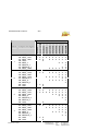
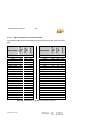
EVALXC2S/XCV/XCVE User Manual Board Module For Xilinx FPGA Families ErSt Electronic GmbH Aeschstrasse 171 CH-8123 Ebmatingen Phone Fax +41 1 980 61 44 +41 1 980 61 30 Internet http://www.erst.ch EVALXC2S/XCV/XCVE User Manual ErSt Electronic GmbH Aeschstrasse 171 CH-8123 Ebmatingen Phone Fax +41 1 980 61 44 +41 1 980 61 30 Internet http://www.erst.ch EVALX2S/XCV/XCVE User Manual Manual Version: 3/47 EVALXC2S EVALXCV EVALXCVE Version 1.0 Version 1.0 Version 1.0 September 2000 September 2000 September 2000 This manual describes the technical properties and the usage of the following products: 2.5V Versions: 1.8V Versions: EVALXCV-HQ240 with XCV50 – XCV800 Version 1.0 September 2000 EVALXC2S-PQ208 Version 1.0 with XC2S50 – XC2S200 September 2000 EVALXCVE-HQ240 Version 1.0 with 50E – 1000E FPGA September 2000 © ErSt Electronic GmbH, 2000 The ErSt Electronic GmbH reserves the right to make changes and improvements of the product without notice. Important Note: The EVALXC2S/XCV/XCVE board module series has been designed and tested exclusively for the usage as a development tool. In particular, strong electromagnetic radiation may be produced. ErSt Electronic GmbH does not undertake any liability for damages that may result from an improper use of this product. ErSt Electronic GmbH Aeschstrasse 171 CH-8123 Ebmatingen Phone Fax +41 1 980 61 44 +41 1 980 61 30 Internet http://www.erst.ch EVALX2S/XCV/XCVE User Manual 4/47 Notational Conventions: 1. 2. 3. 4. Names of active low signals are marked with a trailing \ or start with x, e.g. CS\ or XCS. When used to describe signal voltage levels, 0 means low voltage, 1 means high voltage. Table and figure references are printed in an italic font. Signal names within a sentence are printed in an italic font. Abbreviations: ASIC DIL DIP DLL FPGA GND HQ IEEE IOB ISP JTAG LED OTP PC PCB PLCC PLL PROM PWM QFP SCP SMD SPROM VCCINT VCCO VCCOPT VCXO VQ ZBT Application Specific Integrated Circuit Dual Inline Dual Inline Package Delay-Locked Loop Field Programmable Gate Array System Ground Thermally enhanced QFP Institute of Electrical and Electronics Engineers Input/Output Block In System Programmable Joint Test Action Group Light Emitting Diode One Time Programmable Personal Computer Printed Circuit Board Plastic Leaded Chip Carrier Phase Locked Loop Programmable Read Only Memory Pulse Width Modulation Quad Flat Pack Serial Configuration PROM Surface Mounted Device Serial PROM Internal supply voltage Output driver supply voltage Optional supply voltage Voltage Controlled Crystal Oscillator Plastic very thin QFP Zero Bus Time Spartan-II and Virtex are trademarks of Xilinx Inc. ErSt Electronic GmbH Aeschstrasse 171 CH-8123 Ebmatingen Phone Fax +41 1 980 61 44 +41 1 980 61 30 Internet http://www.erst.ch EVALX2S/XCV/XCVE User Manual 5/47 Contents: 1 Introduction............................................................................8 2 Overview .................................................................................9 2.1 Key Features .............................................................................. 9 2.2 Applications................................................................................ 9 2.3 Function Description.................................................................11 3 Technical Information..........................................................13 3.1 Power Supply ............................................................................13 3.1.1 3.1.2 3.1.3 3.1.4 3.2 3.3V Supply .................................................................................. 14 Reference Voltages........................................................................ 14 Output Driver Supply Voltage ....................................................... 16 Mounting the PWR3 Power Module .............................................. 16 FPGA Configuration.................................................................17 3.2.1 Master Serial Mode ....................................................................... 17 3.2.1.1 One Time Programmable PROMs........................................... 18 3.2.1.2 In System Programmable PROMs........................................... 18 3.2.2 Slave Serial Mode ......................................................................... 19 3.2.2.1 Configuration via XChecker Port ............................................ 19 3.2.3 SelectMAP Mode .......................................................................... 20 3.2.4 Boundary Scan Mode .................................................................... 21 3.2.5 Daisy Chain................................................................................... 21 3.3 Clock..........................................................................................23 3.3.1 External Clock............................................................................... 23 3.3.1.1 Termination Resistors ............................................................. 23 3.3.2 Internal Clock (Crystal Oscillators)................................................ 24 3.3.2.1 VCXO with Feedback Loop.................................................... 24 3.4 Reset and Voltage Supervision .................................................24 3.5 User Buttons ..............................................................................25 3.6 LEDs..........................................................................................25 3.7 Eight Position DIP Switch.........................................................26 3.8 Reference and I/O Signals.........................................................27 ErSt Electronic GmbH Aeschstrasse 171 CH-8123 Ebmatingen Phone Fax +41 1 980 61 44 +41 1 980 61 30 Internet http://www.erst.ch EVALX2S/XCV/XCVE User Manual 3.9 6/47 ZBT RAM Option .....................................................................31 3.10 Signals on Header Connectors...............................................32 3.10.1 3.10.2 3.10.3 3.10.4 3.10.5 3.11 Signal Overview ........................................................................ 32 Signal Assignment to Connector ST4C....................................... 33 Signal Assignment to Connector ST5A....................................... 34 Signal Assignment to Connector ST5B....................................... 35 Dedicated Signals ...................................................................... 36 Stack Extension......................................................................36 4 Literature..............................................................................37 5 Appendix A: FPGA Pin Assignments ...................................39 5.1 Special Considerations ..............................................................39 5.2 Spartan-II Devices in PQ-208 Package.....................................40 5.3 Virtex Devices in HQ-240 Package ...........................................42 5.4 Virtex-E Devices in HQ-240 Package .......................................44 6 Appendix B: Changes and Improvements ............................46 7 Appendix C: Schematic Diagram and PCB Layout..............47 Figures: Figure 1: Block diagram of the board module..................................................... 11 Figure 2: Wiring of the daisy chain .................................................................... 22 ErSt Electronic GmbH Aeschstrasse 171 CH-8123 Ebmatingen Phone Fax +41 1 980 61 44 +41 1 980 61 30 Internet http://www.erst.ch EVALX2S/XCV/XCVE User Manual 7/47 Tables: Table 1: Pin assignment on the power header connectors ST6 and ST7............... 13 Table 2: Derivation of the 3.3V supply voltage ................................................... 14 Table 3: Trim potentiometer for internal reference voltages................................ 14 Table 4: Choosing an internal reference voltage................................................. 15 Table 5: Choosing an external reference voltage ................................................ 15 Table 6: Connecting the output driver voltage .................................................... 16 Table 7: Setting the configuration modes............................................................ 17 Table 8: Master serial mode selection ................................................................ 18 Table 9: Selecting the XC1704 PROMs as serial configuration data source ........ 18 Table 10: Selecting the XC1804 ISP PROMs as serial configuration data source 18 Table 11: JTAG port pin assignment .................................................................. 19 Table 12: Slave serial mode selection................................................................. 19 Table 13: Jumper settings for XChecker configuration........................................ 20 Table 14: XChecker port pin assignment ............................................................ 20 Table 15: SelectMAP mode selection.................................................................. 20 Table 16: SelectMAP port pin assignment .......................................................... 21 Table 17: Boundary scan mode selection............................................................ 21 Table 18: Pin assignment of daisy chain connector J25 ...................................... 22 Table 19: Choice of the clock sources................................................................. 23 Table 20: External clock signals and termination resistors ................................. 23 Table 21: Crystal oscillator control signals and usage........................................ 24 Table 22: Reset pulse polarity selection.............................................................. 25 Table 23: User button connection with FPGA..................................................... 25 Table 24: LED signals and corresponding FPGA pins........................................ 26 Table 25: Signals on the eight position DIP switch ............................................. 26 Table 26: Grouping, bank and signal assignment of VREF jumpers .................... 28 Table 27: Correspondence of VREF jumpers to individual devices...................... 30 Table 28: Options for running the RAM and their activation............................... 31 Table 29: Assignment of signals to the ST4C connector ...................................... 33 Table 30: Assignment of signals to the ST5A connector....................................... 34 Table 31: Assignment of signals to the ST5B connector....................................... 35 Table 32: Dedicated signals on connector ST4B ................................................. 36 Table 33: Pin assignment of Spartan-II FPGAs in the PQ-208 package .............. 41 Table 34: Pin assignment of Virtex FPGAs in the HQ-240 package .................... 43 Table 35: Pin assignment of Virtex-E FPGAs in the HQ-240 package................. 45 ErSt Electronic GmbH Aeschstrasse 171 CH-8123 Ebmatingen Phone Fax +41 1 980 61 44 +41 1 980 61 30 Internet http://www.erst.ch EVALX2S/XCV/XCVE User Manual 1 8/47 Introduction This manual describes the specific properties of the board module like power supply, reference voltages, FPGA configuration, clocks, reset, LEDs, DIP switches and I/O signals. Please take information about the FPGA from the Xilinx literature (see chapter 4 Literature). Online information can be found on the Xilinx websites: http://www.xilinx.com and http://www.support.xilinx.com Information about new products and new developments can be found on the ErSt Electronic Website: http://www.erst.ch If you have questions you may write to the following email address: [email protected] We will answer as soon as possible, usually within one or two days. ErSt Electronic GmbH Aeschstrasse 171 CH-8123 Ebmatingen Phone Fax +41 1 980 61 44 +41 1 980 61 30 Internet http://www.erst.ch EVALX2S/XCV/XCVE User Manual 2 2.1 ♦ ♦ ♦ ♦ ♦ ♦ ♦ ♦ ♦ ♦ ♦ ♦ ♦ ♦ ♦ ♦ ♦ ♦ ♦ 2.2 ♦ ♦ ♦ ♦ ♦ ♦ ♦ ♦ ♦ ♦ 9/47 Overview Key Features Download: Master Serial Mode (SPROM with socket), Slave Serial Mode (XChecker header connector), Boundary Scan Mode (JTAG header connector), SelectMAP Mode (header connector) Configuration from onboard SCPs: ISP SCPs programmable via JTAG, sockets for OTP SCPs. I/O bank reference voltages: Two adjustable VREFs for 8 I/O banks (selectable via jumpers) or eight external voltages (e.g. from power module PWR3) Voltage supervisor with reset button Two separate crystal oscillators with sockets (DIL8 or DIL14) Jumpers to select between internal and external clock sources Four SMB connectors next to the FPGA for feeding high frequency clocks Two header connectors (two rows with 50 pins each) for I/Os, clocks and control signals Two header connectors (one row with 50 pins each) for supply and reference voltages from power module Four ground clips Two user buttons Eight position DIP switch Display with eight LEDs "Done" LED Power LEDs Mode jumpers M0 / M1 / M2 Daisy chain configuration with other board modules possible Several boards may be connected to form a stack Board size 100mm x 150mm Applications ASIC Emulation Error monitoring and analysis Digital PLL circuits PWM controller Adaptive digital filters Signal multiplexers Stimuli generators High speed encoder/decoder Memory controller Interface controller ErSt Electronic GmbH Aeschstrasse 171 CH-8123 Ebmatingen Phone Fax +41 1 980 61 44 +41 1 980 61 30 Internet http://www.erst.ch EVALX2S/XCV/XCVE User Manual ErSt Electronic GmbH 10/47 Aeschstrasse 171 CH-8123 Ebmatingen Phone Fax +41 1 980 61 44 +41 1 980 61 30 Internet http://www.erst.ch EVALX2S/XCV/XCVE User Manual 2.3 11/47 Function Description The board module EVALXC2S/XCV/XCVE is equipped with a member of the Xilinx Spartan-II, Virtex or Virtex-E FPGA family in the PQ208 or HQ-240 package, respectively. This board is especially suited to test digital circuits during the early stages of their development. You can easily attach a logic analyzer an watch the signals in real time. The high count of system gates enables you to implement circuits that reach the complexity of ASICs. The configuration data of the FPGA is downloadable using one of four modes (master serial mode (XChecker), slave serial mode (SPROM), boundary scan mode (JTAG) and SelectMAP mode). The block diagram of Figure 1 shows the functional blocks of the board. Clock Reference Voltage Crystal Oscillator 1 Ext. Clock 1 I/O Connections Power and VRef Onboard VREF VCCINT 2 VRef Crystal Oscillator 2 Ext. Clock 2 Header Connector Ext. Clock 0 8 V Ref Jumper Array for VREF Selection Ext. Clock 3 VCCO VCCOPT 8 VRef 4 Clocks General I/O 146 I/Os Header Connector 50 poles Optional ZBT RAM 256/512K x 18 FPGA Header Connector 50 poles Spartan-ΙΙ or Virtex or Virtex-E Header Connector 50 poles Configuration User Interaction XChecker Daisy Chain JTAG SelectMap 8 Eight LED Display Reset 8 Eight Position DIPSwitch SCP ISP SCP Done LED Mode Select 2 External Connection Voltage Supervisor Three Push Buttons 1 Onboard Item Functional Group Figure 1: Block diagram of the board module ErSt Electronic GmbH Aeschstrasse 171 CH-8123 Ebmatingen Phone Fax +41 1 980 61 44 +41 1 980 61 30 Internet http://www.erst.ch EVALX2S/XCV/XCVE User Manual 12/47 All general I/Os of the FPGA are routed to header connectors. If you use I/O standards that need reference voltages, you can select up to eight different voltage levels for all eight banks individually with jumpers. An optional ZBT RAM helps you to support memory-demanding implementations like imaging and telecommunication applications. The clock input of this RAM is connected to the global clock GCK2 of the FPGA to achieve a real synchronous system clock. Alternatively, you can generate the RAM clock internally to the FPGA. In this case the clock is gated through an output pin connected to the RAM clock input via a jumper. The GCK2 clock may then not be driven externally. By stacking several boards, you may implement circuits whose complexity is beyond the scope of a single FPGA. The whole stack is configurable with a single download by means of an external daisy chain. You can also link the stacked boards in a JTAG chain. Two sockets are provided to hold Xilinx OTP SCPs (two XC1704L in a PLCC44 package). In addition, two ISP SCPs (XC1800 family) are mounted on the back side of the board. You can program these SCPs using the JTAG mode. Four clock sources can be used where two of them are either an onboard crystal oscillator or an external source. The other two sources are always external sources. The crystal oscillators are mounted in sockets and can therefore be exchanged easily. Both, a DIL-8 and a DIL-14 package can be used. There is the possibility to terminate all clock traces near the FPGA with resistors to ground. These resistors may be mounted by you on the bottom side of the PCB. A voltage supervisor circuit generates a short pulse of ca. 2ms duration whenever the core supply voltage (VCCINT) drops below 2.2V (1.7V for Virtex-E) and on power up. The polarity of the reset pulse can be chosen to be either active high or active low. Such a reset pulse is also generated when you press the reset button. An eight-position DIP switch is available for user specific applications. In addition, there are three push buttons. One of them is intended primarily for use as a reset button and is connected to the voltage supervisor circuit. The other two buttons are available for arbitrary purposes. A row with eight LEDs may function as a display for status and error messages. You may disconnect these LEDs from the I/O signals by means of jumpers. This is especially useful if you stack several boards and do not want to have the LEDs connected in parallel. ErSt Electronic GmbH Aeschstrasse 171 CH-8123 Ebmatingen Phone Fax +41 1 980 61 44 +41 1 980 61 30 Internet http://www.erst.ch EVALX2S/XCV/XCVE User Manual 3 13/47 Technical Information This chapter gives a detailed description of the technical details of the board. Please consult the schematic diagrams where you find the components who’s designators are mentioned in the text. 3.1 Power Supply Due to the 0.18/0.22µm process, the FPGA works with an internal supply voltage (VCCINT) of 1.8/2.5V and an output driver voltage (VCCO) of up to max. 3.3V. Depending on the chosen I/O standard, VCCO can be 1.5V, 2.5V or 3.3V. All inputs are 5V compatible. Other devices on the board (crystal oscillators and SCPs) need a supply voltage of 3.3V. This voltage can be derived via a jumper from VCCO if an appropriate I/O standard is used, i.e. one which works with 3.3V. For other I/O standards, which work with 1.5V or 2.5V, the 3.3V voltage must be taken from a third source (VCCOPT). The voltages VCCINT, VCCO and VCCOPT may be taken from external power supplies via the power connectors. The preferred method, however, is the usage of the power module PWR3 that we developed especially for this purpose. The power module can be plugged onto the Virtex board module by means of two 50-pole connectors. In addition, the power module also generates eight reference voltages needed by the FPGA to support the multi I/O standards. Beside the 50-pole connectors, the power module is equipped with three power connectors and can be connected to other board modules using cables. Connector ST6 ST7 Pin Number 1 to 12 13 to 25 26 to 42 43 44 45 46 47 48 49 50 1 to 12 13 to 38 39 to 50 Signal Name VCCOPT GND Reserved VREF0 VREF1 VREF2 VREF3 VREF4 VREF5 VREF6 VREF7 VCCINT GND VCCO Table 1: Pin assignment on the power header connectors ST6 and ST7 ErSt Electronic GmbH Aeschstrasse 171 CH-8123 Ebmatingen Phone Fax +41 1 980 61 44 +41 1 980 61 30 Internet http://www.erst.ch EVALX2S/XCV/XCVE User Manual 3.1.1 14/47 3.3V Supply A 3.3V supply is needed for various devices (SPROMs, crystal oscillators, voltage supervisor, general purpose LEDs, JTAG and XChecker ports). This supply may be derived from VCCO or VCCOPT according to the following table: VCCO 1.5V 2.5V 3.3V VCCOPT 3.3V 3.3V not used J24 (3.3V) 1-2 1-2 2-3 Table 2: Derivation of the 3.3V supply voltage In the case of a VCCO voltage of 3.3V, the VCCOPT voltage is not needed. If the power supply device is a PWR3 power module, its VCCOPT output may be used for arbitrary purposes, e.g. as a 5V power supply. 3.1.2 Reference Voltages The FPGAs have eight I/O banks, which must be supplied with different reference voltages depending on the used I/O standard. Usually you do not need more than two different I/O standards at one time. For convenience, two different reference voltages are generated on the board, derived from VCCINT using trim potentiometers. In conjunction with the PWR3 power module, the reference voltages should be taken from the PWR3. This way you can operate all eight banks differently. Trim Potentiometer R56 R55 Reference Voltage VREF0 (onboard) VREF1 (onboard) Table 3: Trim potentiometer for internal reference voltages The internal reference voltages can be monitored at the connectors J110 (VREF0) and J111 (VREF1), respectively. Connect a voltmeter to the appropriate port while adjusting the potentiometer. ErSt Electronic GmbH Aeschstrasse 171 CH-8123 Ebmatingen Phone Fax +41 1 980 61 44 +41 1 980 61 30 Internet http://www.erst.ch EVALX2S/XCV/XCVE User Manual 15/47 The choice of a reference voltage source is done using jumpers. To choose an internal reference voltage, you must set the jumpers according to the following table: Bank 0 1 2 3 4 5 6 7 VREF0 onboard J102 (1-2) J103 (1-2) J104 (1-2) J105 (1-2) VREF1 onboard J106 (2-3) J107 (2-3) J108 (2-3) J109 (2-3) Table 4: Choosing an internal reference voltage When an external reference voltage is used, a dedicated reference voltage can be assigned to each bank. The jumper settings are listed in Table 5. Bank 0 VREF0 J101 2-3 1 2 3 4 5 VREF1 VREF2 VREF3 VREF4 VREF5 VREF6 VREF7 J103 2-3 J104 2-3 J105 2-3 J106 1-2 J107 1-2 6 J108 1-2 7 J109 1-2 Table 5: Choosing an external reference voltage ErSt Electronic GmbH Aeschstrasse 171 CH-8123 Ebmatingen Phone Fax +41 1 980 61 44 +41 1 980 61 30 Internet http://www.erst.ch EVALX2S/XCV/XCVE User Manual 3.1.3 16/47 Output Driver Supply Voltage You can connect each of the eight I/O bank’s output driver supply to the VCCO voltage individually. To do this, set the jumpers J114 to J121 according to the following table: Bank 0 1 2 3 4 5 6 7 Jumper for connection to VCCO J114 J115 J116 J117 J121 J118 J119 J120 Table 6: Connecting the output driver voltage The VCCO voltage comes from the power module and can be selected to be 1.5V, 2.5V or 3.3V. If you use an I/O standard that does not require an output driver voltage, just remove the corresponding jumper. If you need two or three different output driver voltages at the same time, you can do this be removing the appropriate jumper and using one of the jumper pins to connect an external supply. 3.1.4 Mounting the PWR3 Power Module The PWR3 power module can be plugged to the board module by means of two single inline 50-pole connector pairs. The assembly is correct if the three four pole output connectors of the power module and the single six-pole supply voltage connector of the board module are on the same side. Please check that the orientation of the two boards and the output voltage settings of the power module (refer to the PWR3 user manual) are correct before applying power. ErSt Electronic GmbH Aeschstrasse 171 CH-8123 Ebmatingen Phone Fax +41 1 980 61 44 +41 1 980 61 30 Internet http://www.erst.ch EVALX2S/XCV/XCVE User Manual 3.2 17/47 FPGA Configuration The FPGAs with Virtex architecture support the following four configuration modes: • Master Serial Mode • Slave Serial Mode • SelectMAP mode • Boundary-scan mode The configuration pins (M2, M1, M0) select among these modes with the option in each case of having the IOB pins either pulled up or left floating prior to configuration. The selection codes are listed in Table 7. An inserted jumper ties the appropriate pin to ground whereas the pin is pulled high if the jumper is removed. Here and in the following tables, a “Yes” in the jumper column means that the jumper is present whereas a “–“ means that no jumper is plugged in. Mode Master Serial Boundary Scan SelectMAP Slave Serial Master Serial Boundary Scan SelectMAP Slave Serial J3 (M2) Yes Yes Yes Yes J2 (M1) Yes Yes Yes Yes - J1 (M0) Yes Yes Yes Yes - CCLK Direction Out N/A In In Out N/A In In Bits 1 1 8 1 1 1 8 1 Busy/ Dout Yes No No No Yes No No No Internal Pullups No No No No Yes Yes Yes Yes Table 7: Setting the configuration modes 3.2.1 Master Serial Mode In master serial mode, the CCLK output of the FPGA drives a Xilinx Serial PROM that feeds bit-serial data to the DIN input. The FPGA accepts this data on each rising CCLK edge. After the FPGA has been loaded, the data for the next device in a daisy-chain is presented on the DOUT pin after the rising CCLK edge. The preamble is also forwarded to other devices in the daisy chain. SPROM RESET pin is driven by INIT\, and CE\ input is driven by DONE. ErSt Electronic GmbH Aeschstrasse 171 CH-8123 Ebmatingen Phone Fax +41 1 980 61 44 +41 1 980 61 30 Internet http://www.erst.ch EVALX2S/XCV/XCVE User Manual 18/47 The master serial mode is selected by the following jumper settings: J3 (M2) Yes - J2 (M1) Yes Yes J1 (M0) Yes Yes Internal pullups on IOB pins No Yes Table 8: Master serial mode selection 3.2.1.1 One Time Programmable PROMs Two sockets for XC1704L devices in a PLCC44 package are available. U6 is the first device in the chain. The CEO\ output of the first device enables the second device after all of its contents has been put out. If your particular FPGA only needs one PROM to hold the configuration bit stream, insert U6 only. In order to use these devices as the source of serial configuration data, the following jumper settings apply: J32 (PROM Sel) 2-3 Table 9: Selecting the XC1704 PROMs as serial configuration data source 3.2.1.2 In System Programmable PROMs The two ISP PROMs (U1 and U2, both in VQ44 package) of the XC1800 family are optional. Depending on the size of the FPGA only one or both of them are needed. These devices are programmable many times over the JTAG port but work otherwise the same as the XC1700 family. If no ISP PROMs are present, the bypass resistor R61 (0 Ω) connects the JTAG data input directly with the FPGA. If only one if the ISP PROMs is used, the resistor R29 (0 Ω) bypasses the second one. The jumper settings to use these devices as the source of configuration data are as follows: J32 (PROM Sel) 1-2 Table 10: Selecting the XC1804 ISP PROMs as serial configuration data source ErSt Electronic GmbH Aeschstrasse 171 CH-8123 Ebmatingen Phone Fax +41 1 980 61 44 +41 1 980 61 30 Internet http://www.erst.ch EVALX2S/XCV/XCVE User Manual 19/47 You can program the devices via the JTAG port J5. TDI of U1 is connected directly with the corresponding pin of J5. U2 is chained with U1, i.e. TDI of U2 is connected with TDO of U1. The pin assignment of the JTAG port is listed in Table 11. Pin of JTAG port J5 1 2 3 4 5 6 Signal Name TMS TDI TDO TCK GND 3.3V Table 11: JTAG port pin assignment 3.2.2 Slave Serial Mode In slave serial mode, the FPGA receives configuration data in bit-serial form from a serial PROM or other source of serial configuration data. An external device, e.g. XChecker cable, generates the download clock. Multiple FPGAs can be daisychained for configuration from a single source. After a particular FPGA has been configured, the data for the next device is routed to the DOUT pin. The slave serial mode is selected by the following jumper settings: J3 (M2) Yes J2 (M1) - J1 (M0) - Internal pullups on IOB pins No Yes Table 12: Slave serial mode selection 3.2.2.1 Configuration via XChecker Port In slave serial mode, the serial configuration data comes from the XChecker port J4. Either a parallel or a serial cable may be used. Due to the 3.3V cable supply voltage, we recommend to use an appropriate cable (Xilinx order number: HWXCH3V). Nevertheless, experiments with 5V cables showed, that these cables work well down to 3V, parallel cables even down to 2V. The circumstances under which a certain cable will work depend on many factors, including the PC used. Whether a cable that is specified for 5V operation will work is not guaranteed. In any case we strongly recommend using the MultiLinx cable that has the additional advantage of being able to use the USB bus. This brings an enormous increase in download speed. ErSt Electronic GmbH Aeschstrasse 171 CH-8123 Ebmatingen Phone Fax +41 1 980 61 44 +41 1 980 61 30 Internet http://www.erst.ch EVALX2S/XCV/XCVE User Manual 20/47 The jumper settings to use the XChecker port are as follows: J32 (PROM Sel) Removed (neither 1-2 nor 2-3 connected) Table 13: Jumper settings for XChecker configuration The pin assignments of the XChecker port connector are listed in the following table: Pin of XChecker port J4 1 2 3 4 5 6 7 Signal Name PROG\ DONE INIT\ CCLK DATA 3.3V GND Table 14: XChecker port pin assignment 3.2.3 SelectMAP Mode The SelectMAP mode is the fastest configuration option. Byte-serial data is written into the FPGA with a BUSY flag controlling the flow of data. An external data source provides a byte stream, CCLK, a Chip Select (CS) signal and a Write signal (WRITE). If BUSY is asserted (High) by the FPGA, the data must be held until BUSY goes Low. Data can also be read using the SelectMAP mode. If WRITE is not asserted, configuration data is read out of the FPGA as part of a readback operation. The SelectMAP mode is selected by the following jumper settings: J3 (M2) Yes J2 (M1) - J1 (M0) Yes Yes Internal pullups on IOB pins No Yes Table 15: SelectMAP mode selection ErSt Electronic GmbH Aeschstrasse 171 CH-8123 Ebmatingen Phone Fax +41 1 980 61 44 +41 1 980 61 30 Internet http://www.erst.ch EVALX2S/XCV/XCVE User Manual 21/47 The byte-serial data is fed from an external source to the SelectMAP port J6 using the following pin assignments: Pin of SelectMAP port J6 1 2 3 4 5 6 7 8 9 10 11 12 Signal Name D0 D1 D2 D3 D4 D5 D6 D7 BUSY/DOUT WRITE\ CS\ GND Table 16: SelectMAP port pin assignment 3.2.4 Boundary Scan Mode In the boundary-scan mode, no non-dedicated pins are required, configuration being done entirely through the IEEE 1149.1 Test Access Port. Configuration and readback is always available. The boundary-scan mode simply locks out the other modes. The boundary scan mode is selected by the following jumper settings: J3 (M2) Yes J2 (M1) Yes Yes J1 (M0) - Internal pullups on IOB pins No Yes Table 17: Boundary scan mode selection The pin assignment of the JTAG port J5 is listed in Table 11. 3.2.5 Daisy Chain If several board modules are stacked together, there is the possibility to configure the whole stack at once. To do this, the individual layers must be connected in form of a daisy chain. This is accomplished by connecting appropriate pins of connector J25 (see Table 18) externally. ErSt Electronic GmbH Aeschstrasse 171 CH-8123 Ebmatingen Phone Fax +41 1 980 61 44 +41 1 980 61 30 Internet http://www.erst.ch EVALX2S/XCV/XCVE User Manual 22/47 J25 (Connector) 1 2 3 4 Pin Name DUP D0/DIN BUSY/DOUT DDOWN Table 18: Pin assignment of daisy chain connector J25 Use the following scheme for the external connections: dup din dout ddown Layer 4 Layer 3 Layer 2 Layer 1 Figure 2: Wiring of the daisy chain The easiest way to make the connections dup-din and dout-ddown is to insert a jumper. However, these connections are only needed if the stack is connected to a main board and if the configuration data comes from the main board. If the main board is not used you need only the dout-din connections. The configuration bit streams are then fed to the lowest layer (SCP or XChecker). ErSt Electronic GmbH Aeschstrasse 171 CH-8123 Ebmatingen Phone Fax +41 1 980 61 44 +41 1 980 61 30 Internet http://www.erst.ch EVALX2S/XCV/XCVE User Manual 3.3 23/47 Clock All four clock signals (GCK0 to GCK3) are routed to header connectors. GCK0 and GCK1 may get the clock signal either from an internal crystal oscillator or from an external source, see Table 19. J26 (GCK0) 2-3 2-3 1-2 1-2 J27 (GCK1) 2-3 1-2 2-3 1-2 GCK0 Source internal U3 internal U3 external ST4B-52 external ST4B-52 GCK1 Source internal U4 external ST4B-54 internal U4 external ST4B-54 Table 19: Choice of the clock sources 3.3.1 External Clock The assignment of the clock signals on the header connectors is listed in 1 FPGA pins for Spartan-II devices are put in parenthesis Table 20. There is also the possibility to feed the clock via a SMB connector mounted next to the FPGA. This is the preferred method at high clock frequencies. Signal Name GCK0 GCK1 GCK2 GCK3 1 Connector ST4B 52 54 56 58 FPGA Pin1 92 (80) 89 (77) 210 (182) 213 (185) Direct Clock Connector (SMB) J15 (GCK0) J16 (GCK1) J17 (GCK2) J18 (GCK3) Termination Resistor R49 R50 R51 R52 FPGA pins for Spartan-II devices are put in parenthesis Table 20: External clock signals and termination resistors 3.3.1.1 Termination Resistors All clock signals may be terminated with resistors (R49 to R52). These are connected immediately from the FPGA pin to ground. These resistors form a parallel termination. The values of the resistors should match the impedance of the circuit board trace having a nominal value of 100 Ohms. Please consider the maximal output current capability of the clock source! The resistors (SMD, size 0805) can be soldered to the board directly beneath the FPGA on the bottom side of the PCB. ErSt Electronic GmbH Aeschstrasse 171 CH-8123 Ebmatingen Phone Fax +41 1 980 61 44 +41 1 980 61 30 Internet http://www.erst.ch EVALX2S/XCV/XCVE User Manual 3.3.2 24/47 Internal Clock (Crystal Oscillators) Since the clock frequency depends strongly on the application, the oscillators must be exchangeable. The oscillators socket can hold DIL-8 or DIL-14 packages. Pin 1 is common for both types of packages. 3.3.2.1 VCXO with Feedback Loop Oscillators of the VCXO type need a control signal at pin 1 (Uc). To get a closed feedback loop, this signal must be connected (via FPGA) to Uout. You have the possibility to build an RC loop filter be mounting R54, C41 and R53, C42. In this case, jumpers J30 and J31 remain open. Crystal Oscillator U3 U4 Ucontrol Signal XINIT L43P Clock source for GCK0 GCK1 Table 21: Crystal oscillator control signals and usage Note: 3.4 The jumper J31 (UC VCXO) must be inserted to connect pin 1 of U4 with signal L43P if a feedback signal for a VCXO is needed. Beware in mind that the L43P signals are connected in parallel if several boards are stacked. In this case, only U3 may be used in a PLL loop and J31 as well as the loop filter component R53 should be removed. Reset and Voltage Supervision U5 works as a reset and voltage supervision circuit. A functional reset can be issued at any time by pressing the push button SW2. The button is connected to the voltage supervisor circuit U5, which in turn generates a reset pulse on BUSY/DOUT (FPGA pin 178). A reset pulse is also generated whenever VCCINT drops below a predefined threshold of 2.2V (Spartan-II, Virtex) or 1.7V (Virtex-E) and on power up. The pulse duration is approximately 2ms. You can select the polarity of the reset pulse with jumper J23. The settings are listed in Table 22. ErSt Electronic GmbH Aeschstrasse 171 CH-8123 Ebmatingen Phone Fax +41 1 980 61 44 +41 1 980 61 30 Internet http://www.erst.ch EVALX2S/XCV/XCVE User Manual J23 (Reset) 1-2 2-3 25/47 Reset Pulse Polarity Active Low Active High Table 22: Reset pulse polarity selection Note: 3.5 A manual reset initializes the internal circuits of the FPGA (registers, counters, finite state machines etc.) and must be implemented in the design appropriately. There is no dedicated reset pin on the FPGA. User Buttons Two user buttons (SW3 and SW4) are available for arbitrary purposes. A pressed button ties the connected FPGA pin to ground while the pin is pulled to VCCINT if the button is released. Button SW3 SW4 Signal Name XWRITE XCS Spartan-II Pin 161 160 Virtex Pin 185 184 Table 23: User button connection with FPGA The connection of a user button with the FPGA is routed over a 510Ω resistor. A pressed button does therefore not harm the SelectMAP interface. 3.6 LEDs The eight LEDs D2 to D9 are intended as optical indicators for the display of status information. D1 is connected to the DONE pin of the FPGA and D10 (VCCOPT), D11 (VCCO) and D12 (VCCINT) serve as power indicator LEDs. The DONE LED turns on at the end of a successful bit stream download. Note: The VCCO indicator LED D11 will not lit when the VCCO voltage is 1.5V or less since this value is below the forward voltage of the LED. The LEDs D2 to D9 turn on whenever the corresponding FPGA output is low. Each LED may be disconnected from the I/O signal by removing the corresponding jumper. The following table shows the assignment to the jumpers and the FPGA pins: ErSt Electronic GmbH Aeschstrasse 171 CH-8123 Ebmatingen Phone Fax +41 1 980 61 44 +41 1 980 61 30 Internet http://www.erst.ch EVALX2S/XCV/XCVE User Manual LED D2 D3 D4 D5 D6 D7 D8 D9 Jumper J14 J13 J12 J11 J10 J9 J8 J7 26/47 Signal Name Spartan-II Pin L48P 46 L45N 57 L45P 58 L44P 60 L10N 168 L23N 132 L33N 100 L38N 84 Virtex Pin 56 67 68 71 195 152 113 96 Table 24: LED signals and corresponding FPGA pins Note: 3.7 If the board module is used within a stack the LEDs of all layers are connected in parallel. If a LED is driven by the FPGA the LEDs of the other layers are driven also. The maximal output current of 20mA of an FPGA port is sufficient for up to four layers. If more than four levels are used, or to avoid driving certain LEDs, the jumpers of the appropriate LEDs of the remaining layers must be removed. Eight Position DIP Switch The eight-position DIP switch SW1 can be used for application specific purposes. In the On position the connected FPGA pin is tied to ground. In the Off position the connected FPGA pin is pulled to VCCINT via a resistor. The assignment of the switches to the FPGA pins is as follows: Switch Signal Name Spartan-II Pin 1 D0/DIN 153 2 D1 146 3 D2 142 4 D3 135 5 D4 126 6 D5 119 7 D6 115 8 D7 108 Virtex Pin 177 167 163 156 145 138 134 124 Table 25: Signals on the eight position DIP switch The switches are connected to the FPGA via resistors of 510Ω. Owing to these resistors, the SelectMAP mode can be used even if some switches are closed to ground. ErSt Electronic GmbH Aeschstrasse 171 CH-8123 Ebmatingen Phone Fax +41 1 980 61 44 +41 1 980 61 30 Internet http://www.erst.ch EVALX2S/XCV/XCVE User Manual 3.8 27/47 Reference and I/O Signals For the smaller FPGA devices some pins are usable as general I/Os whereas these pins are reference voltage inputs on the larger ones. Certain I/O standards need no reference voltages. In these cases, all of these pins may be used as general I/Os on every FPGA type. To make the board as versatile as possible, you can connect every possible VREF pin individually to a reference voltage by inserting a jumper. Table 26 gives an overview of the jumper groupings and assignments to the I/O banks. In Table 27 the correspondence of each VREF jumper to the individual devices is listed. A jumper belongs to a certain device if there is a cross in the device column. No cross in the device column means that you can use the corresponding FPGA pin for general I/O. ErSt Electronic GmbH Aeschstrasse 171 CH-8123 Ebmatingen Phone Fax +41 1 980 61 44 +41 1 980 61 30 Internet http://www.erst.ch EVALX2S/XCV/XCVE User Manual Bank 28/47 Virtex and Spartan Virtex only Spartan only 7 J35, VREF_L61P J36, VREF_L57P J37, VREF_L60P J39, J40, J41, J42, VREF_7 VREF10_7 VREF610_7 VREF_L63N J38, L62N 6 J43, VREF_L50N J44, VREF_L51N J45, J46, J47, J48, J49, VREF_L55P VREF_L54N VREF610_6 VREF_6 VREF10_6 J50, L54P J51, L49P 5 J52, VREF_L44N J53, VREF_L43N J54, VREF_L41P J55, J56, J57, J58, VREF_L46P VREF_5 VREF610_5 VREF10_5 J59, L45N 4 J60, VREF_L34P J61, VREF_L35P J62, J63, J64, J65, J66, VREF_L38P VREF_L39N VREF_4 VREF10_4 VREF610_4 J67, L38N J68, L33N 3 J69, VREF_L28N J70, VREF_L27N J71, VREF_L24N J72, J73, J74, J75, VREF_L30P VREF_3 VREF10_3 VREF610_3 J76, L29N 2 J77, VREF_L21P J78, VREF_L18P J79, VREF_L17P J80, J81, J82, J83, VREF_L22N VREF_2 VREF10_2 VREF610_2 J84, L16P 1 J85, VREF_L11P J86, VREF_L10P J87, VREF_L7P J88, J89, J90, J91, VREF_L13N VREF_1 VREF10_1 VREF610_1 J92, L12P J93, VREF_L2N J94, VREF_L0P J95, J96, J97, J98, J99, VREF_L5N VREF_0 VREF40_0 VREF610_0 VREF610 J100, L5P J101, L1P 0 Table 26: Grouping, bank and signal assignment of VREF jumpers ErSt Electronic GmbH Aeschstrasse 171 CH-8123 Ebmatingen Phone Fax +41 1 980 61 44 +41 1 980 61 30 Internet http://www.erst.ch EVALX2S/XCV/XCVE User Manual 29/47 6 5 4 ErSt Electronic GmbH X X X X X X X X X X X X X X X X X X X X X X X XCV400E XCV600E XCV1000E X X XCV300E X X X X XCV200E X X X XCV100E X X XCV50E J35, VREF_L61P J36, VREF_L57P J37, VREF_L60P J38, L62N J39, VREF_7 J40, VREF10_7 J41, VREF610_7 J42, VREF_L63N J43, VREF_L50N J44, VREF_L51N J45, VREF_L55P J46, VREF_L54N J47, VREF610_6 J48, VREF_6 J49, VREF10_6 J50, L54P J51, L49P J52, VREF_L44N J53, VREF_L43N J54, VREF_L41P J55, VREF_L46P J56, VREF_5 J57, VREF610_5 J58, VREF10_5 J59, L45N J60, VREF_L34P J61, VREF_L35P J62, VREF_L38P J63, VREF_L39N J64, VREF_4 J65, VREF10_4 J66, VREF610_4 J67, L38N J68, L33N XC2S200 7 Jumper and Signal XC2S100/150 Bank XC2S50 FPGA Device X X X X X X X X X X X X X X X X X X X X X X X X X X X X X X X X X X X X X X X X X X X X X X X X X X X X X X X X X X X X X X X X X X X X X X X X X X X X X X X X X X X X X X X X X X X X X X X X X X X X X X X X X X X X X X X X X X X X X X X X X X X X X X X X Aeschstrasse 171 CH-8123 Ebmatingen Phone Fax +41 1 980 61 44 +41 1 980 61 30 Internet http://www.erst.ch EVALX2S/XCV/XCVE User Manual 30/47 2 1 0 X X X X X X X X X X X X X X X X X X X X X X X X X X X X X X X X X X X X X X X X X X X X X X X X X X X X X X X X X X X X X X X X X X X X X X X X X X X X X X X X X X X X X X X X X X X X X X X X X X X X X X X X XCV1000E XCV600E X X X X X X X X XCV400E X XCV300E X X X XCV200E X X X X XCV100E X XCV50E J69, VREF_L28N J70, VREF_L27N J71, VREF_L24N J72, VREF_L30P J73, VREF_3 J74, VREF10_3 J75, VREF610_3 J76, L29N J77, VREF_L21P J78, VREF_L18P J79, VREF_L17P J80, VREF_L22N J81, VREF_2 J82, VREF10_2 J83, VREF610_2 J84, L16P J85, VREF_L11P J86, VREF_L10P J87, VREF_L7P J88, VREF_L13N J89, VREF_1 J90, VREF10_1 J91, VREF610_1 J92, L12P J93, VREF_L2N J94, VREF_L0P J95, VREF_L5N J96, VREF_0 J97, VREF40_0 J98, VREF610_0 J99, VREF610 J100, L5P J101, L1P XC2S200 3 Jumper and Signal XC2S100/150 Bank XC2S50 FPGA Device X X X X X X X X X X X X X X X X X X X X X X X X X X X X X X X X X X X X X X Table 27: Correspondence of VREF jumpers to individual devices ErSt Electronic GmbH Aeschstrasse 171 CH-8123 Ebmatingen Phone Fax +41 1 980 61 44 +41 1 980 61 30 Internet http://www.erst.ch EVALX2S/XCV/XCVE User Manual 3.9 31/47 ZBT RAM Option The ZBT RAM U10 is an optional component of the module. If this RAM is present, the header connector ST5B, where all RAM signals are routed to, is not available. This is to avoid conflicts when you stack several boards. The synchronous RAM clock input is specially handled. First, it may be driven directly from GCK2 over the coaxial SMB connector J17. In this case, you should use this GCK2 clock to drive the FPGA also. Doing the clocking that way, you have a true synchronous system clock for both FPGA and RAM. Second, you may drive the RAM clock from the FPGA output signal L20N (pin 138 on Spartan-II, pin 159 on Virtex-E) by inserting jumper J124. Now you are free to use any clock for the FPGA but the price to pay is that you do not have a true synchronous system clock for the RAM any more. However, you may use the DLLs of the FPGA to produce the system clock. When you feed the clock from J17 (GCK2) you have the option to terminate the line with resistor R62 at the RAM, R51 at the FPGA or both. You may put the RAM into Linear Burst Mode by inserting J122. The following table summarizes what has been described above: Option Action to activate option True synchronous clock for both Feed external clock via J17 and remove jumper J124 FPGA and RAM FPGA output drives RAM clock, anyInsert jumper J124 and configure the clock drives FPGA FPGA to put out the RAM clock (on pin 138 for Spartan-II or pin 159 for Virtex-E) Terminate GCK2 clock line at the Solder R51 to the bottom of the board FPGA Terminate the GCK2 clock line at Solder R62 to the bottom of the board the RAM Running RAM in linear burst mode Insert jumper J122 Table 28: Options for running the RAM and their activation ErSt Electronic GmbH Aeschstrasse 171 CH-8123 Ebmatingen Phone Fax +41 1 980 61 44 +41 1 980 61 30 Internet http://www.erst.ch EVALX2S/XCV/XCVE User Manual 32/47 3.10 Signals on Header Connectors 3.10.1 Signal Overview All general I/O signals of the FPGA are routed to header connectors. This includes all the VREF pins also. If you want to operate a bank with an I/O standard that needs a reference voltage, you must connect all VREF pins of that bank to the appropriate reference voltage, see 3.8 Reference and I/O Signals. Note: When you stack several modules, the VREF signals of all modules are connected in parallel. Therefore you must use the same I/O standard for same banks on each module. The tables on the following pages show the connections of the FPGA pins to the header connectors. ErSt Electronic GmbH Aeschstrasse 171 CH-8123 Ebmatingen Phone Fax +41 1 980 61 44 +41 1 980 61 30 Internet http://www.erst.ch EVALX2S/XCV/XCVE User Manual 3.10.2 33/47 Signal Assignment to Connector ST4C Virtex Pin 62 61 60 59 58 57 46 49 48 47 45 44 43 42 41 37 36 35 34 33 Spartan-II Pin 101 102 103 104 105 106 107 108 109 110 111 112 113 114 115 116 117 118 119 120 121 122 123 124 125 Signal Name Connector Pin Spartan-II Pin VREF_L43N VREF610_5 L44P VREF_L44N L45P L45N VREF_L46P L46N L47P L47N L48N L48P VREF_6 L49N L49P VREF_L50N L50P VREF610_6 VREF_L51N L51P L52N L52P VREF10_6 L53N L53P Virtex Pin Signal Name Connector Pin The following table shows the assignment of the FPGA pins to the ST4C connector pins: 73 72 71 70 68 67 66 65 64 63 57 56 54 53 52 50 49 48 47 46 42 41 40 39 38 VREF_L54N L54P L55N VREF_L55P IO_6 L56N L56P VREF_7 L57N VREF_L57P L58N L58P VREF10_7 L59N L59P L60N VREF_L60P VREF610_7 L61N VREF_L61P L62N L62P VREF_L63N L63P IO_7 126 127 128 129 130 131 132 133 134 135 136 137 138 139 140 141 142 143 144 145 146 147 148 149 150 31 30 29 27 24 23 22 21 20 18 17 16 15 14 10 9 8 7 6 4 3 5 - 36 35 34 33 31 28 27 26 24 23 21 20 19 18 17 13 12 11 10 9 7 6 5 4 3 Table 29: Assignment of signals to the ST4C connector ErSt Electronic GmbH Aeschstrasse 171 CH-8123 Ebmatingen Phone Fax +41 1 980 61 44 +41 1 980 61 30 Internet http://www.erst.ch EVALX2S/XCV/XCVE User Manual 3.10.3 34/47 Signal Assignment to Connector ST5A Virtex Pin 69 74 73 82 84 88 96 95 98 100 102 111 113 114 121 125 127 - Spartan-II Pin 1 2 3 4 5 6 7 8 9 10 11 12 13 14 15 16 17 18 19 20 21 22 23 24 25 Signal Name Connector Pin Spartan-II Pin Unconnected Button2 Button1 VREF10_5 VREF_5 VREF_L41P DLL_L40N VREF_L39N VREF_L38P L38N VREF10_4 VREF610_4 VREF_L35P VREF_L34P L33N VREF_4 L32P VREF_L30P VREF_L28N VREF610_3 VREF_L27N VREF10_3 VREF_L24N VREF_3 L23N Virtex Pin Signal Name Connector Pin The following table shows the assignment of the FPGA pins to the ST5A connector pins: 80 86 84 87 94 97 96 101 109 108 111 113 115 118 126 130 132 133 140 144 147 152 VREF_L22N VREF_L21P VREF10_2 VREF_L18P VRE610_2 VREF_L17P VREF_2 L13P VREF_L10P VREF_L11P VREF610_1 L10N VREF10_1 L8P VREF_L7P VREF_1 VREF_0 VREF_L5N L4P VREF610_0 VREF610 VREF_L2N VREF40_0 VREF_L0P IO_0 26 27 28 29 30 31 32 33 34 35 36 37 38 39 40 41 42 43 44 45 46 47 48 49 50 134 136 140 147 148 167 164 166 168 174 175 178 180 202 191 193 201 200 188 203 - 154 157 161 168 169 171 175 186 194 191 193 195 201 202 205 208 231 218 220 222 230 229 216 236 238 Table 30: Assignment of signals to the ST5A connector ErSt Electronic GmbH Aeschstrasse 171 CH-8123 Ebmatingen Phone Fax +41 1 980 61 44 +41 1 980 61 30 Internet http://www.erst.ch EVALX2S/XCV/XCVE User Manual 3.10.4 35/47 Signal Assignment to Connector ST5B Virtex Pin 63 67 68 70 71 81 83 86 87 89 90 94 97 101 99 109 110 112 120 122 123 129 133 Spartan-II Pin 51 52 53 54 55 56 57 58 59 60 61 62 63 64 65 66 67 68 69 70 71 72 73 74 75 Signal Name Connector Pin Spartan-II Pin Unconnected L43P L42N L42P IO_5 L41N DLL_L40P L39P L37N L37P L36N L36P L35N L34N L33P L32N L30N L29N L29P L28P L26P L25N L25P IO_3 L23P Virtex Pin Signal Name Connector Pin The following table shows the assignment of the FPGA pins to the ST5B connector pins. This connector is no present when the ZBT RAM is mounted on the board. 74 78 79 81 82 93 95 99 100 102 103 107 110 114 117 125 127 128 131 139 141 142 149 153 L22P L20N L20P L19N L17N L16N L16P VREF_L13N L12N L12P L11N L9P L9N L8N L7N DLL_L6P DLL_L6N L5P L4N L3P L3N L2P L1P L1N L0N 76 77 78 79 80 81 82 83 84 85 86 87 88 89 90 91 92 93 94 95 96 97 98 99 100 138 139 141 149 151 152 163 162 165 172 173 176 179 181 187 189 192 194 195 199 205 206 204 155 159 160 162 170 173 174 187 189 188 192 199 200 203 206 209 215 217 221 223 224 228 234 235 237 Table 31: Assignment of signals to the ST5B connector ErSt Electronic GmbH Aeschstrasse 171 CH-8123 Ebmatingen Phone Fax +41 1 980 61 44 +41 1 980 61 30 Internet http://www.erst.ch EVALX2S/XCV/XCVE User Manual 3.10.5 36/47 Dedicated Signals The header connector ST4B contains some dedicated signals which are used as clock and configuration signals. You can not change the function of these signals by any FPGA configuration. Signal Name GCK0_ext GCK1_ext GCK2_ext GCK3_ext TCK TMS DUP DDOWN ST4B Pin 52 54 56 58 69 70 76 77 Connected to Virtex pin 92 (over J26 1-2) 89 (over J27 1-2) 210 (over J28) 213 (over J29) 239 2 N/A (goes to pin 1 of J25) N/A (goes to pin 4 of J25) Table 32: Dedicated signals on connector ST4B 3.11 Stack Extension When several board modules are stacked, the signal direction of I/O pins of different levels must be chosen very carefully. Short circuits between the FPGAs may result in damages or shortens their life. Not configured pins of the FPGA are in a high impedance state. During the assembly of the stack you should pay attention to the fact that the pins of one module are aligned exactly with the holes of the sockets of the other module. A good possibility to accomplish this is the usage of two pieces of a prototyping board. Each of these pieces should have three rows with 50 holes. Before the assembly, these pieces are sled up to the ends of the connector pins. Thereby, the pin ends keep their positions. To disassemble a stack we recommend the usage of pliers that are used to remove locking rings. The claws of the pliers should be covered with plastic or rubber tubes to prevent damages on the boards. The modules are then separated easily by repeated application of gentle pressure with the pliers on all four corners. ErSt Electronic GmbH Aeschstrasse 171 CH-8123 Ebmatingen Phone Fax +41 1 980 61 44 +41 1 980 61 30 Internet http://www.erst.ch EVALX2S/XCV/XCVE User Manual 4 37/47 Literature The following list is an excerpt from the Xilinx literature concerning the Virtex FPGA family. The corresponding PDF files may be downloaded directly from http://www.xilinx.com/apps/virtexapp.htm http://www.xilinx.com/apps/sp2app.htm or be requested from a Xilinx distributor. Application Notes Virtex XAPP243: Bus LVDS with Virtex-E Devices XAPP242: Interfacing to Lara Networks Search Engine using Virtex Devices XAPP241: Virtex-EM FIR Filter for Video Applications XAPP240: High-Speed Buffered Crossbar Switch Design using Virtex-EM Devices XAPP237: Virtex-E LVPECL Receivers in Multi-Drop Applications XAPP235: Virtex-E Package Compatibility Guide XAPP234: Virtex SelectLink Communications Channel XAPP233: Multi-channel 622 Mb/s LVDS Data Transfer with Virtex-E Devices XAPP232: Virtex-E LVDS Drivers and Receivers: Interface Guidelines XAPP231: Multi-Drop LVDS with Virtex-E FPGAs XAPP230: The LVDS I/O Standard XAPP217: Gold Code Generators in Virtex Devices XAPP215: Design Tips for HDL Implementation of Arithmetic Functions XAPP214: Virtex Device Quad Data Rate (QDR) SRAM Interface XAPP212: CDMA Matched Filters Implementation in Virtex Devices XAPP211: PN Generators Using the Virtex SRL Macro XAPP210: Linear Feedback Shift Registers in Virtex Devices XAPP208: IDCT implementation in Virtex Devices for MPEG applications XAPP205: Data-Width Conversion FIFOs using Virtex Block SelectRAM Memory XAPP204: CAM in Block Select RAM XAPP203: Designing Flexible, Fast CAMs with Virtex Slices XAPP202: CAM in ATM applications XAPP201: An Overview of Multiple CAM Designs in Virtex Devices XAPP200: Double Data Rate SDRAM XAPP158: Powering Virtex FPGAs XAPP157: Board Routability Guidelines with Xilinx Fine-Pitch BGA Packages XAPP155: Virtex Analog to Digital Converter XAPP154: Virtex Synthesizable Delta-Sigma DAC ErSt Electronic GmbH Aeschstrasse 171 CH-8123 Ebmatingen Phone Fax +41 1 980 61 44 +41 1 980 61 30 Internet http://www.erst.ch EVALX2S/XCV/XCVE User Manual 38/47 XAPP153: Status and Control Semaphore Registers Using Partial Reconfiguration XAPP152: Virtex Power Estimator User Guide XAPP151: Virtex Configuration Architecture Advanced Users Guide XAPP137: Configuring Virtex FPGAs from Parallel EPROMs with a CPLD XAPP136: Synthesizable 143 MHz ZBT SRAM Interface XAPP135: Virtex I/V Curves for Various Output Options XAPP134: Virtex Synthesizable High Performance SDRAM Controller XAPP133: Using the Virtex SelectIO XAPP132: Using the Virtex Delay-Locked Loop XAPP131: 170MHz Synchronous and Asynchronous FIFOs Using the Virtex Block SelectRAM+ XAPP130: Using the Virtex Block SelectRAM+ Spartan-II XAPP134: Synthesizable High Performance SDRAM Controller XAPP136: Synthesizable 200 MHz ZBT SRAM Interface XAPP142: Using Xilinx Programmable Logic with High-Speed Printers XAPP169: MP3 NG: A Next Generation Consumer Platform XAPP173: Using Block SelectRAM+ Memory in Spartan-II FPGAs XAPP174: Using Delay-Locked Loops in Spartan-II FPGAs XAPP175: High Speed FIFOs In Spartan-II FPGAs XAPP176: Spartan-II FPGA Family Configuration and Readback XAPP177: Spartan-II Family I/V Curves for Various Output Options XAPP178: Configuring Spartan-II FPGAs from Parallel EPROMs XAPP179: Using SelectI/O Interfaces in Spartan-II FPGAs XAPP200: Synthesizable 1.6 Gbytes/s DDR SDRAM Controller XAPP211: Pseudo-Random Noise Generators Using the SRL Macro Data Book VirtexTM 2.5V Field Programmable Gate Arrays Virtex-E 1.8V Field Programmable Gate Arrays Datasheet Spartan-II Family FPGAs (XC2S00) ErSt Electronic GmbH Aeschstrasse 171 CH-8123 Ebmatingen Phone Fax +41 1 980 61 44 +41 1 980 61 30 Internet http://www.erst.ch EVALX2S/XCV/XCVE User Manual 5 39/47 Appendix A: FPGA Pin Assignments This appendix lists the FPGA pin assignments of devices compatible with the board module. The naming corresponds to the one in the Xilinx data sheet as far as possible. 5.1 • Active low signals are marked with a \ at the end of the name. • For Spartan-II and Virtex devices, a general I/O signal is denoted with I/O. • For Virtex-E devices, the signals are named with their low voltage differential input names. • Dedicated signals and multipurpose signals (such which may change to general I/Os after configuration) are named with the function name they have prior to configuration. • Reference voltage pins have the string VREF in their name. • Shading indicates banking. Special Considerations 1) Pins 25, 55, 85, 116, 146, 176, 207, 216 and 231 are I/O pins on Virtex devices whereas they are VCCO pins on Virtex-E devices. These pins are connected to VCCO on this board module. If you use this module with a Virtex device, configure these pins as input. 2) Pins 87 and 215 are VREF pins on Virtex devices whereas they are general I/Os on Virtex-E devices. 3) Pins 5, 12, 47, 73, 108, 133, 168, 194, and 229 are optional reference voltage pins in the Virtex 100E to 1000E devices. 4) Pins 54, 66, 115, 126, 175, 187 and 236 are optional reference voltage pins in the Virtex 200E to 1000E devices. 5) Pins 26, 33, 86, 94, 147, 154, 208 and 216 are optional reference voltage pins in the Virtex 400E to 1000E devices. 6) Pins 1, 48, 72, 109, 132, 169, 193, 222 and 230 are optional reference voltage pins in the Virtex 600E to 1000E devices. 7) Pins 19, 40, 80, 101, 140, 161 and 201 are optional reference voltage pins in the Virtex 1000E devices. ErSt Electronic GmbH Aeschstrasse 171 CH-8123 Ebmatingen Phone Fax +41 1 980 61 44 +41 1 980 61 30 Internet http://www.erst.ch EVALX2S/XCV/XCVE User Manual 5.2 Pin 1 2 3 4 5 6 7 8 9 10 11 12 13 14 15 16 17 18 19 20 21 22 23 24 25 26 27 28 29 30 31 32 33 34 35 36 37 38 39 40/47 Spartan-II Devices in PQ-208 Package Description GND TMS I/O I/O_VREF200 I/O I/O_VREF I/O I/O I/O_VREF100 I/O GND VCCO VCCINT I/O I/O I/O I/O I/O GND I/O I/O_VREF I/O I/O I/O_IRDY GND VCCO I/O_TRDY VCCINT I/O I/O I/O_VREF GND I/O I/O I/O I/O I/O VCCINT VCCO ErSt Electronic GmbH 40 41 42 43 44 45 46 47 48 49 50 51 52 53 54 55 56 57 58 59 60 61 62 63 64 65 66 67 68 69 70 71 72 73 74 75 76 77 78 79 GND I/O I/O_VREF100 I/O I/O I/O_VREF I/O I/O_VREF200 I/O I/O M1 GND M0 VCCO M2 PWDN\ STATUS I/O_VREF200 I/O I/O_VREF I/O I/O I/O_VREF100 I/O GND VCCO VCCINT I/O I/O I/O I/O I/O GND I/O_VREF I/O I/O VCCINT GCK1 VCCO GND 80 81 82 83 84 85 86 87 88 89 90 91 92 93 94 95 96 97 98 99 100 101 102 103 104 105 106 107 108 109 110 111 112 113 114 115 116 117 118 119 Aeschstrasse 171 CH-8123 Ebmatingen GCK0 I/O I/O I/O I/O_VREF GND I/O I/O I/O I/O I/O VCCINT VCCO GND I/O I/O_VREF100 I/O I/O I/O_VREF I/O I/O_VREF200 I/O I/O GND DONE VCCO PROGRAM\ I NIT\ D7 I/O_VREF200 I/O I/O_VREF I/O I/O I/O_VREF100 D6 GND VCCO VCCINT D5 Phone Fax +41 1 980 61 44 +41 1 980 61 30 Internet http://www.erst.ch EVALX2S/XCV/XCVE User Manual 120 121 122 123 124 125 126 127 128 129 130 131 132 133 134 135 136 137 138 139 140 141 142 143 144 145 146 147 148 149 150 151 I/O I/O I/O I/O GND I/O_VREF D4 I/O VCCINT I/O_TRDY VCCO GND I/O_IRDY I/O I/O D3 I/O_VREF GND I/O I/O I/O I/O D2 VCCINT VCCO GND D1 I/O_VREF100 I/O I/O I/O_VREF I/O 41/47 152 153 154 155 156 157 158 159 160 161 162 163 164 165 166 167 168 169 170 171 172 173 174 175 176 177 178 179 180 181 182 183 I/O_VREF200 D0/DIN BUSY/DOUT CCLK VCCO TDO GND TDI CS\ WR\ I/O_VREF200 I/O I/O_VREF I/O I/O I/O_VREF100 I/O GND VCCO VCCINT I/O I/O I/O I/O I/O GND I/O_VREF I/O I/O I/O GCK2 GND 184 185 186 187 188 189 190 191 192 193 194 195 196 197 198 199 200 201 202 203 204 205 206 207 208 VCCO GCK3 VCCINT I/O I/O I/O_VREF GND I/O I/O I/O I/O I/O VCCINT VCCO GND I/O I/O_VREF100 I/O I/O I/O_VREF I/O I/O_VREF200 I/O TCK VCCO Table 33: Pin assignment of Spartan-II FPGAs in the PQ-208 package Pins denoted with I/O_VREF are optional reference voltage pins on all devices. Pins denoted with I/O_VREF100 are additional reference voltage pins on XC2S100 and XC2S150 devices. Pins denoted with I/O_VREF200 are additional reference voltage pins on XC2S200 devices. ErSt Electronic GmbH Aeschstrasse 171 CH-8123 Ebmatingen Phone Fax +41 1 980 61 44 +41 1 980 61 30 Internet http://www.erst.ch EVALX2S/XCV/XCVE User Manual 5.3 Pin 1 2 3 4 5 6 7 8 9 10 11 12 13 14 15 16 17 18 19 20 21 22 23 24 25 26 27 28 29 30 31 32 33 34 35 36 37 38 39 42/47 Virtex Devices in HQ-240 Package Description GND TMS I/O I/O VREF7 I/O I/O GND VREF7 I/O VREF7 VREF7 I/O GND VCCO VCCINT I/O I/O VREF7 I/O I/O GND VREF7 I/O I/O VREF7 I/O I/O GND VCCO I/O VCCINT VREF6 I/O I/O VREF6 GND I/O I/O ErSt Electronic GmbH 40 41 42 43 44 45 46 47 48 49 50 51 52 53 54 55 56 57 58 59 60 61 62 63 64 65 66 67 68 69 70 71 72 73 74 75 76 77 78 79 VREF6 I/O I/O VCCINT VCCO GND I/O VREF6 VREF6 I/O VREF6 GND I/O I/O VREF6 I/O I/O I/O M1 GND M0 VCCO M2 I/O I/O I/O VREF5 I/O I/O GND VREF5 I/O VREF5 VREF5 I/O GND VCCO VCCINT I/O I/O 80 81 82 83 84 85 86 87 88 89 90 91 92 93 94 95 96 97 98 99 100 101 102 103 104 105 106 107 108 109 110 111 112 113 114 115 116 117 118 119 Aeschstrasse 171 CH-8123 Ebmatingen VREF5 I/O I/O GND VREF5 I/O I/O VREF5 VCCINT GCK1 VCCO GND GCK0 I/O VREF4 I/O I/O VREF4 GND I/O I/O VREF4 I/O I/O VCCINT VCCO GND I/O VREF4 VREF4 I/O VREF4 GND I/O I/O VREF4 I/O I/O I/O GND Phone Fax +41 1 980 61 44 +41 1 980 61 30 Internet http://www.erst.ch EVALX2S/XCV/XCVE User Manual 120 121 122 123 124 125 126 127 128 129 130 131 132 133 134 135 136 137 138 139 140 141 142 143 144 145 146 147 148 149 150 151 152 153 154 155 156 157 158 159 160 161 DONE VCCO PROGRAM\ INIT\ D7 I/O VREF3 I/O I/O GND VREF3 I/O VREF3 VREF3 D6 GND VCCO VCCINT D5 I/O VREF3 I/O I/O GND VREF3 D4 I/O VREF3 VCCINT I/O VCCO GND I/O I/O VREF2 I/O D3 VREF2 GND I/O I/O VREF2 ErSt Electronic GmbH 43/47 162 163 164 165 166 167 168 169 170 171 172 173 174 175 176 177 178 179 180 181 182 183 184 185 186 187 188 189 190 191 192 193 194 195 196 197 198 199 200 201 202 203 I/O D2 VCCINT VCCO GND D1 VREF2 VREF2 I/O VREF2 GND I/O I/O VREF2 I/O D0/DIN BUSY/DOUT CCLK VCCO TDO GND TDI CS\ WRITE\ I/O VREF1 I/O I/O GND VREF1 I/O VREF1 VREF1 I/O GND VCCO VCCINT I/O I/O VREF1 I/O I/O 204 205 206 207 208 209 210 211 212 213 214 215 216 217 218 219 220 221 222 223 224 225 226 227 228 229 230 231 232 233 234 235 236 237 238 239 240 Aeschstrasse 171 CH-8123 Ebmatingen GND VREF1 I/O I/O VREF1 I/O GCK2 GND VCCO GCK3 VCCINT VREF0 I/O I/O VREF0 GND I/O I/O VREF0 I/O I/O VCCINT VCCO GND I/O VREF0 VREF0 I/O VREF0 GND I/O I/O VREF0 I/O I/O TCK VCCO Table 34: Pin assignment of Virtex FPGAs in the HQ240 package Phone Fax +41 1 980 61 44 +41 1 980 61 30 Internet http://www.erst.ch EVALX2S/XCV/XCVE User Manual 5.4 Pin 1 2 3 4 5 6 7 8 9 10 11 12 13 14 15 16 17 18 19 20 21 22 23 24 25 26 27 28 29 30 31 32 33 34 35 36 37 38 39 44/47 Virtex-E Devices in HQ-240 Package Description GND TMS IO_7 L63P VREF_L63N L62P L62N GND VREF_L61P L61N VREF610_7 VREF_L60P L60N GND VCCO VCCINT L59P L59N VREF10_7 L58P L58N GND VREF_L57P L57N VCCO VREF_7 L56P L56N GND VCCO IO_6 VCCINT VREF_L55P L55N L54P VREF_L54N GND L53P L53N ErSt Electronic GmbH 40 41 42 43 44 45 46 47 48 49 50 51 52 53 54 55 56 57 58 59 60 61 62 63 64 65 66 67 68 69 70 71 72 73 74 75 76 77 78 79 VREF10_6 L52P L52N VCCINT VCCO GND L51P VREF_L51N VREF610_6 L50P VREF_L50N GND L49P L49N VREF_6 VCCO L48P L48N M1 GND M0 VCCO M2 L47N L47P L46N VREF_L46P L45N L45P GND VREF_L44N L44P VREF610_5 VREF_L43N L43P GND VCCO VCCINT L42N L42P 80 81 82 83 84 85 86 87 88 89 90 91 92 93 94 95 96 97 98 99 100 101 102 103 104 105 106 107 108 109 110 111 112 113 114 115 116 117 118 119 Aeschstrasse 171 CH-8123 Ebmatingen VREF10_5 IO_5 L41N GND VREF_L41P VCCO VREF_5 DLL_L40N VCCINT GCK1 VCCO GND GCK0 IDLL_L40P VREF_L39N L39P L38N VREF_L38P GND L37N L37P VREF10_4 L36N L36P VCCINT VCCO GND L35N VREF_L35P VREF610_4 L34N VREF_L34P GND L33N L33P VREF_4 VCCO L32N L32P GND Phone Fax +41 1 980 61 44 +41 1 980 61 30 Internet http://www.erst.ch EVALX2S/XCV/XCVE User Manual 120 121 122 123 124 125 126 127 128 129 130 131 132 133 134 135 136 137 138 139 140 141 142 143 144 145 146 147 148 149 150 151 152 153 154 155 156 157 158 159 160 161 DONE VCCO PROGRAM\ INIT\ D7 L30N VREF_L30P L29N L29P GND VREF_L28N L28P VREF610_3 VREF_L27N D6 GND VCCO VCCINT D5 L26P VREF10_3 L25N L25P GND VREF_L24N D4 VCCO VREF_3 VCCINT IO_3 VCCO GND L23N L23P VREF_L22N L22P D3 VREF_L21P GND L20N L20P VREF10_2 ErSt Electronic GmbH 45/47 162 163 164 165 166 167 168 169 170 171 172 173 174 175 176 177 178 179 180 181 182 183 184 185 186 187 188 189 190 191 192 193 194 195 196 197 198 199 200 201 202 203 L19N D2 VCCINT VCCO GND D1 VREF_L18P VREF610_2 L17N VREF_L17P GND L16N L16P VREF_2 VCCO D0/DIN BUSY/DOUT CCLK VCCO TDO GND TDI CS\ WRITE\ L13P VREF_L13N L12P L12N GND VREFL11P L11N VREF610_1 VREF_L10P L10N GND VCCO VCCINT L9P L9N VREF10_1 L8P L8N 204 205 206 207 208 209 210 211 212 213 214 215 216 217 218 219 220 221 222 223 224 225 226 227 228 229 230 231 232 233 234 235 236 237 238 239 240 GND VREF_L7P L7N VCCO VREF_1 DLL_L6P GCK2 GND VCCO GCK3 VCCINT DLL_L6N VREF_0 L5P VREF_L5N GND L4P L4N VREF610_0 L3P L3N VCCINT VCCO GND L2P VREF_L2N VREF610 VREF40_0 VCCO GND L1P L1N VREF_L0P L0N IO_0 TCK VCCO Table 35: Pin assignment of VirtexE FPGAs in the HQ240 package Aeschstrasse 171 CH-8123 Ebmatingen Phone Fax +41 1 980 61 44 +41 1 980 61 30 Internet http://www.erst.ch EVALXCV User Manual 6 46/47 Appendix B: Changes and Improvements This appendix lists the changes and improvements of the board module compared to its predecessor EVALXCV-HQ240. Changes • The signals TDI and TDO are no longer routed to the pins 68 and 71 of ST4B. This makes it now possible to interconnect stacked boards in a single JTAG chain. • Connectors J4 (XChecker) and J5 (JTAG) now have two rows to enable the wiring of external configuration chains within a stack. • The order of the power connectors for VCCINT, VCCO and VCCOPT is now the same as on the power module PWR3. Additional Features • User buttons are now also accessible on header connector ST5A at pin 2 (Button 2) and pin 3 (Button3). When you stack several boards, the buttons will now be connected in parallel. Pressing the button of the topmost board has now the same effect as pressing the same button on all boards simultaneously. We have done this because it is not possible to reach either button 1 or button 2 with a finger when the boards are stacked. • A synchronous ZBT RAM has been added. It gets its clock either from GCK2 (synchronous clock for both FPGA and RAM) or from an output of the FPGA. ErSt Electronic GmbH Aeschstrasse 171 CH-8123 Ebmatingen Phone Fax +41 1 980 61 44 +41 1 980 61 30 Internet http://www.erst.ch EVALXCV User Manual 7 47/47 Appendix C: Schematic Diagram and PCB Layout The following pages show the technical details of the board: ♦ ♦ ♦ ♦ ♦ Top overlay silk screen and top layer Mid layer 1 Mid layer 2 Bottom overlay silk screen and bottom layer Schematic diagram The ground plane and the supply voltage plane are not shown. ErSt Electronic GmbH Aeschstrasse 171 CH-8123 Ebmatingen Phone Fax +41 1 980 61 44 +41 1 980 61 30 Internet http://www.erst.ch