1
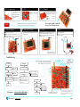
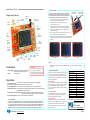
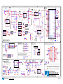
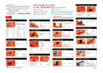
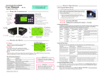
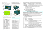
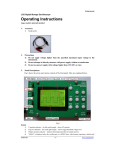
Soldering Hints
DSO 138 Oscilloscope DIY Kit
User Manual
1 Put leads through mounting holes from the side with
part outline. Ensue component evenly touch PCB.
2 Solder leads at the other side. Solder should fully
fill and cover soldering pads.
Avoid bridges between
neighbering pads.
3 Cut unused leads
flush with cutter.
4 Screw driver
5 Flush cutter
6 Tweezers
Step 1 Assembly Main Board and LCD board (follow the order as numbered)
1. Resistors
Rev. 01
Before you start
Tools you need
1 Iron (20W)
2 Solder wire
3 Multimeter
5. USB Socket *
1 Check part values & quantities against part list
2 Always meter resistor values before soldering
3 Understand all part polarities and orientations
* These parts are optional and not required
for the normal oscilloscope function.
9. Pin header (for power)
J4
: USB mini -B
J9
R1, R14, R16 : 100KΩ
R8, R12, R13 : 120Ω
R2
: 1.8MΩ
R9, R15, R26 : 1KΩ
R3
: 200KΩ
R10
: 3KΩ
R4
: 2MΩ
R11, R38
: 1.5KΩ
R5
: 20KΩ
R28, R40
: 470Ω
R6
: 300Ω
R37, R39
: 10KΩ
2. HF-Chokes
10. Transistors
6. Tact Switches
SW4, SW5, : 6 X 6 X 5mm
SW6, SW7,
SW8
Cathode
D1
: 1N5819
D2
: 1N4004
(or 1N4007)
JYE Tech Ltd.
Q1
: 8550
Q2
: 9014
C1, C9,
C10, C11,
C14, C15,
C16, C17,
C18, C20,
C23
: 0.1μF
C2
: 330pF
C7, C8
: 120pF
C3
: 3pF
C12, C13
: 22pF
C5
: 1pF
U4
: 79L05
U5
: 78L05
12. Capacitor trimmers
C4, C6
8. LED
: 5 - 30pF
- www.jyetech.com -
: 1 X 3 pin
J6
: 1 X 4 pin
Solder positive pole
(the longer lead) to
the square pad
D3
:φ3mm, green
L2
J7, J8
: 1 X 2 pin
J3
: 2 X 20 pin
18. Slide switches
SW1, SW2,
SW3
: 2P3T
19. BNC connector
13. Power inductor
: 8MHz
J5
11. Regulators
4. Crystal
Y1
: DC005
J10
17. Pin-header (female)
: 100μH
3. Diodes
15. Power connector
16. Pin-header (male) *
7. Ceramic Capacitors
L1,L3,L4
C19, C21, : 100μF / 1 6 V
C22, C24,
C25, C26
: 2 Pin
: 180Ω
R7, R36
Solder positive pole
(the longer lead) to
the square pad
Face the opening
outward
Note:
Always meter resistor
values before soldering
14. Electrolytic capacitors
: 1mH/0.5A
J1
: BNC
Page 1
20. Test signal ring
21. JP3
22. LCD Board
1 ) Make a small ring with a
lead cut-off.
Note: Install to the side
opposite to LCD panel.
Short JP3 with solder
2 ) Solder the ring to the two
holes of J2 (as shown in
the photo).
Step 2 Test and Use
A. Check voltages
B. Attach LCD board
Plug LCD board into the female headers J3, J7, and J8
on the main board.
: 2 X 20 pin
J2, J3
: 1 X 2 pin
The assembly should look like this
after you have finished all parts
NOTE: You need a 9V DC power supply (at least 200mA capacity)
to run the scope. This power supply is not included in the kit.
1 Apply 9V power to J10 (or J9).
2 Check voltage at TP22. It should be around +3.3V.
3 If voltage at TP22 is good disconnect power. Short JP4
with solder permanently .
1
J1
C. Verify
A. Use
1 Connect power supply again. You should see LCD
lights up and oscilloscope panel displayed.
2 Press various buttons and move switches to verify
their functions.
1 Attach probe clips to J1.
2 Touch the red clip with your finger. Do you see signal
from your finger?
1
2
2
“Trigger” LED blinking twice
indicates booting-up is good.
3
Troubleshooting
LCD Dark
No Display
(No backlight)
Is voltage at V+
good?
NOTE: The voltages in the photo are for reference only.
The voltages on your board could be different.
But they should be close to the values shown.
No Check power
Yes
Is R36 value correct
and soldered good?
supply
No
Fix R36
Yes
Do you get about 3V No
Check R36 and
between J1 pin 16 &
power again
18 on LCD board?
Yes
Short JP4 if it has not been
done. See Step 2 above.
Press SW8. Does LED blink?
Yes
Check J3 soldering for
possible opens or shorts
Check J1 soldering on LCD
board for possible opens
or shorts
No
Check +3.3V voltage
Check Y1, C12, C13
Check LED installation
JYE Tech Ltd.
3.3V
Voltage
References
5.02V
*
0.19V
*
-8.08V*
* 9.39V *(Input Voltage)
6.43V
8.60V
*
3.3V
8.34V
*
-1.39V
No Trace
2.16V
No
0.81V
Fix them
Yes
Set CPL switch to GND No Check U2B, U2C and
and measure V1 and V2.
related parts around
Are they correct?
these two amplifiers
Tech Support:
4.99V
-8.11V
Are the values of AV+ and
AV- correct?
Check LCD
board
-5.0V
www.jyetech.com/forum
- www.jyetech.com -
0V
**
1.66V
Yes
Check R12 and C8
Place the negative pen of volt-meter
here to do voltage measurements.
**
NOTES:
*: These voltages are input voltage dependent. The values
shown were measured when input voltage was 9.39V.
**: These voltages are measured when CPL switch (SW1)
is set to GND position.
Page 2
How to Use
Probe Calibration
Because there is always some capacitance between scope input and
ground probe needs to be calibrated to achieve better measurement
results for high frequency signals. This can be done with the help of
the built-in test signal. To do this please follow the steps below.
Display and Controls
Connector
for Probe
Connectors
for Power Supply
HOLDRUN/
Oscilloscope
Mode
HOLDRUN/
Trigger Level
Readout
Horizontal
Position
[OK]:
HOLD / RUN
Selection
[+] or [-]:
Parameter
Adjustment
HOLDRUN/
[CPL]:
Couple
Selection
[SEN1]:
Sensitivity
Selection 1
Leave black clip
un-connected
Connect red clip to
test signal output
1. Connect the red clip to the test signal terminal and leave the
black clip un-connected (see photo at right).
2. Set [SEN1] switch to 0.1V and [SEN2] switch to X5.
Set [CPL] switch to AC or DC.
C6
3. Adjust timebase to 0.2ms. You should see waveform similar
to that shown in photos below. If traces are not stable adjust
C4
trigger level (the pink triangle on right screen border) so as
you get a stable display.
4. Turn C4 (capacitor trimmer) with a small screw driver so that
the waveform displays sharp rightangle (photo C).
5. Set [SEN1] switch to 1V and [SEN2] switch to X1while keep all other
settings unchanged. Adjust C6 so that sharp rightangle waveform is
displayed.
[SEL]:
Parameter
Selection
[SEN2]:
Sensitivity
Selection 2
Trigger
Level
Indicator
Vertical
Position
Indicator
Timebase
(s/div)
Sensitivity
(V/div)
Couple
Trigger
Slope
“Trigged”
Indicator
Reset
Button
A – Not enough
Trigger
Mode
C – Good
B – Too much
Hints
Connections
Power Supply:
Connect DC power supply to J9 or J10. The power
supply voltage must be in the range of 8 - 12V.
Probe:
Connect probe to J1.
Atte ntion
1. Power supply voltage must not exceed
12V. Otherwise U5 will get hot.
2. Allowed maximum signal input voltage
is 50Vpk (100Vpp) with the clip probe.
Operations
Press on [SEL] button: Select parameter to be adjusted. The selected parameter will be highlighted.
Press on [+] or [-] button: Adjust the parameter selected by [SEL] button.
Press on [OK] button: Freeze waveform refresh (entering HOLD state). Press on it again will de-freeze.
Change [CPL] switch: Set couple to DC, AC, or GND. When GND is selected the scope input is isolated from input
signal and connected to ground (0V input).
Change [SEN1] or [SEN2] switch:
Press on [Reset] button:
Adjust sensitivity. The product of [SEN1] and [SEN2] settings makes the
actual sensitivity which is displayed at the lower-left corner of the panel.
Perform a system reset and re-boots the oscillscope.
0V Line Alignment
Sometimes you may find the 0V line (the trace corresponding to 0V input voltage) does not match with the VPOS
indicator at the screen left border. This can easily be fixed by performing the “0V line alignment” function. First,
set the couple switch [CPL] to GND position. Then press on [SEL] button to make VPOS indicator highlighed and
hold down [OK] button for about 2 seconds. You will set the trace aligned to VPOS indicator when you release
[OK] button. You may see some residue mismatch remains at the highest sensitivity settings. This is normal.
JYE Tech Ltd.
- www.jyetech.com -
The LED at bottom-right corner (labelled “TRIGGED”) is the trigger indicator. It blinks when triggers
are detected.
Triggers and Their Modes
Triggers are events that indicate signal voltage acrossing
a set level (i.e. trigger level) along a specified direction
(i.e. trigger slope, rising or falling). Oscilloscope uses
triggers as reference points in time for stable waveform
display and measurements.
Au to Mode
In auto mode oscilloscope will perform display refresh no
matter triggers happen or not. When triggers are detected
waveform display will be displayed with reference to
trigger points. Otherwise, display waveform at ramdom
reference points.
Normal M ode
In normal mode oscilloscope will only perform display
refresh when there are triggers. If no triggers happen
waveform display will stay unchanged.
Single M ode
Single mode is the same as normal mode except that
oscilloscope will enter HOLD state after a trigger has been
detected and waveform display has been updated.
Normal and single modes are useful for capturing sparse
or single waveform.
Specifications
Max realtime sample rate
Analog bandwidth
Sensitivity range
Max input voltage
Input impedance
Resolution
Record length
Timebase range
Trigger modes
Trigger position range
Power supply
Current consumption
Dimension
Weight
1MSa/s
0 -- 200KHz
10mV/div - 5V/div
50Vpk (1X probe)
1M ohm/20pF
12 bits
1024 points
500s/Div -- 10us/Div
Auto, Normal, and Single
50%
9V DC (8 – 12V)
~120mA
117 x 76 x 15mm
70 gram (without probe)
Tech Support: www.jyetech.com/forum
JYT Tech Ltd.
Tel. +86-0773-2113856
www.jyetech.com
Page 3
5
TP1
4
CPL
AIN
DC 1
J1
BNC
C1
AC 3
0.1u
GND 4
**
SW1A
2
C2
220pF
R1
100K
10mV
1
C3
3pF
0.1V
3
1V
4
R2 1.8M 1%
D
AV+
U2A
TL084/SO
+
2
-
SEN1
SW2A
2
C5
-
R5
10K
30pF
20K 1%
R21
7
2
+
9
-
R9
VBUS
DD+
ID
GND
10K
5
TP6
SW3B
6
7
TP8
R13
120
R25
1.5K
8
3.3K
VSENSEL2
USB
Buttons
R31 1.5K
USBDM
USBDP
C10
+
13
-
C9
Trigg er
Level
AV-
BTN2
0.1u
nRST
7
PB0
PB1
PB2
PB3
PB4
PB5
PB6
PB7
PB8
PB9
PB10
PB11
PB12
PB13
PB14
PB15
VBAT
1
VDDA
9
Y1
8MHZ
PD0/OSC_IN 5
VIN
VOUT
VOUT
2
4
GND
1
*
9.3V
1
2
J6
C14
8
VDD_1
VDD_2
VDD_3
24
36
48
PC13/TEMPER/RTC VSS_1
PC14/OSC32_IN
VSS_2
PC15/OSC32_OUT VSS_3
23
35
47
R28
D2
1N4004
1
3
2
+
DC 9V
C22
100uF
1
3
5
7
9
11
13
15
17
19
21
23
25
27
29
31
33
35
37
39
JP5
SWDIO
SWCLK
LED-K1
LED-K3
IM3
DB0
DB2
DB4
DB6
LCD_nRESET
JP6
R35
10K
TESTSIG
R26
V+
1K
3.3V
V+
C19 +
100uF
TP20
3
VIN
2
GND
L3
100uH
+5V
U5
VOUT
1
LM78L05/T92
5V
0.1u
C21
100uF
0.2V
3
*
8.3V
R37
+
TP27 TP28 TP29 TP30
JYE Tech Ltd.
4
- www.jyetech.com -
C24
L1
100uH
C25
100uF
100uF
R38
1.5K
Q2
9014
2
1N5819
L2
1mH/1A
TP26
TP25 V-
1
IN
OUT
3
-5V
*
AV-
U4
79L05/TO92
C15
0.1u
L4 100uH
+3.3V
+ C26
100uF
+3.3V
C
C16
C17
C18
0.1u
0.1u
0.1u
+3.3V
VGEN
2
C23
R39 0.1u
10K
R40
470
0.8V
+3.3V
R41
10K
R42
1K
These voltages are power volt age dependent. The
values shown were measured at 9.3V power voltage.
3
J7
J8
1
2
1
2
2
4
6
8
10
12
14
16
18
20
22
24
26
28
30
32
34
36
38
40
LCD_RS
LCD_nRD
+3.3V
B
LED-A
LED-K2
LED-K4
DB1
DB3
DB5
DB7
V+
R36
180
+3.3V
LCD HEADER
Notes:
1. Part values used
could be different to
the values shown. Plea se refer to part
list.
2. Parts in dash-line boxes are SMD devices.
-1.4V
*
5
-8.1V
D1
2
* 6.4V
AV+
C20
1
*
*
Q1
8550
8.6V
10K
TP24
SW8
0.1u
+3.3V
D3
470
LCD_nCS
LCD_nWR
IM0
+3.3V
10K
1
2
3
4
TP23
*
8.6V
J10
+
LM1117 -3.3/TO263
+3.3V
D
1K
TP10
VSSA
LED
R34
BTN4
*
JP4
R27
STM32F103Cx
+3.3V
+
A
1
2
TP22
U3
3
44
J3
+
J9
+
-
TP21
Caution:
Power supply voltage can
not be higher than 12V.
22pF
+3.3V
BOOT0
+3.3V
Power Supply
22pF
C13
JP1
USE SWD DE BUG
MODE ON LY
Test Signal Terminal
J2
PD1/OSC_OUT
LCD Module Connector
BTN3
J5
TP16
TP17
2
3
4
R16
100K
SWD Port
SW7
RX1
TX1
LCD_nCS
LCD_RS
LCD_nWR
AV-
TP5
SW5
SEL
1K
1K
U2D
TL084/SO
C11
-
R32
R33
14
C12
6
PA0
PA1
PA2
PA3
PA4
PA5
PA6
PA7
PA8
PA9
PA10
PA11
PA12
PA13
PA14
PA15
SW4
+
B
1
2
3
TP4
TLVL
BTN1
OK
TP14
TP15
12
SW6
Uart
V3
100K
AV+
0.1u
22
22
18
19
20
39
40
41
42
43
TL_PWM
45
VGEN
46
LCD_nRD
21
LCD_nRESET 22
BTN4
25
BTN3
26
BTN2
27
BTN1
28
TP7
R14
DB0
DB1
DB2
DB3
DB4
DB5
DB6
DB7
JP2
1K
AV+
R23
R24
R29
R30
AVR15
R22
1.5K
Analog Channel
TP33
3K
R11
1.5K
JP3
1
2
3
4
5
120pF
1K
R10
VSENSEL1
6
C8
AV-
0.1u
J4 USB_mini_B
TP3
R12
120
TP9
U1
10
VSENSEL2 11
VSENSEL1 12
CPLSEL
13
TP11
14
TP12
15
TP13
V-MON 16
TESTSIG 17
TRIG
29
TX1
30
RX1
31
USBDM
32
USBDP
33
SWDIO 34
SWCLK 37
LED
38
8
R7
8
3.3K
V2
10
4
SW2B
5
1
ADCIN
1.6V
AV+
R19
1.5K
8
X5
120
C6
CPLSEL
X2 3
300
AV+
R20
C7
120pF
6
R6
**
AV+
U2C
TL084/SO
SW3A
1
R8
1pF
SW1B
X1
AV-
5
3.3K
6
7
7
R18
+
1
AV+
C
5
30pF
AV-
10K
U2B
TL084/SO
SEN2
180
R4 2M 1%
R17
TP2
2
MCU
**
0V
V1
AV+
R3
200K 1%
C4
3
3
These voltages wer e measured
when SW1 is at GND position.
V-MON
JYE Tech Ltd.
WWW.JYETECH.COM
TP31
TP32
[email protected]
2
1
Page 4
A