1
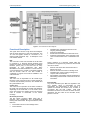
CAN IP (precan_plb46), v1.0
- With PLB v4.6 interface
Product Specification
CORE Facts
Prevas AB
Provided with Core
PO Box 4 (Legeringsgatan 18)
SE-721 03 Västerås
Sweden
Phone:
Fax:
Email:
URL:
Documentation
User’s Manual
Data sheet (this document)
Design File Formats
+46 21 360 19 00
+46 21 360 19 29
[email protected]
www.prevas.se
VHDL Source RTL
Constraint Files
None
Verification
CAN protocol compliance tested,
according to ISO16845, using the
XA3S1600E ECU development
board from Si-Gate
Features
Instantiation templates
None
Compliant with ISO 11898-1, CAN 2.0B
protocol.
Reference designs &
None
Supports bus speeds above 1 Mbit/s
Additional Items
application notes
Xilinx XPS peripheral description
files (.pao, .mpd)
Overload frames on CAN bus are
recognized and handled but not transmitted
by this core
Simulation Tool Used
Modelsim v6.1c
Support
TX and RX FIFOs with configurable depth of
2 to 63 messages each.
Support provided by Prevas AB
High Prio TX Buffer
Applications
Optional High Prio RX buffer
The Prevas CAN Controller IP core targets many
CAN communication applications like:
RX message filtering. Number of filters can
be set from 0-2 by generic parameter. One
dedicated filter for High prio RX buffer.
Automotive networks
Industrial control networks
Loop mode for diagnostic purpose
Maskable interrupts
Sensor monitoring and actuator control
Readable error counters
Other embedded
capabilities
Single clock, fully synchronous design.
Seamless interface (slave port) to PLB v4.6
bus for easy integration with Xilinx
MicroBlazeTM and IBM PowerPCTM in Xilinx
devices.
The Prevas CAN Controller IP Core provides a
flexible solution, which may be implemented in all
Xilinx Spartan™-3, -3A, -3E and Virtex™-II, -II Pro,
-4, -5 device families. See examples in the table
below. The slice count depends on the selected FIFO
depths and number of message filters. The figures
shown are for a configuration with 1 RX filter, RX prio
buffer enabled, RX FIFO depth of 16 messages and
TX FIFO depth of 4 messages.
systems
with
CAN
General Description
The CAN Controller IP implements to the ISO 118981, CAN 2.0B protocol. It takes care of all transfer
layer protocol tasks like message framing, message
arbitration, error signaling and fault confinement and
automatic retransmission due to tx faults or loss of
arbitration. TX/RX FIFOs of configurable depth and
message filters provides message buffering and
filtering and decreases the load on the local CPU.
Max bus speed for CAN networks according to the
standard is 1 Mbit/s. This CAN controller can however
support bus speeds above 1 Mbit/s for special
applications.
Table 1: Example implementation statistics
Family
Example Device
Fmax
(MHz)
Slices *
IOBs
(external)
BRAM
s
Design Tools
Spartan™-3x
XC3S1600E-4
96
975
2
2
ISE 10.1.03i
Virtex™-4
XC4VLX15-12
205
975
2
2
ISE 10.1.03i
Virtex™-5
XC5VLX30-3
150
575
2
2
ISE 10.1.03i
1
Product Specification
CAN Controller (precan_plb46), v1.0
Figure1. CAN Controller IP Block diagram
Functional Description
•
The figure above shows a high level block diagram
and the major data flow of the CAN Controller. The
TX and RX signals should be connected to an
external CAN transceiver chip. A description of the
sub-modules follows.
•
•
•
IPIF
The connection of the CAN controller to the PLB bus
is provided by a PLBV46_SLAVE_SINGLE (IPIF)
module from Xilinx. This block provides a seamless
interface (slave port) to the PLB bus for easy
integration of user peripherals with Xilinx
TM
TM
MicroBlaze and IBM PowerPC in Xilinx devices.
A preconfigured IPIF module is integrated together
with the Prevas CAN IP. The IPIF module is
configured to support the functions available in the
CAN Controller..
CAN core
The CAN core is responsible for all transfer layer
functions of the CAN protocol and consist primarily of
a control unit, bit-stream processor, error handler and
bit synchronization unit.
Control unit
The control unit is supervisor of the other modules in
the CAN core and handles the overall node behavior
depending on the node state, i.e. if the node is in init
mode, error active, error passive or bus off, and if the
node is receiver or transmitter of the current
message.
Calculate CRC and append CRC bits to the
outgoing message stream.
Perform bus arbitration
Monitor the transmitted bits to detect bit errors.
Automatic retransmission of the message in the
case of a transmission error or if arbitration was
lost
During reception of a message, similar tasks are
performed in an opposite way. There are also several
other error checks:
•
•
•
•
Remove and check value of fixed form bits to
detect form errors
Remove stuff bits and check for stuffing errors
Calculate CRC of the incoming message and
compare with received CRC
Acknowledge successfully received messages by
transmitting a dominant bit in the ACK slot of the
CAN frame.
Error handler
Any errors detected by the BSP are signaled to the
error handler, which is responsible for fault
confinement and transmission of error frames. It
updates its transmit and receive error counters in
accordance with the ISO 11898-1, CAN 2.0B
standard and, based on the value of these counters,
determines the error state of the controller; active,
passive or bus off.
Bit stream processor
The bits stream processor (BSP) takes care of
message data serialization and de-serialization,
framing and format tasks. During transmission, these
tasks are:
•
•
Insert fixed form bits in the message frame.
Insert stuff bits
2
Product Specification
CAN Controller (precan_plb46), v1.0
Bit synchronization
The bit synchronization module has the following
functions:
•
•
•
•
•
•
Clock pre-scaling.
Synchronizing the CAN core to the traffic on the
CAN bus.
Place TX bits on the bus with the correct timing
Calculate the sampling point and provide a
sample clock to the rest of the CAN core.
In loop mode, the core is “disconnected” from the
CAN bus, i.e. only recessive bits are transmitted
and the bits transmitted by this node is instead
routed back to the receive input. Incoming data
from the CAN bus is ignored.
Bit error detection
The synchronization process compensates for
propagation delays and oscillator frequency
differences between the transmitting and receiving
nodes.
Configuration and status registers
The configuration and status registers is the interface
for an external micro-controller. Refer to the user
manual for description of the registers.
All registers are 32-bit wide, addressed at word
boundaries and represented in big-endian format (Bit
0 is MSB, bit 31 is LSB).
TX/RX FIFO
Separate storage buffers for transmit and receive
message are provided in a FIFO structure. The depth
of each buffer is individually configurable through
generic parameters and may be from 2 to 63
messages each.
High Prio Buffers
In addition to the FIFOs, there are a High Prio TX
buffer which can store one message. A message
stored in this buffer will be transmitted as soon as the
CAN bus is idle, bypassing any remaining messages
in the TX FIFO.
There is also an optional High Prio RX buffer
(enabled with a generic parameter) This buffer can
store one message. Any incoming message which
matches the dedicated filter for this buffer is stored
here.
RX filters
IDs of incoming messages are compared with userdefined ID acceptance masks. If there is a match, the
message is stored in the RX buffer connected to the
filter. If no match is found, the message is just
acknowledged and then discarded. The number of
acceptance filters for the RX FIFO is defined with a
generic parameter which may be set from 0 to 2. The
high prio RX buffer (if enabled) has a dedicated filter.
If no acceptance filter is used, all successfully
received messages are stored in the RX buffer.
Signal
Dir
Description
Bus2IP_Clk
IN
System clock (min 24 MHz)
Bus2IP_Reset
IN
Active high reset
Bus2IP_Addr[0:31]
IN
Address bus
Bus2IP _Data
IN
Write data bus
IN
Byte enables (not used, all registers are
accessed at word boundaries)
IN
Register read qualifiers
IN
Register write qualifiers
OUT
Read data bus
IP2Bus_RdAck
OUT
Active high read transfer acknowledge
IP2Bus_WrAck
OUT
Active high write transfer acknowledge
IP2Bus_Error
OUT
Not used, tied to GND
can_rx
IN
RX data from CAN transceiver
[0:C_SLV_DWIDTH-1]
Bus2IP _BE
[0:C_SLV_DWIDTH/8-1]
Bus2IP_RdCE
User interface
The user interface of the CAN
controller
uses
naming
conventions of the “user side” of
the IPIF module. These signals
provide a seamless interface to
the IPIF module. Table 2
describes the signal interface.
[0:C_NUM_REG-1]
Bus2IP_WrCE
[0:C_NUM_REG-1]
IP2Bus_Data
[0:C_SLV_DWIDTH-1]
can_tx
OUT
TX data to CAN transceiver
precan_irq
OUT
Interrupt line. Goes high when an irq is
generated.
Table 2: User interface signals
3
Product Specification
CAN Controller (precan_plb46), v1.0
Design parameters
A number of generic parameters can be used to tailor
the design to specific application needs for optimum
performance. The value of these parameters has
some impact on the resource utilization of the IP, see
table 1.
Design Services
Prevas
also
offers
core
integration,
customisation and other design services.
core
Parameter
Default
Description
C_RX_FIFO_DEPTH
4
The desired depth of the RX buffer in number of messages. Settings 2-63
are valid.
C_TX_FIFO_DEPTH
4
The desired depth of the TX buffer in number of messages. Settings 2-63
are valid.
C_NR_OF_FILTERS
1
The desired number of receive filters. Settings 0-2 are valid.
C_RX_PRIO_BUFFER
FALSE
Enable/disable the RX High Prio buffer
C_SLV_DWIDTH
32
Data bus width (Do not change this setting!)
C_NUM_REG
32
The number of register selects within the address space (Do not change
this setting!)
Table 3: Core generic parameters
Core Modifications
More features may be added to the core at request
and additional cost.
Customers may also modify the RTL source code at
own responsibility.
Verification Methods
The CAN Controller core’s functionality has been
extensively tested in hardware, using the XA3S1600E
ECU development board from Si-Gate. The
functionality has also been verified in accordance with
the "ISO16845:2004 Road vehicles - Controller area
network (CAN) - Conformance Test Plan”. This
compliance test has been performed by C&S Group,
Germany.
Ordering Information
This product is available from Prevas AB under terms
of the SignOnce IP License. See www.prevas.se for
pricing or contact Prevas for additional information
about this product.
Prevas AB
PO Box 4 (Legeringsgatan 18)
SE-721 03 Västerås
Sweden
Phone:
Fax:
Email:
URL:
+46 21 360 19 00
+46 21 360 19 29
[email protected]
www.prevas.se
Prevas AB cores are purchased under a Licence
Agreement, copies of which are available on request.
Prevas AB retains the right to make changes to these
specifications at any time, without notice. All
trademarks, registered trademarks, or service marks
are the property of their respective owners.
Related Information
Xilinx Programmable Logic
For information on Xilinx programmable logic or
development system software, contact your local
Xilinx sales office, or:
Xilinx, Inc. 2100 Logic Drive
San Jose, CA 95124
Phone:+1 408-559-7778
URL: www.xilinx.com
4