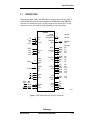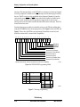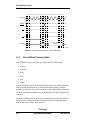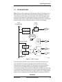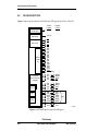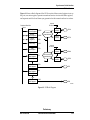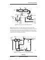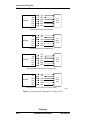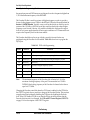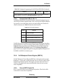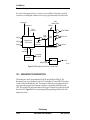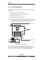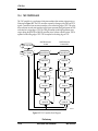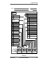
1
DSP56824 OVERVIEW 1 PIN DESCRIPTIONS 2 MEMORY AND OPERATING MODES 3 EXTERNAL MEMORY INTERFACE 4 PORT B GPIO FUNCTIONALITY 5 PORT C GPIO FUNCTIONALITY 6 SERIAL PERIPHERAL INTERFACE 7 SYNCHRONOUS SERIAL INTERFACE 8 TIMERS 9 ON-CHIP CLOCK SYNTHESIS 10 COP/RTI MODULE 11 ONCE MODULE 12 JTAG PORT 13 BOOTSTRAP PROGRAM A BSDL LISTING B PROGRAMMER’S SHEETS C INDEX I 1 DSP56824 OVERVIEW 2 PIN DESCRIPTIONS 3 MEMORY AND OPERATING MODES 4 EXTERNAL MEMORY INTERFACE 5 PORT B GPIO FUNCTIONALITY 6 PORT C GPIO FUNCTIONALITY 7 SERIAL PERIPHERAL INTERFACE 8 SYNCHRONOUS SERIAL INTERFACE 9 TIMERS 10 ON-CHIP CLOCK SYNTHESIS 11 COP/RTI MODULE 12 ONCE MODULE 12 JTAG PORT A BOOTSTRAP PROGRAM B BSDL LISTING C PROGRAMMER’S SHEETS I INDEX DSP56824 16-Bit Digital Signal Processor User’s Manual Motorola, Incorporated Semiconductor Products Sector 6501 William Cannon Drive West Austin, TX 78735-8598 This document (and other documents) can be viewed on the World Wide Web at http://www.motorola-dsp.com. This manual is one of a set of three documents. You need the following manuals to have complete product information: Family Manual, User’s Manual, and Technical Data Sheet. OnCE™ is a trademark of Motorola, Inc. MOTOROLA INC., 1997 Order this document by DSP56824UM/AD Motorola reserves the right to make changes without further notice to any products herein to improve reliability, function or design. Motorola does not assume any liability arising out of the application or use of any product or circuit described herein; neither does it convey any license under its patent rights nor the rights of others. Motorola products are not authorized for use as components in life support devices or systems intended for surgical implant into the body or intended to support or sustain life. Buyer agrees to notify Motorola of any such intended end use whereupon Motorola shall determine availability and suitability of its product or products for the use intended. Motorola and are registered trademarks of Motorola, Inc. Motorola, Inc. is an Equal Employment Opportunity/Affirmative Action Employer. TABLE OF CONTENTS SECTION 1 DSP56824 OVERVIEW . . . . . . . . . . . . . . . . . . . . . . . . 1-1 1.1 INTRODUCTION . . . . . . . . . . . . . . . . . . . . . . . . . . . . . . . . . . . . 1-3 1.2 MANUAL ORGANIZATION . . . . . . . . . . . . . . . . . . . . . . . . . . . . 1-4 1.3 MANUAL CONVENTIONS . . . . . . . . . . . . . . . . . . . . . . . . . . . . . 1-5 1.4 DSP56824 ARCHITECTURE OVERVIEW . . . . . . . . . . . . . . . . 1-7 1.4.1 DSP56824 Peripheral Blocks . . . . . . . . . . . . . . . . . . . . . . . . 1-8 1.4.1.1 On-Chip Memory. . . . . . . . . . . . . . . . . . . . . . . . . . . . . . . . 1-8 1.4.1.2 External Memory Interface (Port A). . . . . . . . . . . . . . . . . . 1-8 1.4.1.3 General Purpose Input/Output Port (Port B) . . . . . . . . . . . 1-9 1.4.1.4 Programmable I/O Port (Port C) . . . . . . . . . . . . . . . . . . . . 1-9 1.4.1.5 Serial Peripheral Interface (SPI) . . . . . . . . . . . . . . . . . . . . 1-9 1.4.1.6 Synchronous Serial Interface (SSI). . . . . . . . . . . . . . . . . . 1-9 1.4.1.7 General Purpose Timer Module . . . . . . . . . . . . . . . . . . . . 1-9 1.4.1.8 On-Chip Clock Synthesis Block . . . . . . . . . . . . . . . . . . . . 1-9 1.4.1.9 COP/RTI Module. . . . . . . . . . . . . . . . . . . . . . . . . . . . . . . 1-10 1.4.1.10 JTAG/OnCE Port. . . . . . . . . . . . . . . . . . . . . . . . . . . . . . . 1-10 1.4.2 DSP56824 Peripheral Interrupts . . . . . . . . . . . . . . . . . . . . . 1-10 1.5 DSP56800 CORE DESCRIPTION . . . . . . . . . . . . . . . . . . . . . . 1-11 1.5.1 Data Arithmetic Logic Unit (Data ALU) . . . . . . . . . . . . . . . . 1-14 1.5.2 Address Generation Unit (AGU) . . . . . . . . . . . . . . . . . . . . . 1-15 1.5.3 Program Controller and Hardware Looping Unit . . . . . . . . . 1-15 1.5.4 Bit Manipulation Unit . . . . . . . . . . . . . . . . . . . . . . . . . . . . . . 1-15 1.5.5 Address and Data Buses . . . . . . . . . . . . . . . . . . . . . . . . . . . 1-16 1.5.6 On-Chip Emulation (OnCE) Module . . . . . . . . . . . . . . . . . . 1-17 1.6 DSP56800 PROGRAMMING MODEL . . . . . . . . . . . . . . . . . . . 1-17 1.7 CODE DEVELOPMENT ON THE DSP56824 . . . . . . . . . . . . . 1-19 SECTION 2 SIGNAL DESCRIPTIONS . . . . . . . . . . . . . . . . . . . . . . 2.1 INTRODUCTION . . . . . . . . . . . . . . . . . . . . . . . . . . . . . . . . . . . . 2.2 POWER AND GROUND SIGNALS . . . . . . . . . . . . . . . . . . . . . . 2.3 CLOCK AND PHASE LOCK LOOP (PLL) SIGNALS . . . . . . . . . 2.4 EXTERNAL MEMORY INTERFACE (PORT A) . . . . . . . . . . . . . 2-1 2-3 2-5 2-6 2-7 Preliminary MOTOROLA DSP56824 User’s Manual iii Table of Contents 2.5 2.6 2.7 2.8 2.9 2.10 INTERRUPT AND MODE CONTROL SIGNALS. . . . . . . . . . . . .2-9 GPIO SIGNALS . . . . . . . . . . . . . . . . . . . . . . . . . . . . . . . . . . . . .2-10 SERIAL PERIPHERAL INTERFACE (SPI) SIGNALS . . . . . . . .2-12 SYNCHRONOUS SERIAL INTERFACE (SSI) SIGNALS . . . . .2-15 TIMER MODULE SIGNALS. . . . . . . . . . . . . . . . . . . . . . . . . . . .2-17 JTAG/ONCE PORT SIGNALS. . . . . . . . . . . . . . . . . . . . . . . . . .2-18 SECTION 3 MEMORY CONFIGURATION AND OPERATING MODES . . . . . . . . . . . . . . . . . . . . .3-1 3.1 INTRODUCTION . . . . . . . . . . . . . . . . . . . . . . . . . . . . . . . . . . . . .3-3 3.2 DSP56824 MEMORY MAP DESCRIPTION . . . . . . . . . . . . . . . .3-3 3.2.1 X Data Memory . . . . . . . . . . . . . . . . . . . . . . . . . . . . . . . . . . . .3-4 3.2.2 Operating Mode Register (OMR) . . . . . . . . . . . . . . . . . . . . . .3-6 3.2.2.1 Nested Looping (NL)—Bit 15 . . . . . . . . . . . . . . . . . . . . . . .3-7 3.2.2.2 Reserved Bits—Bits 14–9 . . . . . . . . . . . . . . . . . . . . . . . . .3-8 3.2.2.3 Condition Codes (CC)—Bit 8 . . . . . . . . . . . . . . . . . . . . . . .3-8 3.2.2.4 X/P Memory (XP)—Bit 7. . . . . . . . . . . . . . . . . . . . . . . . . . .3-8 3.2.2.5 Stop Delay (SD)—Bit 6. . . . . . . . . . . . . . . . . . . . . . . . . . . .3-8 3.2.2.6 Rounding (R)—Bit 5 . . . . . . . . . . . . . . . . . . . . . . . . . . . . . .3-8 3.2.2.7 Saturation (SA)—Bit 4 . . . . . . . . . . . . . . . . . . . . . . . . . . . .3-9 3.2.2.8 External X Memory (EX)—Bit 3 . . . . . . . . . . . . . . . . . . . . .3-9 3.2.2.9 Reserved Bit—Bit 2 . . . . . . . . . . . . . . . . . . . . . . . . . . . . .3-10 3.2.2.10 Operating Mode (MB, MA)—Bits 1–0 . . . . . . . . . . . . . . . .3-10 3.2.3 DSP56824 Status Register (SR). . . . . . . . . . . . . . . . . . . . . .3-10 3.2.4 On-Chip Peripheral Memory Map . . . . . . . . . . . . . . . . . . . . .3-12 3.2.5 Program Memory Map . . . . . . . . . . . . . . . . . . . . . . . . . . . . .3-15 3.3 DSP56824 OPERATING MODES . . . . . . . . . . . . . . . . . . . . . . .3-15 3.3.1 Single Chip Bootstrap Mode (Mode 0) . . . . . . . . . . . . . . . . .3-17 3.3.2 Single Chip User (Mode 1) . . . . . . . . . . . . . . . . . . . . . . . . . .3-17 3.3.3 Normal Expanded Mode (Mode 2) . . . . . . . . . . . . . . . . . . . .3-18 3.3.4 Development Mode (Mode 3) . . . . . . . . . . . . . . . . . . . . . . . .3-18 3.4 EXECUTING PROGRAMS FROM XRAM. . . . . . . . . . . . . . . . .3-18 3.4.1 Description of the XRAM Execution Mode . . . . . . . . . . . . . .3-18 3.4.2 Interrupts in the XRAM Execution Mode . . . . . . . . . . . . . . . .3-20 3.4.3 Entering the XRAM Execution Mode. . . . . . . . . . . . . . . . . . .3-20 3.4.4 Exiting the XRAM Execution Mode . . . . . . . . . . . . . . . . . . . .3-20 Preliminary iv DSP56824 User’s Manual MOTOROLA Table of Contents 3.4.5 3.5 3.5.1 3.5.2 Restrictions in the XRAM Execution Mode . . . . . . . . . . . . . DSP56824 RESET AND INTERRUPT VECTORS . . . . . . . . . DSP56824 Interrupt Priority Register (IPR) . . . . . . . . . . . . . Interrupt Priority Structure . . . . . . . . . . . . . . . . . . . . . . . . . . 3-21 3-21 3-21 3-23 SECTION 4 EXTERNAL MEMORY INTERFACE . . . . . . . . . . . . . . 4.1 INTRODUCTION . . . . . . . . . . . . . . . . . . . . . . . . . . . . . . . . . . . . 4.2 EXTERNAL MEMORY PORT ARCHITECTURE . . . . . . . . . . . . 4.3 PORT A DESCRIPTION . . . . . . . . . . . . . . . . . . . . . . . . . . . . . . 4.3.1 Bus Control Register (BCR). . . . . . . . . . . . . . . . . . . . . . . . . . 4.3.1.1 Reserved Bits—Bits 15–10 . . . . . . . . . . . . . . . . . . . . . . . . 4.3.1.2 Drive (DRV)—Bit 9 . . . . . . . . . . . . . . . . . . . . . . . . . . . . . . 4.3.1.3 Reserved Bit—Bit 8. . . . . . . . . . . . . . . . . . . . . . . . . . . . . . 4.3.1.4 Wait State X Data Memory (WSX[3:0])—Bits 7–4 . . . . . . 4.3.1.5 Wait State P Memory (WSP[3:0])—Bits 3–0 . . . . . . . . . . . 4.3.2 Pins in Different Processing States . . . . . . . . . . . . . . . . . . . . 4-1 4-3 4-3 4-5 4-5 4-5 4-5 4-6 4-6 4-7 4-8 SECTION 5 PORT B GPIO FUNCTIONALITY . . . . . . . . . . . . . . . . 5-1 5.1 INTRODUCTION . . . . . . . . . . . . . . . . . . . . . . . . . . . . . . . . . . . . 5-3 5.2 PORT B PROGRAMMING MODEL . . . . . . . . . . . . . . . . . . . . . . 5-5 5.2.1 Port B Data Direction Register (PBDDR). . . . . . . . . . . . . . . . 5-6 5.2.2 Port B Data (PBD) Register . . . . . . . . . . . . . . . . . . . . . . . . . . 5-6 5.2.2.1 PBD Bit Values for General Purpose Inputs . . . . . . . . . . . 5-6 5.2.2.2 PBD Bit Values for General Purpose Outputs. . . . . . . . . . 5-6 5.2.2.3 PBD Bit Values for Interrupt Inputs . . . . . . . . . . . . . . . . . . 5-6 5.2.3 Port B Interrupt (PBINT) Register . . . . . . . . . . . . . . . . . . . . . 5-7 5.2.3.1 Interrupt Mask (MSK[7:0])—Bits 15–8 . . . . . . . . . . . . . . . 5-7 5.2.3.2 Interrupt Invert (INV[7:0])—Bits 7–0 . . . . . . . . . . . . . . . . . 5-8 5.3 PORT B INTERRUPT GENERATION . . . . . . . . . . . . . . . . . . . . 5-8 5.4 PORT B PROGRAMMING EXAMPLES. . . . . . . . . . . . . . . . . . . 5-9 5.4.1 Receiving Data on Port B . . . . . . . . . . . . . . . . . . . . . . . . . . 5-10 5.4.2 Sending Data on Port B . . . . . . . . . . . . . . . . . . . . . . . . . . . . 5-11 5.4.3 Looping Data on Port B . . . . . . . . . . . . . . . . . . . . . . . . . . . . 5-12 5.4.4 Generating Interrupts on Port B. . . . . . . . . . . . . . . . . . . . . . 5-13 Preliminary MOTOROLA DSP56824 User’s Manual v Table of Contents SECTION 6 PORT C GPIO FUNCTIONALITY . . . . . . . . . . . . . . . . .6-1 6.1 INTRODUCTION . . . . . . . . . . . . . . . . . . . . . . . . . . . . . . . . . . . . .6-3 6.2 PORT C PROGRAMMING MODEL . . . . . . . . . . . . . . . . . . . . . .6-5 6.2.1 Port C Control (PCC) Register . . . . . . . . . . . . . . . . . . . . . . .6-5 6.2.2 Port C Data Direction Register (PCDDR) . . . . . . . . . . . . . . . .6-6 6.2.3 Port C Data (PCD) Register . . . . . . . . . . . . . . . . . . . . . . . . . .6-7 6.3 PORT C PROGRAMMING EXAMPLES. . . . . . . . . . . . . . . . . . .6-7 6.3.1 Receiving Data on Port C GPIO Pins . . . . . . . . . . . . . . . . . . .6-7 6.3.2 Sending Data on Port C GPIO Pins . . . . . . . . . . . . . . . . . . . .6-9 6.3.3 Looping Data on Port C GPIO Pins. . . . . . . . . . . . . . . . . . . .6-10 SECTION 7 SERIAL PERIPHERAL INTERFACE . . . . . . . . . . . . . .7-1 7.1 INTRODUCTION . . . . . . . . . . . . . . . . . . . . . . . . . . . . . . . . . . . . .7-3 7.2 SPI ARCHITECTURE . . . . . . . . . . . . . . . . . . . . . . . . . . . . . . . . .7-5 7.3 SPI PROGRAMMING MODEL . . . . . . . . . . . . . . . . . . . . . . . . . .7-7 7.3.1 SPI Control Registers (SPCR0 and SPCR1) . . . . . . . . . . . . .7-8 7.3.1.1 Reserved Bits—Bits 15–9 . . . . . . . . . . . . . . . . . . . . . . . . .7-8 7.3.1.2 SPI Clock Rate Select (SPR[2:0])—Bits 8, 1–0 . . . . . . . . .7-8 7.3.1.3 SPI Interrupt Enable (SPIE)—Bit 7. . . . . . . . . . . . . . . . . . .7-9 7.3.1.4 SPI Enable (SPE)—Bit 6 . . . . . . . . . . . . . . . . . . . . . . . . .7-10 7.3.1.5 Wired-OR Mode (WOM)—Bit 5 . . . . . . . . . . . . . . . . . . . .7-10 7.3.1.6 Master Mode Select (MST)—Bit 4 . . . . . . . . . . . . . . . . . .7-10 7.3.1.7 Clock Polarity (CPL)—Bit 3 . . . . . . . . . . . . . . . . . . . . . . .7-10 7.3.1.8 Clock Phase (CPH)—Bit 2 . . . . . . . . . . . . . . . . . . . . . . . .7-10 7.3.2 SPI Status Register (SPSR0 and SPSR1) . . . . . . . . . . . . . .7-10 7.3.2.1 Reserved Bits—Bits 15–8 . . . . . . . . . . . . . . . . . . . . . . . .7-11 7.3.2.2 SPI Interrupt Complete Flag (SPIF)—Bit 7. . . . . . . . . . . .7-11 7.3.2.3 Write Collision (WCOL)—Bit 6 . . . . . . . . . . . . . . . . . . . . .7-11 7.3.2.4 Reserved Bit—Bit 5 . . . . . . . . . . . . . . . . . . . . . . . . . . . . .7-11 7.3.2.5 Mode Fault (MDF)—Bit 4 . . . . . . . . . . . . . . . . . . . . . . . . .7-11 7.3.2.6 Reserved Bits—Bits 3–0 . . . . . . . . . . . . . . . . . . . . . . . . .7-11 7.3.3 SPI Data Registers (SPDR0 and SPDR1) . . . . . . . . . . . . . .7-11 7.4 SPI DATA AND CONTROL PINS . . . . . . . . . . . . . . . . . . . . . . .7-12 7.5 SPI SYSTEM ERRORS. . . . . . . . . . . . . . . . . . . . . . . . . . . . . . .7-14 7.5.1 SPI Mode-Fault Error . . . . . . . . . . . . . . . . . . . . . . . . . . . . . .7-14 7.5.2 SPI Write-Collision Error . . . . . . . . . . . . . . . . . . . . . . . . . . . .7-15 Preliminary vi DSP56824 User’s Manual MOTOROLA Table of Contents 7.5.3 7.6 7.7 7.7.1 7.7.2 7.7.3 SPI Overrun . . . . . . . . . . . . . . . . . . . . . . . . . . . . . . . . . . . . . CONFIGURING PORT C FOR SPI FUNCTIONALITY . . . . . . PROGRAMMING EXAMPLES . . . . . . . . . . . . . . . . . . . . . . . . . Configuring an SPI Port as Master . . . . . . . . . . . . . . . . . . . Configuring an SPI Port as Slave . . . . . . . . . . . . . . . . . . . . Sending Data from Master to Slave. . . . . . . . . . . . . . . . . . . 7-16 7-16 7-18 7-18 7-20 7-21 SECTION 8 SYNCHRONOUS SERIAL INTERFACE . . . . . . . . . . . 8-1 8.1 INTRODUCTION . . . . . . . . . . . . . . . . . . . . . . . . . . . . . . . . . . . . 8-3 8.2 SSI ARCHITECTURE . . . . . . . . . . . . . . . . . . . . . . . . . . . . . . . . 8-4 8.2.1 SSI Clocking . . . . . . . . . . . . . . . . . . . . . . . . . . . . . . . . . . . . . 8-6 8.2.2 SSI Clock and Frame Sync Generation. . . . . . . . . . . . . . . . . 8-6 8.3 SSI PROGRAMMING MODEL . . . . . . . . . . . . . . . . . . . . . . . . . . 8-8 8.3.1 SSI Transmit Shift Register (TXSR) . . . . . . . . . . . . . . . . . . 8-10 8.3.2 SSI Transmit Data Buffer Register . . . . . . . . . . . . . . . . . . . 8-10 8.3.3 SSI Transmit Data (STX) Register. . . . . . . . . . . . . . . . . . . . 8-11 8.3.4 SSI Receive Shift Register (RXSR) . . . . . . . . . . . . . . . . . . . 8-11 8.3.5 SSI Receive Data Buffer Register . . . . . . . . . . . . . . . . . . . . 8-11 8.3.6 SSI Receive Data (SRX) Register . . . . . . . . . . . . . . . . . . . . 8-12 8.3.7 SSI Transmit and Receive Control Registers . . . . . . . . . . . 8-12 8.3.7.1 Prescaler Range (PSR)—Bit 15 . . . . . . . . . . . . . . . . . . . 8-12 8.3.7.2 Word Length Control (WL[1:0])—Bits 14–13. . . . . . . . . . 8-13 8.3.7.3 Frame Rate Divider Control (DC[4:0])—Bits 12–8 . . . . . 8-13 8.3.7.4 Prescale Modulus Select (PM[7:0])—Bits 7–0 . . . . . . . . 8-13 8.3.8 SSI Control Register 2 (SCR2) . . . . . . . . . . . . . . . . . . . . . . 8-14 8.3.8.1 Receive Interrupt Enable (RIE)—Bit 15 . . . . . . . . . . . . . 8-15 8.3.8.2 Transmit Interrupt Enable (TIE)—Bit 14 . . . . . . . . . . . . . 8-15 8.3.8.3 Receive Enable (RE)—Bit 13 . . . . . . . . . . . . . . . . . . . . . 8-16 8.3.8.4 Transmit Enable (TE)—Bit 12 . . . . . . . . . . . . . . . . . . . . . 8-16 8.3.8.5 Receive Buffer Enable (RBF)—Bit 11 . . . . . . . . . . . . . . . 8-16 8.3.8.6 Transmit Buffer Enable (TBF)—Bit 10 . . . . . . . . . . . . . . 8-17 8.3.8.7 Receive Direction (RXD)—Bit 9 . . . . . . . . . . . . . . . . . . . 8-17 8.3.8.8 Transmit Direction (TXD)—Bit 8 . . . . . . . . . . . . . . . . . . . 8-17 8.3.8.9 Synchronous Mode (SYN)—Bit 7 . . . . . . . . . . . . . . . . . . 8-18 8.3.8.10 Transmit Shift Direction (TSHFD)—Bit 6. . . . . . . . . . . . . 8-18 8.3.8.11 Transmit Clock Polarity (TSCKP)—Bit 5 . . . . . . . . . . . . . 8-18 Preliminary MOTOROLA DSP56824 User’s Manual vii Table of Contents 8.3.8.12 SSI Enable (SSIEN)—Bit 4 . . . . . . . . . . . . . . . . . . . . . . .8-18 8.3.8.13 Network Mode (NET)—Bit 3 . . . . . . . . . . . . . . . . . . . . . . .8-18 8.3.8.14 Frame Sync Invert (FSI)—Bit 2 . . . . . . . . . . . . . . . . . . . .8-18 8.3.8.15 Frame Sync Length (FSL)—Bit 1 . . . . . . . . . . . . . . . . . . .8-19 8.3.8.16 Early Frame Sync (EFS)—Bit 0 . . . . . . . . . . . . . . . . . . . .8-19 8.3.9 SSI Control/Status Register (SCSR). . . . . . . . . . . . . . . . . . .8-19 8.3.9.1 Reserved Bit—Bit 15 . . . . . . . . . . . . . . . . . . . . . . . . . . . .8-19 8.3.9.2 Receive Shift Direction (RSHFD)—Bit 14 . . . . . . . . . . . .8-19 8.3.9.3 Receive Clock Polarity (RSCKP)—Bit 13 . . . . . . . . . . . . .8-20 8.3.9.4 Reserved Bits—Bits 12–11 . . . . . . . . . . . . . . . . . . . . . . .8-20 8.3.9.5 Receive Frame Sync Invert (RFSI)—Bit 10 . . . . . . . . . . .8-20 8.3.9.6 Receive Frame Sync Length (RFSL)—Bit 9. . . . . . . . . . .8-20 8.3.9.7 Receive Early Frame Sync (REFS)—Bit 8 . . . . . . . . . . . .8-20 8.3.9.8 Receive Data Register Full (RDF)—Bit 7 . . . . . . . . . . . . .8-20 8.3.9.9 Transmit Data Register Empty (TDE)—Bit 6 . . . . . . . . . .8-20 8.3.9.10 Receive Overrun Error (ROE)—Bit 5 . . . . . . . . . . . . . . . .8-21 8.3.9.11 Transmitter Underrun Error (TUE)—Bit 4 . . . . . . . . . . . . .8-21 8.3.9.12 Transmit Frame Sync (TFS)—Bit 3 . . . . . . . . . . . . . . . . .8-22 8.3.9.13 Receive Frame Sync (RFS)—Bit 2. . . . . . . . . . . . . . . . . .8-22 8.3.9.14 Receive Data Buffer Full (RDBF)—Bit 1 . . . . . . . . . . . . .8-22 8.3.9.15 Transmit Data Buffer Empty (TDBE)—Bit 0 . . . . . . . . . . .8-22 8.3.10 SSI Time Slot Register (STSR). . . . . . . . . . . . . . . . . . . . . . .8-22 8.4 SSI DATA AND CONTROL PINS . . . . . . . . . . . . . . . . . . . . . . .8-23 8.5 SSI OPERATING MODES. . . . . . . . . . . . . . . . . . . . . . . . . . . . .8-27 8.5.1 Normal Mode. . . . . . . . . . . . . . . . . . . . . . . . . . . . . . . . . . . . .8-29 8.5.1.1 Normal Mode Transmit . . . . . . . . . . . . . . . . . . . . . . . . . . .8-29 8.5.1.2 Normal Mode Receive . . . . . . . . . . . . . . . . . . . . . . . . . .8-30 8.5.2 Network Mode . . . . . . . . . . . . . . . . . . . . . . . . . . . . . . . . . . . .8-32 8.5.2.1 Network Mode Transmit . . . . . . . . . . . . . . . . . . . . . . . . . .8-32 8.5.2.2 Network Mode Receive . . . . . . . . . . . . . . . . . . . . . . . . . .8-33 8.5.3 Gated Clock Operation . . . . . . . . . . . . . . . . . . . . . . . . . . . . .8-35 8.6 SSI RESET AND INITIALIZATION PROCEDURE . . . . . . . . . .8-36 8.7 CONFIGURING PORT C FOR SSI FUNCTIONALITY . . . . . . .8-37 SECTION 9 TIMERS . . . . . . . . . . . . . . . . . . . . . . . . . . . . . . . . . . . . .9-1 9.1 INTRODUCTION . . . . . . . . . . . . . . . . . . . . . . . . . . . . . . . . . . . . .9-3 Preliminary viii DSP56824 User’s Manual MOTOROLA Table of Contents 9.2 9.2.1 9.2.1.1 9.2.1.2 9.2.1.3 9.2.1.4 9.2.1.5 9.2.1.6 9.2.2 9.2.3 9.3 9.4 9.5 9.6 9.6.1 9.6.2 9.6.3 9.6.4 9.6.5 9.7 9.8 TIMER PROGRAMMING MODEL . . . . . . . . . . . . . . . . . . . . . . . 9-5 Timer Control Registers (TCR01 and TCR2). . . . . . . . . . . . . 9-7 Timer Enable (TE)—Bit 15, Bit 7. . . . . . . . . . . . . . . . . . . . 9-7 Invert (INV)—Bit 6 . . . . . . . . . . . . . . . . . . . . . . . . . . . . . . . 9-7 Overflow Interrupt Enable (OIE)—Bit 12, Bit 4 . . . . . . . . . 9-8 Timer Output Enable (TO[1:0])—Bits 11–10, Bits 3–2 . . . 9-8 Event Select (ES[1:0])—Bits 9–8, Bits 1–0 . . . . . . . . . . . . 9-9 Reserved TCR Bits . . . . . . . . . . . . . . . . . . . . . . . . . . . . . 9-10 Timer Preload Register (TPR) . . . . . . . . . . . . . . . . . . . . . . . 9-10 Timer Count (TCT) Register . . . . . . . . . . . . . . . . . . . . . . . . 9-10 TIMER RESOLUTION . . . . . . . . . . . . . . . . . . . . . . . . . . . . . . . 9-12 TIMER INTERRUPT PRIORITIES . . . . . . . . . . . . . . . . . . . . . . 9-12 EVENT COUNTING WITH THE TIMER MODULE . . . . . . . . . 9-13 TIMER MODULE LOW POWER OPERATION . . . . . . . . . . . . 9-19 Turning Off the Entire Timer Module . . . . . . . . . . . . . . . . . . 9-19 Turning Off Any Timer Not in Use . . . . . . . . . . . . . . . . . . . . 9-19 Low Frequency Timer Operation . . . . . . . . . . . . . . . . . . . . . 9-19 Running A Timer in Wait Mode . . . . . . . . . . . . . . . . . . . . . . 9-20 Running A Timer in Stop Mode . . . . . . . . . . . . . . . . . . . . . . 9-20 TIMER MODULE TIMING DIAGRAMS . . . . . . . . . . . . . . . . . . 9-20 CONFIGURING PORT C FOR TIMER FUNCTIONALITY . . . . 9-22 SECTION 10 ON-CHIP CLOCK SYNTHESIS . . . . . . . . . . . . . . . . . 10.1 INTRODUCTION . . . . . . . . . . . . . . . . . . . . . . . . . . . . . . . . . . . 10.2 TIMING SYSTEM ARCHITECTURE . . . . . . . . . . . . . . . . . . . . 10.2.1 Oscillator . . . . . . . . . . . . . . . . . . . . . . . . . . . . . . . . . . . . . . . 10.2.2 Phase Lock Loop (PLL) . . . . . . . . . . . . . . . . . . . . . . . . . . . . 10.2.3 Prescaler . . . . . . . . . . . . . . . . . . . . . . . . . . . . . . . . . . . . . . . 10.2.4 Clockout Multiplexer (MUX) . . . . . . . . . . . . . . . . . . . . . . . . . 10.2.5 Control Registers . . . . . . . . . . . . . . . . . . . . . . . . . . . . . . . . . 10.3 CLOCK SYNTHESIS PROGRAMMING MODEL . . . . . . . . . . . 10.3.1 PLL Control Register 1 (PCR1) . . . . . . . . . . . . . . . . . . . . . . 10.3.1.1 Reserved Bit—Bit 15. . . . . . . . . . . . . . . . . . . . . . . . . . . . 10.3.1.2 PLL Enable (PLLE)—Bit 14. . . . . . . . . . . . . . . . . . . . . . . 10.3.1.3 PLL Power Down (PLLD)—Bit 13 . . . . . . . . . . . . . . . . . . 10.3.1.4 Low Power Stop (LPST)—Bit 12. . . . . . . . . . . . . . . . . . . 10-1 10-3 10-3 10-5 10-5 10-6 10-7 10-7 10-7 10-8 10-8 10-8 10-8 10-9 Preliminary MOTOROLA DSP56824 User’s Manual ix Table of Contents 10.3.1.5 Test Enable (TSTEN)—Bit 11 . . . . . . . . . . . . . . . . . . . . .10-9 10.3.1.6 Prescaler Divider (PS[2:0])—Bits 10–8 . . . . . . . . . . . . . .10-9 10.3.1.7 CLKO Select (CS[1:0])—Bits 7–6. . . . . . . . . . . . . . . . . .10-11 10.3.1.8 Reserved Bits—Bits 5–4 . . . . . . . . . . . . . . . . . . . . . . . .10-11 10.3.1.9 VCO Curve Select (VCS0)—Bit 3 . . . . . . . . . . . . . . . . .10-11 10.3.1.10 Reserved Bits—Bits 2–0 . . . . . . . . . . . . . . . . . . . . . . . .10-12 10.3.2 PLL Control Register 0 (PCR0). . . . . . . . . . . . . . . . . . . . . .10-12 10.3.2.1 Reserved Bit—Bit 15 . . . . . . . . . . . . . . . . . . . . . . . . . . .10-12 10.3.2.2 Feedback Divider (YD[9:0])—Bits 14–5 . . . . . . . . . . . . .10-12 10.3.2.3 Reserved Bits—Bits 4–0 . . . . . . . . . . . . . . . . . . . . . . . .10-12 10.4 LOW-POWER WAIT AND STOP MODES . . . . . . . . . . . . . . .10-13 10.4.1 PLL, COP, Realtime Clock, Timers, and CLKO Enabled . .10-14 10.4.2 COP, Realtime Clock and CLKO Pin Enabled . . . . . . . . . .10-14 10.4.3 PLL and CLKO Pin Enabled . . . . . . . . . . . . . . . . . . . . . . . .10-14 10.4.4 CLKO Pin Enabled . . . . . . . . . . . . . . . . . . . . . . . . . . . . . . .10-15 10.4.5 Everything Disabled . . . . . . . . . . . . . . . . . . . . . . . . . . . . . .10-15 10.5 PLL LOCK . . . . . . . . . . . . . . . . . . . . . . . . . . . . . . . . . . . . . . . .10-15 10.5.1 PLL Programming Example . . . . . . . . . . . . . . . . . . . . . . . .10-16 10.5.2 Changing the PLL Frequency . . . . . . . . . . . . . . . . . . . . . . .10-17 10.5.3 Turning Off the PLL Before Entering Stop Mode . . . . . . . .10-17 10.6 PLL MODULE LOW-POWER OPERATION . . . . . . . . . . . . . .10-18 10.6.1 Turning Off the Entire Clock Synthesis Module . . . . . . . . .10-18 10.6.2 Turning Off the Prescaler Divider When Not in Use . . . . . .10-18 10.6.3 Turning Off the PLL When Not in Use. . . . . . . . . . . . . . . . .10-18 10.6.4 Turning Off the CLKO Pin When Not in Use . . . . . . . . . . . .10-19 SECTION 11 COP/RTI MODULE . . . . . . . . . . . . . . . . . . . . . . . . . . .11-1 11.1 INTRODUCTION . . . . . . . . . . . . . . . . . . . . . . . . . . . . . . . . . . . .11-3 11.2 COP AND REALTIME TIMER ARCHITECTURE . . . . . . . . . . .11-3 11.3 COP AND RTI TIMER PROGRAMMING MODEL. . . . . . . . . . .11-5 11.3.1 COP and RTI Control Register (COPCTL) . . . . . . . . . . . . . .11-6 11.3.1.1 COP Enable (CPE)—Bit 15 . . . . . . . . . . . . . . . . . . . . . . .11-7 11.3.1.2 COP Timer Divider (CT)—Bit 14 . . . . . . . . . . . . . . . . . . .11-7 11.3.1.3 Reserved Bits—Bits 13–12 . . . . . . . . . . . . . . . . . . . . . . .11-7 11.3.1.4 RTI Timer Enable (RTE)—Bit 11 . . . . . . . . . . . . . . . . . . .11-7 11.3.1.5 RTI Enable (RTIE)—Bit 10 . . . . . . . . . . . . . . . . . . . . . . . .11-7 Preliminary x DSP56824 User’s Manual MOTOROLA Table of Contents 11.3.1.6 RTI Flag (RTIF)—Bit 9 . . . . . . . . . . . . . . . . . . . . . . . . . . 11-8 11.3.1.7 RTI Prescaler (RP)—Bit 8 . . . . . . . . . . . . . . . . . . . . . . . . 11-8 11.3.1.8 RTI/COP Divider (DV[7:0])—Bits 7–0 . . . . . . . . . . . . . . . 11-8 11.3.2 COP and RTI Count (COPCNT) Register . . . . . . . . . . . . . . 11-8 11.3.2.1 Reserved Bits—Bits 15–13 . . . . . . . . . . . . . . . . . . . . . . . 11-9 11.3.2.2 RTI/COP Divider (DV[7:0])—Bits 12–5 . . . . . . . . . . . . . . 11-9 11.3.2.3 RTI Prescaler (RP[1:0])—Bits 4–3 . . . . . . . . . . . . . . . . . 11-9 11.3.2.4 Scaler (SC[2:0])—Bits 2–0 . . . . . . . . . . . . . . . . . . . . . . . 11-9 11.3.3 COP Reset (COPRST) Register . . . . . . . . . . . . . . . . . . . . . 11-9 11.4 PROGRAMMING THE COP AND RTI TIMERS. . . . . . . . . . . 11-10 11.4.1 COP and RTI Timer Resolution . . . . . . . . . . . . . . . . . . . . . 11-11 11.4.2 COP/RTI Timer Low Power Operation . . . . . . . . . . . . . . . 11-11 11.4.3 Programming Example . . . . . . . . . . . . . . . . . . . . . . . . . . . 11-12 SECTION 12 ONCE MODULE. . . . . . . . . . . . . . . . . . . . . . . . . . . . . 12-1 12.1 INTRODUCTION . . . . . . . . . . . . . . . . . . . . . . . . . . . . . . . . . . . 12-3 12.1.1 On-Chip Emulation (OnCE) Module . . . . . . . . . . . . . . . . . . 12-3 12.1.2 Joint Test Action Group (JTAG) Port . . . . . . . . . . . . . . . . . . 12-4 12.2 COMBINED JTAG/ONCE INTERFACE OVERVIEW. . . . . . . . 12-6 12.3 JTAG/OnCE PORT PINOUT . . . . . . . . . . . . . . . . . . . . . . . . . . 12-7 12.4 OnCE MODULE ARCHITECTURE . . . . . . . . . . . . . . . . . . . . . 12-8 12.5 COMMAND, STATUS, AND CONTROL REGISTERS . . . . . 12-14 12.5.1 OnCE Shift Register (OSHR). . . . . . . . . . . . . . . . . . . . . . . 12-14 12.5.2 OnCE Command Register (OCMDR) . . . . . . . . . . . . . . . . 12-14 12.5.3 OnCE Decoder (ODEC). . . . . . . . . . . . . . . . . . . . . . . . . . . 12-17 12.5.4 OnCE Control Register (OCR). . . . . . . . . . . . . . . . . . . . . . 12-17 12.5.4.1 COP Timer Disable (COPDIS)—Bit 15 . . . . . . . . . . . . . 12-17 12.5.4.2 DE Pin Output Enable (DE)—Bit 14 . . . . . . . . . . . . . . . 12-18 12.5.4.3 Breakpoint Configuration (BK[4:0])—Bits 13–9. . . . . . . 12-18 12.5.4.4 Debug Request Mask (DRM)—Bit 8 . . . . . . . . . . . . . . . 12-19 12.5.4.5 FIFO Halt (FH)—Bit 7 . . . . . . . . . . . . . . . . . . . . . . . . . . 12-20 12.5.4.6 Event Modifier (EM[1:0])—Bits 6–5. . . . . . . . . . . . . . . . 12-20 12.5.4.7 Power Down Mode (PWD)—Bit 4 . . . . . . . . . . . . . . . . . 12-23 12.5.4.8 Breakpoint Selection (BS[1:0])—Bits 3–2 . . . . . . . . . . . 12-23 12.5.4.9 Breakpoint Enable (BE[1:0])—Bits 1–0 . . . . . . . . . . . . . 12-25 12.5.5 OnCE Breakpoint 2 Control Register (OBCTL2) . . . . . . . . 12-25 Preliminary MOTOROLA DSP56824 User’s Manual xi Table of Contents 12.5.5.1 Reserved OBCTL2 Register Bits . . . . . . . . . . . . . . . . . .12-25 12.5.5.2 Enable (EN)—Bit 2 . . . . . . . . . . . . . . . . . . . . . . . . . . . . .12-26 12.5.5.3 Invert (INV)—Bit 1 . . . . . . . . . . . . . . . . . . . . . . . . . . . . .12-26 12.5.5.4 Data/Address Select (DAT)—Bit 0 . . . . . . . . . . . . . . . . .12-26 12.5.6 OnCE Status Register (OSR) . . . . . . . . . . . . . . . . . . . . . . .12-26 12.5.6.1 Reserved OSR Bits—Bits 7–5 . . . . . . . . . . . . . . . . . . . .12-26 12.5.6.2 OnCE Core Status (OS[1:0])—Bits 4–3 . . . . . . . . . . . . .12-26 12.5.6.3 Trace Occurrence (TO)—Bit 2 . . . . . . . . . . . . . . . . . . . .12-27 12.5.6.4 Hardware Breakpoint Occurrence (HBO)—Bit 1 . . . . . .12-27 12.5.6.5 Software Breakpoint Occurrence (SBO)—Bit 0 . . . . . . .12-27 12.6 BREAKPOINT AND TRACE REGISTERS . . . . . . . . . . . . . . .12-28 12.6.1 OnCE Breakpoint/Trace Counter (OCNTR) . . . . . . . . . . . .12-28 12.6.2 OnCE Memory Address Latch (OMAL). . . . . . . . . . . . . . . .12-29 12.6.3 OnCE Breakpoint Address Register (OBAR) . . . . . . . . . . .12-29 12.6.4 OnCE Memory Address Comparator (OMAC) . . . . . . . . . .12-29 12.6.5 OnCE Breakpoint and Trace Section . . . . . . . . . . . . . . . . .12-29 12.7 PIPELINE REGISTERS. . . . . . . . . . . . . . . . . . . . . . . . . . . . . .12-31 12.7.1 OnCE PAB Fetch Register (OPABFR) . . . . . . . . . . . . . . . .12-31 12.7.2 OnCE PAB Decode Register (OPABDR) . . . . . . . . . . . . . .12-32 12.7.3 OnCE PAB Execute Register (OPABER) . . . . . . . . . . . . . .12-32 12.7.4 OnCE PAB Change-of-Flow FIFO (OPFIFO) . . . . . . . . . . .12-32 12.7.5 OnCE PDB Register (OPDBR) . . . . . . . . . . . . . . . . . . . . . .12-32 12.7.6 OnCE PGDB Register (OPGDBR) . . . . . . . . . . . . . . . . . . .12-34 12.7.7 OnCE FIFO History Buffer . . . . . . . . . . . . . . . . . . . . . . . . .12-34 12.8 BREAKPOINT 2 ARCHITECTURE . . . . . . . . . . . . . . . . . . . . .12-37 12.9 BREAKPOINT CONFIGURATION . . . . . . . . . . . . . . . . . . . . .12-38 12.9.1 Programming the Breakpoints. . . . . . . . . . . . . . . . . . . . . . .12-42 12.9.2 OnCE Trace Logic Operation . . . . . . . . . . . . . . . . . . . . . . .12-43 12.10 THE DEBUG PROCESSING STATE . . . . . . . . . . . . . . . . . . .12-44 12.10.1 OnCE Normal and Debug and STOP Modes . . . . . . . . . . .12-45 12.10.2 Entering Debug Mode . . . . . . . . . . . . . . . . . . . . . . . . . . . . .12-46 12.10.2.1 JTAG DEBUG_REQUEST and the Debug Event Pin . .12-47 12.10.2.2 Software Request During Normal Activity . . . . . . . . . . .12-47 12.10.2.3 Trigger Events (Breakpoint/Trace Modes) . . . . . . . . . . .12-47 12.10.2.4 Re-entering Debug Mode with EX = 0 . . . . . . . . . . . . . .12-48 12.10.2.5 Exiting Debug Mode . . . . . . . . . . . . . . . . . . . . . . . . . . . .12-48 Preliminary xii DSP56824 User’s Manual MOTOROLA Table of Contents 12.11 ACCESSING THE ONCE MODULE . . . . . . . . . . . . . . . . . . . 12.11.1 Primitive JTAG Sequences . . . . . . . . . . . . . . . . . . . . . . . . 12.11.2 Entering the JTAG Test-Logic-Reset State . . . . . . . . . . . . 12.11.3 Loading the JTAG Instruction Register . . . . . . . . . . . . . . . 12.11.4 Accessing a JTAG Data Register . . . . . . . . . . . . . . . . . . . 12.11.4.1 JTAG/OnCE Interaction: Basic Sequences. . . . . . . . . . 12.11.4.2 Executing a OnCE Command by Reading the OCR. . . 12.11.4.3 Executing a OnCE Command by Writing the OCNTR . 12.11.4.4 OSR Status Polling . . . . . . . . . . . . . . . . . . . . . . . . . . . . 12.11.4.5 JTAG IR Status Polling . . . . . . . . . . . . . . . . . . . . . . . . . 12.11.4.6 TRST/DE Pin Polling. . . . . . . . . . . . . . . . . . . . . . . . . . . 12.11.5 OnCE Unit Low Power Operation . . . . . . . . . . . . . . . . . . . 12.11.6 Resetting the Chip Without Resetting the OnCE Unit . . . . 12-48 12-49 12-49 12-51 12-52 12-53 12-55 12-56 12-57 12-58 12-59 12-59 12-59 SECTION 13 JTAG PORT . . . . . . . . . . . . . . . . . . . . . . . . . . . . . . . . 13-1 13.1 INTRODUCTION . . . . . . . . . . . . . . . . . . . . . . . . . . . . . . . . . . . 13-3 13.2 JTAG/OnCE PORT PINOUT . . . . . . . . . . . . . . . . . . . . . . . . . . 13-5 13.3 JTAG PORT ARCHITECTURE . . . . . . . . . . . . . . . . . . . . . . . . 13-6 13.3.1 JTAG Instruction Register (IR) and Decoder . . . . . . . . . . . . 13-8 13.3.1.1 EXTEST (B[3:0] = 0000) . . . . . . . . . . . . . . . . . . . . . . . . . 13-9 13.3.1.2 SAMPLE/PRELOAD (B[3:0] = 0001). . . . . . . . . . . . . . . . 13-9 13.3.1.3 IDCODE (B[3:0] = 0010) . . . . . . . . . . . . . . . . . . . . . . . . 13-10 13.3.1.4 EXTEST_PULLUP (B[3:0] = 0011) . . . . . . . . . . . . . . . . 13-10 13.3.1.5 HIGHZ (B[3:0] = 0100) . . . . . . . . . . . . . . . . . . . . . . . . . 13-10 13.3.1.6 CLAMP (B[3:0] = 0101) . . . . . . . . . . . . . . . . . . . . . . . . . 13-10 13.3.1.7 ENABLE_ONCE (B[3:0] = 0110). . . . . . . . . . . . . . . . . . 13-11 13.3.1.8 DEBUG_REQUEST (B[3:0] = 0111) . . . . . . . . . . . . . . . 13-11 13.3.1.9 BYPASS (B[3:0] = 1111) . . . . . . . . . . . . . . . . . . . . . . . . 13-11 13.3.2 JTAG Chip Identification (CID) Register . . . . . . . . . . . . . . 13-12 13.3.3 JTAG Boundary Scan Register (BSR). . . . . . . . . . . . . . . . 13-13 13.3.4 JTAG Bypass Register . . . . . . . . . . . . . . . . . . . . . . . . . . . 13-17 13.4 TAP CONTROLLER . . . . . . . . . . . . . . . . . . . . . . . . . . . . . . . . 13-18 13.5 DSP56824 RESTRICTIONS . . . . . . . . . . . . . . . . . . . . . . . . . 13-19 APPENDIX A BOOTSTRAP PROGRAM . . . . . . . . . . . . . . . . . . . . . . A-1 A.1 INTRODUCTION . . . . . . . . . . . . . . . . . . . . . . . . . . . . . . . . . . . . A-3 Preliminary MOTOROLA DSP56824 User’s Manual xiii Table of Contents A.2 DESIGN CONSIDERATIONS . . . . . . . . . . . . . . . . . . . . . . . . . . A.2.1 Boot Source Selection. . . . . . . . . . . . . . . . . . . . . . . . . . . . . . A.2.1.1 Bootstrapping from SPI0 . . . . . . . . . . . . . . . . . . . . . . . . . A.2.1.2 Bootstrapping from Port A . . . . . . . . . . . . . . . . . . . . . . . . A.2.2 COP Reset . . . . . . . . . . . . . . . . . . . . . . . . . . . . . . . . . . . . . . A.2.3 No Load Option . . . . . . . . . . . . . . . . . . . . . . . . . . . . . . . . . . . A.3 BOOTSTRAP LISTING . . . . . . . . . . . . . . . . . . . . . . . . . . . . . . . A-4 A-4 A-4 A-4 A-4 A-5 A-6 APPENDIX B BSDL LISTING . . . . . . . . . . . . . . . . . . . . . . . . . . . . . . B-1 B.1 DSP56824 BSDL LISTING—100-PIN TQFP. . . . . . . . . . . . . . . B-3 APPENDIX C PROGRAMMER’S SHEETS . . . . . . . . . . . . . . . . . . . . C-1 C.1 INTRODUCTION . . . . . . . . . . . . . . . . . . . . . . . . . . . . . . . . . . . . C-3 C.2 INSTRUCTION SET SUMMARY. . . . . . . . . . . . . . . . . . . . . . . . C-3 C.3 INTERRUPT, VECTOR, AND ADDRESS TABLES . . . . . . . . . C-9 C.4 PROGRAMMER’S SHEETS . . . . . . . . . . . . . . . . . . . . . . . . . . C-14 Preliminary xiv DSP56824 User’s Manual MOTOROLA LIST OF FIGURES Figure 1-1 DSP56824 Functional Block Diagram . . . . . . . . . . . . . . . . . . . . . . . . 1-7 Figure 1-2 DSP56800 Core Block Diagram . . . . . . . . . . . . . . . . . . . . . . . . . . . 1-12 Figure 1-3 DSP56800 Bus Block Diagram . . . . . . . . . . . . . . . . . . . . . . . . . . . . 1-13 Figure 1-4 DSP56800 Core Programming Model . . . . . . . . . . . . . . . . . . . . . . . 1-18 Figure 1-5 Code Development with Visibility on All Memory Accesses . . . . . . 1-20 Figure 2-1 DSP56824 Functional Group Pin Allocations . . . . . . . . . . . . . . . . . . 2-3 Figure 3-1 DSP56824 Memory Map . . . . . . . . . . . . . . . . . . . . . . . . . . . . . . . . . . 3-4 Figure 3-2 Bus Control Register Programming Model . . . . . . . . . . . . . . . . . . . . 3-6 Figure 3-3 Operating Mode Register Programming Model . . . . . . . . . . . . . . . . . 3-7 Figure 3-4 Status Register Programming Model. . . . . . . . . . . . . . . . . . . . . . . . 3-11 Figure 3-5 DSP56824 Memory Map (XRAM Execution Mode). . . . . . . . . . . . . 3-19 Figure 3-6 DSP56824 IPR Programming Model. . . . . . . . . . . . . . . . . . . . . . . . 3-22 Figure 3-7 Interrupt Programming. . . . . . . . . . . . . . . . . . . . . . . . . . . . . . . . . . . 3-22 Figure 4-1 DSP56824 Input/Output Block Diagram . . . . . . . . . . . . . . . . . . . . . . 4-4 Figure 4-2 BCR Programming Model . . . . . . . . . . . . . . . . . . . . . . . . . . . . . . . . . 4-5 Figure 4-3 Bus Operation (Read/Write—Zero Wait States) . . . . . . . . . . . . . . . . 4-7 Figure 4-4 Bus Operation (Read/Write—Three Wait States) . . . . . . . . . . . . . . . 4-8 Figure 5-1 DSP56824 Input/Output Block Diagram . . . . . . . . . . . . . . . . . . . . . . 5-4 Figure 5-2 DSP56824 Port B Programming Model. . . . . . . . . . . . . . . . . . . . . . . 5-5 Preliminary MOTOROLA DSP56824 User’s Manual xv List of Figures Figure 5-3 Port B Interrupt Block Diagram. . . . . . . . . . . . . . . . . . . . . . . . . . . . . . 5-9 Figure 6-1 DSP56824 Input/Output Block Diagram. . . . . . . . . . . . . . . . . . . . . . . 6-4 Figure 6-2 DSP56824 Port C Programming Model . . . . . . . . . . . . . . . . . . . . . . . 6-5 Figure 7-1 DSP56824 Input/Output Block Diagram. . . . . . . . . . . . . . . . . . . . . . . 7-4 Figure 7-2 SPI Block Diagram . . . . . . . . . . . . . . . . . . . . . . . . . . . . . . . . . . . . . . . 7-5 Figure 7-3 SPI Transfer with CPH = 0 . . . . . . . . . . . . . . . . . . . . . . . . . . . . . . . . . 7-6 Figure 7-4 SPI Transfer with CPH = 1 . . . . . . . . . . . . . . . . . . . . . . . . . . . . . . . . . 7-6 Figure 7-5 SPI Programming Model . . . . . . . . . . . . . . . . . . . . . . . . . . . . . . . . . . 7-7 Figure 8-1 DSP56824 Input/Output Block Diagram. . . . . . . . . . . . . . . . . . . . . . . 8-4 Figure 8-2 SSI Block Diagram . . . . . . . . . . . . . . . . . . . . . . . . . . . . . . . . . . . . . . . 8-5 Figure 8-3 SSI Clocking. . . . . . . . . . . . . . . . . . . . . . . . . . . . . . . . . . . . . . . . . . . . 8-6 Figure 8-4 SSI Transmit Clock Generator Block Diagram . . . . . . . . . . . . . . . . . . 8-7 Figure 8-5 SSI Transmit Frame Sync Generator Block Diagram. . . . . . . . . . . . . 8-7 Figure 8-6 SSI Programming Model—Register Set. . . . . . . . . . . . . . . . . . . . . . . 8-9 Figure 8-7 SSI Interrupt Vectors . . . . . . . . . . . . . . . . . . . . . . . . . . . . . . . . . . . . 8-10 Figure 8-8 SSI Bit Clock Equation . . . . . . . . . . . . . . . . . . . . . . . . . . . . . . . . . . . 8-13 Figure 8-9 Asynchronous SSI Configurations—Continuous Clock . . . . . . . . . . 8-24 Figure 8-10 Synchronous SSI Configurations—Continuous and Gated Clock . . 8-25 Figure 8-11 Serial Clock and Frame Sync Timing . . . . . . . . . . . . . . . . . . . . . . . . 8-27 Figure 8-12 Normal Mode Timing—Continuous Clock . . . . . . . . . . . . . . . . . . . . 8-31 Figure 8-13 Normal Mode Timing—Gated Clock. . . . . . . . . . . . . . . . . . . . . . . . . 8-31 Figure 8-14 Network Mode Timing—Continuous Clock. . . . . . . . . . . . . . . . . . . . 8-35 Preliminary xvi DSP56824 User’s Manual MOTOROLA List of Figures Figure 9-1 DSP56824 Input/Output Block Diagram . . . . . . . . . . . . . . . . . . . . . . 9-4 Figure 9-2 Timer Module. . . . . . . . . . . . . . . . . . . . . . . . . . . . . . . . . . . . . . . . . . . 9-5 Figure 9-3 Timer Module Programming Model . . . . . . . . . . . . . . . . . . . . . . . . . . 9-6 Figure 9-4 Standard Timer Operation with Overflow Interrupt . . . . . . . . . . . . . 9-21 Figure 9-5 Write to the Count Register with Timer Disabled. . . . . . . . . . . . . . . 9-21 Figure 10-1 DSP56824 Timing System . . . . . . . . . . . . . . . . . . . . . . . . . . . . . . . 10-4 Figure 10-2 PLL Block Diagram . . . . . . . . . . . . . . . . . . . . . . . . . . . . . . . . . . . . . 10-6 Figure 10-3 Clock Synthesis Programming Model . . . . . . . . . . . . . . . . . . . . . . . 10-8 Figure 11-1 RTI and COP Timer Block Diagram . . . . . . . . . . . . . . . . . . . . . . . . 11-4 Figure 11-2 RTI and COP Timer Programming Model . . . . . . . . . . . . . . . . . . . . 11-6 Figure 12-1 JTAG/OnCE Port Block Diagram. . . . . . . . . . . . . . . . . . . . . . . . . . . 12-6 Figure 12-2 DSP56824 OnCE Block Diagram . . . . . . . . . . . . . . . . . . . . . . . . . 12-10 Figure 12-3 OnCE Module Registers Accessed Through JTAG. . . . . . . . . . . . 12-11 Figure 12-4 OnCE Module Registers Accessed from the Core . . . . . . . . . . . . 12-13 Figure 12-5 OnCE Command Format. . . . . . . . . . . . . . . . . . . . . . . . . . . . . . . . 12-15 Figure 12-6 OCR Programming Model . . . . . . . . . . . . . . . . . . . . . . . . . . . . . . . 12-17 Figure 12-7 Debug Event Pin . . . . . . . . . . . . . . . . . . . . . . . . . . . . . . . . . . . . . . 12-20 Figure 12-8 OSR Programming Model . . . . . . . . . . . . . . . . . . . . . . . . . . . . . . . 12-26 Figure 12-9 OnCE FIFO History Buffer. . . . . . . . . . . . . . . . . . . . . . . . . . . . . . . 12-35 Figure 12-10 Breakpoint and Trace Counter Unit . . . . . . . . . . . . . . . . . . . . . . . . 12-38 Figure 12-11 OnCE Breakpoint Programming Model . . . . . . . . . . . . . . . . . . . . . 12-39 Figure 12-12 Breakpoint 1 Unit . . . . . . . . . . . . . . . . . . . . . . . . . . . . . . . . . . . . . . 12-40 Preliminary MOTOROLA DSP56824 User’s Manual xvii List of Figures Figure 12-13 Breakpoint 2 Unit . . . . . . . . . . . . . . . . . . . . . . . . . . . . . . . . . . . . . . 12-41 Figure 12-14 Entering the JTAG Test Logic-Reset State . . . . . . . . . . . . . . . . . . 12-50 Figure 12-15 Holding TMS High to Enter Test-Logic-Reset State. . . . . . . . . . . . 12-50 Figure 12-16 Bit Order for JTAG/OnCE Shifting . . . . . . . . . . . . . . . . . . . . . . . . . 12-51 Figure 12-17 Loading DEBUG_REQUEST . . . . . . . . . . . . . . . . . . . . . . . . . . . . . 12-51 Figure 12-18 Shifting Data through the BYPASS Register . . . . . . . . . . . . . . . . . 12-53 Figure 12-19 OnCE Shifter Selection State Diagram . . . . . . . . . . . . . . . . . . . . . 12-54 Figure 12-20 Executing a OnCE Command by Reading the OCR . . . . . . . . . . . 12-55 Figure 12-21 Executing a OnCE Command by Writing the OCNTR . . . . . . . . . . 12-56 Figure 12-22 OSR Status Polling. . . . . . . . . . . . . . . . . . . . . . . . . . . . . . . . . . . . . 12-57 Figure 12-23 JTAG IR Status Polling. . . . . . . . . . . . . . . . . . . . . . . . . . . . . . . . . . 12-58 Figure 13-1 JTAG Block Diagram . . . . . . . . . . . . . . . . . . . . . . . . . . . . . . . . . . . . 13-6 Figure 13-2 JTAG Port Programming Model . . . . . . . . . . . . . . . . . . . . . . . . . . . . 13-7 Figure 13-3 Bypass Register . . . . . . . . . . . . . . . . . . . . . . . . . . . . . . . . . . . . . . . 13-11 Figure 13-4 Chip Identification Register Configuration . . . . . . . . . . . . . . . . . . . 13-12 Figure 13-5 TAP Controller State Diagram . . . . . . . . . . . . . . . . . . . . . . . . . . . . 13-18 Preliminary xviii DSP56824 User’s Manual MOTOROLA LIST OF TABLES Table 1-1 High True/Low True Signal Conventions. . . . . . . . . . . . . . . . . . . . . . 1-6 Table 1-2 DSP56800 Address and Data Buses . . . . . . . . . . . . . . . . . . . . . . . 1-16 Table 2-1 Functional Group Pin Allocations . . . . . . . . . . . . . . . . . . . . . . . . . . . 2-4 Table 2-2 Power Inputs . . . . . . . . . . . . . . . . . . . . . . . . . . . . . . . . . . . . . . . . . . . 2-5 Table 2-3 Grounds. . . . . . . . . . . . . . . . . . . . . . . . . . . . . . . . . . . . . . . . . . . . . . . 2-5 Table 2-4 Clock and Phase Lock Loop (PLL) Signals . . . . . . . . . . . . . . . . . . . . 2-6 Table 2-5 Address Bus Signals . . . . . . . . . . . . . . . . . . . . . . . . . . . . . . . . . . . . . 2-7 Table 2-6 Data Bus Signals . . . . . . . . . . . . . . . . . . . . . . . . . . . . . . . . . . . . . . . . 2-7 Table 2-7 Bus Control Signals . . . . . . . . . . . . . . . . . . . . . . . . . . . . . . . . . . . . . . 2-7 Table 2-8 Interrupt and Mode Control Signals. . . . . . . . . . . . . . . . . . . . . . . . . . 2-9 Table 2-9 Programmable Interrupt GPIO Signals . . . . . . . . . . . . . . . . . . . . . . 2-10 Table 2-10 Dedicated GPIO Signals . . . . . . . . . . . . . . . . . . . . . . . . . . . . . . . . . 2-11 Table 2-11 Serial Peripheral Interface (SPI0 and SPI1) Signals . . . . . . . . . . . . 2-12 Table 2-12 Synchronous Serial Interface (SSI) Signals . . . . . . . . . . . . . . . . . . 2-15 Table 2-13 Timer Module Signals . . . . . . . . . . . . . . . . . . . . . . . . . . . . . . . . . . . 2-17 Table 2-14 JTAG/OnCE Port Signals . . . . . . . . . . . . . . . . . . . . . . . . . . . . . . . . 2-18 Table 3-1 Looping Status. . . . . . . . . . . . . . . . . . . . . . . . . . . . . . . . . . . . . . . . . . 3-7 Table 3-2 MAC Unit Outputs With Saturation Mode Enabled (SA = 1) . . . . . . . 3-9 Table 3-3 Interrupt Mask Bit Definition . . . . . . . . . . . . . . . . . . . . . . . . . . . . . . 3-11 Preliminary MOTOROLA DSP56824 User’s Manual xix List of Tables Table 3-4 X I/O Registers . . . . . . . . . . . . . . . . . . . . . . . . . . . . . . . . . . . . . . . . . 3-12 Table 3-5 DSP56824 Program RAM Chip Operating Modes . . . . . . . . . . . . . . 3-16 Table 3-6 Interrupt Priority Structure . . . . . . . . . . . . . . . . . . . . . . . . . . . . . . . . 3-23 Table 3-7 Reset and Interrupt Vector Map . . . . . . . . . . . . . . . . . . . . . . . . . . . . 3-24 Table 4-1 Programming WSP[3:0] and WSX[3:0] Bits for Wait States. . . . . . . . 4-6 Table 4-2 Port A Operation with DRV Bit = 0 . . . . . . . . . . . . . . . . . . . . . . . . . . . 4-9 Table 4-3 Port A Operation with DRV Bit = 1 . . . . . . . . . . . . . . . . . . . . . . . . . . . 4-9 Table 5-1 PBDDR Bit Definition . . . . . . . . . . . . . . . . . . . . . . . . . . . . . . . . . . . . . 5-6 Table 5-2 Reading the PBD Register . . . . . . . . . . . . . . . . . . . . . . . . . . . . . . . . . 5-7 Table 5-3 MSK Bit Definition . . . . . . . . . . . . . . . . . . . . . . . . . . . . . . . . . . . . . . . 5-7 Table 5-4 INV Bit Definition . . . . . . . . . . . . . . . . . . . . . . . . . . . . . . . . . . . . . . . . 5-8 Table 6-1 PCC Bit Definition. . . . . . . . . . . . . . . . . . . . . . . . . . . . . . . . . . . . . . . . 6-6 Table 6-2 PCDDR Bit Definition . . . . . . . . . . . . . . . . . . . . . . . . . . . . . . . . . . . . . 6-6 Table 7-1 SPR Divider Programming . . . . . . . . . . . . . . . . . . . . . . . . . . . . . . . . . 7-8 Table 7-2 SPI Interrupt . . . . . . . . . . . . . . . . . . . . . . . . . . . . . . . . . . . . . . . . . . . . 7-9 Table 7-3 SPI Mode Programming . . . . . . . . . . . . . . . . . . . . . . . . . . . . . . . . . . 7-10 Table 7-4 PCC Register Programming for the SS Pin . . . . . . . . . . . . . . . . . . . 7-16 Table 8-1 SSI Data Word Lengths . . . . . . . . . . . . . . . . . . . . . . . . . . . . . . . . . . 8-13 Table 8-2 SSI Bit Clock as a Function of Phi Clock and Prescale Modulus . . . 8-14 Table 8-3 SSI Receive Data Interrupts. . . . . . . . . . . . . . . . . . . . . . . . . . . . . . . 8-15 Table 8-4 SSI Transmit Data Interrupts . . . . . . . . . . . . . . . . . . . . . . . . . . . . . . 8-16 Table 8-5 Frame Sync/Clock Pin Configuration . . . . . . . . . . . . . . . . . . . . . . . . 8-17 Preliminary xx DSP56824 User’s Manual MOTOROLA List of Tables Table 8-6 SSI Operating Modes . . . . . . . . . . . . . . . . . . . . . . . . . . . . . . . . . . . 8-28 Table 8-7 SSI Control Bits Requiring Reset Before Change . . . . . . . . . . . . . . 8-37 Table 9-1 Timer Control Registers (TCR01 and TCR02) . . . . . . . . . . . . . . . . . 9-7 Table 9-2 INV Bit Definition . . . . . . . . . . . . . . . . . . . . . . . . . . . . . . . . . . . . . . . . 9-7 Table 9-3 Timer Interrupt Vectors . . . . . . . . . . . . . . . . . . . . . . . . . . . . . . . . . . . 9-8 Table 9-4 TIO Pin Function . . . . . . . . . . . . . . . . . . . . . . . . . . . . . . . . . . . . . . . . 9-8 Table 9-5 ES[1:0] Bit Definition . . . . . . . . . . . . . . . . . . . . . . . . . . . . . . . . . . . . . 9-9 Table 9-6 Timer Range and Resolution. . . . . . . . . . . . . . . . . . . . . . . . . . . . . . 9-12 Table 9-7 Timer Interrupt Priorities . . . . . . . . . . . . . . . . . . . . . . . . . . . . . . . . . 9-12 Table 10-1 PLL Operations . . . . . . . . . . . . . . . . . . . . . . . . . . . . . . . . . . . . . . . . 10-9 Table 10-2 PS Divider Programming . . . . . . . . . . . . . . . . . . . . . . . . . . . . . . . . 10-10 Table 10-3 CLKOUT Pin Control . . . . . . . . . . . . . . . . . . . . . . . . . . . . . . . . . . . 10-11 Table 10-4 VCS0 Programming. . . . . . . . . . . . . . . . . . . . . . . . . . . . . . . . . . . . 10-11 Table 11-1 COP Timer Divider Definition . . . . . . . . . . . . . . . . . . . . . . . . . . . . . 11-7 Table 11-2 Realtime Prescaler Definition . . . . . . . . . . . . . . . . . . . . . . . . . . . . . 11-8 Table 11-3 COP Timer Range and Resolution . . . . . . . . . . . . . . . . . . . . . . . . 11-11 Table 12-1 JTAG/OnCE Pin Descriptions . . . . . . . . . . . . . . . . . . . . . . . . . . . . . 12-7 Table 12-2 DE and DRM Encoding for TRST/DE Assertion . . . . . . . . . . . . . . . 12-8 Table 12-3 Register Select Encoding . . . . . . . . . . . . . . . . . . . . . . . . . . . . . . . 12-15 Table 12-4 EX Bit Definition. . . . . . . . . . . . . . . . . . . . . . . . . . . . . . . . . . . . . . . 12-16 Table 12-5 GO Bit Definition . . . . . . . . . . . . . . . . . . . . . . . . . . . . . . . . . . . . . . 12-16 Table 12-6 R/W Bit Definition . . . . . . . . . . . . . . . . . . . . . . . . . . . . . . . . . . . . . 12-17 Preliminary MOTOROLA DSP56824 User’s Manual xxi List of Tables Table 12-7 Breakpoint Configuration Bits Encoding—Two Breakpoints . . . . . 12-18 Table 12-8 Event Modifier Selection. . . . . . . . . . . . . . . . . . . . . . . . . . . . . . . . . 12-22 Table 12-9 BS[1:0] Bit Definition . . . . . . . . . . . . . . . . . . . . . . . . . . . . . . . . . . . 12-24 Table 12-10 Breakpoint Programming with the BS[1:0] and BE[1:0] Bits. . . . . . 12-24 Table 12-11 BE[1:0] Bit Definition . . . . . . . . . . . . . . . . . . . . . . . . . . . . . . . . . . . 12-25 Table 12-12 DSP Core Status Bit Description . . . . . . . . . . . . . . . . . . . . . . . . . . 12-27 Table 12-13 Function of OS[1:0] . . . . . . . . . . . . . . . . . . . . . . . . . . . . . . . . . . . . 12-46 Table 13-1 JTAG Pin Descriptions . . . . . . . . . . . . . . . . . . . . . . . . . . . . . . . . . . . 13-5 Table 13-2 JTAG IR Encodings . . . . . . . . . . . . . . . . . . . . . . . . . . . . . . . . . . . . . 13-8 Table 13-3 Device ID Register Bit Assignment . . . . . . . . . . . . . . . . . . . . . . . . 13-12 Table 13-4 BSR Contents for DSP56824 . . . . . . . . . . . . . . . . . . . . . . . . . . . . . 13-13 Table C-1 Instruction Set Summary . . . . . . . . . . . . . . . . . . . . . . . . . . . . . . . . . C-3 Table C-2 Condition Code Register (CCR) Symbols (Standard Definitions) . . C-8 Table C-3 CCR Notation . . . . . . . . . . . . . . . . . . . . . . . . . . . . . . . . . . . . . . . . . . C-8 Table C-4 Interrupt Priority Structure . . . . . . . . . . . . . . . . . . . . . . . . . . . . . . . . C-9 Table C-5 Reset and Interrupt Vectors . . . . . . . . . . . . . . . . . . . . . . . . . . . . . . C-10 Table C-6 DSP56824 I/O and On-Chip Peripheral Memory Map . . . . . . . . . . C-11 Table C-7 List of Programmer’s Sheets . . . . . . . . . . . . . . . . . . . . . . . . . . . . . C-14 Preliminary xxii DSP56824 User’s Manual MOTOROLA LIST OF EXAMPLES Example 1-1 Sample Code Listing . . . . . . . . . . . . . . . . . . . . . . . . . . . . . . . . . . . . . 1-5 Example 1-2 On-Chip and Off-Chip Instruction Fetches . . . . . . . . . . . . . . . . . . . 1-19 Example 3-1 Breaking a Read Instruction in Two. . . . . . . . . . . . . . . . . . . . . . . . . . 3-5 Example 5-1 Receiving Data on Port B . . . . . . . . . . . . . . . . . . . . . . . . . . . . . . . . 5-10 Example 5-2 Sending Data on Port B. . . . . . . . . . . . . . . . . . . . . . . . . . . . . . . . . . 5-11 Example 5-3 Loop-back Example. . . . . . . . . . . . . . . . . . . . . . . . . . . . . . . . . . . . . 5-12 Example 5-4 Generating Interrupts on Port B. . . . . . . . . . . . . . . . . . . . . . . . . . . . 5-13 Example 6-1 Receiving Data on Port C GPIO Pins . . . . . . . . . . . . . . . . . . . . . . . . 6-7 Example 6-2 Sending Data on Port C GPIO Pins. . . . . . . . . . . . . . . . . . . . . . . . . . 6-9 Example 6-3 Loop-back Example. . . . . . . . . . . . . . . . . . . . . . . . . . . . . . . . . . . . . 6-10 Example 7-1 Configuring an SPI Port as Master . . . . . . . . . . . . . . . . . . . . . . . . . 7-18 Example 7-2 Configuring an SPI Port as Slave . . . . . . . . . . . . . . . . . . . . . . . . . . 7-20 Example 7-3 Sending Data from Master to Slave. . . . . . . . . . . . . . . . . . . . . . . . . 7-21 Example 9-1 Counting Events on a Pin . . . . . . . . . . . . . . . . . . . . . . . . . . . . . . . . 9-13 Example 9-2 Decrementing to 0 and Generating an Interrupt . . . . . . . . . . . . . . . 9-15 Example 9-3 Timer Using 25% Duty Cycle. . . . . . . . . . . . . . . . . . . . . . . . . . . . . . 9-17 Example 10-1 Programming the PLL . . . . . . . . . . . . . . . . . . . . . . . . . . . . . . . . . . 10-16 Example 11-1 Sending a COP Reset . . . . . . . . . . . . . . . . . . . . . . . . . . . . . . . . . . 11-12 Example A-1 DSP56824 Bootstrap Code . . . . . . . . . . . . . . . . . . . . . . . . . . . . . . . . A-6 Example B-1 DSP56824 BSDL Listing—100-Pin TQFP. . . . . . . . . . . . . . . . . . . . . B-3 Preliminary MOTOROLA DSP56824 User’s Manual xxiii List of Examples Preliminary xxiv DSP56824 User’s Manual MOTOROLA SECTION 1 DSP56824 OVERVIEW Preliminary MOTOROLA DSP56824 User’s Manual 1-1 DSP56824 Overview 1.1 1.2 1.3 1.4 1.5 1.6 1.7 INTRODUCTION . . . . . . . . . . . . . . . . . . . . . . . . . . . . . . . . . . . . .1-3 MANUAL ORGANIZATION . . . . . . . . . . . . . . . . . . . . . . . . . . . . .1-4 MANUAL CONVENTIONS . . . . . . . . . . . . . . . . . . . . . . . . . . . . .1-5 DSP56824 ARCHITECTURE OVERVIEW . . . . . . . . . . . . . . . . .1-7 DSP56800 CORE DESCRIPTION . . . . . . . . . . . . . . . . . . . . . .1-11 DSP56800 PROGRAMMING MODEL. . . . . . . . . . . . . . . . . . . .1-17 CODE DEVELOPMENT ON THE DSP56824 . . . . . . . . . . . . . .1-19 Preliminary 1-2 DSP56824 User’s Manual MOTOROLA DSP56824 Overview Introduction 1.1 INTRODUCTION This manual describes the DSP56824 16-bit Digital Signal Processor (DSP), its memory and operating modes, and its peripheral modules. This manual is intended to be used with the DSP56800 Family Manual (DSP56800FM/AD), which describes the Central Processing Unit (CPU), programming models, and instruction set details. The DSP56824 Technical Data Sheet (DSP56824/D) provides electrical specifications, timing, pinout, and packaging descriptions. These documents, as well as Motorola’s DSP development tools, can be obtained through a local Motorola Semiconductor Sales Office or authorized distributor. To receive the latest information, access the Motorola DSP home page located at http://www.motorola-dsp.com. The DSP56824 is a member of the DSP56800 core-based family of DSPs. This general purpose DSP combines processing power with configuration flexibility, making it an excellent cost-effective solution for signal processing and control functions. To achieve its design goals, the DSP56824 uses an efficient MPU-style, general purpose, 16-bit DSP core, program and data memories, and support circuitry. The CPU (the DSP56800 core) consists of three execution units operating in parallel, allowing as many as six operations during each instruction cycle. The MPU-style programming model and optimized instruction set allow straightforward generation of efficient, compact DSP and control code. The instruction set is also highly efficient for C Compilers. The DSP56824 supports program execution from internal or external memories. Two data operands can be accessed per instruction cycle from the on-chip data RAM. The programmable peripherals and ports provide support for interfacing multiple external devices, such as codecs, microprocessors, or other DSPs. The DSP56824 also provides sixteen to thirty-two General Purpose Input/Output (GPIO) lines, depending on how peripherals are configured, and two external dedicated interrupt lines. Because of its configuration flexibility, compact program code, and low cost, the DSP56800 core family is well-suited for cost-sensitive applications, including digital wireless messaging, digital answering machines/feature phones, wireline and wireless modems, servo and ac motor control, and digital cameras. Preliminary MOTOROLA DSP56824 User’s Manual 1-3 DSP56824 Overview Manual Organization 1.2 MANUAL ORGANIZATION This manual is arranged in the following sections: • Section 1, DSP56824 Overview, provides a brief overview of the DSP56824, describes the structure of this document, and lists other documentation necessary to use the DSP56824. • Section 2, Pin Descriptions, provides a description of the pins on the DSP56824 chip and how the pins are grouped into the various interfaces. • Section 3, Memory Configuration and Operating Modes, describes the on-chip memory, structures, registers, and interfaces. • Section 4, External Memory Interface, describes the DSP56824 external memory interface, which is also referred to as Port A. • Section 5, Port B GPIO Functionality, describes the dedicated GPIO interface, which is also referred to as Port B. • Section 6, Port C, describes the sixteen dual-function pins that constitute Port C; this section defines the GPIO functions, and Sections 7, 8, and 9 describe these pins’ alternate functionality. • Section 7, Serial Peripheral Interface, describes the Serial Peripheral Interface (SPI), which communicates with external devices, such as Liquid Crystal Displays (LCDs) and Microcontroller Units (MCUs) , and is a part of Port C. • Section 8, Synchronous Serial Interface, describes the Synchronous Serial Interface (SSI), which is a part of Port C and communicates with devices such as codecs, other DSPs, microprocessors, and peripherals to provide the primary data input path. • Section 9, Timers, describes the three internal timer/counter devices that are a part of Port C. • Section 10, On-Chip Clock Synthesis, describes the internal oscillator, Phase Lock Loop (PLL), and timer distribution chain for the DSP56824. • Section 11, COP/RTI Module, describes the on-chip watchdog timer and the realtime interrupt generator. • Section 12, OnCE Module, describes the specifics of the DSP56824’s On-Chip Emulation (OnCE™) module, which is accessed through the Joint Test Action Group (JTAG) port. • Section 13, JTAG Port, describes the specifics of the DSP56824’s JTAG port. Preliminary 1-4 DSP56824 User’s Manual MOTOROLA DSP56824 Overview Manual Conventions • Appendix A, Bootstrap Program, provides a sample listing of bootstrap code that can be used to start or reset the DSP56824. • Appendix B, BSDL Listing, provides the Boundary Scan Description Language (BSDL) listing for the DSP56824. • Appendix C, Programmer’s Sheets, provides programming references and master programming sheets used to program the DSP56824 registers. • Index provides a cross-reference to topics in this manual. 1.3 MANUAL CONVENTIONS The following conventions are used in this manual: • Bits within registers are always listed from Most Significant Bit (MSB) to Least Significant Bit (LSB). Note: Other manuals use the opposite convention, with bits listed from LSB to MSB. • Bits within a register are indicated AA[n:0] when more than one bit is involved in a description. For purposes of description, the bits are presented as if they are contiguous within a register. However, this is not always the case. Refer to the programming model diagrams or to the programmer’s sheets to see the exact location of bits within a register. • When a bit is described as “set,” its value is set to 1. When a bit is described as “cleared,” its value is set to 0. • Pins or signals that are asserted low (made active when pulled to ground) have an overbar over their name. For example, the SS0 pin is asserted low. • Hex values are indicated with a dollar sign ($) preceding the hex value, as follows: $FFFB is the X memory address for the Interrupt Priority Register (IPR). • Code examples are displayed in a monospaced font, as shown in Example 1-1. Example 1-1 Sample Code Listing BFSET #$0007,X:PCC ; Configure: line 1 ; MISO0, MOSI0, SCK0 for SPI master line 2 ; ~SS0 as PC3 for GPIO line 3 Preliminary MOTOROLA DSP56824 User’s Manual 1-5 DSP56824 Overview Manual Conventions • Pins or signals listed in code examples that are asserted low have a tilde in front of their names. In the previous example, line 3 refers to the SS0 pin (shown as ~SS0). • The word “reset” is used in three different contexts in this manual. There is a reset pin that is always written as RESET, the processor state occurring when the RESET pin is asserted that is always written as Reset, and the word reset that refers to the reset function and is written in lower case with a leading capital letter as grammar dictates. The word “pin” is a generic term for any pin on the chip. • The word “assert” means that a high true (active high) signal is pulled high to VCC or that a low true (active low) signal is pulled low to ground. The word “deassert” means that a high true signal is pulled low to ground or that a low true signal is pulled high to VCC. See Table 1-1. Table 1-1 High True/Low True Signal Conventions Note: Signal/Symbol Logic State Signal State Voltage PIN True Asserted Ground1 PIN False Deasserted VCC2 PIN True Asserted VCC PIN False Deasserted Ground 1. 2. Ground is an acceptable low voltage level. See the appropriate data sheet for the range of acceptable low voltage levels (typically a TTL logic low). VCC is an acceptable high voltage level. See the appropriate data sheet for the range of acceptable high voltage levels (typically a TTL logic high). Preliminary 1-6 DSP56824 User’s Manual MOTOROLA DSP56824 Overview DSP56824 Architecture Overview 1.4 DSP56824 ARCHITECTURE OVERVIEW The DSP56824 consists of the DSP56800 core, program and data memory, and peripherals useful for embedded control applications. Figure 1-1 shows a block diagram of the DSP56824 chip. 16 to 32 GPIO lines 4 8 8 4 4 6 2 Serial Serial Synch. Program Timer/ ProgramPeriph. Periph. Serial Memory COP/ Event mable PLL Interrupt GPIO Interface Interface Interface Counters RTI 32K × 16 ROM (SPI0) (SPI1) (SSI) or 128 × 16 RAM or GPIO GPIO or GPIO or GPIO GPIO Data Memory 3584 × 16 RAM PAB 16-bit DSP56800 Core Clock Gen. Address Generation Unit XAB1 XAB2 JTAG/ OnCE™ Port External Address Bus Switch Address 16 XDB2 PGDB Bit Manipulation Unit Data Memory 2048 × 16 ROM External Data Bus Switch PDB CGDB Data ALU 16 × 16 + 36 → 36-bit MAC Three 16-bit Input Registers Two 36-bit Accumulators Program Controller MODA/IRQA MODB/IRQB RESET 5 Data 16 Control Bus Control 4 AA1428 Figure 1-1 DSP56824 Functional Block Diagram Features of the DSP56824 include the following: • 35 Million Instructions Per Second (MIPS) with 70 MHz clock • On-chip memory • Off-chip memory expansion capability – Off-chip expansion to 64 K × 16 data memory – Off-chip expansion to 64 K × 16 program memory • On-chip peripherals (listed in the following subsection) • 2.7–3.6 V power supply Preliminary MOTOROLA DSP56824 User’s Manual 1-7 DSP56824 Overview DSP56824 Architecture Overview • Very low power Complementary Metal Oxide Conductor (CMOS) design • Power management circuitry with power-saving Wait and multiple Stop modes • Fully static logic with operating frequencies down to dc 1.4.1 DSP56824 Peripheral Blocks The DSP56824 provides the following peripheral blocks: • On-chip memory – 32 K × 16 Program ROM – 128 × 16 Program RAM – 3.5 K × 16 RAM for data and applications – 2 K × 16 data ROM • External Memory Interface • GPIO Module • Programmable I/O Module • SPI (two provided) • SSI • General-Purpose Triple Timer module • On-chip Clock Synthesis Block (PLL) • Computer Operating Properly (COP) and Realtime Interrupt (RTI) module • JTAG/OnCE Port 1.4.1.1 On-Chip Memory The DSP56824 uses a Harvard architecture, which provides independent data and program memory. On-chip ROM is provided for both the X data (2 K × 16-bit) and program (P) memory (32 K × 16-bit). In addition, on-chip RAM is provided for both the X data (3.5 K × 16-bit) and P memory (128 × 16-bit). Both the program and data memories can be expanded off-chip. 1.4.1.2 External Memory Interface (Port A) The DSP56824 provides an external memory interface, also known as Port A. This port provides a total of thirty-six pins—sixteen pins for an external address bus, sixteen pins for an external data bus, and four pins for bus control. Preliminary 1-8 DSP56824 User’s Manual MOTOROLA DSP56824 Overview DSP56824 Architecture Overview 1.4.1.3 General Purpose Input/Output Port (Port B) A dedicated General Purpose Input/Output (GPIO) port, also known as Port B, provides sixteen programmable I/O pins. This port is configured so that it is possible to generate interrupts when a transition is detected on any of its lower eight pins. 1.4.1.4 Programmable I/O Port (Port C) Port C provides sixteen multiplexed general purpose programmable I/O pins. Each pin can be individually selected as a GPIO pin or allocated to on-chip peripherals—the general purpose timer module, two SPIs, and an SSI. Unlike the GPIO pins on Port B, the Port C pins cannot be configured to provide GPIO interrupts, but interrupts are available for the timer module, the two SPI ports, and the SSI port on Port C. 1.4.1.5 Serial Peripheral Interface (SPI) The Serial Peripheral Interface (SPI) is an independent serial communications subsystem that allows the DSP56824 to communicate synchronously with peripheral devices such as LCD display drivers, A/D subsystems, and MCU microprocessors. The SPI is also capable of interprocessor communication in a multiple master system. The SPI system can be configured as either a master or a slave device with high data rates. The SPI works in a demand-driven mode. In Master mode, a transfer is initiated when data is written to the SPI Data Register. In Slave mode, a transfer is initiated by the reception of a clock signal. Two separate SPIs are implemented on Port C. 1.4.1.6 Synchronous Serial Interface (SSI) The Synchronous Serial Interface (SSI) is a full-duplex serial port that allows the DSP56824 to communicate with a variety of multiple serial devices including industry-standard codecs, other DSPs, microprocessors, and peripherals that implement the Motorola SPI. It is typically used to transfer samples in a periodic manner. The SSI consists of independent transmitter and receiver sections with independent clock generation and frame synchronization. The SSI is implemented on Port C. 1.4.1.7 General Purpose Timer Module The timer module provides three independently programmable 16-bit timer/event counters. All three timer/counters can be clocked with clocks coming from one of three internal sources, including one of the other timers. In addition, the counters can be clocked with external clocking from the Timer I/O pins (TIO01 or TIO2) on Port C to count external events when configured as inputs. The same pins can be used as a timer pulse or for timer clock generation when used as outputs. The timer/event counters can be used to either interrupt the DSP56824 or to signal an external device at periodic intervals. The timer I/O pins are implemented as part of Port C. 1.4.1.8 On-Chip Clock Synthesis Block The clock synthesis module generates the clocking for the DSP56824. It generates three different clocks used by the DSP56800 core and DSP56824 peripherals. It contains a PLL Preliminary MOTOROLA DSP56824 User’s Manual 1-9 DSP56824 Overview DSP56824 Architecture Overview that can multiply up the frequency or can be bypassed, as well as a prescaler/divider used to distribute clocks to peripherals and to lower power consumption on the DSP56824. It also selects which clock, if any, is routed to the CLKO pin of the DSP56824. 1.4.1.9 COP/RTI Module The Computer Operating Properly (COP) and Realtime Interrupt (RTI) module provides two separate functions: a watchdog timer and an interrupt generator. These two functions monitor processor activity and provide an automatic reset signal if a failure occurs. Both functions are contained in the same block because the input clock for both comes from a common clock divider. 1.4.1.10 JTAG/OnCE Port The JTAG/OnCE port allows the user to insert the DSP56824 into a target system while retaining debug control. The JTAG port provides board-level testing capability that is compatible with the IEEE 1149.1a-1993 IEEE Standard Test Access Port and Boundary Scan Architecture specification defined by the Joint Test Action Group (JTAG). Five dedicated pins interface to a Test Access Port (TAP) that contains a 16-state controller. The OnCE module allows the user to interact in a debug environment with the DSP56800 core and its peripherals nonintrusively. Its capabilities include examining registers, memory, or on-chip peripherals; setting breakpoints in memory; and stepping or tracing instructions. It provides simple, inexpensive, and speed-independent access to the DSP56800 core for sophisticated debugging and economical system development. The JTAG/OnCE port allows access to the OnCE module and through the DSP56824 to its target system, retaining debug control without sacrificing other user accessible on-chip resources. 1.4.2 DSP56824 Peripheral Interrupts The peripherals on the DSP56824 use the interrupt channels found on the DSP56800 core. Each peripheral has its own interrupt vector (often more than one interrupt vector for each peripheral) and can selectively be enabled or disabled via the IPR found on the DSP56800 core. Section 3, Memory Configuration and Operating Modes, provides complete details on interrupt vectors. Preliminary 1-10 DSP56824 User’s Manual MOTOROLA DSP56824 Overview DSP56800 Core Description 1.5 DSP56800 CORE DESCRIPTION The DSP56800 core consists of functional units that operate in parallel to increase throughput of the machine. Major features of the DSP56800 core include the following: • Single-cycle 16 x 16-bit parallel Multiplier-Accumulator (MAC) • Two 36-bit accumulators including extension bits • 16-bit bidirectional barrel shifter • Highly parallel instruction set with unique DSP and controller addressing modes • Nested hardware DO loops • Software subroutine and interrupt stack with unlimited depth • Instruction set supports both DSP and controller functions for compact code • Efficient C Compiler and local variable support An overall block diagram of the DSP56800 core architecture is shown in Figure 1-2. The DSP56800 core is fed by internal program and data memory, an external memory interface, as well as various peripherals suitable for embedded applications. The blocks of the DSP56800 core include the following: • Data Arithmetic Logic Unit (Data ALU) • Address Generation Unit (AGU) • Program Controller and Hardware Looping Unit • Bit Manipulation Unit • Address buses • Data buses Preliminary MOTOROLA DSP56824 User’s Manual 1-11 DSP56824 Overview Clock Generator Address Generation Unit XDB2 XAB1 XAB2 PAB On-Chip Expansion Area Bus Control External Address Bus Switch External Data Bus Switch Port A X Memory RAM/ROM Expansion Control 16-bit DSP56800 Core PLL Program RAM/ROM Expansion Address Peripheral Modules Data Peripheral Pins DSP56800 Core Description PDB CGDB Program Controller Data ALU 16 x 16 + 36 → 36-Bit MAC Three 16-Bit Input Registers Two 36-Bit Accumulators MODA/IRQA MODB/IRQB RESET OnCE JTAG PGDB Bit Manipulation Unit AA1429 Figure 1-2 DSP56800 Core Block Diagram The Program Controller, AGU, and Data ALU each contain a discrete register set and control logic, so that each can operate independently and in parallel with the others. Likewise, each functional unit interfaces with other units, with memory, and with memory-mapped peripherals over the core’s internal address and data buses, as shown in Figure 1-3. Preliminary 1-12 DSP56824 User’s Manual MOTOROLA DSP56824 Overview DSP56800 Core Description AGU Program Controller SR OMR LA LC PC HWS M01 N +/– Instruction decoder/ interrupt unit MOD. ALU SP R0 R1 R2 R3 Clock Generator Program Memory Data Memory Peripherals Clock & Control PAB XAB1 XAB2 PDB External Bus Interface CGDB PGDB XDB2 Data ALU Limiter Bus and Bit Manipulation Unit OnCE Y1 Y0 X0 A2 A1 A0 B2 B1 B0 MAC and ALU AA0006 Figure 1-3 DSP56800 Bus Block Diagram It is possible in a single instruction cycle for the Program Controller to be fetching a first instruction, the AGU to generate two addresses for a second instruction, and the Data ALU to perform a multiply in a third instruction. In a similar manner, the bit manipulation unit can perform an operation of the third instruction described above instead of the multiplication in the Data ALU. The architecture is pipelined to take advantage of the parallel units and significantly decrease the execution time of each instruction. Preliminary MOTOROLA DSP56824 User’s Manual 1-13 DSP56824 Overview DSP56800 Core Description 1.5.1 Data Arithmetic Logic Unit (Data ALU) The Data Arithmetic Logic Unit (Data ALU) performs all of the arithmetic and logical operations on data operands. It contains the following: • Three 16-bit input registers • Two 32-bit accumulator registers • Two 4-bit accumulator extension registers • One parallel, single cycle, non-pipelined MAC unit • An accumulator shifter • One data limiter • One MAC output limiter • One 16-bit barrel shifter The Data ALU is capable of performing the following in one instruction cycle: • Multiplication • Multiply-accumulate with positive or negative accumulation • Addition • Subtraction • Shifting • Logical operations Arithmetic operations are done using two’s-complement fractional or integer arithmetic. Support is also provided for unsigned and multiprecision arithmetic. Data ALU source operands can be 16, 32, or 36 bits and can originate from input registers and/or accumulators. ALU results are stored in one of the accumulators. In addition, some arithmetic instructions store their 16-bit results in any of the three Data ALU input registers or write directly to memory. Arithmetic operations and shifts have a 16-bit or 36-bit result and logical operations are performed on 16-bit operands yielding 16-bit results. Data ALU registers can be read or written by the Core Global Data Bus (CGDB) as 16-bit operands, and the X0 register can also be written by the X Data Bus 2 (XDB2) with a 16-bit operand. Preliminary 1-14 DSP56824 User’s Manual MOTOROLA DSP56824 Overview DSP56800 Core Description 1.5.2 Address Generation Unit (AGU) The Address Generation Unit (AGU) performs all of the effective address calculations and address storage necessary to address data operands in memory. This unit operates in parallel with other chip resources to minimize address generation overhead. It contains two ALUs, allowing the generation of up to two 16-bit addresses every instruction cycle—one for either the XAB1 or PAB bus and one for the XAB2 bus. The ALU can directly address 65,536 locations on the XAB1 or XAB2 bus and 65,536 locations on the Program Address Bus (PAB), for a total capability of 131,072 16-bit data words. Hooks are provided on the DSP56800 core to expand this address space. Its arithmetic unit can perform linear and modulo arithmetic. 1.5.3 Program Controller and Hardware Looping Unit The Program Controller performs instruction prefetch, instruction decoding, hardware loop control, and interrupt (exception) processing. Instruction execution is carried out in other core units, such as the Data ALU or AGU. The program controller consists of a Program Counter (PC) unit, hardware looping control logic, interrupt control logic, and status and control registers. Two mode and interrupt control pins provide input to the program interrupt controller. The Mode Select A/External Interrupt Request A (MODA/IRQA) pin and the Mode Select B/External Interrupt Request B (MODB/IRQB) pin select the DSP56824 operating mode and receive interrupt requests from external sources. The RESET pin resets the DSP56824. When it is asserted, it initializes the chip and places it in the Reset state. When the RESET pin is deasserted, the DSP56824 assumes the operating mode indicated by the MODA and MODB pins. 1.5.4 Bit Manipulation Unit The Bit Manipulation Unit performs bitfield manipulations on X memory words, peripheral registers, and registers on the DSP56800 core. It is capable of testing, setting, clearing, or inverting any bits specified in a 16-bit mask. For branch-on-bitfield instructions, this unit tests bits on the upper or lower byte of a 16-bit word. In other words, the mask tests a maximum of 8 bits at a time. Transfers between buses are accomplished in the bus unit. The bus unit is similar to a switch matrix and can connect any two of the three data buses together without adding Preliminary MOTOROLA DSP56824 User’s Manual 1-15 DSP56824 Overview DSP56800 Core Description any pipeline delays. This is required for transferring a core register to a peripheral register, for example, because the core register is connected to the CGDB bus and the peripheral register is connected to the Peripheral Global Data Bus (PGDB). As a general rule, when reading any register less than 16 bits wide, unused bits are read as 0. Reserved and unused bits should always be written with 0 to ensure future compatibility. 1.5.5 Address and Data Buses Addresses are provided to the internal X data memory on two unidirectional 16-bit buses— X Address Bus 1 (XAB1) and X Address Bus 2 (XAB2). Program memory addresses are provided on the unidirectional 19-bit PAB. Note that the XAB1 can provide addresses for accessing both internal and external memory, whereas the XAB2 can only provide addresses for accessing internal read-only memory. The External Address Bus (EAB) provides addresses for external memory. Data movement on the DSP56824 occurs over three bidirectional 16-bit buses—the CGDB, the Program Data Bus (PDB) and the PGDB, and also over one unidirectional 16-bit bus, the X Data Bus 2 (XDB2). Data transfer between the Data ALU and the X data memory occurs over the CGDB when one memory access is performed, and over the CGDB and the XDB2 when two simultaneous memory reads are performed. All other data transfers to core blocks occur over the CGDB, and all transfers to and from peripherals occur over the PGDB. Instruction word fetches occur simultaneously over the PDB. The External Data Bus (EDB) provides bidirectional access to external data memory. The bus structure supports general register to register, register to memory, and memory to register transfers, and can transfer up to three 16-bit words in the same instruction cycle. Transfers between buses are accomplished in the Bit Manipulation Unit. Table 1-2 lists the address and data buses for the DSP56800 core. Table 1-2 DSP56800 Address and Data Buses Bus Bus Name Bus Width, Direction, and Use XAB1 X Address Bus 1 16-bit, unidirectional, internal and external memory address XAB2 X Address Bus 2 16-bit, unidirectional, internal memory address PAB Program Address Bus 19-bit, unidirectional, internal memory address Preliminary 1-16 DSP56824 User’s Manual MOTOROLA DSP56824 Overview DSP56800 Programming Model Table 1-2 DSP56800 Address and Data Buses (Continued) Bus Bus Name Bus Width, Direction, and Use EAB External Address Bus 16-bit, unidirectional, external memory address CGDB Core Global Data Bus 16-bit, bidirectional, internal data movement Program Data Bus 16-bit, bidirectional, instruction word fetches PGDB Peripheral Global Data Bus 16-bit, bidirectional, internal data movement XDB2 X Data Bus 2 16-bit, unidirectional, internal data movement EDB External Data Bus 16-bit, bidirectional, external data movement PDB 1.5.6 On-Chip Emulation (OnCE) Module The On-Chip Emulation (OnCE) module allows the user to interact in a debug environment with the DSP56800 core and its peripherals nonintrusively. Its capabilities include examining registers, memory, or on-chip peripherals; setting breakpoints in memory; and stepping or tracing instructions. It provides simple, inexpensive, and speed independent access to the DSP56800 core for sophisticated debugging and economical system development. The JTAG port allows access to the OnCE module and through the DSP56824 to its target system, retaining debug control without sacrificing other user accessible on-chip resources. This technique eliminates the costly cabling and the access to processor pins required by traditional emulator systems. The OnCE interface is fully described in Section 12, OnCE Module. 1.6 DSP56800 PROGRAMMING MODEL The programming model for the registers in the DSP56800 core is shown in Figure 1-4. Preliminary MOTOROLA DSP56824 User’s Manual 1-17 DSP56824 Overview DSP56800 Programming Model Data Arithmetic Logic Unit Data ALU Input Registers 31 16 15 Y X0 15 0 Y1 0 Y0 15 0 15 0 Accumulator Registers 35 32 31 16 15 A2 A 0 A1 A0 3 0 15 0 15 0 35 32 31 16 15 0 B2 B B1 B0 0 15 3 0 15 0 Address Generation Unit 15 0 15 0 R0 15 0 N M01 Offset Register Modifier Register R1 R2 R3 SP Pointer Registers Program Controller Unit 18 15 0 15 PC MR Program Counter (PC) 15 8 7 0 0 CCR OMR Status Register (SR) 0 15 15 Operating Mode Register (OMR) 0 15 0 LA Hardware Stack (HWS) Loop Address (LA) Software Stack (Located In X Memory) 12 0 LC Loop Counter (LC) AA0007 Figure 1-4 DSP56800 Core Programming Model Preliminary 1-18 DSP56824 User’s Manual MOTOROLA DSP56824 Overview Code Development on the DSP56824 1.7 CODE DEVELOPMENT ON THE DSP56824 The DSP56824 instruction set, described in detail in the DSP56800 Family Manual (DSP56800FM/AD), provides assembly level programming for this product. This manual provides a number of samples of source code to demonstrate the programming of certain features. These examples are not comprehensive; they are only a sampling of what is possible. See the DSP56800 Family Manual (DSP56800FM/AD) for more information on development hardware and software products for the DSP56824, including an Application Development System (ADS) that allows access to most DSP56824 functions and peripherals. Two mechanisms on the DSP56824 aid code development—full access by all instructions to the external data bus and OnCE module hooks. The first is useful when code is first being developed on a hardware platform using external program memory. This section describes the first option. The OnCE module is fully described in Section 12, OnCE Module. Instructions on the DSP56824 can be executed without regard for whether the instruction fetch is on-chip or off-chip, and whether any data access is on-chip or off-chip. However, executing an instruction (including parallel moves) may require as many as three memory accesses. If more than one of these memory accesses occurs off-chip, an additional instruction cycle is required for every external access because only one access to external memory can occur at a time. This is shown in Example 1-2 and in the following discussion. Example 1-2 On-Chip and Off-Chip Instruction Fetches mac x0,y0,a x:(r0)+,y0 x:(r3)+,x0 • Case 1—Instruction located on-chip, both x:() data accesses performed to on-chip memory – In this case, because all memories are located on-chip, no external accesses are performed, and the instruction runs in one instruction cycle, correctly performing all three accesses to on-chip memory. • Case 2—Instruction located off-chip, both x:() data accesses performed to on-chip memory – In this case, only one external memory access occurs off-chip. The instruction fetch occurs over the external bus, and the data accesses are made to on-chip memory. The instruction still runs in one instruction cycle, correctly performing all three accesses. Preliminary MOTOROLA DSP56824 User’s Manual 1-19 DSP56824 Overview Code Development on the DSP56824 • Case 3—Instruction located on-chip, one x:() data access performed to off-chip memory – In this case only one external memory access occurs off-chip. The instruction fetch is done to on-chip memory, one data access occurs over the external bus, and one data access is done to on-chip memory. The instruction still runs in one instruction cycle, correctly performing all three accesses. • Case 4— Instruction located off-chip, one x:() data access performed to off-chip memory – In this case, two external memory accesses occur off-chip. The instruction fetch occurs over the external bus, followed by the external data access. A data access to internal memory also takes place. The instruction now runs in two instruction cycles, correctly performing all three accesses. Case 4 is often used during code development to provide the best visibility. This feature allows a logic analyzer to be placed on the external bus during code development on target hardware so that all memory accesses are visible. Separate PS and DS pins are provided to indicate whether the access is to external program or data memory. Note: In this mode, accesses to on-chip peripherals are not visible because these memory-mapped registers are on-chip. An example of a system where all program and memory accesses are visible is shown in Figure 1-5. DSP56824 MODA/IRQA MODB/IRQB 64 K SRAM PS DS ADR DATA A15 A14–A0 DATA To Logic Analyzer AA0127 Figure 1-5 Code Development with Visibility on All Memory Accesses In this example, the DSP56824 is programmed for operating Mode 3 (Development mode) in the Operating Mode Register (OMR) to specify that all program accesses are performed externally. See DSP56824 Memory Map Description on page 3-3 for a detailed description of the OMR. Likewise, the EX bit (in the OMR) is set to specify that data accesses are performed externally. An exception to this is the second access on any Preliminary 1-20 DSP56824 User’s Manual MOTOROLA DSP56824 Overview Code Development on the DSP56824 instruction which performs two reads in a single instruction. In this case, the second read using the R3 pointer always occurs to on-chip memory. If this is an issue, the instruction performing two data memory reads can be replaced by two instructions, each performing one of the two data memory accesses. Preliminary MOTOROLA DSP56824 User’s Manual 1-21 DSP56824 Overview Code Development on the DSP56824 Preliminary 1-22 DSP56824 User’s Manual MOTOROLA SECTION 2 SIGNAL DESCRIPTIONS Preliminary MOTOROLA DSP56824 User’s Manual 2-1 Signal Descriptions 2.1 2.2 2.3 2.4 2.5 2.6 2.7 2.8 2.9 2.10 INTRODUCTION . . . . . . . . . . . . . . . . . . . . . . . . . . . . . . . . . . . . .2-3 POWER AND GROUND SIGNALS . . . . . . . . . . . . . . . . . . . . . . .2-5 CLOCK AND PHASE LOCK LOOP (PLL) SIGNALS . . . . . . . . .2-6 EXTERNAL MEMORY INTERFACE (PORT A) . . . . . . . . . . . . .2-7 INTERRUPT AND MODE CONTROL SIGNALS. . . . . . . . . . . . .2-9 GPIO SIGNALS . . . . . . . . . . . . . . . . . . . . . . . . . . . . . . . . . . . . .2-10 SERIAL PERIPHERAL INTERFACE (SPI) SIGNALS . . . . . . . .2-12 SYNCHRONOUS SERIAL INTERFACE (SSI) SIGNALS . . . . .2-15 TIMER MODULE SIGNALS. . . . . . . . . . . . . . . . . . . . . . . . . . . .2-17 JTAG/OnCE PORT SIGNALS . . . . . . . . . . . . . . . . . . . . . . . . . .2-18 Preliminary 2-2 DSP56824 User’s Manual MOTOROLA Signal Descriptions Introduction 2.1 INTRODUCTION The input and output signals of the DSP56824 are organized into functional groups, as shown in Table 2-1 and as illustrated in Figure 2-1. In Table 2-2 through Table 2-14, each table row describes the signal or signals present on an individual pin. Note that some pins can carry more than one signal, depending on chip configuration. DSP56824 Port B VDD 9 VDDPLL VSS VSSPLL 9 Power Port Ground Port B GPIO Programmable Interrupts/GPIO 8 Dedicated GPIO 8 PB0–PB7 XCOLF PB8–PB14 PB15 Port C GPIO EXTAL XTAL CLKO SXFC A0–A15 D0–D15 PS DS RD WR During Reset PLL and Clock SPI0 Port/ GPIO MISO0 MOSI0 SCK0 SS0 Port A SPI1 Port/ GPIO MISO1 MOSI1 SCK1 SS1 PC4 PC5 PC6 PC7 STD SRD STCK STFS SRCK SRFS PC8 PC9 PC10 PC11 PC12 PC13 TIO01 TIO2 PC14 PC15 Port C 16 External Address Bus 16 External Data Bus External Bus Control After Reset IRQA MODA IRQB MODB RESET RESET Interrupt/ Mode Control SSIPort/ GPIO Timer Module/ GPIO JTAG/ OnCE Port PC0 PC1 PC2 PC3 TCK TMS TDI TDO TRST/DE AA1431 Figure 2-1 DSP56824 Functional Group Pin Allocations Preliminary MOTOROLA DSP56824 User’s Manual 2-3 Signal Descriptions Introduction The I/O signals are organized into the functional groups, as summarized in Table 2-1. Table 2-1 Functional Group Pin Allocations Number of Pins Detailed Description Power (VDD or VDDPLL) 10 Table 2-2 Ground (VSS or VSSPLL) 10 Table 2-3 Clock and Phase Lock Loop (PLL) 4 Table 2-4 Address Bus 16 Table 2-5 Data Bus 16 Table 2-6 Bus Control 4 Table 2-7 Interrupt and Mode Control 3 Table 2-8 Programmable Interrupt General Purpose Input/Output 8 Table 2-9 Dedicated General Purpose Input/Output 8 Table 2-10 Serial Peripheral Interface (SPI) Ports * 8 Table 2-11 Synchronous Serial Interface (SSI) Port * 6 Table 2-12 Timer Module* 2 Table 2-13 JTAG/OnCE 5 Table 2-14 Functional Group Note: Notes: * Alternately, General Purpose I/O pins 1. The following pins are pulled high with a weak on-chip resistor: TDI, TMS, and TRST/DE. 2. The following pins are pulled high by the DSP during hardware reset (assertion of RESET): PS, DS, RD, WR, and XCOLF/PB15. 3. The following pins can be pulled high by the DSP during the JTAG EXTEST_PULLUP instruction: EXTAL, D0–D15, PB0–PB15, PC0–PC15, MODA/IRQA, MODB/IRQB, and RESET. 4. All unused port pins configured as inputs should be properly terminated through a pull-up resistor except for pins that are tied to an internal pull-up or pull-down resistor. All power and ground pins should be connected to the appropriate low-impedance power and ground paths. Preliminary 2-4 DSP56824 User’s Manual MOTOROLA Signal Descriptions Power and Ground Signals 2.2 POWER AND GROUND SIGNALS Table 2-2 Power Inputs Signal Name (Number of Pins) Signal Description VDD (9) Power—These pins provide power to the internal structures of the chip, and should all be attached to VDD. VDDPLL PLL Power—This pin supplies a quiet power source to the VCO to provide greater frequency stability. Table 2-3 Grounds Signal Name (Number of Pins) Signal Description VSS (9) GND—These pins provide grounding for the internal structures of the chipand should all be attached to VSS. VSSPLL PLL Ground—This pin supplies a quiet ground to the VCO to provide greater frequency stability. Preliminary MOTOROLA DSP56824 User’s Manual 2-5 Signal Descriptions Clock and Phase Lock Loop (PLL) Signals 2.3 CLOCK AND PHASE LOCK LOOP (PLL) SIGNALS Table 2-4 Clock and Phase Lock Loop (PLL) Signals Signal Name Signal Type State During Reset EXTAL Input Input Signal Description External Clock/Crystal Input—This input should be connected to an external clock or to an external oscillator. After being squared, the input clock can be selected to provide the clock directly to the Digital Signal Processor (DSP) core. The minimum instruction time is two input clock periods broken up into four phases named T0, T1, T2, and T3. This input clock can also be selected as the input clock for the on-chip PLL. When the Low Frequency mode of XCOLF is selected, EXTAL is in phase with Phi1, T1, and T3. When the Default mode is selected, EXTAL is in phase with CLKO, Phi0, T0, and T2. XTAL Output Chipdriven Crystal Output—This output connects the internal crystal oscillator output to an external crystal. If an external clock is used, XTAL should not be connected. CLKO Output Chipdriven Clock Output—This pin outputs a buffered clock signal. By programming the CS[1:0] bits in the PLL Control Register 1 (PCR1), the user can select between outputting a squared version of the signal applied to EXTAL and a version of the DSP master clock at the output of the PLL. The clock frequency on this pin can also be disabled by programming the CS[1:0] bits in PCR1. SXFC Input Input External Filter Capacitor—This pin is used to add an external filter circuit to the PLL. Preliminary 2-6 DSP56824 User’s Manual MOTOROLA Signal Descriptions External Memory Interface (Port A) 2.4 EXTERNAL MEMORY INTERFACE (PORT A) Table 2-5 Address Bus Signals Signal Name A0–A15 Signal Type State During Reset Output Tri-stated Signal Description Address Bus—Signals A0–A15 change in T0 and specify the address for an external program or data memory access. The value of the DRV bit in the Bus Control Register (BCR) causes the address bus to retain the last external address (DRV = 1) or to be tri-stated (DRV = 0) during an internal access or in Stop or Wait mode. See Bus Control Register (BCR) on page 4-5. Table 2-6 Data Bus Signals Signal Name D0–D15 Signal Type Input/ Output State During Reset Tri-stated Signal Description Data Bus—Read data is sampled in on the trailing edge of T2, while write data output is enabled on the leading edge of T2 and tri-stated on the leading edge of T0. D0–D15 are tri-stated when the external bus is inactive. Table 2-7 Bus Control Signals Signal Name PS Signal Type Output State During Reset Signal Description Pulled Program Memory Select—PS is asserted low for high external program memory access. If the external bus is internally not used during an instruction cycle (T0, T1, T2, T3), PS is deasserted high in T0. During an internal access in Stop or Wait mode, the value of the DRV bit in the BCR determines whether the chip continues to drive PS (DRV = 1) or tri-states PS (DRV = 0). Preliminary MOTOROLA DSP56824 User’s Manual 2-7 Signal Descriptions External Memory Interface (Port A) Table 2-7 Bus Control Signals (Continued) Signal Name Signal Type State During Reset Signal Description DS Output Pulled Data Memory Select—DS is asserted low during T0 for high external data memory access. If the external bus is not internally accessed during an instruction cycle (T0, T1, T2, T3), DS is deasserted high in T0. During an internal access in Stop or Wait mode, the value of the DRV bit in the BCR determines whether the chip continues to drive DS (DRV = 1) or tri-states DS (DRV = 0). WR Output Pulled Write Enable—WR is asserted low during external high memory write cycles. When WR is asserted low in T1, internally the data bus pins D0–D15 become outputs and the DSP puts data on the bus during the leading edge of T2. When WR is deasserted high in T3, the external data is latched inside the external device. When WR is asserted, it qualifies the A0–A15, PS, and DS pins. WR can be connected directly to the WE pin of a Static RAM. During an internal access in Stop or Wait mode, the value of the DRV bit in the BCR determines whether the chip continues to drive WR (DRV = 1) or tri-states WR (DRV = 0). RD Output Pulled Read Enable—RD is asserted low during external high memory read cycles. When RD is asserted low during internally late T0/early T1, the data bus pins D0–D15 become inputs and an external device is enabled onto the DSP data bus. When RD is deasserted high in T3, the external data is latched in the DSP. When RD is asserted, it qualifies the A0–A15 and PS and DS pins. RD can be connected directly to the OE pin of a Static RAM or ROM. During an internal access in Stop or Wait mode, the value of the DRV bit in the BCR determines whether the chip continues to drive RD (DRV = 1) or tri-states RD (DRV = 0). Preliminary 2-8 DSP56824 User’s Manual MOTOROLA Signal Descriptions Interrupt and Mode Control Signals 2.5 INTERRUPT AND MODE CONTROL SIGNALS Table 2-8 Interrupt and Mode Control Signals Signal Type State During Reset MODA Input Input IRQA Input Signal Name Signal Description Mode Select A—During hardware reset, MODA and MODB select one of the four initial chip operating modes latched into the Operating Mode Register (OMR). Several clock cycles (depending on PLL setup time) after leaving the Reset state, the MODA pin changes to external interrupt request IRQA. The chip operating mode can be changed by software after reset. External Interrupt Request A—The IRQA input is an asynchronous external interrupt request that indicates that an external device is requesting service. It can be programmed to be level-sensitive or negative-edgetriggered. If level-sensitive triggering is selected, an external pull up resistor is required for Wired-OR operation. If the processor is in the Stop state and IRQA is asserted, the processor will exit the Stop state. MODB Input IRQB Input Input Mode Select B—During hardware reset, MODA and MODB select one of the four initial chip operating modes latched into the OMR. Several clock cycles (depending on PLL setup time) after leaving the Reset state, the MODB pin changes to external interrupt request IRQB. After reset, the chip operating mode can be changed by software. External Interrupt Request B—The IRQB input is an asynchronous external interrupt request that indicates that an external device is requesting service. It can be programmed to be level-sensitive or negative-edgetriggered. If level-sensitive triggering is selected, an external pull up resistor is required for Wired-OR operation. Preliminary MOTOROLA DSP56824 User’s Manual 2-9 Signal Descriptions GPIO Signals Table 2-8 Interrupt and Mode Control Signals (Continued) Signal Name RESET Signal Type State During Reset Input Input Signal Description Reset—This input is a direct hardware reset on the processor. When RESET is asserted low, the DSP is initialized and placed in the Reset state. A Schmitt trigger input is used for noise immunity. When the RESET pin is deasserted, the initial chip operating mode is latched from the MODA and MODB pins. The internal reset signal should be deasserted synchronous with the internal clocks. To ensure complete hardware reset, RESET and TRST/DE should be asserted together. The only exception occurs in a debugging environment when a hardware DSP reset is required and it is necessary not to reset the JTAG/OnCE port. In this case, assert RESET, but do not assert TRST/DE. 2.6 GPIO SIGNALS Table 2-9 Programmable Interrupt GPIO Signals Signal Name PB0–PB7 Signal Type Input or Output State During Reset Input Signal Description Port B GPIO—These eight pins can be programmed to generate an interrupt for any pin programmed as an input when there is a transition on that pin. Each pin can be configured individually to recognize a low-to-high or a high-to-low transition. In addition, these pins are dedicated GPIO pins which can individually be programmed as input or output pins. After reset, the default state is GPIO input. Preliminary 2-10 DSP56824 User’s Manual MOTOROLA Signal Descriptions GPIO Signals Table 2-10 Dedicated GPIO Signals Signal Name PB8–PB14 Signal Type Input or Output State During Reset Input Signal Description Port B GPIO—These eight pins are dedicated GPIO pins which can individually be programmed as input or output pins. After reset, the default state is GPIO input. XCOLF Input Input, pulled high internally XCOLF—During reset, the External Crystal Oscillator Low Frequency (XCOLF) function of this pin is active. PB15/XCOLF is tied to an on-chip pull-up transistor that is active during reset. When XCOLF is driven low during reset (or tied to a 10 kΩ pull-down resistor), the crystal oscillator amplifier is set to the Low Frequency mode. In this low-frequency mode, only oscillator frequencies of 32 kHz and 38.4 kHz are supported. If XCOLF is not driven low during reset (or if a pull-down resistor is not used), the crystal oscillator amplifier operates in the Default mode, and oscillator frequencies from 2 MHz to 10 MHz are supported. If an external clock is provided to the EXTAL pin, 70 MHz is the maximum frequency allowed. (In this case, do not connect a pull-down resistor or drive this pin low during reset.) When the Low Frequency mode is selected, EXTAL is in phase with Phi1, T1, and T3. When the Default mode is selected, EXTAL is in phase with CLKO, Phi0, T0, and T2. PB15 Input or Output Port B GPIO—This pin is a dedicated GPIO pin that can individually be programmed as an input or output pin. After reset, the default state is GPIO input. XCOLF is not resampled for Computer Operating Properly (COP) reset. Preliminary MOTOROLA DSP56824 User’s Manual 2-11 Signal Descriptions Serial Peripheral Interface (SPI) Signals 2.7 SERIAL PERIPHERAL INTERFACE (SPI) SIGNALS Table 2-11 Serial Peripheral Interface (SPI0 and SPI1) Signals Signal Name Signal Type MISO0 Input/ Output PC0 Input or Output State During Reset Input Signal Description SPI0 Master In/Slave Out (MISO0)—This serial data pin is an input to a master device and an output from a slave device. The MISO0 line of a slave device is placed in the high-impedance state if the slave device is not selected. The driver on this pin can be configured as an open-drain driver by the SPI’s Wired-OR Mode (WOM) bit when this pin is configured for SPI operation. Port C GPIO 0 (PC0)—This pin is a GPIO pin called PC0 when the SPI MISO0 function is not being used. After reset, the default state is GPIO input. MOSI0 Input/ Output PC1 Input or Output Input SPI0 Master Out/Slave In (MOSI0)—This serial data pin is an output from a master device and an input to a slave device. The master device places data on the MOSI0 line a half-cycle before the clock edge that the slave device uses to latch the data. The driver on this pin can be configured as an open-drain driver by the SPI’s WOM bit when this pin is configured for SPI operation. Port C GPIO 1 (PC1)—This pin is a GPIO pin called PC1 when the SPI MOSI0 function is not being used. After reset, the default state is GPIO input. Preliminary 2-12 DSP56824 User’s Manual MOTOROLA Signal Descriptions Serial Peripheral Interface (SPI) Signals Table 2-11 Serial Peripheral Interface (SPI0 and SPI1) Signals (Continued) Signal Name Signal Type SCK0 Input/ Output PC2 Input or Output State During Reset Input Signal Description SPI0 Serial Clock (SCKO)—This bidirectional pin provides a serial bit rate clock for the SPI. This gated clock signal is an input to a slave device and is generated as an output by a master device. Slave devices ignore the SCK signal unless the SS pin is active low. In both master and slave SPI devices, data is shifted on one edge of the SCK signal and is sampled on the opposite edge where data is stable. The driver on this pin can be configured as an open-drain driver by the SPI’s WOM bit when this pin is configured for SPI operation. When using Wired-OR mode, the user must provide an external pull-up device. Port C GPIO 2 (PC2)—This pin is a GPIO pin called PC2 when the SPI SCK0 function is not being used. After reset, the default state is GPIO input. SS0 Input PC3 Input or Output Input SPI0 Slave Select (SS0)—This input pin selects a slave device before a master device can exchange data with the slave device. SS must be low before data transactions and must stay low for the duration of the transaction. The SS line of the master must be held high. Port C GPIO 3 (PC3)—This pin is a GPIO pin called PC3 when the SPI SS0 function is not being used. After reset, the default state is GPIO input. MISO1 Input/ Output PC4 Input or Output Input SPI1 Master In/Slave Out (MISO1)—This serial data pin is an input to a master device and an output from a slave device. The MISO1 line of a slave device is placed in the high-impedance state if the slave device is not selected. The driver on this pin can be configured as an open-drain driver by the SPI’s WOM bit when this pin is configured for SPI operation. Port C GPIO 4 (PC4)—This pin is a GPIO pin called PC4 when the SPI MISO1 function is not being used. After reset, the default state is GPIO input. Preliminary MOTOROLA DSP56824 User’s Manual 2-13 Signal Descriptions Serial Peripheral Interface (SPI) Signals Table 2-11 Serial Peripheral Interface (SPI0 and SPI1) Signals (Continued) Signal Name Signal Type MOSI1 Input/ Output PC5 Input or Output State During Reset Input Signal Description SPI1 Master Out/Slave In (MOSI1)—This serial data pin is an output from a master device and an input to a slave device. The master device places data on the MOSI0 line a half-cycle before the clock edge that the slave device uses to latch the data. The driver on this pin can be configured as an open-drain driver by the SPI’s WOM bit when this pin is configured for SPI operation. When using Wired-OR mode, the user must provide an external pull-up device. Port C GPIO5 (PC5)—This pin is a GPIO pin called PC5 when the SPI MOSI1 function is not being used. After reset, the default state is GPIO input. SCK1 Input/ Output PC6 Input or Output Input SPI1 Serial Clock (SCK1)—This bidirectional pin provides a serial bit rate clock for the SPI. This gated clock signal is an input to a slave device and is generated as an output by a master device. Slave devices ignore the SCK signal unless the SS pin is active low. In both master and slave SPI devices, data is shifted on one edge of the SCK signal and is sampled on the opposite edge where data is stable. The driver on this pin can be configured as an open-drain driver by the SPI’s WOM bit when this pin is configured for SPI operation. Port C GPIO 6 (PC6)—This pin is a GPIO pin called PC6 when the SPI SCK1 function is not being used. After reset, the default state is GPIO input. SS1 Input PC7 Input or Output Input SPI1 Slave Select—This input pin is used to select a slave device before a master device can exchange data with the slave device. SS must be low before data transactions and must stay low for the duration of the transaction. The SS line of the master must be held high. Port C GPIO 7 (PC7)—This pin is a GPIO pin called PC7 when the SPI SS1 function is not being used. After reset, the default state is GPIO input. Preliminary 2-14 DSP56824 User’s Manual MOTOROLA Signal Descriptions Synchronous Serial Interface (SSI) Signals 2.8 SYNCHRONOUS SERIAL INTERFACE (SSI) SIGNALS Table 2-12 Synchronous Serial Interface (SSI) Signals Signal Type State During Reset STD Output Input PC8 Input or Output Signal Name Signal Description SSI Transmit Data (STD)—This output pin transmits serial data from the SSI Transmitter Shift Register. Port C GPIO 8 (PC8)—This pin is a GPIO pin called PC8 when the SSI STD function is not being used. After reset, the default state is GPIO input. SRD Input PC9 Input or Output Input SSI Receive Data (SRD)—This input pin receives serial data and transfers the data to the SSI Receive Shift Register. Port C GPIO 9 (PC9)—This pin is a GPIO pin called PC9 when the SSI SRD function is not being used. After reset, the default state is GPIO input. STCK Input/ Output PC10 Input or Output Input SSI Serial Transmit Clock (STCK)—This bidirectional pin provides the serial bit rate clock for the transmit section of the SSI. The clock signal can be continuous or gated and can be used by both the transmitter and receiver in Synchronous mode. Port C GPIO 10 (PC10)—This pin is a GPIO pin called PC10 when the SSI STCK function is not being used. After reset, the default state is GPIO input. STFS Input/ Output PC11 Input or Output Input SSI Serial Transmit Frame Sync (STFS)—This bidirectional pin is used by the Transmit section of the SSI as frame sync I/O or flag I/O. The STFS can be used by both the transmitter and receiver in Synchronous mode. It is used to synchronize data transfer and can be an input or an output. Port C GPIO 11 (PC11)—This pin is a GPIO pin called PC11 when the SSI STFS function is not being used. This pin is not required by the SSI in Gated Clock mode. After reset, the default state is input. Preliminary MOTOROLA DSP56824 User’s Manual 2-15 Signal Descriptions Synchronous Serial Interface (SSI) Signals Table 2-12 Synchronous Serial Interface (SSI) Signals (Continued) Signal Name Signal Type SRCK Input/ Output PC12 Input or Output State During Reset Input Signal Description SSI Serial Receive Clock (SRCK)—This bidirectional pin provides the serial bit rate clock for the receive section of the SSI. The clock signal can be continuous or gated and can be used only by the receiver. Port C GPIO 12 (PC12)—This pin is a GPIO pin called PC12 when the SSI STD function is not being used. After reset, the default state is GPIO input. SRFS Input/ Output PC13 Input or Output Input SSI Serial Receive Frame Sync (SRFS)—This bidirectional pin is used by the receive section of the SSI as frame sync I/O or flag I/O. The STFS can be used only by the receiver. It is used to synchronize data transfer and can be an input or an output. Port C GPIO 13 (PC13)—This pin is a GPIO pin called PC13 when the SSI SRFS function is not being used. After reset, the default state is GPIO input. Preliminary 2-16 DSP56824 User’s Manual MOTOROLA Signal Descriptions Timer Module Signals 2.9 TIMER MODULE SIGNALS Table 2-13 Timer Module Signals Signal Name Signal Type TIO01 Input/ Output PC14 Input or Output State During Reset Input Signal Description Timer 0 and Timer 1 Input/Output (TIO01)—This bidirectional pin receives external pulses to be counted by either the on-chip 16-bit Timer 0 or Timer 1 when configured as an input and external clocking is selected. The pulses are internally synchronized to the DSP core internal clock. When configured as an output, it generates pulses or toggles on a Timer 0 or Timer 1 overflow event. Selection of Timer 0 or Timer 1 is programmable through an internal register. Port C GPIO 14 (PC14)—This pin is a GPIO pin called PC14 when the Timer TIO01 function is not being used. After reset, the default state is GPIO input. TIO2 Input/ Output PC15 Input or Output Input Timer 2 Input/Output (TIO2)—This bidirectional pin receives external pulses to be counted by the on-chip 16-bit Timer 2 when configured as an input, and external clocking is selected. The pulses are internally synchronized to the DSP core internal clock. When configured as an output, it generates pulses or toggles on a Timer 2 overflow event. Port C GPIO 15 (PC15)—This pin is a GPIO pin called PC15 when the Timer TIO2 function is not being used. After reset, the default state is GPIO input. Preliminary MOTOROLA DSP56824 User’s Manual 2-17 Signal Descriptions JTAG/OnCE Port Signals 2.10 JTAG/OnCE PORT SIGNALS Table 2-14 JTAG/OnCE Port Signals Signal Name Signal Type State During Reset Signal Description TCK Input Input, pulled high internally Test Clock Input (TCK)—This input pin provides a gated clock to synchronize the test logic and shift serial data to the JTAG/OnCE port. The pin is connected internally to a pull-down resistor. TMS Input Input, pulled high internally Test Mode Select Input (TMS)—This input pin is used to sequence the JTAG Test Access Port (TAP) controller’s state machine. It is sampled on the rising edge of TCK and has an on-chip pull-up resistor. TDI Input Input, pulled high internally Test Data Input (TDI)—This input pin provides a serial input data stream to the JTAG/OnCE port. It is sampled on the rising edge of TCK and has an on-chip pull-up resistor. TDO Output Tri-stated Test Data Output (TDO)—This tri-statable output pin provides a serial output data stream from the JTAG/OnCE port. It is driven in the Shift-IR and Shift-DR controller states, and changes on the falling edge of TCK. TRST Input Input, Test Reset (TRST)—As an input, a low signal on this pulled pin provides a reset signal to the JTAG TAP controller. high internally Debug Event (DE)—When programmed within the OnCE port as an output, DE provides a low pulse on recognized debug events; when configured as an output signal, the TRST input is disabled. DE Output To ensure complete hardware reset, TRST/DE should be asserted whenever RESET is asserted. The only exception occurs in a debugging environment when a hardware DSP reset is required and it is necessary not to reset the OnCE/JTAG module. In this case, assert RESET, but do not assert TRST/DE. This pin is connected internally to a pull-up resistor. Preliminary 2-18 DSP56824 User’s Manual MOTOROLA SECTION 3 MEMORY CONFIGURATION AND OPERATING MODES Preliminary MOTOROLA DSP56824 User’s Manual 3-1 Memory Configuration and Operating Modes 3.1 3.2 3.3 3.4 3.5 INTRODUCTION . . . . . . . . . . . . . . . . . . . . . . . . . . . . . . . . . . . . .3-3 DSP56824 MEMORY MAP DESCRIPTION . . . . . . . . . . . . . . . .3-3 DSP56824 OPERATING MODES . . . . . . . . . . . . . . . . . . . . . . .3-15 EXECUTING PROGRAMS FROM XRAM. . . . . . . . . . . . . . . . .3-18 DSP56824 RESET AND INTERRUPT VECTORS . . . . . . . . . .3-21 Preliminary 3-2 DSP56824 User’s Manual MOTOROLA Memory Configuration and Operating Modes Introduction 3.1 INTRODUCTION This section describes in detail the on-chip memories and the operating modes of the DSP56824. In addition, the interrupt vectors, Interrupt Priority Register (IPR), and peripheral memory map are provided. 3.2 DSP56824 MEMORY MAP DESCRIPTION The DSP56824 chip uses a Harvard memory architecture in which two independent memory spaces, X data memory and program memory, are provided. RAM and ROM are used for the on-chip data and program memory. The DSP56824 has 3.5 K words of on-chip data RAM, 2 K words of on-chip data ROM, 128 words of on-chip program RAM, and 32 K words of on-chip program ROM. Both the program and data memories can be expanded off-chip. These memory spaces are shown in Figure 3-1. The Operating Mode control bits (MA and MB) in the Operating Mode Register (OMR) control the program memory map and select the reset vector address. The External X Memory (EX) control bit in the OMR controls the data memory map. Preliminary MOTOROLA DSP56824 User’s Manual 3-3 Memory Configuration and Operating Modes DSP56824 Memory Map Description 64 K $FFFF 64 K $FFFF Program Memory Space $7F $0 Interrupt Vectors X Data Memory Space 127 0 $0 0 Operating mode and EX bit in OMR determine memory configurations and reset starting address Mode 0 Mode 1 Mode 2 Mode 3 $FFFF $FFFF External Program Memory $8000 $7FC0 EX bit set and EX bit set and Normal memory map using I/O Short All Other Addressing (EX = 0) Addressing External Program Memory Reserved Internal Program ROM Internal Bootstrap Program ROM $7F80 Internal Program ROM $FFC0 Reset Vector External Program Memory Reserved Internal Program ROM Internal Bootstrap Program ROM Reset Vector Reserved Internal Program ROM Internal Program ROM Internal Program ROM Internal Program RAM (read/write) Internal Program RAM (write) ROM (read) $FF80 Internal Bootstrap Program ROM $2000 $1600 $1000 $0800 Reset Vector $0 On-Chip Peripheral On-Chip Peripheral External Data Memory External Program Memory $80 Internal Program RAM (write) ROM (read) $0 Reset Vector On-Chip Peripheral External Data Memory External Data Memory (Hole) Internal Data RAM Internal Data ROM Internal Data RAM AA1432 Figure 3-1 DSP56824 Memory Map 3.2.1 X Data Memory The DSP56824 has 3.5 K words of on-chip data RAM and 2 K words of on-chip data ROM. Also, 128 additional data memory locations are reserved for on-chip peripheral registers (X:$FF80–$FFFF). The internal data memory map contains a non-accessible segment at X:$1600–$1FFF. When the EX bit is cleared, no memory can be accessed in Preliminary 3-4 DSP56824 User’s Manual MOTOROLA Memory Configuration and Operating Modes DSP56824 Memory Map Description these locations. When the EX bit is set, these locations are accessed as external memory. Any access to these addresses does not access external memory, except when the EX bit is set. These locations should be used by an application only when the EX bit is set exclusively. Note: For DSP56800 core instructions that perform two reads from the X data memory in a single instruction, the second access using the R3 pointer always occurs to on-chip memory. The internal X data memories decode only the upper 13 bits of XAB2, so the second read is Modulo 8192 to on-chip data memory x:$0, as shown: MOVE NOP MOVE #$A000, R3 X:(R1)+,Y0 X:(R3)+, X0 The 2 K on-chip X data ROM can only be accessed using the second access (i.e., using the R3 pointer) of instructions that perform two parallel reads. On-chip X data ROM is not accessible on the first read or by instructions that perform single reads. During development, the data that will finally be located in the X data ROM is often located off-chip. Data that will be mapped into on-chip ROM on a factory-programmed production part should be accessed from the external memory in the same manner as in the final target. Because the second read of a dual read instruction can never access off-chip memory, the -o dbl Assembler switch, which breaks a dual read into two equivalent instructions, must be used. This is shown in Example 3-1. Example 3-1 Breaking a Read Instruction in Two ; Original instruction - X:(R3) accesses the internal ROM MOVE X:(R0)+N,Y1 X:(R3)-,X0 ;X:(R3) cannot access off-chip memory ; Breaking the instruction into two equivalent ; instructions - X:(R3) can access off-chip memory MOVE X:(R0)+N,Y1 MOVE X:(R3)-,X0 ;Now X:(R3) can access off-chip memory The X memory can be expanded off-chip for a total of 65,536 addressable locations when the EX bit in the OMR is set. When the EX bit in the OMR is cleared, the X memory contains a total of 62,848 (65,536 – 2,688) addressable memory locations, including both on-chip and off-chip memory. The 2,560 locations of the memory hole and the 128 locations of the dedicated on-chip peripheral registers account for these 2,688 locations. Preliminary MOTOROLA DSP56824 User’s Manual 3-5 Memory Configuration and Operating Modes DSP56824 Memory Map Description The external data memory bus access time is controlled by four bits of the Bus Control Register (BCR) located at X:$FFF9. This register is shown in Figure 3-2 and described in detail in Section 4, External Memory Interface. BCR—X:$FFF9 Bus Control Register Reset = $00FF Read/Write 15 14 13 12 11 10 9 8 DRV * * * * * * * 7 6 5 4 3 2 1 0 Wait State Field Wait State Field for External X-Memory for External P-Memory * Indicates reserved bits, written as 0 for future compatibility AA0141 Figure 3-2 Bus Control Register Programming Model Operation of the BCR is also controlled by the EX in the OMR. The EX bit determines the mapping of the X memory. Setting the EX bit completely disables the on-chip data memory and enables a full 64 K external memory map. When the EX bit is set, the access time to any data memory is controlled by the BCR. The only exception to this rule is that if a MOVE or a bit field instruction (such as BFSET, BFCLR, or BFCHG) is used with the I/O Short Addressing mode, the EX bit is ignored. This allows on-chip peripheral registers to be accessed when the EX bit is set. Note: 3.2.2 When the EX bit is set, only the upper sixty-four memory-mapped peripheral registers (X:$FFC0 –$FFFF) are accessible with the I/O Short Addressing mode. The other sixty-four locations (X:$FF80–$FFBF) are not accessible in this case. An access to the lower sixty-four addresses results in an access to external X memory. Operating Mode Register (OMR) The Operating Mode Register (OMR) is a 16-bit register that defines the current chip operating mode of the processor. The OMR bits are affected by processor reset, operations on the Hardware Stack (HWS), and by instructions that directly reference the OMR. A nested DO loop also affects the OMR. During processor reset, the chip Operating Mode bits (MA and MB) are loaded from the external mode select pins MODA and MODB, respectively. The OMR programming model is shown in Figure 3-3 and is described in the following subsections. Preliminary 3-6 DSP56824 User’s Manual MOTOROLA Memory Configuration and Operating Modes DSP56824 Memory Map Description When a bit of the OMR is changed by an instruction, a delay of one instruction cycle is necessary before the new mode comes into effect. Note: OMR Operating Mode Register Reset = $0000 Read/Write 15 14 13 12 11 10 9 NL * * * * * * OMR 8 7 6 CC XP SD 5 R 4 3 SA EX 2 * 1 0 MB MA NL—Nested Looping CC—Condition Codes XP—X/P Memory SD—Stop Delay R—Rounding SA—Saturation Mode EX—External X Memory MA, MB—Operating Mode * Indicates reserved bits, read as 0 and should be written with 0 for future compatibility AA1379 Figure 3-3 Operating Mode Register Programming Model 3.2.2.1 Nested Looping (NL)—Bit 15 The Nested Looping (NL) bit displays the status of program DO looping and the hardware stack. When the NL bit is set, it indicates that the program is currently in a nested DO loop (i.e., two DO loops are active). When this bit is cleared, it indicates that the program is currently not in a nested DO loop—there may be a single active DO loop or no DO loop active. This bit is necessary for saving and restoring the contents of the hardware stack. REP looping does not affect this bit. It is important that the user never puts the processor in the reserved combination specified in Table 3-1. This can be avoided by ensuring that the LF bit is never cleared when the NL bit is set. The NL bit is cleared on processor reset. Table 3-1 Looping Status NL (In OMR) LF (in Sr) DO Loop Status 0 0 No DO loops active 0 1 Single DO loop active 1 0 (Reserved) 1 1 Two DO loops active Preliminary MOTOROLA DSP56824 User’s Manual 3-7 Memory Configuration and Operating Modes DSP56824 Memory Map Description If both the NL and LF bits are set (i.e., two DO loops are active) and a DO instruction is executed, a hardware stack overflow interrupt occurs because there is no more space on the HWS to support a third DO loop. The NL bit is also affected by any accesses to the HWS. Any MOVE instruction that writes this register copies the old contents of the LF bit into the NL bit and then sets the LF bit. Any reads of this register, such as from a MOVE or TSTW instruction, copy the NL bit into the LF bit and then clear the NL bit. 3.2.2.2 Reserved Bits—Bits 14–9 The OMR bits 14–9 are reserved. They are read as 0 during DSP read operations and should be written with 0 to ensure future compatibility. 3.2.2.3 Condition Codes (CC)—Bit 8 The Condition Code (CC) bit selects whether condition codes are generated using a 36-bit result from the Multiplier/Accumulator (MAC) array or a 32-bit result. When the CC bit is set, the C, N, V, and Z condition codes are generated based on Bit 31 of the Data Arithmetic Logic Unit (Data ALU) result. When cleared, the C, N, V, and Z condition codes are generated based on Bit 35 of the Data ALU result. The generation of the L, E, and U condition codes are not affected by the CC bit. The CC bit is cleared by processor reset. Note: The unsigned condition tests used when branching or jumping (HI, HS, LO, or LS) can be used only when the condition codes are generated with the CC bit set. Otherwise, the chip does not generate the unsigned conditions correctly. 3.2.2.4 X/P Memory (XP)—Bit 7 The X/P Memory (XP) bit selects the memory from which program instructions are fetched. When the XP bit is set, instructions are fetched from X data memory. When this bit is cleared, instructions are fetched from program memory. The XP bit is cleared by processor reset. 3.2.2.5 Stop Delay (SD)—Bit 6 The Stop Delay (SD) bit selects the delay that the Digital Signal Processor (DSP) needs to exit the Stop mode. When the SD bit is set, the processor exits quickly from Stop mode. When the SD bit is cleared, the processor exits slowly from Stop mode. Specific time intervals for Stop Delay are provided in the DSP56824 Technical Data Sheet (DSP56824/D). The SD bit is cleared by processor reset. 3.2.2.6 Rounding (R)—Bit 5 The Rounding (R) bit selects between two’s-complement rounding and convergent rounding. When the R bit is set, two’s-complement rounding (always round up) is used. When the R bit is cleared, convergent rounding is used. The two rounding modes are Preliminary 3-8 DSP56824 User’s Manual MOTOROLA Memory Configuration and Operating Modes DSP56824 Memory Map Description discussed in detail in the DSP56800 Family Manual (DSP56800FM/AD). The R bit is cleared by processor reset. 3.2.2.7 Saturation (SA)—Bit 4 The Saturation (SA) bit enables automatic saturation on 32-bit arithmetic results, providing a user-enabled Saturation mode for DSP algorithms that do not recognize or cannot take advantage of the extension accumulator. When the SA bit is set, automatic saturation occurs at the output of the MAC unit for basic arithmetic operations such as multiplication, addition, etc. The saturation is performed by a special saturation circuit inside the MAC unit. The saturation logic operates by checking three bits of the 36-bit result out of the MAC unit—exp[3], exp[0], and msp[15]. When the SA bit is set, these three bits determine if saturation is performed on the MAC unit’s output, and whether to saturate to the maximum positive or negative value as shown in Table 3-2. The SA bit is cleared by processor reset. Table 3-2 MAC Unit Outputs With Saturation Mode Enabled (SA = 1) Note: exp[3] exp[0] msp[15] Result Stored in Accumulator 0 0 0 (Unchanged) 0 0 1 $0 7FFF FFFF 0 1 0 $0 7FFF FFFF 0 1 1 $0 7FFF FFFF 1 0 0 $F 8000 0000 1 0 1 $F 8000 0000 1 1 0 $F 8000 0000 1 1 1 (Unchanged) Saturation mode is always disabled during the execution of the following instructions: ASLL, ASRR, LSLL, LSRR, ASRAC, LSRAC, IMPY16, MPYSU, MACSU, AND, OR, EOR, NOT, LSL, LSR, ROL, and ROR. For these instructions, no saturation is performed at the output of the MAC unit. 3.2.2.8 External X Memory (EX)—Bit 3 The External X Memory (EX) bit is necessary for providing a continuous memory map when using more than 64 K of external data memory. When the EX bit is set, all accesses to X memory on the X Address Bus 1 (XAB1) and Core Global Data Bus (CGDB) or Preliminary MOTOROLA DSP56824 User’s Manual 3-9 Memory Configuration and Operating Modes DSP56824 Memory Map Description Peripheral Global Data Bus (PGDB) are forced to be external, except when a MOVE or bit-field instruction is executed using the I/O Short Addressing mode. In this case, the EX bit is ignored, and the access is performed to the on-chip location. When the EX bit is cleared, internal X memory can be accessed with all addressing modes. The EX bit is ignored by the second read of a dual-read instruction, which uses the X Address Bus 2 (XAB2) and X Data Bus 2 (XDB2) and always accesses on-chip X data memory. For instructions with two parallel reads, the second read is always performed to internal on-chip memory. Refer to the DSP56800 Family Manual (DSP56800FM/AD) for a description of the dual-read instructions. Note: When the EX bit is set, only the upper sixty-four peripheral memory-mapped locations are accessible (X:$FFC0–$FFFF) with the I/O Short Addressing mode. The lower sixty-four memory-mapped locations (X:$FF80–$FFBF) are not accessible when the EX bit is set. An access to these addresses results in an access to external memory. The EX bit is cleared by processor reset. 3.2.2.9 Reserved Bit—Bit 2 The OMR Bit 2 is reserved. It is read as 0 during DSP read operations and should be written with 0 to ensure future compatibility. 3.2.2.10 Operating Mode (MB, MA)—Bits 1–0 The chip Operating Mode (MB and MA) bits indicate the operating mode and memory maps of the DSP56824. These bits are loaded from the external mode select pins MODB and MODA on processor reset. After the DSP leaves the Reset state, MB and MA may be changed under program control. Operating modes for the DSP56824 are shown in Table 3-5 on page 3-16. 3.2.3 DSP56824 Status Register (SR) The Status Register (SR) is a 16-bit register consisting of an 8-bit Mode Register (MR) and an 8-bit Condition Code Register (CCR). The MR is the high-order 8 bits of the SR; the CCR is the low-order 8 bits. A full description of the SR is provided in the DSP56800 Family Manual (DSP56800FM/AD). The programming model for the SR is shown in Figure 3-4. Preliminary 3-10 DSP56824 User’s Manual MOTOROLA Memory Configuration and Operating Modes DSP56824 Memory Map Description MR SR Status Register Reset = $0300 Read/Write 15 14 13 LF * * 12 11 CCR 10 9 8 7 6 5 4 3 2 1 0 P2 P1 P0 I1 I0 S L E U N Z V C LF—Loop Flag P[2:0]—Program Counter Extension I[1:0]—Interrupt Mask S—Size L—Limit E—Extension U—Unnormalized N—Negative Z—Zero V—Overflow C—Carry * Indicates reserved bits, read as 0 and should be written with 0 for future compatibility AA1433 Figure 3-4 Status Register Programming Model Within the SR, the MR is of special concern to DSP56824 users, as it allows masking or enabling interrupts for the on-chip peripherals. On reset, the SR is set to $0300, which enables interrupts having IPL 1 (listed in Table 3-7) but masks interrupts with level IPL 0. All the on-chip peripheral interrupts have IPL 0. To enable these interrupts, first selectively enable all desired interrupts for each peripheral using the IPR. After enabling the interrupts, set the I[1:0] bits in the SR to 01. This should be done for all applications that use the on-chip peripherals. See DSP56824 Interrupt Priority Register (IPR) on page 3-21 for more information on the IPR. Table 3-3 shows the valid values to use for initializing the SR, the values for the interrupt mask bits, and the interrupt masking. Table 3-3 Interrupt Mask Bit Definition Value of SR I[1:0] Exceptions Permitted Exceptions Masked (Reserved) 00 (Reserved) (Reserved) $0100 01 IPL 0, 1 None (Reserved) 10 (Reserved) (Reserved) $0300 (Reset Value) 11 IPL 1 IPL 0 Preliminary MOTOROLA DSP56824 User’s Manual 3-11 Memory Configuration and Operating Modes DSP56824 Memory Map Description Note: Unless IPL 0 interrupts are enabled for on-chip peripheral interrupts in the SR, setting the IPR will have no effect. For best results, use the following command to enable peripheral interrupts (IPL 0) in the SR: BFCLR #$0200,SR This command changes the I[1:0] bits from 11 to 01, clearing only the I1 bit and leaving all other bits in the SR unaffected. If it is necessary to temporarily disable peripheral interrupts, issue the following command: BFSET #$0200,SR This command changes the I[1:0] bits from 01 to 11, disabling all the peripheral interrupts. Afterwards, re-enable interrupts using the BFCLR #$0200,SR command. 3.2.4 On-Chip Peripheral Memory Map Table 3-4 shows the on-chip memory mapped I/O registers on the DSP56824. Table 3-4 X I/O Registers Address Register X:$FFFF OPGDBR—OnCE PGDB Bus Transfer Register X:$FFFE (Reserved) * X:$FFFD (Reserved) * X:$FFFC (Reserved) * X:$FFFB IPR—Interrupt Priority Register X:$FFFA (Reserved) * X:$FFF9 BCR—Bus Control Register (Port A) X:$FFF8 (Reserved) * X:$FFF7 (Reserved) * X:$FFF6 (Reserved) * X:$FFF5 (Reserved) * X:$FFF4 (Reserved) * Preliminary 3-12 DSP56824 User’s Manual MOTOROLA Memory Configuration and Operating Modes DSP56824 Memory Map Description Table 3-4 X I/O Registers (Continued) Address Register X:$FFF3 PCR1—PLL Control Register 1 X:$FFF2 PCR0—PLL Control Register 0 X:$FFF1 COPCTL—COP/RTI Control Register X:$FFF0 COPCNT—COP/RTI Count Register (read only) COPRST—COP Reset Register (write only) X:$FFEF PCD—Port C Data Register X:$FFEE PCDDR—Port C Data Direction Register X:$FFED PCC—Port C Control Register X:$FFEC PBD—Port B Data Register X:$FFEB PBDDR—Port B Data Direction Register X:$FFEA PBINT—Port B Interrupt Register X:$FFE9 (Reserved) * X:$FFE8 (Reserved) * X:$FFE7 (Reserved) * X:$FFE6 SPCR1—SPI1 Control Register X:$FFE5 SPSR1—SPI1 Status Register X:$FFE4 SPDR1—SPI1 Data Register X:$FFE3 (Reserved) * X:$FFE2 SPCR0—SPI0 Control Register X:$FFE1 SPSR0—SPI0 Status Register X:$FFE0 SPDR0—SPI0 Data Register X:$FFDF TCR01—Timer 0 and 1 Control Register X:$FFDE TPR0—Timer 0 Preload Register X:$FFDD TCT0—Timer 0 Count Register X:$FFDC TPR1—Timer 1 Preload Register X:$FFDB TCT1—Timer 1 Count Register X:$FFDA TCR2—Timer 2 Control Register X:$FFD9 TPR2—Timer 2 Preload Register X:$FFD8 TCT2—Timer 2 Count Register Preliminary MOTOROLA DSP56824 User’s Manual 3-13 Memory Configuration and Operating Modes DSP56824 Memory Map Description Table 3-4 X I/O Registers (Continued) Address Register X:$FFD7 (Reserved) * X:$FFD6 (Reserved) * X:$FFD5 STSR—SSI Time Slot Register X:$FFD4 SCRRX—SSI Receive Control Register X:$FFD3 SCRTX—SSI Transmit Control Register X:$FFD2 SCR2—SSI Control Register 2 X:$FFD1 SCSR—SSI Control/Status Register X:$FFD0 SRX—SSI Receive Register (read only) STX—SSI Transmit Register (write only) X:$FFCF (Reserved) * X:$FFCE (Reserved) * X:$FFCD (Reserved) * X:$FFCC (Reserved) * X:$FFCB (Reserved) * X:$FFCA (Reserved) * X:$FFC9 (Reserved) * X:$FFC8 (Reserved) * X:$FFC7 (Reserved) * X:$FFC6 (Reserved) * X:$FFC5 (Reserved) * X:$FFC4 (Reserved) * X:$FFC3 (Reserved) * X:$FFC2 (Reserved) * X:$FFC1 (Reserved) * X:$FFC0 (Reserved) * Note: * To ensure compatibility with other DSP56800 family members, these reserved addresses should not be used. Preliminary 3-14 DSP56824 User’s Manual MOTOROLA Memory Configuration and Operating Modes DSP56824 Operating Modes 3.2.5 Program Memory Map The DSP56824 chip has 128 words of on-chip Program RAM and 32 K words of on-chip Program ROM. The first 128 locations of program memory can be either ROM or RAM locations, depending on the operating mode selected and on whether the access is a read or a write. Program memory can be expanded off-chip to a maximum of 65,536 addressable locations. The external data bus access time is controlled by 4 bits of the BCR, shown in Figure 3-2 on page 3-6. On-chip Program RAM can hold a combination of interrupt vectors and program code, and this memory space can be dynamically modified by the application being executed. In addition, this RAM can be used for program patching. In the on-chip Program ROM, locations P:$7F80–$7FBF are reserved for the bootstrap program. This program can be used to load internal or external Program RAM from SPI0 (Section 7, Serial Peripheral Interface) or from Port A (Section 7, External Memory Interface). After loading the RAM, the bootstrap program transfers program control to a user-defined starting address in RAM. See Appendix A, Bootstrap Program, for more information. Locations P:$7FC0–$7FFF of on-chip Program ROM are reserved for production test purposes, and cannot be used. Locations P:$8000–$FFFF are always addressed as external program memory, regardless of operating mode. When Mode 3 is selected (DSP56824 Operating Modes on page 3-15), the entire P memory space is composed of external memory, and the reserved memory restrictions described in the previous paragraph do not apply. Note: 3.3 When using Mode 3, the user should ensure that applications targeted for other operating modes do not violate these P memory restrictions. DSP56824 OPERATING MODES The DSP56824 has four operating modes that determine the memory maps for program and data memories and the start-up procedure when the chip leaves the Reset state. Operating modes can be selected either by applying the appropriate signals to the Preliminary MOTOROLA DSP56824 User’s Manual 3-15 Memory Configuration and Operating Modes DSP56824 Operating Modes MODA and MODB pins during reset, or by writing to the OMR and changing the MA and MB bits, as shown in Table 3-5 . Table 3-5 DSP56824 Program RAM Chip Operating Modes MB or MA or MODB MODA Value Value Chip Operating Mode Program Memory Configuration Reset Vector P:$7F–$0 P:$8000–$80 0 0 Mode 0 Single Chip Start-up Internal Program ROM P:$0000 or P:$0002 (COP reset) Read/Fetch: Internal Program ROM. Write: Internal Program RAM All accesses: Internal Program ROM 0 1 Mode 1 Single Chip User Internal Program ROM P:$7F80 or P:$7F82 (COP reset) All accesses: Internal Program RAM All accesses: Internal Program ROM 1 0 Mode 2 Normal Expanded External program memory P:$E000 or P:$E002 (COP reset) Read/Fetch: Internal Program ROM. Write: Internal Program RAM All accesses: Internal Program ROM 1 1 Mode 3 External program All accesses: External Development memory P:$0000 or program memory P:$0002 (COP reset) All accesses: External program memory The MODA and MODB pins are sampled as the DSP56824 leaves the Reset state, and the initial operating mode of the chip is set accordingly. After the Reset state is exited, the MODA and MODB pins become interrupt pins, IRQA and IRQB. One of four initial operating modes is selected, based on the values detected on MODA and MODB: • Single Chip mode (Mode 0 or Mode 1) • Normal Expanded mode (Mode 2) • Development mode (Mode 3) Chip operating modes can also be changed by writing to the MB and MA bits in the OMR. Changing operating modes does not reset the DSP56824. To prevent an interrupt from going to the wrong memory location, interrupts should be disabled immediately before changing the OMR . Also, one no-operation (NOP) instruction should be included after changing the OMR to allow for remapping to occur. Preliminary 3-16 DSP56824 User’s Manual MOTOROLA Memory Configuration and Operating Modes DSP56824 Operating Modes Note: 3.3.1 On a Computer Operating Properly (COP) reset, the MA and MB bits (in the OMR) revert to the values originally latched from the MODA and MODB pins on deassertion of RESET. These values determine the COP Reset vector. For example, if the DSP56824 left hardware reset in Mode 2 and the mode bits in the OMR were later changed to specify Mode 3, a COP reset would use reset vector P:$E002 (for Mode 2) for its reset vector, and not P:$0002 (for Mode 3). Single Chip Bootstrap Mode (Mode 0) Mode 0 is the Single Chip Bootstrap mode in which all the internal program and data memory space is enabled (Figure 3-1). Mode 0 can be entered by either pulling the MODA and MODB pins low before resetting the chip or by writing to the OMR and clearing the MA and MB bits. Writes to the lower 128 words of internal program space will write to the internal program RAM. The reset vector location in Mode 0 is P:$0000 in the internal program ROM (P:$0002 for COP timer reset). Mode 0 is useful when exiting the Reset state for applications that execute primarily from internal Program ROM. Write access to the internal Program RAM allows an application to copy interrupt vectors and program code from Program ROM to identically addressed locations in Program RAM without changing operating modes. 3.3.2 Single Chip User (Mode 1) Mode 1 is the Single Chip User mode in which 34,640 (32,768 – 128) words of internal Program ROM are enabled for reads and fetches. All accesses to the lower 128 words of internal program space are to the internal Program RAM. The reset vector location in Mode 1 is P:$7F80 in the internal Program ROM (P:$7F82 for COP timer reset). The user should observe that these reset vectors are located in the area reserved for the bootstrap program. Mode 1 is the ordinary User mode for applications that execute primarily from internal Program ROM or for applications that must access the internal Program RAM. The internal Program RAM is typically loaded in Mode 0 or by the bootstrap program in Mode 1. See Appendix A, Bootstrap Program, for more information on loading the internal Program RAM in this manner. Preliminary MOTOROLA DSP56824 User’s Manual 3-17 Memory Configuration and Operating Modes Executing Programs from XRAM 3.3.3 Normal Expanded Mode (Mode 2) In the Normal Expanded mode (Mode 2), all 32,768 words of internal Program ROM are enabled for reads and fetches. Writes to the lower 128 words of internal program space will write to the internal Program RAM. The reset vector location in Mode 2 is at P:$E000 in the internal Program ROM (P:$E002 for COP timer reset). Mode 2 is identical to Mode 0 except that the reset vectors are in external memory. This feature provides additional flexibility for application development. 3.3.4 Development Mode (Mode 3) Mode 3 is the Development mode, in which the entire 65,536 words of program memory space is external. No internal program memory space can be accessed. The reset vector location in Mode 3 is at P:$0000 in the external program memory space (P:$0002 for COP timer reset). Mode 3 is the primary mode for application development on the DSP56824. 3.4 EXECUTING PROGRAMS FROM XRAM The DSP56824 is designed with the ability to execute programs stored in the X data RAM block (XRAM). This ability is called the XRAM Execution mode and is useful for executing code that is downloaded externally to the DSP56824 from one of its peripherals. The capabilities of this mode are presented in the following paragraphs. 3.4.1 Description of the XRAM Execution Mode The XRAM Execution mode provides a means by which programs previously downloaded into XRAM can be executed from RAM. This is useful on chips such as the DSP56824, where the program memory space contains primarily Program ROM. In this mode, program instructions and interrupt vectors are downloaded into XRAM, where they can be executed later in this mode. Instructions execute in this mode at the same speed as P memory execution mode, and most of the DSP56824 instruction set can be executed in this mode. One notable exception is that instructions which perform two reads from the X data memory are not allowed. However, instructions which perform one parallel move operation are still allowed in this mode. An extra instruction cycle is inserted on all instructions that write to XRAM. Figure 3-5 shows the memory map in the XRAM Execution mode. Preliminary 3-18 DSP56824 User’s Manual MOTOROLA Memory Configuration and Operating Modes Executing Programs from XRAM Note: There is no reset vector in the XRAM Execution mode because a reset clears the XP bit in the OMR placing the chip in its Normal mode when program instructions are fetched from the program memory. 64 K $FFFF Data Memory Space 128 $80 $7F Interrupt 127 Vectors $0 0 The XP bit in OMR enables this operating mode. P-Space $FFFF X-Space (EX = 0) $FFFF External Program Memory is not accessible in this mode. $FF80 External X Data Memory $2000 $1600 Internal Program memory is not accessible in this mode. $0 On-chip Peripheral (Reserved) Internal X Data RAM (1536) $1000 Internal X Data ROM (2048) $0800 Internal X Data RAM (2048) $0 External X Data memory can hold data only. Instructions cannot be executed from external X memory. External X Data ROM cannot be accessed for data or instructions. On-Chip X Data RAM can hold both data and program instructions to be executed. The Interrupt Vector table can also be located in internal XRAM if needed. AA1434 Figure 3-5 DSP56824 Memory Map (XRAM Execution Mode) It is still possible to access data located in off-chip X data memory in the XRAM Execution mode. However, instructions located in off-chip X data memory cannot be executed. Access to internal XROM is not allowed, because XROM is accessible only on the second read of a dual read instruction, and dual read instructions are not supported in the XRAM Execution mode. Note: The program will not operate correctly if an instruction is fetched at an address outside the on-chip XRAM space. Preliminary MOTOROLA DSP56824 User’s Manual 3-19 Memory Configuration and Operating Modes Executing Programs from XRAM 3.4.2 Interrupts in the XRAM Execution Mode All interrupts are supported in this mode. The interrupt vector table is located at the beginning of the XRAM memory map, X:$0000. It is only necessary to place interrupt vectors for interrupts that can occur in this mode. The interrupt service routines must also be located in on-chip XRAM. Interrupts must be disabled when entering or exiting the XRAM Execution mode. 3.4.3 Entering the XRAM Execution Mode In this case, the chip is initially operating in Normal mode where instructions are fetched from the program memory space and where it is desired to begin executing instructions from the XRAM. When entering the XRAM Execution mode, do the following: 1. Download the desired program into XRAM, including interrupt vectors and any necessary interrupt service routine. 2. Copy any constants located in Program ROM into XRAM (if desired), because the program memory space cannot be accessed in XRAM Execution mode. 3. Disable interrupts in the Status Register (SR). (See Figure 3-4 on page 3-11.) 4. Set the XP bit in the OMR using a BFSET instruction. 5. Jump to the first instruction in the XRAM. 6. Reenable interrupts from code in XRAM (if desired). 3.4.4 Exiting the XRAM Execution Mode When the chip has finished executing instructions from XRAM and it is desired to begin executing instructions from the program memory space, perform the following sequence of operations to exit the XRAM Execution mode: 1. Disable interrupts in the SR. 2. Clear the XP bit in the OMR using a BFCLR instruction. 3. Jump to the return location in the program memory space. 4. Reenable interrupts from code located in program memory space. Preliminary 3-20 DSP56824 User’s Manual MOTOROLA Memory Configuration and Operating Modes DSP56824 Reset and Interrupt Vectors 3.4.5 Restrictions in the XRAM Execution Mode The following restrictions apply when executing programs from the X data memory: • The EX bit in the OMR must be cleared. • Programs must be entirely located in on-chip XRAM. • Instructions that perform two reads from XRAM are not permitted. • Instructions that access the program memory space are not permitted. • Interrupts must be disabled when entering or exiting the XRAM Execution mode. • Interrupt subroutines must be located in XRAM for any enabled interrupt. 3.5 DSP56824 RESET AND INTERRUPT VECTORS The interrupt vector map specifies the address to which the processor jumps when it recognizes an interrupt or encounters a reset condition. The instruction located at this address must be a Jump to Subroutine (JSR) instruction for an interrupt or a JSR instruction for a reset. The interrupt vector map for a given chip is specified by all possible interrupt sources on the DSP56800 core, as well as from the peripherals. No Interrupt Priority Level (IPL) is specified for hardware reset (assertion of the RESET pin) or for COP reset because these conditions reset the chip, and a reset takes precedence over all other interrupts. Table 3-6 on page 3-23 provides the interrupt priority structure for the DSP56824, including on-chip peripherals. Table 3-7 on page 3-24 lists the reset and interrupt vectors for the DSP56824. A full description of interrupts is provided in the DSP56800 Family Manual (DSP56800FM/AD). Note: 3.5.1 In Mode 2, the hardware reset vector is located at address $E000 and the COP reset vector is at $E002. In Mode 1, the hardware reset vector is located at address $7F80 and the COP reset vector is at $7F82. In Modes 0 and 3, the hardware reset vector is at $0000 and the COP reset vector is at $0002. DSP56824 Interrupt Priority Register (IPR) The Interrupt Priority Register (IPR) is a read/write memory mapped register located at X:$FFFB. The IPR specifies the IPL for each of the interrupting devices, including the IRQA and IRQB pins, as well as each on-chip peripheral capable of generating Preliminary MOTOROLA DSP56824 User’s Manual 3-21 Memory Configuration and Operating Modes DSP56824 Reset and Interrupt Vectors interrupts. The interrupt arbiter on the DSP56800 core contains seven interrupt channels for use by peripherals, in addition to the IRQ interrupts and the interrupts provided by the core. The IPL for each on-chip peripheral device (Interrupt Channels 0–6) and for each external source (IRQA and IRQB) can be individually enabled or disabled under software control. In addition, the IPR specifies the trigger mode of each external interrupt source and can enable or disable the individual external interrupts. The IPR is cleared on hardware reset. Peripheral interrupts are enabled or masked by writing to the IPR after enabling them using the SR. Table 3-6 shows the interrupt priority order. Figure 3-6 shows the IPR, and Figure 3-7 shows how the IPR bits are programmed. Unused bits are read as 0 and should be written with 0 to ensure future compatibility. 15 14 13 12 11 10 9 8 7 CH0 CH1 CH2 CH3 CH4 CH5 CH6 * 6 * 5 4 3 2 1 0 * IBL IBL IB IAL IAL IA 1 0 INV 1 0 INV IRQA Mode IRQB Mode (Reserved) Channel 6 IPL (SSI) Channel 5 IPL (Reserved) Channel 4 IPL (Timer Module) Channel 3 IPL (SPI1) Channel 2 IPL (SPI0) Channel 1 IPL (Realtime Timer) Channel 0 IPL (Port B GPIO) * Indicates reserved bits, read as 0 and written with 0 for future compatibility AA1381 Figure 3-6 DSP56824 IPR Programming Model TST TST IBL1 IAL1 IBINV IAINV Trigger Mode 0 0 Low-level sensitive 0 1 High-level sensitive 1 0 Falling edge sensitive 1 1 Rising edge sensitive IBL0 IAL0 Enabled? IPL 0 No — 1 Yes 0 TST CH0 CH1 Enabled? IPL 0 No — 1 Yes 0 AA1435 Figure 3-7 Interrupt Programming Preliminary 3-22 DSP56824 User’s Manual MOTOROLA Memory Configuration and Operating Modes DSP56824 Reset and Interrupt Vectors Note: To avoid spurious interrupts, it may be necessary to disable IRQx interrupts (by clearing the IALx bit) before modifying IALx or IxINV. 3.5.2 Interrupt Priority Structure The following subsections describe the programmable interrupt structure for the DSP56824. Table 3-6 shows the interrupt priority structure, and Table 3-7 shows the reset and interrupt vector map. Table 3-6 Interrupt Priority Structure Priority Exception IPR Bits Level 1 (Non-maskable) Highest Lower Hardware RESET — COP Timer RESET — Illegal Instruction Trap — Hardware Stack Overflow — OnCE Module Instruction Trap — SWI — Level 0 (Maskable) Higher Lowest IRQA (External interrupt) 2, 1 IRQB (External interrupt) 5, 4 Channel 6 Peripheral Interrupt—SSI 9 Channel 5 Peripheral Interrupt—Reserved 10 Channel 4 Peripheral Interrupt—Timer Module 11 Channel 3 Peripheral Interrupt—SPI1 12 Channel 2 Peripheral Interrupt—SPI0 13 Channel 1 Peripheral Interrupt—Realtime Timer 14 Channel 0 Peripheral Interrupt—Port B GPIO 15 Preliminary MOTOROLA DSP56824 User’s Manual 3-23 Memory Configuration and Operating Modes DSP56824 Reset and Interrupt Vectors Table 3-7 Reset and Interrupt Vector Map Interrupt Starting Address IPL Interrupt Source $0000/$7F801/$E0002 — Hardware RESET $0000/$7F821/$E0022 — COP Timer RESET $0004 — (Reserved) $0006 1 Illegal Instruction Trap $0008 1 Software Interrupt (SWI) $000A 1 Hardware Stack Overflow $000C 1 OnCE Module Instruction Trap $000E 1 (Reserved) $0010 0 IRQA $0012 0 IRQB $0014 0 Port B GPIO Interrupt $0016 0 Real-Time Interrupt $0018 0 Timer 0 Overflow $001A 0 Timer 1 Overflow $001C 0 Timer 2 Overflow $001E 0 (Reserved) $0020 0 SSI Receive Data with Exception Status $0022 0 SSI Receive Data $0024 0 SSI Transmit Data with Exception Status $0026 0 SSI Transmit Data $0028 0 SPI1 Serial System $002A 0 SPI0 Serial System $002C 0 . . 0 Available for program code $007E Notes: 1. 2. Interrupt starting address when in Mode 1 Interrupt starting address when in Mode 2 Preliminary 3-24 DSP56824 User’s Manual MOTOROLA Memory Configuration and Operating Modes DSP56824 Reset and Interrupt Vectors Preliminary MOTOROLA DSP56824 User’s Manual 3-25 Memory Configuration and Operating Modes DSP56824 Reset and Interrupt Vectors Preliminary 3-26 DSP56824 User’s Manual MOTOROLA SECTION 4 EXTERNAL MEMORY INTERFACE Preliminary MOTOROLA DSP56824 User’s Manual 4-1 External Memory Interface 4.1 4.2 4.3 INTRODUCTION . . . . . . . . . . . . . . . . . . . . . . . . . . . . . . . . . . . . .4-3 EXTERNAL MEMORY PORT ARCHITECTURE . . . . . . . . . . . .4-3 PORT A DESCRIPTION . . . . . . . . . . . . . . . . . . . . . . . . . . . . . . .4-5 Preliminary 4-2 DSP56824 User’s Manual MOTOROLA External Memory Interface Introduction 4.1 INTRODUCTION The DSP56824 provides a port for external memory interfacing. This section describes in detail the pins and programming specifics for this external memory interface, also known as Port A. This port provides sixteen pins for an external address bus, sixteen pins for an external data bus, and four pins for bus control. Together, these thirty-six pins comprise Port A. 4.2 EXTERNAL MEMORY PORT ARCHITECTURE Figure 4-1 on page 4-4 shows the general block diagram of the DSP56824 I/O. It includes Ports A (described above), B, and C. Preliminary MOTOROLA DSP56824 User’s Manual 4-3 External Memory Interface External Memory Port Architecture Default Function A15–A0 External Address MUX External Data Switch D15–D0 Bus Control General Purpose I/O Peripheral Communications Interfaces SPI (x2) SSI Timers External Memory Interface (Port A) RD WR PS DS PB0 PB1 PB2 PB3 PB4 PB5 PB6 PB7 PB8 PB9 PB10 PB11 PB12 PB13 PB14 XCOLF/PB15 PC0 PC1 PC2 PC3 MISO0 MOSI0 SCK0 SS0 PC4 PC5 PC6 PC7 MISO1 MOSI1 SCK1 SS1 PC8 PC9 PC10 PC11 PC12 PC13 STD SRD STCK STFS SRCK SRFS PC14 PC15 TIO01 TIO2 AA0131 Figure 4-1 DSP56824 Input/Output Block Diagram Preliminary 4-4 DSP56824 User’s Manual MOTOROLA External Memory Interface Port A Description 4.3 PORT A DESCRIPTION The external memory interface (also referred to as Port A) is the port through which all accesses to external memories and external memory-mapped peripherals are made. This port contains a 16-bit address bus, a 16-bit data bus, and four bus control pins for strobes. The external memory interface uses one programmable register for bus control, the Bus Control Register (BCR). External memory can be accessed at the maximum speed of the bus unit. In addition, software-controlled wait states can be introduced when accessing slower memories or peripherals. Wait states are programmable using registers. Figure 4-3 and Figure 4-4 on page 4-8 show examples of bus cycles with and without wait states. 4.3.1 Bus Control Register (BCR) The Bus Control Register (BCR), located at X:$FFF9, is a 16-bit, read/write register used for inserting software wait states on accesses to external program or data memory. Two 4-bit wait state fields are provided, each capable of specifying from 0 to 15 wait states. On processor reset, each wait state field is set to $F so that 15 wait states are inserted, allowing slower memory to be used immediately after reset. All other BCR bits are cleared on processor reset. BCR—X:$FFF9 Bus Control Register Reset = $00FF Read/Write 15 14 13 12 11 10 9 8 DRV * * * * * * * 7 6 5 4 3 2 1 0 Wait State Field Wait State Field for External X-Memory for External P-Memory * Indicates reserved bits, written as 0 for future compatibility AA0141 Figure 4-2 BCR Programming Model 4.3.1.1 Reserved Bits—Bits 15–10 Bits 15–10 are reserved and are read as 0 during read operations. These bits should be written with 0 to ensure future compatibility. 4.3.1.2 Drive (DRV)—Bit 9 The Drive (DRV) control bit is used to specify what occurs on the external memory port pins when no external access is performed—whether the pins remain driven or are placed in tri-state. Table 4-2 and Table 4-3 on page 4-9 summarize the action of the DRV bit. The DRV bit is cleared on hardware reset. Preliminary MOTOROLA DSP56824 User’s Manual 4-5 External Memory Interface Port A Description 4.3.1.3 Reserved Bit—Bit 8 Bit 8 is reserved and is read as 0 during read operations. This bit should be written with 0 to ensure future compatibility. 4.3.1.4 Wait State X Data Memory (WSX[3:0])—Bits 7–4 The Wait State X Data Memory (WSX[3:0]) control bits allow for programming of the wait states for external X data memory. Table 4-1 shows the wait states provided with these bits. The WSX[3:0] and the WSP[3:0] bits are programmed in the same fashion but do not need to be set to the same value. Table 4-1 Programming WSP[3:0] and WSX[3:0] Bits for Wait States Bit String Hex value Number of Wait States 0000 $0 0 0001 $1 1 0010 $2 2 0011 $3 3 0100 $4 4 0101 $5 5 0110 $6 6 0111 $7 7 1000 $8 8 1001 $9 9 1010 $A 10 1011 $B 11 1100 $C 12 1101 $D 13 1110 $E 14 1111 $F 15 Preliminary 4-6 DSP56824 User’s Manual MOTOROLA External Memory Interface Port A Description 4.3.1.5 Wait State P Memory (WSP[3:0])—Bits 3–0 The Wait State Program Memory (WSP[3:0]) control bits allow for programming of the wait states for external program memory. These bits are programmed as shown in Table 4-1. Figure 4-3 shows an example of bus cycles without wait states, and Figure 4-4 shows an example of bus cycles with wait states. For more information on wait states, see the DSP56824 Technical Data Sheet (DSP56824/D). T0 T1 T2 T3 T0 T1 T2 T3 T0 CLKO A15–A0 PS, DS WR RD D15–D0 Data In Data Out AA0130 Figure 4-3 Bus Operation (Read/Write—Zero Wait States) Preliminary MOTOROLA DSP56824 User’s Manual 4-7 External Memory Interface Port A Description T0 T1 T2 Tw T2 Tw T2 Tw T2 T3 T0 T1 T2 Tw T2 Tw T2 Tw T2 T3 T0 T1 CLKO A15–A0 PS, DS WR RD Data In D15–D0 Data Out AA0133 Figure 4-4 Bus Operation (Read/Write—Three Wait States) 4.3.2 Pins in Different Processing States The DSP56800 core can be in one of six processing states (also called modes): • Normal • Exception • Reset • Wait • Stop • Debug In the Normal mode, each instruction cycle has two possible cases—either the processor needs to perform an external access, or all accesses are done internally. Exception processing is similar. For the case of an external access, the address and bus control pins are driven to perform a normal bus cycle, and the data bus is also driven if the access is a write cycle. For the case where there is no external access on a particular instruction cycle, one of two things may occur. The external address bus and control pins can remain driven with their previous values, or they can be tri-stated. Preliminary 4-8 DSP56824 User’s Manual MOTOROLA External Memory Interface Port A Description The Reset mode always tri-states the external address bus and internally pulls control pins high. The Stop and Wait modes, however, either tri-state the address bus and control pins or let them remain driven with their previous values. This selection is made based on the value of the DRV bit in the BCR. Table 4-2 and Table 4-3 describe the operation of the external memory port in these different modes. The Debug mode is a special state used to debug and test programming code. This state is discussed in detail in Section 9 of the DSP56800 Family Manual (DSP56800FM/AD) but is not described in the following tables. Table 4-2 Port A Operation with DRV Bit = 0 Pins Mode A0–A15 PS, DS, RD, WR D0–D15 Normal mode, external access Driven Driven Driven Normal mode, internal access Tri-stated Tri-stated Tri-stated Stop mode Tri-stated Tri-stated Tri-stated Wait mode Tri-stated Tri-stated Tri-stated Reset mode Tri-stated Pulled high internally Tri-stated Table 4-3 Port A Operation with DRV Bit = 1 Pins Mode A0–A15 PS, DS, RD, WR D0–D15 Normal mode, external access Driven Driven Driven Normal mode, internal access Driven Driven Tri-stated Stop mode Driven Driven Tri-stated Wait mode Driven Driven Tri-stated Reset mode Tri-stated Pulled high internally Tri-stated The data lines are driven during Normal mode external fetch only during an external write cycle. Preliminary MOTOROLA DSP56824 User’s Manual 4-9 External Memory Interface Port A Description Preliminary 4-10 DSP56824 User’s Manual MOTOROLA SECTION 5 PORT B GPIO FUNCTIONALITY Preliminary MOTOROLA DSP56824 User’s Manual 5-1 Port B GPIO Functionality 5.1 5.2 5.3 5.4 INTRODUCTION . . . . . . . . . . . . . . . . . . . . . . . . . . . . . . . . . . . . .5-3 PORT B PROGRAMMING MODEL. . . . . . . . . . . . . . . . . . . . . . .5-5 PORT B INTERRUPT GENERATION . . . . . . . . . . . . . . . . . . . . .5-8 PORT B PROGRAMMING EXAMPLES . . . . . . . . . . . . . . . . . . .5-9 Preliminary 5-2 DSP56824 User’s Manual MOTOROLA Port B GPIO Functionality Introduction 5.1 INTRODUCTION This section describes in detail the pins and programming specifics for Port B of the DSP56824. Port B is a dedicated General Purpose Input/Output (GPIO) port that provides sixteen programmable I/O pins. Port B can be configured to generate an interrupt when a transition is detected on any of its lower eight pins, PB7–PB0, if they are configured as inputs. The upper eight pins, PB15–PB8, do not offer this interrupt functionality. During reset, the XCOLF functionality of PB15 allows selecting a low-frequency clock. For more information on XCOLF, see the DSP56824 Technical Data Sheet (DSP56824/D). Figure 5-1 shows a block diagram of the I/O of the DSP56824. Note: After reset, all Port B pins are inputs. Preliminary MOTOROLA DSP56824 User’s Manual 5-3 Port B GPIO Functionality Introduction External Address MUX External Data Switch Bus Control General Purpose I/O Peripheral Communications Interfaces SPI (x2) SSI Timers Default Function A15–A0 Alternate Function D15–D0 RD WR PS DS PB0 PB1 Interrupts PB2 available PB3 PB4 on these PB5 pins PB6 PB7 PB8 PB9 PB10 PB11 PB12 PB13 PB14 XCOLF/PB15 PC0 PC1 PC2 PC3 MISO0 MOSI0 SCK0 SS0 PC4 PC5 PC6 PC7 MISO1 MOSI1 SCK1 SS1 PC8 PC9 PC10 PC11 PC12 PC13 STD SRD STCK STFS SRCK SRFS PC14 PC15 TIO01 TIO2 Port B AA0134 Figure 5-1 DSP56824 Input/Output Block Diagram Preliminary 5-4 DSP56824 User’s Manual MOTOROLA Port B GPIO Functionality Port B Programming Model 5.2 PORT B PROGRAMMING MODEL Port B provides the following three read/write registers: • Port B Data Direction Register (PBDDR) • Port B Data (PBD) register • Port B Interrupt (PBINT) register Figure 5-2 shows these the programming model for these registers. Bit manipulation instructions can be used to access individual bits. PBINT—X:$FFEA Port B Interrupt Register Reset = $0000 Read/Write 15 PBD—X:$FFEC Port B Data Register Reset = Uninitialized Read/Write 13 12 11 10 9 8 7 MSK MSK MSK MSK MSK MSK MSK MSK INV 7 6 5 4 3 2 1 0 7 15 PBDDR—X:$FFEB Port B Data Direction Register Reset = $0000 Read/Write 14 14 13 12 11 10 9 8 6 5 4 3 2 1 0 INV 6 INV 5 INV 4 INV 3 INV 2 INV 1 INV 0 6 5 4 3 2 1 0 7 BDD BDD BDD BDD BDD BDD BDD BDD BDD BDD BDD BDD BDD BDD BDD BDD 15 14 13 12 11 10 9 8 7 6 5 4 3 2 1 0 15 14 13 12 11 10 9 8 7 6 5 4 3 2 1 0 BD 15 BD 14 BD 13 BD 12 BD 11 BD 10 BD 9 BD 8 BD 7 BD 6 BD 5 BD 4 BD 3 BD 2 BD 1 BD 0 GPIO Interrupt Vector: Port B GPIO Interrupt P:$0014 Enabling GPIO Interrupts in the Interrupt Priority Register: Set Bit 15 to1 in the Interrupt Priority Register (X:$FFFB) AA0135 Figure 5-2 DSP56824 Port B Programming Model Preliminary MOTOROLA DSP56824 User’s Manual 5-5 Port B GPIO Functionality Port B Programming Model 5.2.1 Port B Data Direction Register (PBDDR) The direction of each GPIO pin in Port B is determined by a corresponding control bit in the Port B Data Direction Register (PBDDR). The port pin is configured as an input if the corresponding Data Direction Register bit is cleared and is configured as an output if the corresponding Data Direction Register bit is set. The PBDDR is cleared on processor reset, which configures all port pins as general purpose input pins. Table 5-1 PBDDR Bit Definition 5.2.2 BDD Pin Direction 0 Input 1 Output Port B Data (PBD) Register The Port B Data (PBD) register is a read/write register used to access the Port B GPIO pins. The value of each bit in the register is determined by the individual pin configuration. All sixteen pins can be configured as general purpose inputs (the default setting after reset) or as general purpose outputs. When configured as inputs, the lowest eight pins can also be configured as interrupts. 5.2.2.1 PBD Bit Values for General Purpose Inputs If a Port B pin is configured as a general purpose input, the corresponding bit value reflects the value driven into the pin when the register is read. Writing to the register transfers the written value through the register to the output latch, but no value is transferred to the pin. 5.2.2.2 PBD Bit Values for General Purpose Outputs If a Port B pin is configured as a general purpose output, writing a value to the PBD register drives the value to the output latch for that pin and to the pin itself. Reading the PBD register returns the value latched to the pin. 5.2.2.3 PBD Bit Values for Interrupt Inputs For pins PB7–PB0, if a pin is configured as an input, it can be configured as an interrupt. The method for programming a bit as an interrupt input is described in Port B Interrupt (PBINT) Register on page 5-7. If a pin is configured as an interrupt input, the respective bit in the PBD register reflects the state of the pin when an interrupt event was detected. Detection of a defined interrupt event after the last register read causes the values of all interrupt-enabled pins at the time the interrupt occurred to be locked into their Preliminary 5-6 DSP56824 User’s Manual MOTOROLA Port B GPIO Functionality Port B Programming Model respective bits in the PBD register. These values cannot be changed until a read of the register occurs again. Once the value is read, the bit values are unlocked and the pins operate like general purpose input pins until the next interrupt occurs and locks the values for those pins into the register until the next register read. Table 5-2 Reading the PBD Register 5.2.3 BDD MSK Read of PBD Register Bit 0 0 Value on pin 0 1 Value in PBD latch 1 0 Value in PBD latch (and on pin) 1 1 Value in PBD latch (and on pin) Port B Interrupt (PBINT) Register The Port B Interrupt (PBINT) register is a 16-bit, read/write control register used to set up and control the capability of generating interrupts from the lower eight Port B GPIO pins. The bits of this register are defined in the following text. Note: The GPIO interrupt can be masked using the CH0 bit (Bit 15) in the Interrupt Priority Register (IPR). See DSP56824 Interrupt Priority Register (IPR) on page 3-21 for information on the IPR. 5.2.3.1 Interrupt Mask (MSK[7:0])—Bits 15–8 The Interrupt Mask (MSK[7:0]) control bits are used to enable each of the lower eight Port B pins that can generate a GPIO interrupt. The programming for each of these eight bits is described in Table 5-3. The MSK[7:0] bits are cleared on hardware reset. Table 5-3 MSK Bit Definition MSK Note: Function 0 Pin masked from generating interrupt 1 Pin enabled for generating interrupt Before any set MSK bit can enable a pin to generate an interrupt, the pin must be configured as an input pin in the PBDDR. Preliminary MOTOROLA DSP56824 User’s Manual 5-7 Port B GPIO Functionality Port B Interrupt Generation Port B programmable interrupts have the lowest priority of maskable interrupts. Table 3-6 on page 3-23 lists the interrupt priority order for the DSP56824. 5.2.3.2 Interrupt Invert (INV[7:0])—Bits 7–0 The Interrupt Invert (INV[7:0]) bits are used to individually program whether a rising or falling transition is detected on a pin. The programming for each of these eight bits is described in Table 5-4. The INV[7:0] bits are cleared on hardware reset. Table 5-4 INV Bit Definition 5.3 INV Transition detected 0 Rising Edge 1 Falling Edge PORT B INTERRUPT GENERATION The following information describes the capability for interrupt generation on the lower eight pins of Port B. • Pins PB7–PB0 can be programmed to generate an interrupt by a transition on any of their input signals. • Each pin can be programmed to detect a rising or a falling transition. • Each pin can be individually enabled or masked. • Each pin must be configured as an input pin to generate an interrupt. • Any pin not used for generating an interrupt can be used as a GPIO pin. • When the correct transition occurs on any pin enabled for interrupts, all pins enabled for interrupts are latched into the PBD register. Any pins not enabled for interrupt inputs are not latched. As with all on-chip programmable peripheral interrupts for the DSP56824, the Status Register (SR) must first be set to enable maskable interrupts (interrupts of level IPL1). See DSP56824 Status Register (SR) on page 3-10 for more information about the SR. Next, the IPR must also be set to enable the interrupt. See DSP56824 Interrupt Priority Register (IPR) on page 3-21 for more information about the IPR. The interrupt feature of Port B is set up as follows: Preliminary 5-8 DSP56824 User’s Manual MOTOROLA Port B GPIO Functionality Port B Programming Examples 1. Configure the SR to allow maskable interrupts. 2. Configure any pins desired for interrupt generation as inputs using the PBDDR. 3. Configure the associated INV bits for these pins, but leave associated MSK bits cleared (in the PBINT register). 4. Set the MSK bits for the associated pins. 5. Using the CH0 bit, enable the GPIO interrupt in the IPR. (See DSP56824 Interrupt Priority Register (IPR) on page 3-21.) Figure 5-3 shows the Port B interrupt block diagram. PBDDR[i] PBD[i] Pad Logic Port B Data Latch Port B GPIO Pin Rising Edge Detect PGDB[i] MSK[i] Set GPIO Interrupt Request INV[i] MSK[i] Read of PBD Register Reset MSK[i] Stop Mode Wake-up AA1382 Figure 5-3 Port B Interrupt Block Diagram 5.4 PORT B PROGRAMMING EXAMPLES The following examples show how to use Port B pins for receiving data (configured for input), sending data (configured as output), and for generating interrupts (configured as input). Preliminary MOTOROLA DSP56824 User’s Manual 5-9 Port B GPIO Functionality Port B Programming Examples 5.4.1 Receiving Data on Port B Example 5-1 shows how to configure Port B pins for as inputs and use them for receiving data. Example 5-1 Receiving Data on Port B ;********************* ;* INPUT example * ;* for Port B * ;* of DSP56824 chip * ;********************* START EQU $0040 BCR EQU $FFF9 PBD EQU $FFEC PBDDR EQU $FFEB PBINT EQU $FFEA data_i EQU $0001 ;**************** ;* Vector setup * ;**************** ORG P:$0000 JMP START ORG P:$E000 JMP START ORG P:START ;***************** ;* General setup * ;***************** MOVEP #$0000,X:BCR ;**************** ;* Port B setup * ;**************** MOVEP #$0000,X:PBINT MOVEP #$0000,X:PBDDR ;**************** ;* Main routine * ;**************** ; ; ; ; ; ; Start of program Bus Control Register Port B Data Port B Data Direction Register Port B Interrupt Register data input ; ; ; ; ; Cold Boot also Hardware RESET vector (Mode 0, 1, 3) Warm Boot Hardware RESET vector (Mode 2) Start of program ; ; ; ; External Program memory has 0 wait states. External data memory has 0 wait states. Port A pins are tri-stated when no external access occurs. ; Disable GPIO interrupt requests on ; all lower eight Port B pins (default). ; Select pins PB0-PB15 as input (default). ; ... INPUT ; Input Loop MOVEP MOVE X:PBD,X0 X0,X:data_i BRA INPUT ; ; ; ; ... Read PB0-PB15 into bits 0-15 of “data_i”. Memory to memory move requires two MOVEs. ... Preliminary 5-10 DSP56824 User’s Manual MOTOROLA Port B GPIO Functionality Port B Programming Examples 5.4.2 Sending Data on Port B Example 5-2 shows how to configure Port B pins as outputs and use them for sending data. Example 5-2 Sending Data on Port B ;********************* ;* OUTPUT example * ;* for Port B * ;* of DSP56824 chip * ;********************* START EQU $0040 BCR EQU $FFF9 PBD EQU $FFEC PBDDR EQU $FFEB PBINT EQU $FFEA data_o EQU $0001 ;**************** ;* Vector setup * ;**************** ORG P:$0000 JMP START ORG P:$E000 JMP START ORG P:START ;***************** ;* General setup * ;***************** MOVEP #$0000,X:BCR ;**************** ;* Port B setup * ;**************** MOVEP #$0000,X:PBINT MOVEP #$0000,X:PBDDR ;**************** ;* Main routine * ;**************** OUTPUT MOVE MOVEP X:data_o,X0 X0,X:PBD BRA OUTPUT ; ; ; ; ; ; Start of program Bus Control Register Port B Data Port B Data Direction Register Port B Interrupt Register data output ; ; ; ; ; Cold Boot also Hardware RESET vector (Mode 0, 1, 3) Warm Boot Hardware RESET vector (Mode 2) Start of program ; ; ; ; External Program memory has 0 wait states. External data memory has 0 wait states. Port A pins are tri-stated when no external access occurs. ; Disable GPIO interrupt requests on ; all lower eight Port B pins (default). ; Select pins PB0-PB15 as input (default). ; ; ; ; ; ; ... Output Loop ... Put bits 0-15 of “data_o” on pins PB0-PB15. Memory to memory move requires two MOVEs. ... Preliminary MOTOROLA DSP56824 User’s Manual 5-11 Port B GPIO Functionality Port B Programming Examples 5.4.3 Looping Data on Port B Example 5-3 shows how to configure Port B pins to allow looping data from an output back to an input. Example 5-3 Loop-back Example ;********************* ;* LOOPBACK example * ;* for Port B * ;* of DSP56824 chip * ;********************* START EQU $0040 BCR EQU $FFF9 PBD EQU $FFEC PBDDR EQU $FFEB PBINT EQU $FFEA data_o EQU $0001 data_i EQU $0001 ;**************** ;* Vector setup * ;**************** ORG P:$0000 JMP START ORG P:$E000 JMP START ORG P:START ;***************** ;* General setup * ;***************** MOVEP #$0000,X:BCR ;**************** ;* Port B setup * ;**************** MOVEP #$0000,X:PBINT MOVEP #$FF00,X:PBDDR ; ; ; ; ; ; ; Start of program Bus Control Register Port B Data Port B Data Direction Register Port B Interrupt Register data output data input ; ; ; ; ; Cold Boot also Hardware RESET vector (Mode 0, 1, 3) Warm Boot Hardware RESET vector (Mode 2) Start of program ; ; ; ; External Program memory has 0 wait states. External data memory has 0 wait states. Port A pins are tri-stated when no external access occurs. ; ; ; ; Disable GPIO interrupt requests on all lower eight Port B pins (default). Select pins PB0-PB7 as input, pins PB8-PB15 as output. ;**************** ;* Main routine * ;**************** ; ... LOOPBACK ; Test Loop MOVE X:data_o,X0 MOVEP X0,X:PBD ; Put bits 8-15 of “data_o” on pins PB8-PB15. ; Bits going to input pins are ignored. ; ... Preliminary 5-12 DSP56824 User’s Manual MOTOROLA Port B GPIO Functionality Port B Programming Examples Example 5-3 Loop-back Example (Continued) 5.4.4 MOVEP MOVE X:PBD,X0 X0,X:data_i BRA LOOPBACK ; Read PB0-PB7 into bits 0-7 of “data_i”. ; Bits 8-15 get values of PB8-PB15 as well. ; ... Generating Interrupts on Port B Example 5-4 shows how to configure and use Port B for generating interrupts. Example 5-4 Generating Interrupts on Port B ;********************* ;* INTERRUPT example * ;* for Port B * ;* of DSP56824 chip* ;********************* START EQU $0040 BCR EQU $FFF9 IPR EQU $FFFB PBD EQU $FFEC PBDDR EQU $FFEB PBINT EQU $FFEA data_o EQU $0000 data_i EQU $0001 ;**************** ;* Vector setup * ;**************** ORG P:$0000 JMP START ORG P:$E000 JMP START ORG P:$0014 JSR GPIOISR ORG P:START ;***************** ;* General setup * ;***************** MOVEP #$0000,X:BCR BFCLR #$0200,SR ; ; ; ; ; ; ; ; Start of program Bus Control Register Interrupt Priority Register Port B Data Port B Data Direction Register Port B Interrupt Register data output data input ; ; ; ; ; ; ; Cold Boot also Hardware RESET vector (Mode 0, 1, 3) Warm Boot Hardware RESET vector (Mode 2) ; ; ; ; ; ; ; External Program memory has 0 wait states. External data memory has 0 wait states. Port A pins are tri-stated when no external access occurs. Allow IPL (Interrupt Priority Level) 0. -- Enable maskable interrupts. -- (peripherals, etc.) GPIO Interrupt vector Start of program Preliminary MOTOROLA DSP56824 User’s Manual 5-13 Port B GPIO Functionality Port B Programming Examples Example 5-4 Generating Interrupts on Port B (Continued) ;**************** ;* Port B setup * ;**************** MOVEP #$8000,X:PBINT MOVEP BFSET #$FF00,X:PBDDR #$8000,X:IPR ; ; ; ; Enable rising Select Enable GPIO interrupt requests for transitions on PB7. PB0-PB7 as input, PB8-PB15 as output. GPIO interrupts. ; ; ; ; ; ; ; ; ; ; ... Initialize “data_o” Test Pattern Loop Put bits 8-15 of “data_o” on pins PB8-PB15. Bits going to input pins are ignored. Change output pattern: increment by 1. Increment upper byte by 1. Read PB0-PB7 into bits 0-7 of “data_i”. Bits 8-15 get values of PB8-PB15 as well. ... ;**************** ;* Main routine * ;**************** MOVE TESTPAT MOVE MOVEP ADD MOVE MOVEP MOVE #$0000,X:data_o BRA GPIOISR TESTPAT X:data_o,X0 X0,X:PBD #$0100,X0 X0,X:data_o X:PBD,X0 X0,X:data_i ; GPIO Interrupt Service Routine ; interrupt code RTI Preliminary 5-14 DSP56824 User’s Manual MOTOROLA SECTION 6 PORT C GPIO FUNCTIONALITY Preliminary MOTOROLA DSP56824 User’s Manual 6-1 Port C GPIO Functionality 6.1 6.2 6.3 INTRODUCTION . . . . . . . . . . . . . . . . . . . . . . . . . . . . . . . . . . . . .6-3 PORT C PROGRAMMING MODEL . . . . . . . . . . . . . . . . . . . . . .6-5 PORT C PROGRAMMING EXAMPLES . . . . . . . . . . . . . . . . . . .6-7 Preliminary 6-2 DSP56824 User’s Manual MOTOROLA Port C GPIO Functionality Introduction 6.1 INTRODUCTION The Peripheral Communications Port (Port C) provides sixteen multiplexed programmable I/O pins. These pins may be used as General Purpose Input/Output (GPIO) pins or allocated to on-chip peripherals—a timer module, two Serial Peripheral Interfaces (SPIs), and a Synchronous Serial Interface (SSI). (See Figure 6-1.) Each pin is individually programmable. This section describes how to program the pins for Port C and provides general information about their use as GPIO pins. Specifics for programming the various peripherals represented on Port C are provided in the appropriate sections, as follows: • SPI module programming specifics are located in Section 7, Serial Peripheral Interface. • SSI module programming specifics are located in Section 8, Synchronous Serial Interface. • Timer module programming specifics are located in Section 9, Timers. The Port C I/O interfaces are intended to minimize system chip count and “glue” logic in many Digital Signal Processor (DSP) applications. Each I/O interface has its own control, status, and data registers that are treated as memory-mapped peripheral registers by the DSP56824. Each interface has several dedicated interrupt vector addresses and control bits to enable or disable interrupts. This minimizes the overhead associated with servicing the device, since each interrupt source may have its own service routine. Preliminary MOTOROLA DSP56824 User’s Manual 6-3 Port C GPIO Functionality Introduction External Address MUX External Data Switch Bus Control General Purpose I/O Peripheral Communications Interfaces SPI (x2) SSI Timers Default Function A15–A0 Alternate Function D15–D0 RD WR PS DS PB0 PB1 PB2 PB3 PB4 PB5 PB6 PB7 PB8 PB9 PB10 PB11 PB12 PB13 PB14 XCOLF/PB15 PC0 PC1 PC2 PC3 MISO0 MOSI0 SCK0 SS0 PC4 PC5 PC6 PC7 MISO1 MOSI1 SCK1 SS1 PC8 PC9 PC10 PC11 PC12 PC13 STD SRD STCK STFS SRCK SRFS PC14 PC15 TIO01 TIO2 Port C AA0137 Figure 6-1 DSP56824 Input/Output Block Diagram Preliminary 6-4 DSP56824 User’s Manual MOTOROLA Port C GPIO Functionality Port C Programming Model 6.2 PORT C PROGRAMMING MODEL Port C provides three read/write registers: • Port C Control (PCC) register • Port C Data Direction Register (PCDDR) • Port C Data (PCD) register These registers are shown in Figure 6-2. The PCC register allows the programming of Port C pins as GPIO pins or as dedicated on-chip peripheral pins. The PCDDR specifies whether a pin programmed as a GPIO pin is an input or an output pin. The PCD register allows accessing data transmitted through a GPIO pin. Bit manipulation instructions can be used to access individual bits. Port C pins associated with the SPI can also be configured as open-drain drivers by the Wired-OR Mode (WOM) control bit in the SPI Control Register (SPCR). More information on the SPCR is available in Section 7, Serial Peripheral Interface. 7 PCC—X:$FFED Port C Control Register Reset = $0000 Read/Write PCDDR—X:$FFEE Port C Data Direction Register Reset = $0000 Read/Write PCD—X:$FFEF Port C Data Register Reset = Uninitialized Read/Write 15 14 13 12 11 10 9 8 7 6 5 4 3 2 1 0 CC 15 CC 14 CC 13 CC 12 CC 11 CC 10 CC 9 CC 8 CC 7 CC 6 CC 5 CC 4 CC 3 CC 2 CC 1 CC 0 15 14 13 12 11 10 9 8 7 6 5 4 3 2 1 0 CDD CDD CDD CDD CDD CDD CDD CDD CDD CDD CDD CDD CDD CDD CDD CDD 15 14 13 12 11 10 9 8 7 6 5 4 3 2 1 0 15 14 13 12 11 10 9 8 7 6 5 4 3 2 1 0 CD 15 CD 14 CD 13 CD 12 CD 11 CD 10 CD 9 CD 8 CD 7 CD 6 CD 5 CD 4 CD 3 CD 2 CD 1 CD 0 AA0138 Figure 6-2 DSP56824 Port C Programming Model 6.2.1 Port C Control (PCC) Register Port C pins can be programmed under software control as GPIO pins or as dedicated on-chip peripheral pins. The Port C Control (PCC) register allows the port pins to be Preliminary MOTOROLA DSP56824 User’s Manual 6-5 Port C GPIO Functionality Port C Programming Model selected for one of these two functions. Each Port C pin is independently configured as a GPIO pin if the corresponding Condition Code (CC) bit is cleared and is configured as an SPI, SSI, or Timer pin if the corresponding PCC register bit is set. Table 6-1 shows how this bit is defined. Table 6-1 PCC Bit Definition CC Pin programmed as 0 General Purpose I/O Pin 1 Dedicated Peripheral Pin Unlike the pins on Port B, none of the GPIO pins on Port C can be configured to provide interrupts when configured as GPIO pins. When configured as peripheral pins, interrupts can be set within the peripheral. For example, when PC8–PC13 are configured to access the SSI functionality, Level 0 maskable interrupts can be generated. Note: 6.2.2 All CC bits are cleared on reset. Port C Data Direction Register (PCDDR) If a port pin is selected as a GPIO pin, the direction of that pin is determined by a corresponding bit in the PCDDR. The port pin is configured as an input if the corresponding CDD bit is cleared, and is configured as an output if the corresponding CDD bit is set.Table 6-2 shows how this bit is defined. Table 6-2 PCDDR Bit Definition CDD Pin direction 0 Input 1 Output All PCC register bits and PCDDR bits are cleared on processor reset, configuring all Port C pins as general purpose input pins. If the port pin is selected as an on-chip peripheral pin, the corresponding data direction bit is ignored and the direction of that pin is determined by the operating mode of the on-chip peripheral. Note: All CDD bits are cleared on reset. Preliminary 6-6 DSP56824 User’s Manual MOTOROLA Port C GPIO Functionality Port C Programming Examples 6.2.3 Port C Data (PCD) Register The Port C Data (PCD) register allows accessing data through a port pin that has been configured as a GPIO pin. Data written to the PCD register is stored in an output latch. If the port pin is configured as an output, the output latch data is driven out on the port pin. When the PCD register is read, the logic value on the output port pin is read. If the port pin is configured as an input, data written to the PCD register is still stored in the output latch but is not gated to the port pin. When the PCD register is read, the state of the port pin is read. That is, reading the port data register will reflect the state of the pins regardless of how they were configured. When a port pin is configured as a dedicated on-chip peripheral pin (the corresponding CC bit is set), the PCD register reads the state of the input pin or output driver. 6.3 PORT C PROGRAMMING EXAMPLES The following examples show how to configure Port C pins as GPIO pins, using them for receiving data (configured as input) and for sending data (configured as output). 6.3.1 Receiving Data on Port C GPIO Pins Example 6-1 shows how to configure Port C pins as GPIO pins and how to use them for receiving data. Example 6-1 Receiving Data on Port C GPIO Pins ;********************* ;* INPUT example * ;* for Port C * ;* of DSP56824 chip * ;********************* START EQU $0040 BCR EQU $FFF9 PCC EQU $FFED PCD EQU $FFEF PCDDR EQU $FFEE data_i EQU $0001 ;**************** ;* Vector setup * ;**************** ; ; ; ; ; ; Start of program Bus Control Register Port C Control Register Port C Data Port C Data Direction Register data input Preliminary MOTOROLA DSP56824 User’s Manual 6-7 Port C GPIO Functionality Port C Programming Examples Example 6-1 Receiving Data on Port C GPIO Pins (Continued) ;+-----------------------------------------------------------------------+ ;| Note: Bootstrap ROM configures OMR (Operating Mode Register) to set | ;| chip operating mode for Mode 2 (Normal Expanded Mode), then | ;| jumps to first location of internal program RAM (P:$0000). | ;+-----------------------------------------------------------------------+ ORG P:$0000 ; Cold Boot JMP START ; also Hardware RESET vector (Mode 0, 1, 3) ORG P:$E000 ; Warm Boot JMP START ; Hardware RESET vector (Mode 2) ORG P:START ; Start of program ;***************** ;* General setup * ;***************** MOVEP #$0000,X:BCR ; External Program memory has 0 wait states. ; External data memory has 0 wait states. ; Port A pins are tri-stated when no ; external access occurs. ;**************** ;* Port C setup * ;**************** MOVEP #$0000,X:PCC ; Configures PC0-PC15 as GPIO pins (default) MOVEP #$0000,X:PCDDR ; Selects pins PC0-PC15 as input (default) ;**************** ;* Main routine * ;**************** ; ... INPUT ; Input Loop ; ... MOVEP X:PCD,X0 ; Read PC0-PC15 into bits 0-15 of “data_i” MOVE X0,X:data_i ; (memory to memory move requires two moves) ; ... BRA INPUT Preliminary 6-8 DSP56824 User’s Manual MOTOROLA Port C GPIO Functionality Port C Programming Examples 6.3.2 Sending Data on Port C GPIO Pins Example 6-2 shows how to configure Port C pins as GPIO pins and how to use them for sending data. Example 6-2 Sending Data on Port C GPIO Pins ;********************* ;* OUTPUT example * ;* for Port C * ;* of DSP56824 chip * ;********************* START EQU $0040 BCR EQU $FFF9 PCC EQU $FFED PCD EQU $FFEF PCDDR EQU $FFEE data_o EQU $0000 ;**************** ;* Vector setup * ;**************** ORG P:$0000 JMP START ORG P:$E000 JMP START ORG P:START ;***************** ;* General setup * ;***************** MOVEP #$0000,X:BCR ;**************** ;* Port C setup * ;**************** MOVEP #$0000,X:PCC MOVEP #$FFFF,X:PCDDR ;**************** ;* Main routine * ;**************** ; ; ; ; ; ; Start of program Bus Control Register Port C Control Register Port C Data Port C Data Direction Register data output ; ; ; ; ; Cold Boot also Hardware RESET vector (Mode 0, 1, 3) Warm Boot Hardware RESET vector (Mode 2) Start of program ; ; ; ; External Program memory has 0 wait states. External data memory has 0 wait states. Port A pins are tri-stated when no external access occurs. ; Configure PC0-PC15 as GPIO pins (default). ; Select pins PC0-PC15 as output. ; ... OUTPUT ; Output Loop MOVE MOVEP X:data_o,X0 X0,X:PCD BRA OUTPUT ; ; ; ; ... Put bits 0-15 of “data_o” on pins PC0-PC15. Memory to memory move requires two moves. ... Preliminary MOTOROLA DSP56824 User’s Manual 6-9 Port C GPIO Functionality Port C Programming Examples 6.3.3 Looping Data on Port C GPIO Pins Example 6-3 shows how to configure Port C GPIO pins and then use them to loop data back from an output to an input. Example 6-3 Loop-back Example ;********************* ;* LOOPBACK example * ;* for Port C * ;* of DSP56824 chip* ;********************* START EQU $0040 BCR EQU $FFF9 PCC EQU $FFED PCD EQU $FFEF PCDDR EQU $FFEE data_o EQU $0000 data_i EQU $0001 ;**************** ;* Vector setup * ;**************** ORG P:$0000 JMP START ORG P:$E000 JMP START ORG P:START ;***************** ;* General setup * ;***************** MOVEP #$0000,X:BCR ;**************** ;* Port C setup * ;**************** MOVEP #$0000,X:PCC MOVEP #$FF00,X:PCDDR ; ; ; ; ; ; ; Start of program Bus Control Register Port C Control Register Port C Data Port C Data Direction Register data output data input ; ; ; ; ; Cold Boot also Hardware RESET vector (Mode 0, 1, 3) Warm Boot Hardware RESET vector (Mode 2) Start of program ; ; ; ; External Program memory has 0 wait states. External data memory has 0 wait states. Port A pins are tri-stated when no external access occurs. ; Configure PC0-PC15 as GPIO pins (default). ; Select pins PC0-PC7 as input, ; pins PC8-PC15 as output. ;**************** ;* Main routine * ;**************** ; ... Preliminary 6-10 DSP56824 User’s Manual MOTOROLA Port C GPIO Functionality Port C Programming Examples Example 6-3 Loop-back Example (Continued) LOOPBACK ; Test Loop MOVE X:data_o,X0 MOVEP X0,X:PCD MOVEP MOVE X:PCD,X0 X0,X:data_i BRA LOOPBACK ; ; ; ; ; ; Put bits 8-15 of “data_o” on pins PC8-PC15. Bits going to input pins are ignored. ... Read PC0-PC7 into bits 0-7 of “data_i”. Bits 8-15 get values of PC8-PC15 as well. ... Preliminary MOTOROLA DSP56824 User’s Manual 6-11 Port C GPIO Functionality Port C Programming Examples Preliminary 6-12 DSP56824 User’s Manual MOTOROLA SECTION 7 SERIAL PERIPHERAL INTERFACE Preliminary MOTOROLA DSP56824 User’s Manual 7-1 Serial Peripheral Interface 7.1 7.2 7.3 7.4 7.5 7.6 7.7 INTRODUCTION . . . . . . . . . . . . . . . . . . . . . . . . . . . . . . . . . . . . .7-3 SPI ARCHITECTURE . . . . . . . . . . . . . . . . . . . . . . . . . . . . . . . . .7-5 SPI PROGRAMMING MODEL . . . . . . . . . . . . . . . . . . . . . . . . . .7-7 SPI DATA AND CONTROL PINS . . . . . . . . . . . . . . . . . . . . . . .7-12 SPI SYSTEM ERRORS. . . . . . . . . . . . . . . . . . . . . . . . . . . . . . .7-14 CONFIGURING PORT C FOR SPI FUNCTIONALITY . . . . . . .7-16 PROGRAMMING EXAMPLES . . . . . . . . . . . . . . . . . . . . . . . . .7-18 Preliminary 7-2 DSP56824 User’s Manual MOTOROLA Serial Peripheral Interface Introduction 7.1 INTRODUCTION This section discusses the architecture of the Serial Peripheral Interface (SPI) provided on Port C, its pins, and its programming model. The section includes information on SPI system errors, a discussion of overrun on the SPI, correct programming of Port C when using the SPI, and low-power operation with the SPI. The SPI is an independent, serial communications subsystem that allows the DSP56824 to communicate synchronously with peripheral devices such as Liquid Crystal Display (LCD) drivers, A/D subsystems, and microprocessors. More sophisticated uses such as interprocessor communication in a multiple master system, are also easy to implement. The SPI can be configured as either a master or a slave device with high data rates. In Master mode, a transfer is initiated when data is written to the SPI Data Register (SPDR). In Slave mode, a transfer is initiated by the reception of a clock signal. Clock control logic allows a selection of clock polarity and a choice of two fundamentally different clocking protocols to accommodate most available synchronous serial peripheral devices. In some cases, the phase and polarity are changed between transfers to allow a master device to communicate with peripheral slaves having different requirements. When the SPI is configured as a master, software selects one of eight different bit rates for the clock. Error detection logic is included to support interprocessor communications. A write-collision detector indicates when an attempt is made to write data to the serial shift register while a transfer is in progress. A multiple-master mode-fault detector automatically disables SPI output drivers if more than one Microcontroller Unit (MCU) simultaneously attempts to become bus master. The DSP56824 provides two identical SPIs—SPI0 and SPI1. Figure 7-1 shows SPI0 and SPI1. Preliminary MOTOROLA DSP56824 User’s Manual 7-3 Serial Peripheral Interface Introduction External Address MUX External Data Switch General Purpose I/O Peripheral Communications Interfaces SSI Timers Alternate Function D15–D0 Bus Control SPI (x2) Default Function A15–A0 RD WR PS DS PB0 PB1 PB2 PB3 PB4 PB5 PB6 PB7 PB8 PB9 PB10 PB11 PB12 PB13 PB14 XCOLF/PB15 PC0 PC1 PC2 PC3 MISO0 MOSI0 SCK0 SS0 SPI0 PC4 PC5 PC6 PC7 MISO1 MOSI1 SCK1 SS1 SPI1 PC8 PC9 PC10 PC11 PC12 PC13 STD SRD STCK STFS SRCK SRFS PC14 PC15 TIO01 TIO2 AA0144 Figure 7-1 DSP56824 Input/Output Block Diagram Preliminary 7-4 DSP56824 User’s Manual MOTOROLA Serial Peripheral Interface SPI Architecture 7.2 SPI ARCHITECTURE Figure 7-2 shows a block diagram of the SPI subsystem. When an SPI transfer occurs, a byte is shifted out one data pin, while a different byte is simultaneously shifted in a second data pin. Another way to view this transfer is that an 8-bit shift register in the master device and another 8-bit shift register in the slave are connected as a circular 16-bit shift register. When a transfer occurs, this distributed shift register is shifted eight bit positions; thus, the bytes in the master and slave are effectively exchanged. PGDB Peripheral Data Bus Internal Phi Clock 16-bit Clock Logic SPI Control Register SCK 1 SPI Status Register Control and State Machines Slave Select Logic 8 Zeros and 8 bits Data 8-bit Receive Data Buffer SPDR M S 1 Transmit/Receive 8-bit Shift Reg SS 1 1 Pin Control S Logic M 8 LSBs MISO 1 MOSI 1 AA0145 Figure 7-2 SPI Block Diagram The central element in the SPI system is the block containing the shift register and receive data buffer. The system is single-buffered in the transmit direction and double-buffered in the receive direction. This means that new data for transmission cannot be written to the shifter until the previous transfer is complete. However, received data is transferred into a parallel read data buffer, so the shifter is free to accept a second serial byte. As long as the first byte is read out of the read data buffer before the next serial byte is ready to be transferred, no overrun condition occurs. A single memory address is used for reading data from the read buffer and writing data to the shifter. Preliminary MOTOROLA DSP56824 User’s Manual 7-5 Serial Peripheral Interface SPI Architecture The SPI status block represents the SPI status functions (transfer complete, write collision, and mode fault) located in the SPI Status Register (SPSR). The SPI control block contains the SPI Control Register (SPCR) used to set up and control the SPI system. Figure 7-3 and Figure 7-4 illustrate the different transfer formats. SCK (the Serial Clock) is shown for each polarity (selected by CPL). Both master and slave timing are shown. Master In/Slave Out (MISO) and Master Out/Slave In (MOSI) pins are connected between the master and slave. MISO is the slave output and MOSI is the master output. The Slave Select pin (SS) shown is for the slave. The master’s SS pin is held high but is not shown. SS (to slave) SCK (CPL=0) SCK (CPL=1) MOSI (from master) MSB MISO (from slave) LSB MSB LSB * Not defined, but normally MSB of word just received * AA1383 Figure 7-3 SPI Transfer with CPH = 0 SS (to slave) SCK (CPL=0) SCK (CPL=1) MOSI (from master) MISO (from slave) MSB * LSB MSB LSB * Not defined, but normally LSB of word previously transmitted AA1384 Figure 7-4 SPI Transfer with CPH = 1 Preliminary 7-6 DSP56824 User’s Manual MOTOROLA Serial Peripheral Interface SPI Programming Model 7.3 SPI PROGRAMMING MODEL Each SPI peripheral provides the following registers: • SPI Control Register (SPCR) • SPI Status Register (SPSR) • SPI Data Register (SPDR) These registers are shown in Figure 7-5. The descriptions of the registers in the following paragraphs apply equally to the corresponding registers on SPI0 and SPI1. SPCR1—X:$FFE6 SPCR0—X:$FFE2 SPI Control Register Reset = $0000 Read/Write 15 14 13 12 11 10 9 8 * * * * * * * SPSR1—X:$FFE5 SPSR0—X:$FFE1 SPI Status Register Reset = $0000 Read only 15 14 13 12 11 10 9 8 * * * * * * * * SPDR1—X:$FFE4 SPDR0—X:$FFE0 SPI Data Register Reset = Uninitialized Read/Write 15 14 13 12 11 10 9 8 7 6 5 4 3 2 1 0 SPR SPIE SPE WOM MST CPL CPH SPR SPR 2 1 0 7 6 5 SPIF WC OL 7 3 2 1 0 * * * * 3 2 1 0 MDF * 6 High byte (Always reads as $00) 4 5 4 Low byte (Contains 8-bit data) * Indicates reserved bits, written as 0 for future compatibility SPI interrupt vectors: SPI1 Serial System SPI0 Serial System P:$0028 P:$002A Enabling SPI interrupts in the IPR: SPI1: Set Bit 12 to 1 in the IPR (X:$FFFB). SPI0: Set Bit 13 to 1 in the IPR (X:$FFFB). AA0147 Figure 7-5 SPI Programming Model Note: To use SPI0, the CC[3:0] bits in the PCC register must be correctly set. To use SPI1, the CC[7:4] bits in the PCC register must be correctly set. See Configuring Port C for SPI Functionality on page 7-16 for more information. Preliminary MOTOROLA DSP56824 User’s Manual 7-7 Serial Peripheral Interface SPI Programming Model 7.3.1 SPI Control Registers (SPCR0 and SPCR1) The SPI Control Registers (SPCR0 and SPCR1) are 16-bit, read/write registers used to set up and control the SPI0 and SPI1 peripherals, respectively. The bits within the registers are arranged and programmed identically. The only differences are that the two registers have different addresses and control different SPIs. Programming one register has no effect on the other register. The WOM, MST, CPL, CPH, and the SPR[2:0] bits should not be changed when a transfer is taking place. Typically, these bits are only modified in Slave mode when the SPE bit is cleared, when the device is not selected, or in Master mode and no transfer is in progress. Note: When writing the SPCR0 or the SPCR1, it is necessary to first write the register with the SPE bit cleared. Then a second write is performed to the SPCR with the same value except that the SPE bit is set. The BFSET instruction can be used in place of this second write to set the SPE bit. This is true for all bits in the SPCR except the SPIE bit, which can be modified with a BFSET or BFCLR instruction at any time, even when the SPE bit is set. The SPCR0 and SPCR1 are reset to $0000 on hardware reset. The bits of the SPCR0 and SPCR1 are described in the following text. 7.3.1.1 Reserved Bits—Bits 15–9 Bits 15–9 of the SPCR0 and SPCR1 are reserved and are read as 0 during read operations. These bits should be written with 0 to ensure future compatibility. 7.3.1.2 SPI Clock Rate Select (SPR[2:0])—Bits 8, 1–0 The SPI Clock Rate Select(SPR[2:0]) bits are used to program the divider of the Phi Clock to generate a serial bit clock for the SPI peripheral when the SPI is configured as a master device. For an SPI configured as a slave, the serial clock is input from the master and these bits have no meaning. The SPR bits are cleared on hardware reset. Table 7-1 SPR Divider Programming SPR[2:0] Divider 000 1 001 2 010 4 011 8 Preliminary 7-8 DSP56824 User’s Manual MOTOROLA Serial Peripheral Interface SPI Programming Model Table 7-1 SPR Divider Programming (Continued) Note: SPR[2:0] Divider 100 16 101 32 110 64 111 128 The maximum frequency of the serial bit clock is limited to 10 MHz. This means that for a 70 MHz DSP56824, the SPR bits must be programmed so that the clocking frequency of the serial bit clock is less than or equal to 10 MHz. Thus, setting the SPR[2:0] bits to 000 (divide by 1) can be used only when the frequency of the Phi clock is less than or equal to 10 MHz. Likewise, SPR[2:0 = 001 can be used only when the Phi clock is less than or equal to 20 MHz; SPR[2:0] = 010 requires a Phi clock frequency of less than or equal to 40 MHz. All other combinations (divide by 8 through divide by 128) can be used with any Phi clock frequency up to the maximum frequency of 70 MHz. 7.3.1.3 SPI Interrupt Enable (SPIE)—Bit 7 The SPI Interrupt Enable (SPIE) control bit is used to enable interrupts from the SPI port. When interrupts are disabled (the SPIE bit is cleared), any pending interrupt is cleared and polling is used to sense the SPI Interrupt Complete Flag (SPIF) and Mode Fault (MDF) bits. When interrupts are enabled (the SPIE bit is set), an SPI interrupt is requested if either the SPIF or the MDF bit is set. The SPIE bit is cleared on hardware reset. As with all on-chip peripheral interrupts for the DSP56824, the Status Register (SR) ( bits I[1:0] = 01) must first be set to enable maskable interrupts (interrupts of level IPL0). Next, the IPR must also be set to enable the interrupt. Table 7-2 lists the appropriate bits to set in the Interrupt Priority Register (IPR), and the corresponding interrupt vector. Table 7-2 SPI Interrupt SPI Port (Register) Bit in IPR Interrupt Vector Interrupt Priority SPI0 (SPCR0) Bit 13 (CH2) $002A 0 SPI1 (SPCR1) Bit 12 (CH3) $0028 0 Table 3-6 on page 3-23 lists the interrupt priority order for the DSP56824. Finally, SPI interrupts are configured within the SPI itself, using the SPIE bit. Preliminary MOTOROLA DSP56824 User’s Manual 7-9 Serial Peripheral Interface SPI Programming Model 7.3.1.4 SPI Enable (SPE)—Bit 6 The SPI Enable (SPE) control bit is used to enable the SPI port functionality. Clearing the SPE bit disables the SPI peripheral and the shuts off the Phi clock signal provided to the SPI port to reduce power consumption. The SPE bit is cleared on hardware reset. 7.3.1.5 Wired-OR Mode (WOM)—Bit 5 The Wired-OR Mode (WOM) control bit is used to select the nature of the SPI pins. When enabled (the WOM bit is set), the SPI pins in Port C are configured as open-drain drivers with the P-channel pullups disabled. When disabled (the WOM bit is cleared), the SPI pins are configured as push-pull drivers. The WOM bit is cleared on hardware reset. 7.3.1.6 Master Mode Select (MST)—Bit 4 The Master Mode Select (MST) control bit is used to select Master or Slave mode. The MST bit is cleared on hardware reset. Table 7-3 shows how this mode is set. Table 7-3 SPI Mode Programming MST SPI Mode 0 Slave 1 Master 7.3.1.7 Clock Polarity (CPL)—Bit 3 The Clock Polarity (CPL) control bit is used to define the polarity of the serial bit clock. When data is not being transferred and this bit is cleared, the SCK pin of the master device idles as a logic low. When the CPL bit is set, the SCK pin idles as a logic high. The CPL bit is cleared on hardware reset. 7.3.1.8 Clock Phase (CPH)—Bit 2 The Clock Phase (CPH) control bit is used in conjunction with the CPL bit to control the clock-data relationship between the master and slave. This bit selects one of two different clocking protocols. The CPH bit is cleared on hardware reset. 7.3.2 SPI Status Register (SPSR0 and SPSR1) The SPI Status Registers (SPSR0 and SPSR1) are 16-bit, read-only registers used to indicate the status of the SPI0 and SPI1 peripherals, respectively. The bits within these registers are arranged and interpreted identically. The only differences are that the two registers have different addresses and represent the status of different SPIs. The value of Preliminary 7-10 DSP56824 User’s Manual MOTOROLA Serial Peripheral Interface SPI Programming Model one register is not affected by the value of the other register. The bits of these registers are defined in the following text. 7.3.2.1 Reserved Bits—Bits 15–8 Bits 15–8 of SPSR0 and SPSR1 are reserved and are read as 0 during read operations. These bits should be written with 0 to ensure future compatibility. 7.3.2.2 SPI Interrupt Complete Flag (SPIF)—Bit 7 The SPI Interrupt Complete Flag (SPIF) bit is set upon completion of data transfer between the processor and the external device. If the SPIF bit goes high and the SPIE bit is set, an interrupt is generated. To clear the SPIF bit, read the SPSR with the SPIF bit set, then access the SPDR. Unless the SPSR is read first (with the SPIF bit set), attempts to write to the SPDR are not permitted. The SPIF bit is cleared on hardware reset. 7.3.2.3 Write Collision (WCOL)—Bit 6 The Write Collision (WCOL) flag bit is set when a write collision condition is detected. This bit is cleared by reading the SPSR (with MDF set), followed by an access of the SPDR. The WCOL flag is cleared on hardware reset. 7.3.2.4 Reserved Bit—Bit 5 Bit 5 of SPSR0 and SPSR1 is reserved and is read as 0 during read operations. This bit should be written with 0 to ensure future compatibility. 7.3.2.5 Mode Fault (MDF)—Bit 4 The Mode Fault (MDF) flag is set when a mode fault has occurred. This bit is cleared by reading the SPSR (with MDF set) followed by a write to the SPCR. The MDF flag is cleared on hardware reset. 7.3.2.6 Reserved Bits—Bits 3–0 Bits 3–0 of SPSR0 and SPSR1 are reserved and are read as 0 during read operations. These bits should be written with 0 to ensure future compatibility. 7.3.3 SPI Data Registers (SPDR0 and SPDR1) The SPI Data Registers (SPDR0 and SPDR1) are 16-bit, read/write registers used when the SPI devices are transmitting or receiving data on the serial bus. Only a write to one of these registers initiates transmission or reception of a byte, and this only occurs on the master device. At the completion of transferring a byte of data, the SPIF status bit (in the corresponding SPSR) is set in both the master and slave devices. A read of an SPDR is actually a read of a buffer. To prevent an overrun and the loss of the byte that caused the overrun, the first SPIF must be cleared by the time a second Preliminary MOTOROLA DSP56824 User’s Manual 7-11 Serial Peripheral Interface SPI Data and Control Pins transfer of data from the shift register to the read buffer is initiated. This register is double-buffered for input and single-buffered for output. 7.4 SPI DATA AND CONTROL PINS During an SPI transfer, data is simultaneously transmitted (shifted out serially) and received (shifted in serially). An SCK line synchronizes shifting and sampling of the information on the two serial data lines. An SS line allows individual selection of a slave SPI device. Slave devices that are not selected do not interfere with SPI bus activities. On a master SPI device, the select line can optionally be used to indicate a multiple master bus contention. Each SPI device has four dedicated I/O pins. The four pins on SPI0 are as follows: • MISO0/PC0 (SPI0 Master In Slave Out)—The MISO0 pin carries one of two unidirectional serial data signals. It is an input to a master device and an output from a slave device. If a slave device is not selected, the MISO0 line of the slave device is placed in the high-impedance state. MISO0 can be programmed as a GPIO pin called PC0 when the SPI MISO0 function is not being used. • MOSI0/PC1 (SPI0 Master Out Slave In)—The MOSI0 pin carries the second of the two unidirectional serial data signals. It is an output from a master device and an input to a slave device. The master device places data on the MOSI0 line a half-cycle before the clock edge that the slave device uses to latch the data. MOSI0 can be programmed as a General Purpose Input/Output (GPIO) pin called PC1 when the SPI MOSI0 function is not being used. • SCK0/PC2 (SPI0 Serial Clock)—SCK0, an input to a slave device, is generated by the master device and synchronizes data movement in and out of the device through the MOSI0 and MISO0 lines. Master and slave devices are capable of exchanging a byte of information during a sequence of eight clock cycles. Slave devices ignore the SCK signal unless the Slave Select pin is active low. Four possible timing relationships can be chosen by using the CPL and CPH control bits in the SPCR. Both master and slave devices must operate with the same timing. The SPI Clock Rate Select bits, SPR[2:0], in the SPCR of the master device, select the clock rate. In a slave device, the SPR[2:0] bits have no effect on the operation of the SPI. The SCK0 pin can be programmed as a GPIO pin (PC2) when the SPI SCK0 function is not being used. • SS0/PC3 (SPI0 Slave Select)—The Slave Select (SS) input of a slave device must be externally asserted before a master device can exchange data with the slave device. SS must be low before data transactions and must stay low for the Preliminary 7-12 DSP56824 User’s Manual MOTOROLA Serial Peripheral Interface SPI Data and Control Pins duration of the transaction. The SS line of the master must be held high. If it goes low, a mode fault error flag (the MDF bit) is set in the SPSR. To disable the mode fault circuit, program the SS pin as a GPIO pin in the PCC register. This inhibits the mode fault flag, while the other three lines are dedicated to the SPI peripheral. The state of the master and slave CPH bits (in the SPCR) affects the operation of SS. The CPH bit settings should be the same for both master and slave. When the CPH bit is cleared, the shift clock is the OR of SS with SCK. In this clock phase mode, SS must go high between successive bytes in an SPI message. When the CPH bit is set, SS can be left low between successive SPI bytes. In cases where there is only one SPI slave MCU, its SS line can be tied to VSS as long as only CPH = 1 clock mode is used. The SS0 pin can be programmed as a GPIO pin (PC3) when the SPI SS0 function is not being used. The four pins on SPI1 are as follows: • MISO1/PC4 (SPI1 Master In Slave Out)—MISO1 is one of two unidirectional serial data signals. It is an input to a master device and an output from a slave device. If a slave device is not selected, the MISO0 line of the slave device is placed in the high-impedance state. MISO1 can be programmed as a GPIO pin called PC4 when the SPI MISO1 function is not being used. • MOSI1/PC5 (SPI1 Master Out Slave In)—The MOSI1 line is the second of the two unidirectional serial data signals. It is an output from a master device and an input to a slave device. The master device places data on the MOSI1 line a half-cycle before the clock edge that the slave device uses to latch the data. MOSI1 can be programmed as a GPIO pin called PC5 when the SPI MOSI1 function is not being used. • SCK1/PC6 (SPI1 Serial Clock)—SCK1, an input to a slave device, is generated by the master device and synchronizes data movement in and out of the device through the MOSI1 and MISO1 lines. Master and slave devices are capable of exchanging a byte of information during a sequence of eight clock cycles. Slave devices ignore the SCK signal unless the SS pin is active low. Four possible timing relationships can be chosen by using the CPL and CPH control bits in the SPCR. Both master and slave devices must operate with the same timing. The SPI clock rate select bits (SPR[2:0]) in the SPCR of the master device select the clock rate. In a slave device, the SPR[2:0] bits have no effect on the operation of the SPI. The SCK1 pin can be programmed as a GPIO pin (PC6) when the SPI SCK1 function is not being used. • SS1/PC7 F(SPI1 Slave Select)—The SS input of a slave device must be externally asserted before a master device can exchange data with the slave device. SS must be low before data transactions and must stay low for the duration of the Preliminary MOTOROLA DSP56824 User’s Manual 7-13 Serial Peripheral Interface SPI System Errors transaction. The SS line of the master must be held high. If it goes low, the Mode Fault flag (MDF) bit is set in the SPSR. To disable the mode fault circuit, program the SS pin as a GPIO pin in the PCC register. This inhibits the MDF bit, while the other three lines are dedicated to the SPI. The state of the master and slave CPH bits affects the operation of SS. The CPH bit settings should be the same for both master and slave. When the CPH bit is cleared, the shift clock is the OR of SS with SCK. In this clock phase mode, SS must go high between successive bytes in an SPI message. When the CPH bit is set, SS can be left low between successive SPI bytes. In cases where there is only one SPI slave MCU, its SS line can be tied to VSS as long as only CPH = 1 clock mode is used. SS1 can be programmed as a GPIO (PC7) when the SPI SS1 function is not being used. SPI timing is described in the DSP56824 Technical Data Sheet (DSP56824/D). SPI output pins can be configured as open-drain drivers. The WOM bit in the SPCR is used to enable this option in each SPI. An external pullup resistor is required on each Port C output pin while this option is selected. In multiple-master systems, this option provides extra protection against Complementary Metal Oxide Semiconductor (CMOS) latchup, because even if more than one SPI device tries to simultaneously drive the same bus line, there can be no destructive contention. In some multiple SPI systems where one device is always the master device, it may make sense to bypass the SS function and instead use this pin as a GPIO to drive the slave select of one of the slave SPI devices. Note: 7.5 Bypassing SS disables the mode-fault detection capability. SPI SYSTEM ERRORS Two system errors can be detected by the SPI system. The first type of error arises in a multiple-master system when more than one SPI device simultaneously tries to be a master. This error is called a mode-fault error. The second type of error, a write-collision error, indicates that an attempt was made to write data to an SPDR while a transfer was in progress. 7.5.1 SPI Mode-Fault Error When the SPI system is configured as a master and the SS input line goes to active low, a mode-fault error occurs, usually because two devices attempted to act as master at the Preliminary 7-14 DSP56824 User’s Manual MOTOROLA Serial Peripheral Interface SPI System Errors same time. Only an SPI master can experience a mode-fault error. In cases where more than one device is concurrently configured as a master, a chance of contention between two pin drivers exists. For push-pull CMOS drivers, this contention can cause permanent damage. The mode fault attempts to protect the device by disabling the drivers. When this error is detected, the following actions are taken immediately: 1. The SPI pins are reconfigured as all inputs. 2. The MST control bit is forced to 0 to reconfigure the SPI as a slave. 3. The SPE control bit is forced to 0 to disable the SPI system. 4. The MDF flag is set and an SPI interrupt is generated subject to masking by the SPIE bit, the appropriate bit in the IPR, and the I1 bit in the SR. Note: The SPI pins are reconfigured as inputs regardless of the values of the corresponding Port C Data Direction Register (PCDDR) bits. This condition is removed once the SPE bit is set again, and the pins resume their normal SPI functionality. After software has corrected the problems that led to the mode fault, the MDF bit is cleared and the system returns to normal operation. The MDF bit is automatically cleared by reading the SPSR while the MDF bit is set, followed by a write to the SPCR. Other precautions may need to be taken to prevent driver damage. If two devices are made masters at the same time, mode fault does not help protect either one unless one of them selects the other as slave. The amount of damage possible depends on the length of time both devices attempt to act as master. Because the SS pin is used to detect mode fault, it should not be configured as a GPIO pin on an SPI system where more than one SPI is capable of functioning as an SPI master. Maintaining the SS functionality can help prevent driver damage if mode fault occurs. 7.5.2 SPI Write-Collision Error A write-collision error occurs if the SPDR is written while a transfer is in progress. Because the SPDR is not double-buffered in the transmit direction, writes to the SPDR cause data to be written directly into the SPI shift register. Because this write corrupts any transfer in progress, a write-collision error is generated. The transfer continues undisturbed, and the write data that caused the error is not written to the shifter. A write collision is normally a slave error because a slave has no control over when a master initiates a transfer. A master knows when a transfer is in progress, so there is no reason Preliminary MOTOROLA DSP56824 User’s Manual 7-15 Serial Peripheral Interface Configuring Port C for SPI Functionality for a master to generate a write-collision error, although the SPI logic can detect write collisions in both master and slave devices. The SPI configuration determines the characteristics of a transfer in progress. For a master, a transfer begins when data is written to the SPDR and ends when the SPIF bit is set. For a slave with the CPH bit cleared, a transfer starts when the SS pin goes low and ends when the SS pin returns high. In this case, the SPIF bit is set at the middle of the eighth SCK cycle (when data is transferred from the shifter to the parallel data register), but the transfer is still in progress until SS goes high. For a slave with the CPH bit set, transfer begins when the SCK line goes to its active level, which is the edge at the beginning of the first SCK cycle. In this case, the transfer ends when the SPIF bit is set. 7.5.3 SPI Overrun No mechanism is provided in the SPI for detecting overrun. Overrun is the condition where a second sample has been shifted in and transferred to the Receive Data Buffer before a first sample has been read from the Receive Data Buffer. Overrun is avoided by reading the SPDR from the previous transfer before the start of the eighth cycle of the current transfer. Any data from a previous transfer becomes invalid at the start of the eighth cycle. 7.6 CONFIGURING PORT C FOR SPI FUNCTIONALITY The PCC register is used to individually configure each pin as either an SPI pin or a GPIO pin. When the SPI is used in Slave mode, all four SPI pins must be programmed as SPI pins in the PCC register. When in Master mode, the SCK, MISO, and MOSI pins are configured as SPI pins, and the SS pin is optionally configured as an SPI pin if mode fault detection is desired. Otherwise, SS can be configured as a GPIO pin in the PCC register. This is summarized in Table 7-4. Table 7-4 PCC Register Programming for the SS Pin Mode CC Bit* Slave 0 Not allowed Slave 1 Used as SS pin Functionality of the SS Pin Preliminary 7-16 DSP56824 User’s Manual MOTOROLA Serial Peripheral Interface Configuring Port C for SPI Functionality Table 7-4 PCC Register Programming for the SS Pin (Continued) Mode CC Bit* Master 0 Used as GPIO pin Master 1 Used for mode fault detection Functionality of the SS Pin * For SPI0, use PCC[3]. For SPI1, use PCC[7]. When the PCC register bit is set for an SPI pin, it is not necessary to program the corresponding PCDDR bit. The SPI peripheral ensures the correct direction of this pin. Programming the PCDDR is necessary only when a pin is programmed as a GPIO pin. In applications requiring minimum power consumption, the SPI module can be disabled by clearing the SPE bit in SPCR. This also shuts off the Phi clock signal as it enters the block. Stop mode automatically disables the SPI peripheral and any external clocks for devices configured in Slave mode. The internal Phi clock is stopped in Stop mode. If a device is in the middle of a transfer when it enters Stop mode, all internal state machines are reset so that upon exiting Stop mode, the device waits for a new transfer to be initiated. In Wait mode, the SPI peripheral continues operation and can complete transfers in progress. If the SPI interrupt is enabled in the SPCR, IPR, and SR, the SPI peripheral can generate an interrupt request in Wait mode that brings the DSP56824 out of Wait mode. Preliminary MOTOROLA DSP56824 User’s Manual 7-17 Serial Peripheral Interface Programming Examples 7.7 PROGRAMMING EXAMPLES The following examples show how to configure one SPI port as a master, one as a slave, and how to send data from master to slave. 7.7.1 Configuring an SPI Port as Master Example 7-1 shows how to configure an SPI port as a master. Example 7-1 Configuring an SPI Port as Master ;***************************************** ;* SPI master * ;* for Serial Peripheral Interface (SPI) * ;* of DSP56824 chip * ;***************************************** START EQU $0040 ; Start of program BCR EQU $FFF9 ; Bus Control Register IPR EQU $FFFB ; Interrupt Priority Register PCC EQU $FFED ; Port C Control Register PCDDR EQU $FFEE ; Port C Data Direction Register PCR0 EQU $FFF2 ; PLL Control Register 0 PCR1 EQU $FFF3 ; PLL Control Register 1 SPCR0 EQU $FFE2 ; SPI0 Control Register SPDR0 EQU $FFE0 ; SPI0 Data Register SPSR0 EQU $FFE1 ; SPI0 Status Register ;**************** ;* Vector setup * ;**************** ORG P:$0000 ; Cold Boot JMP START ; also Hardware RESET vector (Mode 0, 1, 3) ORG P:$E000 ; Warm Boot JMP START ; Hardware RESET vector (Mode 2) ; ORG P:$0028 ; ; JSR [unused] ; SPI1 Serial System vector ORG P:START ; Start of program ;***************** ;* General setup * ;***************** MOVEP $0000,X:BCR ; External Program memory has 0 wait states. ; External data memory has 0 wait states. ; Port A pins are tri-stated when no ; external access occurs. ;********************************************************* ;* Phi Clock included for serial bit clock of SPI Master * ;********************************************************* Preliminary 7-18 DSP56824 User’s Manual MOTOROLA Serial Peripheral Interface Programming Examples Example 7-1 Configuring an SPI Port as Master (Continued) MOVEP ; ; ; ; ; ; ; ; ; ; ; ; ; ; Configure: (PLLE) PLL disabled (bypassed) -- Oscillator supplies Phi Clock. (PLLD) PLL Power Down disabled (PLL active). -- PLL block active for PLL to attain lock. (LPST) Low Power Stop disabled. (PS[2:0]) Prescaler Clock disabled. (CS[1:0]) Clockout pin (CLKO) sends Phi Clock. Set Feedback Divider to 1/20 ... insert delay here: wait for PLL lock as specified in data sheet ... Enable PLL for Phi Clock. ; ; ; ; ; ; ; ; ; ; ; BFSET #$0007,X:PCC ; ; ; ; ; BFSET #$0008,X:PCDDR ; BFCLR #$2000,X:IPR ; ; BFSET #$0040,X:SPCR0 ; ;**************** ;* Main routine * ;**************** ; TEST ; ; BRA TEST (SPE) SPI disabled Configure: (SPR[2:0]) SPI Clock Rate Select at /64. (SPIE) SPI Interrupt disabled. (WOM) Wired-OR Mode disabled: -- push-pull drivers. (MST) Master mode selected. (CPL) serial Clock Polarity: -- SCK pin idles as logic low. (CPH) Clock Phase protocol: -- ~SS line can be tied low if only one slave. Configure: MISO0, MOSI0, SCK0 for SPI master, ~SS0 as PC3 for GPIO. Other pins remain as previously set. (reset default is GPIO). Configure GPIO pin PC3 as output Disable SPI0 interrupts (unnecessary but mentioned for completeness). (SPE) SPI Enabled. MOVEP #$0180,X:PCR1 #$0260,X:PCR0 BFSET #$4000,X:PCR1 ;******************** ;* SPI Master setup * ;******************** BFCLR #$0040,X:SPCR0 MOVEP #$0116,X:SPCR0 ... Test Loop ... Preliminary MOTOROLA DSP56824 User’s Manual 7-19 Serial Peripheral Interface Programming Examples 7.7.2 Configuring an SPI Port as Slave Example 7-2 shows how to configure an SPI port as a slave. Example 7-2 Configuring an SPI Port as Slave ;***************************************** ;* SPI slave * ;* for Serial Peripheral Interface (SPI) * ;* of DSP56824 chip * ;***************************************** START EQU $0040 ; Start of program BCR EQU $FFF9 ; Bus Control Register IPR EQU $FFFB ; Interrupt Priority Register PCC EQU $FFED ; Port C Control Register ;PCDDR EQU $FFEE ; Port C Data Direction Register [unused] SPCR1 EQU $FFE6 ; SPI1 Control Register SPDR1 EQU $FFE4 ; SPI1 Data Register SPSR1 EQU $FFE5 ; SPI1 Status Register ;**************** ;* Vector setup * ;**************** ORG P:$0000 ; Cold Boot JMP START ; also Hardware RESET vector (Mode 0, 1, 3) ORG P:$E000 ; Warm Boot JMP START ; Hardware RESET vector (Mode 2) ; ORG P:$002A ; ; JSR [unused] ; SPI0 Serial System vector ORG P:START ; Start of program ;***************** ;* General setup * ;***************** MOVEP #$0000,X:BCR ; External Program memory has 0 wait states. ; External data memory has 0 wait states. ; Port A pins are tri-stated when no ; external access occurs. ;******************* ;* SPI Slave setup * ;******************* BFCLR #$0040,X:SPCR1 ; (SPE) SPI disabled. MOVEP #$0004,X:SPCR1 ; Configure: ; (SPR) SPI Clock Rate Select at /1 ; -- [irrelevant but mentioned for completeness]. ; (SPIE) SPI Interrupt disabled. ; (WOM) Wired-OR Mode disabled: ; -- push-pull drivers ; (MST) Master mode: off (slave mode selected) ; (CPL) serial Clock Polarity: ; -- SCK pin idles as logic low ; (CPH) Clock Phase protocol: ; -- ~SS line can be tied low if only one slave. Preliminary 7-20 DSP56824 User’s Manual MOTOROLA Serial Peripheral Interface Programming Examples Example 7-2 Configuring an SPI Port as Slave (Continued) BFSET ; #$00F0,X:PCC [PCDDR unused] BFCLR #$1000,X:IPR BFSET #$0040,X:SPCR1 ;**************** ;* Main routine * ;**************** Configure: MISO1, MOSI1, SCK1, ~SS1 for SPI slave (~SS0 required for slave mode) other pins remain as previously set (reset default is GPIO) SPI ensures correct direction of used SPI pins. Disable SPI1 interrupts (unnecessary but mentioned for completeness). (SPE) SPI Enabled. ; ... ; Test Loop ; ... TEST BRA 7.7.3 ; ; ; ; ; ; ; ; ; TEST Sending Data from Master to Slave Example 7-3 shows how to send data from an SPI port configured as a master to an SPI port configured as a slave. Example 7-3 Sending Data from Master to Slave ;***************************************** ;* Transfer from SPI master to SPI slave * ;* for Serial Peripheral Interface (SPI) * ;* of DSP56824 chip * ;***************************************** ;* SPI0: Master * ;* SPI1: Slave * ;***************************************** START EQU $0040 ; Start of program BCR EQU $FFF9 ; Bus Control Register IPR EQU $FFFB ; Interrupt Priority Register PCC EQU $FFED ; Port C Control Register PCDDR EQU $FFEE ; Port C Data Direction Register PCR0 EQU $FFF2 ; PLL Control Register 0 PCR1 EQU $FFF3 ; PLL Control Register 1 SPCR0 EQU $FFE2 ; SPI0 Control Register SPCR1 EQU $FFE6 ; SPI1 Control Register SPDR0 EQU $FFE0 ; SPI0 Data Register SPDR1 EQU $FFE4 ; SPI1 Data Register SPSR0 EQU $FFE1 ; SPI0 Status Register SPSR1 EQU $FFE5 ; SPI1 Status Register Preliminary MOTOROLA DSP56824 User’s Manual 7-21 Serial Peripheral Interface Programming Examples Example 7-3 Sending Data from Master to Slave (Continued) ;**************** ;* Vector setup * ;**************** ORG P:$0000 JMP START ORG P:$E000 JMP START ; ORG P:$0028 ; JSR ; ORG P:$002A ; JSR ORG P:START ;***************** ;* General setup * ;***************** MOVEP #$0000,X:BCR ; ; ; ; ; ; ; ; ; Cold Boot also Hardware RESET vector (Mode 0, 1, 3) Warm Boot Hardware RESET vector (Mode 2) SPI1 Serial System vector [unused] SPI0 Serial System vector [unused] Start of program ; External Program memory has 0 wait states. ; External data memory has 0 wait states. ; Port A pins are tri-stated when no external ; access occurs. ;********************************************************* ;* Phi Clock included for serial bit clock of SPI Master * ;********************************************************* MOVEP #$0180,X:PCR1 ; Configure: ; (PLLE) PLL disabled (bypassed) ; -- Oscillator supplies Phi Clock. ; (PLLD) PLL Power Down disabled (PLL active) ; -- PLL block active for PLL to attain lock. ; (LPST) Low Power Stop disabled. ; (PS[2:0]) Prescaler Clock disabled. ; (CS[1:0]) Clockout pin (CLKO) sends Phi Clock. MOVEP #$0260,X:PCR0 ; Set Feedback Divider to 1/20. ; ... ; insert delay here: wait for PLL lock ; as specified in data sheet. ; ... BFSET #$4000,X:PCR1 ; Enable PLL for Phi Clock. ;******************** ;* SPI Master setup * ;******************** BFCLR #$0040,X:SPCR0 ; (SPE) SPI disabled. MOVEP #$0116,X:SPCR0 ; Configure: ; (SPR[2:0]) SPI Clock Rate Select at /64. ; (SPIE) SPI Interrupt disabled. ; (WOM) Wired-OR Mode disabled: ; -- push-pull drivers. ; (MST) Master mode selected. ; (CPL) serial Clock Polarity: ; -- SCK pin idles as logic low. ; (CPH) Clock Phase protocol: ; -- ~SS line can be tied low if only one slave. Preliminary 7-22 DSP56824 User’s Manual MOTOROLA Serial Peripheral Interface Programming Examples Example 7-3 Sending Data from Master to Slave (Continued) BFSET #$0007,X:PCC BFSET BFCLR #$0008,X:PCDDR #$2000,X:IPR BFSET #$0040,X:SPCR0 ;******************* ;* SPI Slave setup * ;******************* BFCLR #$0040,X:SPCR1 MOVEP #$0004,X:SPCR1 BFSET ; #$00F0,X:PCC [PCDDR unused] BFCLR #$1000,X:IPR ; ; ; ; ; ; ; ; ; Configure: MISO0, MOSI0, SCK0 for SPI master, ~SS0 as PC3 for GPIO. Other pins remain as previously set (reset default is GPIO). Configure GPIO pin PC3 as output. Disable SPI0 interrupts (unnecessary but mentioned for completeness). (SPE) SPI Enabled. ; ; ; ; ; ; ; ; ; ; ; ; ; ; ; ; ; ; ; ; ; ; (SPE) SPI disabled. Configure: (SPR) SPI Clock Rate Select at /1 -- [irrelevant but mentioned for completeness] (SPIE) SPI Interrupt disabled. (WOM) Wired-OR Mode disabled: -- push-pull drivers. (MST) Master mode: off (slave mode selected). (CPL) serial Clock Polarity: -- SCK pin idles as logic low (CPH) Clock Phase protocol: -- ~SS line can be tied low if only one slave Configure: MISO1, MOSI1, SCK1, ~SS1 for SPI slave (~SS0 required for slave mode). Other pins remain as previously set (reset default is GPIO). SPI ensures correct direction of used SPI pins. Disable SPI1 interrupts. (unnecessary but mentioned for completeness). (SPE) SPI Enabled. BFSET #$0040,X:SPCR1 ;**************** ;* Main routine * ;**************** ;+----------------------------------------------------------------+ ;| This example serves to illustrate the mechanics of transfer. | ;| Transfers can also be done with interrupts instead of polling. | ;| Data is transferred one byte at a time, lower byte first. | ;| SPI data lines are connected via the Master Out Slave In pins. | ;+----------------------------------------------------------------+ MOVE #$0000,X0 ; Clear X0 to initialize output pattern XLOOP ; Transfer Loop MOVE X0,A1 ; Load output pattern into A1. DO #2,XFER ; Send two bytes (lower byte of A1 goes first). JSR TXBYTE ; Transmit byte out on MOSI0 line. JSR RXBYTE ; Receive byte in from MOSI1 line. Preliminary MOTOROLA DSP56824 User’s Manual 7-23 Serial Peripheral Interface Programming Examples Example 7-3 Sending Data from Master to Slave (Continued) XFER CMP BNE X0,B0 XLOOP INC BRA TXBYTE MOVEP X0 XLOOP X:SPSR0,A0 MOVEP A1,X:SPDR0 REP #8 ASR A RTS RXBYTE ; Receive Byte BFTSTH $0080,X:SPSR1 BCC RXBYTE MOVEP X:SPSR1,B1 MOVEP X:SPDR1,B1 REP #8 ASR B0 RTS ; ; ; ; Did the data come back all right? No, something is wrong with connection. -- Try again until successful. Increment X0 for next output pattern. ; ; ; ; ; ; Transmit Byte Read SPSR0 to clear to SPDR0, otherwise Transmit lower byte Shift upper byte of (only needed during ; ; ; ; ; ; Test for SPIF flag high in Slave Wait until data ready to be received Read SPSR1 to clear SPIF flag (for status) Receive data into B1 SPIF flag so SPI can write write is inhibited. of data from A1. data for next transfer first pass of XFER loop). Shift data into B0 Preliminary 7-24 DSP56824 User’s Manual MOTOROLA SECTION 8 SYNCHRONOUS SERIAL INTERFACE Preliminary MOTOROLA DSP56824 User’s Manual 8-1 Synchronous Serial Interface 8.1 8.2 8.3 8.4 8.5 8.6 8.7 INTRODUCTION . . . . . . . . . . . . . . . . . . . . . . . . . . . . . . . . . . . . .8-3 SSI ARCHITECTURE . . . . . . . . . . . . . . . . . . . . . . . . . . . . . . . . .8-4 SSI PROGRAMMING MODEL . . . . . . . . . . . . . . . . . . . . . . . . . .8-8 SSI DATA AND CONTROL PINS . . . . . . . . . . . . . . . . . . . . . . .8-23 SSI OPERATING MODES. . . . . . . . . . . . . . . . . . . . . . . . . . . . .8-27 SSI RESET AND INITIALIZATION PROCEDURE . . . . . . . . . .8-36 CONFIGURING PORT C FOR SSI FUNCTIONALITY . . . . . . .8-37 Preliminary 8-2 DSP56824 User’s Manual MOTOROLA Synchronous Serial Interface Introduction 8.1 INTRODUCTION This section presents the Synchronous Serial Interface (SSI), and discusses the architecture, the programming model, the operating modes, and initialization of the SSI. The SSI is a full-duplex, serial port that allows the DSP56824 to communicate with a variety of serial devices, including industry-standard codecs, other Digital Signal Processors (DSPs), microprocessors, and peripherals that implement the Motorola Serial Peripheral Interface (SPI). It is typically used to transfer samples in a periodic manner. The SSI consists of independent transmitter and receiver sections with independent clock generation and frame synchronization. The capabilities of the SSI include: • Independent (asynchronous) or shared (synchronous) transmit and receive sections with separate or shared internal/external clocks and frame syncs • Normal mode operation using frame sync • Network mode operation allowing multiple devices to share the port with as many as thirty-two time slots • Gated Clock mode operation requiring no frame sync • Programmable internal clock divider • Programmable word length (8, 10, 12, or 16 bits) • Program options for frame sync and clock generation • SSI power-down feature • Completely separate clock and frame sync selections for the receive and transmit sections Preliminary MOTOROLA DSP56824 User’s Manual 8-3 Synchronous Serial Interface SSI Architecture 8.2 SSI ARCHITECTURE Figure 8-1 shows the Synchronous Serial Interface (SSI) provided on Port C of the SSI. External Address MUX External Data Switch Bus Control General Purpose I/O Peripheral Communications Interfaces SPI (x2) SSI Timers Default Function A15–A0 Alternate Function D15–D0 RD WR PS DS PB0 PB1 PB2 PB3 PB4 PB5 PB6 PB7 PB8 PB9 PB10 PB11 PB12 PB13 PB14 XCOLF/PB15 PC0 PC1 PC2 PC3 MISO0 MOSI0 SCK0 SS0 PC4 PC5 PC6 PC7 MISO1 MOSI1 SCK1 SS1 PC8 PC9 PC10 PC11 PC12 PC13 STD SRD STCK STFS SRCK SRFS PC14 PC15 TIO01 TIO2 SSI AA0148 Figure 8-1 DSP56824 Input/Output Block Diagram Preliminary 8-4 DSP56824 User’s Manual MOTOROLA Synchronous Serial Interface SSI Architecture Figure 8-2 shows a block diagram of the SSI. It consists of three control registers to set up the port, one status register, separate transmit and receive circuits with buffer registers, and separate serial clock and frame sync generation for the transmit and receive sections. Internal Phi Clock Peripheral Data Bus 16-bit Transmit Control Register Receive Control Register Control Register 2 SSI Control/ Status Reg Time Slot Register Transmit Data Register TX Clock Generator SCRTX SCRRX TX Control and State Machines TX Sync Generator SCR2 STFS 1 SCSR Internal Phi Clock STSR STX RX Clock Generator RX Control and State Machines RX Sync Generator Buffer Register 16 Transmit Shift Register STCK 1 SRCK 1 SRFS 1 TXSR STD 1 Receive Data Register SRX Buffer Register 16 Receive Shift Register RXSR SRD 1 AA1436 Figure 8-2 SSI Block Diagram Preliminary MOTOROLA DSP56824 User’s Manual 8-5 Synchronous Serial Interface SSI Architecture 8.2.1 SSI Clocking The SSI uses the following three clocks: • Bit clock—Used to serially clock the data bits in and out of the SSI port • Word clock—Used to count the number of data bits per word (8, 10, 12, or 16 bits) • Frame clock—Used to count the number of words in a frame The bit clock, used to serially clock the data, is visible on the Serial Transmit Clock (STCK) and Serial Receive Clock (SRCK) pins. The word clock is an internal clock used to determine when transmission of an 8, 10, 12, or 16 bit word has completed. The word clock in turn then clocks the frame clock, which counts the number of words in the frame. The frame clock can be viewed on the STFS and SRFS frame sync pins, because a frame sync is generated after the correct number of words in the frame have passed. The relationship between the clocks and the dividers is shown in Figure 8-3. The bit clock can be received from an SSI clock pin or can be generated from the Phi clock through a divider, as shown in Figure 8-4. Serial Bit Clock Word Divider (/8, /10, /12, /16) Word Clock Frame Divider (/1 to /32) Frame Clock AA0150 Figure 8-3 SSI Clocking 8.2.2 SSI Clock and Frame Sync Generation Data clock and frame sync signals can be generated internally by the DSP56824 or can be obtained from external sources. If internally generated, the SSI clock generator is used to derive bit clock and frame sync signals from the Phi clock. The SSI clock generator consists of a selectable, fixed prescaler and a programmable prescaler for bit rate clock generation. In Gated Clock mode, the data clock is valid only when data is being transmitted. Otherwise the clock pin is tri-stated. A programmable frame rate divider and a word length divider are used for frame rate sync signal generation. Figure 8-4 shows a block diagram of the clock generator for the transmit section. The serial bit clock can be internal or external, depending on the Transmit Direction (TXD) bit in the SSI Control Register 2 (SCR2) control register. The receive section contains an equivalent clock generator circuit. Preliminary 8-6 DSP56824 User’s Manual MOTOROLA Synchronous Serial Interface SSI Architecture PSR Phi Clock PM[7:0] Prescaler (/1 or /8) /2 Divider (/1 to /256) /2 WL[1:0] TXD (1 = Output) TXD (1 = Output) STCK Control Reset Word Length Divider Word Clock TXD (0 = Input) Serial Bit Clock Serial Bit Clock AA0151 Figure 8-4 SSI Transmit Clock Generator Block Diagram Figure 8-5 shows the Frame Sync Generator block for the transmit section. When internally generated, both receive and transmit frame sync are generated from the word clock and are defined by the Frame Rate Divider (DC[4:0]) bits and the Word Length (WL[1:0]) bits of the SSI Transmit Control Register (SCRTX). The receive section contains an equivalent circuit for the Frame Sync Generator. Word Clock FSI DC[4:0] Frame Rate Frame Sync TX Frame Sync Out TX Control STFS FSL TX Frame Sync In TXD (1 = Output) FSI AA0152 Figure 8-5 SSI Transmit Frame Sync Generator Block Diagram Preliminary MOTOROLA DSP56824 User’s Manual 8-7 Synchronous Serial Interface SSI Programming Model 8.3 SSI PROGRAMMING MODEL The registers associated with the SSI include the following: • SSI Transmit Shift Register (TXSR, not user-accessible) • SSI Transmit Data Buffer Register (not user-accessible) • SSI Transmit Data (STX, write-only) Register • SSI Receive Shift Register (RXSR, not user-accessible) • SSI Receive Data Buffer Register (not user-accessible) • SSI Receive Data (SRX, read-only) Register • SSI Transmit Control Register (SCRTX) • SSI Receive Control Register (SCRRX) • SSI Control Register 2 (SCR2) • SSI Control/Status Register (SCSR, lower byte read-only) • SSI Time Slot Register (STSR, write-only) The control registers associated with the SSI are shown in Figure 8-6; Figure 8-7 on page 8-10 shows the programming information for SSI interrupts. Table 3-6 Interrupt Priority Structure on page 3-23 lists the interrupt priority order for the DSP56824. The TXSR, RXSR, Receive Data Buffer Register, and Transmit Data Buffer Register are not user-accessible. Note: To use the SSI, the CC[13:8] bits in the Port C Control (PCC) register must be correctly set. See Configuring Port C for SSI Functionality on page 8-37 for more information. Preliminary 8-8 DSP56824 User’s Manual MOTOROLA Synchronous Serial Interface SSI Programming Model SCRRX—X:$FFD4 SSI RX Control Register Reset = $0000 Read/Write 15 12 11 10 9 8 7 6 5 4 3 2 1 0 PSR WL1 WL0 DC 4 DC 3 DC 2 DC 1 DC 0 PM 7 PM 6 PM 5 PM 4 PM 3 PM 2 PM 1 PM 0 15 11 10 9 8 7 6 5 4 3 2 1 0 STSR—X:$FFD5 SSI Time Slot Register Write Only SCRTX—X:$FFD3 SSI TX Control Register Reset = $0000 Read/Write SCR2—X:$FFD2 SSI Control Register 2 Reset = $0000 Read/Write SCSR—X:$FFD1 SSI Control/Status Register Reset = $0041 [15:8]—Read/Write [7:0]—Read Only SRX—X:$FFD0 SSI RX Register Reset = Uninitialized Read Only 14 13 13 12 Dummy Register, Written During Inactive Time Slots (Network Mode) 15 12 11 10 9 8 7 6 5 4 3 2 1 0 PSR WL1 WL0 DC 4 DC 3 DC 2 DC 1 DC 0 PM 7 PM 6 PM 5 PM 4 PM 3 PM 2 PM 1 PM 0 15 14 13 11 10 9 8 7 6 5 4 3 2 1 0 14 13 12 RIE TIE RE TE RBF TBF RXD TXD SYN SH FD 15 13 12 11 10 9 * * RF SI RF SL 12 11 10 9 * 15 14 RSH RSC FD KP 14 13 8 7 6 SC KP 5 14 13 12 11 SSI NET FSI FSL EFS EN 4 3 2 1 RE RDF TDE ROE TUE RFS TFS RD FS BF 8 7 6 5 High Byte 15 STX—X:$FFD0 SSI TX Register Write Only 14 4 3 0 TD BE 2 1 0 2 1 0 Low Byte 10 9 8 7 6 High Byte 5 4 3 Low Byte * Indicates reserved bits, written as 0 for future compatibility AA1437 Figure 8-6 SSI Programming Model—Register Set Preliminary MOTOROLA DSP56824 User’s Manual 8-9 Synchronous Serial Interface SSI Programming Model SSI Interrupt Vectors: SSI Receive Data with Exception Status SSI Receive Data SSI Transmit Data with Exception Status SSI Transmit Data P:$0020 P:$0022 P:$0024 P:$0026 Enabling SSI Interrupts in the IPR: Set Bit 9 in the IPR (X:$FFFB) AA0157 Figure 8-7 SSI Interrupt Vectors 8.3.1 SSI Transmit Shift Register (TXSR) The SSI Transmit Shift Register (TXSR) is a 16-bit shift register that contains the data being transmitted. When a continuous clock is used, data is shifted out to the Serial Transmit Data (STD) pin by the selected (internal/external) bit clock when the associated (internal/external) frame sync is asserted. When a gated clock is used, data is shifted out to the STD pin by the selected (internal/external) gated clock. The Word Length control bits (WL[1:0]) in the SCRTX (described in SSI Transmit and Receive Control Registers on page 8-12) determine the number of bits to be shifted out of the TXSR before it is considered empty and can be written to again. This word length can be 8, 10, 12, or 16 bits. The data to be transmitted occupies the most significant portion of the shift register. The unused portion of the register is ignored. Data is always shifted out of this register with the Most Significant Bit (MSB) first when the SHFD bit of the SCR2 is cleared. If this bit is set, the Least Significant Bit (LSB) is shifted out first. 8.3.2 SSI Transmit Data Buffer Register The SSI Transmit Data Buffer register is a 16-bit register used to buffer samples written to the STX register. It is written by the contents of the STX register whenever the transmit buffer feature is enabled. When enabled, the TXSR receives its values from this buffer register. If the transmit buffer feature is not enabled, this register is bypassed and the contents of the STX register is transferred into the TXSR. When the Transmit Interrupt Enable (TIE) bit in the SCR2 and TDE bit in the SCSR are set, the DSP56824 is interrupted whenever both the STX register and the SSI Transmit Data Buffer register become empty. Preliminary 8-10 DSP56824 User’s Manual MOTOROLA Synchronous Serial Interface SSI Programming Model 8.3.3 SSI Transmit Data (STX) Register The SSI Transmit Data (STX) register is a 16-bit, write-only register. Data to be transmitted is written into this register. If the transmit buffer is used, data is transferred from this register to the Transmit Data Buffer register when it becomes empty. Otherwise, data written to this register is transferred to the TXSR when shifting of previous data is completed. The data written occupies the most significant portion of the STX register. The unused bits (least significant portion) of the STX register are ignored. The DSP56824 is interrupted whenever the STX register becomes empty (when both the STX register and SSI Transmit Data Buffer register are empty, if buffering is enabled) if both the Transmit Data Register Empty (TDE) bit in the SCSR and the TIE bit in the SCR2 are set. 8.3.4 SSI Receive Shift Register (RXSR) The SSI Receive Shift Register (RXSR) is a 16-bit, shift register that receives incoming data from the serial receive data SRD pin. When a continuous clock is used, data is shifted in by the selected (internal/external) bit clock when the associated (internal/external) frame sync is asserted. When a gated clock is used, data is shifted in by the selected (internal/external) gated clock. Data is assumed to be received MSB first if the SHFD bit of the SCR2 is cleared. If this bit is set, the data is received LSB first. Data is transferred to the SSI Receive Data (SRX) register or Receive Data Buffer Register (if the receive buffer is enabled) after 8, 10, 12, or 16 bits have been shifted in depending on the WL[1:0] control bits. 8.3.5 SSI Receive Data Buffer Register The SSI Receive Data Buffer Register is a 16-bit, buffer register used to buffer samples received in the Receive Shift Register. It is written by the Receive Shift Register, whenever the receive buffer feature is enabled, by setting the Receive Buffer Enable (RBF) bit in the SCR2. When enabled, the Receive Data Register then receives its values from this buffer register. The DSP56824 is interrupted whenever both the SSI Receive Data Register and SSI Receive Data Buffer Register become full, if the associated interrupt is enabled. If the receive buffer feature is not enabled, this register is bypassed and the Receive Shift Register is automatically transferred into the SRX register. Preliminary MOTOROLA DSP56824 User’s Manual 8-11 Synchronous Serial Interface SSI Programming Model 8.3.6 SSI Receive Data (SRX) Register The SSI Receive Data (SRX) register is a 16-bit, read-only register. It accepts data contained in the Receive Data Buffer Register if receive buffering is enabled by setting the RBF bit in the SCR2. Otherwise, it accepts data from the Receive Shift Register (RXSR) as it becomes full. The data read occupies the most significant portion of the SRX register. The unused bits (least significant portion) are read as 0s. The DSP56824 is interrupted whenever the SRX register becomes full (when both the SRX register and Receive Data Buffer Register are full if buffering is enabled), if the receive data full interrupt is enabled. 8.3.7 SSI Transmit and Receive Control Registers The SSI Transmit and Receive Control (SCRTX and SCRRX) registers are 16-bit, read/write control registers used to direct the operation of the SSI. These registers control the SSI clock generator bit and frame sync rates, word length, and number of words per frame for the serial data. The SCRTX register is dedicated to the transmit section, and the SCRRX register is dedicated to the receive section except in Synchronous mode, in which the SCRTX register controls both the receive and transmit sections. DSP reset clears all SCRTX and SCRRX bits. SSI reset and STOP reset do not affect the SCRTX and SCRRX bits. The control bits are described in the following paragraphs. Although the bit patterns of the SCRRX and SCTRX registers are the same, the contents of these two registers can be programmed differently. See Figure 8-6 on page 8-9 for the programming models of the SCRTX and SCRRX registers. 8.3.7.1 Prescaler Range (PSR)—Bit 15 The Prescaler Range (PSR) control bit controls a fixed divide-by-eight prescaler in series with the variable prescaler. It extends the range of the prescaler for those cases where a slower bit clock is desired. When the PS bit is cleared, the fixed prescaler is bypassed. When the PSR bit is set, the fixed divide-by-eight prescaler is operational. This allows a 128 kHz master clock to be generated for Motorola MC1440x series codecs. The maximum internally generated bit clock frequency is Fosc/4 and the minimum internally generated bit clock frequency is Fosc/(4 × 8 × 256). Preliminary 8-12 DSP56824 User’s Manual MOTOROLA Synchronous Serial Interface SSI Programming Model 8.3.7.2 Word Length Control (WL[1:0])—Bits 14–13 The Word Length Control (WL[1:0]) bits are used to select the length of the data words being transferred by the SSI. Word lengths of 8, 10, 12, or 16 bits can be selected, as shown in Table 8-1. Table 8-1 SSI Data Word Lengths WL1 WL0 Number of bits/word 0 0 8 0 1 10 1 0 12 1 1 16 These bits control the Word Length Divider shown in the SSI Clock Generator. The WL control bits also control the frame sync pulse length when the FSL bit is cleared. 8.3.7.3 Frame Rate Divider Control (DC[4:0])—Bits 12–8 The Frame Rate Divider Control (DC[4:0]) bits control the divide ratio for the programmable frame rate dividers. The divide ratio operates on the word clock. In Normal mode, this ratio determines the word transfer rate. In Network mode this ratio sets the number of words per frame. The divide ratio ranges from 1 to 32 (DC[4:0] = 00000 to 11111) in Normal mode and from 2 to 32 (DC[4:0] = 00001 to 11111) in Network mode. 8.3.7.4 Prescale Modulus Select (PM[7:0])—Bits 7–0 The Prescale Modulus Select (PM[7:0]) control bits specify the divide ratio of the prescale divider in the SSI clock generator. This prescaler is used only in Internal Clock mode to divide the internal clock of the core. A divide ratio from 1 to 256 (PM[7:0] = $00 to $FF) can be selected. The bit clock output is available at the clock SCK. The bit clock on the SSI can be calculated from the Phi clock value using the equation in Figure 8-8. SCK = Phi Clock Frequency ÷ [4 × (7 × PSR + 1) × (PM + 1)] where PM = PM[7:0] SFS = (SCK) ÷ [(DC + 1) × WL] where DC = DC[4:0] and WL = (8, 10, 12, or 16) AA1385 Figure 8-8 SSI Bit Clock Equation Preliminary MOTOROLA DSP56824 User’s Manual 8-13 Synchronous Serial Interface SSI Programming Model For example, in 8-bit word Normal mode with DC[4:0] set to 1 (00001), PM[7:0] set to 71 (0100 0111), the PSR bit cleared, and a 36.864 MHz Phi clock, a bit clock rate of 36.864 Mhz ÷ [1 × 4 × 72] = 128 kHz is generated. Since the 8-bit word rate is equal to two, the sampling rate (FS rate) would then be 128 kHz ÷ [2 × 8] = 16 kHz. The bit clock output is also available internally for use as the bit clock to shift the transmit and receive shift registers. Careful choice of the crystal oscillator frequency and the prescaler modulus allows the telecommunication industry standard codec master clock frequencies of 2.048 MHz, 1.544 MHz, and 1.536 MHz to be generated. For example, a 24.576 MHz clock frequency can be used to generate the standard 2.048 MHz and 1.536 MHz rates, and a 24.704 MHz clock frequency can be used to generate the standard 1.544 MHz rate. Table 8-2 gives examples of PM[7:0] values that can be used in order to generate different bit clocks. Table 8-2 SSI Bit Clock as a Function of Phi Clock and Prescale Modulus 8.3.8 Phi Clock (MHz) Max Bit Clock (MHz) 16.384 PM[7:0] Values for different SCK 2.048 MHz 1.544 MHz 1.536 MHz 128 kHz 64 kHz 4.096 1 — — 31 ($1F) 63 ($3F) 18.432 4.608 — — 2 35 ($23) 71 ($47) 20.480 5.12 — — — 39 ($27) 79 ($4F) 26.624 6.656 — — — 51 ($33) 103 ($67) 24.576 6.144 2 — 3 47 ($2F) 95 ($5F) 24.704 6.176 — 3 — 32.768 8.192 3 — — 63 ($3F) 127 ($7F) 36.864 9.216 — — 5 71 ($47) 143 ($8F) — — SSI Control Register 2 (SCR2) The SSI Control Register 2 (SCR2) is one of three 16 bit, read/write control registers used to direct the operation of the SSI. The SSI reset is controlled by a bit in SCR2. SCR2 controls the direction of the bit clock and frame sync pins, STCK, SRCK, STFS, and SRFS. Interrupt enable bits for the receive and transmit sections are provided in this control register. SSI operating modes are also selected in this register. The DSP reset clears all Preliminary 8-14 DSP56824 User’s Manual MOTOROLA Synchronous Serial Interface SSI Programming Model SCR2 bits. However, SSI reset and STOP reset do not affect the SCR2 bits. The SCR2 bits are described in the following paragraphs. See Figure 8-6 on page 8-9 for the programming model of the SCR2. As with all on-chip peripheral interrupts for the DSP56824, the Status Register (SR) (bits I[1:0 = 01) must first be set to enable maskable interrupts (interrupts of level IPL0). Next, the CH6 bit (Bit 9) in the Interrupt Priority Register (IPR) must be set to enable the interrupt. Finally the interrupt can be enabled from within the SSI. 8.3.8.1 Receive Interrupt Enable (RIE)—Bit 15 The SSI Receive Interrupt Enable (RIE) control bit allows interrupting the program controller. When the RIE bit is set, the program controller is interrupted when the SSI Receive Data Register Full (RDF) bit in the SCSR is set. When the receive buffer is enabled, two values are available to be read. If not enabled, then one value can be read from the SRX register. If the RIE bit is cleared, this interrupt is disabled. However, the RDF bit still indicates the receive data register full condition. Reading the SRX register clears the RDF bit, thus clearing the pending interrupt. Two receive data interrupts with separate interrupt vectors are available: receive data with exception status, and receive data without exception. Table 8-3 shows these vectors and the conditions under which these interrupts are generated. Table 8-3 SSI Receive Data Interrupts Interrupt Vector RIE ROE RDF Receive Data with Exception Status $0020 1 1 1 Receive Data (without exception) $0022 1 0 1 8.3.8.2 Transmit Interrupt Enable (TIE)—Bit 14 The SSI Transmit Interrupt Enable (TIE) control bit allows interrupting the program controller. When the TIE bit is set, the program controller is interrupted when the SSI Transmit Data Register Empty (TDE) flag in the SCSR is set. When the transmit buffer is enabled, two values can be written to the SSI. If not enabled, then one value can be written to the STX register. When the TIE bit is cleared, this interrupt is disabled. However, the TDE bit always indicates the STX register empty condition, even when the transmitter is disabled by the Transmit Enable (TE) bit (in the SCR2). Writing data to the STX or STSR clears the TDE bit, thus clearing the interrupt. Preliminary MOTOROLA DSP56824 User’s Manual 8-15 Synchronous Serial Interface SSI Programming Model Two transmit data interrupts with separate interrupt vectors are available: transmit data with exception status and transmit data without exceptions. Table 8-4 shows the conditions under which these interrupts are generated and lists the interrupt vectors. Table 8-4 SSI Transmit Data Interrupts Interrupt Vector TIE TUE TDE Transmit Data with Exception Status $0024 1 1 1 Transmit Data (without exception) $0026 1 0 1 8.3.8.3 Receive Enable (RE)—Bit 13 The SSI Receive Enable (RE) control bit enables the receive portion of the SSI. When the RE bit is set, the receive portion of the SSI is enabled. When the RE bit is cleared, the receiver is disabled by inhibiting data transfer into the Receive (RX) buffer. If data is being received when this bit is cleared, the rest of the word is not shifted in nor is it transferred to the SRX register. If the RE bit is reenabled during a time slot before the second to last bit, then the word will be received. 8.3.8.4 Transmit Enable (TE)—Bit 12 The SSI Transmit Enable (TE) control bit enables the transfer of the contents of the STX register to the Transmit Shift Register and also enables the internal gated clock. When the TE bit is set and a word boundary is detected, the transmit portion of the SSI is enabled. When the TE bit is cleared, the transmitter continues to send the data currently in the SSI Transmit Shift Register and then disables the transmitter. The serial output is tri-stated and any data present in the STX register is not transmitted. In other words, data can be written to the STX register with the TE bit cleared, and the TDE bit is cleared but data is not transferred to the Transmit Shift Register. If the TE bit is cleared and then set again during the same transmitted word, the data continues to be transmitted. If the TE bit is set again during a different time slot, data is not transmitted until the next word boundary. The normal transmit enable sequence is to write data to the STX register or to the STSR before setting the TE bit. The normal transmit disable sequence is to clear the TE bit and the TIE bit after the TDE bit is set. When an internal gated clock is being used, the gated clock runs during valid time slots if the TE bit is set. If the TE bit is cleared, the transmitter continues to send the data currently in the SSI Transmit Shift Register until it is empty. Then the clock stops. When the TE bit is set again, the gated clock starts immediately and runs during any valid time slots. 8.3.8.5 Receive Buffer Enable (RBF)—Bit 11 The Receive Buffer Enable (RBF) control bit enables the buffer register for the receive section. When the RBF bit is set, allows for two samples to be received by the SSI (a third Preliminary 8-16 DSP56824 User’s Manual MOTOROLA Synchronous Serial Interface SSI Programming Model sample can be shifting in) before the RDF bit is set and an interrupt request generated when enabled by the RIE bit. When the RBF bit is cleared, the buffer register is not used, and an interrupt request is generated when a single sample is received by the SSI. (Interrupts need to be enabled.) 8.3.8.6 Transmit Buffer Enable (TBF)—Bit 10 The Transmit Buffer Enable (TBF) control bit enables the buffer register for the transmit section. When the TBF bit is set, two samples can be written to the SSI (a third sample can be shifting out) before the TDE bit is set, and an interrupt request can be generated when enabled by the TIE bit. When the TBF bit is cleared, the buffer register is not used, and an interrupt request is generated when a single sample needs to be written to the SSI. 8.3.8.7 Receive Direction (RXD)—Bit 9 The Receive Direction (RXD) control bit selects the direction and source of the clock and frame sync signals used to clock the RXSR. When the RXD bit is set, the frame sync and clock are generated internally and are output to the SRFS and SRCK pins, respectively, if not configured as General Purpose Input/Output (GPIO). When the RXD bit is cleared, the clock source is external, the internal clock generator is disconnected from the SRCK pin, and an external clock source can drive this pin to clock the RXSR. The SRFS pin is an input, meaning that the receive frame sync is supplied from an external source. Table 8-5 shows the frame sync/clock pin configuration. Table 8-5 Frame Sync/Clock Pin Configuration SYN RXD TXD SRFS STFS SRCK STCK 0 0 0 RFS in TFS in RCK in TCK in 0 0 1 RFS in TFS out RCK in TCK out 0 1 0 RFS out TFS in RCK out TCK in 0 1 1 RFS out TFS out RCK out TCK out 1 0 0 GPIO FS in GPIO CK in 1 0 1 GPIO FS out GPIO CK out 1 1 0 GPIO GPIO GPIO Gated in 1 1 1 GPIO GPIO GPIO Gated out 8.3.8.8 Transmit Direction (TXD)—Bit 8 The Transmit Direction (TXD) control bit selects the direction and source of the clock and frame sync signals used to clock the TXSR. When the TXD bit is set, the frame sync Preliminary MOTOROLA DSP56824 User’s Manual 8-17 Synchronous Serial Interface SSI Programming Model and clock are generated internally and are output to the STFS and STCK pins, respectively, if not configured as GPIO. When the TXD bit is cleared, the clock source is external, the internal clock generator is disconnected from the STCK pin, and an external clock source can drive this pin to clock the TXSR. The STFS pin is an input, meaning that the transmit frame sync is supplied from an external source. 8.3.8.9 Synchronous Mode (SYN)—Bit 7 The Synchronous Mode (SYN) control bit enables the Synchronous mode of operation. In this mode, the transmit and receive sections share a common clock pin (STCK) and frame sync pin (STFS). 8.3.8.10 Transmit Shift Direction (TSHFD)—Bit 6 The Transmit Shift Direction (TSHFD) control bit controls whether the MSB or LSB is transmitted first for the transmit section. If the TSHFD bit is set, the LSB is transmitted first. If the TSHFD bit is cleared, the data is transmitted MSB first. Note: The codec device labels the MSB as bit 0, whereas the DSP56824 labels the LSB as bit 0. Therefore, when using a standard codec, the DSP56824 MSB (or codec bit 0) is shifted out first, and the TSHFD bit should be cleared. 8.3.8.11 Transmit Clock Polarity (TSCKP)—Bit 5 The Transmit Clock Polarity (TSCKP) control bit controls which bit clock edge is used to clock out data and latch in data for the transmit section. If the TSCKP bit is set, the falling edge of the bit clock is used to clock the data out. If the TSCKP bit is cleared, the data is clocked out on the rising edge of the bit clock. 8.3.8.12 SSI Enable (SSIEN)—Bit 4 The SSI Enable (SSIEN) control bit enables and disables the SSI. If the SSIEN bit is set, the SSI is enabled, which causes an output frame sync to be generated when set up for internal frame sync or causes the SSI to wait for the input frame sync when set up for external frame sync. If the SSIEN bit is cleared, the SSI is disabled. When disabled, the STCK, STFS, and STFS pins are tri-stated, the status register bits are preset to the same state produced by the DSP reset, and the control register bits are unaffected. 8.3.8.13 Network Mode (NET)—Bit 3 The Network Mode (NET) control bit selects the operational mode of the SSI. When the NET bit is cleared, Normal mode is selected. When the NET bit is set, Network mode is selected. 8.3.8.14 Frame Sync Invert (FSI)—Bit 2 The Frame Sync Invert (FSI) control bit selects the logic of frame sync I/O. If the FSI bit is set, the frame sync is active low. If the FSL bit is cleared, the frame sync is active high. Preliminary 8-18 DSP56824 User’s Manual MOTOROLA Synchronous Serial Interface SSI Programming Model 8.3.8.15 Frame Sync Length (FSL)—Bit 1 The Frame Sync Length (FSL) control bit selects the length of the frame sync signal to be generated or recognized. If the FSL bit is set, then a one-clock-bit-long frame sync is selected. If the FSL bit is cleared, a one-word-long frame sync is selected. The length of this word-long frame sync is the same as the length of the data word selected by WL[1:0]. 8.3.8.16 Early Frame Sync (EFS)—Bit 0 The Early Frame Sync (EFS) control bit controls when the frame sync is initiated for the transmit and receive sections. When the EFS bit is cleared, the frame sync is initiated as the first bit of data is transmitted or received. When the EFS bit is set, the frame sync is initiated one bit before the data is transmitted or received. The frame sync is disabled after one bit-for-bit length frame sync and after one word-for-word length frame sync. 8.3.9 SSI Control/Status Register (SCSR) The SSI Control/Status Register (SCSR) is a 16-bit register used to set up and monitor the SSI. The top half of the register (bits 15–8) is the read/write portion and is used for SSI setup. The bottom half of the register (bits 7–0) is read-only and is used by the DSP56824 to interrogate the status and serial input flags of the SSI. The control and status bits are described in the following paragraphs. See Figure 8-6 on page 8-9 for the programming models of the SCSR. Note: All the flags in the status portion of the SCSR are updated after the first bit of the next SSI word has completed transmission or reception. Some status bits (ROE and TUE) are cleared by reading the SCSR followed by a read or write to either the SRX or STX register. Because of this, the control bits in the top half of the SCSR should only be read when the SSI is disabled (SSIEN = 0). 8.3.9.1 Reserved Bit—Bit 15 Bit 15 is reserved and is read as 0 during read operations. This bit should be written with 0 to ensure future compatibility. 8.3.9.2 Receive Shift Direction (RSHFD)—Bit 14 The Receive Shift Direction (RSHFD) control bit controls whether the MSB or LSB is received first for the receive section. If the RSHFD bit is cleared, data is received MSB first. If the RSHFD bit is set, the LSB is received first. Note: The codec device labels the MSB as bit 0, whereas the DSP56824 labels the LSB as bit 0. Therefore, when using a standard codec, the DSP56824 MSB (or codec bit 0) is shifted out first, and the RSHFD bit should be cleared. Preliminary MOTOROLA DSP56824 User’s Manual 8-19 Synchronous Serial Interface SSI Programming Model 8.3.9.3 Receive Clock Polarity (RSCKP)—Bit 13 The Receive Clock Polarity (RSCKP) control bit controls which bit clock edge is used to latch in data for the receive section. If the RSCKP bit is cleared, the data is latched in on the falling edge of the clock. If the RSCKP bit is set, the rising edge of the clock is used to latch the data in. 8.3.9.4 Reserved Bits—Bits 12–11 Bits 12 and 11 are reserved and are read as 0 during read operations. These bits should be written with 0 to ensure future compatibility. 8.3.9.5 Receive Frame Sync Invert (RFSI)—Bit 10 The Receive Frame Sync Invert (RFSI) control bit selects the logic of frame sync I/O for the receive section. If the RFSI bit is set, the frame sync is active low. If the RFSI bit is cleared, the frame sync is active high. 8.3.9.6 Receive Frame Sync Length (RFSL)—Bit 9 The Receive Frame Sync Length (RFSL) control bit selects the length of the frame sync signal to be generated or recognized for the receive section. If the RFSL bit is set, then a one-clock-bit-long frame sync is selected. If the RFSL bit is cleared, a one-word-long frame sync is selected. The length of this word-long frame sync is the same as the length of the data word selected by WL[1:0]. 8.3.9.7 Receive Early Frame Sync (REFS)—Bit 8 The Receive Early Frame Sync (REFS) control bit controls when the frame sync is initiated for the receive section. When the REFS bit is cleared, the frame sync is initiated as the first bit of data is received. When the REFS bit is set, the frame sync is initiated one bit before the data is received. The frame sync is disabled after one bit-for-bit length frame sync and after one word-for-word length frame sync. 8.3.9.8 Receive Data Register Full (RDF)—Bit 7 The SSI Receive Data Register Full (RDF) flag bit is set when the SRX register is loaded with a new value. If the receive buffer is enabled, the SRX register is loaded from the Receive Data Buffer Register. Otherwise, the SRX register is loaded from the RXSR. RDF is cleared when the DSP56824 reads the SRX register. If the RIE bit is set, a DSP Receive Data interrupt request is issued when the RDF bit is set. The interrupt request vector depends on the state of the Receiver Overrun (ROE) bit (in the SCSR). The RDF bit is cleared by DSP, SSI, and STOP reset. 8.3.9.9 Transmit Data Register Empty (TDE)—Bit 6 The SSI Transmit Data Register Empty (TDE) flag bit is set when there is no data waiting to be transferred to the STX register. If the transmit buffer is enabled, this occurs when the data in the STX register has been transferred first into the Transmit Data Buffer Register and then into the TXSR before a new value has been written to the STX register. Preliminary 8-20 DSP56824 User’s Manual MOTOROLA Synchronous Serial Interface SSI Programming Model If the transmit buffer is not enabled, this occurs when the contents of the STX register is transferred into the TXSR. When set, the TDE bit indicates that data should be written to the STX register or to the STSR before the transmit shift register becomes empty, which would cause an underrun error. The TDE bit is cleared when the DSP56824 writes to the STX register or to the STSR to disable transmission of the next time slot. If the TIE bit is set, an SSI Transmit Data interrupt request is issued when the TDE bit is set. The vector of the interrupt depends on the state of the TUE bit (in the SCSR). The TDE bit is set by DSP, SSI, and STOP reset. 8.3.9.10 Receive Overrun Error (ROE)—Bit 5 The Receiver Overrun Error (ROE) flag bit is set when the RXSR is filled and ready to transfer to the SRX register or the Receive Data Buffer Register (when enabled), and these registers are already full, as indicated by the RDF bit being set. The RXSR is not transferred in this case. A receive overrun error does not cause any interrupts. However, when the ROE bit is set, it causes a change in the interrupt vector used, allowing the use of a different interrupt handler for a receive overrun condition. If a receive interrupt occurs with the ROE bit set, the Receive Data with Exception Status interrupt (vector $0020) is generated. If a receive interrupt occurs with the ROE bit cleared, the Receive Data interrupt (vector $0022) is generated. The ROE bit is cleared by DSP, SSI, or STOP reset and is cleared by reading the SCSR with the ROE bit set, followed by reading the SRX register. Clearing the RE bit does not affect the ROE bit. 8.3.9.11 Transmitter Underrun Error (TUE)—Bit 4 The Transmitter Underrun Error (TUE) flag bit is set when the TXSR is empty (no data to be transmitted), as indicated by the TDE bit being set, and a transmit time slot occurs. When a transmit underrun error occurs, the previously sent data is retransmitted. A transmit time slot in the Normal mode occurs when the frame sync is asserted. In Network mode, each time slot requires data transmission and is, therefore, a transmit time slot (TE = 1). The TUE bit does not cause any interrupts. However, the TUE bit does cause a change in the interrupt vector used for transmit interrupts so that a different interrupt handler can be used for a transmit underrun condition. If a transmit interrupt occurs with the TUE bit set, the Transmit Data with Exception Status interrupt (vector $0024) is generated. If a transmit interrupt occurs with the TUE bit cleared, the Transmit Data interrupt (vector $0026) is generated. The TUE bit is cleared by DSP, SSI, or STOP reset. The TUE bit is also cleared by reading the SCSR with the TUE bit set, followed by writing to the STX register or to the STSR. Preliminary MOTOROLA DSP56824 User’s Manual 8-21 Synchronous Serial Interface SSI Programming Model 8.3.9.12 Transmit Frame Sync (TFS)—Bit 3 When set, the Transmit Frame Sync (TFS) flag bit indicates that a frame sync occurred during transmission of the last word written to the STX register. Data written to the STX register during the time slot when the TFS bit is set is sent during the second time slot (in Network mode) or in the next first time slot (in Normal mode). In Network mode, the TFS bit is set during transmission of the first slot of the frame. It is then cleared when starting transmission of the next slot. The TFS bit is cleared by DSP, SSI, or STOP reset. 8.3.9.13 Receive Frame Sync (RFS)—Bit 2 When set, the Receive Frame Sync (RFS) flag bit indicates that a frame sync occurred during receiving of the next word into the SRX register. In Network mode, the RFS bit is set while the first slot of the frame is being received. It is cleared when the next slot of the frame begins to be received. The RFS bit is cleared by DSP, SSI, or STOP reset. 8.3.9.14 Receive Data Buffer Full (RDBF)—Bit 1 The Receiver Data Buffer Full (RDBF) flag bit is set when the receive section is programmed with the receive buffer enabled, and the contents of the RXSR are transferred to the Receive Data Buffer Register. When set, RDBF indicates that data can be read from the SRX register. Note that an interrupt is only generated if both the RDF and RIE bits are set. The RDBF bit is cleared by DSP, SSI, or STOP reset. 8.3.9.15 Transmit Data Buffer Empty (TDBE)—Bit 0 The Transmitter Data Buffer Empty (TDBE) flag bit is set when the transmit section is programmed with the transmit buffer enabled and the contents of the Transmit Data Buffer Register are transferred to the TXSR. When set, the TDBE bit indicates that data can be written to the STX register. Note that an interrupt is generated only if both the TDE and the TIE bits are set. The TDBE bit is set by DSP, SSI, or STOP reset. 8.3.10 SSI Time Slot Register (STSR) The SSI Time Slot Register (STSR) is used when data is not to be transmitted in an available transmit time slot. For the purposes of timing, the time slot register is a write-only register that behaves like an alternate transmit data register, except that instead of transmitting data, the STD pin is tri-stated. Using this register is important for avoiding overflow/underflow during inactive time slots. Preliminary 8-22 DSP56824 User’s Manual MOTOROLA Synchronous Serial Interface SSI Data and Control Pins 8.4 SSI DATA AND CONTROL PINS The SSI has the following six dedicated I/O pins: • Serial Transmit Data (STD/PC8) • Serial Receive Data (SRD/PC9) • Serial Transmit Clock (STCK/PC10) • Serial Transmit Frame Sync (STFS/PC11) • Serial Receive Clock (SRCK/PC12) • Serial Receive Frame Sync (SRFS/PC13) Figure 8-9 and Figure 8-10 show the main SSI configurations. These pins support all transmit and receive functions with continuous or gated clock as shown. Note that gated clock implementations do not require the use of the frame sync pins (STFS and SRFS). In this case, these pins can be used as GPIO pins, if desired. Preliminary MOTOROLA DSP56824 User’s Manual 8-23 Synchronous Serial Interface SSI Data and Control Pins DSP56824 PC8 PC9 PC10 PC11 PC12 PC13 STD SRD STCK STFS SRCK SRFS Any DSP or codec SSI Internal Continuous Clock (Asynchronous) DSP56824 PC8 PC9 PC10 PC11 PC12 PC13 STD SRD STCK STFS SRCK SRFS Any DSP or codec SSI External Continuous Clock (Asynchronous) DSP56824 PC8 PC9 PC10 PC11 PC12 PC13 STD SRD STCK STFS SRCK SRFS Any DSP or codec SSI Continuous Clock (RX=Internal, TX = External, Async) DSP56824 PC8 PC9 PC10 PC11 PC12 PC13 STD SRD STCK STFS SRCK SRFS Any DSP or codec SSI Continuous Clock (RX = External, TX = Internal, Async) AA1438 Figure 8-9 Asynchronous SSI Configurations—Continuous Clock Preliminary 8-24 DSP56824 User’s Manual MOTOROLA Synchronous Serial Interface SSI Data and Control Pins DSP56824 PC8 PC9 PC10 PC11 PC12 PC13 STD SRD STCK STFS Any DSP or codec SSI Internal Continuous Clock (Synchronous) DSP56824 PC8 PC9 PC10 PC11 PC12 PC13 STD SRD STCK STFS Any DSP or codec SSI External Continuous Clock (Synchronous) DSP56824 PC8 PC9 PC10 PC11 PC12 PC13 STD SRD STCK Any DSP or MCU with SPI SSI Internal Gated Clock (Synchronous) DSP56824 PC8 PC9 PC10 PC11 PC12 PC13 STD SRD STCK SSI External Gated Clock (Synchronous) Any DSP or MCU with SPI AA1439 Figure 8-10 Synchronous SSI Configurations—Continuous and Gated Clock Preliminary MOTOROLA DSP56824 User’s Manual 8-25 Synchronous Serial Interface SSI Data and Control Pins The following paragraphs describe the configuration of the SSI pins. • STD/PC8 (Serial Transmit Data)—The STD pin transmits data from the Serial Transmit Shift Register. The STD pin is an output pin when data is being transmitted and is tri-stated between data word transmissions and on the trailing edge of the bit clock after the last bit of a word is transmitted. Connect an external resistor to this pin to prevent the signal from floating when not being driven. (A floating pin may provide spurious edge transitions or may go into oscillation.) Since this pin is tri-stated, the external resistor can be either high or low, depending on the circuit designer’s choice. • SRD/PC9 (Serial Receive Data)—The SRD pin is used to bring serial data into the Receive Data Shift Register. • STCK/PC10 (Serial Transmit Clock)—The STCK pin can be used as either an input or an output. This clock signal is used by the transmitter and can be either continuous or gated. During Gated Clock mode, data on the STCK pin is valid only during the transmission of data, otherwise it is tri-stated. In Synchronous mode, this pin is used by both the transmit and receive sections. When using Gated Clock mode, an external resistor should be connected to this pin to prevent the signal from floating when not being driven. • STFS/PC11 (Serial Transmit Frame Sync)—The STFS pin can be used as either an input or an output. The frame sync is used by the transmitter to synchronize the transfer of data. The frame sync signal can be one bit or one word in length and can occur one bit before the transfer of data or right at the transfer of data. In Synchronous mode, this pin is used by both the transmit and receive sections. In Gated Clock mode, frame sync signals are not used. • SRCK/PC12 (Serial Receive Clock)—The SRCK pin can be used as either an input or an output. This clock signal is used by the receiver and is always continuous. During Gated Clock mode, the STCK pin is used instead for clocking in data. This pin is not used in Synchronous mode. • SRFS/PC13 (Serial Receive Frame Sync)—The SRFS pin can be used as either an input or an output. The frame sync is used by the receiver to synchronize the transfer of data. The frame sync signal can be one bit or one word in length and can occur one bit before the transfer of data or right at the transfer of data. An example of the pin signals for an 8-bit data transfer is shown in Figure 8-11. Continuous and gated clock signals are shown, as well as the bit-length frame sync signal and the word-length frame sync signal. Note that the shift direction can be defined as MSB first or LSB first, and that there are other options on the clock and frame sync. Preliminary 8-26 DSP56824 User’s Manual MOTOROLA Synchronous Serial Interface SSI Operating Modes Continuous STCK, SRCK Gated STCK, SRCK STFS, SRFS Early STFS, SRFS STD 7 6 5 4 3 2 1 0 7 6 5 4 7 6 5 4 3 2 1 0 7 6 5 4 SRD Bit Length Frame Sync Word Length Frame Sync 8-bit Data AA0155 Figure 8-11 Serial Clock and Frame Sync Timing 8.5 SSI OPERATING MODES The SSI has three basic operating modes, with the option of asynchronous or synchronous protocol, as listed in the following: • Normal mode – Asynchronous protocol – Synchronous protocol • Network mode – Asynchronous protocol – Synchronous protocol • Gated Clock mode – Synchronous protocol only Preliminary MOTOROLA DSP56824 User’s Manual 8-27 Synchronous Serial Interface SSI Operating Modes These modes can be programmed by several bits in the SSI control registers. Table 8-6 lists these operating modes and some of the typical applications in which they can be used: Table 8-6 SSI Operating Modes TX, RX Sections Serial Clock Mode Typical Applications Asynchronous Continuous Normal Multiple synchronous codecs Asynchronous Continuous Network TDM codec or DSP networks Synchronous Continuous Normal Multiple synchronous codecs Synchronous Continuous Network TDM codec or DSP networks Synchronous Gated Normal SPI-type devices; DSP to MCU The transmit and receive sections of the SSI can be synchronous or asynchronous. In Synchronous mode, the transmitter and the receiver use a common clock and frame synchronization signal. In Asynchronous mode, the transmitter and receiver each has its own clock and frame synchronization signals. Continuous or Gated Clock mode can be selected. In Continuous mode, the clock runs continuously. In Gated Clock mode, the clock is only functioning during transmission. Normal or Network mode can also be selected. In Normal mode, the SSI functions with one data word of I/O per frame. In Network mode, any number from two to thirty-two data words of I/O per frame can be used. Network mode is typically used in star or ring time division multiplex networks with other processors or codecs, allowing interface to time division multiplexed networks without additional logic. Use of the gated clock is not allowed in Network mode. These distinctions result in the basic operating modes that allow the SSI to communicate with a wide variety of devices. The SSI supports both Normal and Network modes, and these can be selected independently of whether the transmitter and receiver are synchronous or asynchronous. Typically these protocols are used in a periodic manner, where data is transferred at regular intervals, such as at the sampling rate of an external codec. Both modes use the concept of a frame. The beginning of the frame is marked with a frame sync when programmed with continuous clock. The frame sync occurs at a periodic interval. The length of the frame is determined by the DC[4:0] bits in either the SCRRX or SCRTX register, depending on whether data is being transferred or received. The number of words transferred per frame depends on the mode of the SSI. Preliminary 8-28 DSP56824 User’s Manual MOTOROLA Synchronous Serial Interface SSI Operating Modes In Normal mode, one data word is transferred per frame. In Network mode, the frame is divided into anywhere between two and thirty-two time slots, where in each time slot one data word can optionally be transferred. 8.5.1 Normal Mode Normal mode is the simplest mode of the SSI. It is used to transfer one word per frame. In Continuous Clock mode, a frame sync occurs at the beginning of each frame. The length of the frame is determined by the following factors: • The period of the Serial Bit Clock (PSR, PM[7:0] bits for internal clock or the frequency of the external clock on the STCK pin) • The number of bits per sample (WL[1:0] bits) • The number of time slots per frame (DC[4:0] bits) If Normal mode is configured to provide more than one time slot per frame, data is transmitted only in the first time slot. No data is transmitted in subsequent time slots. 8.5.1.1 Normal Mode Transmit The conditions for data transmission from the SSI in Normal mode are: 1. SSI enabled (SSIEN = 1) 2. Transmitter enabled (TE = 1) 3. Frame sync active (for continuous clock case) 4. Bit clock begins (for gated clock case) When the above conditions occur in Normal mode, the next data word is transferred into the TXSR from the STX register, or from the Transmit Data Buffer Register, if transmit buffering is enabled. The new data word is transmitted immediately. If buffering is not enabled, the TDE bit is set (transmitter empty), and the transmit interrupt occurs if the TIE bit is set (transmit interrupt is enabled). If buffering is enabled, the TDE bit is set (transmitter empty), and the transmit interrupt occurs, if the TIE bit is set (transmit interrupt is enabled), when both values have been transferred to the TXSR. If buffering is enabled, a second data word can be transferred and shifted before the DSP56824 must write new data to the STX register. The STD pin is tri-stated except during the data transmission period. For a continuous clock, the optional frame sync output and clock outputs are not tri-stated, even if both receiver and transmitter are disabled. Preliminary MOTOROLA DSP56824 User’s Manual 8-29 Synchronous Serial Interface SSI Operating Modes 8.5.1.2 Normal Mode Receive The conditions for data reception from the SSI are: 1. SSI enabled (SSIEN = 1) 2. Receiver enabled (RE = 1) 3. Frame sync active (for continuous clock case) 4. Bit clock begins (for gated clock case) With the above conditions in Normal mode with a continuous clock, each time the frame sync signal is generated (or detected) a data word is clocked in. With the above conditions and a gated clock, each time the clock begins, a data word is clocked in. If buffering is not enabled, after receiving the data word it is transferred from the RXSR to the SRX register, the RDF flag is set (receiver full), and the Receive Interrupt occurs if it is enabled (the RIE bit is set). If buffering is enabled, after receiving the data word it is transferred to the Receive Data Buffer register. The RDF flag is set if both the SRX register and Receive Data Buffer register are full, and the Receive Interrupt occurs if it is enabled (the RIE bit is set). The DSP56824 program has to read the data from the SRX register before a new data word is transferred from the RXSR, otherwise the ROE bit is set. If buffering is enabled, the ROE bit is set when both the SRX register and the Receive Data Buffer register contain data and a new data word is ready to be transferred to the Receive Data Buffer register. Figure 8-12 shows transmitter and receiver timing for an 8-bit word with two words per time slot in Normal mode, continuous clock with a late word length frame sync. Preliminary 8-30 DSP56824 User’s Manual MOTOROLA Synchronous Serial Interface SSI Operating Modes Continuous CLK FS TX Data STD SRD RX Data AA0161 Figure 8-12 Normal Mode Timing—Continuous Clock Figure 8-13 shows a similar case for gated clock. Note that a pulldown resistor is required in the gated clock case because the clock pin is tri-stated between transmissions. Gated CLK TX Data STD SRD RX Data AA1440 Figure 8-13 Normal Mode Timing—Gated Clock Preliminary MOTOROLA DSP56824 User’s Manual 8-31 Synchronous Serial Interface SSI Operating Modes 8.5.2 Network Mode Network mode is used for creating a Time Division Multiplexed (TDM) network, such as a TDM codec network or a network of DSPs. In Continuous Clock mode, a frame sync occurs at the beginning of each frame. In this mode, the frame is divided into more than one time slot. During each time slot, one data word can be transferred. Each time slot is then assigned to an appropriate codec or DSP on the network. The DSP can be a master device that controls its own private network, or a slave device that is connected to an existing TDM network and occupies a few time slots. The frame sync signal indicates the beginning of a new data frame. Each data frame is divided into time slots and transmission and/or reception of one data word can occur in each time slot (rather than in just the frame sync time slot as in Normal mode). The frame rate dividers, controlled by the DC[4:0] bits, select two to thirty-two time slots per frame. The length of the frame is determined by the following factors: • The period of the serial bit clock (PSR, PM[7:0] bits for internal clock, or the frequency of the external clock on the STCK pin) • The number of bits per sample (WL[1:0] bits) • The number of time slots per frame (DC[4:0] bits) In Network mode, data can be transmitted in any time slot. The distinction of the Network mode is that each time slot is identified with respect to the frame sync (data word time). This time slot identification allows the option of transmitting data during the time slot by writing to the STX register or ignoring the time slot by writing to STSR. The receiver is treated in the same manner, except that data is always being shifted into the RXSR and transferred to the SRX register. The DSP56824 reads the SRX register and either uses it or discards it. 8.5.2.1 Network Mode Transmit The transmit portion of SSI is enabled when the SSIEN and the TE bits in the SCR2 are both set. However, for continuous clock, when the TE bit is set, the transmitter is enabled only after detection of a new time slot (if the TE bit is set during a slot other than the first). Software has to find the start of the next frame. Normal start-up sequence for transmission is to do the following: 1. Write the data to be transmitted to the STX register. This clears the TDE flag. 2. Set the TE bit to enable the transmitter on the next word boundary (for continuous clock case). 3. Enable transmit interrupts. Preliminary 8-32 DSP56824 User’s Manual MOTOROLA Synchronous Serial Interface SSI Operating Modes Alternatively, the programmer may decide not to transmit in a time slot by writing to the STSR. This clears the TDE flag just as if data were going to be transmitted, but the STD pin remains tri-stated during the time slot. When the frame sync is detected or generated (continuous clock), the first enabled data word is transferred from the STX register to the TXSR and is shifted out (transmitted). When the STX register is empty, the TDE bit is set, which causes a transmitter interrupt to be sent if the TIE bit is set. Software can poll the TDE bit or use interrupts to reload the STX register with new data for the next time slot or write to the STSR to prevent transmitting in the next time slot. Failing to reload the STX register (or writing to the STSR) before the TXSR is finished shifting (empty) causes a transmitter underrun, the TUE error bit to be set, and (3) the STD pin is tri-stated for the next time slot. The operation of clearing the TE bit disables the transmitter after completion of transmission of the current data word. Setting the TE bit enables transmission of the next word. During that time the STD pin is tri-stated. The TE bit should be cleared after the TDE bit is set to ensure that all pending data is transmitted. To summarize, the Network mode transmitter generates interrupts every enabled time slot and requires the DSP program to respond to each enabled time slot. These responses may be one of the following: • Write the data register with data to enable transmission in the next time slot. • Write the time slot register to disable transmission in the next time slot. • Do nothing—transmit underrun occurs at the beginning of the next time slot and the previous data is re-transmitted. 8.5.2.2 Network Mode Receive The receiver portion of the SSI is enabled when both the SSIEN and the RE bits in the SCR2 are set. However, the receive enable only takes place during that time slot if RE is enabled before the second to last bit of the word. If the RE bit is cleared, the receiver is disabled immediately. Software has to find the start of the next frame. When the word is completely received, it is transferred to the SRX register, which sets the RDF bit (Receive Data Register Full). Setting the RDF bit causes a receive interrupt to occur if the receiver interrupt is enabled (the RIE bit is set). The second data word (second time slot in the frame), begins shifting in immediately after the transfer of the first data word to the SRX register. The DSP program has to read the data from the Receive Data Register (which clears RDF) before the second data word is completely received (ready to transfer to RX data register) or a receive overrun error occurs (the ROE bit is set). Preliminary MOTOROLA DSP56824 User’s Manual 8-33 Synchronous Serial Interface SSI Operating Modes An interrupt can occur after the reception of each enabled data word or the programmer can poll the RDF flag. The DSP56824 program response can be one of the following: • Read RX and use the data. • Read RX and ignore the data. • Do nothing—the receiver overrun exception occurs at the end of the current time slot. Note: For a continuous clock, the optional frame sync output and clock output signals are not affected, even if the transmitter or receiver is disabled. TE and RE do not disable the bit clock or the frame sync generation. The only way to disable the bit clock and the frame sync generation is to disable the SSIEN bit in the SCR2. The transmitter and receiver timing for an 8-bit word with continuous clock, buffering disabled, three words per frame sync in Network mode is shown in Figure 8-14. Preliminary 8-34 DSP56824 User’s Manual MOTOROLA Synchronous Serial Interface SSI Operating Modes CLK FS STSR TX Data STD TDE TUE SRD RX Data RDF ROE AA1441 Figure 8-14 Network Mode Timing—Continuous Clock 8.5.3 Gated Clock Operation Gated Clock mode is often used to hook up to SPI-type interfaces on Microcontroller Units (MCUs) or external peripheral chips. In Gated Clock mode, the presence of the clock indicates that valid data is on the STD or SRD pins. For this reason, no frame sync Preliminary MOTOROLA DSP56824 User’s Manual 8-35 Synchronous Serial Interface SSI Reset and Initialization Procedure is needed in this mode. Once transmission of data has completed, the clock pin is tri-stated. Gated clocks are allowed for both the transmit and receive sections with either internal or external clock and in Normal mode. Gated clocks are not allowed in Network mode. The clock runs when the TE bit and/or the RE bit are appropriately enabled. For the case of internally generated clock, all internal bit clocks, word clocks, and frame clocks continue to operate. When a valid time slot occurs (such as the first time slot in Normal mode), the internal bit clock is enabled onto the appropriate clock pin. This allows data to be transferred out in periodic intervals in Gated Clock mode. With an external clock, the SSI waits for a clock signal to be received. Once the clock begins, valid data is shifted in. Note: 8.6 The bit clock pins must be kept free of timing glitches. If a single glitch occurs, all ensuing transfers will be out of synchronization. SSI RESET AND INITIALIZATION PROCEDURE The SSI is affected by three types of reset: • DSP Reset—The DSP reset is generated by asserting either the RESET pin or the Computer Operating Properly (COP) timer reset. The DSP reset clears the SSIEN bit in SCR2, which disables the SSI. All other status and control bits in the SSI are affected as described in SSI Programming Model on page 8-8. • SSI Reset—The SSI reset is generated when the SSIEN bit in the SCR2 is cleared. The SSI status bits are preset to the same state produced by the DSP reset. The SSI control bits are unaffected. The control bits in the top half of the SCSR are also unaffected. The SSI reset is useful for selective reset of the SSI without changing the present SSI control bits and without affecting the other peripherals. • STOP Reset—The STOP reset is caused by executing the STOP instruction. While in Stop mode, no clock is active in the SSI, which is always powered down in Stop mode. The SSI status bits are preset to the same state produced by the DSP reset. The SSI control bits are unaffected. The control bits in the top half of the SCSR are also unaffected. The correct sequence to initialize the SSI is as follows: 1. Issue a DSP or SSI reset. 2. Program SSI control registers. 3. Set the SSIEN bit in SCR2. Preliminary 8-36 DSP56824 User’s Manual MOTOROLA Synchronous Serial Interface Configuring Port C for SSI Functionality To ensure proper operation of the SSI, the DSP programmer should use the DSP or SSI reset before changing any of the following control bits listed in Table 8-7. These control bits should not be changed during SSI operation. Table 8-7 SSI Control Bits Requiring Reset Before Change Note: 8.7 Control Register Bit SCRRX SCRTX WL0 WL1 SCR2 TEFS TFSI TFSL NET RBF RXD TSCKP TSHFD SYN TBF TXN SCSR REFS RFSI RFSL RSCKP RSHFD The SSI bit clock must go low for at least one complete period to ensure proper SSI reset. CONFIGURING PORT C FOR SSI FUNCTIONALITY The Port C Control (PCC) register is used to individually configure each pin as either an SSI pin or a GPIO pin. Setting the corresponding CC bit in the PCC register configures the pin as an SSI pin. When the PCC register bit is set, it is not necessary to program the corresponding PCDDR bit. The SSI peripheral ensures the correct direction of this pin. Programming the Port C Data Direction Register (PCDDR) is necessary only when a pin is programmed as a GPIO pin. Preliminary MOTOROLA DSP56824 User’s Manual 8-37 Synchronous Serial Interface Configuring Port C for SSI Functionality Preliminary 8-38 DSP56824 User’s Manual MOTOROLA SECTION 9 TIMERS Preliminary MOTOROLA DSP56824 User’s Manual 9-1 Timers 9.1 9.2 9.3 9.4 9.5 9.6 9.7 9.8 INTRODUCTION . . . . . . . . . . . . . . . . . . . . . . . . . . . . . . . . . . . . .9-3 TIMER PROGRAMMING MODEL. . . . . . . . . . . . . . . . . . . . . . . .9-5 TIMER RESOLUTION . . . . . . . . . . . . . . . . . . . . . . . . . . . . . . . .9-12 TIMER INTERRUPT PRIORITIES. . . . . . . . . . . . . . . . . . . . . . .9-12 EVENT COUNTING WITH THE TIMER MODULE . . . . . . . . . .9-13 TIMER MODULE LOW POWER OPERATION . . . . . . . . . . . . .9-19 TIMER MODULE TIMING DIAGRAMS . . . . . . . . . . . . . . . . . . .9-20 CONFIGURING PORT C FOR TIMER FUNCTIONALITY . . . .9-22 Preliminary 9-2 DSP56824 User’s Manual MOTOROLA Timers Introduction 9.1 INTRODUCTION This section describes the timer module provided on the DSP56824 as a part of Port C. The timer module provides three independently programmable, 16-bit, timer/event counters, which are referred to as Timer 0, Timer 1, and Timer 2. All three timer/event counters can be clocked with signals coming from one of two internal sources. Timer 1 and Timer 2 can also be clocked by the overflow events of Timer 0 and Timer 1, respectively. In addition, the counters can be clocked with external signals from the Timer I/O pins (TIO01 or TIO2) on Port C to count external events when configured as inputs. The same pins can be used to provide a timer pulse or for timer clock generation when configured as outputs. The timer/event counters can be used either to interrupt the DSP56824 or to signal an external device at periodic intervals. The capabilities of the timer module include the ability to do the following: • Decrement a timer to 0 and interrupt • Decrement a timer to 0 and apply a pulse to a TIO pin • Decrement a timer to 0 and toggle a TIO pin (50% duty cycle) • Generate a wave form on a TIO pin with a duty cycle other than 50% using two timers • Count events on an external TIO pin when selected as the input clock • Operate timers independently or cascade timers together Each timer can be clocked from the following: • A TIO pin • A clock running at half the instruction rate of the chip • A slow clock generated from the Prescaler Divider In addition, Timer 1 can be clocked by the overflow events of Timer 0, and Timer 2 can be clocked by the overflow events of Timer 1. When a timer is clocked using the slower clock from the Prescaler Divider, it can continue counting even when the DSP56800 core is in Stop mode. All three timers are capable of operating in Stop mode. However, only Timer 2 is capable of bringing the DSP56800 core out of Stop mode when it times out. Figure 9-1 shows the timers provided on Port C, and Figure 9-2 on page 9-5 shows a block diagram of the timer module. Preliminary MOTOROLA DSP56824 User’s Manual 9-3 Timers Introduction External Address MUX External Data Switch Bus Control General Purpose I/O Peripheral Communications Interfaces SPI (x2) SSI Timers Default Function A15–A0 Alternate Function D15–D0 RD WR PS DS PB0 PB1 PB2 PB3 PB4 PB5 PB6 PB7 PB8 PB9 PB10 PB11 PB12 PB13 PB14 XCOLF/PB15 PC0 PC1 PC2 PC3 MISO0 MOSI0 SCK0 SS0 PC4 PC5 PC6 PC7 MISO1 MOSI1 SCK1 SS1 PC8 PC9 PC10 PC11 PC12 PC13 STD SRD STCK STFS SRCK SRFS PC14 PC15 TIO01 TIO2 Timers AA1235 Figure 9-1 DSP56824 Input/Output Block Diagram Preliminary 9-4 DSP56824 User’s Manual MOTOROLA Timers Timer Programming Model Peripheral Data Bus PGDB TCR01 16-Bit 16-bit Control Register ES[1:0] TPR0 16-bit Preload Register 4 to 1 MUX TCT0 16-bit Count Register ES[1:0] TPR1 16-bit Preload Register 4 to 1 MUX TCT1 16-bit Count Register Phi Clock / 4 Prescaler Clock TIO01 Synchr INV Tied low Phi Clock / 4 Prescaler Clock Timer0 Overflow TCR2 Timer 0 Overflow 16-bit Control Register Phi Clock / 4 Prescaler Clock Timer1 Overflow ES[1:0] TPR2 16-bit Preload Register 4 to 1 MUX TCT2 16-bit Count Register Timer 1 Overflow Timer 2 Overflow TIO2 Synchr INV TO[1:0] Timer0 Overflow Timer1 Overflow Timer2 Overflow OIE Pin and Interrupt Logic to TIO01 PIN to TIO2 PIN Timer Interrupt Request AA0226 Figure 9-2 Timer Module 9.2 TIMER PROGRAMMING MODEL The timer module contains eight read/write registers, all of which are memory-mapped in the X memory space. These eight registers include three sets of two 16-bit registers, one set for each timer: the Timer Count (TCT) register and the Timer Preload Register(TPR) . In addition, two Timer Control Registers (TCR01 and TCR2) control the operations of the timers.The TCR01 provides control for Timers 0 and 1. The TCR2 Preliminary MOTOROLA DSP56824 User’s Manual 9-5 Timers Timer Programming Model provides control for Timer 2 (the top eight bits of the TCR2 are not used). The timer module’s programming model is shown in Figure 9-3. TCR01—X:$FFDF Timer Control Register Reset = $0000 Read/Write 15 14 13 TE 1 * * 12 11 10 9 8 7 OIE TO1 TO0 ES1 ES0 TE 1 1 1 1 1 0 6 INV 5 * Timer 1 TCR2—X:$FFDA Timer Control Register Reset = $0000 Read/Write 4 3 2 1 0 OIE TO1 TO0 ES1 ES0 0 0 0 0 0 Timer 0 15 14 13 12 11 10 9 8 7 6 * * * * * * * * TE 2 INV 5 * 4 3 2 1 0 OIE TO1 TO0 ES1 ES0 2 2 2 2 2 Timer 2 TPR0—X:$FFDE TPR1—X:$FFDC TPR2—X:$FFD9 Timer Preload Register Reset = Uninitialized Write Only TCT0—X:$FFDD TCT1—X:$FFDB TCT2—X:$FFD8 Timer Count Register Reset = $0000 Read/Write 15 14 13 12 11 10 9 8 7 6 5 4 3 2 1 0 5 4 3 2 1 0 Preload Register 15 14 13 12 11 10 9 8 7 6 Count Register * Indicates reserved bits, written as 0 to ensure future compatibility AA0227 Figure 9-3 Timer Module Programming Model Note: To use the timer module, the CC[15:14] bits in the Port C Control (PCC) register must be correctly set. Preliminary 9-6 DSP56824 User’s Manual MOTOROLA Timers Timer Programming Model 9.2.1 Timer Control Registers (TCR01 and TCR2) Two 16-bit, read/write Timer Control Registers (TCRs) contain the control bits for three 16-bit timers. The upper byte controls one timer, and the lower byte controls another timer, as shown in Table 9-1. Table 9-1 Timer Control Registers (TCR01 and TCR02) Timer Control Register Used 0 TCR01[7:0] 1 TCR01[15:8] 2 TCR2[7:0] (Unused) TCR2[15:8] The timer control bits are defined in the following paragraphs. 9.2.1.1 Timer Enable (TE)—Bit 15, Bit 7 The Timer Enable (TE) control bit (Bit 7 in TCR01 for Timer 0, Bit 15 in TCR01 for Timer 1, or Bit 7 in TCR2 for Timer 2) is used to enable or disable the timer. Setting the TE bit to 1 enables the timer. The counter starts decrementing from its preset value each time an event comes in. Clearing the TE bit disables the timer. The count register is not affected by this operation. However, if a direct write to the count register occurs after the last count register reload, the value written is loaded into the count register instead of the preload value. The TE bit is cleared by reset. 9.2.1.2 Invert (INV)—Bit 6 When the Invert (INV) control bit (Bit 6 in TCR01 for the TIO01 pin, or Bit 6 in TCR2 for the TIO2 pin) is set, the external signal coming in the TIO pin (TIO01 or TIO2, depending on which register has its INV bit set) is inverted before being synchronized and entering the 16-bit counter. All 1-to-0 transitions of the TIO pin then decrement the 16-bit counter. When the INV bit is cleared, the external signal on TIO is not inverted and the 16-bit counter is decremented on all 0-to-1 transitions. The INV bit is cleared on reset.See Table 9-2. Table 9-2 INV Bit Definition INV External Event on TIO Pin 0 Detects rising edges 1 Detects falling edges Preliminary MOTOROLA DSP56824 User’s Manual 9-7 Timers Timer Programming Model 9.2.1.3 Overflow Interrupt Enable (OIE)—Bit 12, Bit 4 When the Overflow Interrupt Enable (OIE) control bit (Bit 4 in TCR01 for Timer 0, Bit 12 in TCR01 for Timer 1, or Bit 4 in TCR2 for Timer 2) is set, an interrupt is requested to the DSP56824 at the next event after the count register reaches 0. When the OIE bit is cleared, the interrupt is disabled and any pending interrupts are cleared. The OIE bit can be individually set for each timer, selectively enabling the interrupt capability independently for each timer. The OIE bit is cleared on reset. As with all on-chip peripheral interrupts for the DSP56824, the Status Register (SR) must first be set to enable maskable interrupts (interrupts of level IPL0). Next, the CH4 bit (Bit 11) in the IPR (see DSP56824 Interrupt Priority Register (IPR) on page 3-21) must also be set to enable this interrupt. Table 9-3 lists the interrupt vectors for the three timers. Table 9-3 Timer Interrupt Vectors Timer Interrupt Vector Interrupt Priority 0 $0018 0 1 $001A 0 2 $001C 0 9.2.1.4 Timer Output Enable (TO[1:0])—Bits 11–10, Bits 3–2 The Timer Output Enable (TO[1:0]) control bits (bits 3–2 in TCR01 for Timer 0, bits 11–10 in TCR01 for Timer 1, or bits 3–2 in TCR2 for Timer 2) are used to program the function of the Timer Output Pin (TIO). Table 9-4 shows the relationship between the value of the TO[1:0] bits and the function of the TIO pin. The TO bits are cleared on reset. Table 9-4 TIO Pin Function TO1 TO0 Function of TIO Signal on TIO 0 0 TIO configured as input 0 1 (Reserved) 1 0 Overflow Pulse mode, TIO configured as output 1 1 Overflow Toggle mode, TIO configured as output Icyc/2 Preliminary 9-8 DSP56824 User’s Manual MOTOROLA Timers Timer Programming Model When the TO[1:0] bits are programmed for Overflow Pulse mode, the width of the pulse is the period of the internal Phi clock. Note: For the Overflow Pulse and Overflow Toggle modes, it is possible to have more than one timer enabled to drive the TIO pin. In this case, the TIO pin is pulsed or toggled when either counter reaches 0. In this way, it is possible with two timers to generate waveforms on the TIO pin with duty cycles other than 50%. Both timers are programmed with the same preload value, but their initial starting value differs. The amount by which their starting values differs determines the duty cycle of the resulting waveform. It is also acceptable for all timers to be programmed such that no timer drives the TIO pin (TO[1:0] = 00 for the timers). The TIO pin is programmed in this manner when used as input. Note: If the Overflow Toggle mode is selected (TO[1:0] = 11) and the TE bit is written as 0 while the TIO pin is either high or low, the TIO pin remains in the same state. If the TO1 bit or TO0 bit is written as 0 with the TE bit equal to 0, the pin remains high and is driven low when the timer is reenabled. 9.2.1.5 Event Select (ES[1:0])—Bits 9–8, Bits 1–0 The Event Select (ES[1:0]) control bits (bits 1–0 in TCR01 for Timer 0, bits 9–8 in TCR01 for Timer 1, or bits 1–0 in TCR2 for Timer 2) select the source of the timer clock. If ES[1:0] is 11, an external signal coming from the TIO pin is used as input to the decrement register. The external signal is synchronized to the internal clock as described in Event Counting with the Timer Module on page 9-13. The ES bits are cleared by reset.See Table 9-5. Table 9-5 ES[1:0] Bit Definition ES[1:0] Note: Clock Selected 00 Internal Phi clock/4 01 Internal prescaler clock 10 Previous timer overflow 11 External event from TIO pin For Timer 0, setting the ES[1:0] bits to 10 causes the clock source to be pulled low, and no signal is applied to the timer. This is because no previous timer is available. Preliminary MOTOROLA DSP56824 User’s Manual 9-9 Timers Timer Programming Model When a timer is clocked using the slower clock from the Prescaler Divider, it can continue counting even when the DSP56800 core is in Stop mode. 9.2.1.6 Reserved TCR Bits Bits 14, 13, and 5 of TCR01 are reserved and are read as 0 during read operations. These bits should be written with 0 for future compatibility. Bits 15–8 and 5 of TCR2 are reserved and are read as 0 during read operations. These bits should be written with 0 for future compatibility. 9.2.2 Timer Preload Register (TPR) The Timer Preload Register (TPR) is a 16-bit, write-only register that contains the value to be reloaded into the count register when a timer is enabled and when the (TCT) register has decremented to 0. Three preload registers are provided, one for each timer. The timer must be disabled (its TE bit in TCR01 or TRC2 is cleared) when the user program writes a new value to its TPR. This new value transfers immediately into the TCT register (described in the following section) unless a direct write to the TCT register has already been performed. Note: The TPR can be written only when the corresponding timer is disabled (its TE bit cleared) in the TCR. Because the TPR is write-only and cannot be read, reading its value can be accomplished by writing the TPR with the TE bit cleared and then reading the corresponding count register (with the TE bit cleared). The TPRs are initialized to 0 on reset. 9.2.3 Timer Count (TCT) Register The Timer Count (TCT) register is a 16-bit, read/write register that contains the count for a timer. Three count registers are provided, one for each timer. When a timer is enabled (its TE bit in the TCR01 or TRC2 is set), its TCT register is decremented by one with each clock. On the next event after the count register reaches 0, an overflow interrupt is generated if the OIE bit is set in the timer control register. Also, the state of the TIO pin can then be affected according to the mode selected by the TO[1:0] bits of the timer control register. If n is the value stored in the count register when the timer is enabled, the overflow interrupt occurs after n + 1 input events. After reaching 0, the count register is reloaded with the contents of the preload register. The Preliminary 9-10 DSP56824 User’s Manual MOTOROLA Timers Timer Programming Model count register is loaded with a direct value when a direct write to the count register is executed. The TCT register may also be read or written by a user program. When writing to the TCT register with the corresponding timer disabled, the value is immediately written to the count register and is not overwritten by the value stored in the preload register when the timer is enabled (its TE bit is set). The value stored or written in the preload register is loaded into the count register on the next event after it reaches 0, unless another write to the count register is performed in the meantime. Refer to Timer Module Timing Diagrams on page 9-20 for more details. Note: The count register can only be written when the corresponding timer is disabled (the TE bit is cleared) in the timer’s control register. The count register may be read only if one of the following conditions is true: • The Phase Lock Loop (PLL) is enabled (the PLL Enable (PLLE) bit in the PLL Control Register 1 (PCR1) is set) and the Prescaler clock is no more than half of the frequency of the Phi Clock (i.e., the frequency of the Prescaler clock is not the same as the frequency of the Phi Clock). • The PLL is bypassed (the PLLE bit in the PCR1 is cleared) and the Prescaler within the PLL is set to divide by 1 (the PS[2:0] bits in the PCR1 equal 000). • The timer with the desired count register is disabled (the TE bit in the appropriate timer’s control register is cleared). See PLL Control Register 1 (PCR1) on page 10-8 for information on the PCR1. Preliminary MOTOROLA DSP56824 User’s Manual 9-11 Timers Timer Resolution 9.3 TIMER RESOLUTION Table 9-6 shows the range of timer interrupt rates (overflow interrupt using the Phi clock) that are provided by the Timer Count Register (TCR2–TCT0) and the Timer Preload Register (TPR2–TCT0). Table 9-6 Timer Range and Resolution Timer Resolution (Preload = 0) Timer Range (Preload = 216 – 1) Two Cascaded Timer Range 57.14 ns 3.74 ms 245 s (approx. 4 minutes) Phi Clock = 25 ns (40 MHz) 100 ns 6.55 ms 429 s (approx. 7 minutes) Phi Clock = 50 ns (20 MHz) 200 ns 13.1 ms 859 s (approx. 14 minutes) Phi Clock = 100 ns (10 MHz) 400 ns 26.2 ms 1718 s (approx. 28 minutes) 31.25 µs 2.0 s 134,218 s (approx. 37 hours) Input Clock Period Phi Clock = 14.29 ns (70 MHz) Prescaler Clock = 31 µs (32.00 kHz) The value stored in the TPR is the preload count. The overflow interrupt occurs every time the input clock provides a quantity of cycles equal to the Preload count + 1. 9.4 TIMER INTERRUPT PRIORITIES The timer module has a simple interrupt priority scheme among its different timers, as shown in Table 9-7. It is important to service timer interrupts with higher priorities in a timely fashion to determine if any timer interrupts with a lower priority are also present. Table 9-7 Timer Interrupt Priorities Timer Priority 0 Highest 1 Middle 2 Lowest Preliminary 9-12 DSP56824 User’s Manual MOTOROLA Timers Event Counting with the Timer Module 9.5 EVENT COUNTING WITH THE TIMER MODULE This section contains examples of how to program some of the timing/counting capabilities of the general purpose timers. This set of examples is by no means a complete list of either the capabilities or the programming techniques that can be used. Instead, it offers a representative range of what can be accomplished. The timer module can be used as an event counter. Setting the ES bits to 11 configures the timer to count the number of edges (external events) detected on the specified TIO pin. An external event is defined as a rising edge when the INV bit is cleared or a falling edge when the INV bit is set. After the pin is conditionally inverted, it is synchronized to the Phi Clock. Events on the TIO pin can be counted in Wait mode, but cannot be counted in Stop mode. Note: The maximum allowed frequency on the TIO pin is the frequency of the Phi clock divided by four. Example 9-1 shows how to count events on a pin. Example 9-1 Counting Events on a Pin ;******************************************************** ;* Example of Counting Events on a pin (with interrupt) * ;* for Timer Module * ;* of DSP56824 chip * ;******************************************************** START EQU $0040 ; Start of program BCR EQU $FFF9 ; Bus Control Register IPR EQU $FFFB ; Interrupt Priority Register TCR01 EQU $FFDF ; Timer 0&1 Control Register TCR2 EQU $FFDA ; Timer 2 Control Register TCT0 EQU $FFDD ; Timer 0 Count Register TPR0 EQU $FFDE ; Timer 0 Preload Register ;**************** ;* Vector setup * ;**************** ORG P:$0000 ; Cold Boot JMP START ; also Hardware RESET vector (Mode 0, 1, 3) ORG P:$E000 ; Warm Boot JMP START ; Hardware RESET vector (Mode 2) ORG P:$0018 ; JSR TISR ; Timer 0 Overflow vector ORG P:START ; Start of program ;***************** ;* General setup * ;***************** MOVEP #$0000,X:BCR ; External Program memory has 0 wait states. ; External data memory has 0 wait states. ; Port A pins tri-stated when no external access. Preliminary MOTOROLA DSP56824 User’s Manual 9-13 Timers Event Counting with the Timer Module Example 9-1 Counting Events on a Pin (Continued) BFCLR #$0200,SR ; Allow IPL (Interrupt Priority Level) 0 ; -- Enable maskable interrupts. ; -- (peripherals, etc.) ;********************** ;* Timer Module setup * ;********************** MOVEP #$0013,X:TCR01 ; Configure: ; Timer 0 & 1 disabled. ; Timer 0 ; -- don't Invert TIO input: detect rising edges. ; -- Overflow Interrupt enabled. ; -- TIO pin configured as input. ; -- timer clock Event source is TIO pin. MOVEP #$0000,X:TCR2 ; Timer 2 disabled. MOVEP #234,X:TCT0 ; Set Timer 0 Count Register to 234 (235 events). MOVEP #234,X:TPR0 ; Set Timer 0 Preload Register to 234. BFSET #$0800,X:IPR ; Enable timer module interrupts. ; ... BFSET #$0080,X:TCR01; Enable Timer 0 ;**************** ;* Main routine * ;**************** TEST ; Test Loop ; ... BRA TEST TISR ; Timer Interrupt Service Routine ; interrupt code RTI Preliminary 9-14 DSP56824 User’s Manual MOTOROLA Timers Event Counting with the Timer Module A timer can also be used to decrement to 0 and generate an interrupt, as shown in Example 9-2. Example 9-2 Decrementing to 0 and Generating an Interrupt ;********************* ;* INTERRUPT example * ;* for Timer Module * ;* of DSP56824 chip * ;********************* START EQU $0040 BCR EQU $FFF9 IPR EQU $FFFB PCR0 EQU $FFF2 PCR1 EQU $FFF3 TCR01 EQU $FFDF TCR2 EQU $FFDA TCT0 EQU $FFDD TPR0 EQU $FFDE ;**************** ;* Vector setup * ;**************** ORG P:$0000 JMP START ORG P:$E000 JMP START ORG P:$0018 JSR TISR ORG P:START ;***************** ;* General setup * ;***************** MOVEP #$0000,X:BCR BFCLR #$0200,SR ;*************************** ;* PLL setup * ;* (to increase Phi Clock) * ;*************************** MOVEP #$0180,X:PCR1 ; ; ; ; ; ; ; ; ; Start of program Bus Control Register Interrupt Priority Register PLL Control Register 0 PLL Control Register 1 Timer 0&1 Control Register Timer 2 Control Register Timer 0 Count Register Timer 0 Preload Register ; ; ; ; ; ; ; Cold Boot also Hardware RESET vector (Mode 0, 1, 3) Warm Boot Hardware RESET vector (Mode 2) ; ; ; ; ; ; External Program memory has 0 wait states. External data memory has 0 wait states. Port A pins tri-stated when no external access. Allow IPL (Interrupt Priority Level) 0. -- Enable maskable interrupts. -- (peripherals, etc.) ; ; ; ; ; ; ; ; Configure: (PLLE) PLL disabled (bypassed). -- Oscillator supplies Phi Clock. (PLLD) PLL Power Down disabled (PLL active). -- PLL block active for PLL to attain lock. (LPST) Low Power Stop disabled. (PS[2:0]) Prescaler Clock disabled. Select Phi Clock for Clockout pin (CLKO). Timer 0 Overflow vector Start of program Preliminary MOTOROLA DSP56824 User’s Manual 9-15 Timers Event Counting with the Timer Module Example 9-2 Decrementing to 0 and Generating an Interrupt (Continued) MOVEP #$0260,X:PCR0 ; ; ; ; ; BFSET #$4000,X:PCR1 ; ;********************** ;* Timer Module setup * ;********************** MOVEP #$001C,X:TCR01 ; ; ; ; ; ; ; ; MOVEP #$0000,X:TCR2 ; MOVEP #99,X:TCT0 ; MOVEP #99,X:TPR0 ; BFSET #$0800,X:IPR ; ; BFSET #$0080,X:TCR01 ; ;**************** ;* Main routine * ;**************** ; TEST ; BRA TEST TISR ; ; RTI Set Feedback Divider to 1/20 ... insert delay here: wait for PLL lock as specified in data sheet. ... Enable PLL for Phi Clock. Configure: Timer 0 & 1 disabled Timer 0 -- don't Invert TIO input: detect rising edges (irrelevant but mentioned for completeness). -- Overflow Interrupt enabled. -- Timer Output toggles TIO pin on overflow. -- timer clock Event source is Phi Clock /4. Timer 2 disabled. Set Timer 0 Count Register to 99 (100 events). Set Timer 0 Preload Register to 99. Enable Timer Module interrupts. ... Enable Timer 0 ... Test Loop Timer Interrupt Service Routine interrupt code Example 9-3 shows how to program Timer 0 and Timer 1 to generate a timing signal with a 25% duty cycle. Preliminary 9-16 DSP56824 User’s Manual MOTOROLA Timers Event Counting with the Timer Module Example 9-3 Timer Using 25% Duty Cycle ;************************** ;* 25% duty cycle example * ;* for Timer Module * ;* of DSP56824 chip * ;************************** START EQU $0040 ; Start of program BCR EQU $FFF9 ; Bus Control Register IPR EQU $FFFB ; Interrupt Priority Register PCR0 EQU $FFF2 ; PLL Control Register 0 PCR1 EQU $FFF3 ; PLL Control Register 1 TCR01 EQU $FFDF ; Timer 0&1 Control Register TCR2 EQU $FFDA ; Timer 2 Control Register TCT0 EQU $FFDD ; Timer 0 Count Register TCT1 EQU $FFDB ; Timer 1 Count Register TPR0 EQU $FFDE ; Timer 0 Preload Register TPR1 EQU $FFDC ; Timer 1 Preload Register ;**************** ;* Vector setup * ;**************** ;+-----------------------------------------------------------------------+ ;| Note: Bootstrap ROM configures OMR (Operating Mode Register) to set | ;| chip operating mode for Mode 2 (Normal Expanded Mode), then | ;| jumps to first location of internal program RAM (P:$0000). | ;+-----------------------------------------------------------------------+ ORG P:$0000 ; Cold Boot JMP START ; also Hardware RESET vector (Mode 0, 1, 3) ORG P:$E000 ; Warm Boot JMP START ; Hardware RESET vector (Mode 2) ORG P:START ; Start of program ;***************** ;* General setup * ;***************** MOVEP #$0000,X:BCR ; External Program memory has 0 wait states. ; External data memory has 0 wait states. ; Port A pins tri-stated when no external access. ;*************************** ;* PLL setup * ;* (to increase Phi Clock) * ;*************************** MOVEP #$0180,X:PCR1 ; Configure: ; (PLLE) PLL disabled (bypassed). ; -- Oscillator supplies Phi Clock. ; (PLLD) PLL Power Down disabled (PLL active). ; -- PLL block active for PLL to attain lock. ; (LPST) Low Power Stop disabled. ; (PS[2:0]) Prescaler Clock disabled. ; Select Phi Clock for Clockout pin (CLKO). Preliminary MOTOROLA DSP56824 User’s Manual 9-17 Timers Event Counting with the Timer Module Example 9-3 Timer Using 25% Duty Cycle (Continued) MOVEP #$0260,X:PCR0 ; ; ; ; ; BFSET #$4000,X:PCR1 ; ;********************** ;* Timer Module setup * ;********************** MOVEP #$0C0C,X:TCR01; ; ; ; ; ; ; ; MOVEP #$0000,X:TCR2 ; ; ; MOVEP #00,X:TCT0 ; MOVEP #99,X:TPR0 ; MOVEP #25,X:TCT1 ; MOVEP #99,X:TPR1 ; BFCLR #$0800,X:IPR ; ; ; BFSET #$8080,X:TCR01; ;**************** ;* Main routine * ;**************** ; TEST ; BRA TEST Set Feedback Divider to 1/20. ... insert delay here: wait for PLL lock as specified in data sheet. ... Enable PLL for Phi Clock. Configure: Timer 0 & 1 disabled Timer 0 & 1 -- don't Invert TIO input: detect rising edges. (irrelevant but mentioned for completeness). -- Overflow Interrupt disabled. -- Timer Output toggles TIO pin on overflow. -- timer clock Event source is Phi Clock /4. Timer 2 disabled Setup Timer 0 & 1 for 25% duty cycle: high for first 25 of 100 events Set Timer 0 Count Register to 00. Set Timer 0 Preload Register to 99. Set Timer 1 Count Register to 25. Set Timer 1 Preload Register to 99. Disable Timer Module interrupts. (superfluous but done for thoroughness). ... Enable Timer 0 & 1 ... Test Loop Preliminary 9-18 DSP56824 User’s Manual MOTOROLA Timers Timer Module Low Power Operation 9.6 TIMER MODULE LOW POWER OPERATION In applications requiring minimum power consumption, there are several options for lowering the power consumption of the chip using the timer module: • Turn off the entire timer module. • Turn off timers not in use. • Lower the timer frequency. • Run a timer in Wait mode. • Run a timer in Stop mode. The following sections discuss these options individually. 9.6.1 Turning Off the Entire Timer Module If the timer module is not required by an application, it is possible to shut off the entire module for lowest power consumption by clearing all the TE bits in TCR01 and TCR2 and setting all the ES[1:0] bits to 01 in these same registers. This provides the prescaler clock to the timers, which is the lowest power setting possible when using the ES bits. If no other module on the DSP56824 is using the prescaler clock, it is possible to further reduce the overall power consumption by shutting down the prescaler divider that generates this clock. See Prescaler Divider (PS[2:0])—Bits 10–8 on page 10-9 for more information. 9.6.2 Turning Off Any Timer Not in Use For applications not requiring all of the timers, it is possible to turn off any timer not in use. Individual timers are shut off by resetting the TE bit to 0 for that individual timer and setting the ES[1:0] bits to 01 for that individual timer. These bits are located in register TCR01 or TCR2, depending on which timer is to be turned off. 9.6.3 Low Frequency Timer Operation For applications requiring a timer to execute at a low frequency, less power is consumed if the timer is clocked using the prescaler clock instead of the Phi clock. Preliminary MOTOROLA DSP56824 User’s Manual 9-19 Timers Timer Module Timing Diagrams 9.6.4 Running Timer in Wait Mode Overall power consumption on the DSP56824 can be reduced by using the Wait mode of the DSP56800 core. It is possible to place the chip in Wait mode for a predetermined amount of time. A timer is enabled and begins counting immediately before executing a WAIT instruction. When the timer reaches 0, a signal is generated that interrupts the DSP56800 core and brings it out of Wait mode. All modes of operation in the timer module are available in Wait mode. 9.6.5 Running Timer in Stop Mode Overall power consumption on the DSP56824 can be greatly reduced using the Stop mode of the DSP56800 core. It is possible to place the chip in Stop mode for a predetermined amount of time by setting up Timer 2 using the prescaler clock as input. This timer is enabled and begins counting. Then the DSP56800 core executes a STOP instruction. When Timer 2 reaches 0, a signal is generated that wakes up the DSP core and brings it out of Stop mode. Note: 9.7 The prescaler clock is the only clock available to the timer module that is active in Stop mode. The TIO pin cannot be used as an event counter in Stop mode. Also, only Timer 2 is capable of bringing the DSP56824 out of Stop mode, and it performs this function independently of the value of the OIE control bit (see Overflow Interrupt Enable (OIE)—Bit 12, Bit 4 on page 9-8) or the bits in the IPR. (See 3.5.1 DSP56824 Interrupt Priority Register (IPR) on page 3-21.) TIMER MODULE TIMING DIAGRAMS The figures in this section illustrate configurations in which the timer can be enabled, disabled, and used. Figure 9-4 shows the standard timer operation, and Figure 9-5 shows a write to the count register after writing the preload register when timer is disabled. Preliminary 9-20 DSP56824 User’s Manual MOTOROLA Timers Timer Module Timing Diagrams Write Preload Enable Timer TE Event Preload Register Preload Count Register Preload Preload – 1 Preload – 2 . . . 0 Preload Overflow Interrupt AA0228 Figure 9-4 Standard Timer Operation with Overflow Interrupt Write Preload Write Count Write Preload Enable Timer TE Event ... Preload Register Preload Preload Value to Write to the Count Register Count Preload Count Count – 1 Count – 2 . . . 0 Overflow Interrupt Preload2 AA0229 Figure 9-5 Write to the Count Register with Timer Disabled Preliminary MOTOROLA DSP56824 User’s Manual 9-21 Timers Configuring Port C for Timer Functionality 9.8 CONFIGURING PORT C FOR TIMER FUNCTIONALITY The Port C Control (PCC) register is used to individually configure each pin as either a timer pin or a General Purpose Input/Output (GPIO) pin. Setting the corresponding CC bit in the PCC register configures the pin as a timer pin. When the PCC register bit is set, it is not necessary to program the corresponding Port C Data Direction Register (PCDDR) bit. The Triple Timer peripheral ensures the correct direction of this pin. Programming the PCDDR is necessary only when a pin is programmed as a GPIO pin. Preliminary 9-22 DSP56824 User’s Manual MOTOROLA SECTION 10 ON-CHIP CLOCK SYNTHESIS Φ ∫ x dx VCO Preliminary MOTOROLA DSP56824 User’s Manual 10-1 On-Chip Clock Synthesis 10.1 10.2 10.3 10.4 10.5 10.6 INTRODUCTION . . . . . . . . . . . . . . . . . . . . . . . . . . . . . . . . . . . .10-3 TIMING SYSTEM ARCHITECTURE . . . . . . . . . . . . . . . . . . . . .10-3 CLOCK SYNTHESIS PROGRAMMING MODEL . . . . . . . . . . .10-7 LOW-POWER WAIT AND STOP MODES . . . . . . . . . . . . . . .10-13 PLL LOCK . . . . . . . . . . . . . . . . . . . . . . . . . . . . . . . . . . . . . . . .10-15 PLL MODULE LOW-POWER OPERATION . . . . . . . . . . . . . .10-18 Preliminary 10-2 DSP56824 User’s Manual MOTOROLA On-Chip Clock Synthesis Introduction 10.1 INTRODUCTION This section describes the architecture of the clock synthesis module, its programming model, and different low-power modes of operation for the clock synthesis module, which generates the clocking for the DSP56824. The module generates three clock signals for use by the DSP56800 core and DSP56824 peripherals. It also contains a Phase Lock Loop (PLL) that can multiply the frequency, as well as a Prescaler Divider used to distribute lower-frequency clocks to peripherals, leading to lower power consumption on the chip. It also selects which clock, if any, is routed to the Clock Output (CLKO) pin of the DSP56824. 10.2 TIMING SYSTEM ARCHITECTURE The DSP56824 timing system, shown in Figure 10-1, has the clock synthesis module at its core. This module is composed of the following five blocks: • Oscillator • Phase Lock Loop (PLL) • Prescaler • Clockout Multiplexer (MUX) • Control registers Together, these five blocks generate the following three clock signals used for core and peripheral operation: • Oscillator clock • Phi clock • Prescaler clock Preliminary MOTOROLA DSP56824 User’s Manual 10-3 On-Chip Clock Synthesis Timing System Architecture 2 OSC PLL (×1 to ×1024) 3 Phi Clock CPU 1 DSP56800 Core To CLKOUT MUX Oscillator Clock 4 Phi Clock PSR (/1 or /8) /2 PM /2 (/1 to /256) SSI SSI Peripheral Prescaler (/1, /24, /26, /28) SPR (/20 to /27) Prescaler Clock PGDB Peripheral Data Bus SPI SPI Peripheral 16-bit 4 to 1 MUX /4 PCR1 Register PCR0 Register Timer Module TIO CLKOUT CLKO MUX Timers SC /8 OSC Clock Phi Clock Prescaler Clock RP /1 or /4 DV /2 to /256 CT /8 or /64 Clock Synthesis Module RTI COP COP & Realtime 1 All clocks can be disabled at this point in Stop mode by the LPST control bit. 2 Clocks are disabled beyond this point in Stop mode if the PLL is powered down. 3 Clocks are disabled beyond this point in Stop mode. 4 Clocks beyond this point can be powered down by the PS[2:0] control bits. AA0170 Figure 10-1 DSP56824 Timing System Typically, the oscillator is attached to an external crystal. It can also be driven by an external oscillator. The output of the oscillator, called the oscillator clock signal, is provided to the Prescaler and to the PLL blocks. The Prescaler divides the oscillator clock signal and provides it to the Computer Operating Properly/Realtime Interrupt (COP/RTI) module (discussed in Section 11, Preliminary 10-4 DSP56824 User’s Manual MOTOROLA On-Chip Clock Synthesis Timing System Architecture COP/RTI Module), to the general purpose timer module, and to the Clockout MUX. This signal is called the Prescaler clock. The PLL multiplies up the oscillator clock signal and provides it to the DSP56800 core, to the SSI, to the SPI modules, to the general purpose timer module, and to the Clockout MUX. This multiplied signal is called the Phi clock. The Clockout MUX delivers one of these three signals (or none) to the CLKO pin. The two control registers PCR0 and PCR1 control PLL multiplication, power-down, and MUX selects as well as other PLL-related options. 10.2.1 Oscillator The DSP56824 supports frequencies from 32 kHz to the maximum specified frequency of the chip. The oscillator derives a clock signal from an external crystal. It is also possible to input an external clock directly to the EXTAL pin. In this case, no crystal is used and the XTAL pin can be left floating. The output of the oscillator drives the Prescaler and the PLL inputs. This output also can provide an input for the Clockout MUX. Detailed information and design guidelines are furnished in the DSP56824 Technical Data Sheet (DSP56824/D) in Section 2, Specifications. 10.2.2 Phase Lock Loop (PLL) The PLL is used to multiply up the oscillator clock frequency to the frequency needed by the core and peripherals for operation. For basic operation, the PCR1 is configured with the PLL Power Down (PLLD) bit cleared and the PLLE bit set to 1. When the PLLD bit is cleared, the PLL loop is powered on, and the oscillator clock is multiplied by the value of the bits in YD[9:0] + 1 at the Voltage Controlled Oscillator (VCO). (The YD bits are contained in the PCR0.) When the PLL Enable (PLLE) bit is set to 1, the output of the VCO drives the Phi clock. By setting the PLLE bit to 0, the PLL is bypassed and the Phi clock is driven directly by the oscillator clock. The bits in PCR0 and PCR1 are described in Clock Synthesis Programming Model on page 10-7. Figure 10-2 shows a block diagram of the PLL. Preliminary MOTOROLA DSP56824 User’s Manual 10-5 On-Chip Clock Synthesis Timing System Architecture . SXFC OSC. Clock Phase Comp. PLL Filter GNDS VDDS VCO PLLE=1 Phi Clock YD[9:0] ÷1 to ÷ 1024 10-Bit PLL Down Counter PLLE=0 AA1442 Figure 10-2 PLL Block Diagram 10.2.3 Prescaler The Prescaler is used when a higher frequency input clock or crystal (1 MHz or more) is required in an application. The Prescaler provides a slower clock signal as input to the RTI and COP timer. In addition, this low-frequency clock signal can also be used as input to the timers in the timer module. When a 32 kHz or 38.4 kHz crystal is used with the DSP56824, it is appropriate to set the Prescaler to divide by 1 (effectively bypassing the Prescaler). The Prescaler clock is generated by a divider clocked on the oscillator output. The following divide ratios are supported: /1, /16, /64, and /256. The Prescaler can also be disabled. The divide ratio is determined by the value of the PS[2:0] bits in the PCR1. See Prescaler Divider (PS[2:0])—Bits 10–8 on page 10-9 for detailed information on PS bit values and corresponding divide rates. Note: The maximum frequency of the Prescaler clock is limited to 1/16 of the maximum clocking frequency of the part. This means that for a 70 MHz DSP56824, the clocking frequency of the Prescaler clock must be less than or equal to 4.375 MHz. Preliminary 10-6 DSP56824 User’s Manual MOTOROLA On-Chip Clock Synthesis Clock Synthesis Programming Model 10.2.4 Clockout Multiplexer (MUX) The Clockout Multiplexer (MUX) selects which clock is provided to the CLKO pin. Disable this pin for lowest power operation using the control bits in PCR1. For testing and some user applications, it is desirable to provide the Phi clock on this pin. In some cases, it may be desirable to provide the oscillator clock on the CLKO pin. 10.2.5 Control Registers The PCR0 and PCR1 control registers provide the majority of the user control over the clock synthesis module. Individual bits and their functions are described in the next section. 10.3 CLOCK SYNTHESIS PROGRAMMING MODEL The clock synthesis module provides two control registers to manage the frequency, signal paths, and outputs of the DSP56824 clocks: • PCR1—PLL Control Register 1 • PCR0—PLL Control Register 0 Clock signal control is also provided by additional registers within the following peripherals: • Synchronous Serial Interface (SSI) • Serial Peripheral Interface (SPI) • COP/RTI Note: Clock signals used within the peripherals can be provided as clock outputs. Users should be reminded that changing a clock may change the behavior of another peripheral. Preliminary MOTOROLA DSP56824 User’s Manual 10-7 On-Chip Clock Synthesis Clock Synthesis Programming Model The clock synthesis programming model is shown in Figure 10-3. PCR1—X:$FFF3 PLL Control Register 1 Reset = $0200 Read/Write PCR0—X:$FFF2 PLL Control Register 0 Reset = $0000 Read/Write 15 * 14 13 12 PLLE PLLD LP ST 11 10 9 8 7 6 5 4 3 2 1 0 TST EN PS 2 PS 1 PS 0 CS 1 CS 0 * * VCS 0 * * * 15 14 13 12 11 10 9 8 7 6 5 4 3 2 1 0 * YD 9 YD 8 YD 7 YD 6 YD 5 YD 4 YD 3 YD 2 YD 1 YD 0 * * * * * * Indicates reserved bits, written as 0 for future compatibility AA0173 Figure 10-3 Clock Synthesis Programming Model 10.3.1 PLL Control Register 1 (PCR1) The PLL Control Register 1 (PCR1) is a 16-bit, read/write register used to direct the operation of the on-chip clock synthesizer. The PCR1 control bits are defined in the following text. 10.3.1.1 Reserved Bit—Bit 15 Bit 15 is reserved and is read as 0 during read operations. This bit should be written with 0 to ensure future compatibility. 10.3.1.2 PLL Enable (PLLE)—Bit 14 The PLL Enable (PLLE) control bit and the PLLD control bit (Bit 13) interact to control PLL operation. When PLLE is set, the DSP56824 system clock (Phi Clock) is generated by the on-chip PLL, using the YD bits to select the PLL Multiplication Factor (MF). The state of the PLL is defined by the PLLD control bit (Bit 13). The interaction of PLLE and PLLD is shown in Table 10-1. 10.3.1.3 PLL Power Down (PLLD)—Bit 13 The state of the PLL is defined by the PLL Power Down (PLLD) control bit (Bit 13). The PLLE and PLLD bits work together to control PLL operation, as shown in Table 10-1. When the PLLE bit is set, the DSP56824 system clock (Phi clock) is generated by the on-chip PLL. Preliminary 10-8 DSP56824 User’s Manual MOTOROLA On-Chip Clock Synthesis Clock Synthesis Programming Model When the PLLD bit is set, the PLL is in the Power Down mode, a low-current mode in which the VCO is inactive. When the PLLD bit is cleared, the PLL is in the Active mode. Before turning the PLL off, clear the PLLE bit to bypass the PLL. Then put the PLL in Power Down mode by setting the PLLD bit. Setting the PLLD bit powers down the complete PLL block, including the PS and YD registers, described in subsections Prescaler Divider (PS[2:0])—Bits 10–8 on page 10-9 and Feedback Divider (YD[9:0])—Bits 14–5 on page 10-12, respectively. The PLLD bit should not be set when the PLLE bit is set. Both the PLLD bit and the PLLE bit are cleared when the chip is reset. Note: The STOP instruction does not power down the PLL if the PLL is not powered down (PLLD = 0) when entering Stop mode. Table 10-1 PLL Operations PLLE PLLD Phi Clock PLL Mode 0 0 Oscillator Clock Active 0 1 Oscillator Clock Power Down 1 0 Oscillator Clock × [YD + 1] Active 1 1 (Reserved) (Reserved) 10.3.1.4 Low Power Stop (LPST)—Bit 12 The Low Power Stop (LPST) control bit is used to place the chip in the lowest power configuration when entering Stop mode. If the LPST bit is set when entering Stop mode, the clock is disabled at the crystal oscillator. If the LPST bit is cleared when entering Stop mode, the oscillator continues running in Stop mode. The LPST bit is cleared on Digital Signal Processor (DSP) reset. 10.3.1.5 Test Enable (TSTEN)—Bit 11 The Test Enable (TSTEN) control bit allows the Prescaler output to drive the CLKO pin when set in conjunction with the CS[1:0] bits, as shown in Table 10-3 on page 10-11. The TSTEN bit is cleared on DSP reset. 10.3.1.6 Prescaler Divider (PS[2:0])—Bits 10–8 The Prescaler Divider (PS[2:0]) control bits are used to pass, disable, or divide the oscillator clock by several different divide ratios: 24, 26, and 28. The output of the divider can be used as the operating clock for the timer module or the COP and realtime timers. On reset, the PS[2:0] bits are set to 010, providing a divide-by-16 prescaler rate. This ensures that implementations using a high-speed clock will function properly, because Preliminary MOTOROLA DSP56824 User’s Manual 10-9 On-Chip Clock Synthesis Clock Synthesis Programming Model the general purpose and COP timers are not designed to work at frequencies higher than 1/16 of the maximum frequency of the DSP56824. The Prescaler Divider is used for systems with higher frequency crystals to provide a slower clocking frequency near 32 kHz for the RTI and COP timers discussed in detail in Section 11, COP/RTI Module. Typically a user would set the divider to divide by one for systems with a 32.0 kHz or 38.4 kHz crystal, but would use the divider when a higher frequency crystal is used. Likewise, it is possible to disable this divider and its output clock for low-power applications that do not require a realtime or COP timer and do not require a low-frequency clock for the timer module. The Prescaler should always be set up with the correct division ratio before any peripheral using the Prescaler clock is enabled. Table 10-2 shows how to program the PS[2:0] bits. Table 10-2 PS Divider Programming PS[2:0] Function Comments 000 Divide by 1 Used for 32.0 and 38.4 kHz crystals 001 Disabled For low-power applications not requiring Realtime or COP Timers 010 Divide by 16 Reset value; also, typically used for higher frequency crystals 011 (Reserved) (Reserved) 100 Divide by 64 Typically for higher frequency crystals 101 (Reserved) (Reserved) 110 Divide by 256 Typically for higher frequency crystals 111 (Reserved) (Reserved) Note: The maximum frequency of the Prescaler clock is limited to 1/16 of the maximum clocking frequency of the part. This means that for a 70 MHz DSP56824, the clocking frequency of the Prescaler clock must be less than or equal to 4.375 MHz. Changing the Prescaler control bits when the COP timer is enabled via the CPE bit (in the COPCTL register) does not result in a change of the Prescaler Divider. This prevents an application from accidentally disabling the COP timer by disabling the Prescaler clock. If the COP Enable (CPE) bit is set, then the PS bits can still be written, but the Prescaler division ratio is not changed. See COP and RTI Control Register (COPCTL) on page 11-6 for a description of the COPCTL register. Preliminary 10-10 DSP56824 User’s Manual MOTOROLA On-Chip Clock Synthesis Clock Synthesis Programming Model Note: There is a restriction when setting the Prescaler’s division ratio. The case where the Prescaler is set to divide by one and the PLL is set for an MF of 1 when the PLL provides the Phi clock (PLLE = 1) is not allowed. Violating this restriction results in faulty Prescaler clock synchronization in the peripherals. 10.3.1.7 CLKO Select (CS[1:0])—Bits 7–6 When programmed in conjunction with the TSTEN bit, the CLKO Select (CS[1:0]) control bits are used to enable one of three different clocks to the CLKO pin or to disable all clocks to this pin. After DSP reset, the Phi clock output is provided on the CLKO pin. The other options are presented in Table 10-3. The CS[1:0] bits are cleared on DSP reset. Table 10-3 CLKOUT Pin Control TSTEN CS[1:0] CS0 CLKO 0 0 0 Phi Clock 0 0 1 (Reserved) 0 1 0 Oscillator Clock 0 1 1 Disabled 1 0 0 (Reserved) 1 0 1 (Reserved) 1 1 0 (Reserved) 1 1 1 Prescaler Output 10.3.1.8 Reserved Bits—Bits 5–4 Bits 5–4 are reserved and are read as 0 during read operations. These bits should be written with 0 to ensure future compatibility. 10.3.1.9 VCO Curve Select (VCS0)—Bit 3 The VCO Curve Select 0 (VCS0) control bit optimizes the VCO for the desired frequency range to provide better lock time and stability, as shown in Table 10-4. The VCS0 bit is cleared on DSP reset. Table 10-4 VCS0 Programming VCS0 PLL Output Frequency 0 45–70 MHz 1 10–45 MHz Preliminary MOTOROLA DSP56824 User’s Manual 10-11 On-Chip Clock Synthesis Clock Synthesis Programming Model 10.3.1.10 Reserved Bits—Bits 2–0 Bits 2–0 are reserved and are read as 0 during read operations. These bits should be written with 0 to ensure future compatibility. 10.3.2 PLL Control Register 0 (PCR0) The PLL Control Register 0 (PCR0) is a 16-bit, read/write register used to direct the operation of the on-chip clock synthesis. The PCR0 controls the frequency programming of the PLL. The PCR0 control bits are defined in the following text. All bits of PCR0 are cleared by DSP hardware reset. 10.3.2.1 Reserved Bit—Bit 15 Bit 15 is reserved and is read as 0 during read operations. This bit should be written with 0 to ensure future compatibility. 10.3.2.2 Feedback Divider (YD[9:0])—Bits 14–5 The Feedback Divider (YD[9:0]) bits control the down counter in the feedback loop, causing it to divide by the value YD + 1, where YD is the value contained in the YD[9:0] bits. The YD[9:0] bits are cleared on DSP reset. The resulting Phi clock signal must be within the limits specified in Section 2, Specifications, of the DSP56824 Technical Data Sheet (DSP56824/D). The frequency of the VCO should also remain higher than the specified minimum value. Recommended PLL MFs for the DSP56824 are provided in the DSP56824 Technical Data Sheet (DSP56824/D). 10.3.2.3 Reserved Bits—Bits 4–0 Bits 4–0 are reserved and are read as 0 during read operations. These bits should be written with 0 to ensure future compatibility. Preliminary 10-12 DSP56824 User’s Manual MOTOROLA On-Chip Clock Synthesis Low-Power Wait and Stop Modes 10.4 LOW-POWER WAIT AND STOP MODES The DSP56824 can be configured for very low-power consumption in Wait mode or minimal power consumption in Stop mode, based on application needs. In Wait mode, all internal core clocks are gated off, but the Phi clock continues to operate so that peripherals continue to function and can bring the chip out of Wait mode by using a peripheral interrupt. In Stop mode, the Phi clock and all internal core clocks are gated off. Stop mode uses less power than Wait mode. Before entering either Stop or Wait mode, it is possible to enable or disable these blocks individually: • CLKO pin • PLL module • COP/RTI module • Timer module • SPI module • SSI module In addition, it is also possible to disable the Prescaler block, but this in turn disables the COP/RTI and the Timer module blocks. All blocks left enabled continue to run in Stop mode, except the SPI and SSI. The Timer module and COP/RTI can bring the chip out of Stop mode. The SPI and SSI are always powered down in Stop mode. Several options for the clock synthesis block are available to the user in Stop mode. • Leave PLL enabled—low power, short wake-up time since PLL already stabilized • Disable PLL—lower power, long wakeup time for PLL to stabilize • Leave Prescaler enabled—allows COP and Realtime timers to continue operating • Disable Prescaler—lower power, disables clock to COP and Realtime timers • Disable oscillator—lowest power, all internal clocks disabled, longest wake-up time Leaving the PLL enabled in Stop or Wait mode avoids the need to wait for the PLL to relock upon exiting. The following are examples of low-power configurations in Stop mode. Preliminary MOTOROLA DSP56824 User’s Manual 10-13 On-Chip Clock Synthesis Low-Power Wait and Stop Modes 10.4.1 PLL, COP, Realtime Clock, Timers, and CLKO Enabled In this Stop mode, the DSP56800 core and the SPI and SSI peripherals are placed in low-power Stop mode, in which all clocks are gated off. The PLL remains running and locked, the COP and realtime clock timers can still continue functioning, and a clock waveform can be provided on the CLKO pin, if desired. In this mode the oscillator is still running. Note: It is also possible to leave the Timer module running if clocked with the Prescaler clock. This Stop mode consumes the most power. This mode is entered by executing a STOP instruction with the PLL, COP/RTI, and Timer module peripherals still enabled. The Timer module must be clocked with the Prescaler Clock. Note: 10.4.2 The CLKO pin can be disabled independently using the CS[1:0] control bits in the PCR1, described in CLKO Select (CS[1:0])—Bits 7–6 on page 10-11. COP, Realtime Clock and CLKO Pin Enabled In this Stop mode, the DSP56800 core and the PLL, SPI, SSI, and Timer module peripherals are placed in low-power Stop mode where all clocks are gated off. The PLL loses lock in this condition. The COP and realtime clock timers can still continue functioning, and a clock waveform can be provided on the CLKO pin, if desired. In this mode the oscillator is still running. This mode is entered by executing a STOP instruction with the PLL disabled and the COP/RTI peripheral still enabled. The CLKO pin can also be disabled independently using the CS[1:0] control bits in the PCR1. 10.4.3 PLL and CLKO Pin Enabled In this Stop mode, the DSP56800 core and the COP/RTI, SPI, SSI, and Timer module peripherals are placed in low-power Stop mode where all clocks are gated off. The PLL remains locked and running in this condition. A clock waveform can be provided on the CLKO pin, if desired. In this mode the oscillator is still running. Preliminary 10-14 DSP56824 User’s Manual MOTOROLA On-Chip Clock Synthesis PLL Lock This mode is entered by executing a STOP instruction with the PLL enabled and the COP/RTI peripheral disabled. The CLKO pin can also be disabled independently using the CS[1:0] control bits in the PCR1. 10.4.4 CLKO Pin Enabled In this Stop mode, the DSP56800 core and the COP/RTI, PLL, SPI, SSI, and Timer module peripherals are placed in low-power Stop mode where all clocks are gated off. The PLL loses lock in this condition. A clock waveform is provided on the CLKO pin. In this mode the oscillator is still running. It may be necessary to wait for the PLL to relock after exiting Stop mode. This mode is entered by executing a STOP instruction when the PLL and COP/RTI peripherals are both disabled and the CLKO pin is enabled. 10.4.5 Everything Disabled In this Stop mode, the DSP56800 core and the COP/RTI, PLL, SPI, SSI, and Timer module peripherals are placed in low-power Stop mode where all clocks are gated off. The PLL loses lock in this condition. The CLKO pin is disabled and the oscillator is disabled as well. If an external crystal is used, the processor must wait for the crystal to stabilize before exiting Stop mode. It may also be necessary to wait for the PLL to relock. This mode is entered by executing a STOP instruction when the LPST bit in the PCR1 is set. This is the lowest power Stop mode available. 10.5 PLL LOCK There are several conditions when it is necessary to wait for the PLL to lock: • When the chip first powers up • When the PLL is taken out of its power down state (clearing the PLLD bit when it had previously been set) • When the frequency of the PLL is changed by modifying the YD bits in the PCR0 Preliminary MOTOROLA DSP56824 User’s Manual 10-15 On-Chip Clock Synthesis PLL Lock Changing the PLL frequency may require changing external filter components and is not recommended. See the DSP56824 Technical Data Sheet (DSP56824/D) for more information. Note: In each of these cases, it is necessary to wait until the PLL locks on its final frequency before the PLL clock is sent to the DSP56800 core and the peripherals (PLLE = 1). PLL lock time is provided in the DSP56824 Technical Data Sheet (DSP56824/D). Failure to wait until the PLL locks can result in improper processing states, software error, and other problems. 10.5.1 PLL Programming Example Example 10-1 provides an example of how to program the PLL to multiply by a factor of 20 and wait for the PLL to stabilize. Example 10-1 Programming the PLL ;********************* ;* PLL Setup example * ;* of DSP56824 chip * ;********************* PCR0 EQU $FFF2 PCR1 EQU $FFF3 ;*************************** ;* PLL setup * ;* (to increase Phi Clock) * ;*************************** MOVEP #$0180,X:PCR1 MOVEP #$0260,X:PCR0 BFSET #$4000,X:PCR1 ; PLL Control Register 0 ; PLL Control Register 1 ; ; ; ; ; ; ; ; ; ; ; ; ; ; Configure: (PLLE) PLL disabled (bypassed) -- Oscillator supplies Phi Clock. (PLLD) PLL Power Down disabled (PLL active). -- PLL block active for PLL to attain lock. (LPST) Low Power Stop disabled. (PS[2:0]) Prescaler Clock disabled. (CS[1:0]) Clockout pin (CLKO) sends Oscillator Clock. Set Feedback Divider to 1/20 ... insert delay here: wait for PLL lock as specified in data sheet ... Enable PLL for Phi Clock. Preliminary 10-16 DSP56824 User’s Manual MOTOROLA On-Chip Clock Synthesis PLL Lock 10.5.2 Changing the PLL Frequency To change the output frequency of the PLL (by reprogramming the YD bits) while the PLL output is used by the DSP56800 core (PLLE = 1; PLLD = 0), perform the following sequence of operations: 1. Clear the PLLE bit to switch back to the oscillator clock. 2. Program the YD bits (only after clearing PLLE). 3. Wait until the PLL has locked. See the DSP56824 Technical Data Sheet (DSP56824/D) for settling time specifications. 4. Set the PLLE bit. Note: 10.5.3 Changing the PLL frequency may require changing external filter components and is not recommended. See the DSP56824 Technical Data Sheet (DSP56824/D) for more information on supported PLL frequencies and recommended external filter component values. Turning Off the PLL Before Entering Stop Mode To turn off the PLL before entering Stop mode, execute the following sequence before issuing the STOP instruction: 1. Clear the PLLE bit to switch back to the Oscillator Clock. 2. Set the PLLD bit to 1 to power down the PLL. 3. Execute the STOP instruction. Note: The PLL can be left running when entering Stop mode. This allows a faster exit to Normal mode. There is no wait for PLL lock because the PLL continues to run in Stop mode. Preliminary MOTOROLA DSP56824 User’s Manual 10-17 On-Chip Clock Synthesis PLL Module Low-power Operation 10.6 PLL MODULE LOW-POWER OPERATION In applications requiring minimum power consumption, there are several options for lowering the power consumption of the chip within the clock synthesis module in Stop or Wait mode. These are discussed individually below. 10.6.1 Turning Off the Entire Clock Synthesis Module If no internal clocks are required by an application in Stop mode, shut off the entire module for lowest power consumption. This is done by resetting the PLLD bit to 1 (PLLE must already be cleared), setting the PS[2:0] bits (in the PCR1) to 001, setting the CS[1:0] bits (in the PCR1) to 11, and setting the LPST bit (in the PCR1) to 1. See PLL Control Register 1 (PCR1) on page 10-8 for details on the PCR1. When the LPST bit is set to 1, an additional period of time is required for crystal oscillator stabilization. Upon exiting Stop mode, it is necessary to wait for the PLL to stabilize again (relock). Both these times are specified in the DSP56824 Technical Data Sheet (DSP56824/D). 10.6.2 Turning Off the Prescaler Divider When Not in Use For applications not requiring a Prescaler Clock to any peripherals, turn off the Prescaler Divider by setting the PS[2:0] bits in PCR1 to 001. Note: 10.6.3 The Prescaler Divider can be turned off independently from the PLL or CLKO pin. Turning Off the PLL When Not in Use For applications in which the time required for the PLL to relock when exiting Stop mode is not an issue, the PLL can be turned off by setting the PLLD bit in the PCR1 to 1. (See PLL Control Register 1 (PCR1) on page 10-8.) This can be done only after the PLLE bit in PCR1 has been cleared. Note: The PLL can be turned off independently from the Prescaler Divider or CLKO pin. Upon exiting Stop mode, the PLL must be reenabled and it is necessary to wait for the PLL to stabilize again (relock). Preliminary 10-18 DSP56824 User’s Manual MOTOROLA On-Chip Clock Synthesis PLL Module Low-power Operation 10.6.4 Turning Off the CLKO Pin When Not in Use For applications where no external clock out pin is required, it is recommended to turn off the CLKO pin to lower power and reduce switching on the pins. This can be accomplished by setting the CS[1:0] bits to 11. (See PLL Control Register 1 (PCR1) on page 10-8.) Note: The CLKO pin can be turned off independently from the PLL or Prescaler Divider. Preliminary MOTOROLA DSP56824 User’s Manual 10-19 On-Chip Clock Synthesis PLL Module Low-power Operation Preliminary 10-20 DSP56824 User’s Manual MOTOROLA SECTION 11 COP/RTI MODULE Preliminary MOTOROLA DSP56824 User’s Manual 11-1 COP/RTI Module 11.1 11.2 11.3 11.4 INTRODUCTION . . . . . . . . . . . . . . . . . . . . . . . . . . . . . . . . . . . .11-3 COP AND REALTIME TIMER ARCHITECTURE . . . . . . . . . . .11-3 COP AND RTI TIMER PROGRAMMING MODEL. . . . . . . . . . .11-5 PROGRAMMING THE COP AND RTI TIMERS . . . . . . . . . . .11-10 Preliminary 11-2 DSP56824 User’s Manual MOTOROLA COP/RTI Module Introduction 11.1 INTRODUCTION This section describes the Computer Operating Properly (COP) and Realtime Interrupt (RTI) module (COP/RTI) provided on the DSP56824. The COP/RTI module provides two separate functions: a watchdog-like timer and a periodic interrupt generator. The COP timer guards processor activity and provides an automatic reset signal if a failure occurs. Both functions are contained in the same block because the input clock for both comes from a common clock divider. 11.2 COP AND REALTIME TIMER ARCHITECTURE The COP timer protects against system failures by providing a means to escape from unexpected input conditions, external events, or programming errors. Once started, the COP timer must be reset by software on a regular basis so that it never reaches its time-out value. When the COP timer reaches its time-out value, an internal reset is generated within the chip and the COP reset vector is fetched. It is assumed that if the COP reset is not received from the program, a system failure has occurred. The COP functionality is typically used by software to ensure the chip is operating properly. Software must periodically service the COP timer by correctly writing to the COP Reset (COPRST) register before the COP timer times out. The COP timer has its own reset vector. This allows the reset recovery from a COP time-out to differ from the reset procedure done after a hardware reset. COP reset is very similar to a hardware reset through the RESET pin. The minor differences are the address from which the reset vector is fetched and the duration during which reset is asserted. The RTI capability provides a periodic interrupt in an application. It consists of a long decrementing counter chain that runs continuously when enabled. When it reaches 0, a status flag is set and an interrupt is generated (optionally, when enabled by the user). The RTI has its own interrupt vector location to reduce overhead in interrupt servicing. Figure 11-1 shows a block diagram of the COP/RTI timer module. This module contains a programmable divider chain for dividing the Prescaler Clock to a periodic rate that can be used as n a RTI. This realtime clock is further divided down to get a COP timer reset. The COP and RTI Control (COPCTL) register is used to set up the peripheral and program the divide ratios. Preliminary MOTOROLA DSP56824 User’s Manual 11-3 COP/RTI Module COP and Realtime Timer Architecture 16-bit Peripheral Data Bus (PGDB) COPCTL 16-bit Control register COPCNT 13-bit Count register SC[2:0] RP[1:0] Prescaler Clock RTE /23 OnCE Disable /1 or /4 RP COPRST 16-bit $5 detect DV[7:0] Realtime Interrupt /2 to /256 DV[7:0] /8 or /64 CT COP Reset CPE AA1386 Figure 11-1 RTI and COP Timer Block Diagram Note: The maximum frequency of the prescaler clock is limited to 1/16 of the maximum clocking frequency of the part. This means that for a 70 MHz DSP56824, the clocking frequency of the Prescaler clock must be less than or equal to 4.375 MHz. The RTI timer and the COP timer share the Scaler (SC), Realtime Prescaler (RP), and COP/RTI Divider (DV) dividers in the clock divider chain. The current value of the RTI timer can be determined at any time by reading the COP/RTI Count (COPCNT) register, the bits of which reflect the shared components of the COP/RTI divider chain. These shared components comprise the RTI timer. The COP timer is a timer whose clock source is cascaded from the RTI timer. It consists of the COP Timer (CT) divider. The COP timer counts from either 7 or 63 down to 0, and then provides the COP reset signal, which resets the Digital Signal Processor (DSP) chip. The COP timer cannot be read. Its only function is to count down to 0 and send a COP reset signal, unless the COP timer itself is reset. The COP reset sequence, provided in Example 11-1, must be programmed to run periodically. Sending this reset sequence is analogous to renewing a library book before it is due. The COPCTL register reflects the control status of both the RTI timer and the COP timer. The COP/RTI peripheral is enabled by the RTI Enable (RTE) bit in the COPCTL register. In addition, the On-Chip Emulation (OnCE) module within the DSP56800 core can disable the counting in the RTI and COP timers to prevent counting when the chip is no Preliminary 11-4 DSP56824 User’s Manual MOTOROLA COP/RTI Module COP and RTI Timer Programming Model longer executing instructions, but instead is in Debug mode. This is useful for debugging realtime systems. When the COP timer expires and a COP reset occurs, the following sequence takes place: 1. DSP reset occurs. 2. The original MODA and MODB values that were captured on RESET deassertion are reloaded into the MA and MB bits of the OMR. 3. Program control is transferred to the appropriate COP reset vector determined by the values in MA and MB. MODA, MODB, and XCOLF are not resampled on COP reset. For example, if Mode 2 was entered on RESET deassertion and the OMR was later altered to select Mode 1, an ensuing COP reset would change program flow to reflect the change to Mode 1. In this case, the reset vector at P:$E002 would be used. 11.3 COP AND RTI TIMER PROGRAMMING MODEL The COP/RTI block contains the following registers: • COP/RTI Control (COPCTL) register • COP/RTI Count (COPCNT) register • COP Reset (COPRST) register Preliminary MOTOROLA DSP56824 User’s Manual 11-5 COP/RTI Module COP and RTI Timer Programming Model These three registers are shown in Figure 11-2 and explained in the following paragraphs. COPCTL—X:$FFF1 COP/RTI Control Register Reset = $0000 Read/Write COPCNT—X:$FFF0 COP/RTI Count Register Reset = Uninitialized Read Only 15 14 CPE CT 13 12 * * 11 10 9 8 RTE RTIE RTIF RP 7 6 5 4 3 2 1 0 DV 7 DV 6 DV 5 DV 4 DV 3 DV 2 DV 1 DV 0 15 14 13 12 11 10 9 8 7 6 5 4 3 2 1 0 * * * DV 7 DV 6 DV 5 DV 4 DV 3 DV 2 DV 1 DV 0 RP 1 RP 0 SC 2 SC 1 SC 0 2 1 0 * Indicates reserved bits, written as 0 for future compatibility COPRST—X:$FFF0 COP Reset Register Write Only 15 14 13 12 11 10 9 8 7 6 5 4 3 COP and Realtime Reset and Interrupt Vectors: RTI COP RESET in Modes 0 or 3 COP RESET in Mode 1 COP RESET in Mode 2 P:$0016 P:$0002 P:$7F82 P:$E002 Enabling RTIs in the Interrupt Priority Register: Set CH1 bit (Bit 14) to 1 in the IPR (X:$FFFB). (COP Time-out resets the part internally and is not an interrupt). AA1443 Figure 11-2 RTI and COP Timer Programming Model 11.3.1 COP and RTI Control Register (COPCTL) The COP and RTI Control (COPCTL) register is a 16-bit, read/write register used to program both the COP timer and the RTI timer. The COPCTL register is reset to $0000 on hardware reset. When changing the bits in this register, it is important to follow the guidelines in Programming the COP and RTI Timers on page 11-10. The bits of this register are defined in the following text. Preliminary 11-6 DSP56824 User’s Manual MOTOROLA COP/RTI Module COP and RTI Timer Programming Model Note: The COPCTL register cannot be written unless preceded by the sequence documented in Programming the COP and RTI Timers on page 11-10. This ensures that the COPCTL register cannot be modified if the computer is not operating properly. The COPCTL register can be read at any time. 11.3.1.1 COP Enable (CPE)—Bit 15 The COP Enable (CPE) control bit enables the COP timer functionality. Both the RTE bit and the CPE bit must be set for the COP timer to function. The CPE bit is cleared on hardware reset. Note: When set, the COP Timer Disable (COPDIS) bit in the OnCE Control Register (OCR) overrides the CPE bit. See COP Timer Disable (COPDIS)—Bit 15 on page 12-17 for more information. 11.3.1.2 COP Timer Divider (CT)—Bit 14 The COP Timer Divider (CT) control bit is used to program the division ratio for the COP timer. The CT bit is cleared on hardware reset. Table 11-1 shows how this bit is set. Table 11-1 COP Timer Divider Definition CT Division 0 /8 1 /64 11.3.1.3 Reserved Bits—Bits 13–12 Bits 13–12 are reserved and are read as 0 during read operations. These bits should be written with 0 for future compatibility. 11.3.1.4 RTI Timer Enable (RTE)—Bit 11 The RTI Timer Enable (RTE) control bit is used to enable the RTI and COP timer functionality. The RTI timer can operate without the CPE bit being set, but both the RTE bit and the CPE bit must be set for the COP timer to operate. The RTE bit is cleared on hardware reset. Note: Clearing the RTE bit disables the input clock to both the RTI timer and COP timer, and can be used to reduce power consumption in systems that do not require these functions. 11.3.1.5 RTI Enable (RTIE)—Bit 10 The RTI Enable (RTIE) control bit is used to enable interrupts from the Realtime timer. When the RTIE bit is cleared, the interrupt is disabled and any pending RTI is cleared. The RTIE bit is cleared on hardware reset. Preliminary MOTOROLA DSP56824 User’s Manual 11-7 COP/RTI Module COP and RTI Timer Programming Model The interrupt vector for the RTI is $0016. As with all on-chip peripheral interrupts for the DSP56824, the Status Register (SR) must first be set to enable maskable interrupts (interrupts of level IPL0). Next, the CH1 bit (Bit 14) in the IPR must also be set to enable this interrupt. (See DSP56824 Interrupt Priority Register (IPR) on page 3-21 for more information.) Finally, set the RTIE bit to enable the RTI. 11.3.1.6 RTI Flag (RTIF)—Bit 9 The RTI Flag (RTIF) Bit 9 is automatically set to 1 at the end of every RTI period, that is, when the RTI timer reaches 0. This read-only bit is cleared by writing a 1 to Bit 9, RTIF, in the COPCTL register. The RTIF bit is cleared on hardware reset. 11.3.1.7 RTI Prescaler (RP)—Bit 8 The RTI Prescaler (RP) control bit is used to program the prescaler for the RTI timer. Table 11-2 shows the different available selections. The RP bit is cleared on hardware reset. Table 11-2 Realtime Prescaler Definition RP Division 0 /1 1 /4 11.3.1.8 RTI/COP Divider (DV[7:0])—Bits 7–0 The RTI/COP Divider (DV[7:0]) control bits are used to program the last divider in the RTI clock chain. When the COPCNT register decrements to 0, the eight bits of this register are reloaded with the value in the DV[7:0] bits. To set the COPCNT register for division by n counts, load the DV bits with the value (n – 1). The DV bits are cleared on hardware reset. Note: 11.3.2 Divide by 1 (DV[7:0] = $0) is not allowed for this divider. All other divider values from 2 to 256 are allowed. Since the value of the DV[7:0] bits is $0 upon reset (an illegal value), this register must be written to before the Realtime or COP timer is first used. COP and RTI Count (COPCNT) Register The COP and RTI Count (COPCNT) register is a 16-bit, read-only register reflecting the value of the COP/RTI divider chain. The COPCNT register is written by the divider chain on the edge of the Prescaler clock opposite that used to clock the divider chain. The COPCNT register can be read at any time. Preliminary 11-8 DSP56824 User’s Manual MOTOROLA COP/RTI Module COP and RTI Timer Programming Model 11.3.2.1 Reserved Bits—Bits 15–13 Bits 15–13 are reserved and are read as 0 during read operations. 11.3.2.2 RTI/COP Divider (DV[7:0])—Bits 12–5 When the COPCNT register is read, the RTI /COP Divider (DV[7:0]) bits show the current value of the last divider in the RTI clock chain. 11.3.2.3 RTI Prescaler (RP[1:0])—Bits 4–3 When the COPCNT register is read, the RTI Prescaler (RP[1:0]) bits show the current value of the prescaler portion of the RTI clock chain. 11.3.2.4 Scaler (SC[2:0])—Bits 2–0 When the COPCNT register is read, the Scaler (SC[2:0]) bits show the current value of the scaler portion of the RTI clock chain. 11.3.3 COP Reset (COPRST) Register The COP Reset (COPRST) register is a 16-bit, write-only register and is used for two purposes. The first use of this register is for resetting the COP timer before it times out. The COP timer, once enabled, can only be reset by writing a sequence in the correct order to the COPRST register. The required sequence is described in the following section, Programming the COP and RTI Timers. This resets the COP timer to its maximum value, and it begins counting down again. The COP timer is the last divide-by-8 or divide-by-64 portion of the counter chain. Note: Writing to this register does not affect the portion of the timing chain shared by both the RTI and the COP timers. The second use of this register is to enable writes to the COPCTL register. It is very important that the COPCTL register is not accidentally overwritten if the computer is not operating properly, so writes to this register are enabled only after a correct sequence is written to the COPRST register. Preliminary MOTOROLA DSP56824 User’s Manual 11-9 COP/RTI Module Programming the COP and RTI Timers 11.4 PROGRAMMING THE COP AND RTI TIMERS Accidental writes to COPCTL are prevented by requiring the user to write a specific sequence to COPRST before writes to the COPCTL register are enabled. Note: Writing this sequence also has the effect of resetting the COP timer. The exact sequence is as follows: 1. Write the value $5555 to the COPRST register. 2. Execute a NOP instruction. 3. Write the value $AAAA to the COPRST register. 4. Execute a NOP instruction. 5. Write the value $5555 to the COPRST register. 6. Execute a NOP instruction. 7. At this point in the sequence, it is now possible to write the COPCTL register. Use the following sequence to modify the bits in the COPCTL register. 8. Write the value $AAAA to the COPRST register. At this point, the COP timer is reset to its maximum value—7 if CT = 0 and 63 if CT = 1. This final write also resets the sequence mechanism and disables writing to the COPCTL register, so it is necessary to begin again at step 1. 9. Execute a NOP instruction. It is also important to modify the COPCTL bits in the proper order when programming the COPCTL register: 1. Write the correct sequence to the COPRST register to enable writes to the COPCTL register, as shown in the previous example. 2. Clear the RTE bit in the COPCTL register using a BFCLR instruction. 3. Change any of the following COPCTL bits as desired: CPE, CT, RTIE, RP, or DV[7:0]. 4. Set the RTE bit in the COPCTL register using a BFSET instruction. 5. Disable writes once again to the COPCTL register by writing the value $AAAA to the COPRST register, as described in step 8 in the preceding sequence. Note: If RTE is set, bits in the COPCTL register can be written, but a malfunction in the COP/RTI module can occur. Always clear the RTE bit before writing to the COPCTL register to ensure proper operation of this module. Preliminary 11-10 DSP56824 User’s Manual MOTOROLA COP/RTI Module Programming the COP and RTI Timers 11.4.1 COP and RTI Timer Resolution Table 11-3 shows the resolution and range of the RTI timer for different Prescaler clock frequencies. Table 11-3 COP Timer Range and Resolution Prescaler Frequency RP Prescaler Resolution (Preload = 0) Range (Preload=28 – 1) 32.00 kHz /1 250 ms 64 ms (31.25 µs) /4 1 ms 256 ms 38.4 kHz /1 208.3 µs 53.3 ms (26.04 µs) /4 833.3 µs 213.3 ms The RTI occurs every 23 × 4RP × (DV[7:0] + 1) Prescaler clock cycles. The COP time-out occurs every 23 × 4RP × (DV[7:0] + 1) × 8(CT + 1) Prescaler clock cycles. 11.4.2 COP/RTI Timer Low Power Operation The COP/RTI module can be shut off to reduce power consumption when the module is not required by an application. To shut off this module, set the RTE bit in the COPCTL register (described in COP and RTI Control Register (COPCTL) on page 11-6) to 0. This gates off all clocks to the COP/RTI module. If either the COP or RTI function is required, the RTE bit must remain set. It is also possible to run the RTI or COP timer when the chip is in Stop mode. When the RTI timer reaches 0, a signal is generated that wakes up the DSP56800 core and brings it out of Stop mode. Caution should be taken that the COP timer is not allowed to time out when the DSP56824 is in Stop mode. The DSP56824 is reset whenever the COP timer times out, regardless of the operating mode it is in when COP time-out occurs. Both timers can continue to operate in Wait mode. Note: The RTI timer can bring the DSP56824 out of Stop mode independently of the value of the RTIE bit in the COPCTL register or the bits in the IPR (described in DSP56824 Interrupt Priority Register (IPR) on page 3-21). Preliminary MOTOROLA DSP56824 User’s Manual 11-11 COP/RTI Module Programming the COP and RTI Timers 11.4.3 Programming Example Example 11-1 shows how to set up the COP timer. Example 11-1 Sending a COP Reset ;********************** ;* COP Timer example * ;* for COP/RTI Module * ;* of DSP56824 chip * ;********************** START EQU $0040 BCR EQU $FFF9 COPCTL EQU $FFF1 COPRST EQU $FFF0 ;PCR0 [unused] EQU $FFF2 PCR1 EQU $FFF3 ;**************** ;* Vector setup * ;**************** ORG P:$0000 JMP START ORG P:$E000 JMP START ORG P:$E002 JMP COPOUT ORG P:START ;***************** ;* General setup * ;***************** MOVEP #$0000,X:BCR ; ; ; ; ; ; ; ; ; ; ; ; ; [PCR0 unused] Cold Boot also Hardware RESET vector (Mode 0, 1, 3) Warm Boot Hardware RESET vector (Mode 2) COP Watchdog RESET vector (Mode 2) Start of program ; External Program memory has 0 wait states. ; External data memory has 0 wait states. ; Port A pins tri-stated if no external access. ;****************************** ;* Prescaler Clock setup * ;* (source for divider chain) * ;****************************** MOVEP #$06C0,X:PCR1 ; Start of program Bus Control Register COP/RTI Control Register COP Reset Register [write only] PLL Control Register 0 PLL Control Register 1 ; ; ; ; ; ; ; ; ; Configure: (PLLE) PLL disabled (bypassed). -- Oscillator supplies Phi Clock. (PLLD) PLL Power Down disabled (PLL active). -- PLL block active for PLL to attain lock. (LPST) Low Power Stop disabled. (PS[2:0]) Set Prescaler Divider to /256. (CS[1:0]) Clockout pin (CLKO) disabled. Feedback Divider unused (PLL bypassed). Preliminary 11-12 DSP56824 User’s Manual MOTOROLA COP/RTI Module Programming the COP and RTI Timers Example 11-1 Sending a COP Reset (Continued) ;******************* ;* COP Timer setup * ;******************* MOVEP #$5555,X:COPRST NOP MOVEP #$AAAA,X:COPRST NOP MOVEP #$5555,X:COPRST NOP BFCLR #$0800,X:COPCTL ; Begin COP reset sequence ; ; ; ; ; COPCTL write-enabled ; (RTE) RTI Timer disabled. ; -- COP/RTI divider chain disabled, thus ; -- COP timer (and RTI timer) disabled. MOVEP #$C1FF,X:COPCTL ; Configure: ; (CPE) COP time-out (chip reset) Enabled. ; (CT) Set COP Timer divider to /64. ; (RTIE) RTI disabled. ; (RTIF) RTI flag remains. ; (RP) Set COP/RTI Prescaler to /4. ; (DV[7:0]) Set COP/RTI Divider to /256. BFSET #$0800,X:COPCTL ; (RTE) RTI Timer Enabled. ; -- COP/RTI divider chain enabled, thus ; -- COP Timer (and RTI Timer) enabled. MOVEP #$AAAA,X:COPRST ; Reset (disable) write mechanism for COPCTL ; and reset COP Timer. NOP ; -- End COP reset sequence. ;**************** ;* Main routine * ;**************** ; ... TEST ; Test Loop ; ... ; code to be watched for potentially wayward execution ; ... JSR COPCLR ; Let the COP know we have not left town. BRA TEST COPCLR ; COP CLEAR -- COP Timer Reset Routine ;****************************************************** ;* Clear the COP Timer: code execution is still valid * ;****************************************************** MOVEP #$5555,X:COPRST ; Begin COP reset sequence. NOP ; . MOVEP #$AAAA,X:COPRST ; . NOP ; . MOVEP #$5555,X:COPRST ; . NOP ; COPCTL write-enabled MOVEP #$AAAA,X:COPRST ; Reset (disable) write mechanism for COPCTL ; and reset COP Timer. NOP ; -- End COP reset sequence. RTS Preliminary MOTOROLA DSP56824 User’s Manual 11-13 COP/RTI Module Programming the COP and RTI Timers Example 11-1 Sending a COP Reset (Continued) COPOUT ; COP time OUT -- COP Watchdog RESET Routine ; the COP timed out: system failure has occurred ; ... ; error recovery code ; ... Preliminary 11-14 DSP56824 User’s Manual MOTOROLA SECTION 12 OnCE MODULE Preliminary MOTOROLA DSP56824 User’s Manual 12-1 OnCE Module 12.1 12.2 12.3 12.4 12.5 12.6 12.7 12.8 12.9 12.10 12.11 INTRODUCTION . . . . . . . . . . . . . . . . . . . . . . . . . . . . . . . . . . . .12-3 COMBINED JTAG/OnCE INTERFACE OVERVIEW. . . . . . . . .12-5 JTAG/OnCE PORT PINOUT . . . . . . . . . . . . . . . . . . . . . . . . . . .12-6 OnCE MODULE ARCHITECTURE . . . . . . . . . . . . . . . . . . . . . .12-8 COMMAND, STATUS, AND CONTROL REGISTERS . . . . . .12-14 BREAKPOINT AND TRACE REGISTERS . . . . . . . . . . . . . . .12-28 PIPELINE REGISTERS. . . . . . . . . . . . . . . . . . . . . . . . . . . . . .12-31 BREAKPOINT 2 ARCHITECTURE . . . . . . . . . . . . . . . . . . . . .12-37 BREAKPOINT CONFIGURATION . . . . . . . . . . . . . . . . . . . . .12-38 THE DEBUG PROCESSING STATE . . . . . . . . . . . . . . . . . . .12-44 ACCESSING THE OnCE MODULE . . . . . . . . . . . . . . . . . . . .12-47 Preliminary 12-2 DSP56824 User’s Manual MOTOROLA OnCE Module Introduction 12.1 INTRODUCTION The DSP56824 provides board and chip-level testing capability through two on-chip modules that are both accessed through the JTAG/OnCE port. These modules are as follows: • On-Chip Emulation (OnCE) module • Test Access Port (TAP) and 16-state controller, also called the Joint Test Action Group (JTAG) port The presence of the JTAG/OnCE port allows the user to insert the Digital Signal Processor (DSP) chip into a target system while retaining debug control. This capability is especially important for devices without an external bus, because it eliminates the need for a costly cable to bring out the footprint of the chip, as required by a traditional emulator system. In addition, on the DSP56824, the JTAG/OnCE port can be used to program the internal Flash memory. Note: 12.1.1 The easiest way to program the DSP56824 Flash memory is with the use of the DSP56824 Application Development System (ADS). Contact your Motorola Sales Representative for more information on this product. On-Chip Emulation (OnCE) Module The On-Chip Emulation (OnCE) module is a Motorola-designed module used in DSP chips to debug application software used with the chip. The module is a separate on-chip block that allows non-intrusive interaction with the DSP and is accessible through the pins of the JTAG interface. The OnCE module makes it possible to examine registers, memory, or on-chip peripherals contents in a special debug environment. This avoids sacrificing any user accessible on-chip resources to perform debugging. The capabilities of the OnCE module include the ability to: • Interrupt or break into Debug mode on a program memory address (fetch, read, write, or access) • Interrupt or break into Debug mode on a data memory address (read, write, or access) • Interrupt or break into Debug mode on an on-chip peripheral register access (read, write, or access) • Enter Debug mode using a DSP microprocessor instruction Preliminary MOTOROLA DSP56824 User’s Manual 12-3 OnCE Module Introduction • Display or modify the contents of any DSP core register • Display or modify the contents of peripheral memory-mapped registers • Display or modify any desired sections of program or data memory • Trace one (single stepping) or as many as 256 instructions • Save or restore the current state of the DSP chip’s pipeline • Display the contents of the realtime instruction trace buffer (whether in Debug mode or not) • Return to User mode from Debug mode • Set up breakpoints without being in Debug mode • Set hardware breakpoints, software breakpoints, and trace occurrences (OnCE events) that can force the chip into Debug mode, force a vectored interrupt, force the realtime instruction buffer to halt, or toggle a pin, based on the user’s needs See OnCE Module Architecture on page 12-8 for a detailed description of this port. 12.1.2 Joint Test Action Group (JTAG) Port The Joint Test Action Group (JTAG) port is a dedicated user-accessible Test Access Port (TAP) that is compatible with the IEEE 1149.1a-1993 Standard Test Access Port and Boundary Scan Architecture. Problems associated with testing high-density circuit boards have led to the development of this proposed standard under the sponsorship of the Test Technology Committee of IEEE and the JTAG. The DSP56824 supports circuit-board test strategies based on this standard. The JTAG port is compliant except in the implementation of the TRST pin, which is multiplexed with the DE pin. Five dedicated pins interface to a TAP that contains a 16-state controller. The TAP uses a boundary scan technique to test the interconnections between integrated circuits after they are assembled onto a printed circuit board. Boundary scan allows a tester to observe and control signal levels at each component pin through a shift register placed next to each pin. This is important for testing continuity and determining if pins are stuck at a one or zero level. The TAP port has the following capabilities: • Perform boundary scan operations to test circuit-board electrical continuity • Bypass the DSP for a given circuit board test by replacing the Boundary Scan Register (BSR) with a single bit register Preliminary 12-4 DSP56824 User’s Manual MOTOROLA OnCE Module Introduction • Provide a means of accessing the OnCE module controller and circuits to control a target system • Disable the output drive to pins during circuit-board testing • Sample the DSP system pins during operation, and shift out the result in the BSR; preload values to output pins prior to invoking the EXTEST instruction • Query identification information (manufacturer, part number, and version) from a DSP Chip • Force test data onto the outputs of a DSP IC while replacing its BSR in the serial data path with a single bit register • Enable a weak pull-up current device on all input signals of a DSP IC (ensures deterministic test results in the presence of a continuity fault during interconnect testing) Preliminary MOTOROLA DSP56824 User’s Manual 12-5 OnCE Module Combined JTAG/OnCE Interface Overview 12.2 COMBINED JTAG/OnCE INTERFACE OVERVIEW The JTAG and OnCE blocks are tightly coupled. Figure 13-1 shows the block diagram of the JTAG/OnCE port with its two distinct parts. The JTAG port is the master; it must enable the OnCE module before the OnCE module can be accessed. \ JTAG OnCE Pins TDI TDO TMS TCK TRST/DE Test Access Port Controller OnCE Command, Status & Control XAB1 PAB CGDB Breakpoint Logic Trace Logic Event Counter PDB PGDB Pipeline Registers PAB FIFO History Buffer AA0093 Figure 12-1 JTAG/OnCE Port Block Diagram There are three different programming models to consider when using the JTAG/OnCE interface: • OnCE programming model—accessible through the JTAG port • OnCE programming model—accessible from the DSP core • JTAG programming model—accessible through the JTAG port The programming models are discussed in more detail in OnCE Module Architecture on page 12-8 and JTAG Port Architecture on page 13-6. Preliminary 12-6 DSP56824 User’s Manual MOTOROLA OnCE Module JTAG/OnCE Port Pinout 12.3 JTAG/OnCE PORT PINOUT As described in the IEEE 1149.1a-1993 specification, the JTAG port requires a minimum of four pins to support TDI, TDO, TCK, and TMS signals. The DSP56824 also uses the optional Test Reset (TRST) input signal and multiplexes it so that the same pin can support the Debug Event (DE) output signal used by the OnCE interface. The pin functions are described in Table 12-1. Table 12-1 JTAG/OnCE Pin Descriptions Pin Name Pin Description TDI Test Data Input—This input provides a serial data stream to the JTAG and the OnCE module. It is sampled on the rising edge of TCK and has an on-chip pull-up resistor. TDO Test Data Output—This tri-stateable output provides a serial data stream from the JTAG and the OnCE module. It is driven in the Shift-IR and Shift-DR controller states of the JTAG state machine and changes on the falling edge of TCK. TCK Test Clock Input—This input proves a gated clock to synchronize the test logic and shift serial data through the JTAG/OnCE port. The maximum frequency for TCK is 1/8 the maximum frequency of the DSP56824 (i.e., 5 MHz for TCK if the maximum CLK input is 40 MHz). The TCK pin has an on-chip pull-down resistor. TMS Test Mode Select Input—This input sequences the TAP controller’s state machine. It is sampled on the rising edge of TCK and has an on-chip pull-up resistor. TRST/DE Test Reset/Debug Event—This bidirectional pin, when configured as an input, provides a reset signal to the TAP controller. When configured as an output, it signals debug events detected on a trigger condition. Pin operation is configured by Bit 14 of the OnCE Control Register (OCR). The TRST/DE pin has an on-chip pull-up resistor. The TRST/DE pin can be configured for one of two functions. It can be used as a reset for the JTAG port or can instead provide a useful event acknowledge feature. This selection is performed through appropriate control bits in the OCR. The two functions available are as follows: • TRST—When enabled, this input resets of the JTAG TAP controller state machine. • DE—When enabled, this open-drain output provides a signal that indicates an event has occurred in the OnCE debug logic. This event can be any of the following occurrences: – Hardware breakpoint – Software breakpoint Preliminary MOTOROLA DSP56824 User’s Manual 12-7 OnCE Module OnCE Module Architecture – Trace or entry into Debug mode caused by a DEBUG_REQUEST instruction being decoded in the JTAG port Instruction Register (IR) Events cause TRST/DE to be asserted only if DE = 1 and DRM = 0 (in the OCR), as shown in Table 12-2. Table 12-2 DE and DRM Encoding for TRST/DE Assertion DE DRM Function 0 X Input: JTAG reset when TRST pulled low 1 0 Output: pulled low on OnCE events 1 1 Output: disabled (weak on-chip pull-up) Figure 12-7 on page 12-20 shows the internal configuration of the TRST/DE pin. The open drain output function indicates a OnCE event has occurred. For example, a trace or breakpoint occurrence causes the pin to go low for a minimum of 8 Phi clocks. This pin is further described in Event Modifier (EM[1:0])—Bits 6–5 on page 12-20. When the JTAG IR does not contain an ENABLE_ONCE instruction, the OCR control bits are reset only by assertion of RESET or COP timer reset. If the ENABLE_ONCE instruction is in the JTAG IR at the time of reset, the OCR bits are not modified. Note: 12.4 Although this implementation is not in strict accordance with IEEE 1149.1a-1993, a JTAG user can confidently use this pin in its TRST mode by ensuring that RESET is asserted on power-up. Setting OCR[14] requires a very specific and lengthy JTAG sequence. OCR[14] cannot be set by any other sequence. Similarly, to guarantee full hardware reset, both RESET and TRST should be asserted. OnCE MODULE ARCHITECTURE While the JTAG port described in JTAG Port Architecture on page 13-6 provides board test capability, the OnCE module provides emulation and debug capability to the user. The OnCE module permits full-speed, non-intrusive emulation on a user’s target system or on a Motorola Application Development Module (ADM) board. A typical debug environment consists of a target system where the DSP resides in the user-defined hardware. The DSP’s JTAG port interfaces to a Command Converter board over a seven-wire link, consisting of the five JTAG serial lines, a ground, and reset wire. The reset wire is optional and is only used to reset the DSP and its associated circuitry. Preliminary 12-8 DSP56824 User’s Manual MOTOROLA OnCE Module OnCE Module Architecture See Section 10, Development Tools, in the DSP56800 Family Manual (DSP56800FM/AD) for more information on the DSP56800 hardware development tools. The OnCE module is composed of four different sub-blocks, each of which performs a different task: • Command, status, and control • Breakpoint and trace • Pipeline registers • FIFO history buffer A block diagram of the OnCE module is shown in Figure 12-2 on page 12-10. The registers serially shift information onto TDI and TDO through the OSHR. Figure 12-3 on page 12-11 shows the OnCE module registers accessible through the JTAG port. Figure 12-4 on page 12-13 shows the OnCE module registers accessible through the DSP core and the corresponding OnCE interrupt vector. Preliminary MOTOROLA DSP56824 User’s Manual 12-9 OnCE Module OnCE Module Architecture TDI / TDO OSHR OCMDR OnCE Command Decoder OnCE State Machine & Control OnCE Command, Status, & Control OCR OSR OBAR OBAR2 XAB1 PAB Breakpoint and Trace Logic Breakpoint and Trace CGDB OCNTR PDB OPDBR PGDB Pipeline Registers OPGDBR PAB OPABFR FIFO OPABDR History OPABER Buffer Change-of-Flow FIFO Peripheral FIFO AA1388 Figure 12-2 DSP56824 OnCE Block Diagram Preliminary 12-10 DSP56824 User’s Manual MOTOROLA OnCE Module OnCE Module Architecture 7 6 5 R/W GO EX OSR OnCE Status Register OnCE Reset* = $00 Read Only 7 6 5 * * * OCR—$02 OnCE Control Register OnCE Reset = $0010 Read/Write 15 14 13 12 11 10 COP DE DIS BK 4 BK 3 BK 2 BK 1 5 4 3 2 OCMDR OnCE Command Register Reset: Not modified Write Only 4 3 7 OBAR—$04 OnCE Breakpoint Address Register Reset: Not modified Write Only 15 6 1 0 RS4 RS3 RS2 RS1 RS0 4 3 OS1 OS0 OCNTR—$03 OnCE Count Register OnCE Reset = $0000 Read/Write 2 2 1 0 TO HBO SBO 9 8 7 BK DRM FH 0 1 0 9 8 6 5 4 3 2 1 0 EM1 EM0 PWD BS1 BS0 BE1 BE0 8-bit event counter 14 13 12 11 10 7 6 5 4 3 2 1 0 16-bit breakpoint address register (program or data memory breakpoints) * Indicates reserved bits, written as zero for future compatibility. OnCE reset occurs when hardware or COP reset occurs, and an ENABLE_ONCE instruction is not latched into the JTAG Instruction Register (IR). AA1389A Figure 12-3 OnCE Module Registers Accessed Through JTAG Preliminary MOTOROLA DSP56824 User’s Manual 12-11 OnCE Module OnCE Module Architecture OPGDBR—$08 OnCE PGDB Register Reset: Not modified Read Only 15 OPDBR—$09 OnCE PDB Register Reset: Not modified Read/Write 15 OPABFR—$0A OnCE PAB Fetch Register Reset: Not modified Read Only 15 OPABER—$10 OnCE PAB Execute Register Reset: Not modified Read Only 15 OPABDR—$13 OnCE PAB Decode Register Reset: Not modified Read Only 15 14 13 12 11 10 9 8 7 6 5 4 3 2 1 0 1 0 16-bit register used to read registers and memory values from the DSP core 14 13 12 11 10 9 8 7 6 5 4 3 2 16-bit register used to execute instructions in debug mode and restore pipeline upon exit 14 13 12 11 10 9 8 7 6 5 4 3 2 1 0 4 3 2 1 0 4 3 2 1 0 16-bit program fetch address 14 13 12 11 10 9 8 7 6 5 16-bit program execute address 14 13 12 11 10 9 8 7 6 5 16-bit program decode address AA1389B Figure 12-3 OnCE Module Registers Accessed Through JTAG (Continued) Preliminary 12-12 DSP56824 User’s Manual MOTOROLA OnCE Module OnCE Module Architecture OBAR2—$05 OnCE Breakpoint Address Register 2 Reset: Not modified Read/Write 15 OBMSK2—$06 OnCE Breakpoint Mask Register 2 Reset: Not modified Read/Write 15 14 13 12 11 10 9 8 7 6 5 4 3 2 1 0 4 3 2 1 0 16-bit breakpoint address register (address or data breakpoints) 14 13 12 11 10 9 8 7 6 5 16-bit breakpoint mask register (address or data breakpoints) 2 OBCTL2—$07 OnCE Breakpoint Control Register 2 OnCE Reset = $0 Read/Write 1 EN 0 INV DAT OnCE reset occurs when hardware or Computer Operating Properly (COP )reset occurs, and an ENAB is not latched into the JTAG port Instruction Register (IR). AA1389C Figure 12-3 OnCE Module Registers Accessed Through JTAG (Continued) OPGDBR—X:$FFFF OnCE PGDB Register Reset: Not modified Write Only OPDBR OnCE PDB Register Reset: Not modified Write Only 15 14 13 12 11 10 9 8 7 6 5 4 3 2 1 0 16-bit register used to read registers and memory values from the DSP core 15 14 13 12 11 10 9 8 7 6 5 4 3 2 1 0 16-bit register used to execute instructions in Debug mode and restore pipeline upon exit OnCE Port interrupt vector: OnCE TRAP P:$000C OnCE TRAPs are Level 1 interrupts and not programmable in the IPR Note: OPGDBR and OPDBR are not dedicated OnCE module registers. They share functionality with the core. If used incorrectly, they can give unexpected results. AA1390 Figure 12-4 OnCE Module Registers Accessed from the Core Preliminary MOTOROLA DSP56824 User’s Manual 12-13 OnCE Module Command, Status, and Control Registers The OnCE module has an associated interrupt vector $000C. The user can configure the Event Modifier (EM) bits of the OCR such that a OnCE event other than trace generates a level 1 non-maskable interrupt. This interrupt capability is described in Event Modifier (EM[1:0])—Bits 6–5 on page 12-20. 12.5 COMMAND, STATUS, AND CONTROL REGISTERS The OnCE command, status, and control registers are described in the following subsections. They include these registers: • OnCE Shift Register (OSHR) • OnCE Command Register (OCMDR) • OnCE Decoder (ODEC) register • OnCE Control Register (OCR) • OnCE Breakpoint 2 Control (OBCTL2) register • OnCE Status Register (OSR) 12.5.1 OnCE Shift Register (OSHR) The OnCE Shift Register (OSHR) is a JTAG shift register that samples the TDI pin on the rising edge of TCK in Shift-DR and provides output to the TDO pin on the falling edge of TCK. During OCMDR/OSR transfers, this register is 8 bits wide. During all other transfers, this register is 16 bits wide. The input from TDI is clocked first into the MSB of the OSHR. The TDO pin receives data from the Least Significant Bit (LSB) of the OSHR. 12.5.2 OnCE Command Register (OCMDR) The OnCE module has its own instruction register and instruction decoder, the OnCE Command Register (OCMDR). After a command is latched into the OCMDR, the command decoder implements the instruction through the OnCE state machine and control block. There are two types of commands: read commands that cause the chip to deliver required data and write commands that transfer data into the chip and write it in one of the on-chip resources. The commands are 8 bits long and have the format shown Preliminary 12-14 DSP56824 User’s Manual MOTOROLA OnCE Module Command, Status, and Control Registers in Figure 12-5. The lowest five bits (RS[4:0]) identify the source for the operation, defined in Table 12-3. Bits 5, 6, and 7 define the Exit (EX) command bit (Table 12-4), the Execute (GO) bit (Table 12-5), and the Read/Write (R/W) bit (Table 12-6), respectively. OCMDR OnCE Command Register Reset: not modified Write Only 7 6 5 R/W GO EX 4 3 2 1 0 RS4 RS3 RS2 RS1 RS0 AA0106 Figure 12-5 OnCE Command Format Table 12-3 Register Select Encoding RS[4:0] Register/Action Selected Mode Read/Write 00000 No register selected All N/A 00001 OnCE Breakpoint and Trace Counter (OCNTR) All Read/Write 00010 OnCE Debug Control Register (OCR) All R/W 00011 (Reserved) All N/A 00100 OnCE Breakpoint Address Register (OBAR) All Write-only 00101 (Reserved) All N/A 00110 (Reserved) All N/A 00111 (Reserved) All N/A 01000 OnCE PGDB Bus Transfer Register (OPGDBR) Debug Read-only 01001 OnCE Program Data Bus Register (OPDBR) Debug Read/Write 01010 OnCE Program Address Register—Fetch cycle (OPABFR) FIFO halted Read-only 01011 (Reserved) N/A N/A 01100 Clear OCNTR All N/A 01101 (Reserved) N/A N/A 01110 (Reserved) N/A N/A 01111 (Reserved) N/A N/A Preliminary MOTOROLA DSP56824 User’s Manual 12-15 OnCE Module Command, Status, and Control Registers Table 12-3 Register Select Encoding (Continued) RS[4:0] Register/Action Selected Mode Read/Write 10000 OnCE Program Address Register—Execute cycle (OPABER) FIFO halted Read-only 10001 OnCE Program address FIFO (OPFIFO) FIFO halted Read-only 10010 (Reserved) N/A N/A 10011 OnCE Program Address Register—Decode cycle (OPABDR) FIFO halted Read-only 101xx (Reserved) N/A N/A 11xxx (Reserved) N/A N/A Table 12-4 EX Bit Definition EX Action 0 Remain in the Debug processing state 1 Leave the Debug processing state Note: Bit 5 in the OnCE command word is the exit command. To leave Debug mode and reenter the Normal mode, both the EX and GO bits must be asserted in the OnCE input command register. Table 12-5 GO Bit Definition GO Action 0 Inactive—no action taken 1 Execute DSP instruction Preliminary 12-16 DSP56824 User’s Manual MOTOROLA OnCE Module Command, Status, and Control Registers Table 12-6 R/W Bit Definition R/W 12.5.3 Action 0 Write to the register specified by the RS[4:0] bits 1 Read from the register specified by the RS[4:0] bits OnCE Decoder (ODEC) The OnCE Decoder (ODEC) decodes all OnCE instructions received in the OCMDR. The ODEC generates all the strobes required for reading and writing the selected OnCE registers. This block prohibits access to the OnCE Program Data Bus Register (OPDBR) and the OnCE PGDB Bus Transfer Register (OPGDBR) if the chip is not in Debug mode. Accessing the Program Address Bus (PAB) pipeline registers from user mode when the FIFO is not halted gives indeterminate results. The ODEC works closely with the OnCE state machine on register reads and writes. 12.5.4 OnCE Control Register (OCR) The 16-bit OnCE Control Register (OCR) contains bit fields that determine how breakpoints are triggered, what action occurs when a OnCE event occurs, as well as controlling other miscellaneous OnCE features. Figure 13-15 illustrates the OCR and its fields. OCR—$02 OnCE Control Register OnCE Reset = $0010 Read/Write 15 14 13 12 11 10 COP DE DIS BK 4 BK 3 BK 2 BK 1 9 8 7 BK DRM FH 0 6 5 4 3 2 1 0 EM1 EM0 PWD BS1 BS0 BE1 BE0 AA0107 Figure 12-6 OCR Programming Model 12.5.4.1 COP Timer Disable (COPDIS)—Bit 15 The COP Timer Disable (COPDIS) bit is used to prevent the COP timer from resetting the DSP chip when it times out. When COPDIS is cleared, the COP timer is enabled. When COPDIS is set, the COP timer is disabled. Preliminary MOTOROLA DSP56824 User’s Manual 12-17 OnCE Module Command, Status, and Control Registers Note: When the COP Enable (CPE) bit in the COP/RTI Control (COPCTL) register is cleared, the COP timer is not enabled. In this case, the COPDIS bit has no effect on the deactivated COP timer. (No COP reset can be generated.) However, the COPDIS bit overrides the CPE bit when both are set. See COP Enable (CPE)—Bit 15 on page 11-7 for more information. 12.5.4.2 DE Pin Output Enable (DE)—Bit 14 The DE Pin Enable (DE) bit configures the TRST/DE pin as an output. When DE is set, the TRST capability is disabled. When DE is cleared, the pin is configured as the TRST input. To avoid accidental reset of JTAG, the user should change DE only when DRM = 1. DE and DRM should not be changed simultaneously. See Debug Request Mask (DRM)—Bit 8 on page 12-19 for details on how DE and DRM bits control TRST/DE functionality. 12.5.4.3 Breakpoint Configuration (BK[4:0])—Bits 13–9 The Breakpoint Configuration (BK[4:0]) bits are used to configure the operation of the OnCE module when it enters the Debug processing state. In addition, these bits can also be used to setup a breakpoint on one address and an interrupt on another address. Table 12-7 lists the different breakpoint combinations available. Table 12-7 Breakpoint Configuration Bits Encoding—Two Breakpoints BK[4:0] Final Trigger Combination and Actions 00000 Breakpoint 1 occurs the number of times specified in the OCNTR. Then the trigger is generated. 00001 Breakpoint 1 or Breakpoint 2 occur the number of times specified in the OCNTR. Then the trigger is generated. 00010 Breakpoint 1 and Breakpoint 2 must occur simultaneously the number of times specified in the OCNTR. Then the trigger is generated. 00100 Breakpoint 1 generates trigger; Breakpoint 2 generates a OnCE Interrupt. 01011 Breakpoint 2 occurs once, followed by Breakpoint 1 occurring the number of times specified in the OCNTR. Then the trigger is generated. 01111 Breakpoint 2 occurs the number of times specified in the OCNTR, followed by Breakpoint 1 occurring once. Then the trigger is generated. 10000 Breakpoint 1 occurs once, followed Trace mode using the instruction count specified in the OCNTR. Then the trigger is generated. 10001 Breakpoint 1 or Breakpoint 2 occurs once, followed Trace mode using the instruction count specified in the OCNTR. Then the trigger is generated. Preliminary 12-18 DSP56824 User’s Manual MOTOROLA OnCE Module Command, Status, and Control Registers Table 12-7 Breakpoint Configuration Bits Encoding—Two Breakpoints (Continued) BK[4:0] Final Trigger Combination and Actions 10010 Breakpoint 1 and Breakpoint 2 occur simultaneously, followed Trace mode using the instruction count specified in the OCNTR. Then the trigger is generated. 10100 Breakpoint 1 occurs once, followed Trace mode using the instruction count specified in the OCNTR. Then the trigger is generated; Breakpoint 2 generates a OnCE Interrupt. 10111 Trace mode using the instruction count specified in the OCNTR. 11011 Breakpoint 2 occurs once, followed by Breakpoint 1 occurring once, followed Trace mode using the instruction count specified in the OCNTR. Then the trigger is generated. All other encodings of BK[4:0] are illegal and may cause unpredictable results. Breakpoint 2 is a simple address compare. It is unaffected by BS/BE bits, except that BE = 00 disables it. BE = 00 disables all of the above BK settings except pure Trace mode (BK[4:0] = 10111). See OnCE Breakpoint 2 Control Register (OBCTL2) on page 12-25 for more information. 12.5.4.4 Debug Request Mask (DRM)—Bit 8 The Debug Request Mask (DRM) bit is used to mask DE, the external Debug Request signal. When this bit is cleared, a pulse on the DE input pin causes the DSP to enter Debug mode of operation. When this bit is set, the DSP does not enter Debug mode when a pulse is placed on the DE input. Preliminary MOTOROLA DSP56824 User’s Manual 12-19 OnCE Module Command, Status, and Control Registers This bit is also used to enable/disable TRST/DE pin drive when the DE bit is set. When DRM = 0 and DE = 1, event occurrences assert TRST/DE low. When DRM = 1, TRST/DE is not asserted even if DE = 1. Figure 12-7 shows how these two bits affect the TRST/DE pin. VCC Internal JTAG Reset TRST/DE Pad OCR[14] (DE) RESET OCR[8] (DRM) TO | HBO | SBO |JTAG_ debug_ack AA1387 Figure 12-7 Debug Event Pin 12.5.4.5 FIFO Halt (FH)—Bit 7 The FIFO Halt (FH) bit allows the user to halt address capture in the OnCE Change-of-Flow FIFO (OPFIFO) register , the OnCE PAB Fetch Register (OPABFR), the OnCE PAB Decode Register (OPABDR), and the OnCE PAB Execute Register (OPABER) when the bit is set. The FH bit is set only by writes to the OCR, never automatically by on-chip circuitry (i.e., it is a control bit, never a status bit). This gives the user a simple method to halt the PAB history capture without setting up event conditions using the EM bits and breakpoint circuitry. Note: The FIFO is halted immediately after the FH bit is set. This means that the FIFO can be halted in the middle of instruction execution, leading to incoherent OPFIFO register contents. 12.5.4.6 Event Modifier (EM[1:0])—Bits 6–5 The Event Modifier (EM[1:0]) bits allow different actions to take place when a OnCE event occurs. OnCE events are defined to be occurrences of hardware breakpoints, software breakpoints, and traces. Each event occurrence sets the respective occurrence bit (HBO, SBO, or TO) in the OnCE Status Register (OSR), regardless of EM encoding. In addition, when the DE pin is enabled, each event occurrence drives DE low until the event is rearmed, again regardless of EM encoding. The first trigger condition of a breakpoint sequence does not set a bit in the OSR. Only completion of the final trigger condition sets the respective bit in the OSR (Hardware Breakpoint Occurrence (HBO) for all but one BK encoding). Preliminary 12-20 DSP56824 User’s Manual MOTOROLA OnCE Module Command, Status, and Control Registers When EM[1:0] = 00, a OnCE event halts the core and the chip enters Debug mode. The core is halted on instruction boundaries only. When the core is halted, the user has access to core registers as well as data and program memory locations including peripheral memory mapped registers. The user also has the ability to execute core instructions forced into the instruction pipeline via OnCE module transfers. If EM[1:0] = 01, the core does not halt when an event occurs (i. e., Debug mode is not entered) but the OPFIFO, the OPABFR, the OPABDR, and the OPABER registers stop capturing. This allows the user to access the PAB history information while the application continues to execute. If EM[1:0] = 10, the core does not halt when an event occurs, but a level 1 interrupt occurs with a vector at location P:$000C. This allows the user to execute diagnostic subroutines upon event occurrences or even to patch program memory by setting a breakpoint at the beginning of the code to be patched. Note that trace occurrences do not trigger vectored interrupts. Only hardware and software breakpoints are allowed OnCE events for this EM encoding. If EM[1:0] = 11, the core does not halt and no other action is taken other than the pulsing low of DE (when enabled). This encoding serves to produce an external trigger without changing OnCE module or core operation. EM encodings 11 and 10 enable automatic event rearming. What this means is that 8 Phi clock cycles after the event occurrence flag (HBO, TO, or SBO) is set, it is reset, thus rearming the event. If DE is enabled, it is asserted (driven low) for 8 Phi clock cycles, then released. If another event occurs within those 8 Phi clock cycles or directly after, the occurrence flag is set immediately and DE remains low. To rearm an event in EM encoding 00, Debug mode must be exited (typically by executing a core instruction when setting EX and GO in the OCMDR), thereby clearing the status bits and releasing DE. To rearm an event in EM encoding 10, the OCR must be written. If the user does not wish to change the value of OCR, writing OCR with its current value rearms the event successfully. DE, if enabled, is released when this occurs. Enabling trace for EM = 11 or EM = 10 is not particularly useful. Since a trace event occurs on every instruction execution once OCNTR reaches 0, the event is continuously set, meaning that DE stays low after the first event. For EM = 10, vectoring is disabled on trace occurrences, though DE goes low and stays low after the first trace occurrence. The appropriate event occurrence bit is not reset in this case (tracing and OCNTR = $0000) until Trace mode is disabled and an event-clearing action takes place, such as exiting Debug mode or writing the OCR while in User mode. Preliminary MOTOROLA DSP56824 User’s Manual 12-21 OnCE Module Command, Status, and Control Registers Note: Any OCR write in User mode resets the event flags, while OCR writes in Debug mode do not reset the event flags. Table 12-8 summarizes the different EM encodings. Table 12-8 Event Modifier Selection EM[1:0] Function Action on Occurrence of an Event 00 Enter Debug mode The core halts and Debug mode is entered. FIFO capture is automatically halted. The event is rearmed by exiting Debug mode. 01 FIFO halt Capture by the OPABFR, the OPABDR, the OPABER, and FIFO is halted. The user program is unaffected. The event is rearmed by writing to the OCR. 10 Vector enable The user program is interrupted by the OnCE event. Program execution goes to P:$000C, FIFO capturing continues, the event is automatically rearmed, and the user program continues to run. Trace occurrences do not cause vectoring, though the TO bit is set and DE is asserted. 11 Rearm The event is automatically rearmed. FIFO capture continues, and the user program continues to run. Note: When events are rearmed, OCNTR is not reloaded with its original value. It remains at 0, and the next triggering condition generates an event. Care must be taken when changing the EM bits. It is recommended that the particular event (trace, hardware, or software breakpoint) is disabled first. On the next OCR write, the EM bits can be modified and the event reenabled. This is only required when the chip is not in Debug mode. Improper operation can occur if this is not followed. For example, if the FIFO has halted due to an event occurrence with EM[1:0] = 01 and the next OCR write changes EM[1:0] to 00, the chip enters Debug mode immediately. Automatic rearming is desirable if the 10 encoding is being used for a ROM patch or the 11 encoding is used for profiling code. The EM[1:0] bits add some powerful debug techniques to the OnCE module. Users can profile code more easily with the 01 encoding or perform special tasks when events occur with the 10 encoding. The most attractive feature of the 10 encoding is the ability to patch the ROM. If a section of code in ROM is incorrect, the user can set a breakpoint at the starting address of the bad code and vector off to a Program RAM location where the patch resides. There are also BK encodings that can be used for this purpose. Preliminary 12-22 DSP56824 User’s Manual MOTOROLA OnCE Module Command, Status, and Control Registers The 11 encoding is useful for toggling the DE pin output. The user can count events on the DE output and determine how much time is being spent in a certain subroutine or other useful things. DE is held low for two instruction cycles to avoid transmission line problems at the board level at high internal clock speeds. This restricts event recognition to no more than one event every three instruction cycles, limiting its usefulness during tracing. 12.5.4.7 Power Down Mode (PWD)—Bit 4 The Power Down Mode (PWD) bit is a power-saving option that reduces running current for applications that do not use the OnCE module. The user can set or reset the PWD bit by writing to the OCR. On hardware reset (deassertion of the RESET signal), this bit is set (Low Power mode) if the JTAG TAP controller is not decoding an ENABLE_ONCE command. If the ENABLE_ONCE command is being decoded, the bit can be set or cleared only through a OnCE module write command to the OCR. To ensure proper operation, breakpoints should be completely disabled before setting PWD. When the OnCE module is powered down (PWD = 1), much of the OnCE module is shut down, although the following two things can still occur: • JTAG DEBUG_REQUEST instruction still halts the core. • The OnCE module state machine is still accessible so that the user can write to the OCR. Note: DEBUG instructions executed by the core are ignored if PWD is set, and no event occurs. 12.5.4.8 Breakpoint Selection (BS[1:0])—Bits 3–2 The Breakpoint Selection (BS[1:0]) control bits select whether the breakpoints are recognized on program memory fetch, program memory access, or first X memory access. These bits are cleared on hardware reset, as described inTable 12-9. These bits are used only in determining triggering conditions for Breakpoint 1, not for additional future breakpoint comparators. The BS and BE bits apply only to the Breakpoint 1 mechanism. Breakpoint 2 and future breakpoint mechanisms are unaffected by BS or BE bit encodings, except for the fact that all breakpoint mechanisms are disabled when BE[1:0] = 00. Preliminary MOTOROLA DSP56824 User’s Manual 12-23 OnCE Module Command, Status, and Control Registers Table 12-9 BS[1:0] Bit Definition BS[1:0] Action on Occurrence of an Event 00 Breakpoint on program memory fetch (fetch of the first word of instructions that are actually executed, not of those that are killed, not of those that are the second word of two-word instructions, and not of jumps that are not taken) 01 Breakpoint on any program memory access (any MOVEM instructions, fetches of instructions that are executed and of instructions that are killed, fetches of second word of two-word instructions, and fetches of jumps that are not taken) 10 Breakpoint on the first X memory access—XAB1/CGDB access 11 (Reserved) Note: It is not possible to set a breakpoint on the XAB2 bus when it is used in the second access of a dual read instruction. The BS[1:0] bits work in conjunction with the BE[1:0] bits to determine how the address breakpoint hardware is setup. The decoding scheme for BS[1:0] and BE[1:0] is shown in Table 12-10. Table 12-10 Breakpoint Programming with the BS[1:0] and BE[1:0] Bits Function BS[1:0] BE[1:0] All combinations 00 (Reserved) 00 01 Program Instruction Fetch 00 10 (Reserved) 00 11 Any program write or fetch 01 01 Any program read or fetch 01 10 Any program access or fetch 01 11 XAB1 write 10 01 XAB1 read 10 10 XAB1 access 10 11 (Reserved) 11 01 (Reserved) 11 10 (Reserved) 11 11 Disable all breakpoints * Preliminary 12-24 DSP56824 User’s Manual MOTOROLA OnCE Module Command, Status, and Control Registers Table 12-10 Breakpoint Programming with the BS[1:0] and BE[1:0] Bits (Continued) Function BS[1:0] BE[1:0] * When all breakpoints are disabled with the BE[1:0] bits set to 00, the full-speed instruction tracing capability is not affected. See Entering Debug Mode on page 12-46. 12.5.4.9 Breakpoint Enable (BE[1:0])—Bits 1–0 The Breakpoint Enable (BE[1:0]) control bits enable or disable the breakpoint logic and select the type of memory operations (read, write, or access) upon which the breakpoint logic operates. Access means either a read or write can be taking place. These bits are cleared on hardware reset. Table 12-11 describes the bit functions. Table 12-11 BE[1:0] Bit Definition BE[1:0] Selection 00 Breakpoint disabled 01 Breakpoint enabled on memory write 10 Breakpoint enabled on memory read 11 Breakpoint enabled on memory access The BE[1:0] bits work in conjunction with the BS[1:0] bits to determine how the address breakpoint hardware is setup. The decoding scheme for BS[1:0] and BE[1:0] is shown in Table 12-10. Breakpoints should remain disabled until after the OBAR is loaded. See OnCE Breakpoint and Trace Section on page 12-29 and Entering Debug Mode on page 12-46 for a more complete description of tracing and breakpoints. Breakpoints can be disabled or enabled for one memory space. 12.5.5 OnCE Breakpoint 2 Control Register (OBCTL2) The OnCE Breakpoint 2 Control Register (OBCTL2) is a 3-bit register used to program Breakpoint 2. It can be read or written by the OnCE unit. It is used to set up the second breakpoint for breakpoint operation. This register is accessed as the lowest 3 bits of a 16-bit word. The upper bits are reserved and should be written with zero to ensure future compatibility. 12.5.5.1 Reserved OBCTL2 Register Bits Bits 15–3 are reserved and are read as 0 during read operations. These bits should be written with 0 to ensure future compatibility. Preliminary MOTOROLA DSP56824 User’s Manual 12-25 OnCE Module Command, Status, and Control Registers 12.5.5.2 Enable (EN)—Bit 2 The Enable (EN) bit is used to enable the second breakpoint unit. When EN is set, the second breakpoint unit is enabled. When EN is cleared, the second breakpoint unit is disabled. 12.5.5.3 Invert (INV)—Bit 1 The Invert (INV) bit is used to specify whether to invert the result of the comparison before sending it to the Breakpoint and Trace unit. When INV is set, then the second breakpoint unit inverts the result of the comparison . When INV is cleared, no inversion is performed. 12.5.5.4 Data/Address Select (DAT)—Bit 0 The Data/Address Select (DAT) bit determines which bus is selected by the second breakpoint unit. When DAT is set, the second breakpoint unit examines the Core Global Data Bus (CGDB). When DAT is cleared, the Program Address Bus (PAB) is examined. 12.5.6 OnCE Status Register (OSR) The OnCE Status Register (OSR) is shown in Figure 12-8. By observing the values of the five status bits in the OSR, the user can determine if the core has halted, what caused it to halt, or why the core has not halted in response to a debug request. The user can see the OSR value when shifting in a new OnCE command (writing to the OCMDR), allowing for efficient status polling. The OSR (and all other OnCE registers) are inaccessible in Stop mode. OSR OnCE Status Register OnCE Reset = $00 Read Only 7 6 5 4 3 2 1 0 * * * OS1 OS0 TO HBO SBO AA0108 Figure 12-8 OSR Programming Model 12.5.6.1 Reserved OSR Bits—Bits 7–5 Bits 7–5 of the OSR are reserved for future expansion and are read as 0 during DSP read operations. 12.5.6.2 OnCE Core Status (OS[1:0])—Bits 4–3 The OnCE Core Status (OS[1:0]) bits describe the operating status of the DSP core. It is recommended that the user read JTAG IR for OS[1:0] information, because OSR is unreadable in Stop mode. Table 12-12 summarizes the OS[1:0] descriptions. On Preliminary 12-26 DSP56824 User’s Manual MOTOROLA OnCE Module Command, Status, and Control Registers transitions from 00 to 11 and from 11 to 00, there is a small chance that intermediate states (01 or 10) may be captured. Table 12-12 DSP Core Status Bit Description OS[1:0] Instruction 00 Normal 01 STOP/WAIT 10 Busy 11 Debug Note: Description DSP core executing instructions or in reset DSP core in Stop or Wait mode DSP is performing external or peripheral access (wait states) DSP core halted and in Debug mode The OS bits are also captured by the JTAG Instruction Register (IR). See Loading the JTAG Instruction Register on page 12-51 for details. 12.5.6.3 Trace Occurrence (TO)—Bit 2 The read-only Trace Occurrence (TO) status bit is set when a trace event occurs. This bit is cleared by hardware reset if ENABLE_ONCE is not decoded in the JTAG IR and also by event rearm conditions described in Event Modifier (EM[1:0])—Bits 6–5 on page 12-20. 12.5.6.4 Hardware Breakpoint Occurrence (HBO)—Bit 1 The read-only Hardware Breakpoint Occurrence (HBO) status bit is set when a OnCE hardware breakpoint event occurs. This bit is cleared by hardware reset if ENABLE_ONCE is not decoded in the JTAG IR and also by the event rearm conditions described in Event Modifier (EM[1:0])—Bits 6–5 on page 12-20. See Breakpoint Configuration (BK[4:0])—Bits 13–9 on page 12-18 to determine which encodings are defined to generate hardware breakpoint events. 12.5.6.5 Software Breakpoint Occurrence (SBO)—Bit 0 The read-only Software Breakpoint Occurrence (SBO) status bit is set when a DSP DEBUG instruction is executed (e.g., a software breakpoint event) except when PWD = 1 in the OCR.The SBO bit is cleared by hardware reset provided that ENABLE_ONCE is not decoded in the JTAG IR. It is also cleared by the event rearm conditions described in Event Modifier (EM[1:0])—Bits 6–5 on page 12-20. The EM[1:0] bits determine if the core or the FIFO is halted. Preliminary MOTOROLA DSP56824 User’s Manual 12-27 OnCE Module Breakpoint and Trace Registers 12.6 BREAKPOINT AND TRACE REGISTERS The following subsections describe these OnCE breakpoint and trace registers: • OnCE Breakpoint/Trace Counter Register (OCNTR) • OnCE Memory Address Latch (OMAL) • OnCE Breakpoint Address Register (OBAR) • OnCE Memory Address Comparator (OMAC) 12.6.1 OnCE Breakpoint/Trace Counter (OCNTR) The OnCE Breakpoint/Trace Counter Register (OCNTR) is an 8-bit counter that allows for as many as 256 valid address compares or instruction executions (depending on whether it is configured as a breakpoint or trace counter) to occur before a OnCE event occurs. In its most common use, OCNTR is $00 and the first valid address compare or instruction execution halts the core. If the user prefers to generate a OnCE event on n valid address compares or n instructions, OCNTR is loaded with n – 1. Again, if Trace mode is selected and EM[1:0] is not cleared, only n – 1 instructions must execute before an event occurs. When used as a breakpoint counter, the OCNTR becomes a powerful tool to debug realtime interrupt sequences such as servicing an A/D or D/A converter or stopping after a specific number of transfers from a peripheral have occurred. OCNTR is cleared by hardware reset provided that ENABLE_ONCE is not decoded in the JTAG IR. When used as a Trace mode counter, the OCNTR allows the user to single-step through code, meaning that after each DSP instruction is executed, Debug mode is reentered, allowing for display of the processor state after each instruction. By placing larger values in OCNTR, multiple instructions can be executed at full core speed before reentering Debug mode. Trace mode is most useful when the EM bits are set for Debug mode entry, but the user has the ability to halt the FIFO or auto rearm the events (with a DE toggle). The trace feature helps the software developer debug sections of code that do not have a normal flow or are getting hung up in infinite loops. Using the trace counter also enables the user to debug areas of code that are time critical. It is important to note that the breakpoint/trace logic is only enabled for instructions executed outside of Debug mode. Instructions forced into the pipeline via the OnCE module do not cause trace or breakpoint events. Preliminary 12-28 DSP56824 User’s Manual MOTOROLA OnCE Module Breakpoint and Trace Registers 12.6.2 OnCE Memory Address Latch (OMAL) The OnCE Memory Address Latch (OMAL) register is a 16-bit register that latches the PAB or XAB1 on every cycle. This latching is disabled if the OnCE module is powered down with the OCR’s PWD bit. Note: 12.6.3 The OMAL register does not latch the XAB2 bus. As a result, it is not possible to set an address breakpoint on any access done on the XAB2/XDB2 bus pair used for the second read in any dual-read instruction. OnCE Breakpoint Address Register (OBAR) The OnCE Breakpoint Address Register (OBAR) is a 16-bit OnCE register that stores the memory breakpoint address. OBAR is available for write operations only through the JTAG/OnCE serial interface. Before enabling breakpoints (by writing to OCR), OBAR should be written with its proper value. OBAR is for Breakpoint 1 only and has no effect on Breakpoint 2. 12.6.4 OnCE Memory Address Comparator (OMAC) The OnCE Memory Address Comparator (OMAC) is a 16-bit comparator that compares the current memory address (stored by OMAL) with memory address register (OBAR). If OMAC is equal to OMAL, then the comparator delivers a signal indicating that the breakpoint address has been reached. 12.6.5 OnCE Breakpoint and Trace Section Two capabilities useful for realtime debugging of embedded control applications are address breakpoints and full-speed instruction tracing. Traditionally, processors had set a breakpoint in program memory by replacing the instruction at the breakpoint address with an illegal instruction that causes a breakpoint exception. This technique is limiting in that breakpoints can only be set in RAM at the beginning of an opcode and not on an operand. In addition, this technique does not allow breakpoints to be set on data memory locations. The DSP56824 instead provides on-chip address comparison hardware for setting breakpoints on program or data memory accesses. This allows breakpoints to be set on Program ROM, as well as Program RAM locations. Breakpoints Preliminary MOTOROLA DSP56824 User’s Manual 12-29 OnCE Module Breakpoint and Trace Registers can be programmed for reads, writes, program fetches, or memory accesses using the OCR’s BS and BE bits. (See Breakpoint Selection (BS[1:0])—Bits 3–2 on page 12-23.) The breakpoint logic can be enabled for the following: • Program instruction fetches • Program memory accesses via the MOVE(M) instruction (read, write, or access) • X data memory accesses (read, write, or access) • On-chip peripheral register accesses (read, write, or access) • On either of two program memory breakpoints ( i.e., on either of two instructions) • On a single bit or field of bits in a data value at a particular address in data memory • On a program memory or data memory location (on XAB1) • On a sequence of two breakpoints Breakpoints are also possible during on-chip peripheral register accesses because these are implemented as memory-mapped registers in the X data space. In addition, the DSP56824 OnCE module provides a full-speed tracing capability, the capability to execute as many as 256 instructions at full speed and then reenter the Debug processing state, or simply generate a OnCE event. This allows the user to single-step through a program in the simplest case when the counter is set for one occurrence or to execute many instructions at full speed before returning to the Debug mode. The breakpoint logic and the trace logic have been designed to work together so that it is possible to set up more sophisticated trigger conditions that combine as many as two breakpoints and trace logic. The individual events and conditions that lead to triggering can also be modified. While debugging, it is sometimes the case that not enough breakpoints are available. In this case, the core-based DEBUG instruction can be substituted for the desired breakpoint location. The JTAG instruction DEBUG_REQUEST (0111) can be used to force Debug mode. Preliminary 12-30 DSP56824 User’s Manual MOTOROLA OnCE Module Pipeline Registers 12.7 PIPELINE REGISTERS The OnCE module provides the user with the ability to halt the DSP core on any instruction boundary. Upon halting the core, the user can execute certain instructions from Debug mode, giving access to on-chip memory and registers. These register values can be brought out through the OnCE module by executing a sequence of DSP instructions that move values to Peripheral Global Data Bus (PGDB), followed by OnCE commands that read the OPGDBR. This register is described in detail in OnCE PGDB Register (OPGDBR) on page 12-34. Executing instructions from Debug mode destroys the pipeline information. The OnCE module provides a means to preserve the pipeline upon entering Debug mode and restoring it upon leaving Debug mode. A restricted set of one- and two-word instructions can be executed from Debug mode. Three-word instructions cannot be forced into the pipeline. But the pipeline can be restored regardless of whether the next instruction to be executed is one, two, or three words long. The OnCE module provides the following pipeline registers: • OnCE PAB Fetch Register (OPABFR) • OnCE PAB Decode Register (OPABDR) • OnCE PAB Execute Register (OPABER) • OnCE PGDB Register (OPGDBR) • OnCE PGDB Register (OPGDBR) • OnCE PAB Change-of-Flow FIFO (OPFIFO) register 12.7.1 OnCE PAB Fetch Register (OPABFR) The OnCE PAB Fetch Register (OPABFR) is a read-only, 16-bit latch that stores the address of the last instruction that was fetched before Debug mode was entered. It holds both opcode and operand addresses. OPABFR is available for read operations only through the serial interface. This register is not affected by the operations performed during Debug mode. Preliminary MOTOROLA DSP56824 User’s Manual 12-31 OnCE Module Pipeline Registers 12.7.2 OnCE PAB Decode Register (OPABDR) The 16-bit OnCE PAB Decode Register (OPABDR) stores the opcode address of the instruction currently in the instruction latch, which is the Program Counter (PC) value. This is the instruction that would have been decoded if the chip had not entered Debug mode. OPABDR is available for read operations only through the JTAG/OnCE port. This register is not affected by the operations performed during Debug mode. 12.7.3 OnCE PAB Execute Register (OPABER) The 16-bit OnCE PAB Execute Register (OPABER) stores the opcode address of the last instruction executed before entering Debug mode. OPABER is available for read operations only through the JTAG/OnCE port. This register is not affected by operations performed during Debug mode. 12.7.4 OnCE PAB Change-of-Flow FIFO (OPFIFO) The OnCE PAB Change-of-Flow FIFO (OPFIFO) register consists of multiple 16-bit register locations, though all locations are accessed through the same address (RS[4:0] in the OCMDR). The registers are serially available for read to the command controller through their common OPFIFO address. The OPFIFO is not affected by the operations performed during Debug mode, except for the shifting performed after reading a OPFIFO value. 12.7.5 OnCE PDB Register (OPDBR) The OnCE PDB Register (OPDBR) is a read/write, 16-bit latch that stores the value of the Program Data Bus (PDB) generated by the last program memory access of the DSP before Debug mode is entered. OPDBR is available for read/write operations only through the JTAG/OnCE serial interface and only when the chip is in Debug mode. Any attempted read of OPDBR when the chip is not in Debug mode results in the JTAG shifter capturing and shifting unspecified data. Similarly, any attempted write has no effect. Immediately upon entering Debug mode, OPDBR should be read out via a OnCE command selecting OPDBR for read. This value should then be saved externally if the Preliminary 12-32 DSP56824 User’s Manual MOTOROLA OnCE Module Pipeline Registers pipeline is to be restored (which is typically the case). Any OPGDBR access corrupts PDB, so if OPDBR is to be saved, it must be saved before OPGDBR read/writes. To restore the pipeline, regardless of where Debug mode was entered in the instruction flow, the same sequence must take place. First, the value read out of OPBDR upon entry to Debug mode is written back to OPDBR with GO = EX = 0. Next, that same value is written again to OPDBR, but this time with GO = EX = 1. The first write is necessary to restore PAB. The old PAB value is saved in the FIFO and restored on the first write. It is not restored directly by the user. The second write actually restores OPDBR and the GO = EX = 1 restarts the core. To force execution of a one-word instruction from Debug mode, write the OPDBR with the opcode of the instruction to be executed and set GO = 1 and EX = 0. The instruction then executes. While executing, OS[1:0] = 00. Upon completion, OS[1:0] = 11 (Debug mode). The user can poll JTAG IR to determine whether the instruction has completed. The period of time that OS[1:0] = 00 is typically unnoticeably small. By the time JTAG IR polls status and is read, OS[1:0] = 11. The only case in which this is not true is on chips with mechanisms to extend wait states infinitely (e.g., transfer acknowledge pins). In that case, polling is necessary. Only a restricted set of one-word instructions can be executed from Debug mode. To force execution of a two-word instruction from Debug mode, write the OPDBR with the opcode of the instruction to be executed and set GO = EX = 0. Next, write OPDBR with the operand with GO = 1 and EX = 0. The instruction then executes. As in the one-word case, JTAG IR should be polled for status. Only a restricted set of two-word instructions can be executed from Debug mode. The set of supported instructions for execution from Debug mode (GO but not EX) are: • JMP #xxxx • MOVE #xxxx,register • MOVE register,x:$ffff • MOVE register,register • MOVE register,x:(r0)+ • MOVE x:(r0)+,register • MOVE register,p:(r0)+ • MOVE p:(r0)+,register Preliminary MOTOROLA DSP56824 User’s Manual 12-33 OnCE Module Pipeline Registers Note that r0 can be any of the r registers. Execution of other DSP instructions is possible, but only the above are specified and supported. Three-word instructions cannot be executed from Debug mode. 12.7.6 OnCE PGDB Register (OPGDBR) The OnCE PGDB Register (OPGDBR) is a read-only, 16-bit latch that stores the value of the Global Data Bus (GDB) upon entry into Debug mode. The OPGDBR is available for read operations only through the serial interface. The OPGDBR is required as a means of passing information between the chip and the command controller. It is typically used by executing a “move reg,X:$FFFF” from Debug mode. The value in “reg” is read out onto PGDB. The value can then be accessed via a OnCE command selecting the OPGDBR for read. The OPGDBR is a temporary register that stores the last value written to the PGDB. Executing the “MOVE reg,X:$FFFF” loads the OPGDBR with the correct value. When the next DSP instruction is executed that modifies the PGDB after executing the “move reg,X:$FFFF” instruction, the OPGDBR holds the newly modified PGDB value. An example of an instruction that modifies the PGDB bus is any instruction that writes to any of the peripheral memory-mapped registers on a DSP chip. The OPGDBR is available for read operations only through the JTAG/OnCE serial interface and only when the chip is in Debug mode. Any attempted read of the OPGDBR when the chip is not in Debug mode results in the JTAG shifter capturing and shifting unspecified data. Note: 12.7.7 The OPGDBR accesses corrupt PDB. Therefore, if the user needs to save the value on PDB, an OPDBR read should be executed before the first OPGDBR access in any debug session. OnCE FIFO History Buffer To aid debugging activity and keep track of the program flow, a read-only FIFO buffer is provided. The FIFO stores PAB values from the instruction flow. The FIFO consists of fetch, decode, and execute registers as well as an optional (peripheral) change-of-flow FIFO. Figure 12-9 illustrates a block diagram of the OnCE FIFO History Buffer. Preliminary 12-34 DSP56824 User’s Manual MOTOROLA OnCE Module Pipeline Registers 16 PAB DSP Core Fetch Address (OPABFR) read/write via OnCE DSP Core Decode Address (OPABDR) read/write via OnCE DSP Core Execute Address (OPABER) read/write via OnCE 16 Circuitry On-core Circuitry Off-core FIFO Location 1 FIFO Location 2 FIFO Location 3 FIFO Location 4 FIFO Location 5 FIFO Location 6 FIFO Location 7 FIFO Location 8 16 FIFO Shift Register (OPFIFO) read/write via OnCE AA1393 Figure 12-9 OnCE FIFO History Buffer Preliminary MOTOROLA DSP56824 User’s Manual 12-35 OnCE Module Pipeline Registers The following instructions are considered to be change-of-flow: • BRA • JMP • Bcc (with condition true) • Jcc (with condition true) • BRSET • BRCLR • RTS • RTI • JSR Note: Addresses of JSR instructions at interrupt vector locations are not stored in the change-of-flow FIFO. When one of the listed instructions is executed, its opcode address is immediately placed in the top location of the Change-of-Flow FIFO (as well as being placed in OPABER). Previous addresses placed in the OPFIFO are shifted down one location and the oldest address is overwritten. The OPABDR holds the PC value. If the core has been halted, the next opcode to be executed resides at the memory location pointed to by OPABDR. Reads of the OPFIFO register return the oldest value in the OPFIFO first. The next read returns the next oldest. The nth read in an n-deep OPFIFO returns the latest changeof-flow address. It is recommended that all OPFIFO locations are read (i.e., n reads for an n-deep OPFIFO) so that the oldest-to-newest ordering is maintained when address capture resumes. The change of flow nature of the FIFO begins after the OPABER and not the fetch, decode, or execute registers (OPABFR, OPABDR, or OPABER). Thus, changes of flow affect only the contents of the OPFIFO. When the OPFIFO is halted in response to setting the FH bit, PAB capture halts immediately. Transfers in progress can be interrupted, meaning that while determinate values are in the registers, these values may not provide entirely coherent information regarding the recent history of program flow. In addition, the state of the OPFIFO can be different when it is halted because of an event occurring when EM = 01 than when it is halted with the core due to an event occurring when EM = 00. Preliminary 12-36 DSP56824 User’s Manual MOTOROLA OnCE Module Breakpoint 2 Architecture 12.8 BREAKPOINT 2 ARCHITECTURE All DSP56800 chips contain a Breakpoint 1 unit. The DSP56824 provides a Breakpoint 2 unit that allows greater flexibility in setting breakpoints. Adding a second breakpoint greatly increases the debug capability of the device. It allows the following additional breakpoints for the detection of more complex events: • On either of two program memory breakpoints (i.e., on either of two instructions) • On a data value at a particular address in data memory • On a bit or field of bits in a data value at a particular address in data memory • On a program memory or data memory location (on XAB1) • On a sequence of two breakpoints Upon detecting a valid event, the OnCE module then performs one of the following four actions: • Halt the DSP core and enter the Debug processing state • Interrupt the DSP core • Halt the OnCE FIFO but let the DSP core continue operation • Rearm the trigger mechanism (and toggle the DE pin) The Breakpoint 1 unit is used in conjunction with the Breakpoint 2 unit for the detection of more complex trigger conditions. The Breakpoint 1 unit is the same as found on other DSP56800 chips. The Breakpoint 2 unit allows specifying more complex breakpoint conditions when used in conjunction with the first breakpoint. In addition, it is possible to set up Breakpoint 2 for interrupts while leaving Breakpoint 1 available to the JTAG/OnCE port. Note that when a breakpoint is set up on the CGDB with the Breakpoint 2 unit, the breakpoint condition should be qualified by an X memory access with the Breakpoint 1 unit. Figure 12-10 shows how the two breakpoint units are combined in the Breakpoint and Trace Counter Unit to specify more complex triggers and to perform one of several actions upon detection of a breakpoint. In addition to simply detecting the breakpoint conditions, this unit allows the first of the two breakpoints to be qualified by the BS and BE bits found in the OCR. This allows a breakpoint to be qualified by a read, write, or access condition. The second breakpoint is unaffected by these bits and merely detects Preliminary MOTOROLA DSP56824 User’s Manual 12-37 OnCE Module Breakpoint Configuration the value on the appropriate bus. A counter is also available for detecting a specified occurrence of a breakpoint condition or for tracing a specified number of instructions. JTAG DEBUG_REQ Breakpoint 1 Breakpoint 2 EM[1:0] End of Instruction Enter DEBUG Final Trigger BS[1:0] BE[1:0] Breakpoint and Trace Control BK[4:0] Final Logic FIFO Halt FH DEBUG Instruction Interrupt Breakpoint 2 interrupt Event Detected Count is 0 Event Counter OCNTR read/write via OnCE JTAG DEBUG_REQ DE pin logic DE Control AA1392 Figure 12-10 Breakpoint and Trace Counter Unit 12.9 BREAKPOINT CONFIGURATION The Breakpoint 1 unit is programmed in the OCR using the BS and BE bits. The Breakpoint 2 unit is programmed by the OnCE Breakpoint 2 Control (OBCTL2) register, located within the Breakpoint 2 unit. The manner in which the two breakpoints are set up for generating triggers and interrupt conditions is specified by the BK bits in the OCR. The action that is performed when a final trigger is detected is specified by the EM bits in the OCR. Figure 12-11 shows the breakpoint programming model for the dual breakpoint system. Preliminary 12-38 DSP56824 User’s Manual MOTOROLA OnCE Module Breakpoint Configuration OCR—$02 OnCE Control Register OnCE Reset = $0010 Read/Write 15 14 13 12 11 10 COP DE DIS BK 4 BK 3 BK 2 BK 1 5 4 3 2 OCNTR—$03 OnCE Count Register OnCE Reset = $0000 Read/Write 7 OBAR—$04 OnCE Breakpoint Address Register Reset: Not modified Write Only 15 OBAR2—$05 OnCE Breakpoint Address Register 2 Reset: Not modified Read/Write 15 OBMSK2—$06 OnCE Breakpoint Mask Register 2 Reset: Not modified Read/Write 15 OBCTL2—$07 OnCE Breakpoint Control Register 2 OnCE Reset = $0 Read/Write 2 6 9 8 7 6 BK DRM FH 0 1 0 9 8 5 4 3 2 1 0 EM1 EM0 PWD BS1 BS0 BE1 BE0 8-bit event counter 14 13 12 11 10 7 6 5 4 3 2 1 0 4 3 2 1 0 4 3 2 1 0 16-bit breakpoint address register (program or data memory breakpoints) 14 13 12 11 10 9 8 7 6 5 16-bit breakpoint address register (address or data breakpoints) 14 13 12 11 10 9 8 7 6 5 16-bit breakpoint mask register (address or data breakpoints) EN 1 0 INV DAT OnCE Port Interrupt Vectors: OnCE TRAP P:$000C Enabling OnCE port interrupts in the IPR: OnCE TRAPs are Level 1 interrupts and not programmable in the IPR. AA1396 Figure 12-11 OnCE Breakpoint Programming Model Preliminary MOTOROLA DSP56824 User’s Manual 12-39 OnCE Module Breakpoint Configuration The Breakpoint 1 unit’s circuitry contains the OMAL, the OBAR, the OMAC, and the OCNTR. The OMAC, an address comparator, and the OBAR, its associated breakpoint address register, are useful in halting a program at a specific point to examine or change registers or memory. Using the OMAC to set breakpoints enables the user to set breakpoints in RAM or ROM while in any operating mode. The OBAR is dedicated to Breakpoint 1 logic. Figure 12-12 illustrates a block diagram of the Breakpoint 1 unit. XAB1 PAB OMAL Memory Address Mux & Latch OBAR Breakpoint Address Register Pwd 16 Write Only Via OnCE 16 OMAC Comparator 1 Breakpoint 1 AA0837 Figure 12-12 Breakpoint 1 Unit For Breakpoint 1, a valid address compare is defined as follows: the value in OBAR matches the value on PAB or XAB1 while meeting the breakpoint conditions specified by the BE/BS bit combination. A valid address compare for Breakpoint 1 can then do a few things based on BK encodings and the state of OCNTR. BK could dictate that the first valid address compare enables trace to decrement OCNTR. BK could also dictate that a valid address compare directly decrements OCNTR. If OCNTR = 0 (because of previous decrements or a direct OCNTR write), one more valid address compare can be set to generate a hardware breakpoint event. In this case, HBO is set, the DE pin is asserted (if enabled), and the EM bits determine whether to halt the core or only the FIFO. Figure 12-13 provides a block diagram of the Breakpoint 2 unit. This unit also has its own address register OBAR2 (similar to Breakpoint 1’s OBAR) and address comparator OMAC2 (similar to Breakpoint 1’s OMAC). If BE = 00, the Breakpoint 2 unit is disabled. Other BE encodings and all BS encodings refer only to Breakpoint 1 functionality. The BK encoding selects which, if any, breakpoint unit or combination of units (OR/AND) decrement OCNTR. The Breakpoint 2 unit operates in a similar manner. A valid Breakpoint 2 address compare occurs when the value on the PAB or CGDB matches the value in the OBAR2 for the bits selected with the OnCE Breakpoint Mask Register 2 (OBMSK2). Preliminary 12-40 DSP56824 User’s Manual MOTOROLA OnCE Module Breakpoint Configuration PAB CGDB OMAL2 Memory Address MUX & Latch OBAR2 Breakpoint 2 Address Register PWD 16 Read/write Via OnCE 16 OBMSK2 OMAC2 Breakpoint 2 Mask Register Comparator Read/write Via OnCE 16 16 Mask 1 OBCTL2 Breakpoint 2 Control Read/write Via OnCE Optional Invert 1 Breakpoint 2 AA0838 Figure 12-13 Breakpoint 2 Unit A valid Breakpoint 2 address compare can do the following based on BK and the state of OCNTR: • If OCNTR > 0, the OCNTR is decremented directly. • If OCNTR = 0, one more valid address compare can generate an HBO event. • The first valid address compare can trigger Breakpoint 1 valid address compares to begin decrementing the OCNTR. • A valid address compare when OCNTR = 0 can trigger Breakpoint 1 valid address compare to generate HBO event. • A valid address compare can generate a OnCE module interrupt. This is not considered an event, since no event flag is set. It is useful for Programmable ROM (PROM) code patching. • The first valid address compare can trigger trace to decrement the OCNTR. Preliminary MOTOROLA DSP56824 User’s Manual 12-41 OnCE Module Breakpoint Configuration • The first valid address compare can trigger the first valid address compare on Breakpoint 1 to allow trace to decrement the OCNTR. Note: When a breakpoint is set up on the CGDB bus with this unit, the breakpoint condition is qualified by an X memory access with the first breakpoint unit. The BE/BS bits allow the user to define the conditions that determine a valid breakpoint. Using these bits, breakpoints could be restricted to occur on first data memory reads or only on fetched instructions that are executed. Again, these bits pertain only to Breakpoint 1. See Breakpoint Selection (BS[1:0])—Bits 3–2 on page 12-23 and Breakpoint Enable (BE[1:0])—Bits 1–0 on page 12-25 to understand various encodings. Perhaps the most important breakpoint capabilities are the ability to break on up to two program memory locations, on a sequence where first one breakpoint is found followed sequentially by a second breakpoint, on a specified data memory location when a programmed value is read/written as data to that location, and on a specified data memory location where a programmed value is detected only at masked bits in a data value. Upon detecting a valid event, the OnCE module then performs one of four actions as is currently available in the OnCE module: • Halt the DSP core and enter the Debug processing state. • Interrupt the DSP core. • Halt the OnCE FIFO, but let the DSP core continue operation. • Rearm the trigger mechanism (and toggle the DE pin). If a breakpoint is set on the last instruction in a DO loop (even if BS = 00, BE = 10), a breakpoint match occurs during the execution of the DO instruction, as well as during the execution of the instruction at the end of the DO loop. 12.9.1 Programming the Breakpoints Breakpoints and trace can be configured while the core is executing DSP instructions or while the core is in reset. Complete access to the breakpoint logic (OCNTR, OBAR, and OCR) is provided during these operating conditions. The user could hold the chip in reset, set OCNTR, OBAR, and OCR such that Debug mode is entered on a specific condition, release reset, and debug the application. Similarly, the application can be running while the user configures breakpoints to toggle DE on each data memory access to a certain location, allowing the user to gather statistical information. In general, to set up a breakpoint, the following sequence must be performed: Preliminary 12-42 DSP56824 User’s Manual MOTOROLA OnCE Module Breakpoint Configuration 1. JTAG must be decoding ENABLE_ONCE to allow OnCE module register read/writes. 2. The PWD bit in the OCR must be cleared to power up the OnCE module, and the BE[1:0] bits in the OCR should be set to 00. 3. Write the breakpoint address into the OBAR. 4. Write n – 1 into the OCNTR, where n is the number of valid address compares that must take place before generating a OnCE event. 5. Write the OCR to set the BE, BS, and BK bits for the desired breakpoint conditions, EM to choose what happens when an event occurs and DE to enable/disable the DE pin. If these steps are done while in Debug mode, Debug mode must be exited to restart the core. If these steps are done in User mode, the breakpoint is set immediately. Note that OnCE events can occur even if ENABLE_ONCE is not latched in the JTAG IR. This is useful in multiprocessor applications. The first breakpoint unit is programmed in the OCR using the BS and BE bits. The second breakpoint unit is programmed by the OnCE Breakpoint 2 Control (OBCTL2) register, located within the second breakpoint unit. The manner in which the two breakpoints are set up for generating triggers and interrupt conditions is specified by the BK bits in the OCR. The action which is performed when a final trigger is detected is specified by the EM bits in the OCR. 12.9.2 OnCE Trace Logic Operation The trace logic is tightly coupled with the breakpoint logic, sharing resources where necessary. When BK[4:0] = 10111, OCNTR is decremented each time an instruction is executed from Normal mode. Instructions executed from Debug mode do not decrement the OCNTR. The event occurrence mechanism is slightly different for trace than for breakpoints. For breakpoints, the event occurs when OCNTR = 0 and another valid address compare happens. For trace, the event occurs (TO is set) when OCNTR first reaches 0. If the EM bits are set for entry to Debug mode, one more instruction is executed after TO is set. Therefore, if the user wants to halt the DSP after executing n instructions, n – 1 should be placed in OCNTR (much like the breakpoint case). But if the user would like to halt only the FIFO after n instructions, n should be placed in OCNTR. This is different from the breakpoint case and occurs because the TO flag is set when OCNTR first reaches 0. Trace events cannot cause OnCE interrupts, although TO is set and DE is asserted (pulled low) for this EM (i.e., EM = 10 acts just like EM = 11 for trace). Preliminary MOTOROLA DSP56824 User’s Manual 12-43 OnCE Module The Debug Processing State Since trace events occur when OCNTR reaches 0 and Trace mode is enabled by one of the BK settings, rearming of trace events acts differently than rearming breakpoint events. For example, EM = 10 and EM = 11 encodings attempt to rearm the trace event, but since the conditions are still valid for trace, TO remains set and DE remains low. Similarly, for EM = 01 (FIFO halt), an OCR write attempts to clear the TO, but again the flag remains set since conditions are still valid for trace. To clear TO and capture additional FIFO values, do the following: 1. Write OCR to disable trace (FIFO begins capturing). 2. Write OCNTR with desired value. 3. Write OCR to enable trace. 4. Poll for TO = 1. If Step 1 is omitted, TO is never reset and the FIFO does not begin capturing, because the conditions for valid trace are still present. Note that there are sequential breakpoints that enable Trace mode. Their Trace mode operation is identical to the BK[4:0] = 10111 operation, except that the HBO bit is set. A common use of the trace logic is to execute a single instruction (OCNTR = 0), then immediately return to Debug mode. Upon returning to Debug mode, the user can display registers or memory locations. When this process is repeated, the user can step through individual instructions and see their effect on the state of the processor. 12.10 THE DEBUG PROCESSING STATE A DSP56800 chip in a user application can enter any of six different processing modes: • Reset mode • Normal mode • Exception mode • Wait mode • Stop mode • Debug mode The first five of these are referenced in Section 7, Interrupts and the Processing States, in the DSP56800 Family Manual (DSP56800FM/AD). The last processing mode, the Debug mode, is described in this subsection. Preliminary 12-44 DSP56824 User’s Manual MOTOROLA OnCE Module The Debug Processing State The Debug mode supports the on-chip emulation features of the chip. In this mode, the DSP core is halted and is set to accept OnCE commands through the JTAG port. Once the OnCE module is set up correctly, the DSP leaves the Debug mode and returns control to the user program. The DSP reenters the Debug mode when the previously set trigger condition occurs, provided that EM = 00 (OnCE events cause entry to Debug mode). Capabilities available in the Debug mode include the following: • Read and write the OnCE registers • Read the instruction FIFO • Reset the OnCE event counter • Execute a single DSP instruction and return to this mode • Execute a single DSP instruction and exit this mode 12.10.1 OnCE Normal and Debug and STOP Modes The OnCE module has three operational modes: Normal, Debug and Stop. Whenever a STOP instruction is executed by the DSP, the OnCE module is no longer accessible. The OnCE module is in the Normal mode except when the DSP enters the Debug mode or if it is in Stop mode. The OnCE module is in Debug mode whenever the DSP enters the Debug mode. The major difference between the states is register access. The following OnCE module registers can be accessed in Normal or Debug mode: • OnCE Control Register (OCR) • OnCE Status Register (OSR) • OnCE Breakpoint and Trace Counter (OCNTR) • OnCE Breakpoint Address Register (OBAR) • OnCE Program Address Bus Fetch Register (OPABFR) (if FIFO halted) • OnCE PAB Decode Register (OPABDR) (if FIFO halted) • OnCE PAB Execute Register (OPABER) (if FIFO halted) • OnCE PAB Change-of-Flow FIFO (OPFIFO) (if FIFO halted) The following OnCE registers can only be accessed when the module is in Debug mode: • OnCE Peripheral Global Data Bus Register (OPGDBR) • OnCE Program Data Bus Register (OPDBR) Preliminary MOTOROLA DSP56824 User’s Manual 12-45 OnCE Module The Debug Processing State If a STOP is executed while the user is accessing OnCE in User mode, problems may occur since few or no internal clocks are running anymore. This should be avoided. The user can recognize the occurrence by capturing the OS bits in the JTAG IR in Capture-IR. The user can then choose to send a DEBUG_REQUEST to bring the core out of STOP. 12.10.2 Entering Debug Mode There are seven ways to enter Debug mode: • JTAG DEBUG_REQUEST during hardware reset • JTAG DEBUG_REQUEST during Stop or Wait • JTAG DEBUG_REQUEST during wait states • Software breakpoint (DEBUG) during normal activity with PWD = 0 and EM = 00 • Trigger events (breakpoint/Trace modes) when EM = 00 • Execute a DSP instruction from Debug mode with EX = 0 • External DE request pin assertion Note: The DE pin, when asserted, causes the DSP to finish the current instruction being executed, save the instruction pipeline information, enter Debug mode, and wait for commands to be entered from the JTAG/OnCE serial input line. A request from the DE pin is treated identical to a JTAG DEBUG_REQUEST. The status bits provide information about the chip status when the Debug mode cannot be entered in response to an external request to enter the Debug mode. Table 13-2 shows the status of the chip as a function of the two status bits OS[1:0]. Table 12-13 Function of OS[1:0] OS[1:0] Status 00 Normal mode 01 Stop or Wait mode 10 DSP busy state (external accesses with wait state) 11 Debug mode Preliminary 12-46 DSP56824 User’s Manual MOTOROLA OnCE Module The Debug Processing State 12.10.2.1 JTAG DEBUG_REQUEST and the Debug Event Pin The core reacts to a debug request by either of these sources in the same way. To send a JTAG DEBUG_REQUEST, the 0111 opcode must be shifted into the JTAG IR, then Update-IR must be passed through. This instructs the core to halt and enter Debug mode. Assertion of the Debug Event (DE) pin produces the same effect. When the DSP enters Debug mode in response to these requests, the DE pin is asserted (pulled low) if it is enabled. The JTAG/OnCE interface is accessible when RESET is asserted, provided that TRST is not asserted (i.e., the JTAG port is not being reset). The user can load DEBUG_REQUEST into the JTAG IR while RESET is held low. If RESET is then deasserted, the chip exit hardware reset directly into Debug mode. After sending the DEBUG_REQUEST instruction, the user should poll the JTAG IR to see whether the chip has entered Debug mode. If the chip is in either Wait or Stop mode, either type of debug request brings the chip out of these modes, much like an external interrupt. Upon leaving Wait or Stop mode, the chip enters Debug mode. As always, the user should poll JTAG IR for status after sending the debug request. It is important to remember that the OSR cannot be polled during Stop mode, since no OnCE module access is allowed. However, JTAG access is allowed. If the chip is in wait states (because of a non-zero value in BCR or transfer acknowledge deassertion on chips having this function), the debug request is latched and the core halts upon execution of the instruction in wait states. The period of time between debug request and the OS bits being set to 11 (Debug mode) is typically much shorter than the time it takes to poll status in JTAG IR, meaning that OS = 11 on the first poll. The only time this is not the case is when a transfer acknowledge is generating a large or infinite number of wait states. For this reason, polling for OS = 11 is always recommended. Sending a debug request when the chip is in Normal mode, results in the chip entering Debug mode as soon as the instruction currently executing finishes. Again, the JTAG IR should be polled for status. See JTAG Port Architecture on page 13-6 for information about using the JTAG TAP controller and its instructions. 12.10.2.2 Software Request During Normal Activity Upon executing the DEBUG instruction, the chip enters the Debug processing state provided that PWD = 0 and EM = 00. 12.10.2.3 Trigger Events (Breakpoint/Trace Modes) The DSP56824 allows the user to configure specific trigger events. These events can include breakpoints, Trace modes, or combinations of breakpoints and Trace mode Preliminary MOTOROLA DSP56824 User’s Manual 12-47 OnCE Module Accessing the OnCE Module operations. The following conditions must occur to halt the core due to breakpoint/trace: • EM = 00 • If OCNTR = 0, breakpoints are enabled (BE not 00), the next valid address compare causes the core to halt, provided it is not the initial enabling breakpoint in a sequential breakpoint. • If OCNTR = 0, Trace mode is selected (one of the BK encodings with BK4 = 1), the next instruction executed causes the core to halt. 12.10.2.4 Re-entering Debug Mode with EX = 0 If a DSP instruction is executed from Debug mode with EX = 0, Debug mode is automatically reentered after the instruction finishes executing. When the instruction is being executed, the core is not in Debug mode, and the OS[1:0] bits reflect this state. This change in status is typically not observable, because the core leaves and reenters Debug mode in a very short time. Still, polling for status in JTAG IR is recommended to guarantee the chip is in Debug mode. 12.10.2.5 Exiting Debug Mode There are three ways to exit Debug mode: • Restore the pipeline by writing original OPDBR value back to OPDBR twice; first with GO = EX = 0 and last with GO = EX = 1. PAB is restored from OPABFR so that fetching continues from the correct address. • Change program flow by writing jmp opcode to OPDBR with GO = EX = 0 and then writing target address to OPDBR with GO = 1, EX = 0. Next, write a NOP to OPDBR with GO = EX = 1. • Hardware reset (assertion of RESET) brings the chip out of Debug mode provided DEBUG_REQUEST is not decoded in the JTAG IR. 12.11 ACCESSING THE OnCE MODULE This subsection describes useful example sequences involving the JTAG/OnCE interface. The sequences are described in a hierarchical manner. Low-level sequences describe basic operations (e.g., JTAG Instruction and Data Register accesses). Building on this, the second group of sequences describe more complicated sequences (e.g., OnCE command entry and status polling). The final set builds further on the lower-level sequences to describe how to display core registers, set breakpoints, and change memory. Preliminary 12-48 DSP56824 User’s Manual MOTOROLA OnCE Module Accessing the OnCE Module 12.11.1 Primitive JTAG Sequences The JTAG/OnCE serial protocol is identical to the protocol described in the IEEE 1149.1a-1993 Standard Test Access Port and Boundary Scan Architecture. It involves the control of four input pins: TRST (actually bidirectional), TDI, TMS and TCK, and the observance of one output pin, TDO. TDI and TDO are the serial input and output, respectively. TCK is the serial clock and TMS is an input used to selectively step through the JTAG state machine. TRST is an asynchronous reset of the JTAG port. It is multiplexed with the DE output function. The following descriptions refer to states in the JTAG state machine diagram described in Figure 13-5 on page 13-18. Please refer to this diagram or to the IEEE 1149.1a-1993 document. 12.11.2 Entering the JTAG Test-Logic-Reset State The Test-Logic-Reset state is the convenient starting point for primitive JTAG/OnCE module sequences. While in this state, JTAG is reset. This means that TDO is disabled, no shifting is taking place and that the JTAG IR is decoding the IDCODE instruction. This state is entered only on power-up or during the initial phase of a series of OnCE module sequences. In addition, this state can be entered to get JTAG into a known state. To enter the Test-Logic-Reset state on power-up, both TRST and RESET should be asserted, as shown in Figure 12-14. See the DSP56824 Technical Data Sheet Preliminary MOTOROLA DSP56824 User’s Manual 12-49 OnCE Module Accessing the OnCE Module (DSP56824/D) for minimum assertion pulse widths. TRST can change at any time with respect to TCK. JTAG State Test-Logic-Reset TCK TRST RESET TMS Power-up AA0840 Figure 12-14 Entering the JTAG Test Logic-Reset State Select-IR-Scan Select-DR-Scan Shift-DR Update-DR JTAG State Exit1-DR At any other time, the Test-Logic-Reset state can be entered by holding TMS high for five or more TCK pulses, as shown in Figure 12-15. TMS is sampled by the chip on the rising edge of TCK. To explicitly show this timing, TMS is shown to change on the falling edge of TCK. The JTAG state machine changes state on rising edges of TCK (or on TRST assertion and power-up). This sequence provides a simple way of resetting JTAG into a known state. Test-Logic-Reset TCK TMS AA0841 Figure 12-15 Holding TMS High to Enter Test-Logic-Reset State Preliminary 12-50 DSP56824 User’s Manual MOTOROLA OnCE Module Accessing the OnCE Module 12.11.3 Loading the JTAG Instruction Register JTAG instructions are loaded in via the IR path in the state machine. Shifting takes place in the Shift-IR path while the actual instruction register update occurs on Update-IR. Note: Bit order for JTAG/OnCE shifting is always as shown in Figure 12-16. TDI MSB... OnCE shifter ...LSB TDO logic Figure 12-16 Bit Order for JTAG/OnCE Shifting Shift-IR Update-IR Exit1-IR Capture-IR Select-IR-Scan Select-DR-Scan Run-Test/Idle JTAG State Test-Logic-Reset The following sequence shows how to load the instruction DEBUG_REQUEST into the JTAG IR, as shown in Figure 12-17. Run-Test/Idle TCK TMS TDO = Don’t Care OS1 OS0 TDI = Tri-state AA0842 Figure 12-17 Loading DEBUG_REQUEST Preliminary MOTOROLA DSP56824 User’s Manual 12-51 OnCE Module Accessing the OnCE Module During Shift-IR, a 4-bit shifter is connected between TDI and TDO. The opcode shifted in is loaded into the JTAG IR on Update-IR. The data shifted out is captured on Capture-IR. TDI, like TMS, is sampled on the rising edge of TCK and changes on the falling edge of TCK. TDI is first sampled on the TCK rising edge following entry into the Shift-IR state and is last sampled on the TCK rising edge when entering Exit1-IR. TDO changes on falling edges of TCK in Shift-IR. It switches back to tri-state on the falling edge of TCK in Exit1-IR. The first two bits shifted out of TDO are constant: first 1, then 0. The following two bits are the OnCE Status bits, OS[1:0]. Note: 12.11.4 The value in OS[1:0] is shifted out whenever a new JTAG instruction is shifted in. This provides a convenient means to obtain status information. Accessing a JTAG Data Register JTAG data registers are loaded via the DR path in the state machine. Shifting takes place in the Shift-DR state and the shifter connected between TDI and TDO is selected by the instruction decoded in the JTAG IR. Data is captured (if applicable) in the selected register on Capture-DR, shifted out on Shift-DR while new data is shifted in, and finally the new data is loaded into the selected register on Update-DR. Assume that BYPASS has been loaded into the JTAG IR and that the state machine is in the Run-Test/Idle state. In BYPASS, a 1-bit register is selected as the data register. The following sequence shows how data can be shifted through the BYPASS register, as shown in Figure 12-18. Preliminary 12-52 DSP56824 User’s Manual MOTOROLA OnCE Module Update-DR Shift-DR Exit1-DR Capture-DR Select-DR-Scan JTAG State Run-Test/Idle Accessing the OnCE Module Run-Test/Idle TCK TMS TDI TDO = Don’t Care = Tri-state AA0843 Figure 12-18 Shifting Data through the BYPASS Register The first bit shifted out of TDO is a constant 0 because the BYPASS register captures 0 on Capture-DR per the IEEE standard. The ensuing bits are just the bits shifted into TDI delayed by one period. 12.11.4.1 JTAG/OnCE Interaction: Basic Sequences JTAG controls the OnCE module via two basic JTAG instructions: DEBUG_REQUEST and ENABLE_ONCE. DEBUG_REQUEST provides a simple way to halt the DSP core. The halt request is latched in the OnCE module so that a new JTAG instruction can be shifted in without waiting for the request to be granted. After DEBUG_REQUEST has been shifted in, JTAG IR status polling takes place to see if the request has been granted. This polling sequence is described in JTAG IR Status Polling on page 12-57. Like any other JTAG instruction, DEBUG_REQUEST selects a data register to be connected between TDI and TDO in the DR path. The 1-bit BYPASS register is selected. Values shifted into the BYPASS register have no effect on the OnCE logic. ENABLE_ONCE is decoded in the JTAG IR for most of the time during a OnCE sequence. When ENABLE_ONCE is decoded, access to the OnCE registers is available Preliminary MOTOROLA DSP56824 User’s Manual 12-53 OnCE Module Accessing the OnCE Module through the DR path. Depending on which register is being accessed, the shifter connected between TDI and TDO during Shift-DR can be either 8 or 16 bits long. The shifter is 8 bits long for OCMDR and OSR accesses, and 16 bits long for all other register accesses. This means that if the OnCE module is expecting a command to be entered (to be loaded into the OCMDR), an 8-bit shifter is selected. If the OnCE command then loaded into the OCMDR has a 16-bit, read/write associated with it, a 16-bit shifter is connected between TDI and TDO during Shift-DR. The OnCE shifter selection can be understood in terms of the state diagram shown in Figure 12-19. Idle UPDATE-IR:ENABLE_ONCE 8-bit Shifter Selected (OCMDR/OSR) No UPDATE_DR 16-bit Read/Write? Yes UPDATE_DR 16-bit Shifter Selected AA0844 Figure 12-19 OnCE Shifter Selection State Diagram As long as ENABLE_ONCE is decoded in JTAG IR, one of the two shifters is available for shifting. If a different JTAG instruction is shifted in, the BYPASS register is selected. 12.11.4.2 Executing a OnCE Command by Reading the OCR The following sequence shows how to read the OCR, assuming ENABLE_ONCE is being decoded in JTAG IR, the JTAG state machine is at Run-Test/Idle, and the DR path Preliminary 12-54 DSP56824 User’s Manual MOTOROLA OnCE Module Accessing the OnCE Module has not yet been entered, meaning that the OnCE module has selected the 8-bit shifter. See Figure 12-20 below. 16-bit read/write? Capture-DR Select-DR-Scan Shift-DR 8-bit shifter selected 16-bit shifter selected Exit1-DR Update-DR Capture-DR Run-Test/Idle 8-bit shifter selected Select-DR-Scan JTAG State yes, 16-bit read Shift-DR Exit1-DR Update-DR Register Select TCK TMS TDI TDO = Don’t Care = Tri-state AA0845 Figure 12-20 Executing a OnCE Command by Reading the OCR In the first shift sequence, the 8-bit shifter is selected. Whenever the 8-bit shifter is selected, the OCMDR is written (on Update-DR) with the value shifted into TDI. In this case, $82 is shifted in. This is the OnCE opcode for Read OCR. Similarly, whenever the 8-bit shifter is selected, it captures the value of the OSR when passing through Capture-DR. This value is then shifted out of TDO in the ensuing shift. In this case, $18 was shifted out, indicating that the DSP is in Debug mode. When Update-DR is passed through in an OCMDR write, the OnCE module begins decoding the opcode in the OCMDR. During command decoding , the OnCE module determines whether a 16-bit shift is to occur (in this case, yes) and if so, whether it is a read or write. If it is a read, the register selected by the RS field in the OCMDR is Preliminary MOTOROLA DSP56824 User’s Manual 12-55 OnCE Module Accessing the OnCE Module captured in the 16-bit shifter on Capture-DR. If it is a legal write, the selected register is written on Update-DR following the 16-bit shift. 12.11.4.3 Executing a OnCE Command by Writing the OCNTR In this sequence, the 8-bit OCNTR is written. First the Write OCR opcode is entered, followed by a 16-bit shift sequence, even though the OCNTR is only 8 bits long. If a selected register is less than 16 bits, it always reads to or writes from the LSB of the 16-bit shifter. The initial set-up is identical to the previous example. See Figure 12-21 below. 16-bit read/write? Capture-DR Select-DR-Scan Shift-DR 8-bit shifter selected 16-bit shifter selected Exit1-DR Update-DR Capture-DR Run-Test/Idle 8-bit shifter selected Select-DR-Scan JTAG State yes, 16-bit write Exit1-DR Update-DR Register Select Shift-DR TCK TMS TDI TDO = Don’t Care or Unspecified = Tri-state AA0846 Figure 12-21 Executing a OnCE Command by Writing the OCNTR In this sequence, $00 was read out from the OSR, indicating the chip is in Normal mode (the DSP core is running). The OnCE opcode shifted in is $01, which corresponds to Write OCNTR. In the ensuing 16-bit shift, $0003 is shifted in. Since the OCNTR is only 8 bits wide, it loads the eight Least Significant Bits, or $03. The bits coming out of TDO are unspecified during 16-bit writes. Preliminary 12-56 DSP56824 User’s Manual MOTOROLA OnCE Module Accessing the OnCE Module 12.11.4.4 OSR Status Polling As described in the previous examples, status information from the OSR is made available each time a new OnCE command is shifted in. This provides a convenient means for status polling. The following sequence shows the OSR status polling. Assume that a breakpoint has been set up to halt the core. See Figure 12-22 below. 16-bit read/write? Capture-DR Select-DR-Scan Update-DR Exit1-DR Capture-DR Select-DR-Scan Shift-DR Shift-DR Update-DR 8-bit shifter selected 8-bit shifter selected Run-Test/Idle JTAG State no Exit1-DR Register Select TCK TMS TDI TDO = don’t care = tri-state AA0847 Figure 12-22 OSR Status Polling On the first 8-bit sequence, $00 is shifted into the OCMDR, which corresponds to no-register selected. Next, $00 is read out from the OSR, indicating the DSP core is still in Normal mode. The OnCE module decodes the $00 opcode and again selects the 8-bit shifter, since no 16-bit access is associated with this opcode. On the second 8-bit sequence, $1A is read from the OSR, indicating the chip is in Debug mode and a hardware breakpoint has occurred. 12.11.4.5 JTAG IR Status Polling OSR status polling has some disadvantages. First, the OSR is not accessible when the DSP is executing a STOP instruction. OSR access (and all other OnCE register accesses) can continue only after the Stop state has been exited, either by an interrupt or a by Preliminary MOTOROLA DSP56824 User’s Manual 12-57 OnCE Module Accessing the OnCE Module Update-IR Shift-IR Exit1-IR Capture-IR Select-IR-Scan Select-DR-Scan Update-IR Shift-IR Exit1-IR Capture-IR Select-IR-Scan Select-DR-Scan JTAG State Run-Test/Idle DEBUG_REQUEST. Secondly, 8-bit shifts are required. Polling the JTAG IR provides a more efficient and more reliable means of gathering status information. The following sequence shows how the JTAG IR can be polled. Again, assume a breakpoint has been set up to halt the core. See Figure 12-23 below. TCK TMS TDI TDO = Don’t Care = Tri-state AA0848 Figure 12-23 JTAG IR Status Polling On the first 4-bit shift sequence, $6 (ENABLE_ONCE) is shifted into the JTAG IR. The first two bits coming out of TDO are the standard constants and the last two are Output Shifter (OS) bits. OS is 00, indicating the DSP is in Normal mode. On the second 4-bit shift sequence, ENABLE_ONCE is again shifted in. The OS bits are now 11, indicating the chip is in Debug mode. ENABLE_ONCE does not have to be shifted in for JTAG IR polling. After reading proper status, the DR path can be entered directly for OnCE register accesses. 12.11.4.6 TRST/DE Pin Polling The TRST/DE pin can also be used to provide information about the processor state. When the DE output function is enabled, TRST/DE goes low upon entry into Debug mode. The pin is not released until Debug mode is exited. Preliminary 12-58 DSP56824 User’s Manual MOTOROLA OnCE Module Accessing the OnCE Module 12.11.5 OnCE Unit Low Power Operation If the OnCE module’s debug capability is not required by an application, it is possible to shut off the breakpoint units and the OnCE module for low power consumption. This is done by setting the PWD bit in the OCR register. This prevents the breakpoint units from latching any values for comparison. 12.11.6 Resetting the Chip Without Resetting the OnCE Unit The DSP can be reset without resetting the OnCE module. This allows setting breakpoints on an application’s final target hardware, which may have a power-on reset circuit. The OnCE module reset is disabled using the following technique. If an ENABLE_ONCE instruction is in the JTAG IR when a hardware or COP timer reset occurs, then the OnCE module unit is not reset. All OnCE module registers retain their current values, and all valid breakpoints remain enabled. If any other instruction is in the JTAG IR when a chip reset occurs, the OnCE module is reset. This capability allows for the following sequence, which is useful for setting breakpoints on final target hardware: 1. Reset the DSP chip using the RESET pin. 2. Come out of reset and begin to execute the application code, perhaps out of Program ROM if this is where the user’s application code is located. 3. Halt the DSP chip and enter the Debug mode. 4. Program the desired breakpoint(s) and leave the ENABLE_ONCE instruction in the JTAG IR. 5. Reset the DSP chip using the RESET pin again, but this time the OnCE module is not reset and the breakpoints remain valid and enabled. 6. Come out of reset and begin to execute the application code, perhaps out of Program ROM if this is where the user’s application code is located. 7. The DSP chip then correctly triggers in the application code when the desired breakpoint condition is detected. 8. The JTAG port can be polled to detect the occurrence of this breakpoint. Another technique for loading breakpoints is accomplished as follows: 1. Reset the DSP chip by asserting both the RESET pin and the TRST pin. 2. Release the TRST pin. Preliminary MOTOROLA DSP56824 User’s Manual 12-59 OnCE Module Accessing the OnCE Module 3. Shift in a ENABLE_ONCE instruction into the JTAG IR. 4. Set up the desired breakpoints. 5. Release the RESET pin. 6. Come out of reset and begin to execute the application code. 7. The DSP chip then correctly triggers in the application code when the desired breakpoint condition is detected. 8. The JTAG port can be polled to detect the occurrence of this breakpoint. Another useful sequence is to enter the Debug mode directly from reset. This is accomplished as follows: 1. Reset the DSP chip by asserting both the RESET pin and the TRST pin. 2. Release the TRST pin. 3. Shift in a DEBUG_REQUEST instruction into the JTAG IR. 4. Release the RESET pin. 5. Come out of reset and directly enter the Debug mode. The OnCE module reset can still be forced on DSP chip reset even if there is an ENABLE_ONCE instruction in the JTAG IR. This is accomplished by asserting the TRST pin in addition to the RESET pin, which guarantees reset of the OnCE module. Preliminary 12-60 DSP56824 User’s Manual MOTOROLA SECTION 13 JTAG PORT Preliminary MOTOROLA DSP56824 User’s Manual 13-1 JTAG Port 13.1 13.2 13.3 13.4 13.5 INTRODUCTION . . . . . . . . . . . . . . . . . . . . . . . . . . . . . . . . . . . .13-3 JTAG/OnCE PORT PINOUT . . . . . . . . . . . . . . . . . . . . . . . . . . .13-5 JTAG PORT ARCHITECTURE . . . . . . . . . . . . . . . . . . . . . . . . .13-6 TAP CONTROLLER . . . . . . . . . . . . . . . . . . . . . . . . . . . . . . . .13-18 DSP56824 RESTRICTIONS . . . . . . . . . . . . . . . . . . . . . . . . . .13-19 Preliminary 13-2 DSP56824 User’s Manual MOTOROLA JTAG Port Introduction 13.1 INTRODUCTION The DSP56824 provides board and chip-level testing capability through two on-chip modules that are both accessed through the JTAG port/OnCE module interface: • On-Chip Emulation (OnCE) module • Test Access Port (TAP) and 16-state controller, also called the Joint Test Action Group (JTAG) port The presence of the JTAG port/OnCE module interface allows the user to insert the DSP chip into a target system while retaining debug control. This capability is especially important for devices without an external bus, because it eliminates the need for a costly cable to bring out the footprint of the chip, as required by a traditional emulator system. The OnCE module is a Motorola-designed module used in Digital Signal Processor (DSP) chips to debug application software used with the chip. The port is a separate on-chip block that allows non-intrusive interaction with the DSP and is accessible through the pins of the JTAG interface. The OnCE module makes it possible to examine registers, memory, or on-chip peripherals contents in a special debug environment. This avoids sacrificing any user accessible on-chip resources to perform debugging. See Section 12, OnCE Module, for a detailed description of the OnCE module as implemented on the DSP56824. The JTAG port is a dedicated user-accessible TAP that is compatible with the IEEE 1149.1a-1993 Standard Test Access Port and Boundary Scan Architecture. Problems associated with testing high-density circuit boards have led to the development of this proposed standard under the sponsorship of the Test Technology Committee of IEEE and the JTAG. The DSP56824 supports circuit-board test strategies based on this standard. Note: Implementation of the TRST/DE pin is not fully compliant with IEEE 1149.1a. Five dedicated pins interface to the TAP, which contains a 16-state controller. The TAP uses a boundary scan technique to test the interconnections between integrated circuits after they are assembled onto a Printed Circuit Board (PCB). Boundary scan allows a tester to observe and control signal levels at each component pin through a shift register placed next to each pin. This is important for testing continuity and determining if pins are stuck at a 1 or 0 level. Preliminary MOTOROLA DSP56824 User’s Manual 13-3 JTAG Port Introduction The TAP port has the following capabilities: • Perform boundary scan operations to test circuit-board electrical continuity • Bypass the DSP for a given circuit-board test by replacing the Boundary Scan Register (BSR) with a single bit register • Sample the DSP system pins during operation and transparently shift out the result in the BSR; pre-load values to output pins prior to invoking the EXTEST instruction • Disable the output drive to pins during circuit-board testing • Provide a means of accessing the OnCE module controller and circuits to control a target system. • Query identification information (manufacturer, part number, and version) from a DSP chip • Force test data onto the outputs of a DSP IC while replacing its BSR in the serial data path with a single bit register • Enable a weak pull-up current device on all input signals of a DSP IC(s) (helps to ensure deterministic test results in the presence of a continuity fault during interconnect testing) This section includes aspects of the JTAG implementation that are specific to the DSP56824. It is intended to be used with IEEE 1149.1a. The discussion includes those items required by the standard to be defined and, in certain cases, provides additional information specific to the DSP56824. For internal details and applications of the standard, refer to IEEE 1149.1a. Preliminary 13-4 DSP56824 User’s Manual MOTOROLA JTAG Port JTAG/OnCE Port Pinout 13.2 JTAG/ONCE PORT PINOUT As described in IEEE 1149.1a, the JTAG port requires a minimum of four pins to support TDI, TDO, TCK, and TMS signals. The DSP56824 also uses the optional TRST input signal and multiplexes it so that the same pin can support the Debug Event (DE) output signal used by the OnCE module interface. The pin functions are described in Table 13-1. Table 13-1 JTAG Pin Descriptions Pin Name Pin Description TDI Test Data Input—This input pin provides a serial input data stream to the JTAG and the OnCE module. It is sampled on the rising edge of TCK and has an on-chip pull-up resistor. TDO Test Data Output—This tri-stateable output pin provides a serial output data stream from the JTAG and the OnCE module. It is driven in the Shift-IR and Shift-DR controller states of the JTAG state machine and changes on the falling edge of TCK. TCK Test Clock Input—This input pin proves a gated clock to synchronize the test logic and shift serial data to and from the JTAG/OnCE port. If the OnCE module is not being accessed, the maximum TCK frequency is as specified in the DSP56824 Technical Data (DSP56824/D). When accessing the OnCE module through the JTAG TAP, the maximum frequency for TCK is 1/8 the maximum frequency specified for the DSP56824 core (i.e., 8.75 MHz for TCK if the maximum CLK input is 70 MHz). The TCK pin has an on-chip pull-down resistor. TMS Test Mode Select Input—This input pin is used to sequence the JTAG TAP controller’s state machine. It is sampled on the rising edge of TCK and has an on-chip pull-up resistor. TRST/DE Test Reset/Debug Event—This bidirectional pin, when configured as an input, provides a reset signal to the JTAG TAP controller. When configured as an output, it signals debug events detected on a trigger condition. The operational mode of the pin is configured by Bit 14 of the OnCE Control Register (OCR). The TRST/DE pin has an on-chip pull-up resistor. Preliminary MOTOROLA DSP56824 User’s Manual 13-5 JTAG Port JTAG Port Architecture 13.3 JTAG PORT ARCHITECTURE The TAP controller is a simple state machine used to sequence the JTAG port through its valid operations: • Serially shift in or out a JTAG port command • Update (and decode) the JTAG port Instruction Register (IR) • Serially input or output a data value • Update a JTAG port (or OnCE module) register Note: The JTAG port oversees the shifting of data into and out of the OnCE module through the TDI and TDO pins, respectively. In this case, the shifting is guided by the same TAP controller used when shifting JTAG information. To OnCE Port TDI Instruction Register Decode TDO Boundary Scan Register ID Register Bypass Register TMS TCK TRST From OnCE Port TAP Controller AA1393 Figure 13-1 JTAG Block Diagram A block diagram of the JTAG port is shown in Figure 13-1. The JTAG port has four read/write registers: the IR, the BSR, the Device Identification Register, and the Bypass Register. Access to the OnCE registers is described in Section12, OnCE Module. Preliminary 13-6 DSP56824 User’s Manual MOTOROLA JTAG Port JTAG Port Architecture The TAP controller provides access to the JTAG IR through the JTAG port. The other JTAG registers must be individually selected by the JTAG IR. Figure 13-2 shows the programming models for the JTAG registers on the DSP56824. 3 2 1 0 INSTRUCTION JTAG Instruction B3 B2 B1 B0 Register Reset = $2 Read/Write ID—(IR = $2) Chip Identification Register Read Only SCAN—(IR = $0, $1, $3) Boundary Scan Register Read Only BYPASS—(IR = $4, $5, $7, $8, $9, $B, $C, $D, $E, $F) JTAG Bypass Register Reset = $0 Read/Write 31 30 29 28 VER 3 VER 2 VER 1 VER 0 15 14 13 12 27 26 25 24 23 22 21 20 19 18 17 16 PNUM PNUM PNUM PNUM PNUM PNUM PNUM PNUM PNUM PNUM PNUM PNUM 15 14 13 12 11 10 9 8 7 6 5 4 11 10 9 8 7 6 5 4 3 2 1 0 PNUM PNUM PNUM PNUM 3 2 1 0 MFG ID11 MFG ID10 MFG ID9 MFG ID8 MFG ID7 MFG ID6 MFG ID5 MFG ID4 MFG ID3 MFG ID2 MFG ID1 MFG ID0 110 109 108 107 106 MODB/ MODA/ PB0 IRQB IRQA ctrl PB0 RE SET 4 3 2 1 0 D12 D13 D14 D15 ctrl D15 pins 105 through 5 0 * Indicates reserved bits, written as 0 for future compatibility AA1394 Figure 13-2 JTAG Port Programming Model Preliminary MOTOROLA DSP56824 User’s Manual 13-7 JTAG Port JTAG Port Architecture 13.3.1 JTAG Instruction Register (IR) and Decoder The TAP controller contains a 4-bit Instruction Register (IR). The instruction is presented to an instruction decoder during the Update-IR state. See TAP Controller on page 13-18 for a description of the TAP controller operating states. The instruction decoder interprets and executes the instructions according to the conditions defined by the TAP controller state machine. The DSP56824 includes the three mandatory public instructions (BYPASS, SAMPLE/PRELOAD, and EXTEST) and six public instructions (CLAMP, HIGHZ, EXTEST_PULLUP, IDCODE, ENABLE_ONCE, and DEBUG_REQUEST). The four bits B[3:0] of the IR decode the nine instructions as shown in Table 13-2. All other encodings are reserved. CAUTION Reserved JTAG instruction encodings should not be used. Hazardous operation of the chip could occur if these instructions are used. Table 13-2 JTAG IR Encodings B[3:0] Instruction 0000 EXTEST 0001 SAMPLE/PRELOAD 0010 IDCODE 0011 EXTEST_PULLUP 0100 HIGHZ 0101 CLAMP 0110 ENABLE_ONCE 0111 DEBUG_REQUEST 1111 BYPASS Preliminary 13-8 DSP56824 User’s Manual MOTOROLA JTAG Port JTAG Port Architecture The JTAG IR is reset to 0010 in the Test-Logic-Reset controller state. Therefore, the IDCODE instruction is selected on JTAG reset. In the Capture-IR state, the two Least Significant Bits (LSBs) of the instruction shift register are preset to 01, where the 1 is in the LSB location as required by the standard. The two Most Significant Bits (MSBs) may either capture status or be set to 0. New instructions are shifted into the instruction shift register stage on Shift-IR state. 13.3.1.1 EXTEST (B[3:0] = 0000) The external test (EXTEST) instruction enables the BSR between TDI and TDO, including cells for all digital device signals and associated control signals. The EXTAL pin and any codec pins associated with analog signals are not included in the BSR path. In EXTEST, the BSR is capable of scanning user-defined values onto output pins, capturing values presented to input signals, and controlling the direction and value of bidirectional pins. The EXTEST instruction asserts internal system reset for the DSP system logic for the duration of EXTEST in order to force a predictable internal state while performing external boundary scan operations. 13.3.1.2 SAMPLE/PRELOAD (B[3:0] = 0001) The SAMPLE/PRELOAD instruction enables the BSR between TDI and TDO. When this instruction is selected, the operation of the test logic has no effect on the operation of the on-chip system logic, or on the flow of a signal between the system pin and the on-chip system logic, as specified by IEEE 1149.1-1993a. This instruction provides two separate functions. First, it provides a means to obtain a snapshot of system data and control signals (SAMPLE). The snapshot occurs on the rising edge of TCK in the Capture-DR controller state. The data can be observed by shifting it transparently through the BSR. In a normal system configuration, many signals require external pull-ups to ensure proper system operation. Consequently, the same is true for the SAMPLE/PRELOAD functionality. The data latched into the BSR during the Capture-DR controller state may not match the drive state of the package signal if the system-required pull-ups are not present within the test environment. The second function of the SAMPLE/PRELOAD instruction is to initialize the BSR output cells (PRELOAD) prior to selection of the CLAMP, EXTEST, or EXTEST_PULLUP instruction. This initialization ensures that known data appears on the outputs when executing EXTEST. The data held in the shift register stage is transferred to the output latch on the falling edge of TCK in the Update-DR controller state. Data is not presented to the pins until the CLAMP, EXTEST, or EXTEST_PULLUP instruction is executed. Note: Since there is no internal synchronization between the JTAG clock (TCK) and the system clock (CLK), the user must provide some form of external synchronization to achieve meaningful results when sampling system values using the SAMPLE/PRELOAD instruction. Preliminary MOTOROLA DSP56824 User’s Manual 13-9 JTAG Port JTAG Port Architecture 13.3.1.3 IDCODE (B[3:0] = 0010) The IDCODE instruction enables the IDREGISTER between TDI and TDO. It is provided as a public instruction to allow the manufacturer, part number, and version of a component to be determined through the TAP. When the IDCODE instruction is decoded, it selects the IDREGISTER, a 32-bit test data register. IDREGISTER loads a constant logic 1 into its LSB. Since the Bypass Register loads a logic 0 at the start of a scan cycle, examination of the first bit of data shifted out of a component during a test data scan sequence immediately following exit from the Test-Logic-Reset controller state shows whether an IDREGISTER is included in the design. When the IDCODE instruction is selected, the operation of the test logic has no effect on the operation of the on-chip system logic, as required in IEEE 1149.1a-1993. 13.3.1.4 EXTEST_PULLUP (B[3:0] = 0011) The EXTEST_PULLUP instruction is provided as a public instruction to aid in fault diagnoses during boundary-scan testing of a circuit board. This instruction functions similarly to EXTEST, with the only difference being the presence of a weak pull-up device on all input signals. Given an appropriate charging delay, the pull-up current supplies a deterministic logic 1 result on an open input. When this instruction is used in board-level testing with heavily loaded nodes, it may require a charging delay greater than the two TCK periods needed to transition from the Update-DR state to the Capture-DR state. Two methods of providing an increase delay are available: traverse into the Run-Test/Idle state for extra TCK periods of charging delay, or limit the maximum TCK frequency (slow down the TCK) so that two TCK periods are adequate. The EXTEST_PULLUP instruction asserts internal system reset for the DSP system logic for the duration of EXTEST_PULLUP in order to force a predictable internal state while performing external boundary scan operations. 13.3.1.5 HIGHZ (B[3:0] = 0100) The HIGHZ instruction enables the single-bit Bypass Register between TDI and TDO. It is provided as a public instruction in order to prevent having to drive the output signals back during circuit board testing. When the HIGHZ instruction is invoked, all output drivers are placed in an inactive-drive state. HIGHZ asserts internal system reset for the DSP system logic for the duration of HIGHZ in order to force a predictable internal state while performing external boundary-scan operations. 13.3.1.6 CLAMP (B[3:0] = 0101) The CLAMP instruction enables the single-bit Bypass Register between TDI and TDO. It is provided as a public instruction. When the CLAMP instruction is invoked, the package output signals respond to the preconditioned values within the update latches of the BSR, even though the Bypass Register is enabled as the test data register. In-circuit Preliminary 13-10 DSP56824 User’s Manual MOTOROLA JTAG Port JTAG Port Architecture testing can be facilitated by setting up guarding signal conditions that control the operation of logic not involved in the test with use of the SAMPLE/PRELOAD or EXTEST instructions. When the CLAMP instruction is executed, the state and drive of all signals remain static until a new instruction is invoked. A feature of the CLAMP instruction is that while the signals continue to supply the guarding inputs to the in-circuit test site, the Bypass mode is enabled, thus minimizing overall test time. Data in the boundary scan cell remains unchanged until a new instruction is shifted in or the JTAG state machine is set to its reset state. CLAMP asserts internal system reset for the DSP system logic for the duration of CLAMP in order to force a predictable internal state while performing external boundary-scan operations. 13.3.1.7 ENABLE_ONCE (B[3:0] = 0110) The ENABLE_ONCE instruction enables the JTAG port to communicate with the OnCE state machine and registers. It is provided as a Motorola public instruction to allow the user to perform system debug functions. When the ENABLE_ONCE instruction is invoked, the TDI and TDO pins are connected directly to the OnCE registers. The particular OnCE register connected between TDI and TDO is selected by the OnCE state machine and the OnCE instruction being executed. All communication with the OnCE instruction controller is done through the Select-DR-Scan path of the JTAG state machine. Refer to the DSP56800 Family Manual (DSP56800FM/AD) for more information. 13.3.1.8 DEBUG_REQUEST (B[3:0] = 0111) The DEBUG_REQUEST instruction asserts a request to halt the core for entry to debug mode. It is typically used in conjunction with ENABLE_ONCE to perform system debug functions. It is provided as a Motorola public instruction. When the DEBUG_REQUEST instruction is invoked, the TDI and TDO pins are connected to the Bypass Register. Refer to the DSP56800 Family Manual (DSP56800FM/AD) for more information. 13.3.1.9 BYPASS (B[3:0] = 1111) The BYPASS instruction enables the single-bit Bypass Register between TDI and TDO, as shown in Figure 13-3. This creates a shift register path from TDI to the Bypass Register and finally to TDO, circumventing the BSR. This instruction is used to enhance test efficiency by shortening the overall path between TDI and TDO when no test operation of a component is required. In this instruction, the DSP system logic is independent of the TAP. When this instruction is selected, the test logic has no effect on the operation of the on-chip system logic, as required in IEEE 1149.1-1993a. TDI D SHIFT_DR CLOCK_DR Q To TDO MUX CK AA0122 Figure 13-3 Bypass Register Preliminary MOTOROLA DSP56824 User’s Manual 13-11 JTAG Port JTAG Port Architecture 13.3.2 JTAG Chip Identification (CID) Register The Chip Identification (CID) register is a 32-bit register that provides a unique JTAG ID for the DSP56824. It is provided as a public instruction to allow the manufacturer, part number, and version of a component to be determined through the TAP. Figure 13-4 shows the CID register configuration. 31 28 27 12 Version Information Customer Part Number 0 1502 11 1 Manufacturer Identity 0 1 01D AA1444 Figure 13-4 Chip Identification Register Configuration For the initial release of the DSP56824, the Device ID number is $0150201D. The version code is $0. Future revisions increment this version code. The value of the customer part number code is $1502. Motorola’s Manufacturer Identity is 00000001110. The Customer Part number consists of two parts: Motorola Design Center number (bits 27:22) and Design Center Assigned Sequence number (bits 21:12). DSP’s Design Center number is 000101. Version information and Design Center Assigned Sequence number values vary depending on the current revision and implementation of a specific chip. The bit assignment for the ID code is given in Table 13-3. Table 13-3 Device ID Register Bit Assignment Bit No. Code Use Value for DSP56824 31–28 Version Number 0000 (For initial version only—these bits may vary) 27–22 Motorola Design Center ID 00 0101 21–12 Family and part ID 01 0000 0010 11–0 Motorola Manufacturer ID 0000 0001 1101 Preliminary 13-12 DSP56824 User’s Manual MOTOROLA JTAG Port JTAG Port Architecture 13.3.3 JTAG Boundary Scan Register (BSR) The Boundary Scan Register (BSR) is used to examine or control the scannable pins on the DSP56824. The BSR for the DSP56824 contains 111 bits. Each scannable pin has at least one BSR bit associated with it. Table 13-4 gives the contents of the BSR for the DSP56824. Table 13-4 BSR Contents for DSP56824 Bit Number Pin/Bit Name Pin Type BSR Cell Type Pin Number (TQFP Package) Input/Output BC_6 45 Control BC_2 N/A 0 D15 1 D15 control 2 D14 Input/output BC_6 44 3 D13 Input/output BC_6 41 4 D12 Input/Output BC_6 40 5 D11 Input/Output BC_6 39 6 D10 Input/Output BC_6 38 7 D9 Input/Output BC_6 37 8 D8 Input/Output BC_6 36 9 D7 Input/Output BC_6 35 10 D6 Input/Output BC_6 34 11 D5 Input/Output BC_6 33 12 D4 Input/Output BC_6 30 13 D3 Input/Output BC_6 29 14 D2 Input/Output BC_6 28 15 D1 Input/Output BC_6 27 16 D0 Input/Output BC_6 26 17 A0 Output BC_2 25 18 A1 Output BC_2 24 19 A2 Output BC_2 23 Preliminary MOTOROLA DSP56824 User’s Manual 13-13 JTAG Port JTAG Port Architecture Table 13-4 BSR Contents for DSP56824 (Continued) Bit Number Pin/Bit Name Pin Type BSR Cell Type Pin Number (TQFP Package) 20 A3 Output BC_2 22 21 A4 Output BC_2 21 22 DS Output BC_2 18 23 DS control Control BC_2 N/A 24 PS Output BC_2 17 25 PS control Control BC_2 N/A 26 A5 Output BC_2 14 27 A6 Output BC_2 13 28 A7 Output BC_2 12 29 A8 Output BC_2 11 30 A9 Output BC_2 8 31 A10 Output BC_2 7 32 A11 Output BC_2 6 33 A12 Output BC_2 5 34 A13 Output BC_2 4 35 A14 Output BC_2 3 36 A15 Output BC_2 2 37 A15 control Control BC_2 N/A 38 RD Output BC_2 1 39 RD control Control BC_2 N/A 40 WR Output BC_2 100 41 WR control Control BC_2 N/A 42 PC15/TIO2 Input/Output BC_6 99 43 PC15/TIO2 control Control BC_2 N/A 44 PC14/TIO01 Input/Output BC_6 98 Preliminary 13-14 DSP56824 User’s Manual MOTOROLA JTAG Port JTAG Port Architecture Table 13-4 BSR Contents for DSP56824 (Continued) Bit Number Pin/Bit Name 45 PC14/TIO01 control 46 PC13/SRFS 47 PC13/SRFS control 48 PC12/SRCK 49 PC12/SRCK control 50 PC11/STFS 51 PC11/STFS control 52 PC10/STCK 53 PC10/STCK control 54 PC9/SRD 55 PC9/SRD control 56 PC8/STD 57 PC8/STD control 58 PC7/SS1 59 PC7/SS1 control 60 PC6/SCK1 61 PC6/SCK1 control 62 PC5/MOSI1 63 PC5/MOSI1 control 64 PC4/MISO1 65 PC4/MISO1 control 66 PC3/SS0 67 PC3/SS0 control 68 PC2/SCK0 69 PC2/SCK0 control Pin Type BSR Cell Type Pin Number (TQFP Package) Control BC_2 N/A Input/Output BC_6 97 Control BC_2 N/A Input/Output BC_6 96 Control BC_2 N/A Input/Output BC_6 95 Control BC_2 N/A Input/Output BC_6 94 Control BC_2 N/A Input/Output BC_6 93 Control BC_2 N/A Input/Output BC_6 92 Control BC_2 N/A Input/Output BC_6 91 Control BC_2 N/A Input/Output BC_6 88 Control BC_2 N/A Input/Output BC_6 87 Control BC_2 N/A Input/Output BC_6 86 Control BC_2 N/A Input/Output BC_6 85 Control BC_2 N/A Input/Output BC_6 84 Control BC_2 N/A Preliminary MOTOROLA DSP56824 User’s Manual 13-15 JTAG Port JTAG Port Architecture Table 13-4 BSR Contents for DSP56824 (Continued) Bit Number Pin/Bit Name Pin Type BSR Cell Type Pin Number (TQFP Package) Input/Output BC_6 83 Control BC_2 N/A Input/Output BC_6 82 Control BC_2 N/A 70 PC1/MOSI0 71 PC1/MOSI0 control 72 PC0/MISO0 73 PC0/MISO0 control 74 EXTAL Input BC_4 77 75 CLKO Output BC_2 74 76 PB15 Input/Output BC_6 73 77 PB15 control Control BC_2 N/A 78 PB14 Input/Output BC_6 72 79 PB14 control Control BC_2 N/A 80 PB13 Input/Output BC_6 71 81 PB13 control Control BC_2 N/A 82 PB12 Input/Output BC_6 70 83 PB12 control Control BC_2 N/A 84 PB11 Input/Output BC_6 67 85 PB11 control Control BC_2 N/A 86 PB10 Input/Output BC_6 66 87 PB10 control Control BC_2 N/A 88 PB9 Input/Output BC_6 65 89 PB9 control Control BC_2 N/A 90 PB8 Input/Output BC_6 64 91 PB8 control Control BC_2 N/A 92 PB7 Input/Output BC_6 63 93 PB7 control Control BC_2 N/A 94 PB6 Input/Output BC_6 62 Preliminary 13-16 DSP56824 User’s Manual MOTOROLA JTAG Port JTAG Port Architecture Table 13-4 BSR Contents for DSP56824 (Continued) Bit Number Pin Type BSR Cell Type Pin Number (TQFP Package) Control BC_2 N/A Input/Output BC_6 61 Control BC_2 N/A Input/Output BC_6 58 Control BC_2 N/A Input/Output BC_6 57 Control BC_2 N/A Input/Output BC_6 56 Control BC_2 N/A Input/Output BC_6 55 Control BC_2 N/A Input/Output BC_6 54 Control BC_2 N/A Pin/Bit Name 95 PB6 control 96 PB5 97 PB5 control 98 PB4 99 PB4 control 100 PB3 101 PB3 control 102 PB2 103 PB2 control 104 PB1 105 PB1 control 106 PB0 107 PB0 control 108 MODA/IRQA Input BC_4 53 109 MODB/IRQB Input BC_4 52 110 RESET Input BC_2 51 13.3.4 JTAG Bypass Register The JTAG Bypass Register is a 1-bit register used to provide a simple, direct path from the TDI pin to the TDO pin. This is useful in boundary scan applications where many chips are serially connected together in a daisy-chain. Individual DSPs or other devices can be programmed with the BYPASS instruction so that individually they become pass-through devices during testing. This allows testing of a specific chip, while still having all of the chips connected through the JTAG ports. Preliminary MOTOROLA DSP56824 User’s Manual 13-17 JTAG Port TAP Controller 13.4 TAP CONTROLLER The TAP controller is a synchronous finite state machine that contains sixteen states, as illustrated in Figure 13-5. The TAP controller responds to changes at the TMS and TCK signals. Transitions from one state to another occur on the rising edge of TCK. The value shown adjacent to each state transition in this figure represents the signal present at TMS at the time of a rising edge at TCK. The TDO pin remains in the high impedance state except during the Shift-DR or Shift-IR controller states. In these controller states, TDO is updated on the falling edge of TCK. TDI is sampled on the rising edge of TCK. Shift-DR-Scan path for data Test-Logic-Reset 1 Shift-IR-Scan path for instructions 0 Run-Test/Idle 1 Select-DR-Scan 0 1 Select-IR-Scan 0 0 1 1 Capture-DR Capture-IR 0 0 Shift-DR Shift-IR 0 1 0 1 1 1 Exit1-DR Exit1-IR 0 0 Pause-IR Pause-DR 0 1 0 Exit2-DR 0 1 0 Exit2-IR 1 1 Update-DR 1 1 0 Update-IR 1 0 AA0114 Figure 13-5 TAP Controller State Diagram Preliminary 13-18 DSP56824 User’s Manual MOTOROLA JTAG Port DSP56824 Restrictions There are two paths through the 16-state machine. The Shift-IR-Scan path captures and loads JTAG instructions into the JTAG IR. The Shift-DR-Scan path captures and loads data into the other JTAG registers. The TAP controller executes the last instruction decoded until a new instruction is entered at the Update-IR state or until the Test-Logic-Reset state is entered. When using the JTAG port to access OnCE module registers, accesses are first enabled by shifting the ENABLE_ONCE instruction into the JTAG IR. After this is selected, the OnCE module registers and commands are read and written through the JTAG pins using the Shift-DR-Scan path. Asserting the JTAG’s TRST pin asynchronously forces the JTAG state machine into the Test-Logic-Reset state. 13.5 DSP56824 RESTRICTIONS The TRST pin shares functionality with the DE output function of the OnCE module. This implementation is not fully compliant with the JTAG standard. The function of this pin is controlled by the OnCE Control Register (OCR). The two bits in the OCR that determine how the pin functions,DE and DRM, are cleared on RESET assertion, forcing the TRST/DE pin to its input JTAG reset function. The bits may be set either by an explicit write to the OCR, which involves a lengthy serial sequence, or on power-up. To guarantee that TRST functions as a JTAG reset, it is recommended that both TRST and RESET be asserted at least once after power-up. The control afforded by the output enable signals using the BSR and the EXTEST instruction requires a compatible circuit board test environment to avoid device-destructive configurations. The user must avoid situations in which the DSP56824 output drivers are enabled into actively driven networks. During power-up, the TRST pin must be externally asserted to force the TAP controller into this state. After power-up is concluded, TMS must be sampled as a logic 1 for five consecutive TCK rising edges. If TMS either remains unconnected or is connected to VDD, then the TAP controller cannot leave the Test-Logic-Reset state, regardless of the state of TCK. The DSP56824 features a low-power Stop mode that is invoked using the STOP instruction. JTAG interaction with low-power Stop mode is as follows: 1. The TAP controller must be in the Test-Logic-Reset state to either enter or remain in Stop mode. Leaving the TAP controller Test-Logic-Reset state negates the ability to achieve low-power but does not otherwise affect device functionality. 2. The TCK input is not blocked in low-power Stop mode. To consume minimal power, the TCK input should be externally connected to VDD or ground. Preliminary MOTOROLA DSP56824 User’s Manual 13-19 JTAG Port DSP56824 Restrictions 3. The TMS and TDI pins include on-chip pull-up resistors. In low-power Stop mode, these two pins should remain either unconnected or connected to VDD to achieve minimal power consumption. Since all DSP56824 clocks are disabled during Stop state, the JTAG interface provides the means of polling the device status (sampled in the Capture-IR state). Preliminary 13-20 DSP56824 User’s Manual MOTOROLA APPENDIX A BOOTSTRAP PROGRAM 0100101001011010 1 0 0 0 1010101010110110 11 00 00 00 0 1 1 1010101010010111 00 1 11 0100101001011010 11 0 00101001010010111 00 1 1010101010110110 00 11 0 1 1 0 1000101010100100 1 0 1 1010101010010111 0100010101011101 11 00 00 11 0101001010010111 0 1 1000101010100100 1 0 0 0100010101011101 1 Preliminary MOTOROLA DSP56824 User’s Manual A-1 Bootstrap Program A.1 A.2 A.3 INTRODUCTION . . . . . . . . . . . . . . . . . . . . . . . . . . . . . . . . . . . . A-3 DESIGN CONSIDERATIONS . . . . . . . . . . . . . . . . . . . . . . . . . . A-4 BOOTSTRAP LISTING . . . . . . . . . . . . . . . . . . . . . . . . . . . . . . . A-6 Preliminary A-2 DSP56824 User’s Manual MOTOROLA Bootstrap Program Introduction A.1 INTRODUCTION This section describes the bootstrap program contained in the DSP56824 Program ROM. This program can load the on-chip Program RAM from an external memory through the External Memory Interface (Port A) or from the Serial Peripheral Interface 0 (SPI0), then transfer program control to a starting address in Program RAM. The Program RAM locations that are available for loading are the 128 internal Program RAM locations from P:$0000 to P:$007F, or the 32K of external Program RAM locations from P:$8000 to P:$FFFF. It is not possible to load any external Program RAM locations from P:$0000 to P:$7FFF as these are only accessible in Mode 3. Figure 3-1 on page 3-4 provides a picture of the DSP56824 memory map. The bootstrap program begins at P:$7F80, which is the Mode 1 reset vector location. The following sequence describes the bootstrap program flow. 1. External memory location P:$C000 is read to determine the source of the data to load into Program RAM. If Bit 15 (D[15]) of P:$C000 is 0, Program RAM is loaded with values read through SPI0. If Bit 15 (D[15]) is 1, Program RAM is loaded with values received through lower byte of Port A. 2. Once the program determines the bootstrap source, data is read from that source. The first word (2 bytes) read contains the number of program words that are loaded. The second word (also 2 bytes) contains the starting address to which the program words are loaded; this address is also where program control is transferred to after exiting the bootstrap program. The least significant byte of each word should be transmitted first, followed by the most significant byte. 3. After the bootstrap program determines the number of words and the starting address, the remaining words are loaded byte-wise into contiguous Program RAM. This continues until the specified number of words have been loaded. 4. When the loading of the Program RAM has completed, the bootstrap program terminates and transfers program control to the starting address. At this point, the program the user has downloaded begins to execute. Note: This routine loads data starting with the least significant byte. Preliminary MOTOROLA DSP56824 User’s Manual A-3 Bootstrap Program Design Considerations A.2 DESIGN CONSIDERATIONS The following describes hardware and software considerations involving choice of boot source and bootstrap operation when the (Computer Operating Properly) COP is enabled. In addition, a special No Load option is described. A.2.1 Boot Source Selection The DSP56824 bootstrap program provides a simple and flexible manner of selecting the boot source, which can be either SPI0 or PortA. A.2.1.1 Bootstrapping from SPI0 To select SPI0 as the boot source, Bit 15 (D[15]) of P:$C000 should be sampled as “0” during the bootstrap program execution. If no external memory is mapped at location P:$C000, a pull-down resistor connected to pin D15 provides the correct signal. In some cases, data can be loaded through SPI0 to external SRAM mapped to the top 32 K of external program space, including location P:$C000. In this case, a pull-down resistor will not work since it will be overridden by the value read from location P:$C000 in SRAM. To solve this problem, the bootstrap program writes 0 to this location before reading it, so no additional external logic is required. A.2.1.2 Bootstrapping from Port A To select Port A as the boot source, Bit 15 (D[15]) of P:$C000 should be sampled as “1” during the bootstrap program execution. If no external memoryis mapped to the upper byte at location P:$C000, a pull-up resistor connected to pin D15 provides the correct signal. This should be done if byte-wide EPROM is used as the source from which data is downloaded. A.2.2 COP Reset Special attention must be taken if the COP timer is to be used in an application where the DSP56824 comes out of reset in Mode 1. The COP timer is typically used as a watchdog-like timer to guard processor activity, providing an automatic reset signal if a failure occurs. Once started, the COP timer must be reset by software on a regular basis so that it never reaches its time-out value. If the COP timer reaches its time-out value, an internal reset is generated within the chip and the COP reset vector is fetched. On a COP reset, the original operating mode that Preliminary A-4 DSP56824 User’s Manual MOTOROLA Bootstrap Program Design Considerations was latched from the pins on hardware reset specifies the location of the COP reset vector. For example, if the chip initially comes out of hardware reset in Mode 1, and later the mode is switched to Mode 3, the COP reset vector will be the Mode 1 COP reset vector, P:$7F82, which was the original mode when exiting reset. COP reset in Mode 1 is essentially identical to hardware reset, as the bootrom code is initiated. In the case when bootstrapping originally occurred via SPI0, the system needs a way to detect that a COP reset has occurred so the program is resent to the Digital Signal Processor (DSP) via SPI0. A.2.3 No Load Option It is also possible to use the bootstrap program to jump to a particular location in program memory to begin execution without loading any Program RAM. This can be accomplished by insuring that the first two bytes read, which select the number of program words to be loaded, are both 0. Preliminary MOTOROLA DSP56824 User’s Manual A-5 Bootstrap Program Bootstrap Listing A.3 BOOTSTRAP LISTING The bootstrap program listing is shown in Example A-1. Example A-1 DSP56824 Bootstrap Code ; ; ; ; ; ; ; ; ; ; ; ; ; ; ; ; ; ; ; ; ; ; ; ; ; ; ; ; ; ; ; ; ; ; ; ; ************************************************************************** * boot_56824.asm * * Bootstrap source code for the Motorola Hawk 16-bit DSP Family, DSP56824. * (C) Copyright 1997 Motorola Inc. * * This is the source code for the Bootstrap program contained in the 56824. * This program is executed on hardware reset in mode 1. The program can load * the internal program memory from one of 2 external sources. The * program reads X:$C000 to decide which external source to access. * The sources include: * * - Bootstrapping from external byte-wide memory (lower byte of data bus) * - Bootstrapping through the SPI serial port (SPI0) * * The decision for which port is selected is shown here: * if (bit 15 of P:$C000 == 0) * load Program RAM through the SPI (SPI0) * if (bit 15 of P:$C000 == 1) * load Program RAM from consecutive byte-wide P: memory locations * (typically EPROM), starting at P:$C000 (lower byte of data bus) * * The number of words to load and the starting load address: * The first two bytes read from external memory or the spi * indicate the number of program words which will * be loaded. The next two bytes indicate the starting load * address; the bootloader will also jump to this address * after all of the words have been loaded. Usually the load * address is 0 (internal PRAM), but the user has the option * to load external program ram if desired. Also, note that both of * these parameters should be passed least-significant-byte first: * * <1st byte read> lower byte of number of words to be loaded * <2nd byte read> upper byte of number of words to be loaded * <3rd byte read> lower byte of load address * <4th byte read> upper byte of load address ; ; ; ; ; ; * Loading PRAM from external byte-wide memory: * The bootrom code will load bytes from the external P memory * space beginning at P:$C004 (bits 7-0). Each two bytes will be condensed * into a 16-bit word and stored in contiguous internal pram memory * locations. Note that routine loads data starting with the least * significant byte: Preliminary A-6 DSP56824 User’s Manual MOTOROLA Bootstrap Program Bootstrap Listing Example A-1 DSP56824 Bootstrap Code (Continued) ; ; ; ; ; ; ; ; ; ; ; ; ; ; ; ; ; ; ; ; ; ; ; ; ; ; ; ; ; ; ; ; ; ; ; ; ; ; ; ; ; * P:$C000 lower byte of number of words to be loaded * P:$C001 upper byte of number of words to be loaded * P:$C002 lower byte of load address * P:$C003 upper byte of load address * P:$C004 lower byte of first word to be loaded * P:$C005 upper byte of first word to be loaded * P:$C006 lower byte of second word to be loaded * P:$C007 upper byte of second word to be loaded * . etc. * * Loading PRAM from the SPI port * The bootrom code loads the internal pram from the SPI port. * Each two bytes will be condensed into a 16-bit word and stored in * contiguous pram memory locations. Note that when using the SPI, * the routine loads data starting with the least significant byte * first. For the SPI, the maximum frequency allowed on the serial * clock pin is 10MHz. * * NOTE: * If this program is entered in software by jumping to p:$7f80, * make certain that the M01 register has been set to $FFFF (linear * addressing). In addition, make sure the BCR register is set to $xxxF * to support slow external EPROMs for the bootstrapping operation. * Also, make sure the MB:MA bits in the OMR register are set to Mode 1. * * Registers used by the program: * R0 - pointer used to write 16-bit instructions to on-chip PRAM * R1 - points to load/jump address * R2 - pointer used to read 8-bit data from off-chip P-memory when * bootstrapping through the External Bus * Y0 - contents of P:$C000, used to save MSB which selects SPI vs EXT BUS * A - loop counter * B - register which holds an 8-bit sample from one of the 2 ports * SP - used for the jump to the load address. SP=$3F after exiting * the bootloader. * * Memory used by the program: * X:$40 and X:$41 are used by the stack * ************************************************************************** * page 255 opt cc,now,mu BOOT EQU $C000 ; ; ; ; The location in P: memory where the external byte-wide EPROM is located when loading from Port A. Also, the MSB of the value read at this location is used to select SPI vs EXT BUS Preliminary MOTOROLA DSP56824 User’s Manual A-7 Bootstrap Program Bootstrap Listing Example A-1 DSP56824 Bootstrap Code (Continued) PCC EQU $FFED ; Port C Control Register SPCR0 EQU $FFE2 ; SPI0 Control Register SPSR0 EQU $FFE1 ; SPI0 Status Register SPSR0 EQU $FFE1 ; SPI0 Status Register ; *** ; *** Initial Entry into the Bootstrap Program: ; *** - Initialize R2 to address of external byte-wide ROM ($C000) ; *** - read the contents of P:$C000 (external memory) ; *** - if bit 15 is 1, bypass SPI initialization ; *** ORG P:$7F80 ; mode 1 reset vector nop ; Two NOPs to account for the case when nop ; COP reset occurs and transfers control ; to the COP reset vector at P:$7F82 move #$3f,sp ; Initialize the stack pointer ; above page 0 MOVE #BOOT,R2 ; Setup R2 as P: address of ; ext byte-wide ROM clr a movem a,p:(r2)+ ; handle case where there's lea (r2); SRAM at P:$C000 MOVE P:(R2)+,Y0 ; Get P:$C000 LEA (R2); Adjust pointer, because in the case ; where bootstrapping from external ; P-memory, P:$C000 will be read again BRSET #$8000,Y0,_BYPASS_SPI ; if (P:$C000's MSB == 1) ; bypass SPI ; else ; initialize SPI ; ****************** Init the SPI if necessary ************* _INIT_SPI BFSET #$0004,X:SPCR0 ; Set up SPIO's SPCR Control Register: ; - interrupts disabled ; - Wired-OR mode disabled ; - slave mode ; - CPL set to 0 ; - CPH set to 1 ; - SPR2-0 not used since slave mode BFSET #$0040,X:SPCR0 ; Enable SPI via setting SPE bit BFSET #$000F,X:PCC ; Set PC0-PC3 to MISO0,MOSI0,SCK0,SS0 ; ****************** End of SPI initialization ************* _BYPASS_SPI ; *** Determine the number of words to be loaded************* jsr get_word ; received word is now in b0 move b0,a ; put number of words in a ; *********************************************************** Preliminary A-8 DSP56824 User’s Manual MOTOROLA Bootstrap Program Bootstrap Listing Example A-1 DSP56824 Bootstrap Code (Continued) ; ******************** Determine the load address************* jsr get_word ; received word is now in b0 move b0,r0 ; put in r0 move b0,r1 ; and save in r1 for jmp ; *********************************************************** tstw a beq _exit ; if 0 words are to be loaded ; branch to _exit ; ***************** Main Loop ************************** _main_loop jsr get_word move b0,b move b,p:(r0)+ ; put word into pram decw a ; decrement number of words counter bgt _main_loop ; ********************* End of Main Loop ********************* ; *** ; *** Exit Bootstrap Program ; *** - goto P:(r1) ; *** _exit ; goto to r1 by pushing it onto the stack and issuing an rts lea (sp)+ move r1,x:(sp)+ ANDC #$FF00,SR ; clear SR as if HW reset move sr,x:(sp) rts ; ******* Shared subroutine to pack 2 bytes read into a word ******* get_word do #2,end_get_word brset #$8000,y0,_read_from_ext_mem _read_from_spi BRCLR #$0080,X:SPSR0,* ; - Wait for SPIF flag to go high MOVE X:SPSR0,B1 ; Read of SPSR0 used to clear SPIF flag MOVE X:SPDR0,B1 ; Put SPI's byte into lower byte of B1 bra _pack_pram _read_from_ext_mem move p:(r2)+,b1 ; put external mem into low bype of b1 _pack_pram rep #8 asr B ; shift into b0 nop end_get_word rts ; ***************** End of subroutine ******************************** END Preliminary MOTOROLA DSP56824 User’s Manual A-9 Bootstrap Program Bootstrap Listing Preliminary A-10 DSP56824 User’s Manual MOTOROLA APPENDIX B BSDL LISTING 00 11 00 00 0100101001011010 1 0 0 1010101010110110 0 1010101010010111 0 1 0100101001011010 1 0 0 0101001010010111 1 00 11 1010101010110110 0 11 1000101010100100 0 1010101010010111 0 1 0100010101011101 00 0101001010010111 11 1 1 0 11 0 1000101010100100 00 1 0100010101011101 1 0 1 Preliminary MOTOROLA DSP56824 User’s Manual B-1 BSDL Listing B.1 DSP56824 BSDL LISTING—100-PIN TQFP. . . . . . . . . . . . . . . B-3 Preliminary B-2 DSP56824 User’s Manual MOTOROLA BSDL Listing DSP56824 BSDL Listing—100-Pin TQFP B.1 DSP56824 BSDL LISTING—100-PIN TQFP Example B-1 provides the Boundary Scan Description Language (BSDL) listing for the DSP56824 in the 100-pin Thin Quad Flat Pack (TQFP) package. Example B-1 DSP56824 BSDL Listing—100-Pin TQFP -- M O T O R O L A S S D T J T A G S O F T W A R E -- BSDL File Generated: Thu Sep 26 10:44:42 1996 --- Revision History: -entity FALCON is generic (PHYSICAL_PIN_MAP : string := "BU"); port (TRSTZ:in bit; TCK: in bit; TMS: in bit; TDI: in bit; TDO: out bit; D: inout bit_vector(0 to 15); A: out bit_vector(0 to 15); DSZ: out bit; PSZ: out bit; RDZ: out bit; WRZ: out bit; PC15_TIO2:inoutbit; PC14_TIO01:inoutbit; PC13_SRFS: inout bit; PC12_SRCK: inout bit; PC11_STFS: inout bit; PC10_STCK: inout bit; PC9_SRD: inout bit; PC8_STD: inout bit; PC7_SSZ1:inout bit; PC6_SCK1:inout bit; PC5_MOSI1:inoutbit; PC4_MISO1:inoutbit; PC3_SSZ0:inout bit; PC2_SCK0:inout bit; PC1_MOSI0:inoutbit; PC0_MISO0:inoutbit; EXTAL: in bit; CLKO: buffer bit; PB: inout bit_vector(0 to 15); MODA_IRQAZ:in bit; MODB_IRQBZ:in bit; RESETZ:in bit; Preliminary MOTOROLA DSP56824 User’s Manual B-3 BSDL Listing DSP56824 BSDL Listing—100-Pin TQFP Example B-1 DSP56824 BSDL Listing—100-Pin TQFP XTAL: linkage bit; SXFC: linkage bit; VSSD0: linkage bit; VSSD1: linkage bit; VDDD0: linkage bit; VDDD1: linkage bit; VSSA0: linkage bit; VSSA1: linkage bit; VDDA0: linkage bit; VDDA1: linkage bit; VSSQ0: linkage bit; VSSQ1: linkage bit; VDDQ0: linkage bit; VDDQ1: linkage bit; VSSPLL: linkage bit; VDDPLL: linkage bit; VSSCLK: linkage bit; VDDCLK: linkage bit; VSSPC: linkage bit; VDDPC: linkage bit; VSSPB: linkage bit; VDDPB: linkage bit); use STD_1149_1_1994.all; attribute PIN_MAP of FALCON : entity is PHYSICAL_PIN_MAP; constant BU : PIN_MAP_STRING := "RDZ: 1, " & "A: (25, 24, 23, 22, 21, 14, 13, 12, 11, 8, 7, 6, 5, 4, 3, 2), " & "VDDA0: 9, " & "VSSA0:10, " & "VSSQ1:15, " & "VDDQ1:16, " & "PSZ: 17, " & "DSZ: 18, " & "VSSA1:19, " & "VDDA1:20, " & "D: (26, 27, 28, 29, 30, 33, 34, 35, 36, 37, 38, 39, 40, 41, 44, 45), " & "VDDD0:31, " & "VSSD0:32, " & "VSSD1:42, " & "VDDD1:43, " & "TDO: 46, " & "TMS: 47, " & "TCK: 48, " & "TRSTZ:49, " & "TDI: 50, " & "RESETZ:51, " & Preliminary B-4 DSP56824 User’s Manual MOTOROLA BSDL Listing DSP56824 BSDL Listing—100-Pin TQFP Example B-1 DSP56824 BSDL Listing—100-Pin TQFP "MODB_IRQBZ:52, " & "MODA_IRQAZ:53, " & "PB: (54, 55, 56, 57, 58, 61, 62, 63, 64, 65, 66, 67, 70, 71, 72, 73), " & "VDDPB:59, " & "VSSPB:60, " & "VSSQ0:68, " & "VDDQ0:69, " & "CLKO: 74, " & "VSSCLK:75, " & "XTAL: 76, " & "EXTAL:77, " & "VDDCLK:78, " & "SXFC: 79, " & "VDDPLL:80, " & "VSSPLL:81, " & "PC0_MISO0:82, " & "PC1_MOSI0:83, " & "PC2_SCK0:84, " & "PC3_SSZ0:85, " & "PC4_MISO1:86, " & "PC5_MOSI1:87, " & "PC6_SCK1:88, " & "VSSPC:89, " & "VDDPC:90, " & "PC7_SSZ1:91, " & "PC8_STD:92, " & "PC9_SRD:93, " & "PC10_STCK:94, " & "PC11_STFS:95, " & "PC12_SRCK:96, " & "PC13_SRFS:97, " & "PC14_TIO01:98, " & "PC15_TIO2:99, " & "WRZ: 100 " ; attribute TAP_SCAN_INofTDI : signal is true; attribute TAP_SCAN_OUT ofTDO : signal is true; attribute TAP_SCAN_MODE ofTMS : signal is true; attribute TAP_SCAN_RESET of TRSTZ : signal is true; attribute TAP_SCAN_CLOCK ofTCK : signal is (20.0e6, BOTH); attribute INSTRUCTION_LENGTH of FALCON : entity is 4; attribute INSTRUCTION_OPCODE of FALCON : entity is "EXTEST (0000)," & "SAMPLE (0001)," & "IDCODE (0010)," & "CLAMP (0101)," & "HIGHZ (0100)," & "EXTEST_PULLUP (0011)," & "ENABLE_ONCE (0110)," & Preliminary MOTOROLA DSP56824 User’s Manual B-5 BSDL Listing DSP56824 BSDL Listing—100-Pin TQFP Example B-1 DSP56824 BSDL Listing—100-Pin TQFP "DEBUG_REQUEST "PLLRES_DISABLE "BYPASS (0111)," & (1000)," & (1111)"; attribute INSTRUCTION_CAPTURE of FALCON : entity is "XX01"; attribute INSTRUCTION_PRIVATE of FALCON : entity is "ENABLE_ONCE, DEBUG_REQUEST, PLLRES_DISABLE"; attribute IDCODE_REGISTER of FALCON : entity is "0010" & -- version "000101" & -- manufacturer's use "0100000000" & -- sequence number "00000001110" & -- manufacturer identity "1"; -- 1149.1 requirement attribute REGISTER_ACCESS of FALCON : entity is "BOUNDARY (EXTEST_PULLUP)," & "BYPASS (ENABLE_ONCE,DEBUG_REQUEST,PLLRES_DISABLE)" ; attribute BOUNDARY_LENGTH of FALCON : entity is 111; attribute BOUNDARY_REGISTER of FALCON : -- num cell port func safe "0 (BC_6, D(15), bidir, "1 (BC_2, *, control, "2 (BC_6, D(14), bidir, "3 (BC_6, D(13), bidir, "4 (BC_6, D(12), bidir, "5 (BC_6, D(11), bidir, "6 (BC_6, D(10), bidir, "7 (BC_6, D(9), bidir, "8 (BC_6, D(8), bidir, "9 (BC_6, D(7), bidir, "10 (BC_6, D(6), bidir, "11 (BC_6, D(5), bidir, "12 (BC_6, D(4), bidir, "13 (BC_6, D(3), bidir, "14 (BC_6, D(2), bidir, "15 (BC_6, D(1), bidir, "16 (BC_6, D(0), bidir, "17 (BC_2, A(0), output3, "18 (BC_2, A(1), output3, "19 (BC_2, A(2), output3, "20 (BC_2, A(3), output3, "21 (BC_2, A(4), output3, "22 (BC_2, DSZ, output3, "23 (BC_2, *, control, "24 (BC_2, PSZ, output3, "25 (BC_2, *, control, entity is [ccell dis X, 1, 0)," & X, 1, X, 1, X, 1, X, 1, X, 1, X, 1, X, 1, X, 1, X, 1, X, 1, X, 1, X, 1, X, 1, X, 1, X, 1, X, 37, X, 37, X, 37, X, 37, X, 37, X, 23, 0)," & X, 25, 0)," & rslt] 0, Z)," & 0, 0, 0, 0, 0, 0, 0, 0, 0, 0, 0, 0, 0, 0, 0, 0, 0, 0, 0, 0, 0, Z)," Z)," Z)," Z)," Z)," Z)," Z)," Z)," Z)," Z)," Z)," Z)," Z)," Z)," Z)," Z)," Z)," Z)," Z)," Z)," Z)," & & & & & & & & & & & & & & & & & & & & & 0, Z)," & Preliminary B-6 DSP56824 User’s Manual MOTOROLA BSDL Listing DSP56824 BSDL Listing—100-Pin TQFP Example B-1 DSP56824 BSDL Listing—100-Pin TQFP "26 "27 "28 "29 "30 "31 "32 "33 "34 "35 "36 "37 "38 "39 "40 "41 "42 "43 "44 "45 "46 "47 "48 "49 "50 "51 "52 "53 "54 "55 "56 "57 "58 "59 "60 "61 "62 "63 "64 "65 "66 "67 "68 "69 "70 "71 "72 "73 "74 (BC_2, (BC_2, (BC_2, (BC_2, (BC_2, (BC_2, (BC_2, (BC_2, (BC_2, (BC_2, (BC_2, (BC_2, (BC_2, (BC_2, (BC_2, (BC_2, (BC_6, (BC_2, (BC_6, (BC_2, (BC_6, (BC_2, (BC_6, (BC_2, (BC_6, (BC_2, (BC_6, (BC_2, (BC_6, (BC_2, (BC_6, (BC_2, (BC_6, (BC_2, (BC_6, (BC_2, (BC_6, (BC_2, (BC_6, (BC_2, (BC_6, (BC_2, (BC_6, (BC_2, (BC_6, (BC_2, (BC_6, (BC_2, (BC_4, A(5), output3, A(6), output3, A(7), output3, A(8), output3, A(9), output3, A(10), output3, A(11), output3, A(12), output3, A(13), output3, A(14), output3, A(15), output3, *, control, RDZ, output3, *, control, WRZ, output3, *, control, PC15_TIO2,bidir, *, control, PC14_TIO01,bidir, *, control, PC13_SRFS, bidir, *, control, PC12_SRCK,bidir, *, control, PC11_STFS, bidir, *, control, PC10_STCK, bidir, *, control, PC9_SRD, bidir, *, control, PC8_STD,bidir, *, control, PC7_SSZ1, bidir, *, control, PC6_SCK1, bidir, *, control, PC5_MOSI1, bidir, *, control, PC4_MISO1, bidir, *, control, PC3_SSZ0, bidir, *, control, PC2_SCK0, bidir, *, control, PC1_MOSI0, bidir, *, control, PC0_MISO0, bidir, *, control, EXTAL, input, X, X, X, X, X, X, X, X, X, X, X, 0)," X, 0)," X, 0)," X, 0)," X, 0)," X, 0)," X, 0)," X, 0)," X, 0)," X, 0)," X, 0)," X, 0)," X, 0)," X, 0)," X, 0)," X, 0)," X, 0)," X, 0)," X, 0)," X)," 37, 37, 37, 37, 37, 37, 37, 37, 37, 37, 37, & 39, & 41, & 43, & 45, & 47, & 49, & 51, & 53, & 55, & 57, & 59, & 61, & 63, & 65, & 67, & 69, & 71, & 73, & & 0, 0, 0, 0, 0, 0, 0, 0, 0, 0, 0, Z)," Z)," Z)," Z)," Z)," Z)," Z)," Z)," Z)," Z)," Z)," & & & & & & & & & & & 0, Z)," & 0, Z)," & 0, Z)," & 0, Z)," & 0, Z)," & 0, Z)," & 0, Z)," & 0, Z)," & 0, Z)," & 0, Z)," & 0, Z)," & 0, Z)," & 0, Z)," & 0, Z)," & 0, Z)," & 0, Z)," & 0, Z)," & 0, Z)," & Preliminary MOTOROLA DSP56824 User’s Manual B-7 BSDL Listing DSP56824 BSDL Listing—100-Pin TQFP Example B-1 DSP56824 BSDL Listing—100-Pin TQFP "75 "76 "77 "78 "79 "80 "81 "82 "83 "84 "85 "86 "87 "88 "89 "90 "91 "92 "93 "94 "95 "96 "97 "98 "99 "100 "101 "102 "103 "104 "105 "106 "107 "108 "109 "110 (BC_2, (BC_6, (BC_2, (BC_6, (BC_2, (BC_6, (BC_2, (BC_6, (BC_2, (BC_6, (BC_2, (BC_6, (BC_2, (BC_6, (BC_2, (BC_6, (BC_2, (BC_6, (BC_2, (BC_6, (BC_2, (BC_6, (BC_2, (BC_6, (BC_2, (BC_6, (BC_2, (BC_6, (BC_2, (BC_6, (BC_2, (BC_6, (BC_2, (BC_4, (BC_4, (BC_2, CLKO, output2, X)," PB(15), bidir, X, *, control, 0)," PB(14), bidir, X, *, control, 0)," PB(13), bidir, X, *, control, 0)," PB(12), bidir, X, *, control, 0)," PB(11), bidir, X, *, control, 0)," PB(10), bidir, X, *, control, 0)," PB(9), bidir, X, *, control, 0)," PB(8), bidir, X, *, control, 0)," PB(7), bidir, X, *, control, 0)," PB(6), bidir, X, *, control, 0)," PB(5), bidir, X, *, control, 0)," PB(4), bidir, X, *, control, 0)," PB(3), bidir, X, *, control, 0)," PB(2), bidir, X, *, control, 0)," PB(1), bidir, X, *, control, 0)," PB(0), bidir, X, *, control, 0)," MODA_IRQAZ, input,X)," MODB_IRQBZ, input,X)," RESETZ, input, X)"; & 77, & 79, & 81, & 83, & 85, & 87, & 89, & 91, & 93, & 95, & 97, & 99, & 101, & 103, & 105, & 107, & & & 0, Z)," & 0, Z)," & 0, Z)," & 0, Z)," & 0, Z)," & 0, Z)," & 0, Z)," & 0, Z)," & 0, Z)," & 0, Z)," & 0, Z)," & 0, Z)," & 0, Z)," & 0, Z)," & 0, Z)," & 0, Z)," & end FALCON; Preliminary B-8 DSP56824 User’s Manual MOTOROLA APPENDIX C PROGRAMMER’S SHEETS Preliminary MOTOROLA DSP56824 User’s Manual C-1 Programmer’s Sheets C.1 C.2 C.3 C.4 INTRODUCTION . . . . . . . . . . . . . . . . . . . . . . . . . . . . . . . . . . . . C-3 INSTRUCTION SET SUMMARY. . . . . . . . . . . . . . . . . . . . . . . . C-3 INTERRUPT, VECTOR, AND ADDRESS TABLES . . . . . . . . . C-9 PROGRAMMER’S SHEETS . . . . . . . . . . . . . . . . . . . . . . . . . . C-14 Preliminary C-2 DSP56824 User’s Manual MOTOROLA Programmer’s Sheets Introduction C.1 INTRODUCTION The following pages provide a set of reference tables and programming sheets that are intended to simplify programming the DSP56824. The programming sheets provide room to write in the value of each bit and the hexadecimal value for each register. The programmer can photocopy these sheets. C.2 INSTRUCTION SET SUMMARY The following tables provide a brief summary of the instruction set for the DSP56824. Table C-1 summarizes the instruction set. Table C-2 and Table C-3 on page C-8 provide a key to the abbreviations in the summary table. For complete instruction set details, see Appendix A of the DSP56800 Family Manual (DSP56800FM/AD). Table C-1 Instruction Set Summary CCR Mnemonic Syntax Parallel Moves Prog. Word Clock Cycles S L E U N Z V C (parallel move) 1 2 + mv * ABS D * * * * * * — ADC1 S,D (no parallel move) 1 2 — * * * * * * * ADD S,D (parallel move) 1 2 + mv * * * * * * AND1 S,D (no parallel move) 1 2 + mv — * — — ? ANDC #iiii,X:<ea> #iiii,D ... 2 + ea 4 + mvb — — — — — — — ? ASL D (parallel move) 1 2 + mv ASLL S1,S2,D (no parallel move) 1 2 ASR D (parallel move) 1 2 + mv ASRAC S1,S2,D (no parallel move) 1 2 — — — — * * — — ASRR S1,S2,D (no parallel move) 1 2 — — — — * * — — Bcc xxxx ee Rn ... 2 1 1 4 + jx — — — — — — — — BFCHG #iii,X:<aa> #iii,X:<pp> #iii,X:<ea> #iii,D ... 2 + ea 4 + mvb — — — — — — — ? * * * * * * * — — — — * * * * * * ? 0 — * ? ? * — — * 0 ? Preliminary MOTOROLA DSP56824 User’s Manual C-3 Programmer’s Sheets Instruction Set Summary Table C-1 Instruction Set Summary (Continued) CCR Mnemonic Syntax Parallel Moves Prog. Word Clock Cycles S L E U N Z V C BFCLR #iii,X:<aa> #iii,X:<pp> #iii,X:<ea> #iii,D ... 2 + ea 4 + mvb — — — — — — — ? BFSET #iii,X:<aa> #iii,X:<pp> #iii,X:<ea> #iii,D ... 2 + ea 4 + mvb — — — — — — — ? BFTSTH #iii,X:<aa> #iii,X:<pp> #iii,X:<ea> #iii,D ... 2 + ea 4 + mvb — — — — — — — ? BFTSTL #iii,X:<aa> #iii,X:<pp> #iii,X:<ea> #iii,D ... 2 + ea 4 + mvb — — — — — — — ? BRA xxxx aa Rn ... 2 1 1 4 + jx — — — — — — — — BRCLR #iiii,X:<ea>,aa #iiii,D,aa ... 2 + ea 8 + mvb — — — — — — — ? 2 + ea 8 + mvb — — — — — — — ? BRSET CLR D (parallel move) 1 2 + mv * * * * * * 0 — CMP S,D (parallel move) 1 2 + mv * * * * * * * ... 1 4 DEBUG DEC(W) D (parallel move) 1 2 + mv DIV S,D (parallel move) 1 2 DO X:(Rn),expr #xx,expr S,expr ... 2 ... 1 2 (no parallel move) 1 2 + mv ENDDO EOR1 S,D * — — — — — — — — * * * * * ? * * — * — — — — ? ? 6 + mv if — * — — — — — — DO = 0, else 10 + mv — — — — — — — — — * — — ? ? 0 — Preliminary C-4 DSP56824 User’s Manual MOTOROLA Programmer’s Sheets Instruction Set Summary Table C-1 Instruction Set Summary (Continued) CCR Mnemonic Parallel Moves Prog. Word Clock Cycles S L E U N Z V C ... 2 + ea 4 + mvb — — — — — — — ? ILLEGAL (no parallel move) 1 8 — — — — — — — — IMPY(16) S1,S2,D (no parallel move) 1 2 — * (parallel move) 1 2 + mv EORC Syntax #iiii,X:<ea> #iiii,D * ? * * * — * * * ? * INC(W) D Jcc xxxx (Rn) ... 1 4 + jx — — — — — — — — JMP xxxx (Rn) ... 2 1 4 + jx — — — — — — — — JSR xxxx AA Rn ... 2 1 1 4 + jx — — — — — — — — LEA ea,D (no parallel move) 1 4 — — — — — — — — LSL1 D (no parallel move) 1 2 + mv — * — — ? ? 0 ? LSLL1 S1,S2,D (no parallel move) 1 2 — — — — * * — — LSR1 D (no parallel move) 1 2 + mv — * — — ? ? 0 ? LSRAC1 S1,S2,D (no parallel move) 1 2 — — — — * * — — LSRR1 S1,S2,D (no parallel move) 1 2 — — — — * * — — MAC (+)S2,S1,D S2,S1,D S1,S2,D (no parallel move) (one parallel move) (two parallel reads) 1 2 + mv * * * * * * * — MACR (+)S2,S1,D S2,S1,D S1,S2,D (no parallel move) (one parallel move) (two parallel reads) 1 2 + mv * * * * * * * — MACSU S1,S2,D (no parallel move) 1 2 — * * * * * * — MOVE2 X:<ea>,D S,X:<ea> ... 1 2 + mv * * ? * * — — — — — — Preliminary MOTOROLA DSP56824 User’s Manual C-5 Programmer’s Sheets Instruction Set Summary Table C-1 Instruction Set Summary (Continued) CCR Mnemonic Parallel Moves Prog. Word Clock Cycles S L E U N Z V C MOVE(C) X:<ea>,D S,X:<ea> #xxxx,D S,D X:(R2 + xx),D S,X:(R2 + xx) ... 1 + ea 2 + mvc * MOVE(I) ... 1 2 MOVE(M) P:<ea>,D S,P:<ea> P:(R2 + xx),D S,P:(R2 + xx) P:<ea>,X:<ea> X:<ea>,P:<ea> ... 1 2 + mvm — * — — — — — — MOVE(P) X:<pp>,D X:<ea>,X:<pp> S,X:<pp> X:<pp>,X:<ea> ... 1 4 + mvp MOVE(S) X:<a>,D S,X:<aa> ... 1 2 + mvs * * — — — — — — Syntax #xx,D ? ? ? ? ? ? ? — — — — — — — — — — — — — — — — MPY (±)S1,S2,D S1,S2,D S1,S2,D (one parallel move) (two parallel reads) D,X:(Rn) + (Nn) 1 2 + mv * * * * * * * — MPYR (±)S1,S2,D S1,S2,D (one parallel move) (two parallel reads) 1 2 + mv * * * * * * * — MPYSU S1,S2,D (no parallel move) 1 2 — * * * * * * — NEG D (parallel move) 1 2 + mv * * * * * ... 1 2 — — — — — — — — 1 2 — * (no parallel move) 1 2 + mv — * — — ? ... 2 + ea 4 + mvb — — — — — — — ? (no parallel move) 1 2 + mv — * — — ? NOP NORM Rn,D NOT1 D NOTC X:<ea> D OR1 S,D * * * * * * * ? — ? 0 — ? 0 — Preliminary C-6 DSP56824 User’s Manual MOTOROLA Programmer’s Sheets Instruction Set Summary Table C-1 Instruction Set Summary (Continued) CCR Mnemonic Syntax Parallel Moves Prog. Word Clock Cycles S L E U N Z V C ORC #iiii,X:<ea> #iiii,D ... 2 + ea 4 + mvb — — — — — — — ? POP D ... 2 2 + mv — ? REP1 X:(Rn) #xx S ... 1 RND D (parallel move) 1 2 + mv ROL D (parallel move) 1 2 + mv — * — — ? ? 0 ? ROR D (parallel move) 1 2 + mv — * — — ? ? 0 ? RTI ... 1 4 + rx — — ? ? RTS ... 1 4 + rx — — — — — — — — (no parallel move) 1 2 + mv — * ... 1 n/a SBC2 S,D STOP3 SUB S,D S,D SWI (parallel move) 1 + mva (two parallel reads) ? ? ? ? ? ? 6 + mv if — — — — — — — — arg = 0, else 4 + mv 2 + mva * * * * * ? * * ? * * * * — ? * ? * — — — — — — — — * * * * * * * * ... 1 8 — — — — — — — — ... 1 2 — — — — — — — — Tcc S,D S,D R0,R1 TFR S,D (parallel move) 1 2 + mv ? — — — — — — — TST S (parallel move) 1 2 + mv * TST(W) S (no parallel move) 1 2 + tst ... 1 n/a WAIT4 Notes: 1. 2. 3. 4. * * * * * 0 — — * * * * * 0 0 — — — — — — — — This MOVE instruction applies only to the case in which two reads are performed in parallel from the X memory. These arithmetic instructions do not permit a parallel move. The STOP instruction disables the internal clock oscillator. After clock turn-on, an internal counter waits for 65,536 cycles before enabling the clock to the internal DSP circuits. The WAIT instruction takes a minimum of 16 cycles to execute when an internal interrupt is pending during the execution of the WAIT instruction. Preliminary MOTOROLA DSP56824 User’s Manual C-7 Programmer’s Sheets Instruction Set Summary Table C-2 Condition Code Register (CCR) Symbols (Standard Definitions) Symbol Description S Size bit indicating data growth detection L Limit bit indicating arithmetic overflow and/or data limiting E Extension bit indicating if the integer portion is in use U Unnormalized bit indicating if the result is unnormalized N Negative bit indicating if Bit 35 (or 31) of the result is set Z Zero bit indicating if the result equals 0 V Overflow bit indicating if arithmetic overflow has occurred in the result C Carry bit indicating if a carry or borrow occurred in the result Table C-3 CCR Notation Notation * Description Set according to the standard definition by the result of the operation — Not affected by the operation 0 Cleared 1 Set U Undefined ? Set according to the special computation definition by the result of the operation Preliminary C-8 DSP56824 User’s Manual MOTOROLA Programmer’s Sheets Interrupt, Vector, and Address Tables C.3 INTERRUPT, VECTOR, AND ADDRESS TABLES Table C-4 Interrupt Priority Structure Priority Exception Enabled By Level 1 (Non-maskable) Highest Lower Hardware RESET — COP Timer RESET — Illegal Instruction Trap — Hardware Stack Overflow — OnCE Trap — Software Interrupt — Level 0 (Maskable) Higher Lowest IRQA (External Interrupt) IPR bits 2, 1 IRQB (External Interrupt) IPR bits 5, 4 Channel 6 Peripheral Interrupt—SSI IPR Bit 9 Channel 5 Peripheral Interrupt—Reserved IPR Bit 10 Channel 4 Peripheral Interrupt—Timer Module IPR Bit 11 Channel 3 Peripheral Interrupt—SPI1 IPR Bit 12 Channel 2 Peripheral Interrupt—SPI0 IPR Bit 13 Channel 1 Peripheral Interrupt—Realtime Timer IPR Bit 14 Channel 0 Peripheral Interrupt—Port B GPIO IPR Bit 15 Preliminary MOTOROLA DSP56824 User’s Manual C-9 Programmer’s Sheets Interrupt, Vector, and Address Tables Table C-5 Reset and Interrupt Vectors Interrupt Starting Address Interrupt Priority Level Interrupt Source $0000 — Hardware RESET $0002 — COP Timer RESET $0004 — (Reserved) $0006 1 Illegal Instruction Trap $0008 1 Software Interrupt (SWI) $000A 1 Hardware Stack Overflow $000C 1 OnCE Trap $000E 1 (Reserved) $0010 0 IRQA $0012 0 IRQB $0014 0 Port B GPIO Interrupt $0016 0 Real-Time Interrupt $0018 0 Timer 0 Overflow $001A 0 Timer 1 Overflow $001C 0 Timer 2 Overflow $001E 0 (Reserved) $0020 0 SSI Receive Data with Exception Status $0022 0 SSI Receive Data $0024 0 SSI Transmit Data with Exception Status $0026 0 SSI Transmit Data $0028 0 SPI1 Serial System $002A 0 SPI0 Serial System $002C 0 (Reserved) $002E 0 (Reserved) $0030 0 (Reserved) Preliminary C-10 DSP56824 User’s Manual MOTOROLA Programmer’s Sheets Interrupt, Vector, and Address Tables Table C-5 Reset and Interrupt Vectors (Continued) Interrupt Starting Address Interrupt Priority Level Interrupt Source $0032 0 (Reserved) $0034 0 (Reserved) $0036 0 (Reserved) $0038 0 (Reserved) $003A 0 (Reserved) $003C 0 (Reserved) $003E 0 (Reserved) $0040 0 (Reserved) $0042 0 (Reserved) $007C 0 (Reserved) $007E 0 (Reserved) Table C-6 DSP56824 I/O and On-Chip Peripheral Memory Map Address Register X:$FFFF OPGDBR— OnCE PGDB Register X:$FFFE (Reserved) X:$FFFD (Reserved) X:$FFFC (Reserved) X:$FFFB IPR—Interrupt Priority Register X:$FFFA (Reserved) X:$FFF9 BCR—Bus Control Register (Port A) X:$FFF8 (Reserved) X:$FFF7 (Reserved) X:$FFF6 (Reserved) X:$FFF5 (Reserved) Preliminary MOTOROLA DSP56824 User’s Manual C-11 Programmer’s Sheets Interrupt, Vector, and Address Tables Table C-6 DSP56824 I/O and On-Chip Peripheral Memory Map (Continued) Address Register X:$FFF4 (Reserved) X:$FFF3 PCR1—PLL Control Register 1 X:$FFF2 PCR0—PLL Control Register 0 X:$FFF1 COPCTL—COP Control Register X:$FFF0 COPCNT—COP/RTI Count Register (read only) COPRST—COP Reset Register (write only) X:$FFEF PCD—Port C Data Register X:$FFEE PCDDR—Port C Data Direction Register X:$FFED PCC—Port C Control Register X:$FFEC PBD—Port B Data Register X:$FFEB PBDDR—Port B Data Direction Register X:$FFEA PBINT—Port B Interrupt Register X:$FFE9 (Reserved) X:$FFE8 (Reserved) X:$FFE7 (Reserved) X:$FFE6 SPCR1—SPI1 Control Register X:$FFE5 SPSR1—SPI1 Status Register X:$FFE4 SPDR1—SPI1 Data Register X:$FFE3 (Reserved) X:$FFE2 SPCR0—SPI0 Control Register X:$FFE1 SPSR0—SPI0 Status Register X:$FFE0 SPDR0—SPI0 Data Register X:$FFDF TCR01—Timer 0 and 1 Control Register X:$FFDE TPR0—Timer 0 Preload Register X:$FFDD TCT0—Timer 0 Count Register X:$FFDC TPR1—Timer 1 Preload Register X:$FFDB TCT1—Timer 1 Count Register X:$FFDA TCR2—Timer 2 Control Register Preliminary C-12 DSP56824 User’s Manual MOTOROLA Programmer’s Sheets Interrupt, Vector, and Address Tables Table C-6 DSP56824 I/O and On-Chip Peripheral Memory Map (Continued) Address Register X:$FFD9 TPR2—Timer 2 Preload Register X:$FFD8 TCT2—Timer 2 Count Register X:$FFD7 (Reserved) X:$FFD6 (Reserved) X:$FFD5 STSR—SSI Time Slot Register (write only) X:$FFD4 SCRRX—SSI Receive Control Register X:$FFD3 SCRTX—SSI Transmit Control Register X:$FFD2 SCR2—SSI Control Register 2 X:$FFD1 SCSR—SSI Control/Status Register X:$FFD0 SRX—SSI Receive Register (read only) STX—SSI Transmit Register (write only) X:$FFCF (Reserved) X:$FFCE (Reserved) X:$FFCD (Reserved) X:$FFCC (Reserved) X:$FFCB (Reserved) X:$FFCA (Reserved) X:$FFC9 (Reserved) X:$FFC8 (Reserved) X:$FFC7 (Reserved) X:$FFC6 (Reserved) X:$FFC5 (Reserved) X:$FFC4 (Reserved) X:$FFC3 (Reserved) X:$FFC2 (Reserved) X:$FFC1 (Reserved) X:$FFC0 (Reserved) Preliminary MOTOROLA DSP56824 User’s Manual C-13 Programmer’s Sheets Programmer’s Sheets C.4 PROGRAMMER’S SHEETS The following pages provide programmer’s sheets that are intended to simplify programming the various registers in the DSP56824. The programmer’s sheets provide room to write in the value of each bit and the hexadecimal value for each register. The programmer can photocopy these sheets. The programmer’s sheets are provided in the same order as the sections in this document. Table C-7 lists the sets of programmer’s sheets, the registers described in the sheets, and the pages in this appendix where the sheets are located. Table C-7 List of Programmer’s Sheets Type of Register CPU Register Page JTAG Instruction Register C-16 JTAG Bypass Register C-16 JTAG ID Register C-16 JTAG Boundary Scan Register C-17 SR—Status Register (includes Mode Register and Condition Code Register) C-18 OMR—Operating Mode Register C-19 IPR—Interrupt Priority Register C-20 Memory BCR—Bus Control Register C-21 Port B GPIO PBINT—Port B Interrupt Register C-22 PBD—Port B Data Register C-22 PBINT—Port B Data Direction Register C-22 PCC—Port C Control Register C-23 PCD—Port C Data Register C-23 PCDDR—Port C Data Direction Register C-23 SPCR0—SPI 0 Control Register C-24 SPSR0—SPI 0 Status Register C-25 SPDR0—SPI 0 Data Register C-25 Port C GPIO SPI0 Preliminary C-14 DSP56824 User’s Manual MOTOROLA Programmer’s Sheets Programmer’s Sheets Table C-7 List of Programmer’s Sheets Type of Register SPI1 SSI Timer 0 Timer 1 Timer 2 PLL COP/RTI Register Page SPCR1—SPI 1 Control Register C-26 SPCS1—SPI 1 Status Register C-27 SPDR1—SPI 1 Data Register C-27 SCRRX—SSI Receive Control Register C-28 SCRTX—SSI Transmit Control Register C-28 SCR2—SSI Control Register 2 C-29 SCSR—SSI Control/Status Register C-30 STSR—SSI Time Slot Register C-31 STX—SSI Transmit Register C-31 STX—SSI Receive Register C-31 TCR01—Timer 0/1 Control Register C-32 TPR0—Timer 0 Preload Register C-32 TCT0—Timer 0 Count Register C-32 TCR01—Timer 0/1 Control Register C-33 TPR1—Timer 1 Preload Register C-33 TCT1—Timer 1 Count Register C-33 TCR2—Timer 2 Control Register C-34 TPR2—Timer 2 Preload Register C-34 TCT2—Timer 2 Count Register C-34 PCR1—PLL Control Register 1 C-35 PCR0—PLL Control Register 0 C-35 COPCTL—COP Control Register C-36 COPCNT—COP Count Register C-36 Preliminary MOTOROLA DSP56824 User’s Manual C-15 Programmer’s Sheets Programmer’s Sheets Date: Application: Programmer: Sheet 1 of 6 CPU JTAG Instruction Register Reset = $2 Read/Write JTAG ID Register Read Only 31 30 29 28 VER 3 VER 2 VER 1 VER 0 27 26 3 2 1 0 B3 B2 B1 B0 25 24 23 14 13 12 11 PNUM PNUM PNUM PNUM MFG 3 2 1 0 ID11 2 22 21 20 19 18 5 17 16 0 10 9 8 7 6 5 4 3 2 1 0 MFG ID10 MFG ID9 MFG ID8 MFG ID7 MFG ID6 MFG ID5 MFG ID4 MFG ID3 MFG ID2 MFG ID1 MFG ID0 0 Bitfield JTAG Bypass Register Reset = $0 Read/Write PNUM PNUM PNUM PNUM PNUM PNUM PNUM PNUM PNUM PNUM PNUM PNUM 15 14 13 12 11 10 9 8 7 6 5 4 1 15 0 1 D Usage VER[3:0] Version number of chip mask (varies with mask) PNUM[15:0] Customer part number (specifies DSP56824) MFG ID[11:0] Specifies Manufacturer identity Preliminary C-16 DSP56824 User’s Manual MOTOROLA Programmer’s Sheets Programmer’s Sheets Date: Application: Programmer: Sheet 2 of 6 CPU 110 JTAG Boundary Scan Register Read Only 107 106 105 104 103 102 101 100 99 98 97 96 RE MODB/ MODA/ PB0 ctrl SET IRQB IRQA 109 108 PB0 PB1 ctrl PB1 PB2 ctrl PB2 PB3 ctrl PB3 PB4 ctrl PB4 PB5 ctrl PB5 95 94 93 92 91 90 89 88 87 86 85 84 83 82 81 80 PB6 ctrl PB6 PB7 ctrl PB7 PB8 ctrl PB8 PB9 ctrl PB9 PB10 ctrl PB10 PB11 ctrl PB11 PB12 ctrl PB12 PB13 ctrl PB13 76 75 74 73 72 71 70 69 68 66 65 64 79 78 77 PB14 ctrl PB14 PB15 ctrl 63 62 61 PB15 CLKO 60 PC5/ PC5/ PC6/ PC6/ MOSI1 MOSI1 SCK1 SCK1 ctrl ctrl 47 46 45 44 EX PC0 PC0 PC1/ PC1/ PC2/ PC2/ MISO0 MISO0 MOSI0 MOSI0 SCK0 SCK0 ctrl ctrl ctrl 59 58 57 56 55 54 PC7/ SS1 ctrl PC7/ SS1 PC8/ STD ctrl PC8 STD PC9/ SRD ctrl PC9/ SRD 43 42 PC13/ PC13/ PC14/ PC14/ PC15/ PC15/ SRFS SRFS TIO01 TIO01 TIO2 TIO2 ctrl ctrl ctrl 53 52 67 PC3/ SS0 ctrl 51 PC3/ PC4/ PC4/ SS0 MISO1 MISO1 ctrl 50 49 48 PC10/ PC10/ PC11/ PC11/ PC12/ PC12/ STCK STCK STFS STFS SRCK SRCK ctrl ctrl ctrl 41 40 39 38 37 36 35 34 33 32 WR ctrl WR RD ctrl RD A15 ctrl A15 A14 A13 A12 A11 31 30 29 28 27 26 25 24 23 22 21 20 19 18 17 16 A10 A9 A8 A7 A6 A5 PS ctrl PS DS ctrl DS A4 A3 A2 A1 A0 D0 15 14 13 12 11 10 9 8 7 6 5 4 3 2 1 0 D1 D2 D3 D4 D5 D6 D7 D8 D9 ctrl D10 D11 D12 D13 D14 D15 ctrl D15 Preliminary MOTOROLA DSP56824 User’s Manual C-17 Programmer’s Sheets Programmer’s Sheets Date: Application: Programmer: Sheet 3 of 6 CPU Carry Overflow Zero Negative Unnormalized Extension Limit Size I1 I0 Exceptions Permitted Exceptions Masked 0 0 (Reserved) (Reserved) 0 1 IPL0, IPL1 None 1 0 (Reserved) (Reserved) 1 1 IPL1 IPL0 Program extension bits provide additional 3 bits for program address LF Exceptions Masked 0 Loop not running 1 Loop is running Status Register (SR) Reset = $0300 Read/Write 15 14 13 12 11 10 9 8 7 6 5 4 3 2 1 0 LF * 0 * 0 P2 P1 P0 I1 I0 S L E U N Z V C MR Mode Register * = Reserved, Program as 0 CCR Condition Code Register Preliminary C-18 DSP56824 User’s Manual MOTOROLA Programmer’s Sheets Programmer’s Sheets Date: Application: Programmer: Sheet 4 of 6 CPU MB MA Description 0 0 Mode 0—Single Chip 0 1 (Reserved) 1 0 Mode 2—Normal Expanded 1 1 Mode 3—Development EX Description 0 External X Memory disabled 1 External X Memory enabled SA Description 0 Saturation Mode disabled 1 Saturation Mode enabled NL Description R Description 0 Nested Loop not executing 0 Convergent rounding used 1 Nested Loop is executing 1 Two’s-complement rounding used SD 15 Operating Mode Register (OMR) Reset = $0000 NL Description 0 Stop Delay enabled 1 Stop Delay disabled XP Description 0 Instructions fetched from P memory 1 Instructions fetched from X memory CC Description 0 Condition codes generated based on 36-bit MAC result 1 Condition codes generated based on 32-bit MAC result 14 * 0 13 * 0 12 * 0 11 * 0 10 * 0 9 8 7 6 5 4 3 2 1 0 * 0 CC XP SD R SA EX * 0 MB MA Read/Write * = Reserved, Program as 0 Preliminary MOTOROLA DSP56824 User’s Manual C-19 Programmer’s Sheets Programmer’s Sheets Date: Application: Programmer: Sheet 5 of 6 CPU IBL1 IBL0 IRQ B Mode IAL1 IAL0 IRQ A Mode 0 0 IRQ B disabled 0 0 IRQ A disabled 0 1 IRQ B enabled, level-sensitive trigger 0 1 IRQ A enabled, level-sensitive trigger 1 0 IRQ B disabled 1 0 IRQ A disabled 1 1 IRQ B enabled, edge-sensitive trigger 1 1 IRQ A enabled, edge-sensitive trigger IxL1 Channel 6 IPL Channel 5 IPL Set to 1 to Enable Interrupt Channels Channel 4 IPL Channel 3 IPL IxINV Trigger Mode 0 0 Low-level sensitive 0 1 High-level sensitive 1 0 Falling-edge sensitive 1 1 Rising-edge sensitive Channel 2 IPL Channel 1 IPL Channel 0 IPL Interrupt Priority Register (IPR) X:$FFFB Reset = $0000 15 14 13 12 11 10 9 8 7 6 5 4 3 2 1 0 CH0 CH1 CH2 CH3 CH4 CH5 CH6 * 0 * 0 * 0 IBL1 IBL0 IB INV IAL1 IAL0 IA INV * = Reserved, Program as 0 Interrupt Channel Associated Peripheral 6 SSI 5 (Reserved) 4 Timer Module 3 SPI1 2 SPI0 1 Realtime Timer 0 Port B GPIO Preliminary C-20 DSP56824 User’s Manual MOTOROLA Programmer’s Sheets Programmer’s Sheets Date: Application: Programmer: Sheet 6 of 6 CPU Wait state field for external X (data) memory DRV Description 0 Port A pins are tri-stated 1 Port A pins remain driven Bus Control Register (BCR) X:$FFF9 Reset = $00FF Wait state field for external P (program) memory 15 14 13 12 11 10 9 8 * 0 * 0 * 0 * 0 * 0 * 0 DRV * 0 7 6 5 4 3 2 1 0 WSX3 WSX2 WSX1 WSX0 WSP3 WSP2 WSP1 WSP0 $0 * = Reserved, Program as 0 Preliminary MOTOROLA DSP56824 User’s Manual C-21 Programmer’s Sheets Programmer’s Sheets Date: Application: Programmer: Sheet 1 of 1 Port B GPIO INVn MSKn Pin masked from generating interrupt 1 Pin enabled for generating interrupt 15 Port B Data Register (PBD) X:$FFEC Reset = Uninitialized Port B Data Direction Register (PBDDR) X:$FFEB Reset = $0000 0 Detects rising edge 1 Detects falling edge Description 0 Port B Interrupt Register (PBINT) X:$FFEA Reset = $0000 Description 14 13 12 11 10 9 8 MSK7 MSK6 MSK5 MSK4 MSK3 MSK2 MSK1 MSK0 7 6 5 4 3 2 1 0 INV7 INV6 INV5 INV4 INV3 INV2 INV1 INV0 15 14 13 12 11 10 9 8 7 6 5 4 3 2 1 0 BD15 BD14 BD13 BD12 BD11 BD10 BD9 BD8 BD7 BD6 BD5 BD4 BD3 BD2 BD1 BD0 15 14 13 12 11 10 9 8 7 6 5 4 3 2 1 0 BDD15 BDD14 BDD13 BDD12 BDD11 BDD10 BDD9 BDD8 BDD7 BDD6 BDD5 BDD4 BDD3 BDD2 BDD1 BDD0 Preliminary C-22 DSP56824 User’s Manual MOTOROLA Programmer’s Sheets Programmer’s Sheets Date: Application: Programmer: Sheet 1 of 1 Port C GPIO PCC register must be configured for Port C GPIO, Timers 0-2, SPI 0-1, and SSI. Use this programming sheet for all these peripherals. Synchronous Serial Interface (SSI) Timer 15 Port C Control Register (PCC) X:$FFED Reset = $0000 14 CC15 13 CC14 CC13 12 11 10 9 8 7 6 5 4 3 2 1 0 CC11 CC10 CC9 CC8 CC7 CC6 CC5 CC4 CC3 CC2 CC1 CC0 Pin is GPIO Pin 1 Pin used for dedicated peripheral 15 Port C Data Direction Register (PCDDR) X:$FFEE Reset = $0000 15 Description 0 CD15 SPI0 CC12 CCn Port C Data Register (PCD) X:$FFEF Reset = Uninitialized SPI1 14 13 CD14 CD13 14 13 12 11 10 9 8 7 6 5 4 3 2 1 0 CD12 CD11 CD10 CD9 CD8 CD7 CD6 CD5 CD4 CD3 CD2 CD1 CD0 12 11 10 9 8 7 6 5 4 3 2 1 0 CDD15 CDD14 CDD13 CDD12 CDD11 CDD10 CDD9 CDD8 CDD7 CDD6 CDD5 CDD4 CDD3 CDD2 CDD1 CDD0 Preliminary MOTOROLA DSP56824 User’s Manual C-23 Programmer’s Sheets Programmer’s Sheets Date: Application: Programmer: Sheet 1 of 2 SPI0 CHP Controls clock phase—see Section 7. CPL Description 0 SCK Pin Idles at Logic Low 1 SCK Pin Idles at Logic High WOM MST Description 0 SPI Pins Configured as Push-Pull Drivers 1 SPI Pins Configured as Open-Drain Drivers SPE SPR2 SPR1 SPR0 Divider 0 0 0 1 0 0 1 2 0 1 0 4 0 1 1 8 1 0 0 16 1 0 1 32 1 1 0 64 1 1 1 128 SPI 0 Control Register (SPCR0) X:$FFE2 Reset = $0000 Description 0 SPI in Slave Mode 1 SPI in Master Mode Description 0 SPI Disabled 1 SPI Enabled SPTE Description 0 SPI Interrupt Disabled 1 SPI Interrupt Enabled 15 14 13 12 11 10 9 8 7 6 5 4 3 2 * 0 * 0 * 0 * 0 * 0 * 0 * 0 SPR2 SPIE SPE WOM MST CPL CPH 1 0 SPR1 SPR0 $0 * = Reserved, Program as 0 Preliminary C-24 DSP56824 User’s Manual MOTOROLA Programmer’s Sheets Programmer’s Sheets Date: Application: Programmer: Sheet 2 of 2 SPI0 WCOL Description MDF Description 0 (Bit is cleared) 0 (Bit is cleared) 1 Write Collision Detected 1 Mode Fault Detected SPIF Description 0 (Bit is cleared) 1 Data transfer is completed 15 14 13 12 11 10 9 8 SPI 0 Status * Register (SPSR0) 0 X:$FFE1 Reset = $0000 * 0 * 0 * 0 * 0 * 0 * 0 * 0 9 8 7 6 5 4 3 2 1 0 * * * * * * SPI 0 Data * 0 0 0 0 0 0 0 Register (SPDR0) X:$FFE0 Reset = $0 $0 Uninitialized * = Reserved, Program as 0 * 0 data data data data data data data data $0 7 6 SPIF WCOL 5 4 3 2 1 0 * 0 MDF * 0 * 0 * 0 * 0 $0 * = Reserved, Program as 0 15 14 13 12 11 10 Preliminary MOTOROLA DSP56824 User’s Manual C-25 Programmer’s Sheets Programmer’s Sheets Date: Application: Programmer: Sheet 1 of 2 SPI1 CHP Controls clock phase—see Section 7. CPL Description 0 SCK Pin Idles at Logic Low 1 SCK Pin Idles at Logic High WOM MST Description 0 SPI Pins Configured as Push-Pull Drivers 1 SPI Pins Configured as Open-Drain Drivers SPE SPR2 SPR1 SPR0 Divider 0 0 0 1 0 0 1 2 0 1 0 4 0 1 1 8 1 0 0 16 1 0 1 32 1 1 0 64 1 1 1 128 SPI 1 Control Register (SPCR1) X:$FFE6 Reset = $0000 Description 0 SPI in Slave Mode 1 SPI in Master Mode Description 0 SPI Disabled 1 SPI Enabled SPTE Description 0 SPI Interrupt Disabled 1 SPI Interrupt Enabled 15 14 13 12 11 10 9 8 7 6 5 4 3 2 * 0 * 0 * 0 * 0 * 0 * 0 * 0 SPR2 SPIE SPE WOM MST CPL CPH 1 0 SPR1 SPR0 $0 * = Reserved, Program as 0 Preliminary C-26 DSP56824 User’s Manual MOTOROLA Programmer’s Sheets Programmer’s Sheets Date: Application: Programmer: Sheet 2 of 2 SPI1 WCOL MDF Description Description 0 (Bit is cleared) 0 (Bit is cleared) 1 Write Collision Detected 1 Mode Fault Detected SPIF Description 0 (Bit is cleared) 1 Data transfer is completed 15 14 13 12 11 10 9 8 SPI 1 Status * Register (SPSR1) 0 X:$FFE5 Reset = $0000 * 0 * 0 * 0 * 0 * 0 * 0 * 0 $0 7 6 SPIF WCOL 5 4 3 2 1 0 * 0 MDF * 0 * 0 * 0 * 0 $0 * = Reserved, Program as 0 15 14 13 12 11 10 9 8 7 6 5 4 3 2 1 0 SPI 1 Data * Register (SPDR1) 0 X:$FFE4 Reset = Uninitialized * 0 * 0 * 0 * 0 * 0 * 0 * 0 data data data data data data data data $0 $0 * = Reserved, Program as 0 Preliminary MOTOROLA DSP56824 User’s Manual C-27 Programmer’s Sheets Programmer’s Sheets Date: Application: Programmer: Sheet 1 of 4 SSI WL1 WL0 Description 0 0 8 bits per word 0 1 10 bits per word 1 0 12 bits per word 1 1 16 bits per word Frame Rate Divider Bits PSR Description 0 Prescaler Disabled 1 Prescaler ÷8 Enabled SSI Receive Control Register (SCRRX) X:$FFD4 Reset = $0000 SSI Transmit Control Register (SCRTX) X:$FFD3 Reset = $0000 Prescale Modulus Bits 15 14 13 12 11 10 9 8 7 6 5 4 3 2 1 0 PSR WL1 WL0 DC4 DC3 DC2 DC1 DC0 PM7 PM6 PM5 PM4 PM3 PM2 PM1 PM0 15 14 13 12 11 10 9 8 7 6 5 4 3 2 1 0 PSR WL1 WL0 DC4 DC3 DC2 DC1 DC0 PM7 PM6 PM5 PM4 PM3 PM2 PM1 PM0 Preliminary C-28 DSP56824 User’s Manual MOTOROLA Programmer’s Sheets Programmer’s Sheets Date: Application: Programmer: Sheet 2 of 4 SSI SHFD SCKP Description 0 Data Clocked on Rising Edge of Bit Clock 1 Data Clocked on Falling Edge of Bit Clock Description 0 Data Sent MSB First 1 Data Sent LSB First SSIEN RXD, TXD, SYN See Table 8- 5 Frame Sync / Clock Pin Configuration. Description 0 SSI Disabled 1 SSI Enabled NET TBF Description 0 Transmit Buffer Disabled 1 Transmit Buffer Enabled RBF 0 Normal Mode Selected 1 Network Mode Selected FSI Description Frame Sync Active High Frame Sync Active Low Receive Buffer Disabled 1 1 Receive Buffer Enabled FSL Description 0 Transmit Disabled 1 Transmit Enabled RE Receive Disabled 1 Receive Enabled TIE Description 0 Transmit Interrupt Disabled 1 Transmit Interrupt Enabled RIE Description 0 Receive Interrupt Disabled 1 Receive Interrupt Enabled SSI Control Register 2 (SCR2) X:$FFD2 Reset = $0000 ˇDescription 0 Frame Sync is One Word Long 1 Frame Sync is One Clock Bit Long EFS Description 0 Description 0 0 TE Description 15 14 13 12 11 10 9 8 7 RIE TIE RE TE RBF TBF RXD TXD SYN Description 0 Frame Sync Initiated with First Data Bit 1 Frame Sync Initiated before First Data Bit 6 5 SHFD SCKP 4 3 2 1 0 SSI NET FSI FSL EFS Preliminary MOTOROLA DSP56824 User’s Manual C-29 Programmer’s Sheets Programmer’s Sheets Date: Application: Programmer: Sheet 3 of 4 ROE SSI TDE (Bit is cleared) 1 TX Data Register Empty (Bit is cleared) 1 RX Data Register has Data 0 (Bit is cleared) 1 RX Overrun Occurred 1 TX Underrun Occurred RFS Description Frame Sync on First Data Bit 1 Frame Sync Before First Data Bit One-Word-Long Frame Sync 1 One-Clock-Bit Long Frame Sync Frame Sync Active High 1 Frame Sync Active Low 0 1 Frame Sync Occurred TFS Description 0 No Frame Sync 1 Frame Sync Occurred RDBF Description 0 Receive Buffer Empty 1 Receive Buffer Full TDBE Description 0 Transmit Buffer Empty 1 Transmit Buffer Full Description 0 RSCKP No Frame Sync Description 0 RFSI 0 Description 0 RFSL Description (Bit is cleared) Description 0 REFS TUE 0 Description 0 RDF Description Description Data Latched on Falling Clock Edge 1 Data Latched on Rising Clock RSHFD Edge Description 0 Data Received MSB First 1 Data Received LSB First SSI Status/Control Register (SCSR) X:$FFD1 Reset = $0000 15 14 13 12 11 10 9 8 7 6 5 4 3 2 * 0 RSH FD RSC KP * 0 * 0 RFSI RFSL REFS RDF TDE ROE TUE RFS TFS 1 0 RDBF TDBE * = Reserved, Program as 0 Preliminary C-30 DSP56824 User’s Manual MOTOROLA Programmer’s Sheets Programmer’s Sheets Date: Application: Programmer: Sheet 4 of 4 SSI 15 14 13 SSI Transmit Register (STX) X:$FFD0 Write-Only 11 10 9 8 7 6 5 High Byte 15 14 13 SSI Receive Register (SRX) X:$FFD0 Read-Only 12 11 14 13 12 11 4 3 2 1 0 2 1 0 2 1 0 Low Byte 10 9 8 7 6 5 High Byte 15 SSI Time Slot Register (STSR) X:$FFD5 Write-Only 12 4 3 Low Byte 10 9 8 7 6 5 4 3 Dummy Register, Written During Inactive Time Slots Preliminary MOTOROLA DSP56824 User’s Manual C-31 Programmer’s Sheets Programmer’s Sheets Date: Application: Programmer: Sheet 1 of 1 Timer 0 ES00 Description 0 0 Internal Phi Clock ÷ 4 Selected 0 1 Internal Prescaler Clock Selected TO10 TO00 0 0 TIO pin configured as input 1 0 Previous Timer Overflow Selected 0 1 (Reserved) 1 1 External Event from TIO Pin 1 0 Overflow pulse 1 1 Overflow toggle OIE0 Description ES10 Description 0 Overflow Interrupt Disabled 1 Overflow Interrupt Enabled INV Description 0 TIO Pin Detects Rising Edge 1 TIO Pin Detects Falling Edge TE0 Description 0 Timer 0 Disabled 1 Timer 0 Enabled Timer 0/1 Control Register (TCR01) X:$FFDF Reset = $0000 15 14 13 12 11 10 9 8 7 6 5 4 3 2 1 0 TE1 * 0 * 0 OIE1 TO11 TO01 ES11 ES01 TE0 INV OIE0 TO10 TO00 ES10 ES00 X X X X X * 0 X * = Reserved, Program as 0 X = Used for Timer 1, Program Accordingly Timer 0 Preload Register (TPR0) X:$FFDE Reset = Uninitialized Write-Only Timer 0 Count Register (TCT0) X:$FFDD Reset = Uninitialized 15 14 13 12 11 10 9 8 7 6 5 4 3 2 1 0 15 14 13 12 11 10 9 8 7 6 5 4 3 2 1 0 Preliminary C-32 DSP56824 User’s Manual MOTOROLA Programmer’s Sheets Programmer’s Sheets Date: Application: Programmer: Sheet 1 of 1 Timer 1 TO11 TO01 0 0 TIO pin configured as input 0 1 (Reserved) 1 0 Overflow pulse 1 1 Overflow toggle OIE1 Description ES11 ES01 0 0 Internal Phi Clock ÷ 4 Selected 0 1 Internal Prescaler Clock Selected 1 0 Previous Timer Overflow Selected 1 1 External Event from TIO Pin INV Description 0 Overflow Interrupt Disabled 1 Overflow Interrupt Enabled TE1 Description Description 0 TIO Pin Detects Rising Edge 1 TIO Pin Detects Falling Edge Description 0 Timer 1 Disabled 1 Timer 1 Enabled Timer 0/1 Control Register (TCR01) X:$FFDF Reset = $0000 15 14 13 12 11 10 9 8 7 6 5 4 3 2 1 0 TE1 * 0 * 0 OIE1 TO11 TO01 ES11 ES01 TE0 INV * 0 OIE0 TO10 TO00 ES10 ES00 X X X X X X * = Reserved, Program as 0 X = Used for Timer 0, Program Accordingly Timer 1 Preload Register (TPR1) X:$FFDC Reset = Uninitialized Write-Only Timer 1 Count Register (TCT1) X:$FFDB Reset = Uninitialized 15 14 13 12 11 10 9 8 7 6 5 4 3 2 1 0 15 14 13 12 11 10 9 8 7 6 5 4 3 2 1 0 Preliminary MOTOROLA DSP56824 User’s Manual C-33 Programmer’s Sheets Programmer’s Sheets Date: Application: Programmer: Sheet 1 of 1 Timer 2 ES12 ES02 0 0 Internal Phi Clock ÷ 4 Selected 0 1 Internal Prescaler Clock Selected TO12 TO02 0 0 TIO pin configured as input 1 0 Previous Timer Overflow Selected 0 1 (Reserved) 1 1 External Event from TIO Pin 1 0 Overflow pulse 1 1 Overflow toggle OIE2 Description Description Description 0 Overflow Interrupt Disabled 1 Overflow Interrupt Enabled INV Description 0 TIO Pin Detects Rising Edge 1 TIO Pin Detects Falling Edge TE2 Description 0 Timer 2 Disabled 1 Timer 2 Enabled Timer 2 Control Register (TCR2) X:$FFDA Reset = $0000 15 14 13 12 11 10 9 8 7 6 5 4 3 2 1 0 * 0 * 0 * 0 * 0 * 0 * 0 * 0 * 0 TE2 INV * 0 OIE2 TO10 TO02 ES12 ES02 $0 $0 * = Reserved, Program as 0 Timer 2 Preload Register (TPR2) X:$FFD9 Reset = Uninitialized Write-Only Timer 2 Count Register (TCT2) X:$FFD8 Reset = Uninitialized 15 14 13 12 11 10 9 8 7 6 5 4 3 2 1 0 15 14 13 12 11 10 9 8 7 6 5 4 3 2 1 0 Preliminary C-34 DSP56824 User’s Manual MOTOROLA Programmer’s Sheets Programmer’s Sheets Date: Application: Programmer: Sheet 1 of 1 TST PLL LPST PS2 PS1 PS0 Description 0 0 0 ÷1, use for 32.0 and 38.4 kHz crystals 0 0 1 Prescaler disabled 0 1 0 ÷ 16 0 1 1 (Reserved) 1 0 0 ÷ 64 1 0 1 (Reserved) 1 1 0 ÷ 256 1 1 1 (Reserved) Description 0 PLL Running 1 Low Power Stop Mode PLLD Description 0 PLL Active 1 PLL Powered Down PLLE TSTEN CS1 CS0 0 0 0 Phi Clock 0 0 1 (Reserved) Description Description 0 PLL Disabled 0 1 0 Oscillator clock 1 PLL Enabled 0 1 1 Disabled 1 0 0 (Reserved) 1 0 1 (Reserved) 1 1 0 (Reserved) 1 1 1 Prescaler Output VCS0 PLL Control Register 1 (PCR1) X:$FFF3 Reset = $0200 Description 0 45–70 MHz 1 10–45 MHz 15 14 13 12 11 10 9 8 7 6 5 4 3 2 1 0 * 0 PLLE PLLD LPST TST EN PS2 PS1 PS0 CS1 CS0 * 0 * 0 VCS0 * 0 * 0 * 0 $0 PLL Feedback Divider PLL Control Register 0 (PCR0) X:$FFF2 Reset = $0000 15 14 13 12 11 10 9 8 7 6 5 4 3 2 1 0 * 0 YD9 YD8 YD7 YD6 YD5 YD4 YD3 YD2 YD1 YD0 * 0 * 0 * 0 * 0 * 0 * = Reserved, Program as 0 Preliminary MOTOROLA DSP56824 User’s Manual C-35 Programmer’s Sheets Programmer’s Sheets Date: Application: Programmer: Sheet 1 of 1 RTIE COP/RTI RTE Description 0 RTE and COP Disabled 1 RTE and COP Enabled CT COP Timer ÷ 8 1 COP Timer ÷ 64 CPE COP Disabled 1 COP Enabled COP/RTI Control Register (COPCTL) X:$FFF1 Reset = $0000 Realtime Interrupt Disabled 1 Realtime Interrupt Disabled Description 0 RTE and COP Disabled 1 RTE and COP Enabled RP Description 0 0 RTIF Description 0 Description Description 0 Realtime Prescaler Disabled 1 Realtime Prescaler Enabled, ÷ 4 COP/RTI Divider 15 14 13 12 11 10 9 8 7 6 5 4 3 2 1 0 CPE CT * 0 * 0 RTE RTIE RTIF RP DV7 DV6 DV5 DV4 DV3 DV2 DV1 DV0 * = Reserved, Program as 0 Initialized as 111 Value set by RP bit COP/RTI Divider COP/RTI Count Register (COPCNT) X:$FFF0 Reset = $5555 15 14 13 12 11 10 9 8 7 6 5 4 3 2 1 0 * 0 * 0 * 0 DV7 DV6 DV5 DV4 DV3 DV2 DV1 DV0 RP1 RP0 SC2 SC1 SC0 * = Reserved, Program as 0 Preliminary C-36 DSP56824 User’s Manual MOTOROLA INDEX A A0–A15 pins 2-7 address and data buses 1-16 Address Bus pins (A0–A15) 2-7 Address Generation Unit (AGU) 1-15 AGU 1-15 B BCR register 4-5 bits 0–3—Wait State Program Memory bits (WSP[3:0]) 4-7 bits 4–7—Wait State X-Data Memory bits (WSX[3:0]) 4-6 bit 9—Drive bit (DRV) 4-5 reserved bits—bits 8, 10–15 4-5 BE[1:0] bits 12-25 bit manipulation unit 1-15 BK[4:0] bits 12-18 Bootstrap mode (Mode 0) 3-17 Bootstrap ROM A-3 Boundary Scan Register (BSR) 13-13 Breakpoint Configuration bits (BK[4:0]) 12-18 Breakpoint Enable bits (BE[1:0]) 12-25 Breakpoint Selection bits (BS[1:0]) 12-23 BS[1:0] bits 12-23 BSR register 13-13 Bus Control Register (BCR) 4-5 BYPASS instruction 13-11 Bypass register 13-17 C CC bit 3-8 CCR register 3-10 CDD bit 6-6 Chip Identification register (CID) 13-12 CID register 13-12 CLKO pin 2-6 turning off when not in use 10-19 CLKO Select bits (CS[1:0]) 10-11 Clock Output pin (CLKO) 2-6 Clock Phase bit (CPH) 7-10 Clock Polarity bit (CPL) 7-10 Clock Synthesis Module 1-9 clocking the SSI 8-6 clockout MUX 10-7 clocks turning off 10-18 Computer Operating Properly (COP) timer 11-3 Condition Code bit (CC) 3-8 Condition Code Register (CCR) 3-10 configuring Port C for SPI functionality 7-16 for SSI functionality 8-37 for timer functionality 9-22 COP and RTI Control register (COPCTL) 11-6 COP and RTI Count register (COPCNT) 11-8 COP Enable bit (CPE) 11-7 COP programming 11-10 COP Reset register (COPRST) 11-9 COP timer 11-3 COP Timer Disable bit (COPDIS) 12-17 COP Timer Divider bit (CT) 11-7 COP/RTI Module 1-10 COP/RTI timer low power operation 11-11 programming 11-10 COPCNT register 11-8 bits 0–2—Scaler bits (SC[2:0]) 11-9 bits 3–4—RTI Prescaler bits (RP[1:0]) 11-9 bits 5–12—RTI/COP Divider bits (DV[7:0]) 11-9 reserved bits 13–15 11-9 COPCTL register 11-6 bits 0–7—RTI/COP Divider bits (DV[7:0]) 11-8 bit 8—RTI Prescaler bit (RP) 11-8 bit 10—RTI Enable bit (RTIE) 11-7 bit 11—RTI Timer Enable bit (RTE) 11-7 bit 14—COP Timer Divider bit (CT) 11-7 bit 15—COP Enable bit (CPE) 11-7 reserved bits—bits 12–13 11-7 COPDIS bit 12-17 COPRST register 11-9 Core Global Data Bus (CGDB) 1-16 CPE bit 11-7 CPH bit 7-10 CPL bit 7-10 crystal oscillator 10-5 Crystal Output pin (XTAL) 2-6 CS[1:0] bits 10-11 CT bit 11-7 D D0–D15 pins 2-7 Data ALU 1-14 data bus 1-16 Data Bus pins (D0–D15) 2-7 Data Memory Select pin (DS) 2-8 DC[4:0] bits 8-13 Preliminary MOTOROLA DSP56824 User’s Manual Index-1 E G DE bit 12-18 DE Enable bit (DE) 12-18 Debug mode 12-45, 12-46 Debug Request Mask bit (DRM) 12-19 DEBUG_REQUEST instruction 13-11 decoder JTAG 13-8 Development mode (Mode 3) 3-18 Drive bit (DRV) 4-5 DRM bit 12-19 DRV bit 4-5 DS pin 2-8 DV[7:0] bits 11-8, 11-9 general purpose I/O 5-3 general purpose I/O module 1-9 general purpose timers 1-9, 9-3 GPIO 5-3 Ground pins (VSS) 2-5 H Hardware Breakpoint Occurrence bit (HBO) 12-27 Harvard architecture 1-8, 3-3 HBO bit 12-27 HIGHZ instruction 13-10 E I Early Frame Sync bit (EFS) 8-19 EFS bit 8-19 EM[1:0] bits 12-20 ENABLE_ONCE instruction 13-11 ES[1:0] bits 9-9 event counting 9-13 Event Modifier bits (EM[1:0]) 12-20 Event Select bits (ES[1:0]) 9-9 EX bit 3-9 executing programs from XRAM 3-18 EXTAL pin 2-6 External Address Bus (EAB) 1-16 External Address Bus pins (A0–A15) 2-7 External Clock/Crystal Input pin (EXTAL) 2-6 External Data Bus pins (D0–D15) 2-7 External Filter Capacitor pin (SXFC) 2-6 external memory 1-8 external memory port architecture 4-3 External X Memory bit (EX) 3-9 EXTEST instruction 13-9 EXTEST_PULLUP instruction 13-10 F Feedback Divider bits (YD[9:0]) 10-12 FH bit 12-20 FIFO Halt bit (FH) 12-20 Frame Rate Divider bits (DC[4:0]) 8-13 Frame Sync Invert bit (FSI) 8-18 Frame Sync Length bit (FSL) 8-19 FSI bit 8-18 FSL bit 8-19 IDCODE instruction 13-10 interrupt generation on Port B 5-8 peripheral 1-10 priorities for timers 9-12 priority 3-22 vector map 3-21 Interrupt Invert bits (INV[7:0]) 5-8 Interrupt Mask bits (MSK[7:0]) 5-7 Interrupt Priority Register (IPR) 3-21 INV bit 9-7 INV[7:0] bits 5-8 Invert bit (INV) 9-7 IPR register 3-21 J JTAG Boundary Scan Register (BSR) 13-13 Bypass register 13-17 Chip Identification register (CID) 13-12 decoder 13-8 Instruction Register 13-8 programming model 12-6 TCK pin 2-18, 12-7, 13-5 TDI pin 2-18, 12-7, 13-5 TDO pin 2-18, 12-7, 13-5 Test Clock Input pin (TCK) 2-18, 12-7, 13-5 Test Data Input pin (TDI) 2-18, 12-7, 13-5 Test Data Output pin (TDO) 2-18, 12-7, 13-5 Test Mode Select Input pin (TMS) 12-7, 13-5 Test Reset/Debug Event pin (TRST/DE) 12-7, 13-5 Preliminary Index-2 DSP56824 User’s Manual MOTOROLA L TMS pin 2-18, 12-7, 13-5 TRST/DE pin 2-18, 12-7, 13-5 JTAG instruction BYPASS 13-11 DEBUG_REQUEST 13-11 ENABLE_ONCE 13-11 EXTEST 13-9 EXTEST_PULLUP 13-10 HIGHZ 13-10 IDCODE 13-10 SAMPLE/PRELOAD 13-9 JTAG port architecture 13-6 pinout 12-7, 13-5 JTAG/OnCE port 1-10 MSK[7:0] bits 5-7 MST bit 7-10 Multiplier-Accumulator (MAC) 1-14 L OBAR register 12-29 OCMDR register 12-14 OCNTR register 12-28 OCR register 12-17 bits 0–1—Breakpoint Enable bits (BE[1:0]) 12-25 bits 2–3—Breakpoint Selection bits (BS[1:0]) 12-23 bit 4—Power Down Mode bit (PWD) 12-23 bits 5–6—Event Modifier bits (EM[1:0]) 12-20 bit 7—FIFO Halt bit (FH) 12-20 bit 8—Debug Request Mask bit (DRM) 12-19 bits 9–13—Breakpoint Configuration bits (BK[4:0]) 12-18 bit 14—DE Enable bit (DE) 12-18 bit 15—COP Timer Disable bit (COPDIS) 12-17 ODEC 12-17 OGDBR register 12-34 OIE bit 9-8 OMAC register 12-29 OMAL register 12-29 OMR register 3-6 bits 0–1—Operating Mode bits (MB and MA) 3-10 bit 3—External X Memory bit (EX) 3-9 bit 4—Saturation bit (SA) 3-9 bit 5—Rounding bit (R) 3-8 bit 6—Stop Delay bit (SD) 3-8 bit 7—X/P Memory bit (XP) 3-8 bit 8—Condition Code bit (CC) 3-8 bit 15—Nested Looping bit (NL) 3-7 reserved bits 2, 9–14 3-8, 3-10 OnCE Breakpoint Address Register (OBAR) 12-29 OnCE Breakpoint Counter register (OCNTR) 12-28 OnCE breakpoint logic operation 12-40 N Nested Looping bit (NL) 3-7 NET bit 8-18 Network Mode bit (NET) 8-18 NL bit 3-7 Normal Expanded mode (Mode 2) 3-18 Normal mode in OnCE module 12-45 O low frequency timer operation 9-19 low power operation PLL 10-18 SPI 7-17 Low Power Stop bit (LPST) 10-9 LPST bit 10-9 M MA bit 3-10 Master Mode Select bit (MST) 7-10 MB bit 3-10 MDF bit 7-11 memory on chip 1-8 memory map description 3-3 on-chip peripherals 3-12 MISO0/PC0 pin 7-12 MISO1/PC4 pin 7-13 MODA/IRQA pin 2-9 MODB/IRQB pin 2-9 Mode bits (MB and MA) 3-10 Mode Fault bit (MDF) 7-11 Mode Register (MR) 3-10 Mode Select A/External Interrupt Request A pin (MODA/IRQA) 2-9 Mode Select B/External Interrupt Request B pin (MODB/IRQB) 2-9 Modulus Select bits (PM[7:0]) 8-13 MOSI0/PC1 pin 7-12 MOSI1/PC5 pin 7-13 MR register 3-10 Preliminary MOTOROLA DSP56824 User’s Manual Index-3 P OnCE breakpoints 12-29 OnCE Command Register (OCMDR) 12-14 OnCE Control Register (OCR) 12-17 OnCE Core Status bits (OS[1:0]) 12-26 OnCE Decoder (ODEC) 12-17 OnCE FIFO history buffer 12-34 OnCE input shift register 12-14 OnCE Memory Address Comparator register (OMAC) 12-29 OnCE Memory Address Latch register (OMAL) 12-29 OnCE PAB Change-of-Flow FIFO register (OPFIFO) 12-32 OnCE PAB Decode Register (OPABDR) 12-32 OnCE PAB Execute Register (OPABER) 12-32 OnCE PAB Fetch Register (OPABFR) 12-31 OnCE PDB Register (OPDBR) 12-32 OnCE PGDB Register (OGDBR) 12-34 OnCE pipeline 12-32 OnCE port 12-8 OnCE port architecture 12-9 OnCE programming model 12-6 OnCE Shift Register (OSHR) 12-14 OnCE Status Register (OSR) 12-26 OnCE tracing 12-29 On-Chip Emulation (OnCE) 1-10 On-Chip Emulation (OnCE) port 12-3, 13-3 on-chip memory 1-8 on-chip peripheral memory map 3-12 OPABDR register 12-32 OPABER register 12-32 OPABFR register 12-31 OPDBR register 12-32 Operating Mode 0 3-17 Operating Mode 1 3-17 Operating Mode 2 3-18 Operating Mode 3 3-18 Operating Mode Register (OMR) 3-6 operating modes 3-15 OPFIFO register 12-32 OS[1:0] bits 12-26 OSHR register 12-14 OSR register 12-26 bit 0—Software Breakpoint Occurrence bit (SBO) 12-27 bit 1—Hardware Breakpoint Occurrence bit (HBO) 12-27 bit 2—Trace Occurrence bit (TO) 12-27 bits 3–4—OnCE Core Status bits (OS[1:0]) 12-26 reserved bits 5–7 12-26 Overflow Interrupt Enable bit for Timer 0 (OIE) 9-8 for Timer 1 (OIE) 9-8 for Timer 2 (OIE) 9-8 P PB0-PB7 pins 2-10 PB15/XCOLF pin 2-11 PB8-PB14 pins 2-11 PBD register 5-6 PBDDR register 5-6 PBINT register 5-7 bits 0–7—Interrupt Invert bits (INV[7:0]) 5-8 bits 8–15—Interrupt Mask bits (MSK[7:0]) 5-7 PC0/MISO0 pin 2-12 PC1/MOSI0 pin 2-12 PC10/STCK pin 2-15 PC11/STFS pin 2-15 PC12/SRCK pin 2-16 PC13/SRFS pin 2-16 PC14/TIO01 pin 2-17 PC15/TIO2 pin 2-17 PC2/SPCK0 pin 2-13 PC3/SS0 pin 2-13 PC4/MISO1 pin 2-13 PC5/MOSI1 pin 2-14 PC6/SCK1 pin 2-14 PC7/SS1 pin 2-14 PC8/STD pin 2-15 PC9/SRD pin 2-15 PCC bit 6-6 PCC register 6-5 PCD register 6-7 PCDDR register 6-6 PCR0 register 10-12 bits 5–14—Feedback Divider bits (YD[9:0]) 10-12 reserved bits 0–4, 15 10-12 PCR1 register 10-8 bit 3—VCO Curve Select 0 bit (VCS0) 10-11 bits 6–7—CLKO Select bits (CS[1:0]) 10-11 bits 8–10—Prescaler Divider bits (PS[2:0]) 10-9 bit 11—Test Enable bit (TSTEN) 10-9 bit 12—Low Power Stop bit (LPST) 10-9 bit 13—PLL Power Down bit (PLLD) 10-8 Preliminary Index-4 DSP56824 User’s Manual MOTOROLA R bit 14—PLL Enable bit (PLLE) 10-8 reserved bits 0–2, 4–5, 11, 15 10-11 PDCCR register Port C Data Direction bit (CDD) 6-6 Peripheral Global Data Bus (PGDB) 1-16 peripheral interrupts 1-10 PGDB bus 1-16 Phase-Locked Loop (PLL) 10-5 PLL architecture 10-3 changing frequency 10-17 lock 10-15 low power operation 10-18 programming examples 10-16 programming model 10-7 turning off when not in use 10-18 PLL Control Register 0 (PCR0) 10-12 PLL Control Register 1 (PCR1) 10-8 PLL Enable bit (PLLE) 10-8 PLL Ground pin (VSSPLL) 2-5 PLL Power Down bit (PLLD) 10-8 PLL Power pin (VDDPLL) 2-5 PLL prescaler 10-6 PLLD bit 10-8 PLLE bit 10-8 PM[7:0] bits 8-13 Port B interrupt generation 5-8 programming examples 5-9 programming model 5-5 Port B Data Direction Register (PBDDR) 5-6 Port B Data register (PBD) 5-6 Port B GPIO 15 pin (PB15/XCOLF) 2-11 Port B GPIO pins (PB0-PB7) 2-10 Port B GPIO pins (PB8-PB14) 2-11 Port B Interrupt register (PBINT) 5-7 Port B Programming Model 5-5 Port C configured for SPI 7-16 configured for SSI 8-37 configured for timer 9-22 programming examples 6-7 programming model 6-5 Port C Control bit (PCC) 6-6 Port C Control register (PCC) 6-5 Port C Data Direction bit (CDD) 6-6 Port C Data Direction Register (PCDDR) 6-6 Port C Data register (PCD) 6-7 Port C GPIO 0 pin (PC0/MISO0) 2-12 Port C GPIO 1 pin (PC1/MOSI0) 2-12 Port C GPIO 10 pin (PC10/STCK) 2-15 Port C GPIO 11 pin (PC11/STFS) 2-15 Port C GPIO 12 pin (PC12/SRCK) 2-16 Port C GPIO 13 pin (PC13/SRFS) 2-16 Port C GPIO 14 pin (PC14/TIO01) 2-17 Port C GPIO 15 pin (PC15/TIO2) 2-17 Port C GPIO 2 pin (PC2/SPCK0) 2-13 Port C GPIO 3 pin (PC3/SS0) 2-13 Port C GPIO 4 pin (PC4/MISO1) 2-13 Port C GPIO 5 pin (PC5/MOSI1) 2-14 Port C GPIO 6 pin (PC6/SCK1) 2-14 Port C GPIO 7 pin (PC7/SS1) 2-14 Port C GPIO 8 pin (PC8/STD) 2-15 Port C GPIO 9 pin (PC9/SRD) 2-15 Power Down Mode bit (PWD) 12-23 Power pins (VDD) 2-5 prescaler PLL 10-6 prescaler clock turning off 10-18 Prescaler Divider bits (PS[2:0]) 10-9 Program Address Bus (PAB) 1-16 Program Controller 1-15 Program Data Bus (PDB) 1-16 Program Memory Map 3-15 Program Memory Select pin (PS) 2-7 Programmable I/O 1-9 programming examples PLL 10-16 Port B 5-9 Port C 6-7 SPI 7-18 Triple Timer 9-13 programming model Port B 5-5 SPI 7-7 SSI 8-8 timer module 9-5 PS pin 2-7 PS[2:0] bits 10-9 PSR bit 8-12 PWD bit 12-23 R R bit 3-8 RBF bit 8-16 RD pin 2-8 RDBF bit 8-22 RDF bit 8-20 RE bit 8-16 Read Enable pin (RD) 2-8 Preliminary MOTOROLA DSP56824 User’s Manual Index-5 S Real Time Interrupt (RTI) module 11-3 Receive Buffer Enable bit (RBF) 8-16 Receive Clock Polarity bit (RSCKP) 8-20 Receive Data Buffer Full bit (RDBF) 8-22 Receive Data Register Full bit (RDF) 8-20 Receive Direction bit (RXD) 8-17 Receive Early Frame Sync bit (REFS) 8-20 Receive Enable bit (RE) 8-16 Receive Frame Sync bit (RFS) 8-22 Receive Frame Sync Invert bit (RFSI) 8-20 Receive Frame Sync Length bit (RFSL) 8-20 Receive Interrupt Enable bit (RIE) 8-15 Receive Overrun Error bit (ROE) 8-21 Receive Shift Direction bit (RSHFD) 8-19 REFS bit 8-20 reserved bits COPCNT register—bits13–15 11-9 COPCTL register—bits 12–13 11-7 OMR register—bits 2, 9–14 3-8, 3-10 OSR register—bits 5–7 12-26 PCR0 register—bits 0–4, 15 10-12 PCR1 register—bits 0–2, 4–5, 11, 15 10-11 SCSR register—bits 11–12, 15 8-20 SPCR register—bits 9–15 7-8 SPSR register—bits 0–3, 5, 8–15 7-11 TCR01 register—bits 5, 13–14 9-10 TCR2 register—bits 5, 8–15 9-10 RESET pin 2-10 reset vector map 3-21 RFS bit 8-22 RFSI bit 8-20 RFSL bit 8-20 RIE bit 8-15 ROE bit 8-21 Rounding bit (R) 3-8 RP bit 11-8 RP[1:0] bits 11-9 RSCKP bit 8-20 RSHFD bit 8-19 RTE bit 11-7 RTI Enable bit (RTIE) 11-7 RTI module 11-3 RTI Prescaler bit (RP) 11-8 RTI Prescaler bits (RP[1:0]) 11-9 RTI timer programming 11-10 RTI Timer Enable bit (RTE) 11-7 RTI/COP Divider bits (DV[7:0]) 11-8, 11-9 RTIE bit 11-7 Running Timer in Stop Mode 9-20 in Wait Mode 9-20 RXD bit 8-17 RXSR register 8-11 S SA bit 3-9 SAMPLE/PRELOAD instruction 13-9 Saturation bit (SA) 3-9 SBO bit 12-27 SC[2:0] bits 11-9 Scaler bits (SC[2:0]) 11-9 SCK0/PC2 pin 7-12 SCK1/PC6 pin 7-13 SCR2 register 8-14 bit 0—Early Frame Sync bit (EFS) 8-19 bit 1—Frame Sync Length bit (FSL) 8-19 bit 2—Frame Sync Invert bit (FSI) 8-18 bit 3—Network Mode bit (NET) 8-18 bit 4—SSI Enable bit (SSIEN) 8-18 bit 5—Transmit Clock Polarity bit (TSCKP) 8-18 bit 6—Transmit Shift Direction bit (TSHFD) 8-18 bit 7—Synchronous Mode bit (SYN) 8-18 bit 8—Transmit Direction bit (TXD) 8-17 bit 9—Receive Direction bit (RXD) 8-17 bit 10—Transmit Buffer Enable bit (TBF) 8-17 bit 11—Receive Buffer Enable bit (RBF) 8-16 bit 12—Transmit Enable bit (TE) 8-16 bit 13—Receive Enable bit (RE) 8-16 bit 14—Transmit Interrupt Enable bit (TIE) 8-15 bit 15—Receive Interrupt Enable bit (RIE) 8-15 SCRRX register 8-12 bits 0–7— Modulus Select bits (PM[7:0]) 8-13 bits 8–12—Frame Rate Divider bits (DC[4:0]) 8-13 bits 13–14—Word Length bits (WL[1:0]) 8-13 bit 15—Prescaler Range bit (PSR) 8-12 SCRTX register 8-12 bits 0–7— Modulus Select bits (PM[7:0]) 8-13 bits 8–12—Frame Rate Divider bits (DC[4:0]) 8-13 bits 13–14—Word Length bits (WL[1:0]) 8-13 bit 15—Prescaler Range bit (PSR) 8-12 SCSR register 8-19 Preliminary Index-6 DSP56824 User’s Manual MOTOROLA S bit 0—Transmit Data Buffer Empty bit (TDBE) 8-22 bit 1—Receive Data Buffer Full bit (RFS) 8-22 bit 2—Receive Frame Sync bit (RFS) 8-22 bit 3—Transmit Frame Sync bit (TFS) 8-22 bit 4—Transmit Underrun Error bit (TUE) 8-21 bit 5—Receive Overrun Error bit (ROE) 8-21 bit 6—Transmit Data Register Empty bit (TDE) 8-20 bit 7—Receive Data Register Full bit (RDF) 8-20 bit 8—Receive Early Frame Sync bit (REFS) 8-20 bit 9—Receive Frame Sync Length bit (RFSL) 8-20 bit 10—Receive Frame Sync Invert bit (RFSL) 8-20 bit 13—Receive Clock Polarity bit (RSCKP) 8-20 bit 14—Receive Shift Direction bit (RSHFD) 8-19 reserved bits 11–12, 15 8-20 SD bit 3-8 Serial Peripheral Interface (SPI) 1-9 Single Chip User mode (Mode 1) 3-17 Software Breakpoint Occurrence bit (SBO) 12-27 SPCR register 7-8 bits 0–1, 8—SPI Clock Rate Select bits (SPR[2:0]) 7-8 bit 2—Clock Phase bit (CPH) 7-10 bit 3—Clock Polarity bit (CPL) 7-10 bit 4—Master Mode Select bit (MST) 7-10 bit 5—Wired-OR Mode bit (WOM) 7-10 bit 6—SPI Enable bit (SPE) 7-10 bit 7—SPI Interrupt Enable bit (SPIE) 7-9 reserved bits 9–15 7-8 SPDR register 7-11 SPE bit 7-10 SPI architecture 7-5 data and control pins 7-12 mode-fault error 7-14 overrun 7-16 programming examples 7-18 programming model 7-7 system errors 7-14 write-collision error 7-15 SPI Clock Rate Select bits (SPR[2:0]) 7-8 SPI Control Register (SPCR) 7-8 SPI Data Register (SPDR) 7-11 SPI Enable bit (SPE) 7-10 SPI Interrupt Complete Flag bit (SPIF) 7-11 SPI Interrupt Enable bit (SPIE) 7-9 SPI Status Register (SPSR) 7-10 SPI0 Master In/Slave Out pin (PC0/MISO0) 2-12 SPI0 Master Out/Slave In pin (PC1/MOSI0) 2-12 SPI0 Serial Clock pin (PC2/SPCK0) 2-13 SPI0 Slave Select pin (PC3/SS0) 2-13 SPI1 Master In/Slave Out pin (PC4/MISO1) 2-13 SPI1 Master Out/Slave In pin (PC5/MOSI1) 2-14 SPI1 Serial Clock pin (PC6/SCK1) 2-14 SPI1 Slave Select pin (PC7/SS1) 2-14 SPIE bit 7-9 SPIF bit 7-11 SPR[2:0] bits 7-8 SPSR register 7-10 bit 4—Mode Fault bit (MDF) 7-11 bit 6—Write Collision bit (WCOL) 7-11 bit 7—SPI Interrupt Complete Flag bit (SPIF) 7-11 reserved bits 0–3, 5, 8–15 7-11 SR register 3-10 SRCK/PC12 Pin 8-26 SRD/PC9 pin 8-26 SRFS/PC13 pin 8-26 SRX register 8-12 SS0/PC3 pin 7-12 SS1/PC7 pin 7-13 SSI architecture 8-4 bit clock 8-6 clock generation 8-6 clocking 8-6 data and control pins 8-23 frame clock 8-6 frame sync generation 8-6 gated clock operation 8-35 Network mode 8-32 receive 8-33 transmit 8-32 Normal mode 8-29 receive 8-30 transmit 8-29 operating modes 8-27 programming model 8-8 reset and initialization procedure 8-36 word clock 8-6 SSI Control Register 2 (SCR2) 8-14 SSI Control/Status Register (SCSR) 8-19 SSI Enable bit (SSIEN) 8-18 SSI Receive Control (SCRRX) register 8-12 SSI Receive Control Register (SCRRX) 8-12 Preliminary MOTOROLA DSP56824 User’s Manual Index-7 T SSI Receive Data Buffer Register 8-11 SSI Receive Data Buffer register 8-11 SSI Receive Data pin (PC9/SRD) 2-15 SSI Receive Data register (SRX) 8-12 SSI Receive Shift Register (RXSR) 8-11 SSI Serial Receive Clock pin (PC12/SRCK) 2-16 SSI Serial Receive Frame Sync pin (PC13/SRFS) 2-16 SSI Serial Transmit Clock pin (PC10/STCK) 2-15 SSI Serial Transmit Frame Sync pin (PC11/STFS) 2-15 SSI Time Slot Register (STSR) 8-22 SSI Transmit Control (SCRTX) register 8-12 SSI Transmit Control Register (SCRTX) 8-12 SSI Transmit Data (STX) register 8-11 SSI Transmit Data Buffer register 8-10 SSI Transmit Data pin (PC8/STD) 2-15 SSI Transmit Data register (STX) 8-11 SSI Transmit Shift Register (TXSR) 8-10 SSIEN bit 8-18 Status Register (SR) 3-10 STCK/PC10 pin 8-26 STD/PC8 pin 8-26 STFS/PC11 pin 8-26 Stop Delay bit (SD) 3-8 Stop mode 10-13 clocks disabled 10-15 clocks enabled 10-14 running a timer in 9-20 used with SPI 7-17 STSR register 8-22 STX register 8-11 SXFC pin 2-6 SYN bit 8-18 Synchronous Mode bit (SYN) 8-18 Synchronous Serial Interface (SSI) 1-9 T TAP controller 13-18 TBF bit 8-17 TCK pin 2-18, 12-7, 13-5 TCR01 register 9-7 bits 0–1—Event Select bits for Timer 0 (ES[1:0]) 9-9 bits 2–3—Timer 0 Output Enable bits (TO[1:0]) 9-8 bit 4—Overflow Interrupt Enable bit for Timer 0 (OIE) 9-8 bit 6—Invert bit for TIO01 pin (INV) 9-7 bit 7—Timer Enable bit for Timer 0 (TE) 9-7 bits 9–8—Event Select bits for Timer 1 (ES[1:0]) 9-9 bits 10–11—Timer 1 Output Enable bits (TO[1:0]) 9-8 bit 12—Overflow Interrupt Enable bit for Timer 1 (OIE) 9-8 bit 15—Timer Enable bit for Timer 1 (TE) 9-7 reserved bits—bits 5, 13–14 9-10 TCR2 register bits 1–0—Event Select bits for Timer 2 (ES[1:0]) 9-9 bit 4—Overflow Interrupt Enable bit for Timer 2 (OIE) 9-8 bit 7—Timer Enable bit for Timer 2 (TE) 9-7 9-7 bits 2–3—Timer 2 Output Enable bits (TO[1:0]) 9-8 bit 6—Invert bit for TIO2 pin (INV) 9-7 reserved bits—bits 5, 8–15 9-10 TCT register 9-5, 9-10 TDBE bit 8-22 TDE bit 8-20 TDI pin 2-18, 12-7, 13-5 TDO pin 2-18, 12-7, 13-5 TE bit 8-16, 9-7 Test Access Port (TAP) 12-3, 13-3 Test Clock Input pin (TCK) 2-18, 12-7, 13-5 Test Data Input pin (TDI) 2-18, 12-7, 13-5 Test Data Output pin (TDO) 2-18, 12-7, 13-5 Test Enable bit (TSTEN) 10-9 Test Mode Select Input pin (TMS) 2-18, 12-7, 13-5 Test Reset/Debug Event pin (TRST/DE) 12-7, 13-5 TFS bit 8-22 TIE bit 8-15 timer operation at low frequency 9-19 resolution COP timer 11-11 RTI timer 11-11 Timer 0 and Timer 1 Input/Output pin (PC14/TIO01) 2-17 Timer 2 Input/Output pin (PC15/TIO2) 2-17 Timer Architecture 9-5 Timer Control Register (TCR01) 9-7 Timer Control Register (TCR2) 9-7 Timer Count Register (TCT) 9-5, 9-10 Timer Count register (TCT) 9-5 Preliminary Index-8 DSP56824 User’s Manual MOTOROLA V Timer Enable bit (TE) 9-7 timer module interrupt priorities 9-12 low power operation 9-19 programming model 9-5 registers 9-5 turning off 9-19 Timer Output Enable bits (TO[1:0]) 9-8 Timer Preload Register (TPR) 9-5, 9-10 timer resolution 9-12 Timers 0-2 9-3 TMS pin 2-18, 12-7, 13-5 TO bit 12-27 TO[1:0] bits 9-8 TPR register 9-5, 9-10 Trace Occurrence bit (TO) 12-27 Transmit Buffer Enable bit(TBF) 8-17 Transmit Clock Polarity bit (TSCKP) 8-18 Transmit Data Buffer Empty bit (TDBE) 8-22 Transmit Data Register Empty bit (TDE) 8-20 Transmit Direction bit (TXD) 8-17 Transmit Enable bit (TE) 8-16 Transmit Frame Sync bit (TFS) 8-22 Transmit Interrupt Enable bit (TIE) 8-15 Transmit Shift Direction bit (TSHFD) 8-18 Transmit Shift Register (TXSR) 8-10 Transmit Underrun Error bit (TUE) 8-21 TRST/DE pin 12-7, 13-5 TSCKP bit 8-18 TSHFD bit 8-18 TSTEN bit 10-9 TUE bit 8-21 turning off timer 9-19 TXD bit 8-17 TXSR register 8-10 Wait State X-Data Memory bits (WSX[3:0]) 4-6 WCOL bit 7-11 Wired-OR Mode bit (WOM) 7-10 WL[1:0] bits 8-13 WOM bit 7-10 Word Length bits (WL[1:0]) 8-13 WR pin 2-8 Write Collision bit (WCOL) 7-11 Write Enable pin (WR) 2-8 WSP[3:0] bits 4-7 WSX[3:0] bits 4-6 X X Address Bus One (XAB1) 1-16 X Address Bus Two (XAB2) 1-16 X Data Bus Two (XDB2) 1-16 X/P Memory bit (XP) 3-8 XP bit 3-8 XRAM Execution mode description 3-18 entering 3-20 exiting 3-20 interrupts 3-20 restrictions 3-21 XTAL pin 2-6 Y YD[9:0] bits 10-12 V VCO Curve Select 0 bit (VCS0) 10-11 VCS0 bit 10-11 VDD pins 2-5 VDDPLL pin 2-5 VSS pins 2-5 VSSPLL pin 2-5 W Wait mode 10-13 running a timer in 9-20 used with SPI 7-17 Wait State Program Memory bits (WSP[3:0]) 4-7 Preliminary MOTOROLA DSP56824 User’s Manual Index-9 DSP56824 OVERVIEW 1 PIN DESCRIPTIONS 2 MEMORY AND OPERATING MODES 3 EXTERNAL MEMORY INTERFACE 4 PORT B GPIO FUNCTIONALITY 5 PORT C GPIO FUNCTIONALITY 6 SERIAL PERIPHERAL INTERFACE 7 SYNCHRONOUS SERIAL INTERFACE 8 TIMERS 9 ON-CHIP CLOCK SYNTHESIS 10 COP/RTI MODULE 11 ONCE MODULE 12 JTAG PORT 13 BOOTSTRAP PROGRAM A BSDL LISTING B PROGRAMMER’S SHEETS C INDEX I 1 DSP56824 OVERVIEW 2 PIN DESCRIPTIONS 3 MEMORY AND OPERATING MODES 4 EXTERNAL MEMORY INTERFACE 5 PORT B GPIO FUNCTIONALITY 6 PORT C GPIO FUNCTIONALITY 7 SERIAL PERIPHERAL INTERFACE 8 SYNCHRONOUS SERIAL INTERFACE 9 TIMERS 10 ON-CHIP CLOCK SYNTHESIS 11 COP/RTI MODULE 12 ONCE MODULE 12 JTAG PORT A BOOTSTRAP PROGRAM B BSDL LISTING C PROGRAMMER’S SHEETS I INDEX