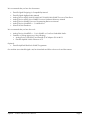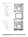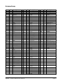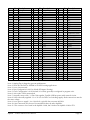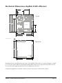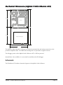
1
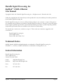
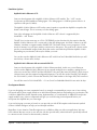
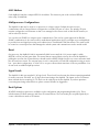
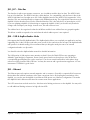
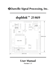
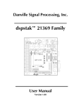
Danville Signal Processing, Inc. dspblok™ 21489+Ethernet CORE PS USB ETHERNET FLASH 60.00 [2.36] EEPROM ADSP-21489 JTAG 60.00 [2.36] User Manual Version 1.10 Danville Signal Processing, Inc. dspblok™ 21489+Ethernet User Manual Copyright © 2012-2013 Danville Signal Processing, Inc. All rights reserved. Printed in the USA. Under the copyright laws, this manual may not be reproduced in any form without prior written permission from Danville Signal Processing, Inc. Danville Signal Processing, Inc. strives to deliver the best product to our customers. As part of this goal, we are constantly trying to improve our products. Danville Signal Processing, Inc., therefore, reserves the right to make changes to product specification or documentation without prior notice. Updated operating manuals and product specification sheets are available at our website for downloading. This manual may contain errors, omissions or “typo’s”. Please send your comments, suggestions and corrections to: Danville Signal Processing, Inc. 38570 100th Avenue Cannon Falls, MN 55009-5534 Trademark Notice dspblok, dspstak, dspFlash and dspBootloader are trademarks of Danville Signal Processing, Inc. VisualDSP++, CrossCore, SHARC and Blackfin are trademarks of Analog Devices, Inc. Contact Information Danville Signal Processing, Inc. 38570 100th Avenue Cannon Falls, MN 55009 E-mail: Web Site: [email protected] http://www.danvillesignal.com Voice: 507-263-5854 Fax: 877-230-5629 dspblok™ 21489+Ethernet User Manual Page B Table of Contents Overview..................................................................................................................1 dspblok™ Development Boards ................................................................................................................ 1 dspblok™ 21489....................................................................................................................................... 1 Intended Audience ................................................................................................................................... 2 Getting Started.......................................................................................................................................... 2 Hardware Overview .................................................................................................7 Power Supply............................................................................................................................................ 7 Memory.................................................................................................................................................... 8 DAI & DPI ................................................................................................................................................ 8 Data Bus ................................................................................................................................................... 8 Clocks....................................................................................................................................................... 8 MAC Address............................................................................................................................................ 9 Multiprocessor Configurations ................................................................................................................... 9 Reset......................................................................................................................................................... 9 Signal Levels ............................................................................................................................................. 9 Boot Options ............................................................................................................................................ 9 Connections ...........................................................................................................10 Connector Recommendations & Notes ...................................................................12 Connector Specification .......................................................................................................................... 12 JH1 – JTAG ............................................................................................................................................. 12 JH2 – DAI, DPI, IO ................................................................................................................................. 12 JH3 – Configuration ................................................................................................................................ 12 JH4 – Power & Clock .............................................................................................................................. 12 JH5, JH7 – Data Bus ............................................................................................................................... 13 JH8 – USB & dspBootloader Mode ......................................................................................................... 13 JH9 – Ethernet ........................................................................................................................................ 13 Mechanical Dimensions (dspblok 21489+Ethernet) ................................................14 Mechanical Dimensions (dspblok 21489+Ethernet+ICE)........................................15 Schematic...............................................................................................................15 Product Warranty ...................................................................................................16 RoHS & WEEE Compliance.....................................................................................17 dspblok™ 21489+Ethernet User Manual Page C Overview Danville Signal's dspblok™ family of products delivers the power of digital signal processing in a small 60mm x 60mm form factor. Connections are brought out to standard 2mm dual row headers. The dspblok reduces development costs, risk and time. Danville’s dspblok DSP function modules are often incorporated directly into larger custom embedded systems. By taking advantage of pretested signal processing modules, pc board layouts become simpler and projects are completed quickly and cost effectively. Danville’s dspblok DSP Engines are largely pin compatible. This allows your application to take advantages of new processor technology and extended features in the future. You can also create small standalone embedded applications by combining a dspblok DSP function module with other dspblok modules. Embedded dspblok systems can be created by using a dspblok power supply such as our dspblok ps-uart, and an I/O module, such as one of our dspblok ad96k family of audio data converter boards. Each board is stacked via 2mm headers to create a low profile configuration where space is at a premium. We also have combination power supply- I/O boards such as our dspblok a9238/48 highspeed ADC boards for SDR applications. Danville dspblok DSP Engines are the driving force behind many of Danville’s standalone products such as our dspstak, dsprak, dspMusik and dspInstrument product lines. dspblok™ Development Boards All dspblok production modules have a companion developer’s version, which includes an Analog Devices’ EZ-KIT style debugger. These boards are physically larger (60mm x 115mm) to accommodate the debugger but have a matching footprint to our production modules (60mm x 60mm). Once you have developed and debugged your software, you can replace the debugger module (ICE version) with a lower cost, smaller production module. The dspblok “with ICE” versions include the free Visual DSP++ KIT license and are supported by the FULL version. Depending on the complexity of your application, you may be able to create and support your application without ever needing to purchase additional development tools. You can also use Analog Devices’ CrossCore Embedded Studio. dspblok™ 21489+Ethernet The dspblok™ 21489+Ethernet is a highly integrated DSP module that incorporates an Analog Devices’ ADSP-21489 SHARC DSP operating at 400 MHz with flash and EEProm. An onboard switching power supply supports the core voltage requirements of the DSP so that only 3.3V is required to power the dspblok. The ADSP-21489 peripherals include SPORTS (8), SPI(2), TWI (I2C), UART, timers, PWMs, JTAG and an external data bus. USB is provided by an FTDI FT232H, which is a high speed USB device with excellent driver support. Each dspblok 21489 also includes a unique MAC address (IEEE EUI-48). Ethernet support (100Mb/s) is provided by a Wiznet W5100. This device manages the TCP/IP stack making the communications support very easy without burdening the DSP. dspblok™ 21489+Ethernet User Manual Page 1 Intended Audience The dspblok 21489 requires an understanding of the Analog Devices’ ADSP-21489 and the associated tools used for development. If the dspblok 21489 is going to be integrated into a larger hardware design, then it is also assumed that the user is familiar with basic hardware design. In most cases, systems integrators, DSP programmers and software engineers can create DSP embedded systems using our embedded dspblok systems (or dspstak family) without the need for additional hardware design and manufacturing. If you do not have a background with these skills, you may want to check out our web site (http://www.danvillesignal.com) as well as the Analog Devices web site for links to useful references. Danville engineers are also available to discuss your application. Getting Started Danville’s customer base is quite diverse. Our customers range from embedded systems hardware designers to system integrators looking for complete turnkey solutions. We often work with embedded systems engineers who may not have specific expertise in digital signal processing. Regardless of your background, you will need the right tools. This means either Visual DSP++5.0 for SHARC or CrossCore Embedded Studio for the software development along with either a dspblok 21489+Ethernet+ICE or an external ADI emulator. Visual DSP++5.0 versus CrossCore Embedded Studio: VisualDSP++ has been ADI’s DSP software environment for many years. In many ways, it has a similar look and feel to Microsoft’s’ Visual Studio Tools. There are separate licenses for SHARC and Blackfin so customers that need to support both families often need to buy two full licenses. In our view, the full version of VisualDSP++ is expensive, about $3500 US. However, once you own VisualDSP++, you can continue updating for free. Version 1.0 customers can now be using Version 5.0 without incurring any maintenance charges. There are also KIT and TESTDRIVE licenses, which are free. CrossCore Embedded Studio is ADI’s replacement for VisualDSP++. Unlike VDSP++, it is Eclipse based. It has a much lower entry cost: $1000 US. It will likely have upgrade costs as new processors are added. This may not matter at all if you are not migrating to newer DSPs. CrossCore supports both Blackfin and SHARC DSP with a single license. ADI offers a free 90 day TESTDRIVE version. dspblok™ 21489+Ethernet User Manual Page 2 Emulation Options: dspblok 21489+Ethernet+ICE: Start your development with a dspblok 21489+Ethernet+ICE module. The “+ICE” version incorporates an ADI Standalone Debug Agent. The debug agent is a USB bus powered device. It operates at full speed (12Mb/s). The dspblok 21489+Ethernet+ICE has the same footprint as a production dspblok except that the board is much larger. This is necessary to fit the debug agent. One of the advantages of the dspblok 21489+Ethernet+ICE is that it is supported by the VisualDSP++ KIT license. The KIT (free) version starts out as a FULL (TESTDRIVE) version but after 90 days requires that the dspblok 21489+Ethernet+ICE is connected via the ADI debug agent. It will not connect to an ADI emulator, simulator or support another SHARC DSP. The linker restricts a user program to 27306 words of memory for code space with no restrictions for data space. The good news is that it can be used to create bootable images (loader files) that can be used with the production dspblok 21489. Depending on your situation, this may be all that you need. You can also use the dspblok 21489+Ethernet+ICE with CrossCore Embedded Studio but you will need to buy a license after 90 days. dspblok 21489+Ethernet with an external ADI ICE : Start your development with a dspblok 21489+Ethernet module. In this case, you will want to connect to the dspblok 21489+Ethernet via an external Analog Devices emulator. Analog Devices offers two versions the USB-ICE and the HPUSB-ICE. We prefer the faster HPUSB-ICE, which is up to 10 times faster and also supports background telemetry. You will also need a Danville JTAG adapter kit (P/N A.08153), which converts the Danville JTAG 2mm header to the larger ADI JTAG connector. You will also need a FULL VisualDSP++ 5.0 or CrossCore Embedded Studio license after 90 days. Development Boards: If you are designing your own companion board, we strongly recommend that you use one of our existing I/O boards and/or power supply boards as an initial development platform. Depending on your situation, this could be a dspblok dev board, dspstak system, dspInstrument, or a combination of dspblok I/O and power supply modules. Any of these components will give you a solid footing for development before you incorporate the dspblok into your own target. If you are laying out your own pc board, we can provide you with PCB footprints and schematic symbols (Gerber & Altium Designer) to help you avoid simple mistakes. Regardless of your situation, Danville engineers are available to help you with your application. We may have solutions that are not yet on our web site. We also provide many solutions that are specifically tailored to customer needs. Contact us about turnkey solutions. dspblok™ 21489+Ethernet User Manual Page 3 We recommend that you have the documents: • • • • • • • Danville Signal Designing for Compatibility Manual Danville Signal dspBootloader Manual Analog Devices ADSP-21483/21486/21487/21488/21489 SHARC Processor Data Sheet Analog Devices ADSP-214xx SHARC Processor Hardware Reference Manual Analog Devices SHARC Processor Programming Reference Manual Analog Devices VisualDSP++ 5.0 Manual Set Wiznet W5100 Datasheet We recommend that you have the tools: • • Analog Devices VisualDSP++ 5.0 for SHARC or CrossCore Embedded Studio Emulator or Debug Agent (one of the following) • Analog Devices HPUSB-ICE and Danville JTAG Adapter P/N A.08153 • Danville dspblok 21489+Ethernet+ICE Optional: • Danville dspFlash Blackfin & SHARC Programmer Our website (www.danvillesignal.com) has downloads and links to these tools and documents. dspblok™ 21489+Ethernet User Manual Page 4 The dspblok 21489+Ethernet+ICE includes the following items: CORE PS Hardware: • • dspblok 21489+Ethernet+ICE Module USB Cable USB ETHERNET FLASH EEPROM ADSP-21489 Software: • VisualDSP++ 5.0 for SHARC (KIT license) CD 115.00 [4.53] Documents (CD): • • • • • This Manual CAD footprints (Gerber & Altium formats) Schematics Sample Programs Debug Agent Driver Analog Devices' Debug Agent 60.00 [2.36] The dspblok 21489+Ethernet includes the following: CORE PS Hardware: • dspblok 21489+Ethernet Module Documents (CD): • • • • USB ETHERNET This Manual CAD footprints (Gerber & Altium formats) Schematics Sample Programs FLASH 60.00 [2.36] EEPROM ADSP-21489 JTAG 60.00 [2.36] dspblok™ 21489+Ethernet User Manual Page 5 Hardware Overview The dspblok 21489+Ethernet is a small module measuring 60mm x 60mm (2.36” x 2.36”). JH2 and JH4 – JH8 are 2mm male headers that are installed on the bottom side of the pc assembly. JH1 and JH3 are mounted on the top side of the pc assembly. If mating 2mm female headers (4.3mm ht.) are used, the pc assembly will be about ¼” above the mating pc board. This allows standard (0.250”) standoffs to be used with the corner mounting holes if desired. The hole size is 2.3mm – suitable for 2-56 or M2 screws. JH9 JH8 JH4 CORE PS • JH1 – JTAG (connects to external ICE) (Top Side) • JH2 – DAI, DPI, I/O, SPI & System (Bottom Side) • JH3 – Clock & Boot Configuration (Top Side) • JH4 – Power & Ext Clock (Bottom Side) • JH5, JH7 – Data Bus (Bottom Side) • JH8 – USB Port & dspBootloader Mode (Bottom Side) • JH9 - Ethernet (Bottom Side) USB ETHERNET FLASH 60.00 [2.36] EEPROM JH2 ADSP-21489 JH5 JH3 JTAG JH7 60.00 [2.36] Power Supply There are two power supply connections to the dspblok: DSP core (Vdd) and DSP I/O and Memory (Vd+3.3). The DSP core supply may range from 3.3V to 5V. This is the input to an on-board switching power supply that supplies 1.1V to the ADSP-21489. DO NOT use a higher voltage supply for the core supply input (JH4-Vdd). A single 3.3V supply is all that is required to power the dspblok 21489, but in some cases, a 5V supply may be more convenient. The DSP I/O and Memory supply must be 3.3V. For example, a product may already have a switching supply that converts directly to 3.3V. In this case, it may be desirable to supply both the DSP core and the dspblok Vd+3.3 (I/O) from this supply. Alternatively, a product might have a 5V supply (perhaps from an external power supply module). A simple LDO fixed regulator could be used to create 3.3V from this supply. Most high-speed devices, including the ADSP-21489, draw most of their power from their core supplies. In this scenario, it makes no sense to power the dspblok core with 3.3V since the LDO would be dissipating the excess voltage as heat. If the I/O requirements are modest, the power dissipation in the LDO might not be significant Power consumption is largely a function of the temperature (due to leakage current) of the ADSP-21489. It is also a function of the core clock and the computation tasks that are being executed on the DSP. The highest consumption occurs when the DSP is performing continuous floating point operations at maximum core clock (400MHz) and at maximum temperature. The Analog Devices’ ADSP-21489 SHARC Processor Data Sheet has an excellent section on estimating power consumption of the DSP. dspblok™ 21489+Ethernet User Manual Page 6 Memory The ADSP-21489 includes 5Mbits of internal SRAM. This is 2.5 times more than the earlier third generation SHARC DSPs (ADSP-21369). It also includes an SDRAM controller, which is not used in the dspblok 21489. We have found that most applications do not need more than the abundant internal memory of the ADSP21489. Those applications that do require large blocks of memory are much better served by the pin compatible dspblok 21469 or dspblok 21469+USB. The ADSP-21469 supports much faster DDR2 SDRAM with an independent interface. A 16Mbit serial flash memory may be used to bootload the DSP. There is a pre-installed bootloader program that resides in the flash. This program accepts standard ADI loader files (SPI, slave, binary, 8 bit) and can be uploaded with a dspblok development board, a dspstak 21489 or any Danville board that includes a USB connector. If you want to manage the flash memory yourself, you can overwrite the internal bootloader via the JTAG port. In this case, the Danville dspFlash Blackfin & SHARC Programmer is available for fast production programming. 8kbits of EEProm memory is also available as byte addressable user memory. For example, you might store serial numbers, build versions or calibration values in this space. DAI & DPI The ADSP-21489 has 20 DAI lines and 14 DPI lines. Collectively these can be thought of as two sets of crossbar switches that connect to a wealth of peripherals. The dspblok 21489 maintains the flexibility of the DAI and DPI by bringing out all 20 DAI and 12 of 14 DPI lines to external connections. The DAI is completely unencumbered and can be assigned to I/O in an arbitrary manner. The DPI is slightly restricted in that the primary SPI interface is assigned to DPI1 (MOSI), DPI2 (MISO), DPI3 (SCK), DPI5 (Flash SS) and DPI6 (EE SS). With the exception of DPI6, these connections are necessary to support SPI master booting. The dspblok 21489 may also be booted from an external host using SPI slave mode. In this case DPI4 is also used as the SPIDS# line. Data Bus The dspblok 21489 brings out the lower 8 bits of external data bus including all address lines with the exception of MS0#. Since the data bus is primarily used for I/O expansion, we elected to ignore the upper data lines (D15-D8) to maintain compatibility with the ADSP-21469. The upper portion of MS1# is used for on-board peripherals. The lower ¾ of the address space is available. MS2# and MS3# can also be used as FLAG2 and FLAG3, respectively. They are configured together so MS1# might be used for the external data bus and FLAG2 & FLAG3 for other purposes. Clocks The dspblok 21489 supports both internal and external clocking options. You must desolder the 25.000MHz HC49 style crystal on the board to use an external clock. The configuration header (JH3) allows any ADSP21489 power-up clock configuration to be set. The default configuration is 25.000M x 16 = 400M. dspblok™ 21489+Ethernet User Manual Page 7 MAC Address Each dspblok 21489 has a unique IEEE EUI-48 address. This feature is part of the on-board EEProm (Microchip 25AA02E48). Multiprocessor Configurations The dspblok 21489 may be used as a coprocessor in a larger system. Perhaps the easiest way to communicate with an external host to configure the secondary SPI port as a slave. The primary SPI port remains configured as an SPI master so that it can manage local resources such as flash and EE memory as well as other I/O devices. You can also use SPORTs for interprocessor communication. This can be a good approach for Blackfin – SHARC combinations. It also works well for multichannel applications where you might use several dspbloks to provide front end signal processing and combine into a consolidated TDM data stream. The results could be routed to a central processor that manages the whole system and communicates to the outside world. Reset On power up, the dspblok 21489 is automatically held in reset until the 3.3V power supply is stable. RESET# is active low and open drain. This means that an external device(s) may also reset the dspblok by pulling the reset line low. External devices should not drive RESET# high since this can cause contention with the on-board reset circuit. The external reset circuit is connected in a wired-OR configuration using an active low – open drain configuration. A 74LVC125 or an open collector/drain transistor circuit are possibilities. You do not need an additional pull up resistor. Signal Levels The dspblok 21489 uses standard 3.3V logic levels. These levels have become the defacto operating standard for many years now. DO NOT use 5V logic when interfacing to the dspblok. The inputs are not 5V tolerant. Most external devices requiring 5V TTL levels can be safely driven by the dspblok. If you have questions concerning interfacing external devices, please contact Danville for suggestions. Boot Options All ADSP-21489 boot options are available via the configuration and programming header (JH3). These include Master SPI (flash memory) and Slave SPI (external host). The boot mode pins are pulled passively to create a default boot mode of SPI Master. dspblok™ 21489+Ethernet User Manual Page 8 Connections Pin JH1 Note 1 Description JTAG 1 2 3 4 5 6 7 8 9 10 11 12 13 14 15 16 JH8 EMUSEL EMU Key (No Pin) GND Vd+3.3 Mon TMS GND TCK GND TRST# GND TDI GND TDO Vd+3.3 Vd+3.3 USB 1 2 3 4 5 6 7 8 9 10 11 12 13 14 15 16 Pin JH2 Note 2 Note 3 Note 3 NC NC USB VBUS NC GND GND USB DP USB DN GND GND Reserved GND USER MODE 1 GND USER MODE 0 GND dspblok™ 21489+Ethernet User Manual Description DAI, DPI, IO 1 2 3 4 5 6 7 8 9 10 11 12 13 14 15 16 17 18 19 20 21 22 23 24 25 26 27 28 29 30 31 32 33 34 35 36 37 38 39 40 GND DPI8 DPI4 DPI13 DPI14 FLG0 DPI7 DPI11 DPI12 DPI9 DPI10 FLG1 FLG3 DPI1/MOSI DPI3/SCK DPI2/MISO RESET# Reserved DAI1 DAI2 DAI3 DAI4 DAI5 DAI6 DAI7 DAI8 DAI9 DAI10 DAI11 DAI12 DAI13 DAI14 DAI15 DAI16 DAI17 DAI18 DAI19 DAI20 GND GND Pin JH3 Note 4 Note 4 Note 4 Note 5 Note 5 Configuration 1 2 3 4 5 6 7 8 9 10 JH4 Note 6 Note 7 Note 7 Note 8 Note 8 Note 9 Description GND BOOTCFG0 Vd+3.3 BOOTCFG1 Vd+3.3 BOOTCFG2 Vd+3.3 CLKCFG0 GND CLKCFG1 Power 1 2 3 4 5 6 7 8 9 10 GND Ext Clk USB PE# NC Vd+3.3 Vd+3.3 (USB) Vdd (3.3V or 5V) Vdd (3.3V or 5V) PS Sync GND Page 9 Pin JH5 Note 10 Note 10 Note 10 Note 10 Note 10 Note 10 Note 10 Note 10 Note 10 Note 10 1 2 3 4 5 6 7 8 9 10 11 12 13 14 15 16 17 18 19 20 Description Pin Data Bus JH7 NC NC NC NC NC NC NC NC D7 D6 D5 D4 D3 D2 D1 D0 RD# WR# ACK NC Note 10 Note 10 Note 10 1 2 3 4 5 6 7 8 9 10 11 12 13 14 15 16 17 18 19 20 21 22 23 24 25 26 27 28 29 30 Description Pin Address Bus JH9 NC NC NC A23 A22 A21 A20 A19 A18 A17 A16 A15 A14 A13 A12 A11 A10 A9 A8 A7 A6 A5 A4 A3 A2 A1 A0 MS1# MS2# MS3# Note 11 Description Ethernet 1 2 3 4 5 6 7 8 9 10 11 12 13 14 15 16 RDRD+ NC NC NC TCT TDTD+ Connector GND NC LINK LED# NC FDX LED# GND GND Vd+3.3 Note 1: Mating Plug is plugged to prevent misalignment. Note 2: DPI4 also functions as SPIDS# in SPI slave booting applications. Note 3: Leave Unconnected. Note 4: Boot Configuration is 001 by default (SPI Master Booting). Note 5: Clock Configuration is 10 by default (16 x ClkIn), generally reconfigured in program code. Note 6: Active after USB is enumerated. Note 7: Normally connect Vd+3.3 Pins 5&6 together. Possible USB bus power with external circuits. Note 8: Vdd is externally supplied: 3.3 to 5V (Vin for DSP Core Switching supply). Both connections must be the same voltage. Note 9: Leave open or supply 1.4 to 1.6M clock, typically data converter MCLK/N Note 10: Not Connected, may be used for extended features by other dspbloks. Note 11: This connector is not used in the dspblok 21489, but is defined for dspblok 21489+ETH. dspblok™ 21489+Ethernet User Manual Page 10 Connector Recommendations & Notes Connector Specification All dspblok connectors are gold plated 2mm dual row headers. Male connectors are generally mounted on the bottom side of the dspblok pc assembly. The exceptions are JH3 & JH1, which are not intended to mate to a motherboard. The plastic base of each male connector is 2mm. The height of the female headers is 4.3mm. This means that the inserted combined height of the two connectors is 6.3mm or approximately ¼ inch. Standard standoffs may be used to secure the dspblok to the target pc board. Mounting holes are 2.3mm dia. to accommodate a 2-56 or M2 screws or standoffs. JH1 – JTAG This connector is mounted on the top side of the dspblok. A 2mm right angle header is used instead of the larger ADI JTAG header. The connections on the JTAG header correspond with the connections on an ADI JTAG header. In addition, Vd+3.3 is also available. This addition allows an active buffer circuit to be added for JTAG chaining applications. Danville has an ADI JTAG adapter available (P/N A.08153). The dspblok 21489+Ethernet+ICE omits JH1 since the debugger is on-board. If you want to use an external emulator or the Danville dspFlash Blackfin & SHARC Programmer, you may remove the ADI Debugger and use the JTAG connection provided below the debugger. JH2 – DAI, DPI, IO This connector is mounted on the bottom side of the dspblok. The DAI lines are all uncommitted by the dspblok. With the exception of the SPI lines, the DPI can be freely assigned. JH3 – Configuration This connector is mounted on the top side of the dspblok. It provides direct access to the ADSP-21489 clock mode and boot mode configuration pins. In most cases, you should leave all the connections open. Use shorting jumpers if you want to change the configuration. Note that each shorting jumper will cause the corresponding mode pin to deviate from the pin state of the default configuration. This means that some pins are pulled high and others low. JH4 – Power & Clock This connector is mounted on the bottom side of the dspblok. This is the main power feed to the dspblok, Vdd is the input to the core switching supply. Both Vdd pins should be connected to together and fed with either 5V or 3.3V. Likewise, Vd+3.3 should be connected together and fed with 3.3V. dspblok™ 21489+Ethernet User Manual Page 11 JH5, JH7 – Data Bus The data bus is split to two separate connectors, one for address and the other for data. The ADSP-21489 has an 16 bit data bus. The ADSP-21469 has a 8 bit data bus. For compatibility, only the lower 8 bits of the ADSP-21489 data bus is brought out to JH5. Earlier dspbloks based on the ADSP-21369 supported a 32 bit data bus. This was needed primarily to support wide SDRAM interfacing. The original JH6 connection on the dspblok 21369zx board was used for the extended data bus. This is also why there are unused pins on JH5. If you are adapting a dspblok 21369zx design to support the dspblok 21489, you should verify that these changes will not impact your design. In most cases, this will not be an issue. The address bus is also organized so that the MS# lines and the lower address lines are grouped together. This allows a smaller receptacle to be used when the whole address space is not required. JH8 – USB & dspBootloader Mode JH8 supports the Danville dspBootloader. The dspBootloader allows you to upload your application and any supporting files via the USB port (and other ports as well). If the connections are left open, the dspBootloader will operate in its default setting. We recommend that you bring the mode pins out to an external configuration header or a dip switch. You should review the dspBootloader manual for detailed information. The USB portion of JH8 requires some attention to detail. Since the DM & DP lines are operating at 480Mb/s, signal integrity is important. Route closely spaced tracks on the top layer of the PCB with a corresponding ground plane layer on the next layer. You do not want discontinuities in this plane. Keep other traces away from the DM & DP lines. You may also want to add a good transient suppressor. A Texas Instruments’ TPD2E001 is good choice. JH9 – Ethernet The Ethernet port only requires external magnetics and a connector. Generally a composite RJ-45connector that includes the isolation transformer is the most convenient choice. By keeping the transformers of the dspblok, you can also use the dspblok in an Ethernet POE (power over ethernet) configuration. This makes the dspblok 21489+Ethernet well suited for remote smart sensor applications. The LED connections are both active low. 200 ohm series limiting resistor are on the dspblok. You may wish to add additional limiting resistance for high efficient LEDs. dspblok™ 21489+Ethernet User Manual Page 12 Mechanical Dimensions (dspblok 21489+Ethernet) 46.00 [1.81] 28.00 [1.10] 6.00 [0.24] CORE PS Top Side USB ETHERNET 60.00[2.36] 57.00 [2.25] FLASH EEPROM ADSP-21489 44.00 [1.73] 24.00 [0.94] JTAG 26.00 [1.02] 57.00 [2.25] 60.00 [2.36] Holes 2.3 [0.090] (4 places) EULAV EULAV Bottom Side EULAV EULAV 55.00[2.17] EULAV 55.00 [2.17] Mounting holes are equidistant from the center of the dspblok. These holes are 2.3mm in diameter, suitable for 2-56 or M2 screws. When 4.3mm height mating female connectors are used, the board will be 6.3mm (0.25 in) above the target board, therefore 0.250 standoffs may be used. Component height above the board is 6mm (0.236 in). The board is 1.6mm (0.062 in) thick. dspblok™ 21489+Ethernet User Manual Page 13 Mechanical Dimensions (dspblok 21489+Ethernet+ 21489+Ethernet+ICE) CORE PS USB ETHERNET 55.00 [2.17] FLASH EEPROM ADSP-21489 115.00 [4.53] 55.00 [2.17] Analog Devices' Debug Agent 60.00 [2.36] The dspblok 21489+Ethernet+ICE board has identical mounting holes and mating connections as the production dspblok 21489. Two additional mounting holes are provided for support as shown. The debugger portion of the dspblok 21489+Ethernet+ICE is USB bus powered. Manual Reset is also available via a tact switch located below the ADI debugger. Schematic The Distribution CD includes schematic diagrams of the dspblok 21489+Ethernet. dspblok™ 21489+Ethernet User Manual Page 14 Product Warranty Danville Signal Processing, Inc. products carry the following warranty: Danville Signal Processing products are warranted against defects in materials and workmanship. If Danville Signal Processing receives notice of such defects during the warranty period, Danville Signal Processing shall, at its option, either repair or replace hardware products, which prove to be defective. Danville Signal Processing software and firmware products, which are designated by Danville Signal Processing for use with our hardware products, are warranted not to fail to execute their programming instructions due to defects in materials and workmanship. If Danville Signal Processing receives notice of such defects during the warranty period, Danville Signal Processing shall, at its option, either repair or replace software media or firmware, which do not execute their programming instructions due to such defects. Danville Signal Processing does not warrant that operation of the software, firmware, or hardware shall be uninterrupted or error free. The warranty period for each product is one year from date of installation. Limitation of Warranty: The forgoing warranty shall not apply to defects resulting from: • • • • • Improper or inadequate maintenance by the Buyer; Buyer-supplied software or interfacing; Unauthorized modification or misuse; Operation outside the environmental specification of the product; Improper site preparation and maintenance. Exclusive Remedies: The remedies provided herein are the Buyer’s sole and exclusive remedies. In no event shall Danville Signal Processing, Inc. be liable for direct, indirect, special, incidental or consequential damages (including loss of profits) whether based on contract, tort, or any other legal theory. dspblok™ 21489+Ethernet User Manual Page 15 RoHS & WEEE Compliance The European Union approved a directive on the restriction of the use of certain hazardous substances in electrical and electronic equipment. This directive is commonly known as RoHS, EU Directive 2002/95/EC. This directive severely limits the amount of lead and 5 other substances that can be in contained in nonexempt products. The directive became European law in February 2003 and took effect July 1, 2006. It is likely that other countries outside the European Union and some states in the United States may adopt similar legislation. There are a number of important exemptions that affect many of our customers. The most important of these is Category 9, Control and Monitoring Instruments. You may wish to review your situation to see if this exemption applies to you. Military, medical and some other products are also exempt. We suggest that you make an appropriate assessment concerning your products. The dspblok 21489 is RoHS compliant. The dspblok 21489 is a subcomponent of a larger system; therefore it is not subject to the WEEE directive EU Directive 2002/96/EC. dspblok™ 21489+Ethernet User Manual Page 16