1
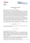
logiSPI SPI to AXI4 Controller Bridge
rd
September 3 , 2014
Data Sheet
Version: v3.01
Core Facts
Xylon d.o.o.
Fallerovo setaliste 22
10000 Zagreb, Croatia
Phone: +385 1 368 00 26
Fax:
+385 1 365 51 67
E-mail: [email protected]
www.logicbricks.com
URL:
Provided with Core
Documentation
User’s Manual
Design File Formats
Encrypted VHDL
Constraints Files
Verification
Features
Reference Designs &
Contact Xylon Support for
Application Notes
information on Reference Designs
Additional Items
logiCRAFT-CC evaluation board
• Supports Xilinx® Zynq®-7000 All Programmable
SoC and all Xilinx FPGA families
Simulation Tool Used
• Bridge controller between the Serial Peripheral
ModelTech’s Modelsim
Interface (SPI) bus and the Advanced eXtensible
Interface (AXI4) on-chip bus
Support
• Works as a Slave controller on the SPI bus, and a
Support provided by Xylon
master controller on the ARM® AMBA® AXI4 bus
• Enables full-duplex communication (MSB first)
between an external SPI Master controller and SoC/FPGA peripherals, on-chip and off-chip memories
• Supports SPI telegrams of different lengths: single transfers or burst transfers (up to 2 kB, back-to-back)
• Supports four signals interface (SI, SO, SCLK and SCS_N)
• Provides transfer status signals, SPI telegrams acknowledgment and Slave reset mechanisms
• Supports SCLK frequency of up to fclk/4, where fclk is frequency of the system clock (AXI4 clock)
• Supports all SPI clock polarity (CPOL) and phase (CPHA) combinations
• Prepared for Xilinx Vivado® and ISE® Design Suits
Applications
• Inter-chip board-level communications; i.e. external MCU controlling FPGA co-processor
Table 1: Example Implementation Statistics for Xilinx® FPGAs
Family
Fmax (MHz)
Fmax (MHz)
(Device)
M_AXI_ACLK
clk
100
100
LCs
Slices1
IOB2
BRAM
152
4
0
(FFs/LUTs)
Spartan®-6
MULT/
DCM /
DSP48/E
CMT
0
0
Design
GTx
278
1779
(XC6SLX45T-3)
Artix -7
ISE
14.7
264
100
100
1690
(XC7A200T-3)
ISE
152
4
0
0
0
N/A
(428/703)
Kintex™-7
14.7
278
100
100
1779
(XC7K70T-2)
ISE
152
4
0
0
0
N/A
(431/706)
Zynq
14.7
243
100
100
1555
Vivado
156
(437/650)
Tools
N/A
(435/729)
™
(XC7Z020-1)
LUTRAM
4
0
0
0
N/A
2014.2
Notes:
1) Assuming 32-bit AXI4 master interface.
2) Assuming only SPI signals are routed off-chip; other signals are connected internally.
Copyright © Xylon d.o.o. 2001-2014 All Rights Reserved
Page 1 of 6
logiSPI – SPI to AXI4 Controller Bridge
Data Sheet
Version: v3.01
logiSPI
SCS_N
SCLK
SO
SPI Interface
Module
Read and Write
Controller
AXI4
Interface
Module
AXI4 bus
SI
Write_done
Read_done
SFRs
Figure 1: logiSPI Architecture
General Description
The logiSPI SPI to AXI4 Controller Bridge IP core allows external host processors to communicate with
peripherals or processors implemented in Xilinx Zynq-7000 All Programmable SoC and FPGAs through the
Serial Peripheral Interface (SPI) serial bus. In enables easy implementations of Xilinx FPGA/SoC companion
chips that expand the capabilities of the embedded host processor by adding missing host features and by
offloading high-speed processing tasks. The IP core works as a SPI Slave bus controller and a 32-bit master
controller on the AMBA Advanced eXtensible Interface (AXI4) on-chip bus.
The SPI is a full-duplex synchronous and a four-wire serial interface between a single bus master, and one or
more bus slave devices. The bus master initiates communication by asserting slave’s select signal and issuing a
data frame (SPI telegram). Data is exchanged between the master and the selected slave device shift registers,
which shift data bits synchronous on SPI clock signal generated by the master device.
The logiSPI IP core accepts the SPI telegram sent by the SPI master, de-serializes it, decodes SPI Master’s
commands and writes/reads data to/from Xilinx Zynq-7000 SoC or FPGA peripherals and on-chip memories
interconnected with a high-speed 32-bit AXI4 on-chip bus. By mean of SoC/FPGA memory controllers, the
logiSPI can relay large bursts of data (up to 2 kBytes) between the SPI master device and SDRAM-type
memories connected to the Xilinx Zynq-7000 SoC or FPGA device.
The logiSPI SPI to AXI4 Controller Bridge IP core implements an acknowledgment mechanism that assures
integrity of data exchanged through the SPI bus. Properly decoded SPI telegrams are acknowledged by the
command code bounced back to the SPI master, and the faulty telegrams are discarded. By asserting and deasserting the slave select signal, the SPI master can reset the logiSPI IP core’s operation.
The following table shows SPI Master commands currently supported by the logiSPI IP core:
Copyright © Xylon d.o.o. 2001-2014 All Rights Reserved
Page 2 of 6
logiSPI – SPI to AXI4 Controller Bridge
SPI Command
RD_8
RD_16
RD_32
RD_SFR
RD_BURST
WR_8
WR_16
WR_32
WR_SFR
WR_BURST
Data Sheet
Version: v3.01
Description
Single transfer: 8-bit read
Single transfer: 16-bit read.
Single transfer: 32-bit read
SFR access: read Special Function Register (internal logiSPI register)
Burst transfer: read specified number of data bytes
Single transfer: 8-bit write
Single transfer: 16-bit write
Single transfer: 32-bit write
SFR access: write to Special Function Register (internal logiSPI register)
Burst transfer: write specified number of data bytes
Table 2: logiSPI supported SPI commands
Functional Description
The Figure 1 represents internal logiSPI architecture. The logiSPI functional blocks are: SPI Interface Module,
Read and Write Controller, AXI4 Interface Module and SFRs Module.
SPI Interface Module
The logiSPI front-end part implements a state machine that receives SPI telegrams from a SPI master and
controls shifting-in and shifting-out of serial data in a full-duplex mode. Serial data on the SPI bus is shifted MSB
first. The SO (MISO) Serial Output is a tristate output to enable use in the SPI bus with multiple-slaves.
Read and Write Controller
Read and Write Controller checks incomming SPI telegram, de-codes the SPI command, and issues proper
write or read operation to the SFRs Module or the AXI4 Interface module.
4 bits
12 bits
variable (8, 16, 32 bits)
SPI_CMD
SPI_ADDR
SPI_DATA
Figure 2 SPI telegram structure for single transfers
•
•
•
SPI_CMD
– SPI command (single transfer)
SPI_ADDR
– SPI address – 12 lowest bits of target AXI4 bus address (the upper address bits
defined by the SFR register)
SPI_DATA
– SPI data bytes to write to/read from target system address
4 bits
SPI_CMD
1 bit
R
11 bits
SPI_BURST_L
32 bits
SPI_ADDR
variable ((SPI_BURST_L + 1) x 8 bits)
SPI_DATA
Figure 3 SPI telegram structure for burst transfers
•
•
•
•
•
SPI_CMD
SPI_ADDR
SPI_DATA
R
SPI_BURST_L
–
–
–
–
–
WR_BURST/RD_BURST command (burst transfer)
SPI address – complete 32-bit system address
SPI data bytes to write to/read from target system address
reserved
burst length in number of bytes (0 – 2047)
Copyright © Xylon d.o.o. 2001-2014 All Rights Reserved
Page 3 of 6
logiSPI – SPI to AXI4 Controller Bridge
Data Sheet
Version: v3.01
AXI4 Interface Module
The AXI4 Interface Module translates the decoded read and write commands from the Read and Write
Controller into properly formatted AMBA AXI4 bus transfers, and vice versa, the AXI4 bus transfers into SPI
formatted telegrams. The module contains write and read address/data FIFOs to compensate different data
speeds on the parallel AXI4 bus and the serial SPI bus.
SFRs
SFRs Module contains Special Function Registers of the logiSPI IP core. Those registers are accessible only
via SPI interface.
Core Modifications
The core is supplied in an encrypted VHDL format compatible with Xilinx Vivado IP Integrator and ISE Platform
Studio. logiSPI has configuration parameters that are selectable prior to VHDL synthesis, and the following table
presents a selection from a list of available parameters:
Table 3: logiSPI VHDL Configuration Parameters
Parameter
Description
C_SPI_MODE
SPI communication mode selection (CPOL, CPHA)
C_BURST_WIDTH
Maximum number of AXI4 data transfers per burst
If you wish to adopt the logiSPI IP core to your specific needs and/or supplement the features set, you can allow
us to tailor the logiSPI to your requirements.
Core I/O Signals
The core signals I/O have not been fixed to any specific device pins to provide flexibility for interfacing with user
logic. Descriptions of all I/O signals are provided in Table 3.
Table 4: Core I/O Signals
Signal
Signal
Description
Direction
Common signals
clk
Input
System clock (AXI4 clock).
System bus interface
AXI4 Master Interface
Bus
Refer to ARM’s AMBA AXI4 protocol specification
SPI signals
sclk
Input
SPI serial clock
scs_n
Input
SPI slave select
si
Input
SPI serial input (MOSI)
so_i
Input
SPI serial output (MISO) – input signal
so_o
Output
SPI serial output (MISO) – output signal
so_t
Output
SPI serial output (MISO) – three state control signal
read_done
Output
Requested read data available on output port
write_done
Output
Data successfully written to target system address
Copyright © Xylon d.o.o. 2001-2014 All Rights Reserved
Page 4 of 6
logiSPI – SPI to AXI4 Controller Bridge
Data Sheet
Version: v3.01
Verification Methods
The logiSPI is fully supported by the Xilinx Vivado and ISE Design Suits. This tight integration tremendously
shortens IP integration and verification. A full logiSPI implementation does not require any particular skills
beyond general Xilinx tools knowledge.
Recommended Design Experience
The user should have experience in the following areas:
- Xilinx design tools
- ModelSim
Available Support Products
TM
Xylon logicBRICKS IP cores can be evaluated on logiCRAFT-CC Xylon development platform,
designed especially for developers working in the fields of multimedia and infotainment. This
demonstrates modularity on all levels: software, board, FPGA, and IP cores. The platform makes
development tool particularly appropriate for the development of embedded systems with strong
capabilities.
which is
platform
excellent
graphics
To learn more about the Xylon development platforms, contact Xylon or visit the web:
Email:
URL:
[email protected]
www.logicbricks.com
Ordering Information
This product is available directly from Xylon under the terms of the Xylon’s IP License. Please visit our web
shop or contact Xylon for pricing and additional information:
Email:
URL:
[email protected]
www.logicbricks.com
This publication has been carefully checked for accuracy. However, Xylon does not assume any responsibility
for the contents or use of any product described herein. Xylon reserves the right to make any changes to
product without further notice. Our customers should ensure that they take appropriate action so that their use
of our products does not infringe upon any patents. Xylon products are not intended for use in the life support
applications. Use of the Xylon products in such appliances is prohibited without written Xylon approval.
Related Information
Xilinx Programmable Logic
For information on Xilinx programmable logic or development system software, contact your local Xilinx sales
office, or:
Xilinx, Inc.
2100 Logic Drive
San Jose, CA 95124
Phone: +1 408-559-7778
Fax:
+1 408-559-7114
www.xilinx.com
URL:
Copyright © Xylon d.o.o. 2001-2014 All Rights Reserved
Page 5 of 6
logiSPI – SPI to AXI4 Controller Bridge
Data Sheet
Version: v3.01
Revision History
Version
Date
2.00.
18.04.2012.
3.01.
03.09.2014.
Note
Initial Xylon release.
Update to AXI4.
Support for Xilinx Vivado Design Suite.
Copyright © Xylon d.o.o. 2001-2014 All Rights Reserved
Page 6 of 6