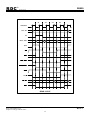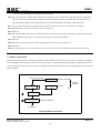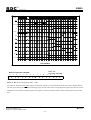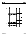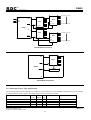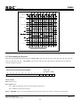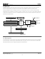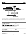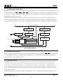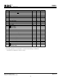
1
RDC
®
R8820
RISC DSP Controller
R8820
16-Bit RISC Microcontroller User’s Manual
RDC RISC DSP Controller
RDC Semiconductor Co., Ltd
http:\\www.rdc.com.tw
Tel. 886-3-583-2666
Fax 886-3-583-2688
Rev:1.3
RDC Semiconductor Co.
Subject to change without notice
1
RDC
®
R8820
RISC DSP Controller
Contents
--------------------------------------------------------------------------------------- page
1. Features -------------------------------------------------------------------------------- 4
2.Block Diagram ------------------------------------------------------------------------- 4
3. Pin Configuration -------------------------------------------------------------------- 5
4. Pin Description------------------------------------------------------------------------ 8
5. Basic Application System Block & Read/Write timing Diagram ---------- 14
6. Oscillator Characteristics ---------------------------------------------------------- 17
7. Execution Unit ----------------------------------------------------------------------- 18
7.1 General Register ----------------------------------------------------------------- 18
7.2 Segment Register ---------------------------------------------------------------- 18
7.3 Instruction Pointer and Status Flags Register -------------------------------- 19
7.4 Address Generation ------------------------------------------------------------- 20
8. Peripheral Control Block Register ----------------------------------------------- 21
9. System Clock Block ----------------------------------------------------------------- 23
10. Reset ---------------------------------------------------------------------------------- 24
11. Bus Interface Unit------------------------------------------------------------------ 26
11.1 Memory and I/O Interface ---------------------------------------------------- 26
11.2 Data Bus------------------------------------------------------------------------- 26
11.3 Wait States ---------------------------------------------------------------------- 27
11.4 Bus Hold ------------------------------------------------------------------------ 28
11.5 Bus Width---------------------------------------------------------------------- 30
12. Chip Select Unit -------------------------------------------------------------------- 31
12.1 UCS ---------------------------------------------------------------------------- 31
12.2 LCS ---------------------------------------------------------------------------- 32
12.3 MCSx -------------------------------------------------------------------------- 33
12.4 PCSx --------------------------------------------------------------------------- 34
13. Interrupt Controller Unit--------------------------------------------------------- 37
13.1 Master Mode and Slave Mode ------------------------------------------------ 37
13.2 Interrupt Vector, Type and Priority ------------------------------------------ 38
13.3 Interrupt Request -------------------------------------------------------------- 39
13.4 Interrupt Acknowledge -------------------------------------------------------- 39
13.5 Programming Register--------------------------------------------------------- 40
Rev:1.3
RDC Semiconductor Co.
Subject to change without notice
2
RDC
®
R8820
RISC DSP Controller
14. DMA Unit --------------------------------------------------------------------------- 53
14.1 DMA Operation ---------------------------------------------------------------- 53
14.2 External Request --------------------------------------------------------------- 59
14.3 Serial Port / DMA Transfer ------------------------------------------------ 61
15. Timer Control Unit ---------------------------------------------------------------- 62
15.1 Timer/Counter Unit Output Mode ------------------------------------------ 66
16. Watchdog Timer ------------------------------------------------------------------- 68
17. Asynchronous Serial Port--------------------------------------------------------- 70
17.1 Serial Port Flow Control -------------------------------------------------- 70
17.1.1 DCE/DTE Protocol ------------------------------------------------ 70
17.1.2 CTS/RTR Protocol-------------------------------------------------- 71
17.2 DMA Transfer to/form a serial port function ------------------------- 71
17.3 The Asynchronous Modes description ---------------------------------- 72
18. PIO Unit ----------------------------------------------------------------------------- 77
18.1 PIO Multi-Function Pin list Table ------------------------------------------- 77
19. PSRAM Control Unit-------------------------------------------------------------- 80
20. Instruction Set Opcodes and Clock Cycle ------------------------------------- 81
20.1 R8000 Execution Timings ---------------------------------------------------- 85
21. AC Characteristics----------------------------------------------------------------- 86
22. Package Information -------------------------------------------------------------- 95
23. Revision History------------------------------------------------------------- 97
Rev:1.3
RDC Semiconductor Co.
Subject to change without notice
3
RDC
®
R8820
RISC DSP Controller
16-Bit Microcontroller with 16-bit external data bus
1. Features
l
Five-stages pipeline
l
Supports 32 PIO pins
l
RISC architecture
l
PSRAM (Pseudo static RAM) interface with
l
Static Design & Synthesizable design
l
Bus interface
auto-refresh control
l
- Multiplexed address and Data bus which
independent watchdog timer
l
is compatible with 80C186 microprocessor
l
The Interrupt controller with seven maskable
- Supports nonmultiplexed address bus [A19 : A0]
external interrupts and one nonmaskable
- 1M byte memory address space
external interrupt
- 64K byte I/O space
l
Two independent DMA channels
Software is compatible with the 80C186
l
Programmable chip-select logic for Memory
microprocessor
l
Three independent 16-bit timers and one
or I/O bus cycle decoder
Support two Asynchronous serial channel with
l
Programmable wait-state generator
hardware handshaking signals.
l
Support serial port/ DMA transfers
2. Block Diagram
INT2/INTA0
INT1/SELECT
CLKOUTA
INT3/INTA1/IRQ
CLKOUTB INT6-INT4
X1
VCC
GND
X2
Clock and
Power
Management
INT0
TMROUT0
TMROUT1
TMRIN0
TMRIN1
NMI
Interrupt
Control Unit
Timer Control
Unit
DRQ0
DRQ1
DMA
Unit
RST
LCS/ONCE0
MCS3/RFSH
Chip
Select
Unit
MCS2-MCS0
Instruction
Queue (64bits)
UCS/ONCE1
PSRAM
Control
Unit
PCS3-PCS0
PCS5/A1
PCS6/A2
Refresh
Control
Unit
ARDY
SRDY
S2~S0
DT/R
DEN
Instruction
Decoder
Micro
ROM
PIO
Unit
Control Signal
Register
File
General,
Segment,
Eflag Register
EA / LA
Address
RTS0/RTR0
Asynchronous Serial
Port0
CTS0/ENRX0
TXD0
RXD0
RTS1/RTR1
Bus
Interface
Unit
HOLD
HLDA
S6/CLKDIV2
UZI
A19~A0
AD15~AD0
ALE
ALU
Execution
Unit
(Special,
Logic,
Adder,
BSF)
Asynchronous Serial
Port1
CTS1/ENRX1
TXD1
RXD1
RD
WHB
WLB
WR
BHE/ADEN
Rev:1.3
RDC Semiconductor Co.
Subject to change without notice
4
RDC
®
R8820
RISC DSP Controller
3. Pin Configuration
UZI/PIO26
S6/CLKDIV2/PIO29
AD15
AD7
AD14
VCC
AD6
AD13
GND
AD5
AD12
AD4
AD11
AD3
AD10
AD2
AD9
95
94
93
92
91
90
89
88
87
86
85
84
83
82
81
TXD1/PIO27
98
96
RXD1/PIO28
99
97
CTS0/ENRX0/PIO21
100
(PQFP)
RXD0/PIO23
1
80
AD1
TXD0/PIO22
2
79
AD8
RTS0/RTR0/PIO20
3
78
AD0
BHE/ADEN
4
77
DRQ0/INT5/PIO12
WR
5
76
DRQ1/INT6/PIO13
RD
6
75
TMRIN0/PIO11
TMROUT0/PIO10
ALE
7
74
ARDY
8
73
TMROUT1/PIO1
S2
9
72
TMRIN1/PIO0
S1
10
71
RST
S0
11
70
GND
GND
12
69
MCS3/RFSH/PIO25
X1
13
68
MCS2/PIO24
R8820
X2
14
VCC
15
CLKOUTA
16
CLKOUTB
17
64
GND
GND
18
63
PCS2/CTS1/ENRX1/PIO18
A19/PIO9
19
62
PCS3/RTS1/RTR1/PIO19
A18/PIO8
20
61
VCC
VCC
21
60
PCS5/A1/PIO3
A17/PIO7
22
59
PCS6/A2/PIO2
A16
23
58
LCS/ONCE0
A15
24
57
UCS/ONCE1
A14
25
56
INT0
A13
26
55
INT1/SELECT
A12
27
54
INT2/INTA0/PIO31
A11
28
53
INT3/INTA1/IRQ
A10
29
52
INT4/PIO30
A9
30
51
MCS1/PIO15
31
32
33
34
35
36
37
38
39
40
41
42
43
44
45
46
47
48
49
50
A8
A7
A6
A5
A4
A3
A2
VCC
A1
A0
GND
WHB
WLB
HLDA
HOLD
SRDY/PIO6
NMI
DT/R/PIO4
DEN/PIO5
MCS0/PIO14
Microcontroller
67
VCC
66
PCS0/PIO16
65
PCS1/PIO17
Rev:1.3
RDC Semiconductor Co.
Subject to change without notice
5
34
35
36
S0
GND
X1
RDC Semiconductor Co.
Subject to change without notice
6
44
45
46
47
48
49
50
A16
A15
A14
A13
A12
43
A18/PIO8
VCC
42
A17/PIO7
41
GND
A19/PIO9
40
33
S1
CLKOUTB
32
S2
39
31
ARDY
CLKOUTA
30
ALE
38
29
RD
37
28
WR
X2
27
BHE/ADEN
VCC
26
RTS0/RTR0/PIO20
MCS3/RFSH/PIO25
92
INT1/SELECT
INT2/INTA0/PIO31
INT3/INTA1/IRQ
78
77
76
UCS/ONCE1
INT0
79
81
80
PCS6/A2/PIO2
LCS/ONCE0
82
VCC
PCS5/A1/PIO3
85
83
PCS3/RTS1/RTR1/PIO19
86
84
GND
PCS2/CTS1/ENRX1/PIO18
87
PCS1/PIO17
GND
93
PCS0/PIO16
RST
94
88
TMRIN1/PIO0
95
89
TMROUT1/PIO1
96
MCS2/PIO24
TMROUT0/PIO10
97
VCC
TMRIN0/PIO11
98
90
DRQ1/INT6/PIO13
99
91
DRQ0/INT5/PIO12
100
RDC
®
RISC DSP Controller
R8820
(LQFP)
AD0
1
75
INT4/PIO30
AD8
2
74
MCS1/PIO15
AD1
3
73
MCS0/PIO14
AD9
4
72
DEN/PIO5
AD2
5
71
DT/R/PIO4
AD10
6
70
NMI
AD3
7
69
SRDY/PIO6
AD11
8
68
HOLD
AD4
9
67
HLDA
AD12
10
66
WLB
AD5
11
65
WHB
GND
12
64
GND
AD13
13
63
A0
AD6
14
62
A1
VCC
15
61
VCC
AD14
16
60
A2
AD7
17
59
A3
AD15
18
58
A4
S6/CLKDIV2/PIO29
19
57
A5
UZI/PIO26
20
56
A6
TXD1/PIO27
21
55
A7
RXD1/PIO28
22
54
A8
CTS0/ENRX0/PIO21
23
53
A9
RXD0/PIO23
24
52
A10
TXD0/PIO22
25
51
A11
R8820
Rev:1.3
RDC
®
R8820
RISC DSP Controller
R8820 Pin OUT
Pin name
AD0
AD8
AD1
AD9
AD2
AD10
AD3
AD11
AD4
AD12
AD5
GND
AD13
AD6
VCC
AD14
AD7
AD15
S6/ CLKDIV 2 /PI O29
LQFP Pin No.
1
2
3
4
5
6
7
8
9
10
11
12
13
14
15
16
17
18
19
PQFP Pin No.
78
79
80
81
82
83
84
85
86
87
88
89
90
91
92
93
94
95
96
Pin name
A11
A10
A9
A8
A7
A6
A5
A4
A3
A2
VCC
A1
A0
GND
WHB
WLB
HLDA
HOLD
SRDY/PI O6
LQFP Pin No.
51
52
53
54
55
56
57
58
59
60
61
62
63
64
65
66
67
68
69
PQFP Pin No.
28
29
30
31
32
33
34
35
36
37
38
39
40
41
42
43
44
45
46
UZI /PI O26
20
97
NMI
70
47
TXD1/PI O27
RXD1/PI O28
21
22
98
99
DT/ R /PI O4
DEN /PI O5
71
72
48
49
CTS 0 / ENRX 0 /PIO21
23
100
73
50
RXD0/PI O23
24
1
MCS0 /PI O14
MCS1 /PI O15
74
51
TXD0/PI O22
RTS 0 / RTR0 /PIO20
25
26
2
3
I NT4/ PI O30
I NT3/ INTA1 /I RQ
75
76
52
53
BHE / ADEN
27
4
I NT2/ INTA0 /PI O31
77
54
WR
28
5
I NT1/ SELECT
I NT0
78
55
79
56
UCS / ONCE1
LCS / ONCE0
80
57
58
59
RD
29
6
ALE
30
7
ARDY
31
32
8
9
PCS6 /A2/PI O2
81
82
33
10
PCS5 /A1/PI O3
83
60
34
11
VCC
84
31
GND
35
12
85
62
X1
36
13
86
63
X2
VCC
CLKOUTA
CLKOUTB
GND
37
38
39
40
41
14
15
16
17
18
PCS3 / RTS1 / RTR1 /PI O19
PCS2 / CTS1/ ENRX1 /PI O18
GND
PCS1 /PI O17
PCS0 /PI O16
VCC
87
88
89
90
91
64
65
66
67
68
A19/PI O9
42
19
92
69
A18/PI O8
VCC
43
44
20
21
GND
RST
93
94
70
71
A17/PI O7
A16
A15
A14
A13
A12
45
46
47
48
49
50
22
23
24
25
26
27
TMRI N1/PI O0
TMROUT1/PI O1
TMROUT0/PI O10
TMRI N0/PI O11
DRQ1/INT6/PI O13
DRQ0/INT5/PI O12
95
96
97
98
99
100
72
73
74
75
76
77
S2
S1
S0
MCS2 /PI O24
MCS3 / RFSH /PI O25
Rev:1.3
RDC Semiconductor Co.
Subject to change without notice
7
RDC
®
R8820
RISC DSP Controller
4. Pin Description
Pin
No.(PQFP)
Symbol
Type
VCC
Input
GND
Input
71
RST
Input*
13
14
X1
X2
Input
Output
16
CLKOUTA
Output
17
CLKOUTB
Output
15, 21, 38,
61, 67, 92
12, 18, 41,
64, 70, 89
Description
System power: +5 volt power supply.
System ground.
Reset input. When RST is asserted, the CPU immediately
terminate all operation, clears the internal registers & logic,
and the address transfers to the reset address FFFF0h.
Input to the oscillator amplifier.
Output from the inverting oscillator amplifier.
Clock output A. The CLKOUTA operation is the same as
crystal input frequency (X1). CLKOUTA remains active
during reset and bus hold conditions.
Clock output B. The CLKOUTB operation is the same as
crystal input frequency (X1). CLKOUTB remains active
during reset and bus hold conditions.
Asynchronous Serial Port Interface
1
RXD0/PIO23
2
TXD0/PIO22
3
RTS0 / RTR 0 /PIO20
100
CTS0 / ENRX0 /PIO21
98
TXD1/PIO27
99
RXD1/PIO28
62
PCS3 / RTS1 / RTR 1 /PIO18
Receive data for asynchronous serial port 0. This pin receives
asynchronous serial data.
Tranmit data for asynchronous serial port 0. This pin
Output/Input transmits asynchronous serial data from the UART of the
microcontrolles.
Ready to send/Ready to Receive signal for asynchronous
serial port 0. When the RTS0 bit in the AUXCON register is
set
and FC bit in the serial port 0 register is set the
Output/Input
RTS0 signal is enabled. Otherwise the RTS0 bit is cleared
and FC bit is set the RTR 0 signal is enabled.
Input/Output
Clear to send/Enable Receiver Request signal for
asynchronous serial port 0. when ENRX0 bit in the
AUXCON register is cleared and the FC bit in the serial port
Input/Output
0 control register is set the ENRX0 signal is enabled. Other
when ENRX0 bit is set and the FC bit is set the
ENRX0 signal is enabled.
Tranmit data for asynchronous serial port 1. This pin
Output/Input transmits asynchronous serial data from the UART of the
microcontrolles.
Receive data for asynchronous serial port 1. This pin receives
Input/Output
asynchronous serial data.
Ready to send/Ready to Receive signal for asynchronous
serial port 1. When the RTS1 bit in the AUXCON register is
Output/Input set and FC bit in the serial port 1 register is set the
RTS1 signal is enabled. Otherwise the RTS1 bit is cleared
and FC bit is set the RTR 1 signal is enabled.
Rev:1.3
RDC Semiconductor Co.
Subject to change without notice
8
RDC
63
®
R8820
RISC DSP Controller
Clear to send/Enable Receiver Request signal for
asynchronous serial port 1. when ENRX0 bit in the
AUXCON register is cleared and the FC bit in the serial port
PCS2 / CTS1 / ENRX1 /PIO19 Input/Output 1 control register is set the ENRX1 signal is enabled. Other
when ENRX1 bit is set and the FC bit is set the
ENRX1 signal is enabled.
Bus Interface
Bus high enable/address enable. During a memory access, the
BHE and (AD0 or A0) encodings indicate what type of the
bus cycle. BHE is asserted during T1 and keeps the asserted
to T3 and Tw. This pin is floating during bus hold and reset.
4
BHE / ADEN
BHE and (AD0 or A0) Encodings
AD0
or
A0
Type of Bus Cycle
BHE
0
0
Word transfer
0
1
High byte transfer (D15-D8)
1
0
Low byte transfer (D7-D0)
Output/Input
1
1
Refresh
The address portion of the AD bus can be enabled or disabled
by DA bit in the LMCS and UMCS register during LCS or
UCS bus cycle access, if BHE / ADEN is held high during
power-on reset. The BHE / ADEN with a internal weak
pull-up register, so no external pull-up register is required.
The AD bus always drives both address and data during LCS
or UCS bus cycle access, if the BHE / ADEN pin with
external pull-low resister during reset.
Write strobe. This pin indicates that the data on the bus is to
5
WR
Output
6
RD
Output
7
ALE
Output
8
ARDY
Input
9
10
11
S2
S1
S0
be written into a memory or an I/O device. WR is active
during T2, T3 and Tw of any write cycle, floats during a bus
hold or reset.
Read Strobe. Active low signal which indicates that the
microcontroller is performing a memory or I/O read cycle.
RD floats during bus hold or reset.
Address latch enable. Active high. This pin indicates that an
address output on the AD bus. Address is guaranteed to be
valid on the trailing edge of ALE. This pin is tri-stated during
ONCE mode and is never floating during a bus hold or reset.
Asynchronous ready. This pin performs the microcontroller
that the address memory space or I/O device will complete a
data transfer. The ARDY pin accepts a rising edge that is
asynchronous to CLKOUTA and is active high. The falling
edge of ARDY must be synchronized to CLKOUTA. Tie
ARDY high, the microcontroller is always asserted in the
ready condition. If the ARDY is not used, tie this pin low to
yield control to SRDY.
Bus cycle status. These pins are encoded to indicate the bus
status. S2 can be used as memory or I/O indicator. S1 can
Output
be used as DT/ R indicator. These pins are floating during
hold and reset.
Bus Cycle Encoding Description
Bus Cycle
S2
S1
S0
Rev:1.3
RDC Semiconductor Co.
Subject to change without notice
9
RDC
19
20
22
23-37
39, 40
78,80,82,84,8
6,88
91,94
79,81,83,85,8
7,90
93,95
®
R8820
RISC DSP Controller
A19/PIO9
A18/PIO8
A17/PIO7
A16-A2
A1 , A0
AD0-AD7
AD8-AD15
42
WHB
43
WLB
44
HLDA
45
HOLD
46
SRDY/PIO6
48
DT/ R /PIO4
0 Interrupt acknowledge
0
0
1 Read data from I/O
0
0
0 Write data to I/O
1
0
1 Halt
1
0
0 Instruction fetch
0
1
1 Read data from memory
0
1
0 Write data to memory
1
1
1 Passive
1
1
Address bus. Non-multiplex memory or I/O address. The A
bus is one-half of a CLKOUTA period earlier than the AD
Output/Input bus. These pins are high-impedance during bus hold or reset.
The multiplexed address and data bus for memory or I/O
accessing. The address is present during the t1 clock phase,
and the data bus phase is in t2-t4 cycle.
The address phase of the AD bus can be disabled when the
BHE / ADEN pin with external pull-Low resister during
Input/Output reset.
The AD bus is in high-impedance state during bus hold or
reset condition and this bus also be used to load system
configuration information (with pull-up or pull-Low
resister) into the RESCON register when the reset input
from low go high.
Write high byte. This pin indicates the high byte data (AD15AD8) on the bus is to be written to a memory or I/O device.
Output
WHB is the logic OR of BHE , WR and AD0 inverting.
This pin is floating during reset or bus hold.
Write low byte. This pin indicates the low byte data (AD7AD0) on the bus is to be written to a memory or I/O device.
Output
WLB is the logic OR of BHE , WR and AD0.
This pin is floating during reset or bus hold.
Bus hold acknowledge. Active high. The microcontroller will
issue a HLDA in response to a HOLD request by external bus
master at the end of T4 or Ti. When the microcontroller is in
hold status (HLDA is high), the AD15-AD0, A19-A0, WR ,
Output
RD , DEN , S0 - S1 , S6 , BHE , DT/ R , WHB and WLB are
floating, and the UCS , LCS , PCS6 - PCS5 , MCS3 MCS0 and PCS3 - PCS0 will be drive high. After HOLD is
detected as being low, the microcontroller will lower HLDA.
Bus Hold request. Active high. This pin indicates that another
Input
bus master is requesting the local bus.
Synchronous ready. This pin performs the microcontroller
that the address memory space or I/O device will complete a
data transfer. The SRDY pin accepts a falling edge that is
asynchronous to CLKOUTA and is active high. SRDY is
Input/Output
accomplished by elimination of the one-half clock period
required to internally synchronize ARDY. Tie SRDY high the
microcontroller is always assert in the ready condition. If the
SRDY is not used, tie this pin low to yield control to ARDY.
Data transmit or receive. This pin indicates the direction of
Output/Input data flow through an external data-bus transceiver. DT/ R
low, the microcontroller receives data. When DT/R is asserted
high, the microcontroller writes data to the data bus.
Rev:1.3
RDC Semiconductor Co.
Subject to change without notice
10
RDC
®
R8820
RISC DSP Controller
49
DEN /PIO5
96
S6/ CLKDIV /PIO29
97
UZI /PIO26
Data enable. This pin is provided as a data bus transceiver
output enable. DEN is asserted during memory and I/O
Output/Input
access. DEN is drived high when DT/ R changes state. It is
floating during bus hold or reset condition.
Bus cycle status bit6/clock divided by 2. For S6 feature, this
pin is low to indicate a microcontroller-initiated bus cycle or
high to indicate a DMA-initiated bus cycle during T2, T3, Tw
and T4. For CLKDIV2 feature. The internal clock of
Output/Input microcontroller is the external clock be divided by 2.
(CLKOUTA, CLKOUTB=X1/2), if this pin held low during
power-on reset. The pin is sampled on the rising edge of
RST .
Upper zero indicate. This pin is the logical OR of the inverted
Output/Input A19-A16. It asserts in the T1 and is held throughout the
cycle.
Chip Select Unit Interface
50
51
68
69
MCS0 /PIO14
MCS1 /PIO15
MCS2 /PIO24
MCS3 / RFSH /PIO25
Output/Input
57
UCS / ONCE1
Output/Input
58
LCS / ONCE0
Output/Input
59
60
PCS6 /A2/PIO2
PCS5 /A1/PIO3
Output/Input
62
63
PCS3 / RTS1 / RTR 1 /PIO19 Output/Input
Midrange memory chip selects. For MCS feature, these pins
are active low when enable the MMCS register to access a
memory. The address ranges are programmable.
MCS3 - MCS0 are held high during bus hold. When
programming LMCS register, pin69 is as a RFSH pin to auto
refresh the PSAM.
Upper memory chip select/ONCE mode request 1. For UCS
feature, this pin acts low when system accesses the defined
portion memory block of the upper 512K bytes (80000hFFFFFh) memory region. UCS default acted address region is
from F0000h to FFFFFh after power-on reset. The address
range acting UCS is programmed by software. For ONCE1
feature. If ONCE0 and ONCE1 are sampled low on the
rising edge of RST . The microcontroller enters ONCE mode.
In ONCE mode, all pins are high-impedance. This pin
incorporates weakly pull-up resistor.
Lower memory chip select/ONCE mode request 0. For LCS
feature, this pin acts low when the microcontroller accesses the
defined portion memory block of the lower 512K (00000h7FFFFh) memory region. The address range acting LCS is
programmed by software.
For ONCE0 feature, see UCS / ONCE1 description. This pin
incorporates weakly pull-up register.
Peripheral chip selects/latched address bit. For PCS feature,
these pins act low when the microcontroller accesses the fifth
or sixth region of the peripheral memory (I/O or memory
space). The base address of PCS is programmable. These pins
assert with the AD address bus and are not float during bus
hold.
For latched address bit feature. These pins output the latched
address A2, A1 when cleared the EX bit in the MCS and
PCS auxiliary register. The A2, A1 retains previous latched
data during bus hold.
Peripheral chip selects. These pins act low when the
microcontroller accesses the defined memory area of the
Rev:1.3
RDC Semiconductor Co.
Subject to change without notice
11
RDC
65
66
®
R8820
RISC DSP Controller
peripheral memory block (I/O or memory address). For I/O
accessed, the base address can be programmed in the region
00000h to 0FFFFh.
For memory address access, the base address can be located in
the 1M byte memory address region. These pins assert with the
multiplexed AD address bus and are not float during bus hold.
PCS2 / STS1 / ENRX1 /PIO18
PCS1 /PIO17
PCS0 /PIO16
Interrupt Control Unit Interface
47
NMI
Input
52
INT4/PIO30
Input/Output
53
INT3/ INTA1 /IRQ
Input/Output
54
INT2/ INTA0 /PIO31
Input/Output
55
INT1/ SELECT
Input/Output
56
INT0 / SO1
Input/Output
Nonmaskable Interrupt. The NMI is the highest priority
hardware interrupt and is nonmaskable. When this pin is
asserted (NMI transition from low to high), the microcontroller
always transfers the address bus to the location specified by the
nonmaskable interrupt vector in the microcontroller interrupt
vector table. The NMI pin must be asserted for at least one
CLKOUTA period to guarantee that the interrupt is recognized.
Maskable interrupt request 4. Act high. This pin indicates that
an interrupt request has occurred. The microcontroller will
jump to the INT4 address vector to execute the service routine
if the INT4 is enable. The interrupt input can be configured to
be either edge- or level-triggered. The requesting device must
holt the INT4 until the request is acknowledged to guarantee
interrupt recognition.
Maskable interrupt request 3/interrupt acknowledge 1/slave
interrupt request. For INT3 feature, except the difference
interrupt line and interrupt address vector, the function of INT3
is the same as INT4.
For INTA1 feature, in cascade mode or special fully-nested
mode, this pin corresponds the INT1.
For IRQ feature, when the microcontroller is as a slave device,
this pin issues an interrupt request to the master interrupt
controller.
Maskable interrupt request 2/interrupt acknowledge 0. For
INT2 feature, except the difference interrupt line and interrupt
address vector, the function of INT2 is the same as INT4.
For INTA0 feature, in cascade mode or special fully-nested
mode, this pin corresponds the INT0.
Maskable interrupt request 1/slave select. For INT1 feature,
except the difference interrupt line and interrupt address vector,
the function of INT1 is the same as INT4.
For SELECT feature, when the microcontroller is as a slave
device, this pin is drived from the master interrupt controller
decoding. This pin acts to indicate that an interrupt appears on
the address and data bus.
The INT0 must act before SELECT acts when the interrupt
type appears on the bus.
Maskable interrupt request 0. Except the interrupt line and
interrupt address vector, the function of INT0 is the same as
INT4.
Timer Control Unit Interface
72
75
TMRIN1/PIO0
TMRIN0/PIO11
73
74
TMROUT1/PIO1
TMROUT0/PIO10
Timer input. These pins can be as clock or control signal input,
which depend upon the programmed timer mode. After
Input/Output internally synchronizing low to high transitions on TMRIN, the
timer controller increments. These pins must be pull-up if not
being used.
Timer output. Depending on timer mode select these pins
Output/Input
provide single pulse or continuous waveform. The duty cycle
Rev:1.3
RDC Semiconductor Co.
Subject to change without notice
12
RDC
®
R8820
RISC DSP Controller
of the waveform can be programmable. These pins are floated
during a bus hold or reset.
DMA Unit Interface
76
77
DRQ1/INT6/PIO13
DRQ0/INT5/PIO12
DMA request. These pins are asserted high by an external
device when the device is ready for DMA channel 1 or channel
0 to perform a transfer. These pins are level-triggered and
internally synchronized. The DRQ signals must remain act
until finish serviced and are not latched.
Input/Output
For INT6/INT5 function: When the DMA function is not being
used, INT6/INT5 can be used as an additional external
interrupt request. And they share the corresponding interrupt
type and register control bits. The INT6/5 are edge-triggered
only and must be hold until the interrupt is acknowledged.
Notes:
1.When enable the PIO Data register, there are 32 MUX definition pins can be as a PIO pin. For example, the DRD1/PIO13
(pin76) can be as a PIO13 when enable the PIO Data register.
2.The PIO status during Power-On reset : PIO1, PIO10, PIO22, PIO23 are input with pull-down, PIO4 to PIO9 are
normal operation and the others are input with pull-up.
Rev:1.3
RDC Semiconductor Co.
Subject to change without notice
13
RDC
®
R8820
RISC DSP Controller
5. Basic Application System Block & Read/Write timing Diagram
Flash ROM
AD15-AD0
Data(16)
A19-A1
X1
Address
WR
WE
RD
OE
UCS
CE
X2
RS232
SRAM
Serial port0
Level
Data(16)
Converter
Address
R8820
RS232
WE
Serial port1
OE
Level
Converter
LCS
CE
Timer0-1
Peripheral
INTx
Data
DMA
VCC
Address
PIO
PCSx
CS
100K
WE
RST
OE
1uF
BASIC APPLICATION SYSTEM BLOCK (A)
Flash ROM
AD15-AD0
Low Byte
D15-D8
D7-D0
Address
Address
RD
OE
OE
UCS
CE
CE
WHB
WE
WE
A19-A1
X1
High Byte
X2
WLB
RS232
Level
SRAM
Serial port0
High Byte
Low Byte
Converter
D15-D8
RS232
Level
R8820
Address
Serial port1
LCS
Converter
D7-D0
Address
OE
OE
CE
CE
WE
WE
Timer0-1
INTx
Peripheral
DMA
VCC
Data
PIO
Address
PCSx
CS
WR
WE
100K
RST
OE
1uF
BASIC APPLICATION SYSTEM BLOCK (B)
Rev:1.3
RDC Semiconductor Co.
Subject to change without notice
14
RDC
®
R8820
RISC DSP Controller
T1
T2
T3
CLKOUTA
T4
TW
A19:A0
ADDRESS
S6
AD15:AD0
ADDRESS
DATA
ALE
RD
BHE
UCS,LCS
PCSx,MCSX
DEN
DT/R
S2:S0
STATUS
UZI
READ CYCLE
Rev:1.3
RDC Semiconductor Co.
Subject to change without notice
15
RDC
®
R8820
RISC DSP Controller
T1
T2
T3
CLKOUTA
T4
TW
A19:A0
ADDRESS
S6
AD15:AD0
ADDRESS
DATA
ALE
WR
WHB,WLB
BHE
UCS,LCS
PCSx,MCSX
DEN
DT/R
S2:S0
STATUS
UZI
WRITE CYCLE
Rev:1.3
RDC Semiconductor Co.
Subject to change without notice
16
RDC
®
R8820
RISC DSP Controller
6. Oscillator Characteristics & System Clock
X1
Rf
C1
X2
R8820
C2
L
C3
200PF
For fundamental-mode crystal:
For third-overtone mode crystal:
C1 -------------- 20pF ± 20%
C1 -------------- 20pF ± 20%
C2 -------------- 20pF ± 20%
C2 -------------- 20pF ± 20%
Rf --------------- 1 mega-ohm
C3 -------------- 200pf
C3 -------------- Don’t care
Rf --------------- 1 mega-ohm
L --------------- 3.0uH ± 20% (40MHz)
L -------------- Don’t care
4.7uH ± 20% (33MHz)
8.2uH ± 20% (25MHz)
12uH ± 20% (20MHZ)
Rev:1.3
RDC Semiconductor Co.
Subject to change without notice
17
RDC
®
R8820
RISC DSP Controller
7. Execution Unit
7.1 General Register
The R8820 has eight 16-bit general registers. And the AX,BX,CX,DX can be subdivided into two 8-bit register (AH,AL,BH,
BL,CH,CL,DH,DL). The functions of these registers are described as follows.
AX : Word Divide , Word Multiply, Word I/O operation.
AH : Byte Divide , Byte Multiply, Byte I/O , Decimal Arithmetic, Translate operation.
AL : Byte Divide , Byte Multiply operation.
BX : Translate operation.
CX : Loops, String operation
CL : Variable Shift and Rotate operation.
DX : Word Divide , Word Multiply, Indirect I/O operation
SP : Stack operations (POP, POPA, POPF, PUSH, PUSHA, PUSHF)
BP : General-purpose register which can be used to determine offset address of operands in Memory.
SI : String operations
DI : String operations
High
15
Data
Group
Index Group
and
Pointer
Low
8 7
0
AX
AH
AL
Accumulator
BX
BH
BL
Base Register
CX
CH
CL
Count/Loop/Repeat/Shift
DX
DH
DL
Data
SP
Stack Pointer
BP
Base Pointer
SI
Source Index
DI
Destination Index
GENERAL REGISTERS
7.2 Segment Register
R8820 has four 16-bit segment registers, CS, DS, SS, ES. The segment registers contain the base addresses (starting location)
of these memory segments, and they are immediately addressable for code (CS), data (DS & ES), and stack (SS) memory.
CS (Code Segment) : The CS register points to the current code segment, which contains instruction to be fetched. The
default location memory space for all instruction is 64K. The initial value of CS register is 0FFFFh.
Rev:1.3
RDC Semiconductor Co.
Subject to change without notice
18
RDC
®
R8820
RISC DSP Controller
DS (Data Segment) : The DS register points to the current data segment, which generally contains program variables. The
DS register initialize to 0000H.
SS (Stack Segment ) : The SS register points to the current stack segment, which is for all stack operations, such as pushes
and pops. The stack segment is used for temporary space. The SS register initialize to 0000H.
ES (Extra Segment) : The ES register points to the current extra segment which is typically for data storage, such as large
string operations and large data structures. The DS register initialize to 0000H.
15
8 7
0
CS
Code Segment
DS
Data Segment
SS
Stack Segment
ES
Extra Segment
SEGMENT REGISTERS
7.3 Instruction Pointer and Status Flags Register
IP (Instruction Pointer) : The IP is a 16-bit register and it contains the offset of the next instruction to be fetched. Software
can not to direct access the IP register and this register is updated by the Bus Interface Unit. It can change, be saved or be
restored as a result of program execution. The IP register initialize to 0000H and the CS:IP starting execution address is at
0FFFF0H.
FLAGS
Reset Value : 0000h
Processor Status Flags Registers
15
14
13
12
Reserved
11
10
9
8
7
6
5
4
3
2
1
0
OF
DF
IF
TF
SF
ZF
Res
AF
Res
PF
Res
CF
These flags reflect the status after the Execution Unit is executed.
Bit 15-12 : Reserved
Bit 11: OF, Overflow Flag. An arithmetic overflow has occurred, this flag will be set.
Bit 10 : DF, Direction Flag. If this flag is set, the string instructions are increment address process. If DF is cleared, the string
instructions are decrement address process. Refer the STD and CLD instructions for how to set and clear the DF flag.
Bit 9 : IF, Interrupt-Enable Flag. Refer the STI and CLI instructions for how to set and clear the IF flag.
Set to 1 : The CPU enables the maskable interrupt request.
Rev:1.3
RDC Semiconductor Co.
Subject to change without notice
19
RDC
®
R8820
RISC DSP Controller
Set to 0 : The CPU disables the maskable interrupt request.
Bit 8: TF, Trace Flag. Set to enable single-step mode for debugging; Clear to disable the single-step mode. If an application
program sets the TF flag using POPF or IRET instruction, a debug exception is generated after the instruction (The
CPU automatically generates an interrupt after each instruction) that follows the POPF or IRET instruction.
Bit 7: SF, Sign Flag. If this flag is set, the high-order bit of the result of an operation is 1,indicating it is negative.
Bit 6: ZF, Zero Flag. The result of operation is zero, this flag is set.
Bit 5: Reserved
Bit 4: AF, Auxiliary Flag. If this flag is set, there has been a carry from the low nibble to the high or a borrow from the high
nibble to the low nibble of the AL general-purpose register. Used in BCD operation.
Bit 3: Reserved.
Bit 2: PF, Parity Flag. The result of low-order 8 bits operation has even parity, this flag is set.
Bit 1: Reserved
Bit 0: CF, Carry Flag. If CF is set, there has been a carry out or a borrow into the high-order bit of the instruction result.
7.4 Address generation
The Execution Unit generates a 20-bit physical address to Bus Interface Unit by the Address Generation. Memory is organized
in sets of segments. Each segment contains a 16 bits value. Memory is addressed using a two-component address that consists
of a 16-bit segment and 16-bit offset. The Physical Address Generation figure describes how the logical address transfers to the
physical address.
Shift left 4 bits
1
2
F
15
1
2
F
9
19
0
0
0
1
15
1
0
2
0
9
Segment Base
0
0
1
15
2
Logical
Address
Offset
0
2
0
F
A
19
2
Physical Address
0
TO Memory
Physical Address Generation
Rev:1.3
RDC Semiconductor Co.
Subject to change without notice
20
RDC
®
R8820
RISC DSP Controller
8. Peripheral Control Block Register
The peripheral control block can be mapped into either memory or I/O space which is to program the FEh register. And it
starts at FF00h in I/O space when reset the microprocessor.
The following table is the definition of all the peripheral Control Block Register , and the detail description will arrange on
the relation Block Unit.
Offset
(HEX)
FE
F6
F4
F2
F0
E6
E4
E2
E0
DA
D8
D6
D4
D2
D0
CA
C8
C6
C4
C2
C0
A8
A6
A4
A2
A0
88
86
84
82
80
7A
78
76
74
72
Register Name
Peripheral Control Block Relocation Register
Reset Configuration Register
Processor Release Level Register
Auxiliary configuration Register
System configuration register
Watchdog timer control register
Enable RCU Register
Clock Prescaler Register
Memory Partition Register
DMA 1 Control Register
DMA 1 Transfer Count Register
DMA 1 Destination Address High Register
DMA 1 Destination Address Low Register
DMA 1 Source Address High Register
DMA 1 Source Address Low Register
DMA 0 Control Register
DMA 0 Transfer Count Register
DMA 0 Destination Address High Register
DMA 0 Destination Address Low Register
DMA 0 Source Address High Register
DMA 0 Source Address Low Register
PCS and MCS Auxiliary Register
Midrange Memory Chip Select Register
Peripheral Chip Select Register
Low Memory Chip Select Register
Upper Memory Chip Select Register
Serial Port 0 Baud Rate Divisor Register
Serial Port 0 Receive Register
Serial Port 0 Transmit Register
Serial Port 0 Status Register
Serial Port 0 Control Register
PIO Data 1 Register
PIO Direction 1 Register
PIO Mode 1 Register
PIO Data 0 Register
PIO Direction 0 Register
Page
22
25
22
30
23
68
80
80
80
56
58
58
59
59
59
55
55
55
56
56
56
34
33
35
32
31
75
75
74
74
72
78
78
78
79
79
Offset
(HEX)
70
66
62
60
5E
5C
5A
58
56
54
52
50
44
42
40
3E
3C
3A
38
36
34
32
30
2E
2C
2A
28
26
24
22
20
18
16
14
12
10
Register Name
Page
PIO Mode 0 Register
Timer 2 Mode / Control Register
Timer 2 Maxcount Compare A Register
Timer 2 Count Register
Timer 1 Mode / Control Register
Timer 1 Maxcount Compare B Register
Timer 1 Maxcount Compare A Register
Timer 1 Count Register
Timer 0 Mode / Control Register
Timer 0 Maxcount Compare B Register
Timer 0 Maxcount Compare A Register
Timer 0 Count Register
Serial Port 0 interrupt control register
Serial port 1 interrupt control register
INT4 Control Register
INT3 Control Register
INT2 Control Register
INT1 Control Register
INT0 Control Register
DMA 1/INT6 Interrupt Control Register
DMA 0/INT5 Interrupt Control Register
Timer Interrupt Control Register
Interrupt Status Register
Interrupt Request Register
Interrupt In-service Register
InterruptPriority Mask Register
Interrupt Mask Register
Interrupt Poll Status Register
Interrupt Poll Register
Interrupt End-of-Interrupt
Interrupt Vector Register
Serial port 1 baud rate divisor
Serial port 1 receive register
Serial port 1 transmit register
Serial port 1 status register
Serial port 1 control register
79
65
66
66
63
65
65
65
62
63
63
62
40
41
42
42
43
43
44
45
45
46
47
47
48
49
50
51
51
52
52
76
76
76
75
75
Rev:1.3
RDC Semiconductor Co.
Subject to change without notice
21
RDC
®
R8820
RISC DSP Controller
Peripheral Control Block Relocation Register:
15
14
13
12
Res
S/M
Res
M/IO
11
10
9
8
7
Offset : FEh
Reset Value : 20FFh
6
5
4
3
2
1
0
R19 - R8
The peripheral control block is mapped into either memory or I/O space by programming this register. When the other chip
selects ( PCSx or MCSx ) are programmed to zero wait states and ignore the external ready, the PCSx or MCSx can overlap
the control block.
Bit 15: Reserved
Bit 14: S/ M , Slave/Master – Configures the interrupt controller
set 0 : Master mode, set 1: Slaved mode
Bit 13 : Reserved
Bit 12: M/ IO , Memory/IO space. At reset, this bit is set to 0 and the PCB map start at FF00h in I/O space.
set 1- The peripheral control block (PCB) is located in memory space.
set 0- The PCB is located in I/O space.
Bit 11-0 : R19-R8 , Relocation Address Bits
The upper address bits of the PCB base address. The lower eight bits default to 00h. When the PCB is mapped to I/O
space, the R19-R16 must be programmed to 0000b.
Offset : F4h
Reset Value : F9h
Processor Release Level Register
15
14
13
12
11
10
9
PRL
8
7
6
5
4
3
2
1
0
1
1
0
1
1
0
0
1
Read only register that specifies the processor release version and RDC identify number
Bit 15-8 : Processor version
01h : version A , 02h : version B, 03h : version C, 04h : version D
Bit 7-0 : RDC identify number - D9h
Rev:1.3
RDC Semiconductor Co.
Subject to change without notice
22
RDC
®
R8820
RISC DSP Controller
9. System Clock Block
PSEN(F0h.15)
enable/disable
X1
CLKIN
X2
CLKIN
or
CLKIN/2
Microprocessor Internal Clock
CLOCK
Divisior
(CLK/2-CLK/128)
CLK
MUX
CLKOUTA
CAD(F0h.8)
CLKIN/2 Select
Divisor Select
CAF(F0h.9)
F2-F0(F0h.2-F0h.0)
S6/CLKDIV2
MUX
CLKOUTB
CBD(F0h.10)
CBF(F0h.11)
System Clock
Offset : F0h
Reset Value : 0000h
15
14
13
12
11
10
9
8
7
6
5
4
3
2
1
0
PSEN
MCSBIT
Power-Save Control Register
0
0
CBF
CBD
CAF
CAD
0
0
0
0
0
F2
F1
F0
Bit 15: PSEN , Enable Power-save Mode. This bit is cleared by hardware when an external interrupt occurs. This bit does not
be changed when software interrupts (INT instruction) and exceptions occurs.
Set 1: enable power-save mode and divides the internal operating clock by the value in F2-F0.
Bit14 : MCSBIT, MCS0 control bit. Set to 0: The MCS0 operate normally. Set to 1: MCS0 is active over the entire
MCSx range
Bit13-12: Reserved
Bit 11: CBF, CLKOUTB Output Frequency selection.
Set 1: CLKOUTB output frequency is same as crystal input frequency.
Set 0 : CLKOUTB output frequency is from the clock divisor, which frequency is same as that of microprocessor
internal clock.
Bit 10 : CBD, CLKOUTB Drive Disable
Set 1: Disable the CLKOUTB. This pin will be three-state.
Set 0 : Enable the CLKOUTB.
Bit 9: CAF, CLKOUTA Output Frequency selection.
Set 1: CLKOUTA output frequency is same as crystal input frequency.
Set 0 : CLKOUTB output frequency is from the clock divisor, which frequency is same as that of microprocessor
Rev:1.3
RDC Semiconductor Co.
Subject to change without notice
23
RDC
®
R8820
RISC DSP Controller
internal clock .
Bit 8: CAD, CLKOUTA Drive Disable.
Set 1: Disable the CLKOUTA. This pin will be three-state.
Set 0 : Enable the CLKOUTA.
Bit 7-3 : Reserved
Bit 2-0: F2- F0, Clock Divisor Select.
F2, F1, F0
----- Divider Factor
0,
0,
0
----
Divide by 1
0,
0,
1
----
Divide by 2
0,
1,
0
----
Divide by 4
0,
1,
1
----
Divide by 8
1,
0,
0
----
Divide by 16
1,
0,
1
----
Divide by 32
1,
1,
0
----
Divide by 64
1,
1,
1
----
Divide by 128
10. Reset
Processor initialization is accomplished with activation of the RST pin. To reset the processor, this pin should be held low
for at least seven oscillator periods. The Reset Status Figure shows the status of the RST pin and others relation pins.
When RST from low go high , the state of input pin (with weakly pull-up or pull-down) will be latched , and each pin will
perform the individual function. The AD15-AD0 will be latched into the register F6h. UCS / ONCE1 , LCS / ONCE0 will
enter ONCE mode (All of the pins will floating except X1 , X2) when with pull-low resisters. The input clock will divide by
2 when S6/ CLKDIV2 with pull-low resister. The AD15-AD0 bus will not drive the address phase during UCS , LCS cycle
if BHE / ADEN with pull-low resister
Rev:1.3
RDC Semiconductor Co.
Subject to change without notice
24
RDC
®
R8820
RISC DSP Controller
CLKOUTA
RST
min 7T
A19-A0
ffff0
(float)
(input)
S6
AD15-AD0
(input)
ea
fff0
ALE
(float)
(float)
RD
(input)
BHE
(input)
UCS
(float)
DEN
DT/R
(float)
S2-S0
7
(float)
4
7
4
Reset Status
Offset : F6h
Reset Value : AD15-AD0
Reset Configuration Register
15
14
13
12
11
10
9
8
7
6
5
4
3
2
1
0
RC
Bit 15- 0 : RC ,Reset Configuration AD15 – AD0.
The AD15 to AD0 must with weakly pull-up or pull-down resistors to correspond the contents when AD15-AD0 be latched
into this register during the RST pin from low go high. And the value of the reset configuration register provides the system
information when software read this register. This register is read only and the contents remain valid until the next processor
reset.
Rev:1.3
RDC Semiconductor Co.
Subject to change without notice
25
RDC
®
R8820
RISC DSP Controller
11. Bus Interface Unit
The bus interface unit drives address, data, status and control information to define a bus cycle. The bus A19-A0 are nonmultiplex memory or I/O address. The AD15-AD0 are multiplexed address and data bus for memory or I/O accessing. The
S2 - S1 are encoded to indicate the bus status, which is described in the Pin Description table in page 5. The Basic
Application System Block (page 10) and Read/Write Timing Diagram (page 12) describe the basic bus operation.
11.1 Memory and I/O interface
The memory space consists of 1M bytes (512k 16-bit port) and the I/O space consists of 64k bytes (32k 16-bit port). Memory
devices exchange information with the CPU during memory read, memory write and instruction fetch bus cycles. I/O read
and I/O write bus cycles use a separate I/O address space. Only IN/OUT instruction can access I/O address space, and
information must be transferred between the peripheral device and the AX register. The first 256 bytes of I/O space can be
accessed directly by the I/O instructions. The entire 64k bytes I/O address space can be accessed indirectly, through the DX
register. I/O instructions always force address A19-A16 to low level.
FFFFFH
Memory
Space
1M Bytes
0FFFFH
I/O
Space
0
64K Bytes
0
Memory and I/O Space
A19:1
512K Bytes
FFFFF
FFFFD
512K Bytes
FFFFE
FFFFC
5
3
1
4
2
0
D15:8
BHE
D7:0
A0
Physical Data Bus Models
11.2 Data Bus
The memory address space data bus is physically implemented by dividing the address space into two banks of up to 512k
bytes. Each one bank connects to the lower half of the data bus and contains the even-addressed bytes (A0=0). The other
Rev:1.3
RDC Semiconductor Co.
Subject to change without notice
26
RDC
®
R8820
RISC DSP Controller
bank connects to the upper half of the data bus and contains odd-addressed bytes (A0=1). A0 and BHE determine whether
one bank or both banks participate in the data transfer.
11.3 Wait States
Wait states extend the data phase of the bus cycle. The ARDY or SRDY input with high level will insert wait states. To avoid
wait states, ARDY and SRDY must be low within a specified setup time prior to phase 2 of T2. To insert wait states, ARDY
or SRDY must drive high within a specified setup time prior to phase 2 of T2 or phase 1 of T3. If the ARDY is not used, tie
this pin low to yield control to SRDY. If the SRDY is not used, tie this pin low to yield control to ARDY. The SRDY/PIO6 is
multi function pin, and SRDY internally pull-down when this pin is programmed for PIO function.
Case 1
TW
TW
TW
T4
Case 2
T3
TW
TW
T4
Case 3
T2
T3
TW
T4
Case 4
T1
T2
T3
T4
CLKOUTA
ARDY(Normally Not-Ready
System)
ARDY(Normally Ready
System)
Asynchronous Ready Waveforms
Case 1
TW
TW
TW
T4
Case 2
T3
TW
TW
T4
Case 3
T2
T3
TW
T4
Case 4
T1
T2
T3
T4
CLKOUTA
SRDY(Normally Not-Ready
System)
SRDY(Normally Ready
System)
Synchronous Ready Waveforms
Rev:1.3
RDC Semiconductor Co.
Subject to change without notice
27
RDC
®
R8820
RISC DSP Controller
11.4 Bus Hold
When the bus hold requested ( HOLD pin active high) by the another bus master, the microprocessor will issue a HLDA
in response to a HOLD request at the end of T4 or Ti. When the microprocessor is in hold status (HLDA is high), the AD15AD0, A19-A0, WR , RD , DEN , S1 - S0 , S6 , BHE , DT/ R , WHB and WLB are floating, and the UCS , LCS , PCS6 PCS5 , MCS3 - MCS0 and PCS3 - PCS0 will be drive high. After HOLD is detected as being low, the microprocessor will
lower the HLDA.
Case 1
Case 2
Ti
T3
Ti
T4
Ti
Ti
Ti
Ti
CLKOUTA
HOLD
HLDA
AD15:AD0
Floating
Floating
A19:A0
Floating
DEN
Floating
S6
Floating
RD
Floating
WR
Floating
DT/R
S2:S0
7
2
Floating
Floating
WLB
BUS HOLD ENTER WAVEFORM
Rev:1.3
RDC Semiconductor Co.
Subject to change without notice
28
RDC
®
R8820
RISC DSP Controller
Case 1
Case 2
Ti
Ti
Ti
Ti
Ti
Ti
Ti
T4
T1
T1
CLKOUTA
HOLD
HLDA
AD15:AD0
A19:A0
Floating
DATA
Floating
ADDRESS
Floating
DEN
S6
RD
WR
DT/R
S2:S0
WLB
Floating
Floating
Floating
Floating
Floating
7
6
Floating
BUS HOLD LEAVE WAVEFORM
Rev:1.3
RDC Semiconductor Co.
Subject to change without notice
29
RDC
®
R8820
RISC DSP Controller
11.5 Bus Width
The R8820 default is 16 bits bus access. And the bus can be programmed as 8-bits or 16-bits access during memory or I/O
access is located in the LCS or MCSx or PCSx address space. The UCS code- fetched selection is 16 bits bus width,
which can not be changed by programmed the register.
Offset : F2h
Reset Value : 0000h
14
13
12
11
10
9
8
7
Reserved
6
5
4
RTS1
ENRX0
15
ENRX1
Auxiliary configuration Register
3
2
RTS0 LSIZ
1
0
MSIZ IOSIZ
Bit 15-7: Reserved.
Bit 6: ENRX1, Enable the Receiver Request of Serial port 1.
Set 1: The CTS1 / ENRX1 pin is configured as ENRX1
Set 0: The CTS1 / ENRX1 pin is configured as CTS1
Bit 5: RTS1, Enable Request to Send of Serial port 1.
Set 1: The RTR 1 / RTS1 pin is configured as RTS1
Set 0: The RTR 1 / RTS1 pin is configured as RTR 1
Bit 4: ENRX0, Enable the Receiver Request of Serial port 0.
Set 1: The CTS0 / ENRX0 pin is configured as ENRX0
Set 0: The CTS0 / ENRX0 pin is configured as CTS0
Bit 3: RTS0, Enable Request to Send of Serial port 0.
Set 1: The RTR 0 / RTS0 pin is configured as RTS0
Set 0: The RTR 0 / RTS0 pin is configured as RTR 0
Bit 2: LSIZ, LCS Data Bus Size selection. This bit can not be changed while executing from LCS space or while the
Peripheral Control Block is overlaid with PCS space.
Set 1: 8 bits data bus access when the memory access located in the LCS memory space.
Set 0: 16 bits data bus access when the memory access located in the LCS memory space.
Bit 1: MSIZ, MCSx , PCSx Memory Data Bus Size selection. This bit can not be changed while executing from the
associated or while the Peripheral Control Block is overlaid on this address space.
Set 1: 8 bits data bus access when the memory access locate in the selection memory space.
Set 0 : 16 bits data bus access when the memory access locate in the selection memory space.
Bit 0: IOSIZ, I/O Space Data Bus Size selection. This bit determines the width of the data bus for all I/O space accesses.
Set 1: 8 bits data bus access.
Set 0 : 16 bits data bus access.
Rev:1.3
RDC Semiconductor Co.
Subject to change without notice
30
RDC
®
R8820
RISC DSP Controller
12. Chip Select Unit
The Chip Select Unit provides 12 programmable chip select pins to access a specific memory or peripheral device.
The chip selects are programmed through five peripheral control registers (A0h, A2h, A4h, A6h, A8h). And all of the
chip selects can be insert wait states by programmed the peripheral control register.
12.1 UCS
The UCS default to active on reset for program code access. The memory active range is upper 512k (80000h – FFFFFh),
which is programmable. And the default memory active range of UCS is 64k ( F0000h – FFFFFh).
The UCS active to drive low four CLKOUTA oscillators if no wait state inserts. There are three wait-states insert to UCS
active cycle on reset.
Offset : A0h
Reset Value :F03Bh
Upper Memory Chip Select Register
15
1
14
13
12
LB2 - LB0
11
10
9
8
7
6
5
4
3
2
1
0
0
0
0
0
DA
0
1
1
1
R2
R1
R0
Bit 15 : Reserved
Bit 14-12 : LB2-LB0, Memory block size selection for UCS chip select pin.
The UCS chip select pin active region can be configured by the LB2-LB0.
The default memory block size is from F0000h to FFFFFh.
LB2, LB1, LB0 ---- Memory Block size , Start address, End Address
1,
1,
1 ----
64k
, F0000h
, FFFFFh
1,
1 , 0 ---- 128k
, E0000h
, FFFFFh
1,
0 , 0 ---- 256k
, C0000h
, FFFFFh
0,
0 , 0 ---- 512k
, 80000h
, FFFFFh
Bit 11-8 : Reserved
Bit 7 : DA , Disable Address. If the BHE / ADEN pin is held high on the rising edge of RST , then the DA bit is valid to
enable/disable the address phase of the AD bus. If the BHE / ADEN pin is held high on the rising edge of RST , the
AD bus always drive the address and data.
Set 1 : Disable the address phase of the AD15 – AD0 bus cycle when UCS is asserted.
Set 0 : Enable the address phase of the AD15 – AD0 bus cycle when UCS is asserted.
Bit 6-3: Reserved
Bit 2 : R2, Ready Mode. This bit is used to configure the ready mode for UCS chip select.
Set 1: external ready is ignored.
Set 0: external ready is required.
Bit 1-0 : R1-R0, Wait-State value. When R2 is set to 0, it can inserted wait-state into an access to the UCS memory area.
Rev:1.3
RDC Semiconductor Co.
Subject to change without notice
31
RDC
®
R8820
RISC DSP Controller
(R1,R0) = (0,0) -- 0 wait-state ; (R1,R0) = (0,1) -- 1 wait-state
(R1,R0) = (1,0) -- 2 wait-state ; (R1,R0) = (1,1) -- 3 wait-state
12.2 LCS
The lower 512k bytes (00000h-7FFFFh) memory region chip selects. The memory active range is programmable, which
has no default size on reset. So the A2h register must be programmed first before to access the target memory range. The LCS
pin is not active on reset, but any read or write access to the A2h register activates this pin.
Offset : A2h
Reset Value :
Low Memory Chip Select Register
15
0
14
13
12
UB2 - UB0
11
10
9
8
7
6
5
4
3
2
1
0
1
1
1
1
DA
PSE
1
1
1
R2
R1
R0
Bit 15: Reserved
Bit 14-12 : UB2-UB0, Memory block size selection for LCS chip select pin
The LCS chip select pin active region can be configured by the UB2-UB0.
The LCS pin is not active on reset, but any read or write access to the A2h (LMCS) register activates this pin.
UB2, UB1, UB0 ---- Memory Block size , Start address, End Address
0,
0 , 0 ----
64k
, 00000h
, 0FFFFh
0,
0 , 1 ---- 128k
, 00000h
, 1FFFFh
0,
1 , 1 ---- 256k
, 00000h
, 3FFFFh
1,
1 , 1 ---- 512k
, 00000h
, 7FFFFh
Bit 11-8 : Reserved
Bit 7 : DA , Disable Address. If the BHE / ADEN pin is held high on the rising edge of RST , then the DA bit is valid to
enable/disable the address phase of the AD bus. If the BHE / ADEN pin is held low on the rising edge of RST , the
AD bus always drive the address and data.
Set 1 : Disable the address phase of the AD15 – AD0 bus cycle when LCS is asserted.
Set 0 : Enable the address phase of the AD15 – AD0 bus cycle when LCS is asserted.
Bit 6 : PSE, PSRAM Mode Enable. This bit is used to enable PSRAM support for the LCS chip select memory space. The
refresh control unit registers E0h,E2h,E4h must be configured for auto refresh before PSRAM support is enabled.
PSE set to 1: PSRAM support is enable
PSE set to 0: PSRAM support is disable
Bit 5-3: Reserved
Bit 2 : R2, Ready Mode. This bit is used to configure the ready mode for LCS chip select.
Set 1: external ready is ignored.
Rev:1.3
RDC Semiconductor Co.
Subject to change without notice
32
RDC
®
R8820
RISC DSP Controller
Set 0: external ready is required.
Bit 1-0 : R1-R0, Wait-State value. When R2 is set to 0, it can inserted wait-state into an access to the LCS memory area.
(R1,R0) = (0,0) -- 0 wait-state ; (R1,R0) = (0,1) -- 1 wait-state
(R1,R0) = (1,0) -- 2 wait-state ; (R1,R0) = (1,1) -- 3 wait-state
12.3 MCSx
The memory block of MCS4 - MCS0 can be located anywhere within the 1M bytes memory space, exclusive of the
areas associated with the UCS and LCS chip selects. The maximum MCSx active memory range is 512k bytes.
The MCSx chip selects are programmed through two registers A6h and A8h, and these select pins are not active on reset.
Both A6h and A8h registers must be accessed with a read or write to activate MCS4 - MCS0 . There aren’t default value on
A6h and A8h registers, so the A6h and A8h must be programmed first before MCS4 - MCS0 active.
Offset : A6h
Reset Value :
Midranage Memory Chip Select Register
15
14
13
12
11
10
9
8
BA19 - BA13
7
6
5
4
3
2
1
0
1
1
1
1
1
R2
R1
R0
Bit 15-7 : BA19-BA13, Base Address. The BA19-BA13 correspond to bits 19-13 of the 1M bytes (20-bits) programmable
base address of the MCS chip select block. The bits 12 to 0 of the base address are always 0.
The base address can be set to any integer multiple of the size of the memory block size selected in these bits. For
example, if the midrange block is 32Kbytes, only the bits BA19 to BA15 can be programmed. So the block address
could be locate at 20000h or 38000h but not in 22000h.
The base address of the MCS chip select can be set to 00000h only if the LCS chip select is not active. And the
MCS chip select address range is not allowed to overlap the LCS chip select address range.
The MCS chip select address range also is not allowed to overlap the UCS chip select address range.
Bit 8-3 : Reserved
Bit 2: R2, Ready Mode. This bit is configured to enable/disable the wait states inserted for the MCS chip selects. The R1,R0
bits of this register determine the number of wait state to insert.
set to 1: external ready is ignored
set to 0: external ready is required
Bit 1-0 : R1-R0, Wait-State value. The R1,R0 determines the number of wait states inserted into a MCS access.
(R1,R0) : (1,1) – 3 wait states , (1,0) – 2 wait states, (0,1) – 1 wait states , (0,0) – 0 wait states
Rev:1.3
RDC Semiconductor Co.
Subject to change without notice
33
RDC
®
R8820
RISC DSP Controller
Offset : A8h
Reset Value :
PCS and MCS Auxiliary Register
15
14
13
12
1
11
10
9
8
M6 - M0
7
6
5
4
3
2
1
0
EX
MS
1
1
1
R2
R1
R0
Bit 15: Reserved
Bit 14-8: M6-M0, MCS Block Size. These bits determines the total block size for the MCS3 - MCS0 chip selects. Each
individual chip select is active for one quarter of the total block size. For example, if the block size is 32K bytes
and the base address is located at 20000h. The individual active memory address range of MCS3 to MCS0 is
MCS0 – 20000h to 21FFF, MCS1-22000 to 23FFFh, MCS2 - 24000h to 25FFFh, MCS3 - 26000h to 27FFFh.
MCSx total block size is defined by M6-M0,
M6-M0
, Total block size, MCSx address active range
0000001b
,
8k
,
2k
0000010b
,
16k
,
4k
0000100b
,
32k
,
8k
0001000b
,
64k
,
16k
0010000b
,
128k
,
32k
0100000b
,
256k
,
64k
1000000b
,
512k
,
128k
Bit 7 : EX, Pin Selector. This bit configures the multiplex output which the PCS6 - PCS5 pins as chip selects or A2-A1.
Set 1 : PCS6 , PCS5 are configured as peripheral chip select pins.
Set 0: PCS6 is configured as address bit A2, PCS5 is configured as A1.
Bit 6: MS, Memory or I/O space Selector.
Set 1: The PCSx pins are active for memory bus cycle.
Set 0: The PCSx pins are active for I/O bus cycle.
Bit 5-3 : Reserved
Bit 2 : R2, Ready Mode. This bit is configured to enable/disable the wait states inserted for the PCS5,PCS6 chip selects. The
R1,R0 bits of this register determine the number of wait state to insert.
set to 1: external ready is ignored
set to 0: external ready is required
Bit 1-0 : R1-R0, Wait-State value. The R1,R0 determines the number of wait states inserted into a PCS5 - PCS6 access.
(R1,R0) : (1,1) – 3 wait states , (1,0) – 2 wait states, (0,1) – 1 wait states , (0,0) – 0 wait states
12.4 PCSx
The peripheral or memory chip selects which are programmed through A4h and A8h register to define these pins.
Rev:1.3
RDC Semiconductor Co.
Subject to change without notice
34
RDC
®
R8820
RISC DSP Controller
The base address memory block can be located anywhere within the 1M bytes memory space, exclusive of the areas associated
with the MCS4 , LCS and MCS chip elects. If the chip selects are mapped to I/O space, the access range is 64k bytes.
PCS6 – PCS5 can be configured from 0 wait-state to 3 wait-states. PCS3 – PCS0 can be configured from 0 wait-state to 15
wait-states.
Offset : A4h
Reset Value :
Peripheral Chip Select Register
15
14
13
12
11
10
9
8
7
BA19 - BA11
6
5
4
3
2
1
0
1
1
1
R3
R2
R1
R0
Bit 15-7 : BA19-BA11, Base Address. BA19-BA11 correspond to bit 19-11 of the 1M bytes (20-bits) programmable base
address of the PCS chip select block.
When the PCS chip selects are mapped to I/O space, BA19-BA16 must be wrote to 0000b because the I/O address
bus in only 64K bytes (16-bits) wide.
PCSx address range:
PCS0
:
Base Address
-
Base Address+255
PCS1
:
Base Address+256
-
Base Address+511
PCS2
:
Base Address+512
-
Base Address+767
PCS3
:
Base Address+768
-
Base Address+1023
PCS4
:
Base Address+1280 -
Base Address+1535
PCS5
:
Base Address+1536 -
Base Address+1791
Bit 6-4: Reserved
Bit 3: R3; Bit 1-0: R1,R0 ,Wait-State Value. The R3,R1,R0 determines the number of wait-states inserted into a PCS3 PCS0 access.
R3, R1, R0
-- Wait States
0,
0,
0
--
0
0,
0,
1
--
1
0,
1,
0
--
2
0,
1,
1
--
3
1,
0,
0
--
5
1,
0,
1
--
7
1,
1,
0
--
9
1,
1,
1
--
15
Bit 2 : R2, Ready Mode. This bit is configured to enable/disable the wait states inserted for the PCS3 - PCS0 chip selects.
The R3,R1,R0 bits determine the number of wait state to insert.
set to 1: external ready is ignored
Rev:1.3
RDC Semiconductor Co.
Subject to change without notice
35
RDC
®
R8820
RISC DSP Controller
set to 0: external ready is required
Rev:1.3
RDC Semiconductor Co.
Subject to change without notice
36
RDC
®
R8820
RISC DSP Controller
13. Interrupt Controller Unit
There are 16 interrupt requests source connect to the controller: 7 maskable interrupt pins ( INT0 – INT6); 2 non-maskable
interrupts (NMI pin , WDT) ; 7 internal unit request source ( Timer 0, 1,2 ;DMA 0,1 ; Asynchronous serial port 0, 1).
Master/Slave Mode Select
(FEH.14)
Timer0/1/2
Interrupt REQ.
0
Timer0 REQ.
1
INT0
0
Timer1 REQ.
1
Interrupt Type
Execation
Unit
Interrupt REQ.
NMI
NMI
Watchdog Timer
0
1
Timer2 REQ.
DMA0 Interrupt REQ.
Interrupt
Control
Logic
INT5
DMA1 Interrupt REQ.
16 Bit
INT6
INT2
INT3
EOI
Register
INT4
Acknowledge
Asynchronous Serial Port 0
In-Service
Register
Asynchronous Serial Port 1
16 Bit
Acknowledge to DMA,
Timer,Serial port Unit
Internal Address/Data Bus
Interrupt Control Unit Block Diagram
13.1 Master Mode and Slave Mode
The interrupt controller can be programmed as a master or slave mode. (program FEh , bit 14). The master mode has two
connections : Fully Nested Mode connection or Cascade Mode connection.
INT0
INT1
INT2
INT3
INT4
INT5
INT6
Interrupt
Interrupt
Interrupt
Interrupt
Interrupt
Interrupt
Interrupt
Source
Source
Source
Source
Source
Source
Source
R8820
Fully Nested Mode Connections
Rev:1.3
RDC Semiconductor Co.
Subject to change without notice
37
RDC
®
R8820
RISC DSP Controller
Interrupt Sources
INT
IR7
INT0
INT4
8259
INT5
8259
INT6
INTA
CAS3-CAS0
INTA0
Interrupt Sources
CAS3-CAS0
R8820
IR7
INT1
Interrupt Sources
8259
8259
INTA1
INT
CAS3-CAS0
INTA
CAS3-CAS0
Interrupt Sources
Cascade Mode Connection
INT0
8259
INTA0
R8820
Cascade
Address Dccode
Select
IRQ
Slave Mode Connection
13.2 Interrupt Vector, Type and Priority
The following table shows the interrupt vector addresses, type and the priority. The maskable interrupt priority can be changed
by programmed the priority register. The Vector addresses for each interrupt are fixed.
Interrupt source
Interrupt Vector EOI
Priority
Type Address Type
Divide Error Exception
00h
00h
1
Trace interrupt
01h
04h
1-1
*
NMI
02h
08h
1-2
*
Breakpoint Interrupt
03h
0Ch
1
Note
Rev:1.3
RDC Semiconductor Co.
Subject to change without notice
38
RDC
®
R8820
RISC DSP Controller
INTO Detected Over Flow Exception
Array Bounds Exception
Undefined Opcode Exception
ESC Opcode Exception
Timer 0
Reserved
DMA 0/INT5
DMA 1/INT6
INT0
INT1
INT2
INT3
INT4
Asynchronous Serial port 1
Timer 1
Timer 2
Asynchronous Serial port 0
Reserved
04h
05h
06h
07h
08h
09h
0Ah
0Bh
0Ch
0Dh
0Eh
0Fh
10h
11h
12h
13h
14h
15h-1Fh
10h
14h
18h
1Ch
20h
08
1
1
1
1
2-1
28h
2Ch
30h
34h
38h
3Ch
40h
44h
48h
4Ch
50h
0A
0B
0C
0D
0E
0F
10
11
08
08
14
3
4
5
6
7
8
9
9
2-2
2-3
9
*/**
**
**
*/**
*/**
Note * : When the interrupt occurs in the same time, the priority is (1-1 > 1-2) ; (2-1> 2-2 > 2-3)
Note **: The interrupt types of these sources are programmable in slave mode.
13.3 Interrupt Request
When an interrupt is request, the internal interrupt controller verifies the interrupt is enable (The IF flag is enable, no MSK bit
set ) and that there are no higher priority interrupt requests being serviced or pending. If the interrupt is granted , the interrupt
controller uses the interrupt type to access a vector from the interrupt vector table.
If the external INT is active (level-trigger) to request the interrupt controller service, and the INT pins must hold till the
microcontroller enter the interrupt service routine. There is no interrupt-acknowledge output when running in fully nested
mode, so it should use PIO pin to simulate the interrupt-acknowledge pin if necessary.
13.4 Interrupt Acknowledge
The processor requires the interrupt type as an index into the interrupt table. The internal interrupt can provide the interrupt
type or an external controller can provide the interrupt type.
The internal interrupt controller provides the interrupt type to processor without external bus cycles generation. When an
external interrupt controller is supplying the interrupt type, the processor generates two acknowledge bus cycles, and the
interrupt type is written to the AD7-AD0 lines by the external interrupt controller.
Rev:1.3
RDC Semiconductor Co.
Subject to change without notice
39
RDC
®
R8820
RISC DSP Controller
T1
T2
T3
T4
T1
T2
T3
T4
CLKOUTA
ADDRESS[19:0]
ADDRESS
S6
Interrupt
TYPE
AD15:AD0
ALE
BHE
INTA0,INTA1
DEN
DT/R
S2:S0
7
0
7
0
INTR ACK
INTR ACK
INTERRUPT ACKNOWLEDGE CYCLE
(CASECADE OR SLAVE MODE)
13.5 Programming the Registers
Software is programmed through the registers ( Master mode: 44h, 42h, 40h, 3Eh, 3Ch, 3Ah, 38h, 36h, 34h, 32h, 30h, 2Eh,
2Ch, 2Ah, 28h, 26h, 24h, 22h;
Slave Mode: 3Ah, 38h, 36h, 34h, 32h, 30h, 2Eh, 2Ch, 2Ah, 28h,22h, 20h ) to define the
interrupt controller operation.
Offset : 44h
Reset Value : 000Fh
Serial Port 0 Interrupt Control Register
15
14
13
12
11
10
9
8
7
6
5
Reserved
4
3
2
1
0
1
MSK
PR2
PR1
PR0
(Master Mode)
Bit 15-4 : Reserved
Bit 3: MSK, Mask.
Set 1: Mask the interrupt source of the asynchronous serial port 0.
Set 0: Enable the serial port 0 interrupt.
Bit 2-0 : PR2-PR0, Priority. These bits determine the priority of the serial port relative to the other interrupt signals.
Rev:1.3
RDC Semiconductor Co.
Subject to change without notice
40
RDC
®
R8820
RISC DSP Controller
The priority selection:
PR2, PR1, PR0 -- Priority
0 , 0 , 0 --
0
0 , 0 , 1 --
1
0 , 1 , 0 --
2
0 , 1 , 1 --
3
1 , 0 , 0 --
4
1 , 0 , 1 --
5
1 , 1 , 0 --
6
1 , 1 , 1 --
7
( High)
( Low )
Offset : 42h
Reset Value : 000Fh
Serial Port 1 Interrupt Control Register
15
14
13
12
11
10
9
8
7
6
5
Reserved
4
3
2
1
0
1
MSK
PR2
PR1
PR0
(Master Mode)
Bit 15-4 : Reserved
Bit 3: MSK, Mask.
Set 1: Mask the interrupt source of the asynchronous serial port 1.
Set 0: Enable the serial port 1 interrupt.
Bit 2-0 : PR2-PR0, Priority. These bits determine the priority of the serial port relative to the other interrupt signals.
The priority selection:
PR2, PR1, PR0 -- Priority
0 , 0 , 0 --
0
0 , 0 , 1 --
1
0 , 1 , 0 --
2
0 , 1 , 1 --
3
1 , 0 , 0 --
4
1 , 0 , 1 --
5
1 , 1 , 0 --
6
1 , 1 , 1 --
7
( High)
( Low )
Rev:1.3
RDC Semiconductor Co.
Subject to change without notice
41
RDC
®
R8820
RISC DSP Controller
Offset : 40h
Reset Value : 000Fh
INT4 Control Register
15
14
13
12
11
10
9
8
Reserved
7
6
5
ETM
4
3
2
1
0
LTM
MSK
PR2
PR1
PR0
(Master Mode)
Bit 15- 8, bit 6-5 : Reserved
Bit 7: ETM, Edge trigger enable. When this bit set to 1 and Bit 4 set to 0, interrupt is triggered by low go high edge.
The low go high edge will be latched (one level) till this interrupt is been serviced.
Bit 4: LTM, Level-Triggered Mode.
Set 1: Interrupt is triggered by high active level
Set 0 : Interrupt is triggered by low go high edge.
Bit 3 : MSK, Mask.
Set 1: Mask the interrupt source of the INT4
Set 0: Enable the INT4 interrupt.
Bit 2-0: PR, Interrupt Priority
These bits setting for priority selection is same as bit 2-0 of 44h
Offset : 3Eh
Reset Value : 000Fh
INT3 Control Register
15
14
13
12
11
10
9
Reserved
8
7
6
ETM
5
4
3
2
1
0
LTM
MSK
PR2
PR1
PR0
(Master Mode)
Bit 15- 8, bit 6- 5 : Reserved
Bit 7: ETM, Edge trigger enable. When this bit set to 1 and Bit 4 set to 0, interrupt is triggered by low go high edge.
The low go high edge will be latched (one level) till this interrupt is been serviced.
Bit 4: LTM, Level-Triggered Mode.
Set 1: Interrupt is triggered by high active level
Set 0 : Interrupt is triggered by low go high edge.
Bit 3 : MSK, Mask.
Set 1: Mask the interrupt source of the INT3
Set 0: Enable the INT3 interrupt.
Bit 2-0: PR, Interrupt Priority
These bits setting for priority selection is same as bit 2-0 of 44h
Rev:1.3
RDC Semiconductor Co.
Subject to change without notice
42
RDC
®
R8820
RISC DSP Controller
Offset : 3Ch
Reset Value : 000Fh
INT2 Control Register
15
14
13
12
11
10
9
8
Reserved
7
6
5
ETM
4
3
2
1
0
LTM
MSK
PR2
PR1
PR0
(Master Mode)
Bit 15- 8, bit 6-5 : Reserved
Bit 7: ETM, Edge trigger enable. When this bit set to 1 and Bit 4 set to 0, interrupt is triggered by low go high edge.
The low go high edge will be latched (one level) till this interrupt is been serviced.
Bit 4: LTM, Level-Triggered Mode.
Set 1: Interrupt is triggered by high active level
Set 0 : Interrupt is triggered by low go high edge.
Bit 3 : MSK, Mask.
Set 1: Mask the interrupt source of the INT2
Set 0: Enable the INT2 interrupt.
Bit 2-0: PR, Interrupt Priority
These bits setting for priority selection is same as bit 2-0 of the register 44h
Offset : 3Ah
Reset Value : 000Fh
INT1 Control Register
15
14
13
12
11
10
9
8
Reserved
7
6
ETM SFNM
5
4
3
2
1
0
C
LTM
MSK
PR2
PR1
PR0
(Master Mode)
Bit 15-8 : Reserved
Bit 7: ETM, Edge trigger enable. When this bit set to 1 and Bit 4 set to 0, interrupt is triggered by low go high edge.
The low go high edge will be latched (one level) till this interrupt is been serviced.
Bit 6: SFNM, Special Fully Nested Mode.
Set 1: Enable the special fully nested mode of INT1
Bit 5: C, Cascade Mode. Set this bit to 1 to enable the cascade mode for INT1 or INT0.
Bit 4: LTM, Level-Triggered Mode.
Set 1: Interrupt is triggered by high active level
Set 0 : Interrupt is triggered by low go high edge.
Bit 3 : MSK, Mask.
Set 1: Mask the interrupt source of the INT1
Set 0: Enable the INT1 interrupt.
Rev:1.3
RDC Semiconductor Co.
Subject to change without notice
43
RDC
®
R8820
RISC DSP Controller
Bit 2-0: PR, Interrupt Priority
These bits setting for priority selection is same as bit 2-0 of the register 44h
(Slave Mode) , This register is for timer 2 interrupt control, reset value is 0000h
Bit 15- 4 : Reserved
Bit 3 : MSK, Mask.
Set 1: Mask the interrupt source of the Timer 2
Set 0: Enable the Timer 2 interrupt.
Bit 2-0: PR, Interrupt Priority
These bits setting for priority selection is same as bit 2-0 of the register 44h
Offset : 38h
Reset Value : 000Fh
INT0 Control Register
15
14
13
12
11
10
9
8
Reserved
7
6
ETM SFNM
5
4
3
2
1
0
C
LTM
MSK
PR2
PR1
PR0
(Master Mode)
Bit 15-8 : Reserved
Bit 7: ETM, Edge trigger enable. When this bit set to 1 and Bit 4 set to 0, interrupt is triggered by low go high edge.
The low go high edge will be latched (one level) till this interrupt is been serviced.
Bit 6: SFNM, Special Fully Nested Mode.
Set 1: Enable the special fully nested mode of INT0.
Bit 5: C, Cascade Mode. Set this bit to 1 to enable the cascade mode for INT1 or INT0.
Bit 4: LTM, Level-Triggered Mode.
Set 1: Interrupt is triggered by high active level
Set 0 : Interrupt is triggered by low go high edge.
Bit 3 : MSK, Mask.
Set 1: Mask the interrupt source of the INT0
Set 0: Enable the INT0 interrupt.
Bit 2-0: PR, Interrupt Priority
These bits setting for priority selection is same as bit 2-0 of the register 44h
(Slave Mode),For Timer 1 interrupt control register, reset value is 0000h
Bit 15-4 : Reserved
Bit 3: MSK , Mask.
Set 1: Mask the interrupt source of the timer 1
Rev:1.3
RDC Semiconductor Co.
Subject to change without notice
44
RDC
®
R8820
RISC DSP Controller
Set 0: Enable the timer 1 interrupt.
Bit 2-0: PR, Interrupt Priority
These bits setting for priority selection is same as bit 2-0 of the register 44h
Offset : 36h
Reset Value : 000Fh
DMA 1/INT6 Interrupt Control Register
15
14
13
12
11
10
9
8
7
6
5
4
3
2
1
0
0
0
0
0
0
0
0
0
0
0
0
0
MSK
PR2
PR1
PR0
(Master Mode)
Bit 15-4 : Reserved
Bit 3: MSK , Mask.
Set 1: Mask the interrupt source of the DMA 1 controller
Set 0: Enable the DMA 1 controller interrupt.
Bit 2-0: PR, Interrupt Priority
These bits setting for priority selection is same as bit 2-0 of the register 44h
(Slave Mode), reset value is 0000h
Bit 15-4 : Reserved
Bit 3: MSK , Mask.
Set 1: Mask the interrupt source of the DMA 1 controller
Set 0: Enable the DMA 1 controller interrupt.
Bit 2-0: PR, Interrupt Priority
These bits setting for priority selection is same as bit 2-0 of the register 44h
Offset : 34h
Reset Value : 000Fh
DMA 0/INT5 Interrupt Control Register
15
14
13
12
11
10
9
8
7
6
5
4
3
2
1
0
0
0
0
0
0
0
0
0
0
0
0
0
MSK
PR2
PR1
PR0
(Master Mode)
Bit 15-4 : Reserved
Bit 3: MSK , Mask.
Set 1: Mask the interrupt source of the DMA 0 controller
Set 0: Enable the DMA 0 controller interrupt.
Rev:1.3
RDC Semiconductor Co.
Subject to change without notice
45
RDC
®
R8820
RISC DSP Controller
Bit 2-0: PR, Interrupt Priority
These bits setting for priority selection is same as bit 2-0 of the register 44h
(Slave Mode), reset value is 0000h
Bit 15-4 : Reserved
Bit 3: MSK , Mask.
Set 1: Mask the interrupt source of the DMA 0 controller
Set 0: Enable the DMA 1 controller interrupt.
Bit 2-0: PR, Interrupt Priority
These bits setting for priority selection is same as bit 2-0 of the register 44h
Offset : 32h
Reset Value : 000Fh
Timer Interrupt Control Register
15
14
13
12
11
10
9
8
7
6
5
4
3
2
1
0
0
0
0
0
0
0
0
0
0
0
0
0
MSK
PR2
PR1
PR0
(Master Mode)
Bit 15-4 : Reserved
Bit 3: MSK , Mask.
Set 1: Mask the interrupt source of the timer controller
Set 0: Enable the timer controller interrupt.
Bit 2-0: PR, Interrupt Priority
These bits setting for priority selection is same as bit 2-0 of the register 44h
(Slave Mode), reset value is 0000h
Bit 15-4 : Reserved
Bit 3: MSK , Mask.
Set 1: Mask the interrupt source of the timer 0 controller
Set 0: Enable the timer 0 controller interrupt.
Bit 2-0: PR, Interrupt Priority
These bits setting for priority selection is same as bit 2-0 of the register 44h
Rev:1.3
RDC Semiconductor Co.
Subject to change without notice
46
RDC
®
R8820
RISC DSP Controller
Offset : 30h
Reset Value :
Interrupt Status Register
15
14
13
12
11
10
9
DHLT
8
7
6
5
4
3
Reserved
2
1
0
TMR2 TMR1 TMR0
(Master Mode), Reset value undefine
Bit 15 : DHLT, DMA Halt.
Set 1: halts any DMA activity. When non-maskable interrupts occur.
Set 0: When an IRET instruction is executed.
Bit 14-3 : Reserved.
Bit 2-0 : TMR2-TMR0,
Set 1: indicates the corresponding timer has an interrupt request pending.
(Slave Mode), Reset value is 0000h
Bit 15 : DHLT, DMA Halt.
Set 1: halts any DMA activity. When non-maskable interrupts occur.
Set 0: When an IRET instruction is executed.
Bit 14-3 : Reserved.
Bit 2-0 : TMR2-TMR0,
Set 1: indicates the corresponding timer has an interrupt request pending.
Offset : 2Eh
Reset Value :
Interrupt Request Register
15
14
13
12
Reserved
11
10
9
8
7
6
5
4
SP0
SP1
I4
I3
I2
I1
I0
3
2
D1/I6 D0/I5
1
0
Res
TMR
(Master Mode)
The Interrupt Request register is a read-only register. For internal interrupts (SP0, SP1, D1/I6, D0/I5, and TMR), the
corresponding bit is set to 1 when the device requests an interrupt. The bit is reset during the internally generated interrupt
acknowledge. For INT4-INT0 external interrupts, the corresponding bit (I4-I0) reflects the current value of the external signal.
Bit 15-11 : Reserved.
Bit 10 : SP0, Serial Port 0 Interrupt Request. Indicates the interrupt state of the serial port 0.
Bit 9 : SP1, Serial Port 1 Interrupt Request. Indicates the interrupt state of the serial port 1.
Bit 8-4 : I4-I0, Interrupt Requests.
Set 1: The corresponding INT pin has an interrupt pending.
Bit 3-2 : D1/I6-D0/I5, DMA Channel or INT Interrupt Request.
Rev:1.3
RDC Semiconductor Co.
Subject to change without notice
47
RDC
®
R8820
RISC DSP Controller
Set 1: The corresponding DMA channel or INT has an interrupt pending.
Bit 1: Reserved.
Bit 0 : TMR, Timer Interrupt Request.
Set 1: The timer control unit has an interrupt pending.
Offset : 2Eh
Reset Value : 0000h
Interrupt Request Register
15
14
13
12
11
10
9
8
7
6
Reserved
5
4
3
2
TMR2 TMR1 D1/I6 D0/I5
1
0
Res
TMR0
(Slave Mode)
The Interrupt Request register is a read-only register. For internal interrupts (D1/I6, D0/I5, TMR2, TMR1, and TMR0), the
corresponding bit is set to 1 when the device requests an interrupt. The bit is reset during the internally generated interrupt
acknowledge.
Bit 15-6 : Reserved.
Bit 5-4 : TMR2/TMR1, Timer2/Timer1 Interrupt Request.
Set 1: Indicates the state of any interrupt requests form the associated timer.
Bit 3-2 : D1/I6-D0/I5, DMA Channel or INT Interrupt Request.
Set 1: Indicates the corresponding DMA channel or INT has an interrupt pending.
Bit 1 : Reserved.
Bit 0 : TMR0, Timer 0 Interrupt Request.
Set 1: Indicates the state of an interrupt request from Timer 0.
Offset : 2Ch
Reset Value : 0000h
In - Service Register
15
14
13
12
Reserved
11
10
9
8
7
6
5
4
SP0
SP1
I4
I3
I2
I1
I0
3
2
D1/I6 D0/I5
1
0
Res
TMR
(Master Mode)
The bits in the INSERV register are set by the interrupt controller when the interrupt is taken. Each bit in the register is cleared
by writing the corresponding interrupt type to the EOI register.
Bit 15-11 : Reserved.
Bit 10 : SP0, Serial Port 0 Interrupt In-Service.
Set 1: the serial port 0 interrupt is currently being serviced.
Bit 9 : SP1, Serial Port 1 Interrupt In-Service.
Set 1: the serial port 1 interrupt is currently being serviced.
Rev:1.3
RDC Semiconductor Co.
Subject to change without notice
48
RDC
®
R8820
RISC DSP Controller
Bit 8-4 : I4-I0, Interrupt In-Service.
Set 1: the corresponding INT interrupt is currently being serviced.
Bit 3-2 : D1/I6-D0/I5, DMA Channel or INT Interrupt In-Service.
Set 1: the corresponding DMA channel or INT interrupt is currently being serviced.
Bit 1 : Reserved.
Bit 0 : TMR, Timer Interrupt In-Service.
Set 1: the timer interrupt is currently being serviced.
Offset : 2Ch
Reset Value : 0000h
In - Service Register
15
14
13
12
11
10
9
8
7
6
Reserved
5
4
TMR2 TMR1
3
2
1
0
D1
D0
Res
TMR0
(Slave Mode)
The bits in the In-Service register are set by the interrupt controller when the interrupt is taken. The in-service bits are
cleared by writing to the EOI register.
Bit 15-6 : Reserved.
Bit 5-4 : TMR2-TMR1, Timer2/Timer1 Interrupt In-Service.
Set 1: the corresponding timer interrupt is currently being serviced.
Bit 3-2 : D1/I6-D0/I5, DMA Channel or INT Interrupt In-Service.
Set 1: the corresponding DMA Channel or INT Interrupt is currently being serviced.
Bit 1 : Reserved.
Bit 0 : TMR0, Timer 0 Interrupt In-Service.
Set 1: the Timer 0 interrupt is currently being serviced.
Offset : 2Ah
Reset Value : 0007h
Priority Mask Register
15
14
13
12
11
10
9
8
7
6
5
4
3
0
0
0
0
0
0
0
0
0
0
0
0
0
2
1
0
PRM2 PRM1 PRM0
(Master Mode)
Determining the minimum priority level at which maskable interrupts can generate an interrupt.
Bit 15-3 : Reserved.
Bit 2-0 : PRM2-PRM0, Priority Field Mask. Determining the minimum priority that is required in order for a maskable
interrupt source to generate an interrupt.
Rev:1.3
RDC Semiconductor Co.
Subject to change without notice
49
RDC
®
R8820
RISC DSP Controller
Priority
(High) 0
1
2
3
4
5
6
(Low) 7
PR2-PR0
000
001
010
011
100
101
110
111
(Slave Mode)
Determining the minimum priority level at which maskable interrupts can generate an interrupt.
Bit 15-3 : Reserved.
Bit 2-0 : PRM2-PRM0, Priority Field Mask. Determining the minimum priority that is required in order for a maskable
interrupt source to generate an interrupt.
Priority
PR2-PR0
(High) 0
000
1
001
2
010
3
011
4
100
5
101
6
110
(Low) 7
111
Offset : 28h
Reset Value : 07FDh
Interrupt Mask Register
15
14
13
12
Reserved
11
10
9
8
7
6
5
4
SP0
SP1
I4
I3
I2
I1
I0
3
2
D1/I6 D0/I5
1
0
Res
TMR
(Master Mode)
Bit 15-11 : Reserved.
Bit 10 : SP0, Serial Port 0 Interrupt Mask. The state of the mask bit of the asynchronous serial port 0 interrupt.
Bit 9 : SP1, Serial Port 1 Interrupt Mask. The state of the mask bit of the asynchronous serial port 1 interrupt.
Bit 8-4 : I4-I0, Interrupt Masks. Indicates the state of the mask bit of the corresponding interrupt.
Bit 3-2 : D1/I6-D0/I5, DMA Channel or INT Interrupt Masks.
Indicates the state of the mask bit of the corresponding DMA Channel or INT interrupt.
Bit 1: Reserved.
Bit 0 : TMR, Timer Interrupt Mask. The state of the mask bit of the timer control unit .
Rev:1.3
RDC Semiconductor Co.
Subject to change without notice
50
RDC
®
R8820
RISC DSP Controller
Offset : 28h
Reset Value : 003Dh
Interrupt Request Register
15
14
13
12
11
10
9
8
7
6
Reserved
5
4
3
2
TMR2 TMR1 D1/I6 D0/I5
1
0
Res
TMR0
(Slave Mode)
Bit 15-6 : Reserved.
Bit 5-4 : TMR2-TMR1, Timer 2/Timer1 Interrupt Mask. The state of the mask bit of the Timer Interrupt Control register.
Set 1: Timer2 or Time1 has its interrupt requests masked
Bit 3-2 : D1/I6-D0/I5, DMA Channel or INT Interrupt Mask.
Indicating the state of the mask bits of the corresponding DMA or INT6/INT5 control register.
Bit 1 : Reserved.
Bit 0 : TMR0, Timer 0 Interrupt Mask. The state of the mask bit of the Timer Interrupt Control Register
Offset : 26h
Reset Value :
Poll Status Register
15
14
13
12
11
IREQ
10
9
8
7
6
5
4
3
Reserved
2
1
0
S4 - S0
(Master Mode)
The Poll Status (POLLST) register mirrors the current state of the Poll register. the POLLST register can be read without
affecting the current interrupt request.
Bit 15 : IREQ, Interrupt Request.
Set 1: if an interrupt is pending. The S4-S0 field contains valid data.
Bit 14-5 : Reserved.
Bit 4-0 : S4-S0, Poll Status. Indicates the interrupt type of the highest priority pending interrupt.
Offset : 24h
Reset Value :
Poll Register
15
14
13
IREQ
12
11
10
9
8
7
6
5
4
Reserved
3
2
1
0
S4 - S0
(Master Mode)
When the Poll register is read, the current interrupt is acknowledged and the next interrupt takes its place in the Poll register.
Bit 15 : IREQ, Interrupt Request.
Set 1: if an interrupt is pending. The S4-S0 field contains valid data.
Rev:1.3
RDC Semiconductor Co.
Subject to change without notice
51
RDC
®
R8820
RISC DSP Controller
Bit 14-5 : Reserved.
Bit 4-0 : S4-S0, Poll Status. Indicates the interrupt type of the highest priority pending interrupt.
Offset : 22h
Reset Value :
End - Of - Interrupt
14
13
12
11
10
9
8
7
6
5
4
3
NSPEC
15
2
1
0
S4 - S0
(Master Mode)
Bit 15 : NSPEC, Non-Specific EOI.
Set 1: indicates non-specific EOI.
Set 0: indicates the specific EOI interrupt type in S4-S0.
Bit 14-5 : Reserved.
Bit 4-0: S4-S0, Source EOI Type. Specifies the EOI type of the interrupt that is currently being processed.
Offset : 22h
Reset Value : 0000h
End - Of - Interrupt
15
14
13
12
11
10
9
8
7
6
5
4
3
2
1
0
0
0
0
0
0
0
0
0
0
0
0
0
0
L2
L1
L0
(Slave Mode)
Bit 15-3 : Reserved.
Bit 2-0 : L2-L0, Interrupt Type. Encoded value indicating the priority of the IS(interrupt service) bit to reset. Writes to these
bits cause an EOI to be issued for the interrupt type in slave mode.
Offset : 20h
Reset Value :
Interrupt Vector Register
15
14
13
12
11
10
9
8
0
0
0
0
0
0
0
0
7
6
5
4
3
T4 - T0
2
1
0
0
0
0
(Slave Mode)
Bit 15-8 : Reserved
Bit 7-3 : T4-T0, Interrupt Type.
The following interrupt type of slave mode can be programmed.
Timer 2 interrupt controller : (T4,T3,T2,T1,T0, 1, 0, 1)b
Timer 1 interrupt controller : (T4,T3,T2,T1,T0, 1, 0, 0)b
DMA 1 interrupt controller : (T4,T3,T2,T1,T0, 0, 1, 1)b
Rev:1.3
RDC Semiconductor Co.
Subject to change without notice
52
RDC
®
R8820
RISC DSP Controller
DMA 0 interrupt controller : (T4,T3,T2,T1,T0, 0, 1, 0)b
Timer 0 interrupt controller : (T4,T3,T2,T1,T0, 0, 0, 0)b
Bit 2-0 :Reserved
Rev:1.3
RDC Semiconductor Co.
Subject to change without notice
53
RDC
®
R8820
RISC DSP Controller
14. DMA Unit
The DMA controller provides the data transfer between the memory and peripherals without the intervention of the CPU.
There are two DMA channels in the DMA unit. Each channel can accept DMA request from one of three sources:
external pin (DRQ0 for channel 0 or DRQ1 for channel 1) or serial port (port 0 or port 1) or Timer 2 overflow. The data
transfer from source to destination can be memory to memory ,or memory to I/O, or I/O to I/O, or I/O to memory. Either bytes
or words can be transferred to or from even or odd addresses and two bus cycles are necessary (read from source and write to
destination) for each data transfer.
Adder Control
Logic
20-bit Adder/Subtractor
CAH.4-Channel 0
TDRQ
DAH.4-Channel 1
20 bit
Timer 2 Request
C8h-Transfer Counter Channel 0
C2h,C0h-Source Address Channel 0
C6h,C4h-Destination Address Channel 0
D8h-Transfer Counter Channel 1
DMA
Control
Logic
DRQ0
Request
Arbitration
Logic
DRQ1
Serial Port0
Serial Port1
D2h,D0h-Source Address Channel 1
Interrupt Request
D6h,D4h-Destination Address Channel 1
CAh.8-Channel 0
INT
CAh.8-Channel 1
Channel Control Register0,CAh
20 bit
Channel Control Register1,DAh
16 bit
Internal Address/Data Bus
DMA Unit Block
14.1 DMA Operation
Every DMA transfer consists of two bus cycles (figure of Typical DMA Transfer) and the two bus cycles can not be separated
by a bus hold request, a refresh request or another DMA request. The registers ( CAh, C8h, C6h, C4h, C2h, C0h, DAh, D8h,
D6h, D4h, D2h, D0h) are used to configure and operate the two DMA channels.
Rev:1.3
RDC Semiconductor Co.
Subject to change without notice
54
RDC
®
R8820
RISC DSP Controller
T1
T2
T3
T4
T1
T2
T3
T4
CLKOUTA
ALE
A19-A0
Address
AD15-AD0
Address
Data
Address
Data
Address
RD
WR
Typical DMA Trarsfer
Offset : CAh (DMA0)
Reset Value : FFF9h
DMA Control Registers
15
14
13
12
11
10
DM/IO DDEC DINC SM/IO SDEC SINC
9
8
TC
INT
7
6
SYN1 SYN0
5
P
4
3
TDRQ Res
2
1
0
CHG
ST
B/W
The definition of Bits 15-0 for DMA0 are same as the Bits 15-0 of register DAh for DMA1.
Offset : C8h (DMA0)
Reset Value :
DMA Transfer Count Register
15
14
13
12
11
10
9
8
7
6
5
4
3
2
1
0
TC15 - TC0
Bit 15-0: TC15-TC0, DMA 0 transfer Count. The value of this register is decremented by 1 after each transfer.
Offset : C6h (DMA0)
Reset Value :
DMA Destination Address High Register
15
14
13
12
11
10
9
8
7
6
5
4
Reserved
3
2
1
0
DDA19 - DDA16
Bit 15-4: Reserved
Rev:1.3
RDC Semiconductor Co.
Subject to change without notice
55
RDC
®
R8820
RISC DSP Controller
Bit 3-0: DDA19-DDA16, High DMA 0 Destination Address. These bits are map to A19- A16 during a DMA transfer when
the destination address is in memory space or I/O space. If the destination address is in I/O space (64Kbytes), these
bits must be programmed to 0000b.
Offset : C4h (DMA0)
Reset Value :
DMA Destination Address Low Register
15
14
13
12
11
10
9
8
7
6
5
4
3
2
1
0
DDA15 - DDA0
Bit 15-0: DDA15-DDA0, Low DMA 0 Destination Address. These bits are mapped to A15- A0 during a DMA transfer.
The value of (DDA19-DDA0)b will increment or decrement by 2 after each DMA transfer.
Offset : C2h (DMA0)
Reset Value :
DMA Source Address High Register
15
14
13
12
11
10
9
8
7
6
5
4
3
2
1
0
DSA19 - DSA16
Bit 15-4: Reserved
Bit 3-0: DSA19-DSA16, High DMA 0 Source Address. These bits are mapped to A19- A16 during a DMA transfer when the
source address is in memory space or I/O space. If the source address is in I/O space (64Kbytes), these bits must be
programmed to 0000b.
Offset : C0h (DMA0)
Reset Value :
DMA Source Address Low Register
15
14
13
12
11
10
9
8
7
6
5
4
3
2
1
0
DSA15 - DSA0
Bit 15-0: DSA15-DSA0, Low DMA 0 Source Address. These bits are mapped to A15- A0 during a DMA transfer.
The value of (DSA19-DSA0)b will increment or decrement by 2 after each DMA transfer.
Offset : DAh (DMA1)
Reset Value : FFF9h
DMA Control Registers
15
14
13
12
11
10
DM/IO DDEC DINC SM/IO SDEC SINC
9
8
TC
INT
7
6
SYN1 SYN0
5
P
4
3
TDRQ Res
2
1
0
CHG
ST
B/W
Rev:1.3
RDC Semiconductor Co.
Subject to change without notice
56
RDC
®
R8820
RISC DSP Controller
Bit 15: DM / IO , Destination Address Space Select.
Set 1: The destination address is in memory space.
Set 0: The destination address is in I/O space.
Bit 14: DDEC, Destination Decrement.
Set 1: The destination address is automatically decrement after each transfer.
The B /W (bit 0) bit determines the decrement value which is by 1 or 2 When both DDEC and DINC bits are
set to 1, the address remains constant
Set 0 : Disable the decrement function.
Bit 13: DINC, Destination Increment.
Set 1: The destination address is automatically increment after each transfer.
The B /W (bit 0) bit determines the increment value which is by 1 or 2
Set 0 : Disable the decrement function.
Bit 12: SM/ IO , Source Address Space Select.
Set 1: The Source address is in memory space.
Set 0: The Source address is in I/O space
Bit 11: SDEC, Source Decrement.
Set 1: The Source address is automatically decrement after each transfer.
The B /W (bit 0) bit determines the decrement value which is by 1 or 2 When both SDEC and SINC bits are set
to 1, the address remains constant
Set 0 : Disable the decrement function.
Bit 10: SINC, Source Increment.
Set 1: The Source address is automatically increment after each transfer.
The B /W (bit 0) bit determines the increment value which is by 1 or 2
Set 0 : Disable the decrement function
Bit 9 : TC, Terminal Count.
Set 1: The synchronized DMA transfer is terminated when the DMA transfer count register reaches 0.
Set 0: The synchronized DMA transfer is terminated when the DMA transfer count register reaches 0.
Unsynchronized DMA transfer is always terminated when the DMA transfer count register reaches 0,
regardless the setting of this bit.
Bit 8 : INT, Interrupt.
Set 1: DMA unit generates an interrupt request when complete the transfer count .
The TC bit must set to 1 to generate an interrupt.
Bit 7-6: SYN1-SYN0, Synchronization Type Selection.
SYN1 , SYN0 -- Synchronization Type
0 , 0
-- Unsynchronized
0 , 1
-- Source synchronized
Rev:1.3
RDC Semiconductor Co.
Subject to change without notice
57
RDC
®
R8820
RISC DSP Controller
1 , 0
-- Destination synchronized
1 , 1
-- Reserved
Bit 5: P , Priority.
Set 1: It selects high priority for this channel when both DMA 0 and DMA 1 are transfer in same time.
Bit 4: TDRQ, Timer Enable/Disable Request
Set 1: Enable the DMA requests from timer 2.
Set 0: Disable the DMA requests from timer 2.
Bit 3: Reserved
Bit 2: CHG, Changed Start Bit. This bit must set to 1 when will modify the ST bit.
Bit 1: ST, Start/Stop DMA channel.
Set 1: Start the DMA channel
Set 0: Stop the DMA channel
Bit 0 : B /W, Byte/Word Select.
Set 1: The address is incremented or decremented by 2 after each transfer.
Set 0 :The address is incremented or decremented by 1 after each transfer.
Offset : D8h (DMA1)
Reset Value :
DMA Transfer Count Register
15
14
13
12
11
10
9
8
7
6
5
4
3
2
1
0
TC15 - TC0
Bit 15-0: TC15-TC0, DMA 1 transfer Count. The value of this register is decremented by 1 after each transfer.
Offset : D6h (DMA1)
Reset Value :
DMA Destination Address High Register
15
14
13
12
11
10
9
8
7
6
5
4
Reserved
3
2
1
0
DDA19 - DDA16
Bit 15-4: Reserved
Bit 3-0: DDA19-DDA16, High DMA 1 Destination Address. These bits are map to A19- A16 during a DMA transfer when
the destination address is in memory space or I/O space. If the destination address is in I/O space (64Kbytes), these
bits must be programmed to 0000b.
Rev:1.3
RDC Semiconductor Co.
Subject to change without notice
58
RDC
®
R8820
RISC DSP Controller
Offset : D4h (DMA1)
Reset Value :
DMA Destination Address Low Register
15
14
13
12
11
10
9
8
7
6
5
4
3
2
1
0
DDA15 - DDA0
Bit 15-0: DDA15-DDA0, Low DMA 1 Destination Address. These bits are mapped to A15- A0 during a DMA transfer.
The value of (DDA19-DDA0)b will increment or decrement by 2 after each DMA transfer.
Offset : D2h (DMA1)
Reset Value :
DMA Source Address High Register
15
14
13
12
11
10
9
8
7
6
5
4
3
Reserved
2
1
0
DSA19 - DSA16
Bit 15-4: Reserved
Bit 3-0: DSA19-DSA16, High DMA 1 Source Address. These bits are mapped to A19- A16 during a DMA transfer when the
source address is in memory space or I/O space. If the source address is in I/O space (64Kbytes), these bits must be
programmed to 0000b.
Offset : D0h (DMA1)
Reset Value :
DMA Source Address Low Register
15
14
13
12
11
10
9
8
7
6
5
4
3
2
1
0
DSA15 - DSA0
Bit 15-0: DSA15-DSA0, Low DMA 1 Source Address. These bits are map to A15- A0 during a DMA transfer.
The value of (DSA19-DSA0)b will increment or decrement by 2 after each DMA transfer.
14.2 External Requests
External DMA requests are asserted on the DRQ pins. The DRQ pins are sampled on the falling edge of CLKOUTA. It takes a
minimum of four clocks before the DMA cycle is initiated by the Bus Interface. The DMA request is cleared four clocks
before the end of the DMA cycle. And no DMA acknowledge is provided, since the chip-selects (MCSx, PCSx) can be
programmed to be active for a given block of memory or I/O space, and the DMA source and destination address registers can
be programmed to point to the same given block.
DMA transfer can be either source or destination synchronized, and it can also be unsynchronized. The Source-Synchronized
Transfer figure shows the typical source-synchronized transfer which provides the source device at least three clock cycles
from the time it is acknowledged to deassert its DRQ line.
Rev:1.3
RDC Semiconductor Co.
Subject to change without notice
59
RDC
®
R8820
RISC DSP Controller
Fetch Cycle
T1
T2
T3
Fetch Cycle
T4
T1
T2
T3
T4
CLKOUTA
DRQ(Case1)
DRQ(Case2)
NOTES:
Case1 : Current source synchronized transfer will not be immediately
followed by another DMA transfer.
Case2 : Current source synchronized transfer will be immediately
followed by antoher DMA transfer.
Source-Synchronized Transfers
The Destination-Synchronized Transfer figure shows the typical destination-synchronized transfer which differs from a sourcesynchronized transfer in that two idle states are added to the end of the deposit cycle. The two idle states extend the DMA
cycle to allow the destination device to deassert its DRQ pin four clocks before the end of the cycle. If the two idle states were
not inserted, the destination device would not have time to deassert its DRQ signal.
Fetch Cycle
T1
T2
T3
Fetch Cycle
T4
T1
T2
T3
T4
TI
TI
CLKOUTA
DRQ(Case1)
DRQ(Case2)
NETES:
Case1 : Current destination synchronized transfer will not be immediately
followed by another DMA transfer.
Case2 : Current destination synchronized transfer will be immediately
followed by another DMA transfer.
Destination-Synchronized Transfers
Rev:1.3
RDC Semiconductor Co.
Subject to change without notice
60
RDC
®
R8820
RISC DSP Controller
14.3 Serial Port/DMA Transfer
The serial port data can be DMA transfer to or from memory( or IO) space. And the B /W bit of DMA control Register must
be set 1 for byte transfer. The map address of Transmit Data Register is written to the DMA Destination Address Register and
the memory (or I/O) address is written to the DMA Source Address Register, when transmit data. The map address of Receive
Data Register is written to the DMA Source Address Register and the memory (or I/O) address is written to the DMA
Destination Address Register, when receive data.
The software is programmed through the Serial Port Control Register to perform the serial port/ DMA transfer.
When a DMA channel is in use by a serial port, the corresponding external DMA request signal is deactivated. For DMA to the
serial port, the DMA channel should be configured as destination synchronized. For DMA from the serial port, the DMA
channel should be configured as source synchronized.
Rev:1.3
RDC Semiconductor Co.
Subject to change without notice
61
RDC
®
R8820
RISC DSP Controller
15. Timer Control Unit
TMRIN1 TMRIN0
Microprocessor Clock
50h,Timer 0 Count Register
TMROUT1
52h,54h,Timer0 Maxcount Compare Register
Counter
Element
&
Control
Logic
58h,Timer 1 Compare Register
5Ah,5Ch,Timer 1 Maxcount Compare Register
60h,Timer 2 count Register
TMROUT2
(Timer2)
(Timer0,1,2)
DMA Request
Interrupt Request
62h,Timer 2 Count Register
16 bit
56h,Timer 0 Control Register
16 bit
5Eh,Timer 1 Control Register
66h,Timer 2 Control Register
16 bit
Internal Address/Data Bus
Timer / Counter Unit Block
There are three 16-bit programmable timers in the R8820. The timer operation is independent of the CPU. The three timers can
be programmed as a timer element or as a counter element. Timers 0 and 1 are each connect to two external pins (TMRIN0,
TMROUT0, TMRIN1, TMROUT1) which can be used to count or time external events, or they can be used to generate a
variable-duty-cycle waveforms. Timer 2 is not connected any external pins. It can be used as a prescale to timer 0 and timer 1
or as a DMA request source.
Offset : 56h
Reset Value : 0000h
Timer 0 Mode / Control Register
15
14
13
12
11
10
9
8
7
6
5
4
3
2
EN
INH
INT
RIU
0
0
0
0
0
0
MC
RTG
P
EXT
1
0
ALT CONT
These bits definition for timer 0 are same as the bits of register 5Eh for timer 1.
Offset : 50h
Reset Value :
Timer 0 Count Register
15
14
13
12
11
10
9
8
7
6
5
4
3
2
1
0
TC15 - TC0
Rev:1.3
RDC Semiconductor Co.
Subject to change without notice
62
RDC
®
R8820
RISC DSP Controller
Bit 15 – 0: TC15-TC0, Timer 0 Count Value. This register contains the current count of timer 0. The count is incremented by
one every four internal processor clocks or by prescaled the timer 2, or by one every four external clock which is
configured the external clock select bit to refer the TMRIN1 signal.
Offset : 52h
Reset Value :
Timer 0 Maxcount Compare A Register
15
14
13
12
11
10
9
8
7
6
5
4
3
2
1
0
TC15 - TC0
Bit 15-0 : TC15 – TC0, Timer 0 Compare A Value.
Offset : 54h
Reset Value :
Timer 0 Maxcount Compare B Register
15
14
13
12
11
10
9
8
7
6
5
4
3
2
1
0
TC15 - TC0
Bit 15-0 : TC15 – TC0, Timer 0 Compare B Value.
Offset : 5Eh
Reset Value : 0000h
Timer 1 Mode / Control Register
15
14
13
12
11
10
9
8
7
6
5
4
3
2
EN
INH
INT
RIU
0
0
0
0
0
0
MC
RTG
P
EXT
1
0
ALT CONT
Bit 15: EN, Enable Bit.
Set 1: The timer 1 is enable.
Set 0: The timer 1 is inhibited from counting.
The INH bit must be set 1 during writing the EN bit, and the INH bit and EN bit must be in the same write.
Bit 14: INH , Inhibit Bit. This bit is allows selective updating the EN bit. The INH bit must be set 1 during writing the EN
bit, and both the INH bit and EN bit must be in the same write. This bit is not stored and is always read as 0.
Bit 13: INT, Interrupt Bit.
Set 1: A interrupt request is generated when the count register equals a maximum count. If the timer is configured in
dual max-count mode, an interrupt is generated each time the count reaches max-count A or max-count B
Set 0: Timer 1 will not issue interrupt request.
Bit 12: RIU, Register in Use Bit.
Set 1: The Maxcount Compare B register of timer 1 is being used
Rev:1.3
RDC Semiconductor Co.
Subject to change without notice
63
RDC
®
R8820
RISC DSP Controller
Set 0: The Maxcount Compare A register of timer 1 is being used
Bit 11-6 : Reserved.
Bit 5: MC, Maximum Count Bit. When the timer reaches its maximum count, the MC bit will set to 1 by H/W. In dual
maxcount mode, this bit is set each time either Maxcount Compare A or Maxcount Compare B register is reached. This
bit is set regardless of the EN bit (66h.15).
Bit 4: RTG, Re-trigger Bit. This bit define the control function by the input signal of TMRIN1 pin. When EXT=1 (5Eh.2),
this bit is ignored.
Set 1: Timer1 Count Register (58h) counts internal events; Reset the counting on every TMRIN1 input signal from low
go high (rising edge trigger).
Set 0: Low input holds the timer 1 Count Register (58h) value; High input enables the counting which counts internal
events.
The definition of setting the (EXT , RTG )
( 0 , 0 ) – Timer1 counts the internal events. if the TMRIN1 pin remains high.
( 0 , 1 ) -- Timer1 counts the internal events; count register reset on every rising transition on the TMRIN1 pin
( 1 , x ) -- TMRIN1 pin input acts as clock source and timer1 count register increase one every four external clock.
Bit 3: P, Prescaler Bit. This bit and EXT(5Eh.2) define the timer 1 clock source.
The definition of setting the (EXT , P )
( 0 , 0 ) – Timer1 Count Register increase one every four internal processor clock.
( 0 , 1 ) – Timer1 count register increase one which prescal by timer 2.
( 1 , x ) -- TMRIN1 pin input acts as clock source and Timer1 Count Register increase one every four external clock.
Bit 2: EXT, External Clock Bit.
Set 1: Timer 1 clock source from external
Set 0: Timer 1 clock source from internal
Bit 1 : ALT, Alternate Compare Bit. This bit controls whether the timer runs in single or dual maximum count mode.
Set 1: Specify dual maximum count mode. In this mode the timer counts to Maxcount Compare A, then resets the
count register to 0. Then the timer counts to Maxcount Compare B, then resets the count register to 0 again,
and starts over with Maxcount Compare A.
Set 0: Specify single maximum count mode. In this mode the timer will count to the valve contained in Maxcount
Compare A and reset to 0, and then the timer counts to Maxcount Compare A again. Maxcount Compare B is
not used in this mode.
Bit 0: CONT, Continuous Mode Bit.
Set 1: The timer to run continuously.
Set 0: The timer will halt after each counting to the maximum count and the EN bit will be cleared.
Rev:1.3
RDC Semiconductor Co.
Subject to change without notice
64
RDC
®
R8820
RISC DSP Controller
Offset : 58h
Reset Value :
Timer 1 Count Register
15
14
13
12
11
10
9
8
7
6
5
4
3
2
1
0
TC15 - TC0
Bit 15 – 0: TC15-TC0, Timer 1 Count Value. This register contains the current count of timer 1. The count is incremented by
one every four internal processor clocks or by prescaled the timer 2, or by one every four external clock which is
configured the external clock select bit to refer the TMRIN1 signal.
Offset : 5Ah
Reset Value :
Timer 1 Maxcount Compare A Register
15
14
13
12
11
10
9
8
7
6
5
4
3
2
1
0
TC15 - TC0
3Bit 15-0 : TC15 – TC0, Timer 1 Compare A Value.
Offset : 5Ch
Reset Value :
Timer 1 Maxcount Compare B Register
15
14
13
12
11
10
9
8
7
6
5
4
3
2
1
0
TC15 - TC0
Bit 15-0 : TC15 – TC0, Timer 1 Compare B Value.
Offset : 66h
Reset Value : 0000h
Timer 2 Mode / Control Register
15
14
13
12
11
10
9
8
7
6
5
4
3
2
1
0
EN
INH
INT
0
0
0
0
0
0
0
MC
0
0
0
0
CONT
Bit 15: EN, Enable Bit.
Set 1: The timer 2 is enable.
Set 0: The timer 2 is inhibited from counting.
The INH bit must be set 1 during writing the EN bit, and the INH bit and EN bit must be in the same write.
Bit 14: INH , Inhibit Bit. This bit is allows selective updating the EN bit. The INH bit must be set 1 during writing the EN
bit, and both the INH bit and EN bit must be in the same write. This bit is not stored and is always read as 0.
Bit 13: INT, Interrupt Bit.
Rev:1.3
RDC Semiconductor Co.
Subject to change without notice
65
RDC
®
R8820
RISC DSP Controller
Set 1: A interrupt request is generated when the count register equals a maximum count.
Set 0: Timer 2 will not issue interrupt request.
Bit 12-6 : Reserved.
Bit 5: MC, Maximum Count Bit. When the timer reaches its maximum count, the MC bit will set to 1 by H/W. This bit is set
regardless of the EN bit (66h.15).
Bit 4-1: Reserved.
Bit 0: COUNT, Continuous Mode Bit.
Set 1: Timer is continuously running when timer reaches the maximum count.
Set 0: The EN bit (66h.15) is cleared and the timer is hold after each timer count reaches the maximum count.
Offset : 60h
Reset Value :
Timer 2 Count Register
15
14
13
12
11
10
9
8
7
6
5
4
3
2
1
0
TC15 - TC0
Bit 15 – 0: TC15-TC0, Timer 2 Count Value. This register contains the current count of timer 2. The count is incremented by
one every four internal processor clocks.
Offset : 62h
Reset Value :
Timer 2 Maxcount Compare A Register
15
14
13
12
11
10
9
8
7
6
5
4
3
2
1
0
TC15 - TC0
Bit 15-0 : TC15 – TC0, Timer 2 Compare A Value.
15.1 Timer/Counter Unit Output Mode
Timers 0 and 1 can use one maximum count value or two maximum count value. Timer 2 can use only one maximum count
value. Timer 0 and timer1 can be configured to single or dual Maximum Compare count mode, the TMROUT0 or TMROUT1
signals can be used to generated waveform of various duty cycle.
Rev:1.3
RDC Semiconductor Co.
Subject to change without notice
66
RDC
®
R8820
RISC DSP Controller
Maxcount A
Maxcount B
Maxcount A
Maxcount B
Dual Maximum
Count Mode
Single Maximum
Count Mode
Maxcount A
1T
Maxcount A
1T
Maxcount A
* 1T:One Microprocessor clock
Timer/Counter Unit Output Modes
Rev:1.3
RDC Semiconductor Co.
Subject to change without notice
67
RDC
®
R8820
RISC DSP Controller
16. Watchdog Timer
R8820 has one independent watchdog timer, which is programmable. The watchdog timer is active after reset and the
timeout count with a maximum count value. The keyed sequence ( 3333h, CCCCh ) must be written to the register (E6h) first
then writing new configuration to the Watchdog Timer Control Register. It is a single write so every one writing to Watchdog
Timer Control Register must follow the rule.
To read the Watchdog Timer Control Register, the keyed sequence (5555h, AAAAh) must be written to the register (E6h) first.
The current count should be reset before modifying the Watchdog Timer timeout period to ensure that an immediate timeout
dose not occur.
Offset : E6h
Reset Value : C080h
15
14
13
12
ENA
WRST
RSTFLAG
NMIFLAG
Watchdog Timer Control Register
11
10
9
8
7
Res
6
5
4
3
2
1
0
COUNT
Bit 15: ENA, Enable Watchdog Timer.
Set 1 : Enable Watchdog Timer.
Set 0 : Disable Watchdog Timer.
Bit 14: WRST, Watchdog Reset.
Set 1: WDT generates a system reset when WDT timeout count is reached.
Set 0 : WDT generates a NMI interrupt when WDT timeout count is reached if the NMIFLAG bit is 0. If the NMIFLAG
bit is 1, the WDT will generate a system reset when timeout.
Bit 13: RSTFLAG, Reset Flag. When watchdog timer reset event has occurred, hardware will set this bit to 1. This bit will be
cleared by any keyed sequence write to this register or external reset. This bit is 0 after an external reset or 1 after
watchdog timer reset.
Bit 12: NMIFLAG, NMI Flag. After WDT generates a NMI interrupt, this bit will be set to 1 by H/W. This bit will be cleared
by any keyed sequence write to this register.
Bit 11-8 : Reserved.
Bit 7-0 : COUNT, Timeout Count. The COUNT setting determines the duration of the watchdog timer timeout interval.
a. The duration equation :
Duration = 2 Exponent / Frequency
b. The Exponent of the COUNT setting:
(Bit 7, Bit 6, Bit 5, Bit 4, Bit 3, Bit 2, Bit 1, Bit 0) = ( Exponent)
( 0 , 0 , 0 , 0, 0 , 0 , 0 , 0 )
=
(N/A)
( x , x , x , x, x , x , x , x )
= ( 10 )
(x , x , x , x, x , x , 1 , 0 ) = ( 20 )
(x , x , x , x, x , 1 , 0 , 0 ) = ( 21 )
Rev:1.3
RDC Semiconductor Co.
Subject to change without notice
68
RDC
®
R8820
RISC DSP Controller
(x , x , x , x, 1 , 0 , 0 , 0 ) = ( 22 )
(x , x , x , 1, 0 , 0 , 0 , 0 ) = ( 23 )
(x , x , 1 , 0, 0 , 0 , 0 , 0 ) = ( 24 )
( x , 1 , 0 , 0, 0 , 0 , 0 , 0 ) = ( 25 )
( 1 , 0 , 0 , 0, 0 , 0 , 0 , 0 ) = ( 26 )
c. Watchdog timer Duration reference table:
Frequency\Exponent
20 MHz
25 MHz
33 MHz
40 MHz
50 MHz
10
51 us
40 us
30 us
25 us
20.5 us
20
52 ms
41 ms
31 ms
26 ms
21 ms
21
104 ms
83 ms
62 ms
52 ms
41.9 ms
22
209 ms
167 ms
125 ms
104 ms
83.9ms
23
24
419 ms 838 ms
335 ms 671 ms
251 ms 503 ms
209 ms 419 ms
167.8 ms 335.5 ms
25
1.67 s
1.34 s
1.00 s
838 ms
671 ms
26
3.35 s
2.68 s
2.01 s
1.67 s
1.34 s
Rev:1.3
RDC Semiconductor Co.
Subject to change without notice
69
RDC
®
R8820
RISC DSP Controller
17. Asynchronous Serial Port
R8820 has two asynchronous serial ports, which provide the TXD, RXD pins for the full duplex bi-directional data transfer and
with handshaking signals CTS , ENRX , RTS , RTR . The serial ports support : 9-bit, 8-bit or 7-bit data transfer; odd parity,
even parity, or no parity; 1 stop bits; Error detection; DMA transfers through the serial port; Multi-drop protocol (9-bit) support;
Double buffers for transmit and receive.
The receive/transmit clock is based on the microprocessor clock. The serial port can be used in power-saved mode, but the
transfer rate must be adjusted to correctly reflect the new internal operating frequency. Software is programmed through the
registers ,(80h, 82h, 84h, 86h, 88h – for port 0), ( 10h,12h,14h,16h,18h – for port 1) to configure the asynchronous serial port.
Internal Address/Data Bus
16 bit
16 bit
Transmit
Data Register(84h),(14h)
Receive
Data Register(86h),(16h)
16 bit
8 bit
8 bit
8 bit
TXD
Transmit
Shift Regoster
Transmit
Hold Register
Receive
Buffer
8 bit
Interrupt Request
RTS
ENRX
CTS
RTR
Control Register(80h),(10h)
Control
Logic
Receive Shift
Register
Status Register(82h),(12h)
Baud Rate
Divisor Register(88h),(18h)
RXD
Serial Port Block Diagram
17.1 Serial Port Flow Control
The two serial ports provided with two data pins (RXD and TXD) and two flow control signals ( RTS , RTR ). Hardware flow
control is enabled when the FC bit in the Serial Port control Register is set. And the flow control signals are configured by
software to support several different protocols.
17.1.1 DCE/DTE Protocol
The R8820 can be as a DCE (Data Communication Equipment) or as a DTE ( Data Terminal Equipment). This protocol
provides flow control where one serial port is receiving data and other serial port is sending data. To implement the DCE
device, the ENRX bit should be set and the RTS bit should be cleared for the associated serial port. To implement the DTE
device, the ENRX bit should be cleared and the RTS bit should be set for the associated serial port. The ENRX bit and RTS
bit are in the register F2h.
The DCE/DTE protocol is asymmetric interface since the DTE device can not signal the DCE device that is ready to receive
Rev:1.3
RDC Semiconductor Co.
Subject to change without notice
70
RDC
®
R8820
RISC DSP Controller
data, and the DCE can not send the request to send signal.
ENRX
RTS
DCE
RTS:Request to send
CTS:Clear to send
RTR:Ready to receive
ENRX:Enable receiver request
DTE
RTR
CTS
DCE/DTE Protocol Connection
The DCE/DTE protocol communication step:
a. DTE send data to DCE
b. RTS signal is asserted by DTE when data is available.
c. The
signal is interpreted by the DCE device as a request to enable its receiver.
d. The DCE asserts the RTR signal to response that DCE is ready to receive data.
17.1.2 CTS/RTR Protocol
The serial port can be programmed as a CTS/RTS protocol by clearing both ENRX bit and RTS bit. This protocol is a
symmetric interface, which provides flow control when both ports are sending and receiving data.
CTS
RTR
CTS:Clear to send
RTR:Ready to receive
RTR
CTS
CTS/RTR Protocol Connection
17.2 DMA Transfer to/from a serial port function
DMA transfers to the serial port function as destination-synchronized DMA transfers. A new transfer is requested when the
Transmit Holding Register is empty. When the port is configured for DMA transmits, the corresponding transmit interrupt is
disabled regardless of the TXIE bit setting.
DMA transfers from the serial port function as source-synchronized DMA transfers. A new transfer is requested when the
Receive Buffer contains valid data. When the port is configured for DMA receives, the corresponding receive interrupt is
disabled regardless of the RXIE bit setting.
The DMA request is generated internally when a DMA channel is being used for serial port transfers. And the DRQ0 or
DRQ1 are not active when a serial port DMA transfers.
Hardware handshaking may be used in conjunction with serial port DMA transfers.
Rev:1.3
RDC Semiconductor Co.
Subject to change without notice
71
RDC
®
R8820
RISC DSP Controller
17.3 The Asynchronous Modes description
There are 4 modes operation in the asynchronous serial port.
Mode1: Mode 1 is the 8-bit asynchronous communications mode. Each frame consists of a start bit, eight data bits and a stop
bit. when parity is used, the eighth data bit becomes the parity bit.
Mode 2: Mode 2 is used together with Mode 3 for multiprocessor communications over a common serial link. In mode 2, the
RX machine will not complete a reception unless the ninth data bit is a one. Any character received with the ninth bit equal to
zero is ignored. No flags are set, no interrupts occur and no data is transferred to Receive Data Register. In mode 3, characters
are received regardless of the state of the ninth data bit.
Mode 3: Mode 3 is the 9-bit asynchronous communications mode. Mode 3 is the same as mode 1 except that a frame
contains nine data bits. The ninth data bit becomes the parity bit when the parity feature is enabled.
Mode 4: Mode 4 is the 7-bit asynchronous communications mode. Each frame consists of a start bit, seven data bits and a
stop bit. Parity bit is not available in mode 4.
Offset : 80h
Reset Value : 0000h
14
DMA
13
12
11
10
9
RISE
BRK
TB8
FC
8
7
TXIE RXIE
6
5
4
3
RMODD
15
TMODE
Serial Port 0 Contrl Register
EVN
PE
2
1
0
MODE
Bit 15-13: DMA, DMA Control Field. These bits configure the serial port for use with DMA transfers.
DMA control bits
(Bit 15, bit 14, bit 13)b ---
Receive
---
Transmit
( 0, 0, 0 )
---
No DMA
---
No DMA
( 0, 0, 1 )
---
DMA 0
---
DMA 1
( 0, 1, 0 )
---
DMA 1
---
DMA 0
( 0, 1, 1 )
---
N/A
---
N/A
( 1, 0, 0 )
---
DMA 0
---
No DMA
( 1, 0, 1 )
---
DMA 1
---
No DMA
( 1, 1, 0 )
---
No DMA
---
DMA 0
( 1, 1, 1 )
---
No DMA
---
DMA 1
Bit 12: RSIE, Receive Status Interrupt Enable. An exception occurs during data reception or error detection occur will
generate an interrupt.
Set 1: Enable the serial port 0 to generate an interrupt request.
Bit 11: BRK, Send Break.
Set this bit to 1 , the TXD pin always drives low.
Rev:1.3
RDC Semiconductor Co.
Subject to change without notice
72
RDC
®
R8820
RISC DSP Controller
Long Break : The TXD is driven low for grater than (2M+3) bit times;
Short break : The TXD is driven low for grater than M bit times;
* M= start bit + data bits number + parity bit + stop bit
Bit 10 : TB8, Transmit Bit 8. This bit is transmitted as ninth data bit in mode 2 and mode 3. This bit is cleared after every
transmission.
Bit 9: FC, Flow Control Enable.
Set 1: Enable the hardware flow control for serial port 0.
Set 0 : Disable the hardware flow control for serial port 0.
Bit 8 : TXIE, Transmitter Ready Interrupt Enable. When the Transmit Holding Register is empty ( THRE bit in Status
Register is set ),it will have an interrupt occurs.
Set 1: Enable the Interrupt.
Set 0 : Disable the interrupt.
Bit 7: RXIE, Receive Data Ready Interrupt Enable. When the receiver buffer contains valid data ( RDR bit in Status
Register is set) , it will generate an interrupt.
Set 1: Enable the Interrupt.
Set 0 : Disable the interrupt.
Bit 6 : TMODE, Transmit Mode.
Set 1: Enable the TX machines.
Set 1: Disable the TX machines.
Bit 5: RMODE, Received Mode.
Set 1: Enable the RX machines.
Set 1: Disable the RX machines.
Bit 4: EVN, Even Parity. This bit is valid only when the PE bit is set.
Set 1: the even parity checking is enforced (even number of 1s in frame).
Set 0: odd parity checking is enforced (odd number of 1s in frame).
Bit 3: PE, Parity Enable.
Set 1 : Enable the parity checking.
Set 0 : Disable the parity checking.
Bit 2-0: MODE, Mode of Operation.
( bit 2, bit 1, bit 0) MODE
( 0 , 0 , 1)
Mode 1
( 0 , 1 , 0)
Mode 2
( 0 , 1 , 1)
Mode 3
( 1 , 0 , 0)
Mode 4
Data Bits
7 or 8
9
8 or 9
7
Parity Bits
1 or 0
N/A
1 or 0
N/A
Stop Bits
1
1
1
1
Rev:1.3
RDC Semiconductor Co.
Subject to change without notice
73
RDC
®
R8820
RISC DSP Controller
Offset : 82h
Reset Value :
Serial Port 0 Status Register
15
14
13
12
11
Reserved
10
9
BRK1 BRK0
8
RB8
7
6
5
RDR THRE FER
4
OER
3
2
1
PER TEMT HS0
0
Res
The Serial Port 0 Status Register provides information about the current status of the serial port 0.
Bit 15-11: Reserved.
Bit 10: BRK1, Long Break Detected. This bit should be reset by software.
When a long break is detected, this bit will be set high.
Bit 9 : BRK0, Short Break Detected. This bit should be reset by software.
When a short break is detected, this bit will be set high
Bit 8: RB8,Received Bit 8. This bit should be reset by software.
This bit contains the ninth data bit received in mode 2 and mode 3.
Bit 7: RDR, Received Data Ready. Read only.
The Received Data Register contains valid data, this bit is set high. This bit can only be reset by reading the Serial
Port 0 Receive Register.
Bit 6: THRE, Transmit Hold Register Empty. Read only.
When the Transmit Hold Register is ready to accept data, this bit will be set. This bit will be reset when writing data
to the Transmit Hold Register.
Bit 5: FER, Framing Error detected. This bit should be reset by software.
This bit is set when a framing error is detected.
Bit 4: OER, Overrun Error Detected. This bit should be reset by software.
This bit is set when an overrun error is detected.
Bit 3: PER, Parity Error Detected. This bit should be reset by software.
This bit is set when a parity error ( for mode 1 and mode 3) is detected.
Bit 2: TEMT, Transmitter Empty. This bit is read only.
When the Transmit Shift Register is empty, this bit will be set.
Bit 1: HS0, Handshake Signal 0. This bit is read only.
This bit reflects the inverted value of the external CTS0 pin.
Bit 0 : Reserved.
Offset : 84h
Reset Value :
Serial Port 0 Transmit Register
15
14
13
12
11
10
9
8
7
6
5
4
Reserved
3
2
1
0
TDATA
Bit 15-8: Reserved
Rev:1.3
RDC Semiconductor Co.
Subject to change without notice
74
RDC
®
R8820
RISC DSP Controller
Bit 7-0 : TDATA, Transmit Data. Software writes this register with data to be transmitted on the serial port 0.
Offset : 86h
Reset Value :
Serial Port 0 Receive Register
15
14
13
12
11
10
9
8
7
6
5
4
3
2
1
0
RDATA
Reserved
Bit 15-8: Reserved
Bit 7-0: RDATA, Received DATA. The RDR bit should be read as 1 before read the RDATA register to avoid reading
invalid data.
Offset : 88h
Reset Value : 0000h
Serial Port 0 Baud Rate Divisor Register
15
14
13
12
11
10
9
8
7
6
5
4
3
2
1
0
BAVDDIV
Bit 15-0: BAUDDIV, Baud Rate Divisor.
The general formula for baud rate divisor is Baud Rate = Microprocessor Clock / (16 x BAUDIV)
For example, The Microprocessor clock is 22.1184MHz and the BBDIV=5 (Decimal), the baud rate of serial port is
115.2k.
Offset : 10h
Reset Value : 0000h
14
13
DMA
12
11
10
9
RISE
BRK
TB8
FC
8
7
TXIE RXIE
6
5
4
3
RMODD
15
TMODE
Serial Port 1 Contrl Register
EVN
PE
2
1
0
MODE
These bits definition are same as the bits definition of Register 80h
Offset : 12h
Reset Value :
Serial Port 1 Status Register
15
14
13
Reserved
12
11
10
9
BRK1 BRK0
8
RB8
7
6
5
4
RDR THRE FER
OER
3
2
1
PER TEMT HS0
0
Res
These bits definition are same as the bits definition of Register 82h
Rev:1.3
RDC Semiconductor Co.
Subject to change without notice
75
RDC
®
R8820
RISC DSP Controller
Offset : 14h
Reset Value :
Serial Port 1 Transmit Register
15
14
13
12
11
10
9
8
7
6
5
4
Reserved
3
2
1
0
TDATA
These bits definition are same as the bits definition of Register 84h
Offset : 16h
Reset Value :
Serial Port 1 Receive Register
15
14
13
12
11
10
9
8
7
6
5
4
Reserved
3
2
1
0
RDATA
These bits definition are same as the bits definition of Register 86h
Offset : 18h
Reset Value : 0000h
Serial Port 1 Baud Rate Divisor Register
15
14
13
12
11
10
9
8
7
6
5
4
3
2
1
0
BAVDDIV
These bits definition are same as the bits definition of Register 88h
Rev:1.3
RDC Semiconductor Co.
Subject to change without notice
76
RDC
®
R8820
RISC DSP Controller
18. PIO Unit
R8820 provides 32 programmable I/O signals, which are multi-function pins with others normal function signals. Software is
programmed through the registers ( 7Ah, 78h, 76h, 74h, 72h, 70h) to configure the multi-function pins for PIO or normal
function.
For internal
pull-up
VCC
PIO
PIO
Mode Direction
Normal Function
Pin
D
PIO Data In/Out
Q
VCC
Write
PDATA
Q
Read
PDATA
D
OE
Microprocessor
Clock
For internal
pull-down
Normal Data In
"0":un-normal function
PIO pin Operation Diagram
18.1 PIO multi-function Pin list table
PIO No.
0
1
2
Pin No.
72
73
59
Multi Function
TMRIN1
TMROUT1
PCS6 /A2
Reset status/PIO internal resister
Input with 10k pull-up
Input with 10k pull-down
Input with 10k pull-up
3
60
PCS5 /A1
4
5
48
49
6
7
8
9
10
11
12
13
14
46
22
20
19
74
75
77
76
50
DT/ R
DEN
SRDY
A17
A18
A19
TMROUT0
TMRIN0
DRQ0/INT5
DRQ1/INT6
MCS0
15
51
MCS1
Input with 10k pull-up
16
66
PCS0
Input with 10k pull-up
17
65
PCS1
Input with 10k pull-up
Input with 10k pull-up
Normal operation/ Input with 10k pull-up
Normal operation/ Input with 10k pull-up
Normal operation/ Input with 10k pull-down
Normal operation/ Input with 10k pull-up
Normal operation/ Input with 10k pull-up
Normal operation/ Input with 10k pull-up
Input with 10k pull-down
Input with 10k pull-up
Input with 10k pull-up
Input with 10k pull-up
Input with 10k pull-up
Rev:1.3
RDC Semiconductor Co.
Subject to change without notice
77
RDC
®
R8820
RISC DSP Controller
18
63
PCS2 / CTS1 / ENRX1
Input with 10k pull-up
19
62
PCS3 / RTS1 / RTR 1
Input with 10k pull-up
20
3
RTS0 / RTR 0
Input with 10k pull-up
21
100
Input with 10k pull-up
22
23
24
2
1
68
CTS0 / ENRX0
TXD0
RXD0
MCS2
25
69
MCS3 / RFSH
Input with 10k pull-up
26
97
Input with 10k pull-up
27
28
29
98
99
96
30
31
52
54
UZI
TXD1
RXD1
S6/ CLKDIV
INT4
INT2
Input with 10k pull-down
Input with 10k pull-down
Input with 10k pull-up
Input with 10k pull-up
Input with 10k pull-up
Input with 10k pull-up
Input with 10k pull-up
Input with 10k pull-up
Offset : 7Ah
Reset Value :
PIO Data 1 Register
15
14
13
12
11
10
9
8
7
6
5
4
3
2
1
0
PDATA (31 - 16)
Bit 15- 0 : PDATA31-PDATA16, PIO Data Bits.
These bits PDATA31- PDATA16 map to the PIO31 –PIO16 which indicate the driven level when the PIO pin as an
output or reflects the external level when the PIO pin as an input .
Offset : 78h
Reset Value : FFFFh
PIO Direction 1 Register
15
14
13
12
11
10
9
8
7
6
5
4
3
2
1
0
PDIR (31 - 16)
Bit 15-0 : PDIR 31- PDIR16, PIO Direction Register.
Set 1: Configure the PIO pin as an input.
Set 0: Configure the PIO pin as an output or as normal pin function.
Offset : 76h
Reset Value : 0000h
PIO Mode 1 Register
15
14
13
12
11
10
9
8
7
6
5
4
3
2
1
0
PMODE (31 - 16)
Bit 15-0: PMODE31-PMODE16, PIO Mode Bit.
Rev:1.3
RDC Semiconductor Co.
Subject to change without notice
78
RDC
®
R8820
RISC DSP Controller
The definition of PIO pins are configured by the combination of PIO Mode and PIO Direction. And the PIO pin is
programmed individual.
The definition (PIO Mode, PIO Direction) for PIO pin function:
( 0 , 0 ) – Normal operation , ( 0 , 1 ) – PIO input with pull-up/pull-down
( 1 , 0 ) – PIO output
, ( 1 , 1 ) -- PIO input without pull-up/pull-down
Offset : 74h
Reset Value :
PIO Data 0 Register
15
14
13
12
11
10
9
8
7
6
5
4
3
2
1
0
PDATA (15 - 0)
Bit 15-0 : PDATA15- PDATA0 : PIO Data Bus.
These bits PDATA15- PDATA0 map to the PIO15 –PIO0 which indicate the driven level when the PIO pin as an
output or reflects the external level when the PIO pin as an input.
Offset : 72h
Reset Value : FFFFh
PIO Direction 0 Register
15
14
13
12
11
10
9
8
7
6
5
4
3
2
1
0
PDIR (15 - 0)
Bit 15-0 : PDIR 15- PDIR0, PIO Direction Register.
Set 1: Configure the PIO pin as an input.
Set 0: Configure the PIO pin as an output or as normal pin function.
Offset : 70h
Reset Value : 0000h
PIO Mode 0 Register
15
14
13
12
11
10
9
8
7
6
5
4
3
2
1
0
PMODE (15 - 0)
Bit 15-0: PMODE15-PMODE0, PIO Mode Bit.
Rev:1.3
RDC Semiconductor Co.
Subject to change without notice
79
RDC
®
R8820
RISC DSP Controller
19. PSRAM Control Unit
The PSRAM interface is provided by the R8820 and the refresh control unit automatically generates refresh bus cycles. The
refresh control unit uses the internal microprocessor clock as a operating source clock. if the power-saved mode is enabled, the
refresh control unit must be programmed to reflect the new clock rate. Software programs the registers (E0, E2, E4) to control
the refresh control unit operation.
Offset : E0h
Reset Value : 0000h
Memory Partition Register
15
14
13
12
11
10
9
M6 - M0
8
7
6
5
4
3
2
1
0
0
0
0
0
0
0
0
0
0
Bit 15-9: M6-M0, Refresh Base. M6-M0 map to A19-A13 of the 20-bit memory refresh address.
Bit 8-0 : Reserved.
Offset : E2h
Reset Value :
Clock Prescaler Register
15
14
13
12
11
10
9
0
0
0
0
0
0
0
8
7
6
5
4
3
2
1
0
RC8 - RC0
Bit 15-9 : Reserved
Bit 8-0: RC8-RC0, Refresh Counter Reload Value.
Offset : E4h
Reset Value : 0000h
Enable RCU Register
15
14
13
12
11
10
9
E
0
0
0
0
0
0
8
7
6
5
4
3
2
1
0
T8 - T0
Bit 15: E, Enable RCU.
Set 1: Enable the refresh counter unit
Set 0 : Disable the refresh counter unit.
Bit 14-9 : Reserved
Bit 8-0: T8-T0, Refresh Count. Read only bits and these bits present value of the down counter which triggers refresh
requests.
Rev:1.3
RDC Semiconductor Co.
Subject to change without notice
80
RDC
®
R8820
RISC DSP Controller
20. INSTUCTION SET OPCODES AND CLOCK CYCLES
Function
DATA TRANSFER INSTRUCTIONS
MOV = Move
register to register/memory
register/memory to register
immediate to register/memory
immediate to register
memory to accumulator
accumulator to memory
register/memory to segment register
segment register to register/memory
PUSH = Push
memory
register
segment register
immediate
POP = Pop
memory
register
segment register
PUSHA = Push all
POPA = Pop all
XCHG = Exchange
register/memory
register with accumulator
XTAL = Translate byte to AL
IN = Input from
fixed port
variable port
OUT = Output from
fixed port
variable port
LEA = Load EA to register
LDS = Load pointer to DS
LES = Load pointer to ES
ENTER = Build stack frame
L=0
L=1
L>1
LEAVE = Tear down stack frame
LAHF = Load AH with flags
SAHF = Store AH into flags
PUSHF = Push flags
POPF = Pop flags
ARITHMETIC INSTRUCTIONS
ADD = Add
reg/memory with register to either
immediate to register/memory
immediate to accumulator
Format
1000100w
1000101w
1100011w
mod reg r/m
mod reg r/m
mod 000 r/m
1011w reg
data
1010000w
1010001w
10001110
10001100
addr-low
addr-low
mod 0 reg r/m
mod 0 reg r/m
11111111
01010 reg
000reg110
011010s0
mod 110 r/m
data
data
data if w=1
addr-high
addr-high
Clocks
data if w=1
1/1
1/6
1/1
1
6
1
3/8
2/2
8
3
2
1
data if s=0
10001111 mod 000 r/m
01011 reg
01)
000 reg 111 (reg¡ Ú
01100000
01100001
8
6
8
36
44
1000011w
10010 reg
11010111
mod reg r/m
3/8
3
10
1110010w
1110110w
port
12
12
1110010w
1110110w
port
10001101
11000101
11000100
11001000
mod reg r/m
mod reg r/m
mod reg r/m
data-low
12
12
1
14
14
(mod¡ Ú
11)
(mod¡ Ú
11)
data-high
L
7
11
11+10(L-1)
7
2
2
2
11
11001001
10011111
10011110
10011100
10011101
000000dw
100000sw
0000010w
Notes
mod reg r/m
mod 000 r/m
data
data
data if w=1
data if sw=01
1/7
1/8
1
Rev:1.3
RDC Semiconductor Co.
Subject to change without notice
81
RDC
®
R8820
RISC DSP Controller
Function
ADC = Add with carry
reg/memory with register to either
immediate to register/memory
immediate to accumulator
INC = Increment
register/memory
register
SUB = Subtract
reg/memory with register to either
immediate from register/memory
immediate from accumulator
SBB = Subtract with borrow
reg/memory with register to either
immediate from register/memory
immediate from accumulator
DEC = Decrement
register/memory
register
NEG = Change sign
register/memory
CMP = Compare
register/memory with register
register with register/memory
immediate with register/memory
immediate with accumulator
Format
Clocks
000100dw
100000sw
0001010w
mod reg r/m
mod 010 r/m
data
1111111w
01000 reg
mod 000 r/m
001010dw
100000sw
0001110w
mod reg r/m
mod 101 r/m
data
000110dw
100000sw
0001110w
mod reg r/m
mod 011 r/m
data
1111111w
01001 reg
mod 001 r/m
1/8
1
1111011w
mod reg r/m
1/8
0011101w
0011100w
100000sw
0011110w
mod reg r/m
mod reg r/m
mod 111 r/m
data
1/7
1/7
1/7
1
MUL = multiply (unsigned)
register-byte
register-word
memory-byte
memory-word
IMUL = Integer multiply (signed)
register-byte
register-word
memory-byte
memory-word
register/memory multiply immediate (signed)
1111011w
mod 100 r/m
011010s1
mod reg r/m
DIV = Divide (unsigned)
register-byte
register-word
memory-byte
memory-word
IDIV = Integer divide (signed)
register-byte
register-word
memory-byte
memory-word
1111011W
mod 110 r/m
AAS = ASCII adjust for subtraction
DAS = Decimal adjust for subtraction
AAA = ASCII adjust for addition
DAA = Decimal adjust for addition
AAD = ASCII adjust for divide
AAM = ASCII adjust for multiply
CBW = Corrvert byte to word
CWD = Convert word to double-word
00111111
00101111
00110111
00100111
11010101
11010100
10011000
10011001
data
data if w=1
data if sw=01
Notes
1/7
1/8
1
1/8
1
data
data if w=1
data if sw=01
1/7
1/8
1
data if w=1
data
data if w=1
1/7
1/8
1
data if sw=01
13
21
18
26
1111011w
mod 101 r/m
data
data if s=0
16
24
21
29
23/28
18
26
23
31
1111011w
mod 111 r/m
18
26
23
31
00001010
00001010
3
2
3
2
14
15
2
2
Rev:1.3
RDC Semiconductor Co.
Subject to change without notice
82
RDC
®
R8820
RISC DSP Controller
Function
BIT MANIPULATION INSTRUCTUIONS
NOT = Invert register/memory
AND = And
reg/memory and register to either
immediate to register/memory
immediate to accumulator
OR = Or
reg/memory and register to either
immediate to register/memory
immediate to accumulator
XOR = Exclusive or
reg/memory and register to either
immediate to register/memory
immediate to accumulator
TEST = And function to flags , no result
register/memory and register
immediate data and register/memory
immediate data and accumulator
Sifts/Rotates
register/memory by 1
register/memory by CL
register/memory by Count
STRING MANIPULATION INSTRUCTIONS
MOVS = Move byte/word
INS = Input byte/word from DX port
OUTS = Output byte/word to DX port
CMPS = Compare byte/word
SCAS = Scan byte/word
LODS = Load byte/word to AL/AX
STOS = Store byte/word from AL/AX
Format
Clocks
1111011w
mod 010 r/m
001000dw
1000000w
0010010w
mod reg r/m
mod 100 r/m
data
data
data if w=1
data if w=1
1/7
1/8
1
000010dw
1000000w
0000110w
mod reg r/m
mod 001 r/m
data
data
data if w=1
data if w=1
1/7
1/8
1
001100dw
1000000w
0011010w
mod reg r/m
mod 110 r/m
data
data
data if w=1
data if w=1
1/7
1/8
1
1000010w
1111011w
1010100w
mod reg r/m
mod 000 r/m
data
data
data if w=1
data if w=1
1/7
1/8
1
1101000w
1101001w
1100000w
mod TTT r/m
mod TTT r/m
mod TTT r/m
1010010w
0110110w
0110111w
1010011w
101011w
1010110w
1010101w
Notes
1/7
count
2/8
1+n / 7+n
1+n / 7+n
13
13
13
18
13
13
7
Repeated by count in CX:
MOVS = Move byte/word
INS = Input byte/word from DX port
OUTS = Output byte/word to DX port
CMPS = Compare byte/word
SCAS = Scan byte/word
LODS = Load byte/word to AL/AX
STOS = Store byte/word from AL/AX
PROGRAM TRANSFER INSTRUCTIONS
Conditional Transfers ¡ Xjump if:
JE/JZ = equal/zero
JL/JNGE = less/not greater or equal
JLE/JNG = less or equal/not greater
JC/JB/JNAE = carry/below/not above or equal
JBE/JNA = below or equal/not above
JP/JPE = parity/parity even
JO = overflow
JS = sign
JNE/JNZ = not equal/not zero
JNL/JGE = not less/greater or equal
JNLE/JG = not less or equal/greater
JNC/JNB/JAE = not carry/not below
/above or equal
JNBE/JA = not below or equal/above
JNP/JPO = not parity/parity odd
JNO = not overflow
JNS = not sign
11110010
11110010
11110010
1111011z
1111001z
11110010
11110100
1010010w
0110110w
0110111w
1010011w
1010111w
0101001w
0101001w
4+9n
5+9n
5+9n
4+18n
4+13n
3+9n
4+3n
01110100
01111100
01111110
01110010
01110110
01111010
01110000
01111000
01110101
01111101
01111111
01110011
disp
disp
disp
disp
disp
disp
disp
disp
disp
disp
disp
disp
1/9
1/9
1/9
1/9
1/9
1/9
1/9
1/9
1/9
1/9
1/9
1/9
01110111
01111011
01110001
01111001
disp
disp
disp
disp
1/9
1/9
1/9
1/9
Rev:1.3
RDC Semiconductor Co.
Subject to change without notice
83
RDC
®
R8820
RISC DSP Controller
Function
Format
Clocks
Notes
Unconditional Transfers
CALL = Call procedure
direct within segment
reg/memory indirect within segment
indirect intersegment
direct intersegment
RET = Retum from procedure
within segment
within segment adding immed to SP
intersegment
instersegment adding immed to SP
JMP = Unconditional jump
short/long
direct within segment
reg/memory indirect within segment
indirect intersegment
direct intersegment
11101000
11111111
11111111
10011010
11000011
11000010
11001011
1001010
disp-low
mod 010 r/m
mod 011 r/m
segment offset
selector
disp-high
data-low
data-high
data-low
data-high
(mod¡ Ú
11)
11
12/17
25
18
16
16
23
23
11101011
11101001
11111111
11111111
11101010
disp-low
disp-low
mod 100 r/m
mod 101 r/m
segment offset
selector
Iteration Control
LOOP = Loop CX times
LOOPZ/LOOPE = Loop while zero/equal
LOOPNZ/LOOPNE = Loop while not zero/equal
JCXZ = Jump if CX = zero
11100010
11100001
11100000
11100011
disp
disp
disp
disp
7/16
7/16
7/16
7/15
Interrupt
INT = Interrupt
Type specified
Type 3
INTO = Interrupt on overflow
BOUND = Detect value out of range
IRET = Interrupt return
11001101
11001100
11001110
01100010
11001111
type
41
41
43/4
21-60
31
PROCESSOR CONTROL INSTRUCTIONS
CLC = clear carry
CMC = Complement carry
STC = Set carry
CLD = Clear direction
STD = Set direction
CLI = Clear interrupt
STI = Set interrupt
HLT = Halt
WAIT = Wait
LOCK = Bus lock prefix
ESC = Math coprocessor escape
NOP = No operation
11111000
11110101
11111001
11111100
11111101
11111010
11111011
11110100
10011011
11110000
11011MMM mod PPP r/m
10010000
2
2
2
2
2
5
5
1
1
1
1
1
SEGMENT OVERRIDE PREFIX
CS
SS
DS
ES
00101110
00110110
00111110
00100110
2
2
2
2
mod reg r/m
disp-high
(mod ?11)
9/9
9
11/16
18
11
Rev:1.3
RDC Semiconductor Co.
Subject to change without notice
84
RDC
®
R8820
RISC DSP Controller
20.1 R8820 Execution Timings
The above instruction timing represent the minimum execution time in clock cycles for each instruction. The timings given
are based on the following assumptions:
1. The opcode, along with and data or displacement required for execution, has been prefetched and resides in the instruction
queue at the time is needed.
2. No wait states or bus HOLDs occur.
3. All word -data is located on even-address boundaries.
4. One RISC micro operation(uOP) maps one cycle(according the pipeline stages described below) , except the following
case:
Pipeline Stages for single micro operation(one cycle):
Fetch à Decode à op_r à ALU à WB
(For ALU function uOP)
Fetch à Decode à EA à Access à WB
(For Memory function uOP)
4.1 Memory read uOP need 6 cycles for bus.
Pipeline stages for Memory read uOP(6 cycles):
Fetch à Decode àEA à Access à Idle à T0 à T1 à T2 à T3 à WB
Bus Cycle
4.2 Memory push uOP need 1 cycle if it has no previous Memory push uOP, and 5 cycles if it has previous Memory push or
Memory Write uOP.
Pipeline stages for Memory push uOP after Memory push uOP (another 5 cycles):
Fetch à Decode à EA à
Access
à Idle à
(2nd uOP) Fetch à Decode àEA à Access à
T0 à
T1 à T2 à T3
à WB
Accessà Accessà Accessà Access
(1st Memory push uOP)
àIdle à T0 à T1 à T2 à T3 à WB
pipeline stall
4.3 MUL uOP and DIV of ALU function uOP for 8 bits operation need both 8 cycles, for 16 bits operation need both 16
cycles.
4.4 All jumps, calls, ret and loopXX instructions required to fetch the next instruction for the destination
address(Unconditional Fetch uOP) will need 9 cycles.
Pipeline stages for unconditional fetch:
Fetch à Decode à EA
à
Accessà
(next uOP) Fetchà Decodeà EA
Idle à T0 à T1 à T2 à T3 àFetch
(Fetch uOP)
à Accessà Accessà Accessà Accessà AccessàIdle à T0à T1à T2àT3àWB
will be flushed
àFetchà Decodeàfollowing stages...(New uOP)
These 9 cycles caused branch penalty
Note: op_r: operand read stage, EA: Calculate Effective Address stage, Idle: Bus Idle stage, T0..T3: Bus T0..T3 stage,
Access: Access data from cache memory stage.
Rev:1.3
RDC Semiconductor Co.
Subject to change without notice
85
RDC
®
R8820
RISC DSP Controller
21. AC Characteristics
T1
T2
T3
CLKOUTA
T4
TW
2
A19:A0
ADDRESS
1
4
3
S6
6
5
AD15:AD0
8
ADDRESS
DATA
10
9
ALE
11
7
12
13
15
14
RD
BHE
16
17
UCS,LCS
18
19
PCS x,MCSX
20
21
DEN
22
23
DTR
24
25
S2:S0
STATUS
26
27
UZI
READ CYCLE
Rev:1.3
RDC Semiconductor Co.
Subject to change without notice
86
RDC
®
R8820
RISC DSP Controller
No.
1
2
3
4
5
6
7
8
9
10
11
12
13
14
15
16
17
18
Description
CLKOUTA high to A Address Valid
A address valid to RD low
S6 active delay
S6 inactive delay
AD address Valid Delay
Address Hold
Data in setup
Data in Hold
ALE active delay
ALE inactive delay
Address Valid after ALE inactive
ALE width
RD active delay
RD Pulse Width
RD inactive delay
CLKOUTA HIGH to LCS UCS valid
UCS,LCS inactive delay
PCS , MCS active delay
MIN
0
1.5T-9
0
0
0
0
5
2
0
0
T/2-5
T-5
0
2T-10
0
0
0
0
MAX
12
12
15
15
15
Unit
ns
ns
ns
ns
ns
ns
ns
ns
ns
ns
ns
ns
ns
ns
ns
ns
ns
ns
19
15
15
12
12
12
12
12
PCS , MCS inactive delay
0
15
ns
20
DEN active delay
0
15
ns
21
22
23
24
25
26
DEN inactive delay
DTR active delay
DTR inactive delay
Status active delay
Status inactive delay
UZI active delay
0
0
0
0
0
0
15
15
15
15
15
15
ns
ns
ns
ns
ns
ns
27
UZI inactive delay
0
15
ns
1. T means a clock period time
2. All timing parameters are measured at 1.5V with 50 PF loading on CLKOUTA
.
All output test conditions are with CL=50 pF
Rev:1.3
RDC Semiconductor Co.
Subject to change without notice
87
RDC
®
R8820
RISC DSP Controller
T1
T2
T3
CLKOUTA
T4
TW
2
A19:A0
ADDRESS
1
4
3
S6
5
6
AD15:AD0
ADDRESS
7
DATA
9
8
ALE
10
11
13
12
WR
14
15
WHB,WLB
16
17
BHE
18
19
UCS,LCS
20
21
PCSx,MCSX
22
23
DEN
24
25
DTR
26
27
S2:S0
STATUS
28
29
UZI
WRITE CYCLE
Rev:1.3
RDC Semiconductor Co.
Subject to change without notice
88
RDC
®
R8820
RISC DSP Controller
No.
1
2
3
4
5
6
7
8
9
10
11
Description
CLKOUTA high to A Address Valid
A address valid to WR low
S6 active delay
S6 inactive delay
AD address Valid Delay
Address Hold
ALE active delay
ALE width
ALE inactive delay
Address valid after ALE inactive
WR active delay
MIN
0
1.5T-9
0
0
0
MAX
12
0
12
T-10
0
12
1/2T-5
0
12
Unit
Ns
Ns
ns
ns
ns
ns
ns
ns
ns
ns
ns
12
WR pulse width
2T-10
ns
13
WR inactive delay
0
12
ns
14
WHB , WLB active delay
0
15
ns
15
16
17
18
WHB , WLB inactive delay
BHE active delay
BHE inactive delay
CLKOUTA high to UCS , LCS valid
0
0
0
0
15
15
15
15
ns
ns
ns
ns
19
UCS , LCS inactive delay
0
15
ns
20
PCS , MCS active delay
0
15
ns
21
PCS , MCS inactive delay
0
15
ns
22
DEN active delay
0
15
ns
23
24
25
26
27
28
DEN inactive delay
DTR active delay
DTR inactive delay
Status active delay
Status inactive delay
UZI active delay
0
0
0
0
0
0
15
15
15
15
15
15
ns
ns
ns
ns
ns
ns
29
UZI inactive delay
0
15
ns
15
15
12
Rev:1.3
RDC Semiconductor Co.
Subject to change without notice
89
RDC
®
R8820
RISC DSP Controller
T1
T2
T3
T4
T1
T2
T3
T4
T1
CLKOUTA
A19:A0
d00C0
AD15:AD0
c0000
0
20000
2211
0
0
2211
101fc
*
1fc
*
ALE
RD
WR
WLB
WHB
UCS
DEN
DT/R
S2:S0
7
5
7
6
7
6
S6
1
DRQ0
DMA (1)
Rev:1.3
RDC Semiconductor Co.
Subject to change without notice
90
RDC
®
R8820
RISC DSP Controller
T1
T2
T3
T4
T1
T2
T3
T4
T1
T2
T3
T4
T1
T2
T3
T4
T1
CLKOUTA
A19:A0
AD15:AD0
c0000
0
20000
2211
0
*
C0002
2211
2
20002
4433
2
*
4433
101fc
1fc
ALE
RD
WR
WLB
WHB
UCS
DEN
DT/R
S2:S0
5
7
6
7
5
7
6
7
6
S6
1
DRQ0
DMA (2)
Rev:1.3
RDC Semiconductor Co.
Subject to change without notice
91
RDC
®
R8820
RISC DSP Controller
T1
T2
T3
Tw
Tw
Tw
T4
Ti
Ti
Ti
Ti
Ti
Ti
Ti
Ti
Ti
Ti
Ti
Ti
T1
CLKOUTA
A19:A0
AD15:AD0
ffff4
ffff6
fff6
f0
fff*
zZZZZ
0
fff6
f0000
0
b8
ALE
RD
WR
WLB
UCS
DEN
DT/R
S2:S0
4
7
4
7
z
1
7
4
3
HOLD
2
4
HLDA
HOLD/HLDA Timing
Rev:1.3
RDC Semiconductor Co.
Subject to change without notice
92
RDC
®
R8820
RISC DSP Controller
T1
T2
T3
Tw
Tw
Tw
Tw
Tw
Tw
T4
T1
CLKOUTA
ALE
2
1
ARDY
SRDY
LCS
ARDY Timing
Rev:1.3
RDC Semiconductor Co.
Subject to change without notice
93
RDC
®
R8820
RISC DSP Controller
T1
T2
T3
Tw
Tw
Tw
Tw
Tw
T4
T1
CLKOUTA
ALE
ARDY
1
2
SRDY
LCS
SRDY Timing
Rev:1.3
RDC Semiconductor Co.
Subject to change without notice
94
RDC
®
R8820
RISC DSP Controller
22. PACKAGE INFORMATION
(PQFP)
D
23.20
0.25
D1 20.00
0.10
0.25
E
17.20
0.10
E1 14.00
"A"
"A"
0.65 BSC
0.089
0.25 MIN
A1
SEATING
PLANE
c
0.22/0.38
WITH
PLATING
c
BASE
METAL
0.13/0.23
b
c1
0.13/0.17
b1
0.22/0.30/0.33
3.40 MAX
A2
2.75 0.12
L1
0~7
L
7 TYP
15 TYP
DETAIL A
1.60 REF
0.88 0.15
0.25
DETAIL A
Rev:1.3
RDC Semiconductor Co.
Subject to change without notice
95
RDC
®
R8820
RISC DSP Controller
(LQFP)
16.00
0.10
14.00
0.10
25
51
50
0.127(TYP)
26
0.10
75
16.00
1
0.10
76
14.00
100
0.50(TYP)
0.22
0.05
"A"
0 ~ 7
0.10
0.60
0.2S(TYP)
GAUGE PLANE
1.40
0.05
0.076(MAX)
0.05
1.60(MAX)
Sealing Plane
0.15
1.00(REF)
UNIT:mm
Rev:1.3
RDC Semiconductor Co.
Subject to change without notice
96
RDC
®
R8820
RISC DSP Controller
23. Revision History
Rev.
0.1
1.0
1.1
Date
2000/3/8
2000/7/31
2000/9/1
1.2
2000/9/22
1.3
2001/3/13
History
Preliminary release
Formal release
Adding the pin configuration & package information for LQFP
package.
Modify the Serial Port 0 Baud Rate Divisor Register in page
73
Add PQFP and LQFP Pin-Out Table
Rev:1.3
RDC Semiconductor Co.
Subject to change without notice
97