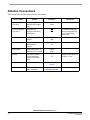
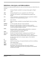
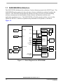
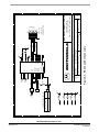
1
56F8323
Evaluation Module User Manual
56F8300
16-bit Digital Signal Controllers
MC56F8323EVMUM
Rev. 2
07/2005
freescale.com
Document Revision History
Version History
Description of Change
Rev 1.0
Initial Public Release
Rev 2.0
Updated look and feel
TABLE OF CONTENTS
Preface Preface-vii
Chapter 1
Introduction
1.1
1.2
1.3
56F8323EVM Architecture. . . . . . . . . . . . . . . . . . . . . . . . . . . . . . . . . . . . . . . . . . . . . . . 1-2
56F8323EVM Configuration Jumpers . . . . . . . . . . . . . . . . . . . . . . . . . . . . . . . . . . . . . . 1-3
56F8323EVM Connections. . . . . . . . . . . . . . . . . . . . . . . . . . . . . . . . . . . . . . . . . . . . . . . 1-5
Chapter 2
Technical Summary
2.1
56F8323. . . . . . . . . . . . . . . . . . . . . . . . . . . . . . . . . . . . . . . . . . . . . . . . . . . . . . . . . . . . . . 2-3
2.2
RS-232 Serial Communications . . . . . . . . . . . . . . . . . . . . . . . . . . . . . . . . . . . . . . . . . . . 2-4
2.3
Debug Support . . . . . . . . . . . . . . . . . . . . . . . . . . . . . . . . . . . . . . . . . . . . . . . . . . . . . . . . 2-8
2.3.1
JTAG Connector . . . . . . . . . . . . . . . . . . . . . . . . . . . . . . . . . . . . . . . . . . . . . . . . . . . . 2-8
2.3.2
Parallel JTAG Interface Connector . . . . . . . . . . . . . . . . . . . . . . . . . . . . . . . . . . . . . . 2-9
2.4
External Interrupts. . . . . . . . . . . . . . . . . . . . . . . . . . . . . . . . . . . . . . . . . . . . . . . . . . . . . 2-11
2.5
Reset . . . . . . . . . . . . . . . . . . . . . . . . . . . . . . . . . . . . . . . . . . . . . . . . . . . . . . . . . . . . . . . 2-11
2.6
Power Supply . . . . . . . . . . . . . . . . . . . . . . . . . . . . . . . . . . . . . . . . . . . . . . . . . . . . . . . . 2-12
2.7
Daughter Card Connectors . . . . . . . . . . . . . . . . . . . . . . . . . . . . . . . . . . . . . . . . . . . . . . 2-14
2.7.1
Peripheral Daughter Card Expansion Connector. . . . . . . . . . . . . . . . . . . . . . . . . . . 2-14
2.7.2
Memory Daughter Card Expansion Connector . . . . . . . . . . . . . . . . . . . . . . . . . . . . 2-17
2.8
Serial 10-bit 4-channel D/A Converter (Optional) . . . . . . . . . . . . . . . . . . . . . . . . . . . . 2-19
2.9
Motor Control PWM Signals and LEDs . . . . . . . . . . . . . . . . . . . . . . . . . . . . . . . . . . . . 2-20
2.10 CAN Interface . . . . . . . . . . . . . . . . . . . . . . . . . . . . . . . . . . . . . . . . . . . . . . . . . . . . . . . . 2-21
2.11 Software Feature Jumpers . . . . . . . . . . . . . . . . . . . . . . . . . . . . . . . . . . . . . . . . . . . . . . . 2-22
2.12 Peripheral Expansion Connectors . . . . . . . . . . . . . . . . . . . . . . . . . . . . . . . . . . . . . . . . . 2-23
2.12.1
PWM Port A Expansion Connector. . . . . . . . . . . . . . . . . . . . . . . . . . . . . . . . . . . . . 2-23
2.12.2
Serial Peripheral Interface #0 Expansion Connector. . . . . . . . . . . . . . . . . . . . . . . . 2-24
2.12.3
Serial Peripheral Interface #1 Expansion Connector. . . . . . . . . . . . . . . . . . . . . . . . 2-24
2.12.4
Serial Communications Port #0 Expansion Connector . . . . . . . . . . . . . . . . . . . . . . 2-25
2.12.5
Serial Communications Port #1 Expansion Connector . . . . . . . . . . . . . . . . . . . . . . 2-25
2.12.6
Encoder #0 / Quad Timer Channel A Expansion Connector. . . . . . . . . . . . . . . . . . 2-26
2.12.7
Timer Channel C Expansion Connector . . . . . . . . . . . . . . . . . . . . . . . . . . . . . . . . . 2-26
2.12.8
FlexCAN Expansion Connector . . . . . . . . . . . . . . . . . . . . . . . . . . . . . . . . . . . . . . . 2-27
2.12.9
A/D Port A Expansion Connector . . . . . . . . . . . . . . . . . . . . . . . . . . . . . . . . . . . . . . 2-27
Table of Contents, Rev. 2
Freescale Semiconductor
Preliminary
i
2.12.10 GPIO Port A Expansion Connector. . . . . . . . . . . . . . . . . . . . . . . . . . . . . . . . . . . . .
2.12.11 GPIO Port B Expansion Connector . . . . . . . . . . . . . . . . . . . . . . . . . . . . . . . . . . . . .
2.12.12 GPIO Port C Expansion Connector . . . . . . . . . . . . . . . . . . . . . . . . . . . . . . . . . . . . .
2.12.13 IRQA / RESET / CLOCK Expansion Connector . . . . . . . . . . . . . . . . . . . . . . . . . .
2.13 Test Points. . . . . . . . . . . . . . . . . . . . . . . . . . . . . . . . . . . . . . . . . . . . . . . . . . . . . . . . . . .
2-28
2-29
2-29
2-30
2-30
Appendix A
56F8323EVM Schematics
Appendix B
56F8323EVM Bill of Material
MC56F8323EVM User Manual, Rev. 2
ii
Freescale Semiconductor
Preliminary
LIST OF FIGURES
1-1
Block Diagram of the 56F8323EVM . . . . . . . . . . . . . . . . . . . . . . . . . . . . . . . . . . . . 1-2
1-2
56F8323EVM Jumper Reference . . . . . . . . . . . . . . . . . . . . . . . . . . . . . . . . . . . . . . . 1-3
1-3
Connecting the 56F8323EVM Cables . . . . . . . . . . . . . . . . . . . . . . . . . . . . . . . . . . . . 1-5
2-1
Schematic Diagram of the RS-232 Interface . . . . . . . . . . . . . . . . . . . . . . . . . . . . . . . 2-4
2-2
Schematic Diagram of the Clock Interface . . . . . . . . . . . . . . . . . . . . . . . . . . . . . . . . 2-6
2-3
Schematic Diagram of the Debug LED Interface . . . . . . . . . . . . . . . . . . . . . . . . . . . 2-7
2-4
Block Diagram of the Parallel JTAG Interface . . . . . . . . . . . . . . . . . . . . . . . . . . . . . 2-9
2-5
Schematic Diagram of the User Interrupt Interface. . . . . . . . . . . . . . . . . . . . . . . . . 2-11
2-6
Schematic Diagram of the RESET Interface . . . . . . . . . . . . . . . . . . . . . . . . . . . . . . 2-11
2-7
Schematic Diagram of the Power Supply . . . . . . . . . . . . . . . . . . . . . . . . . . . . . . . . 2-13
2-8
Serial 10-bit, 4-Channel D/A Converter . . . . . . . . . . . . . . . . . . . . . . . . . . . . . . . . . 2-19
2-9
PWM Interface and LEDs . . . . . . . . . . . . . . . . . . . . . . . . . . . . . . . . . . . . . . . . . . . . 2-20
2-10
CAN Interface . . . . . . . . . . . . . . . . . . . . . . . . . . . . . . . . . . . . . . . . . . . . . . . . . . . . . 2-21
2-11
Software Feature Jumpers . . . . . . . . . . . . . . . . . . . . . . . . . . . . . . . . . . . . . . . . . . . . 2-22
2-12
Typical Analog Input RC Filter. . . . . . . . . . . . . . . . . . . . . . . . . . . . . . . . . . . . . . . . 2-28
List of Figures, Rev. 2
Freescale Semiconductor
Preliminary
iii
MC56F8323EVM User Manual, Rev. 2
iv
Freescale Semiconductor
Preliminary
LIST OF TABLES
1-1
56F8323EVM Default Jumper Options . . . . . . . . . . . . . . . . . . . . . . . . . . . . . . . . 1-4
2-1
Flow Control Header Options . . . . . . . . . . . . . . . . . . . . . . . . . . . . . . . . . . . . . . . 2-4
2-2
SCI1 Jumper Options . . . . . . . . . . . . . . . . . . . . . . . . . . . . . . . . . . . . . . . . . . . . . . 2-5
2-3
RS-232 Serial Connector Description . . . . . . . . . . . . . . . . . . . . . . . . . . . . . . . . . 2-5
2-4
LED Control. . . . . . . . . . . . . . . . . . . . . . . . . . . . . . . . . . . . . . . . . . . . . . . . . . . . . 2-6
2-5
JTAG Connector Description. . . . . . . . . . . . . . . . . . . . . . . . . . . . . . . . . . . . . . . . 2-8
2-6
Parallel JTAG Interface Disable Jumper Selection . . . . . . . . . . . . . . . . . . . . . . . 2-8
2-7
Parallel JTAG Interface Connector Description . . . . . . . . . . . . . . . . . . . . . . . . 2-10
2-8
Parallel JTAG Interface Voltage Selection Jumper . . . . . . . . . . . . . . . . . . . . . . 2-10
2-9
Peripheral Daughter Card Connector Description . . . . . . . . . . . . . . . . . . . . . . . 2-14
2-10
Memory Daughter Card Connector Description . . . . . . . . . . . . . . . . . . . . . . . . 2-17
2-11
D/A Header Description. . . . . . . . . . . . . . . . . . . . . . . . . . . . . . . . . . . . . . . . . . . 2-19
2-12
CAN Signal Isolation Jumper Options. . . . . . . . . . . . . . . . . . . . . . . . . . . . . . . . 2-21
2-13
CAN Header Description . . . . . . . . . . . . . . . . . . . . . . . . . . . . . . . . . . . . . . . . . . 2-22
2-14
PWM Port A Connector Description . . . . . . . . . . . . . . . . . . . . . . . . . . . . . . . . . 2-23
2-15
SPI #0 Connector Description . . . . . . . . . . . . . . . . . . . . . . . . . . . . . . . . . . . . . . 2-24
2-16
SPI #1 Connector Description . . . . . . . . . . . . . . . . . . . . . . . . . . . . . . . . . . . . . . 2-24
2-17
SCI #0 Connector Description . . . . . . . . . . . . . . . . . . . . . . . . . . . . . . . . . . . . . . 2-25
2-18
SCI #1 Connector Description . . . . . . . . . . . . . . . . . . . . . . . . . . . . . . . . . . . . . . 2-25
2-19
Timer A Signal Connector Description . . . . . . . . . . . . . . . . . . . . . . . . . . . . . . . 2-26
2-20
Timer Channel C Connector Description. . . . . . . . . . . . . . . . . . . . . . . . . . . . . . 2-26
2-21
CAN Connector Description . . . . . . . . . . . . . . . . . . . . . . . . . . . . . . . . . . . . . . . 2-27
2-22
A/D Port A Connector Description . . . . . . . . . . . . . . . . . . . . . . . . . . . . . . . . . . 2-27
2-23
GPIO Port A Connector Description . . . . . . . . . . . . . . . . . . . . . . . . . . . . . . . . . 2-28
2-24
GPIO Port B Connector Description . . . . . . . . . . . . . . . . . . . . . . . . . . . . . . . . . 2-29
2-25
GPIO Port C Connector Description . . . . . . . . . . . . . . . . . . . . . . . . . . . . . . . . . 2-29
2-26
IRQA / RESET / CLOCK Connector Description. . . . . . . . . . . . . . . . . . . . . . . 2-30
List of Tables, Rev. 2
Freescale Semiconductor
Preliminary
v
MC56F8323EVM User Manual, Rev. 2
vi
Freescale Semiconductor
Preliminary
Preface
This reference manual describes in detail the hardware on the 56F8323 Evaluation
Module.
Audience
This document is intended for application developers who are creating software for
devices using the Freescale 56F8323 part.
Organization
This manual is organized into two chapters and two appendixes.
•
Chapter 1, Introduction - provides an overview of the EVM and its features.
•
Chapter 2, Technical Summary - describes in detail the 56F8323EVM hardware.
•
Appendix A, 56F8323EVM Schematics - contains the schematics of the
56F8323EVM.
•
Appendix B, 56F8323EVM Bill of Material - provides a list of the materials used on
the 56F8323EVM board.
Suggested Reading
More documentation on the 56F8323 and the 56F8323EVM kit may be found at URL:
www.freescale.com
Preface, Rev. 2
Freescale Semiconductor
Preliminary
vii
Notation Conventions
This manual uses the following notational conventions:
Term or Value
Symbol
Examples
Active High Signals
(Logic One)
No special symbol
attached to the signal
name
A0
CLKO
Active Low Signals
(Logic Zero)
Noted with an
overbar in text and in
most figures
WE
OE
Hexadecimal Values
Begin with a “$”
symbol
Decimal Values
No special symbol
attached to the
number
Binary Values
Begin with the letter “b”
attached to the number
Numbers
Considered positive
unless specifically
noted as a negative
value
Blue Text
Linkable on-line
Bold
Reference sources,
paths, emphasis
Exceptions
In schematic drawings,
Active Low Signals may
be noted by a backslash: /WE
$0FF0
$80
10
34
b1010
b0011
5
-10
Voltage is often shown as
positive: +3.3V
...refer to Chapter 7,
License
...see:
www.freescale.com
MC56F8323EVM User Manual, Rev. 2
viii
Freescale Semiconductor
Preliminary
Definitions, Acronyms, and Abbreviations
Definitions, acronyms and abbreviations for terms used in this document are defined below for
reference.
A/D
Analog-to-Digital; a method of converting Analog signals to Digital
values
ADC
Analog-to-Digital Converter; a peripheral on the 56F8323 part
CAN
Controller Area Network; a serial communications peripheral and
method
CiA
CAN in Automation; an international CAN user’s group that coordinates
standards for CAN communications protocols
CTS
Clear To Send
D/A
Digital-to-Analog; a method of converting Digital values to an Analog
form
56F8323
A 16-bit controller with motor control peripherals
EOnCE
Enhanced On-Chip Emulation; a debug bus and port created by
Freescale to enable a designer to create a low-cost hardware interface for
a professional-quality debug environment
EVM
Evaluation Module; a hardware platform which allows a customer to
evaluate the silicon and develop his application
Flash
Nonvolatile Random Access Memory
FlexCAN
Flexible CAN Interface Module; a peripheral on the 56F8323 part
GPIO
General Purpose Input and Output port on Freescale’s family of
controllers; does not share pin functionallity with any other peripheral on
the chip and can only be set as an input, output, or level-sensitive
interrupt input
IC
Integrated Circuit
JTAG
Joint Test Action Group; a bus protocol/interface used for test and debug
LED
Light Emitting Diode
LQFP
MPIO
Low-profile Quad Flat Package
Multi-Purpose Input and Output port on Freescale’s family of
controllers; shares package pins with other peripherals on the chip and
can function as a GPIO
Preface, Rev. 2
Freescale Semiconductor
Preliminary
ix
OnCE
On-Chip Emulation, a debug bus and port created by Freescale to allow a
means for low-cost hardware which provides a professional-quality
debug environment
PCB
Printed Circuit Board
PLL
Phase Locked Loop
PWM
Quad Dec
Pulse Width Modulation
Quadrature Decoder; a peripheral on the 56F8323 part
RAM
Random Access Memory
R/C
Resistor/Capacitor Network
SRAM
Static Random Access Memory
RTS
Request to Send
SCI
Serial Communications Interface; a peripherial on Freescale’s family of
controllers
SPI
Serial Peripheral Interface; a peripheral on Freescale’s family of
controllers
UART
WS
Universal Asynchronous Receiver/Transmitter
Wait State
References
The following sources were referenced to produce this manual:
[1] DSP56800E Reference Manual, DSP56800ERM; Freescale Semiconductor
[2] 56F8300 Peripheral User Manual, MC56F8300UM; Freescale Semiconductor
[3] 56F8323 Technical Data, MC56F8323; Freescale Semiconductor
[4] CiA Draft Recommendation DR-303-1, Cabling and Connector Pin Assignment,
Version 1.0, CAN in Automation
[5] CAN Specification 2.0B, BOSCH or CAN in Automation
MC56F8323EVM User Manual, Rev. 2
x
Freescale Semiconductor
Preliminary
Chapter 1
Introduction
The 56F8323EVM is used to demonstrate the abilities of the 56F8323 and to provide a hardware
tool allowing the development of applications that use the 56F8323.
The 56F8323EVM is an evaluation module board that includes an 56F8323 part, peripheral
expansion connectors, a CAN interface, an RS-232 interface, a JTAG-to-PC Printer port interface
and a pair of daughter card connectors. The peripheral expansion connectors and daughter card
expansion connectors are for signal monitoring and allow expansion for user features.
The 56F8323EVM is designed for the following purposes:
•
•
•
Allowing new users to become familiar with the features of the 56800E architecture. The
tools and examples provided with the 56F8323EVM facilitate evaluation of the feature set
and the benefits of the family.
Serving as a platform for real-time software development. The tool suite enables the user
to develop and simulate routines, download the software to on-chip SRAM or Flash, run
it, and debug it using a debugger via the JTAG/Enhanced OnCE (EOnCE) port. The
breakpoint features of the EOnCE port enable the user to easily specify complex break
conditions and to execute user-developed software at full speed until the break conditions
are satisfied. The ability to examine and modify all user-accessible registers, memory and
peripherals through the EOnCE port greatly facilitates the task of the developer.
Serving as a platform for hardware development. The hardware platform enables the user
to connect external hardware peripherals. The on-board peripherals can be disabled,
providing the user with the ability to reassign any and all of the controller's peripherals.
The EOnCE port's unobtrusive design means that all memory on the Processor is available
to the user.
Introduction, Rev. 2
Freescale Semiconductor
Preliminary
1-1
1.1 56F8323EVM Architecture
The 56F8323EVM facilitates the evaluation of various features present in the 56F8323 part. The
56F8323EVM can be used to develop real-time software and hardware products based on the
56F8323. The 56F8323EVM provides the features necessary for a user to write and debug
software, demonstrate the functionality of that software and interface with the user's
application-specific device(s). The 56F8323EVM is flexible enough to allow a user to fully
exploit the 56F8323's features to optimize the performance of his product, as shown in
Figure 1-1.
56F8323
Optional
8.00MHz
Crystal
Reset Logic
XTAL/EXTAL
SPI #0
4-Channel
10-Bit D/A
D/A
Header
SCI #1
RS-232
Interface
DSub
9-Pin
RESET
SCI #0
Timer C
Timer A
PWMA
ADCA
QuadDec #0
FlexCAN
JTAG
Connector
DSub
25-Pin
JTAG / EOnCE
Parallel
JTAG
Interface
Peripheral
Expansion
Connectors
CAN Interface
CAN Bus
Header
Debug LEDs
CAN Bus
Daisy Chain
PWM LEDs
+3.3V & GND
+3.3VA & AGND
+3.0VREF
Peripheral
Daughter Card
Connector
Power Supply
+3.3V, +3.3VA,
+5V & +3.0VA
Figure 1-1. Block Diagram of the 56F8323EVM
MC56F8323EVM User Manual, Rev. 2
1-2
Freescale Semiconductor
Preliminary
56F8323EVM Configuration Jumpers
1.2 56F8323EVM Configuration Jumpers
Fifteen jumper groups, (JG1-JG15), shown in Figure 1-2, are used to configure various features
on the 56F8323EVM board. Table 1-1 describes the default jumper group settings.
JG10
4 3
JG15
JG2
1
JG1
JG12
3
2 1
1
3
J8
J7
J15
J10
J12
JG7
1
J5
J15
JG10 J13
Y1
MC56F8323EVM
JG1 JG2
JG12
J2
U1
JG11
JG5
JG8
J4
P2
JG3
J3
JG14
J6
U3
LED3
JG3
JTAG
JG6
JG9
JG13
JG4
3 1
JG11
J19
J14
PC0
PC1
PC2
PC3
PC4
PC5
JG7
JG8
J18
J21
J1
PWMA0
PWMA1
PWMA2
PWMA3
PWMA4
PWMA5
3
J16
J17
S/N
J9
J11
S2
S1
IRQA
RESET
U9
U10
P1
P3
JG5
4 2
JG9
JG14
JG4
JG13
JG6
1
3
Figure 1-2. 56F8323EVM Jumper Reference
Introduction, Rev. 2
Freescale Semiconductor
Preliminary
1-3
Table 1-1. 56F8323EVM Default Jumper Options
Jumper
Group
Comment
Jumpers
Connections
JG1
Connect on-board 8.0MHz crystal input to EXTAL signal
1–2
JG2
Connect on-board 8.0MHz crystal input to XTAL signal
1–2
JG3
Enable on-board Parallel JTAG Host/Target Interface
NC
JG4
Enable RS-232 output
NC
JG5
Pass RXD1 & TXD1 signals to RS-232 level converter
JG6
Pass Temperature Diode signal to ANA7 input
1–2
JG7
Set user Jumper #0 to a 1 value
1–2
JG8
Set user Jumper #1 to a 1 value
1–2
JG9
SPI #0 Daisy Chain (Optional--not populated on board by default)
NC
JG10
CAN bus termination selected
1–2
JG11
Connect Analog Ground to Digital Ground
NC
JG12
Enable on-chip regulator
1–2
JG13
Pass RTS to CTS
1–2
JG14
Select +3.3V operation of on-board Parallel JTAG Host/Target Interface
1–2
JG15
Pass CAN_TX & CAN_RX signals to CAN tranceiver
1–2 & 3–4
1–2 & 3–4
MC56F8323EVM User Manual, Rev. 2
1-4
Freescale Semiconductor
Preliminary
56F8323EVM Connections
1.3 56F8323EVM Connections
An interconnection diagram is shown in Figure 1-3 for connecting the PC and the external
+12.0V DC/AC power supply to the 56F8323EVM board.
Parallel Extension
Cable
56F8323EVM
PC
P1
Connect cable
to Parallel / Printer port
P3
External with 2.1mm,
+12V receptacle
Power connector
Figure 1-3. Connecting the 56F8323EVM Cables
Perform the following steps to connect the 56F8323EVM cables:
1. Connect the parallel extension cable to the Parallel port of the host computer.
2. Connect the other end of the parallel extension cable to P1, shown in Figure 1-3, on the
56F8323EVM board. This connection allows the host computer to control the board.
3. Make sure that the external +12V DC, 1.2A power supply is not plugged into a +120V AC
power source.
4. Connect the 2.1mm output power plug from the external power supply into P3, shown in
Figure 1-3, on the 56F8323EVM board.
5. Apply power to the external power supply. The green Power-On LED, LED13, will
illuminate when power is correctly applied.
Introduction, Rev. 2
Freescale Semiconductor
Preliminary
1-5
MC56F8323EVM User Manual, Rev. 2
1-6
Freescale Semiconductor
Preliminary
Chapter 2
Technical Summary
The 56F8323EVM is designed as a versatile Flash-based microcontroller development card for
developing real-time software and hardware products to support a new generation of applications
in servo and motor control; digital and wireless messaging; digital answering machines; feature
phones; modems; and digital cameras. The power of the 16-bit 56F8323, combined with the
on-board RS-232 interface, CAN interface, Daughter Card Expansion interface and parallel
JTAG interface, makes the 56F8323EVM ideal for developing and implementing many motor
controlling algorithms, as well as for learning the architecture and instruction set of the 56F8323
processor.
The main features of the 56F8323EVM, with board and schematic reference designators, include:
•
MC56F8323, a 16-bit +3.3V/+2.5V processor in a 64-pin LQFP package operating at
60MHz [U1]
•
8.00MHz crystal oscillator for processor frequency generation [Y1]
•
Optional external oscillator frequency input connectors [JG1 and JG2]
•
Joint Test Action Group (JTAG) port interface connector for an external debug Host
Target Interface [J3]
•
On-board Parallel JTAG Host Target Interface, with a connector for a PC printer port
cable [P1], including a disable jumper [JG3]
•
On-board Parallel JTAG Host Taget Interface voltage level selector [JG14]
•
RS-232 interface for easy connection to a host processor [U3 and P2], with a disable
jumper [JG4]
•
RS-232 RTS and CTS signal connector [JG13]
•
CAN interface for high speed, 1.0Mbps, FlexCAN communications [U8 and J12]
•
CAN bypass and bus termination [J13 and JG10]
•
CAN signal to CAN transceiver isolation connector [JG15]
•
Peripheral Daughter Card Expansion Connector, which allows the user to attach his own
SCI, SPI, PWM, Quad Decoder or GPIO-compatible peripherals to the Processor [J1]
Technical Summary, Rev. 2
Freescale Semiconductor
Preliminary
2-1
•
Memory Daughter Card Expansion Connector, which allows the user to attach additonal
power and grounds[J2]
•
Connector which allows the user to attach his own SCI #0 / MPIO-compatible peripheral
[J21]
•
Connector which allows the user to attach his own SCI #1 / MPIO-compatible peripheral
[J17]
•
Connector which allows the user to attach his own SPI #0 / MPIO-compatible peripheral
[J8]
•
Connector which allows the user to attach his own SPI #1 / MPIO-compatible peripheral
[J15]
•
Connector which allows the user to attach his own PWMA-compatible peripheral [J5]
•
Connector which allows the user to attach his own CAN physical layer peripheral [J10]
•
Connector which allows the user to attach his own Timer A / Encoder #0-compatible
peripheral [J7]
•
Connector which allows the user to attach his own Timer C-compatible peripheral [J9]
•
Connector which allows the user to attach his own A/D port A-compatible peripheral [J6]
•
Connector which allows the user to attach his own peripheral to GPIO Port A [J16]
•
Connector which allows the user to attach his own peripheral to GPIO Port B [J18]
•
Connector which allows the user to attach his own peripheral to GPIO Port C [J19]
•
On-board power regulation from an external +12V DC-supplied power input [P3]
•
Light Emitting Diode (LED) power indicator [LED13]
•
Six on-board LEDs allow real-time debugging of user programs [LED1-6]
•
Six on-board Port A PWM monitoring LEDs [LED7-12]
•
Internal (OCR_DIS) Core Regulator selector [JG12]
•
Temperature Sense Diode-to-ANA7 selector [JG6]
•
Manual RESET push-button [S1]
•
Manual interrupt push-button for IRQA [S2]
•
General purpose jumper on GPIO PB3 [JG7]
•
General purpose jumper on GPIO PB0 [JG8]
•
Optional 4-Channel 10-bit Serial D/A, SPI for real-time user data display [U5]
MC56F8323EVM User Manual, Rev. 2
2-2
Freescale Semiconductor
Preliminary
56F8323
2.1 56F8323
The 56F8323EVM uses a Freescale MC56F8323 part, designated as U1 on the board and in the
schematics. This part will operate at a maximum external bus speed of 60MHz. A full description
of the 56F8323, including functionality and user information, is provided in these documents:
•
56F8323 Technical Data Sheet, (MC56F8323): Electrical and timing specifications, pin
descriptions, device specific peripheral information and package descriptions (this
document)
•
56F8300 Peripheral User Manual, (MC56F8300UM): Detailed description of peripherals
of the 56F8300 family of devices
•
DSP56800E Reference Manual, (DSP56800ERM): Detailed description of the 56800E
family architecture, 16-bit core processor, and the instruction set
Refer to these documents for detailed information about chip functionality and operation. They
can be found on this URL:
www.freescale.com
Technical Summary, Rev. 2
Freescale Semiconductor
Preliminary
2-3
2.2 RS-232 Serial Communications
The 56F8323EVM provides an RS-232 interface by the use of an RS-232 level converter, Maxim
MAX3245EEAI, designated as U3. Refer to the RS-232 schematic diagram in Figure 2-1. The
RS-232 level converter transitions the SCI UART’s +3.3V signal levels to RS-232-compatible
signal levels and connects to the host’s serial port via connector P2. Flow control is not provided,
but could be implemented using uncommitted GPIO signals and connected to the RTS and CTS
signals on JG13; see Table 2-1. The SCI1 port signals can be isolated from the RS-232 level
converter by removing the jumpers in JG5; reference Table 2-2. The pin-out of connector P2 is
detailed in Table 2-3. The RS-232 level converter/transceiver can be disabled by placing a
jumper at JG4.
RS-232
Level Converter
Interface
56F8323
P2
JG5
TXD1
1
3
RXD1
T1in
2
4
R1out
JG13
RTS 1
CTS
T1out
R1in
T2in
2
R2out
R2in
T2out
+3.3V
x
1
6
2
7
3
8
4
9
5
FORCEOFF
Jumper Removed:
Enable RS-232
Jumper Pin 1-2:
Disable RS-232
JG4
1
2
Figure 2-1. Schematic Diagram of the RS-232 Interface
Table 2-1. Flow Control Header Options
JG13
Pin #
Signal
1
RTS to Transceiver
2
CTS from Transceiver
MC56F8323EVM User Manual, Rev. 2
2-4
Freescale Semiconductor
Preliminary
RS-232 Serial Communications
Table 2-2. SCI1 Jumper Options
JG5
Pin #
Signal
Pin #
Signal
1
TXD1
2
TXD to RS-232 Transceiver
3
RXD1
4
RXD from RS-232 Transceiver
Table 2-3. RS-232 Serial Connector Description
P2
Pin #
Signal
Pin #
Signal
1
Jumper to 6 & 4
6
Jumper to 1 & 4
2
TXD
7
CTS
3
RXD
8
RTS
4
Jumper to 1 & 6
9
NC
5
GND
The 56F8323EVM uses on-chip 8.00MHz relaxation oscillator or the on-board 8.00MHz crystal,
Y1, connected to its External Crystal Inputs, EXTAL and XTAL. To achieve its maximum
internal operating frequency, the 56F8323 uses its internal PLL to multiply this input clock
frequency. Additionally an external oscillator source can be connected to the device by using the
oscillator bypass connectors, JG1 and JG2; see Figure 2-2. If the input frequency is above
8MHz, then the EXTAL input should be jumpered to ground by adding a jumper between JG1
pins 2 and 3. The input frequency would then be injected on JG2’s pin 2. If the input frequency is
below 4MHz, then the input frequency can be injected on JG1’s pin 2.
Technical Summary, Rev. 2
Freescale Semiconductor
Preliminary
2-5
EXTERNAL
OSCILLATOR
HEADERS
56F8323
JG1
1
EXTAL
2
3
8.00MHz
JG2
1
XTAL
2
Figure 2-2. Schematic Diagram of the Clock Interface
Six on-board Light-Emitting Diodes, (LEDs), are provided to allow real-time debugging for user
programs. These LEDs will allow the programmer to monitor program execution without having
to stop the program during debugging; refer to Figure 2-3. Table 2-4 describes the control of
each LED.
Table 2-4. LED Control
Controlled by
User LED
Color
Signal
LED1
RED
GPIO Port C Bit 0
LED2
YELLOW
GPIO Port C Bit 1
LED3
GREEN
GPIO Port C Bit 2
LED4
RED
GPIO Port C Bit 3
LED5
YELLOW
GPIO Port C Bit 4
LED6
GREEN
GPIO Port C Bit 5
MC56F8323EVM User Manual, Rev. 2
2-6
Freescale Semiconductor
Preliminary
RS-232 Serial Communications
Setting PC0, PC1, PC2, PC3, PC4 or PC5 to a Logic One value will turn on the associated LED.
56F8323
INVERTING BUFFER
+3.3V
RED LED
PC0
YELLOW LED
PC1
GREEN LED
PC2
RED LED
PC3
YELLOW LED
PC4
GREEN LED
PC5
Figure 2-3. Schematic Diagram of the Debug LED Interface
Technical Summary, Rev. 2
Freescale Semiconductor
Preliminary
2-7
2.3 Debug Support
The 56F8323EVM provides an on-board Parallel JTAG Host Target Interface and a JTAG
interface connector for external Target Interface support. Two interface connectors are provided
to support each of these debugging approaches. These two connectors are designated the JTAG
connector and the Host Parallel Interface Connector.
2.3.1 JTAG Connector
The JTAG connector on the 56F8323EVM allows the connection of an external Host Target
Interface for downloading programs and working with the 56F8323’s registers. This connector is
used to communicate with an external Host Target Interface which passes information and data
back and forth with a host processor running a debugger program. Table 2-5 shows the pin-out
for this connector.
Table 2-5. JTAG Connector Description
J3
Pin #
Signal
Pin #
Signal
1
TDI
2
GND
3
TDO
4
GND
5
TCK
6
GND
7
NC
8
KEY
9
RESET
10
TMS
11
+3.3V
12
NC
13
DE
14
TRST
When this connector is used with an external Host Target Interface, the parallel JTAG interface
should be disabled by placing a jumper in jumper block JG3. Refer to Table 2-6 for this jumper’s
selection options.
Table 2-6. Parallel JTAG Interface Disable Jumper Selection
JG3
Comment
No jumpers
Enable On-board Parallel JTAG Interface
1–2
Disable on-board Parallel JTAG Interface
MC56F8323EVM User Manual, Rev. 2
2-8
Freescale Semiconductor
Preliminary
Debug Support
2.3.2 Parallel JTAG Interface Connector
The Parallel JTAG Interface Connector, P1, allows the 56F8323 to communicate with a Parallel
Printer Port on a Windows PC; reference Figure 2-4. Using this connector, the user can
download programs and work with the 56F8323’s registers. Table 2-7 shows the pin-out for this
connector. When using the parallel JTAG interface, the jumper at JG3 should be removed, as
shown in Table 2-6. A jumper at JG14 selects the Parallel Printer Port’s interface voltage
between +3.3V and +5.0V; see Table 2-8.
DB-25 Connector
56F8323
Parallel JTAG Interface
IN
OUT
P_TRST
IN
OUT
IN
OUT
TMS
IN
OUT
TMS
TDI
TDO
TDI
TDO
TRST
TCK
IN
OUT
TCK
P_RESET
IN
OUT
RESET
P_DE
IN
OUT
DE
+3.3V
Jumper Removed:
Enable JTAG I/F
JG3
EN
1
2
Jumper Pin 1-2:
Disable JTAG I/F
Figure 2-4. Block Diagram of the Parallel JTAG Interface
Technical Summary, Rev. 2
Freescale Semiconductor
Preliminary
2-9
Table 2-7. Parallel JTAG Interface Connector Description
P1
Pin #
Signal
Pin #
Signal
1
NC
14
NC
2
PORT_RESET
15
PORT_IDENT
3
PORT_TMS
16
N/C
4
PORT_TCK
17
N/C
5
PORT_TDI
18
GND
6
PORT_TRST
19
GND
7
PORT_DE
20
GND
8
PORT_IDENT
21
GND
9
PORT_VCC
22
GND
10
NC
23
GND
11
PORT_TDO
24
GND
12
NC
25
GND
13
PORT_CONNECT
Table 2-8. Parallel JTAG Interface Voltage Selection Jumper
JG14
Comment
1–2
+3.3V Parallel Printer Port
Interface
2–3
+5.0V Parallel Printer Port
Interface
MC56F8323EVM User Manual, Rev. 2
2-10
Freescale Semiconductor
Preliminary
Reset
2.4 External Interrupts
One on-board push-button switch is provided for external interrupt generation, as shown in
Figure 2-5. S2 allows the user to generate a hardware interrupt for signal line IRQA. This switch
allows the user to generate interrupts for user-specific programs.
+3.3V
56F8323
10K
S2
IRQA
0.1µF
Figure 2-5. Schematic Diagram of the User Interrupt Interface
2.5 Reset
Logic is provided on the 56F8323 to generate an internal Power-On RESET. Additional reset
logic is provided to support the RESET signals from the JTAG connector, the Parallel JTAG
Interface and the user RESET push-button, S1; refer to Figure 2-6.
JTAG_RESET
RESET
RESET
PUSHBUTTON
MANUAL RESET
S1
JTAG_TAP_RESET
TRST
Figure 2-6. Schematic Diagram of the RESET Interface
Technical Summary, Rev. 2
Freescale Semiconductor
Preliminary
2-11
2.6 Power Supply
The main power input to the 56F8323EVM, +12V DC at 1.2A, is through a 2.1mm coax power
jack. This input power is rectified to provide a DC supply input. This allows a user the option to
use a +12V AC power supply. A 1.2Amp power supply is provided with the 56F8323EVM;
however, less than 500mA is required by the EVM. The remaining current is available for custom
control applications when connected to the Daughter Card connectors. The 56F8323EVM
provides +5.0V DC regulation for the CAN interface and additional regulators. The
56F8323EVM provides +3.3V DC voltage regulation for the processor, memory, D/A, ADC,
parallel JTAG interface and supporting logic; refer to Figure 2-7. Additional voltage regulation
logic provides a low noise +3.0V DC voltage reference to the controller’s A/D VREFH.
Optionally, the processor’s A/D VREFH voltage can be provided by the +3.3VA supply on the
board by removing U15 and adding a 10 ohm resistor at R83. A jumper, JG11, and resistor, R68,
are provided to allow the analog and digital grounds to be isolated on the 56F8323EVM board.
This allows the analog ground reference point to be provided on a custom board attached to the
56F8323EVM’s Daughter Card connectors. By removing R68, the AGND reference is
disconnected from the 56F8323EVM’s digital ground. By placing a jumper in JG11 or by
reinstalling R68, the AGND is reconnected to the 56F8323EVM’s digital ground. Power applied
to the 56F8323EVM is indicated with a Power-On LED, referenced as LED13. Optionally, the
user can provide the +2.5 DC voltage needed by the controller’s core on connector J14 and
disable the on-chip CORE voltage regulator by removing the jumper on JG12. Additonally, four
0 ohm resistors or shorting wires must be added at R70, R71, R72 and R73, to allow the external
+2.5V DC to pass to the 56F8323.
MC56F8323EVM User Manual, Rev. 2
2-12
Freescale Semiconductor
Preliminary
Power Supply
+12V DC/AC
P3
Input
Bridge
Rectifier
+5.0V
Regulator
Power
Condition
+5.0V DC
+3.3V
Regulator
+3.3V DC
CAN
56F8323
VDD_IO & PLL
56F8323EVM
Parts
J14
+2.5V DC
Ext In
1
R70-R73
56F8323
VDD Core
+3.3VA DC
56F8323
ADCA
2
Power On
+3.3V
Regulator
U15
+3.0V
Regulator
R67
10Ω
+3.0VA DC
56F8323
VREFH
Figure 2-7. Schematic Diagram of the Power Supply
Technical Summary, Rev. 2
Freescale Semiconductor
Preliminary
2-13
2.7 Daughter Card Connectors
The EVM board contains two daughter card expansion connectors. One connector, J1, contains
the processor’s peripheral port signals. The second connector, J2, contains addional power and
ground signals.
2.7.1 Peripheral Daughter Card Expansion Connector
The processor’s peripheral port signals are connected to the Peripheral Daughter Card Expansion
connector, J1. The Peripheral Daughter Card connector is used to connect a user-specific
daughter card to the processor’s peripheral port signals. The Peripheral Port Daughter Card
connector is a 100-pin high-density connector with signals for the IRQs, RESET, SPI, SCI,
PWM, ADC and Quad Timer ports. Table 2-9 shows the Peripheral Daughter Card connector’s
signal-to-pin assignments.
Table 2-9. Peripheral Daughter Card Connector Description
J1
Pin #
Signal
Pin #
Signal
1
+12V
2
+12V
3
GND
4
GND
5
+5.0V
6
+5.0V
7
GND
8
GND
9
+3.3V
10
+3.3V
11
GND
12
GND
13
NC
14
NC
15
NC
16
NC
17
GND
18
GND
19
PHASEA0 / PB7 / TA0
20
PHASEB0 / PB6 / TA1
21
INDEX0 / PB5 / TA2
22
HOME0 / PB4 / TA3
23
TC0
24
SS0
25
TC0
26
SS0
27
TC1
28
MISO0
MC56F8323EVM User Manual, Rev. 2
2-14
Freescale Semiconductor
Preliminary
Daughter Card Connectors
Table 2-9. Peripheral Daughter Card Connector Description (Continued)
J1
Pin #
Signal
Pin #
Signal
29
IRQA
30
NC
31
TC1
32
TC3
33
PWMA0
34
PWMA1
35
PWMA2
36
PWMA3
37
PWMA4
38
PWMA5
39
GND
40
GND
41
ISA0
42
ISA1
43
ISA2
44
GND
45
FAULTA1
46
FAULTA0
47
NC
48
FAULTA2
49
GND
50
GND
51
NC
52
MISO0
53
NC
54
NC
55
NC
56
NC
57
GND
58
GND
59
NC
60
NC
61
NC
62
SS0
63
NC
64
NC
65
NC
66
NC
67
MOSI0
68
SS0
69
TC0
70
TC1
71
SCLK0
72
TC0
73
CAN_TX
74
CAN_RX
75
MOSI0
76
MISO0
77
SCLK0
78
SS0
Technical Summary, Rev. 2
Freescale Semiconductor
Preliminary
2-15
Table 2-9. Peripheral Daughter Card Connector Description (Continued)
J1
Pin #
Signal
Pin #
Signal
79
GND
80
GND
81
+VREFH
82
+VREFH
83
GNDA
84
GNDA
85
NC
86
NC
87
NC
88
NC
89
NC
90
NC
91
NC
92
NC
93
AN0
94
AN1
95
AN2
96
AN3
97
AN4
98
AN5
99
AN6
100
AN7
MC56F8323EVM User Manual, Rev. 2
2-16
Freescale Semiconductor
Preliminary
Daughter Card Connectors
2.7.2 Memory Daughter Card Expansion Connector
Additional power and ground signals are connected to the Memory Daughter Card Expansion
connector, J2. Table 2-10 shows the port signal-to-pin assignments.
Table 2-10. Memory Daughter Card Connector Description
J2
Pin #
Signal
Pin #
Signal
1
NC
2
NC
3
NC
4
NC
5
NC
6
NC
7
NC
8
NC
9
GND
10
GND
11
NC
12
NC
13
NC
14
NC
15
NC
16
NC
17
NC
18
NC
19
GND
20
GND
21
GND
22
GND
23
NC
24
NC
25
NC
26
NC
27
NC
28
NC
29
NC
30
NC
31
GND
32
GND
33
GND
34
GND
35
NC
36
NC
37
NC
38
NC
39
NC
40
NC
41
NC
42
NC
Technical Summary, Rev. 2
Freescale Semiconductor
Preliminary
2-17
Table 2-10. Memory Daughter Card Connector Description (Continued)
J2
Pin #
Signal
Pin #
Signal
43
GND
44
GND
45
NC
46
NC
47
NC
48
NC
49
NC
50
NC
51
NC
52
GND
53
GND
54
GND
55
+3.3V
56
+3.3V
57
GND
58
GND
59
+5.0V
60
+5.0V
MC56F8323EVM User Manual, Rev. 2
2-18
Freescale Semiconductor
Preliminary
Serial 10-bit 4-channel D/A Converter (Optional)
2.8 Serial 10-bit 4-channel D/A Converter (Optional)
The 56F8323EVM board contains the provions for a user to provide a serial 10-bit, 4-channel
D/A converter connected to the 56F8323’s SPI #0 port. The output pins are uncommitted and are
connected to a 4x2 header, J4, to allow easy user connections. Refer to Figure 2-8 for the D/A
connections and Table 2-11 for the header’s pin-out. The D/A’s output full-scale range value can
be set to a value from +0.0V to +2.4V by a trimpot, R48. If this trimpot is preset to +2.05V, it
would provide approximately +2mV per step. If another device must be used with SPI #0’s
MISO signal and with the D/A converter on the board, the daisy chain jumper, JG9, can be used
to extend or isolate the serial chain.
56F8323
D/A Connector
MAX5251
MOSI0
MISO0
SCLK0
JG9
2 1
DIN
D/A 0
1
2
DOUT
D/A 1
3
4
D/A 2
5
6
D/A 3
7
8
SCLK
SS0
CS
RSTO
CL
VREF
+3.3VA
R48
Figure 2-8. Serial 10-bit, 4-Channel D/A Converter
Table 2-11. D/A Header Description
J4
Pin #
Signal
Pin #
Signal
1
D/A Channel 0
2
AGND
3
D/A Channel 1
4
AGND
5
D/A Channel 2
6
AGND
7
D/A Channel 3
8
AGND
Technical Summary, Rev. 2
Freescale Semiconductor
Preliminary
2-19
2.9 Motor Control PWM Signals and LEDs
The 56F8323 has one PWM unit. This unit contains six PWM output signals, three Fault input
signals and three Phase Current sense inputs. The PWM signals are connected to a set of six
PWM LEDs via inverting buffers. The buffers are used to isolate and drive the processor’s PWM
outputs to the PWM LEDs. The PWM LEDs indicate the status of PWM signals; refer to
Figure 2-9. Additionally, the PWM signals are routed out to a header, J5, and to the peripheral
daughter card connector, J1, for easy use by the end user.
56F8323
PWMA0
PWMA0
PWMA1
PWMA1
PWMA2
PWMA2
PWMA3
PWMA3
PWMA4
PWMA4
PWMA5
PWMA5
+3.3V
LED
Buffer
Yellow LED
LED7
Green LED
LED8
Yellow LED
LED9
Green LED
LED10
Yellow LED
LED11
Phase C Top
Green LED
LED12
Phase C Bottom
Phase A Top
Phase A Bottom
Phase B Top
Phase B Bottom
Figure 2-9. PWM Interface and LEDs
MC56F8323EVM User Manual, Rev. 2
2-20
Freescale Semiconductor
Preliminary
CAN Interface
2.10 CAN Interface
The 56F8323EVM board contains a CAN physical-layer interface chip that is attached to the
FlexCAN port’s CAN_RX and CAN_TX pins on the 56F8323. The EVM board uses a Philips
high-speed, 1.0Mbps, physical layer interface chip, PCA82C250. Due to the +5.0V operating
voltage of the CAN interface chip, a pull-up to +5.0V is required to level shift the Transmit Data
output line from the 56F8323. The CAN_TX and CAN_RX signals from the processor can be
isolated by the connector at JG15; see Table 2-12. The CANH and CANL signals pass through
inductors before attaching to the CAN bus connectors. A primary, J12, and daisy chain, J13,
CAN connectors are provided to allow easy daisy chaining of CAN devices. CAN bus
termination of 120 ohms can be provided by adding a jumper to JG10. Refer to Table 2-13 for
the CAN connector signals and to Figure 2-10 for a connection diagram.
+5.0V
56F8323
JG15
CAN_TX
CAN_RX
1
3
1K
CAN Transceiver
2
TXD
4
J12
CANH
4
CANL
3
CAN Bus
Connector
5
RXD
J13
PCA82C250T
Daisy Chain CAN
Connector
4
5
3
JG10
1
2
CAN Bus
Terminator
120
Figure 2-10. CAN Interface
Table 2-12. CAN Signal Isolation Jumper Options
JG15
Pin #
Signal
Pin #
Signal
1
CAN_TX
2
CAN_TX to CAN Transceiver
3
CAN_RX
4
CAN_RX from CAN Transceiver
Technical Summary, Rev. 2
Freescale Semiconductor
Preliminary
2-21
Table 2-13. CAN Header Description
J12 and J13
Pin #
Signal
Pin #
Signal
1
NC
2
NC
3
CANL
4
CANH
5
GND
6
NC
7
NC
8
NC
9
NC
10
NC
2.11 Software Feature Jumpers
The 56F8323EVM board contains two software feature jumpers that allow the user to select
“user-defined” software features. Two GPIO port pins, PB3 and PB0, are pulled high or low with
10K ohm resistors on JG7 and JG8, respectively. Attaching a jumper between pins 1 and 2 will
place a high, or 1, on the port pin. Attaching a jumper between pins 2 and 3 will place a low, or 0,
on the port pin; see Figure 2-11.
56F8323
JG7
SCLK0 / PB3
2
1
10K
+3.3V
User Jumper
#0
3
10K
JG8
SS0 / PB0
2
1
10K
+3.3V
3
User Jumper
#1
10K
Figure 2-11. Software Feature Jumpers
MC56F8323EVM User Manual, Rev. 2
2-22
Freescale Semiconductor
Preliminary
Peripheral Expansion Connectors
2.12 Peripheral Expansion Connectors
The EVM board contains a group of Peripheral Expansion Connectors used to gain access to the
resources of the 56F8323. The following signal groups have expansion connectors:
•
•
•
•
•
•
•
•
•
•
•
•
•
PWM Port A
Serial Peripheral Interface Port #0
Serial Peripheral Interface Port #1
Serial Communications Port 0
Serial Communications Port 1
Encoder #0 / Timer Channel A
Timer Channel C
FlexCAN Port
A/D Input Port A
GPIO Port A
GPIO Port B
GPIO Port C
IRQA / RESET / CLOCK
2.12.1 PWM Port A Expansion Connector
The PWM port A is attached to this connector. Refer to Table 2-14 for connection information.
Table 2-14. PWM Port A Connector Description
J5
Pin #
Signal
Pin #
Signal
1
PWMA0 / PA0
2
PWMA1 / PA1
3
PWMA2 / PA2 / SS1
4
PWMA3 / PA3 / MISO1
5
PWMA4 / PA4 / MOSI1
6
PWMA5 / PA5 / SCLK1
7
FAULTA0 / PA6
8
FAULTA1 / PA7
9
FAULTA2 / PA8
10
NC
11
ISA0 / PA9
12
ISA1 / PA10
13
ISA2/PA11
14
GND
Technical Summary, Rev. 2
Freescale Semiconductor
Preliminary
2-23
2.12.2 Serial Peripheral Interface #0 Expansion Connector
The Serial Peripheral Interface #0 is an MPIO port attached to this connector. This port can be
configured as a Serial Peripheral Interface or as a General Purpose I/O port. Refer to Table 2-15
for connection information.
Table 2-15. SPI #0 Connector Description
J8
Pin #
Signal
Pin #
Signal
1
MOSI0 / PB2
2
MISO0 / PB1 / RXD1
3
SCLK0 / PB3
4
SS0 / PB0 / TXD1
5
GND
6
+3.3V
2.12.3 Serial Peripheral Interface #1 Expansion Connector
The Serial Peripheral Interface #1 is an MPIO port attached to this connector. This port can be
configured as a Serial Peripheral Interface or as a General Purpose I/O port. Refer to Table 2-16
for the connection information.
Table 2-16. SPI #1 Connector Description
J15
Pin #
Signal
Pin #
Signal
1
MOSI1 / PWMA4
2
MISO1 / PWMA3
3
SCLK1 / PWMA5
4
SS1 / PWMA2
5
GND
6
+3.3V
MC56F8323EVM User Manual, Rev. 2
2-24
Freescale Semiconductor
Preliminary
Peripheral Expansion Connectors
2.12.4 Serial Communications Port #0 Expansion Connector
The Serial Communications Port #0 is an MPIO port attached to the SCI #0 expansion connector.
This port can be configured as a Serial Communications Interface or as Timer Port C channels.
Refer to Table 2-17 for connection information.
Table 2-17. SCI #0 Connector Description
J21
Pin #
Signal
Pin #
Signal
1
TXD0 / TC0
2
RXD0 / TC1
3
GND
4
+3.3V
5
GND
6
+5.0V
2.12.5 Serial Communications Port #1 Expansion Connector
The Serial Communications Port #1 is an MPIO port attached to the SCI #0 expansion connector.
This port can be configured as a Serial Communications Interface or as SPI0 signals. Refer to
Table 2-18 for connection information.
Table 2-18. SCI #1 Connector Description
J17
Pin #
Signal
Pin #
Signal
1
TXD1 / SS0
2
RXD1 / MISO0
3
GND
4
+3.3V
5
GND
6
+5.0V
Technical Summary, Rev. 2
Freescale Semiconductor
Preliminary
2-25
2.12.6 Encoder #0 / Quad Timer Channel A Expansion Connector
The Encoder #0 / Quad Timer Channel A port is an MPIO port attached to the Timer A expansion
connector. This port can be configured as a Quadrature Decoder interface port, as a Quad Timer
port, or as GPIO. Refer to Table 2-19 for the signals attached to the connector.
Table 2-19. Timer A Signal Connector Description
J7
Pin #
Signal
Pin #
Signal
1
PHASEA0 / TA0 / PB7
2
PHASEB0 / TA1 / PB6
3
INDEX0 / TA2 / PB5
4
HOME0 / TA3 / PB4
5
GND
6
+3.3V
2.12.7 Timer Channel C Expansion Connector
The Timer Channel C port is an MPIO port attached to the Timer C expansion connector. This
port can be configured as a Quad Timer Interface, as SCI0 signals, or as GPIO. Refer to
Table 2-20 for the signals attached to the connector.
Table 2-20. Timer Channel C Connector Description
J9
Pin #
Signal
Pin #
Signal
1
TC0 / TXD0 / PC6
2
TC1 / RXD0 / TC5
3
GND
4
TC3 / PC4
MC56F8323EVM User Manual, Rev. 2
2-26
Freescale Semiconductor
Preliminary
Peripheral Expansion Connectors
2.12.8 FlexCAN Expansion Connector
The FlexCAN port is an MPIO port attached to the FlexCAN expansion connector. This port can
be configured as a FlexCAN Interface or as GPIO. Refer to Table 2-21 for connection
information.
Table 2-21. CAN Connector Description
J10
Pin #
Signal
Pin #
Signal
1
CAN_TX / PC3
2
GND
3
CAN_RX / PC2
4
GND
2.12.9 A/D Port A Expansion Connector
The 8-channel Analog-to-Digital conversion port A is attached to this connector. Refer to
Table 2-22 for connection information. There is an RC network on each of the Analog Port A
input signals; see Figure 2-12.
Table 2-22. A/D Port A Connector Description
J6
Pin #
Signal
Pin #
Signal
1
AN0
2
AN1
3
AN2
4
AN3
5
AN4
6
AN5
7
AN6
8
AN7
9
GNDA
10
+VREFH
Technical Summary, Rev. 2
Freescale Semiconductor
Preliminary
2-27
100 ohm
Analog Input
To Controller Analog Port
0.0022µF
Figure 2-12. Typical Analog Input RC Filter
2.12.10 GPIO Port A Expansion Connector
The GPIO port A is attached to this connector. Refer to Table 2-23 for connection information.
Table 2-23. GPIO Port A Connector Description
J16
Pin #
Signal
Pin #
Signal
1
PA0 / PWMA0
2
PA1 / PWMA1
3
PA2 / PWMA2 / SS1
4
PA3 / MISO1 / PWMA3
5
PA4 / PWMA4 / MOSI1
6
PA5 / SCLK1 / PWMA5
7
PA6 / FAULTA0
8
PA7 / FAULTA1
9
PA8 / FAULTA2
10
PA9 / ISA0
11
PA10 / ISA1
12
PA11 / ISA2
13
GND
14
+3.3V
MC56F8323EVM User Manual, Rev. 2
2-28
Freescale Semiconductor
Preliminary
Peripheral Expansion Connectors
2.12.11 GPIO Port B Expansion Connector
The GPIO port B is attached to this connector. Refer to Table 2-24 for connection information.
Table 2-24. GPIO Port B Connector Description
J18
Pin #
Signal
Pin #
Signal
1
PB0 / SS0
2
PB1 / MISO0
3
PB2 / MOSI0
4
PB3 / SCLK0
5
PB4 / HOME0
6
PB5 / INDEX0
7
PB6 / PHASEB0
8
PB7 / PHASEA0
9
GND
10
+3.3V
2.12.12 GPIO Port C Expansion Connector
The GPIO port C is attached to this connector. Refer to Table 2-25 for connection information.
Table 2-25. GPIO Port C Connector Description
J19
Pin #
Signal
Pin #
Signal
1
PC0 / EXTAL
2
PC1 / XTAL
3
PC2 / CAN_RX
4
PC3 / CAN_TX
5
PC4 / TC3
6
PC5 / TC1
7
PC6 / TC0
8
NC
9
GND
10
+3.3V
Technical Summary, Rev. 2
Freescale Semiconductor
Preliminary
2-29
2.12.13 IRQA / RESET / CLOCK Expansion Connector
The IRQA / RESET / CLOCK signals are attached to this connector. Refer to Table 2-26 for
connection information.
Table 2-26. IRQA / RESET / CLOCK Connector Description
J11
Pin #
Signal
Pin #
Signal
1
IRQA
2
RESET
3
EXTAL / PC0
4
XTAL / PC1
9
GND
10
+3.3V
2.13 Test Points
The 56F8323EVM board has a total of eleven test points:
•
•
•
•
•
•
Analog Ground (AGND) [TP4]
Four Digital Grounds (GND) [TP1, TP2, TP3 & TP10]
Two +3.3V [TP6 & TP11]
+3.3VA [TP5]
Two +5.0V [TP7 & TP8]
+12V [TP9]
MC56F8323EVM User Manual, Rev. 2
2-30
Freescale Semiconductor
Preliminary
Appendix A
56F8323EVM Schematics
56F8323EVM Schematics, Rev. 2
Freescale Semiconductor
Preliminary
Appendix A-1
MC56F8323EVM User Manual, Rev. 2
Appendix A-2
Freescale Semiconductor
Preliminary
1
2
3
4
C1
2.2uF
1
2
JG12
C3
2.2uF
A
C4
2.2uF
OCR_DIS
+3.3V
R74
1K
C2
2.2uF
VCAP1
VCAP2
VCAP3
VCAP4
11
17
44
60
57
23
5
43
OCR_DIS 45
VDD_IO1 6
VDD_IO2 20
VDD_IO3 48
VDD_IO4 59
40
42
55
56
53
58
54
47
46
12
2
62
61
1
64
63
22
24
25
21
B
VSS_IO1
VSS_IO2
VSS_IO3
VSS_IO4
VCAP1
VCAP2
VCAP3
VCAP4
OCR_DIS
VDD_IO1
VDD_IO2
VDD_IO3
VDD_IO4
VREFH
DISABLE REGULATOR
ENABLE REGULATOR
N/C
1-2
B
ANA0
ANA1
ANA2
ANA3
ANA4
ANA5
ANA6
ANA7
C6
0.1uF
0 Ohm
VREFP
VREFM
VREFN
VA
R80
TEMP_SENSE
C
R76
+3.3VA
0 Ohm
R79
0 Ohm
R78
0 Ohm
R77
0 Ohm
+3.3V
DNP
DNP
DNP
DNP
47K
R17
47K
R16
47K
R15
0 Ohm
R73
0 Ohm
R72
0 Ohm
R71
0 Ohm
R70
VDDcore
Sheet
1
E
of
13
1.1
Rev.
FAX: (480) 413-2510
2100 East Elliot Road
Tempe, Arizona 85284
(480) 413-5090
Designer: DSPO Design
D
FAULTA2
FAULTA1
FAULTA0
VCAP4
VCAP3
VCAP2
VCAP1
E
DSP Standard Products Division
Single trace
to GNDA
C42
100pF
ANA7
VDD_IO4
VDD_IO3
VDD_IO2
VDD_IO1
D
Single trace
to GNDA
C8
0.1uF
C41
0.001uF
2
1
JG6
MC56F8323EVM.DSN
Date: Monday, May 12, 2003
Document
Number
C7
0.1uF
C5
0.1uF
ANA0
ANA1
ANA2
ANA3
ANA4
ANA5
ANA6
ANA7
PHASEA0
PHASEB0
INDEX0
HOME0
PWMA0
PWMA1
PWMA2
PWMA3
PWMA4
PWMA5
ISA0
ISA1
ISA2
FAULTA0
FAULTA1
FAULTA2
MC56F8323 Processor
38
37
36
35
39
41
34
26
27
28
29
30
31
32
33
52
51
50
49
3
4
7
8
9
10
16
18
19
13
14
15
C
Figure A-1. 56F8323 Processor
A
Size
Title
VREFLO
VREFP
VREFMID
VREFN
VSSA_ADC
VDDA_ADC
TEMP_SENSE
MC56F8323FG60
VDAA_OSC_PLL
TDI
TDO
TCK
TRST
TMS
MISO0/RXD1/PB1
PWMA0/PA0
MOSI0/PB2
PWMA1/PA1
SCLK0/PB3
PWMA2/SS1/PA2
SS0/TXD1/PB0
PWMA3/MISO1/PA3
PWMA4/MOSI1/PA4
TC0/TXD0/PC6 PWMA5/SCLK1/PA5
ISA0/PA9
TC1/RXD0/PC5
ISA1/PA10
TC3/PC4
ISA2/PA11
CAN_TX/PC3
FAULTA0/PA6
CAN_RX/PC2
FAULTA1/PA7
FAULTA2/PA8
IRQA
PHA0/TA0/PB7
RESET
PHB0/TA1/PB6
INDEX0/TA2/PB5
XTAL/PC1
HOME0/TA3/PB4
EXTAL/PC0
U1
ON-CHIP CORE REGULATOR
+VREFH
+3.3V_PLL
TDI
TDO
TCK
/TRST
TMS
XTAL
EXTAL
/IRQA
/RESET
CAN_TX
CAN_RX
TC0
TC1
TC3
MISO0
MOSI0
SCLK0
/SS0
A
1
2
3
4
56F8323EVM Schematics, Rev. 2
Freescale Semiconductor
Preliminary
Appendix A-3
1
2
3
4
A
A
+3.3V
Y1
8.00MHz
2
3
1
RST
DS1818
DNP
GND
Vcc
U2
OPTIONAL
2
DS1818
3
S1
1
/POR
RESET PUSHBUTTON
1M
R14
1
2
3
JG1
GPIOC0
B
C
1K
R26
10K
R25
D
1
2
3
JG7
User
Jumper
#0
1K
R28
10K
R27
User
Jumper
#1
D
/IRQA
E
E
of
13
1.1
Rev.
FAX: (480) 413-2510
Sheet 2
(480) 413-5090
2100 East Elliot Road
Tempe, Arizona 85284
DSP Standard Products Division
C9
0.1uF
R24
10K
+3.3V
1
2
3
JG8
Designer: DSPO Design
S2
IRQA PUSHBUTTON
GPIOB0
+3.3V
SOFTWARE FEATURE JUMPERS
GPIOB3
+3.3V
MC56F8323EVM.DSN
Date: Monday, May 12, 2003
Document
Number
/SS0
SCLK0
Figure A-2. Reset, Clock & IRQ
A
Size
C
RESET, CLOCK & IRQ
XTAL
EXTAL
/POR
Title
GPIOC1
R23
10K
+3.3V
1
2
JG2
OSC BYPASS
B
1
2
3
4
MC56F8323EVM User Manual, Rev. 2
Appendix A-4
Freescale Semiconductor
Preliminary
1
2
3
4
/SS0
MISO0
A
R5IN
R4IN
R3IN
T3IN
/EN
1K
R36
1K
R35
1K
R34
1K
R32
1K
R30
1 - 2
RS-232 DISABLE
2
4
1
2
JG13
1
3
JG5
1
2
JG4
RTS/CTS
+3.3V
N/C
RS-232 ENABLE
RS-232 SHUTDOWN JUMPER
A
C33
1.0uF
C32
1.0uF
A
Size
Title
/EN
1
1
1
1
T3IN
GND
V+
V-
VCC
INVALID
R1IN
R2IN
R3IN
R4IN
R5IN
T1OUT
T2OUT
T3OUT
MAX3245EEAI
FORCEOFF
FORCEON
R2OUTB
R1OUT
R2OUT
R3OUT
R4OUT
R5OUT
T1IN
T2IN
T3IN
C2-
C1C2+
C1+
U3
21
4
5
6
7
8
9
10
11
25
27
3
26
1
R3IN
R4IN
R5IN
1
C35
1.0uF
1.0uF
C34
+3.3V
MC56F8323EVM.DSN
C
Date: Monday, May 12, 2003
Document
Number
RS-232 AND SCI CONNECTORS
22
23
20
19
18
17
16
15
14
13
12
2
24
1
28
C
D
D
1
6
2
7
3
8
4
9
5
P2
DCD
DSR
TXD
CTS
RXD
RTS
DTR
E
E
of
13
1.1
Rev.
FAX: (480) 413-2510
Sheet 3
(480) 413-5090
2100 East Elliot Road
Tempe, Arizona 85284
DSP Standard Products Division
SCI #1
RS-232
CONNECTOR
Designer: DSPO Design
CTS
RXD
RTS
TXD
Figure A-3. RS-232 and SCI Connectors
B
R29
1K
+3.3V
RTS1
CTS1
TXD1
RXD1
B
1
2
3
4
56F8323EVM Schematics, Rev. 2
Freescale Semiconductor
Preliminary
Appendix A-5
1
2
3
4
A
A
MISO0
B
5.1K
DNP
R58
/RESET
/SS0
SCLK0
A
Size
Title
11
14
7
8
10
12
9
20
U5
AGND
UP0
FBD
OUTD
OUTC
FBC
REFCD
REFAB
FBB
OUTB
OUTA
FBA
2
1
13
19
18
17
16
15
6
5
4
3
1
+Vref
MC56F8323EVM.DSN
C
Date: Monday, May 12, 2003
Document
Number
D
+Vref
D/A0
D/A1
D/A2
D/A3
J4
2
4
6
8
Sheet 4
E
of
13
1.1
Rev.
FAX: (480) 413-2510
2100 East Elliot Road
Tempe, Arizona 85284
(480) 413-5090
Designer: DSPO Design
D
E
DSP Standard Products Division
R48
1K POT
DNP
+3.3VA
DNP
1
3
5
7
SERIAL D/A CONNECTOR
Set to 2.7V
DEBUG SERIAL 4-CHANNEL D/A CONVERTER
MAX5251BEAP
DNP
DGND
PDL
CL
CS
SCLK
DOUT
DIN
VDD
OPTIONAL
C
Figure A-4. Debug Serial 4-Channel D/A Converter
+3.3V
DNP
SPI0
DAISYCHAIN
1
2
JG9
+3.3V
MOSI0
B
1
2
3
4
MC56F8323EVM User Manual, Rev. 2
Appendix A-6
Freescale Semiconductor
Preliminary
1
2
3
4
A
A
PWMA5
PWMA4
PWMA3
PWMA2
PWMA1
PWMA0
B
13
PA5
12
10
8
6
4
2
270
R12
270
R11
270
R10
270
R9
270
R8
270
R7
C
LED12
LED11
LED10
LED9
LED8
LED7
D
PWM STATE
LEDS
D
Sheet 5
E
of
13
1.1
Rev.
FAX: (480) 413-2510
2100 East Elliot Road
Tempe, Arizona 85284
(480) 413-5090
Designer: DSPO Design
GREEN LED
YELLOW LED
GREEN LED
YELLOW LED
GREEN LED
E
DSP Standard Products Division
+3.3V
YELLOW LED
MC56F8323EVM.DSN
Date: Monday, May 12, 2003
Document
Number
PWM PORT A STATE LEDS
74AC04
U6F
74AC04
U6E
74AC04
U6D
74AC04
U6C
74AC04
U6B
74AC04
U6A
C
Figure A-5. PWM Port A State LEDs
A
Size
Title
11
PA4
5
PA2
9
3
PA1
PA3
1
PA0
B
1
2
3
4
56F8323EVM Schematics, Rev. 2
Freescale Semiconductor
Preliminary
Appendix A-7
1
2
3
4
A
A
TC1
TC3
CAN_TX
CAN_RX
XTAL
EXTAL
B
13
11
PC4
PC5
9
5
PC2
PC3
3
1
PC1
PC0
B
270
R6
270
R5
270
R4
270
R3
270
R2
270
R1
C
+3.3V
D
D
E
E
of
13
1.1
Rev.
FAX: (480) 413-2510
Sheet 6
(480) 413-5090
2100 East Elliot Road
Tempe, Arizona 85284
DSP Standard Products Division
USER
LEDS
Designer: DSPO Design
GREEN LED
YELLOW LED
RED LED
GREEN LED
YELLOW LED
RED LED
MC56F8323EVM.DSN
LED6
LED5
LED4
LED3
LED2
LED1
Date: Monday, May 12, 2003
Document
Number
USER DEBUG LEDS
12
10
8
6
4
2
Figure A-6. User Debug LEDs
A
Size
Title
74AC04
U7F
74AC04
U7E
74AC04
U7D
74AC04
U7C
74AC04
U7B
74AC04
U7A
C
1
2
3
4
MC56F8323EVM User Manual, Rev. 2
Appendix A-8
Freescale Semiconductor
Preliminary
1
2
3
4
A
/IRQA
EXTAL
AN0
AN2
AN4
AN6
PC0
PB2
PB3
J5
J8
1
3
5
J11
2
4
6
SPI #0
1
3
5
2
4
6
2
4
6
8
10
12
14
PWMA
1
3
5
7
9
11
13
2
4
6
8
10
A/D PORT A
1
3
5
7
9
J6
IRQ, RESET
& CLOCK
PA0
PA2/SS1
PA4/MOSI1
PA6
PA8
PA9
PA11
MOSI0
SCLK0
PWMA0
PWMA2
PWMA4
FAULTA0
FAULTA2
ISA0
ISA2
A
PC1
ISA1
PWMA1
PWMA3
PWMA5
FAULTA1
AN1
AN3
AN5
AN7
+VREFH
/RESET
XTAL
+3.3V
MISO0
/SS0
+3.3V
PB1/RXD1
PB0/TXD1
PA1
PA3/MISO1
PA5/SCLK1
PA7
Spare
1
PA10
B
J15
2
4
6
2
4
6
1
3
J10
2
4
SCI #1
1
3
5
J17
SPI #1
1
3
5
RXD1
MISO1
/SS1
CAN
& GPIO PORT C
PC3
PC2
TXD1
MOSI1
SCLK1
MISO0
+3.3V
+5.0V
PWMA3
PWMA2
+3.3V
C
TC0
TC0
PHASEA0
INDEX0
PWMA0
PWMA2
PWMA4
FAULTA0
FAULTA2
ISA1
C
J16
1
3
5
7
9
11
13
2
4
6
8
10
12
14
PA1
PA3
PA5
PA7
PA9
PA11
2
4
6
J9
1
3
2
4
TXD0
J21
2
4
6
SCI #0
1
3
5
B
Size
Title
RXD0
TC1
TC3
D
EXTAL
CAN_RX
TC3
TC0
/SS0
MOSI0
HOME0
PHASEB0
PC0
PC2
PC4
PC6
PB0
PB2
PB4
PB6
MC56F8323EVM.DSN
D
Date: Monday, May 12, 2003
Document
Number
2
4
6
8
10
2
4
6
8
10
XTAL
CAN_TX
TC1
1
+3.3V
MISO0
SCLK0
INDEX0
PHASEA0
+3.3V
PC1
PC3
PC5
Spare
PB1
PB3
PB5
PB7
E
E
of 13
1.1
Rev.
FAX: (480) 413-2510
Sheet 7
(480) 413-5090
2100 East Elliot Road
Tempe, Arizona 85284
DSP Standard Products Division
GPIO PORT C
1
3
5
7
9
J19
GPIO PORT B
1
3
5
7
9
J18
Designer: DSPO Design
DSP PORT EXPANSION CONNECTORS
TC1
+3.3V
+5.0V
PC5/RXD0
PC4
TIMER CHANNEL C
& SCI #0
PC6/TXD0
PWMA1
PWMA3
PWMA5
FAULTA1
ISA0
ISA2
PHASEB0
HOME0
+3.3V
+3.3V
PB6/TA1
PB4/TA3
QUAD DECODER #0
& TIMER CHANNEL A
1
3
5
J7
GPIO PORT A
PB7/TA0
PB5/TA2
PA0
PA2
PA4
PA6
PA8
PA10
Figure A-7. Port Expansion Connectors
CAN_TX
CAN_RX
/SS0
PWMA4
PWMA5
B
1
2
3
4
56F8323EVM Schematics, Rev. 2
Freescale Semiconductor
Preliminary
Appendix A-9
1
2
3
4
PB2
PC6
PB3
PC5
PC6
GNDA
GND
GND
TD0
GND
GND
GND
GND
GND
GND
TA0
TA2
GND
TXD0
RXD0
GND
GND
GND
J1
1
3
5
7
9
11
13
15
17
19
21
23
25
27
29
31
33
35
37
39
41
43
45
47
49
51
53
55
57
59
61
63
65
67
69
71
73
75
77
79
81
83
85
87
89
91
93
95
97
99
2
4
6
8
10
12
14
16
18
20
22
24
26
28
30
32
34
36
38
40
42
44
46
48
50
52
54
56
58
60
62
64
66
68
70
72
74
76
78
80
82
84
86
88
90
92
94
96
98
100
+12V
PB1
PC4
PB0
+3.3V
+5.0V
GNDA
GND
GND
TD1
AN1
AN3
AN5
AN7
+VREFH
PB0
PC5
GND PB0/TXD1
GND
GND
GND
GND
GND
GND
TA1
TA3
GND
TXD1
RXD1
GND
GND
GND
B
A
A
Size
Title
/SS0
TC1
TC0
CAN_RX
MISO0
/SS0
/SS0
MISO0
FAULTA0
FAULTA2
ISA1
TC3
PWMA1
PWMA3
PWMA5
PHASEB0
HOME0
/SS0
/SS0
MISO0
GND
GNDA
MC56F8323EVM.DSN
C
Date: Monday, May 12, 2003
Document
Number
J2
1
3
5
7
9
11
13
15
17
19
21
23
25
27
29
31
33
35
37
39
41
43
45
47
49
51
53
55
57
59
2
4
6
8
10
12
14
16
18
20
22
24
26
28
30
32
34
36
38
40
42
44
46
48
50
52
54
56
58
60
GND
GND
GND
GND
GND
GND
GND
GND
GND
D
+3.3V
+5.0V
D
E
E
of
13
1.1
Rev.
FAX: (480) 413-2510
Sheet 8
(480) 413-5090
2100 East Elliot Road
Tempe, Arizona 85284
DSP Standard Products Division
Designer: DSPO Design
GND
Daughter Address/Data Connector
+5.0V
+3.3V
GND
GND
GND
GND
GND
GND
GND
DAUGHTER CARD CONNECTOR
C
Figure A-8. Daughter Card Connectors
B
Daughter Peripheral Port Connector
AN0
AN2
AN4
AN6
+VREFH
MOSI0
TC0
SCLK0
CAN_TX
MOSI0
SCLK0
ISA0
ISA2
FAULTA1
PHASEA0
INDEX0
TC0
TC0
TC1
/IRQA
TC1
PWMA0
PWMA2
PWMA4
+3.3V
+5.0V
+12V
A
1
2
3
4
MC56F8323EVM User Manual, Rev. 2
Appendix A-10
Freescale Semiconductor
Preliminary
1
2
3
4
A
CAN_TX
CAN_RX
1 2
3 4
CAN Select
JG15
B
U8
GND
CANH
CANL
VCC
VREF
PCA82C250T
SLOPE
TXD
RXD
BCANH
B
2
4
6
8
10
BCANH
MC56F8323EVM.DSN
C
Date: Saturday, June 28, 2003
Document
Number
L1
R38
120
1/4W
1
2
JG10
D
CAN BUS
TERMINATION
E
E
of
13
1.1
Rev.
FAX: (480) 413-2510
Sheet 9
(480) 413-5090
2100 East Elliot Road
Tempe, Arizona 85284
DSP Standard Products Division
BCANL
BCANH
BCANH
BCANL
D
Designer: DSPO Design
Figure A-9. High-Speed CAN Interface
A
Size
CANH
CANL
1
+5.0V
HIGH-SPEED CAN INTERFACE
BCANL
J13
1
3
5
7
9
2
4
6
8
10
2
7
6
3
5
C
DAISY-CHAIN
CAN BUS CONNECTOR
8
1
4
J12
Title
R37
1K
+5.0V
1
3
5
7
9
CAN BUS CONNECTOR
BCANL
A
1
2
3
4
56F8323EVM Schematics, Rev. 2
1
2
3
4
A
A
P_RESET
R22
47K
25
24
23
22
21
20
19
18
17
16
15
14
5.1K
R47
13
12
11
10
9
8
7
6
5
4
3
2
1
Q1
2N2222A
R46
5.1K
+3.3V
B
PORT_CONNECT
PORT_PU
PORT_TDO
PORT_VCC
PORT_DE
R56
+3.3V
51 Ohm
/J_RESET
51 Ohm
R57
+5.0V
5.1K
JG14 +Vsel
1
2
3
8
PORT_TDI
GND
2G
1G
2A4
2A3
2Y2
2Y1
1Y4
1Y3
1Y2
1Y1
R81
C
U11B
74AC00
1K
DNP
R82
1K
13
0 Ohm
R55
0 Ohm
R54
0 Ohm
R51
74AC00
JG3
+3.3V
0 Ohm
R53
0 Ohm
R52
1
11
6
B
Size
Title
R45
5.1K
20
1
19
3
5
7
11
8
6
4
2
GND
2A4
2A3
2A2
2Y1
1Y4
1Y3
1Y2
1Y1
TCK
TDO
TDI
+3.3V
MC74LCX244DW
VCC
1G
2G
2Y4
2Y3
2Y2
2A1
1A4
1A3
1A2
1A1
U10
D
/DE
PWR
TDO
P_DE
14
12
10
8
6
4
2
KEY
/J_TRST
TMS
P_DE
/J_TRST
/DE
PWR
TDO
MC56F8323EVM.DSN
D
Date: Friday, June 20, 2003
Document
Number
5.1K
R44
47K
R21
47K
R20
47K
R19
47K
R18
+3.3V
(480) 413-5090
Designer: DSPO Design
E
Sheet 10 of 13
1.1
Rev.
FAX: (480) 413-2510
2100 East Elliot Road
Tempe, Arizona 85284
DSP Standard Products Division
JTAG Connector
13
11
9
7
5
3
1
J3
/J_TRST
TDI
TCK
TMS
P_RESET
/J_RESET
10
17
15
13
9
12
14
16
18
E
PARALLEL JTAG HOST TARGET INTERFACE AND JTAG CONNECTOR
/TRST
/RESET
On-Board
Host Target Interface
Disable
R43
5.1K
U11D
12
5
4
R42
5.1K
74AC00
+Vsel
1
U11C
8
3
10
19
1
17
15
7
9
12
14
16
18
74AC00
U11A
PORT_PU
10
9
2
1
MC74HC244DW
2Y4
2Y3
VCC
2A2
2A1
1A4
1A3
1A2
1A1
PORT_CONNECT
/J_TRST
/POR
/J_RESET
3
5
20
13
11
6
PORT_TCK
R41
4
PORT_TMS
/PORT_TRST
2
PORT_RESET
U9
Parallel JTAG Interface
C
Figure A-10. Parallel JTAG Host Target Interface and JTAG Connector
P1
PORT_IDENT
B
2
1
Freescale Semiconductor
Preliminary
Appendix A-11
1
2
3
4
MC56F8323EVM User Manual, Rev. 2
Appendix A-12
Freescale Semiconductor
Preliminary
1
2
3
4
A
A
AN3
AN2
AN1
AN0
100
R65
100
R63
100
R61
100
R59
B
B
AN7
AN6
AN5
NOTE: Use a single trace
for GNDA signals to the
common GNDA point.
C
D
ANA7
ANA6
ANA5
ANA4
D
E
E
13
1.1
Rev.
FAX: (480) 413-2510
Sheet 11 of
(480) 413-5090
2100 East Elliot Road
Tempe, Arizona 85284
DSP Standard Products Division
C56
0.0022uF
C54
0.0022uF
C52
0.0022uF
C50
0.0022uF
Designer: DSPO Design
100
R66
100
R64
100
R62
100
R60
MC56F8323EVM.DSN
Date: Monday, May 12, 2003
Document
Number
A/D INPUT FILTERS
ANA3
ANA2
ANA1
AN4
Figure A-11. A/D Input Filters
A
Size
Title
C55
0.0022uF
C53
0.0022uF
C51
0.0022uF
C49
0.0022uF
ANA0
C
1
2
3
4
56F8323EVM Schematics, Rev. 2
1
2
3
4
+3.3V
TP6
+3.3V
TEST POINT
+3.3V
TP11
+3.3V
TEST POINT
1
1
1
3
A
+3.3VA
TP5
+3.3VA
TEST POINT
+12V
TP9
+12.0V
TEST POINT
+3.3V
+5.0V
U13
VOUT
VOUT
L6
MC33269DT-3.3
GND
VIN
D3
2 -
1
DNP
FM4001
3
+
4
2
+ 1
C47
47uF
10VDC
D1
TP1
GROUND
TEST POINT
TP10
GROUND
TEST POINT
FERRITE BEAD
2
P3
4
1
1
1
1
3
B
TP2
GROUND
TEST POINT
C12
0.1uF
0 Ohm
R75
FERRITE BEAD
L3
+ C43
470uF
16VDC
+12V
EXTERNAL POWER INPUT
7-12V DC/AC
1
+
VCC
U12
FM4001
D2
4
2
+3.3VA
+5.0V
1
3
C
2
3
1
VOUT
VOUT
NR
VOUT
TP4
C
+5.0V
TP7
B
Size
Title
L5
0 Ohm
C48
10uF
6VDC
R69
+
D
VDDcore
2
3
MC33269
1
4
3.3V AND 5.0V
REGULATOR
Designer: DSPO Design
E
13
1.1
Rev.
FAX: (480) 413-2510
Sheet 12 of
(480) 413-5090
2100 East Elliot Road
Tempe, Arizona 85284
DSP Standard Products Division
REG113NA3/3K
4
5
3.0V REF
REGULATOR
1
2
3
1
2
J14
E
NOTE: To use, provide +2.5VDC
on pin-1. Add 0 OHM resistors
for VCAP1, VCAP2, VCAP3 and
VCAP4, and remove OCR_DIS
jumper.
External
VDDcore
INPUT
NOTE: Remove 0 OHM
resistor to use Analog
GND isolation jumper.
MC56F8323EVM.DSN
+VREFH
Date: Monday, May 12, 2003
Document
Number
1
2
JG11
+3.3VA
Single trace
to GNDA.
R68
0 Ohm
C46
47uF
10VDC
0 Ohm
DNP
R67
+VREFH
POWER GOOD LED
D
LED13
GREEN LED
R13
270
+5.0V
POWER SUPPLIES
+
FERRITE BEAD
Figure A-12. Power Supplies
TP3
L4
FERRITE BEAD
C44
47uF
10VDC
+3.0V
+
+5.0V
C36
0.01uF
4
5
C11
0.1uF
4
2
REG113NA-3/3K
GND
EN
VIN
U15
MC33269DT-3.3
GND
VIN
U14
DNP
FM4001
D4
FERRITE BEAD
L2
GROUND ANALOG GROUND
+5.0V
TEST POINT TEST POINT TEST POINT
TP8
+5.0V
TEST POINT
+5.0V
VOUT
VOUT
MC33269DT-5.0
GND
VIN
+3.3V
1
+3.3V_PLL
C45
47uF
10VDC
C10
0.1uF
3
1
1
B
1
A
1
Freescale Semiconductor
Preliminary
Appendix A-13
1
2
3
4
MC56F8323EVM User Manual, Rev. 2
Appendix A-14
Freescale Semiconductor
Preliminary
1
2
3
4
C13
0.1uF
C19
0.1uF
C14
0.1uF
+3.3V
C20
0.1uF
+5.0V
A
C27
0.1uF
+3.3V
C28
0.1uF
+12V
C29
0.1uF
+VREFH
C30
0.1uF
B
+3.3V
B
+VREFH
C31
0.1uF
+3.3V
C23
0.1uF
U10
74LCX244
C17
0.1uF
C18
0.1uF
+5.0V
C57
0.1uF
+3.3V
C58
0.1uF
+3.3V
C
+Vsel
C40
0.01uF
U9
74HC244
C59
0.01uF
J2
MEMORY CONNECTOR
C39
0.01uF
+3.3VA
C
B
Size
Title
C24
0.1uF
D
+3.3V
MC56F8323EVM.DSN
D
Date: Friday, June 20, 2003
Document
Number
C25
0.1uF
U6
74AC04
BYPASS CAPACITORS
+3.3V
U11
74AC00
Figure A-13. Bypass Capacitors
C22
0.1uF
U3
MAX3245
C38
0.01uF
J6
A/D CONNECTOR
C21
0.1uF
C37
0.01uF
U1
MC56F8323
C16
0.1uF
+Vref
U5
MAX5251
C15
0.1uF
J1
PERIPHERAL CONNECTOR
+5.0V
U8
PCA82C250
+3.3V
A
E
of
13
1.1
Rev.
FAX: (480) 413-2510
Sheet 13
(480) 413-5090
2100 East Elliot Road
Tempe, Arizona 85284
DSP Standard Products Division
C26
0.1uF
Designer: DSPO Design
+3.3V
U7
74AC04
E
1
2
3
4
Appendix B
56F8323EVM Bill of Material
Qty
Description
Ref. Designators
Vendor Part #
Integrated Circuits
1
MC56F8323
U1
0
Power-On Reset
1
RS-232 Transceiver
U3
Maxim, MAX3245EEAI
0
SPI 4-Channel D/A
U5 (Optional)
Maxim, MAX5251BEAP
2
74AC04
1
CAN Transceiver
U8
Philips Semiconductor, PCA82C250T
1
74HC244
U9
ON Semiconductor, MC74LHC44AADW
1
74LCX244
U10
ON Semiconductor, MC74LCX244ADW
1
74AC00
U11
Fairchild, 74AC00SC
1
+5.0V Voltage Regulator
U12
ON Semiconductor, MC33269DT-5
2
+3.3V Voltage Regulator
U13, U14
1
+3.0V Voltage Regulator
U15
U2 (Optional)
U6, U7
Freescale Semiconductor, MC56F8323VFB60
Dallas Semiconductor, DS1818
ON Semiconductor, MC74AC04AD
ON Semiconductor, MC33269DT-3.3
Burr-Brown, REG113NA-3/3K
Resistors
13
270 Ω
R1–R13
SMEC, RC73L2A271OHMJT
1
1M Ω
R14
SMEC, RC73L2A105OHMJT
8
47K Ω
R15–R22
SMEC, RC73L2A473OHMJT
4
10K Ω
R23, R24, R25, R27
SMEC, RC73L2A103OHMJT
11
1K Ω
R26, R28–R30, R32, R34–R37,
R74, R81
SMEC, RC73L2A103OHMJT
56F8323EVM Bill of Material, Rev. 2
Freescale Semiconductor
Preliminary
Appendix B-1
Qty
Description
Ref. Designators
Vendor Part #
Resistors (Continued)
1
120 Ω, 1/4W
7
5.1K Ω
13
0Ω
R51–R55, R68, R69, R75–R80
2
51 Ω
R56, R57
SMEC, RC73L2A51OHMJT
0
5.1K Ω
R58 (Optional)
SMEC, RC73L2A512OHMJT
8
100 Ω
R59–R66
SMEC, RC73L2A101OHMJT
0
0Ω
0
1K Ω
R38
YAGEO, CFR 120QBK
R41–R47
R67, R70–R73 (Optional)
R82 (Optional)
SMEC, RC73L2A512OHMJT
SMEC, RC73JP2A
SMEC, RC73JP2A
SMEC, RC73L2A103OHMJT
Potentioneters
0
1K Ω
R48 (Optional)
BC/MEPCOPAL, ST4B102CT
Inductors
1
CAN Bus Filter
5
1.0mH FERRITE BEAD
L1
EPCOS, B82790-S0513-N201
L2–L6
Panasonic, EXC-ELSA35V
LEDs
2
Red LED
LED1, LED4
Hewlett-Packard, HSMS-C650
5
Yellow LED
LED2, LED5, LED7, LED9,
LED11
Hewlett-Packard, HSMY-C650
6
Green LED
LED3, LED6, LED8, LED10,
LED12, LED13
Hewlett-Packard, HSMG-C650
Diode
1
+50V 1A BRIDGE RECT
D1
DIODES, DF02S
1
S2B-FM401
D2
Vishay, DL4001DICT
0
S2B-FM401
D3 & D4 (Optional)
Vishay, DL4001DICT
Capacitors
4
2.2µF, +25V DC
(Low ESR)
29
0.1µF
4
1.0µF, +25V DC
C1–C4
TAIYO YUDEN, CELMK212BJ225MG-T
C5–C31, C57, C58
SMEC, MCCE104K2NR-T1
C32–C35
SMEC, MCCE105K3NR-T1
MC56F8323EVM User Manual, Rev. 2
Appendix B-2
Freescale Semiconductor
Preliminary
Qty
Description
Ref. Designators
Vendor Part #
Capacitors (Continued)
6
0.01µF
C36–C40, C59
SMEC, MCCE103K2NR-T1
1
0.001µF
C41
SMEC, MCCE102K2NR-T1
1
100pF
C42
SMEC, MCCE101K2NR-T1
1
470µF, +16V DC
C43
ELMA, RV-16V471MH10R
4
47µF, +16V DC
C44–C47
1
10µF, +10V DC
C48
KEMET, T494B106M010AS
8
0.0022µF
C49–C56
SMEC, MCCE222K2NR-T1
ELMA, RV2-16V470M-R
Jumpers
4
3 × 1 Bergstick
JG1, JG7, JG8, JG14
SAMTEC, TSW-103-07-S-S
8
1 × 2 Bergstick
JG2, JG3, JG4, JG6, JG10,
JG11, JG12, JG13
SAMTEC, TSW-102-07-S-S
2
2 × 2 Bergstick
JG5, JG15
SAMTEC, TSW-102-07-S-D
0
1 × 2 Bergstick
JG9 (Optional)
SAMTEC, TSW-102-07-S-S
Test Points
4
GND Test Point
TP1–TP3, TP10
KEYSTONE, 5001 (BLACK)
1
GNDA Test Point
TP4
KEYSTONE, 5002 (WHITE)
1
+3.3VA Test Point
TP5
KEYSTONE, 5004 (YELLOW)
2
+3.3V Test Point
1
+5.0V & +12V Test Point
0
1 × 1 Bergstick
TP6, TP11
TP7, TP8, TP9
T15, T16 (Optional)
KEYSTONE, 5000 (RED)
KEYSTONE, 5003 (ORANGE)
Samtec, TSW-101-06-S-S
Crystals
1
8.00MHz Crystal
Y1
CTS, ATS08ASM-T
Connectors
1
DB25M Connector
P1
AMPHENOL, 617-C025P-AJ121
1
DE9S Connector
P2
AMPHENOL, 617-C009S-AJ120
1
2.1mm coax
Power Connector
P3
Switchcraft, RAPC-722
56F8323EVM Bill of Material, Rev. 2
Freescale Semiconductor
Preliminary
Appendix B-3
Qty
Description
Ref. Designators
Vendor Part #
Connectors (Continued)
1
Peripheral Daughter Card
Connector
J1
HRS, FX6-100P-0.8SV2
1
Memory Bus Daughter
Card Connector
J2
HRS, FX6-60P-0.8SV2
1
7x2 JTAG Header
J3
SAMTEC, TSW-107-07-S-D
0
4x2 Header
J4 (Optional)
SAMTEC, TSW-104-07-S-D
5
5x2 Header
J6, J12, J13, J18, J19
SAMTEC, TSW-105-07-S-D
2
7x2 Header
J5, J16
SAMTEC, TSW-107-07-S-D
5
3x2 Header
J7, J8, J11, J15, J17, J21
SAMTEC, TSW-103-07-S-D
2
2x2 Header
J9, J10
SAMTEC, TSW-102-07-S-D
1
1x2 Header
J14
SAMTEC, TSW-102-07-S-S
Switches
2
SPST Pushbutton
S1–S2
Panasonic, EVQ-PAD05R
Transistors
1
2N2222A
Q1
ZETEX, FMMT2222ACT
Miscellaneous
13
Shunt
4
Rubber Feet
SH1–SH13
RF1–RF4
Samtec, SNT-100-BL-T
3M, SJ5018BLKC
MC56F8323EVM User Manual, Rev. 2
Appendix B-4
Freescale Semiconductor
Preliminary
INDEX
Numerics
F
1.2 Amp power supply 2-12
4-Channel 10-bit Serial D/A 2-2
56F8300 Peripheral User Manual 2-3
56F8323 Preface-ix
56F8323 Technical Data Sheet 2-3
8.00MHz crystal oscillator 2-1
FlexCAN Preface-ix
FlexCAN Interface Module
FlexCAN Preface-ix
A
A/D Preface-ix
ADC Preface-ix
Analog-to-Digital
A/D Preface-ix
Analog-to-Digital Converter
ADC Preface-ix
C
CAN Preface-ix
bus termination 2-1
bypass 2-1
interface 2-1
CAN in Automation
CiA Preface-ix
CAN physical layer peripheral 2-2
CiA Preface-ix
Clear To Send
CTS Preface-ix
Controller Area Network
CAN Preface-ix
CTS Preface-ix
D
D/A Preface-ix
Daughter Card Expansion
interface 2-1
Debugging 2-6
Digital-to-Analog
D/A Preface-ix
DSP56800E Reference Manual 2-3
E
G
General Purpose Input and Output
GPIO Preface-ix
GPIO Preface-ix
H
Host Parallel Interface Connector 2-8
Host Target Interface 2-8
I
IC Preface-ix
Integrated Circuit
IC Preface-ix
J
Joint Test Action Group
JTAG Preface-ix
JTAG Preface-ix, 2-1
JTAG/Enhanced OnCE (EOnCE) 1-1
Jumper Group 1-4
JG1 1-4
JG10 1-4
JG11 1-4
JG12 1-4
JG13 1-4
JG14 1-4
JG15 1-4
JG2 1-4
JG3 1-4
JG4 1-4
JG5 1-4
JG6 1-4
JG7 1-4
JG8 1-4
JG9 1-4
Enhanced On-Chip Emulation
EOnCE Preface-ix
EOnCE Preface-ix
Evaluation Module
EVM Preface-ix
EVM Preface-ix
External oscillator frequency input 2-1
Index, Rev. 2
Freescale Semiconductor
Preliminary
Index - i
L
R
LED Preface-ix
Light Emitting Diode
LED Preface-ix
Low-profile Quad Flat Package
LQFP Preface-ix
LQFP Preface-ix
R/C Preface-x
real-time debugging 2-6
Request To Send
RTS Preface-x
Resistor/Capacitor Network
R/C Preface-x
RS-232 2-1
level converter 2-4
schematic diagram 2-4
RTS Preface-x
M
MPIO Preface-ix
Multi Purpose Input and Output
MPIO Preface-ix
O
On-board power regulation 2-2
OnCE Preface-x
On-Chip Emulation
OnCE Preface-x
P
Parallel JTAG Host Target Interface 2-1
PCB Preface-x
peripheral port signals 2-14
Phase Locked Loop
PLL Preface-x
PLL Preface-x
Printed Circuit Board
PCB Preface-x
Pulse Width Modulation
PWM Preface-x
PWM Preface-x
PWMA-compatible peripheral 2-2
S
SCI Preface-x
SCI/MPIO-compatible peripheral 2-2
Serial Communications Interface
SCI Preface-x
Serial Peripheral Interface
SPI Preface-x
SPI Preface-x
SPI/MPIO-compatible peripheral 2-2
SRAM Preface-x
Static Random Access Memory
SRAM Preface-x
T
Timer-compatible peripheral 2-2
U
UART Preface-x
Universal Asynchronous Receiver/Transmitter
UART Preface-x
Q
W
QuadDec Preface-x
Quadrature Decoder
interface port 2-26
QuadDec Preface-x
Wait State
WS Preface-x
WS Preface-x
MC56F8323EVM User Manual, Rev. 2
Index-ii
Freescale Semiconductor
Preliminary
How to Reach Us:
Home Page:
www.freescale.com
E-mail:
[email protected]
USA/Europe or Locations Not Listed:
Freescale Semiconductor
Technical Information Center, CH370
1300 N. Alma School Road
Chandler, Arizona 85224
+1-800-521-6274 or +1-480-768-2130
[email protected]
Europe, Middle East, and Africa:
Freescale Halbleiter Deutschland GmbH
Technical Information Center
Schatzbogen 7
81829 Muenchen, Germany
+44 1296 380 456 (English)
+46 8 52200080 (English)
+49 89 92103 559 (German)
+33 1 69 35 48 48 (French)
[email protected]
Japan:
Freescale Semiconductor Japan Ltd.
Headquarters
ARCO Tower 15F
1-8-1, Shimo-Meguro, Meguro-ku,
Tokyo 153-0064, Japan
0120 191014 or +81 3 5437 9125
[email protected]
Asia/Pacific:
Freescale Semiconductor Hong Kong Ltd.
Technical Information Center
2 Dai King Street
Tai Po Industrial Estate
Tai Po, N.T., Hong Kong
+800 2666 8080
[email protected]
For Literature Requests Only:
Freescale Semiconductor Literature Distribution Center
P.O. Box 5405
Denver, Colorado 80217
1-800-441-2447 or 303-675-2140
Fax: 303-675-2150
[email protected]
Information in this document is provided solely to enable system and
software implementers to use Freescale Semiconductor products. There are
no express or implied copyright licenses granted hereunder to design or
fabricate any integrated circuits or integrated circuits based on the
information in this document.
Freescale Semiconductor reserves the right to make changes without further
notice to any products herein. Freescale Semiconductor makes no warranty,
representation or guarantee regarding the suitability of its products for any
particular purpose, nor does Freescale Semiconductor assume any liability
arising out of the application or use of any product or circuit, and specifically
disclaims any and all liability, including without limitation consequential or
incidental damages. “Typical” parameters that may be provided in Freescale
Semiconductor data sheets and/or specifications can and do vary in different
applications and actual performance may vary over time. All operating
parameters, including “Typicals”, must be validated for each customer
application by customer’s technical experts. Freescale Semiconductor does
not convey any license under its patent rights nor the rights of others.
Freescale Semiconductor products are not designed, intended, or authorized
for use as components in systems intended for surgical implant into the body,
or other applications intended to support or sustain life, or for any other
application in which the failure of the Freescale Semiconductor product could
create a situation where personal injury or death may occur. Should Buyer
purchase or use Freescale Semiconductor products for any such unintended
or unauthorized application, Buyer shall indemnify and hold Freescale
Semiconductor and its officers, employees, subsidiaries, affiliates, and
distributors harmless against all claims, costs, damages, and expenses, and
reasonable attorney fees arising out of, directly or indirectly, any claim of
personal injury or death associated with such unintended or unauthorized
use, even if such claim alleges that Freescale Semiconductor was negligent
regarding the design or manufacture of the part.
Freescale™ and the Freescale logo are trademarks of Freescale Semiconductor,
Inc. All other product or service names are the property of their respective owners.
This product incorporates SuperFlash® technology licensed from SST.
© Freescale Semiconductor, Inc. 2005. All rights reserved.
MC56F8323EVMUM
Rev. 2
07/2005