1
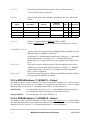
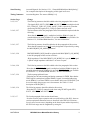
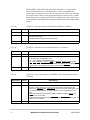
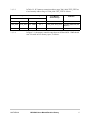
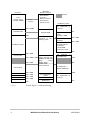
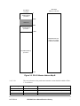
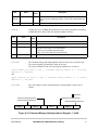
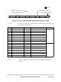
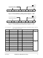
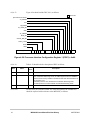
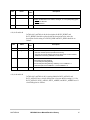
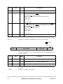
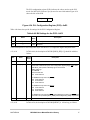
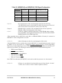
Supplement
MPC8245UMHIST/D
Rev. 0, 11/2001
MPC8245 User Manual
Revision History
Revision History of the
MPC8245 Integrated Processor
User’s Manual
This document lists the differences between revision 0 and revision 1 of the MPC8245
Integrated Processor User’s Manual. Revision 1 of the manual with these changes
incorporated is posted on the Worldwide Web at http://www.motorola.com/semiconductors.
Each item below refers to the section and page number in Revision 0 of the user’s manual.
Section, Page
Change
1.1.1, 1-4
The second bullet under the Memory Interface heading should
state:
– High-bandwidth data bus (32- or 64-bit) to SDRAM
1.1.1, 1-4
The fourth bullet under the Memory Interface heading should state:
–Supports 1 to 8 banks of 16-, 64-, 128-, 256-, or 512-Mbit memory
devices
1.1.1, 1-4
The second to the last bullet under the Memory Interface heading
should state:
– Extended ROM space supports 8-, 16-, or 32-bit gathering data
path, 32- or 64-bit (wide) data path
1.1.1, 1-4
The second to the last bullet under the 32-bit PCI interface heading
should be replaced with the following sentence:
– Address translation with two inbound and outbound units (ATU)
1.1.1, 1-5
The second to the last bullet under the Two-channel Integrated
DMA Controller (Writes To ROM/PORTX Not Supported) heading
should be replaced with the following:
– Local-to-PCI memory
1.1.1, 1-5
The following statement should be added to the list of Debug Features:
– Error injection/capture on data path
2.1.1, 2-6
Sections that describe signals SDMA13 and SDMA14 have been added to this
chapter:
Signal
Signal Name
Interface
…
…
…
SDMA13
SDRAM address 13
Memory
SDMA14
SDRAM address 14
Memory
…
…
…
2.1.2, 2-7
Alternate
Function(s)
Pins
I/O
Section #
…
…
…
…
See Table 6-2
1
O
2.2.2.a
1
O
2.2.2.b
…
…
…
…
In Table 2-2, Signals SDMA12/SRESET, SDMA12/TBEN,
SDMA14/CHKSTOP_IN are driven if extended addressing mode is enabled.
2.2.2.4 and 2.2.2.5, 2-18
The last sentence of the state meanings for SDRAM Address (SDMA[11:0]) and
SDRAM Address 12 (SDMA12) should state:
See Section 6.2.2, “SDRAM Address Multiplexing,” Section 6.3.1.1, “Base ROM
Address Multiplexing,” and Section 6.3.2.1, “Extended ROM Address
Multiplexing,” for a complete description of the mapping of these signals in all
cases.
2.2.2.5, 2-18
The following sentence should be added to the first paragraph of this section:
“SDMA12 is used in extended addressing mode. See Section 6.2.2, “SDRAM
Address Multiplexing” and Section 2.4, “Configuration Signals Sampled at
Reset,” for more information.”
2.2.2.6, 2-18
The following signal descriptions of SDMA13 and SDMA14 should be added to
this chapter after the SDMA12 description:
2.2.2.a SDRAM Address 13 (SDMA13)—Output
The SDMA13 signal is similar to SDMA[11:0] in that it corresponds to different row or column address
bits, depending on the memory in use. SDMA13 is multiplexed with TBEN and is used in extended
addressing mode. See Section 6.3.2, “Extended ROM Interface,” for more information.
State Meaning
Timing Comments
Asserted/Negated: See Section 6.3.2.1, “Extended ROM Address Multiplexing,”
for a complete description of the mapping of this signal in all cases.
Assertion/Negation: The same as SDMA[11:0].
2.2.2.b SDRAM Address 14 (SDMA14)—Output
The SDMA14 signal is similar to SDMA[11:0] in that it corresponds to different row or column address
bits, depending on the memory in use. SDMA14 is multiplexed with CHKSTOP_IN and is used in extended
addressing mode. See Section 6.3.2, “Extended ROM Interface,” for more information.
2
MPC8245 User’s Manual Revision History
MOTOROLA
State Meaning
Timing Comments
Asserted/Negated: See Section 6.3.2.1, “Extended ROM Address Multiplexing,”
for a complete description of the mapping of this signal in all cases.
Assertion/Negation: The same as SDMA[11:0].
Section, Page
Change
2.2.5, 2-25
The following sentences should be added to the first paragraph of this section:
“The signals SIN1, SOUT1, SIN2/CTS1, and SOUT2/RTS1 are multiplexed with
PCI_CLK0, PCI_CLK1, PCI_CLK2, and PCI_CLK3, respectively. Note that
when using DUART signals, PCI_CLK[0:3] signals cannot be used.”
2.2.6.2, 2-27
The last sentence of the first paragraph of this section should be replaced with the
following:
“Note that the SRESET signal is multiplexed with the SDMA12 signal. In
extended addressing mode, SDMA12 is used and SRESET is not available. See
Section 6.3.2, “Extended ROM Interface,” for more information.”
2.2.6.3, 2-27
The following sentence should be added to the first paragraph of this section:
“Note that the output driver for MCP can be designated as open-drain by setting
the MIOCR[MCP_OD_MODE] parameter.”
2.2.6.3, 2-28
PMCR2[SHARED_MCP] should be replaced with MIOCR[MCP_OD_MODE]
in the last paragraph of this section as follows:
“High impedance: If the MIOCR[MCP_OD_MODE] bit is set, the MCP signal
is placed in high impedance when there is no error to report.”
2.2.6.6, 2-28
2.2.6.7, 2-29
2.2.8.2, 2-34
2.3.2, 2-37
MOTOROLA
The following sentences should be added to the first paragraph of this section:
“Note that the CHKSTOP_IN signal is multiplexed with the SDMA14 signal. In
extended addressing mode, SDMA14 is used and CHKSTOP_IN is not available.
See Section 6.3.2, “Extended ROM Interface,” for more information.”
The first paragraph should state:
“Following are the state meaning and timing comments for TBEN. Note that the
TBEN signal is multiplexed with the SDMA13 signal. In extended addressing
mode, SDMA13 is used and TBEN is not available. In this case, PICR1[DEC] can
be used to enable the processor core’s decrementer. See Table 4-31 for a
description of PICR1[DEC].”
The following sentence should be added to this section:
“Note that PCI_CLK[0:3] cannot be used when using DUART signals SIN1,
SOUT1, SIN2/CTS1, and SOUT2/RTS1.”
The fourth paragraph of this section should state:
“In order to insure proper operation and successful locking of the DLL, there are
certain requirements that must be met as described in the MPC8245 Hardware
Specification. In some cases (depending on the board layout and the frequencies),
the DLL lock range must be lengthened by setting the
MPC8245 User’s Manual Revision History
3
MIOCR1[DLL_MAX_DELAY] bit described in Section 4.5, “Output/Clock
Driver and Miscellaneous I/O Control Registers.” This is accomplished by
increasing the time between each of the 128 tap points in the delay line. Although
this increased time makes it easier to guarantee that the reference clock is within
the DLL lock range, it also means there may be slightly more jitter in the output
clock of the DLL, should the phase comparator shift the clock between adjacent tap
points. ”
2.4, 2-40
In Table 2-5, the state meaning of signal MAA0 should be as follows:
Signal Name
Default
…
…
…
MAA0
1
Address map setting. This signal should always be pulled high since the MPC8245 only
supports address map B.
1 The MPC8245 is configured for address map B.
…
…
…
2.4, 2-41
In Table 2-5, the default value of signal PMAA2 is 0, as follows:
Signal Name
Default
…
…
…
PMAA2
0
Driver capability for the PCI and EPIC controller output signals. The value of this signal
sets the initial value of ODCR[DRV_PCI].
0 40 Ω drive capability on PCI/EPIC signals
1 20 Ω drive capability on AD[31:0], C/BE[3:0], DEVSEL, FRAME, GNT[4:0], PAR,
INTA, IRDY, PERR, SERR, STOP, TRDY, IRQ0/S_INT, IRQ1/S_CLK, and IRQ4/L_INT
signals and 6 Ω drive capability on IRQ2/S_RST and IRQ3/S_FRAME
…
…
…
2.4, 2-41
4
State Meaning
State Meaning
In Table 2-5, the second sentence of the SDMA1 state meaning should state the
following:
Signal Name
Default
State Meaning
…
…
…
SDMA1
1
Extended addressing mode. When this signal is low during reset, the extended
addressing mode is enabled. The value of this signal during reset determines the
function of the SRESET, TBEN, CHKSTOP_IN, TRIG_IN, and TRIG_OUT signals. See
6.3.2, “Extended ROM Interface,” for more information on the multiplexing of these
signals.
0 Extended addressing mode enabled. SDMA12, SDMA13, SDMA14, RCS2, and
RCS3 signals are available.
1 Extended addressing mode disabled. SRESET, TBEN, CHKSTOP_IN, TRIG_IN, and
TRIG_OUT are available.
…
…
…
MPC8245 User’s Manual Revision History
MOTOROLA
3.1, 3-2
In Table 3-2, PCI memory transaction address range 7000_0000–7FFF_FFFF has
a local memory address range of 7000_0000–7FFF_FFFF as follows:
PCI Memory Transaction Address Range
Hex
Decimal
Local Memory
Address Range
…
…
…
…
…
7000_0000
7FFF_FFFF
2G - 256M
2G - 1
7000_0000–7FFF_FFFF
…
…
…
…
…
3.1, 3-4
MOTOROLA
Definition
…
Extended ROM/Flash (256
MBytes)11
…
In Figure 3-1, the memory controller range between 2GB and 4GB - 32MB should
state “Forwards to PCI memory space,” as follows:
MPC8245 User’s Manual Revision History
5
MPC8245
Memory Controller
Processor
0
Local
memory space
0 to 2GB - 256MB
Local
memory
Not forwarded
to PCI bus.
Memory controller
performs local
memory access
Reserved
PCI Memory Space
0
Not addressable
processor
2GB - 256MB
Extended ROM
Extended ROM
2GB
Forwards to PCI
Memory Space
by
PCI memory space in
range
2 to 4GB - 32MB
Not addressable
processor
by
2GB
4GB - 32MB
4GB - 16MB
If local ROM,
not addressable as
PCI memory.
If remote ROM,
PCI memory space
PCI Memory Space
4GB
PCI I/O Space
4GB - 32MB
PCI I/O Space
4GB - 32MB + 64KB Clears A[31:24] and
forwards to PCI I/O
space,
except
0xFE01_0000–
4GB - 24MB
0xFE7F_FFFF,
which is reserved
PCI I/O Space
CONFIG_ADDR
CONFIG_DATA
PCI Int Ack
ROM or Flash
3.1, 3-6
6
I/O
addresses
0 to 64KB range
in
64KB
8MB
I/O addresses in
8MB to 12MB range
4GB - 20MB
4GB - 18MB
4GB - 17MB
4GB - 16MB
4GB
0
12MB
PCI Configuration
Access
Int Ack Broadcast PCI
Not addressable
processor
ROM Access
by
4GB
Replace Figure 3-3 with the following:
MPC8245 User’s Manual Revision History
MOTOROLA
MPC8245
PCI Master
I/O Space
Memory Controller
0
Addressable by
processor
64KB
Reserved
8MB
Addressable by
processor
12MB
MPC8245 does not
respond as a target
to PCI I/O accesses
Not addressable by
processor
4GB
Figure 3-3. PCI I/O Master Address Map B
3.4.1, 3-26
The cross reference to the performance monitor section should be added to Table
3-13 as follows:
Local Memory Offset
Register Set
…
…
0xF_E000 – 0xF_EFFF
Performance monitor
…
…
MOTOROLA
Reference
…
Section 16.2.3, “Performance Monitor Counter (PMC0–PMC3)”
…
MPC8245 User’s Manual Revision History
7
3.4.2, 3-27
The cross reference to the performance monitor section should be added to Table
3-14 as follows:
PCI Memory Offset
Register Set
…
…
0xE00 – 0xEFF
Performance monitor
…
…
Reference
…
Section 16.2.3, “Performance Monitor Counter (PMC0–PMC3)”
…
Chapter 4
The correct Performance Monitor Command Registers are the 4 CMDR registers
(CMDR0-CMDR3) referenced in Section 16.2. The Performance Monitor
Command Registers at 0x48 through 0x5C should not be used. Any reference to
these registers have been removed from this chapter.
4.1.3.1, 4-6
In Table 4-1, offsets 0xD8 and 0xDC should have reset values of 0x0C00_000E and
0x0800_000E, respectively.
Size
(Bytes)
Program
Access
(Bytes)
Access
Reset Value
…
…
…
…
…
0xD8
Extended ROM configuration register 3
4
4
Read/Write
0x0C00_000E
0xDC
Extended ROM configuration register 4
4
4
Read/Write
0x0800_000E
…
…
…
…
…
Address
Offset
…
…
Register
4.2.8, 4-15
1
The description of this register in Table 4-12 should read as follows:
Bits
Reset Value
msb 15–0
x1
Table 4-13 should be titled “Table 4-13. Subsystem ID—0x2E and the description
of this register should read as follows:
Bits
Reset Value
msb 15–0
x1
Description
Value is determined at startup through configuration pins MDH[0:15] but can be
programmed by software after reset.
Initial value depends on reset configuration signal. See Section 2.4, “Configuration Signals Sampled at Reset.”
4.2.11, 4-16
8
Value is determined at startup through configuration pins MDH[16:31] but can be
programmed by software after reset.
Initial value depends on reset configuration signal. See Section 2.4, “Configuration Signals Sampled at Reset.”
4.2.9, 4-15
1
Description
Table 4-15 should contain the following description for bit 5 of the PGCR:
MPC8245 User’s Manual Revision History
MOTOROLA
Bits
Reset
Value
R/W
…
…
…
5
0
…
…
Description
…
R/W Controls ability to retry all incoming PCI read transactions to local memory while the
processor core is writing data to the PCI bus (for example, while internal buffers have
data to be written to the PCI bus).
0 Disables ability to retry all incoming PCI memory read transactions to local memory
while the processor core is writing data to the PCI bus.
1 Enables ability to retry all incoming PCI memory read transactions to local memory
while the processor core is writing data to the PCI bus.
…
4.4.2, 4-23
…
In figure 4-9, PCI_HOLD_DELAY[0-1] should include bits 5-4 as follows:
Reserved
PLL_SLEEP
PCI_HOLD_DELAY[0–1]
DLL_EXTEND
0
7
4.4.2, 4-23
1
6
0
5
4
3
00
2
1
0
Bits 6-4 of power management configuration register 2 should be updated as
follows:
Bits
Reset Value
R/W
Description
…
…
…
…
6
—
0
Reserved
5–4
PCI_HOLD_DEL
xx 1
…
…
…
PCI output hold delay value relative to the PCI_SYNC_IN signal. See the
MPC8245 Hardware Specification for the detailed number of nanoseconds
guaranteed for each setting. There are eight sequential settings for this value; each
corresponds to a set increase in hold time:
00 Recommended for 66 MHz PCI bus (default)
01
10 Recommended for 33 MHz PCI bus
11
The initial values of bits 5 and 4 are determined by the inverse of MCP and CKE
reset configuration signals, respectively. See Section 2.4, “Configuration Signals
Sampled at Reset,” for more information. As these two pins have internal pull-up
resistors, the default value after reset is 0b00.
…
Initial value depends on reset configuration signal. See Section 2.4, “Configuration Signals Sampled at Reset.”
4.5, 4-24 and 4-25
MOTOROLA
Table 4-21 should be updated as follows:
Bit 6 of the output driver control register has been renamed DRV_STD_MEM.
MPC8245 User’s Manual Revision History
9
Bits 5-4, DRV_MEM_CTRL[1-2], only drive SDRAM_CLK[0:3] and
SDRAM_SYNC_OUT signals for silicon revision 1.1.
Bits 1-0, DRV_MEM_CLK[1-2], should be added to the table.
Please note these changes in the table below:
Bits
Name
Reset
Value
msb 7
addr<73>
DRV_PCI
x1
6
DRV_STD_MEM
1
5–4
DRV_MEM_CTRL[1–2]
xx1
3–2
DRV_PCI_CLK[1–2]
1
Controls drive strength of PCI_CLK[0:4] and PCI_CLK_SYNC_OUT.
DRV_PCI_CLK[1–2]:
00 reserved
01 40-Ω drive capability
10 20-Ω drive capability
11 6-Ω drive capability
1–0
DRV_MEM_CLK_[1–2]
11
Controls drive strength of SDRAM_CLK[0:3] and SDRAM_SYNC_OUT
for silicon revision 1.2
Description
Driver capability for the PCI and EPIC controller output signals.
0 40 Ω drive capability on PCI/EPIC signals
1 20 Ω drive capability on AD[31:0], C/BE[3:0], DEVSEL, FRAME,
GNT[4:0], PAR, INTA, IRDY, PERR, SERR, STOP, TRDY, IRQ0/S_INT,
IRQ1/S_CLK, and IRQ4/L_IN signals and 6 Ω drive capability on
IRQ2/S_RST and IRQ3/S_FRAME
The initial value of this bit is determined by the PMAA2 reset
configuration pin.
Driver capability for standard and memory signals (PMAA[0:2], SDA,
SCL, CKO, QACK, DA[10:6], MCP, MDH[0:31], MDL[0:31], PAR[0:7],
and MAA[0:2])
0 40 Ω drive capability on standard signals
1 20 Ω drive capability on standard signals
Driver capability for the memory signals (CS[0:7], DQM[0:7], WE, FOE,
RCS0, RCS1, SDBA[1:0], SDRAS, SDCAS, CKE, AS, and SDMA[11:0],
CHKSTOP_IN, SRESET, TBEN,TRIG_OUT.
Controls drive strength of SDRAM_CLK[0:3] and SDRAM_SYNC_OUT
for silicon revision 1.1
DRV_MEM_CTRL[1–2]:
00 reserved
01 40-Ω drive capability
10 20-Ω drive capability
11 6-Ω drive capability
The initial value of DRV_MEM_CTRL[1–2] is determined by the PMAA0
and PMAA1 reset configuration pins, respectively.
DRV_MEM_CLK_[1–2]:
00 reserved
01 40-Ω drive capability
10 20-Ω drive capability
11 6-Ω drive capability
1
See Initial value depends on reset configuration signal. See Section 2.4, “Configuration Signals Sampled at Reset.”
4.5, 4-25
10
In Table 4-22, the description for bit 15 should state that it disables/enables the
PCI_SYNC_OUT signal of the MPC8245 as follows:
MPC8245 User’s Manual Revision History
MOTOROLA
Bits
Name
Reset
Value
15
addr<75>
PCI_SYNC_OUT
0
This bit disables/enables the PCI_SYNC_OUT signal of the MPC8245. A
value of one (0b1) disables the output. A value of zero (0b0) enables the
output.
…
…
…
…
4.5, 4-26
Description
In Table 4-23, bit 5 of MIOCR1 should be reserved. Also note that the description
of MIOCR1[DLL_MAX_DELAY] should be added as follows:
Bits
Name
Reset
Value
…
…
…
5–3
—
000
2
DLL_MAX_DELAY
0
This bit can be used to set the delay line length. Please see Section 2.3.2, “DLL
Operation and Locking,” for more information.
0 shorter (or normal) DLL delay line length
1 DLL_max_mode, longer DLL delay line length
…
…
…
…
4.7.1, 4-27
Description
…
Reserved
The extended starting and ending address fields have three bits as shown below.
The section originally showed these fields as two bits.
The correct formulas for the lower and upper boundaries are as follows
Lower boundary for bank n = 0b0 || <extended starting address n> || <starting
address n> || 0x0_0000.
and
Upper boundary for bank n = 0b0 || <extended ending address n > || <ending
address n> || 0xF_FFFF.
4.7.1, 4-28
The correct figures for the extended memory starting address registers are as
follows:
Reserved
Extended Starting Address 1
Extended Starting Address 2
Extended Starting Address 3
0000_0
31
Extended Starting Address 0
0000_0
27 26
24 23
0000_0
19 18
16 15
0000_0
11 10
8
7
3
2
0
Figure 4-12. Extended Memory Starting Address Register 1—0x88.
MOTOROLA
MPC8245 User’s Manual Revision History
11
Reserved
Extended Starting Address 6
Extended Starting Address 5
Extended Starting Address 7
0000_0
31
Extended Starting Address 4
0000_0
27 26
24 23
0000_0
19 18
16 15
0000_0
11 10
8
7
3
2
0
Figure 4-13. Extended Memory Starting Address Register 2—0x8C
4.7.1, 4-29
The correct bit settings for extended memory starting address registers 1 and 2 are
shown in table 4-27 as follows:
Bits
Name
Reset Value
31–27
—
All 0s
Reserved
26–24
Extended starting address 3
All 0s
Extended starting address for bank 3
23–19
—
All 0s
Reserved
18–16
Extended starting address 2
All 0s
Extended starting address for bank 2
15–11
—
All 0s
Reserved
10–8
Extended starting address 1
All 0s
Extended starting address for bank 1
7–3
—
All 0s
Reserved
2–0
Extended starting address 0
All 0s
Extended starting address for bank 0
31–27
—
All 0s
Reserved
26–24
Extended starting address 7
All 0s
Extended starting address for bank 7
23–19
—
All 0s
Reserved
18–16
Extended starting address 6
All 0s
Extended starting address for bank 6
15–11
—
All 0s
Reserved
10–8
Extended starting address 5
All 0s
Extended starting address for bank 5
7–3
—
All 0s
Reserved
2–0
Extended starting address 4
All 0s
Extended starting address for bank 4
4.7.1, 4-30
12
Description
Byte Address
0x88
0x8C
The correct figures for the extended memory ending address registers are as
follows:
MPC8245 User’s Manual Revision History
MOTOROLA
Reserved
Extended Ending Address 2
Extended Starting Address 1
Extended Ending Address 3
Extended Ending Address 0
0000_0
31
0000_0
27 26
24 23
0000_0
19 18
16 15
0000_0
11 10
8
7
3
2
0
Figure 4-16. Extended Memory Ending Address Register 1—0x98
Reserved
Extended Ending Address 6
Extended Starting Address 5
Extended Ending Address 7
0000_0
31
Extended Ending Address 4
0000_0
27 26
24 23
0000_0
19 18
16 15
0000_0
11 10
8
7
3
2
0
Figure 4.17. Extended Memory Ending Address Register 2—0x9C
4.7.1, 4-30 and 4-31
The correct bit settings for extended memory ending address registers 1 and 2 are
shown in table 4-29 as follows:
Bits
Name
Reset Value
31–27
—
All 0s
Reserved
26–24
Extended ending address 3
All 0s
Extended ending address for bank 3
23–19
—
All 0s
Reserved
18–16
Extended ending address 2
All 0s
Extended ending address for bank 2
15–11
—
All 0s
Reserved
10–8
Extended ending address 1
All 0s
Extended ending address for bank 1
7–3
—
All 0s
Reserved
2–0
Extended ending address 0
All 0s
Extended ending address for bank 0
31–27
—
All 0s
Reserved
26–24
Extended ending address 7
All 0s
Extended ending address for bank 7
23–19
—
All 0s
Reserved
18–16
Extended ending address 6
All 0s
Extended ending address for bank 6
15–11
—
All 0s
Reserved
10–8
Extended ending address 5
All 0s
Extended ending address for bank 5
7–3
—
All 0s
Reserved
2–0
Extended ending address 4
All 0s
Extended ending address for bank 4
MOTOROLA
Description
MPC8245 User’s Manual Revision History
Byte Address
0x98
0x9C
13
4.8, 4-33
Figure 4-20 should include DEC, bit 8, as follows:
Reserved
Speculative PCI Reads
CF_APARK
0b1
LE_MODE
ST_GATH_EN
DEC
CF_DPARK
MCP_EN
FLASH_WR_EN
PROC_TYPE
RCS0
0b00
1111_1111
31
0
0
24 23 22 21 20 19 18 17 16 15
000
0
13 12 11 10 9
0
8
7
1
6
5
4
0
3
2
1
0
Figure 4-20. Processor Interface Configuration Register 1 (PIRC1)—0xA8
4.8, 4-34
Table 4-32 should include a description of DEC as follows:
Bits
Name
Reset
Value
…
…
…
…
8
DEC
0
This bit can be used to enable the time base and decrementor of the processor
core. In extended addressing mode, the TBEN signal functions as SDMA13.
This bit can be used by software to enable the time base and decrementor in
the processor core.
0 Disable processor core decrementer in extended addressing mode
1 Enable processor core decrementer in extended addressing mode
…
…
…
…
4.9.2, 4-43
14
Description
In Table 4-40, the reference to MPC107 in the description of PCI SERR error
should be replaced with a reference to the MPC8245, as follows:
MPC8245 User’s Manual Revision History
MOTOROLA
Bits
Name
Reset
Value
…
…
…
…
6
PCI SERR error
0
This bit indicates the assertion of SERR by an external PCI agent regardless of
whether the MPC8245 is the initiator, the target, or a non-participating agent.
0 SERR not detected
1 SERR detected
…
…
…
…
Description
4.10, 4-45 and 4-48
In Table 4-43 and Table 4-44, the description for RCS2_BURST and
RCS3_BURST should be replaced with the description below. Also, the
description for bit setting 01 of RCS2_DBW and RCS3_DBW should be as
follows:
Bits
Name
Reset
Value
…
…
…
…
30
RCSn_BURST
0
Burst mode ROM chip-select n timing enable
0 Indicates standard (nonburst) ROM access timing
1 Indicates burst-mode ROM access timing. When burst mode is enabled,
ROM reads use RCSn_ROMNAL for burst beats.
29–28
RCSn_DBW
11
These bits control the of the data bus width for RCSn.
00 8-bit data path with gathering
01 16-bit data path with gathering
10 32-bit data path with gathering. Gathering occurs if DBUS0 = 1.
11 wide data path; 64-bit if DBUS0 = 1, 32-bit if DBUS0 = 0
…
…
…
…
Description
4.10, 4-46 and 4-49
In Table 4-43 and Table 4-44, bit setting 00000 for RCS2_ASFALL and
RCS3_ASFALL have a 0 clock falling time. Also note that bit setting 11111 for
RCS2_ASFALL, RCS3_ASFALL, RSC2_ASRISE, and RCS3_ASRISE has a 31
clock falling time as follows:
MOTOROLA
MPC8245 User’s Manual Revision History
15
Bits
Name
Reset
Value
…
…
…
14–10
RCSn_ASFALL
All 0s
RCSn AS fall time. These bits control the falling edge timing of the AS signal
relative to the falling edge of RCSn for the Port X interface. See Section 6.3.5,
“Port X Interface,” for more information.
00000 0 clocks (AS asserted coincident with the chip select)
00001 1 clock
00010 2 clocks
00011 3 clocks
...
11111 31 clocks
9–5
RCSn_ASRISE
All 0s
RCSn AS rise time. These bits control the rising edge timing of the AS signal
relative to the falling edge of RCSn for the Port X interface. See Section 6.3.5,
“Port X Interface,” for more information.
00000 Disables AS signal generation
00001 1 clock
00010 2 clocks
00011 3 clocks
...
11111 31 clocks
…
…
…
4.10, 4-51
Description
…
…
In figure 4-32, the RCSn_SADDR field is 16 bits long, as follows:
Reserved
RCSn_SIZE
0000
31
RCSn_SADDR
28 27
0000_0000
12 11
4
3
0
In Table 4-45 and Table 4-46, the RCS2_SADDR and RCS3_SADDR fields are 16
bits long as follows:
Bits
Name
Reset
Value
…
…
…
27–12
RCSn_SADDR
…
…
4.12, 4-53
16
Description
…
0xC000 Starting address for RCSn in megabytes.
Physical starting address = 0x7 || RCSn_SADDR || 0x000
…
…
Table 4-46 should be titled “Table 4-46. Extended ROM Configuration Register
4—0xDC”
Section 4.12 should read as follows:
MPC8245 User’s Manual Revision History
MOTOROLA
The PLL configuration register (PCR) indicates the values used to set the PLL
mode. See MPC8245 Hardware Specification for more information Figure 4-34
shows the bits of the PCR.
PLL_CFG
7
000
3
2
0
Figure 4-34. PLL Configuration Register (PCR)—0xE2
Table 4-48 shows the specific bit settings for the PLL Configuration Register.
Table 4-48. Bit Settings for the PCR—0xE2
1
Bits
Name
Reset
Value
7–3
PLL_CFG
x1
2–0
—
000
Description
PLL Configuration. Indicates the values used to set the PLL mode.
Reserved
Initial value depends on reset configuration signal. See Section 2.4, “Configuration Signals Sampled at Reset.”
4.13, 4-54
In Table 4-49, the description of MCCR1[DBUS_SIZ[0-1]] should be added as
follows:
Bits
Name
Reset
Value
…
…
…
…
xx
Read-only. This field indicates the state of the memory data path width. The value
of this field is determined by the reset configuration signals [DL[0], FOE]. Used
with DBUS_SIZ2 (stored in MCCR4[17]) as shown below.
DBUS_SIZ[0–2]:
For SDRAM:
0nn 32-bit data bus
1nn 64-bit data bus
22–21 DBUS_SIZ[0–1]
Description
For ROM/Flash chip select #0 (RCSO):
00n 32-bit data bus
n1n 8-bit data bus
10n 64-bit data bus
For ROM/Flash chip select #1 (RCS1):
0n0 32-bit data bus
nn1 8-bit data bus
1n0 64-bit data bus
For ROM/Flash chip select #2 (RCS2) and ROM/Flash chip select #3 (RCS3) data
bus width is set by ERCR1[RCS2_DBW] and ERCR2[RCS2_DBW], respectively.
…
4.13, 4-58
MOTOROLA
…
…
…
In Table 4-50, the description of MCCR2[REFINT] is 14 bits long, as follows:
MPC8245 User’s Manual Revision History
17
Bits
Name
Reset
Value
…
…
…
15–2
REFINT
All 0s
…
…
…
4.13, 4-59
Description
…
Refresh interval. These bits directly represent the number of clock cycles between
CBR refresh cycles. One row is refreshed in each RAM bank during each CBR
refresh cycle. The value for REFINT depends on the specific RAMs used and the
operating frequency of the MPC8245. See Section 6.2.12, “SDRAM Refresh,” for
more information. Note that the period of the refresh interval must be greater than
the read/write access time to ensure that read/write operations complete
successfully.
…
MCCR2[DBUS_SIZE[2]], bit 17, should be included in Figure 4-38 as follows:
Reserved
BUF_TYPE[1]
BSTOPRE[0–1]
BUF_TYPE[0]
WMODE
DBUS_SIZE[2]
PRETOACT
ACTOPRE
31
BSTOPRE[6–9]
REGDIMM
28 27
4.13, 4-60
0
0
SDMODE
24 23 22 21 20 19 18 17 16 15 14
ACTORW
8
7
4
3
0
In Table 4-52, the description of MCCR4[DBUS_SIZE[2]], bit 17 should be added
as follows:
Bits
Name
Reset
Value
…
…
…
…
17
DBUS_SIZE[2]
0
See description for bits 22–21 of MCCR1.
…
…
…
…
5.3.1.2.1, 5-16
Description
The following text and table should be added at the end of this section:
Table 5-2 shows how HID0[SBCLK], HID0[ECLK], and the hard reset signals are used to configure CKO
when PMCR1[CKO_SEL] = 0. When PMCR1[CKO_SEL] = 1, the CKO_MODE field of PMCR1
determines the signal driven on CKO. Note that the initial value of PMCR1[CKO_SEL] is determined by
the value on the AS signal at the negation of HRST_CPU. See Section 2.2.8.8, “Debug Clock
(CKO)—Output,” and Section 2.4, “Configuration Signals Sampled at Reset,” for more information.
18
MPC8245 User’s Manual Revision History
MOTOROLA
Table 5-2. HID0[BCLK] and HID0[ECLK] CKO Signal Configuration
5.8, 5-33
Chapter 6
6.1, 6-5
HRST_CPU and
HRST_CTRL
HID0[ECLK]
HID0[SBCLK]
Asserted
x
x
Processor core clock
Negated
0
0
High impedance
Negated
0
1
sys-logic-clk divided by 2
Negated
1
0
Processor core clock
Negated
1
1
sys-logic-clk
Signal Driven on CKO
The second sentence of the second paragraph should state the following:
“The MPC8245 processor version number is 0x8081, the processor revision level
starts at 0x1014 and is incremented for each revision of the chip.”
SDRAM CLK[0:3], MCLK, CLK, and MemCLK have all been replaced by
SDRAM_CLKn in all timing figures in this chapter.
In Table 6-2, SDMA12 should be added to the 2-bank SDRAM address column
next to the SDBA1 output signal and the following note should be added to JEDEC
DIMM SDRAM 168-pin DIMM signal BA1:
“When upgrading from an MPC8240 system, BA1 on SDRAM DIMM will already be connected to
SDRAM12 if 13xnx2 configurations were used.”
6.2.2, 6-11
Add the following text after the second paragraph of this section:
“Note that SDMA[14:12] are available only when the MPC8245 is in extended addressing mode, selected
by SDMA1 at reset. See Section 2.4, “Configuration Signals Sampled at Reset,” for more information.
When using extended addressing mode, the TBEN, SRESET, CHKSTOP_IN, TRIG_IN, and TRIG_OUT
signals are not available. The following pin function changes occur in extended addressing mode:
•
TBEN becomes SDMA13
•
SRESET becomes SDMA12
•
CHKSTOP_IN becomes SDMA14
•
TRIG_IN becomes RCS2
•
TRIG_OUT becomes RCS3
Since TBEN is not functional, PICR1[DEC] can be used to enable the processor core’s decrementer.”
6.2.2, 6-11
MOTOROLA
In Figure 6-4, rows labeled 13xnx2 should be removed. Rows labeled “12x10x4,”
“12x9x4,” and “11x8x4 or 12x8x4” should be updated as follows:
MPC8245 User’s Manual Revision History
19
msb
Row x Col x Bank
0-2 3 4 5 6
12x10x4 SDRAS
or
13x9x2
SDCAS
12x9x4
or
13x8x2
11x8x4,
12x8x4,
or
13x8x2
7
8
9
1
1
B
A
1
B
A
1
B
A
1
B
A
1
B
A
1
B
A
1
B
A
0
B
A
0
B
A
0
B
A
0
B
A
0
B
A
0
9 8
SDRAS
1
1
SDCAS
8
SDRAS
1
1
SDCAS
6.2.2, 6-13
0-4
SDRAS
SDCAS
SDRAS
SDCAS
6.3.1, 6-51
20
1 9 8 7 6 5 4 3 2 1 0
0
7 6 5 4 3 2 1 0
1 9 8 7 6 5 4 3 2 1 0
0
7 6 5 4 3 2 1 0
1 9 8 7 6 5 4 3 2 1 0
0
7 6 5 4 3 2 1 0
lsb
Physical Address
Row x Col x Bank
12x9x4
or
13x9x2
1 1 1 1 1 1 1 1 1 1 2 2 2 2 2 2 2 2 2 2 3 3
0 1 2 3 4 5 6 7 8 9 0 1 2 3 4 5 6 7 8 9 0 1
In Figure 6-5, rows labeled 13xnx2 should be removed. Rows labeled “12x10x4”
and “12x9x4” should be updated as follows:
ms
b
12x10x4
or
13x10x2
lsb
Physical Address
5 6 7 8 9
1 B B
1 A A
1 0
9
B B
A A
1 0
1 B B
1 A A
1 0
B B
A A
1 0
1 1 1 1 1 1 1 1 1 1 2 2 2 2 2 2 2 2 2 2 3 3
0 1 2 3 4 5 6 7 8 9 0 1 2 3 4 5 6 7 8 9 0 1
1 9 8 7 6 5 4 3 2 1 0
0
8 7 6 5 4 3 2 1 0
1 9 8 7 6 5 4 3 2 1 0
0
8 7 6 5 4 3 2 1 0
The fifth paragraph of this section should be replaced with the following paragraph:
“For the 8-bit data path, the MPC8245 uses either 22 or 23 address bits depending
on the state of the SDMA1 signal at reset. If extended addressing mode is
disabled (SDMA1 high at reset), the 8-bit interface uses 22 address bits and can
only address 4 Mbytes for the associated chip select; if extended addressing mode
is enabled (SDMA1 low at reset), the 8-bit interface uses 23 address bits and can
address 8 Mbytes for the associated chip select.”
MPC8245 User’s Manual Revision History
MOTOROLA
6.3.1, 6-52
Table 6-14 should be replaced with the following table. Note the differences in the
8-bit interface cells.
DBUS_SIZE[0–2]
1
SDRAM data
bus width
Bank 0
(RCS0)
Bank 1
(RCS1)
MDL[0]
FOE
MCCR4
[DBUS_SIZE2]
0
0
0
32 bits
32-bit interface
21 address bits
8-Mbyte space
32-bit interface
21 address bits
8-Mbyte space
0
0
1
32 bits
32-bit interface
21 address bits
8-Mbyte space
8-bit interface
22 or 23 address bits 1
4- or 8-Mbyte space1
0
1
0
32 bits
8-bit interface
22 or 23 address bits1
4- or 8-Mbyte space1
32-bit interface
21 address bits
8-Mbyte space
0
1
1
32 bits
8-bit interface
22 or 23 address bits1
4- or 8-Mbyte space1
8-bit interface
22 or 23 address bits1
4- or 8-Mbyte space1
1
0
0
64 bits
64-bit interface
20 address bits
8-Mbyte space
64-bit interface
20 address bits
8-Mbyte space
1
0
1
64 bits
64-bit interface
20 address bits
8-Mbyte space
8-bit interface
22 or 23 address bits1
4- or 8-Mbyte space1
1
1
0
64 bits
8-bit interface
22 or 23 address bits1
4- or 8-Mbyte space1
64-bit interface
20 address bits
8-Mbyte space
1
1
1
64 bits
8-bit interface
22 or 23 address bits1
4- or 8-Mbyte space1
8-bit interface
22 or 23 address bits1
4- or 8-Mbyte space1
For the 8-bit interface, the setting of the SDMA1 signal at reset determines whether 22 or 23 address bits are used
to provide 4 or 8 Mbytes of addressable space.
6.3.2, 6-54
The first paragraph should be replaced with the following:
“At power-on reset, the 256-Mbyte extended ROM space is disabled. The
extended ROM interface is optional and must be first enabled by pulling the
SDMA1 signal low at reset, to enable extended addressing mode, and setting
MCCR4[EXTROM]. Once enabled, the extended ROM space is accessed by
CPU or PCI memory transactions to physical addresses from 0x7000_0000 to
0x7FFF_FFFF. Note that extended addressing mode also effects base ROM
addressing in 8-bit mode. See Section 6.3.1, “Base ROM Interface Operation,”
for more information.
6.3.4, 6-60
MOTOROLA
The following sentence, found towards the middle of the second to the last
paragraph of this section, should be removed:
MPC8245 User’s Manual Revision History
21
“Additionally, if the memory interface is configured in the registered mode
(MCCR4[REGISTERED] = 1]), one more clock cycle is incurred in these read
access times.”
Chapter 9
All references to extended doorbell registers should be removed from this
chapter.
Chapter 11
SDR0-SDR15 will now be called SIR0-SIR15.
11.2, 11-5
The DUART interrupt vector/priority registers at offsets 0x5_1120 and 0x5_1140
should be abbreviated as IIVPRs as follows.
Address Offset
from EUMBBAR
Register Name
Field Mnemonics
...
...
...
0x5_1120
DUART Ch1 interrupt vector/priority register (IIVPR4)
M, A, P, S, PRIORITY, VECTOR
...
...
...
0x5_1140
DUART Ch2 interrupt vector/priority register (IIVPR5)
M, A, P, S, PRIORITY, VECTOR
...
...
...
11.4, 11-10
The second sentence of the second paragraph in this section should not include
the words “global timers” as follows:
“However, in pass-through mode, the EPIC unit passes the raw interrupts from
the MU (including watchpoint facility, DUART, and DMA unit), and I2C to the
L_INT output signal.”
12.4.2, 12-14
Table 12-4 should be titled “Table 12-4. Bit Settings for Divisor Register UDMB,
UDLB,—Offsets 0x501/0x601, 0x500/0x600”
12.4.7, 12-20
Table 12-13 has been added. This table describes how parity is selected using the
PEN, SP, and EPS bits in the ULCR.
Table 12-13. Parity Selection Using ULCR[PEN], ULCR[SP], and ULCR[EPS]
12.4.9, 12-21
22
PEN
SP
EPS
Parity Selected
0
0
0
No parity
0
0
1
No parity
0
1
0
No parity
0
1
1
No parity
1
0
0
Odd parity
1
0
1
Even parity
1
1
0
Mark parity
1
1
1
Space parity
Figure 12-12 should be included:
MPC8245 User’s Manual Revision History
MOTOROLA
RFE
TEMT
THRE
BI
FE
PE
OE
DR
7
6
5
4
3
2
1
0
Figure 12-12. Line Status Register (ULSR)
12.4.13, 12-25
Table 12-18 includes new tables in the description of TXRDY and RXRDY bits:
Table 12-18. Bit Settings for UDSR—0x510, 0x610
Bit
Name
Reset
Value
R/W
7–2
—
All 0s
R
Reserved
1
TXRDY
0
R
Transmitter ready reflects the status of the transmitter FIFO or the UTHR. The
status is dependent on the DMA mode selected, which is determined by the
DMS and FEN bits in the UFCR.
0 This bit is cleared in the following instances:
Description
DMS
FEN
Mode
Meaning
0
0
0
TXRDY is cleared when there are no characters in
the transmitter FIFO or UTHR.
0
1
0
TXRDY is cleared when there are no characters in
the transmitter FIFO or UTHR
1
0
0
TXRDY is cleared when there are no characters in
the transmitter FIFO or UTHR.
1
1
1
TXRDY is cleared when there are no characters in
the transmitter FIFO or UTHR. TXRDY remains clear
when the transmitter FIFO is not yet full.
1 This bit is set in the following instances:
MOTOROLA
DMS
FEN
Mode
Meaning
0
0
0
TXRDY is set after the first character is loaded into
the transmitter FIFO or UTHR.
0
1
0
TXRDY is set after the first character is loaded into
the transmitter FIFO or UTHR.
1
0
0
TXRDY is set after the first character is loaded into
the transmitter FIFO or UTHR.
1
1
1
TXRDY is set when the transmitter FIFO is full.
MPC8245 User’s Manual Revision History
23
Table 12-18. Bit Settings for UDSR—0x510, 0x610 (continued)
Bit
Name
Reset
Value
R/W
Description
0
RXRDY
1
R
Receiver ready reflects the status of the receiver FIFO or URBR. The status is
dependent on the DMA mode selected, which is determined by the DMS and
FEN bits in the UFCR.
0 This bit is cleared in the following instances:
DMS
FEN
Mode
Meaning
0
0
0
RXRDY is cleared when there is at least one
character in the receiver FIFO or URBR.
0
1
0
RXRDY is cleared when there is at least one
character in the receiver FIFO or URBR.
1
0
0
RXRDY is cleared when there is at least one
character in the receiver FIFO or URBR.
1
1
1
RXRDY is cleared when the trigger level or a time-out
has been reached and remains cleared until the
receiver FIFO is empty.
1 This bit is set in the following instances:
DMS
FEN
Mode
Meaning
0
0
0
RXRDY is set when there are no characters in the
receiver FIFO or URBR.
0
1
0
RXRDY is set when there are no characters in the
receiver FIFO or URBR.
1
0
0
RXRDY is set when there are no characters in the
receiver FIFO or URBR.
1
1
1
RXRDY is set when the trigger level has not been
reached and there has been no time out.
15.1, 15-1
The second bullet under the first paragraph of this section should state:
•
2.0-volt core and 3.0 to 3.6-volt I/O
16.3.2, 16-10
In Table 16-6, performance monitor events 55–58 and 63–64 are not supported and
should be reserved.
Chapter 17
Throughout this chapter, DH[31:0], DL[31:0], and DPAR[7:0] should be replaced
with MDH[31:0], MDL[31:0], and PAR[7:0], respectively
In Table 17-1, change register names as follows:
24
MPC8245 User’s Manual Revision History
MOTOROLA
Local Bus
Offset
PCI Bus
Offset
Size
(bytes)
Program
Access Size
(bytes)
Register
Register
Access
Reset
Value
0xF_F000
0xF00
4
4
Data High Error Injection Mask
R/W
0x0000_0000
0xF_F004
0xF04
4
4
Data Low Error Injection Mask
R/W
0x0000_0000
0xF_F008
0xF08
4
1, 2, or 4
Parity Error Injection Mask
Register
R/W
0x0000_0000
0xF_F00C
0xF0C
4
4
Data High Error Capture Monitor
Register
R
0x0000_0000
0xF_F010
0xF10
4
4
Data Low Error Capture Monitor
Register
R
0x0000_0000
0xF_F014
0xF14
4
1, 2, or 4
Parity High Error Capture Monitor
Register
R/W
0x0000_0000
17.5.2, 17-17
The first sentence of the second paragraph should state:
“When memory data-path parity/ECC error data is loaded into the monitors, the
capture flag in the parity error capture monitor register, at offsets 0xF_F014, and
0xF14, is also set.”
D.1.3, D-12
Second implementation note under the first bullet should state:
“Implementation Note—The MPC8245 processor version number is 0x8081; the
processor revision level starts at 0x1014 and is incremented for each revision of the
chip. The revision level is updated on all silicon revisions.”
The second sentence of the second paragraph of this section should state:
“The MPC8245 processor version number is 0x8081; the processor revision level
starts at 0x1014 and is incremented for each revision of the chip.“
D.1.3.2, D-15
MOTOROLA
MPC8245 User’s Manual Revision History
25
26
MPC8245 User’s Manual Revision History
MOTOROLA
MOTOROLA
MPC8245 User’s Manual Revision History
27
HOW TO REACH US:
USA/EUROPE/LOCATIONS NOT LISTED:
Motorola Literature Distribution;
P.O. Box 5405, Denver, Colorado 80217
1-303-675-2140 or 1-800-441-2447
JAPAN:
Motorola Japan Ltd.;
SPS, Technical Information Center,
3-20-1, Minami-Azabu Minato-ku,
Tokyo 106-8573 Japan
81-3-3440-3569
Information in this document is provided solely to enable system and software implementers to use
ASIA/PACIFIC:
Motorola products. There are no express or implied copyright licenses granted hereunder to design
Motorola Semiconductors H.K. Ltd.;
Silicon Harbour Centre, 2 Dai King Street,
Tai Po Industrial Estate, Tai Po, N.T., Hong Kong
852-26668334
or fabricate any integrated circuits or integrated circuits based on the information in this document.
TECHNICAL INFORMATION CENTER:
use of any product or circuit, and specifically disclaims any and all liability, including without
1-800-521-6274
limitation consequential or incidental damages. “Typical” parameters which may be provided in
HOME PAGE:
Motorola reserves the right to make changes without further notice to any products herein.
Motorola makes no warranty, representation or guarantee regarding the suitability of its products
for any particular purpose, nor does Motorola assume any liability arising out of the application or
Motorola data sheets and/or specifications can and do vary in different applications and actual
performance may vary over time. All operating parameters, including “Typicals” must be validated
http://www.motorola.com/semiconductors
for each customer application by customer’s technical experts. Motorola does not convey any
DOCUMENT COMMENTS:
license under its patent rights nor the rights of others. Motorola products are not designed,
FAX (512) 933-2625,
Attn: RISC Applications Engineering
intended, or authorized for use as components in systems intended for surgical implant into the
body, or other applications intended to support or sustain life, or for any other application in which
the failure of the Motorola product could create a situation where personal injury or death may
occur. Should Buyer purchase or use Motorola products for any such unintended or unauthorized
application, Buyer shall indemnify and hold Motorola and its officers, employees, subsidiaries,
affiliates, and distributors harmless against all claims, costs, damages, and expenses, and
reasonable attorney fees arising out of, directly or indirectly, any claim of personal injury or death
associated with such unintended or unauthorized use, even if such claim alleges that Motorola was
negligent regarding the design or manufacture of the part.
Motorola and the Stylized M Logo are registered in the U.S. Patent and Trademark Office.
digital dna is a trademark of Motorola, Inc. All other product or service names are the property of
their respective owners. Motorola, Inc. is an Equal Opportunity/Affirmative Action Employer.
© Motorola, Inc. 2001
MPC8245UMHIST/D