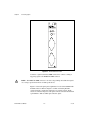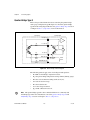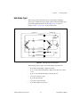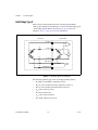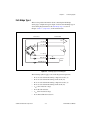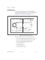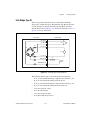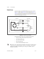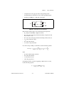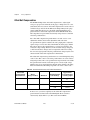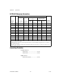
1
PXI NI PXI-4220 User Manual NI PXI-4220 User Manual May 2005 373530B-01 Support Worldwide Technical Support and Product Information ni.com National Instruments Corporate Headquarters 11500 North Mopac Expressway Austin, Texas 78759-3504 USA Tel: 512 683 0100 Worldwide Offices Australia 1800 300 800, Austria 43 0 662 45 79 90 0, Belgium 32 0 2 757 00 20, Brazil 55 11 3262 3599, Canada 800 433 3488, China 86 21 6555 7838, Czech Republic 420 224 235 774, Denmark 45 45 76 26 00, Finland 385 0 9 725 725 11, France 33 0 1 48 14 24 24, Germany 49 0 89 741 31 30, India 91 80 51190000, Israel 972 0 3 6393737, Italy 39 02 413091, Japan 81 3 5472 2970, Korea 82 02 3451 3400, Lebanon 961 0 1 33 28 28, Malaysia 1800 887710, Mexico 01 800 010 0793, Netherlands 31 0 348 433 466, New Zealand 0800 553 322, Norway 47 0 66 90 76 60, Poland 48 22 3390150, Portugal 351 210 311 210, Russia 7 095 783 68 51, Singapore 1800 226 5886, Slovenia 386 3 425 4200, South Africa 27 0 11 805 8197, Spain 34 91 640 0085, Sweden 46 0 8 587 895 00, Switzerland 41 56 200 51 51, Taiwan 886 02 2377 2222, Thailand 662 278 6777, United Kingdom 44 0 1635 523545 For further support information, refer to the Signal Conditioning Technical Support Information document. To comment on National Instruments documentation, refer to the National Instruments Web site at ni.com/info and enter the info code feedback. © 2003–2005 National Instruments Corporation. All rights reserved. Important Information Warranty The NI PXI-4220 is warranted against defects in materials and workmanship for a period of one year from the date of shipment, as evidenced by receipts or other documentation. National Instruments will, at its option, repair or replace equipment that proves to be defective during the warranty period. This warranty includes parts and labor. The media on which you receive National Instruments software are warranted not to fail to execute programming instructions, due to defects in materials and workmanship, for a period of 90 days from date of shipment, as evidenced by receipts or other documentation. National Instruments will, at its option, repair or replace software media that do not execute programming instructions if National Instruments receives notice of such defects during the warranty period. National Instruments does not warrant that the operation of the software shall be uninterrupted or error free. A Return Material Authorization (RMA) number must be obtained from the factory and clearly marked on the outside of the package before any equipment will be accepted for warranty work. National Instruments will pay the shipping costs of returning to the owner parts which are covered by warranty. National Instruments believes that the information in this document is accurate. The document has been carefully reviewed for technical accuracy. In the event that technical or typographical errors exist, National Instruments reserves the right to make changes to subsequent editions of this document without prior notice to holders of this edition. The reader should consult National Instruments if errors are suspected. In no event shall National Instruments be liable for any damages arising out of or related to this document or the information contained in it. EXCEPT AS SPECIFIED HEREIN, NATIONAL INSTRUMENTS MAKES NO WARRANTIES, EXPRESS OR IMPLIED, AND SPECIFICALLY DISCLAIMS ANY WARRANTY OF MERCHANTABILITY OR FITNESS FOR A PARTICULAR PURPOSE. CUSTOMER’S RIGHT TO RECOVER DAMAGES CAUSED BY FAULT OR NEGLIGENCE ON THE PART OF NATIONAL INSTRUMENTS SHALL BE LIMITED TO THE AMOUNT THERETOFORE PAID BY THE CUSTOMER. NATIONAL INSTRUMENTS WILL NOT BE LIABLE FOR DAMAGES RESULTING FROM LOSS OF DATA, PROFITS, USE OF PRODUCTS, OR INCIDENTAL OR CONSEQUENTIAL DAMAGES, EVEN IF ADVISED OF THE POSSIBILITY THEREOF. This limitation of the liability of National Instruments will apply regardless of the form of action, whether in contract or tort, including negligence. Any action against National Instruments must be brought within one year after the cause of action accrues. National Instruments shall not be liable for any delay in performance due to causes beyond its reasonable control. The warranty provided herein does not cover damages, defects, malfunctions, or service failures caused by owner’s failure to follow the National Instruments installation, operation, or maintenance instructions; owner’s modification of the product; owner’s abuse, misuse, or negligent acts; and power failure or surges, fire, flood, accident, actions of third parties, or other events outside reasonable control. Copyright Under the copyright laws, this publication may not be reproduced or transmitted in any form, electronic or mechanical, including photocopying, recording, storing in an information retrieval system, or translating, in whole or in part, without the prior written consent of National Instruments Corporation. Trademarks National Instruments, NI, ni.com, and LabVIEW are trademarks of National Instruments Corporation. Refer to the Terms of Use section on ni.com/legal for more information about National Instruments trademarks. Other product and company names mentioned herein are trademarks or trade names of their respective companies. Patents For patents covering National Instruments products, refer to the appropriate location: Help»Patents in your software, the patents.txt file on your CD, or ni.com/patents. WARNING REGARDING USE OF NATIONAL INSTRUMENTS PRODUCTS (1) NATIONAL INSTRUMENTS PRODUCTS ARE NOT DESIGNED WITH COMPONENTS AND TESTING FOR A LEVEL OF RELIABILITY SUITABLE FOR USE IN OR IN CONNECTION WITH SURGICAL IMPLANTS OR AS CRITICAL COMPONENTS IN ANY LIFE SUPPORT SYSTEMS WHOSE FAILURE TO PERFORM CAN REASONABLY BE EXPECTED TO CAUSE SIGNIFICANT INJURY TO A HUMAN. (2) IN ANY APPLICATION, INCLUDING THE ABOVE, RELIABILITY OF OPERATION OF THE SOFTWARE PRODUCTS CAN BE IMPAIRED BY ADVERSE FACTORS, INCLUDING BUT NOT LIMITED TO FLUCTUATIONS IN ELECTRICAL POWER SUPPLY, COMPUTER HARDWARE MALFUNCTIONS, COMPUTER OPERATING SYSTEM SOFTWARE FITNESS, FITNESS OF COMPILERS AND DEVELOPMENT SOFTWARE USED TO DEVELOP AN APPLICATION, INSTALLATION ERRORS, SOFTWARE AND HARDWARE COMPATIBILITY PROBLEMS, MALFUNCTIONS OR FAILURES OF ELECTRONIC MONITORING OR CONTROL DEVICES, TRANSIENT FAILURES OF ELECTRONIC SYSTEMS (HARDWARE AND/OR SOFTWARE), UNANTICIPATED USES OR MISUSES, OR ERRORS ON THE PART OF THE USER OR APPLICATIONS DESIGNER (ADVERSE FACTORS SUCH AS THESE ARE HEREAFTER COLLECTIVELY TERMED “SYSTEM FAILURES”). ANY APPLICATION WHERE A SYSTEM FAILURE WOULD CREATE A RISK OF HARM TO PROPERTY OR PERSONS (INCLUDING THE RISK OF BODILY INJURY AND DEATH) SHOULD NOT BE RELIANT SOLELY UPON ONE FORM OF ELECTRONIC SYSTEM DUE TO THE RISK OF SYSTEM FAILURE. TO AVOID DAMAGE, INJURY, OR DEATH, THE USER OR APPLICATION DESIGNER MUST TAKE REASONABLY PRUDENT STEPS TO PROTECT AGAINST SYSTEM FAILURES, INCLUDING BUT NOT LIMITED TO BACK-UP OR SHUT DOWN MECHANISMS. BECAUSE EACH END-USER SYSTEM IS CUSTOMIZED AND DIFFERS FROM NATIONAL INSTRUMENTS' TESTING PLATFORMS AND BECAUSE A USER OR APPLICATION DESIGNER MAY USE NATIONAL INSTRUMENTS PRODUCTS IN COMBINATION WITH OTHER PRODUCTS IN A MANNER NOT EVALUATED OR CONTEMPLATED BY NATIONAL INSTRUMENTS, THE USER OR APPLICATION DESIGNER IS ULTIMATELY RESPONSIBLE FOR VERIFYING AND VALIDATING THE SUITABILITY OF NATIONAL INSTRUMENTS PRODUCTS WHENEVER NATIONAL INSTRUMENTS PRODUCTS ARE INCORPORATED IN A SYSTEM OR APPLICATION, INCLUDING, WITHOUT LIMITATION, THE APPROPRIATE DESIGN, PROCESS AND SAFETY LEVEL OF SUCH SYSTEM OR APPLICATION. Conventions The following conventions are used in this manual: <> Angle brackets that contain numbers separated by an ellipsis represent a range of values associated with a bit or signal name—for example, DIO<3..0>. » The » symbol leads you through nested menu items and dialog box options to a final action. The sequence File»Page Setup»Options directs you to pull down the File menu, select the Page Setup item, and select Options from the last dialog box. This icon denotes a note, which alerts you to important information. This icon denotes a caution, which advises you of precautions to take to avoid injury, data loss, or a system crash. When this icon is marked on the product, refer to the Read Me First: Safety and Radio-Frequency Interference document, shipped with the product, for precautions to take. When symbol is marked on a product it denotes a warning advising you to take precautions to avoid electrical shock. When symbol is marked on a product it denotes a component that may be hot. Touching this component may result in bodily injury. bold Bold text denotes items that you must select or click in the software, such as menu items and dialog box options. Bold text also denotes parameter names. italic Italic text denotes variables, emphasis, a cross reference, or an introduction to a key concept. This font also denotes text that is a placeholder for a word or value that you must supply. monospace Text in this font denotes text or characters that you should enter from the keyboard, sections of code, programming examples, and syntax examples. This font is also used for the proper names of disk drives, paths, directories, programs, subprograms, subroutines, device names, functions, operations, variables, filenames and extensions, and code excerpts. monospace italic Italic text in this font denotes text that is a placeholder for a word or value that you must supply. Contents Chapter 1 About the NI PXI-4220 What You Need to Get Started ......................................................................................1-2 National Instruments Documentation ............................................................................1-3 Installing the Application Software, NI-DAQ, and the DAQ Device ...........................1-3 Installing the NI PXI-4220 ............................................................................................1-4 LED Pattern Descriptions ..............................................................................................1-4 Chapter 2 Connecting Signals Connecting Bridge Sensor Signals to the NI PXI-4220 ................................................2-1 Quarter-Bridge Type I .....................................................................................2-4 Quarter-Bridge Type II....................................................................................2-6 Half-Bridge Type I ..........................................................................................2-7 Half-Bridge Type II.........................................................................................2-8 Full-Bridge Type I...........................................................................................2-9 Full-Bridge Type II..........................................................................................2-10 Full-Bridge Type III ........................................................................................2-11 Remote Sense ..................................................................................................2-12 Chapter 3 Configuring and Testing Verifying and Self-Testing Using Device Test Panels ..................................................3-1 NI PXI-4220 Software-Configurable Settings...............................................................3-2 Common Software-Configurable Settings ......................................................3-2 Bridge Configuration and Completion..............................................3-2 Excitation Level ................................................................................3-2 Filter ..................................................................................................3-3 Gain/Input Range ..............................................................................3-3 Offset Null Compensation Potentiometers .......................................3-3 Shunt Calibration Switches...............................................................3-4 Simultaneous Sample and Hold ........................................................3-4 Configurable Settings in MAX ......................................................................................3-4 NI-DAQmx......................................................................................................3-5 Creating a Strain Global Channel or Task ........................................3-6 Creating a Custom Voltage with Excitation Global Channel or Task ................................................3-7 © National Instruments Corporation v NI PXI-4220 User Manual Contents Verifying the Signal ...................................................................................................... 3-8 Verifying the Signal in NI-DAQmx Using a Task or Global Channel ........... 3-8 Chapter 4 Theory of Operation Strain Gauge Theory...................................................................................................... 4-1 Wheatstone Bridges ........................................................................................ 4-1 Strain Gauges .................................................................................................. 4-2 Acronyms, Formulas, and Variable Definitions ............................................. 4-2 Software Scaling and Equations ..................................................................... 4-3 Quarter-Bridge Type I..................................................................................... 4-4 Quarter-Bridge Type II ................................................................................... 4-6 Half-Bridge Type I.......................................................................................... 4-8 Half-Bridge Type II ........................................................................................ 4-10 Full-Bridge Type I .......................................................................................... 4-12 Full-Bridge Type II ......................................................................................... 4-14 Full-Bridge Type III........................................................................................ 4-16 NI PXI-4220 Theory of Operation ................................................................................ 4-18 Bridge Configuration and Completion............................................................ 4-21 Excitation ........................................................................................................ 4-21 Remote Sense ................................................................................... 4-22 Gain/Input Range ............................................................................................ 4-24 Filter ................................................................................................................ 4-25 Offset Null Compensation .............................................................................. 4-26 Shunt Calibration ............................................................................................ 4-27 Simultaneous Sample and Hold ...................................................................... 4-28 Maximum Acquisition Rate.............................................................. 4-30 Measurement Considerations .......................................................................... 4-30 Differential Signals........................................................................... 4-30 Common-Mode Rejection Ratio....................................................... 4-30 Effective CMR.................................................................................. 4-31 Timing and Control Functional Overview ...................................................... 4-31 Programmable Function Inputs....................................................................... 4-32 Device and PXI Clocks ................................................................................... 4-33 NI PXI-4220 User Manual vi ni.com Contents Chapter 5 Developing Your Application Developing Your Application in NI-DAQmx ...............................................................5-1 Typical Program Flow.....................................................................................5-1 General Discussion of Typical Flow Chart .....................................................5-3 Creating a Task Using DAQ Assistant or Programmatically ...........5-3 Adjusting Timing and Triggering .....................................................5-4 Configuring Channel Properties........................................................5-4 Perform Offset Null Compensation ..................................................5-6 Perform Shunt Calibration ................................................................5-7 Acquiring, Analyzing, and Presenting ..............................................5-7 Completing the Application ..............................................................5-8 Developing an Application Using LabVIEW..................................................5-8 Using a DAQmx Channel Property Node in LabVIEW ...................5-10 Synchronization and Triggering ......................................................................5-12 Synchronizing the NI PXI-4220 ......................................................................5-12 Synchronizing the NI PXI-4220 Using LabVIEW ...........................5-14 Other Application Documentation and Material ...........................................................5-15 Calibrating the NI PXI-4220..........................................................................................5-16 Calibrating the NI PXI-4220 ...........................................................................5-16 Internal Calibration Procedure ..........................................................5-16 External Device Calibration..............................................................5-17 Calibrating the System ....................................................................................5-17 Offset Null Compensation ................................................................5-17 Shunt Calibration ..............................................................................5-17 Appendix A Specifications Appendix B Timing Signal Information Appendix C Removing the NI PXI-4220 Appendix D Common Questions © National Instruments Corporation vii NI PXI-4220 User Manual Contents Glossary Index Figures Figure 2-1. Figure 2-2. Figure 2-3. Figure 2-4. Figure 2-5. Figure 2-6. Figure 2-7. Figure 2-8. Figure 2-9. Figure 2-10. Figure 2-11. NI PXI-4220 Front Label...................................................................... 2-2 PXI-4220 Front Connector and General Circuit Diagram .................... 2-3 Socketed Resistor Locations ................................................................. 2-4 Quarter-Bridge I Circuit Diagram......................................................... 2-5 Quarter-Bridge II Circuit Diagram ....................................................... 2-6 Half-Bridge Type I Circuit Diagram..................................................... 2-7 Half-Bridge Type II Circuit Diagram ................................................... 2-8 Full-Bridge Type I Circuit Diagram ..................................................... 2-9 Full-Bridge Type II Circuit Diagram .................................................... 2-10 Full-Bridge Type III Circuit Diagram................................................... 2-11 Remote Sense Circuit Diagram............................................................. 2-12 Figure 4-1. Figure 4-2. Figure 4-3. Figure 4-4. Figure 4-5. Figure 4-6. Figure 4-7. Figure 4-8. Basic Wheatstone Bridge Circuit Diagram........................................... 4-1 Quarter-Bridge Type I Measuring Axial and Bending Strain............... 4-4 Quarter-Bridge Type I Circuit Diagram ............................................... 4-4 Quarter-Bridge Type II Measuring Axial and Bending Strain ............. 4-6 Quarter-Bridge Type II Circuit Diagram .............................................. 4-7 Half-Bridge Type I Measuring Axial and Bending Strain.................... 4-8 Half-Bridge Type I Circuit Diagram..................................................... 4-9 Half-Bridge Type II Rejecting Axial and Measuring Bending Strain .................................................................... 4-10 Half-Bridge Type II Circuit Diagram ................................................... 4-11 Full-Bridge Type I Rejecting Axial and Measuring Bending Strain .... 4-12 Full-Bridge Type I Circuit Diagram ..................................................... 4-13 Full-Bridge Type II Rejecting Axial and Measuring Bending Strain... 4-14 Full-Bridge Type II Circuit Diagram .................................................... 4-15 Full-Bridge Type III Measuring Axial and Rejecting Bending Strain ...................................................................... 4-17 Full-Bridge Type III Circuit Diagram................................................... 4-17 Block Diagram of the NI PXI-4220...................................................... 4-19 Signal During Simultaneous Sample and Hold Sampling .................... 4-29 AI CONV CLK Signal Routing ............................................................ 4-32 NI PXI-4220 PXI Trigger Bus Signal Connection ............................... 4-34 Figure 4-9. Figure 4-10. Figure 4-11. Figure 4-12. Figure 4-13. Figure 4-14. Figure 4-15. Figure 4-16. Figure 4-17. Figure 4-18. Figure 4-19. Figure 5-1. Figure 5-2. Figure 5-3. NI PXI-4220 User Manual Typical Program Flowchart .................................................................. 5-2 LabVIEW Channel Property Node with Filtering Enabled at 10 kHz and SS/H Disabled ................................................................... 5-11 General Synchronizing Flowchart ........................................................ 5-13 viii ni.com Contents Figure B-1. Figure B-2. Figure B-3. Figure B-4. Figure B-5. Figure B-6. Figure B-7. Figure B-8. Figure B-9. Figure B-10. Figure B-11. Figure B-12. Typical Posttriggered Sequence ............................................................B-2 Typical Pretriggered Sequence..............................................................B-2 AI START TRIG Input Signal Timing .................................................B-3 AI START TRIG Output Signal Timing...............................................B-3 AI REF TRIG Input Signal Timing.......................................................B-4 AI REF TRIG Output Signal Timing ....................................................B-5 AI SAMP CLK Input Signal Timing ....................................................B-6 AI SAMP CLK Output Signal Timing..................................................B-6 AI CONV CLK Input Signal Timing ....................................................B-7 AI CONV CLK Output Signal Timing .................................................B-8 AI SAMPLE CLK TIMEBASE Signal Timing ....................................B-9 AI HOLD COMPLETE Signal Timing.................................................B-10 Figure C-1. Injector/Ejector Handle Position Before Device Removal....................C-2 Tables Table 3-1. Excitation Voltage for Configuration and Gauge Resistances..............3-3 Table 4-1. Table 4-2. Table 4-3. Table 4-4. Strain-Gauge Configurations.................................................................4-2 Control Codes for Coarse and Fine Null Potentiometers ......................4-26 Maximum Sampling Rates ....................................................................4-30 PXI Trigger Bus Timing Signals...........................................................4-35 Table 5-1. Table 5-2. Table 5-3. NI-DAQmx Properties ..........................................................................5-4 Programming a Task in LabVIEW........................................................5-8 Synchronizing the NI PXI-4220 Using LabVIEW................................5-14 Table A-1. Maximum Sampling Rates ....................................................................A-1 © National Instruments Corporation ix NI PXI-4220 User Manual 1 About the NI PXI-4220 This chapter provides an introduction to the NI PXI-4220 device and its installation. The NI PXI-4220 is part of the SC Series of data acquisition (DAQ) devices with integrated signal conditioning. The SC Series reduces measurement setup and configuration complexity by integrating signal conditioning and DAQ on the same product. The NI PXI-4220 is a full-featured dynamic strain device with programmable bridge-sensor signal conditioning, programmable filter, and programmable gain settings per channel ensuring maximum accuracy for bridge sensors. The NI PXI-4220 features the National Instruments (NI) programmable gain amplifier (PGA), an instrumentation-class amplifier that guarantees fast settling times at all gain settings. The NI PXI-4220 also uses the NI-DAQmx DAQ Assistant, specifically the Strain Gage Calibration wizard, to easily perform offset null compensation and shunt calibration. The NI PXI-4220 is a two-channel module for interfacing to Wheatstone bridge configurations. The NI PXI-4220 has the following features: • Two differential analog input (AI) channels • 16-bit resolution • 333 kS/s single-channel sampling rate • 66 kS/s per channel when simultaneously sampling • Direct connectivity through two male D-Subminiature (D-SUB) connectors • Instrumentation amplifier per channel • Simultaneous sample-and-hold (SS/H) capability using track-and-hold (T/H) circuitry • Synchronization with other DAQ devices through the PXI trigger bus • 4-pole software programmable Butterworth filters with software selectable filter settings of bypass (no filtering), 10 Hz, 100 Hz, 1 kHz, and 10 kHz per channel • Programmable voltage excitation with remote sense per channel • Programmatic offset null compensation per channel © National Instruments Corporation 1-1 NI PXI-4220 User Manual Chapter 1 About the NI PXI-4220 • Programmatic shunt calibration per channel • Programmatic bridge completion per channel • Programmable Function Input (PFI) pin for external timing, triggering, and calibration. You can configure most settings on a per-channel basis through software. The NI PXI-4220 is configured using Measurement & Automation Explorer (MAX) or through function calls to NI-DAQmx. What You Need to Get Started To set up and use the NI PXI-4220, you need the following: ❑ Hardware – NI PXI-4220 device – PXI chassis – Sensors as required by your application ❑ Software – NI-DAQ 7.0 or later – One of the following: • LabVIEW • Measurement Studio • LabWindows™/CVI™ • Refer to National Instruments»NI-DAQ»NI-DAQ Read Me for supported text-based compilers ❑ Documentation – NI PXI-4220 User Manual – DAQ Quick Start Guide – Read Me First: Safety and Radio-Frequency Interference – PXI chassis user manual – Documentation for your software ❑ Tools – 1/8 in. flathead screwdriver You can download NI documents from ni.com/manuals. NI PXI-4220 User Manual 1-2 ni.com Chapter 1 About the NI PXI-4220 National Instruments Documentation The NI PXI-4220 User Manual is one piece of the documentation set for your DAQ system. You could have any of several types of manuals, depending on the hardware and software in your system. Use the manuals you have as follows: • DAQ Quick Start Guide—This document describes how to install NI-DAQ devices and NI-DAQ. Install NI-DAQmx before you install the PXI module. • PXI chassis manual—Read this manual for maintenance information on the chassis and for installation instructions. • Software documentation—You may have both application software and NI-DAQmx software documentation. NI application software includes LabVIEW, Measurement Studio, and LabWindows/CVI. After you set up the hardware system, use either your application software documentation or the NI-DAQmx documentation to help you write your application. If you have a large, complex system, it is worthwhile to look through the software documentation before you configure the hardware. Installing the Application Software, NI-DAQ, and the DAQ Device Refer to the DAQ Quick Start Guide, packaged with the NI-DAQ software, for instructions for installing your application software, NI-DAQ driver software, and the DAQ device to which you will connect the NI PXI-4220. NI-DAQ 7.0 or later is required to configure and program the NI PXI-4220 device. If you do not have NI-DAQ 7.0 or later, you can either contact an NI sales representative to request it on a CD or download the it from ni.com. © National Instruments Corporation 1-3 NI PXI-4220 User Manual Chapter 1 About the NI PXI-4220 Installing the NI PXI-4220 Refer to the Read Me First: Radio-Frequency Interference document before removing equipment covers or connecting or disconnecting any signal wires. Note Refer to the DAQ Quick Start Guide to unpack, install, and configure the NI PXI-4220 in a PXI chassis. LED Pattern Descriptions The following LEDs on the NI PXI-4220 front panel confirm the system is functioning properly: NI PXI-4220 User Manual • The ACCESS LED is normally green and blinks yellow for a minimum of 100 ms during the NI PXI-4220 configuration. • The ACTIVE LED is normally green and blinks yellow for a minimum of 100 ms during data acquisition. 1-4 ni.com 2 Connecting Signals This chapter describes how to connect Wheatstone bridge sensors to the NI PXI-4220 in quarter-, half-, and full-bridge configurations, and for remote sensing. Connecting Bridge Sensor Signals to the NI PXI-4220 This section discusses how to connect the signals of supported strain-gauge configuration types as well as full-bridge sensors such as load, force, torque, and pressure sensors. It also discusses connecting leads for remote sensing. Refer to Chapter 4, Theory of Operation, for a discussion of strain-gauge concepts. Caution Refer to the Read Me First: Safety and Radio-Frequency Interference document before removing equipment covers or connecting/disconnecting any signal wires. Figure 2-1 shows the NI PXI-4220 front label, including the location of the D-SUB connectors and PFI0/CAL SMB connector. © National Instruments Corporation 2-1 NI PXI-4220 User Manual Chapter 2 Connecting Signals NI PXI-4220 2 Channel Bridge Input ACCESS ACTIVE PFI 0/ CAL AI 0 AI 1 Figure 2-1. NI PXI-4220 Front Label Construct a signal lead with an SMB connection to connect a timing or triggering signal to the PFI0/CAL SMB connector. The PFI0/CAL SMB connector is for low-voltage timing and calibration signals only. Voltages greater than ±10 V can damage the device. Caution Figure 2-2 shows the pin signal assignments for each of the NI PXI-4220 D-SUB connectors. Refer to Figure 2-2 when constructing D-SUB connection leads to ensure the signal wires are routed correctly. In the electrical connection diagram, each signal connection node is labeled with a pin number to indicate which pin carries the signal. NI PXI-4220 User Manual 2-2 ni.com Chapter 2 Shunt Cal COM (SCCOM) Shunt Cal A (SCA) Remote Sense+ (RS+) Excitation+ (P+) Signal+ (S+) Connecting Signals Pin 1 (S0+) Pin 6 (S0–) Channel 0 Pin 3 (RS0+) 1 2 3 4 5 6 7 8 9 + Pin 2 (P0+) – R1 Quarter-Bridge Completion + +Vex 2 – Half-Bridge Completion R2 Channel 1 + 1 2 3 4 5 6 7 8 9 Pin 7 (P0–) – + –Vex 2 – Pin 8 (RS0–) Pin 9 (QTR/Shunt Cal B) Shunt Cal B B Shunt Cal A A Pin 5 (SCCOM) QTR/Shunt Cal B (QTR/SCB) Remote Sense– (RS–) Excitation– (P–) Signal– (S–) Pin 4 (QTR/Shunt Cal A) SCB0 Shunt Calibration Switches Figure 2-2. PXI-4220 Front Connector and General Circuit Diagram Note Refer to Figure 2-3 for quarter-bridge and shunt cal completion resistor locations. © National Instruments Corporation 2-3 NI PXI-4220 User Manual Chapter 2 Connecting Signals Figure 2-3 shows the location of the socketed NI PXI-4220 resistors. 1 2 3 4 5 6 PXI-9-PIN DSUB 1 2 3 R4 (Shunt Cal B CH 0) 4 R1 (Shunt Cal A CH 0) 5 R5 (Quarter-Bridge Completion CH0) 6 R2 (Quarter-Bridge Completion CH1) R6 (Shunt Cal B CH 1) R3 (Shunt Cal A CH 1) Figure 2-3. Socketed Resistor Locations Quarter-Bridge Type I This section provides information about connecting the quarter-bridge strain-gauge configuration type I. Figure 2-4 shows the quarter-bridge type I circuit wiring diagram. Refer to the Quarter-Bridge Type I section of Chapter 4, Theory of Operation, for more information. If you have a two-wire strain-gauge element, connect the active element leads to S+ (pin 1) and P+ (pin 2) and short S+ (pin 1) to QTR/SCB (pin 9) and SCA (pin 4). Note NI PXI-4220 User Manual 2-4 ni.com Chapter 2 Transducer Connecting Signals NI PXI-4220 RL S+ (Pin 1) RL P+ (Pin 2) VCH + – P+ R4 R1 QTR P– (Pin 7) S– R3 VEX + – R2 P– RL QTR/SCB (Pin 9) SCA (Pin 4) Jumper not required when using SCB. SCCOM (Pin 5) RS B Shunt Cal B Shunt Cal A RS A Figure 2-4. Quarter-Bridge I Circuit Diagram The following symbols apply to the circuit diagram and equations: • R1 and R2 are half-bridge completion resistors. • R3 is the quarter-bridge completion resistor (dummy resistor). • R4 is the active element measuring tensile strain (+ε). • VEX is the excitation voltage. • RL is the lead resistance. • VCH is the measured voltage. • RS A is shunt calibration resistor A. • RS B is shunt calibration resistor B. This configuration uses the Shunt Cal A switch for shunt calibration. The value of the quarter-bridge completion resistor (dummy resistor) must equal the nominal resistance of the strain gauge. NI recommends using a 0.1% precision resistor. If a less precise resistor is used, offset null compensation calibration is not as accurate. Refer to the Offset Null Compensation section of Chapter 4, Theory of Operation, for more information. Note © National Instruments Corporation 2-5 NI PXI-4220 User Manual Chapter 2 Connecting Signals Quarter-Bridge Type II This section provides information about connecting the quarter-bridge strain-gauge configuration type II. Figure 2-5 shows the quarter-bridge type II circuit wiring diagram. Refer to the Quarter-Bridge Type II section of Chapter 4, Theory of Operation, for more information. Transducer NI PXI-4220 S+ (Pin 1) VCH RL + – P+ (Pin 2) R4 R1 VEX R3 RL P– (Pin 7) RL SCA (Pin 4) RL + – R2 RS Shunt Cal A SCCOM (Pin 5) Figure 2-5. Quarter-Bridge II Circuit Diagram The following symbols apply to the circuit diagram and equations: • R1 and R2 are half-bridge completion resistors. • R3 is the quarter-bridge temperature-sensing element (dummy gauge). • R4 is the active element measuring tensile strain (+ε). • VEX is the excitation voltage. • RL is the lead resistance. • VCH is the voltage measured. • RS is shunt calibration resistor A. The quarter-bridge type II is often confused with the more commonly used half-bridge type I. For more information, refer to the Quarter-Bridge Type II and Half-Bridge Type I sections of Chapter 4, Theory of Operation. Note NI PXI-4220 User Manual 2-6 ni.com Chapter 2 Connecting Signals Half-Bridge Type I This section provides information about connecting the half-bridge strain-gauge configuration type I. Figure 2-6 shows the half-bridge type I circuit wiring diagram. Refer to the Half-Bridge Type I section of Chapter 4, Theory of Operation, for more information. Transducer NI PXI-4220 S+ (Pin 1) VCH RL + – P+ (Pin 2) R4 R1 VEX R3 RL P– (Pin 7) RL SCA (Pin 4) RL + – R2 RS Shunt Cal A SCCOM (Pin 5) Figure 2-6. Half-Bridge Type I Circuit Diagram The following symbols apply to the circuit diagram and equations: • R1 and R2 are half-bridge completion resistors. • R3 is an active element measuring compression from Poisson effect (–νε). • R4 is an active element measuring tensile strain (+ε). • VEX is the excitation voltage. • RL is the lead resistance. • VCH is the voltage measured. • RS is shunt calibration resistor A. © National Instruments Corporation 2-7 NI PXI-4220 User Manual Chapter 2 Connecting Signals Half-Bridge Type II This section provides information about connecting the half-bridge strain-gauge configuration type II. Figure 2-7 shows the half-bridge type II circuit wiring diagram. Refer to the Half-Bridge Type II section of Chapter 4, Theory of Operation, for more information. Transducer NI PXI-4220 S+ (Pin 1) VCH RL + – P+ (Pin 2) R4 R1 VEX R3 RL P– (Pin 7) RL SCA (Pin 4) RL + – R2 RS Shunt Cal A SCCOM (Pin 5) Figure 2-7. Half-Bridge Type II Circuit Diagram The following symbols apply to the circuit diagram and equations: NI PXI-4220 User Manual • R1 and R2 are half-bridge completion resistors. • R3 is an active element measuring compressive strain (–ε). • R4 is an active element measuring tensile strain (+ε). • VEX is the excitation voltage. • RL is the lead resistance. • VCH is the voltage measured. • RS is shunt calibration resistor A. 2-8 ni.com Chapter 2 Connecting Signals Full-Bridge Type I This section provides information about connecting the full-bridge strain-gauge configuration type I. Figure 2-8 shows the full-bridge type I circuit wiring diagram. Refer to the Full-Bridge Type I section of Chapter 4, Theory of Operation, for more information. Transducer NI PXI-4220 S+ (Pin 1) VCH S– (Pin 6) RL R4 + – P+ (Pin 2) R1 VEX R2 R3 + – P– (Pin 7) RL SCA (Pin 4) RS RL SCCOM (Pin 5) Shunt Cal A RL Figure 2-8. Full-Bridge Type I Circuit Diagram The following symbols apply to the circuit diagram and equations: • R1 is an active element measuring compressive strain (–ε). • R2 is an active element measuring tensile strain (+ε). • R3 is an active element measuring compressive strain (–ε). • R4 is an active element measuring tensile strain (+ε). • VEX is the excitation voltage. • RL is the lead resistance. • VCH is the measured voltage. • RS is shunt calibration resistor A. © National Instruments Corporation 2-9 NI PXI-4220 User Manual Chapter 2 Connecting Signals Full-Bridge Type II This section provides information about connecting the full-bridge strain-gauge configuration type II. Figure 2-9 shows the full-bridge type II circuit wiring diagram. Refer to the Full-Bridge Type II section of Chapter 4, Theory of Operation, for more information. Transducer NI PXI-4220 S+ (Pin 1) VCH S– (Pin 6) RL R4 + – P+ (Pin 2) R1 VEX R2 R3 + – P– (Pin 7) RL SCA (Pin 4) RS RL SCCOM (Pin 5) Shunt Cal A RL Figure 2-9. Full-Bridge Type II Circuit Diagram The following symbols apply to the circuit diagram and equations: NI PXI-4220 User Manual • R1 is an active element measuring compressive Poisson effect (–νε). • R2 is an active element measuring tensile Poisson effect (+νε). • R3 is an active element measuring compressive strain (–ε). • R4 is an active element measuring tensile strain (+ε). • VEX is the excitation voltage. • RL is the lead resistance. • VCH is the measured voltage. • RS is shunt calibration resistor A. 2-10 ni.com Chapter 2 Connecting Signals Full-Bridge Type III This section provides information about connecting the full-bridge strain-gauge configuration type I. The full-bridge type III only measures axial strain. Figure 2-10 shows the full-bridge type III circuit wiring diagram. Refer to the Full-Bridge Type III section of Chapter 4, Theory of Operation, for more information. Transducer NI PXI-4220 S+ (Pin 1) VCH S– (Pin 6) RL R4 + – P+ (Pin 2) R1 VEX R2 R3 + – P– (Pin 7) RL SCA (Pin 4) RS RL SCCOM (Pin 5) Shunt Cal A RL Figure 2-10. Full-Bridge Type III Circuit Diagram The following symbols apply to the circuit diagram and equations: • R1 is an active element measuring compressive Poisson effect (–νε). • R2 is an active element measuring tensile strain (+ε). • R3 is an active element measuring compressive Poisson effect (–νε). • R4 is an active element measuring the tensile strain (+ε). • VEX is the excitation voltage. • RL is the lead resistance. • VCH is the measured voltage. • RS is shunt calibration resistor A. © National Instruments Corporation 2-11 NI PXI-4220 User Manual Chapter 2 Connecting Signals Remote Sense For remote sensing, wire the NI PXI-4220 for remote sense as shown in Figure 2-11. Refer to the Remote Sense section of Chapter 4, Theory of Operation, for more information about remote sensing. Using remote sense with the NI PXI-4220 is recommended to properly regulate the excitation voltage, VEX, being applied to the sensor. Transducer NI PXI-4220 S+ (Pin 1) S– (Pin 6) RL VCH + – P+ (Pin 2) R1 R4 + VEX R2 R3 – Remote Sense Feedback Loop P– (Pin 7) RL RS+ (Pin 3) RS– (Pin 8) VRSENSE + – Figure 2-11. Remote Sense Circuit Diagram The following symbols apply to the circuit diagram and equations: • R1, R2, R3, and R4 are the transducer bridge elements. • VCH is the measured voltage. • VEX is the excitation voltage. • RL is the lead resistance. • VRSENSE is the measured bridge excitation. Remote sense is illustrated using a full-bridge circuit diagram for simplicity, but in general, the VRSENSE terminals should be connected to your transducer at the points that supply VEX. For example, connect RSX+ (pin 3) to PX+ (pin 2), and RSX– (pin 8) to PX– (pin 7) at the sensor. Note NI PXI-4220 User Manual 2-12 ni.com 3 Configuring and Testing This chapter provides details on configuring the NI PXI-4220 in MAX. In MAX you can use device test panels to verify device functionality and signal connection. MAX also allows you to easily create, configure, and test NI-DAQmx Tasks and NI-DAQmx Global Channels to control and configure the NI PXI-4220. Verifying and Self-Testing Using Device Test Panels Once you have successfully installed the NI PXI-4220, verified the installation, and connected the signals, use the NI PXI-4220 device test panels to verify the device is measuring signals properly. The test panels allow you to measure the signal connected to the NI PXI-4220 directly as well as configure some of the properties of your measurement. To open the NI PXI-4220 device test panels when in MAX, complete the following steps: 1. Display the list of devices and interfaces by clicking the + next to the Devices and Interfaces icon. 2. Display the list of NI-DAQmx devices by clicking the + next to NI-DAQmx Devices icon. 3. Click PXI-4220. 4. Click the Test Panels button in the device toolbar. 5. Configure the settings shown on the screen and click Start to take a measurement. To measure scaled voltages, further configure channel properties, and configure timing settings, use an NI-DAQmx Task or NI-DAQmx Global Channel. © National Instruments Corporation 3-1 NI PXI-4220 User Manual Chapter 3 Configuring and Testing NI PXI-4220 Software-Configurable Settings This section describes how to set the bridge configuration, voltage excitation level, filter bandwidth, and gain/input signal range, as well as how to use configuration utilities in MAX to programmatically perform offset null compensation and shunt calibration. It also describes how to perform configuration of these settings for the NI PXI-4220 in NI-DAQmx. For more information about the relationship between the settings and the measurements and how to configure settings in your application, refer to Chapter 5, Developing Your Application. Common Software-Configurable Settings This section describes the most frequently used software-configurable settings for the NI PXI-4220. Bridge Configuration and Completion Bridge configuration is a software-configurable setting that allows you to connect quarter-, half-, or full-bridge sensors configurations. Refer to Chapter 4, Theory of Operation, for more information. Excitation Level Excitation level is a software-configurable setting that allows you to set the voltage excitation level on Pins 2 and 7. You can choose voltage excitation settings between 0 and 10 V. To prevent the module from overheating, refer to Table 3-1 for appropriate excitation levels for common sensor resistances. (maximum excitation voltage) = (resistance connected between the excitation terminals) × (29.0 mA) Table 3-1 shows the maximum allowable excitation voltages for standard bridge configurations and resistances. For other bridge resistances, the maximum allowable excitation voltage is: V EX , max = ( bridge resistance ) ( 29.0 mA ) Refer to Chapter 4, Theory of Operation, for more information about excitation. NI PXI-4220 User Manual 3-2 ni.com Chapter 3 Configuring and Testing Table 3-1. Excitation Voltage for Configuration and Gauge Resistances Configuration/ Sensor Quarter- or Half-Bridge Full-Bridge or Full-Bridge Sensor Resistance Excitation Voltage Range 120 Ω 0 to 6.950 V 350 Ω 0 to 10 V 1000 Ω 0 to 10 V 120 Ω 0 to 3.475 V 350 Ω 0 to 10 V 1000 Ω 0 to 10 V Filter Lowpass Filter Cutoff Frequency is a software-configurable setting that allows you to select a lowpass filter cutoff frequency. You can choose 10 Hz, 100 Hz, 1 kHz, 10 kHz, or disable the filter. With the filter disabled, the module has a bandwidth of 20 kHz. Refer to Chapter 4, Theory of Operation, for more information. Gain/Input Range Gain/input range refers to the signal conditioning gain and digitizer input range, software-configurable settings that allow you to choose the appropriate amplification to fully utilize the range of the NI PXI-4220 DAQ circuitry. In most applications, NI-DAQ sets the gain for you determined by the input range. Refer to Chapter 4, Theory of Operation, for more information. Otherwise, you should determine the appropriate gain using the input signal voltage range and the full-scale limits of the NI PXI-4220 signal conditioning output signal. Offset Null Compensation Potentiometers Coarse and fine offset null compensation potentiometers are software-configurable settings that allow you to remove unwanted offset voltage. In most cases, you do not explicitly set the potentiometers, but instead allow driver software to automatically adjust them for you. However, if you want to explicitly set the potentiometers, you can write an application program that adjusts the settings. Refer to Chapter 4, Theory of Operation, for more information. © National Instruments Corporation 3-3 NI PXI-4220 User Manual Chapter 3 Configuring and Testing Shunt Calibration Switches Shunt calibration switches A and B are software-configurable settings that allow you to engage or disengage the shunt calibration resistors in order to perform gain calibration. In most cases, you do not explicitly control the shunt calibration switches, but instead allow driver software to automatically adjust them for you during the automated shunt calibration procedure. However, if you want to explicitly control the calibration switches, you can write an application program that controls the shunt calibration switches. Refer to Chapter 4, Theory of Operation, for more information. Null calibration is done for you automatically if you perform shunt calibration using the NI-DAQmx driver. Refer to Chapter 4, Theory of Operation, for more information about how to perform shunt calibration using the driver. Note Simultaneous Sample and Hold When it is critical to measure two or more signals at the same instant in time, simultaneous sample and hold (SS/H) is required. Typical applications that might require SS/H include vibration measurements and phase difference measurements. You can disable this setting through your application if you require scan rates beyond the maximum allowable with SS/H engaged. NI recommends leaving SS/H engaged. Disabling SS/H introduces a small offset voltage. You can compensate for this offset by performing offset null calibration. Refer to Chapter 5, Developing Your Application, for more information about how to enable and disable SS/H. You cannot change the simultaneous sampling mode in MAX. You must use an ADE such as LabVIEW to configure the setting. Refer to your ADE help file for more information. Note Configurable Settings in MAX If you are not using an NI ADE, or if you are using an NI ADE prior to version 7.0 or an unlicensed copy of an NI ADE, additional dialog boxes from the NI License Manager appear allowing you to create a task or global channel in unlicensed mode. These messages continue to appear until you install version 7.0 or later of an NI ADE. Note You can use MAX to configure your bridge-based sensor measurement. This section describes where you can access each software-configurable setting available in MAX. NI PXI-4220 User Manual 3-4 ni.com Chapter 3 Configuring and Testing NI-DAQmx In NI-DAQmx, you can configure software settings such as bridge configuration, voltage excitation level, filter bandwidth, gain/input range, and calibration settings in the following two ways: • NI-DAQmx Task or Global Channel in MAX • Functions in your application Some software-configurable settings can only be set through your application. This section only discusses settings available in MAX. Refer to Chapter 5, Developing Your Application, for information about using functions in your application. Note The following sections describe settings you can change in MAX and where they are located. Strain and custom voltage with excitation are the most commonly used NI-DAQmx Task or NI-DAQmx Global Channel types with the NI PXI-4220. Use the Custom Voltage with Excitation NI-DAQmx Task or Global Channel when measuring load, force, torque, pressure or other bridge-based sensors. You can configure the following settings using MAX or your application. • Bridge Configuration—set through the settings tab of your NI-DAQmx Task or NI-DAQmx Global Channel and functions in your application. The default bridge configuration for NI-DAQmx is full bridge. • Voltage Excitation— set either through NI-DAQmx Task or NI-DAQmx Global Channel. You also can set the voltage excitation level through your application. In NI-DAQmx you can choose from contiguous voltages between 0 and 10 V. The default voltage excitation in NI-DAQmx is 0 V. • Lowpass Filter Cutoff Frequency—set using the Device tab through either the NI-DAQmx Task or NI-DAQmx Global Channel. You also can set it through your application. The default filter cutoff frequency in NI-DAQmx is 10 kHz. • Input Range—set the input range through NI-DAQmx Task or NI-DAQmx Global Channel. When you set the minimum and maximum range of the NI-DAQmx Task or NI-DAQmx Global Channel, the driver selects the best gain for the measurement. You also can set it through your application. • Calibration Settings—set offset null compensation potentiometer settings and control shunt calibration switches only through Strain NI-DAQmx Task or Strain NI-DAQmx Global Channel or through your application. The Custom Voltage with Excitation NI-DAQmx Task or NI-DAQmx Global Channel cannot adjust calibration © National Instruments Corporation 3-5 NI PXI-4220 User Manual Chapter 3 Configuring and Testing settings in MAX at this time. In these cases, adjust calibration settings in your application. The default configuration settings set the potentiometers at their midpoint, 62 for the coarse potentiometer and 2,047 for the fine potentiometer. The default state of the shunt calibration switches is open. This leaves the shunt calibration resistor disconnected from the circuit. For more information about how to further configure the NI PXI-4220, or how to use LabVIEW to configure the device and take measurements, refer to Chapter 5, Developing Your Application. Note Creating a Strain Global Channel or Task To create a new NI-DAQmx strain global task or channel, complete the following steps: NI PXI-4220 User Manual 1. Double-click the Measurement & Automation Explorer icon on the desktop. 2. Right-click Data Neighborhood and select Create New. 3. Select NI-DAQmx Task or NI-DAQmx Global Channel and click Next. 4. Select Analog Input, and then select Strain. 5. If you are creating a task, keep the Create New Local Channels selected and select the channels to add to the task. You can select blocks of channels by pressing the <Shift> key while making the selections or individual channels by pressing the <Ctrl> key while making the selections. If you are creating a global channel, you can select only one channel. Click Next. 6. Name the task or channel, and then click Finish. 7. In the box labeled Channel List, select the channel(s) you want to configure. You can select blocks of channels by pressing the <Shift> key while making the selections or individual channels by pressing the <Ctrl> key while making the selections. 8. Enter the specific values for your application in the Settings tab. Context help information for each setting is provided on the right side of the screen. 9. Click the Device tab and select the auto-zero mode and lowpass filter cutoff frequency. 3-6 ni.com Chapter 3 Configuring and Testing For most NI PXI-4220 applications, you should set the autozero mode to None. Autozero is not useful for relative transducers such as strain gauges. Autozero performs a software compensation for offset voltage from the signal conditioning and DAQ circuitry, not the transducer, and is therefore not as accurate as hardware offset null compensation. Note 10. Ensure that you have selected the strain channel(s) you wish to calibrate in the Channel List box, and then click Calibration to perform offset null compensation and shunt calibration on the strain channel(s). 11. On the screen that opens, you can choose to enable offset null compensation and/or shunt calibration, and enter the shunt calibration resistor information. Click Next. 12. The Measure and Calibrate screen displays information specific to the strain channel(s). Click Measure to acquire a signal from the strain channel(s) and Reset Data to reset the values to default. Click Calibrate to calibrate the strain channel(s). When you have completed calibrating the strain channel(s), click Finish. For offset null compensation and shunt calibration of quarter-bridge configuration types, the value of the quarter-bridge completion resistor must equal the nominal resistance of the strain gauge. Note 13. If you are creating a task and want to set timing or triggering controls, enter the values in the Task Timing and Task Triggering tabs. Creating a Custom Voltage with Excitation Global Channel or Task Use the Custom Voltage with Excitation NI-DAQmx Task or Global Channel when measuring load, force, torque, pressure, or other bridge-based sensors. To create an NI-DAQmx Custom Voltage with Excitation Task or NI-DAQmx Global Channel, complete the following steps: 1. Double-click the Measurement & Automation Explorer icon on the desktop. 2. Right-click Data Neighborhood and select Create New. 3. Select NI-DAQmx Global Channel or NI-DAQmx Task and click Next. 4. Select Analog Input, and then select Custom Voltage with Excitation. © National Instruments Corporation 3-7 NI PXI-4220 User Manual Chapter 3 Configuring and Testing 5. If you are creating a channel, you can select only one channel. If you are creating a task, keep the Create New Local Channels selected and select the channels to add to the task. You can select blocks of channels by pressing the <Shift> key while making the selections or individual channels by pressing the <Ctrl> key while making the selections. Click Next. 6. Select the name of the task or channel, and then click Finish. 7. In the box labeled Channel List, select the channel(s) you want to configure. You can select blocks of channels by pressing the <Shift> key while making the selections or individual channels by pressing the <Ctrl> key while making the selections. 8. Enter the specific values for your application in the Settings tab. Context help information for each setting is provided on the right side of the screen. 9. Click the Device tab and select the auto-zero mode and lowpass filter cutoff frequency. 10. If you are applying custom scaling, select Create New from the Custom Scaling drop-down and follow the wizard instructions. 11. If you are creating a task and want to set timing or triggering controls, enter the values in the Task Timing and Task Triggering tabs. Verifying the Signal This section describes how to take measurements using test panels in order to verify signal connection, system configuration, and device installation. Verifying the Signal in NI-DAQmx Using a Task or Global Channel You can verify the signals on the NI PXI-4220 using NI-DAQmx by completing the following steps: NI PXI-4220 User Manual 1. Click the + next to Data Neighborhood. 2. Click the + next to NI-DAQmx Tasks. 3. Click the task. 4. In the Channel List, select + to add channels to the strain task or – to delete channels. 5. In the window that opens, click the + next to the module. 6. Select the channel(s) you want to verify. You can select a block of channels using the <Shift> key or multiple channels using the <Ctrl> key. Click OK. 3-8 ni.com Chapter 3 Configuring and Testing 7. Enter the appropriate information on the Settings tab. 8. Click the Device tab. 9. Enter the appropriate information on the Device tab. 10. Click the Test button 11. Click the Start button. 12. After you have completed verifying the channels, click the Stop button. You have now verified the NI PXI-4220 configuration and signal connection. For more information about how to further configure the NI PXI-4220, or how to use LabVIEW to configure the module and take measurements, refer to Chapter 5, Developing Your Application. Note © National Instruments Corporation 3-9 NI PXI-4220 User Manual 4 Theory of Operation This chapter discusses strain-gauge concepts, the theory of operational measurement concepts, and timing and control concepts. Strain Gauge Theory This section discusses how to arrange, connect, and scale signals from bridge-based sensors, especially strain gauges. Wheatstone Bridges All strain-gauge configurations are based on the concept of a Wheatstone bridge. A Wheatstone bridge is a network of four resistive legs. One or more of these legs are active sensing elements. Figure 4-1 shows a Wheatstone bridge circuit diagram. VEX + R4 R1 – VCH + R2 R3 VEX – Figure 4-1. Basic Wheatstone Bridge Circuit Diagram The Wheatstone bridge is the electrical equivalent of two parallel voltage divider circuits. R1 and R2 compose one voltage divider circuit, and R4 and R3 compose the second voltage divider circuit. The output of a Wheatstone bridge is measured between the middle nodes of the two voltage dividers. A physical phenomenon, such as a change in strain or temperature applied to a specimen, changes the resistance of the sensing elements in the Wheatstone bridge. The Wheatstone bridge configuration is used to measure the small variations in resistance that the sensing elements produce corresponding to physical changes in the specimen. © National Instruments Corporation 4-1 NI PXI-4220 User Manual Chapter 4 Theory of Operation Strain Gauges Strain-gauge configurations are arranged as Wheatstone bridges. The gauge is the collection of all of the active elements of the Wheatstone bridge. There are three types of strain-gauge configurations: quarter-, half-, and full-bridge. The number of active element legs in the Wheatstone bridge determines the kind of bridge configuration. Refer to Table 4-1 to see how many active elements are in each configuration. Table 4-1. Strain-Gauge Configurations Configuration Number of Active Elements Quarter-bridge 1 Half-bridge 2 Full-bridge 4 Each of these configurations is subdivided into multiple configuration types. The orientation of the active elements and the kind of strain measured determines the configuration type. NI supports seven configuration types in software. However, with custom software scaling, you can use all Wheatstone bridge configuration types with any NI hardware product that supports the gauge configuration type. The supported strain gauge configuration types measure axial strain, bending strain, or both. While you can use some similar configuration types to measure torsional strain, NI software scaling does not support these configuration types. It is possible to use NI products to measure torsional strain, but to properly scale these configuration types you must create a custom scale in MAX or perform scaling in your software application. This document discusses all of the mechanical, electrical, and scaling considerations of each strain-gauge configuration type supported by NI. Acronyms, Formulas, and Variable Definitions In the figures and equations in this document, the acronyms, formulas, and variables are defined as: ε is the measured strain (+ε is tensile strain and –ε is compressive strain). εS is the simulated strain. GF is the gauge factor, which should be specified by the gauge manufacturer. NI PXI-4220 User Manual 4-2 ni.com Chapter 4 Theory of Operation Rg is the nominal gauge resistance, which should be specified by the gauge manufacturer. RL is the lead resistance. If lead lengths are long, RL can significantly impact measurement accuracy. RS is the shunt calibration resistor value. U is the ratio of expected signal voltage to excitation voltage with the shunt calibration circuit engaged. Parameter U appears in the equations for simulated strain and is defined by the following equation: –Rg U = -----------------------4R S + 2R g ν is the Poisson’s ratio, defined as the negative ratio of transverse strain to axial strain (longitudinal) strain. Poisson’s ratio is a material property of the specimen you are measuring. VCH is the measured signal’s voltage. VEX is the excitation voltage. Vr is the voltage ratio that is used in the voltage to strain conversion equations and is defined by the following equation: V CH ( strained ) – V CH (unstrained) V r = ----------------------------------------------------------------------------- V EX Software Scaling and Equations Once you have acquired the voltage signal VCH , you can scale this voltage to the appropriate strain units in software. This is done automatically for you in MAX using a strain task or strain channel. You also can scale the voltages manually in your application using the voltage to strain conversion equations provided in this document for each configuration type. Finally, there are voltage to strain conversion functions included in LabVIEW and NI-DAQmx. In LabVIEW, the conversion function, Convert Strain Gauge Reading.vi, is in the Functions»All Functions»NI Measurements»Data Acquisition»Signal Conditioning subpalette. © National Instruments Corporation 4-3 NI PXI-4220 User Manual Chapter 4 Theory of Operation The names given the strain-gauge types in the following sections directly correspond to bridge selections in MAX and the LabVIEW Convert Strain Gauge Reading VI. Quarter-Bridge Type I This section provides information about the quarter-bridge strain-gauge configuration type I. The quarter-bridge type I measures either axial or bending strain. Figure 4-2 shows how to position a strain-gauge resistor in an axial and bending configurations. Figure 4-3 shows the quarter-bridge type I circuit wiring diagram. R4 (+ ) R4 (+ ) Axial Bending Figure 4-2. Quarter-Bridge Type I Measuring Axial and Bending Strain A quarter-bridge type I has the following characteristics: • A single active strain-gauge element is mounted in the principle direction of axial or bending strain. • A passive quarter-bridge completion resistor (dummy resistor) is required in addition to half-bridge completion. • Temperature variation in specimen decreases the accuracy of the measurements. • Sensitivity at 1000 µε is ∼ 0.5 mVout /VEX input. RL R1 VEX + – – R2 VCH RL + R3 R4 (+ ) RL Figure 4-3. Quarter-Bridge Type I Circuit Diagram The following symbols apply to the circuit diagram and equations: NI PXI-4220 User Manual • R1 and R2 are half-bridge completion resistors. • R3 is the quarter-bridge completion resistor (dummy resistor). 4-4 ni.com Chapter 4 Theory of Operation • R4 is the active strain-gauge element measuring tensile strain (+ε). • VEX is the excitation voltage. • RL is the lead resistance. • VCH is the measured voltage. To convert voltage readings to strain units, use the following equation: –4 Vr R × 1 + ------L- strain ( ε ) = ------------------------------GF ( 1 + 2V r ) Rg where • Rg is the nominal gauge resistance of the sensor. • RL is the lead resistance. • GF is the gauge factor. To simulate the effect on strain of applying a shunt resistor across R3, use the following equation: – 4U ε s = ----------------------------GF ( 1 + 4U ) The value of the quarter-bridge completion resistor (dummy resistor) must equal the nominal resistance of the strain gauge. NI recommends using a 0.1% precision resistor. If a less precise resistor is used, offset null compensation calibration is not as accurate. To minimize temperature drift errors, the strain gauge should have a self-temperature-compensation (STC) number that corresponds to the thermal expansion coefficient of the material under test. STC gauges have a temperature sensitivity that counteracts the thermal expansion coefficient of the test specimen. The STC number approximately equals the thermally induced change in strain with change in temperature and is expressed in units of microstrain per degree Fahrenheit. For example, if the test specimen is aluminum, use a gauge with an STC number of 13.0. If the test specimen is steel, use a gauge with an STC number of 6.0. To minimize temperature drift errors in the wiring, use the three-wire connection shown in Figure 2-4, Quarter-Bridge I Circuit Diagram. The wires connected to pins P+ (pin 2) and QTR/SCB (pin 9) carry the same current and are on opposite sides of the same element of the bridge. Therefore, any temperature-related changes in voltage drop across RL caused by temperature variation of the leads cancel out, leaving VCH © National Instruments Corporation 4-5 NI PXI-4220 User Manual Chapter 4 Theory of Operation unchanged. The voltage drop across the lead resistance on a quarter-bridge type I configuration is uncompensated in hardware. It is important to accurately determine the gauge lead resistance and enter it in MAX or in the application software equation so the software can compensate for the voltage drop. You can neglect lead resistance (RL) of the wiring if shunt calibration is performed or if lead length is very short (∼ <10 ft), depending on the wire gauge. For example, 10 ft of 24-AWG copper wire has a lead resistance of 0.25 Ω. Quarter-Bridge Type II This section provides information about the quarter-bridge strain-gauge configuration type II. The quarter-bridge type II measures either axial or bending strain. Figure 4-4 shows how to position a strain-gauge resistor in an axial and bending configurations. Figure 4-5 shows the quarter-bridge type II circuit wiring diagram. R4 (+ ) R4 (+ ) Bending Axial R3 R3 Figure 4-4. Quarter-Bridge Type II Measuring Axial and Bending Strain A quarter-bridge type II has the following characteristics: NI PXI-4220 User Manual • One active strain-gauge element and one passive, temperature-sensing quarter-bridge element (dummy gauge). The active element is mounted in the direction of axial or bending strain. The dummy gauge is mounted in close thermal contact with the strain specimen, but not bonded to the specimen, and is usually mounted transverse (perpendicular) to the principle axis of strain. • Often confused with the half-bridge type I configuration. There is a key difference between the quarter-bridge type II and half-bridge type I configurations. In the half-bridge type I configuration, the R3 element is active and bonded to the strain specimen to measure the effect of Poisson’s ratio. In the quarter-bridge type II configuration, the R3 element is not necessarily bonded to the surface, but is in close thermal contact with the specimen or with another piece of the same material at the same temperature. 4-6 ni.com Chapter 4 • Completion resistors provide half-bridge completion. • Compensates for specimen temperature variation. • Sensitivity at 1000 µε is ∼ 0.5 mVout /VEX input. Theory of Operation RL R1 VEX + – – VCH + R2 RL RL R4 (+ ) R3 Figure 4-5. Quarter-Bridge Type II Circuit Diagram The following symbols apply to the circuit diagram and equations: • R1 and R2 are half-bridge completion resistors. • R3 is the quarter-bridge temperature-sensing element (dummy gauge). • R4 is the active strain-gauge element measuring tensile strain (+ε). • VEX is the excitation voltage. • RL is the lead resistance. • VCH is the voltage measured. To convert voltage readings to strain units, use the following equation: –4 Vr R × 1 + ------L- strain ( ε ) = ------------------------------GF ( 1 + 2V r ) Rg where • Rg is the nominal gauge resistance. • RL is the lead resistance. • GF is the gauge factor. To simulate the effect on strain of applying a shunt resistor across R3, use the following equation: – 4U ε s = -----------------------------GF ( 1 + 4U ) The dummy gauge element must always be unstrained and mounted to the same type of material as the active gauge, but not strained. The dummy gauge temperature must closely track the temperature of the active gauge. © National Instruments Corporation 4-7 NI PXI-4220 User Manual Chapter 4 Theory of Operation The nominal value of R3 is equal to Rg. Gauges need not have an STC number corresponding to the material type of the test specimen. As shown in Figure 2-5, Quarter-Bridge II Circuit Diagram, for greatest calibration accuracy, use separate wires between the bridge and the shunt calibration pins SCA (pin 4) and SCCOM (pin 5). Do not directly short SCA (pin 4) or SCCOM (pin 5) inside your connector unless the strain-gauge leads are short and have minimal lead resistance. You can neglect lead resistance (RL) of the wiring if shunt calibration is performed or if lead length is very short (∼ <10 ft), depending on the wire gauge. For example, 10 ft of 24-AWG copper wire has a lead resistance of 0.25 Ω. Half-Bridge Type I This section provides information about the half-bridge strain-gauge configuration type I. The half-bridge type I measures either axial or bending strain. Figure 4-6 shows how to position strain-gauge resistors in an axial and bending configurations. Figure 4-7 shows the half-bridge type I circuit wiring diagram. R4 (+ ) R4 (+ ) Bending Axial R3 (– ) R3 (– ) Figure 4-6. Half-Bridge Type I Measuring Axial and Bending Strain A half-bridge type I has the following characteristics: NI PXI-4220 User Manual • Two active strain-gauge elements. One is mounted in the direction of axial strain, and the other acts as a Poisson gauge and is mounted transverse (perpendicular) to the principal axis of strain. • Completion resistors provide half-bridge completion. • Sensitive to both axial and bending strain. • Compensates for specimen temperature variation. 4-8 ni.com Chapter 4 Theory of Operation • Compensates for the aggregate effect on the principle strain measurement due to the Poisson’s ratio of the specimen material. • Sensitivity at 1000 µε is ∼ 0.65 mVout/VEX input. RL R1 VEX + – – VCH + R2 RL RL R4 (+ ) R3 (– ) Figure 4-7. Half-Bridge Type I Circuit Diagram The following symbols apply to the circuit diagram and equations: • R1 and R2 are half-bridge completion resistors. • R3 is the active strain-gauge element measuring compression from Poisson effect (–νε). • R4 is the active strain-gauge element measuring tensile strain (+ε). • VEX is the excitation voltage. • RL is the lead resistance. • VCH is the voltage measured. To convert voltage readings to strain units, use the following equation: – 4V r R - × 1 + -----L- strain ( ε ) = -------------------------------------------------------------GF [ ( 1 + ν ) – 2V r ( ν – 1 ) ] R g where • Rg is the nominal gauge resistance. • RL is the lead resistance. • ν is the Poisson’s ratio. • GF is the gauge factor. To simulate the effect on strain of applying a shunt resistor across R3, use the following equation: – 4U ε s = ------------------------------------------------------------GF [ ( 1 + ν ) – 2U ( ν – 1 ) ] © National Instruments Corporation 4-9 NI PXI-4220 User Manual Chapter 4 Theory of Operation Notes In half-bridge type I, R4 is mounted along the principal axis of the stress field and R3 is mounted transverse to the axis of the stress field. Use this configuration in applications where no stress exists along the axis of the transverse strain gauge. The nominal values of R3 and R4 equal Rg. Gauges need not have an STC number corresponding to the material type of the test specimen. As shown in Figure 2-6, Half-Bridge Type I Circuit Diagram, for greatest calibration accuracy, use separate wires between the bridge and the shunt calibration pins SCA (pin 4) and SCCOM (pin 5). Do not directly short SCA (pin 4) or SCCOM (pin 5) inside your connector unless the strain-gauge leads are short and have minimal lead resistance. You can neglect lead resistance (RL) of the wiring if shunt calibration is performed or if lead length is very short (∼ <10 ft), depending on the wire gauge. For example 10 ft of 24-AWG copper wire has a lead resistance of 0.25 Ω. Half-Bridge Type II This section provides information about the half-bridge strain-gauge configuration type II. The half-bridge type II measures bending strain only. Figure 4-8 shows how to position strain-gauge resistors in a bending configuration. Figure 4-9 shows the half-bridge type II circuit wiring diagram. R4 R4 (+ ) Axial Bending R3 (– ) R3 Figure 4-8. Half-Bridge Type II Rejecting Axial and Measuring Bending Strain A half-bridge type II configuration has the following characteristics: NI PXI-4220 User Manual • Two active strain-gauge elements. One is mounted in the direction of bending strain on one side of the strain specimen (top), and the other is mounted in the direction of bending strain on the opposite side (bottom). • Completion resistors provide half bridge completion. 4-10 ni.com Chapter 4 • Sensitive to bending strain. • Rejects axial strain. • Compensates for specimen temperature variation. • Sensitivity at 1000 µε is ∼ 1 mVout/VEX input. Theory of Operation RL R1 VEX + – – VCH + R2 RL RL R4 (+ ) R3 (– ) Figure 4-9. Half-Bridge Type II Circuit Diagram The following symbols apply to the circuit diagram and equations: • R1 and R2 are half-bridge completion resistors. • R3 is the active strain-gauge element measuring compressive strain (–ε). • R4 is the active strain-gauge element measuring tensile strain (+ε). • VEX is the excitation voltage. • RL is the lead resistance. • VCH is the voltage measured. To convert voltage readings to strain units, use the following equation: –2 V R strain ( ε ) = ------------r × 1 + -----L- GF R g where • Rg is the nominal gauge resistance. • RL is the lead resistance. • GF is the gauge factor. To simulate the effect on strain of applying a shunt resistor across R3, use the following equation: – 2U ε s = ---------GF © National Instruments Corporation 4-11 NI PXI-4220 User Manual Chapter 4 Theory of Operation Notes Half-bridge type II requires one strain gauge to undergo tensile strain while the other strain gauge undergoes compressive strain of the same magnitude. This configuration is often used to measure bending strain where the strain gauges are mounted on opposite sides of a beam. The nominal values of R3 and R4 equal Rg. Gauges need not have an STC number corresponding to the material type of the test specimen. As shown in Figure 2-7, Half-Bridge Type II Circuit Diagram, for greatest calibration accuracy, use separate wires between the bridge and the shunt calibration pins SCA (pin 4) and SCCOM (pin 5). Do not directly short SCA (pin 4) or SCCOM (pin 5) inside your connector unless the strain-gauge leads are short and have minimal lead resistance. You can neglect lead resistance (RL) of the wiring if shunt calibration is performed or if lead length is very short (∼ <10 ft), depending on the wire gauge. For example, 10 ft of 24-AWG copper wire has a lead resistance of 0.25 Ω. Full-Bridge Type I This section provides information about the full-bridge strain-gauge configuration type I. The full-bridge type I measures bending strain only. Figure 4-10 shows how to position strain-gauge resistors in a bending configuration. Figure 4-11 shows the full-bridge type I circuit wiring diagram. R2 R2 (+ ) R1 R4 R1 (– ) R4 (+ ) R3 R3 (– ) Axial Bending Figure 4-10. Full-Bridge Type I Rejecting Axial and Measuring Bending Strain NI PXI-4220 User Manual 4-12 ni.com Chapter 4 Theory of Operation A full-bridge type I configuration has the following characteristics: • Four active strain-gauge elements. Two are mounted in the direction of bending strain on one side of the strain specimen (top), and the other two are mounted in the direction of bending strain on the opposite side (bottom). • Highly sensitive to bending strain. • Rejects axial strain. • Compensates for specimen temperature variation. • Compensates for lead resistance. • Sensitivity at 1000 µε is ∼ 2.0 mVout /VEX input. R4 (+ ) R1 (– ) VEX + – – R2 (+ ) VCH + R3 (– ) Figure 4-11. Full-Bridge Type I Circuit Diagram The following symbols apply to the circuit diagram and equations: • R1 is an active strain-gauge element measuring compressive strain (–ε). • R2 is an active strain-gauge element measuring tensile strain (+ε). • R3 is an active strain-gauge element measuring compressive strain (–ε). • R4 is an active strain-gauge element measuring tensile strain (+ε). • VEX is the excitation voltage. • RL is the lead resistance. • VCH is the measured voltage. © National Instruments Corporation 4-13 NI PXI-4220 User Manual Chapter 4 Theory of Operation To convert voltage readings to strain units, use the following equation: –V strain ( ε ) = --------r GF where • GF is the gauge factor. To simulate the effect on strain of applying a shunt resistor across R3, use the following equation: –U ε s = -------GF Notes The nominal values of R1, R2, R3, and R4 equal Rg. Gauges need not have an STC number corresponding to the material type of the test specimen. As shown in Figure 2-8, Full-Bridge Type I Circuit Diagram, for greatest calibration accuracy, use separate wires between the bridge and the shunt calibration pins SCA (pin 4) and SCCOM (pin 5). Do not directly short SCA (pin 4) or SCCOM (pin 5) inside your connector unless the strain-gauge leads are short and have minimal lead resistance. Full-Bridge Type II This section provides information about the full-bridge type II strain-gauge configuration. The full-bridge type II only measures bending strain. Figure 4-12 shows how to position strain-gauge resistors in a bending configuration. Figure 4-13 shows the full-bridge type II circuit wiring diagram. R4 R4 (+ ) R1 R1(– ) R3 (– ) R3 Axial R2 R2 (+ ) Bending Figure 4-12. Full-Bridge Type II Rejecting Axial and Measuring Bending Strain NI PXI-4220 User Manual 4-14 ni.com Chapter 4 Theory of Operation A full-bridge type II configuration has the following characteristics: • Four active strain-gauge elements. Two are mounted in the direction of bending strain with one on one side of the strain specimen (top), and the other on the opposite side (bottom). The other two act together as a Poisson gauge and are mounted transverse (perpendicular) to the principal axis of strain with one on one side of the strain specimen (top), the other on the opposite side (bottom). • Rejects axial strain. • Compensates for specimen temperature variation. • Compensates for the aggregate effect on the principle strain measurement due to the Poisson’s ratio of the specimen material. • Compensates for lead resistance. • Sensitivity at 1000 µε is ∼ 1.3 mVout /VEX input. R1(– VEX ) + R4 (+ ) – – R2 (+ ) VCH + R3 (– ) Figure 4-13. Full-Bridge Type II Circuit Diagram The following symbols apply to the circuit diagram and equations: • R1 is an active strain-gauge element measuring compressive Poisson effect (–νε). • R2 is an active strain-gauge element measuring tensile Poisson effect (+νε). • R3 is an active strain-gauge element measuring compressive strain (–ε). • R4 is an active strain-gauge element measuring tensile strain (+ε). • VEX is the excitation voltage. • RL is the lead resistance. • VCH is the measured voltage. © National Instruments Corporation 4-15 NI PXI-4220 User Manual Chapter 4 Theory of Operation To convert voltage readings to strain units, use the following equation: –2 Vr strain ( ε ) = ------------------------GF ( 1 + ν ) where • GF is the gauge factor. • ν is the Poisson’s ratio. To simulate the effect on strain of applying a shunt resistor across R3, use the following equation: – 2U ε s = -------------------------GF ( 1 + ν ) Notes Full-bridge type II is sometimes used for strain measurement of bending beams. R3 and R4 are positioned along the beam axis and on opposite sides of the beam, and R1 and R2 are positioned transverse to the beam axis and on opposite sides of the beam. The nominal values of R1, R2, R3, and R4 equal Rg. Gauges need not have an STC number corresponding to the material type of the test specimen. As shown in Figure 2-9, Full-Bridge Type II Circuit Diagram, for greatest calibration accuracy, use separate wires between the bridge and the shunt calibration pins SCA (pin 4) and SCCOM (pin 5). Do not directly short SCA (pin 4) or SCCOM (pin 5) inside your connector unless the strain-gauge leads are short and have minimal lead resistance. Full-Bridge Type III This section provides information about the full-bridge strain-gauge configuration type III. The full-bridge type III only measures axial strain. Figure 4-14 shows how to position strain-gauge resistors in an axial configuration. Figure 4-15 shows the full-bridge type III circuit wiring diagram. NI PXI-4220 User Manual 4-16 ni.com Chapter 4 Theory of Operation R2 R2 (+ ) R1 (– R1 ) R4 (+ ) R4 R3 (– Bending Axial ) R3 Figure 4-14. Full-Bridge Type III Measuring Axial and Rejecting Bending Strain A full-bridge type III configuration has the following characteristics: • Four active strain-gauge elements. Two are mounted in the direction of axial strain with one on one side of the strain specimen (top), and the other on the opposite side (bottom). The other two act together as a Poisson gauge and are mounted transverse (perpendicular) to the principal axis of strain with one on one side of the strain specimen (top), the other on the opposite side (bottom). • Compensates for specimen temperature variation. • Rejects bending strain. • Compensates for the aggregate effect on the principle strain measurement due to the Poisson’s ratio of the specimen material. • Compensates for lead resistance. • Sensitivity at 1000 µε is ∼ 1.3 mVout /VEX input R1(– VEX ) + R4 (+ ) – – R2 (+ ) VCH + R3 (– ) Figure 4-15. Full-Bridge Type III Circuit Diagram The following symbols apply to the circuit diagram and equations: • R1 is an active strain-gauge element measuring compressive Poisson effect (–νε). • R2 is an active strain-gauge element measuring tensile strain (+ε). © National Instruments Corporation 4-17 NI PXI-4220 User Manual Chapter 4 Theory of Operation • R3 is an active strain-gauge element measuring compressive Poisson effect (–νε). • R4 is an active strain-gauge element measuring the tensile strain (+ε). • VEX is the excitation voltage. • RL is the lead resistance. • VCH is the measured voltage. To convert voltage readings to strain units, use the following equation: –2 Vr strain ( ε ) = ----------------------------------------------------------GF [ ( ν + 1 ) – V r ( ν – 1 ) ] where • GF is the gauge factor. • ν is the Poisson’s ratio. To simulate the effect on strain of applying a shunt resistor across R3, use the following equation: – 4U ε s = ---------------------------------------------------------GF [ ( ν + 1 ) – U ( ν – 1 ) ] Notes Full-bridge type III is sometimes used for axial strain measurement. R2 and R4 are positioned along the beam axis and on opposite sides of the beam, and R1 and R3 are positioned transverse to the beam axis and on opposite sides of the beam. The nominal values of R1, R2, R3, and R4 equal Rg. Gauges need not have an STC number corresponding to the material type of the test specimen. As shown in Figure 2-10, Full-Bridge Type III Circuit Diagram, for greatest calibration accuracy, use separate wires between the bridge and the shunt calibration pins SCA (pin 4) and SCCOM (pin 5). Do not directly short SCA (pin 4) or SCCOM (pin 5) inside your connector unless the strain-gauge leads are short and have minimal lead resistance. NI PXI-4220 Theory of Operation This section provides information about the circuit features of the module. Refer to the block diagram in Figure 4-16, while reading this section. NI PXI-4220 User Manual 4-18 ni.com © National Instruments Corporation 4-19 P–(1) RS+(1) RS–(1) P+(1) SCCOM(1) SCB(1) S–(1) SCA(1) S+(1) P–(0) RS+(0) RS–(0) P+(0) SCCOM(0) SCB(0) S–(0) SCA(0) + – – + Input/Cal Multiplexer – + – + Input/Cal Multiplexer –1 Amplifier –1 Amplifier DAC Lowpass Filter DAC Lowpass Filter DAC Variable Gain Amp DAC Variable Gain Amp DAQ-STC Counter/ Timing I/O Digital I/O Analog Input Timing/Control DMA DMA/ Interrupt Request Bus Interface IRQ Cal MUX Analog Input Control DAQ-STC Bus Interface Data RTSI Bus Interface DAQ-APE EEPROM Control EEPROM Generic Bus Interface PCI Bus Interface 82C55 DIO Control Plug and Play DMA Interface MINIMITE EEPROM SMB/PFI0 Address/Data Control A/D Converter Configuration Memory NI-PGA Calibration DACs Temperature Sensor Analog Mode Multiplexer Voltage Reference Signal Conditioning References Analog Input Multiplexer RTSI Bus Interface AI Control Simultaneous Sample/Hold Trigger Interface Lowpass Filter Lowpass Filter Simultaneous Sample/Hold ADC FIFO PXI Connector S+(0) Chapter 4 Theory of Operation Figure 4-16. Block Diagram of the NI PXI-4220 NI PXI-4220 User Manual Chapter 4 Theory of Operation The instrumentation amplifier stage presents a very high input impedance to external signals and passes only the differential signal. The offset null compensation circuitry adjusts the signal voltage by a specified offset after an offset null compensation calibration is performed. The signal from the instrumentation amplifier stage passes through a lowpass filter stage, a variable gain stage, another lowpass filter stage, and finally a simultaneous sample-and-hold stage before reaching the multiplexing and analog-to-digital conversion stage. The NI PXI-4220 includes a 4-pole Butterworth filter per channel with four software-selectable cutoff frequencies to reduce signal noise and improve accuracy. You can programmatically configure the filter bandwidths on a per channel basis for cutoff frequencies of 10 Hz, 100 Hz, 1 kHz, 10 kHz, or disable the filter. The variable gain stage allows you to set the gain at many discrete settings between 1 and 50. These settings, along with the 1 or 20 gain setting of the instrumentation amplifier, permit the NI PXI-4220 to have 49 gain settings between 1 and 1,000. By default the NI PXI-4220 T/H circuitry is enabled to allow SS/H, which allows you to acquire synchronized measurements from both channels. You cannot enable or disable SS/H on a per channel basis. Disabling SS/H results in higher maximum sample rates. Disabling SS/H introduces a small offset voltage. You can compensate for this offset by performing offset null calibration. The NI PXI-4220 uses a multiplexed architecture that enables the measurement of multiple channels using a single analog-to-digital converter (ADC). With SS/H disabled, the multiplexing architecture of the NI PXI-4220 results in measurements between channels that are separated in time. The time delay between channels is determined by the sample rate at which you acquire measurements. For most low-frequency measurement applications, this time delay or phase delay is not significant. Excitation circuitry and the shunt calibration switches are two circuitry stages that are not directly in the signal path. The excitation stage is a stable output with a controlled feedback loop called remote sense. The remote sense signal is connected to the analog multiplexer. You can scan the remote sense lines independently in your application. The shunt calibration switches are controlled by the digital interface and control circuitry. You must connect the shunt calibration pins to the bridge for shunt calibration to function correctly. When the switch is closed, a socketed shunt calibration resistor in the NI PXI-4220 connects across a leg of a Wheatstone bridge. NI PXI-4220 User Manual 4-20 ni.com Chapter 4 Theory of Operation For more detailed information about the operation of any of these circuitry stages, refer to the Bridge Configuration and Completion, Excitation, Gain/Input Range, Filter, Offset Null Compensation, Shunt Calibration, and Simultaneous Sample and Hold sections. Bridge Configuration and Completion You can configure the NI PXI-4220 for use with Wheatstone bridge sensors that require bridge completion. Bridge completion is necessary for quarter- or half-bridge sensors. You can set the NI PXI-4220 for quarter-, half-, or full-bridge configuration to match the configuration completion requirements of each sensor. When quarter- or half-bridge configuration is selected, SX– (pin 6) (where X is a particular channel) is disconnected from the front signal connector and internally connected to a half-bridge completion network. When quarter-bridge configuration type I is selected, a socketed quarter-bridge completion resistor is internally connected between PX– (pin 7) and QTR/SCBX (pin 9). You then field wire the quarter-bridge sensor between SX+ (pin 1) and PX+ (pin 2) with a third lead connected to QTR/SCBX (pin 9) as shown in Figure 2-4, Quarter-Bridge I Circuit Diagram. Make sure that the value of the precision quarter-bridge completion resistor exactly matches the nominal gauge resistance of the strain gauge. The quarter-bridge completion resistor is socketed for easy replacement. The quarter-bridge completion resistor for AI 0 is located on the NI PXI-4220 at reference designator R5, and the completion resistor for AI 1 is located at R2. Note The NI PXI-4220 ships with a 350 Ω quarter-bridge completion resistor installed. Refer to the Configurable Settings in MAX section of Chapter 3, Configuring and Testing, for more information about programmatically setting bridge completion in MAX. For more information about programmatically setting bridge completion in NI-DAQmx, refer to the Developing Your Application in NI-DAQmx section of Chapter 5, Developing Your Application. Excitation The NI PXI-4220 provides DC excitation voltage for a Wheatstone bridge sensor. For half- and full-bridge applications, the excitation voltage is available at pins PX+ (pin 2) and PX– (pin 7). For quarter-bridge applications, PX– (pin 7) is not used; instead, wire to SX+ (pin 1) and PX+ (pin 2) and short SX+ (pin 1) to pin QTR/SCBX (pin 9). Pin QTR/SCBX (pin 9) internally connects to PX– (pin 7). © National Instruments Corporation 4-21 NI PXI-4220 User Manual Chapter 4 Theory of Operation The output buffers have negative feedback connections at pins RSX+ (pin 3) and RSX– (pin 8). You should run separate wires from the bridge to these pins so that the amplifiers obtain feedback directly from the bridge, thereby forcing bridge voltage to equal the desired setting. Pin PX+ (pin 2) is always positive with respect to chassis ground, and pin PX– (pin 7) is always negative with respect to chassis ground. The inverting amplifier –X1 forces the voltage at pin PX– (pin 7) to equal the negative of the voltage at pin PX+ (pin 2). For example, if you set the module output for +5 V, pin PX+ (pin 2) is at +2.5 V with respect to ground, and pin PX– (pin 7) is at –2.5 V with respect to chassis ground. The excitation setting originates from an internal digital-to-analog converter (DAC). You can set the excitation voltage between 0 V and 10 V. You can power a 350 Ω full-bridge at 10 V without exceeding the maximum power rating of the excitation source. The excitation outputs are protected with surge suppressors that prevent either of the excitation output pins from exceeding 6 V with respect to chassis ground. Chassis ground is at the same potential as earth ground when the PXI chassis is plugged into a standard 3-prong AC outlet. If pin PX– (pin 7) is connected to earth ground, the excitation source does not function properly. Note Refer to the Configurable Settings in MAX section of Chapter 3, Configuring and Testing, for more information about programmatically setting excitation level in MAX. For more information about programmatically setting excitation level in NI-DAQmx, refer to the Developing Your Application in NI-DAQmx section of Chapter 5, Developing Your Application. Remote Sense The excitation output buffers have negative feedback connections at the remote-sense pins, RSX+ (pin 3) and RSX– (pin 8). You should run separate wires from the bridge to these pins so that the amplifiers obtain feedback directly from the bridge, forcing the excitation voltage applied to the bridge to equal the voltage at pins RSX+ (pin 3) and RSX– (pin 8). This removes unwanted DC offset in the excitation and compensates for changes in lead resistance caused by temperature variation in the lead wires. NI recommends connecting the remote sense pins directly to the sensor to obtain optimum excitation voltage regulation and measurement accuracy. Note NI PXI-4220 User Manual 4-22 ni.com Chapter 4 Theory of Operation The NI PXI-4220 excitation output circuits set the output voltage by monitoring the remote sense pins. Hence, the NI PXI-4220 corrects for a voltage (I × R) drop in the excitation leads between the module and the bridge, even if lead resistance changes with temperature. You can scan the remote sense pins. The output multiplexer has input connections to the RSX+ (pin 3) and RSX– (pin 8) signals. You can scan these signals for monitoring and scaling purposes, even if the remote sense pins are not connected. Take the difference of these signals to determine the real excitation voltage. Wire the NI PXI-4220 for remote sense as shown in Figure 2-11, Remote Sense Circuit Diagram. There are no configuration settings you need to change in the software. Note If you use remote sense, set RL to zero in the MAX configuration of the channel and in your application equations for measured strain (ε). If you leave the remote sense pin unconnected, internal 1 kΩ resistors provide feedback to the buffers from pins PX+ (pin 2) and PX– (pin 7). Therefore, you need not install a jumper wire between RSX+ (pin 3) and PX+ (pin 2), or RSX– (pin 8) and PX– (pin 7) when you do not have remote sense leads available from the sensor. NI recommends performing a shunt calibration to compensate for the voltage drop across lead resistance and other forms of gain error. If you are not connecting remote sense and are not performing shunt calibration, you must scale the measurements in your application to compensate for the excitation voltage drop across the lead resistance. Use the following gain adjustment factor: 2R Gain Adjust Factor = 1 + --------LRg This gain adjust factor is used in your application to compensate for the voltage drop across the leads as follows: V CH × Gain Adjusting Factor © National Instruments Corporation 4-23 NI PXI-4220 User Manual Chapter 4 Theory of Operation Gain/Input Range In normal NI PXI-4220 operation you do not need to set the gain. NI-DAQmx automatically sets the appropriate gain based on the range of your task or global channel, or the input limits set in LabVIEW. The NI PXI-4220 has multiple gain stages to provide optimal overall signal gains appropriate for fully utilizing the range of the NI PXI-4220 DAQ circuitry. The first gain stage (the instrumentation amplifier stage) provides gains of either 1 or 20. The second gain stage provides many discrete settings between 1 and 50. Together, these two gain stages combine for 49 overall gain settings between 1 and 1,000. This allows the driver to select a gain setting for your input range that fully utilizes the input range of the ADC. The third stage, the NI programmable gain instrumentation amplifier (NI PGIA) stage provides four input ranges of ±10 V, ±5 V, ±0.5 V, and ±0.05 V for the ADC. For overall module gain settings equal to or greater than 20, the gain of the first stage is set to 20 so that the noise and offset drift of later stages is small in comparison to this stage. The instrumentation amplifier stage uses operational amplifiers with very low temperature drift and noise characteristics. If overall module gain is less than 20, the first stage is set to 1 and the appropriate second stage gain is applied. For common strain-gauge configurations where the gauge factor is 2.0, the maximum input signal (in microvolts) is: quarter bridge = ( max strain ) × ( excitation voltage ) × (0.5 µV/V/µε) half bridge = ( max strain ) × ( excitation voltage ) × (1.0 µV/V/µε) full bridge = ( max strain ) × ( excitation voltage ) × (2.0 µV/V/µε) After you determine the input signal voltage, you can use the following equation to determine the appropriate gain: gain ≤ ( NI PXI-4220 output voltage range ( 10 V ) ) ÷ ( maximum input signal voltage ) If you are using a bridge-based sensor, use the manufacturer-specified sensitivity (usually expressed in the units of millivolts per volt) to determine the maximum input signal. The maximum input signal is: sensor sensitivity ) × ( excitation voltage ) × ( maximum input )( max input signal voltage ) = (--------------------------------------------------------------------------------------------------------------------------------------------------( sensor full-scale input ) NI PXI-4220 User Manual 4-24 ni.com Chapter 4 Theory of Operation For example, if you have a 0–500 psi pressure sensor with 3.0 mV/V sensitivity, an excitation voltage of 10 V, and a maximum pressure of 200 psi, the maximum signal is: ( 3.0 mV/V ) × ( 10 V ) × ( 200 psi ) 12 mV = -------------------------------------------------------------------------------( 500 psi ) For example, because the NI PXI-4220 DAQ circuitry has a maximum analog input range of ±10 V and you have set the maximum input to the NI PXI-4220 to be +12 mV, set the gain to the setting closest to 10 V 833 = ---------------12 mV but less than 833. A larger gain setting saturates the NI PXI-4220 DAQ circuitry for a 12 mV signal. In this example, the closest gain that is less than 833 for the NI PXI-4220 is 750. Refer to the Configurable Settings in MAX section of Chapter 3, Configuring and Testing, for more information about programmatically setting gain using range settings in MAX. For more information about programmatically setting gain using range settings in NI-DAQmx, refer to the Developing Your Application in NI-DAQmx section of Chapter 5, Developing Your Application. Filter The NI PXI-4220 provides two filtering stages with an overall response of a four-pole Butterworth filter. You can control the cutoff frequency of the filter through software. You can choose 10 Hz, 100 Hz, 1 kHz, 10 kHz, or filter bypass to disable the filter. For additional flexibility in cutoff frequency settings and for greater upper-band suppression in the stop-band, NI recommends combining the hardware filtering provided by the NI PXI-4220 with digital filtering. NI recommends using the Advanced Analysis functions of LabVIEW for digital filtering, for example the Filter Express VI available at Functions»Analysis. The Advanced Analysis functions are only available in LabVIEW Full or Professional versions. Refer to the Configurable Settings in MAX section of Chapter 3, Configuring and Testing, for more information about programmatically setting the cutoff frequency of the filter in MAX. For more information about programmatically setting the cutoff frequency of the filter in NI-DAQmx, refer to the Developing Your Application in NI-DAQmx section of Chapter 5, Developing Your Application. © National Instruments Corporation 4-25 NI PXI-4220 User Manual Chapter 4 Theory of Operation Offset Null Compensation The NI PXI-4220 provides offset null compensation to adjust signal voltages to proper levels when the strain gauge or bridge sensor is at rest (unstrained). For most sensors offset null compensation is used to remove an initial voltage offset from the Wheatstone bridge. Many strain gauge signal conditioning devices use a manually adjusted multiturn screw potentiometer for offset null compensation. In the NI PXI-4220, offset null compensation is performed electronically using software-controlled electronic potentiometers. Two offset null compensation potentiometers are used, one for coarse adjustments and the other for fine adjustments. The sum of the two potentiometer signals is added to the analog input path to adjust the signal voltage to remove the offset, which nulls the strain-gauge channel. The voltage input to the potentiometers is a voltage proportional to the excitation voltage setting. Therefore, if the excitation voltage changes by a small amount due to changes such as temperature and sensor loading, the correction signal produced by the potentiometers changes by the same amount and the offset null compensation is maintained. The offset null compensation potentiometers are controlled digitally using control codes. The control codes of the potentiometers are set in software using integer values. The coarse potentiometer ranges from 0 to 127 and the fine potentiometer from 0 to 4,095. The span of correction (the voltage nulling range) for each potentiometer depends on the channel gain setting. Table 4-2 summarizes the nulling range and scale of the control codes. Table 4-2. Control Codes for Coarse and Fine Null Potentiometers Offset Null Compensation Potentiometer Coarse Fine Range (Integer Values) 0 to 127 0 to 4095 Mid-Scale Module Channel Gain Settings Approximate Correction Span at Analog Input 62 ≥20 VEX/10 <20 2 × VEX ≥20 VEX/364 <20 VEX/18 2047 In most cases, you do not explicitly set the offset null compensation potentiometers, but instead allow the NI-DAQmx driver software to automatically adjust them for you. This can be done in MAX. NI PXI-4220 User Manual 4-26 ni.com Chapter 4 Theory of Operation Refer to the Configurable Settings in MAX section of Chapter 3, Configuring and Testing, for more information about programmatically performing offset null compensation in MAX. For more information about programmatically performing offset null compensation in NI-DAQmx, refer to the Developing Your Application in NI-DAQmx section of Chapter 5, Developing Your Application. Shunt Calibration Shunt calibration is a process used to obtain a gain adjust factor, which is used to correct for system gain error and discrepancies between nominal gauge factor and actual gauge factor of the strain gauge. The gain adjust factor is derived using theoretical (simulated) signal levels that should result from engaging a shunt resistor across one leg of a bridge sensor, and the measured signal levels with the shunt resistor actually engaged. Use the following formula to calculate the gain adjust factor: simulated signal level Gain Adjust Factor = -----------------------------------------------------------------------------------------------------------------------measured signal level with shunt resistor engaged The gain adjust factor is then multiplied by each future measurement to obtain highly accurate measurements that are adjusted for any gain errors or discrepancies in the nominal gauge factor. Refer to the Configurable Settings in MAX section of Chapter 3, Configuring and Testing, for more information about performing shunt calibration automatically in global channels using NI-DAQmx in MAX. For more information about programmatically performing shunt calibration in NI-DAQmx, refer to the Developing Your Application in NI-DAQmx section of Chapter 5, Developing Your Application. The NI PXI-4220 has two independent shunt calibration circuits available for each channel at pins SCA (pin 4), QTR/SCB (pin 9), and SCCOM (pin 5) on the D-SUB connectors. Each shunt calibration circuit consists of a resistor in series with a switch. The NI PXI-4220 shunt calibration switch is a long-life solid-state switch. The electronic switch is galvanically isolated from ground; therefore, you can connect shunt calibration resistor A to any external bridge element. © National Instruments Corporation 4-27 NI PXI-4220 User Manual Chapter 4 Theory of Operation Shunt calibration resistor B cannot be enabled in software using NI-DAQmx 7.0. If you enable shunt calibration resistor B in your application, remember that shunt calibration resistor A and shunt calibration resistor B have a common lead, SCCOM. With this common lead shunt calibration resistor A and shunt calibration resistor B can only perform shunt calibration across the same element or two adjacent elements. Note Perform an offset null compensation just before you perform a shunt calibration. Performing a shunt calibration before an offset null compensation causes improper gain adjustment because you incorrectly compensate for the offset signal voltage. Simultaneous Sample and Hold SS/H signal conditioning allows multiplexing DAQ devices to return synchronized samples of all channels with negligible skew time between channels. SS/H signal conditioning is performed on the NI PXI-4220 with T/H circuitry. The outputs of the T/H amplifiers follow their inputs, also called tracking the inputs, until they receive a hold signal from the DAQ circuitry. Both channels on the NI PXI-4220 hold their signal at the same time. Multiple NI PXI-4220 devices can be synchronized, allowing you to simultaneously sample channels on multiple modules. The DAQ circuitry then digitizes the signal of each channel, giving you simultaneous sampling between channels since no time elapsed between the holding of each signal. All signals are then released and the T/H circuitry output returns to tracking the input signal. For accurate measurements, refer to Table 4-3 to determine the maximum sample rate when using the NI PXI-4220 with SS/H enabled. Figure 4-17 shows an example of a signal during a SS/H sampling. NI PXI-4220 User Manual 4-28 ni.com Chapter 4 Channels Sampled Signals Held Theory of Operation Channels Signals Return to Released Tracking CH0 CH1 Hold Line Convert Clock 1 2 3 1 – HoldTime 2 – Max [Min Settle Time of MIO, Min Settle Time of SCXI] 3 – TrackTime Actual input signal Voltage output of the T/H circuitry Figure 4-17. Signal During Simultaneous Sample and Hold Sampling It is possible to enable and disable SS/H programmatically in NI-DAQmx, although NI recommends that you leave SS/H enabled for most applications. By default, the NI PXI-4220 has SS/H enabled. You should only disable SS/H if your application does not require simultaneous © National Instruments Corporation 4-29 NI PXI-4220 User Manual Chapter 4 Theory of Operation sampling and requires higher acquisition rates than are possible with SS/H enabled. Refer to the Configuring Channel Properties section of Chapter 5, Developing Your Application, for more information about programmatically enabling and disabling SS/H in LabVIEW. Maximum Acquisition Rate Table 4-3 shows the maximum acquisition rates for the NI PXI-4220 when scanning one or two channels, and with SS/H enabled or disabled. Table 4-3. Maximum Sampling Rates Number of Channels SS/H Enabled SS/H Disabled 1 100.0 kS/s 333 kS/s 2 66 kS/s/ch 100.0 kS/s/ch Measurement Considerations This section provides more information on the type of signal connection made to the NI PXI-4220 and important factors that can affect your measurement. Differential Signals Both of the analog inputs of the NI PXI-4220 are differential. In general, a differential measurement system is preferable because it rejects not only common-mode voltages and ground loop-induced errors, but also the noise picked up in the environment to a certain degree. Common-Mode Rejection Ratio The ability of a measurement device to reject voltages that are common to both input pins is referred to as the common-mode rejection ratio (CMRR), and is usually stated in decibels at a given frequency or over a given frequency band of interest. Common-mode signals can arise from a variety of sources and can be induced through conductive or radiated means. One of the most common sources of common-mode interference is due to 50 or 60 Hz powerline noise. The minimum NI PXI-4220 CMRR is 85 dB at gains ≥20. This results in 0.006% of the CMV introduced as error on the measured signal. NI PXI-4220 User Manual 4-30 ni.com Chapter 4 Theory of Operation Effective CMR When the frequency of a common-mode signal is known and outside of the measurement frequency band of interest, you can use an analog or digital filter, or both, to further reduce the residual error left from the finite CMRR of the instrument. The combined CMR of the instrument and the filter attenuation results in an effective CMR. When expressed in decibels, the effective CMR is equal to the sum of the CMRR and the attenuation due to the filter at a specified frequency. Timing and Control Functional Overview The NI PXI-4220 is similar to the NI E Series DAQ device architecture in many ways. This architecture uses the NI data acquisition system timing controller (DAQ-STC) for time-related functions. The DAQ-STC consists of two timing groups that control AI and general-purpose counter/timer functions. These groups include a total of seven 24-bit and three 16-bit counters and a maximum timing resolution of 50 ns. The DAQ-STC makes possible applications such as internal hardware timing or multiple-point acquisitions, equivalent time sampling, and seamless changing of the sampling rate. The NI PXI-4220 uses the PXI trigger bus to easily synchronize several measurement functions between multiple NI PXI-4220 devices to a common trigger or timing event. The PXI trigger bus is connected through the rear signal connector to the PXI chassis backplane. The DAQ-STC provides a flexible interface for connecting timing signals to other devices or external circuitry. The NI PXI-4220 can also use the PXI trigger bus to interconnect timing signals between PXI devices and the programmable function input (PFI) pin on the front SMB connector to connect the device to external circuitry. These connections are designed to enable the device to both control and be controlled by other devices and circuits. The DAQ-STC has internal timing signals you can control by an external source. These timing signals can also be controlled by signals internally generated by the DAQ-STC, and these selections are software configurable. Figure 4-18 shows an example of the signal routing multiplexer controlling the AI CONV CLK signal. © National Instruments Corporation 4-31 NI PXI-4220 User Manual Chapter 4 Theory of Operation PXI Trigger<0..5> AI CONV CLK PXI Star PFI0 Sample Interval Counter TC Figure 4-18. AI CONV CLK Signal Routing Figure 4-18 shows that AI CONV CLK can be generated from a number of sources, such as the external signals PFI0 and PXI_Trig<0..5>, and the internal signals sample interval (SI2) counter TC. Programmable Function Inputs PFI0 is connected to the front SMB connector of the NI PXI-4220. Software can select PFI0 as the external source for a given timing signal. Any timing signal can use the PFI0 pin as an input, and multiple timing signals can simultaneously use the same PFI. This flexible routing scheme reduces the need to change physical connections to the I/O connector for different applications. The front SMB connector also uses the programmable functionality of PFI0 to route precision voltage sources into the NI PXI-4220 for external device calibration. You can enable PFI0 to output only the AI START TRIG signal. NI PXI-4220 User Manual 4-32 ni.com Chapter 4 Theory of Operation Device and PXI Clocks Many functions performed by the NI PXI-4220 require a frequency timebase to generate the necessary timing signals for controlling A/D conversions, digital-to-analog converter (DAC) updates, or general-purpose signals at the I/O connector. The NI PXI-4220 can use either its internal 20 MHz master timebase or an external timebase received over the PXI trigger bus on the PXI clock line. The external timebase is software configurable. If you configure the device to use the internal timebase, you can program the device to share its internal timebase over the PXI trigger bus to another device programmed to receive this timebase signal. This clock source, whether local or from the PXI trigger bus, is used directly by the device as the primary frequency source. The default configuration uses the internal timebase without sharing the clock over the PXI trigger bus timebase signal. The NI PXI-4220 can use the PXI_Trig<7> line to synchronize Master Timebase with other devices. For the NI PXI-4220, PXI_Trig<0..5> or PXI_Star connects through the NI PXI-4220 backplane. The PXI star trigger line allows the NI PXI-4220 to receive triggers from any star trigger controller plugged into slot 2 of the chassis. The NI PXI-4220 cannot drive the PXI star trigger line. For more information on the star trigger, refer to the PXI Hardware Specification Revision 2.1 and PXI Software Specification Revision 2.1. © National Instruments Corporation 4-33 NI PXI-4220 User Manual Chapter 4 Theory of Operation Figure 4-19 shows this signal connection scheme. DAQ-STC AI REF TRIG RTSI Switch PXI Bus Connector AI START TRIG PXI Trigger<0..5> PXI Star AI CONV CLK AI SAMP CLK AI PAUSE TRIG AI SAMPLE CLK TIMEBASE PXI Trigger<7> Switch Master Timebase Figure 4-19. NI PXI-4220 PXI Trigger Bus Signal Connection Table 4-4 provides more information about each of the timing signals available on the PXI trigger bus. For more detailed timing signal information, refer to Appendix B, Timing Signal Information. NI PXI-4220 User Manual 4-34 ni.com Chapter 4 Theory of Operation Table 4-4. PXI Trigger Bus Timing Signals Signal AI START TRIG AI REF TRIG Direction This is the source for the analog input digital start trigger, the trigger that begins an acquisition. Input Input Output This sends out the actual analog input start trigger. Output Output Input This is the trigger that creates the reference point between the pretrigger samples and the posttrigger samples. Input Input This clock controls the time interval between samples. Each time the sample clock produces a pulse, one sample per channel is acquired. Input This clock directly causes analog-to-digital conversions. Input Input Output AI CONV CLK Availability on PXI Trigger Bus Input Output AI SAMP CLK Description Availability on PFI0 SMB Input Output Input Output Output Input Output AI PAUSE TRIG Input This signal can pause and resume acquisition. Input Input AI SAMPLE CLK TIMEBASE Input This timebase provides the master clock from which the sample clocks are derived. Input Input © National Instruments Corporation 4-35 NI PXI-4220 User Manual Developing Your Application 5 This chapter describes basic programming information about the NI PXI-4220 and how to develop your application in LabVIEW. Developing Your Application in NI-DAQmx If you are not using an NI ADE, or if you are using an NI ADE prior to version 7.0 or an unlicensed copy of an NI ADE, additional dialog boxes from the NI License Manager appear allowing you to create a task or global channel using the DAQ Assistant in unlicensed mode. These messages continue to appear until you install version 7.0 or later of an NI ADE in order to take full advantage of the NI DAQ Assistant. Note This section describes how to configure and use NI-DAQmx to control the NI PXI-4220 in LabVIEW. LabVIEW provides greater flexibility and access to more settings than MAX, but you can use LabVIEW in conjunction with MAX to quickly create a customized application. Typical Program Flow Figure 5-1 shows a typical program flow chart about creating a task, configuring channels, taking a measurement, analyzing the data, presenting the data, stopping the measurement, and clearing the task. The Creating a Task Using DAQ Assistant or Programmatically section, Adjusting Timing and Triggering section, Configuring Channel Properties section, Perform Offset Null Compensation section, Perform Shunt Calibration section, Acquiring, Analyzing, and Presenting section, and Completing the Application section further describes some of the steps shown in Figure 5-1. © National Instruments Corporation 5-1 NI PXI-4220 User Manual Chapter 5 Developing Your Application Yes Create Task Using DAQ Assistant? No Create a Task Programmatically Create Task in DAQ Assistant or MAX Create AI Strain Channel No Hardware Timing/Triggering? No Further Configure Channels? Yes Yes Adjust Timing Settings Configure Channels Perform Offset Null Compensation? Yes Yes Bridge Null Operation Analyze Data? Process Data No No Perform Shunt Calibration? Yes Yes Shunt Calibration Operation Display Data? Graphical Display Tools Yes Start Measurement No No Continue Sampling? No Read Measurement Stop Measurement Clear Task Figure 5-1. Typical Program Flowchart NI PXI-4220 User Manual 5-2 ni.com Chapter 5 Developing Your Application General Discussion of Typical Flow Chart The following sections briefly discuss some considerations for a few of the steps in Figure 5-1. These sections are meant to give you an overview of some of the options and features available when programming with NI-DAQmx. Creating a Task Using DAQ Assistant or Programmatically When creating an application, you must first decide whether to create the appropriate task using the DAQ Assistant or programmatically in the ADE. Developing your application using NI-DAQmx gives you the ability to configure most settings such as measurement type, selection of channels, bridge configuration, excitation voltage, signal input limits, task timing, and task triggering using the DAQ Assistant tool. You can access the DAQ Assistant either through MAX or through your NI ADE. Choosing to use the DAQ Assistant can simplify the development of your application. NI recommends creating tasks using the DAQ Assistant for ease of use, when using a sensor that requires complex scaling, or when many properties differ between channels in the same task. If you are using an ADE other than an NI ADE, or if you want to explicitly create and configure a task for a certain type of acquisition, you can programmatically create the task from your ADE using function or VI calls. If you create a task using the DAQ Assistant, you can still further configure the individual properties of the task programmatically using function calls or property nodes in your ADE. NI recommends creating a task programmatically if you need explicit control of programmatically adjustable properties of the DAQ system. Programmatically creating tasks is also recommended if you are synchronizing multiple devices using master and slave tasks. Refer to the Synchronizing the NI PXI-4220 section for more information about synchronizing multiple NI PXI-4220 devices. Programmatically adjusting properties for a task created in the DAQ Assistant overrides the original, or default, settings only for that session. The changes are not saved to the task configuration. The next time you load the task, the task uses the settings originally configured in the DAQ Assistant. © National Instruments Corporation 5-3 NI PXI-4220 User Manual Chapter 5 Developing Your Application Adjusting Timing and Triggering There are several timing properties that you can configure either through the DAQ Assistant or programmatically by using function calls or property nodes in your application. If you create a task in the DAQ Assistant, you still can modify the timing properties of the task programmatically in your application. When programmatically adjusting timing settings, you can set the task to acquire continuously, acquire a buffer of samples, or acquire one point at a time. For continuous acquisition, you must use a While Loop around the acquisition components even if you configured the task for continuous acquisition using MAX or the DAQ Assistant. For continuous and buffered acquisitions, you can set the acquisition rate and the number of samples to read in the DAQ Assistant or programmatically in your application. By default, the clock settings are automatically set by an internal clock based on the requested sample rate. You also can select advanced features such as clock settings that specify an external clock source, internal routing of the clock source, or select the active edge of the clock signal. Configuring Channel Properties All of the different ADEs used to configure the NI PXI-4220 access an underlying set of NI-DAQmx properties. Table 5-1 lists of the properties that configure the NI PXI-4220. You can use this list to determine what kind of properties you need to set to configure the device for your application. For a complete list of NI-DAQmx properties, refer to your ADE Help. Some properties cannot be adjusted while a task is running. For these properties, you must stop the task, make the adjustment, and restart the application. Table 5-1 assumes all properties are configured before the task is started. Note Table 5-1. NI-DAQmx Properties Property Short Name Description Analog Input» General Properties» Advanced»Range»High AI.Rng.High Specifies the upper limit of the input range. Analog Input» General Properties» Advanced»Range»Low AI.Rng.Low Specifies the lower limit of the input range. NI PXI-4220 User Manual 5-4 ni.com Chapter 5 Developing Your Application Table 5-1. NI-DAQmx Properties (Continued) Property Short Name Description Analog Input» General Properties»Filter» Analog Lowpass»Enable AI.Lowpass.Enable Enables the lowpass filter of the channel. Analog Input» General Properties»Filter» Analog Lowpass» Cutoff Frequency AI.Lowpass.CutoffFreq Specifies in hertz the frequency corresponding to the –3 dB cutoff of the filter. You can specify 10, 100, 1,000, or 10,000. Analog Input» General Properties» Signal Conditioning» Bridge»Configuration AI.Bridge.Cfg Specifies whether the sensor is a type of Wheatstone bridge. Analog Input» General Properties» Signal Conditioning» Bridge»Shunt Cal» Shunt Cal Enable AI.Bridge.ShuntCal.Enable Specifies whether to place the shunt calibration resistor across one arm of the bridge. Analog Input» General Properties» Signal Conditioning» Excitation»Value AI.Excit.Val Specifies the amount of excitation in volts. Analog Input» Strain»Strain Gage» Configuration AI.StrainGage.Cfg Specifies the strain-gauge configuration type. Analog Input» General Properties» Signal Conditioning» Bridge»Nominal Resistance AI.Bridge.NomResistance Specifies in ohms the resistance of the bridge in an unloaded condition. Analog Input»Strain» Strain Gage»Gage Factor AI.StrainGage.GageFactor Specifies the sensitivity of the strain gauge. Analog Input»Strain» Strain Gage»Poisson Ration AI.StrainGage.PoissonRatio Specifies the ratio of lateral strain to axial strain in the specimen material. © National Instruments Corporation 5-5 NI PXI-4220 User Manual Chapter 5 Developing Your Application Table 5-1. NI-DAQmx Properties (Continued) Property Short Name Description Analog Input» General Properties» Signal Conditioning» Bridge»Initial Bridge Voltage AI.Bridge.InitialVoltage Specifies in volts the output voltage of the bridge in the unloaded condition. Analog Input» General Properties» Signal Conditioning» Bridge»Balance»Coarse Potentiometer Property AI.Bridge.Balance.CoarsePot Specifies by how much to compensate for offset in the signal. This value can be between 0 and 127. Analog Input» General Properties» Signal Conditioning» Bridge»Balance» Fine Potentiometer Property AI.Bridge.Balance.FinePot Specifies by how much to compensate for offset in the signal. This value can be between 0 and 4,095. Analog Input» General Properties» Signal Conditioning» Excitation»Source AI.Excit.Src Specifies the source of excitation. Analog Input» General Properties» Advanced» Sample and Hold Enable AI.SampAndHold.Enable Specifies whether to enable the sample and hold circuitry of the device. Note This is not a complete list of NI-DAQmx properties and does not include every property you may need to configure your application. It is a representative sample of important properties to configure for strain and Wheatstone bridge measurements. For a complete list of NI-DAQmx properties and more information about NI-DAQmx properties, refer to your ADE Help. Perform Offset Null Compensation The NI PXI-4220 provides offset null compensation circuitry to adjust signal voltages to proper levels when the strain gauge or bridge sensor is at rest (unstrained). For most sensors, offset null compensation is used to remove an initial voltage offset from the Wheatstone bridge. If you are measuring strain, you can use a strain task or global channel to perform offset null compensation. The offset null compensation is performed during NI PXI-4220 User Manual 5-6 ni.com Chapter 5 Developing Your Application the configuration of the global channel(s). Refer to the Creating a Strain Global Channel or Task section of Chapter 3, Configuring and Testing, for information about offset null compensation when in MAX. If you are not measuring strain, or would like to adjust the offset to an arbitrary voltage, you can manually adjust the coarse and fine potentiometer settings using properties. For more information about offset null compensation, refer to the Offset Null Compensation section of Chapter 4, Theory of Operation. Perform Shunt Calibration Shunt calibration is a process used to obtain a gain adjust factor, which is used to correct for system gain error and discrepancies between nominal gauge factor and actual gauge factor of the strain gauge. If you are measuring strain, you can use a strain task or global channel to perform shunt calibration. The shunt calibration is performed during the configuration of the global channel(s). Refer to the Creating a Strain Global Channel or Task section of Chapter 3, Configuring and Testing, for information about shunt calibration when in MAX. To manually perform shunt calibration, refer to the Shunt Calibration section of Chapter 4, Theory of Operation. Acquiring, Analyzing, and Presenting After configuring the task and channels, you can start your acquisition, read measurements, analyze the data returned, and display it according to the needs of your application. Typical methods of analysis include digital filtering, averaging data, performing harmonic analysis, applying a custom scale, or adjusting measurements mathematically. Some custom scaling applications require the actual excitation voltage applied to the bridge instead of the nominal excitation voltage output by the NI PXI-4220. You can scan the remote sense pins RSX+ (pin 3) and RSX– (pin 8) with the DAQmx physical channels DevX/_pPosX and DevX/_pNegX to find the actual excitation voltage. Take the difference of the two physical channels to determine the actual excitation applied to the bridge, and use this value in your scaling equation. Note If RSX+ and RSX– are not wired to the bridge where PX+ and PX– connect, then _pPosX and _pNegX only measure the internal excitation. Measuring this voltage does not correct for the voltage drop in the excitation leads. © National Instruments Corporation 5-7 NI PXI-4220 User Manual Chapter 5 Developing Your Application NI provides powerful analysis toolsets for each NI ADE to help you perform advanced analysis on the data without requiring you to have a programming background. After you acquire the data and perform any required analysis, it is useful to display the data in a graphical form or log it to a file. NI ADEs provide easy to use tools for graphical display, such as charts, graphs, slide controls, and gauge indicators. NI ADEs have tools that allow you to easily save the data to files such as spreadsheets for easy viewing, ASCII files for universality, or binary files for smaller file sizes. Completing the Application After you have completed the measurement, analysis, and presentation of the data, it is important to stop and clear the task. This releases any memory used by the task and frees up the DAQ hardware for use in another task. Developing an Application Using LabVIEW This section describes in more detail the steps shown in the typical program flowchart in Figure 5-1, such as how to create a task in LabVIEW and how to configure the channels of the NI PXI-4220. If you need more information or for further instructions, select Help»VI, Function, & How-To Help from the LabVIEW menu bar. Except where otherwise stated, the VIs in Table 5-2 are located on the Functions» All Functions»NI Measurements»DAQmx - Data Acquisition subpalette and accompanying subpalettes in LabVIEW. Note Table 5-2. Programming a Task in LabVIEW Flowchart Step VI or Program Step Create Task in DAQ Assistant Create a DAQmx Task Name Constant located on the Controls» All Controls»I/O»DAQmx Name Controls subpalette, right-click it, and select New Task (DAQ Assistant). Create a Task Programmatically (optional) DAQmx Create Task.vi—This VI is optional if you created and configured your task using the DAQ Assistant. However, if you use it in LabVIEW any changes you make to the task will not be saved to a task in MAX. NI PXI-4220 User Manual 5-8 ni.com Chapter 5 Developing Your Application Table 5-2. Programming a Task in LabVIEW (Continued) Flowchart Step VI or Program Step Create AI Strain Channel (optional) DAQmx Create Virtual Channel.vi (AI Voltage by default, to change to a strain gauge channel click AI Voltage and select Analog Input»Strain»Strain Gage.)—This VI is optional if you created and configured your task and channels using the DAQ Assistant. Any channels created with this VI are not saved in the task in the DAQ Assistant, they are only available for the present session. Adjust Timing Settings (optional) DAQmx Timing.vi (Sample Clock by default)—This VI is Configure Channels (optional) DAQmx Channel Property Node—Refer to the Using a DAQmx Channel Property Node in LabVIEW section for more information. This step is optional if you created and fully configured the channels in your task using the DAQ Assistant. Any channel modifications made with a channel property node are not saved in the task in the DAQ Assistant, they are only available for the present session. Perform Offset Null Compensation Use the DAQmx Perform Bridge Offset Nulling Calibration VI found at Functions»All Functions»NI Measurements» DAQmx - Data Acquisition»DAQmx Advanced»DAQmx Calibration. You can also perform offset null compensation when you create and configure your channels using the DAQ Assistant. Refer to the Creating a Strain Global Channel or Task section of Chapter 3, Configuring and Testing, for information about offset null compensation in MAX. Perform Shunt Calibration You can perform shunt calibration when you create and configure your channels using the DAQ Assistant. Refer to the Creating a Strain Global Channel or Task section of Chapter 3, Configuring and Testing, for information about shunt calibration in MAX. Start Measurement DAQmx Start Task.vi Read Measurement DAQmx Read.vi © National Instruments Corporation optional if you created and configured your task using the DAQ Assistant. Any timing settings modified with this VI are not saved in the task in the DAQ Assistant, they are only available for the present session. 5-9 NI PXI-4220 User Manual Chapter 5 Developing Your Application Table 5-2. Programming a Task in LabVIEW (Continued) Flowchart Step VI or Program Step Analyze Data Some examples of data analysis include filtering, scaling, harmonic analysis, or level checking. Some data analysis tools are located on the Functions»Signal Analysis subpalette and on the Functions»All Functions»Analyze subpalette. Display Data You can use graphical tools such as charts, gauges, and graphs to display your data. Some display tools are located on the Controls»Numeric Indicators subpalette and Controls»All Controls»Graph subpalette. Continue Sampling For continuous sampling, use a While Loop. If you are using hardware timing, you also need to set the DAQmx Timing.vi sample mode to Continuous Samples. To do this, right-click the terminal of the DAQmx Timing.vi labeled sample mode and select Create»Constant. Click the box that opens and select Continuous Samples. Stop Measurement DAQmx Stop Task.vi (This VI is optional; clearing the task automatically stops the task.) Clear Task DAQmx Clear Task.vi Using a DAQmx Channel Property Node in LabVIEW Note With the NI PXI-4220 you must use property nodes to disable SS/H. You can use property nodes in LabVIEW to manually configure your channels. To create a LabVIEW property node, complete the following steps: NI PXI-4220 User Manual 1. Launch LabVIEW. 2. You can create the property node in a new VI or in an existing VI. 3. Open the block diagram view. 4. From the All Functions toolbox select All Functions» NI Measurements»DAQmx - Data Acquisition, and select DAQmx Channel Property Node. 5. There is a box labeled Active Channels, which allows you to specify exactly what channel(s) you want to configure. If you want to configure several channels with different properties, separate the lists of properties with another Active Channels box and assign the appropriate channel to each list of properties. 5-10 ni.com Chapter 5 Developing Your Application Note If you do not use Active Channels, the properties are set on all of the channels in the task. 6. Right-click ActiveChans and select Add Element. Left-click the new ActiveChans box. Navigate through the menus and select the property you want to define. 7. You must change the property to read or write to either get the property or write a new value. Right-click the property, go to Change To, and select Write, Read, or Default Value. 8. After you have added the property to the property node, right-click the terminal to change the attributes of the property, add a control, constant, or indicator. Figure 5-2. LabVIEW Channel Property Node with Filtering Enabled at 10 kHz and SS/H Disabled 9. To add another property to the property node, right-click an existing property and left-click Add Element. To change the new property left-click it and select the property you wish to define. Refer to the LabVIEW Help for information about property nodes and specific NI-DAQmx properties. Note © National Instruments Corporation 5-11 NI PXI-4220 User Manual Chapter 5 Developing Your Application Synchronization and Triggering If you have multiple NI PXI-4220 devices, you can synchronize them to acquire samples at the same time and at the same rate. With SS/H enabled, and each device synchronized, you can use multiple NI PXI-4220 devices to acquire and analyze complex signals. Note The phase difference is lower between channels on the same device with SS/H than between channels on different devices. For multiple NI PXI-4220 devices to start an acquisition simultaneously, they must all reference a common start trigger. To prevent drift over the course of the acquisition, they must share a common timebase or sample clock. The NI PXI-4220 that generates the start trigger and the timebase for all of the synchronized devices is called the master. The master NI PXI-4220 exports the shared timing signals through the PXI bus to the slave devices. Each NI PXI-4220 contains a DAQ-STC chip and is capable of generating a hardware sample clock based on its timebase clock and start trigger. When using a shared timebase and start trigger, each slave NI PXI-4220 still generates a hardware sample clock, but it generates the clock using the timebase and start trigger of the master NI PXI-4220. This causes the slave device to acquire samples at the same time as the master. The preferred method of synchronization is to use a shared timebase, but it is also possible to synchronize multiple NI PXI-4220 devices by sharing the sample clock between them. This manual only discusses the shared timebase method. Synchronizing the NI PXI-4220 Figure 5-3 shows a typical program flow chart for synchronizing the sample clocks and start triggers of two devices, taking a measurement, and clearing the data. NI PXI-4220 User Manual 5-12 ni.com Chapter 5 Developing Your Application Create a Master Task Create Master Channels Configure Slave Timing Set Slave to Use Timebase from Master Configure Master Channel Configure Slave Triggering Configure Master Timing Get Master Timebase Source and Rate from Master Task Start Slave Measurement(s) Start Master Measurement Create a Slave Task Read Measurement Create Slave Channels Configure Slave Channel Continue Sampling? Yes No More Slave Tasks? Yes Clear Master Task, Clear Slave Task No Figure 5-3. General Synchronizing Flowchart © National Instruments Corporation 5-13 NI PXI-4220 User Manual Chapter 5 Developing Your Application Synchronizing the NI PXI-4220 Using LabVIEW This section describes in more detail the steps shown in the general synchronizing flowchart in Figure 5-3. For more information about synchronizing the NI PXI-4220 using LabVIEW or for further instructions, select Help»VI, Function, & How-To Help from the LabVIEW menu bar. Except where otherwise stated, the VIs in Table 5-3 are located on the Functions» All Functions»NI Measurements»DAQmx - Data Acquisition subpalette and accompanying subpalettes in LabVIEW. Note Table 5-3. Synchronizing the NI PXI-4220 Using LabVIEW Flowchart Step Create a Master Task VI or Program Step DAQmx Create Task.vi—This VI is optional if you created and configured your task using the DAQ Assistant. However, if you use it in LabVIEW, any changes you make to the task are not saved to a task in MAX. Create Master Channels DAQmx Create Virtual Channel.vi (AI Voltage by default—To change to a strain gauge channel, click AI Voltage and select Analog Input»Strain»Strain Gage.) Configure Master Channels Use a DAQmx Channel Property Node—Refer to the Using a DAQmx Channel Property Node in LabVIEW section for more information. Configure Master Timing DAQmx Timing.vi (Sample Clock by default) Get Master Timebase Source and Rate from Master Task Use a DAQmx Timing Property Node to get MasterTimebase.Src and MasterTimebase.Rate. Create a Slave Task DAQmx Create Task.vi—This VI is optional if you created and configured your task using the DAQ Assistant. However, if you use it in LabVIEW, any changes you make to the task are not saved to a task in MAX. Create Slave Channels DAQmx Create Virtual Channel.vi (AI Voltage by default—To change to a strain gauge channel, click AI Voltage and select Analog Input»Strain»Strain Gage.) Configure Slave Channels DAQmx Channel Property Node—Refer to the Using a DAQmx Channel Property Node in LabVIEW section for more information. Configure Slave Timing DAQmx Timing.vi (Sample Clock by default) NI PXI-4220 User Manual 5-14 ni.com Chapter 5 Developing Your Application Table 5-3. Synchronizing the NI PXI-4220 Using LabVIEW (Continued) Flowchart Step VI or Program Step Set Slave to Use Timebase from Master Use a DAQmx Timing Property Node to set MasterTimebase.Src and MasterTimebase.Rate to the values retrieved from the master task in the Get Master Timebase Source and Rate from Master Task step. Configure Slave Triggering DAQmx Trigger.vi (Start Digital Edge)—Use /MasterDevice/ai/StartTrigger as the source, substituting the master device identifier for MasterDevice. Start Slave Measurement(s) DAQmx Start Task.vi Start Master Measurement DAQmx Start Task.vi Read Measurement DAQmx Read.vi Continue Sampling For continuous sampling, use a While Loop. You also need to have set the sample mode to Continuous Samples in the Configure Master Timing and Configure Slave Timing steps. To set the sample mode, right-click the terminal of the DAQmx Timing.vi labeled sample mode and select Create»Constant. Click the box that opens and select Continuous Samples. Clear Master Task DAQmx Clear Task.vi Clear Slave Task DAQmx Clear Task.vi Other Application Documentation and Material The following locations provide more information that you may find useful when setting up or connecting signal sources or programming your application. • LabVIEW Example Programs, available by selecting Open» Examples from the opening screen. Most of the examples applicable to the NI PXI-4220 are located in Hardware Input and Output» DAQmx»Analog Measurements and Hardware Input and Output»DAQmx»Synchronization»Multi-Device. Note The example program Acq Strain Samples (with Calibration).vi, located in Hardware Input and Output»DAQmx»Analog Measurements»Strain, allows you to programmatically perform shunt calibration in LabVIEW. © National Instruments Corporation 5-15 NI PXI-4220 User Manual Chapter 5 Developing Your Application • PXI-4220 Supported Properties in the LabVIEW VI, Function, & How-To Help. • Application Note 025: Field Wiring and Noise Considerations for Analog Signals available at ni.com. Go to ni.com/info and enter the info code rdfwn3. Calibrating the NI PXI-4220 There are two types of calibration used to improve the accuracy of the NI PXI-4220. Device calibration ensures the accuracy of the NI PXI-4220. System calibration removes the offset and gain errors, two sources of potential measurement errors. Calibrating the NI PXI-4220 The NI PXI-4220 is shipped with a calibration certificate and is calibrated at the factory to the specifications described in Appendix A, Specifications. Calibration constants are stored on the NI PXI-4220. Internal Calibration Procedure The NI PXI-4220 incorporates internal calibration paths that allow routing channel inputs to ground or to an onboard high-precision reference voltage. NI driver software disconnects the channel inputs from the front signal connector and reconnects the inputs to ground or to an onboard reference when performing an internal two-point calibration. The driver software determines the correct adjustment factors for offset and gain error and stores them as calibration constants. The driver software automatically uses these adjustment factors to correctly scale each measurement. You need not change any input connections for an internal calibration. To obtain the highest level of accuracy, you should periodically perform an internal calibration. You can self-calibrate the NI PXI-4220 within MAX. To perform a self-calibration, complete the following steps: NI PXI-4220 User Manual 1. Double-click the Measurement & Automation Explorer icon on the desktop. 2. Display the list of devices and interfaces by clicking the + next to the Devices and Interfaces icon. 3. Display the list of NI-DAQmx devices by clicking the + next to NI-DAQmx Devices icon. 4. Right-click the NI PXI-4220 and select Self-Calibrate. 5-16 ni.com Chapter 5 Developing Your Application 5. A dialog box opens indicating that the NI PXI-4220 is self-calibrating. 6. When the dialog box closes, the NI PXI-4220 is successfully self-calibrated. To maintain the accuracy specifications in Appendix A, Specifications, NI recommends performing an internal calibration at an ambient temperature within ±1 °C of the acquisition temperature. Note External Device Calibration NI recommends you perform an external calibration once a year. At the time of publication, there is currently no external calibration procedure document available for the NI PXI-4220. Return the NI PXI-4220 to NI for external calibration. NI provides a certificate of calibration with the calibrated NI PXI-4220. For information about how to contact NI, refer to the Signal Conditioning Technical Support Information document. Calibrating the System You should perform offset null compensation or shunt calibration on transducers in your system to improve accuracy. This is considered system, or end-to-end, calibration. Offset Null Compensation Performing an offset null compensation removes offset in the measurement system. Factors such as imperfections in the strain gauge, electrical offset in the measurement system, signal leads with significant lead resistance, as well as other system variables can create offset. Refer to the Offset Null Compensation section of Chapter 4, Theory of Operation, for information about how to perform offset null compensation. Shunt Calibration Performing shunt calibration removes gain or amplitude errors in the measurement system. Factors such as non-ideal gauges, incorrect strain gauge factor, temperature fluctuations, as well as other system variables can create these errors. Refer to the Shunt Calibration section of Chapter 4, Theory of Operation, for information about how to perform shunt calibration. © National Instruments Corporation 5-17 NI PXI-4220 User Manual A Specifications This appendix lists the specifications for the NI PXI-4220 device. These specifications are typical at 25 °C unless otherwise noted. All specifications are with SS/H enabled unless otherwise noted. Analog Input Number of input channels ...................... 2 Voltage gain settings.............................. X1 to X1000 with the following gain settings: 1; 1.15; 1.3; 1.5; 1.8; 2; 2.2; 2.4; 2.7; 3.1; 3.6; 4.2; 5.6; 6.5; 7.5; 8.7; 10; 11.5; 13; 15; 18; 20; 22; 24; 27; 31; 36; 42; 56; 65; 75; 87; 100; 115; 130; 150; 180; 200; 220; 240; 270; 310; 360; 420; 560; 650; 750; 870; 1,000. Resolution .............................................. 16 bits, 1 in 65,536 Table A-1. Maximum Sampling Rates Number of Channels SS/H Enabled SS/H Disabled 1 100.0 kS/s 333 kS/s 2 66 kS/s/ch 100.0 kS/s/ch Input coupling ........................................ DC Bandwidth .............................................. 20 kHz, filter bypassed © National Instruments Corporation A-1 NI PXI-4220 User Manual Appendix A Specifications NI PXI-4220 Accuracy Information Absolute Accuracy Noise + Quantization (µV) Temperature Drift Averaged Gain Drift (%/°C) Offset Drift (µ/°C) Absolute Accuracy at Full Scale 5000 500 0.0300 25.00 ±13.5 mV 1500 2500 250 0.0300 25.00 ±6.8 mV 0.1 500 1000 100 0.0300 25.00 ±2.4 mV 10 0.1 300 500 50 0.0300 25.00 ±1.4 mV ±500.0 mV 20 0.1 150 250 25 0.0300 5.00 ±675 µV ±180.0 mV 42 0.1 75 100 10 0.0300 5.00 ±265 µV ±100.0 mV 100 0.1 50 50 5.0 0.0300 5.00 ±155 µV ±50.0 mV 200 0.1 50 25 2.5 0.0300 5.00 ±103 µV ±18.0 mV 420 0.1 50 10 1.0 0.0300 5.00 ±69 µV ±10.0 mV 1000 0.1 50 10 1.0 0.0300 5.00 ±61 µV Nominal Range Gain % of Reading 1 Year Maximum Offset (µV) Single Pt. ±10.0 V 1 0.1 3000 ±5.0 V 2 0.1 ±1.8 V 4.2 ±1.0 V Accuracies are valid for measurements following an internal self-calibration and using the 10 kHz filter setting. Averaged numbers assume an average of 100 single-channel readings. Measurement accuracies are listed for operational temperatures within ±1 °C of internal calibration temperature and ±10 °C of external or factory calibration temperature. The absolute accuracy at full scale calculations use the maximum range input voltage (for example, 10 V on the ±10 V range) at one year accuracy, assuming averaged data. Overvoltage Protection D-SUB connectors Powered on ......................................±35 V Powered off .....................................±25 V SMB connector Powered on and off..........................±15 V NI PXI-4220 User Manual A-2 ni.com Appendix A Specifications T/H Characteristics Acquisition time..................................... 7 µs typ Hold mode settling time......................... 3 µs typ Droop rate .............................................. 30 mV/s typ, 100 mV/s max Interchannel skew .................................. 200 ns typ Intermodule skew ................................... 250 ns typ Transfer Characteristics Offset error ............................................. 150 µV (G ≤20) 3 mV (G <20) Gain error ............................................... ±0.1% Non-linearity .......................................... Better than 0.02% of FSR DNL ....................................................... ±0.5 LSB typ ±1 LSB max No missing codes ................................... 16 bits, guaranteed Calibration Recommended warm-up time ................ 15 minutes External calibration interval................... 1 year Onboard calibration reference Level ............................................... 5.000 V ±1 mV (actual value stored in EEPROM) Temperature coefficient .................. ±5 ppm/°C Long-term stability ......................... 15 ppm/ 1,000 h Pre-calibration errors1 Pre-calibration gain error ................ ±18,900 ppm max Signal conditioning component only............................... ±1% max 1 The pre-calibration errors apply only for users doing register-level programming. NI-DAQmx users do not see the pre-calibration errors. © National Instruments Corporation A-3 NI PXI-4220 User Manual Appendix A Specifications Amplifier Characteristics Input impedance (DC) ............................>1 G Input bias current ....................................±20 nA max Input offset current .................................±20 nA max CMRR (DC to 60 Hz) Gain >20 ..........................................>85 dB Gain <20 ..........................................>60 dB Crosstalk at 1 kHz, gain = 200 ...............≥95 dB Dynamic Characteristics Minimum scan interval ±0.0015% relative accuracy (16-bit) ......5 µs Wideband noise, gain = 200, 10 kHz filter............................................40 µVpp Noise RTI, gain = 200, 0.1 to 10 Hz.......1.5 µVpp Spot noise RTI, gain = 200, 1000 Hz .....16nV Hz Filter Characteristics Lowpass filter type .................................4-pole Butterworth (24 dB/octave rolloff) Lowpass filter settings ............................10 Hz, 100 Hz, 1 kHz, 10 kHz, or bypass Bandwidth, filter bypassed .....................–3 db at 20 kHz NMR, 10 Hz filter.........................................–62 dB at 60Hz typ Stability Recommended warm-up time.................15 min Gain drift (with self-calibration at temperature) .....±40 ppm/°C max Gain drift (without self-calibration) .......±45 ppm/°C max NI PXI-4220 User Manual A-4 ni.com Appendix A Specifications Offset drift (with self-calibration at temperature) Gain ≥20 ......................................... ±2 µV/°C typ, +5 µV/°C max Gain <20 ......................................... ±15 µV/°C typ, ±25 µV/°C max Offset drift (without self-calibration at temperature) Gain >20 ......................................... ±18 µV/°C typ, +23 µV/°C max Gain <20 ......................................... ±350 µV/°C typ, ±375 µV/°C max Null Compensation Range ..................................................... ±4% of excitation voltage, 20,000 counts of resolution (±80,000 microstrain null compensation range, 4 microstrain resolution for quarter-bridge, GF = 2.0). Excitation Type ....................................................... Constant voltage Settings................................................... 0.0 to 10.0 V in 1,024 equally spaced increments Error ....................................................... ±20 mV ±0.3% of nominal setting ±0.1% of value read from remote sense Maximum operating current................... 29 mA, all ranges Short-circuit protection .......................... Yes Regulation, no load to 120 Ω load With remote sense........................... ±0.003% Without remote sense...................... ±0.30% Temperature drift ................................... ±0.005%/°C, ±30 µV/°C max Noise, DC to 10 kHz .............................. 200 µVpp © National Instruments Corporation A-5 NI PXI-4220 User Manual Appendix A Specifications Remote sense ..........................................Error less than ±0.02% per Ω of lead resistance, both leads Protection................................................Surge arrestors in parallel with excitation terminals, shunt to ground Bridge Completion1 Half-bridge..............................................Two precision resistors, 5 kΩ each Quarter-bridge ........................................350 Ω resistor socketed on PXI-4220 (120 Ω resistor included in kit) Shunt Calibration2 Type ........................................................Two independent points Resistor ...................................................100 kΩ resistors socketed on PXI-4220 Switch resistance ....................................32 Ω typical, 50 Ω max Switch off leakage ..................................<1 nA Switch break-down voltage ....................±60 V Digital, Timing, Power Digital Triggers Number of triggers ..........................2 Purpose ............................................Start and stop trigger, gate, clock Source ..............................................PFI0/TRIG1 (front SMB connector), PXI_Trig<0..5>, PXI_Star (PXI trigger bus) 1 2 Half-bridge completion is performed inside the module and configured under software control. The quarter-bridge completion resistor is located near the front of the PXI-4220 and is socketed. Resistors shipped with the PXI-4220 are 350 Ω (installed) and 120 Ω (in bag with kit) RN-55 style (standard 1/4 W size). The tolerance is ±0.1% and the temperature coefficient is 10 ppm/°C max. Shunt calibration resistors are located near the front of the PXI-4220 and are socketed. Resistors shipped with the PXI-4220 are 100 kΩ RN-55 style (standard 1/4 W size). The tolerance is ±0.1% and the temperature coefficient is 10 ppm/°C max. NI PXI-4220 User Manual A-6 ni.com Appendix A Specifications Slope ............................................... Positive or negative; software selectable Compatibility .................................. 5 V/TTL Response ......................................... Rising or falling edge Pulse width...................................... 10 ns min Impedance ....................................... 10 kΩ Coupling.......................................... DC PXI Trigger Bus Trigger lines .................................... 6 Star trigger ...................................... 1 FIFO buffer size ..................................... 512 samples Data transfers ......................................... DMA, interrupts, programmed I/O DMA modes........................................... Scatter-gather (single transfer, demand transfer) Configuration memory size.................... 512 words Bus interface .......................................... Master, slave Power requirements................................ 1 A at ±5 VDC (±5%) Physical Dimensions (not including connectors) ..................... 16.0 × 10.0 × 2.0 cm (6.3 × 3.9 × 0.79 in.) Analog input signal connector ............... 9-pin D-SUB Maximum Working Voltage (Signal + common-mode) ...................... Either the SX+ (pin 1) or SX– (pin 6) input should remain within ±10 V of ground. Both inputs should remain within ±10 V of each other. Maximum working voltage refers to the signal voltage plus the common mode voltage. © National Instruments Corporation A-7 NI PXI-4220 User Manual Appendix A Specifications Environment Operating temperature ............................0 to 55 °C Storage temperature ................................–20 to 70 °C Humidity .................................................10 to 90% RH, noncondensing Maximum altitude...................................2,000 m Pollution Degree (indoor use only).....................................2 Safety The PXI-4220 is designed to meet the requirements of the following standards of safety for electrical equipment for measurement, control, and laboratory use: • IEC 61010-1, EN 61010-1 • UL 61010-1 • CAN/CSA-C22.2 No 61010-1 Note For UL and other safety certifications, refer to the product label, or visit ni.com/certification, search by model number or product line, and click the appropriate link in the Certification column. Electromagnetic Compatibility Emissions................................................EN 55011 Class A at 10 m FCC Part 15A above 1 GHz Immunity ................................................EN 61326:1997 + A2:2001, Table 1 EMC/EMI ...............................................CE, C-Tick, and FCC Part 15 (Class A) Compliant Note For EMC compliance, operate this device with shielded cabling. NI PXI-4220 User Manual A-8 ni.com Appendix A Specifications CE Compliance The PXI-4220 meets the essential requirements of applicable European Directives, as amended for CE marking, as follows: Low-Voltage Directive (safety) ............. 73/23/EEC Electromagnetic Compatibility Directive (EMC) .................................... 89/336/EEC Refer to the Declaration of Conformity (DoC) for this product for any additional regulatory compliance information. To obtain the DoC for this product, visit ni.com/certification, search by model number or product line, and click the appropriate link in the Certification column. Note © National Instruments Corporation A-9 NI PXI-4220 User Manual Timing Signal Information B This appendix contains more information on the timing signals discussed in Chapter 4, Theory of Operation. Connecting Timing Signals Caution Exceeding the maximum input voltage ratings listed in Appendix A, Specifications, can damage the device and the computer. NI is not liable for any damage resulting from such signal connections. Programmable Function Input Connections You can externally control seven internal timing signals from PFI0 and the PXI trigger bus pins. The source for each of these signals is software configurable from PFI0, PXI_Trig<0..5>, or PXI_Star when you want external control. This flexible routing scheme reduces the need to change the physical wiring to the device I/O connector for applications requiring alternative wiring. As an input, each PFI signal can be individually configured for edge or level detection and polarity selection. You can use the polarity selection for any timing signal, but the edge or level detection depends on the particular timing signal being controlled. The detection requirements for each timing signal are listed in the corresponding sections. In edge-detection mode, the minimum pulse width required is 10 ns. This requirement applies for both rising-edge and falling-edge polarity settings. There is no maximum pulse width requirement in edge-detect mode. In level-detection mode, there are no pulse width requirements imposed by the PFIs themselves. Limits can be imposed by the particular timing signal being controlled. These requirements are listed in the sections describing the particular signals. © National Instruments Corporation B-1 NI PXI-4220 User Manual Appendix B Timing Signal Information DAQ Timing Connections The timing signals are AI START TRIG, AI REF TRIG, AI SAMP CLK, AI CONV CLK, AI PAUSE TRIG, AI SAMPLE CLK TIMEBASE, and AI HOLD COMPLETE. Posttriggered DAQ allows you to view data that is acquired after a trigger event is received. Figure B-1 shows a typical posttriggered sequence. AI START TRIG AI SAMP CLK AI CONV CLK Scan Counter 4 3 2 1 0 Figure B-1. Typical Posttriggered Sequence Pretriggered DAQ allows you to view data that is acquired before the trigger of interest in addition to data acquired after the trigger. Figure B-2 shows a typical pretriggered sequence. AI START TRIG AI REF TRIG n/a AI SAMP CLK AI CONV CLK Scan Counter 3 2 1 0 2 2 2 1 0 Figure B-2. Typical Pretriggered Sequence NI PXI-4220 User Manual B-2 ni.com Appendix B Timing Signal Information AI START TRIG Signal The AI START TRIG signal can be input or output through PFI0 or PXI_Trig<0..5>. It can only be input through PXI_Star. As an input, AI START TRIG is configured in the edge-detection mode. You can select PFI0 as the source for AI START TRIG and configure the polarity selection for either rising or falling edge. The selected edge of AI START TRIG starts the sequence for both posttriggered and pretriggered acquisitions. Refer to Figures B-1 and B-2 for the relationship of AI START TRIG to the sequence. As an output, AI START TRIG reflects the action that initiates a sequence, even if the acquisition is externally triggered by another PFI. The output is an active high pulse with a pulse width of 50 to 100 ns. This output is set to high-impedance at startup. Figures B-3 and B-4 show the input and output timing requirements for AI START TRIG. tw Rising-Edge Polarity Falling-Edge Polarity tw = 10 ns minimum Figure B-3. AI START TRIG Input Signal Timing tw tw = 50 to 100 ns Figure B-4. AI START TRIG Output Signal Timing © National Instruments Corporation B-3 NI PXI-4220 User Manual Appendix B Timing Signal Information The device also uses AI START TRIG to initiate pretriggered operations. In pretriggered applications, AI START TRIG is generated by a software trigger unless a PFI pin is selected as the source of AI START TRIG. Refer to the AI REF TRIG Signal section for a complete description of the use of AI START TRIG and AI REF TRIG in a pretriggered operation. AI REF TRIG Signal The AI REF TRIG signal can be input through PFI0, PXI_Trig<0..5>, or PXI_Star. Refer to Figure B-2 for the relationship of AI REF TRIG to the sequence. As an input, AI REF TRIG is configured in edge-detection mode. You can configure the polarity selection for either rising or falling edge. The selected edge of AI REF TRIG initiates the posttriggered phase of a pretriggered sequence. In pretriggered mode, the AI START TRIG signal initiates the acquisition. The scan counter (SC) indicates the minimum number of scans before AI REF TRIG is recognized. After the SC decrements to zero, it is loaded with the number of posttrigger scans to acquire while the acquisition continues. The device ignores AI REF TRIG if it is asserted prior to the SC decrementing to zero. After the selected edge of AI REF TRIG is received, the device acquires a fixed number of scans and the acquisition stops. In pretriggered mode, the device acquires data both before and after receiving AI REF TRIG. As an output, AI REF TRIG reflects the posttrigger in a pretriggered sequence, even if the acquisition is externally triggered by another PFI. AI REF TRIG is not used in posttriggered DAQ. The output is an active high pulse with a pulse width of 50 to 100 ns. This output is set to high-impedance at startup. Figures B-5 and B-6 show the input and output timing requirements for AI REF TRIG. tw Rising-Edge Polarity Falling-Edge Polarity tw = 10 ns minimum Figure B-5. AI REF TRIG Input Signal Timing NI PXI-4220 User Manual B-4 ni.com Appendix B Timing Signal Information tw tw = 50 to 100 ns Figure B-6. AI REF TRIG Output Signal Timing AI SAMP CLK Signal The AI SAMP CLK signal can be externally input from PFI0, PXI_Trig<0..5>, or PXI_Star. It can be output on any PXI trigger bus line. Refer to Figures B-1 and B-2 for the relationship of AI SAMP CLK to the sequence. As an input, AI SAMP CLK is configured in edge-detection mode. You can configure the polarity selection for either rising or falling edge. The selected edge of AI SAMP CLK initiates a scan. The SI2 counter starts if you select an internally triggered AI CONV CLK. As an output, AI SAMP CLK reflects the actual start pulse that initiates a scan, even if the starts are externally triggered by another PFI, PXI_Trig<0..5>, or PXI_Star. You have two output options. The first option is an active high pulse with a pulse width of 50 to 100 ns, which indicates the start of the scan. The second option is an active high pulse that terminates at the start of the last conversion in the scan, which indicates a scan in progress. AI SAMP CLK is deasserted, toff, after the last conversion in the scan is initiated. This output is set to high-impedance at startup. Figures B-7 and B-8 show the input and output timing requirements for AI SAMP CLK. © National Instruments Corporation B-5 NI PXI-4220 User Manual Appendix B Timing Signal Information tw Rising-Edge Polarity Falling-Edge Polarity tw = 10 ns minimum Figure B-7. AI SAMP CLK Input Signal Timing tw AI SAMP CLK tw = 50 to 100 ns a. Start of Scan Start Pulse AI CONV REF AI SAMP CLK toff = 10 ns minimum toff b. Scan in Progress, Two Conversions per Scan Figure B-8. AI SAMP CLK Output Signal Timing The AI CONV CLK pulses are masked off until the device generates AI SAMP CLK. If you use internally generated conversions, the first AI CONV CLK appears when the onboard SI2 counter reaches zero. If you select an external AI CONV CLK, the first external pulse after AI SAMP CLK generates a conversion. Separate the AI SAMP CLK pulses by at least one scan period. NI PXI-4220 User Manual B-6 ni.com Appendix B Timing Signal Information A counter on the device internally generates AI SAMP CLK unless you select some external source. The AI START TRIG signal starts this counter, and the application software or the sample counter stops it. Scans generated by either an internal or external AI SAMP CLK are inhibited unless they occur within a sequence. Scans occurring within a sequence can be gated by either the hardware AI PAUSE TRIG signal or the software command register gate. AI CONV CLK Signal PFI0, PXI_Trig<0..5>, or PXI_Star can externally input the AI CONV CLK signal, which is also available as an output on PXI_Trig<0..5>. Refer to Figures B-1 and B-2 for the relationship of AI CONV CLK to the sequence. As an input, AI CONV CLK is configured in edge-detection mode. You can configure the polarity selection for either rising or falling edge. The selected edge of AI CONV CLK initiates an A/D conversion. As an output, AI CONV CLK reflects the actual convert pulse that connects to the ADC, even if the conversions are externally generated by another PFI. The output is an active low pulse with a pulse width of 50 to 100 ns. This output is set to high-impedance at startup. Figures B-9 and B-10 show the input and output timing requirements for AI CONV CLK. tw Rising-Edge Polarity Falling-Edge Polarity tw = 10 ns minimum Figure B-9. AI CONV CLK Input Signal Timing © National Instruments Corporation B-7 NI PXI-4220 User Manual Appendix B Timing Signal Information tw tw = 50 to 150 ns Figure B-10. AI CONV CLK Output Signal Timing The ADC switches to hold mode within 60 ns of the selected edge. This hold-mode delay time is a function of temperature and does not vary from one conversion to the next. Separate the AI CONV CLK pulses by at least one conversion period. The NI PXI-4220 sample interval counter generates AI CONV CLK unless you select an external source. The AI SAMP CLK signal starts the counter, which counts down and reloads itself until the scan finishes. The counter then reloads itself in preparation for the next AI SAMP CLK pulse. A/D conversions generated by an internal or external AI CONV CLK signal are inhibited unless they occur within a sequence. Scans occurring within a sequence can be gated by either the hardware AI PAUSE TRIG signal or the software command register gate. AI PAUSE TRIG Signal PFI0, PXI_Trig<0..5>, or PXI_Star can externally input the AI PAUSE TRIG signal, which is not available as an output on the I/O connector. AI PAUSE TRIG can mask off scans in a sequence. You can configure the pin you select as the source for AI PAUSE TRIG in level-detection mode. You can configure the polarity selection for the pin as either active high or active low. In level-detection mode, the AI SAMP CLK signal is masked off and no scans can occur. AI PAUSE TRIG can neither stop a scan in progress nor continue a previously gated-off scan. In other words, after a scan has started, AI PAUSE TRIG does not gate off conversions until the beginning of the next scan. Conversely, if conversions are gated off, AI PAUSE TRIG does not gate them back on until the beginning of the next scan. NI PXI-4220 User Manual B-8 ni.com Appendix B Timing Signal Information AI SAMPLE CLK TIMEBASE Signal PFI0, PXI_Trig<0..5>, or PXI_Star can externally input the AI SAMPLE CLK TIMEBASE signal, which is not available as an output on the I/O connector. The onboard scan interval (SI) counter uses AI SAMPLE CLK TIMEBASE as a clock to time the generation of the AI SAMP CLK signal. Configure the pin you select as the source for AI SAMPLE CLK TIMEBASE in level-detection mode. Configure the polarity selection for the pin for either active high or active low. The maximum allowed frequency is 20 MHz, with a minimum pulse width of 23 ns high or low. There is no minimum frequency. Either the 20 MHz or 100 kHz internal timebase generates AI SAMPLE CLK TIMEBASE unless you select an external source. Figure B-11 shows the timing requirements for AI SAMPLE CLK TIMEBASE. tp tw tw tp = 50 ns minimum tw = 23 ns minimum Figure B-11. AI SAMPLE CLK TIMEBASE Signal Timing © National Instruments Corporation B-9 NI PXI-4220 User Manual Appendix B Timing Signal Information AI HOLD COMPLETE Signal AI HOLD COMPLETE is an output-only signal that generates a pulse with the leading edge occurring approximately 50 to 100 ns after an A/D conversion begins. The polarity of this output is software configurable, but the polarity is typically configured so that a low-to-high leading edge can clock external analog input multiplexers indicating when the input signal has been sampled and can be removed. This signal has a 400 to 500 ns pulse width and is software enabled. Figure B-12 shows the timing for AI HOLD COMPLETE. Note The polarity of AI HOLD COMPLETE is not software selectable when programmed using NI-DAQmx. It is a positive polarity pulse. AI CONV CLK AI HOLD COMPLETE td tw td = 50 to 100 ns tw = 400 to 500 ns Figure B-12. AI HOLD COMPLETE Signal Timing NI PXI-4220 User Manual B-10 ni.com C Removing the NI PXI-4220 This section provides details about removing an NI PXI-4220 device from MAX and from a PXI chassis. You must physically remove the NI PXI-4220 from the chassis before you can remove it from MAX. Note Removing the NI PXI-4220 from a PXI Chassis Consult the PXI chassis documentation for additional instructions and cautions. To remove the NI PXI-4220 device from a PXI chassis, complete the following steps while referring to Figure C-1: 1. Power off the PXI chassis. Do not remove the NI PXI-4220 device from a chassis that is powered on. 2. Rotate the mounting screws that secure the NI PXI-4220 to the chassis counter-clockwise until they are loose, but do not completely remove the screws. 3. Remove the NI PXI-4220 by pushing down steadily on the injector/ejector handle until the device disengages from the chassis. 4. Slide the device completely out. The next time you restart the computer the NI PXI-4220 will have a red circle with a white X inside it next to the device in MAX. © National Instruments Corporation C-1 NI PXI-4220 User Manual Appendix C Removing the NI PXI-4220 Figure C-1. Injector/Ejector Handle Position Before Device Removal Removing the NI PXI-4220 from MAX To remove an NI PXI-4220 device from MAX, complete the following steps after launching MAX: 1. Expand Devices and Interfaces to display the list of installed devices and interfaces. The NI PXI-4220 should have a red circle with a white X inside it next to the device to indicate it has been physically removed from the chassis. 2. Right-click the NI PXI-4220 and click Delete. 3. You are presented with a confirmation window. Click Yes to continue deleting the device or No to cancel this action. The NI PXI-4220 is now removed from the list of installed devices in MAX. NI PXI-4220 User Manual C-2 ni.com D Common Questions This appendix lists common questions related to the use of the NI PXI-4220. Which version of NI-DAQ works with the NI PXI-4220 and how do I get the most current version of NI-DAQ? You must have NI-DAQ 7.0 or later and use NI-DAQmx. Visit ni.com, select Download Software»Drivers and Updates»Search Drivers and Updates, and enter the keyword NI-DAQ to find the latest version of NI-DAQ for your operating system. When no signal is connected to the NI PXI-4220, what sort of behavior should I expect? While the NI PXI-4220 may react differently due to system and condition variables, in most cases, when no signal is connected to the NI PXI-4220 the instrumentation amplifiers float, and the signal will likely drift to the positive or negative voltage rail. How do I control the gain, excitation voltage, filter setting, bridge configuration, potentiometer settings, and shunt calibration switches from LabVIEW? The gain of each NI PXI-4220 channel is automatically set based on the channel limits used in setting up the acquisition. Although excitation voltage, filter setting, and bridge configuration are usually set using MAX, you also can control or change these settings programmatically using a DAQmx Channel Property Node in LabVIEW. Are there any special considerations for an NI PXI-4220 channel not connected to a Wheatstone bridge? If you are attempting to make a voltage with no bridge signal conditioning, you should set the excitation voltage to zero and the bridge configuration to full bridge. This is because the NI PXI-4220 input offset correction constants are obtained with the excitation set to 0 V. With the excitation voltage other than zero, error voltages from the auto-nulling circuits can © National Instruments Corporation D-1 NI PXI-4220 User Manual Appendix D Common Questions increase offset error beyond the limits given in the specifications. You cannot perform offset null compensation when the excitation is set to 0 V. How do I program the NI PXI-4220? Refer to Chapter 5, Developing Your Application, for application programming information or your ADE help file. There is no register-level programming manual available for the NI PXI-4220. If I am powering my bridge-based transducers with an external voltage source, what voltage setting should I set on the NI PXI-4220? Even with an external voltage source for the transducers, internal excitation voltage is still used by the offset null compensation circuitry inside the NI PXI-4220. Set the internal excitation voltage equal to the external excitation voltage to ensure the accuracy of offset null compensation. How do I perform an external calibration of the NI PXI-4220? As of the NI PXI-4220 release, an external calibration document is not available. To see if an NI PXI-4220 external calibration document is currently available, click Manual Calibration Procedures at ni.com/calibration. NI PXI-4220 User Manual D-2 ni.com Glossary Symbol Prefix Value p pico 10 –12 n nano 10 –9 µ micro 10 – 6 m milli 10 –3 k kilo 10 3 M mega 10 6 G giga 10 9 Symbols % percent + positive of, or plus – negative of, or minus / per ° degree Ω ohm A A amperes A/D analog-to-digital AC alternating current ADC analog-to-digital converter—an electronic device, often an integrated circuit, that converts an analog voltage to a digital number © National Instruments Corporation G-1 NI PXI-4220 User Manual Glossary ADE application development environment AI analog input AI CONV CLK convert signal AI HOLD COMPLETE scan clock signal AI PAUSE TRIG analog input gate signal AI SAMP CLK start scan signal AIGND analog input ground signal AISENSE analog input sense signal B bandwidth the range of frequencies present in a signal, or the range of frequencies to which a measuring device can respond bipolar a signal range that includes both positive and negative values (for example, –5 to +5 V) breakdown voltage the voltage high enough to cause breakdown of optical isolation, semiconductors, or dielectric materials. See also working voltage. bus the group of conductors that interconnect individual circuitry in a computer. Typically, a bus is the expansion vehicle to which I/O or other devices are connected. bus master a type of a plug-in device or controller with the ability to read and write devices on the computer bus C C Celsius CalDAC calibration DAC NI PXI-4220 User Manual G-2 ni.com Glossary CH channel—pin or wire lead to which you apply or from which you read the analog or digital signal. Analog signals can be single-ended or differential. For digital signals, you group channels to form ports. Ports usually consist of either four or eight digital channels. channel clock the clock controlling the time interval between individual channel sampling within a scan. Devices with SS/H do not have this clock. channel rate reciprocal of the interchannel delay CMR common-mode rejection CMRR common-mode rejection ratio—the ability of an instrument to reject interference from a common-mode signal, usually expressed in decibels (dB) common-mode signal any voltage present at the instrumentation amplifier inputs with respect to amplifier ground counter/timer a circuit that counts external pulses or clock pulses (timing) CTR counter D D/A digital-to-analog DAC digital-to-analog converter—an electronic device, often an integrated circuit, that converts a digital number into a corresponding analog voltage or current DAQ data acquisition—(1) collecting and measuring electrical signals from sensors, transducers, and test probes or fixtures and inputting them to a computer for processing; (2) collecting and measuring the same kinds of electrical signals with A/D and/or DIO devices plugged into a computer, and possibly generating control signals with D/A and/or DIO devices in the same computer DAQ Assistant a configuration utility with which you define and configure your DAQ operation DAQ-STC data acquisition system timing controller chip © National Instruments Corporation G-3 NI PXI-4220 User Manual Glossary dB decibel—the unit for expressing a logarithmic measure of the ratio of two signal levels: db = 20 · log10(V1/V2), for signals in volts DC direct current DGND digital ground signal DIFF differential mode differential input an analog input consisting of two terminals, both of which are isolated from computer ground, whose difference is measured DIO digital input/output dithering the addition of Gaussian noise to an analog input signal DMA direct memory access—a method by which data can be transferred to/from computer memory from/to a device or memory on the bus while the processor does something else. DMA is the fastest method of transferring data to/from computer memory. DNL differential nonlinearity—a measure in least significant bit of the worst-case deviation of code widths from their ideal value of 1 LSB driver software that controls a specific hardware device such as a DAQ device E EEPROM electrically erasable programmable read-only memory—ROM that can be erased with an electrical signal and reprogrammed EMC electromagnetic compatibility EMI electromagnetic interference—defines unwanted electromagnetic radiation from a device, which could interfere with desired signals in test or communication equipment ESD electrostatic discharge NI PXI-4220 User Manual G-4 ni.com Glossary F FIFO first-in first-out memory buffer floating signal sources signal sources with voltage signals that are not connected to an absolute reference or system ground. Also called nonreferenced signal sources. Some common example of floating signal sources are batteries, transformers, or thermocouples. ft feet G g grams gain the factor by which a signal is amplified, sometimes expressed in decibels gain accuracy a measure of deviation of the gain of an amplifier from the ideal gain grounded measurement system See referenced single-ended configuration. H h hour Hz hertz—the number of scans read or updates written per second I I/O input/output—the transfer of data to/from a computer system involving communications channels, operator interface devices, and/or DAQ and control interfaces in. inches INL integral nonlinearity—a measure in LSB of the worst-case deviation from the ideal A/D or D/A transfer characteristic of the analog I/O circuitry input bias current the current that flows into the inputs of a circuit input impedance the resistance and capacitance between the input terminals of a circuit © National Instruments Corporation G-5 NI PXI-4220 User Manual Glossary input offset current the difference in the input bias currents of the two inputs of an instrumentation amplifier instrumentation amplifier a circuit whose output voltage with respect to ground is proportional to the difference between the voltages at its two high impedance inputs interchannel delay amount of time that passes between sampling consecutive channels. The interchannel delay must be short enough to allow sampling of all the channels in the channel list, within the scan interval. The greater the interchannel delay, the more time the PGA is allowed to settle before the next channel is sampled. The interchannel delay is regulated by AI CONV CLK. K k kilo—the standard metric prefix for 1,000, or 103, used with units of measure such as volts, hertz, and meters kS 1,000 samples L LabVIEW Laboratory Virtual Instrument Engineering Workbench—a program development application based on the programming language G and used commonly for test and measurement purposes LED light-emitting diode linearity the adherence of device response to the equation R = KS, where R = response, S = stimulus, and K = a constant LSB least significant bit M MAX Measurement & Automation Explorer—NI software for configuring devices and channels. maximum working voltage the highest voltage with respect to ground that should be applied to an input terminal during normal use, normally well under the breakdown voltage for safety margin. Includes both the signal and common-mode voltages. NI PXI-4220 User Manual G-6 ni.com Glossary MITE MXI Interface to Everything—a custom ASIC designed by NI that implements the PCI bus interface. The MITE supports bus mastering for high-speed data transfers over the PCI bus. MSB most significant bit mux multiplexer—a switching device with multiple inputs that sequentially connects each of its inputs to its output, typically at high speeds, in order to measure several signals with a single analog input channel MXI Multisystem eXtension Interface N NI National Instruments NI-DAQ NI driver software for DAQ hardware NI-DAQmx the latest NI-DAQ driver with new VIs, functions, and development tools for controlling measurement devices noise an undesirable electrical signal—noise comes from external sources such as the AC power line, motors, generators, transformers, fluorescent lights, soldering irons, CRT displays, computers, electrical storms, welders, radio transmitters, and internal sources such as semiconductors, resistors, and capacitors. Noise corrupts signals you are trying to send or receive. normal mode voltage voltage that occurs in the case of interference between two conductors of a circuit NRSE nonreferenced single-ended mode—all measurements are made with respect to a common (NRSE) measurement system reference, but the voltage at this reference can vary with respect to the measurement system ground O OUT output pin—a counter output pin where the counter can generate various TTL pulse waveforms © National Instruments Corporation G-7 NI PXI-4220 User Manual Glossary P PCI peripheral component interconnect PFI programmable function input PGA programmable gain amplifier port (1) a communications connection on a computer or a remote controller; (2) a digital port, consisting of four or eight lines of digital input and/or output ppm parts per million PXI PCI eXtensions for Instrumentation—an open specification that builds on the CompactPCI specification by adding instrumentation-specific features PXI trigger bus the timing bus that connects PXI DAQ devices directly, by means of connectors built into the backplane of the PXI chassis, for precise synchronization of functions. This bus is functionally equivalent to the RTSI bus for PCI DAQ devices. R referenced single-ended configuration RSE—all measurements are made with respect to a common reference measurement system or ground; also called a grounded measurement system relative accuracy a measure in LSB of the accuracy of an ADC. It includes all nonlinearity and quantization errors. It does not include offset and gain errors of the circuitry feeding the ADC. resolution the smallest signal increment that can be detected by a measurement system. Resolution can be expressed in bits, in proportions, or in percent of full scale. For example, a system has 16-bit resolution, one part in 65,536 resolution, and 0.0015% of full scale. rise time the difference in time between the 10 and 90% points of the step response of a system rms root mean square—the square root of the average value of the square of the instantaneous signal amplitude; a measure of signal amplitude NI PXI-4220 User Manual G-8 ni.com Glossary RSE See referenced single-ended configuration. RTSI bus real-time system integration bus—the NI timing bus that connects DAQ devices directly, for precise synchronization of functions S s seconds S samples S/s samples per second—used to express the rate at which a DAQ device samples an analog signal sample counter the clock that counts the output of the channel clock, in other words, the number of samples taken. On devices with SS/H, this counter counts the output of the scan clock and hence the number of scans. scan one or more analog or digital input samples. Typically, the number of input samples in a scan is equal to the number of channels in the input group. For example, one pulse from the scan clock produces one scan which acquires one new sample from every analog input channel in the group. scan clock the clock controlling the time interval between scans scan interval controls how often a scan is initialized. The scan interval is regulated by AI SAMP CLK. scan rate reciprocal of the scan interval self-calibrating a property of a DAQ device that has an extremely stable onboard reference and calibrates its own A/D and D/A circuits without manual adjustments by the user settling time the amount of time required for a voltage to reach its final value within specified limits signal conditioning the manipulation of signals to prepare them for digitizing software trigger a programmed event that triggers an event such as DAQ SS/H simultaneous sample-and-hold STC system timing controller © National Instruments Corporation G-9 NI PXI-4220 User Manual Glossary T THD total harmonic distortion—the ratio of the total rms signal due to harmonic distortion to the overall rms signal, in decibel or a percentage TRIG trigger signal trigger any event that causes or starts some form of data capture TTL transistor-transistor logic—a digital circuit composed of bipolar transistors wired in a certain manner V V volts VCC positive supply voltage VDC volts direct current VI virtual instrument—(1) a combination of hardware and/or software elements, typically used with a PC, that has the functionality of a classic stand-alone instrument; (2) a LabVIEW software module (VI), which consists of a front panel user interface and a block diagram program VIN volts in Vm measured voltage Vrms volts, root mean square W waveform multiple voltage readings taken at a specific sampling rate WFTRIG waveform generation trigger signal NI PXI-4220 User Manual G-10 ni.com Index A CONVERT* signal See also PFI2/CONVERT* signal DAQ timing connections, B-7 signal routing (figure), 4-32 AIGATE signal, B-8 B block diagram, 4-19 bridge configuration full-bridge configuration I, 2-9, 4-12 full-bridge configuration II, 2-10, 4-14 full-bridge configuration III, 2-11, 4-16 half-bridge configuration I, 2-7, 4-8 half-bridge configuration II, 2-8, 4-10 overview, 3-2, 4-21 quarter-bridge configuration I, 2-4, 4-4 quarter-bridge configuration II, 2-6, 4-6 questions about, D-1 D DAQ timing connections AIGATE signal, B-8 CONVERT* signal, B-7 SCANCLK signal, B-10 SISOURCE signal, B-9 STARTSCAN signal, B-5 TRIG1 signal, B-3 TRIG2 signal, B-4 typical posttriggered acquisition (figure), B-2 typical pretriggered acquisition (figure), B-2 C calibration internal calibration overview, 5-16 procedure for, 5-16 shunt calibration questions about, D-1 theory of operation, 4-27 clocks, device and RTSI, 4-33 common questions, D-1 configuration settings excitation level, 3-2 filter bandwidth, 3-3 gain, 3-3, 4-24 null potentiometers, 3-3 conventions used in the manual, iv © National Instruments Corporation E electromagnetic compatibility specifications, A-8 excitation maximum allowable voltages (table), 3-3 questions about, D-1 setting excitation voltage level, 3-2 theory of operation, 4-21 EXTSTROBE* signal DAQ timing connections, B-2 I-1 NI PXI-4220 User Manual Index F M filters bandwidth configuration, 3-3 questions about, D-1 full-bridge configuration I, 2-9, 4-12 full-bridge configuration II, 2-10, 4-14 full-bridge configuration III, 2-11, 4-16 Measurement & Automation Explorer (MAX) removing NI PXI-4220, C-2 measurements calibrating PXI-4220, 5-16 strain gauge connections full-bridge configuration I, 2-9, 4-12 full-bridge configuration II, 2-10, 4-14 full-bridge configuration III, 2-11, 4-16 half-bridge configuration I, 2-7, 4-8 half-bridge configuration II, 2-8, 4-10 quarter-bridge configuration I, 2-9, 4-12 quarter-bridge configuration II, 2-10, 4-14 remote sense, 2-12 G gain configuration, 3-3, 4-24 questions about, D-1 H half-bridge configuration I, 2-7, 4-8 half-bridge configuration II, 2-8, 4-10 hardware overview timing signal routing device and RTSI clocks, 4-33 programmable function inputs, 4-32 N NI PXI-4220 software National Instruments ADE software, 1-3 NI-DAQ, 1-3 NI-DAQ software, 1-3, D-1 null compensation, theory of operation, 4-26 null potentiometers coarse and fine control codes (table), 4-26 configuring, 3-3 questions about, D-1 I injector/ejector handle position (figure), C-2 installation hardware, 1-4 software, 1-3 internal calibration. See calibration L LED pattern descriptions, 1-4 NI PXI-4220 User Manual I-2 ni.com Index O R operation of PXI-4220. See theory of operation regulatory compliance specifications, A-9 remote sense, 2-12 removing NI PXI-4220 from Measurement & Automation Explorer (MAX), C-2 from PXI chassis, C-1 RTSI clocks, 4-33 RTSI triggers, signal connections, PXI (figure), 4-34 P PFIs (programmable function inputs) timing connections, B-1 posttriggered data acquisition overview, B-2 typical acquisition (figure), B-2 potentiometers. See null potentiometers pretriggered acquisition overview, B-2 typical acquisition (figure), B-2 PXI-4220 block diagram, 4-19 calibration, 5-16 common questions, D-1 configuration settings, 3-2 specifications, A-1 taking measurements. See measurements theory of operation excitation, 4-21 null compensation, 4-26 shunt calibration, 4-27 S safety specifications, A-8 SCANCLK signal, DAQ timing connections, B-2 shunt calibration questions about, D-1 theory of operation, 4-27 signal connections timing connections DAQ timing connections, B-2 programmable function input connections, B-1 SISOURCE signal, B-9 software installation, 1-3 National Instruments ADE software, 1-3 NI-DAQ, 1-3 NI-DAQ version required, D-1 Q quarter-bridge configuration I, 2-4, 4-4 quarter-bridge configuration II, 2-6, 4-6 questions and answers, D-1 © National Instruments Corporation I-3 NI PXI-4220 User Manual Index timing connections DAQ timing connections AIGATE signal, B-8 CONVERT* signal, B-7 SCANCLK signal, B-10 SISOURCE signal, B-9 STARTSCAN signal, B-5 TRIG1 signal, B-3 TRIG2 signal, B-4 typical posttriggered acquisition (figure), B-2 typical pretriggered acquisition (figure), B-2 overview, B-1 programmable function input connections, B-1 timing signal routing CONVERT* signal routing (figure), 4-32 device and RTSI clocks, 4-33 programmable function inputs, 4-32 TRIG1 signal, B-3 See also PFI0/TRIG1 signal TRIG2 signal, B-4 See also PFI1/TRIG2 signal troubleshooting, questions and answers, D-1 specifications electromagnetic compatibility, A-8 regulatory compliance, A-9 safety, A-8 STARTSCAN signal, B-5 See also PFI7/STARTSCAN signal strain gauge connections full-bridge configuration I, 2-9, 4-12 full-bridge configuration II, 2-10, 4-14 full-bridge configuration III, 2-11, 4-16 half-bridge configuration I, 2-7, 4-8 half-bridge configuration II, 2-8, 4-10 quarter-bridge configuration I, 2-4, 4-4 quarter-bridge configuration II, 2-6, 4-6 questions about, D-1 remote sense, 2-12 T taking measurements. See measurements theory of operation block diagram, 4-19 excitation, 4-21 null compensation, 4-26 shunt calibration, 4-27 NI PXI-4220 User Manual I-4 ni.com