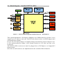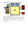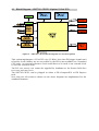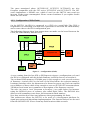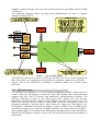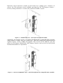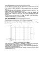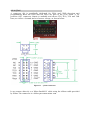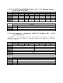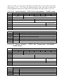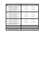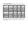
1
Unit / Module Description:
Dual 3-GHz PXIe ADC Module
Unit / Module Number:
SMT702
Document Issue Number:
8
Issue Date:
11/12/12
Original Author:
PhSR
User Manual
for
SMT702
Sundance Multiprocessor Technology Ltd, Chiltern House,
Waterside, Chesham, Bucks. HP5 1PS.
This document is the property of Sundance and may not be copied
nor communicated to a third party without prior written
permission.
© Sundance Multiprocessor Technology Limited 2006
Revision History
Issue
Changes Made
Date
Initials
1
Original Document released
12/09/08
PhSR
2
DMA and system monitor added
30/01/09
PhSR
3
ADCs Output characteristics updated. Ordering
information updated with FX70t part.
01/12/09
PhSR
4
FPGA Design supports Xlinks.
06/05/10
PhSR
5
Added missing currents; Added weight.
22/05/10
PhSR
6
Soft Reset added in the control register.
14/07/10
PhSR
7
Comment added on board modification (ADC
reset)
27/07/10
PhSR
8
Added FX100T version
11/12/12
JV
Table of Contents
1
2
Introduction ........................................................................................................................ 7
Related Documents........................................................................................................... 8
2.1 Referenced Documents ................................................................................................ 8
3
Acronyms, Abbreviations and Definitions................................................................ 8
3.1 Acronyms and Abbreviations ..................................................................................... 8
4
Functional Description .................................................................................................... 9
4.1 General Block Diagram................................................................................................. 9
4.2 Block Diagram - Standard SMT702 (PXIe) ..............................................................10
4.3 Block Diagram – SMT702-HYBRPXI32 (option 32-bit PXI) ..................................11
4.1 Block Diagram – SMT702-CPCI32 (Option 32-bit PCI).........................................12
4.2 Module Description.....................................................................................................13
4.2.1 ADCs..........................................................................................................................13
4.2.2 FPGA ..........................................................................................................................13
4.2.2.1 General Description......................................................................................13
4.2.2.2 Resources used – XC5VLX110T. ................................................................13
4.2.2.3 Resources used – XCV5FX70T....................................................................15
4.2.2.4 Resources used – XCV5FX100T. ................................................................16
4.2.3 Configuration (CPLD+Flash).................................................................................18
4.2.4 DDR2 Memory .........................................................................................................19
4.2.5 Clock circuitry .........................................................................................................20
4.2.6 Data (samples) path / Data capture ...................................................................21
4.2.7 PXI Express Bus .......................................................................................................22
4.2.8 SHB Connector ........................................................................................................24
4.2.9 Power dissipation ...................................................................................................24
4.2.10JTAG ..........................................................................................................................25
4.2.11PXI Express Hybrid Connectors...........................................................................27
4.3 FPGA Design .................................................................................................................28
4.3.1 Control Registers ....................................................................................................28
4.3.1.1 Memory Map...................................................................................................28
4.3.1.2 Register Descriptions ...................................................................................31
4.3.1.2.1 General Control Register – 0x8 (read-only)......................................31
4.3.1.2.2 Set Control Register – 0x10 (write). ...................................................34
4.3.1.2.3 Clear Control Register – 0x20 (write). ...............................................36
4.3.1.2.4 Board Name and Version – 0x24 (read-only). ..................................36
4.3.1.2.5 Firmware Version and Revision Numbers – 0x40 (read-only). ....36
4.3.1.2.6 ADCA (ADC083000) Register 0x1 – Configuration Register –
0x44 (write). ................................................................................................................37
4.3.1.2.7 ADCA (ADC083000) Register 0x2 – Offset Adjust – 0x48 (write
and read). 37
4.3.1.2.8 ADCA (ADC083000) Register 0x3 – Full Scale Voltage Adjust –
0x4C (write and read). ..............................................................................................38
4.3.1.2.9 ADCA (ADC083000) Register 0xD – Extended Clock Phase Adjust
Fine – 0x74 (write and read)....................................................................................38
4.3.1.2.10 ADCA (ADC083000) Register 0xE – Extended Clock Phase
Adjust Coarse – 0x78 (write and read). ................................................................39
4.3.1.2.11 ADCA (ADC083000) Register 0xF – Test Pattern register – 0x7C
(write and read)..........................................................................................................39
4.3.1.2.12 ADCB (ADC083000) Register 0x1 – Configuration Register –
0x84 (write and read)................................................................................................40
4.3.1.2.13 ADCB (ADC083000) Register 0x2 – Offset Adjust – 0x88 (write
and read). 41
4.3.1.2.14 ADCB (ADC083000) Register 0x3 – Full Scale Voltage Adjust –
0x8C (write and read). ..............................................................................................41
4.3.1.2.15 ADCB (ADC083000) Register 0xD – Extended Clock Phase
Adjust Fine 0xB4 (write and read). ........................................................................42
4.3.1.2.16 ADCB (ADC083000) Register 0xE – Extended Clock Phase
Adjust Coarse – 0xB8 (write and read). ................................................................42
4.3.1.2.17 ADCB (ADC083000) Register 0xF – Test Pattern register – 0xBC
(write and read)..........................................................................................................43
4.3.1.2.18 Frequency Synthesizer (LMX2531) Register R0 – 0xC0 (write and
read).
43
4.3.1.2.19 Frequency Synthesizer (LMX2531) Register R1 – 0xC4 (write and
read).
44
4.3.1.2.20 Frequency Synthesizer (LMX2531) Register R2 – 0xC8 (write and
read).
44
4.3.1.2.21 Frequency Synthesizer (LMX2531) Register R3 – 0xCC (write
and read). 45
4.3.1.2.22 Frequency Synthesizer (LMX2531) Register R4 – 0xD0 (write
and read). 45
4.3.1.2.23 Frequency Synthesizer (LMX2531) Register R5 – 0xD4 (write
and read). 46
4.3.1.2.24 Frequency Synthesizer (LMX2531) Register R6 – 0xD8 (write
and read). 47
4.3.1.2.25 Frequency Synthesizer (LMX2531) Register R7 – 0xDC (write
and read). 48
4.3.1.2.26 Frequency Synthesizer (LMX2531) Register R8 – 0xE0 (write and
read).
48
4.3.1.2.27 Frequency Synthesizer (LMX2531) Register R9 – 0xE4 (write and
read).
49
4.3.1.2.28 Frequency Synthesizer (LMX2531) Register R12 - 0xE8 (write
and read). 49
4.3.1.2.29 ADCA – DCM Phase Shift – 0x108 (write). .....................................50
4.3.1.2.30 ADCB – DCM Phase Shift – 0x10C (write).......................................50
4.3.1.2.31 System Monitor – FPGA Die Temperatures – 0x180 (read). .......51
4.3.1.2.32 System Monitor – FPGA Die Temperature thresholds – 0x180
(write).
51
4.3.1.2.33 System Monitor – FPGA Core Voltages – 0x184 (read)................52
4.3.1.2.34 System Monitor – FPGA core voltage thresholds – 0x184 (write).
52
4.3.1.2.35 System Monitor – FPGA Aux Voltages – 0x188 (read).................53
4.3.1.2.36
System Monitor – FPGA aux voltage thresholds – 0x188 (write).
53
4.3.1.2.37 Amount of samples stored in DDR2 – Bank A – 0x18C (write).54
4.3.1.2.38 Amount of samples stored in DDR2 – Bank B – 0x190 (write). 54
4.3.2 System Monitor. ......................................................................................................54
4.3.3 External Signal characteristics.............................................................................55
5
Board Layout ....................................................................................................................57
5.1 Top View........................................................................................................................57
5.2 Bottom View..................................................................................................................58
6
Photo ...................................................................................................................................59
6.1 Overview of the board................................................................................................59
6.2 Front panel....................................................................................................................61
6.3 How is it going to stand on your desk?..................................................................61
7
Software Packages ..........................................................................................................62
8
Physical Properties .........................................................................................................64
9
Hardware Modification..................................................................................................65
10 Safety ..................................................................................................................................66
11 EMC......................................................................................................................................66
12 Ordering Information.....................................................................................................66
Table of Figures
Figure 1 - SMT702 General Block Diagram............................................................................. 9
Figure 2 - SMT702 Block Diagram (Standard SMT702 - PXI Express) .............................10
Figure 3 - SMT702 Block Diagram (32-bit PXI Option).......................................................11
Figure 4 - SMT702-CPCI32 Block Diagram (32-bit CPCI Option) .....................................12
Figure 5 - Configuration (Flash). .............................................................................................18
Figure 6 - Clock circuitry Block Diagram. .............................................................................21
Figure 7 - Data (samples) path. ...............................................................................................22
Figure 8 - Standard SMT702 - PXI Express Peripheral Module.........................................23
Figure 9 - SMT702-HYBRPXI32 (opt.) - Hybrid Peripheral Slot Compatible PXI-1
Module..................................................................................................................................23
Figure 10 - Forced airflow for a 3U module. ........................................................................24
Figure 11 - JTAG Connector.....................................................................................................25
Figure 12 - Photo of a Xilinx Parallel IV cable and its ribbon cable for JTAG
connection ...........................................................................................................................26
Figure 13 - Block Diagram - FPGA Design (standard Firmware). .....................................28
Figure 14 – Register Memory Map. .........................................................................................30
Figure 15 – Main Characteristics. ...........................................................................................56
Figure 16 - Board Layout (Top View)......................................................................................57
Figure 17 - Board Layout (Bottom View) ...............................................................................58
Figure 18 - Overview of the board..........................................................................................60
Figure 19 - SMT702 Front Panel..............................................................................................61
Figure 20 - SMT702 - PXI Express Chassis. ...........................................................................61
Figure 21 - SMT702 Demo application. .................................................................................63
Figure 22 - ADC Reset structure modification. ...................................................................65
1 Introduction
The SMT702 is a PXI Express (opt. Hybrid) Peripheral Module (3U), which integrates
two fast 8-bit ADCs, a clock circuitry, 2 banks of DDR2 Memory (1GByte each), IO
connectors (2 SHBs, SATA and RSL) and a Virtex5 Xilinx FPGA, under the 3U format.
The PXIe specification integrates PCI Express signalling into the PXI standard for
more backplane bandwidth. It also enhances PXI timing and synchronisation
features by incorporating a 100MHz differential reference clock and triggers. The
SMT702 can also integrate the standard 32-bit PXI signalling as an option.
Both ADC chips are identical and can produce 3 Giga-samples per second each, with
an 8-bit resolution. The manufacturer is National Semiconductor and the part
number is ADC083000. Analog-to-Digital converters are clocked by circuitry based
on a PLL coupled with a VCO in order to generate a low-jitter signal. Each ADC
integrates settings such as offset and scale factor, which makes the pair of ADC
suitable to be combined together in order to make a 6GSPS single Analog to Digital
converter. This will be subject to a specific FPGA design.
An on-board PLL+VCO chip ensures a stable fixed sampling frequency (maximum
rate), in order for the board to be used as a digitiser without the need of external
clock signal. The PLL will be able to lock its internal VCO either on the 100MHz PXI
express reference, on the 10MHz PXI reference or on an external reference signal.
The sampling clock for the converters can be either coming from the PLL+VCO chip
(fixed frequency of 1.5ghz) or from an external source. The chip used is a National
Semiconductor part: LMX2531LQ1500. The reference clock selected is also output
on a connector in order to pass it to an other module.
The Virtex5 FPGA is responsible for controlling all interfaces, including PXI (32-bit)
and PXIe (up to 8 lanes – not all PXI Express controller support 8 lane), as well as
routing samples. The FPGA fitted on the SMT702 is part of the Virtex-5 familly from
Xilinx, XC5VLX110T-3 (fastest speed grade available).
Two DDR2 memory banks are accessible by the FPGA in order to store data on the
fly. Each bank can store up to 1GByte.
An SHB connector is available in order to transfer data/samples to an other
Sundance module (SMT712 for instance)
All analog connectors on the front panel are SMA.
2 Related Documents
2.1 Referenced Documents
1 - National Semiconductor ADC083000:
http://www.national.com/pf/DC/ADC083000.html
2 – National Semiconductor LMX2531LQ1500:
http://www.national.com/pf/LM/LMX2531LQ1500E.html
3 - Virtex5 FPGA:
http://www.xilinx.com/products/silicon_solutions/fpgas/virtex/virtex5/index.htm
4 - PXIe specifications: http://www.pxisa.org/Spec/PXIEXPRESS_HW_SPEC_R1.PDF
5 – Micron 2Gigabit DDR2 chip MT47H128M16:
http://download.micron.com/pdf/datasheets/dram/ddr2/2gbddr2.pdf
6 – Sundance xlink presentation:
ftp://ftp2.sundance.com/Pub/documentation/pdf-files/X-Link.pdf
7 – Sundance xlink specifications:
ftp://ftp2.sundance.com/Pub/documentation/pdf-files/D000051S-spec.pdf
3 Acronyms, Abbreviations and Definitions
3.1 Acronyms and Abbreviations
PXIe : PXI Express.
SNR: Signal-to-Noise Ratio. It is expressed in dBs. It is defined as the ratio of a signal
power to the noise power corrupting the signal.
SINAD: Signal-to-Noise Ratio plus Distorsion. Same as SNR but includes harmonics
too (no DC component).
ENOB: Effective Number Of Bits. This is an alternative way of defining the Signal-toNoise Ratio and Distorsion Ratio (or SINAD). This means that the ADC is equivalent
to a perfect ADC of ENOB number of bits.
SFDR: Spurious-Free Dynamic Range. It indicates in dB the ratio between the powers
of the converted main signal and the greatest undesired spur.
4 Functional Description
4.1 General Block Diagram
Below is the general block diagram showing all resources available on the board.
Note that not all option are implement in the standard firmware.
Figure 1 - SMT702 General Block Diagram.
The following block diagram shows all three options. The first option (PXIe) can be
plugged into any PXI Express slot, the second (32-bit PXI) into any Hybrid PXI
Express slot and the third can go in any CPCI system.
4.2 Block Diagram - Standard SMT702 (PXIe)
Figure 2 - SMT702 Block Diagram (Standard SMT702 - PXI Express)
This option implements a PCI Express Endpoint core (Xilinx) based on 4 lanes. It can
support up to 8 lanes or only one. The FPGA also has accesses to all PXI triggers and
synchronisation signals.
In case the user has in mind to recompile/change the firmware, the PCI Express Core
is free and provided by Xilinx. A free license locked on a PC MAC key has to be
requested.
The SMT702 (PXIe version) can only be plugged into a PXI Express or CompactPCI
Express Rack.
Note that not all resources are implemented in the standard FPGA firmware.
4.3 Block Diagram – SMT702-HYBRPXI32 (option 32-bit PXI)
Figure 3 - SMT702 Block Diagram (32-bit PXI Option)
This option implements a 32-bit PCI core (33 Mhz). The FPGA also has accesses to all
PXI triggers and synchronisation signals.
The PCI core source core cannot be supplied by Sundance as the license held does
not cover such use for it. In case the user intends to recompile the source code or
design his own firmware, he would have to purchase a license for the core.
The SMT702-HYBRPXI32 can only be plugged into a PXI Express or CompactPCI
Express rack.
Note that not all ressoures shown on the above diagram are implemented in the
standard firmware.
4.1 Block Diagram – SMT702-CPCI32 (Option 32-bit PCI)
Figure 4 - SMT702-CPCI32 Block Diagram (32-bit CPCI Option)
This option implements a 32-bit PCI core (33 Mhz). Note that PXI trigger signals and
reference clock (10Mhz) are not accessible by the PFGA (not available on a standard
CPCI rack). An external reference clock would have to be used or an external clock
to feed the converter with.
The PCI core source core cannot be supplied by Sundance as the license held does
not cover such use for it.
The SMT702-CPCI32 can be plugged in either a PXI (CompactPCI) or PXI Express
rack.
Note that not all resources shown on the above diagram are implemented in the
standard firmware.
4.2 Module Description
4.2.1 ADCs
The ADCs are 8-bit parts from National Semiconductor (ADC083000). On the
SMT702, each ADC can achieve up to 3 GSPS, in DDR mode.
Both ADCs are used in the extended mode. For more information, please refer to the
ADC083000 datasheet (National Semiconductor). This implies that they are
configured using a Serial Interface implemented in the FPGA.
The typical Bit Error Rate (BER) of the ADC083000 is 10-18.
Each ADC takes a DDR clock, i.e. to achieve 3GSPS, a clock of 1.5Ghz is required.
The ADCs can only work with a DDR clock within the range 500-1500MHz, which
means they can sample at a rate between 1 and 3 GSPS.
Both ADCs are AC-coupled using an RF Transformer.
They have functionalities such as offset and scale adjustments, as well as test
pattern mode. There is also calibration cycle that can be run once the system is in
temperature.
The FPGA is able to synchronise the ADCs so they samples in phase. The FPGA is
able to return the phase shift between ADCA and ADCB to the host application by
sampling their clock with its local clock and phase shifting it with a DCM.
4.2.2 FPGA
4.2.2.1 General Description
The FPGA fitted as standard on the SMT702 is part of the Virtex5 LXT family:
XC5VLX110T. The package used if FFG1136 and the speed grade is -3 (fastest part).
The SMT702 can also receive an FPGA from the Virtex5 FXT family (XC5VFX70T and
XC5VFX100T in the same package).
The FPGA is fitted with a heatsink coupled with a fan to keep it within an
appropriate range of temperature when using the default firmware provided.
Nevertheless the board requires some forced cooling. It is recommended to use a
PXI-1062Q chassis or equivalent from National instrument as it already integrates a
built-in cooling system. Using slot blockers from National Instrument would
improve even more the cooling capacity of the system.
In order to improve the heat dissipation is a system, some slot blockers can be used
(from National Instrument), which redirect the air flow of non-used slots to where it
is needed.
4.2.2.2 Resources used – XC5VLX110T.
Below is a summary (ISE11.4) of the resources used in the FPGA by the default
firmware (Standard SMT702 – XCV5VLX110T FPGA – PXIe option):
Slice Logic Utilization:
Number of Slice Registers:
Number used as Flip Flops:
Number used as Latches:
Number used as Latch-thrus:
Number of Slice LUTs:
Number used as logic:
Number using O6 output only:
Number using O5 output only:
15,254 out of
15,244
4
6
11,699 out of
11,230 out of
9,310
295
69,120
22%
69,120
69,120
16%
16%
Number using O5 and O6:
Number used as Memory:
Number used as Dual Port RAM:
Number using O6 output only:
Number using O5 output only:
Number using O5 and O6:
Number used as Shift Register:
Number using O6 output only:
Number used as exclusive route-thru:
Number of route-thrus:
Number using O6 output only:
Number using O5 output only:
Slice Logic Distribution:
Number of occupied Slices:
Number of LUT Flip Flop pairs used:
Number with an unused Flip Flop:
Number with an unused LUT:
Number of fully used LUT-FF pairs:
Number of unique control sets:
Number of slice register sites lost
to control set restrictions:
1,625
439 out of
308
204
20
84
131
131
30
357
325
32
17,920
2%
out of
17,280
35%
out of
out of
out of
18,945
18,945
18,945
19%
38%
42%
1,801 out of
69,120
2%
6,129
18,945
3,691
7,246
8,008
812
A LUT Flip Flop pair for this architecture represents one LUT paired with
one Flip Flop within a slice. A control set is a unique combination of
clock, reset, set, and enable signals for a registered element.
The Slice Logic Distribution report is not meaningful if the design is
over-mapped for a non-slice resource or if Placement fails.
OVERMAPPING of BRAM resources should be ignored if the design is
over-mapped for a non-BRAM resource or if placement fails.
IO Utilization:
Number of bonded IOBs:
Number of LOCed IOBs:
IOB Flip Flops:
IOB Master Pads:
IOB Slave Pads:
Number of bonded IPADs:
Number of bonded OPADs:
Specific Feature Utilization:
Number of BlockRAM/FIFO:
Number using BlockRAM only:
Number using FIFO only:
Total primitives used:
Number of 36k BlockRAM used:
Number of 18k BlockRAM used:
Number of 36k FIFO used:
Number of 18k FIFO used:
Total Memory used (KB):
Number of BUFG/BUFGCTRLs:
Number used as BUFGs:
Number of IDELAYCTRLs:
Number of BUFDSs:
Number of BUFIOs:
Number of DCM_ADVs:
Number of LOCed DCM_ADVs:
Number of GTP_DUALs:
Number of LOCed GTP_DUALs:
Number of PCIEs:
Number of PLL_ADVs:
Number of SYSMONs:
Number of RPM macros:
128
463
461
693
1
1
10
8
out of
out of
640
463
72%
99%
out of
out of
50
32
20%
25%
38 out of
22
16
148
25%
5,328
32
24%
71%
22
8
80
12
8
8
2
1
6
1
27%
12%
20%
66%
100%
25%
100%
100%
16%
100%
21
1
14
2
1,314
23
23
6
1
16
8
8
2
2
1
1
1
out of
out of
out
out
out
out
out
out
out
out
out
out
of
of
of
of
of
of
of
of
of
of
Average Fanout of Non-Clock Nets:
3.00
4.2.2.3 Resources used – XCV5FX70T.
Below is a summary (ISE11.4) of the resources used in the FPGA by the default
firmware (Standard SMT702 – XCV5VFX70T FPGA – PXIe option):
Slice Logic Utilization:
Number of Slice Registers: 15,344 out of 44,800 34%
Number used as Flip Flops:
Number used as Latches:
Number used as Latch-thrus:
Number of Slice LUTs:
Number used as logic:
Number using O6 output only:
Number using O5 output only:
Number using O5 and O6:
Number used as Memory:
Number used as Dual Port RAM:
Number using O6 output only:
Number using O5 output only:
Number using O5 and O6:
Number used as Shift Register:
Number using O6 output only:
Number used as exclusive route-thru:
Number of route-thrus:
Number using O6 output only:
Number using O5 output only:
Slice Logic Distribution:
Number of occupied Slices:
Number of LUT Flip Flop pairs used:
Number with an unused Flip Flop:
Number with an unused LUT:
Number of fully used LUT-FF pairs:
Number of unique control sets:
Number of slice register sites lost
to control set restrictions:
15,337
1
6
11,832 out of
11,372 out of
9,458
289
1,625
429 out of
308
204
20
84
121
121
31
393
318
75
44,800
44,800
26%
25%
13,120
3%
out of
11,200
55%
out of
out of
out of
19,052
19,052
19,052
19%
37%
42%
1,821 out of
44,800
4%
6,261
19,052
3,708
7,220
8,124
821
A LUT Flip Flop pair for this architecture represents one LUT paired with
one Flip Flop within a slice. A control set is a unique combination of
clock, reset, set, and enable signals for a registered element.
The Slice Logic Distribution report is not meaningful if the design is
over-mapped for a non-slice resource or if Placement fails.
OVERMAPPING of BRAM resources should be ignored if the design is
over-mapped for a non-BRAM resource or if placement fails.
IO Utilization:
Number of bonded IOBs:
Number of LOCed IOBs:
IOB Flip Flops:
IOB Master Pads:
IOB Slave Pads:
Number of bonded IPADs:
Number of bonded OPADs:
Specific Feature Utilization:
Number of BlockRAM/FIFO:
Number using BlockRAM only:
Number using FIFO only:
Total primitives used:
Number of 36k BlockRAM used:
463
463
693
1
1
10
8
out of
out of
640
463
72%
100%
out of
out of
50
32
20%
25%
38 out of
22
16
148
25%
21
Number of 18k BlockRAM used:
Number of 36k FIFO used:
Number of 18k FIFO used:
Total Memory used (KB):
Number of BUFG/BUFGCTRLs:
Number used as BUFGs:
Number of IDELAYCTRLs:
Number of BUFDSs:
Number of BUFIOs:
Number of DCM_ADVs:
Number of LOCed DCM_ADVs:
Number of GTX_DUALs:
Number of LOCed GTX_DUALs:
Number of PCIEs:
Number of LOCed PCIEs:
Number of PLL_ADVs:
Number of SYSMONs:
Number of RPM macros:
128
Average Fanout of Non-Clock Nets:
1
14
2
1,314
25
25
6
1
16
8
8
2
2
1
1
1
1
out of
out of
out
out
out
out
out
out
out
out
out
out
out
of
of
of
of
of
of
of
of
of
of
of
5,328
32
24%
78%
22
8
80
12
8
8
2
3
1
6
1
27%
12%
20%
66%
100%
25%
100%
33%
100%
16%
100%
3.00
4.2.2.4 Resources used – XCV5FX100T.
Below is a summary (ISE14.3) of the resources used in the FPGA by the default
firmware (Standard SMT702 – XCV5VFX100T FPGA – PXIe option):
Slice Logic Utilization:
Number of Slice Registers:
Number used as Flip Flops:
Number used as Latches:
Number used as Latch-thrus:
Number of Slice LUTs:
Number used as logic:
Number using O6 output only:
Number using O5 output only:
Number using O5 and O6:
Number used as Memory:
Number used as Dual Port RAM:
Number using O6 output only:
Number using O5 output only:
Number using O5 and O6:
Number used as Shift Register:
Number using O6 output only:
Number using O5 and O6:
Number used as exclusive route-thru:
Number of route-thrus:
Number using O6 output only:
Number using O5 output only:
Number using O5 and O6:
Slice Logic Distribution:
Number of occupied Slices:
Number of LUT Flip Flop pairs used:
Number with an unused Flip Flop:
Number with an unused LUT:
Number of fully used LUT-FF pairs:
Number of unique control sets:
Number of slice register sites lost
to control set restrictions:
16,720
16,712
2
6
12,911
12,053
10,065
348
1,640
816
308
204
20
84
508
507
1
42
441
389
51
1
out of
64,000
26%
out of
out of
64,000
64,000
20%
18%
out of
19,840
4%
7,335
21,153
4,433
8,242
8,478
987
out of
16,000
45%
out of
out of
out of
21,153
21,153
21,153
20%
38%
40%
2,113 out of
64,000
3%
A LUT Flip Flop pair for this architecture represents one LUT paired with
one Flip Flop within a slice. A control set is a unique combination of
clock, reset, set, and enable signals for a registered element.
The Slice Logic Distribution report is not meaningful if the design is
over-mapped for a non-slice resource or if Placement fails.
OVERMAPPING of BRAM resources should be ignored if the design is
over-mapped for a non-BRAM resource or if placement fails.
IO Utilization:
Number of bonded IOBs:
Number of LOCed IOBs:
IOB Flip Flops:
IOB Master Pads:
IOB Slave Pads:
Number of bonded IPADs:
Number of LOCed IPADs:
Number of bonded OPADs:
Specific Feature Utilization:
Number of BlockRAM/FIFO:
Number using BlockRAM only:
Number using FIFO only:
Total primitives used:
Number of 36k BlockRAM used:
Number of 18k BlockRAM used:
Number of 36k FIFO used:
Number of 18k FIFO used:
Total Memory used (KB):
Number of BUFG/BUFGCTRLs:
Number used as BUFGs:
Number of IDELAYCTRLs:
Number of BSCANs:
Number of BUFDSs:
Number of BUFIOs:
Number of DCM_ADVs:
Number of LOCed DCM_ADVs:
Number of GTX_DUALs:
Number of LOCed GTX_DUALs:
Number of PCIEs:
Number of LOCed PCIEs:
Number of PLL_ADVs:
Number of SYSMONs:
Number of RPM macros:
137
Average Fanout of Non-Clock Nets:
465 out of
465 out of
694
1
1
10
2 out of
8
640
465
72%
100%
10
20%
42 out of
26
16
228
18%
8,208
32
17%
81%
22
4
8
80
12
8
8
2
3
1
6
1
27%
25%
12%
20%
66%
100%
25%
100%
33%
100%
16%
100%
22
4
14
2
1,404
26
26
6
1
1
16
8
8
2
2
1
1
1
1
out of
out of
out
out
out
out
out
out
out
out
out
out
out
out
3.12
of
of
of
of
of
of
of
of
of
of
of
of
The parts mentioned above (XC5VLX110T, XC5FX70T, XC5FX100T) are also
footprint compatible with the SXT series: XC5VSX50T and XC5VSX95T. The SXT
series implements a DSP48E core, which if used on the SMT702 may result an
increase of the power consumption. Please contact Sundance if you require details
about the SXT series.
4.2.3 Configuration (CPLD+Flash)
Configuration port
Address[25:0]
Data[7:0]
jtag
Switch[1:0]
Ctrl[4:0]
On the SMT702, the FPGA is connected to a CPLD via a serial link. The CPLD is
responsible for controlling read and write operations to and from the Flash memory
and to route data to the FPGA configuration port.
The following diagram show how connections are made on the board between the
CPLD, the Flash memory and the FPGA:
Figure 5 - Configuration (Flash).
A reset coming from the bus (PXI or PXI Express) triggers a configuration cycle and
the FPGA is configured with the default firmware (stored in factory at location 0).
The on-board Flash memory (256-Mbit part) is big enough to store several versions
of firmware. A switch (SW1) at the back of the board allows the selection among 4
locations (Switches select the bitstream to be booted at power up). Each can contain
up to 8Mbytes of data, which is big enough to store an XC5LX110T bitstream (about
3.8 Mbytes) and some text (comments or description of the firmware version).
The user can store a ‘user’ bitstream at location 1 (see table below) for instance
using the SMT6002 piece of software, also called Flash Utility. The SMT6002 also
allows to add comments (text) above the bitstream in flash memory.
Note that switches don’t have any influence when programming the flash.
This architecture allows the SMT702 to be used as a development platform for
signal processing and algorithms implementation. The function Reboot can be used
from the SMT6002 GUI to boot from any flash location within seconds.
Both FPGA and CPLD can be reprogrammed/reconfigured at anytime via JTAG (J8
connector – Using a Xilinx parallel/USB programming cable) but it can cause
problems as it will break the access to the board from the host.
At power up or under a reset on the PXI or PXI Express bus, it takes 140ms for the
FPGA (XC5VLX110T-3) to be fully configured and ready to answer the requests from
the host.
The following table shows the settings that can be used and the start addresses of
the bitstream in the Flash memory.
Position
Switch 2
Position
Switch 1
Bitstream start
address in
flash
Description
ON
ON
0x1800000
(Location 3)
User Bitstream 2
ON
OFF
0x1000000
(Location 2)
User Bitstream 1
OFF
ON
0x0800000
(Location 1)
User bitstream 0
OFF
OFF
0x0000000
(Location 0)
Default
bitstream
Default
selection
Note that the CPLD routes the contents of the flash starting from the location
selected (SW1) until the FPGA indicates that it is configured. Addresses are
incremented by a counter that rolls over to 0 when the maximum address is
reached. For instance, in the case where Location 1 is selected and a corrupted
bitstream is loaded at that location (or if there is no bitstream at that location), the
default bitstream will end up being loaded.
The default bitstream returns ‘DEF’ as firmware version (see register ‘Firmware
Version and Revision numbers).
It is recommended to keep the Switch SW1 so the User bitstream 0 is selected and
store a custom/user bitstream at Location 1 is needed. The card would then boot
from this location. Otherwise the card would boot automatically from the default
firmware (Location 0)
Storing a new bitstream using the SMT6002 first involves erasing the appropriate
sectors before programming them with the bitstream. This is automatically handled
by the SMT6002. Storing a new bitstream at location 1 (User Bitstream 0) will only
require from the user to select the file (.bit for instance) and press the ‘Comit’
button. The advanced tab offers more options such as a full erase or a partial erase
of the flash memory. None of them should be required in normal mode of operation.
Note that a full erase will erase the entire contents of the flash including the default
firmware and that it can take up to 3-4 minutes. The partial erase will erase the User
bitstreams only.
4.2.4 DDR2 Memory
Two banks of DDR2 memory are available on the SMT702, directly connected to the
FPGA. Interfaces are part of the default FPGA design. Each bank is 64-bit wide and
128-Meg deep, so each bank can store up to 1 Giga bytes (or 8-bit ADC samples).
Each memory bank is dedicated to one ADC. Both DDR2 interfaces are independent.
The type of memory fitted on the board can be clocked at a maximum or 333MHz.
In order to achieve storage real-time of the ADC samples, the DDR2 interface is
clocked at 250MHz (Default bitstream).
4.2.5 Clock circuitry
An on-board PLL+VCO chip ensures a stable fixed sampling frequency (maximum
rate, i.e. 1500MHz), in order for the board to be used as a digitiser without the need
of external clock signal. The PLL will be able to lock its internal VCO either on the
10MHz PXI reference or the 100MHz PXI express reference or on an external
reference signal. The sampling clock for the converters can be either coming from
the PLL+VCO chip or from an external source. The chip used is a National
Semiconductor part: LMX2531LQ1500.
The selection Internal/External clock is made via a bit in the control register. The
same applies to the selection of the reference clock.
Note that the PLL+VCO chip also has the possibility to output half of the fixed VCO
frequency, i.e. 1500/2=750MHz.
Below is a block diagram of the clock circuitry.
#5
Ref Out
PXIe Ref (10MHz)
(back-plane)
“1
0
”
Fixed on-board clock generator
c_REF_CLK_
OUT_DIV
PXIe Ref (100MHz)
(back-plane)
“01”
#4
750 or 1500
MHz
(1.5GHz or half of it)
”
”
“0
0
“0
5-80
MHz
c_REF_CLK_ON
BOARD_DIV
Ext Ref
500-1500
MHz
LMX2531
Reference Clock Selection
“1”
c_RF_CLK_SEL[1:0]
#3
LMX2531
Ext Clk
500-1500
MHz
Clock Distribution LMX2531
National Semiconductor
c_CLK_SOURCE_SEL
ADCA (8-bit,
3GSPS)
ADC083000
#2
National Semiconductor
ADCB (8-bit,
3GSPS)
ADC083000
#1
National Semiconductor
#x
SMA connector on
the front panel
Note that all blocks are control by the Register Block. Command are
received from the PXIe bus and decoded.
Figure 6 - Clock circuitry Block Diagram.
4.2.6 Data (samples) path / Data capture
This section details how samples from the ADCs are being captured and stored. By
default and after a power-up or reset operation, all interfaces are in reset state. The
only exception is the PXI/Express Interface. Relevant interface should first be taken
out of the initial reset state.
The next step is to program both ADCs and the clock generator and make sure it
locked to a reference signal. This is not needed in case of using an external
sampling clock. An ADC calibration cycle can be run. ADCs are then ready to output
samples and a clock to the FPGA.
Here are the details of the following step. One Xilinx DCM per ADC clock is used
inside the FPGA to ensure a good capture of data. The status of these DCMs should
be checked to make sure they are ‘locked’. They are available in the Global Control
Register. After being latched, samples go through a multiplexer to be pipelined and
then stored into the DDR2 memory available on the board. The DDR2 interface uses
some Xilinx specific blocks, such as idelays, DCMs and Phy, which have to be
‘locked’ and ‘ready’ as well. These have to be checked the same way, using the bits
available from the Global Control Register.
Each ADC is being dedicated a DDR2 Memory bank, which can be seen as a Fifo.
Both Fifos have status bits to check whether they are empty or full (bit available
from Global Control Register). Each Fifo is connected to a DMA channel. DMA
channel are implemented as Xlinks.
Samples coming from the ADCs are also routed straight on the SHB connector (DDR
32-bit bus).
The following diagram shows the data path implemented in order to capture
samples from the ADCs:
Figure 7 - Data (samples) path.
The SMT702 comes with a piece of software, the SMT7002. It is a demo application
that shows how to set up the module and allows capturing samples into text files.
Source code of the SMT7002 is available to purchase under the product name
SMT7026.
4.2.7 PXI Express Bus
As standard, the SMT702 is a 3U PXI Express peripheral module, which means it
comes with two PXI Express connectors: XP4 (PXI timing and synchronisation
signals) and XP3 (x8 PCI Express and additional synchronisation signals). The
SMT702 dedicates 8 lanes to the PXI Express bus, which gives an effective
bandwidth per direction of 16Gb/s. It also implies core and user clocks to be 250
MHz. Note that not all PXIe Express chassis and controller can handle 8 lanes on
peripheral modules. Currently only 1 and 4 lanes are supported. The Express core
developed by Sundance and based on Xlinks is able to achieve over 700Mbytes per
second for a 4-lane core clocked at 250MHz and half of it when clocked at 125MHz.
The standard SMT702 can plug in any PXI Express Peripheral Slot or any PXI Express
Hybrid Slot (PXI Express chassis, such as the NI-1062Q from National Instrument or
equivalent).
Reference clock selection is made on the board via a jumper (J11). Position 1-2
selects the PXI reference clock (100Mhz provided by the PXI Express chassis –
Factory setting). Position 2-3 selects the on-board 250Mhz crystal.
Figure 8 - Standard SMT702 - PXI Express Peripheral Module
Optionally, the module can be a 3U Hybrid Peripheral Slot Compatible PXI-1 Module,
which means it comes with two connectors: XP4 (PXI timing and synchronisation
signals) and P1 (32-bit, 33MHz PCI Signals). This version of the SMT702 can only
plug in a PXI Express Hybrid Slot (PXI Express chassis, such as the NI-1062Q from
National Instrument or equivalent).
Figure 9 - SMT702-HYBRPXI32 (opt.) - Hybrid Peripheral Slot Compatible PXI-1 Module
4.2.8 SHB Connector
An SHB Connector is available from the FPGA. It maps 32 single-ended data lines
and a set of control signals including a clock.
It can be used to transfer samples to an other Sundance module, for instance the
SMT712.
A second SHB connector is available on the standard version of the SMT702 (not
available on the option -HYBRPXI32 and –CPCI32).
Note that in order to achieve transfers to an SMT712 board, the standard SHB
interface can’t be used but requires its DDR version (implement into default
firmware).
The SHB transfers have been tested at 375MHz, DDR mode, 32-bit words, giving a
continuous transfer speed of 3GBytes per second.
4.2.9 Power dissipation
The SMT702 has been designed to work in a PXI Express chassis, which has built-in
cooling facilities. It provides enough airflow and has a fan regulation.
PXI Express chassis are specified so they can dissipate 30 Watts of heat.
The following picture shows the direction of the forced air flow across a 3U PXI
Express module:
Figure 10 - Forced airflow for a 3U module.
A PXI Express rack has a capacity of dissipating 30 watts of heat per slot using
forced air-cooling system via typically two 110-cfm fans with filter.
In case the SMT702 is used in an other type of chassis, some similar airflow must be
implemented as the board requires it.
The SMT702 has been developed using the following PXI Express rack from Nation
Instrument: PXIe-1062Q.
4.2.10 JTAG
A connector (J8) is specifically dedicated for FPGA and CPLD detection and
programming. Both the CPLD and the FPGA are part of the JTAG chain. A 14position (2x7) connector (2mm) is available and shows TDI, TDO, TCK and TMS
lines, as well as a Ground and a reference voltage, as shown below:
Figure 11 - JTAG Connector.
It can connect directly to a Xilinx Parallel IV cable using the ribbon cable provided
by Xilinx. The connector is a Molex part: Molex 87831-1428.
Figure 12 - Photo of a Xilinx Parallel IV cable and its ribbon cable for JTAG connection
4.2.11 PXI Express Hybrid Connectors
As being a PXI Express Hybrid Peripheral Module, the SMT702 is a 3U card with 2
PXI connectors, XP4 and XP3 or P1. The following table shows their pinouts.
The SMT702 implements up to eight 2.5-Gigabit PCI Express lanes, allowing a
maximum theoretical data transfer of 2 gigabytes per second. It also implements
optionally a 32-bit, 33-MHz PCI interface.
4.3 FPGA Design
The following block diagram shows how the default FPGA design is organised.
DDR2 Memory BankA
64-bit wide
DDR2 Memory BankB
64-bit wide
1Gbytes, 250MHz
1Gbytes, 250MHz
DDR2 Interface
DDR2 Interface
Flash
CPLD
#3
#2
32-bit SHB
ADCA (8-bit,
3GSPS)
ADC083000
4x8 bits
(375MHz)
Demux
1:2
DDR
LVDS
ADCB (8-bit,
3GSPS)
ADC083000
4x8 bits
(375MHz)
National Semiconductor
LVDS
Demux
1:2
DDR
M
Hz
)
(3
75
2xlanes
DD
R
Ext Clk
National Semiconductor
#1
ADC and
Clock SPIs
LMX2531
bi
ts
Ext Ref
4x
8
#4
Clock
Distribution
DDR LVDS
PXIe Ref (100MHz)
8x8 bits (187.5 MHz)
PXI Ref (10MHz)
DDR LVDS
8x8 bits (187.5 MHz)
#5
\
Ref Out
8x8 bits
(187.5 MHz)
DDR
LVDS
4x8
bits
(375
MHz)
DDR
4xRSL
4xlanes
PCI
Express
Core
(Endpoint)
4 PXIe Lanes
PXIe
Bus
Data&Control
4 [email protected]/s
PCI Interface
(opt)
via RSL connectors
([email protected]/s)
32-bit PXI/SHB
Control
Registers
Virtex 5 LXT
#x
Dual SATA
connector
(optional)
RSL
Interface
8x8 bits
(187.5 MHz)
DDR
LVDS
DDR
SHB(ChA)
connector
SMA connector on
the front panel
32-bit PXI
Bus (optional)
or DDR SHB
(ChB)
connector
(standard SMT702)
1 - Note that all blocks are control by the Register Block. Command
are received from the PXIe bus and decoded.
2 – Samples are stored directly in the memory and played back to
be sent over PXIe, RSL, optionally SATA or optionally PCI
Figure 13 - Block Diagram - FPGA Design (standard Firmware).
4.3.1 Control Registers
The Control Registers drive the complete functionality of the SMT702. They are
setup via the PXIe bus (standard firmware provided). The settings of the ADCs,
triggers, clocks and the configuration of the RSL/PXI interfaces (optional SATA) and
the internal FPGA data path settings can be configured.
The data passed on to the SMT702 over the PXIe bus must conform to a certain
packet structure and to specific addresses and offsets. Only valid packets will be.
4.3.1.1 Memory Map
The write packets must contain the address where the data must be written to and
the read packets must contain the address where the required data must be read.
The following figure shows the memory map for the writable and readable registers
on the SMT702:
The access to a specific register is made by reading or writing to the address:
Address from Host = Offset + Register Address
Offset
Description.
0x0000
SMT7xx Boards common registers (Reboot, global reset).
0x0400
SMT702 Registers (ADCs, Clock and control).
0x0800
ADCa data channel (Xlink)
0x0C00
ADCb data channel (Xlink)
0x1000
Table of Contents (see Xlink Specifications for more details).
0x1400
Flash memory for bitstream storage.
0x2400
Event Block
Offset 0x0000 – SMT7xx Common Registers.
Register
Address
Writable Registers
Readable Registers
0x04
Global Reset (bit31).
Reserved.
0x80
Reconfiguration – Bitstream number.
Reserved.
Offset 0x0400 – SMT702 Registers.
Register
Address
0x08
Writable Registers
Readable Registers
Reserved.
General Control Register.
0x010
Set Control Register.
Reserved.
0x020
Clear Control Register.
Reserved.
0x24
Reserved
Board Name and Version.
0x40
Reserved.
Firmware Version and Revision Numbers.
0x44
ADCA (ADC083000) Register 0x1.
Read-back (FPGA Register) ADCA (ADC083000)
Register 0x1.
0x48
ADCA (ADC083000) Register 0x2.
Read-back (FPGA Register) ADCA (ADC083000)
Register 0x2.
0x4C
ADCA (ADC083000) Register 0x3.
Read-back (FPGA Register) ADCA (ADC083000)
Register 0x3.
0x74
ADCA (ADC083000) Register 0xD.
Read-back (FPGA Register) ADCA (ADC083000)
Register 0xD.
0x78
ADCA (ADC083000) Register 0xE.
Read-back (FPGA Register) ADCA (ADC083000)
Register 0xE.
0x7C
ADCA (ADC083000) Register 0xF.
Read-back (FPGA Register) ADCA (ADC083000)
Register 0xF.
0x84
ADCB (ADC083000) Register 0x1.
Read-back (FPGA Register) ADCB (ADC083000)
Register 0x1.
0x88
ADCB (ADC083000) Register 0x2.
Read-back (FPGA Register) ADCB (ADC083000)
Register 0x2.
0x8C
ADCB (ADC083000) Register 0x3.
Read-back (FPGA Register) ADCB (ADC083000)
Register 0x3.
0xB4
ADCB (ADC083000) Register 0xD.
Read-back (FPGA Register) ADCB (ADC083000)
Register 0xD.
0xB8
ADCB (ADC083000) Register 0xE.
Read-back (FPGA Register) ADCB (ADC083000)
Register 0xE.
0xBC
ADCB (ADC083000) Register 0xF.
Read-back (FPGA Register) ADCB (ADC083000)
Register 0xF.
0xC0
Frequency Synthesizer (LMX2531) register R0
Read-back (FPGA register) Frequency Synthesizer
(LMX2531) register R0
0xC4
Frequency Synthesizer (LMX2531) register R1
Read-back (FPGA register) Frequency Synthesizer
(LMX2531) register R1
0xC8
Frequency Synthesizer (LMX2531) register R2
Read-back (FPGA register) Frequency Synthesizer
(LMX2531) register R2
0xCC
Frequency Synthesizer (LMX2531) register R3
Read-back (FPGA register) Frequency Synthesizer
(LMX2531) register R3
0xD0
Frequency Synthesizer (LMX2531) register R4
Read-back (FPGA register) Frequency Synthesizer
(LMX2531) register R4
0xD4
Frequency Synthesizer (LMX2531) register R5
Read-back (FPGA register) Frequency Synthesizer
(LMX2531) register R5
0xD8
Frequency Synthesizer (LMX2531) register R6
Read-back (FPGA register) Frequency Synthesizer
(LMX2531) register R6
0xDC
Frequency Synthesizer (LMX2531) register R7
Read-back (FPGA register) Frequency Synthesizer
(LMX2531) register R7
0xE0
Frequency Synthesizer (LMX2531) register R8
Read-back (FPGA register) Frequency Synthesizer
(LMX2531) register R8
0xE4
Frequency Synthesizer (LMX2531) register R9
Read-back (FPGA register) Frequency Synthesizer
(LMX2531) register R9
0xE8
Frequency Synthesizer (LMX2531) register R12
Read-back (FPGA register) Frequency Synthesizer
(LMX2531) register R12
0x108
ADCA – DCM Phase Shift.
Reserved.
0x10C
ADCB – DCM Phase shift.
Reserved.
0x180
FPGA Die temperature thresholds.
System Monitor – Read-back FPGA die
temperature measured
0x184
FPGA Core voltage thresholds.
System Monitor – Read-back FPGA Vccint (Core
Voltage) measured
0x188
FPGA Aux voltage thresholds
System Monitor – Read-back FPGA Vccaux (Core
Voltage) measured
0x18C
Reserved
Amount of samples left to be read out out of
DDR2 BankA
0x190
Reserved
Amount of samples left to be read out out of
DDR2 BankB
Figure 14 – Register Memory Map.
Note that ADC registers are write-only (ADC chips), which means that the contents
of the ADC registers can only be read-back from the FPGA. THe same applies to the
Clock chip.
4.3.1.2 Register Descriptions
4.3.1.2.1
General Control Register – 0x8 (read-only).
Offset 0x0400 – General control Register – 0x8 (Read-only register).
Byte
Bit 7
Bit 6
Bit 5
Bit 4
3
ADCb synch
reference
state
ADCa synch
reference
state
System
Monitor
–
Vccaux
alarm
System
Monitor –
Vccint
alarm
Defaul
t
‘0’
‘0’
‘0’
2
DDR2 Fifo
Full
(Memory
Bank A)
DDR2 Fifo
Ready
(Memory
Bank B)
Defaul
t
‘0’
1
Bit 3
Bit 2
Bit 1
Bit 0
System
Monitor
– Die
temperat
ure
alarm
DDR2 Fifo
Almost
Empty
(Memory
Bank B)
DDR2 Fifo
Almost
Empty
(Memory
Bank A)
DDR2 Fifo
Full
(Memory
Bank B)
‘0’
‘0’
‘0’
‘0’
‘0’
IDelay
Control
Ready
(Memor
y Bank
B)
DDR2 Fifo
empty
(Memory
Bank B)
DDR2
lock
status
(Memory
Bank B)
DDR2 phy
init done
(Memory
Bank B)
Ddr2 Fifo
Ready
(Memory
Bank A)
IDelay
Control
Ready
(Memory
Bank A)
‘0’
‘0’
‘0’
‘0’
‘0’
‘1’
‘1’
DDR2 Fifo
empty
(Memory
Bank A)
DDR2 lock
status
(Memory
Bank A)
DDR2
phy init
done
(Memor
y Bank
A)
ADCb
calibrati
on
complete
d
ADCa
calibration
completed
ADCa
DCM Busy
ADCb
DCM Busy
Defaul
t
‘0’
‘0’
‘0’
‘0’
‘0’
‘0’
‘1’
‘1’
0
ADCB
Programme
d
ADCA
Programme
d
ADCb
DCM
Lock
Status
ADCa DCM
Lock
Status
Lock
Detect
(Clock
Chip)
Clock Chip
Programme
d
ADCB
Calibratio
n Running
ADCA
Calibratio
n Running
Defaul
t
‘0’
‘0’
‘0’
‘0’
‘0’
‘0’
‘0’
‘0’
Offset 0x0400 – General control Register – 0x8 (Read-only register).
Setting
Bit 0
Description – ADCA Calibration Running
0
0
Normal Mode of Operation – ADCA not calibrating. A calibration cycle lasts 14000
sampling clock cycles.
1
1
ADCA is busy running a Calibration cycle. A calibration cycle lasts 14000 sampling clock
cycles. Nothing should be done while ADCa is in the middle of a calibration cycle.
Setting
Bit 1
0
0
Normal Mode of Operation – ADCB not calibrating. A calibration cycle lasts 14000
sampling clock cycles.
1
1
ADCB is busy running a Calibration cycle. A calibration cycle lasts 14000 sampling clock
cycles. Nothing should be done while ADCb is in the middle of a calibration cycle.
Setting
Bit 2
0
0
Clock chip not yet programmed.
1
1
Clock chip has been programmed with all registers after an update request has been sent.
Description – ADCB Calibration Running
Description – Clock chip programmed
Setting
Bit 3
Description – Lock Detect (Clock chip)
0
0
The Clock chip hasn’t locked (reference on internal VCO).
1
1
The clock chip has lock. The on-board clock can be used to clock the ADCs.
Setting
Bit 4
0
0
FPGA DCM not locked.
1
1
FPGA DCM Locked. Normal Mode of Operation.
Setting
Bit 5
0
0
FPGA DCM not locked.
1
1
FPGA DCM Locked. Normal Mode of Operation.
Setting
Bit 6
0
0
ADCa not yet programmed.
1
1
ADCa has been programmed with all registers after an update request has been sent.
Setting
Bit 7
0
0
ADCb not yet programmed.
1
1
ADCb has been programmed with all registers after an update request has been sent.
Setting
Bit 8
0
0
Normal Mode of Operation.
1
1
The DCM is busy, meaning either in the process of locking or updating its phase shift.
Can be polled when one needs to reprogram phase shifts to make sure it is in the middle
of a cycle.
Setting
Bit 9
0
0
Normal Mode of Operation.
1
1
The DCM is busy, meaning either in the process of locking or updating its phase shift.
Can be polled when one needs to reprogram phase shifts to make sure it is not in the
middle of a cycle.
Setting
Bit 13
0
0
A problem occurred or Memory Bank A is kept in reset.
1
1
Normal Mode of Operation.
Setting
Bit 14
0
0
A problem occurred or Memory Bank A is kept in reset.
1
1
Normal Mode of Operation.
Setting
Bit 15
0
0
DDR2 fifo contains samples.
1
1
DDR2 fifo is empty.
Setting
Bit 16
Description – IDelay Control Ready. Memory Bank A.
0
0
A problem occurred or Memory Bank A is kept in reset.
1
1
Normal Mode of Operation.
Setting
Bit 17
0
0
Fifo not ready. Data should not be written.
1
1
Normal Mode of Operation.
Setting
Bit 18
0
0
A problem occurred or Memory Bank B is kept in reset.
1
1
Normal Mode of Operation.
Setting
Bit 19
0
0
Description – ADCa DCM Lock Status.
Description – ADCb DCM Lock Status.
Description – ADCa programmed.
Description – ADCb programmed.
Description – ADCa DCM Busy.
Description – ADCb DCM Busy.
Description – DDR2 phy init done. Memory Bank A.
Description – DDR2 lock status. Memory Bank A.
Description – DDR2 fifo empty. Memory Bank A.
Description – DDR2 Fifo Ready. Memory Bank A.
Description – DDR2 phy init done. Memory Bank B.
Description – DDR2 lock status. Memory Bank B.
A problem occurred or Memory Bank B is kept in reset.
1
1
Setting
Bit 20
0
0
DDR2 fifo contains samples.
1
1
DDR2 fifo is empty.
Setting
Bit 21
Description – IDelay Control Ready. Memory Bank B.
0
0
A problem occurred or Memory Bank B is kept in reset.
1
1
Normal Mode of Operation.
Setting
Bit 22
0
0
Fifo not ready. Data should not be written.
1
1
Normal Mode of Operation.
Setting
Bit 23
0
0
Memory bank A not full.
1
1
Memory bank A full.
Setting
Bit 24
0
0
Memory bank B not full.
1
1
Memory bank B full.
Setting
Bit 25
0
0
Memory bank A not almost empty.
1
1
Memory bank A almost empty.
Setting
Bit 26
0
0
Memory bank B not almost empty.
1
1
Memory bank B almost empty.
Setting
Bit 27
0
0
Normal Mode of Operation.
1
1
Upper die temperature threshold reached.
Setting
Bit 28
0
0
Normal Mode of operation.
1
1
Upper Vccint threshold reached.
Setting
Bit 29
0
0
Normal Mode of Operation.
1
1
Upper Vccaux threshold reached.
Setting
Bit 30
0
0
The clock coming out of ADCa is at a low logic level at the time it’s been scanned.
1
1
The clock coming out of ADCa is at a high logic level at the time it’s been scanned.
Setting
Bit 31
0
0
The clock coming out of ADCb is at a low logic level at the time it’s been scanned.
1
1
The clock coming out of ADCb is at a high logic level at the time it’s been scanned.
Normal Mode of Operation.
Description – DDR2 fifo empty. Memory Bank B.
Description – DDR2 Fifo Ready. Memory Bank B.
Description – DDR2 Fifo Full. Memory Bank A
Description – DDR2 Fifo Full. Memory Bank B
Description – DDR2 Fifo almost empty. Memory Bank A
Description – DDR2 Fifo almost empty. Memory Bank B
Description – System Monitor – FPGA Die Temperature Alarm
Description – System Monitor – Vccint Alarm
Description – System Monitor – Vccaux Alarm
Description – ADCa synch reference state
Description – ADCb synch reference state
4.3.1.2.2
Set Control Register – 0x10 (write).
Offset 0x0400 - Reset Register – 0x10 (write)
Byte
Bit 7
Bit 6
Bit 5
Bit 4
Bit 3
Bit 2
Bit 1
Bit 0
Default
‘0’
‘0’
‘0’
‘0’
‘0’
‘0’
‘0’
‘0’
Byte
Bit 7
Bit 6
Bit 5
Bit 4
Bit 3
Bit 2
Bit 1
Bit 0
2
System
Monitor
Reset
Soft Reset
SHB2
Reset
SHB1
Reset
DDR2
Reset
DDR2
ChA&B
Read
Enable
External
Trigger
Selection
DDR2
Capture
enable
Default
‘0’
‘1’
‘0’
‘0’
‘0’
‘0’
‘0’
‘0’
1
DCM Reset
ADC
Calibration
request
(autoclears)
Reference
Clock
OnBoard
Divider
Reference
Clock Out
Divider
Default
‘0’
‘0’
‘0’
‘0’
0
Sampling
Clock
Selection
Source
CLOCK
Power
Supplies
Enable
ADCB
Power
Supplies
Enable
Default
‘0’
‘0’
‘0’
3
Ref
Clock
Circuitry
Reset
Ref Clock Selection
‘0’
‘1’
‘00’
ADCA
Power
Supplies
Enable
ADC
Reset
Clock
Update
(autoclears)
ADCB
Update
(auto-clear)
ADCA
Update
(autoclears)
‘0’
‘1’
‘0’
‘0’
‘0’
Offset 0x0400 - Reset Register – 0x10 (write)
Setting
Bit 0
Description – ADCA Update (Auto-Clears)
0
0
Normal Mode of Operation
1
1
All Current ADCA Register are passed from the FPGA to the ADCA Chip
Setting
Bit 1
0
0
Normal Mode of Operation
1
1
All Current ADCB Register are passed from the FPGA to the ADCB Chip
Setting
Bit 2
0
0
Normal Mode of Operation
1
1
All Current Clock Register are passed from the FPGA to the Clock Chip
Setting
Bit 3
0
0
Normal Mode of Operation.
1
1
ADCs kept in Reset (Default).
Setting
Bit 4
0
0
ADCA is not powered.
1
1
Normal Mode of Operation – ADCA under power.
Setting
Bit 5
0
0
ADCB is not powered.
1
1
Normal Mode of Operation – ADCB under power.
Setting
Bit 6
0
0
CLOCK circuitry is not powered.
1
1
Normal Mode of Operation – CLOCK under power.
Description – ADCB Update (Auto-Clears)
Description – Clock Update (Auto-Clears)
Description – ADC Reset (Does not auto-clear)
Description – ADCA Power Supplies Enable
Description – ADCB Power Supplies Enable
Description – CLOCK Power Supplies Enable
Setting
Bit 7
Description – Sampling Clock Source Selection
0
0
ADCs are clocked using the on-board clock synthesizer.
1
1
ADCs are clocked using an external source.
Setting
Bit 9-8
0
00
External Reference Selected.
1
01
100-MHz PXI Express Reference Clock.
2
10
10-MHz PXI Express Reference Clock.
3
11
100-MHz PXI Express Reference Clock.
Setting
Bit 10
0
0
Normal Mode of Operation.
1
1
Reference Clock Circuitry kept in Reset (Default).
Setting
Bit 12
0
0
Divide by 1.
1
1
Divide by 2.
Setting
Bit 13
0
0
Divide by 1.
1
1
Divide by 2.
Setting
Bit 14
0
0
Normal Mode of Operation (Default)
1
1
Forces the FPGA to recalibrate its IOs. This is required when the sampling clock of the
ADCs has been changed.
Setting
Bit 15
0
0
Normal Mode of operation
1
1
Resets ADC DCMs.
Setting
Bit 16
0
0
DDR2 Memory not enabled. Nothing can be written.
1
1
DDR2 memory enabled, meaning samples can be written in memory until it is full.
Setting
Bit 17
0
0
On-board trigger selected (bit 16)
1
1
External trigger selected (Trig Input). A Level ‘high’ on the Trig Input is required to start
an acquisition (length of the pulse being at least 1/8th of the ADC sampling clock.
Setting
Bit 18
0
0
DDR2 Memory read operation not enabled.
1
1
DDR2 memory read operation enabled, meaning samples contained in DDR2 memory can
be transferred to the host.
Setting
Bit 19
Description – DDR2 Reset
0
0
Normal Mode of Operation
1
1
Keeps DDR2 circuitry in Reset
Setting
Bit 20
Description – SHB1 Reset
0
0
Normal Mode of Operation
1
1
Keeps SHB1 circuitry in Reset
Setting
Bit 21
Description – SHB2 Reset
0
0
Normal Mode of Operation
1
1
Keeps SHB2 circuitry in Reset
Setting
Bit 22
Description – Reference Clock Selection
Description – Reference Clock Circuitry Reset
Description – Reference Clock Out Divider.
Description – On-board Reference Clock Divider
Description – ADCs Calibration Request (Auto-Clears)
Description – ADC DCMs Reset
Description – DDR2 Capture Enable
Description – Trigger Source Selection
Description – DDR2 read Enable
Description – Soft Reset
0
0
Normal Mode of Operation
1
1
Resets Xlinks blocks – usually used before starting an acquisition to clear Xlinks FIFOs.
Setting
Bit 23
0
0
Normal Mode of Operation
1
1
Keeps System Monitor circuitry in Reset
Description – System Monitor Reset
Note 1: The on-board reference clock is used by the on-board clock generator, which
can only take reference clock within the range 5-80MHz. Bit13 must be set for all
reference reaching the chip above 80MHz.
4.3.1.2.3
Clear Control Register – 0x20 (write).
Same as Set Control Register (0x10) but used to clear individual register bits.
4.3.1.2.4
Board Name and Version – 0x24 (read-only).
Offset 0x0400 - Reset Register – 0x24 (read-only)
Byte
Bit 7
Bit 6
Bit 5
Bit 4
Bit 3
3
Board Name (MSB)
2
Board Name (LSB)
1
FPGA Type
0
FPGA Type
Bit 2
Bit 1
Bit 0
PCB Revision
Offset 0x0400 - Reset Register – 0x24 (read-only)
Setting
Bit 3:0
Description – PCB Revision
Return a number coded in binary on 4 bits.
Setting
Bit 11:4
Description – FPGA Type
Return 110 for an LX110T FPGA, 070 for and FX70T FPGA, 100 for and FX100T FPGA.
Setting
Bit 31:12
Description – Board name
Returns 0702, as an hexadecimal value.
4.3.1.2.5 Firmware Version and Revision Numbers – 0x40 (readonly).
Offset 0x0400 - Reset Register – 0x40 (read-only)
Byte
Bit 7
Bit 6
Bit 5
Bit 4
Bit 3
3
Firmware Version Number (MSB)
2
Firmware Version Number (LSB)
1
Firmware Revision Number (MSB)
0
Firmware Revision Number (LSB)
Bit 2
Offset 0x0400 - Reset Register – 0x40 (read-only)
Setting
Bit 15:0
Description – Firmware Revision
Return a number coded in binary on 16 bits.
Setting
Bit 31:16
Description – Firmware Version
Returns 0DEF (hexadecimal value) for the default firmware.
Bit 1
Bit 0
4.3.1.2.6 ADCA (ADC083000)
Register – 0x44 (write).
Register
0x1
–
Configuration
Offset 0x0400 - ADCA (ADC083000) Register 0x1 – Configuration Register – 0x44 (write)
Byte
Bit 7
Bit 6
Bit 5
Bit 4
Bit 3
Bit 2
Bit 1
Bit 0
1
Reserved
DRE
RTD
DCS
DCP
nDE
OV
OE
Default
‘1’
‘1’
‘0’
‘1’
‘0’
‘1’
‘1’
‘0’
0
Reserved
Reserved
Reserved
Reserved
Reserved
Reserved
Reserved
Reserved
Default
‘1’
‘1’
‘1’
‘1’
‘1’
‘1’
‘1’
‘1’
Offset 0x0400 - ADCA (ADC083000) Register 0x1 – Configuration Register – 0x44 (write)
Setting
Bit 14
Description (DRE – Differential Reset Enable)
0
0
Single-ended Reset enabled.
1
1
Differential Reset enabled.
Setting
Bit 13
0
0
Normal Operation.
1
1
Input termination resistor is not trimmed during calibration cycle.
Setting
Bit 12
0
0
Stabilisation circuit disabled.
1
1
Duty Cycle Stabilizer applied to the sampling clock.
Setting
Bit 11
0
0
0° phase – ADC output clock time-aligned with data.
1
1
90° phase – ADC output clock placed in the middle of data.
Setting
Bit 10
0
0
DDR Mode.
1
1
SRD Mode.
Setting
Bit 9
0
0
Reduced output amplitude – 510mV. This setting is recommended on the SMT702. It
reduces the overall noise on the board and therefore increases the performance of the
ADCs.
1
1
Standard output amplitude – 710mV.
Setting
Bit 8
0
0
1:4 Demux Mode (DDR Mode must be Selected).
1
1
1:2 Demux Mode (DDR Mode must be selected).
Description (RTD – resistor Trim Disable)
Description (DCS – Duty Cycle Stabilizer)
Description (DCP – DDR Clock Phase – DDR Mode only)
Description (nDE – DDR Enable)
Description (OV – LVDS Output Voltage amplitude)
Description (OE –Output Edge)
4.3.1.2.7 ADCA (ADC083000) Register 0x2 – Offset Adjust – 0x48
(write and read).
Offset 0x0400 - ADCA (ADC083000) Register 0x2 – Offset Adjust – 0x48 (write and read)
Byte
Bit 7
Bit 6
Bit 5
Bit 4
Bit 3
1
Offset Value
Default
“00000000”
0
Reserved
Reserved
Reserved
Reserved
Reserved
Bit 2
Bit 1
Bit 0
Reserved
Reserved
Reserved
Default
‘1’
‘1’
‘1’
‘1’
‘1’
‘1’
‘1’
‘1’
Offset 0x0400 - ADCA (ADC083000) Register 0x2 – Offset Adjust – 0x48 (write and
read)
Setting
Bit 8-15
Description (Offset Adjust)
0
0
Setting
Bit 7
0
0
Positive offset.
1
1
Negative offset.
8-bit value - 0.176mV per bit – 0x0 is 0mv and 0xFF is 45mV.
Description (Offset sign)
4.3.1.2.8 ADCA (ADC083000) Register 0x3 – Full Scale Voltage
Adjust – 0x4C (write and read).
Offset 0x0400 - ADCA (ADC083000) Register 0x3 – Full Scale Voltage Adjust – 0x4C (write and
read)
Byte
Bit 7
Bit 6
Bit 5
Bit 4
Bit 3
1
Adjust Value
Default
“10000000”
Bit 2
Bit 1
Bit 0
0
Adjust
Value
Reserved
Reserved
Reserved
Reserved
Reserved
Reserved
Reserved
Default
‘0’
‘1’
‘1’
‘1’
‘1’
‘1’
‘1’
‘1’
Offset 0x0400 - ADCA (ADC083000) Register 0x3 – Full Scale Voltage Adjust – 0x4C
(write and read)
Setting
Bit 7-15
0
0
Description (Full Scale Voltage Adjust)
9-bit value – 20% adjustment around the nominal 700mVpp differential value – 0x0 is
560mVp-p and 0x1FF is 840mVp-p.
4.3.1.2.9 ADCA (ADC083000) Register 0xD – Extended Clock Phase
Adjust Fine – 0x74 (write and read).
Offset 0x0400 - ADCA (ADC083000) Register 0xD – Extended Clock Phase Adjust Fine – 0x74
(write and read)
Byte
Bit 7
Bit 6
Bit 5
Bit 4
Bit 3
1
Phase Adjust (Fine)
Default
“00000000”
Bit 2
Bit 1
Bit 0
0
Phase
Adjust
Reserved
Reserved
Reserved
Reserved
Reserved
Reserved
Reserved
Default
‘0’
‘1’
‘1’
‘1’
‘1’
‘1’
‘1’
‘1’
Offset 0x0400 - ADCA (ADC083000) Register 0xD – Extended Clock Phase Adjust Fine –
0x74 (write and read)
Setting
Bit 7-15
Description (Fine Adjust Magnitude)
0
0
9-bit value – With all bits set, adjust=110ps.
4.3.1.2.10 ADCA (ADC083000) Register 0xE – Extended Clock Phase
Adjust Coarse – 0x78 (write and read).
Offset 0x0400 - ADCA (ADC083000) Register 0xE – Extended Clock Phase Adjust Coarse – 0x78
(write and read)
Byte
Bit 7
Bit 6
Bit 5
Bit 4
1
ENA
Default
‘0’
0
Reserved
Reserved
Reserved
Reserved
Default
‘1’
‘1’
‘1’
‘1’
Bit 3
Bit 2
Bit 1
Bit 0
LFS
Reserved
Reserved
‘0’
‘1’
‘1’
Reserved
Reserved
Reserved
Reserved
‘1’
‘1’
‘1’
‘1’
Phase Adjust (Coarse)
Offset 0x0400 - ADCA (ADC083000) Register 0xE – Extended Clock Phase Adjust Coarse
– 0x78 (write and read)
Setting
Bit 10
Description (LFS – Low Frequency Sample Clock)
0
0
Sample Clock above 900MHz.
1
1
Sample Clock below 900MHz.
Setting
Bit 11-14
0
0
Setting
Bit 15
0
0
Disabled.
1
1
Enabled.
Description (Coarse Adjust Magnitude)
4-bit value – Each LSB adds approximately 70ps of Clock Adjust.
Description (ENA - enable)
4.3.1.2.11 ADCA (ADC083000) Register 0xF – Test Pattern register –
0x7C (write and read).
Offset 0x0400 - ADCA (ADC083000) Register 0xF – Test Pattern Register – 0x7C (write and read)
Byte
Bit 7
Bit 6
Bit 5
Bit 4
Bit 3
Bit 2
Bit 1
Bit 0
1
Reserved
Reserved
Reserved
Reserved
TPO
Reserved
Reserved
Reserved
Default
‘1’
‘1’
‘1’
‘1’
‘0’
‘1’
‘1’
‘1’
0
Reserved
Reserved
Reserved
Reserved
Reserved
Reserved
Reserved
Reserved
Default
‘1’
‘1’
‘1’
‘1’
‘1’
‘1’
‘1’
‘1’
Offset 0x0400 - ADCA (ADC083000) Register 0xF – Test Pattern Register – 0x7C (write
and read)
Setting
Bit 11
Description (TPO – Test Pattern Output Enable)
0
0
Normal mode of Operation.
1
1
All ADC outputs in Test Pattern mode.
4.3.1.2.12 ADCB (ADC083000) Register 0x1 – Configuration Register
– 0x84 (write and read).
Offset 0x0400 - ADCB (ADC083000) Register 0x1 – Configuration Register – 0x84 (write and read)
Byte
Bit 7
Bit 6
Bit 5
Bit 4
Bit 3
Bit 2
Bit 1
Bit 0
1
Reserved
DRE
RTD
DCS
DCP
nDE
OV
OE
Default
‘1’
‘1’
‘0’
‘1’
‘0’
‘1’
‘1’
‘0’
0
Reserved
Reserved
Reserved
Reserved
Reserved
Reserved
Reserved
Reserved
Default
‘1’
‘1’
‘1’
‘1’
‘1’
‘1’
‘1’
‘1’
Offset 0x0400 - ADCB (ADC083000) Register 0x1 – Configuration Register – 0x84 (write
and read)
Setting
Bit 14
Description (DRE – Differential Reset Enable)
0
0
Single-ended Reset enabled.
1
1
Differential Reset enabled.
Setting
Bit 13
0
0
Normal Operation.
1
1
Input termination resistor is not trimmed during calibration cycle.
Setting
Bit 12
0
0
Stabilisation circuit disabled.
1
1
Duty Cycle Stabilizer applied to the sampling clock.
Setting
Bit 11
0
0
0° phase – ADC output clock time-aligned with data.
1
1
90° phase – ADc output clock placed in the middle of data.
Setting
Bit 10
0
0
DDr Mode.
1
1
SRD Mode.
Setting
Bit 9
0
0
Reduced output amplitude – 510mV. This setting is recommended on the SMt702. It
reduces the overall noise on the board and therefore increases the performance of the
ADCs.
1
1
Standard output amplitude – 710mV.
Setting
Bit 8
0
0
1:4 Demux Mode (DDR Mode must be Selected).
1
1
1:2 Demux Mode (DDR Mode must be selected).
Description (RTD – resistor Trim Disable)
Description (DCS – Duty Cycle Stabilizer)
Description (DCP – DDR Clock Phase – DDR Mode only)
Description (nDE – DDR Enable)
Description (OV – LVDS Output Voltage amplitude)
Description (OE –Output Edge)
4.3.1.2.13 ADCB (ADC083000) Register 0x2 – Offset Adjust – 0x88
(write and read).
Offset 0x0400 - ADCB (ADC083000) Register 0x2 – Offset Adjust – 0x88 (write and read)
Byte
Bit 7
Bit 6
Bit 5
Bit 4
Bit 3
1
Offset Value
Default
“00000000”
Bit 2
Bit 1
Bit 0
0
Reserved
Reserved
Reserved
Reserved
Reserved
Reserved
Reserved
Reserved
Default
‘1’
‘1’
‘1’
‘1’
‘1’
‘1’
‘1’
‘1’
Offset 0x0400 - ADCB (ADC083000) Register 0x2 – Offset Adjust – 0x88 (write and read)
Setting
Bit 8-15
Description (Offset Adjust)
0
0
Setting
Bit 7
0
0
Positive offset.
1
1
Negative offset.
8-bit value - 0.176mV per bit – 0x0 is 0mv and 0xFF is 45mV.
Description (Offset sign)
4.3.1.2.14 ADCB (ADC083000) Register 0x3 – Full Scale Voltage
Adjust – 0x8C (write and read).
Offset 0x0400 - ADCB (ADC083000) Register 0x3 – Full Scale Voltage Adjust – 0x8C (write and
read)
Byte
Bit 7
Bit 6
Bit 5
Bit 4
Bit 3
1
Adjust Value
Default
“10000000”
Bit 2
Bit 1
Bit 0
0
Adjust
Value
Reserved
Reserved
Reserved
Reserved
Reserved
Reserved
Reserved
Default
‘0’
‘1’
‘1’
‘1’
‘1’
‘1’
‘1’
‘1’
Offset 0x0400 - ADCB (ADC083000) Register 0x3 – Full Scale Voltage Adjust – 0x8C
(write and read)
Setting
Bit 7-15
0
0
Description (Full Scale Voltage Adjust)
9-bit value – 20% adjustment around the nominal 700mVpp differential value – 0x0 is
560mVp-p and 0x1FF is 840mVp-p.
4.3.1.2.15 ADCB (ADC083000) Register 0xD – Extended Clock Phase
Adjust Fine 0xB4 (write and read).
Offset 0x0400 - ADCB (ADC083000) Register 0xD – Extended Clock Phase Adjust Fine – 0xB4
(write and read)
Byte
Bit 7
Bit 6
Bit 5
Bit 4
Bit 3
1
Phase Adjust (Fine)
Default
“00000000”
Bit 2
Bit 1
Bit 0
0
Phase
Adjust
Reserved
Reserved
Reserved
Reserved
Reserved
Reserved
Reserved
Default
‘0’
‘1’
‘1’
‘1’
‘1’
‘1’
‘1’
‘1’
Offset 0x0400 - ADCB (ADC083000) Register 0xD – Extended Clock Phase Adjust Fine –
0xB4 (write and read)
Setting
Bit 7-15
0
0
Description (Fine Adjust Magnitude)
9-bit value – With all bits set, adjust=110ps.
4.3.1.2.16 ADCB (ADC083000) Register 0xE – Extended Clock Phase
Adjust Coarse – 0xB8 (write and read).
Offset 0x0400 - ADCB (ADC083000) Register 0xE – Extended Clock Phase Adjust Coarse – 0xB8
(write and read)
Byte
Bit 7
Bit 6
Bit 5
Bit 4
1
ENA
Default
‘0’
0
Reserved
Reserved
Reserved
Reserved
Default
‘1’
‘1’
‘1’
‘1’
Bit 3
Bit 2
Bit 1
Bit 0
LFS
Reserved
Reserved
‘0’
‘1’
‘1’
Reserved
Reserved
Reserved
Reserved
‘1’
‘1’
‘1’
‘1’
Phase Adjust (Coarse)
Offset 0x0400 - ADCB (ADC083000) Register 0xE – Extended Clock Phase Adjust Coarse
– 0xB8 (write and read)
Setting
Bit 10
Description (LFS – Low Frequency Sample Clock)
0
0
Sample Clock above 900MHz.
1
1
Sample Clock below 900MHz.
Setting
Bit 11-14
0
0
Setting
Bit 15
0
0
Disabled.
1
1
Enabled.
Description (Coarse Adjust Magnitude)
4-bit value – Each LSB adds approximately 70ps of Clock Adjust.
Description (ENA - enable)
4.3.1.2.17 ADCB (ADC083000) Register 0xF – Test Pattern register –
0xBC (write and read).
Offset 0x0400 - ADCB (ADC083000) Register 0xF – Test Pattern Register – 0xBC (write and read)
Byte
Bit 7
Bit 6
Bit 5
Bit 4
Bit 3
Bit 2
Bit 1
Bit 0
1
Reserved
Reserved
Reserved
Reserved
TPO
Reserved
Reserved
Reserved
Default
‘1’
‘1’
‘1’
‘1’
‘0’
‘1’
‘1’
‘1’
0
Reserved
Reserved
Reserved
Reserved
Reserved
Reserved
Reserved
Reserved
Default
‘1’
‘1’
‘1’
‘1’
‘1’
‘1’
‘1’
‘1’
Offset 0x0400 - ADCB (ADC083000) Register 0xF – Test Pattern Register – 0xBC (write
and read)
Setting
Bit 11
Description (TPO – Test Pattern Output Enable)
0
0
Normal mode of Operation.
1
1
All ADC outputs in Test Pattern mode.
4.3.1.2.18 Frequency Synthesizer (LMX2531) Register R0 – 0xC0
(write and read).
The LMX2531 in the SMT702 is a clock synthesizer that generates a frequency
within the range 1499-1510MHz. The chip has a built-in VCO and uses a reference
clock to lock its pll.
Offset 0x0400 - Frequency Synthesizer (LMX2531) Register R0 – 0xC0 (write and read)
Byte
Bit 7
Bit 6
Bit 5
Bit 4
Bit 3
Bit 2
Bit 1
2
Reserved
N[7:4]
Default
‘0000’
‘0000’
1
N[3:0]
NUM[11:8]
Default
‘0000’
‘0000’
0
NUM[7:0]
Default
‘00000000’
Offset 0x0400 - Frequency Synthesizer (LMX2531) Register R0 – 0xC0 (write and read)
Setting
Bit 11-0
0
0
Setting
Bit 21-12
0
0
Fractional numerator (NUM[11:0])
Value between 0 (all 0s) and 4194303 (all 1s)
N Counter (N[7:0])
Value between 0 (0x0) and 2039 (0x3F7)
Bit 0
4.3.1.2.19 Frequency Synthesizer (LMX2531) Register R1 – 0xC4
(write and read).
Offset 0x0400 - Frequency Synthesizer (LMX2531) Register R1 – 0xC4 (write and read)
Byte
Bit 7
Bit 6
Bit 5
Bit 4
Bit 3
Bit 2
Bit 1
Bit 0
2
Reserved
Reserved
ICP[4]
Default
‘000000’
‘1’
‘0’
1
ICP[3:0]
Default
‘000’
N[10:8]
NUM[21:20]
‘000’
‘00’
0
NUM[19:12]
Default
‘00000000’
Offset 0x0400 - Frequency Synthesizer (LMX2531) Register R1 – 0xC4 (write and read)
Setting
Bit 9-0
Fractional numerator (NUM[21:12])
0
0
Setting
Bit 12-10
0
0
Setting
Bit 16-13
0
0
Value between 0 (all 0s) and 4194303 (all 1s)
N Counter (N[10:8])
Value between 0 (0x37) and 2039 (0x3F7)
Charge Pump Current (ICP[4:0])
0x0 corresponds to 90uA (state 1x) and 0xF (State 16x) to 1440uA (90uA per state)
4.3.1.2.20 Frequency Synthesizer (LMX2531) Register R2 – 0xC8
(write and read).
Offset 0x0400 - Frequency Synthesizer (LMX2531) Register R2 – 0xC8 (write and read)
Byte
Bit 7
Bit 6
Bit 5
Bit 4
Bit 3
Bit 2
Bit 1
Bit 0
2
Reserved
Reserved
DEN[11:0]
Default
‘00000’
‘1’
‘00’
1
DEN[11:0]
Default
‘00000000’
0
DEN[11:0]
R[5:0]
Default
‘00’
‘000000’
Offset 0x0400 - Frequency Synthesizer (LMX2531) Register R2 – 0xC8 (write and read)
Setting
Bit 5-0
0
0
Setting
Bit 17-6
0
0
R Counter Value (R[5:0])
R Country Value – These bits determine the phase detector frequency. Only possible
values are 1, 2, 4, 8, 16 or 32
Fractional Denominator DEN[11:0]
Value between 0 (all 0s) and 4194303 (all 1s)
4.3.1.2.21 Frequency Synthesizer (LMX2531) Register R3 – 0xCC
(write and read).
Offset 0x0400 - Frequency Synthesizer (LMX2531) Register R3 – 0xCC (write and read)
Byte
Bit 7
Bit 6
Bit 5
Bit 4
Bit 3
Bit 2
Bit 1
Bit 0
2
Reserved
DIV2
FDM
DITHER[1:0]
Default
‘0000’
‘0’
‘0’
‘00’
1
ORDER[1:0]
FoLD[3:0]=’0000’
DEN[21:12]
Default
‘00’
‘0000’
‘00’
0
DEN[21:12]
Default
‘00000000’
Offset 0x0400 - Frequency Synthesizer (LMX2531) Register R3 – 0xCC (write and read)
Setting
Bit 9-0
Fractional Denominator DEN[21:12]
0
0
Setting
Bit 13-10
0
0x0
Setting
Bit 15-14
0
0x0
Fourth
1
0x1
Reset Modulator (all fractions are ignored)
2
0x2
Second
3
0x3
Third
Setting
Bit 17-16
0
0x0
Weak dithering
1
0x1
Reserved
2
0x2
Strong Dithering
3
0x3
Dithering Disabled
Setting
Bit 18
0
Value between 0 (all 0s) and 4194303 (all 1s)
Multiplexed Output for Ftest/LD pin FoLD[3:0]
Ftest/LD pin not used on the SMT702 – Set Register to 0x0
Order of Delta Sigma modulator ORDER[1:0]
Dithering DITHER[1:0]
Fractional Denominator Mode FDM
0x0
Only 12 LSBs of the fractional numerator and denominator are considered
1
0x1
Only the 10 MSBs of the fractional numerator and denominator are considered
Setting
Bit 19
0
0x0
VCO output frequency not divided by 2
1
0x1
VCO output frequency divided by 2
Divide By 2 option DIV2
4.3.1.2.22 Frequency Synthesizer (LMX2531) Register R4 – 0xD0
(write and read).
Offset 0x0400 - Frequency Synthesizer (LMX2531) Register R4 – 0xD0 (write and read)
Byte
Bit 7
Bit 6
Bit 5
Bit 4
Bit 3
Bit 2
Bit 1
Bit 0
2
Reserved
ICPFL[3:0]
Default
‘000000’
‘00’
1
ICPFL[3:0]
TOC[13:0]
Default
‘00’
‘000000’
0
TOC[13:0]
Default
‘00000000’
Offset 0x0400 - Frequency Synthesizer (LMX2531) Register R4 – 0xD0 (write and read)
Setting
Bit 13-0
0
0
Setting
Bit 17-14
0
0
Timeout Counter for fastlock (TOC[13:0])
0x0 Timeout 0 – 0x1 Timeout always enable – 0x2 – timeout 0 – 0x3 timeout 0 – 0x4
timeout 4x2 phase detector - … - 0x3FFF 16383x2 phase detector
Charge Pump Current for fastlock ICPFL[3:0]
0x0 corresponds to 90uA (state 1x) and 0xF (State 16x) to 1440uA (90uA per state)
4.3.1.2.23 Frequency Synthesizer (LMX2531) Register R5 – 0xD4
(write and read).
Offset 0x0400 - Frequency Synthesizer (LMX2531) Register R5 – 0xD4 (write and read)
Byte
Bit 7
Bit 6
Bit 5
Bit 4
Bit 3
1
TOC[13:0]
Default
‘000000’
Bit 2
Bit 1
Bit 0
0
Reserved
EN_DIGLO
D
EN_PLLLDO
2
EN_PLLL
DO1
EN_VCOLD
EN_OSC
EN_VCO
EN_PLL
Default
‘0’
‘0’
‘0’
‘0’
‘0’
‘0’
‘0’
‘0’
Offset 0x0400 - Frequency Synthesizer (LMX2531) Register R5 – 0xD4 (write and read)
Setting
Bit 0
Enable bit for pll – EN_PLL
0
0
PLL powered off
1
1
PLL powered on
Setting
Bit 1
0
0
VCO powered off
1
1
VCO powered on
Setting
Bit 2
0
0
Reference Oscillator powered off
1
1
Reference Oscillator powered on
Setting
Bit 3
0
0
LDO powered off
1
1
LDO powered on
Setting
Bit 4
0
0
LDO powered off
1
1
LDO powered on
Setting
Bit 5
0
0
LDO powered off
1
1
LDO powered on
Setting
Bit 6
0
0
PLL powered off
1
1
PLL powered on
Setting
Bit 14
Enable bit for vco – EN_VCO
Enable bit for Oscillator inverter – EN_OSC
Enable bit for VCO LDO – EN_VCOLDO
Enable bit for PLL LDO1 – EN_PLLLDO1
Enable bit for PLL LDO2 – EN_PLLLDO2
Enable bit for Digital LDO – EN_DIGLDO
Reset all register REG_RST
0
0
Normal Operation
1
1
All register set to the default values
4.3.1.2.24 Frequency Synthesizer (LMX2531) Register R6 – 0xD8
(write and read).
Offset 0x0400 - Frequency Synthesizer (LMX2531) Register R6 – 0xD8 (write and read)
Byte
Bit 7
Bit 6
Bit 5
Bit 4
Bit 3
Bit 2
Bit 1
Bit 0
2
Reserved
XTLSEL[2:0]
Default
‘00000’
‘000’
1
VCO_ACI_SEL[3:0]
EN_LPF
LTR
R4_ADJ[1:0]
R4_ADJ_FL[1:0
]
Default
‘0000’
‘0’
‘00’
‘00’
0
R4_ADJ_FL[1:0]
R3_ADJ[1:0]
R3_ADJ_FL[1:0]
C3_4_ADJ[2:0]
Default
‘00’
‘00’
‘00’
‘000’
Offset 0x0400 - Frequency Synthesizer (LMX2531) Register R6 – 0xD8 (write and read)
Setting
Bit 2-0
Value for C3 and C4 in the internal loop filter – C3_4_ADJ[2:0]
0
0x0
C3=50pF and C4=50pF
1
0x1
C3=50pF and C4=100pF
2
0x2
C3=50pF and C4=150pF
3
0x3
C3=100pF and C4=50pF
4
0x4
C3=150pF and C4=50pF
5
0x5
C3=100pF and C4=100pF
6
0x6
C3=50pF and C4=150pF
7
0x7
C3=50pF and C4=150pF
Setting
Bit 4-3
0
0x0
10 kΩ
1
0x1
20 kΩ
2
0x2
30 kΩ
3
0x3
40 kΩ
Setting
Bit 6-5
0
0x0
10 kΩ
1
0x1
20 kΩ
2
0x2
30 kΩ
3
0x3
40 kΩ
Setting
Bit 8-7
0
0x0
10 kΩ
1
0x1
20 kΩ
2
0x2
30 kΩ
3
0x3
40 kΩ
Setting
Bit 10-9
0
0x0
10 kΩ
1
0x1
20 kΩ
2
0x2
30 kΩ
3
0x3
40 kΩ
Value for internal loop filter resistor R3 during fastlock – R3_ADJ_FL[1:0]
Value for internal loop filter resistor R3 – R3_ADJ[1:0]
Value for internal loop filter resistor R4 during fastlock – R3_ADJ_FL[1:0]
Value for internal loop filter resistor R4 – R4_ADJ[1:0]
Setting
Bit 11
Enable for partially integrated internal loop filter – EN_LPFLTR
0
0
Disabled (R3 and R4=0R and C3+C4=200pF)
1
1
Enabled
Setting
Bit 15-12
0
0
Setting
Bit 18-16
0
0x0
<25MHz
1
0x1
25-50MHz
2
0x2
50-70MHz
3
0x3
>70MHz
4
0x4
Manual mode
5
0x5
Reserved
6
0x6
Reserved
7
0x7
Reserved
Optimisation of VCO Phase noise – VCO_ACI_SEL
Should always be set to 8
Crystal Selection – XTLSEL[2:0]
4.3.1.2.25 Frequency Synthesizer (LMX2531) Register R7 – 0xDC
(write and read).
Offset 0x0400 - Frequency Synthesizer (LMX2531) Register R7 – 0xDC (write and read)
Byte
Bit 7
Bit 6
Bit 5
Bit 4
Bit 3
Bit 2
Bit 1
Bit 0
2
Reserved
XTLMAN[11:0]
Default
‘00000’
‘000000000000’
1
XTLMAN[11:0]
Default
‘000000000000’
0
XTLMAN[11:0]
XTLDIV[1:0]
Reserved
Default
‘000000000000’
‘00’
‘0000’
Offset 0x0400 - Frequency Synthesizer (LMX2531) Register R7 – 0xDC (write and read)
Setting
Bit 5-4
0
0x0
Reserved
1
0x1
Divide by 2 - <20Mhz
2
0x2
Divide by 4 – 20-40Mhz
3
0x3
Divide by 8 - >40Mhz
Setting
Bit 17-6
0
0x0
Division Ratio for the Crystal Frequency – XTLDIV[1:0]
Manual Crystal Mode – XTLMAN[11:0]
To be programmed with 0s
4.3.1.2.26 Frequency Synthesizer (LMX2531) Register R8 – 0xE0
(write and read).
Offset 0x0400 - Frequency Synthesizer (LMX2531) Register R8 – 0xE0 (write and read)
Byte
Bit 7
Bit 6
Bit 5
Bit 4
2
Reserved
Default
‘00000000’
1
Reserved
Bit 3
Bit 2
Bit 1
Bit 0
Default
‘00000000’
0
Reserved
XTLMAN
2
Default
‘0000000’
‘0’
Offset 0x0400 - Frequency Synthesizer (LMX2531) Register R8 – 0xE0 (write and read)
Setting
Bit 0
Manual crystal mode second adjustment – XTLMAN2
0
0x0
To be programmed with zeros
4.3.1.2.27 Frequency Synthesizer (LMX2531) Register R9 – 0xE4
(write and read).
Offset 0x0400 - Frequency Synthesizer (LMX2531) Register R9 – 0xE4 (write and read)
Byte
Bit 7
Bit 6
Bit 5
Bit 4
2
Reserved
Default
‘00000000’
1
Reserved
Default
‘00000000’
0
Reserved
Default
‘10111010’
Bit 3
Bit 2
Bit 1
Bit 0
Offset 0x0400 - Frequency Synthesizer (LMX2531) Register R9 – 0xE4 (write and read)
Setting
0
0x0
Should be programmed as above
4.3.1.2.28 Frequency Synthesizer (LMX2531) Register R12 - 0xE8
(write and read).
Offset 0x0400 - Frequency Synthesizer (LMX2531) Register R12 – 0xE8 (write and read)
Byte
Bit 7
Bit 6
Bit 5
Bit 4
2
Reserved
Default
‘00000000’
1
Reserved
Default
‘00010000’
0
Reserved
Default
‘01001000’
Bit 3
Bit 2
Bit 1
Offset 0x0400 - Frequency Synthesizer (LMX2531) Register R12 – 0xE8 (write and read)
Setting
0
0x0
Should be programmed as above
Bit 0
4.3.1.2.29 ADCA – DCM Phase Shift – 0x108 (write).
Offset 0x0400 – ADCA – DCM Phase Shift – 0x108 (write).
Byte
Bit 7
Bit 6
Bit 5
Bit 4
Bit 3
Bit 2
Bit 1
Bit 0
1
Phase Shift
Sign
Default
‘0’
0
Phase Shift[7:0]
Default
‘00000000’
Offset 0x0400 - ADCA – DCM Phase Shift – 0x108 (write)
Setting
Bit 8
Sign of Phase Shift
0
0x0
Positive phase shift
1
0x1
Negative phase shift
Setting
Bit 7-0
0
Phase Shift value
8-bit phase shift value to describe a phase shift between 0 and 255
The default firmware implements one DCM_ADV (see Xilinx Virtex 5 documentation
for more details) per ADC data path, i.e. one DCM_ADV for ADCA and one for ADCB.
Both are set to have a programmable phase shift, which means it can be changed
from the host application. Both DCMs are set in mode VARIABLE_CENTER.
There is one bit to set the sign of the phase shit and 8 bit to set the value. The phase
shift range is -255…+255. Once the control word of send, the DCM is being reset
and programmed with the new phase shift. By default, the shift register is set to 0.
4.3.1.2.30 ADCB – DCM Phase Shift – 0x10C (write).
Offset 0x0400 – ADCB – DCM Phase Shift – 0x10C (write).
Byte
Bit 7
Bit 6
Bit 5
Bit 4
Bit 3
Bit 2
Bit 1
Bit 0
1
Phase Shift
Sign
Default
‘0’
0
Phase Shift[7:0]
Default
‘00000000’
Offset 0x0400 - ADCB – DCM Phase Shift – 0x10C (write)
Setting
Bit 8
Sign of Phase Shift
0
0x0
Positive phase shift
1
0x1
Negative phase shift
Setting
Bit 7-0
0
Phase Shift value
8-bit phase shift value.
The default firmware implements one DCM_ADV per ADC data path, i.e. one
DCM_ADV for ADCA and one for ADCB. Both are set to have a programmable phase
shift, which means it can be changed from the host application. Both DCMs are set
in mode VARIABLE_CENTER.
There is one bit to set the sign of the phase shit and 8 bit to set the value. The phase
shift range is -255…+255. Once the control word of send, the DCM is being reset
and programmed with the new phase shift. By default, the shift register is set to 0.
4.3.1.2.31 System Monitor – FPGA Die Temperatures – 0x180 (read).
Offset 0x0400 – System Monitor – FPGA Die Temperatures – 0x180 (read).
Byte
Bit 7
Bit 6
Bit 5
Bit 4
Bit 3
Bit 2
Bit 1
3
Reserved
Maximum Die Temperature[9:4]
Default
‘00’
‘000000’
Bit 0
2
Maximum Die Temperature[3:0]
Minimum Die Temperature[9:6]
Default
‘0000’
‘0000’
1
Minimum Die Temperature[5:0]
Current Die
Temperature[9:8]
Default
‘000000’
‘00’
0
Current Die Temperature[7:0]
Default
‘00000000’
Offset 0x0400 – System Monitor – FPGA Die Temperatures – 0x180 (read).
Setting
Bit 29..20
2
Setting
The Temperature is coded on 10 bits.
Bit 19..10
1
Setting
Maximum FPGA Die Temperature (measured)
Minimum FPGA Die Temperature (measured)
The Temperature is coded on 10 bits.
Bit 9..0
0
Current FPGA Die Temperature (measured)
The Temperature is coded on 10 bits.
4.3.1.2.32 System Monitor – FPGA Die Temperature thresholds –
0x180 (write).
Offset 0x0400 – System Monitor – FPGA Die Temperature thresholds – 0x180 (write).
Byte
Bit 7
Bit 6
Bit 5
Bit 4
Bit 3
Bit 2
Bit 1
3
Reserved
Die Temperature OT lower threshold[9:4]
Default
‘00’
‘000000’
Bit 0
2
Die Temperature OT lower threshold[3:0]
Die Temperature upper threshold[9:6]
Default
‘0000’
‘0000’
1
Die Temperature upper threshold[5:0]
Die Temperature lower
threshold[9:8]
Default
‘000000’
‘00’
0
Die Temperature lower threshold[7:0]
Default
‘00000000’
Offset 0x0400 – System Monitor – FPGA Die Temperature thresholds – 0x180 (write).
Setting
Bit 29..20
2
Setting
1
Die Temperature OT (Over temperature) lower threshold
The Temperature is coded on 10 bits.
Bit 19..10
Die Temperature upper threshold
The Temperature is coded on 10 bits.
Setting
Bit 9..0
Die Temperature lower threshold
0
The Temperature is coded on 10 bits.
4.3.1.2.33 System Monitor – FPGA Core Voltages – 0x184 (read).
Offset 0x0400 – System Monitor – FPGA Core Voltages – 0x184 (read).
Byte
Bit 7
Bit 6
Bit 5
Bit 4
Bit 3
Bit 2
Bit 1
3
Reserved
Maximum Vccint[9:4]
Default
‘00’
‘000000’
2
Maximum Vccint[3:0]
Minimum Vccint [9:6]
Default
‘0000’
‘0000’
Bit 0
1
Minimum Vccint [5:0]
Current Vccint [9:8]
Default
‘000000’
‘00’
0
Current Vccint [7:0]
Default
‘00000000’
Offset 0x0400 – System Monitor – FPGA Core Voltages – 0x184 (read).
Setting
Bit 29..20
2
Setting
The Voltage is coded on 10 bits.
Bit 19..10
1
Setting
Maximum FPGA Vccint (measured)
Minimum FPGA Vccint (measured)
The Voltage is coded on 10 bits.
Bit 9..0
0
Current FPGA Vccint (measured)
The Voltage is coded on 10 bits.
4.3.1.2.34 System Monitor – FPGA core voltage thresholds – 0x184
(write).
Offset 0x0400 – System Monitor – FPGA core voltage thresholds – 0x184 (write).
Byte
Bit 7
Bit 6
Bit 5
Bit 4
Bit 3
3
Reserved
Default
‘00000000’
Bit 2
Bit 1
Bit 0
2
Reserved
Vccint upper threshold[9:6]
Default
‘0000’
‘0000’
1
Vccint upper threshold[5:0]
Vccint lower
threshold[9:8]
Default
‘000000’
‘00’
0
Vccint lower threshold[7:0]
Default
‘00000000’
Offset 0x0400 – System Monitor – FPGA core voltage thresholds – 0x184 (write).
Setting
1
Bit 19..10
FPGA Core voltage upper threshold
The Voltage is coded on 10 bits.
Setting
Bit 9..0
FPGA Core voltage lower threshold
0
The Voltage is coded on 10 bits.
4.3.1.2.35 System Monitor – FPGA Aux Voltages – 0x188 (read).
Offset 0x0400 – System Monitor – FPGA Aux Voltages – 0x188 (read).
Byte
Bit 7
Bit 6
Bit 5
Bit 4
Bit 3
Bit 2
Bit 1
3
Reserved
Maximum Vccaux[9:4]
Default
‘00’
‘000000’
2
Maximum Vccaux [3:0]
Minimum Vccaux [9:6]
Default
‘0000’
‘0000’
Bit 0
1
Minimum Vccaux [5:0]
Current Vccaux [9:8]
Default
‘000000’
‘00’
0
Current Vccaux [7:0]
Default
‘00000000’
Offset 0x0400 – System Monitor – FPGA Aux Voltages – 0x188 (read).
Setting
Bit 29..20
2
Setting
The Voltage is coded on 10 bits.
Bit 19..10
1
Setting
Maximum FPGA Vccaux (measured)
Minimum FPGA Vccaux (measured)
The Voltage is coded on 10 bits.
Bit 9..0
0
Current FPGA Vccaux (measured)
The Voltage is coded on 10 bits.
4.3.1.2.36 System Monitor – FPGA aux voltage thresholds – 0x188
(write).
Offset 0x0400 – System Monitor – FPGA aux voltage thresholds – 0x188 (write).
Byte
Bit 7
Bit 6
Bit 5
Bit 4
Bit 3
3
Reserved
Default
‘00000000’
Bit 2
Bit 1
Bit 0
2
Reserved
Vccaux upper threshold[9:6]
Default
‘0000’
‘0000’
1
Vccaux upper threshold[5:0]
Vccaux lower
threshold[9:8]
Default
‘000000’
‘00’
0
Vccaux lower threshold[7:0]
Default
‘00000000’
Offset 0x0400 – System Monitor – FPGA aux voltage thresholds – 0x188 (write).
Setting
Bit 19..10
1
Setting
FPGA Aux voltage upper threshold
The Voltage is coded on 10 bits.
Bit 9..0
FPGA Aux voltage lower threshold
0
The Voltage is coded on 10 bits.
4.3.1.2.37 Amount of samples stored in DDR2 – Bank A – 0x18C
(write).
Offset 0x0400 – Amount of samples stored in DDR2 – Bank A – 0x18C (read).
Byte
Bit 7
Bit 6
Bit 5
Bit 4
Bit 3
Bit 2
Bit 1
Bit 0
3
Reserved
Amount of samples
Default
‘000000’
‘00’
2
Amount of samples
Default
‘00000000’
1
Amount of samples
Default
‘00000000’
0
Amount of samples
Default
‘00000000’
Offset 0x0400 – Amount of samples stored in DDR2 – Bank A – 0x18C (read).
Setting
Bit 25..0
0
Amount of samples.
Returns the amount of samples currently left to be transferred to the host.
4.3.1.2.38 Amount of samples stored in DDR2 – Bank B – 0x190
(write).
Offset 0x0400 – Amount of samples stored in DDR2 – Bank B – 0x190 (read).
Byte
Bit 7
Bit 6
Bit 5
Bit 4
Bit 3
Bit 2
Bit 1
Bit 0
3
Reserved
Amount of samples
Default
‘000000’
‘00’
2
Amount of samples
Default
‘00000000’
1
Amount of samples
Default
‘00000000’
0
Amount of samples
Default
‘00000000’
Offset 0x0400 – Amount of samples stored in DDR2 – Bank B – 0x190 (read).
Setting
0
Bit 25..0
Amount of samples.
Returns the amount of samples currently left to be transferred to the host.
4.3.2 System Monitor.
Virtex 5 FPGAs implement a function block called System Monitor (Xilinx). It allows
the user to monitor the FPGA Die temperature, the FPGA core voltage (Vccint) and
the Auxiliary voltage (Vccaux). It also provides the minimum and maximum values
measured since a system monitor reset has been applied.
The SMT702 firmware implements a state machine that collects minimum,
maximum and current readings for the die temperature, Vccint and Vccaux. They
are all accessible
4.3.3 External Signal characteristics
The main characteristics of all external signals of the SMT702 are gathered into the
following table.
Analogue Inputs
AC coupled option. 600 or 800mV - AC coupled via
RF transformer.
Input voltage range
Impedance
50Ω.
Bandwidth
ADC bandwidth: 3 Ghz (ADC datasheet).
External Reference Input
10-15dBm (AC-coupled)
Input Voltage Level
50-Ohm (Termination implemented at the connector)
Input Impedance
0 – 100 MHz.
Frequency Range
External Reference Output
Output Voltage Level
1.6 Volts peak-to-peak (AC-coupled)
Output Impedance
50-Ohm (Termination implemented at the connector)
External Sampling Clock Input
Input Voltage Level
0.5 – 3.3 Volts peak-to-peak (AC-coupled)
Input Format
Single-ended or differential on option (3.3V LVPECL).
Frequency range
500-1500 MHz (DDR sampling clock)
External Trigger Inputs
Input Voltage Level
1.5-3.3 Volts peak-to-peak.
Format
DC-coupled and Single-ended (Termination implemented
at the connector). Differential on option (3.3 V PECL).
Impedance
50-Ohm.
Frequency range
62.5 MHz maximum
ADCs Output characteristics
The figures below have been obtained using WaveVision version 5 with default options.
On-board VCO used - ADCs running at 3GSPS – 16k-point FFT E4433B Signal Generator coupled with a 6th-order filter – Coherent sampling captures
Bandwidth
2.2GHz
2.6GHz
at -3dBs
at -6dBs
ENOB
373 MHz (filtered) – Full Scale-0.5dB –
3GSPS – On-board VCO
749 MHz (filtered) – Full Scale-0.5dB –
3GSPS – On-board VCO
1498 MHz (filtered) – Full Scale-0.5dB –
7.1 bits (Cha)
6.76 bits (Chb)
7.2 bits (Cha)
6.906 bits (Chb)
6.7 bits (Cha)
6.563 bits (Chb)
3GSPS – On-board VCO
SNR
373 MHz (filtered) – Full Scale-0.5dB –
3GSPS – On-board VCO
749 MHz (filtered) – Full Scale-0.5dB –
3GSPS – On-board VCO
1498 MHz (filtered) – Full Scale-0.5dB –
3GSPS – On-board VCO
SINAD
373 MHz (filtered) – Full Scale-0.5dB –
3GSPS – On-board VCO
749 MHz (filtered) – Full Scale-0.5dB –
3GSPS – On-board VCO
1498 MHz (filtered) – Full Scale-0.5dB –
3GSPS – On-board VCO
SFDR
373 MHz (filtered) – Full Scale-0.5dB –
3GSPS – On-board VCO
749 MHz (filtered) – Full Scale-0.5dB –
3GSPS – On-board VCO
1498 MHz (filtered) – Full Scale-0.5dB –
3GSPS – On-board VCO
44.6dBs (Cha)
42.5dBs (Chb)
46.5dBs (Cha)
46.3dBs (Chb)
43.2dBs (Cha)
41.8dBs (Chb)
44.6dBs (Cha)
42.4dBs (Chb)
45.1dBs (Cha)
43.3dBs (Chb)
42.6dBs (Cha)
41.6dBs (Chb)
58.165dBs (Cha)
46.722dBs (Chb)
53.183dBs (Cha)
47.234dBs (Chb)
54.454dBs (Cha)
47.859dBs (Chb)
Output Data Width
8-Bits
Data Format
Offset Binary
Minimum Sampling Clock (DDR)
500 MHz (equivalent to ADC sampling at 1GSPS)
Maximum Sampling Clock (DDR)
1500 MHz (equivalent to ADC sampling at 1GSPS)
Figure 15 – Main Characteristics.
5 Board Layout
5.1 Top View
Figure 16 - Board Layout (Top View)
5.2 Bottom View
Figure 17 - Board Layout (Bottom View)
6 Photo
6.1 Overview of the board
Figure 18 - Overview of the board
6.2 Front panel
On the front panel of the SMT702, 6 SMA connectors are available for ADC
ChannelA, ADC ChannelB, External Reference and Clock in and out. There is also a
dual SATA-I connector.
Figure 19 - SMT702 Front Panel.
6.3 How is it going to stand on your desk?
The SMT702 has been designed to be plugged into a PXI Express chassis from
National Instrument – The NI PXIe-1062Q is an example.
Figure 20 - SMT702 - PXI Express Chassis.
7 Software Packages
Here is a list of the software packages that will be required for the SMT702 to work.
• SMT6300 is the software package that installs the Sundance driver for the
SMT702 board.
• SMT6002 is the software package that installs the server application to write
into flash memory (this is to store bitstreams and to reboot dynamically the
board). The application is called Flash Utility.
• SMT7002 is the software package that installs a demo application (smt702
Configuration) for the SMT702 as shown below:
As soon as the application is launched, it reads from the FPGA the board name, type
of FPGA, PCB revision and the firmware version. Once running, status flags are
displayed in the status section as well as the temperature of the FPGA and its
internal voltages (1.0V and 2.5V). A log is available on the right hand side.
Figure 21 - SMT702 Demo application.
Parameters to configure the clock chip and dcm phase shifts can be loaded
(Hardware selection section – example files are provided in \\Program
Files\Sundance\SMT7026\Host\Smt702Config\Custom_Parameters)
from
a
configuration file, as well as the clock and reference source. Samples can be stored
into DDR2 memory, played back, stored into files and displayed into 2 graphs. The
first one shows the raw samples and the second the FFT of the captured samples
(2048 points). Each captured can be stored into individual files (smt7002_cha.txt or
smt7002_chb.txt) and also a concatenated version of all captures made
(smt7002_total_cha.txt or smt7002_total_chb.txt)
In order to have the software source code for the SMT7002, the SMT7026 package
will have to be purchased. They come as a visual C++ project with all necessary files
to recompile the application and modify it.
8 Physical Properties
Dimensions
PXI Express 3U
SMT702-LX110T
Weight
Supply Currents
Board Booted Board Booted Board Booted
ADCs
OFF ADCs
ON ADCs
ON
Clock
OFF Clock
ON Clock
ON
SHBs
OFF SHBs
OFF SHBs
ON
272 grams
+12V 0.88 amp.
1.03 amps.
1.07 amps.
+3.3V 1.70 amps.
4.4 amps.
5.5 amps.
MTBF
Dimensions
PXI Express 3U
SMT702-FX70T
Weight
Supply Currents
Board Booted Board Booted Board Booted
ADCs
OFF ADCs
ON ADCs
ON
Clock
OFF Clock
ON Clock
ON
SHBs
OFF SHBs
OFF SHBs
ON
272 grams
+12V 0.9 amp.
1.06 amp.
1.08 amp.
+3.3V 1.95 amps.
4.4 amps.
5.4 amps.
MTBF
The SMT7002 GUI has been used to configure the boards from which currents
consumed were measured. Boards were setup as follows, internal clock locked on
external 10-MHz reference, ADCs clocked at 3GSPS and set in Test mode, continuous
acquisitions (DMAs).
9 Hardware Modification
It has been found that modifying the converter reset structure improves the
synchronisation between the ADCs. The non-symetrical structure previously used
would add a non-wanted delay on the second ADC channels.
The new structure consists in removing some ICs and replacing them by 2 sets of
differential wires. ADCs can now be more accurately synchronised in frequency. A
software function has been added to the software package, returning the skew
between the 2 ADC sampling clocks. A typical skew measured at the FPGA is 170pS.
Figure 22 - ADC Reset structure modification.
10 Safety
This module presents no hazard to the user when in normal use.
11 EMC
This module is designed to operate from within an enclosed host system, which is
build to provide EMC shielding. Operation within the EU EMC guidelines is not
guaranteed unless it is installed within an adequate host system.
This module is protected from damage by fast voltage transients originating from
outside the host system which may be introduced through the output cables.
Short circuiting any output to ground does not cause the host PC system to lock up
or reboot.
12 Ordering Information
Three variations of this product are available:
1 – SMT702 with an XC5VLX110T-3 (fastest speed grade available) FPGA and works
as a PXI Express Peripheral Module. The part number for this option is SMT702.
Requires a PXI Express chassis such as the NI-1062Q from National Instrument.
2 – SMT702 with an XC5VLX110T-3 (fastest speed grade available) FPGA and works
as a PXI Express Hybrid Peripheral Module (PXI P1 connector). The part number for
this option is SMT702-HYBRPXI32. Requires a PXI Express chassis such as the NI1062Q from National Instrument.
3 - SMT702 with an XC5VLX110T-3 (fastest speed grade available) FPGA and works
as a Compact PCI Module. The part number for this option is SMT702-CPCI32.
Requires a Compact PCI rack. Note that it can also be plugged into a PXI Express
chassis such as the NI-1062Q from National Instrument.
4 - SMT702 with an XC5VLX110T-3 (fastest speed grade available) FPGA and works
in standalone. It can be fitted in a PCI slot (Can be PCI-32 or 64 or PCI-X on a PC
motherboard) without being electrically connected to it. This option requires an
external power cable and a connection to an other piece of hardware from Sundance
via SHB or RSL or SATA (optional). The part number for this option is SMT702STANDALONE. Note that the Standalone version of the SMT702 does not have any
dual SATA connector.
5 – SMT702 with an XC5VFX70T-3 (fastest speed grade available) FPGA and works as
a PXI Express Peripheral Module. The part number for this option is SMT702FX70T. Requires a PXI Express chassis such as the NI-1062Q from National
Instrument.
6 – SMT702 with an XC5VFX70T-3 (fastest speed grade available) FPGA and works as
a PXI Express Hybrid Peripheral Module (PXI P1 connector). The part number for this
option is SMT702-HYBRPXI32-FX70T. Requires a PXI Express chassis such as the
NI-1062Q from National Instrument.
7 - SMT702 with an XC5VFX70T-3 (fastest speed grade available) FPGA and works as
a Compact PCI Module. The part number for this option is SMT702-CPCI32-FX70T.
Requires a Compact PCI rack. Note that it can also be plugged into a PXI Express
chassis such as the NI-1062Q from National Instrument.
8 – SMT702 with an XC5VFX100T-3 (fastest speed grade available) FPGA and works
as a PXI Express Peripheral Module. The part number for this option is SMT702FX100T. Requires a PXI Express chassis such as the NI-1062Q from National
Instrument.
9 – SMT702 with an XC5VFX100T-3 (fastest speed grade available) FPGA and works
as a PXI Express Hybrid Peripheral Module (PXI P1 connector). The part number for
this option is SMT702-HYBRPXI32-FX100T. Requires a PXI Express chassis such as
the NI-1062Q from National Instrument.
710- SMT702 with an XC5VFX100T-3 (fastest speed grade available) FPGA and works
as a Compact PCI Module. The part number for this option is SMT702-CPCI32FX100T. Requires a Compact PCI rack. Note that it can also be plugged into a PXI
Express chassis such as the NI-1062Q from National Instrument.
Note that an SMT702 can also be used in a PC. This will require a PXIe to PCIe
adaptor (Sundance part number SMT580) as show below:
The SMT580 only routes the PCI express lanes, reference clock and power supplies.
None of the PXI signals are routed.