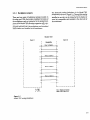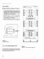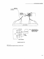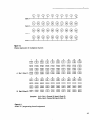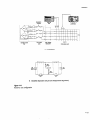
1
Instruction
Manual
Models 7011 -S and 701 I-C
Quad 1 x 10 Multiplexer
Contains Operating and Servicing Information
Cards
“il” il’>
Keithley Instruments, Inc. warrants this product to be free from de&p tn material and workmanship for a period of 1 year from date of
shipment.
:r’i i
Keithley Instruments, Inc. warrants the following items for 90 dz$gfi om the date of shipment: probes, cables, rechargeable batteries,
diskettes, and documentation.
:t;;,:,:i
During tbc warranty period, we will, at our option, either repair or replace any product that proves to be defective.
To exercise this wtxranty, write or call your local Kcithley representative, or contact Keithley headquarters in Cleveland, Ohio. You will
be given prompt assistance and return instructions. Send the product, transportation prepaid, to the indicated service facility. Repairs
will be made and the product returned, transportation prepaid. Repaired or replaced products are warranted for the balance of the origi1x11warranty period, or at least 90 days.
LIMITATION OF WARRANTY
This warranty does not apply to defects resulting from product modification without Keithley’s express written consent, or misuse of
any product or part. This warranty also does not apply to fuses, software, non-rechargeable batteries, damage from battery leakage, or
problems arising from normal wxr or failure to follow instructions.
THIS WAJ&Nl!Y
1s IN I&%7 OF ALL OTHER WARRANTIES, EXPRESSED OR IMPLIED, INCLUDING ANY IMPLIED
WARRANTi’Oti
MERCHANTABILITY
OR FITNESS FOR A PARTICULAR USE. THE REMEDIES PROVIDED HEREIN ARE
BUYER’S SOLE AND EXCLUSIVE REMEDIES.
NEITHER KEITHLEY INSTRUMENTS, INC. NOR ANY OF ITS EMPLOYEES SHALL BE LIABLE FOR ANY DIRECT, INDIRECT, SPECIAL, INCIDENTAL OR CONSEQUENTIAL DAMAGES ARISING OUT OF THE USE OF ITS INSTRUMENTS AND
SOFTWARE EVEN IF KEITHLEY INSTRUMENTS, INC., HAS BEEN ADVISED IN ADVANCE OF THE POSSIBILITY OF
SUCH DAMAGES. SUCH EXCLUDED DAMAGES SHALL INCLUDE, BUT ARE. NOT LIMITED TO: COSTS OF REMOVAL
AND INSTALLATION, LOSSES SUSTAINED AS THE RESULT OF INJURY TO ANY PERSON, OR DAMAGE TO PROPERTY.
Keithley Instruments, Inc. - 28775 Aurora Road * Cleveland, OH 44139 * 216-248-0400 - Fax: 216-248-6168 - http://www.keithley.com
Models
7011 -S and 7011 -C Instruction
01991, Keithley Instruments, Inc.
Test Instrumentation Group
All Rights Reserved
Cleveland, Ohio, U. S. A.
Manual
Manual
Print History
The print histoxy shown below lists the printing dates of all Revisions and Addenda created for this manual. The
Revision Level letter increases alphabetically as the w@
undergoes subsequent updates. Addenda, which are
released between Revisions, contain important change information that the user should incorporate immediately
into the manual. Addenda are numbered sequentially. When a new Revision is created, all Addenda associated
with the previous Revision of the manual are incorporated into the new Revision of the manual. Each new Revision includes a revised copy of this print history page.
R&ion A (Dcament Number 7011-90101) ........_.............~................................................
November 1991
Addendum A (Document Number 7011-901-02)..........................................................................
January 992
Revision B (Donunmt Number 7011~901-01)................................................................................
l&1-31 1992
Revision C (Dmment Number 7011-90141) ..........................................................................
December 1992
Safety Precautions
The following safety precautions should be observed before using
this product and any associaled instrumentation. Although some in~tnmen~s and accessories would nomxdly be used with non-hazardous voltages, there are situations where hazardous conditions
may be p*esent.
This product is intended for use by qualified personnel who recognize shock hazards and are familiar with the safety precautions required to avoid possible injury. Read the operating information
carefully before using the product.
The types of product users arc:
Responsible body is tbc individual or group responsible for the use
and maintenance of equipment, and for ensuring that operators are
adequately trained.
Operators use the product for its intended function. They must be
trained in electrical safety procedures and proper use of the instmment. They must be protected from electric shock and contact with
hazardous live circuits.
Maintenance personnel perform routine procedures on the product
to keep it operating, for example, setting the line voltage or replacing consumable materials. Maintenance procedures are described in
the manual. The proccdurcs explicitly state if the operator may perform them. Otherwise, they should be performed only by service
perS”lld.
Service personnel 8.n~trained to work on live circuits, and perform
safe installations and repairs of products. Only properly trained service personnel may perform installation and service procedures.
Exercise extreme caution when a shock hazard is present. Lethal
voltage may be present on cable connector jacks or test fixtures. The
American National Standards Institute (ANSI) states that a shock
hazard exists when voltage levels greater than 30V RMS, 42.4V
peak, or 60VDC are present. A good safety practice is to expect
that hazardous voltage is present in any unknown circuit before
measuring.
Users of this product must be protected from electric shock at all
times. The responsible body must ensure that users are prevcntcd
access and/or insulated from every connection point. In some cases,
connections must be exposed to potendal human contact. Product
users in these circumstances must be trained to protect themselves
from the risk of electric shock. If the circuit is capable of operating
at or above 1000 voks, no conductive part of the circuit may be
exposed.
As described in the International Electrotechnical Commission
(IEC) Standard IEC 664, digital multimeter measuring circuits
(c,g,, Keithley Models 175A, 199, 2000, 2001, 2002, and 2010)
measuring circuits are Installation Category Il. All other instmmerits’ signal terminals are Installation Category I and must not bc
connected to mains.
Do not connect switching cards directly to unlimited power circuits.
They are intended to be used with impedance limited sources.
NEVER connect switching cards directly to AC mains. When connecting sources to switching cards, install protective devices to limit fault current and voltage to the card.
Before operating an instrument, make sure the lint cord is connected to a properly grounded power receptacle. Inspect the connecting
cables, teat leads, and jumpers for possible wear, cracks, or breaks
before each use.
For maximum safety, do not touch the product, test cables, or any
other instruments while power is applied to the circuit under test.
ALWAYS remove power from the entire test system and discharge
any capacitors before: connecting or disconnecting cables or jumpers, installing or removing switching cards, or making internal
changes, such as installing or removing jumpers.
Do not touch any object that could provide a current path to the
common side of the circuit under test or power line (earth) ground.
Always make measurements with dry hands while standing on a
dry, insulated surface capable of withstanding the voltage being
measured.
Do not exceed the maximum signal levels of the instruments and accessories, as defined in the specifications and operating information, and as shown on the instrument or test fixturn panels, or
switching card.
When fuses are used in a product. replacc with same type and rating
Carcontinued protection against fire hazard.
Chassis connections most only be used as shield connectioos for
measuring circuits, NOT as safety earth ground connections.
If you are using a test fixture, keep the lid closed while powcr is applied to the device under tat. Safe operation requires the USCof a
lid interlock.
Ifa@. screw is present, connect it to safety earth ground using the
wire recommended in the user documentation.
symbol on an instrument indicates that the user should refer to the operating instructions located in the manual.
TheA
symbol oo an instrument shows that it can source or measure 1000 volts or more, including the combined effect of normal
and common mode voltages. Use standard safety precautions to
avoid personal contact with these voltages.
The WARNING heading in a manual explains dangers that might
result in personal injury or death. Always read the associated information very carefully before performing the indicated procedure.
The CAUTION heading in a manual explains hazards that could
damage the instrument. Such damage may invalidate the warranty.
Instrumentation and accessories shall not be connected to humans.
Before performing any maintenance, disconnect the line cord and
all test cables.
To maintain protection from electric shock and fire, replacement
components in mains circuits, including the power transformer, test
leads. and inout iacks. must be ourchased from Keithlev lnsmmats. Standard fuses, with applicable national safety approvals,
may be used if the rating and type arc the same. Other components
that are not safety related may be purchased from other suppliers as
long as they are equivalent to the original component. (Note that scleaed parts should be purchased only through Kcithley Instruments
to maintain accuracy and functionality of the product.) If you arc
unsure about the applicability of a replacement component, call a
Keithley Instruments oflicc for information.
To clean the instrument. USCa dame cloth or mild. water based
cleaner. Clean the exterior of the instrument only. Do not apply
cleaner directly to the instrument or allow liquids to enter or spill
on the instmmcnt.
7011SPECIFICATIONS
MOD”, ‘IOU-S Quad 1x10 Multiplew with SaewT.smh&.
MODEL7011-C QuadlxlOMvltiplexerwithMT~~Connector.
MDLTIPLBX CONPIGDRATION
Four independent 1x10 2-p& Multiplex banks or two independent 1x10 &pole Multiplex banks. Adjjcent
banksenbecomfftedtogether.
Jumperscanberemovedtoisolateany
bank from the backplane.
CONTACT CONFIGDRATION: 2-jmle Form A @Ii, Lo).
CONNECTOR TYPE:
7011-5: Screw terminal, #16AWG IMximllm wire size, with a92 tnch
O.D. 28 Conductors maxima
#Z?AWGtypical wire size
with .062inch O.D. 30 Conductor madmum
mmc %-pin m&Ewxardconnebor.
Mates tofem&twistedwire
cable, crimp or solder connedor.
MAXMUM SIGNAL LEVEb
DC Sign& 1lOV DC behveen any two pins, IA witched. 3WA
bG.eive load).
AC Sign& 125V FM5 or 173V AC peak, between any two pins,
1A switched, 60VA ke&tive load).
COMMON MODE VOLTAGE: 175” peak, my pin to chassis.
CONTACTLIFE
CONTACT POTENTIAL
7011-5: c 500 nv per contact pair Hi, Lo).
< 1.5 pv par single contact
m11-c
< 1.5 WVper contact pair m, Lo) eypically < 1 @q.
< 35 p? per single contact oj@zdly c 3 PVL
OPFSET ‘XItRt3iVI: < 100 PA.
ACTUATION TIME: 3 ms.
ISOLATION:
Bank >lC@Q < 25 pF.
CbanneI to channel: >lO%Z,< 50 pF.
Differenti
Configured as 1x10 =-l@Q, < 100 pF.
Configured as 1x40 >loSQ, < 200 pF.
Common Mode
Configured as 1x10 >lOQ, < 2W pF.
Conftgurect as 1x40 >l@O, < 600 pF.
CROSS TALK OMHz, 500 Load):
Bank <-4OdB.
Channeb <4OdB.
INSERTION LOSS (MS2Somx,sO Load): < 0.1 dB below 1 MHz, < 3 dB
below 2 MHZ.
RELAYDRNECURRENT
(per r&y):
16 mA.
E7WIRONMEN-C
opdi0~
O’C to WC, up to 35-x < 80% Fx.
-25°C to 65’C
smagez
spedfieti0ns subjj to change without notice.
Table of Contents
1.1
1.2
1.3
1.4
1.5
1.6
1.7
1.7.1
1.7.2
1.7.3
1.7.4
1.8
Introduction .....................................................................................................................................................
1-l
l-1
Features .............................................................................................................................................................
l-2
warranty informaton.. ...................................................................................................................................
l-2
Manual a&km& .............................................................................................................................................
1-2
Safety symbols and terms ..............................................................................................................................
1-2
specifications ...................................................................................................................................................
l-2
Unpacking am.3inspection
l-2
Inspectior, for damage......................................................................................................................................
l-2
Shipping axItents.. ..................................................................................................................................
1-3
apron
mand.. ................................................................................................................................
1-3
Repacking for shipment .........................................................................................................................
l-3
Optional a~c~soties.. ......................................................................................................................................
2.1
2.2
22.1
2.2.2
2.3
2.3.1
2.3.2
2.3.3
2.3.4
2.4
2.4.1
2.4.2
2-1
Introduct$m ....................................................................................................................................................
2-1
Basic m&ipkxer ca~figurations ..................................................................................................................
2-2
Multiplexer bank-to-bank jumpers.. .....................................................................................................
2-5
Backplane jumpers ..................................................................................................................................
2-6
Typical nultiplexer switching schemes.......................................................................................................
2-7
S&++&xl
swit&ing ..........................................................................................................................
2-7
Differential switching .............................................................................................................................
2-a
sensing. .....................................................................................................................................................
2-8
SMIJ co~cxtiq~. ....................................................................................................................................
2-10
Multiplexer expansmn ..................................................................................................................................
t:?y
Two-card svitching system
..........................................................................................................................
Mainframe multiplexer expansion
3.1
3.2
3.3
3.3.1
3.3.2
3.3.3
3.3.4
3.4
3.4.1
3.4.2
3.4.3
3.5
~~od,,,&m,
.....................................................................................................................................................
3-l
3-l
&n,&,g
prxa~tion,s .....................................................................................................................................
3-l
C~~&i~~.
.....................................................................................................................................................
3-2
&&-t&m&
jumpers
3-3
Backplane *pa
..................
3-4
Screw te&d
KXEE&X card
..............................................................................................................................
3-6
Multi-pin (mass te rmination) connector card .....................................................................................
3-11
Tyqicd com&icm s&emes ........................................................................................................................
3-11
Single card system.. ...............................................................................................................................
3-14
Two-c& system.. .................................................................................................................................
Tw~mainfrme
Model 7011 i,,&&hc,n
system ........................................................................................................................
3-14
3-19
and remow., .........................................................................................................
4.1
4.2
4.3
4.3.1
4.3.2
4.3.3
4.4
4.4.1
4.4.2
4.4.3
4.5
4.5.1
4.52
4.5.3
4.5.4
4.5.5
4.5.6
5.1
5.2
5.3
5.3.1
5.3.2
5.3.3
5.3.4
5.3.5
5.3.6
5.3.7
5.3.8
5.4
5.5
5.5.1
5.5.2
5.5.3
5.5.4
5.5.5
5.6
5.6.1
5.6.2
5.6.3
6.1
6.2
6.3
6.4
6.5
4-1
Introduction.. ....................................................................................................................................................
4-1
Power limits.. ....................................................................................................................................................
4-l
Mainframe control of multiplexer card.. ......................................................................................................
42
Channel assignments ..............................................................................................................................
4-4
Front panel control. .................................................................................................................................
44
IEEE-488 bus operation.. .........................................................................................................................
4-5
Multiplexer switching examples ...................................................................................................................
45
Resistor testing .........................................................................................................................................
49
Transistor testing .....................................................................................................................................
4-11
with
matrix
cards..
...................................................................................................................
Testing
4-15
Measurement considerations .......................................................................................................................
415
Path isolation.. ........................................................................................................................................
4-16
Magnetic fields .......................................................................................................................................
4-16
Radio frequency interference.. .............................................................................................................
4-17
Ground loops .........................................................................................................................................
4-17
Keeping connectors clean .....................................................................................................................
4-17
AC frequency response.. .......................................................................................................................
5-l
Introduction ......................................................................................................................................................
5-l
Handling and cleaning precautions.. ............................................................................................................
Performance
verification
...............................................................................................................................
5-2
5-2
Environmental conditions ......................................................................................................................
5-2
Recommended equipment .....................................................................................................................
5-3
Multiplexer card connections ................................................................................................................
5-3
Channel resistance tests ..........................................................................................................................
5-5
Offset current tests...................................................................................................................................
5-7
Contact potential tests.............................................................................................................................
5-8
Bank and channel-to-channel isolation tests .......................................................................................
5-12
Differential and common-mode isolation tests.. ...............................................................................
.:.........................5-14
Special handling of static-sensitive devices.. ..................................................................
5-15
Principles of operation ..................................................................................................................................
5-15
Block diagram ........................................................................................................................................
5-15
ID data circuits.. .....................................................................................................................................
5-17
Relay control ...........................................................................................................................................
5-17
Relay power control ..............................................................................................................................
5-17
Power-on safeguard ..............................................................................................................................
5-17
Troubleshooting .............................................................................................................................................
5-17
Troubleshooting equipment .................................................................................................................
5-18
Troubleshooting access.........................................................................................................................
5-18
Troubleshooting Procedure ..................................................................................................................
6-l
Introduction ......................................................................................................................................................
6-l
Parts lists ...........................................................................................................................................................
6-1
Ordering information.. ....................................................................................................................................
6-l
Factory service.. ................................................................................................................................................
6-2
Component layouts and schematic diagrams.. ...........................................................................................
List of Illustrations
2-l
2-2
2-3
24
2-5
2-6
2-8
2-7
2-9
2-10
2-11
2-12
2-13
Model 7011 simplified schematic.. ........................................................................................................
2-2
Four 1 x 10 multiplexer configuration (jumpers not installed) ........................................................2-3
Two 1 x 20 multiplexer configuration (jumpers installed). ...............................................................
2-3
One 1 x 40 multiplexer configuration (jumpers installed) ................................................................
2-4
Model 7001 analog backplane ...............................................................................................................
2-5
Bank connections to backplane .............................................................................................................
2-6
Differential switching example .............................................................................................................
2-7
Single-ended switching example ..........................................................................................................
2-7
Sensing example.. ....................................................................................................................................
2-8
SMLJ connectiom .....................................................................................................................................
2-9
Two separate multiplexer systems .....................................................................................................
2-10
Multiplexer input expansion example ...............................................................................................
2-11
Mixed card type example .....................................................................................................................
2-12
Figure 31
Figure 32
Figure 33
Figure 34
Figure 35
Figure 36
Figure 37
Figure 38
Figure 39
Figure 310
Figure 311
Figure 312
Figure 313
Figure 314
Figure 315
Figure 316
Figure 317
Figure 318
Figure 319
32
Bank-to-bank jumper locations .............................................................................................................
33
Bank-to-bank jumper terminal identification .....................................................................................
33
Bank-to-bank jumper installation .........................................................................................................
34
Backplane jumpers.. ................................................................................................................................
3-4
Model 7011 screw terminal connector card.. .......................................................................................
3-5
Typical screw terminal connections .....................................................................................................
35
Cable clamp for screw terminal connector card .................................................................................
37
MI&-pin card terminal identification .................................................................................................
39
Typical round cable connection techniques ........................................................................................
310
Model 7011~MTR connector pinout.. ..................................................................................................
310
Model 7011~KIT-R (with/cable) assembly ........................................................................................
................................................................
312
Single card system example (multi-pin connector card).
Single card System example (screw terminal connector card) ........................................................3-13
3-15
Tw-d
system example (nxxki-pin connector card). ...................................................................
‘&v-d
system example (screw terminal connector card) ..........................................................316
Two-mainframe system example (multi-pin connector card). .......................................................317
Two-mainframe system example (screw terminal connector card) ...............................................318
3-20
Model 7011-C card jn&lk&m
in Model 7001 .................................................................................
321
7011-Scard inst&dion in Model 7001...............................................................................................
Figure
Figure
Figure
Figure
4-2
Channel status display ...........................................................................................................................
4-3
Display o*ganization for multiplexer channels ..................................................................................
4-3
Model 7011 progr amming channel assignments.. ..............................................................................
4-6
2-tie resistance testing.. .......................................................................................................................
Figure
Figure
Figure
Figure
Figure
Figure
Figure
Figure
Figure
Figure
Figure
Figure
Figure
4-I
4-2
4-3
4-4
iii
Figure
Figure
Figure
Figure
Figure
Figure
Figure
Figure
Figure
Figure
Figure
45
4-6
4-7
48
49
4-10
4-11
412
413
414
415
4-7
Four-wire resistance testing.. .................................................................................................................
48
Low *&stance testing.. ...........................................................................................................................
Configuration for current gain and common-emitter test.. .............................................................4-10
Typical common-emitte~ characteristics ............................................................................................
411
4-12
Conmcting multiplexer and ma&ix cards together .........................................................................
4-13
Resktitity test configuration ...............................................................................................................
4-14
Measurement required for resistivity test..........................................................................................
4-15
Path isolation resistance ........................................................................................................................
4-16
Voltage attenuation by path isolation resistance.. ............................................................................
Power line ground loops ......................................................................................................................
4-17
4-17
Eliminating ground loops ....................................................................................................................
Figure
Figure
Figure
Figure
Figure
Figure
Figure
Figure
Figure
Figure
5-l
5-2
5-3
5-4
5-5
56
5-7
5-8
5-9
S-10
5-4
Pati *esistance test connections ............................................................................................................
5-6
Differadial offset current test connections ..........................................................................................
5-7
Contact potential test comwciions ........................................................................................................
5-8
Bank i&&ion test connections.. ............................................................................................................
S-10
Channel-to-channel isolMio* test connections ..................................................................................
5-12
Differential isolation test connections ................................................................................................
5-14
Co-on-mode
i.solation test connections.. .......................................................................................
5-15
Model 7011 block diagram ...................................................................................................................
5-16
SM and stop sequences.......................................................................................................................
5-16
T-tit
and acknowkdge sequence.. ...............................................................................................
iv
List of Tables
Table 3-1
Table 3-2
3-3
Bank-to-bank jumpers (refer to Figure 3-Z) .........................................................................................
3-6
................................................................................................................
Mass termination ~ccessori~
Table 4-l
4-6
Pa&d Cha.r,r,els in 4-p& Operation ........_.._...t...................................................................................
Table 5-1
Table 5-2
Table 5-3
Table 5-4
Table 5-5
Table 5-6
5-2
verification equipment.. .........................................................................................................................
5-9
.................................................................................................................
Bank is&.tic,n test s-q
5-11
Channel-to-channel isolation test mmmary .....................................................................................
5-13
Differential and ~~-~~-nd.e
&&ion &ding. ............................................................................
5-17
&co-end&
~~~bk&xdzing equipment.. ....................................................................................
5-19
Troubleshooting procedux .................................................................................................................
v/vi
General
1.1
Introduction
This section contains general information
Model 7011 Quad 1 x 10 Multiplexer card.
Information
1.4
Manual addenda
1.5
Safety symbols and terms
1.6
Specifications
1.7
Unpacking and inspection
1.8
Repacking for shipment
1.9
Optional accessories
about the
There are two basic versions of this multiplexer card;
the Model 7011-S and the Model 7011-C. The Model
7011-Sassembly consists of a screw terminal connector
card and a relay card. External test circuits are wired
directly to the saew terminals of the connector card.
Also available from Keithley is the Model 7011-ST.This
is an extra screw terminal connector card. With an extra
connector card, you can wire a second test system
without disturbing the wiring con@uration of the first
test system.
1.2
Features
The Model 7011 is a low voltage, two-pole, quad, 1 x 10
multiplexer card. Some of the key features in&de:
The Model 7011-C assembly consists of a multi-pin
bmss termination) connector card and the relay card.
Fxtemal test circuit connedions to the multiplexer are
made via the 96-pin male DIN connector on the connector card. Keithley offers a variety of optional accessories that can be used to make conneciiom to the
connector card (see paragraph 1.9).
l
l
l
The rest of Setion 1 is arranged in the following manner:
1.2
Features
1.3
warranty information
l
Low contact potential and offset current for minimal effects on low-level signals.
The connector board detaches from the relay board
allowing easy accessto the saew terminals (Model
7011-S)and jumpers.
Easy jumper cotiguration
four multiplexer banks.
of one, two, three or
Backplane jumpers. Cutting jumpers disconnects
multiplexer bank outputs from the Model 7001 analog backplane.
1-l
1.3
Warranty
information
Warranty information
is Located on the inside front
cover of this instruction manual. Should you Model
7011 require warranty service, contact the Keithley representative or authorized repair fxility in your area for
further information. When returning the multiplexer
card for repair, be sure to fill out and include the service
form at the back of this manual in order to provide the
repair facility with the necessary information.
1.4
Manual addenda
Any improvements or changes concerning the multiplexer card or manual will be explained in an addendum inchxded with the card. Addenda are provided in
a page replacement format. Simply replace the obsolete
pages with the new pages.
1 .S
Safety symbols and terms
The following symbols and terms may be found on an
ins!mmwnt or used in this manual.
The A
symbol on an instrument indicates that the
user should refer to the operating instmztions located
in the insfnxtion manual.
nigh
The $ symbol on an instrument shows :,
voltage may be present on the terminal(s). L* standard safety precautions to avoid personal contact with
these voltages.
The WARNING heading used in this manual explains
dangers that might result in personal injury or death.
Always read the associated information very carefully
before performing the indicated procedure.
The CAUTION heading used in this manual explains
hazards that could damage the multiplexer card. Such
damage may invalidate the warranty.
1-2
Specifications
1.6
Model 7011 specifications are found at the front of this
manual. These specifications are exclusive of the multiplexer mainframe speci6cation.3.
1.7
Unpacking
1.7.1
Inspection
and inspection
for damage
The Model 7011 is packaged in a z-sealable, anti-static
bag to protect it from damage due to static discharge
and from contamination that could degrade its performance. Before removing the card from the bag, observe
the following precautions on handling.
Handling Precautions:
1. Always grasp the card by the side edges and shields.
Do not touch the board surfaces or components.
2. When not installed in a Model 7001 mainframe,
keep the card in the anti-static bag and store it in the
original packing carton.
After removing the card from its anti-static bag, inspect
it for any obvious signs of physical damage. Report
any such damage to the shipping agent immediately.
1.7.2
Shipping
contents
The following items are included with every Model
7011 order:
l
Model 7011 Quad 1 x 10 Multiplexer Card
l
Model 7011 Instruction Manual
l
Additional accessoties as ordered
1.7.3 Instruction manual
1.8
The Model 7011 Instruclion Manual is three-hole
driBad so that it can be added to the three-ring binder
of the Model 7001 Inshwtion h4anuaI. After removing
the plastic wrapping place the manual in the binder
following the mainframe instruction manuaL Note that
a manual identification tab is included and should pr+
cede the multiplexer card instruction manual.
The following accessoriesare available for use with the
Model 7011:
If an additional instruction manual is required, order
the manual package, KeithIey part number 7011-90100. The manual package indudes an instruction manuaI and any pertinent addenda.
1.7.4 Repacking for shipment
Should it become necessary to return the Model 7011
for repair, carefully pack the unit in ik original packing
carton or the equivalent, and include the following information:
l
l
l
Advise as to the warranty status of the multiplexer
card.
Write ATENTION
shipping label.
REPAIR DEPARTMENT on the
FiII out and include the service form located at the
back of this manuaL
Optional
accessories
Model 70ll-ST - This screw terminal connector card
is identical to the one provided with the Model 7011-S
assembly. An extra screw terminal connector card allows you to wire a second test system without disturbing the wiring coniiguration of the fist connector card.
Model 7011~KIT-R - This connection kit includes a
96-pin female DIN connector that wiU mate directly to
the connector on the Model 7011-C or to a standard 9&
pin male DIN bulkhead connector (see Model 7011MTR). This connector uses solder cups for connections
to external circoi~ It includes an adapter for a round
cable and the housing.
Model 7Oll-WC-2 - This 2-meter round cable assembly is terminated with a 96-pin female DIN connector on each end. It wiII mate directly to the connector
on the Model 7011-C and to a standard 96-pin male
DIN buIIchead connector (see Model 7011~MTR).
Model 7011-m-This
96pin male DIN buIkhead
connector uses solder cups for connections to external
circu.i&y. It will mate to the Model 7011~KIT-R connector, and Model 7011~MTC-2 cable assembly.
l-3
2
Multiplexing
2.1
Introduction
24
This section covers the basics for multiplex switching
and is arranged as follows:
2.2
2.3
Basic multiplex conBgurations: Covers the basic
multiplex configurations; quad 1 x 10 con+ration, dual 1 x 20 configuration and single 1 x 40
cotiguration. The significance of the backplane
jumpers is also covered here.
Typical multiplex switching schemes: Explains
some of the basic ways a multiplexer cambe used
to source or measure. Covers single-ended
switching, differential (floating) switching and
sensing.
2.2
Basics
System expansion: Discusses the various configurations that are possible by using multiple
cards.
Basic multiplexer
configurations
A simplified schematic of the Model 7011 multiplexer
is shown in Figure 2-l. It is organized as four 1 x 10
multiplexer banks. Each bank has 10 inputs and one
output. Two-pole switching is provided for each multiplexer input, with HI and LO switched. Two or more
banks can be jumpered together to expand multiplexer
inputs, and backplane jumpers provide bank connections to a second card installed in Model 7001 mainframe.
2-l
Bank to Bank
Jumpers
Figure 2-l
Mode/ 707 7 simplified
schematic
2.2.1
bank-to-bank
Multiplexer
jumpers
Jumpers are installed on the connector card to connect
multiplexer banks together to form a multiplexer of 1 x
40. Each jum:~ :- set connects two adjacent banks together. These j;-nper sets are included with the Model
7011.
The bank-to-bank jumpers allow you to configure the
multiplexer card in a variety of ways. Typical multiplexer coniigwations include:
l
Four 1 x 10 rxtitiplexers;
ure 2-2).
2-2
no jumpers installed (Fig-
l
l
Backplane Jumpers
(to 7001 Analog
Backplane)
Two 1 x 20 multiplexers; Bank A jumpered to Bank
B, Bank C jumpered to Bank D (Figure 2-3).
One 1 x 40 multiplexer; all bank-to-bank jumpers
installed (Figure 2-4).
Other combinations are possible, including multiplexers of various sizes (in multiples of 10 channels). For
example, you could install jumpers to configure the
card as one 1 x 30 and one 1 x 10 multiplexer.
Refer to Section 3 for information on installing bank-tobank jumpers.
2
‘* ‘12
Bank A
10.
,
1.
.’
10,
,
Bank B
Bank C
Bank D
Figure 2-2
Four 1 x 10 multiplexer
,I
configuration
1.
(jumpers
,x2
Bank 6
109
1.
,x2
,z2
Bank C
10.
i
:2
1.
,*2
10.
,*2
Bank D
~~--z+O”,utD
not installed)
.
.
l
.
.
l
.
.
l
Figure 2-3
Two 7 x 20 multiplexer
configuration
(jumpers
installed)
2-3
inputs
10
,’
10.
,
Bank A
,:
1.
,*2
10.
;2
1.
;2
;I-
Jumpers
Bank B
Jumpers
Bank C
10.
./Z
1.
,,2
100
,‘2
JUllp~S
Bank D
One 1 x 40 multiplexer
2-4
configuration
Output A
(jumpers
installedl
2.2.2
Backplane
jumpers
There are four pairs of backplane jumpers located on
the relay card. With the jumpers installed, the banks of
the multiplexer card are connected to the analog backplane of the Model 7001 allowing expansion with a second 7001 card installed in the mainframe. With the
jumpers removed (cut), the multiplexer card is isolated
from another card installed in the mainframe.
The three-pole analog backplane of the Model 7001
nminframe is shown in Fieure 2-5. Throwh this analog
backplane the banks of a kodel7011 muitplexer car&
installed in one slot, can be connected to the banks (or
rows) of a compatible card installed in the other slot of
the mainframe.
Model 7001
Card 1
----
r----
I
I
1
I
HS
I
I
Analog
Backplane
L
ROW
1or BankA
I
r----
Card 2
_---
1
I
I
kti
I
I
I
L
““IG
Row2OrBa”kB
I H
Ht
L+-----4~L
‘<G
I
I
I
I
I
L
L>I
Q-----f
I
I
9
:A
I
I
I
I
ROW4 or Bank D
I<
g
,?-----f”
L--------l
L--------l
H = High
L= LOW
G = Guard
ROW= Matrix Card (7012)
ea"!i = MUX Card (7011)
Figure 2-5
Model
7001 analog
backplane
2-s
Figure 2-6 shows how each bank of the Model 7011 is
connected to the backplane. Notice that since the Model 7011 is a twopole card, there is no connection made
to the Guard terminal of the backplane. The Model
7011 is shipped from the factory with the backplane
jumpers installed.
7011
Bank
(1 Of4)
H\>
H
L>
L
H = High
L=Lcw
G = Guard
Removing (cutting) the backplane jumpers isolates the
card from the backplane, and subsequently, any card
installed in the other slot. For information on removing
the @mpers, refer to section 3.
NOTE
The Model 7001 does not provide an
analog backplane for the non-701X series cards. As a result, any of these
cads installed in one slot in the mainframe is electrically isolated from any
card installed in the other slot. The
only way to connect a Model 7011 to
one of these cards is to wire them together.
2-6
7001
Analog
Backplane
Figure 2-6
Bank connections
2.3
Backplane
Jumpers
>
G
<
<
<
to backplane
Typical multiplexer
schemes
switching
The following paragraphs describe some basic switching schemes that are possible with a two-pole switching multiplexer. These switching schemes include
some various shielding configurations to help minimize noise pick up in sensitive measurement applications. These shields are shown connected to chassis
ground. For some test configurations, shielding may
prove to be more effective connected to circuit common. Chassis ground is accessible at the rear panel of
the Model 7001.
2.3.1
Single-ended
switching
In the single-ended switching configuration, the source
or measure instrument is connected to the DLJT
through a single pathway as shown in Figure 2-7. The
insinJml?nt is connectd to the output of one of the
banks and the DUT is shown connect4 to one of the
inputs for that bank.
Figure 2-7
Sing/e-ended
switching
2.3.2
Differential
switching
The differential or floating switching configl.lration is
shown in Figure 2-8. The advantage of using this configuration is that the terminals of the scarce or measure
instrument are not confined to the same pathway. Each
terminal of the instrument can be switched to any
available input in the test system.
example
Input l-10
Figure 2-8
Differential
switching
example
2-7
2.3.3
Sensing
2.3.4
.
Figure 2-9 shows how the multiplexer card can be configured to use instruments that have sensing capability.
The main advantage of using sensing is to cancel the effacts of switch card path resistance (43) and the resistame of external cabling. Whenever path resistance is a
consideration, sensing should be used.
Figure 2-10 shows how to connect a Keithley Model
or 238 Source Measure Unit to the multiplexer
card. By wing lkxx cables that are unterminated at one
end, the driven guard and chassis ground are physically extended all the way to the card.
236,237
Bank C, D
Figure 2-9
Sensing example
2-8
SMU connections
Input l-10
\
iIT-
Output LO
7011
LbInput l-10
TriaX
Cables (3)
WARNING : Hazardous v&ages may be present on
WARNING
GUARD. Make sure all cable shields are
properly insulated before applying power.
Figure 2- 10
SMU connections
2-9
2.4
Multiplexer
two cards will be controlled by the same mainframe,
but they will be electrically isolated from each other.
Figure 2-11 shows an example using two Model 7011
niultiplexer cards.
expansion
With the use of additional switching cards and mainframes, larger systems can be configured. Each Model
7001 Switch System mainframe will accommodate up
to two cards, and up to six mainframes can be connected together. Thus, a switch system using as many as 12
cards can be configured.
2.4.1
Two-card
switching
Multiplexer
You can double the number of multiplexer inputs by
simply installing two “as shipped” Model 7011s in the
Model 7001 mainframe. By leaving the backplane
jumpers installed, the banks of the multiplexer card installed in slot 1 (CARD 1) are automatically connected
to the banks of the multiplexer card installed in slot 2
(CARD 2) through the analog backplane.
systems
Each Model 7001 Switch System mainframe can accommodate two cards to allow the following switching
configurations.
Figure 2-12 shows an example of input expansion.
Each Model 7011 card is configured as four 1 x 10 multiplexers. By connecting the banks together (via Model
7001 analog backplane), the resultant multiplexer systern has 20 inputs for each of the four banks. Notice
that if all the bank-to-bank jumpers (for both cards)
were installed, the result would be a single 1 x 80 multiplexer.
Separate switching systems
Two singie-card systems can be configured by removing the backplane jumpers from one of the cards. The
h”kB
7031 Analog
&.CkplCl”e
Card 1
----------
r----
7011
input expansion
._
1
/
Card 2
r---------I-~
-
Bankc i
sm-
L-----------A
I-------------
Four 1x10 Muniplexers
Figure Z- 11
Two separate
2-l 0
multiplexer
systems
Four 1x10 Multiplexers
7Wl Analog
Card 1
r-------
Card 2
-----
BX.kph”e
-----,
7011
--------
_-----_--Quad 1x10 Multiplexers
----Quad 1x10 Multiplexers
Quad 1 x20 Multiplexer
Figure 2- 12
Mdripkxer
input expansion
exampk
Mixing card types
Different types of cards can be used together to create
some unique switching systems. For example, you
could have a Model 7011 multiplexer card installed in
one slot and a Model 7012 matrix card installed in the
other slot.
Figure 2-13 shows a possible switching system using a
matrix card and a multiplexer card. The backplane
jumpers for both the matrix and multiplexer cards
must be installed. This allows matrix rows to be conneded to multiplexer banks. On the multiplexer card,
the bank-to-bank jumpers must be removed to main-
tain isolation between matrix rows. Seethe instmction
manual for the Model 7012 for complete information
on the mati card.
2.4.2
Mainframe
multiplexer
expansion
Multiplexer systems using up to 12 multiplexer cards
are possible by using six Model 7001 mainframes together. Each Model 7011 added to the system provides
40 additional inputs. Paragraph 3.4.3 explains how to
connect a test system using two mainframes.
2-1 ,l
r----
Card 1
------7012
Card 2
r------------
701 1
Bank A
Bank C
Bank D
4xlOMatrix
Figure 2- 73
Mixed card type example
2-12
---
------_-__
---..--------__
Quad 1 x 10 MUX
3
Card Connections
3.1
introduction
WARNING
The procedures in this section are intended only for qualified service personnel. Do not perform these
procedures unless qualified to do so.
Failure to recognize and observe “ormal safety precautions could result
in personal injury or death.
The information in this section is arranged as follows:
3.2
Handling precautions: Explains precautions that
must be followed to prevent contamination to the
multiplexer card assembly. Contamination could
degrade the performance of the multiplexer card.
3.3
Conmxtions: Covers the basics for connecting
extecd circuitry to the two available connector
cards for the multiplexer; the screw terminal connector card and the multi-pin connector card.
3.4
Typical connection schemes: Provides some typical connection schemes for single card, two-card
and two-mainframe system configurations.
3.5
Model 7Oll ixkallation: Provides a procedure to
install the multiplexer card assembly in the
Model 7001 mainframe.
& Installation
3.2
Handling
precautions
To maintain high impedance isolation, care should be
taken when handling the relay card to avoid contamination from such foreign materials as body oils. Such
contamination can substantially lower leakage resistances, thus degrading performance.
To avoid possible contamination, always grasp the relay and connector cards by the side edges or shields.
Do not touch the board surfaces or components. On
connectors, do not touch areas adjacent to the electrical
contacts. Dirt build-up over a period of time is another
possible source of contamination. To avoid this problem, operate the mainframe and multiplexer card in a
clean environment.
If a card becomes contaminated, it should be thoroughly cleaned as explained in paragraph 5.2.
3.3
Connections
This paragraph provides the basic information needed
to connect your external teSt circuitry to the multiplexer. It includes the installation of the bank-to-bank
jumpers on the connector card, insta.Ilation/removal of
backplane jumpers on the relay card, and detailed in-
3-1
fcmnaiion on making external connections tcl the two
available connector cards.
WARNING
The following connection infolmation is intended to be used by qualified service personnel. Failure to
recognize and observe standard safety precautions could result in personal injmy or death.
A. Screw Terminal Connector
Card
Figure 3- 1
Bank-to-bank
3-2
jumper
locations
:~3.3.1
Bank-to-bank
jumpers
As explained in paragraph 22.1, the banks of the multiplexer card can be connected together (using plug-in
jumpers) to form larger mukiplexers. The locations of
the bank-to-bank jumper terminals for both connector
cards are shown in Figure 3-l.
6. Multi-pin Connector Card
u-II
Terminal identification is provided by Figure 32. On
the drawing, the six terminal pairs are labeled WlOO
through W105. The top three terminal pairs (WlOl,
W103 and W105) are used to connect the LO terminals
of the banks together. The bottom terminal pairs
(WlOO,WI02 and W104) are used to connect the HI terminals of the banks together. Table 3-1 summarizes the
effects of each jumper.
Bank
AtoB
LO
IFzl
L-A
WlOl
HI
l-S-3
xitir
Figure 3-2
Bank-to-bank
jumper
Bank
BtoC
Bank
ctocJ
h-3
L-2
w103
rr-Tl
m6F
E--G-l
L-4
terminal
w105
r&--a
L-d
WI04
identification
Table 3-7
Jumper
Jumper Terminal
Pair
LtFigure 3-3
Bank-to-bank
3.3.2
jumper
Backplane
installation
jumpers
The Model 7001 mainframe has an analog backplane
that allows the banks of a Model 7011 multiplexer to be
internally connected to a compatible switching card installed in the other slot (seeparagraph 2.4.1 for details).
Bank-to-bank
jumpers
,nstalled
jumper
Effect
The backplane jumpers for the multiplexer card
assembly are located on the relay card as shown in
Figure 3-4. The card is shipped from the factory with
the jumpers installed.
WlOl
WlOO
Connect Bank A LO to Bank B LO
ConnectBankAHItoBankBHI
Jumper removal
w103
w102
Connect Bank B LO to Bank C LO
ConmxtBmkBHItoBankCHl
Perform the following
jumpers:
w105
w104
Connect Bank C LO to Bank D LO
ConnectBankCHItoBankDHl
(refer to Figure 3-Z)
Referring to Figure 3-l for jumper locations, perform
the following steps to install bank-to-bank jumpers:
1. If mated together, separate the relay card from the
comector card by removing the mounting screw
and pulling the two cards away from each other.
Remember to only handle the cards by the edges
and shields to avoid contamination.
2. Refer to Figure 32 and Table 31 to determine
which jumpers to install.
3. Using Figure 3-3 as a guide, install the jumpers on
the appropriate terminal pairs.
steps to remove backplane
1. If mated together, separate the relay card from the
connector card by removing the mounting screw
and pulling the two cards away from each other.
Remember to only handle the cards by the edges
and shields to avoid contamination.
2. Use Figure 3-4 to locate the jumper(s) that are to be
removed.
3. It is not necessary to physically remove the jumpers from the PC board. Using a pair of wire cutters,
cut one lead of each jumper.
3-3
Card Connections & Installation
:umper installation
Referring to Figure 3-4 for jumper locations, perform
the following steps to install backplane TOWjumpers:
1. If mated together, separate the relay card from the
connector card by removing the mounting screw
and pulling the two cards away from each other.
Remember to only handle the cards by the edges
and shields to avoid contamination.
2. Physically remove a cut jumper by unsoldering it
from the PC board.
3. Install a new #22 AWG jumper wire o(eithley P/N
J-15) and solder it to the PC board.
4. Remove the solder flux from the PC board The
cleaning pmcedure is explained in paragraph 5.2.
7011 Relay Card
e
a..
...
:::
.. .. ..
.. .. ..
.. .. ..
.. .. ..
..,*. .
.. .. ..
0
;~
I
Figure 34
Backplane jumpers
3.3.3
Screw terminal connector
card
The screw terminal connector card is shown in Figure
3-5. Connections are made directly to the screw terminals of the twelve terminal blocks. Each screw terminal
will accommodate #X-22 AWG wire.
3-4
Figure 3-5
Mode/ 7077 screw terminal
connector
card
Wiring procedure
Perform the following procedure to wire circuitry to
the screw terminal connector card:
WARNING
Make sure all power is off and any
stored energy in external circuitry is
discharged.
1. Jf mated together, separate the connector card from
the relay card by removing the mounting screw
and pulling the two cards away from each other.
Remember to only handle the cards by the edges
and shields to avoid contamination.
2. Using an insulated screwdriver, connect the circuitry to the appropriate terminals. Figure 3-6
shows how the output of Bank A would be connected to a DMM.
3. Referring to Figure 3-7, remove the top half of the
cable clamp as follows:
A. Loosen the cable clamp screw enough to disengage it from the bottom half of the cable clamp.
B. Using your thumb and forefinger, press the retaining clips inward and, with your other
hand, remove the top half of the clamp.
4. Route wires under wire guide/connector shim.
5. Route the wires through the bottom half of the cable clamp.
6. Replace the top half of the clamp. It simply snaps
onto the bottom half of the clamp. lighten the cable clamp screw. The clamp serves as a strain relief
for terminal block wires.
7. Mate the connector card to the relay card. The
Model 7011 is now ready to be installed in the
Model 7001 mainframe. See paragraph 3.5 for details.
Figure 3-6
Typical screw terminal
’
connections
Clips \
Figure 3-7
Cable clamp for screw terminal
connector card
3-5
3.3.4
Multi-pin
tor card
(mass termination)
connec-
Since comections to external circuiq are made at the
96-pin male DIN bulkhead connector, there is no need
to separate the connector card from the relay card. If
the connector card is separated from the relay card,
carefully mate them together and install tlw supplied
440 mounting screw. Make sure to handle the cards by
the edges and shields to avoid contamination.
Terminal identification for the DIN connedor of the
multi-pin connector card is provided by Figure 3-8.
This connector will mate to a 96-pin female DIN connector.
Keithley has a variety of cable and connector accessories available to accommodate connections from the
3-6
connector card to test instrumentation and DUT (devices under test). In general, these accessories, which
are summarized in Table 3-2, utilize a round cable assembly for connections.
Table 3-2
Mass termination
accessories
Model
Description
7011-m-R
96pin female DIN connector and
housing for round cable.
7011~ME-2
Two-meter round cable assembly
terminated with a 96-pin female
DIN comwctor on each end.
7011~MTR
96-pin male DIN bulkhead connector.
1
Card Connections & hstahtion
Pins of the Model 7011-C mass termination connector can be identiiied in one of three ways:
1. Mux terminal, consisting of banks A-D and inputs l-10.
2. Connector description. consisting of rows a-c and columns l-32.
3. Schematic and component layout designation (l-96).
The following pinout diagrams show the correspondence between these arrangements:
3231302928273~*25*423~221*0191~1716151413121110
l
.
.
.
.
.
.
..*.....*....*...........
9 8 7 6 5 4 3 2 1
View from pin side
of connector
3-7
Card Connections & /nm//arion
Typical connection techniques
All external circuitry, such as instrumentation and
DLJTs,that you wish to connect to the multiplexer card
must be terminated with a single 9&pin female DIN
coMecror. The following coxlnection techniques provide some guidelines and suggestions for wiring your
circui&y.
WARNING
Before beginning any wiring procedures, make sure all power is off and
any stored energy in external circuitry is discharged.
NOTE
External circuitry should be connected
,7ed id only wirh the 7001’s pow(I
e1
after the Model 7011 assembly is
in:;slled in the Model 7001 mainframe. Installation is covered in paragraph 3.5.
Output relays- The multi-pin connector card uses a
relay for each of the four output banks. These output
relays are normally open to prevent any hazardous
voltages (via the mainframe backplane) from appearing cm the pins of the rw.le DIN connector. The output
relays will only close when the Model 7011~MTC-2 cable assembly is connected to card. If building you own
cable assembly, you must make sure that it shorts pins
la to lb of the card ccmnector (Figure 3-8) when it is
mated to the card. Shorting pins la to lb allows the
output relays to close.
3-8
Round cable assemblies -Figure
3-9 shows typical
round cable connection techniques using accessories
available from Keithley.
In Figure 3-9A, connections are accomplished using a
Model 7011 h4TC-2 cable and a Model 7011~MTR bulkhead connector. The two-meter round cable is terminated with a 96-pin female DIN connector at each end.
This cable mates directly to the multi-pin connector
card and to the bulkhead connector. The bulkhead connector has solder cups to allow direct connection ia instrumentation and DUT. Figure 3-10 provider rhe
pinout for the bulkhead connector.
In Figure 3-9B, connections are accomplished using a
Model 7011 MTC-2 cable assembly that is cut in half.
The 96-pin female DIN connector on one end of the cable mates directly to the multi-pin connector card. The
unterminated end of the cable is wired directly to instrumentation and DUT. The other half of the cable assembly could be used for a second switching card.
In Figure 3-9C, connections are accomplished using a
custom-built cable assembly that consists of a Model
7011~KlT-R connector and a suitable round cable. Hitachi cable part number N28!?‘-P/D-50TAB is a 5O-conductor cable. Two of these cz~les can be used to supply
100 conductors.The connector has solder cups to accommodate the individual wires of the unterminated
cable. Figure 3-11 provides an exploded view of the
connector assembly and shows how the cable is connected. The connector end of the resultant cable assembly mates directly to the multi-pin connector card. The
unterminated end of the cable assembly is wired dirl?crly to inshumen tation and DIJT.
Figure 3-9
Typical round cable connection
techniques
3-9
0
Note : See Figure 3-6 for terminal
identification.
Figure 3- 10
Model 7011 -MTR connector
Figure 3- 11
Model 707 I-KIT-R (with/cable)
3-10
pinout
assembly
View from solder
cup side of
connector
3.4
Typical connection
schemes
The following information provides some typical connection schemes for single card, two-card and twoconnection
mainframe
system configurations.
schemes for the multi-pin connector card use some of
the techniques presented in paragraph 3.3.2. Keep in
mind that these are only examples to demonstrate various ways to wire a test system. Connection details for
both connector cards (multi-pin and screw terminal
connector cards) are provided in paragraph 3.3.
3.4.1
using the Model 7011~h4TC-2 round cable assembly.
This cable mates directly to both the external bulkhead
connector and the Model 7011-C multiplexer card assembly. Notice that the bulkhead connector is shown
mounted to a fixture to help keep the cabling stable
during the test.
The single card system in Figure S13 is identical to the
system in the previous illustration, except for the connection scheme. The system in Figure 3-13 uses the
screw terminal connector card. With this card, single
conductor connectional are made directly from the terminal blocks of the connector card to instrumentation
and DLlTs.
Single card system
Figure 3-12 shows how external connections can be
made to a single card system that uses the multi-pin
comvxtor card. This single card system is configured
as two 1 x 20 mtitiplexers. To accomplish this, the appropriate bank-to-bank jumpers must be installed to
connect Banks A and B together and Banks C and D tw
gether.
Instrumentation and DUTs are hard-wired to the Model 7011~MTR male bulkhead comwctor. ‘Ibis connector
has solder cups that will accept wire size up to #24
AWG. The test system is connected to the multiplexer
When using a single card system, you will want to
make sure that the card remains elwtrically isolated
from any other switching cards. There are several ways
to ensure isolation for a single card in the Model 7001
mainframe:
1. Vacate the other mainframe slot. If there is a Model
701X card installed in the other slot, remove it.
2. Remove the backplane jumpers on the multiplexer
card. This will disconnect the card from the analog
backplane of the mainframe.
3. Remove the backplane jumpers from the switching
card installed in the other slot.
3-11
Figure 3- 12
Single cardsystem
3-l 2
example
(multi-pin
connector
card)
Card Connections & Insrallation
mdB
--...-
_
- 2nd D
1
I
DUT Test Fixture
I
Notes: Bank-to-bank jumpers installed
I
1
(Dual 1x20)
Simplified Equivalent Circuit
Figure 3-13
single card system example
(screw terminal
connector
card)
3-13
3.4.2
Two-card
system
Both Figure 314 and Figure 315 show a system using
two multiplexer cards installed in one Model 7001
mainframe to configure a single 1 x 80 multiplexer systen Each card is conf?gured as a single 1 x 40 multiplexer. To accomplish this, all bank-to-bank jumpers
(both cards) are installed to connect Banks A, B, C, and
D together. By leaving the backplane jumpers of both
cards installed, the banks of Card 1 are connected to the
banks of Card 2 through the analog backplane of the
Model 7001 mainframe resulting in the 1 x SOcon@ration.
Figure 314 shows how external connections can be
made for the multi-pin connector cards. In this example, a single Model 7011-h4TC-2 round cable assembly
is cot in half to provide two cables, each of which is onterminated at one end. The unterminated ends of the
two cables are hard-wired to the instrument and DLJT
as shown in the &awing. The other ends of these cables
mate directly to the Model 7011-C multiplexer card assemblies.
Figure 315 shows how external connections can be
made for the screw terminal connector card. Single
conductor conneclions are made directlv from the
saew terminals of the connector card to the~%Inzrnent
and DUT.
3.4.3
Two-mainframe
By leaving the bac!+me jumpers of the cards in mainfmme #l installed, the banks of Card 1 are connected to
the banks of Card 2 through the analog backplane of
the Model 7001 mainframe resulting in a 1 x 80 configuration. External bank connections from the instrument to the card in the second mainframe connect the
banks of all three cards together to form the 1 x 120
multiplexer system. This system is similar to the TWW
card System (see previous paragraph) except that a
third multiplexer card (installed in a second mainframe) is added.
Figure 316 shows the connection scheme for the multipin connector cards. External circuit connections to the
Model 7001 #l mainframe are identical to the ones
used for the Two-card System. The third multiplexer
card (installed in Model 7001 #2 mainframe) shows
how a custom-built cable can be used to make connections to external circuiq. A suitable round cable can be
constructed using a 96-pin female DIN connector
(Model 7011~KIT-R) with two lengths of Hitachi cable
P/N N28Ll7-P/D5OTAB. This cable contains 50 conductors; two lengths provide 100 conductors. This cable will mate to the Model 7011-C multiplexer card
assembly. The unterminated end of the cable is connected directly to the inaument and DUT. Notice that
the bank conneciions for the third multiplexer card are
made at the inskumenis.
system
Both Figure 316 and Figure 317 show a system using
three multiplexer cards installed in two Model 7001
mainframes to contigure a single 1 x 120 multiplexer
3-14
system. Each card is con6gured as a single 1 x 40 mul:I,.gplexer. To accomplish this, bank-to-bank jumpers of
fall three cards must be installed to connect Banks A, B,
L’ C, and D together.
Figure 317 shows connections for the screw terminal
connector card. Single conductor connections are made
directly from the screw termimds of the connector card
to the instrument and DUT.
DUT Test Fixture
Figure 3-14
TWO-card system example
(multi-pin
connector
card)
3-15
DUTTest Fixture
Simplified Equivalent Circuit
Figure 3-75
Two-card system example
3-16
(screw terminal
connector
card)
I
Card Connections & installation
DUT Test Fixture
1
,O,l-K”-R
40
41
DUT Test Fixture
Simplified Equivalent Circuit
Figure 3- 16
Two-mainhme
system example
(multi-pin connector card)
3-17
Simplified Equivalent Circuit
Figure 3- 17
Two-mainframe
3-l 8
system example
(screw terminal
connectOr
card)
3.5
Model 7011 installation
moval
and re-
This paragraph explains how to install and remove the
Model 7011 multiplexer card assembly froti tlw Model
7001 mainframe.
WARNING
Instdlation or removal of the Model
7Oll is to be performed by qualified
service personnel. Failure to recognize and observe standard safety precautions could result in personal
injury or death.
NOTE
If using the screw terminal connector
card, make sure your external circuitxy is wired to the card (as explained in
paragraph 3.3.1) before installing the
card assembly in the Model 7001
mainframe.
CAUTION
To prevent contamination to the multiplexer card that could degrade performance, only handle the card
assembly by the edges and shields.
Multiplexer
card installation
Perform the following steps to install the multiplexer
card assembly in the Model 7001 mainframe:
WARNING
Turn off power from all instmmentation (including the Model 7001 mainframe) and disconnect their line
cords. Make sure all power is removed and any stored energy in external circuitry is discharged.
1. Mate the connector card to the relay card if they are
separated. IInstall the supplied 4-40 screw at the end
of the card to secure the assembly. Make sure to handle the cards by the edges and shields to prevent
contamination.
2. Facing the rear panel of the Model 7001, select the
slot (CARD 1 or CARD 2) that you wish to install the
card in.
3. Referring to Figure 3-18 for Model 7011-C installation, or Figure 3-19 for Model 7011-S installation,
feed the multiplexer card assembly into the desired
slot such that the edges of the relay card ride in the
rails.
4. With the ejector -in
the unlocked position, puSh
the card assembly all the way into the mainframe
until the engage into the ejector cups. Then
push both arms inward to lock the card into the
mainframe.
5. For the 7011-C, also install the screw shown in Figure 3-18.
Multiplexer
card removal
To remove the muXiplexer card assembly, first unlock
it by pulling the latches outward, then pull the card assembly out of the mainframe. Remember to handle the
card assembly by the edges and shields to avoid contamination that could degrade performance.
3-l 9
Ejector Arms (2)
3-18
7011-C card installation
3-20
in Model
7001
Figure 3- 19
7011~scardinstallation
in Model700]
3-21
Operation
4.1
Maximum
Introduction
The information in this section is formatted as follows:
signal levels
To prevent overheating or damage to the relays, never
exceed the following maximum signal levels:
4.2
Power limits: Summarizes the maximum power
limits of the Model 7011 multiplexer card assembly.
DC signals:
4.3
Mainframe control of multiplexer card: Summarizes prognmming steps to control the multiplexer card from the Model 7001 Switch System
mainframe.
AC signals: 125V rms or 175V AC peak between any two pins (terminals), 1A
switched, 60VA (resistive load)
4.4
Multiplexer switching examples: Provides some
typical applications for using the Model 7011.
4.5
4.2
Measurement considerations: Reviews a mmber of considerations when using the Model 7011
to make measurements.
Power limits
CAUTfON
4.3
IlOV between any two pins (temiII&), 1A switched, 30VA (resistive
load).
Mainframe
card
control of multiplexer
The following information pertains to the Model 7011
multiplexer card. It assumes that you are familiar with
the operation of the Model 7001 mainframe.
If you are not familiar with the operation of the mainframe, it is recommended that you proceed to Getting
Started (Section 3) of the Model 7001 Instruction Manual after reading the following infomu.tion.
To prevent damage to the card, do not
exceed the maximum signal level
specifications of the card.
4-1
4.3.1
Channel
assignments
The Model 7001 has a cbamel status display (Figure 4
1) that provides the real-time state of each available
channel. The left portion of the display is for slot 1
(Card I), and the ri&t portion is for slot 2 (Card 2).
Multiplexer organization of the channel status display
for each slot is shown in Figure 4-2. The card contains
40 channels and is made up of four banks (Bank A, B,
C, and D) of 10 multiplexer inputs as shown in the il1UStiatiOII.
To control the multiplexer (mux) card from the mainframe, each multiplexer input must have a unique
CHANNEL assignment which includes the slot numher that the card is installed in. The CHANNE L assignments for the multiplexer card are provided in Figure
4-3. Each CHANNEL assignment is made up of the slot
designator (1 or 2.)and the multiplexer channel. To be
consistent with Model 7001 operation, the slot designator and nwx input are separated by exclamation points
(!). Some examples of CHANNEL assignments are as
follows:
CHANNEL
CHANNEL
D)
CHANNEL
C)
CHANNEL
l!l = Slot 1, Cbamel 1 (Input 1 of Bank A)
1!40 = Slot 1, Channel 40 (Input 10 of Bank
2!23 = Slot 2, Channel 23 (Input 3 of Bank
2!36 = Slot 2, Input 36 (Lnput 6 of Bank D)
7001 Display
CARD
4-2
1
CARD
2
Operation
Display
organization
for multiplexer
channels
A. Slot 1 (Card 1) 1
B. Slot 2 (Card 2) 1
Examples : 1!18 = Slot 1, Channel 18 (Input 8, Bank B)
2!36 = Slot 2. Channel 38 &xut 6. Bank Db
Figure 4-3
Model 7011 programming
channel
assignments
4-3
4.3.2
Front panel control
Closing and opening channels
A multiplexer channel is closed from the front panel by
simply keying in the CHANNE L assignment and
pressing CLOSE. For example, to close channel 36 (Input 6 ,ef Bank D) of a multiplexer card installed in slot
2, key in the following channel list and press CLOSE:
A manual scan can be performed by using the RESET
default conditions of the Model 7001. RESETis selected
from the SAVESETUP menu of the main MENU. When
,,#,&%T is performed, the mainframe is configured for
:%-iiinbite number of manual scans. The first press of
STEP takes the mainframe out of the idle state. The
next press of SlXP will close the first cbamel specified
in the scan list. Each subsequent press of STEP will select the next channel in the scan list.
SELECT CHANNELS 2!36
The above closed channel can be opened by pressing
OPEN or OPEN ALL. The OPEN key opens only the
channels specified in the channel list, and OPEN ALL
opens all channels.
The following display is an example of a channel list
that consists of several channels:
SELECT CHANNELS 2!1,2!3,2!22-2!25
Notice that channel entries are separated by convnas
6). A com~,a is inserted by pwsing JZNTERor the right
cursor key D ). The channel range is qxcified by using
the hyphen (-) key I separate the range limits. Pressing CLOSE will cl@>r all the channels specified in the
&me’i list. Pressing OPEN (or OPEN ALL) will open
the channels.
4.3.3
IEEE-488 bus operation
Bus operation is demonstrated using HP BASIC 4.0.
The prclgr amming statements assume that the primary
address of the mainframe is 07.
Closing and opening channels
The following SCI’I commands are used to close and
open channels:
:CLOSe <lisfi
:Ol’EN <list> I ALL
ne folkming statement closes channels 1!1, and 1!3
through 1!11:
OlJ-mJT 707; “:dos (@1!1,1!3:1!11)”
Scanning channels
Multiplexer channels are scanned by matig
a scan
list and con+ring
the Model 7001 to perform a scan.
The scan list is created in the same manner as a channel
list (see Closing and opening Channels). However, the
San list is specim l%n the %Kx.N CHANNEL” display mode. )The SCAN LIST key toggles between the
channel list and the scan list.) The following shows an
example of a scan list
Notice that the colon (:) is used to separate the range
hits.
Eiti
l!?.
of the following statement5 will open channels
.d 1!3 throl.@ l!ll:
0uTMlT 707; “mpen (@ l!l, 1!3:1!11)”
OUTPUT 707; “:opf?n alY
SCAN CHANNELS 2!1,2!3,2!21-2!25
Scanning channels
When a scan is performed, the &am& specified in the
scan list will be scanned in the order that they are presented in the scan list.
4-4
There are many commands associated with scanning.
However, it is possible to configure a scan using as llttie as four corNnan ds. These commands are listed as
follows:
%ST
:TRIGger:SEQuence:COLNt:ALITo ON”
:ROUTe:SCAN clistz
:DJIlThe first command resets the mainframe to a default
scan configuration. The second command automatically sets the channel count to the number of channels in
the Scan List, the third command defines the Scan List
and the fourth command takes the Model 7001 out of
the idle state.
The following program will perform a single scan
through all 40 channels of a multiplexer card installed
in slot 1:
10 ouTI?uT 707; “%w’
OUTPUT 707; “:&ig:seqxoun:aufo
20
30
40
50
OUTPUT 707;“:scan
0uTMlT707;“:ini~
on-
(@1!1:1!40)”
END
Line 10 Selects a default conQuration for the scan.
Lie 20 Set.5ckannd count to the scan-list-length.
Line30
Line5
opensallchanneL5.
Line25
Sets a l/4 second delay after each channel
closes.
4.4
Multiplexer
switching
examples
This paragraph presents some typical applications for
the Model 7011. These include resistor testing, transistor testing, and resistivity testing, which shows how to
use the Model 7011 with a matrix card (Model 7012).
4.4.1
Resistor testing
The Model 7011 can be used to test a large number of
resistors using only one test instnunent or group of instruments. Such tests include two-wire and four-wire
resistance measurements using a DMM, and low-resistance measurements using a current source and sensitive digital voltmeter, as discussed in the following
paragraphs.
Definesthescml.ist.
Line 40 Take the Model 7001 out of the idle state. The
scan is coniigmd to start as soon as this
command is executed.
When the above program is run, the scan will be completed in approximately 240 milliseconds (3msec delay
for each relay close and a 3msec delay for each open),
which is too fast to view from the front panel. An additional relay delay can be added to the program to slow
down the scan for viewing. The program is modified
by adding line 25 to slow down the scan. Also, Line 5 is
added to the beginning of the program to ensure that
all channels are open before the scan is started.
5 OUTPW 707; “:open alY
10 0IJTmT707;“*RsY
20 OUTPUT 707; “:trig:seq:coun:auto on”
25 OUTPU’I 707; “:trigzdelO.Z5”
30 0uTruT707;“:scan
40 0InPuT707;
“:W
50 END
(@ 1!1:1!40)”
Two-wire resistance tests
Figure 4-1 shows a typical test setup for making twowire resistance measurements. The Model 7011 card
provides the switching function, while the resistance
mea.sUTementsare made by a Model 199 DMM. Since
only two-pole switching is required for this application, one Model 7011 card can be used to switch up to
40 resistors (additional multiplexer banks can be added, if desired, by adding more cards).
Accuracy of measurements can be optimized by minimizing sway resistance.
Make connecting wires as short as possible to minimize path resistance. Another technique is to short one
of the multiplexer inputs, close the shorted channel
and then enable the DMM zero feature to cancel path
resistance. Leave zero enabled for the entire test.
4-5
Table 4-1
1
I
I
I
I
I
I
_I
Paired Channels in &pole Operation
7001
CHANNEL
assignment
Channel
p&ill
4-p&
1
land21
2
2and22
3
3and23
4
4and24
5
5and25
6
6and26
7
7and27
8
8and28
9
9and29
10
10 and 30
11
11 and 31
12
12 and 32
13
13and33
14
14and34
15
15 and 35
16
~‘.
5 and 36
17
17and37
18
18 and 35
19
19 and 39
BankB,Ingand
BankD,In9
20
2Oand40
BankB,InlOand
BankD,InlO
A. Test Configuration
IL---J
I IL----l
I
IL---l
7011
199 DMM
I
Dlrr
8. Simplified Equivalent Circuit
Figure 4-4
Z-wire
resistance
Four-wire resistc
testing
tests
More precise measurements over a wider range of system and DIJT conditions can be obtained by using the
four-wire measurement scheme shown in Figure 45.
Here, separate sense leads from the Model 196 DMM
are routed through the multiplexer to the resistor under test. The extra set of sense leads minimizes the effects of voltage drops amoss the test leads. Note,
however, that an extra two poles of switching are required for each resiStor tested. For this reason, only 20
resistors per card can be tested using this configuratiOIL
The Model 7011 can be configured for 20 channels of 4
pole operation by isolating Banks A and B from Banks
C and D, and by programming the Model 7001 mainframe for 4pole mode. The resulting pa&d channels
are shown in Table 4-1.
4-6
CONlWtiOXl
designations
BankA,Inl
and
BankC,Inl
BmkA,LnZand
BankC,In2
Bank A, In 3 and
BankC,In3
BmkA,In4and
BankC,In4
BankA,In5and
BankC,In5
BmkA,In6and
BankC,Ino
BankA,ln7and
BankC,In7
BankA,InSand
BankC,In8
BankA,lnznd
BankC,In
BankA,InlOand
BankC,lnlO
BankB,Inl and
BankD,Inl
BankB,InZand
Ban!cD,InZ
BankB,In3and
BankD,In3
BankB,In4and
BmlcD,In4
BankB,In5and
BankD,Ln5
BankB,ln6and
BankD,In6
BankB,In7and
BankD,In’/
BankB,InSand
BankD,In8
Bank jumper removal is described in paragraph 3.3.1.
To configure the connector card for 4-p& operation,
only mncwe the jumpers between Banks C and D
i.WlO2 and W103).
Selecting 4-p& operation for a Model 7001 card slot is
discussed in Section 4 of the Model 7001 Instruction
Manual. After the Ppole mode is selected, the Model
7001 mainframe will display just 20 channels for the
chosen card slot. Each closed channel will also dose its
paired channel on the card.
Although the four-wire connection scheme minimizes
problems caused by voltage drops, there is one other
potentially txublesome area associated with low r&stance measurements: thermal EM% caused by the relay contacts. In order to compensate for thermal EMFs,
the offset-compensated ohms feature of the Model 196
DMM should be used. To we this feature, short the HI
and LO terminals of one of the bank inputs, then close
the relay. Enable zero on the Model 196, then select offset-compensated ohms.
A. TestConfigmtian
L---J
196DMM
removed
r---i
r---1
L---J
7011
L---J
DLn
B. aimpmedEq”ivalentcircuit
Figure 4ii
Four-wire resistance testing
4-7
Low-level resistance measurements
Many times, it is necessary to make resistance measurements with either lower voltage sensitivity or
higher currents than are available with ordinary
DMMs. Examples of cases where low-level resistance
measurements may be necessary include the testing of
PC board traces, contacts, bus bars, and low resistance
shunts.
Figure 44 shows a typical test con6guation for a
switching system capable of testing a number of low
resistance devices. The Model 220 Current Source forces current through the device under test, while the
Model 182 Sensitive Digital Voltmeter measures theresuliing voltage across the device.
will have a detrimental effect on measurement accwacy unless steps are taken to avoid them (the Model 7011
has been designed to keep relay EMF at a minimal level.). Thermal FMF effects can be virtually eliminated by
taking two voltage measurements, E, and E,, the first
with the current, I, flowing in one direction, and the
second with a current, I, of the same magnitude flowing in the opposite direction. The resistance can then be
calculated as follows:
Note that simply reversing the current source polarity
will result in a 2X accuracy specification change. To
avoid this problem, matrix switching could be added
to the test system to reverse the current. Seeparagraph
4.4.3.
Since low voltage levels are being measured, thermal
F.MF offsets generated by relay and connector contacts
L---J
Dud1%?B
MUX
r-.--
r---1
I a:G
L-l
Figure 4-6
Low resistance
4-8
testing
L:-:J
I
I
L-1-J
1
I
4.4.2
Transistor
testing
Typical transistor tests that can be performed with the
aid of the Model 7011 include current gain tests, leakage tests, as well as tests to determine the commonemitter characteristics of the device. The following
paragraphs discuss these tesests
and give typical equipment con@urations for the tests.
Current gain tests
The DC or static common-xnitter current gain of a
transistor can be determined by biasing the transistor
for a speci6c value of base current, 1~ and then measuring the collector current, 1~. The DC common-emitter current gain, p, of the transistor is then determined
as follows:
Figure 47 shows the test configuration and equivalent
circuit for the current gain test. The Model 224 Current
Source is used to source the base current, I,. The Model
730 Voltage Source supplies the collector-emitter voltage, V,, and the collector current, k, is measured by
the Model 196 DMM. Switching among the transistors
being tested is, of course, performed by the Model 7011
multiplexer card.
In order to perform the current gain test, the voltage
source is f&t set to the desired value of Ve The current source is then set to a base current value that will
result in the desired value of E as measured by the
DMh4. The current gain can then be calculated as outlined above.
In order to reduce errors caused by voltage burden, use
a higher current range on the Model 196 DMM. Doing
so will result in the loss of one or two decades of reso
lution, but 3 ‘/z or 4 ‘/~-digit resolution wiIl probably be
adequate for most situations.
4-9
Model 224
C”ment eowce
A. Test Configuration
B. Simplified Equivalent
Figure 4-7
Configuration
4-l 0
for current gain and common-emitter
test
Circuit
Operation
4.4.3
Common-emitter characteristics are determined by
setting the base current, IB, to specific values. At each IB
value, the collector-amitter voltage, v,, is swept
across the desired range at specific intervals, and the
collector current, b is then measured. When the data
are plotted, the result is the familiar family of commonemitter curves (Figure 4-S).
Testing with matrix
The Model 7011 can be added to a matrix switching
system to enhance the test capabilities of that system.
The following paragraphs discuss an overall multiplexer/matrix switching system and also briefly outline a typical test that can be made with such a system.
Multiplexer
The same test coni%guration that is used for current
gain tests can be used for measuring common-emi~er
characteristics. The Model 224 is used to set the base
current, I, to the desired values. The Model 230 Voltage Source provides the collector-emitter voltage, V,
and the Model 196 DMM measures the collector current, IQ
cards
and matrix card connections
Figure 4-9 shows a typical sy.stem using Model 7012
and 7011 cards together. In this instance, the multiplexer card is configured as four 1 x 10 multiplexers. Note
that rows of the ma&ix card are connected to the banks
of the multiplexer card through the analog backplane
of the mainframe; no external wiring is necessary to
connect the two cards together.
In this application, the DUTs are connected to the bank
inputs on the multiplexer card, allowing a large nunher of DUTs to be switched through the matrix card.
Also, the instruments are connected to the columns on
the matrix card. This particular configuration is best
suited for applications requiring a large number of
DIJTs to be connected to several insttuments. In other
cases, the test co~guration may call for a large numher of instnunents and few DUTs. In those situations,
the instruments would be connected to the multiplexer
inputs, and the DUTs would be connected to the colUItUlS.
6
F!
4
4
0
1
3
2
VCE, votts
4
5
Figure 4-8
Typical
common-emitter
characteristics
4-11
[email protected]
Jumpers
L-------
Figure 4-9
Connecting
Resistivity
multiplexer
---------7011
M”lti~pr
and matrix
--‘7()0,&p&
General Purpose
B~Ckphll?
cards together
tests
The general test con6gwation shown in Figure 410
can be used to perform resistivity tests on semiccmductars. Such tests can yield important information such
as doping concentratiOn.
As shown in Figure 410, the Model 7011 switches ten
samples for the test. The Model 7012 Matrix card allows any device test node to be connected to any instmment terminal. The Model 220 Current Source
4-12
forces a current through the DUT, and the Model 196
DMh4 measures the voltage across the device. In order
to minimize errors caused by sample loading, the Modd 196 should be used on the 3OOmVor 3V ranges. Also,
resistance values should be 1MQ or less.
In order to perform the tests, a current Wmn the Model
220) is applied to two terminals, and the voltage is
measured (by the Model 196) across the two opposite
terminals. A total of eight such measumnents are required, as shown in Figure 411.
A. Connections
6. Simplified Equivalent Circuit (One measurement leg shown)
Figure 4-l 0
Resistiviv
2~3 COnfiguratiOn
4-l 3
Operation
Figure 4-l 1
Measurement
4-14
required
for resistivity
test
Once the measurements have been taken, the resistitity can be calculated. Two values of resistivity, A and B,
are initially computed as follows:
o* =
1.133l~,r~(v~+v~-li,-V~)
I
GB =
1.1331~gr~(v~+v*-v115-v,)
I
WhW2:
o/, and oB are the rssistivities in Q-cm,
ts is the sample thickness in an,
V1 through Vs are the voltages measured by the Model
196,
4.5.1
Path isolation
The path isolation is simply the equivalent impedance
between any two test paths in a measurement system.
Ideally, the path isolation should be infinite, but the actual resistance and distributed capadtance of cables
and connectors results in less than infinite path isolation values for these devices.
Path isolation resistance forms a signal path that is in
parallel with the equivalent resistance of the DUT, as
shown in Figure 412. For low-to-medium device r&stance values, path isolation resistance is seldom a consideration; however, it can seriously degrade measurement accuracy when testing high-impedance devices.
The voltage measured across such a device, for example, can be substantially attenuated by the voltage divider action of the device source resistance and path
isolation resistance, as shown in Figure 413. Also, leakage currents can be generated through these resistances by voltage sources in the system.
I is the current through tlw sample in amperes,
f* and fB are geometrical factors based on sample symmeby (fA = f, = 1) for perfect symmetry.
r----i
I
I
r
I
I
I
I
I
I I
__-_
_
----
1
I I
I I
1
I I
1
I
I
Once oA and oa are known, the average resistivity,
oAvG, can be determined as follows:
L----J
Dur
4.5
Measurement
L-_--J
MUX
Card
l--Z--.
Measure
Instrument
considerations
Many memmments made with the Model 7011 are
subject to various effects that can seriously affect lowlevel measurement accuracy. The following paragraphs discuss these effects and ways to minimize
them.
RDw = Source Resistance of DUT
E em = Source EMF of DUT
RpAm = Path Isolation Resistance
RN = Input Resistance of Measuring Instrument
Figure 4-12
Path isolation
resistance
4-l 5
produced by various signals such as the AC power line
voltage. Large inductors such as power transformers
can generate substantial magnetic fields, so care must
be taken to keep the switching and maswing circuits
a good distance away from these potential noise
S0ll.K~.
EDUTbmi
~UJT= ROUT+ bm
At high current levels, even a single conductor can gencrate significant fields. These effects can be minimized
by using twisted pairs, which will cancel out most of
the resulting fields.
4.5.3
Any differatlal isolation capacitance a&& Ix measurement settling time as well as AC measurement accuracy. Thus, it is often important that such capacitance
be kept as low as possible. Although the distributed capacitance of the matrix card is generally fixed by design, there is one area where you do have control over
the capacitance in your system; the conrwting cables.
To minimize capacitance, keep all cables as short as
possible
4.5.2
Magnetic
fields
When a conductor cuts through magnetic lines of force,
a very small current is generated. This phenomenon
will frequently cause unwanted signals to occur in the
test leads of a switcbin.g matrix system. If the conductar has suflicient length, e”en weak magnetic fiekls like
those of the earth can mat* sufficient signals to aff&
low-level measurements.
Two ways to reduce these effeck are: (1) reduce the
lengths of the test leads, and (2) minimize the exposed
circuit area. In extreme cases, magnetic shielding may
be required. Special metal with high permeability at
low flux densities (such as mu metal) is effective at re
ducing these effects.
Even when the conductor is stationary, magneticallyinduced signals may still be a problem. Fields can be
4-16
Radio frequency
interference
RFI (Radio Frequency Interference) is a general term
used to describe electromagnetic interference over a
wide range of t%quencies across the spectrum. Such
RFl can be particularly troublesome at low signal levels, but is can also affect measurements at high levels if
the problem is of sufiicient severity.
RFI can be caused by steady-state sources such as radio
or TV signals, or some types of electrcmic equipment
(microprocessors, high speed digital circuits, etc.), or it
can result from impulse sources, as in the case of arcing
in high-voltage environments. In either case, the effect
on the measurement can be considerable if enough of
the unwanted signal is present
RFIcanbe minimized in several ways. The most obvious method is to keep the equipment and signal leads
a.5far away from the RFl source a.5possible. Shielding
the switching ad, signal leads, sources, and measuring instrumer,~ will often reduce RFI to an acceptable
1eveL In extreme cases, a specially-constructed screen
ro0n-l may be required to !5ufficiently attenuate the
ixmbieaome signal.
Many inshuments incorporate internal filtering that
may help to reduce RFI effects in some situations. In
some cases,additional external filtering may also be required. Keep in mind, however, that tiltering may have
detrimental effects on the desired signal.
4.5.4
Ground
loops
when two or more instruments are conneaed together,
care must be taken to avoid unwanted signals caused
by ground loops. Ground loops usually occur when
sensitive instrumentation is connected to other instcw
mentation with more than one signal return path such
as power lin e ground. As shown in Figure 414, the reding ground loop causes current to flow through the
instrument LO signal leads and then back through
power line ground. This circulating current develops a
small but undesirable voltage between the LO terminals of the two instruments. This voltage will be added
to the scnlrce voltage, affecting the accuracy of the measurement.
Ground loops are not nomwlly a problem with inskumats having isolated LO terminals. However, all instruments in the test setup may not be designed in this
manner. When in doubt, consult the manual for ail instrumentation in the test setup.
4.5.5
Keeping connectors
clean
As is the case with any high-resistance device, the integrity of connectors can be damaged if they are not
handled properly. If connector insulation becomes contaminated, the insulation resistance will be substantially reduced, affecting high-impedance measurement
pd.%
Oils and salts from the skin can contaminate connector
insulators, reducing their resistance. Also, contaminants present in the air can be deposited on the insalatar surface. To avoid these problems, never touch the
connector insulating material. In addition, the multiplexer card should be used only in clean, dry environments to avoid contamination.
Figure 415 shows how to connect several instruments
together to eliminate this type of ground loop problem.
Here, only one instrument is connected to power line
ground.
If the connector insulators should become contaminated, either by inadvertent touching, or from air-borne
deposits, they can be deaned with a cotton swab
dipped in clean methanol. After thoroughly cleaning,
they should be allowed to dry for several hours in a
low-humidity environment before use, or they can be
dried more quickly using dry nitrogen.
4.5.6
AC frequency
response
The AC frequency response of the Model 7011 is important in test systems that switch AC sign&. Refer to the
spetications at the front of this manual.
Figure 415
Eliminating
ground
loops
4-l 7
5
Service Information
WARNING
The information
in this section is intended only for qualified service personnel. Some of the procedures may
expose you to hazardous voltages
that could result in personal injury or
death. Do not attempt to perform
these procedures
unless you are
qualified to do so.
5.1
Introduction
This section contains information
necessary to service
the Model 7011 multiplexer card and is arranged as follows:
5.2
Handling
handling
and cleaning precautions: Discusses
precautions and methods to clean the
5.6
Troubleshooting:
Presents some troubleshooting
tips for the Model 7011 induding relay replacement precautions.
5.2
Handling and cleaning precautions
Because of the high-impedance areas on the Model
7011, care should be taken when handling or servicing
the card to prevent possible contamination. The following precautions should be taken when servicing
the card.
Handle the card only by the edges and shields. Do not
touch any board surfaces or components not associated
with the repair. Do not touch areas adjacent to electrical
contacts. When servicing the card, wear clean cotton
gloves.
card should it become contaminated.
5.3
verification: Covers the procedures
necessary to determine if the card meets stated
Perfomance
Cpdl~tiOIlS.
5.4
Special handling
of static-sensitive
devices:
Reviews precautions necessary when handling
static-sensitive devices.
5.5
Principles
operation.
of operation:
Briefly discusses circuit
Do not store or operate the card in an environment
where dust could settle on the circuit board. Use dry nitrogen gas to clean dust off the board if necessary.
Should it become necessary to use solder on the circuit
board, use an OA-based (organic activated) flux. Remove the flux from the work areas when the repair has
been completed. Use pure water along with clean cotton swabs or a clean soft brush to remove the flux. Take
care not to spread the flux to other areas of the circuit
5-l
Service information
board. Once the 511xhas been removed, swab only the
repaired area with methanol, then blow dry the board
with dry nitrogen gas.
the side edges. Do not touch the connectors, and do not touch the board
s.lufaces or components.
on plugs
and receptacles, do not touch areas
adjacent to the electrical contacts.
After cleaning, the card should be placed in a 50°C low
hc: xlity environment for several hours before use.
NOTE
Performance
5.3
Failure of any performance verification test may indicate that the multiplexer card is contaminated. See paragraph 5.2 to clean the card.
verification
The following paragraphs discuss performance verification procedures for the Model 7011, inclwling path
resistance, offset current, contact potential, and isolation.
With the Model 7011’sbackplane jumpers installed, the
performance veriiication procedures must be performed with only one multiplexer card (the one being
checked) installed in the Modal 7001 mainframe. These
conditions do not apply if the backplane jumpers are
removed.
CAUTION
Contamination
will degrade the perfo-ce
of the card. To avoid contamination, always grasp the card by
5.3.1
Environmental
conditions
All verification measurements should be made at an
ambient temperature between W and 28OC,and at a
relative humidity of less than 70%.
5.3.2
Recommended
equipment
Table 5-l s-arizes
the equipment necessary for perfo-ce
verification, along with an application for
each unit.
Table 5-l
Verification
equipment
Description
Model or part
specifications
Applications
DMM
Keithley Model 196
3cm; 0.01%
Path resistance
Electrometer w/voltage source
Keithley Model 617
lOpA< laOpA;
1MlV source;
0.2%
Offset cumnt,
tion
1.6%
5-2
6Oppm
path isola-
Contact potential
Sensitive Digital Voltmeter
Keith@ Model 182
Triax cable (untermknated)
Keithley Model 7025 -
offset current
Low thermal cable
(unterminated)
Keithley Model 1484 -
contact potential
3mv;
5.3.3
Multiplexer
card connections
The following information summarizes methods that
can be used to connect test inshumentation to the two
connector cards. Detailed connection information is
provided in Section 3.
Model 7011-S-Instrumentation
can simply be hardwired directly to the screw terminals of the connector
card. Jumper wires should be kept as short as possible.
Model 7011~C-Gne
method to make instrument connections to the multiplexer card is by hard-wiring a 96pin female DIN connector then mating it to the connector on the Model 7011-C. Input and output shorting
connections can also be done at the connector. The connector in the Model 7011~IQT-Rconnection kit (see Table 3-2) can be used for this purpose. Pi identification
for the connector is provided by Figure 3-8.
CAUTION
After making solder connections to a
connector, remove solder flux as explained in paragraph 5.2. Failure to
clean the solder connections could
result in degraded petiormance preventing the card from passing verification tests.
Before pre-wiring any connectors or plugs, study the
following test procedures to fuIIy understand the connection requirements.
5.3.4
Channel
resistance
1. Turn the Model 7001 off if it is on.
2. Turn on the Model 196, and a.IIow it to warm up for
one hour before making measurements.
3. Connect ail input terminals of Bank A together to
form one common terminaI, as shown in Figure 51.
4. Set the Model 196 to the 3WR range and connect
the four test leads to the OHMS and OHMS SENSE
input jacks.
5. Short the four test leads toaether and zero the
Model 196. Leave zero enable: for the entire test.
6. Connect OHMS Hl and OHMS SENSE HI of the
Model 196 to the common terminal (jumper on
Bank A inputs). It is recommended that the physical connections be made at inputs 1 and 10 of Bank
A, as shown in Figure 5-l.
7. Connect OHMS LO and OHMS SENSE LO to the
HI (H) terminal of Bank A.
8. Install the Model 7011 in slot 1 (CARD 1) of the
Model 7001.
9. Turn on the Model 7001 and program it to close
Channel l!l (Bank A, Input 1). Verify that the resistance of this path is <IQ.
10. Open Channel l!l and close Channel 1!2 (Bank A,
Input 2). Verify that the resistance of this path is
dL-2.
Using
the basic procedure in steps 9 and 10, check
11.
the resistance of Bank A HI (H) terminal paths for
Inputs 3 through 10 (Channels 1!3 through l!lO).
12. Turn off the Model 7001 and move the OHMS LO
and OHMS SENSE LO test leads to the LO (L) terminal of Bank A.
13. Repeat steps 9 through 11 to check the LO (L) terminal paths of BankA(ChamveIs l!l through l!lO).
14. Repeat the basic procedure in steps 1 through 13
for Banks B through D (Channels l!ll through
1!40).
tests
Perform the f&wing
steps to verify that each contact
of every relay is closing properly and that the resistance is within speciiication.
5-3
i
--i
--H
-L
-H I &c”ts
-L
--H
--L /I
HLHL~LHLHL~LHLHiHL~L
Bank lnptlts
Model 7011
Figure 5-l
Path resistance
5-4
test connections
5.3.5
Offset current
tests
These tests check leakage current between HI (H) and
LO (L) Wfferential offset current) and from HI (H) and
LO (L) to chassis (common-mode offset current) of
each pathway. In general, these tests are performed by
simply measuring the leakage current with an electrometer. In the following procedure, the Model 617 is
used to measure the leakage current. Test connections
are shown in Figure 5-Z.
Perform the following procedure to check offset current
Turn the Model 7001 off if if is on, and remove any
jumpers or wires connl?cted to the multiplexer
card.
Connect the friax cable to the Model 617,but do not
connect it to the multiplexer card at this tie.
Turn on the Model 617 and allow the unit to warm
up for two hours before testing. After warm up, select the 2M)pA range, and enable zero check and
zero correct in that order. Leave zero correct enabled for the entire procedure. Also, be certain that
V-Q GUARD is OFF and ground strap is connected to LO.
Connect the !xiax cable to Bank A HI and LO, as
shown in Figure 5-2A.
5. Install the Model 7011 in slot 1 (CARD 1) of the
Model 7001.
6. Turn on the Model 7001 and program the unit to
close channel l!l (Bank A, Input 1).
7. On the Model 617, disable zero check and allow the
reading to settle. Verify that the reading is <lM)pA.
This specification is the offset (leakage) current of
the pathway.
8. Enable zero check on the Model 617 and open
Channel l!l from the front panel of the Model
7001.
9. Repeat the basic procedure in steps 6 through 8 to
check the rest of the pathways (Inputs 2 through
10) of BankA(Channels l!Zthrough l!lO).
10. Turn off the Model 7001 and change the eleckometer connections to Bank B.
11. Repeat the basic procedure in steps 6 through 10 to
che& Bank B, Inputs 1 through 10 (Channels l!ll
through 1!20).
12. Repeat the basic procedure in steps 6 through 11
for Banks C and D Khannels 1!21 through 1!40).
13. Turn off the Model 7001 and change the electrometer corm&ions, as shown in Figure 5-2B. Note that
eledmmeter HI is connected to HI and LO of the
Bank A output, which are jumpered together. Electrometer LO is connected to chassis.
14. Repeat steps 6 through 12 to check that the common mode offset current is <loOpA.
5-5
Bank
outputs
L----.-------------J
Model 7011
A) Differential
------------_
Bank inputs
L------------------J
Model 7011
B) Common-Mode
Figure 5-2
Differential
5-6
offset current
test connections
5.3.6
Contact
potential
tests
7. Install the Model 7011in the Model 7001 slot 1, and
turn the Model 7001 on.
These tests check the EMF generated by each relay contact pair (H and L) for each pathway. The tests simply
consist of using a sensitive digital voltmeter (Model
182) to measure the contact potential.
8. Allow Models 7001,7011 and 182 to warm up for
9.
10.
Perform the following procedure to check contact potential of each path:
11.
1. Turn the Model 7001 off if it is on.
2. Place jumpers between Banks A-B, B-C, and C-D.
3. Turn on the Model 182 and allow the unit to warm
up to achieve rated accumcy.
4. Place a short between HI to LO on each input
(Channels l-40).
5. Place a short between HI to LO on output Bank D
(long enough to cut with wire cutters).
6. Connect the Model 182 input leads to HI and LO
output Bank A using copper wires.
12.
13.
14.
15.
16.
17.
two hours.
Select the 3mV range on the Model 182.
Press REL READING (on the Model 182) to null
out internal offsets. Leave REL READING enabled
for the entire procedure.
Turn the Model 7001 off. Remove the Model 7011
from slot 1. Cut the short on B and D output HI to
LO.
Install the Model 7011 in the Model 7001 slot 1, and
turn power on.
wait 15 minutes.
Program the Model 7001 to close Channel l!l.
After settling, verify that reading on the Model 182
is <5OOnV (for the Model 7011-S). This measurement represents the contact potential of the pathway.
From the Model 7001, open Channel l!l.
Repeat steps 12 through 14 for all 40 channels.
Model7011
Figure 5-3
Contact potential
test connections
s-7
5.3.7
Bank and channel-to-channel
tests
isolation
Bank isolation tests check the leakage resistance between adjacent banks. Channel-to-channel isolation
tests check the leakage resistance between a Bank Output connection and a Bank Input connection with an
adjacent Bank Input relay closed. In general, the tests
are pa-formed by applying a voltage (1OOWacross the
leakage resistance and then measuring the -nt.
The
isolation resistance is then calculated as R = V/I. In the
following procedure, the Model 617 functions as both a
voltage source and an ammeter. In the V/I function,
the Model 617 internally calculates the resistance from
the known voltage and current levels and displays the
resistive value.
Perform the following steps to check bank and channel-to-channel isolation:
1. Turn the Model 7001 off if it is on, and remove any
jumpers or test leads conneaed to the multiplexe!r
card.
2. Turn on the Model 617 and allow the unit to warm
up for two hours before testing.
3. On the Model 617, select the ZpArange, and enable
zero check and zero correct in that order. Leave
zero comxt enabled for the entire procedure.
4. Connect the electrometer to the Model 7011, as
shown in Figure 5-4.
5. Install the Model 7011 in slot 1 (CARD 1) of the
Model 7001 and turn the mainframe on.
6. On the Model 617, select the 2OpA range and release zero check.
7. On the Model 617, press SUPPRESSto cancel offset
current, then enable zero check.
WARNING
The following steps use high voltage
(1OOV). Be sure to remove power
from the circuit before making connection changes.
8. On the Model 617, set the voltage source for +lOOV,
and select the 2OnA current range. Make sure the
voltage source is in standby.
9. Placethe Model 617 in the b/I measurement funciion by pressing SHIET OHMS.
10. Prmam the Model 7001 to close Channels 1!1 and
l!l;(Bank A, Input 1 and Bank B, Input 2).
Model7011
5-8
11. On the Model 617, disable zero check and press
OPERATE to source +lOOV
12. After allowing the reading on the Model 617 to settle, verify that it is >lGQ (lOgQ). This measurement
is the leakage resistance (bank isolation) between
Bank A, Input 1 and Bank B, Input 2.
13. Place the Model 617 voltage source in standby and
enable zero check.
14. Turn off the Model 7031 and move the electrometer
connections to Banks B and C.
15. Install the Model 7011 in slot 1 of the mainframe
and tom the Model 7001 on.
16. Program the Model 7001 to close Channels 1!12
and 1!23 (Bank B, Input 2 and Bank C, Input 3).
17. On the Model 617, disable zero check and press
OPERATE to source +lOOV.
18. After allowing the reading on the Model 617 to settle, vaify that it is rlGS2 (1O’Q).
19. Place the Model 617 voltage source in standby and
enable zero check.
20. Turn off the Model 7001 and move the electrometer
connections to Bank C and D.
21. Install the Model 7011 in slot 1 of the mainframe,
and turn the Model 7001 on.
22. Using Table 5-2 as a guide, repeat the basic procedue of steps 16 through 18 for the rest of the path
pairs (test numbers 3 through 9 in the table).
23. Place the Model 617 voltage source in standby and
enable zero check.
NOTE
Refer to for the following procedure to
check channel-to-ckannel isolation.
24.
25.
26.
27.
28.
29.
30.
31.
Turn off the Model 7001 and connect the Model 617
to the card as shown in Figure 5-5.
Install the Model 7011 in slot 1 of the Model 7001,
and turn the mainframe on.
l’rogmm the Model 7001 to close Channel 1!2
CBankA, Input 2). Make sure all other channels are
open.
On the Model 617, disable zero check and press
OPERATE to source 1OOV.
After allowing the reading on the Model 617 to settle, verify that it is >lGsL (lOgsZ).
Place the Model 617 voltage source in standby, and
enable zero check.
Using Table 5-3 as a guide, perform tests 2 through
9 for the remaining Bank A Inputs. Remember to
move Bank Input connections as indicated in the
table.
Use Table 5-3 (test numbers 10 through 36) and the
above procedure to test Banks B, C, and D.
Table 5-2
Bank isolation
test summary
Test
Bank isolation
Test equipment location
Channels closed*
1
Bank A, Input 1 to Bank B, Input 2
BankAandBankB
l!l and 1!12
2
Bank B, Input 2 to Bank C, Input 3
BankBandBankC
1!12 and 1!23
3
Bank C, Input 3 to Bank D, Input 4
BankCandBankD
1!23and1!34
4
Bank C,
Input 4 to Bank D, Input 5
BankCandBankD
1!24 and 1!35
5
Bank C, Input 5 to Bank D, Input 6
BankCandBankD
1!25 and 1!36
6
Bank C, Input 6 to Bank D, Input 7
BankCandBankD
1!26 and 1!37
7
Bank C, Input 7 to Bank D, Input 8
BankCandBankD
1!27 and 1!38
8
Bank C, Input 8 to Bank D, Input 9
BankCandBankD
1!28 and 1!39
9
Bank C, Input 9 to Bank D, Input 10
BankCandBankD
1!29and1!40
number
1
*Assumes Model 7011installed in slot 1 of mainframe. Programmed as slot (1) and channel.
5-9
Service Information
Figure 5-5
Channel-to-channel
5-10
isolation
test connections
Table 5-3
Channel-to-channel
Test
number
1
2
3
4
5
6
7
8
9
10
11
12
13
14
15
16
17
18
19
20
21
22
23
24
25
26
27
28
29
30
31
32
33
34
35
36
isolation
test summy
Channel-t o-cbmnel isolation
Bank A,
Bank A,
Bank A,
Bank A,
Bank A,
Bank A,
Bank A,
Bank A,
Bank A,
Input
Input
Input
Input
Input
Input
Input
Input
Input
Channel
closed*
Input
Input
Input
Input
Input
Input
Input
Input
Input
2
3
4
5
6
7
8
9
10
Bank A and Input
Bank A and Input
Bank A and Input
Bank A and Input
Bank A and Input
Bank A and Input
BmkAandInput7
Bank A and Input
Bank A and Input
1
2
3
4
5
6
1!3
1!4
1!5
1!6
I!7
8
9
1!8
1!9
l!lO
Bank B, Input
Bank B, Input
Bank B, Input
Bank B, Input
Bank B, Input
Bank B, Input
Bank B, Input
Bank B, Input
Bank B, Input
1 to Bank B, Input
2 to Bank B, Input
3 to Bank B, Input
4 to Bank B, Input
5 to Bank 8, Input
6 to Bank B, Input
7 to Bank B, Input
8 to Bank B, Input
9 to Bank B, Input
2
3
4
5
6
7
8
9
10
Bank B and
Bank B and
Bank B and
Bank B and
Bank B and
Bank B and
Bank Band
Bank B and
Bank B and
Input
Input
Input
Input
Input
Input
Input
Input
Input
1
2
3
4
5
6
7
8
9
1!12
1!13
1!14
Bank
Bank
Bank
Bank
Bank
Bank
Bank
Bank
Bank
1 to Bank
2 to Bank
3 to Bank
4 to Bank
5 to Bank
6 to Bank
7 to Bank
8 to Bank
9 to Bank
2
3
4
5
6
7
8
9
10
Bank C and
Bank C and
Bank C and
Bank C and
Bank C and
Bank C and
Bank C and
Bank C and
Bank C and
Input
Input
Input
Input
Input
Input
Input
Input
Input
1
2
3
4
5
6
7
8
9
1!22
1!23
Bank D and Input
Bank D and Input
Bank D and Input
Bank D and Input
BankDandInput5
Bank D and Input
Bank D and Input
Bank D and Input
BankDandInput9
1
2
3
4
C, Input
C, Input
C, Input
C, Input
C, Input
C, Input
C, Input
C, Input
C, Input
Bank D, Jnput
Bank D, Input
Bank D, Input
Bank D, Input
Bank D, Input
Bank D, Input
Bank D, Input
Bank D, Input
Bank D, Input
1 to Bank A,
2 to Bank A,
3 to Bank A,
4 to Bank A,
5 to Bank A,
6 to Bank A,
7 to Bank A,
8 to Bank A,
9 to Bank A,
Test equipment location
C, Input
C, Input
C, Input
C, Input
C, Input
C, Input
C, Input
C, Input
C, Input
1 to Bank D, Input 2
2 to Bank D, Input 3
3 to Bank D, Innput 4
4 to Bank D, Input 5
5 to Bank D, Input 6
6 to Bank D, Input 7
7 to Bank D, Input 8
8 to Bank D, Input 9
9 to Bank D, Input 10
6
7
8
1!2
1!15
1!16
1!17
1!18
1!19
1!20
I!24
1!25
1!26
1!27
1!28
1!29
1!30
I!32
1!33
I!34
1!35
1!36
1!37
1!38
1!39
1!40
5-11
Service Information
5.3.8
Differential
tion tests
and common-mode
WARNING
isolaThe following
steps use high voltage
power
from the circuit before making connection changes.
(100X9. Be sure to remove
These tests check the leakage resistance (isolation) between HI 0 and LO Q (differ&ial), and from HI @I)
and LO CL) to chassis kommon-mode) of every bank
and channeL In general, the test is performed by applying a voltage NJOv) ~CXISSthe terminals and then measuring the leakage current. The isolation resistance is
then calculated as R = V/I. In the following procedure,
the Model 617 functions as a voltage source and an ammeter. In the V/I function, the Model 617 intemalIy calculates the resistance from the known voltage and
current levels, and displays the resistance value.
4. On the Model 617, set the voltage source for +lOOV,
5.
6.
7.
+rform the following steps to check differential and
::ommon mode isolation:
1. Turn the Model 7001 off if it is on, and remove any
jumpers and test leads connected to the multiplexer card.
2. Turn on the Model 617 and allow the unit to warm
up for two hours for rated accuracy.
3. On the Model 617, select the 2pA range, and enable
zero check and zero correct in that order. Leave
zero correct enabled for the entire procedure.
Figure 5-6
Differential
3-12
isolation
test connections
8.
9.
10.
11.
and select the 2CGnAcurrent range. Make sure the
voltage source is still in standby.
Place the Model 617 in the V/I measurement functim by pressing SHFI OHMS.
With the Model 617 in standby, connect the electrometer to Bank A of the multiplexer card, as
shown in Figure 5-6.
install the Model 7011 in slot 1 CARD 1) of the
mainframe, and turn the Model 7001 on.
Make sure all the relays are open. (press OPEN
ALL on the Model 7001.)
On the Model 617, disable zero check, and press
olmL4TF. to source 1ooV.
After allowing the reading on the Model 617 to settle,verify that it is >lGQ (1O’Q). This measurement
is the differential leakage resistance (isolation) of
BankA.
Place the Model 617 in standby and enable zero
check
12. Program the Model 7001 to close Channel 1!1
(BankA, Input 1).
13. On tlw Model 617, disable zero check and press
OPERATE to source +lOOc!
14. After allowing the reading on the Model 617 to settle,verifytbatitis&o
~lG~(lOgS&Thismeasurement check5 the differential isolation of Input 1.
15. Using Table 5-4 as a guide, repeat the basic procedure in steps 11 through 14 to test Inputs 2 through
IO of Bank A (test numbers 3 through 11 of the table).
16. Use Table 5-4 (test numbers 12 through 42) and the
above procedure to test Banks B, C and D.
17. Place the Model 617 voltage source in standby and
enable zero check.
NOTE
Refer to Figure 5-7 for the following
procedure to check common mode
isolation.
18. Turn off the Model 7001, and connect the electrometer to the Model 7011 as shown in Figure 5-7.
19. Repeat steps 4 through 16 to check common mode
isolation. Verify that each reading is a1G.Q (lOpQ).
Table 5-4
Differential
r-
Test
number
and
common-mode isolation
testing
Differential or commode isolation
closed*
mon
Channel
1
2
3
4
5
6
7
8
9
10
11
BankA
Bank A, Input
Bank A, Input
Bank A, Input
Bank A, Input
Bank A, Input
Bank A, Input
Bank A, Input
Bank A, Input
Bank A, Input
Bank A, Input
1
2
3
4
5
6
7
8
9
10
None
1!1
1!2
1!3
1!4
1!5
1!6
1!7
1!8
1!9
l!lO
12
13
14
15
16
17
18
19
20
21
22
BankB
Bank B, Input
Bank B, Input
Bank B, Input
Bank B, Input
Bank B, Input
Bank B, Input
Bank B, Input
Bank B, Input
Bank B, Input
Bank B, Input
1
2
3
4
5
6
7
8
9
10
None
1!11
1!12
1!13
1!14
I!15
1!16
1!17
I!18
1!19
1!20
23
24
25
26
27
28
29
30
31
32
33
Bi3llkC
Bank C, Input
Bank C, Input
Bank C, Input
Bank C, Input
Bank C, Input
Bank C, Input
Bank C, Input
Bank C, Input
Bank C, Input
Bank C, Input
1
2
3
4
5
6
7
8
9
10
None
I!21
1!22
1!23
1!24
1!25
1!26
I!27
I!28
1!29
I!30
34
35
36
37
38
39
40
41
42
43
44
BankD
Bank D, Input
Bank D, Input
Bank D, Input
Bank D, Input
Bank D, Input
Bank D, Input
Bank D, Input
Bank D, Input
Bank D, Input
Bank D, Input
1
2
3
4
5
6
7
8
9
10
None
1!31
I!32
1!33
1!34
1!35
I!%
1!37
1!38
1!39
1!40
asslot(1)andcharmeL
Igxmrmd
5-l 3
service information
Figure57
Common-mode
5.4
isolation
test connections
Special handling of static-sensitive
devices
CMOS and other high-impedance devices are subject
to possible static discharge damage because of the
high-impedance levels involved. When handling such
devices, use the precautions listed below.
NOTE
In order to prevent damage, assume
that all park are static~ensitive.
1. Such devices should be transported and handled
2
3.
4.
5.
5-14
only in containers specially designed to prevent or
dissipate static build-up. Typically, these devices
will be received in anti-static containers made of
plastic or foam. Keep these parts in their original
containers until ready for installation or use.
Remove the devices from their protective containers only at a properly-gCounded workstation. Also,
ground yourself with an appropriate wrist strap
while working with these devices.
Handle the devices only by the body; do not touch
the pins or terminals.
Any printed circuit board into which the device is
to be inserted must first be grounded to the bench
or table.
Use only anti-static type de-soldering tools and
grounded-tip soldering irons.
5.5
ID data is contained within an on-card EEPROM
W105). In order to read this information, the sequence
described below is performed on power-up.
Principles of operation
The following paragraphs discuss the basic operating
principles for the Model 7011,and can be used as an aid
in troubleshooting the card. The schematic drawing of
the card is shown on drawing number 7011-106,located at the end of Section 6.
5.5.1 Block diagram
Figure 5-8 shows a simplilied block diagram of the
Model 7011. Key elements include the relay drivers
and relays, as well as the ROM, which contains card ID
and conQuration information. These various elements
are discussed in the following paragraphs.
5.5.2 ID data circuits
Upon power-up, card identification information from
each card is read by the mainframe. This ID data indudes such information as card ID, hardware settling
time, and relay con&uration information.
1. The IDDATA line (pin 6 of U105) is set from high to
low while the IDCLK line (pin 5 of U105) is held
high. This action initiates a start command to the
ROM to kmsmit data serially to the mainframe
(Figure 5-9).
2. The mainframe sends the ROM address location to
be read over the IDDATA line. The ROM then
transmits an acknowledge signal back to the mainframe, and it then transmits data at that location
back to the mainframe CFigure 5-10).
3. The mainfkame then transmits an acknowledge
signal, indicating that it requires more data. The
ROM will then sequentially transmit data after
each acknowledge signal it receives.
4. Once all data is received, the mainframe sends a
stop command, which is a low-to-high transition
of the IDDATA line with the IDCLK line held high
(seeFigure 5-9).
Relays
I User connections
4
I
To Mainframe
ROM
Relay
Power
Control
u105
0100, QlOl
U106, u107
3.5V (Steady State)
15.7 (= 100 msec during
relay achration)
+6V, +14.6V
Figure 5-8
Model 7011 block diagram
5-l 5
Service lnfomration
ID CLK
I
I
I
I
I
I
I
I
I
l/l
I
I
I\
I
I
I
ID DATA -
I
I
I
I
stat Bii
I
I
I
I
I
I
I
I
Stop Bit
Figure 5-9
Stat and stop sequences
I
I
I
ID CLK
IDDATA
(Data oulpui
from mainframe
or ROM)
I
IDDATA
(Dataoutput
I
from mainframe
or ROM)
Start
Figure510
Transmit and acknowledge
5-l 6
sequence
x
x
I
I
I
I
I
(
I
I
I
Servfce Information
5.5.3
Relay control
Card relays are controlled by serial data &nmnitted
via the relay DATA line. A total of five bytes for each
card are shifted in serial fashion into latches located in
the card relay driver ICs. The serial data is clocked in
by the CLK line. As data overflows one register, it is fed
out the Q’S line of the register down the chain.
Once all five bytes have shifted into the card, the
STROBE line is set high to latch the relay information
into the Q outputs of the relay drivers, and the appropriate relays are energized (assuming the driver outputs are enabled, as discussed below). Note that a relay
driver output goes low to energize the corresponding
Rhy.
5.5.4
Relay power control
A relay power control circuit, made up of U106, U107,
QlCO, QlOl, and associated components, keeps power
dissipated in relay coils at a minimum, thus reducing
possible problems caused by thermal EM%.
During steady-state operation, the relay supply~ voltage, +V, is regulated to +3.5V to minimize coil power
dissipation. When a relay is first closed, the STROBE
p&e applied to WC6 changes the parameters of therelay supply voltage regulator, QlOO, allowing the relay
supply voltage, +V, to rise to +5.7V for about lC0msec.
This brief voltage rise ensures that relays close as
quickly as possible. After the 1OOmsecperiod. has
elapsed, the relay supply voltage (+v) drops back
down to its nominal steady-state value of +3X
5.5.5
power-on
safeguard
NOTE
The power-on safeguard circuit discussed below is actually located on the
digital board in the Model 7001 mainframe.
A power-on safeguard &xit, made up of U114 (a Dtype tlip-flop) and associated components ensures that
relays do not randomly energize on power-up and
power-down. This circuit disables all relays (all relays
are open) during power-up and power-down periods.
The PRESET line on the D-type flip-flop is controlled
by the 68302 micmprocessor, while the CLK line of the
D-type tllp-flop is controlled by a VIA port line on the
68302 processor. The Q output of the flip-flop drive
each switch card relay driver IC enable pin (UlO&
u104, pin 8).
When the 68302 microprocessor is in the reset mode,
the flip-flop PRESET line is held low, and Q out immediately goes high, disabling aU relays (relay driver IC
enable pins are high, disabling the relays). After the re
set condition elapses (=ZOOmec), PRESET goes high
while Q out stays high. When the first valid STROBE
pulse occurs, a low logic level is clocked into the D
type flip-flop, setting Q out low and enabling all relay
drivers simultaneously. Note that Q out stays low, (enabling relay drivers) until the 68302 processor goes into
a reset condition.
5.6
Troubleshooting
5.6.1
Troubleshooting
equipment
Table 5-5 summarizes recommended equipment for
troubleshooting the Model 7011.
Tab/e 5-5
Recommended
troubleshooting
Description
Manufacturer
and model
Application
Multimeter
Keithley 196
Measure DC voltages
oscilloscope
TEK 2243
View logic waveforms
equipment
5-17
Service lnformarion
5.6.2
Troubleshooting
access
In order to gain access to the r&y card top surface to
measure voltages under actual operation conditions,
perform the following steps:
1.
2.
3.
4.
Disconnect the connector card from the relay card.
Remove the Model 7001 cover.
Install the relay card in the CARD 1 slot location.
Turn on Model 7001 power to measure voltages
(see following paragraph).
5.6.3
Troubleshooting
Table 5-6 s-aims
Observe the following
when troubleshooting
the switch card:
precautions
or repairing
To avoid contamination,
which could
degrade card performance,
always
handle the card only by the handle
and side edges. Do not touch edge
connectors, board surfaces, or components on the card. Also, do not
touch areas adjacent to electrical EOIItacts on connectors.
Procedure
switch card troubleshooting.
WARNING
Lethal voltages are present within
the 7001 mainframe. Some of the pmcedures may expose you to hazardous voltages.
Observe
standard
safety precautions for dealing with
live circuits. Failure to do SDcould resuit in personal injury or death.
5-18
CAUTION
Use care when removing relays from
the PC board to avoid pulling traces
away from the circuit board. Before
attempting to remove a relay, use an
appropriate
de-soldering
tool, such
as a solder sucker, to clear each
mounting
hole completely
free of
solder. Each relay pin must be free to
move in its mounting hole before removal. Also, make certain that no
burrs are present on the ends of the
relay pins.
Table .5d
Troubleshooting
step
procedure
Item/component
ChNllent.5
1
GND pad
All voltages referenced to digital ground
(GND pad).
2
+6V pad
+iwDc
Relay voltage.
3
+5V pad
+5vDc
Logic voltage.
4
+14.6V pad
+14.6VDC
Relay bias voltage.
5
+V pad
+3.5vDc*
Regulated relay voltage.
6
u105, pin 5
IDCLKpulseS
During power-up only.
7
U105, pin 6
ID DATA pulses
During power-up only.
8
uloo, pin 7
STROBE pulse
End of relay update sequence.
9
Uloa, pin 2
CLK pukes
During relay update sequence only.
10
UlOO, pin 3
DATA pukes
During relay update sequence only.
11
ulooa1o4,
Low with relay energized;
high with relay de-energized.
Relay driver outputs.
pins 10-M
L
5-19
6
Replaceable
6.1
introduction
This seciion contains replacement parts infcmnation,
schematic diagrams, and component layout drawings
for the Model 7011.
6.2
1.
2.
3.
4.
5.
Card model number 7011
Card serial number
Part description
Circuit description, if applicable
Keithley part number
6.4
Parts lists
Parts lists for the various circuit boards are inchded in
tables integrated with schematic diagrams and component layout drawings for the boards. Parts are listed alphabetically in order of circuit designation.
Parts
Factory service
If the card is to be returned to Keithky Instnunents for
repair, perform the f0lkxvin~
1. Complete the service form at the back of this manual and include it with the card.
2 Carefully pack the card in the original pa&kg cartoll.
6.3
Ordering
information
To place an order, or to obtain information concerning
replacement park, contact your Keithley representative or the factay (see inside front cover for addresses).
When ordering parts, be sure to include the following
information:
3. Write ATENTION
label.
REPAIR DEPT on the shipping
Note: It is not necessary to return the matrix mainframe with the card.
b-l
6.5
Component
diagrams
layouts and schematic
Component layout drawings and schematic diagrams
are included on the following pages integrated with
the parts lists:
Table 1 Parts List, Relay Card for 7011-Sand 7011-C.
7011-100 Component Layout, Relay Card for 7011-S
and 7011-C.
7011-106 Schematic, Relay Card for 7011-S and 7011C.
NOTE
The Model 7011and 7012 use the same
relay card, only the connector cards
are different.
6-2
Table2
Parts List, Screw Terminated Connector
Card for 7011-S.
7011-160 Component Layout, Screw Terminated Connector Card for 7011-S.
7011-166 Schematic, Screw Terminated Connector
Card for 7011-S.
Table 3
Parts List, Mass Terminated Connector Card
for 7011-c.
7011-170 Component Layout, Mass Terminated Connector Card for 7011-C.
7011-176 Schematic, Mass Terminated tonnector
Card for 7011-C.
Table 6-1
Relay Board for Model
Circuit
Desig.
7011 -S and 701 l-C, Parts List
Description
Keithley
Part No.
EJECTORARM
ROLL PIN (FOR EJECTORARMS)
SHIELD
SOCKET (FOR U105)
7011-301
DP-6-l
7011-305
SO-72
Cl12
c113,114
c115-117
CAP,.lUF,20%,5OV,CERAMIC
CAF,lUF,20%5OV,CERAMIC
CAp,O.OOlUF,2O%,5OOV,CER4MIC
CAP,lOUF,-20+100%,25V,ALUM ELEC
CAP,l5OPF,lO%,lOOOV,CERAMIC
C-365.1
C-237-l
c-22-.001
c-31410
c-64-15OP
J1002,1003
CONNECTOR, MALE
CS-736-2
KlOO-139
RELAY, ULTRA-SMALL POLARIZED TF2E-5V
RL-149
P2001
CONNECTOR, RIGHT ANGLE MALE
c-775-1
QlOO
QlOl
TRANS, Nl’N PWR, TIP31, (TO-220AB)
TRANS,N CHAN MOSPOW FET,V11713 (TO-92)
TG253
TG195
RlOO
RlOl
R102,103
RlC4
R105
R106,107
RES, 2.49K, l%, l/SW, METAL FILM
RES, l.l5K, l%, l/EW,METALRLM
RES, 560,10%, 1/2W, COMPOSITION
RES,1K,1%,1/8W,METALFILM
RES,22OK,5%,1/4W,COMPOSITION OR FILM
RES,lOK,5%,1/4W,COMPOSITION OR FILM
R-88-2.49K
R-8&1.15K
R-1-560
R-8%1K
R-76220K
R-761OK
moo-104
u105
U106
u107
IC, &BIT SERIAL-IN LATCH DRIVER, 5841A
EPROM PROGRAM
IC,RETRIG MONO MUITMB,74HC123
IC,AJD SHUNT REGULATOR,TL431CLP
K-536
7011~800-““”
IC492
K-677
ClOO-109,118,119
c110,111
WlOO-107
J-15
-
I
m
I
N
2
d
r-
a
m
n
>a+
L
rf
:1-
I
I
I
c
e
L
BE
d
e
L
eE
u
z
,Y Y"
I
@
I
I
I
ti
r
m
C
n
I
0
--T-----
m
I
a
1
..__
Iu-
L
M
/
V
I-
m
I
Table 6-2
Screw Terminal
Board for Model
Circuit
Desig.
J1004,1005,1007
1008,1010,1011,
1013,1014
7011 -S, Parts List
Description
Keithley
Part No.
CABLE CLAMl’
CAPTIVE SCREW (FOR TOP CLAMP)
CONNECTOR, JUMl’ER (FOR CS-339-Z)
CONNECTOR SHIM (FOR P1002,1003)
SHIELD
STRIP, P0LYuRETHAiwz (FOR BOTTOM CLAMP)
TOP CLAMF
7011-304-l
FA-243-1
CS-476
7011-309
7011-305
2001-345-I
7011-302
COW, 8 PIN
E-115-8
J1006,1009,1012, CONN,
1015
6-PIN
TE-115-6
P1002,1003
CONNECTOR, 4%PIN, 3 ROWS
a-748-3
WlOO-105
CONN,BERG, 2 PIN
(X-339-2
Table 6-3
Mass Terminated
Connector
Board for Model
707 7-C Parts List
Description
Keithley
Part No.
BRACKET
STANDOFF
SHIELD
CONNECTOR SHIM
CONN,BERG
CONNECTOR, JUMl’ER (FOR WlOO-105)
7011-307
ST-203-l
7011-311
7011-309
cs339
CS-476
c101,102
Cl03
CAP,lUF,20%,5OV,CERAMIC
CAP,.luF20%>0V,CERAMIC
C-237-l
C-365-.1
CRlOl-105
DIODE,SILICON,IN4148 m-35)
RF-28
E101,102
FERRITE BEAD
CT-8
J1004
CONN, 96-PIN, 3 ROWS
cs514
KlOl-104
RLAY, ULTRA-SMALL POLARIZED TF2E-4.5V
RL-162
P1002,1003
CONNECTOR, FEMALE
a-748-3
4101-103
TRANS, N CHAN MOSPOW FET, V11713 (TO-92)
TG-195
R103,104
R105
R106
R107
R108,llO
RlG9
Rlll
RES, lM, lo%, 1/2W, COMPOSITION
RES,39,5%, 1/4W, COMPOSITION OR FILM
RES,1O,5%,1/4W,COMl’OSITION OR FILM
RES,4.99K,l%,l/8W,METALFIL.M
RES,lOK,5%,1/4W,COMPOSITION OR FILM
RES,1OOK,5%,1/4W,COh4POSITIONOR FILM
RES,lOK,l%,l/SW,METAL FILM
R-l-1M
R-76-39
R-76-10
R-88-4.99K
R-76-10K
R-76-100K
R-8810K
UlOl
u102
IC,QUAD 2 INPUT NOR,74HCOZ
IC, DUAL COMP,LM393
IC-412
IC-343
WlOo-105
CONN, BERG,2 PIN
c-339-2
Circuit
D&g.
m
I
a
‘,
..”
N
f:
a
., ”
,:
,’
Service
Form
Serial No.
Model No.
Name and Telephone
Date
No.
Company
List all control settings, describe problem and check boxes that apply to problem.
Cl Intermittent
0
Analog output follows display
0 IEEE failure
m Front panel operational
D Obvious problem on power-up
B All ranges or functions are bad
0
Particular range or function bad; specify
0
0
Batteries and fuses are OK
Checked all cables
Display or output (check one)
0
0
0
Drifts
Unstable
Overload
0
Calibration
only
0 Data required
(attach any additional
0
0
Unable to zero
Will not read applied input
0
Certificate
of calibration
required
sheets as necessary)
Show a block diagram of your measurement
Also, describe signal source.
system including
Where is the measurement
(factory, controlled
being performed?
out-of-doors,
etc.)
temperature7
Other?
Relative humidity?
information.
laboratory,
connected (whether power is turned on or not).
Ambient
What power line voltage is used?
Any additional
all instruments
(If special modifications
have been made by the wer, please describe.)
“F
Keithley Instruments, Inc.
lest Instrumentation Croup
28775 Aurora Road
Cleveland, Ohio 44139
Printed in the U.S.A.