1
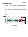
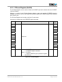
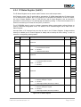
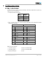
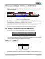
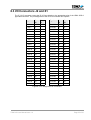
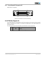
The Embedded I/O Company
TAMC100
Carrier for 1 Industry Pack®
User Manual
Issue 1.0
July 2008
TEWS TECHNOLOGIES GmbH
Am Bahnhof 7
Phone: +49-(0)4101-4058-0
25469 Halstenbek, Germany
Fax: +49-(0)4101-4058-19
www.tews.com
e-mail: [email protected]
TEWS TECHNOLOGIES LLC
9190 Double Diamond Parkway,
Suite 127, Reno, NV 89521, USA
www.tews.com
Phone: +1 (775) 850 5830
Fax: +1 (775) 201 0347
e-mail: [email protected]
TAMC100-10
AMC Carrier for 1 IndustryPack, Mid-size, HD50
SCSI-2 front I/O connector
TAMC100-10R
RoHS compliant version of TAMC100-10
TAMC100-11
AMC Carrier for 1 IndustryPack, Full-size, HD50
SCSI-2 front I/O connector
TAMC100-11R
This document contains information, which is
proprietary to TEWS TECHNOLOGIES GmbH. Any
reproduction without written permission is forbidden.
TEWS TECHNOLOGIES GmbH has made any
effort to ensure that this manual is accurate and
complete. However TEWS TECHNOLOGIES GmbH
reserves the right to change the product described
in this document at any time without notice.
TEWS TECHNOLOGIES GmbH is not liable for any
damage arising out of the application or use of the
device described herein.
RoHS compliant version of TAMC100-11
Style Conventions
Hexadecimal characters are specified with prefix 0x,
i.e. 0x029E (that means hexadecimal value 029E).
For signals on hardware products, an ‚Active Low’ is
represented by the signal name with # following, i.e.
IP_RESET#.
Access terms are described as:
W
Write Only
R
Read Only
R/W
Read/Write
R/C
Read/Clear
R/S
Read/Set
©2008 by TEWS TECHNOLOGIES GmbH
TAMC100 User Manual Issue 1.0
Page 2 of 26
Issue
Description
Date
0.2
Preliminary Issue
February 2008
1.0
Initial Issue
July 2008
TAMC100 User Manual Issue 1.0
Page 3 of 26
Table of Contents
1
2
3
PRODUCT DESCRIPTION ......................................................................................... 6
TECHNICAL SPECIFICATION................................................................................... 7
PEX8311 TARGET CHIP............................................................................................ 8
3.1 PEX8111 ...........................................................................................................................................8
3.1.1 PCI Express Configuration Space Register Mapping ..........................................................8
3.2 PCI9056 ..........................................................................................................................................10
3.2.1 PCI Configuration Registers (PCR) ...................................................................................10
4
REGISTER ADDRESSING ....................................................................................... 11
4.1 PCI9056 PCI Base Address Configuration .................................................................................11
4.2 IP I/O, ID, INT Space and Interface Registers.............................................................................11
4.2.1 Revision ID Register (0x400) .............................................................................................12
4.2.2 IP Control Register (0x402) ...............................................................................................13
4.2.3 IP Reset Register (0x40A) .................................................................................................14
4.2.4 IP Status Register (0x40C) ................................................................................................15
4.3 IP Interrupts ...................................................................................................................................16
4.4 IP Memory Space ..........................................................................................................................16
5
CONFIGURATION HINTS ........................................................................................ 17
5.1 Big / Little Endian..........................................................................................................................17
5.2 Configuration EEPROM ................................................................................................................18
5.2.1 PEX8111 EEPROM ...........................................................................................................18
5.2.2 PCI9056 EEPROM.............................................................................................................18
5.3 PCI9056 Interrupt enable..............................................................................................................19
6
MODULE MANAGEMENT ....................................................................................... 20
6.1 Indicators .......................................................................................................................................20
6.1.1 On Board Link-LED ............................................................................................................20
6.1.2 Front Panel LEDs...............................................................................................................20
6.2 Temperature and Voltage Sensors..............................................................................................20
6.3 Connectivity...................................................................................................................................21
7
INSTALLATION........................................................................................................ 22
7.1 AMC Module Insertion & Hot-Swap.............................................................................................22
7.1.1 Insertion .............................................................................................................................22
7.1.2 Extraction ...........................................................................................................................22
7.2 Installation of IndustryPacks .......................................................................................................22
7.3 Component Height Violation on TAMC100-x0 ...........................................................................23
7.4 Voltage Limits on IndustryPack Modules...................................................................................23
7.5 Fuses and Filters...........................................................................................................................23
8
PIN ASSIGNMENT ................................................................................................... 24
8.1 Overview ........................................................................................................................................24
8.2 IP Connector J1.............................................................................................................................24
8.3 I/O Connectors J2 and X1 ............................................................................................................25
8.3.1 Front Panel I/O Connector X1............................................................................................26
8.4 IP Strobe Signal J3........................................................................................................................26
TAMC100 User Manual Issue 1.0
Page 4 of 26
Table of Figures
FIGURE 1-1: BLOCK DIAGRAM........................................................................................................................6
FIGURE 2-1: TECHNICAL SPECIFICATION.....................................................................................................7
FIGURE 3-1: PCI-COMPATIBLE CONFIGURATION REGISTERS (TYPE 1) ..................................................8
FIGURE 3-2: PCI-COMPATIBLE CAPABILITY REGISTERS ...........................................................................9
FIGURE 3-3: PCI CONFIGURATION REGISTERS (PCR) .............................................................................10
FIGURE 4-1: PCI BASE ADDRESS CONFIGURATION .................................................................................11
FIGURE 4-2: IP I/O, ID, INT SPACE AND INTERFACE REGISTER SPACE.................................................11
FIGURE 4-3: REVISION ID REGISTER ..........................................................................................................12
FIGURE 4-4: IP CONTROL REGISTER ..........................................................................................................13
FIGURE 4-5: IP RESET REGISTER................................................................................................................14
FIGURE 4-6: IP STATUS REGISTER..............................................................................................................15
FIGURE 4-7: IP MEMORY SPACE..................................................................................................................16
FIGURE 5-1: LOCAL BUS LITTLE/BIG ENDIAN.............................................................................................17
FIGURE 5-2: PCI9056 CONFIGURATION EEPROM DATA ...........................................................................19
FIGURE 6-1: ON BOARD LINK-LED ...............................................................................................................20
FIGURE 6-2: FRONT PANEL LEDS ................................................................................................................20
FIGURE 6-3: TEMPERATURE AND VOLTAGE SENSORS ...........................................................................20
FIGURE 7-1: AMC MODULE INSERTION.......................................................................................................22
FIGURE 7-2: AMC MODULE EXTRACTION ...................................................................................................22
FIGURE 7-3: COMPONENT HEIGHT VIOLATION .........................................................................................23
FIGURE 7-4: VOLTAGE LIMITS ......................................................................................................................23
FIGURE 7-5: FUSE CURRENTS .....................................................................................................................23
FIGURE 8-1: CONNECTOR OVERVIEW ........................................................................................................24
FIGURE 8-2: IP J1 LOGIC INTERFACE PIN ASSIGNMENT..........................................................................24
FIGURE 8-3: PIN ASSIGNMENT I/O CONNECTORS ....................................................................................25
FIGURE 8-4: FRONT PANEL I/O CONNECTOR NUMBERING .....................................................................26
TAMC100 User Manual Issue 1.0
Page 5 of 26
1 Product Description
The TAMC100 is a standard single width / mid-size or full-size AMC.1 compliant carrier for one singlesize IndustryPack (IP) module used to build modular, flexible and cost effective I/O solutions for
applications in process control, medical systems, telecommunication and traffic control. A HD50 SCSI2 type connector provides access to all IP I/O lines.
The TAMC100 is a versatile solution to upgrade well known legacy I/O solutions to a high performance
form factor.
All IP interrupt request lines are mapped to PCIe INTA; alternatively Message Signaled Interrupts
(MSI) can be used. For fast interrupt source detection the TAMC100 provides a special IP interrupt
status register.
The IP power lines are fuse protected by self healing fuses and RF filtered. The operating temperature
range is -40°C to +85°C.
According to AMC.0, the TAMC100 provides an IPMI compliant Module Management Controller
(MMC) with temperature monitoring and hot-swap support.
The TAMC100 is available as mid-size module or as full-size module. The mid-size option has
restrictions to its usage because of a component height violation, but allows improving the density of a
µTCA system.
IP Bus
IP I/O
IP Slot
IP Interface
Local Bus
PCI Express
to Local Bridge
PCI9056
PEX8111
IPMB
PCIe(1x)
AMC Edge Connector
HD50 SCSI-2 Connector
MMC
Figure 1-1: Block Diagram
TAMC100 User Manual Issue 1.0
Page 6 of 26
2 Technical Specification
AMC Interface
Mechanical Interface
Advanced Mezzanine Card (AMC) Interface confirming to
PICMG® AMC.0 R2.0
Mid / Full Size
Electrical Interface
PICMG® AMC.1 R1.0
PCIe single lane (x1) port (AMC.1 Type 1 compliant)
IPMI
IPMI Version
1.5
Front Panel LEDs
Blue Hot-Swap LED
Red Power Good LED (LED1)
Green IP-Activity LED (LED 2)
On Board Devices
PCI Express Target Chip
PEX8311 (PLX Technology)
IP Interface
IP Interface
According to IndustryPack specification ANSI / VITA 4-1995
IP Slots
One single-size IP
IP Access
8 / 16 bit
8 / 32 MHz
8 Mbyte memory space
Mapping of IP Interrupts
Routing of all IP interrupts to PCIe INTA/MSI, local interrupt status
register
DMA
Not supported
32-Bit Access
Not supported
Protection
Self Healing fuses and RF-filtering on all IP power lines
I/O Interface
I/O Connector
Front-I/O via HD50 SCSI-2 type connector
Physical Data
Power Requirements
tbd. typical @ +12V DC (Payload Power)
tbd. typical @ +3.3V DC (Management Power)
Additional power is required by IP modules
Temperature Range
Operating
Storage
MTBF
633.000 h
-40°C - +85°C
-40°C - +85°C
MTBF values shown are based on calculation according to MIL-HDBK-217F and
MIL-HDBK-217F Notice 2; Environment: GB 20°C.
The MTBF calculation is based on component FIT rates provided by the
component suppliers. If FIT rates are not available, MIL-HDBK-217F and
MIL-HDBK-217F Notice 2 formulas are used for FIT rate calculation.
Humidity
5 – 95 % non-condensing
Weight
100 g
Figure 2-1: Technical Specification
TAMC100 User Manual Issue 1.0
Page 7 of 26
3 PEX8311 Target Chip
The PEX8311 internally consists of two devices, a PEX8111 (PCI Express to PCI bridge) and a
PCI9056 (PCI to local bus bridge). These are visible as two separate devices with own headers on the
PCI/PCIe bus.
In the following chapters both the PEX8111 and the PCI9056 are described as independent devices.
3.1 PEX8111
3.1.1 PCI Express Configuration Space Register Mapping
3.1.1.1
PCI
CFG
Register
Address
PCI-Compatible Configuration Registers (Type 1)
31
24
23
16
15
8
7
0
Read after
initialization
write access
0x00
PCI Device ID
PCI Vendor ID
10B5 8111
0x04
PCI Status
PCI Command
0010 0000
0x08
0x0C
PCI Class Code
PCI Built-In SelfTest
(Not Supported)
PCI Header Type
Internal PCI Bus
Latency Timer
PCI Device Revision
ID
060400 21
PCI Cache Line Size
00 01 00 00
0x10
PCI Base Address 0
0000000C
0x14
PCI Base Address 1
00000000
0x18
0x1C
Secondary Latency
Timer
Subordinate Bus
Number
Secondary Status
Secondary Bus
Number
Primary Bus Number
00 00 00 00
I/O Limit
I/O Base
0200 00 00
0x20
Memory Limit
Memory Base
0000 0000
0x24
Prefetchable Memory Limit
Prefetchable Memory Base
0000 0000
0x28
Prefetchable Memory Base Upper 32 Bits
0x2C
Prefetchable Memory Limit Upper 32 Bits
0x30
I/O Limit Upper 16 Bits
0x34
0x38
0x3C
00000000
00000000
I/O Base Upper 16 Bits
Reserved
0000 0000
PCI Capabilities
Pointer
000000 40
Internal PCI
Interrupt Line
0000 01 00
PCI Base Address for Expansion ROM (Not Supported)
Bridge Control
Internal PCI
Interrupt Wire
Figure 3-1: PCI-Compatible Configuration Registers (Type 1)
TAMC100 User Manual Issue 1.0
Page 8 of 26
3.1.1.2
PCI
CFG
Register
Address
0x40
0x44
PCI-Compatible Capability Registers
31
24
23
16
Power Management Capabilities
Power Management
Data
0
Power Management
Capability ID
Power Management Control/Status
0x58
Read after
initialization
write access
CA02 5001
00 00 0000
0000 0000
Reserved
Message Singled Interrupts Control
0x54
0000 0000
Message Signaled
Interrupts Next
Capability Pointer
Message Signaled
Interrupts Capability
ID
0080 60 05
Message Signaled Interrupts Address
0000 0000
Message Signaled Interrupts Upper Address
0000 0000
0x5C
Reserved
0x60
PCI Express Capabilities
Message Signaled Interrupts Data
0x64
PCI Express Next
Capability Pointer
PCI Express
Capability ID
Device Capabilities
PCI Express Device Status
0x6C
0x70
7
Device-Specific Control
0x4C
0x68
8
Power Management
Next Capability
Pointer
Power Management
Bridge Support
0x48
0x50
15
PCI Express Device Control
Link Status
Slot Status
0x7C
Reserved
0000 2000
0000 4C11
Link Control
Slot Capabilities
0x78
0071 00 10
0000 0000
Link Capabilities
0x74
0000 0000
1011 0000
0000 0C80
Slot Control
Root Control
0400 0000
0000 0000
0x80
Root Status
0000 0000
0x84
Main Control Register Index
0000 0000
0x88
Main Control Register Data
0000 0000
Figure 3-2: PCI-Compatible Capability Registers
TAMC100 User Manual Issue 1.0
Page 9 of 26
3.2 PCI9056
3.2.1 PCI Configuration Registers (PCR)
PCI CFG
Register
Address
Write ‘0’ to all unused (Reserved) bits
31
24
23
16
15
PCI
writeable
8
7
Initial Values
(Hex Values)
0
0x00
Device ID
Vendor ID
N
9056 10B5
0x04
Status
Command
Y
0280 0000
0x08
0x0C
Class Code
BIST
Header Type
PCI Latency
Timer
Revision ID
N
068000 BA
Cache Line Size
Y
00 00 00 00
0x10
PCI Base Address 0 for MEM Mapped Config. Registers
Y
FFFFFE00
0x14
Reserved
N
00000000
0x18
PCI Base Address 2 for Local Address Space 0
Y
FFFFF800
0x1C
PCI Base Address 3 for Local Address Space 1
Y
FF000000
0x20
Reserved
N
00000000
0x24
Reserved
N
00000000
0x28
PCI Cardbus Information Structure Pointer
N
00000000
N
8064 1498
Y
00000000
N
000000 40
0x2C
Subsystem ID
0x30
0x34
Reserved
0x38
0x3C
Subsystem Vendor ID
PCI Base Address for Local Expansion ROM
New Cap. Ptr.
Reserved
Max_Lat
0x40
Min_Gnt
PM Cap.
0x44
PM Data
PM CSR EXT
0x48
Reserved
HS CSR
0x4C
VPD Address
0x50
N
00000000
00 00 01 00
Wire Interrupt
Interrupt Line
Y
PM Nxt Cap.
PM Cap. ID
N
0002 48 01
Y
00 00 0000
PM CSR
HS Nxt Cap.
HS Cap. ID
Y
00 00 4C 06
VPD Nxt Cap.
VPD Cap. ID
Y
0000 00 03
Y
00000000
VPD Data
Figure 3-3: PCI Configuration Registers (PCR)
TAMC100 User Manual Issue 1.0
Page 10 of 26
4 Register Addressing
4.1 PCI9056 PCI Base Address Configuration
The local on board addressable regions are accessed from the PCI Express side by using the
PCI9056 local spaces.
PCI9056
PCI Base Address
(Offset in PCI
Configuration
Space)
PCI
Space
Mapping
Size
(Byte)
Port
Width
(Bit)
Endian
Mode
Description
2 (0x18)
MEM
2K
16
Little
IP I/O, ID, INT Space
and Interface
Registers
3 (0x1C)
MEM
16M
16
Little
IP Memory Space
Figure 4-1: PCI Base Address Configuration
4.2 IP I/O, ID, INT Space and Interface Registers
PCI Base Address:
PCI9056 PCI Base Address 2 (Offset 0x18 in PCI Configuration Space).
Offset to PCI
Base Address 2
Register Name
Size
(Byte)
0x000 … 0x07F
IP I/O Space
128
0x080 … 0x0BF
IP ID Space
64
0x0C0 … 0x0FF
IP INT Space
64
0x100 … 0x3FF
Reserved
-
0x400
REVISION ID
2
0x402
IP CONTROL
2
0x404 … 0x408
Reserved
-
0x40A
IP RESET
2
0x40C
IP STATUS
2
0x40E … 0x7FF
Reserved
-
Figure 4-2: IP I/O, ID, INT Space and Interface Register Space
TAMC100 User Manual Issue 1.0
Page 11 of 26
The TAMC100 supports read and write cycles to the IP ID space. A PCIe access to the TAMC100 will
be terminated in every case. If the IP supports write access to its ID space, data will be written to the
ID-PROM. If the IP does not support write access to its ID space, no ACK# will be generated by the IP
to the local control logic, and a local timeout will terminate the IP write cycle after a timeout time of 8µs
and the timeout bit is set in the IP Status Register.
The TAMC100 supports read and write cycles to the IP INT space. A read access to the IP INT space
initiates an IP interrupt acknowledge cycle. A read access with address A1=0 (e.g. 0x0000_00c0)
initiates an interrupt acknowledge cycle for IP INT0#, a read access with address A1=1 (e.g.
0x0000_00C2) initiates an interrupt acknowledge cycle for IP INT1#. The read access returns the
interrupt vector. This feature is helpful for IP modules that require an interrupt acknowledge cycle to
remove their pending interrupt request. If the IP does not support write access to its INT space, no
ACK# will be generated by the IP, and a local timeout will terminate the cycle after a timeout time of
8µs and the timeout bit is set in the IP Status Register.
4.2.1 Revision ID Register (0x400)
The Revision ID Register shows the revision of the on board IP FPGA logic. Initial Value is 0x00.
Changes in the on board FPGA logic will be signed by incrementing the register value.
Bit
Symbol
Description
Access
Reset
Value
15
0
14
0
13
0
12
11
-
Reserved
-
0
0
10
0
9
0
8
0
7
6
5
4
3
REV_ID
FPGA Logic Revision ID
R
-
2
1
0
Figure 4-3: Revision ID Register
TAMC100 User Manual Issue 1.0
Page 12 of 26
4.2.2 IP Control Register (0x402)
The IP Control Registers can be used to control IP interrupts, recover time and clock rate. After powerup or board reset, all bits in the IP Control Register are cleared (‘0’).
Each IP interrupt can be enabled or disabled separately. Interrupt detection can be switched between
level and edge sensitive. Edge sensitive interrupts must be cleared by a write to the corresponding bit
in the IP Status Register.
If the ERR_INT_EN bit is set to ‘1’, an active IP ERROR# line will generate an interrupt. This interrupt
can be cleared by setting the ERR_INT_EN bit to ‘0’.
The status of the IP ERROR# line can be read from the IP Status Register.
If the TIME_INT_EN bit is set to ‘1’ and an IP timeout occurs, the TAMC100 will generate an interrupt.
This interrupt can be cleared by writing ‘1’ to the IP timeout status bit in the IP Status Register.
If IP recovery time is enabled for the IP slot, an IP cycle for this slot will not begin until the IP recovery
time is expired. The IP recovery time is approx. 1µs.
IP clock rate can be selected between 8 MHz and 32 MHz. After power-up or board reset, the clock
rate is set to 8 MHz.
Bit
Symbol
Description
Access
Reset
Value
15
0
14
0
13
0
12
11
-
Reserved
0
-
0
10
0
9
0
8
0
7
INT1_EN
0 : IP interrupt 1 disabled
1 : IP interrupt 1 enabled
R/W
6
INT0_EN
0 : IP interrupt 0 disabled
1 : IP interrupt 0 enabled
R/W
0
5
INT1_SENSE
0 : IP interrupt 1 level sensitive
1 : IP interrupt 1 edge sensitive
R/W
0
4
INT0_SENSE
0 : IP interrupt 0 level sensitive
1 : IP interrupt 0 edge sensitive
R/W
0
3
ERR_INT_EN
0 : IP error interrupt disabled
1 : IP error interrupt enabled
R/W
0
2
TIME_INT_EN
0 : IP timeout interrupt disabled
1 : IP timeout interrupt enabled
R/W
0
1
RECOVERY
0 : IP recovery time disabled
1 : IP recovery time enabled
R/W
0
0
CLKRATE
0 : IP clock rate 8 MHz
1 : IP clock rate 32 MHz
R/W
0
0
Figure 4-4: IP Control Register
TAMC100 User Manual Issue 1.0
Page 13 of 26
4.2.3 IP Reset Register (0x40A)
The IP Reset Register can be used to initiate an IP RESET cycle and to detect when the IP RESET
cycle has finished.
Writing a ‘1’ to bit 0 of the IP Reset Register initiates a reset cycle and the IP RESET# signal is
asserted. After 200 ms, the on board logic automatically negates the IP RESET# signal and completes
the IP Reset cycle.
The IP Reset Register can be read to verify the IP reset status.
At power-up or board reset, the IP RESET# signal is asserted.
Bit
Symbol
Description
Access
Reset
Value
15
0
14
0
13
0
12
0
11
0
10
0
9
0
8
-
Reserved
-
0
7
0
6
0
5
0
4
0
3
0
2
0
1
0
0
IP_RESET
Read: 0 - IP RESET# signal is de-asserted
1 - IP RESET# signal is asserted
Write: 0 - No effect
1 - Assert IP RESET# signal (automatic negation
after 200 ms)
R/W
0
Figure 4-5: IP Reset Register
TAMC100 User Manual Issue 1.0
Page 14 of 26
4.2.4 IP Status Register (0x40C)
The IP Status Register can be used to read IP timeout, error and interrupt status.
An IP timeout occurs if the IP module fails to generate the IP ACK# signal within the IP timeout time.
The IP timeout time is approx. 8µs. An IP timeout is not reported to the PEX8311 or the PCI master,
but in the IP Status Register. If the IP_TIME_EN bit in the IP Control Register is set, an interrupt is
generated if a timeout occurs. This interrupt can be cleared by writing ‘1’ to the timeout status bit. If a
timeout occurs during an IP read, all ones (0xFF) is returned.
The IP ERROR# signal is used to indicate component failure, unrecoverable self-test failures or
serious, hard-wired configuration errors. The status of the IP ERROR# signal can be read in the IP
Status Register.
Interrupt status of IP interrupt lines can also be read in the IP Status Register. If edge sensitive
interrupt is enabled (see IP Control Register for detail) and an interrupt is active, writing ‘1’ to bit 1:0
clears the corresponding interrupt status.
Bit
Symbol
Description
Access
-
Reserved
-
15
14
0
0
13
12
0
TIME
Read: 0 - IP timeout has not occurred
1 - IP timeout has occurred
Write: 0 - No effect
1 - Clear IP timeout status
R/W
-
Reserved
-
11
10
0
0
0
9
8
Reset
Value
0
ERR
Read: 0 - IP ERROR# signal de-asserted
1 - IP ERROR# signal asserted
Write: 0 - No effect
1 - No effect
R/W
0
7
0
6
0
5
4
-
Reserved
0
-
0
3
0
2
0
1
INT1
Read : 0 - No IP interrupt 1 request
1 - Active IP interrupt 1 request
Write : 0 - No effect
1 - Clear edge sensitive IP interrupt 1 status
R/W
0
0
INT0
Read : 0 - No IP interrupt 0 request
1 - Active IP interrupt 0 request
Write : 0 - No effect
1 - Clear edge sensitive IP interrupt 0 status
R/W
0
Figure 4-6: IP Status Register
TAMC100 User Manual Issue 1.0
Page 15 of 26
4.3 IP Interrupts
All IP interface interrupt sources (Timeout, Error, IP INT0, IP INT1) are mapped to PCI interrupt
INTA#.
For quick interrupt source detection, the IP Status Register can be read to determine the IP interrupt
source.
Level sensitive IP interrupts, which are most common for IP modules are cleared by either an interrupt
acknowledge cycle to the IP or by accessing an Interrupt Status Register on the IP module.
A read access to the IP INT space initiates an IP interrupt acknowledge cycle. A read access with
address A1=0 (e.g. 0x0000_00c0) initiates an interrupt acknowledge cycle for IP INT0#, a read access
with address A1=1 (e.g. 0x0000_00C2) initiates an interrupt acknowledge cycle for IP INT1#. The read
access returns the interrupt vector. This feature is helpful for IP modules that require an interrupt
acknowledge cycle to remove their pending interrupt request.
Timeout interrupts and edge sensitive IP interrupts must be cleared in the IP Status Register.
IP Error interrupts must be cleared in the IP Control Register.
4.4 IP Memory Space
PCI Base Address:
PCI9056 PCI Base Address 3 (Offset 0x1C in PCI Configuration Space).
Offset to PCI
Base Address 2
Register Name
Size
(Byte)
0x00_0000 …
0x7F_FFFF
IP MEM Space (16 bit)
8M
0x80_0000 …
0xBF_FFFF
IP MEM Space (8 bit)
4M
0xC0_0000 …
0xFF_FFFF
Reserved
-
Figure 4-7: IP Memory Space
The PCI9056 local space 3 from address 0x00_0000 to 0x7F_FFFF is used for the IP Memory space
(16 bit port).
IPs with Memory space that uses D7:0 only, should be accessed via address 0x80_0000 to
0xBF_FFFF; this allows linear addressing of the IP memory space for IP’s with 8 bit port width (D0-D7)
only.
Please note that the 8 bit access only works correctly when the PCI9056 local space 3 is set to
8 bit port width before!
This is done by writing “00” to bits [1:0] in the Local Address Space 1 Bus Region Descriptor
Register at offset 0xF8 from the PCI Base Address 0. To switch back to 16 bit port, write “01” to
these two bits.
TAMC100 User Manual Issue 1.0
Page 16 of 26
5 Configuration Hints
5.1 Big / Little Endian
The serial PCI Express interface is always Little Endian. Little Endian to Big Endian conversion only
swaps byte lanes, not individual bits.
• PCI Express Interface (Little Endian)
Byte
Mapping
Internal AD
DWORD
Byte 0
AD[7..0]
Byte 1
AD[15..8]
Byte 2
AD[23..16]
Byte 3
AD[31..24]
• Both Local Address Space 0 and 1 and the Expansion ROM Space can be programmed to operate
in Big or Little Endian Mode.
Big Endian
Little Endian
32 Bit
Byte 0
D[31..24]
Byte 0
D[7..0]
Byte 1
D[23..16]
Byte 1
D[15..8]
Byte 2
D[15..8]
Byte 2
D[23..16]
Byte 3
D[7..0]
Byte 3
D[31..24]
16 Bit (upper lane)
Byte 0
D[31..24]
Byte 0
D[23..16]
Byte 1
D[23..16]
Byte 1
D[31..24]
16 Bit (lower lane)
Byte 0
D[15..8]
Byte 0
D[7..0]
Byte 1
D[7..0]
Byte 1
D[15..8]
Byte 0
D[31..24]
Byte 0
D[7..0]
8 Bit (upper lane)
Byte 0
D[31..24]
8 Bit (lower lane)
Byte 0
D[7..0]
Figure 5-1: Local Bus Little/Big Endian
Default use on the TAMC100:
• Local Address Space 0
16 bit bus in Little Endian Mode
• Local Address Space 1
16 bit bus in Little Endian Mode
• Expansion ROM Space
not used
TAMC100 User Manual Issue 1.0
Page 17 of 26
The Endian Mode can be changed in the PCI9056 LCS_BIGEND Big/Little Endian Descriptor register.
It can be accessed with PCI Base Address 0 + 0x0C or PCI Base Address 1 + 0x0C
For further information please refer to the PEX8311 / PCI9056 manual.
5.2 Configuration EEPROM
5.2.1 PEX8111 EEPROM
After power-on or PCI reset, the PEX8111 loads initial configuration register data from an on board
configuration EEPROM. Only register values differing from default values are stored in the EEPROM.
For further information please refer to the PEX8311 / PEX8111 manual.
Modifications are:
• Address Stepping is disabled (PCI Command Register)
• Slot Clock Configuration is enabled (Link Status/Control Register)
• PCI Express Enable (Device Initialization Register)
5.2.2 PCI9056 EEPROM
After power-on or PCI reset, the PCI9056 loads initial configuration register data from an on board
configuration EEPROM.
For further information please refer to the PEX8311 / PCI9056 manual.
The address range 0x00 - 0x3F is factory programmed with configuration information; the PCI9056
reads this memory area at power up for its configuration. This memory area must not be overwritten.
The address range 0x40 - 0x5F is also factory programmed with configuration information used by the
software drivers. This memory area also must not be overwritten.
The configuration EEPROM contains the following data:
• Vendor ID
• Vendor Device ID
• Subsystem Vendor ID
• Subsystem Device ID
• The module version and revision
TAMC100 User Manual Issue 1.0
Page 18 of 26
Address
Configuration Register
TAMC100
0x00-0x3F
PCI9056 Configuration Data
- DO NOT MODIFY -
-
0x40
Vendor ID
0x10B5
0x41
Device ID
0x9056
0x42
Subsystem Vendor ID
0x1498
0x43
Subsystem ID
0x8064
0x44
Module Version
0x0100
0x45
Module Revision
0x0000
0x46
Module Variant
s.b.
0x47
EEPROM Revision
0x0000
0x48-0x7F
Reserved
-
Figure 5-2: PCI9056 Configuration EEPROM Data
Module Variant:
TAMC100-10
0x800A
TAMC100-11
0x800B
5.3 PCI9056 Interrupt enable
To use interrupts, bit 11 (Local Interrupt enable) of the LCS_INTCSR (LCS Interrupt Control/Status,
Local MEM BASE0 offset 0x068) must be set to “1”.
For further information please refer to the PEX8311 / PCI9056 manual.
TAMC100 User Manual Issue 1.0
Page 19 of 26
6 Module Management
6.1 Indicators
For a quick visual inspection the TAMC100 offers 3 LEDs in the front panel and one on board LED.
6.1.1 On Board Link-LED
To help diagnose system bring up problems, the Link Up status of the PEX8111 can be visually
inspected with an on board LED.
LED
Color
State
Description
Link
Red
Off
Link
On
No link
Figure 6-1: On Board Link-LED
6.1.2 Front Panel LEDs
LED
Color
State
Description
HS
Blue
Off
No Power or module is powered
Short Blink
Hot-Swap negotiation (extraction)
Long Blink
Hot-Swap negotiation (insertion)
On
Module is ready to be powered or module
is ready to be unpowered
Off
No fault
On
Failure or out of service status
Off
Board is unpowered
On
Board is powered and OK
Blink
IP-Access
FAIL
Red
ACK
Green
Figure 6-2: Front Panel LEDs
6.2 Temperature and Voltage Sensors
Sensor Number
Signal Type
Signal Monitored
0
Event
Hot-swap switch
1
Temperature
LM75 #1
2
Temperature
LM75 #2
3
Voltage
+12V (PWR)
4
Voltage
+1.5V
5
Voltage
+12V (IP)
6
Voltage
-12V (IP)
Figure 6-3: Temperature and Voltage Sensors
TAMC100 User Manual Issue 1.0
Page 20 of 26
6.3 Connectivity
The TAMC100 provides a single x1 2.5 Gbps PCI-Express Link on AMC Port 4. The PCI-Express
Interface works with SSC and non SSC PCI-Express Reference Clocks.
TAMC100 User Manual Issue 1.0
Page 21 of 26
7 Installation
7.1 AMC Module Insertion & Hot-Swap
7.1.1 Insertion
Handle
Blue LED
Description
Open (Full extracted)
OFF
Insert Module into slot
Open (Full extracted)
ON
Module is ready to attempt activation
Closed (Pushed all way in)
Long Blink
Hot-Swap Negotiation
Closed (Pushed all way in)
OFF
Module is ready & powered
Figure 7-1: AMC Module Insertion
When the blue LED does not go off but returns to the “ON” state, the module FRU information is
invalid or the carrier cannot provide the necessary power.
7.1.2 Extraction
Handle
Blue LED
Description
Pulled out 1/2
OFF
Request Hot-Swap
Pulled out 1/2
Short Blink
Hot-Swap Negotiation
Pulled out 1/2
ON
Module is ready to be extracted
Open (Full extracted)
ON
Extract Module from slot
Figure 7-2: AMC Module Extraction
7.2 Installation of IndustryPacks
Before installing an IndustryPack, be sure that the power supply for the TAMC100 is turned off.
The component is an Electrostatic Sensitive Device (ESD). Use an anti-static mat connected to
a wristband when handling or installing the components.
Installing IndustryPacks on the TAMC100 is done by simply snapping them into the IP slot. The
connectors are keyed, so the IndustryPack can only be installed correctly. After an IP has been
installed it can be secured on the carrier board. This is normally necessary only in high vibration or
shock environments. Screws and spacers are required to fix a single IP on the TAMC100. They can
be ordered from TEWS TECHNOLOGIES (Part number: TIPxxx-HK).
TAMC100 User Manual Issue 1.0
Page 22 of 26
7.3 Component Height Violation on TAMC100-x0
With an assembled standard IndustryPack module with 1.6mm PCB thickness, the mid-size
TAMC100-10 violates the component envelope. The picture shows in red the violation of the hatched
AMC component envelope.
0,39 mm
100,00 mm
1,75 mm
39,30 mm
13,21 mm
11,85 mm
2,80 mm
Figure 7-3: Component Height Violation
The TAMC100-10 is intended for the use in µTCA systems where the adjacent AMC module provides
enough spacing (no components on the adjacent AMC modules back side) for the protruding
IndustryPack module. It allows improving the density of the µTCA system.
If your IndustryPack module has devices assembled on its back side or if you are not sure if the
available spacing is sufficient, it is strongly recommended to use the full-height TAMC100-11.
The TAMC100-10 is not suitable for the use on an AdvancedTCA AMC carrier board.
7.4 Voltage Limits on IndustryPack Modules
The AMC.0 specification limits the voltages on AMC modules to following thresholds:
DC voltage
AC voltage
Positive
+27V
+27V peak
Negative
-15V
-15V peak
Figure 7-4: Voltage Limits
When IndustryPack modules with voltages that excess these thresholds are to be used, additional
insulation to adjacent modules or carrier boards becomes necessary.
7.5 Fuses and Filters
The IP slot is protected with self-healing fuses. The maximum currents on the IP Module Voltages are:
Voltage
Current Limit
+5V
2A
+12V
120mA
-12V
120mA
Figure 7-5: Fuse currents
For improved performance the TAMC100 provides RF filtering and decoupling capacitors on all IP
power lines.
TAMC100 User Manual Issue 1.0
Page 23 of 26
8 Pin Assignment
8.1 Overview
Figure 8-1: Connector Overview
J4 and J5 are for factory use only.
8.2 IP Connector J1
The table below shows the complete IP J1 logic interface pin assignments. Some of these signals are
not used on the TAMC100.
Pin # Signal
Pin # Signal
Pin # Signal
Pin # Signal
1
GND
2
CLK
26
GND
27
+5V
3
Reset#
4
D0
28
R/W#
29
IDSel#
5
D1
6
D2
30
DMAReq0#
31
MemSel#
7
D3
8
D4
32
DMAReq1#
33
IntSel#
9
D5
10
D6
34
DMAck#
35
IOSel#
11
D7
12
D8
36
Reserved
37
A1
13
D9
14
D10
38
DMAEnd#
39
A2
15
D11
16
D12
40
Error#
41
A3
17
D13
18
D14
42
IntReq0#
43
A4
19
D15
20
BS0#
44
IntReq1#
45
A5
21
BS1#
22
-12V
46
Strobe#
47
A6
23
+12V
24
+5V
48
ACK#
49
Reserved
25
GND
50
GND
Figure 8-2: IP J1 Logic Interface Pin Assignment
TAMC100 User Manual Issue 1.0
Page 24 of 26
8.3 I/O Connectors J2 and X1
The IP J2 I/O connector routes the IP I/O lines directly to the appropriate pins of the HD50 SCSI-2
type cable connector. The pin assignment of the IP J2 I/O connector is IP specific.
Signal
Pin
J2
Pin
X1
Signal
Pin
J2
Pin
X1
IP I/O 0
1
1
IP I/O 25
26
26
IP I/O 1
2
2
IP I/O 26
27
27
IP I/O 2
3
3
IP I/O 27
28
28
IP I/O 3
4
4
IP I/O 28
29
29
IP I/O 4
5
5
IP I/O 29
30
30
IP I/O 5
6
6
IP I/O 30
31
31
IP I/O 6
7
7
IP I/O 31
32
32
IP I/O 7
8
8
IP I/O 32
33
33
IP I/O 8
9
9
IP I/O 33
34
34
IP I/O 9
10
10
IP I/O 34
35
35
IP I/O 10
11
11
IP I/O 35
36
36
IP I/O 11
12
12
IP I/O 36
37
37
IP I/O 12
13
13
IP I/O 37
38
38
IP I/O 13
14
14
IP I/O 38
39
39
IP I/O 14
15
15
IP I/O 39
40
40
IP I/O 15
16
16
IP I/O 40
41
41
IP I/O 16
17
17
IP I/O 41
42
42
IP I/O 17
18
18
IP I/O 42
43
43
IP I/O 18
19
19
IP I/O 43
44
44
IP I/O 19
20
20
IP I/O 44
45
45
IP I/O 20
21
21
IP I/O 45
46
46
IP I/O 21
22
22
IP I/O 46
47
47
IP I/O 22
23
23
IP I/O 47
48
48
IP I/O 23
24
24
IP I/O 48
49
49
IP I/O 24
25
25
IP I/O 49
50
50
Figure 8-3: Pin Assignment I/O Connectors
TAMC100 User Manual Issue 1.0
Page 25 of 26
8.3.1 Front Panel I/O Connector X1
AMP 787395-5 or compatible.
1
50
26
FAIL
TAMC100
25
ACK
Figure 8-4: Front Panel I/O Connector Numbering
8.4 IP Strobe Signal J3
The IP strobe signal is an uncommitted line of the IP logic interface, which may be used as an optional
input to or output from an IP module. It is reserved for a digital strobe or clock signal related to the
functionality of the IP.
The strobe signal of the IP slot is accessible on the TAMC100 via a 2-pin jumper field.
Pin
Signal
1
GND
2
Strobe
TAMC100 User Manual Issue 1.0
Description
Ground
External Strobe Signal
Page 26 of 26