1
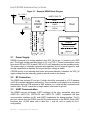
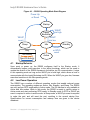
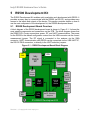
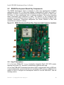
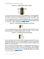
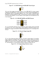
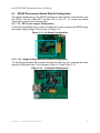
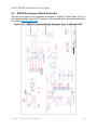
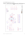
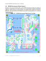
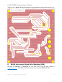
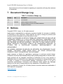
Indy® RS500 Hardware User’s Guide 1 Indy® RS500 Overview The Impinj® Indy® RS500 is a System-in-Package (SiP) that comprises a completely integrated reader solution for EPC Gen2 / ISO18000-63 (formerly 18000-6C) applications. The SiP was developed to make embedding UHF RFID reader capability easy. The Indy RS500 builds on market-leading Indy reader chip technology and integrates all of the necessary components into a tiny package. It is fully tested and is certified for modular operation under FCC and IC regulations. The RS500 comes in a surface mount package designed to work as a SMT (surface mount technology) component in a standard PCB manufacturing process. This document provides hardware developers technical guidance to ensure optimal performance when using the Indy RS500. Details on the use of the Indy RS500 Development Kit are also included. Air Interface Protocol EPCglobal UHF Class 1 Gen 2 / ISO 18000-63 (formerly 18000-6C) Supports dense reader mode (DRM) Tx Output Power 10 to 23 dBm Operating Frequencies IPJ-RS500-GX (902-928MHz) covers all 900MHz bands worldwide IPJ-RS500-EU (865-868MHz) covers current EU operating band Package 29 mm by 32 mm by 3.8 mm Package Type 32 pin surface mount package (SMT compatible) Rx Sensitivity -65 dBm (1% packet error rate). Assumes a 15 dB antenna return loss at 23 dBm output power. DC Power Supply 3.6 to 5.25 Volts DC Power Consumption 2.6 Watts at 23 dBm output power and 5 Volt supply 2 Watts at 23 dBm output power and 3.6 Volt supply Supported Regions Worldwide regional support. All major regions supported. Compliance Certified: FCC and Canada modular operation, RoHS compliant For technical support, visit the Impinj support portal at: support.impinj.com www.impinj.com Revision 1.1 Copyright © 2014, Impinj, Inc. Impinj and Indy are either registered trademarks or trademarks of Impinj, Inc. For more information, contact [email protected] Indy® RS500 Hardware User’s Guide 2 1 2 3 4 5 6 7 8 Table of Contents INDY® RS500 OVERVIEW .................................................................................................................... 1 TABLE OF CONTENTS ......................................................................................................................... 2 2.1 FIGURES ............................................................................................................................................ 2 2.2 TABLES .............................................................................................................................................. 3 RS500 HARDWARE INTERFACE......................................................................................................... 4 3.1 POWER SUPPLY ................................................................................................................................. 5 3.2 RF CONNECTION ................................................................................................................................ 5 3.3 UART COMMUNICATION ..................................................................................................................... 5 3.4 RESET PIN ......................................................................................................................................... 6 3.5 HEALTH AND STATUS PINS .................................................................................................................. 6 3.5.1 Health Pin Behavior ................................................................................................................... 6 3.5.2 Status Pin Behavior ................................................................................................................... 7 3.6 GPIO PINS ........................................................................................................................................ 7 3.7 W AKEUP PIN ...................................................................................................................................... 7 3.8 BOOT PIN........................................................................................................................................... 8 RS500 OPERATING MODES ................................................................................................................ 8 4.1 STARTUP BEHAVIOR ........................................................................................................................... 9 4.2 LOW POWER OPERATION .................................................................................................................... 9 RS500 DEVELOPMENT KIT ............................................................................................................... 11 5.1 RS500 DEVELOPMENT BOARD OVERVIEW ........................................................................................ 11 5.2 RS500 DEVELOPMENT BOARD KEY COMPONENTS ............................................................................ 12 5.2.1 Key IC Descriptions ................................................................................................................. 12 5.2.2 Connector Descriptions ........................................................................................................... 13 5.3 RS500 DEVELOPMENT BOARD DEFAULT CONFIGURATION ................................................................. 17 5.3.1 J8 – SiP Current Jumper Configuration ................................................................................... 17 5.3.2 J12 – Supply Voltage Selection Jumper Configuration ........................................................... 17 5.3.3 J13-16 – UART Selection Jumpers Configuration................................................................... 18 5.3.4 Additional Jumper Configurations............................................................................................ 18 5.4 RS500 DEVELOPMENT BOARD USB-UART DETAILS ......................................................................... 18 5.5 RS500 DEVELOPMENT BOARD SCHEMATIC ....................................................................................... 19 5.6 RS500 DEVELOPMENT BOARD LAYOUT............................................................................................. 21 5.7 RS500 DEVELOPMENT BOARD BILL OF MATERIALS (BOM) ................................................................ 22 REGULATORY GUIDELINES ............................................................................................................. 23 6.1 PRODUCT LABELLING........................................................................................................................ 23 6.2 PRODUCT MANUALS ......................................................................................................................... 24 6.3 US REQUIREMENTS .......................................................................................................................... 24 6.4 CANADIAN REQUIREMENTS ............................................................................................................... 25 6.5 ANTENNA REQUIREMENTS ................................................................................................................ 26 6.6 MAXIMUM POWER EXPOSURE (MPE) AND USAGE LIMITATIONS .......................................................... 26 DOCUMENT CHANGE LOG ............................................................................................................... 27 NOTICES .............................................................................................................................................. 27 2.1 Figures FIGURE 3-1 - EXAMPLE RS500 BLOCK DIAGRAM .............................................................................................. 5 FIGURE 4-1 – RS500 OPERATING MODE STATE DIAGRAM ................................................................................ 9 FIGURE 5-1 – RS500 DEVELOPMENT BOARD BLOCK DIAGRAM........................................................................ 11 FIGURE 5-2 – RS500 DEVELOPMENT BOARD KEY COMPONENT AND CONNECTOR LOCATIONS ......................... 12 FIGURE 5-3 – J4: RS500 CONTROL SIGNALS AND 3.3V SUPPLY ..................................................................... 13 Revision 1.1, Copyright © 2014, Impinj, Inc. 2 Indy® RS500 Hardware User’s Guide FIGURE 5-4 – J5: RS500 GPIOS, HEALTH, AND STATUS ................................................................................ 14 FIGURE 5-5 – J6: RS500 RESET AND USB-UART CONTROL SIGNAL .............................................................. 14 FIGURE 5-6 – J7: RS500 RESET AND ANALOG SIGNALS.................................................................................. 14 FIGURE 5-7 – J9: RS500 W AKEUP AND USB-UART CONTROL SIGNAL ........................................................... 15 FIGURE 5-8 – J10: USB-UART ACBUS AND BCBUS OUTPUTS .................................................................... 15 FIGURE 5-9 – J11: EXTERNAL VOLTAGE SUPPLY VIN ..................................................................................... 15 FIGURE 5-10 – J12: SUPPLY VOLTAGE SELECTION JUMPER ............................................................................ 15 FIGURE 5-11 – J13-16: UART SELECTION JUMPERS ...................................................................................... 16 FIGURE 5-12 – J8 DEFAULT CONFIGURATION ................................................................................................. 17 FIGURE 5-13 – J12 DEFAULT CONFIGURATION ............................................................................................... 17 FIGURE 5-14 – J13-16 DEFAULT CONFIGURATION .......................................................................................... 18 FIGURE 5-15 – RS500 DEVELOPMENT BOARD SCHEMATIC PAGE 2: USB AND UART ...................................... 19 FIGURE 5-16 – RS500 DEVELOPMENT BOARD SCHEMATIC PAGE 3: RS500, HEADERS, AND LEDS .................. 20 FIGURE 5-17 – RS500 DEVELOPMENT BOARD LAYOUT TOP SIDE ................................................................... 21 FIGURE 5-18 – RS500 DEVELOPMENT BOARD LAYOUT BOTTOM SIDE (VIEWED FROM TOP) ............................. 22 2.2 Tables TABLE 7-1: DOCUMENT CHANGE LOG............................................................................................................. 27 Revision 1.1, Copyright © 2014, Impinj, Inc. 3 Indy® RS500 Hardware User’s Guide 3 RS500 Hardware Interface An example Indy RS500 system-level block diagram for an embedded system is shown in Figure 3-1. This figure shows the electrical connections that may and must be made to control the RS500. In the figure, the required connections are illustrated with solid lines. Recommended and optional connections are illustrated with different dotted and dashed line patterns. They are also listed below. More details for each connection are listed in the following subsections. Required connections: VDC_IN and GND are required to power the RS500. RF is required to connect to the UHF RFID antenna. UART1 Tx and Rx are required to communicate with the system host. Recommended connections: nRST is used to reset the RS500 if UART communication is not available. This connection is highly recommended. This pin internally driven strong low during software resets, so it should only be driven externally by an open drain signal. It must not be driven strong high. UART2 Tx and Rx may be used to examine debug information. HEALTH indicates successful operation of the RS500. Connection to an LED provides a visual indication of whether or not an error condition exists. STATUS provides an indication when the RS500 is in active mode (for example, inventorying tags). Connection to an LED provides a visual indicator of the device’s activity. Optional connections: GPIOs allow interaction with the RS500 as both digital inputs and outputs. They may be used to trigger inventory, generate events based on inventory activity, or provide general-purpose user-controlled digital I/O. WKUP provides a mechanism to wake up the RS500 from the low power Sleep mode. WKUP is also used to force entry into the Impinj firmware bootstrap. If unused, this pin should be tied to logic low. UC_ADC allows use of an ADC to convert an analog input voltage into a digital value. UC_DAC allows use of a DAC to generate an analog output voltage from a digital value. BOOT0 provides access to the built-in bootloader in case the Impinj firmware is corrupted. For more details on the built-in bootloader, please contact Impinj support. No connect: SWCLK and SWD connections are reserved for Impinj use only. Revision 1.1, Copyright © 2014, Impinj, Inc. 4 Indy® RS500 Hardware User’s Guide Figure 3-1 - Example RS500 Block Diagram 3.6 - 5.25 V UART1 RX & TX VDC_IN Test Points 3.1 UC_ADC & UC_DAC GPIOs STATUS & HEALTH GND UART2 RX & TX Indy RS500 SiP RF User Def. NRST WKUP Host GPIOs Key Required Recommended Optional Power Supply RS500 is powered by a voltage applied to the VDC_IN pin (pin 11) relative to the GND pins. The supply voltage operating range is 3.6 V to 5.25 V. Current consumption varies from about 600 mA (3 W) to about 100 uA (0.5 mW) depending on the operating mode. The power supply is internally bypassed and regulated, and no external bypass or bulk storage capacitance is required, as long as the input voltage is stable. If RS500 activity is not required at all times, and power reduction is desired, the VDC_IN supply voltage may be externally gated to remove power to the device. 3.2 RF Connection The RS500 has a single RF pin (pin 1) which should be connected to a 50 Ω antenna via 50 Ω controlled impedance connection. This connection could simply be a microstrip transmission line to a PCB antenna or SMT antenna, or it could include a connector and coaxial cable. The RF connection is single ended, referenced to ground. 3.3 UART Communication The RS500 has two full-duplex UART interfaces at the pins, accessible using pins UART1-RX, UART1-TX, UART2-RX, and UART2-TX. UART1 implements the host communication interface via IRI, and UART2 implements the debug interface. The Tx pins are outputs from the RS500, and the Rx pins are inputs to the RS500. Both UART interfaces are 115,200 baud, with 8 data bits, 1 stop bit, and no parity bit (8-n-1 configuration). Revision 1.1, Copyright © 2014, Impinj, Inc. 5 Indy® RS500 Hardware User’s Guide Each of the UART interfaces signals at 3.3V relative to GND. The specific VIH, VIL, VOH and VOL specifications may be found in the device datasheet. The TX pins are driven strong high and low with a sink/source current of about 8 mA. If the load on a pin draws more than the 8 mA sink and source current, the pin is not guaranteed to meet the VOH and VOL specs listed in the datasheet. Excessive current sunk or sourced on the GPIO pins can also cause electrical damage to the device. Voltages outside of the maximum IO operating voltage range of -0.3 to 4.0 V should not be applied to the UART pins. This can cause permanent damage to the device. 3.4 Reset Pin The RS500 may be reset by a logic low voltage on the NRST pin (pin 9). Usage of this pin is recommended in all designs. It may be used to reset the part if an unexpected operating state is entered. The RS500 does have an internal watchdog circuit that will reset it if abnormal operation occurs, but the NRST pin provides a further level of reliability. The NRST pin is pulled high (3.3 V) by an internal 40 kΩ nominal resistor. To reset the part, drive the pin strong low for at least the minimum reset pulse width as specified in the datasheet (approximately 25 µs). This pin may be driven active low to reset the part, but should not be driven strong high. Driving the pin strong high prevents the RS500 from resetting itself in case of a watchdog reset or user requested software reset. This pin should be driven using an “open drain drives low” drive mode, which creates either a strong low voltage or a floating voltage output. Voltages outside of the maximum IO operating voltage range of -0.3 to 4.0 V should not be applied to the NRST pin. This can cause permanent damage to the device. 3.5 Health and Status Pins The RS500 has two pins that indicate the state of the device through their voltages: HEALTH (pin 22) and STATUS (pin 21). Both pins are outputs operating at a logical voltage level of 3.3 V, and can sink and source 8 mA each. If the load on one of these pins draws more than the 8 mA sink and source current, the pin is not guaranteed to meet the VOH and VOL specs listed in the datasheet. Excessive current sunk or sourced on the pins can also cause electrical damage to the device. 3.5.1 Health Pin Behavior The HEALTH pin indicates whether the RS500 is operating in its normal mode, or if some other condition exists. The pin is cycled high and low in specific patterns to indicate the state of the RS500. Those patterns are as follows: Reset – HEALTH pin is held low Idle mode, no reads occurring – 1 second high, 1 second low Active mode, reads occurring – 250 ms high, 750 ms low Watchdog reset has occurred – Low Revision 1.1, Copyright © 2014, Impinj, Inc. 6 Indy® RS500 Hardware User’s Guide Recovery mode – Blink alternate pattern with STATUS LED 3.5.2 Status Pin Behavior The STATUS pin indicates whether the RS500 is operating in its active mode, or if some other condition exists. The pin is cycled high and low in specific patterns to indicate the state of the RS500. Those patterns are as follows: Reset – STATUS pin is held low Startup – STATUS pin pulses high during startup Normal operation – During inventory, the high time is between 150ms and 750ms based on the number of tags in the field. The low time is 1000ms minus the high time. If there are no tags in the field the pin remains low. Watchdog reset has occurred – Alternate high and low Recovery mode – Toggle with a pattern of logical NOT of the HEALTH pin status 3.6 GPIO Pins The RS500’s GPIOs can be controlled using the IRI interface. Their drive mode, direction, and state are all controllable via IRI. There are two directions: input and output. In both input and output directions, there are three possible pin states: high, low, and float. For more details on using IRI to control the GPIOs, see the IRI Toolkit (ITK) documentation. In the output direction, the GPIOs are driven strong high and low with a source and sink current of 8 mA, and in float mode the pin is not driven either high or low, leaving the pin floating, also known as “high impedance” or “high-Z”. The pins are driven to 3.3 V nominally. If the load on a pin draws more than the 8 mA sink and source current, the pin is not guaranteed to meet the VOH and VOL specs listed in the datasheet. Excessive current sunk or sourced on the GPIO pins can also cause electrical damage to the device. In the input direction, the high and low states apply a pull-up or pull-down resistor, and in float mode the pin is not pulled either high or low, leaving the pin floating, also known as “high impedance” or “high-Z”. The pull-up and pull-down resistors are about 40 kΩ nominal. See the device datasheet for more specific ratings. The inputs logic levels are proportional to 3.3V. Specific VIH and VIL specs may be found in the device datasheet. Voltages outside of the maximum IO operating voltage range of -0.3 to 4.0 V should not be applied to the pins, no matter their configuration. This can cause permanent damage to the device. 3.7 Wakeup Pin The WKUP pin is used to wake the device when it is in the Standby or Sleep operating modes. This pin is edge sensitive, and will wake the device on a rising edge. The WKUP pin must be logic low in order for the device to re-enter Idle mode after a Sleep wakeup, so it should only be pulsed high to wake up the part. Revision 1.1, Copyright © 2014, Impinj, Inc. 7 Indy® RS500 Hardware User’s Guide The WKUP pin is also used to force the part into the Impinj bootstrap. The pin is polled at startup, and while it remains high, the device stays in the bootstrap. This allows bootloading of the part even if the bootloadable code is corrupted. The WKUP pin operates at a 3.3 V logic level. It has a 40 kΩ typical pull-down resistor inside the RS500. Voltages outside of the maximum IO operating voltage range of -0.3 to 4.0 V should not be applied to the WKUP pin. This can cause permanent damage to the device. If the WKUP pin is not used, it should be left floating or tied to logic low (ground). This will prevent accidental entry into the Impinj bootstrap. 3.8 Boot Pin The BOOT0 pin is used to force the RS500 into executing its internal bootloader. This bootloader is stored in non-volatile memory, and cannot be damaged by memory writes. The Impinj bootstrap resides in flash memory, and could be overwritten by erroneous bootload operations. The internal bootloader provides a fail-safe method of re-flashing the part. The BOOT0 pin is active high, and causes the part to enter the internal bootloader when held high during a reset or power up. If unused, this pin should be tied to logic low (ground). The BOOT0 pin operates at a 3.3 V logic level. Voltages outside of the maximum IO operating voltage range of -0.3 to 4.0 V should not be applied to the WKUP pin. This can cause permanent damage to the device. For more details on using the internal bootloader, please contact Impinj support at support.impinj.com. 4 RS500 Operating Modes RS500 has five operating modes and a startup mode. The transitions between these modes are shown in Figure 4-1. Transitions are shown in two categories: IRI activity and non-IRI activity. IRI activity shows transitions that are caused by commands communicated over IRI. Non-IRI activity shows transitions that are caused by inputs to the part such as WKUP, NRST, and GPIOs, and power supply conditions such as power supply ramps. More details on startup behaviour and low power modes are given in the following subsections. Revision 1.1, Copyright © 2014, Impinj, Inc. 8 Indy® RS500 Hardware User’s Guide Figure 4-1 – RS500 Operating Mode State Diagram Power Up or Reset Startup WKUP pin high Impinj Bootstrap WKUP pin low WKUP event Sleep Idle WKUP or GPIO event Key IRI Activity Standby Active Non-IRI Activity 4.1 Startup Behavior Upon reset or power up, the RS500 configures itself in the Startup mode. It automatically begins code execution in the Impinj bootstrap, which can be used to update the version of the RS500 firmware in the device via IRI communication. It stays in this operating mode as long as the WKUP pin is held high, which allows a host to communicate with the Impinj Bootstrap via IRI. When the WKUP pin goes low, firmware execution transitions to the Idle operating mode. 4.2 Low Power Operation The RS500 has a number of different operating modes that enable reduced power consumption. The operating modes are Active, Idle, Standby, and Sleep. The RS500 can only perform RFID reads while in Active mode. The IRI interface is only available in Active and Idle modes. While in Idle mode, the RS500 is ready to quickly return to Active mode and start performing RFID reads. In Standby mode, a GPIO or WKUP pin event is required to return to active mode. In Sleep mode, a WKUP pin event is required to wake the part, and will reset the part, resulting in the normal startup flow. Specifications for current consumption and wakeup time are given in the device datasheet. Revision 1.1, Copyright © 2014, Impinj, Inc. 9 Indy® RS500 Hardware User’s Guide Within Idle mode, there are two possible configurations: low latency and standard latency. Low latency idle mode consumes more current but returns to active mode more quickly. See the datasheet for more detailed specifications on wakeup time performance. The NRST pin can be used in any mode to reset RS500, eventually returning it to Idle mode via the normal startup behavior. For more detail see section 3.7: Wakeup Pin. If the low power performance provided by these modes does not meet the requirement of a system, power may be gated to the RS500’s VDC_IN pin, allowing its current consumption to be eliminated entirely. In this configuration, voltages above 0V should not be applied to any of the pins of the device, as they can cause excessive current consumption and unexpected part behaviour. Revision 1.1, Copyright © 2014, Impinj, Inc. 10 Indy® RS500 Hardware User’s Guide 5 RS500 Development Kit The RS500 Development Kit enables quick evaluation and development with RS500. It provides an easy way to communicate with the RS500 via RS-232, and provides easy access to the inputs and outputs of the device. This section provides details on how to use the main component of the development kit, the RS500 development board. 5.1 RS500 Development Board Overview A block diagram of the RS500 development board is shown in Figure 5-1. It shows the most notable components and connections on the PCB. The block diagram shows that the RS500 SiP’s 3 main connections: power, RF, and UART communication. The power for the RS500 in the default configuration comes from the USB connector via the current measurement jumper. The RF signal is connected to the antenna via the SMA connector. UART communication with RS500 can be connected via the USB-UART IC, the RS-232 DB-9 connectors, or directly to the UART selection jumpers. Figure 5-1 – RS500 Development Board Block Diagram RF SMA LEDs Indy RS500 SiP SiP Current Jumper USBUART IOs USB Mini RS500 IO Test Points Reset Switch Dual USBUART 3.3V Reg RS232 Level Shifter Host UART RS-232 DB-9 Debug UART RS-232 DB-9 UART Selection Jumpers IPJ-RS500 Development Kit Revision 1.1, Copyright © 2014, Impinj, Inc. 11 Indy® RS500 Hardware User’s Guide 5.2 RS500 Development Board Key Components The RS500 development board is designed to allow easy development of RS500 applications using a PC or other hosts capable of generating IRI traffic over UART. It includes a number of components and connectors to allow connection to USB or RS232 hosts, or other development kits or customer hardware. This section describes these components and connectors in detail. The locations of the component and connectors on the PCB are shown in Figure 5-2, and they are described in detail in the following subsections. Component designators are shown outlined in blue, and connectors are outlined in orange. Figure 5-2 – RS500 Development Board Key Component and Connector Locations 5.2.1 Key IC Descriptions U1 is the Indy RS500 SiP. It is a completely integrated Gen2 UHF RFID reader, requiring only power, RF, and UART connections to read and write tags. U4 is a dual USB-UART transceiver that allows UART communication with a USB host. It can simultaneously connect both the host and debug UART ports to a USB host. For details on how to configure the development board to use the USB-UART, see the following section. Revision 1.1, Copyright © 2014, Impinj, Inc. 12 Indy® RS500 Hardware User’s Guide U5 is an RS-232 level translator that allows RS500, which signals at 3.3 V logic levels, to communicate with RS-232 devices that signal at logic levels of +/-5 V. This allows usage of the DB-9 connectors. For details on how to configure the development board to use the RS-232 level translator and DB-9 connectors, see the following section. U6 is a 3.3 V linear regulator that is used to power the USB-UART and RS-232 level translation ICs from either the USB or arbitrary voltage input. 5.2.2 Connector Descriptions The connectors on the RS500 development board are listed in this section. They are listed in order of their Jn designator. Each connector is described in at least one sentence. Figures are included for those with multiple signals of note. Each figure shows the connector in same orientation as it appears on the development board, when viewed from the top, face up. In the figures, “NC” indicates that the pin on the connector is not connected to any signal. Most of the connectors included for debug or development purposes are 100-mil pitch male headers. These allow easy connection via 100-mil pitch female hook-up wires, jumpers, or grabber cables. For those connectors intended for use with jumpers, the default position is indicated with a gray bracket. The default position enables USB host power and UART communication. Alternate configurations may be required for DB-9 RS-232 connection, direct connection to other development kits, etc. J1 is a serial wire debug (SWD) header reserved for Impinj use. This connector is not populated on the production development board. J2 is the 50-ohm SMA RF connector. The antenna should be connected via this connector. J3 is a 3-pin header with ground on each pin. It can be used as a reference for multimeters or oscilloscopes. J4 is an 8-pin header with 4 pins connected to the regulated 3.3V signal, and 4 others connected to control signals for the RS500. The RS500 control signals include the SWD signals reserved for Impinj use only, the internal bootload signal BOOT0, and the wakeup signal WKUP. Figure 5-3 – J4: RS500 Control Signals and 3.3V Supply J4 3.3V SW_CLK 3.3V SW_DIO 3.3V BOOT0 3.3V WKUP J5 is a 10-pin header with 4 pins connected to the RS500’s user controllable GPIOs, and 2 pins connected to the indicator pins HEALTH and STATUS. The remaining 4 pins are not connected to any signal. Revision 1.1, Copyright © 2014, Impinj, Inc. 13 Indy® RS500 Hardware User’s Guide Figure 5-4 – J5: RS500 GPIOs, Health, and Status J5 GPIO4 HEALTH GPIO3 STATUS GPIO2 NC GPIO1 NC NC NC J6 is a 2-pin header with one pin connected to the RS500 active low reset signal NRST, and the other connected to the “data terminal ready” (DTR) output of the USB-UART IC. This output is conditioned with an open-drain drives low buffer, as the NRST signal must not be driven strong high. This configuration allows the user to install a jumper on J6 to force the RS500 into reset whenever the USB-UART COM port is not connected. For more details, contact Impinj support at support.impinj.com. If the USB-UART COM port is not used, no jumper should be placed on J6. Figure 5-5 – J6: RS500 Reset and USB-UART Control Signal J6 NRST CTRL J7 is a 3-pin header with one pin connected to the RS500’s active low NRST signal, and two pins connected to the analog signals UC_DAC and UC_ADC. These are intended as test points to allow connection of external signals to the RS500. Figure 5-6 – J7: RS500 Reset and Analog Signals J7 NRST UC_DAC UC_ADC J8 is a 2-pin header that connects the RS500’s voltage supply signal VDC_IN to the development board’s main 3.6 – 5.25 V power supply signal. In most cases, this header should be populated with a jumper so that the RS500 is powered. A series current meter can be connected in place of a jumper to measure the current consumption of the RS500 for low power debugging. J9 is a 2-pin header with one pin connected to the RS500’s wakeup signal WKUP, and the other connected to the ADBUS2 output of the USB-UART IC. This configuration allows the user to install a jumper on J9 to allow the USB-UART to wake the RS500 when instructed to by code running on a PC connected over USB. For more details, contact Impinj support at support.impinj.com. If the USB-UART COM port is not used, no jumper should be placed on J9. Revision 1.1, Copyright © 2014, Impinj, Inc. 14 Indy® RS500 Hardware User’s Guide Figure 5-7 – J9: RS500 Wakeup and USB-UART Control Signal J9 WKUP CTRL J10 is an 8-pin header that allows access to the USB-UART IC’s debug signals ACBUS[0:3] and BCBUS[0:3]. These signals are not critical for RS500 development, but are included mainly for debugging purposes. Four of the signals, ACBUS[2:3] and BCBUS[2:3], provide indicators of UART Tx and Rx activity, and are connected to LEDs to provide visual feedback. For more details on these signals, see the datasheet for the FTDI FT2232D IC. Figure 5-8 – J10: USB-UART ACBUS and BCBUS Outputs J10 BCBUS3 ACBUS3 BCBUS2 ACBUS2 BCBUS1 ACBUS1 BCBUS0 ACBUS0 J11 is a 3-pin header that allows use of an external voltage supply in place of the USB 5 V supply. A 3.6 – 5.25 V voltage supply may be applied on the VIN pin relative to the GND pin. This supply should then be selected using a jumper on J12, connecting VIN to VDC_IN. Figure 5-9 – J11: External Voltage Supply VIN J11 VIN GND NC J12 is a 3-pin header that allows selection of the input voltage supply. In the default supply configuration (indicated below with gray lines), a jumper connects the on-board voltage supply net to the USB 5 V supply. This allows the device to be powered by the USB host. In order to use an external voltage supply, a voltage should be applied at J11, and the jumper on J12 should be positioned to connect VIN and VDC_IN. Figure 5-10 – J12: Supply Voltage Selection Jumper J12 VIN VDC_IN VUSB Revision 1.1, Copyright © 2014, Impinj, Inc. 15 Indy® RS500 Hardware User’s Guide J13-16 are 3-pin headers that allow multiple connections of the UART signals. They control both Tx and Rx signals on both the host(UART1) and debug(UART2) interfaces. The default jumper positions (indicated below with gray lines) allow host and debug communication with a USB host via the USB-UART IC. If communication with over the DB-9 RS-232 connectors is desired, the jumper should be moved to the other position. These headers can also be used to connect external UART devices to the bus by removing the jumpers and connecting the external device to the center pins of the headers. Signaling in this configuration should be at 0 – 3.3 V logic levels. J13 selects the debug (UART2) Tx signal. J14 selects the host (UART1) Tx signal. J15 selects the debug (UART2) Rx signal. J16 selects the host (UART1) Rx signal. Figure 5-11 – J13-16: UART Selection Jumpers J13 J14 J15 J16 UART1 RX RS-232 UART1 RX UART1 RX USB UART2 RX RS-232 UART2 RX UART2 RX USB UART1 TX RS-232 UART1 TX UART1 TX USB UART2 TX RS-232 UART2 TX UART2 TX USB J17 is a female USB mini-A connector used to connect the RS500 development board to a USB host for power, UART communication, or both. If the USB port is used to power the device, J12 should be configured appropriately. If the USB port is used to communicate with the device, J13-16 should be configured appropriately. J18 is a female DB-9 connector used to communicate with the host (UART1) port of the RS500 over RS-232. If J18 is to be used, the board must be powered by USB or an external source on J11, and J14 and J16 must be configured appropriately, as described above. J19 is a female DB-9 connector used to communicate with the debug (UART2) port of the RS500 over RS-232. If J19 is to be used, the board must be powered by USB or an external source on J11, and J13 and J15 must be configured appropriately, as described above. Revision 1.1, Copyright © 2014, Impinj, Inc. 16 Indy® RS500 Hardware User’s Guide 5.3 RS500 Development Board Default Configuration The default configuration of the RS500 development board allows communication with the RS500 over the USB-UART interface with a host PC. To restore the default configuration, perform the following steps. 5.3.1 J8 – SiP Current Jumper Configuration J8 should be populated with a jumper shorting both its pins, powering the RS500 using the board’s supply voltage. This is shown in Figure 5-12. Figure 5-12 – J8 Default Configuration 5.3.2 J12 – Supply Voltage Selection Jumper Configuration J12 should be populated with a jumper shorting the lower two pins, powering the board using the USB power input. This is shown in Figure 5-10 and Figure 5-13. Figure 5-13 – J12 Default Configuration Revision 1.1, Copyright © 2014, Impinj, Inc. 17 Indy® RS500 Hardware User’s Guide 5.3.3 J13-16 – UART Selection Jumpers Configuration J13-16 should be populated with jumpers shorting the center and left hand pins, connecting the UART pins of the RS500 to the USB-UART component. This is shown in Figure 5-11 and Figure 5-14. Figure 5-14 – J13-16 Default Configuration 5.3.4 Additional Jumper Configurations All other jumpers on the board should be removed. 5.4 RS500 Development Board USB-UART details U4 is a dual USB-UART made by FTDI. Its part number is FT2232D and its product details, including Windows, Mac, and Linux drivers, can be viewed here. This part allows a PC without a UART or RS232 interface to communicate with the RS500 over USB. The FTDI part achieves this by enumerating as a USB device, and adding a pair of COM ports. When it enumerates, the lower numbered COM port will correspond to the host UART interface, and the higher numbered COM port will correspond to the debug UART interface. In Windows, these COM ports can be viewed in the Device Manager under the “Ports (COM & LPT)” category. The FTDI driver has a configurable latency for communication. Reducing this latency provides more responsiveness. The latency should be reduced to 1 ms for ideal performance. In Windows, this latency can be changed by the following process: 1. Open the Windows Device Manager 2. Navigate to the “Ports (COM & LPT)” section 3. Right click on the “USB Serial Port (COMx)” representing the FTDI interface 4. Select “Properties” 5. In the Properties dialog, navigate to the “Port Settings” tab and click “Advanced” 6. Under the “BM Options” group, lower the “Latency Timer” using the dropdown Revision 1.1, Copyright © 2014, Impinj, Inc. 18 Indy® RS500 Hardware User’s Guide 5.5 RS500 Development Board Schematic The two circuit pages of the schematic are shown in Figure 5-15 and Figure 5-16. For the changelog page, see the PDF version of the schematic that is distributed with the kit or online at support.impinj.com. Figure 5-15 – RS500 Development Board Schematic Page 2: USB and UART Revision 1.1, Copyright © 2014, Impinj, Inc. 19 Indy® RS500 Hardware User’s Guide Figure 5-16 – RS500 Development Board Schematic Page 3: RS500, Headers, and LEDs Revision 1.1, Copyright © 2014, Impinj, Inc. 20 Indy® RS500 Hardware User’s Guide 5.6 RS500 Development Board Layout Renders of the top and bottom sides of the RS500 Development Board are shown in Figure 5-17 and Figure 5-18. These images do not show the two mid-layers of the PCB, which are used for power and ground nets. For detailed PDF renders and Cadence BRD files, see the files that are distributed along with the development kit or online at support.impinj.com. Figure 5-17 – RS500 Development Board Layout Top Side Revision 1.1, Copyright © 2014, Impinj, Inc. 21 Indy® RS500 Hardware User’s Guide Figure 5-18 – RS500 Development Board Layout Bottom Side (Viewed from Top) 5.7 RS500 Development Board Bill of Materials (BOM) The bill of materials is distributed as an XLS file in the kit and online at support.impinj.com. Both GX and EU kits have their own unique BOM XLS files. Revision 1.1, Copyright © 2014, Impinj, Inc. 22 Indy® RS500 Hardware User’s Guide 6 Regulatory Guidelines The RS-500 (Impinj model number IPJ-RS500-GX) is approved for modular certification by FCC and Industry Canada (IC) under the following ID numbers: • FCC ID: TWY-IPJRS500 • IC: 6324A-IPJRS500 Modular approval allows installation in different end-use products by an original equipment manufacturer (OEM) with limited or no additional testing or equipment authorization for the transmitter function provided by the RS500. Specifically: • No additional transmitter compliance testing is required if the module is operated with one of the antennas listed in the document below. • No additional transmitter-compliance testing is required if the module is operated with the same general type of antenna (i.e. near-field segmented loop, circularly polarized patches) as those listed in this User’s Guide and in the FCC filing for the RS500. Acceptable antennas must be of equal or less far field gain than the antennas previously authorized under the same FCC ID, and must have similar in band and out of band characteristics. In addition, the end product must comply with all applicable FCC equipment authorizations, regulations, requirements and equipment functions not associated with the RS500. For example, compliance must be demonstrated to regulations for other transmitter components within the host product, to requirements for unintentional radiators (Part 15B), and to additional authorization requirements for the non-transmitter functions. The OEM applying the RS500 is required to include all FCC and/or IC statements and warnings detailed in the following sections to the end product labeling (where specified) and in the finished product manual. The OEM must also strictly adhere to antenna and installation guidelines and MPE restrictions stated in this document. 6.1 Product Labelling A statement must be included on the exterior of the final OEM product which communicates that the device identified by the aforementioned FCC and Industry Canada ID numbers are contained within the product. For example: This product contains a radio module certified as FCC ID: TWY-IPJRS500 and IC: 6324A-IPJRS500 OR Contains FCC ID: TWY-IPJRS500 Contains IC: 6324A-IPJRS500 The OEM must include the following statements on the exterior of the finished product unless the product is too small (e.g. less than 4 x 4 inches): Revision 1.1, Copyright © 2014, Impinj, Inc. 23 Indy® RS500 Hardware User’s Guide This device complies with Part 15 of the FCC Rules. Operation is subject to the following two conditions: (1) this device may not cause harmful interference, and (2) this device must accept any interference received, including any interference that may cause undesired operation. 6.2 Product Manuals The user manual for the end product must include the following information in a prominent location: To comply with FCC’s RF radiation exposure requirements, the antenna(s) used for this transmitter must be installed such that a minimum separation distance of 25cm is maintained between the radiator (antenna) & user’s/nearby people’s body at all times and must not be co-located or operating in conjunction with any other antenna or transmitter 6.3 US Requirements The finished product manual must contain the following statement: WARNING: The Federal Communications Commission warns that changes or modifications of the radio module within this device not expressly approved by Impinj, Inc. could void the user’s authority to operate the equipment. In the case where an OEM seeks class B (residential) limits for the host product, the finished product manual must contain the following statement: Note: This equipment has been tested and found to comply with the limits for a Class B digital device, pursuant to part 15 of the FCC Rules. These limits are designed to provide reasonable protection against harmful interference in a residential installation. This equipment generates, uses and can radiate radio frequency energy and, if not installed and used in accordance with the instructions, may cause harmful interference to radio communications. However, there is no guarantee that interference will not occur in a particular installation. If this equipment does cause harmful interference to radio or television reception, which can be determined by turning the equipment off and on, the user is encouraged to try to correct the interference by one or more of the following measures: Reorient or relocate the receiving antenna. Increase the separation between the equipment and receiver. Connect the equipment into an outlet on a circuit different from that to which the receiver is connected. Consult the dealer or an experienced radio/TV technician for help. In the case where an OEM seeks the lesser category of a Class A digital device for their finished product, the following statement must be included in the manual of the finished product: Note: This equipment has been tested and found to comply with the limits for a Class A digital device, pursuant to part 15 of the FCC Rules. These limits are Revision 1.1, Copyright © 2014, Impinj, Inc. 24 Indy® RS500 Hardware User’s Guide designed to provide reasonable protection against harmful interference when the equipment is operated in a commercial environment. This equipment generates, uses, and can radiate radio frequency energy and, if not installed and used in accordance with the instruction manual, may cause harmful interference to radio communications. Operation of this equipment in a residential area is likely to cause harmful interference in which case the user will be required to correct the interference at his expense. 6.4 Canadian Requirements The OEM must include the following regulatory statements (shown in italics) in both English and French on the exterior of the finished product and/or in the product manual: This device complies with Industry Canada licence-exempt RSS standard(s). Operation is subject to the following two conditions: (1) this device may not cause interference, and (2) this device must accept any interference, including interference that may cause undesired operation of the device. Le présent appareil est conforme aux CNR d'Industrie Canada applicables aux appareils radio exempts de licence. L'exploitation est autorisée aux deux conditions suivantes : (1) l'appareil ne doit pas produire de brouillage, et (2) l'utilisateur de l'appareil doit accepter tout brouillage radioélectrique subi, même si le brouillage est susceptible d'en compromettre le fonctionnement. The OEM must include the following regulatory statements (shown in italics) in both English and French in the finished product manual: Under Industry Canada regulations, this radio transmitter may only operate using an antenna of a type and maximum (or lesser) gain approved for the transmitter by Industry Canada. To reduce potential radio interference to other users, the antenna type and its gain should be so chosen that the equivalent isotropically radiated power (e.i.r.p.) is not more than that necessary for successful communication. This radio transmitter IC: 6324A-IPJRS500 has been approved by Industry Canada to operate with the antenna types listed below with the maximum permissible gain and required antenna impedance for each antenna type indicated. Antenna types not included in this list, having a gain greater than the maximum gain indicated for that type, are strictly prohibited for use with this device. Conformément à la réglementation d'Industrie Canada, le présent émetteur radio peut fonctionner avec une antenne d'un type et d'un gain maximal (ou inférieur) approuvé pour l'émetteur par Industrie Canada. Dans le but de réduire les risques de brouillage radioélectrique à l'intention des autres utilisateurs, il faut choisir le type d'antenne et son gain de sorte que la puissance isotrope rayonnée équivalente (p.i.r.e.) ne dépasse pas l'intensité nécessaire à l'établissement d'une communication satisfaisante. Le présent émetteur radio IC: 6324A-IPJRS500 a été approuvé par Industrie Canada pour fonctionner avec les types d'antenne énumérés ci-dessous et ayant un gain admissible maximal et l'impédance requise pour chaque type d'antenne. Les Revision 1.1, Copyright © 2014, Impinj, Inc. 25 Indy® RS500 Hardware User’s Guide types d'antenne non inclus dans cette liste, ou dont le gain est supérieur au gain maximal indiqué, sont strictement interdits pour l'exploitation de l'émetteur. Laird Technologies Model S9025-PR, CP patch antenna, 5.5dBi linear far field gain Impinj, Inc. Mini-Guardrail Model IMP-A0303-00 Near Field antenna, -20 dBi far field gain 6.5 Antenna Requirements The RS500 is compatible with many varieties of antennas, but for purposes of Impinj’s modular certification with FCC and IC, only two antennas were tested. RS500 users can have their own antenna and RS500 systems certified with FCC and IC. In order to operate the RS500 under either FCC ID: TWY-IPJRS500 or IC: 6324AIPJRS500, the OEM must strictly follow these antenna guidelines: The OEM may operate only with the following antennas or antenna types with maximum gain as shown: o Laird Technologies Model S9025-PR, circularly-polarized patch antenna with 5.5dBi linear far field gain o Impinj, Inc. Mini-Guardrail Model IMP-A0303-00, segmented loop (Near Field) antenna, -20 dBi far field gain RF I/O interface to the antenna connector on the PCB shall be accomplished via a microstrip or stripline transmission line with characteristic impedance of 50 ohms +/10%. A custom coaxial pigtail may also be utilized to connect to the antenna in lieu of a connector. The connector on the OEM’s PCB which interfaces to the antenna must be of a unique type to disable connection to a non-permissible antenna in compliance with FCC section 15.203. The following connectors are allowed: o Right angle Reverse-Polarity SMA (RP-SMA) Jack : Amphenol part number 132136RP or equivalent o Ultra Miniature Coaxial Connector (UMCC) Jack: Molex part number 0734120110 or equivalent o Custom 50 ohm coaxial pigtail from PCB to antenna The OEM must professionally install the RS500 into its final environment to ensure that the conditions are met. 6.6 Maximum Power Exposure (MPE) and Usage Limitations The minimum safe distance for people from the RS500 has been determined by conservative calculation to be less than 20 cm for the allowable antenna types. The end product User’s Guide must include the following statement in a prominent location: To comply with FCC’s RF radiation exposure requirements, the antenna(s) used for this transmitter must be installed such that a minimum separation distance of 20 cm is maintained between the radiator (antenna) & user’s/nearby people’s body at all Revision 1.1, Copyright © 2014, Impinj, Inc. 26 Indy® RS500 Hardware User’s Guide times and must not be co-located or operating in conjunction with any other antenna or transmitter. 7 Document Change Log Table 7-1: Document Change Log Version Date 1.0 1.1 8 Description Initial Release 4/30/2014 Added hardware interface details Removed details covered in the RS500 datasheet Reorganized sections Notices Copyright © 2014, Impinj, Inc. All rights reserved. Impinj gives no representation or warranty, express or implied, for accuracy or reliability of information in this document. Impinj reserves the right to change its products and services and this information at any time without notice. EXCEPT AS PROVIDED IN IMPINJ’S TERMS AND CONDITIONS OF SALE (OR AS OTHERWISE AGREED IN A VALID WRITTEN INDIVIDUAL AGREEMENT WITH IMPINJ), IMPINJ ASSUMES NO LIABILITY WHATSOEVER AND IMPINJ DISCLAIMS ANY EXPRESS OR IMPLIED WARRANTY, RELATED TO SALE AND/OR USE OF IMPINJ PRODUCTS INCLUDING LIABILITY OR WARRANTIES RELATING TO FITNESS FOR A PARTICULAR PURPOSE, MERCHANTABILITY, OR INFRINGEMENT. NO LICENSE, EXPRESS OR IMPLIED, BY ESTOPPEL OR OTHERWISE, TO ANY PATENT, COPYRIGHT, MASK WORK RIGHT, OR OTHER INTELLECTUAL PROPERTY RIGHT IS GRANTED BY THIS DOCUMENT. Impinj assumes no liability for applications assistance or customer product design. Customers should provide adequate design and operating safeguards to minimize risks. Impinj products are not designed, warranted or authorized for use in any product or application where a malfunction may reasonably be expected to cause personal injury or death or property or environmental damage (“hazardous uses”) or for use in automotive environments. Customers must indemnify Impinj against any damages arising out of the use of Impinj products in any hazardous or automotive uses. Indy is a trademark of Impinj, Inc. All other product or service names are trademarks of their respective companies. www.impinj.com Revision 1.1, Copyright © 2014, Impinj, Inc. 27