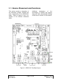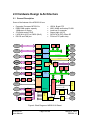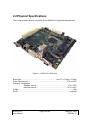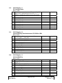
1
S
s
ss
es
prre
Xp
ye
ey
ke
nk
urrn
nT
on
eX
co
Siilliic
Tu
Original Design Manufacturer
ADS512101
A
Addvvaanncceedd D
Deevveellooppm
meenntt SSyysstteem
m
U
Usseerr’’ss M
Maannuuaall
Silicon Turnkey Express
749 Miner Road • Highland Heights, Ohio 44143
Phone (440) 461-4700 • (800) 827-2650
©Copyright 2006, Silicon Turnkey Express
An Affiliate of RPC Electronics Inc., All Rights Reserved.
ADS512101
User Manual
Page 1 of 48
March 14, 2008
PRELIM 1.0
Revision History
Rev
1.0
Date
Mar 14, 2008
WARNING:
Comments
Release of user manual for PCB Rev 3
This document is preliminary. It may contain errors and incomplete data.
Check with your provider or Silicon Turnkey Express (www.silicontkx.com)
or call 440-461-4700) for the latest information.
Support:
Your ADS512101 does include technical support from STx. If you should encounter any start
up problems or if the ADS512101 does NOT include all the material, immediately email
[email protected] and provide your name, contact information and problem. STx
commits to acknowledging all requests within 4 hours and usually can resolve most issues
within 24 hours.
Additional support information may be found at www.silicontkx.com
Warranty:
To assure all future engineering notifications are communicated the enclosed warranty
information must be completed.
ADS512101
User Manual
Page 2 of 48
March 14, 2008
PRELIM 1.0
NOTICE
The information contained within this guide is the property of Silicon Turnkey Express
(STx), and except as otherwise indicated shall not be reproduced in whole or in part
without the explicit written authorization of STx. The distribution of this document
outside of the company is prohibited without the written authorization of STx.
The following information is intended to alert the user to possible dangers and important
information contained within this guide. The “WARNINGS”, “CAUTIONS” and “NOTES”
do not eliminate these dangers. Close attention to the information supplied along with
“common sense” operation is the major accident prevention measure.
WARNING:
Failure to follow this warning may result in bodily injury.
CAUTION:
Failure to follow this caution may result in possible damage to the
board.
NOTE:
Failure to follow this note may result in improper results from the
board.
ADS512101
User Manual
Page 3 of 48
March 14, 2008
PRELIM 1.0
Reference Websites
Below is a list of websites that can be used to obtain additional information and details
that may not be fully provided in this manual.
Abatron BDI2000 JTAG Emulator ........................... www.ultsol.com/mfgs_emul_abtr.htm
Altera Quartus II………………………………………………………..……. ...www.altera.com
CodeWarrior USB TAP ........................................................................ www.freescale.com
5 Volt Only Operation
CAUTION:
Failure to follow this caution may result in possible damage to the
board.
The ADS512101 can operate from either 5 VDC only power supplies, such as the 5
watt wall mounted power supply included in this kit, or an ATX standard power
supply. When the ADS512101 is operated with the 5W wall mounted power supply
included with this kit normal operation will be LIMITED.
5 watt, 5 volts operation will NOT provide 12 volts required for peripherals or PCI.
The USB port will NOT provide 500 ma maximum. However all other ADS512101
function will be normal for worse case maximum power usage.
Other 5 volts power supplies (that meet the specification for the ADS512101) with
7.5 watts or greater will provide support for the maximum USB power of 500 ma.
However, 12 volts is NOT supported for peripherals or PCI.
ATX power supplies supports all power for all peripherals and PCI. Follow the
instructions in this manual for either 5 volts or ATX operation (see Section 3.2.6).
Media Access Control Address
Every ADS512101 has a unique MAC address saved in memory as part of the
standard environment. A label on the backside of the PCB (under the STx logo)
provides the PCB revision number, the serial number, and the MAC address. This
same information will appear on a label on the CD container.
If the MAC address needs to be reloaded, use these steps:
1 – Boot from main FLASH
2 – Type ‘setenv ethaddr ‘ MAC Address as ‘00:1E:59:nn:nn:nn’
3 – If an incorrect MAC address is entered, U-Boot must be reloaded and a new
MAC address can be entered.
ADS512101
User Manual
Page 4 of 48
March 14, 2008
PRELIM 1.0
Table of Contents
5 Volt Only Operation........................................................................................................ 4
Media Access Control Address ......................................................................................... 4
Table of Contents.............................................................................................................. 5
List of Figures…………………………………………………………………………….……… 9
List of Included Accessories.............................................................................................. 9
List of Optional Accessories.............................................................................................. 9
1.0 General Description................................................................................................ 10
1.1 Device Placement and Functions........................................................................ 11
1.1.01
BT1, Battery............................................................................................. 12
1.1.02
J01 – RJ45, 10/100 BaseT ...................................................................... 12
1.1.03
J02 – Audio Connectors .......................................................................... 12
1.1.04
J03 – Mini-PCI Connector ....................................................................... 12
1.1.05
J04 – Mini-PCI Connector ....................................................................... 12
1.1.06
J05 – SATA Interface .............................................................................. 12
1.1.07
J06 – DVI-I............................................................................................... 12
1.1.08
LED 1 – 5V Good .................................................................................... 12
1.1.09
LED 2 to 5 – CPLD .................................................................................. 13
1.1.10
LED 6 – ATA Activity ............................................................................... 13
1.1.11
LED 7 – USB Power ................................................................................ 13
1.1.12
P01 – 5V Only Operation......................................................................... 13
1.1.13
P02 – JTAG Connector ........................................................................... 13
1.1.14
P03 – Expansion Bus .............................................................................. 13
1.1.15
P04 – Back Up FLASH ............................................................................ 13
1.1.16
P05 – CPLD............................................................................................. 13
1.1.18
P07 – RS232, UART 0 ............................................................................ 13
1.1.19
P08 – RS232 ........................................................................................... 13
1.1.20
P09 – CAN 0............................................................................................ 13
1.1.21
P10 – CAN 1............................................................................................ 13
1.1.22
P11 – ATA Drive Select........................................................................... 13
1.1.23
P12 – PATA Connector ........................................................................... 13
1.1.24
P13 – Front Panel ATA LED.................................................................... 13
1.1.25
P14 – PCI Connector............................................................................... 13
1.1.26
P15 – J1850 Interface ............................................................................. 13
1.1.27
P16 – SPDIF Interface............................................................................. 13
1.1.28
P17 – Mini USB ....................................................................................... 14
1.1.29
P18 – EEPROM WP................................................................................ 14
1.1.30
P19 – LCD Backlight Inverter Power ....................................................... 14
1.1.31
P20 – LCD Connector ............................................................................. 14
1.1.32
P21 – LCD Connector ............................................................................. 14
1.1.34
P22 – Touch Screen Interface................................................................. 14
1.1.35
P23 – Front Panel Hardware Switch ....................................................... 14
1.1.35
P24 – Front Panel Hibernation Switch..................................................... 14
1.1.36
P25 – Power Switch By-Pass .................................................................. 14
1.1.37
P27 – RS232, UART 1 ............................................................................ 14
1.1.38
P28 – Audio ............................................................................................. 14
1.1.39
P29 – Micro-SD Socket ........................................................................... 14
ADS512101
User Manual
Page 5 of 48
March 14, 2008
PRELIM 1.0
Table of Contents
1.0 General Description (continued)............................................................................. 10
1.1 Device Placement and Functions (continued)..................................................... 11
1.1.40
PWR-1 – ATX Power Connector ............................................................. 14
1.1.41
PWR-2 – DC Power Input........................................................................ 14
1.1.42
SW1 – Power Switch ............................................................................... 14
1.1.43
SW2 – Hibernate Switch.......................................................................... 14
1.1.44
SW3 – Mode Switch ................................................................................ 14
2.0 Hardware Design & Architecture............................................................................... 15
2.1 General Description............................................................................................. 15
2.2 Physical Specifications........................................................................................ 16
3.0 Control & Configuration .......................................................................................... 17
3.1 Switch Settings.................................................................................................... 17
3.1.1
SW1 – Power On Reset .......................................................................... 17
3.1.2
SW2 – Hibernation Mode ........................................................................ 17
3.1.3
SW3 – Boot Mode ................................................................................... 17
3.2 Jumper Settings .................................................................................................. 18
3.2.1
P01 – ATX Power Supply Operation ....................................................... 18
3.2.2
P04 – Boot Backup FLASH ..................................................................... 18
3.2.3
P11 – ATA Drive Voltage Select.............................................................. 18
3.2.4
P18 – EEPROM_WP............................................................................... 18
3.2.5
P25 – Power By-Pass.............................................................................. 18
3.3 LED Indicators..................................................................................................... 18
4.0 Schematic .............................................................................................................. 19
5.0 CPLD Configuration ............................................................................................... 20
5.01 CPLD Register 0.......................................................................................... 20
5.02 CPLD Register 1.......................................................................................... 20
5.03 CPLD Register 2.......................................................................................... 20
5.04 CPLD Register 3.......................................................................................... 20
5.05 CPLD Register 4.......................................................................................... 21
5.06 CPLD Register 5.......................................................................................... 21
5.07 CPLD Register 6.......................................................................................... 21
5.08 CPLD Register 7.......................................................................................... 22
5.09 CPLD Register 8.......................................................................................... 22
5.10 CPLD Register 9.......................................................................................... 23
5.11 CPLD Register 10........................................................................................ 23
5.12 CPLD Register 11........................................................................................ 24
5.13 CPLD Register 12........................................................................................ 24
5.14 CPLD Register 13........................................................................................ 24
5.15 CPLD Register 14........................................................................................ 25
5.16 CPLD Register 15........................................................................................ 25
5.17 CPLD Register 16........................................................................................ 25
5.18 CPLD Register 17........................................................................................ 26
5.19 CPLD Register 18........................................................................................ 26
6.0 Operation ............................................................................................................... 27
6.1 Central Processing Unit....................................................................................... 27
ADS512101
User Manual
Page 6 of 48
March 14, 2008
PRELIM 1.0
Table of Contents
6.0 Operation (continued)............................................................................................. 27
6.2 Power supplies .................................................................................................... 27
6.2.1
Power Rails ............................................................................................. 27
6.2.2
Power Sequencing .................................................................................. 28
6.2.3
Hibernation Mode .................................................................................... 29
6.3 Resets ................................................................................................................. 29
6.4 Clocks.................................................................................................................. 30
6.5 CPU Configuration .............................................................................................. 30
6.6 Interrupts ............................................................................................................. 31
6.7 Memory ............................................................................................................... 31
6.7.1
DDR2 SDRAM......................................................................................... 31
6.7.2
NOR FLASH ............................................................................................ 31
6.7.3
NAND FLASH.......................................................................................... 31
6.8 I/O Function......................................................................................................... 32
6.8.01
10/1000 Ethernet ..................................................................................... 32
6.8.02
RS232 / RS485 Port (4-wire)................................................................... 32
6.8.03
CAN BUS................................................................................................. 32
6.8.04
I2C Bus.................................................................................................... 32
6.8.07
USB 2.0 ................................................................................................... 33
6.8.06
AUDIO and Touch Screen controller ....................................................... 33
6.8.07
VIDEO ..................................................................................................... 33
6.8.08
LCD Backlight.......................................................................................... 33
6.8.09
SATA Drive Interface............................................................................... 33
6.8.10
PATA Drive Interface............................................................................... 33
6.8.11
PCI........................................................................................................... 34
6.8.12
Mini-PCI................................................................................................... 34
6.8.13
Micro-SD.................................................................................................. 34
7.0 U-Boot ................................................................................................................. 35
7.1 Standard Commands .......................................................................................... 35
7.2 Start Up Display .................................................................................................. 36
7.3 Re-Install U-Boot Instructions.............................................................................. 36
Appendix A – Memory Map............................................................................................. 38
Appendix B – Connector Pin Assignments (see page 8 for index) ................................. 39
Glossary .......................................................................................................................... 48
ADS512101
User Manual
Page 7 of 48
March 14, 2008
PRELIM 1.0
Appendix B - Connector Pin Assignments
J01 – Ethernet.................................................................................................................39
J02– Audio Jack.............................................................................................................. 39
J3 – Mini PCI 2................................................................................................................39
J4 – Mini PCI 3……………………………………………………………………………….. 39
J06 – DVI-I ...................................................................................................................... 40
J06 – DVI-I continued...................................................................................................... 41
P02 – MPC5121e JTAG.................................................................................................. 41
P03 – Expansion Bus...................................................................................................... 41
P05 – CPLD JTAG .......................................................................................................... 42
P06 – UART 0 ................................................................................................................. 42
P07 – UART 0 ................................................................................................................. 42
P08 – UART 1 ................................................................................................................. 43
P08 – UART 1 ................................................................................................................. 43
P09 – CAN 0 ................................................................................................................... 43
P10 – CAN 1 ................................................................................................................... 43
P12 – PATA Connector................................................................................................... 43
P13 – ATA Activity .......................................................................................................... 44
P14 – PCI........................................................................................................................ 44
P14 – PCI continued ....................................................................................................... 44
P14 – PCI continued ....................................................................................................... 45
P15 – J1850 ....................................................................................................................45
P16 – SPDIF ................................................................................................................... 45
P17 – USB Mini AB Connector ....................................................................................... 45
P19 – LCD Backlight ....................................................................................................... 45
P20 – LCD (LVDS) Connector ........................................................................................ 46
P21 – LCD (TFT 18bit).................................................................................................... 46
P22 – LCD Touchscreen................................................................................................. 46
P23 – Power Switch ........................................................................................................ 46
P24 – Hibernate Switch................................................................................................... 46
P27 – UART 1 Interface .................................................................................................. 46
P28 – Audio..................................................................................................................... 47
P29 – Micro-SD............................................................................................................... 47
PWR-1 – ATX Power Connector..................................................................................... 47
PWR-2 – 5V Power Connector ....................................................................................... 47
ADS512101
User Manual
Page 8 of 48
March 14, 2008
PRELIM 1.0
List of Figures
Figure 1 – ADS512101.................................................................................................... 10
Figure 2 – ADS512101 Top Board Layout ...................................................................... 11
Figure 3 – ADS512101 Bottom Board Layout................................................................. 12
Figure 4 – ADS512101 Block Diagram ........................................................................... 15
Figure 5 – ADS512101.................................................................................................... 16
Figure 6 – U-Boot Start Up Screen………………………………………………. ............... 36
Figure 7 – U-Boot Re-Install Screen…………………….. ................................................ 37
List of Included Accessories
•
•
•
•
•
User Manual (on CD)
Schematic (on CD)
5V, 5W Wall Mount Power Supply
Null Modem Cable
Additional Freescale collateral material (on CD)
List of Optional Accessories
These accessories are available from Silicon Turnkey Express. See the
enclosed order form or visit web site:
Accessories
Add-On Features
•
•
•
•
•
•
•
•
•
•
•
•
•
•
•
•
•
•
•
•
•
•
Cases with custom silkscreen
Backplates/Custom silkscreen
LCDs, Inverter, Touchscreen
Monitors, Touchscreen
USB 802.11 Radio
MiniPCI WiMAX Radio
DRAM Modules
Memory Upgrades
Hard Drive (IDE or SATA)
Solid State Hard Drive (FLASH)
CD-ROM or DVD Drive
Wall Cube Power Supplies
Internal Power Supplies
PCI Riser Cards
Peripherals inside the case
Cables (All kinds & Customs)
ADS512101
User Manual
Bluetooth ® Radio
Camera/Image Capture
Microphone
GPS module
Echo Cancellation module
Profibus/Fieldbus
Software
•
•
•
•
•
•
•
•
•
Page 9 of 48
Operating Systems
Graphic Solutions
Cellular Connectivity
GPS Location
Touchscreen
Bluetooth ® Technology
Voice Recognition
Wireless
Database Client
March 14, 2008
PRELIM 1.0
1.0 General Description
The
ADS512101
Advanced
Development System is a mini-ITX formfactor reference and mother board
based on
Freescale’s MPC5121e
microprocessor. The board will provide
on-board DDR SDRAM, NOR FLASH,
NAND FLASH, (2) 4 wire RS232 ports,
2 CAN ports, USB 2.0, 10/100 Ethernet,
Audio in/out/mic, SATA and PATA drive
support, PCI, Micro-SD, 24bpp graphics,
all powered from a standard ATX or 5
Volt wall mount power supply.
The board can be integrated into any
configuration required by the addition of
optional peripherals.
These would
include items such as enclosures,
displays, HDD and numerous other
mini-ITX accessories.
Figure 1 – ADS512101
Silicon Turnkey Express will work with your embedded systems engineers to integrate a
final product that will give your end users the best performing and most cost effective
embedded solution.
ADS512101
User Manual
Page 10 of 48
March 14, 2008
PRELIM 1.0
1.1 Device Placement and Functions
This section provides a description of
the connectors, jumpers, switches and
main components of the ADS512101
board. Refer to Figures 2 and 3 for
location of the devices referenced
below.
Additional
descriptions
of
the
functionality of switches and jumpers
along with their recommended settings
will be found in Section 3 of this manual.
Figure 2 – ADS512101 Top Board Layout
ADS512101
User Manual
Page 11 of 48
March 14, 2008
PRELIM 1.0
Figure 3 – ADS512101 Bottom Board Layout
1.1.01 BT1 – Battery
1.1.05 J04 – Mini-PCI Connector
Battery type CD2424, 3.3 Volts used for
Real Time Clock.
(See Figure 3)
J5 is a Mini-PCI 32 bit connector with
+3.3v that uses ID_SEL_AD23.
1.1.02 J01 – RJ45, 10/100 BaseT
1.1.06 J05 – SATA Interface
J1 is a standard Ethernet input jack.
J7 is the serial ATA interface connector.
1.1.03 J02 – Audio Connectors
J2 has three stereo connection, J2A
(Blue) is Line In; J2B (Green) is Line
Out; J2C (Pink) is Aux In.
1.1.07 J06 – DVI-I
J24 is the Digital Video Interface.
1.1.04 J03 – Mini-PCI Connector
(See Figure 3)
J3 is a Mini-PCI 32 bit connector with
+3.3v that uses ID_SEL_AD22.
ADS512101
User Manual
1.1.08 LED 1 – 5V Good
Indicates when 5 Volts is on.
Page 12 of 48
March 14, 2008
PRELIM 1.0
1.1.09 LED 2 to 5 – CPLD
Is user definable by the CPLD.
1.1.18 P07 – RS232, UART 0
P7 is a 9-pin “D” style connector for
serial communications.
1.1.10 LED 6 – ATA Activity
Indicates when ATA data fetches occur.
1.1.19 P08 – RS232
1.1.11 LED 7 – USB Power
P39 is a header connector for an
additional RS232 connector. See
Appendix B for pin out.
Indicates when USB power is on.
1.1.20 P09 – CAN 0
1.1.12 P01 – 5V Only Operation
See Jumpers Section 3.2.6.
P9 is a 9-pin “D” style connector for
Control Area Network.
1.1.13 P02 – JTAG Connector
1.1.21 P10 – CAN 1
Connector P02 is a 16-pin header used
for the COP/JTAG input. This port is
made available to aid in the
programming of the ADS512101.
The pin-outs for the connector are listed
in Appendix A
P40 is a header connector for an
additional CAN connector. See
Appendix B for pin out.
1.1.22 P11 – ATA Drive Select
See Jumper Section 3.2.3.
A JTAG interface device, such as the
Abatron’s BDI2000 or Freescale’s CW
USB Codetap or equivalent, should be
used.
1.1.14 P03 – Expansion Bus
P03 provides signals for EMB, PLC, and
GPIO. See Appendix C for pin out.
1.1.15 P04 – Back Up FLASH
Normally Open
A jumper is used to re-FLASH U-Boot to
main FLASH. See Appendix XX, ReFLASH U-Boot.
1.1.23 P12 – PATA Connector
P12 is a 40 pin connector for attaching
an optional parallel device.
1.1.24 P13 – Front Panel ATA
LED
P13 is a 2-pin header used to enable
the front panel LED.
1.1.25 P14 – PCI Connector
J4 is the standard PCI connector that
uses ID_SEL_AD21.
1.1.16 P05 – CPLD
1.1.26 P15 – J1850 Interface
Header P05 is a CPLD JTAG port for
programming and application debugging
of the CPLD.
P31 is a serial connection for J1850.
An Altera Quartus II with a Byteblaster
cable or equivalent programming kit
should be used.
P32 is a connection (header) for the
SPDIF to the MPC5121e.
ADS512101
User Manual
1.1.27 P16 – SPDIF Interface
Page 13 of 48
March 14, 2008
PRELIM 1.0
1.1.28 P17 – Mini USB
J23 is a USB mini AB connector that is
compatible with the USB 2.0 format.
1.1.29 P18 – EEPROM WP
See Jumper Seciton 3.2.2.
1.1.36 P25 – Power Switch ByPass
This jumper is used to by pass the
power switch to allow for remote access
by applying power to the ADS512101.
1.1.37 P27 – RS232, UART 1
1.1.30 P19 – LCD Backlight
Inverter Power
This is a 10 pin header to accommodate
an external serial port.
This provides power and control signals
to an LCD Inverter.
1.1.38 P28 – Audio
This is a 10 pin header to accommodate
external audio connections.
1.1.31 P20 – LCD Connector
This is a 20 pin LVD connector.
1.1.39 P29 – Micro-SD Socket
1.1.32 P21 – LCD Connector
(See Figure 3)
P29 allows use of any Micro-SD
memory.
This connector is for a TFT, 18bit LCD
to accommodate Media5200 monitors.
1.1.40 PWR-1 – ATX Power
Connector
1.1.34 P22 – Touch Screen
Interface
This is an enhancement that may is not
available on the standards ADS512101.
1.1.35 P23 – Front Panel
1.1.41 PWR-2 – DC Power Input
Hardware Switch
P26 is a header to provide a connection
for the Front Panel Hardware Reset
switch SW 1.
Push once (momentary)
Power on Reset.
J25 is the main ATX power input
connector for the ADS512101. It is
designed to use a standard 20-pin ATX
power supply.
causes
a
J13 is the 5VDC to the board. P01
needs to be installed to enable the on
board power signal. See Section 3.2.6.
1.1.42 SW1 – Power Switch
See Switch Settings, Section 3.1.1
Push and hold for 5 seconds causes a
power down.
1.1.43 SW2 – Hibernate Switch
See Switch Settings, Section 3.1.2
1.1.35 P24 – Front Panel
Hibernation Switch
1.1.44 SW3 – Mode Switch
P27 is a header to provide a connection
for the Front Panel Hibernation mode
switch SW2.
ADS512101
User Manual
See Switch Settings, Section 3.1.3
Page 14 of 48
March 14, 2008
PRELIM 1.0
2.0 Hardware Design & Architecture
2.1 General Description
Some of the features of the ADS512101 are:
•
•
•
•
•
•
•
•
•
•
•
Freescale Processor MPC5121e
DDR2 RAM module- capacity
128Mbyte to 2 Gbytes
JTAG and control CPLD
LVDS 24-bit (LCD) or CMOS (Rev3)
RS-232 and CAN port
USB A, B and OTG
NOR, NAND and backup FLASH
Local bus IO connector
Stereo Audio (AC97)
SATA/PATA (IDE), Micro-SD
PCI/mini-PCI (radio slots)
SATA
SATA
7 pin
DDR2
DDR2
D
1
6
D
1
6
Standard
32-bit PCI
slot
SATA
DDR1/2 Memory
Interface
Mini USB
Type AB
USB 2.0
Magnetics
RJ45
10/ 100
PHY
UTMI
USB OTG PHY
Mini-PCI
32-bit slot
32bit
Mini-PCI
32-bit slot
PCI 2.3
Interface
10/100
ENet
RMII
10/100
MII / RMII
PSC0, PSC1,
PSC2
PCI, 32bit, 33/66 MHz
MicroSD
PATA Control
DB9
CAN
CAN
Transceiver
CAN
CAN Bus port 0
CAN Bus port 1
Buffers
Signal
Level
shifters
PATA
2X5 Header
PATA
DB9
RS232
RS232
Transceiver
2X5 Header
Audio Jacks
Analog
Audio
Line IN
Line OUT
MIC IN
PSC /
UART
Audio Codec
PSC /
AC97
Rs232
PSC3, UART 0
PSC4, UART 1
NOR
Backup
Boot
FLASH
D
16
D
16
Local Memory
Bus Controller
EMB
NAND FL
Controller
Audio AC97
PSC5
SDATA
TEMP
SENSO
R
EEPRO
M
NAND
FLASH
8bit
D8
EXP
Header
2x40 Pin
EMB AD Bus 32bit
D
32
AD
32
Peripher
al
Reset
C t l
PATA
40 Pin
PATA
I2C port 0
I2C port 2
SPDIF
CPLDs
CLK
C
P
U
R
es
et
s
SPDIF
1x3 Header
CPU
Configuratio
n
Address
latch
L_ADD
NOR
Boot
FLASH
X32
Power
Supplies
+3.3v
+2.5v
+1.8v
+1.4v
+1.2v
+0.9v
Power Supply sequence
Board Resets
20 pin LVDS
LVDS
LVDS
Transmitter
Video
MPC5121
TFT 24Bit
Resets
SYS-33mhz
DVI Driver
DIV-I
Connector
LVDS
Eth-25mhz
SATA-25mhz
Audio-24.576
VG
A
Buff
VGA DAC
Analog
PCI-33/66mhz
CPLD-33mhz
+5.0v Standby
Power
on
Reset
Cocks;
System
Ethernet
SATA
Audio
PCI
CPLD
Configuratio
n
Switches
ATX Power
Provides
12V
(20pin)
Standby
Power
+3.3v
5.0v
+5v
connector
(No 12V)
Figure 4- Block Diagram of ADS512101 Board
ADS512101
User Manual
Page 15 of 48
March 14, 2008
PRELIM 1.0
2.2 Physical Specifications
This section contains general information on the ADS512101’s physical characteristics.
Figure 5 – ADS512101 Side View
Board Size...............................................................................mini-ITX (170mm x 170mm)
Power Requirement ...................................................................................... ATX or 5VDC
Operating Temperature
Standard Version.......................................................................00 to +700C
Industrial Version....................................................................-400 to +850C
Weight ......................................................................................................................... 200g
RoHS................................................................................................................... Compliant
ADS512101
User Manual
Page 16 of 48
March 14, 2008
PRELIM 1.0
3.0 Control & Configuration
This section contains general set-up information about the various jumpers, switches,
and LEDs found on the ADS512101 board. Section 3.1 describes the function and
recommended switch settings. Section 3.2 describes the function and recommended
jumpers on the board. Section 3.3 describes the LED indicator function.
3.1
Switch Settings
SW3 Boot Mode (Continued)
This section provides a brief description
of the functionality and recommended
settings for the switches located on the
ADS512101.
SW3 is the CPLD Boot Configuration
Reset functions of the ADS512101.
Refer to CPLD Register 18, Section
5.19 for additional information.
Refer to Figure 2 for the locations of
these switches.
SW3 is a single-pole single-throw
(SPDT) 8-position switch used to
configure the CPLD for booting the
ADS512101 during power-up.
3.1.1
SW1 – Power On Reset
SW1 is a push button that provides a
power on reset signal for the hardware
on the ADS512101. The push button
can be remotely locate with connector
P27.
Push once to power on board and push
and hold for five seconds to power down
board.
3.1.2
SW2 – Hibernation Mode
SW2 provide a hibernation request to
the ADS512101.
Push once to put ADS512101 in
hibernation mode. Push again to bring
ADS512101 out of hibernation.
3.1.3
SW3 – Boot Mode
CAUTION:
Failure to follow this
caution may result in
possible damage to the
board.
All switches should be set to factory
default, normal operation, ‘ON’.
SW
1
State
ON
1
OFF
Low Boot
2
ON
NOR Boot
2
OFF
NAND Boot
3
3
ON
OFF
PCI = 33MHz
4
4
ON
OFF
5
5
6-7
6-7
6-7
6-7
8
8
ON
OFF
ON-ON
ON-OFF
OFF-ON
ON-ON
ON
OFF
Function
High Boot
PCI = 66MHZ*
Watchdog Disabled
Undefined
Core PLL = 1.5x
Core PLL = 2x
DDR2 = 200MHz
DDR2 = 166.67MHz
DDR2 = 133.33MHz
DDR2 = 133.33MHz
Reserved
Reserved
*M66en must also be high for 66mhz
For proper operation
these switches should be
left in the factory default
position.
ADS512101
User Manual
Page 17 of 48
March 14, 2008
PRELIM 1.0
3.2
Jumper Settings
P11
This section provides a brief description
of the functionality and recommended
settings for the jumpers located on the
ADS512101. Refer to Figure 2 for the
locations of these jumpers.
3.2.1
P01 – ATX Power Supply
Operation
Normally Open
This jumper must be installed to use an
external 5volt power supply connected
to PWR-2. It must be removed to use
an ATX power supply.
3.2.2
P04 – Boot Backup FLASH
Normally Open
When this jumper is installed powering
the ADS512101 will launch U-Boot in a
protected back up FLASH and reinstall
U-Boot to main FLASH.
3.2.3
P11 – ATA Drive Voltage
Select
CAUTION:
Failure to follow this
caution may result in
possible damage to the
board.
Be sure to select the
correct voltage setting for
the drive used prior to
turning the power on to
the board.
Normally +3.3 Volts, Pins 1&2
Jumper P21 selects the appropriate
power setting (+3.3 or +5.0) per the ATA
specification for the drive in use.
Pin No
1
2
3
3.2.4
Description
PATA 3V PWR
PATA IO PWR
PATA 5V PWR
P18 – EEPROM_WP
Normally Open
With this jumper installed the EEPROM
can be accessed allowing it to be
programmed or erased as needed.
When the jumper is removed the
EEPROM cannot be programmed.
3.2.5
P25 – Power By-Pass
Normally Open
With this jumper iinstalled the Power On
switch is by-passed. The ADS512101
will launch U-Boot when power is
applied.
3.3
LED Indicators
This section provides a list of functions
for the LEDs on the ADS512101 board.
Refer to Figure 2 for the locations of
these LEDs.
See CPLD Register 17, Section 5.18, for
additional information.
LED
1
2
3
4
5
6
7
ADS512101
User Manual
ATA Drive Voltage Select
(Continued)
Page 18 of 48
Function
5VDC GOOD
USER DEFINED
USER DEFINED
USER DEFINED
USER DEFINED
ATA ACTIVITY
USB POWER ON
Color
GREEN
RED
YELLOW
GREEN
GREEN
GREEN
GREEN
March 14, 2008
PRELIM 1.0
4.0
Schematic
overall parts cost using a variety of fixed
and user selectable options.
The schematic, and basic assembly
information in a portable document
format for the ADS512101 can be
located on the CD in the STx
Engineering Document Folder supplied
with the board.
These options inherently are contained
in connectors, jumpers and switches on
the board.
The ADS512101 design can be
customized for optional flexibility and
custom interfaces so the embedded
systems engineer can obtain a lower
The schematic provides guidelines for
using the already installed as well as
user modifiable options available on the
present design.
ADS512101
User Manual
Page 19 of 48
March 14, 2008
PRELIM 1.0
CPLD Configuration
This The configuration CPLD controls the MPC5121e hard reset configuration word.
The hardware configuration is controlled by switches SW3 to SW5 (see section 3.1.3
through 3.1.7) and documented in the following CPLD table. If all switches are set to
ON, then the CPLD will drive the default configuration word.
Other functions of the CPLD are driven by or read by internal registers that are memory
mapped at the base address 0x6000_0000. The CPLD uses the MPC5121e’s chip
select 2 on the local bus as its chip select and address decodes the lower 5 address
bits. See the following table of CPLD registers descriptions for additional information.
5.01
CPLD Register 0
Board ID 1, used along with register 1
Base + 0x00
Bit #
7-0
5.02
7-0
Ability R/ W
0x00
Read only
Bit description
Value at reset
Ability R/ W
Upper byte of Board ID
0x03
Read only
Value at reset
Ability R/ W
0x01
Read only
CPLD Register 2
CPLD Revision
Base + 0x02
Bit #
7-0
5.04
Value at reset
CPLD Register 1
Board ID 0, used along with register 0
Base + 0x01
Bit #
5.03
A distinct board ID is assign to the board,
16bits 0x0001 = ADS5121e rev 03
Upper byte of Board ID
CPLD rev
CPLD rev info
Writing a sequence of AA then 55 then 96
CPLD Register 3
Configuration word bits 33..32
Base + 0x03; 0x1010_1000 = default, CPLD drives Reset Configuration Word
Bit #
7-2
This register is reserved
Reserved
Value at reset
Ability R/ W
101010
Read / Write
1
RST_CONF_EMB_AX2
CFG_word_33
Read only
0
RST_CONF_EMB_AX3
CFG_word_32
Read only
ADS512101
User Manual
Page 20 of 48
March 14, 2008
PRELIM 1.0
5.05
CPLD Register 4
Configuration word bits 31..24
Base + 0x04; 0x0000_0001 = default, CPLD drives Reset Configuration Word
Bit #
5.06
Value at reset
Ability R/ W
7
Ability to read Configuration switches through software
Switch definitions are from 5121 user manual HRW
RST_CONF_SYSDIV, EMB_AX0 driven 0
CFG_word_31
Read only
6
RST_CONF_SYSDIV System PLL divider
CFG_word_30
Read only
5
RST_CONF_SYSDIV
CFG_word_29
Read only
4
RST_CONF_SYSDIV
CFG_word_28
Read only
3
RST_CONF_SYSPLL System PLL Multiply factor
CFG_word_27
Read only
2
RST_CONF_SYSPLL
CFG_word_26
Read only
1
RST_CONF_SYSPLL
CFG_word_25
Read only
0
RST_CONF_SYSPLL
CFG_word_24
Read only
CPLD Register 5
Configuration switch settings (EMB_AD[23:16])
Base + 0x05; 0x1000_1101 = default, CPLD drives Reset Configuration Word
Bit #
5.07
Value at reset
Ability R/ W
7
Ability to read Configuration switches by software
Switch definitions from 5121 user manual HRW
RST_CONF_SYSPLL System PLL Multiply factor
CFG_word_23
Read only
6
RST_CONF_CKS_IN Checkstop disabled
CFG_word_23
Read only
5
RST_CONF_NFC_DBW NAND data port 8bit
CFG_word_21
Read only
4
RST_CONF_NFC_PS NAND FLASH page size 2Kbytes
CFG_word_20
Read only
3
RST_CONF_LPC_DBW LPC DATA port 11 =32 bit
CFG_word_19
Read only
2
RST_CONF_LPC_DBW
CFG_word_18
Read only
1
Reserved, not mentioned in manual
CFG_word_17
Read only
0
RST_CONF_LPC_MX LPC Multiplexed mode
CFG_word_16
Read only
CPLD Register 6
Configuration switch settings (EMB_AD[15:8])
Base + 0x06; 0x0101_0000 = default, CPLD drives Reset Configuration Word
Bit #
Value at reset
Ability R/ W
7
Ability to read Configuration switches through software
Switch definitions are from 5121 user manual HRW
RST_CONF_PCIARB enable PCI arbiter
CFG_word_15
Read only
6
RST_CONF_PCIHOST PCI Host mode
CFG_word_14
Read only
5
RST_CONF_COREPLL Core PLL Multiply factor
CFG_word_13
Read only
4
RST_CONF_COREPLL Core PLL Multiply factor
CFG_word_12
Read only
3
RST_CONF_COREPLL Core PLL Multiply factor
CFG_word_11
Read only
2
RST_CONF_COREPLL Core PLL Multiply factor
CFG_word_10
Read only
1
RST_CONF_LPC_AX No LPC Address Extension
CFG_word_09
Read only
0
RST_CONF_LPC_AX No LPC Address Extension
CFG_word_08
Read only
ADS512101
User Manual
Page 21 of 48
March 14, 2008
PRELIM 1.0
5.08
CPLD Register 7
Configuration switch settings (EMB_AD[7:0])
Base + 0x07; 0x0010_0000 = default, CPLD drives Reset Configuration Word
Bit #
5.09
Value at reset
Ability R/ W
7
Ability to read Configuration switches by software Switch
definitions from 5121 user manual HRW
RST_CONF_PCI66EN M66EN signal, 1 = 66
CFG_word_07
Read only
6
RST_CONF_TLE Little ENDIAN
CFG_word_06
Read only
5
RST_CONF_BMS boot high
CFG_word_05
Read only
4
RST_CONF_COREDIS Core Disable mode (normal)
CFG_word_04
Read only
3
RST_CONF_TPR factory test mode disabled
CFG_word_03
Read only
2
RST_CONF_SWEN watchdog timer disabled at reset
CFG_word_02
Read only
1
RST_CONFIG_ROM_LOC LPC boot
CFG_word_01
Read only
0
RST_CONFIG_ROM_LOC LPC boot
CFG_word_00
Read only
CPLD Register 8
NOR FLASH Control
Base + 0x08
0x00000000 = default configuration, CPLD drives Reset Configuration Word
Bit #
7
6
5
Back up FLASH Write Protect 1 = (Full) write protected
Write enable signal held high
Back up FLASH sector write protect
Value at reset
1
Ability R/ W
Read / Write
1
Read / Write
1
Read / Write
4
Boot FLASH Write Protect 1 = (Full) write protected
Write enable signal held high
Boot FLASH sector write protect
1
Read / Write
3
NOR_FL_RDY
1
Read only
2
Boot or Backup FLASH status, 0 = Backup; 1 = Boot
Dependant on P4 Jumper, jumper installed = Backup
Or if 0xAA is written to register 2, R/W Control is
immediate
Backup NOR FLASH reset,
will be released from reset, at power up,
if configuration is set for Backup FLASH
x
Read only
1
0
Boot NOR FLASH reset
will be released from reset, at power up,
if configuration is set for Backup FLASH
ADS512101
User Manual
Page 22 of 48
Read/Write
0
Read / Write
1
Read / Write
March 14, 2008
PRELIM 1.0
5.10
CPLD Register 9
NAND FLASH, CAN, MEDIA_GPIO Control
Base + 0x09
Bit #
7
Currently only NAND chip select 0 is used,
chip select 1-3 are for future expansion.
MEDIA_GPIO
6
Reserved
0
Read / Write
5
Reserved
0
Read / Write
4
CAN Shut Down 0=Shut Down
0
Read / Write
3
NAND FLASH CE3 # enable 0=enabled
Future expansion, currently not used
NAND FLASH CE2 # enable 0=enabled
Future expansion, currently not used
NAND FLASH CE1 # enable 0=enabled
Future expansion, currently not used
Reserved
1
Read / Write
1
Read / Write
1
Read / Write
0
Read / Write
Value at reset
Ability R/ W
2
1
0
5.11
Value at reset
Ability R/ W
0
Read only
CPLD Register 10
PCI Interrupt Masking
Base + 0x0A
Bit #
1 = interrupt is masked
7
PCI_INTB_SLOT3
1
Read / Write
6
PCI_INTA_SLOT3
1
Read / Write
5
PCI_INTB_SLOT2
1
Read / Write
4
PCI_INTA_SLOT2
1
Read / Write
3
PCI_INTD_SLOT1
1
Read / Write
2
PCI_INTC_SLOT1
1
Read / Write
1
PCI_INTB_SLOT1
1
Read / Write
0
PCI_INTA_SLOT1
1
Read / Write
ADS512101
User Manual
Page 23 of 48
March 14, 2008
PRELIM 1.0
5.12
CPLD Register 11
PCI Interrupt Status
Base + 0x0B
Bit #
5.13
7
PCI interrupts are received at the CPU on the PCI_INTN
signal, this is a dedicated input on the CPU, 0 =
pending, corresponding mask bit also must be cleared
PCI_INTB_SLOT3
6
PCI_INTA_SLOT3
1
Read only
5
PCI_INTB_SLOT2
1
Read only
4
PCI_INTA_SLOT2
1
Read only
3
PCI_INTD_SLOT1
1
Read only
2
PCI_INTC_SLOT1
1
Read only
1
PCI_INTB_SLOT1
1
Read only
0
PCI_INTA_SLOT1
1
Read only
Ability R/ W
1
Read only
Value at reset
Ability R/ W
0
Read / Write
CPLD Register 12
Interrupt Routing Selection between CPU IRQ0 or IRQ1
Base + 0x0C
Bit #
5.14
Value at reset
7
Controls which IRQ is used for the listed IRQs
0 = CPU_IRQ0, 1 = CPU_IRQ1
SW1_HIBERNATE#
6
Secure Digital Card (SD_CD#)
0
Read / Write
5
TOUCH_SCR_BUSYN
0
Read / Write
4
TOUCH_SCR_IRQN
0
Read / Write
3
FEC_PHY_INTN
0
Read / Write
2
TEMP_MON_INT
0
Read / Write
1
PWR_CPLD_INT
0
Read / Write
0
WATCHDOG_BARK
0
Read / Write
Value at reset
Ability R/ W
CPLD Register 13
Interrupt Masking
Base + 0x0D
Bit #
7
1 = interrupt is masked
1
Read / Write
6
SW1_HIBERNATE#, writing 0 to this bit clears INT in
register 14
Secure Digital Card (SD_CD#)
1
Read / Write
5
TOUCH_SCR_BUSYN
1
Read / Write
4
TOUCH_SCR_IRQN
1
Read / Write
3
FEC_PHY_INTN
1
Read / Write
2
TEMP_MON_INT
1
Read / Write
1
Reserved
1
Read / Write
0
WATCHDOG_BARK
1
Read / Write
ADS512101
User Manual
Page 24 of 48
March 14, 2008
PRELIM 1.0
5.15
CPLD Register 14
Interrupt Status
Base + 0x0E
Bit #
5.16
7
0 = Interrupt pending
0 = pending, corresponding mask bit also must be cleared
SW1_HIBERNATE#
6
Secure Digital Card (SD_CD#)
1
Read only
5
TOUCH_SCR_BUSYN
1
Read only
4
TOUCH_SCR_IRQN
1
Read only
3
FEC_PHY_INTN
1
Read only
2
TEMP_MON_INT
1
Read only
1
Reserved, always = ‘1’
1
Read only
0
WATCHDOG_BARK
1
Read only
Ability R/ W
1
Read only
Value at reset
Ability R/ W
CPLD Register 15
MISC Control 0
Base + 0x0F
Bit #
5.17
Value at reset
7
WATCHDOG_HITME, 10 sys clocks long
0
Read / Write
6
AUD_PC_BEEP
0
Read / Write
5
UART0_FOFF#
1
Read / Write
4
1
Read / Write
3
CPU_PWR_DN, signal pulled up to +5v on board.
1 = tri-state
PCI_CLKRUNN3
1
Read only
2
PCI_CLKRUNN2
1
Read only
1
PATA_RESET
1
Read only
0
FEC_PHY_RSTN
1
Read only
Value at reset
Ability R/ W
CPLD Register 16
Video Control 1
Base + 0x010
Bit #
7
LCD_FRAME_RATE
0
Read / Write
6
LCD_R_FB (Removed, Jumper option on board)
0
Read / Write
5
DVI_MSEN
0
Read only
4
LCD_LVDS_SDIRn
0
Read / Write
3
Reserved
0
Read only
2
DVI_DAC_PWRDNn
0
Read only
1
VGA_DAC_PWRDNn
0
Read only
0
LCD_PWR_DWNn
0
Read only
ADS512101
User Manual
Page 25 of 48
March 14, 2008
PRELIM 1.0
5.18
CPLD Register 17
User LED
Base + 0x011
Bit #
7
Ability R/ W
0
Read / Write
0
Read / Write
0
Read / Write
0
Read / Write
3
LED 3 Control, 0=LED0=Reset Status; 1=User Control
register 17 (0)
LED 2 Control, 0=LED0=Reset Status; ; 1=User Control
register 17 (0)
LED 1 Control, 0=LED0=Reset Status; ; 1=User Control
register 17 (0)
LED 0 Control, 0=LED0=Reset Status; ; 1=User Control
register 17 (0)
LED 3
0
Read / Write
2
LED 2
0
Read / Write
1
LED 1
0
Read / Write
0
LED 0
0
Read / Write
6
5
4
5.19
Value at reset
CPLD Register 18
Configuration Switch Settings, SW3
Base + 0x012
7
SW3
Position
8
5-6
7&6
cfg_sys_pll
00 = 200mhz DDR2 clock
01 = 166.67mhz DDR2 clock
10 = 133.33mhz DDR2 clock
00
Read only
4
5
cfg_core_pll
0 = 2x
1= 1.5x
0
Read only
3
4
cfg_watchdog
0 = disabled
0
Read only
2
3
0 = 33mhz
0 = disabled
cfg_PCI_speed
M66en signal also must be
high for 66mhz
0
Read only
1
0
2
1
cfg_NOR_boot 0 = NOR boot
cfg_LOW-bo0t 0 = high boot
0
0
Read only
Read only
Bit #
ADS512101
User Manual
Function
Description
Reserved
Page 26 of 48
Value at reset
0 = OFF
0
Ability R/W
Read only
March 14, 2008
PRELIM 1.0
6.0
Operation
Caution: Features in bold italics may not be implemented or function properly
in Revision 1 or Revision 2 of the ADS512101 (see page 5 of User’s Manual to
find locations of Revision of ADS512101.
6.1
Central Processing Unit
The ADS512101’s MPC5121e is configured to run at a 66 Mhz system clock, and
asynchronous mode 66 Mhz/33 Mhz PCI clock frequency. The initial configuration is
from 3 strapping pins (UART0_DCD#, UART0_DSR, UART0_CTS), and will be set for
bootstrap option E as the default (See Table 9-3 for details). The boot strap options will
be selectable from a configuration dip switch read by the CPLD, the actual boot strap
pins will be driven by the CPLD during reset only.
The MCP5121 I/O includes: NOR FLASH memory, NAND FLASH memory, DDR2SDRAM memory, CPLD, MII (10/100 Fast Ethernet Controller), I2C (EEPROM, STM),
PSC (programmable serial controller) for RS232 and AC97 (audio), Interrupt controller,
USB 2.0 (ULPI), PCI bus, PCI controller, EPIC controller, Graphics (on chip MBX)
controller, PATA controller, SATA controller and Micro-SD.
See MPC5121e user manual for detail descriptions for each interface.
6.2
Power supplies
The ADS512101 board requires a mini-ATX power supply (either the 4 pins or 20 pins
connector can be used) or a 5v external power supply. When using an ATX power
supply 12v is provided to PCI.
6.2.1
Power Rails
The ADS512101 board requires several power rails that are provided on board, and
include:
+1.4v @ TBD for the CPU Core voltage.
+1.2v @ 0.5A for the SATA controller.
+1.8v @ 4A for the DDR2 voltage.
+0.9v @ 3.3A for DDR-SDRAM termination.
+3.3v @ 2.0A for the CPU I/O, on board peripheral logic.
+2.5v @ 0.5A for Fast Ethernet.
+12v @ 2A (direct input from off-board power supply) for disk drive power and LCD.
VOUT = 0.6 * (100k+Rset / rset)
ADS512101
User Manual
Page 27 of 48
March 14, 2008
PRELIM 1.0
Power Rails (continued)
The power enables for each of the regulators are used to sequence the power supplies.
These will not release if the CPLD is not powered properly and the RTC clock are not
running. These are open drain signals and work in tandem with the SS RC time
constants of the regulators. They are used to Power-down the regulators in 0 time but
allow the time constants of SS for Power-up.
6.2.2
Power Sequencing
Power sequencing rules require that the IO voltage rail is powered before the Core
Voltages. This is controlled by the SS time constants of the Core regulators are longer
than that of the IO regulators. During “sequenced” power down the CPLD will disable the
Core regulators first and then disable the IO Regulators.
The normal controlled power down sequence will be (on SW1 Toggle).
1: Assert PON_RESET (via MASTER_RESETN).
2: De-assert core Power - ENA_1V4, ENA1V2.
3: Wait some time.
4: De-assert IO Power - ENA_3V3, ENA2V5….etc.
5: De-assert (ATX)-POWER_ONN.
The Normal Power-UP sequence will be (on SW1 Toggle).
1: Assert (ATX)-POWER_ONN.
2: Assert IO Power - ENA_3V3, ENA2V5….etc.
3: Wait some time.
4: Assert core Power - ENA_1V4, ENA1V2.
5: Assert PON_RESET (via MASTER_RESETN).
Power on sequencing CPLD and the 8bit I/O expander control the power up and power
down of the entire board.
Power On Sequencing CPLD
If “Power_ON” is used
This is generated from PB Switch PS1 Toggle
and “Not Hibernate”. If Hibernating the power will shut down
and this must be toggled
POWER_ONN
Power Up Delayed by ATX Power up Rate-Signaled by “POWER OKAY”
If “Standby” is used. This comes from Supply. Otherwise
it is tied to VCC (+5V)
POWER_OKAY
ENA_3V3, ENA_2V5
ENA_1V8, ENA_V9V
No Big Delay Required in CPLD
Enable Will Go active 2 Clocks
after Power Good
No Big Delay Required in CPLD
SS RAMP on these is 2X
ENA_1V4, ENA_1V2
Set By SS on Regs
See Analog Ramps
PWR_GOOD_ALL
Set By Maxim
Watchdog (600ms)
PWRON_RESETN
HARD_RESETN
RESET_DISTRIBUTION SIGNALS
(FLASH, FEC, PATA… ETC)
RTC OUT (32KHz
MUST BE RUNNING
ADS512101
User Manual
Page 28 of 48
March 14, 2008
PRELIM 1.0
6.2.3
Hibernation Mode
Hibernate (Not Operational in Revision 1 or Revision 2 of ADS512101)
The Hibernate Pin from the CPU will shut down all of the regulators and devices
that allow the MPC5121E to go into deep low power mode (Still TBD). Hibernate
can wake or sleep per MPC5121E spec.
For controlled entry into the hibernate mode, the CPU must prepare the MPC5121e
in anticipation of entering the hibernate mode, that is, having the power supply
removed. The CPU must first write a value to the time target register that will give
the MPC5121e enough time to complete all bus transactions in progress and shut
down any other processes that must be terminated in an orderly manner and
cause the MPC5121e to enter the hibernation mode before the HIB_MODE pin is
asserted which will turn off the external power sources. (See section 9.4.3 of the
MPC5121e user manual.)
The external signals SET_WU_SRC[0:5] are used as external wakeup signals.
(See section 9.2 of the mpc5121e user manual.)
GPIO 30 is used to initiate hibernation or wake from hibernation mode.
6.3
Resets
Two reset switches provide the on board resets.
Reset signal SW1_TOGGLE is connected to the power sequence (PS) CPLD and is the
main “on/off” switch. This signal is used within the PS CPLD to enable or disable the on
board power supplies. The PS CPLD will also enable all on board power supplies
properly, and driving the MASTER_RESETN signal to the main power on reset and
watchdog timer IC. Reset signal SOFT_RESETN is connected to:
The main CPLD for use by this device.
The CPU for the soft reset function.
The COP JTAG port, the COP JTAG can also drive this signal.
The main reset and watchdog timer device IC is held in reset until the PS CPLD has
released the MASTER_RESETN signal. It then releases the PWRON_RESETN signal
once an internal time delay (about 210ms) has been met. The PWRON_RESETN signal
is used by the Configuration CPLD and clears its internal registers. It also is used by the
CPU for its power on reset.
ADS512101
User Manual
Page 29 of 48
March 14, 2008
PRELIM 1.0
6.4
Clocks
The main clock driver is a programmable clock synthesizer IC. The SYS_CLK is the
main processor clock (33.0 Mhz). The SYS_CLK_CPLD is used by the Configuration
CPLD for synchronization to the CPU’s input clock and internal functions. The
USB_CLK_24M000M is used by the CPU’s internal USB circuitry. The
FEC_CLK_25M000M is used by both the CPU’s internal fast Ethernet circuitry and the
Ethernet PHY. The SATA_CLK_25M000M is used by the CPU’s internal SATA drive
circuitry. The CPLD_CLK_BASIC is used by the Configuration CPLD for internal
functions. The AUD_CLK_24M576M is used by the Audio Codec U26.
6.5
CPU Configuration
The CPU configuration is completely user selectable by the bank of configuration
switches SW3 to SW6. All 32 configuration signals are driven by the CPLD during
power on reset only, and correspond to the 32 independent switch positions.
Default configuration: see table 7-3 Reset Configuration Word with in the MPC5121e
user manual.
Bit [0..31] = 0000_0111_00??_??11_0?10_110?_????_????
Bit [1..0] = RST_CONF_ROMLOC = 00 = LPC boot.
Bit 2 = RST_CONF_SWEN = 0 = watchdog timer at reset disabled.
Bit 3 = RST_CONF_TPR = 0 = Factory test mode (normal operation).
Bit 4 = RST_CONF_COREDIS = 0 = Core disable mode (normal operation.
Bit 5 = RST_CONF_BMS = 1 = boot mode select,
set so ROM loc start address = 0xFF80.
Bit 6 = RST_CONF_TLE = 1 = little endian mode.
Bit 7 = RST_CONF_PCI66EN = 1 = PCI66Mhz operation.
Bit [9 & 8] = RST_CONF_LPC_AX = 00 = no LPC address extension.
Bit [13 to 10] = RST_CONF_COREPLL = TBD.
Bit 14 = RST_CONF_PCIHOST = 1 = PCI host mode.
Bit 15 = RST_CONF_PCIARB = 1 PCI arbiter enabled.
Bit 16 = RST_CONF_LPC_MX = 0 = LPC non-multiplex mode.
Bit 17 = not describe in user manual. This may be used for LPC_AX3?
For the switch function.
Bit [19 & 18] = RST_CONF_LPC_DBW = 01 = LPC data port size = 16 bit.
Bit 20 = RST_CONF_NFC_PS = 1 = NAND FLASH page size = 2k page size.
Bit 21 = RST_CONF_NFC_DBW = 1 = NAND FLASH 8 bit data port size.
Bit 22 = RST_CONF_CKS_IN = 0 = checkstop input disabled.
Bit [26 to 23] = RST_CONF_SYSPLL = TBD.
Bit [LPC_AX3, 31 to 27] = RST_CONF_SYSDIV = TBD.
ADS512101
User Manual
Page 30 of 48
March 14, 2008
PRELIM 1.0
6.6
Interrupts
The CPU has 2 interrupt sources; CPU_IRQ0 and CPU_IRQ1.
The EPIC can receive 56 separate interrupts from three different interrupt domains as
follows:
2 external—off-chip interrupt signals sources are IRQ[1:0]
57 internal—on-chip interrupt signals sources are:
DDR MEMC, LPC, NFC, PATA, PCI, DMA, MU, FEC, PSC, FIFOC, USB,
CSB arbiter, CAN, BDLC, DIU, AXE, SPDIF, SDHC, RTC, GTM, I2C, GPIO,
GPT, SATA, MBX, TEMP, IIM and PMC.
1 external and 5 internal—off-chip interrupt signal source is IRQ0. On-chip MCP
interrupt signals sources are
software watchdog timer (WDT), PCI, temperature sensor and system bus
arbiter (SBA)
The CPLD accepts all other on board interrupts, and multiplexes these interrupts onto
the CPU’s IRQ signals. These will be user selectable, TBD.
PCI_INTN; PCI_INTC_SLOT1; FEC_PHY_INTN; PCI_INTD_SLOT1;
PCI_INTA_SLOT2; PCI_INTB_SLOT2; PCI_INTA_SLOT3; PCI_INTB_SLOT3;
PCI_INTA_SLOT1; PCI_INTB_SLOT1; PWR_CPLD_INT; WATCHDOG_BARK;
TOUCH_SCR_IRQN; TOUCH_SCR_BUSYN; TEMP_MON_INT
6.7
Memory
6.7.1
DDR2 SDRAM
The dedicated DDR2 memory bus is 32 bits data, single bank, 256 Mbytes Max @ 200
MHz, no ECC. It uses the MPC5121e DDR2 SDRAM controller and is directly
connection to the MPC5121e.
6.7.2
NOR FLASH
The FLASH memory is 64 Mbytes total, 16 bits wide, and its interface consists of 3
devices; 2 banks of main FLASH and 1 bank of BOOT Flash. The FLASH uses the chip
select LPC_CS0#. This chip select is connected to the CPLD, and the CPLD directs the
appropriate NOR_FLx_CSN signal to the correct FLASH.
6.7.3
NAND FLASH
(Not operational in Revision 1 or Revision 2 of ADS512101)
Dedicated NAND FLASH memory is 1 GB and directly connected to the MPC5121e.
ADS512101
User Manual
Page 31 of 48
March 14, 2008
PRELIM 1.0
6.8
I/O Function
See Appendix B for pin definitions
6.8.01 10/100 Ethernet
The 10/100 Ethernet port uses the Freescale MPC5121e MII interface and a standard
RJ45 connector with indicator LEDs and a 10/100 Ethernet PHY. The Port 0 PHY
address is 00001.
6.8.02 RS232 / RS485 Port (4-wire)
PSC (programmable serial controller) ports can be configured as UART, RS232 4 wire
port. The PSC is configured within the MPC5121e, see user MPC5121e manual for
details on setting up PSC. Transceivers are directly connected to both the CPU, a 9 pin
D, DB9 connector and a 10 pin header.
6.8.03 CAN BUS
Two Individual Controller Area Network Buses are a 2 wire interface used mainly by the
automotive industry. The CAN specification defines the Data Link Layer; ISO 11898
defines the Physical Layer. The CAN bus [CAN bus] is a balanced (differential) 2-wire
interface running over either a Shielded Twisted Pair (STP), Un-shielded Twisted Pair
(UTP), or Ribbon cable. Each node is connected to a male 9 pin D connector and a 10
pin header. The Bit Encoding used is: Non Return to Zero (NRZ) encoding (with bitstuffing) for data communication on a differential two wire bus. The use of NRZ encoding
ensures compact messages with a minimum number of transitions and high resilience to
external disturbance.
Both CAN buses are directly connected to the MPC5121e’s dedicated CAN bus and use
a transceiver.
6.8.04 I2C Bus
Two I2C ports use Port 0 and Port 2.
Port 0 (I2C0) is used for:
Serial EEPROM with address set to binary 1, 0, 1, 0, A2, A1, A0, R/W, or 0xA0.
Temperature monitor with address set to binary 1, 0, 0, 1, A2, A1, A0, R/W, or 0x90.
Remote 8-bit I/O expander with address set to 0x70.
RTC with address hard coded at 0xD0. A battery backup is provided and is
automatically switched within the device.
The RTC provides a square wave output:
RTC_CLK_OUT is connected to the CFG CPLD.
RTC_CLK_OUT is connected to the PS CPLD.
RTC_CLK_OUT is connected to the CPU as an optional input, instead of
the XTAL X1
ADS512101
User Manual
Page 32 of 48
March 14, 2008
PRELIM 1.0
I2C Bus (continued)
Port 2 (I2C2) is used for:
Digital potentiometer with address is hard coded to 0x5C.
Digital Transmitter with address is set to 0x70 read, 0x71 write.
6.8.07 USB 2.0
(Not operational in Revision 1 or Revision 2 of ADS512101)
The USB 2.0 Host port is connected directly to MPC5121e dedicated USB 2.0
controller. A USB power switch is used to turn on and off the USB power. USB
control and fault condition controlled directly from CPU.
6.8.06 AUDIO and Touch Screen controller
The MPC5121e use a PSC (programmable serial controller) set for the AC97
communication protocol. The audio codec is controlled by the AC97 controller and
provides LINE IN, LINEOUT and MIC IN.
The Touch Screen controller is population option and not available on the standard
ADS512101. Contact [email protected] for information.
6.8.07 VIDEO
The MPC5121e has an integrated graphics engine, the PowerVR® MBX Lite IP core.
The MBX controller is directly connected to:
A 24-bit LVDS transceiver.
A Triple 8 bit video DAC with whose output is high speed video buffered then connected
to the DVI-I connector.
A Digital transmitter that is connected to the DVI-I connector.
6.8.08 LCD Backlight
The LCD backlight uses a digital potentiometer to control the LCD backlight and is
controlled directly from the CPU’s I2C interface and addressed at 0x5C.
6.8.09 SATA Drive Interface
The MPC5121e directly connects to the SATA drive connector J5.
6.8.10 PATA Drive Interface
The PATA drive circuitry uses the MPC5121e PATA bus interface. The MPC5121 PATA
interface connects to signal level translator ICs to convert from the CPU’s +3.3v signal
level to the PATA +5.0v signal level. The level translated signals are then connected to
the PATA connector.
The PATA power is enabled by an regulator and is controlled by the CPU’s I2C0 bus.
The signal PATA_PWR_ENABN enables the PATA_12V_PWR supplying the necessary
+12v power to the PATA power connector.
ADS512101
User Manual
Page 33 of 48
March 14, 2008
PRELIM 1.0
6.8.11 PCI
The PCI slot is compliant to PCI2.3, 32 bit bus. It can either 33 MHz or 66 MHz which is
determined by selectable clock with the Mode Switch, SW3. This is 3.3 volts only.
6.8.12 Mini-PCI
Two Mini-PCI slots are compliant to PCI2.3, 32 bit bus. It can either 33 MHz or 66 MHz
which is determined by selectable clock with the Mode Switch, SW3. This is 3.3 volts
only.
6.8.13 Micro-SD
A Micro-SD slot is available and is directly connected to the MPC5121e ATA controller.
ADS512101
User Manual
Page 34 of 48
March 14, 2008
PRELIM 1.0
7.0
U-Boot
7.1
Standard Commands
?
asknev
autoscr
base
bdinfo
boot
bootd
bootm
bootp
clocks
cmp
coninfo
cp
crc32
dhcp
echo
erase
exit
flinfo
go
help
i2c
icrc32
iloop
imd
iminfo
imls
imm
imw
inm
iprobe
itest
loadb
loads
loady
loop
md
mii
mm
mtest
mw
nfs
nm
ping
printenv
protect
rarpboot
reset
run
saveenv
setenv
sleep
test
tftpboot
version
ADS512101
User Manual
-
alias for ‘help”
get environment variables from stdin
run script from memory
print or set address offset
print Board Infro structure
boot default, i.e., run ‘bootcmd’
boot default, i.e., run ‘bootcmd’
boot application image from memory
boot image via network using BootP/TFTP protocol
print clock configuration
memory compare
print console devices and information
memory copy
checksum calculation
invoke DHCP client to obtain IP/boot params
echo args to console
erase FLASH memory
exit script
print FLASH memory information
start application at address ‘addr’
print online help
I2C sub-system
checksum calculation
infinite loop on address range
i2c memory display
print header information for application image
list all images found in flash
i2c memory modify (auto-incrmenting)
memory write (fill)
memory modify (constant address)
probe to discover valid I2C chip addresses
return true/false on integer compare
load binary file over serial line (Kermit mode)
load S-Record file over serial line
load binary file over serial line (ymodem mode)
infinite loop on address range
memory display
MII utility commands
memory modify (auto-incrementing)
simple RAM test
memory write (fill)
boot image via network using NFS protocol
memory modify (constant address)
send ICMP ECHO_REQUEST to network host
print environment variables
enable or disable FLASH write protection
boot image via network using RARP/TFTP protocol
Perform RESET of the CPU
run commands in an environment variable
save environment variables to persistent storage
set environment variables
delay execution for some time
minimal test like /bin/sh
boot image via network using TFTP protocol
print monitor verison
Page 35 of 48
March 14, 2008
PRELIM 1.0
7.2
Start Up Display
U-Boot 1.3.2 (Mar 14 2008 - 12:42:04) MPC512X
CPU:
MPC5121e rev. 1.0, Core e300c4 at 399.999 MHz, CSB at 199 MHz
Board: ADS5121 rev. 0x0301 (CPLD rev. 0x02)
I2C:
ready
DRAM: 512 MB
FLASH: 64 MB
*** Warning - bad CRC, using default environment
PCI:
In:
Out:
Err:
Net:
Bus Dev VenId DevId Class Int
serial
serial
serial
FEC ETHERNET
Type "run jffs2boot" to boot Linux
Hit any key to stop autoboot:
=>
0
Figure 6 – U-Boot Start Screen
7.2.1 U-Boot Warnings:
*** Warning - bad CRC, using default environment
This indicates a new U-Boot has been started and environment variables have not been
saved. To eliminate this warning, a ‘saveenv’ command must be performed.
7.3
Re-Install U-Boot Instructions
The ADS512101 has a protected back up FLASH memory for U-Boot. If U-Boot should
become corrupt for any reason, U-Boot can be re-installed. Please follow these
instructions to re-flash U-Boot to the main memory.
1 – Remove power from the ADS512101
2 – Install a jumper on the ‘Back Up Flash’ Header, P4
3 – Reconnect power to the ADS5121 and use SW1 to launch U-Boot.
– This process will write the back up U-Boot to main memory.
– Follow the on screen instructions.
4 – Remove power from the ADS512101
5 – Remove the jumper from header P4.
6 – Reconnect power to the ADS512101 and use SW1 to launch U-Boot.
See Figure 7 for the U-Boot re-install screen.
ADS512101
User Manual
Page 36 of 48
March 14, 2008
PRELIM 1.0
U-Boot 1.3.2 (Mar 14 2008 - 12:42:04) MPC512X
CPU:
Board:
I2C:
DRAM:
FLASH:
PCI:
In:
Out:
Err:
Net:
MPC5121e rev. 1.0, Core e300c4 at 399.999 MHz, CSB at 199 MHz
ADS5121 rev. 0x0301 (CPLD rev. 0x02)
ready
512 MB
64 MB
Bus Dev VenId DevId Class Int
serial
serial
serial
FEC ETHERNET
BOOTING FROM BACKUP FLASH
RECOVERY MODE PROCESS STARTING at AUTOBOOT ...
Hit any key to stop autoboot: 0
Copying U-Boot image to dram
Switching to main flash and erasing
Un-Protected 1 sectors
. done
Erased 1 sectors
PROGRAMMING MAIN FLASH with U-BOOT IMAGE
Copy to Flash... done
PLEASE SELECT MAIN FLASH BY REMOVING JUMPER at P4
Rebooting in 10 Seconds
Resetting the board.
Figure 7 –U-Boot Re-Installing Screen
ADS512101
User Manual
Page 37 of 48
March 14, 2008
PRELIM 1.0
Appendix A – Memory Map
The following memory map isonly an example, refer to the MCP5121e user manual for specific
memory map configurations, many of these memory map settings are user defined.
Function
Bytes
32 Bit Address
Reserved
Start
End
8000 0000
803F FFFF
IMMRBAR
Default setting at
reset FF40 0000
Move after boot
CS#
Size
1M
Recommend.
4M For future
revs
DDR SDRAM
256MB
0x0000 0000
0x0FFF FFFF
DDR_MCSN
256MB
BOOT Space EBC
NOR FLASH
Boot High
64MB
0xFC00 0000
0xFFFF FFFF
LPC_CS0N
64MB
NAND FLASH
Upto 2GB
1MB
0x4000 0000
0x400F FFFF
1MB
PCI Memory
PCILAWBAR0-2
256MB
256MB
256MB
256MB
0xA000 0000
0xB000 0000
0xC000 0000
0xD000 0000
0xAFFF FFFF
0xBFFF FFFF
0xCFFF FFFF
0xDFFF FFFF
1GB
SRAM
256KB
0x3000 0000
0x3001 FFFF
CPLD
32B
0x8200 0000
0x820F FFFF
MBX (graphics)
16MB
0x2000 0000
0x20FF FFFF
16MB
USB ULPI
2.0 Device
4KB
IMMR_0x3000
IMMR_3FFF
4KB
PATA Drive
IMMR_0x1 0200
IMMR_0x1 02FF
SATA Drive
IMMR_0x2 0000
IMMR_0x2 1FFF
Local Configuration
Registers
1KB
IMMR_0x0 0000
IMMR_0xF FFFF
RS232 A
PSC3
IMMR_0x1 1300
IMMR_0x1 13FF
RS232 B
PSC4
IMMR_0x1 1400
IMMR_0x1 14FF
Audio (AC97)
PSC5
IMMR_0x1 1500
IMMR_0x1 15FF
IMMR_0x0 1300
IMMR_0x0 137F
CAN A
128KB
LPC_CS2N
32B
64B
CAN B
IMMR_0x0 1380
IMMR_0x0 13FF
IIC0
IMMR_0x0 1700
IMMR_0x0 171F
32B
IIC2
IMMR_0x0 1740
IMMR_0x0 17FF
32B
Fast Ethernet
Controller
IMMR_0x0 2800
IMMR_0x0 2FFF
256B
ADS512101
User Manual
Page 38 of 48
March 14, 2008
PRELIM 1.0
Appendix B – Connector Pin Assignments
J01 – Ethernet
Pin No
1
2
3
4
5
6
7
8
9
10
1G
2G
J3/J4 – Mini PCI 2/3 continued
Description
TCT
TDP
TDN
RDP
RDN
RCT
LD1C
LD1A
LD2C
LD2A
G1
G2
Pin No
7
8
9
10
11
12
13
14
15
16
17
18
19
20
21
22
23
24
25
26
27
28
29
30
31
32
33
34
35
36
37
38
39
40
41
42
43
44
45
46
47
48
J02– Audio Jack
Pin No
1
J2C
2
3
4
5
J2B
22
23
24
25
J2A
32
33
34
35
Description
SHIELD GND
Microphone
RIGHT MIC 2 (OUTER)
AGND
LEFT MIC 1 (INNER)
AGND
Line Out
RIGHT HP OUT (OUTER)
AGND
LEFT HP OUT (INNER)
AGND
Line In
RIGHT LINE IN (OUTER)
AGND
LEFT LINE IN (INNER)
AGND
J3/J4 – Mini PCI 2/3
Pin No
1
2
3
4
5
6
Description
TIP
RNG
8PMJ3
8PMJ1
8PMJ6
8PMJ2
ADS512101
User Manual
Page 39 of 48
Description
8PMJ7
8PMJ4
8PMJ8
8PMJ5
LED1P
LED2P
LED1N
LED2N
CHSGND
Reserved1
(not)INTB
5V1
3.3V1
(not)INTA
Reserved2
Reserved3
GND1
3.3VAUX1
CLK
(not)RST
GND2
3.3V2
(not)REQ
(not)GNT
3.3V3
GND3
AD31
(not)PME
AD29
Reserved4
GND4
AD30
AD27
3.3V4
AD25
AD28
RSVD5
AD26
C (not)BE3
AD24
AD23
IDSEL
March 14, 2008
PRELIM 1.0
J3/J4 – Mini PCI 2/3 continued
Pin No
49
50
51
52
53
54
55
56
57
58
59
60
61
62
63
64
65
66
67
68
69
70
71
72
73
74
75
76
77
78
79
80
81
82
83
84
85
86
87
88
89
90
91
92
93
Description
3.3V5
GND6
AD21
AD22
AD19
AD20
GND7
PAR
AD17
AD18
C (not)BE2
AD16
(not)IRDY
GND8
3.3V6
(not)FRAME
(not)CLKRUN
(not)TRDY
(not)SERR
(not)STOP
GND9
3.3V7
PERR N
(not)DEVSEL
C (not)BE1
GND10
AD14
AD15
GND11
AD13
AD12
AD11
AD10
GND12
GND13
AD9
AD8
C (not)BE0
AD7
3.3V8
3.3V9
AD6
AD5
AD4
Reserved6
ADS512101
User Manual
J3/J4 – Mini PCI 2/3 continued
Pin No
94
95
96
97
98
99
100
101
102
103
104
105
106
107
108
109
110
111
112
113
114
115
116
117
118
119
120
121
122
123
124
Description
AD2
AD3
AD0
5V2
Reserved WIP1
AD1
Reserved WIP2
GND14
GND15
AC SYNC
(not)M66E
AC SDIN
AC SDOUT
AC BCLK
AC CODEC IO
AC CODECID1
(not)AC RESET
MOD AUDIO MON
Reserved7
AUDIO GND1
GND16
AUDIO OUT
AUDIO IN
AOUT GND
AIN GND
AUDIO GND2
AUDIO GND3
Reserved8
(not)MPCIACT
5VANA
3.3VAUX2
J06 – DVI-I
Pin No
C1
C2
C3
C4
C5_1
C5_2
1
2
3
4
Page 40 of 48
Description
ANALOG RED
ANALOG GRN
ANALOG BLUE
ANALOG H-SYNC
ANALOG RTN1
ANALOG RTN2
TX2TX2+
TX2/4 SHLD
TX4-
March 14, 2008
PRELIM 1.0
J06 – DVI-I continued
Pin No
5
6
7
8
9
10
11
12
13
14
15
16
17
18
19
20
21
22
23
24
25
26
P03 – Expansion Bus
Description
TX4+
DDC CLK
DDC DATA
ANALOG V-SYNC
TX1TX1+
TX1/3 SHLD
TX3TX3+
5VDC
GND
TX0HP DETECT
TX0+
TX0/5 SHLD
TX5TX5+
TSC SHLD
TXC+
TXCSHELL1
SHELL2
Pin No
1
2
3
4
5
6
7
8
9
10
11
12
13
14
15
16
17
18
19
20
21
22
23
24
25
26
27
28
29
30
31
32
33
34
35
36
37
38
39
40
P02 – MPC5121e JTAG
(16 pin Header)
Pin No
1
2
3
4
5
6
7
8
9
10
11
12
13
14
15
16
Description
5121E JTAG COP TDO
5121E JTAG COP QACKN
5121E JTAG COP TDI
COP CON TRSTN
TP110 JTAG COP HALTED
3.3VDC
5121E JTAG COP TCK
NC
5121E JTAG COP TMS
NC
SOFT RESET N
GND
HARD RESET N
NC
5121 CPU CHKSTP OUT
GND
ADS512101
User Manual
Page 41 of 48
Description
GND
GND
EMB AD0
EMB AD1
EMB AD2
EMB AD3
EMB AD4
EMB AD5
EMB AD6
EMB AD7
3.3VDC
3.3VDC
EMB AD8
EMB AD9
EMB AD10
EMB AD11
EMB AD12
EMB AD13
EMB AD14
EMB AD15
GND
GND
EMB AD16
EMB AD17
EMB AD18
EMB AD19
EMB AD20
EMB AD21
EMB AD22
EMB AD23
3.3VDC
3.3VDC
EMB AD24
EMB AD25
EMB AD26
EMB AD27
EMB AD28
EMB AD29
EMB AD30
EMB AD31
March 14, 2008
PRELIM 1.0
P03 – Expansion Bus continued
Pin No
41
42
43
44
45
46
47
48
49
50
51
52
53
54
55
56
57
58
59
60
61
62
63
64
65
66
67
68
69
70
71
72
73
74
75
76
77
78
79
80
P05 – CPLD JTAG
Description
GND
GND
LPC CS2N
EMB AX3
LPC ACKN
EMB AX2
LPC OEN
EMB AX1
LPC R WN
EMB AX0
PWR ON RESET N
TP117
HARD RESET N
TP118
GND
TIP116
LPC CLK
TP119
GND
GND
CPU GPIO14
TP115
CPU GPIO15
TP120
CPU GPIO28
TP114
CPU GPIO29
TP121
CPU GPIO30
TP113
CPU GPIO31
TP112
3.3VDC
3.3VDC
TP123
TP111
TP122
TP109
GND
GND
ADS512101
User Manual
(10 pin Header)
Pin No
1
2
3
4
5
6
7
8
9
10
Description
CPLD_TCK
GND
CPLD_TDO
5V_STANDBY
CPLD_TMS
NC
NC
NC
CPLD_TDI
GND
P06 – UART 0
(10 pin Header)
Pin No
1
2
3
4
5
6
7
8
9
10
Description
NC
CSER PB RXD
CSER PB TXD
NC
GND
NC
CSER PB RTS
CSER PB CTS
NC
NC
P07 – UART 0
Pin No
1
2
3
4
5
6
7
8
9
Page 42 of 48
Description
TP003
CSER PA RXD
CSER PA TXD
TP005
GND
TP004
CSER PA RTS
CSER PA CTS
TP006
March 14, 2008
PRELIM 1.0
P08 – UART 1
P12 – PATA Connector
Pin No
1
2
3
4
5
6
7
8
9
10
11
12
13
14
15
16
17
18
19
20
21
22
23
24
25
26
27
28
29
30
31
32
33
34
35
36
37
38
39
40
(10 pin Header)
Pin No
1
2
3
4
5
6
7
8
9
10
Pin No
1
Description
NC
CSER PB RXD
CSER PB TXD
NC
GND
NC
CSER PB RTS
CSER PB CTS
NC
NC
Description
TP011
P09 – CAN 0
Pin No
1
2
3
4
5
6
7
8
9
Description
TP011
CANL
GND
TP014
SIG GND
TP012
CANH
TP013
TP015
P10 – CAN 1
(10 pin Header)
Pin No
1
2
3
4
5
6
7
8
9
10
Description
NC
CANL
GND
NC
SIG GND
NC
CANH
NC
NC
NC
ADS512101
User Manual
Page 43 of 48
Description
PATA CON RESET
GND
PATA CON AD7
PATA CON AD98
PATA CON AD6
PATA CON AD9
PATA CON AD5
PATA CON AD10
PATA CON AD4
PATA CON AD11
PATA CON AD3
PATA CON AD12
PATA CON AD2
PATA CON AD13
PATA CON AD1
PATA CON AD14
PATA CON AD0
PATA CON AD15
GND
NC
PATA CON DRQ
GND
PATA CON IOWN
GND
PATA CON IORN
GND
PATA CON IOCHRDY
GND
PATA CON DACK
GND
PATA CON INTRQ
PATA CON IOCS16N
PATA CON DA1
NC
PATA CON DA0
PATA CON DA2
PATA CON CS0N
PATA CON CS1N
PATA CON DASPN
GND
March 14, 2008
PRELIM 1.0
P13 – ATA Activity
P14 – PCI continued
Pin No
B20
A20
21B
A21
B22
A22
B23
A23
B24
A24
B25
A25
B26
A26
B27
A27
B28
A28
B29
A29
N30
A30
B31
A31
B32
A32
B33
A33
B34
A34
B35
A35
B36
A36
B37
A37
B38
A38
B39
A39
B40
A40
B41
A41
B42
(2 pin Header)
Pin No
1
2
Pin Name
SIGNAL (PATA IO PWR +
PATA CON DASPN
GND
P14 – PCI
Pin No
B1
A1
B2
A2
B3
A3
B4
A4
B5
A5
B6
A6
B7
A7
B8
A8
B9
A9
B10
A10
B11
A11
B12
A12
B13
A13
B14
A14
B15
A15
B16
A16
B17
A17
B18
A18
B19
A19
Pin Name
-12V
(not)TRST
TCK
12V
GND0
TMS
TDO
TDI
5V 1
5V
5V 2
(not)INTA
(not)INTB
(not)INTC
(not)INTD
5V 5
(not)PRSNT1
Reserved3
Reserved1
3.3V (I/O)
(not)PRSNT2
Reserved4
----Reserved2
3.3v (AUX)
GND1
(not)RST
CLK
3.3V (I/O) 3
GND2
GNT
(not)REQ
GND9
3.3V (I/O) 1
(not)PME
ADS512101
User Manual
Page 44 of 48
Pin Name
AD31
AD30
AD29
3.3V 7
GND19
AD28
AD27
AD26
AD25
GND10
3.3V 1
AD24
C/(not)BE3
IDSEL
AD23
3.3V 8
GND20
AD22
AD21
AD20
AD19
GND11
3.3V 2
AD18
AD17
AD16
C/(not)BE2
3.3V 9
GND3
(not)FRAME
(not)IRDY
GND12
3.3V 3
(not)TRDY
(not)DEVSEL
GND13
GND4
(not)STOP
(not)LOCK
3.3V 10
(not)PERR
Reserved5
3.3V 4
Reserved6
(not)SERR
March 14, 2008
PRELIM 1.0
P14 – PCI continued
Pin No
A42
B43
A43
B44
A44
B45
A45
B46
A46
B47
A47
B48
A48
B49
A49
B50
A50
B51
A51
B52
A52
B53
A53
B54
A54
B55
A55
B56
A56
B57
A57
B58
A58
B59
A59
B60
A60
B61
A61
B62
A62
Pin Name
GND14
3.3V 5
PAR
C/(not)BE1
AD15
AD14
3.3V 11
GND5
AD13
AD12
AD11
AD10
GND15
M66EN
AD09
GND6
GND16
GND7
GND17
AD08
C/(not)BE0
AD07
3.3V 12
3.3V 6
AD06
AD05
AD04
AD03
GND18
GND8
AD02
AD01
AD00
3.3V (I/O) 2
3.3 (I/O) 4
(not)ACK64
(not)REQ64
5V 3
5V 6
5V 4
5V 7
ADS512101
User Manual
P15 – J1850
(3 pin Header)
Pin No
1
2
3
Pin Name
CPU J1850 TX
CPU J1850 RX
GND
P16 – SPDIF
(4 pin Header)
Pin No
1
2
3
4
Pin Name
SPDIF TXCLK
SPDIF TX
SPDIF RX
GND
P17 – USB Mini AB Connector
Pin No
1
2
3
4
5
6
7
8
9
Pin Name
USB CONMB PWR
USB CONMB DN
USB CONMB DP
USB CONMB ID
GND
SHIELD GND
SHIELD GND
SHIELD GND
SHIELD GND
P19 – LCD Backlight
Pin No
1
2
3
4
5
6
7
8
Page 45 of 48
Pin Name
12VDC
12VDC
GND
GND
LCD PWRDNN
B (DIGITAL POT 10K)
W (DIGITAL POT 10K)
NC
March 14, 2008
PRELIM 1.0
P20 – LCD (LVDS) Connector
Pin No
1
2
3
4
5
6
7
8
9
10
11
12
13
14
15
16
17
18
19
20
Description
D3+
D3DPS
FRC
GND1
CK+
CKGND2
D2+
D2GND3
D1+
D1GND4
D0+
D0GND5
GND6
VCC1
VCC2
P21 – LCD (TFT 18bit)
Pin No
1
2
3
4
5
6
7
8
9
10
11
12
13
14
15
16
17
18
19
20
21
22
Pin Name
GND
VID_CLK_0
VID_HSYNC
VID_VSYNC
GND
VID_RED0
VID_RED1
VID_RED2
VID_RED3
VID_RED4
VID_RED5
GND
VID_GREEN0
VID_GREEN1
VID_GREEN2
VID_GREEN3
VID_GREEN4
VID_GREEN5
GND
VID_BLUE0
VID_BLUE1
VID_BLUE2
ADS512101
User Manual
P21 – LCD (TFT 18bit) continued
Pin No
23
24
25
26
27
28
29
30
31
32
33
Pin Name
VID_BLUE3
VID_BLUE4
VID_BLUE5
GND
VID_BLANK#
+LCD_TFT
+LCD_TFT
SCANDIR1
SCANDIR2
NC
NC
P22 – LCD Touchscreen
Pin No
1
2
3
4
5
Pin Name
TS_XP
TS_YP
TS_XM
TS_YM
GND
P23 – Power Switch
(2 pin Header)
Pin No
1
2
Pin Name
SW1 TOGGLEN (PULSE,
DEBOUCE)
GND
P24 – Hibernate Switch
(2 pin Header)
Pin No
1
1
Pin Name
SW2_TOGGLEN
GND
P27 – UART 1 Interface
Pin No
1
2
3
4
5
6
7
8
Page 46 of 48
Pin Name
3.3 V
5V
GND
GND
UART1_TXD
UART1_RXD
NC
NC
March 14, 2008
PRELIM 1.0
PWR-1 – ATX Power Connector
P28 – Audio
Pin No
1
2
3
(10 pin Header)
Pin No
1
2
3
4
5
6
7
8
9
10
Pin Name
AUD_C_AUX_R
AUD_C_AUX_L
GND
GND
AUD_C_LOUT_R
AUD_C_LOUT_L
AUD_C_CD_GND
AUD_C_CD_GND
AUD_C_CD_INR
AUD_C_CD_INL
4
5
6
7
8
9
10
11
12
13
14
15
16
17
18
19
20
P29 – Micro-SD
Pin No
1
2
3
4
5
6
7
8
9
10
11
12
13
14
15
16
17
Pin Name
NC/DAT2
CPU_PATA_DACK#/CD_DAT3
CPU_PATA_IOW#/CMD
3.3v/Vcc
CPU_PATA_IOR#/CLOCK
GND/GND
CPU_PATA_IOCHRDY/DAT0
CPU_PATA_INTRQ/DAT1
NC/NC1
NC/NC2
NC/NC3
SD-CD#/CD_SW1
GND/CD_SW2
GND/GND1
GND/GND2
GND/GND3
GND/GND4
ADS512101
User Manual
Description
3.3VDC (FUSED - F2)
3.3VDC (FUSED - F2)
GND
5V, ONLY (WALL PS OR
4PIN CONNECTOR)
GND
5V, ONLY (WALL PS OR
4PIN CONNECTOR)
GND
POWER OK
5V STANDBY
12VDC
3.3VDC (FUSED - F2)
-12VDC
GND
POWER_ONN
GND
GND
GND
NC
5VDC
5VDC
PWR-2 – 5V Power Connector
Page 47 of 48
Pin No
1
2
3
4
Pin Name
5V
GND
Pwer_Basrrel 6
5V
March 14, 2008
PRELIM 1.0
Glossary
Below is a list of common terms and acronyms you may find incorporated in this manual.
AC97....................................................................................................................Audio Codec driver
ATX..................................................... Advanced Technology Extended (mother board form factor)
AXE...................................................................................... 32-bit RISC Audio Acceleration Engine
BDLC ......................................................................................................... Byte Data Link Controller
CAN ............................................................................................................. Controller Area Network
COP ................................................................................................................................. Debug Port
CPLD .....................................................................................Complex Programmable Logic Device
CPU ............................................................................................................... Central Processor Unit
DDR ........................................................................................................... Double Data Rate (RAM)
DMA............................................................................................................... Direct Memory Access
DSP ............................................................................................................. Digital Signal Processor
DVI......................................................................................................... Digital Video Interface/Input
EMB ................................................................................................................. External Memory Bus
FEC.............................................................................................................. Fast Ethernet Controller
GIGE........................................................................................................................ Gigabit Ethernet
GMII ......................................................................................... Gigabit Media Independent Interface
GPIO.................................................................................................. General Purpose Input/Output
GPT ............................................................................................................ General Purpose Timers
HDD .......................................................................................................................... Hard Disk Drive
I2C (IIC) ...........................................................................................................Inter-Integrated Circuit
J1850 ......................................................................................... CAN Protocol (Ford, GM, Chrysler)
IPIC............................................................................................. Integrated Programmable Interrupt
JTAG........................................................................................................... Test Port per IEEE 1149
LCD..................................................................................................................Liquid Crystal Display
LPC..............................................................................................................................LocalPlus Bus
LVDS ........................................................................................... Low Voltage Differential Signaling
MBX ..............Power VR® MBX Lite IP (Intergrated Graphics Engine by Imagination Technologies)
MDIO ...............................................................................................Management Data Input/Output
Mini-ITX ........................................... Low Power Motherboard Standard (17cm x 17cm form factor)
NFC ...............................................................................................................NAND Flash Controller
OTG .......................................................................................................................On The Go (USB)
PATA .............................................................................................................Parallel AT Attachment
PCI............................................................................................ Peripheral Component Interconnect
PMC.......................................................................................................Power Management Control
PSC ................................................................................................... Programmable Serial Channel
RAM........................................................................................................... Random Access Memory
RGMII .......................................................................Reduced Gigabit Media Independent Interface
RMII ...................................................................................... Reduced Media Independent Interface
RTC ......................................................................................................................... Real Time Clock
SAP.................................................................................................................... System Access Port
SATA ................................................................................ Serial Advanced Technology Attachment
SPDIF ............................................................................Sony-Philips Digital-audio Interface Format
TLM..................................................................................................................... Tap Linking Module
TPM ..................................................................................................... Test Port to Magenta Module
TSEC ..............................................................................................Triple Speed Ethernet Controller
USB ................................................................................................................... Universal Serial Bus
VBAT .........................................................................................................................Battery Voltage
WDT......................................................................................................................... Watchdog Timer
WP…………………………………………………………………………………………….. Write Protect
ADS512101
User Manual
Page 48 of 48
March 14, 2008
PRELIM 1.0