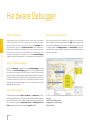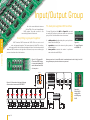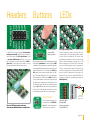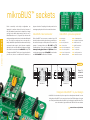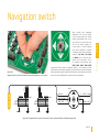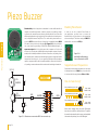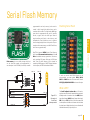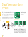
1
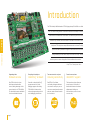
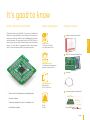
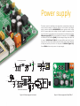
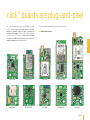
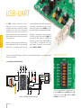
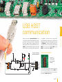
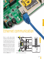
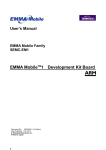
EasyFT90x CMOS image sensor Many on-board modules Easy-add extra boards Two connectors for each port Fast USB 2.0 programmer and Onboard camera Multimedia peripherals mikroBUS™ sockets Amazing connectivity In-circuit debugger To our valued customers EasyFT90x v7 is our first development board for FT90x, a new and exciting 32-bit MCU architecture from FTDI Chip. We put all our expertise into designing it. Our team relied on tried and tested concepts that define our range of “Easy” boards, but we also incorporated innovations that utilize some standout features specific to FT90x. You made the right choice. But the fun has only just begun! Nebojsa Matic, Owner and General Manager of MikroElektronika EasyFT90x Communication Introduction Introduction It's good to know 6 7 Power supply Power supply Multimedia 10 11 Programmer/debugger On-board programmer Installing programmer drivers Programming software mikroICD™ 13 14 15 16 Connectivity Input/Output group mikroBUS™ sockets click™ boards 22 23 24 25 26 26 8 Supported MCUs MCU cards MCU card schematic USB-UART USB host USB device Ethernet communication CAN communication I2S 18 20 21 Audio Input/Output microSD card slot TFT display 320x240 pixels Touch panel controller GLCD Camera Navigation switch Piezo buzzer 27 28 29 30 31 32 33 34 Other modules Serial flash memory DS1820 - Digital temperature sensor LM35 - Analog temperature sensor I2C EEPROM ADC inputs Additional GNDs 35 36 37 38 39 40 page 5 EasyFT90x Table of contents Introduction The FT90x family of MCUs is based on FTDI Chip’s proprietary 32-bit RISC core called FT32. The most exciting feature of this new architecture is its ability to execute EasyFT90x states at up to 100Mhz, which translates to 310DMIPS. Performance-wise, introduction instructions from Shadow RAM. This enables FT90x MCUs to operate at zero wait Taking advantage of that feature, EasyFT90x is our first “Easy” boards this places FT90x high above many MCUs with similar clock rates. The high speed also made it possible to integrate a camera interface into FT90x. that incorporates a camera along with all other modules and connectors. EasyFT90x v7 development Team Supporting video Two connectors for each port Onboard camera Everything is already here ™ mikroProg on board Amazing connectivity EasyFT90x is the first of our development boards with a camera, taking advantage of the camera interface of FT90x MCUs. The board also boasts a multitude of other multimedia features. Powerful on-board mikroProg™ programmer and In-Circuit debugger supports all existing FT90x MCUs. It features fast enhanced programming and rich set of debugging instructions. EasyFT90x v7 is all about connectivity. Having two different connectors for each port, you can connect accessory boards, sensors and your custom electronics easier then ever before. page 6 For easier connections ™ mikroBUS support This innovative socket allows you to use dozens of click add-on boards with almost no hardware adjustments. Adding new functionality to your device was never so easy. It's good to know FT900 is the default chip of EasyFT90 v7. It operates at a 100MHz, has 256K bytes of program/shadow memory, 64K bytes of data memory, a parallel camera interface, USB2.0 Hi-Speed (480Mbps) host controller with BCD emulation, I2S master/slave interface (24.57/22.57MHz), 65 General purpose I/O pins, 4x16-bit timers with prescale and watchdog funtion, two 10 bit DACs, 2 programmable UARTs, 7xpwm, master/ slave I2C, one master and two slave SPI, and 2xCAN controllers. System specification Package contains 1 Damage resistant protective box 2 EasyFT90x v7 board in antistatic bag 3 USB cable 4 User manual and board schematics EasyFT90x FT900 - default microcontroller power supply 7–23V AC or 9–32V DC or via USB cable (5V DC) power consumption ~72-80mA when all peripheral modules are disconnected board dimensions 266 x 220mm (10.47 x 8.66 inch) • Great choice for both beginners and professionals • Rich with modules EasyFT90x BUILT-IN COMPONENT PACKAGE OVERVIEW SYMBOL SIDE VIEW SYMBOL TOP VIEW SYMBOL SIDE VIEW RESISTOR 1/8W 1 SIDE VIEW SYMBOL TOP VIEW ELECTROLYTIC CAPACITOR SIDE VIEW SYMBOL TOP VIEW SIDE VIEW TANTALUM CAPACITOR SYMBOL TOP VIEW FERRITE BEAD SIDE VIEW 6 SYMBOL SYMBOL SYMBOL SYMBOL SYMBOL MBRS140T3 Comes with examples for mikroC, mikroBasic and mikroPascal compilers weight ~500g (1.1 lbs) SIDE VIEW TOP VIEW EasyFT90x 5 3 • TOP VIEW INDUCTOR 4 2 SYMBOL TOP VIEW CAPACITOR SIDE VIEW ADAPTER JACK TOP VIEW JOYSTICK SIDE VIEW TOP VIEW SCHOTTKY DIODE 1. EMITTER 2. BASE 3. COLLECTOR SIDE VIEW TOP VIEW SIDE VIEW RECTIFIER DIODE TOP VIEW LED DIODE SIDE VIEW Schematic TOP VIEW TRANSISTOR 1 2 3 4 SYMBOL SIDE VIEW SYMBOL TOP VIEW MC34063A SWITCHING REG. SYMBOL SIDE VIEW SIDE VIEW SYMBOL TOP VIEW FT232RL USB UART SYMBOL TOP VIEW PIEZO BUZZER SIDE VIEW SIDE VIEW SYMBOL TOP VIEW I2C EEPROM SYMBOL TOP VIEW POTENTIOMETER SIDE VIEW SIDE VIEW SYMBOL TOP VIEW RJ-45 Ethernet connector SYMBOL TOP VIEW SCREW TERMINAL SIDE VIEW SIDE VIEW SYMBOL TOP VIEW USB A HOST CONNECTOR SYMBOL TOP VIEW PCB TEST POINT SIDE VIEW We present you with a complete color schematics for EasyFT90x v7 development board. We wanted to make electronics more understandable, even for absolute beginners, so we provided photos of most used SMD components, and made additional comments and drawings so you can get to know what your board is consisted of, and how it actually works. TOP VIEW CMOS image sensor Many on-board modules Easy-add extra boards Two connectors for each port Fast USB 2.0 programmer and Onboard camera Multimedia peripherals mikroBUS™ sockets Amazing Connectivity In-Circuit Debugger SYMBOL TOP VIEW TRI-STATE DIP SWITCH HW REV. 1.01 Copyright © 2015 MikroElektronika. All rights reserved. MikroElektronika assumes no responsibility or liability for any errors or inaccuracies that may appear in the present document. Specification and information contained in the present schematic are subject to change at any time without notice. SIDE VIEW USB Type B Female connector SIDE VIEW TOP VIEW DIP SWITCH EasyFT90x v7 schematic ver 1.01 If you are experiencing some problems with any of our products or just need additional information, please contact our technical support: www.mikroe.com/support If you want to learn more about our product, please visit our website: www.mikroe.com 0100000071847 Designed by MikroElektronika Ltd. www.mikroe.com page 7 Power supply 3.3V VOLTAGE REGULATOR VCC-5V 1 3 E17 220uF/35V/LESR GND Vin Vout VCC-USB FP1 LD50 POWER 2 MC33269DT3.3 C55 100nF VCC-5V VCC-3.3V REG1 C52 100nF E16 10uF CN7 VCC 1 D- 2 D+ 3 R88 2K2 C19 GND 4 10nF USB B mikroProg CCONNECTOR Supported MCUs EasyFT90x The board contains a switching power supply that creates stable voltage and current levels necessary for powering each part of the board. Power supply section contains specialized MC33269DT3.3 power regulator which creates VCC-3.3V power supply, thus making the board capable of supporting 3.3V microcontrollers. Power supply unit can be powered in three different ways: with USB power supply (CN7), using external adapters via adapter connector (CN34) or additional screw terminals (CN35). External adapter voltage levels must be in range of 9-32V DC and 7-23V AC. Use jumper J1 to specify which power source you are using. Upon providing the power using either external adapters or USB power source you can turn on the power with SWITCH 1 (Figure 3-1). Power LED ON indicates the presence of a power supply. VCC-5V U15 3 2 1 SWITCH1 1 VCC-USB VCC-SW L1 220uH 2 J1 3 E18 220uF/35V/LESR D7 MBRS140T3 C53 220pF 4 SWC DRVC SWE IPK CT GND VIN CMPR 8 R95 0.22 D3 D4 1N4007 1N4007 - 7 6 5 MC34063A 5V SWITCHING POWER SUPPLY VCC-EXT + D5 R94 3K CN34 E19 220uF/35V/LESR 1N4007 CN35 1N4007 R96 1K Figure 3-2: Power supply unit schematic page 8 D6 VCC-SW Figure 3-1: Power supply unit of EasyFT90x v7 Board power supply creates stable 3.3V necessary for operation of the microcontroller and all on-board modules. Power supply: via DC connector or screw terminals (7V to 23V AC or 9V to 32V DC), or via USB cable (5V DC) Power capacity: up to 500mA with USB, and up to 1500mA with external power supply 1 2 3 4 5 6 Set J1 jumper to USB position To power the board with a USB cable, place jumper J1 in USB position. You can then plug in the USB cable as shown on images 1 and 2 , and turn the power switch ON. 2. Using adapter Set J1 jumper to EXT position To power the board via adapter connector, place jumper J1 in EXT position. You can then plug in the adapter cable as shown on images 3 and 4 , and turn the power switch ON. 3. With laboratory power supply Set J1 jumper to EXT position To power the board using screw terminals, place jumper J1 in EXT position. You can then screw-on the cables in the screw terminals as shown on images 5 and 6 , and turn the power switch ON. page 9 Power supply 1. With USB cable EasyFT90x How to power the board? MCU cards microcontroller with on-chip peripherals. After testing and building the final program on the development board, this card can also be taken out of the socket and used in your final device. Figure 4-1: MCU card with FT900 MCUs EasyFT90x Microcontrollers are supported using specialized MCU cards containing 104 pin, which are placed into the on-board female MCU socket (Figure 4.1). The default card contains the FT900 1 FT900 has 100MHz maximum frequency, 256KB of Flash, 64KB of on-chip data memory and 256KB of Shadow program memory. It has an integrated Parallel Camera Interface, Ethernet, USB (Host, Device), 65 General purpose I/O pins, 4 x 16-bit timers with 32-bit watchdog function, 7 Analog Input pins (ADC), 2 UARTs, I2S master/slave interface, internal slow clock oscillator, 2 x I2C (master/ slave), SPI (master/slave) and 2xCAN controllers, and a debug interface. 2 12MHz crystal oscillator. We carefully chose the most convenient crystal value that provides clock frequency for the PLL multipliers. 3 MCU card also contains 32.768 kHz crystal oscillator which provides external clock waveform for the internal RTCC module. 3 1 2 page 10 103 VCC-3.3V 101 99 97 95 93 GPIO15 91 GPIO13 89 GPIO11 87 GPIO9 85 GPIO7 83 TX_N 81 RX_N 79 VCC-3.3V VCC- 3.3V VCC- 1.5V C5 1uF 1 2 GPIO16 GPIO14 GPIO12 GPIO10 GPIO8 TX_P RX_P GND 3 R8 12K3 VCC-1.5V VCC-3.3V 100 99 98 97 96 95 94 93 92 91 90 89 88 87 86 85 84 83 82 81 80 79 78 77 76 GPIO16 GPIO15 GPIO14 GPIO13 DAC_REFP VCC3V3 AGND GPIO12 GPIO11 GPIO10 GPIO9 GPIO8 GPIO7 GPIO6 VDDBAT RTC_XI/RTC_CLKIN RTC_XIO TXON TXOP RXIN RXIP VCC3V3 RREFSET VCC1V2 VCC3V3 FTDI FT900Q YYWW-A TP 75 74 73 72 71 70 69 68 67 66 65 64 63 62 61 60 59 58 57 56 55 54 53 52 51 R9 12K R4 R5 R6 H-D_P H-D_N USB-D_P USB-D_N GND H-D_N USB-D_N GPIO6 GPIO4 GPIO2 GPIO0 GPIO66 GPIO64 GPIO62 GPIO60 GPIO58 GND X2 X1 X2 GPIO5 GPIO4 GPIO3 GPIO2 GPIO1 GPIO0 GPIO66 GPIO65 GPIO64 GPIO63 GPIO62 GPIO61 12MHz C6 C7 18pF 18pF 78 76 74 72 70 68 66 64 62 60 58 56 54 77 75 73 71 69 67 65 63 61 59 57 55 53 VCC-3.3V H-D_P USB-D_P GPIO5 GPIO3 GPIO1 GPIO65 GPIO63 GPIO61 GPIO57 VCC-3.3V HD4C 0 R7 GPIO56 GPIO57 GPIO58 GPIO60 GND GPIO40 GPIO42 GPIO44 GPIO46 FSRC RST# GPIO48 GPIO50 GPIO52 GPIO54 GPIO56 GND DBG GPIO48 GPIO49 GPIO50 GPIO51 GPIO52 GPIO53 GPIO54 GPIO55 10K 28 30 32 34 36 38 40 42 44 46 48 50 52 R3 10pF HRREF AGND H_DP H_DM DRREF D_DP D_DM VCC3V3 VCC1V2 XIO XI/CLKIN VCC3V3 VCC1V2 GPIO5 GPIO4 GPIO3 GPIO2 GPIO1 GPIO0 GPIO66 GPIO65 GPIO64 GPIO63 GPIO62 GPIO61 VCC- 3.3V VCC- 3.3V VCC- 3.3V VCC- 3.3V VCC- 3.3V VCC- 3.3V VCC- 3.3V VCC- 3.3V C8 C9 C10 C11 100nF 100nF 100nF 100nF E1 10uF E2 10uF E3 10uF E4 10uF VCC- 1.2V VCC- 1.2V VCC- 1.2V VCC- 1.2V VCC- 1.5V HD2B 27 29 31 33 35 37 39 41 43 45 47 49 51 R2 C3 RTC_X2 VCC-3.3V GPIO39 GPIO41 GPIO43 GPIO45 GPIO47 VPP DBG GPIO49 GPIO51 GPIO53 GPIO55 VCC-3.3V HD1A GND GPIO18 GPIO20 GPIO22 GPIO24 GPIO26 GPIO28 GPIO30 GPIO32 GPIO34 GPIO36 GPIO38 GND 10pF X1 32.768KHz GPIO42 GPIO43 GPIO44 GPIO45 GPIO46 GPIO47 FSOURCE VPP RESETN STESTRESTN DEBUG GPIO48 GPIO49 GPIO50 GPIO51 GPIO52 GPIO53 GPIO54 GPIO55 GND VCC3V3 GPIO56 GPIO57 GPIO58 GPIO60 2 4 6 8 10 12 14 16 18 20 22 24 26 R33 0R 26 27 28 29 30 31 32 33 34 35 36 37 38 39 40 41 42 43 44 45 46 47 48 49 50 1 3 5 7 9 11 13 15 17 19 21 23 25 GPIO42 GPIO43 GPIO44 GPIO45 GPIO46 GPIO47 FSRC VPP RST# VCC-3.3V GPIO17 GPIO19 GPIO21 GPIO23 GPIO25 GPIO27 GPIO29 GPIO31 GPIO33 GPIO35 GPIO37 VCC-3.3V GPIO17 GPIO18 GPIO19 GPIO20 GPIO21 GPIO22 GPIO23 GPIO24 GPIO25 GPIO26 GPIO27 GPIO28 GPIO29 GPIO30 GPIO31 GPIO32 GPIO33 GPIO34 GPIO35 GPIO36 GPIO37 GPIO38 GPIO39 GPIO40 GPIO41 R32 100K C2 RTC_X1 1 2 3 4 5 6 7 8 9 10 11 12 13 14 15 16 17 18 19 20 21 22 23 24 25 R31 287K 4 VCC-1.2V U1 GPIO17 GPIO18 GPIO19 GPIO20 GPIO21 GPIO22 GPIO23 GPIO24 GPIO25 GPIO26 GPIO27 GPIO28 GPIO29 GPIO30 GPIO31 GPIO32 GPIO33 GPIO34 GPIO35 GPIO36 GPIO37 GPIO38 GPIO39 GPIO40 GPIO41 EN ADJ 5 1uF C1 100nF GND EasyFT90x RTC_X1 RTC_X2 TX_N TX_P RX_N RX_P GPIO12 GPIO11 GPIO10 GPIO9 GPIO8 GPIO7 GPIO6 GPIO16 GPIO15 GPIO14 GPIO13 R1 10K IN OUT AP7331-ADJ C4 VCC- 3.3V U3 C12 C13 C14 C15 C16 4.7uF 100nF 100nF 100nF 100nF Figure 4-2: MCU card schematic page 11 MCUs GND 104 102 100 98 96 94 92 90 88 86 84 82 80 HD3D How to properly place your MCU card into the socket? Before you plug the microcontroller card into the socket, make sure that the power supply is turned off. Images below show how to correctly plug the MCU card. First make sure that MCU card orientation matches the silkscreen outline 2 Figure 4-3: On-board MCU socket has silkscreen markings which will help you to correctly orient the MCU card before inserting. MCUs EasyFT90x 1 on the EasyFT90x v7 board MCU socket. Place the MCU card over the socket so each male header is properly aligned with the female socket as shown in Figure 4-4. Then put the MCU card slowly down until all the pins match the socket. Check again if page 12 Figure 4-4: Place the MCU card on the socket so that pins are aligned correctly. everything is placed correctly and press the MCU card until it is completely plugged into the socket as shown in Figure 4-5. If done correctly all pins should be fully inserted. Only now can you turn on the power supply. 3 Figure 4-5 Properly placed MCU card. On-board programmer What is mikroProg™? How do I start? In order to start using mikroProg™, and program your microcontroller, you just have to follow two simple steps: 1. Install the necessary software - Install programmer drivers - Install mikroProg Suite™ for FT90x software 2. Power up the board, and you are ready to go. - Plug in the programmer USB cable - LINK LED should light up. mikroProg™ RST# In addition to mikroProg™, EasyFT90x allows eFUSE programming. eFUSE permanently programs the chip, disabling further altercations. eFUSE is chiefly used when the microcontroller is to be installed in a final device, for security reasons. To enable this method of programming, switch the four jumpers under the mikroPROG™ USB port into the EFUSE position. VCC-USB DBG PRG_GP37 J21 GP37 PRG_GP36 J22 GP36 PRG_GP39 J23 GP39 PRG_GP38 J24 GP38 EFUSE_SCK C46 100nF D- USBD_P D+ 3 C19 2 GND 4 10nF USB B EFUSE_MOSI VCC-5V VCC-1.8V FSRC R53 100 CN7 VCC 1 USBD_N EFUSE_MISO VPP RST# FP1 PROG-RST# EFUSE_SS# mikroProg CCONNECTOR mikroProg™ or eFUSE VCC-3.3V T9 RESET Figure 5-1: mikroProg™ block schematics page 13 Programmer / debugger EasyFT90x mikroProg™ is a fast programmer and debugger for FT90x devices, the first of its kind. The programmer supports all currently available FT90x devices. It also features a powerful debugger which will be of great help in your development. Outstanding performance and easy operation are among it's top features. Installing programmer drivers On-board mikroProg™ requires drivers in order to work. Drivers are located on the link below: When you locate the drivers, please extract the setup file from the ZIP archive. You should be able to locate the driver setup file. Double click the setup file to begin installation of the programmer drivers. Programmer / debugger EasyFT90x www.mikroe.com/downloads/get/2216/ mikroprog_suite_for_ft90x_drivers.zip mikroprog_suite_for_ft90x_drivers.zip WinRAR ZIP archive page 14 Step 1 - Start Installation Step 2 - Select Destination Welcome screen of the installation. Just click on Next button to proceed. Click Change button to select new destination folder or use the suggested installation path. Step 3 - Installing drivers Step 4 - Finish installation Drivers are installed automatically in a matter of seconds. You will be informed if the drivers are installed correctly. Click on Finish button to end installation process. Programming software Installation wizard - 6 simple steps EasyFT90x A standalone programming software utility called mikroProg Suite™ for FT90x is available as an alternative to programming the MCU directly from the FT90x compiler. This software is used for programming of all supported FT90x microcontrollers. The software has an intuitive interface and SingleClick™ programming technology. To begin, first locate the installation archive on our web site: www.mikroe.com/downloads/get/2215/mikroprog_suite_ft90x_v100.zip After downloading, extract the package and double click the executable setup file, to start the installation. Step 1 - Start Installation Step 2 - Accept EULA and continue Step 3 - Install for All users or current user Step 4 - Choose destination folder Step 5 - Installation in progress Step 6 - Finish Installation Quick Guide 1 Click the Detect MCU button in order to recognize the device ID. 2 Click the Read button to read the entire microcontroller memory. You can click the Save button to save it to target HEX file. 3 If you want to write the HEX file to the microcontroller, first make sure to load the target HEX file. You can drag and drop the file onto the software window, or use the Load button to open the Browse dialog and point to the HEX file location. Then click the Write button to begin programming. 4 Click the Erase button to wipe out the microcontroller memory. < Figure 5-2: mikroProg Suite™ window page 15 Programmer / debugger mikroProg Suite™ for FT90x Programmer / debugger EasyFT90x Hardware Debugger What is Debugging? How do I use the debugger? Every developer comes to a point where he has to monitor the code execution in order to find errors in the code, or simply to see if everything is going as planned. This hunt for bugs, or errors in the code is called debugging. There are two ways to do this: one is the software simulation, which enables you to simulate what is supposed to be happening on the microcontroller as your code lines are executed, and the other, most reliable one, is monitoring the code execution on the chip itself. And this latter one is called hardware debugging. "hardware" means that it is the real deal — code executes right on the target device. When you build your project for debugging, and program the microcontroller with this HEX file, you can start the debugger using [F9] command. Compiler will change layout to debugging view, and a blue line will mark where code execution is currently paused. Use debugging toolbar in the Watch Window to guide the program execution, and stop anytime. Add the desired variables to Watch Window and monitor their values. What is hardware debugger? The on-board mikroProg™ programmer supports a hardware debugger — a highly effective tool for Real-Time debugging on hardware level. The debugger enables you to execute your program on the host FT90x microcontroller and view variable values, Special Function Registers (SFR), RAM, CODE along with the code execution on hardware. Whether you are a beginner, or a professional, this powerful tool, with an intuitive interface and convenient set of commands will enable you to track down bugs quickly. mikroProg debugger is one of the fastest, and most reliable debugging tools on the market. Supported Compilers All MikroElektronika compilers, mikroC™, mikroBasic™ and mikroPascal™ for FT90x natively support mikroProg™ for FT90x. Specialized DLL module allows compilers to exploit the full potential of fast hardware debugging. Along with compilers, make sure to install the appropriate programmer drivers and mikroProg Suite™ for FT90x programming software, as described on pages 14 and 15. page 16 Figure 5-3: mikroC PRO for FT90x compiler in debugging view, with SFR registers in Watch Window Debugger commands Here is a short overview of which debugging commands are supported in MikroElektronika compilers. You can see what each command does, and what are their shortcuts when you are in debugging mode. It will give you some general picture of what your debugger can do. Shortcut Description Start Debugger [F9] Starts Debugger. Run/Pause Debugger [F6] Run/Pause Debugger. Stop Debugger [Ctrl + F2] Stops Debugger. Step Into [F7] Executes the current program line, then halts. If the executed program line calls another routine, the debugger steps into the routine and halts after executing the first instruction within it. Step Over [F8] Executes the current program line, then halts. If the executed program line calls another routine, the debugger will not step into it. The whole routine will be executed and the debugger halts at the first instruction following the call. Step Out [Ctrl + F8] Executes all remaining program lines within the subroutine. The debugger halts immediately upon exiting the subroutine. Run To Cursor [F4] Executes the program until reaching the cursor position. Toggle Breakpoints [F5] Toggle breakpoints option sets new breakpoints or removes those already set at the current cursor position. Show/Hide breakpoints [Shift+F4] Shows/Hides window with all breakpoints Clears breakpoints [Shift+Ctrl+F5] Delete selected breakpoints Jump to interrupt [F2] Opens window with available interrupts (doesn't work in hardware debug mode) EasyFT90x Command Name page 17 Programmer / debugger Toolbar Icon Input/Output Group Tri-state pull-up/down DIP switches One of the most distinctive features of EasyFT90x v7 for are its Input/Output PORT groups. They add so much to the connectivity potential of the board. Tri-state DIP switches, like SW11 on Figure 6-3, are used to enable 4K7 pull-up or pull-down resistor on any desired port pin. Each of these switches has three states: 1. PORT headers, PORT buttons and PORT LEDs are next to each other and grouped together. This layout givest the EasyFT90x a clean, well organized look and it makes development easier. We have also provided additional PORT headers on the right side of the board, so you can access any pin you want from that side of the board too. Connectivity middle position disables both pull-up and pull-down feature from the PORT pin up position connects the resistor in pull-up state to the selected pin down position connects the resistor in pull-down state to the selected PORT pin. 2. 3. Figure 6-1: I/O group 0007 contains PORT header, tri-state pull up/down DIP switch, buttons and LEDs all in one place Figure 6-3: Tri-state DIP switch on PORT00-07 Button press level tri-state DIP switch is used to determine which logic level will be applied to port pins when buttons are pressed 1 2 3 4 5 6 7 8 GP07 GP06 GP05 GP04 GP03 GP02 GP01 GP00 LEDS ON SW11 PORT_00_07_LED RN4 10K LD4 RN2 10K LD3 VCC-3.3V _ LD1 T3 T2 GP00 T4 GP02 T5 GP03 T6 GP04 GP05 GP06 GP07 T7 T1 PORT_00_07_LEVEL page 18 CN11 VCC-3.3V +1 2 3 4 5 6 7 8 _ VCC-3.3V T8 GP01 GP03 GP05 GP07 RN1 10K LD2 GP01 GP04 LD5 RN3 10K +1 2 3 4 5 6 7 8 GP00 RN5 10K LD6 GP05 LD7 GP06 GP07 LD8 RN6 10K GP02 RN7 10K GP03 RN8 10K GP00 GP02 GP04 GP06 SW11 UP PULL DOWN O N Figure 6-2: Schematic of the single I/O group connected to microcontroller PORT 00-07 GP01 EasyFT90x Everything is grouped together VCC BUTTON PRESS LEVEL GND SW1 R8 R9 220 220 J6 J7 GP00 GP02 GP04 GP06 VCC-3.3V GP01 GP03 GP05 GP07 CN12 Figure 6-4: Switch SW8.1 enables LEDs on PORT group 00-07 Figure 6-5: Button press level DIP switch (tri-state) The logic state of all microcontroller digital inputs may be changed using push buttons. Tri-state DIP switch SW11 is available for selecting which logic state will be applied to corresponding MCU pin when button is pressed, for each I/O port separately. If you, for example, place SW11.1 in VCC position, then pressing any push button on PORT 00-07 I/O group will apply logic one to the appropriate microcontroller pin. The same goes for GND. If DIP switch is in the middle position neither of two logic states will be applied to the appropriate microcontroller pin. You can disable pin protection 220ohm resistors by placing jumpers J6 and J7, which will connect your push buttons directly to VCC or GND. Be aware that doing so you may accidentally damage the MCU in case of wrong usage. LEDs LED (Light-Emitting Diode) is a highly efficient electronic light source. When connecting LEDs, it is necessary to place a current limiting resistor in series so that LEDs are provided with the current value specified by the manufacturer. The current varies from 0.2mA to 20mA, depending on the type of the LED and the manufacturer. The EasyFT90x v7 board uses low-current LEDs with typical current consumption of 0.2mA or 0.3mA. Board contains 67 LEDs which can be used for visual indication of the logic state on PORT pins. An active LED indicates that a logic high (1) is present on the pin. In order to enable PORT LEDs, it is necessary to enable the corresponding DIP switch on SW8 (Figure 6-6). 78 76 74 72 70 68 66 64 62 60 58 56 54 Reset Button Figure 6-4: IDC10 male headers enable easy connection with MikroElektronika accessory boards In the far upper right section of the board, there is a RESET button, which can be used to manually reset the microcontroller. 77 75 GP01 73 71 69 67 65 63 61 59 57 55 53 SMD LED SMD resistor limiting current through the LED Figure 6-6: SW8.1 through SW8.8 switches are used to enable PORT LEDs page 19 EasyFT90x With enhanced connectivity as one of the key features of EasyFT90x v7, we have provided two connection headers for each PORT. I/O PORT group contains one male IDC10 header (like CN11 shown above). There is one more IDC10 header available on the right side of the board, next to DIP switches (like CN12 on Figure 6-4). These headers can be used to connect accessory boards with IDC10 female sockets. Buttons Connectivity Headers mikroBUS sockets Connectivity EasyFT90x ™ Easier connectivity and simple configuration are imperative in modern electronic devices. Success of the USB standard comes from its simplicity of usage and high and reliable data transfer rates. As we in MikroElektronika see it, Plug-and-Play devices with minimum settings are the future in the embedded world too. This is why our engineers have come up with a simple, but brilliant pinout with lines that most of today’s accessory boards require, which almost completely eliminates the need for additional hardware settings. We called this new standard the mikroBUS™. EasyFT90x v7 supports mikroBUS™ with two on-board sockets. As you can see, there are no additional DIP switches, or jumper selections. Everything is already routed to the most appropriate pins of the microcontroller sockets. mikroBUS™ host connector mikroBUS™ pinout explained Each mikroBUS™ host connector consists of two 1x8 female headers containing pins that are most likely to be used in the target accessory board. There are three groups of communication pins: SPI, UART and I2C communications. There are also single pins for PWM, Interrupt, Analog input, Reset and Chip Select. Pinout contains two power groups: +5V and GND on one header and +3.3V and GND on the other 1x8 header. AN - Analog pin RST - Reset pin CS - SPI Chip Select line SCK - SPI Clock line MISO - SPI Slave Output line MOSI - SPI Slave Input line +3.3V - VCC-3.3V power line GND - Reference Ground VCC-3.3V GP09 GP01 GP28 GP27 GP30 GP29 VCC-5V AN RST CS SCK MISO MOSI 3.3V GND PWM INT RX TX SCL SDA 5V GND MIKROBUS 1 VCC-3.3V GP56 GP03 GP53 GP52 GP44 GP45 GP10 J85 AN GP54 AN GP04 GP61 GP27 GP30 GP29 PWM - PWM output line INT - Hardware Interrupt line RX - UART Receive line TX - UART Transmit line SCL - I2C Clock line SDA - I2C Data line +5V - VCC-5V power line GND - Reference Ground VCC-5V AN RST CS SCK MISO MOSI 3.3V GND PWM INT RX TX SCL SDA 5V GND GP57 GP05 GP53 GP52 GP44 GP45 Figure 7-1: mikroBUS™ connection schematic MIKROBUS 2 Integrate mikroBUS™ in your design mikroBUS™ is not made only to be a part of our development boards. You can freely place mikroBUS™ host connectors in your final PCB designs, as long as you clearly mark them with mikroBUS™ logo and footprint specifications. For more information, logo artwork and PCB files visit our website: www.mikroe.com/mikrobus page 20 click boards are plug-and-play! ™ For the complete list of available click™ boards, please visit: EasyFT90x www.mikroe.com/click Connectivity For a few years now, we have been expanding our range of click™ boards. Almost each month several new click™ boards are released, carrying all types of sensors and communication modules. There are over a 100 click™ boards to choose from. You’ll be able to expand your EasyFT90x v7 board with additional functionality with literally zero hardware configuration. Just plug and play. BLE P click™ BlueTooth click™ GPS click™ WiFi PLUS click™ GSM click™ microSD click™ MPU 9DOF click™ nRF C click™ Proximity click™ BUZZ click™ page 21 connectors and USB controllers. Still, certain technology enables UART communication to be done via USB connection. Controllers such as FT232RL from FTDI convert UART signals to the appropriate USB standard. The UART (universal asynchronous receiver/ transmitter) is one of the most common ways of exchanging data between the MCU and peripheral components. It is a serial protocol with separate transmit and receive lines that can be used for fullduplex communication. Both sides must be initialized with the same baud rate, otherwise the data will not be received correctly. USB-UART A communication is being done through a FT232RL controller, USB connector (CN8), and microcontroller UART module. To establish this connection, you must connect TX and RX lines of the FT232RL to the appropriate pins of the microcontroller. This selection is done using DIP switches SW2.2 and SW2.3. Modern PC computers, laptops and notebooks are no longer equipped with RS-232 connectors and UART controllers. They are nowadays replaced with USB In order to use the USB-UART module on EasyFT90x v7, you must first install FTDI drivers on your computer. Drivers can be found on link below: Enabling USB-UART www.ftdichip.com/Drivers/VCP.htm VCC-3.3V VCC-5V VCC-5V C20 C21 E1 100nF 100nF 10uF VCC-3.3V VCC-5V VCC-3.3V VCC-3.3V 1 2 3 4 5 6 7 8 FTDI-RXD FTDI-TXD SW2 GP48 GP49 TXD DTR# RTS# VCCIO RXD RI# GND NC DSR# DCD# CTS# CBUS4 CBUS2 CBUS3 FT232RL FT232RL 1 2 3 4 FTDI-RXD 5 6 7 8 9 10 11 12 13 14 FTDI-TXD U8 OSCO OSCI TEST AGND NC CBUS0 CBUS1 GND VCC RESET# GND 3V3OUT USBDM USBDP 28 27 26 25 24 23 22 21 20 19 18 17 16 15 R93 2K2 R92 4K7 RX TX VCC 1 D- RX-LED1 TX-LED1 LD9 LD10 R91 4K7 GND 4 USB B FTDI1-D_N FTDI1-D_P R90 10K C25 100nF Figure 8-1: USB-UART connection schematic page 22 2 D+ 3 USB UART CONNECTOR CN8 O N Communication EasyFT90x USB-UART In order to enable USB-UART communications, you must push SW2.2 (GP49) and SW2.3 (GP48) to ON position. This connects the RX and TX lines to GP48 and GP49 microcontroller pins. VCC-3.3V R80 10K R82 47K VCC-5V USB-PSW 4 5 O N GP00 GP02 1 2 3 4 5 6 7 8 SW3 VCC-5V U11 EN OC GND IN OUT TPS2041B 3 R83 4K7 R84 2K2 LD29 OC LD30 ON USB-OC CN10 2 1 VCC 1 E9 10uF E10 10uF Q2 BC846 D1 BAT43 USB-VBUS Figure 9-1: USB host connection schematic R81 R85 100 10K H-D_N D- H-D_P D+ 3 2 GND 4 USB A USB HOST CONNECTOR VCC-3.3V to establish a connection with the target device (eg. USB Keyboard, USB Mouse, etc). USB host also provides the necessary 5V power supply to the target via TPS2041B IC. Detection whether USB device is connected to HOST connector can be done through VBUS line. Connection of USB HOST VBUS line and GPO0 pin is established when SW3.1 is on. Powering USB device Figure 9-2: Powering USB device through PSW line You can enable or disable power supply to USB device connected to HOST, through microcontroller GP02 pin. In order to connect EN TPS2041B IC pin to microcontroller, you must push SW3.2 to ON position. page 23 Communication USB is the acronym for Universal Serial Bus. This is a very popular industry standard that defines cables, connectors and protocols used for communication and power supply between computers and other devices. EasyFT90x v7 contains a USB HOST connector (CN10) for a USB Standard Type A plug, which enables microcontrollers that support USB communication EasyFT90x USB HOST communication Communication EasyFT90x USB device communication EasyFT90x v7 also contains USB DEVICE connector (CN9) which enables microcontrollers that support USB communication to establish a connection with the target host (eg. PC, Laptop, etc). It lets you build a slave USB device (HID, Composite, Generic, etc.). Connector supports USB Standard Type B plug. USB Device is directly connected to MCU pins GPO3, USBD-N and USBD-P (no switches to flip). When connected to HOST, dedicated ambercolored power LED will light up as well. GP03-DTC USB-D_N USB-D_P R67 100 VCC 1 R69 27 D- R73 27 D+ 3 2 GND 4 GROUNDPROBES ON LD20 USB B R77 4K7 GND page 24 GND USB DEVICE CONNECTOR CN9 D2 BAT43 Figure 10-1: USB host connection schematic EasyFT90x Communication Ethernet communication VCC-3.3V LEDB R62 LD39 2K2 ETH_LED0 VCC-3.3V FP2 A2 K2 CN24 TD+ TD- A1 K1 TX_N R68 51 CT RD- R64 51 RX_P RD+ RJ45 TX_P R66 51 CT CONNECTOR ETHERNET Ethernet is a popular computer networ king technology for local area networks (LAN). Systems communicating over Ethernet divide a stream of data into individual packets called frames. Each frame contains source and destination addresses and errorchecking data so that damaged data can be detected and re-transmitted. EasyFT90x v7 features a standard RJ-45 connector which enables microcontrollers that support Ethernet communication to establish a connection with a computer, router or other devices. All four Ethernet lines (TPOUT+, TPOUT-, TPIN+ and TPIN-) are routed directly to the MCU card socket and cannot be accessed via PORT headers. Additional signalization LEDs (green and yellow) are provided on the Board next to RJ-45 connector. C47 C48 R72 51 VCC-3.3V R74 LD40 2K2 103 101 99 97 95 93 91 89 87 85 83 81 79 TX_N RX_N RX_N 10nF 10nF LEDA TX_P RX_P 104 102 100 98 96 94 92 90 88 86 84 82 80 ETH_LED1 MCU CARD SOCKET Figure 11-1: Ethernet connection schematic page 25 IS CAN communication VCC-3.3V TX-CAN RX-CAN 1 2 3 4 R57 100 C49 SW3 VCC-3.3V Figure 12-2: enabling CAN communication GP15 GP16 100nF J9 R56 10 U13 D GND Vdd R Rs CANH CANL Vref SN65HVD230 8 7 6 5 VCC-3.3V R75 3K3 1 C81 100nF OSC1 OE VCC GND OUT 4 CANH 2 CANL OSC24M5760 C82 1uF 3 I2S-OSC C83 15pF GP66 J86C CN30 Figure 12-1: CAN connection schematic page 26 VCC-3.3V MCU-GP66 TX-CAN RX-CAN CANL In order to enable CAN communication, you must push SW3.3 (GP16) and SW3.4 (GP15) to ON position. This connects the TX and RX lines to appropriate microcontroller pins and its CAN module. FT90x microcontrollers have an integrated I2S master/slave interface. I2S is a serial bus standard used for carrying audio data between various devices (hence, the protocol is sometimes called Inter-IC Sound). The interface comprises a Bit clock line, a Left/Right clock line (LRCLK), a Master clock (MCLK) and two data lines (SDAI, SDAO). The bit clock (BCLK) regulates data transmission (one pulse for each bit), while the pulsing of the LR clock specifies which data channel is currently being transferred (by convention, low level is for the left audio channel, high level for the right). The master clock is used by an I2S slave module (if required). The frequencies for these clocks are derived from the external 24.576 MHz crystal oscillator which is tucked under the MCU card on the EasyFT90x board. In case you won’t be using I2S, you can free up the extra pin (GP66), by placing Jumper J86 in the GPIO position. CANH Enabling CAN 1 2 3 4 5 6 7 8 Controller Area Network (CAN or CAN bus) is a vehicle bus standard designed to allow microcontrollers and devices to communicate with each other within a vehicle without a host computer. CAN is a message-based protocol, designed specifically for automotive applications but now also used in other areas such as industrial automation and medical equipment. EasyFT90x v7 is equipped with SN65HVD230 – a 3.3V CAN Transceiver and a pair of screw terminals which provide microcontrollers with integrated CAN controller with the necessary physical interface for CAN communication. Make sure to correctly connect negative and positive differential communication lines before using this module. O N Communication EasyFT90x 2 Figure 13-1: Schematic of I2S module Audio I/O Enabling Audio I/O Figure 14-1: Audio IN/OUT connection schematics VCC-3.3V R31 10 L 48 47 46 45 44 43 42 41 40 39 38 37 PHONEJACK GPIO4 GND GPIO1 GPIO0 XTEST CVDD3 SO SI SCLK TX RX GPIO5 36 35 34 33 32 31 30 29 28 27 26 25 R24 27 SW2 C17 C18 C16 47nF 10nF 10nF SPIM-MISO SPIM-MOSI SPIM-SCK MICP R28 10K R37 1K C22 1.8nF MICN C23 E2 E3 100pF 10uF 10uF R38 1K C24 1.8nF 1M MP3-DREQ MP3-RST# MP3-CS# MP3-DCS X2 12.288MHz C26 22pF C27 22pF In order to use Audio I/O module, you must connect data and Audio control lines of the microcontroller with the VS1053 audio codec. To do this, push SW3.5– SW3.8 switches to ON position. This will connect SPI data lines with MCU_SCK, MCU_MISO and MCU_MOSI microcontroller pins, and audio control and chip select lines with GP60, GP07, GP08 and GP09 pins. CN14 MICROPHONE R39 1K 1 2 3 4 5 6 7 8 R30 Figure 14-2: Enabling audio codec communication lines R36 1K MP3-CS# MP3-DCS GP27 GP30 GP29 R35 20 VCC-3.3V VCC-3.3V O N O N SPIM-SCK SPIM-MISO SPIM-MOSI 1 2 3 4 5 6 7 8 R29 100K R34 20 R26 27 GPIO VS1053 R33 10 13 14 15 16 17 18 19 20 21 22 23 24 GPIO MP3-DREQ MCP/LN1 MICN XRESET DGND0 CVDD0 IOVDD0 CVDD1 DREQ GPIO2 GPIO3 GPIO6 GPIO7 XDCS/BSYNC IOVDD1 VC0 DGND1 XTAL0 XTAL1 IOVDD2 DGND2 DGND3 DGND4 XCS CVDD2 R27 100k 1 2 3 4 5 6 7 8 9 10 11 12 LN2 AGND3 LEFT AVDD2 RCAP AVDD1 GBUF AGND2 AGND1 RIGHT AVDD0 AGND0 U7 MICP MICN MP3-RST# CN13 R32 10 R GBUF R23 10K Multimedia VCC-1.8V R GBUF C15 1uF L VCC-3.3V EasyFT90x receives the input bit stream through a serial input bus, which it listens to as a system slave. The input stream is decoded and passed through a digital volume control to an 18-bit oversampling, multi-bit, sigma-delta Digital to Analog Converter (DAC). The decoding is controlled via a serial control bus. In addition to the basic decoding, it is possible to add application specific features like DSP effects to the user RAM memory. You can build music players, audio recording devices, internet radio player applications, and much more. It's hard to imagine modern multimedia devices without high quality audio reproduction modules. Sounds and music are almost as important as graphical user interfaces. Along with other multimedia modules, EasyFT90x v7 contains high end stereo VS1053 audio codec. It features Ogg Vorbis/MP3/AAC/WMA/FLAC/ WAV/MIDI audio decoder, as well as an PCM/IMA ADPCM/Ogg Vorbis encoder on a single chip. Board also contains two stereo audio connectors for interfacing with standard 3.5mm stereo audio jacks. VS1053 SW3 GP09 GP08 GP60 GP07 VCC-3.3V 1 E4 C28 10uF 100nF C32 C33 C29 100nF 100nF 100nF C34 C30 100nF 2.2uF 2 3 U9 IN OUT GND EN ADJ AP7331-ADJ VCC-1.8V 5 R100 4 120K R101 R102 22K 12K1 E5 C35 C31 C36 C37 10uF 100nF 100nF 100nF 100nF page 27 EasyFT90x microSD CARD SLOT VCC-SD MICRO SD CARD SD-CD# SD-DATA0 SD-DATA1 SD-DATA2 SD-DATA3 SD-CMD SD-CLK SW4 GP25 GP24 GP23 GP22 GP21 GP20 GP19 SD-DATA2 R41 SD-DATA3 R42 SD-CMD R43 27 27 27 SD-CLK R44 27 SD-DATA0 R45 SD-DATA1 R46 SD-CD# 27 27 1 2 3 4 5 6 7 8 DAT2 DAT3 CMD +3.3V CLK GND DAT0 DAT1 CD GND R40 10K 1 2 3 4 5 6 7 8 Secure Digital (SD) is a non-volatile memory card format developed for use in portable devices. It comes in different packages and memory capacities. It is mostly used for storing large amounts of data. EasyFT90x v7 features a microSD card slot. The microSD form factor is the smallest card format currently available. It uses a standard SPI user interface with minimum additional electronics, mainly used for stabilizing communication lines which can be significantly distorted at high transfer rates. Special ferrite is also provided to compensate the voltage and current glitch that can occur when pushing in and pushing out microSD card into the socket. O N Multimedia microSD card slot CN6 Enabling microSD In order to access the microSD card, you must enable communication lines with switches SW4.1 through SW4.8 page 28 Figure 15-1: microSD card slot connection schematics TFT display 320x240 pixels One of the most powerful ways of presenting data and interacting with users is through color displays and touch panel inputs. This is a crucial element of any multimedia device. EasyFT90x v7 features an EasyTFT board carrying a 320x240 pixel 2.83" color TFT display with LED back-light and a HX8347D controller. R10 20 R11 1K BCK_PWM R12 GP40 GP05 GP41 GP32 GP33 GP34 GP35 GP36 GP37 GP38 GP39 GP42 CN29 1 20 PMRD PMWR GND VCC NC RS NC CS D0 D1 D2 D3 D4 D5 D6 D7 RST NC +5V BPWM VCC-3.3V GP46 GP47 BPWM VCC-5V BCK_LIGHT BPWM Each pixel is capable of showing 262.144 different colors. TFT display is connected to microcontroller PORT 32-39 using standard 8080 parallel 8-bit interface, with additional control lines. Board features back-light driver which besides standard mode can also be driven with PWM signal in order to regulate brightness in 0 to 100% range. Q5 BC846 TFT display is enabled using SW5.7–SW5.8 DIP switches. Back-light can be enabled in two different ways: VCC-5V GP58 1. It can be turned on with full brightness using SW5.8 switch. O N 1 2 3 4 5 6 7 8 In order to use PWM back-light both SW13.3 and SW13.4 switches must be enabled at the same time. Driving Display Back-light 4K7 BCK_LIGHT BCK_PWM IMPORTANT: SW5 24 XR YU XL YD 21 Figure 16-1: TFT display connection schematic GLCD-TFT SOCKET 2. Brightness level can be determined with PWM signal from the microcontroller, allowing you to write custom back-light controlling software. This back-light mode is enabled when both SW5.7 and SW5.8 switches are in ON position. Figure 16-2: Turn on switches SW5.7 and SW5.8 to enable back-light page 29 A touch panel is a glass panel whose surface is covered with two layers of resistive material. When the screen is pressed, the outer layer is pushed onto the inner layer. The pressure at the specific spot is measured by appropriate controllers. This is how touch panels can be used as an input devices. EasyFT90x v7 is equipped with a touch panel controller and a connector for 4-wire resistive touch panels. It can very accurately register pressure at a specific point, representing the touch coordinates in the form of analog voltages, which can then be easily converted to X and Y values. Touch panel comes as a part of TFT 320x240 display. Enabling Touch panel Touch panel is enabled using SW6.1, SW6.2, SW6.3 and SW6.4 switches. They connect BOTTOM and LEFT lines of the touch panel with GP10 and GP11 analog inputs, and DRIVEA and DRIVEB with GP31 and GP43 digital outputs on microcontroller sockets. Make sure to disconnect other peripherals, LEDs and additional pull-up or pull-down resistors from the interface lines so they do not interfere with signal/data integrity. Figure 17-2: Turn on switches SW6.1, SW6.2, SW6.3 and SW6.4 to enable Touch panel controller VREF Q3 BC856 CN29 VCC-3.3V 10K FP4 FERRITE R13 1K R14 20 PMRD PMWR GND VCC NC RS NC CS D0 D1 D2 D3 D4 D5 D6 D7 RST NC +5V BPWM 1 VREF C56 C57 1uF 100nF Q4 BC846 RIGHT R15 10K VREF Q6 BC856 VCC-3.3V R17 4K7 R16 DRIVEA 10K READ-X R19 10nF 10K READ-X READ-Y DRIVEA DRIVEB 24 READ-Y GLCD-TFT SOCKET RIGHT TOP READ-X READ-Y VCC-3.3V Q8 BC846 R20 100K Figure 17-1: Touch Panel controller and connection schematic page 30 C50 O N 21 E15 10uF Q7 BC846 R18 100K C58 R21 10nF 10K 1 2 3 4 5 6 7 8 VCC-3.3V TOP CN33 XR YU XL YD Multimedia EasyFT90x Touch Panel controller SW6 R22 4K7 DRIVEB GP10 GP11 GP31 GP43 Display connector is routed to PORT 32-39 (control and data lines) of the microcontroller sockets. The same port is also used by the TFT display. You can control the display contrast using the dedicated potentiometer P3. Full brightness display back-light can be enabled with SW5.8 switch and PWM-driven back-light with SW5.7 switch. Q5 BC846 R12 Multimedia GP46 GP47 R10 20 GLCD_VEE GP40 GP05 GP41 GP32 GP33 GP34 GP35 GP36 GP37 GP38 GP39 GP42 VEE BCK_LIGHT BPWM R11 1K BCK_PWM VCC-5V BPWM VCC-3.3V CN29 4K7 VCC-5V BCK_LIGHT BCK_PWM 1 2 3 4 5 6 7 8 Graphical Liquid Crystal Displays, or GLCDs are used to display monochromatic graphical content, such as text, images, human-machine interfaces and other content. EasyFT90x v7 provides the connector and the necessary interface for supporting GLCD with a resolution of 128x64 pixels, driven by the KS108 or compatible display controller. Communication with the display module is done through CN33 display connector. Board is fitted with a plastic display distancer, which allows the GLCD module to perfectly and firmly fit into place. P3 10K GP58 Figure 18-2: GLCD 128x64 connection schematic O N GLCD 128x64 EasyFT90x Figure 18-1: To activate full brightness display backlight, flip SW5.8 to ON. For PWM backlight, both SW5.7 and 5.8 should be turned on SW5 Connector pinout explained CS1 and CS2 - Controller Chip Select lines VCC - +5V display power supply GND - Reference ground Vo - GLCD contrast level from potentiometer P3 RS - Data (High), Instruction (Low) selection line R/W - Determines whether display is in Read or Write mode. E - Display Enable line D0–D7 - Data lines RST - Display reset line Vee - Reference voltage for GLCD contrast potentiometer P3 LED+ - Connection with the back light LED anode LED- - Connection with the back light LED cathode page 31 VCC-1.8V C60 C61 100nF 100nF U10 SW5 1 2 3 4 5 6 7 8 GP10 GP11 GP12 GP13 GP14 GP15 GP16 GP17 O N CAM_D7 CAM_D6 CAM_D5 CAM_D4 CAM_D3 CAM_D2 CAM_D1 CAM_D0 I2C0-SCL I2C0-SDA CAM_D0 CAM_D1 CAM_D2 CAM_D3 CAM_D4 CAM_D5 CAM_D6 CAM_D7 B4 A4 B5 A5 F5 E5 F4 E4 D0 D1 D2 D3 D4 D5 D6 D7 OV07670-VL2A E3 E1 B1 A3 A2 D2 D1 E2 1 2 3 4 5 6 7 8 SW7 AVDD-2.8V CAM_RST GP18 GP50 GP09 GP08 GP07 GP06 O N CAM_PWDN CAM_RST CAM_HREF CAM_VSYNC CAM_PCLK CAM_XCLK 1 2 3 4 5 6 7 8 AVDD-2.8V C2 B2 A1 C1 F1 F3 B3 F2 Figure 19-1: Jumper J85 reroutes the AN pin on the second mikroBUS™ socket from GP10 to GP54 VREF1 VREF2 AVDD DVDD DOVDD DOGND AGND RESET To use the onboard camera, flip the following switches to the ON position: SW7.1, SW7.2, SW7.3, SW7.4, SW7.5, SW7.6, SW7.7, SW7.8, SW5.1, SW 5.2, SW5.3, SW5.4, SW5.5, SW5.6, SW2.4 and SW2.5 The first upper left pin of the mikroBUS™ socket is usually reserved for an analog line, but in some click™ boards that pin has a different function. For example, WiFi3 click uses that pin for a PWD line. Since the camera on EasyFT90x takes up all the the analog lines, we added a jumper (J85) that enables you to reroute the AN pin on the second mikroBUS™ socket (GP10) to a General Purpose IO (GP54). This allows you to use some of those click boards like WiFi3 click together with the camera, to stream video over WiFi, for example. XCLK PCLK PWDN SIO_C SIO_D HREF VSYNC STROBE Enabling the camera A jumper to help you stream video over WiFi GP44 GP45 CAM_XCLK CAM_PCLK CAM_PWDN I2C0-SCL I2C0-SDA CAM_HREF CAM_VSYNC CAM_STROBE One of the most distinguishing features of FT90x microcontrollers is the integrated Camera Parallel interface (CPI). To make full use of it, and to allow you to develop multimedia applications that combine the camera and TFT, EasyFT90x incorporates a OV07670-VL2A CMOS image sensor. The sensor has a resolution of up to 640x480px (but keep in mind that the EasyTFT screen has 320x240px). CPI is an 8-bit interface. Camera control signals are VSYNC, HREF, and PCLK. Therefore, to enable the camera, activate DIP switches from 7.1 through 7.8, as well as SW5.1 through 5.6. SW2.4 and SW2.5 should also be on. O N Multimedia EasyFT90x Onboard camera SW2 Figure 19-2: Onboard camera connection schematic. page 32 OV07670-VL2A GP63 GP62 GP66 GP65 GP64 Figure 20-1: Navigation switch is an intuitive solution for browsing through on-screen menus. KEY1 GP64 UP UP PULL DOWN +1 2 3 4 5 6 7 8 _ VCC-3.3V SW91 UP PULL DOWN +1 2 3 4 5 6 7 8 SW81 1 4 GP65 CENTER 2 5 GP66 LEFT 6 3 RIGHT GP63 DOWN GP62 _ VCC-3.3V Figure 20-2: Navigation switch connection schematic. Pull-up resistors should be enabled during operation page 33 Multimedia When working with multimedia applications it is far more intuitive to use a single joystick than several different push buttons that are far apart. This is more natural for users as they can browse through onscreen menus, or even play games much easier. EasyFT90x v7 features a navigation switch with five different positions: Up, Down, Left, Right and Center. Each of those acts as a button, and is connected to one of the following microcontroller pins: GP64, GP62, GP66, GP63, GP65 (respectively). Before using the navigation switch, it is necessary to pull-up mentioned microcontroller pins using tri-state DIP switches located in I/O groups. After pressing the navigation switch in desired direction, associated microcontroller pins are connected to GND, which can be detected in user software. EasyFT90x Navigation switch Piezo Buzzer Enabling Piezo Buzzer In order to use the on-board Piezo Buzzer in your application, you first have to connect the transistor driver of piezo buzzer to the appropriate microcontroller pin. This is done using the SW6.6 DIP switch which connects it to GP55 pin. Figure 21-2: push SW6.6 to ON position to connect Piezo buzzer to GP55 Supported sound frequencies Piezo buzzer’s resonant frequency (where you can expect VCC-5V it's best performance) is 3.8kHz, but you can also use it TOP to create sound in the range between VIEW 2kHz and 4kHz. VCC-5V VCC-5V How to make it sing? R47 1K Q1 BC846 R48 1K R49 100K BUZZER 1 2 3 4 5 6 7 8 PZ1 BUZZER SW6 Figure 21-1: Piezo buzzer connected to GP55 microcontroller pin page 34 R3 1K TOP VIEW PERSPECTIVE VCC-5V R3 VIEW PZ1 R27 1K Freq = 3kHz, Duty Cycle = 50% TOP Freq = 3kHz, VIEW 10K VolumeQ8= 50% PERSPECTIVE VIEW BC846 R3 PZ1 1K R27 PZ1 O N Multimedia EasyFT90x Piezoelectricity is the charge that accumulates in certain solid materials in response to mechanical pressure. It works in reverse too: providing a charge to piezoelectric materials causes them to phisically deform. One of the most widely used applications of piezoelectricity is the production of sound generators, called piezo buzzers. EasyFT90x v7 for comes with a piezo buzzer connected to GP55 microcontroller pin. Connection is established using SW6.6 DIP switch. Buzzer is driven by transistor Q1 (Figure 25-1). Microcontrollers can create sound by generating a PWM (Pulse Width Modulated) signal – a square wave signal, which is nothing more than a sequence of logic zeros and ones. You can generate a PWM signal using a hardware capture-compare module, which is usually available in most microcontrollers, or by writing a custom software which emulates the desired signal waveform. Supported sound frequenciesof the duty cycle. You can generate PWM signal using hardware capture-compare module, which is usually available in most microcontrollers, or by writing a custom software which emulates the desired signal waveform. GP55 Freq = 3kHz, Duty Cycle = 80% PERSPECTIVE VIEW Freq = 3kHz, Duty Cycle = 20% Freq = 3kHz, 10K VolumeQ8= 80% BC846 R27 Freq = 3kHz, 10K VolumeQ8= 20% BC846 Buzzer starts "singing" when you provide PWM signal from the microcontroller to the buzzer driver. The pitch of the sound is determined by the frequency, and amplitude is determined by the duty cycle of the PWM signal. BUZZER BUZZER BUZZER Serial Flash Memory R7 100K R6 27 1 2 3 4 VCC-3.3V CS SDO WP GND VCC-3.3V In order to connect Serial Flash Memory to the microcontroller you must enable SW2.1, SW2.6, SW2.7 and SW2.8 switches. This connects SPI lines to GP51 (CS), MOSI, MISO AND SCK microcontroller pins. C42 U12 VCC HOLD SCK SDI 8 7 6 5 100nF O N FLASH-CS# 1 2 3 4 5 6 7 8 25P80 SPIM-SCK SPIM-MISO SPIM-MOSI SW2 Other modules EasyFT90x features M25P80 Serial Flash Memory which uses SPI communication interface and has 8 Mbits of available memory, organized as 16 sectors, each containing 256 pages. Each page is 256 bytes wide. Thus, the whole memory can be viewed as consisting of 4096 pages, or 1,048,576 bytes. Maximum clock frequency for READ instructions is 40MHz. Flash memory is a non-volatile storage chip that can be electrically erased and reprogrammed. It was developed from EEPROM (electrically erasable VCC-3.3V Enabling Serial Flash EasyFT90x programmable read-only memory) and must be erased in fairly large blocks before these can be rewritten with new data. The high density NAND type must also be programmed and read in (smaller) blocks, or pages, while the NOR type allows a single machine word (byte) to be written or read independently. Flash memories come in different sizes and supporting different clock speeds. They are mostly used for mass storage, as in USB Flash Drives, which are very popular today. What is SPI? GP27 GP30 GP29 GP51 Figure 22-1: Schematic of Serial Flash Memory module The Serial Peripheral Interface Bus or SPI bus is a synchronous serial data link standard that operates in full duplex mode. It consists of four lines MISO (Master Input Slave Output), MOSI (Master Output Slave Input), SCK (Clock) and CS (Chip Select). Devices communicate in master/slave mode where the master device initiates the data frame. Multiple slave devices are allowed with individual slave select (chip select) lines. page 35 Board provides a separate socket (TS1) for the DS1820. Communication line with the microcontroller is established through the SW6.5 DIP switch (ON position). DS1820 is a digital temperature sensor that uses 1-wire® interface for its operation. It is capable of measuring temperatures within the range of -55 to 128°C, and provides ±0.5°C accuracy for temperatures within the range of -10 to 85°C. It requires 3V to 5.5V power supply for stable operation. It takes maximum of 750ms for the DS1820 to calculate temperature with 9-bit resolution. 1-wire® serial communication enables data to be transferred over a single communication line, while the process itself is under the control of the master microcontroller. The advantage of such communication is that only one microcontroller pin is used. Multiple sensors can be connected on the same line. All slave devices by default have a unique ID code, which enables the master device to easily identify all devices sharing the same interface. Enabling DS1820 Sensor 1 2 3 DS1820 R54 1K5 DS1820 C40 100nF SW6 Figure 23-1: DS1820 connected to PB10 pin page 36 Figure 23-2: DS1820 socket GP26 GND DQ VCC TS1 1 2 3 4 5 6 7 8 VCC-3.3V O N Other modules EasyFT90x Digital Temperature Sensor DS1820 Figure 23-3: DS1820 correctly placed in socket Figure 23-4: Enabled SW6.5 DIP switch EasyFT90x v7 enables you to establish 1-wire® communication between DS1820 and the microcontroller over PB10 or PA3 pin. The connection is done placing SW14.5 or SW6.5 DIP switch to ON position (Figure 20-3). When placing the sensor in the socket make sure that half-circle on the board’s silkscreen markings matches the rounded part of the DS1820 sensor. If you accidentally connect the sensor the other way, it may be permanently damaged. Make sure to disconnect other peripherals, LEDs and additional pull-up or pull-down resistors from the interface lines in order not to interfere with signal/data integrity. 60 μA current drain. As it draws only 60 μA from its supply, it has very low self-heating, less than 0.1°C in still air. EasyFT90x v7 enables you to get analog readings from the LM35 sensor in restricted temperature range from +2ºC to +150ºC. The board has a socket (TS2) for the LM35 sensor in TO-92 plastic packaging. The microcontroller reads of the temperature data of a single analog input line, which is selected with jumper J84. Figure 24-2: Choose between two analog input lines to use with LM35, with jumper J84 Other modules The LM35 is a low-cost precision integratedcircuit temperature sensor, whose output voltage is linearly proportional to the Celsius (Centigrade) temperature. The LM35 thus has an advantage over linear temperature sensors calibrated in degrees Kelvin, as the user is not required to subtract a large constant voltage from its output to obtain convenient Centigrade scaling. It has a linear +10.0 mV/°C scale factor and less than Enabling LM35 Sensor GP11 LM35 1 2 3 VCC-5V R55 Figure 24-3: LM35 socket J84 100 VCC VOUT GND TS2 C43 100nF GP12 Figure 24-1: LM35 connected to PC0 pin EasyFT90x Analog Temperature Sensor LM35 Figure 24-4: LM35 correctly placed in socket Use the jumper J84, right next to the temperature sensor, to connect it to either GP11 or GP12. Having two pins to choose from gives you more flexibility to use the temperature sensor with other board modules. When placing the sensor in the socket make sure that half-circle on the board’s silkscreen markings matches the rounded part of the LM35 sensor. If you accidentally connect the sensor the other way, it can be permanently damaged and you might need to replace it with another one. During the readings of the sensor, make sure that no other device uses the selected analog line, because it may interfere with the readings. page 37 I C EEPROM 2 EasyFT90x EEPROM is short for Electrically Erasable Programmable Read Only Memory. It is usually a secondary storage memory in devices containing data that is retained even if the device looses its power supply. Because of the ability to alter single bytes of data, EEPROM devices are used to store personal preference and configuration data in a wide spectrum of consumer, automotive, telecommunication, medical, industrial, and PC applications. VCC-3.3V C51 100nF VCC-3.3V 1 2 3 4 VCC-3.3V U14 A0 A1 A2 VSS VCC WP SCL SDA 8 7 6 5 VCC-3.3V R58 2K2 R59 2K2 I2C0-SCL I2C0-SDA O N 24AA01 EEPROM 1 2 3 4 5 6 7 8 Other modules EasyFT90x v7 supports serial EEPROM which uses I2C communication interface and has 1024 bytes of available memory. EEPROM itself supports single byte or 16-byte (page) write and read operations. Data rates depend on the power supply voltage, and go up to 400 kHz for a 3.3V power supply. SW2 Figure 25-1: Schematic of I2C EEPROM module page 38 GP44 GP45 Enabling I2C EEPROM Figure 25-2: Turn on switches SW2.4 and SW2.5 to connect EEPROM lines to MCU In order to connect I2C EEPROM to the microcontroller you must enable SW2.4 and SW2.5 switches, as shown on Figure 23-2. 2K2 pull-up resistors necessary for I2C communication are already provided on SDA and SCL lines once switches are turned on. Prior to using EEPROM in your application, make sure to disconnect other peripherals, LEDs and additional pull-up or pull-down resistors from GP45 and GP44 communication lines that could interfere with the data signals and cause data corruption. What is I2C? I2C is a multi-master serial single-ended bus that is used to attach low-speed peripherals to computer or embedded systems. I²C uses only two open-drain lines, Serial Data Line (SDA) and Serial Clock (SCL), pulled up with resistors. SCL line is driven by a master, while SDA is used as a bidirectional line either by a master or slave device. Up to 112 slave devices can be connected to the same bus. Each slave must have a unique address. ADC inputs Other modules EasyFT90x Digital signals have two discrete states, which are decoded as high and low, and interpreted as logic 1 and logic 0. Analog signals, on the other hand, are continuous, and can have any value within defined range. A/D converters are specialized circuits which can convert analog signals (voltages) into a digital representation, usually in form of an integer number. The value of this number is linearly dependent on the input voltage value. Most microcontrollers nowadays internally have A/D converters connected to one or more input pins. Some of the most important parameters of A/D converters are conversion time and resolution. Conversion time determines how fast can an analog voltage be represented in form of a digital number. This is an important parameter if you need fast data acquisition. The other parameter is resolution. Resolution represents the number of discrete steps that supported voltage range can be divided into. It determines the sensitivity of the A/D converter. Resolution is represented in maximum number of bits that the resulting number occupies. Most microcontrollers have 10-bit resolution, meaning that maximum value of conversion can be represented with 10 bits, which converted to integer is 210=1024. This means that the supported voltage range, for example from 0-1.8V, can be divided into 1024 discrete steps of about 1.758mV. EasyFT90x provides two interfaces in the form of potentiometers for simulating analog input voltages that can be routed to any of the 5 supported analog input pins. Enabling ADC inputs Figure 26-1: Schematic of ADC inputs VCC-3.3V GP06 GP07 GP08 GP09 GP10 P1 R50 ADC1 220 J81 C44 100nF 10K VCC-3.3V GP06 GP07 GP08 GP09 GP10 P2 R51 ADC2 220 J82 C41 100nF 10K In order to connect the output of the potentiometer P1 to GP06, GP07, GP08, GP09 or GP10 analog microcontroller input, you have to place the jumper J81 in the desired position. By moving the potentiometer knob, you can create voltages in range from GND to VCC. The same applies for potentiemeter P2 and its corresponding jumper J82 (just make sure not to put both potentiometers to the same input) page 39 Additional GNDs EasyFT90x v7 contains GND pins located in different sections of the board, which allows you to easily connect oscilloscope GND reference when you monitor signals on microcontroller pins, or signals of on-board modules. GND is located below power supply region. EasyFT90x 1 Other modules GND is located below microSD section. 2 Figure 27-1: Three oscilloscope GND pins are conveniently positioned so different parts of the board can be reached with an oscilloscope probe page 40 3 GND is located just above PORT64-66 Input/Output Group. What’s Next? You have now completed the journey through each and every feature of EasyFT90x v7. You got to know its modules, organization, supported microcontrollers, programmer and debugger. Now you are ready to start using your new board. 1 Compiler You still don’t have an appropriate compiler? Locate the FT90x compiler that suits you best on our website: www.mikroe.com/ft90x/compilers Choose between mikroC™, mikroBasic™ and mikroPascal™ and download fully functional demo version, so you can begin building your FT90x applications. We are suggesting several steps which are probably the best way to begin. We invite you to join the users of the EasyFT90x brand. You will find very useful projects and tutorials and can get help from a large ecosystem of users. Welcome! 2 Projects Once you have chosen your compiler, and since you already got the board, you are ready to start writing your first projects. We have equipped our compilers with dozens of examples that demonstrate the use of each and every feature of the EasyFT90x v7 board, and all of our accessory boards as well. This makes an excellent starting point for your future projects. Just load the example, read well commented code, and see how it works on hardware. Browse through the compiler Examples on this link: www.mikroe.com/easyft90x 3 Community If you want to find answers to your questions on many interesting topics we invite you to visit our forum at www.mikroe.com/forum and browse through more than 150 thousand posts. You are likely to find just the right information for you. On the other hand, if you want to download free projects and libraries, or share your own code, please visit the Libstock website. With user profiles, you can get to know other programmers, and subscribe to receive notifications on their code. www.libstock.com 4 Support We all know how important it is that we can rely on someone in moments when we are stuck with our projects, facing a deadline, or when we just want to ask a simple, basic question, that’s pulling us back for a while. We do understand how important this is to people and therefore our Support Department is one of the pillars upon which our company is based. MikroElektronika offers Free Tech Support to the end of product lifetime, so if something goes wrong, we are ready and willing to help! www.mikroe.com/support page 41 www.mikroe.com DISCLAIMER MikroElektronika shall assume no responsibility or liability for any errors, omissions and inaccuracies that may appear in this manual. In no event shall MikroElektronika, its directors, officers, employees or distributors be liable for any indirect, specific, incidental or consequential damages (including damages for loss of business profits and business information, business interruption or any other pecuniary loss) arising out of the use of this manual or product, even if MikroElektronika has been advised of the possibility of such damages. MikroElektronika reserves the right to change information contained in this manual at any time without prior notice, if necessary. HIGH RISK ACTIVITIES The products of MikroElektronika are not fault – tolerant nor designed, manufactured or intended for use or resale as on – line control equipment in hazardous environments requiring fail – safe performance, such as in the operation of nuclear facilities, aircraft navigation or communication systems, air traffic control, direct life support machines or weapons systems in which the failure of Software could lead directly to death, personal injury or severe physical or environmental damage (‘High Risk Activities’). MikroElektronika and its suppliers specifically disclaim any expressed or implied warranty of fitness for High Risk Activities. TRADEMARKS The MikroElektronika name and logo, mikroC™, mikroBasic™, mikroPascal™, Visual TFT™, Visual GLCD™, mikroProg™, Ready™, MINI™, mikroBUS™, EasyPIC™, EasyAVR™, Easy8051™, click™ boards and mikromedia™ are trademarks of MikroElektronika. All other trademarks mentioned herein are property of their respective companies. All other product and corporate names appearing in this manual may or may not be registered trademarks or copyrights of their respective companies, and are only used for identification or explanation and to the owners’ benefit, with no intent to infringe. Copyright © 2015 MikroElektronika. All Rights Reserved. page 43 Supported MCUs MikroElektronika provides this manual ‘as is’ without warranty of any kind, either expressed or implied, including, but not limited to, the implied warranties or conditions of merchantability or fitness for a particular purpose. EasyFT90x All the products owned by MikroElektronika are protected by copyright law and international copyright treaty. Therefore, this manual is to be treated as any other copyright material. No part of this manual, including product and software described herein, may be reproduced, stored in a retrieval system, translated or transmitted in any form or by any means, without the prior written permission of MikroElektronika. The manual PDF edition can be printed for private or local use, but not for distribution. Any modification of this manual is prohibited. If you want to learn more about our products, please visit our website at www.mikroe.com If you are experiencing some problems with any of our products or just need additional information, please place your ticket at www.mikroe.com/support If you have any questions, comments or business proposals, do not hesitate to contact us at [email protected] EasyFT90x v7 manual ver 1.01a 0100000072660 Designed by MikroElektronika Ltd. www.mikroe.com