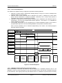
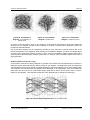
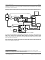
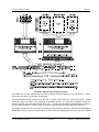
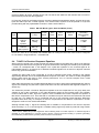
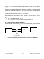
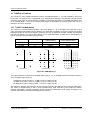
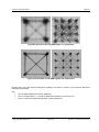
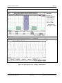
1
CMX7164 CML Microcircuits Multi Mode Modem COMMUNICATION SEMICONDUCTORS D/7164_FI-1.x/FI-2.x/FI-4.x/FI-6.x/22 May 2015 DATASHEET Provisional Issue 7164FI-1.x, 7164FI-2.x, 7164FI-4.x and 7164FI-6.x Multi Mode Modem Features Half-duplex modem supports multiple modulations and channel spacings 7164FI-1.x o o o o o o 7164FI-2.x o o o o o o o V.23 modulation Two frame sync detectors Automatic frame sync detect Rx carrier frequency correction Receive signal quality measurement High Performance I/Q Radio Analogue Interface o o o o o 4/16/64 QAM up to 96kbps in 25kHz Different rate, robust FEC choices Channel estimation and equalisation Two frame sync detectors Automatic frame sync detect Rx carrier frequency and phase correction Receive signal quality measurement 7164FI-6.x o o o o o 2/4/8/16-FSK up to 10ksymbols/s in 25kHz e.g. 40kbps for 16-FSK Compatible FEC for CMX7143 and FX/MX919B 4-FSK (not 2-FSK) Over-air compatibility with CMX969 for RD-LAP Tx/Rx Two frame sync detectors Automatic frame sync detect Rx carrier frequency correction Receive signal quality measurement Auxiliary Functions o o o o o o o o Master C-BUS/SPI Serial Interface o o Four 10-bit DACs Autonomous RAMDAC sequencer Automatic support for dc calibration of CMX998 Four 10-bit ADCs ADC averaging and trip on high/low ‘watch’ modes Four GPIO Sequence GPIO on Tx or Rx trigger Start Tx on digital trigger input For external slave devices e.g. RF transceiver and synthesiser Pass-through mode expands host C-BUS/SPI capacity Two Synthesised Clock Generators Low Power 3.3V Operation with Powersave Functions Small 64-pin VQFN and LQFP Packages 7164FI-4.x o o o o o o o GMSK/GFSK with BT=0.5, 0.3, 0.27 or 0.25 Over-air compatible with FX/MX909B and CMX7143FI-1.x Two frame sync detectors Automatic frame sync detect Rx carrier frequency correction Receive signal quality measurement Tx and Rx: ‘direct connect’ to zero IF transceiver Simple external RC filters Digital IF filter reconfigures for multiple RF channel spacings (Rx) Deviation control without manual trim (Tx) I/Q trims C-BUS host Serial Interface o SPI-like with register addressing o Read/Write 128-byte FIFOs and data buffers streamline transfers and relax host service latency 2015 CML Microsystems Plc Applications High Performance Narrowband Data Radio o o o o Telemetry/SCADA/data modems 6.25kHz to 25kHz RF channel spacing Compatible worldwide e.g. ETSI, FCC, ARIB, etc. FCC Part 90 per new spectral efficiency requirements Digital Software Defined Radio (SDR) High-speed Wireless Data Mobile Data over Fading Channels V.23 compatibility for interoperability with legacy equipment in the field CMX7164 Multi Mode Modem CMX7164 RF Rx RF Tx ADCs DACs Aux 4 x ADC Digital Filters FIFO Modem Digital Filters Configuration Modulate External Serial Devices Aux 2 x CLK Synth Aux 4 x DAC Registers Aux 4 x GPIO C-BUS/SPI master FEC CMX7164 C-BUS Host µC ModulationSpecific Function Image™ 3.3V 3.3V Multi Mode Modem 1 Brief Description The CMX7164 Multi Mode Modem is a half-duplex device currently supporting GMSK/GFSK, 4/16/64QAM, 2/4/8/16-Level FSK and V.23 modes in multiple channel spacings under host control. Its *Function Image (FI) is loaded to initialise the device and determine modulation types. The 7164FI-1.x supports GMSK/GFSK modulation, with BT=0.5, 0.3, 0.27, or 0.25. User-programmable filters are also possible (contact CML Technical Support for further information). The 7164FI-1.x supports up to 20kbps. Flexible bit rates support a wide range of applications requiring a selectable bit rate and robustness. The 7164FI-1.x supports zero IF (I/Q) and two-point modulation (Mod1/2) transmit modes, with zero IF receive mode. The GMSK/GFSK data is over-air compatible with the FX/MX909B and the CMX7143FI-1.x. The 7164FI-2.x supports 2-FSK, 4-FSK, 8-FSK, and 16-FSK modulations, root raised cosine filtered with =0.2 with optional sinc filtering. User-programmable filters are also possible (contact CML Technical Support for further information). The 7164FI-2.x supports up to 10ksymbols/s in a 25kHz channel. Flexible bit rates support a wide range of applications requiring a selectable bit rate and robustness. The 7164FI2.x supports zero IF (I/Q) and two-point modulation (Mod1/2) transmit modes, with zero IF receive mode. The data is over-air compatible with the FX/MX919B and the (CMX)7143FI-2.x. Additionally, 4-FSK coded mode also supports RD-LAP channel coding which is over-air compatible with CMX969. The 7164FI-4.x supports 4-, 16- and 64-QAM modulations, root raised cosine filtered with =0.2, 0.35 or a user programmable filter (contact CML Technical Support for further information). The 7164FI-4.x supports up to 96kbps in a 25kHz channel, with channel estimation and equalisation to provide robust performance under realistic channel conditions. The 7164FI-4.x supports zero IF (I/Q) transmit and receive. QAM data is over-air compatible with the CMX7163FI-4.x. The 7164FI-6.x supports V.23 modulation at 1200 baud to provide half-duplex modem functionality for interoperability with legacy equipment in the field. The 7164FI-6.x supports 1 to 8 byte data blocks with start bit, stop bit and parity generation in transmit and start bit, stop bit and parity checking and removal in receive. Within this Datasheet and the accompanying User Manual any reference to FI1-x, FI-2.x, FI-4.x or FI-6.x is intended to refer to 7164FI1.x, 7164FI-2.x, 7164FI-4.x or 7164FI-6.x respectively. Forward error correction and raw modes are available and support user-defined packet structures to support a range of applications. For greater flexibility, in FI-4.x only, different rate FEC modes are 2015 CML Microsystems Plc Page 2 D/7164_FI-1.x/FI-2.x/FI-4.x/FI-6.x/22 CMX7164 Multi Mode Modem CMX7164 provided. Receive signal quality measurement is supported, making a useful assessment of link conditions. High-performance digital IF filters may be reconfigured to support multiple channel spacings via host command. This feature may eliminate the need to switch between multiple discrete IF filters. An integrated analogue interface supports ‘direct connection’ to zero IF I/Q radio transceivers with few external components; no external codecs are required. Intelligent auxiliary ADC, DAC and GPIO sub-systems perform valuable functions and minimise host interaction and host I/O resources. Two synthesised system clock generators develop clock signals for offchip use. The C-BUS/SPI master interface expands host C-BUS/SPI ports to control external devices. *Function Image™. The device utilises CML’s proprietary FirmASIC component technology. On-chip sub-systems are configured by a Function Image™ data file that is uploaded during device initialisation and defines the device's function and feature set. The Function Image™ can be loaded automatically from a host µC over the C-BUS serial interface or from an external memory device. The device's functions and features can be enhanced by subsequent Function Image™ releases, facilitating in-the-field upgrades. The CMX7164 operates from a 3.3V supply and includes selectable powersaving modes. It is available in 64-VQFN and 64-LQFP packages. Note that text shown in pale grey indicates features that will be supported in future versions of the device. This Data Sheet is the first part of a two-part document. 2015 CML Microsystems Plc Page 3 D/7164_FI-1.x/FI-2.x/FI-4.x/FI-6.x/22 CMX7164 Multi Mode Modem CMX7164 CONTENTS Section Page 1 Brief Description ...................................................................................................................... 2 1.1 History......................................................................................................................... 10 2 Block Diagrams...................................................................................................................... 13 3 Signal List............................................................................................................................... 16 4 PCB Layout Guidelines and Power Supply Decoupling .................................................... 19 5 External Components............................................................................................................ 20 5.1 Xtal Interface............................................................................................................... 20 5.2 C-BUS Interface.......................................................................................................... 20 5.3 I/Q Output Reconstruction Filter ................................................................................. 21 5.4 I/Q Input Antialias Filter .............................................................................................. 21 5.5 GPIO Pins ................................................................................................................... 21 6 General Description............................................................................................................... 22 6.1 CMX7164 Features..................................................................................................... 22 6.2 Signal Interfaces (I/Q Tx and Rx) ............................................................................... 23 6.3 Signal Interfaces (Two-point Tx and I/Q Rx) .............................................................. 24 7 Detailed Descriptions ............................................................................................................ 25 7.1 Xtal Frequency............................................................................................................ 25 7.2 Host Interface ............................................................................................................. 25 7.2.1 C-BUS Operation ................................................................................................. 25 7.3 Function Image™ Loading.......................................................................................... 28 7.3.1 FI Loading from Host Controller ........................................................................... 28 Streaming C-BUS may be used to load the Modem Command FIFO Word - $49 write register with the Function Image™, and the ..................................................................... 28 7.3.2 FI Loading from Serial Memory ............................................................................ 30 7.4 Device Control ............................................................................................................ 31 7.4.1 Normal Operation Overview ................................................................................. 31 7.4.2 Basic Tx and Rx Operation .................................................................................. 32 7.4.3 Device Configuration (Using the Programming Register) .................................... 33 7.4.4 Device Configuration (Using dedicated registers) ................................................ 34 7.4.5 Interrupt Operation ............................................................................................... 34 7.4.6 Signal Control ....................................................................................................... 34 7.4.7 Tx Mode ............................................................................................................... 35 7.4.8 Rx Mode ............................................................................................................... 37 7.4.9 Carrier Sense Mode ............................................................................................. 38 7.4.10 The Transmit Sequence ....................................................................................... 40 7.4.11 CMX998 DC Offset Calibration (I/Q Transmit Only) ............................................ 40 7.4.12 Other Modem Modes ........................................................................................... 43 7.4.13 Data Transfer ....................................................................................................... 48 7.4.14 Data Buffering ...................................................................................................... 50 7.4.15 Raw Data Transfer ............................................................................................... 51 7.4.16 Formatted Data Transfer ...................................................................................... 51 7.4.17 Pre-loading Commands ....................................................................................... 51 7.4.18 GPIO Pin Operation ............................................................................................. 51 2015 CML Microsystems Plc Page 4 D/7164_FI-1.x/FI-2.x/FI-4.x/FI-6.x/22 CMX7164 Multi Mode Modem CMX7164 7.4.19 Auxiliary ADC Operation ...................................................................................... 52 7.4.20 Auxiliary DAC/RAMDAC Operation ...................................................................... 52 7.4.21 SPI Thru-Port ....................................................................................................... 53 7.4.22 SPI/C-BUS AGC .................................................................................................. 54 7.5 Digital System Clock Generators ................................................................................ 56 7.5.1 Main Clock Operation........................................................................................... 57 7.5.2 System Clock Operation ...................................................................................... 58 7.6 Signal Level Optimisation ........................................................................................... 58 7.6.1 Transmit Path Levels And Ramping .................................................................... 59 7.6.2 Receive Path Levels............................................................................................. 59 7.7 C-BUS Register Summary.......................................................................................... 60 8 7164FI-1.x Features ............................................................................................................... 61 8.1 7164FI-1.x Modulation ................................................................................................ 61 8.2 7164FI-1.x Radio Interface ......................................................................................... 61 8.2.1 I/Q Transmit and I/Q Receive Interfaces.............................................................. 61 8.2.2 Two-point Modulation Transmit with I/Q Receive Interface ................................. 63 8.3 7164FI-1.x Formatted Data ........................................................................................ 64 8.4 7164FI-1.x Typical Transmit Performance ................................................................. 65 8.5 7164FI-1.x Typical Receive Performance .................................................................. 70 8.5.1 Signal-to-Noise and Co-channel Performance .................................................... 70 9 7164FI-2.x Features ............................................................................................................... 74 9.1 7164FI-2.x Modulation ................................................................................................ 74 9.2 7164FI-2.x Radio Interface ......................................................................................... 76 9.2.1 I/Q Transmit and I/Q Receive Interfaces.............................................................. 76 9.2.2 Two-point Modulation Transmit with I/Q Receive Interface ................................. 78 9.3 7164FI-2.x Formatted Data ........................................................................................ 79 9.4 7164FI-2.x Receiver Response Equaliser .................................................................. 83 9.5 7164FI-2.x Typical Transmit Performance ................................................................. 84 9.6 7164FI-2.x Typical Receive Performance .................................................................. 91 9.6.1 4-FSK ................................................................................................................... 91 9.6.2 8-FSK and 16-FSK ............................................................................................... 95 9.6.3 Receiver Dynamic Range .................................................................................... 99 9.6.4 Receiver Response Equaliser Performance ........................................................ 99 10 7164FI-4.x Features ............................................................................................................. 104 10.1 7164FI-4.x Modulation .............................................................................................. 104 10.2 7164FI-4.x Radio Interface ....................................................................................... 105 10.2.1 Control interfaces ............................................................................................... 105 10.3 7164FI-4.x Formatted Data ...................................................................................... 106 10.4 7164FI-4.x Receiver Response Equaliser ................................................................ 107 10.5 7164FI-4.x Typical Transmit Performance ............................................................... 109 10.6 7164FI-4.x Typical Receive Performance ................................................................ 114 10.6.1 Signal-to-Noise and Co-channel Performance .................................................. 114 10.6.2 Adjacent Channel Performance ......................................................................... 118 10.6.3 Receiver Dynamic Range .................................................................................. 119 10.6.4 Receiver Response Equaliser Performance ...................................................... 119 11 7164FI-6.x Features ............................................................................................................. 125 2015 CML Microsystems Plc Page 5 D/7164_FI-1.x/FI-2.x/FI-4.x/FI-6.x/22 CMX7164 Multi Mode Modem CMX7164 11.1 7164FI-6.x Modulation .............................................................................................. 125 11.2 7164FI-6.x Radio Interface ....................................................................................... 125 11.2.1 I/Q Transmit and I/Q Receive Interfaces............................................................ 125 11.3 7164FI-6.x Formatted Data ...................................................................................... 125 11.4 7164FI-6.x Typical Transmit Performance ............................................................... 125 11.5 7164FI-6.x Typical Receive Performance ................................................................ 128 11.5.1 Signal-to-Noise Performance ............................................................................. 128 11.5.2 Adjacent Channel Performance ......................................................................... 128 12 Performance Specification ................................................................................................. 130 12.1 Electrical Performance ............................................................................................. 130 12.1.1 Absolute Maximum Ratings ............................................................................... 130 12.1.2 Operating Limits ................................................................................................. 130 12.1.3 Operating Characteristics................................................................................... 131 12.1.4 7164FI-1.x Parametric Performance .................................................................. 136 12.1.5 7164FI-2.x Parametric Performance .................................................................. 138 12.1.6 7164FI-4.x Parametric Performance .................................................................. 140 12.1.7 7164FI-6.x Parametric Performance .................................................................. 142 12.2 C-BUS Timing ........................................................................................................... 144 12.3 Packaging ................................................................................................................. 145 Table Table 1 Table 2 Table 3 Table 4 Table 5 Table 6 Table 7 Table 8 Table 9 Page BOOTEN Pin States ......................................................................................................... 28 C-BUS Registers .............................................................................................................. 60 Formatted Block Types and Sizes (FI-1.x) ....................................................................... 65 Native Formatted Block Types, Sizes and Rates for 4-FSK (FI-2.x) ................................ 80 Native Formatted Block Types, Sizes and Rates for 8-FSK (FI-2.x) ................................ 80 Native Formatted Block Types, Sizes and Rates for 16-FSK (FI-2.x) .............................. 81 RD-LAP Block Types, Sizes and Rates (FI-2.x)............................................................... 83 Formatted Block Types, Sizes and Rates (FI-4.x) ......................................................... 106 ACR Rejection Performance .......................................................................................... 119 Figure Page Figure 1 Overall Block Diagram .................................................................................................... 13 Figure 2 FI-4.x Block Diagram – I/Q Tx and Rx ............................................................................ 14 Figure 3 FI-1.x / FI-2.x Block Diagram – I/Q Tx and Rx ................................................................ 14 Figure 4 FI-1.x / FI-2.x Block Diagram – two-point Tx with I/Q Rx ................................................ 14 Figure 5 FI-6.x Block Diagram - I/Q Tx and Rx ............................................................................. 15 Figure 6 FI-6.x Block Diagram - Two-point Tx with I/Q Rx ............................................................ 15 Figure 7 CMX7164 Power Supply and De-coupling ...................................................................... 19 Figure 8 Recommended External Components – Xtal Interface................................................... 20 Figure 9 Recommended External Components – C-BUS Interface.............................................. 20 Figure 10 Recommended External Components – I/Q Output Reconstruction Filter ................... 21 Figure 11 CMX7164 I/Q Tx, I/Q Rx ............................................................................................... 23 Figure 12 CMX7164 Two-point Tx, I/Q Rx .................................................................................... 24 Figure 13 Basic C-BUS Transactions ........................................................................................... 26 Figure 14 C-BUS Data Streaming Operation ................................................................................ 27 2015 CML Microsystems Plc Page 6 D/7164_FI-1.x/FI-2.x/FI-4.x/FI-6.x/22 CMX7164 Multi Mode Modem Figure 15 Figure 16 Figure 17 Figure 18 Figure 19 Figure 20 Figure 21 Figure 22 Figure 23 Figure 24 Figure 25 Figure 26 Figure 27 Figure 28 Figure 29 Figure 30 Figure 31 Figure 32 Figure 33 Figure 34 Figure 35 Figure 36 Figure 37 Figure 38 Figure 39 Figure 40 Figure 41 Figure 42 Figure 43 Figure 44 Figure 45 Figure 46 Figure 47 Figure 48 Figure 49 Figure 50 Figure 51 Figure 52 Figure 53 Figure 54 Figure 55 Figure 56 Figure 57 Figure 58 Figure 59 Figure 60 Figure 61 Figure 62 CMX7164 FI Loading from Host .................................................................................................... 29 FI Loading from Serial Memory..................................................................................... 30 Host Tx Data Flow (No Tx Sequence/Carrier Sense) ................................................... 36 Host Rx Data Flow ........................................................................................................ 37 Carrier Sense ................................................................................................................ 39 Transmit Sequence ....................................................................................................... 40 CMX998 DC Calibration Interfaces ............................................................................... 41 Transmit Constellation (7164FI-4.x).............................................................................. 43 Transmit Eye Diagram (7164FI-2.x).............................................................................. 43 Transmit Eye Diagram (7164FI-1.x).............................................................................. 43 Constellation Diagram – no frequency or phase error .................................................. 44 Constellation Diagram – phase error ............................................................................ 44 Constellation Diagram – frequency error ...................................................................... 44 Received Eye Diagram7164 FI-2.x (4-FSK mode) ....................................................... 44 Received Eye Diagram7164 FI-1.x ............................................................................... 45 Sample at Symbol Timing with I/Q DC Offset Diagnostic Mode (no frequency error) .. 45 Sample at Symbol Timing with I/Q DC Offset Diagnostic Mode (with frequency error) 45 Normalised Constellation (even with a frequency or phase error) ................................ 46 Normalised Constellation (noisy received signal) ......................................................... 46 Channel Filtered I/Q Signals ......................................................................................... 46 Channel Filtered I/Q Signals with I/Q DC Offset Estimate ............................................ 46 Received Signal (First FM Demodulator) 7164FI-6.x.................................................... 47 Received Signal (Second FM Demodulator) 7164FI-6.x .............................................. 48 Command and Rx Data FIFOs ..................................................................................... 49 AGC using SPI Thru-Port .............................................................................................. 54 AGC using SPI Thru-Port and external LNA ................................................................. 55 AGC Behaviour During Burst Reception ....................................................................... 56 Main Clock Generation ................................................................................................. 57 Digital System Clock Generation Schemes .................................................................. 58 Outline Radio Design (I/Q in/out for GMSK/GFSK) ...................................................... 62 Outline Radio Design (GMSK/GFSK – I/Q in, two-point mod out) ................................ 63 Formatted Data Over Air Signal Format ....................................................................... 64 Tx Spectrum and Modulation Measurement Configuration for I/Q Operation............... 65 Tx Modulation Spectra (GMSK), 9.6kbps (BT=0.5), I/Q Modulation ............................. 66 Tx Modulation Spectra (GMSK), 8kbps, BT=0.3 I/Q Modulation ................................. 67 Tx Spectrum and Modulation Measurement Configuration for Two-point Modulation .. 68 Tx Modulation Spectra (GMSK), 8kbps, BT=0.3 Two-point Modulation ....................... 69 Modem Sensitivity Performance ................................................................................... 71 Sensitivity: 12.5kHz Channel, 8ksymbols/s With and Without Coding ......................... 72 Modem Co-channel Rejection with FM Interferer (as EN 300 113) .............................. 73 PRBS Waveform (Two-point Modulation) ..................................................................... 76 Outline Radio Design (I/Q in/out for 2 or 4-FSK) .......................................................... 77 Outline Radio Design (2 or 4-FSK – I/Q in, two-point mod out) .................................... 78 Native Formatted Data Over Air Signal Format ............................................................ 79 Suggested Frame Structures ........................................................................................ 80 RD-LAP Over Air Signal Format ................................................................................... 82 Tx Spectrum and Modulation Measurement Configuration for I/Q Operation............... 84 Tx Modulation Spectra (4-FSK), 9.6ksymbols/s (19.2kbps), I/Q Modulation ................ 85 2015 CML Microsystems Plc Page 7 D/7164_FI-1.x/FI-2.x/FI-4.x/FI-6.x/22 CMX7164 Multi Mode Modem CMX7164 Figure 63 Tx Modulation Spectra (2-FSK), 9.6k symbols/s (9.6kbps), I/Q Modulation ................. 86 Figure 64 Tx Modulation Spectra (8-FSK), 9.6k symbols/s (28.8kbps), I/Q Modulation ............... 87 Figure 65 Tx Modulation Spectra (16-FSK), 9.6k symbols/s (38.4kbps), I/Q Modulation ............. 88 Figure 66 Tx Spectrum and Modulation Measurement Configuration for Two-point Modulation .. 89 Figure 67 Tx Modulation Spectra (4-FSK), 19.2kbps, Two-point Modulation ............................... 90 Figure 68 Modem Sensitivity Performance (Root Raised Cosine Pulse Shaping) ........................ 92 Figure 69 12.5kHz Channel Sensitivity With and Without Sinc Filter Comparison ....................... 93 Figure 70 Sensitivity: 12.5kHz Channel, 4.8ksymbols/s With and Without Coding ...................... 93 Figure 71 Modem Co-channel Rejection with FM Interferer (as EN 300 113) .............................. 94 Figure 72 ACR Rejection Performance ......................................................................................... 95 Figure 73 Signal to Noise Performance – Comparison of uncoded (raw) 4-FSK, 8-FSK and 16FSK ................................................................................................................................................ 96 Figure 74 8-FSK and 16-FSK Coding Performance in Static Channel ......................................... 97 Figure 75 8-FSK Coding Performance in TU50 Fading Channel, 150MHz .................................. 98 Figure 76 8-FSK and 16-FSK Co-channel Rejection with FM Interferer (as EN 300 113) ............ 98 Figure 77 8-FSK and 16-FSK Block Error Rate, Block Size 0, High Rate Code, 12 Byte Blocks of Data in Uncoded Mode................................................................................................................... 99 Figure 78 4-FSK Signal-to-Noise Performance, Equalised and Non-Equalised ......................... 100 Figure 79 8-FSK Signal-to-Noise Performance, Equalised and Non-Equalised ......................... 101 Figure 80 16-FSK Signal-to-Noise Performance, Equalised and Non-Equalised ....................... 102 Figure 81 Performance of Equalised Signals with Temperature Variation ................................. 103 Figure 82 QAM Mappings ........................................................................................................... 104 Figure 83 Outline Radio Design (I/Q in/out for QAM) .................................................................. 105 Figure 84 Suggested Frame Structures ...................................................................................... 106 Figure 85 Received 4 and 16-QAM signals, no equalisation ...................................................... 108 Figure 86 Received 4 and 16-QAM signals with equalisation ..................................................... 108 Figure 87 Tx Spectrum and Modulation Measurement Configuration for I/Q Operation............. 109 Figure 88 Tx Modulation Spectra (4-QAM), 18ksymbols/s I/Q Modulation into CMX998 ........... 110 Figure 89 Tx Modulation Spectra (16-QAM), 18ksymbols/s I/Q Modulation into CMX998 ......... 111 Figure 90 Tx Modulation Spectra (64-QAM), 18ksymbols/s I/Q Modulation into CMX998 ......... 112 Figure 91 Tx Modulation Spectra (16-QAM), 9ksymbols/s I/Q Modulation into CMX998 ........... 113 Figure 92 Modem Sensitivity Performance ................................................................................. 114 Figure 93 Modem Co-channel Rejection with FM Interferer (as EN 300 113) ............................ 115 Figure 94 4-QAM Performance with Different Coding Schemes ................................................ 115 Figure 95 16-QAM Performance with Different Coding Schemes .............................................. 116 Figure 96 64-QAM Performance with Different Coding Schemes .............................................. 116 Figure 97 Comparison of BER and PER for 4-QAM Modulation................................................. 117 Figure 98 Comparison of BER and PER for 16-QAM Modulation............................................... 118 Figure 99 Comparison of BER and PER for 64-QAM Modulation............................................... 118 Figure 100 4-QAM Signal-to-Noise Performance, Equalised and Non-Equalised ...................... 120 Figure 101 16-QAM Signal-to Noise Performance, Equalised and Non-Equalised .................... 120 Figure 102 64-QAM Signal-to-Noise Performance, Equalised.................................................... 121 Figure 103 Performance of 16-QAM Equalised Signals with Temperature Variation ................. 122 Figure 104 Performance of 64-QAM Equalised Signals with Temperature Variation ................. 123 Figure 105 Performance of 16-QAM Equalised Signals with Temperature Variation and Constant Signal-to-Noise Ratio ................................................................................................................... 123 Figure 106 Performance of 64-QAM Equalised Signals with Temperature Variation and Constant Signal-to-Noise Ratio ................................................................................................................... 124 2015 CML Microsystems Plc Page 8 D/7164_FI-1.x/FI-2.x/FI-4.x/FI-6.x/22 CMX7164 Multi Mode Modem Figure 107 Figure 108 Figure 109 Figure 110 Figure 111 Figure 112 Figure 113 CMX7164 Tx Spectrum and Modulation Measurement Configuration for I/Q Operation........... 125 Tx Modulation V.23, 1200bps, I/Q Modulation .......................................................... 126 Tx Modulation V.23, 1200bps, I/Q Modulation .......................................................... 127 Signal Level vs BER .................................................................................................. 128 C-BUS Timing ........................................................................................................... 144 Mechanical Outline of 64-pin VQFN (Q1) ................................................................. 145 Mechanical Outline of 64-pin LQFP (L9) ................................................................... 145 Information in this datasheet should not be relied upon for final product design. It is always recommended that you check for the latest product datasheet version from the CML website: [www.cmlmicro.com]. 2015 CML Microsystems Plc Page 9 D/7164_FI-1.x/FI-2.x/FI-4.x/FI-6.x/22 CMX7164 Multi Mode Modem 1.1 History Version 22 Changes 21 20 19 18 CMX7164 Added information covering 7164FI-6.x Section 7.4.22: AGC control algorithm can now be used to control a second device using one of the available GPIO pins. Section 10.1 Updated Figure 82 (QAM Mappings) Section 12.2: Original C-BUS timing diagram replaced by latest version Section 13.1.22:Register $B3 – changed reserved bit 9 set value and added example settings Section 13.1.31: description for register $77: b11-0 description corrected to describe RSSI averaging period set by P4.3 Section 13.2.6 (Prog Block 4 – Modulation Control): P4.5 entry corrected to indicate that the parameter also supports FI-1.x Section 13.2.6: Added description for P4.3 Section 13.2.7: Transmit sequence – added description for minimum pulse period on GPIOA to trigger transmission and corrected the explanation of DC Calibration Sequence delays for default values Descriptions for registers $5D, $5E, $5F, $60, $61, $65 – added note regarding delay between successive writes Section 13.2.9: Added Program Block 7.17 for AGC control of external device via GPIO pins. Section 15.10: App Note updated for clarification Section 12: Performance figures replace TBDs Section 13.1.22: $B3 register table corrected and note added describing correct settings for the I/Q output drivers Section 13.2.2: Table for P0.0, b11-0 corrected to show value of 1 as invalid Section 13.2.5: Table showing new program registers P3.3 to P3.6 and associated description Section 13.2.6: Summary table, and subsequent description, Program Block 4, P4.5 corrected to say that two of the values apply also to FI-1.x. Section 13.2.6: Summary table for Program Block 4, P4.8:b15-2 corrected to say “reserved, set to 1” Section 15.10: New Application Note - Aborting Rx and Restarting Frame Sync Search Miscellaneous typographical and editorial improvements Section 13.2.4: Clarification to description on frame sync detection and error tolerance. Section 13.2.6: Entries and descriptions for P4.8 to P4.10 which offer additional control Added 16-FSK operation Section 11: Performance figures replace TBDs Section 12.2.4: Entire section rewritten to improve clarity Described the state of GPIO pins after reset and before a Function Image is loaded Added voltage differential between power supplies to section 11 specification Added description of RAMDAC ramp profile scaling Added description of modulation envelope ramp control Added control method for narrower channel filter options in FI-1.x Added information on 8/16 FSK, channel coding Figure 5 replaced by new drawing showing removal of unused components Miscellaneous typographical and editorial improvements 2015 CML Microsystems Plc Page 10 Date (D/M/Y) 11/05/15 02/09/14 19/06/14 12/05/14 12/02/14 D/7164_FI-1.x/FI-2.x/FI-4.x/FI-6.x/22 CMX7164 Multi Mode Modem CMX7164 16/17 Update of graphs to improve datasheet clarity in v14. Datasheet becomes v16. 21/10/13 14/15 Added details of FI-2 Equaliser operation Added programming register control for I/Q dc offset acquisition Added corrections to framesync programming register description Added power connection to pin 37 in Figure 7 Enhancements for custom filter support Added payload byte lengths to Tables 3, 4, 5 and 6 Document formatting corrected and typos/clarifications Added RD-LAP channel coding block types in FI-2.x Clarification of FI-1.x channel coding Add 8-FSK and 16-FSK operation in FI-2.x 01/08/13 11/12/ 13 10 9 Add GMSK/GFSK operation in FI-1.x 30/4/12 8 Added details of FI-4 Equaliser operation and control: Mode register, programming block Added details of programming block read mechanism (Available for selected programming registers only) Updated receive performance curves for FI-4 Added description of soft decision output bits for FI-2 only Added details of bus hold function for unused inputs Added details of Core regulator select Corrected conditions under which current measurements were made Changed reference to input impedance of I/Q INPUTs Typos/clarifications Remove constraint on use of document with FI-2.x, as the latter is now updated. Advice in section 5.5 greyed out as not implemented in current FI. Added advice about terminating unconnected GPIO pins in section 5.5 Added details of default and inverting gains to the description of the I/Q Output Control - $5D, $5E registers Pointed out correct use of handshaking when using signal control (Register $61) to select I and Q offset measurements (Registers $75 and $76) Clarified behaviour of the I and Q offset registers (Rx dc offset correction) when using automatic Rx IQ dc mode Clarified behaviour and scaling of RSSI measurements Documented further AGC controls added in FI-4.0.5.4, and described AGC operation in detail Documented the Pll On bit added to the mode register in FI-4.0.5.4, which provides a fast idle mode for programming register modifications without powersave, but with improved speed Added parameters in Program Block 1 to reduce delay when transitioning from Idle to Tx or Rx modes Added information about receive dynamic range Corrected and clarified scaling of Tx output fine control. 9/1/12 7 6 5 4 2015 CML Microsystems Plc Page 11 15/03/13 10/01/13 21/09/11 22/08/11 17/8/11 3/8/11 D/7164_FI-1.x/FI-2.x/FI-4.x/FI-6.x/22 CMX7164 Multi Mode Modem 3 2 1 CMX7164 Remove information indicating that a reset with no FI load is possible. See sections 11.1.1 Reset Operations, 7.3 Function image loading FIFO level interrupts to the host require re-arming using $50 FIFO control. See 11.1.4 FIFO Control $50 Include description for "I/Q Input dc correction loop gain". See 11.1.10 Signal control $61 Spectrum figure ACP mislabeled as for 25kHz when it is for 12.5kHz. See fig 58 Expand description of FI-2 4-FSK deviation configuration. See 11.1.10 Signal control $61 Include over-air symbol sequence for FI-2 (2-FSK and 4-FSK) and FI-4 data. See 7.4.15, 11.1.3 and 11.1.26. Specifically this matters for bit wise transfers, indicating which bits are valid Default values in 11.1.9 to be changed: $07FF becomes $0400; $0801 becomes $0C00 Addition of "Tx Done flag set on completion of DC Calibration" to 7.4.11, 11.1.18 and 11.1.36. Also indicate that AuxADC paths, etc in 7.4.11 are fixed permanently, by changing the description "assumed" to "required" Figure 34 to show "Main PLL out" sourced directly from the Xtal in Idle mode Update Figure 3 and correct minor typographical errors (Fig 43) Clarify text at the end of section 12.3.2 Change b11 to b9 in section 11.1.14 Remove FI Load Activation Block references and describe default states in section11.1.2 and Table 5 Clarify bit names in section 11.1.20, to avoid duplication Add missing action #20 in section 11.2.1 Original document, prepared for first alpha release of FI. 2015 CML Microsystems Plc Page 12 15/4/11 22/3/11 24/2/11 D/7164_FI-1.x/FI-2.x/FI-4.x/FI-6.x/22 CMX7164 Multi Mode Modem 2 CMX7164 Block Diagrams Transmit Functions Tx Data Buffer Data Modulator FI-1.x, FI-2.x & FI-6.x: I/Q or 2-point modulation FI-4.x: I/Q output Channel Coder (FI-1.x, FI-2.x & FI-4.x) IOUTPUTP IOUTPUTN QOUTPUTP QOUTPUTN Receive Functions Channel Filter IINPUTP IINPUTN Data Demodulator Channel Filter QINPUTP QINPUTN Channel Decoder (FI-1.x, FI-2.x & FI-4.x) Frame Sync Detect (FI-6.x) Rx Data Buffer Auxiliary Functions I Thresholds ADC 1 Q Averaging Thresholds ADC 2 IRQN Averaging Command FIFO MUX RDATA Thresholds ADC 3 AUXADC1 Averaging CSN Rx Data FIFO AUXADC2 CDATA Thresholds AUXADC3 ADC 4 Averaging AUXADC4 SCLK Registers Auxiliary Multiplexed ADCs C-BUS Interface GPIOA GPIOB GPIO with O/P Sequencer System Clock Div 1 SYSCLK1 System Clock Div 2 SYSCLK2 GPIOC GPIOD FI Configured I/O System Clock PLL AUXDAC1 DAC 1 AUXDAC2 DAC 2 Ramp-profile RAM XTAL/ CLOCK Crystal Oscillator Main Clock PLL XTALN System Clocks AUXDAC3 DAC 3 AUXDAC4 DAC 4 MOSI Power control Auxiliary DACs AGC Controller CLK MISO SPI Thru Port Flash Boot SSOUT0 Device Reset BOOTEN2 DVSS DACREF DVCORE DVDD3V3 AVSS AVDD RESETN Boot Control Reg. ADCREF Bias C-BUS/SPI Thru Control BOOTEN1 Host Thru Commands SSOUT2 VBIAS SSOUT1 Figure 1 Overall Block Diagram Figure 1 illustrates the overall functionality of the CMX7164, detailing the auxiliary functions. The following figures expand upon the transmit and receive functions. 2015 CML Microsystems Plc Page 13 D/7164_FI-1.x/FI-2.x/FI-4.x/FI-6.x/22 CMX7164 Multi Mode Modem CMX7164 Auto Frame Sync Detect RSSI Link Quality Detect RF Rx I Channel/Pulseshaping Filters I/Q Demod Q ADC Q Symbol De-Mapper (4-, 16- or 64-QAM) Raw Mode Data FIFO Buffer Coded Mode Data Channel Decoder: Error Correct/ Detect Coded Mode Data I DAC RF Tx I Symbol Mapper (4-, 16- or 64-QAM) Pulse-shaping Filters Q I/Q Mod Q DAC Buffer Construct Frame: Add Preamble, Framesync and Tails Channel Coder CDATA Registers I ADC RDATA CSN SCLK Host µC IRQN FIFO Raw Mode Data Figure 2 FI-4.x Block Diagram – I/Q Tx and Rx Auto Frame Sync Detect RSSI Link Quality Detect RF Rx I/Q Demod I Q ADC Pulse Shaping Filter Q I DAC RF Tx FM Demod Channel Filters I I/Q Mod Q FM Mod Pulse Shaping Filter Q DAC Symbol Mapper (2/4/8/16FSK) Symbol De-mapper (2/4/8/16FSK) Raw Mode Data Coded Mode Data Buffer FIFO Buffer Construct Frame: Add Preamble, Framesync and Tails Channel Decoder: Error Correct/ Detect Channel Coder CDATA Registers I ADC Coded Mode Data (4-FSK only) RDATA CSN SCLK Host µC IRQN FIFO Raw Mode Data Figure 3 FI-1.x / FI-2.x Block Diagram – I/Q Tx and Rx Auto Frame Sync Detect RSSI Link Quality Detect RF Rx I/Q Demod I Q ADC I DAC RF Tx FM Demod Channel Filters 2-Point Mod Q DAC Q Mod1 Mod2 Pulse Shaping Filter Pulse Shaping Filter Symbol Mapper (2/4/8/16FSK) Symbol De-mapper (2/4/8/16FSK) Raw Mode Data Coded Mode Data Buffer FIFO Buffer Construct Frame: Add Preamble, Framesync and Tails Channel Decoder: Error Correct/ Detect Channel Coder CDATA Registers I ADC Coded Mode Data (4-FSK only) RDATA CSN SCLK Host µC IRQN FIFO Raw Mode Data Figure 4 FI-1.x / FI-2.x Block Diagram – two-point Tx with I/Q Rx 2015 CML Microsystems Plc Page 14 D/7164_FI-1.x/FI-2.x/FI-4.x/FI-6.x/22 CMX7164 Multi Mode Modem CMX7164 Auto Frame Sync Detect RSSI Link Quality Detect I ADC I/Q Demod I 1st FM Demod Channel Filters Q ADC 2nd FM Demod Q Low Pass Filter Raw Mode Data FIFO Buffer Formatted Data CDATA Registers RF Rx Start, Stop & Parity Checking RDATA CSN SCLK Host µC IRQN Formatted Data I DAC RF Tx I/Q Mod I Q FM Mod V.23 Tone Generation Buffer Q DAC Construct Frame: Add Preamble, Framesync and Tails Start, Stop and Parity Insertion FIFO Raw Mode Data Figure 5 FI-6.x Block Diagram - I/Q Tx and Rx Auto Frame Sync Detect RSSI Link Quality Detect I ADC I/Q Demod I 1st FM Demod Channel Filters Q ADC Q 2nd FM Demod Low Pass Filter Raw Mode Data FIFO Buffer Formatted Data Start, Stop & Parity Checking Formatted Data I DAC RF Tx Mod1 V.23 Tone Generation 2-Point Mod Buffer Mod2 Q DAC Construct Frame: Add Preamble, Framesync and Tails Start, Stop & Parity Insertion CDATA Registers RF Rx RDATA CSN SCLK Host µC IRQN FIFO Raw Mode Data Figure 6 FI-6.x Block Diagram - Two-point Tx with I/Q Rx 2015 CML Microsystems Plc Page 15 D/7164_FI-1.x/FI-2.x/FI-4.x/FI-6.x/22 CMX7164 Multi Mode Modem 3 CMX7164 Signal List 64-pin Q1/L9 Pin Pin No. Description Name Type 1 GPIOB BI General Purpose I/O 2 BOOTEN1 IP+PU The combined state of BOOTEN1 and BOOTEN2, upon RESET, determine the Function Image™ load interface 3 BOOTEN2 IP+PU The combined state of BOOTEN1 and BOOTEN2, upon RESET, determine the Function Image™ load interface 4 DVSS PWR Negative supply rail (ground) for the digital on-chip circuits 5 DVDD 3V3 PWR 3.3V positive supply rail for the digital on-chip circuits. This pin should be decoupled to DVSS by capacitors mounted close to the supply pins. 6 SSOUT2 OP SPI: Slave Select Out 2 7 RESETN IP Logic input used to reset the device (active low) 8 GPIOC BI General Purpose I/O 9 GPIOD BI General Purpose I/O 10 DVSS PWR Negative supply rail (ground) for the digital on-chip circuits 11 NC NC Do not connect 12 AVDD PWR Positive 3.3V supply rail for the analogue on-chip circuit. Levels and thresholds within the device are proportional to this voltage. This pin should be decoupled to AVSS by capacitors mounted close to the device pins. 13 NC NC May also be connected to AVSS 14 NC NC Do not connect 15 NC NC Do not connect 16 NC NC May also be connected to AVDD 17 IOUTPUTP OP 18 IOUTPUTN OP Differential outputs for I channel; ‘P’ is positive, ‘N’ is negative. Together these are referred to as the I Output. When the 7164 FI-1 or FI-2 is in two-point modulation mode the I Output is used as ‘Mod 1’. 19 QOUTPUTP OP 20 QOUTPUTN OP 21 AVSS PWR 22 DACREF 23 NC NC Do not connect 24 NC NC Do not connect 25 NC NC Do not connect 2015 CML Microsystems Plc Differential outputs for Q channel; ‘P’ is positive, ‘N’ is negative. Together these are referred to as the Q Output. When the 7164 FI-1 or FI-2 is in two-point modulation mode the Q Output is used as ‘Mod 2’. Negative supply rail (ground) for the analogue on-chip circuits DAC reference voltage, connect to AVSS Page 16 D/7164_FI-1.x/FI-2.x/FI-4.x/FI-6.x/22 CMX7164 Multi Mode Modem 64-pin Q1/L9 Pin Pin No. 26 CMX7164 Description Name NC Type NC Do not connect Internally generated bias voltage of approximately AVDD/2. If VBIAS is powersaved this pin will be connected via a high impedance to AVDD. This pin must be decoupled to AVSS by a capacitor mounted close to the device pins. 27 VBIAS OP 28 IINPUTP IP 29 IINPUTN IP 30 ADCREF 31 QINPUTP IP 32 QINPUTN IP Differential inputs for Q channel signals; ‘P’ is positive, ‘N’ is negative. Together these are referred to as the Q Input. 33 AUXADC1 IP Auxiliary ADC input 1 34 AUXADC2 IP Auxiliary ADC input 2 35 AUXADC3 IP Auxiliary ADC input 3 36 AUXADC4 IP Auxiliary ADC input 4 Differential inputs for I channel signals; ‘P’ is positive, ‘N’ is negative. Together these are referred to as the I Input. ADC reference voltage; connect to AVSS 37 AVDD PWR Positive 3.3V supply rail for the analogue on-chip circuit. Levels and thresholds within the device are proportional to this voltage. This pin should be decoupled to AVSS by capacitors mounted close to the device pins. 38 AVSS PWR Negative supply rail (ground) for the analogue on-chip circuits 39 AUXDAC1 OP Auxiliary DAC output 1 (Optionally the RAMDAC output) 40 AUXDAC2 OP Auxiliary DAC output 2 41 AUXDAC3 OP Auxiliary DAC output 3 42 AUXDAC4 OP Auxiliary DAC output 4 43 DVSS PWR Negative supply rail (ground) for the digital on-chip circuits 44 DVCORE PWR Internally generated digital core voltage of approximately 1.8V. This pin should be decoupled to DVSS by capacitors mounted close to the device pins 45 DVDD3V3 PWR 3.3V positive supply rail for the digital on-chip circuits. This pin should be decoupled to DVSS by capacitors mounted close to the supply pins. 46 NC NC Do not connect 47 NC NC May also be connected to DVSS 48 DVSS PWR Negative supply rail (ground) for the digital on-chip circuits 49 XTALN OP Output of the on-chip Xtal oscillator inverter 50 XTAL/CLOCK IP Input to the oscillator inverter from the Xtal circuit or external clock source 51 SYSCLK1 OP Synthesised digital clock output 1 2015 CML Microsystems Plc Page 17 D/7164_FI-1.x/FI-2.x/FI-4.x/FI-6.x/22 CMX7164 Multi Mode Modem 64-pin Q1/L9 CMX7164 Pin Pin No. Description Name Type 52 SYSCLK2 OP Synthesised digital clock output 2 53 SCLK IP C-BUS serial clock input from the µC 54 RDATA TS OP 3-state C-BUS serial data output to the µC. This output is high impedance when not sending data to the µC. 55 CDATA IP C-BUS serial data input from the µC 56 CSN IP C-BUS chip select input from the µC 57 IRQN OP ‘wire-Orable’ output for connection to the Interrupt Request input of the µC. This output is pulled down to DVSS when active and is high impedance when inactive. An external pull-up resistor is required. 58 DVCORE PWR Internally generated digital core voltage of approximately 1.8V. This pin should be decoupled to DVSS by capacitors mounted close to the device pins 59 MOSI OP SPI: Master Out Slave In 60 SSOUT1 OP SPI: Slave Select Out 1 61 MISO IP SPI: Master In Slave Out 62 SSOUT0 OP SPI: Slave Select Out 0 63 CLK OP SPI: Serial Clock 64 GPIOA BI General Purpose I/O ~ On this device, the central metal pad (which is exposed on the Q1 package only) may be electrically unconnected or, alternatively, may be connected to Analogue ground (AVss). No other electrical connection is permitted. EXPOSED METAL PAD Notes: SUBSTRATE IP OP BI TS OP PWR NC = = = = = = 2015 CML Microsystems Plc Input (+ PU/PD = internal pull-up / pull-down resistor of approximately 75kΩ) Output Bidirectional 3-state Output Power Connection No Connection - should NOT be connected to any signal Page 18 D/7164_FI-1.x/FI-2.x/FI-4.x/FI-6.x/22 CMX7164 Multi Mode Modem 4 CMX7164 PCB Layout Guidelines and Power Supply Decoupling C20 C21 C22 C23 C24 C25 10µF 10nF 10nF 10µF 10nF 10nF C26 C27 C28 C31 22µF 10nF 10nF 100nF Figure 7 CMX7164 Power Supply and De-coupling Notes: To achieve good noise performance, AVDD and VBIAS decoupling and protection of the receive path from extraneous in-band signals is very important. It is recommended that the printed circuit board is laid out with a ground plane in the CMX7164 analogue area to provide a low impedance connection between the AVSS pins and the AVDD and VBIAS decoupling capacitors. 2015 CML Microsystems Plc Page 19 D/7164_FI-1.x/FI-2.x/FI-4.x/FI-6.x/22 CMX7164 Multi Mode Modem 5 CMX7164 External Components 5.1 Xtal Interface X1 C1 C2 For frequency range see 12.1.2 Operating Limits 22pF Typical 22pF Typical Figure 8 Recommended External Components – Xtal Interface Notes: The clock circuit can operate with either a Xtal or external clock generator. If using an external clock generator it should be connected to the XTAL/CLOCK pin and the xtal and other components are not required. For external clock generator frequency range see 12.1.2 Operating Limits. When using an external clock generator the Xtal oscillator circuit may be disabled to save power, see 13.2.3 Program Block 1 – Clock Control for details. Also refer to section 7.1 Xtal Frequency. The tracks between the Xtal and the device pins should be as short as possible to achieve maximum stability and best start up performance. It is also important to achieve a low impedance connection between the Xtal capacitors and the ground plane. The DVSS to the Xtal oscillator capacitors C1 and C2 should be of low impedance and preferably be part of the DVSS ground plane to ensure reliable start up. For correct values of capacitors C1 and C2 refer to the documentation of the Xtal used. 5.2 C-BUS Interface R2 10k - 100k Figure 9 Recommended External Components – C-BUS Interface Note: If the IRQN line is connected to other compatible pull-down devices only one pull-up resistor is required on the IRQN node. 2015 CML Microsystems Plc Page 20 D/7164_FI-1.x/FI-2.x/FI-4.x/FI-6.x/22 CMX7164 Multi Mode Modem 5.3 CMX7164 I/Q Output Reconstruction Filter The CMX7164 I/Q Outputs provide internal reconstruction filtering with four selectable bandwidths (-3dB point shown in section 13.1.22). The bandwidth of the internal reconstruction filter may be selected using the I/Q Output Configuration - $B3 write or Signal Control - $61 write registers. To complete the I/Q output reconstruction filter one of the following external RC networks should be used for each of the differential outputs. The external RC network should have a bandwidth that matches the bandwidth of the selected internal reconstruction filter. Bandwidth (kHz) 100 50 25 12.5 R3-R6 (kOhms) 22 20 22 22 C9-C10 (pF) 33 75 150 270 Figure 10 Recommended External Components – I/Q Output Reconstruction Filter When transmitting an I/Q signal, each I/Q output will produce a signal with bandwidth half the channel bandwidth. A reconstruction filter with a –3dB point close to half the channel bandwidth will therefore have significant roll off within the channel bandwidth – which is undesirable. An appropriate choice for channels occupying up to a 25kHz bandwidth (channel bandwidth/2 = 12.5kHz) would be a reconstruction filter of 25kHz bandwidth. 5.4 I/Q Input Antialias Filter The device has a programmable antialias filter in the I/Q input path, which is controlled using the I/Q Input Configuration - $B0 write or Signal Control - $61 write registers. This should be sufficient for most applications, however if additional filtering is required it can be done at the input to the device. The input impedance of the I/Q Input pins varies with the input gain setting, see section 12.1.3 Operating Characteristics. 5.5 GPIO Pins All GPIO pins are configured as inputs with an internal bus-hold circuit, after the Function Image™ has been loaded. This avoids the need for users to add external termination (pullup/pulldown) resistors onto these inputs. The bus-hold is equivalent to a 75kΩ resistor either pulling up to logic 1 or pulling down to logic 0. As the input is pulled to the opposite logic state by the user, the bus-hold resistor will change, so that it also pulls to the new logic state. The internal bus-hold can be disabled or re-enabled using programming register P1.20 in Program Block 1 – Clock Control. If the device is reset (either by asserting RESETN pin 7, issuing a C-BUS General RESET or by triggering an internal power on reset) all GPIO pins will be immediately configured as inputs. Any GPIO pins not TM being pulled either up or down by an external load will be left in a floating state until the Function Image is loaded. To avoid GPIO floating input states that may somewhat elevate supply current between a TM RESET and Function Image load, it will be necessary to connect pull up or pull down resistors of 220k to these pins. 2015 CML Microsystems Plc Page 21 D/7164_FI-1.x/FI-2.x/FI-4.x/FI-6.x/22 CMX7164 Multi Mode Modem 6 6.1 CMX7164 General Description CMX7164 Features The CMX7164 is intended for use in half-duplex modems. Transmission takes the form of a data burst consisting of preamble, frame sync and data payload, followed by a tail sequence. Reception may utilise the preamble to assist with signal acquisition1, but is then followed by frame sync detection and data decoding. A flexible power control facility allows the device to be placed in its optimum powersave mode when not actively processing signals. The device includes a Xtal clock generator, with phase locked loop and buffered output, to provide a System Clock output, if required, for other devices. Block diagrams of the device are shown in section 2, Block Diagrams. Tx Functions: Automatic preamble and frame sync insertion simplifies host control I/Q analogue outputs (7164FI-4), I/Q or two-point modulation analogue outputs (7164 FI-1 or FI-2) Pulse shape filtering RAMDAC capability for PA ramping control Tx trigger feature allowing precise control of burst start time Tx burst sequence for automatic RAMDAC ramp and Tx hardware switching Carrier sense for “listen before talk” operation Raw and formatted (channel coded) data modes Flexible Tx coded data block size, up to: 416 bytes (7164FI-4), 12 bytes (7164FI-2 4-FSK), 48 bytes (7164FI-2 8/16-FSK), 18 bytes (7164FI-1) Rx Functions: Automatic frame sync detection simplifies host control I/Q analogue inputs Rx channel filtering and pulse shape filtering Channel estimation and equalisation Tracking of symbol timing and input I/Q dc offsets AGC using SPI Thru-Port Raw and formatted (channel coded) data modes Flexible Rx coded data block size, up to: 416 bytes (7164FI-4), 12 bytes (7164FI-2 4-FSK), 48 bytes (7164FI-2 8/16-FSK), 18 bytes (7164FI-1). Auxiliary Functions: Two programmable system clock outputs Four auxiliary ADCs with six selectable input paths SPI Thru-Port for interfacing to synthesisers, Cartesian loop IC (CMX998), direct conversion receiver (CMX994) and other serially controllable devices In-build calibration routine to support CMX998 Cartesian loop transmitter IC Four auxiliary DACs, one with built-in programmable RAMDAC 1 The frame sync detection algorithm of the CMX7164 is capable of detecting a frame sync without having bit synchronisation, so preamble is not required for obtaining bit sync. Some preamble is still needed to ensure that the beginning of the frame sync is transmitted and received without distortion. Preamble may also be used to provide a known signal on which to acquire I/Q dc offset corrections. 2015 CML Microsystems Plc Page 22 D/7164_FI-1.x/FI-2.x/FI-4.x/FI-6.x/22 CMX7164 Multi Mode Modem CMX7164 Interface: Optimised C-BUS (4-wire, high speed synchronous serial command/data bus) interface to host for control and data transfer, including streaming C-BUS for efficient data transfer Open drain IRQ to host Four GPIO pins Tx trigger input (Provided by GPIOA) Serial memory or C-BUS (host) boot mode Both transmit and receive data can be raw or coded data blocks. FI-4.x provides a variety of coding rates for flexibility and very large block sizes having the potential to improve performance in fading conditions considerably. FI-2.x provides coding compatible with CMX7143FI-2.x. . FI-1.x provides coding compatible with CMX7143FI-1.x. 6.2 Signal Interfaces (I/Q Tx and Rx) FI-4.x produces QAM modulation. The transmitted signal is provided as an I/Q baseband, for mixing up onto an RF carrier, with amplification. For reception an I/Q baseband signal should be interfaced into the 7164FI-4.x. 7164FI-2.x produces 2-FSK, 4-FSK, 8-FSK, and 16-FSK modulation and can be configured to produce I/Q modulation, in which case the signal interfaces are the same as for FI-4.x. 7164FI-1.x produces GMSK/GFSK modulation and can also be configured to produce I/Q modulation, in which case the signal interfaces are the same as for FI-4.x. In receive, the I/Q interface provides amplitude information, so the RSSI signal is calculated internally. It is averaged in order to produce the RSSI measurement and to support the carrier sense decision whether to transmit. CMX7164 IINPUT T/R Receive Processing Radio Receiver QINPUT Transmit Processing IOUTPUT QOUTPUT Mix onto RF carrier and linearise if required Figure 11 CMX7164 I/Q Tx, I/Q Rx 2015 CML Microsystems Plc Page 23 D/7164_FI-1.x/FI-2.x/FI-4.x/FI-6.x/22 CMX7164 Multi Mode Modem 6.3 CMX7164 Signal Interfaces (Two-point Tx and I/Q Rx) FI-2.x produces 4-FSK modulation and can be configured to produce two-point modulation. FI-1.x produces GMSK/GFSK modulation and can also be configured to produce two-point modulation. This option is not applicable for FI-4.x. The I/Q interface is the only option available for receive. CMX7164 IINPUT T/R Receive Processing Radio Receiver QINPUT Transmit Processing IOUTPUT (MOD1) Reference (e.g VCTCXO) PLL VCO QOUTPUT (MOD2) Control Voltage Input Figure 12 CMX7164 Two-point Tx, I/Q Rx 2015 CML Microsystems Plc Page 24 D/7164_FI-1.x/FI-2.x/FI-4.x/FI-6.x/22 CMX7164 Multi Mode Modem 7 7.1 CMX7164 Detailed Descriptions Xtal Frequency The CMX7164 is designed to work with a Xtal, or an external frequency oscillator within the ranges specified in section 12.1.3 Operating Characteristics. Program Block 1 (see User Manual) must be loaded with the correct values to ensure that the device will work to specification with the user selected clock frequency. A table of configuration values can be found in Table 23 supporting baud rates up to 20ksymbols/s when the Xtal frequency is 9.6MHz or the external oscillator frequency is 9.6 or 19.2 MHz. Rates other than those tabulated (within this range) are possible, see section 13.2.3 Program Block 1 – Clock Control. Further information can be provided on request. The modem can operate with a clock or Xtal input frequency tolerance of 50ppm. The receive performance will be compromised as the system tracks, so a maximum tolerance of 20ppm is recommended. 7.2 Host Interface A serial data interface (C-BUS) is used for command, status and data transfers between the CMX7164 and the host µC; this interface is compatible with Microwire™, SPI™ and other similar interfaces. Interrupt signals notify the host µC when a change in status has occurred; the µC should read the IRQ Status register across the C-BUS and respond accordingly. Interrupts only occur if the appropriate mask bit has been set, see Interrupt Operation. 7.2.1 C-BUS Operation This block provides for the transfer of data and control or status information between the CMX7164 internal registers and the host µC over the C-BUS serial bus. Single register transactions consist of a single register address byte sent from the µC, which may be followed by a data word sent from the µC to be written into one of the CMX7164’s write-only registers, or a data word read out from one of the CMX7164’s read-only registers. Streaming C-BUS transactions consist of a single register address byte followed by many data bytes being written to or read from the CMX7164. All C-BUS data words are a multiple of 8 bits wide, the width depending on the source or destination register. Note that certain C-BUS transactions require only an address byte to be sent from the µC, no data transfer being required. The operation of the C-BUS is illustrated in Figure 13. Data sent from the µC on the CDATA (command data) line is clocked into the CMX7164 on the rising edge of the SCLK input. Data sent from the CMX7164 to the µC on the RDATA (reply data) line is valid when SCLK is high. The CSN line must be held low during a data transfer and kept high between transfers. The C-BUS interface is compatible with most common µC serial interfaces and may also be easily implemented with general purpose µC I/O pins controlled by a simple software routine. Section 12.2 C-BUS Timing gives detailed C-BUS timing requirements. Note that, due to internal timing constraints, there may be a delay of up to 60µs between the end of a C-BUS write operation and the device reading the data from its internal register. 2015 CML Microsystems Plc Page 25 D/7164_FI-1.x/FI-2.x/FI-4.x/FI-6.x/22 CMX7164 Multi Mode Modem CMX7164 C-BUS single byte command (no data) CSN Note: The SCLK line may be high or low at the start and end of each transaction. SCLK CDATA 7 6 5 MSB RDATA 4 3 2 Address 1 4 3 2 Address 1 4 3 2 Address 1 0 LSB Hi-Z C-BUS n-bit register write CSN SCLK CDATA 7 6 5 MSB RDATA 0 LSB n-1 n-2 n-3 2 Write data 1 n-1 n-2 n-3 2 Read data 1 MSB 0 LSB Hi-Z C-BUS n-bit register read CSN SCLK CDATA 7 6 5 MSB RDATA 0 LSB Hi-Z MSB 0 LSB Data value unimportant Repeated cycles Either logic level valid (and may change) Either logic level valid (but must not change from low to high) Figure 13 Basic C-BUS Transactions 2015 CML Microsystems Plc Page 26 D/7164_FI-1.x/FI-2.x/FI-4.x/FI-6.x/22 CMX7164 Multi Mode Modem CMX7164 To increase the data bandwidth between the µC and the CMX7164, certain of the C-BUS read and write registers are capable of data-streaming operation. This allows a single address byte to be followed by the transfer of multiple read or write data words, all within the same C-BUS transaction. This can significantly increase the transfer rate of large data blocks, as shown in Figure 14. Example of C-BUS data-streaming (8-bit write register) CSN SCLK CDATA RDATA 7 6 5 4 3 2 1 0 7 6 5 4 3 2 1 0 7 6 5 4 3 2 1 0 Address First byte Second byte … 7 6 5 4 3 2 1 0 Last byte … 7 6 5 4 3 2 1 0 Last byte Hi-Z Example of C-BUS data-streaming (8-bit read register) CSN SCLK CDATA RDATA 7 6 5 4 3 2 1 0 Address 7 6 5 4 3 2 1 0 7 6 5 4 3 2 1 0 First byte Second byte Hi-Z Data value unimportant Repeated cycles Either logic level valid (and may change) Either logic level valid (but must not change from low to high) Figure 14 C-BUS Data Streaming Operation Notes: 1. For Command byte transfers only the first 8 bits are transferred ($01 = Reset) 2. For single byte data transfers only the first 8 bits of the data are transferred 3. The CDATA and RDATA lines are never active at the same time. The address byte determines the data direction for each C-BUS transfer. 4. The SCLK can be high or low at the start and end of each C-BUS transaction 5. The gaps shown between each byte on the CDATA and RDATA lines in the above diagram are optional, the host may insert gaps or concatenate the data as required. 2015 CML Microsystems Plc Page 27 D/7164_FI-1.x/FI-2.x/FI-4.x/FI-6.x/22 CMX7164 Multi Mode Modem 7.3 CMX7164 Function Image™ Loading The Function Image™ (FI), which defines the operational capabilities of the device, may be obtained from the CML Technical Portal, following registration and authorisation. This is in the form of a 'C' header file which can be included into the host controller software or programmed into an external serial memory. The TM Function Image size can never exceed 128 kbytes, although a typical FI will be considerably less than this. Note that the BOOTEN1/2 pins are only read at power-on, when the RESETN pin goes high, or following a C-BUS General Reset, and must remain stable throughout the FI loading process. Once the FI load has completed, the BOOTEN1/2 pins are ignored by the CMX7164 until the next power-up or Reset. The BOOTEN1/2 pins are both fitted with internal low current pull-up devices. For serial memory load operation, BOOTEN2 should be pulled low by connecting it to DVss either directly or via a 47k resistor (see Table 1). Whilst booting, the boot loader will return the checksum of each block loaded in the C-BUS Rx Data FIFO. The checksums can be verified against the values provided with the FI to ensure that the FI has loaded correctly. Once the FI has been loaded, the CMX7164 performs these actions: (1) The product identification code ($7164) is reported in the C-BUS Rx Data FIFO (2) The FI version code is reported in C-BUS Rx Data FIFO. Table 1 BOOTEN Pin States C-BUS host load reserved Serial Memory load reserved BOOTEN2 1 1 0 0 BOOTEN1 1 0 1 0 7.3.1 FI Loading from Host Controller The FI can be included into the host controller software build and downloaded into the CMX7164 at powerup over the C-BUS interface, using the Command FIFO. For Function Image™ load, the FIFO accepts raw 16-bit Function Image™ data (using the Modem Command FIFO Word) - $49 write register, there is no need for distinction between control and data fields. The BOOTEN1/2 pins must be set to the C-BUS load configuration, the CMX7164 powered or Reset, and then data can then be sent directly over the C-BUS to the CMX7164. If the host detects a brownout, the BOOTEN1/2 pins should be set to re-load the FI. A General Reset should then be issued or the RESETN pin used to reset the CMX7164 and the appropriate FI load procedure followed. Streaming C-BUS may be used to load the Modem Command FIFO Word - $49 write register with the Function Image™, and the Modem Command FIFO Level - $4B read register used to ensure that the FIFO is not allowed to overflow during the load process. The download time is limited by the clock frequency of the C-BUS; with a 5MHz SCLK it should take less than 250ms to complete even when loading the largest possible Function Image™. 2015 CML Microsystems Plc Page 28 D/7164_FI-1.x/FI-2.x/FI-4.x/FI-6.x/22 CMX7164 Multi Mode Modem CMX7164 BOOTEN2 = 1 BOOTEN1 = 1 Power-up or write General Reset to CMX7164 Read the RxFIFO Level - $4F until 3 device check words appear in RxFIFO Word - $4D. Read and discard them Block number N =1 BOOTEN1 and BOOTEN2 may be changed once it is clear that the CMX7164 has comitted to C-BUS boot – i.e. when a word has been read from the C-BUS command FIFO Write Block 1 Length (DBN_len) to CmdFIFO Word - $49 Write Start Block N Address (DBN_ptr) to CmdFIFO Word - $49 Check CmdFIFO Level - $4B Write up to “128-FIFO fill level” words to CmdFIFO Word - $49 End of Block? No Yes Read and verify 32-bit checksum words from RxFIFO Word - $4D N = N+1 Is the next block the Activation Block? No – load next block Yes Write Start Block N Length (ACTIVATE_len) to CmdFIFO Word - $49 Write Start Block N Address (ACTIVATE_ptr) to CmdFIFO Word - $49 Poll Status -$7E until Reg Done b14 = 1 (PRG Flag is unmasked in Reg Done Select register - $69 by default and indicates when the FI is loaded) VDD Read the Product ID Code and the FI version code from the RxFIFO Word -$4D BOOTEN1 BOOTEN2 CMX7164 is now ready for use Figure 15 FI Loading from Host 2015 CML Microsystems Plc Page 29 D/7164_FI-1.x/FI-2.x/FI-4.x/FI-6.x/22 CMX7164 Multi Mode Modem CMX7164 7.3.2 FI Loading from Serial Memory The FI must be converted into a format for the serial memory programmer (normally Intel Hex) and loaded into the serial memory either by the host or an external programmer. The serial memory should contain the same data stream as written to the Command FIFO shown in Figure 15. The most significant byte of each 16-bit word should be stored first in serial memory. The serial memory should be interfaced to the CMX7164 SPI Thru-Port using SSOUT0 as the chip select. The CMX7164 needs to have the BOOTEN pins set to Serial Memory Load, and then on power-on, following the RESETN pin becoming high, or following a C-BUS General Reset, the CMX7164 will automatically load the data from the serial memory without intervention from the host controller. BOOTEN2 = 0 BOOTEN1 = 1 Power-up or write General Reset to CMX7164 Poll Status -$7E until Reg Done b14 = 1 (PRG Flag is unmasked in Reg Done Select register $69 by default and indicates when the FI is loaded ) Read and discard 3 device check words from the RxFIFO Word - $4D. BOOTEN1 and BOOTEN2 may be changed from this point on, if required VDD Read and verify the 32-bit checksum word of each block loaded – found in the RxFIFO Word - $4D Read the Product ID code and the FI version code from the RxFIFO Word - $4D CMX7164 is now ready for use BOOTEN1 BOOTEN2 Jumper for programming serial memory (if required) Figure 16 FI Loading from Serial Memory The CMX7164 has been designed to function with the AT25F512 serial flash device, however other manufacturers' parts may also be suitable. The time taken to load the FI should be less than 500ms even when loading the largest possible Function Image™. 2015 CML Microsystems Plc Page 30 D/7164_FI-1.x/FI-2.x/FI-4.x/FI-6.x/22 CMX7164 Multi Mode Modem 7.4 CMX7164 Device Control Once the Function Image™ is loaded, the CMX7164 can be set into one of four main modes using the Modem Mode and Control - $6B write register: Idle mode – for configuration or low power operation Transmit mode – for transmission of raw or formatted data Receive mode – for detection and reception of bursts containing raw or formatted data Carrier sense mode – for attempting to transmit if the channel is free, otherwise continuing to receive. These four modes are described in the following sections. All control is carried out over the C-BUS interface: either directly to operational registers in transmit, receive and carrier sense modes or, for parameters that are not likely to change during operation, using the Programming Register - $6A write in Idle mode. To conserve power when the device is not actively processing a signal, place the device into Idle mode. Additional power-saving can be achieved by disabling unused hardware blocks, however, most of the hardware power-saving is automatic. Note that VBIAS must be enabled to allow any of the Input or Output blocks to function. It is only possible to write to the Programming register whilst in Idle mode. See: 13.1.17 Programming Register - $6A write 13.1.18 Modem Mode and Control - $6B write 13.2 Programming Register Operation 13.1.24 VBIAS Control - $B7 write. 7.4.1 Normal Operation Overview In normal operation (after the CMX7164 is configured) the appropriate mode must be selected and data provided in transmit or retrieved in receive. This process is carried out by selecting the mode (Tx, Rx or Carrier Sense), selecting the frame sync to use (Frame Sync 1 or 2) and selecting formatted or raw data. Such a selection is required at the beginning of transmission or reception of a burst. In transmit (or following a carrier sense period where no signal is detected on channel) the CMX7164 will begin by switching GPIO signals as configured by the transmit sequence. The RAMDAC can also be configured to ramp up at this point. Transmission then begins with preamble and the selected frame sync. The main payload of user data comes next, ending with selectable tail bits. The burst ends with the transmission sequence ramping the RAMDAC down and/or switching GPIO signals. In receive (or following a carrier sense period where signal is detected on channel) the CMX7164 will begin by searching for either or both of the configured frame sync patterns. On detection of a frame sync, reception and delivery of Rx data will begin. Reception continues until the CMX7164 is switched into a different mode, determined by the host. During the burst, data must be transferred into or out of the CMX7164. Transfers use the Command FIFO to transfer data and commands about data type into the CMX7164, and the Rx FIFO to transfer data out of the CMX7164. The IRQ Status register is used to indicate that the data has been dealt with. The CMX7164 can be configured to interrupt the host when a specified data block has been transferred, or on FIFO fill level. The CMX7164 offers internal buffering of data in addition to the Command and Rx FIFOs in both receive and transmit directions. The amount of buffering offered is dependant on the mode in which the device is operating. In the process of burst transmission or reception the most significant registers are: 13.1.18 Modem Mode and Control - $6B write 13.1.37 IRQ Status - $7E read 13.1.19 IRQ Mask - $6C write 13.1.3 Modem Command FIFO Data/Control - $48, $49 and $4A write 13.1.26 Receive FIFO Data/Control - $4C, $4D, $4E read Modem Command FIFO Level - $4B read 2015 CML Microsystems Plc Page 31 D/7164_FI-1.x/FI-2.x/FI-4.x/FI-6.x/22 CMX7164 Multi Mode Modem CMX7164 13.1.27 Receive FIFO Level - $4F read 7.4.2 Basic Tx and Rx Operation The CMX7164 has many features that provide a great deal of flexibility, but basic data transmission and reception can be carried out fairly easily by understanding the operation of just a few registers. There are other ways of controlling signal transmission and reception but basic examples are given below: Basic Transmit Operation Transmission of raw data bytes uses the following procedure: C-BUS Operation Write $0080 to FIFO Control - $50 write Write $18 to the Modem Command FIFO Control Byte (see Modem Command FIFO Data/Control - $48, $49 and $4A write) Write 8 data bytes to the Modem Command FIFO Data Byte - see Modem Command FIFO Data/Control - $48, $49 and $4A write Write $0042 to Modem Mode and Control - $6B write Poll the IRQ Status - $7E read register for bit 8 – Cmd Done = 1 Action Flush the Command FIFO Select 8 byte data blocks Description To ensure that no data is remaining from previous transmissions Selects blocks of data bytes to be transmitted – 8 bytes in each, after which the CMX7164 will request more data from the host Pre load the Command FIFO with data to transmit This provides a buffer of 8 data bytes before transmission starts, so that the host does not need to write data as promptly for the rest of the burst Start transmission Write $F000 to the Modem Command FIFO Word (see Modem Command FIFO Data/Control - $48, $49 and $4A write) Poll the IRQ Status - $7E read register for bit 9 – Tx Last Tail = 1 Indicate burst end is intended Initiates a transmission with preamble, Frame Sync 1 and then the pre loaded data When this is complete a further 8 data bytes may be written to the Modem Command FIFO Data Byte (see Modem Command FIFO Data/Control - $48, $49 and $4A write) and the IRQ Status - $7E read register polled again. This step may be repeated as many times as needed. Indicate that no more data is to follow – so when the data loaded into the Command FIFO is modulated the CMX7164 will terminate the burst with tail bits Wait until the data block has been read from the FIFO Wait until the burst ends The burst has completed, with all data and tail bits having been modulated. It is now possible to transition to other modes, or transmit another burst using the Modem Mode and Control - $6B write register. The procedure described above can be adapted, making transmission of different numbers of bytes, bits or coded blocks possible. Basic Receive Operation Reception of raw data bytes uses the following procedure: C-BUS Operation Write $8000 to FIFO Control - $50 write Write $1400 to the Modem Command FIFO Word (see Modem Command FIFO 2015 CML Microsystems Plc Action Flush the Command FIFO Select 4 byte data block reception – repeat forever Description To ensure that no data is remaining from previous data reception Selects blocks of data bytes to be received (after frame sync is detected) – 4 bytes in each, at which point the host will be notified. This will continue until the mode is changed. Page 32 D/7164_FI-1.x/FI-2.x/FI-4.x/FI-6.x/22 CMX7164 Multi Mode Modem CMX7164 C-BUS Operation Data/Control - $48, $49 and $4A write) Write $0033 to Rx Tracking - $66 write Write $0401 to Modem Mode and Control - $6B write - Action Description Select tracking modes Poll the IRQ Status $7E read register for bit 8 – Cmd Done = 1 Read the Receive FIFO Data Byte (see Receive FIFO Data/Control $4C, $4D, $4E read) 4 times Wait for data Selects automatic I/Q dc offset correction and symbol timing tracking Initiates a frame sync search, searching for Frame Sync 1. Once it is detected then Rx data will be made available. The input signal should contain preamble, Frame Sync 1 and then raw data. The frame sync should be detected and Rx data made available This indicates that the 4 data bytes requested have been received and are available - End of reception Start reception Apply input signal Retrieve the received data Data is read from the Receive Data FIFO. Once 4 data bytes are read the IRQ Status register may be polled again to check if more data is available if required, and then those data bytes read. This step may be repeated as many times as needed Once enough data has been received a mode change (using the Modem Mode and Control $6B write register) will stop reception or start searching for another frame sync. The procedure described above can be adapted, making reception of different numbers of bytes, bits or coded blocks possible. The registers used for basic transmission and reception are: 13.1.18 Modem Mode and Control - $6B write 13.1.37 IRQ Status - $7E read 13.1.3 Modem Command FIFO Data/Control - $48, $49 and $4A write 13.1.26 Receive FIFO Data/Control - $4C, $4D, $4E read 13.1.4 FIFO Control - $50 write 13.1.15 Rx Tracking - $66 write 7.4.3 Device Configuration (Using the Programming Register) While in Idle mode the Programming register becomes active. The Programming register provides access to the Program Blocks. Program Blocks allow configuration of the CMX7164 during major mode change. Features that can be configured include: Flexible selection of Baud rates, from 2k to 20k baud Pre-amble and frame syncs to be using in transmit and receive Selection of Automatic control of 4 x GPIO and the RAMDAC during transmission Configuration of RAMDAC profile Configuration of RSSI averaging Configuration of the carrier sense window and thresholds Configuration of System Clock outputs Configuration of SPI Thru-Port rate and word format Configuration of AGC commands using the SPI Thru-Port. Full details of how to configure these aspects of device operation are given in section 13.2 in the User Manual. 2015 CML Microsystems Plc Page 33 D/7164_FI-1.x/FI-2.x/FI-4.x/FI-6.x/22 CMX7164 Multi Mode Modem CMX7164 7.4.4 Device Configuration (Using dedicated registers) Some device features may be configured using dedicated registers. This allows for configuration outside of Idle mode. Configuration of the following features is possible: Auxiliary ADC detect thresholds Auxiliary ADC input selection and averaging mode Output gain Output dc offsets Selection of AGC mode, or manual control of the gain level. The registers that allow configuration of these features are: 13.1.8 I/Q Output Control - $5D, $5E write 13.1.9 I/Q Input Control - $5F, $60 write 13.1.21 I/Q Input Coarse Gain - $B1, $B2 write 13.1.23 I/Q Output Coarse Gain - $B4, $B5 write 13.1.22 I/Q Output Configuration - $B3 write 13.1.20 I/Q Input Configuration - $B0 write 13.1.5 AuxADC1-4 Control - $51 to $54 write 13.1.6 AuxADC1-4 Threshold- $55 to $58 write 13.1.10 Signal Control - $61 write 13.1.14 AGC Control - $65 write. 7.4.5 Interrupt Operation The CMX7164 can produce an interrupt output when various events occur. Examples of such events include detection of a frame sync, an overflow of the internal data buffering in receive, or completion of transmission whilst in transmit. Each event has an associated IRQ Status register bit and an IRQ Mask register bit. The IRQ Mask register is used to select which status events will trigger an interrupt on the IRQN line. All events can be masked using the IRQ mask bit (bit 15) or individually masked using the IRQ Mask register. Enabling an interrupt by setting a mask bit (01) after the corresponding IRQ Status register bit has already been set to 1 will also cause an interrupt on the IRQN line. The IRQ bit (bit 15) of the IRQ Status register reflects the IRQN line state. All interrupt flag bits in the IRQ Status register are cleared and the interrupt request is cleared following the command/address phase of a C-BUS read of the IRQ Status register. See: 13.1.37 IRQ Status - $7E read 13.1.19 IRQ Mask - $6C write. 7.4.6 Signal Control The CMX7164 offers two signal inputs (I Input, Q Input), and two modulator outputs (I Output, Q Output). The analogue gain/attenuation of each input and output can be set individually. During I/Q modulation transmit, I Output and Q Output will output in-phase and quadrature output signals. They may be independently inverted and their gains changed. During I/Q modulation receive, I Input and Q Input will accept in-phase and quadrature modulated signals. They may be independently inverted and their gains changed. During two-point modulation transmit the 7164FI-2.x or 7164FI-1.x will output two signals that may be used to drive VCOs in order to create FM modulation. The two signals are provided on the I and Q Outputs, they may be independently inverted and their gains changed. Note: When transmitting (or receiving) in I/Q mode it may be necessary to swap the I and Q signals. This effect can be achieved by negating either the I or Q signals. 2015 CML Microsystems Plc Page 34 D/7164_FI-1.x/FI-2.x/FI-4.x/FI-6.x/22 CMX7164 Multi Mode Modem See: CMX7164 13.1.8 I/Q Output Control - $5D, $5E write 13.1.9 I/Q Input Control - $5F, $60 write 13.1.21 I/Q Input Coarse Gain - $B1, $B2 write 13.1.23 I/Q Output Coarse Gain - $B4, $B5 write 13.1.22 I/Q Output Configuration - $B3 write 13.1.20 I/Q Input Configuration - $B0 write. 7.4.7 Tx Mode In typical Tx operation, the preamble and FS1 or FS2 are transmitted automatically, and then data from the Command FIFO is transmitted directly until a TxEnd command is processed, or the mode is changed to Rx or Idle. Data may be written to the Command FIFO prior to starting transmission, enabling the host to create a buffer of data and therefore avoiding risk of the data running out during transmission. Further buffering is provided to expand the amount of data that may be absorbed by the CMX7164. The host should write the initial data to the Command FIFO and then set modem control to the required transmit type with the Mode bits as Tx. As soon as the data has been read from the C-BUS TxData registers the Cmd Done IRQ and/or Command FIFO IRQ will be asserted (when configured correctly). More data should be loaded into the Command FIFO at this stage before data buffered in the CMX7164 runs out, otherwise an under-run will occur. To end the burst the host should send a TxEnd command, signalling to the CMX7164 that the burst is to end, and the imminent data under-run is intentional. It is possible to define a transmission sequence with defined RAMDAC ramp up/down, and GPIO on/off events. The transmission sequence is configured using Program Block 5. For precise control of the instant that transmission starts it is possible to trigger a transmission using GPIOA as an input. Selecting a Tx mode with GPIOA configured as an “automatic input” places the device into a “Tx pending” state, where it is neither receiving nor transmitting, just waiting for a trigger on GPIOA to begin transmission. In general Figure 17 describes operation when a transmit sequence is defined by the host by: Removing the need for the host to provide a ramp up – instead the configured Tx sequence will deal with this Inserting GPIO on/off events before ramp up and after ramp down as specified by the transmit sequence. 2015 CML Microsystems Plc Page 35 D/7164_FI-1.x/FI-2.x/FI-4.x/FI-6.x/22 CMX7164 Multi Mode Modem CMX7164 Tx_Process note: This assumes that: The transmit control sequence and frame syncs have been configured using the programming register Load data to Command FIFO Set Modem Control toTxPreamble, Frame sync and required data mode, Mode = Tx Tx triggered on GPIO? Yes Wait for Tx Trigger Here the device is waiting for a GPIO trigger to start the transmission attempt. As no carrier sense is selected it is not note: receiving and is committed to transmit GPIO Tx Trigger No Yes Ensure that RAMDAC speed is fast enough to allow for hardware and internal processing delays The Modem will transmit the preamble, frame sync and data The host should ensure that any external hardware is also set into Tx mode (if not automatically controlled by the GPIO pins). note: Execute RAMDAC rampup note: No IRQ = CmdDone or Cmd FIFO? IRQ=Error, Modem status = Underflow may occur at this point, if enabled. yes note: No more data to send? yes Load data to Command FIFO Load TxEnd Command Due to internal processing delays in the filters etc, the host should wait for IRQ=TxDone or implement its own delay to ensure all data has been transmitted. No IRQ = TxDone? note: Yes Execute RAMDAC rampdown See Rx_Process flow diagram note: Goto Rx_Process Set Modem Control to Idle: Mode = Idle note: The host should ensure that any external hardware is also set into Idle mode (if not automatically controlled by the GPIO pins). Goto Idle Mode Figure 17 Host Tx Data Flow (No Tx Sequence/Carrier Sense) 2015 CML Microsystems Plc Page 36 D/7164_FI-1.x/FI-2.x/FI-4.x/FI-6.x/22 CMX7164 Multi Mode Modem CMX7164 7.4.8 Rx Mode In Rx mode a frame sync must be detected, then data is supplied to the host through the Rx Data FIFO. Data should be read in response to a “Cmd Done”/”Rx Data FIFO” IRQ or status indication. The CMX7164 will continue decoding the input waveform until the host sets the mode bits to either Tx or Idle, as required. Once initial timing is established, timing corrections can be derived from the data to track the received signal. The Rx Tracking register allows selection of the tracking mode used to track the signal level, I/Q dc offset and symbol timing of the input signal as required. Use of the automatic tracking modes is recommended. Data may be in variable size blocks and/or may be processed irregularly by the host note: Rx_Process Load Command FIFO with Rx data command(s). Set Modem Control to Rx and receive either framesync. If enabled , IRQ=FrameSync will occur before IRQ=DataRdy The Modem will start to look for frame sync. The host should ensure that any external hardware is also set into Rx mode (if not automatically controlled by the GPIO pins). note: note: No IRQ = CmdDone or Rx FIFO? yes Load data from Rx FIFO An IRQ=DataRdy may still be pending at this point No note: Load Command FIFO with further Rx data command(s) more data to receive? note: yes Transmission required? Further data is requested the device will buffer data internally. Therefore an internal data overflow can occur if the Command FIFO is not written promptly. No Set Modem Control to Idle Yes note: Goto Tx_Process note: The Modem will drop into Idle mode. The host should ensure that any external hardware is also set into Idle mode (if not automatically controlled by the GPIO pins). See Tx_Process Flow Diagram Goto Idle_Process Figure 18 Host Rx Data Flow 2015 CML Microsystems Plc Page 37 D/7164_FI-1.x/FI-2.x/FI-4.x/FI-6.x/22 CMX7164 Multi Mode Modem CMX7164 7.4.9 Carrier Sense Mode Carrier sense mode is a receive mode, pending a transmission. A carrier sense period, averaging window length and threshold must be defined in the Program Blocks prior to entering this mode. The signal strength is calculated internally – as the I/Q signal contains amplitude information. On entry to Carrier Sense mode, reception will begin (or continue if the previous mode was receive) with an attempt to search for a frame sync. During the defined carrier sense period average RSSI will be computed over a moving window. Three outcomes are possible: 1. If during the carrier sense period the average RSSI is above the carrier sense threshold then transmission will be aborted, and search for frame sync will continue. The device reverts to receive. 2. There is a possibility that a valid frame sync will be detected during the carrier sense period. If this is the case, the transmission will be aborted immediately and the device will revert to receive. 3. If the RSSI average remains below the carrier sense threshold then transmission will proceed. In each of the three possible cases, status bits will be used to indicate the result of the carrier sense period. If the carrier sense mechanism is used in conjunction with GPIOA as a Tx trigger, operation is as follows: the device is put in receive, searching for a frame sync. If frame sync is found during this period then it is indicated to the host via the status bits and normal reception resumes. No carrier sense happens until GPIOA is used to start the transmit process, at which point carrier sense begins and operation is as described above. Note: The Command FIFO and Command Buffer will automatically be flushed when a carrier sense attempt to transmit results in the CMX7164 reverting to receive mode. This is to avoid accidentally processing transmit commands pre-loaded by the host as receive commands. This is the only situation in which the FIFOs or buffers will be flushed other than by direct host instruction. 2015 CML Microsystems Plc Page 38 D/7164_FI-1.x/FI-2.x/FI-4.x/FI-6.x/22 CMX7164 Multi Mode Modem CMX7164 note: Carrier sense process This assumes that: a carrier sense threshold and period have been defined using the programming register Clear Command FIFO Set Modem Control toTxPreamble, Frame sync and required data type, Rx Frame sync and required data type. Mode = Carrier Sense Tx triggered on GPIO? Yes Wait for Tx Trigger No Here the device is in receive and searching for a frame sync, as well as monitoring RSSI (Carrier sensing) note: Yes GPIO Tx Trigger Carrier sense begins Yes Here the device is in receive and searching for a frame sync, as well as waiting for a GPIO trigger to start note: the transmission attempt IRQ = FS Received Yes Rx Process IRQ = FS Received Rx Process No Yes IRQ=CS abort No Tx Process Yes IRQ = CS Tx Figure 19 Carrier Sense 2015 CML Microsystems Plc Page 39 D/7164_FI-1.x/FI-2.x/FI-4.x/FI-6.x/22 CMX7164 Multi Mode Modem CMX7164 7.4.10 The Transmit Sequence The CMX7164 is capable of being configured to provide the following features: 1. Selecting Tx mode results in transmission starting directly on entry to Tx mode or is delayed until GPIOA is used as an input trigger 2. Selecting carrier sense mode will result in behaviour as in point 1, followed by a carrier sense period, where transmission is delayed (reception continues) until a carrier sense period is completed and no activity is sensed on the channel 3. Selecting Tx calibration will cause CMX998 cartesian loop dc calibration to be carried out prior to transmission, as part of the programmable transmit sequence. See section 7.4.11 CMX998 DC Offset Calibration for details. 4. Once started, transmission can be configured to be a simple modulation output or can include a programmable sequence of events including RAMDAC ramp up/down and GPIO On/Off. Each of these operations can be selected independently of the others. The following diagram illustrates transmit operation. Time Modem Control Mode Mode = Rx Reception Active (High) Mode = CS or Tx Active if mode=CS, Inactive if mode=Tx Carrier Sense Tx Trigger Input (GPIOA) Tx on Outputs (GPIOA-D) RAMDAC Output Preamble/ Sync Modulation Out Transmit Calibration Data Payload Tail Bits Cal Pre-Tx, in Receive Awaiting Tx Trigger on GPIOA, if Configured Carrier Sense if selected may cause abort to Rx at any point CMX9 98 DC Offset Cal Transmit Sequence – RAMDAC and GPIO on/off if configured Tx Ended Figure 20 Transmit Sequence 7.4.11 CMX998 DC Offset Calibration (I/Q Transmit Only) When transmitting in I/Q mode, the CMX7164 may be interfaced to a CMX998 Cartesian Loop IC. The CMX998 is used to provide linearisation of the power amplifier used to transmit the modulation produced by the CMX7164. If the signal produced by the CMX7164 when no modulation is present does not exactly 2015 CML Microsystems Plc Page 40 D/7164_FI-1.x/FI-2.x/FI-4.x/FI-6.x/22 CMX7164 Multi Mode Modem CMX7164 match the dc reference of the CMX998, carrier leakage will result. This worsens the transmitted signal quality. DC offset calibration is intended to significantly reduce the carrier leakage. The CMX998 Cartesian Feed-back Loop Transmitter datasheet and an application note “CMX998 Cartesian Feedback Loop DC Calibration” are both available from the CML website (www.cmlmicro.com) and should be referred to for a more in-depth understanding of the need for dc offset calibration. The CMX7164 performs automatic dc offset calibration as either part of a transmit sequence or in a separate calibration stage. DC offset calibration determines the dc offset that should be applied to the I Output and Q Output signals by the CMX7164 to minimise carrier leakage. The results of calibration will be held by the CMX7164 for use in later transmissions and are made available to the host. The interface is required to be as shown in Figure 21 CMX998 DC Calibration Interfaces. I Input A I Output Q Input A Q Output DCMEAS B CMX998 C-BUS In PA Cntrl C D AuxADC2 CMX7164 SPI Thru-Port (Chip Sel = SSOUT1) AuxDAC1 (RAMDAC) A. The CMX7164 I and Q Outputs are used to provide dc levels, which are adjusted to make the error I/ Q measurements equal to the Reference I/Q measurements B. AuxADC2 is used to sample DCMEAS – To measure Reference signals and error signals C. The SPI Thru-Port is used to control the CMX998 – selecting Reference I/Q and Error I/Q as measurements, as well as high gain/low gain modes of the CMX998 D. The RAMDAC is typically used to ramp-up the PA Control voltage after calibration is complete. This is not a part of the calibration sequence, but may be active as part of the transmit sequence. Figure 21 CMX998 DC Calibration Interfaces During calibration the CMX998 is controlled by the CMX7164 using the SPI Thru-Port (The CMX998 is assumed to be device 1) to select one of the following to be output to the CMX998 DCMEAS output: I Reference Q Reference I Error (Low/high gain2) Q Error (Low/high gain) The CMX998 dc reference for the in-phase signal path The CMX998 dc reference for the quadrature signal path The CMX998 measure of the dc produced by the input signal on the inphase signal path The CMX998 measure of the dc produced by the input signal on the quadrature signal path. During calibration the CMX7164 uses AuxADC2 to measure Reference I and Reference Q. It then puts (outputs) a dc level on the I Output, Q Output signals. AuxADC2 is used to measure the DCMEAS I and Q 2 The low and high gain states are created by adjusting the gain of the error amplifiers in the CMX998, see the CMX998 datasheet for more information. 2015 CML Microsystems Plc Page 41 D/7164_FI-1.x/FI-2.x/FI-4.x/FI-6.x/22 CMX7164 Multi Mode Modem CMX7164 Error and I Output, Q Output are adjusted to make the DCMEAS I and Q errors equal to the DCMEAS I Reference and Q Reference measurements. There are three complications to this process: 1. The total gain of the feedback loop I Output to CMX998 DCMEAS Error signal to AuxADC is unknown – so the adjustment to the I Output signal may not be calculated completely accurately from a single measurement. Therefore the gain applied to the calculated adjustment may be programmed and a number of iterations selected, resulting in a damped feedback loop. 2. The dc error to be corrected is usually large enough that if measured with the CMX998 in high gain mode the DCMEAS output would saturate. This makes calculation of the magnitude of error impossible. Therefore low gain mode should be used initially. 3. When changing from low to high gain modes the circuit changes (see dc calibration Application Note “CMX998 Cartesian Feedback Loop DC Calibration”), therefore the correction needed changes. However the low gain correction should at least be close to bringing the high gain measurement out of saturation. The relationship between correction computed using low gain and high gain is consistent – so may be noted and applied as an offset. The calibration sequence implemented in the CMX7164 has the following stages: Setup RefI RefQ ErrorILo ErrorQLo HighGain ErrorQHi ErrorIHi Tidyup Initialise the SSP port, AuxADC and select RefI as DCMEAS output from the CMX998 Read RefI, select DCMEAS = RefQ Read RefQ, select DCMEAS = ErrorI Read ErrorI assuming Low gain and adjust the I Output accordingly Read ErrorQ assuming Low gain and adjust the Q Output accordingly Iterate – go to ErrorILo after a delay for corrected signals to settle Select High gain mode of the CMX998, apply Low to High gain mode correction Read ErrorQ assuming High gain and adjust the Q Output accordingly Read ErrorI assuming High gain and adjust the I Output accordingly Iterate – go to ErrorQHi after a delay for corrected signals to settle Restore the CMX998, to its stage pre-calibration – ready to output modulation. Note: Despite no modulation being produced, the Tx Done flag of IRQ Status - $7E read register will be set at the completion of the CMX998 DC Offset Calibration task. The timings of each calibration step can be configured using Program Block 5 – Burst Tx Sequence. To reduce calibration time, a calibration sequence may be configured that omits some stages of the calibration process. However there must always be a Setup and TidyUp stage, and if ErrorQHi and ErrorIHi are included then the high gain stage must be included as well. The registers used during Tx dc offset calibration are: 13.1.18 Modem Mode and Control - $6B write 13.2.7 Program Block 5 – Burst Tx Sequence 13.1.30 I/Q Offset - $75, $76 read 13.1.8 I/Q Output Control - $5D, $5E write 2015 CML Microsystems Plc Page 42 D/7164_FI-1.x/FI-2.x/FI-4.x/FI-6.x/22 CMX7164 Multi Mode Modem CMX7164 7.4.12 Other Modem Modes Tx Preamble In Tx mode, a transmit preamble feature is provided to aid setup – the preamble may be programmed to any useful repeating 8-bit pattern. Tx PRBS In Tx mode, a fixed PRBS (pseudo random bit sequence) or a repeated preamble transmission is provided and may be used for test and alignment. A 511 bit PRBS conforming to ITU-T O.153 (Paragraph 2.1) is used to generate the PRBS. The output created by transmitting a PRBS (using 7164FI-4.x in 16-QAM mode) is shown in Figure 22. The 16 constellation points are just visible on the plot. Likewise the transmitted eye diagram when using 7164FI-2.x in two-point modulation 4-FSK mode is shown in Figure 23, and the transmitted eye diagram when using 7164FI-1.x in two-point modulation GMSK/GFSK mode is shown in Figure 24. Figure 22 Transmit Constellation (7164FI-4.x) Figure 23 Transmit Eye Diagram (7164FI-2.x) Figure 24 Transmit Eye Diagram (7164FI-1.x) Rx Constellation (7164 FI-4.x only) A test mode to examine the Rx constellation diagram is also provided, this utilises the IOUTPUTP/N and QOUTPUTP/N pins to produce a diagnostic signal where the RRC filtered I/Q signals are output. This produces a two-dimensional constellation diagram which may be displayed on an oscilloscope in X-Y mode. Note that best results are often obtained with an analogue oscilloscope. 2015 CML Microsystems Plc Page 43 D/7164_FI-1.x/FI-2.x/FI-4.x/FI-6.x/22 CMX7164 Multi Mode Modem Figure 25 Constellation Diagram – no frequency or phase error CMX7164 Figure 26 Constellation Diagram – phase error Figure 27 Constellation Diagram – frequency error As shown in the third plot, if there is any frequency error between transmitting and receiving CMX7164 devices then the diagram will spin and be difficult to interpret. Therefore other diagnostic modes are provided as described below. Any of the GPIO signals can be configured to produce a pulse train at the nominal symbol rate of the receiving CMX7164 to aid triggering whilst viewing the constellation diagram (I Output or Q Output alone vs time) or other diagnostic modes in receive. In some cases it is advisable to obtain a trigger pulse that is synchronised to the transmitting modem symbol rate, for example if the transmitted signal comes from a signal generator. Rx Eye (7164FI-1.x and FI-2.x only) A test mode to examine the Rx eye diagram is provided. This utilises the IOUTPUTP/N pins to produce a diagnostic output signal that may be used to create an eye diagram. The diagnostic signal is produced by channel filtering the I/Q input signals, FM demodulating the result and applying an Rx pulse shaping filter. This produces a one-dimensional eye diagram when displayed on an oscilloscope. One of the CMX7164 GPIO pins may be used as an oscilloscope trigger signal that is locked to the symbol rate, in order to display an eye diagram. Note that best results are often obtained with an analogue oscilloscope. Figure 28 Received Eye Diagram7164 FI-2.x (4-FSK mode) 2015 CML Microsystems Plc Page 44 D/7164_FI-1.x/FI-2.x/FI-4.x/FI-6.x/22 CMX7164 Multi Mode Modem CMX7164 Figure 29 Received Eye Diagram7164 FI-1.x Rx Diagnostics (7164FI-4.x only) A diagnostic mode is provided that produces channel filtered I/Q signals and an optional dc offset correction indication. This aids in diagnosing reception issues that may be related to I/Q dc offsets in the CMX7164 input signal. This diagnostic mode can still be of use when there is a frequency error present in the received signal. As shown in Figure 30 and Figure 31, the estimated I/Q dc offset correction is an extra dot in the centre of the constellation. Figure 30 Sample at Symbol Timing with I/Q DC Offset Diagnostic Mode (no frequency error) Figure 31 Sample at Symbol Timing with I/Q DC Offset Diagnostic Mode (with frequency error) A normalised received constellation diagnostic output is provided. It relies on having detected a frame sync and therefore being able to output the signal level measured at the symbol timing instant, with the frequency error removed and amplitude corrected. So long as the CMX7164 remains locked to a suitable signal the normalised constellation output will remain static regardless of frequency error and amplitude of the input signal (within limits – see section 12.1.5 7164FI-2.x Parametric Performance). If the signal becomes noisy or its amplitude small then the constellation points will spread as shown in Figure 32 and Figure 33. 2015 CML Microsystems Plc Page 45 D/7164_FI-1.x/FI-2.x/FI-4.x/FI-6.x/22 CMX7164 Multi Mode Modem CMX7164 Figure 32 Normalised Constellation (even with a frequency or phase error) Figure 33 Normalised Constellation (noisy received signal) Rx Diagnostics (7164 FI-1.x, FI-2.x and FI6.x only) A diagnostic mode is provided that produces channel filtered I/Q signals and an optional dc offset correction indication. This aids in diagnosing reception issues that may be related to I/Q dc offsets in the CMX7164 input signal. As shown in Figure 34 and Figure 35, the estimated I/Q dc offset correction is an extra dot in the centre of the constellation. Figure 34 Channel Filtered I/Q Signals Figure 35 Channel Filtered I/Q Signals with I/Q DC Offset Estimate Note: The images of receive diagnostic modes shown above are idealised. In practice when using the I Output and Q Output signals to view diagnostics the transitions between constellation point are not instantaneous. Using an analogue oscilloscope is the best way to observe these diagnostic signals. See: 13.1.18 Modem Mode and Control - $6B write 13.1.10 Signal Control - $61 write. 2015 CML Microsystems Plc Page 46 D/7164_FI-1.x/FI-2.x/FI-4.x/FI-6.x/22 CMX7164 Multi Mode Modem CMX7164 First FM Demodulator output (7164FI-6.x only) A test mode to examine the FM demodulated signal is provided, this utilises the IOUTPUTP/N pins to produce a diagnostic output signal. The diagnostic signal is produced by channel filtering the I/Q input signals, FM demodulating the result and applying a low pass filter. This reproduces the FFSK tones. Figure 36 Received Signal (First FM Demodulator) 7164FI-6.x 2015 CML Microsystems Plc Page 47 D/7164_FI-1.x/FI-2.x/FI-4.x/FI-6.x/22 CMX7164 Multi Mode Modem CMX7164 Rx Eye Diagram (Second FM Demodulator output) (7164FI-6.x only) A test mode to examine the second FM demodulated signal is provided, this utilises the QOUTPUTP/N pins to produce a diagnostic output signal. The diagnostic signal is produced by FM demodulating the FFSK tones from the first FM Demodulator output. Figure 37 Received Signal (Second FM Demodulator) 7164FI-6.x 7.4.13 Data Transfer The payload data is transferred to and from the host via the C-BUS Command and Rx Data FIFOs, each of which provide efficient streaming C-BUS access. FIFO fill level can be determined by reading the Receive FIFO Level and Modem Command FIFO Level and controlled using FIFO Control - $50 write register. Interrupts may be provided on FIFO fill thresholds being reached, or successful transfer of a block of host requested FIFO data between CMX7164 modem and FIFOs. Each FIFO word is 16 bits, with the least significant byte (LSByte) containing data, and the most significant (MSByte) containing control information. The control information indicates to the CMX7164 what type, or how much data is in the LSByte, for example if the byte belongs to a header block or contains only 4 valid bits. The control and data bytes may be written or read together using the Receive FIFO Word and Modem Command FIFO Word registers, or individually using their byte-wide registers. Word wide FIFO writes involve writing 16-bit words to the Modem Command FIFO Word register using either a single write or streaming C-BUS. The whole word written is put into the Command FIFO, with the upper byte interpreted as control and the lower byte as data. This causes the control byte to be held in the Command FIFO Control Byte register. 2015 CML Microsystems Plc Page 48 D/7164_FI-1.x/FI-2.x/FI-4.x/FI-6.x/22 CMX7164 Multi Mode Modem CMX7164 Byte wide FIFO writes involve writing to the Modem Command FIFO Data Byte register using either single access or streaming C-BUS. This causes the Modem Command FIFO Control Byte (MSByte) and data written to the Modem Command FIFO Data Byte (LSByte) registers to be put into the command FIFO as one word. The control byte can be written separately as a single byte (this does not result in anything being added to the FIFO) or is preserved from a previous 16-bit Modem Command FIFO Data Byte write. Likewise a word read from the Rx Data FIFO will return the Receive FIFO Control Byte in the MSByte and the Receive FIFO Data Byte at the top of the FIFO in the LSByte. Both registers will be updated so that when read next time they will provide details of the next item in the FIFO. Reading the Receive FIFO Control Byte only will not change the FIFO content. Reading the Receive FIFO Data Byte only will provide the data and remove the item from the FIFO – updating both control and data registers. In summary: Operation write Modem Command FIFO Control Byte register write Modem Command FIFO Data Byte register write Modem Command FIFO Word register read Receive FIFO Control Byte register read Receive FIFO Data Byte register read Receive FIFO Data Word register CMD Level Effect Cmd FIFO control word updated, nothing added to Cmd FIFO Cmd FIFO control word + data byte written are added to Cmd FIFO data word (control and data bytes) is added to Cmd FIFO. Cmd FIFO control word updated for future writes. Rx FIFO control word is returned, no effect on Rx FIFO contents Oldest Rx FIFO data byte is removed from FIFO and returned, Rx FIFO Word updated Oldest Rx FIFO data word (control and data bytes) is removed from FIFO and returned, Rx FIFO control word updated. C-BUS interface Rx Level CMD FIFO LEVEL RX FIFO LEVEL CMD FIFO CTRL RX FIFO CTRL MSB LSB CMD FIFO WRITE8 RX FIFO READ8 LSB 128x16 CMD FIFO bit 15-8 mux RX FIFO READ16 bit 7-0 bit 7-0 bit 15-8 CMD Level mux CMD FIFO WRITE16 MSB 128x16 RX FIFO Rx Level Figure 38 Command and Rx Data FIFOs 2015 CML Microsystems Plc Page 49 D/7164_FI-1.x/FI-2.x/FI-4.x/FI-6.x/22 CMX7164 Multi Mode Modem CMX7164 Raw or formatted data may be transmitted with the CMX7164 adding preamble, frame sync and tail bits. Raw or formatted transmission/reception is selected using the Modem Mode and Control - $6B write register, each whole transmission/reception must continue in the selected mode. Relevant registers are: 13.1.18 Modem Mode and Control - $6B write 13.1.3 Modem Command FIFO Data/Control - $48, $49 and $4A write 13.1.26 Receive FIFO Data/Control - $4C, $4D, $4E read 13.1.25 Modem Command FIFO Level - $4B read 13.1.27 Receive FIFO Level - $4F read 13.1.4 FIFO Control - $50 write Note: The Command FIFO and Command Buffer will automatically be flushed when a carrier sense attempt to transmit results in the CMX7164 reverting to receive mode. This is to avoid accidentally processing transmit commands pre-loaded by the host as receive commands. This is the only situation in which the FIFOs or buffers will be flushed other than by direct host instruction. 7.4.14 Data Buffering To expand the buffering capabilities of the CMX7164 two internal buffers are provided: A Command buffer which buffers commands from the control FIFO which are yet to be processed. An Rx data buffer which buffers received data yet to be loaded into the Rx data FIFO. Transfer between the FIFOs and their respective buffers will occur during transmission, reception and Idle mode. Such transfer is not instantaneous so the FIFO fill levels should be used to indicate how much data the host may read or write at any time. The Internal Buffer Fill Level - $70 read register allows the buffer fill levels to be read; their contents will be flushed when the respective FIFO is flushed. 2015 CML Microsystems Plc Page 50 D/7164_FI-1.x/FI-2.x/FI-4.x/FI-6.x/22 CMX7164 Multi Mode Modem See: CMX7164 13.1.4 FIFO Control - $50 write 13.1.28 Internal Buffer Fill Level - $70 read. Note: The Command FIFO and Command Buffer will automatically be flushed when a carrier sense attempt to transmit results in the CMX7164 reverting to receive mode. This is to avoid accidentally processing transmit commands pre-loaded by the host as receive commands. This is the only situation in which the FIFOs or buffers will be flushed other than by direct host instruction. 7.4.15 Raw Data Transfer When transferring raw data the FIFO Control byte indicates the amount of data that will be transferred in a block before the CMX7164 interrupts the host. Byte and bit-wise transfers are possible, providing the facility to transmit or receive a burst of arbitrary length, not just a whole number of bytes. It is suggested that data is transferred in the maximum size blocks possible until the end of a burst – where the remaining bits, or bytes can be transferred in a single transaction of the required size. When using byte wise or bit wise transfers the most significant bit of the data byte is transmitted (or received) first. When using bit wise transfers with a bit count of less than 8 the most significant bits are used. In all cases the bits are combined into symbols according to the selected modulation type. It is also possible to ignore the concept of blocks of data whilst in raw mode. Instead, a transmission can just be treated as a series of bytes to transmit and FIFO levels/level IRQs used to manage the data flow. Likewise in receive the host can request continual data reception and the resulting bytes will be placed in the Rx Data FIFO. FIFO levels and level IRQs may be used to manage the data flow. This mode provides the ability to simply stream (using streaming C-BUS if desired) multiple bytes into or out of the CMX7164 as FIFO content allows. 7.4.16 Formatted Data Transfer When the transfer of formatted data is selected by the Modem Mode and Control - $6B write register the FIFO Control byte indicates the block type to use in either sending or decoding the data. The block type dictates the format or quantity of data transferred, including how error detection and correction bits are added to the over air data stream. 7.4.17 Pre-loading Commands It is advisable to pre-load data into the Command FIFO before transmission begins, or to pre-load receive data commands into the Command FIFO prior to frame sync reception. 7.4.18 GPIO Pin Operation The CMX7164 provides four GPIO pins, each pin can be configured independently as automatic/manual, input/output and rising/falling (with the exception of the combination automatic + input function which is only allowed for GPIOA). Pins that are automatic outputs become part of a transmit sequence and will automatically switch, along with the RAMDAC – AuxDAC1 (if it is configured as automatic) during the course of a burst. Pins that are manual are under direct user control. When automatic, a rising or a falling event at the start or end of transmission will cause the specified GPIO to be switched high or low accordingly. GPIOA may be configured as an automatic input. This means that any attempted transmission will wait until GPIOA input is high (if rising is selected) or low (if falling is selected). See: 13.2.7 Program Block 5 – Burst Tx Sequence 13.1.13 GPIO Control - $64 write 13.1.33 GPIO Input - $79 read. 2015 CML Microsystems Plc Page 51 D/7164_FI-1.x/FI-2.x/FI-4.x/FI-6.x/22 CMX7164 Multi Mode Modem CMX7164 7.4.19 Auxiliary ADC Operation The inputs to the four Auxiliary ADCs can be independently routed from any of four dedicated AuxADC input pins or the two main inputs. AuxADCs can be disabled to save power. BIAS in the VBIAS Control $B7 write register must be enabled for Auxiliary ADC operation. Averaging can be applied to the ADC readings by selecting the relevant bits in the AuxADC1-4 Control $51 to $54 write registers. This is a rolling average system such that a proportion of the current data will be added to the last value. The proportion is determined by the value of the average counter in the AuxADC14 Control - $51 to $54 write registers. Setting the average counter to zero will disable the averager, for an average value of 1; 50% of the current value will be applied, for a value of 2 = 25%, 3 = 12.5%, continuing up to the maximum useful value of 11 = 0.0488%. High and low thresholds may be independently applied to both ADC channels (the comparison is applied after averaging, if this is enabled) and an IRQ generated when an input exceeds the high or low threshold, or on every sample as required. The thresholds are programmed via the AuxADC1-4 Threshold- $55 to $58 write register. Auxiliary ADC data is read back in the AuxADC1-4 Read - $71 to $74 read registers and includes the threshold status as well as the actual conversion data (subject to averaging, if enabled). The AuxADC sample rate is selected using Program Block 1 – Clock Control. See: 13.1.5 AuxADC1-4 Control - $51 to $54 write 13.1.6 AuxADC1-4 Threshold- $55 to $58 write 13.1.29 AuxADC1-4 Read - $71 to $74 read 13.2.3 Program Block 1 – Clock Control 13.1.24 VBIAS Control - $B7 write. 7.4.20 Auxiliary DAC/RAMDAC Operation The four auxiliary DACs are programmed via the AuxDAC1-4 Control - $59 to $5C write registers. AuxDAC1 may also be programmed to operate as a RAMDAC which will autonomously output a preprogrammed profile at a programmed rate. The RAMDAC may be configured as automatic or manual using Program Block 5 – Burst Tx Sequence. The AuxDAC1-4 Control - $59 to $5C write register, with b12 set, controls the RAMDAC mode of operation when configured as a manually triggered RAMDAC. The RAMDAC ramp rate is controlled by the Internal system clock rate, which changes between active CS/Tx/Rx modes and Idle mode. Therefore it is inadvisable to return to Idle mode prior to RAMDAC ramp completion. The default profile is a Raised Cosine (see Table 21 in the user manual), but this may be over-written with a user defined profile by writing to Program Block 0. The current profile may be scaled using the Signal Control - $61 write register. The AuxDAC outputs hold the user-programmed level during a powersave operation if left enabled, otherwise they will return to zero. See: 13.1.7 AuxDAC1-4 Control - $59 to $5C write 13.2.2 Program Block 0 – RAMDAC 13.2.3 Program Block 1 – Clock Control 13.2.7 Program Block 5 – Burst Tx Sequence 13.1.10 Signal Control - $61 write. 2015 CML Microsystems Plc Page 52 D/7164_FI-1.x/FI-2.x/FI-4.x/FI-6.x/22 CMX7164 Multi Mode Modem CMX7164 7.4.21 SPI Thru-Port The CMX7164 offers an SPI Thru-Port which allows the host, using the main C-BUS interface, to command the CMX7164 to read or write up to three external SPI/C-BUS devices attached to the CMX7164. The CMX7164 acts as a SPI/C-BUS master in this mode, controlling three chip selects, clock and data out (MOSI), and receiving data in (MISO). Each individual SPI/C-BUS device can be independently configured using Program Block 6 – SPI ThruPort Configuration to have clock speed, inter-frame guard period and clock phase/polarity to match the specification of the slave SPI/C-BUS device attached. In order to offer a simpler, more convenient interface, a device can be designated C-BUS, rather than SPI. This means that data read/written is assumed to be in the format: Address byte, data byte1 (optional), data byte 2 (optional) In each case the CMX7164, as the master, drives the address and data for a write operation, or drives the address and receives the data for a read operation. Commands can be called 0, 1 or 2 byte reads or writes – with a 0 byte write typically being a reset command. As the word format is known, then for convenience only the desired read data is returned to the host. SPI mode is a little more flexible. No assumption is made about the SPI word format, nor any assumption that the length is a whole number of bytes. See: 13.1.11 SPI Thru-Port Control - $62 write 13.1.12 SPI Thru-Port Write - $63 write 13.1.32 SPI Thru-Port Read - $78 read 13.2.8 Program Block 6 – SPI Thru-Port Configuration. 2015 CML Microsystems Plc Page 53 D/7164_FI-1.x/FI-2.x/FI-4.x/FI-6.x/22 CMX7164 Multi Mode Modem CMX7164 7.4.22 SPI/C-BUS AGC Using the SPI Thru-Port, the CMX7164 provides a method of controlling an external C-BUS or SPI device capable of implementing variable gain steps. When using I/Q receive modes this allows for a fast response to large signals causing clipping and an increase in gain when the signal becomes too small. Controlling the external device requires the host to program a table of eight SPI/C-BUS commands that the CMX7164 stores and outputs when a specific gain step is required. In conjunction with each gain step that is output, a second external device can also be enabled using one of the four available GPIO pins. This feature is intended for use with RF systems using an external LNA or other stages prior to a SPI/C-BUS controlled device. The commands may be produced by the AGC function, or the CMX7164 can be commanded to output them manually if required. Commands are programmed using Program Block 7 – AGC Configuration. AGC is controlled by sensing over-range in the received signal – in which case the gain is backed off. While searching for a frame sync the gain will also be backed off when the signal is considered “large” – this ensures that after frame sync is detected there is headroom for the amplitude to increase a little. If the signal is sensed to be small for a period of time the gain can also be increased. The signal magnitude low or high threshold considered to require a gain change, the time for which it should remain low before making a change and the time to allow a gain adjustment to take effect are all programmable. The overall system is shown in Figure 39. HOST uP CMX7164 RF Receiver IC (e.g. CMX991 or CMX992) I Input Clip/Level Sense T/R Q Input Local Oscillator Local Oscillator (IF, Quadrature) LNA Control Output Baseband Gain Control Register C-BUS Control Registers SPI Thru-Port AGC Gain Step Select C-BUS control of external device GPIO Figure 39 AGC using SPI Thru-Port 2015 CML Microsystems Plc Page 54 D/7164_FI-1.x/FI-2.x/FI-4.x/FI-6.x/22 CMX7164 Multi Mode Modem CMX7164 HOST uP CMX7164 RF Receiver IC e.g. CMX970, CMX972, CMX973 I Input Clip/Level Sense T/R LNA ON/OFF Q Input Local Oscillator Local Oscillator (IF) Baseband Gain Control Register C-BUS Control Registers SPI Thru-Port AGC Gain Step Select C-BUS control of external device GPIO Figure 40 AGC using SPI Thru-Port and external LNA Note: The external LNA control feature of the CMX7164 may be useful where an RF device does not provide an LNA control output like that available in the CMX991 or CMX992. An example of where CMX7164 control would be necessary is a receiver using the CMX994 but not using the IC’s internal LNA; in order to achieve the maximum operating dynamic range of a direct conversion receiver, like the CMX994, the signal level to mixers must be controlled in order to minimise the chance of local oscillator pulling hence the need for LNA control. Controlling the external device as shown in Figure 39 causes the gain to step suddenly. This in itself may cause a short burst of errors, so once signal is being received it may be desirable to ensure that the gain is not changed unnecessarily. This is typically the case with short bursts of data, where it is likely that the signal amplitude will remain constant throughout the burst. To help achieve this, various AGC automatic modes are provided: o o o o Manual Gain – Controlled manually always, allowing user control and for control during latching in of I/Q dc corrections Full Auto – Gain can increase and decrease during the search for frame sync and during burst reception AGC lock on FS – Gain can increase and decrease during the search for frame sync but once a frame sync is detected its level will be fixed AGC down after FS – Gain can increase and decrease during the search for frame sync but once a frame sync is detected its level will only decrease. AGC changes during the frame sync can cause the frame sync to be corrupted and therefore not detected by the CMX7164. To avoid this problem the CMX7164 compares the incoming on-channel signal to a Signal Detect Threshold, the resulting AGC behaviour is as shown in Figure 41: 2015 CML Microsystems Plc Page 55 D/7164_FI-1.x/FI-2.x/FI-4.x/FI-6.x/22 CMX7164 Multi Mode Modem CMX7164 Clip threshold High threshold No backoff even if signal>high threshold Detect threshold Normal AGC operation – reacts to small signals by increasing gain, clipping and large signals result in decreasing gain Preamble Timer starts to count down when detect threshold is met Frame sync Data Payload If (timer > allow high time) and (signal > high threshold) then backoff Timer expires: Either framesync detected (So AGC behaves based on Full Auto/Lock on FS or AGC Down After FS selection) or a false detect, so continue running AGC normally Figure 41 AGC Behaviour During Burst Reception A general issue with I/Q receivers is that of dc offsets. Offsets are generated by the receiver hardware and typically vary with channel selection, but depending on receiver architecture can also change with gain. The CMX7164 is capable of calculating I/Q dc offset corrections but, if the gain steps suddenly and therefore the dc offset changes suddenly, errors may occur. Once again this may only be an issue for longer bursts when it is necessary to change gain during reception. To overcome the dc offset issue, the CMX7164 allows an I/Q dc offset correction to be latched-in for each AGC gain step. When a gain step other than maximum gain is selected the tabulated dc offset correction will become active and tracking will be suspended. Additionally, in receivers with large dc offsets present, a gain change may result in a sufficiently large step in dc offset that the signal will look small/large to the AGC algorithm resulting in unwanted gain changes. The CMX7164 is able to use the I/Q dc offset information to correct for this effect. AGC thresholds and parameters may be changed during reception for ease of setup and are controlled using the Signal Control - $61 write register. All times are measured in units of 6/5 of a symbol period. All levels or thresholds are compared to the magnitude of signed 16 bit samples, with max range therefore being 32767 to -32768. See: 7.5 13.2.8 Program Block 6 – SPI Thru-Port Configuration 13.2.9 Program Block 7 – AGC Configuration 13.1.14 AGC Control - $65 write 13.1.10 Signal Control - $61 write 15.3.1 Effect of AGC on DC Offsets. Digital System Clock Generators The CMX7164 includes a two-pin Xtal Oscillator circuit. This can either be configured as an oscillator, as shown in section 4, or the XTAL/CLK input can be driven by an externally generated clock. The crystal (Xtal) source frequency is typically 9.6MHz and if an external oscillator is used, the input frequency is typically 9.6 or 19.2 MHz. For both cases reference frequencies in the range specified in 12.1.2 Operating Limits may be used. 2015 CML Microsystems Plc Page 56 D/7164_FI-1.x/FI-2.x/FI-4.x/FI-6.x/22 CMX7164 Multi Mode Modem CMX7164 7.5.1 Main Clock Operation A digital PLL is used to create the main clock for the internal sections of the CMX7164. The configuration of the main clock and the internal clocks derived from it is controlled using Program Block 1 – Clock Control. The CMX7164 defaults to settings appropriate for a 19.2MHz externally generated clock with a baud rate of 9.6ksymbols/s, however if a different reference frequency is to be used, or a different baud rate required, then Program Block entries P1.1 to P1.6 will need to be programmed appropriately at power-on. A table of preferred values is provided in Table 23 along with details of how to calculate settings for other baud rates and crystal frequencies. Prog Reg P1.2 (bits8-0) PLL ClkIn (XTAL) ÷1 to Ref Clk 512 Ph Det Prog Reg P1.3 VCO Q Pump ÷1 to 4096 Loop Filt Lock Timer VCO Clk MAIN PLL PLL ClkOut Tx/Rx (Active) Main PLL out Prog Reg P1.5 SYMBOL CLOCK DIVIDER ÷1 to 256 (Idle) ÷5 Symbol Clock Prog Reg P1.1(Idle), P1.4(Active) Internal CLK DIVIDER ÷1 to 64 Prog Reg P1.0 Aux ADC CLK DIVIDER ÷3 to 1024 Internal System Clk Aux ADC Clock Figure 42 Main Clock Generation See: 13.2.3 Program Block 1 – Clock Control. 2015 CML Microsystems Plc Page 57 D/7164_FI-1.x/FI-2.x/FI-4.x/FI-6.x/22 CMX7164 Multi Mode Modem CMX7164 7.5.2 System Clock Operation Two System Clock outputs, SYSCLK1 and SYSCLK2, are available to drive additional circuits, as required. The System Clock circuitry is shown in Figure 43 Digital System Clock Generation Schemes. Having chosen the input frequency source, system clock generation may be by simply dividing the input frequency source, or via its own phase locked loop. The system clock PLL does not affect any other internal operation of the CMX7164 – so if a frequency that is not a simple fraction of the Xtal is required, it can be used with no side effects. There is one phase locked loop, with independent output dividers to provide phase locked output signals. SYSPLLCON0 SYSPLLCON1 ÷1 to Ref Clk 512 SYSPLLCON2 VCO Ph Det Q Pump ÷1 to 4096 Local Clk ÷1 or ÷2 Loop Filt Lock Timer VCO Clk SYSCLK PLL PLL ClkIn SysClkIn (XTAL) PLL ClkOut 1 SYSCLKDIV1 b15, 13, 5-0 0 2 SYSCLKCON b1-0 SYSCLK1 DIVIDER ÷1 to 64 1 0 SYSCLK1 SYSCLKDIV1 b11-6 SYSCLKCON b3-2 PHASE SHIFT SYSCLKDIV2 b15, 13, 5-0 2 SYSCLK2 DIVIDER ÷1 to 64 1 0 1 0 SYSCLK2 SYSCLKDIV1 b12 SYSCLKCON b5-4 Figure 43 Digital System Clock Generation Schemes See: 13.2.3 Program Block 1 – Clock Control. 7.6 Signal Level Optimisation The internal signal processing of the CMX7164 will operate with wide dynamic range and low distortion only if the signal level at all stages in the signal processing chain is kept within the recommended limits. For a device working from a 3.3V supply, the signal range which can be accommodated without distortion is specified in 12.1.3 Operating Characteristics. Signal gain and dc offset can be manipulated as follows: 2015 CML Microsystems Plc Page 58 D/7164_FI-1.x/FI-2.x/FI-4.x/FI-6.x/22 CMX7164 Multi Mode Modem CMX7164 7.6.1 Transmit Path Levels And Ramping For the maximum signal out of the I/Q Outputs, the signal level at the output of the modem block is set to be 0dB, the Fine Output adjustment has a maximum attenuation of 6dB and no gain, whereas the Coarse Output adjustment has a variable attenuation of up to 14.2dB and 6dB gain. The signals output from I Output and Q Output may be independently inverted. Inversion is achieved by selecting a negative value for the (linear) Fine Output adjustment. When transmitting I/Q format signals inverting one of the I/Q pair has a similar effect to swapping I with Q. DC offsets may be added to the signal, however care must be taken that the combination of gain and dc offset does not cause the signal to clip at any point in the signal processing chain, which is: Fine gain followed by dc offset addition, followed by coarse gain. The nature of the QAM modulation produced by FI-4.x means that the I/Q signal envelope naturally ramps up at the start of a transmission as symbols are modulated and ramps down at the end. This has the effect of reducing switch on/off transients especially when using the CMX998 Cartesian Loop IC. The modulation created by FI-1.x and FI-2.x is constant envelope so there is no inherent ramping effect. To address this, when using FI-1.x and FI-2 the modulation envelope can be optionally ramped up and down at beginning and end of a transmission, this option is selected using Program Block 4 – Modulation Control. See: 13.1.8 I/Q Output Control - $5D, $5E write 13.1.23 I/Q Output Coarse Gain - $B4, $B5 write 13.2.6 Program Block 4 – Modulation Control. 7.6.2 Receive Path Levels The Coarse Input has a variable gain of up to +22.4dB and no attenuation. With the lowest gain setting (0dB), the maximum allowable input signal level at the I Input or Q Input pins is specified in section 12.1.3 Operating Characteristics. A Fine Input level adjustment is provided, although the CMX7164 should operate correctly with the default level selected. The primary purpose of the Fine Input level adjustment is to allow independent inversion of the I/Q Input signals. Inversion is achieved by selecting a negative value for the (linear) Fine Input gain adjustment. When receiving I/Q format signals, inverting one of the I/Q pair has a similar effect to swapping I with Q. DC offsets can be removed by the CMX7164, the offset to remove can be selected by the host or calculated automatically by the CMX7164. It should be noted that if the maximum allowable signal input level is exceeded, signal distortion will occur regardless of the internal dc offset removal or attenuation. See: 13.1.9 I/Q Input Control - $5F, $60 write 13.1.20 I/Q Input Configuration - $B0 write. 2015 CML Microsystems Plc Page 59 D/7164_FI-1.x/FI-2.x/FI-4.x/FI-6.x/22 CMX7164 Multi Mode Modem 7.7 CMX7164 C-BUS Register Summary Table 2 C-BUS Registers Word Size (bits) ADDR. (hex) Read/ Write $01 W C-BUS General Reset 0 $48 $49 $4A $4B $4C $4D $4E $4F $50 $51 to $54 $55 to $58 $59 to $5C $71 to $74 W W W R R R R R W W W W R Modem Command FIFO Data Byte Modem Command FIFO Word Modem Command FIFO Control Byte Modem Command FIFO Level Receive FIFO Data Byte Receive FIFO Word Receive FIFO Control Byte Receive FIFO Level FIFO Control AuxADC1-4 Control AuxADC1-4 Threshold AuxDAC1-4 Control AuxADC1-4 Read 8 16 8 8 8 16 8 8 16 16 16 16 16 $5D $5E $5F $60 $61 $65 $66 $69 $70 $75 $76 $77 $7A $7B W W W W W W W W R R R R R R I Output Control Q Output Control I Input Control Q Input Control Signal Control AGC Control Rx Tracking Reg Done Select Internal Buffer Fill Level I Offset Q Offset AGC Gain and RSSI Rx Error Magnitude Frequency Error 16 16 16 16 16 16 16 16 16 16 16 16 16 16 $62 $63 $64 $78 $79 W W W R R SPI Thru-Port Control SPI Thru-Port Write GPIO Control SPI Thru-Port Read GPIO Input 16 16 16 16 16 $6A $6B $6C $7D $7E $7F W W W R R R Programming Modem Mode and Control IRQ Mask Programming Register Read IRQ Status Modem Mode and Control Readback 16 16 16 16 16 16 $B0 $B1 $B2 $B3 $B4 $B5 $B7 W W W W W W W I/Q Input Configuration I Input Coarse Gain Q Input Coarse Gain I/Q Output Configuration I Output Coarse Gain Q Output Coarse Gain VBIAS Control 16 16 16 16 16 16 16 REGISTER All other C-BUS addresses are reserved and must not be accessed. 2015 CML Microsystems Plc Page 60 D/7164_FI-1.x/FI-2.x/FI-4.x/FI-6.x/22 CMX7164 Multi Mode Modem 8 CMX7164 7164FI-1.x Features The 7164FI-1.x uses a GMSK/GFSK modulation scheme with a configurable over-air bit rate up to 20kbps. The modulating signal is Gaussian filtered with a filter BT selectable from 0.5, 0.3, 0.27 or 0.25. Raw data can be transferred, in addition to formatted data blocks. Formatted data blocks may be of variable length (up to 18 bytes) and support 16-bit CRC for error detection, plus hamming coding for error correction. The modulation scheme and coding are designed to produce a signal that is over-air compatible with the CML FX/MX909B and CMX7143 (7143FI-1.x) modems. 8.1 7164FI-1.x Modulation The GMSK/GFSK modulation running at 8kbps with BT of 0.3 (or less) can be accommodated within a 12.5kHz channel bandwidth, A rate of 9.6kbps with BT=0.5 is typical in 25kHz bandwidth channels while meeting the transmit and receive requirements of international standards such as EN 300 113. Channel bandwidth is dependent on the deviation that the modulating signal causes the carrier to deviate by as well as the data rate and the BT. As a result, the user can choose to configure the device to suitable settings for a particular application. 8.2 7164FI-1.x Radio Interface The transmit radio interface of the 7164FI-1.x can be set to two-point modulation or I/Q. When the 7164FI1.x is in two-point modulation mode the I Output is used as ‘Mod 1’, and the Q Output is used as ‘Mod 2’. The receive signal must come from an I/Q radio receiver. 8.2.1 I/Q Transmit and I/Q Receive Interfaces The 7164FI-1.x can produce an I/Q modulated signal, taking a baseband modulating signal and using it to frequency modulate an I/Q baseband signal, with a user-programmable deviation. In receive the 7164FI-1.x will accept an I/Q input signal and provide significant channel filtering digitally. It will then frequency demodulate the resulting signal, which is treated as a limiter discriminator output signal would be internally. An overview of how the CMX7164 might use the CMX9923 for reception and the CMX9984 for transmission is shown in Figure 44. The internal functions of the CMX7164 when operating in this mode are shown in Figure 3. Note that the transmit and receive interfaces are identical to those used for QAM modulation in Figure 83, facilitating multi-mode modem operation. However no linearisation is required when transmitting GMSK/GFSK. 3 CMX992 is an RF Quadrature/IF Receiver 4 CMX998 is a Cartesian Feedback Loop Transmitter which is designed primarily for non-constant envelope modulations such as QAM although it will also support GMSK/. Conventional I/Q vector modulators such as the CMX993 would be more typical of solutions for GMSK/ modulation. 2015 CML Microsystems Plc Page 61 D/7164_FI-1.x/FI-2.x/FI-4.x/FI-6.x/22 CMX7164 Multi Mode Modem CMX7164 HOST µP GPIOn LNA Enable CMX7164 GPIO I Input Tx / Rx 2 LO LNA C-BUS 2 x ADC Q Input 2 CMX992 Thru C-BUS 4 Local Oscillator RAMDAC (Aux DAC0) PA Gain Control 2 x DAC 90 Directional Coupler Power Amplifier I Output 2 Q Output 2 Local Oscillator 90 CMX998 Figure 44 Outline Radio Design (I/Q in/out for GMSK/GFSK) Use of I/Q receive mode introduces the problem of I/Q dc offsets. There are dc offsets caused by the radio receiver – resulting in the signal into the CMX7164 having a dc offset other than BIAS. The offset needs to be removed prior to demodulation. Offsets typically remain constant for a particular radio frequency selected, but will vary if that frequency is changed. Gain within the radio receiver may also affect the dc offset seen by the CMX7164. I/Q dc offset effects are a radio issue which is beyond the control of the CMX7164. However the CMX7164 does provide dc offset calculation and removal. These are described in detail in the application note (Section 15.3 DC Offsets in I/Q Receivers). 2015 CML Microsystems Plc Page 62 D/7164_FI-1.x/FI-2.x/FI-4.x/FI-6.x/22 CMX7164 Multi Mode Modem CMX7164 8.2.2 Two-point Modulation Transmit with I/Q Receive Interface An overview of how the CMX7164 might integrate with an I/Q receiver, and two-point modulation transmitter is shown in Figure 45. The internal functions of the CMX7164 when operating in this mode are shown in Figure 4. HOST uP GPIOn LNA Enable CMX7164 GPIO IINPUT Tx / Rx LO LNA C-BUS 2 x ADC QINPUT CMX992 Local Oscillator 4 Thru C-BUS RAMDAC (Aux DAC1) PA Gain Control Reference (e.g VCTCXO) 2 x DAC IOUTPUT (MOD1) QOUTPUT (MOD2) PLL Control Voltage Input VCO Power Amplifier Figure 45 Outline Radio Design (GMSK/GFSK – I/Q in, two-point mod out) 2015 CML Microsystems Plc Page 63 D/7164_FI-1.x/FI-2.x/FI-4.x/FI-6.x/22 CMX7164 Multi Mode Modem 8.3 CMX7164 7164FI-1.x Formatted Data The 7164FI-1.x supports formatted data, which provides the ability to channel code blocks of data using hamming coding and CRCs. The frame structure as used in a formatted data system is illustrated in Figure 46. Typically it comprises a frame head consisting of a 16-bit sync word, followed by a 16-symbol frame sync pattern, control and data bytes, and then one or more data blocks. Figure 46 Formatted Data Over Air Signal Format The 'Frame head' may be used to contain addressing and control flag information. The 'Data' block(s) contain user data, and an optional checksum. The CMX7164 performs all of the block formatting and de-formatting, the binary data transferred between the modem and its µC being that enclosed by the thick dashed rectangles near the top of Figure 46. When receiving data blocks with CRCs the CMX7164 will indicate CRC success or failure and will provide the data regardless. 2015 CML Microsystems Plc Page 64 D/7164_FI-1.x/FI-2.x/FI-4.x/FI-6.x/22 CMX7164 Multi Mode Modem CMX7164 In Figure 46 the size of data block illustrated is 20 bytes when user bytes and CRC bytes are counted together. The CMX7164 adds further flexibility by supporting block sizes of 4, 6, 12 or 18 user bytes, with an optional 2-byte CRC. The resulting data content is: Table 3 Formatted Block Types and Sizes (FI-1.x) Block type Frame Head (With bit/frame sync) Frame Head (User data/CRC only) 4 byte data block without CRC 6 byte data block without CRC 12 byte data block without CRC 18 byte data block without CRC 4 byte data block with CRC 6 byte data block with CRC 12 byte data block with CRC 18 byte data block with CRC 8.4 User bytes 2 6 4 6 12 18 4 6 12 18 CRC bytes 0 0 0 0 0 0 2 2 2 2 FEC bytes 1 1 2 3 6 9 3 4 7 10 Total bytes 3 7 6 9 18 27 9 12 21 30 7164FI-1.x Typical Transmit Performance Using the test system shown in Figure 47 the 7164FI-1.x internal PRBS generator was used to modulate the RF vector signal generator. Some typical results are shown in the following figures. The desired deviation was achieved by adjusting the CMX7164 peak deviation using register $61. I Output CMX7164 I/Q Inputs Q Output RF Vector Signal Generator Spectrum Analyser / Vector Signal Analyser Buffer Amplifiers (if required to drive RF signal generator modulation inputs) Figure 47 Tx Spectrum and Modulation Measurement Configuration for I/Q Operation 2015 CML Microsystems Plc Page 65 D/7164_FI-1.x/FI-2.x/FI-4.x/FI-6.x/22 CMX7164 Multi Mode Modem CMX7164 Modulation Spectrum EN 300 113 Adjacent Channel measurement for 25kHz channel: ACP < -81dB (limit is –60dB) (Integration window = 16kHz) Peak deviation (+1 symbol) = 2.4kHz Eye Diagram (Deviation for +1 symbol = 2.4 kHz) Figure 48 Tx Modulation Spectra (GMSK), 9.6kbps (BT=0.5), I/Q Modulation 2015 CML Microsystems Plc Page 66 D/7164_FI-1.x/FI-2.x/FI-4.x/FI-6.x/22 CMX7164 Multi Mode Modem CMX7164 Modulation Spectrum EN 300 113 Adjacent Channel measurement for 25kHz channel: ACP < -73dB (limit is –60dB) (Integration window = 8kHz) Peak deviation (+1 symbol) = 2.0kHz Eye Diagram Figure 49 Tx Modulation Spectra (GMSK), 8kbps, BT=0.3 I/Q Modulation 2015 CML Microsystems Plc Page 67 D/7164_FI-1.x/FI-2.x/FI-4.x/FI-6.x/22 CMX7164 Multi Mode Modem CMX7164 CMX7164 IOUTPUT(Mod1) or QOUTPUT (Mod2) Buffer Amplifier (if required to drive RF signal generator modulation input) RF Signal Generator DC FM Modulation Input Spectrum Analyser / Vector Signal Analyser Figure 50 Tx Spectrum and Modulation Measurement Configuration for Two-point Modulation Using the test system shown in Figure 50 the 7164FI-1.x internal PRBS generator was used to modulate the RF FM signal generator. Some typical results are shown in the following figures. The desired deviation was achieved by adjusting the deviation control in the RF signal generator. 2015 CML Microsystems Plc Page 68 D/7164_FI-1.x/FI-2.x/FI-4.x/FI-6.x/22 CMX7164 Multi Mode Modem CMX7164 Modulation Spectrum EN 300 113 Adjacent Channel measurement for 12.5kHz channel: ACP = -69dB (Integration window = 8kHz) Peak deviation (+1 symbol) = 2.0kHz Eye Diagram Figure 51 Tx Modulation Spectra (GMSK), 8kbps, BT=0.3 Two-point Modulation 2015 CML Microsystems Plc Page 69 D/7164_FI-1.x/FI-2.x/FI-4.x/FI-6.x/22 CMX7164 Multi Mode Modem 8.5 CMX7164 7164FI-1.x Typical Receive Performance The performance of the receiver will be different for any combination of bit rate and deviation. To aid the designer, some typical performance data has been measured using a realistic I/Q receiver. 8.5.1 Signal-to-Noise and Co-channel Performance The performance of the 7164FI-1.x, when receiving, is illustrated by the graphs shown in Figure 52, Figure 53 and Figure 54. It should be noted that error rate performance depends on the modulation rate deviation and BT; results have been taken for typical channel bandwidths. The 7164FI-1.x supports multiple combinations of these factors but it is beyond the scope of this document to provide data for every combination. Data is provided, showing a selection of representative cases ranging from best case performance (with coding) to worst case where no coding is used (raw mode) plus the effect of using different BT values. In the following graphs, the modulation is GMSK and the data rate is dependent on channel bandwidth. The 25kHz channel data rate is 9.6ksymbols/s, the 12.5kHz channel data rate is 8ksymbols/s, which is typical of the rate that may be achieved in each RF channel. The signal-to-noise ratio is calculated as: SNR = Mean signal power -174 + NF + 10 log10(RxBW) Where: NF = receiver noise figure in dB RxBW = receiver noise bandwidth Mean signal power is in dBm SNR = Signal-to-Noise Ratio in dB. The graph in Figure 52 compares the raw sensitivity performance of data transfer using a 12.5kHz and a 25kHz channel. Pulse shaping was achieved using a Gaussian filter with BT=0.5 in the 25kHz channel, and BT=0.3 in the 12.5kHz channel. The modulation parameters used in all of the figures that follow in this section are summarised below Channel Bandwidth (kHz) 25 Baud Rate (Symbols/s) Pulse Shaping Filter Deviation (kHz) 9600 12.5 8000 Gaussian BT=0.5 Gaussian BT=0.3 2015 CML Microsystems Plc Receiver Noise Bandwidth (kHz) Used in Figures 2.4 Measured Tx ACP (dBc) 81 16 Figure 52 2.0 73 8 Figure 52 Figure 53 Figure 54 Page 70 D/7164_FI-1.x/FI-2.x/FI-4.x/FI-6.x/22 CMX7164 Multi Mode Modem CMX7164 1.0E-02 8kbps, Bt - 0.3 9.6kbps. Bt - 0.5 BER 1.0E-03 1.0E-04 1.0E-05 1.0E-06 6.0 7.0 8.0 9.0 10.0 11.0 12.0 13.0 14.0 15.0 16.0 Signal to Noise Ratio / dB Figure 52 Modem Sensitivity Performance 2015 CML Microsystems Plc Page 71 D/7164_FI-1.x/FI-2.x/FI-4.x/FI-6.x/22 CMX7164 Multi Mode Modem CMX7164 Data transfer may have channel coding applied to it when GMSK/GFSK modulation is selected. The graph in Figure 53 shows the improvement due to channel coding in the 12.5kHz channel case (8ksymbols/s with Gaussian pulse shaping filter with BT=0.3). 1.0E-02 8kbps, Bt - 0.3, Raw 8kbps. Bt - 0.3, code 2 BER 1.0E-03 1.0E-04 1.0E-05 1.0E-06 8.0 9.0 10.0 11.0 12.0 13.0 14.0 15.0 16.0 17.0 Signal to Noise Ratio / dB Figure 53 Sensitivity: 12.5kHz Channel, 8ksymbols/s With and Without Coding 2015 CML Microsystems Plc Page 72 D/7164_FI-1.x/FI-2.x/FI-4.x/FI-6.x/22 CMX7164 Multi Mode Modem CMX7164 The co-channel rejection ratio (Figure 54) is measured with an interferer modulated with 400Hz FM and having a deviation of 1.5kHz; which is 12% of the nominal 12.5kHz channel bandwidth. This particular interfering signal is used as it is specified in ETSI standard EN 300 113 for co-channel tests. 1.00E-01 BER 1.00E-02 1.00E-03 1.00E-04 3.5 4 4.5 Co-Channel Rejection / dB 5 Figure 54 Modem Co-channel Rejection with FM Interferer (as EN 300 113) 2015 CML Microsystems Plc Page 73 D/7164_FI-1.x/FI-2.x/FI-4.x/FI-6.x/22 CMX7164 Multi Mode Modem 9 CMX7164 7164FI-2.x Features The 7164FI-2.x uses a 2, 4, 8 or 16 FSK modulation scheme with a configurable over-air symbol rate up to 10ksymbols/s, which corresponds to a maximum bit rate of 40kbps when using 16-FSK. In each case, the modulating signal is root raised cosine filtered with a filter alpha of 0.2. Raw data can be transferred and, in addition, formatted data blocks are supported which may be of variable length (up to 48 bytes) with a combination of 16-bit or 32-bit CRC for error detection, plus trellis coding for error correction. In 4-FSK mode the modulation scheme and coding is designed to produce a signal that is over-the-air compatible with the CML FX/MX919B and CMX7143 (7143FI-2.x) modems. 4-FSK mode also supports RD-LAP coded block types which are over-air compatible with CMX969. 9.1 7164FI-2.x Modulation The 4-FSK scheme running at 2.4ksymbols/s (4.8kbps) can be used to fit inside a 6.25kHz channel bandwidth, a rate of 9.6ksymbols/s (19.2kbps) can be used in 25kHz bandwidth channels. Similarly the 2FSK scheme running at 2.4ksymbols/s (2.4kbps) can be used to fit inside a 6.25kHz channel bandwidth, a rate of 9.6ksymbols/s (9.6kbps) can be used in 25kHz bandwidth channels. A 12.5kHz channel bandwidth is possible with data rates in between these extremes. Channel bandwidth is dependent on the peak deviation that the modulating signal causes the carrier to deviate by as well as the data rate. The 7164FI-2.x can also transmit and receive 8-FSK and 16-FSK modulated signals. When the device is in 8/16-FSK mode, the preamble and the framesync will always be transmitted using 4-FSK modulation. The following table shows the list of possible modulation types along with choices for their corresponding preamble and framesync modulation types: Payload modulation type (Controlled by programming register P4.2) Applicable modulation type(s) for preamble and framesync (Controlled by programming register P4.2) FEC available for payload data? (Controlled by Modem Mode and Control - $6B write register) 2-FSK 2-FSK or 4-FSK No 4-FSK 4-FSK Yes 8-FSK 4-FSK Yes 16-FSK 4-FSK Yes Normally, when receiving, the 7164FI-2.x can be programmed to receive data using a fixed modulation type. In this case it will search for framesync 1 and/or 2 and then continue to receive data according to the modulation type defined using the programming register P4.2 in Program Block 4 – Modulation Control programming block. This is the case for both raw and coded data reception. Alternatively, the device can be used in its “AutoModMode”, selected using the Modem Mode and Control $6B write register. In this mode, the 7164FI-2.x will search for framesync 1 and 2 with the type of received framesync dictating the type of modulation for the payload data. Programming register P4.4 in Program Block 4 – Modulation Control programming block defines the relationship between the received framesync and the modulation type for the payload data in “AutoModMode”. The following table lists the programming register which controls the payload modulation type for each receive mode. 2015 CML Microsystems Plc Page 74 D/7164_FI-1.x/FI-2.x/FI-4.x/FI-6.x/22 CMX7164 Multi Mode Modem CMX7164 b11-8 of Modem Mode and Control - $6B write register The 7164FI-2.x will search for: 0010 0100 0101 1001 1010 1011 1101 (AutoModMode) Sync1 and Sync2 Sync1 Sync2 Sync1 and Sync2 Sync1 Sync2 Sync1 and Sync2 Rx Payload modulation type is controlled by: P4.2 P4.2 P4,2 P4.2 P4.2 P4.2 P4.4 The bit to symbol mappings that this Function Image™ uses for 2-FSK and 4-FSK are: 2-FSK bit to symbol mapping Input Bit Relative Symbol Level 0 -3 1 4-FSK bit to symbol mapping Input Bit Relative Symbol Pair Level 00 -1 01 -3 10 +1 11 +3 +3 The bit to symbol mappings that this Function Image™ uses for 8-FSK and 16-FSK are: 8-FSK bit to symbol mapping Input tri-bits Relative Symbol Level 000 -1 001 -3 010 -7 011 -5 100 +1 101 +3 110 +7 111 +5 2015 CML Microsystems Plc 16-FSK bit to symbol mapping Input quad Relative Symbol bits Level 0000 -1 0001 -3 0010 -7 0011 -5 0100 -15 0101 -13 0110 -9 0111 -11 1000 +1 1001 +3 1010 +7 1011 +5 1100 +15 1101 +13 1110 +9 1111 +11 Page 75 D/7164_FI-1.x/FI-2.x/FI-4.x/FI-6.x/22 CMX7164 Multi Mode Modem CMX7164 RRC filters are implemented in both Tx and Rx with a filter alpha of 0.2. Care has been taken to ensure that the maximum frequency deviation level is the same across all the different order modulations i.e. all of 2-FSK +1, 4-FSK +3, 8-FSK +7, and 16-FSK +15 symbols have the same frequency deviation. Ref Lv l 0 dBm Marker 1 [T 1] FreqDe v 5k 55.5 000 s ym 4 .923 kHz CF SR 4 50 MHz 9 .6 kHz 1 1 [T 1] Fre qDev FR EQ M eas Sig nal F requenc y D emod 4 FSK 55 .5000 s ym 4.92 3 kH z A LN D1 3 kH z Hz 1VIEW T1 BU RS T NO T F OU ND -5k 0 SY MB OLS 99 .9375 Figure 55 PRBS Waveform (Two-point Modulation) When receiving 8 and 16-FSK signals the initial acquisition of I/Q dc offset correction is critical to good reception. The 7164FI-2.x is capable of calculating an I/Q dc offset correction, but performance will be improved by choice of preamble pattern. If the deviation is small then a typical +3,+3,-3,-3,… preamble pattern can have a large dc component in I or Q which will make dc offset calculation difficult. A +3,+3,+3,+3… pattern is a better choice, with particular benefit to 8 and 16-FSK reception. It is recommended that such a preamble pattern be chosen for 8 and 16-FSK reception, along with an alternate I/Q dc offset acquisition mode set using programming register P4.5 as described in 13.2.6 Program Block 4 – Modulation Control. 9.2 7164FI-2.x Radio Interface The transmit radio interface of the 7164FI-2.x can be set to two-point modulation or I/Q. When the 7164FI2.x is in two-point modulation mode the I Output is used as ‘Mod 1’, and the Q Output is used as ‘Mod 2’. The receive signal must come from an I/Q radio receiver. 9.2.1 I/Q Transmit and I/Q Receive Interfaces The 7164FI-2.x can produce an I/Q modulated signal, taking a baseband modulating signal and using it to frequency modulate an I/Q baseband signal, with a user programmable deviation. In receive the 7164FI-2.x will accept an I/Q input signal and provide significant channel filtering digitally. It will then frequency demodulate the resulting signal, which is treated as a limiter discriminator output signal would be internally. An overview of how the CMX7164 might use the CMX9925 for reception and the 5 CMX992 is an RF Quadrature/IF Receiver 2015 CML Microsystems Plc Page 76 D/7164_FI-1.x/FI-2.x/FI-4.x/FI-6.x/22 CMX7164 Multi Mode Modem CMX7164 CMX9986 for transmission is shown in Figure 56. The internal functions of the CMX7164 when operating in this mode are shown in Figure 3. Note that the transmit and receive interfaces are identical to those used for QAM modulation in Figure 83, facilitating multi-mode modem operation. However no linearisation is required when transmitting 2/4-FSK. HOST µP GPIOn LNA Enable CMX7164 GPIO I Input Tx / Rx 2 LO LNA C-BUS 2 x ADC Q Input 2 CMX992 Thru C-BUS 4 Local Oscillator RAMDAC (Aux DAC0) PA Gain Control 2 x DAC 90 Directional Coupler Power Amplifier I Output 2 Q Output 2 Local Oscillator 90 CMX998 Figure 56 Outline Radio Design (I/Q in/out for 2 or 4-FSK) Use of I/Q receive mode brings with it the problem of I/Q dc offsets. There are dc offsets caused by the radio receiver – resulting in the signal into the CMX7164 having a dc offset other than BIAS. The offset needs to be removed prior to demodulation. Offsets typically remain constant for a particular radio frequency selected, but will vary if that frequency is changed. Gain within the radio receiver may also affect the dc offset seen by the CMX7164. I/Q dc offset effects are a radio issue which is beyond the control of the CMX7164. However the CMX7164 does provide dc offset calculation and removal. These are described in detail in the application note section 15.3 DC Offsets in I/Q Receivers. 6 CMX998 is a Cartesian Feedback Loop Transmitter which is designed primarily for non-constant envelope modulations such as QAM although it will also support GMSK/4-FSK; conventional I/Q vector modulators such as the CMX993 would be more typical of solutions for GMSK/4-FSK modulation. 2015 CML Microsystems Plc Page 77 D/7164_FI-1.x/FI-2.x/FI-4.x/FI-6.x/22 CMX7164 Multi Mode Modem CMX7164 9.2.2 Two-point Modulation Transmit with I/Q Receive Interface An overview of how the CMX7164 might integrate with an I/Q receiver, and two-point modulation transmitter is shown in Figure 57. The internal functions of the CMX7164 when operating in this mode are shown in Figure 4. HOST uP GPIOn LNA Enable CMX7164 GPIO IINPUT Tx / Rx LO LNA C-BUS 2 x ADC QINPUT CMX992 Local Oscillator 4 Thru C-BUS RAMDAC (Aux DAC1) PA Gain Control Reference (e.g VCTCXO) 2 x DAC IOUTPUT (MOD1) QOUTPUT (MOD2) PLL Control Voltage Input VCO Power Amplifier Figure 57 Outline Radio Design (2 or 4-FSK – I/Q in, two-point mod out) 2015 CML Microsystems Plc Page 78 D/7164_FI-1.x/FI-2.x/FI-4.x/FI-6.x/22 CMX7164 Multi Mode Modem 9.3 CMX7164 7164FI-2.x Formatted Data When transmitting/receiving 4-FSK the 7164FI-2.x supports two kinds of formatted data – native formatted data and RD-LAP formatted data, both of which provide the ability to channel code blocks of data using trellis coding and CRCs. RD-LAP formatted data is only available when 4-FSK is selected. When transmitting/receiving 8-FSK or 16-FSK the 7164FI-2.x supports native formatted data in a range of block sizes and with two channel code rates (high and low) for each modulation type; RD-LAP formatting is not available. Native formatted data: The frame structure as used in a formatted data system is illustrated in Figure 58. It typically consists of a 24-symbol frame sync pattern followed by a 'Header Block', one or more 'Intermediate Blocks and a 'Last Block'. Header Block 7 6 5 4 3 2 Intermediate Blocks 1 0 7 6 5 4 3 2 1 Last Block 0 7 6 5 4 3 2 1 0 Byte 0 Byte 1 Byte 2 Byte 3 Byte 4 Data Bytes (e.g.10) Byte 5 Data Bytes (e.g.8) Data Bytes (e.g.12) Byte 6 Byte 7 Byte 8 CRC2 (4 bytes) Byte 9 Byte 10 CRC1 (2 bytes) Byte 11 7 0 7 Byte 0 0 7 Byte 1 0 Byte 11 '000' tri-bits 0 1 2 3 4 5 29 30 31 32 64 65 FEC CODING / DECODING ( ERROR CORRECTION ) coded symbols 0 1 2 INTERLEAVING / DE-INTERLEAVING Over-air signal (symbols) SYMBOL SYNC FRAME SYNC 'HEADER' BLOCK 24 66 'LAST' BLOCK INTERMEDIATE BLOCKS 66 66 66 FRAME PREAMBLE FRAME Frame Sync: -1 +1 -1 +1 -1 +3 -3 +3 -3 -1 +1 -3 +3 +3 -1 sent first +1 -3 -3 +1 +3 -1 -3 +1 +3 last Symbol Sync : at least 24 symbols of '..+3 +3 -3 -3 ...' sequence Figure 58 Native Formatted Data Over Air Signal Format 2015 CML Microsystems Plc Page 79 D/7164_FI-1.x/FI-2.x/FI-4.x/FI-6.x/22 CMX7164 Multi Mode Modem CMX7164 The 'Header' block is self-contained as it includes its own checksum (CRC1), and would normally carry information such as the address of the calling and called parties, the number of following blocks in the frame (if any) and miscellaneous control information. The 'Intermediate' block(s) contain only data, the checksum at the end of the 'Last' block (CRC2) also checks the data in any preceding 'Intermediate' blocks. This checksum calculation should be reset as required using the “Reset CRC2” block type – so that any transmitted CRC2 contains the CRC of only the desired blocks. In receive it must be reset to match the expected input data block sequence. A variety of different frame formats are possible, some examples are illustrated in Figure 59. Figure 59 Suggested Frame Structures The CMX7164 performs all of the block formatting and de-formatting, the binary data transferred between the modem and its C being that enclosed by the thick dashed rectangles near the top of Figure 58. When receiving header blocks and last blocks the CMX7164 will indicate CRC success or failure and will provide the data regardless. In Figure 58 the size of data block illustrated is always 12 bytes when user bytes and CRC bytes are counted together. The CMX7164 adds further flexibility by supporting other block sizes depending on the modulation type in use. The reference to tri-bits, and symbol count for the 12-byte block in Figure 58 is specific to 4-FSK coded data. The resulting data content for each block size and modulation type is shown below: Table 4 Native Formatted Block Types, Sizes and Rates for 4-FSK (FI-2.x) Block Size 0 1 Block Size (Bytes) 6 bytes 9 bytes 2 12 bytes Coding Rate 0.75 Excluding pad tri-bit 0.75 Excluding pad tri-bit User(CRC) bytes for a: Header Inter Last Block Block Block 4(2) 6 2(4) 7(2) 9 5(4) 0.75 Excluding pad tri-bit 10(2) 12 8(4) Total bytes (excluding frame/symbol sync.) 8 bytes+ 4 bits 12 bytes + 4 bits 16 bytes + 4 bits Table 5 Native Formatted Block Types, Sizes and Rates for 8-FSK (FI-2.x) Block Size 0 Block Size (Bytes) 12 bytes 1 24 bytes 2 36 bytes 3 48 bytes Coding Rate 2/3 (high rate) 1/2 (low rate) 2/3 (high rate) 1/2 (low rate) 2/3 (high rate) 1/2 (low rate) 2/3 (high rate) 1/2 (low rate) 2015 CML Microsystems Plc User(CRC) bytes for a: Header Inter Last Block Block Block 10(2) 12 8(4) 22(2) 24 20(4) 34(2) 36 32(4) 46(2) 48 44(4) Page 80 Total bytes (excluding frame/symbol sync.) 18 bytes + 6 bits (high rate) 24 bytes + 6 bits (low rate) 36 bytes + 6 bits (high rate) 48 bytes + 6 bits (low rate) 54 bytes + 6 bits (high rate) 64 bytes + 6 bits (low rate) 72 bytes + 6 bits (high rate) 96 bytes + 6 bits (low rate) D/7164_FI-1.x/FI-2.x/FI-4.x/FI-6.x/22 CMX7164 Multi Mode Modem CMX7164 Table 6 Native Formatted Block Types, Sizes and Rates for 16-FSK (FI-2.x) Block Size 0 Block Size (Bytes) 12 bytes 1 24 bytes 2 36 bytes 3 48 bytes Coding Rate 3/4 (high rate) 9/16 (low rate) 3/4 (high rate) 9/16 (low rate) 3/4 (high rate) 9/16 (low rate) 3/4 (high rate) 9/16 (low rate) User(CRC) bytes for a: Header Inter Last Block Block Block 10(2) 12 8(4) 22(2) 24 20(4) 34(2) 36 32(4) 46(2) 48 44(4) Total bytes (excluding frame/symbol sync.) 17 bytes (high rate) 22 bytes (low rate) 33 bytes (high rate) 43 bytes (low rate) 49 bytes (high rate) 64 bytes (low rate) 65 bytes (high rate) 85 bytes (low rate) RD-LAP formatted data: The frame structure in RD-LAP mode is illustrated in Figure 60 RD-LAP Over Air Signal Format, and typically consists of a Frame Preamble (comprising a 24-symbol Frame Synchronisation pattern and Station ID block) followed by one or more 'Header’ blocks, one or more 'Intermediate’ blocks and a 'Last’ block. Channel Status (S) symbols are included at regular intervals. The first frame of any transmission is preceded by a Symbol Synchronisation pattern. 2015 CML Microsystems Plc Page 81 D/7164_FI-1.x/FI-2.x/FI-4.x/FI-6.x/22 CMX7164 Multi Mode Modem CMX7164 Figure 60 RD-LAP Over Air Signal Format The ‘Station ID’ and the ‘Header’ block are self-contained as they include their own checksums – CRC0 (6-bit CRC) and CRC1 (16-bit CRC) respectively. The 'Intermediate' block(s) contains only data, the checksum at the end of the 'Last' block (CRC2 – 32-bit CRC) also checks the data in any preceding 'Intermediate' blocks. This checksum calculation should be reset as required using the ‘Reset CRC2’ block type – so that any transmitted CRC2 contains the CRC of only the desired blocks. In receive it must be reset to match the expected input data block sequence. The CMX7164 performs all of the block formatting and de-formatting, the binary data transferred between the modem and its C being that enclosed by the thick dashed rectangles near the top of Figure 60. When 2015 CML Microsystems Plc Page 82 D/7164_FI-1.x/FI-2.x/FI-4.x/FI-6.x/22 CMX7164 Multi Mode Modem CMX7164 receiving Station ID blocks, Header blocks and Last blocks the CMX7164 will indicate CRC success or failure and will provide the data regardless. In Figure 60, except for the Station ID block, the size of data block illustrated is always 12 bytes when user bytes and CRC bytes are counted together. The channel status symbols must be packed in a byte and provided along with the payload data as shown in Table 16 and Table 17. Table 7 RD-LAP Block Types, Sizes and Rates (FI-2.x) Block Type Block Size 3 12 bytes + 3 channel status symbols 30 bits + 1 channel status symbol 0 Coding Rate ( only) Channel Status Byte + User(CRC) bytes for a: Header Inter Last Station ID Block Block Block Block Total bytes (excluding frame/symbol sync,) RD-LAP coding 1+10(2) 1+12 1+8(4) - 17 bytes + 2 bits RD-LAP coding - - - 1+3 (6-bits) 5 bytes + 6 bits Note that in order to be compatible with CMX969 RD-LAP coding the initial CRC value must be configured to 0 as shown in Program Block 3 – Preamble/Tail. 9.4 7164FI-2.x Receiver Response Equaliser When receiving signals using a radio receiver the signal provided to the CMX7164 is likely to be distorted. Considering the architecture of Figure 56 as typical, the distortion will largely be caused by the crystal filter – shown as a bandpass filter in the diagram. The crystal filter operates on the received signal at an intermediate frequency; its purpose is to attenuate unwanted signals such as those on adjacent channels before they get to the CMX7164.7 Typically the pass band of the crystal filter is not flat or perfectly linear phase, resulting in the wanted signal being distorted due to the amplitude/phase response of the filter. The result is usually a degraded receive signal which will result in poor receive performance for 8 or 16-FSK reception and a small degradation in 2 or 4-FSK reception. Other radio architectures may provide baseband filtering in order to help reject unwanted adjacent channel signals. Such filtering may also have a pass band that is not flat, and therefore will degrade reception in a similar way. The CMX7164 provides a Receiver Response Equaliser that will compensate for the group delay and variation in gain of the crystal filter, or any other distortions present in the received signal. The equaliser must be trained with a clean, high level signal in order to establish the receiver response and produce a filter which compensates for it. Once this filter is calculated it may be read from the CMX7164 and stored for later use. The CMX7164 can be configured with up to two previously stored Receiver Response Equaliser filters which may, for example, be used to compensate for two different crystal filters in a radio designed to receive in two channel bandwidths. Although trained using a signal the resulting filter is suitable to compensate for the receiver response whilst receiving 2, 4, 8, or 16-FSK signals. A suitable training signal may either be produced using another 7 Note that the CMX7164 provides significant channel filtering itself, but further rejection of unwanted signals is desirable in most applications to improve receiver dynamic range and prevent blocking or products generating intermodulation products reaching the low power ‘back-end’ of the receiver. 2015 CML Microsystems Plc Page 83 D/7164_FI-1.x/FI-2.x/FI-4.x/FI-6.x/22 CMX7164 Multi Mode Modem CMX7164 CMX7164 or a signal generator using preamble, framesync and pseudo-random data, along with pulse shaping filters that are compatible with the FI-2.x signal specification within this datasheet. The Receiver Response Equaliser has two modes, single mode produces better results when correcting for receivers with a simple baseband roll off (for example in a direct conversion architecture). Dual mode produces better results when compensating for a radio receiver which includes a crystal filter. Program Block 11 – Receiver Response Equaliser (FI-2.x and FI-4.x) provides equaliser mode selection, allows adjustment of the gain used in the feedback path when training the equaliser and allows the training time to be altered. The same Program Block allows the filter resulting from training to be read for storage and to be programmed back in to the CMX7164 later for use when receiving. Results when using the Receiver Response Equaliser are shown in section 9.6.4 Receiver Response Equaliser Performance. See: 9.5 13.1.18 Modem Mode and Control - $6B write 13.2.13 Program Block 11 – Receiver Response Equaliser (FI-2.x and FI-4.x) 7164FI-2.x Typical Transmit Performance Using the test system shown in Figure 61 the 7164FI-2.x internal PRBS generator was used to modulate the RF vector signal generator. Some typical results are shown in the following figures. The desired deviation was achieved by adjusting the CMX7164 peak deviation using register $61. I Output CMX7164 I/Q Inputs Q Output RF Vector Signal Generator Spectrum Analyser / Vector Signal Analyser Buffer Amplifiers (if required to drive RF signal generator modulation inputs) Figure 61 Tx Spectrum and Modulation Measurement Configuration for I/Q Operation 2015 CML Microsystems Plc Page 84 D/7164_FI-1.x/FI-2.x/FI-4.x/FI-6.x/22 CMX7164 Multi Mode Modem CMX7164 M a rk er 1 [ T1 ] RB W 5 00 H z -1 3 .8 2 d Bm VB W 5 kH z 44 9. 99 99 3 38 7 M Hz SW T R ef L v l 0 dB m 1 .5 s RF At t 30 dB Un i t dB m 0 1 [ T1 ] -10 1 CH PW R AC P U p AC P L ow -20 -1 3 .8 2 dB m 44 9. 9 99 93 38 7 MH z -0 .3 4 dB m - 73 .0 9 dB Modulation Spectrum A EN 300 113 Adjacent Channel measurement for 25kHz channel: - 72 .3 7 dB -30 1VIEW 1RM -40 ACP < -72dB (limit is –60dB) -50 (Integration window = 16kHz) -60 -70 Peak deviation (+3 symbol) = 2.85kHz -80 -90 C0 C0 c l1 cl 1 cu 1 c u1 -100 Ce nt er 45 0 M Hz 7 .5 k H z/ CF SR Ref Lvl 0 dBm 4 5 0 M Hz 9 . 6 k Hz Sp an 7 5 kH z Me a s Si g n al Ey e [ I] De m o d 4FSK CF SR Ref Lvl 0 dBm 7 5m 4 5 0 M Hz 9 . 6 k Hz Me a s Si g n al Fr e q u en c y De m o d 4FSK 5k A REAL A FREQ Hz T1 T1 - 7 5m 0 SY M B O LS 4 - 5k 0 Eye Diagram SY M B O LS 4 9 .9 3 7 5 Deviation (Deviation for +3 symbol = 2.85 kHz) Figure 62 Tx Modulation Spectra (4-FSK), 9.6ksymbols/s (19.2kbps), I/Q Modulation 2015 CML Microsystems Plc Page 85 D/7164_FI-1.x/FI-2.x/FI-4.x/FI-6.x/22 CMX7164 Multi Mode Modem CMX7164 RB W VB W SW T R ef L vl 0 dBm 5 00 H z 5 kHz 1 . 35 s RF At t Un i t 30 dB dBm 0 A - 10 - 20 - 30 1 VI E W 2 VI E W 1RM 2SA - 40 - 50 - 60 Modulation Spectrum Comparison of 4-FSK (inner trace) and 2-FSK (outer trace), both at 9.6k symbols/s with the same deviation setting in CMX7164. - 70 - 80 - 90 - 1 00 C en t e r 4 5 0 M H z 6.7 kHz/ CF SR Ref Lvl 0 dBm S p an 6 7 k H z 4 5 0 M Hz 9 . 6 k Hz Me a s Si g n al Ey e [ I] De m o d 2FSK 7 5m A REAL Eye Diagram T1 - 7 5m 0 SY M B O LS 4 Figure 63 Tx Modulation Spectra (2-FSK), 9.6k symbols/s (9.6kbps), I/Q Modulation 2015 CML Microsystems Plc Page 86 D/7164_FI-1.x/FI-2.x/FI-4.x/FI-6.x/22 CMX7164 Multi Mode Modem CMX7164 Modulation Spectrum Eye Diagram Figure 64 Tx Modulation Spectra (8-FSK), 9.6k symbols/s (28.8kbps), I/Q Modulation 2015 CML Microsystems Plc Page 87 D/7164_FI-1.x/FI-2.x/FI-4.x/FI-6.x/22 CMX7164 Multi Mode Modem CMX7164 Modulation Spectrum Eye Diagram Figure 65 Tx Modulation Spectra (16-FSK), 9.6k symbols/s (38.4kbps), I/Q Modulation 2015 CML Microsystems Plc Page 88 D/7164_FI-1.x/FI-2.x/FI-4.x/FI-6.x/22 CMX7164 Multi Mode Modem CMX7164 CMX7164 IOUTPUT(Mod1) or QOUTPUT (Mod2) Buffer Amplifier (if required to drive RF signal generator modulation input) RF Signal Generator DC FM Modulation Input Spectrum Analyser / Vector Signal Analyser Figure 66 Tx Spectrum and Modulation Measurement Configuration for Two-point Modulation Using the test system shown in Figure 66 the 7164FI-2.x internal PRBS generator was used to modulate the RF FM signal generator. Some typical results are shown in the following figures. The desired deviation was achieved by adjusting the deviation control in the RF signal generator. 2015 CML Microsystems Plc Page 89 D/7164_FI-1.x/FI-2.x/FI-4.x/FI-6.x/22 CMX7164 Multi Mode Modem CMX7164 M a rk er 1 [ T1 ] RB W 5 00 H z -4 0 .7 7 d Bm VB W 5 kH z 45 0. 00 83 7 83 6 M Hz SW T R ef L v l 0 dB m RF At t 1 . 35 s 30 dB Un i t dB m 0 1 [ T1 ] -10 CH PW R AC P U p -20 AC P L ow -4 0 .7 7 dB m 45 0. 0 08 37 83 6 MH z -0 .4 5 dB m - 75 .4 8 dB A Modulation Spectrum EN 300 113 Adjacent Channel measurement for 25kHz channel: - 74 .7 2 dB -30 1VIEW 1RM 1 -40 ACP = -75dB (Integration window = 16kHz) -50 Peak deviation (+3 symbol) = 2.85kHz -60 -70 -80 C0 C0 cl 1 -90 c l 1 c u1 c u1 -100 Ce nt er 45 0 M Hz 6 .7 k H z/ Sp an 6 7 kH z CF SR Ref Lvl 0 dBm 4 5 0 M Hz 9 . 6 k Hz Me a s Si g n al Ey e [ I] De m o d 4 FSK 7 5m A REAL T1 T S2 TS1 - 7 5m 0 SY M B O LS 4 Eye Diagram Figure 67 Tx Modulation Spectra (4-FSK), 19.2kbps, Two-point Modulation 2015 CML Microsystems Plc Page 90 D/7164_FI-1.x/FI-2.x/FI-4.x/FI-6.x/22 CMX7164 Multi Mode Modem 9.6 CMX7164 7164FI-2.x Typical Receive Performance The performance of the receiver will be different for any combination of nFSK modulation, bit-rate and deviation. To aid the user some typical performance data has been measured using a realistic I/Q receiver. This is provided to serve as guidance, however, each user must consider his own application requirements and then select both the receiver used and any coding (whether used and if so block size and code rate, where applicable). 9.6.1 4-FSK 9.6.1.1 Signal-to-Noise and Co-channel Performance The performance of the 7164FI-2.x when receiving is shown in the following graphs. It should be noted that error rate performance depends on the modulation type, symbol rate and deviation; results have been taken for typical channel bandwidths. The 7164FI-2.x supports multiple combinations of these factors but it is beyond the scope of this document to provide data for every combination. Data is provided showing a selection of representative cases ranging from best case performance (maximum coding) to worst case where no coding is used (raw mode) plus the effect of using the two supported types of data pulse shaping: plain Root Raised Cosine (RRC) filtering or RRC plus sinc filter. In the following graphs, the modulation is 4-FSK and the data rate is dependant on channel bandwidth. The 25kHz channel data rate is 9.6ksymbols/s, the 12.5kHz channel data rate is 4.8ksymbols/s and the 6.25kHz channel data rate is 2.4ksymbols/s, which is typical of the rate that may be achieved in each RF channel. The signal-to-noise ratio is calculated as: SNR = Mean signal power -174 + NF + 10 log10(RxBW) Where: NF = receiver noise figure in dB RxBW = receiver noise bandwidth Mean signal power is in dBm SNR = Signal-to-Noise Ratio in dB. The graph in Figure 68 compares the raw sensitivity performance of data transfer using a 6.25kHz, a 12.5kHz and a 25kHz channel, in each case the deviation of the transmitted modulation has been adjusted to give a realistic Tx ACP, in the 6.25kHz and 12.5kHz case the Tx ACP was ~63dBc and in the 25kHz case the Tx ACP was ~73dBc. The pulse shaping filter used was an RRC with no sinc filter in place. The modulation parameters used in all of the figures that follow in this section are summarised below Channel Bandwidth (kHz) 25 12.5 12.5 Baud Rate (Symbols/s) Pulse Shaping Filter Deviation (kHz) 9600 4800 4800 RRC Only RRC + Sinc RRC Only 6.25 2400 RRC Only 2015 CML Microsystems Plc Receiver Noise Bandwidth (kHz) Used in Figures 2.85 2.45 1.9 Measured Tx ACP (dBc) 72 63 63 18 9 9 0.95 63 4.5 Figure 68 Figure 69 Figure 68 Figure 69 Figure 70 Figure 71 Figure 72 Figure 68 Page 91 D/7164_FI-1.x/FI-2.x/FI-4.x/FI-6.x/22 CMX7164 Multi Mode Modem CMX7164 1.00E-02 6.25k Channel 12.5k Channel 25k Channel BER 1.00E-03 1.00E-04 1.00E-05 1.00E-06 10.0 11.0 12.0 13.0 14.0 15.0 16.0 Signal to Noise Ratio / dB 17.0 18.0 19.0 20.0 Figure 68 Modem Sensitivity Performance (Root Raised Cosine Pulse Shaping) The 7164FI-2.x supports pulse shaping filters using an alternative RRC plus sinc filter option. Simply switching from a RRC Only filter to this filter reduces the bandwidth of the modulated signal – so an increased deviation was used to return the Tx ACP to ~63dBc. The graph in Figure 69 compares the performance of a 12.5kHz channel system with and without the sinc filtering included. It can be seen that the sinc filter degrades the sensitivity by less than 0.5dB. 2015 CML Microsystems Plc Page 92 D/7164_FI-1.x/FI-2.x/FI-4.x/FI-6.x/22 CMX7164 Multi Mode Modem CMX7164 1.00E-01 Pulse shaping: RRC Only Pulse shaping: RRC + Sinc 1.00E-02 BER 1.00E-03 1.00E-04 1.00E-05 1.00E-06 10.0 11.0 12.0 13.0 14.0 Signal to Noise Ratio / dB 15.0 16.0 17.0 Figure 69 12.5kHz Channel Sensitivity With and Without Sinc Filter Comparison Data transfer may have channel coding applied to it when 4-FSK modulation is selected. The graph in Figure 70 shows the improvement due to channel coding in the 12.5kHz channel case (4.8ksymbols/s with an RRC only pulse shaping filter). 1.00E-02 4FSK Raw 4FSK Block Type 2 BER 1.00E-03 1.00E-04 1.00E-05 1.00E-06 9.0 10.0 11.0 12.0 13.0 14.0 15.0 Signal to Noise Ratio / dB 16.0 17.0 18.0 Figure 70 Sensitivity: 12.5kHz Channel, 4.8ksymbols/s With and Without Coding 2015 CML Microsystems Plc Page 93 D/7164_FI-1.x/FI-2.x/FI-4.x/FI-6.x/22 CMX7164 Multi Mode Modem CMX7164 The co-channel rejection ratio (Figure 71) is measured with an interferer modulated with 400Hz FM and having a deviation of 1.5kHz; which is 12% of the nominal 12.5kHz channel bandwidth. This particular interfering signal is used as it is specified in ETSI standard EN 300 113 for co-channel tests. BER 1.00E-01 1.00E-02 1.00E-03 8 8.2 8.4 8.6 8.8 9 9.2 Co-Channel Rejection / dB 9.4 9.6 9.8 10 Figure 71 Modem Co-channel Rejection with FM Interferer (as EN 300 113) 2015 CML Microsystems Plc Page 94 D/7164_FI-1.x/FI-2.x/FI-4.x/FI-6.x/22 CMX7164 Multi Mode Modem 9.6.1.2 CMX7164 Adjacent Channel Performance The 7164 FI-2.x provides excellent rejection of adjacent signals present on the I/Q inputs. Assessment of the adjacent channel rejection (ACR) performance of the modem is normally made in terms of BER or PER for a given ratio between the wanted signal (on channel) and larger interferer on the adjacent channel. Detailed measurement methods vary depending on the standards in use, in particular whether the wanted signal is raised above the sensitivity limit and where the reference is taken. The figures quoted here are based on the measurement method from EN 300 113. The BER curve shown in Figure 72 is based on the difference between the interferer (400Hz FM modulation, 1.5kHz deviation) and the power of the wanted signal for 4.8ksymbols/s. BER 1.00E-02 1.00E-03 1.00E-04 60 61 62 63 64 65 Adjacent Channel Rejection / dB 66 67 68 Figure 72 ACR Rejection Performance The results in Figure 72 are typical of what may be achieved with 7164FI-2.x and a typical I/Q radio receiver with no adjacent channel selectivity in the radio circuits. In a more normal RF architecture, some adjacent channel selectivity will be provided making system results better than the measured values for the 7164FI-2.x alone. Furthermore, the results observed are not necessarily the maximum that the CMX7164 can achieve but are limited by the practical dynamic range of the CMX7164 combined with the system gain and noise figure of the receiver used in these tests. 9.6.2 8-FSK and 16-FSK 9.6.2.1 Signal-to-Noise It should be noted that error rate performance depends on the modulation type, symbol rate and deviation. In the following graphs the modulation is 4-FSK, 8-FSK and 16-FSK and the data rate is 4.8ksymbols/s, which is typical of the rate that may be achieved in a 12.5kHz RF channel. The signal-to-noise ratio is calculated as: SNR = Mean signal power -174 + NF + 10 log10(RxBW) 2015 CML Microsystems Plc Page 95 D/7164_FI-1.x/FI-2.x/FI-4.x/FI-6.x/22 CMX7164 Multi Mode Modem CMX7164 Where: NF = receiver noise figure in dB RxBW = receiver noise bandwidth Mean signal power is in dBm SNR = Signal-to-Noise Ratio in dB. 1.00E-01 4-FSK 8-FSK 1.00E-02 16-FSK BER 1.00E-03 1.00E-04 1.00E-05 1.00E-06 1.00E-07 10 12 14 16 18 20 22 24 26 28 30 32 34 Signal to Noise Ratio / dB Figure 73 Signal to Noise Performance – Comparison of uncoded (raw) 4-FSK, 8-FSK and 16-FSK 9.6.2.2 Co-channel Performance The co-channel rejection ratio (Figure 76) is measured with an interferer modulated with 400Hz FM and having a deviation of 1.5kHz; which is 12% of the nominal 12.5kHz channel bandwidth. This particular interfering signal is used as it is specified in ETSI standard EN 300 113 for co-channel tests. The measurement uses wanted signal levels of -95dBm (8-FSK) and -90dBm (16-FSK), as required by EN 300 113. 9.6.2.3 Coding Performance The performance of the 8-FSK and 16-FSK coding modes is shown in Figure 74 and Figure 75. The high rate coding mode gives adequate performance in a static channel (AWGN) but the low rate code gives much better performance in a faded channel (Figure 75). Best performance, particularly in faded channels, is achieved with the largest block size (block size 3). Typical Block Error Rate with the smallest block size (12 bytes) is shown in Figure 77. 2015 CML Microsystems Plc Page 96 D/7164_FI-1.x/FI-2.x/FI-4.x/FI-6.x/22 CMX7164 Multi Mode Modem CMX7164 Figure 74 8-FSK and 16-FSK Coding Performance in Static Channel 2015 CML Microsystems Plc Page 97 D/7164_FI-1.x/FI-2.x/FI-4.x/FI-6.x/22 CMX7164 Multi Mode Modem CMX7164 Figure 75 8-FSK Coding Performance in TU50 Fading Channel, 150MHz 1.00E-01 BER 1.00E-02 1.00E-03 1.00E-04 8-FSK 16-FSK 1.00E-05 15 17 19 21 23 25 Co-Channel Rejection / dB Figure 76 8-FSK and 16-FSK Co-channel Rejection with FM Interferer (as EN 300 113) 2015 CML Microsystems Plc Page 98 D/7164_FI-1.x/FI-2.x/FI-4.x/FI-6.x/22 CMX7164 Multi Mode Modem CMX7164 Figure 77 8-FSK and 16-FSK Block Error Rate, Block Size 0, High Rate Code, 12 Byte Blocks of Data in Uncoded Mode 9.6.3 Receiver Dynamic Range The adjacent channel rejection results in section 9.6.1.2 also indicate that a wanted signal can be successfully received over the dynamic range shown in Figure 72 without any need for an AGC. Note that this is limited at the top end by the maximum allowed signal amplitude into the CMX7164, but performance at the bottom end is affected by noise added by the test receiver – so these figures are not the absolute limit of CMX7164 FI-1.x/2.x/4.x/6.x performance. Results for 8-FSK and 16-FSK operation should be corrected for the different Eb/No of the modulation. 9.6.4 Receiver Response Equaliser Performance The performance of the 7164FI-2.x when receiving a signal using the EV9942 (CMX994 with temperature compensated baseband filter) is shown in the following graphs. The EV9942 includes a baseband channel filter, the nominal bandwidth of which is 8kHz (-3dB)8. The following tests were carried out using a 4.8ksymbols/s, 8-FSK or 16-FSK signal and are representative for a typical 12.5kHz RF channel. Where the results are quoted as using no equalisation the Receiver Response Equaliser was disabled. Where the results are quoted as Equalised the Receiver Response Equaliser was provided with a training sequence at a level of –70dBm, which produced 400mV 8 EV9942 with default components fitted and ‘Mid’ channel bandwidth selected Rx Control Register ($12), b4-b3 = ‘01’. 2015 CML Microsystems Plc Page 99 D/7164_FI-1.x/FI-2.x/FI-4.x/FI-6.x/22 CMX7164 Multi Mode Modem CMX7164 (differential) on the I and Q inputs. Equaliser gain was set to 1000 and training lasted for 10000 symbol periods. While training, the received signal had less than 100Hz frequency error. Once trained, the resulting equaliser coefficients were used for the remaining tests. Firstly the signal-to-noise performance of equalised and non equalised received signals are compared. The test is similar to that described in 9.6.1.1 Signal-to-Noise and Co-channel Performance. 1.00E-01 1.00E-02 Not Equalised Equalised BER 1.00E-03 1.00E-04 1.00E-05 1.00E-06 8.0 9.0 10.0 11.0 12.0 13.0 14.0 Signal To Noise Ratio / dB 15.0 16.0 17.0 18.0 Figure 78 4-FSK Signal-to-Noise Performance, Equalised and Non-Equalised 2015 CML Microsystems Plc Page 100 D/7164_FI-1.x/FI-2.x/FI-4.x/FI-6.x/22 CMX7164 Multi Mode Modem CMX7164 1.00E-01 Not Equalised 1.00E-02 Equalised BER 1.00E-03 1.00E-04 1.00E-05 1.00E-06 15.0 17.0 19.0 21.0 23.0 25.0 27.0 29.0 31.0 Signal To Noise Ratio / dB Figure 79 8-FSK Signal-to-Noise Performance, Equalised and Non-Equalised 2015 CML Microsystems Plc Page 101 D/7164_FI-1.x/FI-2.x/FI-4.x/FI-6.x/22 CMX7164 Multi Mode Modem CMX7164 1.00E-01 1.00E-02 Not Equalised 1.00E-03 BER Equalised 1.00E-04 1.00E-05 1.00E-06 22.0 24.0 26.0 28.0 30.0 32.0 34.0 36.0 38.0 40.0 42.0 Signal To Noise Ratio /dB Figure 80 16-FSK Signal-to-Noise Performance, Equalised and Non-Equalised 2015 CML Microsystems Plc Page 102 D/7164_FI-1.x/FI-2.x/FI-4.x/FI-6.x/22 CMX7164 Multi Mode Modem CMX7164 1.00E-01 994 no equaliser 994 with equaliser BER 1.00E-02 1.00E-03 1.00E-04 -40 -20 0 20 40 60 80 Temperature / deg C Figure 81 Performance of Equalised Signals with Temperature Variation Tests were carried out using modulation with a signal to noise ratio of 13dB using the EV9942 (CMX994 with temperature compensated baseband filter). BER performance was measured with and without equalisation being applied then the temperature was varied and the equalised and non-equalised bit error rate measurements repeated. The results are shown in Figure 81. The results show that equaliser performance is maintained across the full operating temperature range. For all results the frequency error between transmitter and receiver was less than 100Hz. 2015 CML Microsystems Plc Page 103 D/7164_FI-1.x/FI-2.x/FI-4.x/FI-6.x/22 CMX7164 Multi Mode Modem CMX7164 10 7164FI-4.x Features The 7164FI-4.x uses a QAM modulation scheme, switchable between 4-, 16- and 64-QAM on a burst by burst basis. The symbol rate is configurable up to 20ksymbols/s resulting in 106 000 user bits per second maximum. Raw data can be transferred, in addition to formatted data blocks. Formatted data blocks may be of variable length – from 15 to 416 bytes and support a combination of 16-bit or 32-bit CRC for error detection, plus error correction. 10.1 7164FI-4.x Modulation The 7164FI-4.x produces QAM modulation, with three options: 4-, 16- or 64-QAM, see Figure 82. In each case, the signal is Root Raised Cosine filtered. The same filter is applied in receive to remove inter-symbol interference. Due to the way the signal is produced, there is no deviation to select, instead only the baud rate may be altered. This has a direct effect on the signal bandwidth. A baud rate of 18ksymbols/s is typical of a 25kHz channel spacing and provides: QAM Variant Bits per Symbol 4-QAM 16-QAM 64-QAM 2 4 6 Base Over-air Bit Rate (18ksymbols/s) 36kbps 72kbps 108kbps Q 01 Q Q 00 0111 0101 0110 0100 0010 0000 10 4-QAM Mapping 1111 1100 1110 1000 1010 101101 100101 100111 000111 000101 001101 001111 101100 100100 100110 000110 000100 001100 001110 101010 101000 100000 100010 000010 000000 001000 001010 101011 101001 100001 100011 000011 000001 001001 001011 111011 111001 110001 110011 010011 010001 011001 011011 111010 111000 110000 110010 010010 010000 011000 011010 111110 111100 110100 110110 010110 010100 011100 011110 111111 111101 110101 110111 010111 010101 011101 011111 0001 I 1101 101111 101110 0011 I 11 Raw Mode Over-air Bit Rate (18ksymbols/s) 32kbps 64kbps 96kbps I 1001 1011 16-QAM Mapping 64-QAM Mapping Figure 82 QAM Mappings The signal spectrum is identical in bandwidth when using 4-, 16- or 64-QAM, however the peak-to-mean of each modulation type does vary. 4-QAM has a peak to mean of 5.3dB (=0.2) or 3.8dB (=0.35) 16-QAM has a peak to mean of 7.8dB (=0.2) or 6.4dB (=0.35) 64-QAM has a peak to mean of 9dB (=0.2) or 7.5dB (=0.35) The difference between the base over air rate and the raw mode rate (which is the actual user data rate in raw mode at 18ksymbols/s) is due to some symbols being used internally by the modem to perform channel equalisation. A further implication of this is that any transmission must contain a multiple of 16 symbols, the CMX7164 will automatically pad as necessary. 2015 CML Microsystems Plc Page 104 D/7164_FI-1.x/FI-2.x/FI-4.x/FI-6.x/22 CMX7164 Multi Mode Modem CMX7164 10.2 7164FI-4.x Radio Interface QAM modulation requires control of both phase and amplitude in the transmitter, and to measure both phase and amplitude in the receiver. Therefore the 7164FI-4.x offers I/Q transmit and I/Q receive interfaces. This is shown in Figure 83, using the CMX9929 for reception and the CMX99810 for transmit – with RF power amplifier linearisation. The internal functions of the CMX7164 when operating in this mode are shown in Figure 2. HOST µP GPIOn LNA Enable CMX7164 GPIO I Input Tx / Rx 2 LO LNA C-BUS 2 x ADC Q Input 2 CMX992 4 Local Oscillator Thru C-BUS RAMDAC (Aux DAC0) PA Gain Control 2 x DAC 90 Directional Coupler Power Amplifier I Output 2 Q Output 2 Local Oscillator 90 CMX998 Figure 83 Outline Radio Design (I/Q in/out for QAM) Use of I/Q receive mode brings with it the problem of I/Q dc offsets. There are dc offsets caused by the radio receiver – resulting in the signal into the CMX7164 having a dc offset other than VBIAS. The offset needs to be removed prior to demodulation. Offsets typically remain constant for a particular radio frequency selected, but will vary if that frequency is changed. Gain within the radio receiver may also affect the dc offset seen by the CMX7164. I/Q dc offset effects are a radio issue which is beyond the control of the CMX7164. However the CMX7164 does provide dc offset calculation and removal. These are described in detail in the application note section 15.3 DC Offsets in I/Q Receivers. 10.2.1 Control interfaces As can be seen in Figure 83, the CMX7164 provides control interfaces to assist with controlling the radio transmitter and receiver. These include: A SPI Thru-Port– port which may be used to control radio ICs with C-BUS/SPI interfaces A RAMDAC which can be used to control PA ramp up and ramp down Four GPIO pins which may be used for Tx/Rx switching, LNA off and general device control. 9 CMX992 is an RF Quadrature/IF Receiver 10 CMX998 is a Cartesian Feedback Loop Transmitter 2015 CML Microsystems Plc Page 105 D/7164_FI-1.x/FI-2.x/FI-4.x/FI-6.x/22 CMX7164 Multi Mode Modem CMX7164 10.3 7164FI-4.x Formatted Data The 7164FI-4.x supports formatted data, which provides the ability to channel code blocks of data using a variety of coding rates and CRCs. A frame structure would typically consist of a 24-symbol frame sync pattern followed by a 'Header Block', one or more 'Intermediate Blocks and a 'Last Block'. The 'Header' block is self-contained in that it includes its own checksum (CRC1), and would normally carry information such as the address of the calling and called parties, the number of following blocks in the frame (if any) and miscellaneous control information. The 'Intermediate' block(s) contain only data, the checksum at the end of the 'Last' block (CRC2) also checks the data in any preceding 'Intermediate' blocks. This checksum calculation should be reset as required using the “Reset CRC2” block type – so that any transmitted CRC2 contains the CRC of only the desired blocks. In receive it must be reset to match the expected input data block sequence. A variety of different frame formats are possible, some examples are illustrated in Figure 84. ‘HEADER’ BLOCK ‘NORMAL’ FRAME Figure 84 Suggested Frame Structures The CMX7164 performs all of the block formatting and de-formatting. When receiving header blocks and last blocks the CMX7164 will indicate CRC success or failure and will provide the data regardless. The size of the data block can be varied, as can the coding rate applied. A lower coding rate (more FEC bits) will improve performance in noisy or faded conditions but will reduce the user data rate available. Small data blocks provide the ability to produce a short burst or granularity in burst size. However to cope with fading conditions longer coded blocks are necessary. The 7164FI-4.x provides blocks with the following formatted block sizes/rates: Table 8 Formatted Block Types, Sizes and Rates (FI-4.x) Block Block Size Coding Rate Coding Rate Type (4-/16- QAM) (64- QAM) 0 15 bytes 0.75 0.83 1 60 bytes 0.75 0.83 2 33 bytes 0.55 0.61 3 37 bytes 0.62 0.69 4 44 bytes 0.55 0.61 5 176 bytes 0.55 0.61 6 73 bytes 0.52 0.58 7 292 bytes 0.52 0.58 8 88 bytes 0.55 0.61 9 352 bytes 0.55 0.61 10 104 bytes 0.65 0.72 11 416 bytes 0.65 0.72 2015 CML Microsystems Plc User(CRC) bytes for a: Header Inter Last Block Block Block 13(2) 58(2) 31(2) 35(2) 42(2) 174(2) 71(2) 290(2) 86(2) 350(2) 102(2) 414(2) 15 60 33 37 44 176 73 292 88 352 104 416 Page 106 11(4) 56(4) 29(4) 33(4) 40(4) 172(4) 69(4) 288(4) 84(4) 348(4) 100(4) 412(4) Total bytes (excluding frame/symbol sync.) (4-/16- QAM) 21 bytes 81 bytes 61 bytes 61 bytes 81 bytes 321 bytes 141 bytes 561 bytes 161 bytes 641 bytes 161 bytes 641 bytes Total bytes (excluding frame/symbol sync.) (64- QAM) 19 bytes + 4 bits 73 bytes + 4 bits 55 bytes + 4 bits 55 bytes + 4 bits 73 bytes + 4 bits 289 bytes + 4 bits 127 bytes + 4 bits 505 bytes + 4 bits 145 bytes + 4 bits 577 bytes + 4 bits 145 bytes + 4 bits 577 bytes + 4 bits D/7164_FI-1.x/FI-2.x/FI-4.x/FI-6.x/22 CMX7164 Multi Mode Modem CMX7164 10.4 7164FI-4.x Receiver Response Equaliser When receiving signals using a radio receiver the signal provided to the CMX7164 is likely to be distorted. Considering the architecture of Figure 83 as typical, the distortion will largely be caused by the crystal filter – shown as a bandpass filter in the diagram. The crystal filter operates on the received signal at an intermediate frequency, its purpose is to attenuate unwanted signals such as those on adjacent channels before they get to the CMX7164.11 Typically the pass band of the crystal filter is not flat or perfectly linear phase, resulting in the wanted QAM signal being distorted due to the amplitude/phase response of the filter. The result is usually a significantly degraded receive signal and therefore poor receive performance. Other radio architectures may provide baseband filtering in order to help reject unwanted adjacent channel signals. Such filtering may also have a pass band that is not flat, and therefore will degrade reception. The CMX7164 provides a Receiver Response Equaliser that will compensate for the group delay and variation in gain of the crystal filter, or any other distortions present in the received signal. The equaliser must be trained with a clean, high level 4-QAM signal in order to establish the receiver response and produce a filter which compensates for it. Once this filter is calculated it may be read from the CMX7164 and stored for later use. The CMX7164 can be configured with up to two previously stored Receiver Response Equaliser filters which may, for example be used to compensate for two different crystal filters in a radio designed to receive in two channel bandwidths. Although trained using a 4-QAM signal the resulting filter is suitable to compensate for the receiver response whilst receiving 4, 16 or 64-QAM signals. A suitable training signal may either be produced using another CMX7164 or the training sequence described in section 15.9 FI-4.x Receiver Response Equaliser Training Sequence. The Receiver Response Equaliser has two modes, single mode produces better results when correcting for receivers with a simple baseband roll off (for example in a direct conversion architecture). Dual mode produces better results when compensating for a radio receiver which includes a crystal filter. Program Block 11 – Receiver Response Equaliser (FI-2.x and FI-4.x) provides equaliser mode selection, allows adjustment of the gain used in the feedback path when training the equaliser and allows the training time to be altered. The same Program Block allows the filter resulting from training to be read for storage and to be programmed back in to the CMX7164 later for use when receiving. An example of the effect of the receiver crystal filter on a 4 and 16-QAM signals is shown in Figure 85. Once the equaliser has been trained the resulting received signal was as shown in Figure 86. Each plot is gathered by using the Rx diagnostics mode of the 7164FI-4.x, see section 7.4.12 Other Modem Modes for details. 11 Note that the CMX7164 provides significant channel filtering itself, but further rejection of unwanted signals is desirable in most applications to improve receiver dynamic range and prevent blocking or products generating intermodulation products reaching the low power ‘back-end’ of the receiver. 2015 CML Microsystems Plc Page 107 D/7164_FI-1.x/FI-2.x/FI-4.x/FI-6.x/22 CMX7164 Multi Mode Modem CMX7164 Figure 85 Received 4 and 16-QAM signals, no equalisation Figure 86 Received 4 and 16-QAM signals with equalisation Results when using the Receiver Response Equaliser are shown in section 10.6.4 Receiver Response Equaliser Performance. See: 13.1.18 Modem Mode and Control - $6B write 13.2.13 Program Block 11 – Receiver Response Equaliser (FI-2.x and FI-4.x) 15.9 FI-4.x Receiver Response Equaliser Training Sequence 2015 CML Microsystems Plc Page 108 D/7164_FI-1.x/FI-2.x/FI-4.x/FI-6.x/22 CMX7164 Multi Mode Modem CMX7164 10.5 7164FI-4.x Typical Transmit Performance The 7164FI-4.x transmits QAM modulation using an I/Q interface. The modulation may be evaluated using a test system as illustrated in Figure 87 Tx Spectrum and Modulation Measurement Configuration for I/Q Operation. I Output CMX998 Transmitter Board I/Q CMX7164 Q Output Spectrum Analyser / Vector Signal Analyser Inputs Figure 87 Tx Spectrum and Modulation Measurement Configuration for I/Q Operation Some typical results are shown in the following figures. The internal PRBS generator was used to generate the data in all the results shown. Two baud rates are demonstrated – 18ksymbols/s which is typical of a 25kHz channel and 9ksymbols/s which is typical of a 12.5kHz channel. In all cases the transmit filter selected had =0.2. Depending on transmitter requirements (e.g. applicable standards) faster baud rates may be possible. 2015 CML Microsystems Plc Page 109 D/7164_FI-1.x/FI-2.x/FI-4.x/FI-6.x/22 CMX7164 Multi Mode Modem CMX7164 4-QAM Modulation spectrum with 18ksymbols/s Adjacent Channel measurement for 25kHz channel: ACP = -76dB (Integration window = 16kHz) Constellation Diagram (Receiver filtered) Error Vector Figure 88 Tx Modulation Spectra (4-QAM), 18ksymbols/s I/Q Modulation into CMX998 2015 CML Microsystems Plc Page 110 D/7164_FI-1.x/FI-2.x/FI-4.x/FI-6.x/22 CMX7164 Multi Mode Modem CMX7164 16-QAM Modulation spectrum with 18ksymbols/s Adjacent Channel measurement for 25kHz channel: ACP = -75dB (Integration window = 16kHz) Constellation Diagram (Receiver filtered) Error Vector Figure 89 Tx Modulation Spectra (16-QAM), 18ksymbols/s I/Q Modulation into CMX998 2015 CML Microsystems Plc Page 111 D/7164_FI-1.x/FI-2.x/FI-4.x/FI-6.x/22 CMX7164 Multi Mode Modem CMX7164 64-QAM Modulation spectrum with 18ksymbols/s Adjacent Channel measurement for 25kHz channel: ACP = -75dB (Integration window = 16kHz) Figure 90 Tx Modulation Spectra (64-QAM), 18ksymbols/s I/Q Modulation into CMX998 For a particular baud rate we can see that the spectral shape, and adjacent channel power measurements for each QAM type are almost identical. This is to be expected, as each is generated using the same filters. The average power generated will vary though, as each type of QAM used has a different peak–tomean ratio and the CMX7164 transmits each with the same peak power. 2015 CML Microsystems Plc Page 112 D/7164_FI-1.x/FI-2.x/FI-4.x/FI-6.x/22 CMX7164 Multi Mode Modem CMX7164 16-QAM Modulation spectrum with 9ksymbols/s Adjacent Channel measurement for 12.5kHz channel: ACP = -76dB (Integration window = 8kHz) Constellation Diagram (Receiver filtered) Error Vector Figure 91 Tx Modulation Spectra (16-QAM), 9ksymbols/s I/Q Modulation into CMX998 Comparing Figure 89 and Figure 91 demonstrates that changing baud rate simply scales the transmitted spectrum – halving baud rate will halve the bandwidth occupied. This relationship can be used to select the maximum baud rate for a given channel bandwidth. 2015 CML Microsystems Plc Page 113 D/7164_FI-1.x/FI-2.x/FI-4.x/FI-6.x/22 CMX7164 Multi Mode Modem CMX7164 10.6 7164FI-4.x Typical Receive Performance 10.6.1 Signal-to-Noise and Co-channel Performance The performance of the 7164FI-4.x when receiving is shown in the following graphs. It should be noted that error rate performance depends on the modulation rate; whether 4-QAM, 16-QAM or 64-QAM is in use; the coding type selected and the block size. The 7164FI-4.x supports multiple combinations of these factors and it is beyond the scope of this document to provide data for every combination, however graphs are provided showing a selection of representative cases ranging from best case performance (maximum coding and block size) to worst case where no coding is used (raw mode). Formatted block types 0, 6 and 7 (See Table 8 and section 10.3 7164FI-4.x Formatted Data, for details) show different levels of error correction performance, formatted block type 7 giving the best performance (see Table 8). In all of the following graphs (Figure 92 - Figure 99) the data rate is 18ksymbols/s, which is typical of the rate that may be achieved in a 25kHz RF channel. The selected transmit and receive filters had =0.2. The signal-to-noise ratio is calculated as: SNR = Mean signal power -174 + NF + 10 log10(RxBW) Where: NF = receiver noise figure in dB RxBW = receiver noise bandwidth, which in Figure 92 - Figure 99 is 18kHz Mean signal power is in dBm SNR = Signal-to-Noise Ratio in dB. 1.0E-02 4QAM Raw 16QAM Raw 64QAM Raw BER 1.0E-03 1.0E-04 1.0E-05 8 10 12 14 16 18 20 22 Signal to Noise Ratio / dB 24 26 28 30 32 Figure 92 Modem Sensitivity Performance The co-channel rejection ratio (Figure 93) is measured with an interferer modulated with 400Hz FM and having a deviation of 3kHz; which is 12% of the nominal 25kHz channel bandwidth. This particular interfering signal is used as it is specified in ETSI standard EN 300 113 for co-channel tests. The 2015 CML Microsystems Plc Page 114 D/7164_FI-1.x/FI-2.x/FI-4.x/FI-6.x/22 CMX7164 Multi Mode Modem CMX7164 measurement is taken at approximately 20dB above sensitivity and although this is not in line with EN 300 113, it means that the data presented here gives a true representation of the performance of the 7164FI-4.x modem rather than being partially influenced by the thermal noise level. The methodology is in line with standards for 6.25kHz channel spaced systems (EN 301 166). 1.0E-02 4QAM Raw 16QAM Raw 64QAM Raw BER 1.0E-03 1.0E-04 1.0E-05 7 10 13 16 19 Co-channel Rejection Ratio / dB 22 25 28 Figure 93 Modem Co-channel Rejection with FM Interferer (as EN 300 113) 1.0E-02 4QAM Raw 4QAM Block Type 0 4QAM Block Type 6 4QAM Block Type 7 BER 1.0E-03 1.0E-04 1.0E-05 2 4 6 8 10 12 14 Signal to Noise Ratio / dB Figure 94 4-QAM Performance with Different Coding Schemes 2015 CML Microsystems Plc Page 115 D/7164_FI-1.x/FI-2.x/FI-4.x/FI-6.x/22 CMX7164 Multi Mode Modem CMX7164 1.0E-02 16QAM Raw 16QAM Block Type 0 16QAM Block Type 6 16QAM Block Type 7 BER 1.0E-03 1.0E-04 1.0E-05 10 12 14 16 18 Signal to Noise Ratio / dB 20 22 Figure 95 16-QAM Performance with Different Coding Schemes 1.0E-02 64QAM Raw 64QAM Block Type 0 64QAM Block Type 6 64QAM Block Type 7 BER 1.0E-03 1.0E-04 1.0E-05 18 20 22 24 26 Signal to Noise Ratio / dB 28 30 Figure 96 64-QAM Performance with Different Coding Schemes The required performance of a modem may be assessed in terms of either Bit Error Rate (BER) or Packet Error Rate (PER). The performance of both measures is affected by coding type and block size but the PER also depends on the size of the packet. Short packets with strong coding will exhibit a much lower PER then a long packet with no coding. A comparison of PER vs BER for 4-QAM modulation is shown in Figure 97 based on packets of 182 bytes. The same comparisons for 16-QAM and 64-QAM are shown in Figure 98 and Figure 99 respectively. 2015 CML Microsystems Plc Page 116 D/7164_FI-1.x/FI-2.x/FI-4.x/FI-6.x/22 CMX7164 Multi Mode Modem CMX7164 Regulatory standards for radio modem designs using the 7164FI-4.x commonly use either BER or PER to assess the receiver performance. Typical BER assessment values are 5%, 1% or 0.1% whereas PER is most often assessed at 20%. It will be observed from Figure 97 that a 4-QAM modem using no coding (raw mode) with 182-byte packets will achieve 20% PER at just over 13dB SNR while 1% BER is achieved at 9.5dB SNR. With formatted block type 6 (see Table 8), approximately 7dB SNR gives 1% BER and 20% PER. It is recommended that designers assess the performance of the 7164FI-4.x with the correct bit rate, coding, packet size etc. for their particular application having in mind the regulatory requirements that may apply and paying careful attention to the test methods that will be used. BER - Raw Data 1.0E-02 BER - Block Type 0 60 BER - Block Type 6 BER - Block Type 7 PER - RAW Data 50 PER - Block Type 0 40 BER PER - Block Type 7 30 1.0E-04 20 PER / % PER - Block Type 6 1.0E-03 10 1.0E-05 0 2 4 6 8 10 12 14 Signal to Noise Ratio / dB Figure 97 Comparison of BER and PER for 4-QAM Modulation 2015 CML Microsystems Plc Page 117 D/7164_FI-1.x/FI-2.x/FI-4.x/FI-6.x/22 CMX7164 Multi Mode Modem CMX7164 1.0E-02 60 BER - Block Type 0 BER - Block Type 6 50 BER - Block Type 7 PER - Block Type 0 PER - Block Type 6 40 BER PER - Block Type 7 30 1.0E-04 20 PER / % 1.0E-03 10 1.0E-05 0 10 11 12 13 14 15 16 17 Signal to Noise Ratio / dB Figure 98 Comparison of BER and PER for 16-QAM Modulation 1.0E-02 60 BER - Block Type 0 BER - Block Type 6 50 BER - Block Type 7 PER - Block Type 0 PER - Block Type 6 40 BER PER - Block Type 7 30 1.0E-04 20 PER / % 1.0E-03 10 1.0E-05 0 18 19 20 21 22 Signal to Noise Ratio / dB 23 24 Figure 99 Comparison of BER and PER for 64-QAM Modulation 10.6.2 Adjacent Channel Performance The 7164FI-4.x provides excellent rejection of adjacent signals present on the I/Q inputs. Assessment of the adjacent channel rejection (ACR) performance of the modem is normally made in terms of BER or PER for a given ratio between the wanted signal (on channel) and larger interferer on the adjacent channel. Detailed measurement methods vary depending on the standards in use, in particular whether 2015 CML Microsystems Plc Page 118 D/7164_FI-1.x/FI-2.x/FI-4.x/FI-6.x/22 CMX7164 Multi Mode Modem CMX7164 the wanted signal is raised above the sensitivity limit and where the reference is taken. The figures quoted here are based on the measurement method from EN 300 113, which tends to give lower figures than some other methods. In these tests the adjacent channel signal is close to the maximum input signal amplitude allowed by the 7164FI-4.x. The figures quoted in Table 9 are based on the difference between the interferer (400Hz FM modulation, 3kHz deviation) and the mean power of the wanted signal for less than 20% PER (182 byte packets), for 18ksymbols/s. It has been observed that adjacent channel rejection is limited by the headroom offered by the I/Q Inputs above the sensitivity level of the input signal. This means that when the adjacent channel interferer reaches the maximum allowed input level of the I/Q Inputs, a rapid transition from almost zero BER to a large BER is observed. Given the relative sensitivity levels of the 4-QAM, 16-QAM and 64-QAM signals the result is a measured adjacent channel rejection of: Table 9 ACR Rejection Performance Raw Data Formatted Block Type 0 Formatted Block Type 6 Formatted Block Type 7 4-QAM 62dB (less than 1e-3 BER) 65dB for 6% PER 65dB for 0% PER 65dB for 0% PER 16-QAM 55dB (less than 1e-3 BER) 62dB (0% PER) 62dB (0% PER) 62dB (0% PER) 64-QAM 48dB (less than 1e-3 BER) 58dB (19% PER) 58dB (0% PER) 58dB (0% PER) The figures in Table 9 are typical of what may be achieved with 7164FI-4.x and a typical I/Q radio receiver with no adjacent channel selectivity in the radio circuits. In a more normal RF architecture some adjacent channel selectivity will be provided making system results better than the measured values for the 7164FI4.x alone. Furthermore, the results observed are not necessarily the maximum that the CMX7164 can achieve but are limited by the practical dynamic range of the CMX7164 combined with the system gain and noise figure of the receiver used in these tests. 10.6.3 Receiver Dynamic Range The adjacent channel rejection results in section 10.6.2 also indicate that a wanted signal can be successfully received over the dynamic range stated in Table 9 without any need for an AGC. Note that this is limited at the top end by the maximum allowed signal amplitude into the CMX7164, but performance at the bottom end is affected by noise added by the test receiver – so these figures are not the absolute limit of CMX7164 FI-1.x/2.x/4.x/6.x performance. 10.6.4 Receiver Response Equaliser Performance The performance of the 7164FI-4.x when receiving a signal through a typical IF crystal filter as used in EV9910B/EV9920B12 is shown in the following graphs. The nominal bandwidth of the filter is 15kHz, however its response within that bandwidth is not flat, both amplitude and group delay distortion is introduced into the signal. The following tests were carried out using a 16ksymbols/s 4-QAM, 16-QAM or 64-QAM signal. Where the results are quoted as using no equalisation the Receiver Response Equaliser was disabled. Where the results are quoted as Equalised the Receiver Response Equaliser was provided a 4-QAM training sequence with level –70dBm which produced 400mV (differential) on the I and Q inputs. Equaliser gain was set to 3000 and training lasted for 800 symbol periods. While training the received signal had less than 100Hz frequency error. Once trained the resulting equaliser coefficients were used for the remaining tests. Firstly the signal-to-noise performance of equalised and non equalised received signals are compared. The test is similar to that described in section 10.6.1 Signal-to-Noise and Co-channel Performance, except that as the baud rate is 16ksymbols/s the RxBW parameter is 16000. Applying this factor also means that the results in section 10.6.1 may be directly compared to those below in Figure 100. 12 Evaluation card for CMX991 / CMX992 RF Quadrature Transceiver / Receiver ICs. 2015 CML Microsystems Plc Page 119 D/7164_FI-1.x/FI-2.x/FI-4.x/FI-6.x/22 CMX7164 Multi Mode Modem CMX7164 1.00E-01 Equalised Not Equalised BER 1.00E-02 1.00E-03 1.00E-04 1.00E-05 7.0 8.0 9.0 10.0 11.0 12.0 Signal To Noise Ratio /dB 13.0 14.0 Figure 100 4-QAM Signal-to-Noise Performance, Equalised and Non-Equalised 1.00E-01 Equalised 1.00E-02 Not Equalised BER 1.00E-03 1.00E-04 1.00E-05 1.00E-06 16.0 18.0 20.0 22.0 24.0 26.0 28.0 30.0 Signal To Noise Ratio / dB 32.0 34.0 36.0 Figure 101 16-QAM Signal-to Noise Performance, Equalised and Non-Equalised 2015 CML Microsystems Plc Page 120 D/7164_FI-1.x/FI-2.x/FI-4.x/FI-6.x/22 CMX7164 Multi Mode Modem CMX7164 1.00E+00 Equalised 1.00E-01 BER 1.00E-02 1.00E-03 1.00E-04 1.00E-05 20.0 21.0 22.0 23.0 24.0 25.0 26.0 27.0 Signal To Noise Ratio / dB 28.0 29.0 30.0 Figure 102 64-QAM Signal-to-Noise Performance, Equalised Figure 100, Figure 101 and Figure 102 show that equaliser training improves the received signal performance in all cases: 4-QAM, 16-QAM and 64-QAM. We can see that without equalisation 16-QAM signals have a residual bit error rate even with a high signal level, as the non equalised curve flattens off. 64-QAM is unusable without equalisation producing a residual bit error rate of greater than 1e-2 regardless of signal-to-noise ratio. The 4-QAM curves show that 4-QAM is less affected by the receiver response, therefore the improvement made by equalisation is less. Once equalisation is present the measured figures compare well to the results (with no crystal filter in the receive path) in section 10.6.1 Signal-toNoise and Co-channel Performance. The response of crystal filters varies with temperature. This will affect the ability of an equaliser which is trained at room temperature to compensate effectively for crystal filter distortions at a different temperature. Other types of filter may be more stable with temperature, for example the baseband filters in the CMX99413. Measurements showing the degradation in signal-to-noise performance over temperature when the equaliser was trained at room temperature are shown in plots Figure 103 to Figure 106. 13 Direct Conversion Receiver IC. 2015 CML Microsystems Plc Page 121 D/7164_FI-1.x/FI-2.x/FI-4.x/FI-6.x/22 CMX7164 Multi Mode Modem CMX7164 CMX992 No Equaliser 1.00E-01 CMX992 With Equaliser CMX994 No Equaliser CMX994 With Equaliser 1.00E-02 BER 1.00E-03 1.00E-04 1.00E-05 1.00E-06 -40 -15 10 35 60 85 Temperature / deg C Figure 103 Performance of 16-QAM Equalised Signals with Temperature Variation Tests were carried out using 16-QAM modulation with a signal level of -103dBm (Figure 103) and a signal level of –95dBm for 64-QAM (Figure 104), using the EV9910B14 (CMX991 with GMCF-45 45G15B1 crystal filter) and the EV9942 (CMX994 with temperature compensated baseband filter). BER performance was measured with and without equalisation being applied then the temperature was varied and the equalised and non-equalised bit error rate measurements repeated. The results are shown in Figure 103 and Figure 104. The results show that with a crystal filter equalisation is most effective at the temperature at which calibration was carried out and that performance degrades away from this temperature. In contrast it will be observed that with the CMX994 equaliser performance is maintained across the full operating temperature range. For all results a frequency error between transmitter and receiver of less than 100Hz. As the crystal filter was used in EV9910B/EV9920B we should note that its specified range of operation is -20 to +55 deg C. It was also observed that a re-calibration at a given temperature would result in equalisation coefficients capable of producing a much improved BER at that temperature. 14 Evaluation card for CMX991 / CMX992 RF Quadrature Transceiver / Receiver ICs. 2015 CML Microsystems Plc Page 122 D/7164_FI-1.x/FI-2.x/FI-4.x/FI-6.x/22 CMX7164 Multi Mode Modem CMX7164 1.00E-01 1.00E-02 BER 1.00E-03 1.00E-04 CMX992 No Equaliser CMX992 With Equaliser CMX994 No Equaliser CMX994 With Equaliser 1.00E-05 1.00E-06 -40 -15 10 35 60 85 Temperature / deg C Figure 104 Performance of 64-QAM Equalised Signals with Temperature Variation Because of the different sensitivities of the EV9910B and EV9942 further plots are shown (Figure 105 and Figure 106) where a constant signal to noise is used. CMX992 No Equaliser 1.00E-01 CMX992 With Equaliser CMX994 No Equaliser 1.00E-02 CMX994 With Equaliser BER 1.00E-03 1.00E-04 1.00E-05 1.00E-06 -40 -15 10 35 60 85 Temperature / deg C Figure 105 Performance of 16-QAM Equalised Signals with Temperature Variation and Constant Signal-to-Noise Ratio 2015 CML Microsystems Plc Page 123 D/7164_FI-1.x/FI-2.x/FI-4.x/FI-6.x/22 CMX7164 Multi Mode Modem CMX7164 1.00E-01 1.00E-02 BER 1.00E-03 1.00E-04 CMX992 No Equaliser CMX992 With Equaliser 1.00E-05 CMX994 No Equaliser CMX994 With Equaliser 1.00E-06 1.00E-07 -40 -15 10 35 60 85 Temperature / deg C Figure 106 Performance of 64-QAM Equalised Signals with Temperature Variation and Constant Signal-to-Noise Ratio 2015 CML Microsystems Plc Page 124 D/7164_FI-1.x/FI-2.x/FI-4.x/FI-6.x/22 CMX7164 Multi Mode Modem CMX7164 11 7164FI-6.x Features The 7164FI-6.x uses an FFSK modulation scheme compatible with ITU-T V.23 with an over-air bit rate of 1200bps. Raw and formatted data can be transferred. Formatting adds start, stop and parity bits. 11.1 7164FI-6.x Modulation The modulation bandwidth is dependent on the peak frequency deviation of the modulating signal. The user can set the deviation in order to meet the requirements of a particular application. 11.2 7164FI-6.x Radio Interface The transmit radio interface of 7164FI-6.x can be set to two-point modulation or I/Q. When the 7164FI-6.x is in two-point modulation mode, the I Output is used as ‘Mod 1’ and the Q Output is used as ‘Mod 2’. The 7164FI-6.x receive input signal must come from a zero-IF I/Q radio receiver. 11.2.1 I/Q Transmit and I/Q Receive Interfaces The 7164FI-6.x can produce a zero-IF modulated I/Q Tx output signal of user-configured deviation. In receive, the 7164FI-6.x accepts a zero-IF I/Q input signal and provides significant digital channel filtering. It frequency demodulates the resulting signal, which is then treated internally in the same manner as a limiter discriminator output signal. Note that the transmit and receive interfaces are identical to those used by other CMX7164 FIs. Use of I/Q receive mode introduces the issue of I/Q dc offsets. These are dc offsets caused by the radio receiver – resulting in the signal into the CMX7164 having a dc offset other than that present on the VBIAS pin. The offsets need to be removed prior to demodulation. Offsets typically remain constant for a particular radio frequency selected, but will vary if that frequency is changed. Gain within the radio receiver may also affect the dc offset seen by the CMX7164. I/Q dc offset effects are a radio issue which is beyond the control of the CMX7164, however, the CMX7164 does provide dc offset calculation and removal. This is described in Section 15 (Application Notes). 11.3 7164FI-6.x Formatted Data The 7164FI-6.x supports formatted data. In this mode, the CMX7164 will automatically add start, stop and (optionally) parity bits to bytes in Tx and also check and remove start, stop and parity bits in Rx. Formatted data can be transferred in blocks of 1 to 8 bytes. When receiving formatted data, the CMX7164 will indicate errors in received data. 11.4 7164FI-6.x Typical Transmit Performance Using the test system shown in Figure 107, the 7164FI-6.x internal PRBS generator is used to modulate the RF vector signal generator. Some typical results are shown in the following figures. The desired deviation is achieved by adjusting the CMX7164 peak deviation via register $61. I Output CMX7164 FI-6 I/Q Inputs Q Output RF Vector Signal Generator Spectrum Analyser / Vector Signal Analyser Buffer Amplifiers (if required to drive RF signal generator modulation inputs) Figure 107 Tx Spectrum and Modulation Measurement Configuration for I/Q Operation 2015 CML Microsystems Plc Page 125 D/7164_FI-1.x/FI-2.x/FI-4.x/FI-6.x/22 CMX7164 Multi Mode Modem CMX7164 Modulation Spectrum (Peak deviation = 1.5kHz) Modulation Spectrum EN 300 113 Adjacent Channel measurement for 12.5kHz channel: ACP < -66dB (limit is –60dB) (Measurement bandwidth = 8.5kHz) Figure 108 Tx Modulation V.23, 1200bps, I/Q Modulation 2015 CML Microsystems Plc Page 126 D/7164_FI-1.x/FI-2.x/FI-4.x/FI-6.x/22 CMX7164 Multi Mode Modem CMX7164 Modulation Spectrum (Peak deviation = 3.0 kHz) Modulation Spectrum EN 300 113 Adjacent Channel measurement for 25kHz channel: ACP < -74dB (limit is –70dB) (Measurement bandwidth = 16kHz) Figure 109 Tx Modulation V.23, 1200bps, I/Q Modulation 2015 CML Microsystems Plc Page 127 D/7164_FI-1.x/FI-2.x/FI-4.x/FI-6.x/22 CMX7164 Multi Mode Modem CMX7164 11.5 7164FI-6.x Typical Receive Performance 11.5.1 Signal-to-Noise Performance Signal-to-noise performance was measured by sending 200 bursts of a known PRBS sequence. Each burst contained 800 bytes, for a total of 160,000 bytes, or 1,280,000 bits. Bit errors were detected by comparing with the known sequence. A CMX994-based receiver was used for this test. Tx Deviation was ±1.5kHz and the default, narrow channel filter was used. Figure 110 Signal Level vs BER 11.5.2 Adjacent Channel Performance Assessment of the adjacent channel rejection (ACR) performance of the modem is normally made in terms of BER or PER for a given ratio between the wanted signal (on channel) and larger interferer on the adjacent channel. Detailed measurement methods vary depending on the standards in use, in particular whether the wanted signal is raised above the sensitivity limit and where the reference is taken. The figures quoted here are based on the measurement method from EN 300 113. The results are based on the difference between the interferer (400Hz FM modulation, 1.5kHz deviation) and the power of the wanted signal for 1.2ksymbols/s. Channel bandwidth 12.5kHz 25kHz Adjacent Channel rejection 60dB 70dB BER <1% <1% The results shown here are typical of what may be achieved with 7164FI-6.x and a typical I/Q radio receiver with no adjacent channel selectivity provided by receiver RF circuits. Genuine RF receivers typically provide some adjacent channel selectivity that would make system performance better than the measured values for the 7164FI-6.x alone. Furthermore, the results observed are not necessarily the 2015 CML Microsystems Plc Page 128 D/7164_FI-1.x/FI-2.x/FI-4.x/FI-6.x/22 CMX7164 Multi Mode Modem CMX7164 maximum that the CMX7164 can achieve but are limited by the practical dynamic range of the CMX7164 combined with the system gain and noise figure of the receiver used in these tests. 2015 CML Microsystems Plc Page 129 D/7164_FI-1.x/FI-2.x/FI-4.x/FI-6.x/22 CMX7164 Multi Mode Modem CMX7164 12 Performance Specification 12.1 Electrical Performance 12.1.1 Absolute Maximum Ratings Exceeding these maximum ratings can result in damage to the device. Min. Max. Units -0.3 -0.3 -0.3 -0.3 4.0 2.16 4.0 IOVDD + 0.3 V V V V 0 0 0.3 50 V mV L9 Package (64-pin LQFP) Total Allowable Power Dissipation at TAMB = 25ºC Derating Storage Temperature Operating Temperature Min. Max. 1690 16.9 +125 +85 Units mW mW/ºC °C ºC Q1 Package (64-pin VQFN) Total Allowable Power Dissipation at TAMB = 25ºC Derating Storage Temperature Operating Temperature Min. Max. 3500 35.0 +125 +85 Units mW mW/ºC ºC ºC Power Supplies DVDD - DVSS DVCORE - DVSS AVDD - AVSS Voltage on any pin to VSS Voltage differential between power supplies: DVDD and AVDD DVSS and AVSS -55 -40 -55 -40 12.1.2 Operating Limits Correct operation of the device outside these limits is not implied. DVDD - DVSS DVCORE - DVSS AVDD - AVSS Voltage differential between power supplies: DVDD and AVDD DVSS and AVSS Operating Temperature Xtal Frequency External Clock Frequency 2015 CML Microsystems Plc Page 130 Min 3.0 1.7 3.0 Typ 3.3 1.8 3.3 Max. 3.6 1.9 3.6 Units V V V 0 0 -40 3.0 3.0 – – – – – 0.3 50 +85 12.288 24.576 V mV °C MHz MHz D/7164_FI-1.x/FI-2.x/FI-4.x/FI-6.x/22 CMX7164 Multi Mode Modem CMX7164 12.1.3 Operating Characteristics For the following conditions unless otherwise specified: External components as recommended in Section 5, External Components. Maximum load on digital outputs = 30pF. Xtal Frequency = 9.6MHz0.002% (20ppm); TAMB = 40°C to +85°C. AVDD = DVDD = 3.0V to 3.6V. Current consumption figures quoted in this section apply to the device when loaded with FI1.x/2.x/4.x/6.x only. Current consumption may vary with other valid Function Images™. DC Parameters Supply Current (see also section 12.1.5) All Powersaved AIDD + DIDD Idle Mode DIDD AIDD Additional Current for One Auxiliary System Clock (output running at 5MHz – SYSCLKPLL active) DIDD (DVDD = 3.3V, DVCORE = 1.8V) Additional Current for one Auxiliary System Clock (output running at 4.8MHz – SYSCLKPLL not required) DIDD (DVDD = 3.3V, DVCORE = 1.8V) Additional Current for Each Auxiliary ADC DIDD (DVDD = 3.3V, DVCORE = 1.8V) Additional Current for Each Auxiliary DAC AIDD (AVDD = 3.3V) Notes: 10 11 12 13 14 15 Notes Min. Typ. Max. Unit – 1.0 – µA – – 550 17 – – µA µA – 900 – µA – 675 – µA – 190 – µA – 210 to 370 – µA 11 10,15 12,15 13 15 15 15 14,15 Idle mode with VBIAS disabled. TAMB = 25°C, not including any current drawn from the device pins by external circuitry. System Clocks, Auxiliary circuits disabled, but all other digital circuits (including the Main Clock PLL) enabled and VBIAS enabled. Using a 19.2MHz external clock input, Xtal oscillator circuit powered down. A lower current is measured when outputting the smallest possible dc level from an AuxDAC, a higher current is measured when outputting the largest possible dc value. Using a 19.2MHz external clock input. 2015 CML Microsystems Plc Page 131 D/7164_FI-1.x/FI-2.x/FI-4.x/FI-6.x/22 CMX7164 Multi Mode Modem DC Parameters (continued) XTAL/CLK Input Logic ‘1’ Input Logic ‘0’ Input Current (Vin = DVDD) Input Current (Vin = DVSS) C-BUS Interface and Logic Inputs Input Logic ‘1’ Input Logic ‘0’ Input Leakage Current (Logic ‘1’ or ‘0’) Input Capacitance C-BUS Interface and Logic Outputs Output Logic ‘1’ (IOH = 2mA) Output Logic ‘0’ (IOL = -5mA) “Off” State Leakage Current VBIAS Output Voltage Offset wrt AVDD/2 (IOL < 1A) Output Impedance Notes: 20 21 CMX7164 Notes Min. Typ. Max. Unit 70% – – 40 – – – – – 30% 40 – DVDD DVDD µA µA 70% – 1.0 – – – – – – 30% 1.0 7.5 DVDD DVDD µA pF 90% – -1.0 – – – – 10% 1.0 DVDD DVDD µA – – ±2% 50 – – AVDD k 20 11 11 21 Characteristics when driving the XTAL/CLK pin with an external clock source. Applies when utilising VBIAS to provide a reference voltage to other parts of the system. When using VBIAS as a reference, VBIAS must be buffered. VBIAS must always be decoupled with a capacitor, as shown in section 4 PCB Layout Guidelines and Power Supply Decoupling. 2015 CML Microsystems Plc Page 132 D/7164_FI-1.x/FI-2.x/FI-4.x/FI-6.x/22 CMX7164 Multi Mode Modem AC Parameters CMX7164 Notes Min. Typ. Max. Unit 30 30 15 15 – – – – ns ns – – – – – 150 20 300 20 20 – – – – – k pF k pF ms SYSCLK1/2 Outputs SYSPLL Operating Frequency SYSCLK1/2 Output Frequency Rise Time Fall Time 38 – – – – – – – 250 20 13.5 6 MHz MHz ns ns VBIAS Start-up Time (from powersave) – 30 – ms 31 10 140 32 – – 200 – 20 to 80 k k %AVDD 33 0.5 0 +0.5 dB 33 1.0 0 +1.0 dB XTAL/CLK Input 'High' Pulse Width 'Low' Pulse Width Input Impedance (at 9.6MHz) Powered-up Resistance Capacitance Powered-down Resistance Capacitance Xtal Start-up Time (from powersave) Differential I and Q Inputs Input Impedance, Enabled Input Impedance, Muted or Powersaved Maximum Input Voltage Excursion Programmable Input Gain Stage Gain (at 0dB) Cumulative Gain Error (w.r.t. attenuation at 0dB) Notes: 30 31 32 33 Timing for an external input to the XTAL/CLOCK pin. With no external components connected. For each input pin and for AVDD = 3.3V, the maximum allowed signal swing is: (3.3 x 0.8) - (3.3 x 0.2) = 2.0V. Design Value. Overall attenuation input to output has a design tolerance of 0dB ±1.0dB. 2015 CML Microsystems Plc Page 133 D/7164_FI-1.x/FI-2.x/FI-4.x/FI-6.x/22 CMX7164 Multi Mode Modem CMX7164 AC Parameters Modulator I/Q Outputs (I Output, Q Output) Power-up to Output Stable I/Q Output Coarse Gain Attenuators Attenuation (at 0dB) Cumulative Attenuation Error (w.r.t. attenuation at 0dB) Output Impedance Enabled Disabled Output Voltage Range Notes Min. Typ. Max. Unit 40 – 50 100 µs 42 42 0.2 0 +0.2 dB 41 41 0.6 – – 0 600 >100 +0.6 – – dB M 43, 44 0.3 – AVDD-0.3 V 20 – – k Load Resistance Notes: 40 41 42 43 44 Power-up refers to issuing a C-BUS command to turn on an output. These limits apply only if VBIAS is on and stable. At power supply switch-on, the default state is for all blocks, except the XTAL and C-BUS interface, to be in placed in powersave mode. Small signal impedance, at AVDD = 3.3V and TAMB = 25°C. Figures relate to attenuator block only. Design Value. Overall attenuation input to output has a design tolerance of 0dB ±1.0dB. For each output pin. With respect to the output driving a 20k load to AVDD/2. The levels of I/Q Output Fine Gain and Offset (registers $5D and $5E) should be adjusted so that the output voltage remains between 20% and 80% of AVDD on each output pin (when 0dB of coarse output gain is used). This will produce the best performance when the device operates with AVDD = 3.3V. 2015 CML Microsystems Plc Page 134 D/7164_FI-1.x/FI-2.x/FI-4.x/FI-6.x/22 CMX7164 Multi Mode Modem AC Parameters (cont.) Auxiliary Signal Inputs (AuxADC1-4) Source Output Impedance CMX7164 Notes Min. Typ. Max. Unit 50 – – 24 k – 10 – Bits 51 – 1 225 - – 512 µs Hz 56 56 54, 55 54, 55 52, 54 – – – – – 26.5 3 – – – 30 3.5 ±18 ±2 ±1 k pF mV LSBs LSBs – 10 60 10 – Bits µs µs – 5 – – – – – – ±20 – ±4 ±1 mV k LSBs LSBs Auxiliary 10-Bit ADCs Resolution Conversion Time Sample Rate Input Impedance Resistance Capacitance Offset Error Integral Non-linearity Differential Non-linearity Auxiliary 10-Bit DACs Resolution Conversion Time Settling Time to 0.5 LSB Offset Error Resistive Load Integral Non-linearity Differential Non-linearity Notes: 50 51 52 54 55 56 51 54, 55 54, 55 52, 54 Denotes output impedance of the driver of the auxiliary input signal, to ensure < 1 bit additional error under nominal conditions. Typical – based on 9.6MHz Xtal or external oscillator Guaranteed monotonic with no missing codes. Specified between 2.5% and 97.5% of the full-scale range. Calculated from the line of best fit of all the measured codes. The input signal internally drives a S/H (sample and hold) circuit that is newly charged for one ADC conversion period on each ADC conversion. That circuit connects the input pin to an internal VDD/2 voltage source via a series resistorcapacitor network. The S/H circuit’s net time constant, including the external source impedance of any input signal, will determine the S/H settling time. Provided the external source impedance is of low value, the resultant settling time will be correspondingly small. Using the above figures and calculating time t = 9 time constants x R x C, the result would be 9 * 30kΩ * 3.5pF = 0.95µs. 2015 CML Microsystems Plc Page 135 D/7164_FI-1.x/FI-2.x/FI-4.x/FI-6.x/22 CMX7164 Multi Mode Modem CMX7164 12.1.4 7164FI-1.x Parametric Performance For the following conditions unless otherwise specified: External components as recommended in section 5. Maximum load on digital outputs = 30pF. Clock source = 19.2MHz 0.002% (20ppm) clock input; TAMB = 40°C to +85°C. AVDD = DVDD = 3.0V to 3.6V. Reference signal level = 308mV rms at 1kHz with AVDD = 3.3V Signal levels track with supply voltage, so scale accordingly. Signal-to-Noise Ratio (SNR) in bit rate bandwidth. Input stage gain = 0dB, Output stage attenuation = 0dB. All figures quoted in this section apply to the device when loaded with FI-1.x only. The use of other valid Function Images™, can modify the parametric performance of the device. DC Parameters Supply Current Rx Mode DIDD (8ksymbols/s – search for FS) DIDD (9.6ksymbols/s – search for FS) DIDD (8ksymbols/s – FS found) DIDD (9.6ksymbols/s – FS found) AIDD (AVDD = 3.3V) Tx Mode DIDD (8ksymbols/s) DIDD (9.6ksymbols/s ) AIDD (AVDD = 3.3V) Notes Min. Typ. Max. Unit 61 61 61 61 – – – – – 10.3 10.8 9.2 9.4 8.7 – – – – – mA mA mA mA mA – – – 4.9 5.0 7.7 – – – mA mA mA 60 Notes: 60 61 Transmitting in I/Q mode, continuous GMSK/GFSK PRBS, all GPIOs and RAMDAC set to manual. 8ksymbols/s: 12.5kHz channel, BT=0.3; 9.6ksymbols/s: 25kHz channel, BT=0.5. 2015 CML Microsystems Plc Page 136 D/7164_FI-1.x/FI-2.x/FI-4.x/FI-6.x/22 CMX7164 Multi Mode Modem CMX7164 AC Parameters Modem Symbol Rate Modulation Notes Min. 2 000 Filter BT Typ. ppm - Vp-p Vp-p dB - kHz dB dB 62 63 64 - 2.6 3.3 - Rx Frequency Error Tolerated Rx Co-channel Rejection Rx Adjacent Channel Rejection 66 65 67 - +/- 1.0 >63 64 65 Unit -1 sym s GMSK/ GFSK 0.25, 0.27, 0.3 or 0.5 - Tx Bit-rate Accuracy Tx Output Level (I Output, Q Output) FI-1.x I/Q modulation mode FI-1.x Two-point modulation mode Tx Adjacent Channel Power (I Output, Q Output, PRBS) Notes: 62 63 Max. 20 000 Determined by the accuracy of the Xtal oscillator provided. Transmitting continuous PRBS data. This is a differential voltage; I Output = IOUTPUTP-IOUTPUTN and Q Output = IOUTPUTP-IOUTPUTN. See section 8.4 See section 8.5 66 Optimum performance is achieved with 0Hz frequency error. The figure quoted is for a symbol rate of 9.6ksymbols/s. The frequency error tolerated is proportional to the symbol rate. 67 Measured as per EN 300 113, offset = 12.5kHz. 8kbps, BT = 0.3 2015 CML Microsystems Plc Page 137 D/7164_FI-1.x/FI-2.x/FI-4.x/FI-6.x/22 CMX7164 Multi Mode Modem CMX7164 12.1.5 7164FI-2.x Parametric Performance For the following conditions unless otherwise specified: External components as recommended in section 5. Maximum load on digital outputs = 30pF. Clock source = 19.2MHz 0.002% (20ppm) clock input; TAMB = 40°C to +85°C. AVDD = DVDD = 3.0V to 3.6V. Reference signal level = 308mV rms at 1kHz with AVDD = 3.3V Signal levels track with supply voltage, so scale accordingly. Signal-to-Noise Ratio (SNR) in bit rate bandwidth. Input stage gain = 0dB, Output stage attenuation = 0dB. All figures quoted in this section apply to the device when loaded with FI-2.x only. The use of other valid Function Images™, can modify the parametric performance of the device. DC Parameters Supply Current Rx Mode DIDD (4.8ksymbols/s – search for FS) DIDD (9.6ksymbols/s – search for FS) DIDD (4.8ksymbols/s – FS found) DIDD (9.6ksymbols/s – FS found) AIDD (AVDD = 3.3V) Tx Mode DIDD (4.8ksymbols/s) DIDD (9.6ksymbols/s) AIDD (AVDD = 3.3V) Notes Min. Typ. Max. Unit – – – – – 12.9 20.2 8.7 11.6 7.7 – – – – – mA mA mA mA mA – – – 6.4 9.2 8.0 – – – mA mA mA 69 Notes: 69 Transmitting in I/Q mode, continuous 4-FSK PRBS, all GPIOs and RAMDAC set to manual. 2015 CML Microsystems Plc Page 138 D/7164_FI-1.x/FI-2.x/FI-4.x/FI-6.x/22 CMX7164 Multi Mode Modem CMX7164 AC Parameters Modem Symbol Rate Modulation Filter RRC Alpha Tx Bit-rate Accuracy Tx Output Level (I Output, Q Output) FI-2.x I/Q modulation mode FI-2.x Two-point modulation mode Tx Adjacent Channel Power (I Output, Q Output, PRBS) Rx Frequency Error Tolerated Rx Co-channel Rejection Rx Adjacent Channel Rejection Notes: 70 71 72 73 75 Notes Min. 2 000 70 71 Typ. Max. 10 000 Unit -1 sym s 2-FSK or 0.2 - ppm - Vp-p Vp-p dB - kHz dB dB 72 - 2.6 4.1 - 75 73 73 - +/- 1.0 - Determined by the accuracy of the Xtal oscillator provided. Transmitting continuous PRBS data. This is a differential voltage; I Output = IOUTPUTP-IOUTPUTN and Q Output = IOUTPUTP-IOUTPUTN. See section 9.5 7164FI-2.x Typical Transmit Performance See section 9.6 7164FI-2.x Typical Receive Performance Optimum performance is achieved with 0Hz frequency error. The figure quoted is for a symbol rate of 9.6ksymbols/s. The frequency error tolerated is proportional to the symbol rate. 2015 CML Microsystems Plc Page 139 D/7164_FI-1.x/FI-2.x/FI-4.x/FI-6.x/22 CMX7164 Multi Mode Modem CMX7164 12.1.6 7164FI-4.x Parametric Performance For the following conditions unless otherwise specified: External components as recommended in section 5. Maximum load on digital outputs = 30pF. Clock source = 19.2MHz 0.002% (20ppm) clock input; TAMB = 40°C to +85°C. AVDD = DVDD = 3.0V to 3.6V. Reference signal level = 308mV rms at 1kHz with AVDD = 3.3V Signal levels track with supply voltage, so scale accordingly. Signal-to-Noise Ratio (SNR) in bit rate bandwidth. Input stage gain = 0dB, Output stage attenuation = 0dB. All figures quoted in this section apply to the device when loaded with FI-4.x only. The use of other valid Function Images™, can modify the parametric performance of the device. DC Parameters Supply Current Rx Mode DIDD (9.6ksymbols/s – search for FS) DIDD (18ksymbols/s – search for FS) DIDD (9.6ksymbols/s – FS found) DIDD (18ksymbols/s – FS found) AIDD (AVDD = 3.3V) Tx Mode DIDD (9.6ksymbols/s) DIDD (18ksymbols/s) AIDD (AVDD = 3.3V) Notes: 80 81 Notes Min. Typ. Max. Unit 80 80 – – – – – 15.7 to 21.0 24.1 to 34.1 11.0 15.4 7.7 – – – – – mA mA mA mA mA – – – 7.5 11.1 8.0 – – – mA mA mA 81 A lower current is measured when searching for Framesync1, a higher current is measured when doing automatic modulation detection. Transmitting continuous 16-QAM PRBS, all GPIOs and RAMDAC set to manual. 2015 CML Microsystems Plc Page 140 D/7164_FI-1.x/FI-2.x/FI-4.x/FI-6.x/22 CMX7164 Multi Mode Modem CMX7164 AC Parameters Modem Symbol Rate Modulation Filter RRC Alpha Tx Bit-rate Accuracy Tx Output Level (I Output, Q Output) FI-4.x I/Q modulation mode Tx Adjacent Channel Power (I Output, Q Output, PRBS) Rx Frequency Error Tolerated Rx Co-channel Rejection Rx Adjacent Channel Rejection Notes: 90 91 92 93 95 96 Notes Min. 2 000 Typ. Max. 20 000 QAM 0.2 or 0.35 - 96 90 91 Unit -1 sym s ppm 92 - 2.6 - - Vp-p dB 95 93 93 - +/- 1.0 - - kHz dB dB Determined by the accuracy of the Xtal oscillator provided. Transmitting continuous PRBS data. This is a differential voltage; I Output = IOUTPUTP-IOUTPUTN and Q Output = IOUTPUTP-IOUTPUTN. See section 10.5 7164FI-4.x Typical Transmit Performance See section 10.6 7164FI-4.x Typical Receive Performance Optimum performance is achieved with 0Hz frequency error. The figure quoted is for a symbol rate of 18ksymbols/s. The frequency error tolerated is proportional to the symbol rate. A user programmable filter option is also provided, allowing for compensation for external hardware and different values than those provided. 2015 CML Microsystems Plc Page 141 D/7164_FI-1.x/FI-2.x/FI-4.x/FI-6.x/22 CMX7164 Multi Mode Modem CMX7164 12.1.7 7164FI-6.x Parametric Performance For the following conditions unless otherwise specified: External components as recommended in Section 5. Maximum load on digital outputs = 30pF. Clock source = 19.2MHz (clock input); TAMB = 40°C to +85°C. AVDD = DVDD = 3.0V to 3.6V. All figures quoted in this section apply to the device when loaded with FI-6.x only. The use of other valid Function Images™, can modify the parametric performance of the device. DC Parameters Supply Current Rx Mode DIDD (– search for FS) DIDD (– FS found) AIDD (AVDD = 3.3V) Tx Mode DIDD (1200symbols/s) AIDD (AVDD = 3.3V) Notes Min. Typ. Max. Unit – – – 1.4 2.5 7.8 – – – mA mA mA – – 1.3 7.8 – – mA mA 70 Notes: 70 Transmitting in I/Q mode, continuous PRBS, all GPIOs and RAMDAC set to manual. 2015 CML Microsystems Plc Page 142 D/7164_FI-1.x/FI-2.x/FI-4.x/FI-6.x/22 CMX7164 Multi Mode Modem CMX7164 AC Parameters Modem Symbol Rate Modulation Notes Tx Bit-rate Accuracy Tx Output Level (I Output, Q Output) Tx Adjacent Channel Power (I Output, Q Output, PRBS) 72 73 74 Rx Frequency Error Tolerated Rx Co-channel Rejection Rx Adjacent Channel Rejection 76 Notes: 72 73 74 75 76 75 Min. Typ. 1200 V.23 Max. Unit -1 sym s - 2.6 - - Ppm Vp-p dB - +/- 2 - - kHz dB dB Determined primarily by the accuracy of the Xtal oscillator provided. Transmitting continuous default preamble. See Section 11.4 See Section 11.5 Optimum performance is achieved with 0Hz frequency error. 2015 CML Microsystems Plc Page 143 D/7164_FI-1.x/FI-2.x/FI-4.x/FI-6.x/22 CMX7164 Multi Mode Modem CMX7164 12.2 C-BUS Timing … CSN tCSOFF tCSE tCK tCSH … SCLK 7 CDATA 6 5 4 3 2 1 0 7 6 5 4 3 2 1 0 7 6 5 … tHIZ RDATA 7 Hi-Z 6 5 4 3 2 1 … 0 = Level undefined or not important tCK tCDC 70% VDDIO SCLK 30% VDDIO tCDS tCDH tLOZ CDATA tRDS tRDH RDATA Figure 111 C-BUS Timing AC Parameters C-BUS Timing Input pin rise/fall time (10% - 90% of VDDIO) Capacitive load on RDATA and IRQN tCSE CSN enable to SCLK high time tCSH Last SCLK high to CSN high time tLOZ SCLK low to RDATA output enable time tHIZ CSN high to RDATA high impedance tCSOFF CSN high time between transactions tCK SCLK cycle time tCDC SCLK duty cycle tCDS CDATA setup time tCDH CDATA hold time tRDS RDATA setup time tRDH RDATA hold time Notes: Notes 1, 2 Min. Typ. Max. Unit – – 40 40 0 – 50 100 40 25 25 25 0 – – – – – – – – – – – – – 3 30 – – – 40 – – 60 – – – – ns pF ns ns ns ns ns ns % ns ns ns ns 1. Depending on the command, 1, 2 or more bytes of CDATA are sent to the peripheral MSB first, LSB (Bit 0) last. RDATA is read from the peripheral MSB first, LSB (Bit 0) last. 2. Commands are acted upon between the last rising edge of SCLK of each command and the rising edge of the CSN signal. 2015 CML Microsystems Plc Page 144 D/7164_FI-1.x/FI-2.x/FI-4.x/FI-6.x/22 CMX7164 Multi Mode Modem CMX7164 12.3 Packaging DIM. * * * TYP. MIN. MAX. 9.00 BSC A B C F G H J K L L1 P T 0.80 7.00 7.00 0.00 0.18 0.20 0.30 0 9.00 BSC 0.90 1.00 7.80 7.80 0.05 0.30 0.25 0.50 0.15 0.40 0.50 0.20 NOTE : A & B are reference data and do not include mold deflash or protrusions. All dimensions in mm Angles are in degrees Exposed Metal Pad Index Area 1 Index Area 2 Dot Dot Chamfer Index Area 1 is located directly above Index Area 2 Depending on the method of lead termination at the edge of the package, pull back (L1) may be present. L minus L1 to be equal to, or greater than 0.3mm The underside of the package has an exposed metal pad which should ideally be soldered to the pcb to enhance the thermal conductivity and mechanical strength of the package fixing. Where advised, an electrical connection to this metal pad may also be required Figure 112 Mechanical Outline of 64-pin VQFN (Q1) Order as part no. CMX7164Q1 Figure 113 Mechanical Outline of 64-pin LQFP (L9) Order as part no. CMX7164L9 As package dimensions may change after publication of this datasheet, it is recommended that you check for the latest Packaging Information from the Design Support/Package Information page of the CML website: [www.cmlmicro.com]. 2015 CML Microsystems Plc Page 145 D/7164_FI-1.x/FI-2.x/FI-4.x/FI-6.x/22 CMX7164 Multi Mode Modem CMX7164 About FirmASIC CML’s proprietary FirmASIC component technology reduces cost, time to market and development risk, with increased flexibility for the designer and end application. FirmASIC combines Analogue, Digital, Firmware and Memory technologies in a single silicon platform that can be focused to deliver the right feature mix, performance and price for a target application family. Specific functions of a FirmASIC device are determined by uploading its Function Image™ during device initialization. New Function Images™ may be later provided to supplement and enhance device functions, expanding or modifying end-product features without the need for expensive and time-consuming design changes. FirmASIC devices provide significant time to market and commercial benefits over Custom ASIC, Structured ASIC, FPGA and DSP solutions. They may also be exclusively customised where security or intellectual property issues prevent the use of Application Specific Standard Products (ASSP’s). Handling precautions: This product includes input protection, however, precautions should be taken to prevent device damage from electro-static discharge. CML does not assume any responsibility for the use of any circuitry described. No IPR or circuit patent licences are implied. CML reserves the right at any time without notice to change the said circuitry and this product specification. CML has a policy of testing every product shipped using calibrated test equipment to ensure compliance with this product specification. Specific testing of all circuit parameters is not necessarily performed. 2015 CML Microsystems Plc Page 146 D/7164_FI-1.x/FI-2.x/FI-4.x/FI-6.x/22