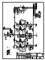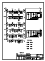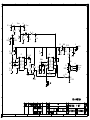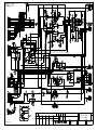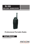
1
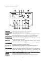
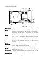
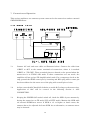
Users Manual
Solid-State HF Band
600W Linear Power Amplifier
Model HL-1.1KFX
1.
Introduction
Thank you for purchasing the HL-1.1KFX.
This compact and lightweight desktop HF linear power amplifier has a maximum input
power of 1.35kW. Our solid-state broadband power amp technology makes it the smallest
and lightest in the industry in its class.
Typical output power is 600W PEP (SSB, CW) with the drive power of 65-90W.
It is best suited for the DX-pedition use due to its light and compact design.
2.
2-1
Cautions
The amplifier is cooled by forced airflow. Several inches of clearance on the top
and the rear wall are necessary to allow for smooth air intake into the fan. Do not
block the air vents on the top cover.
2-2
Keep the amplifier out of direct sunlight, in a cool dry environment.
This unit is not corresponded to protection against dust, water, condensation, nor
vibration.
2-3
Internal high voltages (AC, DC and RF), are present at all times, ON AIR or OFF.
Internal access should be limited to avoid injury.
2-4
Turn off the AC main power immediately upon any unusual sounds, sights, or
odors. Check the multimeter readings of Vd and Id, the fuses and all cable
connections around the amplifier. Please notify the dealer or the factory of any
problems.
2-5
For your safety, do not operate the amplifier without adequate grounding. A
proper ground connection will result in peak performance and stability, in
addition to reduced RF strays or noises.
2-6
To eliminate the RF interference to such home appliances as TV, FM radio,
telephone sets, and etc., it is recommended that clamp-on ferrite cores be
inserted at both ends of the remote control cable, ALC cable, coaxial jumper cable,
and antenna cables, as needed. Also, a common mode AC line filter (near the AC
outlet), and in-line low pass filters on the antenna coaxial cable (as necessary),
are recommended.
1
2-7
The amplifier has fast acting sophisticated protection circuits. Please note,
however, any such actions that cause the same fault to occur repeatedly, will lead
to failure of the valuable final power FET transistors.
2-8
Before checking inside the amplifier, be sure to wait a few minutes for the high
DC voltage to discharge (monitor Vd meter reading). The potentiometers for RF
power detector, protection circuits, FET bias voltage circuit, etc., are precisely
adjusted at the factory, and should not be altered. Doing so, would require
readjustment with precision measuring instruments.
2-9
The DC power supply section consists of most efficient and sophisticated
switching mode circuit. It accepts the wide AC line voltages ranging from AC
100V up to 260V. Since the line voltage is detected and selected automatically,
you do not have to worry about the tap change of internal power transformer
whichever country you will travel. Be sure to verify capacity of AC line fuse
before you plug the AC power cord into the outlet.
2-10
Before starting the amplifier, be sure to connect a dummy load (50 ohms, 600W
min.) or a well-adjusted antenna to the output terminal. Operating without any
load will cause extreme stress to the RF power FET’s, although protection
circuits should work under critical conditions.
2-11
Required drive power is slightly less than 100W to obtain the full 600W output.
Do not attempt to operate with excessive drive from a high power transceiver.
2-12
Keep the aluminum heat sink and air openings free from dust and blockages.
Periodic cleaning will prevent degraded cooling efficiency.
2-13
For long continuous operation in RTTY/FM modes, it is recommended that you
reduce the RF drive levels by 20% to 30% lower output than CW/SSB modes.
2-14
To prevent damage to the precision electronic components, avoid extreme
physical shock to the amplifier. If factory service is required, the amplifier should
be shipped using the original box and packing materials.
2
3.
3-1
Features
Our solid-state broadband design engineers worked to make the HL-1.1KFX, the
lightest and most compact 600W out portable HF amplifier in the industry. This
world-class compact 600W HF amplifier is the easiest to handle and operate
anywhere in the world.
3-2
The amplifier’
s main PA section includes 4 high power MOS FET SD2933 /
THP2933, resulting in 600W PEP (SSB/CW max.) on HF. The amplifier’
s
broadband characteristics require no further tuning once the operating band is
selected.
3-3
The amplifier allows operation in full break-in CW mode due to the use of the
amplifier’
s high-speed antenna relays (made by Panasonic).
3-4
With the unique duct structure design and the powerful blower fan, the
aluminum heat sink block for RF PA module (and other components), are
effectively cooled. The fan’
s quiet operation allows for even the weakest DX
signals to be heard.
3-5
The amp utilizes a sophisticated circuit to run the various high speed protection
circuits such as overdrive, high antenna SWR, DC overvoltage, band miss-set etc.
3-6
This amplifier is compatible with wide AC line voltage ranging from AC 100V to
260V. Although AC line voltage is automatically selected, be sure to install proper
fuse into AC line fuse holder.
3-7
For the safety of the operator, an Interlock system is employed. The AC power is
shut down if the top cover is removed, and the automated safety interlock is
activated.
3-8
An analog multimeter allows the operator to monitor Pf (Forward output power),
Pr (Reflected power), Vd (Drain voltage of power FET), Id (Drain current) etc.
3
4.
Specifications
Frequency
1.8~29.7 MHz all amateur bands including WARC bands
Mode
SSB, CW (RTTY)
RF Drive
65~90W typ. (100W max.)
Output Power
600W PEP typ. (RTTY 400W max.)
Drain Voltage
48V
Drain Current
30A max.
Input Impedance
50Ω (unbalanced)
Output Impedance
50Ω (unbalanced)
Final Transistor
SD2933 / THP2933 x 4
Circuit
Class AB parallel push-pull
Cooling Method
Forced Air Cooling
Multi-meter
Output Power
Pf 1kW
Reflected Power
Pr 100W
Drain Voltage
Vd 60V
Drain Current
Id 50A
Input/Output Connectors UHF SO-239
AC Power
AC 200~260V, 50/60Hz 7.5A max.
AC 100~130V, 50/60Hz 15A max.
AC Consumption
1.4kVA max. when TX
Dimension
232 x 145 x 392 mm, 9.1 x 5.7 x 15.4 inches (WxHxD)
Weight
Approx. 9.5kgs. or 22.5lbs.
Accessories
AC Power Cord x 1
Coax Jumper Cable (with PL259’
s) x 1
RCA Plug x 2
Spare Fuse 8A x 2 (for AC200V line)
Spare Fuse 15A x 2 (for AC100V line)
Spare Fuse 15A x 2 (for F202, F203 of PC1662V power amp board)
Spare Fuse 1A x 1 (for PC1662V power amp board) (miniature fuse)
Spare Fuse 2A x 1 (for PC1785V control board) (miniature fuse)
Users Manual
4
5.
5-1
AC Line Voltage
Although the amplifier is designed to work with both AC 115V (100-130V) and
AC 230V (200-260V), for stability we recommend operation from AC 230V.
5-2
The correct AC plug (not included in the package) must be obtained locally due
to the AC plug variations worldwide.
5-3
The AC line fuse has been factory preset for 115V use (or as requested by the
customer at the time of order). If you wish to change to AC 230V, change the fuse
to 8A. For your safety, before making this change, be sure to pull the AC plug
from the AC outlet to avoid injury.
NOTICE
Please note the followings when you are using
AC100V line (AC100V~120V).
NEVER EXCEED OUTPUT POWER OF 500W,
WHEN RUNNING THE AMP FROM AC100~120V LINE.
Otherwise, over-current protection completely shuts down the drain voltage power
supply for five minutes before it gets resettable.
When this protection works, O.DRIVE lamp lights and HL-1.1KFX will enter the
through state, the reset of the amp being disabled for five minutes.
To restart the amp, turn the POWER switch OFF, and wait for 5 (five) minutes. Then
turn the power ON.
If the protection works too often, please take one or all of the following measures.
① Lower the drive power of the transceiver.
② Connect the ALC line. Adjust the ALC Output Adjustment Knob on the rear panel
so that the drain current (ID) will never exceed 26.0A on any frequency.
③ Change to AC200~240V line.
5
6-A. Front Panel Description
10
13 12 11
14
TOKYO HY-POWER
SOLID STATE LINEAR AMPLIFIER
FAN
ID
METER
BAND
PROTECT
POWER
OPER
ON AIR
O.DRIVE
PR
O.VOLT
FUSE
O.HEAT
MODEL
OFF
STBY
1 2 3
①POWER
HL-1.1 K FX
4
5 6 7 8 9
: Main power switch to turn AC power on and off.
②POWER (LED) : Green LED lights when power is turned on.
③OPER.
: OPERATE/STAND-BY switch. At OPERATE, the amplifier is ready to
go into ON AIR (TX) mode and at STBY, it is on STAND-BY mode.
④ON AIR (LED) : Green LED lights when the amplifier is in transmit (TX) mode.
⑤O.DRIVE (LED) : When overdrive or band miss-set is detected, LED lights to indicate
the protection circuit has worked.
⑥PR (LED)
: LED lights when reflected power from antenna exceeds 70W to
indicate protection circuit has worked.
⑦O.VOLT (LED) : When the DC drain voltage of the FET (Vd) is too high, the LED lights
to indicate the protection circuit has worked.
⑧FUSE (LED)
: LED lights when the 15A glass fuse has blown from excessive Id.
(Two fuses are on the PC1622V PA board.)
⑨O.HEAT (LED) : When the PA module temperature reaches 80 deg.C, the LED lights to
indicate the protection circuit has worked. (It is necessary for the
cooling fan to operate for several minutes to cool the PA module.)
(Turn the main POWER switch to off, and then on again to reset the Protection Circuits.)
⑩BAND
: Select the desired operating frequency band.
⑪METER
: To change the multi-meter scales. Meter reads Pf, Pr, Vd, and Id.
6
⑫ID (LED)
: LED lights when the input drain current is over 20A. This does not
mean that any damage occurred to the amplifier, but is useful for the
user to notice any stress influencing the final FET caused by high drain
current, load impedance trouble, etc. We recommend that you note the
usual condition of the lighting. When any unusual symptoms are
noticed, the user may lower the drive power from the transceiver, check
the antenna SWR, etc.
⑬FAN (LED)
: LED lights when fan is running at high speed. When the heatsink
reaches 50℃ the cooling fan will switch to high-speed mode to cool the
heatsink.
⑭MULTIMETER : Pf (Forward output power), Pr (Reflected power from antenna), Vd
(FET drain voltage), and Id (FET drain current) are shown on the scale
as selected by ⑪METER select switch.
7
6-B. Rear Panel Description
FUSE
ANT
IN PUT
AC
ALC ADJ
STBY
⑭AC POWER
ALC
GND
: AC Mains Socket. Socket for the AC power cord. (Socket is EMI
filtered.)
⑮STBY
: RCA Jack. Connect the control cable from the ACC terminal (or SEND,
TX GND etc.) of the transceiver. The center pin is to be shorted to
ground though the relay circuit of the transceiver. The DC current
necessary is 5V, 1mA only.
⑯ALC
: RCA Jack for ALC Voltage Output. Negative DC voltage appears at the
center pin, which is fed back to the ALC terminal of the transceiver.
ALC is used to keep the amplifier output power at certain limits. Also it
is useful when the transceiver output power is higher than 100W.
(See page 12, 8.ALC Connection). Also consult your HF transceiver’s
user manual.
⑰GND
: Ground Terminal
⑱ALC ADJ
: Potentiometer to adjust ALC voltage level. Minus 10V is available at
maximum, when turned full counter-clockwise.
Factory setting is 0 volts, with the pot turned full clockwise.
⑲FUSE
: A pair of fuses for AC mains. 15A glass pre-installed fuse. (Change to
8A fuses if 230V line is used.)
⑳IN PUT (TX)
: RF Input Connector. Connect the coax jumper cable from the
transceiver.
21 ANT (OUTPUT) : RF Output Connector. Connect the coax cable to the antenna.
○
8
Inner Layout of HL-1.1KFX
Upper View
①RF Power Detector and Send-Receive Switching Relay
②Inter-lock Switch
③Sub- Power Source Unit
④LPF Board
⑤Main Power Source Unit
⑥Sub- Fan (for Main Power Source Unit)
⑦Control Board
⑧Power Amp Unit
⑨Frequency Detector Board
⑩Cooling Fan
⑪AC Fuse
9
7. Connection and Operation
This section explains a one-antenna system connected to the transceiver and an external
SWR/POWER meter.
KFX
REAR
SIDE
TRANSCEIVER
ALC
ACC
(SEND,TX GND)
SWR/POWER
METER
TX
ANT
ANTENNA
ANT
ANT
INPUT
AC
STBY
HL-1.1KFX
7-1
ALC
REAR
SIDE
Connect AC cord and coax cables as illustrated above. Connect the cable from
“SEND” to ACC or the remote terminals of transceiver, where it is marked
“SEND” or “TX GND”. These terminal pins are shorted to the ground when the
transceiver is in TX/ON AIR mode. If these connections are not made, the
amplifier will not go into TX (amplification) mode. For a temporary check to the
amp, ground the SEND center pin by inserting and RCA plug whose center pin
has been soldered to the outer case of the plug with a small piece of wire.
7-2
At first, turn the ALC knob full clockwise to avoid ALC voltage to the transceiver.
Application of ALC will be covered in the following Section 8. ALC
CONNECTION.
7-3
Keeping the POWER (AC mains) switch off, check the SWR of your antenna by
keying the transceiver to TX mode (CW or RTTY mode). Monitor the SWR with
an external SWR/Power meter. If SWR is 1.5 or higher at band center, the
antenna has to be adjusted for lower SWR. As an alternative, an antenna tuner
may be inserted.
10
7-4
Turn the POWER switch on. Turn the BAND switch to a desired operating
frequency band. Turn the STAND-BY switch to OPER (operate) position and the
amplifier is ready to go. If you key the transceiver with the carrier level set
relatively low (such as 20-30W), you will achieve an amplified output signal of
few hundred watts. Monitor this output with the multimeter (in the Pf position)
or with an external power meter. Increase drive level to roughly 50W and see if
the antenna SWR stays constant. (As higher RF currents flow, some antennas
may show a changed SWR value due to heated connector junctions and trap
coils.)
7-5
You can now increase the drive level to nearly 80-90W to achieve maximum
carrier output power of 600W (CW) from the amplifier. If you change to SSB
mode, average voice power of a few hundred watts will be observed on the panel
meter, Pf scale, while peak voice power reaching a little over 600W. For high duty
cycle transmissions like RTTY mode, it is recommended that you reduce the drive
power by some 30%.
7-6
With a high power transceiver in SSB mode, you can overdrive the amplifier
resulting in a distorted output signal. This can occur if you speak too loud or if
you set the microphone gain too high. Speak into the microphone properly to
reduce the possibilities of splattering into the neighborhood. The ALC is effective
in preventing the output signal from being distorted or to limit the carrier level to
within rated output levels. It is strongly recommended to make ALC connection,
especially when 200W out high power radio is used to drive.
7-7
Protection circuits may work during operation depending on the conditions. If the
protection circuit has shut down the amplifier, check the antenna SWR, Vd, AC
line voltage, or try to reduce the drive level. To reset, turn off the POWER switch
once, then back on again. The power transformer has an overheat protection in
the coil layer. If this temperature switch activates, the amplifier will put you in
receive mode with the cooling fan operating until the transformer has cooled off.
It may take ten to fifteen minutes to cool, depending upon room temperature. For
more details on this protection circuit, see Section 9. PROTECTION CIRCUITS.
11
8.
ALC Connection
ALC voltage is available at the terminal marked ALC (RCA phono jack) on the right
upper corner of the rear panel. Negative maximum DC voltage of ten volts (-10V) is
produced at this terminal when the amplifier is fully driven. This voltage is adjustable
with the ALC ADJ. knob located above the ALC jack. If the ALC voltage is properly fed
back to the transceiver, we advise you to keep the maximum output power constant or
hold the power at a certain level. Also ALC is useful in avoiding your SSB signal from
being distorted when overdriven. You may not always need to connect ALC to the
transceiver, if you set the mic gain properly and do not overdrive the amplifier. Depending
upon the manufacturer of the transceiver, the suitable ALC voltage differs. ICOM may
need 0~-4V, ad Yaesu may need 0~-5V range. Kenwood may need -6~-8V maximum.
Check your transceiver manual.
8-1
Prepare an ALC control cable using RCA plug supplied in the package. Solder a
single wire or (more preferably) a shielded single wire to the center pin of RCA
plug and solder the shield braid to the outer side of the plug. Connect the control
cable to the “ALC (or ETERNAL ALC)” jack of the transceiver. External ALC
input is sometimes available at one of the pins of the “ACC” socket of the
transceiver as well.
8-2
At first, turn ALC ADJ full clockwise. Drive the amplifier in CW/RTTY mode to
full output power. Then turn the ALC ADJ counter-clockwise. Observe the
SWR/Power meter at the output, (or Pf of the multimeter). Stop turning the ALC
ADJ at the point the power starts to decrease. Or if you wish to further reduce
the power, keep turning ALC ADJ until the desired level is achieved. If you
further try to increase the drive power you will now see the output power become
rather saturated, fro these adjustments.
(Maximum ALC voltage produced is -10V when the amplifier output power is
over 200W.)
ALC
ADJ
AC
MAX
REAR PANEL ALC POT.
STBY ALC
To Transceiver
12
MIN
9.
Protection Circuits
There are five major protection functions in this amplifier. If the amplifier has shut down
for some reason, before re-setting, correct the possible cause of the shut down. Turn off
the POWER once and back on to reset.
9-1
O. DRIVE (Over Drive / Band Miss-set)
When the drive power exceeds the 100W level, the amplifier will shut down to
STAND-BY mode (or receive) in order to protect the input side of the power FET’s.
This protection might also activate if the band is set wrong. This usually occurs,
when the amplifier band setting is lower than that of the transceiver.
9-2
O. HEAT (Over Heat)
When the temperature of the aluminum heat sink in the power amplifier reaches
80 degrees C, the amplifier defaults to RECEIVE mode to protect the power FET’s.
9-3
O. VOLT (Over Voltage)
If there is a sudden AC line voltage spike, the FET drain voltage may rise above
acceptable levels, and O. VOLT protection may trip.
9-4
FUSE (Fuse Blown)
If either of the glass fuses (15A) on PC1662V fails, O. VOLT protection activates.
Under normal usage of the amplifier, this failure should rarely (if ever) occur. If it
occurs, there is a possibility that the power FET’s have failed together. If the
amplifier cannot be reset, consult with the dealer or the service center.
9-5
PR (Reflected Power Protection)
If reflected power because of the antenna reaches approximately 80W, the PR
protection may trip. If it does, one solution is to reduce the drive power from the
transceiver. Or you may need to check that your antenna match (SWR) is still OK.
If the match cannot be corrected and the antenna system isn’t faulty, use an
antenna tuner.
As noted above, the amplifier is equipped with several kinds of fast acting protection
circuits using the latest in analog technology. However, if the amplifier is operated in
such a manner that multiple protections work repeatedly over a long period of time, the
amplifier can be seriously damaged.
13
10. Explanation of Major Circuits
Five major circuit blocks are explained in their basic form and using signal flows.
10-1
Main DC Power Supply
10-2
Power Amp/ L.P.F.
10-3
RF Power Detector/ TX-RX Switching
10-4
Control Board
10-1
Main DC Power Supply
The main DC power supply feeds the 50V DC power to the final PA stage. It is a
state of art, switching power supply with high efficiency. A part of 50V line is
converted to 24V using a DC-DC converter and is supplied to the cooling fan.
10-2
Power Amp (PA PC1662V) / L.P.F. (PC1399B)
The RF PA is the heart of this amplifier and is composed of four SD2933 MOS
FET’s made by ST Micro, a French-Italian joint venture firm. The amplifier is a
parallel push-pull type of class AB amplifier. The gate bias supply circuit is
regulated for the best stability and is thermally compensated.
The PA has a 6dB attenuator on the input for gain reduction and to enhance the
stability of the wide band power PA. The heat sink has two different thermal
sensors to detect temperatures of 40 deg. C, and 80 deg. C, respectively. At 40 deg.
C, the cooling fan shifts into high-speed mode. At 80 deg. C, the amplifier will lock
the amplifier into RECEIVE mode to protect the power FET’s.
In the L.P.F. (output low pass filter) circuit, there are eight different band filters
that are selected either by the auto band decoder or by the manual band switch.
Each L.P.F. is used to reject harmonics so that the amplifier meets international
telecommunication equipment standards.
10-3
RF Power Detector / TX-RX Switch (PC1398B)
As illustrated in the block diagram, there are two RF power detectors on this
board. One detects the drive signal level from the radio and the other monitors the
outgoing power and the reflected power from the load (antenna).
The TX-RX switch (Send-Receive switching) will switch the flow of drive
power/output power and the incoming signal from the antenna with two
high-speed relays mounted at the input and output sides of the PA.
14
10-4
Control Board (PC1698)
This is the heart of the control signal processing for the HL-1.1KFX. It judges the
operating condition of the amplifier, as well as issuing the commands to the
peripheral circuits. Various analog signals are processed such as RF drive from the
transceiver, RF power signals at various points, DC power supply information, etc.
There are ope-amps, various three terminal voltage regulators, GAL logic device
etc. Warning signals are processed by the logic IC for Over Heat, Over Voltage, Pr,
Band Miss-set etc. Ope-amps produce the necessary DC signals to drive the Pf, Pr
meters. Also there is a control circuit that issues the drive shut down command in
case of the over drive, band miss-set and high antenna SWR conditions.
15
11. Trouble Shooting
Failure
Possible Cause
Solution
AC mains not
① AC fuses blown
① Replace with new ones.
operating
② AC cord not plugged in
② Plug in securely.
③ Interlock switch lifting
③ Screw bolts tightly on the top cover.
④ Wrong tap used on
power transformer
primary
Can’t enter
Transmit
mode
④ Correct primary wiring.
① Remote control cable
① Check the cable and connect properly.
not connected
② Protection circuits on
② Check the drive power, antenna SWR,
antenna selector A/B. Reset with AC
POWER switch.
O.Drive lights
PR lights
① RF overdrive
① Decrease drive.
② Band miss-set
② Match the BAND correctly.
① Reflected power high,
① Check/adjust antenna
Antenna SWR high
(Or decrease drive.).
② Poor connection to coax
cables
O. Volt lights
② Check the coax cable connectors.
① Drain voltage of power
① Check AC line stability.
amp extremely high
FUSE lights
② Fuse blown
② Replace F202 and F203 (20A) on the
PA board (PC1662V).
③ Antenna SWR high
③ Adjust the antenna.
④ Short circuit
④ Contact the distributor, or service
center.
O.Heat lights
Cool off until LED turns off. Check for air
① Internal Temperature
above 80 deg.C
intake blockages. Also check air vent on
top cover.
TVI, FMI
① Overdrive
① Decrease the drive. Check ALC
setting.
② RF leakage from coax
② Insert common mode filters on
cable, grounding wire,
antenna cable or AC line. Add
AC power cord etc.
clamp-on ferrite cores (TDK, Amidon,
Palomar) on various cables.
16
12. Parts Layout
12-1
Top View (Detailed)
12-2
Top View & Side View
12-3
PA (PC1662V)
12-4
Power Detector (PC1398B)
12-5
Control Board (PC1785) Front View
12-6
Control Board (PC1785) Copper Side
12-7
L.P.F. (PC1399B)
12-8
Frequency Detector Unit (PCS1733)
12-9
Sub DC Unit (PC1784)
13. Schematic Diagrams
13-1
PC1662V PA (Power Amplifier)
13-2
PC1398B RF Power Detector
13-3
PC1399B L.P.F. (Low Pass Filter)
13-4
PCS1733 Frequency Detector Unit
13-5
PC1785 Control Board
13-6
Overall Block Diagram
17
HL1.1KFX DEVELOPMENT CHART
MAIN SW POWER SUPPLY(ADF1000F48)
METER
SUB SW POWER SUPPLY(ADF1015)
LPF UNIT(PC1398B)
SUB FAN
FUSE(F1、F2)
DET UNIT(PC1398B)
MAIN FAN
CONT UNIT(PC1785)
PA UNIT(PC1662V)
F DET UNIT(PC1733)
TOP VIEW
LEFT SIDE VIEW
RIGHT SIDE VIEW
PC1662V
RF OUT
J201 RF IN
F201 MINI FUSE 1A
VR205 BIAS REF
HI
LO
VR204
VR201
VR203
HI
LO
FET BIAS ADJx4
(VR201∼VR204)
VR202
PC1398B DET UNIT
J504 RF IN
J505 RF OUT
TC503 PR ADJ
TC501 TX ADJ
TC502 PF ADJ
J501
RL502
RL501
J502
HL1.1KFX CONTROL BOARD(FRONT VIEW), PC1785
VR101 PF SCALE ADJ
VR102 PR SCALE ADJ
VR103 ID SCALE ADJ
LO
HI
VR101
VR102
VR1013
FUSE(F101.F102 2A)
IC108
D704
VR106 TP
VR105 TP
VR107 VD SCALE ADJ
VR105 BAND MISS SET ADJ
VR106 O.DRIVE ADJ
J303
PC1399B LPF
J304
RL307/L302
L301/RL301
RL311/L310
L309/RL305
RL309/L306
L305/RL303
RL310/L308
L307/RL304
RL312/L312
L311/RL306
RL308/L304
L303/RL302
PC1399B LPF(COPPER SIDE)
PCS1733(COPPER SIDE)
PCS1733
TC1
J3
J4
J1
J2
IC1
PC1784
F301
J301
PC1784(COPPER SIDE)
J302
J302
-15V
COM
+15V
FG
AC IN
AC IN
J301
FB
1
OH1
IC201
78L08
R234
120/1W
RT201
TH
R238
1k
C-EX
0.01
2
タンタル
3
C226 +
10u
G
+
T/R
C225
10u
G
FB203
EXCELSA35
3
5
6
7
B7B-EH
R235
2.2k
C242
0.01
R237
5k
C-EX
0.01
パターンカット
I
2
4
+15V
Q205
2SC1959
TL431
1
VR205
10k
LED201
R236
4R7
G
タンタル
O
R237A
2K
OH2
S202 80degree
J206
C-EX 0.01
1
C-EX Bttto side
VR204
2k
D204
1S2076A
R216
47 1/2W
R227A
C207
2
0.1u
VR203
2k
J201
R205
100 10W
TMP-J01x-V6
D203
1S2076A
R215
Q203
SD2933
C208
R224
4.7k
R225 1R0
R210
39 10W
J204
J205
T202
D12A 5
R223
T201
D12A 3:1
TMP-J01x-V6
R223A
R206
100 10W
R201
50 10W
R207
150 10W
R212
150/5w
R208
150 10W
C205
150p
CH2H
R222
R203
50 10W
12/5w *4
1
2
R222A
R202
50 10W
3
0.1u
VR202
2k
D202
1S2076A
J202
82P
CH2H
220p 270p
chip chip
2
3
4
C233
0.1u
chip
R220A 1R0
R214
47 1/2W
C227 C228
1
C229
C234
0.1u
chip
C211 C211A
0.1u *2
chip
C202
C237
0.01u
T203
D12A 1:3
6
4
C205A
250p
chip
ISO202
TLP521
G
R232
10k
C235
0.1u
chip
LED310
F201
LM10 1A
0.1
C238
R231
4.7K1W
R225A 1R0
RL201
R311
51 1/2W
VDD2
C212 C212A
0.1u *2
chip
47 1/2W
C-EX 0.01
FB202A
C224
0.1×2
chip
C222
0.1×2
chip
0.1u
R204
100 10W
G
F203
15A
R226
4.7k
R227 1R0
0.1u
2.2k
R310
S201 50degree
L202
FB202
1R0
Q204
SD2933
C209
2
OH1
C215
0.01u
C213 C213A
0.1u *2
chip
1
G
3
B4B-EH
R228
220/5w
B2B-EH
J210
2
4
4.5V
1
OH2
Q202
SD2933
L201
C204
R220 1R0
0.1u
VR201
2k
C201
T203
D201
1S2076A
R221
4.7k
FB201
F202
15A
R218A 1R0
R213
47 1/2W
Q201
SD2933
タンタル
3.3μ/25V
C203
C219,219A,221,221A
0.1μx4 chip
0.1u
FB201A
C210 C210A
0.1u *2
chip
R218 1R0
C217
0.1×2
chip
C218
0.1×2
chip
R219
4.7k
R229
4.7K1W
パターンカット
3
R217
220/5w
1
T203
PRI D12A 1T
VDD1
R230
10k
G
C239
0.01u
ISO201
TLP521
C214 0.01u
2nd
3T
銅板にてショート2カ所有り
承認
検図
検図
担当
第三 角法
溝呂木
溝呂木
処理
TOKYO HY-POWER
L1373JH
個数
PC1662V HL1.1KFX
アンプ回路
図番
H18.4.6
材質
品番
設計
H18.4.6
承認
型名
製図
単位:mm
検図
尺度
4
変更事項
名称
記号
2
C240 0.1
1373D01A
J502
J501
AMP
T501
J504
C510
470u
120P
J505
C503
15p
6P
D501
T502
22Ω/0.5W
R501
TC502
6P
RFC502 470u
C502 1SS97
C504
C506
150P
0.01
120P
C513
15p
TC503
D502
D503
1SS97
1SS97
C505
150P
ANT
R502
6P
RFC503 470u
C511
C512 C509
120P
150P
+
C513
(裏付)
3.3μ/16Vタンタル
R503
J503
22Ω/0.5W 22Ω/0.5W
C501
0.01
RL502 G2R-1
C508
RL502
15p
TC501
RFC501
RL501
RL501 G2R-1
IN
FIL
1
COX
2
COX G
3
T+15V
4
T/R
5
PF
6
G
7
PR
指定なきコンデンサーは 0.01uF50V
指定なきダイオードは1S2076A
旧型名L1303HVJ
検図
検図
担当
溝呂木
材質
処理
TOKYO HY-POWER
L1373JH
PC-1398B
検出基板
個数
HL1.1KFX
図番
溝呂木
第三 角法
承認
品番
設計
H18.3.29
検図
型名
製図
H18.3.29
単位:mm
尺度
承認
変更事項
名称
記号
L1373D04
J301
J302
C302-1
470p
50p
*
*
*
(3.5/3.8MHz)
C320
C321
400p
100p
*
*
L304 12T
T106-2
1
2
RL308
3
4
5
39p
C323 C324 C325 C326 C326-1
*
*
*
*
C330
30p
*
250p
15p
6
C331
*
39p
400p 400p 100p 200p
33p
*
470p 400p 200p 200p
*
* C322
*
*
* C313
L303 13T
T106-2
RL302
J303
C316
C315 C316 C317
C307 C308 C309 C310 C312
* *
*
*
*
C305
150p 470p 470p 470p 470p 250p
RL307
C302
470p
RL308
C301
RF OUT
RL307
RL309
(1.9MHz)
2130pF
RL310
RL301
L302 16T
T106-2
RL311
L301 20T
T130-2
RL312
RF IN
7
+15V
B1
B2
B3
B4
B5
B6
200p
* C327-39p
* C328-39p
C329-15p
L305 10T
T106-6
39p
C335
RL304
C337
39p
C341
C342
400p
200p
* C339
250p
27p
*
*
L308 7T
T106-6
L307 T106-6 7T
(10/14MHz)
*
RL310
J304
C343
5p
C346
C347
C348
10p
C350
150p
C345
150p
150p
33p
C349
150p
*
*
RL305
L309
*
1
*
9T
L310
2
RL311
8T
RL301
250p
C336
RL302
22p
*
RL303
C333
*
RL304
C332
RL305
(7MHz)
RL309
L306 T106-6 10T
RL306
RL303
3
4
5
6
(18/21MHz)
C351
*
100p
C352
6p
5p
C355
2p
200p
20p
C356
*
15p
C357
C358
C359
82p
12p
*
C353/354
RL306
L311
(24/28MHz)
RL312
L312
7T
C360
C361
5p
C363
C364
39p
39p
C362
150p
8p
*
*
7
+15V
B1
B2
B3
B4
B5
B6
*
C365
7T
2p
C367
C368
39p
33p
*
チップコン表示
d2:400p
A2:100p
a2:250p
Y1:82p
E2:150p
Q1:39p
H2:200p
N1:33p
C366
12p
*はチップ
検図
検図
担当
溝呂木
材質
処理
TOKYO HY-POWER
L1373JH
PC-1399B
LPF基板
個数
HL1.1KFX
図番
溝呂木
第三 角法
承認
品番
設計
H18.3.29
検図
型名
製図
H18.3.29
単位:mm
尺度
承認
変更事項
名称
記号
L1373D02A
1
2
3
5
4
6
7
A
A
J1
R1
10k
1W
7mV
B
J2
70Vrms
RF in
RF out
C1
4P
D3
1SS286
C2
100p
D2
1S2076
D1
1S2076
R4
1k
R5
C3
0.01
L1
1mH
10k
B
IC3
C6
0.01
R3
50
2 FMin
1 Vcc
20MHz
PSC 7
R9
X1
3 SWin
S/F 6
4 GND
OUT 5
220k
C5
Bias 8
C8
R8
2.2k
TC1
220
C10
20p
2 GP5
3 GP4
J3
R12 47
1
2
C13
10uF
DC15V
G
C14
R13
100
Vss 8
4 GP3
GP0 7
0.1uF
RL1
GP1 6
D4
GP2 5
1S2076
C
J4
3
2
1
Stby out
Stby in
NC
C11
R15 4.7K
Q1
0.01
C12
10uF
IC2
0.01
R7
40mV
0.01
1 Vcc
C7
PIC12F683
IC1
C4
C
C9
0.01
0.01
TD7101F
R2
470
78L05
33p
R11 10k
56p
Q2
2SC1815
J5
2SC1815
1
2
予備
D
D
注意:J4の端子順番
PCS1733
E
2007.6.20
1
2
3
2007.6.20
L1373JH
4
5
6
F DET
E
1373D08
7
PC1785 HL1.1KFX
CONTROL UNIT
EXCELSA35
FB101
51Ω1/2W
B5
6
B6
7
C106
C105
C104
C103
C102
C107
0.001
0.001
0.001
0.001
3
C141
10u
(10/14)
(18/21)
+
C142
0.01
+
5
2
100K
VR105
(BAND
MISS
ADJ)
RA103
10k
+
NC
NC
NC
(24/28)
2
R141
51K
C155
3.3μ
タンタル
R143 1.2K
C151
0.01
4
5
7
1
6
6
7
IC102
LM339
8
9
J102
+15V
10
1
B1
2
B2
3
B3
4
B4
5
B5
6
B6
9
C109
0.1
1
2
3
G
4
+15V
5
T/R
6
G
7
R101
100
R514
C114
0.001
C112
0.001
FB102
C115
0.001μ
VR101
100k
(PF ADJ)
C113
0.001
C126
10u
12
R127
10
C128 10μ
D113
1S2076A
VR102
100k
+
+
R128
10k
R107
3K
R106 1k
+
C129 0.01
PR
7
OUT
IN
OUT
IN
OUT
IN
OUT
GND
_OE
16
R137
15
R138
LED104(O.D/B.M.S)
3
LED105
(PR)
LED106
(O.V)
LED107
(F.B)
LED108
(O.H)
14
13
12
11
注意:PA基板J210の①②
に極性が逆接続
J114
to PC1662V RL201
R144 1K
1
R129
4.7K
2
RL101
D708
SR140
D111-2
HZ24-3-E
C147
0.01
R124
100K
R142
2k
R706
47Ω1/2W
C152 R111
0.01μ 100K
IC101
10
9
8
ADJ)
LF347
R513 1K
R109
1.2K
1
2
1K
R114
6.2K
3
R123
150K
R112 1K
0.01μ
C608
C607
0.001μ
VR103
50K
J110
to LED102
D114
HZ3C2
1
LED102
(ID
ADJ)
2
R120 1K
+15V
ON
D511
UZP30B
AIR LED103
RA102
47
IC101
LF347
J109
(ALC VR)
R115
1
22K
2
4
D107
1S2076A
5
7
6
+
R702
2.2K
1/8W
D112
1S2076A
R118
R145
10K
1K
J108-1/2
STBY
6
IN
R136
STBY
5
OUT
17
470*5
R121 1K
STBY
STBY
4
IN
R135
+15V
-15V
R512 10K
3
3
G
OUT
R134
18
+5V
-15V
PF
IN
19
14
11
R104
47Ω5W
T/R
OUT
C146
10u
J108-2/2
OPR
OUT
IN
C127
0.01
R113 39K
2
M-
C148 +
1u/50V
タンタル
C609
1u/50V
タンタル
R105
150K
1
M+
4
4
13
R108
COX
3
+5V
IC101
LF347
(PR
J105
LANP+
Q101
2SC1959
Q102
2SC1815
13
IC102
LM339
33K
R102
100
C111
0.001
R126
3.3K
11
10
+
R103
100
COX G
IN
D110
1S2076A
+
R700 10k
VR106
20K
(OD ADJ)
(VD ADJ)
50KΩVR
VR107
M LANP-
C145
0.01
C610 3.3μ
タンタル
RA104
10k
SW102
(METER)
M
2
D111-1
HZ24-3-E
IC102
LM339
VD
ID
J103
FB
C144
10μ
VCC
8
PR
C110
0.001
OH2
CLK
14
PF
7
OH1
+
IC103
GAL16V8
1
3
R140
10k
SW101
(BAND)
C143
10μ
RA105
10k
IC102
12 LM339
D106
5
+
4
RA101
33Ω
1
+5V
R131
220k
R701
10k
(7)
D105
4
B4
C150
0.01
C154
10u
C140
0.01
D109
1S2076A
(3.5)
D104
B3
C139
10u
+
(1.9)
D103
3
D102
2
B2
D101
1
B1
0.001
J101
0.001
0.001
C101
C108
0.1
+15V
J107
R130
+15V
D108 1S2076A
2
1
SW103
R117 150K
22K
R116
C606
220μ25V
J104
1
FAN
2
FAN RIN
3
T/R IN
4
G
5
ALC
6
G
7
FAN
8
FAN RIN
to Fan LED
L or H
C1300.001μ
J112
to PC1733 J3
D510 IZ24
C121
C119
C117
0.001μ 0.001μ 0.001μ
C120
C118
0.001μ 0.001μ
J106
VD
ID
2
ID-G
3
+15V
4
G
5
AC15V
6
AC15V
7
F101
LM20
C131 C132
470u 0.01μ
J111
SUB SW FAN
C702
220u/16V
2
+
+
+
R707
15Ω2W
C137
10u
1
G
C138
10u/16V
タンタル
+
2
R703 4.7K
7
forJ104⑦⑧
D703
Fan L or H
R705 200K
8
承認
変更事項
検図
検図
製図
H20.1.24
担当
設計
H20.1.24
材質
処理
TOKYO HY-POWER
L1390HJ
個数
PC1785 HL1.1KFX
コントロール基板
図番
溝呂木
承認
品番
溝呂木
第三 角法
検図
型名
PC*****
単位:mm
名称
記号
R704 470K
尺度
D702
RD18
変更:D708の追加(2008.3.28)
+5V
2
5V
O
G
1
for J110
LED102
ID LED LtoH
-
+
J113
to ADF1000F48 STBY
C116
0.001μ
IC108
7805A
I
G
+24V
1K 1W
-15V
+
+
C125
10u
IC104
7824
+15V
2
R511
POWER
C134 C135
470u 10u/35V
タンタル
D704
IN4002
-
+
FB103
EXCELSA35
O
G
C605 C124
47u50V 10u
C123
0.01μ
1
I
R133 180Ω5W
LED101
24V
R132 180Ω5W
1K
+15V
+
F102
LM20
C122
0.01μ
+
R119
1
1390D01A
DET
UNIT
J504
INPUT
( RF IN )
PA
ANT
( RF OUT )
JP3
2.5D2V
JP1
J503
1 COX
2 COX G
3 OPR
4 T/R
5 PF
6 G
7 PR
EHR-7
1
2
3
4
5
6
7
J501
RF IN
RF OUT
J502
JP5
2.5D2V
EHR-7
RF OUT
RF IN
J1
J2
JP201
J203
FB
OH1
OH2
G
+15V
T/R
G
2.5D2V
STBY IN
STBY OUT
JP29
PC1733
F-2
JP27
S-3
DC IN
J3
G
F DET UNIT
J206
OH2
G
OH1
G
J210
JP6
VDD
G
1 2
1
2
3
+5V
STBY ON
JP21
J301
AC
NC
AC
NC
FG
SUB AC
J303 EHR-7
+15V 1
B1 2
B2 3
B3 4
B4 5
B5 6
B6 7
JP10
JP11
EHR-7
1
2
3
4
5
6
7
1
2
3
4
5
6
7
FB48
FB47
FB42
FB25/26
FB44
FB43
0V FB27/28
JP22
FB23/24
FB22
FB21
FB14
FB13
FB12
1
2
3
4
5
6
7
JP20
PC1784
EHR-3
J302
+15V 1
-15V 2
COM 3
EHR-7
PC1785
CONT UNIT
+15V
+15V 1
B1
B1 2
B2
B2 3
J101
B3
J102 B3 4
B4
B4 5
B5 6
B5
B6
B6 7
FB
OH1
OH2
J103
G
+15V
T/R
G
1 COX
2 COX G
3 OPR
4 T/R J105
5 PF
6 G
7 PR
FB41
YAW1015
(AC85∼AC264V)
EHR-4
1
F-3 2
3.2A
3
4
J304
+15V
B1
B2
B3
B4
B5
B6
JP8-1BFB38
JP8-1A FB37
RS
FG
FB49
JP23
RF OUT
FB31
FB29/30
AC85∼AC264V
FB50
J302
RF IN
FB46
FB45
+DC48V
JP24
EHR-7
1
2
3
4
5
6
7
シールド
JP8-2A FB40
JP8-2B FB39
シールド
JP25
PC1399B
UNIT
J301
シールド線
FB34
FB33
FB32
1
2
EHR-2
EHR-4
JP9
1
S202
2
3
S201
4
ADF1000F48
(AC85∼AC264V)
JP30
POW SW
S-1
2.5D2V
RF OUT
EHR-3
NC
J4
JP26
JP4
J202
J201
RF IN
JP7 1 2 EHR-2
FB36
FB35
AC85∼AC264V
AC100V-15A
AC200V-8A
F-1
PC1662V
UNIT
FB50
JP28
2.5D2V
LPF
PC1398
J505
JP2
FB11
FB10
FB9
FB19/20
FB17/18
FB15/16
to PC1662V RL201
VD
ID
ID・G
+15V
G
+15V
-15V
J106
2
1
J114
1 +5V
2 G
J113
LANP
JP12
EHR-4
C2 R3
LANP+ 1
J107 LANP- 2
A
M1
M+ 3
M- 4
EHR-3
1
1 1
2
JP13
RV16YN 1K
J109 2 2
(ALC ADJ)
3
3 3
EHR-4
1 1
2 2
STBYスイッチ
JP14
J108
3 3
S-2
4 4
FAN 1
FAN RTN 2
T/R 3
G 4
J104 ALC 5
G 6
FAN 7
FAN RTN 8
EHR-7
to ADF1000F48 STBY
JP19
D702
RD18
D102
BL又はBG LED
ID LED LtoH
FB7
to PC1733 J3
470K
R704
JP18
D703
BL又はBG LED
FAN LED Lor H
1 +15V
J112
2 G
FAN DC24V
JP15
FB1 FB2
1
2
FB3 FB4
T/R
J-3
RCA-J
JP16
ALC
J-4
RCA-J
J111
+ 1
- 2
FB8
4.7K
R703
C1 0.01μ
FB5
ADF1000F48
FAN DC15V
FB6
1
2
J110
to LED102 JP17
200K
R705
PC***
Overall Wiring Schematic
承認
変更事項
検図
検図
製図
担当
設計
承認
材質
個数
総合結線図
HL1.1KFX
処理
L1390HJ
図番
TOKYO HY-POWER
品番
溝呂木 溝呂木
第三 角法
検図
型名
H20.3.25 H20.3.25
単位:mm
名称
記号
尺度
注意:コント基板のJ114とPA基板のJ210間で1と2の極性が逆に結線
コント基板J104の①②からメインFANの①②間で極性が逆に結線
L1390D02