1
System
Generator for
DSP
User Guide
UG640 (v 14.3) October 16, 2012
This document applies to the following software versions: ISE Design Suite 14.3 and 14.4
Xilinx is disclosing this user guide, manual, release note, and/or specification (the "Documentation") to you solely for use in the development
of designs to operate with Xilinx hardware devices. You may not reproduce, distribute, republish, download, display, post, or transmit the
Documentation in any form or by any means including, but not limited to, electronic, mechanical, photocopying, recording, or otherwise,
without the prior written consent of Xilinx. Xilinx expressly disclaims any liability arising out of your use of the Documentation. Xilinx reserves
the right, at its sole discretion, to change the Documentation without notice at any time. Xilinx assumes no obligation to correct any errors
contained in the Documentation, or to advise you of any corrections or updates. Xilinx expressly disclaims any liability in connection with
technical support or assistance that may be provided to you in connection with the Information.
THE DOCUMENTATION IS DISCLOSED TO YOU “AS-IS” WITH NO WARRANTY OF ANY KIND. XILINX MAKES NO OTHER
WARRANTIES, WHETHER EXPRESS, IMPLIED, OR STATUTORY, REGARDING THE DOCUMENTATION, INCLUDING ANY
WARRANTIES OF MERCHANTABILITY, FITNESS FOR A PARTICULAR PURPOSE, OR NONINFRINGEMENT OF THIRD-PARTY
RIGHTS. IN NO EVENT WILL XILINX BE LIABLE FOR ANY CONSEQUENTIAL, INDIRECT, EXEMPLARY, SPECIAL, OR INCIDENTAL
DAMAGES, INCLUDING ANY LOSS OF DATA OR LOST PROFITS, ARISING FROM YOUR USE OF THE DOCUMENTATION.
© Copyright 2006 - 2012. Xilinx, Inc. XILINX, the Xilinx logo, Artix, ISE, Kintex, Spartan, Virtex, and other designated brands included herein
are trademarks of Xilinx in the United States and other countries. All other trademarks are the property of their respective owners.
System Generator for DSP User Guide
www.xilinx.com
UG640 (v 14.3) October 16, 2012
Table of Contents
Chapter 1: Hardware Design Using System Generator
A Brief Introduction to FPGAs . . . . . . . . . . . . . . . . . . . . . . . . . . . . . . . . . . . . . . . . . . . . . . 10
Note to the DSP Engineer . . . . . . . . . . . . . . . . . . . . . . . . . . . . . . . . . . . . . . . . . . . . . . . . . . 14
Note to the Hardware Engineer . . . . . . . . . . . . . . . . . . . . . . . . . . . . . . . . . . . . . . . . . . . . . 15
Design Flows using System Generator . . . . . . . . . . . . . . . . . . . . . . . . . . . . . . . . . . . . . . . 15
Algorithm Exploration . . . . . . . . . . . . . . . . . . . . . . . . . . . . . . . . . . . . . . . . . . . . . . . . . . . . 15
Implementing Part of a Larger Design . . . . . . . . . . . . . . . . . . . . . . . . . . . . . . . . . . . . . . . 15
Implementing a Complete Design . . . . . . . . . . . . . . . . . . . . . . . . . . . . . . . . . . . . . . . . . . . 16
System-Level Modeling in System Generator . . . . . . . . . . . . . . . . . . . . . . . . . . . . . . . . 17
System Generator Blocksets . . . . . . . . . . . . . . . . . . . . . . . . . . . . . . . . . . . . . . . . . . . . . . . .
Signal Types . . . . . . . . . . . . . . . . . . . . . . . . . . . . . . . . . . . . . . . . . . . . . . . . . . . . . . . . . . . . .
Floating-Point Data Type . . . . . . . . . . . . . . . . . . . . . . . . . . . . . . . . . . . . . . . . . . . . . . . . . .
AXI Signal Groups . . . . . . . . . . . . . . . . . . . . . . . . . . . . . . . . . . . . . . . . . . . . . . . . . . . . . . . .
Bit-True and Cycle-True Modeling . . . . . . . . . . . . . . . . . . . . . . . . . . . . . . . . . . . . . . . . . .
Timing and Clocking . . . . . . . . . . . . . . . . . . . . . . . . . . . . . . . . . . . . . . . . . . . . . . . . . . . . . .
Synchronization Mechanisms . . . . . . . . . . . . . . . . . . . . . . . . . . . . . . . . . . . . . . . . . . . . . .
Block Masks and Parameter Passing . . . . . . . . . . . . . . . . . . . . . . . . . . . . . . . . . . . . . . . . .
Resource Estimation . . . . . . . . . . . . . . . . . . . . . . . . . . . . . . . . . . . . . . . . . . . . . . . . . . . . . .
18
20
21
24
24
25
36
37
39
Automatic Code Generation . . . . . . . . . . . . . . . . . . . . . . . . . . . . . . . . . . . . . . . . . . . . . . . . . 39
Compiling and Simulating Using the System Generator Token . . . . . . . . . . . . . . . . . .
Viewing ISE Reports . . . . . . . . . . . . . . . . . . . . . . . . . . . . . . . . . . . . . . . . . . . . . . . . . . . . . .
Compilation Results . . . . . . . . . . . . . . . . . . . . . . . . . . . . . . . . . . . . . . . . . . . . . . . . . . . . . .
HDL Testbench . . . . . . . . . . . . . . . . . . . . . . . . . . . . . . . . . . . . . . . . . . . . . . . . . . . . . . . . . . .
40
44
44
50
Compiling MATLAB into an FPGA. . . . . . . . . . . . . . . . . . . . . . . . . . . . . . . . . . . . . . . . . . 51
Simple Selector . . . . . . . . . . . . . . . . . . . . . . . . . . . . . . . . . . . . . . . . . . . . . . . . . . . . . . . . . . .
Simple Arithmetic Operations . . . . . . . . . . . . . . . . . . . . . . . . . . . . . . . . . . . . . . . . . . . . . .
Complex Multiplier with Latency . . . . . . . . . . . . . . . . . . . . . . . . . . . . . . . . . . . . . . . . . . .
Shift Operations . . . . . . . . . . . . . . . . . . . . . . . . . . . . . . . . . . . . . . . . . . . . . . . . . . . . . . . . . .
Passing Parameters into the MCode Block . . . . . . . . . . . . . . . . . . . . . . . . . . . . . . . . . . . .
Optional Input Ports . . . . . . . . . . . . . . . . . . . . . . . . . . . . . . . . . . . . . . . . . . . . . . . . . . . . . .
Finite State Machines . . . . . . . . . . . . . . . . . . . . . . . . . . . . . . . . . . . . . . . . . . . . . . . . . . . . . .
Parameterizable Accumulator . . . . . . . . . . . . . . . . . . . . . . . . . . . . . . . . . . . . . . . . . . . . . .
FIR Example and System Verification . . . . . . . . . . . . . . . . . . . . . . . . . . . . . . . . . . . . . . .
RPN Calculator . . . . . . . . . . . . . . . . . . . . . . . . . . . . . . . . . . . . . . . . . . . . . . . . . . . . . . . . . . .
Example of disp Function . . . . . . . . . . . . . . . . . . . . . . . . . . . . . . . . . . . . . . . . . . . . . . . . . .
51
52
55
56
57
60
62
63
66
69
71
Importing a System Generator Design into a Bigger System . . . . . . . . . . . . . . . . . . 73
HDL Netlist Compilation . . . . . . . . . . . . . . . . . . . . . . . . . . . . . . . . . . . . . . . . . . . . . . . . . .
Integration Design Rules . . . . . . . . . . . . . . . . . . . . . . . . . . . . . . . . . . . . . . . . . . . . . . . . . . .
New Integration Flow between System Generator & Project Navigator . . . . . . . . . . .
A Step-by-Step Example . . . . . . . . . . . . . . . . . . . . . . . . . . . . . . . . . . . . . . . . . . . . . . . . . . .
73
73
74
75
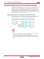
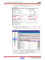
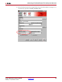
Generating a PlanAhead Project File from System Generator . . . . . . . . . . . . . . . . . 82
Step-by-Step Example for Generating a PlanAhead Project File . . . . . . . . . . . . . . . . . 82
Importing a System Generator Design into PlanAhead . . . . . . . . . . . . . . . . . . . . . . 86
Steps to Import a System Generator Design as a Sub-Module . . . . . . . . . . . . . . . . . . . 86
Creating a New System Generator Design from within PlanAhead . . . . . . . . . . . . . . 87
Configurable Subsystems and System Generator . . . . . . . . . . . . . . . . . . . . . . . . . . . . 88
System Generator for DSP User Guide
UG640 (v 14.3) October 16, 2012
www.xilinx.com
3
Defining a Configurable Subsystem . . . . . . . . . . . . . . . . . . . . . . . . . . . . . . . . . . . . . . . . .
Using a Configurable Subsystem . . . . . . . . . . . . . . . . . . . . . . . . . . . . . . . . . . . . . . . . . . .
Deleting a Block from a Configurable Subsystem . . . . . . . . . . . . . . . . . . . . . . . . . . . . .
Adding a Block to a Configurable Subsystem . . . . . . . . . . . . . . . . . . . . . . . . . . . . . . . .
Generating Hardware from Configurable Subsystems . . . . . . . . . . . . . . . . . . . . . . . . .
88
90
91
91
92
Notes for Higher Performance FPGA Design . . . . . . . . . . . . . . . . . . . . . . . . . . . . . . . . 94
Review the Hardware Notes Included with Each Block Dialog Box . . . . . . . . . . . . . .
Register the Inputs and Outputs of Your Design . . . . . . . . . . . . . . . . . . . . . . . . . . . . . .
Insert Pipeline Registers . . . . . . . . . . . . . . . . . . . . . . . . . . . . . . . . . . . . . . . . . . . . . . . . . . .
Use Saturation Arithmetic and Rounding Only When Necessary . . . . . . . . . . . . . . . .
Use the System Generator Timing and Power Analysis Tools . . . . . . . . . . . . . . . . . . .
Set the Data Rate Option on All Gateway Blocks . . . . . . . . . . . . . . . . . . . . . . . . . . . . . .
Reduce the Clock Enable (CE) Fanout . . . . . . . . . . . . . . . . . . . . . . . . . . . . . . . . . . . . . . .
Experiment with Different Synthesis Settings . . . . . . . . . . . . . . . . . . . . . . . . . . . . . . . . .
Other Things to Try . . . . . . . . . . . . . . . . . . . . . . . . . . . . . . . . . . . . . . . . . . . . . . . . . . . . . . .
94
94
95
97
97
97
97
98
98
Processing a System Generator Design with FPGA Physical Design Tools . . . . 99
HDL Simulation . . . . . . . . . . . . . . . . . . . . . . . . . . . . . . . . . . . . . . . . . . . . . . . . . . . . . . . . . . 99
Generating an FPGA Bitstream . . . . . . . . . . . . . . . . . . . . . . . . . . . . . . . . . . . . . . . . . . . . 102
Resetting Auto-Generated Clock Enable Logic . . . . . . . . . . . . . . . . . . . . . . . . . . . . . . 105
ce_clr and Rate Changing Blocks . . . . . . . . . . . . . . . . . . . . . . . . . . . . . . . . . . . . . . . . . . . 105
ce_clr Usage Recommendations . . . . . . . . . . . . . . . . . . . . . . . . . . . . . . . . . . . . . . . . . . . 107
Design Styles for the DSP48 . . . . . . . . . . . . . . . . . . . . . . . . . . . . . . . . . . . . . . . . . . . . . . . . 108
About the DSP48 . . . . . . . . . . . . . . . . . . . . . . . . . . . . . . . . . . . . . . . . . . . . . . . . . . . . . . . .
Designs Using Standard Components . . . . . . . . . . . . . . . . . . . . . . . . . . . . . . . . . . . . . .
Designs Using Synthesizable Mult, Mux and AddSub Blocks . . . . . . . . . . . . . . . . . .
Designs that Use DSP48 and DSP48 Macro Blocks . . . . . . . . . . . . . . . . . . . . . . . . . . . .
DSP48 Design Techniques . . . . . . . . . . . . . . . . . . . . . . . . . . . . . . . . . . . . . . . . . . . . . . . .
108
109
109
110
115
Using FDATool in Digital Filter Applications . . . . . . . . . . . . . . . . . . . . . . . . . . . . . . 118
Design Overview . . . . . . . . . . . . . . . . . . . . . . . . . . . . . . . . . . . . . . . . . . . . . . . . . . . . . . . .
Open and Generate the Coefficients for this FIR Filter . . . . . . . . . . . . . . . . . . . . . . . .
Parameterize the MAC-Based FIR Block . . . . . . . . . . . . . . . . . . . . . . . . . . . . . . . . . . . .
Generate and Assign Coefficients for the FIR Filter . . . . . . . . . . . . . . . . . . . . . . . . . . .
Browse Through and Understand the Xilinx Filter Block . . . . . . . . . . . . . . . . . . . . . .
Run the Simulation . . . . . . . . . . . . . . . . . . . . . . . . . . . . . . . . . . . . . . . . . . . . . . . . . . . . . .
119
119
120
121
123
124
Generating Multiple Cycle-True Islands for Distinct Clocks . . . . . . . . . . . . . . . . 127
Multiple Clock Applications . . . . . . . . . . . . . . . . . . . . . . . . . . . . . . . . . . . . . . . . . . . . . .
Clock Domain Partitioning . . . . . . . . . . . . . . . . . . . . . . . . . . . . . . . . . . . . . . . . . . . . . . . .
Crossing Clock Domains . . . . . . . . . . . . . . . . . . . . . . . . . . . . . . . . . . . . . . . . . . . . . . . . . .
Netlisting Multiple Clock Designs . . . . . . . . . . . . . . . . . . . . . . . . . . . . . . . . . . . . . . . . .
Step-by-Step Example . . . . . . . . . . . . . . . . . . . . . . . . . . . . . . . . . . . . . . . . . . . . . . . . . . . .
Creating a Top-Level Wrapper . . . . . . . . . . . . . . . . . . . . . . . . . . . . . . . . . . . . . . . . . . . .
127
128
129
130
131
135
Using ChipScope Pro Analyzer for Real-Time Hardware Debugging . . . . . . . . 139
ChipScope Pro Overview . . . . . . . . . . . . . . . . . . . . . . . . . . . . . . . . . . . . . . . . . . . . . . . . . 139
Tutorial Example: Using ChipScope in System Generator . . . . . . . . . . . . . . . . . . . . . 139
Real-Time Debug . . . . . . . . . . . . . . . . . . . . . . . . . . . . . . . . . . . . . . . . . . . . . . . . . . . . . . . . 145
Tutorial Example: Using ChipScope Pro Analyzer with JTAG Hardware Co-Simulation149
AXI Interface . . . . . . . . . . . . . . . . . . . . . . . . . . . . . . . . . . . . . . . . . . . . . . . . . . . . . . . . . . . . . . . 151
Introduction . . . . . . . . . . . . . . . . . . . . . . . . . . . . . . . . . . . . . . . . . . . . . . . . . . . . . . . . . . . .
AXI4 Support in System Generator . . . . . . . . . . . . . . . . . . . . . . . . . . . . . . . . . . . . . . . . .
AXI4-Stream Support in System Generator . . . . . . . . . . . . . . . . . . . . . . . . . . . . . . . . . .
AXI-Stream Blocks in System Generator . . . . . . . . . . . . . . . . . . . . . . . . . . . . . . . . . . . .
4
www.xilinx.com
151
151
152
153
System Generator for DSP User Guide
UG640 (v 14.3) October 16, 2012
: Hardware/Software Co-Design
Hardware/Software Co-Design in System Generator . . . . . . . . . . . . . . . . . . . . . . . . 156
Black Box Block . . . . . . . . . . . . . . . . . . . . . . . . . . . . . . . . . . . . . . . . . . . . . . . . . . . . . . . . . 156
PicoBlaze Block . . . . . . . . . . . . . . . . . . . . . . . . . . . . . . . . . . . . . . . . . . . . . . . . . . . . . . . . . . 156
EDK Processor Block . . . . . . . . . . . . . . . . . . . . . . . . . . . . . . . . . . . . . . . . . . . . . . . . . . . . . 156
Integrating a Processor with Custom Logic. . . . . . . . . . . . . . . . . . . . . . . . . . . . . . . . . . 156
Memory Map Creation . . . . . . . . . . . . . . . . . . . . . . . . . . . . . . . . . . . . . . . . . . . . . . . . . . .
Hardware Generation . . . . . . . . . . . . . . . . . . . . . . . . . . . . . . . . . . . . . . . . . . . . . . . . . . . .
Hardware Co-Simulation . . . . . . . . . . . . . . . . . . . . . . . . . . . . . . . . . . . . . . . . . . . . . . . . .
The Software Driver . . . . . . . . . . . . . . . . . . . . . . . . . . . . . . . . . . . . . . . . . . . . . . . . . . . . .
Writing a Software Program. . . . . . . . . . . . . . . . . . . . . . . . . . . . . . . . . . . . . . . . . . . . . . .
Asynchronous Support . . . . . . . . . . . . . . . . . . . . . . . . . . . . . . . . . . . . . . . . . . . . . . . . . . .
Clock Wiring in the Hardware Co-Simulation Flow . . . . . . . . . . . . . . . . . . . . . . . . . .
158
159
159
160
163
166
167
EDK Support . . . . . . . . . . . . . . . . . . . . . . . . . . . . . . . . . . . . . . . . . . . . . . . . . . . . . . . . . . . . . . 175
Importing an EDK Processor . . . . . . . . . . . . . . . . . . . . . . . . . . . . . . . . . . . . . . . . . . . . . . 175
Exposing Processor Ports to System Generator . . . . . . . . . . . . . . . . . . . . . . . . . . . . . . . 177
Exporting a pcore . . . . . . . . . . . . . . . . . . . . . . . . . . . . . . . . . . . . . . . . . . . . . . . . . . . . . . . . 178
Designing with Embedded Processors and Microcontrollers . . . . . . . . . . . . . . . . 178
Designing PicoBlaze Microcontroller Applications . . . . . . . . . . . . . . . . . . . . . . . . . . . 178
Designing and Exporting MicroBlaze Processor Peripherals . . . . . . . . . . . . . . . . . . . 184
Using XPS . . . . . . . . . . . . . . . . . . . . . . . . . . . . . . . . . . . . . . . . . . . . . . . . . . . . . . . . . . . . . . 200
Using Platform Studio SDK . . . . . . . . . . . . . . . . . . . . . . . . . . . . . . . . . . . . . . . . . . . . . . . 205
Tutorial Example - Using System Generator and SDK to Co-Debug an Embedded DSP Design
214
Summary . . . . . . . . . . . . . . . . . . . . . . . . . . . . . . . . . . . . . . . . . . . . . . . . . . . . . . . . . . . . . . . 237
Chapter 3: Using Hardware Co-Simulation
Introduction . . . . . . . . . . . . . . . . . . . . . . . . . . . . . . . . . . . . . . . . . . . . . . . . . . . . . . . . . . . . 239
M-Code Access to Hardware Co-Simulation . . . . . . . . . . . . . . . . . . . . . . . . . . . . . . . . . 239
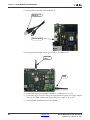
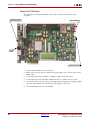
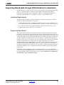
Installing Your Hardware Board . . . . . . . . . . . . . . . . . . . . . . . . . . . . . . . . . . . . . . . . . . . . 239
Ethernet-Based Hardware Co-Simulation . . . . . . . . . . . . . . . . . . . . . . . . . . . . . . . . . . . 239
JTAG-Based Hardware Co-Simulation . . . . . . . . . . . . . . . . . . . . . . . . . . . . . . . . . . . . . . 240
Third-Party Hardware Co-Simulation . . . . . . . . . . . . . . . . . . . . . . . . . . . . . . . . . . . . . . 240
Compiling a Model for Hardware Co-Simulation . . . . . . . . . . . . . . . . . . . . . . . . . . . 241
Choosing a Compilation Target . . . . . . . . . . . . . . . . . . . . . . . . . . . . . . . . . . . . . . . . . . . . 241
Invoking the Code Generator . . . . . . . . . . . . . . . . . . . . . . . . . . . . . . . . . . . . . . . . . . . . . . 241
Hardware Co-Simulation Blocks . . . . . . . . . . . . . . . . . . . . . . . . . . . . . . . . . . . . . . . . . . . 242
Hardware Co-Simulation Clocking . . . . . . . . . . . . . . . . . . . . . . . . . . . . . . . . . . . . . . . . . 245
Selecting the Target Clock Frequency . . . . . . . . . . . . . . . . . . . . . . . . . . . . . . . . . . . . . . . 245
Clocking Modes . . . . . . . . . . . . . . . . . . . . . . . . . . . . . . . . . . . . . . . . . . . . . . . . . . . . . . . . . 246
Selecting the Clock Mode . . . . . . . . . . . . . . . . . . . . . . . . . . . . . . . . . . . . . . . . . . . . . . . . . 246
Board-Specific I/O Ports . . . . . . . . . . . . . . . . . . . . . . . . . . . . . . . . . . . . . . . . . . . . . . . . . . . . 247
I/O Ports in Hardware Co-simulation . . . . . . . . . . . . . . . . . . . . . . . . . . . . . . . . . . . . . . 248
Ethernet Hardware Co-Simulation . . . . . . . . . . . . . . . . . . . . . . . . . . . . . . . . . . . . . . . . . . 248
Point-to-Point Ethernet Hardware Co-Simulation . . . . . . . . . . . . . . . . . . . . . . . . . . . . 249
Network-Based Ethernet Hardware Co-Simulation . . . . . . . . . . . . . . . . . . . . . . . . . . . 253
Remote JTAG Cable Support in JTAG Co-Simulation . . . . . . . . . . . . . . . . . . . . . . . . . 254
Shared Memory Support . . . . . . . . . . . . . . . . . . . . . . . . . . . . . . . . . . . . . . . . . . . . . . . . . . . 256
Compiling Shared Memories for Hardware Co-Simulation . . . . . . . . . . . . . . . . . . . . 257
Co-Simulating Unprotected Shared Memories . . . . . . . . . . . . . . . . . . . . . . . . . . . . . . . 259
System Generator for DSP User Guide
UG640 (v 14.3) October 16, 2012
www.xilinx.com
5
Co-Simulating Lockable Shared Memories . . . . . . . . . . . . . . . . . . . . . . . . . . . . . . . . . .
Co-Simulating Shared Registers . . . . . . . . . . . . . . . . . . . . . . . . . . . . . . . . . . . . . . . . . . .
Co-Simulating Shared FIFOs . . . . . . . . . . . . . . . . . . . . . . . . . . . . . . . . . . . . . . . . . . . . . .
Restrictions on Shared Memories . . . . . . . . . . . . . . . . . . . . . . . . . . . . . . . . . . . . . . . . . .
260
262
263
266
Specifying Xilinx Tool Flow Settings . . . . . . . . . . . . . . . . . . . . . . . . . . . . . . . . . . . . . . . 266
Frame-Based Acceleration using Hardware Co-Simulation . . . . . . . . . . . . . . . . . . 268
Shared Memories . . . . . . . . . . . . . . . . . . . . . . . . . . . . . . . . . . . . . . . . . . . . . . . . . . . . . . . .
Adding Buffers to a Design . . . . . . . . . . . . . . . . . . . . . . . . . . . . . . . . . . . . . . . . . . . . . . .
Compiling for Hardware Co-simulation . . . . . . . . . . . . . . . . . . . . . . . . . . . . . . . . . . . .
Using Vector Transfers . . . . . . . . . . . . . . . . . . . . . . . . . . . . . . . . . . . . . . . . . . . . . . . . . . .
268
270
274
276
Real-Time Signal Processing using Hardware Co-Simulation . . . . . . . . . . . . . . . 281
Shared Memory I/O Buffering Example . . . . . . . . . . . . . . . . . . . . . . . . . . . . . . . . . . . .
Applying a 5x5 Filter Kernel Data Path . . . . . . . . . . . . . . . . . . . . . . . . . . . . . . . . . . . . .
5x5 Filter Kernel Test Bench . . . . . . . . . . . . . . . . . . . . . . . . . . . . . . . . . . . . . . . . . . . . . . .
Reloading the Kernel . . . . . . . . . . . . . . . . . . . . . . . . . . . . . . . . . . . . . . . . . . . . . . . . . . . . .
281
283
286
290
Installing Your Board for Ethernet Hardware Co-Simulation . . . . . . . . . . . . . . . . 291
Installing Software on the Host PC . . . . . . . . . . . . . . . . . . . . . . . . . . . . . . . . . . . . . . . . . 291
Setting Up the Local Area Network on the PC . . . . . . . . . . . . . . . . . . . . . . . . . . . . . . . 291
Loading the Sysgen HW Co-Sim Configuration Files . . . . . . . . . . . . . . . . . . . . . . . . . 293
Installing the Proxy Executable for Linux Users . . . . . . . . . . . . . . . . . . . . . . . . . . . . . . 295
Installing an ML402 Board for Ethernet Hardware Co-Simulation . . . . . . . . . . . . . . 295
Installing an ML506 Board for Ethernet Hardware Co-Simulation . . . . . . . . . . . . . . 300
Installing an ML605 Board for Ethernet Hardware Co-Simulation . . . . . . . . . . . . . . 305
Installing a Spartan-3A DSP 1800A Starter Board for Ethernet Hardware Co-Simulation307
Installing a Spartan-3A DSP 3400A Board for Ethernet Hardware Co-Simulation . 308
Installing an SP601/SP605 Board for Ethernet Hardware Co-Simulation . . . . . . . . 313
Installing Your Board for JTAG Hardware Co-Simulation. . . . . . . . . . . . . . . . . . . 315
Installing an ML402 Board for JTAG Hardware Co-Simulation . . . . . . . . . . . . . . . . .
Installing an ML605 Board for JTAG Hardware Co-Simulation . . . . . . . . . . . . . . . . .
Installing an SP601/SP605 Board for JTAG Hardware Co-Simulation . . . . . . . . . . .
Installing a KC705 Board for JTAG Hardware Co-Simulation . . . . . . . . . . . . . . . . . .
315
317
319
321
Supporting New Boards through JTAG Hardware Co-Simulation . . . . . . . . . . . 323
Hardware Requirements . . . . . . . . . . . . . . . . . . . . . . . . . . . . . . . . . . . . . . . . . . . . . . . . . . 323
Supporting New Boards . . . . . . . . . . . . . . . . . . . . . . . . . . . . . . . . . . . . . . . . . . . . . . . . . . 323
Chapter 4: Importing HDL Modules
Black Box HDL Requirements and Restrictions . . . . . . . . . . . . . . . . . . . . . . . . . . . . .
Black Box Configuration Wizard . . . . . . . . . . . . . . . . . . . . . . . . . . . . . . . . . . . . . . . . . . .
Black Box Configuration M-Function . . . . . . . . . . . . . . . . . . . . . . . . . . . . . . . . . . . . . . .
HDL Co-Simulation . . . . . . . . . . . . . . . . . . . . . . . . . . . . . . . . . . . . . . . . . . . . . . . . . . . . . . . .
338
339
340
354
Introduction . . . . . . . . . . . . . . . . . . . . . . . . . . . . . . . . . . . . . . . . . . . . . . . . . . . . . . . . . . . . 354
Configuring the HDL Simulator . . . . . . . . . . . . . . . . . . . . . . . . . . . . . . . . . . . . . . . . . . . 354
Co-Simulating Multiple Black Boxes . . . . . . . . . . . . . . . . . . . . . . . . . . . . . . . . . . . . . . . . 356
Black Box Examples . . . . . . . . . . . . . . . . . . . . . . . . . . . . . . . . . . . . . . . . . . . . . . . . . . . . . . . . 357
Importing a Xilinx Core Generator Module . . . . . . . . . . . . . . . . . . . . . . . . . . . . . . . . . .
Importing a VHDL Module . . . . . . . . . . . . . . . . . . . . . . . . . . . . . . . . . . . . . . . . . . . . . . .
Importing a Verilog Module . . . . . . . . . . . . . . . . . . . . . . . . . . . . . . . . . . . . . . . . . . . . . .
Dynamic Black Boxes. . . . . . . . . . . . . . . . . . . . . . . . . . . . . . . . . . . . . . . . . . . . . . . . . . . . .
Simulating Several Black Boxes Simultaneously . . . . . . . . . . . . . . . . . . . . . . . . . . . . . .
Advanced Black Box Example Using ModelSim . . . . . . . . . . . . . . . . . . . . . . . . . . . . . .
6
www.xilinx.com
357
371
378
380
382
384
System Generator for DSP User Guide
UG640 (v 14.3) October 16, 2012
Importing, Simulating, and Exporting an Encrypted VHDL File . . . . . . . . . . . . . . . . 389
Black Box Tutorial Exercise 9: Prompting a User for Parameters in a Simulink Model and
Passing Them to a Black Box . . . . . . . . . . . . . . . . . . . . . . . . . . . . . . . . . . . . . . . . . . . . 394
Chapter 5: System Generator Compilation Types
HDL Netlist Compilation . . . . . . . . . . . . . . . . . . . . . . . . . . . . . . . . . . . . . . . . . . . . . . . . . . 398
NGC Netlist Compilation . . . . . . . . . . . . . . . . . . . . . . . . . . . . . . . . . . . . . . . . . . . . . . . . . . 398
Bitstream Compilation . . . . . . . . . . . . . . . . . . . . . . . . . . . . . . . . . . . . . . . . . . . . . . . . . . . . . 399
XFLOW Option Files . . . . . . . . . . . . . . . . . . . . . . . . . . . . . . . . . . . . . . . . . . . . . . . . . . . . . 400
Additional Settings . . . . . . . . . . . . . . . . . . . . . . . . . . . . . . . . . . . . . . . . . . . . . . . . . . . . . . 401
Re-Compiling EDK Processor Block Software Programs in Bitstreams . . . . . . . . . . 402
EDK Export Tool . . . . . . . . . . . . . . . . . . . . . . . . . . . . . . . . . . . . . . . . . . . . . . . . . . . . . . . . . . . 403
Creating a Custom Bus Interface for Pcore Export . . . . . . . . . . . . . . . . . . . . . . . . . . . .
Export as Pcore to EDK . . . . . . . . . . . . . . . . . . . . . . . . . . . . . . . . . . . . . . . . . . . . . . . . . . .
System Generator Ports as Top-Level Ports in EDK . . . . . . . . . . . . . . . . . . . . . . . . . . .
Supported Processors and Current Limitations . . . . . . . . . . . . . . . . . . . . . . . . . . . . . .
See Also: . . . . . . . . . . . . . . . . . . . . . . . . . . . . . . . . . . . . . . . . . . . . . . . . . . . . . . . . . . . . . . .
404
405
406
406
406
Hardware Co-Simulation Compilation . . . . . . . . . . . . . . . . . . . . . . . . . . . . . . . . . . . . . 407
Timing and Power Analysis Compilation . . . . . . . . . . . . . . . . . . . . . . . . . . . . . . . . . . . 407
Timing Analysis Concepts Review . . . . . . . . . . . . . . . . . . . . . . . . . . . . . . . . . . . . . . . . . 409
Timing Analyzer Features . . . . . . . . . . . . . . . . . . . . . . . . . . . . . . . . . . . . . . . . . . . . . . . . 410
Creating Compilation Targets . . . . . . . . . . . . . . . . . . . . . . . . . . . . . . . . . . . . . . . . . . . . . . 416
Defining New Compilation Targets . . . . . . . . . . . . . . . . . . . . . . . . . . . . . . . . . . . . . . . . 417
Index . . . . . . . . . . . . . . . . . . . . . . . . . . . . . . . . . . . . . . . . . . . . . . . . . . . . . . . . . . . . . . . . . . . . . . . . . . .
System Generator for DSP User Guide
UG640 (v 14.3) October 16, 2012
www.xilinx.com
421
7
8
www.xilinx.com
System Generator for DSP User Guide
UG640 (v 14.3) October 16, 2012
Chapter 1
Hardware Design Using System
Generator
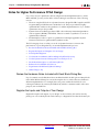
System Generator is a system-level modeling tool that facilitates FPGA hardware design. It
extends Simulink in many ways to provide a modeling environment that is well suited to
hardware design. The tool provides high-level abstractions that are automatically
compiled into an FPGA at the push of a button. The tool also provides access to underlying
FPGA resources through low-level abstractions, allowing the construction of highly
efficient FPGA designs.
A Brief Introduction to FPGAs
Provides background on FPGAs, and discusses
compilation, programming, and architectural
considerations in the context of System Generator.
Design Flows using System
Generator
Describes several settings in which constructing
designs in System Generator is useful.
System-Level Modeling in
System Generator
Discusses System Generator's ability to implement
device-specific hardware designs directly from a
flexible, high-level, system modeling environment.
Automatic Code Generation
Discusses automatic code generation for System
Generator designs.
Compiling MATLAB into an
FPGA
Describes how to use a subset of the MATLAB
programming language to write functions that
describe state machines and arithmetic operators.
Functions written in this way can be attached to
blocks in System Generator and can be automatically
compiled into equivalent HDL.
Importing a System Generator
Design into a Bigger System
Discusses how to take the VHDL netlist from a System
Generator design and synthesize it in order to embed
it into a larger design. Also shows how VHDL created
by System Generator can be incorporated into a
simulation model of the overall system.
Generating a PlanAhead Project
File from System Generator
Provides an example of how to generate a PlanAhead
project file (with design strategies) and invoke
PlanAhead from within System Generator.
System Generator for DSP User Guide
UG640 (v 14.3) October 16, 2012
www.xilinx.com
9
Chapter 1: Hardware Design Using System Generator
Configurable Subsystems and
System Generator
Explains how to use configurable subsystems in
System Generator. Describes common tasks such as
defining configurable subsystems, deleting and
adding blocks, and using configurable subsystems to
import compilation results into System Generator
designs.
Notes for Higher Performance
FPGA Design
Suggests design practices in System Generator that
lead to an efficient and high-performance
implementation in an FPGA.
Processing a System Generator
Design with FPGA Physical
Design Tools
Describes how to take the low-level HDL produced by
System Generator and use it in tools like Xilinx's
Project Navigator, ModelSim, and Synplicity's
Synplify.
Resetting Auto-Generated Clock
Enable Logic
Describes the behavior of rate changing blocks from
the System Generator library when the ce_clr signal
is used for re-synchronization.
Design Styles for the DSP48
Describes three ways to implement and configure a
DSP48 (Xtreme DSP Slice) in System Generator
Using FDATool in Digital Filter
Applications
Demonstrates one way to specify, implement and
simulate a FIR filter using the FDATool block.
Generating Multiple Cycle-True
Islands for Distinct Clocks
Describes how to implement multi-clock designs in
System Generator
Using ChipScope Pro Analyzer
for Real-Time Hardware
Debugging
Demonstrates how to connect and use the Xilinx
Debug Tool called ChipScope™ Pro within System
Generator
AXI Interface
Provides an introduction to AMBA AXI4 and
draws attention to AMBA AXI4 details with
respect to System Generator.
A Brief Introduction to FPGAs
A field programmable gate array (FPGA) is a general-purpose integrated circuit that is
“programmed” by the designer rather than the device manufacturer. Unlike an
application-specific integrated circuit (ASIC), which can perform a similar function in an
electronic system, an FPGA can be reprogrammed, even after it has been deployed into a
system.
An FPGA is programmed by downloading a configuration program called a bitstream into
static on-chip random-access memory. Much like the object code for a microprocessor, this
bitstream is the product of compilation tools that translate the high-level abstractions
produced by a designer into something equivalent but low-level and executable. Xilinx
System Generator pioneered the idea of compiling an FPGA program from a high-level
Simulink model.
An FPGA provides you with a two-dimensional array of configurable resources that can
implement a wide range of arithmetic and logic functions. These resources include
dedicated DSP blocks, multipliers, dual port memories, lookup tables (LUTs), registers, tristate buffers, multiplexers, and digital clock managers. In addition, Xilinx FPGAs contain
sophisticated I/O mechanisms that can handle a wide range of bandwidth and voltage
requirements. The Virtex®-4 FPGAs include embedded microcontrollers (IBM PowerPC®
10
www.xilinx.com
System Generator for DSP User Guide
UG640 (v 14.3) October 16, 2012
A Brief Introduction to FPGAs
405), and multi-gigabit serial transceivers. The compute and I/O resources are linked
under the control of the bitstream by a programmable interconnect architecture that allows
them to be wired together into systems.
FPGAs are high performance data processing devices. DSP performance is derived from
the FPGA’s ability to construct highly parallel architectures for processing data. In contrast
with a microprocessor or DSP processor, where performance is tied to the clock rate at
which the processor can run, FPGA performance is tied to the amount of parallelism that
can be brought to bear in the algorithms that make up a signal processing system. A
combination of increasingly high system clock rates (current system frequencies of 100-200
MHz are common today) and a highly-distributed memory architecture gives the system
designer an ability to exploit parallelism in DSP (and other) applications that operate on
data streams. For example, the raw memory bandwidth of a large FPGA running at a clock
rate of 150 MHz can be hundreds of terabytes per second.
There are many DSP applications (e.g., digital up/down converters) that can be
implemented only in custom integrated circuits (ICs) or in an FPGA; a von Neumann
processor lacks both the compute capability and the memory bandwidth required.
Advantages of using an FPGA include significantly lower non-recurring engineering costs
than those associated with a custom IC (FPGAs are commercial off-the-shelf devices),
shorter time to market, and the configurability of an FPGA, which allows a design to be
modified, even after deployment in an end application.
When working in System Generator, it is important to keep in mind that an FPGA has
many degrees of freedom in implementing signal processing functions. You have, for
example, the freedom to define data path widths throughout your system and to employ
many individual data processors (e.g., multiply-accumulate engines), depending on
system requirements. System Generator provides abstractions that allow you to design for
an FPGA largely by thinking about the algorithm you want to implement. However, the
more you know about the underlying FPGA, the more likely you are to exploit the unique
capabilities an FPGA provides in achieving high performance.
The remainder of this topic is a brief introduction to some of the logic resources available in
the FPGA, so that you gain some appreciation for the abstractions provided in System
Generator.
System Generator for DSP User Guide
UG640 (v 14.3) October 16, 2012
www.xilinx.com
11
Chapter 1: Hardware Design Using System Generator
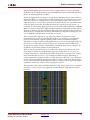
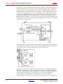
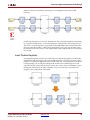
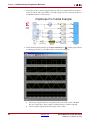
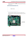
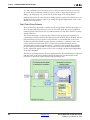
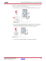
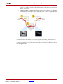
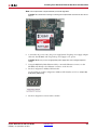
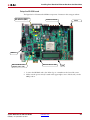
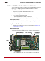
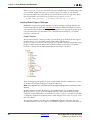
The figure above shows a physical view of a Virtex®-4 FPGA. To a signal DSP engineer, an
FPGA can be thought of as a 2-D array of logic slices striped with columns of hard macro
blocks (block memory and arithmetic blocks) suitable for implementing DSP functions,
embedded within a configurable interconnect mesh. In a Virtex®-4 FPGA, the DSP blocks
(shown in the next figure) can run in excess of 450 MHz, and are pitch-matched to dual
port memory blocks (BRAMs) whose ports can be configured to a wide range of word sizes
(18 Kb total per BRAM). The Virtex®-4 SX55 device contains 512 such DSP blocks and
BRAMs. In System Generator, you can access all of these resources through arithmetic and
logic abstractions to build very high performance digital filters, FFTs, and other arithmetic
and signal processing functions.
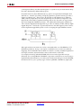
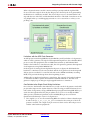
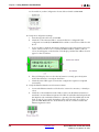
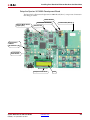
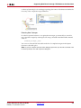
While the multiply-accumulate function supported by a Virtex®-4 DSP block is familiar to
a DSP engineer, it is instructive to take a closer look at the Virtex® FPGA family logic slice
(shown below), which is the fundamental unit of the logic fabric array.
Each logic slice contains two 4-input lookup tables (LUTs), two configurable D-flip flops,
multiplexers, dedicated carry logic, and gates used for creating slice-based multipliers.
Each LUT can implement an arbitrary 4-input Boolean function. Coupled with dedicated
logic for implementing fast carry circuits, the LUTs can also be used to build fast
adder/subtractors and multipliers of essentially any word size. In addition to
implementing Boolean functions, each LUT can also be configured as a 16x1 bit RAM or as
12
www.xilinx.com
System Generator for DSP User Guide
UG640 (v 14.3) October 16, 2012
A Brief Introduction to FPGAs
a shift register (SRL16). An SRL16 shift register is a synchronously clocked 16x1 bit delay
line with a dynamically addressable tap point.
In System Generator, these different memory options are represented with higher-level
abstractions. Instead of providing a D-flip flop primitive, System Generator provides a
register of arbitrary size. There are two blocks that provide abstractions of arbitrary
width, arbitrary depth delay lines that map directly onto the SRL16 configuration. The
delay block can be used for pipeline balancing, and can also be used as storage for timedivision multiplexed (TDM) data streams. The addressable shift register (ASR) block,
with a function depicted in the figure below, provides an arbitrary width, arbitrary depth
tapped delay line. This block is of particular interest to the DSP engineer, since it can be
used to implement tapped delay lines as well as sweeping through TDM data streams.
Although random access memories can be constructed either out of the BRAM or LUT
(RAM16x1) primitives, doing so can require considerable care to ensure most efficient
mappings, and considerable clerical attention to detail to correctly assemble the primitives
into larger structures. System Generator removes the need for such tasks.
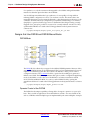
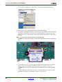
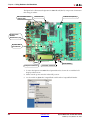
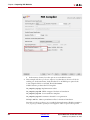
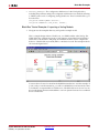
For example, the dual port RAM (DPRAM) block shown in the figure below maps
efficiently onto as many BRAM or RAM16x1 components on the device as are necessary to
implement the desired memory. As can be seen from the mask dialog box for the DPRAM,
the interface allows you to specify a type of memory (BRAM or RAM16x1), depth (data
System Generator for DSP User Guide
UG640 (v 14.3) October 16, 2012
www.xilinx.com
13
Chapter 1: Hardware Design Using System Generator
width is inferred from the Simulink signal driving a particular input port), initial memory
contents, and other characteristics.
In general, System Generator maps abstractions onto device primitives efficiently, freeing
you from worrying about interconnections between the primitives. System Generator
employs libraries of intellectual property (IP) when appropriate to provide efficient
implementations of functions in the block libraries. In this way, you don’t always have to
have detailed knowledge of the underlying FPGA details. However, when it makes sense
to implement an algorithm using basic functions (e.g., adder, register, memory), System
Generator allows you to exploit your FPGA knowledge while reducing the clerical tasks of
managing all signals explicitly.
System Generator library blocks and the mapping from Simulink to hardware are
described in detail in subsequent topics of this documentation. There is a wealth of
detailed information about FPGAs that can be found online at http://support.xilinx.com,
including data books, application notes, white papers, and technical articles.
Note to the DSP Engineer
System Generator extends Simulink to enable hardware design, providing high-level
abstractions that can be automatically compiled into an FPGA. Although the arithmetic
abstractions are suitable to Simulink (discrete time and space dynamical system
simulation), System Generator also provides access to features in the underlying FPGA.
The more you know about a hardware realization (e.g., how to exploit parallelism and
pipelining), the better the implementation you’ll obtain. Using IP cores makes it possible to
have efficient FPGA designs that include complex functions like FFTs. System Generator
also makes it possible to refine a model to more accurately fit the application.
Scattered throughout the System Generator documentation are notes that explain ways in
which system parameters can be used to exploit hardware capabilities.
14
www.xilinx.com
System Generator for DSP User Guide
UG640 (v 14.3) October 16, 2012
Design Flows using System Generator
Note to the Hardware Engineer
System Generator does not replace hardware description language (HDL)-based design,
but does makes it possible to focus your attention only on the critical parts. By analogy,
most DSP programmers do not program exclusively in assembler; they start in a higherlevel language like C, and write assembly code only where it is required to meet
performance requirements.
A good rule of thumb is this: in the parts of the design where you must manage internal
hardware clocks (e.g., using the DDR or phased clocking), you should implement using
HDL. The less critical portions of the design can be implemented in System Generator, and
then the HDL and System Generator portions can be connected. Usually, most portions of
a signal processing system do not need this level of control, except at external interfaces.
System Generator provides mechanisms to import HDL code into a design (see Importing
HDL Modules) that are of particular interest to the HDL designer.
Another aspect of System Generator that is of interest to the engineer who designs using
HDL is its ability to automatically generate an HDL testbench, including test vectors. This
aspect is described in the topic HDL Testbench.
Finally, the hardware co-simulation interfaces described in the topic Using Hardware CoSimulation allow you to run a design in hardware under the control of Simulink, bringing
the full power of MATLAB and Simulink to bear for data analysis and visualization.
Design Flows using System Generator
System Generator can be useful in many settings. Sometimes you may want to explore an
algorithm without translating the design into hardware. Other times you might plan to use
a System Generator design as part of something bigger. A third possibility is that a System
Generator design is complete in its own right, and is to be used in FPGA hardware. This
topic describes all three possibilities.
Algorithm Exploration
System Generator is particularly useful for algorithm exploration, design prototyping, and
model analysis. When these are the goals, you can use the tool to flesh out an algorithm in
order to get a feel for the design problems that are likely to be faced, and perhaps to
estimate the cost and performance of an implementation in hardware. The work is
preparatory, and there is little need to translate the design into hardware.
In this setting, you assemble key portions of the design without worrying about fine points
or detailed implementation. Simulink blocks and MATLAB M-code provide stimuli for
simulations, and for analyzing results. Resource estimation gives a rough idea of the cost
of the design in hardware. Experiments using hardware generation can suggest the
hardware speeds that are possible.
Once a promising approach has been identified, the design can be fleshed out. System
Generator allows refinements to be done in steps, so some portions of the design can be
made ready for implementation in hardware, while others remain high-level and abstract.
System Generator's facilities for hardware co-simulation are particularly useful when
portions of a design are being refined.
Implementing Part of a Larger Design
Often System Generator is used to implement a portion of a larger design. For example,
System Generator is a good setting in which to implement data paths and control, but is
System Generator for DSP User Guide
UG640 (v 14.3) October 16, 2012
www.xilinx.com
15
Chapter 1: Hardware Design Using System Generator
less well suited for sophisticated external interfaces that have strict timing requirements. In
this case, it may be useful to implement parts of the design using System Generator,
implement other parts outside, and then combine the parts into a working whole.
A typical approach to this flow is to create an HDL wrapper that represents the entire
design, and to use the System Generator portion as a component. The non-System
Generator portions of the design can also be components in the wrapper, or can be
instantiated directly in the wrapper.
Implementing a Complete Design
Many times, everything needed for a design is available inside System Generator. For such
a design, pressing the Generate button instructs System Generator to translate the design
into HDL, and to write the files needed to process the HDL using downstream tools. The
files written include the following:
•
HDL that implements the design itself;
•
A clock wrapper that encloses the design. This clock wrapper produces the clock and
clock enable signals that the design needs.
•
A HDL testbench that encloses the clock wrapper. The testbench allows results from
Simulink simulations to be compared against ones produced by a logic simulator.
•
Project files and scripts that allow various synthesis tools, such as XST and Synplify
Pro to operate on System Generator HDL
•
Files that allow the System Generator HDL to be used as a project in Project
Navigator.
For details concerning the files that System Generator writes, see the topic Compilation
Results.
16
www.xilinx.com
System Generator for DSP User Guide
UG640 (v 14.3) October 16, 2012
System-Level Modeling in System Generator
System-Level Modeling in System Generator
System Generator allows device-specific hardware designs to be constructed directly in a
flexible high-level system modeling environment. In a System Generator design, signals
are not just bits. They can be signed and unsigned fixed-point numbers, and changes to the
design automatically translate into appropriate changes in signal types. Blocks are not just
stand-ins for hardware. They respond to their surroundings, automatically adjusting the
results they produce and the hardware they become.
System Generator allows designs to be composed from a variety of ingredients. Data flow
models, traditional hardware design languages (VHDL, Verilog, and EDIF), and functions
derived from the MATLAB programming language, can be used side-by-side, simulated
together, and synthesized into working hardware. System Generator simulation results are
bit and cycle-accurate. This means results seen in simulation exactly match the results that
are seen in hardware. System Generator simulations are considerably faster than those
from traditional HDL simulators, and results are easier to analyze.
System Generator Blocksets
Describes how System Generator's blocks are
organized in libraries, and how the blocks can be
parameterized and used.
Signal Types
Describes the data types used by System Generator
and ways in which data types can be automatically
assigned by the tool.
Bit-True and Cycle-True
Modeling
Specifies the relationship between the Simulink-based
simulation of a System Generator model and the
behavior of the hardware that can be generated from
it.
Timing and Clocking
Describes how clocks are implemented in hardware,
and how their implementation is controlled inside
System Generator. Explains how System Generator
translates a multirate Simulink model into working
clock-synchronous hardware.
Synchronization Mechanisms
Describes mechanisms that can be used to
synchronize data flow across the data path elements
in a high-level System Generator design, and
describes how control path functions can be
implemented.
Block Masks and Parameter
Passing
Explains how parameterized systems and subsystems
are created in Simulink.
Resource Estimation
Describes how to generate estimates of the hardware
needed to implement a System Generator design.
System Generator for DSP User Guide
UG640 (v 14.3) October 16, 2012
www.xilinx.com
17
Chapter 1: Hardware Design Using System Generator
System Generator Blocksets
A Simulink blockset is a library of blocks that can be connected in the Simulink block editor
to create functional models of a dynamical system. For system modeling, System
Generator blocksets are used like other Simulink blocksets. The blocks provide
abstractions of mathematical, logic, memory, and DSP functions that can be used to build
sophisticated signal processing (and other) systems. There are also blocks that provide
interfaces to other software tools (e.g., FDATool, ModelSim) as well as the System
Generator code generation software.
System Generator blocks are bit-accurate and cycle-accurate. Bit-accurate blocks produce
values in Simulink that match corresponding values produced in hardware; cycle-accurate
blocks produce corresponding values at corresponding times.
18
www.xilinx.com
System Generator for DSP User Guide
UG640 (v 14.3) October 16, 2012
System-Level Modeling in System Generator
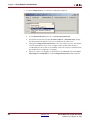
Xilinx Blockset
The Xilinx Blockset is a family of libraries that contain basic System Generator blocks.
Some blocks are low-level, providing access to device-specific hardware. Others are highlevel, implementing (for example) signal processing and advanced communications
algorithms. For convenience, blocks with broad applicability (e.g., the Gateway I/O
blocks) are members of several libraries. Every block is contained in the Index library. The
libraries are described below.
Note: It is important that you don’t name your design the same as a Xilinx block. For example, if you
name your design shared_memory.mdl, it may cause System Generator to issue an error message.
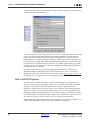
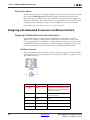
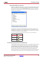
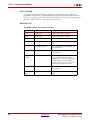
Library
Description
AXI4
Blocks with interfaces that conform to the AXI™4 specification
Basic Elements
ElementsStandard building blocks for digital logic
Communication
Forward error correction and modulator blocks, commonly used in
digital communications systems
Control Logic
Blocks for control circuitry and state machines
DSP
Digital signal processing (DSP) blocks
Data Types
Blocks that convert data types (includes gateways)
Floating-Point
Blocks that support the Floating-Point data type
Index
Every block in the Xilinx Blockset.
Math
Blocks that implement mathematical functions
Memory
Blocks that implement and access memories
Shared Memory
Blocks that implement and access Xilinx shared memories
Tools
“Utility” blocks, e.g., code generation (System Generator token),
resource estimation, HDL co-simulation, etc
Note: More information concerning blocks can be found in the topic Xilinx Blockset.
Xilinx Reference Blockset
The Xilinx Reference Blockset contains composite System Generator blocks that implement
a wide range of functions. Blocks in this blockset are organized by function into different
libraries. The libraries are described below.
Library
Description
Communication
Blocks commonly used in digital communications systems
Control Logic
LogicBlocks used for control circuitry and state machines
DSP
Digital signal processing (DSP) blocks
Imaging
Image processing blocks
Math
Blocks that implement mathematical functions
System Generator for DSP User Guide
UG640 (v 14.3) October 16, 2012
www.xilinx.com
19
Chapter 1: Hardware Design Using System Generator
Each block in this blockset is a composite, i.e., is implemented as a masked subsystem, with
parameters that configure the block.
You can use blocks from the Reference Blockset libraries as is, or as starting points when
constructing designs that have similar characteristics. Each reference block has a
description of its implementation and hardware resource requirements. Individual
documentation for each block is also provided in the topic Xilinx Reference Blockset.
Signal Types
In order to provide bit-accurate simulation of hardware, System Generator blocks operate
on Boolean, floating-point, and arbitrary precision fixed-point values. By contrast, the
fundamental scalar signal type in Simulink is double precision floating point. The
connection between Xilinx blocks and non-Xilinx blocks is provided by gateway blocks. The
gateway in converts a double precision signal into a Xilinx signal, and the gateway out
converts a Xilinx signal into double precision. Simulink continuous time signals must be
sampled by the Gateway In block.
Most Xilinx blocks are polymorphic, i.e., they are able to deduce appropriate output types
based on their input types. When full precision is specified for a block in its parameters
dialog box, System Generator chooses the output type to ensure no precision is lost. Sign
extension and zero padding occur automatically as necessary. User-specified precision is
usually also available. This allows you to set the output type for a block and to specify how
quantization and overflow should be handled. Quantization possibilities include unbiased
rounding towards plus or minus infinity, depending on sign, or truncation. Overflow
options include saturation, truncation, and reporting overflow as an error.
20
www.xilinx.com
System Generator for DSP User Guide
UG640 (v 14.3) October 16, 2012
System-Level Modeling in System Generator
Note: System Generator data types can be displayed by selecting Format > Port Data Types in
Simulink. Displaying data types makes it easy to determine precision throughout a model. If, for
example, the type for a port is Fix_11_9, then the signal is a two's complement signed 11-bit number
having nine fractional bits. Similarly, if the type is Ufix_5_3, then the signal is an unsigned 5-bit
number having three fractional bits.
In the System Generator portion of a Simulink model, every signal must be sampled.
Sample times may be inherited using Simulink's propagation rules, or set explicitly in a
block customization dialog box. When there are feedback loops, System Generator is
sometimes unable to deduce sample periods and/or signal types, in which case the tool
issues an error message. Assert blocks must be inserted into loops to address this problem.
It is not necessary to add assert blocks at every point in a loop; usually it suffices to add an
assert block at one point to “break” the loop.
Note: Simulink can display a model by shading blocks and signals that run at different rates with
different colors (Format > Sample Time Colors in the Simulink pulldown menus). This is often useful
in understanding multirate designs.
Floating-Point Data Type
System Generator blocks found in the Floating-Point library support the floating-point
data type.
System Generator uses the Floating-Point Operator v6.0 IP core to leverage the
implementation of operations such as addition/subtraction, multiplication, comparisons
and data type conversion.
The floating-point data type support is in compliance with IEEE-754 Standard for FloatingPoint Arithmetic. Single precision, Double precision and Custom precision floating-point
data types are supported for design input, data type display and for data rate and type
propagation (RTP) across the supported System Generator blocks.
IEEE-754 Standard for Floating-Point Data Type
As shown below, floating-point data is represented using one Sign bit (S), X exponent bits
and Y fraction bits. The Sign bit is always the most-significant bit (MSB).
S
X Exponent bits
E0 to Ex-1
Y Fraction Bits
F0 to FY-1
According to the IEEE-754 standard, a floating-point value is represented and stored in the
normalized form. In the normalized form the exponent value E is a biased/normalized
value. The normalized exponent, E, equals the sum of the actual exponent value and the
exponent bias. In the normalized form, Y-1 bits are used to store the fraction value. The F 0
fraction bit is always a hidden bit and its value is assumed to be 1.
S represents the value of the sign of the number. If S is 0 then the value is a positive
floating-point number; otherwise it is negative. The X bits that follow are used to store the
normalized exponent value E and the last Y-1 bits are used to store the fraction/mantissa
value in the normalized form.
For the given exponent width, the exponent bias is calculated using the following
equation:
System Generator for DSP User Guide
UG640 (v 14.3) October 16, 2012
www.xilinx.com
21
Chapter 1: Hardware Design Using System Generator
Exponent_bias = 2(X - 1) - 1, where X is the exponent bit width.
According to the IEEE standard, a single precision floating-point data is represented using
32 bits. The normalized exponent and fraction/mantissa are allocated 8 and 24 bits,
respectively. The exponent bias for single precision is 127. Similarly, a double precision
floating-point data is represented using a total of 64 bits where the exponent bit width is 11
and the fraction bit width is 53. The exponent bias value for double precision is 1023.
The normalized floating-point number in the equation form is represented as follows:
Normalized Floating-Point Value = (-1)S x F0.F1F2 …. FY-2FY-1 x (2)E
The actual value of exponent (E_actual) = E - Exponent_bias. Considering 1 as the value for
the hidden bit F0 and the E_actual value, a floating-point number can be calculated as
follows:
FP_Value = (-1)S x 1.F1F2 …. FY-2FY-1 x (2)(E_actual)
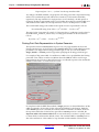
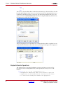
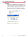
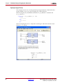
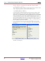
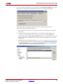
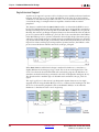
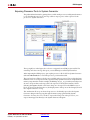
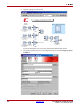
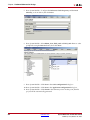
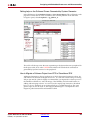
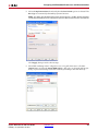
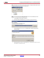
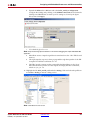
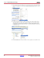
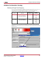
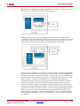
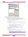
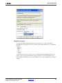
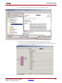
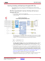
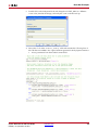
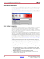
Floating-Point Data Representation in System Generator
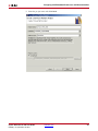
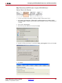
The System Generator Gateway In block previously only supported the Boolean and
Fixed-point data types. As shown below, the Gateway In block GUI and underlying mask
parameters now support the Floating-point data type as well. You can select either a
Single, Double or Custom precision type after specifying the floating-point data type.
For example, if Exponent width of 9 and Fraction width of 31 is specified then the floatingpoint data value will be stored in total 40 bits where the MSB bit will be used for sign
representation, the following 9 bits will be used to store biased exponent value and the 30
LSB bits will be used to store the fractional value.
In compliance with the IEEE-754 standard, if Single precision is selected then the total bit
width is assumed to be 32; 8 bits for the exponent and 24 bits for the fraction. Similarly
when Double precision is selected, the total bit width is assumed to be 64 bits; 11 bits for
the exponent and 53 bits for the fraction part. When Custom precision is selected, the
Exponent width and Fraction width fields are activated and you are free to specify values
for these fields (8 and 24 are the default values). The total bit width for Custom precision
data is the summation of the number of exponent bits and the number of fraction bits.
22
www.xilinx.com
System Generator for DSP User Guide
UG640 (v 14.3) October 16, 2012
System-Level Modeling in System Generator
Similar to fraction bit width for Single precision and Double precision data types the
fraction bit width for Custom precision data type must include the hidden bit F0
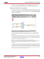
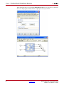
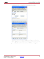
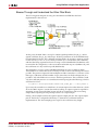
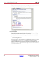
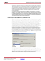
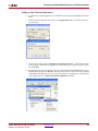
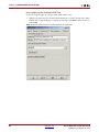
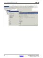
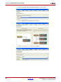
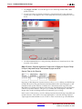
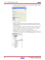
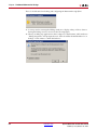
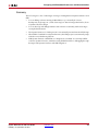
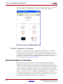
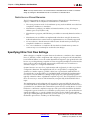
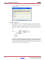
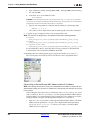
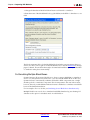
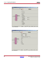
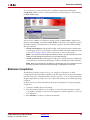
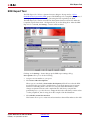
Displaying the Data Type on Output Signals
As shown below, after a successful rate and type propagation, the floating-point data type
is displayed on the output of each System Generator block.To display the signal data type
as shown in the diagram below, you select the pulldown menu item Format > Port/Signal
Displays > Port Data Types.
A floating-point data type is displayed using the format:
XFloat_<exponent_bit_width>_<fraction_bit_width>. Single and Double
precision data types are displayed using the string “XFloat_8_24” and “XFloat_11_53”,
respectively.
If for a Custom precision data type the exponent bit width 9 and the fraction bit width 31
are specified, then it will be displayed as “XFloat_9_31”. A total of 40 bits will be used to
store the floating-point data value. Since floating-point data is stored in a normalized form,
the fractional value will be stored in 30 bits.
In System Generator the fixed-point data type is displayed using format
XFix_<total_data_width>_<binary_point_width>. For example, a fixed-point
data type with the data width of 40 and binary point width of 31 is displayed as
XFix_40_31.
It is necessary to point out that in the fixed-point data type the actual number of bits used
to store the fractional value is different from that used for floating-point data type. In the
example above, all 31 bits are used to store the fractional bits of the fixed-point data type.
System Generator uses the exponent bit width and the fraction bit width to configure and
generate an instance of the Floating-Point Operator core.
System Generator for DSP User Guide
UG640 (v 14.3) October 16, 2012
www.xilinx.com
23
Chapter 1: Hardware Design Using System Generator
Rate and Type Propagation
During data rate and type propagation across a System Generator block that supports
floating-point data, the following design rules are verified. The appropriate error is issued
if one of the following violations is detected.
1.
If a signal carrying floating-point data is connected to the port of a System Generator
block that doesn’t support the floating-point data type.
2.
If the data input (both A and B data inputs, where applicable) and the data output of a
System Generator block are not of the same floating-point data type. The DRC check
will be made between the two inputs of a block as well as between an input and an
output of the block.
If a Custom precision floating-point data type is specified, the exponent bit width and
the fraction bit width of the two ports are compared to determine that they are of the
same data type.
Note: The Convert and Relational blocks are excluded from this check. The Convert block
supports Float-to-float data type conversion between two different floating-point data types. The
Relational block output is always the Boolean data type because it gives a true or false result for
a comparison operation.
3.
If the data inputs are of the fixed-point data type and the data output is expected to be
floating-point and vice versa.
Note: The Convert and Relational blocks are excluded from this check. The Convert block
supports Fixed-to-float as well as Float-to-fixed data type conversion. The Relational block
output is always the Boolean data type because it gives a true or false result for a comparison
operation.
4.
If User Defined precision is selected for the Output Type of blocks that support the
floating-point data type. For example, for blocks such as AddSub, Mult, CMult, and
MUX, only Full output precision is supported if the data inputs are of the floatingpoint data type.
5.
If the Carry In port or Carry Out port is used for the AddSub block when the operation
on a floating-point data type is specified.
6.
If the Floating-Point Operator IP core gives an error for DRC rules defined for the IP.
AXI Signal Groups
System Generator blocks found in the AXI4 library contain interfaces that conform to the
AXI™ 4 specification. Blocks with AXI interfaces are drawn such that ports relating to a
particular AXI interface are grouped and colored in similarly. This makes it easier to
identify data and control signals pertaining to the same interface. Grouping similar AXI
ports together also make it possible to use the Simulink Bus Creator and Simulink Bus
Selector blocks to connect groups of signals together. More information on AXI can be
found in the section entitled AXI Interface. For more detailed information on the AMBA
AXI4 specification, please refer to the Xilinx AMBA AXI4 documents found at the
following location: http://www.xilinx.com/ipcenter/axi4
Bit-True and Cycle-True Modeling
Simulations in System Generator are bit-true and cycle-true. To say a simulation is bit-true
means that at the boundaries (i.e., interfaces between System Generator blocks and nonSystem Generator blocks), a value produced in simulation is bit-for-bit identical to the
corresponding value produced in hardware. To say a simulation is cycle-true means that at
the boundaries, corresponding values are produced at corresponding times. The
24
www.xilinx.com
System Generator for DSP User Guide
UG640 (v 14.3) October 16, 2012
System-Level Modeling in System Generator
boundaries of the design are the points at which System Generator gateway blocks exist.
When a design is translated into hardware, Gateway In (respectively, Gateway Out) blocks
become top-level input (resp., output) ports.
Timing and Clocking
Discrete Time Systems
Designs in System Generator are discrete time systems. In other words, the signals and the
blocks that produce them have associated sample rates. A block’s sample rate determines
how often the block is awoken (allowing its state to be updated). System Generator sets
most sample rates automatically. A few blocks, however, set sample rates explicitly or
implicitly.
Note: For an in-depth explanation of Simulink discrete time systems and sample times, consult the
Using Simulink reference manual from the MathWorks, Inc.
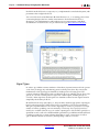
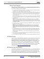
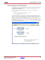
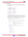
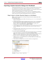
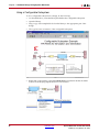
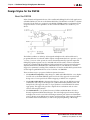
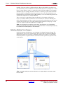
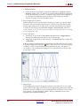
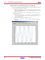
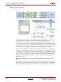
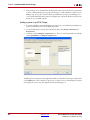
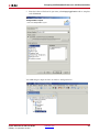
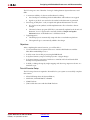
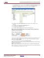
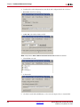
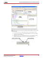
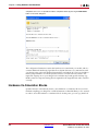
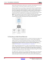
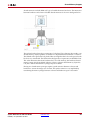
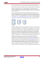
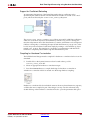
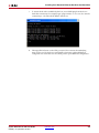
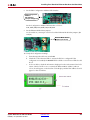
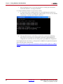
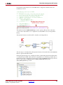
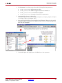
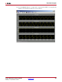
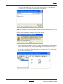
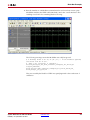
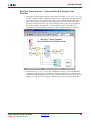
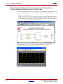
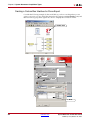
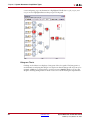
A simple System Generator model illustrates the behavior of discrete time systems.
Consider the model shown below. It contains a gateway that is driven by a Simulink source
(Sine Wave), and a second gateway that drives a Simulink sink (Scope).
The Gateway In block is configured with a sample period of one second. The Gateway Out
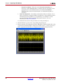
block converts the Xilinx fixed-point signal back to a double (so it can analyzed in the
Simulink scope), but does not alter sample rates. The scope output below shows the
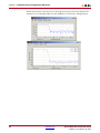
unaltered and sampled versions of the sine wave.
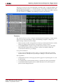
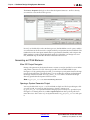
Multirate Models
System Generator supports multirate designs, i.e., designs having signals running at
several sample rates. System Generator automatically compiles multirate models into
System Generator for DSP User Guide
UG640 (v 14.3) October 16, 2012
www.xilinx.com
25
Chapter 1: Hardware Design Using System Generator
hardware. This allows multirate designs to be implemented in a way that is both natural
and straightforward in Simulink.
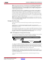
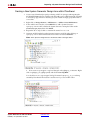
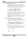
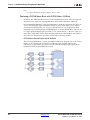
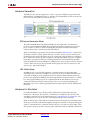
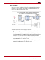
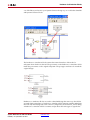
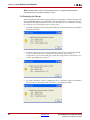
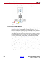
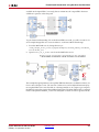
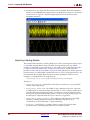
Rate-Changing Blocks
System Generator includes blocks that change sample rates. The most basic rate changers
are the Up Sample and Down Sample blocks. As shown in the figure below, these blocks
explicitly change the rate of a signal by a fixed multiple that is specified in the block’s
dialog box.
Other blocks (e.g., the Parallel To Serial and Serial To Parallel converters) change rates
implicitly in a way determined by block parameterization.
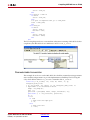
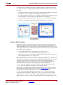
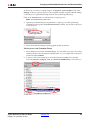
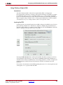
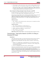
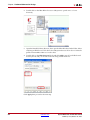
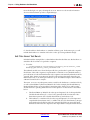
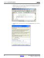
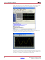
Consider the simple multirate example below. This model has two sample periods, SP1
and SP2. The Gateway In dialog box defines the sample period SP1. The Down Sample
block causes a rate change in the model, creating a new rate SP2 which is half as fast as SP1.
Hardware Oversampling
Some System Generator blocks are oversampled, i.e., their internal processing is done at a
rate that is faster than their data rates. In hardware, this means that the block requires more
than one clock cycle to process a data sample. In Simulink such blocks do not have an
observable effect on sample rates.
One block that can be oversampled is the DAFIR FIR filter. An oversampled DAFIR
processes samples serially, thus running at a higher rate, but using less hardware.
Although blocks that are oversampled do not cause an explicit sample rate change in
Simulink, System Generator considers the internal block rate along with all other sample
rates when generating clocking logic for the hardware implementation. This means that
you must consider the internal processing rates of oversampled blocks when you specify
the Simulink system period value in the System Generator token dialog box.
Asynchronous Clocking
System Generator focuses on the design of hardware that is synchronous to a single clock.
It can, under some circumstances, be used to design systems that contain more than one
clock. This is possible provided the design can be partitioned into individual clock
domains with the exchange of information between domains being regulated by dual port
memories and FIFOs. System Generator fully supports such multi-clock designs, including
the ability to simulate them in Simulink and to generate complete hardware descriptions.
Details are discussed in the topic Generating Multiple Cycle-True Islands for Distinct
Clocks. The remainder of this topic focuses exclusively on the clock-synchronous aspects
of System Generator. This discussion is relevant to both single-clock and multiple-clock
designs.
26
www.xilinx.com
System Generator for DSP User Guide
UG640 (v 14.3) October 16, 2012
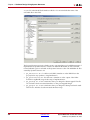
System-Level Modeling in System Generator
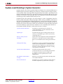
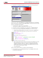
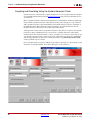
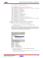
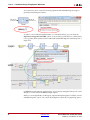
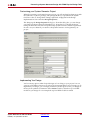
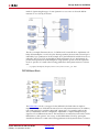
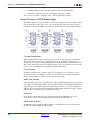
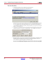
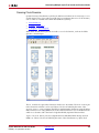
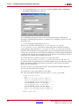
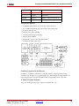
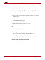
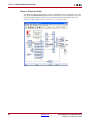
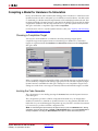
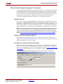
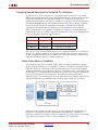
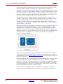
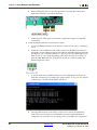
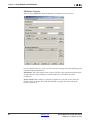
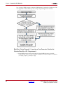
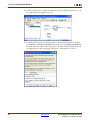
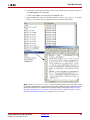
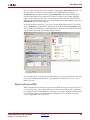
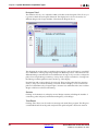
Synchronous Clocking
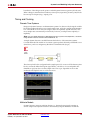
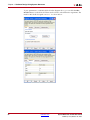
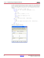
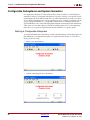
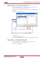
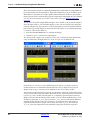
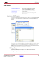
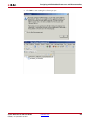
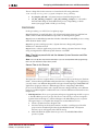
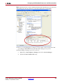
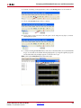
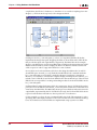
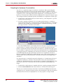
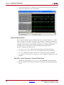
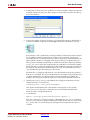
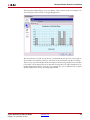
As shown in the figure below, when you use the System Generator token to compile a
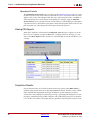
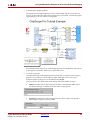
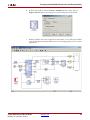
design into hardware, there are three clocking options for Multirate implementation: (1)
Clock Enables (the default), (2) Hybrid DCM-CE, and (3) Expose Clock Ports.
The Clock Enables Option
When System Generator compiles a model into hardware with the Clock Enable option
selected, System Generator preserves the sample rate information of the design in such a
way that corresponding portions in hardware run at appropriate rates. In hardware,
System Generator generates related rates by using a single clock in conjunction with clock
enables, one enable per rate. The period of each clock enable is an integer multiple of the
period of the system clock.
Inside Simulink, neither clocks nor clock enables are required as explicit signals in a
System Generator design. When System Generator compiles a design into hardware, it
uses the sample rates in the design to deduce what clock enables are needed. To do this, it
employs two user-specified values from the System Generator token: the Simulink system
period and FPGA clock period. These numbers define the scaling factor between time in a
Simulink simulation, and time in the actual hardware implementation. The Simulink
system period must be the greatest common divisor (gcd) of the sample periods that
appear in the model, and the FPGA clock period is the period, in nanoseconds, of the
system clock. If p represents the Simulink system period, and c represents the FPGA
system clock period, then something that takes kp units of time in Simulink takes k ticks of
the system clock (hence kc nanoseconds) in hardware.
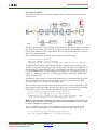
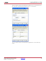
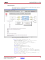
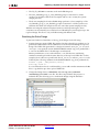
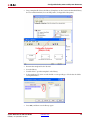
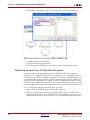
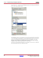
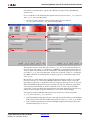
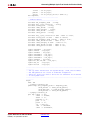
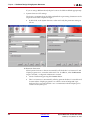
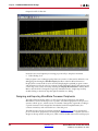
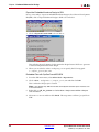
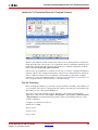
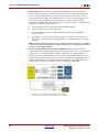
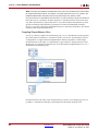
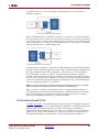
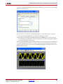
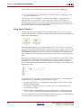
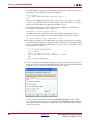
To illustrate this point, consider a model that has three Simulink sample periods 2, 3, and
4. The gcd of these sample periods is 1, and should be specified as such in the Simulink
System Period field for the model. Assume the FPGA Clock Period is specified to be 10ns.
With this information, the corresponding clock enable periods can be determined in
hardware.
In hardware, we refer to the clock enables corresponding to the Simulink sample periods 2,
3, and 4 as CE2, CE3, and CE4, respectively. The relationship of each clock enable period to
the system clock period can be determined by dividing the corresponding Simulink
sample period by the Simulink System Period value. Thus, the periods for CE2, CE3, and
System Generator for DSP User Guide
UG640 (v 14.3) October 16, 2012
www.xilinx.com
27
Chapter 1: Hardware Design Using System Generator
CE4 equal 2, 3, and 4 system clock periods, respectively. A timing diagram for the example
clock enable signals is shown below:
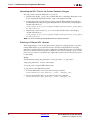
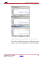
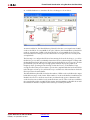
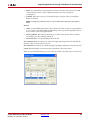
The Hybrid DCM-CE Option
If the implementation target is an FPGA with a Digital Clock Manager (DCM), you can
choose to drive the clock tree with a DCM. The DCM option is desirable when high fanout
on clock enable nets make it difficult to achieve timing closure.
System Generator instantiates the DCM in a top-level HDL clock wrapper and configures
the DCM to provide up to three clock ports at different rates for Virtex®-4 and Virtex®-5 and
up to two clock ports for Spartan-3A DSP. If the design has more clock ports than the DCM
can support, the remaining clocks are supported with the CE (clock enable) configuration.
The mapping of rates to the DCM outputs is done according to the following priority
scheme:
CLK0 > CLK2x > CLKdv > CLKfx. The DCM supports the higher clock rates first.
A dcm_reset input port is exposed on the top-level wrapper to allow the external design
to reset the DCM after bitstream configuration. A dcm_locked output port is also exposed
to help the external design synchronize the input data with the single clk input port.
Known Limitations: The following System Generator blocks are not supported by the
Hybrid DCM-CE Option:
•
Clock Enable Probe
•
Clock Probe
•
DAFIR
•
Downsample - when the Sample option First value of the frame is selected
•
FIR Compiler - when the core rate is not equal to the input sample rate
•
Parallel to Serial- when the Latency option is specified as 0 (zero)
•
Time Division De-Multiplexer
•
Time Division Multiplexer
•
Upsample - when the Copy samples (otherwise zeros are inserted) option is not
selected.
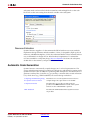
The Expose Clock Ports Option
When you select this option, System Generator creates a top-level wrapper that exposes a
clock port for each rate. You can then manually instantiate a clock generator outside the
design to drive the clock ports.
Known Limitations: The following System Generator blocks are not supported by the
Expose Clock Ports Option:
28
•
Clock Enable Probe
•
Clock Probe
•
DAFIR
www.xilinx.com
System Generator for DSP User Guide
UG640 (v 14.3) October 16, 2012
System-Level Modeling in System Generator
•
Downsample - when the Sample option First value of the frame is selected
•
FIR Compiler - when the core rate is not equal to the input sample rate
•
Parallel to Serial- when the Latency option is specified as 0 (zero)
•
Time Division De-Multiplexer
•
Time Division Multiplexer
•
Upsample - when the Copy samples (otherwise zeros are inserted) option is not
selected.
Tutorial Example: Using the Hybrid DCM-CE Option
The following step-by-step example will show you how to select the Hybrid DCM-CE
option, netlist the HDL design, implement the design in ISE®, simulate the design and
examine the files and reports to verify that the DCM is properly instantiated and
configured.
The hybrid_dcm_ce_case1.mdl design example is located at the following pathname
...<ISE_Design_Suite_tree>/sysgen>/examples/clocking_options/hybri
d_dcm_ce_case1/hybrid_dcm_ce_case1.mdl
1.
Open the model in MATLAB and observe the following blocks:
•
Addressable Shift Register (ASR): used to implement the input delay buffer. The
address port runs n times faster than the data port, where n is the number of the filter
taps (5 for this example)
•
Coefficient ROM: used to store the filter coefficients
•
Counter: used to generate addresses for the ROM and ASR
•
Comparator: used to generate the reset and enable signals
System Generator for DSP User Guide
UG640 (v 14.3) October 16, 2012
www.xilinx.com
29
Chapter 1: Hardware Design Using System Generator
30
•
MAC Engine: used as a Multiply-Accumulator operator for the filter
2.
Double-click on the System Generator token to bring up the following dialog box:
www.xilinx.com
System Generator for DSP User Guide
UG640 (v 14.3) October 16, 2012
System-Level Modeling in System Generator
As shown, click on the the Clocking tab, select Hybrid DCM-CE, then click Generate.
After a few moments, a sub-directory named hdl_netlist_dcm is created in the current
working directory containing the generated files.
3.
In the MATLAB Current Directory window, double-click on the file
hybrid_dcm_ce_case1_sysgen.log. As shown below, the DCM clocks are listed
first (highest rates first), followed by the CE driven clocks.
4.
Launch ISE, then load the ISE project at pathname
./hdl_netlist_dcm/hybrid_dcm_ce_case1_dcm_mcw.ise
5.
Under the Project Navigator Processes view, double-click on Implement Design.
6.
From the Project Navigator Design Sources Hierarchy view, do the following:
a.
Double-click on the file hybrid_dcm_ce_case1_dcm_mcw.vhd, then scroll
down to view the DCM component declaration as shown below by the VHDL
code snippet:
b.
Observe that System Generator automatically infers and instantiates the DCM
instance and its parameters according to the required clock outputs.
c.
Close the VHDL file.
Next, you are going to examine the clock propagation by examining the ISE timing report.
First, you must generate the report.
7.
Open the following folder: Processes view > Implement Design > Place & Route >
Generate Post-Place & Route Static Timing
System Generator for DSP User Guide
UG640 (v 14.3) October 16, 2012
www.xilinx.com
31
Chapter 1: Hardware Design Using System Generator
8.
Double -click on Analyze Post-Place & Route Static Timing and you should see the
information in the figure below:
This design is comprised of six clock rates – 1, 2, 4, 8, 20, 40 with respect to the 10 ns
global clock constraint. The timing report validates the correct clock generation and
propagation by System Generator as follows:
♦
DCM-based clocks: clk_1 (CLK0 ->10 ns), clk_2 (CLKFX ->20 ns) , clk_4 (CLKDIV
->40 ns) generated by the DCM based on the 10 ns global clock input
♦
Clock Enable-based clocks: ce_8 (80 ns), ce_20 (200 ns), ce_40 (400 ns) generated
by clock enables based on the clk_4 clock input
Next you want to perform a behavior simulation using the ModelSim.
9.
32
As shown in the following figure, move to the Sources for dialog box in the Sources
window, then select Behavioral Simulation
www.xilinx.com
System Generator for DSP User Guide
UG640 (v 14.3) October 16, 2012
System-Level Modeling in System Generator
Note: System Generator automatically creates the top-wrapper VHDL testbench, script file and
input/output stimulus data files. The Processes tab changes and displays according to the
Sources type being selected.
1. Select
2. Double Click
10. Simulate the design, as shown above, by double-click on Simulate Behavioral Model
in the Processes window
11. After the simulation is finished, you should be able to observe the simulation
waveforms as shown in the figure below:
All DCM clocks are included in the top-level wrapper testbench file
(hybrid_dcm_ce_case1_dcm_mcw_tb.vhd) – clk_1, clk_2 and clk_4.
Summary
System Generator for DSP User Guide
UG640 (v 14.3) October 16, 2012
www.xilinx.com
33
Chapter 1: Hardware Design Using System Generator
When you select the Hybrid DCM-CE option, System Generator automatically infers and
instantiates a DCM without further manual intervention. In addition, the tool intelligently
generates different clock rates by using a combination of DCM and CE clock generation
algorithms and by assigning appropriate clock rates to either the DCM or CE in order to
obtain optimal Quality of Results and low power consumption. You do not have to set
attributes or specify DCM clock outputs. You should expect minimal clock skew when
selecting the Hybrid DCM-CE option compared to the Clock Enables option alone.
Tutorial Example: Using the Expose Clock Ports Option
The following step-by-step example will show you how to select the Expose Clock Ports
option, netlist the HDL design, implement the design in ISE, simulate the design, then
examine the files and reports to verify the design.
The expose_clock_ports_case1 design example is located at the following pathname
<ISE_Design_Suite_tree>/sysgen>/examples/clocking_options/expose_c
lock_ports_case1/expose_clock_ports_case1.mdl
34
1.
Open the model in MATLAB and observe the following blocks:
•
Addressable Shift Register (ASR): used to implement the input delay buffer. The
address port runs n times faster than the data port, where n is the number of the filter
taps (5 for this example)
•
Coefficient ROM: used to store the filter coefficients
•
Counter: used to generate addresses for the ROM and ASR
•
Comparator: used to generate the reset and enable signals
•
MAC Engine: used as a Multiply-Accumulator operator for the filter
www.xilinx.com
System Generator for DSP User Guide
UG640 (v 14.3) October 16, 2012
System-Level Modeling in System Generator
2.
Double-click on the System Generator token to bring up the following dialog box:
As shown above, click on the Clocking tab, select Expose Clock Ports, then click Generate.
After a few moments, a sub-directory named hdl_netlist is created in the current working
directory containing the generated files.
3.
Launch ISE, then load the ISE project at pathname
./hdl_netlist/expose_clock_ports_case1_mcw.ise
4.
Under the Project Navigator Processes view, double-click on Implement Design.
5.
From the Project Navigator Design Sources Hierarchy view, do the following:
a.
Double-click on the file expose_clock_ports_case1_mcw.vhd, then scroll
down to view the entity named expose_clock_ports_mcw, as shown below:
b. Observe that System Generator infers the clocks based on the different rates in the
design and brings the clock ports to the top-level wrapper. Since this design
contains two clock rates, clocks clk_1 and clk_5 are pulled to the top-level
wrapper. This will allow you to directly drive the multiple synchronous clocks
from outside the System Generator design.
c.
Close the VHDL file.
Next you want to perform a behavior simulation using the ModelSim.
6.
As shown below, move to the Sources for dialog box in the Sources window, then
select Behavioral Simulation
System Generator for DSP User Guide
UG640 (v 14.3) October 16, 2012
www.xilinx.com
35
Chapter 1: Hardware Design Using System Generator
Note: System Generator automatically creates the top-wrapper VHDL testbench, script file and
input/output stimulus data files. The Processes tab changes and displays according to the
Sources type being selected.
1. Select
2. Double Click
7.
Simulate the design, as shown above, by double-click on Simulate Behavioral Model
in the Processes window
8.
After the simulation is finished, you should be able to observe the simulation
waveforms as shown in the figure below:
Summary
When you select the Expose Clock Ports option, System Generator automatically infers the
correct clocks from the design rates and exposes the clock ports in the top-level wrapper.
The clock rates are determined by the same methodology when you use the Clock Enables
option. You can now drive the exposed clock ports from an external synchronous clock
source.
Synchronization Mechanisms
System Generator does not make implicit synchronization mechanisms available. Instead,
synchronization is the responsibility of the designer, and must be done explicitly.
36
www.xilinx.com
System Generator for DSP User Guide
UG640 (v 14.3) October 16, 2012
System-Level Modeling in System Generator
Valid Ports
System Generator provides several blocks (in particular, a FIFO) that can be used for
synchronization. Several blocks provide input (respectively, output) ports that specify
when an input (resp., output) sample is valid. Such ports can be chained, affording a
primitive form of flow control. Blocks with such ports include the FFT, FIR, and Viterbi.
Indeterminate Data
Indeterminate values are common in many hardware simulation environments. Often they
are called “don’t cares” or “Xs”. In particular, values in System Generator simulations can
be indeterminate. A dual port memory block, for example, can produce indeterminate
results if both ports of the memory attempt to write the same address simultaneously.
What actually happens in hardware depends upon effectively random implementation
details that determine which port sees the clock edge first. Allowing values to become
indeterminate gives the system designer greater flexibility. Continuing the example, there
is nothing wrong with writing to memory in an indeterminate fashion if subsequent
processing does not rely on the indeterminate result.
HDL modules that are brought into the simulation through HDL co-simulation are a
common source for indeterminate data samples. System Generator presents indeterminate
values to the inputs of an HDL co-simulating module as the standard logic vector 'XXX . .
. XX'.
Indeterminate values that drive a Gateway Out become what are called NaNs. (NaN
abbreviates “not a number”.) In a Simulink scope, NaN values are not plotted. Conversely,
NaNs that drive a Gateway In become indeterminate values. System Generator provides
an Indeterminate Probe block that allows for the detection of indeterminate values. This
probe cannot be translated into hardware.
In System Generator, any arithmetic signal can be indeterminate, but Boolean signals
cannot be. If a simulation reaches a condition that would force a Boolean to become
indeterminate, the simulation is halted and an error is reported. Many Xilinx blocks have
control ports that only allow Boolean signals as inputs. The rule concerning indeterminate
Booleans means that such blocks never see an indeterminate on a control port
A UFix_1_0 is a type that is equivalent to Boolean except for the above restriction
concerning indeterminate data.
Block Masks and Parameter Passing
The same scoping and parameter passing rules that apply to ordinary Simulink blocks
apply to System Generator blocks. Consequently, blocks in the Xilinx Blockset can be
parameterized using MATLAB variables and expressions. This capability makes possible
highly parametric designs that take advantage of the expressive and computational power
of the MATLAB language.
Block Masks
In Simulink, blocks are parameterized through a mechanism called masking. In essence, a
block can be assigned mask variables whose values can be specified by a user through dialog
box prompts or can be calculated in mask initialization commands. Variables are stored in
a mask workspace. A mask workspace is local to the blocks under the mask and cannot be
accessed by external blocks.
Note: It is possible for a mask to access global variables and variables in the base workspace. To
access a base workspace variable, use the MATLAB evalin function. For more information on the
System Generator for DSP User Guide
UG640 (v 14.3) October 16, 2012
www.xilinx.com
37
Chapter 1: Hardware Design Using System Generator
MATLAB and Simulink scoping rules, refer to the manuals titled Using MATLAB and Using Simulink
from The MathWorks, Inc.
Parameter Passing
It is often desirable to pass variables to blocks inside a masked subsystem. Doing so allows
the block’s configuration to be determined by parameters on the enclosing subsystem. This
technique can be applied to parameters on blocks in the Xilinx blockset whose values are
set using a listbox, radio button, or checkbox. For example, when building a subsystem
that consists of a multiply and accumulate block, you can create a parameter on the
subsystem that allows you to specify whether to truncate or round the result. This
parameter will be called trunc_round as shown in the figure below.
As shown below, in the parameter editing dialog for the accumulator and multiplier
blocks, there are radio buttons that allow either the truncate or round option to be selected.
In order to use a parameter rather than the radio button selection, right click on the radio
button and select: “Define With Expression”. A MATLAB expression can then be used as
the parameter setting. In the example below, the trunc_round parameter from the
38
www.xilinx.com
System Generator for DSP User Guide
UG640 (v 14.3) October 16, 2012
Automatic Code Generation
subsystem mask can be used in both the accumulator and multiply blocks so that each
block will use the same setting from the mask variable on the subsystem.
Resource Estimation
System Generator supplies tools that estimate the FPGA hardware resources needed to
implement a design. Estimates include numbers of slices, lookup tables, flip-flops, block
memories, embedded multipliers, I/O blocks and tristate buffers. These estimates make it
easy to determine how design choices affect hardware requirements. To estimate the
resources needed for a subsystem, drag a Resource Estimator block into the subsystem,
double-click on the estimator, and press the Estimate button.
Automatic Code Generation
System Generator automatically compiles designs into low-level representations. The
ways in which System Generator compiles a model can vary, and depend on settings in the
System Generator token. In addition to producing HDL descriptions of hardware, the tool
generates auxiliary files. Some files (e.g., project files, constraints files) assist downstream
tools, while others (e.g., VHDL testbench) are used for design verification.
Compiling and Simulating Using
the System Generator Token
Describes how to use the System Generator token to
compile designs into equivalent low-level HDL.
Compilation Results
Describes the low-level files System Generator
produces when HDL Netlist is selected on the System
Generator token and Generate is pushed.
HDL Testbench
Describes the VHDL testbench that System Generator
can produce.
System Generator for DSP User Guide
UG640 (v 14.3) October 16, 2012
www.xilinx.com
39
Chapter 1: Hardware Design Using System Generator
Compiling and Simulating Using the System Generator Token
System Generator automatically compiles designs into low-level representations. Designs
are compiled and simulated using the System Generatortoken. This topic describes how to
use the block.
Before a System Generator design can be simulated or translated into hardware, the design
must include a System Generator token. When creating a new design, it is a good idea to
add a System Generator token immediately. The System Generator token is a member of
the Xilinx Blockset’s Basic Elements and Tools libraries. As with all Xilinx blocks, the
System Generator token can also be found in the Index library.
A design must contain at least one System Generator token, but can contain several System
Generator tokens on different levels (one per level). A System Generator token that is
underneath another in the hierarchy is a slave; one that is not a slave is a master. The scope
of a System Generator token consists of the level of hierarchy into which it is embedded
and all subsystems below that level. Certain parameters (e.g. Simulink System Period)
can be specified only in a master.
Once a System Generator token is added, it is possible to specify how code generation and
simulation should be handled. The token’s dialog box is shown below:
40
www.xilinx.com
System Generator for DSP User Guide
UG640 (v 14.3) October 16, 2012
Automatic Code Generation
Compilation Type and the Generate Button
Pressing the Generate button instructs System Generator to compile a portion of the
design into equivalent low-level results. The portion that is compiled is the sub-tree whose
root is the subsystem containing the block. (To compile the entire design, use a System
Generator token placed at the top of the design.) The compilation type (under
Compilation) specifies the type of result that should be produced. The possible types are
•
Two types of Netlists, HDL Netlist and NGC Netlist
•
Bitstream - produces an FPGA configuration bitstream that is ready to run in a
hardware FPGA platform
•
EDK Export Tool - for exporting to the Xilinx Embedded Development Kit
•
Various varieties of hardware co-simulation
•
Timing and Power Analysis - a report on the timing and power consumption of the
design.
HDL Netlist is the type used most often. In this case, the result is a collection of HDL and
EDIF files, and a few auxiliary files that simplify downstream processing. The collection is
ready to be processed by a synthesis tool (e.g., XST), and then fed to the Xilinx physical
design tools (i.e., ngdbuild, map, par, and bitgen) to produce a configuration bitstream for
a Xilinx FPGA. The files that are produced are described in more detail in Compilation
Results.
NGC Netlist is similar to HDL Netlist but the resulting files are NGC files instead of HDL
files.
When the type is a variety of hardware co-simulation, then System Generator produces an
FPGA configuration bitstream that is ready to run in a hardware FPGA platform. The
particular platform depends on the variety chosen. For example, when the variety is
Hardware Co-simulation > XtremeDSP Development Kit > PCI and USB, then the
bitstream is suitable for the XtremeDSP board (available for separate purchase from
Xilinx). System Generator also produces a hardware co-simulation block to which the
bitstream is associated. This block is able to participate in Simulink simulations. It is
functionally equivalent to the portion of the design from which it was derived, but is
implemented by its bitstream. In a simulation, the block delivers the same results as those
produced by the portion, but the results are calculated in working hardware.
The remaining compilation parameters are described in the table below. Some are
available only when the compilation type is HDL Netlist. For example, the clock pin
location cannot be chosen for a hardware co-simulation compilation because it is fixed in
each hardware FPGA platform.
Control
Description
Part
Defines the FPGA part to be used.
Target Directory
Defines where System Generator should write compilation results.
Because System Generator and the FPGA physical design tools
typically create many files, it is best to create a separate target
directory, i.e., a directory other than the directory containing your
Simulink model files. The directory can be an absolute path (e.g.
c:\netlist) or a path relative to the directory containing the model
(e.g. netlist).
System Generator for DSP User Guide
UG640 (v 14.3) October 16, 2012
www.xilinx.com
41
Chapter 1: Hardware Design Using System Generator
Control
Description
Synthesis tool
Specifies the tool to be used to synthesize the design. The
possibilities are Synplify, Synplify Pro and Xilinx XST.
Hardware description
language
Specifies the language to be used for HDL netlist of the design. The
possibilities are VHDL and Verilog.
Create testbench
This instructs System Generator to create an HDL testbench.
Simulating the testbench in an HDL simulator compares Simulink
simulation results with ones obtained from the compiled version of
the design. To construct test vectors, System Generator simulates the
design in Simulink, and saves the values seen at gateways. The top
HDL file for the testbench is named <name>_testbench.vhd/.v,
where <name> is a name derived from the portion of the design
being tested and the extension is dependent on the hardware
description language.
Import as
configurable
subsystem
Tells System Generator to do two things: 1) Construct a block to
which the results of compilation are associated, and 2) Construct a
configurable subsystem consisting of the block and the original
subsystem from which the block was derived. See Configurable
Subsystems and System Generator for details.
FPGA clock period
Defines the period in nanoseconds of the system clock. The value
need not be an integer. The period is passed to the Xilinx
implementation tools through a constraints file, where it is used as
the global PERIOD constraint. Multicycle paths are constrained to
integer multiples of this value.
Clock pin location
Defines the pin location for the hardware clock. This information is
passed to the Xilinx implementation tools through a constraints file.
Multirate
implementation
Clock Enables (default): Creates a clock enable generator circuit to
drive a multirate design.
Hybrid DCM-CE: Creates a clock wrapper with a DCM that can
drive up to three clock ports at different rates for Virtex®-4 and
Virtex®-5 and up to two clock ports for Spartan-3A DSP. The
mapping of rates to the DCM output ports is done using the
following priority scheme: CLK0 > CLK2x > CLKdv > CLKfx. The
DCM honors the higher clock rates first. If the design contains more
clocks than the DCM can handle, the remaining clocks are
implemented using the Clock Enable configuration.
A reset input port is exposed on the DCM clock wrapper to allow
resetting the DCM and a locked output port is exposed to help the
external design synchronize the input data with the single clk
input pin.
Expose Clock Ports: This option exposes multiple clock ports on the
top-level of the System Generator design so you can apply multiple
synchronous clock inputs from outside the design.
42
www.xilinx.com
System Generator for DSP User Guide
UG640 (v 14.3) October 16, 2012
Automatic Code Generation
Control
Description
DCM input clock
period(ns)
Specify if different than the FPGA clock period(ns) option (system
clock). The FPGA clock period (system clock) will then be derived
from this hardware-defined input.
Provide clock enable
clear pin
This instructs System Generator to provide a ce_clr port on the toplevel clock wrapper. The ce_clr signal is used to reset the clock
enable generation logic. Capability to reset clock enable generations
logic allows designs to have dynamic control for specifying the
beginning of data path sampling. See the topic for details.
Simulink System Period
You must specify a value for Simulink system period in the System Generator token
dialog box. This value tells the underlying rate, in seconds, at which simulations of the
design should run. The period must evenly divide all sample periods in the design. For
example, if the design consists of blocks whose sample periods are 2, 6, and 8, then the
largest acceptable sample period is 2, though other values such as 1 and 0.5 are also
acceptable. Sample periods arise in three ways: some are specified explicitly, some are
calculated automatically, and some arise implicitly within blocks that involve internal rate
changes. For more information on how the system period setting affects the hardware
clock, refer to Timing and Clocking.
Before running a simulation or compiling the design, System Generator verifies that the
period evenly divides every sample period in the design. If a problem is found, System
Generator opens a dialog box suggesting an appropriate value. Clicking the button labeled
Update instructs System Generator to use the suggested value. To see a summary of period
conflicts, click the button labeled View Conflict Summary. If you allow System Generator
to update the period, you must restart the simulation or compilation.
It is possible to assemble a System Generator model that is inconsistent because its periods
cannot be reconciled. (For example, certain blocks require that they run at the system rate.
Driving an up-sampler with such a block produces an inconsistent model.) If, even after
updating the system period, System Generator reports there are conflicts, then the model is
inconsistent and must be corrected.
The period control is hierarchical; see the discussion of hierarchical controls below for
details.
Block Icon Display
The options on this control affect the display of the block icons on the model. After
compilation (which occurs when Generating, Simulating, or by pressing Control-D) of
the model various information about the block in your model can be displayed, depending
on which option is chosen.
•
Default—basic information about port directions are shown
•
Sample rates—the sample rates of each port are shown
•
Pipeline stages—the number of pipeline stages are shown
•
HDL port names—the names of the ports are shown
•
Input data types—the input data types for each port are shown
•
Output data types—output data types for each port are shown
System Generator for DSP User Guide
UG640 (v 14.3) October 16, 2012
www.xilinx.com
43
Chapter 1: Hardware Design Using System Generator
Hierarchical Controls
The Simulink System Period control (see the topic Simulink System Period above) on the
System Generator token is hierarchical. A hierarchical control on a System Generator token
applies to the portion of the design within the scope of the token, but can be overridden on
other System Generator tokens deeper in the design. For example, suppose Simulink
System Period is set in a System Generator token at the top of the design, but is changed in
a System Generator token within a subsystem S. Then that subsystem will have the second
period, but the rest of the design will use the period set in the top level.
Viewing ISE Reports
When the Compilation is finished, the Compilation status dialog box appears as shown
below. If your compilation target wasBitstream or Timing and Power Analysis, you can
click on the Show Reports button and the associated ISE Reports will be avilable for your
viewing:
Compilation Results
In topic discusses the low-level files System Generator produces when HDL Netlist is
selected on the System Generator token and Generate is clicked. The files consist of HDL,
NGC and EDIF that implement the design. In addition, System Generator produces
auxiliary files that simplify downstream processing, e.g., bringing the design into Project
Navigator, simulating using an HDL simulator, and synthesizing using various synthesis
tools. All files are written to the target directory specified on the System Generator token.
44
www.xilinx.com
System Generator for DSP User Guide
UG640 (v 14.3) October 16, 2012
Automatic Code Generation
If no testbench is requested, then the key files produced by System Generator are the
following:
File Name or Type
Description
<design>.vhd/.v
This contains most of the HDL for the design
<design>_cw.vhd/.v
This is a HDL wrapper for <design>_files.vhd/.v. It
drives clocks and clock enables.
.edn and .ngc files
Besides writing HDL, System Generator runs CORE
Generator™ (coregen) to implement portions of the design.
Coregen writes EDIF files whose names typically look
something like
multiplier_virtex2_6_0_83438798287b830b.edn.
Other required files may be supplied as .ngc files.
globals
This file consists of key/value pairs that describe the design.
The file is organized as a Perl hash table so that the keys and
values can be made available to Pearl scripts using Perl evals.
<design>_cw.xcf (or .ncf)
This contains timing and port location constraints. These are
used by the Xilinx synthesis tool XST and the Xilinx
implementation tools. If the synthesis tool is set to something
other than XST, then the suffix is changed to .ncf.
<design>_cw.ise
This allows the HDL and EDIF to be brought into the Xilinx
project management tool Project Navigator.
hdlFiles
This contains the full list of HDL files written by System
Generator. The files are listed in the usual HDL dependency
order.
synplify_<design>.prj, or
These files allow the design to be compiled by the synthesis
tool you specified.
xst_<design>.pr
vcom.do
This script can be used in ModelSim to compile the HDL for a
behavioral simulation of the design.
If a testbench is requested, then, in addition to the above, System Generator produces files
that allow simulation results to be compared. The comparisons are between Simulink
simulation results and corresponding results from ModelSim. The additional files are the
following:
File Name or Type
Description
Various .dat files
These contain the simulation results from Simulink.
<design>_tb.vhd/.v
This is a testbench that wraps the design. When simulated in
ModelSim, this testbench compares simulation results from
Simulink against those produced by ModelSim.
vsim.do
This script can be used in ModelSim to run a testbench
simulation.
pn_behavioral.do,
pn_postmap.do,
pn_postpar.do,
pn_posttranslate.do
These files allow various ModelSim simulations to be started
inside Project Navigator.
System Generator for DSP User Guide
UG640 (v 14.3) October 16, 2012
www.xilinx.com
45
Chapter 1: Hardware Design Using System Generator
Using the System Generator Constraints File
When a design is compiled, System Generator produces a constraints file that tells
downstream tools how to process the design. This enables the tools to produce a higher
quality implementation, and to do so using considerably less time. Constraints supply the
following:
•
The period to be used for the system clock;
•
The speed, with respect to the system clock, at which various portions of the design
must run;
•
The pin locations at which ports should be placed;
•
The speed at which ports must operate.
The file format depends on the synthesis tool that is specified in the System Generator
token. When XST is selected, the file is written in the XCF format; for Synplify and Synplify
Pro, the NCF format is used. The file name ends with.xcf or .ncf, as appropriate.
System Clock Period
The system clock period (i.e., the period of the fastest hardware clock in the design) can be
specified in the System Generator token. System Generator writes this period to the
constraints file. Downstream tools use the period as a goal when implementing the design.
Multicycle Path Constraints
Many designs consist of parts that run at different clock rates. For the fastest part, the
system clock period is used. For the remaining parts, the clock period is an integer multiple
of the system clock period. It is important that downstream tools know what speed each
part of the design must achieve. With this information, efficiency and effectiveness of the
tools are greatly increased, resulting in reduced compilation times and improved
hardware realizations. The division of the design into parts, and the speed at which each
part must run, are specified in the constraints file using multicycle path constraints.
IOB Timing and Placement Constraints
When translated into hardware, System Generator's Gateway In and Gateway Out blocks
become input and output ports. The locations of these ports and the speeds at which they
must operate can be entered in the Gateway In and Out parameter dialog boxes.
See the descriptions of the Gateway In block and the Gateway Out block for more
information. Port location and speed are specified in the constraints file by IOB timing.
46
www.xilinx.com
System Generator for DSP User Guide
UG640 (v 14.3) October 16, 2012
Automatic Code Generation
Constraints Example
The figure below shows a small multirate design and the constraints System Generator
produces for it.
The up sampler doubles the rate, and the down sampler divides the rate by three. Assume
the system clock period is 10 ns. Then the clock periods are 10 ns for the FIR, 20 ns for the
input register, and 30 ns for the output register. The following text describes the constraints
that convey this information.
The lines that indicate the system clock period is10 ns are the following:
# Global period constraint
NET "clk" TNM_NET = "clk_392b7670";
TIMESPEC "TS_clk_392b7670" = PERIOD "clk_392b7670" 10.0 ns HIGH 50 %;
To build timing constraints, the blocks in the design are partitioned into timing groups.
Two blocks are in the same timing group if and only if they run at the same sample rate. In
this design there are three timing groups, corresponding to the three rates. The nature of
constraints dictates that no name is needed for the fastest group. The remaining groups are
named ce_2_392b7670_group and ce_3_392b7670_group; they correspond to periods 20 ns
and 30 ns respectively.
The FIR runs at the system (i.e., fastest) rate and therefore is constrained using the global
period constraint shown above. The logic used to generate clocks always runs at the
system rate and is also constrained to the system rate.
The ce_2_392b7670_group consists of the blocks that operate at half the system rate, i.e., the
input register and the up sampler. Every block in the group is driven by the clock enable
net named ce2_sysgen. The constraints that define the group are the following:
# ce_2_392b7670_group and inner group constraint
Net "ce_2_sg_x0*" TNM_NET = "ce_2_392b7670_group";
TIMESPEC "TS_ce_2_392b7670_group_to_ce_2_392b7670_group" = FROM
"ce_2_392b7670_group" TO "ce_2_392b7670_group" 20.0 ns;
Note: A wildcard character is added to the net name to constrain any additional copies of this net
that may be generated when clock enable logic is replicated. The maximum fanout of a clock enable
net can be controlled in the synthesis tool.
The ce_3_392b7670_group operates at one third the system rate. It contains the down
sampler and the output register, and is defined in a similar manner to the ce2_group.
# ce_3_392b7670_group and inner group constraint
Net "ce_3_sg_x0*" TNM_NET = "ce_3_392b7670_group";
System Generator for DSP User Guide
UG640 (v 14.3) October 16, 2012
www.xilinx.com
47
Chapter 1: Hardware Design Using System Generator
TIMESPEC "TS_ce_3_392b7670_group_to_ce_3_392b7670_group" = FROM
"ce_3_392b7670_group" TO "ce_3_392b7670_group" 30.0 ns;
Group to group constraints establish relative speeds. Here are the constraints that relate
the speeds of ce_2_392b7670_group and ce_3_392b7670_group:
# Group-to-group constraints
TIMESPEC "TS_ce_2_392b7670_group_to_ce_3_392b7670_group" = FROM
"ce_2_392b7670_group" TO "ce_3_392b7670_group" 20.0 ns;
TIMESPEC "TS_ce_3_392b7670_group_to_ce_2_392b7670_group" = FROM
"ce_3_392b7670_group" TO "ce_2_392b7670_group" 20.0 ns;
Port timing requirements can be set in the parameter dialog boxes for gateways. These
requirements are translated into port constraints such as those shown below. In this
example, the 3-bit din input is constrained to operate at its gateway's sample rate
(corresponding to a period of 20 ns). The "FAST" attributes indicate the ports should be
implemented using hardware that reduces delay. The reduction comes at a cost of
increased noise and power consumption.
# Offset in constraints
NET "din(0)" OFFSET = IN : 20.0 : BEFORE "clk";
NET "din(0)" FAST;
NET "din(1)" OFFSET = IN : 20.0 : BEFORE "clk";
NET "din(1)" FAST;
NET "din(2)" OFFSET = IN : 20.0 : BEFORE "clk";
NET "din(2)" FAST;
Selecting Specify IOB Location Constraints for a gateway allows port locations to be
specified. The locations must be entered as a cell array of strings in the box labeled IOB
Pad Locations. Locations are package-specific; in this example a Virtex®-E 2000 in a FG680
package is used. The location constraints for the din bus are provided in the dialog box as
"{'D35', 'B36', 'C35' }". This is translated into constraints in the .xcf (or .ncf) file in the
following way:
# Loc constraints
NET "din(2)" LOC = "D35";
NET "din(1)" LOC = "B36";
NET "din(0)" LOC = "C35";
Clock Handling in HDL
Clock Handling in HDL
This topic describes how System Generator handles hardware clocks in the HDL it
generates. Assume the design is named <design>, and <design> is an acceptable HDL
identifier. When System Generator compiles the design, it writes a collection of HDL
entities or modules, the topmost of which is named <design>, and is stored in a file
named <design>.vhd/.v.
The “Clock Enables” Multirate Implementation
Clock and clock enables appear in pairs throughout the HDL. Typical clock names are
clk_1, clk_2, and clk_3, and the names of the companion clock enables are ce_1, ce_2, and
ce_3 respectively. The name tells the rate for the clock/clock enable pair; logic driven by
clk_1 and ce_1 runs at the system (i.e., fastest) rate, while logic driven by (say) clk_2 and
ce_2 runs at half the system rate. Clocks and clock enables are not driven in the entity or
module named <design> or any subsidiary entities; instead, they are exposed as top-level
input ports
Of course, there must be a way to generate these clocks and clock enables. System
Generator produces a separate clock wrapper (written to a file named
48
www.xilinx.com
System Generator for DSP User Guide
UG640 (v 14.3) October 16, 2012
Automatic Code Generation
<design>_cw.vhd/.v) to do this. This wrapper is external to the files described above.
The idea is to make the HDL flexible. In some applications, the files described above are
added to a larger design, but the clock wrapper is omitted. In this case, you are responsible
for generating clocks and clock enables, but a finer degree of control is obtained. If, on the
other hand, the clock wrapper is suitable for the application, then include it.
The names of the clocks and clock enables in System Generator HDL suggest that clocking
is completely general, but this is not the case. To illustrate this, assume a design has clocks
named clk_1 and clk_2, and companion clock enables named ce_1 and ce_2 respectively.
You might expect that working hardware could be produced if the ce_1 and ce_2 signals
were tied high, and clk_2 were driven by a clock signal whose rate is half that of clk_1. For
most System Generator designs this does not work. Instead, clk_1 and clk_2 must be driven
by the same clock, ce_1 must be tied high, and ce_2 must vary at a rate half that of clk_1 and
clk_2.
The clock wrapper consists of two components: one for the design itself, and one clock
driver component that generate clocks and clock enables. The clock driver is contained in a
file named <design>_cw.vhd/.v. The logic within the <design>_cw generates the
ce_x signals. The optional ce_clr port would be generated if the design was generated
by selecting Provide clock enable clear pin on the System Generator token. The ports that
are not clocks or clock enables are passed through to the exterior of the clock wrapper.
Schematically, the clock wrapper looks like the diagram below.
Note: The clock wrapper exposes a port named ce. The port does nothing except to serve as a
companion to the clk port on the wrapper. The reason for having the port is to allow the clock wrapper
to be used as a black box in System Generator designs.
The “Hybrid DCM-CE” Multirate Implementation
If the implementation target is an FPGA with a Digital Clock Manager (DCM), you can
choose to drive the clock tree with a DCM. The DCM option is desirable when high fanout
on clock enable nets make it difficult to achieve timing closure.
System Generator instantiates the DCM in a top-level HDL clock wrapper ( with a suffix
_dcm_mcw) and configures the DCM to provide up to three clock ports at different rates for
Virtex®-4 and Virtex®-5 and up to two clock ports for Spartan-3A DSP. If the design has more
clock ports than the DCM can support, the remaining clocks are supported with the CE
(clock enable) configuration as described in the previous topic.
For a detailed examination of the files produced by this option, refer to the topic Tutorial
Example: Using the Hybrid DCM-CE Option.
System Generator for DSP User Guide
UG640 (v 14.3) October 16, 2012
www.xilinx.com
49
Chapter 1: Hardware Design Using System Generator
The “Expose Clock Ports” Multirate Implementation
When you select this option, System Generator creates a top-level wrapper that exposes a
clock port for each rate. You can then manually instantiate a clock generator outside the
design to drive the clock ports.
For a detailed examination of the files produced by this option, refer to the topic Tutorial
Example: Using the Expose Clock Ports Option.
Core Caching
System Generator uses cores produced by Xilinx CORE Generator™ (coregen) to
implement parts of designs. Generating cores can be expensive, so System Generator
caches previously generated ones. Before coregen is called, System Generator looks in the
cache, and if the core has already been generated, System Generator reuses it.
By default, the cache is the directory $TEMP/sg_core_cache. And by default, System
Generator caches no more than 2,000 cores. When the limit is reached, System Generator
deletes cached cores to make room for new ones.
Note: Environment variables can be used to change the location of the cache and the cache size
limit. The variables are described below.
Environment Variable
Description
SGCORECACHE
Location to store cached files. Setting this variable to a string of
blanks instructs System Generator not to cache cores.
SGCORECACHELIMIT
Maximum number of cores to cache.
HDL Testbench
Ordinarily, System Generator designs are bit and cycle-accurate, so Simulink simulation
results exactly match those seen in hardware. There are, however, times when it is useful to
compare Simulink simulation results against those obtained from an HDL simulator. In
particular, this makes sense when the design contains black boxes. The Create Testbench
checkbox in the System Generator token makes this possible.
Suppose the design is named <design>, and a System Generator token is placed at the top
of the design. Suppose also that in the token the Compilation field is set to HDL Netlist,
and the Create Testbench checkbox is selected. When the Generate button is clicked,
System Generator produces the usual files for the design, and in addition writes the
following:
1.
A file named <design>_tb.vhd/.v that contains a testbench HDL entity;
2.
Various .dat files that contain test vectors for use in an HDL testbench simulation.
3.
Scripts vcom.do and vsim.do that can be used in ModelSim to compile and simulate
the testbench, comparing Simulink test vectors against those produced in HDL.
System Generator generates the .dat files by saving the values that pass through
gateways. In the HDL simulation, input values from the .dat files are stimuli, and output
values are expected results. The testbench is simply a wrapper that feeds the stimuli to the
HDL for the design, then compares HDL results against expected ones.
50
www.xilinx.com
System Generator for DSP User Guide
UG640 (v 14.3) October 16, 2012
Compiling MATLAB into an FPGA
Compiling MATLAB into an FPGA
System Generator provides direct support for MATLAB through the MCode block. The
MCode block applies input values to an M-function for evaluation using Xilinx's fixedpoint data type. The evaluation is done once for each sample period. The block is capable
of keeping internal states with the use of persistent state variables. The input ports of the
block are determined by the input arguments of the specified M-function and the output
ports of the block are determined by the output arguments of the M-function. The block
provides a convenient way to build finite state machines, control logic, and computation
heavy systems.
In order to construct an MCode block, an M-function must be written. The M-file must be
in the directory of the model file that is to use the M-file or in a directory in the MATLAB
path.
This tutorial provides ten examples that use the MCode block:
•
Example 1 Simple Selector shows how to implement a function that returns the
maximum value of its inputs;
•
Example 2 Simple Arithmetic Operations shows how to implement simple arithmetic
operations;
•
Example 3 Complex Multiplier with Latency shows how to build a complex
multiplier with latency;
•
Example 4 Shift Operations shows how to implement shift operations;
•
Example 5 Passing Parameters into the MCode Block shows how to pass parameters
into a MCode block;
•
Example 6 Optional Input Ports shows how to implement optional input ports on an
MCode block;
•
Example 7 Finite State Machines shows how to implement a finite state machine;
•
Example 8 Parameterizable Accumulator shows how to build a parameterizable
accumulator;
•
Example 9 FIR Example and System Verification shows how to model FIR blocks and
how to do system verification;
•
Example 10 RPN Calculator shows how to model a RPN calculator – a stack machine;
•
Example 11 Example of disp Function shows how to use disp function to print
variable values.
The first two examples are in the mcode_block_tutorial.mdl file of the
examples/mcode_block directory in your installation of the System Generator software.
Examples 3 and 4 are in the mcode_block_tutorial2.mdl file. Examples 5 and 6 are in the
mcode_block_tutorial3.mdl file. Examples 7 and 8 are in the mcode_block_tutorial4.mdl
file. Example 9 is mcode_block_verify_fir.mdl. Example 10 is in
mcode_block_rpn_calculator.mdl.
Simple Selector
This example is a simple controller for a data path, which assigns the maximum value of
two inputs to the output. The M-function is specified as the following and is saved in an Mfile xlmax.m:
function z = xlmax(x, y)
if x > y
z = x;
System Generator for DSP User Guide
UG640 (v 14.3) October 16, 2012
www.xilinx.com
51
Chapter 1: Hardware Design Using System Generator
else
z = y;
end
The xlmax.m file should be either saved in the same directory of the model file or should
be in the MATLAB path. Once the xlmax.m has been saved to the appropriate place, you
should drag a MCode block into your model, open the block parameter dialog box, and
enter xlmax into the MATLAB Function field. After clicking the OK button, the block has
two input ports x and y, and one output port z.
The following figure shows what the block looks like after the model is compiled. You can
see that the block calculates and sets the necessary fixed-point data type to the output port.
Simple Arithmetic Operations
This example shows some simple arithmetic operations and type conversions. The
following shows the xlSimpleArith.m file, which specifies the xlSimpleArith Mfunction.
function [z1, z2, z3, z4] = xlSimpleArith(a, b)
% xlSimpleArith demonstrates some of the arithmetic operations
% supported by the Xilinx MCode block. The function uses xfix()
% to create Xilinx fixed-point numbers with appropriate
52
www.xilinx.com
System Generator for DSP User Guide
UG640 (v 14.3) October 16, 2012
Compiling MATLAB into an FPGA
% container types.%
% You must use a xfix() to specify type, number of bits, and
% binary point position to convert floating point values to
% Xilinx fixed-point constants or variables.
% By default, the xfix call uses xlTruncate
% and xlWrap for quantization and overflow modes.
% const1 is Ufix_8_3
const1 = xfix({xlUnsigned, 8, 3}, 1.53);
% const2 is Fix_10_4
const2 = xfix({xlSigned, 10, 4, xlRound, xlWrap}, 5.687);
z1 = a + const1;
z2 = -b - const2;
z3 = z1 - z2;
% convert z3 to Fix_12_8 with saturation for overflow
z3 = xfix({xlSigned, 12, 8, xlTruncate, xlSaturate}, z3);
% z4 is true if both inputs are positive
z4 = a>const1 & b>-1;
This M-function uses addition and subtraction operators. The MCode block calculates
these operations in full precision, which means the output precision is sufficient to carry
out the operation without losing information.
One thing worth discussing is the xfix function call. The function requires two
arguments: the first for fixed-point data type precision and the second indicating the value.
The precision is specified in a cell array. The first element of the precision cell array is the
type value. It can be one of three different types: xlUnsigned, xlSigned, or xlBoolean.
The second element is the number of bits of the fixed-point number. The third is the binary
point position. If the element is xlBoolean, there is no need to specify the number of bits
and binary point position. The number of bits and binary point position must be specified
in pair. The fourth element is the quantization mode and the fifth element is the overflow
mode. The quantization mode can be one of xlTruncate, xlRound, or xlRoundBanker.
The overflow mode can be one of xlWrap, xlSaturate, or xlThrowOverflow.
Quanitization mode and overflow mode must be specified as a pair. If the quantizationoverflow mode pair is not specified, the xfix function uses xlTruncate and xlWrap for
signed and unsigned numbers. The second argument of the xfix function can be either a
double or a Xilinx fixed-point number. If a constant is an integer number, there is no need
to use the xfix function. The Mcode block converts it to the appropriate fixed-point
number automatically.
System Generator for DSP User Guide
UG640 (v 14.3) October 16, 2012
www.xilinx.com
53
Chapter 1: Hardware Design Using System Generator
After setting the dialog box parameter MATLAB Function to xlSimpleArith, the block
shows two input ports a and b, and four output ports z1, z2, z3, and z4.
54
www.xilinx.com
System Generator for DSP User Guide
UG640 (v 14.3) October 16, 2012
Compiling MATLAB into an FPGA
M-functions using Xilinx data types and functions can be tested in the MATLAB command
window. For example, if you type: [z1, z2, z3, z4] = xlSimpleArith(2, 3) in
the MATLAB command window, you'll get the following lines:
UFix(9, 3): 3.500000
Fix(12, 4): -8.687500
Fix(12, 8): 7.996094
Bool: true
Notice that the two integer arguments (2 and 3) are converted to fixed-point numbers
automatically. If you have a floating-point number as an argument, an xfix call is
required.
Complex Multiplier with Latency
This example shows how to create a complex number multiplier. The following shows the
xlcpxmult.m file which specifies the xlcpxmult function.
function [xr, xi] = xlcpxmult(ar, ai, br, bi)
xr = ar * br - ai * bi;
xi = ar * bi + ai * br;
The following diagram shows the sub-system:
Two delay blocks are added after the MCode block. By selecting the option Implement
using behavioral HDL on the Delay blocks, the downstream logic synthesis tool is able to
perform the appropriate optimizations to achieve higher performance.
System Generator for DSP User Guide
UG640 (v 14.3) October 16, 2012
www.xilinx.com
55
Chapter 1: Hardware Design Using System Generator
Shift Operations
This example shows how to implement bit-shift operations using the MCode block. Shift
operations are accomplished with multiplication and division by powers of two. For
example, multiplying by 4 is equivalent to a 2-bit left-shift, and dividing by 8 is equivalent
to a 3-bit right-shift. Shift operations are implemented by moving the binary point position
and if necessary, expanding the bit width. Consequently, multiplying a Fix_8_4 number by
4 results in a Fix_8_2 number, and multiplying a Fix_8_4 number by 64 results in a
Fix_10_0 number.
The following shows the xlsimpleshift.m file which specifies one left-shift and one
right-shift:
function [lsh3, rsh2] = xlsimpleshift(din)
% [lsh3, rsh2] = xlsimpleshift(din) does a left shift
% 3 bits and a right shift 2 bits.
% The shift operation is accomplished by
% multiplication and division of power
% of two constant.
lsh3 = din * 8;
rsh2 = din / 4;
The following diagram shows the sub-system after compilation:
56
www.xilinx.com
System Generator for DSP User Guide
UG640 (v 14.3) October 16, 2012
Compiling MATLAB into an FPGA
Passing Parameters into the MCode Block
This example shows how to pass parameters into the MCode block. An input argument to
an M-function can be interpreted either as an input port on the MCode block, or as a
parameter internal to the block.
The following M-code defines an M-function xl_sconvert is contained in file
xl_sconvert.m:
function dout = xl_sconvert(din, nbits, binpt)
proto = {xlSigned, nbits, binpt};
dout = xfix(proto, din);
The following diagram shows a subsystem containing two MCode blocks that use Mfunction xl_sconvert. The arguments nbits and binpt of the M-function are specified
differently for each block by passing different parameters to the MCode blocks. The
parameters passed to the MCode block labeled signed convert 1 cause it to convert
the input data from type Fix_16_8 to Fix_10_5 at its output. The parameters passed to
the MCode block labeled signed convert2 causes it to convert the input data from type
Fix_16_8 to Fix_8_4 at its output.
System Generator for DSP User Guide
UG640 (v 14.3) October 16, 2012
www.xilinx.com
57
Chapter 1: Hardware Design Using System Generator
To pass parameters to each MCode block in the diagram above, you can click the Edit
Interface button on the block GUI then set the values for the M-function arguments. The
mask for MCode block signed convert 1 is shown below:
58
www.xilinx.com
System Generator for DSP User Guide
UG640 (v 14.3) October 16, 2012
Compiling MATLAB into an FPGA
The above interface window sets the M-function argument nbits to be 10 and binpt to
be 5. The mask for the MCode block signed convert 2 is shown below:
The above interface window sets the M-function argument nbits to be 8 and binpt
to be 4.
System Generator for DSP User Guide
UG640 (v 14.3) October 16, 2012
www.xilinx.com
59
Chapter 1: Hardware Design Using System Generator
Optional Input Ports
This example shows how to use the parameter passing mechanism of MCode blocks to
specify whether or not to use optional input ports on MCode blocks.
The following M-code, which defines M-function xl_m_addsub is contained in file
xl_m_addsub.m:
function s = xl_m_addsub(a, b, sub)
if sub
s = a - b;
else
s = a + b;
end
The following diagram shows a subsystem containing two MCode blocks that use Mfunction xl_m_addsub.
60
www.xilinx.com
System Generator for DSP User Guide
UG640 (v 14.3) October 16, 2012
Compiling MATLAB into an FPGA
The Block Interface Editor of the MCode block labeled add is shown in below.
As a result, the add block features two input ports a and b; it performs full precision
addition. Input parameter sub of the MCode block labeled addsub is not bound with any
value. Consequently, the addsub block features three input ports: a, b, and sub; it
performs full precision addition or subtraction based on the value of input port sub.
System Generator for DSP User Guide
UG640 (v 14.3) October 16, 2012
www.xilinx.com
61
Chapter 1: Hardware Design Using System Generator
Finite State Machines
This example shows how to create a finite state machine using the MCode block with
internal state variables. The state machine illustrated below detects the pattern 1011 in an
input stream of bits.
The M-function that is used by the MCode block contains a transition function, which
computes the next state based on the current state and the current input. Unlike example 3
though, the M-function in this example defines persistent state variables to store the state
of the finite state machine in the MCode block. The following M-code, which defines
function detect1011_w_state is contained in file detect1011_w_state.m:
function matched = detect1011_w_state(din)
% This is the detect1011 function with states for detecting a
% pattern of 1011.
seen_none = 0; %
seen_1 = 1;
%
%
seen_10 = 2;
%
%
seen_101 = 3; %
%
initial state, if input is 1, switch to seen_1
first 1 has been seen, if input is 0, switch
seen_10
10 has been detected, if input is 1, switch to
seen_1011
now 101 is detected, is input is 1, 1011 is
detected and the FSM switches to seen_1
% the state is a 2-bit register
persistent state, state = xl_state(seen_none, {xlUnsigned, 2, 0});
% the default value of matched is false
matched = false;
switch state
case seen_none
if din==1
state = seen_1;
else
state = seen_none;
end
case seen_1 % seen first 1
if din==1
state = seen_1;
else
62
www.xilinx.com
System Generator for DSP User Guide
UG640 (v 14.3) October 16, 2012
Compiling MATLAB into an FPGA
state = seen_10;
end
case seen_10 % seen 10
if din==1
state = seen_101;
else
% no part of sequence seen, go to seen_none
state = seen_none;
end
case seen_101
if din==1
state = seen_1;
matched = true;
else
state = seen_10;
matched = false;
end
end
The following diagram shows a state machine subsystem containing a MCode block after
compilation; the MCode block uses M-function detect1101_w_state.
Parameterizable Accumulator
This example shows how to use the MCode block to build an accumulator using persistent
state variables and parameters to provide implementation flexibility. The following Mcode, which defines function xl_accum is contained in file xl_accum.m:
function q = xl_accum(b, rst, load, en, nbits, ov, op,
feed_back_down_scale)
% q = xl_accum(b, rst, nbits, ov, op, feed_back_down_scale) is
% equivalent to our Accumulator block.
binpt = xl_binpt(b);
init = 0;
precision = {xlSigned, nbits, binpt, xlTruncate, ov};
persistent s, s = xl_state(init, precision);
q = s;
if rst
if load
% reset from the input port
s = b;
else
% reset from zero
s = init;
System Generator for DSP User Guide
UG640 (v 14.3) October 16, 2012
www.xilinx.com
63
Chapter 1: Hardware Design Using System Generator
end
else
if ~en
else
% if enabled, update the state
if op==0
s = s/feed_back_down_scale + b;
else
s = s/feed_back_down_scale - b;
end
end
end
The following diagram shows a subsystem containing the accumulator MCode block using
M-function xl_accum. The MCode block is labeled MCode Accumulator. The
subsystem also contains the Xilinx Accumulator block, labeled Accumulator, for
comparison purposes. The MCode block provides the same functionality as the Xilinx
Accumulator block; however, its mask interface differs in that parameters of the MCode
block are specified with a cell array in the Function Parameter Bindings parameter.
64
www.xilinx.com
System Generator for DSP User Guide
UG640 (v 14.3) October 16, 2012
Compiling MATLAB into an FPGA
Optional inputs rst and load of block Accum_MCode1 are disabled in the cell array of the
Function Parameter Bindings parameter. The block mask for block MCode Accumulator is
shown below:
System Generator for DSP User Guide
UG640 (v 14.3) October 16, 2012
www.xilinx.com
65
Chapter 1: Hardware Design Using System Generator
The example contains two additional accumulator subsystems with MCode blocks using
the same M-function, but different parameter settings to accomplish different accumulator
implementations.
FIR Example and System Verification
This example shows how to use the MCode block to model FIRs. It also shows how to do
system verification with the MCode block.
The model contains two FIR blocks. Both are modeled with the MCode block and both are
synthesizable. The following are the two functions that model those two blocks.
function y = simple_fir(x, lat, coefs, len, c_nbits, c_binpt, o_nbits,
o_binpt)
coef_prec = {xlSigned, c_nbits, c_binpt, xlRound, xlWrap};
out_prec = {xlSigned, o_nbits, o_binpt};
coefs_xfix
persistent
persistent
persistent
= xfix(coef_prec, coefs);
coef_vec, coef_vec = xl_state(coefs_xfix, coef_prec);
x_line, x_line = xl_state(zeros(1, len-1), x);
p, p = xl_state(zeros(1, lat), out_prec, lat);
sum = x * coef_vec(0);
for idx = 1:len-1
sum = sum + x_line(idx-1) * coef_vec(idx);
sum = xfix(out_prec, sum);
end
y = p.back;
p.push_front_pop_back(sum);
x_line.push_front_pop_back(x);
function y = fir_transpose(x, lat, coefs, len, c_nbits, c_binpt,
o_nbits, o_binpt)
coef_prec = {xlSigned, c_nbits, c_binpt, xlRound, xlWrap};
out_prec = {xlSigned, o_nbits, o_binpt};
coefs_xfix = xfix(coef_prec, coefs);
persistent coef_vec, coef_vec = xl_state(coefs_xfix, coef_prec);
persistent reg_line, reg_line = xl_state(zeros(1, len), out_prec);
if lat <= 0
error('latency must be at least 1');
end
66
www.xilinx.com
System Generator for DSP User Guide
UG640 (v 14.3) October 16, 2012
Compiling MATLAB into an FPGA
lat = lat - 1;
persistent dly,
if lat <= 0
y = reg_line.back;
else
dly = xl_state(zeros(1, lat), out_prec, lat);
y = dly.back;
dly.push_front_pop_back(reg_line.back);
end
for idx = len-1:-1:1
reg_line(idx) = reg_line(idx - 1) + coef_vec(len - idx - 1) * x;
end
reg_line(0) = coef_vec(len - 1) * x;
The parameters are configured as following:
System Generator for DSP User Guide
UG640 (v 14.3) October 16, 2012
www.xilinx.com
67
Chapter 1: Hardware Design Using System Generator
In order to verify that the functionality of two blocks are equal, we also use another MCode
block to compare the outputs of two blocks. If the two outputs are not equal at any given
time, the error checking block will report the error. The following function does the error
checking:
function eq = error_ne(a, b, report, mod)
persistent cnt, cnt = xl_state(0, {xlUnsigned, 16, 0});
switch mod
case 1
eq = a==b;
case 2
eq = isnan(a) || isnan(b) || a == b;
case 3
eq = ~isnan(a) && ~isnan(b) && a == b;
otherwise
eq = false;
error(['wrong value of mode ', num2str(mod)]);
end
if report
if ~eq
error(['two inputs are not equal at time ', num2str(cnt)]);
end
end
cnt = cnt + 1;
The block is configured as following:
68
www.xilinx.com
System Generator for DSP User Guide
UG640 (v 14.3) October 16, 2012
Compiling MATLAB into an FPGA
RPN Calculator
This example shows how to use the MCode block to model a RPN calculator which is a
stack machine. The block is synthesizable:
The following function models the RPN calculator.
function [q, active] = rpn_calc(d, rst, en)
d_nbits = xl_nbits(d);
% the first bit indicates whether it's a data or operator
is_oper = xl_slice(d, d_nbits-1, d_nbits-1)==1;
din = xl_force(xl_slice(d, d_nbits-2, 0), xlSigned, 0);
% the lower 3 bits are operator
op = xl_slice(d, 2, 0);
% acc the the A register
persistent acc, acc = xl_state(0, din);
% the stack is implemented with a RAM and
% an up-down counter
persistent mem, mem = xl_state(zeros(1, 64), din);
persistent acc_active, acc_active = xl_state(false, {xlBoolean});
persistent stack_active, stack_active = xl_state(false, ...
{xlBoolean});
stack_pt_prec = {xlUnsigned, 5, 0};
persistent stack_pt, stack_pt = xl_state(0, {xlUnsigned, 5, 0});
% when en is true, it's action
System Generator for DSP User Guide
UG640 (v 14.3) October 16, 2012
www.xilinx.com
69
Chapter 1: Hardware Design Using System Generator
OP_ADD = 2;
OP_SUB = 3;
OP_MULT = 4;
OP_NEG = 5;
OP_DROP = 6;
q = acc;
active = acc_active;
if rst
acc = 0;
acc_active = false;
stack_pt = 0;
elseif en
if ~is_oper
% enter data, push
if acc_active
stack_pt = xfix(stack_pt_prec, stack_pt + 1);
mem(stack_pt) = acc;
stack_active = true;
else
acc_active = true;
end
acc = din;
else
if op == OP_NEG
% unary op, no stack op
acc = -acc;
elseif stack_active
b = mem(stack_pt);
switch double(op)
case OP_ADD
acc = acc + b;
case OP_SUB
acc = b - acc ;
case OP_MULT
acc = acc * b;
case OP_DROP
acc = b;
end
stack_pt = stack_pt - 1;
elseif acc_active
acc_active = false;
acc = 0;
end
end
end
stack_active = stack_pt ~= 0;
70
www.xilinx.com
System Generator for DSP User Guide
UG640 (v 14.3) October 16, 2012
Compiling MATLAB into an FPGA
Example of disp Function
The following MCode function shows how to use the disp function to print variable
values.
function x = testdisp(a, b)
persistent dly, dly = xl_state(zeros(1, 8), a);
persistent rom, rom = xl_state([3, 2, 1, 0], a);
disp('Hello World!');
disp(['num2str(dly) is ', num2str(dly)]);
disp('disp(dly) is ');
disp(dly);
disp('disp(rom) is ');
disp(rom);
a2 = dly.back;
dly.push_front_pop_back(a);
x = a + b;
disp(['a = ', num2str(a), ', ', ...
'b = ', num2str(b), ', ', ...
'x = ', num2str(x)]);
disp(num2str(true));
disp('disp(10) is');
disp(10);
disp('disp(-10) is');
disp(-10);
disp('disp(a) is ');
disp(a);
disp('disp(a == b)');
disp(a==b);
The Enable print with disp option must be checked.
System Generator for DSP User Guide
UG640 (v 14.3) October 16, 2012
www.xilinx.com
71
Chapter 1: Hardware Design Using System Generator
Here are the lines that are displayed on the MATLAB console for the first simulation step.
mcode_block_disp/MCode (Simulink time: 0.000000, FPGA clock: 0)
Hello World!
num2str(dly) is [0.000000, 0.000000, 0.000000, 0.000000, 0.000000,
0.000000, 0.000000, 0.000000]
disp(dly) is
type: Fix_11_7,
maxlen: 8,
length: 8,
0: binary 0000.0000000, double 0.000000,
1: binary 0000.0000000, double 0.000000,
2: binary 0000.0000000, double 0.000000,
3: binary 0000.0000000, double 0.000000,
4: binary 0000.0000000, double 0.000000,
5: binary 0000.0000000, double 0.000000,
6: binary 0000.0000000, double 0.000000,
7: binary 0000.0000000, double 0.000000,
disp(rom) is
type: Fix_11_7,
maxlen: 4,
length: 4,
0: binary 0011.0000000, double 3.0,
1: binary 0010.0000000, double 2.0,
2: binary 0001.0000000, double 1.0,
3: binary 0000.0000000, double 0.0,
a = 0.000000, b = 0.000000, x = 0.000000
1
disp(10) is
type: UFix_4_0, binary: 1010, double: 10.0
disp(-10) is
type: Fix_5_0, binary: 10110, double: -10.0
disp(a) is
type: Fix_11_7, binary: 0000.0000000, double: 0.000000
disp(a == b)
type: Bool, binary: 1, double: 1
72
www.xilinx.com
System Generator for DSP User Guide
UG640 (v 14.3) October 16, 2012
Importing a System Generator Design into a Bigger System
Importing a System Generator Design into a Bigger System
A System Generator design is often a sub-design that is incorporated into a larger HDL
design. This topic shows how to embed two System Generator designs into a larger design
and how VHDL created by System Generator can be incorporated into the simulation
model of the overall system.
Starting with Release 10.1, System Generator introduced a new integration flow between
System Generator (Sysgen) and Project Navigator (ProjNav). This first phase of integration
concentrates on the following areas:
•
Allows you to add a System Generator design as a sub-level to a larger design
•
Consolidates and associates System Generator constraints to the top-level design
•
Enables you to perform certain design iterations between Project Navigator and the
System Generator design
HDL Netlist Compilation
Selecting the HDL Netlist compilation target from the System Generator token instructs
System Generator to generate HDL along with other related files such as NGC files and
EDIF files that implement the design. In addition, System Generator produces auxiliary
files that simplify downstream processing such as bringing the design into Project
Navigator, simulating the design using an HDL simulator, and performing logic synthesis
using various logic synthesis tools. See the topic System Generator Compilation Types for
more details.
Starting with Release 10.1, the System Generator project information is encapsulated in the
file <design_name>_cw.sgp or <design_name>_mcw.sgp depending on which
clocking option is selected. This topic shows how multiple System Generator designs can
be included as sub-modules in a larger design.
Integration Design Rules
When a System Generator model is to be included into a larger design, the following two
design rules must be followed.
Rule 1: No Gateway or System Generator token should specify an IOB/CLK location
constraint. Otherwise, the NGDBuild tool will issue the following warning:
WARNING:NgdBuild:483 - Attribute "LOC" on "clk" is on the wrong type
of object. Please see the Constraints Guide for more information on
this attribute.
Also, IOB timing constraints should be set to "none" in this case as well to avoid the
following NGDBuild error:
NgdBuild:756 -Could not find net(s) 'gateway_out(1)' in the design.
To suppress this error, specify the correct net name or remove the
constraint.
Rule 2: If there are any I/O ports from the System Generator design that are required to be
bubbled up to the top-level design, appropriate buffers should be instantiated in the toplevel HDL code.
System Generator for DSP User Guide
UG640 (v 14.3) October 16, 2012
www.xilinx.com
73
Chapter 1: Hardware Design Using System Generator
New Integration Flow between System Generator & Project Navigator
The illustration below shows the entire flow of how multiple System Generator designs
can be integrated into Project Navigator as lower-level designs. System Generator
generates a project file with an extension .sgp that you can add a System Generator source
type in Project Navigator. This SGP file is an empty file by design, but by its location, it
implicitly identifies the location of the System Generator model. Prior to the integration
with Project Navigator in Release 10.1, you had to manually consolidate and associate UCF
constraints into the top-level design. It is now done automatically during the
implementation in Project Navigator as shown in the following figure.
74
www.xilinx.com
System Generator for DSP User Guide
UG640 (v 14.3) October 16, 2012
Importing a System Generator Design into a Bigger System
A Step-by-Step Example
In this example, two HDL netlists from System Generator are integrated into a larger
VHDL design. Design #1 is named SPRAM and design #2 is named MAC_FIR. The toplevel VHDL entity combines the two data ports and a control signal from the SPRAM
design to create a bidirectional bus. The top-level VHDL also instantiates the MAC_FIR
design and supplies a separate clock signal named clk2. A block diagram of this design is
shown below.
The files used in this example are located in the System Generator tree at pathname
<ISE_Design_Suite_tree>/sysgen/examples/projnav/mult_diff_designs.
The following files are provided:
•
spram.mdl - System Generator design #1
•
mac_fir.mdl - System Generator design #2
Files within the sub-directory named top_level:
•
top_level.ise – ProjNav project for compiling top_level design
•
top_level.vhd – Top-level VHDL file
•
top_level_testbench.do – Custom ModelSim .do file
•
top_level_testbench.vhd – Top-level VHDL testbench file
•
wave.do – ModelSim .do file called by top_level_testbench.do to display
waveforms
System Generator for DSP User Guide
UG640 (v 14.3) October 16, 2012
www.xilinx.com
75
Chapter 1: Hardware Design Using System Generator
Generating the HDL Files for the System Generator Designs
The steps used to create the HDL files are as follows:
1.
Open the first design, spram.mdl, in MATLAB. This is a multirate design due to the
down sampling block placed after the output of the Single Port RAM.
2.
Double click on the System Generator token; select the HDL Netlist target and press
the Generate button. By pressing the Generate button, the HDL file for this design is
created in the directory
<ISE_Design_Suite_tree>/sysgen/examples/projnav/mult_diff_desig
ns/hdl_netlist1.
3.
Repeat steps 1 and 2 for the mac_fir.mdl model. The HDL file for this design is
created in the directory
<ISE_Design_Suite_tree>/sysgen/examples/projnav/mult_diff_desig
ns/hdl_netlist2.
Note: You are now finished generating HDL Netlists from System Generator
Switching to Different HDL Libraries
When integrating two or more System Generator designs into a bigger design, you need to
rename HDL libraries to prevent name clashes and other undesired behaviors during
simulation. System Generator provides a utility that switches library names for all related
files in your System Generator design. In addition, it also makes a backup copy in a folder
just in case you want to revert back to the original library name. The following is the syntax
for this utility:
Syntax:
xlSwitchLibrary(<target_dir_pathname>, <from_lib_name>, <to_lib_name>)
<target_dir_pathname>: location of the design
<from_lib_name>: Original HDL library name
<to_lib_name>: New HDL library name
76
1.
From the MATLAB Console, enter the following command:
xlSwitchLibrary('hdl_netlist1','work','design1_lib')
2.
Next, from the MATLAB Console, enter the following command:
xlSwitchLibrary('hdl_netlist2','work','design2_lib')
www.xilinx.com
System Generator for DSP User Guide
UG640 (v 14.3) October 16, 2012
Importing a System Generator Design into a Bigger System
The transcript should look similar to the following:
Adding System Generator Source into the Top-Level Design
The next two steps are used to synthesize the top_level design:
1.
Launch ISE and reload the pre-generated top-level design ISE project at
~top_level/top_level.ise.
Note: At this point, your Project Navigator should look like the figure below. Both spram_cw and
mac_fir_cw instances are instantiated at the top_level design. But since they are not located on the
same directory as the top-level design, Project Navigator puts a question mark next to each one of
them to indicate that it can not find these two instances / modules.
:
2.
Add the System Generator source: under the Sources tab, right-click on
u_spram_cw -> Add Source…at
<ISE_Design_Suite_tree>/sysgen/examples/projnav/mult_diff_desig
ns/hdl_netlist1/spram_cw.sgp
System Generator for DSP User Guide
UG640 (v 14.3) October 16, 2012
www.xilinx.com
77
Chapter 1: Hardware Design Using System Generator
3.
Repeat item 2 with u_mac_fir at
<ISE_Design_Suite_tree>/sysgen/examples/projnav/mult_diff_desig
ns/hdl_netlist2/mac_fir_cw.sgp
4.
As shown below, make sure the file top_level is selected, then implement the design
by double clicking on Implement Design in the Processes window. Once the
implementation is finished, Project Navigator should look like the figure below.
5.
Examine the timing constraints in the Place and Route Report that is located in the
Detailed Reports section of the Design Summery pane.
Note that in the PAR report the multirate constraints were met:
Constraints for each System Generator design were created and translated to a UCF (User
Constraint File). These UCF constraint files were then consolidated and associated during
ISE implementation (NGDBUILD). They are briefly described as follows:
A system sample period of 100 ns was set in the System Generator token for both designs
(1 & 2)
•
78
TS_clk_f488215c2 constraints are from the SRAM design (1)
www.xilinx.com
System Generator for DSP User Guide
UG640 (v 14.3) October 16, 2012
Importing a System Generator Design into a Bigger System
•
The TS_clk_c4b7e2441 constraints are from the FIR design (2)
•
The ce16_c4b7e244_group_to_ce16_cb47e244_group1 constraint is for all the
synchronous elements after the down sampler and it is set to sixteen, the system
sample period (3)
•
The down sampling block in the SRAM design performs a down sample by 2. The
ce2_f488215c_group_to_ce2_f488215c_group2 constraint is for all the synchronous
elements after the down sampler and is set to twice the system sample period (4)
With the new integration between System Generator and Project Navigator, these
constraints are automatically associated and consolidated by Project Navigator up to the
top-level design. This flow is only available starting with Release 10.1.
Simulating the Entire Design
To perform a behavioral simulation of the top_level design, do the following:
1.
System Generator creates VHDL files and invokes the selected logic synthesis tool to
generate the HDL Netlist. These VHDL files are used when simulating the top-level
design. The VHDL files generated for a design are named <design>_cw.vhd, and
<design>.vhd. Open the custom ModelSim do file named “top_level_testbench.do”
to see how the VHDL files for both designs are referenced.
Memory initialization (.mif) and coefficient (.coe) files that are used during
simulation must be placed in the same directory as the top-level VHDL file. For this
example, the mif files are copied from both hdl_netlist1 and hdl_netlist2 subfolders by the following statement in the ModelSim do file (top_level_testbench.do):
foreach i [glob ../hdl_netlist1/*.mif] {
file copy -force $i .
In a case where there are also coefficient files, you can add a similar statement to the do
file to copy the files up to the top-level VHDL file.
2.
Change the Design View to Simulation. Select the top_level_testbenchstructural(top_level.vhd) source file. This file is imported into the project as a
testbench file, thus allowing you to simulate the design using the Simulator.
System Generator for DSP User Guide
UG640 (v 14.3) October 16, 2012
www.xilinx.com
79
Chapter 1: Hardware Design Using System Generator
3.
80
In the Processes View, right click on Simulate Behavioral Model and select Process
Properties… You should see a Simulation Properties dialog box as shown below. Note
that aCustom Do File has been specified.
www.xilinx.com
System Generator for DSP User Guide
UG640 (v 14.3) October 16, 2012
Importing a System Generator Design into a Bigger System
The previous screen shot shows the ModelSim commands used to compile the VHDL code
generated by System Generator. To simulate the top_level design, double left click on the
Simulate Behavioral Model process. The ModelSim .do file compiles the VHDL code and
runs the simulation for 10000 ns. The resulting waveform is shown below.
Summary
This topic has shown you how to import a System Generator Design into a larger system.
There are a few important things to keep in mind during each phase of the process.
While creating a System Generator design:
•
IOB constraints should not be specified on Gateways in the System Generator model;
neither should the System Generator token specify a clock pin location.
•
Use the HDL Netlist compilation target in the System Generator token. The HDL
Netlist file that System Generator produces contains both the RTL, EDIF and
constraint information for your design.
For top-level simulation:
•
Create a custom ModelSim .do file in order to compile the VHDL files created by
System Generator. Modify the Project Navigator settings to use this custom .do file
New capabilities:
•
Add System Generator Source type project file (.sgp) into Project Navigator as a submodule design
•
Consolidate and associate System Generator constraints into the top-level design
•
Launch MATLAB and System Generator MDL directly from Project Navigator to
perform certain design iterations
System Generator for DSP User Guide
UG640 (v 14.3) October 16, 2012
www.xilinx.com
81
Chapter 1: Hardware Design Using System Generator
Generating a PlanAhead Project File from System Generator
Starting with Xilinx ISE Design Suite 13.3, you can now generate a PlanAhead project file
(PPR file) from within System Generator using either an HDL Netlist or Bitstream
compilation type and invoke PlanAhead using the generated file In addition, you can
iterate a design between PlanAhead and System Generator by using different Synthesis
and Implementation strategies. This eliminates the need for you to manually port
individual HDL files into a PlanAhead project. Currently, System Generator only supports
the project file generator for a top-level design.
Step-by-Step Example for Generating a PlanAhead Project File
This example illustrates how to generate a PlanAhead project file from within System
Generator. The design comes from the System Generator examples directory.
82
1.
Launch Xilinx System Generator and from the MATLAB console navigate to the
System Generator examples directory at the following path:
<ISE tree>/sysgen/examples/shared_memory/hardware_cosim/con5X5_video
2.
Open the file conv5X5_video_ex.mdl, then double click on the System Generator
Token.
www.xilinx.com
System Generator for DSP User Guide
UG640 (v 14.3) October 16, 2012
Generating a PlanAhead Project File from System Generator
3.
Set the parameters in the dialog box as follows:
Note: Both the Synthesis and Implementation strategies are set to defaults; PlanAhead Defaults
and ISE Defaults respectively. These strategy options are only available when the Compilation setting
is set to either HDL Netlist or Bitstream and the Project type is PlanAhead. In other iterations, you can
choose a different strategy from the dropdown lists.
4.
Click Generate to generate the netlist files and the PlanAhead project file (PPR file).
5.
From the MATLAB console, navigate to the sub-folder netlist_default/hdl_netlist,
right click on the file conv5x5_video_ex_cw.ppr and select Open Outside MATLAB.
System Generator for DSP User Guide
UG640 (v 14.3) October 16, 2012
www.xilinx.com
83
Chapter 1: Hardware Design Using System Generator
6.
Observe in the PlanAhead Project Summary pane that the Design strategies are the
same as that specified in the System Generator Token.
7.
Create a custom Synthesis strategy, by clicking on the PlanAhead Defaults strategy in
the Project Summary report (as shown above).
8.
As shown below, right click on the Strategy name in the Project Settings dialog box and
select Save As.
9.
Enter a new name such as custom_conv5X5_video. Change the -opt_mode parameter
from speed to area, click Apply then click OK. Notice that the Synthesis strategy in the
PlanAhead Summary window now says custom_conv5X5_video.
10. Return to the open conv5X5_video_ex.mdl design in the MATLAB environment and
double-click on the System Generator token.
84
www.xilinx.com
System Generator for DSP User Guide
UG640 (v 14.3) October 16, 2012
Generating a PlanAhead Project File from System Generator
11. Select PlanAhead in the Project type field and notice that the Synthesis strategy is now
automatically specified as custom_conv5X5_video.
System Generator for DSP User Guide
UG640 (v 14.3) October 16, 2012
www.xilinx.com
85
Chapter 1: Hardware Design Using System Generator
Importing a System Generator Design into PlanAhead
Starting with ISE Design Suite 14.1, you can import an existing System Generator design
into PlanAhead. The model can be added to any hierarchy level as a sub-module or
imported as the top-level design. Another possibility is to invoke System Generator from
within PlanAhead and create a new System Generator module.
The procedure below describes how to import a known good algorithm from System
Generator into PlanAhead. After import, you may want to modify the System Generator
design and verify the algorithm with Simulink all inside of PlanAhead.
Steps to Import a System Generator Design as a Sub-Module
Note: The files described below are located in the System Generator examples folder named
planahead/sysgen_import.
1.
Open a PlanAhead project and add a file named top_level.vhd as the structural
Top-level source file.
2.
Add an existing System Generator design named rgb2grey.mdl. as a sub-module in
the PlanAhead Sources window. Right-click on top_level structural, select Add
Sources > Add or Create DSP Source > Add Sub-Design... Navigate to the
rgb2grey.mdl, select the file and click OK, then Finish.
3.
After the rgb2gray model is added, right-click on it in the PlanAhead Sources window
and select Open File. This will invoke MATLAB and open the System Generator
model.
4.
Simulate the model to make sure the output simulation results match those provided
as references in the top_level.vhd
5.
Close the model and exit MATLAB
6.
Now you ready to generate an HDL netlist from the System Generator model. Rightclick on the rgb2grey.mdl file and select Generate Output Products...
Note: Note: It will take approximately 3~5 minutes to generate. Once the netlist generation is
finished, you should see a hierarchical tree showing up under the rgb2grey model.
86
7.
The top_level.vhd file already contains a component and instance of the
rgb2gray_cw for your convenience but you can easily add them yourself by using
View Instantiation Template.
8.
At this point, your Design Sources should look similar to the figure below:
www.xilinx.com
System Generator for DSP User Guide
UG640 (v 14.3) October 16, 2012
Importing a System Generator Design into PlanAhead
Creating a New System Generator Design from within PlanAhead
1.
Create a new PlanAhead project by selecting an RTL Project type and targeting the
XC7K325TFFG900-2 device. Click through the Add Sources, Add Existing IP, and Add
Constraints popup windows. Basically you just created an empty project file with no
source files.
2.
Right-click on Design Sources > Add Sources... > Add or Create DSP Sources
3.
In the Add Sources window, select Add Files to add a System Generator
rgb2grey.mdl model located in the System Generator examples folder under
planahead/sysgen_import, then click Finish.
4.
Repeat the above step to add a constraint file named kc705.xdc
5.
Generate an HDL netlist from the System Generator model by right-clicking on
rgb2grey.mdl in the PlanAhead Sources window and select Generate…
Note: At this point, the Design Sources should look similar to the figure below
6. Now create a top-wrapper or top-level design for the rgb2gray_cw instance. Rightclick on rgb2gray_cw (rgb2gray.mdl) and select Create Top HDL.
You should now see a top-wrapper Verilog file named rgb2gray_cw_stub being
created by PlanAhead. This feature is useful even if you are an HDL coder.
System Generator for DSP User Guide
UG640 (v 14.3) October 16, 2012
www.xilinx.com
87
Chapter 1: Hardware Design Using System Generator
Configurable Subsystems and System Generator
A configurable subsystem is a kind of block that is made available as a standard part of
Simulink. In effect, a configurable subsystem is a block for which you can specify several
underlying blocks. Each underlying block is a possible implementation, and you are free to
choose which implementation to use. In System Generator you might, for example, specify
a general-purpose FIR filter as a configurable subsystem whose underlying blocks are
specific FIR filters. Some of the underlying filters might be fast but require much hardware,
while others are slow but require less hardware. Switching the choice of the underlying
filter allows you to perform experiments that trade hardware cost against speed.
Defining a Configurable Subsystem
A configurable subsystem is defined by creating a Simulink library. The underlying blocks
that implement a configurable subsystem are organized in this library. To create such a
library, do the following:
88
•
Make a new empty library.
•
Add the underlying blocks to the library.
www.xilinx.com
System Generator for DSP User Guide
UG640 (v 14.3) October 16, 2012
Configurable Subsystems and System Generator
•
Drag a template block into the library. (Templates can be found in the Simulink library
browser under Simulink/Ports & Subsystems/Configurable Subsystem.)
•
Rename the template block if desired.
•
Save the library.
•
Double click to open the template for the library.
•
In the template GUI, turn on each checkbox corresponding to a block that should be
an implementation.
•
Press OK, and then save the library again.
System Generator for DSP User Guide
UG640 (v 14.3) October 16, 2012
www.xilinx.com
89
Chapter 1: Hardware Design Using System Generator
Using a Configurable Subsystem
To use a configurable subsystem in a design, do the following:
90
•
As described above, create the library that defines the configurable subsystem.
•
Open the library.
•
Drag a copy of the template block from the library to the appropriate part of the
design.
•
The copy becomes an instance of the configurable subsystem.
•
Right-click on the instance, and under Block choice select the block that should be
used as the underlying implementation for the instance.
www.xilinx.com
System Generator for DSP User Guide
UG640 (v 14.3) October 16, 2012
Configurable Subsystems and System Generator
Deleting a Block from a Configurable Subsystem
To delete an underlying block from a configurable subsystem, do the following:
•
Open and unlock the library for the subsystem.
•
Double click on the template, and turn off the checkbox associated to the block to be
deleted.
•
Press OK, and then delete the block.
•
Save the library.
•
Compile the design by typing Ctrl-d.
•
If necessary, update the choice for each instance of the configurable subsystem.
Adding a Block to a Configurable Subsystem
To add an underlying block to a configurable subsystem, do the following:
•
Open and unlock the library for the subsystem.
•
Drag a block into the library.
System Generator for DSP User Guide
UG640 (v 14.3) October 16, 2012
www.xilinx.com
91
Chapter 1: Hardware Design Using System Generator
•
Double click on the template, and turn on the checkbox next to the added block.
•
Press OK, and then save the library.
•
Compile the design by typing Ctrl-d.
•
If necessary, update the choice for each instance of the configurable subsystem.
Generating Hardware from Configurable Subsystems
In System Generator, blocks both participate in simulations and produce hardware.
Sometimes, for a configurable subsystem, it is worthwhile to use one underlying block for
simulation, but use another for hardware generation. For example, it might make sense to
use ordinary System Generator blocks to produce simulation results, but use a black box to
supply the corresponding HDL. The System Generator configurable subsystem manager
block makes this possible; the ordinary block choice for the configurable subsystem is used
when simulating, and the block specified in the manager is used for hardware generation.
To use a configurable subsystem manager, do the following:
92
•
Open and unlock the library for the configurable subsystem.
•
Select one of the blocks in the library, and double click to open it. (Aside from the
template any block will do, provided the block is itself a subsystem. If there is no such
subsystem in the library, it is not possible to use a configurable subsystem manager.)
www.xilinx.com
System Generator for DSP User Guide
UG640 (v 14.3) October 16, 2012
Configurable Subsystems and System Generator
•
Drag a manager block into the subsystem opened above. (The manager block can be
found in Xilinx Blockset/Tools/Configurable Subsystem Manager).
•
Double click to open the GUI on the manager, then select the block that should be
used for hardware generation in the configurable subsystem.
•
Press OK, then save the subsystem, and the library.
The MathWorks description of configurable subsystems can be found the following
address:
http://www.mathworks.com/access/helpdesk/help/toolbox/simulink/slref/configura
blesubsystem.shtml.
System Generator for DSP User Guide
UG640 (v 14.3) October 16, 2012
www.xilinx.com
93
Chapter 1: Hardware Design Using System Generator
Notes for Higher Performance FPGA Design
If you focus all your optimization efforts using the back-end implementation tools like
MAP and PAR, you may not be able to achieve timing closure because of the following
reasons:
•
The more complex IP blocks in a System Generator design like FIR Compiler and FFT
are generated by CORE Generator under the hood. They are provided as highlyoptimized NGC netlists to the synthesis tool and the implementation tools, so further
optimization may not be possible.
•
System Generator netlisting produces HDL code with many instantiated primitives
such as registers, BRAMs, and DSP48s. There is not much a synthesis tool can do to
optimize these elements.
•
ISE SmartXplorer relies on previous optimization techniques applied in System
Generator itself and on optimum RTL synthesis results.
The following tips focus on what you can do in System Generator to increase the
performance of your design before you start the implementation process.
•
Review the Hardware Notes Included with Each Block Dialog Box
•
Register the Inputs and Outputs of Your Design
•
Insert Pipeline Registers
•
Use Saturation Arithmetic and Rounding Only When Necessary
•
Use the System Generator Timing and Power Analysis Tools
•
Set the Data Rate Option on All Gateway Blocks
•
Reduce the Clock Enable (CE) Fanout
•
Experiment with Different Synthesis Settings
•
Other Things to Try
Review the Hardware Notes Included with Each Block Dialog Box
Pay close attention to the Hardware Notes included in the block dialog boxes. Many blocks
in the Xilinx Blockset library have notes that explain how to achieve the most hardware
efficient implementation. For example, the notes point out that the Scale block costs
nothing in hardware. By contrast, the Shift block (which is sometimes used for the same
purpose) can use hardware.
Register the Inputs and Outputs of Your Design
Register the inputs and outputs of your design. As shown below, this can be done by
placing one or more Delay blocks with a latency 1 or Register blocks after the Gateway In
94
www.xilinx.com
System Generator for DSP User Guide
UG640 (v 14.3) October 16, 2012
Notes for Higher Performance FPGA Design
and before Gateway Out blocks. Selecting any of the Register block features adds
hardware.
Double registering the I/Os may also be beneficial. This can be performed by instantiating
two separate Register blocks, or by instantiating two Delay blocks, each having latency 1.
This allows one of the registers to be packed into the IOB and the other to be placed next to
the logic in the FPGA fabric. A Delay block with latency 2 does not give the same result
because the block with a latency of 2 is implemented using an SRL16 and cannot be packed
into an IOB.
Insert Pipeline Registers
Insert pipeline registers wherever possible and reasonable. Deep pipelines are efficiently
implemented with the Delay blocks since the SRL16 primitive is used. If an initial value is
needed on a register, the Register block should be used. Also, if the input path of an SRL16
is failing timing, you should place a Register block before the related Delay block and
reduce the latency of the Delay block by one. This allows the router more flexibility to place
the Register and Delay block (SRL + Register) away from each other to maximize the
margin for the routing delay of this path.
System Generator for DSP User Guide
UG640 (v 14.3) October 16, 2012
www.xilinx.com
95
Chapter 1: Hardware Design Using System Generator
As shown below, the Convert block can be pipelined with embedded register stages to
guarantee maximum performance.
To achieve a more efficient implementation on some Xilinx blocks, you can select the
Implement using behavioral HDL option. As shown below, if the delay on a Delay block
is 32 or greater, Xilinx synthesis infers a SRLC32E (32-bit Shift-Register) which maps into a
single LUT.
For BRAMS, use the internal output register. You do this by setting the latency from 1 (the
default) to 2. This enables the BRAM output register.
When you are using DSP48s, use the input, output and internal registers; for FIFOs, use the
embedded registers option. Also, check all the high-level IP blocks for pipelining options.
96
www.xilinx.com
System Generator for DSP User Guide
UG640 (v 14.3) October 16, 2012
Notes for Higher Performance FPGA Design
Use Saturation Arithmetic and Rounding Only When Necessary
Saturation arithmetic and rounding have area and performance costs. Use only if
necessary. For example a Reinterpret block doesn‘t cost any logic. A Convert (cast) block
doesn‘t cost any logic if Quantization is set to Truncate and if Overflow is set to Wrap. If the
data type requires the use of the Rounding and Saturation options, then pipeline the
Convert block with embedded register stages. If you are using a DSP48, the rounding can
be done within the DSP48.
Use the System Generator Timing and Power Analysis Tools
If your System Generator design is to be included as a sub-module in a larger design, you
should use the System Generator Timing and Power Analysis Tools to achieve timing
closure before including the module in the larger design. If the System Generator design
doesn’t meet timing on its own, it is very unlikely that the module will meet timing when
it is included in the larger design. It is much easier to identify and fix timing critical paths
and parts of the desgin when doing timing closure on a module by module basis.
The timing analysis tool shows you the slowest paths and those paths which are failing to
meet timing. The power analysis tool XPower can be used to provide a quick, less accurate
analysis or a complete analysis using a full HDL simulation run. For more information,
refer to topic Timing and Power Analysis Compilation.
Before doing timing analysis, give subsystems, blocks from the Xilinx blockset as well as
signals (wires) representative names. During the HDL netlisting process, SysGen preserves
these instance and net names and you will be able to much easier trace back the failing
paths listed in the Timing Report (TRW file) to the related instances and nets inside the
System Generator design
Set the Data Rate Option on All Gateway Blocks
Select the IOB timing constraint option Data Rate on all Gateway In and Gateway Out
blocks. When Data Rate is selected, the IOBs are constrained at the data rate at which the
IOBs operate. The rate is determined by the Simulink system period(sec) field in the
System Generator token and the sample rate of the Gateway relative to the other sample
periods in the design.
Reduce the Clock Enable (CE) Fanout
An algorithm in the ISE® Mapper uses register duplication and placement based on
recursive partitioning of loads on high fanout nets. This means improved FMAX on
System Generator designs with large CE fanout.
Although this feature is enabled in System Generator by default, the fanout reduction
occurs downstream during the ISE mapping operation and the following MAP options
must be turned on:
•
Perform Timing-Driven Packing and Placement: on
•
Map Effort Level: High
•
Register Duplication: on
If you are using the ISE Project Navigator flow, these MAP options are also on by default.
However, if you are using a System Generator flow like Bitstream, you must turn on these
MAP options by modifying the bitstream OPT file or by providing you own OPT file. See
the topic XFLOW Option Files for more information.
System Generator for DSP User Guide
UG640 (v 14.3) October 16, 2012
www.xilinx.com
97
Chapter 1: Hardware Design Using System Generator
Experiment with Different Synthesis Settings
Try several implementations with different RTL synthesis options. You can use the
automatically generated ISE project (.xise file within the System Generator netlist
directory) and change the synthesis options there. If you are using XST, using Read Cores,
Optimize Instantiated Primitives and the appropriate Control Set implementation
settings can give better timing results.
Other Things to Try
•
Change the Source Design
♦
Use Additional Pipelining
Use the Output and Pipeline registers inside BRAM and DSP48s.
♦
Run Functions in Parallel
Run functions in parallel at a slower clock rate
♦
Use Retiming Techniques
Move existing registers through combinational logic.
♦
Use Hard Cores where Possible
Use Block RAM instead of distributed RAM.
♦
•
Use a Different Design Approach for Functions
Avoid Over-Constraining the Design
Don’t over-constrain the design and use up/down sample blocks where
appropriate.
•
Consider Decreasing the Frequency of Critical Design Modules
•
Squeeze Out the Implementation Tools
•
98
♦
Try Different Synthesis Options.
♦
Increase the MAP/PAR Effort Level
♦
Use the SmartXplorer Tool
♦
Floorplan Critical Modules
Use a Faster Device
www.xilinx.com
System Generator for DSP User Guide
UG640 (v 14.3) October 16, 2012
Processing a System Generator Design with FPGA Physical Design Tools
Processing a System Generator Design with FPGA Physical
Design Tools
HDL Simulation
System Generator creates custom .do files for use with your generated project and a
ModelSim simulator. To use these files, you must have ModelSim. You may run your
simulations from the standalone ModelSim tool, or you may associate it with the Xilinx
ISE® Project Navigator, and run your simulations from within Project Navigator as part of
the full software implementation flow.
Compiling Your IP
Before you can simulate your design, you must compile your IP (cores) libraries with
ModelSim.
ModelSim SE
There are multiple ways to compile your IP libraries. Complete instructions for running
compxlib can be found in the chapter titled COMPXLIB in the Command Line Tools User
Guide.
From the Windows command line you can compile the necessary HDL libraries using the
compxlib program. For example, the following command can be used to compile all the
HDL libraries with ModelSim SE:
compxlib -s mti_se -f all -l all
Simulation using ModelSim within Project Navigator
Before you can launch ModelSim from Project Navigator you must specify the location of
your installed version of ModelSim. To do so, open Project Navigator and choose the main
menu Edit > Preferences. This brings up a dialog box. Choose the ISE General >
Integrated Tools category in the dialog box. Enter the full path to the version of ModelSim
System Generator for DSP User Guide
UG640 (v 14.3) October 16, 2012
www.xilinx.com
99
Chapter 1: Hardware Design Using System Generator
on your PC in the Model Tech Simulator edit box. You must include the name of the
executable file in this field.
The Project Navigator project is already set up to run simulations at four different stages of
implementation. System Generator creates four different ModelSim .do files when the
Create Testbench option is selected on the System Generator token. The ModelSim do files
created by System Generator are:
100
•
pn_behavioral.do - for a behavioral (HDL) simulation on the HDL files in the
project, before any synthesis or implementation.
•
pn_posttranslate.do - this file runs a simulation on the output of the Xilinx
translation (ngdbuild) step, the first step of implementation.
•
pn_postmap.do - to run a simulation after your design has been mapped. This file
also includes a back-annotated simulation on the post-mapped design.
•
pn_postpar.do - to run a simulation after your design has been placed and routed.
This file also includes a back-annotated simulation step.
www.xilinx.com
System Generator for DSP User Guide
UG640 (v 14.3) October 16, 2012
Processing a System Generator Design with FPGA Physical Design Tools
In the Project Navigator Design Simulation view, you can use the pull-down menu to
select Behavioral Simulation, Post-Translate Simulation, Post-Map Simulation, or PostRoute Simulation (corresponding to pn_behavioral.do, pn_posttranslate.do,
pn_postmap.do, and pn_postpar.do respectively).
If you select the <your design>_tb.vhd/.v file in the Project Navigator Design
Simulation view, the ModelSim Simulator will become available in the Processes view.
Expand the ModelSim Simulator process by clicking on the plus button to the left of it. A
simulation process associated with the ModelSim Simulator will appear (in the image
below the process is labeled Simulate Behavioral Model).
System Generator for DSP User Guide
UG640 (v 14.3) October 16, 2012
www.xilinx.com
101
Chapter 1: Hardware Design Using System Generator
The Process Properties dialog box shows that the System Generator.do file is already
associated as a custom file for this process.
Now if you double-click on the simulation process, the ModelSim console opens, and the
associated custom do file is used to compile and run your System Generator testbench. The
testbench uses the same input stimuli that was generated in Simulink, and compares the
HDL simulation results with the Simulink results. Provided that your design was error
free, ModelSim reports that the simulation finished without errors.
Generating an FPGA Bitstream
Xilinx ISE Project Navigator
During code generation, the System Generator creates several project files for use in Xilinx
and partner software tools. One of these project files is for the Xilinx ISE® Project
Navigator tool. By opening this project file, you can import your System Generator design
into the Project Navigator, and from there, you can synthesize, simulate, and implement
the design. This file is called <design_name>_cw.ise and it is created in the target
directory specified in the System Generator token.
Note: my_project_cw.ise is used in the following discussion.
Opening a System Generator Project
You may double-click on your .ise file in Windows Explorer. The Project Navigator file
association with .ise causes Project Navigator to launch, opening your
my_project_cw.ise System Generator design project. You may also open the Project
Navigator tool directly, then choose File > Open Project from the top-level pull down
menu. Browse to the location of your System Generator my_project_cw.ise and open
it.
102
www.xilinx.com
System Generator for DSP User Guide
UG640 (v 14.3) October 16, 2012
Processing a System Generator Design with FPGA Physical Design Tools
Customizing your System Generator Project
When first opening your System Generator project, you will see that it has been set up with
the synthesis tool, device, package, and speed grade that you specified in the System
Generator token. To change these settings, right-click on top_level in the Design
Implementation View and select Design Properties...
This brings up the Design Properties dialog box. From this dialog box, you can change
your Device, Package, Speed, and Synthesis Tool. Note that if you change the device
family, the Xilinx IP cores that were produced by System Generator must be regenerated.
In such a case, it is better if you return to the System Generator and re-generate your
project.
Implementing Your Design
You have many options within Project Navigator for working on your project. You can
open any of the Xilinx software tools such as the Constraints Editor, report viewers, etc. To
implement your design, you can simply instruct Project Navigator to run your design all
the way from synthesis to bitstream. In the Sources window, select the top- level HDL
module in your design. In our example the top-level HDL module is named
System Generator for DSP User Guide
UG640 (v 14.3) October 16, 2012
www.xilinx.com
103
Chapter 1: Hardware Design Using System Generator
my_project_cw - structural. The Processes window shows the processes that can
be run on the top-level HDL module.
In the Processes window, if you right-click on Generate Programming File and select Run,
you are instructing Project Navigator to run through whatever processes are necessary to
produce a programming file (FPGA bitstream) from the selected HDL source. In the
messages console window, you see that Project Navigator is synthesizing, translating,
mapping, routing, and generating a bitstream for your design.
Now that you have generated a bitstream for your design, you have access to all the files
that were produced on the way to bitstream creation.
104
www.xilinx.com
System Generator for DSP User Guide
UG640 (v 14.3) October 16, 2012
Resetting Auto-Generated Clock Enable Logic
Resetting Auto-Generated Clock Enable Logic
System Generator provides a bit and cycle accurate modeling of FPGA hardware in the
Simulink environment. Several clocking options are available including the default option
Clock Enables. With this option, System Generator uses a single clock accompanied by
clock enables (ce) to keep various sample domains in sync. Multirate clocking is described
in detail in the topic Compilation Results. System Generator models are often included as
part of a bigger system design which need dynamic control for specifying the beginning of
data path sampling. To allow this control within a bigger framework System Generator
token provides an optional ce_clr port in the top-level HDL clock wrapper for resetting
the clock enable generation logic. The figure below shows the reset of the CE4 signal
generation logic after ce_clr signal is de-asserted.
The effect of ce_clr signal cannot be simulated using the original System Generator
design. To model this behavior within Simulink follow the steps below:
1.
Select Provide clock enable clear pin and NGC Netlist Compilation option on the
System Generator token.
2.
Press the Generate button on the System Generator token.
3.
Run the following command from the MATLAB console to produce the post translate
VHDL netlist. Use “-ofmt verilog” with netgen for generating Verilog netlist:
>> !netgen -ofmt vhdl ./<target_directory>/<design_name>_cw.ngc
4.
Bring in the post translate VHDL/Verilog file as a Black Box within Simulink and use
HDL co-simulation to model the effect of asserting ce_clr signal on your design.
ce_clr and Rate Changing Blocks
The ce_clr signal changes the sampling phase of all the multi-sample data signals. This
behavior has the potential of changing the functionality of all rate changing blocks which
rely heavily on the ce signal to have a periodic occurrence. The various rate changing
blocks and their behavior with regards to the de-assertion of the ce_clr signal is
explained in the table below. These blocks were characterized by importing and simulating
the post translate HDL model as a black box.
System Generator for DSP User Guide
UG640 (v 14.3) October 16, 2012
www.xilinx.com
105
Chapter 1: Hardware Design Using System Generator
Table 1-1:
Block Name
106
Synchronized to
ce after ce_clr
Behavior after ce_clr is de-asserted
Synchronized
deasserted
and the next ce pulse
to ce_clr
( 1 sample cycle
delay)
Down Sampler
with Last Value
of frame
Yes
N/A
The last sampled value is held till the
new ce signal arrives.
Down Sampler
with First Value
of frame
No
No
Re-synchronization does not occur
after de-assertion of the ce_clr signal.
Up Sampler
with copy
samples
Yes
N/A
In hardware, this block is
implemented as a wire.
Up Sampler
with zeros
inserted
No
Yes
The last value (zero or sample) is held
till the next destination ce signal
arrives.
Time Division
Multiplexer
No
Yes
The TDM block samples through all
the remaining input channels and
then sets the output to 0 till the next ce
arrives. The new ce signal resynchronizes the output to the new
frame definition.
Time Division
Demultiplexer
No
Yes
The TDD block holds the output
channels to the same value till the
next ce signal arrives. The new ce
signal re-synchronizes the output to
the new frame definition.
Parallel to Serial
No
Yes
The p2s block samples through all the
remaining data words and then holds
the output to the last sampled word
until the next ce arrives. The new ce
signal starts the conversion of the
parallel data stream to a serial one.
Serial to Parallel
No
Yes
The s2p block holds the output when
the ce_clr is asserted. When deasserted, the input is sampled on the
last value of the input sample frame,
and the output occurs on the first ce
pulse corresponding to the output
rate.
www.xilinx.com
System Generator for DSP User Guide
UG640 (v 14.3) October 16, 2012
Resetting Auto-Generated Clock Enable Logic
Table 1-1:
Block Name
Addressable
Shift Register
(ASR)
Polyphase FIR
Synchronized to
ce after ce_clr
Behavior after ce_clr is de-asserted
Synchronized
deasserted
and the next ce pulse
to ce_clr
( 1 sample cycle
delay)
No
No
Yes
The ASR block will hold the values in
the shift register when ce_clr is
asserted. When de-asserted, the
stored values will be shifted out, and
new data will be put into the shift
register.
No
Interpolating or Decimating FIR does
not work with the ce_clr signal unless
the optional reset port is used to reset
the FIR after the ce_clr is de-asserted.
ce_clr Usage Recommendations
•
Based on the above analysis, the ce_clr signal can be used if the following
recommendations are adhered to:
•
Replace down sampler blocks with first value of frame behavior with an equivalent
circuit using down sampler block with last value of frame selected.
•
Design for N clock cycles of invalid data after ce_clr is de-asserted, where N is the
slowest ce associated with the block.
•
Design the model to always use down sampler with last value of frame and up
sampler with copy samples.
•
If N cycle invalid data is not desired replace parallel to serial, serial to parallel, time
division multiplexer and time division demultiplexer block with an equivalent circuit
built out of a counter, mux and up/down sampler blocks. The equivalent design
circuit should also have a reset port pulled to the top-level and connected to the same
signal driving the ce_clr port.
•
Counters used in performing operations like multiply-accumulate should always be
reset using a combination of user reset which is tied to the ce_clr signal and ce
signal extracted from the Clock Enable Probe block.
•
Always verify the effect of ce_clr signal on the design by importing and simulating
the post translate HDL model as a black box.
System Generator for DSP User Guide
UG640 (v 14.3) October 16, 2012
www.xilinx.com
107
Chapter 1: Hardware Design Using System Generator
Design Styles for the DSP48
About the DSP48
Xilinx Virtex® and Spartan® devices offer an efficient building block for DSP applications
called the DSP48 (also known as the Xtreme DSP Slice). The DSP48 is available as a System
Generator block which is a wrapper for the DSP48 UNISIM primitive. Architectural and
usage information for this primitive can be found in the DSP48 Users Guide for your
device.
The DSP48 combines an 18-bit by 18-bit signed multiplier with a 48-bit adder and a
programmable mux to select the adder's inputs. It implements the basic operation: "p=a*b
+(c+cin);", however other operations can be selected dynamically. Optional input and
multiplier pipeline registers are also included and must be used to achieve maximum
speed. Also included with the DSP48 are high performance local interconnects between
adjacent DSP48 blocks (BCIN-BCOUT and PCIN-PCOUT). The DSP48 also includes
support for symmetric rounding. This combination of features enables DSP systems which
use the higher-speedDSP48 devices to be clocked at over 500 MHz.
There are three ways to program a DSP48 in System Generator:
108
•
Use Standard Components - Map designs to Mult and AddSub blocks or use higherlevel IP such as the MACFIR filter generator blocks. This approach is useful if the
design uses a lower-speed clock and the mapping to DSP48s is not required.
•
Use Synthesizable Blocks - Structure the design to map onto the DSP48's internal
architecture and compose the design from synthesizable Mult, AddSub, Mux and
Delay blocks. This approach relies on logic synthesis to infer DSP48 blocks where
appropriate. This approach gives the compiler the most freedom and can often
achieve full-rate performance.
•
Use DSP48 Blocks - Use System Generator's DSP48 and DSP48 Macro blocks to
directly implement DSP48-based designs. This is the highest performance design
technique. Be aware however that obtaining maximum performance and minimum
area for designs using DSP48s may require careful mapping of the target algorithm to
the DSP48's internal architecture, as well as the physical planning of the design.
www.xilinx.com
System Generator for DSP User Guide
UG640 (v 14.3) October 16, 2012
Design Styles for the DSP48
Designs Using Standard Components
Designs for Xilinx FPGAs such as Spartan®-3 will compile to the Virtex®-4 devices.
Multipliers will be mapped into the DSP48 block, however, logic synthesis tools cannot
pack adders and muxes into the DSP48 block since these blocks are delivered as cores
which prevents synthesis from optimizing the logic. Place and route tools do place the
MULT18x18S and MULT18x18 into the DSP48 block but do not pack the adder, or mux into
the DSP48 block. (PAR will however pack the mux into the LUT-based adder).
To obtain the best possible performance, you should set the multiplier latency to 3 and
include an input register to cover the delay from the DSP48's output to the adder. In
Virtex®-4, unlike Spartan®-3 devices, the multiply speed in nearly independent of bit
width. For medium speed designs, this approach works fine.
An additional way to use the DSP48 is to use IP blocks optimized for the DSP48 such as the
MACFIR block available from coregen, or to use the architecture wizard to generate a
custom configured DSP48. Both of these approached require importing the logic
containing the DSP48 as a black box into System Generator. Simulation will require
ModelSim HDL cosim.
Designs Using Synthesizable Mult, Mux and AddSub Blocks
Synthesis tools now have the ability to infer DSP48 logic. This enables the tools to pack
adders, multipliers and muxes into the DSP48 block, as well as to enable the application of
retiming and other synthesis techniques such as register duplication.
If the design is composed of synthesizable blocks, both Synplify Pro and XST have
demonstrated the ability to infer DSP48s and to make use of the DSP48's local interconnect
buses (PCOUT-PCIN and BCOUT-BCIN). In the above example, three blocks have been
built using the MCode blocks which are defined by the following M-functions.
function o = xlsynmux2(i0,i1,sel)
if (sel==0) o=i0; else o=i1; end
function p = xlsynmult(a,b)
p=a*b;
function s = xlsynadd(a,b)
s=a+b;
System Generator for DSP User Guide
UG640 (v 14.3) October 16, 2012
www.xilinx.com
109
Chapter 1: Hardware Design Using System Generator
For synthesis to work, the circuit must be mappable to the DSP48 and signal bitwidths
must be less than the equivalent buses in the DPS48.
You should kept in mind that the logic synthesis tools are rapidly evolving and that
inferring DPS48 configurations is more of an art than a science. This means that some
mappable designs may not be mapped efficiently, or that the mapping results may not be
consistent. It will be necessary to inspect the post synthesis netlist using a tool similar to
Synplify Pro's gate-level technology viewer to determine if the design is being correctly
mapped. If not, it may be possible to recast it to be correctly inferred. A model of a fully
synthesizable FIR filter is located at the follwing pathname in the System Generator
software tree:
.../sysgen/examples/dsp48/synth_fir/synth_fir_tb.mdl
Designs that Use DSP48 and DSP48 Macro Blocks
DSP48 Block
The DSP48 block is effectively a wrapper for the DSP48 UNISIM primitive. Because of this,
any possible DSP48 design can be implemented. This low-level implementation however
requires an 11-bit binary opmode to be routed to the DSP48's control ports in order to
configure its function. The Constant block has a special mode enabling it to generate a
DSP48 control field. The DSP48's parameters dialog box is used to configure the pipelining
mode of the DSP48 as well as the use of the DSP48's local interconnect buses named
PCOUT-PCIN and BCOUT-BCIN. You can try out the DSP48 block by opening the
simulink model that is located at the follwing pathname in the System Generator software
tree:
.../sysgen/examples/dsp48/dsp48_primitive.mdl
Dynamic Control of the DSP48
The DSP48 has the unique capability of being able to change its operation on a per cycle
basis. This is useful in applications where the DSP48 is used in a 'resource shared' mode
such as a FIR filter where multiple taps are implemented by the same multiplier. A simple
110
www.xilinx.com
System Generator for DSP User Guide
UG640 (v 14.3) October 16, 2012
Design Styles for the DSP48
method of generating this type of control pattern is to use a mux to select the DSP48
instruction on a clock by clock basis.
The above example illustrates the use of a DSP48 and Constant blocks to implement a 35bit by 35-bit multiplier over 4 clock cycles. During synthesis, the mux and constant logic is
reduced by logic optimization. In the example above, the DSP48 block and the 4:1 mux are
reduced to just two 4-LUTs. A Simulink model that illustrates how to implement both
parallel and sequential 35*35-bit multipliers using dynamic operation for the sequential
mode of operation is located at the follwing pathname in the System Generator software
tree:
.../sysgen/examples/dsp48/mult35x35/mult35x35_tb.mdl
DSP48 Macro Block
The DSP48 Macro block is a wrapper for the DSP48 block which makes it simple to
implement a sequence of DSP48 instructions (known as dynamic instructions). In addition,
it provides support for specifying input and output types. For example, in the model
above, a DSP48 Macro block is configured to implement a complex multiplier using a
sequence of four different instructions. The instructions are entered in a text window in the
DSP48 Macro's dialog menu. You can try out the DSP48 Macro block by opening the
simulink model that is located at the follwing pathname in the System Generator software
System Generator for DSP User Guide
UG640 (v 14.3) October 16, 2012
www.xilinx.com
111
Chapter 1: Hardware Design Using System Generator
tree:
.../sysgen/examples/dsp48/dsp48_macro.mdl
Replacing a DSP48 Macro Block with DSP48 Macro 2.0 Block
In Release 11.4, Xilinx introduced version 2.0 of the DSP Macro block. The following text
describes how to replace an existing DSP Macro block with a DSP Macro 2.0 block.
One fundamental difference of the new DSP48 Macro 2.0 block compared to the previous
version is that internal input multiplexer circuits are removed from the core in order to
streamline and minimize the size of logic for this IP. This has some implications when
migrating from an existing design with DSP48 Macro to the new DSP48 Macro 2.0. You can
no longer specify multiple input operands (i.e. A1, A2, B1, B2, etc…). Because of this, you
must add a simple MUX circuit when designing with the new DSP48 Macro 2.0 if there is
more than one unique input operand as shown in the following example.
DSP48 Macro-Based Signed 35x35 Multiplier
The following DSP48 Macro consists of multiple 18-bit input operands such as alo, ahi for
input to port A and blo, bhi for input to port B. The input operands and Opcode
instructions are specified as shown below. Notice that the multiple input operands are
handled internally by the DSP48 Macro block.
112
www.xilinx.com
System Generator for DSP User Guide
UG640 (v 14.3) October 16, 2012
Design Styles for the DSP48
DSP48 Macro 2.0-Based Signed 35x35 Multiplier
The same model shown above can be migrated to the new DSP48 Macro 2.0 block. The
following simple steps and design guidelines are required when updating the design.
1.
Make sure that input and output pipeline register selections between the old and the
new block are the same. You can do this by examining and comparing the Pipeline
Options settings.
2.
If there is more than one unique input operand required, you must provide MUX
circuits as shown in the fugure below.
3.
Ensure that the new design provides the same functionality correctness and quality of
results compared to the old version. This can be accomplished by performing a quick
Simulink simulation and implementing the design.
4.
When configuring and specifying a pre-adder mode using the DSP48 Macro 2.0 block
in System Generator, certain design parameters such as data width input operands are
device dependent. Refer to the LogiCORE IP DSP48 Macro v2.0 Product Specification
for details on all the parameters on this LogicCore IP.
System Generator for DSP User Guide
UG640 (v 14.3) October 16, 2012
www.xilinx.com
113
Chapter 1: Hardware Design Using System Generator
4 inputs and 2 ouputs MUX circuit can be decoded as the following:
114
sel
A inputs
B inputs
Opode
0
alo
blo
A*B
1
alo
bhi
A*B+P>>17
2
ahi
blo
A*B+P
3
ahi
bhi
A*B+P>>17
www.xilinx.com
System Generator for DSP User Guide
UG640 (v 14.3) October 16, 2012
Design Styles for the DSP48
You can find the above complete model at the following pathname:
<sysgen_path>/examples/dsp48/mult35x35/dsp48macro_mult35x35.mdl
DSP48 Design Techniques
Designing Filters with the DSP48
The DSP48 is an ideal block to implement FIR filters. You can examine how to use the
DSP48 block for Type 1 and Type 2 FIR filters by opening the simulink model that is located
at the follwing pathname in the System Generator software tree:
.../sysgen/examples/dsp48/firs/dsp48_firs_tb.mdl
Design Techniques for Very-High Performance Designs
DSP48-based designs usually require I/O, BRAMS and SLICE logic. Typically, this
associated SLICE logic is used to implement delay registers, SRL16s, muxes, counters, and
control logic. Since the DSP48 block is expected to operate at speeds greater than 500 MHz,
other components will also be required to operate at the same speed. This generally
requires special design techniques for the non-DSP48 logic.
At 500 MHz only 2 ns is available in each clock. For V4-11 devices, roughly 300 ps are
required for register clock to out and 300 ps for setup. For comparison, a LUT delay is 166
ps. Special inputs and outputs such as clock enables and DSP48 and BRAM signals
generally have setup and clock to out times closer to 500 ps. With clock skew and jitter,
roughly 1 ns is available for net delays. This restriction will generally allow only 1 net in
each path and it must be fairly short.
There are a number of guidelines that can be used to insure the operation at DSP48 speeds.
Some of these guidelines are outlined below.
1.
Always use DSP48, BRAM16, FIFO16 with input, mult and output registers
2.
Use additional FF to buffer DSP48 and BRAM outputs if necessary
3.
Plan out the usage of the PCOUT-PCIN bus to allow DSP48 chaining
4.
Add registers to any path that is greater than 20 - 40 slices long
5.
Limit fanout to 32 loads located within a 20 slice distance
6.
Add output registers to any LUT-based logic
7.
Limit LUTs to 1 level or a 4:1 MUX and insure a local register for input or output
System Generator for DSP User Guide
UG640 (v 14.3) October 16, 2012
www.xilinx.com
115
Chapter 1: Hardware Design Using System Generator
8.
Use RAMs, SRL16 to clock out control patterns instead of state machines
9.
Use DSP48 to implement counters and adders greater than 8-16 bits
10. Use area constraints – "INST ff1* LOC = SLICE_X0Y8:SLICE_X1Y23;"
Physical Planning for DSP48-Based Designs
The DSP48 requires correct placement to achieve dense, high performance designs. While
the automatic place and route tools do a good job, the best results may require manual
placement of DSP48 and RAM blocks. There are several additional issues with the DSP48s.
Cascade Routing Buses
Adjacent DSP48 blocks are connected with two local buses called PCOUT, and BCOUT.
The PCOUT bus is used to pass accumulation data from one DSP48 to the next. The
BCOUT bus is used to pass delayed B input data to the next DSP48. The DSP48 and DSP48
Macro block both support PCOUT and BCOUT buses. The use of the buses is shown in the
figure above, which illustrates a pipelined 4-Tap Type 1 FIR filter.
C-Input Sharing
Each pair of DSP48s share a single C input. You should be aware of this when you do
resource planning. Since the placer will not always find the most optimal placement to
share C inputs, DSP48s should avoid using C inputs if possible.
Adder Trees Planning
Tree-based filter topologies are problematic for efficient DSP48 implementation. An adder
tree requires isolated 2-input adders. Two input 36-bit adders can be implemented using a
single DSP48, however this requires a C input and precludes the use of the multiplier. In
addition, the long signals between DSP48s may require additional pipeline stages. A better
approach is to convert the tree into a pipelined cascade.
Placement
Most designs will benefit from some placement of DSP48 and BRAMs. Use of area
constraints to constrain LUT fabric logic placement may also be beneficial.
Signal Length Planning
At 500 MHz, signal lengths should be limited to around 20 slices. This means that long
signals should have multiple pipeline stages.
116
www.xilinx.com
System Generator for DSP User Guide
UG640 (v 14.3) October 16, 2012
Design Styles for the DSP48
Clock Enable Planning
When using the Clock Enables clocking option, the clock enables are often the limiting
path at high frequencies. This is partially due to System Generator's use of LUTs to gate
clocks at the destination. To avoid clock enables in the critical path, avoid using the System
Generator upsampled and downsampled clock domains. This requires the manual use of
clock enables for logic that runs at less than the system clock rate.
Place and Route Flow
•
Use the command map -timing with effort level high for both map and place
•
Use trce –v 100 to get a good sense of the failing nets and inspect the
xflow/design.twr file to understand the nature of the design's timing.
•
The file bitstream_v4.opt is available in the examples/dsp48 directory. This
file can be used with the Bitstream compile target to set the PAR options mentioned
above.
Synthesis Flow
•
Use Synplify Pro with retiming and pipelining enabled to avoid having to manually
pipeline every LUT and signal.
•
Use Synplify Pro with the fanout limit set around 32 to avoid long net delays.
•
Open compiled projects in Synplify Pro and inspect the generated logic using the
RTL- and Gate-level views to get a good idea of what logic is being generated.
•
The file syn.pl is available in the examples/dsp48 directory. Place this file in
<ISE_Design_Suite_tree>/sysgen/scripts directory to modify the synthesis
options in System Generator
Logic Depth Planning
The following rules seem to allow the LUT fabric to run at 450 MHz using a -11 V4 device:
•
Only one net can be allowed in a critical path at 450 MHz. This allows a 4:1 mux to a
reg a 4_input LUT to a reg or a net through a LUT directly to a DSP48
•
Counters up to 16-bits can be used, but do not use count limited counters without
additional pipelining
•
If accumulators or counters are used, invert the enable line to an active-low condition
to prevent a extra LUT from being inserted in the critical path
•
Any adders must have local input registers. It may be necessary to place control
counters in the DSP48 to insure speed.
Fanout Planning
Avoid fanouts of more than 32 LUTs or 8 DSP48s or BRAMs. This can be avoided by
inserting additional pipeline registers in these signals paths.
Register Retiming
Check retiming on delay blocks to allow them to be used as registers for pipelining. Then
use Synplify Pro or XST with retiming enabled to allow the synthesis tool to move registers
into optimal positions.
System Generator for DSP User Guide
UG640 (v 14.3) October 16, 2012
www.xilinx.com
117
Chapter 1: Hardware Design Using System Generator
Using FDATool in Digital Filter Applications
The following example demonstrates one way of specifying, implementing, and
simulating a FIR filter using the FDATool block. The FDATool block is used to define the
filter order and coefficients and the Xilinx Blocksets are used to implement a MAC-based
FIR filter using a single MAC (Multiply-ACcumulate) engine. The quality of frequency
response is then validated by comparing it to a double-precision Simulink filter model.
Although a single MAC engine FIR filter is used for this example, we strongly recommend
that you look at the DSP Reference Library provided as a part of the Xilinx Reference
Blockset. The DSP Reference Library consists of multi-MAC, as well as, multi-channel
implementation examples with variations on the type of memory used.
118
www.xilinx.com
System Generator for DSP User Guide
UG640 (v 14.3) October 16, 2012
Using FDATool in Digital Filter Applications
A demo included in the System Generator demos library also shows an efficient way to
implement a MAC-based interpolation filter. To see the demo, type the following in the
MATLAB command window:
>> demo blockset xilinx
then select FIR filtering: Polyphase 1:8 filter using SRL16Es from the list of demo designs.
Design Overview
This design uses the random number source block from the DSP Blockset library to drive
two different implementations of a FIR filter:
•
The first filter is the one that could be implemented in a Xilinx device. It is a fixedpoint FIR filter implemented with a dual-port Block memory and a single multiplyaccumulator.
•
The second filter is what is referred to as reference filter. It is a double-precision,
direct-form II transpose filter.
The frequency response of each filter is then plotted in a transfer function scope.
Open and Generate the Coefficients for this FIR Filter
1.
From the MATLAB console window, cd into the directory
<ISE_Design_Suite_tree>/sysgen/sysgen/examples/mac_fir.
2.
Open the design model by typing mac_df2t from your MATLAB command window.
For the purpose of this tutorial, the variables coef, coef_width, coef_binpt,
data_width, data_binpt and Fs are not defined. You will first use these variables as
mask parameters to the MAC Based FIR block and then design and assign the filter
System Generator for DSP User Guide
UG640 (v 14.3) October 16, 2012
www.xilinx.com
119
Chapter 1: Hardware Design Using System Generator
coefficients using the FDATool. The fully functional model is available in the current
directory and is called mac_df2t_soln.mdl.
Parameterize the MAC-Based FIR Block
120
1.
Right Click on the MAC-Based FIR block and select Edit Mask as shown in the figure
below.
2.
Double-click on the Parameters tab and add the parameters coef, data_width and
data_binpt as shown below.
www.xilinx.com
System Generator for DSP User Guide
UG640 (v 14.3) October 16, 2012
Using FDATool in Digital Filter Applications
Generate and Assign Coefficients for the FIR Filter
1.
Drag and drop the FDATool block into your model from the DSP Xilinx Blockset
Library.
2.
Double-click on the FDATool block and enter the following specifications in the Filter
Design & Analysis Tool for a low-pass filter designed to eliminate high-frequency
noise in audio systems:
♦
Response Type: Lowpass
♦
Filter Order: Minimum order
♦
Frequency Specifications
♦
3.
-
Units: Hz
-
Fs: 44100
-
Fpass: 6000
-
Fstop: 7725
Magnitude Specifications
-
Units: dB
-
Apass: 1
-
Astop: 48
Click on Design Filter at the bottom of the tool window to find out the filter order and
observe the magnitude response.
You can also view the phase response, impulse response, coefficients and more by
selecting the appropriate icon at the top-right of the GUI. Based on the FDATool, a 43tap FIR filter (order 0-42) is required in order to meet the design specifications listed
above.
System Generator for DSP User Guide
UG640 (v 14.3) October 16, 2012
www.xilinx.com
121
Chapter 1: Hardware Design Using System Generator
The filter coefficients can be displayed in the MATLAB workspace by typing:
>> xlfda_numerator('FDATool')
These useful functions help you find the maximum and minimum coefficient value in
order to adequately specify the coefficient width and binary point:
>> max(xlfda_numerator('FDATool'))
>> min(xlfda_numerator('FDATool'))
For this tutorial, the coefficient type has been set to be Fix_12_12, which is a 12-bit
number with the binary point to the left of the twelfth bit. The result of the max()
function above shows that the largest coefficient is 0.3022, which means that the binary
point may be positioned to the left of the most significant bit. How do you reason that?
A Fix_12_12 number has a range of -0.5 to 0.4998, meaning the dynamic range is
maximized by putting the binary point left of the most significant bit. If you moved the
binary point to the right (by using a Fix_12_11 number) you would lose one bit of
dynamic range because a Fix_12_11 number has a range of -1 to 0.9995, which is more
than you require to represent the coefficients.
4.
Click on the Reference Filter block and the MAC Based FIR block and verify the
parameter values for coef, coef_width, coef_binpt, data_width, data_binpt and Fs as
shown below.
Click OK on each dialog box
122
www.xilinx.com
System Generator for DSP User Guide
UG640 (v 14.3) October 16, 2012
Using FDATool in Digital Filter Applications
Browse Through and Understand the Xilinx Filter Block
The following block diagram showing how the MAC-based FIR filter has been
implemented for this tutorial.
At this point, the MAC filter is set up for a 10-bit signed input data (Fix_10_8), a 12-bit
signed coefficient (Fix_12_12), and 43 taps. All these parameters can be modified directly
from the MAC block GUI. The coefficients and data need to be stored in a memory system.
For the tutorial, you choose to use a dual-port memory to store the data and coefficients,
with the data being captured and read out using a circular RAM buffer. The RAM is used
in a mixed-mode configuration: values are written and read from port A (RAM mode), and
the coefficients are only read from port B (ROM mode).
The multiplier is set up to use the embedded multiplier resource available in Xilinx
Virtex® devices as well as three levels of latency in order to achieve the fastest performance
possible. The precision required for the multiplier and the accumulator is a function of the
filter taps (coefficients) and the number of taps. Since these are fixed at design time, it is
possible to tailor the hardware resources to the filter specification. The accumulator need
only have sufficient precision to accumulate maximal input against the filter taps, which is
calculated as follows:
acc_nbits = ceil(log2(sum(abs(coef*2^coef_width_bp)))) + data_width+ 1;
Upon reset, the accumulator re-initializes to its current input value rather than zero, which
allows the MAC engine to stream data without stalling. A capture register is required for
streaming operation since the MAC engine reloads its accumulator with an incoming
sample after computing the last partial product for an output sample.
Finally, a downsampler reduces the capture register sample period to the output sample
period. The block is configured with latency to obtain the most efficient hardware
implementation. The downsampling rate is equal to the coefficient array length.
System Generator for DSP User Guide
UG640 (v 14.3) October 16, 2012
www.xilinx.com
123
Chapter 1: Hardware Design Using System Generator
Run the Simulation
1.
Change the simulation time to 0.05, then run the simulation
You should get the message shown in the figure below.
System Generator gets its input sample period from the din Gateway In block which
has 1/Fs specified as the data input sample period. As the MAC-based FIR filter is
over-sampled according to the number of taps, the System Clock Period will always be
equal to 1/(Filter Taps * Fs).
2.
Double click on the System Generator token and change the Simulink system period to
specify the System Clock Period as 5.273427e-007 = 1/(43 * 44100) as shown below.
3.
Run the simulation again and notice that the Xilinx implementation of the MAC-based
FIR filter meets the original filter specifications and that its frequency response is
almost identical to the double precision Simulink models.
As you can see, the filter passband response measurement as well as zeros can clearly
be seen. You should get similar frequency responses as shown in the following figure.
124
www.xilinx.com
System Generator for DSP User Guide
UG640 (v 14.3) October 16, 2012
Using FDATool in Digital Filter Applications
It is possible to increase or decrease the precision of the Xilinx Filter in order to reach the
perfect area/performance/quality trade off required by your design specifications.
Stop the simulation and modify the coefficient width to FIX_10_10 and the data width to
FIX_8_6 from the block GUI. Update the model (Ctrl-d) and push into the MAC engine
block. You should now notice that the datapath has been automatically updated to only
eighteen bits on the output of the multiplier and twenty on the output of the accumulator.
System Generator for DSP User Guide
UG640 (v 14.3) October 16, 2012
www.xilinx.com
125
Chapter 1: Hardware Design Using System Generator
Restart the simulation and observe how the frequency response has been affected. The
attenuation has indeed degraded (less than 40dB) due to the fixed-wordlength effects.
126
www.xilinx.com
System Generator for DSP User Guide
UG640 (v 14.3) October 16, 2012
Generating Multiple Cycle-True Islands for Distinct Clocks
Generating Multiple Cycle-True Islands for Distinct Clocks
System Generator's shared memory interfaces allow you to implement designs that are
driven by multiple-clock sources. These multi-clock designs may employ a combination of
distinct clocks and derived clock enables to implement advanced clocking strategies
completely within a single design environment. This topic describes how to implement
multi-clock designs in System Generator through discussions of the following topics:
•
Applications that benefit from multiple clocks;
•
Using hierarchy to partition a System Generator model into two or more clock
domains;
•
Using shared memories to cross clock domains;
•
Simulating and netlisting multiple clock designs;
•
Wiring multiple clock domains together using the Xilinx Multiple Subsystem
Generator block.
A step-by-step example is provided to help clarify the topics listed above. Although the
example uses two clocks, the concepts presented here can be extended so that System
Generator designs requiring any number of clock sources can be constructed using similar
techniques.
Before continuing with the example, you may want to familiarize yourself with standard
System Generator clocking terminology and implementation methodologies. This
information is covered in-depth in the topic Timing and Clocking. In general, System
Generator designs are driven by a single, system clock source. Multirate design portions
are handled using clock enables derived from the system clock source. It is possible,
however, to use System Generator to implement designs that are driven by distinct clock
sources.
Broadly speaking, the approach is the following:
Divide the design into several subsystems, each of which is to be driven by a different
clock. In the example, you call these subsystems asynchronous clock islands. Xilinx shared
memory blocks should be used as bridges that communicate between these clock islands.
Once the design is partitioned, the Xilinx Multiple Subsystem Generator block may be
used to translate the design into hardware that uses multiple distinct clock sources.
Multiple Clock Applications
A common application for multiple clock domains is for interfacing different pieces of
external hardware that operate at different clock rates. For example, you may need to
provide a set of I/O registers to a microprocessor, and the processor must be able to read
and write these registers synchronous to its own clock. You may get data from a clock/data
recovery unit and need to re-synchronize the data to your local clock domain. You may
need to feed data to a digital-to-analog converter that must be running at a precise sample
rate which is different from your system clock.
Another important application for multiple clock domains is in employing a high-speed
processing unit. Let us take an example of an interpolating FIR filter. The filter gets symbol
data from an external unit, and the filter needs to take the symbols and perform a 4X
interpolation that creates four output samples for each input symbol. The output samples
are fed to a digital-to-analog converter (DAC) that is clocked at the sample rate.
The FIR filter may be clocked at any of several rates. It may be clocked at the symbol rate,
and on each cycle it must create four samples which will then be fed to the DAC at the
sample rate. This highly parallel implementation has large hardware resource
System Generator for DSP User Guide
UG640 (v 14.3) October 16, 2012
www.xilinx.com
127
Chapter 1: Hardware Design Using System Generator
requirements and would only be employed if the sample rate were very fast. An
alternative approach is to clock the FIR filter at the sample rate, creating one sample per
cycle. This scenario takes an intermediate amount of hardware and would be used for
intermediate sample rates. If the sample rate is slow, the FIR filter may be clocked at a rate
several times faster than the sample rate, perhaps by means of a DCM that multiplies the
sample-rate clock. In this way the multiplier-accumulator units of the FIR filter may be
reused several times during the calculation of each sample output, requiring the least
amount of hardware. This last method would use a symbol-rate clock domain, a highspeed processing clock domain, and a sample-rate clock domain.
A good FPGA design practice is to have each resource in the FPGA device operating at the
highest possible rate to optimize hardware usage. In general, it is best to use a single clock
domain when possible and to use clock enables to gate slower circuitry, creating multicycle
paths. The drawback to this technique is that it increases power consumption and may
make it difficult to route the high-speed clock enable. As a result, separate domains for
high-speed processing are preferable in some instances. Also, it may not be possible to
avoid dealing with different clock domains when dealing with asynchronous data inputs
and outputs.
Clock Domain Partitioning
Partitioning a multiple-clock design into multiple domains is an important aspect of FPGA
design. System Generator uses design hierarchy to support clock domain partitioning.
More specifically, when a design uses multiple clock domains, the logic associated with
each distinct clock domain should be grouped together in a Simulink subsystem.
The subsystems, or in this case, synchronous islands, are cycle-true in the sense that the
hardware that is generated for an island is faithful to the Simulink behavior of the island
model. The notion of bit and cycle accuracy is preserved only within the individual
synchronous islands. The end model containing the synchronous islands is not necessarily
cycle-true, because it drives the islands with asynchronous clocks. Although System
Generator and Simulink are able to simulate the design using ideal clock sources, the
complexities involved with asynchronous clocking systems can result in discrepancies
between the software simulations and hardware realizations.
The advantages to partitioning a design using subsystems are manifold:
•
The physical clock lines are abstracted away from the block diagram;
•
Cross-domain transfers are well-defined and can be handled with metastable-safe
blocks from the Xilinx Blockset;
•
Because the domains are well-defined, System Generator can accurately produce
timing constraints for the synchronous islands.
The abstraction level of System Generator reduces the risk that users will perpetrate some
of the more common design errors. These include:
128
•
Gated Clocks: because the clocks in System Generator are inferred during hardware
generation, it is not possible to connect non-clock lines to clock inputs (i.e., gated
clocks).
•
Asynchronous Clears: because the asynchronous resets in System Generator are
inferred during hardware generation, it is not possible to explicitly clear synchronous
logic using the asynchronous reset, which often results in timing problems.
•
Inferred Latches: latches will not be generated from System Generator designs.
www.xilinx.com
System Generator for DSP User Guide
UG640 (v 14.3) October 16, 2012
Generating Multiple Cycle-True Islands for Distinct Clocks
Crossing Clock Domains
System Generator shared memory blocks should be used whenever it is necessary to cross
clock domains. The tool provides several blocks for transferring data across clock domains,
each of which is available in the Xilinx Shared Memory library:
•
Shared Memory
•
To FIFO / From FIFO
•
To Register / From Register
When these shared memory blocks are used to cross clock domains, each set should be
split into a matched pair.
The To FIFO block is put in the domain in which it is to be written. The From FIFO is put
in the domain in which it is to be read. The two blocks are linked by the name of the
Shared memory name parameter. The FIFO is implemented in hardware using the Xilinx
FIFO Generator core. Using FIFO blocks is the safest and easiest-to-use of the three blocks
which cross domains and is the best for high-bandwidth, sequential data transfers.
A pair of Shared Memory blocks is implemented as embedded Xilinx dual-port block
RAM core. The two blocks are linked by the name of the shared memory object. Each
System Generator for DSP User Guide
UG640 (v 14.3) October 16, 2012
www.xilinx.com
129
Chapter 1: Hardware Design Using System Generator
member of the pair resides in a different domain. Because the RAM is a true dual-port,
each domain may write to the RAM. Care must be taken, by means of semaphores or other
logic, to ensure that two writes or a read and a write to the same address do not happen
simultaneously. For example, if domain A writes to a memory location at the same time
that domain B is reading from it, the data read may not be valid. The shared memory is
implemented as a using Xilinx Dual Port Block Memory core to ensure that large memories
are efficiently mapped across multiple BRAMs.
The To Register is put in the domain in which it is to be written, and the From
Register in the domain from which it is to be read. The two blocks are linked by the
name of the shared memory. The To Register may also be read synchronously in its own
domain. The register may be of variable width and will synthesize as flip-flops. A 1-bit
To/From Register pair will synthesize as a single flop.
Note: Crossing domains in this manner can be unsafe, and requires the use of metastabilityreducing synchronization flops and semaphores for multiple-bit transfers. This technique should only
be used when the hardware pitfalls are well-understood.
Netlisting Multiple Clock Designs
Each clock domain should have its own subsystem in a System Generator design. The
diagram below shows a two-domain design. The top-level block contains the Multiple
Subsystem Generator block and two subsystems which each comprise a clock domain.
Each subsystem has a System Generator token that sets the system clock period for that
clock domain.
Note: The Multiple Subsystem Generator block does not support designs that include an EDK
Processor block
130
www.xilinx.com
System Generator for DSP User Guide
UG640 (v 14.3) October 16, 2012
Generating Multiple Cycle-True Islands for Distinct Clocks
The diagram below illustrates the concept of putting domain-crossing blocks into their
own subsystem. When a multiple-domain design is netlisted, System Generator does the
following:
•
Creates an HDL file for Domain 0 (on the left), excluding the To FIFO block, and calls
the netlister to create a black-box netlist delivered as an NGC file;
•
Creates an HDL file for Domain 1 (on the right), excluding the From FIFO block, and
calls the netlister to create a black-box netlist delivered as an NGC file;
•
Invokes the Xilinx CORE Generator™ to produce a core for the FIFO block (middle);
•
Creates a top-level HDL wrapper that instantiates three block components.
Step-by-Step Example
This example shows how design hierarchy can be used to partition a System Generator
design into multiple asynchronous clock islands. The example also demonstrates how
Xilinx Shared Memory blocks may be used to communicate between these islands. Lastly,
the example describes how the Multiple Subsystem Generator block can be used to netlist
the complete multi-clock design.
1.
From the MATLAB window, change directory to the following:
<ISE_Design_Suite_tree>/sysgen/examples/multiple_clocks/.
2.
Open the two_async_clks model from the MATLAB command window, and save it
into a temporary directory of your choosing.
Subsystem hierarchy is used in this example to partition the design into two synchronous
clock domains, to which you refer as domains A and B, that are internally synchronous to
a single clock, but asynchronous relative to each other. The design includes two
subsystems named ss_clk_domainA and ss_clk_domainB, which include logic
associated with clock domains, A and B, respectively. The blocks inside the
ss_clk_domainA subsystem operate in clock domain A while all blocks inside the
ss_clk_domainB subsystem operate in a second clock domain, B.
The asynchronous islands in the example communicate with one another via a shared
memory interface implemented using a pair of Xilinx Shared Memory blocks. The two
Shared Memory blocks are distributed so that one block resides in domain
ss_clk_domainA and the other resides in domain ss_clk_domainB. Both blocks
specify the same shared memory object name, bram_iface. This allows the Shared
Memory blocks to access a common address space during simulation. Note that in the
diagram there is no physical connection shown between the two shared memory halves.
System Generator for DSP User Guide
UG640 (v 14.3) October 16, 2012
www.xilinx.com
131
Chapter 1: Hardware Design Using System Generator
This is because the connection is implicitly defined by the fact that the two Shared Memory
blocks specify the same shared memory object name and therefore, share an address space.
When the two subsystems are wired together and translated into hardware, the shared
memory blocks are moved from their respective subsystems and merged into a block RAM
core. For more information on how this works, refer to the topic Multiple Subsystem
Generator.
The synchronous islands sample different input sources. Island ss_clk_domainA samples a
sinusoid input, while ss_clk_domainB samples a saw-tooth wave input. Each subsystem
writes its samples into opposite halves of the shared memory. Once an island has filled its
half of memory, it reads samples from the other island's half. You can simulate the design
to visualize of the model's behavior.
3.
Press the Simulink Start button to simulate the design.
4.
Open the scope to visualize the output signals.
Also shown in the output scope are the two clocks, clk_A and clk_B. At the default time
scale, it is difficult to distinguish the two. Zoom in to get a more detailed view.
Notice that clk_A and clk_B have different periods and are out of phase with one
another. Earlier, it was claimed that System Generator uses a single clock source per
design. In the scope, you clearly see two different clocks. How is this possible?
The answer is in the hierarchical construction of the design. All blocks are buried in at least
one level of hierarchy using subsystems. Because there is no System Generator token at the
top level, you can consider each subsystem as a completely separate System Generator
design (at least for the time being). In this model, you have effectively defined two clock
domains by giving the ss_clk_domainA and ss_clk_domainB subsystems different
Simulink system periods. This is allowed since you are treating these subsystems as
separate System Generator designs. The clock probes in the ss_clk_domainA and
ss_clk_domainB subsystems use the Simulink system periods in their respective
132
www.xilinx.com
System Generator for DSP User Guide
UG640 (v 14.3) October 16, 2012
Generating Multiple Cycle-True Islands for Distinct Clocks
subsystems to determine their output, hence different system periods yield different
system clocks.
Now consider the clocks defined by the System Generator token in the ss_clk_domainA
and ss_clk_domainB subsystems.
5.
Open the System Generator token parameter dialog boxes inside the
ss_clk_domainA and ss_clk_domainB subsystems.
The System Generator token dialog box in the ss_clk_domainA subsystem defines an
FPGA clock period of 10ns (i.e., a frequency of 100MHz). To simplify the sample period
values in the model, the 10 ns clock is normalized to a Simulink system period value of 2
sec. In the ss_clk_domainB subsystem, an FPGA clock period of 15ns (i.e., a frequency
66.7 MHz) is defined. Normalizing this clock period gives us a Simulink system period
value of 3 sec.
Because the two subsystems in this example implement multiple, synchronous, System
Generator domains, you will use the Multiple Subsystem Generator block to wire the
subsystems together into a single HDL top-level component that exposes two clock ports.
When the Multiple Subsystem Generator translates a design into hardware, it generates
each subsystem individually as an NGC netlist file. It also creates a top-level VHDL
component or Verilog module that instantiates the subsystem netlist files as black boxes,
and wires them together using shared memory cores as clock domain bridges.
You begin by using the Multiple Subsystem Generator block to netlist subsystems
ss_clk_domainA and ss_clk_domainB.
6.
Open the Multiple Subsystem Generator dialog box by double clicking on the Multiple
Subsystem Generator block included in the top-level of the two_async_clks model.
7.
Pick a suitable target directory inside the Multiple Subsystem Generator dialog box.
The default directory is netlist.
System Generator for DSP User Guide
UG640 (v 14.3) October 16, 2012
www.xilinx.com
133
Chapter 1: Hardware Design Using System Generator
8.
Press the Generate button. You may leave the Part, Synthesis Tool, and Hardware
Description Language fields as they are.
Once the Multiple Subsystem Generator block is finished running, it will display a
message box indicating that generation is complete. It is worthwhile to take a look at the
generated results.
9.
cd into the design's target directory, netlist.
There are two NGC files in this directory: ss_clk_domaina_cw.ngc and
ss_clk_domainb_cw.ngc. These files store the netlist and constraints information
corresponding to the subsystems ss_clk_domaina and ss_clk_domainb. Note that
these NGC files include the clock wrapper layer logic associated with each subsystem. This
is necessary to ensure that any clock enable logic required by a multirate design is included
in netlist file. By using the clock wrapper layer of a design, the corresponding clock driver
components are automatically included in the netlist.
Also in this directory is a dual port memory core netlist file named
dual_port_block_memory_virtex2_6_1_ef64ec122427b7be.edn. This core
provides the hardware implementation for the Shared Memory blocks used in the original
design. The width and depth of the memory are based on values used in the Shared
Memory block configurations.
You will now take a look at the top-level HDL component that the Multiple Subsystem
Generator block produced for the design.
10. Open the two_async_clks.vhd file in a text editor.
This component defines the HDL top-level for the two_async_clks model.
entity two_async_clks is
port (
din_a: in std_logic_vector(7 downto 0);
din_b: in std_logic_vector(7 downto 0);
ss_clk_domaina_cw_ce: in std_logic := '1';
ss_clk_domaina_cw_clk: in std_logic;
ss_clk_domainb_cw_ce: in std_logic := '1';
ss_clk_domainb_cw_clk: in std_logic;
dout_a: out std_logic_vector(7 downto 0);
dout_b: out std_logic_vector(7 downto 0)
);
end two_async_clks;
134
www.xilinx.com
System Generator for DSP User Guide
UG640 (v 14.3) October 16, 2012
Generating Multiple Cycle-True Islands for Distinct Clocks
There are several interesting things to notice about the port interface. First, the component
exposes two clock ports (shown in bold text). The two clock ports are named after the
subsystems from which they are derived (e.g., ss_clk_domaina), and are wired to their
respective subsystem NGC netlist files. Also note that the top-level ports of each
subsystem (e.g., din_a and dout_a) appear as top-level ports in the port interface.
The Multiple Subsystem Generator block does not generate circuitry (e.g., a DCM) to
generate multiple clock sources. You may modify the top-level HDL component to include
the circuitry, or instantiate the top-level HDL as a component in a separate wrapper that
includes the clocking circuitry.
Creating a Top-Level Wrapper
If you decide to create a top-level HDL wrapper for your multi-clock System Generator
design, it should perform the following tasks at a minimum:
•
Instantiate the System Generator top-level component along with other wrapper logic
(e.g., a DCM);
•
Wire the System generator component to the other logic;
•
Create a new top-level port map which supersedes that from the System Generator
component.
The following is an example of making a top-level HDL component to instantiate clocking
circuitry. In this example, you take the output created when the example from the previous
topic is generated using the Multiple Subsystem Generator block. The resulting System
Generator design is called two_async_clks and the top-level HDL component is called
top_wrapper (for the case of VHDL synthesis).
Because the clock lines and main clock enables are inferred, the names of the clocks and
clock enables (with the _ce and _clk suffixes above) are generated automatically by
putting suffixes on the subsystem names from which the clocks are inferred. The other port
names, such as dout_a, are taken directly from the names given to the gateway blocks in
the System Generator design.
An example VHDL top-level wrapper to instantiate the entity two_async_clks, with
deletions made for clarity, is provided below. Note that the wrapper uses a DCM
component to generate the two clocks required by the System Generator design.
----------------------------------------------------------------------------- top_wrapper.vhd
-- Example Top Level Wrapper
--- This is an example top-level wrapper for instantiating a System
Generator
-- design along with a DCM. In this example, the DCM connects the two
clock
-- inputs of the System Generator block ('two_async_clks') to two
buffered
-- outputs of the DCM, namely, CLK0 and CLKFX. CLK0 is the same
frequency
-- and phase as the input clock, and CLKFX is configured to be twice the
-- frequency of the input clock.
-----------------------------------------------------------------------------library IEEE;
library unisim;
use IEEE.std_logic_1164.all;
System Generator for DSP User Guide
UG640 (v 14.3) October 16, 2012
www.xilinx.com
135
Chapter 1: Hardware Design Using System Generator
use unisim.vcomponents.all;
entity top_wrapper is
port (
clk : in std_logic;
din_a : in std_logic_vector(7 downto 0);
din_b : in std_logic_vector(7 downto 0);
dout_a : out std_logic_vector(7 downto 0);
dout_b : out std_logic_vector(7 downto 0)
);
end top_wrapper;
architecture structural of top_wrapper is
--------------------------------------- SysGen Model Component Declaration
-------------------------------------component two_async_clks
port (
din_a: in std_logic_vector(7 downto 0);
din_b: in std_logic_vector(7 downto 0);
ss_clk_domaina_cw_ce: in std_logic := '1';
ss_clk_domaina_cw_clk: in std_logic;
ss_clk_domainb_cw_ce: in std_logic := '1';
ss_clk_domainb_cw_clk: in std_logic;
dout_a: out std_logic_vector(7 downto 0);
dout_b: out std_logic_vector(7 downto 0)
);
end component;
component bufg
port(i: in std_logic;
o: out std_logic);
end component;
--------------------------------------- DCM Component Declaration
-------------------------------------component dcm
-- synopsys translate_off
generic (clkout_phase_shift : string := "fixed";
dll_frequency_mode : string := "low";
duty_cycle_correction : boolean := true;
clkdv_divide : real := 3;
clkfx_multiply : integer := 2;
clkfx_divide : integer := 1);
-- synopsys translate_on
port (clkin : in std_logic;
clkfb : in std_logic;
dssen : in std_logic;
psincdec : in std_logic;
psen : in std_logic;
psclk : in std_logic;
rst : in std_logic;
clk0 : out std_logic;
clk90 : out std_logic;
clk180 : out std_logic;
clk270 : out std_logic;
clk2x : out std_logic;
clk2x180 : out std_logic;
clkdv : out std_logic;
clkfx : out std_logic;
clkfx180 : out std_logic;
136
www.xilinx.com
System Generator for DSP User Guide
UG640 (v 14.3) October 16, 2012
Generating Multiple Cycle-True Islands for Distinct Clocks
locked : out std_logic;
psdone : out std_logic;
status : out std_ulogic_vector(7 downto 0));
end component;
--------------------------------------- DCM Attributes
-------------------------------------attribute dll_frequency_mode : string;
attribute duty_cycle_correction : string;
attribute startup_wait : string;
attribute clkdv_divide : string;
attribute clkfx_multiply : string;
attribute clkfx_divide : string;
attribute clkin_period : string;
attribute
attribute
attribute
attribute
attribute
attribute
attribute
signal
signal
signal
signal
signal
signal
signal
signal
signal
signal
duty_cycle_correction of dcm0 : label is "true";
startup_wait of dcm0 : label is "false";
dll_frequency_mode of dcm0 : label is "low";
clkdv_divide of dcm0 : label is "3";
clkfx_multiply of dcm0 : label is "2";
clkfx_divide of dcm0 : label is "1";
clkin_period of dcm0 : label is "10";
clk0unbuf : std_logic;
clk0buf : std_logic;
clkfxbuf : std_logic;
clk2xunbuf : std_logic;
clkfxunbuf : std_logic;
clkdvunbuf : std_logic;
clkdvbuf : std_logic;
ff1,ff2,ff3,ff4 : std_logic;
dcm_rst : std_logic;
intlock : std_logic;
------------------------------------------------------------------------------- The top level instantiates the SysGen design, a DCM, and two BUFGs.
-- The DCM generates two clocks of different frequencies.
-- These two clocks are used to drive the two different clock domains
-- in the SysGen block.
-----------------------------------------------------------------------------begin
dcm0: dcm
-- synopsys translate_off
generic map (dll_frequency_mode => frequency_mode,
clkdv_divide => clkdv_divide_generic,
clkfx_multiply => clkfx_multiply_generic,
clkfx_divide => clkfx_divide_generic)
-- synopsys translate_on
port map (clkin => clk,
clkfb => clk0buf,
dssen => '0',
psincdec => '0',
psen => '0',
psclk => '0',
rst => dcm_rst,
clk0 => clk0unbuf,
clk2x => clk2xunbuf,
System Generator for DSP User Guide
UG640 (v 14.3) October 16, 2012
www.xilinx.com
137
Chapter 1: Hardware Design Using System Generator
clkfx => clkfxunbuf,
clkdv => clkdvunbuf,
locked => intlock);
bufg_clk0: bufg
port map (i => clk0unbuf,
o => clk0buf);
bufg_clkfx: bufg
port map (i => clkfxunbuf,
o => clkfxbuf);
--------------------------------------------------------------------- This is the DCM reset. It is a four-cycle shift register used to
-- hold the DCM in reset for a few cycles after programming.
-------------------------------------------------------------------flop1: FDS port map (D => '0', C => clk, Q => ff1, S => '0');
flop2: FD port map (D => ff1, C => clk, Q => ff2);
flop3: FD port map (D => ff2, C => clk, Q => ff3);
flop4: FD port map (D => ff3, C => clk, Q => ff4);
dcm_rst <= ff2 or ff3 or ff4;
------------------------------------------------------------- SysGen Component Port Mapping
-- One clock input is being connected to clk0 of the DCM,
-- and the other clock is being connected to clkfx.
-----------------------------------------------------------two_async_clks: two_async_clks
port map (
din_a => din_a,
din_b => din_b,
ss_clk_domaina_cw_ce => '1',
ss_clk_domaina_cw_clk => clk0buf,
ss_clk_domainb_cw_ce => '1',
ss_clk_domainb_cw_clk => clkfxbuf,
dout_b => dout_b);
end structural;
138
www.xilinx.com
System Generator for DSP User Guide
UG640 (v 14.3) October 16, 2012
Using ChipScope Pro Analyzer for Real-Time Hardware Debugging
Using ChipScope Pro Analyzer for Real-Time Hardware Debugging
The integration of ChipScope™ Pro in the System Generator flow allows real-time
debugging at system speed. By inserting a ChipScope block into your System generator
design, you can debug and verify all the internal signals and nodes within your FPGA.
ChipScope Pro Overview
The increasing density of FPGA devices has rendered attaching test probes to these devices
impractical. The ChipScope™ Pro tools integrate key logic analyzer hardware components
with the target design inside of a Xilinx device. The ChipScope Pro tools communicate
with these components during system operation and in effect provide the designer with a
logic analyzer for nodes inside the Xilinx FPGA. ChipScope gives you a deep trace
memory, fast clock speeds and multiple trigger options, which can vary in complexity. You
can easily capture and view signal activity inside your FPGA without having to dedicate
critical logic space, come up with complex capture schemes, or allocate additional I/O
pins. Data samples are captured based on user-defined trigger conditions and stored in
internal block memory. All control and data transfer is done via the JTAG port eliminating
the need to drive data off-chip using I/O pins.
Please refer to the following Web page for further details on ChipScope Pro:
http://www.xilinx.com/ise/optional_prod/cspro.htm
Tutorial Example: Using ChipScope in System Generator
Note: This tutorial assumes that you have already installed and configured both the hardware and
software required to run an ML506 platform. For installation and configuration information, refer to the
ML506 documents located at the following web address:
http://www.xilinx.com/products/boards/ml506/docs.htm
This tutorial shows how to modify a Simulink model to integrate the ChipScope™ block
and how to select the data to be captured and viewed for debugging. The steps are as
follows:
1.
2.
From the MATLAB console, change the directory to
<sysgen_path>/examples/chipscope/example1. The following files are located in
this directory:
♦
chipscope_ex1.mdl – Your working model.
♦
chipscope_ex1_soln.mdl – Solution model, including the ChipScope block.
Open the chip_ex1.mdl model from the MATLAB console. This model represents a
simple usage model of a DDS Compiler block that will produce sine and cosine output
waveforms. Both sine and cosine output waveforms will later be connected to a
Chipscope block, enabling you to debug and verify the Systen Generator block by
probing and plotting the waveforms.
System Generator for DSP User Guide
UG640 (v 14.3) October 16, 2012
www.xilinx.com
139
Chapter 1: Hardware Design Using System Generator
140
3.
The 8-bit Counter is used to trigger ChipScope. The most significant bit is extracted
with a slice block and can be used for a variety of purposes such as driving an LED on
the ML506 Platform for this exercise.
4.
Simulate the model by clicking on the Start simulation Icon
. At this point, without
modifying the model, you should be able to see the following plot.
♦
The first plot represents the most significant bit of the 8-bit counter. The MSB
becomes 1 when the counter output is within the range of 128 through 255.
♦
The second plot represents the full output of the counter.
www.xilinx.com
System Generator for DSP User Guide
UG640 (v 14.3) October 16, 2012
Using ChipScope Pro Analyzer for Real-Time Hardware Debugging
♦
The third and forth plots show the output sine and cosine respectively.
5.
Integrate ChipScope into the Simulink model. The ChipScope block can be found in
the Simulink Library Browser in the Xilinx Blockset, under the Tools library. While
holding down the left mouse button, select the ChipScope block and drag it into the
open area in the lower-right corner of the Simulink model.
6.
Double click on the ChipScope block in order to set the following parameters:
♦
Number of trigger ports: Multiple trigger ports allow a larger range of events to
be detected and can reduce the number of values that must be stored. Up to 16
trigger ports can be selected. In this example, only one is used.
♦
Display settings for trigger port: For each trigger port, the number of match units
and the match type need to be set. The pulldown menu displays options for a
particular trigger port. For N ports, the display options for trigger port 0 to N-1
can be shown. In this example, there is one Trigger port named Trig0. This option
should therefore be set to 0.
♦
Number of match units: Using multiple match units per trigger port increases the
flexibility of event detection. One to four match units can be used in conjunction
to test for a trigger event. In this example, this option should be set to 1 since you
are only checking for one condition (i.e., the 8-bit counter value). You will set the
trigger value at run-time in the ChipScope Pro Analyzer.
♦
Match type: This option can be set to one of the following six types:
1. Basic: performs = or <> comparisons
2. Basic With Edges: in addition to the basic operations high/low, low/high
transitions can also be detected
3. Extended: performs =, <>,>,<, <=, >= comparisons
4. Extended With Edges: in addition to the extended operations, high/low,
low/high transitions can also be detected.
5. Range: performs =, <>, >, >=, <, <=, in range, not in range comparisons
6. Range With Edges: in addition to the range operations, high/low, low/high
transitions can also be detected. In this example, set the Match Type to Basic with
Edges.
♦
Number of data ports: Up to 256 bits can be captured per sample. This means that
the sum over all ports of the bits used per port must be less than or equal to 256.
System Generator propagates the data width automatically; therefore, only the
number of data ports needs to be specified. In this example, you want to view the
sine and cosine and trig_counter, hence you enter 3.
♦
Depth of capture buffer: The depth of the capture buffer is a power of 2, up to
16384 samples. In this example, set the depth to 1024 (min value required for V5).
System Generator for DSP User Guide
UG640 (v 14.3) October 16, 2012
www.xilinx.com
141
Chapter 1: Hardware Design Using System Generator
After parameterization the ChipScope™ GUI should look like the following:
142
www.xilinx.com
System Generator for DSP User Guide
UG640 (v 14.3) October 16, 2012
Using ChipScope Pro Analyzer for Real-Time Hardware Debugging
7.
Connecting the ChipScope Block
The signal used to trigger ChipScope is the counter output. The two buses that you
want to probe are the sine and cosine from the Sine/Cosine table. Connect the signals
appropriately as shown on the following figure:
Note that the names of the ports on the ChipScope block are specified by names given
to the signals connected to the block, e.g. Sine and Cosine.
8.
Location Constraints
Now that the design is fully implemented and simulates correctly, the next step is to
prepare it for connection to the hardware target. Although it can work on any
hardware platform, the process is described for the ML506.
Two pins need to be locked down in this design: The LED and the clock pin.
♦
LED Pin: Double click on the Gateway Out1 block, select Specify IOB Location
constraints and type in {'AE24'} (note the need for single quotes).
♦
Clock Pin: Double click on the System Generator token, set the clock period to
10ns and the clock pin location to AH15.
System Generator for DSP User Guide
UG640 (v 14.3) October 16, 2012
www.xilinx.com
143
Chapter 1: Hardware Design Using System Generator
If you are using a different board, the pin locations should be modified appropriately.
9.
System Generator GUI settings
The last two parameters that should be updated before generating a bitstream are the
target device and the compilation target.
♦
Double click on the System Generator token and verify the parameter settings as
follows:
10. Bitstream Generation
Xilinx System Generator software automatically calls both the Core Generator™ and
ChipScope generator to create the netlist and cores. In addition, when the Bitstream
target is selected, a configuration bitstream is created.
144
♦
Create a bitstream by pressing the Generate button.
♦
The Core Generator is automatically called to generate the Sine/Cosine table and
Counter netlists. ChipScope generator is called to create an Integrated Logic
Analyzer (ILA) core and an ICON core to communicate with the ChipScope Pro
software via the JTAG port.
www.xilinx.com
System Generator for DSP User Guide
UG640 (v 14.3) October 16, 2012
Using ChipScope Pro Analyzer for Real-Time Hardware Debugging
Real-Time Debug
The next step is to run the design on the ML506 platform and view the probed outputs with
the ChipScope™ Pro Analyzer.
1.
Connect one end of the Parallel Cable IV or Platform USB cable to the General JTAG
connector (J1) on the ML506 board. Connect the other end to your computer.
2.
Launch ChipScope Pro Analyzer
♦
Open the JTAG Chain by clicking on the following icon
, or by selecting JTAG
Chain > Xilinx Platform USB Cable. You should see the following table of the
JTAG Chain Device Order. After observing the order, click OK
System Generator for DSP User Guide
UG640 (v 14.3) October 16, 2012
www.xilinx.com
145
Chapter 1: Hardware Design Using System Generator
3.
Configure the FPGA
♦
4.
Under the New Project Window, right click on Device 4 > Configure > Select
New File. At this point, you need to look for the bitstream which was generated
in step 10 of the previous section ( ./bitstream/chip_cw.bit). After configuration,
you should see an INFO message at the bottom of the ChipScope Analyzer
window “Found 1 Core Unit in the JTAG chain”.
Import ChipScope Project File
System Generator creates a project file for ChipScope in order to group data signals
into buses. A bus is created for each data port so that it can be viewed in the same
manner (sign and precision) in which it was viewed in the Simulink environment.
Load this project file by going under File > Import > Select New File, and select
<ISE_Design_Suite_tree>/sysgen/examples/chipscope/netlist/temp/
chip_chipscope.cdc.
5.
Plot the Sine Waves
♦
In the New Project window, under Device 4, double click on Trigger Setup to
bring up the setup window but do not set it yet at this step.
♦
In the New Project window, under Device $ > Unit 0 MyILA0 (ILA), double click
on Bus Plot.
A Bus Plot window appears. Select cosine and sine in the Bus Selection section, and
then arm the trigger by clicking the
button. Since you have not yet set any trigger
conditions, values are captured immediately. Both the sine and cosine appear as
shown below. You can change the display option to represent the waveforms with
points, lines, or both.
6.
Setup Trigger
In the Trigger Setup window, change the current X value with all 1s. A low-to-high
pulse is used for this trigger and can be manually triggered by pushing the center PB
SW as shown below. ChipScope starts capturing data when it detects a low-to-high
pulse. Earlier, you setup the buffer to 1024 so that up to 1024 data points can be
captured and visualized in ChipScope.
146
www.xilinx.com
System Generator for DSP User Guide
UG640 (v 14.3) October 16, 2012
Using ChipScope Pro Analyzer for Real-Time Hardware Debugging
Re-capture the data by clicking on the
button and you should see this screen below
indicating that the ChipScope is waiting for a qualified trigger signal before capturing
and displaying data.
This method of triggering is useful if you want a full control of when you like to
capture the data. This is accomplished by connecting one of the PB switches to a single
shot (Rising Edge Detector) circuit. The center PB switch (AJ6, SW14) is used for this
exercise.
System Generator for DSP User Guide
UG640 (v 14.3) October 16, 2012
www.xilinx.com
147
Chapter 1: Hardware Design Using System Generator
Importing Data Into the MATLAB Workspace From ChipScope
Now you can export the data captured by ChipScope™ back into the MATLAB workspace.
1.
Export data from ChipScope Pro Analyzer
♦
2.
Start MATLAB and change the current working directory to the location where you
saved sinecos.prn.
♦
3.
Type xlLoadChipScopeData('sinecos.prn'); This loads the data from the
.prn file into the MATLAB workspace. In the workspace there are two new
arrays named Sin and Cos.
You can plot the values using the MATLAB plot function.
♦
148
Select File > Export option from within ChipScope Pro Analyzer. Select ASCII
format and choose Bus Plot Buses to export. Press the Export button and save the
file as sinecos.prn.
Type: plot(1:1024, sine, 1:1024, cosine) and the following plot is
generated:
www.xilinx.com
System Generator for DSP User Guide
UG640 (v 14.3) October 16, 2012
Using ChipScope Pro Analyzer for Real-Time Hardware Debugging
Tutorial Example: Using ChipScope Pro Analyzer with JTAG Hardware
Co-Simulation
Design Description
The following Simulink design model is used to demonstrate an integrated design flow
between ChipScope Pro Analyzer and JTAG Hardware Co-simulation. The model contains
a DDS Compiler block and a ChipScope block. The phase_in input port of the DDS
Compiler block is accumulated phase variations, which are in turn used to adjust sine and
cosine output waveforms. These outputs are then internally captured by ChipScope Pro
Analyzer in real time.
Setup the SP601 Hardware Co-Simulation Platform
Setup the SP601 Platform for JTAG Hardware Co-Simulation as described in the topic
Installing an SP601/SP605 Board for JTAG Hardware Co-Simulation.
Generate a Bitstream File
1.
Open <sysgen_path>/examples/chipscope/example2/chipscope_ex2.mdl and
generate a netlist targeting SP601 JTAG
2.
Save the current Simulink model as chipscope_ex2_hwcs.mdl
3.
Replace all the Simulink blocks with the JTAG HWCS block that you just generated
except for input and output gateways
System Generator for DSP User Guide
UG640 (v 14.3) October 16, 2012
www.xilinx.com
149
Chapter 1: Hardware Design Using System Generator
4.
Add a Simulink Slider Gain block to attenuate phase inc/dec changes and your model
should look similar to the figure below:
Benefits
One of the main benefits for this feature is the ability capture and examine the System
Generator data in real time. The data can be captured directly from external IO pins via
non-memory-mapped IO such as Analog to Digital without having to capture the data
onto Shared Memory of FIFO and then read it onto Simulink. In this particular example,
ChipScope captures data at real time rates when using Free Running, HW Co-simulation
mode.
How to Iterate a Design between System Generator for DSP and ChipScope
Pro Analyzer
In Simulink
Press play on the Simulink model to start hardware co-simulation to download the
bitstream
In ChipScope Pro Analyzer
1.
Start the ChipScope Pro Analyzer from the Windows Start menu
2.
From the pulldown menu: File > Open Project... and select
chipscope_ex2_chipscope.cpj
3.
From the pulldown menu: JTAG Chain > Xilinx Platform USB Cable... then press OK
4.
From the toolbar: Press the Trigger Now button (i.e. T! button)
Note: You should be able to observe the following output waveform from the Bus Plot
150
www.xilinx.com
System Generator for DSP User Guide
UG640 (v 14.3) October 16, 2012
AXI Interface
In Simulink
1.
Press Play and change the Slider Gain setting to change the frequency of the DDS
2.
Press Pause in Simulink
In ChipScope Pro Analyzer
1.
Press the Trigger Now button again to capture the new Sine and Cosine waves that are
running at a different frequency
AXI Interface
Introduction
AMBA® AXI™4 (Advanced eXtensible Interface 4) is the fourth generation of the AMBA
interface defined and controlled by ARM®, and has been adopted by Xilinx as the nextgeneration interconnect for FPGA designs. Xilinx and ARM worked closely to ensure that
the AXI4 specification addresses the needs of FPGAs.
AXI is an open interface standard that is widely used by many 3rd-party IP vendors since
it is public, royalty-free and an industry standard.
The AMBA AXI4 interface connections are point-to-point and come in three different
flavors: AXI4, AXI4-Lite and AXI4-Stream.
•
AXI4 is a memory-mapped interface which support burst transactions
•
AXI4-Lite is a lightweight version of AXI4 and has a non-bursting interface
•
AXI4-Stream is a high-performance streaming interface for unidirectional data
transfers (from master to slave) with reduced signaling requirements (compared to
AXI4). AXI4-Stream supports multiple channels of data on the same set of wires.
In the following documentation, AXI4 refers to the AXI4 memory map interface, and AXI4Lite and AXI4-Stream each refer to their respective flavor of the AMBA AXI4 interface.
When referring to the collection of interfaces, the term AMBA AXI4 shall be used.
The purpose of this section is to provide an introduction to AMBA AXI4 and to draw
attention to AMBA AXI4 details with respect to System Generator. For more detailed
information on the AMBA AXI4 specification please refer to the Xilinx AMBA-AXI4
documents found in http://www.xilinx.com/ipcenter/axi4.htm.
AXI4 Support in System Generator
AXI4 (memory-mapped) support in System Generator is available through the EDK
Processor block found in the System Generator block set. The EDK Processor block allows
users to connect hardware circuits created in System Generator to a Xilinx Microblaze
processor; users have the option to connect to the processor via a PLB46 or AXI4 interface.
Users need not be fluent in AXI4 nomenclature when using this flow because the EDK
Processor block presents to the users a bus-agnostic interface that is memory centric. Users
need only create hardware that utilize Shared Registers, Shared FIFOs and Shared
Memories and The EDK Processor block will take care of connecting these memories to the
chosen interface.
Please refer to the System Generator documentation for more information on Hardware
and Software Co-design refer to the topic titled Integrating a Processor with Custom Logic
and EDK_Processor block.
System Generator for DSP User Guide
UG640 (v 14.3) October 16, 2012
www.xilinx.com
151
Chapter 1: Hardware Design Using System Generator
AXI4-Stream Support in System Generator
The 3 most common AXI4-Stream signals are TVALID, TREADY and TDATA. Of all the
AXI4-Stream signals, only TVALID is denoted as mandatory, all other signals are optional.
All information-carrying signals propagate in the same direction as TVALID; only
TREADY propagates in the opposite direction.
Since AXI4-Steam is a point-to-point interface, the concept of master and slave interface is
pertinent to describe the direction of data flow. A master produces data and a slave
consumes data.
Naming conventions
AXI4-Stream signals are named in the following manner:
<Role>_<ClassName>[_<BusName>]_[<ChannelName>]<SignalName>
For instance:
m_axis_tvalid
Here m denotes the Role (master), axis the ClassName (AXI4-Stream) and tvalid the
SignalName
s_axis_control_tdata
Here s denotes the Role (slave), axis the ClassName, control the BusName which
distinguishes between multiple instances of the same class on a particular IP, and tdata
the SignalName.
Notes on TREADY/TVALID handshaking
The TREADY/TVALID handshake is a fundamental concept in AXI to control how data is
exchanged between the master and slave allowing for bidirectional flow control. TDATA,
and all the other AXI-Streaming signals (TSTRB, TUSER, TLAST, TID, and TDEST) are all
qualified by the TREADY/TVALID handshake. The master indicates a valid beat of data
by the assertion of TVALID and must hold the data beat until TREADY is asserted.
TVALID once asserted cannot be de-asserted until TREADY is asserted in response (this
behavior is referred to as a “sticky” TVALID). AXI also adds the rule that TREADY can
depend on TVALID, but the assertion of TVALID cannot depend on TREADY. This rule
prevents circular timing loops. The timing diagram below provides an example of the
TREADY/TVALID handshake.
Handshaking Key Points
152
•
A transfer on any given channel occurs when both TREADY and TVALID are high in
the same cycle.
•
TVALID once asserted, may only be de-asserted after a transfer has completed
(TREADY is sampled high). Transfers may not be retracted or aborted.
www.xilinx.com
System Generator for DSP User Guide
UG640 (v 14.3) October 16, 2012
AXI Interface
•
Once TVALID is asserted, no other signals in the same channel (except TREADY) may
change value until the transfer completes (the cycle after TREADY is asserted).
•
TREADY may be asserted before, during or after the cycle in which TVALID is
asserted.
•
The assertion of TVALID may not be dependent on the value of TREADY. But the
assertion of TREADY may be dependent on the value of TVALID.
•
There must be no combinatorial paths between input and output signals on both
master and slave interfaces:
♦
Applied to AXI4-Stream IP, this means that the TREADY slave output cannot be
combinatorially generated from the TVALID slave input. A slave that can
immediately accept data qualified by TVALID, should pre-assert its TREADY
signal until data is received. Alternatively TREADY can be registered and driven
the cycle following TVALID assertion.
♦
The default design convention is that a slave should drive TREADY
independently or pre-assert TREADY to minimize latency.
♦
Note that combinatorial paths between input and output signals are permitted
across separate AXI4-Stream channels. It is however a recommendation that
multiple channels belonging to the same interface (related group of channels that
operate together) should not have any combinatorial paths between input and
output signals.
•
For any given channel, all signals propagate from the source (typically master) to the
destination (typically slave) except for TREADY. Any other information-carrying or
control signals that need to propagate in the opposite direction must either be part of
a separate channel (“back-channel” with separate TREADY/TVALID handshake) or
be an out-of-band signal (no handshake). TREADY should not be used as a
mechanism to transfer opposite direction information from a slave to a master.
•
AXI4-Stream allows TREADY to be omitted which defaults its value to 1. This may
limit interoperability with IP that generates TREADY. It is possible to connect an
AXI4-Stream master with only forward flow control (TVALID only)
AXI-Stream Blocks in System Generator
System Generator blocks that present an AXI4-Stream interface can be found in the Xilinx
Blockset Library entitled AXI4. Blocks in this library are drawn slightly differently from
regular (non AXI4-Stream) blocks.
Port Groupings
System Generator for DSP User Guide
UG640 (v 14.3) October 16, 2012
www.xilinx.com
153
Chapter 1: Hardware Design Using System Generator
Blocks that proffer AXI4-Stream interfaces have AXI4-Stream channels grouped together
and color coded. For example, on the DDS Compiler 5.0 block shown above, the top-most
input port data_tready and the top two output ports, data_tvalid and data_tdata belong in
the same AXI4-Stream channel. As does phase_tready, phase_tvalid and phase_tdata.
Signals that are not part of any AXI4-Stream channels are given the same background color
as the block; rst is an example.
Port Name Shortening
In the example shown below, the AXI4-Stream signal names have been shortened to
improve readability on the block. Name shortening is purely cosmetic and when netlisting
occurs, the full AXI4-Stream name is used. Name shorting is turned on by default; you can
uncheck the Display shortened port names option in the block parameter dialog box to
reveal the full name.
Breaking Out Multi-Channel TDATA
In AXI4-Stream, TDATA can contain multiple channels of data. In System Generator, the
individual channels for TDATA are broken out. So for example, the TDATA of port dout
below contains both real and imaginary components.
The breaking out of multi-channel TDATA does not add additional logic to the design and
is done in System Generator as a convenience to the users. The data in each broken out
TDATA port is also correctly byte-aligned.
154
www.xilinx.com
System Generator for DSP User Guide
UG640 (v 14.3) October 16, 2012
Hardware/Software Co-Design
The Chapter covers topics regarding developing software and hardware in System
Generator.
Hardware/Software Co-Design
in System Generator
A collection of tutorial exercises that touch on designs
with embedded processors.
Integrating a Processor with
Custom Logic
A collection of tutorial exercises that touch on designs
with embedded processors
EDK Support
Describes System Generator support for the Xilinx
Embedded Development Kit.
Designing with Embedded
Processors and Microcontrollers
A collection of tutorial exercises that touch on designs
with embedded processors.
System Generator for DSP User Guide
UG640 (v 14.3) October 16, 2012
www.xilinx.com
155
Chapter : Hardware/Software Co-Design
Hardware/Software Co-Design in System Generator
System Generator provides three ways for processors to be brought into a model;
processors can be imported through a Black Box block, a PicoBlaze Microcontroller block
and an EDK Processor block.
Black Box Block
The Black Box approach provides the largest degree of flexibility, at the cost of design
complexity. You can interface any processor HDL into a System Generator design in this
manner. All ports and buses on the processor can be exposed to the System Generator
diagram, and you are free to engineer the required connectivity between the processor and
other System Generator blocks. You also have complete control over software compilation
issues. Please refer to the topic Importing HDL Modules for more information.
PicoBlaze Block
The PicoBlaze™ block provides the smallest degree of flexibility but is the least complex to
use. The Xilinx PicoBlaze Microcontroller block implements an embedded 8-bit
microcontroller using the PicoBlaze macro, and exposes a fixed interface to System
Generator. Ordinarily, a single block ROM containing 1024 or fewer 8 bit words serves as
the program store. You can program the PicoBlaze using the PicoBlaze Assembler
language. This flow is documented in the topic Designing PicoBlaze Microcontroller
Applications.
EDK Processor Block
The EDK Processor block provides an interface to MicroBlaze™ processors created using
the Xilinx Platform Studio (XPS). The EDK Processor block allows System Generator
Shared Memory blocks (i.e., "From/To Register"s, "From/To FIFOs", and "Shared Memory"
blocks) to be associated with a processor through an automatically generated memory map
interface. Once associated, that memory can be read or written in software running on the
MicroBlaze processor. This flow is documented in the topic Integrating a Processor with
Custom Logic.
The EDK Processor block can import a MicroBlaze processor specified through an EDK
project created using Xilinx Platform Studio and Base System Builder. Alternatively, a
System Generator design with an EDK Processor block can also be exported into an EDK
project.
The export process creates a PLB-based pcore, which can be added to any XPS project and
communicate with the MicroBlaze or PowerPC® processor.
Integrating a Processor with Custom Logic
Integrating a processor with a piece of user-defined logic is typically a fairly involved
process. The communications between a processor and a custom piece of hardware often
occurs over a shared bus. Additionally, the information conveyed frequently consists of
different types of data; for example data for processing, data denoting the status of the
hardware or data affecting the mode of operation. Organizing how this data is transferred
between the processor and custom logic is a tedious and error prone process that would
benefit from automation. Furthermore, connectivity is only half of the problem, writing
software to communicate with custom logic can also be challenging.
156
www.xilinx.com
System Generator for DSP User Guide
UG640 (v 14.3) October 16, 2012
Integrating a Processor with Custom Logic
The EDK Processor block provides a solution to both these problems through automation.
The EDK Processor block encourages the interface between the processor and the custom
logic to be specified via shared-memories. Shared-memories are used to provide storage
locations that can be referenced by name. This allows a memory map and the associated
software drivers to be generated.
Please refer to the EDK Processor block documentation regarding information on the use
of the block. The topics that follow describe the automatic memory map creation,
hardware generation in different compilation flows, and the use of the associated software
drivers, and the two clock wiring schemes provided by the EDK Processor block.
Memory Map Creation
Explains the memory map generated when
shared memories are added to a processor.
Hardware Generation
Documents the different hardware generation
options in different compilation flows.
Hardware Co-Simulation
Explains how to create a hardware cosimulation model for the EDK Processor block.
The Software Driver
Documents how a software driver is created and
how to writing software using the software
driver to perform read/write operations to the
memory-mapped interface.
Writing a Software Program
Documents the process of writing software to
control hardware created in System Generator.
Asynchronous Support
Documents the capability in System Generator,
in both import and export mode, to allow the
processor and the System Generator design to
run with different clocks.
Clock Wiring in the Hardware
Co-Simulation Flow
Documents the dual clock wiring and single
clock wiring scheme offered by the EDK
Processor block in the hardware co-simulation
flow.
Troubleshooting
Describes how to resolve issues such as how to
update outdated netlists that are cashed inside
XPS.
System Generator for DSP User Guide
UG640 (v 14.3) October 16, 2012
www.xilinx.com
157
Chapter : Hardware/Software Co-Design
Memory Map Creation
A System Generator model is shown on the bottom-right of the figure above. The System
Generator model corresponds to custom logic that will be integrated with the
MicroBlaze™ processor. In the construction of the model, shared-memories are used in
locations where software access is required. For example, the status of the hardware might
be kept in a register. To make that status information visible in the processor, the register is
replaced by a named shared-register. Naming the shared-register "status" gives the name
of the memory context that will be useful later on during software development.
The block GUI of the EDK Processor block allows these shared-memories to be added to
the memory map of the processor (bottom-left of the figure). The block diagram at the top
of the figure above shows the flow of data. When a shared memory is added to the memory
map of the processor, the EDK Processor block creates the corresponding matching shared
memory. This shared memory is attached to the memory map that is generated for that
EDK Processor block. Next, a bus adaptor is used to connect that memory map to the
MicroBlaze processor.
Note: The EDK Processor block does not support Shared Memory blocks with spaces in their
names.
When hardware is generated, each shared memory pair is implemented with a single
physical memory. The implementation for each class of shared memory is documented in
the topic Shared Memory Support, found under the topic Using Hardware Co-Simulation.
158
www.xilinx.com
System Generator for DSP User Guide
UG640 (v 14.3) October 16, 2012
Integrating a Processor with Custom Logic
Hardware Generation
The EDK Processor block supports two modes of operation: EDK pcore generation and
HDL netlisting. The different modes of operation are illustrated below and can be chosen
from a list-box in the EDK Processor block's GUI.
EDK pcore Generation Mode
The Xilinx Embedded Development Kit (EDK) allows peripherals to be attached to
processors created within the EDK. These peripherals can be packaged as pcores. Each
pcore contains a collection of files describing the peripheral's hardware description,
software drivers, bus connectivity and documentation.
When set in EDK-pcore-generation mode and used with the EDK Export Tool (selected via
the System Generator token), System Generator is able to create a pcore from the given
System Generator model. The figure above shows the part of the model that is created as a
pcore. When set in this mode, the assumption is that the MicroBlaze™ processor added to
the model is just a place-holder. Its actual implementation will be filled in by the EDK
when the peripheral is finally added into an EDK project. As such, the pcore that is created
consists of the custom logic, the generated memory map and virtual connections to the
custom logic, and the bus adaptor.
HDL Netlist Mode
An EDK processor can also be brought into a System Generator model when HDL
netlisting mode is selected. The EDK Processor block can be set to HDL netlisting mode
only when an EDK project is supplied to the block. When in HDL netlisting mode, the
processor described in the EDK project will be imported into System Generator as a black
box. The supplied EDK project is also augmented with the bus interfaces necessary to
connect the System Generator memory map to the processor. During netlisting, the
MicroBlaze™ processor and the generated memory-map hardware are both netlisted into
hardware.
Hardware Co-Simulation
Currently the EDK Processor block provides hardware-based simulation through
hardware co-simulation. The creation of a Hardware Co-Simulation block follows the
standard co-simulation flow described in the topic Using Hardware Co-Simulation. The
only difference is how top-level ports of the imported XPS project are treated.
When an XPS project is imported into System Generator, the import wizard assumes that
all the ports are well constrained and applies that given constraint on the ports during the
creation of the Hardware Co-Simulation block. That is to say, if the top-level entity of the
XPS system contains ports that connect to pads on the FPGA, when compiling a Hardware
System Generator for DSP User Guide
UG640 (v 14.3) October 16, 2012
www.xilinx.com
159
Chapter : Hardware/Software Co-Design
Co-Simulation block, these ports will still connect to the pads on the FPGA and will not
appear as ports on the Hardware Co-Simulation block. Similarly, the bitstream flow
constraints specified on top-level ports in the imported XPS system will be honored.
Should there be top-level ports that do not connect to pads, or are not constrained, these
ports can be made visible in System Generator by exposing the ports using the Processor
Port Interface table in the Advanced tab of the EDK Processor block. See the topic Exposing
Processor Ports to System Generator for details.
You may use the EDK's XPS tool to write and compile your software. However before
simulation can begin, the Compile and update bitstream button in the co-simulation
block's Software tab must be used to put the compiled C-code into the bitstream.
When used in conjunction with a hardware-board supported by network-based hardware
co-simulation, it is possible to free up the JTAG port on the FPGA and use that for software
debug with XMD.
The Software Driver
For both the EDK pcore generation mode and the HDL netlist mode, the EDK Processor
block automatically generates a custom software driver, which can be used to drive the
memory map which is automatically generated by the block.
Location of the Software Driver
In the EDK pcore generation mode, the software driver is located at pathname
<pcores>/<sysgen_pcore_dir>/src.<sysgen_pcore_dir> which is the directory
where System Generator places the exported pcore. Normally, this is under the netlist
directory specified by the System Generator token.
In the HDL netlist mode, when the XPS project is imported into System Generator, the
software driver is placed at <xps_project_dir>/pcores/sg_plbiface_v1_00_a/src,
where <xps_project_dir> is the location of the imported XPS project. After going
through the HDL netlist, NGC netlist, Bitstream, or other hardware co-simulation
compilation flows as provided by the System Generator token, the software driver and the
associated API documentation are placed under the directory
<netlist_dir>/SDK_Export/sysgen_repos/drivers/sg_plbiface_v1_00_a/src
along with other SDK export files. By doing so, the generated software driver can be used
in the Xilinx SDK (Software Development Kit).
Launching Xilinx SDK from System Generator
In the HDL netlist mode, the EDK Processor automatically invokes the Export to SDK
utility provided by XPS (Xilinx Platform Studio) to export the imported XPS project to
<netlist_dir>/SDK_Export. For the Bitstream compilation flow, this directory also
contains the bit file and the back-annotation BMM file generated from the compilation
flow. Thus, for the Bitstream compilation flow, the SDK_Export directory is the only
directory required to be handed off to a software developer for software development.
160
www.xilinx.com
System Generator for DSP User Guide
UG640 (v 14.3) October 16, 2012
Integrating a Processor with Custom Logic
As shown in the following figure, you can click on the Launch Xilinx SDK button on the
Software tab of a Hardware Co-Simulation block GUI to launch the Xilinx SDK.
When Xilinx SDK is launched from System Generator, the following items are
automatically set up by System Generator.
1.
The workspace is set to the one as specified on the above Hardware Co-Simulation
block GUI.
2.
A Xilinx Hardware Platform Specification is automatically created and points to
<netlist_dir>/SDK_Export/hw/<edk_project_name>.xml. This XML file is
generated by XPS through the Export to SDK utility. It contains information from the
hardware specification MHS file and software specification MSS file in the original
XPS project.
3.
System Generator automatically adds <netlist_dir>/SDK_Export/sysgen_repos to
local software repositories. You can verify this by going to Xilinx Tools > Repositories
> Local Repositories as shown in the following figure. By doing so, Xilinx SDK can
locate the software driver generated by System Generator.
System Generator for DSP User Guide
UG640 (v 14.3) October 16, 2012
www.xilinx.com
161
Chapter : Hardware/Software Co-Design
Note: If you launch Xilinx SDK standalone, rather than through System Generator as mentioned
above, you need to specify the Workspace directory and manually add the folder
<netlist_dir>/SDK_Export/sysgen_repos to the local repositories.
API Documentation
There is API documention associated with the software driver, which you can find by
clicking the Documentation link shown in the above the figure.
In order to utilize these functions, the following two header files need to be included in
your C code.
#include "xparameters.h"
#include "sg_plbiface.h"
The hardware settings of the shared memories inside the System Generator pcore can be
found in the header file xparameters.h. For example, absolute memory-mapped
addresses, data bit widths (n_bits) and binary point positions (bin_pt), depths of the "To
FIFO" shared memories on the processor memory map can be found in this header file. The
header file sg_plbiface.h defines the basic data types and software driver functions for
accessing the shared memories.
162
www.xilinx.com
System Generator for DSP User Guide
UG640 (v 14.3) October 16, 2012
Integrating a Processor with Custom Logic
There is a Shared Memory Settings session in the API documentation, which lists the settings
of the available shared memories contained by the System Generator peripheral as shown
in the following figure.
Writing a Software Program
You should follow the Xilinx SDK flow to create a software application project and write
software to drive the System Generator peripheral. In the HDL netlist mode, you can
choose a sample application to customize for the System Generator peripheral as shown in
the figure below.
In the API documentation, a number of example code snippets are provided to perform
read/write operations. These code snippets are detailed in the following text.
Accessing "From Register" and "To Register" shared memories
Single-Word Writes
The following code snippet writes a value to the "To Register" shared memory named
"toreg".
uint32_t value;
xc_iface_t *iface;
xc_to_reg_t *toreg;
// initialize the software driver, assuming the Pcore device ID is 0
xc_create(&iface, &SG_PLBIFACE_ConfigTable[0]);
System Generator for DSP User Guide
UG640 (v 14.3) October 16, 2012
www.xilinx.com
163
Chapter : Hardware/Software Co-Design
// obtain the memory location for storing the settings of shared memory
"t"
xc_get_shmem(iface, "toreg", &toreg);
// write value to the "din" port of shared memory "toreg"
xc_write(iface, toreg->din, (const unsigned) value);
Single-Word Reads
The following code snippet reads data stored in the "From Register" shared memory
named "fromreg" into "value".
uint32_t value;
xc_iface_t *iface;
xc_from_reg_t *fromreg;
// initialize the software driver, assuming the Pcore device ID is 0
xc_create(&iface, &SG_PLBIFACE_ConfigTable[0]);
// obtain the memory location for storing the settings of shared memory
"fromreg"
xc_get_shmem(iface, "fromreg", (void **) &fromreg);
// read data from the "dout" port of shared memory "fromreg" and store
at value
xc_read(iface, fromreg->dout, &value);
Accessing "From FIFO" and "To FIFO" shared memories
Single-Word Writes
The following code snippet writes value to the "To FIFO" shared memory named "tofifo".
uint32_t full;
uint32_t value;
xc_iface_t *iface;
xc_to_fifo_t *tofifo;
// initialize the software driver, assuming the Pcore device ID is 0
xc_create(&iface, &SG_PLBIFACE_ConfigTable[0]);
// obtain the memory location for storing the settings of shared memory
"t"
xc_get_shmem(iface, "tofifo", (void **) &tofifo);
// check the "full" port of shared memory "tofifo"
do {
xc_read(iface, tofifo->full, &full);
} while (full == 1);
// write value to the "din" port of shared memory "tofifo"
value = 100;
xc_write(iface, tofifo->din, value);
164
www.xilinx.com
System Generator for DSP User Guide
UG640 (v 14.3) October 16, 2012
Integrating a Processor with Custom Logic
Single-Word Reads
The following code snippet reads data stored in the "From Register" shared memory
named "fromreg" into "value".
uint32_t empty;
uint32_t value;
xc_iface_t *iface;
xc_from_fifo_t *fromfifo;
// initialize the software driver, assuming the Pcore device ID is 0
xc_create(&iface, &SG_PLBIFACE_ConfigTable[0]);
// obtain the memory location for storing the settings of shared memory
"fromfifo"
xc_get_shmem(iface, "fromreg", (void **) &fromfifo);
// check the "empty" port of shared memory "fromfifo"
do {
xc_read(iface, fromfifo->empty, Ø);
} while (empty == 1);
// read data from the "dout" port of shared memory "fromfifo" and store
at value
xc_read(iface, fromfifo->dout, &value);
Accessing "Shared Memory" Shared Memories
Single-Word Writes
The following code snippet writes "value" to the shared memory named "shram1".
uint32_t value;
xc_iface_t *iface;
xc_shram_t *shram;
// initialize the software driver, assuming the Pcore device ID is 0
xc_create(&iface, &SG_PLBIFACE_ConfigTable[0]);
// obtain the memory location for storing the settings of shared memory
"shram1"
xc_get_shmem(iface, "shram1", (void **) &shram);
// write value to the shared memory "shram1"
xc_write(iface, xc_get_addr(shram->addr, 2), (const unsigned) value);
Single-Word Reads
The following code snippet reads data stored in the shared memory named "shram2" into
"value".
uint32_t value;
xc_iface_t *iface;
xc_shram_t *shram;
// initialize the software driver, assuming the Pcore device ID is 0
xc_create(&iface, &SG_PLBIFACE_ConfigTable[0]);
// obtain the memory location for storing the settings of shared memory
"fromfifo"
xc_get_shmem(iface, "shram2", (void **) &shram);
// read data from the shared memory "shram2" and store at value
xc_read(iface, xc_get_addr(shram->addr, 2), &value);
System Generator for DSP User Guide
UG640 (v 14.3) October 16, 2012
www.xilinx.com
165
Chapter : Hardware/Software Co-Design
Asynchronous Support
Asynchronous support for processors allow for the processor and the accelerator hardware
hanging off the processor to be clocked with different clocks. This allows the hardware
accelerator to run at the fastest possible clock rate, or at a clock rate that is necessary for its
correct functioning, for example when it is required to interface with an external
peripheral.
This feature is enabled when the Dual Clock check box is selected in the EDK Processor
block GUI's Implementation tab. The figure below shows how clocks will be connected for
the import and export flow; in the export flow, the MicroBlaze ™(MB) block is not present.
Basically, the custom logic design in System Generator is driven with the clk clock and the
processor system is driven with the xps_clk clock. The clock source that drives the PLB bus
in the MicroBlaze processor system is extracted to drive the bus adaptor, the memory map,
and halves of the shared memories. Shared memories straddle between these two domains
(e.g. the clk domain and the plb_clock domain) and are driven by both these clocks. In the
import flow where an XPS project is imported into System Generator, the PLB bus on the
processor must be driven with the same clock as the xps_clk signal.
When Dual Clock is enabled and a design is netlisted for hardware co-simulation, a
slightly different clock wiring topology is used. This is shown in the figure below. The
clock source from the board is bifurcated with one branch going into the Hardware Cosimulation module before being connected to the clk clock (depicted in the figure above).
The other branch is routed through a clock buffer and connected to the xps_clk clock
signal.
This topology allows for the custom logic designed in System Generator to be singlestepped, while allowing the MicroBlaze processor to continue in free-running mode. This
allows for clock-sensitive peripherals (such as the RS232 UARTS) to work when the
Hardware Co-Simulation token is set to single-step.
166
www.xilinx.com
System Generator for DSP User Guide
UG640 (v 14.3) October 16, 2012
Integrating a Processor with Custom Logic
In hardware co-simulation, the processor subsystem is driven by the board clock directly.
This means that the processor subsystem must be able to meet the requirements set by this
clock. In hardware co-simulation, it is possible for users to select different ratios of clock
frequencies based of the input board frequency. Note that this hardware co-simulation
clock is generated in the hardware co-simulation module and is not available to the
processor subsystem.
For exmaple, if the input board frequency is 125MHz, and the hardware co-simulation
frequency is set to 33 Mhz, only the custom logic portion of the design will be constrained
to 33 MHz, the MicroBlaze processor must still run at 125 MHz. If the MicroBlaze processor
cannot meet timing at this speed, you need to instantiate a clock generator pheripheral in
your XPS project and slow down the clock in that way.
Clock Wiring in the Hardware Co-Simulation Flow
When a Xilinx Platform Studio (XPS) project is imported into System Generator using the
EDK Processor block, you can generate a Hardware Co-Simulation block for the imported
XPS project. The Hardware Co-Simulation block allows you to run the XPS system on the
hardware while simulating the System Generator design in Simulink on the host PC.
In a typical hardware co-simulation session, a portion of the System Generator design runs
on hardware, while the rest of the design is simulated in software. The design portion
running in hardware is driven with a clock generated by a clock control module. This clock
control module is a piece of hardware automatically inserted by System Generator
hardware co-simulation to ensure that the hardware and the Simulink simulation are
synchronized. The hardware co-simulation flow allows you to select the clock frequency
used to drive the hardware. For example, in the hardware co-simulation settings dialog
box for the ML506 board shown below, a 100 MHz clock frequency is selected. The Design
Under Test (DUT) running on hardware is then driven by a 100 MHz clock output from the
hardware co-simulation clock control module.
When participating in hardware co-simulation, the EDK Processor block provides two
clocking schemes to suit different simulation and runtime requirements: dual-clock wiring
and single-clock wiring. In dual-clock wiring, the EDK Processor and the System Generator
design are driven by two asynchronous clocks; in single-clock wiring, the EDK Processor
and the rest of the System Generator design are driven by the same clock.
System Generator for DSP User Guide
UG640 (v 14.3) October 16, 2012
www.xilinx.com
167
Chapter : Hardware/Software Co-Design
As a rule of thumb, if you want the processor to free-run at the board rate, you should
choose the dual-clock wiring scheme. In case you want to single-step the processor for
debug or profiling purposes, you should choose the single-clock wiring scheme.
Starting with Release 12.1, the dual-clock wiring scheme is turned on by default. You can
change the wiring scheme to single-clock wiring through the Implementation tab on the
EDK Processor block GUI.
Dual Clock Wiring Scheme
There are three key advantages of the dual-clock wiring scheme. The first advantage is to
allow the imported XPS project (processor) to run at full speed. This allows peripherals
interfacing with external I/Os such as UART and memory controller to function correctly
during simulation.
The second advantage is to speed up the simulation time by having an asynchronous
communication interface between the XPS project with the DUT. In fact, the DUT and the
imported XPS project run asynchronously. The DUT is controlled by the clock control
module automatically added by System Generator hardware co-simulation. This clock
control module ensures that the DUT is synchronized with the Simulink software
simulation during single-stepped hardware co-simulation. Allowing the imported XPS
project and the processor inside it to run asynchronously from the DUT eliminates the
need to simulate though thousands of lines of boot-loading code before meaningful data
shows up in Simulink.
The dual-clock wiring scheme is shown in the figure below. The main difference compared
with the single-clock wiring scheme is that the board input clock directly drives the
hardware co-simulation module and the imported XPS project.
168
www.xilinx.com
System Generator for DSP User Guide
UG640 (v 14.3) October 16, 2012
Integrating a Processor with Custom Logic
The third advantage is that designs compiled with the dual-clock wiring scheme tend to
meet timing more easily compared with the single-clock wiring scheme. With the dualclock wiring scheme, the DCM in the hardware co-simulation clock control module and
the clock generator in the imported XPS project are not cascaded (as is the case when
single-clock wiring is used). This greatly improves the chances of meeting timing when
generating the Hardware Co-Simulation block with the imported XPS project.
Limitations for Boards with Multiple-Input Clocks
In the dual-clock wiring scheme, both the hardware co-simulation clock control module
and the imported XPS project are driven by the board input clock specified by the
hardware co-simulation compilation target. For FPGA boards with multiple clock sources,
it is possible that the imported XPS project uses a different board input clock than the
System Generator hardware co-simulation compilation target.
An example is the ML506 FPGA board. The ML506 FPGA board has two input clock
sources, one crystal 100 MHz input clock and one LVDS 200 MHz input clock. The XPS
project generated by Base System Builder uses the 100 MHz input clock, while the System
Generator ML506 hardware co-simulation compilation target uses the LVDS 200 MHz
input clock.
The following procedure uses the ML506 board to illustrate how to change the clock
sources in an XPS project in order to match the input clock source used by System
Generator hardware co-simulation.
1.
Find out the frequency of the board input clock used by the System Generator
hardware co-simulation target. For the JTAG ML506 hardware co-simulation
compilation target, you can look at the file
<sysgen>/plugins/compilation/Hardware Co-Simulation/ML506/JTAG/
ML506_JTAG.ucf
2.
Verify that the board input clock frequency is 200 MHz. Another way to find out the
board input clock source is to run the hardware co-simulation compilation target once
and look at the file <netlist_dir>/jtagcosim_top.ucf. In the following snippet of
the file ML506_JTAG.ucf, you can see that the System Generator hardware cosimulation uses a 200 MHz LVDS board input clock source.
NET "sys_clk_p" LOC = "L19";
NET "sys_clk_n" LOC = "K19";
NET "sys_clk_p" TNM_NET = "hwcosim_sys_clk";
NET "sys_clk_n" TNM_NET = "hwcosim_sys_clk";
TIMESPEC "TS_hwcosim_sys_clk" = PERIOD "hwcosim_sys_clk" 200 MHz HIGH
50%;
3.
In the system.mhs file found in the XPS project, change the input clock frequency from
100 MHz to 200 MHz, which is the frequency of the clock source used by the System
Generator hardware co-simulation compilation target.
PORT fpga_0_clk_1_sys_clk_pin = dcm_clk_s, DIR = I, SIGIS = CLK,
CLK_FREQ = 200000000
System Generator for DSP User Guide
UG640 (v 14.3) October 16, 2012
www.xilinx.com
169
Chapter : Hardware/Software Co-Design
4.
Change the input clock frequency of the clock generator in the imported XPS project.
BEGIN clock_generator
PARAMETER INSTANCE = clock_generator_0
PARAMETER C_CLKIN_FREQ = 200000000
PARAMETER C_CLKOUT0_FREQ = 125000000
PARAMETER C_CLKOUT0_PHASE = 0
PARAMETER C_CLKOUT0_GROUP = NONE
PARAMETER C_CLKOUT0_BUF = TRUE
PARAMETER C_EXT_RESET_HIGH = 0
PARAMETER HW_VER = 4.00.a
PORT CLKIN = dcm_clk_s
PORT CLKOUT0 = clk_125_0000MHz
PORT RST = sys_rst_s
PORT LOCKED = Dcm_all_locked
END
5.
After this, you can import the modified XPS project through the EDK Processor block
and generate a Hardware Co-Simulation block for this project.
Single Clock Wiring Scheme
The System Generator hardware co-simulation module can use the DCM (Digital Clock
Manager), the MMCM (Mix-Mode Clock Manager), or the PLL (Phase Lock Loop) to
convert the board input clock to the clock frequency requested by you. The clock generated
by hardware co-simulation is used to drive all blocks in the DUT.
170
www.xilinx.com
System Generator for DSP User Guide
UG640 (v 14.3) October 16, 2012
Integrating a Processor with Custom Logic
When a System Generator model contains an XPS project imported through the EDK
Processor block in single clock mode, the XPS project is driven by the clock generated by
the Hardware Co-Simulation module. This allows the processor to be simulated in lockstep with the rest of the DUT and the Simulink simulation. This kind of simulation can be
very helpful when you are debugging transactions over a custom bus or when you are
profiling code.
Limitations with the XPS Clock Generator
An XPS project created using BSB (Base System Builder) usually includes a clock generator,
which is used to generate clock signals with requested frequencies to drive the MicroBlaze
processor and other peripherals such as DDR3 external memory and Ethernet MAC.
Similar to the hardware co-simulation module, the clock generator generates the requested
clock frequencies using DCM/MMCM/PLL.
In the single-clock wiring scheme depicted in the previous figure, the DCM inside the
hardware co-simulation clock control module and the clock generator from the imported
XPS project are cascaded. For some FPGA boards such as ML506 and SP601, cascading
DCM/PLLs prevents the design from achieving timing closure.
Additionally, in single-step hardware co-simulation, the output clock from the hardware
co-simulation module is synchronized with the Simulink simulation. The XPS clock
generator simply stops working in single-stepped hardware co-simulation.
One Solution to the Single-Clock Wiring Limitations
One solution to the limitation described above is to take out the clock generator in the XPS
project and re-import it into System Generator. The following procedure illustrates how to
take out the clock generator using a ML506-based project generated using BSB. While you
can do this through the XPS GUI, this procedure shows you how to modify the MHS
(Microprocessor Hardware Specification) file and MSS (Microprocessor Software
Specification) file directly to remove clock generator.
1.
The original system.mhs file created using BSB is shown below. Observe that the input
board clock fpga_0_clk_1_sys_clk_pin is connected to the CLKIN pin of the clock
generator instance. The output clock pin CLKOUT0 is then used to drive the processor
and the other hardware peripherals.
System Generator for DSP User Guide
UG640 (v 14.3) October 16, 2012
www.xilinx.com
171
Chapter : Hardware/Software Co-Design
PORT fpga_0_clk_1_sys_clk_pin = dcm_clk_s, DIR = I, SIGIS = CLK,
CLK_FREQ = 100000000
BEGIN clock_generator
PARAMETER INSTANCE = clock_generator_0
PARAMETER C_CLKIN_FREQ = 100000000
PARAMETER C_CLKOUT0_FREQ = 125000000
PARAMETER C_CLKOUT0_PHASE = 0
PARAMETER C_CLKOUT0_GROUP = NONE
PARAMETER C_CLKOUT0_BUF = TRUE
PARAMETER C_EXT_RESET_HIGH = 0
PARAMETER HW_VER = 4.00.a
PORT CLKIN = dcm_clk_s
# input clock
PORT CLKOUT0 = clk_125_0000MHz # output clock
PORT RST = sys_rst_s
PORT LOCKED = Dcm_all_locked
END
2.
Next, you should simply comment out the clock generator. The output clock is directly
attached to the board input clock. The modified system.mhs file is like the following:
PORT fpga_0_clk_1_sys_clk_pin = clk_125_0000MHz, DIR = I, SIGIS = CLK,
CLK_FREQ = 100000000
# BEGIN clock_generator
# PARAMETER INSTANCE = clock_generator_0
# PARAMETER C_CLKIN_FREQ = 100000000
# PARAMETER C_CLKOUT0_FREQ = 125000000
# PARAMETER C_CLKOUT0_PHASE = 0
# PARAMETER C_CLKOUT0_GROUP = NONE
# PARAMETER C_CLKOUT0_BUF = TRUE
# PARAMETER C_EXT_RESET_HIGH = 0
# PARAMETER HW_VER = 4.00.a
# PORT CLKIN = dcm_clk_s
# input clock
# PORT CLKOUT0 = clk_125_0000MHz # output clock
# PORT RST = sys_rst_s
# PORT LOCKED = Dcm_all_locked
# END
3.
The Dcm_all_locked pin on the clock generator is used to indicate whether the output
clock signal is locked with the input clock signal. Replace the input pins driven by this
signal with net_vcc. These kind of changes can be tricky in some design scenarios. So
far, no abnormality has been observed for the hardware peripherals generated from
BSB.
BEGIN proc_sys_reset
PARAMETER INSTANCE = proc_sys_reset_0
PARAMETER C_EXT_RESET_HIGH = 0
PARAMETER HW_VER = 2.00.a
PORT Slowest_sync_clk = clk_125_0000MHz
PORT Ext_Reset_In = sys_rst_s
PORT MB_Debug_Sys_Rst = Debug_SYS_Rst
PORT Dcm_locked = net_vcc
# changed from Dcm_all_locked
PORT MB_Reset = mb_reset
PORT Bus_Struct_Reset = sys_bus_reset
PORT Peripheral_Reset = sys_periph_reset
END
172
www.xilinx.com
System Generator for DSP User Guide
UG640 (v 14.3) October 16, 2012
Integrating a Processor with Custom Logic
4.
Comment out the software driver for the clock generator in the system.mss file
# BEGIN DRIVER
# PARAMETER DRIVER_NAME = generic
# PARAMETER DRIVER_VER = 1.00.a
# PARAMETER HW_INSTANCE = clock_generator_0
# END
5.
After the modification, the clock generator is safely removed from the XPS project. You
can import this modified XPS project into System Generator through the single-clock
wiring scheme.
Caveats with Peripherals like UART and MDM
Peripherals like UART and MDM (microprocessor debugger module) do not work in the
single-stepped hardware co-simulation mode.
The UART peripheral needs to be driven by a specific input clock source in order to
communicate properly through the serial ports. If you choose a hardware co-simulation
frequency on the hardware co-simulation dialog box which is different from the clock
frequency with the original XPS project, you will see invalid output on the serial port
console.
For MDM, its connection with gdb will time out if its input clock frequency is too slow. In
this case, the debug session in SDK (Software Development Kit) or XMD (Xilinx
Microprocessor Debugger) will run into errors such as “Unable to stop MicroBlaze
processor.”
Troubleshooting
Limitations on the Imported XPS Project
In theory, any XPS project can be imported into System Generator through the EDK
Processor block. However, you may need to modify the XPS project in some situations to
avoid resource conflicts and to allow the EDK Processor block to properly interpret the
project.
•
Input clock port: XPS uses SIGIS = CLK to tag an external port as a clock port. The
EDK Processor block only recognizes a single input clock to implement the single
clock and dual clock wiring described above. In this case, you need to remove the
SIGIS = CLK tag on other clock ports. The following XPS project example has two
input clock ports, sys_clk_pin and fpga_0_PCIe_Diff_Clk_IBUF_DS. In order to
import this project into System Generator, you need to ensure that SIGIS = CLK is
removed from the PCI input clock ports.
PORT sys_clk_pin = dcm_clk_s, DIR = I, SIGIS = CLK, CLK_FREQ = 100000000
PORT fpga_0_PCIe_Diff_Clk_IBUF_DS_P_pin = PCIe_Diff_Clk, DIR = I,
DIFFERENTIAL_POLARITY = P # need to remove SIGIS = CLK
PORT fpga_0_PCIe_Diff_Clk_IBUF_DS_N_pin = PCIe_Diff_Clk, DIR = I,
DIFFERENTIAL_POLARITY = N # need to remove SIGIS = CLK
•
Resource conflict: You need to ensure that there is no resource conflict between the
imported XPS project and the rest of the System Generator design. For example, if you
use the Point-to-Point Ethernet-Based Hardware Co-Simulation flow and the target
hardware board has only one Ethernet MAC component (e.g., the Xilinx ML506,
SP601, and SP605 evaluation boards), the XPS project can contain peripherals that use
the Ethernet MAC (e.g., xps_ethernetlite). You should consider changing to the JTAGBased Hardware Co-Simulation flow in this case. Another example is when the target
hardware board only has a single BSCAN module (e.g., the Spartan 3A DSP 1800
System Generator for DSP User Guide
UG640 (v 14.3) October 16, 2012
www.xilinx.com
173
Chapter : Hardware/Software Co-Design
Starter board). You have to remove the JTAG-Based MDM (Microprocessor Debug
Module) peripheral from the imported XPS project. Otherwise, you need to switch to
the Point-to-Point Ethernet-Based Hardware Co-Simulation flow and use the Ethernet
for downloading the bitstream.
•
Constraint handling: The EDK Processor block automatically modifies the UCF (user
constraint file) file from the imported XPS based on the compilation flow that is used.
Upon importing an XPS project, a copy of the modified UCF file is placed under
<xps_project_dir>/data/sg_<xps_project_name>.ucf. The snippet of a modified
UCF file is shown below. Constraints that belong to certain external ports of the
imported XPS are commented/uncommented depending on whether or not the port
is exposed on the EDK Processor block. The input clock ports are commented out in
the hardware co-simulation flow automatically.
# constraints for pin 'fpga_0_RS232_Uart_1_RX_pin' (not exposed)
Net fpga_0_RS232_Uart_1_RX_pin LOC = AG15 | IOSTANDARD=LVCMOS33;
# constraints for pin 'fpga_0_RS232_Uart_1_TX_pin' (not exposed)
Net fpga_0_RS232_Uart_1_TX_pin LOC = AG20 | IOSTANDARD=LVCMOS33;
#
#
#
#
constraints for pin 'fpga_0_clk_1_sys_clk_pin' (exposed, clock port)
Net fpga_0_clk_1_sys_clk_pin TNM_NET = sys_clk_pin;
TIMESPEC TS_sys_clk_pin = PERIOD sys_clk_pin 100000 kHz;
Net fpga_0_clk_1_sys_clk_pin LOC = AH15 | IOSTANDARD=LVCMOS33;
In case where you do not want the EDK Processor block to make automatic
modifications, you can put the line #### SYSGEN VERBATIM ### in the original XPS
project UCF file. All the lines after this commented line will be untouched. See the
explanation found from the beginning of the modified UCF file, which is also shown in
the code snippet below.
# This file is generated automatically by System Generator for DSP from
# the following file:
#
# C:\dev\trunk\test\edk\edkplbimport\EDKPrj\data\system.ucf
# Do NOT modify this file directly. Instead, change the above original
# file. Synchronize the processor memory map, or re-import the XPS
# project to apply the changes. # # In case that the automatic changes
by System Generator for DSP are
# undesired, put the following comment in the above original file. All
# the contents after this comment will be copied verbatim.
# #### SYSGEN VERBATIM ###
174
www.xilinx.com
System Generator for DSP User Guide
UG640 (v 14.3) October 16, 2012
EDK Support
EDK Support
Importing an EDK Processor
How to import an EDK project into System
Generator using the EDK Import Wizard.
Exposing Processor Ports to
System Generator
How to route top-level ports in the EDK into
System Generator.
Exporting a pcore
How to export a System Generator design to the
EDK as a pcore.
Importing an EDK Processor
A processor created using the Xilinx Platform Studio (XPS) tool, found in the Xilinx EDK
suite of tools, can be imported into a System Generator model using the EDK Import
Wizard.
There are two ways to launch the EDK Import Wizard in the EDK Processor block: (1) press
the Import… button, or (2) select HDL netlisting when the EDK project field is empty.
Note: When you import the EDK Project into System Generator, there are modifications made to the
EDK project. These modifications are described in the following topic.
EDK Import Wizard
When the Wizard starts up, it prompts you for an EDK project file (xmp file).
Clicking the Import... button starts the import process.
System Generator for DSP User Guide
UG640 (v 14.3) October 16, 2012
www.xilinx.com
175
Chapter : Hardware/Software Co-Design
Note: The import process will alter your EDK project to work inside System Generator. If you wish
to retain an unadulterated version, please make a copy before importing. System Generator
automatically backs up the hardware platform specification (i.e., the MHS file) and the software
platform specification (the MSS file) of the EDK project to files with the "bak" suffix.
When an EDK project is imported into System Generator, the EDK project is augmented
with a PLB46 interface depending on the options made on the EDK Processor block. A
pcore (xlsg_plbiface) is also added to provide software drivers for the interface.The MHS
and MSS files in the EDK project will be altered. Following that, the HDL files that describe
the processor will be generated and linked to your System Generator project.
Making Changes to Processor Hardware After an Import
After importing an EDK project, further changes to the hardware inside of the EDK will
not be reflected inside of System Generator. In other words, the hardware makeup of the
processor is now fixed. If changes to the processor hardware are to be made, the EDK
project must be re-imported using the EDK Import Wizard.
It is recommended that you re-import an EDK project when it is changed. The EDK
Processor block can detect the PLB interfaces and the related pcores that are automatically
added by System Generator during a previoius import, and will not include redundant
hardware or software to the XPS project.
Limitations
Currently the Wizard can only import single processor projects. Only the MicroBlaze
processor is supported. Peripherals added to the processor cannot conflict with the
resources used by other System Generator services. For instance, if network-based
hardware co-simulation is used, the EDK project cannot make use of the peripherals using
the Ethernet MAC.
176
www.xilinx.com
System Generator for DSP User Guide
UG640 (v 14.3) October 16, 2012
EDK Support
Exposing Processor Ports to System Generator
The preferred mechanism for getting data to and from the processor and System Generator
is via shared-memories. It is however possible to expose ports on the top-level of the
processor to System Generator.
The top-right box in the figure above shows a snippet from an EDK project in XPS. The
external port list has among other ports, a user-defined port called myExternalPort.
After importing the EDK project, open up the processor's block GUI in System Generator.
Select the Advanced tab to reveal the processor port interface table.
The port list shows all the top-level ports available on the processor. This port list has been
filtered to remove clock ports and also signals used by System Generator to implement the
memory-map interface. In this example, the RS232 ports, sys_rst_pin and myexternalport are
shown to be ports that can be exposed to the top-level of the System Generator block.
Selecting the expose check box will cause the port to be exposed on the EDK Processor
block. As shown in the figure above, the display name of the port can be changed, should
the original name be too long.
This mechanism allows ports from the processor to be directly exposed to the System
Generator design without going through the memory map generated by System
Generator. You may choose to do this to expose the reset ports on the processor, or to
expose interrupt ports directly to the System Generator diagram.
System Generator for DSP User Guide
UG640 (v 14.3) October 16, 2012
www.xilinx.com
177
Chapter : Hardware/Software Co-Design
Exporting a pcore
System Generator designs containing an EDK Processor block can be exported as an EDK
pcore using the EDK Export Tool compilation target on the System Generator token.
Before exporting to the EDK as a pcore, the EDK Processor block must be configured for
"EDK pcore generation". This can be done by opening the EDK Processor block GUI and
selecting the relevant drop down option in the "Configure processor for" parameter.
Please refer to the topic EDK Export Tool for more information.
Designing with Embedded Processors and Microcontrollers
Designing PicoBlaze Microcontroller Applications
The PicoBlaze™ block in System Generator implements an 8-bit microcontroller.
Applications requiring a complex, but non-time critical state machine as well as data
processing applications are candidates to employ this block. The microcontroller is fully
embedded into the device and requires no external support. Any additional logic can be
connected to the microcontroller inside the device providing ultimate flexibility.
PicoBlaze Overview
The following example uses PicoBlaze 3 (hereto referred to simply as PicoBlaze), which is
optimized for low resource requirements. A memory block is used as a program store for
up to 1024 instructions.
Signal
178
Direction
Description
in_port[7:0]
Input
Input Data Port. During an INPUT
operation, data is transferred from
the port to a register.
brk
Input
Interrupt. Must be at least two clock
cycles in duration.
rst
Input
Reset
instr[17:0]
Input
Instruction Input.
out_port[7:0]
Output
Output Data Port.
port_id[7:0]
Output
Port Address.
www.xilinx.com
System Generator for DSP User Guide
UG640 (v 14.3) October 16, 2012
Designing with Embedded Processors and Microcontrollers
Signal
Direction
Description
rs
Output
Read Strobe.
ws
Output
Write Strobe.
addr[9:0]
Output
Address of the next instruction.
ack
Output
Interrupt Acknowledge.
Architecture Highlights
•
Predictable performance, two clock cycles per instruction
•
43 - 66 MIPS (dependent upon device type and speed grade)
•
Fast interrupt response
•
96 slices, 0.5 to 1 block RAM
•
16 8-bit general-purpose registers
•
64-byte internal RAM
•
Internal 31-location CALL/RETURN stack
•
256 input and 256 output ports
PicoBlaze Instruction Set Architecture
PicoBlaze is a hardware-centric microcontroller, which can be programmed using
assembly code. It supports a program length up to 1024 instructions. Requirements for
larger program space are typically addressed by using multiple microcontrollers.
16 General Purpose Registers
There are 16 8-bit general-purpose registers specified 's0' to 'sF'.
System Generator for DSP User Guide
UG640 (v 14.3) October 16, 2012
www.xilinx.com
179
Chapter : Hardware/Software Co-Design
ALU
The Arithmetic Logic Unit (ALU) provides operations such as add, sub, load, and, or, xor,
shift, rotate, compare, and test. The first operand to each instruction is a register to which
the result is stored. Operations requiring a second operand can specify either a second
register or an 8-bit constant value.
Flags and Program Control
The result of an ALU operation determines the status of the zero and carry flags. The zero
flag is set whenever the result is zero. The carry flag is set when there is an overflow from
an arithmetic operation. The status of the flags can be used to determine the execution
sequence of the program using conditional program flow control instructions such as
jump and call.
Input/Output
There are 256 input ports and 256 output ports. The port being accessed is indicated by an
8-bit address value provided on port_id. The port address can be specified in the
program as an absolute value or indirectly specified as the contents of a register. During an
input operation, the value provided to in_port is transferred into any of the 16 registers.
During an output operation, a value is transferred from a register to out_port.
Interrupt
The processor provides a single interrupt input port, brk. When interrupts are enabled,
setting brk to 1 causes the program counter to be set to memory location 0x3FF, where a
jump vector to the interrupt service routine is stored. At this time, a pulse is generated on
the ack port (two clock cycles after brk is asserted), the control flags are preserved and
further interrupts are disabled. The return instruction ensures that the end of an interrupt
routine restores the status of the control flags and specifies if future interrupts should be
enabled.
For extensive details regarding the feature and instruction set, please refer online to the
topic PicoBlaze User Resources.
Tutorial Example - Using PicoBlaze in System Generator
In the following example, you modify a PicoBlaze program that alters the output
frequency of a Direct Digital Synthesizer (DDS) during an interrupt.
A Simulink model and PicoBlaze assembler code are provided but need modification.
1.
From the MATLAB console, change directory to
<ISE_Design_Suite_tree>/sysgen/examples/picoblaze. The following
files are located in this directory:
♦
Pico_dds.mdl – An unfinished Simulink model
♦
Pico_code.psm – Unfinished PicoBlaze code
2.
Open Pico_dds.mdl.
3.
Modify the design.
a.
180
Find the PicoBlaze block in the Xilinx Blockset Library under Index or Control
Logic and add it to the model where indicated. The default settings of the block do
not give the same number of ports as is expected by the model. This will be
corrected in the following step. You may need to resize the block to fit into the
space allocated in the design.
www.xilinx.com
System Generator for DSP User Guide
UG640 (v 14.3) October 16, 2012
Designing with Embedded Processors and Microcontrollers
b. Double-click the block and set Version to PicoBlaze 3. Turn off the option to
Display internal state. Connect the ports to the existing lines in the model.
c.
Find the PicoBlaze Instruction Display block in the Index or Tools Library and add it
to the model where indicated. Make sure it is connected properly, as shown in the
figure below:
System Generator for DSP User Guide
UG640 (v 14.3) October 16, 2012
www.xilinx.com
181
Chapter : Hardware/Software Co-Design
d. Double-click the PicoBlaze Instruction Display block and set the Version to
PicoBlaze 3. Check the Disable Display option. Disabling the display option
allows the simulation to run without the overhead of updating the block display.
4.
e.
Find the ROM block in the Memory Library and add it to the model where
indicated. Flip the block by Right clicking on the block and selecting Format > Flip
Block. Attach the ports to the existing lines.
f.
Change the Single-Step Simulation block to be in continuous mode by double
clicking on the block.
Configure the program store. Double click the ROM to do the following.
With the Basic tab selected:
182
a.
The ROM block is used to store the PicoBlaze instructions. The depth of the ROM
must be set to 1024. This is because the program uses interrupts and setting brk to
1 causes the program counter to be set to 0x3FF.
b.
As detailed in step 5, the code is assembled and produces an initialization file for
the memory named fill_pico_code_program_store.m. Hence the ROM
Initial Value Vector should be set to fill_pico_code_program_store.
c.
To increase the performance for synchronous designs, the Latency should be set to
www.xilinx.com
System Generator for DSP User Guide
UG640 (v 14.3) October 16, 2012
Designing with Embedded Processors and Microcontrollers
Click on the Output tab and enter the following:
a.
5.
The Word Type should be Unsigned and Number of Bits should be set to 18 with
the Binary Point at 0.
Edit the PicoBlaze assembly program.
a.
Open pico_code.psm.
b. Add instructions as described in the pico_code.psm file. For detailed
information about the PicoBlaze instruction set see the Xilinx Application Note
XAPP627 at
http://www.xilinx.com/support/documentation/application_notes/xapp627.p
df
c.
6.
Save the file.
Run the assembler to generate the memory initialization file.
Note: The Xilinx PicoBlaze Assembler is only available with the Windows Operating System. Thirdparty PicoBlaze Assemblers are available for Linux, but are not shipped by Xilinx.
In the MATLAB command window, type:
>> xlpb_as -p pico_code.psm
xlpb_as stands for Xilinx PicoBlaze Assembler.
A file named fill_pico_code_program_store.m was created.
7.
Simulate the Simulink model.
Run the simulation by clicking on the Start Simulation Icon.
System Generator for DSP User Guide
UG640 (v 14.3) October 16, 2012
www.xilinx.com
183
Chapter : Hardware/Software Co-Design
Output should look like this:
Notice the sine wave frequency increasing proportionally to the phase increment.
8.
Utilize Debug Tools
If the program is not working properly, there are several tools that can be utilized to ease
debugging. Deselecting the Disable Display checkbox in the PicoBlaze Instruction
Display block causes the block to be activated, displaying the updated program counter
and instruction each clock cycle. In conjunction with enabling the display, the registers and
control flag values can be viewed by selecting the Display Internal State in the PicoBlaze
Microcontroller block. Change the Single-Step Simulation block to single-step mode by
double clicking on the block. Step through the simulation to debug.
Designing and Exporting MicroBlaze Processor Peripherals
The Xilinx Platform Studio (XPS) tool suite allows the development of customized
MicroBlaze™ and PowerPC® processor systems. A hardware peripheral of the processor
system is called “pcore”, which consists of a bundle of design files organized according to
a specific structure. These design files describe the hardware implementation, the
connection interface, and software drivers of the XPS pcore.
The EDK Processor block in conjunction with the EDK Export Tool allows customized
processor hardware peripherals to be designed in System Generator. A System Generator
design can be exported as an XPS pcore, which can be included and used in an XPS project.
184
www.xilinx.com
System Generator for DSP User Guide
UG640 (v 14.3) October 16, 2012
Designing with Embedded Processors and Microcontrollers
The following exercise illustrates how to create a XPS pcore using System Generator. The
files used in this exercise can be found in:
<ISE_Design_Suite_tree>/sysgen/examples/EDK/rgb2gray, where
<ISE_Design_Suite_tree>/sysgen denotes the System Generator installation
directory.
Tutorial Example - Creating a MicroBlaze Peripheral in System Generator
Note: You must have EDK installed to complete this exercise.
Prerequisites
The exercise assumes that you have the following items installed on your computer.
•
ISE Design Suite 14
•
Windows 7 (64 bit)
•
MATLAB R2011a (or greater).
•
Spartan6 SP601 Evaluation Platform
Copy the export_pcore Example Directory to Your Local Drive
1. Copy the export_pcore example folder to your C:\drive.
You should see the following subfolders and files:
edk
•
C:\export_pcore\edk\system.xmp
This is an pre-configured XPS project.
source
•
C:\export_pcore\source\rgb2gray.mdl
This is a System Generator design that will be exported as a pcore.
•
C:\export_pcore\source\rgb2gray.c --provided C code
This is is a C code application program that will be used to drive the System Generator
pcore and the processor-based hardware design from the Software Development Kit
(SDK).
Export the System Generator Design as a pcore
1.
Launch MATLAB and from the MATLAB console, set the current directory to
C:\export_pcore\source.
System Generator for DSP User Guide
UG640 (v 14.3) October 16, 2012
www.xilinx.com
185
Chapter : Hardware/Software Co-Design
2.
Open the rgb2gray.mdl model.
Notice that the EDK Processor block has already been added to this model.
3.
186
Click on the System Generator token and generate a pcore using the Export as a pcore
to EDKflow.:
www.xilinx.com
System Generator for DSP User Guide
UG640 (v 14.3) October 16, 2012
Designing with Embedded Processors and Microcontrollers
As shown above, set the Compilation type to be Export as a pcore to EDK. Click on the
Settings... button to open up options for the compilation target. Accept the default settings
so that the pcore is generated and exported into the model's target directory.
Click on the Generate button to initiate the pcore export process.
Note: This should take less than 5 mins.
4.
Open the provided XPS project at pathname C:\export_pcore\edk\system.xmp.
Under the IP Catalog tab select Project Local Pcores > Users. You should see the pcore
as shown below:
5.
Select all the default settings from the popped up dialog windows.
Add the pcore to the Embedded Design
1.
Next, add the pcore into the embedded design. You can either use your mouse to drag
and drop the pcore into the System Assembly View or you can right-click on the pcore
instance and select Add IP.
2.
Connect a clock to the system pcore. From the System Assembly View, select the
following: Port tab > rgb2gray_axiw_0 > connect to 50 MHz clock, as shown below::
System Generator for DSP User Guide
UG640 (v 14.3) October 16, 2012
www.xilinx.com
187
Chapter : Hardware/Software Co-Design
Export the Embedded Hardware Design to SDK
Now you are ready to export an embedded hardware design to the Software Development
Kit(SDK): click on Export Hardware Design to SDK as shown below:
1.
Click on Export & Launch SDK as shown below:
This will take about 15 minutes for this particular design because XPS has to generate
a netlist and implement the entire design.
2.
When you are asked to select a workspace, you can specify the following path:
C:\export_pcore\edk\SDK
Embedded Flow with SysGen Pcore/XPS/SDK
1.
From the SDK main menu, select Xilinx Tools > Repositories .
2.
Click on New… and point to C:\export_core\edk and then click OK.
This is where the XPS project is located.
Note: If you skip this step, SDK won't be able to find System Generator pcore instances such
as shared memories.
188
3.
Right click on edk_hw_platform and select New > Project. Select Xilinx C Project.
and click Next >
4.
Select Hello World and then click Finish. This step creates a Xilinx C project file in
SDK.
www.xilinx.com
System Generator for DSP User Guide
UG640 (v 14.3) October 16, 2012
Designing with Embedded Processors and Microcontrollers
Note: Note: after this step, a board package and a default ELF file are automatically created for you
and you should see something similar to the following in SDK:
Create a Software Application using SDK
In this next procedure, you will create a software application using SDK
1.
Set the STDIO Connection. From the main SDK menu, select Run > Run
Configurations …
2.
Double-click on the Xilinx C/C++ ELF. Select the STDIO Connection tab.
3.
Click on the Connect STDIO to Console radio button, select an active channel like
COM1 or COM2 and then click Apply.
Note: You cables need to be connected to the SP601 - both the UART and JTAG cables
System Generator for DSP User Guide
UG640 (v 14.3) October 16, 2012
www.xilinx.com
189
Chapter : Hardware/Software Co-Design
4.
Find and delete the helloworld.c file that was auto created by the tool as an
example and replace it with the provided C code from
C:\export_pcore\source\rgb2gray.c as shown below:
Note: Note: the easiest way to add a new source file is to drag and drop from Window Explorer.
Once added, SDK should auto compile and if things go as planned, you should see the following
compiling messages:
190
5.
Compile the Ccode and if things go as planned, you should see the following
compiling messages:
6.
Now you're ready to configure and download a bit file to your SP601 evaluation board:
from the main menu, select Xilinx Tools > Program FPGA > Program
www.xilinx.com
System Generator for DSP User Guide
UG640 (v 14.3) October 16, 2012
Designing with Embedded Processors and Microcontrollers
7.
Execute the ELF file. Right-click on the elf file and select Run As > Launch on
Hardware.
You should see the following messages echoed to the Console through the Uart
peripheral:
Iterate Your Software
To iterate your software, you simply modify your rgb2gray.c file, save the file and then
click Run (or Play button).
Try the following:
1.
Modify line 27 of your C code by changing I from 15 to 16.
2.
Re-run the C code file.
Did you see any differences on the Console?
System Generator for DSP User Guide
UG640 (v 14.3) October 16, 2012
www.xilinx.com
191
Chapter : Hardware/Software Co-Design
Tutorial Example - Designing and Simulating MicroBlaze Processor Systems
This topic shows an example on how to design and simulate a System Generator model
containing a MicroBlaze™ processor. A DSP48 co-processor is developed using System
Generator. Using the EDK Processor block, you import a MicroBlaze processor, customized
in Xilinx Platform Studio (XPS), into the System Generator model. You then attach the
DSP48 co-processor to the imported MicroBlaze processor through the automatic memory
mapping mechanisms provided by the EDK Processor block.
This tutorial uses hardware co-simulation to simulate and verify the design. In this case,
the MicroBlaze processor is compiled into hardware, while the DSP48 co-processor model
is left in the System Generator diagram for software simulation. In this example, the
hardware simulation and software simulation communicate with each other using the
point-to-point Ethernet co-simulation technology.
This tutorial example contains the following topics:
•
Create an XPS Project
•
Create a DSP48 Co-Processor Model
•
Import an XPS Project
•
Configure Memory Map Interface
•
Write Software Programs
•
Create a Hardware Co-Simulation Block
•
Create a Testbench Model
•
Update the Co-Simulation Block with Compiled Software
•
Run the Simulation
This example uses the Xilinx Virtex®-4 ML402 Evaluation Platform.
The files used in this tutorial can be found a pathname:
<ISE_Design_Suite_tree>/sysgen/examples/EDK/DSP48CoProcessor, where
<ISE_Design_Suite_tree>/sysgen denotes the System Generator installation
directory.
192
www.xilinx.com
System Generator for DSP User Guide
UG640 (v 14.3) October 16, 2012
Designing with Embedded Processors and Microcontrollers
Create an XPS Project
First of all, you will need to create a new XPS project, which contains an PLB-based UART
peripheral. A tutorial on how to create a new XPS project can be found in the topic Using
XPS.
Create a DSP48 Co-Processor Model
Copy the DSP48CoProcessorModel found in the folder
<ISE_Design_Suite_tree>/sysgen/examples/EDK/DSP48CoProcessor into a
temporary working directory, then open the model.
The model contains a DSP48 block with the a, b, and c ports fed from three shared From
Registers with corresponding names. The op port receives signals from a multiplexer
whose select line is sourced from a shared From FIFO named instr.
The output port p of the DSP48 block is sliced and fed into another two shared To Resigers:
the top 16 bits into the overflow register and the bottom 32 bits into the result register.
System Generator for DSP User Guide
UG640 (v 14.3) October 16, 2012
www.xilinx.com
193
Chapter : Hardware/Software Co-Design
Import the XPS Project
In this step, you import an XPS project that contains a MicroBlaze processor into the DSP48
Co-Processor model. Double click on the subsystem called Processor Subsystem and look
into it. In that subsystem, you will find a System Generator token and a blue text box as the
place holder for an EDK Processor block. Open the System Generator block set and drag an
EDK Processor block from the Index library into the Processor Subsystem. Your
augmented subsystem should look like the one shown below:
You will now configure the EDK Processor block to import the XPS project. The import
process will make changes to the XPS project. Thus, ensure that the XPS project is not
currently opened by Xilinx Platform Studio before importing.
Double click on the processor block to bring up the block dialog box. In the Configure
processor for drop-down menu, select HDL netlisting. The Import… button is enabled as
a result of the selection.
Note that the Import… button is disabled when the processor is configured for EDK pcore
generation. In EDK pcore generation mode, it is expected that you will create a pcore in
System Generator and export it to be used in another XPS project. In this case, the
processor is not instanced inside the EDK Processor block. In HDL netlisting mode, it is
expected that you import an XPS project into the System Generator model and netlist it
with other System Generator blocks.
If no XPS project is ever imported, configuring the processor for HDL netlisting will
automatically trigger the launching of the XPS Import Wizard. The XPS Import Wizard can
be launched manually by pressing the Import… button.
In the pop-up file selection dialog, browse to the XPS project created in earlier steps. The
import process starts once a XPS project file (xmp file) is selected. The import process
copies necessary files into the XPS project and changes the project accordingly to allow the
MicroBlaze processor to communicate with the System Generator model.
Note that if there is any software applications contained by the imported XPS project, they
are not compiled during import.
194
www.xilinx.com
System Generator for DSP User Guide
UG640 (v 14.3) October 16, 2012
Designing with Embedded Processors and Microcontrollers
Configure Memory Map Interface
Re-open the dialog box of the EDK Processor block. Add all the shared memories in the
model to the processor's memory map by selecting <all> in the Available memories pulldown menu and then press the Add button. The EDK Processor block dialog box should
look like the following screenshot. Dismiss the dialog box by clicking the OK button at the
bottom.
Write Software Programs
You will write software programs running on MicroBlaze processor to read from and write
to the shared memories. Re-open the XPS project in Xilinx Platform Studio. Create a new
software application called MyProject. Make sure that the MyProject software application is
marked for download into BRAM while the other software applications are unmarked.
Refer to the topic Using XPS on how to add a new software application to an EDK project.
Create a new source code file MyProject.c for MyProject and open it in the XPS code
editor.
The above figure shows a portion of the System Assembly View of the XPS project in Xilinx
Platform Studio. A sg_plbiface peripheral is automatically added to an XPS project after it is
successfully imported into System Generator. The sg_plbiface peripheral connects the PLB
bus attached to the imported MicroBlaze processor to the System Generator model
through a memory-mapped interface, and to capture information on how to generate the
System Generator for DSP User Guide
UG640 (v 14.3) October 16, 2012
www.xilinx.com
195
Chapter : Hardware/Software Co-Design
corresponding device software drivers. Right click on sg_plbiface in the System Assembly
View to see its API documentation.
Follow the instructions in the API documentation to include the following header file and
initialize the software driver in MyProject.c.
#include "sg_plbiface.h"
xc_iface_t *iface;
// initialize the software driver
xc_create(&iface, &SG_PLBIFACE_ConfigTable[0]);
Before reviewing the code to run on the processor, first consider how to write data to the a
register on the model. Look at the DSP48 Co-Processor model. Recall that the a port of the
DSP48 block is driven by the output of a shared register by the same name. You want to
write a value to that shared register from with-in MicroBlaze processor code. By referring
to the driver API, you can see that the shared memory called a is a “To Register” memory
type with xc_to_reg_t access data type, which contains the following data fields:
typedef struct {
xc_w_addr_t din;
uint32_t n_bits;
uint32_t bin_pt;
} xc_to_reg_t;
Once the software driver is initialized, din stores the memory-mapped address of the din
port of the shared memory a, while n_bits and bin_pt store the number of bits and
binary point information.
So in order to write a value to the a shared register, you need to first obtain the shared
register settings through xc_get_shmem and thus:
xc_to_reg_t *toreg_a;
xc_get_shmem(iface, "a",
(void **) &toreg_a);
Note: Calling xc_get_shmem is expensive. You should cache the returned toreg_a for later use
and avoid calling xc_get_shmem multiple times in a program.
196
www.xilinx.com
System Generator for DSP User Guide
UG640 (v 14.3) October 16, 2012
Designing with Embedded Processors and Microcontrollers
You can then use the following single-word write access function to write to the a shared
register:
// -- Set the a port register to 2
xc_write(iface, toreg_a->din, 2);
Copy and paste the above code into your source code file MyProject.c
A reference copy of the full code of MyProject.c is located at the following pathname:
<ISE_Design_Suite_tree>/sysgen/examples/EDK/DSP48CoProcessor/MyProject
.c
Create a Hardware Co-Simulation Block
The complete Simulink model can be simulated through hardware co-simulation. Make
sure that the shared memories are added into the Memory Maps window and the EDK
Processor block is configured for HDL netlisting. These are required for hardware cosimulation.
Open the dialog box of the System Generator token in the same subsystem as the EDK
Processor block. You generate the hardware co-simulation block from this level of the
model so that only the imported MicroBlaze processor runs in hardware while the rest of
the design is kept in Simulink for software simulation.
Under the Compilation menu select Hardware Co-simulation > ML402 > Ethernet >
Point-to-point. Next, press the Generate button to begin the compilation process. This
may take some time. Upon completion, a hardware co-simulation block is created that
contains a MicroBlaze processor.
System Generator for DSP User Guide
UG640 (v 14.3) October 16, 2012
www.xilinx.com
197
Chapter : Hardware/Software Co-Design
Create a Testbench Model
A testbench model will be created to use the co-simulation block created in the previous
step. Open the DSP48CoProcessor model and delete the Processor Subsystem. Copy the
Processor Subsystem hwcosim block you just generated into the DSP48CoProcessor
model. Save the model as DSP48CoProcessor_testbench.mdl.
198
www.xilinx.com
System Generator for DSP User Guide
UG640 (v 14.3) October 16, 2012
Designing with Embedded Processors and Microcontrollers
Update the Co-Simulation Block with Compiled Software
Return to the testbench model. Double click on the Processor Subsystem hwcosim block to
bring up the dialog box shown above. To compile the software contained in the XPS project
listed in the Software tab and load it into the hardware co-simulation bitstream, click the
button labeled Compile and update bitstream.
Since Point-to-point Ethernet co-simulation is chosen, you need to configure the Ethernet
interface and also the Configuration interface of the Processor Subsystem hwcosim block.
Select a valid Host interface for your Ethernet communications, and set the configure
interface to Point-to-point Ethernet. Refer to the topic Using Hardware Co-Simulation for
more usage information of the hardware co-simulation block.
Run the Simulation
Before starting the simulation, you need to set up a terminal connected to the COM port of
your computer. This allows for text inputs and outputs to be read from and written to the
MicroBlaze processor through the RS232 port.
Open up your favorite terminal program. Windows comes with a Hyperterminal
application, which can be found in Start > All Programs > Accessories > Communications
> Hyperterminal. Set up the terminal program to listen to the COM port that you have
wired your RS232 to.
Configure your terminal as follows:
•Baud rate = 115200
•Data = 8 bits
•Parity = none
•Stop = 1 bit
System Generator for DSP User Guide
UG640 (v 14.3) October 16, 2012
www.xilinx.com
199
Chapter : Hardware/Software Co-Design
•Flow control = none
Set the simulation time of the testbench model to inf, allowing enough simulation time for
the MicroBlaze processor to wake up and respond.
Using XPS
This topic provides a quick tutorial on several aspects of the Xilinx Embedded
Development Kit (EDK). Please refer to the EDK documentation for more in depth
explanations and tutorials.
Tutorial Example - Creating a New XPS Project
The Base System Builder is an EDK Wizard to help you construct a fully configured EDK
project. This topic walks you through creating an EDK project configured with a
MicroBlaze™ Processor, running on a Xilinx ML402 hardware development board.
200
1.
Launch Xilinx Platform Studio from the Windows start menu
2.
When XPS launches, the following dialog should appear. Select Base System Builder
wizard (recommended), then click OK.
3.
Next, specify the XPS project name as system.xmp and the location, as shown below,
then click OK.
www.xilinx.com
System Generator for DSP User Guide
UG640 (v 14.3) October 16, 2012
Designing with Embedded Processors and Microcontrollers
4.
Next, tell Base System Builder that you would like to create a new design, then click
Next.
5.
Base System Builder – Select the Board Vendor and Board Name, then click Next.
6.
Base System Builder – Select a Single Processor System, then click Next.
System Generator for DSP User Guide
UG640 (v 14.3) October 16, 2012
www.xilinx.com
201
Chapter : Hardware/Software Co-Design
7.
Base System Builder – Configure the Reference Clock Frequency and the Local
Memory, as shown below, then click Next.
8.
Base System Builder – Select RS232_Uart, dlmb_cntlr and ilmb_cntlr. Remove other
peripherals using the Remove button, then click Next.
9.
Base System Builder – Click Next in the Cache configuration dialog box.
10. Base System Builder – Click Next in the Application configuration dialog box.
11. Base System Builder – Click Finish in the Summary screen. At this point, the XPS
project will be automatically generated.
202
www.xilinx.com
System Generator for DSP User Guide
UG640 (v 14.3) October 16, 2012
Designing with Embedded Processors and Microcontrollers
Adding a New Software Application
1.
To add a new software application to an EDK Project, first open the EDK project in the
EDK.
2.
In the Project Information Area, click on the Applications tab to reveal the Software
Projects page.
3.
The first item on this page is Add Software Application Project … Double click on this
to bring up the Add Software Application Project dialog box. Type in a project name,
then click OK.
4.
By default, the project is created and not set to be initialized into BRAMS. Make sure to
initialized the project into BRAMS; otherwise, the software code will not be compiled
and added to the bitstream. Also, if you have more than one application, ensure that all
other applications have Marked to Initialize BRAM unchecked.
System Generator for DSP User Guide
UG640 (v 14.3) October 16, 2012
www.xilinx.com
203
Chapter : Hardware/Software Co-Design
5.
Next, create Source or header files. Double click on the Sources branch of a project tree
to cause a File Open Dialog to pop-up. The dialog is rooted at the base location of your
EDK project. It is good to create a directory named after your project and keep your
source and header files there; in this case, MyProject. Create the directory in the same
directory as your EDK.xmp file
Adding a pcore to an EDK Project
1.
Pcores in an EDK project must be in the user repository, or in a directory named pcores,
at the same directory level as the EDK project file
2.
To ensure that the pcore has been loaded from XPS, select Project > Rescan User
Repositories
3.
You may use the Configure Co-processor tool. The tool can be launched from XPS by
selecting Hardware > Configure Coprocessor...
Available pcores are listed on the right hand window. Select the relevant pcore, then click
on the Add button. The Configure Coprocessor tool takes care of connecting the clock and
reset signals, however, any user signals must be wired up by you.
204
www.xilinx.com
System Generator for DSP User Guide
UG640 (v 14.3) October 16, 2012
Designing with Embedded Processors and Microcontrollers
Using Platform Studio SDK
Introduction
The Xilinx Platform Studio Software Development Kit (SDK) is an Integrated
Development Environment for creating software platform designs. The SDK is an eclipsebased IDE that makes it easier to write high-quality C/C++ code for Xilinx embedded
processors. System Generator provides access to the SDK by automatically generating an
SDK workspace and providing a "hello world" program template that contains example
code which allows you to write productive code in a short period of time.
Invoking the SDK
System Generator automatically generates an SDK workspace if an EDK Processor block is
present during a Hardware Co-simulation compilation. Additionally, the Hardware Cosimulation token will have an additional tab in the block's GUI called Software. In this tab,
there is a SDK panel that provides access to the SDK.
Pressing the Edit software button will launch the SDK. The SDK workspace can also be
found under the netlist directory of the design. The ELF file field tells the Hardware Cosimulation block what executable binary to use during simulation, and the "Compile and
update bitstream" takes the binary file specified in "ELF file" and merges it into the
bitstream.
Please refer to documentation in the SDK regarding the creation of a software platform and
a managed C or C++ project within the SDK.
System Generator for DSP User Guide
UG640 (v 14.3) October 16, 2012
www.xilinx.com
205
Chapter : Hardware/Software Co-Design
Creating a Hello World Application in SDK
When SDK is launched with a workspace created from System Generator, it is possible to
create a C application project that has example code that shows how memories in System
Generator can be read from and written to.
In the C/C++ Project navigation pane, right click on a Software Platform and select
New > Managed Make C Application Project.
In the list of Sample Applications, select the sg_plbiface example and click Finish. This
creates a software project with a main() routine that prints "Hello World". The file also
contains example functions that show how to access the memories in the System Generator
design.
206
www.xilinx.com
System Generator for DSP User Guide
UG640 (v 14.3) October 16, 2012
Designing with Embedded Processors and Microcontrollers
Getting help on the Software Drivers Generated by System Generator
In the SDK menu, select Hardware Design > View Design Report. This will launch a web
page that contains the resources available to this software platform. In the left hand
navigation panel, select Peripherals > sg_plbiface_0..
This will scroll the report into the section pertaining to the System Generator peripheral. In
the IP Specs table, click on the DRIVER link and that will launch the documentation
generated by System Generator for the peripheral.
How to Migrate a Software Project from XPS to Standalone SDK
Adding and managing software applications in XPS is deprecated starting in release 11.1
and will become obsolete starting in release 12.1. You can still continue using an existing
XPS project until 12.1, but it is highly recommend that you migrate the software portion to
the Standalone SDK flow to take advantage of the flexibility and advanced features in
adding and managing software. You can follow the step-by-step instructions described
below on how to migrate from an existing XPS flow to an SDK design flow. The same
generic steps can also be used on other Sysgen/EDK designs to accomplish the same
migration paths between XPS and Standalone SDK.
System Generator for DSP User Guide
UG640 (v 14.3) October 16, 2012
www.xilinx.com
207
Chapter : Hardware/Software Co-Design
How to Migrate to the Standalone SDK Flow
In the following description, a design called VFBC will be used.
1.
Open the System Generator model with the hardware co-sim block (vfbc_hwcs.mdl).
Double-click on the Hardware Co-Sim block and click on the Edit software button to
launch SDK.
Note: Notice that you do not have to enter the ELF file yet at this point.
208
www.xilinx.com
System Generator for DSP User Guide
UG640 (v 14.3) October 16, 2012
Designing with Embedded Processors and Microcontrollers
2.
Click OK to start creating the software project.
System Generator for DSP User Guide
UG640 (v 14.3) October 16, 2012
www.xilinx.com
209
Chapter : Hardware/Software Co-Design
210
3.
Right-click on the system.xml file and select New > Project
4.
Select the Software Platform Wizard
www.xilinx.com
System Generator for DSP User Guide
UG640 (v 14.3) October 16, 2012
Designing with Embedded Processors and Microcontrollers
5.
Enter the project name and click Finish
System Generator for DSP User Guide
UG640 (v 14.3) October 16, 2012
www.xilinx.com
211
Chapter : Hardware/Software Co-Design
6.
212
Right-click on SysGen_VFBC > New > Manage Make C Application Project
www.xilinx.com
System Generator for DSP User Guide
UG640 (v 14.3) October 16, 2012
Designing with Embedded Processors and Microcontrollers
7.
Enter the Software Platform Project name, select Empty Application with no template
and click Finish.
Your SDK design cockpit should look similar to the figure below:.
System Generator for DSP User Guide
UG640 (v 14.3) October 16, 2012
www.xilinx.com
213
Chapter : Hardware/Software Co-Design
8.
The last step is to either create a new C-code source file or add an existing one to the
project. In this case, you can just add the existing one from C:\VFBC\C-code\vfbc.c.
The easiest way to add a C-code source file to the VFBC {SysGen_VFBC} application
project is to simply Copy & Paste or Drag & Drop the file into the project. Once the file
is added, the project will be built and compiled automatically.
How to Iterate the Design between System Generator and SDK
By default, the ELF file is named after the application project name – VFBC.elf in this
case. It’s also located under the folder of the application project location.
Design iteration using the SDK is similar to that performed in XPS but with more advanced
features and functionality. Once the C-code is modified and saved, the software
application is rebuilt and recompiled automatically. This, in turn, generates a new ELF file
that isthen be used by System Generator to recompile and update the bitstream to the
target platform.
Software Iteration
1.
SDK -- Modify C-code and make sure the software project is recompiled successfully
2.
Sysgen – Simulate the design
Hardware Iteration
1.
SDK – Add new peripherals or modify existing ones
2.
Sysgen – Re-import an XPS project into the Sysgen design
3.
Sysgen – Re-generate a Hardware Co-Simulation block
4.
SDK – Modify C-code accordingly
5.
Sysgen – Re-simulate the design
Note: Making Hardware changes requires a new design implementation through Place & Route.
Tutorial Example - Using System Generator and SDK to Co-Debug an
Embedded DSP Design
Introduction
Xilinx ISE Design Suite includes a new beta feature that introduces key improvements in
the integration flow between System Generator, Xilinx Platform Studio (XPS), and
Software Development Kit (SDK). These improvements concentrate on the following
areas:
1.
Enables you to rapidly import a test MicroBlaze processor subsystem into System
Generator and simulated through hardware co-simulation in order to debug a DSP
circuit under development
2.
Perform co-debugging with System Generator and SDK together
The majority of this tutorial exercise is focused on the use-case where you import an XPS
design into System Generator. This flow allows you to debug your DSP design in System
Generator with real live data generated from the MicroBlaze. System Generator's
Hardware Co-Simulation technology allows the MicroBlaze to be running in hardware and
for the rest of the DSP design to be simulated (in software) in System Generator. This gives
you visibility into all the signals of the DSP design and is useful for finding hardware and
interface/protocol bugs.
214
www.xilinx.com
System Generator for DSP User Guide
UG640 (v 14.3) October 16, 2012
Designing with Embedded Processors and Microcontrollers
The following are some of benefits of using Co-Debug between System Generator and
SDK:
•
•
•
Concurrent visibility of software and hardware for debug
♦
Set a breakpoint and debug while the MicroBlaze and hardware are stopped
♦
Signals to probe do not need to be chosen before the bit stream is generated
Find a bug, modify the C code, recompile and update the bitstream in seconds.
♦
No need to rerun synthesis and the implementation flow when the software
changes
♦
The initial software program (ELF file) is automatically updated to the download
bitstream. You no longer need to manually click the Compile and update
bitstream button on the Hardware Co-Simulation block.
Tight integration
♦
The SDK project is automatically setup with the correct hardware platform
♦
The required logic is automatically added to the design
Objectives
After completing this tutorial exercise, you will be able to:
•
Use shared memories in System Generator to interface DSP hardware with the
MicroBlaze embedded processor
•
In XPS, create a basic XPS project using the BSB Wizard
•
In System Generator, import an XPS project into a Sysgen design
•
In System Generator, generate a hardware co-simulation block and launch SDK
directly from System Generator
•
In SDK, co-debug a design by single-stepping and observing output waveforms on a
Simulink scope
Tutorial Exercise Setup
The following software is required to be installed on your system to successfully complete
this exercise:
•
Xilinx ISE Design Suite 14 (System Edition)
•
MATLAB / Simulink R2011a or R2011b
•
SP601 Platform
•
JTAG Cables that come with the SP601 Platform
System Generator for DSP User Guide
UG640 (v 14.3) October 16, 2012
www.xilinx.com
215
Chapter : Hardware/Software Co-Design
Design Description
The System Generator design below includes a FIR Compiler 5.0 block with Shared
Memory blocks – From / To FIFOs. Also included is an SP601 embedded system with a
MicroBlaze processor, PLB4.6 bus, and a UART Lite peripheral, all created using the
Platform Studio BSB (Base System Builder) Wizard.
This simple design contains the following major components:
216
•
FIR Compiler 5.0: a parameterizable FIR filter that accepts input data from the din
pin.
•
MicroBlaze Processor Subsystem: contains an SP601 embedded system with a
MicroBlaze processor, PLB4.6 bus, and a UART Lite peripheral created using the
Platform Studio BSB (Base System Builder) Wizard. This subsystem will be compiled
into hardware using the System Generator hardware co-simulation design flow.
•
From FIFO din block: is used to accept input data from the MicroBlaze processor and
feed it to the input din of FIR Compiler. This input data is accessible via both Simulink
and MicroBlaze during the co-debugging session.
•
To FIFO dout block: is used to accept output data from the FIR Compiler dout and
feed it to the MicroBlaze processor. This output data is also accessible via both
Simulink and MicroBlaze during the co-debugging session.
www.xilinx.com
System Generator for DSP User Guide
UG640 (v 14.3) October 16, 2012
Designing with Embedded Processors and Microcontrollers
The two design files for this exercise are located at the following pathname:
<ISE Design Suite_tree>/sysgen/examples/SDK_CoDebug
♦
fir_compiler_mb.mdl – A System Generator Simulink design model
♦
axi_sdk_codebug_example.c or plb_sdk_codebug_example.c- C code used to
drive the DSP design from the Microblaze processor depending on which
memory map type (AXI4 or PLB) you are using.
PROCEDURE
In this procedure, you will follow four primary steps:
Step 1 Familiarize yourself with the tool flow between System Generator and Platform
Studio and how DSP and Embedded components can be integrated together
Step 2 Create an embedded system that includes a MicroBlaze embedded processor using
Xilinx Platform Studio (XPS)
Step 3 Incorporate an XPS project into a System Generator design and generate a
Hardware Co-Simulation block
Step 4 Create a software application project and co-debug a System Generator design
using an integrated flow between System Generator and SDK
Step 1 Familiarize yourself with tool flow between System Generator and Xilinx
Platform Studio
Note: You can skip this step and start with Step 2 if you are already familiar with Sysgen design
flows. You can revisit these steps later if you like.
General Flow for this Exercise
The figure above shows a typical Xilinx tool flow between IP, Project Navigator, Platform
Studio, Software Development Kit and System Generator. Depending on your application,
you may want to use different design methodologies when designing an Embedded DSP
application. Sysgen provides two different approaches to integrating a MicroBlaze
processor from Platform Studio with a System Generator design and they serve different
purposes. It will be helpful to understand some of its basic differences between these two
unique flows.
1.
EDK Export flow: allows you to generate and export a Sysgen design model as a pcore
to the MicroBlaze processor project. This flow works well if you want to integrate a
System Generator design as a sub-level design to the MicroBlaze processor system.
The typical steps to accomplish this design flow are described as follows:
♦
Create a System Generator design model
♦
Generate and export the System Generator model to an XPS project. The XPS
project can be created using the Base System Builder Wizard. The System
Generator pcore will appear in the XPS IP catalog.
♦
Add and attach the System Generator pcore to an embedded MicroBlaze
processor system
System Generator for DSP User Guide
UG640 (v 14.3) October 16, 2012
www.xilinx.com
217
Chapter : Hardware/Software Co-Design
2.
EDK Import flow: allows you to integrate a MicroBlaze processor system into a
System Generator design as a sub-system. This flow is very useful especially if you
want to bring the MicroBlaze processor system into the System Generator design
environment for debugging and simulating purposes. You can take advantages of a
very complex and powerful simulation platform – Simulink, HDL (including
ModelSim and ISIM), and hardware simulations. The typical steps to accomplish this
design flow can be described as follows:
♦
Create an XPS project using the Base System Builder Wizard
♦
Create a System Generator design model
♦
Import the XPS project into a System Generator design by using the EDK
Processor block
♦
Depending on your needs, you can either perform hardware co-simulation for
debugging or validating your hardware platform or add the netlist into a bigger
design
Note: The obvious advantage with this flow is the ability to perform the hardware co-simulation
on the processor block and its peripherals and take advantages of the rich and powerful Simulink
simulation and debugging capability.
3.
218
System Generator Dual Clock Support for EDK Processors: System Generator
supports dual clock wiring, which means that the imported processor system and the
other portion of a System Generator model are driven by two independent clock
domains. One major benefit with dual clock wiring is that the MicroBlaze processor
system and the System Generator user logic can run at different clock frequencies. For
example, MicroBlaze can comfortably operate at 100 MHz, while a DSP FIR (finite
impulse response) filter in System Generator can run at up to 400 MHz.
www.xilinx.com
System Generator for DSP User Guide
UG640 (v 14.3) October 16, 2012
Designing with Embedded Processors and Microcontrollers
Step 2 Generating the BSB System Using the XPS BSB Wizard
General Flow for this Exercise
1.
Create a sub-folder in the SDK_CoDebug examples folder named “XPS”
1.
Select Start > All Programs > Xilinx Tools > ISE Design Suite 14 > EDK > Xilinx
Platform Studio or double-click the Xilinx Platform Studio shortcut on the desktop if
available
2.
Select File > New Project
3.
Select Base System Builder wizard and click OK
4.
Specify an XPS project name, located in the SDK_CoDebug/XPS folder and click OK.
5.
Click Next
System Generator for DSP User Guide
UG640 (v 14.3) October 16, 2012
www.xilinx.com
219
Chapter : Hardware/Software Co-Design
220
6.
Select the Spartan-6 SP601 Evaluation Platform and click Next
7.
Select a Single-Processor System and click Next
8.
Change “Local Memory” to 32 KB and click Next
www.xilinx.com
System Generator for DSP User Guide
UG640 (v 14.3) October 16, 2012
Designing with Embedded Processors and Microcontrollers
9.
Use the Remove button to remove unused IO Devices and Internal Peripherals under
Processor 1 at the right-hand side of the screen and only keep RS232_Uart_1,
dlmb_cntlr, and ilmb_cntr as shown in the figure below. Click Next.
10. Click Next in the Cache configuration screen and press OK on Timing closure
Warning.
11. Click Next in the Application configuration screen
12. Click Finish in the Summary screen
13. Click OK in The Next Step screen and close the XPS application
Step 3 Import the Embedded System into the Sysgen Design and Generate a
Hardware Co-Simulation Block
General Flow for this Exercise
You have just completed the process of creating and configuring an embedded system for
a Xilinx FPGA. This embedded system is now ready to be incorporated into a Sysgen
design – fir_example_mb.mdl
1.
Switch to Sysgen and open the file fir_example_mb.mdl
Note: This may take up to 3 minutes the first time since Sysgen will call PartGen in order to populate
the devices in the Sysgen token.
Note: Change the Simulink Solver on this model to ‘ode45’ or you will get the following warning:
Warning: The model 'fir_example_mb' does not have continuous states, hence Simulink is using the
solver 'VariableStepDiscrete' instead of solver 'ode45'
System Generator for DSP User Guide
UG640 (v 14.3) October 16, 2012
www.xilinx.com
221
Chapter : Hardware/Software Co-Design
2.
Double-click on the MicroBlaze Processor Subsystem to open down to a lower
hierarchy
3.
Open the Simulink Library Browser, then open the Xilinx Blockset/Index folder. Select
and Drag an EDK Processor block into the Subsystem sheet as shown above. Select the
pulldown menu File > Save to save the sheet.
4.
Double-click on the EDK Processor block and click Add to map all available shared
memory blocks and you should see the following shared memories:
Click Apply, then proceed to the next step.
222
www.xilinx.com
System Generator for DSP User Guide
UG640 (v 14.3) October 16, 2012
Designing with Embedded Processors and Microcontrollers
5.
Select the Implementation tab and verify that the Dual Clocks options is selected. The
Bus Type is automatically detected by System Generator.
Note: You will be using the Dual Clocks feature for this exercise. It enables System Generator
and the imported XPS processor subsystem to operate in different asynchronous clock domains.
Click Apply, then proceed to the next step.
6.
Select HDL netlisting in the Configure Processor for pull down menu. Click the
Import button and use the Import EDK project... dialog box to select the XPS project
that you just created in Step 2. The file is called system.xmp in the XPS directory.
System Generator for DSP User Guide
UG640 (v 14.3) October 16, 2012
www.xilinx.com
223
Chapter : Hardware/Software Co-Design
7.
Click Apply and OK to close the dialog box. Save the design with the File > Save
pulldown menu.
8.
You are now ready to generate a hardware co-simulation block for this subsystem.
Double-click on the Sysgen Token on this Subsystem and set its parameters as shown
below.
9.
Click the Generate button to start generating a Hardware Co-Simulation block. This
may take a few minutes.
Step 4 Create a Software Application Project and Co-Debug the Sysgen Design
Using an Integrated Design Flow between Sysgen and SDK
General Flow for this Exercise
Importing an XPS design into System Generator allows you to co-debug your DSP design
in SDK with real live data generated from the MicroBlaze while observing signals on the
Simulink model. System Generator's Hardware Co-Simulation technology allows the
MicroBlaze to be running in hardware and for the rest of the DSP design to be simulated (in
software) in System Generator. This gives you visibility into all the signals of the DSP
design and is useful for finding hardware and interface/protocol bugs.
In this section of the exercise, you will co-debug a System Generator design using SDK and
System Generator. This will involve single-steping the C-code and oberving expected
output signals inside the SDK console as well as on the waveform Scope of the Simulink
224
www.xilinx.com
System Generator for DSP User Guide
UG640 (v 14.3) October 16, 2012
Designing with Embedded Processors and Microcontrollers
model. This co-debug methodology enables you to examine and verify signal values at
different points in the C-code and Simulink signals.
1.
Delete the Subsystem block from the fir_example_mb.mdl model as shown below:
2.
Now you will replace it with the hardware co-simulation block you just generated.
Open the file ...netlist\Subsystem_hwcosim_lib.mdl. then copy and paste the
generated hwcosim block into the model as shown in the figure below.
3.
Save the model fir_example_mb.mdl as fir_example_mb_hwcs.mdl
System Generator for DSP User Guide
UG640 (v 14.3) October 16, 2012
www.xilinx.com
225
Chapter : Hardware/Software Co-Design
4.
Double click on the Subsystem hwcosim block and configure the block as follows:
•
Basic Tab: select Free running
•
Cable Tab: select Xilinx Platform USE
Note: Verify that the Share cable for concurrent access with: checkbox is selected
226
•
Shared Memories tab:
•
Software tab:
5.
Click the Launch Xilinx SDK button, as shown in the figure above to launch SDK.
www.xilinx.com
System Generator for DSP User Guide
UG640 (v 14.3) October 16, 2012
Designing with Embedded Processors and Microcontrollers
Note: When SDK is launched directly from System Generator, the target hardware platform should
already be associated for you as shown by the figure below:
Note: You can also choose launch SDK independently and associate the SDK project with a
hardware co-sim design using the following procedure:
a.
Launch SDK from the Windows Desktop
b. Specify the SDK_Working directory associated with the Sysgen design
c.
From the SDK pulldown menu, select Xilinx Tools > System Generator CoDebug Settings
d. Enter the pathname to the associated Hardware Co-Simulation model. You can use
the default Port specification 4739.
System Generator for DSP User Guide
UG640 (v 14.3) October 16, 2012
www.xilinx.com
227
Chapter : Hardware/Software Co-Design
6.
Continuing from step 5, create a new Xilinx C Project: File > New > Xilinx C Project >
Hello World (default project template)
7.
Click Next and Finish
Note: At this point, both the Xilinx C application and Xilinx Software Platform should have
already been created for you. (In the previous version of SDK, you would have to manually create
each step separately.)
228
8.
The next task is to develop C-code to interface with the System Generator pcore. The
default file helloworld.c is created for you and it can be used as your starting point.
For your convenience, a complete C-code source file is provided for you named
sg_hello_world.c and is located in the SDK_CoDebug folder.
9.
Under the “hello_world_0” C application, within the src folder, delete the
helloworld.c and replace it with the ...sg_hello_world.c. The easiest way to add a new
C-code file is to simply drag and drop it from Windows Explorer into the src directory.
www.xilinx.com
System Generator for DSP User Guide
UG640 (v 14.3) October 16, 2012
Designing with Embedded Processors and Microcontrollers
Note: Notice that the new C-code is automatically detected and compiled. If there is no syntax error
and everything goes well, you should see a screen-shot similar to the one shown below.
10. Before you start debugging your design, you may need to make sure that the COM
port setting in SDK STDIO is the same with what is being set on your PC.
Verify the COM port setting on your PC as follows:
a.
Right-click on My Computer > Manage, then click on Device Manager.
b.
Expand the Ports (COM & LPT) entry
System Generator for DSP User Guide
UG640 (v 14.3) October 16, 2012
www.xilinx.com
229
Chapter : Hardware/Software Co-Design
c.
View the Silicon Labs CP210x USB toUART Bridge entry. The COM port
assignment appears in parenthesis at the end of the line. In the case below, the port
assignment is COM4.
d. If the port assignment is COM1, right-click on Silicon Labs CP210x USB toUART
Bridge (COM1) and select Properties.
e.
Click on the Port Settings tab and then click Advanced.
f.
In the COM Port Number entry box, change the value from COM1 to any other
unused port such as COM2.
g.
Click OK to exit all open windows in this sub-procedure
11. There are a couple of ways to get to COM port settings from the SDK GUI. Here is one
way:
a.
230
Select the pulldown menu Run > Run Configurations...
www.xilinx.com
System Generator for DSP User Guide
UG640 (v 14.3) October 16, 2012
Designing with Embedded Processors and Microcontrollers
b.
Expand the Xilinx C/C++ ELF tree and select hello_world_0 Configuration.
Configure the COM port by clicking on the STDIO Connection tab and select the
COM port and BAUD Rate to match your PC settings as shown by the figure
below, then click Apply.
c.
Close the dialog box for now.
Note: Keep the following expected behavior in mind when debugging this simple Embedded DSP
application.
♦
MicroBlaze creates a impulse signal that is transferred into the “din” FIFO shared
memory.
♦
This input impulse response is then propagated through the input din of the FIR
Compiler IP with filter coefficients of 1~16.
♦
The FIR Compiler outputs are then captured by the MicroBlaze via the “dout”
FIFO shared memory. In this case the outputs are simply the filter coefficients,
which are 1, 2, 3, 4…16.
12. Highlight the file hello_world_0.elf under the Debug folder and select the pulldown
menu Run > Debug to initiate a debug session
Note: Click Yes on the next screen
System Generator for DSP User Guide
UG640 (v 14.3) October 16, 2012
www.xilinx.com
231
Chapter : Hardware/Software Co-Design
The tool should start downloading and configuring the bitstream through JTAG.
13. You may need to rearrange the Debug windows to display what you like to observe
during the Debug session as shown in the following figure.
14. When you debug any application in the workspace for the first-time, CDT switches to
"Debug Perspective" and prompts the user "if this should be the default behavior on
debug?". Click on Yes to confirm this behavior.
232
www.xilinx.com
System Generator for DSP User Guide
UG640 (v 14.3) October 16, 2012
Designing with Embedded Processors and Microcontrollers
Current Debug Sessions
Variables
C-code
First Console
Second Console
Note: Here are some of the nice features in this Debug cockpit that might be useful to you when
debugging a design.
♦
You can hover on most of the variables in the C-code to display the values
♦
You don’t have to bring up a separate HyperTerminal console. It’s now being
integrated inside the SDK GUI.
♦
The First Console is not available the first time you launch SDK but it can be
added by using the New Console View as shown in the figure below.
Display Selected Console
System Generator for DSP User Guide
UG640 (v 14.3) October 16, 2012
www.xilinx.com
New Console View
233
Chapter : Hardware/Software Co-Design
15. First, just download the bitstream and run the whole program without any
breakpoints by clicking on the play button as shown below.
16. You should see the same results for the dout signal both on the SDK console and
Simulink scope as shown below.
SDK Console
Simulink Scope
17. Place a breakpoint on line 55 of your C-code by double clicking on the line number.
This will toggle the breakpoint off/on.
Note: You need to right click on the gray bar and select Show Line Numbers to display line
numbers. When you first start SDK it does not show line numbers.
234
www.xilinx.com
System Generator for DSP User Guide
UG640 (v 14.3) October 16, 2012
Designing with Embedded Processors and Microcontrollers
18. Instead of clicking on the play button, click on the Debug button as shown below.
19. Click on the Resume button (F8) to continue.
20. Again, place your mouse cursor into the open console and press any key to continue
running the program.
21. Continue clicking the Resume button and observe both the SDK console and Simulink
Scope. You should see dout bit 0~16 being displayed as you step through the program.
On the Simulink side, multiple signals are wired to the scope.
Note: Click on the Autoscale button to refresh the scope.
System Generator for DSP User Guide
UG640 (v 14.3) October 16, 2012
www.xilinx.com
235
Chapter : Hardware/Software Co-Design
22. Next, terminate the current debug session and relaunch another one by right-clicking
on the current application and select the Terminate and Relaunch submenu as shown
below.
23. Another nice feature in SDK is an ability to examine and override variables. This is
especially useful if you want to test for certain conditions of your C-code as well as
your System Generator model. For example, if you want to test the While-loop by
overriding the “i” variable, right-click on the “i” variable and change its current value
to 16 (the last value).
24. Click the Resume button and you should see “Done” printed out on the SDK console.
236
www.xilinx.com
System Generator for DSP User Guide
UG640 (v 14.3) October 16, 2012
Designing with Embedded Processors and Microcontrollers
Summary
The following are some of advantages of using Co-Debug between System Generator and
SDK:
•
You can debug software running in MicroBlaze as you normally do (insert
breakpoints, single step, etc..) while observing how data is being transferred to/from
a System Generator design
•
You can develop and debug hardware and software concurrently without having to
recompile the bitstream
•
The System Generator Co-Debug circuit is automatically inserted into the XPS design
•
When SDK is launched from System Generator, the SDK project is automatically setup
with the correct hardware platform
•
SDK-System Generator-ModelSim tool integration is enabled. You can import HDL
code into System Generator, simulate it using ModelSim while co-debugging through
the improved System Generator and SDK integration
System Generator for DSP User Guide
UG640 (v 14.3) October 16, 2012
www.xilinx.com
237
Chapter : Hardware/Software Co-Design
238
www.xilinx.com
System Generator for DSP User Guide
UG640 (v 14.3) October 16, 2012
Chapter 3
Using Hardware Co-Simulation
Introduction
System Generator provides hardware co-simulation, making it possible to incorporate a
design running in an FPGA directly into a Simulink simulation. "Hardware CoSimulation" compilation targets automatically create a bitstream and associate it to a block.
When the design is simulated in Simulink, results for the compiled portion are calculated
in hardware. This allows the compiled portion to be tested in actual hardware and can
speed up simulation dramatically.
M-Code Access to Hardware Co-Simulation
It is possible to programmatically control the hardware created through the System
Generator hardware co-simulation flow using MATLAB M-code (M-Hwcosim). The MHwcosim interfaces allow for MATLAB objects that correspond to the hardware to be
created in pure M-code, independent of the Simulink framework. These objects can then be
used to read and write data into hardware. This capability is useful for providing a
scripting interface to hardware co-simulation, allowing for the hardware to be used in a
scripted test-bench or deployed as hardware acceleration in M-code.
For more information of this subject, refer to the topic M-Code Access to Hardware CoSimulation in the section Programmatic Access.
Installing Your Hardware Board
The first step in performing hardware co-simulation is to install and setup your hardware
board. The following topics provide Specific installation and setup instructions for Xilinx
supported boards:
Ethernet-Based Hardware Co-Simulation
Installing an ML402 Board for Ethernet Hardware Co-Simulation
Installing an ML506 Board for Ethernet Hardware Co-Simulation
Installing an ML605 Board for Ethernet Hardware Co-Simulation
Installing a Spartan-3A DSP 1800A Starter Board for Ethernet Hardware Co-Simulation
Installing a Spartan-3A DSP 3400A Board for Ethernet Hardware Co-Simulation
Installing an SP601/SP605 Board for Ethernet Hardware Co-Simulation
Note: If installation instructions for your particular board are not provided here, please refer to the
installation instructions that come with your board Kit.
System Generator for DSP User Guide
UG640 (v 14.3) October 16, 2012
www.xilinx.com
239
Chapter 3: Using Hardware Co-Simulation
JTAG-Based Hardware Co-Simulation
Installing an ML402 Board for JTAG Hardware Co-Simulation
Installing an ML605 Board for JTAG Hardware Co-Simulation
Installing an SP601/SP605 Board for JTAG Hardware Co-Simulation
Installing a KC705 Board for JTAG Hardware Co-Simulation
Third-Party Hardware Co-Simulation
As part of the Xilinx XtremeDSP™ Initiative, Xilinx works with distributors and many
OEMs to provide a variety of DSP prototyping and development boards. Please refer to the
following Xilinx web site page for more information on available board
http://www.xilinx.com/products/boards_kits/index.htm
240
www.xilinx.com
System Generator for DSP User Guide
UG640 (v 14.3) October 16, 2012
Compiling a Model for Hardware Co-Simulation
Compiling a Model for Hardware Co-Simulation
Once your hardware board is installed, the starting point for hardware co-simulation is the
System Generator model or subsystem you would like to run in hardware. A model can be
co-simulated, provided it meets the requirements of the underlying hardware board. This
model must include a System Generator token; this block defines how the model should be
compiled into hardware. The first step in the flow is to open the System Generator token
dialog box and select a compilation type under Compilation.
For information on how to use the System Generator token, see Compiling and Simulating
Using the System Generator Token.
Choosing a Compilation Target
You may choose the hardware co-simulation board by selecting an appropriate
compilation type in the System Generator token dialog box. Hardware co-simulation
targets are organized under the Hardware Co-Simulation submenu in the Compilation
dialog box field.
When a compilation target is selected, the fields on the System Generator token dialog box
are automatically configured with settings appropriate for the selected compilation target.
System Generator remembers the dialog box settings for each compilation target. These
settings are saved when a new target is selected, and restored when the target is recalled.
Invoking the Code Generator
The code generator is invoked by pressing the Generate button in the System Generator
token dialog box.
The code generator produces a FPGA configuration bitstream for your design that is
suitable for hardware co-simulation. System Generator not only generates the HDL and
netlist files for your model during the compilation process, but it also runs the downstream
tools necessary to produce an FPGA configuration file.
Note: A status dialog box (shown below) will appear after you press the Generate button. During
compilation, the status box provides a Cancel and Show Details button. Pressing the Cancel button
will stop compilation. Pressing the Show Details button exposes details about each phase of
System Generator for DSP User Guide
UG640 (v 14.3) October 16, 2012
www.xilinx.com
241
Chapter 3: Using Hardware Co-Simulation
compilation as it is run. It is possible to hide the compilation details by pressing the Hide Details
button on the status dialog box.
The configuration bitstream contains the hardware associated with your model, and also
contains additional interfacing logic that allows System Generator to communicate with
your design using a physical interface between the board and the PC. This logic includes a
memory map interface over which System Generator can read and write values to the
input and output ports on your design. It also includes any board-specific circuitry (e.g.,
DCMs, external component wiring) that is required for the target FPGA board to function
correctly.
Hardware Co-Simulation Blocks
System Generator automatically creates a new hardware co-simulation block once it has
finished compiling your design into an FPGA bitstream. A Simulink library is also created
in order to store the hardware co-simulation block. At this point, you can copy the block
242
www.xilinx.com
System Generator for DSP User Guide
UG640 (v 14.3) October 16, 2012
Hardware Co-Simulation Blocks
out of the library and use it in your System Generator design as you would other Simulink
and System Generator blocks.
The hardware co-simulation block assumes the external interface of the model or
subsystem from which it is derived. The port names on the hardware co-simulation block
match the ports names on the original subsystem. The port types and rates also match the
original design.
Hardware co-simulation blocks are used in a Simulink design the same way other blocks
are used. During simulation, a hardware co-simulation block interacts with the underlying
FPGA board, automating tasks such as device configuration, data transfers, and clocking.
A hardware co-simulation block consumes and produces the same types of signals that
System Generator for DSP User Guide
UG640 (v 14.3) October 16, 2012
www.xilinx.com
243
Chapter 3: Using Hardware Co-Simulation
other System Generator blocks use. When a value is written to one of the block's input
ports, the block sends the corresponding data to the appropriate location in hardware.
Similarly, the block retrieves data from hardware when there is an event on an output port.
Hardware co-simulation blocks may be driven by Xilinx fixed-point signal types, Simulink
fixed-point signal types, or Simulink doubles. Output ports assume a signal type that is
appropriate for the block they drive. If an output port connects to a System Generator
block, the output port produces a Xilinx fixed-point signal. Alternatively, the port
produces a Simulink data type when the port drives a Simulink block directly.
Note: When Simulink data types are used as the block signal type, quantization of the input data is
handled by rounding, and overflow is handled by saturation.
Like other System Generator blocks, hardware co-simulation blocks provide parameter
dialog boxes that allow them to be configured with different settings. The parameters that
a hardware co-simulation block provides depend on the FPGA board the block is
implemented for (i.e., different FPGA boards provide their own customized hardware cosimulation blocks).
244
www.xilinx.com
System Generator for DSP User Guide
UG640 (v 14.3) October 16, 2012
Hardware Co-Simulation Clocking
Hardware Co-Simulation Clocking
Selecting the Target Clock Frequency
If you are using a Xilinx ML402 or ML506 board, System Generator allows you to choose a
clock frequency for the target design that is equal to or less than the system clock
frequency. The following table outlines the frequencies that are available:
Board
Xilinx ML402
Interface
JTAG,
Point-to-point Ethernet,
Network-based Ethernet
System Clock
Frequency
100 MHz
Available
Frequencies
100 MHz
66.7 MHz
50 MHz
33.3 MHz
Xilinx ML506
Point-to-point Ethernet,
Network-based Ethernet
200 MHz
100 MHz
66.7 MHz
50 MHz
33.3 MHz
As shown below, you set the target clock frequency at compilation time, by clicking the
Settings button on the System Generator token dialog box, then select the frequency in the
pulldown menu.
1. Click
2. Select
System Generator for DSP User Guide
UG640 (v 14.3) October 16, 2012
www.xilinx.com
245
Chapter 3: Using Hardware Co-Simulation
Clocking Modes
There are several ways in which a System Generator hardware co-simulation block can be
synchronized with its associated FPGA hardware. In single-step mode, the FPGA is in
effect clocked from Simulink, whereas in free-running clock mode, the FPGA runs off an
internal clock, and is sampled asynchronously when Simulink wakes up the hardware cosimulation block.
Single-Step Clock
In single-step clock mode, the hardware is kept in lock step with the software simulation.
This is achieved by providing a single clock pulse (or some number of clock pulses if the
FPGA is over-clocked with respect to the input/output rates) to the hardware for each
simulation cycle. In this mode, the hardware co-simulation block is bit-true and cycle-true
to the original model.
Because the hardware co-simulation block is in effect producing the clock signal for the
FPGA hardware only when Simulink awakes it, the overhead associated with the rest of
the Simulink model's simulation, and the communication overhead (e.g. bus latency)
between Simulink and the FPGA board can significantly limit the performance achieved
by the hardware. As a general rule of thumb, as long as the amount of computation inside
the FPGA is significant with respect to the communication overhead (e.g. the amount of
logic is large, or the hardware is significantly over-clocked), the hardware will provide
significant simulation speed-up.
Free-Running Clock
In free-running clock mode, the hardware runs asynchronously relative to the software
simulation. Unlike the single-step clock mode, where Simulink effectively generates the
FPGA clock, in free-running mode, the hardware clock runs continuously inside the FPGA
itself.
In this mode, simulation is not bit and cycle true to the original model, because Simulink is
only sampling the internal state of the hardware at the times when Simulink awakes the
hardware co-simulation block. The FPGA port I/O is no longer synchronized with events
in Simulink. When an event occurs on a Simulink port, the value is either read from or
written to the corresponding port in hardware at that time. However, since an unknown
number of clock cycles have elapsed in hardware between port events, the current state of
the hardware cannot be reconciled to the original System Generator model. For many
streaming applications, this is in fact highly desirable, as it allows the FPGA to work at full
speed, synchronizing only periodically to Simulink.
In free-running mode, you must build explicit synchronization mechanisms into the
System Generator model. A simple example is a status register, exposed as an output port
on the hardware co-simulation block, which is set in hardware when a condition is met.
The rest of the System Generator model can poll the status register to determine the state of
the hardware.
Selecting the Clock Mode
Not every hardware board supports a free running clock. However, for those that do, the
parameters dialog box for the hardware co-simulation block provides a means to select the
desired clocking mode. You may change the co-simulation clocking mode before
simulation starts by selecting either the Single stepped or Free running radio button
under the Clocking etch box.
246
www.xilinx.com
System Generator for DSP User Guide
UG640 (v 14.3) October 16, 2012
Board-Specific I/O Ports
Note: The clocking options available to a hardware co-simulation block depend on the FPGA board
being used (i.e., some boards may not support a free-running clock source, in which case it is not
available as a dialog box parameter).
Board-Specific I/O Ports
FPGA boards often include a variety of on-board devices (e.g., external memory, analog to
digital converters, etc.) that the FPGA can communicate with. For a variety of reasons, it
may be useful to form connections to these components in your System Generator models,
and to use these components during hardware co-simulation. For example, if your board
includes external memory, you may want to define the control and interface logic to this
memory in your System Generator design, and use the physical memory during hardware
co-simulation.
You can interface to these types of components by including board-specific I/O ports in
your System Generator models. A board-specific port is a port that is wired to an FPGA
pad when the model is compiled for hardware co-simulation. Note that this type of port
differs from standard co-simulation ports that are controlled by a corresponding port on a
hardware co-simulation block.
A board-specific I/O port is implemented using special non-memory mapped gateway blocks
that tell System Generator to wire the signals to the appropriate FPGA pins when the
model is compiled into hardware. To connect a System Generator signal to a board-specific
port, connect the appropriate wire to the special gateway (in the same way as is done for a
traditional gateway).
Non-memory mapped gateways that are common to a specific device are often packaged
together in a Simulink subsystem or library. The XtremeDSP Development Kit, for
example, provides a library of external device interface subsystems, including analog to
digital converters, digital to analog converters, LEDs, and external memory. The interface
subsystems are constructed using Gateways that specify board-specific port connections.
These subsystems are treated like other System Generator subsystems during simulation
(i.e., they perform double precision to Xilinx fixed-type conversions). When System
System Generator for DSP User Guide
UG640 (v 14.3) October 16, 2012
www.xilinx.com
247
Chapter 3: Using Hardware Co-Simulation
Generator compiles the design into hardware, it connects the signals that are associated
with the Gateways to the appropriate external devices they signify in hardware.
I/O Ports in Hardware Co-simulation
A hardware co-simulation block does not include board-specific ports on its external
interface. This means that if a model includes a gateway that corresponds to a boardspecific port, the corresponding port is connected to the simulation model instead of the
actual hardware when the design is compiled for hardware co-sim. To leave the port
connected to a real port, use a non-memory mapped gateway instead. See the topic on nonmemory-mapped ports Supporting New Boards.
Ethernet Hardware Co-Simulation
System Generator provides hardware co-simulation interfaces that facilitate highthroughput communication with an FPGA board over an Ethernet connection. These
interfaces eliminate the communication range limitation imposed by programming cable
solutions, while also offering superior bandwidth for real-time applications. By supporting
device configuration over Ethernet, there is no need for a separate programming cable.
Two flavors of Ethernet hardware co-simulation are supported by the tool. Point-to-point
Ethernet co-simulation provides a straightforward high-performance co-simulation
environment using a direct, point-to-point Ethernet connection between a PC and FPGA
board. Network-based Ethernet Co-Simulation allows communication with a remote
FPGA through the widely deployed IPv4 network infrastructure.
248
www.xilinx.com
System Generator for DSP User Guide
UG640 (v 14.3) October 16, 2012
Ethernet Hardware Co-Simulation
Point-to-Point Ethernet Hardware Co-Simulation
Point-to-point Ethernet Hardware Co-simulation provides a co-simulation interface using
a raw Ethernet connection. The raw Ethernet connection refers to a Layer 2 (a.k.a. DataLink Layer) Ethernet connection, between a supported FPGA development board and a
host PC, with no network routing equipment along the path. By taking the advantage of
the ubiquity and advancement of Ethernet technologies, the interface facilitates a
convenient and high-bandwidth co-simulation to an external FPGA device.
Interface Features
The interface supports 10/100/1000 Mbps half/full duplex modes. Jumbo Frame is also
supported on a Gigabit Ethernet, provided it is enabled by the underlying connection. For
FPGA device configuration, the interface supports either JTAG-based configuration over a
Xilinx Parallel Cable IV or a Xilinx Platform USB cable, or , for selected boards, Ethernetbased configuration over the same Point-to-point Ethernet connection for co-simulation.
Note: This co-simulation interface utilizes an evaluation version of the Ethernet MAC core. Because
this is an evaluation version of the core, it will become dysfunctional after continuous, prolonged
operation (e.g., around 7 hours) in the target FPGA. Operation of the core will restart with a new
simulation. For more information about obtaining the full version of the core, please visit the product
page at http://www.xilinx.com/xlnx/xebiz/designResources/ip_product_details.jsp?key=TEMAC.
Supported FPGA Development Boards
Development boards that support point-to-point ethernet hardware co-simulation are
listed in the topic Ethernet-Based Hardware Co-Simulation. Links to the appropriate board
installation instructions are also provided.
Configuring Co-Simulation Block Parameters
There are several block parameters specific to the Point-to-point Ethernet co-simulation
interface. The rest of this topic describes step-by-step how to configure the parameters of
the Point-to-point Ethernet co-simulation block. Refer to the topic Point-to-point Ethernet
Co-Simulation in the Xilinx Block section for details of all the block parameters.
1.
Use the Basic tab to select the appropriate clock source for the co-simulation.
Select a Clock
System Generator for DSP User Guide
UG640 (v 14.3) October 16, 2012
www.xilinx.com
249
Chapter 3: Using Hardware Co-Simulation
2.
250
Use the Configuration tab to select the Configuration Method:
♦
For the Download cable panel, choose Point-to-point Ethernet.
♦
For JTAG-based download cables (Parallel Cable IV or Platform USB), change
the cable speed if the default value is not suitable for the cable in use.
♦
Change the Configuration timeout (ms) value only when necessary. The default
value should suffice in most cases. A larger value is needed when it takes a
considerable amount of time to re-establish a network connection with the FPGA
board after device configuration completes.
♦
If there is a Video I/O daughter card attached to the ML402 board, select Video
I/O Daughter Card (VIODC) from the Configuration profile pulldown menu
www.xilinx.com
System Generator for DSP User Guide
UG640 (v 14.3) October 16, 2012
Ethernet Hardware Co-Simulation
3.
Use the Ethernet tab to configure the Ethernet Interface Settings:
♦
From the Host interface panel, use the pulldown list to select the appropriate
network interface for co-simulation.
Note: The pull down list only shows those Ethernet-compatible network interfaces installed
on the host, which support 10/100/1000 Mbps, and are currently enabled and attached to an
active Ethernet segment. If the target interface is not listed as expected, examine the
connection and click the Refresh button to update the list.
♦
4.
The information box beneath the pull-down list provides the details about the
selected interface. Examine the information to ensure the appropriate interface is
chosen, and adjust the network settings in the operating system when necessary.
Depending on which configuration method is chosen, the MAC address in the FPGA
interface panel may need to be changed.
a.
For Point-to-point Ethernet-based configuration:
Observe the MAC address displayed on the LCD screen of the target board when the
configuration boot-loader is running. Change the FPGA MAC address in the cosimulation block if the default value does not match the target board. Refer to Optional
Step to Set the Ethernet MAC Address and the IPv4 Address for details about
assigning the MAC address on a ML402 board.
Select an Interface
System Generator for DSP User Guide
UG640 (v 14.3) October 16, 2012
www.xilinx.com
251
Chapter 3: Using Hardware Co-Simulation
Note: The MAC address must be specified using six pairs of two-digit hexadecimal number
separated by colons (for example, 00:0a:35:11:22:33).
Co-Simulating the Design
After setting the block parameters appropriately, you may begin co-simulation by pressing
the Simulink Start button. System Generator automates the device configuration process
and transfers the design under test (DUT) into the FPGA device for co-simulation. A dialog
box will be shown to describe the status of the process.
252
1.
The final configuration file is first generated based on the input bitstream specified in
the block parameters.
2.
The final configuration file is then transferred to the target board using the selected
download cable, and used to configure the FPGA device. The progress of
configuration is shown in the dialog box when the configuration is performed over a
Point-to-point Ethernet connection.
3.
Upon the completion of device configuration, the co-simulation engine re-establishes
the connection to the target board, and starts co-simulating the design.
www.xilinx.com
System Generator for DSP User Guide
UG640 (v 14.3) October 16, 2012
Ethernet Hardware Co-Simulation
Known Issues
•
If you encounter problems transmitting data over a point-to-point Ethernet
connection or experience instability issues, please disable the Hyper-Threading
option in the BIOS on an Intel board.
•
IP fragmentation is not supported by the network-based Ethernet configuration.
Please consult with your network administrator or the user manual for the Ethernet
interface card to ensure that the connection established between the host and the
target FPGA board can handle a maximum transmission unit (MTU) size of at least
1300 bytes without fragmentation. The MTU size (or similarly maximum frame size
setting such as “maximum transfer size” or “jumbo frame size”) may be determined
or changed through the Ethernet interface settings.
Network-Based Ethernet Hardware Co-Simulation
Interface Features
The interface supports operations in 10/100/1000 Mbps half/full duplex modes. For
FPGA device configuration, the interface supports Ethernet-based configuration over the
same network connection for co-simulation. This means that a separate programming
cable (e.g., Parallel Cable IV) is not required.
Note: This co-simulation interface utilizes an evaluation version of the Ethernet MAC core. Because
this is an evaluation version of the core, it will become dysfunctional after continuous, prolonged
operation (e.g., around 7 hours) in the target FPGA. Operation of the core will restart with a new
simulation. For more information about obtaining the full version of the core, please visit the product
page at http://www.xilinx.com/xlnx/xebiz/designResources/ip_product_details.jsp?key=TEMAC.
Supported FPGA Development Boards
The Xilinx ML402 and ML506 development board is currently supported for the networkbased Ethernet co-simulation.
Setup Procedures
1.
Network-based Ethernet co-simulation performs device configuration over the
network configuration. Before using network configuration, you must ensure the IP
address, MAC address, and configuration server are properly setup on the System
ACE™ CompactFlash. Refer to the topic Optional Step to Set the Ethernet MAC
Address and the IPv4 Address for information on how to do this.
2.
The target FPGA listens on the UDP port 9999. Please ensure the underlying network
does not block the associated traffic.
Known Issues
•
IP fragmentation is not supported by the network-based Ethernet configuration.
Please consult with your network administrator or the user manual for the Ethernet
interface card to ensure that the connection established between the host and the
target FPGA board can handle a maximum transmission unit (MTU) size of at least
1300 bytes without fragmentation. The MTU size (or similarly maximum frame size
setting such as “maximum transfer size” or “jumbo frame size”) may be determined
or changed through the Ethernet interface settings.
System Generator for DSP User Guide
UG640 (v 14.3) October 16, 2012
www.xilinx.com
253
Chapter 3: Using Hardware Co-Simulation
Remote JTAG Cable Support in JTAG Co-Simulation
Starting with Release 12.2, JTAG Co-simulation supports a remote JTAG cable connection
via the CSE (ChipScope Engine) server (which is also being used with iMPACT software
and ChipScope Pro software). This allows you to run JTAG Co-simulation over a JTAG
cable that is connected to a board in a remote location.
Specifying the Cable Location
As shown in the figure below, the “Cable Location” option on the Cable tab of the JTAG
Co-simulation block is used to specify the location of the cable.
If the Cable Location is set to Local, a local JTAG cable is used.
254
www.xilinx.com
System Generator for DSP User Guide
UG640 (v 14.3) October 16, 2012
Ethernet Hardware Co-Simulation
If the Cable Location is set to Remote CSE Server, you can specify a CSE server, in form of
a host name or an IP address, followed by an optional port number:
<host name or IP address> [ :<port number> ]
If you omit the port number, the default port number is used by the CSE server.
Starting Up a CSE server
Before starting JTAG co-simulation, you need to start the CSE server on the remote
machine that connects to the target board with a JTAG cable. The CSE server can be started
by simply running the CSE server executable located in the ISE installation:
•
Windows 32-bit: <ISE_tree>\bin\nt\cse_server.exe
•
Windows 64-bit: <ISE_tree>\bin\nt64\cse_server.exe
•
Linux 32-bit: <ISE_tree>/bin/lin/cse_server
•
Linux 64-bit: <ISE_tree>/bin/lin64/cse_server
cse_server starts a CSE server with the default port number.
cse_server -port <port number> starts a CSE server with the given port number.
System Generator for DSP User Guide
UG640 (v 14.3) October 16, 2012
www.xilinx.com
255
Chapter 3: Using Hardware Co-Simulation
Shared Memory Support
System Generator's hardware co-simulation interfaces allow shared memory blocks and
shared memory block derivatives (e.g., Shared FIFO and Shared Registers) to be compiled
and co-simulated in FPGA hardware. These interfaces make it possible for hardware-based
shared memory resources to map transparently to common address spaces on the host PC.
When applied to System Generator co-simulation hardware, shared memories can help
facilitate high-speed data transfers between the host PC and FPGA, and further bolster the
tool's real-time hardware co-simulation capabilities. This topic describes how shared
memories can be used within the context of System Generator's hardware co-simulation
framework.
256
Compiling Shared Memories for
Hardware Co-Simulation
Describes how to compile a System Generator
design for hardware co-simulation when the
design contains shared memory blocks.
Co-Simulating Unprotected
Shared Memories
Describes how shared memory blocks
configured with unprotected access mode
behave during hardware co-simulation.
Co-Simulating Lockable Shared
Memories
Describes how shared memory blocks
configured with lockable access mode behave
during hardware co-simulation.
Co-Simulating Shared Registers
Describes how to compile a System Generator
design for hardware co-simulation when the
design contains shared Registers.
Co-Simulating Shared FIFOs
Describes how to compile a System Generator
design for hardware co-simulation when the
design contains shared FIFOs.
Restrictions on Shared Memories
Lists the restrictions that are imposed when
using shared memory blocks with hardware cosimulation.
www.xilinx.com
System Generator for DSP User Guide
UG640 (v 14.3) October 16, 2012
Shared Memory Support
Compiling Shared Memories for Hardware Co-Simulation
System Generator allows shared memory and shared memory derivative (e.g., shared
FIFO and shared register) blocks to be compiled for hardware co-simulation. Designs that
include shared memories are compiled for hardware co-simulation the same way
traditional System Generator designs are compiled – by selecting a compilation target and
pressing the Generate button on the System Generator dialog box. A design containing
shared memory blocks may be compiled for hardware co-simulation provided the
requirements described in the topic Restrictions on Shared Memories are satisfied.
When a shared memory is compiled for hardware co-simulation, it is implemented in
hardware either by a core or HDL component. The table below shows how shared memory
blocks are mapped to hardware implementations
To Block
From Block
Hardware Implementation
Shared Memory
Shared Memory
Dual Port Block Memory
To FIFO
To FIFO
Fifo Generator
To Register
To Register
synth_reg_w_init.(vhd,v)
There are two ways in which shared memories are compiled for hardware co-simulation.
The type of compilation depends on whether the shared memory name is unique in the
design, or if the shared memory has a partner who shares the same name. The following
topics describe the two types of compilation behavior.
Single Shared Memory Compilation
A shared memory block is considered "single" if it has a unique name within a design.
When a single shared memory is compiled for hardware co-simulation, System Generator
builds the other half of the memory and automatically wires it into the resulting netlist.
Additional interfacing logic is attached to the memory that allows it to communicate with
the PC. When you co-simulate the shared memory, one half of the memory is used by the
logic in your System Generator design. The other half communicates with the PC
interfacing logic as shown in the figure below. In this manner, it is possible to communicate
with the shared memory embedded inside the FPGA while a simulation is running.
The shared memory hardware and interface logic are completely encapsulated by the
hardware co-simulation block that is generated for the design. By co-simulating a
hardware co-simulation block that contains a shared memory, it is possible for your design
logic and host PC software to share a common address space on the FPGA.
System Generator for DSP User Guide
UG640 (v 14.3) October 16, 2012
www.xilinx.com
257
Chapter 3: Using Hardware Co-Simulation
Note: The name of the hardware shared memory is the same as the shared memory name used by
the original shared memory block. For example, if a shared memory block uses "my_memory," the
hardware implementation of the block can be accessed using the "my_memory" name.
All shared memories embedded inside the FPGA are automatically created and initialized
before the start of a simulation by their respective co-simulation blocks. This means that
any other shared memory objects that wish to access the hardware shared memory must
specify Ownership and initialization parameter as Owned and initialized elsewhere.
Doing so causes the software-based shared memories to attach automatically to the shared
memories that reside inside the FPGA.
Compiling Shared Memory Pairs
It is also possible to compile a shared memory pair (i.e., two shared memories that specify
the same name) for hardware co-simulation. In this case, the two shared memory halves
are merged into a single hardware implementation during compilation. Unlike single
shared memories, both sides of a shared memory pair connect to System Generator user
design logic. For example, the figure below shows the hardware implementation for a To /
From FIFO shared memory pair.
Note that because both sides of the shared memory connect to user design logic, it is not
possible to communicate with these shared memories directly from the host PC.
258
www.xilinx.com
System Generator for DSP User Guide
UG640 (v 14.3) October 16, 2012
Shared Memory Support
Viewing Shared Memory Information
Hardware co-simulation blocks allow you to view information about the shared memories
that were compiled as part of the design. A hardware co-simulation block that contains
shared memories will have an enabled Shared Memories tab in the block configuration
dialog box shown below. Clicking on this tab exposes a table of information about each
shared memory in the design.
The shared memory information table describes the type, bit width, and depth of each
shared memory in the design. For Shared Memory blocks, it also specifies the Access
Protection mode. Clicking on the [+] or [-] symbol next to the shared memory icon expands
or collapses the shared memory table, respectively.
The icons associated with each shared memory type are shown in the table below.
Memory Type
Icon
Shared Memory
Shared FIFO
Shared Register
Co-Simulating Unprotected Shared Memories
Unprotected shared memory blocks may be written to or read from at any time – this type
of memory has no notion of mutually exclusive access. Data transfers to and from an
unprotected hardware shared memory occur a single-word at a time, unlike the highspeed data transfer mode used by lockable shared memories. To ensure data coherency
between software and hardware, a single image of the shared memory data is shared
between hardware and software. This image is stored in the FPGA using dual port
memory. System Generator allows both hardware design logic and other software-based
shared memory objects on the host PC to access the shared memory data concurrently.
System Generator for DSP User Guide
UG640 (v 14.3) October 16, 2012
www.xilinx.com
259
Chapter 3: Using Hardware Co-Simulation
When software shared memory objects read or write data to the shared memory, a proxy
seamlessly handles communication with the hardware memory resource.
The following figure shows an example of unprotected shared memory implemented in
the FPGA that is communicating with three shared memory objects running on the host
PC. In this example, the software shared memory objects access the hardware shared
memory by specifying the same shared memory name, my_mem. From the perspective of
the software shared memories, the implementation of the shared memory resource is
irrelevant; the hardware shared memory is treated as any another shared memory object.
Read and writes to the shared memory are handled by the shared memory API.
Note: Not all shared memory objects need to be created or executed in the Simulink environment.
The C++ application in the figure below is just one example of an external application that may
communicate with the hardware shared memory data using the shared memory API.
Co-Simulating Lockable Shared Memories
In lockable access mode, the System Generator co-simulation hardware must acquire lock
over the shared memory object before it may access its contents. When the hardware
acquires (releases) lock of the shared memory, the memory contents are transferred to
(from) the FPGA using a high-speed data transfer. Using this methodology, it is possible to
implement System Generator hardware co-simulation designs with high memory
bandwidth requirements. For more information on how to do this, refer to the tutorial
entitled Real-Time Signal Processing using Hardware Co-Simulation.
Unlike unprotected shared memories, two images of the shared memory data are used
when a lockable shared memory is co-simulated. One memory image is stored using dual
port memory in the FPGA. This image is accessed by the System Generator hardware cosimulation design and co-simulation interfacing logic. The other image is implemented as
a shared memory object on the host PC. This software shared memory image is accessed by
any software shared memory objects used in a design.
In lockable mode, a software process or hardware circuit that wishes to access the shared
memory must first obtain the lock. If the hardware has lock of the memory, no software
objects may access the memory contents. Likewise, if a software object controls the
memory, the hardware cannot read or write to the memory. Note that lockable hardware
260
www.xilinx.com
System Generator for DSP User Guide
UG640 (v 14.3) October 16, 2012
Shared Memory Support
shared memories include additional logic to handle the mutual exclusion. The interaction
between hardware and software lockable shared memories is shown in the figure below: .
The red circle in the figure above represents a lock token. This token may be passed to any
shared memory object, regardless of whether it is implemented in hardware or software.
The dashed circle represents lock placeholders and signifies that lock can be passed to the
block it is associated with. The diamond in the figure above represents a modifiable token.
This token illustrates that when hardware has lock of the memory, the hardware shared
memory image may be modified. Likewise, when a software shared memory object has
lock, the software shared memory image may be modified.
Having two shared memory images requires synchronization between software and
hardware to ensure the images are coherent. This synchronization is accomplished by
transferring the memory image between software and hardware upon lock transfer.
System Generator for DSP User Guide
UG640 (v 14.3) October 16, 2012
www.xilinx.com
261
Chapter 3: Using Hardware Co-Simulation
System Generator performs high speed data transfers between the host PC and FPGA. The
semantics associated with these transactions are shown in the figure below. .
Co-Simulating Shared Registers
A To Register, From Register or shared register pair may be generated and co-simulated in
FPGA hardware. Here and throughout this topic, a shared register pair is defined as a To
Register block and From Register block that specify the same name (e.g., 'Bar'). In
hardware, a shared register is implemented using a synthesizable register component (for
VHDL) or a module (for Verilog). This topic explains how single shared registers and
shared register pairs behave during hardware co-simulation.
When a design that includes a shared register pair is compiled for hardware co-simulation,
the pair is replaced by a single register instance. Both sides of the register attach to user
design logic; that is, logic that originated from the original System Generator model.
Unlike designs compiled using the Multiple Subsystem Generator block, all ports on the
hardware register attach to signals in the same clock domain. In this case, control of the
register is not shared between the PC and FPGA hardware since all register ports are
attached to user design logic. Compiling a shared register pair into hardware is equivalent
to compiling a System Generator Register or Delay block.
Compiling a single To Register or From Register block for hardware co-simulation results
in a different type of implementation. A single register is still created to replace the To or
From Register block. Only in this case, the register connects to both the PC interface and
FPGA logic. The side of the register in the original model remains connected to user design
logic. The other side of the register attaches to data and control ports that interface with the
PC.
For example, in the following figure, when a From Register block is compiled for hardware
co-simulation, the dout register port remains attached to the user design. The din, ce, and
clk register ports attach to control and data ports that interface with the PC. In this way, it
262
www.xilinx.com
System Generator for DSP User Guide
UG640 (v 14.3) October 16, 2012
Shared Memory Support
is possible for the PC to write to the register using System Generator's hardware cosimulation interfaces.
When a To Register block is compiled for hardware co-simulation, as shown in the figure
below, the input ports are wired to user logic while the output port is wired to PC interface
logic. You may access a shared register during hardware co-simulation using the other half
of the shared register (i.e., using a To or From Register block), a C program or executable
(System Generator API), or a MATLAB program.
For designs that use hardware co-simulation, shared register pairs are typically distributed
between software and FPGA hardware. In other words, one half of the pair is implemented
in the FPGA while the other half is simulated in software using a To or From Register
block. When data is written to a software To Register block, the hardware register is
updated to with the same data. Similarly, when data is written into the hardware register,
the same data is read by the From Register software block. A software shared register may
connect to a hardware shared register simply by specifying the name of the shared register
as it was compiled for hardware co-simulation.
Note: You may find the names of all shared memories embedded inside an FPGA co-simulation
design by viewing the Shared Memories tab on a hardware co-simulation block.
When a software / hardware shared memory pair is co-simulated, System Generator
transparently manages the interaction between the PC and FPGA hardware. This means
that a shared register pair simulated in software should behave the same as a shared
register pair distributed between the PC and FPGA hardware.
Co-Simulating Shared FIFOs
A To FIFO, From FIFO or shared FIFO pair may be generated and co-simulated in hardware.
Here and throughout this topic, a shared FIFO pair is defined as a To FIFO block and From
FIFO block that specify the same name (e.g., 'Bar'). In hardware, a shared FIFO is
implemented using the FIFO Generator core. The core is configured to use independent
(asynchronous) clocks, and block memory for data storage. This topic explains why cosimulating shared FIFOs is useful, and also how these blocks behave in hardware.
System Generator for DSP User Guide
UG640 (v 14.3) October 16, 2012
www.xilinx.com
263
Chapter 3: Using Hardware Co-Simulation
Asynchronous FIFOs are typically used in multi-clock applications to safely cross clock
domain boundaries. When a Free-Running Clock mode is used for hardware cosimulation, the FPGA operates asynchronously relative to the Simulink simulation. That is,
the FPGA is not kept in lockstep with the simulation. Using the Free-Running Clock mode
effectively establishes two clock domains: the Simulink simulation clock domain and the
FPGA free-running clock domain. In these designs, Shared FIFOs provide a reliable and
safe way to transfer data between the host PC and FPGA board.
Shared FIFOs may also be used to support burst transfers during co-simulation. It is
possible to create vectors or frames of data, and transfer the data to the FPGA in a single
transaction with the hardware. These interfaces can be used to further accelerate
simulation speeds beyond what is typically possible with hardware co-simulation. For
more information on how this is accomplished, refer to the topic Frame-Based Acceleration
using Hardware Co-Simulation.
When a shared FIFO pair is generated for co-simulation, a single asynchronous FIFO core
replaces the two software shared FIFO blocks. As shown in the figure below, the read /
write FIFO sides are attached to user design logic (i.e., logic derived from the original
System Generator model) that attached to the From FIFO and To FIFO blocks. Because both
FIFO sides attach to user logic in hardware, the PC does not share control of the FIFO with
the design. Instead, the FIFO behavior is similar to a System Generator design that
includes a traditional FIFO block.
Note that even though the FIFO exposes independent clock ports, the same co-simulation
clock drives both ports when a FIFO pair is compiled. This is different from compiling a
shared FIFO pair using the Multiple Subsystem Generator block, where the clocks are from
distinct clock domains.
Single shared FIFO blocks are treated differently than shared FIFO pairs. A single To FIFO
or From FIFO block is replaced by an asynchronous FIFO core when it is compiled for
hardware co-simulation. One side of the FIFO (i.e., the unused shared FIFO half in System
Generator) is connected to PC interface logic. The other side is connected to user design
logic that attached to the original To or From FIFO block. In this manner, control over the
FIFO is distributed between the PC and FPGA design.
As shown in the following figure, when a To FIFO block is compiled for hardware cosimulation, the write side of the FIFO is connected to the same logic that attached to To
264
www.xilinx.com
System Generator for DSP User Guide
UG640 (v 14.3) October 16, 2012
Shared Memory Support
FIFO block in user design. The read side of the FIFO is connected to PC interface logic that
allows the PC to read data from the FIFO during simulation.
In the figure below, the opposite wiring approach is used when a From FIFO block is
compiled for hardware co-simulation. In this case, the write side of the FIFO is connected
to PC interface logic, while the read side is connected to the user design logic. The host PC
writes data into the FIFO and the design logic may read data from the FIFO.
For designs that use hardware co-simulation, shared FIFO pairs are typically distributed
between software and FPGA hardware. In other words, one half of the pair is implemented
in the FPGA while the other half is simulated in software using a To or From FIFO block.
Together, the software and hardware portions form a fully functional asynchronous FIFO.
When a software / hardware shared FIFO pair is co-simulated, System Generator
transparently manages the necessary transactions between the PC and FPGA hardware.
When data is written to a software To FIFO block during simulation, the same data is
written to the FIFO in hardware. The design in hardware may then retrieve this data by
reading from the FIFO. Similarly, when data is written into the hardware FIFO by design
logic, the data may be read by the From FIFO software block. Note that the empty, full, read
and write count ports on the shared FIFO blocks pessimistically reflect the state of the
hardware FIFO counterpart. A software shared FIFO may connect to a hardware shared
FIFO simply by specifying the name of the shared FIFO as it was compiled for hardware
co-simulation.
System Generator for DSP User Guide
UG640 (v 14.3) October 16, 2012
www.xilinx.com
265
Chapter 3: Using Hardware Co-Simulation
Note: You may find the names of all shared memories embedded inside an FPGA co-simulation
design by viewing the Shared Memories tab on a hardware co-simulation block.
Restrictions on Shared Memories
The following restrictions apply to System Generator designs that use shared memory,
register, or FIFO blocks in conjunction with hardware co-simulation:
•
The access protection mode of a shared memory may not be modified once it has been
compiled for hardware co-simulation.
•
Shared memory address port widths are limited to 24-bits (or less), allowing an
address space of 16,777,216 words;
•
Shared memory, register, and FIFO data port widths are currently limited to 32-bits or
less.
•
Shared memories and FIFOs are implemented in hardware using block memories;
neither distributed nor external memory implementations are currently supported.
•
No more than two shared memories with the same shared memory name may be
compiled for hardware co-simulation.
•
Two or more hardware co-simulation blocks that have shared memory names in
common may not concurrently be used in the same design.
Specifying Xilinx Tool Flow Settings
When a design is compiled for System Generator hardware co-simulation, the command
line tool, XFLOW, is used to implement and configure your design for the selected FPGA
board. XFLOW defines various flows that determine the sequence of programs that should
be run on your design during compilation. There are typically multiple flows that must be
run in order to achieve the desired output results, which in the case of hardware cosimulation targets, is a configuration bitstream.
System Generator uses two flows, implementation and configuration, in order to produce a
configuration bitstream. The implementation flow is responsible for compiling the
synthesis tool netlist output (e.g., EDIF or NGC) into a placed and routed NCD file. To
accomplish this, it runs the Xilinx tools NGDBuild, MAP, and PAR. The implementation
flow can also execute TRACE (for timing analysis purposes), although this program is
typically omitted in order to expedite the compilation process. The configuration flow runs
the tools necessary to create an FPGA bitstream, using the fully elaborated NCD file as
input.
The implementation and configuration flow types have separate XFLOW options files
associated with them. An XFLOW options file declares the programs that should be run for
a particular flow, and defines the command line options that are used by these tools. Each
hardware co-simulation compilation target provides options files that define the default
configuration options for these tools. Sometimes you may want to use options files that use
settings that differ (e.g., to specify a higher placer effort level in PAR) from the default
options provided by the target. In this case, you may create your own options files, or edit
the default options files to include your desired settings.
266
www.xilinx.com
System Generator for DSP User Guide
UG640 (v 14.3) October 16, 2012
Specifying Xilinx Tool Flow Settings
The Hardware Co-Simulation Settings dialog box, shown below, allows you to specify
options files other than the default options files provided by the compilation target.
Parameters available on the Hardware Co-Simulation Settings GUI are:
•
Implementation Flow: Specifies the options file that is used by the implement flow
type. By default, System Generator will use the implement options file that is
specified by the compilation target.
•
Configuration Flow: Specifies the options file that is used by the config flow type. By
default, System Generator will use the config options file that is specified by the
compilation target.
The Xilinx ISE® software includes several example XFLOW options files. From the base
directory of your Xilinx ISE software tree, these files are located under the directory
sysgen/plugins/compilation/Bitstream. Commonly used implementation
options files include:
•
balanced.opt
•
bitgen.opt
Note: It is possible to define options files that may cause errors in the System Generator hardware
co-simulation flow. As a result, it is typically a good idea to make backup copies of the default options
files before modifying them. In addition, the configuration options file should be edited with caution, as
most FPGA hardware boards have specific configuration parameter requirements.
System Generator for DSP User Guide
UG640 (v 14.3) October 16, 2012
www.xilinx.com
267
Chapter 3: Using Hardware Co-Simulation
Frame-Based Acceleration using Hardware Co-Simulation
With the tremendous growth in programmable device size and computational power,
lengthy simulation times have become an expected, yet undesirable part of life for most
engineers. Depending on the design size and complexity, the required simulation time can
be quite large, sometimes on the order of days to run to completion. This problem is
exacerbated by the fact that most systems must be simulated many times before the design
is considered functional and ready for deployment. Fortunately, System Generator for DSP
provides hardware co-simulation interfaces that allow you to dramatically accelerate
simulation speeds of your FPGA designs.
There are several factors that influence exactly how much acceleration can be gained by
using hardware co-simulation. These considerations include the size of the design, the
number of ports on the model, and the hardware over-sampling rate. Under normal
operation, the PC communicates with the FPGA during each Simulink simulation cycle.
These software / hardware transactions often involve significant overhead and can end up
being the limiting factor in simulation performance. Also of importance is the cosimulation interface being used. Some interfaces (e.g., PCI) are faster than others (e.g.,
JTAG). For a reasonably large design, the typical simulation is accelerated by an order of
magnitude when co-simulated in hardware.
Keeping the above points in mind, there are ways to further bolster simulation
performance. Remember that every time the PC interacts with hardware, there is an
overhead cost that impacts simulation performance. One of the ways the number of FPGA
transactions can be mitigated is by utilizing Simulink vector and frame signal types. Here
and throughout the rest of this tutorial, FPGA transactions involving Simulink vector and
frame signals as simply referred to as vector transfers. This idea is straightforward –
bundle as many input data samples together as possible and have the FPGA process the
data in a single transaction. Fewer transactions with the FPGA results in better simulation
performance.
In this tutorial, Simulink vector and frame signals are used to increase simulation
performance beyond what is traditionally possible with hardware co-simulation. A stepby-step example filter design is presented to help illustrate these concepts.
Before diving into the details, it is worth exploring exactly what you are trying to
accomplish from a high-level perspective. In summary, you will do the following during a
Simulink simulation cycle:
•
Buffer a series of scalar input data values into a Simulink vector;
•
Transfer the vector data to a buffer residing on the FPGA using a burst transfer;
•
Use the FPGA, in free-running clock mode, to sequentially process the entire input
buffer;
•
Use the FPGA to write the data into an output buffer;
•
Transfer the contents of the output buffer back into Simulink and reconstruct the data
as a Simulink vector;
•
Unbuffer the vector into a series of output scalar values.
Shared Memories
Before a System Generator design can support vector transfers, it must be augmented with
appropriate input and output buffers. In hardware, these buffers are implemented using
internal memory (e.g., BRAMs) and are used to store vectors of simulation data that are
written to and read from the FPGA by the PC. This means that the maximum size of the
268
www.xilinx.com
System Generator for DSP User Guide
UG640 (v 14.3) October 16, 2012
Frame-Based Acceleration using Hardware Co-Simulation
buffers is limited by the amount of internal memory available on the target device. In
System Generator, shared memory blocks provide interfaces that implement such buffers.
A question that quickly comes to mind is why not use standard FIFO or memory blocks?
The buffers required for hardware co-simulation differ from traditional FIFOs and
memories in that they must be controllable by both the PC and FPGA user design logic.
The standard FIFO and memory blocks provided by System Generator can only interface
with user design logic.
There are two types of shared memories that provide this control: lockable shared
memories and shared FIFOs. These blocks provide different buffering styles; each with
their own handshaking protocols that determine when and how burst transactions with
the FPGA occur. In this tutorial, primary attention is focused on shared FIFO buffers. For
an example on how to use lockable shared memories, please refer to the tutorial entitled
Real-Time Signal Processing using Hardware Co-Simulation. You may find the lockable
shared memory and FIFO blocks in the Shared Memory library of the Xilinx Blockset.
Because shared FIFOs play a central role in enabling vector transfers, it is worth a brief
aside to discuss their behavior. A shared FIFO pair is comprised of a To FIFO block and a
From FIFO block that specify the same name (e.g., Bar in the figure above). The To FIFO
block provides the "write side" control signals, while the From FIFO block provides the
"read side" control signals. When used together, a shared FIFO pair is conceptually the
same thing as a single FIFO – only the control signals for the two sides are graphically
disjoint. This means that a shared FIFO pair shares the same FIFO memory space. For
example, if you write data into a To FIFO block, you may retrieve the same data by reading
from the From FIFO block. The connection between these two blocks is implicit; shared
FIFOs are associated with one another by name and not by explicit Simulink wires.
Shared FIFOs and shared memories in general may be compiled for hardware cosimulation. Note that although this tutorial touches briefly on how shared FIFOs are cosimulated, it is useful to refer to the topic titled Co-Simulating Shared FIFOs for more indepth information. When one-half of a shared FIFO block is compiled for hardware cosimulation, a full FIFO block is embedded in the FPGA using the FIFO Generator core. One
side of the FIFO connects to user design logic (i.e., the System Generator logic that
connected to the shared FIFO block). The other half connects to interface logic that allows
it to be controlled by the PC. This side of the FIFO may be controlled by other System
Generator software model logic (e.g., the half of the shared FIFO), by a C program or
software executable, or by a MATLAB program. By compiling shared FIFOs for hardware
System Generator for DSP User Guide
UG640 (v 14.3) October 16, 2012
www.xilinx.com
269
Chapter 3: Using Hardware Co-Simulation
co-simulation, you create embedded FIFO-style buffers in the FPGA that can be controlled
directly by a PC.
There are several ways to communicate with a shared FIFO that is embedded inside the
FPGA. The most common approach is to include the other half of the shared FIFO in the
System Generator design. It is also possible to communicate with the shared FIFO using a
C program or MATLAB program. System Generator provides additional blocks that
support vector transfers to and from the FIFO. These blocks will be touched on later in the
tutorial as they play a key role in supporting burst transfers to and from the FPGA.
Adding Buffers to a Design
Having gained an understanding of how shared FIFOs work in hardware, you will now
turn you attention towards building designs that can utilize these buffers for high-speed
vector processing in the FPGA.
Consider the scenario in which you have an FPGA data path that you would like to
accelerate using vector transfers. You need to include input buffer storage in the FPGA that
can store data input samples that are written by the PC. An output buffer is also required
so that the processed data values can be stored while the FPGA waits for the PC to retrieve
them. With these requirements in mind, a From FIFO block is used to implement the input
data buffer and a To FIFO block is used to implement the output data buffer. In the model
shown below, data is written into the data path as soon as it shows up in the input FIFO.
Note that the data path block contains new data (nd) and data valid (vld) flow control
ports. These ports support a simple flow control scheme that determines when new data
enters and valid data leaves the data path. The nd signal is asserted whenever there is data
270
www.xilinx.com
System Generator for DSP User Guide
UG640 (v 14.3) October 16, 2012
Frame-Based Acceleration using Hardware Co-Simulation
available in the input FIFO. Conversely, data is written into the output FIFO whenever
valid data is present on the data path.
To gain a better understanding of how the Shared FIFOs are used, you will now take a look
at an example design that uses vector transfers to accelerate a MAC filter design.
1.
From the MATLAB console, change directory to
<ISE_Design_Suite_tree>/sysgen/examples/shared_memory/hardware_
cosim/frame_acc.
2.
Open macfir_sw_w_fifos.mdl from the MATLAB console.
The example design implements a 32-tap MAC FIR filter that removes additive white noise
from a sinusoid input source. The amount of white noise can be adjusted interactively by
moving the Slider Gain control bar before or during simulation. An output scope compares
the filtered output data against the unfiltered input data. The MAC filter itself is contained
inside a subsystem named hw_cosim. This subsystem contains all of the logic that will be
System Generator for DSP User Guide
UG640 (v 14.3) October 16, 2012
www.xilinx.com
271
Chapter 3: Using Hardware Co-Simulation
compiled into the FPGA for hardware co-simulation. You consider everything else in the
design (i.e., all blocks in the top-level) as the design test bench.
Pushing into the hw_cosim subsystem, you have an n-tap MAC FIR Filter block that
implements the design data path. Wrapping the filter are From FIFO and To FIFO blocks
that provide the input and output buffers, respectively. The MAC filter in the example
design is a modified version of the n-tap MAC filter available in the System Generator DSP
Reference Blockset library. In the example, the filter is modified to include valid in and
valid out ports in order to support the FIFO flow control scheme.
In total, there are four shared memory blocks in the design that define the CA and VA
shared FIFO pairs. In truth, you only need the shared FIFO blocks contained inside the
hw_cosim subsystem to successfully compile the design for hardware co-simulation.
Because you would like to simulate the complete design, including FPGA hardware, you
include a CA To FIFO block and VA From FIFO block in the test bench logic. These shared
FIFO blocks are responsible for writing and reading test data from the shared FIFOs in the
hw_cosim subsystem.
Unfiltered data from the din Gateway In block is written into the CA To FIFO block. At this
point, the CA From FIFO block in the hw_cosim subsystem reads data from the FIFO and
writes it into the MAC filter. The MAC filter in turn processes the data and writes it into the
output buffer, represented by the VA To FIFO block. Lastly, the VA From FIFO block in the
top-level reads the data and sends it to the Scope block for visualization.
For this example, you have chosen a maximum buffer size of 4K. This parameter is set by
specifying 4K for the Depth parameter on the CA From FIFO and VA To FIFO block dialog
boxes. Note that because shared FIFOs are implemented using asynchronous FIFO
272
www.xilinx.com
System Generator for DSP User Guide
UG640 (v 14.3) October 16, 2012
Frame-Based Acceleration using Hardware Co-Simulation
Generator cores, the actual depth of the hardware FIFO is n-1 words, where n is the depth
specified on the dialog box.
You will now have a chance to simulate the design to see how fast it runs in software.
3.
Press the Simulink Start button to simulate the design in software.
4.
Record the time required to simulate the design for 10000 cycles. To get an accurate
measurement, it is preferable to leave the scope block closed since the graphic updates
may affect simulation performance.
You may adjust the Slider Gain bar during simulation to see how the presence of additional
noise affects the filter performance. You may view the filtered and unfiltered data in the
output scope block. The top axis shows the unfiltered input data. The bottom axis shows
the filtered data results.
System Generator for DSP User Guide
UG640 (v 14.3) October 16, 2012
www.xilinx.com
273
Chapter 3: Using Hardware Co-Simulation
Compiling for Hardware Co-simulation
You will now compile the design for hardware co-simulation. Before performing the
following steps, ensure that you have an appropriate hardware co-simulation board
installed in System Generator and attached to your PC. In this example, you only want to
compile the portion of the design that resides inside the hw_cosim subsystem. This is
because you want the CA To FIFO and VA From FIFO blocks to remain in software as part
of the design test bench (while their partner shared FIFOs are compiled into FPGA logic).
5.
Double-click on the System Generator token in the hw_cosim subsystem to open the
System Generator dialog box.
6.
From the Compilation submenu, choose an appropriate hardware co-simulation
target. Note that although you use the Point-to-point Ethernet hardware co-simulation
interface in this example, any installed hardware co-simulation board (e.g., a board
that supports JTAG co-simulation) will suffice.
7.
Press the Generate button on the System Generator dialog box to generate the design.
A new hardware co-simulation library and block are created once System Generator
finishes compiling the design. Note that the new hardware co-simulation block does not
have any input or output ports. This is because the subsystem that was compiled did not
contain gateway blocks or Simulink ports. Instead, all connections to other Simulink blocks
are handled implicitly through shared memories that were compiled into the FPGA.
Because you left the To FIFO and From FIFO blocks as part of the software testbench, the
software FIFOs will automatically attach to the FIFOs in hardware at the beginning of
simulation.
It is often necessary to examine the type and configuration of a shared memory that was
compiled for hardware co-simulation. The information about each shared memory is
available in a Shared Memories tab on the hardware co-simulation block dialog box. This
tab contains a tree view of information about each shared memory embedded in the
design.
8.
Double-click on the hardware co-simulation block to open the parameters dialog box.
9.
Select the Shared Memories tab in the hardware co-simulation block dialog box.
The tree-view contains information about the CA and VA shared FIFO blocks that were
compiled. If your co-simulation design contains other shared memory blocks, information
about these blocks will also be displayed here. You may expand or collapse shared
274
www.xilinx.com
System Generator for DSP User Guide
UG640 (v 14.3) October 16, 2012
Frame-Based Acceleration using Hardware Co-Simulation
memory information by clicking on the (+) or (-) icons located adjacent to the shared
memory icons.
10. Close the parameters dialog box.
You are now ready to insert the hardware co-simulation block in the original design. Before
continuing on with the next steps, it is worthwhile to either rename the design or create a
backup of the original since you will be making modifications.
11. Remove the hw_cosim subsystem from the design.
12. Insert the hardware co-simulation block in place of the hw_cosim subsystem.
13. Configure the hardware co-simulation block with any settings necessary to cosimulate using single-step clock mode.
14. Press the Simulink Start button to start the design.
System Generator for DSP User Guide
UG640 (v 14.3) October 16, 2012
www.xilinx.com
275
Chapter 3: Using Hardware Co-Simulation
15. Record the amount of time required to simulate the design for 10000 cycles.
___________________________________________________________________
16. Close the design, but leave the hardware co-simulation library open since you will
need it in the next topic.
In the simulation above, hardware co-simulation uses single word transfers. That is,
whenever there is a new simulation value to be read or written to the hardware cosimulation, the PC initiates a transaction with the FPGA. The next topic describes how
vector transfers may be used to increase simulation speed by making more efficient use of
the available hardware co-simulation bandwidth.
Using Vector Transfers
The System Generate Shared Memory Read and Write blocks allow you to use vector
transfers with hardware co-simulation. These blocks may be found in the Shared Memory
library in the Xilinx Blockset.
The Shared Memory Write block accepts a Simulink scalar, vector, matrix or frame data
type and writes the data sequentially into a shared memory. The complete contents of the
Simulink signal are written into the shared memory in a single simulation cycle. As is the
case with all shared memory blocks, an association is made between a Shared Memory
Read or Write block and another shared memory by specifying the same shared memory
name.
Matrix types are treated as having a column-major order. That is, when data is written
sequentially into a shared memory, the elements in a column are written first before
advancing to the next column. For example, assume you have the matrix of data shown
below. During simulation, this matrix data is written into the FIFO (or shared memory) in
the following order:
Using these blocks, it is possible to read or write full vector, frame, or matrix signals into
shared memories, provided the following conditions are met:
•
The input signal driven to a shared memory write block is an 8-bit, 16-bit, or 32-bit
signed or unsigned integer;
•
The number of elements in the vector or matrix does not exceed the depth of the
shared memory or FIFO.
•
The data width of the Shared Memory Read or Write block (i.e., the bitwidth of the
scalar, or vector or matrix element) equals the shared memory or FIFO data width.
You can use these blocks in the example design to read and write vectors of data samples
to the MAC filter in a single software / hardware transaction.
276
www.xilinx.com
System Generator for DSP User Guide
UG640 (v 14.3) October 16, 2012
Frame-Based Acceleration using Hardware Co-Simulation
17. Open macfir_hw_w_frames_tb.mdl from the MATLAB console.
This design is a very similar to the previous design, with a few modifications made to
support the Shared Memory Read and Write blocks. Before simulating the design, you
consider each of these modifications. Most importantly, Shared Memory Read and Write
blocks have been substituted in place of the To and From FIFO testbench blocks in the
previous design. By specifying CA and VA as the Write and Read shared memory names,
respectively, an association is automatically made to the input and output FIFO buffers in
the FPGA hardware during simulation.
A Simulink Buffer block builds a frame of scalar input samples by sequentially buffering
the unfiltered input data. A simple analogy is that the Buffer block is performing a serial to
parallel conversion. Recalling that you compiled the FIFO buffers with a depth of 4K, you
choose a frame size of 4095.
Note that the buffer block introduces a sample rate change in the design. For every 4095
inputs, there is only one output. Thus if the data input sample period is 1, the buffer data
output sample period is 4095. This means that the Shared Memory Write block need only
send a new frame of data to the FPGA on every 4095th simulation cycle (which is
considerably more efficient than initiating a hardware transaction during every simulation
cycle).
Because the Buffer block introduces a rate change, you must adjust the downstream blocks
to accommodate the slower sample period. You begin by telling the Shared Memory Read
block to read a frame of data every 4095th simulation cycle.
18. Double-click on the Shared Memory Read block to open its parameters dialog box.
On the Type field under the Basic tab, you have configured the block to use shared FIFOs.
To ensure a new frame is read at the appropriate time, you configure the Shared Memory
Read block with a Sample time value of 4095.
The Shared Memory Read block allows you to specify the output data type and
dimensions.
System Generator for DSP User Guide
UG640 (v 14.3) October 16, 2012
www.xilinx.com
277
Chapter 3: Using Hardware Co-Simulation
19. On the parameters dialog box, switch to the Output Type tab.
There are several things of interest on this tab. First, you set the output data type as an int32
to match the filter data path output width of 32-bits. Note the design will not simulate
unless these widths match. Secondly, you choose an output dimension that is 4095 words
deep in the Output dimensions field. Finally, you tell the block to generate frame-based
output since frame data types are required by the downstream Unbuffer block.
20. Close the parameters dialog box.
The Simulink Unbuffer block takes the frame data from the Shared Memory Read block
and deserializes it into sequential scalar values. The Simulink Unbuffer block also
introduces a sample rate change in the diagram. Because the input sample period to the
block is 4095, and the frame size is 4095 words, the Unbuffer block output sample period is
1. This works out nicely since you have data moving through the overall system at an
effective sample period of 1.
Because the Shared Memory Write and Read block operate on integer values, you must
insert Simulink type conversion blocks into the diagram so that the data is interpreted
correctly in various portions of the model. The in_data_conv subsystem converts the
Simulink doubles into 16-bit integer values that can be interpreted appropriately by the
FPGA hardware. On the output side, the out_data_conv subsystem converts the 32-bit
integers into 32-bit Simulink fixed-precision values.
Before simulating the design, you must add the hardware co-simulation block you created
from the previous design.
278
www.xilinx.com
System Generator for DSP User Guide
UG640 (v 14.3) October 16, 2012
Frame-Based Acceleration using Hardware Co-Simulation
21. Add the hardware co-simulation block to the design as shown below.
As mentioned before, the Shared Memory Write block writes a new input frame of 4095
words to the FPGA on every 4095th clock cycle. Likewise, the Shared Memory Read block
reads an output frame of 4095 words from the FPGA on every 4095th clock cycle. This
means that the FPGA must process the entire frame in a single-cycle. How exactly is this
accomplished?
The first step is to configure the FPGA in free-running clock mode. In doing so, you allow
the FPGA to process data considerably faster than if it were otherwise kept in lockstep with
the Simulink simulation. Whereas in single-step mode the FPGA can only process one data
per Simulink cycle, the FPGA processing speed is limited only by the system clock
frequency when operating in free-running clock mode. Even so, if the buffer is large
enough, the FPGA may not have time to process the complete buffer before the next block
in the design is woken up. You still need a way to stall the rest of the simulation while the
FPGA processes the entire buffer.
The Shared Memory Read block checks the number of FIFO words available in the output
buffer before trying to read a frame. If the number of words in the buffer is insufficient, the
Read block waits for a small amount of time, and then checks again to determine if the
words have become available. It only reads the frame once all of the words are available in
the output buffer, in this case 4095. In this manner, the Shared Memory Read block can stall
the simulation until the complete frame has been processed by the FPGA.
System Generator for DSP User Guide
UG640 (v 14.3) October 16, 2012
www.xilinx.com
279
Chapter 3: Using Hardware Co-Simulation
The simulation flow of data through the diagram is shown below.
Two steps necessary to run the simulation using Simulink frames signals are provided
below:
22. Double-click on the hardware co-simulation block to bring up the parameters dialog
box.
23. Select Free running clock mode as shown below.
24. Configure the hardware co-simulation block with any additional settings necessary for
simulation according to the requirements of your co-simulation board.
25. Press the Simulink Start button to start the design.
26. Record the amount of time required to simulate the design for 10000 cycles.
___________________________________________________________________
27. What is the simulation speed increase over the time recorded in step 15?
___________________________________________________________________
280
www.xilinx.com
System Generator for DSP User Guide
UG640 (v 14.3) October 16, 2012
Real-Time Signal Processing using Hardware Co-Simulation
Real-Time Signal Processing using Hardware Co-Simulation
The shared memory interfaces available in System Generator allow signal processing
designs with high bandwidth and memory requirements to be co-simulated using FPGA
hardware. When used in conjunction with the Xilinx Shared Memory Read and Write
blocks, it is possible for hardware co-simulation designs to process complete Simulink
vector and matrix signals in a single simulation cycle. These large data transactions
between Simulink and the FPGA are realized using burst transfers, and depending on the
co-simulation interface, often provide sufficient throughput for real-time signal processing
applications.
There are two types of System Generator interfaces that support burst transfers when
compiled into FPGA hardware. These interfaces include lockable shared memories and
shared FIFO blocks. Both blocks provide different handshaking protocols that determine
how and when transactions between the FPGA and host PC occur. Before using these
blocks, it is useful to understand how they work in relation to hardware co-simulation. For
more information, please refer to the following topics:
Co-Simulating Lockable Shared Memories
Co-Simulating Shared FIFOs
In this document, a high-speed co-simulation buffering interface implemented as a System
Generator model is presented. The example interface uses lockable-shared memories to
implement the required buffer storage. Note that it is relatively straightforward to modify
the flow control logic so that shared FIFOs may be used in place of the shared memories.
The high-speed buffering interface is discussed first, followed by an example in which the
interface is used to support real-time processing of a video stream using a 5x5 filter kernel.
Described last is how an additional unprotected shared memory is applied to the system to
support dynamic reloading of the image kernel during co-simulation.
Shared Memory I/O Buffering Example
When a lockable shared memory is compiled for hardware co-simulation, additional
circuitry is included in the FPGA to the handle the mutual exclusion. Part of this circuitry
includes logic to enable high-speed transfers of the memory image when the FPGA
acquires or releases lock of the memory. It takes advantage of the lockable shared memory
mutual exclusion semantics to implement a high-speed I/O buffering interface for
hardware co-simulation. This topic describes this interface, which is included as an
example model in your System Generator software installation.
1.
From the MATLAB console, change directory to
<ISE_Design_Suite_tree>/sysgen/examples/shared_memory/hardware_
cosim/io_bufferin
2.
Open highspeed_iobuf_ex.mdl from the MATLAB console.
The I/O buffering interface allows you to easily buffer and stream data through a System
Generator signal processing data path during hardware co-simulation. The example
design is comprised of two subsystems that implement input and output buffer storage,
named Input Buffer and Output Buffer, respectively. The turquoise block in the center of
the diagram is a placeholder for the signal processing data path which you will substitute
into the design.
At the heart of each buffering subsystem is a lockable shared memory block that provides
the buffer storage. Each shared memory is wrapped by logic that controls the flow of data
System Generator for DSP User Guide
UG640 (v 14.3) October 16, 2012
www.xilinx.com
281
Chapter 3: Using Hardware Co-Simulation
from the host PC, through the interface, and back to the host PC. Operation of the I/O
buffering interface is shown in the flow chart below:
Notice that the buffering interface design includes several data valid ports. These ports are
used for data flow control. A "true" output from the Input Buffer dout_valid port
indicates new data is ready to be processed by the data path. Likewise, when the data path
is finished processing the data, it should drive the Output Buffer subsystem's
din_valid port to "true" to indicate valid output data (the din_valid port is analogous to
a write enable control signal).
The example includes a placeholder that should be replaced by a System Generator data
path. You may insert any data path in the buffer interface provided that it works within the
valid signal semantics described above.
282
www.xilinx.com
System Generator for DSP User Guide
UG640 (v 14.3) October 16, 2012
Real-Time Signal Processing using Hardware Co-Simulation
Note: The output buffer shared memory does not release lock until the output buffer is full. To avoid
deadlock, the number of valid assertions by the data path should equal the output memory buffer size
for a given processing cycle.
Applying a 5x5 Filter Kernel Data Path
You will now apply a data path to the I/O buffering interface to demonstrate a complete
system capable of processing a 128x128 8-bit grayscale video stream in real-time. You have
chosen to use a 5x5 image processing kernel to implement the data path portion of the
high-speed buffering interface. For more information about the filter kernel, refer to the
System Generator demo entitled sysgenConv5x5. You begin by considering various
aspects of the design implementation.
3.
From the MATLAB console, change directory to
$SYSGEN/examples/shared_memory/hardware_cosim/conv5x5_video.
4.
Open conv5x5_video_ex.mdl from the MATLAB console.
Buffer and Data Path Configuration
With the frame and pixel constraints in mind, the input and output buffer parameter
dialog boxes are configured with a depth of 128x128 (16K) words and a word width of 8bits. This depth allows the interface to process a complete frame in a single simulation
cycle. Note that these configuration parameters are propagated automatically to the
lockable shared memories that implement the buffer storage.
The data path uses line buffers to properly align data samples in the filter kernel. The size
of these line buffers can be parameterized to accommodate different frame sizes. In this
example, the line buffers are implemented in the Virtex2 5 Line Buffer block in the
conv5x5_video_ex/5x5_filter subsystem, and are pre-configured with a line size of
System Generator for DSP User Guide
UG640 (v 14.3) October 16, 2012
www.xilinx.com
283
Chapter 3: Using Hardware Co-Simulation
128. If you decide to process a different size frame, the Line Size parameter should be
updated accordingly.
Valid Bit Generation
The data path includes a subsystem named valid_generator that is responsible for
driving the din_valid port of the output buffer block. The subsystem has two inputs,
valid_in and offset. The valid_in port is driven by the dout_valid signal from the
input buffer block, which is delayed by a variable number of cycles before it is driven to the
valid_out port. The logic associated with the valid_generator subsystem is shown
below.
An addressable shift register block (ASR) is used to delay the valid bit. The offset port is
used to control the address of the ASR block, which in turn controls the amount of latency
the valid bit incurs. By simply delaying the valid bit generated by the input buffer block,
You ensure the number of words written to the output buffer is always equal to the buffer
size. Note that when the design is run in hardware, a change in the offset value will cause
the vertical alignment of the filtered images to change.
284
www.xilinx.com
System Generator for DSP User Guide
UG640 (v 14.3) October 16, 2012
Real-Time Signal Processing using Hardware Co-Simulation
Support for Coefficient Reloading
An interesting characteristic of the kernel data path is that its coefficients can be
dynamically reloaded at run-time. The 5x5 filter block includes Load and Coef control
ports, which are driven by the coefficient_memory subsystem.
The coefficient_memory contains a copy of the most recently loaded filter coefficients,
which are stored in an unprotected shared memory named coef_buffer. During runtime, the subsystem monitors the shared memory contents, and initiates a reload sequence
if detects a change. By co-simulating the unprotected shared memory, any process on the
host PC may write new kernel coefficients simply by writing to a shared memory object
named coef_buffer. This interface is convenient, as communication with the FPGA
hardware is completely abstracted through the Shared Memory API.
Compiling for Hardware Co-simulation
The full filter kernel design must be compiled for hardware co-simulation before it can be
simulated.
5.
Double click on the System Generator token located at the top of the
conv5x5_video_ex model.
6.
Select an appropriate hardware co-simulation target.
7.
Press the Generate button to compile the design for hardware co-simulation.
A hardware co-simulation block is created once the design finishes compiling.
Hardware co-simulation blocks include information about any shared memories, registers,
or FIFOs that were compiled as part of the design. You may view this information by
double-clicking on the hardware co-simulation block to open the parameters dialog box.
System Generator for DSP User Guide
UG640 (v 14.3) October 16, 2012
www.xilinx.com
285
Chapter 3: Using Hardware Co-Simulation
Once the dialog box is open, selecting the Shared Memories tab reveals information
about each shared memory in the compiled design.
Go ahead and leave the hardware co-simulation library open. In the next topic you will
include the hardware co-simulation block in a video processing testbench design.
5x5 Filter Kernel Test Bench
Included with the example files is a Simulink test bench model that uses the hardware cosimulation block to filter a looped video sequence.
8.
From the
...sysgen/examples/shared_memory/hardware_cosim/conv5x5_video
directory, open conv5x5_video_testbench.mdl.
The testbench model uses a From Workspace block to produce the looped video sequence.
Each frame of the video sequence is represented as a 128x128 uint8 Simulink matrix (a
pre-load function loads and initializes the video sequence automatically when the model is
opened). Video frames are written into the FPGA Processing subsystem where they are
filtered at the rate of one frame per simulation cycle. The filtered output is then written to
a Matrix Viewer block for analysis.
The FPGA Processing subsystem contains a stub for the hardware co-simulation block,
as well as Shared Memory Read and Write blocks. In this example, the Shared Memory
Read and Write blocks are responsible for managing video frame I/O to and from the
shared memories operating inside the FPGA. The operation of these blocks is described
below:
286
a.
The Shared Memory Write block wakes up and requests lock of the input buffer
lockable shared memory Foo. Once lock is granted, the block writes the video
frame data input into the lockable shared memory and releases lock.
b.
The hardware co-simulation block wakes up and requests lock of the input and
output buffer shared memories Foo and Bar. The host PC shared memory images
are transferred to the FPGA and lock is granted. The FPGA processes the input
buffer data and writes the output into the output buffer. Lastly the FPGA releases
www.xilinx.com
System Generator for DSP User Guide
UG640 (v 14.3) October 16, 2012
Real-Time Signal Processing using Hardware Co-Simulation
lock of Foo and Bar, causing the FPGA shared memory images to be transferred
back to the host PC.
c.
The Shared Memory Read block wakes up and requests lock of the output buffer
lockable shared memory Bar. The block reads a video from the output buffer and
drives its output port with the processed video frame data.
Note that the three steps listed above assume a specific sequencing of the hardware cosimulation and Shared Memory Read and Write blocks. To ensure these blocks are
properly sequenced, you can set block priorities, where a lower priority block is woken up
first during simulation.
System Generator for DSP User Guide
UG640 (v 14.3) October 16, 2012
www.xilinx.com
287
Chapter 3: Using Hardware Co-Simulation
9.
Add the hardware co-simulation block to the testbench model in place of the turquoise
placeholder residing in the FPGA Processing subsystem.
The Shared Memory Write block in the testbench is pre-configured with a priority of 1, and
the Shared Memory Read block is pre-configured with a priority of 3. Since you want the
hardware co-simulation block to wake up second in the simulation sequence, you must set
the hardware co-simulation block priority to 2.
10. Right-click on the hardware co-simulation block, and select Block Properties.
11. Specify a Priority of 2 in the Block Properties dialog box.
288
www.xilinx.com
System Generator for DSP User Guide
UG640 (v 14.3) October 16, 2012
Real-Time Signal Processing using Hardware Co-Simulation
For high-speed processing applications, the hardware co-simulation block should be
configured to operate in Free Running clock mode. When this mode is used, the
synchronization between the FPGA and Simulink are handled entirely by the lockable
shared memories. By running the FPGA in free-running mode, you allow it to run fast
enough to process a complete video frame in a single Simulink cycle. Keep in mind that the
hardware co-simulation block circuitry waits to acquire lock before processing data. Since
the lock cannot be granted until the hardware co-simulation block is woken up, the FPGA
sits idle until new data is presented in the input buffer.
12. Double-click on the hardware co-simulation block and choose a Free Running
Clock under the Basic Tab.
You are now ready to simulate the design.
13. Press the Simulink Start button to start simulation.
Two windows will appear showing the original and filtered video streams.
The left image is the original video frame. The image on the right is the same frame that has
been processed using the "smooth" filter kernel. Note that the smoothing filter is just one of
several filters that can be applied to the video source.
System Generator for DSP User Guide
UG640 (v 14.3) October 16, 2012
www.xilinx.com
289
Chapter 3: Using Hardware Co-Simulation
Reloading the Kernel
The filter data path is designed so that the filter kernel can be reloaded dynamically while
hardware co-simulation is running. Once the simulation is running, you may use the
xlReloadFilterCoef function to load a new kernel. The function accepts a string kernel
identifier (e.g., sobelxy) as an input parameter. A list of available filter kernels can be
viewed by typing help xlReloadFilterCoef in the MATLAB console. The function is
supplied as a MATLAB source file and can be found in the
$SYGEN/examples/shared_memory/hardware_cosim/conv5x5_video
directory.
Note: Once you have reloaded the filter, you may choose to adjust the coefficient gain. The gain can
be adjusted using the Coefficient Adjust slider control at the top-level of the testbench model. This
also demonstrates how System Generator's traditional, port-based, hardware co-simulation
interfacing can be used in conjunction with the shared memory hardware co-simulation interfaces.
It is worthwhile to note that System Generator provides a MATLAB object interface to
shared memory objects. The xlReloadFilterCoef function uses this object interface to
write new coefficients into the unprotected shared memory named coef_buffer running in
the FPGA. The function is fully annotated with comments that explain how the shared
memory object is created, written to, and released when the operation is complete.
Note: The source code for the MATLAB object interface is supplied with the System Generator
software installation, and can be found in the $SYGEN/examples/shared_memory/mex_function
directory. Also included in this directory is MATLAB M-code that demonstrates how the mex-function
source code was built.
14. After ensuring the testbench design is running, load the SobelXY filter kernel into the
FPGA by typing xlReloadFilterCoef('sobelxy') from the MATLAB command
window.
You will now see the video output generated using the SobelX-Y kernel.
290
www.xilinx.com
System Generator for DSP User Guide
UG640 (v 14.3) October 16, 2012
Installing Your Board for Ethernet Hardware Co-Simulation
Installing Your Board for Ethernet Hardware Co-Simulation
Note: If installation instructions for your particular board are not provided here, please refer to the
installation instructions that come with your Board Kit. For instructions on how to install a Xilinx USB
Cable and cable driver software on a Windows or Linux Operating System, refer to the following
document: http://www.xilinx.com/support/documentation/user_guides/ug344.pdf
Installing Software on the Host PC
•
Install Xilinx ISE® Design Suite software as described in the document: ISE Design
Suite Installation, Licensing, and Release Notes
•
Install WinPcap version 4.1.1 software, which may be obtained from the website at
http://www.winpcap.org.
•
Install the currently supported version of MATLAB®/Simulink software from The
MathWorks. Refer to the System Generator for DSP Release Information for the
currently supported version of MATLAB.
Setting Up the Local Area Network on the PC
For Ethernet Point-to-Point Hardware Co-Simulation, you are required to have a 10/100
Fast Ethernet or a Gigabit Ethernet Adapter on your PC. To configure the settings do the
following:
1.
As shown below, from the Start menu, select Control Panel, then right-click on Local
Area Connection, then select Properties.
System Generator for DSP User Guide
UG640 (v 14.3) October 16, 2012
www.xilinx.com
291
Chapter 3: Using Hardware Co-Simulation
292
2.
As shown below, select Internet Protocol (TCP/IP), then click on the Properties button
and set the IP Address 192.168.8.2 and Subnet mask to 255.255.255.0. (The last digit of
the IP Address must be something other than 1, because 192.168.8.1 is the default IP
address for the board.
3.
Click on the Configure button, select the Advanced tab, select Flow Control, then
select Auto.
www.xilinx.com
System Generator for DSP User Guide
UG640 (v 14.3) October 16, 2012
Installing Your Board for Ethernet Hardware Co-Simulation
4.
Set Speed & Duplex to Auto, then click out using the OK button.
Loading the Sysgen HW Co-Sim Configuration Files
Note: The following instructions apply only to boards that support Ethernet-based hardware
configuration. These boards include: ML402, ML506, and Spartan-3A DSP 3400.
System Generator comes with HW Co-Sim configuration files that first need to be loaded
into the CompactFlash card with a CompactFlash Reader.
1.
Optionally Backup the Demo Files
The CompactFlash card comes with a series of demo files that you might want to re-load
and exercise later.
a.
Connect the CompactFlash Reader to the PC. This is usually done through a USB
port.
b.
Insert the CompactFlash card into a CompactFlash Reader.
c.
Click on the MyComputer icon, then select the Removable Disk drive that
represents the CompactFlash Reader.
d. Create or open a backup folder on the PC and copy the content of the
CompactFlash card to that folder for later use.
Note: For the following steps, 'e:' is assumed to be the drive name associated with the
CompactFlash reader.
2.
Re-Format the CompactFlash Card
The card needs to be re-formatted to a FAT16 file system before the System Generator files
can be transferred. You use the mkdosfs utility to format the card.
a.
Download the mkdosfs program from the Xilinx URL address:
http://www.xilinx.com/products/boards/ml310/current/utilities/mkdosfs.zip.
b.
Extract to folder C:/mkdosfs
System Generator for DSP User Guide
UG640 (v 14.3) October 16, 2012
www.xilinx.com
293
Chapter 3: Using Hardware Co-Simulation
c.
Open a Windows shell by selecting Start > Run..., then type cmd in the Run dialog
box and click OK.
d. In the shell, move to the mkdosfs folder:
cd C:\mkdosfs
Caution! In the following step, make sure the drive name (e.g., 'e:' in this case) is specified
correctly for the Compact Flash Removable Disk. Otherwise, the information on the mistakenly
targeted drive will be erased and the drive will be re-formatted.
e.
Type the following mkdosfs command after the Windows command prompt:
mkdosfs -v -F 16 e:
The content of the Compact Flash card should be wiped clean and re-formatted.
3.
Copy the Sysgen configuration files to the Compact Flash card
Note: For reference, the Sysgen files to be copied are located at the following pathname:
For ML402:
...<ISE_Design_Suite_tree>/sysgen/plugins/bin/ML402_sysace_cf.zip
For ML506:
...<ISE_Design_Suite_tree>/sysgen/plugins/bin/ML506_sysace_cf.zip
For Spartan-3A DSP 3400:
...<ISE_Design_Suite_tree>/sysgen/plugins/bin/S3ADSP_DB__sysace_cf.zip
Invoke MATLAB on the PC, then enter the following command on the MATLAB
Command Line. The command for ML402 is illustrated:
unzip(fullfile(xilinx.environment.getpath('sysgen'),'plugins/bin/ML402_sysace_cf.zip'),'e:/')
The following files and folder should now be listed on the CompactFlash drive:
Optional Step to Set the Ethernet MAC Address and the IPv4 Address
Note: The following step may be necessary if the default MAC and IP addresses conflict with your
default network settings, or if you wish to co-simulate two or more boards concurrently. If not, proceed
to the next topic.
After writing the data to the card, you will find two files, mac.dat and ip.dat, in the
card root directory. The mac.dat and ip.dat files specify the Ethernet MAC address
and IPv4 address associated with the board, respectively. These addresses are used to
uniquely identify a target board during Ethernet hardware co-simulation.
a.
294
Open mac.dat in a text editor and change the Ethernet MAC address. The MAC
address must be specified as a six pair of two-digit hexadecimal separated by
colons (e.g. 00:0a:35:11:22:33). All-zeros, broadcast, or multicast MAC
addresses are not supported.
www.xilinx.com
System Generator for DSP User Guide
UG640 (v 14.3) October 16, 2012
Installing Your Board for Ethernet Hardware Co-Simulation
b.
Open ip.dat in a text editor and change the IP address. The IP address must be
specified in IPv4 dotted decimal notation (e.g. 192.168.8.1). All-zeros,
broadcast, multicast, or loop-back IP address are not supported. After changing
the IP address for the board, update the IP address for the network connection on
the PC accordingly as mentioned in topic Setting Up the Local Area Network on
the PC. For a direct connection, the board and the PC must be on the same subnet.
Otherwise, the board IP address should be reachable from the PC and vice versa.
Installing the Proxy Executable for Linux Users
Running hardware co-simulation on a Linux machine requires that you first run a shell
script that installs a proxy executable. Do the following:
1.
Log into the root account on your Linux machine
2.
Go to the bin directory where System Generator is installed. For example,
cd $XILINX_DSP/sysgen/bin
3.
Run the shell script called install_pcap_proxy.sh. For example, at the shell command
line type:
./install_pcap_proxy.sh
Installing an ML402 Board for Ethernet Hardware Co-Simulation
The following procedure describes how to install and configure the hardware and software
required to run Ethernet Hardware Co-Simulation on an ML402 board.
Assemble the Required Hardware
1.
Xilinx Virtex®-4 SX ML402 board which includes the following:
a.
Virtex®-4 ML402 board
b. 5V Power Supply bundled with the ML402 Kit
c.
2.
CompactFlash Card
You also need the following items on hand:
a.
Ethernet network Interface Card (NIC) for the host PC.
b.
Ethernet RJ45 Male/Male cable. (May be a Network or Crossover cable.)
c.
CompactFlash Reader for the PC.
Setup the PC
1.
Install the related software on the PC as described in the topic Installing Software on
the Host PC.
2.
Setup the Local Area Network as described in the topic Setting Up the Local Area
Network on the PC.
Load the Sysgen ML402 HW Co-Sim Configuration Files
System Generator comes with HW Co-Sim configuration files that first need to be loaded
into the ML402 CompactFlash card. Follow the instructions that are described in the topic
Loading the Sysgen HW Co-Sim Configuration Files.
System Generator for DSP User Guide
UG640 (v 14.3) October 16, 2012
www.xilinx.com
295
Chapter 3: Using Hardware Co-Simulation
Setup the ML402 board
The figure below illustrates the ML402 components of interest in this setup procedure:
296
1.
Position the ML402 board so the Virtex®-4 and Xilinx logos are oriented near the top
edge of the board.
2.
Make sure the power switch, located in the upper-right corner of the board, is in the
OFF position.
3.
As shown below, Eject the CompactFlash card from the CompactFlash Reader.
4.
Remove the CompactFlash card from the CompactFlash Reader.
5.
Locate the CompactFlash card slot (on the back side of the ML402 board), and carefully
insert the CompactFlash card with its front label facing away from the board. The
figure below shows the back side of the board with the ConpactFlash card properly
inserted.
www.xilinx.com
System Generator for DSP User Guide
UG640 (v 14.3) October 16, 2012
Installing Your Board for Ethernet Hardware Co-Simulation
Note: The CompactFlash card provided with your board might differ.
Caution! Be careful when inserting or removing the CompactFlash card from the slot. Do not
force it.
6.
Connect the AC power cord to the power supply brick. Plug the power supply adapter
cable into the ML402 board. Plug in the power supply to AC power.
Caution! Make sure you use an appropriate power supply with correct voltage and power
ratings.
7.
Using the RJ45 Male/Male Ethernet Cable, connect the Ethernet connector on the
ML402 board directly to the Ethernet connector on the host PC.
8.
Set the Configuration Address DIP Switches.
As shown below, set the Configuration Address DIP Switches as follows: 1:on, 2:off,
3:off, 4:on, 5:off, 6:on]
9.
Set the Configuration Source Selector Switch.
System Generator for DSP User Guide
UG640 (v 14.3) October 16, 2012
www.xilinx.com
297
Chapter 3: Using Hardware Co-Simulation
As shown below, set the Configuration Source Selector Switch to SYS ACE
10. Verify the Configuration Settings
a.
Turn the target board Power switch ON.
b.
Check the on-board status LEDs to ensure the FPGA is configured. If the
configuration succeeded, the DONE LED should be on and all error LEDs should
be off.
c.
As shown below, check the information displayed on the 16-character 2-line LCD
screen of the board. If no error occurred, the Ethernet MAC address (without
colons) should appear on the first line of the display and the IPv4 address should
appear on the second line.
d. If the LCD display does not show the information correctly, press the System
ACE™ Reset button to reconfigure the FPGA.
e.
Check the status LEDs again to ensure the configuration sequence completed
successfully.
11. Verify the Ethernet Interface and Connection Status
298
a.
Connect the Ethernet interface of the board to a network connection, or directly to
a host.
b.
Check the on-board Ethernet status LEDs to make sure the Ethernet interface is
attached to an active Ethernet segment. The LEDs should reflect the link speed and
the duplex mode at which the interface is operating. The TX and RX leds should
flash on and off occasionally depending on the network traffic. If no LED is on,
press the CPU Reset button to reset the FPGA, and also examine whether the
Ethernet segment is active.
www.xilinx.com
System Generator for DSP User Guide
UG640 (v 14.3) October 16, 2012
Installing Your Board for Ethernet Hardware Co-Simulation
c.
To ensure the board is reachable by the host, issue ICMP ping from the host to
check the connectivity. For example, type "ping 192.168.8.1" on a console to test the
connectivity to a board with IP address 192.168.8.1.
d. The target FPGA listens on the UDP port 9999. Please ensure the underlying
network does not block the associated traffic when network-based Ethernet
configuration is used. This does not affect point-to-point Ethernet configuration.
System Generator for DSP User Guide
UG640 (v 14.3) October 16, 2012
www.xilinx.com
299
Chapter 3: Using Hardware Co-Simulation
Installing an ML506 Board for Ethernet Hardware Co-Simulation
The following procedure describes how to install and configure the hardware and software
required to run an ML506 board Point-to-Point Ethernet Hardware Co-Simulation.
Assemble the Required Hardware
1.
2.
Xilinx Virtex®-5 SX ML506 board which includes the following:
a.
Virtex-5 ML506 board
b.
5V Power Supply bundled with the ML506 kit
c.
CompactFlash Card
You also need the following items on hand:
a.
Ethernet network Interface Card (NIC) for the host PC.
b.
Ethernet RJ45 Male/Male cable. (May be a Network or Crossover cable.)
c.
CompactFlash Reader for the PC.
Install Related Software
Install the related software on the PC as described in the topic Installing Software on the
Host PC.
Setup the Local Area Network
Set up the Local Area Network on your PC as described in the topic Setting Up the Local
Area Network on the PC.
Load the Sysgen ML506 HW Co-Sim Configuration Files
System Generator comes with HW Co-Sim configuration files that first need to be loaded
into the ML506 CompactFlash card. Follow the instructions that are described in the topic
Loading the Sysgen HW Co-Sim Configuration Files.
300
www.xilinx.com
System Generator for DSP User Guide
UG640 (v 14.3) October 16, 2012
Installing Your Board for Ethernet Hardware Co-Simulation
Setup the ML506 board
The figure below illustrates the ML506 components of interest in this setup procedure:
Configuration Address
DIP Switches (SW3)
Power Connector
Power
Ethernet
Ethernet Mode Select
jumpers (J22 & J23)
Ethernet Status LEDs
LCD
1.
Position the ML506 board so the Xilinx logo is oriented near the lower-left corner.
2.
Make sure the power switch, located in the upper-right corner of the board, is in the
OFF position.
System Generator for DSP User Guide
UG640 (v 14.3) October 16, 2012
www.xilinx.com
301
Chapter 3: Using Hardware Co-Simulation
3.
As shown below, Eject the CompactFlash card from the CompactFlash Reader.
4.
Remove the CompactFlash card from the CompactFlash Reader.
5.
Locate the CompactFlash card slot (on the back side of the ML506 board), and carefully
insert the CompactFlash card with its front label facing away from the board. The
figure below shows the back side of the board with the CompactFlash card properly
inserted.
Note: The CompactFlash card provided with your board might differ.
Caution! Be careful when inserting or removing the CompactFlash card from the slot. Do not
force it.
6.
Connect the AC power cord to the power supply brick. Plug the 5V power supply
adapter cable into the ML506 board. Plug in the power supply to AC power.
Caution! Make sure you use an appropriate power supply with correct voltage and power
ratings.
7.
302
Using the RJ45 Male/Male Ethernet Cable, connect the Ethernet connector on the
ML506 board directly to the Ethernet connector on the host PC.
www.xilinx.com
System Generator for DSP User Guide
UG640 (v 14.3) October 16, 2012
Installing Your Board for Ethernet Hardware Co-Simulation
8.
Set the SW3 Configuration Address DIP Switches.
SW3 Configuration
Address
DIP Switches
(not yet configured)
Set the Configuration Address DIP Switches as follows:
1:on, 2:off, 3:off, 4:on, 5:off, 6:on, 7:off, 8:on
9.
Set the Ethernet Mode Select jumpers
As shown below, connect pin 1 and 2 on both the Ethernet Mode Select jumpers (J22
and J23)
Ethernet Mode Select
jumpers (J22 & J23)
10. Verify the Configuration Settings
a.
Turn the target board Power switch ON.
b.
Check the on-board status LEDs to ensure the FPGA is configured. If the
configuration succeeded, the DONE LED should be on and all error LEDs should
be off.
c.
As shown below, check the information displayed on the 16-character 2-line LCD
screen of the board. If no error occurred, the Ethernet MAC address (without
colons) should appear on the first line of the display and the IPv4 address should
appear on the second line.
System Generator for DSP User Guide
UG640 (v 14.3) October 16, 2012
www.xilinx.com
303
Chapter 3: Using Hardware Co-Simulation
d. If the LCD display does not show the information correctly, press the System
ACE™ Reset button to reconfigure the FPGA.
System ACE™ Reset
e.
Check the status LEDs again to ensure the configuration sequence completed
successfully.
11. Verify the Ethernet Interface and Connection Status
a.
Connect the Ethernet interface of the board to a network connection, or directly to
a host.
b.
Check the on-board Ethernet status LEDs to make sure the Ethernet interface is
attached to an active Ethernet segment. The LEDs should reflect the link speed and
the duplex mode at which the interface is operating. The TX and RX leds should
flash on and off occasionally depending on the network traffic. If no LED is on,
press the CPU Reset button to reset the FPGA, and also examine whether the
Ethernet segment is active.
c.
To ensure the board is reachable by the host, issue ICMP ping from the host to
check the connectivity. For example, type "ping 192.168.8.1" on a console to test the
connectivity to a board with IP address 192.168.8.1.
d. The target FPGA listens on the UDP port 9999. Please ensure the underlying
network does not block the associated traffic when network-based Ethernet
configuration is used. This does not affect point-to-point Ethernet configuration.
304
www.xilinx.com
System Generator for DSP User Guide
UG640 (v 14.3) October 16, 2012
Installing Your Board for Ethernet Hardware Co-Simulation
Installing an ML605 Board for Ethernet Hardware Co-Simulation
The following procedure describes how to install and configure the hardware and software
required to run an ML605 board Point-to-Point Ethernet Hardware Co-Simulation.
Assemble the Required Hardware
1.
2.
Xilinx Virtex®-6 LX ML605 board which includes the following:
a.
Virtex-6 ML605 board
b.
12V Power Supply bundled with the ML605 kit
You also need the following items on hand:
a.
Ethernet network Interface Card (NIC) for the host PC.
b.
Ethernet RJ45 Male/Male cable. (May be a Network or Crossover cable.)
Install Related Software
Install the related software on the PC as described in the topic Installing Software on the
Host PC.
Setup the Local Area Network
1.
Set up the Local Area Network on your PC as described in the topic Setting Up the
Local Area Network on the PC.
Setup the ML605 board
The figure below illustrates the ML605 components of interest in this setup procedure:
Ethernet Mode Select
jumpers (J66 & J67)
Power Connector
Power Switch
LEDs
Ethernet
1.
Position the ML605 board so the Xilinx logo is oriented near the lower-left corner.
System Generator for DSP User Guide
UG640 (v 14.3) October 16, 2012
www.xilinx.com
305
Chapter 3: Using Hardware Co-Simulation
2.
Make sure the power switch, located in the upper-right corner of the board, is in the
OFF position.
3.
Connect the AC power cord to the power supply brick. Plug the 12V power supply
adapter cable into the ML605 board. Plug in the power supply to AC power.
Caution! Make sure you use an appropriate power supply with correct voltage and power
ratings.
4.
306
Using the RJ45 Male/Male Ethernet Cable, connect the Ethernet connector on the
ML605 board directly to the Ethernet connector on the host PC.
www.xilinx.com
System Generator for DSP User Guide
UG640 (v 14.3) October 16, 2012
Installing Your Board for Ethernet Hardware Co-Simulation
Installing a Spartan-3A DSP 1800A Starter Board for Ethernet Hardware
Co-Simulation
The following procedure describes how to install and setup the hardware and software
required to run Hardware Co-Simulation on a Spartan-3A DSP 1800A Starter Board. This
board uses a JTAG cable instead of System ACE™ to download the configuration
bitstream.
Assemble the Required Hardware
1.
2.
Xilinx Spartan-3A DSP 1800A Starter Board which includes the following:
a.
Spartan-3A DSP 1800A Starter Board
b.
5V Power Supply bundled with the development kit
You also need the following items on hand:
a.
Ethernet network Interface Card (NIC) for the host PC.
b.
Ethernet RJ45 Male/Male cable. (May be a Network or Crossover cable.)
c.
Xilinx Parallel Cable IV with associated Power Jack splitter cable or a Xilinx
Platform USB Cable and a 14-pin ribbon cable.
Install Related Software
Install the related software on the PC as described in the topic Installing Software on the
Host PC.
Setup the Local Area Network
1.
Set up the Local Area Network on your PC as described in the topic Setting Up the
Local Area Network on the PC.
Setup the Spartan-3A DSP 1800A Starter Board
1.
Position the Spartan-3A DSP 1800A Starter Board so the Xilinx logo is oriented
rightside up and located in the lower-right quadrant of the board.
2.
Make sure the power switch, located in the upper-right corner of the board, is in the
OFF position.
3.
If you are using a Xilinx Parallel Cable IV, follow steps 3a through 3d.
a.
Connect the DB25 Plug Connector on the Xilinx Parallel Cable IV to the IEEE-1284
compliant PC Parallel (Printer) Port Connector.
b. Using the narrow (14 pin) 6” High Performance Ribbon cable, connect the pod end
of the Xilinx Parallel Cable IV to the JTAG Port (J2) on the Starter Board.
c.
Connect the attached Power Jack cable to the Keyboard/Mouse connector on the
PC.
d. If necessary, connect the male end of the Keyboard/Mouse cable to the associated
female connector on the Xilinx Power Jack cable (splitter cable).
4.
If you are using a Xilinx Platform Cable USB, follow step 4a and 4b.
a.
Connect the Xilinx Platform Cable USB to a USB port on the PC.
b. Using the narrow (14 pin) 6” High Performance Ribbon cable, connect the pod end
of the Xilinx Platform Cable USB to the JTAG Port (J2) on the Starter Board.
System Generator for DSP User Guide
UG640 (v 14.3) October 16, 2012
www.xilinx.com
307
Chapter 3: Using Hardware Co-Simulation
5.
Connect the AC power cord to the power supply brick. Plug the 5V power supply
adapter cable into the 5V DC ONLY connector (J5) on the Starter Board. Plug the power
supply cord into AC power.
Caution! Make sure you use an appropriate power supply with correct voltage and power
ratings.
6.
Turn the Spartan-3A DSP 1800A Starter Board POWER switch ON.
Installing a Spartan-3A DSP 3400A Board for Ethernet Hardware CoSimulation
The following procedure describes how to install and configure the hardware and software
required to run an Spartan-3A DSP 3400A Development Board Point-to-Point Ethernet
Hardware Co-Simulation.
Assemble the Required Hardware
1.
2.
Xilinx Spartan-3A DSP 3400A Development Board Kit which includes the following:
a.
Spartan-3A DSP 3400A Development Board
b.
+12V Power Supply bundled with Board LYR178-101C (Rev C) or
+5 V Power Supply bundled with Board LYR178-101D (Rev D)
c.
CompactFlash Card
You also need the following items on hand:
a.
Ethernet network Interface Card (NIC) for the host PC.
b.
Ethernet RJ45 Male/Male cable. (May be a Network or Crossover cable.)
c.
CompactFlash Reader for the PC.
Install Related Software
Install the related software on the PC as described in the topic Installing Software on the
Host PC.
Load the Sysgen Spartan-3A DSP 3400A HW Co-Sim Configuration Files
System Generator comes with HW Co-Sim configuration files that first need to be loaded
into the Spartan-3A DSP 3400 CompactFlash card. Follow the instructions that are
described in the topic Loading the Sysgen HW Co-Sim Configuration Files.
308
www.xilinx.com
System Generator for DSP User Guide
UG640 (v 14.3) October 16, 2012
Installing Your Board for Ethernet Hardware Co-Simulation
Setup the Spartan-3A 3400A Development Board
The figure below illustrates the Spartan-3A 3400A Board (Rev C) components of interest in
this setup procedure:
Power Switch
+12V Power Connector
Ethernet Mode Select
jumper (JP2)
LYR178-101C (Rev C)
Ethernet Port
Configuration
Address
DIP Switches (S2)
System ACE™
Reset Button
Compact Flash Card
System Generator for DSP User Guide
UG640 (v 14.3) October 16, 2012
www.xilinx.com
LCD
309
Chapter 3: Using Hardware Co-Simulation
The figure below illustrates the Spartan-3A 3400A Board (Rev D) components of interest in
this setup procedure:
Ethernet Mode Select
jumper (JP2)
Ethernet Port
LYR178-101D (Rev D)
Configuration
Address
DIP Switches (S2)
System ACE™
Reset Button
LCD
Compact Flash Card
310
Power Switch
+5V Power Connector
1.
Position the Spartan-3A 3400A Development Board as shown above with the LCD
display at the bottom.
2.
Make sure the power switch is in the OFF position.
3.
As shown below, Eject the CompactFlash card from the CompactFlash Reader.
www.xilinx.com
System Generator for DSP User Guide
UG640 (v 14.3) October 16, 2012
Installing Your Board for Ethernet Hardware Co-Simulation
4.
Remove the CompactFlash card from the CompactFlash Reader.
5.
Locate the CompactFlash card slot (on the back side of the Spartan-3A 3400A Board)
and carefully insert the CompactFlash card with its front label facing away from the
board. The figure below shows the back side of a board with the ConpactFlash card
properly inserted.
Note: The CompactFlash card provided with your board might differ.
Caution! Be careful when inserting or removing the CompactFlash card from the slot. Do not
force it.
6.
If you are using a “Rev C” 3400A Development Board, plug the +12V power supply
adapter cable into the power connector. Plug in the power supply into AC power.
If you are using a “Rev D” 3400A Development Board, plug the +5V power supply
adapter cable into the power connector. Plug in the power supply into AC power.
Caution! Make sure you use an appropriate power supply with the correct voltage and power
ratings.
7.
Using the RJ45 Male/Male Ethernet Cable, connect the Ethernet connector on the
Spartan-3A 3400A board directly to the Ethernet connector on the host PC.
8.
Set the S2 Configuration Address DIP Switches as follows:
1:off, 2:on, 3:off, 4:on, 5:off, 6:on, 7:on, 8:off
9.
Set the Ethernet Mode Select jumper JP2 to pin 1 and pin 2 (the default GMII).
10. Verify the Configuration Settings
a.
Turn the target board Power switch ON.
b. As shown below, check the information displayed on the 16-character 2-line LCD
screen of the board. If no error occurred, the Ethernet MAC address (without
colons) should appear on the first line of the display and the IPv4 address should
appear on the second line.
System Generator for DSP User Guide
UG640 (v 14.3) October 16, 2012
www.xilinx.com
311
Chapter 3: Using Hardware Co-Simulation
c.
If the LCD display does not show the information correctly, press the System
ACE™ Reset button to reconfigure the FPGA.
11. Verify the Ethernet Interface and Connection Status
a.
To ensure the board is reachable by the host, issue ICMP ping from the host to
check the connectivity. For example, type "ping 192.168.8.1" on a console to test the
connectivity to a board with IP address 192.168.8.1.
b. The target FPGA listens on the UDP port 9999. Please ensure the underlying
network does not block the associated traffic when network-based Ethernet
configuration is used. This does not affect point-to-point Ethernet configuration.
For in-depth reference information on the Spartan-3A 3400A Development Board, please
refer to the following online manual:
http://www.xilinx.com/support/documentation/boards_and_kits/ug498_s3a_3400_bo
ard.pdf
312
www.xilinx.com
System Generator for DSP User Guide
UG640 (v 14.3) October 16, 2012
Installing Your Board for Ethernet Hardware Co-Simulation
Installing an SP601/SP605 Board for Ethernet Hardware Co-Simulation
The following procedure describes how to install and setup the hardware and software
required to run Ethernet Hardware Co-Simulation on an SP601/SP605 board.
Assemble the Required Hardware
1.
Xilinx Spartan®-6 SP605 Kit includes the following:
a.
Spartan-6 LXT SP605 board
b. 12V Power Supply
c.
Xilinx Platform USB cable
d. Xilinx Point-to-point Ethernet cable
Install Related Software
Install the related software on the PC as described in the topic Installing Software on the
Host PC.
Setup the SP601/SP605 Board
The figure below illustrates the SP605 components of interest in this JTAG setup
procedure:
Mini USB
Connector
Power
Switch
LEDs
Power
Connector
2.
Make sure the power switch, located in the right edge of the board, is in the OFF
position.
3.
On the SP605 board, connect the small end of the Mini USB cable to the connector USB
socket closest to the LEDs, as shown below. On the SP601 board, connect the small end
of the USB cable to the socket labeled “USB JTAG”.
System Generator for DSP User Guide
UG640 (v 14.3) October 16, 2012
www.xilinx.com
313
Chapter 3: Using Hardware Co-Simulation
Connecting Xilinx USB cable to the SP605 board
Connect Large
End to PC
Connect Small
End Here
Connecting Ethernet cable and USB JTAG cable to the SP601 board
USB JTAG
Cable
Ethernet
Cable
USB UART
Cable
314
4.
Connect the large end of the Mini USB cable to a USB socket on your PC.
5.
Connect one end of the Ethernet cable to the Ethernet socket on the SP601/SP605
board and the other end to the Ethernet socket on the PC.
www.xilinx.com
System Generator for DSP User Guide
UG640 (v 14.3) October 16, 2012
Installing Your Board for JTAG Hardware Co-Simulation
6.
Connect the AC power cord to the power supply brick. Plug the power supply adapter
cable into the SP601/SP605 board. Plug in the power supply to AC power.
7.
Turn the SP601/SP605 board Power switch ON.
Installing Your Board for JTAG Hardware Co-Simulation
Installing an ML402 Board for JTAG Hardware Co-Simulation
The following procedure describes how to install and setup the hardware and software
required to run JTAG Hardware Co-Simulation on an ML402 board.
Assemble the Required Hardware
1.
2.
Xilinx Virtex®-4 SX ML402 board which includes the following:
a.
Virtex-4 ML402 board
b.
5V Power Supply bundled with the ML402 kit
c.
CompactFlash Card
You also need the following items on hand:
a.
Xilinx Parallel Cable IV with associated Power Jack splitter cable or Xilinx
Platform USB Cable and a 14-pin ribbon cable.
b.
CompactFlash Reader for the PC.
Install Xilinx ISE Design Suite Software on the Host PC
Install Xilinx ISE® Design Suite software in the Host PC as described in the document:
IXilinx Design Tools: Installation and Licensing Guide
Setup the ML402 Board
The figure below illustrates the ML402 components of interest in this JTAG setup
procedure:
System Generator for DSP User Guide
UG640 (v 14.3) October 16, 2012
www.xilinx.com
315
Chapter 3: Using Hardware Co-Simulation
1.
Position the ML402 board so the Virtex®-4 and Xilinx logos are oriented near the top
edge of the board.
2.
Make sure the power switch, located in the upper-right corner of the board, is in the
OFF position.
3.
If you are using a Xilinx Parallel Cable IV, follow steps 3a through 3d.
a.
Connect the DB25 Plug Connector on the Xilinx Parallel Cable IV to the IEEE-1284
compliant PC Parallel (Printer) Port Connector.
b. Using the narrow (14 pin) 6” High Performance Ribbon cable, connect the pod end
of the Xilinx Parallel Cable IV to the FPGA & CPU Debug Port (shown above) on
the ML402 board.
c.
Connect the attached Power Jack cable to the Keyboard/Mouse connector on the
PC.
d. If necessary, connect the male end of the Keyboard/Mouse cable to the associated
female connector on the Xilinx Power Jack cable (splitter cable).
4.
If you are using a Xilinx Platform Cable USB, follow step 4a and 4b.
a.
Connect the Xilinx Platform Cable USB to a USB port on the PC.
b. Using the narrow (14 pin) 6” High Performance Ribbon cable, connect the pod end
of the Xilinx Platform Cable USB to the FPGA & CPU Debug Port (shown above)
on the ML402 board.
5.
Connect the AC power cord to the power supply brick. Plug the power supply adapter
cable into the ML402 board. Plug in the power supply to AC power.
Caution! Make sure you use an appropriate power supply with correct voltage and power
ratings.
6.
316
Turn the ML402 board Power switch ON.
www.xilinx.com
System Generator for DSP User Guide
UG640 (v 14.3) October 16, 2012
Installing Your Board for JTAG Hardware Co-Simulation
Installing an ML605 Board for JTAG Hardware Co-Simulation
The following procedure describes how to install and setup the hardware and software
required to run JTAG Hardware Co-Simulation on an ML605 board.
Assemble the Required Hardware
1.
Xilinx Virtex®-6 SX ML605 board which includes the following:
a.
Virtex-6 ML605 board
b.
12V Power Supply bundled with the ML605 kit
c.
Mini USB cable
Install Xilinx ISE Design Suite Software on the Host PC
Install Xilinx ISE® Design Suite software in the Host PC as described in the document:
IXilinx Design Tools: Installation and Licensing Guide
Setup the ML605 Board
The figure below illustrates the ML605 components of interest in this JTAG setup
procedure:
Power Connector
Mini USB
Connector
Power Switch
LEDs
1.
Position the ML605 board as shown above.
2.
Make sure the power switch, located in the upper-right corner of the board, is in the
OFF position.
System Generator for DSP User Guide
UG640 (v 14.3) October 16, 2012
www.xilinx.com
317
Chapter 3: Using Hardware Co-Simulation
3.
As shown below, connect the small end of the Mini USB cable to the connector USB
socket closest to the LEDs.
Connect Large
End to PC
Connect Small
End Here
4.
Connect the large end of the Mini USB cable to a USB socket on your PC.
As shown below, the LED next to the Mini USB connector turns green when the cable
is connected properly.
LED turns green when
the cable is connected
properly
5.
Connect the AC power cord to the power supply brick. Plug the power supply adapter
cable into the ML605 board. Plug in the power supply to AC power.
Caution! Make sure you use an appropriate power supply with correct voltage and power
ratings.
6.
318
Turn the ML605 board Power switch ON.
www.xilinx.com
System Generator for DSP User Guide
UG640 (v 14.3) October 16, 2012
Installing Your Board for JTAG Hardware Co-Simulation
Installing an SP601/SP605 Board for JTAG Hardware Co-Simulation
The following procedure describes how to install and setup the hardware and software
required to run JTAG Hardware Co-Simulation on an SP601/SP605 board.
Assemble the Required Hardware
1.
Xilinx Spartan®-6 SP601/SP605 Kit includes the following:
a.
Spartan-6 LXT SP601/SP605 board
b. 12V Power Supply
c.
Mini USB cable
Install Xilinx ISE Design Suite Software on the Host PC
Install Xilinx ISE® Design Suite software in the Host PC as described in the document:
Install Xilinx ISE® Design Suite software in the Host PC as described in the document:
IXilinx Design Tools: Installation and Licensing Guide
Setup the SP601/SP605 Board
The figure below illustrates the SP605 components of interest in this JTAG setup
procedure:
Mini USB
Connector
Power
Switch
LEDs
Power
Connector
1.
Position the SP605 board as shown above.
2.
Make sure the power switch, located in the right edge of the board, is in the OFF
position.
3.
As shown below, connect the small end of the Mini USB cable to the connector USB
socket closest to the LEDs.
System Generator for DSP User Guide
UG640 (v 14.3) October 16, 2012
www.xilinx.com
319
Chapter 3: Using Hardware Co-Simulation
Connecting Xilinx USB cable to the SP605 board
Connect Large
End to PC
Connect Small
Connecting Xilinx USB cable and AC power cable to the SP601 board
USB JTAG
Cable
Power
Cable
320
4.
Connect the large end of the Mini USB cable to a USB socket on your PC.
5.
Connect the AC power cord to the power supply brick. Plug the power supply adapter
cable into the SP601/SP605 board. Plug in the power supply to AC power.
6.
Turn the SP601/SP605 board Power switch ON.
www.xilinx.com
System Generator for DSP User Guide
UG640 (v 14.3) October 16, 2012
Installing Your Board for JTAG Hardware Co-Simulation
Installing a KC705 Board for JTAG Hardware Co-Simulation
The following procedure describes how to install and setup the hardware and software
required to run JTAG Hardware Co-Simulation on an KC705 board.
Assemble the Required Hardware
1.
Xilinx Kintex®-7 KC705 board which includes the following:
a.
Kintex®-7 KC705 board
b.
12V Power Supply bundled with the KC705 kit
c.
Micro USB-JTAG cable
Install Xilinx ISE Design Suite Software on the Host PC
Install Xilinx ISE® Design Suite software in the Host PC as described in the document:
IXilinx Design Tools: Installation and Licensing Guide
Install the Digilent ChipScopePlugin
If you have not already installed the Digilent ChipScope Plugin during the IDS installation,
do the following:
1.
Navigate to the digilent subfolder in the Xilinx installation tree,:
$XILINX\bin\<OS>\digilent
Windows 32, for example, is in the following folder:
C:\Xilinx\14.1\ISE_DS\ISE\bin\nt\digilent
2.
Double click on the install_digilent.exe executable and follow the wizard instructions
to install the plugin.
System Generator for DSP User Guide
UG640 (v 14.3) October 16, 2012
www.xilinx.com
321
Chapter 3: Using Hardware Co-Simulation
Setup the KC705 Board
The figure below illustrates the KC705 components of interest in this JTAG setup
procedure:
JTAG Connector
Power Switch
LEDs
Power Connector
322
1.
Position the KC705 board as shown above.
2.
Make sure the power switch, located in the upper-right corner of the board, is in the
OFF position.
3.
Connect the small end of the Micro USB-JTAG cable to the JTAG socket.
4.
Connect the large end of the Micro USB-JTAG cable to a USB socket on your PC.
5.
Connect the AC power cord to the power supply brick. Plug the power supply adapter
cable into the KC705 board. Plug in the power supply to AC power.
6.
Turn the KC705 board Power switch ON.
www.xilinx.com
System Generator for DSP User Guide
UG640 (v 14.3) October 16, 2012
Supporting New Boards through JTAG Hardware Co-Simulation
Supporting New Boards through JTAG Hardware Co-Simulation
System Generator provides a generic interface that uses JTAG and a Xilinx programming
cable (e.g., Parallel Cable IV or Platform Cable USB) to communicate with FPGA
hardware. This takes advantage of the ability of JTAG to extend System Generator's
hardware in the simulation loop capability to numerous other FPGA boards.
Hardware Requirements
An FPGA board can support the JTAG hardware co-simulation interface, provided it
includes the following hardware components:
•
A Xilinx FPGA part that is available in System Generator as a supported device (i.e., a
device that can be chosen in the Part field of the System Generator token dialog box);
•
An on-board oscillator that supplies the FPGA with a free-running clock source;
•
A JTAG header that provides access to the FPGA.
Supporting New Boards
Although the JTAG hardware co-simulation interface is generic, an FPGA board must
provide its own board support package before it can be supported in System Generator. A
board support package is comprised of four files that provide information about the board,
or board. A number of FPGA boards already have board support packages available. You
may have an FPGA board that does not have a hardware co-simulation board support
package. In this case, you can create your own, assuming your board meets the specified
Hardware Requirements. Creating a new board support package for a board is a
straightforward process. System Generator provides a utility, called the System Generator
Board Description Builder (SBDBuilder), that allows you to create new board support
packages in a graphical environment. It is also possible to define board support packages
manually by editing a series of template files that are included in the System Generator
software tree.
SBDBuilder can be launched by using the command xlSBDBuilder in the MATLAB
console. Alternatively, SBDBuilder can also be launched from the System Generator Token
by double-clicking on the System Generator token; under Compilation select Hardware
Co-Simulation > New Compilation Target ...
System Generator for DSP User Guide
UG640 (v 14.3) October 16, 2012
www.xilinx.com
323
Chapter 3: Using Hardware Co-Simulation
SBDBuilder Dialog Box
After invoking SBDBuilder, the main dialog box will appear as shown below:
Once the main dialog box is open, you may create a board support package by filling in the
required fields described below:
Board Name: Tells a descriptive name of the board. This is the name that will be listed in
System Generator when selecting your JTAG hardware co-simulation board for
compilation.
System Clock: JTAG hardware co-simulation requires an on-board clock to drive the
System Generator design. The fields described below specify information about the
board's system clock:
324
www.xilinx.com
System Generator for DSP User Guide
UG640 (v 14.3) October 16, 2012
Supporting New Boards through JTAG Hardware Co-Simulation
•
Frequency (MHz): Specifies the frequency of the on-board system clock in MHz.
Note: You should use a clock frequency between 10 MHz and 100 MHz. Depending on the
target FPGA device and your design, the design compiled for hardware co-simulation may
not meet timing constraints at a higher clock frequency after the hardware co-simulation
logic is added.
•
Pin Location: Specifies the FPGA input pin to which the system clock is connected.
JTAG Options: System Generator needs to know several things about the FPGA board's
JTAG chain to be able to program the FPGA for hardware co-simulation. The topic
Obtaining Platform Information describes how and where to find the information required
for these fields. If you are unsure of the specifications of your board, please refer to the
manufacturer's documentation. The fields specific to JTAG Options are described below:
•
Boundary Scan Position: Specifies the position of the target FPGA on the JTAG chain.
This value should be indexed from 1. (e.g. the first device in the chain has an index of
1, the second device has an index of 2, etc.)
•
IR Lengths: Specifies the lengths of the instruction registers for all of the devices on
the JTAG chain. This list may be delimited by spaces, commas, or semicolons.
•
Detect: This action attempts to identify the IR Lengths automatically by querying the
FPGA board. The board must be powered and connected to a Parallel Cable IV for this
to function properly. Any unknown devices on the JTAG chain will be represented
with a "?" in the list, and must be specified manually.
Targetable Devices: This table displays a list of available FPGAs on the board for
programming. This is not a description of all of the devices on the JTAG chain, but rather a
description of the possible devices that may exist at the aforementioned boundary scan
position. For most boards, only one device needs to be specified, but some boards may
have alternate, e.g., a choice between an xcv1000 or an xcv2000 in the same socket. Use the
Add and Delete buttons described below to build the device list:
•
Add: Brings up a menu to select a new device for the board. As shown in the figure
below, devices are organized by family, then part name, then speed, and finally the
package type.
•
Delete: Remove the selected device from the list.
Non-Memory-Mapped Ports: You can add support for your own board-specific ports
when creating a board support package. Board-specific ports are useful when you have onboard components (e.g., external memories, DACs, or ADCs) that you would like the
FPGA to interface to during hardware co-simulation. Board specific ports are also referred
to as non-memory-mapped because when the design is compiled for hardware cosimulation, these ports will be mapped to their physical locations, rather than creating
Simulink ports. See Specifying Non-Memory Mapped Ports for more information. The
Add, Edit, and Delete buttons provide the controls needed for configuring non-memory
mapped ports.
System Generator for DSP User Guide
UG640 (v 14.3) October 16, 2012
www.xilinx.com
325
Chapter 3: Using Hardware Co-Simulation
•
Add: Brings up the dialog to enter information about the new port.
•
Edit: Make changes to the selected port.
•
Delete: Remove the selected port from the list.
Help: Displays this documentation.
Load: Fill in the form with values stored in an SBDBuilder Saved Description XML file.
This file is automatically saved with every plugin that you create, so it is useful for
reloading old plugin files for easy modification.
Save Zip: Prompts you for a filename and a target pathname. This will create a zip file with
all of the plugin files for System Generator. The zip will be in a suitable format for passing
to the System Generator xlInstallPlugin function.
Exit: Quit the application.
Specifying Non-Memory Mapped Ports
You may use SBDBuilder to specify the non-memory mapped ports for your FPGA board.
When you choose to Add or Edit a non-memory mapped port from the main dialog, the
port editor dialog will come up as shown below.
The port editor dialog presents the following controls for port configuration:
Port Options: Specifies the options that will affect the entire port.
•
Port Name: This is the name that will describe the port in System Generator. It should
be a MATLAB-compatible name (begins with a letter, followed by only letters,
numbers, and underscores).
•
Input/Output: Specifies the direction of the port.
New Pin: This is the entry point to add pins to a port. Ports may consist of a single pin for
a Boolean value, or multiple pins for a vector or bus.
326
•
Pin LOC: Defines the absolute placement of the pin within the FPGA by specifying a
location constraint. It is necessary to define this for every pin to make sure that the
FPGA programming corresponds to the actual hardware connections.
•
PULLUP: A constraint that can be applied to each pin. It guarantees a logic High level
to allow 3-stated nets to avoid floating when not being driven.
www.xilinx.com
System Generator for DSP User Guide
UG640 (v 14.3) October 16, 2012
Supporting New Boards through JTAG Hardware Co-Simulation
•
FAST: A constraint that can be applied to each pin. It increases the speed of an IOB
output. FAST produces a faster output but may increase noise and power
consumption.
•
Add Pin: Add a pin to the port. Note that the pin is not part of the port until this
button is selected.
Note: Pressing 'enter' while the cursor is in the Pin LOC field is equivalent to pressing this
button.
Pin List:
•
Index: (Cannot edit directly) Since a port can be more than one bit, it is represented as
a vector of pins. The index indicates which bit position a particular pin represents in
the port. Zero is the least-significant bit.
•
Move Up/Down: Move the selected pin up or down in the pin list. This is useful to
correct the vector bit-ordering of the port.
•
Delete Pin: Removes the selected pin from the list.
Save and Start New: Save the port to the board support package. The form will then be
cleared so that you may enter a new port.
Save and Close: Save the port to the board support package and return to the main screen.
Cancel: Discard changes to the current port and return to the main screen.
When you are finished entering a port, it will look similar to the dialog box shown below:
System Generator for DSP User Guide
UG640 (v 14.3) October 16, 2012
www.xilinx.com
327
Chapter 3: Using Hardware Co-Simulation
Saving Plugin Files
Once you have filled out the dialog box with information about your board, it should
resemble the dialog box shown below:
At this point, you can save the board support package into a System Generator plugin zip
file or as the raw board support package files described in the topic Board Support Package
Files, plus the additional SBDBuilder files described below:
328
•
yourboard.xml: This is the SBDBuilder Saved Description, which allows SBDBuilder
to reload plugins you have previously created. The name you select for this file
('yourboard') will propagate into the names of the other files as well.
•
yourboard_libgen.m: Automates the process of creating the gateways for the nonmemory-mapped ports on this device. Running this script results in the creation a
library like that shown below:
www.xilinx.com
System Generator for DSP User Guide
UG640 (v 14.3) October 16, 2012
Supporting New Boards through JTAG Hardware Co-Simulation
Board Support Package Files
An FPGA board that supports JTAG hardware co-simulation is defined in System
Generator by its board support package. This package tells System Generator useful
information about the board, such as the appropriate part settings and additional
information related to the JTAG and Boundary Scan interface provided by the board. A
board support package is comprised of the files listed below:
Note: In this document, three of the filenames are prefixed by the name 'yourboard'. This prefix
should be replaced with a moniker suitable for 'your board' (e.g., xtremedspkit, mblazedemo).
1.
xltarget.m – Tells System Generator that your FPGA board is a compilation target.
There is a unique xltarget.m file for each compilation target. This function tells the tool
the name of the compilation target (this name is shown in the compilation target field
of the System Generator token dialog box) and also the name of the function where it
can look for information about the particular board.
2.
yourboard_target.m – Configures the System Generator token dialog box with
information about the FPGA board, including device and part information, clock
frequency, and the location of the clock pin.
3.
yourboard_postgeneration.m – Tells System Generator the scripts to run after HDL
netlist generation in order to produce an FPGA configuration file that is suitable for
your board. It also specifies non-System Generator token dialog box related
information, including the position of the device in the board's Boundary Scan chain
and the instruction register lengths of each device. This function is referred to as a
post-generation function.
4.
yourboard.ucf – User Constraints File (UCF) for the FPGA board. Specifies clock pin
location and frequency, and optionally constrains any board-specific ports.
Included in the System Generator software tree are templates for the files listed above. If
you would like to manually support a new board, you may customize each of the four
template files with information that is specific to your board. You must also rename the
files by substituting a suitable name in place of the 'yourboard' prefix.
Each template is fully annotated with step-by-step instructions that indicate which fields
should be modified, and the types of values that should be given to these fields. The fields
that must be modified are underlined using "~~~" notation. The template files can be
found in the sysgen/hwcosim/jtag/templates directory of your System Generator
install tree.
System Generator for DSP User Guide
UG640 (v 14.3) October 16, 2012
www.xilinx.com
329
Chapter 3: Using Hardware Co-Simulation
Obtaining Platform Information
SBDBuilder (or alternatively, the board support package template files) require certain
information about your FPGA board. The table below lists the information you need.
Information
Description
Clock pin location
Pin location constraint for the FPGA system clock source.
Clock period
Period constraint for the FPGA system clock source.
Device position in the
Boundary Scan Chain
Tells the position of the target FPGA in the board's Boundary Scan
Chain. Indexing begins at 1, with device 1 being the first device in
the chain.
Instruction register
lengths
Instruction register length of every device in the Boundary Scan
Chain.
You may obtain the clock pin location and period from any number of possible sources,
including the vendor documentation, existing constraints files, or vendor online
documentation/support.
If you do not know which devices are in your board's boundary scan chain, you may use
iMPACT to assist you in finding this information. iMPACT is a tool that is included with
the Xilinx ISE® software that allows you to perform device configuration and file
generation functions. When the tool is invoked, it automatically detects the contents of
your board's boundary scan chain, and displays these contents graphically, as shown
below.
330
www.xilinx.com
System Generator for DSP User Guide
UG640 (v 14.3) October 16, 2012
Supporting New Boards through JTAG Hardware Co-Simulation
Once you have determined which devices are in the Boundary Scan Chain, you must
determine the instruction register lengths for each device. The table below specifies the
instruction register lengths for various Xilinx families. You may use the auto detection
capability of SBDBuilder to determine the instruction register lengths. If this utility does
not work, you may use the following table to find the instruction register lengths for a
particular part family.
Family
IR Length
System_ACE™-CF
8
Spartan®-3, 3E, 3A, 3AN, 3A DSP
6
Spartan-6 LX, LXT
6
Virtex®-4 LX, SX
10
Virtex®-4 FX 12, 20
10
Virtex®-4 FX 40, 60, 100, 140
14
Virtex®-5 LX, LXT, SXT
10
Virtex®-5 FX 30T, 70T
10
Virtex®-5 FX 100T, 130T, 200T
14
Virtex®-6 LX, LXT
10
Platform Flash XCFxxS
8
Platform Flash XCFxxP
16
System Generator for DSP User Guide
UG640 (v 14.3) October 16, 2012
www.xilinx.com
331
Chapter 3: Using Hardware Co-Simulation
Manual Specification of Board-Specific Ports
You can manually specify your own board-specific ports when creating a board support
package. To define board-specific ports for your FPGA board, you must do the following:
•
Add all board-specific ports to the yourboard.ucf template file. Each constraint
should be accompanied by a special comment, <port> contingent, where <port>
is the name of the board specific port. When System Generator compiles a model for
hardware, it creates a custom UCF file. Constraints associated with signals that aren't
used in the model are removed from the custom UCF file.
Example constraints for ports adc1_d(0) and adc1_d(1):
net adc1_d(0) loc = af20; # adc1_d contingent
net adc1_d(1) loc = ad18; # adc1_d contingent
•
Declare all board-specific ports in the yourboard_postgeneration.m function.
Note: Bi-directional ports are currently not supported.
Include this line in yourboard_postgeneration.m function:
params.('non_memory_mapped_ports') = non_mm_ports;
•
Customize a gateway with the board-specific port information:
♦
Create a library and add a gateway
♦
Name the Gateway with the name of your board specific port (this name must
match the port name used in the post-generation function and UCF file)
♦
Select the Gateway by clicking on it
♦
In the MATLAB command window, type the following
> xlSetNonMemMap(gcb, 'Xilinx', 'jtaghwcosim')
♦
Save the library
You are now ready to use your board-specific gateway in System Generator. When you
include the gateway in your model, you must make sure the signals that drive (or are
driven by) the gateway have widths that match the widths of the ports in hardware. You
can force the width of a signal driving a gateway out by preceding it with a convert block.
332
www.xilinx.com
System Generator for DSP User Guide
UG640 (v 14.3) October 16, 2012
Supporting New Boards through JTAG Hardware Co-Simulation
Note: A subsystem (as shown below) is a convenient place to store the gateway out and convert
block pairs.
Providing Your Own Top Level
When a model is compiled for JTAG hardware co-simulation, System Generator produces
a generic top-level HDL entity for the design. This entity instantiates the logic required by
the model and the interfacing logic required for JTAG hardware co-simulation.
Sometimes your board may have a special requirement that precludes you from using this
generic top level. For example, your board may have components that rely on clocks that
are generated by a DCM that resides in the board's FPGA. In these situations, System
Generator allows you to use your own top-level netlist when it compiles the model into
hardware.
Note: If you choose to use your own top-level component, you must provide a previously
synthesized version (.ngc, .edf, .edn) to System Generator.
Note: Your top-level component must instantiate the generic JTAG hardware co-simulation top-level
component. The component instantiation must include the required clocking signals, plus any boardspecific I/O ports your board may support. An example component instantiation is provided below:
component jtagcosim_top port (
-- required clocking ports
sys_clk : in std_logic;
cosim_clk : out std_logic;
sys_clk_buf : out std_logic;
-- board specific ports
adc1_d : in std_logic_vector(13 downto 0);
dac1_d : out std_logic_vector(13 downto 0);
dac1_div0 : out std_logic;
dac1_div1 : out std_logic;
dac1_mod0 : out std_logic;
dac1_mod1 : out std_logic;
dac1_reset : out std_logic
);
end component;
You may specify your own top-level netlist in yourboard_postgeneration.m as
follows:
params.vendor_toplevel = 'yourboard_toplevel';
System Generator for DSP User Guide
UG640 (v 14.3) October 16, 2012
www.xilinx.com
333
Chapter 3: Using Hardware Co-Simulation
Here yourboard_toplevel is the name of the pre-compiled, top-level netlist component
you would like System Generator to use for the top level. You must also tell System
Generator the netlist file names that are associated with the top-level component. These
files are specified as shown below in yourboard_postgeneration.m.
params.vendor_netlists = {'yourboard_toplevel.ngc','foo.edf'};
Installing Board-Support Packages
SBDBuilder can generate a plugin zip file for your board support package that may be
installed automatically using the xlInstallPlugin utility provided with System Generator.
You may manually install the board support package files if an appropriate plugin zip file
is not provided. This topic describes how to install the files manually in your System
Generator software tree.
Plugins Directory
The System Generator software provides a special directory in which the board support
package files for new compilation targets can be added. This directory,
plugins/compilation, provides a repository for System Generator compilation target
plugins, and has unique properties that are discussed later in this topic. Your System
Generator software tree should resemble the tree hierarchy shown below.
The board support package files for you board should be saved in a subdirectory, or series
of subdirectories, under the plugins/compilation directory.
Note: All configuration files associated with a board support package must be saved in the same
directory.
System Generator searches this directory (and subdirectories) for compilation targets.
Recall that the xltarget.m file tells System Generator the board should be used as a
compilation target. When the tool searches the plugins/compilation directory, it adds
a compilation target to the System Generator token dialog box for every xltarget.m file
that it encounters.
The System Generator token dialog box Compilation submenus mirror the directory
structure under the plugins/compilation directory. When you create a new directory,
334
www.xilinx.com
System Generator for DSP User Guide
UG640 (v 14.3) October 16, 2012
Supporting New Boards through JTAG Hardware Co-Simulation
or directory hierarchy, for a board support package, the names of the directories define the
taxonomy of the compilation target submenus.
Detecting New Packages
In order for System Generator to recognize the new target, you must tell it to search for
new compilation targets by entering the following command in the MATLAB command
window:
xlrehash_xltarget_cache
You can now select the FPGA board from the list of compilation targets in the System
Generator token dialog box.
Note: If you have a System Generator token dialog box open when you enter this command, it will
not show up until you close and re-open the dialog box.
System Generator for DSP User Guide
UG640 (v 14.3) October 16, 2012
www.xilinx.com
335
Chapter 3: Using Hardware Co-Simulation
336
www.xilinx.com
System Generator for DSP User Guide
UG640 (v 14.3) October 16, 2012
Chapter 4
Importing HDL Modules
Sometimes it is important to add one or more existing HDL modules to a System Generator
design. The System Generator Black Box block allows VHDL, Verilog, and EDIF to be
brought into a design. The Black Box block behaves like other System Generator blocks - it
is wired into the design, participates in simulations, and is compiled into hardware. When
System Generator compiles a Black Box block, it automatically wires the imported module
and associated files into the surrounding netlist.
Table 4-1:
The Black Box Interface
Black Box HDL Requirements
and Restrictions
Black Box Configuration Wizard
Details the requirements and restrictions for VHDL,
Verilog, and EDIF associated with black boxes.
Describes how to use the Black Box Configuration
Wizard.
Black Box Configuration MFunction
Describes how to create a black box configuration Mfunction.
HDL Co-Simulation
Configuring the HDL Simulator
Explains how to configure ISE® Software or
ModelSim to co-simulate the HDL in the Black Box
block.
Co-Simulating Multiple Black
Boxes
Describes how to co-simulate several Black Box blocks
in a single HDL simulator session.
Black Box Tutorial Example 1:
Importing a Core Generator
Module that Satisfies Black Box
HDL Requirements
Describes an approach that uses the System Generator
Black Box Configuration Wizard.
Black Box Tutorial Example 2:
Importing a Core Generator
Module that Needs a VHDL
Wrapper to Satisfy Black Box
HDL Requirements
Describes an approach that requires that you to
provide a VHDL core wrapper. Simulation issues are
also addressed.
System Generator for DSP User Guide
UG640 (v 14.3) October 16, 2012
www.xilinx.com
337
Chapter 4: Importing HDL Modules
Black Box Tutorial Example 3:
Importing a VHDL Module
Describes how to use the Black Box block to import
VHDL into a System Generator design and how to use
ModelSim to co-simulate.
Black Box Tutorial Example 4:
Importing a Verilog Module
Demonstrates how Verilog black boxes can be used in
System Generator and co-simulated using ModelSim.
Black Box Tutorial Example 5:
Dynamic Black Boxes
Demonstrates dynamic black boxes using a transpose
FIR filter black box that dynamically adjusts to
changes in the widths of its inputs.
Black Box Tutorial Example 6:
Simulating Several Black Boxes
Simultaneously
Demonstrates how several System Generator Black
Box Blocks can be co-simulated simultaneously, using
only one ModelSim license while doing so.
Black Box Tutorial Exercise 7:
Advanced Black Box Example
Using ModelSim
Describes how to design a Black Box block with a
dynamic port interface and how to configure a black
box using mask parameters. Also, describes how to
assign generic values based on input port data types
and how to save black box blocks in Simulink libraries
for later reuse. How to specify custom scripts for
ModelSim HDL co-simulation is also covered.
Black Box Tutorial Example 8:
Importing, Simulating, and
Exporting an Encrypted VHDL
File
Describes how to import a design as an encrypted
VHDL file into a Black Box block, simulate the design,
then export the VHDL back out as a separate
encrypted file from the rest of the netlist.
Black Box Tutorial Exercise 9:
Prompting a User for Parameters
in a Simulink Model and Passing
Them to a Black Box
Describes how to access generics/parameters from
the masked counter and pass them onto the black box
to override the default local parameters in the VHDL
file.
Black Box HDL Requirements and Restrictions
An HDL component associated with a black box must adhere to the following System
Generator requirements and restrictions:
338
•
The entity name must not collide with any other entity name in the design.
•
Bi-directional ports are supported in HDL black boxes, however they will not be
displayed in the System Generator as ports; they only appear in the generated HDL
after netlisting.
•
For Verilog black boxes, the module and port names must be lower case and must
follow standard VHDL naming conventions.
•
Any port that is a clock or clock enable must be of type std_logic. (For Verilog black
boxes, ports must be of non-vector inputs, e.g., input clk.)
•
Clock and clock enable ports in black box HDL should be expressed as follows: Clock
and clock enables must appear as pairs (i.e., for every clock, there is a corresponding
clock enable, and vice-versa). Although a black box may have more than one clock
port, a single clock source is used to drive each clock port. Only the clock enable rates
differ.
•
Each clock name (respectively, clock enable name) must contain the substring clk, for
example my_clk_1 and my_ce_1.
www.xilinx.com
System Generator for DSP User Guide
UG640 (v 14.3) October 16, 2012
Black Box Configuration Wizard
•
The name of a clock enable must be the same as that for the corresponding clock, but
with ce substituted for clk. For example, if the clock is named src_clk_1, then the
clock enable must be named src_ce_1.
•
Falling-edge triggered output data cannot be used.
Black Box Configuration Wizard
System Generator provides a configuration wizard that makes it easy to associate a VHDL
or Verilog module to a Black Box block. The Configuration Wizard parses the VHDL or
Verilog module that you are trying to import, and automatically constructs a configuration
M-function based on its findings. It then associates the configuration M-function it
produces to the Black Box block in your model. Whether or not you can use the
configuration M-function as is depends on the complexity of the HDL you are importing.
Sometimes the configuration M-function must be customized by hand to specify details
the configuration wizard misses. Details on the construction of the configuration Mfunction can be found in the topic Black Box Configuration M-Function.
Using the Configuration Wizard
The Black Box Configuration Wizard opens automatically when a new black box block is
added to a model.
Note: Before running the Configuration Wizard, ensure the VHDL or Verilog you are importing
meets the specified Black Box HDL Requirements and Restrictions.
For the Configuration Wizard to find your module, the model must be saved in the same
directory as the module you are trying to import. This means, in particular, that the model
must be saved to same directory.
Note: The wizard only searches for .vhd and .v files in the same directory as the .mdl file. If the
wizard does not find any files it issues a warning and the black box is not automatically configured.
The warning looks like the following:
System Generator for DSP User Guide
UG640 (v 14.3) October 16, 2012
www.xilinx.com
339
Chapter 4: Importing HDL Modules
After searching the model's directory for .vhd and .v files, the Configuration Wizard
opens a new window that lists the possible files that can be imported. An example
screenshot is shown below:
You can select the file you would like to import by selecting the file, and then pressing the
Open button. At this point, the configuration wizard generates a configuration M-function
and associates it with the black box block.
Note: The configuration M-function is saved in the model's directory as <module>_config.m,
where <module> is the name of the module that you are importing.
Configuration Wizard Fine Points
The configuration wizard automatically extracts certain information from the imported
module when it is run, but some things must be specified by hand. These things are
described below:
Note: The configuration function is annotated with comments that instruct you where to make these
changes.
•
If your model has a combinational path, you must call the tagAsCombinational
method of the block's SysgenBlockDescriptor object.
•
The Configuration Wizard only knows about the top-level entity that is being
imported. There are typically other files that go along with this entity. These files must
be added manually in the configuration M-function by invoking the addFile method
for each additional file.
•
The Configuration Wizard creates a single-rate black box. This means that every port
on the black box runs at the same rate. In most cases, this is acceptable. You may want
to explicitly set port rates, which can result in a faster simulation time.
Black Box Configuration M-Function
An imported module is represented in System Generator by a Black Box block. Information
about the imported module is conveyed to the black box by a configuration M-function.
This function defines the interface, implementation, and the simulation behavior of the
black box block it is associated with. More specifically, the information a configuration Mfunction defines includes the following:
340
•
Name of the top-level entity for the module;
•
VHDL or Verilog language selection;
www.xilinx.com
System Generator for DSP User Guide
UG640 (v 14.3) October 16, 2012
Black Box Configuration M-Function
•
Port descriptions;
•
Generics required by the module;
•
Clocking and sample rates;
•
Files associated with the module;
•
Whether the module has any combinational paths.
The name of the configuration M-function associated with a black box is specified as a
parameter in the black box parameters dialog box (parity_block_config.m in the
example shown below).
Configuration M-functions use an object-based interface to specify black box information.
This interface defines two objects, SysgenBlockDescriptor and SysgenPortDescriptor.
When System Generator invokes a configuration M-function, it passes the function a block
descriptor:
function sample_block_config(this_block)
A SysgenBlockDescriptor object provides methods for specifying information about the
black box. Ports on a block descriptor are defined separately using port descriptors.
Language Selection
The black box can import VHDL and Verilog modules. SysgenBlockDescriptor provides a
method, setTopLevelLanguage, that tells the black box what type of module you are
importing. This method should be invoked once in the configuration M-function. The
following code shows how to select between the VHDL and Verilog languages.
VHDL Module:
this_block.setTopLevelLanguage('VHDL');
Verilog Module:
this_block.setTopLevelLanguage('Verilog');
Note: The Configuration Wizard automatically selects the appropriate language when it generates
a configuration M-function.
Specifying the Top-Level Entity
You must tell the black box the name of the top-level entity that is associated with it.
SysgenBlockDescriptor provides a method, setEntityName, which allows you to specify
the name of the top-level entity.
Note: Use lower case text to specify the entity name.
For example, the following code specifies a top-level entity named foo.
System Generator for DSP User Guide
UG640 (v 14.3) October 16, 2012
www.xilinx.com
341
Chapter 4: Importing HDL Modules
this_block.setEntityName('foo');
Note: The Configuration Wizard automatically sets the name of the top-level entity when it
generates a configuration M-function.
Defining Block Ports
The port interface of a black box is defined by the block's configuration M-function. Recall
that black box ports are defined using port descriptors. A port descriptor provides
methods for configuring various port attributes, including port width, data type, binary
point, and sample rate.
Adding New Ports
When defining a black box port interface, it is necessary to add input and output ports to
the block descriptor. These ports correspond to the ports on the module you are importing.
In your model, the black box block port interface is determined by the port names that are
declared on the block descriptor object. SysgenBlockDescriptor provides methods for
adding input and output ports:
Adding an input port:
this_block.addSimulinkInport('din');
Adding an output port:
this_block.addSimulinkOutport('dout');
The string parameter passed to methods addSimulinkInport and addSimulinkOutport
specifies the port name. These names should match the corresponding port names in
the imported module.
Note: Use lower case text to specify port names.
Adding a bidirectional port:
config_phase = this_block.getConfigPhaseString;
if (strcmpi(config_phase,'config_netlist_interface'))
this_block.addInoutport('bidi');
% Rate and type info should be added here as well
end
Bi-directional ports are supported only during the netlisting of a design and will not
appear on the System Generator diagram; they only appear in the generated HDL. As
such, it is important to only add the bi-directional ports when System Generator is
generating the HDL. The if-end conditional statement is guarding the execution of the
code to add-in the bi-directional port.
It is also possible to define both the input and output ports using a single method call. The
setSimulinkPorts method accepts two parameters. The first parameter is a cell array of
strings that define the input port names for the block. The second parameter is a cell array
of strings that define the output port names for the block.
Note: The Configuration Wizard automatically sets the port names when it generates a
configuration M-function
Obtaining a Port Object
Once a port has been added to a block descriptor, it is often necessary to configure
individual attributes on the port. Before configuring the port, you must obtain a descriptor
for the port you would like to configure. SysgenBlockDescriptor provides methods for
342
www.xilinx.com
System Generator for DSP User Guide
UG640 (v 14.3) October 16, 2012
Black Box Configuration M-Function
accessing the port objects that are associated with it. For example, the following method
retrieves the port named din on the this_block descriptor:
Accessing a SysgenPortDescriptor object:
din = this_block.port('din');
In the above code, an object din is created and assigned to the descriptor returned by the
port function call.
SysgenBlockDescriptor also provides methods, inport and outport, that return a port
object given a port index. A port index is the index of the port (in the order shown on the
block interface) and is some value between 1 and the number of input/output ports on the
block. These methods are useful when you need to iterate through the block's ports (e.g.,
for error checking).
Configuring Port Types
SysgenPortDescriptor provides methods for configuring individual ports. For example,
assume port dout is unsigned, 12 bits, with binary point at position 8. The code below
shows one way in which this type can be defined.
dout = this_block.port('dout');
dout.setWidth(12);
dout.setBinPt(8);
dout.makeUnsigned();
The following also works:
dout = this_block.port('dout');
dout.setType('Ufix_12_8');
The first code segment sets the port attributes using individual method calls. The second
code segment defines the signal type by specifying the signal type as a string. Both code
segments are functionally equivalent.
The black box supports HDL modules with 1-bit ports that are declared using either single
bit port (e.g., std_logic) or vectors (e.g., std_logic_vector(0 downto 0)) notation. By default,
System Generator assumes ports to be declared as vectors. You may change the default
behavior using the useHDLVector method of the descriptor. Setting this method to true
tells System Generator to interpret the port as a vector. A false value tells System
Generator to interpret the port as single bit.
dout.useHDLVector(true); % std_logic_vector
dout.useHDLVector(false); % std_logic
Note: The Configuration Wizard automatically sets the port types when it generates a configuration
M-function.
Configuring Bi-Directional Ports for Simulation
Bi-directional ports (or inout ports) are supported only during the generation of the HDL
netlist, that is, bi-directional ports will not show up in the System Generator diagram. By
default, bi-directional ports will be driven with 'X' during simulation. It is possible to
overwrite this behavior by associating a data file to the port. Be sure to guard this code
since bi-directional ports can only be added to a block during the config_netlist_interface
phase.
if
(strcmpi(this_block.getConfigPhaseString,'config_netlist_interface'))
bidi_port = this_block.port('bidi');
System Generator for DSP User Guide
UG640 (v 14.3) October 16, 2012
www.xilinx.com
343
Chapter 4: Importing HDL Modules
bidi_port.setGatewayFileName('bidi.dat');
end
In the above example, a text file "bidi.dat" is used during simulation to provide stimulation
to the port. The data file should be a text file, where each line represents the signal driven
on the port at each simulation cycle. For example, a 3-bit bi-directional port that is
simulated for 4 cycles might have the following data file:
ZZZ
110
011
XXX
Simulation will return with an error if the specified data file cannot be found.
Configuring Port Sample Rates
The black box block supports ports that have different sample rates. By default, the sample
rate of an output port is the sample rate inherited from the input port (or ports, if the inputs
run at the same sample rate). Sometimes it is necessary to explicitly specify the sample rate
of a port (e.g., if the output port rate is different than the block's input sample rate).
Note: When the inputs to a black box have different sample rates, you must specify the sample rates
of every output port.
SysgenPortDescriptor provides a method, setRate, which allows you to explicitly set the
rate of a port.
Note: The rate parameter passed to the setRate method is not necessarily the Simulink sample rate
of that the port runs at. Instead, it is a positive Integer value that defines the ratio between the desired
port sample period and the Simulink system clock period defined by the System Generator token
dialog box.
Assume you have a model in which the Simulink system period value for the model is
defined as 2 sec. Also assume, the example dout port is assigned a rate of 3 by invoking
the setRate method as follows:
dout.setRate(3);
A rate of 3 means that a new sample is generated on the dout port every 3 Simulink system
periods. Since the Simulink system period is 2 sec, this means the Simulink sample rate of
the port is 3 x 2 = 6 sec.
Note: If your port is a non-sampled constant, you may define it as so in the configuration M-function
using the setConstant method of SysgenPortDescriptor. You can also define a constant by passing
Inf to the setRate method.
Dynamic Output Ports
A useful feature of the black box is its ability to support dynamic output port types and
rates. For example, it is often necessary to set an output port width based on the width of
an input port. SysgenPortDescriptor provides member variables that allow you to
determine the configuration of a port. You can set the type or rate of an output port by
examining these member variables on the block's input ports.
For example, you can obtain the width and rate of a port (in this case din) as follows:
input_width = this_block.port('din').width;
input_rate = this_block.port('din').rate;
Note: A black box's configuration M-function is invoked at several different times when a model is
compiled. The configuration function may be invoked before the data types and rates have been
propagated to the black box.
344
www.xilinx.com
System Generator for DSP User Guide
UG640 (v 14.3) October 16, 2012
Black Box Configuration M-Function
The SysgenBlockDescriptor object provides Boolean member variables
inputTypesKnown and inputRatesKnown that tell whether the port types and rates
have been propagated to the block. If you are setting dynamic output port types or rates
based on input port configurations, the configuration calls should be nested inside
conditional statements that check that values of inputTypesKnown and
inputRatesKnown.
The following code shows how to set the width of a dynamic output port dout to have the
same width as input port din:
if (this_block.inputTypesKnown)
dout.setWidth(this_block.port('din').width);
end
Setting dynamic rates works in a similar manner. The code below sets the sample rate of
output port dout to be twice as slow as the sample rate of input port din:
if (this_block.inputRatesKnown)
dout.setRate(this_block.port('din').rate*2);
end
Black Box Clocking
In order to import a multirate module, you must tell System Generator information about
the module's clocking in the configuration M-function. System Generator treats clock and
clock enables differently than other types of ports. A clock port on an imported module
must always be accompanied by a clock enable port (and vice versa). In other words, clock
and clock enables must be defined as a pair, and exist as a pair in the imported module.
This is true for both single rate and multirate designs.
Note: Although clock and clock enables must exist as pairs, System Generator drives all clock ports
on your imported module with the FPGA system clock. The clock enable ports are driven by clock
enable signals derived from the FPGA system clock.
SysgenBlockDescriptor provides a method, addClkCEPair, which allows you to define
clock and clock enable information for a black box. This method accepts three parameters.
The first parameter defines the name of the clock port (as it appears in the module). The
second parameter defines the name of the clock enable port (also as it appears in the
module).
The port names of a clock and clock enable pair must follow the naming conventions
provided below:
•
The clock port must contain the substring clk
•
The clock enable must contain the substring ce
•
The strings containing the substrings clk and ce must be the same (e.g., my_clk_1
and my_ce_1).
The third parameter defines the rate relationship between the clock and the clock enable
port. The rate parameter should not be thought of as a Simulink sample rate. Instead, this
parameter tells System Generator the relationship between the clock sample period, and
the desired clock enable sample period. The rate parameter is an integer value that defines
the ratio between the clock rate and the corresponding clock enable rate.
For example, assume you have a clock enable port named ce_3 that would like to have a
period three times larger than the system clock period. The following function call
establishes this clock enable port:
addClkCEPair('clk_3','ce_3',3);
System Generator for DSP User Guide
UG640 (v 14.3) October 16, 2012
www.xilinx.com
345
Chapter 4: Importing HDL Modules
When System Generator compiles a black box into hardware, it produces the appropriate
clock enable signals for your module, and automatically wires them up to the appropriate
clock enable ports.
Combinational Paths
If the module you are importing has at least one combinational path (i.e., a change on any
input can effect an output port without a clock event), you must indicate this in the
configuration M-function. SysgenBlockDescriptor object provides a
tagAsCombinational method that indicates your module has a combinational path. It
should be invoked as follows in the configuration M-function:
this_block.tagAsCombinational;
Specifying VHDL Generics and Verilog Parameters
You may specify a list of generics that get passed to the module when System Generator
compiles the model into HDL. Values assigned to these generics can be extracted from
mask parameters and from propagated port information (e.g., port width, type, and rate).
This flexible means of generic assignment allows you to support highly parametric
modules that are customized based on the Simulink environment surrounding the black
box.
The addGeneric method allows you to define the generics that should be passed to your
module when the design is compiled into hardware. The following code shows how to set
a VHDL Integer generic, dout_width, to a value of 12.
addGeneric('dout_width','Integer','12');
It is also possible to set generic values based on port on propagated input port information
(e.g., a generic specifying the width of a dynamic output port).
Because a black box's configuration M-function is invoked at several different times when
a model is compiled, the configuration function may be invoked before the data types (or
rates) have been propagated to the black box. If you are setting generic values based on
input port types or rates, the addGeneric calls should be nested inside a conditional
statement that checks the value of the inputTypesKnown or inputRatesKnown
variables. For example, the width of the dout port can be set based on the value of din as
follows:
if (this_block.inputTypesKnown)
% set generics that depend on input port types
this_block.addGeneric('dout_width', ...
this_block.port('din').width);
end
Generic values can be configured based on mask parameters associated with a block box.
SysgenBlockDescriptor provides a member variable, blockName, which is a string
representation of the black box's name in Simulink. You may use this variable to gain
access the black box associated with the particular configuration M-function. For example,
assume a black box defines a parameter named init_value. A generic with name
init_value can be set as follows:
simulink_block = this_block.blockName;
init_value = get_param(simulink_block,'init_value');
this_block.addGeneric('init_value', 'String', init_value);
Note: You can add your own parameters (e.g., values that specify generic values) to the black box
by doing the following:
346
www.xilinx.com
System Generator for DSP User Guide
UG640 (v 14.3) October 16, 2012
Black Box Configuration M-Function
•
Copy a black box into a Simulink library or model;
•
Break the link on the black box;
•
Add the desired parameters to the black box dialog box.
Black Box VHDL Library Support
This Black Box feature allow you to import VHDL modules that have predefined library
dependencies. The following example illustrates how to do this import.
The VHDL module below is a 4-bit, Up counter with asynchronous clear
(async_counter.vhd). It will be compiled into a library named async_counter_lib.
The VHDL module below is a 4-bit, Up counter with synchronous clear
(sync_counter.vhd). It will be compiled into a library named sync_counter_lib..
System Generator for DSP User Guide
UG640 (v 14.3) October 16, 2012
www.xilinx.com
347
Chapter 4: Importing HDL Modules
The VHDL module below is the top-level module that is used to instantiate the previous
modules. This is the module that you need to point to when adding the BlackBox into you
System Generator model.
The VHDL is imported by first importing the top-level entity, top_level, using the Black
Box.
348
www.xilinx.com
System Generator for DSP User Guide
UG640 (v 14.3) October 16, 2012
Black Box Configuration M-Function
Once the file is imported, the associated Black Box Configuration M-file needs to be
modified as follows:
The interface function addFileToLibrary is used to specify a library name other than
“work” and to instruct the tool to compile the associated HDL source to the specified
library.
The System Generator model should look similar to the figure below.
The next step is to double-click on the System Generator token and click on the Generate
button to generate the HDL netlist.
During the generation process, an ISE project file is created and placed in the netlist folder.
To verify that each VHDL sub-module was compiled into its own library, double click on
the ISE project file to bring up Project Navigator. Select the Libraries tab and you will see
that not only is there a work library, but a async_counter_lib library and a
sync_counter_lib library as well.
System Generator for DSP User Guide
UG640 (v 14.3) October 16, 2012
www.xilinx.com
349
Chapter 4: Importing HDL Modules
Error Checking
It is often necessary to perform error checking on the port types, rates, and mask
parameters of a black box. SysgenBlockDescriptor provides a method, setError, which
allows you to specify an error message that is reported to the user. The string parameter
passed to setError is the error message that is seen by user.
Black Box API
SysgenBlockDescriptor Member Variables
Type
350
Member
Description
String
entityName
Name of the entity or module.
String
blockName
Name of the black box block.
Integer
numSimulinkInports
Number of input ports on black box.
Integer
numSimulinkOutports
Number of output ports on the black
box.
Boolean
inputTypesKnown
true if all input types are defined, and
false otherwise.
Boolean
inputRatesKnown
true if all input rates are defined, and
false otherwise.
Array of
Doubles
inputRates
Array of sample periods for the input
ports (indexed as in inport(indx)).
Sample period values are expressed as
integer multiples of the Simulink
System Period value specified by the
master System Generator token
Boolean
error
true if an error has been detected, and
false otherwise.
Cell Array of
Strings
errorMessages
Array of all error messages for this
block.
www.xilinx.com
System Generator for DSP User Guide
UG640 (v 14.3) October 16, 2012
Black Box Configuration M-Function
SysgenBlockDescriptor Methods
Method
Description
setTopLevelLanguage(language)
Declares language for the top-level entity (or
module) of the black box. language should be
'VHDL' or 'Verilog'.
setEntityName(name)
Sets name of the entity or module.
addSimulinkInport(pname)
Adds an input port to the black box. pname tells the
name the port should have.
addSimulinkOutport(pname)
Adds an output port to the black box. pname tells
the name the port should have.
setSimulinkPorts(in,out)
Adds input and output ports to the black box. in
(respectively, out) is a cell array whose element tell
the names to use for the input (resp., output) ports.
addInoutport(pname)
Adds a bi-directional port to the black box. pname
specifies the name the port should have. Bidirectional ports can only be added during the
'config_netlist_interface' phase of configuration.
tagAsCombinational()
Indicate that the block has a combinational path (i.e.,
direct feedthrough) from an input port to an output
port.
addClkCEPair(clkPname, cePname,
rate)
Defines a clock/clock enable port pair for the block.
clkPname and cePname tell the names for the clock
and clock enable ports respectively. rate, a double,
tells the rate at which the port pair runs. The rate
must be a positive integer. Note the clock
(respectively, clock enable) name must contain the
substring clk (resp., ce). The names must be parallel
in the sense that the clock enable name is obtained
from the clock name by replacing clk with ce.
port(name)
Returns the SysgenPortDescriptor that matches the
specified name.
inport(indx)
Returns the SysgenPortDescriptor that describes a
given input port. indx tells the index of the port to
look for, and should be between 1 and
numInputPorts.
outport(indx)
Returns the SysgenPortDescriptor that describes a
given output port. indx tells the index of the port to
look for, and should be between 1 and
numOutputPorts.
System Generator for DSP User Guide
UG640 (v 14.3) October 16, 2012
www.xilinx.com
351
Chapter 4: Importing HDL Modules
Method
352
Description
addGeneric(identifier, value)
Defines a generic (or parameter if using Verilog) for
the block. identifier is a string that tells the name of
the generic. value can be a double or a string. The
type of the generic is inferred from value's type. If
value is an integral double, e.g., 4.0, the type of the
generic is set to integer. For a non-integral double,
the type is set to real. When value is a string
containing only zeros and ones, e.g., `0101', the type
is set to bit_vector. For any other string value the
type is set to string.
addGeneric(identifier, type, value)
Explicitly specifies the name, type, and value for a
generic (or parameter if using Verilog) for the block.
All three arguments are strings. identifier tells the
name, type tells the type, and value tells the value.
addFile(fn)
Adds a file name to the list of files associated to this
black box. fn is the file name. Ordinarily, HDL files
are associated to black boxes, but any sorts of files
are acceptable. VHDL (respectively, Verilog) file
names should end in .vhd (resp., .v). The order in
which file names are added is preserved, and
becomes the order in which HDL files are compiled.
File names can be absolute or relative. Relative file
names are interpreted with respect to the location of
the .mdl or library .mdl for the design.
getDeviceFamilyName()
Gets the name of the FPGA device corresponding to
the Blackbox.
getConfigPhaseString
Returns the current configuration phase as a string.
A valid return string includes: config_interface,
config_rate_and_type, config_post_rate_and_type,
config_simulation, config_netlist_interface and
config_netlist.
setSimulatorCompilationScript
(script)
Overrides the default HDL co-simulation
compilation script that the black box generates.
script tells the name of the script to use. This method
can, for example, be used to short-circuit the
compilation phase for repeated simulations where
the HDL for the black box remains unchanged.
setError(message)
Indicates that an error has occurred, and records the
error message. message gives the error message.
www.xilinx.com
System Generator for DSP User Guide
UG640 (v 14.3) October 16, 2012
Black Box Configuration M-Function
SysgenPortDescriptor Member Variables
Type
Member
Description
String
name
Tells the name of the port.
Integer
simulinkPortNumber
Tells the index of this port in Simulink.
Indexing starts with 1 (as in Simulink).
Boolean
typeKnown
True if this port's type is known, and
false otherwise.
String
type
Type of the port, e.g., UFix_<n>_<b>,
Fix_<n>_<b>, or Bool
Boolean
isBool
True if port type is Bool, and false
otherwise.
Boolean
isSigned
True if type is signed, and false
otherwise.
Boolean
isConstant
True if port is constant, and false
otherwise.
Integer
width
Tells the port width.
Integer
binpt
Tells the binary point position, which
must be an integer in the range
0..width.
Boolean
rateKnown
True if the rate is known, and false
otherwise.
Double
rate
Tells the port sample time. Rates are
positive integers expressed as MATLAB
doubles. A rate can also be infinity,
indicating that the port outputs a
constant.
SysgenPortDescriptor Methods
Method
Description
setName(name)
Sets the HDL name to be used for this port.
setSimulinkPortNumber(num)
Sets the index associated with this port in Simulink.
num tells the index to assign. Indexing starts with 1
(as in Simulink).
setType(typeName)
Sets the type of this port to type. Type must be one of
Bool, UFix_<n>_<b> , Fix_<n>_<b> , signed or
unsigned. The last two choices leave the width and
binary point position unchanged.
setWidth(w)
Sets the width of this port to w.
setBinpt(bp)
Sets the binary point position of this port to bp.
makeBool()
Makes this port Boolean.
makeSigned()
Makes this port signed.
makeUnsigned()
Makes this port unsigned.
System Generator for DSP User Guide
UG640 (v 14.3) October 16, 2012
www.xilinx.com
353
Chapter 4: Importing HDL Modules
Method
Description
setConstant()
Makes this port constant
setGatewayFileName(filename)
Sets the dat file name that will be used in simulations
and test-bench generation for this port. This function
is only meant for use with bi-directional ports so that
a hand written data file can be used during
simulation. Setting this parameter for input or
output ports is invalid and will be ignored.
setRate(rate)
Assigns the rate for this port. rate must be a positive
integer expressed as a MATLAB double or Inf for
constants.
useHDLVector(s)
Tells whether a 1-bit port is represented as single-bit
(ex: std_logic) or vector (ex: std_logic_vector(0
downto 0)).
HDLTypeIsVector()
Sets representation of the 1-bit port to
std_logic_vector(0 downto 0).
HDL Co-Simulation
Introduction
This topic describes how a mixed language/mixed flow design that includes Xilinx blocks,
HDL modules, and a Simulink block diagram can be simulated in its entirety.
System Generator simulates black boxes by automatically launching an HDL simulator,
generating additional HDL as needed (analogous to an HDL testbench), compiling HDL,
scheduling simulation events, and handling the exchange of data between the Simulink
and the HDL simulator. This is called HDL co-simulation.
Configuring the HDL Simulator
Black box HDL can be co-simulated with Simulink using the System Generator interface to
either ISE® Simulator or the ModelSim simulation software from Model Technology, Inc.
ISE Simulator
To use the ISE® Simulator for co-simulating the HDL associated with the black box, select
ISE Simulator as the option for the Simulation mode parameter on the black box as shown
in the following figure. The model is then ready to be simulated and the HDL cosimulation takes place automatically.
354
www.xilinx.com
System Generator for DSP User Guide
UG640 (v 14.3) October 16, 2012
HDL Co-Simulation
ModelSim Simulator
To use the ModelSim simulator by Model Technology, Inc., you must first add the
ModelSim block that appears in the Tools library of the Xilinx Blockset to your Simulink
diagram.
For each black box that you wish to have co-simulated using ModelSim simulator, you
need to open its block parameterization dialog and set it to use the ModelSim session
represented by the black box that was just added. You do this by making the following two
settings:
System Generator for DSP User Guide
UG640 (v 14.3) October 16, 2012
www.xilinx.com
355
Chapter 4: Importing HDL Modules
1. Change the Simulation Mode field from Inactive to External co-simulator.
2. Enter the name of the ModelSim block (e.g., ModelSim) in the HDL Co-Simulator to use
field.
The block parameter dialog for the ModelSim block includes some parameters that you
can use to control various options for the ModelSim session. See the Modelsim block help
pages for details. The model is then ready to be simulated with these options, and the HDL
co-simulation takes place automatically.
Co-Simulating Multiple Black Boxes
System Generator allows many black boxes to share a common ModelSim co-simulation
session. I.e., many black boxes can be set to "use" the same ModelSim block. In this case,
System Generator automatically combines all black box HDL components into a single
shared top-level co-simulation component. This is transparent to the user. It does mean,
however, that only one ModelSim simulation license is needed to co-simulate several black
boxes in the Simulink simulation.
For an example of how to do this, see Simulating Several Black Boxes Simultaneously.
Multiple black boxes can also be co-simulated with ISE® Simulator by just selecting ISE
Simulator as the option for Simulation mode on each black box.
356
www.xilinx.com
System Generator for DSP User Guide
UG640 (v 14.3) October 16, 2012
Black Box Examples
Black Box Examples
Black Box Tutorial Example 1:
Importing a Core Generator
Module that Satisfies Black Box
HDL Requirements
Describes an approach that uses the System Generator
Black Box Configuration Wizard.
Black Box Tutorial Example 2:
Importing a Core Generator
Module that Needs a VHDL
Wrapper to Satisfy Black Box
HDL Requirements
Describes an approach that requires that you to
provide a VHDL core wrapper. Simulation issues are
also addressed.
Black Box Tutorial Example 3:
Importing a VHDL Module
Describes how to use the Black Box block to import
VHDL into a System Generator design and how to use
ModelSim to co-simulate.
Black Box Tutorial Example 4:
Importing a Verilog Module
Demonstrates how Verilog black boxes can be used in
System Generator and co-simulated using ModelSim.
Black Box Tutorial Example 5:
Dynamic Black Boxes
Demonstrates dynamic black boxes using a transpose
FIR filter black box that dynamically adjusts to
changes in the widths of its inputs.
Black Box Tutorial Example 6:
Simulating Several Black Boxes
Simultaneously
Demonstrates how several System Generator Black
Box Blocks can be co-simulated simultaneously, using
only one ModelSim license while doing so.
Black Box Tutorial Exercise 7:
Advanced Black Box Example
Using ModelSim
Describes how to design a Black Box block with a
dynamic port interface and how to configure a black
box using mask parameters. Also, describes how to
assign generic values based on input port data types
and how to save black box blocks in Simulink libraries
for later reuse. How to specify custom scripts for
ModelSim HDL co-simulation is also covered.
Black Box Tutorial Example 8:
Importing, Simulating, and
Exporting an Encrypted VHDL
File
Describes how to import an encrypted VHDL file into
a Black Box, simulate the design, then export the
encrypted VHDL file separately from the rest of the
design netlist.
Black Box Tutorial Exercise 9:
Prompting a User for Parameters
in a Simulink Model and Passing
Them to a Black Box
Describes how to access generics/parameters from
the masked counter and pass them onto the black box
to override the default local parameters in the VHDL
file.
Importing a Xilinx Core Generator Module
This topic describes two different ways of importing Xilinx CORE Generator™ modules,
as black boxes, into System Generator. The first example shows how to import blocks
which satisfy Black Box HDL Requirements and Restrictions. The second example shows
System Generator for DSP User Guide
UG640 (v 14.3) October 16, 2012
www.xilinx.com
357
Chapter 4: Importing HDL Modules
how to write a VHDL wrapper to import CORE Generator™ modules as black boxes. The
flow graph below illustrates the process of importing CORE generator modules.
Black Box Tutorial Example 1: Importing a Core Generator Module that
Satisfies Black Box HDL Requirements
1.
358
Start CORE Generator and open the the following CORE Generator project file:
<ISE_Design_Suite_tree>/sysgen/examples/coregen_import/example1
/coregen_import_example1.cgp
www.xilinx.com
System Generator for DSP User Guide
UG640 (v 14.3) October 16, 2012
Black Box Examples
2.
Double click the CORDIC 4.0 icon to launch the customization GUI
3.
Parameterize and generate the CORDIC 4.0 core with component name
cordic_sincos, a functional Selection of Sin and Cos and the remaining options set
to be the default values as shown below:
System Generator for DSP User Guide
UG640 (v 14.3) October 16, 2012
www.xilinx.com
359
Chapter 4: Importing HDL Modules
360
www.xilinx.com
System Generator for DSP User Guide
UG640 (v 14.3) October 16, 2012
Black Box Examples
4.
Click Generate. Core Generator produces the following files after generation:
♦
cordic_sincos.ngc: Implementation netlist
♦
cordic_sincos.vhd: VHDL wrapper for behavioral simulation
♦
cordic_sincos.vho: Core instantiation template
♦
cordic_sincos.xco: Parameters selected for core generation
5.
Start Simulink and open the design file
(<ISE_Design_Suite_tree>/sysgen/examples/coregen_import/example
1/coregen_import_example1.mdl)
6.
Drag and drop the black box from the Xilinx "Basic Elements" library into the model
coregen_import_example1.mdl. Select cordic_sincos.vhd for the top-level
HDL file and click Open.
7.
Connect the input and output ports of the black box to the open wires.
System Generator for DSP User Guide
UG640 (v 14.3) October 16, 2012
www.xilinx.com
361
Chapter 4: Importing HDL Modules
362
8.
Open the cordic_sincos_config.m file, and add the EDIF netlist to the black box
file list as shown below. This file will get included as part of the System Generator
netlist for the design when it is netlisted.
9.
Open the black box parameterization GUI and select ISE Simulator for the simulation
mode.
www.xilinx.com
System Generator for DSP User Guide
UG640 (v 14.3) October 16, 2012
Black Box Examples
10. Press the Simulate button to compile and co-simulate the CORDIC core using the ISE
simulator. The simulation results are as shown below.
System Generator for DSP User Guide
UG640 (v 14.3) October 16, 2012
www.xilinx.com
363
Chapter 4: Importing HDL Modules
Black Box Tutorial Example 2: Importing a Core Generator Module that
Needs a VHDL Wrapper to Satisfy Black Box HDL Requirements
364
1.
Start Core Generator and open the following Core Generator project file:
<ISE_Design_Suite_tree>/sysgen/examples/coregen_import/example2
/coregen_import_example2.cgp
2.
As shown below, double click the FIR Compiler icon to launch the customization GUI.
3.
Customize and generate the FIR Compiler 4.0 core with the following parameters:
♦
Component Name: fir_compiler_8tap
♦
Filter Coefficients:
-
Select Source: COE File
-
Coefficient File: Browse and load Coefficients: fir_compiler_8tap.coe file
located in the System Generator directory.
www.xilinx.com
System Generator for DSP User Guide
UG640 (v 14.3) October 16, 2012
Black Box Examples
♦
Click Next >
♦
Hardware Oversampling Specification
♦
-
Input Sampling Frequency: 25
-
Clock Frequency: 300
Leave the other parameters set to the default values
System Generator for DSP User Guide
UG640 (v 14.3) October 16, 2012
www.xilinx.com
365
Chapter 4: Importing HDL Modules
♦
4.
In the next two frames, leave the options set to the default values.
This example will show you how to import a core that does not have a CE (clock
enable) port. In the next frame, Verify that the CE or ACLKEN port option in the
Control Signals field is not selected, then click Geneate.
CORE Generator produces the following files:
fir_compiler_8tap.ngc: Implementation netlist
fir_compiler_8tap.vhd: VHDL wrapper for behavioral simulation
fir_compiler_8tap.vho: Core instantiation template
fir_compiler_8tap.xco: Parameters selected for core generation
Multiple .mif files: Memory initialization files for functional simulation
Since this core does not have a ce port and the System Generator blackbox requires a
clk, ce pair, you need to specify a core wrapper to add a ce port to the top level.
366
www.xilinx.com
System Generator for DSP User Guide
UG640 (v 14.3) October 16, 2012
Black Box Examples
5.
Open the following empty template wrapper file:
<ISE_Design_Suite_tree>/sysgen/examples/coregen_import/example2
/ fir_compiler_8tap_wrapper.vhd
This file contains an empty entity declaration.
6.
Modify the template wrapper according to the instructions below:
♦
Open the fir_compiler_8tap.vho file.
♦
Copy the component declaration from fir_compiler_8tap.vho and paste it
in fir_compiler_8tap_wrapper.vhd in the component declaration area.
(after -- Add Component Declaration from VHO file ------)
♦
Copy the core instantiation template from fir_compiler_8tap.vho and paste
it in fir_compiler_8tap_wrapper.vhd in the architecture body.
(after ------------- ADD INSTANTIATION Template -----)
♦
Copy the port declaration for the component fir_compiler_8tap and paste it
for the fir_compiler_8tap entity declaration
(after ---- Add Port declaration for entity ----)
System Generator for DSP User Guide
UG640 (v 14.3) October 16, 2012
www.xilinx.com
367
Chapter 4: Importing HDL Modules
♦
7.
368
Add the ce port to the top-level entity declaration, and change the case of the CLK
port to clk.
Start Simulink and open the following design file:
<ISE_Design_Suite_tree>/sysgen/examples/coregen_import/example2
/coregen_import_example2.mdl
www.xilinx.com
System Generator for DSP User Guide
UG640 (v 14.3) October 16, 2012
Black Box Examples
8.
Drag and drop the black box from the "Basic Elements" library in the
coregen_import_example2.mdl. Select fir_compiler_8tap_wrapper.vhd
for the top-level HDL file.
9.
Connect the black box to the open wires.
10. Open the fir_compiler_8tap_wrapper_config.m file, and add the VHDL file,
EDIF netlist and MIF files to the black box file list as shown below. These files get
included as part of the System Generator netlist for the design when it is generated.
Note: The order in which the files are added in the configuration function is the order in which they
get compiled during synthesis and simulation.
System Generator for DSP User Guide
UG640 (v 14.3) October 16, 2012
www.xilinx.com
369
Chapter 4: Importing HDL Modules
11. Open the black box parameterization GUI and select the ISE Simulator for simulation
mode.
12. Press the Simulate button to compile and co-simulate the FIR core using the ISE
simulator. The simulation results are as shown below.
370
www.xilinx.com
System Generator for DSP User Guide
UG640 (v 14.3) October 16, 2012
Black Box Examples
Importing a VHDL Module
Black Box Tutorial Example 3: Importing a VHDL Module
This topic explains how to use the black box to import VHDL into a System Generator
design and how to use ModelSim to co-simulate the VHDL module.
1.
From the MATLAB console, change the directory to
<ISE_Design_Suite_tree>/sysgen/examples/black_box/intro.
The following files are located in this directory:
2.
♦
black_box_intro.mdl - A Simulink model containing an example black box.
♦
transpose_fir.vhd - Top-level VHDL for a transpose form FIR filter. This file
is the VHDL that is associated with the black box.
♦
mac.vhd – Multiply and add component used to build the transpose FIR filter.
Open the black_box_intro model from the MATLAB command window by
typing
>> black_box_intro
3.
Open the subsystem named Transpose FIR Filter Black Box. At this point, the
subsystem contains two inports and one outport. The black box subsystem is shown
below:
4.
Go to the Simulink Library Browser and add a black box block to this subsystem. The
black box is located in the Xilinx Blockset's Basic Elements library. The Black Box
Configuration Wizard is automatically invoked when a new black box is added to the
subsystem. A browser window appears that lists the VHDL source files that can be
System Generator for DSP User Guide
UG640 (v 14.3) October 16, 2012
www.xilinx.com
371
Chapter 4: Importing HDL Modules
associated with the black box. From this window, select the top -level VHDL file
transpose_fir.vhd. This is illustrated in the figure below:
Note: The wizard will only run if the black box is added to a model that has been saved to a file. If
the model has not been saved, the wizard does not know where to search for files and System
Generator will instead display a warning that looks like the following:
5.
372
The wizard parses the VHDL to generate a configuration M-function for the black box.
This is a MATLAB script that, among other things, associates the black box to the
VHDL and creates black box ports. Once the function has run, the ports on the black
box match those in the top-level VHDL entity (not including clock and clock enable
ports). This is illustrated below:
www.xilinx.com
System Generator for DSP User Guide
UG640 (v 14.3) October 16, 2012
Black Box Examples
Be aware of the following rules when working this example:
6.
♦
A synchronous HDL design that is associated with a black box must have one or
more clock and clock enable ports. These ports must occur in pairs, one clock for
each clock enable, and vice-versa. Each of these ports must be of type std_logic.
The name of the clock port must contain the substring clk. The name of the clock
enable port must be the same as the name of the clock port, but with ce
substituted for clk.
♦
The clock enable port has a specific meaning to System Generator and is not a
general purpose user enable for the block. Refer to the topic Black Box HDL
Requirements and Restrictions for details.
Double click on the black box block. The dialog box shown below appears:
The following are the fields in the dialog box:
♦
Block configuration M-function - This specifies the name of the configuration Mfunction for the black box. In this example, the field contains the name of the
function that was generated by the Configuration Wizard. By default, the black
box uses the function the wizard produces. You can, however, substitute one you
produce yourself. For more information on the configuration M-function, refer to
the topic Black Box Configuration M-Function.
♦
Simulation mode - There are three simulation modes:
-
Inactive - When the mode is Inactive, the black box participates in the
simulation by ignoring its inputs and producing zeros. This setting is
typically used when a separate simulation model is available for the black
box, and the model is wired in parallel with the black box using a simulation
multiplexer. Black Box Tutorial Example 1: Importing a Core Generator
Module that Satisfies Black Box HDL Requirements shows how this is
accomplished.
-
ISE Simulator - When the mode is ISE Simulator, simulation results for the
black box are produced using co-simulation on the HDL associated to the
black box.
System Generator for DSP User Guide
UG640 (v 14.3) October 16, 2012
www.xilinx.com
373
Chapter 4: Importing HDL Modules
-
♦
External co-simulator - When the mode is External co-simulator, it is
necessary to add a ModelSim HDL co-simulation block to the design, and to
specify the name of the ModelSim block in the field labeled HDL cosimulator to use. In this mode, the black box is simulated using HDL cosimulation.
FPGA Area Estimation - The numbers entered in this field are estimates of how
much of the FPGA is used by the HDL for the black box. These numbers must be
entered by hand. The numbers are only needed if you would like to use the
resource estimating utilities supplied with System Generator. For more
information, see Resource Estimation.
To continue the tutorial, leave the parameters set as they currently are.
374
7.
Wire the black box's ports to the corresponding subsystem ports.
8.
Run the simulation by clicking the Simulation Play button and then double click on the
scope block. Notice the black box output shown in the Output Signal scope is zero.
This is expected as the black box is configured to be inactive during simulation.
www.xilinx.com
System Generator for DSP User Guide
UG640 (v 14.3) October 16, 2012
Black Box Examples
9.
Go to the Simulink Library Browser and add a ModelSim block to this subsystem. The
ModelSim block is located in the Xilinx Blockset /Tools library. This block enables the
black box to communicate with a ModelSim simulator. Double click on the ModelSim
block to open the dialog box shown below:
10. Make sure the parameters match those shown in the preceding figure. Close the dialog
box.
11. From the Simulink menu, select Port Data Types from the Format menu to display the
port types for the black box. Compile the model (Ctrl-d) to ensure the port data types
are up to date. Notice that the black box port output type is UFix_26_0. This means it
is unsigned, 26 bits wide and has a binary point 0 positions to the left of the least
significant bit.
12. Open the configuration M-function transpose_fir_config.m and change the
output type from UFix_26_0 to Fix_26_12. The modified line should read:
dout_port.setType('Fix_26_12');
13. Edit the configuration M-function to associate an additional HDL file with the black
box. Locate the line:
this_block.addFile('transpose_fir.vhd');
Immediately above this line, add the following:
this_block.addFile('mac.vhd');
System Generator for DSP User Guide
UG640 (v 14.3) October 16, 2012
www.xilinx.com
375
Chapter 4: Importing HDL Modules
14. Save the changes to the configuration M-function and recompile the model (Ctrl-d).
Your subsystem should appear as follows:
15. From the black box block parameter dialog box, change the Simulation mode field
from Inactive to External co-simulator. Enter ModelSim in the HDL co-simulator to
use field. The name in this field corresponds to the name of the ModelSim block that
you added to the model. The black box dialog box should appear as follows:
376
www.xilinx.com
System Generator for DSP User Guide
UG640 (v 14.3) October 16, 2012
Black Box Examples
16. Run the simulation. A ModelSim command window and waveform viewer opens.
ModelSim simulates the VHDL while Simulink controls the overall simulation. The
resulting waveform looks something like the following:
The following warnings received in ModelSim can safely be ignored.
# ** Warning: There is an 'U'|'X'|'W'|'Z'|'-' in an arithmetic operand,
the result will be 'X'(es).
# Time: 0 ps Iteration: 0 Instance: /
xlcosim_black_box_ex1_down_converter_transpose_fir_filter_bl
ack_box_modelsim/
black_box_ex1_down_converter_transpose_fir_filter_black_box_
black_box/g0__22/g_last/m2
They are caused by the black box VHDL not specifying initial values at the start of
simulation.
System Generator for DSP User Guide
UG640 (v 14.3) October 16, 2012
www.xilinx.com
377
Chapter 4: Importing HDL Modules
17. Examine the scope output after the simulation has completed. When the Simulation
Mode was set to Inactive, the Output Signal scope displayed constant zero. Notice the
waveform is no longer zero. Instead, Output Signal shows the results from the
ModelSim simulation.
Importing a Verilog Module
This example demonstrates how Verilog black boxes can be used in System Generator and
co-simulated using ModelSim. Verilog modules are imported the same way VHDL
modules are imported. For more information on how this is done, seethe topics Black Box
Configuration Wizard and Black Box Configuration M-Function. System Generator
provides all of the code that is needed to incorporate Verilog black boxes, both to generate
hardware and to co-simulate HDL. System Generator also allows Verilog black boxes to be
parameterized. This example demonstrates all of these capabilities. The files for this
example are contained in the following directory:
<ISE_Design_Suite_tree>/sysgen/examples/black_box/example4.
The files are:
378
•
black_box_ex4.mdl – A Simulink model with two black boxes, one using VHDL
and the other using Verilog.
•
word_parity_block.vhd – The VHDL for the combinational portion of the state
machine seen in word parity example presented above. This is a purely combinational
(stateless) block that computes the parity of each input word and outputs the parity
bit. It has been parameterized with a generic so that it can accept any input type (see
the description of dynamic black boxes for a discussion of generics).
•
word_parity_block_config.m – The configuration M-function for the VHDL
black box, including the generic setting. The M-function tags this block as
combinational so that it simulates correctly in Simulink.
•
shutter.v – The Verilog for a simple synchronous latch. The code has been
parameterized so that the input port din can have arbitrary width.
www.xilinx.com
System Generator for DSP User Guide
UG640 (v 14.3) October 16, 2012
Black Box Examples
•
shutter_config.m – The configuration M-function for the Verilog black box,
including the parameter setting. The configuration M-function uses methods referring
to VHDL syntax even for configuring Verilog black boxes. Thus for this black box, you
have the lines:
this_block.setEntityName('shutter');
this_block.addGeneric('din_width', dwidth);
Black Box Tutorial Example 4: Importing a Verilog Module
1.
Navigate into the example4 directory and open the example model.
This is a simple design with two black boxes, one VHDL and the other Verilog. The
VHDL black box computes the parity of each input word, and the Verilog black box
latches the words that have odd parity. No Simulink model is used to compute the
behavior of the black boxes; instead, HDL co-simulation is used. The example model is
shown in the figure below.
You must have a license for mixed-mode ModelSim simulation to run this example. If
you do and you run the simulation, you will see a ModelSim waveform window that
looks like the one captured below. The behavior of both black boxes is shown. You can
browse the design structure in ModelSim to see how System Generator has combined
the two black boxes.
System Generator for DSP User Guide
UG640 (v 14.3) October 16, 2012
www.xilinx.com
379
Chapter 4: Importing HDL Modules
2.
Change the input type to an arbitrary type and rerun the simulation. Both black boxes
adjust in the appropriate way to the change.
Dynamic Black Boxes
This example extends the transpose FIR filter black box so that it is dynamic, i.e., able to
adjust to changes in the widths of its inputs. The example is contained in the directory
<ISE_Design_Suite_tree>/sysgen/examples/black_box/example3. For this
example to run correctly, you must change your directory (cd within the MATLAB
command window) to this directory before launching the example model.
The files contained in this directory are:
•
black_box_ex3.mdl - A Simulink model containing a dynamic black box.
•
transpose_fir_parametric.vhd – The VHDL for the transpose FIR filter.
•
mac.vhd – Multiply and add component used to build the transpose FIR filter.
•
transpose_fir_parametric_config.m – The configuration M-function for the
black box.
Black Box Tutorial Example 5: Dynamic Black Boxes
380
1.
Open the model by typing black_box_ex3 at the MATLAB command prompt.
2.
Run the simulation from the top-level model, and view the results displayed in the
scopes.
www.xilinx.com
System Generator for DSP User Guide
UG640 (v 14.3) October 16, 2012
Black Box Examples
3.
Reduce the number of bits on the gateway Din Gateway In from 16 bits down to 12
and the binary point from 14 to 10, then run the simulation again. Note that both the
input and output widths on the black box adjust automatically. The black box
subsystem and simulation results should look like those shown below.
System Generator for DSP User Guide
UG640 (v 14.3) October 16, 2012
www.xilinx.com
381
Chapter 4: Importing HDL Modules
4.
The black box is able to adjust to changes in input width because of its configuration
M-function. To make this work, the M-function must be augmented by hand. Open the
M-function file transpose_fir_parametric.m. The important points are described
below.
•
Obtaining data input width:
input_bitwidth = this_block.port('din').width;
•
Calculating output width:
output_bitwidth = ceil(log2(2^(input_bitwidth-1)*2^(coef_bitwidth-1) *
number_of_coef));
•
Setting output data type:
dout_port.makeSigned;
dout_port.width = output_bitwidth;
dout_port.binpt = 12;
•
Passing input and output bit widths to VHDL as generics:
this_block.addGeneric('input_bitwidth',this_block.port('din').width);
this_block.addGeneric('output_bitwidth',output_bitwidth);
For details concerning the black box configuration M-function, seethe topic Black Box
Configuration M-Function.
If you examine the black box VHDL file transpose_fir_parametric.vhd you see generics
input_bitwidth and output_bitwidth that specify input and output width. These
are passed to lower-level VHDL components.
Simulating Several Black Boxes Simultaneously
Several System Generator black boxes can co-simulate simultaneously, using only one
ModelSim license while doing so. The example shown below illustrates this. The files for
the example are contained in the directory
<ISE_Design_Suite_tree>/sysgen/examples/black_box/example2.
The files contained in this directory are:
•
black_box_ex2.mdl: A Simulink model containing two black boxes.
•
parity_block.vhd: VHDL for a simple state machine that tracks the running
parity of an 8-bit input word.
•
parity_block_config.m: The configuration M-function for the black boxes. The
code has barely been changed from what was produced by the Configuration Wizard:
the line that tagged the block as having a combinational feed-through path
(this_block.tagAsCombinational) has been removed.
Black Box Tutorial Example 6: Simulating Several Black Boxes
Simultaneously
Navigate into the example2 directory and open the example model. This is a simple
model with two identical black boxes, each implementing a state machine. The state
machines compute the running parity of their inputs. One black box is fed the input stream
of the model and the other is fed the input stream after it has been serialized and deserialized. Notice that no simulation model is provided for either state machine. Instead,
HDL co-simulation is used to produce simulation results. The ModelSim block provides
382
www.xilinx.com
System Generator for DSP User Guide
UG640 (v 14.3) October 16, 2012
Black Box Examples
the connection between the black boxes and ModelSim. The example model is shown in
the figure below.
If you run the simulation, you will see a Simulink scope and ModelSim waveform window
that look like the figures below. The scope shows that the black boxes produce matching
parity results (as expected), but with one delayed from the other by one clock cycle. The
waveform window shows the same results, but viewed in ModelSim and expressed in
binary. System Generator automatically configures the waveform viewer to display the
input and output signals of each black box. You can also browse the design structure in
ModelSim to see how System Generator has elaborated the design to combine the two
black boxes.
System Generator for DSP User Guide
UG640 (v 14.3) October 16, 2012
www.xilinx.com
383
Chapter 4: Importing HDL Modules
Advanced Black Box Example Using ModelSim
The following topics are discussed in this example:
•
How to design a black box with a dynamic port interface;
•
How to configure a black box using mask parameters;
•
How to assign generic values based on input port data types;
•
Saving black box blocks in Simulink libraries for later reuse;
•
How to specify custom scripts for ModelSim HDL co-simulation.
This example also shows a way to view signals coming from a black box. In Simulink,
waveforms are typically viewed with a scope. The Simulink scope block serves this
purpose and the System Generator WaveScope block is available in versions 8.1 and later.
The waveform viewer in the ModelSim simulator may also be used to view waveforms. In
this example, a black box is configured as a specialized ModelSim waveform scope for
Xilinx fixed-point signals. When a model that uses the black box scope is simulated, the
signals that drive the black box are displayed in ModelSim.
The files for this example are contained in the directory
<ISE_Design_Suite_tree>/sysgen/examples/black_box/example5.
The files contained in this directory are:
384
•
black_box_ex5.mdl: A Simulink model containing a black box scope.
•
scope_lib.mdl: A Simulink library containing the black box waveform viewer.
•
scope_config.m: The configuration M-function for the black box waveform viewer.
•
scope1.vhd, scope2.vhd, scope3.vhd, scope4.vhd: Black box VHDL for the
signal scope that accept one, two three, and four input signals, respectively.
•
waveform.do – A script that instructs ModelSim how to display signals during
simulation.
www.xilinx.com
System Generator for DSP User Guide
UG640 (v 14.3) October 16, 2012
Black Box Examples
Black Box Tutorial Exercise 7: Advanced Black Box Example Using
ModelSim
1.
Navigate into the example5 directory and open the example black_box_ex5.mdl
file. The model includes an adder that is driven by two input gateways. The gateways
are configured to produce signed 8-bit values, each with six bits to the right of the
binary point. Sine wave generators drive the gateways. The model also includes a
black box named waveform scope. This is driven by three signals. The first input is
driven by the adder. The other two are driven by the inputs to the adder. The
ModelSim block enables HDL co-simulation. The example model is shown below.
2.
Simulate the black_box_ex5 model. A ModelSim window opens and ModelSim
compiles the files necessary for simulation. After the compilation is complete, both
MATLAB and ModelSim simulations begin. A ModelSim waveform viewer opens and
displays four signals. The first input to the block, sig1, is driven by the adder. This
System Generator for DSP User Guide
UG640 (v 14.3) October 16, 2012
www.xilinx.com
385
Chapter 4: Importing HDL Modules
signal is represented in two ways in the ModelSim viewer – binary and analog. The
ModelSim waveforms for the black_box_ex5 simulation are shown below.
3.
Double click on the Simulink scope in the model. The output is shown below and
resembles the analog signal in the ModelSim waveform viewer.
The black box in this example is configured using mask parameters. There are many
situations in which this is useful. In this case, the number of black box input ports, i.e.,
the number of scope inputs, is determined by a mask parameter.
386
www.xilinx.com
System Generator for DSP User Guide
UG640 (v 14.3) October 16, 2012
Black Box Examples
4.
Double click on the waveform scope black box. Notice a Number of Input Ports field is
included in the block dialog box and is unique to this black box instance. The dialog
box is shown below:
5.
Change the number of input ports from 3 to 4 and apply the changes. The black box
now has an additional input port labeled sig4 and should look like the following:
Every black box has a standard list of mask parameters. The black box in this example
has an additional mask parameter nports that stores the number of input ports
selected by the user. To change a black box mask it is necessary to disable the link to the
library. When a black box is changed in this way, it is best to save the black box in a
library. (See the Simulink documentation on libraries for details.) The tutorial library
scope_lib.mdl contains the modified signal scope black box used in this example.
When a black box configuration M-function adds an HDL file, the path to the file can
be relative to the directory in which the library is saved. This eliminates the need to
copy the HDL into the same directory as the model.
The black box's configuration M-function is invoked whenever the block parameter
dialog box is modified. This allows the M-function to check the mask parameters and
configure the black box accordingly. In this example, the M-function adjusts the
number of block input ports based on the nports parameter specified in the mask.
6.
Open the file scope_config.m that defines the configuration M-function for the
example black box. Locate the line:
simulink_block = this_block.blockName;
This obtains the Simulink name of the black box and assigns it to the variable
simulink_block. The name is useful because it is the handle that MATLAB
functions need to manipulate the block.
7.
Locate the line:
nports = eval(get_param(simulink_block,'nports'));
The value of the nports mask parameter is obtained by the get_param command.
The get_param returns a string containing the number of ports. An eval encloses the
get_param and converts the string into an integer that is assigned to the nports
variable.
System Generator for DSP User Guide
UG640 (v 14.3) October 16, 2012
www.xilinx.com
387
Chapter 4: Importing HDL Modules
8.
Once the number of input ports is determined, the M-function adds the input ports to
the black box. The code that does this is shown below.
for i=1:nports
this_block.addSimulinkInport(sprintf('sig%d',i));
end
There are four VHDL files, named scope1.vhd, scope2.vhd, scope3.vhd, and
scope4.vhd, which the black box in this example can use. The black box associates
itself to the one that declares an appropriate number of ports.
9.
The configuration M-function selects the appropriate VHDL file for the black box.
Locate the following line in scope_config.m:
entityName = sprintf('scope%d',nports);
The HDL entity name for the black box is constructed by appending the value of
nports to scope. The VHDL is associated with the black box in the following line:
this_block.addFile(['vhdl/' entityName '.vhd']);
10. The input port widths for each VHDL entity are assigned using generics. The generic
name identifies the input port to which the width is assigned. For example, the width3
generic specifies the width of the third input. In scope_config.m, the generic names
and values are set as follows:
% ----------------------------if (this_block.inputTypesKnown)
for i=1:nports
width = this_block.inport(i).width;
this_block.addGeneric(sprintf('width%d',i),width);
end
end % if(inputTypesKnown)
% -----------------------------
11. You can change the way ModelSim displays the signal waveforms during simulation
by using custom tcl scripts in the ModelSim block. Double click on the ModelSim block
in the black_box_ex5 model. The following dialog box appears:
Custom scripts are defined by selecting the Add Custom Scripts checkbox. In this
case, a script named waveform.do is specified in the Script to Run after vsim field.
This script contains the ModelSim commands necessary to display the adder output as
an analog waveform.
388
www.xilinx.com
System Generator for DSP User Guide
UG640 (v 14.3) October 16, 2012
Black Box Examples
Importing, Simulating, and Exporting an Encrypted VHDL File
This example show you how to import an encrypted VHDL file into a Black Box block,
simulate the design, then export the VHDL out as an encrypted file that is separate from the rest
of the netlist.
Black Box Tutorial Example 8: Importing, Simulating, and Exporting an
Encrypted VHDL File
1.
From MATLAB, open the following MDL file:
<ISE_Design_Suite_tree>/sysgen/examples/black_box/example7/blac
k_box_ex7.mdl
This design imports an encrypted VHDL file generated from the licensed core Color
Correction Matrix v1.0. The input to the core is a 24-bit RGB signal {R, G, B} and the
output is a Color transformed 24-bit signal {Rt, Gt, Bt} signal such that :
The active_video_in signal is used to mark each video_data_in sample as valid. The
signals hblank_in and vblank_in are ignored in this example design. Refer to the
Color Correction Matrix v1.0 LogiCORE datasheet for more information on this core.
2.
The file named encrypted_hdl_import.vhd is the encrypted simulation model
generated by Core Generator. In order to import this encrypted simulation model, you
must first create a VHDL wrapper file that instantiates the encrypted VHDL model.
You then import this wrapper file using the standard Black Box Configuration Wizard.
This process is described in the topic Black Box Tutorial Example 2: Importing a Core
Generator Module that Needs a VHDL Wrapper to Satisfy Black Box HDL
Requirements and has already been done for you in this example.
During the Black Box creation process, the Black Box Configuration Wizard creates a
configuration file named encrypted_hdl_import_wrapper_config.m.
System Generator for DSP User Guide
UG640 (v 14.3) October 16, 2012
www.xilinx.com
389
Chapter 4: Importing HDL Modules
Double click on the Black Box in the example design and you will see this config file
specified:
Notice also that the ISE Simulator has been been specified as the simulator to use.
3.
In order to tell System Generator to netlist the encrypted VHDL file separately, you
must open the file encrypted_hdl_inport_wrapper_config.m and modify the
file by adding the following line:
this_block.addFile('encrypted_hdl_import.vhd','encrypted_hdl_import.vhd');
In the above line, the second parameter in the addFile function instructs System
Generator to netlist the encrypted file as a separate file and to not include the file in the
390
www.xilinx.com
System Generator for DSP User Guide
UG640 (v 14.3) October 16, 2012
Black Box Examples
consolidated VHDL netlist. The following figure shows how this line has already been
added for you in this example:
System Generator for DSP User Guide
UG640 (v 14.3) October 16, 2012
www.xilinx.com
391
Chapter 4: Importing HDL Modules
4.
Press the Simulate button to simulate the design.
The simulation results are as shown below.
392
www.xilinx.com
System Generator for DSP User Guide
UG640 (v 14.3) October 16, 2012
Black Box Examples
5.
Double click on the System Generator Token and verify that the Compilation option is
set to HDL Netlist. Click Generate.
A folder named hdl is created inside the example7 folder.
6.
Open the hdl folder and notice the file named encrypted_hdl_import.vhd. Open
the file to see that this is the encrypted file that was netlisted separately.
Note: The file encrypted_hdl_import.vhd is for simulation purposes only. If you want to netlist
this design for implementation, you’ll need to include another addFile line in the configuration file that
specifies the NGC file that is created by Core Generator. Refer to the tutorial Black Box Tutorial
Example 2: Importing a Core Generator Module that Needs a VHDL Wrapper to Satisfy
Black Box HDL Requirements for an example of how to do this.
System Generator for DSP User Guide
UG640 (v 14.3) October 16, 2012
www.xilinx.com
393
Chapter 4: Importing HDL Modules
Black Box Tutorial Exercise 9: Prompting a User for Parameters in a
Simulink Model and Passing Them to a Black Box
This tutorial exercise describes how to access generics/parameters from a masked counter and
pass them onto the black box to override the default local parameters in the VHDL file.
394
1.
Navigate into the directory
<ISE_Design_Suite_tree>/sysgen/examples/example8 directory and open
the file black_box_ex8.mdl. The model is a simple counter, which includes two
input signals (reset and enable), a subsystem with a black box, and an output signal
(count) . The black box example model is shown below.
2.
Simulate the black_box_ex8 model. The Simulink waveforms for the
black_box_ex8 simulation are shown below.
www.xilinx.com
System Generator for DSP User Guide
UG640 (v 14.3) October 16, 2012
Black Box Examples
3.
Double click on the Subsystem block and change the COUNT_MAX to a different
count value, simulate the design, and verify the count on the WaveScope.
4.
Next, take a look at the counter_config.m file and examine the following lines of
M-code that were added to the original machine-generated code by System Generator.
a.
Access parameters from the masked counter block:
System Generator for DSP User Guide
UG640 (v 14.3) October 16, 2012
www.xilinx.com
395
Chapter 4: Importing HDL Modules
b. Set the appropriate bit width for the count output based on the count_max value
entered by a user.
c.
Modify the addGeneric statements as follows:
The following is a screen-shot of the parameters that are declared at the beginning of the
counter.vhd file.
396
www.xilinx.com
System Generator for DSP User Guide
UG640 (v 14.3) October 16, 2012
Chapter 5
System Generator Compilation Types
There are different ways in which System Generator can compile your design into an
equivalent, often lower-level, representation. The way in which a design is compiled
depends on settings in the System Generator dialog box. The support of different
compilation types provides you the freedom to choose a suitable representation for your
design’s environment. For example, an HDL or NGC netlist is an appropriate
representation when your design is used as a component in a larger system. If, on the other
hand, the complete system is modeled inside System Generator, you may choose to
compile your design into an FPGA configuration bitstream. Sometimes you may want to
compile your design into an equivalent high-level module that performs a specific
function in applications external to System Generator (e.g., ModelSim hardware cosimulation).
HDL Netlist Compilation
System Generator uses the HDL Netlist compilation
type as the default generation target. More details
regarding the HDL Netlist compilation flow can be
found in the topic Compilation Results.
NGC Netlist Compilation
Describes how System Generator can be configured to
compile your design into a standalone NGC file.
Bitstream Compilation
Describes how System Generator can be configured to
compile your design into an FPGA configuration
bitstream.
EDK Export Tool
Describes how System Generator can be configured to
compile your design into an FPGA configuration
bitstream that is appropriate for the selected part.
Hardware Co-Simulation
Compilation
Describes how System Generator can be configured to
compile your design into FPGA hardware that can be
used by Simulink and ModelSim.
Timing and Power Analysis
Compilation
Describes how to use the System Generator Timing
and Power Analysis tools on the compilation target.
Creating Compilation Targets
Describes how to add custom compilation targets to
the System Generator token.
System Generator for DSP User Guide
UG640 (v 14.3) October 16, 2012
www.xilinx.com
397
Chapter 5: System Generator Compilation Types
HDL Netlist Compilation
System Generator uses the HDL Netlist compilation type as the default generation target.
More details regarding the HDL Netlist compilation flow can be found in the sub-topic
titled Compilation Results.
As shown below, you may select HDL netlist compilation by left-clicking the Compilation
submenu control on the System Generator token dialog box, and select the HDL Netlist
target.
NGC Netlist Compilation
The NGC Netlist compilation target allows you to compile your design into a standalone
Xilinx NGC binary netlist file. The NGC netlist file that System Generator produces
contains the logical and optional constraint information for your design. This means the
HDL, cores, and constraints file information corresponding to a System Generator design
are self-contained within a single file.
If you have chosen to include clock wrapper logic in your design, the netlist file is saved as
<design>_cw.ngc. Otherwise, the file is saved as <design>.ngc. Here <design> is
derived from the portion of the design being compiled. This file can be used as a module in
a larger design, or as input to NGDBuild when the netlist constitutes the complete design.
For an example showing how a System Generator design can be used as a component in a
larger design, refer to the topic titled Importing a System Generator Design into a Bigger
System.
The NGC compilation target generates an HDL component instantiation template that
makes it easy to include your System Generator design as a component in a larger design.
For VHDL compilation, the template is saved as <design>_cw.vho when the clock
wrapper is included. Otherwise it is saved as <design>.vho . Alternatively, a .veo
extension is used for Verilog compilation. The instantiation template is saved in the
design's target directory.
System Generator produces the NGC netlist file by performing the following steps during
compilation:
1.
Runs the selected synthesis tool to produce a lower-level netlist. The type of netlist
(e.g., EDIF for Synplify or Synplify Pro, NGC for XST) depends on which synthesis tool
is chosen for compilation.
Note: Note: IO buffers are not inserted in the design during synthesis.
2.
398
Combines synthesis results, core netlists, black box netlists, and optionally the
constraints files into a single NGC file.
www.xilinx.com
System Generator for DSP User Guide
UG640 (v 14.3) October 16, 2012
Bitstream Compilation
As shown below, you may select the NGC compilation target by left-clicking the
Compilation submenu control on the System Generator token dialog box, and selecting
the NGC Netlist target.
You may access additional compilation settings specific to NGC Netlist compilation by
clicking on the Settings... button when NGC Netlist is selected as the compilation type in
the System Generator token dialog box. Parameters specific to the NGC Netlist Settings
dialog box include:
•
Include Clock Wrapper: Selecting this checkbox tells System Generator whether the
clock wrapper portion of your design should be included in the NGC netlist file. Refer
to the topic Compilation Results for more information on the clock wrapper.
Note: If you exclude the clock wrapper from multirate designs, you will need to drive the clock
enable ports with appropriate signals from your own top-level design.
•
Include Constraints File: Selecting this checkbox tells System Generator whether the
constraints file associated with the design should be included in the NGC netlist file.
Note: When the constraints file is excluded, you should supply your own constraints to ensure
the multi-cycle paths in the System Generator design are appropriately constrained.
Bitstream Compilation
The Bitstream compilation type allows you to compile your design into a Xilinx
configuration bitstream file that is suitable for the FPGA part that is selected in the System
Generator dialog box. The bitstream file is named <design>_cw.bit and is placed in the
design's target directory, where <design> is derived from the portion of the design being
compiled.
System Generator produces the bitstream file by performing the following steps during
compilation:
1.
Generates an HDL netlist for the design;
2.
Runs the selected synthesis tool to produce a lower-level netlist. The type of netlist
(e.g., EDIF for Synplify Pro, NGC for XST) depends on which synthesis tool is chosen
for compilation.
3.
Runs XFLOW to produce a configuration bitstream.
System Generator for DSP User Guide
UG640 (v 14.3) October 16, 2012
www.xilinx.com
399
Chapter 5: System Generator Compilation Types
As shown below, you may select the Bitstream compilation by left-clicking the
Compilation submenu control on the System Generator token dialog box, and selecting
the Bitstream target.
System Generator uses XFLOW to run the tools necessary to produce the configuration
bitstream. Execution of XFLOW is broken into two flows, implementation and configuration.
The implementation flow is responsible for compiling the synthesis tool netlist output
(e.g., EDIF or NGC) into a placed and routed NCD file. In summary, the implementation
flow performs the following tasks:
1.
Combines synthesis results, core netlists, black box netlists, and constraints files using
NGDBuild.
2.
Runs MAP, PAR, and Trace on the design (in that particular order).
The configuration flow type runs the tools (e.g., BitGen) necessary to create an FPGA BIT
file, using the fully elaborated NCD file as input.
XFLOW Option Files
The implementation and configuration flow types have separate XFLOW options files
associated with them. An XFLOW options file declares the programs that should be run for
a particular flow, and defines the command line options that are used by these tools. The
Xilinx ISE® software includes several example XFLOW options files. From the base
directory of your Xilinx ISE software tree, these files are located under the xilinx\data
directory. Three commonly used implementation options files include:
•
balanced.opt;
•
fast_runtime.opt;
•
high_effort.opt.
Note: By default, System Generator uses the balanced.opt file for the implementation flow, and
bitgen.opt file for the configuration flow.
Sometimes you may want to use options files that use settings that differ (e.g., to specify a
higher placer effort level in PAR) from the default options provided by the target. In this
case, you may create your own options files, or edit the default options files to include your
desired settings. The Bitstream settings dialog box allows you to specify options files other
than the default files.
400
www.xilinx.com
System Generator for DSP User Guide
UG640 (v 14.3) October 16, 2012
Bitstream Compilation
Additional Settings
You may access additional compilation settings specific to Bitstream compilation by
clicking on the Settings... button when Bitstream is selected as the compilation type in the
System Generator token dialog box. Parameters specific to the Bitstream Settings dialog
box include:
•
•
Import Top-level Netlist: Allows you to specify your own top-level netlist into which
the System Generator portion of the design is included as a module. You may choose
to import your own top-level netlist if you have a larger design that instantiates the
System Generator clock wrapper level as a component. Refer to the Compilation
Results topic for more information on the clock wrapper level. This top-level netlist is
included in the bitstream file that is generated during compilation. Selecting this
checkbox enables the edit fields Top-level Netlist File (EDIF or NGC) and Search Path
for Additional Netlist and Constraint Files.
♦
Top-level Netlist File (EDIF or NGC): Specifies the name and location of the toplevel netlist file to include during compilation. Note that any HDL components
that are used by your top-level (including the top-level itself) must have been
previously synthesized into netlist files.
♦
Search Path for Additional Netlist and Constraint Files: Specifies the directory
where System Generator should look for additional netlist and constraint files
that go along with the top-level netlist file. System Generator copies all netlist
(e.g., .edn, .edf, .ngc) and constraints files (e.g., .ucf, .xcf, .ncf) into the
implementation directory when this directory is specified. If you do not specify a
directory, System Generator will only copy the netlist file specified in the Toplevel Netlist File field.
Specify Alternate Clock Wrapper: Allows you to substitute your own clock wrapper
logic in place of the clock wrapper HDL System Generator produces. The clock
wrapper level is the top-level HDL file that is created for a System Generator design,
and is responsible for driving the clock and clock enable signals in that design.
Sometimes you may want to supply your own clock wrapper, for example, if your
design uses multiple clock signals, or if you have a board-specific hardware you
would like your design to interface to.
Note: The name of the alternate clock wrapper file must be named <design>_cw.vhd or
<design>_cw.v or it will not be used during bitstream generation.
•
XFLOW Option Files: When a design is compiled for System Generator hardware cosimulation, the command line tool, XFLOW, is used to implement and configure your
design for the selected FPGA platform. XFLOW defines various flows that determine
the sequence of programs that should be run on your design during compilation.
There are typically multiple flows that must be run in order to achieve the desired
output results, which in the case of hardware co-simulation targets, is a configuration
bitstream.
♦
Implementation Phase (NBDBuild, MAP, PAR, TRACE): Specifies the options
file that is used by the implement flow type. By default, System Generator will
use the implement options file that is specified by the compilation target.
♦
Configuration Phase (BitGen): Specifies the options file that is used by the
configuration flow type. By default, System Generator will use the configuration
options file that is specified by the compilation target.
System Generator for DSP User Guide
UG640 (v 14.3) October 16, 2012
www.xilinx.com
401
Chapter 5: System Generator Compilation Types
Re-Compiling EDK Processor Block Software Programs in Bitstreams
When you perform bitstream compilation on a System Generator design with an EDK
Processor block, the imported EDK project and the shared memories sitting between the
System Generator design and MicroBlaze™ processor are netlisted and included in the
resulting bitstream.
System Generator also tries to compile any active software programs inside the imported
EDK project. If the compilation of active software programs succeeds, System Generator
invokes the data2bram utility to include the compiled software programs into the resulting
bitstream.
Note: No error or warning message is issued when System Generator encounters failures during
software program compilation or when System Generator updates the resulting bitstream with the
compiled software programs.
You can modify the software programs in the imported EDK project and use the following
command to compile the software programs, and update the System Generator bitstream
with the compiled software programs:
xlProcBlockCallbacks('updatebitstream', [], xmp_file, bit_file,
bmm_file);
where
xmp_file is the pathname to the imported EDK project file
bit_file is the pathname to the Sysgen bitstream file
bmm_file is the pathname of the back-annotated BMM file produced by
Sysgen during bitstream compilation
If the imported EDK project contains a BMM file named imported_edk_project.bmm,
System Generator creates a back-annotated BMM file named
imported_edk_project_bd.bmm. You should provide the later back-annotated BMM
file to the above command in order to update the bitstream properly.
402
www.xilinx.com
System Generator for DSP User Guide
UG640 (v 14.3) October 16, 2012
EDK Export Tool
EDK Export Tool
The EDK Export Tool allows a System Generator design to be exported to a Xilinx
Embedded Development Kit (EDK) project. The EDK Export Tool simplifies the process of
creating a peripheral by automatically generating the files required by the EDK.
The EDK Export Tool can be accessed from the System Generator token GUI under the
Compilation pull-down menu – the figure below shows this being done. After the EDK
Export Tool is selected, the Settings… button will be enabled.
Clicking on the Settings… button brings up the EDK export settings dialog.
Pcore options allow you to do the following:
•
Assign a version number to your pcore
•
Select Pcore under development
When a pcore is marked as Pcore under development, XPS will not cache the HDL
produced for this pcore. This is useful when you are developing pcores in System
Generator and testing them out in XPS. You can just enable this checkbox, make
changes in System Generator and compiled in XPS. XPS always compiles the
generated pcore, so you don’t have to empty the XPS cache which may contain caches
of other peripherals, thus slowing down the compile of the final bitstream.
•
Select Enable custom bus interfaces
This feature allows you to create custom bus interfaces that will be understood in XPS.
System Generator for DSP User Guide
UG640 (v 14.3) October 16, 2012
www.xilinx.com
403
Chapter 5: System Generator Compilation Types
Creating a Custom Bus Interface for Pcore Export
Consider the following example. In the model below, you have one design that you are
going to export as a pcore to XPS. This design has the output ports Pixel Enable, Y, Cr, and
Cb. You want to group these signals into a bus to simplify the connection in XPS.
1. Double Click
2. Select
3. Click
4. Select
5. Click
6. Enter
404
www.xilinx.com
System Generator for DSP User Guide
UG640 (v 14.3) October 16, 2012
EDK Export Tool
You follow the sequence in the previous figure to bring up the Bus Interface dialog box. In
this dialog box, you define a new Bus Interface called vid_out that is marked as a
myVideoBus Bus Standard and is Bus Type INITIATOR. (Other supported Bus Types
include: Target, Master, Slave, Master-slave, Monitor.) Next, in the Port-Bus Mapping
table, you list all the gateways that you want in the bus, then give each a Bus Interface
Name. You then Netlist the design as a pcore. Remember that you marked this pcore bus as
INITIATOR since it contains outputs.
In another model (shown below), you create corresponding input gateways. You set this
up as a TARGET bus giving the bus interface the same Bus Standard myVideoBus. XPS
will use the Bus Standard name to match different bus interfaces. XPS will then connect the
outputs to the inputs with the same Bus Interface Names.
You export this pcore to the XPS project. When these two pcores are used in the same XPS
project, XPS will detect that they have compatible buses and will allow you to connect
them if you wish.
Export as Pcore to EDK
When a System Generator design is exported to the EDK, the name of the pcore (processor
core) has the postfix "_plbw" appended to the model name if a PLB v6.4 bus is specified.
For example, when a model called mul_accumulate is exported to the EDK, it will be called
mul_accumulate_plbw on the EDK side. If Fast Simplex Link is specified, the postfix
“_sm” is appended to the model name.
System Generator for DSP User Guide
UG640 (v 14.3) October 16, 2012
www.xilinx.com
405
Chapter 5: System Generator Compilation Types
The following table shows subdirectory structure of the pcore that is generated by System
Generator:
pcore
Description
Subdirectory
data
The data directory contains four files: BBD, PAO, MPD and
TCL.
• The BBD (black-box definition) file tells the EDK what EDN
or NGC files are used in the design.
• The PAO (peripheral analyze order) file tells the EDK the
analyze order of the HDL files.
• The MPD (Microprocessor Peripheral Description) file tells
the EDK how the peripheral will connect to the processor.
• The TCL file is used by LibGen when elaborating software
drivers for this peripheral.
doc
Documentation files in HTML format.
hdl
The hdl directory contains the hdl files produced by System
Generator.
netlist
The netlist directory contains the EDN and NGC files listed by
the BBD file
src
Source files for the software drivers.
System Generator Ports as Top-Level Ports in EDK
Input and output ports created in System Generator are made available to the EDK tool as
ports on the peripheral. You may pull these ports to the top-level of the EDK design. This
is useful for instance when the System Generator design has ports that go to the
input/output pads on the FPGA device.
Supported Processors and Current Limitations
Currently, PLB v4.6 memory-map links to the MicroBlaze™ processor are exported with
the EDK Export Tool. There can only be one instance of an EDK Processor block.
See Also:
EDK Processor
406
www.xilinx.com
System Generator for DSP User Guide
UG640 (v 14.3) October 16, 2012
Hardware Co-Simulation Compilation
Hardware Co-Simulation Compilation
System Generator can compile designs into FPGA hardware that can be used in the loop
with Simulink simulations. This capability is discussed in the topic Using Hardware CoSimulation.
You may select a hardware co-simulation target by left-clicking the Compilation submenu
control on the System Generator dialog box, and selecting the desired hardware cosimulation platform. The list of available co-simulation platforms depends on which
hardware co-simulation plugins are installed on your system.
Note: If you have an FPGA platform that is not listed as a compilation target, you may create a new
System Generator compilation target that uses JTAG to communicate with the FPGA hardware. Refer
to the Supporting New Boards for more information on how to do this.
Timing and Power Analysis Compilation
Sometimes the hardware created by System Generator may not meet the requested timing
requirements. System Generator provides a Timing and Power Analysis tool flow that can
help you resolve timing and power related issues. The timing analysis tool shows you,
both in graphical and textual formats, the slowest system paths and those paths that are
failing to meet the timing requirements. This allows you to concentrate on methods of
speeding up those paths. Methods for doing so will be discussed. Underlying the System
Generator Timing Analysis tool is Trace, a software application delivered as part of the
ISE® software used to analyze timing paths.
As shown below, you invoke the Timing Analyzer by double-clicking on the System
Generator token and selecting the Timing and Power Analysis option from the
Compilation submenu. Specify the optional Power Analysis option and the the exact
device you wish to target as the size and speed of the device will affect the path delays.
Result files will be put in the Target Directory. The value in the FPGA Clock Period box is
the value that will be used during place & route:
1. Select
3. Click
2. Select Part
4. Select Power Analysis Type
5. Click
System Generator for DSP User Guide
UG640 (v 14.3) October 16, 2012
www.xilinx.com
407
Chapter 5: System Generator Compilation Types
After filling out the dialog box, click the Generate button and System Generator will
perform the following steps:
1.
The design is compiled using Simulink then netlisted by Sysgen into HDL source.
2.
If you selected the Power Analysis option Full simulation-based analysis, the ISim
simulator is called to simulate the HDL design. The HDL Synthesis Tool is then called
to turn the HDL into an EDIF (Synplify/Synplify Pro) or NGC (XST) netlist.
3.
NGD Build is called to next to turn the netlist into an NGD file. The ISE Mapper
software is then called to map elements of logic together into slices; this creates an
NCD file.
4.
The ISE Place & Route software is then called to place the slices and other elements on
the Xilinx die and to route the connections between the slices. This creates another
NCD file.
5.
The ISE Trace software is then called to analyze the second NCD file and find the paths
with the worst slack. This creates a trace report. The System Generator Timing
Analyzer tool appears, displaying the data from the trace report.
Note: If timing data is generated using this method and you wish to view it again at a later time, then
you can enter the following command at the MATLAB command line:
>>xlTimingAnalysis('timing')
where 'timing' is the name of the target directory in which a prior analysis was carried out.
6.
As shown below, you can click the Power Analysis button on the Timing Analyzer
window to bring up the Xilinx XPower Analysis tool report.
Click
408
www.xilinx.com
System Generator for DSP User Guide
UG640 (v 14.3) October 16, 2012
Timing and Power Analysis Compilation
Timing Analysis Concepts Review
This brief topic is intended for those with little or no knowledge of logic path analysis.
Period and Slack
A timing failure usually means there is a setup time violation in the design. A setup time
violation means that a particular signal cannot get from the output of one synchronous
element to the input of another synchronous element within the requested clock period
and subject to the second synchronous element's setup time requirement. A typical path is
shown in the following schematic:
The path shown is from the Q output of the register on the left (register3) to the D input of
the register on the right (parity_reg). The path goes through two LUTs (lookup tables) that
are configured as 4-input XOR gates. This path has two levels of logic. That means that it
goes through two separate combinational elements (the two LUTs).
The requested period for this path is 10ns. This path easily meets timing. The second of the
two red comma-separated numbers above each logic elements shows the slack for the path.
The slack is the amount of time by which the path 'meets timing'. In this case the slack is
7.79ns. That means that the path could be 7.79ns slower and still meet the 10ns period
requirement. A negative slack value indicates that the path does not meet timing and has
a setup (or hold) time violation.
Path Analysis Example
Let us examine this path in more detail. The first value on the top of register3 is 0.35ns. This
means that the clk-to-out time of the register is 0.35ns, so the data will appear on the Q
output 0.35ns after the rising edge of the clock signal. (The clock signal, not shown, drives
the C inputs of both registers.)
The input of the LUT y_4[0] shows two numbers on each input. The first is the arrival time
of the signal. This value is 0.98ns. This means that the signal arrives at the input 0.98ns
after the rising edge of the clock. Therefore the net delay is (0.98ns-0.35ns)=0.63ns. Any
path delay is divided into net delays and logic delays. In an FPGA, the net delays are
normally the predominant type of delay. This is because the configurable routing fabric of
the FPGA requires that a net traverse many delay-inducing switchboxes in order to reach
its destination.
The path leaves y_4[0] and travels along another net to y[0]. The first of the two values at
the output of y[0] shows the arrival time of the signal at the output of that LUT. This value
is 1.62ns. The signal travels along the final net, incurring a net delay of 0.26ns to arrive at
the D input of parity_reg at 1.88ns after the clock edge. This register has a required setup
time. The setup time for this register is 0.33ns. This means that the signal must arrive at the
D input 0.33ns before the rising edge of the next clock. Therefore the total path requires
(1.88ns+0.33ns)=2.21ns. Subtracted from 10ns, this yields the 7.79ns slack value.
System Generator for DSP User Guide
UG640 (v 14.3) October 16, 2012
www.xilinx.com
409
Chapter 5: System Generator Compilation Types
Clock Skew and Jitter
The net delay values shown here are estimates provided by Synplify. The synthesizer
doesn't know the actual net delay values because these are not determined until after the
place & route process. An actual path contains other variables which must be accounted
for, including clock skew and clock jitter. Clock skew is the amount of time between clock
arrival at the source and destination synchronous elements. Clock jitter is a variation of the
clock period from cycle to cycle. Jitter is created by the DCMs (digital clock managers) and
by other means. The timing analysis is carried out with worst-case values for the given
part's delay values, jitter, skew, and temperature derating.
Timing Analyzer Features
Observing the Slow Paths
Clicking on the Slow Paths icon displays the paths with the least slack for each timing
constraint. An example is shown below:
The top section of the display shows a list of slow paths, while the bottom section of the
display shows details of the path that is selected. The elements of this display are explained
here:
410
•
Timing Constraint: You may opt to view the paths from all timing constraints or just a
single constraint. A typical System Generator design has but a single timing
constraint which defines the period of the system clock. This is the constraint shown
in this example. TS_clk_a5c9593d is the name of the constraint; the (sometimes
confusing) suffix is a hash meant to make the identifier unique when multiple System
Generator designs are used as components inside a larger design. The timing group
clk_a5c9593 is a group of synchronous logic, again with a hash suffix. The group in
this case contains all the synchronous elements in the design. The period of the clock
here is 10ns with a 50% duty cycle.
•
Source: The System Generator block that drives the path.
•
Destination: This is the System Generator block that is the terminus of the path.
•
Slack: The slack for this particular path. See the topic entitled Period and Slack for
more details.
•
Delay (Path): The delay of the entire path, including the setup time requirement.
•
% Route Delay: This is the percentage of the path that is consumed by routing (net)
delay. The remainder portion of the path is consumed by logic delay.
www.xilinx.com
System Generator for DSP User Guide
UG640 (v 14.3) October 16, 2012
Timing and Power Analysis Compilation
•
Levels of Logic: The number of levels of combinatorial logic in the path. The
combinatorial logic typically comprises LUTs, F5 muxes, and carry chain muxes.
•
Path Element: This shows the logic and net elements in the highlighted path.
•
Delay (Element): This shows the delay through the logic and net elements in the
highlighted path.
•
Type of Delay: This is the kind of delay incurred by the given path element. These
values are defined in the Xilinx part's data sheet. In the example shown above, Tcko is
the clk-to-out time of a flip-flop; net is a net delay; Tilo is the delay through a LUT, and
Tas is the setup time of a flip-flop.
You may click on the column headings to reorder the paths or elements according to delay,
slack, path name, or other column headings. Failing paths are highlighted in red/pink.
Name Unmunging and Displaying Low-Level Names
Part of the magic of the timing analyzer lies in its ability to perform the un-glorious task of
name unmunging, the task of automatically correlating System Generator components with
the low-level component names produced by the Xilinx implementation tools. The names
of these components often differ considerably. In fact, the logic blocks and wires that
appear in a System Generator diagram may have only a loose relation to the actual logic
that gets generated during the synthesis process. The System Generator timing analyzer
must correlate the names of logic elements and nets in the trace report to blocks and wires
in the System Generator diagram.
The timing analyzer cannot always perform this un-munging process. In the path shown in
the screen capture above, path elements #2 and #5 have a question mark displayed in the
name field. This means that the timing analyzer could not un-munge the name from the
trace report and correlate it to a System Generator block.
To see the actual names from the trace report, check the Display low-level names box. This
will show the trace report names. You may be able to correlate them to System Generator
elements by observation.
Cross-Probing
Highlighting a path in the Slow Paths view will highlight the blocks in the path in the
System Generator diagram. The path's source and destination blocks, as well as
combinational blocks through which the path passes, will be highlighted in red. The
diagram below shows how the model appears when the path that has Registerc as its
System Generator for DSP User Guide
UG640 (v 14.3) October 16, 2012
www.xilinx.com
411
Chapter 5: System Generator Compilation Types
source and parity_reg as its destination is highlighted. The blocks xor_1b, xor_2a, and
xor_3a are also highlighted because they are part of the path.
Histogram Charts
Clicking on the Charts icon displays a histogram of the slow paths. This histogram is a
useful metric in analyzing the design. You may know that the design will only run at, for
example, 99MHz in your part when you wish it to run at 100MHz. But how close is the
design to meeting timing and how much work is involved in meeting this requirement?
412
www.xilinx.com
System Generator for DSP User Guide
UG640 (v 14.3) October 16, 2012
Timing and Power Analysis Compilation
The histogram will quickly give you an estimate of the work involved. For example, look
at the histogram of the results of a simple design below:
This shows that most of the slow paths are concentrated about 1.5ns. The slowest path is
about 2.35ns. The numbers at the tops of the bins show the number of paths in each bin.
There is only one path in the bin which encompasses the time range 2.31ns-2.39ns. The bins
to the right of it are empty. This shows that the slowest path is an outlier and that if your
timing requirement were for a period of, for example, 2ns, you would need only to speed
up this single path to meet your timing requirements.
System Generator for DSP User Guide
UG640 (v 14.3) October 16, 2012
www.xilinx.com
413
Chapter 5: System Generator Compilation Types
Histogram Detail
The slider bar allows you to adjust the width of the bins in the histogram. This allows you
to get more detail about the paths if desired. The display below shows the results of a
different design with a larger number of bins than the diagram above:
This diagram shows the paths grouped into three regions, with each forming a rough bell
curve distribution. These groups are probably from different portions of the circuit or from
different timing constraints that are from different clock regions. If you wish to analyze the
paths from a single timing constraint, you may select a single constraint for viewing from
the Timing constraint pulldown menu at the top of the display.
Note the bins and portions thereof shown in red. These are the paths that have negative
slack; i.e., they do not meet the timing constraint. In this example you can see that some
paths have failed but not by a large margin so it seems reasonable that with some work this
design could be reworked to meet timing.
Statistics
Clicking on the Statistics icon displays several design statistics, including the number of
constraints, paths analyzed, and maximum frequency of the design.
Trace Report
Clicking on the Trace icon shows the raw text report from the Trace program. This file gives
considerable detail about the paths analyzed. Each path analyzed contains information
414
www.xilinx.com
System Generator for DSP User Guide
UG640 (v 14.3) October 16, 2012
Timing and Power Analysis Compilation
about every net and logic delay, clock skew, and clock uncertainty. The box at the bottom
left of this display shows the path name of the timing report.
Improving Failing Paths
"Now I have information about my failing paths; but what do I do now?" you may ask
yourself. This is the trick for which there is no simple answer, and this is where you may
need to delve into the lower-level aspects of FPGA design.
In general, steps that may be taken to meet timing are, in this order:
1.
Change the source design. Just about any timing problem can be solved by changing
the source design and this is the easiest way to speed up the circuit. Unfortunately, this
is often the last step taken by designers, who often look for a quick solution such as
using a faster part. The source design may be changed in several ways:
a.
Pipelining. This is the surest way to improve speed, but may also be tricky.
Adding pipelining registers increases latency. For designs with feedback, this may
require great care since portions of the design may require pipeline rebalancing.
See the later example for more details on pipelining.
b.
Parallelization. This is probably the second most-important improvement you can
make. Do you have a FIR filter that won't operate at the correct speed? You can use
two FIR filters in parallel, each operating at half-rate, and interleave the outputs.
This is the classic speed/area tradeoff.
c.
Retiming. This involves taking existing registers and moving them to different
points within the combinational logic to rob from Peter to pay Paul, so to speak.
This works if, to stretch the maxim, Paul is bereft of slack, while Peter has a surfeit.
Some synthesis tools can perform a degree of retiming automatically.
d. Replication. Replication of registers or buffers increases the amount of logic but
reduces the fanout on the replicated objects. This decreases the capacitance of the
net and reduces net delay. The replicated registers may also be floorplanned to
place them closer to the logic groups they drive. Replication is often performed
automatically by the tools and manual replication is not a common practice in a
high-level design environment like System Generator.
e.
Shannon Expansion. This method involves replicating the faster logic in a critical
path in order to remove dependencies on slower logic. This is sometimes done
automatically by the synthesizer.
System Generator for DSP User Guide
UG640 (v 14.3) October 16, 2012
www.xilinx.com
415
Chapter 5: System Generator Compilation Types
f.
Using Hard Cores. Are you using a ROM that is implemented in distributed RAM
when it would operate much faster in a block memory hard core? Do you have a
wide adder that would benefit from being put in a DSP48 block, which can operate
at 500MHz? Take advantage of the embedded hard cores.
g.
New Paradigms. Do you need to create a large delay? Instead of using a counter
with a long carry chain, why not build a delay out of cascaded Johnson rings using
SRL16s? Or how about using an LFSR? Neither requires a carry chain and can
operate much faster. Sometimes you have to rethink certain design elements
completely.
2.
Eliminate overconstraints. Ensure that elements of your design that only need to be
operated at a subsampled rate are designed that way by using the downsample and
upsample blocks in System Generator. If these blocks are not used, then the timing
analyzer is not aware that these sections of the circuit are subsampled, and the design
is overconstrainted.
3.
Change the constraints. Is it possible to run the design at a lower clock speed? If so,
this is an easy way to meet your requirements. Unfortunately, this is rarely possible
due to design requirements.
4.
Increase PAR effort levels. The mapper and place & route tools (PAR) in ISE take
effort levels as arguments. When using ISE (from the Project Navigator GUI), try the –
timing option in MAP. You may also increase the PAR effort levels which will increase
the PAR execution time but may also result in a faster design.
5.
Multipass PAR using SmartXplorer. PAR is an iterative process and is somewhat
chaotic in that the initial conditions can vastly influence the final result. SmartXplorer
can be invoked from Project Navigator and allows you to run multiple implementation
flows using different sets of implementation properties designed to optimize design
performance.
6.
Floorplanning. This step should be avoided if possible, but can yield huge
improvements. The automatic placer in PAR can be improved upon by human
intervention. Floorplanning places critical elements close to each other on the Xilinx
die, reducing net delays. The PACE tool in ISE may be used for CPLD. A more
advanced tool, PlanAhead™ software, is used for FPGA.
7.
Use a faster part. This is often the first solution seized upon, but is also expensive. If
you are using an old Xilinx part, porting your design to a newer, faster Xilinx part may
often save money because the new parts may be cheaper on account of Moore's Law.
However, moving to a faster part in the same family incurs significant extra costs, and
often isn't necessary if the previous steps are followed.
Creating Compilation Targets
The HDL and netlist files that System Generator produces when it compiles a design into
hardware must be run through additional tools in order to produce a configuration
bitstream file that is suitable for your FPGA. A typical flow that allows you to generate an
FPGA configuration file is ProjectNavigator. There are other ways in which a bitstream can
be generated for your model. For example, it is possible to configure System Generator to
automatically run the tools necessary to produce a configuration file when it compiles a
design. This is advantageous since the complete bitstream generation process is
accomplished inside the tool. Moreover, you can have System Generator run different tools
(e.g., ChipScope™ Pro Analyzer and iMPACT) once the configuration file is generated for
a model.
416
www.xilinx.com
System Generator for DSP User Guide
UG640 (v 14.3) October 16, 2012
Creating Compilation Targets
The way in which System Generator compiles a model into hardware depends on the
compilation target that is chosen for the design. The HDL Netlist compilation target is
most common, and generates an HDL netlist of your design plus any cores that go along
with it. New compilation targets can be created that extend the HDL Netlist target so that
additional tools can be applied to the resulting HDL netlist files.
This topic explains how you can create new compilation targets that extend the HDL
Netlist target in order to produce and configure FPGA hardware. More specifically, it
describes how to configure System Generator to produce a bitstream for a model, and how
to invoke various tools once the bitstream is created.
Defining New Compilation Targets
You can create new compilation targets to run tools that process the output files associated
with HDL Netlist compilation. A compilation target is defined by a minimum of two
MATLAB functions. The first function, xltarget.m, tells System Generator to support
the target (i.e., make it selectable from the System Generator token dialog box), and
specifies the MATLAB function where more information about the target can be found.
This function is called a "target info" function. A target info function defines information
about the target, and can take any name, provided it is specified correctly in the target's
xltarget.m function. In some cases, a target info function defines a post-generation
function. A post-generation function is responsible for invoking tools or scripts after
normal HDL netlist compilation is complete. These functions are discussed in more detail
in the topics that follow.
The xltarget Function
An xltarget function specifies one or more compilation targets that should be supported by
System Generator. It also provides entry points through which System Generator can find
out more information about these targets.
Note: System Generator determines which compilation targets to support by searching the
plugins/compilation (and its subdirectories) of your System Generator software install tree for
xltarget.m files.
Although an xltarget function can specify multiple targets, it is not uncommon for each
compilation target to have its own xltarget function. The directories these functions are
saved in distinguish the targets. This means that each xltarget.m file must be saved in
its own subdirectory under the plugins/compilation directory.
System Generator for DSP User Guide
UG640 (v 14.3) October 16, 2012
www.xilinx.com
417
Chapter 5: System Generator Compilation Types
An xltarget function returns a cell array of target information. Different elements in this
cell array define different compilation targets. The elements in this cell array are MATLAB
structs that define two parameters:
1.
The name of the compilation target as it should appear in the Compilation field of the
System Generator parameters dialog box;
2.
The name of the MATLAB function it should invoke to find out more information (e.g.,
System Generator dialog box parameters, which post-generation function to use, if
any) about the target.
The following code shows how to define three compilation targets named Standalone
Bitstream, iMPACT, and ChipScope™ Pro Analyzer:
function s = xltarget
s = {};
target_1.('name') = 'Standalone Bitstream';
target_1.('target_info') = 'xltools_target';
target_2.('name') = 'iMPACT';
target_2.('target_info') = 'xltools_target';
target_3.('name') = 'ChipScope Pro Analyzer';
target_3.('target_info') = 'xltools_target';
s = {target_1, target_2, target_3};
The name field in the code shown above specifies the name of the compilation target, as it
should appear in the Compilation field of the System Generator dialog box:
target_1.('name') = 'Standalone Bitstream';
The target_info field tells System Generator the target info function it should call to find
out more information about the target. This function can have any name provided it is
saved in the same directory as the corresponding xltarget.m file, or it is saved somewhere
in the MATLAB path.
target_1.('target_info') = 'xltools_target';
Note: An example xltarget function is included in the examples/comp_targets directory of your
System Generator install tree. You can modify this function to define your own bitstream-related
compilation targets.
Target Info Functions
A target info function (specified by the target_info field in the code above) is responsible
for two things:
•
It defines the available and default settings for the target in the System Generator
token dialog box;
•
It specifies the functions System Generator should call before and after the standard
code generation process.
Note: An example target info function, xltools_target.m, is included in the
examples/comp_targets directory of your System Generator install tree.
One such function that is particularly useful to compilation targets is the post-generation
function. A post-generation function is run after standard code generation. The code below
shows how a post-generation function is specified in a target info function:
settings.('postgeneration_fcn') = 'xltools_postgeneration';
Post-generation Functions
One way to extend System Generator compilation is by defining a new variety of
compilation that specifies a post-generation function. A post-generation function is a
418
www.xilinx.com
System Generator for DSP User Guide
UG640 (v 14.3) October 16, 2012
Creating Compilation Targets
MATLAB function that tells System Generator how to process the HDL and netlist files
once they are generated. This function is run after System Generator finishes the normal
code generation steps involved with HDL Netlist compilation (i.e., producing an HDL
description of the design, running CORE Generator™, etc). For example, a hardware cosimulation target defines a post-generation function that in turn runs the tools necessary to
produce hardware that can be used in the Simulink simulation loop.
Note: Two post-generation functions xlBitstreamPostGeneration.m and
xltools_postgeneration.m, are included in the examples/comp_targets directory of your
System Generator install tree.
xlBitstreamPostGeneration.m
This example post-generation function compiles your model into a configuration bitstream
that is appropriate for the settings (e.g., FPGA part, clock frequency, clock pin location)
given in the System Generator dialog box of your design.
It then uses an XFLOW-based flow to invoke the Xilinx tools necessary to produce an
FPGA configuration bitstream.
It is possible to configure the tools and configurations for each tool invoked by XFLOW.
For more information on how to do this, refer to the topic in this example entitled Using
XFLOW
xltools_postgeneration.m
Sometimes you may want to run tools that configure and run the FPGA after a
configuration bitstream has been generated (e.g., iMPACT, ChipScope™ Pro Analyzer).
The xltools_postgeneration function first calls the xlBitstreamGeneration function to
generate the bitstream. It then invokes the appropriate tool (or tools) depending on the
compilation target that is selected.
For example, you may want a compilation target that invokes iMPACT after the bitstream
is generated. This can be done as follows (assuming iMPACT is in your system path):
if (strcmp(params.compilation, 'iMPACT'))
dos('impact');
end;
The first line checks the name of the compilation target. The second line sets up a DOS
command that invokes iMPACT. ChipScope Pro Analyzer can be invoked similarly to the
code above:
if (strcmp(params.compilation, 'ChipScope Pro Analyzer'))
xlCallChipScopeAnalyzer;
end;
Note: xlCallChipScopeAnalyzer is a MATLAB function provided by System Generator to invoke
ChipScope.
Configuring and Installing the Compilation Target
Listed below are the steps necessary to configure and install new bitstream compilation
targets.
1.
Copy the xltarget.m, xltools_postgeneration.m, and xltools_target.m
files from examples/comp_targets into a temporary directory.
2.
Change the permissions of the above files so they can be modified.
3.
Add the desired compilation targets (e.g., iMPACT, ChipScope Analyzer Pro) to the
xltarget.m file.
System Generator for DSP User Guide
UG640 (v 14.3) October 16, 2012
www.xilinx.com
419
Chapter 5: System Generator Compilation Types
4.
Add the desired tool invocations to the xltools_postgeneration.m file.
5.
Create a new directory (e.g., Bitstream) under the plugins/compilation directory
of your System Generator software install tree. Copy the xltarget.m,
xltools_postgeneration.m, and xltools_target.m files into this directory.
Note: The System Generator Compilation submenus mirror the directory structure under the
plugins/compilation directory. When you create a new directory, or directory hierarchy, for the
compilation target files, the names of the directories define the taxonomy of the compilation target
submenus.
6.
Copy the xlBitstreamPostGeneration.m, xlToolsMakebit.pl,
balanced_xltools.opt and bitgen_xltools.opt files from the
examples/comp_targets directory into a directory that is in your MATLAB path.
These files must be in a common directory.
7.
In the MATLAB command window, type the following:
>> rehash toolboxcache
>> xlrehash_xltarget_cache
8.
You can now access the newly installed compilation target from the System Generator
graphical interface.
Using XFLOW
The post-generation scripting included with this example uses XFLOW to produce a
configuration file for your FPGA. XFLOW allows you to automate the process of design
synthesis, implementation, and simulation using a command line interface. XFLOW uses
command files to tell it which tools to run, and how they should be run.
This example contains two XFLOW options files, balanced_xltools.opt and
bitgen_xltools.opt. These files are associated with the implementation and
configuration flows of XFLOW, respectively. The balanced_xltools.opt options files
runs the Xilinx NGDBUILD, MAP, and PAR tools. The settings for each tool are specified in
the options files . The bitgen_xltools.opt file runs BITGEN to produce a
configuration file for your FPGA. You may modify these files as desired (e.g., to run the
timing analyzer after PAR).
420
www.xilinx.com
System Generator for DSP User Guide
UG640 (v 14.3) October 16, 2012
Index
A
importing a Core Generator
module 358
importing a Core Generator
module that needs a VHDL
wrapper 364
importing a Verilog module
Addressable Shift Register block 13
Algorithm Exploration 15
ASR block 13
Asynchronous Clocking 26
Auto-Generated Clock Enable Logic
resetting in System Generator 105
Automatic Code Generation 39
AXI
Interface 151
signal Groups 24
378
importing a VHDL module 371
importing a Xilinx Core Generator module 357
Importing an Encrypted VHDL
File 389
Importing, Simulating, and Exporting an Encrypted VHDL
Module 389
simulating several black boxes
simultaneously 382
HDL Co-Sim
configuring the HDL simulator
B
Bit-Accurate 18
Bitstream Compilation 399
Bit-True Modeling 24
Black Box
Configuration M-Function
adding new ports 342
black box API 350
black box clocking 345
combinational paths 346
configuring port sample rates
344
configuring port types 343
defining block ports 342
dynamic output ports 344
error checking 350
language selection 341
obtaining a port object 342
specifying the top-level entity
341
specifying Verilog parameters
346
specifying VHDL Generics 346
SysgenBlockDescriptor Member Variables 350
SysgenBlockDescriptor methods 351
SysgenPortDescriptor Member
Variables 353
SysgenPortDescriptor methods
353
Examples 357
advanced black box example using ModelSim 384
dynamic black boxes 380
System Generator for DSP User Guide
UG640 (v 14.3) October 16, 2012
354
co-simulating multiple black
boxes 356
Black Box Configuration
M-function 340
Black Box Configuration Wizard 339
Block Masks 37
Blockset
Xilinx 19
C
ChipScope Pro Analyzer 139
Clock Domain Partitioning 128
Clock Enable
Fanout Reduction 97
Clock Frequency
selecting for Hardware Co-Sim 245
Clocking
and timing 25
asynchronous 26
synchronous 27
Clocking Options
Clock Enable 27
Expose Clock Ports 28
Hybrid DCM-CE 28, 42
Code Generation
automatic 39
Color Shading
blocks by signal rate 21
Compilation Type
using XFLOW 420
www.xilinx.com
Compilation Types
Bitstream Compilation 399
configuring and installing the Compilation Target 419
creating new compilation targets
416
EDK Export Tool 403
Hardware Co-Simulation Compilation 407
HDL Netlist Compilation 398
NGC Netlist Compilation 398
Compiling for
bitstream generation 399
EDK Export 403
Hardware Co-Simulation 407
NGC Netlist generation 398
Compiling for HDL Netlist generation
398
Compiling MATLAB
complex multiplier with latency 55
disp function 71
finite state machines 62
FIR example 66
into an FPGA 51
optional input ports 60
parameterizable accumulator 63
passing parameters into the MCode
block 57
RPN calculator 69
shift operation 56
simple arithmetic operation 52
simple selector 51
Compiling Shared Memories
for HW Co-Sim 257
Configurable Subsystems and System
Generator 88
Configuring and Installing the Compilation Target 419
Constraints File
System Generator 46
Controls
hierarchical 44
Creating Compilation Targets 416
Crossing Clock Domains 129
Custom Bus Interfaces
for exported pcore 404
Cycle-Accurate 18
Cycle-True Clock Islands 127
Cycle-True Modeling 24
421
D
FDATool
using in digital filter applications
DCM locked pin 42
DCM reset pin 42
Debugging
using ChipScope Pro 139
Defining New Compilation Targets 417
Target Info functions
xltools_target 418
the xltarget Function 417
Discrete Time Systems 25
Distinct Clocks
generating multiple cycle-true islands 127
DSP48
design styles for 108
design techniques 115
mapping from the DSP48 block 110
mapping standard components to
109
mapping to from logic synthesis
tools 109
physical planning for 116
DSP48 Macro block 111
E
EDK
generating software drivers 160
support from System Generator 175
writing a software program 163
EDK Export Tool 403
exporting a pcore 178
EDK Import Wizard 175
EDK Processor
exposing processor ports 177
importing 175
Encrypted VHDL File
how to import as a Black Box 389
Ethernet-based HW Co-Sim 307
Export pcore
enable Custom Bus Interfaces 404
Exporting
a pcore 178
a System Generator model as a pcore
159
Expose Clock Ports Option
tutorial 34
F
Fanout Reduction
for Clock Enable 97
422
118
Floating-Point Data Type
signal Groups 21
FPGA
a brief introduction 10
generating a bitstream 102
notes for higher performance 94
Frame-Based Acceleration
using Hardware Co-Sim 268
Full Precision signal type 20
G
Generating
an FPGA bitstream 102
EDK software drivers 160
Generating an FPGA Bitstream
Generating an FPGA Bitstream 102
H
Hardware
oversampling 26
Hardware Co-Sim 239
blocks 242
choosing a compilation target 241
compiling shared memories 257
co-simulating lockable shared memories 260
co-simulating shared FIFOs 263
co-simulating shared registers 262
co-simulating unprotected shared
memories 259
Installing Software on the Host PC
291
Installing the Proxy Executable for
Linux Users 295
invoking the code generator 241
JTAG hardware requirements 323
Loading the Sysgen HW Co-Sim
Configuration Files 293
Network-Based Ethernet 253
Point-to-Point Ethernet 249
processor integration 159
restrictions on shared memories 266
selecting the target clock frequency
245
Setting Up the Local Area Network
on the PC 291
shared memory support 256
using for frame-based acceleration
268
www.xilinx.com
using for real-time signal processing
281
Xilinx tool flow settings 266
Hardware Co-Simulation Compilation
407
Hardware Debugging
using ChipScope Pro 139
Hardware Generation 159
Hardware Generation Mode
EDK pcore 159
HDL netlist 159
Hardware/Software Co-Design 156
Examples
creating a MicroBlaze Peripheral in System Generator 185
designing and simulating MicroBlaze Processor Systems
192
using EDK 200
using PicoBlase in System Generator 180
HDL Co-Sim
configuring the HDL simulator 354
co-simulating multiple black boxes
356
HDL Netlist Compilation 398
HDL Testbench 50
Hierarchical Controls 44
Histogram Charts
from Timing Analyzer 412, 415
Hybrid DCM-CE Option
locked pin 28
reset pin 28
tutorial 29
I
Implementing
a complete design 16
part of a design 15
Importing
a System Generator design 73
A System Generator Design into PlanAhead 86
an EDK processor 175
an EDK project 159
Importing a System Generator Design 73
integration design rules 73
integration flow with Project Navigator 74
step-by-step example 75
Installation
Installing a KC705 Board for JTAG
Hardware Co-Sim 321
System Generator for DSP User Guide
UG640 (v 14.3) October 16, 2012
Installing a Spartan-3A DSP 1800A
Starter Board for Hardware CoSim 307
Installing am ML402 Board for JTAG
Hardware Co-Sim 315
Installing an ML605 Board for JTAG
Hardware Co-Sim 317
Installing an SP601/SP605 Board for
Ethernet Hardware Co-Sim 313
Installing an SP601/SP605 Board for
JTAG Hardware Co-Sim 319
Introduction
to FPGAs 10
J
JTAG Hardware Co-Sim
board support package files 329
Detecting New Board Packages 335
installing board-support packages
334
manually specifying board-specific
ports 332
obtaining platform information 330
providing your own top-level 333
supporting new boards 323
JTAG-based HW Co-Sim 313, 315, 317,
319, 321
K
KC705 Board
Installation for JTAG HW Co-Sim
321
L
Linux
Installing the Proxy Executable for
Linux Users 295
Locked pin
Hybrid DCM-CE Option 28
passing parameters into the MCode
block 57
RPN calculator 69
simple arithmetic operation 52
simple selector 51
simple shift operation 56
Memory Map Creation
for processor integration 158
M-Function
black box configuration 340
MicroBlaze
in System Generator tutorial 185
System Design and Simulation 192
ML402 Board
Installation for JTAG HW Co-Sim
315
ML605 Board
Installation for JTAG HW Co-Sim
317
Modeling
bit-true and cycle-true 24
Multiple Clock Applications 127
Multirate Designs
color shading by signal rate 21
Multirate Models 25
System Generator for DSP User Guide
UG640 (v 14.3) October 16, 2012
178
in System Generator tutorial 180
overview 178
PlanAhead
generating a PPR file from System
Generator 82
Importing a System Generator Design 86
PLB-based pcore 156
Point-to-Point Ethernet HW Co-Sim 249
Power Analysis
using XPower 407
Processor Integration
Hardware Co-Sim 159
hardware generation 159
memory map creation 158
using custom logic 156
Project File
Generating a PlanAhead project file
from System Generator 82
Project Navigator
integration flow with System Generator 74
R
N
Netlisting
multiple clock designs 130
Network-Based Ethernet Hardware CoSim 253
NGC Netlist Compilation 398
Notes
for higher performance FPGA design
94
O
OutputFiles
produced by System Generator 44
Oversampling 26
M
MATLAB
compiling into an FPGA 51
complex multiplier with latency 55
disp function 71
finite state machines 62
FIR example 66
optional input ports 60
parameterizable accumulator 63
designing within System Generator
Rate-Changing Blocks 26
Real-Time Signal Processing
using Hardware Co-Sim 281
Reducing
Clock Enable Fannout 97
Reference Blockset
Xilinx 19
Reset pin
Hybrid DCM-CE Option 28
Resource Estimation 39
S
SBD Builder
saving plugin files 328
specifying board-specific I/O ports
326
P
Parameter Passing 38
Pcore
export as under development 403
pcore
exporting 178
exporting a System Generator model
as a peripheral 159
PicoBlaze
www.xilinx.com
SDK Standalone
Migrating a software project from
XPS 207
Shared Memory Support
for HW Co-Sim 256
Signal Groups
AXI 24
Floating-Point Data Type 21
Signal Types 20
423
displaying data types 21
full precision 20
gateway blocks 20
user-specified precision 20
Simulink System Period 43
Software Project
migrating from XPS to SDK 207
SP601/SP605 Board
Installation for Ethernet Hardware
C-Sim Co-Sim 313
Installation for JTAG Hardware CoSim 319
Spartan-3A DSP 1800A Starter Board
Installation for Ethernet HW Co-Sim
307
Synchronization Mechanisms
indeterminate data 37
valid ports 37
Synchronous Clocking 27
Clock Enable option 27
Expose Clock Ports option 28
Hybrid DCM-CE option 28, 42
System Generator
adding a block to a Configurable
Subsystem 91
and Configurable Subsystems 88
blocksets 18
defining a Configurable Subsystem
88
deleting a block from a Configurable
Subsystem 91
generating hardware from Configurable Subsystems 92
output files 44
processing a design with physical
design tools 99
resetting auto-generated Clock Enable logic 105
system-level modeling 17
using a Configurable Subsystem 90
System Generator Constraints
constraints file 46
example 47
IOB timing and placement 46
multicycle path 46
system clock period 46
System Generator Design Flows
algorithm exploration 15
implementing a complete design 16
implementing part of a larger design
15
System Generator token
compiling and simulating 40
System-Level Modeling 17
424
T
Tapped Delay Lines 13
TDM data streams 13
Testbench
HDL 50
Time-Division Multiplexed 13
Timing Analysis
clock skew and jitter 410
concepts review 409
cross-probing 411
displaying low-level names 411
histogram charts 412, 415
improving failing paths 415
observing slow paths 410
path analysis example 409
period and slack 409
statistics 414
trace report 414
Timing Analyzer
invoking on previously-generated
data 408
Timing and Clocking 25
Timing and Power Analysis
compilation type
Compiling for
timing and power
analysis 407
Trace Report
timing analysis 414
Tutorials
Black Box
Dynamic Black Boxes 380
Importing a Core Generator
Module 358
Importing a Core Generator
Module that Needs a VHDL
Wrapper 364
Importing a Verilog Module
379
Importing a VHDL Module 371
Importing, Simulating, and Exporting an Encrypted VHDL
Module 389
Simulating Several Black Boxes
Simultaneously 382
ChipScope
Using ChipScope in System
Generator 139
Clocking
Using the Clock Generator(DCM) Option 29
Using the Expose Clock Ports
Option 34
www.xilinx.com
Hardware/Software Co-Design
Creating a MicroBlaze Peripheral in System Generator 185
Creating a New XPS Project 200
Designing and Simulating MicroBlaze Processor Systems
192
Using PicoBlaze in System Generator 180
Using System Generator and SDK to
Co-Debug an Embedded DSP Design 214
U
Underdevelopment
export pcore as 403
Using XFLOW 420
V
Variable Clock Frequency
selecting for Hardware Co-Sim 245
W
Wizards
Base System Builder 200
Black Box Configuration 339, 371
EDK Import 175
XPS Import 194
X
Xilinx
Blockset 19
Reference Blockset 19
Xilinx Tool Flow Settings
for HW Co-Sim 266
xlCallChipScopeAnalyzer 419
xlmax 51
xlSimpleArith 52
xltarget
defining new Compilation Targets
417
xlTimingAnalysis 408
xltools_postgeneration 418, 419
xltools_target 418
XPower
power analysis 407
XPS Import Wizard 194
System Generator for DSP User Guide
UG640 (v 14.3) October 16, 2012