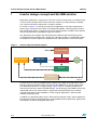
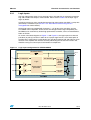
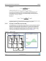
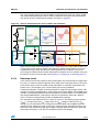
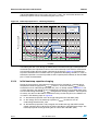
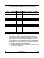
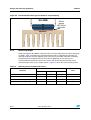
1
AN3338 Application note SLLIMM™ small low-loss intelligent molded module By Carmelo Parisi and Giovanni Tomasello Introduction In recent years the variable speed motor control market has required high performance solutions able to satisfy the increasing energy saving requirements, compactness, reliability, and system costs in home appliances, such as washing machines, dish washers, refrigerators, air conditioning compressor drives, and in low power industrial applications, such as sewing machines, pumps, tools, etc. To meet these market needs, STMicroelectronics has developed a new family of compact, high efficiency, dual-in-line intelligent power modules, with optional extra features, called small low-loss intelligent molded module (SLLIMM™). The SLLIMM product family combines optimized silicon chips, integrated in three main inverter blocks: ■ power stage – six short-circuit rugged IGBTs – six freewheeling diodes ■ driving network – three high voltage gate drivers – discrete gate resistors – three bootstrap diodes ■ protection and optional features – op amps for advanced current sensing – comparators for fault protection against overcurrent and short-circuit – NTC sensor for temperature control – smart shutdown function – dead time, interlocking function and undervoltage lockout. Thanks to the state of art DBC mounting technology, the fully isolated SLLIMM package (SDIP) offers extremely low thermal resistance with optimum cost-effectiveness and quality level. Compared to discrete-based inverters, including power devices, and driver and protection circuits, the SLLIMM family provides a high integrated level that means simplified circuit design, reduced component count, smaller weight, and high reliability. The aim of this application note is to provide a detailed description of SLLIMM products, providing guidelines to motor drive designers for an efficient, reliable, and fast design when using the new ST SLLIMM family. September 2012 Doc ID 18441 Rev 3 1/73 www.st.com Contents AN3338 Contents 1 2 3 4 2/73 Inverter design concept and SLLIMM solution . . . . . . . . . . . . . . . . . . . . 6 1.1 Product synopsis . . . . . . . . . . . . . . . . . . . . . . . . . . . . . . . . . . . . . . . . . . . . 7 1.2 Product line-up and nomenclature . . . . . . . . . . . . . . . . . . . . . . . . . . . . . . . 9 1.3 Internal circuit . . . . . . . . . . . . . . . . . . . . . . . . . . . . . . . . . . . . . . . . . . . . . . 11 1.4 Absolute maximum ratings . . . . . . . . . . . . . . . . . . . . . . . . . . . . . . . . . . . . 13 Electrical characteristics and functions . . . . . . . . . . . . . . . . . . . . . . . . 17 2.1 IGBTs . . . . . . . . . . . . . . . . . . . . . . . . . . . . . . . . . . . . . . . . . . . . . . . . . . . . 17 2.2 Freewheeling diodes . . . . . . . . . . . . . . . . . . . . . . . . . . . . . . . . . . . . . . . . 17 2.3 High voltage gate drivers . . . . . . . . . . . . . . . . . . . . . . . . . . . . . . . . . . . . . 17 2.3.1 Logic inputs . . . . . . . . . . . . . . . . . . . . . . . . . . . . . . . . . . . . . . . . . . . . . . 19 2.3.2 High voltage level shift . . . . . . . . . . . . . . . . . . . . . . . . . . . . . . . . . . . . . . 21 2.3.3 Undervoltage lockout . . . . . . . . . . . . . . . . . . . . . . . . . . . . . . . . . . . . . . . 21 2.3.4 Dead time and interlocking function management . . . . . . . . . . . . . . . . . 22 2.3.5 Comparators for fault sensing . . . . . . . . . . . . . . . . . . . . . . . . . . . . . . . . 24 2.3.6 Short-circuit protection and smart shutdown function . . . . . . . . . . . . . . 25 2.3.7 Timing chart of short-circuit protection and smart shutdown function . . 26 2.3.8 Current sensing shunt resistor selection . . . . . . . . . . . . . . . . . . . . . . . . 27 2.3.9 RC filter network selection . . . . . . . . . . . . . . . . . . . . . . . . . . . . . . . . . . . 28 2.3.10 Overtemperature protection . . . . . . . . . . . . . . . . . . . . . . . . . . . . . . . . . . 30 2.3.11 Op amps for advanced current sensing . . . . . . . . . . . . . . . . . . . . . . . . . 32 2.3.12 Bootstrap circuit . . . . . . . . . . . . . . . . . . . . . . . . . . . . . . . . . . . . . . . . . . . 33 2.3.13 Bootstrap capacitor selection . . . . . . . . . . . . . . . . . . . . . . . . . . . . . . . . . 34 2.3.14 Initial bootstrap capacitor charging . . . . . . . . . . . . . . . . . . . . . . . . . . . . 36 Package . . . . . . . . . . . . . . . . . . . . . . . . . . . . . . . . . . . . . . . . . . . . . . . . . . 38 3.1 DBC substrate . . . . . . . . . . . . . . . . . . . . . . . . . . . . . . . . . . . . . . . . . . . . . 38 3.2 PCB . . . . . . . . . . . . . . . . . . . . . . . . . . . . . . . . . . . . . . . . . . . . . . . . . . . . . 39 3.3 Package structure . . . . . . . . . . . . . . . . . . . . . . . . . . . . . . . . . . . . . . . . . . 39 3.4 Package outline and dimensions . . . . . . . . . . . . . . . . . . . . . . . . . . . . . . . 42 3.5 Input and output pins description . . . . . . . . . . . . . . . . . . . . . . . . . . . . . . . 45 Power losses and dissipation . . . . . . . . . . . . . . . . . . . . . . . . . . . . . . . . 52 Doc ID 18441 Rev 3 AN3338 5 Contents 4.1 Conduction power losses . . . . . . . . . . . . . . . . . . . . . . . . . . . . . . . . . . . . . 52 4.2 Switching power losses . . . . . . . . . . . . . . . . . . . . . . . . . . . . . . . . . . . . . . 55 4.3 Thermal impedance overview . . . . . . . . . . . . . . . . . . . . . . . . . . . . . . . . . 56 4.4 Power losses calculation example . . . . . . . . . . . . . . . . . . . . . . . . . . . . . . 59 Design and mounting guidelines . . . . . . . . . . . . . . . . . . . . . . . . . . . . . . 61 5.1 Layout suggestions . . . . . . . . . . . . . . . . . . . . . . . . . . . . . . . . . . . . . . . . . 61 5.1.1 5.2 General suggestions . . . . . . . . . . . . . . . . . . . . . . . . . . . . . . . . . . . . . . . 61 Mounting instructions . . . . . . . . . . . . . . . . . . . . . . . . . . . . . . . . . . . . . . . . 65 5.2.1 Heatsink mounting . . . . . . . . . . . . . . . . . . . . . . . . . . . . . . . . . . . . . . . . . 65 5.2.2 Mounting torque . . . . . . . . . . . . . . . . . . . . . . . . . . . . . . . . . . . . . . . . . . . 66 5.2.3 General handling precaution and storage notices . . . . . . . . . . . . . . . . . 67 5.2.4 Packaging specifications . . . . . . . . . . . . . . . . . . . . . . . . . . . . . . . . . . . . 69 6 References . . . . . . . . . . . . . . . . . . . . . . . . . . . . . . . . . . . . . . . . . . . . . . . . 71 7 Revision history . . . . . . . . . . . . . . . . . . . . . . . . . . . . . . . . . . . . . . . . . . . 72 Doc ID 18441 Rev 3 3/73 List of tables AN3338 List of tables Table 1. Table 2. Table 3. Table 4. Table 5. Table 6. Table 7. Table 8. Table 9. Table 10. Table 11. Table 12. Table 13. Table 14. Table 15. 4/73 SLLIMM line-up. . . . . . . . . . . . . . . . . . . . . . . . . . . . . . . . . . . . . . . . . . . . . . . . . . . . . . . . . . . 9 Inverter part of STGIPL14K60 . . . . . . . . . . . . . . . . . . . . . . . . . . . . . . . . . . . . . . . . . . . . . . 14 Control part of STGIPL14K60 . . . . . . . . . . . . . . . . . . . . . . . . . . . . . . . . . . . . . . . . . . . . . . . 16 Supply voltage and operation behavior . . . . . . . . . . . . . . . . . . . . . . . . . . . . . . . . . . . . . . . 16 Total STGIPL14K60 system . . . . . . . . . . . . . . . . . . . . . . . . . . . . . . . . . . . . . . . . . . . . . . . . 16 Integrated pull-up/down resistor values . . . . . . . . . . . . . . . . . . . . . . . . . . . . . . . . . . . . . . . 20 Interlocking function truth table of STGIPS10K60A . . . . . . . . . . . . . . . . . . . . . . . . . . . . . . 22 Interlocking function truth table of STGIPS14K60, STGIPL14K60, STGIPS20K60, and STGIPL20K60 . . . . . . . . . . . . . . . . . . . . . . . . . . . . . . . . . . . . . . . . . . 23 Outline drawing of SDIP-25L package . . . . . . . . . . . . . . . . . . . . . . . . . . . . . . . . . . . . . . . . 43 Outline drawing of SDIP-38L package . . . . . . . . . . . . . . . . . . . . . . . . . . . . . . . . . . . . . . . . 45 Input and output pins of SDIP-25L package . . . . . . . . . . . . . . . . . . . . . . . . . . . . . . . . . . . . 46 Input and output pins of SDIP-38L package . . . . . . . . . . . . . . . . . . . . . . . . . . . . . . . . . . . . 47 RC Cauer thermal network elements by device . . . . . . . . . . . . . . . . . . . . . . . . . . . . . . . . . 59 Mounting torque and heatsink flatness . . . . . . . . . . . . . . . . . . . . . . . . . . . . . . . . . . . . . . . . 66 Document revision history . . . . . . . . . . . . . . . . . . . . . . . . . . . . . . . . . . . . . . . . . . . . . . . . . 72 Doc ID 18441 Rev 3 AN3338 List of figures List of figures Figure 1. Figure 2. Figure 3. Figure 4. Figure 5. Figure 6. Figure 7. Figure 8. Figure 9. Figure 10. Figure 11. Figure 12. Figure 13. Figure 14. Figure 15. Figure 16. Figure 17. Figure 18. Figure 19. Figure 20. Figure 21. Figure 22. Figure 23. Figure 24. Figure 25. Figure 26. Figure 27. Figure 28. Figure 29. Figure 30. Figure 31. Figure 32. Figure 33. Figure 34. Figure 35. Figure 36. Figure 37. Figure 38. Figure 39. Figure 40. Figure 41. Figure 42. Figure 43. Figure 44. Figure 45. Figure 46. Figure 47. Figure 48. Figure 49. Inverter motor drive block diagram . . . . . . . . . . . . . . . . . . . . . . . . . . . . . . . . . . . . . . . . . . . . 7 Discrete-based inverter vs. SLLIMM solution comparison . . . . . . . . . . . . . . . . . . . . . . . . . . 8 SLLIMM block diagram . . . . . . . . . . . . . . . . . . . . . . . . . . . . . . . . . . . . . . . . . . . . . . . . . . . . . 9 SLLIMM nomenclature . . . . . . . . . . . . . . . . . . . . . . . . . . . . . . . . . . . . . . . . . . . . . . . . . . . . 11 Internal circuit of STGIPS10K60A . . . . . . . . . . . . . . . . . . . . . . . . . . . . . . . . . . . . . . . . . . . 12 Internal circuit of STGIPS14K60 and STGIPS20K60 . . . . . . . . . . . . . . . . . . . . . . . . . . . . . 13 Internal circuit of STGIPL14K60 and STGIPL20K60 . . . . . . . . . . . . . . . . . . . . . . . . . . . . . 14 Stray inductance components of output stage . . . . . . . . . . . . . . . . . . . . . . . . . . . . . . . . . . 16 High voltage gate drive die image . . . . . . . . . . . . . . . . . . . . . . . . . . . . . . . . . . . . . . . . . . . 19 High voltage gate driver block diagram . . . . . . . . . . . . . . . . . . . . . . . . . . . . . . . . . . . . . . . 19 Logic input configuration for STGIPS10K60A. . . . . . . . . . . . . . . . . . . . . . . . . . . . . . . . . . . 20 Logic input configuration for STGIPS14K60 and STGIPL20K60 . . . . . . . . . . . . . . . . . . . . 21 Timing chart of undervoltage lockout function . . . . . . . . . . . . . . . . . . . . . . . . . . . . . . . . . . 23 Timing chart of dead time function . . . . . . . . . . . . . . . . . . . . . . . . . . . . . . . . . . . . . . . . . . . 25 Smart shutdown equivalent circuitry . . . . . . . . . . . . . . . . . . . . . . . . . . . . . . . . . . . . . . . . . . 27 Timing chart of smart shutdown function . . . . . . . . . . . . . . . . . . . . . . . . . . . . . . . . . . . . . . 28 Examples of SC protection circuit . . . . . . . . . . . . . . . . . . . . . . . . . . . . . . . . . . . . . . . . . . . . 30 Example of SC event . . . . . . . . . . . . . . . . . . . . . . . . . . . . . . . . . . . . . . . . . . . . . . . . . . . . . 31 NTC resistance vs. temperature curve . . . . . . . . . . . . . . . . . . . . . . . . . . . . . . . . . . . . . . . . 32 Example of overtemperature protection circuit . . . . . . . . . . . . . . . . . . . . . . . . . . . . . . . . . . 32 3-phase system . . . . . . . . . . . . . . . . . . . . . . . . . . . . . . . . . . . . . . . . . . . . . . . . . . . . . . . . . 34 General advanced current sense scheme and waveforms. . . . . . . . . . . . . . . . . . . . . . . . . 34 Bootstrap circuit . . . . . . . . . . . . . . . . . . . . . . . . . . . . . . . . . . . . . . . . . . . . . . . . . . . . . . . . . 35 Bootstrap capacitor vs. switching frequency. . . . . . . . . . . . . . . . . . . . . . . . . . . . . . . . . . . . 38 Initial bootstrap charging time . . . . . . . . . . . . . . . . . . . . . . . . . . . . . . . . . . . . . . . . . . . . . . . 39 DCB structure . . . . . . . . . . . . . . . . . . . . . . . . . . . . . . . . . . . . . . . . . . . . . . . . . . . . . . . . . . . 40 PCB structure . . . . . . . . . . . . . . . . . . . . . . . . . . . . . . . . . . . . . . . . . . . . . . . . . . . . . . . . . . . 41 Images and internal view of SDIP-25L package . . . . . . . . . . . . . . . . . . . . . . . . . . . . . . . . . 42 Images and internal view of SDIP-38L package . . . . . . . . . . . . . . . . . . . . . . . . . . . . . . . . . 43 Outline drawing of SDIP-25L package . . . . . . . . . . . . . . . . . . . . . . . . . . . . . . . . . . . . . . . . 44 Outline drawing of SDIP-38L package . . . . . . . . . . . . . . . . . . . . . . . . . . . . . . . . . . . . . . . . 47 Pinout of SDIP-25L package (bottom view) . . . . . . . . . . . . . . . . . . . . . . . . . . . . . . . . . . . . 49 Pinout of SDIP-38L package (bottom view) . . . . . . . . . . . . . . . . . . . . . . . . . . . . . . . . . . . . 50 Typical IGBT power losses . . . . . . . . . . . . . . . . . . . . . . . . . . . . . . . . . . . . . . . . . . . . . . . . . 55 IGBT and diode approximation of the output characteristics . . . . . . . . . . . . . . . . . . . . . . . 56 Typical switching waveforms of STGIPL14K60 . . . . . . . . . . . . . . . . . . . . . . . . . . . . . . . . . 59 Equivalent thermal circuit with heatsink single IGBT . . . . . . . . . . . . . . . . . . . . . . . . . . . . . 60 Thermal impedance curves (STGIPS14K60 and STGIPL14K60) . . . . . . . . . . . . . . . . . . . 61 Thermal impedance RC Cauer thermal network. . . . . . . . . . . . . . . . . . . . . . . . . . . . . . . . . 61 Maximum IC(RMS) current vs. fsw simulated curves . . . . . . . . . . . . . . . . . . . . . . . . . . . . . 63 General suggestions 1 . . . . . . . . . . . . . . . . . . . . . . . . . . . . . . . . . . . . . . . . . . . . . . . . . . . . 65 General suggestions 2 . . . . . . . . . . . . . . . . . . . . . . . . . . . . . . . . . . . . . . . . . . . . . . . . . . . . 66 Example 1 of a possible wrong layout . . . . . . . . . . . . . . . . . . . . . . . . . . . . . . . . . . . . . . . . 67 Example 2 of a possible wrong layout . . . . . . . . . . . . . . . . . . . . . . . . . . . . . . . . . . . . . . . . 68 Recommended silicon grease thickness and positioning . . . . . . . . . . . . . . . . . . . . . . . . . . 69 Measurement point of Cu heatsink flatness . . . . . . . . . . . . . . . . . . . . . . . . . . . . . . . . . . . . 70 Recommended fastening order of mounting screws . . . . . . . . . . . . . . . . . . . . . . . . . . . . . 70 Packaging specifications of SDIP-25L package . . . . . . . . . . . . . . . . . . . . . . . . . . . . . . . . . 73 Packaging specifications of SDIP-38L package . . . . . . . . . . . . . . . . . . . . . . . . . . . . . . . . . 74 Doc ID 18441 Rev 3 5/73 Inverter design concept and SLLIMM solution 1 AN3338 Inverter design concept and SLLIMM solution Motor drive applications, ranging from a few tens of watts to mega watts, are mainly based on the inverter concept thanks to the fact that this solution can meet efficiency, reliability, size, and cost constraints required in a number of markets. As shown in Figure 1, an inverter for motor drive applications is basically composed of a power stage, mainly based on IGBTs and freewheeling diodes; a driving stage, based on high voltage gate drivers; a control unit, based on microcontrollers or DSPs; some optional sensors for protections and feedback signals for controls. The approach of this solution with discrete devices produces high manufacturing costs associated with high reliability risks, bigger size and higher weight, a considerable number of components and the significant stray inductances and dispersions in the board layout. Figure 1. Inverter motor drive block diagram 0DLQV 0LFURFRQWUROOHU *DWHGULYHU %ULGJHUHFWLILHU 3RZHUVWDJH 0 6HQVRUV )HHGEDFN !-V In recent years, the use of intelligent power modules has rapidly increased thanks to the benefits of greater integration levels. The new ST SLLIMM family is able to replace more than 30 discrete devices in a single package. Figure 2 shows a comparison between a discrete-based inverter and the SLLIMM solution, the advantages of SLLIMM can be easily understood and can be summarized in a significantly improved design time, reduced manufacturing efforts, higher flexibility in a wide range of applications, and increased reliability and quality level. In addition, the optimized silicon chips in both control and power stages and the optimized board layout provide maximized efficiency, reduced EMI and noise generation, higher levels of protection, and lower propagation delay time. 6/73 Doc ID 18441 Rev 3 AN3338 Figure 2. Inverter design concept and SLLIMM solution Discrete-based inverter vs. SLLIMM solution comparison 3DVVLYHFRPSRQHQWV 'LRGHV 5HVLVWRUV &DSDFLWRUV +9JDWHGULYHUV 5HGXFHWRWDO V\VWHPFRVW ,*%7V):'V (DV\OD\RXW DQGGHVLJQ 5HGXFHG(0, DQGQRLVH 0 /,0 6/ +LJKTXDOLW\ DQGUHOLDELOLW\ $GYDQFHG SURWHFWLRQ IXQFWLRQ ,PSURYH (IILFLHQF\ !-V 1.1 Product synopsis The SLLIMM family has been designed to satisfy the requirements of a wide range of final applications in the range of 300 W - 2.0 kW, such as: ● washing machines ● dish washers ● refrigerators ● air conditioning compressor drives ● sewing machines ● pumps ● tools ● low power industrial applications The main features and integrated functions can be summarized as follows: ● 600 V, 10 - 20 A ratings ● 3-phase IGBT inverter bridge including: ● – six low-loss and short-circuit protected IGBTs – six low forward voltage drop and soft recovery freewheeling diodes three control ICs for gate driving and protection including: – smart shutdown function – comparator for fault protection against overcurrent and short-circuit – op amps for advanced current sensing – three integrated bootstrap diodes – interlocking function – undervoltage lockout Doc ID 18441 Rev 3 7/73 Inverter design concept and SLLIMM solution AN3338 ● NTC thermistor for temperature monitor ● open emitter configuration for individual phase current sensing ● DBC fully isolated package for enhanced thermal behavior ● isolation voltage rating of 2500 VRMS ● several passive components for IGBT switching speed optimum setting ● gate driver proper biasing and noise filtering. Figure 3 shows the block diagram of SLLIMM included in the inverter solution Figure 3. SLLIMM block diagram 0DLQV %ULGJHUHFWLILHU *DWHGULYHU 89/2 'HDGWLPH /HYHO 6KLIW 6PDUW &RPSDUDWRU 6KXW'RZQ %RRWVWUDS GLRGH +DOIEULGJH 2S$PS *DWHGULYHU 0LFURFRQWUROOHU 89/2 'HDGWLPH /HYHO 6KLIW 6PDUW &RPSDUDWRU 6KXW'RZQ +DOIEULGJH %RRWVWUDS GLRGH 0 2S$PS *DWHGULYHU 89/2 'HDGWLPH /HYHO 6KLIW 6PDUW &RPSDUDWRU 6KXW'RZQ %RRWVWUDS GLRGH +DOIEULGJH 2S$PS 17& WHPSHUDWXUH PRQLWRULQJ 6//,00 )HHGEDFN !-V The power devices (IGBTs and freewheeling diodes), incorporated in the half bridge block, are tailored for a motor drive application delivering the greatest overall efficiency, thanks to the optimized trade-off between conduction and switching power losses and very low EMI generation, as a result of reduced dV/dt and di/dt. The IC gate drivers have been selected in order to meet two levels of functionality giving the designers more freedom to choose: a basic version which includes the essential features for a cost-effective solution and a fully featured version which provides advanced options for a sophisticated control method. The fully isolated SDIP package is available in a 25-lead version (SDIP-25L) and 38-lead version (SDIP-38L) and offers excellent heat dissipation characteristics, thanks to the state of the art DBC mounting technology, ensuring at the same time, very high voltage isolation rating (2500 VRMS), compact size and high reliability. 8/73 Doc ID 18441 Rev 3 AN3338 Inverter design concept and SLLIMM solution 1.2 Product line-up and nomenclature Table 1. SLLIMM line-up Basic version Fully featured version Features STGIPS10K60A STGIPS14K60 STGIPL14K60 STGIPS20K60 STGIPL20K60 Voltage (V) 600 600 600 600 600 Current @ TC=25 °C (A) 10 14 15 18 20 RthJC max. single IGBT (°C/W) 3.8 3 2.8 2.4 2.2 Package type SDIP-25L SDIP-25L SDIP-38L SDIP-25L SDIP-38L Package size (mm) X, Y, Z 44.4x22.0x5.4 44.4x22.0x5.4 49.6x24.5x5.4 44.4x22.0x5.4 49.6x24.5x5.4 DBC substrate Yes Yes Yes Yes Yes NTC Yes No Yes No Yes Integrated bootstrap diode Yes Yes Yes Yes Yes SD function No Yes Yes Yes Yes Comparator for fault protection No Yes (1 pin) Yes (3 pins) Yes (1 pin) Yes (3 pins) Smart shutdown function No Yes Yes Yes Yes Op amps for advanced current sensing No No Yes No Yes Interlocking function Yes Yes Yes Yes Yes Undervoltage lockout Yes Yes Yes Yes Yes Yes (3 pins) Yes (3 pins) Yes (3 pins) Yes (3 pins) Yes (3 pins) Yes Yes Yes Yes Yes High side IGBT input signal Active High Active High Active High Active High Active High Low side IGBT input signal Active High Active Low Active Low Active Low Active Low Open emitter configuration 3.3 / 5 V input interface compatibility Doc ID 18441 Rev 3 9/73 Inverter design concept and SLLIMM solution Figure 4. AN3338 SLLIMM nomenclature 67 * ,3 / . [ 6SHFLDOIHDWXUHV $ %DVLFYHUVLRQ / 6LQJOHSKDVH 9&(6 YROWDJHGLYLGHGE\ * ĭ ,*%7'LRGH 7HFKQRORJ\ 6//,00,30 .+ +LJKIUHTXHQF\·N+] : 9HU\+LJKIUHTXHQF\·N+] & 0HGLXPIUHTXHQF\·N+] 3DFNDJH / 6',3/PROGHG 1 1',3/ PROGHG 6 6',3/ PROGHG 1RPLQDOFXUUHQW ,& FXUUHQWDW7& & !-V 10/73 Doc ID 18441 Rev 3 AN3338 Inverter design concept and SLLIMM solution 1.3 Internal circuit Figure 5. Internal circuit of STGIPS10K60A Doc ID 18441 Rev 3 11/73 Inverter design concept and SLLIMM solution Figure 6. 12/73 Internal circuit of STGIPS14K60 and STGIPS20K60 Doc ID 18441 Rev 3 AN3338 AN3338 Inverter design concept and SLLIMM solution Figure 7. Internal circuit of STGIPL14K60 and STGIPL20K60 1.4 Absolute maximum ratings The absolute maximum ratings represent the extreme capability of the device and they can be normally used as a worst limit design condition. It is important to note that the absolute maximum value is given according to a set of testing conditions such us temperature, frequency, voltage, and so on. The device performances can change according to the applied condition. Doc ID 18441 Rev 3 13/73 Inverter design concept and SLLIMM solution AN3338 The SLLIMM specifications are described below by using the STGIPL14K60 datasheet as an example. Please refer to the respective product datasheets for a detailed description of other types. Table 2. Inverter part of STGIPL14K60 Symbol Parameter Value Unit VPN Supply voltage applied between P-NU, NV, NW 450 V VPN(surge) Supply voltage (surge) applied between P-NU, NV, NW 500 V (1) VCES Collector emitter voltage (VIN =0) 600 V ±IC (2) Each IGBT continuous collector current at TC=25 °C 15 A ±IC (3) Each IGBT pulsed collector current 30 A PTOT Each IGBT total dissipation at TC=25 °C 44 W tSCW Short-circuit withstand time, VCE=0.5· V(BR)CES, Tj=125 °C, VCC=Vboot=15 V, VIN(1)=0÷5 V 5 µs 1. Applied between HINU, HINV, HINW; LINU, LINV, LINW and GND. 2. Calculated according to the iterative Equation 1. 3. Pulse width limited by max. junction temperature. Equation 1 IC (TC ) = Tjmax − TC Rth (j−c ) ⋅ VCE(sat)(max)(@Tj max,IC(TC )) ● VPN: supply voltage applied between P-NU, NV, NW ● VPN(surge): supply voltage (surge) applied between P-NU, NV, NW ● VCES: collector emitter voltage The power stage of SLLIMM is based on IGBTs (and freewheeling diodes) having 600 V VCES rating. Considering the SLLIMM internal stray inductances during the commutations, which can generate up to 100 V of surge voltage, the maximum surge voltage between P-N (VPN(surge)) allowed is 500 V. At the same time, the maximum supply voltage (in steadystate) applied between P-N (VPN) allowed is 450 V because of an additional 50 V of surge voltage generated by the stray inductance between the SLLIMM and the DC-link capacitor. Figure 8 shows the parasitic inductances of the output stage. It is possible to note that there are two major components, the first is due to the internal layout of SLLIMM, while the second is due to the layout of the board. 14/73 Doc ID 18441 Rev 3 AN3338 Figure 8. Inverter design concept and SLLIMM solution Stray inductance components of output stage 7KHUHDOYROWDJHRYHUWKH,*%7 'XHWRGLGW YDOXHDQGSDUDVLWLF )ODW931 FDQH[FHHGWKHUDWLQJYROWDJH LQGXFWDQFHWKHRYHUYROWDJHVSLNH YDOXH FDQDSSHDURQWKH6//,00SLQV 931 931VXUJH 3 +LJK GLGW YDOXH +9,& WRPRWRU 89: & 9EXV 1 6//,00 3DUDVLWLFLQGXFWDQFH GXHWRWKH6//,00LQWHUQDOOD\RXW 3DUDVLWLFLQGXFWDQFH GXHWR3&%OD\RXW !-V ● ±IC: each IGBT continuous collector current The allowable DC current continuously flowing at collector electrode (TC = 25 °C). The IC parameter is calculated according to Equation 1. ● tSCW: short-circuit withstand time The IGBTs incorporated inside the SLLIMM are tailored for a motor control application, therefore, short-circuit self-protection is one of the main module features. tSCW represents the short-circuit, non-repetitive, withstand time. If the short-circuit conditions exceed the above specifications, the lifetime of the device is drastically shortened. It is strongly recommended that the SLLIMM should not be operated under these conditions. Doc ID 18441 Rev 3 15/73 Inverter design concept and SLLIMM solution Table 3. AN3338 Control part of STGIPL14K60 Symbol Parameter Value Unit VOUT Output voltage applied between OUTU, OUTV, OUTW, and GND (VCC=15 V) Vboot -21 to Vboot +0.3 V VCC Low voltage power supply -0.3 to 21 V VCIN Comparator input voltage -0.3 to VCC +0.3 V Vboot Bootstrap voltage -0.3 to 620 V VIN Logic input voltage applied between HIN, LIN and GND -0.3 to 15 V VSD/OD Open drain voltage -0.3 to 15 V dVOUT/dt Allowed output slew rate 50 V/ns ● VCC: low voltage power supply VCC represents the supply voltage of the control part. A local filtering is recommended to enhance the SLLIMM noise immunity. Generally, the use of one electrolytic capacitor (with a greater value but not negligible ESR) and one smaller ceramic capacitor (hundreds of nF), faster than the electrolytic one to provide current, is suggested. Small filter capacitors are already connected inside the SLLIMM, directly on the involved pins (see internal circuits Figure 5, 6, and 7). Please refer to Table 4 in order to properly drive the SLLIMM. Table 4. Supply voltage and operation behavior VCC voltage (typ. value) (1) Operating behavior < 12 V As the voltage is lower than the UVLO threshold the control circuit is not fully turned on. A perfect functionality cannot be guaranteed. 12 V – 13.5 V IGBTs can work, however conduction and switching losses increase due to low voltage gate signal. 13.5 V – 18 V Recommended value (see relevant datasheets). 18 V – 21 V IGBTs can work. Switching speed is faster and saturation current higher, increasing short-circuit broken risk and EMI issues. > 21 V Control circuit is destroyed. Absolute max. rating is 21 V. 1. Except for STGIPS10K60A. For further information please refer to the relevant datasheet. Table 5. Total STGIPL14K60 system Symbol Parameter Value Unit VISO Isolation withstands voltage applied between each pin and heatsink plate (AC voltage, t = 60 sec.) 2500 V Tj (1) Operating junction temperature -40 to 150 °C TC Module case operation temperature -40 to 125 °C 1. The maximum junction temperature rating of the power chips integrated within the SDIP module is 150 °C (@ TC = 100 °C). To ensure safe operation of the SDIP module, the average junction temperature should be limited to Tj(avg) ≤ 125 °C (@TC ≤ 100 °C). 16/73 Doc ID 18441 Rev 3 AN3338 2 Electrical characteristics and functions Electrical characteristics and functions In this section the main electrical characteristics of the power stage are discussed, together with a detailed description of all the SLLIMM functions. 2.1 IGBTs The SLLIMM achieves power savings in the inverter stage thanks to the use of IGBTs manufactured with the proprietary advanced PowerMESH™ process. These power devices, optimized for the typical motor control switching frequency, offer an excellent trade-off between voltage drop (VCE(sat)) and switching speed (tfall), and therefore minimize the two major sources of energy loss, conduction and switching, reducing the environmental impact of daily-use equipment. A full analysis on the power losses of the complete system is reported in Section 4: Power losses and dissipation. This IGBT family is capable of surviving short-circuits lasting up to 5 microseconds, as expected by targeted applications. 2.2 Freewheeling diodes The Turbo 2 ultrafast high voltage diodes have been adequately selected for the SLLIMM family and carefully tuned to achieve the best trr/VF trade-off and softness as freewheeling diodes in order to further improve the total performance of the inverter and significantly reduce the electromagnetic interference (EMI) in motor control applications which are quite sensitive to this phenomena. 2.3 High voltage gate drivers The SLLIMM is equipped with a versatile high voltage gate driver IC (HVIC), designed using BCD offline (Bipolar, CMOS, and DMOS) technology (see Figure 9) and particularly suited to field oriented control (FOC) motor driving applications, able to provide all the functions and current capability necessary for high side and low side IGBT driving. This driver can be used in all applications where high voltage shifted control is necessary and it includes a patented internal circuitry which replaces the external bootstrap diode. Each high voltage gate driver chip controls two IGBTs in half bridge topology, offering the basic functions such as dead time, interlocking, integrated bootstrap diode, and also the advanced features such as smart shutdown (patented), fault comparator, and a dedicated high performance op amp for advanced current sensing. A schematic summary of the features by device are listed in Table 1. In this application note the main characteristics of a high voltage gate drive related to the SLLIMM are discussed. For a greater understanding, please refer to the AN2738 application note. Doc ID 18441 Rev 3 17/73 Electrical characteristics and functions Figure 9. AN3338 High voltage gate drive die image Figure 10. High voltage gate driver block diagram %RRWVWUDSGULYHU 9&& )ORDWLQJVWUXFWXUH 9&& 89 GHWHFWLRQ IURPP& IURPWRP& &6' 6'2' *1' WRPRWRU 89: 9&& 9%LDV 6KXWGRZQ ODWFK 6PDUW VKXW GRZQ /9* GULYHU /9* 1 9 &3 &,1 &RPS 56) &6) 95() '7 &') 5') WR$'& 'HDG WLPH 9%LDV 9&& 23287 23 2SDPS +9,& 23 56+817 6//,00 !-V 18/73 WR'&OLQN &%227 +9* 287 /,1 IURPP& +9* GULYHU 6KRRW WURXJK SUHYHQWLRQ 9 56' 6 5 /HYHO VKLIWHU /RJLF 9%227 3 89 78 &'6'%6+10 GHWHFWLRQ IURP/9* +,1 %227 Doc ID 18441 Rev 3 AN3338 2.3.1 Electrical characteristics and functions Logic inputs The high voltage gate driver IC has two logic inputs, HIN and LIN, to separately control the high side and low side outputs, HVG and LVG. Please refer to Table 1 for the input signal logics by device. In order to prevent any cross conduction between high side and low side IGBT a safety time (dead time) is introduced (see Section 2.3.4: Dead time and interlocking function management for further details). All the logic inputs are provided with hysteresis (~1 V) for low noise sensitivity and are TTL/CMOS 3.3 V compatible. Thanks to this low voltage interface logic compatibility, the SLLIMM can be used with any kind of high performance controller, such as microcontrollers, DSPs or FPGAs. As shown in the block diagrams of Figure 11 and Figure 12, the logic inputs have internal pull-down (or pull-up) resistors in order to set a proper logic level in case of interruption in the logic lines. If logic inputs are left floating, the gate driver outputs LVG and HVG are set to low level. This simplifies the interface circuit by eliminating the six external resistors and, therefore saving cost, board space and number of components. Figure 11. Logic input configuration for STGIPS10K60A %RRWVWUDSGULYHU 9%227 3 9&& 89GHWHFWLRQ 89GHWHFWLRQ +LJKVLGH OHYHO VKLIWLQJ GULYHU /RJLF +,1 287 6KRRWWURXJK SUHYHQWLRQ /RZVLGH GULYHU /,1 +9,& 1 6//,00 !-V Doc ID 18441 Rev 3 19/73 Electrical characteristics and functions AN3338 Figure 12. Logic input configuration for STGIPS14K60, STGIPL14K60, STGIPS20K60, and STGIPL20K60 %RRWVWUDSGULYHU 9%227 3 9&& 89GHWHFWLRQ 89GHWHFWLRQ +LJKVLGH OHYHO VKLIWLQJ GULYHU /RJLF +,1 9 6KRRWWURXJK SUHYHQWLRQ 287 /RZVLGH GULYHU /,1 6KXWGRZQ 1 6PDUW6' 6' &,1 +9,& 95() 6//,00 !-V The typical values of the integrated pull-up/down resistors are shown in Table 6: Table 6. Integrated pull-up/down resistor values Input pin PN Input pin logic High side gate driving HINU, HINV, HINW STGIPS10K60A Active high 500 kΩ Low side gate driving LINU, LINV, LINW STGIPS10K60A Active high 500 kΩ High side gate driving HINU, HINV, HINW STGIPS14K60 STGIPL14K60 STGIPS20K60 STGIPL20K60 Active high 85 kΩ Low side gate driving LINU, LINV, LINW STGIPS14K60 STGIPL14K60 STGIPS20K60 STGIPL20K60 Active low SD / OD shutdown STGIPS14K60 STGIPL14K60 STGIPS20K60 STGIPL20K60 Active low 20/73 Doc ID 18441 Rev 3 Internal pull-up Internal pull-down 720 kΩ 125 kΩ AN3338 2.3.2 Electrical characteristics and functions High voltage level shift The built-in high voltage level shift allows direct connection between the low voltage control inputs and the high voltage power half bridge in any power application up to 600 V. It is obtained thanks to the BCD offline technology which integrates, in the same die bipolar devices, low and medium voltage CMOS for analog and logic circuitry and high voltage DMOS transistors with a breakdown voltage in excess of 600 V. This key feature eliminates the need for external optocouplers, resulting in significant savings regarding component count and power losses. Other advantages are high-frequency operation and short input-tooutput delays. 2.3.3 Undervoltage lockout The SLLIMM supply voltage VCC is continuously monitored by an undervoltage lockout (UVLO) circuitry which turns off the gate driver outputs when the supply voltage goes below the VCC_thOFF threshold specified on the datasheet and turns on the IC when the supply voltage goes above the VCC_thON voltage. A hysteresis of about 1.5 V is provided for noise rejection purposes. The high voltage floating supply Vboot is also provided with a similar undervoltage lockout circuitry. When the driver is in UVLO condition, both gate driver outputs are set to low level, setting the half bridge power stage output to high impedance. The timing chart of undervoltage lockout, plotted in Figure 13, is based on the following steps: ● t1: when the VCC supply voltage raises the VCC_thON threshold, the gate driver starts to work after the next input signal HIN/LIN is on. The circuit state becomes RESET. ● t2: input signal HIN/LIN is on and the IGBT is turned on. ● t3: when the VCC supply voltage goes below the VCC_thOFF threshold, the UVLO event is detected. The IGBT is turned off in spite of input signal HIN/LIN. The state of the circuit is now SET. ● t4: the gate driver re-starts once the VCC supply voltage again raises the VCC_thON threshold. ● t5: input signal HIN/LIN is on and the IGBT is turned on again. Doc ID 18441 Rev 3 21/73 Electrical characteristics and functions AN3338 Figure 13. Timing chart of undervoltage lockout function sͺƚŚKE 9&& § § sͺƚŚK&& ,& &LUFXLWVWDWH 7LPH ^d Z^d Z^d W § § +,1/,1 W W W W !-V 2.3.4 Dead time and interlocking function management In order to prevent any possible cross-conduction between high side and low side IGBTs, the SLLIMM provides both the dead time and the interlocking functions. The interlocking function is a logic operation which sets both the outputs to low level when the inputs are simultaneously active. The dead time function is a safety time introduced by the device between the falling edge transition of one driver output and the rising edge of the other output. If the rising edge set externally by the user occurs before the end of this dead time, it is ignored and results as delayed until the end of the dead time. Table 7. Interlocking function truth table of STGIPS10K60A Logic input (VI) Outputs Condition LIN HIN LVG HVG Interlocking half bridge tri-state H H L L 0 “logic state” half bridge tri-state L L L L 1 “logic state” low side direct driving H L H L 1 “logic state” high side direct driving L H L H The dead time is internally set at 320 ns as the typical value of STGIPS10K60A. 22/73 Doc ID 18441 Rev 3 AN3338 Table 8. Electrical characteristics and functions Interlocking function truth table of STGIPS14K60, STGIPL14K60, STGIPS20K60, and STGIPL20K60 Logic input (VI) Outputs Condition Note: SD LIN HIN LVG HVG Shutdown enable half bridge tri-state L X X L L Interlocking half bridge tri-state H L H L L 0 “logic state” half bridge tri-state H H L L L 1 “logic state” low side direct driving H L L H L 1 “logic state” high side direct driving H H H L H X: not important. The dead time is internally set at 600 ns as typical value. In Figure 14 the details of dead time and interlocking function management of the STGIPS14K60, STGIPL14K60, STGIPS20K60, and STGIPL20K60 products are described. Doc ID 18441 Rev 3 23/73 Electrical characteristics and functions AN3338 Figure 14. Timing chart of dead time function G INTE RLO RLO CKIN HIN INTE CONTROL SIGNAL EDGES OVERLAPPED: INTERLOCKING + DEAD TIME CKIN G LIN LVG DTHL DTLH HVG gate driver outputs OFF (HALF-BRIDGE TRI-STATE) gate driver outputs OFF (HALF-BRIDGE TRI-STATE) LIN CONTROL SIGNALS EDGES SYNCHRONOUS (*): DEAD TIME HIN LVG DTLH DTHL HVG gate driver outputs OFF (HALF-BRIDGE TRI-STATE) gate driver outputs OFF (HALF-BRIDGE TRI-STATE) LIN CONTROL SIGNALS EDGES NOT OVERLAPPED, BUT INSIDE THE DEAD TIME: DEAD TIME HIN LVG DTLH DTHL HVG gate driver outputs OFF (HALF-BRIDGE TRI-STATE) gate driver outputs OFF (HALF-BRIDGE TRI-STATE) LIN CONTROL SIGNALS EDGES NOT OVERLAPPED, OUTSIDE THE DEAD TIME: DIRECT DRIVING HIN LVG DTLH DTHL HVG gate driver outputs OFF (HALF-BRIDGE TRI-STATE) gate driver outputs OFF (HALF-BRIDGE TRI-STATE) (*) HIN and LIN can be connected togheter and driven by just one control signal 2.3.5 Comparators for fault sensing The SLLIMM family integrates up to three comparators (with reference to the product line-up in Table 1) intended for advanced fault protection, such as overcurrent, overtemperature or any other type of fault measurable via a voltage signal. Each comparator has an internal reference voltage VREF, specified in the datasheet, on its inverting input (see Figure 10), while the non-inverting input is available on CIN pins (one per half bridge). The comparators input can be connected to an external shunt resistor, in order to implement a simple overcurrent or short-circuit detection function, as discussed in detail in Section 2.3.6: Shortcircuit protection and smart shutdown function. Nevertheless, in the case of three internal comparators, they can be separately used in order to implement three independent controls. 24/73 Doc ID 18441 Rev 3 AN3338 2.3.6 Electrical characteristics and functions Short-circuit protection and smart shutdown function The SLLIMM is able to monitor the output current and provide protection against overcurrent and short-circuit conditions in a very short time (comparator triggering to high/low side driver turn-off propagation delay tisd = 200 ns), thanks to the smart shutdown function. This feature is based on an innovative patented circuitry which provides an intelligent fault management operation and greatly reduces the protection intervention delay independently on the protection time duration which can be set as desired by the device user. As already mentioned in Section 2.3.5: Comparators for fault sensing and shown in Figure 10, each comparator input can be connected to an external shunt resistor, RSHUNT, in order to implement a simple overcurrent detection function. An RC filter network (RSF and CSF) is necessary to prevent erroneous operation of the protection. The output signal of the comparators is fed to an integrated MOSFET with the open drain available on the SD/OD pin, shared with the SD input. When the comparator triggers, the device is set in shutdown state and all its outputs are set to low level, leaving the half bridge in tri-state. In common overcurrent protection architectures, usually the comparator output is connected to the SD input and an external RC network (RSD and CSD) is connected to this SD/OD line in order to provide a mono-stable circuit which implements a protection time when a fault condition occurs. Contrary to common fault detection systems, the new smart shutdown structure allows to immediately turn off the output gate driver in the case of fault, without waiting for the external capacitor to be discharged. This strategy minimizes the propagation delay between the fault detection event and the actual outputs switch off. In fact, the time delay between the fault and outputs disabling is not dependent on the RC value of the external SD circuitry but, thanks to the new architecture, has a preferential path internally in the driver. Then the device immediately turns off the driver outputs and latches the turn-on of the open drain switch, until the SD signal has reached its lower threshold. After the SD signal goes below the lower threshold, the open drain is switched off (see Figure 16). The smart shutdown system provides the possibility to increase the value of the external RC network across the SD pin (sized to fix the disable time generated after the fault event) as much as desired by the user without compromising the intervention time delay of the SLLIMM protection. A block diagram of the smart shutdown architecture is depicted in Figure 15. Doc ID 18441 Rev 3 25/73 Electrical characteristics and functions AN3338 Figure 15. Smart shutdown equivalent circuitry /,1 /9* +,1 +9* 9%LDV 6' )6' 46 &3 &RPS 95() 45 6(7GRPLQDQW)) +9,& 6//,00 ([FHSWIRU67*,36.$ !-V In normal operation the outputs follow the commands received from the respective input signals. When a fault detection event occurs, the fault signal (FSD) is set to high by the fault detection circuit output and the FF receives a SET input signal. Consequently, the FF outputs set the SLLIMM output signals to low level and, at the same time, turn on the open drain MOSFET which works as active pull-down for the SD signal. Note that the gate driver outputs stay at low level until the SD pin has experienced both a falling edge and a rising edge, although the fault signal could be returned to low level immediately after the fault sensing. In fact, even if the FF is reset by the falling edge of the SD input, the SD signal also works as enable for the outputs, thanks to the two AND ports. Moreover, once the internal open drain transistor has been activated, due to the latch, it cannot be turned off until the SD pin voltage reaches the low logic level. Note that, since the FF is SET dominant, oscillations of the SD pin are avoided if the fault signal remains steady at high level. 2.3.7 Timing chart of short-circuit protection and smart shutdown function With reference to Figure 16, the short-circuit protection is based on the following steps: 26/73 ● t1: when the output current is lower than the max. allowed level, the SLLIMM is working in normal operation. ● t2: when the output current reaches the max. allowed level (ISC), the overcurrent/shortcircuit event is detected and the protection is activated. The voltage across the shunt resistor, and then on the CIN pin, exceeds the VREF value, the comparator triggers, setting the device in shutdown state and both its outputs are set to low level leading the half bridge to tri-state. The smart shutdown switches off the IGBT gate (HVG, LVG) through a preferential path (200 ns as typical internal delay time) and, at the same time, it switches on the M1 internal MOSFET. The SD signal starts the discharge phase and its value drops with a time constant τA. The time constant τA value is given by: Doc ID 18441 Rev 3 AN3338 Electrical characteristics and functions Equation 2 ( ) τ A = RON _ OD // RSD ⋅ CSD ● t3: the SD signal reaches the lower threshold Vsd_L_THR and the control unit switches off the input HIN and LIN. The smart shutdown is disabled (M1 off) and SD can rise up with a time constant τB, given by: Equation 3 τB = RSD ⋅ CSD ● t4: when the SD signal reaches the upper threshold Vsd_H_THR, the system is reenabled. Figure 16. Timing chart of smart shutdown function /^ 7LPH&RQVWDQWV 6'GLVFKDUJHWLPH W$ 521B2'56'&6' ,& sZ& 6'UHFKDUJHWLPH W% 56'&6' 5&FLUFXLWWLPH FRQVWDQW 96+817ÂÂ9&,1 6KXWGRZQFLUFXLW +9*/9* 9%LDV 56' 6' 9VGB+B7+5 9VGB/B7+5 W W IURPWRP& &6' 6'2' 6PDUW VKXW 0 GRZQ 0 521B2' 6//,00 +,1/,1 7LPH 2.3.8 W W W W !-V Current sensing shunt resistor selection As previously discussed, the shunt resistors RSHUNT externally connected between the N pin and ground (see Figure 10) are used to realize the overcurrent detection. When the output current exceeds the short-circuit reference level (ISC), the CIN signal overtakes the VREF value and the short-circuit protection is active. For a reliable and stable operation the current sensing resistor should be a high quality, low tolerance non-inductive type. In fact, stray inductance in the circuit, which includes the layout, the RC filter, and also the shunt resistor, must be minimized in order to avoid undesired short-circuit detection. For these reasons, the shunt resistor and the filtering components must be placed as close as possible to the SLLIMM pins, for additional suggestions refer to Section 5.1: Layout suggestions. Doc ID 18441 Rev 3 27/73 Electrical characteristics and functions AN3338 The value of the current sense resistor can be calculated by following different guidelines, functions of the design specifications, or requirements. A common criterion is presented here based on the following steps: ● Defining of the overcurrent threshold value (IOC_th). For example, it can be fixed considering the IGBT typical working current in the application and adding 20-30% as overcurrent. ● Calculation of the shunt resistor value according to the conditioning network. An example of the conditioning network is shown in Figure 22. Further details can be found in the user manuals listed (see References 7, References 8, and References 9). ● Selection of the closest shunt resistor commercial value. ● Calculation of the power rating of the shunt resistor, taking into account that this parameter is strongly temperature dependent. Therefore, the power derating ratio of the shunt resistor, ΔP(T)%, shown in the manufacturer's datasheet, must be considered in the calculation as follows: Equation 4 PSHUNT( T ) = RSHUNT ⋅ I2RMS ΔP(T )% where IRMS is the IGBT RMS working current. For a proper selection of the shunt resistor, a safety margin of at least 30% is recommended on the calculated power rating. 2.3.9 RC filter network selection Two options of shunt (1- or 3-shunt) resistor circuit can be adopted in order to implement different control technique and short-circuit protection, as shown in Figure 17. Figure 17. Examples of SC protection circuit 18 19 1: 56) &,1 56+817 6//,00 18 56+817B8 5 19 6+817B9 1: 56+817B: &6) 6//,00 VKXQWUHVLVWRUFLUFXLW &,1 56) 56+817 &6) VKXQWUHVLVWRUVFLUFXLW !-V A RC filter network is required to prevent undesired short-circuit operation due to the noise on the shunt resistor. 28/73 Doc ID 18441 Rev 3 AN3338 Electrical characteristics and functions Both solutions allow to detect the total current in all three phases of the inverter. The filter is based on the RSF and CSF network and its time constant is given by: Equation 5 tSF = RSF ⋅ CSF In addition to the RC time constant, the turn-off propagation delay of the gate driver, tisd (specified in the datasheet) and the IGBT turn-off time (in the range of tens of ns), must be considered in the total delay time (tTotal), which is the time necessary to completely switch off the IGBT once the short-circuit event is detected. Therefore, the tTotal is calculated as follows: Equation 6 t Total = tSF + tisd + toff also considering that the IGBT short-circuit withstand time (tSC) is 5 µs, the tSF is recommended to be set in the range of 1~2 µs. In the case of a 3-shunt resistors circuit, a specific control technique can be implemented by using the three shunt resistors (RSHUNT_U, RSHUNT_V and RSHUNT_W) able to monitor each phase current. An example of a short-circuit event is shown in Figure 18, where it is possible to note the very fast protection, thanks to the smart shutdown function, against fault events. The main steps are: ● t1: collector current IC starts to rise. SC event is not detected yet due to the RC network on the CIN pin ● t2: voltage on VCIN reaches the VREF. SC event is detected and the smart shutdown starts to turn off the SLLIMM. ● t3: the SLLIMM is definitively turned off in less than 300 ns (including the td(off) time of IGBT) from SC detection. Finally, the total disable time is t3-t2 and the total SC action time is t3-t1. Doc ID 18441 Rev 3 29/73 Electrical characteristics and functions AN3338 Figure 18. Example of SC event ([DPSOHRI6&HYHQW QV +,1 3 WR'&OLQN +,1 +9,& 89: WRPRWRU &,1 ,& ,& sZ& 1 6//,00 &,1 56+817 7LPH W ,& $'LY[ +,1 9'LY W W &,1 9'LY W QV'LY 6&HYHQWRQWKH ORZVLGH,*%7 !-V 2.3.10 Overtemperature protection STGIPS10K60A, STGIPL14K60, and STGIPL20K60 are equipped with a negative temperature coefficient (NTC) thermistor for an easy overtemperature protection, in the case of slow case temperature drift or just for the temperature measurements, sending this information to the microcontroller in real-time. Due to the thermal impedance of SLLIMM and its own time constant, the NTC thermistor is not suited to detect rapid junction temperature rise of the power devices directly. Therefore, it cannot be used for short-circuit or overcurrent protection, but only for slow changes in temperature monitoring. The resistance versus temperature characteristic of NTC thermistor, represented in Figure 19, is non-linear and is described by the following expression: Equation 7 R(T ) = R25 ⎛1 1 ⎞ B⎜ − ⎟ ⋅ e ⎝ T 298 ⎠ where T is the temperature in Kelvin, B and R25, respectively, are a constant value in the SLLIMM working range and the resistance value at 25 °C, both parameters are shown in the datasheet. 30/73 Doc ID 18441 Rev 3 AN3338 Electrical characteristics and functions Figure 19. NTC resistance vs. temperature curve An easy circuit, using a voltage divider, for both overtemperature protection and temperature monitoring, is shown in Figure 20: Figure 20. Example of overtemperature protection circuit 9'' 7 17& 7 &27 527 917&BWK 6' 6//,00 !-V The external comparator is used to send a shutdown signal to the SLLIMM in case of overtemperature. The VNTC_th is a threshold voltage, fixed by design, and connected on the non inverting input, whilst the inverting input is connected on a voltage divider based on the NTC and ROT resistors. When voltage on the inverting input exceeds the VNTC_th value the comparator triggers, pulling down the SD and, consequently, switching off the IGBTs. For a proper sizing of the voltage divider, first of all the maximum allowed temperature level (TOT_Max) must be fixed, consequently the thermistor resistance is given by Equation 7, as well as by Figure 19. The value of ROT resistance can be calculated by using the voltage divider formula: Doc ID 18441 Rev 3 31/73 Electrical characteristics and functions AN3338 Equation 8 − V (T) = ROT ⋅ VDD RNTC(T) + ROT taking into account that, if T = TOT_Max then V-(TOT_Max) = VNTC_th. The maximum allowed power on the thermistor should not exceed 50 mW in all the operating range, in order to guarantee a safe working condition and avoid power consumption affecting the temperature measurement through self-heating. Therefore, considering (T = TOT_Max), it must be: Equation 9 2 ⎞ VDD ⎟ ≤ 50mW ⎟ ⎜R ⎝ NTC + ROT ⎠ ⎛ RNTC ⋅ I2 = RNTC ⋅ ⎜ Finally, to increase the noise immunity of the NTC thermistor, it is recommended to parallel a decoupling capacitor (COT), whose value must be between 10 to 100 nF. 2.3.11 Op amps for advanced current sensing The SLLIMM devices, in the SDIP-38L package, integrate also three operational amplifiers optimized for field oriented control (FOC) applications. In a typical FOC application the currents in the three half bridges are sensed using a shunt resistor. The analog current information is transformed into a discontinuous sense voltage signal, having the same frequency as the PWM signal driving the bridge. The sense voltage is a bipolar analog signal, whose sign depends on the direction of the current (see Figure 21): Figure 21. 3-phase system 3-phase driver Sinusoidal Vector Control 96 96 Sensing: Discontinuous Voltage at fPWM frequency 96 Power stage SKDVH PRWRU IPHASE AM09338v1 32/73 Doc ID 18441 Rev 3 AN3338 Electrical characteristics and functions The sense voltage signals must be provided to an A/D converter. They are usually shifted and amplified by dedicated op amps in order to exploit the full range of the A/D converter. The typical scheme and principle waveforms are shown in Figure 22: Figure 22. General advanced current sense scheme and waveforms WR'&OLQN 6HQVHYROWDJHVLJQDO WRPRWRU 6KLIWHGDQGFHQWHUHG VLJQDO $PSOLILHGVLJQDO )LOWHUHGVLJQDO 95() 5 5 5287 23 2SDPS 56+817 9VHQVH +DOIEULGJH FXUUHQWVHQVLQJ 5 9ROWDJH VKLIWLQJ RIWKH9VHQVH 23 &287 5 & 5 WR$'& 9ROWDJHJDLQ DQGILOWHULQJ 5287 UHTXLUHGWR PDNHWKH RSDPSVWDEOH &287 UHTXLUHGE\WKH$'& IRUVDPSOLQJSXUSRVH !-V ADCs used in vector control applications have a typical full scale range (FSR) of about 3.3 V. The sense signals must be shifted and centered on FSR/2 voltage (about 1.65 V) and amplified with a gain which provides the matching between the maximum value of the sensed signal and the FSR of the ADC. Some typical examples of sense network sizing can be found in the user manuals listed (see References 7, References 8, and References 9). 2.3.12 Bootstrap circuit In the 3-phase inverter the emitters of the low side IGBTs are connected to the negative DC bus (VDC-) as common reference ground, which allows all low side gate drivers to share the same power supply, while, the emitter of high side IGBTs is alternately connected to the positive (VDC+) and negative (VDC-) DC bus during the running conditions. A bootstrap method is a simple and cheap solution to supply the high voltage section. This function is normally accomplished by a high voltage fast recovery diode. The SLLIMM family includes a patented integrated structure that replaces the external diode. It is realized with a high voltage DMOS driven synchronously with the low side driver (LVG) and a diode in series. An internal charge pump provides the DMOS driving voltage. The operation of the bootstrap circuit is shown in Figure 23. The floating supply capacitor CBOOT is charged, from the VCC supply, when the VOUT voltage is lower than the VCC voltage (e.g. low side IGBT is on), through the bootstrap diode and the DMOS path with reference to the “bootstrap charge current path”. During the high side IGBT on phase, the bootstrap circuit provides the right gate voltage to properly drive the IGBT (see “bootstrap discharge current path”). This circuit is iterated for all three half bridges. Doc ID 18441 Rev 3 33/73 Electrical characteristics and functions AN3338 Figure 23. Bootstrap circuit &%227 ERRWVWUDS GLRGH 9ERRW 287 3 9ERRW 9&& '026 /HJHQG +9* FKDUJH SXPS 89: 287 9&& %RRWVWUDS FKDUJH FXUUHQWSDWK %RRWVWUDS GLVFKDUJH FXUUHQWSDWK /,1 *1' /9* +9,& 1 6//,00 !-V The value of the CBOOT capacitor should be calculated according to the application condition and must take the following into account: 2.3.13 ● voltage across CBOOT must be maintained at a value higher than the undervoltage lockout level for the IC driver. This enables the high side IGBT to work with a correct gate voltage (lower dissipation and better overall performances). Please consider that if a voltage below the UVLO threshold is applied on the bootstrap channel, the IC disables itself (no output) without any fault signal. ● the voltage across CBOOT is affected by different components such as drop across the integrated bootstrap structure, drop across the low side IGBT, and others. ● when the high side IGBT is on, the CBOOT capacitor discharges mainly to provide the right IGBT gate charge but other phenomena must be considered such as leakage currents, quiescent current, etc. Bootstrap capacitor selection A simple method to properly size the bootstrap capacitor considers only the amount of charge that is needed when the high voltage side of the driver is floating and IGBT gate is driven once. This approach does not take into account either the duty cycle of the PWM, or the fundamental frequency of the current. During the bootstrap capacitor charging phase, the low side IGBT is on and the voltage across CBOOT (VCBOOT) can be calculated as follows: Equation 10 VCBOOT = VCC − VF − VRDS(on) − VCE(sat) max where: VCC: supply voltage of gate driver 34/73 Doc ID 18441 Rev 3 AN3338 Electrical characteristics and functions VF: bootstrap diode forward voltage drop VCE(sat)max: maximum emitter collector voltage drop of low side IGBT VRDS(on): DMOS voltage drop The dimension of the bootstrap capacitance CBOOT value is based on the minimum voltage drop (ΔVCBOOT) to guarantee when the high side IGBT is on, and must be: Equation 11 ΔVCBOOT = VCC − VF − VRDS(on) − VGE(min) − VCE(sat) max under the condition: Equation 12 VCBOOT(min) > VBS _ thON where: VGE(min): minimum gate emitter voltage of high side IGBT VBS_thON: bootstrap turn-on undervoltage threshold (maximum value, see datasheet) Considering the factors contributing to VCBOOT decreasing, the total charge supplied by the bootstrap capacitor (during high side on phase) is: Equation 13 ( ) Q TOT = Q GA TE + ILKGE + IQBO + ILK + ILKDiode + ILKCap ⋅ tHon + Q LS where: QGATE: total IGBT gate charge ILKGE: IGBT gate emitter leakage current IQBO: bootstrap circuit quiescent current ILK: bootstrap circuit leakage current ILKDiode: bootstrap diode leakage current ILKCap: bootstrap capacitor leakage current (relevant when using an electrolytic capacitor but can be ignored if other types of capacitors are used) tHon: high side on time QLS: charge required by the internal level shifters Finally, the minimum size of the bootstrap capacitor is: Equation 14 CBOOT = QTOT ΔVCBOOT For an easier selection of bootstrap capacitor, Figure 24 shows the behavior of CBOOT (calculated) versus switching frequency (fsw), with different values of ΔVCBOOT, corresponding to Equation 14 for a continuous sinusoidal modulation and for STGIPS20K60 Doc ID 18441 Rev 3 35/73 Electrical characteristics and functions AN3338 and STGIPL20K60 (worst case) and a duty cycle δ = 50%. For all the other devices the bootstrap capacitor can be calculated using the same curve. Figure 24. Bootstrap capacitor vs. switching frequency AM09341v1 5 STGIPx20K60 δ=50% C BOOT Calculated (µF) 4 3 ΔVCBOOT =0.1V 2 ΔVCBOOT =0.3V ΔVCBOOT =0.5V 1 0 0 5 10 15 20 fsw (kHz) Considering the limit cases during the PWM control and further leakages and dispersions in the board layout, the capacitance value to use in the bootstrap circuit must be selected two or three times higher than the CBOOT calculated in the graph of Figure 24. The bootstrap capacitor should be with a low ESR value for a good local decoupling, therefore, in case an electrolytic capacitor is used, one parallel ceramic capacitor placed directly on the SLLIMM pins is strictly recommended. 2.3.14 Initial bootstrap capacitor charging During the startup phase, the bootstrap capacitor must be charged for a suitable time to complete the initial charging time (tCHARGE), which is, at least, the time VCBOOT needs to exceed the turn-on undervoltage threshold VBS_thON, as already stated in Equation 12. For a normal operation, the voltage across the bootstrap capacitor must never drop down to the turn-off undervoltage threshold VBS_thOFF throughout the working conditions. For the period of startup, only the low side IGBT is switched on and, just after this phase, the PWM is run, as shown in the following steps of Figure 25: 36/73 ● t1: the bootstrap capacitor starts to charge through the low side IGBT (LVG) ● t2: the voltage across the bootstrap capacitor (VCBOOT) reaches its turn-on undervoltage threshold VBS_thON. ● t3: the bootstrap capacitor is fully charged, this enables the high side IGBT and the CBOOT capacitor starts to discharge in order to provide the right IGBT gate charge. The bootstrap capacitor recharges during the on state of low side IGBT (LVG). Doc ID 18441 Rev 3 AN3338 Electrical characteristics and functions Figure 25. Initial bootstrap charging time 9&& '&%XV931 +9* /9* 9%6BWK21 9%6BWK2)) 9&%227 7LPH W W W !-V The initial charging time is given by Equation 15 and must be, for safety reasons, at least three times longer than the calculated value. Equation 15 tCHARGE ≥ CBOOT ⋅ RDS(on) δ ⎛ VCC ⎞ ⎟ * ln⎜ ⎜ ΔV ⎟ ⎝ CBOOT ⎠ where δ is the duty cycle of the PWM signal and RDS(on) is 120 Ω typical value, as shown in the datasheet. A practical example can be done by considering a motor drive application where the PWM switching frequency is 12.5 kHz, with a duty cycle of 50%, and ΔVCBOOT = 0.1 V (that means, a gate driver supply voltage VCC = 17.6 V). From the graph in Figure 24 the bootstrap capacitance is 1.5 µF, therefore, the CBOOT can be selected by using a value between 3.0 and 4.5 µF. According to the commercial value the bootstrap capacitor can be 3.3 µF. From Equation 15, the initial charging time is: Equation 16 tCHARGE ≥ 3.3 ⋅ 10−6 ⋅120 ⎛ 17.6 ⎞ ⎟⎟ = 4ms ⋅ ln⎜⎜ 0.5 ⎝ 0.1 ⎠ For safety reasons, the initial charging time must be at least 12 ms. Doc ID 18441 Rev 3 37/73 Package 3 AN3338 Package The SLLIMM benefits from a compact package while providing high power density, the best thermal performance, and great electrical isolation (> 2500 VRMS). The SDIP is a dual-in-line transfer mold package, available in 25-lead version (SDIP-25L) and 38-lead version (SDIP-38L) and based on the state of the art DBC mounting technology for the power stage, whilst the control stage is assembled on a PCB layer. A vacuum soldering process is used to avoid any gas inclusion (voids) during the soldering process that could cause potential hot spots. It results in a further increase in the reliability of the SLLIMM family due to the improved thermal and electrical conductivity. This technology makes it possible to achieve extremely low thermal resistance values, high stability in thermal cycling, small size with optimum cost-effectiveness, and quality level. 3.1 DBC substrate DBC means direct bonded copper and denotes a process in which copper and a ceramic material are directly bonded, as shown in Figure 26. Direct bonded copper substrates have been proven for many years to be an excellent solution for electrical isolation and thermal management of high power semiconductor modules. Figure 26. DCB structure The advantages of DBC substrates are, firstly, high current-carrying capability, due to thick copper metallization, and secondly, a thermal expansion coefficient close to the silicon one at the copper surface. DBC has two layers of copper that are directly bonded onto an aluminum-oxide (Al2O3) ceramic base. The DBC process yields a super-thin base and eliminates the need for thick, heavy copper bases that were used prior to this process. Because SLLIMM with DBC bases has fewer layers, it has much lower thermal resistance values than those based on different materials. 38/73 Doc ID 18441 Rev 3 AN3338 Package The main properties of DBC ceramic substrates The main properties of DBC include good mechanical strength, mechanically stable shape, good adhesion and corrosion resistance, and also offer: 3.2 ● Excellent electrical isolation ● Very good thermal conductivity ● The thermal expansion coefficient is close to that of silicon, so no interface layers are required ● Good heat spreading ● May be structured just like printed circuit boards or “IMS substrates” ● Environmentally clean PCB A PCB (printed circuit board) is used to mechanically support the gate driver ICs and to electrically connect those using conductive pathways. Thanks to the internal PCB it is possible to realize various electric configurations, necessary to add advanced features, and to insert several passive components, such as resistors or capacitors, to properly bias the gate drivers. The insertion of filter capacitors, directly across the gate driver pins, improves the SLLIMM noise immunity and helps users to work in a safer condition. Figure 27 shows the internal PCB detail. Figure 27. PCB structure 3.3 Package structure Figure 28 and Figure 29 contain images and an internal structure illustration of the SDIP25L and SDIP-38L package. Doc ID 18441 Rev 3 39/73 Package AN3338 Figure 28. Images and internal view of SDIP-25L package Top view Bottom view z x SLLIMM y SDIP-25L Main dimensions HVI C PCB IGBT FWD DBC x = 44.4 mm y1 = 22 mm (body only) y2 = 25.22 mm (including leads) z1 = 5.4 mm (body only) z2 = 11.6 mm (including leads) Internal view 40/73 Doc ID 18441 Rev 3 AN3338 Package Figure 29. Images and internal view of SDIP-38L package Top view Bottom view z x SLLIMM y SDIP-38L Main dimensions HVGD PCB IGBT x = 49.6 mm y1 = 24.5 mm (body only) y2 = 29.1 mm (including leads) z1 = 5.4 mm (body only) z2 = 10.91 mm (including leads) FWD DBC Internal view Doc ID 18441 Rev 3 41/73 Package 3.4 AN3338 Package outline and dimensions ' & ( Figure 30. Outline drawing of SDIP-25L package 42/73 Doc ID 18441 Rev 3 AN3338 Table 9. Package Outline drawing of SDIP-25L package (mm) Dimension Min. Typ. Max. A 44 44.8 A1 0.95 1.75 A2 1.2 2 A3 39 39.8 B 21.6 22.4 B1 11.45 12.25 B2 24.83 C 5 5.8 C1 6.4 7.4 C2 11.1 12.1 e 1.95 2.35 2.75 e1 3.2 3.6 4 e2 4.3 4.7 5.1 e3 6.1 6.5 6.9 F 0.8 1 1.2 F1 0.3 0.5 0.7 R 1.35 T 0.4 Doc ID 18441 Rev 3 25.22 25.63 2.15 0.55 0.7 43/73 Package AN3338 Figure 31. Outline drawing of SDIP-38L package 44/73 Doc ID 18441 Rev 3 AN3338 Table 10. Package Outline drawing of SDIP-38L package (mm) Dimension Min. 3.5 Typ. Max. A 49.1 50.1 A1 44.1 45.1 A2 1.37 1.47 A3 1.23 2.23 B 24 25 B1 27.1 27.6 28.1 B2 28.6 29.1 29.6 B3 11.25 12.45 B4 12.05 13.25 C 5 6 C1 6.4 7.4 C2 10.41 11.41 e 1.1 1.3 1.5 e1 3.2 3.4 3.6 e2 5.8 6 6.2 e3 4.6 4.8 5 e4 5.6 5.8 6 e5 6.3 6.5 6.7 e6 4.5 4.7 4.9 F 0.8 1 1.2 F1 0.35 0.5 0.65 R1 1.3 T1 0.45 2.1 0.55 0.65 Input and output pins description This paragraph defines the input and output pins of SLLIMM. For a more accurate description and layout suggestions, please consult the relevant sections. Doc ID 18441 Rev 3 45/73 Package AN3338 Figure 32. Pinout of SDIP-25L package (bottom view) Table 11. Input and output pins of SDIP-25L package Name Pin # Description STGIPS14K60 STGIPS10K60A STGIPS20K60 STGIPS14K60 STGIPS10K60A STGIPS20K60 1 OUTU High side reference output for U phase 2 VbootU Bootstrap voltage for U phase 3 Low side logic input for U phase (active high) LINU LINU Low side logic input for U phase (active low) 4 HINU High side logic input for U phase 5 VCC Low voltage power supply 6 OUTV High side reference output for V phase 7 VbootV Bootstrap voltage for V phase 8 GND Ground 9 Low side logic input for V phase (active high) LINV LINV Low side logic input for V phase (active low) 10 HINV High side logic input for V phase 11 OUTW High side reference output for W phase 12 VbootW Bootstrap voltage for W phase 13 14 Low side logic input for W phase (active high) LINW LINW Low side logic input for W phase (active low) High side logic input for W phase HINW 15 T1 SD / OD NTC thermistor terminal 1 SD logic input (active low) / open drain (comp output) 16 T2 CIN NTC thermistor terminal 2 Comparator input 17 NW Negative DC input for W phase 18 W W phase output 19 P Positive DC input 20 NV Negative DC input for V phase 46/73 Doc ID 18441 Rev 3 AN3338 Table 11. Package Input and output pins of SDIP-25L package (continued) Name Pin # Description STGIPS14K60 STGIPS10K60A STGIPS20K60 STGIPS10K60A STGIPS14K60 STGIPS20K60 21 V V phase output 22 P Positive DC input 23 NU Negative DC input for U phase 24 U U phase output 25 P Positive DC input Figure 33. Pinout of SDIP-38L package (bottom view) Marking area Table 12. Input and output pins of SDIP-38L package STGIPL14K60 STGIPL20K60 Pin # Name Description 1 OUTU High side reference output for U phase 2 VbootU Bootstrap voltage for U phase 3 LINU Low side logic input for U phase (active low) 4 HINU High side logic input for U phase 5 OP-U Op amp inverting input for U phase 6 OPOUTU Op amp output for U phase 7 OP+U Op amp non inverting input for U phase 8 CINU Comparator input for U phase 9 OUTV High side reference output for V phase 10 VbootV Bootstrap voltage for V phase 11 LINV Low side logic input for V phase (active low) 12 HINV High side logic input for V phase Doc ID 18441 Rev 3 47/73 Package Table 12. AN3338 Input and output pins of SDIP-38L package (continued) STGIPL14K60 STGIPL20K60 Pin # Name Description 13 OP-V Op amp inverting input for V phase 14 OPOUTV Op amp output for V phase 15 OP+V Op amp non inverting input for V phase 16 CINV Comparator input for V phase 17 OUTW High side reference output for W phase 18 VbootW Bootstrap voltage for W phase 19 LINW Low side logic input for W phase (active low) 20 HINW High side logic input for W phase 21 OP-W Op amp inverting input for W phase 22 OPOUTW Op amp output for W phase 23 OP+W Op amp non inverting input for W phase 24 CINW Comparator input for W phase 25 VCC Low voltage power supply 26 SD / OD Shutdown logic input (active low) / open drain (comparator output) 27 GND Ground 28 T2 NTC thermistor terminal 2 29 T1 NTC thermistor terminal 1 30 NW Negative DC input for W phase 31 W W phase output 32 P Positive DC input 33 NV Negative DC input for V phase 34 V V phase output 35 P Positive DC input 36 NU Negative DC input for U phase 37 U U phase output 38 P Positive DC input 48/73 Doc ID 18441 Rev 3 AN3338 Package High-Side bias voltage pins /high-side bias voltage reference Pins: VbootU-OUTU, VbootV-OUTV, VbootW-OUTW ● The bootstrap section is designed to realize a simple and efficient floating power supply, in order to provide the gate voltage signal to the high-side IGBTs. ● The SLLIMM family integrates the bootstrap diodes. This helps customer to save cost, board space, and number of components. ● The advantage of the ability to bootstrap the circuit scheme is that no external power supplies are required for the high-side IGBTs. ● Each bootstrap capacitor is charged from the VCC supply during the on-state of the corresponding low side IGBT. ● To prevent malfunctions caused by noise and ripple in supply voltage, a good quality (low ESR, low ESL) filter capacitor should be mounted close to these pins. ● The value of bootstrap capacitors is strictly related to the application conditions. Please consult Section 2.3.12: Bootstrap circuit. Gate driver bias voltage Pin: VCC ● Control supply pin for the built-in ICs. ● To prevent malfunctions caused by noise and ripple in the supply voltage, a good quality (low ESR, low ESL) filter capacitor should be mounted close to this pin. Gate drive supply ground Pin: GND ● Ground reference pin for the built-in ICs. ● To avoid noise influences, the main power circuit current should not be allowed to flow through this pin (see Section 5.1: Layout suggestions). Signal input Pins: HINU, HINV, HINW; LINU, LINV, LINW; LINU, LINV, LINW ● These pins control the operation of the built-in IGBTs. ● The signal logic of HINU, HINV, HINW, LINU, LINV, and LINW pins is active high. The IGBT associated with each of these pins is turned on when a sufficient logic (higher than a specific threshold) voltage is applied to these pins. ● The signal logic of LINU, LINV, LINW pins is active low. The IGBT associated with each of these pins is turned on when a logic voltage (lower than a specific threshold voltage) is applied to these pins. ● The wiring of each input should be as short as possible to protect the SLLIMM against noise influences. Doc ID 18441 Rev 3 49/73 Package AN3338 Internal comparator non-inverting Pins: CINU, CINV, CINW ● The current sensing shunt resistor, connected on each phase leg, could be used by the internal comparator (pins CINU, CINV and CINW) to detect short-circuit current. ● The shunt resistor should be selected to meet the detection levels matched for the specific application. ● An RC filter (typically ~ 1 µs) should be connected to the CINU, CINV, CINW pins to eliminate noise. ● The connection length between the shunt resistor and CINU, CINV, CINW pins should be minimized. ● If a voltage signal, higher than the specified VREF (see datasheet), is applied to this pin, the SLLIMM automatically shuts down and the SD / OD pin is pulled down (to inform the microcontroller). Shutdown / open drain Pin: SD / OD ● The SD / OD pin works as an enable/disable pin. ● The signal logic of the SD / OD pin is active low. The SLLIMM shuts down if a voltage lower than a specific threshold is applied to this pin, leading each half bridge in tri-state. ● The SD / OD status is connected also to the internal comparator status (Section 2.3.6: Short-circuit protection and smart shutdown function). When the comparator triggers, the SD / OD pin is pulled down acting as a FAULT pin. The SD / OD, when pulled down by the comparator, is open drain configured. The SD / OD voltage should be pulled up to the 3.3 V or 5 V logic power supply through a pull-up resistor. ● Thermistor Pins: T1, T2 ● A co-packaged NTC is available for temperature monitor purposes. ● A simple voltage divider (as shown in Section 2.3.10: Overtemperature protection) can be realized with an external resistor in order to realize a temperature dependent voltage signal. ● The NTC is not able to sense IGBT junction temperature fast variation (due to its slow dynamic). Integrated operational amplifier (only for STGIPL14K60 and STGIPL20K60) Pins: OP-U, OP-V, OP-W; OPOUTU, OPOUTV, OPOUTW; OPU, OPV, OPW 50/73 ● The op amps are completely uncommitted. ● The op amps performances are optimized for advanced control technique (FOC). ● Thanks to the integrated op amps it is possible to realize compact and efficient board layout, minimizing the required BOM list. Doc ID 18441 Rev 3 AN3338 Package Positive DC-link Pin: P ● These are three DC-link positive power supply pins of the inverter, which offer designers more flexibility in their approach. They are internally connected to the collectors of the high-side IGBTs. ● To suppress the surge voltage caused by the DC-link wiring or PCB pattern inductance, connect smoothing filter capacitors close to these pins (typically, metal film capacitors are used). Negative DC-link Pins: NU, NV, NW ● These are the DC-link negative power supply pins (power ground) of the inverter. ● These pins are connected to the low side IGBT emitters of each phase. ● The power ground of the application should be separated from the logic ground of the system and they should be reconnected at one specific point (star connection). Inverter power output Pins: U, V, W ● Inverter output pins for connecting to the inverter load (e.g. motor). Doc ID 18441 Rev 3 51/73 Power losses and dissipation 4 AN3338 Power losses and dissipation The total power losses in an inverter are comprised of conduction losses, switching losses, and off-state losses and they are essentially generated by the power devices of the inverter stage, such as the IGBTs and the freewheeling diodes. The conduction losses (Pcond) are the on-state losses during the conduction phase. The switching losses (Psw) are the dynamic losses encountered during the turn-on and the turn-off. The off-state losses, due to the blocking voltage and leakage current, can be neglected. Finally, the total power losses are given by: Equation 17 Ptot ≈ Pcond + Psw Figure 34 shows a typical waveform of an inductive hard switching application such as a motor drive, where the major sources of power losses are specified. Figure 34. Typical IGBT power losses VCE IC 10% VCE 10% IC VCE(sat) 10% IC Esw(off) Esw(on) tc(on) 10% VCE conduction tc(off) AM09357v1 4.1 Conduction power losses The conduction losses are caused by IGBT and freewheeling diode forward voltage drop at rated current. They can be calculated using a linear approximation of the forward characteristics for both IGBT and diode, having a series connection of DC voltage source representing the threshold voltage, VTO for IGBT, (and VFO for diode) and a collector emitter on-state resistance, RCE, (and anode cathode on-state resistance, RAK), as shown in Figure 35, for reference. 52/73 Doc ID 18441 Rev 3 AN3338 Power losses and dissipation Figure 35. IGBT and diode approximation of the output characteristics AM09345v1 RAK = ΔVFM / ΔIFM ΔIFM RCE = ΔVCE / ΔIC ΔIC ΔVFM ΔVCE VTO VFO Both forward characteristics are temperature dependent, and so must be considered under a specified temperature. The linear approximations can be translated for IGBT in the following equation: Equation 18 v ce(ic ) = VTO + RCE ⋅ ic and, for freewheeling diode: Equation 19 v fm (ifm ) = VFO + RAK ⋅ ifm The conduction losses of IGBT and diode can be derived as the time integral of the product of conduction current and voltage across the devices, as follows: Equation 20 Pcond_IGBT = 1 T ∫ T 0 vce ⋅ ic (t)dt = 1 T⎛ 2 ⎜ VTO ⋅ ic (t) + R ce ⋅ ic (t) ⎞⎟dt ⎠ T 0⎝ ∫ Equation 21 Pcond_Diode = 1 T 1 T⎛ v f ⋅ if (t)dt = ⎜ V ⋅ i (t) + R AK ⋅ i2f (t) ⎞⎟ dt ⎠ T 0 T 0 ⎝ FO f ∫ ∫ where T is the fundamental period. The different utilization mode of SLLIMM, modulation technique, and working conditions make the power losses very difficult to estimate, it is therefore necessary to fix some starting points. Doc ID 18441 Rev 3 53/73 Power losses and dissipation AN3338 Assuming that: 1. the application is a variable voltage variable frequency (VVVF) inverter based on sinusoidal PWM technique 2. the switching frequency is high and therefore the output currents are sinusoidal 3. the load is ideal inductive. Under these conditions, the output inverter current is given by: Equation 22 i = Î cos(θ- φ ) where Î is the current peak, θ stands for ωt and φ is the phase angle between output voltage and current. The conduction power losses can be obtained as: Equation 23 V ⋅ Î Pcond_IGBT = TO 2π ∫ π +φ 2 π − +φ 2 R ⋅ Î 2 ξ cos(θ - φ)dθ + CE 2π ∫ π +φ 2 ξ cos2 (θ - φ )dθ π − +φ 2 Equation 24 V Î Pcond_Diode = FO 2π ∫ π +φ 2 (1 − ξ) cos(θ - φ)dθ + RAK Î2 2π π − +φ 2 ∫ π +φ 2 (1− ξ) cos2(θ - φ)dθ π − +φ 2 where ξ is the duty cycle for this PWM technique and is given by: Equation 25 ξ= 1+ ma ⋅ cos θ 2 and ma is the PWM amplitude modulation index. Finally, solving Equation 23 and Equation 24, we have: Equation 26 ⎛ 1 ma ⋅ cos φ ⎞ RCE ⋅ Î 2 ⎟⎟ + + Pcond_IGBT = VTO ⋅ Î ⎜⎜ 8 2π ⎠ ⎝ 2π ⎛ 1 ma ⋅ cos φ ⎞ ⎟⎟ ⎜⎜ + 3π ⎠ ⎝8 ⎛ 1 ma ⋅ cos φ ⎞ R AK ⋅ Î 2 ⎟⎟ + − Pcond_Diode = VFO ⋅ Î ⎜⎜ 8 2π ⎠ ⎝ 2π ⎛ 1 ma ⋅ cos φ ⎞ ⎟⎟ ⎜⎜ − 3π ⎠ ⎝8 Equation 27 54/73 Doc ID 18441 Rev 3 AN3338 Power losses and dissipation and therefore, the conduction power losses of one device (IGBT and diode) are: Equation 28 Pcond = Pcond_IGBT + Pcond_Diode Of course, the total conduction losses per inverter are six times this value. 4.2 Switching power losses The switching loss is the power consumption during the turn-on and turn-off transients. As already shown in Figure 34, it is given by the pulse of power dissipated during the turn-on (ton) and turn-off (toff). Experimentally, it can be calculated by the time integral of product of the collector current and collector-emitter voltage for the switching period. Anyway, the dynamic performances are strictly related to many parameters such as voltage and current, temperature, so it is necessary to use the same assumptions of conduction power losses (Section 4.1: Conduction power losses) to simplify the calculations. Under these conditions, the switching energy losses are given by: Equation 29 Eon(θ) = Êon cos(θ- φ ) Equation 30 Eoff (θ) = Ê off cos(θ- φ) where Êon and Êoff are the maximum values taken at Tjmax and Îc, θ stands for ωt and φ is the phase angle between output voltage and current. Finally, the switching power losses per device depend on the switching frequency (fsw) and are calculated as follows: Equation 31 Psw = 1 2π ∫ π +φ 2 (EIGBT + EDiode) ⋅ fswdθ = π - +φ 2 (EIGBT + EDiode) ⋅ fsw π where EIGBT and EDiode are the total switching energy for IGBT and freewheeling diode, respectively. Also in this case, the total switching losses per inverter are six times this value. Figure 36 shows the real turn-on and turn-off waveforms of STGIPL14K60 under the following conditions: ● VPN = 300 V, IC = 7 A, Tj = 25 °C with inductive load on full bridge topology, taken on the high side IGBT. The red plots represent instantaneous power as a result of IC (in blue) and VCE (in green) waveforms multiplication, during the switching transitions. The areas under these plots are the switching energies computed by graphic integration thanks to the digital oscilloscope. Doc ID 18441 Rev 3 55/73 Power losses and dissipation AN3338 Figure 36. Typical switching waveforms of STGIPL14K60 WRQ QV 7XUQRQ 7XUQRII WRII QV 67*,3/. +LJKVLGH 7M r& 67*,3/. +LJKVLGH 7M r& 9+,1 9+,1 ,& ,& 9&( 9&( 9+,1 9'LY (RQ P- 9&( 9'LY (RII P- ,& $'LY (RQ 9&(Â ,& GW W QV'LY !-V Eon and Eoff are the areas under the red plots. 4.3 Thermal impedance overview During operation, power losses generate heat which elevates the temperature in the semiconductor junctions contained in the SLLIMM, limiting its performance and lifetime. To ensure safe and reliable operation, the junction temperature of power devices must be kept below the limits defined in the datasheet, therefore, the generated heat must be conducted away from the power chips and into the environment using an adequate cooling system. The most common schemes are based on one heatsink designed for free conventional air flow or, in some cases, for forced air operation. Free conventional air flow systems require bigger heatsinks (about 50% more) than a forced air based heatsink, for a given thermal resistance. Therefore, the choice of the cooling system becomes the starting point for the application designer and the thermal aspect of the system is one of the key factors in designing high efficiency and high reliability equipment. In this environment the package and its thermal resistance play a fundamental role. Thermal resistance quantifies the capability of a given thermal path to transfer heat in the steady-state and it generically is given as the ratio between the temperature increase above the reference and the relevant power flow: Equation 32 Rth = ΔT ΔP The thermal resistance specified in the datasheet is the junction-case Rth(j-c) which is defined as the difference in temperature between junction and case reference divided by the power dissipation per device: Equation 33 R th(j-c) = 56/73 Tj − Tc Doc ID 18441 Rev 3 PD AN3338 Power losses and dissipation The SLLIMM family benefits from the state of the art DBC substrate and therefore offers a very low Rth(j-c) value. The backside of the DBC substrate is used as the cooling interface to the heatsink. Thermal grease or another thermal interface material between the DBC and the heatsink is used to reduce the thermal resistance of the interface (Rth(c-h)) and, of course, it depends of the material and its thickness. Basically, the sum of the three thermal resistance components mentioned above gives the thermal resistance between junction and ambient Rth(j-a), as shown in Figure 37. Figure 37. Equivalent thermal circuit with heatsink single IGBT 6//,00 -XQFWLRQ 5WKMF 3RZHU6WDJH 7M &DVH ,*%7 ):' '%& +HDWVLQN 3WRW 5WKFK 5WKKD 7F 7K $PELHQW 7DPE !-V As the power loss Ptot is cyclic, also the transient thermal impedance must be considered. It is defined as the ratio between the time dependent temperature increase above the reference, ΔT(t), and the relevant heat flow: Equation 34 Zth(t) = ΔT(t ) ΔP Contrary to that already seen, regarding the thermal resistance, the thermal impedance is typically represented by an RC equivalent circuit. For pulsed power loss, the thermal capacitance effect delays the rise in junction temperature and therefore the advantage of this behavior is the short-term overload capability of the SLLIMM. For example, Figure 38 shows thermal impedance from junction to case curves of STGIPS14K60 (in SDIP-25L package) and STGIPL14K60 (in SDIP-38L package). As per all the other SLLIMM curves, the thermal impedance reaches saturation in about 10 seconds. Doc ID 18441 Rev 3 57/73 Power losses and dissipation AN3338 Figure 38. Thermal impedance curves (STGIPS14K60 and STGIPL14K60) STGIPL14K60 4 3 3 Zth(j-c) (°C/W) Zth(j-c) (°C/W) STGIPS14K60 4 2 2 1 1 0 1.E-05 AM09348v1 1.E-04 1.E-03 1.E-02 1.E-01 1.E+00 1.E+01 0 1.E-05 1.E+02 1.E-04 1.E-03 1.E-02 1.E-01 1.E+00 1.E+01 1.E+02 time (sec) time (sec) More generally, in the case of the device, power is time dependent too. The device temperature can be calculated by using the convolution integral method applied to Equation 34Equation 34, as follows: Equation 35 Δ T( t) = t ∫Z 0 th (t − τ) ⋅ P( τ)dτ An alternative method, very useful for the simulator tools, is the transient thermal impedance model, which provides a simple method to estimate the junction temperature rise under a transient condition. By using the thermo-electrical analogy, the transient thermal impedance Zth(t) can be transformed into an electrical equivalent RC network. The number of RC sections increases the model details, therefore a ninth order model, based on the Cauer network, has been used in order to improve the accuracy of the model, as shown the Figure 39. Figure 39. Thermal impedance RC Cauer thermal network 7M 3WRWW =WKW 5 & 5 & 5 & 5 & 5 & 5 & 5 & 5 & 5 & 7FDVH !-V Temperatures inside the electrical RC network represent voltages, power flows represent currents, electrical resistances and capacitances represent thermal resistances and capacitances respectively. The case temperature is represented with a DC voltage source and can be interpreted as the initial junction temperature. 58/73 Doc ID 18441 Rev 3 AN3338 Power losses and dissipation Transient thermal impedance models are derived by curve fitting an equation to the measured data. Values for the individual resistors and capacitors are the variables from that equation and are defined device by device in Table 13. Table 13. RC Cauer thermal network elements by device Element STGIPS10K60A STGIPS14K60 STGIPL14K60 STGIPS20K60 STGIPL20K60 R1 (°C/W) 8.80E-02 1.61E-02 8.15E-03 1.00E-04 3.85E-03 R2 (°C/W) 1.54E-02 9.42E-02 1.07E-01 5.00E-03 1.50E-02 R3 (°C/W) 3.16E-01 1.20E-02 5.00E-02 7.00E-02 5.17E-03 R4 (°C/W) 3.96E-03 3.50E-01 2.00E-01 1.03E-02 4.68E-02 R5 (°C/W) 8.16E-01 5.86E-01 6.57E-01 6.00E-01 4.18E-01 R6 (°C/W) 4.32E-01 1.58E-03 1.00E-02 1.15E-01 6.71E-02 R7 (°C/W) 1.23E-02 7.50E-01 8.00E-01 1.00E-03 1.27E-01 R8 (°C/W) 4.48E-01 1.60E-02 2.00E-02 1.00E-01 6.14E-01 R9 (°C/W) 1.66E+00 1.10E+00 9.50E-01 1.55E+00 1.00E+00 C1 (W·sec/°C) 3.20E-04 9.20E-04 1.00E-03 1.80E-03 1.50E-03 C2 (W·sec/°C) 6.30E-04 9.07E-05 9.96E-05 3.09E-05 9.82E-05 C3 (W·sec/°C) 9.00E-05 1.00E-03 9.59E-05 8.94E-05 9.62E-05 C4 (W·sec/°C) 5.00E-04 4.14E-05 1.85E-05 9.29E-05 9.48E-05 C5 (W·sec/°C) 5.00E-03 1.40E-02 9.68E-03 1.20E-02 9.97E-03 C6 (W·sec/°C) 1.20E-02 3.57E-05 2.00E-02 7.04E-05 7.86E-05 C7 (W·sec/°C) 1.49E-03 3.00E-03 1.76E-03 2.93E-04 2.91E-03 C8 (W·sec/°C) 8.09E-04 5.75E-04 8.27E-04 9.43E-04 5.50E-02 C9 (W·sec/°C) 1.20E-01 1.54E-01 5.00E-01 1.00E-01 6.21E-02 4.4 Power losses calculation example As a result of power loss calculation and thermal aspects, fully treated in the previous sections, we are able to simulate the maximum IC(RMS) current versus switching frequency curves for a VVVF inverter using a 3-phase continuous PWM modulation to synthesize sinusoidal output currents. The curves graphed in Figure 40 represent the maximum current managed by SLLIMM in safety conditions, when the junction temperature rises to the maximum junction temperature of 150 °C and case temperature is 100 °C, which is a typical operating condition to guarantee the reliability of the system. These curves, functions of the motor drive typology and control scheme, are simulated under the following conditions: ● VPN = 300 V, ma = 0.8, cos = 0.6, Tj = 150 °C, Tc = 100 °C, fSINE = 60 Hz, max. value of Rth(j-c), typical VCE(sat) and Etot values. Doc ID 18441 Rev 3 59/73 Power losses and dissipation AN3338 Figure 40. Maximum IC(RMS) current vs. fsw simulated curves !-V 0D[LPXP, &506 FXUUHQW$ IVZ N+] 67*,36.$ 60/73 67*,36. 67*,3/. Doc ID 18441 Rev 3 67*,36. 67*,3/. AN3338 5 Design and mounting guidelines Design and mounting guidelines In this section the main layout suggestions for an optimized design and major mounting recommendations, to appropriately handle and assemble the SLLIMM family, are introduced. 5.1 Layout suggestions Optimization of PCB layout for high voltage, high current and high switching frequency applications is a critical point. PCB layout is a complex matter as it includes several aspects, such as length and width of track and circuit areas, but also the proper routing of the traces and the optimized reciprocal arrangement of the various system elements in the PCB area. A good layout can help the application to properly function and achieve expected performance. On the other hand, PCB without a careful layout can generate EMI issues (both induced and perceived by the application), can provide overvoltage spikes due to parasitic inductances along the PCB traces, and can produce higher power loss and even malfunction in the control and sensing stages. The compactness of the SLLIMM solution, which offers optimized gate driving network and reduced parasitic elements, allows designers to focus only on some specific issues, such as the ground issue or noise filter. Anyhow, in order to avoid all the aforementioned conditions, the following general guidelines and suggestions must be followed in PCB layout for 3-phase applications. 5.1.1 General suggestions ● PCB traces should be designed to be as short as possible and the area of the circuit (power or signal) should be minimized to avoid the sensitivity of such structures to surrounding noise. ● Ensure a good distance between switching lines with high voltage transitions and the signal line sensitive to electrical noise. Specifically, the tracks of each OUT phase, bringing significant currents and high voltages, should be separated from the logic lines and analog sensing circuit of op amps and comparators. ● Place the RSENSE resistors as close as possible to the low side pins of the SLLIMM (NU, NV and NW). Parasitic inductance can be minimized by connecting the ground line (also called driver ground) of the SLLIMM directly to the cold terminal of sense resistors. Use of a low inductance type resistor, such as an SMD resistor instead of long-lead type resistors, can help to further decrease the parasitic inductance. ● Avoid any ground loop. Only a single path must connect two different ground nodes. ● Place each RC filter as close as possible to the SLLIMM pins in order to increase their efficiency. ● In order to prevent surge destruction, the wiring between the smoothing capacitor and the P - N pins should be as short as possible. The use of a high frequency, high voltage non-inductive capacitor about 0.1 or 0.22 µF between the P and N pins is recommended. ● Fixed voltage tracks, such as GND or HV lines, can be used to shield the logic and analog lines from the electrical noise produced by the switching lines (e.g. OUTU, OUTV and OUTW). ● Generally it is recommended to connect each half bridge ground in a star configuration and the three RSENSE very close to each other and to the power ground. Doc ID 18441 Rev 3 61/73 Design and mounting guidelines AN3338 In Figure 41 and Figure 42 the general suggestions for all SLLIMM products are summarized. Figure 41. General suggestions 1 C onnect all s ignal ground together and then connect the s ignal ground and power ground at only one point W iring between NU,NV,NW and s hunt res is tor s hould be as s hort as pos s ible Dec oupling c apac itor P OUT U L IN U HIN U VCC NU + P OUT V - V B OOT V V P W P ower G ND (N) Layer 1 NW to VIN(UL) VIN(UH) MCU +15V from power G ND s ource G ND L IN V HIN V NV S hunt res is tor Isolation dis tances between high voltage block (bootstrap) and low voltage block mus t be kept V B OOT U U B us c apac itor to motor Boots trap capacitor s hould be located as close as pos s ible to the SLLIMM pins to VIN(VL) VIN(VH) MCU OUT W V B OOT W L IN W HIN W S D/OD C IN VIN(WL) to VIN(WH) MCU +3.3V S hutdown/Fault Layer 2 Use of low inductance type res is tor, s uch as S MD res is tor ins tead of long-lead type res is tor, can help to further decreas e the paras itic inductance S ignal ground and power ground mus t be connected at only one point (star connections) avoiding long connections. P le as e ens ure a s afety dis tances between ground tracks and noisy tracks (high voltage or high frequency s ignals tracks) C IN connections mus t be as s hort as pos s ible C onnect C IN filter capacitor to s ignal ground. T his connection s hould be as s hort as pos s ible AM09351v1 62/73 Doc ID 18441 Rev 3 AN3338 Design and mounting guidelines Figure 42. General suggestions 2 Use of low inductance type res is tor, s uch as S MD one, can help to further decreas e the paras itic inductance R educe all dis tances between s hunt res is tors and SLLIMM power G ND Isolation dis tances between high voltage block (bootstrap) and low voltage block mus t be kept Boots trap capacitor s hould be located as close as pos s ible to the SLLIMM pins OUT U V B OOT U P L IN U HIN U OP -U OP OUT U OP +U C IN U U + NU to motor - L IN V HIN V OP -V OP OUT V OP +V C IN V V Dec oupling c apac itor S hunt res is tors Layer 1 P hase current U to VIN(VL) VIN(VH) MCU P hase current V OUT W V B OOT W NV L IN W HIN W OP -W OP OUT W OP +W C IN W VCC S D/OD G ND T2 T1 P W P ower G ND (N) VIN(UL) to VIN(UH) MCU OUT V V B OOT V P B us c apac itor P la ce the S MD components as close as pos s ible the op amp pins. K eep a s afety dis tance between noisy tracks and op amp C IN tracks NW VIN(WL) to VIN(WH) MCU P hase current W +15V G ND +3.3V S hutdown/Fault T emp feedback Layer 2 S ignal ground and power ground mus t be connected at only one point (star connections), avoiding long connections. P le as e ens ure a s afety dis tances between ground tracks and noisy tracks (high voltage or high frequency s ignals tracks) P la ce an R C filter directly acros s the C IN (for each phase) pin to avoid false s hort-circuit trigger C onnect all the s ignal ground together and after this, connect them to the power ground at only one point P la ce an R C filter directly acros s S D pin NTC will provide a temperature feedback to the MCU AM09352v1 Special attention must be paid to some wrong layouts. In Figure 43 and Figure 44 some common PCB mistakes are shown. Doc ID 18441 Rev 3 63/73 Design and mounting guidelines AN3338 Figure 43. Example 1 of a possible wrong layout W RONG ! Decoupling capacitor is too far from SLLIMM. C onnect it as close as pos s ible to the P pin W RONG ! R ight-angled track turns produce a field concentration at the inner edge. P refer 45 angled tracks P W RONG ! S tub connections and vias produce reflections , especially on critical s ignal tracks. P refer s tar connections and reduce number of vias OUT U V B OOT U U Dec oupling c apac itor P B us c apac itor to motor L IN U HIN U VCC NU OUT V V B OOT V V + - NV P Layer 1 S hunt res is tor +15V from power G ND s ource G ND L IN V HIN V C IN filter W P ower G ND (N) to VIN(UL) VIN(UH) MCU NW to VIN(VL) VIN(VH) MCU OUT W V B OOT W L IN W HIN W S D/OD C IN VIN(WL) to VIN(WH) MCU +3.3V S hutdown/Fault Layer 2 W RONG ! C IN filter is close to high voltage s witching track (W pin). Noise will influence comparator performances W RONG ! C IN filter ground is not the s ame as per SLLIMM ground. T his may cause noise W RONG ! Long dis tance between C IN filter and SLLIMM C IN pin. It is important to minimize this dis tance in order to reduce the noise impact AM09353v1 64/73 Doc ID 18441 Rev 3 AN3338 Design and mounting guidelines Figure 44. Example 2 of a possible wrong layout *URXQGSDWK :521* 9HU\ODUJHJURXQGORRS 'RHVQRWXVHGWKHVXJJHVWHGVWDU FRQQHFWLRQ /RQJJURXQGSDWKFRXOGEHDIIHFWHG E\QRLVHGXHWRKLJKYROWDJH VZLWFKLQJWUDFNVDQGFRXOGDIIHFW GULYHURUDSSOLFDWLRQSHUIRUPDQFH 6HQVHUHVLVWRU FROGWHUPLQDO :521* 7KHFROGWHUPLQDORIWKHVHQVH UHVLVWRULVQRWFKRVHQDVVWDUFHQWUH 6//,00 JURXQG %XON FDSDFLWRU :521* &RQQHFWLRQEHWZHHQWKH6//,00 DQGJURXQGLVQRWPLQLPL]HG 6//,00 !-V 5.2 Mounting instructions The purpose of the mounting instructions is to define some basic assembly rules in order to limit thermal and mechanical stresses or assure the best thermal conduction and electrical isolation of both SDIP-25L and SDIP-38L packages when mounting on a heatsink. For further details please refer to the TN0107 technical note. 5.2.1 Heatsink mounting The following precautions should be observed to maximize the effect of the heatsink and minimize stresses on the device. Smooth the surface by removing burrs and protrusions; it is essential to ensure an optimal contact between the SLLIMM and the heatsink. Apply a uniform layer of silicon grease, from 100 µm up to 200 µm of thickness, between the device and the heatsink to reduce the contact thermal resistance, as shown in Figure 45. Be sure to apply the coating thinly and evenly, paying attention to not having any voids remaining on the contact surface between the SLLIMM and the heatsink. We recommend using high quality grease with stable performance within the operating temperature range of the SLLIMM. Doc ID 18441 Rev 3 65/73 Design and mounting guidelines AN3338 Figure 45. Recommended silicon grease thickness and positioning 6//,00 6LOLFRQ JUHDVH a˩P WKLFNQHVV +HDWVLQN !-V 5.2.2 Mounting torque While mounting the SLLIMM to a heatsink make sure not to apply excessive force during the assembly. Table 14 provides the specified fastening torque. Inappropriate mounting can damage the device and over tightening the screws may cause DBC substrate or molding compound cracks. Avoid mechanical stress due to tightening on one side only. It is recommended to temporarily fasten both screws, then fasten them permanently to the specified torque value using a torque wrench. Figure 47 shows the screw fastening order. Table 14. Mounting torque and heatsink flatness Limits Parameter 66/73 Units Min. Typ. Max. Mounting torque (M3 screw) 0.4 0.7 1.0 Nm Heatsink flatness -50 150 µm SDIP-25L package weight 13 g SDIP-38L package weight 17 g Doc ID 18441 Rev 3 AN3338 Design and mounting guidelines Figure 46. Measurement point of Cu heatsink flatness #UHEATSINKSURFACE 4OPVIEW !-V Figure 47. Recommended fastening order of mounting screws 4EMPORARYFASTENING 0ERMANENTFASTENING !-V 5.2.3 General handling precaution and storage notices The incidence of thermal and/or mechanical stress to the semiconductor devices due to improper handling may result in significant deterioration of their electrical characteristics and/or reliability. Doc ID 18441 Rev 3 67/73 Design and mounting guidelines AN3338 The SLLIMM is an ESD sensitive device, it may be damaged in the case of ESD shocks. All equipment used to handle power modules must comply with ESD standards including transportation, storage, and assembly. Transportation Be careful when handling the SLLIMM and packaging material. Ensure that the module is not subjected to mechanical vibration or shock during transport. Do not toss or drop to ensure the SLLIMM is correctly functioning before boarding. Wet conditions are dangerous and moisture can also adversely affect the packaging. Hold the package avoiding touching the leads during mounting. Put package boxes upside down, leaning them or giving them uneven stress may cause the terminals to be deformed or the resin to be damaged. Throwing or dropping the packaging boxes may cause the modules to be damaged. Wetting the packaging boxes may cause the breakdown of modules when operating. Pay particular care when transporting in wet conditions. Storage ● Do not force or load the external pressure to the modules while they are in storage ● Humidity should be kept within the range of 40% to 75%, the temperature should not go over 35 °C or below 5 °C ● Lead solder ability is degraded by lead oxidation or corrosion. So using storage areas where there is minimal temperature fluctuation is highly recommended ● The presence of harmful gases or dusty conditions is not acceptable for storage. ● Use antistatic containers Electrical shock and thermal injury ● 68/73 Do not touch either module or heatsink when SLLIMM is operating to avoid sustaining an electrical shock and/or a burn injury. Doc ID 18441 Rev 3 AN3338 5.2.4 Design and mounting guidelines Packaging specifications Figure 48. Packaging specifications of SDIP-25L package Doc ID 18441 Rev 3 69/73 Design and mounting guidelines AN3338 Figure 49. Packaging specifications of SDIP-38L package 70/73 Doc ID 18441 Rev 3 AN3338 6 References References 1. STGIPS10K60A datasheet 2. STGIPS14K60 datasheet 3. STGIPL14K60 datasheet 4. STGIPS20K60 datasheet 5. STGIPL20K60 datasheet 6. AN2738 application note 7. UM0969 user manual 8. UM0900 user manual 9. UM1036 user manual 10. Minimum-Loss Strategy for Three-Phase PWM Rectifier, IEEE, JUNE 1999 11. TN0107 technical note. Note: SLLIMM™ and PowerMESH™ are trademarks of STMicroelectronics. Doc ID 18441 Rev 3 71/73 Revision history 7 AN3338 Revision history Table 15. 72/73 Document revision history Date Revision Changes 21-Mar-2011 1 Initial release. 12-Jul-2011 2 Modified: RthJC Table 1 on page 9, Figure 32 on page 46 and Heatsink flatness max. value Table 14 on page 66. 17-Sep-2012 3 Updated: Figure 4 on page 10, Figure 18 on page 30, Figure 41 on page 62, Figure 42 on page 63 and Figure 43 on page 64. Doc ID 18441 Rev 3 AN3338 Please Read Carefully: Information in this document is provided solely in connection with ST products. STMicroelectronics NV and its subsidiaries (“ST”) reserve the right to make changes, corrections, modifications or improvements, to this document, and the products and services described herein at any time, without notice. All ST products are sold pursuant to ST’s terms and conditions of sale. Purchasers are solely responsible for the choice, selection and use of the ST products and services described herein, and ST assumes no liability whatsoever relating to the choice, selection or use of the ST products and services described herein. No license, express or implied, by estoppel or otherwise, to any intellectual property rights is granted under this document. If any part of this document refers to any third party products or services it shall not be deemed a license grant by ST for the use of such third party products or services, or any intellectual property contained therein or considered as a warranty covering the use in any manner whatsoever of such third party products or services or any intellectual property contained therein. UNLESS OTHERWISE SET FORTH IN ST’S TERMS AND CONDITIONS OF SALE ST DISCLAIMS ANY EXPRESS OR IMPLIED WARRANTY WITH RESPECT TO THE USE AND/OR SALE OF ST PRODUCTS INCLUDING WITHOUT LIMITATION IMPLIED WARRANTIES OF MERCHANTABILITY, FITNESS FOR A PARTICULAR PURPOSE (AND THEIR EQUIVALENTS UNDER THE LAWS OF ANY JURISDICTION), OR INFRINGEMENT OF ANY PATENT, COPYRIGHT OR OTHER INTELLECTUAL PROPERTY RIGHT. UNLESS EXPRESSLY APPROVED IN WRITING BY TWO AUTHORIZED ST REPRESENTATIVES, ST PRODUCTS ARE NOT RECOMMENDED, AUTHORIZED OR WARRANTED FOR USE IN MILITARY, AIR CRAFT, SPACE, LIFE SAVING, OR LIFE SUSTAINING APPLICATIONS, NOR IN PRODUCTS OR SYSTEMS WHERE FAILURE OR MALFUNCTION MAY RESULT IN PERSONAL INJURY, DEATH, OR SEVERE PROPERTY OR ENVIRONMENTAL DAMAGE. ST PRODUCTS WHICH ARE NOT SPECIFIED AS "AUTOMOTIVE GRADE" MAY ONLY BE USED IN AUTOMOTIVE APPLICATIONS AT USER’S OWN RISK. Resale of ST products with provisions different from the statements and/or technical features set forth in this document shall immediately void any warranty granted by ST for the ST product or service described herein and shall not create or extend in any manner whatsoever, any liability of ST. ST and the ST logo are trademarks or registered trademarks of ST in various countries. Information in this document supersedes and replaces all information previously supplied. The ST logo is a registered trademark of STMicroelectronics. All other names are the property of their respective owners. © 2012 STMicroelectronics - All rights reserved STMicroelectronics group of companies Australia - Belgium - Brazil - Canada - China - Czech Republic - Finland - France - Germany - Hong Kong - India - Israel - Italy - Japan Malaysia - Malta - Morocco - Philippines - Singapore - Spain - Sweden - Switzerland - United Kingdom - United States of America www.st.com Doc ID 18441 Rev 3 73/73