1
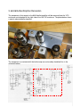
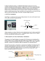
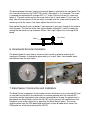
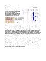
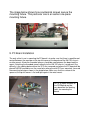
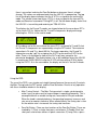
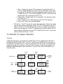
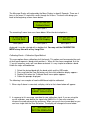
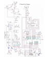
Revised 1 June 2011
N4YG Direct Digital Synthesis System
for the
Heathkit HW-101
Detailed Installation
Instructions
&
User’s Manual
Overview
The following are step-by-step instructions for installation of the N4YG Direct Digital
Synthesis (DDS) System into the Heathkit HW-101 Transceiver. It is assumed that the
beginning point is with only the DDS Printed Circuit (PC) board and the processor chip.
The starting point may be with a completed PC board or with a complete kit. It is highly
recommended that, in order to minimize the possibility or frustration, an assembled and
tested PC board be purchased..
The following are the steps required to replace the VFO with the N4YG DDS System:
1. PC Board Assembly
2. Old VFO Removal
3. 6AU6 Buffer/Amplifier Relocation
4. RIT Pot Installation
5. Microswitch (for Zero Set Button) Installation
6. Incremental Encoder Installation
7. Band Sensor Construction and Installation
8. LCD Display Mounting
9. PC Board Installation
10. Cable Connection to the HW-101
11. Initial System Checks and Adjustments
12. Getting to Know the HW-101 DDS System
13. DDS/HW-101 System Calibration
1. PC Board Assembly
If an assembled board has not been purchased, you may download a separate document
with detailed instructions for assembling the PC board from www.n4yg.com.
2. Old VFO Removal
Remove the old VFO as described in the HW-101 Manual. Keep the following in mind:
1. All of the connections to the VFO will be connected to either the DDS board
or to the 6AU6 buffer/amplifier later.
2. Although the pilot lamp which is attached to the VFO to illuminate the VFO
dial will no longer be required, it cannot be removed without compensation.
The two pilot lamps are an integral part of the filament supply network and
removal of either or both of them upsets the filament voltage on some tubes.
The easiest solution is to retain both lamps, but move the one from the VFO
enclosure to some place out of the way.
3. 6AU6 Buffer/Amplifier Relocation
The components that comprise the 6AU6 buffer/amplifier will be removed from the VFO
enclosure and relocated to the right side of the HW-101 enclosure. The photo below shows
a typical relocated buffer/amplifier.
The components associated with the buffer/amp are enclosed by the dotted line in the
schematic below.
In order to simplify this process, unsoldering will be kept to a minimum. First of all,
unsolder and remove the output coil which is atop the VFO. Remove the tube socket and
terminal strip along with all the components soldered to them as a unit. Duplicate the hole
pattern on an L-shaped bracket and reattach everything. Connect filament and plate
voltage. A page near the end of these instructions contains drawings of the bent aluminum
flange to accept the buffer/amp. Place the 6AU6 in the socket and turn on the HW-101 and
make sure that the filament lights. Also make sure plate voltage is present.
4. RIT Pot Installation
The RIT pot is installed on the front panel midway between the meter and the plastic bezel.
Drill the hole and attach the pot and knob.
RIT Pot-Rear View
J2/Pin 7
J1/Pin 5
J1/Pin 7
Resistor ~330 Ohms
Cable connections are shown. Note the resistor attached to one lug, the other end of which
connects to the wire coming from J2, pin 7. It is probably better to wait until the PC board
has been mounted before connecting to the cables.
5. Microswitch (for Zero Set Button) Installation
The purpose of the Zero Set button in the original HW-101 design was to lock the dial so
that the frequency of VFO could be adjusted to match the dial setting. In the DDS system,
it will play a very vital role and allow selection of VFO A and/or VFO B, split or single VFO
operation, selection of the calibration mode and completion the calibration process.
The Zero Set microswitch is mounted on a small piece of Veroboard. The board mounting
provides a ground connection such that a single wire is the only other connection. The
small piece of Veroboard is shown below. It is an X-ray view so that the copper traces can
be seen. Assemble the board below and then connect the wire coming from J1, pin 1
before attaching the board to the front panel.
Microswitch
To Pin 1 of J1
The drawing below illustrates how the microswitch board is attached to the front panel. The
left screw which attaches the FUNCTION switch (slide switch) is first removed. The screw
is removed and replaced with a longer 6-32 x ¾” screw. Place the nut on this screw and
tighten it. Then put another nut on the screw stud so that it stands about 1/2 inch from the
back side of the front panel. Place the switch assembly onto the screw and then place the
remaining nut on the screw. Only finger tighten the nut at this time.
Now replace the plastic zero set button, if you removed it, passing it through it the inside of
the front panel. Test the feel of the zero set pushbutton and adjust it switch assembly by
moving the two loose nuts up and down. When it feels right, tighten the nut on top of the
board.
Switch
Front Panel
6. Incremental Encoder Installation
The photos below illustrate how an aluminum disk can be inserted for mounting the
Incremental Encoder. A rectangular piece works just as well. Note: Your encoder make
look different from the one shown.
7. Band Sensor Construction and Installation
The Band Sensor incorporates three infrared sensors which consist of an infrared LED and
an infrared transistor which are contained in a common package with the infrared LED
transmitter and the infrared transistor receiver separated by an air gap. An optical mask is
placed onto the Band Switch shaft of the HW-101 and the sensors are mounted such that
the optical mask rotates within the air gap when the Band Switch rotates. The sensor
receives power from the DDS board and sends back a three-bit code which informs the
DDS processor of the band setting of the HW-101.
Optical Mask Construction
80
10c
40
20
10b
15 10 10a
Optical Mask
*Band Markings Show Sensor 1 Position For the
Indicated Band
Completed Band Sensor on Underside of HW-101
The optical mask shown in the photo of the completed sensor unit (above) is constructed
from an aluminum soft drink can. We have since discovered that a better material is from a
plastic milk jug. Find a flat area on the side of the jug and and cut out an area of about 2.5
inches by 2.5 inches. Remove the backing from the sticky paper which has the image
shown below and stick it on the 2.5 inch piece of plastic. Using scissors cut along the large
circle which is the edge of the disk. Then cut the six ¼ inch holes. Make sure not to cut
through the edge of the disk and leave the annulus complete so that the disk will not tend
to catch on the sensors as it rotates. A hand-operated single hole punch works very well
for cutting these holes. The size of the holes along the edges is not critical, but the center
should be ¼ inch in diameter or slightly larger. Now use the scissors to cut along the
dotted line. This gives a means of getting the disk onto the Band Switch Shaft.
Mounting the Optical Mask on the Band Switch Shaft
You will need 2 grommets whose inside diameters are about ¼ inch and some small
string. Cut through one side of each of the grommets and then open them up and place
them on the Band Switch shaft. Now make 2 or three wraps with string in the grooves of
the grommets, tighten the string and tie securely. These should be as tight as possible,
providing resistance to movement of the grommets along the shaft. Now, with the two
grommets separated by about an inch, open the slit in the optical mask and place it on the
shaft with the image facing toward the rear of the HW-101. Then move the grommets
along the shaft and press snugly against each side of the optical mask. Don’t worry about
placement right now because you will need to adjust the position after the sensor board is
mounted.
Constructing the Sensor Board
The optical sensor whose schematic is
shown here is constructed on a small
piece of Veroboard. Images below
illustrate how the board is laid out and
are also life size templates for
constructing the board. The purpose of
the image on the left is to locate where
the copper traces are to be cut in 8
Optical Sensor Board Layout
Optical Sensor Board Schematic
places (indicated in magenta). Note that this requires cuts which are about 0.03 inches
wide between holes in the Veroboard. Cuts are not centered on holes, but between
holes. Cut the board to the size shown (count the number of holes in each dimension).
Then remove copper from the 8 locations as shown. Drill the 1/8 inch diameter mounting
hole. Then make a copy of this page on your printer. Cut out the image on the right and
paste it on top of the board you have prepared, being careful to line up the holes in the
image with holes on the board. Use a glue stick to paste it on the board. This will allow you
to move it around and line up the holes. Hold the board and overlay up to a bright light to
line up the overlay with the holes. Use an awl or some other pointed instrument to punch
through the paper at each hole location.
Now you are ready to put the components on the board. Begin by installing the 4 jumpers
on the top side of the board. There are 2 additional jumpers, shown in blue on the left.
These are placed beneath the board. The longer one must be insulated. Then install the 4
resistors as shown. To install the 3 sensor modules, begin with S2, the one in the middle.
Be sure to place the beveled edge of the modules are along the top edge of the board.
Push Sensor 2 down snuggly against the board and solder in place. The other two sensors
should be leaned toward Sensor 2 such that the top left edge of Sensor 2 touches the top
right edge of Sensor 1 and that the right edge of Sensor 2 touches the top left edge of
Sensor 3. Solder Sensor 1 and Sensor 3 in place.
Mounting the Sensor Board
Construct the two-piece sensor board mount shown in the photos and in the drawings
below. Use 4-40 hardware. Things are made easier if you tap the chassis and appropriate
pieces, but nuts may be used if a tap is not available. If not tapped, all holes (and the slot)
are 1/8 inch. Before mounting the board, solder the 5 wires coming from connector J2 to
the appropriate points on the sensor board. Notice that when mounted the board is not
vertical but is at an angle of 10 to 30 (10 degrees is shown, but this may need be greater)
degrees from vertical. Mount the board and adjust the placement of the optical mask so
that the mask is centered in the air gap. Set the band switch to the 80 meter position.
Rotate the mask until the spoke labeled “80” is aligned with the center of Sensor 1. Rotate
the Band Switch through all bands several times and verify that it does touch anything and
that, at each position, the labeled spoke corresponds to the band selected.
Front
Side
Front
3/8
10°
Side
3/4
3/8
1-1/4
1/2
3/4
Top
Top
5/16
3/4
3/4
7/8
Chassis Piece
3/4
Sensor Board Piece
8. LCD Display Mounting
The front panel of the HW-101 has a flange bent inward. The mounting technique is
illustrated below and uses two small L-shaped pieces of bent aluminum which are placed
underneath the flange and each is attached with a #4 countersunk machine screw and nut.
The display attaches to the two L-shaped pieces with #3 machine screws, 1/2 inch long,
each with 3 nuts for adjustment purposes. Dimensions are approximate. The pieces are
symmetric
Top
5/16”
1/2”
The image below shows how countersink screws secure the
mounting fixture. This particular one is an earlier one-piece
mounting fixture.
9. PC Board Installation
The only critical issue in mounting the PC board is to make sure that there is good thermal
contact between the regulator at the top left corner of the board and the HW-101 chassis
or other mount. Aluminum threaded spacers should be used between the board and the
mount. Attaching the threaded spacers directly to the HW-101 chassis is preferred. One
difficulty is the cabling below where the VFO was removed and where the PC board will be
placed. N5CQK wanted to use the same holes where the old VFO was mounted. Joe used
the mounting technique shown in the photo below. Make sure that the surface of the
spacer at the top left corner is flat and tight against the metal mount.
NOTE: A paper template of
the DDS board may be
very beneficial for locating
holes for mounting the
board.
10. Cable Connection to the HW-101
The next page shows how the cables are connected to the PC board as well as to points in
the HW-101, the Incremental Encoder, the RIT pot, the Band Sensor, and the
Buffer/Amplifier. Wires should be cut to lengths that allow them to be neatly routed and
bundled.
Here are a few hints/suggestions:
-
-
It may be easier to use the original wire which was connected old VFO for the
LSB shift.
The CW mode connection can be made on the low side of R310 going to the
cathode of V15A instead of connecting to the mode switch. The Mode switch
wiring is very crowded and this will allow you to make the connection away from
thw switch.
A good source for 12 Volts AC is I from pin 4 of V17. You can run the wire from
the DDS board through the existing harness to V17.
Buffer Amp
6AU6 Grid
INCREMENTAL
ENCODER
Incremental Encoder
connections may vary
J7
+A B–
12.6 VAC
J6
GND
+5 VDC
MTA
MTB
ITA
ITB
RIT Pot +5
J2
J1
+5 VDC
Sensor 1
Sensor 2
Sensor 3
Ground
LSB Shift (Note 4)
CW (Note 3)
RIT Pot Wiper
Tx/Rx (Note2)
RIT Pot Ground
Not Used (Note 1)
Not Used (Note 1)
Not Used (Note 1)
Zero Set Switch
J3
DDS Board
J5
1
16
Pin 10, RL1
LCD Display
Notes
1. Pins 2, 3, and 4 will be used if and when
code is written to support other modes,
Calibration in particular.
2. This pin connects to Pin 10 of RL1(See
Photo on Left). It provides an indication of the
Transmit and Receive Modes.
3. This line comes from the MODE switch
2F/3. It should already have a gray wire
attached.
4. This line comes from the MODE switch. It
was originally connected to the VFO. It
provides an indication of the LSB mode,
during which the VFO is shifted 2.8 KHz.
Buffer/Amp Relocation Flange Template
3 ½”
Bend this panel down 90
degrees along this line
1 ¼”
7/64” Dia
1 ¾”
5/8” Dia
¼” Dia
5/32” Dia
7/16” Dia
¼” Dia
Two unmarked
holes are 1/8” Dia.
Incremental Encoder Mount Template
3/8” Dia(2)
1/8” Dia
1/8” Dia
Round corners as necessary to
fit into the space in front panel
1 3/8”
11. Initial System Checks and Adjustments
If U1 and U7 are in their sockets, remove them. Disconnect all cables except J6, the 12.6
VAC power. Make sure there are no loose wires which might get shorted out. Turn on the
HW-101. Connect the negative lead of a voltmeter to the HW-101 chassis. Set it to read
DC volts. Touch the lead of the 7805 voltage regulator near the edge of the board with the
plus lead of the volt meter. You should read about +5 volts. Touch pin 8 of the DIP socket
for U7. You should read about +12 volts. Set the meter to read negative voltage. Touch pin
4 of the same DIP socket. You should read about -12 volts. Turn off the HW-101.
If the above reading were as expected, put U1 and U7 into their sockets and connect all
cables. Also make sure that the 3.395 MHz trap is plugged in. There will be no RF output
unless the trap is plugged in. Pin 1 of the connector should correspond with the pin 1
maker on the trap board. Set the trimmer pot “RF Level” to the center of rotation. Turn the
HW-101 on. The LCD should light up. Adjust the trimmer pot “CONTRAST” until the
characters look the best. You should also see the following:
•
•
•
•
•
The LCD should indicate a frequency in the band to which the Band Switch
is set.
You should be able to hear noise in the receiver.
You should be able to tune the DDS by rotating the Main Tuning control.
You should be able to rotate the band switch and notice the band reflected
in the frequency reading
You should hear signals if an antenna is connected
If all has gone as expected, then it is time to peak the output coil of the Buffer/Amplifier. To
do this, turn on the crystal calibrator and find the signal somewhere near the middle of any
band, near 7200 MHz for example. Peak the signal with the DRIVER PRESELECTOR.
Adjust the “RF LEVEL” pot so that 9 S-units or less is indicated. Adjust the slug in the
output coil to peak the S-meter reading. Now increase the “RF LEVEL” until the S-meter no
longer increases. This completes the initial checks and adjustments.
12. Getting to Know the HW-101 DDS System
What the Display Shows:
The typical display will look something like this:
A 7236.431 KHz
A
RIT Off
Assuming that the above is for the HW-101 in the receive mode, the top line shows
the receive frequency. The DDS unit has 2 VFOs, A and B, for each of the 8 HW101 bands. The values for the current band are saved in non-volatile memory when
there is any action involving the Zero Set button or whenever there is a band
change. The values are recovered each time the HW-101 is powered up. The top
line of the display above indicates that the A VFO is assigned to the receive(Rx)
mode. The second shows two things, VFO A is also assigned to the transmit(Tx)
mode and Receiver Incremental Tuning(RIT) is off. So the above display shows that
the HW-101 is transmitting and receiving on 7236.431 KHz.
The displays for the Rx and Tx modes are shown below for the case where RIT is
set for minus 215 Hz. Notice that the Tx and Rx frequencies displayed change,
reflecting the -215 Hz in the receive mode.
A 7236.216 KHz
A RIT = -215 Hz
A 7236.431 KHz
A RIT = -215 Hz
All the above are for the case where the same VFO is assigned to Tx and Rx, but
the Rx and Tx frequencies are separated by using the RIT control. The maximum
separation in Rx and Tx is about 800 Hz. For larger separation, the Rx and Tx
frequencies may be “split” by assigning the A VFO to one and the B VFO to the
other. There is no limitation on how far the Rx/Tx split may except for the
preselector bandwidth. The display below is for a split condition where the HW-101
is receiving on 29435.130 KHz using the B VFO and transmitting 22 KHz higher
using the A VFO. As in the case above, the display on the left is for the Rx mode.
B 29435.130 KHz
A
RIT Off
A 29457.130 KHz
B
RIT Off
Using the DDS:
The use of the DDS is very simple and straight forward because there are only 3 controls,
the Main Tuning knob, the RIT control, and the Zero Set button. Results of any operation
with these should be evident in the display.
•
Main Tuning Control – The Main Tuning control is simple yet designed to
make it easy to make small or large changes in operating frequency. This is
accomplished with a variable tuning rate, measured in KHz per revolution.
When the knob is rotated clockwise, the operating frequency increases and
vice versa for counter clockwise. When rotated slowly, the tuning rate is slow.
As the rotation rate is increased, the tuning rate increases.
•
Zero Set Button –There are four functions of the Zero Set Button. These are
invoked by 1) Click, a single short press and release, 2) Double Click, two
short press and release actions in quick succession, 3) Long Click, a press
for about 1 second or more before releasing and 4) Very Long Click, a press
for 3 seconds or more. These four operation accomplish the following:
o Click – Toggles the current VFO assignments for both Rx and Tx. If
VFO A is assigned to both Rx and Tx, then a click would assign VFO
B to both VFOs. Another click would toggle both again, returning VFO
A to both Rx and Tx. If the initial assignment is Rx-A, Tx-B then a click
would reverse the assignment to Rx-B, Tx-A.
o Double Click – Toggles only the Tx assignment. This effectively splits
or unsplits Rx/Tx.
o Long – Equates the Tx VFO frequency to the Rx VFO frequency.
o Very Long – Enters the Calibration Mode
•
RIT Control – The RIT control will require little explanation. Rotate the control
until the second line of the display shows “RIT Off”. If the pointer on the RIT
know is not in the 12 O’clock position, loosen the set screw on the knob and
rotate it until the pointer is in the 12 O’clock position and then tighten the set
screw. Rotation clockwise from the “RIT Off” position will show + values and
counter-clockwise will give – values.
13. DDS/HW-101 System Calibration
Overview
Calibration procedures are provided in the DDS processor for calibrating the HW-101 in
combination with the DDS system. The DDS system uses a 50 MHz crystal oscillator as
its reference. The HW-101 uses 11 other crystals which, like all crystals, are not accurate
enough to provide that frequency accuracy to which amateurs have come to expect. The
following simplified diagram shows how these 11 crystals are used in the Receive and
Transmit chains.
3393.6
To
3396.4
Balanced
Modulator
Audio/Keying
USB
LSB
CW
To Audio
Amp
3396.4
3393.6
3395.4
First
Tx Mixer
Carrier
Oscillator
Product
Detector
8896.4
To
8393.6
Second
Tx Mixer
VFO/DDS
Heterodyne
Oscillator
5500 to 5000
3395
Second
Rx Mixer
*Frequencies in KHz
8395
To
8895
First
Rx Mixer
To Driver
and Final
Amps
12395
15895
22895
29895
36895
37395
37895
38395
From RF
Amp
The calibration routine provides a means of correcting for errors in all of these. The
frequency readout should be accurate to within 100 Hz when the calibration is completed
using an accurate frequency reference,
The calibration is done in 3 steps as follows:
• Band Calibration
• LSB Shift Calibration
• CW Shift Calibration
These three steps may be done in any order however it is recommended that they be done
in the order shown. The first two steps require only an accurate frequency source with the
8 band segments of the HW-101 transceiver. The frequency source may be at any
frequency within the 500 KHz band segments. The 100 KHz calibrator provides a good
reference if it has been accurately calibrated itself. The last step, CW Shift Calibration,
requires only a stable auxiliary receiver.
Band Calibration must be done for each of the 8 band segments, that is, for each of
the 8 band switch positions. Band Calibration is completed while in the USB Mode,
For any particular band, this provides correction of any error in the combination of the USB
crystal and the Heterodyne crystal for that particular band as well as any error in the DDS
frequency reference oscillator.
LSB Shift Calibration may be done with the band switch in any, but only one of the 8
positions. A single-band calibration of LSB Shift is all that is necessary. This
compensates for any inaccuracy in the intended 2.8 KHz shift in the carrier oscillator
frequency when switching from the USB Mode to the LSB Mode.
When the CW mode is selected in the HW-101, the USB crystal is used for the receive
mode but the CW crystal is used in the transmit mode. The carrier oscillator is shifted
down 1 KHz, meaning that the transmit frequency is shifted up 1 KHz. In the original
design (with the old VFO) , this shift was uncompensated and thus the readout showed a
frequency 1 KHz lower than the actual transmit frequency. The CW calibration provides
this compensation and correction of any errors in the CW crystal frequency relative to the
USB crystal. CW Shift Calibration, like LSB Shift Calibration, can be done with the
band switch in any band position and it need be done only once.
Entering the Calibration Mode
When in the Operating Mode, a Very Long click will cause the DDS system to enter the
CALIBRATION MODE. Once in the CALIBRATION MODE, you should not change
bands. If you should accidentally change bands, exit the CALIBRATION MODE and start
over by executing a Very Long click. Always select the band of interest before entering
the CALIBRATION MODE. After pressing the Zero Set button for about 3 seconds, The
display associated with the Operating Mode (shown on the left) will be replaced by the
screen shown in the middle, which will be replaced after about 5 seconds by the message
display shown on the right.
A 7236.431 KHz
A
RIT Off
Operating Mode
CALIBRATION MODE
Menu in 5 Secs
Initial Calibration Display
Clk-Scroll Menu
Dbl-Sel Lng-Exit
Message Display
The Message Display will replaced by the Menu Display in about 5 Seconds. There are 4
items in the menu. A single click scrolls through the 4 items. The fourth click brings you
back to the beginning screen shown below.
Clk-Scrl Dbl-Sel
Calibrate Band
Menu Option 1
The remaining 3 menu items are shown below. When the desired option is
Clk-Scrl Dbl-Sel
Cal LSB Shift
Clk-Scrl Dbl-Sel
Cal CW Display
Clk-Scrl Dbl-Sel
Exit Cal
Menu Option 2
Menu Option 3
Menu Option 4
displayed, it may be selected with a double-click. You may exit the CALIBRATION
MODE at any time with a Very Long Click.
Calibrating Bands – Calibration Signal Method
This menu option allows calibration of all the bands. This option must be executed for each
of the 8 band segments (band switch positions). When this has been completed, 9 of the
11 crystal frequency errors will have been corrected. It is very simple to calibrate a band.
Follow the steps outlined below:
1.
2.
3.
4.
Select the desired band with the band switch and the USB mode.
Press and hold the Zero Set button until the initial calibration display appears.
Double-Click when the “Calibrate Band” menu option appears.
Follow the prompts displayed.
The following is an example of how the 80M band might be calibrated:
1. When step 3 above is executed, a display similar to that shown below will appear.
A 3827.431 KHz
0-BEAT CAL>CLICK
2. In response to this message, zero-beat to your calibration signal. If you are using the
crystal calibrator, zero-beat to the signal near 3800 KHz. As you near zero beat,
increase the audio volume to the maximum. When you are as close to zero beat as you
can hear single-click the Zero Set button. The display will change to the one below.
A 3801.869 KHz
SET CAL FREQ>CLK
3. Now simply set the display to the known frequency of the calibration signal. Since we
are using the crystal calibrator, set the display so that it is as shown below and single
click.
A 3800.000 KHz
SET CAL FREQ>CLK
This would complete calibration of the 80M band. In this example, the calibration signal is
the crystal calibrator, but it could be any stable signal whose frequency is accurately
known and in the 80M band. For example, you may have an accurate 3625.000 KHz
signal. Using that signal the displays for steps 2 and 3 would be as shown below.
A 3626.869 KHz
SET CAL FREQ>CLK
A 3625.000 KHz
SET CAL FREQ>CLK
The above should be repeated for the remaining 7 band segments.
Calibrating Bands – On-The-Air QSO Method
An alternative band calibration procedure is a procedure which can be done while in QSO
with a station whose rig is accurately calibrated. Although this could be done in either the
LSB or USB mode, the USB mode is preferred. Make sure RIT of OFF during this
procedure. After carefully adjusting the HW-101 frequency to the received signal, ask to
other station to give you his exact frequency. Suppose it is 7173.755 KHz. Write it down.
Tell the other station to wait a few seconds. Enter the calibration mode by pressing the
Zero Set button until the Calibration display appears. Select Calibrate Band and then,
without adjusting anything, click the Zero Set. Then adjust the HW-101 to the frequency of
the other station, 7173.755 in our example, and press Zero Set again. That does it. This
may actually be the best method.
Calibrating LSB Shift
Calibrating the LSB Shift is much like the Band Calibration, except that any band may be
used. You must start in the USB Mode. All you have to do is to follow the prompts
Here is a step-by-step description of the process once you are in the Calibration Mode.
1. Single-Click until the display appears as below. Then Double-Click.
Clk-Scrl Dbl-Sel
Cal LSB Offset
2. The display will be as follows for the 20M band. Select the USB mode and
Click.
A 14.236.531 KHz
SEL USB MODE>CLK
3. The display will change to the one below. Zero Beat to any calibration signal.
We will again show the case where the crystal calibrator is used
A 14.236.531 KHz
0-BEAT CAL>CLICK
4. Zero Beat to the signal. The display will be similar to the example shown
below. Click.
A 14.200.000 KHz
0-BEAT CAL>CLICK
5. The display will change as shown below. Select the LSB Mode and then
Click.
A 14.200.000 KHz
SEL LSB MODE>CLK
6. The display will become as below.
A 14.200.000 KHz
0-BEAT CAL>CLICK
7. The calibration signal should be found about 2.8 KHz below the previous
location and might be as shown below after zero beating. Click.
A 14.197.182 KHz
0-BEAT CAL>CLICK
8. The display will change to the operating mode and LSB Shift Calibration is
complete.
CW Offset Calibration
CW Offset Calibration requires only a stable test signal anywhere within any of the 8 band
segments. N4YG has found this to be the most difficult of all the calibration tasks because
it is sometimes difficult to get a good zero beat indication with a receiver which is in close
proximity to the transmitter to which it is being zero beat. It is possible to skip CW Offset
Calibration because this crystal is fairly close to its design value of 1 KHz relative to
the USB crystal. This 1 KHz offset is already in the chip and thus may be left as it is
if you wish.
The calibration steps for CW Offset are as follows:
1. Select the USB mode, enter the CALIBRATION Mode and select the “Cal CW
Display” option. The display will appear something like the one below.
A 7.167.384 KHz
0B HW Rx&Rx2>CLK
2. The above display is directing you to zero beat both the HW-101 Receiver and
an auxiliary receiver to the same calibration signal. Do this and Click. The
display becomes something like below.
A 7.160.000 KHz
Rx2 AS IS>CLICK
3. The display above directs you not to alter the auxiliary receiver again. Click.
A 7.160.000 KHz
0B HW Tx&Rx2>CLK
4. The above display directs you to transmit with the HW-101 while monitoring the
tone in the auxiliary. You will have to incrementally change the HW-101
frequency because you cannot change the frequency of the HW-101 while
transmitting. You should find that when you reduce the HW-101 frequency by
about 1000 Hz you will be near zero beat. When you are satisfied with the zero
beat, Click, and you are done.
PC Board Circuit Diagram