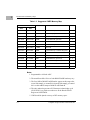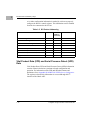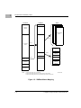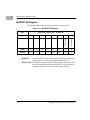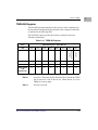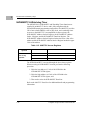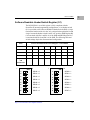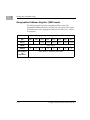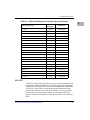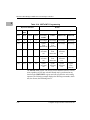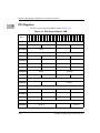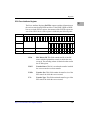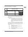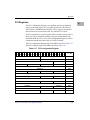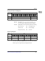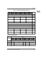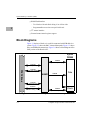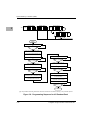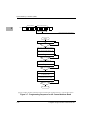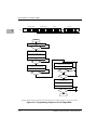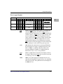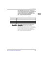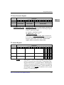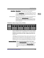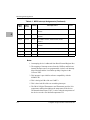
1
MVME5100
Single Board Computer
Programmer’s
Reference Guide
V5100A/PG2
September 2001 Edition
© Copyright 2001 Motorola, Inc.
All rights reserved.
Printed in the United States of America.
Motorola and the Motorola logo are registered trademarks and AltiVec is a trademark of
Motorola, Inc.
PowerPC and the PowerPC logo are registered trademarks; and PowerPC 750 is a
trademark of International Business Machines Corporation and are used by Motorola, Inc.
under license from International Business Machines Corporation.
All other products mentioned in this document are trademarks or registered trademarks of
their respective holders.
Safety Summary
The following general safety precautions must be observed during all phases of operation, service, and repair of this
equipment. Failure to comply with these precautions or with specific warnings elsewhere in this manual could result
in personal injury or damage to the equipment.
The safety precautions listed below represent warnings of certain dangers of which Motorola is aware. You, as the
user of the product, should follow these warnings and all other safety precautions necessary for the safe operation of
the equipment in your operating environment.
Ground the Instrument.
To minimize shock hazard, the equipment chassis and enclosure must be connected to an electrical ground. If the
equipment is supplied with a three-conductor AC power cable, the power cable must be plugged into an approved
three-contact electrical outlet, with the grounding wire (green/yellow) reliably connected to an electrical ground
(safety ground) at the power outlet. The power jack and mating plug of the power cable meet International
Electrotechnical Commission (IEC) safety standards and local electrical regulatory codes.
Do Not Operate in an Explosive Atmosphere.
Do not operate the equipment in any explosive atmosphere such as in the presence of flammable gases or fumes.
Operation of any electrical equipment in such an environment could result in an explosion and cause injury or damage.
Keep Away From Live Circuits Inside the Equipment.
Operating personnel must not remove equipment covers. Only Factory Authorized Service Personnel or other
qualified service personnel may remove equipment covers for internal subassembly or component replacement or any
internal adjustment. Service personnel should not replace components with power cable connected. Under certain
conditions, dangerous voltages may exist even with the power cable removed. To avoid injuries, such personnel
should always disconnect power and discharge circuits before touching components.
Use Caution When Exposing or Handling a CRT.
Breakage of a Cathode-Ray Tube (CRT) causes a high-velocity scattering of glass fragments (implosion). To prevent
CRT implosion, do not handle the CRT and avoid rough handling or jarring of the equipment. Handling of a CRT
should be done only by qualified service personnel using approved safety mask and gloves.
Do Not Substitute Parts or Modify Equipment.
Do not install substitute parts or perform any unauthorized modification of the equipment. Contact your local
Motorola representative for service and repair to ensure that all safety features are maintained.
Observe Warnings in Manual.
Warnings, such as the example below, precede potentially dangerous procedures throughout this manual. Instructions
contained in the warnings must be followed. You should also employ all other safety precautions which you deem
necessary for the operation of the equipment in your operating environment.
Warning
To prevent serious injury or death from dangerous voltages, use extreme
caution when handling, testing, and adjusting this equipment and its
components.
Flammability
All Motorola PWBs (printed wiring boards) are manufactured with a flammability rating
of 94V-0 by UL-recognized manufacturers.
EMI Caution
!
Caution
This equipment generates, uses and can radiate electromagnetic energy. It
may cause or be susceptible to electromagnetic interference (EMI) if not
installed and used with adequate EMI protection.
Lithium Battery Caution
This product contains a lithium battery to power the clock and calendar circuitry.
!
Caution
!
Attention
!
Vorsicht
Danger of explosion if battery is replaced incorrectly. Replace battery only
with the same or equivalent type recommended by the equipment
manufacturer. Dispose of used batteries according to the manufacturer’s
instructions.
Il y a danger d’explosion s’il y a remplacement incorrect de la batterie.
Remplacer uniquement avec une batterie du même type ou d’un type
équivalent recommandé par le constructeur. Mettre au rebut les batteries
usagées conformément aux instructions du fabricant.
Explosionsgefahr bei unsachgemäßem Austausch der Batterie. Ersatz nur
durch denselben oder einen vom Hersteller empfohlenen Typ. Entsorgung
gebrauchter Batterien nach Angaben des Herstellers.
CE Notice (European Community)
Motorola Computer Group products with the CE marking comply with the EMC Directive
(89/336/EEC). Compliance with this directive implies conformity to the following
European Norms:
EN55022 “Limits and Methods of Measurement of Radio Interference Characteristics
of Information Technology Equipment”; this product tested to Equipment Class B
EN55024 “Information technology equipment—Immunity characteristics—Limits and
methods of measurement”
Board products are tested in a representative system to show compliance with the above
mentioned requirements. A proper installation in a CE-marked system will maintain the
required EMC performance.
In accordance with European Community directives, a “Declaration of Conformity” has
been made and is available on request. Please contact your sales representative.
Notice
While reasonable efforts have been made to assure the accuracy of this document,
Motorola, Inc. assumes no liability resulting from any omissions in this document, or from
the use of the information obtained therein. Motorola reserves the right to revise this
document and to make changes from time to time in the content hereof without obligation
of Motorola to notify any person of such revision or changes.
Electronic versions of this material may be read online, downloaded for personal use, or
referenced in another document as a URL to the Motorola Computer Group website. The
text itself may not be published commercially in print or electronic form, edited, translated,
or otherwise altered without the permission of Motorola, Inc.
It is possible that this publication may contain reference to or information about Motorola
products (machines and programs), programming, or services that are not available in your
country. Such references or information must not be construed to mean that Motorola
intends to announce such Motorola products, programming, or services in your country.
Limited and Restricted Rights Legend
If the documentation contained herein is supplied, directly or indirectly, to the U.S.
Government, the following notice shall apply unless otherwise agreed to in writing by
Motorola, Inc.
Use, duplication, or disclosure by the Government is subject to restrictions as set forth in
subparagraph (b)(3) of the Rights in Technical Data clause at DFARS 252.227-7013
(Nov. 1995) and of the Rights in Noncommercial Computer Software and Documentation
clause at DFARS 252.227-7014 (Jun. 1995).
Motorola, Inc.
Computer Group
2900 South Diablo Way
Tempe, Arizona 85282
Contents
About This Manual
Summary of Changes ...............................................................................................xxiv
Overview of Contents ..............................................................................................xxiv
Comments and Suggestions ...................................................................................... xxv
Conventions Used in This Manual...........................................................................xxvi
Terminology......................................................................................................xxvi
CHAPTER 1
Product Data and Memory Maps
Introduction................................................................................................................1-1
Memory maps ............................................................................................................1-4
Processor Memory Map......................................................................................1-4
Default Processor Memory Map..................................................................1-4
Processor Memory Map...............................................................................1-5
PCI Memory Map ........................................................................................1-7
VME Memory Map .....................................................................................1-7
PCI Local Bus Memory Map..............................................................................1-8
VMEbus Memory Map .......................................................................................1-8
System Bus.................................................................................................................1-8
Processors ...........................................................................................................1-9
Processor Type Identification .............................................................................1-9
Processor PLL Configuration .............................................................................1-9
L2 Cache .............................................................................................................1-9
L2 Cache SRAM Size.......................................................................................1-10
Cache Speed......................................................................................................1-10
FLASH Memory ...............................................................................................1-10
ECC Memory....................................................................................................1-11
P2 I/O Modes ....................................................................................................1-11
Serial Presence Detect (SPD) Definitions ........................................................1-12
Hawk ASIC ..............................................................................................................1-12
Hawk I2C interface and configuration information..........................................1-13
Vital Product Data (VPD) and Serial Presence Detect (SPD) Data..................1-14
PCI Local Bus ..........................................................................................................1-15
PCI Arbitration Assignments for Hawk ASIC .................................................1-15
The Ethernet Controller ....................................................................................1-16
PMC/PCI Expansion Slots................................................................................1-17
vii
The Universe ASIC .......................................................................................... 1-17
PCI Configuration Space.................................................................................. 1-19
Hawk External Register Bus Address Assignments......................................... 1-21
MVME5100 Hawk External Register Bus Summary ............................... 1-21
Dual TL16C550 UARTs................................................................................... 1-23
Status Register .................................................................................................. 1-24
MODFAIL Bit Register .................................................................................... 1-25
MODRST Bit Register ..................................................................................... 1-26
TBEN Bit Register ........................................................................................... 1-27
NVRAM/RTC & Watchdog Timer................................................................... 1-28
Software Readable Header/Switch Register (S1)............................................. 1-29
Geographical Address Register (VME board) ................................................. 1-30
Extended Features Register 1 ........................................................................... 1-31
Board Last Reset Register ................................................................................ 1-32
Extended Features Register 2 ........................................................................... 1-33
CHAPTER 2
Hawk PCI Host Bridge & Multi-Processor Interrupt Controller
Introduction ............................................................................................................... 2-1
Overview ............................................................................................................ 2-1
Features .............................................................................................................. 2-1
Block Diagram........................................................................................................... 2-3
Functional Description .............................................................................................. 2-4
Architectural Overview ...................................................................................... 2-4
PPC Bus Interface .............................................................................................. 2-5
PPC Address Mapping ................................................................................ 2-6
PPC Slave.................................................................................................... 2-7
PPC FIFO .................................................................................................... 2-9
PPC Master................................................................................................ 2-10
PPC Arbiter ............................................................................................... 2-15
PPC Parity ................................................................................................. 2-17
PPC Bus Timer.......................................................................................... 2-18
PCI Bus Interface ............................................................................................. 2-19
PCI Address Mapping ............................................................................... 2-19
PCI Slave................................................................................................... 2-22
PCI FIFO ................................................................................................... 2-26
PCI Master ................................................................................................ 2-26
Generating PCI Cycles .............................................................................. 2-29
PCI Arbiter ................................................................................................ 2-34
Endian Conversion ........................................................................................... 2-38
When PPC Devices are Big-Endian .......................................................... 2-38
viii
When PPC Devices are Little Endian........................................................2-39
PHB Registers............................................................................................2-40
Error Handling ..................................................................................................2-41
Watchdog Timers ..............................................................................................2-42
PCI/PPC Contention Handling .........................................................................2-45
Transaction Ordering ........................................................................................2-48
PHB Hardware Configuration ..........................................................................2-49
Multi-Processor Interrupt Controller (MPIC) ..........................................................2-51
MPIC Features: .................................................................................................2-51
Architecture ......................................................................................................2-51
External Interrupt Interface...............................................................................2-52
CSR’s Readability.............................................................................................2-53
Interrupt Source Priority ...................................................................................2-53
Processor’s Current Task Priority .....................................................................2-54
Nesting of Interrupt Events...............................................................................2-54
Spurious Vector Generation ..............................................................................2-54
Interprocessor Interrupts (IPI) ..........................................................................2-55
8259 Compatibility ...........................................................................................2-55
Hawk Internal Errror Interrupt..........................................................................2-55
Timers ...............................................................................................................2-56
Interrupt Delivery Modes..................................................................................2-56
Block Diagram Description ..............................................................................2-57
Program Visible Registers .........................................................................2-59
Interrupt Pending Register (IPR) ...............................................................2-59
Interrupt Selector (IS) ................................................................................2-59
Interrupt Request Register (IRR)...............................................................2-60
In-Service Register (ISR) ..........................................................................2-60
Interrupt Router .........................................................................................2-60
Programming Notes ..........................................................................................2-62
External Interrupt Service..........................................................................2-62
Reset State .................................................................................................2-63
Operation ..........................................................................................................2-64
Interprocessor Interrupts............................................................................2-64
Dynamically Changing I/O Interrupt Configuration .................................2-64
EOI Register ..............................................................................................2-65
Interrupt Acknowledge Register................................................................2-65
8259 Mode.................................................................................................2-65
Current Task Priority Level.......................................................................2-65
Architectural Notes ...........................................................................................2-66
Effects of Interrupt Serialization.......................................................................2-66
Registers...................................................................................................................2-67
ix
PPC Registers ................................................................................................... 2-68
Vendor ID/Device ID Registers ................................................................ 2-70
Revision ID Register ................................................................................. 2-70
General Control-Status/Feature Registers................................................. 2-71
PPC Arbiter/PCI Arbiter Control Registers .............................................. 2-73
Hardware Control-Status/Prescaler Adjust Register ................................. 2-77
PPC Error Test/Error Enable Register ...................................................... 2-79
PPC Error Status Register ......................................................................... 2-82
PPC Error Address Register...................................................................... 2-84
PPC Error Attribute Register .................................................................... 2-85
PCI Interrupt Acknowledge Register ........................................................ 2-87
PPC Slave Address (0,1 and 2) Registers ................................................. 2-88
PPC Slave Offset/Attribute (0, 1 and 2) Registers .................................... 2-89
PPC Slave Address (3) Register................................................................ 2-90
PPC Slave Offset/Attribute (3) Registers.................................................. 2-91
WDTxCNTL Registers ............................................................................. 2-92
WDTxSTAT Registers.............................................................................. 2-96
General Purpose Registers ........................................................................ 2-96
PCI Registers .................................................................................................... 2-97
Vendor ID/ Device ID Registers ............................................................... 2-98
PCI Command/ Status Registers ............................................................... 2-99
Revision ID/ Class Code Registers ......................................................... 2-101
Header Type Register.............................................................................. 2-101
MPIC I/O Base Address Register ........................................................... 2-102
MPIC Memory Base Address Register ................................................... 2-102
PCI Slave Address (0,1,2, and 3) Registers ............................................ 2-103
PCI Slave Attribute/ Offset (0,1,2 and 3) Registers................................ 2-104
CONFIG_ADDRESS Register ............................................................... 2-106
CONFIG_DATA Register ...................................................................... 2-109
MPIC Registers .............................................................................................. 2-110
MPIC Registers ....................................................................................... 2-110
Feature Reporting Register ..................................................................... 2-113
Global Configuration Register ................................................................ 2-114
Vendor Identification Register ................................................................ 2-116
Processor Init Register ............................................................................ 2-116
IPI Vector/Priority Registers................................................................... 2-117
Spurious Vector Register ........................................................................ 2-118
Timer Frequency Register....................................................................... 2-118
Timer Current Count Registers ............................................................... 2-119
Timer Basecount Registers ..................................................................... 2-120
Timer Vector/Priority Registers .............................................................. 2-121
Timer Destination Registers.................................................................... 2-122
x
External Source Vector/Priority Registers ..............................................2-122
External Source Destination Registers ....................................................2-124
Hawk Internal Error Interrupt Vector/Priority Register ..........................2-125
Hawk Internal Error Interrupt Destination Register ................................2-126
Interprocessor Interrupt Dispatch Registers ............................................2-126
Current Task Priority Registers ...............................................................2-127
Interrupt Acknowledge Registers ............................................................2-127
End-of-Interrupt Registers.......................................................................2-128
CHAPTER 3
System Memory Controller (SMC)
Introduction................................................................................................................3-1
Overview.............................................................................................................3-1
Bit Ordering Convention ....................................................................................3-1
Features...............................................................................................................3-1
Block Diagrams .........................................................................................................3-2
Functional Description...............................................................................................3-6
SDRAM Accesses...............................................................................................3-6
Four-beat Reads/Writes ...............................................................................3-6
Single-beat Reads/Writes ............................................................................3-6
Address Pipelining.......................................................................................3-6
Page Holding ...............................................................................................3-7
SDRAM Speeds...........................................................................................3-7
SDRAM Organization ........................................................................................3-9
PPC60x Bus Interface.........................................................................................3-9
Responding to Address Transfers................................................................3-9
Completing Data Transfers..........................................................................3-9
PPC60x Data Parity ...................................................................................3-10
PPC60x Address Parity .............................................................................3-10
Cache Coherency .......................................................................................3-11
Cache Coherency Restrictions...................................................................3-11
L2 Cache Support ......................................................................................3-11
SDRAM ECC ...................................................................................................3-11
Cycle Types ...............................................................................................3-11
Error Reporting..........................................................................................3-12
Error Logging ............................................................................................3-13
ROM/Flash Interface ........................................................................................3-14
ROM/Flash Speeds ....................................................................................3-19
I2C Interface .....................................................................................................3-22
I2C Byte Write...........................................................................................3-23
I2C Random Read .....................................................................................3-25
xi
I2C Current Address Read ........................................................................ 3-27
I2C Page Write .......................................................................................... 3-29
I2C Sequential Read.................................................................................. 3-31
Refresh/Scrub ................................................................................................... 3-34
CSR Accesses................................................................................................... 3-34
External Register Set ........................................................................................ 3-34
Chip Configuration........................................................................................... 3-35
Programming Model................................................................................................ 3-35
CSR Architecture ............................................................................................. 3-35
Register Summary ............................................................................................ 3-36
Detailed Register Bit Descriptions ................................................................... 3-38
Vendor/Device Register ............................................................................ 3-39
Revision ID/General Control Register ...................................................... 3-39
SDRAM Enable and Size Register (Blocks A, B, C, D)........................... 3-41
SDRAM Base Address Register (Blocks A/B/C/D) ................................. 3-43
CLK Frequency Register........................................................................... 3-44
ECC Control Register ............................................................................... 3-45
Error Logger Register ............................................................................... 3-49
Error_Address Register ............................................................................. 3-51
Scrub/Refresh Register.............................................................................. 3-51
Scrub Address Register ............................................................................. 3-52
ROM A Base/Size Register....................................................................... 3-53
ROM B Base/Size Register ....................................................................... 3-56
ROM Speed Attributes Registers .............................................................. 3-58
Data Parity Error Log Register ................................................................. 3-60
Data Parity Error Address Register........................................................... 3-61
Data Parity Error Upper Data Register ..................................................... 3-61
Data Parity Error Lower Data Register ..................................................... 3-62
I2C Clock Prescaler Register .................................................................... 3-63
I2C Control Register ................................................................................. 3-63
I2C Status Register.................................................................................... 3-64
I2C Transmitter Data Register .................................................................. 3-65
I2C Receiver Data Register....................................................................... 3-66
SDRAM Enable and Size Register (Blocks E,F,G,H) .............................. 3-66
SDRAM Base Address Register (Blocks E/F/G/H).................................. 3-67
SDRAM Speed Attributes Register .......................................................... 3-68
Address Parity Error Log Register ............................................................ 3-70
Address Parity Error Address Register ..................................................... 3-71
32-Bit Counter........................................................................................... 3-72
External Register Set................................................................................. 3-72
tben Register.............................................................................................. 3-73
Software Considerations.......................................................................................... 3-74
xii
Programming ROM/Flash Devices...................................................................3-74
Writing to the Control Registers .......................................................................3-74
Initializing SDRAM Related Control Registers ...............................................3-75
SDRAM Speed Attributes .........................................................................3-75
SDRAM Size .............................................................................................3-76
I2C EEPROMs ..........................................................................................3-76
SDRAM Base Address and Enable ...........................................................3-76
SDRAM Control Registers Initialization Example ...................................3-77
Optional Method for Sizing SDRAM........................................................3-83
ECC Codes...............................................................................................................3-86
CHAPTER 4
Hawk Programming Details
Introduction................................................................................................................4-1
PCI Arbitration...........................................................................................................4-1
Hawk MPIC External Interrupts .........................................................................4-1
8259 Interrupts....................................................................................................4-3
Exceptions..................................................................................................................4-5
Sources of Reset..................................................................................................4-5
Soft Reset............................................................................................................4-5
CPU Reset...........................................................................................................4-5
Error Notification and Handling .........................................................................4-6
Endian Issues .............................................................................................................4-7
Processor/Memory Domain ................................................................................4-9
MPIC’s Involvement...........................................................................................4-9
PCI Domain ........................................................................................................4-9
APPENDIX A
Related Documentation
Motorola Computer Group Documents ....................................................................A-1
Manufacturers’ Documents.......................................................................................A-2
Related Specifications...............................................................................................A-4
APPENDIX B
MVME5100 VPD Reference Information
Vital Product Data (VPD) Introduction .................................................................... B-1
How to Read the VPD Information ................................................................... B-1
How to Modify the VPD Information................................................................ B-2
What Happens if the VPD Information is Corrupted?....................................... B-3
How to Fix Corrupted VPD Information ........................................................... B-3
What if Your Board Has the Wrong VPD?........................................................ B-3
xiii
How to Fix Wrong VPD Problems.................................................................... B-3
VPD Definitions - Packet Types........................................................................ B-4
VPD Definitions - Product Configuration Options Data................................... B-7
VPD Definitions - FLASH Memory Configuration Data ................................. B-9
VPD Definitions - L2 Cache Configuration Data ........................................... B-10
VPD Definitions - VPD Revision Data ........................................................... B-12
Configuration Checksum Calculation Code............................................. B-14
Serial Presence Detect (SPD) Checksum Calculation ............................. B-15
xiv
List of Figures
Figure 1-1. MVME5100 Block Diagram ...................................................................1-3
Figure 1-2. VMEbus Master Mapping.....................................................................1-18
Figure 2-1. Hawk PCI Host Bridge Block Diagram ..................................................2-3
Figure 2-2. PPC to PCI Address Decoding................................................................2-6
Figure 2-3. PPC to PCI Address Translation .............................................................2-7
Figure 2-4. PCI to PPC Address Decoding..............................................................2-20
Figure 2-5. PCI to PPC Address Translation ...........................................................2-21
Figure 2-6. PCI Spread I/O Address Translation .....................................................2-31
Figure 2-7. Big-to-Little-Endian Data Swap ...........................................................2-39
Figure 2-8. Serial Mode Interrupt Scan ...................................................................2-52
Figure 2-9. MPIC Block Diagram ...........................................................................2-58
Figure 3-1. Hawk Used with Synchronous DRAM in a System ..............................3-2
Figure 3-2. Hawk’s System Memory Controller Internal Data Paths ........................3-3
Figure 3-3. Overall SDRAM Connections (4 Blocks using Register Buffers) ..........3-4
Figure 3-4. Hawk’s System Memory Controller Block Diagram ..............................3-5
Figure 3-5. Programming Sequence for I2C Byte Write .........................................3-24
Figure 3-6. Programming Sequence for I2C Random Read ....................................3-26
Figure 3-7. Programming Sequence for I2C Current Address Read .......................3-28
Figure 3-8. Programming Sequence for I2C Page Write .........................................3-30
Figure 3-9. Programming Sequence for I2C Sequential Read.................................3-33
Figure 3-10. Read/Write Check-bit Data Paths........................................................3-46
Figure 4-1. Big-Endian Mode ....................................................................................4-7
Figure 4-2. Little-Endian Mode .................................................................................4-8
xv
xvi
List of Tables
Table 1-1. MVME Key Features ................................................................................1-1
Table 1-2. Default Processor Memory Map...............................................................1-4
Table 1-3. Suggested CHRP Memory Map ...............................................................1-6
Table 1-4. Hawk PPC Register Values for Suggested Memory Map.........................1-7
Table 1-5. I2C Device Addressing ...........................................................................1-14
Table 1-6. PCI Arbitration Assignments..................................................................1-15
Table 1-7. IDSEL Mapping for PCI Devices...........................................................1-19
Table 1-8. On-Board PCI Device Identification ......................................................1-20
Table 1-9. Hawk External Register Bus Summary ..................................................1-21
Table 1-10. 16550 Access Registers ........................................................................1-23
Table 1-11. MVME5100 Status Register .................................................................1-24
Table 1-12. MODFAIL Bit Register ........................................................................1-25
Table 1-13. MODRST Bit Register..........................................................................1-26
Table 1-14. TBEN Bit Register ................................................................................1-27
Table 1-15. M48T37V Access Registers .................................................................1-28
Table 1-16. Extended Features Register 1................................................................1-31
Table 1-17. Extended Features Register 2................................................................1-33
Table 2-1. PPC Slave Response Command Types .....................................................2-8
Table 2-2. PPC Master Transaction Profiles and Starting Offsets ...........................2-11
Table 2-3. PPC Master Write Posting Options.........................................................2-12
Table 2-4. PPC Master Read Ahead Options...........................................................2-12
Table 2-5. PPC Master Transfer Types ....................................................................2-14
Table 2-6. PPC Arbiter Pin Assignments.................................................................2-15
Table 2-7. PCI Slave Response Command Types....................................................2-23
Table 2-8. PCI Master Command Codes .................................................................2-27
Table 2-9. PCI Arbiter Pin Description....................................................................2-34
Table 2-10. Fixed Mode Priority Level Setting .......................................................2-35
Table 2-11. Mixed Mode Priority Level Setting ......................................................2-36
Table 2-12. Arbitration Setting ................................................................................2-37
Table 2-13. Address Modification for Little Endian Transfers................................2-40
Table 2-14. WDTxCNTL Programming ..................................................................2-44
Table 2-15. PHB Hardware Configuration ..............................................................2-50
Table 2-16. PPC Register Map for PHB ..................................................................2-68
Table 2-17. PCI Configuration Register ..................................................................2-97
xvii
Table 2-18. PCI I/O Register ................................................................................... 2-98
Table 2-19. MPIC Register Map............................................................................ 2-110
Table 2-20. Cascade Mode Encoding .................................................................... 2-115
Table 2-21. Tie Mode Encoding ............................................................................ 2-115
Table 3-1. 60x Bus to SDRAM Estimated Access Timing at 100 MHz with PC100
SDRAMs (CAS_latency of 2) ................................................................................... 3-7
Table 3-2. Error Reporting....................................................................................... 3-12
Table 3-3. PPC60x to ROM/Flash (16 Bit Width)
Address Mapping..................................................................................................... 3-16
Table 3-4. PPC60x to ROM/Flash (64 Bit Width)
Address Mapping..................................................................................................... 3-17
Table 3-5. PPC60x Bus to ROM/Flash Access Timing
(120ns @ 100 MHz) ................................................................................................ 3-19
Table 3-6. PPC60x Bus to ROM/Flash Access Timing
(80ns @ 100 MHz) .................................................................................................. 3-20
Table 3-7. PPC60x Bus to ROM/Flash Access Timing
(50ns @ 100 MHz) .................................................................................................. 3-20
Table 3-8. PPC60x Bus to ROM/Flash Access Timing
(30ns @ 100 MHz) .................................................................................................. 3-21
Table 3-9. Register Summary .................................................................................. 3-36
Table 3-10. Block_A/B/C/D/E/F/G/H Configurations ............................................ 3-42
Table 3-11. ROM Block A Size Encoding .............................................................. 3-54
Table 3-12. rom_a_rv and rom_b_rv encoding ....................................................... 3-54
Table 3-13. Read/Write to ROM/Flash.................................................................... 3-55
Table 3-14. ROM Block B Size Encoding .............................................................. 3-57
Table 3-15. ROM Speed Bit Encodings .................................................................. 3-59
Table 3-16. Trc Encoding ........................................................................................ 3-69
Table 3-17. tras Encoding ........................................................................................ 3-69
Table 3-18. Deriving tras, trp, trcd and trc Control Bit Values
from SPD Information ............................................................................................. 3-78
Table 3-19. Programming SDRAM SIZ Bits .......................................................... 3-81
Table 3-20. Address Lists for Different Block Size Checks.................................... 3-85
Table 3-21. Syndrome Codes Ordered by Bit in Error ............................................ 3-86
Table 3-22. Single Bit Errors Ordered by Syndrome Code ..................................... 3-87
Table 4-1. MPIC Interrupt Assignments.................................................................... 4-1
Table 4-2. PBC ISA Interrupt Assignments .............................................................. 4-3
Table 4-3. Error Notification and Handling............................................................... 4-6
Table A-1. Motorola Computer Group Documents ................................................. A-1
Table A-2. Manufacturers’ Documents ................................................................... A-2
xviii
Table A-3. Related Specifications ...........................................................................A-4
Table B-1. VPD Packet Types................................................................................... B-4
Table B-2. MCG Product Configuration Options Data............................................. B-7
Table B-3. FLASH Memory Configuration Data ..................................................... B-9
Table B-4. L2 Cache Configuration Data ............................................................... B-10
Table B-5. VPD Revision Data ............................................................................... B-12
xix
xx
About This Manual
The MVME5100 Single Board Computer Programmer’s Guide provides
the information you will need to program and configure your MVME5100
Single Board Computer. It provides specific programming information
and data applicable to this board.
This guide provides programming information and other data applicable to
the MVME5100. As an added convienience, it also provides details of the
chip set (Hawk) programming functions. It is important to note that much
of the board’s programming functionality is associated with the Hawk
ASIC. Additional programming information can also be found in the
following manuals (refer to Appendix A, Related Documentation):
❏
PPCBug Firmware Package User’s Manual
❏
PPCBug Diagnostics Manual
❏
MPC750 RISC Microprocessor User’s Manual
❏
MPC7400 RISC Microprocessor User’s Manual
❏
Universe II User Manual
The MVME5100 is a high-performance VME single board computer
featuring the Motorola Computer Group (MCG) PowerPlus II architecture
with a choice of PowerPC® processors—either Motorola’s MPC7400 with
AltiVec™ technology for algorithmic intensive computations or the lowpower MPC750.
xxi
As of the printing date of this manual, the MVME5100 is available in the
configurations shown below.
Model
Description
MPC750 configurations with 450 MHz MPC750, 17MB Flash and 1MB L2 Cache
MVME5100-0131
64MB ECC SDRAM, SCANBE handles
MVME5100-0161
512MB ECC SDRAM, SCANBE handles
MVME5100-0133
64MB ECC SDRAM, IEEE 1101 handles
MVME5100-0163
512MB ECC SDRAM, IEEE 1101 handles
MPC 7400 configurations with 400 MHz MPC7400 and 17MB Flash
xxii
MVME5101-0131
64MB ECC SDRAM, SCANBE handles, 1MB L2 Cache
MVME5101-0161
512MB ECC SDRAM, SCANBE handles, 1MB L2 Cache
MVME5101-0133
64MB ECC SDRAM, IEEE 1101 handles, 1MB L2 Cache
MVME5101-0163
512MB ECC SDRAM, IEEE 1101 handles, 1MB L2 Cache
MVME5101-2131
64MB ECC SDRAM, SCANBE handles, 2MB L2 Cache
MVME5101-2133
64MB ECC SDRAM, IEEE 1101 handles, 2MB L2 Cache
MVME5101-2141
128MB ECC SDRAM, SCANBE handles, 2MB L2 Cache
MVME5101-2143
128MB ECC SDRAM, IEEE 1101 handles, 2MB L2 Cache
MVME5101-2161
512MB ECC SDRAM, SCANBE handles, 2MB L2 Cache
MVME5101-2163
512MB ECC SDRAM, IEEE 1101 handles, 2MB L2 Cache
I/O Modules
MVME712M Compatible I/O
IPMC712-001
Multifunction rear I/O PMC module; Ultra
Wide SCSI, one parallel port, three sync and
one sync/async serial ports.
MVME712M
Transition module connectors: One DB-25
sync/async serial port, three DB-25 async
serial port, one AUI connector, one D-36
parallel port, and one 50-pin 8-bit SCSI;
includes 3-row DIN P2 adapter module and
cable.
MVME761 Compatible I/O
IPMC761-001
Multifunction rear I/O PMC module: Ultra
Wide SCSI, one parallel port, two async and
two sync/async serial ports.
MVME761-001
Transition module: Two DB-9 async serial port
connectors, two HD-26 sync/async serial port
connectors, one HD-36 parallel port connector,
one RJ-45 10/100 Ethernet connector; includes
3-row DIN P2 adapter module and cable (for
8-bit SCSI).
MVME761-011
Transition module: Two DB-9 async serial port
connectors, two HD-26 sync/async serial port
connectors, one HD-36 parallel port connector,
and one RJ-45 10/100 Ethernet connector;
includes 5-row DIN P2 adapter module and
cable (for 16-bit SCSI); requires backplane
with 5-row DIN connectors.
SIM232DCE or DTE
EIA-232 DCE or DTE Serial Interface Module
SIM530DCE or DTE
EIA-530 DCE or DTE Serial Interface Module
SIMV35DCE or DTE
V.35 DCE or DTE Module
SIMX21DCE or DTE
X.21 DCE or DTE Serial Interface Module
xxiii
Related Products
Part Number
PMCSPAN-002
Description
Primary 32-bit PCI expansion, mates directly to the
MVME5100 providing slots for either two single-wide
or one double-wide PMC cards; optional PMCSPAN010.
PMCSPAN-010
Secondary 32-bit PCI expansion; plugs directly into
PMCSPAN-002 providing two additional PMC slots.
RAM500-004
Stackable (top) 64MB ECC SDRAM mezzanine.
RAM500-006
Stackable (top) 256MB ECC SDRAM mezzanine.
RAM500-016
Stackable (bottom) 256MB ECC SDRAM mezzanine.
Summary of Changes
The following changes were made for the 2nd revision of this manual.
Date
09/2001
Doc. Rev
V5100A/PG2
Changes
Memory Maps and additional register information
was added to Chapter 1. Corrections were made to
Table 4-1 in Chapter 4. Additions were made to
Appendix A, Releated Documentation. Appendix
B, VPD Information was added. This section titled
"About this Manual" was also added.
Overview of Contents
The following paragraphs briefly describe the contents of each chapter.
Chapter 1, Product Data and Memory Maps, provides a description of the
MVME5100, tables of specific memory maps and other control registers.
xxiv
Chapter 2, Hawk PCI Host Bridge & Multi-Processor Interrupt
Controller, provides a description of the Hawk’s PowerPC to Local Bus
Bridge (PHB) and the Multi-Processor Interrupt Controller (MPIC)
including a list of features, a block diagram, a functional description and
corresponding register tables.
Chapter 3, System Memory Controller (SMC), provides an explanation of
the System Memory Controller (SMC) portion of the Hawk ASIC
including a features list, block diagrams, functional descriptions, and an
explanation and description of all corresponding registers.
Chapter 4, Hawk Programming Details, procides a summary of the Hawk
programming details that are relevant to every day programming
functions, including a listing of the Hawk MPIC External Interrupts, the
8259 Interrupts, and a description of certain exceptions such as sources of
reset, error notification and handling, endian issues, and processor/Hawk
relationships.
Appendix A, Related Documentation, provides a listing of related
Motorola manuals, vendor documentation and industry specifications.
Appendix B, MVME5100 VPD Reference Information, provides an
explanation of the VPD reference information including certain "How to"
info, as well as specific VPD Data Definitions.
Comments and Suggestions
Motorola welcomes and appreciates your comments on its documentation.
We want to know what you think about our manuals and how we can make
them better. Mail comments to:
Motorola Computer Group
Reader Comments DW164
2900 S. Diablo Way
Tempe, Arizona 85282
You can also submit comments to the following e-mail address:
[email protected]
xxv
In all your correspondence, please list your name, position, and company.
Be sure to include the title and part number of the manual and tell how you
used it. Then tell us your feelings about its strengths and weaknesses and
any recommendations for improvements.
Conventions Used in This Manual
The following typographical conventions are used in this document:
bold
is used for user input that you type just as it appears; it is also used for
commands, options and arguments to commands, and names of
programs, directories and files.
italic
is used for names of variables to which you assign values. Italic is also
used for comments in screen displays and examples, and to introduce
new terms.
courier
is used for system output (for example, screen displays, reports),
examples, and system prompts.
<Enter>, <Return> or <CR>
<CR> represents the carriage return or Enter key.
CTRL
represents the Control key. Execute control characters by pressing the
Ctrl key and the letter simultaneously, for example, Ctrl-d.
Terminology
A character precedes a data or address parameter to specify the numeric
format, as follows (if not specified, the format is hexadecimal):
0x
xxvi
Specifies a hexadecimal number
%
&
Specifies a binary number
Specifies a decimal number
An asterisk (*) following a signal name for signals that are level significant
denotes that the signal is true or valid when the signal is low.
An asterisk (*) following a signal name for signals that are edge significant
denotes that the actions initiated by that signal occur on high to low
transition.
In this manual, assertion and negation are used to specify forcing a signal
to a particular state. In particular, assertion and assert refer to a signal that
is active or true; negation and negate indicate a signal that is inactive or
false. These terms are used independently of the voltage level (high or low)
that they represent.
Data and address sizes are defined as follows:
Byte
8 bits, numbered 0 through 7, with bit 0 being the least significant.
Half word
16 bits, numbered 0 through 15, with bit 0 being the least significant.
Word
32 bits, numbered 0 through 31, with bit 0 being the least significant.
Double word
64 bits, numbered 0 through 63, with bit 0 being the least significant.
xxvii
xxviii
1Product Data
and Memory Maps
1
Introduction
The MVME5100 is a state-of-the-art Single Board Computer. It
incorporates Motorola’s PowerPlus II architecture with a choice of
PowerPC processors—either Motorola’s MPC7400 with AltiVec™
technology for algorithmic intensive computations or the low-power
MPC750.
The MVME5100 incorporates a highly optimized PCI interface and
memory controller enabling up to 582MB/s memory read bandwidth and
640MB/s burst write bandwidth.
The on-board Hawk ASIC provides the bridge function between the
processor’s bus and the PCI bus. It provides 32-bit addressing and 64-bit
data; however, 64-bit addressing (dual address cycle) is not supported. The
ASIC also supports various processor external bus frequencies up to
100 MHz.
Note
Unless otherwise specified, the designation “MVME5100”
refers to all models of the MVME5100-series Single Board
Computers.
The following table lists the key features of the MVME5100.
Table 1-1. MVME Key Features
Feature
Specification
Microprocessors and
Bus Clock Frequency
• MPC7400 @400 MHz Internal Clock Frequency
• MPC750 @450 MHz Internal Clock Frequency
• Bus Clock Frequency up to 100 MHz
L2 Cache (Optional)
• 1MB (MPC750) or 2MB (MPC7400) using burst-mode
SRAM modules.
Memory
• EEPROM, on-board programmable
• 1MB via two 32-pin PLCC/CLCC sockets;
16MB Surface Mount
1-1
1
Product Data and Memory Maps
Table 1-1. MVME Key Features (Continued)
Feature
1-2
Specification
Main Memory
(SDRAM)
• PC100 ECC SDRAM with 100 MHz bus
• 32MB to 512MB on board, expandable to
1GB via RAM500 memory mezzanine
NVRAM
• 32KB (4KB available for users)
Memory Controller
• Hawk System Memory Controller (SMC)
PCI Host Bridge
• Hawk PCI Host Bridge (PHB)
Interrupt Controller
• Hawk Multi-Processor Interrupt Controller (MPIC)
Peripheral Support
• Dual 16550-Compatible Asynchronous Serial Port’s
Routed to the Front Panel RJ-45 Connnector (COM1) and
On-Board Header (COM2)
• Dual Ethernet Interfaces, one routed to the Front Panel
RJ-45, one routed to the Front Panel RJ-45 or optionally
routed to P2, RJ-45 on MVME761
VMEbus
•
•
•
•
PCI/PMC/Expansion
• Two 32/64-bit PMC Slots with Front-Panel I/O Plus,
P2 Rear I/O (MVME2300 Routing)
• One PCI Expansion Connector (for the PMCSpan)
Miscellaneous
• Combined RESET and ABORT Switch
• Status LEDs
Form Factor
• 6U VME
Tundra Universe Controller, 64-bit PCI
Programmable Interrupter & Interrupt Handler
Programmable DMA Controller With Link List Support
Full System Controller Functions
Computer Group Literature Center Web Site
Introduction
100 MHz MPC604 Processor Bus
The following block diagram illustrates the architecture of the
MVME5100 Single Board Computer.
L2 Cache
1M,2M
Processor
750 Max
Clock
Generator
Mezzanine SDRAM
32MB to 512MB
System
Registers
SDRAM
32MB to 512MB
TL16C550
UART/9pin
planar
Hawk Asic
System Memory Controller (SMC)
and PCI Host Bridge (PHB)
FLASH
1MB to 17MB
RTC/NVRAM/WD
M48T37V
PCI Expansion
TL16C550
UART
Ethernet 1
10/100TX
10/100Tx
RJ45
Ethernet 2
10/100TX
VME Bridge
Universe 2
Buffers
Front Panel
PMC Front I/O
SLot1
PMC Front I/O
Slot2
HDR
IPMC761 RECEPTACLE
DEBUG
RJ45
33 MHz 32/64-bit PCI Local Bus
10/100Tx
RJ45
2,64-bit PMC Slots
Hawk X-bus
VME P2
761 or PMC
VME P1
Figure 1-1. MVME5100 Block Diagram
http://www.motorola.com/computer/literature
1-3
1
1
Product Data and Memory Maps
Memory maps
The following sections describe the memory maps for the MVME5100.
Processor Memory Map
The processor memory map configuration is under the control of the PCI
Host Bridge (PHB) and System Memory Controller (SMC) portions of the
Hawk ASIC. The Hawk adjusts system mapping to suit a given
application via programmable map decoder registers. At system power-up
or reset, a default processor memory map takes over.
Following a reset, the memory map presented to the processor is identical
to the CHRP memory map described in this document.
The MVME5100 is fully capable of supporting both the PREP and the
CHRP processor memory maps with ROM/FLASH size limited to 16MB
and RAM size limited to 2GB.
Default Processor Memory Map
The default processor memory map that is valid at power-up or reset
remains in effect until reprogrammed for specific applications. Table 1-2
defines the entire default map ($00000000 to $FFFFFFFF).
Table 1-2. Default Processor Memory Map
Processor Address
Size
Start
Definition
End
0000 0000
7FFF FFFF
2GB
Not Mapped
8000 0000
8080 FFFF
8M+64K
Zero-based PCI/ISA I/O Space
8081 0000
FEF7 FFFF
2GB-24MB-576KB
Not Mapped
FEF8 0000
FEF8 FFFF
64KB
System Memory Controller Registers
1-4
Computer Group Literature Center Web Site
Memory maps
Table 1-2. Default Processor Memory Map (Continued)
Processor Address
Size
Start
Definition
End
FEF9 0000
FEFE FFFF
384KB
Not Mapped
FEFF 0000
FEFF FFFF
64KB
PCI Host Bridge (PHB) Registers
FF00 0000
FFEF FFFF
15MB
Not Mapped
FFF0 0000
FFFF FFFF
1MB
ROM/FLASH Bank A or Bank B (See
Note)
Note
The first 1MB of ROM/FLASH Bank A (soldered Flash up
to 8MB) appears in this range after a reset if the rom_b_rv
control bit in the SMC’s ROM B Base/Size register is
cleared. If the rom_b_rv control bit is set, this address range
maps to ROM/FLASH Bank B (socketed 1MB Flash).
For an example of the CHRP memory map refer to the following table. For
detailed processor memory maps, including suggested CHRP- and PREPcompatible memory maps, refer to the Hawk related portion of this
manual.
Processor Memory Map
The following table describes a suggested CHRP Memory Map from the
point of view of the processor. This memory map is an alternative to the
PREP memory map. Note: in all recommended CHRP maps, the beginning
of PCI Memory Space is determined by the end of DRAM rounded up to
the nearest 256MB-boundry as required by CHRP. For example, if
memory was 1G on the baseboard and 192MB on a mezzanine, the
beginning of PCI memory would be rounded up to address 0x50000000
(1G + 256M).
http://www.motorola.com/computer/literature
1-5
1
1
Product Data and Memory Maps
Table 1-3. Suggested CHRP Memory Map
Processor Address
Start
Size
Definition
Notes
End
0000 0000
top_dram
dram_size
System Memory (onboard DRAM)
1
top_dram
F3FF FFFF
4G-dram_size
PCI Memory Space
1, 5
F400 0000
F7FF FFFF
64MB
FLASH Bank A (optional)
1, 2
F800 0000
FBFF FFFF
64MB
FLASH Bank B (optional)
1, 2
FC00 0000
FDFF FFFF
32MB
Reserved
FE00 0000
FE7F FFFF
8MB
PCI/ISA I/O Space
FE80 0000
FEF7 FFFF
7.5MB
Reserved
FEF8 0000
FEF8 FFFF
64KB
System Memory Controller Registers
FEF9 0000
FEFE FFFF
384KB
Reserved
FEFF 0000
FEFF FFFF
64KB
Processor Host Bridge Registers
FF00 0000
FF7F FFFF
8MB
FLASH Bank A (preferred)
1, 2
FF80 0000
FF8F FFFF
1MB
FLASH Bank B (preferred)
1, 2
FF90 0000
FFEF FFFF
6MB
Reserved
FFF0 0000
FFFF FFFF
1MB
Boot ROM
1
4
3
Notes
1. Programmable via Hawk ASIC
2. The actual PowerPlus II size of each ROM/FLASH bank may vary.
3. The first 1MB of ROM/FLASH Bank A appears at this range after
a reset if the rom_b_rv control bit is cleared. If the rom_b_rv control
bit is set this address maps to ROM/FLASH Bank B.
4. The only method to generate a PCI Interrupt Acknowledge cycle
(8259 IACK) is to perform a read access to the Hawks PIACK
Register at 0xFEFF0030.
5. VME should be placed at toe top of PCI memory space.
1-6
Computer Group Literature Center Web Site
Memory maps
The following table shows the programmed values for the associated
Hawk PCI Host Bridge Registers for the suggested Processor Memory
Map.
Table 1-4. Hawk PPC Register Values for Suggested Memory
Map
Address
Register Name
Register Name
FEFF 0040
MSADD0
X000 F3FF [X:1..8]
FEFF 0044
MSOFF0 & MSATT0
0000 00C2
FEFF 0048
MSADD1
FE00 FE7F
FEFF 004C
MSOFF1 & MSATT1
0200 00C0
FEFF 0050
MSADD2
0000 0000
FEFF 0054
MSOFF2 & MSATT2
0000 0000
FEFF 0058
MSADD3
0000 0000
FEFF 005C
MSOFF3 & MSATT3
0000 0000
PCI Memory Map
Following a reset, the Hawk ASIC disable’s all PCI slave map decoders.
The MVME5100 is fully capable of supporting both PREP and CHRP PCI
Memory Maps with RAM size limited to 2GB. The default values for the
PCI Slave Image registers, are listed in Chapter 3, PPCBug, of the
MVME5100 Single Board Computer Installation and Use manual.
VME Memory Map
The MVME5100 is fully capable of supporting both the PREP and the
CHRP VME Memory Maps with RAM size limited to 2GB. The default
values for the VME Slave Image registers are listed in Chapter 3, PPCBug,
of the MVME5100 Single Board Computer Installation and Use manual.
http://www.motorola.com/computer/literature
1-7
1
1
Product Data and Memory Maps
PCI Local Bus Memory Map
The PCI memory map is controlled by the MPU/PCI bus bridge controller
portion of the Hawk ASIC and by the Universe PCI/VME bus bridge
ASIC. The Hawk and Universe devices adjust system mapping to suit a
given application via programmable map decoder registers.
No default PCI memory map exists. Resetting the system turns the PCI
map decoders off, and they must be reprogrammed in software for the
intended application.
For detailed PCI memory maps, including suggested CHRP- and PREPcompatible memory maps, refer to the Hawk portion of this manual
(Chapters 2 and 3).
VMEbus Memory Map
The map of the VMEbus is programmable. Like other parts of the
MVME510x memory map, the mapping of local resources as viewed by
VMEbus masters varies among applications.
The Universe PCI/VME bus bridge ASIC includes a user-programmable
map decoder for the VMEbus-to-local-bus interface. The address
translation capabilities of the Universe enable the processor to access any
range of addresses on the VMEbus.
Recommendations for VMEbus mapping, including suggested CHRP- and
PREP-compatible memory maps, can be found in the Hawk portion of this
manual (Chapters 2 and 3).
System Bus
The following sections describe the processor system bus for the
MVME5100. Only the PPC60x bus interface is supported.
1-8
Computer Group Literature Center Web Site
System Bus
Processors
The MVME5100 has the BGA foot print that supports the MPC750 and
MPC7400 processors. The maximum external processor bus speed is
100 MHz. Parity checking is supported for the system address and data
busses.
Processor Type Identification
The processor version can be determined by reading the Processor Version
Register (PVR). The PVR version number value for the MPC750
processor is 0x0008. The processor revision level starts at 0x0100 and is
updated for each silicon revision. For example, revision 1 of the MPC750
is 0x00080100. Revision 2 is 0x00080200, and so on. Incremental
revisions, such as 2.1, are identified as 0x00080201 and so on. For the
MPC7400, the PVR version number value is 0x000C, and the revision
levels use the same nomenclature as the MPC750, e.g., 0x0100 and so on.
Processor PLL Configuration
The processor internal clock frequency (core frequency) is a multiple of
the system bus frequency. The processor has four configuration pins,
PLL_CFG[0:3], for hardware strapping of the processor core frequency
between 2x and 8x the system bus frequency, in 0.5x steps.
The PLL configuration is dynamic at power-up and varies depending upon
the existence of a memory mezzanine attached to the host board.
L2 Cache
The MVME5100 SBC uses a back-door L2 cache structure via the Max
processor chip. Max’s L2 cache is implemented with an onchip 2-way, setassociative tag memory and external direct mapped synchronous SRAMs
for data storage. The external SRAMs are accessed through a dedicated 72bit wide (64-bits of data and 8 bits of address) L2 cache port on the
processor. The L2 cache normally operates in copyback modes and
supports system cache coherency through snooping. Parity generation and
http://www.motorola.com/computer/literature
1-9
1
1
Product Data and Memory Maps
checking may be disabled by programming Max accordingly. Refer to the
MPC750 or the MPC7400 RISC Microprocessor Users Manual and
Chapter 3 of this manual for more information on programming cache.
L2 Cache SRAM Size
The L2 cache port will support SRAM configurations of 1MB or 2MB.
The L2 cache size is defined by reading the Vital Product Data (VPD)
SROM and programming the L2SIZ bits in the processor’s Cache Control
Register (L2CR).
Cache Speed
The MPC7400 and the MPC750 cache port provides the clock for the
synchronous SRAMs. This clock is generated by dividing the processor
core frequency. Available core-to-cache dividers range from 1 to 4, in .5
steps for the MPC7400. For the MPC750, the core-to-cache dividers range
from 1 to 3 in .5 steps.
The core-to-cache ratio is selected by reading the VPD SROM and
programming the L2CLK bits of the processor’s Cache Control Register.
Refer to the MPC7400 RISC Microprocessor Users Manual or the
MPC750 RISC Microprocessor Users Manual as listed in Appendix A,
Related Documentation for more information.
FLASH Memory
The MVME5100 contains two banks of FLASH memory. Bank B consists
of two 32-pin devices that can be populated with 1MB of FLASH memory.
Only 8-bit writes are supported for this bank. Bank A has 4 16-bit Smart
Voltage FLASH SMT devices. With the 16 Mbit FLASH devices, the
FLASH size is 8MB. With 32 Mbit FLASH devices, the FLASH size is
16MB. Only 32-bit writes are supported for this bank of FLASH. There is
a jumper to tell the Hawk ASIC where to fetch the reset vector. When the
jumper is installed, the Hawk ASIC maps 0xfff00100 to these sockets
(Bank B). Flash memory characteristics are fully compatible with those
specified further on in this programmer’s guide for Flash Blocks
A and B.
1-10
Computer Group Literature Center Web Site
System Bus
ECC Memory
The on-board and optional memory mezzanines allow a variety of memory
size options; i.e., memory size can be 32MB, 64MB, 128MB, 256MB, or
512MB for a total of up to 1GB of planar and mezzanine ECC memory.
The SDRAM memory is controlled by the Hawk ASIC, which provides
single-bit error correction and double-digit error detection. ECC is
calculated over 72-bits. Refer to the Hawk portion of this manual
(Chapters 2 and 3) for additional programming information.
Memory block size is dependent upon the SDRAM devices installed.
Installing five 64 Mbit (16-bit data) devices provide 32MB of memory.
With 64 Mbit (8-bit data) devices, each block consists of 9 devices that
total 64MB per block. With 128 Mbit (8-bit data) devices, a block can be
populated for 128MB. With 256 Mbit (8-bit data) devices, a block can be
populated for 256MB.
When populated, the planar memory blocks appear as Block A and
Block B to the Hawk. The optional mezzanine memory blocks appear as
Block C and Block E to the Hawk.
The optional memory mezzanine can configure the planar local bus
frequency upon power-up. This will reduce the planar local bus frequency
of 100 MHz to 83.33 MHz when mezzanines are used. Either one or two
mezzanines can be installed. Each mezzanine will add one bank of
SDRAM memory of either 32MB, 64MB, 128MB, or 256MB. A total of
512MB of mezzanine memory can be added.
Refer to the MVME5100 Single Board Computer Installation and Use
manual for installation and configuration instructions for the RAM500
memory mezzanine board, and refer to Chapters 2 and 3 of this manual for
additonal programming information on programming the memory
mezzanines using the Hawk ASIC.
P2 I/O Modes
The MVME5100 has two P2 I/O modes (SBC and PMC) that are user
configurable with 4 jumpers on the planar (refer to the jumper settings in
the MVME5100 Single Board Computer Installation and Use manual).
The jumpers route the on-board Ethernet Port 2 to Row C of the P2
http://www.motorola.com/computer/literature
1-11
1
1
Product Data and Memory Maps
connector. The SBC mode (also know as 761 mode or IPMC mode) is
backwards compatible with the MVME761 transition card and P2 adapter
card (excluding PMC IO routing) used on MVME2600/2700 models.
PMC mode is backwards compatible with the MVME2300 and
MVME2400 models. The SBC mode is accomplished by configuring
planar jumpers and attaching an IPMC761 PMC card in PMC slot 1 of the
MVME5100. Refer to the IPMC712/761 I/O Module Installation and Use
manual for additional installation and programming information. PMC
mode is accomplished by configuring planar jumpers. The P2 IO mode
jumper configuration for the SBC and PMC modes are described in the
MVME5100 Single Board Computer Installation and Use manual.
Serial Presence Detect (SPD) Definitions
The MVME5100 SPD uses the SPD JEDEC standard definition. On-board
SPD for SDRAM Bank A or both A and B of the Hawk is accessed at
Address $A8 . Only Bank A or Banks A and B may be populated. If both
Banks A and B are populated, they will be of the same speed and memory
size. Memory Mezzanine 1 SPD for SDRAM Bank C of the Hawk is
accessed at Address $AA. Memory Mezzanine 2 SPD for SDRAM Bank
E of the Hawk is accessed at address $AC.
The SPD format conforms to the JEDEC industry standard JESD21-C.
Hawk ASIC
The Hawk ASIC provides the bridge function between the MPC60x bus
and the PCI local bus. It provides 32-bit addressing and 64-bit data. The
64-bit addressing capability (dual address cycle) is not supported. The
Hawk supports various PowerPC processor external bus frequencies, up to
100MHz.
There are four programmable map decoders for each direction to provide
flexible address mappings between the MPC and the PCI local bus. Refer
to Chapters 2 and 3 in this manual for more programming information on
the Hawk.
1-12
Computer Group Literature Center Web Site
Hawk ASIC
The Hawk ASIC also provides an Multi-Processor Interrupt Controller
(MPIC) to handle various interrupt sources. The interrupt sources are: Four
MPIC Timer Interrupts, the interrupts from all PCI devices, and the two
software interrupts.
Hawk I2C interface and configuration information
The Hawk ASIC has an I2C (Inter-Integrated Circuit) two-wire serial
interface bus: Serial Clock Line (SCL) and Serial Data Line (SDA)
composed of two 256 x 8 Serial EEPROM’s.
This interface has master-only capability and is used to communicate the
configuration information to a slave I2C serial EEPROM. A separate
EEPROM is used to maintain the configuration information related to the
board (Vital Product Data; VPD, User Configuration Data; UCD) and a
separate EEPROM for on-board Memory Subsystem Data (MSD).
If an optional memory mezzanine is used, that mezzanine shall contain a
separate EEPROM with its own memory subsystem data. Each slave
device connected to the I2C bus is software addressable by a unique
address.
There can be seven slave devices connected to the I2C bus on the
MVME5100. The VPD address is $A0. The UPD address is $A2.
The on-board MSD address (Memory Bank A and B) is $A8. The optional
Memory Mezzanine 1 MSD addresses is $AA (Memory Bank C) and $AC
(Memory Bank E) for mezzanine 2.
The IPMC761 VPD address is $A4. A digital thermometer (DS1621) I2C
address is $A6. Some configuration options in the Hawk ASIC must be
configured at power-up reset time before software performs any accesses
http://www.motorola.com/computer/literature
1-13
1
1
Product Data and Memory Maps
to it. Other configuration information is needed by software to properly
configure the Hawk’s control registers. This information can be obtained
from devices connected to the I2C bus.
Table 1-5. I2C Device Addressing
Device Function
Size
Device
Address
(A2A1A0)
Software Address
Onboard Configuration VPD
256x8
000b
$A0
Onboard User Configuration Data UPD
256x8
001b
$A2
IPMC761 Onboard Configuration VPD
256x8
010b
$A4
Digital Thermometer (DS1621)
256x8
011b
$A6
Onboard Memory Bank SPD (Bank A and B)
256x8
100b
$A8
Optional Memory Mezzanine 1 (Banks C/D)
256x8
101b
$AA
Optional Memory Mezzanine 2 (Banks E/F)
256x8
110b
$AC
Unpopulated SROM device
256x8
111b
$AE
Vital Product Data (VPD) and Serial Presence Detect (SPD)
Data
Vital Product Data (VPD) and Serial Presence Detect (SPD) information
consists of data items that are pertinent to board configuration and
operation. For information on the VPD and SPD data formats and
defintions refer to Appendix B, MVME5100 VPD Reference Information.
The registers related to this information is accessed through the I2C
interface of the Hawk ASIC.
1-14
Computer Group Literature Center Web Site
PCI Local Bus
PCI Local Bus
There are eight potential PCI bus masters on the MVME510x:
❏
Hawk ASIC (MPU/PCI bus bridge controller)
❏
Intel GD82559ER Ethernet controller (Port 1)
❏
Intel GD82559ER Ethernet controller (Port 2)
❏
Universe II ASIC (PCI/VME bus bridge controller)
❏
PMC Slot 1 (SCSI device on IPMC761 in PMC Slot 1)
❏
PIB device on IPMC761 in PMC Slot 1
❏
PMC Slot 2 (PCI mezzanine card)
❏
PCI Expansion Slot
PCI Arbitration Assignments for Hawk ASIC
The PCI arbitration is performed by the Hawk ASIC, which supports seven
external PCI masters, in addition to itself. Details on PCI arbitration can be
found futher on in this chapter (PCI Arbitration Assignments for Hawk
ASIC).
The arbitration assignments for the MVME510x are shown in the
following table.
Table 1-6. PCI Arbitration Assignments
PCI Bus Request
PCI Master(s)
Request 0 (PARBI0)
Universe ASIC (VMEbus) PARBI0
Request 1 (PARBI1)
PMC Slot 1 (SCSI device on IPMC761 in PMC Slot 1)*
Request 2 (PARBI2)
PIB device on IPMC761 in PMC Slot 1*
http://www.motorola.com/computer/literature
1-15
1
1
Product Data and Memory Maps
Table 1-6. PCI Arbitration Assignments (Continued)
PCI Bus Request
PCI Master(s)
Request 3 (PARBI3)
PMC Slot 2
Request 4 (PARBI4)
PCIX Slot (PCI Expansion via PMCSPAN)
Request 5 (PARBI5)
Ethernet Port 1 (Front Panel)
Request 6 (PARBI6)
Ethernet Port 2 (Front Panel or P2)
*Refer to the IPMC712/761 I/O Module Installation and Use manual.
The Ethernet Controller
The MVME5100 provides dual Ethernet interfaces (Port 1 and Port 2) via
two pairs of Intel GD82559ER Fast Ethernet PCI controller chips. Port 1’s
10BaseT/100BaseTx interface is routed through the front panel. Port 2’s
Ethernet interface is routed to either the front panel or the P2 connector, as
configured by jumpers. The front panel connectors are RJ-45. Every
MVME5100 board is assigned two Ethernet Station Addresses. The
address is $0001AFxxxxxx, where xxxxxx is the unique number assigned
to each interface. The higher Ethernet Station Address corresponds to Port
1 and the lower Ethernet Station Address corresponds to Port 2. The
Ethernet Station Addresses are displayed on labels attached to the PMC
front-panel keep-out area. In addition, the presence of the Ethernet device
can be positively determined by reading the Vital Product Data (VPD)
Serial EEPROM which provides storage of the MVME5100 hardware
configuration. Refer to Appendix B, MVME5100 VPD Reference
Information for more information on VPD. Refer to the Intel GD82559ER
Reference Manual and Data Sheet, as referenced in Appendix A, Related
Documentation, for additional details on the Ethernet controller.
1-16
Computer Group Literature Center Web Site
PCI Local Bus
PMC/PCI Expansion Slots
Up to two PMC slots and one PCIX slot may be present. The presence of
the PMCs and/or PCIX can be positively determined by reading the Base
Module Feature Register. The INTA#, INTB#, INTC#, and INTD# from
the three PMC/PCIX slots are routed by the MVME5100 as follows:
PMC Slot 1
INTA# INTB# INTC# INTD#
PMC Slot 2
INTA# INTB# INTC# INTD#
PCIX Slot
INTA# INTB# INTC# INTD#
IRQ9 IRQ10 IRQ11 IRQ12
Hawk MPIC
The Universe ASIC
The VMEbus interface is provided by the Universe ASIC. Refer to the
Universe II User Manual as listed in Appendix A, Related Documentation
for more information.
http://www.motorola.com/computer/literature
1-17
1
1
Product Data and Memory Maps
PROCESSOR
VMEBUS
PCI MEMORY
ONBOARD
MEMORY
PROGRAMMABLE
SPACE
NOTE 2
NOTE 1
PCI MEMORY
SPACE
VME A24
VME A16
NOTE 3
VME A24
VME A16
NOTE 1
VME A24
PCI/ISA
MEMORY SPACE
VME A16
PCI
I/O SPACE
VME A24
VME A16
MPC
RESOURCES
NOTES:
1. Programmable mapping done by Hawk ASIC.
2. Programmable mapping performed via PCI Slave images in Universe ASIC.
3. Programmable mapping performed via Special Slave image (SLSI) in Universe ASIC.
11553.00 9609
Figure 1-2. VMEbus Master Mapping
1-18
Computer Group Literature Center Web Site
PCI Local Bus
PCI Configuration Space
Access to PCI configuration space is accomplished via the Hawk ASIC
using the CONADD and CONDAT Registers. The location and operation
of these registers is fully described in the section titled Generating PCI
Configuration Cycles in Chapter 2. The IDSEL assignments for
MVME5100 are shown on the following table:
Table 1-7. IDSEL Mapping for PCI Devices
Device
Number
Field
PCI
Address
Line
0b0_0000
AD31
Hawk ASIC
0b0_1011
AD11
PCI/ISA Bridge (on IPMC761)
0b0_1100
AD12
Not used
0b0_1101
AD13
Universe VME Bridge ASIC
0b0_1110
AD14
Ethernet Device Port 1 (Front Panel)
0b1_0000
AD16
PMC Slot 1 (SCSI Device (on IPMC761))
0b1_0001
AD17
PMC Slot 2
0b1_0011
AD19
Ethernet Device Port 2 (Front Panel or P2)
0b1_0100
AD20
PCI Expansion (PMCspan) Note: AD20 connection to
IDSEL is made on the PMCspan
IDSEL Connection
http://www.motorola.com/computer/literature
1-19
1
1
Product Data and Memory Maps
The following table shows the current Vendor ID, the Device ID, and the
Revision ID for each of the on-board PCI devices on the MVME5100:
Table 1-8. On-Board PCI Device Identification
1-20
Device
Device
Vendor ID
Device ID
Revision ID
SMC,PHB
Hawk ASIC
1057h
4803h
01h
VME
Universe ASIC
10E3h
0000h
XXh
Ethernet
Intel
GD82559ER
8086h
1209h
09h
Computer Group Literature Center Web Site
PCI Local Bus
Hawk External Register Bus Address Assignments
This section will describe in detail the Hawk External Register Bus
Address Assignments on MVME5100. The address range for the External
Register Set on MVME5100 is fixed at $FEF88000-$FEF8FFFF.
MVME5100 Hawk External Register Bus Summary
The Hawk External Register Summary of the MVME5100 is shown in the
table below:
Table 1-9. Hawk External Register Bus Summary
Address
Bits:
REQUIRED (r)
OPTIONAL (o)
by PowerPlus II
Register Name
0 1 2 3 4 5 6 7
$FEF88000
UART - 1 -RBR/THR
$FEF88010
UART - 1 -IER
$FEF88020
UART - 1 -IIR/FCR
$FEF88030
$FEF88040
UART - 1 -LCR
THIS GROUP
REQUIRED
UART - 1 -MCR
$FEF88050
UART - 1 -LSR
$FEF88060
UART - 1 -MSR
$FEF88070
UART - 1 -SCR
$FEF88080
o r
r
STATUS REGISTER
$FEF88090
o r
r
MODFAIL REGISTER
$FEF880A0
o r
MODRST REGISTER
$FEF880C0
o r
TBEN REGISTER
http://www.motorola.com/computer/literature
1-21
1
1
Product Data and Memory Maps
Table 1-9. Hawk External Register Bus Summary (Continued)
Address
Bits:
REQUIRED (r)
OPTIONAL (o)
by PowerPlus II
Register Name
0 1 2 3 4 5 6 7
$FEF880C8
$FEF880D0
NVRAM/RTC ADDR
THIS GROUP
OPTIONAL
$FEF880D8
$FEF880E0
$FEF880E8
NVRAM/RTC DATA
o o o o o o o o SOFTWARE READABLE
HEADER/SWITCH
REQUIRED
GEOGRAPHIC Address
REGISTER
$FEF880F0
o o o o o o o o EXTENDED FEATURES
REGISTER 1
$FEF88100
o EXTENDED FEATURES
REGISTER 2
$FEF88200
UART - 2-RBR/THR
$FEF88210
UART - 2-IER
$FEF88220
UART - 2-IIR/FCR
$FEF88230
$FEF88240
1-22
NVRAM/RTC ADDR
THIS GROUP
OPTIONAL
UART - 2-LCR
UART - 2-MCR
$FEF88250
UART - 2-LSR
$FEF88260
UART - 2-MSR
$FEF88270
UART - 2-SCR
Computer Group Literature Center Web Site
PCI Local Bus
Dual TL16C550 UARTs
The MVME5100 implementation of the Dual TL16C550 UARTs are fully
compliant with the PowerPlus II Programming Model for UART
Registers. The following tables reflect this model.
The MVME5100 uses UART-1 and UART-2 for asynchronous serial
debug ports (four are allowed by the PowerPlus II Programming Model).
The first UART (UART-1) is addressed at External Register Set Address
Offset $8000 (FEF8 8000). The second (UART-2) is addressed at offset
$8200 (FEF8 8200). The UART 8-bit data port (RD0-RD7) is connected
to the most significant bits of the 64-bit External Register Set. The UART
port addressing occurs on 16-byte address boundaries, and are backward
compatible with the PPMC750.
Table 1-10. 16550 Access Registers
Required or
Optional
External Register
Set Address Offset
Function
UART-1 Registers
8000
Receiver Buffer (Read), Transmitter Holding (Write)
8010
Interrupt Enable
8020
Interrupt Identification (Read), FIFO Control (Write)
8030
Line Control
8040
MODEM Control
8050
Line Status
8060
MODEM Status
8070
Scratch
8200
Receiver Buffer (Read), Transmitter Holding (Write)
8210
Interrupt Enable
8220
Interrupt Identification (Read), FIFI Control (Write)
8230
Line Control
8240
MODEM Control
8250
Line Status
8260
MODEM Status
8270
Scratch
UART-2 Registers
http://www.motorola.com/computer/literature
1-23
1
Product Data and Memory Maps
Status Register
The MVME5100 implementation of this Register is fully compliant with
the PowerPlus II programming model, with exceptions to bits RD5, RD6
and RD7, as identified in the following table:
An 8-bit status register, accessible through the External Register Set port,
defines the status of the Module.
Table 1-11. MVME5100 Status Register
RD0
RD1
RD2
RD3
RD4
RD5
SYSCON_
BIT
Status Register - FEF88080h
BAUDOUT
REG
FUSE
1
OPER
R
R
R
R
R
R
R
R
RESET
X
X
X
X
X
X
X
0
REQUIRED
OR
OPTIONAL
X
X
X
X
X
O
R
R
FIELD
1-24
RD6
RD7
SYSCON_
System Controller Mode bit. If this bit is set, the module is not the
master of its PCI bus (PCI bus 0). If this bit is cleared, the module
is the master of its PCI bus (PCI bus 0). This bit always reads as
cleared (“0”).
BAUDOUT
This is the baud output clock of the TL16C550 UART, referenced
to the 1.8432 MHz UART oscillator. This signal can be used as a
timing reference.
FUSE
This bit provides the current state of the FUSE signal. If set, at
least one of the planar fuses or polyswitches is open.
Computer Group Literature Center Web Site
PCI Local Bus
MODFAIL Bit Register
The MVME5100 implementation of this register is fully compliant with
the PowerPlusII programming specification with exceptions to bit RD5, as
indicated in the following table:
The MODFAIL Bit Register provides the means to illuminate the
module’s Board Fail LED.
Table 1-12. MODFAIL Bit Register
RD0
RD1
RD2
RD3
RD4
MODFAIL
BIT
Module Fail Bit Register - FEF88090h
ABORT_
REG
OPER
R
R
R
R
R
R/W
R
R/W
RESET
X
X
X
X
X
0
X
1
REQUIRED
OR
OPTIONAL
X
X
X
X
X
O
R
R
GREEN_LED
(NOT USED)
FIELD
RD5
RD6
RD7
MODFAIL
Setting this bit will illuminate the Board Fail LED. Clearing this
bit will turn off the LED.
ABORT_
This bit provides the current state of the ABORT_ signal. If set,
ABORT_ is not active. If cleared, the ABORT_ signal is active.
GREEN_LED This bit not used.
http://www.motorola.com/computer/literature
1-25
1
Product Data and Memory Maps
MODRST Bit Register
The MODRST Bit register provides the means to reset the board.
Table 1-13. MODRST Bit Register
REG
D0
D1
D2
D3
D4
D5
OPER
R
R
R
R
R
R
R
W
RESET
X
X
X
X
X
X
X
0
FIELD
MODRST
D6
D7
MODRST
BIT
Module Reset Bit Register - FEF880A0h
RESET_REQ
(Not Used
1
Setting this bit resets the module. This bit will automatically clear
following the reset. This bit is undefined when reading.
RESET_REQ Clearing this bit causes the RST_REQ_ signal to be asserted. This
bit will automatically deassert following reset. The host board is
expected to assert a PCI reset when this signal is cleared.
1-26
Computer Group Literature Center Web Site
PCI Local Bus
TBEN Bit Register
The MVME5100 implementation of this register is fully compliant with
the PowerPlus II Programming Specification, with exceptions to Bit RD6,
as indicated in the following table:
The TBEN Bit register provides the means to control the Processor
Timebase Enable input.
Table 1-14. TBEN Bit Register
REG
RD0
RD1
RD2
RD3
RD4
RD5
RD6
OPER
R
R
R
R
R
R
R/W
R/W
RESET
X
X
X
X
X
X
1
1
REQUIRED
OR
OPTIONAL
X
X
X
X
X
X
O
R
TBEN1
(NOT USED)
FIELD
RD7
TBEN0
BIT
TBEN Bit Register - Offset 80C0h
TBEN0
Processor 0 Time Base Enable. When this bit is cleared, the TBEN
pin of Processor 0 will be driven low. When this bit is set, the
TBEN pin is driven high.
TBEN1
This bit is not used.
http://www.motorola.com/computer/literature
1-27
1
1
Product Data and Memory Maps
NVRAM/RTC & Watchdog Timer
The MVME5100’s NVRAM/RTC and Watchdog Timer functions are
supplied by an M48T37V device and is fully compliant with the
PowerPlusII internal programming configuration. The M48T37V provides
32K of non-volatile SRAM, a time-of-day clock, and a watchdog timer.
Accesses to the M48T37V is accomplished via three registers: the
NVRAM/RTC Address Strobe 0 Register, the NVRAM/RTC Address
Strobe 1 Register, and the NVRAM/RTC Data Port Register. The
NVRAM/RTC Address Strobe 0 Register latches the lower 8 bits of the
address and the NVRAM/RTC Address Strobe 1 Register latches the upper
5 bits of the address
Table 1-15. M48T37V Access Registers
Required of
Optional
This Group
Optional
Offset Address
Function
80C8
NVRAM/RTC Address Strobe 0 (A7-A0)
80D0
NVRAM/RTC Address Strobe 1 (A15-A8)
80D8
NVRAM/RTC Data Register
The NVRAM and RTC is accessed through the above three registers.
When accessing an NVRAM/RTC location, perform the following
procedure:
1. Write the low address (A7-A0) of the NVRAM to the
NVRAM/RTC STB0 register,
2. Write the high address (A15-A8) of the NVRAM to the
NVRAM/RTC STB1 register, and
3. Then read or write the NVRAM/RTC Data Port.
Refer to the M48T37V Data Sheet for additional details and programming
information.
1-28
Computer Group Literature Center Web Site
PCI Local Bus
Software Readable Header/Switch Register (S1)
The MVME5100’s use of this register is fully compliant with the
PowerPlus II internal programming configuration. A 1x8 header/switch
(S1) is provided as the Software Readable Header/Switch (SRH). A logic
0 means the header/switch is in the "on" position for that particular bit and
a logic 1 means the header/switch is in the "off" position. SRH Register Bit
0 is associated with Pin 1 and Pin 16 of the SRH and SRH Register Bit 7
is associated with Pin 8 and Pin 9 of the SRH. The following table and
switch settings depict the aforementioned configuration.
REG
Software Readable Header/Switch Register - Offset 80E0h
BIT
RD0
RD1
RD2
RD3
RD4
RD5
RD6
RD7
FIELD
SRH7
SRH6
SRH5
SRH4
SRH3
SRH2
SRH1
SRH0
OPER
R
R
R
R
R
R
R
R
RESET
N/A
N/A
N/A
N/A
N/A
N/A
N/A
N/A
REQUIRED
OR
OPTIONAL
O
O
O
O
O
O
O
O
1
16
1
8
SRH7 = 0
http://www.motorola.com/computer/literature
SRH5 = 1
SRH6 = 1
8
7
SRH6 = 0
SRH4 = 1
7
6
SRH5 = 0
SRH3 = 1
6
5
SRH4 = 0
SRH2 = 1
5
4
SRH3 = 0
SRH1 = 1
4
3
SRH2 = 0
SRH0 = 1
3
2
SRH1 = 0
16
2
SRH0 = 0
ON
1
1
ON
SRH7 = 1
1-29
1
1
Product Data and Memory Maps
Geographical Address Register (VME board)
The following register provides geographical address status. The
Geographical Address Register is an 8-bit read-only register.This register
reflects the states of the geographical address pins on the 5-row, 160-pin
P1 connector.
REG
BIT
Geographical Address Register - Offset 80E8h
RD0
RD1
FIELD
RD2
RD3
RD4
RD5
RD6
RD7
GAP#
GA4#
GA3#
GA2#
GA1#
GA0#
X
X
X
OPER
RESET
REQUIRED
OR
OPTIONAL
1-30
READ ONLY
X
X
X
X
X
REQUIRED ON MODULE WITH VME
Computer Group Literature Center Web Site
PCI Local Bus
Extended Features Register 1
This register is used to read if a PMC board is present or if a PCI expansion
slot is present. Exceptions to the PowerPlus II Programming Specification
are included in the following table.
Table 1-16. Extended Features Register 1
REG
Extended Features Register 1 - Offset 80F0h
BIT
RD7
OPER
R
R
R
R
R
R
R
R
RESET
x
x
x
x
x
x
x
x
REQUIRED
OR
OPTIONAL
O
O
O
O
O
O
O
O
USBV1_OK
(NOT USED)
MMEZ2_P_L
RD6
MMEZ1_P_L
RD5
PMC2_ERDY
(NOT USED)
RD4
PMC2P_L
RD3
PMC1P_L
RD2
TMPRSNT_L
(NOT USED)
RD1
USBV0_OK
(NOT USED)
FIELD
RD0
PMC1P_L
PMC Module 1 Present. If set, there is no PMC module installed
in position 1. If cleared, the PMC module is installed
PMC2P_L
PMC Module 2 Present. If set, there is no PMC module installed
in position 2. If cleared, the PMC module is installed.
MMEZ1_P_L Memory Mezzanine 1 present. When set there is no memory
mezzanine 1 present. When cleared, there is a memory mezzanine
1 present.
MMEZ2_P_L Memory Mezzanine 2 present. When set, there is no memory
mezzanine 1 present. When cleared, there is a memory mezzanine
2 present.
http://www.motorola.com/computer/literature
1-31
1
Product Data and Memory Maps
Board Last Reset Register
This register is used to retain the source of the most recent reset.
REG
RD1
OPER
R
R
R
R
R
R
R
R
RESET
x
x
x
x
x
x
x
x
REQUIRED
OR
OPTIONAL
X
X
O
O
O
O
O
O
1-32
RD4
RD5
RD6
WDT2
FPBTN
RD3
CPCIRST
FIELD
RD2
RD7
PWRON
RD0
CMDRST
BIT
Board Last Reset Register - Offset 80F8h
SWHRST
1
PWRON
Power-On Reset. If set, a power-on reset has occurred or an
undervoltage reset has occurred on 3.3V or 5V.
FPBTN
Front Panel Push Button Reset. If set, a front panel push button
reset has occurred.
WDT2
Watchdog Timer Level 2 Reset. If set, a level 2 Watchdog timer
reset has occurred.
CPCIRST
CompactPCI Reset. If set, a CompactPCI RST# reset has
occurred. Not applicable for the MVME5100.
CMDRST
CompactPCI Command Reset. If set, a software reset command
has been issued to the 21554 bridge from the CompactPCI bus.
Not applicable for MVME5100.
SWHRST
Software Hard Reset. If set, a software initiated hard reset has
occurred via the PBC Port 92 Fast Reset bit of the SA Test Mode
register.
Computer Group Literature Center Web Site
PCI Local Bus
Extended Features Register 2
This register is used to read if a PMC board is present or if a PCI expansion
slot is present.
Table 1-17. Extended Features Register 2
REG
RD0
RD1
RD2
RD3
RD4
RD5
RD6
RD7
FIELD
PCIXP_L
BIT
Extended Features Register 2 - Offset 80F0h
OPER
R
R
R
R
R
R
R
R
RESET
x
x
x
x
x
x
x
x
REQUIRED
OR
OPTIONAL
O
O
O
O
O
O
O
O
PCIXP_L
PCI Expansion Slot Present. If set, there is no PCIX device
installed. If cleared, the PCIX slot contains a PCI Mezzanine Card.
http://www.motorola.com/computer/literature
1-33
1
1
Product Data and Memory Maps
1-34
Computer Group Literature Center Web Site
2Hawk PCI Host Bridge & MultiProcessor Interrupt Controller
2
Introduction
Overview
This chapter describes the architecture and usage of the PowerPC to PCI
Host Bridge (PHB) and the Multi-Processor Interrupt Controller (MPIC)
portion of the Hawk ASIC. The Hawk is intended to provide PowerPC 60x
(PPC60x bus) compliant devices access to devices residing on the PCI
Local Bus. In the remainder of this chapter, the PPC60x bus is referred to
as the PPC bus and the PCI Local Bus as PCI. PCI is a high performance
32-bit or 64-bit burst mode, synchronous bus capable of transfer rates of
132MB/sec in 32-bit mode or 264MB/sec in 64-bit mode using a 33 MHz
clock.
Features
❏
PPC Bus Interface
– Direct interface to MPC750 or MPC7400 processor.
– 64-bit data bus, 32-bit address bus.
– Four independent software programmable slave map decoders.
– Multi-level write post FIFO for writes to PCI.
– Support for PPC bus clock speeds up to 100 MHz.
– Selectable big or little endian operation.
– 3.3 V signal levels
❏
PCI Interface
– Fully PCI Rev. 2.1 compliant.
– 32-bit addressing, 32 or 64-bit data bus.
– Support for accesses to all three PCI address spaces.
– Multiple-level write posting buffers for writes to the PPC bus.
2-1
Hawk PCI Host Bridge & Multi-Processor Interrupt Controller
– Read-ahead buffer for reads from the PPC bus.
2
– Four independent software programmable slave map decoders.
❏
Interrupt Controller
– MPIC compliant.
– MPIC programming model.
– Support for 16 external interrupt sources and two processors.
– Supports 15 programmable Interrupt and Processor Task priority
levels.
– Supports the connection of an external 8259 for ISA/AT
compatibility.
– Distributed interrupt delivery for external I/O interrupts.
– Multiprocessor interrupt control allowing any interrupt source to
be directed to either processor.
– Multilevel cross processor interrupt control for multiprocessor
synchronization.
– Four Interprocessor Interrupt sources
– Four 32-bit tick timers.
– Processor initialization control
❏
2-2
Two 64-bit general purpose registers for cross-processor
messaging.
Computer Group Literature Center Web Site
http://www.motorola.com/computer/literature
Reset
Clocks
PPC Decode
Reg
PPC Input
Clock Phasing
Reg
PCI Input
PPC60x Bus
PPC Slave
PPC/PCI
Clock
PCI Slave
PCI Decode
Mux
PPC FIFO
Mux
PCI FIFO
PCI Host Bridge (PHB)
PCI Bus
Data
FIFO
Command
FIFO
Data
FIFO
Command
FIFO
PPC Registers
Endian
Endian
PCI Registers
MPIC Interface
PPC
Arbiter
PPC
Timer
Reg
Reg
PCI
Parity
PPC
Lock
PPC Output
Mux
PCI Output
Mux
PCI
Arbiter
PPC Master
PCI Master
Block Diagram
Block Diagram
2
Figure 2-1. Hawk PCI Host Bridge Block Diagram
2-3
Hawk PCI Host Bridge & Multi-Processor Interrupt Controller
2
Functional Description
Architectural Overview
A functional block diagram of the Hawk’s PCI Host Bridge (PHB) is
shown in Figure 2-1. The PHB control logic is subdivided into the
following functions: PCI Slave, PCI Master, PPC Slave and PPC Master.
The PHB data path logic is subdivided into the following functions: PCI
FIFO, PPC FIFO, PCI Input, PPC Input, PCI Output, and PPC Output.
Address decoding is handled in the PCI Decode and PPC Decode blocks.
The control register logic is contained in the PCI Registers and PPC
Registers blocks. The clock phasing and reset control logic is contained
within the PPC/PCI Clock block.
The FIFO structure implemented within PHB was selected to allow
independent data transfer operations to occur between PCI bound
transactions and PPC bound transactions. The PCI FIFO is used to support
PPC bound transactions, while the PPC FIFO is used to support PCI bound
transactions. Each FIFO supports a command path and a data path. The
data path portion of each FIFO incorporates a multiplexer to allow
selection between write data and read data, as well as logic to handle the
PPC/PCI endian function.
All PPC originated PCI bound transactions utilize the PPC Slave and PCI
Master functions for maintaining bus tracking and control. During both
write and read transactions, the PPC Slave places command information
into the PPC FIFO. The PCI Master draws this command information from
the PPC FIFO when it is ready to process the transaction. During write
transactions, write data is captured from the PPC60x bus within the PPC
Input block. This data is fed into the PPC FIFO. The PCI Output block
removes the data from the FIFO and presents it to the PCI bus. During read
transactions, read data is captured from the PCI bus within the PCI Input
block. From there, the data is fed into the PPC FIFO. The PPC Output
block removes the data from the FIFO and presents it to the PPC60x bus.
2-4
Computer Group Literature Center Web Site
Functional Description
All PCI originated PPC bound transactions utilize the PCI Slave and PPC
Master functions for maintaining bus tracking and control. During both
write and read transactions, the PCI Slave places command information
into the PCI FIFO. The PPC Master draws this command information from
the PCI FIFO when it is ready to process the transaction. During write
transactions, write data is captured from the PCI bus within the PCI Input
block. This data is fed into the PCI FIFO. The PPC Output block removes
the data from the FIFO and presents it to the PPC60x bus. During read
transactions, read data is captured from the PPC60x bus within the PPC
Input block. From there, the data is fed into the PCI FIFO. The PCI Output
block removes the data from the FIFO and presents it to the PCI bus.
The MPIC is hosted by the PHB. A custom MPIC Interface is provided to
allow write data and control to be passed to the MPIC and to allow read
data to be passed back to the PHB. The MPIC Interface is controlled
exclusively by the PCI Slave.
The data path function imposes some restrictions on access to the MPIC,
the PCI Registers, and the PPC Registers. The MPIC and the PCI Registers
are only accessible to PCI originated transactions. The PPC Registers are
only accessible to PPC originated transactions.
The PHB has several small blocks that support various PPC functions.
Arbitration is provide by the PPC Arbiter block. Cache line locking (via
PCI Lock) is handled by the PPC Lock block. Finally, a timer function is
implemented in the PPC Timer block.
The PHB also provides miscellaneous support for various PCI functions.
Arbitration on the PCI bus is handled by the PCI Arbiter block. Parity
checking and generation is handled within the PCI Parity block.
PPC Bus Interface
The PPC Bus Interface connects directly to one MPC750 or MPC7400
microprocessor and one peripheral PPC60x master device. It uses a subset
of the capabilities of the PPC bus protocol.
http://www.motorola.com/computer/literature
2-5
2
Hawk PCI Host Bridge & Multi-Processor Interrupt Controller
2
PPC Address Mapping
The PHB will map either PCI memory space or PCI I/O space into PPC
address space using four programmable map decoders. These decoders
provide windows of access to the PCI bus from the PPC bus. The most
significant 16 bits of the PPC address are compared with the address range
of each map decoder, and if the address falls within the specified range, the
access is passed on to the PCI. An example of this is shown in Figure 2-2.
PPC Bus Address
8 0 8 0 1 2 3 4
0
1516
Decode is
XSADDx Register
>=
and
31
<=
7 0 8 0 9 0 0 0
0
1516
31
Figure 2-2. PPC to PCI Address Decoding
There are no limits imposed by the PHB on how large of an address space
a map decoder can represent. There is a lower limit of a minimum of 64KB
due to the resolution of the address compare logic.
For each map, there is an associated set of attributes. These attributes are
used to enable read accesses, enable write accesses, enable write posting,
and define the PCI transfer characteristics.
2-6
Computer Group Literature Center Web Site
Functional Description
Each map decoder also includes a programmable 16-bit address offset. The
offset is added to the 16 most significant bits of the PPC address, and the
result is used as the PCI address. This offset allows PCI devices to reside
at any PCI address, independent of the PPC address map. An example of
this is shown in Figure 2-3.
PPC Bus Address
8 0 8 0 1 2 3 4
0
1516
31
+
XSOFFx Register
9 0 0 0
0
15
=
PCI Bus Address
1 0 8 0 1 2 3 4
31
1615
0
Figure 2-3. PPC to PCI Address Translation
Care should be taken to ensure that all programmable decoders decode
unique address ranges since overlapping address ranges will lead to
undefined operation.
PPC Slave
The PPC slave provides the interface between the PPC bus and the PPC
FIFO. The PPC slave is responsible for tracking and maintaining
coherency in the PPC60x processor bus protocol. The actions taken by the
PPC Slave to service a transaction are dependent upon whether the
transaction is posted or compelled. During compelled transactions, such as
a read or a non-posted single beat write, the PPC Slave will hold off
asserting AACK_ and TA_ until after the transaction has completed on the
PCI bus. This has the effect of removing all levels of pipelining during
compelled PHB accesses. The interdependency between the assertion of
http://www.motorola.com/computer/literature
2-7
2
Hawk PCI Host Bridge & Multi-Processor Interrupt Controller
AACK_ and TA_ allows the PPC Slave to assert a retry to the processor in
the event that the transaction is unable to complete on the PCI side. It
should be noted that any transaction that crosses a PCI word boundary
could be disrupted after only having a portion of the data transferred.
2
The PPC Slave cannot perform compelled burst write transactions. The
PPC bus protocol mandates that the qualified retry window must occur no
later than the assertion of the first TA_ of a burst transaction. If the PHB
was to attempt a compelled linkage for all beats within a burst write, there
is a possibility that the transaction could be interrupted. The interruption
would occur at a time past the latest qualified retry window and the PPC
Slave would be unable to retry the transaction. Therefore, all burst write
transactions are posted regardless of the write posting attribute within the
associated map decoder register.
If the PPC Slave is servicing a posted write transaction and the PPC FIFO
can accept the transaction, the assertion of AACK_ and TA_ occurs as soon
as the PPC Slave decode logic settles out and the PPC bus protocol allows
for the assertion. If the PPC FIFO is full, the PPC Slave holds the processor
with wait states (AACK_ will not be asserted) until there is room within the
PPC FIFO to store the pending transaction.
The PPC Slave divides PPC command types into three categories: address
only, write, and read. If a command type is an address only and the address
presented at the time of the command is a valid PHB address, the PPC
slave will respond immediately by asserting AACK_. The PHB will not
respond to address only cycles where the address presented is not a PHB
address. The response of the PPC Slave to command types is listed in
Table 2-1.
Table 2-1. PPC Slave Response Command Types
Transfer
Encoding
Transaction
Clean Block
00000
Addr Only
Flush Block
00100
Addr Only
SYNC
01000
Addr Only
Kill Block
01100
Addr Only
EIEIO
10000
Addr Only
PPC Transfer Type
2-8
Computer Group Literature Center Web Site
Functional Description
Table 2-1. PPC Slave Response Command Types (Continued)
Transfer
Encoding
Transaction
ECOWX
10100
No Response
TLB Invalidate
11000
Addr Only
ECIWX
11100
No Response
LWARX
00001
Addr Only
STWCX
00101
Addr Only
TLBSYNC
01001
Addr Only
ICBI
01101
Addr Only
Reserved
1XX01
No Response
Write-with-flush
00010
Write
Write-with-kill
00110
Write
Read
01010
Read
Read-with-intent-to-modify
01110
Read
Write-with-flush-atomic
10010
Write
Reserved
10110
No Response
Read-atomic
11010
Read
Read-with-intent-to-modify-atomic
11110
Read
Reserved
00011
No Response
Reserved
00111
No Response
Read-with-no-intent-to-cache
01011
Read
Reserved
01111
No Response
Reserved
1xx11
No Response
PPC Transfer Type
2
PPC FIFO
A 64-bit by 8 entry FIFO (2 cache lines total) is used to hold data between
the PPC Slave and the PCI Master to ensure that optimum data throughput
is maintained. The same FIFO is used for both read and write transactions.
A 46-bit by 4 entry FIFO is used to hold command information being
passed between the PPC Slave and the PCI Master. If write posting has
been enabled, then the maximum number of transactions that may be
posted is limited by the abilities of either the data FIFO or the command
FIFO.
http://www.motorola.com/computer/literature
2-9
Hawk PCI Host Bridge & Multi-Processor Interrupt Controller
For example, two burst transactions make the data FIFO the limiting factor
for write posting. Four single beat transactions make the command FIFO
the limiting factor. If either limit is exceeded, then any pending PPC
transactions is delayed (AACK_ and TA_ are not asserted) until the PCI
Master has completed a portion of the previously posted transactions and
created some room within the command and/or data FIFOs.
2
The PHB does not support byte merging or byte collapsing. Each and
every single beat transaction presented to the PPC Slave is presented to the
PCI bus as a unique single beat transfer.
PPC Master
The PPC Master can transfer data either in 1-to-8 byte single beat
transactions or 32 byte, four beat burst transactions. This limitation is
strictly imposed by the PPC60x bus protocol. The PPC Master attempts to
move data using burst transfers whenever possible. If a transaction starts
on a non-cache line address, the PPC Master performs as many single beat
transactions as needed until the next highest cache line boundary is
reached. If a write transaction ends on a non-cache line boundary, then the
PPC Master finishes the transaction with as many single beat transactions
as needed to complete the transaction.
Table 2-2 shows the relationship between the starting addresses and the
PPC60x bus transaction types when write posting and read ahead are
enabled.
2-10
Computer Group Literature Center Web Site
Functional Description
2
Table 2-2. PPC Master Transaction Profiles and Starting Offsets
Start Offset
(i.e. from 0x00,0x20,0x40,etc.)
Write Profile
Read Profile
Notes
0x...00 -> 0x....07
Burst @ 0x00
Burst @ 0x20
....
Burst @ 0x00
Burst @ 0x20
....
Most efficient
0x....08 -> 0x....0f
Single @ 0x08
Single @ 0x10
Single @ 0x18
Burst @ 0x20
....
Burst @ 0x00
Burst @ 0x20
....
Discard read beat 0x00
0x....10 -> 0x....17
Single @ 0x10
Single @ 0x18
Burst @ 0x20
....
Burst @ 0x00
Burst @ 0x20
....
Discard read beat 0x00
and 0x08
0x....18 -> 0x....1f
Single @ 0x18
Burst @ 0x20
....
Single @ 0x18
Burst @ 0x20
....
While the PCI Slave is filling the PCI FIFO with write data, the PPC
Master can be moving previously posted write data onto the PPC60x bus.
In general, the PPC60x bus is running at a higher clock rate than the PCI
bus, which means the PCI bus can transfer data at a continuous
uninterrupted burst while the PPC60x bus transfers data in distributed
multiple bursts. The PHB write posting mechanism has been tuned to
create the most efficient possible data transfer between the two busses
during typical operation. It is conceivable that some non-typical conditions
could exist that would upset the default write post tuning of the PHB. For
example, if a PPC60x master is excessively using PPC60x bus bandwidth,
then the additional latency associated with obtaining ownership of the
PPC60x bus might cause the PCI Slave to stall if the PCI FIFO gets full. If
the PCI Slave is continuously stalling during write posted transactions,
then further tuning might be needed. This can be accomplished by
changing the WXFT (Write Any Fifo Threshold) field within the PSATTx
registers to recharacterize PHB write posting mechanism. The FIFO
http://www.motorola.com/computer/literature
2-11
Hawk PCI Host Bridge & Multi-Processor Interrupt Controller
threshold should be lowered to anticipate any additional latencies incurred
by the PPC Master on the PPC60x bus. Table 2-3 summarizes the PHB
available write posting options.
2
Table 2-3. PPC Master Write Posting Options
WXFT
WPEN
PPC60x Start
PPC60x Continuation
xx
0
FIFO = 1 dword
FIFO = 1 dword
00
1
FIFO >= 4 cache lines
FIFO >= 1 cache line
01
1
FIFO >= 3 cache lines
FIFO >= 1 cache line
10
1
FIFO >= 2 cache lines
FIFO >= 1 cache line
11
1
FIFO >= 1 cache lines
FIFO >= 1 cache line
The PPC Master has an optional read ahead mode controlled by the RAEN
bit in the PSATTx registers that allows the PPC Master to prefetch data in
bursts and store it in the PCI FIFO. The contents of the PCI FIFO is then
used to satisfy the data requirements for the remainder of the PCI read
transaction. The PHB read ahead mechanism is tuned for maximum
efficiency during typical operation conditions. If excessive latencies are
encountered on the PPC60x bus, it may be necessary to tune the read ahead
mechanism to compensate for this. Additional tuning of the read-ahead
function is controlled by the RXFT/RMFT (Read Any FIFO
Threshold/Read Multiple FIFO Threshold) fields in the PSATTx registers.
These fields can be used to characterize when the PPC Master continues
reading ahead with respect to the PCI FIFO threshold. The FIFO threshold
should be raised to anticipate any additional latencies incurred by the PPC
Master on the PPC60x bus. Table 2-4 summarizes the PHB available read
ahead options.
Table 2-4. PPC Master Read Ahead Options
RXFT
RMFT
RAEN
PCI
Command
Initial
Read Size
xx
xx
0
Read
1 cache
line
Read Line
2-12
Continuation
PCI received
data and
FRAME_
asserted
Subsequent
Read Size
1 cache line
Computer Group Literature Center Web Site
Functional Description
Table 2-4. PPC Master Read Ahead Options (Continued)
2
RXFT
RMFT
RAEN
PCI
Command
Initial
Read Size
Continuation
Subsequent
Read Size
00
xx
1
Read
4 cache
lines
FIFO <= 0
cache lines
FIFO >= 4
cache lines
4 cache
lines
FIFO <= 1
cache line
FIFO >= 4
cache lines
4 cache
lines
FIFO <= 2
cache lines
FIFO >= 4
cache lines
4 cache
lines
FIFO <= 3
cache lines
FIFO >= 4
cache lines
Read Line
xx
00
x
Read Multiple
01
xx
1
Read
Read Line
xx
01
x
Read Multiple
10
xx
1
Read
Read Line
xx
10
x
Read Multiple
11
xx
1
Read
Read Line
xx
11
x
Read Multiple
Upon completion of a prefetched read transaction, any residual read data
left within the PCI FIFO will be invalidated (discarded). The PHB does not
have a mechanism for snooping the PPC60x bus for transactions associated
with the prefetched read data within the PCI FIFO. Therefore, caution
should be exercised when using the prefetch option within coherent
memory space.
The PPC Master never performs prefetch reads beyond the address range
mapped within the PCI Slave map decoders. As an example, assume PHB
has been programmed to respond to PCI address range $10000000 through
$1001FFFF with an offset of $2000. The PPC Master performs its last read
on the PPC60x bus at cache line address $3001FFFC or word address
$3001FFF8.
http://www.motorola.com/computer/literature
2-13
Hawk PCI Host Bridge & Multi-Processor Interrupt Controller
The PPC60x bus transfer types generated by the PPC Master depend on the
PCI command code and the INV/GBL bits in the PSATTx registers. The
GBL bit determines whether or not the GBL_ signal is asserted for all
portions of a transaction and is fully independent of the PCI command
code and INV bit. The following table shows the relationship between the
PCI command codes and the INV bit.
2
Table 2-5. PPC Master Transfer Types
PCI Command Code
INV
PPC Transfer Type
PPC Transfer Size
TT0-TT4
Memory Read
Memory Read Multiple
Memory Read Line
0
Read
Burst/Single Beat
01010
Memory Read
Memory Read Multiple
Memory Read Line
1
Read With Intent to
Modify
Burst/Single Beat
01110
Memory Write
Memory Write and
Invalidate
x
Write with Kill
Burst
00110
Memory Write
Memory Write and
Invalidate
x
Write with Flush
Single Beat
00010
The PPC Master incorporates an optional operating mode called Bus Hog.
When Bus Hog is enabled, the PPC Master continually requests the PPC
bus for the entire duration of each PCI transfer. When Bus Hog is not
enabled, the PPC Master structures its bus request actions according to the
requirements of the FIFO. The Bug Hog mode was primarily designed to
assist with system level debugging and is not intended for normal modes
of operation. It is a brute force method of guaranteeing that all PCI to
PPC60x transactions will be performed without any intervention by host
CPU transactions. Caution should be exercised when using this mode since
the over-generosity of bus ownership to the PPC Master can be detrimental
to the host CPU’s performance. The Bus Hog mode can be controlled by
the XMBH bit within the GCSR. The default state for XMBH is disabled.
2-14
Computer Group Literature Center Web Site
Functional Description
PPC Arbiter
2
The PHB has an internal PPC60x bus arbiter. The use of this arbiter is
optional. If the internal arbiter is disabled, then the PHB must be allowed
to participate in an externally implemented PPC60x arbitration
mechanism. The selection of either internal or external PPC arbitration
mode is made by sampling an RD line at the release of reset. Refer to the
section titled PHB Hardware Configuration in this chapter for more
information.
The PHB has been designed to accommodate up to four PPC60x bus
masters, including itself (HAWK), two processors (CPU0/CPU1), and an
external PPC60x master (EXTL). EXTL can be a L2 cache, a second
bridge chip, etc. When the PPC Arbiter is disabled, PHB generates an
external request and listen for an external grant for itself. It also listens to
the other external grants to determine the PPC60x master identification
field (XID) within the GCSR. When the PPC Arbiter is enabled, the PHB
receives requests and issue grants for itself and for the other three bus
masters. The XID field is determined by the PPC Arbiter.
The PPC60x arbitration signals and their functions are summarized in
Table 2-6.
Table 2-6. PPC Arbiter Pin Assignments
Internal Arbiter
Pin
Type
Reset
XARB0
BiDir
XARB1
Pin Name
External Arbiter
Direction
Function
Direction
Function
Tristate
Output
CPU0 Grant_
Input
CPU0 Grant_
BiDir
Tristate
Output
CPU1 Grant_
Input
CPU1 Grant_
XARB2
BiDir
Tristate
Output
EXTL Grant_
Input
EXTL Grant_
XARB3
BiDir
Tristate
Input
CPU0 Request_
Output
HAWK Request_
XARB4
Input
--
Input
CPU1 Request_
Input
HAWK Grant_
XARB5
Input
--
Input
EXTL Request_
Input
--
http://www.motorola.com/computer/literature
2-15
Hawk PCI Host Bridge & Multi-Processor Interrupt Controller
While RST_ is asserted, XARB0 through XARB4 is held in tri-state. If the
internal arbiter mode is selected, then XARB0 through XARB3 is driven
to an active state no more than ten clock periods after PHB has detected a
rising edge on RST_. If the external arbiter mode has been selected, then
XARB4 is driven to an active state no more than ten clock periods after
PHB has detected a rising edge on RST_.
2
The PPC Arbiter implements the following prioritization scheme:
❏
HAWK (Highest Priority)
❏
EXTL
❏
CPUx
❏
CPUy (Lowest Priority)
The PPC Arbiter is controlled by the XARB register within the PHB
PPC60x register group.
The PPC Arbiter supports two prioritization schemes. Both schemes affect
the priority of the CPU’s with respect to each other. The CPU fixed option
always places the priority of CPU0 over CPU1. The CPU rotating option
gives priority on a rotational basis between CPU0 and CPU1. In all cases,
the priority of the CPUs remains fixed with respect to the priority of
HAWK and EXTL, with HAWK always having the highest priority of all.
The PPC Arbiter supports four parking modes. Parking is implemented
only on the CPUs and is not implemented on either HAWK or EXTL. The
parking options include parking on CPU0, parking on CPU1, parking on
the last CPU, or parking disabled.
There are various system level debug functions provided by the PPC
Arbiter. The PPC Arbiter has the optional ability to flatten the PPC60x bus
pipeline. Flattening can be imposed uniquely on single beat reads, single
beat writes, burst reads, and burst writes. It is possible to further qualify the
ability to flatten based on whether there is a switch in masters or whether
to flatten unconditionally for each transfer type. This is a debug function
only and is not intended for normal operation.
2-16
Computer Group Literature Center Web Site
Functional Description
PPC Parity
2
The PHB generates data parity whenever it is sourcing PPC data. This
happens during PPC Master write cycles and PPC Slave read cycles. Valid
data parity is presented when DBB_ is asserted for PPC Master write
cycles. Valid data parity is presented when TA_ is asserted for PPC Slave
read cycles.
The PHB checks data parity whenever it is sinking PPC data. This happens
during PPC Master read cycles and PPC Slave write cycles. Data parity is
considered valid anytime TA_ has been asserted. If a data parity error is
detected, then the PHB will latch address and attribute information within
the ESTAT, EADDR, and EATTR registers, and an interrupt or machine
check will be generated depending on the programming of the ESTAT
register.
The PHB has a mechanism to purposely induce data parity errors for
testability. The DPE field within the ETEST register can be used to
purposely inject data parity errors on specific data parity lines. Data parity
errors can only be injected during cycles where PHB is sourcing PPC data.
The PHB will generate address parity whenever it is sourcing a PPC
address. This will happen for all PPC Master transactions. Valid address
parity will be presented when ABB_ is being asserted.
The PHB has a mechanism to purposely inject address parity errors for
testability. The APE field within the ETEST register can be used to
purposely inject address parity errors on specific address parity lines.
Address parity errors can only be injected during cycles where PHB is
sourcing a PPC address.
The PHB does not have the ability to check for address parity errors.
http://www.motorola.com/computer/literature
2-17
Hawk PCI Host Bridge & Multi-Processor Interrupt Controller
2
PPC Bus Timer
The PPC Timer allows the current bus master to recover from a potential
lock-up condition caused when there is no response to a transfer request.
The time-out length of the bus timer is determined by the XBT field within
the GCSR.
The PPC Timer is designed to handle the case where an address tenure is
not closed out by the assertion of AACK_. The PPC Timer will not handle
the case where a data tenure is not closed out by the appropriate number of
TA_ assertions. The PPC Timer starts timing at the exact moment when
the PPC60x bus pipeline has gone flat. In other words, the current address
tenure is pending closure, all previous data tenures have completed, and
the current pending data tenure awaiting closer is logically associated with
the current address tenure.
The time-out function is aborted if AACK_ is asserted anytime before the
time-out period has passed. If the time-out period reaches expiration, then
the PPC Timer asserts AACK_ to close the faulty address tenure. If the
transaction was an address only cycle, then no further action is taken. If the
faulty transaction was a data transfer cycle, then the PPC Timer asserts the
appropriate number of TA_ signals to close the pending data tenure. Error
information related to the faulty transaction will be latched within the
ESTAT, EADDR, and EATTR registers, and an interrupt or machine
check will be generated depending on the programming of the ESTAT
register.
There are two exceptions that dynamically disable the PPC Timer. If the
transaction is PCI bound, then the burden of closing out a transaction is left
to the PCI bus. Note that a transaction to the PPC60x registers is
considered to be PCI bound since the completion of these types of accesses
depends on the ability of the PCI bus to empty PCI bound write posted
data.
A second exception is the assertion of the XTOCLM_ signal. This is an
open collector (wired OR), bi-directional signal that is used by a bridge to
indicate the burden of timing a transaction has been passed on to another
bus domain. The PHB asserts this signal whenever it has determined that
a transaction is being timed by its own PCI bus. Any other bridge devices
listening to this signal understand that the current pending cycle should not
2-18
Computer Group Literature Center Web Site
Functional Description
be subject to a time-out period. During non-PCI bound cycles, the PPC
Timer aborts the timing of the transaction any time it detects XTOCLM_
has been asserted.
PCI Bus Interface
The PCI Interface of the PHB is designed to connect directly to a PCI
Local Bus and supports Master and Target transactions within Memory
Space, I/O Space, and Configuration Space.
PCI Address Mapping
The PHB provides three resources to the PCI:
❏
Configuration registers mapped into PCI Configuration space
❏
PPC bus address space mapped into PCI Memory space
❏
MPIC control registers mapped into either PCI I/O space or PCI
Memory space
Configuration Registers
The PHB Configuration registers are mapped within PCI Configuration
space according to how the system connects Hawk’s DEVSEL_ pin. The
PHB provides a configuration space that is fully compliant with the PCI
Local Bus Specification 2.1 definition for configuration space. There are
two base registers within the standard 64 byte header that are used to
control the mapping of MPIC. One register is dedicated to mapping MPIC
into PCI I/O space, and the other register is dedicated to mapping MPIC
into PCI Memory space. The mapping of PPC address space is handled by
device specific registers located above the 64 byte header. These control
registers support a mapping scheme that is functionally similar to the PCIto-PPC mapping scheme described in the section titled PPC Address
Mapping.
http://www.motorola.com/computer/literature
2-19
2
Hawk PCI Host Bridge & Multi-Processor Interrupt Controller
PPC Bus Address Space
2
The PHB maps PPC address space into PCI Memory space using four
programmable map decoders. The most significant 16 bits of the PCI
address is compared with the address range of each map decoder, and if the
address falls within the specified range, the access is passed on to the PPC
bus. An example of this is shown in Figure 2-4.
PCI Bus Address
8 0 8 0 1 2 3 4
31
Decode is
PSADDx Register
1615
>=
and
0
<=
7 0 8 0 9 0 0 0
31
1615
0
Figure 2-4. PCI to PPC Address Decoding
There are no limits imposed by the PHB on how large of an address space
a map decoder can represent. There is a lower limit of a minimum of 64KB
due to the resolution of the address compare logic.
For each map, there is an independent set of attributes. These attributes are
used to enable read accesses, enable write accesses, enable write posting,
and define the PPC bus transfer characteristics.
2-20
Computer Group Literature Center Web Site
Functional Description
Each map decoder also includes a programmable 16-bit address offset. The
offset is added to the 16 most significant bits of the PCI address, and the
result is used as the PPC address. This offset allows devices to reside at any
PPC address, independent of the PCI address map. An example of this is
shown in Figure 2-5.
PCI Bus Address
8 0 8 0 1 2 3 4
31
1615
0
+
PSOFFx Register
9 0 0 0
31
16
=
PPC Bus Address
1 0 8 0 1 2 3 4
0
1516
31
Figure 2-5. PCI to PPC Address Translation
All PHB address decoders are prioritized so that programming multiple
decoders to respond to the same address is not a problem. When the PCI
address falls into the range of more than one decoder, only the highest
priority one will respond. The decoders are prioritized as shown below.
Decoder
PCI Slave 0
Priority
highest
PCI Slave 1
PCI Slave 2
PCI Slave 3
http://www.motorola.com/computer/literature
lowest
2-21
2
Hawk PCI Host Bridge & Multi-Processor Interrupt Controller
MPIC Control Registers
2
The MPIC control registers are located within either PCI Memory or PCI
I/O space using traditional PCI defined base registers within the predefined
64-byte header. Refer to the section titled Multi-Processor Interrupt
Controller (MPIC) for more information.
PCI Slave
The PCI Slave provides the control logic needed to interface the PCI bus
to the PCI FIFO. The PCI Slave can accept either 32-bit or 64-bit
transactions; however, it can only accept 32-bit addressing. There is no
limit to the length of the transfer that the PCI Slave can handle. During
posted write cycles, the PCI Slave will continue to accept write data until
the PCI FIFO is full. If the PCI FIFO is full, the PCI Slave will hold off the
master with wait states until there is more room in the FIFO. The PCI Slave
will not initiate a disconnect. If the write transaction is compelled, the PCI
Slave will hold off the master with wait states while each beat of data is
being transferred. The PCI Slave issues TRDY_ only after the data transfer
has successfully completed on the PPC bus. If a read transaction is being
performed within an address space marked for prefetching, the PCI Slave
(in conjunction with the PPC Master) attempts to read ahead far enough on
the PPC bus to allow for an uninterrupted burst transaction on the PCI bus.
Read transactions within address spaces marked for no prefetching receive
a TRDY_ indication on the PCI bus only after one burst read has
successfully completed on the PPC bus. Each read on the PPC bus is only
started after the previous read is acknowledged on the PCI bus and there is
an indication that the PCI Master wishes for more data to be transferred.
The following paragraphs identify some associations between the
operation of the PCI slave and the PCI 2.1 Local Bus Specification
requirements.
2-22
Computer Group Literature Center Web Site
Functional Description
Command Types:
2
Table 2-7 shows which types of PCI cycles the slave has been designed to
accept.
Table 2-7. PCI Slave Response Command Types
Command Type
Slave Response?
Interrupt Acknowledge
No
Special Cycle
No
I/O Read
Yes
I/O Write
Yes
Reserved
No
Reserved
No
Memory Read
Yes
Memory Write
Yes
Reserved
No
Reserved
No
Configuration Read
Yes
Configuration Write
Yes
Memory Read Multiple
Yes
Dual Address Cycle
No
Memory Read Line
Yes
Memory Write and
Invalidate
Yes
Addressing
The PCI Slave will accept any combination of byte enables during read or
write cycles. During write cycles, a discontinuity (i.e., a ‘hole’) in the byte
enables forces the PCI Slave to issue a disconnect. During all read cycles,
the PCI Slave returns an entire word of data regardless of the byte enables.
During I/O read cycles, the PCI Slave performs integrity checking of the
byte enables against the address being presented and assert SERR* in the
event there is an error.
http://www.motorola.com/computer/literature
2-23
Hawk PCI Host Bridge & Multi-Processor Interrupt Controller
The PCI Slave only honors the Linear Incrementing addressing mode. The
PCI Slave performs a disconnect with data if any other mode of addressing
is attempted.
2
Device Selection
The PCI slave will always respond valid decoded cycles as a medium
responder.
Target Initiated Termination
The PCI Slave normally strives to complete transactions without issuing
disconnects or retries. There are four exceptions where the PCI Slave
performs a disconnect:
❏
All burst configuration cycles are terminated with a disconnect after
one data beat has been transferred.
❏
All transactions that have a byte enable hole are disconnected.
❏
All transactions attempting to perform non-linear addressing mode
are terminated with a disconnect after one data beat is transferred.
❏
A transaction that crosses from a valid PHB decode space to an
invalid PHB decode space is disconnected. Note that this does not
include crossing contiguous multiple map decoder space, in which
case PHB does not issue a disconnect.
There are two exceptions where the PCI Slave performs a retry (disconnect
with no data transfer):
❏
While within a lock sequence, the PCI Slave retries all non-locking
masters.
❏
At the completion of a lock sequence between the times the two
locks are released on the PCI bus and the PPC bus. All accesses to
the PCI Slave, regardless of who is master is will be retried.
Delayed Transactions
The PCI Slave does not participate in the delayed transaction protocol.
2-24
Computer Group Literature Center Web Site
Functional Description
Fast Back-to-Back Transactions
2
The PCI Slave supports both of the fundamental target requirements for
fast back-to-back transactions. The PCI Slave meets the first criteria of
being able to successfully track the state of the PCI bus without the
existence of an IDLE state between transactions. The second criteria
associate with signal turn-around timing is met by default since the PCI
Slave functions as a medium responder.
Latency
The PCI Slave does not have any hardware mechanisms in place to
guarantee that the initial and subsequent target latency requirements are
met. Typically this is not a problem since the bandwidth of the PPC bus far
exceeds the bandwidth of the PCI bus.
Exclusive Access
The PCI Slave fully supports the PCI lock function. From the perspective
of the PPC bus, the PHB enables a lock to a single 32 byte cache line.
When a cache line has been locked, the PHB snoops all transactions on the
PPC bus. If a snoop hit happens, the PHB retries the transaction. Note that
the retry is ‘benign’ since there is no follow-on transaction after the retry
is asserted. The PHB contiues to snoop and retry all accesses to the locked
cache line until a valid ‘unlock’ is presented to the PHB and the last locked
cache line transaction is successfully executed.
Note that the PHB locks the cache line that encompasses the actual address
of the locked transaction. For example, a locked access to offset 0x28
creates a lock on the cache line starting at offset 0x20.
From the perspective of the PCI bus, the PCI Slave locks the entire
resource. Any attempt by a non-locking master to access any PCI resource
represented by the PHB results in the PCI Slave issuing a retry.
Parity
The PCI Slave supports address parity error detection, data parity
generation, and data parity error detection.
Cache Support
The PCI Slave does not participate in the PCI caching protocol.
http://www.motorola.com/computer/literature
2-25
Hawk PCI Host Bridge & Multi-Processor Interrupt Controller
2
PCI FIFO
A 64-bit by 16 entry FIFO (4 cache lines total) is used to hold data between
the PCI Slave and the PPC Master to ensure that optimum data throughput
is maintained. The same FIFO is used for both read and write transactions.
A 52-bit by 4 entry FIFO is used to hold command information being
passed between the PCI Slave and the PPC Master. If write posting is
enabled, then the maximum number of transactions that may be posted is
limited by the abilities of either the data FIFO or the command FIFO. For
example, one burst transaction, 16 double words long, would make the
data FIFO the limiting factor for write posting. Four single beat
transactions would make the command FIFO be the limiting factor. If
either limit is exceeded then any pending PCI transactions are delayed
(TRDY_ is not asserted) until the PPC Master has completed a portion of
the previously posted transactions and created some room within the
command and/or data FIFOs.
PCI Master
The PCI Master, in conjunction with the capabilities of the PPC Slave,
attempts to move data in either single beat or four-beat (burst) transactions.
The PCI Master supports 32-bit and 64-bit transactions in the following
manner:
❏
All PPC60x single beat transactions, regardless of the byte count,
are subdivided into one or two 32-bit transfers, depending on the
alignment and the size of the transaction. This includes single beat
8-byte transactions.
❏
All PPC60x burst transactions are transferred in 64-bit mode if the
PCI bus has 64-bit mode enabled. If at any time during the
transaction the PCI target indicates it can not support 64-bit mode,
the PCI Master continues to transfer the remaining data within that
transaction in 32-bit mode.
The PCI Master can support Critical Word First (CWF) burst transfers.
The PCI Master divides this transaction into two parts. The first part starts
on the address presented with the CWF transfer request and continues up
to the end of the current cache line. The second transfer starts at the
beginning of the associated cache line and works its way up to (but not
including) the word addressed by the CWF request.
2-26
Computer Group Literature Center Web Site
Functional Description
It should be noted that even though the PCI Master can support burst
transactions, a majority of the transaction types handled are single-beat
transfers. Typically PCI space is not configured as cacheable, therefore
burst transactions to PCI space would not naturally occur. It must be
supported since it is conceivable that bursting could happen. For example,
nothing prevents the processor from loading up a cache line with PCI write
data and manually flushing the cache line.
The following paragraphs identify some associations between the
operation of the PCI Master and the PCI 2.1 Local Bus Specification
requirements.
Command Types
The PCI Command Codes generated by the PCI Master depend on the type
of transaction being performed on the PPC bus. Please refer to the section
on the PPC Slave earlier in this chapter for a further description of PPC bus
read and PPC bus write. Table 2-8 summarizes the command types
supported and how they are generated.
Table 2-8. PCI Master Command Codes
Entity Addressed
PPC
Transfer Type
TBST*
MEM
C/BE
PCI Command
PIACK
Read
x
x
0000
Interrupt Acknowledge
CONADD/CONDAT
Write
x
x
0001
Special Cycle
PPC Mapped PCI Space
Read
x
0
0010
I/O Read
Write
x
0
0011
I/O Write
-- Unsupported --
0100
Reserved
-- Unsupported --
0101
Reserved
PPC Mapped PCI Space
Read
1
1
0110
Memory Read
Write
x
1
0111
Memory Write
-- Unsupported --
1000
Reserved
-- Unsupported --
1001
Reserved
CONADD/CONDAT
Read
x
x
1010
Configuration Read
CONADD/CONDAT
Write
x
x
1011
Configuration Write
1100
Memory Read Multiple
-- Unsupported --
http://www.motorola.com/computer/literature
2-27
2
Hawk PCI Host Bridge & Multi-Processor Interrupt Controller
Table 2-8. PCI Master Command Codes (Continued)
2
Entity Addressed
PPC
Transfer Type
TBST*
MEM
-- Unsupported -PPC Mapped PCI Space
Read
0
1
-- Unsupported --
C/BE
PCI Command
1101
Dual Address Cycle
1110
Memory Read Line
1111
Memory Write and
Invalidate
Addressing
The PCI Master generates all memory transactions using the Linear
Incrementing addressing mode.
Combining, Merging, and Collapsing
The PCI Master does not participate in any of these protocols.
Master Initiated Termination
The PCI Master can handle any defined method of target retry, target
disconnect, or target abort. If the target responds with a retry, the PCI
Master waits for the required two clock periods and attempts the
transaction again. This process continues indefinitely until the transaction
is completed, the transaction is aborted by the target, or if the transaction
is aborted due to a PHB detected bridge lock. The same happens if the
target responds with a disconnect and there is still data to be transferred.
If the PCI Master detects a target abort during a read, any untransferred
read data is filled with ones. If the PCI Master detects a target abort during
a write, any untransferred portions of data will be dropped. The same rule
applies if the PCI Master generates a Master Abort cycle.
Arbitration
The PCI Master can support parking on the PCI bus. There are two cases
where the PCI Master continuously asserts its request.
2-28
❏
If the PCI Master starts a transaction that is going to take more than
one assertion of FRAME_, the PCI Master continuously asserts its
request until the transaction has completed. For example, the PCI
Master continuously asserts requests during the first part of a two
part critical word first transaction.
❏
If at least one command is pending within the PPC FIFO.
Computer Group Literature Center Web Site
Functional Description
The PCI Master always removes its request when it receives a disconnect
or a retry.
There is a case where the PCI Master could assert a request but not actually
perform a bus cycle. This may happen if the PCI Master is placed in the
speculative request mode. Refer to the section titled PCI/PPC Contention
Handling for more information. In no case will the PCI Master assert its
request for more than 16 clocks without starting a transaction.
Fast Back-to-Back Transactions
The PCI Master does not generate fast back-to-back transactions.
Arbitration Latency
Because a bulk of the transactions are limited to single-beat transfers on
PCI, the PCI Master does not implement a Master Latency Timer.
Exclusive Access
The PCI Master is not able to initiate exclusive access transactions.
Address/Data Stepping
The PCI Master does not participate in the Address/Data Stepping
protocol.
Parity
The PCI Master supports address parity generation, data parity generation,
and data parity error detection.
Cache Support
The PCI Master does not participate in the PCI caching protocol.
Generating PCI Cycles
There are four basic types of bus cycles that can be generated on the PCI
bus:
❏
❏
❏
❏
Memory and I/O
Configuration
Special Cycle
Interrupt Acknowledge
http://www.motorola.com/computer/literature
2-29
2
Hawk PCI Host Bridge & Multi-Processor Interrupt Controller
Generating PCI Memory and I/O Cycles
2
Each programmable slave may be configured to generate PCI I/O or
memory accesses through the MEM and IOM fields in its XSATTx
register as shown below.
:
MEM
IOM
PCI Cycle Type
1
x
Memory
0
0
Contiguous I/O
0
1
Spread I/O
If the MEM bit is set, the PHB performs Memory addressing on the PCI
bus. The PHB takes the PPC bus address, applies the offset specified in the
XSOFFx register, and maps the result directly to the PCI bus.
The IBM CHRP specification describes two approaches for handling PCI
I/O addressing: contiguous or spread address modes. When the MEM bit
is cleared, the IOM bit is used to select between these two modes whenever
a PCI I/O cycle is to be performed.
The PHB performs contiguous I/O addressing when the MEM bit is clear
and the IOM bit is clear. The PHB takes the PPC address, apply the offset
specified in the XSOFFx register, and map the result directly to PCI.
The PHB performs spread I/O addressing when the MEM bit is clear and
the IOM bit is set. The PHB takes the PPC address, applies the offset
specified in the MSOFFx register, and maps the result to PCI as shown in
Figure 2-6.
2-30
Computer Group Literature Center Web Site
Functional Description
.
2
PPC Address + Offset
31
31
12 11
25 24
5 4
0
5 4
0
00 00 00 00 00 00 00
PCI Address
1915 9702
Figure 2-6. PCI Spread I/O Address Translation
Spread I/O addressing allows each PCI device’s I/O registers to reside on
a different PPC memory page, so device drivers can be protected from
each other using memory page protection.
All I/O accesses must be performed within natural word boundaries. Any
I/O access that is not contained within a natural word boundary results in
unpredictable operation. For example, an I/O transfer of four bytes starting
at address $80000010 is considered a valid transfer. An I/O transfer of four
bytes starting at address $80000011 is considered an invalid transfer since
it crosses the natural word boundary at address $80000013/$80000014.
Generating PCI Configuration Cycles
The PHB uses configuration Mechanism #1 as defined in the PCI Local
Bus Specification 2.1 to generate configuration cycles. Please refer to this
specification for a complete description of this function.
Configuration Mechanism #1 uses an address register/data register format.
Performing a configuration access is a two step process. The first step is to
place the address of the configuration cycle within the
CONFIG_ADDRESS register. Note that this action does not generate any
cycles on the PCI bus.
http://www.motorola.com/computer/literature
2-31
Hawk PCI Host Bridge & Multi-Processor Interrupt Controller
The second step is to either read or write configuration data into the
CONFIG_DATA register. If the CONFIG_ADDRESS register is set up
correctly, the PHB will pass this access on to the PCI bus as a configuration
cycle.
2
The addresses of the CONFIG_ADDRESS and CONFIG_DATA registers
are actually embedded within PCI I/O space. If the CONFIG_ADDRESS
register has been set incorrectly or the access to either the
CONFIG_ADDRESS or CONFIG_DATA register is not 1, 2, or 4 bytes
wide, the PHB will pass the access on to PCI as a normal I/O Space
transfer.
The CONFIG_ADDRESS register is located at offset $CF8 from the
bottom of PCI I/O space. The CONFIG_DATA register is located at offset
$CFC from the bottom of PCI I/O space. The PHB address decode logic
has been designed such that XSADD3 and XSOFF3 must be used for
mapping to PCI Configuration (consequently I/O) space. The
XSADD3/XSOFF3 register group is initialized at reset to allow PCI I/O
access starting at address $80000000. The powerup location (Little Endian
disabled) of the CONFIG_ADDRESS register is $80000CF8, and the
CONFIG_DATA register is located at $80000CFC.
The CONFIG_ADDRESS register must be prefilled with four fields: the
Register Number, the Function Number, the Device Number, and the Bus
Number.
The Register Number and the Function Number get passed along to the
PCI bus as a portion of the lower address bits.
When performing a configuration cycle, the PHB uses the upper 20
address bits as IDSEL lines. During the address phase of a configuration
cycle, only one of the upper address bits will be set.
2-32
Computer Group Literature Center Web Site
Functional Description
The device that has its IDSEL connected to the address bit being asserted
is selected for a configuration cycle. The PHB decodes the Device Number
to determine which of the upper address lines to assert. The decoding of
the five-bit Device Number is show as follows:
Device Number
Address Bit
00000
AD31
00001 - 01010
All Zeros
01011
AD11
01100
AD12
(etc.)
(etc.)
11101
AD29
11110
AD30
11111
All Zeros
The Bus Number determines which bus is the target for the configuration
read cycle. The PHB will always host PCI bus #0. Accesses that are to be
performed on the PCI bus connected to the PHB must have zero
programmed into the Bus Number. If the configuration access is targeted
for another PCI bus, then that bus number should be programmed into the
Bus Number field. The PHB will detect a non-zero field and convert the
transaction to a Type 1 Configuration cycle.
Generating PCI Special Cycles
The PHB supports the method stated in PCI Local Bus Specification 2.1
using Configuration Mechanism #1 to generate special cycles. To prime
the PHB for a special cycle, the host processor must write a 32 bit value to
the CONFIG_ADDRESS register. The contents of the write are defined
later in this chapter under the CONFIG_ADDRESS register definition.
After the write to CONFIG_ADDRESS has been accomplished, the next
write to the CONFIG_DATA register causes the PHB to generate a special
cycle on the PCI bus. The write data is driven onto AD[31:0] during the
special cycle’s data phase.
http://www.motorola.com/computer/literature
2-33
2
Hawk PCI Host Bridge & Multi-Processor Interrupt Controller
Generating PCI Interrupt Acknowledge Cycles
2
Performing a read from the PIACK register will initiate a single PCI
Interrupt Acknowledge cycle. Any single byte or combination of bytes
may be read from, and the actual byte enable pattern used during the read
will be passed on to the PCI bus. Upon completion of the PCI interrupt
acknowledge cycle, the PHB will present the resulting vector information
obtained from the PCI bus as read data.
PCI Arbiter
The Hawk’s internal PCI arbiter supports up to 8 PCI masters. This
includes Hawk and 7 other external PCI masters. The arbiter can be
configured to be enabled or disabled at reset time by strapping the rd[9] bit
either high for enabled or low for disabled. Table 2-9 describes the pins and
its function for both modes.
Table 2-9. PCI Arbiter Pin Description
Pin Name
Pin
Type
Reset
Internal Arbiter
Direction
Function
External Arbiter
Direction
Function
PARBI0
Input
--
Input
ext req0_
input
HAWK gnt_
PARBI1
Input
--
Input
ext req1_
Input
NA
PARBI2
Input
--
Input
ext req2_
Input
NA
PARBI3
Input
--
Input
ext_req3_
Input
NA
PARBI4
Input
--
Input
ext_req4_
Input
NA
PARBI5
Input
--
Input
ext req5_
Input
NA
PARBI6
Input
--
Input
ext req6_
Input
NA
PARBO0
Output
Tristate
Output
ext gnt0_
Output
HAWK req_
PARBO1
Output
Tristate
Output
ext gnt1_
Output
NA
PARBO2
Output
Tristate
Output
ext gnt2_
Output
NA
PARBO3
Output
Tristate
Output
ext gnt3_
Output
NA
PARBO4
Output
Tristate
Output
ext gnt4_
Output
NA
PARBO5
Output
Tristate
Output
ext gnt5_
Output
NA
PARBO6
Output
Tristate
Output
ext gnt6_
Output
NA
2-34
Computer Group Literature Center Web Site
Functional Description
The Hawk’s PCI arbiter has various programming options. It supports 3
different priority schemes: fixed, round robin, and mixed mode. It also
allows various levels of reprioritization programming options within fixed
and mixed modes. Parking can be programmed to any of the requestors, the
last requestor or none. A special bit is added to hold grant asserted for an
agent that initiates a lock cycle. Once a lock cycle is detected, the grant is
held asserted until the PCI LOCK_ pin is released. This feature works only
when the “POL” bit is enabled.
The priority scheme can be programmed by writing the “PRI” field in the
PCI Arbiter control register. The default setting for priority scheme is fixed
mode. The Fixed mode holds each requestor at a fixed level in its
hierarchy. The levels of priority for each requestor are programmable by
writing the “HEIR” field in the PCI Arbiter control register. Table 2-10
describes all available settings for the “HEIR” field in fixed mode.
Table 2-10. Fixed Mode Priority Level Setting
HEIR
Setting
Priority Levels
Highest
Lowest
000
PARB6
PARB5
PARB4
PARB3
PARB2
PARB1
PARB0
HAWK
001
HAWK
PARB6
PARB5
PARB4
PARB3
PARB2
PARB1
PARB0
010
PARB0
HAWK
PARB6
PARB5
PARB4
PARB3
PARB2
PARB1
011
PARB1
PARB0
HAWK
PARB6
PARB5
PARB4
PARB3
PARB2
100
PARB2
PARB1
PARB0
HAWK
PARB6
PARB5
PARB4
PARB3
101
PARB3
PARB2
PARB1
PARB0
HAWK
PARB6
PARB5
PARB4
110
PARB4
PARB3
PARB2
PARB1
PARB0
HAWK
PARB6
PARB5
111
PARB5
PARB4
PARB3
PARB2
PARB1
PARB0
HAWK
PARB6
Notes 1. “000” is the default setting in fixed mode.
2. The HEIR setting only covers a small subset of all possible
combinations. It is the responsibility of the system designer
to connect the request/grant pair in a manner most beneficial
to their design goals.
http://www.motorola.com/computer/literature
2-35
2
Hawk PCI Host Bridge & Multi-Processor Interrupt Controller
When the arbiter is programmed for round robin priority mode, the arbiter
maintains fairness and provides equal opportunity to the requestors by
rotating its grants. The contents in “HEIR” field are “don’t cares” when
operated in this mode.
2
When the arbiter is programmed for mixed mode, the 8 requestors are
divided up into 4 groups and each groups is occupied by 2 requestors.
PARB6 and PARB5 are defined in group1; PARB4 and PARB3 are
defined in group 2; PARB2 and PARB1 are defined in group 3; PARB0
and HAWK are defined in group 4. Arbitration is set for round robin mode
between the 2 requestors within each group and set for fixed mode between
the 4 groups. The levels of priority for each group are programmable by
writing the “HEIR” field in the PCI Arbiter control register. Table 2-11
describes all available setting for the “HEIR” field in mixed mode.
Table 2-11. Mixed Mode Priority Level Setting
HEIR
Setting
000
001
010
011
2-36
PRIORITY Levels
Highest
Lowest
group 1
group 2
group 3
group 4
PARB6 & 5
PARB4 & 3
PARB2 & 1
PARB0 &
HAWK
group 4
group 1
group 2
group 3
PARB0 &
HAWK
PARB6 & 5
PARB4 & 3
PARB2 & 1
group 3
group 4
group 1
group 2
PARB2 & 1
PARB0 &
HAWK
PARB6 & 5
PARB4 & 3
group 2
group 3
group 4
group 1
PARB4 & 3
PARB2 & 1
PARB0 &
HAWK
PARB6 & 5
Computer Group Literature Center Web Site
Functional Description
Notes 1. “000” is the default setting in mixed mode.
2
2. The HEIR setting only covers a small subset of all possible
combinations and the requestors within each group is fixed
and cannot be interchanged with other groups. It is the
responsibility of the system designer to connect the
request/grant pair in a manner most beneficial to their design
goals.
3. All other combinations in the HEIR setting not specified in the
table are invalid and should not be used.
Arbitration parking is programmable by writing to the “PRK” field of the
PCI arbiter control register. Parking can be programmed for any of the
requestors, last requestor or none. The default setting for parking is “Park
on HAWK”. Table 2-12 describes all available settings for the “PRK”
field.
Table 2-12. Arbitration Setting
PRK setting
Function
0000
Park on last requestor
0001
Park on PARB6
0010
Park on PARB5
0011
Park on PARB4
0100
Park on PARB3
0101
Park on PARB2
0110
Park on PARB1
0111
Park on PARB0
1000
Park on HAWK
1111
Parking disabled
http://www.motorola.com/computer/literature
2-37
Hawk PCI Host Bridge & Multi-Processor Interrupt Controller
Notes 1. “1000” is the default setting.
2
2. Parking disabled is a test mode only and should not be
used, since no one will drive the PCI bus when in an idle
state.
3. All other combinations in the PRK setting not specified in the
table are invalid and should not be used.
A special function is added to the PCI arbiter to hold the grant asserted
through a lock cycle. When the “POL” bit in the PCI arbiter control
register is set, the grant associated with the agent initiating the lock cycle
will be held asserted until the lock cycle is complete. If this bit is clear, the
arbiter does not distinguish between lock and non-lock cycle.
Endian Conversion
The PHB supports both big- and little-endian data formats. Since the PCI
bus is inherently little-endian, conversion is necessary if all PPC devices
are configured for big-endian operation. The PHB may be programmed to
perform the endian conversion described below.
When PPC Devices are Big-Endian
When all PPC devices are operating in big-endian mode, all data to/from
the PCI bus must be swapped such that the PCI bus looks big endian from
the PPC bus’s perspective. This association is true regardless of whether
the transaction originates on the PCI bus or the PPC bus. This is shown in
Figure 2-7.
2-38
Computer Group Literature Center Web Site
Functional Description
DL23-16
DL31-24
D6
D7
PPC Bus
D7
D6
D5
D4
D3
D2
D1
D0
64-bit PCI
2
DL15-08
DL23-16
DL31-24
AD07-00
DL07-00
D3
D4
D5
D6
D7
D7
D6
D5
D4
32-bit PCI
D3
D2
D1
D0
AD07-00
DH31-24
D2
AD15-08
DH23-16
D1
AD23-16
DH15-08
D0
AD31-24
DH07-00
AD15-08
DL15-08
D5
AD23-16
DL07-00
D4
AD31-24
DH31-24
D3
AD39-32
DH23-16
D2
AD47-40
DH15-08
D1
AD55-48
D0
AD63-56
DH07-00
.
PPC Bus
1916 9610
Figure 2-7. Big-to-Little-Endian Data Swap
When PPC Devices are Little Endian
When all PPC devices are operating in little-endian mode, the originating
address is modified to remove the exclusive-ORing applied by PPC60x
processors. Note that no data swapping is performed.
http://www.motorola.com/computer/literature
2-39
Hawk PCI Host Bridge & Multi-Processor Interrupt Controller
Address modification happens to the originating address regardless of
whether the transaction originates from the PCI bus or the PPC bus. The
three low order address bits are exclusive-ORed with a three-bit value that
depends on the length of the operand, as shown in Table 2-13.
2
Table 2-13. Address Modification for Little Endian Transfers
Note
Data
Length
(bytes)
Address
Modification
1
XOR with 111
2
XOR with 110
4
XOR with 100
8
no change
The only legal data lengths supported in Little-Endian mode
are 1, 2, 4, or 8-byte aligned transfers.
Since this method has some difficulties dealing with unaligned PCIoriginated transfers, the PPC master of the PHB will break up all unaligned
PCI transfers into multiple aligned transfers into multiple aligned transfers
on the PPC bus.
PHB Registers
The PHB registers are not sensitive to changes in Big-Endian and LittleEndian mode. With respect to the PPC bus (but not always the address
internal to the processor), the PPC registers are always represented in BigEndian mode. This means that the processor’s internal view of the PPC
registers appears different depending on which mode the processor
operates.
With respect to the PCI bus, the configuration registers are always
represented in Little-Endian mode.
2-40
Computer Group Literature Center Web Site
Functional Description
The CONFIG_ADDRESS and CONFIG_DATA registers are actually
represented in PCI space to the processor and are subject to the Endian
functions. For example, the powerup location of the CONFIG_ADDRESS
register with respect to the PPC bus is $80000cf8 when the PHB is in BigEndian mode. When the PHB is switched to Little-Endian mode, the
CONFIG_ADDRESS register with respect to the PPC bus is $80000cfc.
Note that in both cases the address generated internal to the processor will
be $80000cf8.
The contents of the CONFIG_ADDRESS register are not subject to the
Endian function.
The data associated with PIACK accesses is subject to the Endian
swapping function. The address of a PIACK cycle is undefined; therefore,
address modification during Little-Endian mode is not an issue.
Error Handling
The PHB is capable of detecting and reporting the following errors to one
or more PPC masters:
❏
XBTO - PPC address bus time-out
❏
XDPE - PPC data parity error
❏
PSMA - PCI master signalled master abort
❏
PRTA - PCI master received target abort
❏
PPER - PCI parity error
❏
PSER - PCI system error
Each of these error conditions will cause an error status bit to be set in the
PPC Error Status Register (ESTAT). If a second error is detected while any
of the error bits is set, the OVFL bit is asserted, but none of the error bits
are changed. Each bit in the ESTAT may be cleared by writing a 1 to it;
writing a 0 to it has no effect. New error bits may be set only when all
previous error bits have been cleared.
http://www.motorola.com/computer/literature
2-41
2
Hawk PCI Host Bridge & Multi-Processor Interrupt Controller
When any bit in the ESTAT is set, the PHB will attempt to latch as much
information as possible about the error in the PPC Error Address
(EADDR) and Attribute Registers (EATTR). Information is saved as
follows:
2
Error
Status
Error Address and
Attributes
XBTO
From PPC bus
XDPE
From PPC bus
PRTA
From PCI bus
PSMA
From PCI bus
PPER
Invalid
PSER
Invalid
Each ESTAT error bit may be programmed to generate a machine check
and/or a standard interrupt. The error response is programmed through the
PPC Error Enable Register (EENAB) on a source by source basis. When a
machine check is enabled, either the XID field in the EATTR Register or
the DFLT bit in the EENAB Register determines the master to which the
machine check is directed. For errors in which the master who originated
the transaction can be determined, the XID field is used. For errors not
associated with a particular PPC master, or associated with masters other
than processor 0,1 or 2, the DFLT bit is used. One example of an error
condition which cannot be associated with a particular PPC master would
be a PCI system error.
Watchdog Timers
PHB features two watchdog timers called Watchdog Timer 1 (WDT1) and
Watchdog Timer 2 (WDT2). Although both timers are functionally
equivalent, each timer operates completely independent of each other.
WDT1 and WDT2 are initialized at reset to a count value of 8 seconds and
16 seconds respectively. The timers are designed to be reloaded by
software at any time.
2-42
Computer Group Literature Center Web Site
Functional Description
When not being loaded, the timer will continuously decrement itself until
either reloaded by software or a count of zero is reached. If a timer reaches
a count of zero, an output signal will be asserted and the count will remain
at zero until reloaded by software or PHB reset is asserted. External logic
can use the output signals of the timers to generate interrupts, machine
checks, etc.
Each timer is composed of a prescaler and a counter. The prescaler
determines the resolution of the timer, and is programmable to any binary
value between 1 microseconds and 32,768 microsecons. The counter
counts in the units provided by the prescaler. For example, the watchdog
timer would reach a count of zero within 24 microseconds if the prescaler
was programmed to 2 microseconds and the counter was programmed to
12.
The watchdog timers are controlled by registers mapped within the PPC
control register space. Each timer has a WDTxCNTL register and a
WDTxSTAT register. The WDTxCNTL register can be used to start or
stop the timer, write a new reload value into the timer, or cause the timer
to initialize itself to a previously written reload value. The WDTxSTAT
register is used to read the instantaneous count value of the watchdog
timer.
Programming of the Watchdog Timers is performed through the
WDTxCNTL register and is a two step process.
❏
Step 1 is to ‘arm’ the WDTxCNTL register by writing
PATTERN_1 into the KEY field. Only the KEY byte lane may be
selected during this process. The WDTxCNTL register will not arm
itself if any of the other byte lanes are selected or the KEY field is
written with any other value than PATTERN_1. The operation of
the timer itself remains unaffected by this write.
❏
Step 2 is to write the new programming information to the
WDTxCNTL register. The KEY field byte lane must be selected
and must be written with PATTERN_2 for the write to take affect.
The effects on the WDTxCNTL register depend on the byte lanes
that are written to during step 2 and are shown in Table 2-14.
http://www.motorola.com/computer/literature
2-43
2
Hawk PCI Host Bridge & Multi-Processor Interrupt Controller
2
Table 2-14. WDTxCNTL Programming
Byte Lane Selection
Results
KEY
ENAB
/RES
RELOAD
WDT
WDTxCNTL Register
0:7
8:15
16:23
24:31
Prescaler/
Enable
Counter
RES/ENAB
RELOAD
No
x
x
x
No Change
No Change
No Change
No Change
Yes
No
x
x
Update
from
RES/ENAB
Update
from
RELOAD
No Change
No Change
Yes
Yes
No
x
Update
from data
bus
Update
from
RELOAD
Update
from data
bus
No Change
Yes
Yes
x
No
Update
from data
bus
Update
from
RELOAD
Update
from data
bus
No Change
Yes
Yes
Yes
Yes
Update
from data
bus
Update
from data
bus
Update
from data
bus
Update
from
data bus
The WDTxCNTL register will always become unarmed after the second
write regardless of byte lane selection. Reads may be performed at any
time from the WDTxCNTL register and will not affect the write arming
sequence The following example displays the PPCBug commands, which
arm, the disarm, the Watchdog timer 2.
2-44
Computer Group Literature Center Web Site
Functional Description
PPC1-Bug>md feff0000
FEFF0000 10574801 00030000 00A0FFF6 00000000 .W................
FEFF0010 000000BE 00000000 00000000 00000000 ....................
PPC1-Bug>md feff0060
FEFF0060 000FFFFF 0000FFFF 000FFFFF 0000FFFF ....................
FEFF0070 03FE0000 00000000 00000000 FFFFFFFF ....................
PPC1-Bug>mw feff0068 55;b
Effective address: FEFF0068
Effective data : 55
PPC1-Bug>md feff0060
FEFF0060 000FFFFF 0000FFFF 004FFFFF 0000FFFF ........O...........
FEFF0070 03FE0000 00000000 00000000 FFFFFFFE ....................
PPC1-Bug>mw feff0068 aa0f5555
Effective address: FEFF0068
Effective data: : AA0F5555
PPC1-Bug>md feff0060
FEFF0060 000FFFFF 0000FFFF 000F5555 00005555 ...........UU..UU...
FEFF0070 03FE0000 00000000 00000000 FFFFFFFE ....................
PPC1-Bug>
PCI/PPC Contention Handling
The PHB has a mechanism that detects when there is a possible resource
contention problem (i.e., deadlock) as a result of overlapping PPC and PCI
initiated transactions. The PPC Slave, PCI Slave, and PCI Master
functions contain the logic needed to implement this feature.
The PCI Slave and the PPC Slave contribute to this mechanism in the
following manner. Each slave function will issue a stall signal to the PCI
Master anytime it is currently processing a transaction that must have
control of the opposing bus before the transaction can be completed. The
events that activate this signal are:
❏
Read cycle with no read data in the FIFO
❏
Non-posted write cycle
❏
Posted write cycle and FIFO full
http://www.motorola.com/computer/literature
2-45
2
Hawk PCI Host Bridge & Multi-Processor Interrupt Controller
A simultaneous indication of a stall from both slaves means that a bridge
lock has happened. To resolve this, one of the slaves must back out of its
currently pending transaction. This will allow the other stalled slave to
proceed with its transaction. When the PCI Master detects bridge lock, it
will always signal the PPC Slave to take actions to resolve the bridge lock.
2
If the PPC bus is currently supporting a read cycle of any type, the PPC
Slave will terminate the pending cycle with a retry. Note that if the read
cycle is across a mod-4 address boundary (i.e. from address 0x...02, 3
bytes), it is possible that a portion of the read could have been completed
before the stall condition was detected. The previously read data will be
discarded and the current transaction will be retried.
If the PPC bus is currently supporting a posted write transaction, the
transaction will be allowed to complete since this type of transaction is
guaranteed completion. If the PPC bus is currently supporting a non-posted
write transaction, the transaction will be terminated with a retry. Note that
a mod-4 non-posted write transaction could be interrupted between write
cycles, and thereby results in a partially completed write cycle. It is
recommended that write cycles to write-sensitive, non-posted locations be
performed on mod-4 address boundaries.
The PCI Master must make the determination to perform the resolution
function since it must make some decisions on possibly removing a
currently pending command from the PPC FIFO.
There are some performance issues related to bridge lock resolution. PHB
offers two mechanism that allow fine tuning of the bridge lock resolution
function.
Programmable Lock Resolution
Consider the scenario where the PPC Slave is hosting a read cycle and the
PCI Slave is hosting a posted write transaction. If both transactions happen
at roughly the same time, then the PPC Slave will hold off its transaction
until the PCI Slave can fill the PCI FIFO with write posted data. Once this
happens, both slaves will be stalled and a bridge lock resolution cycle will
happen. The effect of this was to make the PPC Slave waste PPC bus
bandwidth. In addition, a full PCI FIFO will cause the PCI Slave to start
issuing wait states to the PCI bus.
2-46
Computer Group Literature Center Web Site
Functional Description
From the perspective of the PCI bus, a better solution would be to select a
PCI FIFO threshold that will allow the bridge lock resolution cycle to
happen early enough to keep the PCI FIFO from getting filled. A similar
case exists with regard to PCI read cycles. Having the bridge lock
resolution associated with a particular PCI FIFO threshold would allow the
PPC Master to get an early enough start at prefetching read data to keep the
PCI Slave from starving for read data.
From the perspective of the PPC bus, a selective FIFO threshold will make
the PPC Slave release the PPC bus at an earlier time thereby reducing
wasted PPC bus bandwidth. PHB offers an option to have the PPC Slave
remove a stalled transaction immediately upon detecting any PCI Slave
activity. This option would help in the case where distributing PPC60x bus
bandwidth between multiple masters is of the utmost importance.
The PHB is tuned to provide the most efficient solution for bridge lock
resolution under normal operating conditions. If further fine tuning is
desired, the WLRT/RLRT (Write Lock Resolution Threshold/Read Lock
Resolution Threshold) fields within the HCSR can be adjusted
accordingly. Note that the FIFO full option exists mainly to remain
architecturally backwards compatible with previous bridge designs.
Speculative PCI Request
There is a case where the processor could get starved for PCI read data
while the PCI Slave is hosting multiple PPC60x bound write cycles. While
attempting to perform a read from PCI space, the processor would
continually get retried as a result of bridge lock resolution.
Between PCI writes, the PPC Master will be taking PPC60x bus bandwidth
trying to empty write posted data, which will further hamper the ability of
the processor to complete its read transaction.
PHB offers an optional speculative PCI request mode that helps the
processor complete read cycles from PCI space. If a bridge lock resolution
cycle happens when the PPC Slave is hosting a compelled cycle, the PCI
Master will speculatively assert a request on the PCI bus. Sometime later
when the processor comes back and retries the compelled cycle, the results
of the PCI Master holding will increase the chance of the processor
successfully completing its cycle.
http://www.motorola.com/computer/literature
2-47
2
Hawk PCI Host Bridge & Multi-Processor Interrupt Controller
PCI speculative requesting will only be effective if the PCI arbiter will at
least some times consider the PHB to be a higher priority master than the
master performing the PPC60x bound write cycles. The PCI Master obeys
the PCI specification for benign requests and will unconditionally remove
a speculative request after 16 clocks.
2
The PHB considers the speculative PCI request mode to be the default
mode of operation. If this is not desired, then the speculative PCI request
mode can be disable by changing the SPRQ bit in the HCSR.
Transaction Ordering
All transactions will be completed on the destination bus in the same order
that they are completed on the originating bus. A read or a compelled write
transaction will force all previously issued write posted transactions to be
flushed from the FIFO. All write posted transfers will be completed before
a read or compelled write begins to ensure that all transfers are completed
in the order issued.
All PCI Configuration cycles intended for internal PHB registers will also
be delayed if PHB is busy so that control bits which may affect write
postings do not change until all write posted transactions have completed.
For the same reason all PPC60x write posted transfers will also be
completed before any access to the PHB PPC registers begins.
The PCI Local Bus Specification 2.1 states that posted write buffers in both
directions must be flushed before completing a read in either direction.
PHB supports this by providing two optional FIFO flushing options. The
XFBR (PPC60x Flush Before Read) bit within the GCSR register controls
the flushing of PCI write posted data when performing PPC-originated
read transactions. The PFBR (PCI Flush Before Read) bit within the
GCSR register controls the flushing of PPC write posted data when
performing PCI-originated read transactions. The PFBR and XFBR
functions are completely independent of each other; however, both
functions must be enabled to guarantee full compliance with PCI Local
Bus Specification 2.1.
When the XFBR bit is set, the PHB will handle read transactions
originating from the PPC bus in the following manner:
2-48
Computer Group Literature Center Web Site
Functional Description
❏
Write posted transactions originating from the processor bus are
flushed by the nature of the FIFO architecture. The PHB will hold
the processor with wait states until the PCI bound FIFO is empty.
❏
Write posted transactions originated from the PCI bus are flushed
whenever the PCI slave has accepted a write-posted transaction and
the transaction has not completed on the PPC bus.
The PPC Slave address decode logic settles out several clocks after the
assertion of TS_, at which time the PPC Slave can determine the
transaction type. If it is a read and XFBR is enabled, the PPC Slave will
look at the ps_fbrabt signal. If this signal is active, the PPC Slave will retry
the processor.
When the PFBR bit is set, PHB will handle read transactions originating
from the PCI bus in the following manner:
❏
Write posted transactions originating from the PCI bus are flushed
by the nature of the FIFO architecture. The PHB will hold the PCI
Master with wait states until the PPC bound FIFO is empty.
❏
Write posted transactions originated from the PPC60x bus are
flushed in the following manner. The PPC Slave will set a signal
called xs_fbrabt anytime it has committed to performing a posted
write transaction. This signal will remain asserted until the PCI
bound FIFO count has reached zero.
The PCI Slave decode logic settles out several clocks after the assertion of
FRAME_, at which time the PCI Slave can determine the transaction type.
If it is a read and PFBR is enabled, the PCI Slave will look at the xs_fbrabt
signal. If this signal is active, the PCI Slave will retry the PCI Master.
PHB Hardware Configuration
Hawk has the ability to perform custom hardware configuration to
accommodate different system requirements. The PHB has several
functions that may be optionally enabled or disabled using passive
hardware external to Hawk. The selection process occurs at the first rising
http://www.motorola.com/computer/literature
2-49
2
Hawk PCI Host Bridge & Multi-Processor Interrupt Controller
edge of CLK after RST_ has been released. All of the sampled pins are
cascaded with several layers of registers to eliminate problems with hold
time.
2
Table 2-15 summarizes the hardware configuration options that relate to
the PHB.
Table 2-15. PHB Hardware Configuration
Function
PCI 64-bit Enable
PPC Register Base
MPIC Interrupt Type
PPC Arbiter Mode
PCI Arbiter Mode
PPC:PCI Clock Ratio
2-50
Sample Pin(s)
REQ64_
RD[5]
RD[7]
RD[8]
RD[9]
RD[10:12]
Sampled
State
Meaning
0
64-bit PCI Bus
1
32-bit PCI Bus
0
Register Base = $FEFF0000
1
Register Base = $FEFE0000
0
Parallel Interrupts
1
Serial Interrupts
0
Disabled
1
Enabled
0
Disabled
1
Enabled
000
Reserved
100
1:1
010
2:1
110
3:1
001
3:2
101
Reserved
011
5:2
111
Reserved
Computer Group Literature Center Web Site
Multi-Processor Interrupt Controller (MPIC)
Multi-Processor Interrupt Controller (MPIC)
2
The MPIC is a multi-processor structured intelligent interrupt controller.
MPIC Features:
❏
MPIC programming model
❏
Supports two processors
❏
Supports 16 external interrupts
❏
Supports 15 programmable Interrupt & Processor Task priority
levels
❏
Supports the connection of an external 8259 for ISA/AT
compatibility
❏
Distributed interrupt delivery for external I/O interrupts
❏
Direct/Multicast interrupt delivery for Interprocessor and timer
interrupts
❏
Four Interprocessor Interrupt sources
❏
Four timers
❏
Processor initialization control
Architecture
The PCI Slave of the PHB implements two address decoders for placing
the MPIC registers in PCI IO or PCI Memory space. Access to these
registers requires PPC and PCI bus mastership. These accesses include
interrupt and timer initialization and interrupt vector reads.
The MPIC receives interrupt inputs from 16 external sources, four
interprocessor sources, four timer sources, and one Hawk internal error
interrupt source. The externally sourced interrupts 1 through 15 have two
modes of activation; low level or active high positive edge. External
interrupt 0 can be either level or edge activated with either polarity. The
Hawk internal error interrupt request is an active low level sensitive
interrupt. The Interprocessor and timers interrupts are event activated.
http://www.motorola.com/computer/literature
2-51
Hawk PCI Host Bridge & Multi-Processor Interrupt Controller
If the OPIC bit (refer to the General Control-Status/Feature Registers
section for more information) is enabled, the Hawk detected errors will be
passed on to MPIC. If the OPIC bit is disabled, Hawk detected errors are
passed directly to the processor 0 interrupt pin.
2
External Interrupt Interface
The external interrupt interface functions as either a parallel or a serial
interface depending on the EINTT bit in the MPIC Global Configuration
Register. If this bit is set, MPIC is in serial mode. Otherwise, MPIC
operates in the parallel mode.
In serial mode, all 16 external interrupts are serially scanned into MPIC
using the SI_STA and SI_DAT pins as shown in Figure 2-8.
In parallel mode, 16 external signal pins are used as interrupt inputs
(interrupts 0 through 15).
PCLK
SI_STA
SI_DAT
EXT0 EXT1 EXT2
EXT13EXT14 EXT15
Figure 2-8. Serial Mode Interrupt Scan
Using PCLK as a reference, external logic will pulse SI_STA one clock
period indicating the beginning of an interrupt scan period. On the same
clock period that SI_STA is asserted, external logic will feed the state of
EXT0 on the SI_DAT pin. External logic will continue to sequentially
place EXT1 through EXT15 on SI_DAT during the next 15 clock periods.
This process may be repeated at any rate, with the fastest possible next
assertion of SI_STA on the clock following the sampling of EXT15. Each
scan process must always scan exactly 16 external interrupts.
2-52
Computer Group Literature Center Web Site
Multi-Processor Interrupt Controller (MPIC)
CSR’s Readability
2
Unless explicitly specified, all registers are readable and return the last
value written. The exceptions are the IPI dispatch registers and the EOI
registers which return zeros on reads, the interrupt source ACT bit which
returns current interrupt source status, the interrupt acknowledge register,
which returns the vector of the highest priority interrupt which is currently
pending, and reserved bits which returns zeros. The interrupt acknowledge
register is also the only register which exhibits any read side-effects.
Interrupt Source Priority
Each interrupt source is assigned a priority value in the range from 0 to 15
where 15 is the highest. In order for delivery of an interrupt to take place,
the priority of the source must be greater than that of the destination
processor. Therefore, setting a source priority to zero inhibits that
interrupt.
http://www.motorola.com/computer/literature
2-53
Hawk PCI Host Bridge & Multi-Processor Interrupt Controller
2
Processor’s Current Task Priority
Each processor has a task priority register which is set by system software
to indicate the relative importance of the task running on that processor.
The processor will not receive interrupts with a priority level equal to or
lower than its current task priority. Therefore, setting the current task
priority to 15 prohibits the delivery of all interrupts to the associated
processor.
Nesting of Interrupt Events
A processor is guaranteed never to have an in service interrupt preempted
by an equal or lower priority source. An interrupt is considered to be in
service from the time its vector is returned during an interrupt
acknowledge cycle until an EOI (End of Interrupt) is received for that
interrupt. The EOI cycle indicates the end of processing for the highest
priority in service interrupt.
Spurious Vector Generation
Under certain circumstances the MPIC will not have a valid vector to
return to the processor during an interrupt acknowledge cycle. In these
cases the spurious vector from the spurious vector register will be returned.
The following cases would cause a spurious vector fetch:
2-54
❏
INT is asserted in response to an externally sourced interrupt, which
is activated with level sensitive logic, and the asserted level is
negated before the interrupt is acknowledged.
❏
INT is asserted for an interrupt source, which is masked using the
mask bit, in the Vector-Priority register before the interrupt is
acknowledged.
Computer Group Literature Center Web Site
Multi-Processor Interrupt Controller (MPIC)
Interprocessor Interrupts (IPI)
2
Processors 0 and 1 can generate interrupts which are targeted for the other
or both processors. There are four Interprocessor Interrupts (IPI) channels.
The interrupts are initiated by writing a bit in the IPI dispatch registers. If
subsequent IPI’s are initiated before the first is acknowledged, only one IPI
will be generated. The IPI channels deliver interrupts in Direct Mode and
can be directed to more than one processor.
8259 Compatibility
The MPIC provides a mechanism to support PC-AT compatible chip sets
using the 8259 interrupt controller architecture. After power-on reset, the
MPIC defaults to 8259 pass-through mode. In this mode, if the OPIC is
enabled, interrupts from external source number 0 (the interrupt signal
from the 8259 is connected to this external interrupt source on the MPIC)
are passed directly to processor 0. If the pass-through mode is disabled and
the OPIC is enabled, the 8259 interrupts are delivered using the priority
and distribution mechanisms of the MPIC.
MPIC does not interact with the vector fetch from the 8259 interrupt
controller.
Hawk Internal Errror Interrupt
Hawk’s PHB and SMC detected errors are grouped together and sent to the
interrupt logic as a singular interrupt source (Hawk internal error
interrupt). This Hawk internal error interrupt request is an active low-level
sensitive interrupt. The interrupt delivery mode for this interrupt is
distributed. When the OPIC is disabled, the Hawk internal error interrupt
will be passed directly on to processor 0 INT pin.
For system implementations where the MPIC controller is not used, the
Hawk internal error condition will be made available by a signal which is
external to the Hawk ASIC. Presumably this signal will be connected to an
externally sourced interrupt input of an MPIC controller of a different
device. Since the MPIC specification defines external I/O interrupts to
operate in the distributed mode, the delivery mode of this error interrupt
should be consistent.
http://www.motorola.com/computer/literature
2-55
Hawk PCI Host Bridge & Multi-Processor Interrupt Controller
2
Timers
There is a divide by eight pre scaler which is synchronized to the PCI
clock. The output of the pre scaler enables the decrement of the four timers.
The timers may be used for system timing or to generate periodic
interrupts. Each timer has four registers, which are used for configuration
and control. They are:
❏
Current Count Register
❏
Base Count Register
❏
Vector-Priority Register
❏
Destination Register
Interrupt Delivery Modes
The direct and distributed interrupt delivery modes are supported. Note
that the direct delivery mode has sub modes of multicast or non-multicast.
The IPIs and Timer interrupts operate in the direct delivery mode. The
externally sourced, or I/O interrupts operate in the distributed mode.
In the direct delivery mode, the interrupt is directed to one or both
processors. If it is directed to two processors (i.e., multicast), it will be
delivered to two processors. The interrupt is delivered to the processor
when the priority of the interrupt is greater than the priority contained in
the task register for that processor, and when the priority of the interrupt is
greater than any interrupt which is in-service for that processor. An
interrupt is considered to be in service from the time its vector is returned
during an interrupt acknowledge cycle until an EOI is received for that
interrupt. The EOI cycle indicates the end of processing for the highest
priority in service interrupt.
2-56
Computer Group Literature Center Web Site
Multi-Processor Interrupt Controller (MPIC)
In the distributed delivery mode, the interrupt is pointed to one or more
processors but it will be delivered to only one processor. Therefore, for
externally sourced or I/O interrupts, multicast delivery is not supported.
The interrupt is delivered to a processor when the priority of the interrupt
is greater than the priority contained in the task register for that processor,
when the priority of the interrupt is greater than any interrupt which is inservice for that processor, when the priority of that interrupt is the highest
of all interrupts pending for that processor, and when that interrupt is not
in-service for the other processor. If both destination bits are set for each
processor, the interrupt will be delivered to the processor that has a lower
task register priority. Note, due to a deadlock condition that can occur
when the task register priorities for each processor are the same and both
processors are targeted for interrupt delivery, the interrupt will be
delivered to processor 0 or processor 1 as determined by the TIE mode.
Additionally, if priorities are set the same for competing interrupts,
external int. 0 is given the highest priority in hardware followed by
external interrupt 1 through 15 and then followed by timer 0 through timer
3 and followed by IPI 0 and 1. For example, if both ext0 and ext1 interrupts
are pending with the same assigned priority; during the following interrupt
acknowledge cycles, the first vector returned shall be that of ext0 and then
ext1. This is an arbitrary choice.
Block Diagram Description
The description of the MPIC block diagram shown in Figure 2-9 focuses
on the theory of operation for the interrupt delivery logic.
http://www.motorola.com/computer/literature
2-57
2
Hawk PCI Host Bridge & Multi-Processor Interrupt Controller
2
Int. signals
Program Visible
Registers
IPR
Interrupt
Selector_1
Interrupt
Selector_0
IRR_1
IRR_0
ISR_1
ISR_0
Interrupt Router
INT 1
INT 0
Figure 2-9. MPIC Block Diagram
2-58
Computer Group Literature Center Web Site
Multi-Processor Interrupt Controller (MPIC)
Program Visible Registers
2
These are the registers that software can access. They are described in
detail in the MPIC Registers section.
Interrupt Pending Register (IPR)
The interrupt signals to MPIC are qualified and synchronized to the clock
by the IPR. If the interrupt source is internal to the Hawk ASIC or external
with their Sense bit = 0 (edge sensitive), a bit is set in the IPR. That bit is
cleared when the interrupt associated with that bit is acknowledged. If the
interrupt source is external and level activated, the output from the IPR is
not negated until the level into the IPR is negated.
Externally sourced interrupts are qualified based upon their Sense and/or
Pol bits in the Vector-Priority register. IPI and Timer Interrupts are
generated internally to the Hawk ASIC and are qualified by their
Destination bit. Since the internally generated interrupts use direct delivery
mode with multicast capability, there are two bits in the IPR, one for each
processor, associated with each IPI and Timer interrupt source.
The MASK bits from the Vector-Priority registers are used to qualify the
output of the IPR. Therefore, if an interrupt condition is detected when the
MASK bit is set, that interrupt will be requested when the MASK bit is
lowered.
Interrupt Selector (IS)
There is a Interrupt Selector (IS) for each processor. The IS receives
interrupt requests from the IPR. If the interrupt requests are from an
external source, they are qualified by the destination bit for that interrupt
and processor. If they are from an internal source, they have been qualified.
The output of the IS will be the highest priority interrupt that has been
qualified. This output is the priority of the selected interrupt and its source
identification. The IS will resolve an interrupt request in two PHB clock
ticks.
The IS also receives a second set of inputs from the ISR. During the End
Of Interrupt cycle, these inputs are used to select which bits are to be
cleared in the ISR.
http://www.motorola.com/computer/literature
2-59
Hawk PCI Host Bridge & Multi-Processor Interrupt Controller
2
Interrupt Request Register (IRR)
There is a Interrupt Request Register (IRR) for each processor. The IRR
always passes the output of the IS except during Interrupt Acknowledge
cycles. This guarantees that the vector which is read from the Interrupt
Acknowledge Register does not change due to the arrival of a higher
priority interrupt. The IRR also serves as a pipeline register for the two tick
propagation time through the IS.
In-Service Register (ISR)
There is a In-Service Register (ISR) for each processor. The contents of the
ISR are the priority and source of all interrupts, which are in-service. The
ISR receives a bit-set command during Interrupt Acknowledge cycles and
a bit-clear command during End Of Interrupt cycles.
The ISR is implemented as a 40 bit register with individual bit set and clear
functions. Fifteen bits are used to store the priority level of each interrupt
which is in-service. Twenty-five bits are used to store the source
identification of each interrupt which is in service. Therefore, there is one
bit for each possible interrupt priority and one bit for each possible
interrupt source.
Interrupt Router
The Interrupt Router monitors the outputs from the ISR’s, Current Task
Priority Registers, Destination Registers, and the IRR’s to determine when
to assert a processor’s INT pin.
When considering the following rule sets, it is important to remember that
there are two types of inputs to the Interrupt Selectors. If the interrupt is a
distributed class interrupt, there is a single bit in the IPR associated with
this interrupt and it is delivered to both Interrupt Selectors. This IPR bit is
qualified by the destination register contents for that interrupt before the
Interrupt Selector compares its priority to the priority of all other
requesting interrupts for that processor. If the interrupt is programmed to
be edge sensitive, the IPR bit is cleared when the vector for that interrupt
is returned when the Interrupt Acknowledge register is examined. On the
other hand, if the interrupt is a direct/multicast class interrupt, there are two
bits in the IPR associated with this interrupt. One bit for each processor.
2-60
Computer Group Literature Center Web Site
Multi-Processor Interrupt Controller (MPIC)
Then one of these bits is delivered to each Interrupt Selector. Since this
interrupt source can be multicast, each of these IPR bits must be cleared
separately when the vector is returned for that interrupt to a particular
processor.
If one of the following sets of conditions is true, the interrupt pin for
processor 0 is driven active.
❏
Set1
– The source ID in IRR_0 is from an external source.
– The destination bit for processor 1 is 0 for this interrupt.
– The priority from IRR_0 is greater than the highest priority in
ISR_0.
– The priority from IRR_0 is greater than the contents of task
register_0.
❏
Set2
– The source ID in IRR_0 is from an external source.
– The destination bit for processor 1 is a 1 for this interrupt.
– The source ID in IRR_0 is not present is ISR_1.
– The priority from IRR_0 is greater than the highest priority in
ISR_0.
– The priority from IRR_0 is greater than the Task Register_0
contents.
– The contents of Task Register_0 is less than the contents of Task
Register_1.
❏
Set3
– The source ID in IRR_0 is from an internal source.
– The priority from IRR_0 is greater than the highest priority in
ISR_0.
– The priority from IRR_0 is greater than the Task Register_0
contents.
There is a possibility for a priority tie between the two processors when
resolving external interrupts. In that case, the interrupt will be delivered to
processor 0 or processor 1 as determined by the TIE mode bit. This case is
not defined in the above rule set.
http://www.motorola.com/computer/literature
2-61
2
Hawk PCI Host Bridge & Multi-Processor Interrupt Controller
2
Programming Notes
External Interrupt Service
The following summarizes how an external interrupt is serviced:
2-62
❏
An external interrupt occurs.
❏
The processor state is saved in the machine status save/restore
registers. A new value is loaded into the Machine State Register
(MSR). The External Interrupt Enable bit in the new MSR (MSRee)
is set to zero. Control is transferred to the O/S external interrupt
handler.
❏
The external interrupt handler calculates the address of the Interrupt
Acknowledge register for this processor (MPIC Base Address +
0x200A0) + (processor ID shifted left 12 bits).
❏
The external interrupt handler issues an Interrupt Acknowledge
request to read the interrupt vector from the Hawk’s MPIC. If the
interrupt vector indicates the interrupt source is the 8259, the
interrupt handler issues a second Interrupt Acknowledge request to
read the interrupt vector from the 8259. The Hawk’s MPIC does not
interact with the vector fetch from the 8259.
❏
The interrupt handler saves the processor state and other interruptspecific information in system memory and re-enables for external
interrupts (the MSRee bit is set to 1). MPIC blocks interrupts from
sources with equal or lower priority until an End-of-Interrupt is
received for that interrupt source. Interrupts from higher priority
interrupt sources continue to be enabled. If the interrupt source is the
8259, the interrupt handler issues an EOI request to the MPIC. This
resets the In-Service bit for the 8259 within the MPIC and allows it
to recognize higher priority interrupt requests, if any, from the 8259.
If none of the nested interrupt modes of the 8259 are enabled, the
interrupt handler issues an EOI request to the 8259.
Computer Group Literature Center Web Site
Multi-Processor Interrupt Controller (MPIC)
– The device driver interrupt service routine associated with this
interrupt vector is invoked.
– If the interrupt source was not the 8259, the interrupt handler
issues an EOI request for this interrupt vector to the MPIC. If the
interrupt source was the 8259 and any of the nested interrupt
modes of the 8259 are enabled, the interrupt handler issues an
EOI request to the 8259.
Normally, interrupts from ISA devices are connected to the 8259 interrupt
controller. ISA devices typically rely on the 8259 Interrupt Acknowledge
to flush buffers between the ISA device and system memory. If interrupts
from ISA devices are directly connected to the MPIC (bypassing the
8259), the device driver interrupt service routine must read status from the
ISA device to ensure buffers between the device and system memory are
flushed.
Reset State
After power on reset, the MPIC state is:
❏
Current task priority for all CPUs set to 15.
❏
All interrupt source priorities set to zero.
❏
All interrupt source mask bits set to a one.
❏
All interrupt source activity bits cleared.
❏
Processor Init Register is cleared.
❏
All counters stopped and interrupts disabled.
❏
Controller mode set to 8259 pass-through.
http://www.motorola.com/computer/literature
2-63
2
Hawk PCI Host Bridge & Multi-Processor Interrupt Controller
2
Operation
Interprocessor Interrupts
Four interprocessor interrupt (IPI) channels are provided for use by all
processors. During system initialization the IPI vector/priority registers for
each channel should be programmed to set the priority and vector returned
for each IPI event. During system operation a processor may generate an
IPI by writing a destination mask to one of the IPI dispatch registers. Note
that each IPI dispatch register is shared by both processors. Each IPI
dispatch register has two addresses but they are shared by both processors.
That is there is a total of four IPI dispatch registers in the MPIC.
The IPI mechanism may be used for self interrupts by programming the
dispatch register with the bit mask for the originating processor.
Dynamically Changing I/O Interrupt Configuration
The interrupt controller provides a mechanism for safely changing the
vector, priority, or destination of I/O interrupt sources. This is provided to
support systems which allow dynamic configuration of I/O devices. In
order to change the vector, priority, or destination of an active interrupt
source, the following sequence should be performed:
❏
Mask the source using the MASK bit in the vector/priority register.
❏
Wait for the activity bit (ACT) for that source to be cleared.
❏
Make the desired changes.
❏
Unmask the source.
This sequence ensures that the vector, priority, destination, and mask
information remain valid until all processing of pending interrupts is
complete.
2-64
Computer Group Literature Center Web Site
Multi-Processor Interrupt Controller (MPIC)
EOI Register
2
Each processor has a private EOI register which is used to signal the end
of processing for a particular interrupt event. If multiple nested interrupts
are in service, the EOI command terminates the interrupt service of the
highest priority source. Once an interrupt is acknowledged, only sources
of higher priority will be allowed to interrupt the processor until the EOI
command is received. This register should always be written with a value
of zero which is the nonspecific EOI command.
Interrupt Acknowledge Register
Upon receipt of an interrupt signal, the processor may read this register to
retrieve the vector of the interrupt source which caused the interrupt.
8259 Mode
The 8259 mode bits control the use of an external 8259 pair for PC-AT
compatibility. Following reset, this mode is set for pass through which
essentially disables the advanced controller and passes an 8259 input on
external interrupt source 0 directly through to processor zero. During
interrupt controller initialization, this channel should be programmed for
mixed mode in order to take advantage of the interrupt delivery modes.
Current Task Priority Level
Each processor has a separate Current Task Priority Level register. The
system software uses this register to indicate the relative priority of the task
running on the corresponding processor. The interrupt controller will not
deliver an interrupt to a processor unless it has a priority level which is
greater than the current task priority level of that processor. This value is
also used in determining the destination for interrupts which are delivered
using the distributed deliver mode.
http://www.motorola.com/computer/literature
2-65
Hawk PCI Host Bridge & Multi-Processor Interrupt Controller
2
Architectural Notes
The hardware and software overhead required to update the task priority
register synchronously with instruction execution may far outweigh the
anticipated benefits of the task priority register. To minimize this
overhead, the interrupt controller architecture should allow the task
priority register to be updated asynchronously with respect to instruction
execution. Lower priority interrupts may continue to occur for an
indeterminate number of cycles after the processor has updated the task
priority register. If this is not acceptable, the interrupt controller
architecture should recommend that, if the task priority register is not
implemented with the processor, the task priority register should only be
updated when the processor enters or exits an idle state.
Only when the task priority register is integrated within the processor, such
that it can be accessed as quickly as the MSRee bit, for example, should
the architecture require the task priority register be updated synchronously
with instruction execution.
Effects of Interrupt Serialization
All external interrupt sources that are level sensitive must be negated at
least N PCI clocks prior to doing an EOI cycle for that interrupt source,
where N is equal to the number of PCI clocks necessary to scan in the
external interrupts. In the example shown, 16 external interrupts are
scanned in, N = 16. Serializing the external interrupts causes a delay
between the time that the external interrupt source changes level and when
MPIC logic actually sees the change. Spurious interrupts can result if an
EOI cycle occurs before the interrupt source is seen to be negated by MPIC
logic.
2-66
Computer Group Literature Center Web Site
Registers
Registers
2
This section provides a detailed description of all PHB registers. The
section is divided into two parts: the first covers the PPC Registers and the
second covers the PCI Configuration Registers. The PPC Registers are
accessible only from the PPC bus using any single beat valid transfer size.
The PCI Configuration Registers reside in PCI configuration space. These
are primarily accessible from the PPC bus by using the
CONFIG_ADDRESS and CONFIG_DATA registers. The PPC Registers
are described first; the PCI Configuration Registers are described next. A
complete discussion of the MPIC registers can be found later in this
chapter.
It is possible to place the base address of the PPC registers at either
$FEFF0000 or $FEFE0000. Having two choices for where the base
registers reside allows the system designer to use two of the Hawk’s PCI
Host Bridges connected to one PPC60x bus. Please refer to the section
titled PHB Hardware Configuration for more information. All references
to the PPC registers of PHB within this document are made with respect to
the base address $FEFF0000.
The following conventions are used in the Hawk register charts:
❏
R
Read Only field.
❏
R/W
Read/Write field.
❏
S
Writing a ONE to this field sets this field.
❏
C
Writing a ONE to this field clears this field.
http://www.motorola.com/computer/literature
2-67
Hawk PCI Host Bridge & Multi-Processor Interrupt Controller
2
PPC Registers
The PPC register map of the PHB is shown in Table 2-16.
Table 2-16. PPC Register Map for PHB
Bit --->
$FEFF0000
1 1 1 1 1 1 1 1 1 1 2 2 2 2 2 2 2 2 2 2 3 3
0 1 2 3 4 5 6 7 8 9 0 1 2 3 4 5 6 7 8 9 0 1 2 3 4 5 6 7 8 9 0 1
VENID
$FEFF0004
DEVID
REVID
$FEFF0008
GCSR
$FEFF000C
XARB
PARB
$FEFF0010
XPAD
$FEFF0014
$FEFF0018
$FEFF001C
$FEFF0020
ETEST
EENAB
$FEFF0024
ESTAT
$FEFF0028
EADDR
$FEFF002C
EATTR
$FEFF0030
PIACK
$FEFF0034
$FEFF0038
$FEFF003C
XSADD0
$FEFF0040
$FEFF0044
2-68
XSOFF0
XSATT0
Computer Group Literature Center Web Site
Registers
Table 2-16. PPC Register Map for PHB (Continued)
2
Bit --->
1 1 1 1 1 1 1 1 1 1 2 2 2 2 2 2 2 2 2 2 3 3
0 1 2 3 4 5 6 7 8 9 0 1 2 3 4 5 6 7 8 9 0 1 2 3 4 5 6 7 8 9 0 1
$FEFF0048
XSADD1
$FEFF004C
XSOFF1
$FEFF0050
$FEFF0054
XSADD2
XSOFF2
$FEFF0058
$FEFF005C
XSATT1
XSATT2
XSADD3
XSOFF3
$FEFF0060
XSATT3
WDT1CNTL
$FEFF0064
$FFEF0068
WDT1STAT
WDT2CNTL
$FEFF006C
WDT2STAT
$FEFF0070
GPREG0(Upper)
$FEFF0074
GPREG0(Lower)
$FEFF0078
GPREG1(Upper)
$FEFF007C
GPREG1(Lower)
http://www.motorola.com/computer/literature
2-69
Hawk PCI Host Bridge & Multi-Processor Interrupt Controller
2
Vendor ID/Device ID Registers
Address
Bit
$FEFF0000
1 1 1 1 1 1 1 1 1 1 2 2 2 2 2 2 2 2 2 2 3 3
0 1 2 3 4 5 6 7 8 9 0 1 2 3 4 5 6 7 8 9 0 1 2 3 4 5 6 7 8 9 0 1
Name
VENID
DEVID
R
R
$1057
$4803
Operation
Reset
VENID
Vendor ID. This register identifies the manufacturer of the
device. This identifier is allocated by the PCI SIG to
ensure uniqueness. $1057 has been assigned to Motorola
and is hardwired as a read-only value. This register is
duplicated in the PCI Configuration Registers.
DEVID
Device ID. This register identifies this particular device.
The Hawk will always return $4803. This register is
duplicated in the PCI Configuration Registers.
Revision ID Register
Address
Bit
$FEFF0004
1 1 1 1 1 1 1 1 1 1 2 2 2 2 2 2 2 2 2 2 3 3
0 1 2 3 4 5 6 7 8 9 0 1 2 3 4 5 6 7 8 9 0 1 2 3 4 5 6 7 8 9 0 1
Name
Operation
Reset
REVID
R
R
R
R
$00
$01
$00
$00
REVID
2-70
Revision ID. This register identifies the PHB revision
level. This register is duplicated in the PCI Configuration
Registers.
Computer Group Literature Center Web Site
Registers
General Control-Status/Feature Registers
2
The General Control-Status Register (GCSR) provides miscellaneous
control and status information for the PHB. The bits within the GCSR are
defined as follows:
Address
Bit
$FEFF0008
1 1 1 1 1 1 1 1 1 1 2 2 2 2 2 2 2 2 2 2 3 3
0 1 2 3 4 5 6 7 8 9 0 1 2 3 4 5 6 7 8 9 0 1 2 3 4 5 6 7 8 9 0 1
Name
GCSR
00
00
00
00
00
00
00
00
00
00
00
00
00
00
00
00
0
0
0
0
0
0
0
0
0
0
0
0
0
0
0
0
Reset
R
R
R
R
R
R
R
R
R
R
R
R
R
R
R
R
XID0
R
XID1
R
R
R
R
OPIC R
R
P64
R
XBT0 R/W
XBT1 R/W
XFBR R/W
HMBH R/W
PFBR R
R
R
R/W
LEND
Operation
LEND
Endian Select. If set, the PPC bus is operating in little
endian mode. The PPC address is modified as described in
the section titled When PPC Devices are Little Endian on
page 2-39. When LEND is clear, the PPC bus is operating
in Big Endian mode, and all data to/from PCI is swapped
as described in the section titled When PPC Devices are
Big-Endian on page 2-38.
PFBR
PCI Flush Before Read. If set, the PHB guarantees that
all PPC initiated posted write transactions are completed
before any PCI initiated read transactions are allowed to
complete. When PFBR is clear, there is no correlation
between these transaction types and their order of
completion. Refer to the section on Transaction Ordering
for more information.
XMBH
PPC Master Bus Hog. If set, the PPC master of the PHB
operates in the Bus Hog mode. Bus Hog mode means the
PPC Master continually requests the PPC bus for the
entire duration of each transfer.
If Bus Hog is not enabled, the PPC master requests the bus
in a normal manner. Refer to the section titled PPC
Master for more information.
http://www.motorola.com/computer/literature
2-71
Hawk PCI Host Bridge & Multi-Processor Interrupt Controller
2
XFBR
PPC Flush Before Read. If set, the PHB will guarantee
that all PCI initiated posted write transactions will be
completed before any PPC-initiated read transactions will
be allowed to complete. When XFBR is clear, there is no
correlation between these transaction types and their order
of completion. Refer to the section titled Transaction
Ordering for more information.
XBTx
PPC Bus Time-out. This field specifies the enabling and
PPC bus time-out length to be used by the PPC timer. The
time-out length is encoded as follows:
MBT
Time Out Length
00
256 msec
01
64 msec
10
8 msec
11
disabled
P64
64-bit PCI Mode. If set, the PHB is connected to a 64-bit
PCI bus. Refer to the section titled PHB Hardware
Configuration for more details of how this bit is set.
OPIC
OpenPIC Interrupt Controller Enable. If set, the PHB
detected errors are passed on to the MPIC. If cleared, PHB
detected errors are passed on to the processor 0 INT pin.
XIDx
PPC ID. This field is encoded as shown below to indicate
who is currently the PPC bus master. This information is
obtained by sampling the XARB0 thru XARB3 pins when
in external PPC arbitration mode. When in internal PPC
arbitration mode, this information is generated by the PPC
Arbiter. In a multiprocessor environment, these bits allow
software to determine on which processor it is currently
running.
.
2-72
MID
Current PPC Data Bus
Master
00
device on ABG0*
01
device on ABG1*
10
device on ABG2
11
Hawk
Computer Group Literature Center Web Site
Registers
PPC Arbiter/PCI Arbiter Control Registers
2
The PPC Arbiter Register (XARB) provides control and status for the PPC
Arbiter. Refer to the section titled PPC Arbiter for more information. The
bits within the XARB register are defined as follows:
Address
Bit
Name
$FEFF000C
1 1 1 1 1 1 1 1 1 1 2 2 2 2 2 2 2 2 2 2 3 3
0 1 2 3 4 5 6 7 8 9 0 1 2 3 4 5 6 7 8 9 0 1 2 3 4 5 6 7 8 9 0 1
XARB
PARB
0
0
0
0
0
0
0
0
0
0
0
0
0
1
0
0
1
0
0
0
0
0
0
0
0
ENA
R
R/W
R
R
R/W
R/W
R/W
POL
HIER0 R/W
HIER1 R/W
HIER2 R/W
PRK0 R/W
R
PRK1
R
PRK2
R
PRK3
R
PRI0
R
PRI1
R
ENA
R
R
R
RW
RW
RW
R
Reset
RW
PRK0
PRK1
PRI
FSW0
FSW1
FSW0
FBW1
FSR0
FSR1
FBR0
FBR1
Operation
FBRx
Flatten Burst Read. This field is used by the PPC Arbiter
to control how bus pipelining will be affected after all
burst read cycles. The encoding of this field is shown in
the table below.
FSRx
Flatten Single Read. This field is used by the PPC Arbiter
to control how bus pipelining will be affected after all
single beat read cycles. The encoding of this field is
shown in the table below.
FBWx
Flatten Burst Write. This field is used by the PPC
Arbiter to control how bus pipelining will be affected after
all burst write cycles. The encoding of this field is shown
in the table below.
FSWx
Flatten Single Write. This field is used by the PPC Arbiter
to control how bus pipelining will be affected after all
single beat write cycles. The encoding of this field is
shown in the table below.
FBR/FSR/FBW/FSW
00
01
10
11
http://www.motorola.com/computer/literature
Effects on Bus Pipelining
None
None
Flatten always
Flatten if switching masters
2-73
Hawk PCI Host Bridge & Multi-Processor Interrupt Controller
2
PRI
Priority. If set, the PPC Arbiter will impose a rotating
between CPU0 grants. If cleared, a fixed priority will be
established between CPU0 and CPU1 grants, with CPU0
having a higher priority than CPU1.
PRKx
Parking. This field determines how the PPC Arbiter will
implement CPU parking. The encoding of this field is
shown in the table below.
PRK
ENA
CPU Parking
00
None
01
Park on last CPU
10
Park always on CPU0
11
Park always on CPU1
Enable. This read only bit indicates the enabled state of
the PPC Arbiter. If set, the PPC Arbiter is enabled and is
acting as the system arbiter. If cleared, the PPC Arbiter is
disabled and external logic is implementing the system
arbiter. Refer to the section titled PHB Hardware
Configuration for more information on how this bit gets
set.
The PCI Arbiter Register (PARB) provides control and status for the PCI
Arbiter. Refer to the section titled PCI Arbiter for more informatiion. The
bits within the PARB register are defined as follows:
PRIx
2-74
Priority. This field is used by the PCI Arbiter to establish
a particular bus priority scheme. The encoding of this field
is shown in the following table.
PRI
Priority Scheme
00
Fixed
01
Round Robin
10
Mixed
11
Reserved
Computer Group Literature Center Web Site
Registers
PRKx
HIERx
HIER
Parking. This field is used by the PCI Arbiter to establish
a particular bus parking scheme. The encoding of this
field is shown in the following table.
PRK
Parking Scheme
0000
Park on last master
0001
Park always on PARB6
0010
Park always on PARB5
0011
Park always on PARB4
0100
Park always on PARB3
0101
Park always on PARB2
0110
Park always on PARB1
0111
Park always on PARB0
1000
Park always on HAWK
1111
None
Hierarchy. This field is used by the PCI Arbiter to
establish a particular priority ordering when using a fixed
or mixed mode priority scheme. When using the fixed
priority scheme, the encoding of this field is shown in the
table below.
Priority ordering, highest to lowest
000
PARB6 -> PARB5 -> PARB4 -> PARB3 -> PARB2 -> PARB1 -> PARB0 -> HAWK
001
HAWK -> PARB6 -> PARB5 -> PARB4 -> PARB3 -> PARB2 -> PARB1 -> PARB0
010
PARB0 -> HAWK -> PARB6 -> PARB5 -> PARB4 -> PARB3 -> PARB2 -> PARB1
011
PARB1 -> PARB0 -> HAWK -> PARB6 -> PARB5 -> PARB4 -> PARB3 -> PARB2
100
PARB2 -> PARB1 -> PARB0 -> HAWK -> PARB6 -> PARB5 -> PARB4 -> PARB3
101
PARB3 -> PARB2 -> PARB1 -> PARB0 -> HAWK -> PARB6 -> PARB5 -> PARB4
110
PARB4 -> PARB3 -> PARB2 -> PARB1 -> PARB0 -> HAWK -> PARB6 -> PARB5
111
PARB5 -> PARB4 -> PARB3 -> PARB2 -> PARB1 -> PARB0 -> HAWK -> PARB6
http://www.motorola.com/computer/literature
2-75
2
Hawk PCI Host Bridge & Multi-Processor Interrupt Controller
When using the mixed priority scheme, the encoding of this field is shown
in the following table.
2
HIER
2-76
Priority ordering, highest to lowest
000
Group 1 -> Group 2 -> Group 3 -> Group 4
001
Group 4 -> Group 1 -> Group 2 -» Group 3
010
Group 3 -> Group 4 -> Group 1 -> Group 2
011
Group 2 -> Group 3 -> Group 4 -> Group 1
100
Reserved
101
Reserved
110
Reserved
111
Reserved
POL
Park on lock. If set, the PCI Arbiter will park the bus on
the master that successfully obtains a PCI bus lock. The
PCI Arbiter keeps the locking master parked and does not
allow any non-locked masters to obtain access of the PCI
bus until the locking master releases the lock. If this bit is
cleared, the PCI Arbiter does not distinguish between
locked and non-locked cycles.
ENA
Enable. This read only bit indicates the enabled state of
the PCI Arbiter. If set, the PCI Arbiter is enabled and is
acting as the system arbiter. If cleared, the PCI Arbiter is
disabled and external logic is implementing the system
arbiter. Please refer to the section titled PHB Hardware
Configuration for more information on how this bit gets
set.
Computer Group Literature Center Web Site
Registers
Hardware Control-Status/Prescaler Adjust Register
2
The Hardware Control-Status Register (HCSR) provides hardware
specific control and status information for the PHB. The bits within the
HCSR are defined as follows:
$FEFF0010
0
1
2
3
4
5
6
7
8
9
10
11
12
13
14
15
16
17
18
19
20
21
22
23
24
25
26
27
28
29
30
31
HCSR
Reset
R
R
R
R
R
R
R
R
R
R
R
R/W
R/W
R/W
R/W
R/W
Operation
XPAD
R
R/W
0
0
0
0
0
X
X
X
0
0
0
1
0
0
0
0
XPR2
XPR1
XPR0
Name
SPRQ
WLRT1
WLRT0
RLRT1
RLRT0
Address
Bit
$00
$9C
XPRx
PPC/PCI Clock Ratio. This is a read only field that is used
to indicate the clock ratio that has been established by the
PHB at the release of reset. The encoding of this field is
shown in the following table.
XPR
SPRQ
PPC60x/PCI clock ratio
000
Undefined
001
1:1
010
2:1
011
3:1
100
3:2
101
Undefined
110
5:2
111
Undefined
Speculative PCI Request. If set, the PHB PCI Master will
perform speculative PCI requesting when a PCI bound
transaction has been retried due to bridge lock resolution.
If cleared, the PCI Master will only request the PCI bus
when a transaction is pending within the PHB FIFOs.
http://www.motorola.com/computer/literature
2-77
Hawk PCI Host Bridge & Multi-Processor Interrupt Controller
WLRTx
2
WLRT
00
01
10
11
Write lock resolution threshold
Match write threshold mode (i.e. PSATTx WXFT)
Immediate
FIFO full
FIFO full
RLRTx
RLRT
00
01
10
11
Write Lock Resolution Threshold. This field is used by
the PHB to determine a PPC bound write FIFO threshold
at which a bridge lock resolution will create a retry on a
pending PCI bound transaction. The encoding of this field
is shown in the following table.
Read Lock Resolution Threshold. This field is used by the
PHB to determine a PPC bound read FIFO threshold at
which a bridge lock resolution will create a retry on a
pending PCI bound transaction. The encoding of this field
is shown in the following table.
Read lock resolution threshold
Match read threshold mode (i.e. PSATTx RXFT or RMFT)
Immediate
FIFO less than 1 cache line
FIFO less than 1 cache line
The PPC Prescaler Adjust Register (XPAD) is used to specify a scale
factor for the prescaler to ensure that the time base for the bus timer is
1MHz. The scale factor is calculated as follows:
XPAD = 256 - Clk,
where Clk is the frequency of the CLK input in MHz. The following table
shows the scale factors for some common CLK frequencies.
2-78
Frequency
XPAD
100
$9C
83
$AD
66
$BE
50
$CE
Computer Group Literature Center Web Site
Registers
PPC Error Test/Error Enable Register
2
The Error Test Register (ETEST) provides you with a way to send certain
types of errors to test the PHB error capture and status circuitry. The bits
within the ETEST are defined as follows:
0
1
2
3
4
5
6
7
8
9
10
11
12
13
14
15
16
17
18
19
20
21
22
23
24
25
26
27
28
29
30
31
$FEFF0020
R/W
R/W
R/W
R/W
R/W
R/W
R/W
R/W
R
R
R
R
R/W
R/W
R/W
R/W
R
R/W
R/W
R/W
R/W
R/W
R/W
R/W
R
R
R/W
R/W
R/W
R/W
R/W
R/W
XBTOII
XDPEI
PPERI
PSERI
PSMAI
PRTAI
Operation
Reset
0
0
0
0
0
0
0
0
0
0
0
0
0
0
0
0
0
0
0
0
0
0
0
0
0
0
0
0
0
0
0
0
DFLT
XBTOM
XDPEM
PPERM
PSERM
PSMAM
PRTAM
EENAB
APE0
APE1
APE2
APE3
ETEST
DPE0
DPE1
DPE2
DPE3
DPE4
DPE5
DPE6
DPE7
Address
Bit
Name
DPEx
Data Parity Error Enable. These bits are used for test
reasons to purposely inject data parity errors whenever the
PHB is sourcing PPC data. A data parity error will be
created on the corresponding PPC data parity bus if a bit
is set. For example, setting DPE0 will cause DP0 to be
generated incorrectly. If the bit is cleared, the PHB will
generate correct data parity.
APEx
Address Parity Error Enable. These bits are used for test
reasons to purposely inject address parity errors whenever
the PHB is acting as a PPC bus master. An address parity
error will be created on the corresponding PPC address
parity bus if a bit is set. For example, setting APE0 will
cause AP0 to be generated incorrectly. If the bit is cleared,
the PHB will generate correct address parity.
The Error Enable Register (EENAB) controls how the PHB is to respond
to the detection of various errors. In particular, each error type can
uniquely be programmed to generate a machine check, generate an
interrupt, generate both, or generate neither. The bits within the ETEST are
defined as follows:
http://www.motorola.com/computer/literature
2-79
Hawk PCI Host Bridge & Multi-Processor Interrupt Controller
2
2-80
DFLT
Default PPC Master ID. This bit determines which
MCHK_ pin will be asserted for error conditions in which
the PPC Master ID cannot be determined or the PHB was
the PPC Master. For example, in the event of a PCI parity
error for a transaction in which the PHB’s PCI Master was
not involved, the PPC Master ID cannot be determined.
When DFLT is set, MCHK1_ is used. When DFLT is
clear, MCHK0_ will be used.
XBTOM
PPC Address Bus Time-out Machine Check Enable.
When this bit is set, the XBTO bit in the ESTAT register
will be used to assert the MCHK output to the current
address bus master. When this bit is clear, MCHK will not
be asserted.
XDPEM
PPC Data Parity Error Machine Check Enable. When
this bit is set, the XDPE bit in the ESTAT register will be
used to assert the MCHK output to the current address bus
master. When this bit is clear, MCHK will not be asserted.
PPERM
PCI Parity Error Machine Check Enable. When this
bit is set, the PPER bit in the ESTAT register will be used
to assert the MCHK output to bus master 0. When this bit
is clear, MCHK will not be asserted.
PSERM
PCI System Error Machine Check Enable. When this bit
is set, the PSER bit in the ESTAT register will be used to
assert the MCHK output to bus master 0. When this bit is
clear, MCHK will not be asserted.
PSMAM
PCI Signalled Master Abort Machine Check Enable.
When this bit is set, the PSMA bit in the ESTAT register
will be used to assert the MCHK output to the bus master
which initiated the transaction. When this bit is clear,
MCHK will not be asserted.
PRTAM
PCI Master Received Target Abort Machine Check
Enable. When this bit is set, the PRTA bit in the ESTAT
register will be used to assert the MCHK output to the bus
master which initiated the transaction. When this bit is
clear, MCHK will not be asserted.
Computer Group Literature Center Web Site
Registers
XBTOI
PPC Address Bus Time-out Interrupt Enable. When this
bit is set, the XBTO bit in the MERST register will be
used to assert an interrupt through the MPIC interrupt
controller. When this bit is clear, no interrupt will be
asserted.
XDPEI
PPC Data Parity Error Interrupt Enable. When this bit is
set, the XDPE bit in the ESTAT register will be used to
assert an interrupt through the MPIC. When this bit is
clear, no interrupt will be asserted.
PPERI
PCI Parity Error Interrupt Enable. When this bit is set, the
PPER bit in the ESTAT register will be used to assert an
interrupt through the MPIC interrupt controller. When this
bit is clear, no interrupt will be asserted.
PSERI
PCI System Error Interrupt Enable. When this bit is set,
the PSER bit in the ESTAT register will be used to assert
an interrupt through the MPIC interrupt controller. When
this bit is clear, no interrupt will be asserted.
PSMAI
PCI Master Signalled Master Abort Interrupt Enable.
When this bit is set, the PSMA bit in the ESTAT register
will be used to assert an interrupt through the MPIC
interrupt controller. When this bit is clear, no interrupt will
be asserted.
PRTAI
PCI Master Received Target Abort Interrupt Enable.
When this bit is set, the PRTA bit in the ESTAT register
will be used to assert an interrupt through the MPIC
interrupt controller. When this bit is clear, no interrupt will
be asserted.
http://www.motorola.com/computer/literature
2-81
2
Hawk PCI Host Bridge & Multi-Processor Interrupt Controller
2
PPC Error Status Register
The Error Status Register (ESTAT) provides an array of status bits
pertaining to the various errors that the PHB can detect. The bits within the
ESTAT are defined in the following paragraphs.
Address
Bit
$FEFF0024
1 1 1 1 1 1 1 1 1 1 2 2 2 2 2 2 2 2 2 2 3 3
0 1 2 3 4 5 6 7 8 9 0 1 2 3 4 5 6 7 8 9 0 1 2 3 4 5 6 7 8 9 0 1
Name
ESTAT
2-82
R
R
$00
$00
$00
0
0
0
0
0
0
0
0
Reset
R
PRTA R/C
PSMA R/C
PSER R/C
PPER R/C
XDPE R
XBTO R/C
R
R/C
OVF
Operation
OVF
Error Status Overflow. This bit is set when any error is
detected and any of the error status bits are already set. It
may be cleared by writing a 1 to it; writing a 0 to it has no
effect.
XBTO
PPC Address Bus Time-out. This bit is set when the PPC
timer times out. It may be cleared by writing a 1 to it;
writing a 0 to it has no effect. When the XBTOM bit in the
EENAB register is set, the assertion of this bit will assert
MCHK to the master designated by the XID field in the
EATTR register. When the XBTOI bit in the EENAB
register is set, the assertion of this bit will assert an
interrupt through the MPIC.
XDPE
PPC Data Parity Error. This bit is set when the PHB
detects a data bus parity error. It may be cleared by writing
a 1 to it; writing a 0 to it has no effect. When the XDPEM
bit in the EENAB register is set, the assertion of this bit
will assert MCHK to the master designated by the XID
field in the EATTR register. When the XDPEI bit in the
EENAB register is set, the assertion of this bit will assert
an interrupt through the MPIC.
Computer Group Literature Center Web Site
Registers
PPER
PCI Parity Error. This bit is set when the PCI PERR_ pin
is asserted. It may be cleared by writing it to a 1; writing
it to a 0 has no effect. When the PPERM bit in the EENAB
register is set, the assertion of this bit will assert MCHK
to the master designated by the DFLT bit in the EATTR
register. When the PPERI bit in the EENAB register is set,
the assertion of this bit will assert an interrupt through the
MPIC.
PSER
PCI System Error. This bit is set when the PCI SERR_ pin
is asserted. It may be cleared by writing it to a 1; writing
it to a 0 has no effect. When the PSERM bit in the EENAB
register is set, the assertion of this bit will assert MCHK
to the master designated by the DFLT bit in the EATTR
register. When the PSERI bit in the EENAB register is set,
the assertion of this bit will assert an interrupt through the
MPIC.
PSMA
PCI Master Signalled Master Abort. This bit is set when
the PCI master signals master abort to terminate a PCI
transaction. It may be cleared by writing it to a 1; writing
it to a 0 has no effect. When the PSMAM bit in the
EENAB register is set, the assertion of this bit will assert
MCHK to the master designated by the XID field in the
EATTR register. When the PSMAI bit in the EENAB
register is set, the assertion of this bit will assert an
interrupt through the MPIC.
PRTA
PCI Master Received Target Abort. This bit is set when
the PCI master receives target abort to terminate a PCI
transaction. It may be cleared by writing it to a 1; writing
it to a 0 has no effect. When the PRTAM bit in the EENAB
register is set, the assertion of this bit will assert MCHK
to the master designated by the XID field in the EATTR
register. When the PRTAI bit in the EENAB register is set,
the assertion of this bit will assert an interrupt through the
MPIC.
http://www.motorola.com/computer/literature
2-83
2
Hawk PCI Host Bridge & Multi-Processor Interrupt Controller
2
PPC Error Address Register
The Error Address Register (EADDR) captures addressing information on
the various errors that the PHB can detect. The register captures the PPC
address when the XBTO bit is set in the ESTAT register. The register
captures the PCI address when the PSMA or PRTA bits are set in the
ESTAT register. The register’s contents are not defined when the XDPE,
PPER or PSER bits are set in the ESTAT register.
Address
Bit
Name
Operation
Reset
2-84
$FEFF0028
1 1 1 1 1 1 1 1 1 1 2 2 2 2 2 2 2 2 2 2 3 3
0 1 2 3 4 5 6 7 8 9 0 1 2 3 4 5 6 7 8 9 0 1 2 3 4 5 6 7 8 9 0 1
EAADR
R
$00000000
Computer Group Literature Center Web Site
Registers
PPC Error Attribute Register
2
The Error Attribute Register (EATTR) captures attribute information on
the various errors that the PHB can detect. If the XDPE, PPER or PSER
bits are set in the ESTAT register, the contents of the EATTR register are
zero. If the XBTO bit is set the register is defined by the following table:
Address
Bit
$FEFF002C
1 1 1 1 1 1 1 1 1 1 2 2 2 2 2 2 2 2 2 2 3 3
0 1 2 3 4 5 6 7 8 9 0 1 2 3 4 5 6 7 8 9 0 1 2 3 4 5 6 7 8 9 0 1
Name
R
$00
$00
0
0
0
0
0
0
0
0
0
0
0
0
0
0
0
0
Reset
R
TT4
R
TT3
R
TT2
R
TT1
R
TT0
R
TSIZ2 R
TSIZ1 R
TSIZ0 R
TBST R
R
R
R
XID0 R
XID1 R
R
R
Operation
EATTR
XIDx
PPC Master ID. This field contains the ID of the PPC
master which originated the transfer in which the error
occurred. The encoding scheme is identical to that used in
the GCSR register.
TBST
Transfer Burst. This bit is set when the transfer in which
the error occurred was a burst transfer.
TSIZx
Transfer Size. This field contains the transfer size of the
PPC transfer in which the error occurred.
TTx
Transfer Type. This field contains the transfer type of the
PPC transfer in which the error occurred.
http://www.motorola.com/computer/literature
2-85
Hawk PCI Host Bridge & Multi-Processor Interrupt Controller
If the PSMA or PRTA bit are set, the register is defined by the following
table:
2
Address
Bit
$FEFF002C
1 1 1 1 1 1 1 1 1 1 2 2 2 2 2 2 2 2 2 2 3 3
0 1 2 3 4 5 6 7 8 9 0 1 2 3 4 5 6 7 8 9 0 1 2 3 4 5 6 7 8 9 0 1
Name
EATTR
$00
$00
0
0
0
0
0
0
0
0
0
0
0
0
0
0
0
0
2-86
R
R
R
R
R
R
R
R
R
R
R
R
R
R
R
R
R
Reset
R
BYTE0
BYTE1
BYTE2
BYTE3
BYTE4
BYTE5
BYTE6
BYTE7
COMM0
COMM1
COMM2
COMM3
MID0
MID1
WP
Operation
WP
Write Post Completion. This bit is set when the PCI
master detects an error while completing a write post
transfer.
XIDx
PPC Master ID. This field contains the ID of the PPC
master which originated the transfer in which the error
occurred. The encoding scheme is identical to that used in
the GCSR register.
COMMx
PCI Command. This field contains the PCI command of
the PCI transfer in which the error occurred.
BYTEx
PCI Byte Enable. This field contains the PCI byte enables
of the PCI transfer in which the error occurred. A set bit
designates a selected byte.
Computer Group Literature Center Web Site
Registers
PCI Interrupt Acknowledge Register
2
The PCI Interrupt Acknowledge Register (PIACK) is a read only register
that is used to initiate a single PCI Interrupt Acknowledge cycle. Any
single byte or combination of bytes may be read from, and the actual byte
enable pattern used during the read will be passed on to the PCI bus. Upon
completion of the PCI interrupt acknowledge cycle, the PHB will present
the resulting vector information obtained from the PCI bus as read data.
Address
Bit
$FEFF0030
1 1 1 1 1 1 1 1 1 1 2 2 2 2 2 2 2 2 2 2 3 3
0 1 2 3 4 5 6 7 8 9 0 1 2 3 4 5 6 7 8 9 0 1 2 3 4 5 6 7 8 9 0 1
Name
Operation
Reset
http://www.motorola.com/computer/literature
PIACK
R
$00000000
2-87
Hawk PCI Host Bridge & Multi-Processor Interrupt Controller
PPC Slave Address (0,1 and 2) Registers
The PPC Slave Address Registers (XSADD0, XSADD1, and XSADD2)
contains address information associated with the mapping of PPC memory
space to PCI memory I/O space. The fields within the XSADDx registers
are defined as follows:
Address
Bit
XSADD0 - $FEFF0040
XSADD1 - $FEFF0048
XSADD2 - $FEFF0050
0
1
2
3
4
5
6
7
8
9
10
11
12
13
14
15
16
17
18
19
20
21
22
23
24
25
26
27
28
29
30
31
2
Name
XSADDx
START
END
R/W
R/W
$0000
$0000
Operation
Reset
2-88
START
Start Address. This field determines the start address of a
particular memory area on the PPC bus which will be used
to access PCI bus resources. The value of this field will be
compared with the upper 16 bits of the incoming PPC
address.
END
End Address. This field determines the end address of a
particular memory area on the PPC bus which will be used
to access PCI bus resources. The value of this field will be
compared with the upper 16 bits of the incoming PPC
address.
Computer Group Literature Center Web Site
Registers
PPC Slave Offset/Attribute (0, 1 and 2) Registers
XSATTx
R
R/W
R/W
R
R/W
R
R
R/W
R/W
Reset
R/W
$0000
$00
0
0
0
0
0
0
0
0
Operation
MEM
IOM
XSOFFx
REN
WEN
Name
WPEN
Bit
XSOFF0/XSATT0 - $FEFF0044
XSOFF1/XSATT1 - $FEFF004C
XSOFF2/XSATT2 - $FEFF0054
0
1
2
3
4
5
6
7
8
9
10
11
12
13
14
15
16
17
18
19
20
21
22
23
24
25
26
27
28
29
30
31
Address
2
The PPC Slave Offset Registers (XSOFF0, XSOFF1, and XSOFF2)
contains offset information associated with the mapping of PPC memory
space to PCI memory I/O space. The field within the XSOFFx registers is
defined as follows:
XSOFFx
PPC Slave Offset. This register contains a 16-bit offset
that is added to the upper 16 bits of the PPC address to
determine the PCI address used for transfers from the PPC
bus to PCI. This offset allows PCI resources to reside at
addresses that would not normally be visible from the
PPC bus.
The PPC Slave Attributes Registers (XSATT0, XSATT1, and XSATT2)
contain attribute information associated with the mapping of PPC memory
space to PCI memory I/O space. The bits within the XSATTx registers are
defined as follows:
REN
Read Enable. If set, the corresponding PPC Slave is
enabled for read transactions.
WEN
Write Enable. If set, the corresponding PPC Slave is
enabled for write transactions.
WPEN
Write Post Enable. If set, write posting is enable for the
corresponding PPC Slave.
http://www.motorola.com/computer/literature
2-89
Hawk PCI Host Bridge & Multi-Processor Interrupt Controller
2
MEM
PCI Memory Cycle. If set, the corresponding PPC Slave
will generate transfers to or from PCI memory space.
When clear, the corresponding PPC Slave will generate
transfers to or from PCI I/O space using the addressing
mode defined by the IOM field.
IOM
PCI I/O Mode. If set, the corresponding PPC Slave will
generate PCI I/O cycles using spread addressing as
defined in the section titled Generating PCI Cycles. When
clear, the corresponding PPC Slave will generate PCI I/O
cycles using contiguous addressing. This field only has
meaning when the MEM bit is clear.
PPC Slave Address (3) Register
Address
Bit
MSADD3 - $FEFF0058
1 1 1 1 1 1 1 1 1 1 2 2 2 2 2 2 2 2 2 2 3 3
0 1 2 3 4 5 6 7 8 9 0 1 2 3 4 5 6 7 8 9 0 1 2 3 4 5 6 7 8 9 0 1
Name
Operation
Reset
XSADD3
START
END
R/W
R/W
Regbase 0xfeff0000 => $8000
Regbase 0xfefe0000 => $9000
Regbase 0xfeff0000 => $8080
Regbase 0xfefe0000 => $9080
The PPC Slave Address Register 3 (XSADD3) contains address
information associated with the mapping of PPC memory space to PCI I/O
space. XSADD3 (in conjunction with XSOFF3/XSATT3) is the only
register group that can be used to initiate access to the PCI
CONFIG_ADDRESS ($80000CF8) and CONFIG_DATA ($80000CFC)
registers. The power up value of XSADD3 (and XSOFF3/XSATT3) are
set to allow access to these special register spaces without PPC register
initialization.
2-90
Computer Group Literature Center Web Site
Registers
The fields within XSADD3 are defined as follows:
2
START
Start Address. This field determines the start address of a
particular memory area on the PPC bus which will be used
to access PCI bus resources. The value of this field will be
compared with the upper 16 bits of the incoming PPC
address.
END
End Address. This field determines the end address of a
particular memory area on the PPC bus which will be used
to access PCI bus resources. The value of this field will be
compared with the upper 16 bits of the incoming PPC
address.
PPC Slave Offset/Attribute (3) Registers
XSATT3
Reset
R
Regbase 0xfeff0000 => $8000
Regbase 0xfefe0000 => $7000
$00
R/W
R/W
R
R/W
R
R
R
R/W
R/W
1
1
0
0
0
0
0
0
Operation
IOM
XSOFF3
REN
WEN
Name
WPEN
Bit
XSOFF3/XSATT3 - $FEFF005C
0
1
2
3
4
5
6
7
8
9
10
11
12
13
14
15
16
17
18
19
20
21
22
23
24
25
26
27
28
29
30
31
Address
The PPC Slave Offset Register 3 (XSOFF3) contains offset information
associated with the mapping of PPC memory space to PCI I/O space. The
field within the XSOFF3 register is defined as follows:
XSOFFx
PPC Slave Offset. This register contains a 16-bit offset
that is added to the upper 16 bits of the PPC address to
determine the PCI address used for transfers from the PPC
bus to PCI. This offset allows PCI resources to reside at
addresses that would not normally be visible from the
PPC bus. It is initialized to $8000 to facilitate a zero based
access to PCI space.
http://www.motorola.com/computer/literature
2-91
Hawk PCI Host Bridge & Multi-Processor Interrupt Controller
The PPC Slave Attributes Register 3 (XSATT3) contains attribute
information associated with the mapping of PPC memory space to PCI I/O
space. The bits within the XSATT3 register are defined as follows:
2
REN
Read Enable. If set, the corresponding PPC Slave is
enabled for read transactions.
WEN
Write Enable. If set, the corresponding PPC Slave is
enabled for write transactions.
WPEN
Write Post Enable. If set, write posting is enabled for the
corresponding PPC Slave.
IOM
PCI I/O Mode. If set, the corresponding PPC Slave
generates PCI I/O cycles using spread addressing as
defined in the section on Generating PCI Cycles. When
clear, the corresponding PPC Slave generates PCI I/O
cycles using contiguous addressing.
WDTxCNTL Registers
Bit
WDT1CNTL - $FEFF0060
WDT2CNTL - $FEFF0068
0
1
2
3
4
5
6
7
8
9
10
11
12
13
14
15
16
17
18
19
20
21
22
23
24
25
26
27
28
29
30
31
Address
KEY
Operation
W
Reset
$00
1 R/W ENAB
0
R ARM
WDTxCNTL
Name
RES
RELOAD
R
R/W
R/W
00
$7 or $8
$FF
The Watchdog Timer Control Registers (WDT1CNTL and
WDT2CNTL) are used to provide control information to the watchdog
timer functions within the PHB. The fields within WDTxCNTL registers
are defined as follows:
2-92
Computer Group Literature Center Web Site
Registers
KEY
Key. This field is used during the two step arming process
of the Control register. This field is sensitive to the
following data patterns:
PATTERN_1 = $55
PATTERN_2 = $AA
The Control register will be in the armed state if
PATTERN_1 is written to the KEY field. The Control
register will be changed if in the armed state and
PATTERN_2 is written to the KEY field. An incorrect
sequence of patterns will cause the Control register to be
in the unarmed state.
A value of all zeros will always be returned within the
KEY field during read cycles.
ENAB
ENAB. This field determines whether or not the WDT is
enabled. If a one is written to this bit, the timer will be
enabled. A zero written to this bit will disable the timer.
The ENAB bit may only be modified on the second step
of a successful two step arming process.
ARM
ARMED. This read-only bit indicates the armed state of
the register. If this bit is a zero, the register is unarmed. If
this bit is a one, the register is armed for a write.
RES
RESOLUTION. This field determines the resolution of
the timer. The RES field may only be modified on the
second step of a successful two step arming process. The
following table shows the different options associated
with this bit.
RES
Timer Resolution
Approximate Max
Time
0000
1 us
64 msec
0001
2 us
128 msec
0010
4 us
256 msec
0011
8 us
512 msec
http://www.motorola.com/computer/literature
2-93
2
Hawk PCI Host Bridge & Multi-Processor Interrupt Controller
RES
Timer Resolution
Approximate Max
Time
0100
16 us
1 sec
0101
32 us
2 sec
0110
64 us
4 sec
0111
128 us
8 sec
1000
256 us
16 sec
1001
512 us
32 sec
1010
1024 us
1 min
1011
2048 us
2 min
1100
4096 us
4 min
1101
8192 us
8 min
1110
16,384 us
16 min
1111
32,768 us
32 min
2
RELOAD Reload. This field is written with a value that will be used
to reload the timer. The RELOAD field may only be
modified on the second step of a successful two step
arming process.
Note
An R206 resistor must be installed if a board reset is the result of
a timeout of Watchdog Timer 2. See the attached sample for an
example of PPCBug setting WDT2.
PPC6-Bug>md feff0068
FEFF0068 000FFFFF 0000FFFF 03FE4000
00000000 ...........@.....
FEFF0078 00000000 FFFFFFFE FFFFFFFF
FFFFFFFF .................
PPC6-Bug>md feff006c
FEFF006C 0000FFFF 03FE4000 00000000
00000000 ......@...........
FEFF007C FFFFFFFE FFFFFFFF FFFFFFFF
FFFFFFFF ...................
PPC6-Bug>mw feff0068 55:b
Effective address: FEFF0068
Effective data : 55
2-94
Computer Group Literature Center Web Site
Registers
PPC6-Bug>mw feff0068 aa88;h
Effective address: FEFF0068
Effective data : AA88
PPC6-Bug>md feff006c
FEFF006C 0000B26D 03FE4000 00000000
00000000 ...m..@..........
FEFF007C FFFFFFFE FFFFFFFF FFFFFFFF
FFFFFFFF .................
PPC6-Bug>md feff006c
FEFF006C 00006145 03FE4000 00000000
00000000 ..aE..@..........
FEFF007C FFFFFFFE FFFFFFFF FFFFFFFF
FFFFFFFF .................
PPC6-Bug>md feff0068
FEFF0068 0088FFFF 00000000 03FE4000
00000000 ...........@.....
FEFF0078 00000000 FFFFFFFE FFFFFFFF
FFFFFFFF .................
PPC6-Bug>md feff006c
FEFF006C 00000000 03FE4000 00000000
00000000 ......@..........
FEFF007C FFFFFFFE FFFFFFFF FFFFFFFF
FFFFFFFF .................
PPC6-Bug>md feff0068
FEFF0068 0088FFFF 00000000 03FE4000
00000000 ...........@.....
FEFF0078 00000000 FFFFFFFE FFFFFFFF
FFFFFFFF .................
PPC6-Bug>
http://www.motorola.com/computer/literature
2
2-95
Hawk PCI Host Bridge & Multi-Processor Interrupt Controller
WDTxSTAT Registers
Address
Bit
WDT1STAT - $FEFF0064
WDT2STAT - $FEFF006C
0
1
2
3
4
5
6
7
8
9
10
11
12
13
14
15
16
17
18
19
20
21
22
23
24
25
26
27
28
29
30
31
2
WDTxSTAT
Name
Operation
Reset
COUNT
R
R
R
$00
$00
$FF
The Watchdog Timer Status Registers (WDT1STAT and WDT2STAT)
are used to provide status information from the watchdog timer functions
within the PHB. The field within WDTxSTAT registers is defined as
follows:
COUNT
Count. This read-only field reflects the instantaneous
counter value of the WDT.
General Purpose Registers
Address
Bit
Name
Operation
Reset
GPREG0 (Upper) - $FEFF0070
GPREG0 (Lower) - $FEFF0074
GPREG1 (Upper) - $FEFF0078
GPREG1 (Lower) - $FEFF007C
1 1 1 1 1 1 1 1 1 1 2 2 2 2 2 2 2 2 2 2 3 3
0 1 2 3 4 5 6 7 8 9 0 1 2 3 4 5 6 7 8 9 0 1 2 3 4 5 6 7 8 9 0 1
GPREGx
R/W
$00000000
The General Purpose Registers (GPREG0, GPREG1, GPREG2, and
GPREG3) are provided for inter-process message passing or general
purpose storage. They do not control any hardware.
2-96
Computer Group Literature Center Web Site
Registers
PCI Registers
2
The PCI Configuration Registers are compliant with the configuration
register set described in the PCI Local Bus Specification, Revision 2.1.
The CONFIG_ADDRESS and CONFIG_DATA registers described in
this section are accessed from the PPC bus within PCI I/O space.
All write operations to reserved registers will be treated as no-ops. That is,
the access will be completed normally on the bus and the data will be
discarded. Read accesses to reserved or unimplemented registers will be
completed normally and a data value of 0 will be returned.
The PCI Configuration Register map of the PHB is shown in Table 2-17.
The PCI I/O Register map of the PHB is shown in Table 2-18
Table 2-17. PCI Configuration Register
3 3 2 2 2 2 2 2 2 2 2 2 1 1 1 1 1 1 1 1 1 1
1 0 9 8 7 6 5 4 3 2 1 0 9 8 7 6 5 4 3 2 1 0 9 8 7 6 5 4 3 2 1 0
<--- Bit
DEVID
VENID
$00
STATUS
COMMAND
$04
CLASS
REVID
HEADER
$08
$0C
MIBAR
$10
MMBAR
$14
$18 - $7C
PSADD0
PSOFF0
$80
PSATT0
PSADD1
PSOFF1
$88
PSATT1
PSADD2
PSOFF2
PSADD3
http://www.motorola.com/computer/literature
$8C
$90
PSATT2
PSOFF3
$84
$94
$98
PSATT3
$9C
2-97
Hawk PCI Host Bridge & Multi-Processor Interrupt Controller
2
Table 2-18. PCI I/O Register
3 3 2 2 2 2 2 2 2 2 2 2 1 1 1 1 1 1 1 1 1 1
1 0 9 8 7 6 5 4 3 2 1 0 9 8 7 6 5 4 3 2 1 0 9 8 7 6 5 4 3 2 1 0
<--- Bit
CONFIG_ADDRESS
$CF8
CONFIG_DATA
$CFC
Vendor ID/ Device ID Registers
Offset
Bit
Name
$00
3 3 2 2 2 2 2 2 2 2 2 2 1 1 1 1 1 1 1 1 1 1
1 0 9 8 7 6 5 4 3 2 1 0 9 8 7 6 5 4 3 2 1 0 9 8 7 6 5 4 3 2 1 0
DEVID
VENID
R
R
$4803
$1057
Operation
Reset
2-98
VENID
Vendor ID. This register identifies the manufacturer of the
device. This identifier is allocated by the PCI SIG to
ensure uniqueness. $1057 has been assigned to Motorola.
This register is duplicated in the PPC Registers.
DEVID
Device ID. This register identifies the particular device.
The Hawk will always return $4803. This register is
duplicated in the PPC Registers.
Computer Group Literature Center Web Site
Registers
PCI Command/ Status Registers
2
The Command Register (COMMAND) provides coarse control over the
PHB ability to generate and respond to PCI cycles. The bits within the
COMMAND register are defined as follows:
R/C
R/C
R/C
R/C
R/C
R
R
R/C
R
R
R
R
R
R
R
R
R
R
R
R
R
R
R
R/W
R
R/W
R
R
R
R/W
R/W
R/W
MSTR
MEMSP
IOSP
Operation
Reset
0
0
0
0
0
0
1
0
1
0
1
0
0
0
0
0
0
0
0
0
0
0
0
0
0
0
0
0
0
1
0
0
PERR
COMMAND
SERR
STATUS
RCVPE
SIGSE
RCVMA
RCVTA
SIGTA
SELTIM1
SELTIM0
DPAR
FAST
Name
P66M
Bit
$04
31
30
29
28
27
26
25
24
23
22
21
20
19
18
17
16
15
14
13
12
11
10
9
8
7
6
5
4
3
2
1
0
Offset
IOSP
IO Space Enable. If set, the PHB will respond to PCI I/O
accesses when appropriate. If cleared, the PHB will not
respond to PCI I/O space accesses.
MEMSP
Memory Space Enable. If set, the PHB will respond to
PCI memory space accesses when appropriate. If cleared,
the PHB will not respond to PCI memory space accesses.
MSTR
Bus Master Enable. If set, the PHB may act as a master on
PCI. If cleared, the PHB may not act as a PCI Master.
PERR
Parity Error Response. If set, the PHB will check parity on
all PCI transfers. If cleared, the PHB will ignore any
parity errors that it detects and continue normal operation.
SERR
System Error Enable. This bit enables the SERR_ output
pin. If clear, the PHB will never drive SERR_. If set, the
PHB will drive SERR_ active when a system error is
detected.
http://www.motorola.com/computer/literature
2-99
Hawk PCI Host Bridge & Multi-Processor Interrupt Controller
The Status Register (STATUS) is used to record information for PCI bus
related events. The bits within the STATUS register are defined as follows:
2
2-100
P66M
PCI66 MHz. This bit indicates the PHB is capable of
supporting a 66.67 MHz PCI bus.
FAST
Fast Back-to-Back Capable. This bit indicates that the
PHB is capable of accepting fast back-to-back
transactions with different targets.
DPAR
Data Parity Detected. This bit is set when three conditions
are met: 1) the PHB asserted PERR_ itself or observed
PERR_ asserted; 2) the PHB was the PCI Master for the
transfer in which the error occurred; 3) the PERR bit in the
PCI Command Register is set. This bit is cleared by
writing it to 1; writing a 0 has no effect.
SELTIM
DEVSEL Timing. This field indicates that the PHB will
always assert DEVSEL_ as a ‘medium’ responder.
SIGTA
Signalled Target Abort. This bit is set by the PCI Slave
whenever it terminates a transaction with a target-abort. It
is cleared by writing it to 1; writing a 0 has no effect.
RCVTA
Received Target Abort. This bit is set by the PCI Master
whenever its transaction is terminated by a target-abort. It
is cleared by writing it to 1; writing a 0 has no effect.
RCVMA
Received Master Abort. This bit is set by the PCI Master
whenever its transaction (except for Special Cycles) is
terminated by a master-abort. It is cleared by writing it to
1; writing a 0 has no effect.
SIGSE
Signaled System Error. This bit is set whenever the PHB
asserts SERR_. It is cleared by writing it to 1; writing a 0
has no effect.
RCVPE
Detected Parity Error. This bit is set whenever the PHB
detects a parity error, even if parity error checking is
disabled (see bit PERR in the PCI Command Register). It
is cleared by writing it to 1; writing a 0 has no effect.
Computer Group Literature Center Web Site
Registers
Revision ID/ Class Code Registers
2
Offset
Bit
$08
3 3 2 2 2 2 2 2 2 2 2 2 1 1 1 1 1 1 1 1 1 1
1 0 9 8 7 6 5 4 3 2 1 0 9 8 7 6 5 4 3 2 1 0 9 8 7 6 5 4 3 2 1 0
Name
Operation
Reset
CLASS
REVID
R
R
$060000
$01
REVID
Revision ID. This register identifies the PHB revision
level. This register is duplicated in the PPC Registers.
CLASS
Class Code. This register identifies PHB as the following:
Base Class Code
$06
PCI Bridge Device
Subclass Code
$00
PCI Host Bridge
Program Class Code
$00
Not Used
Header Type Register
Bit
$0C
31
30
29
28
27
26
25
24
23
22
21
20
19
18
17
16
15
14
13
12
11
10
9
8
7
6
5
4
3
2
1
0
Offset
Name
Operation
Reset
HEADER
R
R
R
R
$00
$00
$00
$00
The Header Type Register (Header) identifies the PHB as the following:
Header Type: $00 - Single Function Configuration Header
http://www.motorola.com/computer/literature
2-101
Hawk PCI Host Bridge & Multi-Processor Interrupt Controller
2
MPIC I/O Base Address Register
Offset
Bit
$10
3 3 2 2 2 2 2 2 2 2 2 2 1 1 1 1 1 1 1 1 1 1
1 0 9 8 7 6 5 4 3 2 1 0 9 8 7 6 5 4 3 2 1 0 9 8 7 6 5 4 3 2 1 0
Name
MIBAR
Operation
Reset
R/W
R
$0000
$0000
IO/MEM R 1
RES
R 0
BASE
The MPIC I/O Base Address Register (MIBAR) controls the mapping of
the MPIC control registers in PCI I/O space.
IO/MEM IO Space Indicator. This bit is hard-wired to a logic one to
indicate PCI I/O space.
RES
Reserved. This bit is hard-wired to zero.
BASE
Base Address. These bits define the I/O space base
address of the MPIC control registers. The MIBAR
decoder is disabled when the BASE value is zero.
MPIC Memory Base Address Register
Offset
Bit
$14
3 3 2 2 2 2 2 2 2 2 2 2 1 1 1 1 1 1 1 1 1 1
1 0 9 8 7 6 5 4 3 2 1 0 9 8 7 6 5 4 3 2 1 0 9 8 7 6 5 4 3 2 1 0
Name
MMBAR
2-102
R
$0000
$0000
0
0
0
0
Reset
R/W
R
R
R
R
Operation
IO/MEM
MTYP0
MTYP1
PRE
BASE
Computer Group Literature Center Web Site
Registers
The MPIC Memory Base Address Register (MMBAR) controls the
mapping of the MPIC control registers in PCI memory space.
2
IO/MEM IO Space Indicator. This bit is hard-wired to a logic zero
to indicate PCI memory space.
MTYPx
Memory Type. These bits are hard-wired to zero to
indicate that the MPIC registers can be located anywhere
in the 32-bit address space.
PRE
Prefetch. This bit is hard-wired to zero to indicate that the
MPIC registers are not prefetchable.
BASE
Base Address. These bits define the memory space base
address of the MPIC control registers. The MBASE
decoder is disabled when the BASE value is zero.
PCI Slave Address (0,1,2, and 3) Registers
Offset
Bit
PSADD0 - $80
PSADD1 - $88
PSADD2 - $90
PSADD3 - $98
3 3 2 2 2 2 2 2 2 2 2 2 1 1 1 1 1 1 1 1 1 1
1 0 9 8 7 6 5 4 3 2 1 0 9 8 7 6 5 4 3 2 1 0 9 8 7 6 5 4 3 2 1 0
Name
Operation
Reset
PSADDx
START
END
R/W
R/W
$0000
$0000
http://www.motorola.com/computer/literature
2-103
Hawk PCI Host Bridge & Multi-Processor Interrupt Controller
The PCI Slave Address Registers (PSADDx) contain address information
associated with the mapping of PCI memory space to PPC memory space.
The fields within the PSADDx registers are defined as follows:
2
START
Start Address. This field determines the start address of a
particular memory area on the PCI bus which will be used
to access PPC bus resources. The value of this field will
be compared with the upper 16 bits of the incoming PCI
address.
END
End Address. This field determines the end address of a
particular memory area on the PCI bus which will be used
to access PPC bus resources. The value of this field will
be compared with the upper 16 bits of the incoming PCI
address.
PCI Slave Attribute/ Offset (0,1,2 and 3) Registers
PSATTx
Reset
$0000
R/W
R/W
R
R
R/W
R/W
R/W
R/W
R/w
R/W
R/W
R/W
R
R
R/W
R/W
R/W
1
0
0
0
1
0
1
0
0
0
0
0
0
0
0
0
Operation
GBL
INV
PSOFFx
WXFT1
WXFT0
Name
RXFT1
RXFT0
RMFT1
RMFT0
REN
WEN
WPEN
RAEN
Bit
PSOFF0/PSATT0 - $84
PSOFF1/PSATT1 - $8C
PSOFF2/PSATT2 - $94
PSOFF3/PSATT3 - $9C
31
30
29
28
27
26
25
24
23
22
21
20
19
18
17
16
15
14
13
12
11
10
9
8
7
6
5
4
3
2
1
0
Offset
The PCI Slave Attribute Registers (PSATTx) contain attribute information
associated with the mapping of PCI memory space to PPC memory space.
The fields within the PSATTx registers are defined as follows:
2-104
Computer Group Literature Center Web Site
Registers
INV
Invalidate Enable. If set, the PPC Master will issue a
transfer type code which specifies the current transaction
should cause an invalidate for each PPC transaction
originated by the corresponding PCI Slave. The transfer
type codes generated are shown in Table 2-3.
GBL
Global Enable. If set, the PPC Master will assert the
GBL_ pin for each PPC transaction originated by the
corresponding PCI Slave.
RAEN
Read Ahead Enable. If set, read ahead is enabled for the
corresponding PCI Slave.
WPEN
Write Post Enable. If set, write posting is enabled for the
corresponding PCI Slave.
WEN
Write Enable. If set, the corresponding PCI Slave is
enabled for write transactions.
REN
Read Enable. If set, the corresponding PCI Slave is
enabled for read transactions.
RMFTx
Read Multiple FIFO Threshold. This field is used by the
PHB to determine a FIFO threshold at which to continue
prefetching data from local memory during PCI read
multiple transactions. This threshold applies to
subsequent prefetch reads since all initial prefetch reads
will be four cache lines. This field is only applicable if
read-ahead has been enabled. The encoding of this field is
shown in the table below.
RMFT/RXFT
Subsequent Prefetch FIFO Threshold
00
0 Cache lines
01
1 Cache line
10
2 Cache lines
11
3 Cache lines
RXFTx
Read Any FIFO Threshold. This field is used by the PHB
to determine a FIFO threshold at which to continue
prefetching data from local memory during PCI read and
read line transactions. This threshold applies to
subsequent prefetch reads since all initial prefetch reads
http://www.motorola.com/computer/literature
2-105
2
Hawk PCI Host Bridge & Multi-Processor Interrupt Controller
will be four cache lines. This field is only applicable if
read-ahead has been enabled. The encoding of this field is
shown in the table above.
2
WXFT
Write FIFO Threshold
00
4 Cache lines
01
3 Cache lines
10
2 Cache lines
11
1 Cache lines
WXFTx
Write Any FIFO Threshold. This field is used by the PHB
to determine a FIFO threshold at which to start writing
data into local memory during any PCI write transaction.
Once the threshold is exceeded and the write has begun,
the PHB will continue to empty its FIFO until it can no
longer create a cache line. This field is only applicable if
write-posting has been enabled. The encoding of this field
is shown in the above table.
The PCI Slave Offset Registers (PSOFFx) contain offset information
associated with the mapping of PCI memory space to PPC memory space.
The field within the PSOFFx registers is defined as follows:
PSOFFx
PCI Slave Offset. This register contains a 16-bit offset that
is added to the upper 16 bits of the PCI address to
determine the PPC address used for transfers from PCI to
the PPC bus. This offset allows PPC resources to reside at
addresses that would not normally be visible from PCI.
CONFIG_ADDRESS Register
The description of the CONFIG_ADDRESS register is presented in three
perspectives: from the PCI bus, from the PPC bus in big-endian mode, and
from the PPC bus in little-endian mode. Note that the view from the PCI
bus is purely conceptual, since there is no way to access the
CONFIG_ADDRESS register from the PCI bus.
2-106
Computer Group Literature Center Web Site
Registers
Conceptual perspective from the PCI bus:
Offset
Bit
$CFB
$CFA
$CF8
CONFIG_ADDRESS
FUN
REG
R/W
R
R/W
R/W
R/W
R/W
1
$00
$00
$00
$0
$00
0
0
DEV
R
R
BUS
EN
Reset
$CF9
3 3 2 2 2 2 2 2 2 2 2 2 1 1 1 1 1 1 1 1 1 1
1 0 9 8 7 6 5 4 3 2 1 0 9 8 7 6 5 4 3 2 1 0 9 8 7 6 5 4 3 2 1 0
Name
Operation
2
Perspective from the PPC bus in Big Endian mode:
Offset
Bit (DH)
$CF8
$CF9
$CFA
$CFB
1 1 1 1 1 1 1 1 1 1 2 2 2 2 2 2 2 2 2 2 3 3
0 1 2 3 4 5 6 7 8 9 0 1 2 3 4 5 6 7 8 9 0 1 2 3 4 5 6 7 8 9 0 1
Name
CONFIG_ADDRESS
Operation
R/W
R/W
R/W
R/W
Reset
$00
$00
$0
$00
0
0
R
1
BUS
R/W
FUN
EN
DEV
R
R
REG
$00
Perspective from the PPC bus in Little Endian mode:
Offset
Bit (DL)
$CFC
$CFF
CONFIG_ADDRESS
FUN
REG
R/W
R
R/W
R/W
R/W
R/W
1
$00
$00
$00
$0
$00
http://www.motorola.com/computer/literature
0
0
DEV
R
R
BUS
EN
Reset
$CFE
1 1 1 1 1 1 1 1 1 1 2 2 2 2 2 2 2 2 2 2 3 3
0 1 2 3 4 5 6 7 8 9 0 1 2 3 4 5 6 7 8 9 0 1 2 3 4 5 6 7 8 9 0 1
Name
Operation
$CFD
2-107
Hawk PCI Host Bridge & Multi-Processor Interrupt Controller
The register fields are defined as follows:
2
REG
Register Number. Configuration Cycles: Identifies a target
double word within a target’s configuration space. This
field is copied to the PCI AD bus during the address phase
of a Configuration cycle.
Special Cycles: This field must be written with all zeros.
FUN
Function Number. Configuration Cycles: Identifies a
function number within a target’s configuration space.
This field is copied to the PCI AD bus during the address
phase of a Configuration cycle.
Special Cycles: This field must be written with all ones.
DEV
Device Number. Configuration Cycles: Identifies a
target’s physical PCI device number. Refer to the section
on Generating PCI Cycles for a description of how this
field is encoded.
Special Cycles: This field must be written with all ones.
BUS
Bus Number. Configuration Cycles: Identifies a targeted
bus number. If written with all zeros, a Type 0
Configuration Cycle will be generated. If written with any
value other than all zeros, then a Type 1 Configuration
Cycle will be generated.
Special Cycles: Identifies a targeted bus number. If
written with all zeros, a Special Cycle will be generated.
If written with any value other than all zeros, then a
Special Cycle translated into a Type 1 Configuration
Cycle will be generated.
EN
Enable. Configuration Cycles: Writing a one to this bit
enables CONFIG_DATA to Configuration Cycle
translation. If this bit is a zero, subsequent accesses to
CONFIG_DATA will be passed though as I/O Cycles.
Special Cycles: Writing a one to this bit enables
CONFIG_DATA to Special Cycle translation. If this bit is
a zero, subsequent accesses to CONFIG_DATA will be
passed though as I/O Cycles.
2-108
Computer Group Literature Center Web Site
Registers
CONFIG_DATA Register
The description of the CONFIG_DATA register is also presented in three
perspectives; from the PCI bus, from the PPC bus in Big Endian mode, and
from the PPC bus in Little Endian mode. Note that the view from the PCI
bus is purely conceptual, since there is no way to access the
CONFIG_DATA register from the PCI bus. Conceptual perspective from
the PCI bus:
Offset
Bit
$CFF
$CFE
Reset
$CFC
3 3 2 2 2 2 2 2 2 2 2 2 1 1 1 1 1 1 1 1 1 1
1 0 9 8 7 6 5 4 3 2 1 0 9 8 7 6 5 4 3 2 1 0 9 8 7 6 5 4 3 2 1 0
Name
Operation
$CFD
CONFIG_DATA
Data ‘D’
Data ‘C’
Data ‘B’
Data ‘A’
R/W
R/W
R/W
R/W
n/a
n/a
n/a
n/a
Perspective from the PPC bus in Big Endian mode:
Offset
Bit (DL)
$CFC
$CFD
Reset
$CFF
1 1 1 1 1 1 1 1 1 1 2 2 2 2 2 2 2 2 2 2 3 3
0 1 2 3 4 5 6 7 8 9 0 1 2 3 4 5 6 7 8 9 0 1 2 3 4 5 6 7 8 9 0 1
Name
Operation
$CFE
CONFIG_DATA
Data ‘A’
Data ‘B’
Data ‘C’
Data ‘D’
R/W
R/W
R/W
R/W
n/a
n/a
n/a
n/a
Perspective from the PPC bus in Little Endian mode:
Offset
Bit (DH)
$CF8
$CF9
Reset
$CFB
1 1 1 1 1 1 1 1 1 1 2 2 2 2 2 2 2 2 2 2 3 3
0 1 2 3 4 5 6 7 8 9 0 1 2 3 4 5 6 7 8 9 0 1 2 3 4 5 6 7 8 9 0 1
Name
Operation
$CFA
CONFIG_DATA
Data ‘D’
Data ‘C’
Data ‘B’
Data ‘A’
R/W
R/W
R/W
R/W
n/a
n/a
n/a
n/a
http://www.motorola.com/computer/literature
2-109
2
Hawk PCI Host Bridge & Multi-Processor Interrupt Controller
2
MPIC Registers
The following conventions are used in the Hawk register charts:
❏
R - Read Only field.
❏
R/W - Read/Write field.
❏
S - Writing a ONE to this field sets this field.
❏
C - Writing a ONE to this field clears this field.
MPIC Registers
The MPIC register map is shown in Table 2-19. The "Off" field is the
address offset from the base address of the MPIC registers in the PPC-IO
or PPC-Memory space. Note that this map does not depict linear
addressing. The PCI-SLAVE of the PHB has two decoders for generating
the MPIC select. These decoders will generate a select and acknowledge
all accesses which are in a reserved 256K byte range. If the index into that
256K block does not decode a valid MPIC register address, the logic will
return $00000000.
The registers are 8, 16, or 32 bits accessible.
Table 2-19. MPIC Register Map
3 3 2 2 2 2 2 2 2 2 2 2 1 1 1 1 1 1 1 1 1 1
Off
1 0 9 8 7 6 5 4 3 2 1 0 9 8 7 6 5 4 3 2 1 0 9 8 7 6 5 4 3 2 1 0
2-110
FEATURE REPORTING REGISTER 0
$01000
GLOBAL CONFIGURATION REGISTER 0
$01020
MPIC VENDOR IDENTIFICATION REGISTER
$01080
PROCESSOR INIT REGISTER
$01090
IPI0 VECTOR-PRIORITY REGISTER
$010a0
IPI1 VECTOR-PRIORITY REGISTER
$010b0
IPI2 VECTOR-PRIORITY REGISTER
$010c0
IPI3 VECTOR-PRIORITY REGISTER
$010d0
Computer Group Literature Center Web Site
Registers
Table 2-19. MPIC Register Map (Continued)
2
3 3 2 2 2 2 2 2 2 2 2 2 1 1 1 1 1 1 1 1 1 1
Off
1 0 9 8 7 6 5 4 3 2 1 0 9 8 7 6 5 4 3 2 1 0 9 8 7 6 5 4 3 2 1 0
SP REGISTER
$010e0
TIMER FREQUENCY REPORTING REGISTER
$010f0
TIMER 0 CURRENT COUNT REGISTER
$01100
TIMER 0 BASE COUNT REGISTER
$01110
TIMER 0 VECTOR-PRIORITY REGISTER
$01120
TIMER 0 DESTINATION REGISTER
$01130
TIMER 1 CURRENT COUNT REGISTER
$01140
TIMER 1 BASE COUNT REGISTER
$01150
TIMER 1VECTOR-PRIORITY REGISTER
$01160
TIMER 1DESTINATION REGISTER
$01170
TIMER 2 CURRENT COUNT REGISTER
$01180
TIMER 2 BASE COUNT REGISTER
$01190
TIMER 2 VECTOR-PRIORITY REGISTER
$011a0
TIMER 2 DESTINATION REGISTER
$011b0
TIMER 3 CURRENT COUNT REGISTER
$011c0
TIMER 3 BASE COUNT REGISTER
$011d0
TIMER 3 VECTOR-PRIORITY REGISTER
$011e0
TIMER 3 DESTINATION REGISTER
$011f0
INT. SRC. 0 VECTOR-PRIORITY REGISTER
$10000
INT. SRC. 0 DESTINATION REGISTER
$10010
INT. SRC. 1 VECTOR-PRIORITY REGISTER
$10020
INT. SRC. 1 DESTINATION REGISTER
$10030
INT. SRC. 2 VECTOR-PRIORITY REGISTER
$10040
INT. SRC. 2 DESTINATION REGISTER
$10050
INT. SRC. 3 VECTOR-PRIORITY REGISTER
$10060
INT. SRC. 3 DESTINATION REGISTER
$10070
INT. SRC. 4 VECTOR-PRIORITY REGISTER
$10080
INT. SRC. 4 DESTINATION REGISTER
$10090
http://www.motorola.com/computer/literature
2-111
Hawk PCI Host Bridge & Multi-Processor Interrupt Controller
Table 2-19. MPIC Register Map (Continued)
2
3 3 2 2 2 2 2 2 2 2 2 2 1 1 1 1 1 1 1 1 1 1
Off
1 0 9 8 7 6 5 4 3 2 1 0 9 8 7 6 5 4 3 2 1 0 9 8 7 6 5 4 3 2 1 0
2-112
INT. SRC. 5 VECTOR-PRIORITY REGISTER
$100a0
INT. SRC. 5 DESTINATION REGISTER
$100b0
INT. SRC. 6 VECTOR-PRIORITY REGISTER
$100c0
INT. SRC. 6 DESTINATION REGISTER
$100d0
INT. SRC. 7 VECTOR-PRIORITY REGISTER
$100e0
INT. SRC. 7 DESTINATION REGISTER
$100f0
INT. SRC. 8 VECTOR-PRIORITY REGISTER
$10100
INT. SRC. 8 DESTINATION REGISTER
$10110
INT. SRC. 9 VECTOR-PRIORITY REGISTER
$10120
INT. SRC. 9 DESTINATION REGISTER
$10130
INT. SRC. 10 VECTOR-PRIORITY REGISTER
$10140
INT. SRC. 10 DESTINATION REGISTER
$10150
INT. SRC. 11 VECTOR-PRIORITY REGISTER
$10160
INT. SRC. 11 DESTINATION REGISTER
$10170
INT. SRC. 12 VECTOR-PRIORITY REGISTER
$10180
INT. SRC. 12 DESTINATION REGISTER
$10190
INT. SRC. 13 VECTOR-PRIORITY REGISTER
$101a0
INT. SRC. 13 DESTINATION REGISTER
$101b0
INT. SRC. 14 VECTOR-PRIORITY REGISTER
$101c0
INT. SRC. 14 DESTINATION REGISTER
$101d0
INT. SRC. 15 VECTOR-PRIORITY REGISTER
$101e0
INT. SRC. 15 DESTINATION REGISTER
$101f0
HAWK INTERNAL ERROR VECTOR-PRIORITY REGISTER
$10200
HAWK INTERNAL ERROR DESTINATION REGISTER
$10210
IPI 0 DISPATCH REGISTER PROC. 0
$20040
IPI 1 DISPATCH REGISTER PROC. 0
$20050
IPI 2 DISPATCH REGISTER PROC. 0
$20060
Computer Group Literature Center Web Site
Registers
Table 2-19. MPIC Register Map (Continued)
2
3 3 2 2 2 2 2 2 2 2 2 2 1 1 1 1 1 1 1 1 1 1
Off
1 0 9 8 7 6 5 4 3 2 1 0 9 8 7 6 5 4 3 2 1 0 9 8 7 6 5 4 3 2 1 0
IPI 3 DISPATCH REGISTER PROC. 0
$20070
CURRENT TASK PRIORITY REGISTER PROC. 0
$20080
IACK REGISTER
P0
$200a0
EOI REGISTER
P0
$200b0
IPI 0 DISPATCH REGISTER PROC. 1
$21040
IPI 1 DISPATCH REGISTER PROC. 1
$21050
IPI 2 DISPATCH REGISTER PROC. 1
$21060
IPI 3 DISPATCH REGISTER PROC. 1
$21070
CURRENT TASK PRIORITY REGISTER PROC. 1
$21080
IACK REGISTER
P1
$210a0
EOI REGISTER
P1
$210b0
Feature Reporting Register
Offset
Bit
$01000
3 3 2 2 2 2 2 2 2 2 2 2 1 1 1 1 1 1 1 1 1 1
1 0 9 8 7 6 5 4 3 2 1 0 9 8 7 6 5 4 3 2 1 0 9 8 7 6 5 4 3 2 1 0
Name
FEATURE REPORTING
NIRQ
NCPU
VID
Operation
R
R
R
R
R
Reset
$0
$00F
$0
$01
$03
http://www.motorola.com/computer/literature
2-113
Hawk PCI Host Bridge & Multi-Processor Interrupt Controller
2
NIRQ
NUMBER OF IRQs. The number of the highest external
IRQ source supported. The IPI, Timer, and PHB Detected
Error interrupts are excluded from this count.
NCPU
NUMBER OF CPUs. The number of the highest physical
CPU supported. There are two CPUs supported by this
design. CPU #0 and CPU #1.
VID
VERSION ID. Version ID for this interrupt controller.
This value reports what level of the specification is
supported by this implementation. Version level of 02 is
used for the initial release of the MPIC specification.
Global Configuration Register
Offset
Bit
$01020
3 3 2 2 2 2 2 2 2 2 2 2 1 1 1 1 1 1 1 1 1 1
1 0 9 8 7 6 5 4 3 2 1 0 9 8 7 6 5 4 3 2 1 0 9 8 7 6 5 4 3 2 1 0
GLOBAL CONFIGURATION
Name
TIE
M
EINTT
RESET
Reset
2-114
R/W 0
R/W 0
R
0
C
0
Operation
R
R
R
R
$00
$00
$00
$00
RESET
RESET CONTROLLER. Writing a one to this bit forces
the controller logic to be reset. This bit is cleared
automatically when the reset sequence is complete. While
this bit is set, the values of all other register are undefined.
EINTT
External Interrupt Type. This read only bit indicates the
external interrupt type: serial or parallel mode. When this
bit is set MPIC is in serial mode for external interrupts 0
through 15. When this bit is cleared MPIC is in parallel
mode for external interrupts.
Computer Group Literature Center Web Site
Registers
M
CASCADE MODE. Allows cascading of an external
8259 pair connected to the first interrupt source input pin
(0). In the pass through mode, interrupt source 0 is passed
directly through to the processor 0 INT pin. MPIC is
essentially disabled. In the mixed mode, 8259 interrupts
are delivered using the priority and distribution
mechanism of the MPIC. The Vector/Priority and
Destination registers for interrupt source 0 are used to
control the delivery mode for all 8259 generated interrupt
sources.
Table 2-20. Cascade Mode Encoding
M
TIE
Mode
0
Pass Through
1
Mixed
Tie Mode. Writing a one to this register bit will cause a tie
in external interrupt processing to swap back and forth
between processor 0 and 1. The first tie in external
interrupt processing always goes to Processor 0 after a
reset. When this register bit is set to 0, a tie in external
interrupt processing will always go to processor 0 (Mode
used on Version $02 of MPIC).
Table 2-21. Tie Mode Encoding
T
Mode
0
Processor 0 always selected
1
Swap between Processor’s
http://www.motorola.com/computer/literature
2-115
2
Hawk PCI Host Bridge & Multi-Processor Interrupt Controller
2
Vendor Identification Register
Offset
Bit
$01080
3 3 2 2 2 2 2 2 2 2 2 2 1 1 1 1 1 1 1 1 1 1
1 0 9 8 7 6 5 4 3 2 1 0 9 8 7 6 5 4 3 2 1 0 9 8 7 6 5 4 3 2 1 0
Name
VENDOR IDENTIFICATION
STP
Operation
Reset
R
R
R
R
$00
$00
$00
$00
There are two fields in the Vendor Identification Register which are not
defined for the MPIC implementation but are defined in the MPIC
specification. They are the vendor identification and device ID fields.
STP
STEPPING.The stepping or silicon revision number of
Hawk’s MPIC.
Processor Init Register
Offset
Bit
$01090
3 3 2 2 2 2 2 2 2 2 2 2 1 1 1 1 1 1 1 1 1 1
1 0 9 8 7 6 5 4 3 2 1 0 9 8 7 6 5 4 3 2 1 0 9 8 7 6 5 4 3 2 1 0
Name
Reset
R
R
R
R
$00
$00
$00
$00
P0 R/W 0
P1 R/W 0
Operation
PROCESSOR INIT
P1
PROCESSOR 1. Writing a 1 to P1 will assert the Soft
Reset input of processor 1. Writing a 0 to it will negate the
SRESET signal.
P0
PROCESSOR 0. Writing a 1 to P0 will assert the Soft
Reset input of processor 0. Writing a 0 to it will negate the
SRESET signal.
The Soft Reset input to the 604 is negative edge-sensitive.
2-116
Computer Group Literature Center Web Site
Registers
IPI Vector/Priority Registers
2
Offset
Bit
IPI 0 - $010A0
IPI 1 - $010B0
IPI 2 - $010C0
IPI 3 - $010D0
3 3 2 2 2 2 2 2 2 2 2 2 1 1 1 1 1 1 1 1 1 1
1 0 9 8 7 6 5 4 3 2 1 0 9 8 7 6 5 4 3 2 1 0 9 8 7 6 5 4 3 2 1 0
Name
Reset
PRIOR
ACT
R
0
MASK R/W 1
Operation
IPI VECTOR/PRIORITY
VECTOR
R
R/W
R
R/W
$000
$0
$00
$00
MASK
MASK. Setting this bit disables any further interrupts
from this source. If the mask bit is cleared while the bit
associated with this interrupt is set in the IPR, the interrupt
request will be generated.
ACT
ACTIVITY. The activity bit indicates that an interrupt has
been requested or that it is in-service. The ACT bit is set
to a one when its associated bit in the Interrupt Pending
Register or In-Service Register is set.
PRIOR
PRIORITY. Interrupt priority 0 is the lowest and 15 is the
highest. Note that a priority level of 0 will not enable
interrupts.
VECTOR VECTOR. This vector is returned when the Interrupt
Acknowledge register is examined during a request for the
interrupt associated with this vector.
http://www.motorola.com/computer/literature
2-117
Hawk PCI Host Bridge & Multi-Processor Interrupt Controller
2
Spurious Vector Register
Offset
Bit
$010E0
3 3 2 2 2 2 2 2 2 2 2 2 1 1 1 1 1 1 1 1 1 1
1 0 9 8 7 6 5 4 3 2 1 0 9 8 7 6 5 4 3 2 1 0 9 8 7 6 5 4 3 2 1 0
Name
Operation
Reset
VECTOR
R
R
R
R/W
$00
$00
$00
$FF
VECTOR This vector is returned when the Interrupt Acknowledge
register is read during a spurious vector fetch.
Timer Frequency Register
Offset
Bit
Name
Operation
Reset
$010F0
3 3 2 2 2 2 2 2 2 2 2 2 1 1 1 1 1 1 1 1 1 1
1 0 9 8 7 6 5 4 3 2 1 0 9 8 7 6 5 4 3 2 1 0 9 8 7 6 5 4 3 2 1 0
TIMER FREQUENCY
R/W
$00000000
This register is used to report the frequency (in Hz) of the clock source for
the global timers. Following reset, this register contains zero. The system
initialization code must initialize this register to one-eighth the MPIC
clock frequency. For the PHB implementation of the MPIC, a typical value
would be $7de290 (which is 66/8 MHz or 8.25 MHz).
2-118
Computer Group Literature Center Web Site
Registers
Timer Current Count Registers
2
Offset
Bit
Timer 0 - $01100
Timer 1 - $01140
Timer 2 - $01180
Timer 3 - $011C0
3 3 2 2 2 2 2 2 2 2 2 2 1 1 1 1 1 1 1 1 1 1
1 0 9 8 7 6 5 4 3 2 1 0 9 8 7 6 5 4 3 2 1 0 9 8 7 6 5 4 3 2 1 0
Name
Reset
CC
T R 0
Operation
TIMER CURRENT COUNT
R
$00000000
T
TOGGLE. This bit toggles whenever the current count
decrements to zero. The bit is cleared when a value is
written into the corresponding base register and the CI bit
of the corresponding base register transitions from a 1 to
a 0.
CC
CURRENT COUNT. The current count field decrements
while the Count Inhibit bit is the Base Count Register is
zero. When the timer counts down to zero, the Current
Count register is reloaded from the Base Count register
and the timer’s interrupt becomes pending in MPIC
processing.
http://www.motorola.com/computer/literature
2-119
Hawk PCI Host Bridge & Multi-Processor Interrupt Controller
2
Timer Basecount Registers
Offset
Bit
Timer 0 - $01110
Timer 1 - $01150
Timer 2 - $01190
Timer 3 - $011D0
3 3 2 2 2 2 2 2 2 2 2 2 1 1 1 1 1 1 1 1 1 1
1 0 9 8 7 6 5 4 3 2 1 0 9 8 7 6 5 4 3 2 1 0 9 8 7 6 5 4 3 2 1 0
Name
Reset
2-120
BC
CI R/W 1
Operation
TIMER BASECOUNT
R/W
$00000000
CI
COUNT INHIBIT. Setting this bit to one inhibits counting
for this timer. Setting this bit to zero allows counting to
proceed.
BC
BASE COUNT. This field contains the 31 bit count for
this timer. When a value is written into this register and the
CI bit transitions from a 1 to a 0, it is copied into the
corresponding Current Count register and the toggle bit in
the Current Count register is cleared. When the timer
counts down to zero, the Current Count register is
reloaded from the Base Count register and the timer’s
interrupt becomes pending in MPIC processing.
Computer Group Literature Center Web Site
Registers
Timer Vector/Priority Registers
2
Offset
Bit
Timer 0 - $01120
Timer 1 - $01160
Timer 2 - $011A0
Timer 3 - $011E0
3 3 2 2 2 2 2 2 2 2 2 2 1 1 1 1 1 1 1 1 1 1
1 0 9 8 7 6 5 4 3 2 1 0 9 8 7 6 5 4 3 2 1 0 9 8 7 6 5 4 3 2 1 0
Name
Reset
PRIOR
ACT
R
0
MASK R/W 1
Operation
TIMER VECTOR/PRIORITY
VECTOR
R
R/W
R
R/W
$000
$0
$00
$00
MASK
MASK. Setting this bit disables any further interrupts
from this source. If the mask bit is cleared while the bit
associated with this interrupt is set in the IPR, the interrupt
request will be generated.
ACT
ACTIVITY. The activity bit indicates that an interrupt has
been requested or that it is in-service. The ACT bit is set
to a one when its associated bit in the Interrupt Pending
Register or In-Service Register is set.
PRIOR
PRIORITY. Interrupt priority 0 is the lowest and 15 is the
highest. Note that a priority level of 0 will not enable
interrupts.
VECTOR VECTOR. This vector is returned when the Interrupt
Acknowledge register is examined upon acknowledgment
of the interrupt associated with this vector.
http://www.motorola.com/computer/literature
2-121
Hawk PCI Host Bridge & Multi-Processor Interrupt Controller
2
Timer Destination Registers
Offset
Bit
Timer 0 - $01130
Timer 1 - $01170
Timer 2 - $011B0
Timer 3 - $011F0
3 3 2 2 2 2 2 2 2 2 2 2 1 1 1 1 1 1 1 1 1 1
1 0 9 8 7 6 5 4 3 2 1 0 9 8 7 6 5 4 3 2 1 0 9 8 7 6 5 4 3 2 1 0
Name
TIMER DESTINATION
Reset
R
R
R
R
$00
$00
$00
$00
P0 R/W 0
P1 R/W 0
Operation
This register indicates the destinations for this timer’s interrupts. Timer
interrupts operate in the Directed delivery interrupt mode. This register
may specify multiple destinations (multicast delivery).
P1
PROCESSOR 1. The interrupt is directed to processor 1.
P0
PROCESSOR 0. The interrupt is directed to processor 0.
External Source Vector/Priority Registers
Offset
Bit
Int Src 0 - $10000
Int Src 1-> Int Src15 - $10020 -> $101E0
3 3 2 2 2 2 2 2 2 2 2 2 1 1 1 1 1 1 1 1 1 1
1 0 9 8 7 6 5 4 3 2 1 0 9 8 7 6 5 4 3 2 1 0 9 8 7 6 5 4 3 2 1 0
Name
EXTERNAL SOURCE VECTOR/PRIORITY
2-122
R
0
R/W 1
Reset
R
$000
R
0
R
0
SENSE R/W 0
POL
R/W 0
ACT
MASK
Operation
PRIOR
VECTOR
R/W
R
R/W
$0
$00
$00
Computer Group Literature Center Web Site
Registers
MASK
MASK. Setting this bit disables any further interrupts
from this source. If the mask bit is cleared while the bit
associated with this interrupt is set in the IPR, the interrupt
request will be generated.
ACT
ACTIVITY. The activity bit indicates that an interrupt has
been requested or that it is in-service. The ACT bit is set
to a one when its associated bit in the Interrupt Pending
Register or In-Service Register is set.
POL
POLARITY. This bit sets the polarity for external
interrupts. Setting this bit to zero enables active low or
negative-edge. Setting this bit to one enables active high
or positive-edge. Only External Interrupt Source 0 uses
this bit in this register. For external interrupts 1 through
15, this bit is hard-wired to 0.
SENSE
SENSE. This bit sets the sense for external interrupts.
Setting this bit to zero enables edge sensitive interrupts.
Setting this bit to one enables level sensitive interrupts.
For external interrupt sources 1 through 15, setting this bit
to zero enables positive edge triggered interrupts. Setting
this bit to one enables active low level triggered interrupts.
PRIOR
PRIORITY. Interrupt priority 0 is the lowest and 15 is the
highest. Note that a priority level of 0 will not enable
interrupts.
VECTOR VECTOR. This vector is returned when the Interrupt
Acknowledge register is examined upon acknowledgment
of the interrupt associated with this vector.
http://www.motorola.com/computer/literature
2-123
2
Hawk PCI Host Bridge & Multi-Processor Interrupt Controller
2
External Source Destination Registers
Offset
Bit
Int Src 0 - $10010
Int Src 1-> Int Src 15 - $10030 -> $101F0
3 3 2 2 2 2 2 2 2 2 2 2 1 1 1 1 1 1 1 1 1 1
1 0 9 8 7 6 5 4 3 2 1 0 9 8 7 6 5 4 3 2 1 0 9 8 7 6 5 4 3 2 1 0
Name
Reset
R
R
R
R
$00
$00
$00
$00
P0 R/W 0
P1 R/W 0
Operation
EXTERNAL SOURCE DESTINATION
This register indicates the possible destinations for the external interrupt
sources. These interrupts operate in the Distributed interrupt delivery
mode.
2-124
P1
PROCESSOR 1. The interrupt is pointed to processor 1.
P0
PROCESSOR 0. The interrupt is pointed to processor 0.
Computer Group Literature Center Web Site
Registers
Hawk Internal Error Interrupt Vector/Priority Register
Offset
Bit
$10200
3 3 2 2 2 2 2 2 2 2 2 2 1 1 1 1 1 1 1 1 1 1
1 0 9 8 7 6 5 4 3 2 1 0 9 8 7 6 5 4 3 2 1 0 9 8 7 6 5 4 3 2 1 0
Name
HAWK INTERNAL ERROR INTERRUPT VECTOR/PRIORITY
$000
PRIOR
R/W
R
R/W
0
0
1
0
R
0
R/W 1
Reset
R
R
R
SENSE R
R
ACT
MASK
Operation
2
VECTOR
$0
$00
$00
MASK
MASK. Setting this bit disables any further interrupts
from this source. If the mask bit is cleared, while the bit
associated with this interrupt is set in the IPR, the interrupt
request will be generated.
ACT
ACTIVITY. The activity bit indicates that an interrupt has
been requested or that it is in-service. The ACT bit is set
to one when its associated bit in the Interrupt Pending
Register or In-Service Register is set.
SENSE
SENSE. This bit sets the sense for Hawk’s internal error
interrupt. It is hardwired to 1 to enable active low level
sensitive interrupts.
PRIOR
PRIORITY. Interrupt priority 0 is the lowest and 15 is the
highest. Note that a priority level of 0 will not enable
interrupts.
VECTOR VECTOR. This vector is returned when the Interrupt
Acknowledge register is examined upon acknowledgment
of the interrupt associated with this vector.
http://www.motorola.com/computer/literature
2-125
Hawk PCI Host Bridge & Multi-Processor Interrupt Controller
2
Hawk Internal Error Interrupt Destination Register
Offset
Bit
$10210
3 3 2 2 2 2 2 2 2 2 2 2 1 1 1 1 1 1 1 1 1 1
1 0 9 8 7 6 5 4 3 2 1 0 9 8 7 6 5 4 3 2 1 0 9 8 7 6 5 4 3 2 1 0
Name
Reset
R
R
R
R
$00
$00
$00
$00
P0 R/W 0
P1 R/W 0
Operation
HAWK INTERNAL ERROR INTERRUPT DESTINATION
This register indicates the possible destinations for the Hawk internal error
interrupt source. These interrupts operate in the Distributed interrupt
delivery mode.
P1
PROCESSOR 1. The interrupt is pointed to processor 1.
P0
PROCESSOR 0. The interrupt is pointed to processor 0.
Interprocessor Interrupt Dispatch Registers
Offset
Bit
Processor 0 $20040, $20050, $20060, $20070
Processor 1 $21040, $21050,$21060, $21070
3 3 2 2 2 2 2 2 2 2 2 2 1 1 1 1 1 1 1 1 1 1
1 0 9 8 7 6 5 4 3 2 1 0 9 8 7 6 5 4 3 2 1 0 9 8 7 6 5 4 3 2 1 0
Name
Reset
R
R
R
R
$00
$00
$00
$00
P0 W 0
P1 W 0
Operation
IPI DISPATCH
There are four Interprocessor Interrupt Dispatch Registers. Writing to an
IPI Dispatch Register with the P0 and/or P1 bit set causes an interprocessor
interrupt request to be sent to one or more processors. Note that each IPI
Dispatch Register has two addresses. These registers are considered to be
per processor registers and there is one address per processor. Reading
these registers returns zeros.
2-126
P1
PROCESSOR 1. The interrupt is directed to processor 1.
P0
PROCESSOR 0. The interrupt is directed to processor 0.
Computer Group Literature Center Web Site
Registers
Current Task Priority Registers
2
Offset
Bit
Processor 0 $20080
Processor 1 $21080
3 3 2 2 2 2 2 2 2 2 2 2 1 1 1 1 1 1 1 1 1 1
1 0 9 8 7 6 5 4 3 2 1 0 9 8 7 6 5 4 3 2 1 0 9 8 7 6 5 4 3 2 1 0
Name
CURRENT TASK PRIORITY
TP
Operation
Reset
R
R
R
R
R/W
$00
$00
$00
$0
$F
There is one Task Priority Register per processor. Priority levels from 0
(lowest) to 15 (highest) are supported. Setting the Task Priority Register to
15 masks all interrupts to this processor. Hardware will set the task register
to $F when it is reset or when the Init bit associated with this processor is
written to a one.
TP
Task Priority of processor.
Interrupt Acknowledge Registers
Offset
Bit
Processor 0 $200A0
Processor 1 $210A0
3 3 2 2 2 2 2 2 2 2 2 2 1 1 1 1 1 1 1 1 1 1
1 0 9 8 7 6 5 4 3 2 1 0 9 8 7 6 5 4 3 2 1 0 9 8 7 6 5 4 3 2 1 0
Name
Operation
Reset
VECTOR
R
R
R
R
$00
$00
$00
$FF
On PowerPC-based systems, Interrupt Acknowledge is implemented as a
read request to a memory-mapped Interrupt Acknowledge register.
Reading the Interrupt Acknowledge register returns the interrupt vector
corresponding to the highest priority pending interrupt. Reading this
register also has the following side effects. Reading this register without a
pending interrupt will return a value of $FF hex.
❏
The associated bit in the Interrupt Pending Register is cleared.
❏
Reading this register will update the In-Service register.
VECTOR Vector. This vector is returned when the Interrupt
Acknowledge register is read.
http://www.motorola.com/computer/literature
2-127
Hawk PCI Host Bridge & Multi-Processor Interrupt Controller
2
End-of-Interrupt Registers
Offset
Bit
Processor 0 $200B0
Processor 1 $210B0
3 3 2 2 2 2 2 2 2 2 2 2 1 1 1 1 1 1 1 1 1 1
1 0 9 8 7 6 5 4 3 2 1 0 9 8 7 6 5 4 3 2 1 0 9 8 7 6 5 4 3 2 1 0
Name
Operation
Reset
EOI
R
R
R
R
W
$00
$00
$00
$0
$0
EOI
2-128
END OF INTERRUPT. There is one EOI register per
processor. EOI Code values other than 0 are currently
undefined. Data values written to this register are ignored;
zero is assumed. Writing to this register signals the end of
processing for the highest priority interrupt currently in
service by the associated processor. The write operation
will update the In-Service register by retiring the highest
priority interrupt. Reading this register returns zeros.
Computer Group Literature Center Web Site
3System Memory Controller
(SMC)
3
Introduction
The SMC in the Hawk ASIC is equivalent to the former Falcon Pair
portion of a Falcon/Raven chipset. The SMC has interfaces between the
PPC60x bus and SDRAM, ROM/Flash, and its Control and Status Register
sets (CSR). Note that the term SDRAM refers to Synchronous Dynamic
Random Access Memory and is used throughout this document.
Overview
This chapter provides a functional description and programming model for
the SMC portion of the Hawk. Most of the information for using the device
in a system, programming it in a system, and testing it, is contained here.
Bit Ordering Convention
All SMC bused signals are named using Big-Endian bit ordering (bit 0 is
the most significant bit), except for the RA signals, which use LittleEndian bit ordering (bit 0 is the least significant bit).
Features
❏
SDRAM Interface
–
–
–
–
–
–
❏
Double-bit error detect/Single-bit error correct on 72-bit basis.
Two blocks with up to 256MB each at 100 MHz.
Eight blocks with up to 256MB each at 66.67 MHz
Uses -8, -10, or PC100 SDRAMs
Programmable base address for each block.
Built-in Refresh/Scrub.
Error Notification for SDRAM
– Software programmable Interrupt on Single/Double-Bit Error.
– Error address and Syndrome Log Registers for Error Logging.
– Does not provide TEA_ on Double-Bit Error. (Chip has no
TEA_ pin.)
3-1
System Memory Controller (SMC)
❏
ROM/Flash Interface
– Two blocks with each block being 16 or 64 bits wide.
– Programmable access time on a per-block basis.
3
❏
I2C master interface.
❏
External status/control register support
Block Diagrams
Figure 3-1 depicts a Hawk as it would be connected with SDRAMs in a
system. Figure 3-2 shows the SMC’s internal data paths. Figure 3-3 shows
the overall SDRAM connections. Figure 3-4 shows a block diagram of the
SMC portion of the Hawk ASIC.
Synch
DRAM
SDRAM
Data (64 Bits)
PPC60x Bus
PowerPC
Data (64 Bits)
PowerPC
Data Parity (8 Bits)
Data
HAWK
SDRAM
Address & Control
PowerPC
Address &Control
PowerPC
Address Parity (4 bits)
SDRAM
Check Bits (8 Bits)
Check
Figure 3-1. Hawk Used with Synchronous DRAM in a System
3-2
Computer Group Literature Center Web Site
Block Diagrams
SDRAM
Side
HAMGEN
3
(8 Bits)
Latched D
(64 Bits)
MUX
DFF’s
PowerPC
Side
D[0:63]
(64 Bits)
(8 Bits)
+
Uncorrected Data
(64 Bits)
CKD[0:7]
PARGEN
DP[0:7]
LATCHES
+
RD[0:63]
(8 Bits)
HAMGEN
SYNDEC
(8 Bits)
LATCHES
Corrected Data
(64 Bits)
PARCHK
(64 Bits)
Figure 3-2. Hawk’s System Memory Controller Internal Data Paths
http://www.motorola.com/computer/literature
3-3
System Memory Controller (SMC)
3
D0/D1_CS_
C0/C1_CS_
B0/B1_CS_
A0/A1_CS_
BA,RA,RAS_,
HAWK
CAS_,WE_,DQM
RD0-63
CKD0-7
SDRAM
BLOCK A
SDRAM
BLOCK B
SDRAM
BLOCK C
SDRAM
BLOCK D
Figure 3-3. Overall SDRAM Connections (4 Blocks using Register Buffers)
3-4
Computer Group Literature Center Web Site
Block Diagrams
3
PPC60x Ctrl
SDRAM
&
ROM/Flash
CONTROL
PPC60x
SLAVE
INTERFACE
PPC60x Attr
PPC60x
ADDRESS
DECODER
REFRESHER
/SCRUBBER
ARBITER
MEM Ctrl
SDRAM
ADDRESS
MULTIPLEXOR
MEM Addr
PPC60x Addr
I2C Bus
PPC60x Data
I2C
INTERFACE
STATUS
/CONTROL
REGISTERS
DATA
MULTIPLEXOR
SDRAM
ERROR
LOGGER
JTAG
MEM Data
Figure 3-4. Hawk’s System Memory Controller Block Diagram
http://www.motorola.com/computer/literature
3-5
System Memory Controller (SMC)
Functional Description
The following sections describe the logical function of the SMC. The SMC
has interfaces between the PowerPC bus and SDRAM, ROM/Flash, and its
Control and Status Register sets (CSR).
3
SDRAM Accesses
Four-beat Reads/Writes
The SMC performs best when doing bursting (4-beat accesses). This is
made possible by the burst nature of synchronous DRAMs. When the
PPC60x Master begins a burst read to SDRAM, the SMC starts the access
and when the access time is reached, the SDRAM provides all four beats
of data, one on each clock. Hence, the SMC can provide the four beats of
data with zero idle clocks between each beat.
Single-beat Reads/Writes
Because of start-up, addressing, and completion overhead, single-beat
accesses to and from the PPC60x bus do not achieve data rates as high as
do four-beat accesses. Single-beat writes are the slowest because they
require that the SMC perform a read cycle then a write cycle to the
SDRAM in order to complete. Fortunately, in most PPC60x systems,
single-beat accesses can be held to a minimum, especially with data cache
and copyback modes in place.
Address Pipelining
The SMC takes advantage of the fact that PPC60x processors can do
address pipelining. Many times while a data cycle is finishing, the PPC60x
processor begins a new address cycle. The SMC can begin the next
SDRAM access earlier when this happens, thus increasing throughput.
3-6
Computer Group Literature Center Web Site
Functional Description
Page Holding
Further savings comes when the new address is close enough to a previous
one that it falls within an open page in the SDRAM array. When this
happens, the SMC can transfer the data for the next cycle without having
to wait to activate a new page in SDRAM. In the SMC this feature is
referred to as page holding.
SDRAM Speeds
The SDRAM that the Hawk ASIC controls use the 60x clock. The SMC
can be configured to operate at several different 60x clock frequencies
using SDRAMs that have various speed characteristics. The bits that
control this configuration are located in the SDRAM Speed Attributes
Register, which is described in the Register portion of this section. Refer
to Table 3-1 for some specific timing numbers.
Table 3-1. 60x Bus to SDRAM Estimated Access Timing at 100 MHz with PC100
SDRAMs (CAS_latency of 2)
Access Type
Access Time
4-Beat Read after idle,
SDRAM Bank Inactive
10-1-1-1
4-Beat Read after idle,
SDRAM Bank Active - Page Miss
12-1-1-1
4-Beat Read after idle,
SDRAM Bank Active - Page Hit
7-1-1-1
4-Beat Read after 4-Beat Read,
SDRAM Bank Active - Page Miss
5-1-1-1
4-Beat Read after 4-Beat Read,
SDRAM Bank Active - Page Hit
2.5-1-1-1
4-Beat Write after idle,
SDRAM Bank Active or Inactive
4-1-1-1
4-Beat Write after 4-Beat Write,
SDRAM Bank Active - Page Miss
6-1-1-1
http://www.motorola.com/computer/literature
Comments
2.5-1-1-1 is an average of 21-1-1 half of the time and 31-1-1 the other half.
3-7
3
System Memory Controller (SMC)
Table 3-1. 60x Bus to SDRAM Estimated Access Timing at 100 MHz with PC100
SDRAMs (CAS_latency of 2) (Continued)
3
Access Type
4-Beat Write after 4-Beat Write,
SDRAM Bank Active - Page Hit
Access Time
Comments
3-1-1-1
3-1-1-1 for the second burst
write after idle.
2-1-1-1 for subsequent burst
writes.
1-Beat Read after idle,
SDRAM Bank Inactive
10
1-Beat Read after idle,
SDRAM Bank Active - Page Miss
12
1-Beat Read after idle,
SDRAM Bank Active - Page Hit
7
1-Beat Read after 1-Beat Read,
SDRAM Bank Active - Page Miss
8
1-Beat Read after 1-Beat Read,
SDRAM Bank Active - Page Hit
5
1-Beat Write after idle,
SDRAM Bank Active or Inactive
5
1-Beat Write after 1-Beat Write,
SDRAM Bank Active - Page Miss
13
1-Beat Write after 1-Beat Write,
SDRAM Bank Active - Page Hit
8
Notes 1. SDRAM speed attributes are programmed for the
following: CAS_latency = 2, tRCD = 2 CLK Periods, tRP =
2CLK Periods, tRAS = 5 CLK Periods, tRC = 7 CLK
Periods, tDP = 2 CLK Periods, and the swr dpl bit is set in
the SDRAM Speed Attributes Register.
2. The Hawk is configured for “no external registers” on the
SDRAM control signals.
3-8
Computer Group Literature Center Web Site
Functional Description
SDRAM Organization
The SDRAM is organized as 1, 2, 3, 4, 5, 6, 7, or 8 blocks, 72 bits wide
with 64 of the bits being normal data and the other 8 being checkbits. The
72 bits of SDRAM for each block can be made up of x4, x8, or x16
components or of 72-bit DIMMs that are made up of x4 or x8 components.
The 72-bit, unbuffered DIMMs can be used as long as AC timing is met
and they use the components listed. All components must be organized
with 4 internal banks.
PPC60x Bus Interface
The SMC has a PowerPC slave interface only. It has no PowerPC master
interface. The slave interface is the mechanism for all accesses to
SDRAM, ROM/Flash, and the internal and external register sets.
Responding to Address Transfers
When the SMC detects an address transfer that it is to respond to, it asserts
AACK_ immediately if there is no uncompleted PPC60x bus data transfer
in process. If there is one in process, then the SMC waits and asserts
AACK_ coincident with the uncompleted data transfer’s last data beat if
the SMC is the slave for the previous data. If it is not, it holds off AACK_
until the CLK after the previous data transfer’s last data beat.
Completing Data Transfers
If an address transfer to the SMC will have an associated data transfer, the
SMC begins a read or write cycle to the accessed entity
(SDRAM/ROM/Flash/Internal or External Register) as soon as the entity
is free. If the data transfer will be a read, the SMC begins providing data
to the PPC60x bus as soon as the entity has data ready and the PPC60x data
bus is granted. If the data transfer will be a write, the SMC begins latching
data from the PowerPC data bus as soon as any previously latched data is
no longer needed and the PPC60x data bus is available.
http://www.motorola.com/computer/literature
3-9
3
System Memory Controller (SMC)
PPC60x Data Parity
The Hawk has 8 DP pins for generating and checking PPC60x data bus
parity.
3
During read cycles that access the SMC, the Hawk generates the correct
value on DP0-DP7 so that each data byte lane along with its corresponding
DP signal has odd parity. This can be changed on a lane basis to even parity
by software bits that can force the generation of wrong (even) parity.
During write cycles to the SMC, the SMC checks each of the eight PPC60x
data byte lanes and its corresponding DP signal for odd parity. If any of the
eight lanes has even parity, the SMC logs the error in the CSR and can
generate a machine check if so enabled.
While normal (default) operation is for the SMC to check data parity only
on writes to it, it can be programmed to check data parity on all reads or
writes to any device on the PPC bus.
Refer to the Data Parity Error Log Register section further on in this
document for additional control register details.
PPC60x Address Parity
The Hawk has four AP pins for generating and checking PPC60x address
bus parity.
During any address transfer cycle on the PPC60x, the SMC checks each of
the four 8-bit PPC60x address lanes and its corresponding AP signal for
odd parity. If any of the four lanes has even parity, the SMC logs the error
in the CSR and can generate a machine check if so enabled.
Note that the SMC does not generate address parity because it is not a
PPC60x address master.
Refer to the Address Parity Error Log Register section further on in this
document for additional control register details.
3-10
Computer Group Literature Center Web Site
Functional Description
Cache Coherency
The SMC supports cache coherency to SDRAM only. It does this by
monitoring the ARTRY_ control signal on the PPC60x bus and behaving
appropriately when it is asserted. When ARTRY_ is asserted, if the access
is a SDRAM read, the SMC does not source the data for that access. If the
access is a SDRAM write, the SMC does not write the data for that access.
Depending upon when the retry occurs, the SMC may cycle the SDRAM
even though the data transfer does not happen.
Cache Coherency Restrictions
The PPC60x GBL_ signal must not be asserted in the CSR areas.
L2 Cache Support
The SMC provides support for a look-aside L2 cache (only at 66.67 MHz)
by implementing a hold-off input, L2CLM_. On cycles that select the
SMC, the SMC samples L2CLM_ on the second rising edge of the CLK
input after the assertion of TS_. If L2CLM_ is high, the SMC responds
normally to the cycle. If it is low, the SMC ignores the cycle.
SDRAM ECC
The SMC performs single-bit error correction and double-bit error
detection for SDRAM across 64 bits of data using 8 check bits. No
checking is provided for ROM/Flash.
Cycle Types
To support ECC, the SMC always deals with SDRAM using full width
(72-bit) accesses. When the PPC60x bus master requests any size read of
SDRAM, the SMC reads the full width at least once. When the PPC60x
bus master requests a four-beat write to SDRAM, the SMC writes all 72
bits four times. When the PPC60x bus master requests a single-beat write
to SDRAM, the SMC performs a full width read cycle to SDRAM, merges
in the appropriate PPC60x bus write data, and writes full width back to
SDRAM.
http://www.motorola.com/computer/literature
3-11
3
System Memory Controller (SMC)
Error Reporting
The SMC checks data from the SDRAM during single- and four-beat reads,
during single-beat writes, and during scrubs. Table 3-2 shows the actions it
takes for different errors during these accesses 60x.
3
Note that the SMC does not assert TEA_ on double-bit errors. In fact, the
SMC does not have a TEA_ signal pin and it assumes that the system does
not implement TEA_. The SMC can, however, assert machine check
(MCHK0_) on double-bit error.
Table 3-2. Error Reporting
Error Type
Single-Bit
Error
Double-Bit
Error
Single-Beat/FourBeat Read
Terminate the
PPC60x bus cycle normally.
Single-Beat Write
Terminate the
PPC60x bus cycle normally.
Provide corrected data to Correct the data read
the PPC60x bus master. from SDRAM, merge
with the write data, and
write the corrected,
merged data to SDRAM.
Assert Hawk’s internal
error interrupt, if so
Assert Hawk’s internal
enabled. 2
error interrupt, if so
enabled. 2
Terminate the
Terminate the
PPC60x bus cycle norPPC60x bus cycle normally.
mally.
Provide miss-corrected,
raw SDRAM data to the
PPC60x60x bus master.
Four-Beat Write
Do not perform the write
portion of the read-modify-write cycle to
SDRAM.
Scrub
This cycle is not seen on
the PPC60x bus.
Write corrected data
back to SDRAM if so
enabled.
N/A 1
Assert Hawk’s internal
error interrupt, if so
enabled. 2
This cycle is not seen on
the PPC60x bus.
N/A 1
Do not perform the
write portion of the
read-modify-write cycle
to SDRAM.
Assert Hawk’s internal
Assert Hawk’s internal
error interrupt if so
error interrupt, if so
enabled. 2
enabled. 2
Assert MCHK0_ if so
enabled.
Some of these errors are detected correctly and are treated the same as double-bit errors. The rest could
show up as “no error” or “single-bit error”, both of which are incorrect.
Assert Hawk’s internal
error interrupt, if so
enabled. 2
Assert MCHK0_ if so
enabled.
Triple- (or
greater)
Bit Error
3-12
Computer Group Literature Center Web Site
Functional Description
Notes 1. No opportunity for error since no read of SDRAM occurs
during a four-beat write.
2. The SMC asserts Hawk’s internal error interrupt output upon
detecting an interrupt-qualified error condition. The potential
sources of Hawk’s internal error interrupt assertion are single-bit
error, multiple-bit error, and single-bit error counter overflow.
Error Logging
ECC error logging is facilitated by the SMC because of its internal latches.
When an error (single- or double-bit) occurs, the SMC records the address
and syndrome bits associated with the data in error. Once the error logger
has logged an error, it does not log any more until the elog control /status
bit has been cleared by software, unless the currently logged error is
single-bit and a new, double-bit error is encountered. The logging of errors
that occur during scrub can be enabled/disabled in software. Refer to the
Error Logger Register section in this chapter for more information.
http://www.motorola.com/computer/literature
3-13
3
System Memory Controller (SMC)
ROM/Flash Interface
The SMC provides the interface for two blocks of ROM/Flash. Each block
provides addressing and control for up to 64MB. Note that no ECC error
checking is provided for the ROM/Flash.
3
The ROM/Flash interface allows each block to be individually configured
by jumpers and/or by software as follows:
1. Access for each block is controlled by three software programmable
control register bits: an overall enable, a write enable, and a reset
vector enable. The overall enable controls normal read accesses.
The write enable is used to program Flash devices. The reset vector
enable controls whether the block is also enabled at $FFF00000 $FFFFFFFF. The overall enable and write enable bits are always
cleared at reset. The reset vector enable bit is cleared or set at reset
depending on external jumper configuration. This allows the board
designer to use external jumpers to enable/disable Block A/B
ROM/Flash as the source of reset vectors.
2. The base address for each block is software programmable. At reset,
Block A’s base address is $FF000000, if Bank A is less than or
equal to 8MB; otherwise, it is 0xF4000000. Block B’s base address
is $FF800000.
As noted above, in addition to appearing at the programmed base
address, the first 1MB of Block A/B also appears at $FFF00000$FFFFFFFF if the reset vector enable bit is set.
3. The assumed size for each block is software programmable. It is
initialized to its smallest setting at reset.
4. The access time for each block is software programmable.
5. The assumed width for Block A/B is determined by an external
jumper at reset time. It also is available as a status bit and cannot be
changed by software.
3-14
Computer Group Literature Center Web Site
Functional Description
When the width status bit is cleared, the block’s ROM /Flash is
considered to be 16 bits wide, where each half of the SMC interfaces
to 8 bits. In this mode, the following rules are enforced:
a. only single-byte writes are allowed (all other sizes are ignored),
and
b. all reads are allowed (multiple accesses are performed to the
ROM/Flash devices when the read is for greater than one byte).
When the width status bit is set, the block’s ROM/Flash is
considered to be 64 bits wide, where each half of the SMC interfaces
with 32 bits. In this mode, the following rules are enforced:
a. only aligned, 4-byte writes should be attempted (all other sizes
are ignored), and
b. all reads are allowed (multiple accesses to the ROM/Flash
device are performed for burst reads).
More information about ROM/Flash is found in the following sections in
this chapter.
In order to place code correctly in the ROM/Flash devices, address
mapping information is required. Table 3-3 shows how PPC60x addresses
map to the ROM/Flash addresses when ROM/Flash is 16 bits wide. Table
3-4 shows how they map when Flash is 64 bits wide.
http://www.motorola.com/computer/literature
3-15
3
System Memory Controller (SMC)
Table 3-3. PPC60x to ROM/Flash (16 Bit Width)
Address Mapping
3
3-16
PPC60x A0-A31
ROM/Flash A22-A0
ROM/Flash Device Selected
$XX000000
$000000
Upper
$XX000001
$000001
Upper
$XX000002
$000002
Upper
$XX000003
$000003
Upper
$XX000004
$000000
Lower
$XX000005
$000001
Lower
$XX000006
$000002
Lower
$XX000007
$000003
Lower
$XX000008
$000004
Upper
$XX000009
$000005
Upper
$XX00000A
$000006
Upper
$XX00000B
$000007
Upper
$XX00000C
$000004
Lower
$XX00000D
$000005
Lower
$XX00000E
$000006
Lower
$XX00000F
$000007
Lower
.
.
.
.
.
.
.
.
.
$XXFFFFF8
$7FFFFC
Upper
$XXFFFFF9
$7FFFFD
Upper
$XXFFFFFA
$7FFFFE
Upper
$XXFFFFFB
$7FFFFF
Upper
$XXFFFFFC
$7FFFFC
Lower
$XXFFFFFD
$7FFFFD
Lower
$XXFFFFFE
$7FFFFE
Lower
$XXFFFFFF
$7FFFFF
Lower
Computer Group Literature Center Web Site
Functional Description
Table 3-4. PPC60x to ROM/Flash (64 Bit Width)
Address Mapping
PPC60x A0-A31
ROM/Flash A22-A0
ROM/Flash Device Selected
$X0000000
$000000
Upper
$X0000001
$000000
Upper
$X0000002
$000000
Upper
$X0000003
$000000
Upper
$X0000004
$000000
Lower
$X0000005
$000000
Lower
$X0000006
$000000
Lower
$X0000007
$000000
Lower
$X0000008
$000001
Upper
$X0000009
$000001
Upper
$X000000A
$000001
Upper
$X000000B
$000001
Upper
$X000000C
$000001
Lower
$X000000D
$000001
Lower
$X000000E
$000001
Lower
$X000000F
$000001
Lower
.
.
.
.
.
.
.
.
.
$X3FFFFF0
$7FFFFE
Upper
$X3FFFFF1
$7FFFFE
Upper
$X3FFFFF2
$7FFFFE
Upper
$X3FFFFF3
$7FFFFE
Upper
$X3FFFFF4
$7FFFFE
Lower
$X3FFFFF5
$7FFFFE
Lower
$X3FFFFF6
$7FFFFE
Lower
$X3FFFFF7
$7FFFFE
Lower
$X3FFFFF8
$7FFFFF
Upper
$X3FFFFF9
$7FFFFF
Upper
http://www.motorola.com/computer/literature
3-17
3
System Memory Controller (SMC)
Table 3-4. PPC60x to ROM/Flash (64 Bit Width)
Address Mapping (Continued)
3
3-18
PPC60x A0-A31
ROM/Flash A22-A0
ROM/Flash Device Selected
$X3FFFFFA
$7FFFFF
Upper
$X3FFFFFB
$7FFFFF
Upper
$X3FFFFFC
$7FFFFF
Lower
$X3FFFFFD
$7FFFFF
Lower
$X3FFFFFE
$7FFFFF
Lower
$X3FFFFFF
$7FFFFF
Lower
Computer Group Literature Center Web Site
Functional Description
ROM/Flash Speeds
The SMC provides the interface for two blocks of ROM/Flash. Access
times to ROM/Flash are programmable for each block. Access times are
also affected by block width. Refer to Table 3-5, Table 3-6, Table 3-7, and
Table 3-8 for specific timing numbers.
Table 3-5. PPC60x Bus to ROM/Flash Access Timing
(120ns @ 100 MHz)
CLOCK PERIODS REQUIRED FOR:
ACCESS TYPE
4-Beat Read
1st Beat
2nd Beat
3rd Beat
4th Beat
Total
Clocks
16
Bits
64
Bits
16
Bits
64
Bits
16
Bits
64
Bits
16
Bits
64
Bits
16
Bits
64
Bits
70
22
64
16
64
16
64
16
262
70
4-Beat Write
N/A
N/A
1-Beat Read (1 byte)
22
22
-
-
-
-
-
-
22
22
1-Beat Read (2 to 8
bytes)
70
22
-
-
-
-
-
-
70
22
1-Beat Write
21
21
-
-
-
-
-
-
21
21
Note
The information in Table 3-5 applies to access timing when
configured for devices with an access time equal to 12 clock
periods.
http://www.motorola.com/computer/literature
3-19
3
System Memory Controller (SMC)
Table 3-6. PPC60x Bus to ROM/Flash Access Timing
(80ns @ 100 MHz)
3
CLOCK PERIODS REQUIRED FOR:
1st Beat
ACCESS TYPE
4-Beat Read
2nd Beat
3rd Beat
4th Beat
Total
Clocks
16
Bits
64
Bits
16
Bits
64
Bits
16
Bits
64
Bits
16
Bits
64
Bits
16
Bits
64
Bits
54
18
48
12
48
12
48
12
198
54
4-Beat Write
N/A
N/A
1-Beat Read (1 byte)
18
18
-
-
-
-
-
-
18
18
1-Beat Read (2 to 8
bytes)
54
18
-
-
-
-
-
-
54
18
1-Beat Write
21
21
-
-
-
-
-
-
21
21
Notes The information in Table 3-6 applies to access timing when
configured for devices with an access time equal to 8 clock
periods.
Table 3-7. PPC60x Bus to ROM/Flash Access Timing
(50ns @ 100 MHz)
CLOCK PERIODS REQUIRED FOR:
1st Beat
ACCESS TYPE
2nd Beat
3rd Beat
4th Beat
Total
Clocks
16
Bits
64
Bits
16
Bits
64
Bits
16
Bits
64
Bits
16
Bits
64
Bits
16
Bits
64
Bits
4-Beat Read
42
15
36
9
36
9
36
9
150
42
4-Beat Write
N/A
N/A
1-Beat Read (1 byte)
15
15
-
-
-
-
-
-
15
15
1-Beat Read (2 to 8
bytes)
42
15
-
-
-
-
-
-
42
15
1-Beat Write
21
21
-
-
-
-
-
-
21
21
3-20
Computer Group Literature Center Web Site
Functional Description
Note
The information in Table 3-7 applies to access timing when
configured for devices with an access time equal to 5 clock
periods.
3
Table 3-8. PPC60x Bus to ROM/Flash Access Timing
(30ns @ 100 MHz)
CLOCK PERIODS REQUIRED FOR:
ACCESS TYPE
1st Beat
2nd Beat
3rd Beat
4th Beat
Total
Clocks
16
Bits
64
Bits
16
Bits
64
Bits
16
Bits
64
Bits
16
Bits
64
Bits
16
Bits
64
Bits
4-Beat Read
34
13
28
7
28
7
28
7
118
34
4-Beat Write
N/A
1-Beat Read (1 byte)
13
13
-
-
-
-
-
-
13
13
1-Beat Read (2 to 8
bytes)
34
13
-
-
-
-
-
-
34
13
1-Beat Write
21
21
-
-
-
-
-
-
21
21
Note
N/A
The information in Table 3-8 applies to access timing when
configured for devices with an access time equal to 3 clock
periods.
http://www.motorola.com/computer/literature
3-21
System Memory Controller (SMC)
I2C Interface
The ASIC has an I2C (Inter-Integrated Circuit) two-wire serial interface
bus: Serial Clock Line (SCL) and Serial Data Line (SDA). This interface
has master-only capability and may be used to communicate the
configuration information to a slave I2C device such as serial EEPROM.
The I2C interface is compatible with these devices, and the inclusion of a
serial EEPROM in the memory subsystem may be desirable. The
EEPROM could maintain the configuration information related to the
memory subsystem even when the power is removed from the system.
Each slave device connected to the I2C bus is software addressable by a
unique address. The number of interfaces connected to the I2C bus is solely
dependent on the bus capacitance limit of 400pF.
3
For I2C bus programming, the ASIC is the only master on the bus and the
serial EEPROM devices are all slaves. The I2C bus supports 7-bit
addressing mode and transmits data one byte at a time in a serial fashion
with the most significant bit (MSB) being sent out first. Five registers are
required to perform the I2C bus data transfer operations. These are the I2C
Clock Prescaler Register, I2C Control Register, I2C Status Register, I2C
Transmitter Data Register, and I2C Receiver Data Register.
The I2C SDA is an open-drain bi-directional line on which data can be
transferred at a rate up to 100 Kbits/s in the standard mode, or up to 400
kbits/s in the fast mode. The I2C serial clock (SCL) is programmable via
I2_PRESCALE_VAL bits in the I2C Clock Prescaler Register. The I2C
clock frequency is determined by the following formula:
I2C CLOCK = SYSTEM CLOCK / (I2_PRESCALE_VAL+1) / 2
The I2C bus has the ability to perform byte write, page write, current
address read, random read, and sequential read operations.
3-22
Computer Group Literature Center Web Site
Functional Description
I2C Byte Write
The I2C Status Register contains the i2_cmplt bit which is used to indicate
if the I2C master controller is ready to perform an operation. Therefore, the
first step in the programming sequence should be to test the i2_cmplt bit
for the operation-complete status. The next step is to initiate a start
sequence by first setting the i2 start and i2 enbl bits in the I2C Control
Register and then writing the device address (bits 7-1) and write bit (bit
0=0) to the I2C Transmitter Data Register. The i2_cmplt bit will be
automatically clear with the write cycle to the I2C Transmitter Data
Register. The I2C Status Register must now be polled to test the i2_cmplt
and i2_ackin bits. The i2_cmplt bit becomes set when the device address
and write bit have been transmitted, and the i2_ackin bit provides status as
to whether or not a slave device acknowledged the device address. With
the successful transmission of the device address, the word address will be
loaded into the I2C Transmitter Data Register to be transmitted to the slave
device. Again, i2_cmplt and i2_ackin bits must be tested for proper
response. After the word address is successfully transmitted, the next data
loaded into the I2C Transmitter Data Register will be transferred to the
address location selected previously within the slave device. After
i2_cmplt and i2_ackin bits have been tested for proper response, a stop
sequence must be transmitted to the slave device by first setting the i2 stop
and i2enbl bits in the I2C Control Register and then writing a dummy data
(data=don’t care) to the I2C Transmitter Data Register. The I2C Status
Register must now be polled to test i2_cmplt bit for the operation-complete
status. The stop sequence will initiate a programming cycle for the serial
EEPROM and also relinquish the ASIC master’s possession of the I2C bus.
Figure 3-5 shows the suggested software flow diagram for programming
the I2C byte write operation.
http://www.motorola.com/computer/literature
3-23
3
System Memory Controller (SMC)
3
M
START S
B
DATA
WORD ADDR
DEVICE ADDR
SDA
A
C
K
A
W
C
R
K
A
C
K
STOP
ACK from Slave Device
BEGIN
READ I2C STATUS REG
CMPLT=1?
N
Y
LOAD “$09” (START CONDITION) TO
I2C CONTROL REG
LOAD “DEVICE ADDR+WR BIT” TO
I2C TRANSMITTER DATA REG
READ I2C STATUS REG
N
CMPLT=ACKIN=1?
*
Y
LOAD “WORD ADDR” TO
I2C TRANSMITTER DATA REG
READ I2C STATUS REG
N
CMPLT=ACKIN=1?
*
Y
LOAD “DATA” TO
I C TRANSMITTER DATA REG
2
READ I2C STATUS REG
N
CMPLT=ACKIN=1?
*
Y
LOAD “$05” (STOP CONDITION) TO
I2C CONTROL REG
LOAD “DUMMY DATA” TO
I2C TRANSMITTER DATA REG
READ I2C STATUS REG
CMPLT=1?
N
Y
END
(*): Stop condition should be generated to abort the transfer after a software wait loop (~1ms) has been expired
Figure 3-5. Programming Sequence for I2C Byte Write
3-24
Computer Group Literature Center Web Site
Functional Description
I2C Random Read
The I2C random read begins in the same manner as the I2C byte write. The
first step in the programming sequence should be to test the i2_cmplt bit
for the operation-complete status. The next step is to initiate a start
sequence by first setting the i2_start and i2_enbl bits in the I2C Control
Register and then writing the device address (bits 7-1) and write bit (bit
0=0) to the I2C Transmitter Data Register. The i2_cmplt bit will be
automatically clear with the write cycle to the I2C Transmitter Data
Register. The I2C Status Register must now be polled to test the i2_cmplt
and i2_ackin bits. The i2_cmplt bit becomes set when the device address
and write bit have been transmitted, and the i2_ackin bit provides status as
to whether or not a slave device acknowledged the device address. With
the successful transmission of the device address, the word address will be
loaded into the I2C Transmitter Data Register to be transmitted to the slave
device. Again, i2_cmplt and i2_ackin bits must be tested for proper
response. At this point, the slave device is still in a write mode. Therefore,
another start sequence must be sent to the slave to change the mode to read
by first setting the i2_start and i2_enbl bits in the I2C Control Register and
then writing the device address (bits 7-1) and read bit (bit 0=1) to the I2C
Transmitter Data Register. After i2_cmplt and i2_ackin bits have been
tested for proper response, the I2C master controller writes a dummy value
(data=don’t care) to the I2C Transmitter Data Register.This causes the I2C
master controller to initiate a read transmission from the slave device.
Again, i2_cmplt bit must be tested for proper response. After the I 2C
master controller has received a byte of data (indicated by i2_datin=1 in the
I2C Status Register), the system software may then read the data by polling
the I2C Receiver Data Register. The I2C master controller does not
acknowledge the read data for a single byte transmission on the I2C bus,
but must complete the transmission by sending a stop sequence to the slave
device. This can be accomplished by first setting the i2_stop and i2_enbl
bits in the I2C Control Register and then writing a dummy data (data=don’t
care) to the I2C Transmitter Data Register. The I2C Status Register must
now be polled to test i2_cmplt bit for the operation-complete status. The
stop sequence will relinquish the ASIC master’s possession of the I2C bus.
Figure 3-6 shows the suggested software flow diagram for programming
the I2C random read operation.
http://www.motorola.com/computer/literature
3-25
3
System Memory Controller (SMC)
DEVICE ADDR
SDA
3
DEVICE ADDR
WORD ADDR x
A
W
C
R
K
M
START S
B
A
M
C START S
K
B
R
D
DATA x
A
C
K
N
O
A
C
K
STOP
ACK and DATA from Slave Device
BEGIN
READ I2C STATUS REG
CMPLT=1?
N
Y
LOAD “$09” (START CONDITION) TO
I2C CONTROL REG
LOAD “DEVICE ADDR+WR BIT” TO
I2C TRANSMITTER DATA REG
READ I2C STATUS REG
READ I2C STATUS REG
CMPLT=ACKIN=1?
N
CMPLT=ACKIN=1?
*
N
*
Y
Y
LOAD “DUMMY DATA” TO
TRANSMITTER DATA REG
I2 C
LOAD “WORD ADDR x” TO
I2C TRANSMITTER DATA REG
READ I2C STATUS REG
READ I2C STATUS REG
CMPLT=ACKIN=1?
N
*
CMPLT=DATIN=1?
N
*
Y
Y
LOAD “$09” (REPEATED START
CONDITION) TO I2C CONTROL REG
LOAD “DEVICE ADDR+RD BIT” TO
I2C TRANSMITTER DATA REG
READ I2C RECEIVER DATA REG
LOAD “$05” (STOP CONDITION) TO
I2C CONTROL REG
LOAD “DUMMY DATA” TO
I2C TRANSMITTER DATA REG
READ I2C STATUS REG
CMPLT=1?
N
Y
END
(*): Stop condition should be generated to abort the transfer after a software wait loop (~1ms) has been expired
Figure 3-6. Programming Sequence for I2C Random Read
3-26
Computer Group Literature Center Web Site
Functional Description
I2C Current Address Read
The I2C slave device should maintain the last address accessed during the
last I2C read or write operation, incremented by one. The first step in the
programming sequence should be to test the i2_cmplt bit for the operationcomplete status. The next step is to initiate a start sequence by first setting
the i2_start and i2_enbl bits in the I2C Control Register and then writing
the device address (bits 7-1) and read bit (bit 0=1) to the I 2C Transmitter
Data Register. The i2_cmplt bit will be automatically clear with the write
cycle to the I2C Transmitter Data Register. The I2C Status Register must
now be polled to test the i2_cmplt and i2_ackin bits. The i2_cmplt bit
becomes set when the device address and read bit have been transmitted,
and the i2_ackin bit provides status as to whether or not a slave device
acknowledged the device address. With the successful transmission of the
device address, the I2C master controller writes a dummy value
(data=don’t care) to the I2C Transmitter Data Register.This causes the I2C
master controller to initiate a read transmission from the slave device.
Again, i2_cmplt bit must be tested for proper response. After the I 2C
master controller has received a byte of data (indicated by i2_datin=1 in
the I2C Status Register), the system software may then read the data by
polling the I2C Receiver Data Register. The I2C master controller does not
acknowledge the read data for a single byte transmission on the I2C bus,
but must complete the transmission by sending a stop sequence to the slave
device. This can be accomplished by first setting the i2_stop and i2_enbl
bits in the I2C Control Register and then writing a dummy data (data=don’t
care) to the I2C Transmitter Data Register. The I2C Status Register must
now be polled to test i2_cmplt bit for the operation-complete status. The
stop sequence will relinquish the ASIC master’s possession of the I2C bus.
Figure 3-7 shows the suggested software flow diagram for programming
the I2C current address read operation.
http://www.motorola.com/computer/literature
3-27
3
System Memory Controller (SMC)
DATA of (last ADDR+1)
DEVICE ADDR
SDA
3
M
START S
B
N
O
A
C
K
A
R
C
D
K
STOP
ACK and DATA from Slave Device
BEGIN
READ I2C STATUS REG
CMPLT=1?
N
Y
LOAD “$09” (START CONDITION) TO
I2C CONTROL REG
LOAD “DEVICE ADDR+RD BIT” TO
I2C TRANSMITTER DATA REG
READ I2C STATUS REG
CMPLT=ACKIN=1?
N
*
Y
LOAD “DUMMY DATA” TO
I2C TRANSMITTER DATA REG
READ I2C STATUS REG
CMPLT=DATIN=1?
N
*
Y
READ I2C RECEIVER DATA REG
LOAD “$05” (STOP CONDITION) TO
I2C CONTROL REG
LOAD “DUMMY DATA” TO
I2C TRANSMITTER DATA REG
READ I2C STATUS REG
CMPLT=1?
N
Y
END
(*): Stop condition should be generated to abort the transfer after a software wait loop (~1ms) has been expired
Figure 3-7. Programming Sequence for I2C Current Address Read
3-28
Computer Group Literature Center Web Site
Functional Description
I2C Page Write
The I2C page write is initiated the same as the I2C byte write, but instead
of sending a stop sequence after the first data word, the I2C master
controller will transmit more data words before a stop sequence is
generated. The first step in the programming sequence should be to test the
i2_cmplt bit for the operation-complete status. The next step is to initiate a
start sequence by first setting the i2_start and i2_enbl bits in the I2C
Control Register and then writing the device address (bits 7-1) and write
bit (bit 0=0) to the I2C Transmitter Data Register. The i2_cmplt bit will be
automatically clear with the write cycle to the I 2C Transmitter Data
Register. The I2C Status Register must now be polled to test the i2_cmplt
and i2_ackin bits. The i2_cmplt bit becomes set when the device address
and write bit have been transmitted, and the i2_ackin bit provides status as
to whether or not a slave device acknowledged the device address. With
the successful transmission of the device address, the initial word address
will be loaded into the I2C Transmitter Data Register to be transmitted to
the slave device. Again, i2_cmplt and i2_ackin bits must be tested for
proper response. After the initial word address is successfully transmitted,
the first data word loaded into the I2C Transmitter Data Register will be
transferred to the initial address location of the slave device. After
i2_cmplt and i2_ackin bits have been tested for proper response, the next
data word loaded into the I2C Transmitter Data Register will be transferred
to the next address location of the slave device, and so on, until the block
transfer is complete. A stop sequence then must be transmitted to the slave
device by first setting the i2_stop and i2_enbl bits in the I2C Control
Register and then writing a dummy data (data=don’t care) to the I2C
Transmitter Data Register. The I2C Status Register must now be polled to
test i2_cmplt bit for the operation-complete status. The stop sequence will
initiate a programming cycle for the serial EEPROM and also relinquish
the ASIC master’s possession of the I2C bus. Figure 3-8 shows the
suggested software flow diagram for programming the I2C page write
operation.
http://www.motorola.com/computer/literature
3-29
3
System Memory Controller (SMC)
3
SDA
A
C
K
A
W
C
R
K
DATA n
DATA 1
WORD ADDR 1
DEVICE ADDR
M
START S
B
A
C STOP
K
A
C
K
ACK from Slave Device
BEGIN
READ I2C STATUS REG
CMPLT=1?
N
Y
LOAD “$09” (START CONDITION) TO
I2C CONTROL REG
LOAD “DEVICE ADDR+WR BIT” TO
I2C TRANSMITTER DATA REG
READ I2C STATUS REG
CMPLT=ACKIN=1?
N
*
LOAD “DATA1 ... DATA n” TO
I2C TRANSMITTER DATA REG
Y
LOAD “WORD ADDR 1” TO
I2C TRANSMITTER DATA REG
READ
I2 C
READ I2C STATUS REG
STATUS REG
CMPLT=ACKIN=1?
CMPLT=ACKIN=1?
N
*
N
*
Y
Y
LAST BYTE ?
N
Y
LOAD “$05” (STOP CONDITION) TO
I2C CONTROL REG
LOAD “DUMMY DATA” TO
I2C TRANSMITTER DATA REG
READ I2C STATUS REG
CMPLT=1?
N
Y
END
(*): Stop condition should be generated to abort the transfer after a software wait loop (~1ms) has been expired
Figure 3-8. Programming Sequence for I2C Page Write
3-30
Computer Group Literature Center Web Site
Functional Description
I2C Sequential Read
The I2C sequential read can be initiated by either an I2C random read
(described here) or an I2C current address read.
3
2
The first step in the programming sequence of an I C random read
initiation is to test the i2_cmplt bit for the operation-complete status. The
next step is to initiate a start sequence by first setting the i2_start and
i2_enbl bits in the I2C Control Register and then writing the device address
(bits 7-1) and write bit (bit 0=0) to the I2C Transmitter Data Register. The
i2_cmplt bit is automatically cleared with the write cycle to the I2C
Transmitter Data Register.
The I2C Status Register must now be polled to test the i2_cmplt and
i2_ackin bits. The i2_cmplt bit becomes set when the device address and
write bit are transmitted, and the i2_ackin bit provides status as to whether
or not a slave device acknowledged the device address. With the successful
transmission of the device address, the initial word address is loaded into
the I2C Transmitter Data Register to be transmitted to the slave device.
Again, i2_cmplt and i2_ackin bits must be tested for proper response.
At this point, the slave device is still in a write mode. Therefore, another
start sequence must be sent to the slave to change the mode to read by first
setting the i2_start, i2_ackout, and i2_enbl bits in the I2C Control Register
and then writing the device address (bits 7-1) and read bit (bit 0=1) to the
I2C Transmitter Data Register. After i2_cmplt and i2_ackin bits are tested
for proper response, the I2C master controller writes a dummy value
(data=don’t care) to the I2C Transmitter Data Register.This causes the I2C
master controller to initiate a read transmission from the slave device.
After the I2C master controller has received a byte of data (indicated by
i2_datin=1 in the I2C Status Register) and the i2_cmplt bit has also been
tested for proper status, the I2C master controller responds with an
acknowledge and the system software may then read the data by polling
the I2C Receiver Data Register.
http://www.motorola.com/computer/literature
3-31
System Memory Controller (SMC)
As long as the slave device receives an acknowledge, it will continue to
increment the word address and serially clock out sequential data words.
The I2C sequential read operation is terminated when the I2C master
controller does not respond with an acknowledge. This can be
accomplished by setting only the i2_enbl bit in the I2C Control Register
before receiving the last data word. A stop sequence then must be
transmitted to the slave device by first setting the i2_stop and i2_enbl bits
in the I2C Control Register and then writing a dummy data (data=don’t
care) to the I2C Transmitter Data Register. The I2C Status Register must
now be polled to test i2_cmplt bit for the operation-complete status. The
stop sequence will relinquish the ASIC master’s possession of the I2C bus.
Figure 3-9 shows the suggested software flow diagram for programming
the I2C sequential read operation.
3
3-32
Computer Group Literature Center Web Site
Functional Description
DEVICE ADDR
SDA
WORD ADDR 1
A
W
C
R
K
M
START S
B
DEVICE ADDR
A
M
C START S
K
B
DATA 1
A
C
K
A
R
C
D
K
3
DATA n
N
O
A
C
K
STOP
ACK and DATA from Slave Device
BEGIN
READ I2C STATUS REG
CMPLT=1?
N
LOAD “DUMMY DATA” TO
I2C TRANSMITTER DATA REG
Y
LOAD “$09” (START CONDITION) TO
I2C CONTROL REG
READ I2C STATUS REG
LOAD “DEVICE ADDR+WR BIT” TO
I2C TRANSMITTER DATA REG
CMPLT=DATIN=1?
N
*
Y
READ I2C STATUS REG
CMPLT=ACKIN=1?
READ I2C RECEIVER DATA REG
N
*
LOAD “$01” TO I2C CONTROL REG
Y
LOAD “WORD ADDR 1” TO
I2C TRANSMITTER DATA REG
LAST BYTE - 1 ?
Y
READ I2C STATUS REG
N
CMPLT=ACKIN=1?
N
*
LAST BYTE ?
Y
Y
LOAD “$0B” (REPEATED START
CONDITION) TO I2C CONTROL REG
LOAD “DEVICE ADDR+RD BIT” TO
I2C TRANSMITTER DATA REG
READ I2C STATUS REG
CMPLT=ACKIN=1?
N
LOAD “$05” (STOP CONDITION) TO
I2C CONTROL REG
LOAD “DUMMY DATA” TO
I2C TRANSMITTER DATA REG
READ I2C STATUS REG
N
*
CMPLT=1?
Y
N
Y
END
(*): Stop condition should be generated to abort the transfer after a software wait loop (~1ms) has been expired
Figure 3-9. Programming Sequence for I2C Sequential Read
http://www.motorola.com/computer/literature
3-33
System Memory Controller (SMC)
Refresh/Scrub
The SMC performs refresh by doing a burst of 4 CAS-Before-RAS (CBR)
refresh cycles to each block of SDRAM once every 60 microseconds. It
performs scrubs by replacing every 128th refresh burst with a read cycle to
8 bytes in each block of SDRAM. If during the read cycle, the SMC detects
a single-bit error, it performs a write cycle back to SDRAM using
corrected data providing the SWEN control bit is set. It does not perform
the write if the SWEN bit is cleared. If the SMC detects a double-bit error,
it does not perform a write.
3
If so enabled, single- and double-bit scrub errors are logged and the
PPC60x bus master is notified via interrupt.
CSR Accesses
The SMC has a set of control and status registers (CSR) that allow software
to control certain functions and to monitor some status.
External Register Set
The SMC has an external register chip select pin which enables it to talk to
an external set of registers. This interface is like the ROM/Flash interface
but with less flexibility. It is intended for the system designer to be able to
implement general-purpose status/control signals with this external set.
Refer to the section on External Register Set, further on in this chapter, for
a description of this register set.
The SMC has a mode in which two of its pins become control register
outputs. When the SMC is to operate in this mode, the External Register
Set cannot be implemented. The two control bits appear in the range where
the External Register Set would have been had it been implemented.
3-34
Computer Group Literature Center Web Site
Programming Model
Chip Configuration
Some configuration options in the Hawk must be configured at power-up
reset time before software performs any accesses to it. The Hawk obtains
this information by latching the value on some of the upper RD signals just
after the rising edge of the PURST_ signal pin. The recommended way to
control the RD signals during reset is to place pull-up or pull-down
resistors on the RD bus. If there is a set of buffers between the RD bus and
the ROM/Flash devices, it is best to put the pull-up/pull-down resistors on
the far side of the buffers so that loading will be kept to a minimum. The
Hawk’s SDRAM buffer control signals cause the buffers to drive toward
the Hawk during power-up reset.
Other configuration information is needed by software to properly
configure the Hawk’s control registers. This information can be obtained
from devices connected to the I2C bus.
Programming Model
CSR Architecture
The CSR (control and status register set) consists of the chip’s internal
register set and its external register set. The base address of the CSR is hard
coded to the address $FEF80000 (or $FEF90000 if the RD[5] pin is high
at reset). To remain backwards compatible with older Raven/Falcon
designs, Hawk offers two options:
RD[5]=0=>PHB is at 0xFEFF0000, SMC is at 0xFEF80000 (default)
RD[5]=1=>PHB is at 0xFEFE0000, SMC is at 0xFEF90000
Accesses to the CSR are performed on the upper 32 bits of the PPC60x data
bus. Unlike the internal register set, data for the external register set can be
writen and read on both the upper and lower halves of the PPC60x data bus.
CSR read accesses can have a size of 1, 2, 4, or 8 bytes with any alignment.
CSR write accesses are restricted to a size of 1 or 4 bytes and they must be
aligned.
http://www.motorola.com/computer/literature
3-35
3
System Memory Controller (SMC)
Register Summary
Table 3-9 shows a summary of the internal and external register set.
3
31
30
29
28
27
26
mbe_me
esblk0
SBE COUNT
swen
scb1
SCRUB FREQUENCY
rom a we
rom b we
rom_b_spd1
rom a en
rom b en
rom_a_spd0
DPE_DP
dpe_me
DPE_TT
dpe_ckall
dpelog
FEF80060
rom_b_spd0
ROM
B SIZ
rom_a_rv
ROM B BASE
FEF80058
rom_b_rv
rom_a_64
ROM
A SIZ
rom_a_spd1
ROM A BASE
rom_b_64
SCRUB ADDRESS
FEF80050
3-36
25
ram d en
isa_hole
aonly_en
RAM D BASE
int
mien
sien
dpien
scien
ERR_SYNDROME
FEF80048
FEF80068
24
23
22
21
20
19
18
17
16
15
13
12
11
10
9
8
14
RAM C BASE
RAM D
SIZ
ERROR_ADDRESS
scb0
FEF80040
PU STAT
por
FEF80038
apien
derc
esbt
rwcb
embt
esen
elog
escb
refdis
FEF80028
RAM B BASE
scof
CLK FREQUENCY
RAM C
SIZ
esblk2
FEF80020
RAM B
SIZ
esblk1
RAM A BASE
FEF80030
REVID
ram c en
RAM A
SIZ
FEF80018
DEVID
ram b en
ram a en
FEF80008
FEF80010
7
VENDID
tben_en
FEF80000
6
5
4
3
2
1
BIT # ---->
0
Table 3-9. Register Summary
GWDP
Computer Group Literature Center Web Site
Programming Model
Table 3-9. Register Summary (Continued)
FEF80070
DPE_A
FEF80078
DPE_DH
FEF80080
DPE_DL
3
FEF80090
i2_start
i2_stop
i2_ackout
i2_enbl
i2_ackin
i2_cmplt
FEF800A0
i2_err
FEF80098
i2_datin
I2_PRESCALE_VAL
trcd
trp
tdp
CTR32
p0_tben
FEF80100
p1_tben
APE_A
FEF88000
FEF8FFF8
http://www.motorola.com/computer/literature
31
30
29
28
27
26
25
24
23
22
21
20
19
18
17
16
15
14
13
12
11
10
9
8
7
6
5
4
3
2
1
EXTERNAL REGISTER SET
0
BIT # ---->
RAM H BASE
APE_AP
FEF800E8
FEF88300
RAM H
SIZ
ape_me
APE_TT
RAM G
SIZ
RAM G BASE
swr_dpl
tras0
trc2
trc1
cl3
apelog
FEF800E0
RAM F BASE
RAM E BASE
FEF800D0
RAM F
SIZ
tras1
FEF800C8
RAM E
SIZ
trc0
FEF800C0
ram h en
I2_DATARD
ram g en
FEF800B0
ram f en
I2_DATAWR
ram e en
FEF800A8
3-37
System Memory Controller (SMC)
Notes 1. All empty bit fields are reserved and read as zeros.
2. All status bits are shown in italics.
3. All control bits are shown with underline.
3
4. All control-and-status bits are shown with italics and
underline.
Detailed Register Bit Descriptions
The following sections describe the registers and their bits in detail. The
possible operations for each bit in the register set are as follows:
R
The bit is a read only status bit.
R/W
The bit is readable and writable.
R/C
The bit is cleared by writing a one to itself.
The possible states of the bits after local and power-up reset are as defined
below.
3-38
P
The bit is affected by power-up reset (PURST_).
L
The bit is affected by local reset (RST_).
X
The bit is not affected by reset.
V
The effect of reset on the bit is variable.
Computer Group Literature Center Web Site
Programming Model
Vendor/Device Register
$FEF80000
0
1
2
3
4
5
6
7
8
9
10
11
12
13
14
15
16
17
18
19
20
21
22
23
24
25
26
27
28
29
30
31
Address
Bit
Name
Operation
Reset
VENDID
DEVID
READ ONLY
$1057
READ ONLY
$4803
VENDID This read-only register contains the value $1057. It is the
vendor number assigned to Motorola Inc.
DEVID
This read-only register contains the value $4803. It is the
device number for the Hawk.
Revision ID/General Control Register
Address
READ ONLY
R
R
R
R
R
R
R
R/W
R
R
R
R
R
R
R
R
$01
X
X
X
X
X
X
VP
0 PL
X
X
X
X
VP
VP
VP
VP
0
0
0
0
0
0
aonly_en
isa_hole
0
0
0
0
pu_stat0
pu_stat1
pu_stat2
pu_stat3
0
1
2
3
4
5
6
7
8
9
10
11
12
13
14
15
16
17
18
19
20
21
22
23
24
25
26
27
28
29
30
31
0
0
0
0
0
0
0
tben_en
Reset
R
R
R
R
R
R
R
R/W
Operation
REVID
X
X
X
X
X
X
X
0P
Bit
Name
$FEF80008
tben en
tben_en controls the enable for the p1_tben and p0_tben
output signals. When tben_en is set, the I2clm_ input pin
becomes the p1_tben output pin and the ercs_output pin
becomes the p0_tben output pin. Also, the SMC does not
respond to accesses that fall within the external register set
address range except for the address $FEF88300. When
tben_en is cleared, the I2clm_ and ercs_ pins retain their
normal function and the SMC does respond to external
register set accesses.
http://www.motorola.com/computer/literature
3-39
3
System Memory Controller (SMC)
Software should only set the tben_en bit when there is no
external L2 cache connected to the I2clm_ pin and when
there is no external register set.
3
REVID
The REVID bits are hard-wired to indicate the revision
level of the SMC. The value for the first revision is $01.
aonly_en
Normally, the SMC responds to address-only cycles only
if they fall within the address range of one of its enabled
map decoders. When the aonly_en bit is set, the SMC also
responds to address-only cycles that fall outside of the
range of its enabled map decoders provided they are not
acknowledged by some other slave within 8 clock periods.
aonly_en is read-only and reflects the level that was on
the RD4 pin at power-up reset time.
isa_hole
When it is set, isa_hole disables any of the SDRAM or
ROM/Flash blocks from responding to PowerPC accesses
in the range from $000A0000 to $000BFFFF. This has the
effect of creating a hole in the SDRAM memory map for
accesses to ISA. When isa_hole is cleared, there is no hole
created in the memory map.
pu_stat0-pu_stat3
3-40
pu_stat0, pu_stat1, pu_stat2, and pu_stat3 are readonly status bits that indicate the levels that were on the
RD13, RD14, RD15, and RD16 signal pins respectively at
power-up reset. They provide a means to pass information
to software using pull-up/pull-down resistors on the RD
bus or on a buffered RD bus.
Computer Group Literature Center Web Site
Programming Model
SDRAM Enable and Size Register (Blocks A, B, C, D)
0
1
2
3
4
5
6
7
8
9
10
11
12
13
14
15
16
17
18
19
20
21
22
23
24
25
26
27
28
29
30
31
Operation
R/W
R
R
R
R/W
R/W
R/W
R/W
R/W
R
R
R
R/W
R/W
R/W
R/W
R/W
R
R
R
R/W
R/W
R/W
R/W
R/W
R
R
R
R/W
R/W
R/W
R/W
Reset
0 PL
X
X
X
0P
0P
0P
0P
0 PL
X
X
X
0P
0P
0P
0P
0 PL
X
X
X
0P
0P
0P
0P
0 PL
X
X
X
0P
0P
0P
0P
Name
$FEF80010
ram a en
0
0
0
ram a siz0
ram a siz1
ram a siz2
ram a siz3
ram b en
0
0
0
ram b siz0
ram b siz1
ram b siz2
ram b siz3
ram c en
0
0
0
ram c siz0
ram c siz1
ram c siz2
ram c siz3
ram d en
0
0
0
ram d siz0
ram d siz1
ram d siz2
ram d siz3
Address
Bit
Writes to this register must be enveloped by a period of time in which no
accesses to SDRAM occur. The requirements of the envelope are that all
SDRAM accesses must have completed before the write starts and none
should begin until after the write is done. A simple way to do this is to
perform at least two read accesses to this (or another register) before and
after the write.
Additionally, sometime during the envelope, before or after the write, all
of the SDRAMs’ open pages must be closed and the Hawk’s open page
tracker must be reset. The way to do this is to allow enough time for at least
one SDRAM refresh to occur by waiting for the 32-bit counter (see register
description further on in this chapter) to increment at least 100 times. The
wait period needs to happen during the envelope.
ram a/b/c/d en
ram a/b/c/d en enables 60x accesses to the corresponding
block of SDRAM when set, and disables them when
cleared.
Note that ram e/f/g/h en are located at $FEF800C0 (refer
to the section on SDRAM Enable and Size Register
(Blocks E, F, G, H) further on in this chapter for more
information.) They operate the same for blocks E-H as
these bits do for blocks A-D.
ram a/b/c/d siz0-3 These control bits define the size of their corresponding
block of SDRAM. Table 3-10 shows the block
configuration assumed by the SMC for each value of ram
siz0-ram siz3. Note that ram e/f/g/h size0-3 are located
at $FEF800C0. They operate identically for blocks E-H as
these bits do for blocks A-D.
http://www.motorola.com/computer/literature
3-41
3
System Memory Controller (SMC)
Table 3-10. Block_A/B/C/D/E/F/G/H Configurations
3
ram a-h
siz0-3
Component
Configuration
Number of
SDRAM
Components
In the Block
Block
SIZE
SDRAM
Technology
%0000
-
-
0MBytes
-
%0001
4Mx16
5
32MBytes
64Mbit
%0010
8Mx8
9
64MBytes
64Mbit
%0011
8Mx16
5
64MBytes
128Mbit
%0100
16Mx4
18
128MBytes
64Mbit
%0101
16Mx8
9
128MBytes
128Mbit
%0110
16Mx16
5
128MBytes
256Mbit
%0111
32Mx4
18
256MBytes
128Mbit
%1000
32Mx8
9
256MBytes
256Mbit
%1001
64Mx4
18
512MBytes
256Mbit
%1010
%1111
Reserved
-
-
-
Notes 1. All SDRAM components should be organized with 4
internal banks.
2. When DIMMs are used, the Component Configuration
refers to the configuration of the devices used on the DIMMs.
3. It is important that all of the ram a/b/c/d/e/f/g/h siz0-3 bits be
set to accurately match the actual size of their corresponding
blocks. This includes clearing them to binary 00000 if their
corresponding blocks are not present. Failure to do so will cause
problems with addressing and with scrub logging.
3-42
Computer Group Literature Center Web Site
Programming Model
SDRAM Base Address Register (Blocks A/B/C/D)
Name
Operation
Reset
$FEF80018
31
30
29
28
27
26
25
24
23
22
21
20
19
18
17
16
15
14
13
12
11
10
9
8
7
6
5
4
3
2
1
0
Address
Bit
RAM A BASE
RAM B BASE
RAM C BASE
RAM D BASE
READ/WRITE
0 PL
READ/WRITE
0 PL
READ/WRITE
0 PL
READ/WRITE
0 PL
Writes to this register must be enveloped by a period of time in which no
accesses to SDRAM occur. The requirements of the envelope are that all
SDRAM accesses must have completed before the write starts and none
should begin until after the write is done. A simple way to do this is to
perform at least two read accesses to this, or another register, before and
after the write.
Additionally, sometime during the envelope, before or after the write, all
of the SDRAMs’ open pages must be closed and the Hawk’s open page
tracker reset. The way to do this is to allow enough time for at least one
SDRAM refresh to occur by waiting for the 32-Bit Counter, described
further on in this chapter, to increment at least 100 times. The wait period
must happen during the envelope.
RAM A/B/C/D BASE
These control bits define the base address for their block’s
SDRAM. RAM A/B/C/D BASE bits 0-7/8-15/16-23/2431 correspond to PPC60x address bits 0 - 7. For larger
SDRAM sizes, the lower significant bits of A/B/C/D
BASE are ignored. This means that the block’s base
address will always appear at an even multiple of its size.
Remember that bit 0 is MSB.
Note that RAM_E/F/G/H_BASE are located at
$FEF800C8 (refer to the section on SDRAM Base
Address Register (Blocks E/F/G/H). They operate the
same for blocks E-H as these bits do for blocks A-D.
Also note that the combination of RAM_X_BASE and
ram_x_siz should never be programmed such that
SDRAM responds at the same address as the CSR,
ROM/Flash, External Register Set, or any other slave on
the PowerPC bus.
http://www.motorola.com/computer/literature
3-43
3
System Memory Controller (SMC)
CLK Frequency Register
$FEF80020
31
30
29
28
27
26
25
24
23
22
21
20
19
18
17
16
15
14
13
12
11
10
9
8
7
6
5
4
3
2
1
0
Name
CLK FREQUENCY
READ/WRITE
READ ZERO
READ ZERO
R/C
R
R
R
R
R
R
R
64 P
X
X
1P
X
X
X
X
X
X
X
Operation
Reset
por
0
0
0
0
0
0
0
3
Address
Bit
CLK FREQUENCY
These bits should be programmed with the hexadecimal
value of the operating CLOCK frequency in MHz (i.e. $42
for 66 MHz). When these bits are programmed this way,
the chip’s prescale counter produces a 1 MHz
(approximate) output. The output of the chip prescale
counter is used by the refresher/scrubber and the 32-bit
counter. After power-up, this register is initialized to $64
(for 100 MHz). The formula is:
Counter_Output_Frequency = (Clock
Frequency)/CLK_FREQUENCY
For example, if the Clock Frequency is 100 MHz and
CLK_FREQUENCY is $64, then the counter output
frequency is 100 MHz/100 = 1 MHz.
When the CLK pin is operating slower than 100MHz,
software should program CLK_FREQUENCY to be at
least as slow as the CLK pin’s frequency as soon as
possible after power-up reset so that SDRAM refresh does
not get behind. It is okay for the software then to take
some time to “up” CLK_FREQUENCY to the correct
value. Refresh will get behind only when the actual CLK
pin’s frequency is lower than the value programmed into
CLK_FREQUENCY.
por
3-44
por is set by the occurrence of power up reset. It is cleared
by writing a one to it. Writing a 0 to it has no effect.
Computer Group Literature Center Web Site
Programming Model
ECC Control Register
0PL
0PL
0 PL
0 PL
0 PL
0PL
X
X
X
1 PL
0 PL
0 PL
X
X
X
X
X
0 PL
X
X
X
X
X
X
X
R/C
R/W
R/W
R/W
R/W
R/W
R
R
R
R/W
R/W
R/W
R
R
R
R
R
Reset
READ ZERO
R/W
R
R
R
R
R
R
R
Operation
mbe_me
0
0
0
0
0
0
0
int
mien
sien
dpien
scien
apien
0
0
0
derc
rwcb
refdis
0
0
0
0
0
Name
$FEF80028
31
30
29
28
27
26
25
24
23
22
21
20
19
18
17
16
15
14
13
12
11
10
9
8
7
6
5
4
3
2
1
0
Address
Bit
refdis
When set, refdis causes the refresher and all of its
associated counters and state machines to be cleared and
maintained that way until refdis is removed (cleared). If a
refresh cycle is in process when refdis is updated by a
write to this register, the update does not take effect until
the refresh cycle has completed. This prevents the
generation of illegal cycles to the SDRAM when refdis is
updated.
rwcb
rwcb, when set, causes reads and writes to SDRAM from
the PPC60x bus to access check-bit data rather than
normal data. The data path used for reading and writing
check bits is D0-D7. Each 8-bit check-bit location
services 64 bits of normal data. Figure 3-10 shows the
relationship between normal data and check-bit data.
http://www.motorola.com/computer/literature
3-45
3
System Memory Controller (SMC)
0
3
Normal
View of
Data
(rwcb=0)
64 bits
0
1
2
3
4
5
6
7
Check-bit
View
(rwcb=1)
Figure 3-10. Read/Write Check-bit Data Paths
Note that if test software attempts to force a single-bit error to a location
using the rwcb function, the scrubber may correct the location before the
test software gets a chance to check for the single-bit error. This can be
avoided by disabling scrub writes. Also note that writing bad check-bits
can set the elog bit in the Error Logger Register. The writing of check-bits
causes the SMC to perform a read-modify-write to SDRAM. If the location
to which check-bits are being written has a single- or double-bit error, data
in the location may be altered by the write check-bits operation. To avoid
this, it is recommended that the derc bit also be set while the rwcb bit is
set. A possible sequence for performing read-write check-bits is as
follows:
1. Disable scrub writes by clearing the swen bit if it is set.
2. Make sure software is not using DRAM at this point, because while
rwcb is set, DRAM will not function as normal memory.
3. Set the derc and rwcb bits in the Data Control register.
4. Perform the desired read and/or write check-bit operations.
3-46
Computer Group Literature Center Web Site
Programming Model
5. Clear the derc and rwcb bits in the Data Control register.
6. Perform the desired testing related to the location/locations that
have had their check-bits altered.
7. Enable scrub writes by setting the swen bit if it was set before.
derc
Setting derc to one alters SMC operation as follows:
1. During reads, data is presented to the PPC60x data bus uncorrected
from the SDRAM array.
2. During single-beat writes, data is written without correcting singlebit errors that may occur on the read portion of the read-modifywrite. Check-bits are generated for the data being written.
3. During single-beat writes, the write portion of the read-modifywrite happens regardless of whether there is a multiple-bit error
during the read portion. No correction of data is attempted. Checkbits are generated for the data being written.
4. During scrub cycles, if swen is set, a read-writes to SDRAM
happens with no attempt to correct data bits. Check-bits are
generated for the data being written.
derc is useful for initializing SDRAM after power-up and
for testing SDRAM, but it should be cleared during
normal system operation.
apien
When apien is set, the logging of a PPC60x address parity
error causes the int bit to be set if it is not already. When
the int bit is set, the Hawk’s internal error interrupt is
asserted.
scien
When scien is set, the rolling over of the
SBE COUNT register causes the int bit to be set if it is
not already. When the int bit is set, the Hawk’s internal
error interrupt is asserted.
dpien
When dpien is set, the logging of a PPC60x data parity
error causes the int bit to be set if it is not already. When
the int bit is set, the Hawk’s internal error interrupt is
asserted.
http://www.motorola.com/computer/literature
3-47
3
System Memory Controller (SMC)
3
sien
When sien is set, the logging of a single-bit error causes
the int bit to be set if it is not already. When the int bit is
set, the Hawk’s internal error interrupt is asserted.
mien
When mien is set, the logging of a non-correctable error
causes the int bit to be set if it is not already. When the int
bit is set, the Hawk’s internal error interrupt is asserted.
int
int is set when one of the SMC’s interrupt conditions
occurs. It is cleared by reset or by software writing a one
to it. The Hawk’s internal error interrupt tracks int. When
int is set, Hawk’s internal error interrupt is asserted.
When int is cleared, Hawk’s internal error interrupt is
negated.
mbe_me
When mbe_me is set, the detection of a multiple-bit error
during a PowerPC read or write to SDRAM causes the
SMC to pulse its machine check interrupt request pin
(MCHK0_) true. When mbe_me is cleared, the SMC
does not assert its MCHK0_ pin on multiple-bit errors.
The SMC never asserts its MCHK0_ pin in response to a
multiple-bit error detected during a scrub cycle.
!
Caution
3-48
The Hawk’s internal error interrupt and the MCHK0_ pin are the only nonpolled notification that a multiple-bit error has occurred. The SMC does
not assert TEA as a result of a multiple bit error. In fact, the SMC does not
have a TEA_ signal pin and it assumes that the system does not implement
TEA.
Computer Group Literature Center Web Site
Programming Model
Error Logger Register
Address
$FEF80030
scof
0
0
0
esblk2
esblk1
esblk0
0
READ ONLY
R/C
R
R
R
R
R
R
R
READ/WRITE
0P
0P
X
X
X
0P
0P
0P
X
Reset
SBE_COUNT
0P
0P
0 PL
0P
X
X
X
0P
Operation
ERR_SYNDROME
R
R
R/W
R
R
R
R
R/C
31
30
29
28
27
26
25
24
23
22
21
20
19
18
17
16
15
14
13
12
11
10
9
8
7
6
5
4
3
2
1
0
Name
esbt
embt
esen
escb
0
0
0
elog
Bit
0P
elog
When set, elog indicates that a single- or a multiple-bit
error has been logged by the SMC. If elog is set by a
multiple-bit error, then no more errors will be logged until
software clears it. If elog is set by a single-bit error, then
no more single-bit errors will be logged until software
clears it, however if elog is set by a single-bit error and a
multiple-bit error occurs, the multiple-bit error will be
logged and the single-bit error information overwritten.
elog can only be set by the logging of an error and cleared
by the writing of a one to itself or by power-up reset.
escb
escb indicates the entity that was accessing SDRAM at
the last logging of a single- or multiple-bit error by the
SMC. If escb is 1, it indicates that the scrubber was
accessing SDRAM. If escb is 0, it indicates that the
PPC60x bus master was accessing SDRAM.
esen
When set, esen allows errors that occur during scrubs to
be logged. When cleared, esen does not allow errors that
occur during scrubs to be logged.
embt
embt is set by the logging of a multiple-bit error. It is
cleared by the logging of a single-bit error. It is undefined
after power-up reset. The syndrome code is meaningless if
its embt bit is set.
http://www.motorola.com/computer/literature
3-49
3
System Memory Controller (SMC)
esbt
3
esbt is set by the logging of a single-bit error. It is cleared
by the logging of a multiple-bit error. When the SMC logs
a single-bit error, the syndrome code indicates which bit
was in error. Refer to the section on SDRAM ECC Codes.
ERR_SYNDROME ERR_SYNDROME reflects the syndrome value at the
last logging of an error. This eight-bit code indicates the
position of the data error. When all the bits are zero, there
was no error. Note that if the logged error was multiple-bit
then these bits are meaningless. Refer to the section on
SDRAM ECC Codes for a decoding of the syndromes.
esblk0,esblk1, esbik2 Together these three bits indicate which block of SDRAM
was being accessed when the SMC logged a scrub error.
esblk0,esblk1, esbik2 are 0,0,0 for Block A; 0,0,1 for
Block B; 0,1,0 for Block C; and 0,1,1 for Block D, etc.
scof
scof is set by the SBE COUNT register rolling over from
$FF to $00. It is cleared by software writing a 1 to it.
SBE COUNT SBE_COUNT keeps track of the number of single-bit
errors that have occurred since it was last cleared. It
counts up by one each time it detects a single-bit error
(independent of the state of the elog bit). The
SBE_COUNT is cleared by power-up reset and by
software writing all zeros to itself. When
SBE COUNT rolls over from $FF to $00, the SMC sets
the scof bit. The rolling over of SBE_COUNT pulses the
Hawk’s internal error interrupt low if the scien bit is set.
3-50
Computer Group Literature Center Web Site
Programming Model
Error_Address Register
Address
$FEF80038
0
1
2
3
4
5
6
7
8
9
10
11
12
13
14
15
16
17
18
19
20
21
22
23
24
25
26
27
28
29
30
31
Bit
Name
Operation
X R 0
X R 0
X R 0
ERROR_ADDRESS
READ ONLY
0P
Reset
ERROR_ADDRESS
These bits reflect the value that corresponds to bits 0-28 of
the PPC60x address bus when the SMC last logged an
error during a PowerPC access to SDRAM. They reflect
the value of the SCRUB ADDRESS counter if the error
was logged during a scrub cycle.
Scrub/Refresh Register
Address
0
1
2
3
4
5
6
7
8
9
10
11
12
13
14
15
16
17
18
19
20
21
22
23
24
25
26
27
28
29
30
31
Name
scb0
scb1
0
0
0
0
0
swen
$FEF80040
Bit
R
R
R
R
R
R
R
R/W
Reset
READ ZERO
READ ZERO
READ/WRITE
0P
0P
X
X
X
X
X
0P
Operation
SCRUB FREQUENCY
X
X
$00 P
scb0, scb1 These bits increment every time the scrubber completes a
scrub of the entire SDRAM. When they reach binary 11,
they roll over to binary 00 and continue. These bits are
cleared by power-up reset.
swen
SCRUB_FREQUENCY
When set, swen allows the scrubber to perform write
cycles. When cleared, swen prevents scrubber writes.
Determines the rate of scrubbing by setting the roll-over
count for the scrub prescale counter. Each time the SMC
performs a refresh burst, the scrub prescale counter
increments by one. When the scrub prescale counter
reaches the value stored in this register, it clears and
resumes counting starting at 0.
http://www.motorola.com/computer/literature
3-51
3
System Memory Controller (SMC)
Note that when this register is all 0’s, the scrub prescale
counter does not increment, disabling any scrubs from
occurring. Since SCRUB_FREQUENCY is cleared to
0’s at power-up reset, scrubbing is disabled until software
programs a non-zero value into it.
3
Scrub Address Register
Address
31
30
29
0
1
2
3
4
5
6
7
8
9
10
11
12
13
14
15
16
17
18
19
20
21
22
23
24
25
26
27
28
0
0
0
Reset
SCRUB ADDRESS
READ/WRITE
0P
R
R
R
Operation
X
X
X
Name
$FEF80048
X R 0
X R 0
X R 0
Bit
SCRUB ADDRESS These bits form the address counter used by the scrubber
for all blocks of SDRAM. The scrub address counter
increments by one each time a scrub to one location
completes to all of the blocks of SDRAM. When it
reaches all 1s, it rolls back over to all 0s and continues
counting. The SCRUB_ADDRESS counter is readable
and writable for test purposes.
Note that for each block, the most significant bits of
SCRUB ADDRESS COUNTER are meaningful only
when their SDRAM devices are large enough to require
them.
3-52
Computer Group Literature Center Web Site
Programming Model
ROM A Base/Size Register
$FEF80050
31
30
29
28
27
26
25
24
23
22
21
20
19
18
17
16
15
14
13
12
11
10
9
8
7
6
5
4
3
2
1
0
Address
Bit
X
0 PL
0 PL
VP
X
X
X
X
X
$FF0 PL
Reset
READ ZERO
R/W
R/W
R/W
R
R
R
R
R
READ/WRITE
rom a we
rom a en
rom_a_rv
0
0
0
0
0
rom a siz2
rom a siz1
rom a siz0
rom_a_64
Operation
0 PL
0 PL
0 PL
VP
ROM A BASE
R/W
R/W
R/W
R
Name
Writes to this register must be enveloped by a period of time in which no
accesses to ROM/Flash Block A, occur. A simple way to provide the
envelope is to perform at least two accesses to this or another of the SMC’s
registers before and after the write.
ROM A BASE
These control bits define the base address for ROM/Flash
Block A. ROM A BASE bits 0-11 correspond to PPC60x
address bits 0 - 11 respectively. For larger ROM/Flash
sizes, the lower significant bits of ROM A BASE are
ignored. This means that the block’s base address will
always appear at an even multiple of its size. ROM A
BASE is initialized to $FF0 at power-up or local bus reset.
Note that in addition to the programmed address, the first
1Mbyte of Block A also appears at $FFF00000 $FFFFFFFF if the rom_a_rv bit is set and the rom_b_rv
bit is cleared.
Also note that the combination of ROM_A_BASE and
rom_a_siz should never be programmed such that
ROM/Flash Block A responds at the same address as the
CSR, SDRAM, External Register Set, or any other slave
on the PowerPC bus.
rom_a_64
rom_a_64 indicates the width of ROM/Flash being used
for Block A. When rom_a_64 is cleared, Block A is 16
bits wide, where each half of SMC interfaces to 8 bits.
When rom_a_64 is set, Block A is 64 bits wide, where
http://www.motorola.com/computer/literature
3-53
3
System Memory Controller (SMC)
each half of the SMC interfaces to 32 bits. rom_a_64
matches the value that was on the RD2 pin at power-up
reset. It cannot be changed by software.
3
rom a siz
The rom a siz control bits are the size of ROM/Flash for
Block A. They are encoded as shown in Table 3-11.
Table 3-11. ROM Block A Size Encoding
rom a siz
BLOCK
SIZE
%000
1MB
%001
2MB
%010
4MB
%011
8MB
%100
16MB
%101
32MB
%110
64MB
%111
Reserved
rom_a_rv rom_a_rv and rom_b_rv determine which if either of
Blocks A and B is the source of reset vectors or any other
access in the range $FFF00000 - $FFFFFFFF as shown in
the table below.
Table 3-12. rom_a_rv and rom_b_rv encoding
3-54
rom_a_rv
rom_b_rv
Result
0
0
Neither Block is the source of
reset vectors.
0
1
Block B is the source of reset
vectors.
1
0
Block A is the source of reset
vectors.
1
1
Block B is the source of reset
vectors.
Computer Group Literature Center Web Site
Programming Model
rom_a_rv is initialized at power-up reset to match the
value on the RD0 pin.
rom a en
When rom a en is set, accesses to Block A ROM/Flash in
the address range selected by ROM A BASE are enabled.
When rom a en is cleared, they are disabled.
rom a we When rom a we is set, writes to Block A ROM/Flash are
enabled. When rom a we is cleared, they are disabled.
Note that if rom_a_64 is cleared, only 1-byte writes are
allowed. If rom_a_64 is set, only 4-byte writes are
allowed. The SMC ignores other writes. If a valid write is
attempted and rom a we is cleared, the write does not
happen but the cycle is terminated normally.
See Table 3-13 for details of ROM/Flash accesses.
Table 3-13. Read/Write to ROM/Flash
Cycle
Transfer
Size
Alignment
rom_x_64
rom_x_we
Hawk Response
write
1-byte
X
0
0
Normal termination, but no
write to ROM/Flash
write
1-byte
X
0
1
Normal termination, write
occurs to ROM/Flash
write
1-byte
X
1
X
No Response
write
4-byte
Misaligned
X
X
No Response
write
4-byte
Aligned
0
X
No Response
write
4-byte
Aligned
1
0
Normal termination, but no
write to ROM/Flash
write
4-byte
Aligned
1
1
Normal termination, write
occurs to ROM/Flash
write
2,3,5,6,7,
8,32-byte
X
X
X
No Response
read
X
X
X
X
Normal Termination
http://www.motorola.com/computer/literature
3-55
3
System Memory Controller (SMC)
ROM B Base/Size Register
31
30
29
28
27
26
25
R/W
R/W
R/W
R
R
R
R
X
0 PL
0 PL
VP
X
X
X
X
X
R
$FF4 PL
0 PL
0 PL
0 PL
VP
rom b we
rom b en
rom_b_rv
0
0
0
0
0
R/W
R/W
R/W
R
READ ZERO
24
rom b siz2
rom b siz1
rom b siz0
rom_b_64
READ/WRITE
23
ROM B BASE
22
21
20
19
18
17
16
15
14
13
12
11
10
9
8
7
6
5
4
3
2
Reset
1
Operation
$FEF80058
0
3
Address
Bit
Name
Writes to this register must be enveloped by a period of time in which no
accesses to ROM/Flash Block B, occur. A simple way to provide the
envelope is to perform at least two accesses to this (or another of the
SMC’s registers before and after the write).
ROM B BASE
These control bits define the base address for ROM/Flash
Block B. ROM B BASE bits 0-11 correspond to PPC60x
address bits 0 - 11 respectively. For larger ROM/Flash
sizes, the lower significant bits of ROM B BASE are
ignored. This means that the block’s base address will
always appear at an even multiple of its size. ROM B
BASE is initialized to $FF4 at power-up or local bus reset.
Note that in addition to the programmed address, the first
1Mbyte of Block B also appears at $FFF00000 $FFFFFFFF if the rom_b_rv bit is set.
Also note that the combination of ROM_B_BASE and
rom_b_siz should never be programmed such that
ROM/Flash Block B responds at the same address as the
CSR, SDRAM, External Register Set, or any other slave
on the PowerPC bus.
3-56
Computer Group Literature Center Web Site
Programming Model
rom_b_64 rom_b_64 indicates the width of ROM/Flash
device/devices being used for Block B. When rom_b_64
is cleared, Block B is 16 bits wide, where each half of the
SMC interfaces to 8 bits. When rom_b_64 is set, Block B
is 64 bits wide, where each half of the SMC interfaces to
32 bits. rom_b_64 matches the value that was on the RD3
pin at power-up reset. It cannot be changed by software.
rom b siz The rom b siz control bits are the size of ROM/Flash for
Block B. They are encoded as shown in Table 3-14.
Table 3-14. ROM Block B Size Encoding
rom b siz
BLOCK
SIZE
%000
1MB
%001
2MB
%010
4MB
%011
8MB
%100
16MB
%101
32MB
%110
64MB
%111
Reserved
rom_b_rv rom_b_rv and rom_a_rv determine which if either of
Blocks A and B is the source of reset vectors or any other
access in the range $FFF00000 - $FFFFFFFF as shown in
Table 3-12.
rom_b_rv is initialized at power-up reset to match the
value on the RD1 pin.
rom b en
When rom b en is set, accesses to Block B ROM/Flash in
the address range selected by ROM B BASE are enabled.
When rom b en is cleared they are disabled.
http://www.motorola.com/computer/literature
3-57
3
System Memory Controller (SMC)
rom b we When rom b we is set, writes to Block B ROM/Flash are
enabled. When rom b we is cleared, they are disabled.
Refer back to Table 3-13 for more details.
ROM Speed Attributes Registers
Address
Bit
$FEF80060
0
1
2
3
4
5
6
7
8
9
10
11
12
13
14
15
16
17
18
19
20
21
22
23
24
25
26
27
28
29
30
31
Reset
READ ZERO
READ ZERO
READ ZERO
R
R
R/W
R/W
R
R
R/W
R/W
Operation
0
0
rom a spd0
rom a spd1
0
0
rom b spd0
rom b spd1
Name
X
X
X
X
X
0 PL
0 PL
X
X
0 PL
0 PL
3
rom_a_spd0,1
rom_a_spd0,1 determine the access timing used for
ROM/Flash Block A. The encoding of these bits are
shown in Table 3-15.
The device access times shown in the table are
conservative and allow time for buffers on address,
control, and data signals. For more accurate information
see the section entitled Timing Specifications for
ROM/Flash Signals further on in this manual, along with
the section titled ROM/Flash Read Timing Diagram.
3-58
Computer Group Literature Center Web Site
Programming Model
Writes that change these bits must be enveloped by a
period of time in which no accesses to ROM/Flash Block
A, occur. A simple way to provide the envelope is to
perform at least two accesses to this or another of the
SMC’s registers before and after the write.
Table 3-15. ROM Speed Bit Encodings
rom_a/b_spd0,1
Approximate ROM Block A/B Device Access Time
%00
12 Clock Periods (120ns @ 100 MHz, 180ns @ 66.67 MHz)
%01
8 Clock Periods (80ns @ 100 MHz, 120ns @ 66.67 MHz)
%10
5 Clock Periods (50ns @ 100 MHz, 75ns @ 66.67 MHz)
%11
3 Clock Periods (30ns @100 MHz, 45ns @ 66.67 MHz)
rom_b_spd0,1
rom_b_spd0,1 determine the access timing used for
ROM/Flash Block B. Refer to the table above.
Writes that change these bits must be enveloped by a
period of time in which no accesses to ROM/Flash, Bank
B, occur. A simple way to provide the envelope is to
perform at least two accesses to this or another of the
SMC’s registers before and after the write.
http://www.motorola.com/computer/literature
3-59
3
System Memory Controller (SMC)
Data Parity Error Log Register
Address
0
1
X
2
0P
3
0P
4
0P
5
0P
6
0P
7
8
9
10
11
12
13
14
15
X
R
0
16
17
X
R
0
18
X
R
0
X
R
0
19
20
X
R
0
21
X
R
0
0 PL R/W dpe_ckall 22
0 PL R/W dpe_me 23
24
25
26
27
28
29
30
31
Reset
dpelog
0
0
dpe_tt0
dpe_tt1
dpe_tt2
dpe_tt3
dpe_tt4
Operation
DPE_DP
GWDP
R/C
R
R
R
R
R
R
R
Name
$FEF80068
READ ONLY
READ/WRITE
0P
0 PL
0P
3
Bit
dpelog
dpelog is set when a parity error occurs on the PPC60x
data bus during a PPC60x data cycle whose parity the
SMC is qualified to check. It is cleared by writing a one to
it or by power-up reset.
dpe_tt0-4
dpe_tt is the value that was on the TT0-TT4 signals when
the dpelog bit was set.
DPE_DP
DPE_DP is the value that was on the DP0-DP7 signals
when the dpelog bit was set.
dpe_ckall
When dpe_ckall is set, the Hawk checks data parity on all
cycles in which TA_ is asserted. When dpe_ckall is
cleared, the Hawk checks data parity on cycles when TA_
is asserted only during writes to the Hawk.
Note that the Hawk does not check parity during cycles in
which there is a qualified ARTRY_ at the same time as the
TA_.
3-60
dpe_me
When dpe_me is set, the transition of the dpelog bit from
false to true causes the Hawk to pulse its machine check
interrupt request pin (MCHK0_) true. When dpe_me is
cleared, the Hawk does not assert its MCHK0_ pin based
on the dpelog bit.
GWDP
The GWDP0-GWDP7 bits are used to invert the value that
is driven onto DP0-DP7 respectively during reads to the
Hawk. This allows test software to generate wrong (even)
parity on selected byte lanes. For example, to create a
parity error on DH24-DH31 and DP3 during Hawk reads,
software should set GWDP3.
Computer Group Literature Center Web Site
Programming Model
Data Parity Error Address Register
Address
0
1
2
3
4
5
6
7
8
9
10
11
12
13
14
15
16
17
18
19
20
21
22
23
24
25
26
27
28
29
30
31
Bit
$FEF80070
Name
DPE_A
Operation
READ ONLY
0 PL
Reset
DPE_A
DPE_A is the address of the last PPC60x data bus parity
error that was logged by the Hawk. It is updated only
when dpelog goes from 0 to 1.
Data Parity Error Upper Data Register
Address
0
1
2
3
4
5
6
7
8
9
10
11
12
13
14
15
16
17
18
19
20
21
22
23
24
25
26
27
28
29
30
31
Bit
$FEF80078
Name
DPE_DH
Operation
READ ONLY
0 PL
Reset
DPE_DH
DPE_DH is the value on the upper half of the PPC60x
data bus at the time of the last logging of a PPC60x data
bus parity error by the Hawk. It is updated only when
dpelog goes from 0 to 1.
http://www.motorola.com/computer/literature
3-61
3
System Memory Controller (SMC)
Data Parity Error Lower Data Register
Address
Bit
0
1
2
3
4
5
6
7
8
9
10
11
12
13
14
15
16
17
18
19
20
21
22
23
24
25
26
27
28
29
30
31
3
$FEF80080
Name
DPE_DL
Operation
READ ONLY
0 PL
Reset
DPE_DL
3-62
DPE_DL is the value on the lower half of the PPC60x
data bus at the time of the last logging of a PPC60x data
bus parity error by the Hawk. It is updated only when
dpelog goes from 0 to 1.
Computer Group Literature Center Web Site
Programming Model
I2C Clock Prescaler Register
Address
$FEF80090
0
1
2
3
4
5
6
7
8
9
10
11
12
13
14
15
16
17
18
19
20
21
22
23
24
25
26
27
28
29
30
31
Bit
Name
Operation
I2_PRESCALE_VAL
READ ZERO
READ ZERO
READ/WRITE
X
X
$01F3 P
Reset
I2_PRESCALE_VAL
I2_PRESCALE_VAL is a 16-bit register value that will
be used in the following formula for calculating frequency
of the I2C gated clock signal:
I2C CLOCK = SYSTEM CLOCK/
(I2_PRESCALE_VAL +1)/2
After power-up, I2_PRESCALE_VAL is initialized to
$1F3 which produces a 100 KHz I2C gated clock signal
based on a 100.0 MHz system clock. Writes to this
register will be restricted to 4-bytes only.
I2C Control Register
Operation
READ ZERO
READ ZERO
READ ZERO
X
X
X
Reset
i2_start
X
X
X
X
0 PL
0 PL
0 PL
0 PL
Name
$FEF80098
0
1
2
3
4
5
6
7
8
9
10
11
12
13
14
15
16
17
18
19
20
21
22
23
0
24
R
R
0
25
R
0
26
R
0
27
R/W i2_start
28
R/W i2_stop
29
R/W i2_ackout 30
R/W i2_enbl
31
Address
Bit
When set, the I2C master controller generates a start sequence
on the I2C bus on the next write to the I2C Transmitter Data
Register and clears the i2_cmplt bit in the I2C Status Register.
After the start sequence and the I2C Transmitter Data Register
contents have been transmitted, the I2C master controller will
automatically clear the i2_start bit and then set the i2_cmplt
bit in the I2C Status Register.
http://www.motorola.com/computer/literature
3-63
3
System Memory Controller (SMC)
i2_stop
When set, the I2C master controller generates a stop sequence
on the I2C bus on the next dummy write (data=don’t care) to
the I2C Transmitter Data Register and clears the i2_cmplt bit
in the I2C Status Register. After the stop sequence has been
transmitted, the I2C master controller will automatically clear
the i2_stop bit and then set the i2_cmplt bit in the I2C Status
Register.
i2_ackout
When set, the I2C master controller generates an acknowledge
on the I2C bus during read cycles. This bit should be used only
in the I2C sequential read operation and must remain cleared
for all other I2C operations. For I2C sequential read operation,
this bit should be set for every single byte received except on
the last byte in which case it should be cleared.
i2_enbl
When set, the I2C master interface will be enabled for I2C
operations. If clear, reads and writes to all I2C registers are still
allowed but no I2C bus operations will be performed.
3
I2C Status Register
Address
Bit
Name
Operation
Reset
3-64
0
1
2
3
4
5
6
7
8
9
10
11
12
13
14
15
16
17
18
19
20
21
22
23
24
X
R 0
X
R 0
25
X
R 0
26
X
R 0
27
0 PL R i2_datin 28
0 PL R i2_err
29
0 PL R i2_ackin 30
1 PL R i2_cmplt 31
$FEF800A0
READ ZERO
X
READ ZERO
X
READ ZERO
X
i2_datin
This bit is set whenever the I2C master controller has
successfully received a byte of read data from an I2C bus slave
device. This bit is cleared after the I2C Receiver Data Register is
read.
i2_err
This bit is set when both i2_start and i2_stop bits in the I2C
Control Register are set at the same time. The I2C master
controller will then clear the contents of the I2C Control
Computer Group Literature Center Web Site
Programming Model
Register, and further writes to the I2C Control Register will not
be allowed until after the I2C Status Register is read. A read
from the I2C Status Register will clear this bit.
i2_ackin
This bit is set if the addressed slave device is acknowledged to
either a start sequence or data writes from the I2C master
controller and cleared otherwise. The I2C master controller will
automatically clear this bit at the beginning of the next valid I2C
operation.
i2_cmplt
This bit is set after the I2C master controller has successfully
completed the requested I2C operation and cleared at the
beginning of every valid I2C operation. This bit is also set after
power-up.
I2C Transmitter Data Register
Address
Bit
0
1
2
3
4
5
6
7
8
9
10
11
12
13
14
15
16
17
18
19
20
21
22
23
24
25
26
27
28
29
30
31
$FEF800A8
Name
Operation
Reset
I2_DATAWR
READ ZERO
X
READ ZERO
X
READ ZERO
X
READ/WRITE
0 PL
I2_DATAWR The I2_DATAWR contains the transmit byte for I2C data
transfers. If a value is written to I2_DATAWR when the i2_start
and i2_enbl bits in the I2C Control Register are set, a start
sequence is generated immediately followed by the transmission
of the contents of the I2_DATAWR to the responding slave
device. The I2_DATAWR[24:30] is the device address, and the
I2_DATAWR[31] is the WR/RD bit (0=WRite, 1=ReaD). After
a start sequence with I2_DATAWR[31]=0, subsequent writes to
the I2C Transmitter Data Register will cause the contents of
I2_DATAWR to be transmitted to the responding slave device.
After a start sequence with I2_DATAWR[31]=1, subsequent
writes to the I2C Transmitter Data Register (data=don’t care)
will cause the responding slave device to transmit data to the I2C
Receiver Data Register. If a value is written to I2_DATAWR
(data=don’t care) when the i2_stop and i2_enbl bits in the I2C
Control Register are set, a stop sequence is generated.
http://www.motorola.com/computer/literature
3-65
3
System Memory Controller (SMC)
I2C Receiver Data Register
31
30
29
28
27
26
25
24
23
22
21
20
19
18
17
16
15
14
13
12
11
10
9
8
7
6
5
4
3
2
1
0
$FEF800B0
I2_DATARD
READ ZERO
READ ZERO
READ ZERO
READ
X
X
X
0 PL
The I2_DATARD contains the receive byte for I2C data
transfers. During I2C sequential read operation, the current
receive byte must be read before any new one can be brough in.
A read of this register will automatically clear the i2_datin bit in
the I2C Status Register.
I2_DATARD
SDRAM Enable and Size Register (Blocks E,F,G,H)
31
30
29
28
27
26
25
24
23
22
21
20
19
18
17
16
15
14
13
12
11
10
9
8
7
6
5
4
3
2
1
Operation
R/W
R
R
R
R/W
R/W
R/W
R/W
R/W
R
R
R
R/W
R/W
R/W
R/W
R/W
R
R
R
R/W
R/W
R/W
R/W
Reset
0 PL
X
X
X
0P
0P
0P
0P
0 PL
X
X
X
0P
0P
0P
0P
0 PL
X
X
X
0P
0P
0P
0P
ram e en
0
0
0
ram e siz0
ram e siz1
ram e siz2
ram e siz3
ram f en
0
0
0
ram f siz0
ram f siz1
ram f siz2
ram f siz3
ram g en
0
0
0
ram g siz0
ram g siz1
ram g siz2
ram g siz3
ram h en
0
0
0
ram h siz0
ram h siz1
ram h siz2
ram h siz3
0
$FEF800C0
R/W
R
R
R
R/W
R/W
R/W
R/W
Address
Bit
Name
0 PL
X
X
X
0P
0P
0P
0P
3
Address
Bit
Name
Operation
Reset
Writes to this register must be enveloped by a period of time in which no
accesses to SDRAM occur. The requirements of the envelope are that all
SDRAM accesses must have completed before the write starts and none
should begin until after the write is done. A simple way to do this is to
perform at least two read accesses to this or another register before and
after the write.
Additionally, sometime during the envelope, before or after the write, all
of the SDRAMs’ open pages must be closed and the Hawk’s open page
tracker reset. The way to do this is to allow enough time for at least one
SDRAM refresh to occur by waiting for the 32-bit Counter (see section
further on) to increment at least 100 times. The wait period needs to
happen during the envelope.
3-66
Computer Group Literature Center Web Site
Programming Model
ram e/f/g/h en ram e/f/g/h en enables accesses to the corresponding block of
SDRAM when set, and disables them when cleared.
Note that ram a/b/c/d en are located at $FEF80010 (refer to the
section on SDRAM Enable and Size Register (Blocks A,B,C,D)
in a previous section). They operate the same for blocks A-D as
these bits do for blocks E-H.
ram e/f/g/h siz0-3 These control bits define the size of their corresponding block of
SDRAM. Note that ram a/b/c/d siz0-3 are located at
$FEF80010. They operate identically for blocks A-D as these
bits do for blocks E-H. The table associated with the previous
section on blocks A,B,C,D shows how these bits relate to the
block configuration.
SDRAM Base Address Register (Blocks E/F/G/H)
Name
Operation
Reset
$FEF800C8
0
1
2
3
4
5
6
7
8
9
10
11
12
13
14
15
16
17
18
19
20
21
22
23
24
25
26
27
28
29
30
31
Address
Bit
RAM E BASE
RAM F BASE
RAM G BASE
RAM H BASE
READ/WRITE
0 PL
READ/WRITE
0 PL
READ/WRITE
0 PL
READ/WRITE
0 PL
Writes to this register must be enveloped by a period of time in which no
accesses to SDRAM occur. The requirements of the envelope are that all
SDRAM accesses must have completed before the write starts and none
should begin until after the write is done. A simple way to do this is to
perform at least two read accesses to this or another register before and
after the write.
Additionally, sometime during the envelope, before or after the write, all
of the SDRAMs’ open pages must be closed and the Hawk’s open page
tracker reset. The way to do this is to allow enough time for at least one
SDRAM refresh to occur by waiting for the 32-Bit Counter to increment
at least 100 times. The wait period needs to happen during the envelope.
RAM E/F/G/H BASE These control bits define the base address for their block’s
SDRAM. RAM E/F/G/H BASE bits 0-7/8-15/16-23/24-31
correspond to PowerPC60x address bits 0 - 7. For larger SDRAM
sizes, the lower significant bits of RAM E/F/G/HBASE are
ignored. This means that the block’s base address will always
appear at an even multiple of its size. Remember that bit 0 is
MSB.
http://www.motorola.com/computer/literature
3-67
3
System Memory Controller (SMC)
Note that RAM A/B/C/D BASE are located at $FEF80018
(refer to the section titled SDRAM Base Address Register
(Blocks A/B/C/D) for more information). They operate the
same for blocks A-D as these bits do for blocks E-H.
3
Also note that the combination of RAM_X_BASE and
ram_x_siz should never be programmed such that SDRAM
responds at the same address as the CSR, ROM/Flash,
External Register Set, or any other slave on the PowerPC bus.
SDRAM Speed Attributes Register
0
1
2
3
4
5
6
7
8
9
10
11
12
13
14
15
16
17
18
19
20
21
22
23
24
25
26
27
28
29
30
31
Operation
R
R
R
R/W
R
R/W
R/W
R/W
R
R
R/W
R/W
R
R
R/W
R/W
R
R
R
R/W
R
R
R
R/W
R
R
R
R
R
R
R
R
Reset
X
X
X
1P
X
0P
1P
1P
X
X
1P
1P
X
X
1P
1P
X
X
X
1P
X
X
X
1P
X
X
X
X
X
X
X
X
Name
$FEF800D0
0
0
0
cl3
0
trc0
trc1
trc2
0
0
tras0
tras1
0
0
swr_dpll
tdp
0
0
0
trp
0
0
0
trcd
0
0
0
0
0
0
0
0
Address
Bit
The SDRAM Speed Attributes Register should be programmed based on
the SDRAM device characteristics and the Hawk’s operating frequency to
ensure reliable operation.
In order for writes to this register to work properly they should be
separated from any SDRAM accesses by a refresh before the write and by
another refresh after the write. The refreshes serve two purposes: 1) they
make sure that all of the SDRAMs are idle ensuring that mode-register-set
operations for cl3 updates work properly, and 2) they make sure that no
SDRAM accesses happen during the write. A simple way to meet these
requirments is to use the following sequence:
1. Make sure all accesses to SDRAM are done.
2. Wait for the “32-Bit Counter” (refer to section further on) to
increment at least 100 times.
3. Perform the write/writes to this register (and other SMC registers if
desired).
4. Wait again for the “32-Bit Counter” to increment at least 100 times
before resuming accesses to SDRAM.
3-68
Computer Group Literature Center Web Site
Programming Model
cl3
trc0,1,2
When cl3 is cleared, the SMC assumes that the SDRAM runs
with a CAS_ latency of 2. When cl3 is set, the SMC assumes that
it runs with a CAS_ latency of 3. Note that writing so as to
change cl3 from 1 to 0 or vice-versa causes the SMC to perform
a mode-register-set operation to the SDRAM array. The moderegister-set operation updates the SDRAM’s CAS latency to
match cl3.
Together trc0,1,2 determine the minimum number of clock
cycles that the SMC assumes the SDRAM requires to satisfy its
Trc parameter. These bits are encoded as follows:
Table 3-16. Trc Encoding
tras0,1
trc0,1,2
Minimum Clocks for Trc
%000
8
%001
9
%010
10
%011
11
%100
reserved
%101
reserved
%110
6
%111
7
Together tras0,1 determine the minimum number of clock
cycles that the SMC assumes the SDRAM requires to satisfy its
tRAS parameter. These bits are encoded as follows:
Table 3-17. tras Encoding
tras0,1
Minimum Clocks for tras
%00
4
%01
5
%10
6
%11
7
http://www.motorola.com/computer/literature
3-69
3
System Memory Controller (SMC)
swr_dpl
swr_dpl causes the SMC to always wait until four clocks after
the write command portion of a single write before allowing a
precharge to occur. This function may not be required. If such is
the case, swr_dpl can be cleared by software.
tdp
tdp determines the minimum number of clock cycles that the
SMC assumes the SDRAM requires to satisfy its Tdp parameter.
When tdp is 0, the minimum time provided for Tdp is 1 clock.
When tdp is 1, the minimum is 2 clocks.
trp
trp determines the minimum number of clock cycles that the
SMC assumes the SDRAM requires to satisfy its Trp parameter.
When trp is 0, the minimum time provided for Trp is 2 clocks.
When trp is 1, the minimum is 3 clocks.
trcd
trcd determines the minimum number of clock cycles that the
SMC assumes the SDRAM requires to satisfy its Trcd
parameter. When trcd is 0, the minimum time provided for Trcd
is 2 clocks. When trcd is 1, the minimum is 3 clocks.
3
Address Parity Error Log Register
Address
0
1
2
3
4
5
6
7
8
9
10
11
12
13
14
15
16
17
18
19
20
21
22
23
24
25
26
27
28
29
30
31
Name
apelog
0
0
ape_tt0
ape_tt1
ape_tt2
ape_tt3
ape_tt4
0
0
0
0
ape_ap0
ape_ap1
ape_ap2
ape_ap3
0
0
0
0
0
0
0
ape_me
Operation
R/C
R
R
R
R
R
R
R
R
R
R
R
R
R
R
R
R
R
R
R
R
R
R
R/W
READ ZERO
Reset
0P
X
X
0P
0P
0P
0P
0P
X
X
X
X
0P
0P
0P
0P
X
X
X
X
X
X
X
0 PL
$FEF800E0
Bit
X
3-70
apelog
apelog is set when a parity error occurs on the PPC60x address
bus during any PPC60x address cycle (TS_ asserted to AACK_
asserted). It is cleared by writing a one to it or by power-up reset.
ape_tt0-4
ape_tt is the value that was on the TT0-TT4 signals when the
apelog bit was set.
Computer Group Literature Center Web Site
Programming Model
ape_ap0-3
APE_AP is the value that was on the AP0-AP3 signals when the
apelog bit was set.
ape_me
When ape_me is set, the transition of the apelog bit from false
to true causes the Hawk to pulse its machine check interrupt
request pin (MCHK0_) true. When ape_me is cleared, apelog
does not affect the MCHK0_ pin.
Address Parity Error Address Register
Address
$FEF800E8
0
1
2
3
4
5
6
7
8
9
10
11
12
13
14
15
16
17
18
19
20
21
22
23
24
25
26
27
28
29
30
31
Bit
Name
APE_A
Operation
READ ONLY
0 PL
Reset
APE_A
APE_A is the address of the last PPC60x address bus parity
error that was logged by the Hawk. It is updated only when
apelog goes from 0 to 1.
http://www.motorola.com/computer/literature
3-71
3
System Memory Controller (SMC)
32-Bit Counter
Address
Bit
31
30
29
28
27
26
25
24
23
22
21
20
19
18
17
16
15
14
13
12
11
10
9
8
7
6
5
4
3
2
1
0
3
$FEF80100
Name
CTR32
Operation
READ/WRITE
Reset
0 PL
CTR32
Note
CTR32 is a 32-bit, free-running counter that increments
once per microsecond if the CLK_FREQUENCY register
has been programmed properly. Notice that CTR32 is
cleared by power-up and local reset.
When the system clock is a fractional frequency, such as
66.67 MHz, CTR32 will count at a fractional amount faster or
slower than 1 MHz, depending on the programming of the
CLK_FREQUENCY Register.
External Register Set
Address
$FEF88000 - $FEF8FFF8
31
30
29
28
27
26
25
24
23
22
21
20
19
18
17
16
15
14
13
12
11
10
9
8
7
6
5
4
3
2
1
0
Bit
Name
EXTERNAL REGISTER SET
Operation
Reset
READ/WRITE
X PL
EXTERNAL REGISTER SET The EXTERNAL REGISTER SET is user provided and
is external to the Hawk. It is enabled only when the
tben_en bit is cleared. When the tben_en bit is set, the
EXTERNAL REGISTER SET is disabled and the Hawk
does not respond in its range except for the tben register at
$FEF88300.
The tben register (which is internal to Hawk) responds
only when tben_en is set.
3-72
Computer Group Literature Center Web Site
Programming Model
The Hawk’s EXTERNAL REGISTER SET interface is
similar to that for ROM/Flash Block A and B. In fact,
another name for the External Register Set is ROM/Flash
Block C. The differences between Blocks A/B and C are
that the following parameters are fixed rather than
programmable for Block C.
1. The device speed for Block C is fixed at 11 Clocks.
2. The width for Block C is fixed at 64 bits.
3. The address range for Block C is fixed at $FEF88000$FEF8FFF8 ($FEF98000-$FEF9FFF8 when Hawk is
configured for the alternate CSR base address).
4. Block C is never used for reset vectors.
5. Block C is always enabled unless the tben_en bit is set.
6. Writes to Block C cannot be disabled.
tben Register
Address
Bit
Reset
R
R
R/W
R/W
R
R
R
R
Operation
READ ZERO
READ ZERO
READ ZERO
X
X
1 PL
1 PL
X
X
X
X
Name
0
0
p1_tben
p0_tben
0
0
0
0
0
1
2
3
4
5
6
7
8
9
10
11
12
13
14
15
16
17
18
19
20
21
22
23
24
25
26
27
28
29
30
31
$FEF88300
X
X
X
The tben Register is only enabled when the tben_en bit in the Revision
ID/General Control Register is set. When tben_en is cleared, the External
Register Set interface is enabled and appears in its designated range.
When tben_en is set, the External Register Set interface is disabled and the
SMC does not respond to accesses in its designated range except that it
responds to the address of this, tben register.
p1_tben
When the tben_en bit is set, the L2CLM_ input pin becomes the
P1_TBEN output pin and it tracks the value on p1_tben. When
p1_tben is 0, the P1_TBEN pin is low and when p1_tben is 1,
the P1_TBEN pin is high.
http://www.motorola.com/computer/literature
3-73
3
System Memory Controller (SMC)
When the tben_en bit is cleared, p1_tben has no effect on any
pin.
p0_tben
3
When the tben_en bit is set, the ERCS_ output pin becomes the
P1_TBEN output pin and it tracks the value on p0_tben. When
p0_tben is 0, the P0_TBEN pin is low and when p1_tben is 1,
the P0_TBEN pin is high.
When the tben_en bit is cleared, p0_tben has no effect on any
pin.
Note that when tben_en is high, L2CLM_ cannot be driven by
an external L2 cache controller and no External Register Set
devices can be controlled.
Software Considerations
This section contains information that will be useful in programming a
system that uses the Hawk.
Programming ROM/Flash Devices
Those who program devices to be controlled by the Hawk should make
note of the address mapping that is shown in Table 3-3 and in Table 3-4.
For example, when using 8-bit devices, the code will be split so that every
other 4-byte segment goes in each device.
Writing to the Control Registers
Software should not change control register bits that affect SDRAM
operation while SDRAM is being accessed. Because of pipelining,
software should always make sure that the two accesses before and after
the updating of critical bits are not SDRAM accesses.
A possible scenario for trouble would be to execute code out of SDRAM
while updating the critical SDRAM control register bits. The preferred
method is to be executing code out of ROM/Flash and avoiding SDRAM
accesses while updating these bits.
3-74
Computer Group Literature Center Web Site
Software Considerations
Some registers have additional requirements for writing. For more
information refer to the register sections in this chapter titled SDRAM
Enable and Size Register (Blocks A,B,C,D), SDRAM Base Address
Register (Blocks A/B/C/D), SDRAM Enable and Size Register (Blocks
E,F,G,H), SDRAM Base Address Register (Blocks E/F/G/H), and SDRAM
Speed Attributes Register.
Since software has no way of controlling refresh/scrub accesses to
SDRAM, the hardware is designed so that updating control bits
coincidentally with refreshes is not a problem.
As with SDRAM control bits, software should not change control bits that
affect ROM/Flash while the affected Block is being accessed. This
generally means that the ROM/Flash size, base address, enable, write
enable, etc. are changed only while executing initially in the reset vector
area ($FFF00000 - $FFFFFFFF).
Initializing SDRAM Related Control Registers
In order to establish proper SDRAM operation, software must configure
control register bits in Hawk that affect each SDRAM block’s speed, size,
base address, and enable. The SDRAM speed attributes are the same for all
blocks and are controlled by one 32-bit register. The size, base address and
enable can be different for each block and are controlled in individual 8bit registers.
SDRAM Speed Attributes
The SDRAM speed attributes come up from power-up reset initialized to
the slowest settings that Hawk is capable of. This allows SDRAM accesses
to be performed before the SDRAM speed attributes are known.
An example of a need for this is when software requires some working
memory that it can use while gathering and evaluating SDRAM device
data from serial EEPROM’s. Once software knows the SDRAM speed
parameters for all blocks, it should discontinue accessing SDRAM for at
least one refresh period before and after it programs the SDRAM speed
attribute bits.
http://www.motorola.com/computer/literature
3-75
3
System Memory Controller (SMC)
SDRAM Size
The SDRAM size control bits come up from power-up reset cleared to
zero. Once software has determined the correct size for an SDRAM block,
it should set the block’s size bits to match. The value programmed into the
size bits tells the Hawk how big the block is (for map decoding), and how
to translate that block’s 60x addresses to SDRAM addresses.
3
Programming a block’s size to non-zero also allows it to participate in
scrubbing if scrubbing is enabled.
After software programs the size bits, it should wait for a refresh to happen
before beginning to access SDRAM.
I2C EEPROMs
Most of the information needed to program the SDRAM speed attributes
and size is provided by EEPROM devices that are connected to Hawk’s
I2C bus. The EEPROM devices contain data in a specific format called
Serial Presence Detect (SPD).
SDRAM Base Address and Enable
Each block needs to be programmed for a unique base address that is an
even multiple of its size. Once a block’s speed attributes, size, and base
address have been programmed and time for at least one refresh has
passed, it can be enabled.
3-76
Computer Group Literature Center Web Site
Software Considerations
SDRAM Control Registers Initialization Example
The following is a possible sequence for initializing SDRAM control
registers:
3
1. Get a small piece of SDRAM for software to use for this routine
(optional).
This routine assumes that SDRAM related control bits are still at the
power-up-reset default settings. We will use a small enough piece of
SDRAM that the address signals that are affected by SDRAM size
will not matter.
For each SDRAM block:
a. Set the block’s base address to some even multiple of 32MB
(refer to the section titled SDRAM Base Address Register
(Blocks A/B/C/D) for more information.)
b. Set the block’s size to 4Mx16 and enable it (refer to the section
titled SDRAM Enable and Size Register (Blocks A,B,C,D) for
more information.)
c. Test the first 1MB of the block.
d. If the test fails, disable the block, clear its size to 0MB, disable it
and then repeat steps 1 through 5 with the next block. If the test
passes, go ahead and use the first 1M of the block.
2. Using the I2C bus, determine which memory blocks are present.
Using the addressing scheme established by the board designer,
probe for SPD’s to determine which blocks of SDRAM are present.
SPD byte 0 could be used to determine SPD presence. SPD Byte 5
indicates the number of SDRAM blocks that belong to an SPD.
3. Obtain the CAS latency information for all blocks that are present
to determine whether to set or to clear the cl3 bit.
For each SDRAM block that is present:
a. Check SPD byte 18 to determine which CAS latencies are
supported.
b. If a CAS latency of 2 is supported, then go to Step 3. Otherwise,
a CAS latency of 3 is all that is supported for this block.
http://www.motorola.com/computer/literature
3-77
System Memory Controller (SMC)
c. If a CAS latency of 2 is supported, check SPD byte 23 to
determine the CAS_latency _2 cycle time. If the CAS_latency_2
cycle time is less than or equal to the period of the system clock
then this block can operate with a CAS latency of 2. Otherwise
a CAS latency of 3 is all that is supported for this block.
If any block does not support a CAS latency of 2, then cl3 is to
be set. If all of the blocks support a CAS latency of 2, then the
cl3 bit is to be cleared.
Do not update the cl3 bit at this point. You will use the
information from this step later.
3
4. Determine the values to use for tras, trp, trcd, and trc
The values to use for tras, trp, trcd and trc can be obtained from
the SPD. The tras bits determine the minimum tRAS time produced
by the Hawk. The trp bit determines the minimum tRP time
produced by the Hawk, etc. Each set of bits should accommodate
the slowest block of SDRAM. The SPD parameters are specified in
nanoseconds and have to be converted to 60x clock periods for the
Hawk.
Use the following table to convert SPD bytes 27, 29 and 30 to the
correct values for tras, trp, trcd and trc.
Do not actually update these bits in the Hawk at this time. You will
use the information from this step later.
Table 3-18. Deriving tras, trp, trcd and trc Control Bit Values from SPD
Information
Control Bits
$FEF800D1
bits 2,3
(tras)
3-78
Parameter
tRAS
(SPD Byte
30)
Parameter Expressed
in CLK Periods
tRAS_CLK = tRAS/T
(T = CLK Period
in nanoseconds)
See Notes 1, 2 and 9
Possible Control Bit Values
0.0 < tRAS_CLK <= 4.0
tras =%00
4.0 < tRAS_CLK <=5.0
tras =%01
5.0 < tRAS_CLK <= 6.0
tras =%10
6.0 < tRAS_CLK <= 7.0
tras =%11
7.0 < tRAS_CLK
Illegal
Computer Group Literature Center Web Site
Software Considerations
Table 3-18. Deriving tras, trp, trcd and trc Control Bit Values from SPD
Information (Continued)
Control Bits
Parameter
Parameter Expressed
in CLK Periods
$FEF800D2
bit 3
(trp)
tRP
(SPD Byte
27)
tRP_CLK = tRP/T
(T = CLK Period
in nanoseconds)
See Notes 3, 4 and 9
$FEF800D2
bit 7
(trcd)
tRCD
(SPD Byte
29)
tRCD_CLK = tRCD/T
(T = CLK Period
in nanoseconds)
See Notes 5, 6 and 9
$FEF800D0
bits 5,6,7
(trc)
tRC
(SPD Bytes
30 and 27)
tRC_CLK = (tRAS +
tRP)/T
(T = CLK Period
in nanoseconds)
See Notes 7, 8 and 9
http://www.motorola.com/computer/literature
Possible Control Bit Values
0.0 < tRP_CLK <= 2
trp =%0
2.0 < tRP_CLK <= 3
trp =%1
3 < tRP_CLK
Illegal
0.0 < tRCD_CLK <= 2
trcd =%0
2.0 < tRCD_CLK <= 3
trcd =%1
3 < tRCD_CLK
3
Illegal
0.0 < tRC_CLK <= 6.0
trc =%110
6.0 < tRC_CLK <= 7.0
trc =%111
7.0 < tRC_CLK <= 8.0
trc =%000
8.0 < tRC_CLK <= 9.0
trc =%001
9.0 < tRC_CLK <= 10.0
trc =%010
10.0 < tRC_CLK <=
11.0
trc =%011
11.0 < tRC_CLK
illegal
3-79
System Memory Controller (SMC)
Notes 1. Use tRAS from the SDRAM block that has the slowest
tRAS.
2. tRAS_CLK is tRAS expressed in CLK periods.
3
3. Use tRP from the SDRAM block that has the slowest tRP.
4. tRP_CLK is tRP expressed in CLK periods.
5. Use tRCD from the SDRAM block that has the slowest
tRCD.
6. tRCD_CLK is tRCD expressed in CLK periods.
7. Use tRC from the SDRAM block that has the slowest tRC.
8. tRC_CLK is tRC expressed in CLK periods.
9. Remember that CLK is the Hawk’s 60x clock input pin.
5. Determine the size for each block that is present.
(Do not actually program the Hawk’s size bits at this point. You use
this information to program them later.)
Each block’s size can be determined using the following algorithm:
a. Calculate the number of rows in each device using SPD byte 3.
If the number of rows is ROWS and the value in SPD byte 3 is R,
then ROWS=2R.
b. Calculate the number of columns in each device using SPD byte
4. If the number of columns is COLUMNS and the value in SPD
byte 4 is C, then
COLUMNS=2C.
c. Calculate the total number of addresses within each device. If the
total number of addresses in a device is A, then
A=ROWS X COLUMNS
d. Calculate the total number of locations in the block using the
results of step 3 and SPD byte 17. If the total number of locations
in the block is L, and the value in byte 17 is 4, then
L=Ax4
or
L = 2 R x 2C x 4
(Note that the Hawk only works if byte 17 is 4).
e. Obtain the primary device width from SPD byte 13.
f. Determine the size bits based on the results of steps d and e using
the table on the next page.
3-80
Computer Group Literature Center Web Site
Software Considerations
Table 3-19. Programming SDRAM SIZ Bits
Total Number of
Locations within
the Block (L) 1
Primary
Device Width 2
Block Size 3
Value to be
programmed into
the Block’s
ram_x_siz bits 4
4M
16
32MB
%0001
8M
8
64MB
%0010
8M
16
64MB
%0011
16M
4
128MB
%0100
16M
8
128MB
%0101
16M
16
128MB
%0110
32M
4
256MB
%0111
32M
8
256MB
%1000
64M
4
512MB
%1001
3
Notes 1. Total Number of block Locations (L) is 2R x 2C x 4 where
R is the value in SPD byte 3 and C is the value in SPD byte 4.
2. Primary Device Width is from SPD byte 13.
3. Block Size is the total number of block locations (L) x 8
bytes.
4. ram_x_siz refers to ram_a_siz, ram_b_siz, ram_c_siz, etc.
(Refer to the sections titled SDRAM Enable and Size Register
(Blocks A,B,C,D) and SDRAM Enable and Size Register (Blocks
E,F,G,H) for more information.
6. Make sure the software is no longer using SDRAM, and disable the
block that was being used.
7. Wait for at least one SDRAM refresh to complete. A simple way to
do this is to wait for the 32-bit counter to increment at least 100
times. (Refer to the section titled “32-Bit Counter” for more
information). Note that the refdis control bit must not be set in the
ECC Control Register.
http://www.motorola.com/computer/literature
3-81
System Memory Controller (SMC)
8. Now that at least one refresh has occurred since SDRAM was last
accessed, it is okay to write to the SDRAM control registers.
a. Program the SDRAM Speed Attributes Register using the
information obtained in steps 3 and 4 and the fact that the
swr_dp and tdp bits should be set to 1’s.
3
b. Program the SDRAM Base Address Register (Blocks A/B/C/D)
and the SDRAM Base Address Register (Blocks E/F/G/H). Each
block’s base address should be programmed so that it is an even
multiple of its size. (The size information was obtained in step
5). If the isa_hole bit is to be set this may be a good time to do
that also. Refer to the Revision ID/General Control Register
section for more information.
c. Program the SDRAM Enable and Size Register (Blocks
A,B,C,D) and the SDRAM Enable and Size Register (Blocks
E,F,G,H). Use the information from step 5 for this. Only those
blocks that exist should be enabled. Also, only those that exist
should be programmed with a non-zero size.
9. Wait for at least one SDRAM refresh to complete. A simple way to
do this is to wait for the 32-bit counter to increment at least 100
times (refer to the section on the 32-Bit Counter for more
information). Note that the refdis control bit must not be set in the
ECC Control Register.
10. SDRAM is now ready to use.
3-82
Computer Group Literature Center Web Site
Software Considerations
Optional Method for Sizing SDRAM
Generally SDRAM block sizes can be determined by using SPD
information (refer to the previous section on SDRAM Control Registers
Initialization example). Another method for accomplishing this is as
follows:
1. Initialize the SMC’s control register bits to a known state.
a. Clear the isa_hole bit (refer to the section titled Vendor/Device
Register for more information.)
b. Make sure the CLK Frequency Register matches the operating
frequency.
c. Wait for at least one SDRAM refresh to complete. A simple way
to do this is to wait for the 32-bit counter to increment at least
100 times (refer to the section on 32-Bit Counter for more
information). Note that the refdis control bit must not be set in
the ECC Control Register.
d. Make sure that the SDRAM Speed Attributes Register contains
its power-up reset values. If not, make sure that the values match
the actual characteristics of the SDRAM being used.
e. Make sure the following bits are initialized as follows:
refdis = 0
rwcb = 0
derc = 1
scien = 0
dpien = 0
sien = 0
mien = 0
mbe_me = 0
SCRUB_FREQUENCY = $00
(Refer to the ECC Control Register section and the
Scrub/Refresh Register section for more information).
f. Make sure that ROM/Flash banks A and B are not enabled to
respond in the range $00000000 - $20000000. (Refer to the
section on ROM A Base/Size Register and ROM B Base/Size
Register for more information.)
g. Make sure that no other devices are set up to respond in the range
$00000000 - $20000000.
http://www.motorola.com/computer/literature
3-83
3
System Memory Controller (SMC)
2. For each of the Blocks A through H:
a. Set the block’s base address to $00000000. Refer to the sections
titled SDRAM Base Address Register (Blocks A/B/C/D) and
SDRAM Enable and Size Register (Blocks E,F,G,H).
3
b. Enable the block and make sure that the other seven blocks are
disabled. Refer to the same sections as referenced in the previous
step.
c. Set the block’s size control bits. Start with the largest possible
(512MB). Refer to the same sections as referenced in the
previous step.
d. Wait for at least one SDRAM refresh to complete.
e. Write a unique 64-bit data pattern to each one of a specified list
of addresses. The list of addresses to be written varies depending
on the size that is currently being checked. The address lists are
shown in the table below.
f. Read back all of the addresses that have been written.
If all of the addresses still contain exactly what was written, then
the block’s size has been found. It is the size for which it is
currently programmed.
If any of the addresses do not contain exactly what was written,
then the block’s memory size is less than that for which it is
programmed. Sizing needs to continue for this block by
programming its control bits to the next smaller size, waiting for
at least one refresh to complete, and repeating steps e and f.
g. If no match is found for any size then the block is unpopulated
and has a size of 0MB. Its size should be programmed to 0.
3-84
Computer Group Literature Center Web Site
Software Considerations
Table 3-20. Address Lists for Different Block Size Checks
512MB
(64Mx4)
256MB
(32Mx8)
256MB
(32Mx4)
128MB
(16Mx16)
128MB
(16Mx8)1
128MB
(16Mx4)1
$00000000
$00008000
$10000000
$00000000
$00004000
$08000000
$00000000
$00008000
$00000000
$04000000
$00000000
$00004000
$00000000
$00004000
64MB
(8Mx16)2
64MB
(8Mx8)2
32MB
(4Mx16)3
$00000000
$00002000
$00000000
$00002000
$00000000
$00001000
Notes 1. 16Mx8 and 16Mx4 are the same. If the real size is either
one of these, this algorithm will program for 16Mx8
regardless of whether the SDRAM size is 16Mx8 or 16Mx4.
This is not a problem because the Hawk behaves identically
when programmed for either size.
2. 8Mx16 and 8Mx8 are the same. The same idea that applies
to 16Mx8 and 16Mx4 applies to them.
3. This needed only to check for non-zero size.
3. Wait enough time to allow at least 1 SDRAM refresh to occur before
beginning any SDRAM accesses.
http://www.motorola.com/computer/literature
3-85
3
System Memory Controller (SMC)
ECC Codes
When the Hawk reports a single-bit error, software can use the syndrome
that was logged by the Hawk to determine which bit was in error. Table
3-21 shows the syndrome for each possible single bit error. Table 3-22
shows the same information ordered by syndrome.
3
Table 3-21. Syndrome Codes Ordered by Bit in Error
Bit Syndrome Bit Syndrome Bit Syndrome Bit Syndrome Bit Syndrome
rd0
$4A
rd16
$92
rd32
$A4
rd48
$29
ckd0
$01
rd1
$4C
rd17
$13
rd33
$C4
rd49
$31
ckd1
$02
rd2
$2C
rd18
$0B
rd34
$C2
rd50
$B0
ckd2
$04
rd3
$2A
rd19
$8A
rd35
$A2
rd51
$A8
ckd3
$08
rd4
$E9
rd20
$7A
rd36
$9E
rd52
$A7
ckd4
$10
rd5
$1C
rd21
$07
rd37
$C1
rd53
$70
ckd5
$20
rd6
$1A
rd22
$86
rd38
$A1
rd54
$68
ckd6
$40
rd7
$19
rd23
$46
rd39
$91
rd55
$64
ckd7
$80
rd8
$25
rd24
$49
rd40
$52
rd56
$94
rd9
$26
rd25
$89
rd41
$62
rd57
$98
rd10
$16
rd26
$85
rd42
$61
rd58
$58
rd11
$15
rd27
$45
rd43
$51
rd59
$54
rd12
$F4
rd28
$3D
rd44
$4F
rd60
$D3
rd13
$0E
rd29
$83
rd45
$E0
rd61
$38
rd14
$0D
rd30
$43
rd46
$D0
rd62
$34
rd15
$8C
rd31
$23
rd47
$C8
rd63
$32
3-86
Computer Group Literature Center Web Site
ECC Codes
Table 3-22. Single Bit Errors Ordered by Syndrome Code
Syn- Bit Syn- Bit Syn- Bit Syn- Bit Syn- Bit Syn- Bit Syn- Bit Syn- Bit
drome
drome
drome
drome
drome
drome
drome
drome
$00
-
$20
ckd5
$40
ckd6
$60
-
$80
ckd7
$A0
-
$C0
-
$E0
rd45
$01
ckd0
$21
-
$41
-
$61
rd42
$81
-
$A1
rd38
$C1
rd37
$E1
-
$02
ckd1
$22
-
$42
-
$62
rd41
$82
-
$A2
rd35
$C2
rd34
$E2
-
$03
-
$23
rd31
$43
rd30
$63
-
$83
rd29
$A3
-
$C3
-
$E3
-
$04
ckd2
$24
-
$44
-
$64
rd55
$84
-
$A4
rd32
$C4
rd33
$E4
-
$05
-
$25
rd8
$45
rd27
$65
-
$85
rd26
$A5
-
$C5
-
$E5
-
$06
-
$26
rd9
$46
rd23
$66
-
$86
rd22
$A6
-
$C6
-
$E6
-
$07
rd21
$27
-
$47
-
$67
-
$87
-
$A7
rd52
$C7
-
$E7
-
$08
ckd3
$28
-
$48
-
$68
rd54
$88
-
$A8
rd51
$C8
rd47
$E8
-
$09
-
$29
rd48
$49
rd24
$69
-
$89
rd25
$A9
-
$C9
-
$E9
rd4
$0A
-
$2A
rd3
$4A
rd0
$6A
-
$8A
rd19
$AA
-
$CA
-
$EA
-
$0B
rd18
$2B
-
$4B
-
$6B
-
$8B
-
$AB
-
$CB
-
$EB
-
$0C
-
$2C
rd2
$4C
rd1
$6C
-
$8C
rd15
$AC
-
$CC
-
$EC
-
$0D
rd14
$2D
-
$4D
-
$6D
-
$8D
-
$AD
-
$CD
-
$ED
-
$0E
rd13
$2E
-
$4E
-
$6E
-
$8E
-
$AE
-
$CE
-
$EE
-
$0F
-
$2F
-
$4F
rd44
$6F
-
$8F
-
$AF
-
$CF
-
$EF
-
$10
ckd4
$30
-
$50
-
$70
rd53
$90
-
$B0
rd50
$D0
rd46
$F0
-
$11
-
$31
rd49
$51
rd43
$71
-
$91
rd39
$B1
-
$D1
-
$F1
-
$12
-
$32
rd63
$52
rd40
$72
-
$92
rd16
$B2
-
$D2
-
$F2
-
$13
rd17
$33
-
$53
-
$73
-
$93
-
$B3
-
$D3
rd60
$F3
-
$14
-
$34
rd62
$54
rd59
$74
-
$94
rd56
$B4
-
$D4
-
$F4
rd12
$15
rd11
$35
-
$55
-
$75
-
$95
-
$B5
-
$D5
-
$F5
-
$16
rd10
$36
-
$56
-
$76
-
$96
-
$B6
-
$D6
-
$F6
-
$17
-
$37
-
$57
-
$77
-
$97
-
$B7
-
$D7
-
$F7
-
$18
-
$38
rd61
$58
rd58
$78
-
$98
rd57
$B8
-
$D8
-
$F8
-
$19
rd7
$39
-
$59
-
$79
-
$99
-
$B9
-
$D9
-
$F9
-
$1A
rd6
$3A
-
$5A
-
$7A
rd20
$9A
-
$BA
-
$DA
-
$FA
-
$1B
-
$3B
-
$5B
-
$7B
-
$9B
-
$BB
-
$DB
-
$FB
-
$1C
rd5
$3C
-
$5C
-
$7C
-
$9C
-
$BC
-
$DC
-
$FC
-
$1D
-
$3D
rd28
$5D
-
$7D
-
$9D
-
$BD
-
$DD
-
$FD
-
$1E
-
$3E
-
$5E
-
$7E
-
$9E
rd36
$BE
-
$DE
-
$FE
-
$1F
-
$3F
-
$5F
-
$7F
-
$9F
-
$BF
-
$DF
-
$FF
-
http://www.motorola.com/computer/literature
3-87
3
System Memory Controller (SMC)
3
3-88
Computer Group Literature Center Web Site
4Hawk Programming Details
4
Introduction
This chapter contains details of several programming functions associated
with the Hawk ASIC chip.
PCI Arbitration
PCI arbitration must be provided by the host board.
Hawk MPIC External Interrupts
The MVME5100 Hawk MPIC is fully compliant with the industry
standard Multi-Processor Interrupt Controller Specification. Following a
power-up reset, the MPIC is configured to operate in the parallel interrupt
delivery mode on the MVME5100 series:
Table 4-1. MPIC Interrupt Assignments
MPIC
IRQ
Edge/
Level
Polarity
Interrupt Source
Notes
IRQ0
Level
High
PIB (8259) from IPMC761 in PMC Slot 1
IRQ1
Level
Low
TL16C550 UART Serial Port 1, 2
IRQ2
Level
Low
PCI-Ethernet Device Port 1 (Front panel)
IRQ3
Level
Low
Hawk WDT1O_L / WDT2O_L
5
IRQ4
Level
Low
Thermal Alarm output (TOUT) of Dallas
Semiconductor DS1621
6
IRQ5
Level
Low
PCI-VME INT 0 (Universe LINT0#)
2
IRQ6
Level
Low
PCI-VME INT 1 (Universe LINT1#)
2
IRQ7
Level
Low
PCI-VME INT 2 (Universe LINT2#)
2
IRQ8
Level
Low
PCI-VME INT 3 (Universe LINT3#)
2
3
1, 4
4-1
Hawk Programming Details
Table 4-1. MPIC Interrupt Assignments (Continued)
4
MPIC
IRQ
Edge/
Level
Polarity
Interrupt Source
IRQ9
Level
Low
PCI-PMC1 INTA#, PMC2 INTB#, PCIX
INTA#
IRQ10
Level
Low
PCI-PMC1 INTB#, PMC2 INTC#, PCIX
INTB#
IRQ11
Level
Low
PCI-PMC1 INTC#, PMC2 INTD#, PCIX
INTC#
IRQ12
Level
Low
PCI-PMC1 INTD#, PMC2 INTA#, PCIX
INTD#
IRQ13
Level
Low
PCI-Ethernet Device Port 2 (Front panel or P2)
IRQ14
Level
Low
ABORT_L
IRQ15
Level
Low
RTC - Alarm
Notes
1
Notes
1. Interrupting device is addressed from Hawk External Register Bus.
2. The mapping of interrupt sources from the VMEbus and Universe
internal interrupt sources are programmable via the Local Interrupt
Map 0 Register and the Local Interrupt Map 1 Register in the
Universe ASIC.
3. This interrupt is provided for software compatibility with the
MVME2700.
4. This is the logical OR of the two UART’s.
5. This is the wired OR of the two watch dog interrupts.
6. The DS1621 Digital Thermometer and Thermostat provides 9-bit
temperature readings that indicate the temperature of the device.
The thermal alarm output, TOUT, is active when the temperature of
the device exceeds a user defined temperature TH.
4-2
Computer Group Literature Center Web Site
PCI Arbitration
8259 Interrupts
There are 15 interrupt requests supported by the Peripheral Bus Controller
(PBC), which is only available if an IPMC761 or IPMC712 is installed.
These 15 interrupts are ISA-type interrupts that are functionally equivalent
to two 82C59 interrupt controllers. Except for IRQ0, IRQ1, IRQ2,
IRQ8_, and IRQ13, each of the interrupt lines can be configured for either
edge-sensitive mode or level-sensitive mode by programming the
appropriate ELCR registers in the PBC.
There is also support for four PCI interrupts, PIRQA_ through PIRQD_.
The PBC has four PIRQ route control registers to allow each of the PCI
interrupt lines to be routed to any of twelve ISA interrupt lines (IRQ0,
IRQ2, IRQ8_, and IRQ13 are reserved for ISA system interrupts). These
active low inputs are used for some of the on-board PCI devices.
Since PCI interrupts are defined as level-sensitive, software must program
the selected IRQ(s) for level-sensitive mode. The assignments of the ISA
interrupts supported by the PBC as shown in the following table:
1
2
MSK/
IRQ1
3-10
3
RTCX1/
IRQ8_
4
5
PIRQA_
6
Routed to
ISA
IRQ
Edge/
Level
IRQ0
INT1
Edge
High
Timer 1 / Counter 0
IRQ1
Edge
High
Not Used
IRQ2
Edge
High
Cascade Interrupt from
INT2
Edge
Low
ABORT Switch, RTC
IRQ9
Level
Low
Watch Dog 1/2
IRQ10
Level
Low
LAN (on front)
IRQ11
Level
Low
Internal USB controller
Edge
High
Not Used
IRQ8_
7
MSDT/
IRQ12
IRQ12
8
PIRQC_
IRQ13
INT2
http://www.motorola.com/computer/literature
Interrupt Source
Notes
PSIO
IRQ
Input
Polarity
PRI
Controller
Table 4-2. PBC ISA Interrupt Assignments
1
2
LAN (to rear)
4-3
4
Hawk Programming Details
Table 4-2. PBC ISA Interrupt Assignments (Continued)
4
Routed to
ISA
IRQ
9
IRQ14
IRQ14
Edge
High
Primary IDE interface
10
IRQ15
IRQ15
Level
Low
PMC1 or PMC2 Interrupt
11
IRQ3
IRQ3
Level
Low
COM2 or COM4 Interrupt
12
IRQ4
IRQ4
Level
Low
COM1 or COM3 Interrupt
13
PIRQB_
IRQ5
Level
Low
21554 Secondary Interrupt
14
IRQ6
IRQ6
Edge
High
Not Used
15
IRQ7
IRQ7
Edge
High
Not Used
INT1
Interrupt Source
Notes
Edge/
Level
Polarity
PSIO
IRQ
Input
Controller
PRI
Notes 1. Internally generated by the PBC.
2. These interrupt sources must be routed to the appropriate ISA
IRQ using the PBC interrupt routing registers.
4-4
Computer Group Literature Center Web Site
Exceptions
Exceptions
Sources of Reset
There are five potential reset sources on the MVME5100 series. They are
as follows:
1. Power-On Reset
2. RESET Switch
3. Watchdog Timer Reset
4. Software generated Module Reset using MODRST Bit Register.
5. Reset generated from system bus
Each source of reset will result in a reset of the processor, Hawk ASIC, and
all other on-board logic. The PMC RESETOUT_L pin will also be
activated by all reset sources except for the PMC PCI RST# input.
Soft Reset
Software can assert the SRESET# pin of the processor by appropriately
programming the P0 bit in the Processor Init Register of the Hawk MPIC.
CPU Reset
The Hawk SRST1_L output is connected to the CPU reset logic. Setting
the P1 bit in the Hawk Processor Init register will result in the local
processor being held in reset. Clearing the P1 bit will release the reset. This
feature can be used by a processor on the host board to disable the local
processor while the host processor programs the Bank A on-board
FLASH.
http://www.motorola.com/computer/literature
4-5
4
Hawk Programming Details
Error Notification and Handling
The Hawk ASIC can detect certain hardware errors and can be
programmed to report these errors via the MPIC interrupts or the Machine
Check Interrupt. The following table summarizes how the hardware errors
are handled by the MVME5100 series:
4
Table 4-3. Error Notification and Handling
Cause
Action
Single-bit ECC
Store: Write corrected data to memory
Load: Present corrected data to the MPC master
Generate interrupt via MPIC if so enabled
Double-bit ECC
Store: Terminate the bus cycle normally without writing to SDRAM
Load: Present uncorrected data to the MPC master
Generate interrupt via MPIC if so enabled
Generate Machine Check Interrupt to the Processor(s) if so enabled
MPC Bus Time Out
Store: Discard write data and terminate bus cycle normally
Load: Present undefined data to the MPC master
Generate interrupt via MPIC if so enabled
Generate Machine Check Interrupt to the Processor(s) if so enabled
PCI Target Abort
Store: Discard write data and terminate bus cycle normally
Load: Return all 1s and terminate bus cycle normally
Generate interrupt via MPIC if so enabled
Generate Machine Check Interrupt to the Processor(s) if so enabled
PCI Master Abort
Store: Discard write data and terminate bus cycle normally
Load: Return all 1s and terminate bus cycle normally
Generate interrupt via MPIC if so enabled
Generate Machine Check Interrupt to the Processor(s) if so enabled
PERR# Detected
Generate interrupt via MPIC if so enabled
Generate Machine Check Interrupt to the Processor(s) if so enabled
SERR# Detected
Generate interrupt via MPIC if so enabled
Generate Machine Check Interrupt to the Processor(s) if so enabled
4-6
Computer Group Literature Center Web Site
Endian Issues
Endian Issues
The MVME5100 series supports both Little and Big-Endian software.
Because the PowerPC processor is inherently big endian, and PCI is
inherently Little-Endian, it is easy to misinterpret the processing scheme.
For that reason, provisions have been made to accommodate the handling
of endian issues within the MVME5100. The following figures show how
the MVME5100 series handles the endian issue in Big-Endian and LittleEndian modes:
Big-Endian PROGRAM
Hawk
DRAM
60X System Bus
Hawk
N-way Byte Swap
Big-Endian
Little-Endian
PCI Local Bus
Figure 4-1. Big-Endian Mode
http://www.motorola.com/computer/literature
4-7
4
Hawk Programming Details
Little-Endian PROGRAM
Little Endian
Big Endian
EA Modification (XOR)
4
Hawk
DRAM
60X System Bus
Hawk
Big-Endian
EA Modification
Little-Endian
PCI Local Bus
Figure 4-2. Little-Endian Mode
4-8
Computer Group Literature Center Web Site
Endian Issues
Processor/Memory Domain
The MPC750 processor can operate in both Big-Endian and Little-Endian
modes. However, it always treats the external processor/memory bus as
Big-Endian by performing address rearrangement and reordering when
running in Little-Endian mode.
The MPIC registers inside the Hawk, the registers inside the SMC, the
SDRAM, the ROM/FLASH, and the system registers always appear as
Big-Endian.
MPIC’s Involvement
Since PCI is Little-Endian, the MPIC performs byte swapping in both
directions (from PCI to memory and from the processor to PCI). This is in
order to maintain address invariance when it is programmed to operate in
Big-Endian mode with the processor and the memory sub-system.
In Little-Endian mode, it reverse-rearranges the address for PCI-bound
accesses and rearranges the address for memory-bound accesses
(from PCI). In this case, no byte swapping is done.
PCI Domain
The PCI bus is inherently Little-Endian and all devices connected directly
to PCI will operate in Little-Endian mode, regardless of the mode of
operation in the processor’s domain.
http://www.motorola.com/computer/literature
4-9
4
Hawk Programming Details
4
4-10
Computer Group Literature Center Web Site
ARelated Documentation
A
Motorola Computer Group Documents
The Motorola publications listed below are referenced in this manual. You
can obtain paper or electronic copies of Motorola Computer Group
publications by:
❏
Contacting your local Motorola sales office
❏
Visiting Motorola Computer Group’s World Wide Web literature
site, http://www.motorola.com/computer/literature
Table A-1. Motorola Computer Group Documents
Document Title
MVME5100 Single Board Computer Installation and Use
Motorola
Publication Number
V5100A/IH
MVME761 Transition Module Installation and Use
VME761A/IH
MVME762 6-Channel Serial Transition Module Installation
and Use
VME762A/UM
MVME762 6-Channel Serial Transition Module Installation
and Use Supplement
VME762A/UM1A1
IPMC712/761 I/O Module Installation and Use
VIPMCA/IH
PMCspan PMC Adapter Carrier Module Installation
and Use
PMCSPANA/IH
PPCBug Firmware Package User’s Manual, Part 1 of 2
PPCBUGA1/UM
PPCBug Firmware Package User’s Manual, Part 2 of 2
PPCBUGA2/UM
PPCBug Diagnostics Manual
PPCDIAA/UM
To obtain the most up-to-date product information in PDF or HTML
format, visit http://www.motorola.com/computer/literature.
A-1
A
Manufacturers’ Documents
Manufacturers’ Documents
For additional information, refer to the following table for manufacturers’
data sheets or user’s manuals. As an additional help, a source for the listed
document is provided. Please note that while these sources have been
verified, the information is subject to change without notice.
Table A-2. Manufacturers’ Documents
Publication
Number
Document Title
MPC750 RISC Microprocessor Users Manual
Motorola Literature Distribution Center
Telephone: (800) 441-2447 or (303) 675-2140
WebSite: http://e-www.motorola.com/webapp/DesignCenter/
E-mail: [email protected]
MPC750UM/AD
8/97
MPC7400 RISC Microprocessor Users Manual
Motorola Literature Distribution Center
Telephone: (800) 441-2447 or (303) 675-2140
WebSite: http://e-www.motorola.com/webapp/DesignCenter/
E-mail: [email protected]
MPC7400UM/D
Universe II User Manual (CA91C142)
Tundra Semiconductor Corporation
603 March Road, Kanata, ON, Canada K2K 2M5
1-800-267-7231, (613) 592-0714, Fax: (613) 592-1320
http://www.tundra.com/page.cfm?tree_id=100008#Universe II
9000000.MD303.01
Dallas Semiconductor
DS1621 Digital Thermometer and Thermostat
Dallas Semiconductor
http://www.dalsemi.com
DS1621
Intel LXT970 Fast Ethernet Transceiver Data Sheet
Intel Corporation
http://developer.intel.com/design/network
LXT970
Intel GD82559ER Fast Ethernet PCI Controller Datasheet
Intel Corporation
http://developer.intel.com/design/network
A-2
714682-001
Rev. 1.0
March 1999
Computer Group Literature Center Web Site
Related Documentation
Table A-2. Manufacturers’ Documents (Continued)
Document Title
Publication
Number
Texas Instruments TL16C550C UART Data Sheet
Texas Instruments
http://www.ti.com
TL16550
M48T37V CMOS 32Kx8 Timekeeper SRAM Data Sheet
SGS Thomson Microelectronics
tap//.us.st.com
M48T37V
2-Wire Serial CMOS EEPROM Data Sheet
Atmel Corporation
http://www.atmel.com/atmel/support/
AT24C04
http://www.motorola.com/computer/literature
A-3
A
A
Related Specifications
Related Specifications
For additional information, refer to the following table for related
specifications. As an additional help, a source for the listed document is
provided. Please note that, while these sources have been verified, the
information is subject to change without notice.
Table A-3. Related Specifications
Publication
Number
Document Title and Source
Peripheral Component Interconnect (PCI) Interface
Specification, Revision 2.1
PCI Special Interest Group
P.O. Box 14070
Portland, Oregon 97214-4070
Marketing/Help Line:
Telephone: (503) 696-6111
Document/Specification Ordering:
Telephone: 1-800-433-5177 or (503) 797-4207
FAX: (503) 234-6762
http://www.pcisig.com/
Common Mezzanine Card Specification
IEEE Standards Department
445 Hoes Lane, P.O Box 1331
Piscataway, NJ 08855-1331
PCI Local Bus
Specification
P1386
Draft 2.0
http://standards.ieee.org/catalog/
PCI Mezzanine Card Specification
IEEE Standards Department
445 Hoes Lane, P.O Box 1331
Piscataway, NJ 08855-1331
P1386.1
Draft 2.0
http://standards.ieee.org/catalog/
A-4
Computer Group Literature Center Web Site
BMVME5100 VPD Reference
Information
B
Vital Product Data (VPD) Introduction
Vital Product Data (VPD) consists of data items that are pertinent to board
configuration and operation. This appendix includes information on how
to perform various tasks to read, modify and correct Vital Product Data, as
well as general format and content information for this product. For more
detailed instructions, refer to the PPCBug Firmware User’s Manual, as
referenced in the Motorola Computer Group Documents section of
Appendix A of this manual. Information that is contained in the VPD
includes:
❏
Marketing Product Number (e.g., MVME5100-013x)
❏
Factory Assembly Number (e.g., 01-W3403F01)
❏
Serial number of the specific MVME5100
❏
Processor family number (e.g., 750, 7410, etc.)
❏
Hardware clock frequencies (internal, external, fixed, PCI bus)
❏
Component configuration information (connectors, Ethernet
addresses, FLASH bank ID, L2 cache ID)
❏
Security information (VPD type, version and rev. data, 32-bit crc
protection)
❏
Base address information for various components
❏
Direct Memory Addresses
❏
Interrupt resources
How to Read the VPD Information
There are several ways to read VPD information:
❏
Version command - ver
B-1
MVME5100 VPD Reference Information
– Displays most of the identification strings and hardware clock
frequencies
B
❏
Serial EEPROM command - srom;i
– Can be used as a byte viewer
❏
Indirect block move command - ibm<addr>;i
– Reads the entire SROM block to memory
❏
Memory display command - md<addr>
– Can be used to display a VPD block which has been copied to
memory
❏
Network I/O physical command - niop
– Can be used to upload a VPD block from memory to a network
file
How to Modify the VPD Information
The following commands can be used to modify the VPD information in
various ways:
❏
Serial EEPROM command - srom;i
– Can be used as a byte editor
❏
Network I/O physical command - niop
– Can be used to download a VPD block from a network file to
memory
❏
Indirect block move command - ibm<addr>;iw
– Writes a block of memory into the SROM
❏
SROM update command - update
– Updates each SROM on the board to the current revision using
network files
B-2
Computer Group Literature Center Web Site
Vital Product Data (VPD) Introduction
What Happens if the VPD Information is Corrupted?
B
If for some reason, the VPD information becomes corrupted, the following
occurs:
❏
A warning is displayed in the startup banner
❏
The firmware ignores the VPD contents and attempts to acquire
information from other sources
❏
Some device drivers will not work
❏
Some diagnostic tests fail
❏
The board runs much slower than usual
How to Fix Corrupted VPD Information
❏
The firmware is designed to reach the prompt with bad VPD
❏
Use the srom, ibm, or update command to fix the VPD
What if Your Board Has the Wrong VPD?
If for some reason your board has the wrong VPD information, the
following occurs:
❏
No warning is displayed
❏
The firmware believes the incorrect VPD information
❏
The board may hang during startup (no-start condition)
❏
The board may be very unstable if it reaches the prompt
❏
Device drivers, diagnostic tests, and firmware commands may hang
or fail in unexpected ways
How to Fix Wrong VPD Problems
If you suspect that your board has problems as a result of wrong VPD
information, perform the following:
http://www.motorola.com/computer/literature
B-3
MVME5100 VPD Reference Information
B
❏
Press the abort switch during startup (double-button reset reset/abort) to enter the safe mode (at this point, the firmware will
ignore all SROM contents and reset)
❏
Use the srom, ibm, or update command to change the VPD to the
correct parameters
The data listed in the following tables are for general reference
information. It is divided into two major sections: VPD Data Definitions,
which define VPD packet formats, and VPD Content Information, which
includes information on what is actually contained in the VPD.
VPD Definitions - Packet Types
The following table describes and lists the currently assigned packet
identifiers. Note: Additional packet identifiers may be added to this list
as future versions of the VPD are released.
Table B-1. VPD Packet Types
ID#
Size
Description
Data
Type
Notes
00
N/A
Guaranteed Illegal
01
Variable
Product Identifier (e.g., “PrPMC800”, “MCP750”,
ASCII
“MVME5100”, “PPMC750-2xx”, “PRPMCCR,” etc.)
1
02
Variable
Factory Assembly Number (e.g., “01-W3403F01x”,
etc.)
ASCII
1
03
Variable
Serial Number (e.g., “3383185”, etc.)
ASCII
1
04
10
Product Configuration Options Data
The data in this packet further describes the board
configuration (e.g., header population, I/O routing,
etc.). Its exact contents is dependent upon the product
configuration/type.
A following table describes this packet.
Binary
05
04
MPU Internal Clock Frequency in Hertz (e.g.,
350,000,000 decimal, etc.)
Integer (4byte)
B-4
N/A
2
Computer Group Literature Center Web Site
Vital Product Data (VPD) Introduction
Table B-1. VPD Packet Types (Continued)
ID#
Size
Description
B
Data
Type
Notes
06
04
MPU External Clock Frequency in Hertz (e.g.,
100,000,000 decimal, etc.).
This is also called the local processor bus frequency.
Integer (4byte)
2
07
04
Reference Clock Frequency in Hertz (e.g., 32,768
decimal, etc.). This value is the frequency of the
crystal driving the OSCM.
Integer (4byte)
2
08
06
Ethernet Address (e.g., 08003E26A475, etc.)
Binary
3, 4
09
Variable
MPU Type (e.g., 601, 602, 603, 604, 750, 801, 821,
823, 860, 860DC, 860DE, 860DH, 860EN, 860MH,
etc.)
ASCII
1
0A
04
EEPROM CRC
This packet is optional. This packet would be utilized
in environments where CRC protection is required.
When computing the CRC this field (i.e., 4 bytes) is
set to zero.
This CRC only covers the range as specified the size
field.
Integer (4byte)
2
0B
0C
FLASH Memory Configuration
A table found later in this document further describes
this packet.
Binary
0C
TBD
VLSI Device Revisions/Versions
Binary
0D
04
Host PCI-Bus Clock Frequency in Hertz (e.g.,
33,333,333 decimal, etc.)
Integer (4byte)
0E
0F
L2 Cache Configuration
A table found later in this document further describes
this packet.
Binary
http://www.motorola.com/computer/literature
2
B-5
MVME5100 VPD Reference Information
Table B-1. VPD Packet Types (Continued)
B
ID#
0F
Size
04
Description
Data
Type
VPD Revision. A table found later in this section
further describes this packet.
10BF
Reserved
C0FE
User Defined
An example of a user defined packet could be the type
of LCD panel connected in an MPC821 based
application.
FF
N/A
Termination Packet (follows the last initialized data
packet)
Notes
Binary
N/A
Notes:
1. Data size varies, depending on the product configuration/type.
2. Integer values are formatted/stored in big-endian byte ordering.
3. This packet may be omitted if the ethernet interface is non-existent,
or the ethernet interface has an associative SROM (e.g.,
DEC21x4x).
4. This packet may contain an additional byte following the address
data. This additional byte indicates the ethernet interface number
and is specified in applications where the host product supports
multiple ethernet interfaces. For each ethernet interface present, the
instance number is incremented by one starting with zero.
B-6
Computer Group Literature Center Web Site
Vital Product Data (VPD) Introduction
VPD Definitions - Product Configuration Options Data
B
The product configuration options data packet consists of a binary bit field.
The first bit of the first byte is bit 0 (i.e., PowerPC bit numbering). An
option is present when the assigned bit is a one. the following table further
describes the product configuration options VPD data packet:
Table B-2. MCG Product Configuration Options Data
Bit Number
Bit Mnemonic
Bit Description
0
PCO_PCI0_CONN1
PCI/PMC bus 0 connector 1 present
1
PCO_PCI0_CONN2
PCI/PMC bus 0 connector 2 present
2
PCO_PCI0_CONN3
PCI/PMC bus 0 connector 3 present
3
PCO_PCI0_CONN4
PCI/PMC bus 0 connector 4 present
4
PCO_PCI1_CONN1
PCI/PMC bus 1 connector 1 present
5
PCO_PCI1_CONN2
PCI/PMC bus 1 connector 2 present
6
PCO_PCI1_CONN3
PCI/PMC bus 1 connector 3 present
7
PCO_PCI1_CONN4
PCI/PMC bus 1 connector 4 present
8
PCO_ISA_CONN1
ISA bus connector 1 present
9
PCO_ISA_CONN2
ISA bus connector 2 present
10
PCO_ISA_CONN3
ISA bus connector 3 present
11
PCO_ISA_CONN4
ISA bus connector 4 present
12
PCO_EIDE1_CONN1
IDE/EIDE device 1 connector 1 present
13
PCO_EIDE1_CONN2
IDE/EIDE device 1 connector 2 present
14
PCO_EIDE2_CONN1
IDE/EIDE device 2 connector 1 present
15
PCO_EIDE2_CONN2
IDE/EIDE device 2 connector 2 present
16
PCO_ENET1_CONN
Ethernet device 1 connector present
17
PCO_ENET2_CONN
Ethernet device 2 connector present
18
PCO_ENET3_CONN
Ethernet device 3 connector present
19
PCO_ENET4_CONN
Ethernet device 4 connector present
20
PCO_SCSI1_CONN
SCSI device 1 connector present
21
PCO_SCSI2_CONN
SCSI device 2 connector present
22
PCO_SCSI3_CONN
SCSI device 3 connector present
23
PCO_SCSI4_CONN
SCSI device 4 connector present
http://www.motorola.com/computer/literature
B-7
MVME5100 VPD Reference Information
Table B-2. MCG Product Configuration Options Data (Continued)
B
Bit Number
Bit Mnemonic
24
PCO_SERIAL1_CONN
Serial device 1 connector present
25
PCO_SERIAL2_CONN
Serial device 2 connector present
26
PCO_SERIAL3_CONN
Serial device 3 connector present
27
PCO_SERIAL4_CONN
Serial device 4 connector present
28
PCO_FLOPPY_CONN1
Floppy device connector 1 present
29
PCO_FLOPPY_CONN2
Floppy device connector 2 present
30
PCO_PARALLEL1_CONN
Parallel device 1 connector present
31
PCO_PARALLEL2_CONN
Parallel device 2 connector present
32
PCO_PMC1_IO_CONN
PMC slot 1 I/O connector present
33
PCO_PMC2_IO_CONN
PMC slot 2 I/O connector present
34
PCO_USB0_CONN
USB channel 0 connector present
35
PCO_USB1_CONN
USB channel 1 connector present
36
PCO_KEYBOARD_CONN
Keyboard connector present
37
PCO_MOUSE_CONN
Mouse connector present
38
PCO_VGA1_CONN
VGA device 1 connector present
39
PCO_SPEAKER_CONN
Speaker connector present
40
PCO_VME_CONN
VME backplane connector present
41
PCO_CPCI_CONN
Compact PCI backplane connector present
42
PCO_ABORT_SWITCH
Abort switch present
43
PCO_BDFAIL_LIGHT
Board fail light present
44
PCO_SWREAD_HEADER
Software readable header present
45
PCO_MEMMEZ_CONN
Memory mezzanine connector present
46
PCO_PCI0_EXP_CONN
PCI bus 0 expansion connector present
47
Reserved for future configuration options
48
PCO_DIMM1_CONN
DIMM slot 1 connector present
49
PCO_DIMM2_CONN
DIMM slot 2 connector present
50
PCO_DIMM3_CONN
DIMM slot 3 connector present
51
PCO_DIMM4_CONN
DIMM slot 4 connector present
52-127
B-8
Bit Description
Reserved for future configuration options
Computer Group Literature Center Web Site
Vital Product Data (VPD) Introduction
VPD Definitions - FLASH Memory Configuration Data
B
The FLASH memory configuration data packet consists of byte fields
which indicate the size/organization/type of the FLASH memory array.
The following table(s) further describe the FLASH memory configuration
VPD data packet.
Table B-3. FLASH Memory Configuration Data
Byte
Offset
Field
Size
(Bytes)
Field
Mnemonic
Field Description
00
2
FMC_MID
Manufacturer’s Identifier (FFFF = Undefined/NotApplicable)
02
2
FMC_DID
Manufacturer’s Device Identifier (FFFF =
Undefined/Not-Applicable)
04
1
FMC_DDW
Device Data Width (e.g., 8-bits, 16-bits)
05
1
FMC_NOD
Number of Devices/Sockets Present
06
1
FMC_NOC
Number of Columns (Interleaves)
07
1
FMC_CW
Column Width in Bits
This will always be a multiple of the device’s data
width.
08
1
FMC_WEDW
Write/Erase Data Width
The FLASH memory devices must be programmed in
parallel when the write/erase data width exceeds the
device’s data width.
09
1
FMC_BANK
Bank Number of FLASH Memory Array: 0 = A, 1 = B
0A
1
FMC_SPEED
ROM Access Speed in Nanoseconds
0B
1
FMC_SIZE
Total Bank Size (Should agree with the physical
organization above): 00=256K, 01=512K, 02=1M,
03=2M, 04=4M, 05=8M
A product may contain multiple FLASH memory configuration packets.
http://www.motorola.com/computer/literature
B-9
MVME5100 VPD Reference Information
B
VPD Definitions - L2 Cache Configuration Data
The L2 cache configuration data packet consists of byte fields that show
the size, organization, and type of the L2 cache memory array. Note: The
PPMCBASE does not contain L2 Cache . The following table(s) further
describe the L2 cache memory configuration VPD data packet.
Table B-4. L2 Cache Configuration Data
Byte
Offset
Field
Size
(Bytes)
00
2
L2C_MID
Manufacturer’s Identifier (FFFF =
Undefined/Not-Applicable)
02
2
L2C_DID
Manufacturer’s Device Identifier (FFFF =
Undefined/Not-Applicable)
04
1
L2C_DDW
Device Data Width (e.g., 8-bits, 16-bits, 32bits, 64-bits, 128-bits)
05
1
L2C_NOD
Number of Devices Present
06
1
L2C_NOC
Number of Columns (Interleaves)
07
1
L2C_CW
Column Width in Bits
This will always be a multiple of the device’s
data width.
08
1
L2C_TYPE
L2 Cache Type:
00 - Arthur Backside
01 - External
02 - In-Line
09
1
L2C_ASSOCIATE
Associative Microprocessor Number (If
Applicable)
0A
1
L2C_OPERATIONMODE
Operation Mode:
00 - Either Write-Through or Write-Back
(S/W Configurable)
01 - Either Write-Through or Write-Back
(H/W Configurable)
02 - Write-Through Only
03 - Write-Back Only
B-10
Field Mnemonic
Field Description
Computer Group Literature Center Web Site
Vital Product Data (VPD) Introduction
Table B-4. L2 Cache Configuration Data (Continued)
Field Mnemonic
B
Byte
Offset
Field
Size
(Bytes)
Field Description
0B
1
L2C_ERROR_DETECT
Error Detection Type:
00 - None
01 - Parity
02 - ECC
0C
1
L2C_SIZE
L2 Cache Size (Should agree with the
physical organization above):
00 - 256K
01 - 512K
02 - 1M
03 - 2M
04 - 4M
0D
1
L2C_TYPE_BACKSIDE
L2 Cache Type (Backside Configurations):
00 - Late Write Sync, 1nS Hold, Differential
Clock, Parity
01 - Pipelined Sync Burst, 0.5nS Hold, No
Differentia Clock, Parity
02 - Late Write Sync, 1nS Hold, Differential
Clock, No Parity
03 - Pipelined Sync Burst, 0.5nS Hold, No
Differential Clock, No Parity
0E
1
L2C_RATIO_BACKSIDE
L2 Cache Core to Cache Ration (Backside
Configurations):
00 - Disabled
01 - 1:1 (1)
02 - 3:2 (1.5)
03 - 2:1 (2)
04 - 5:2 (2.5)
05 - 3:1 (3)
A product may contain multiple L2 cache configuration packets. This
product, the PPMCBASE, does not contain a L2 Cache device.
http://www.motorola.com/computer/literature
B-11
MVME5100 VPD Reference Information
B
VPD Definitions - VPD Revision Data
The VPD revision data packet consists of byte fields that indicate the type,
version, and revision of the vital product data. The following table(s)
further describe the VPD revision data packet.
Table B-5. VPD Revision Data
Byte
Offset
Field
Size
(Bytes)
Field Mnemonic
Field Description
00
1
VR_TYPE
Vital Product Data Type:
00 - Processor board VPD
01 - Baseboard (non-processor) VPD
02 - Transition module VPD
01
1
VR_ARCH
Vital Product Data Architecture Revision
(currently at 2)
02
1
VR_BUILD
Vital Product Data Board Build Revision (starts
at 0)
03
1
VR_REASON
Vital Product Data Revision Flags:
00 - Initial release
A product must have exactly one VPD revision packet.
B-12
Computer Group Literature Center Web Site
Vital Product Data (VPD) Introduction
SROM_CRC.C
B
/*
* srom_crc - generate CRC data for the passed buffer
* description:
* This function’s purpose is to generate the CRC for the
* passed buffer.
* call:
*
argument #1 = buffer pointer
*
argument #2 = number of elements
* return:
*
CRC data
*/
unsigned int
srom_crc(elements_p, elements_n)
register unsigned char *elements_p; /* buffer pointer */
register unsigned int elements_n;
/* number of elements */
{
register unsigned int crc;
register unsigned int crc_flipped;
register unsigned char cbyte;
register unsigned int index, dbit, msb;
crc = 0xffffffff;
for (index = 0; index < elements_n; index++) {
cbyte = *elements_p++;
for (dbit = 0; dbit < 8; dbit++) {
msb = (crc >> 31) & 1;
crc <<= 1;
if (msb ^ (cbyte & 1)) {
crc ^= 0x04c11db6;
crc |= 1;
}
cbyte >>= 1;
}
}
crc_flipped = 0;
for (index = 0; index < 32; index++) {
crc_flipped <<= 1;
dbit = crc & 1;
crc >>= 1;
crc_flipped += dbit;
}
crc = crc_flipped ^ 0xffffffff;
return (crc);
}
http://www.motorola.com/computer/literature
B-13
MVME5100 VPD Reference Information
B
Configuration Checksum Calculation Code
/* * * * * * * * * * * * * * * * * * * * * * * * * * * * * * * * * *
*
* cssect - checksum section
* description:
*
This component’s purpose is to checksum the buffer pointed to
*
by the buffer pointer.
* notes:
* call:
*
argument #1 = buffer (section) to checksum
*
argument #2 = number of bytes in buffer
* return:
*
0xXX = checksum
*/
UCHAR
cssect(nvram_ptr, count)
register UCHAR *nvram_ptr; /* NVRAM buffer pointer */
register UINT count; /* count, number of bytes */
{
register UCHAR y, isum, sum;
for (sum = 0; count; count--) {
y = *nvram_ptr++;
isum = sum + y;
if ((isum < y) || (isum < sum)) isum += 1;
sum = isum;
}
return (sum);
/* return calculated checksum */
}
B-14
Computer Group Literature Center Web Site
Vital Product Data (VPD) Introduction
Serial Presence Detect (SPD) Checksum Calculation
B
The checksum field (Byte 63) designates the checksum for checking data
integrity (similar to parity) for bytes 0-62. It is written during board
production and can be used to verify the data integrity for these bytes.
The process for calculating the Checksum includes the following:
1. Convert the binary information in byte locations 0-62 to decimal.
2. Add together (sum) all decimal values for addresses 0-62.
3. Divide the sum by 256.
4. Convert the remainder to binary (will be less than 256).
5. Store the result (single byte) in address 63 as “Checksum.”
Note
The same result can be obtained by adding the binary values in
addresses 0-62 and eliminating all but the low order byte. The
low order byte is the “Checksum.”
http://www.motorola.com/computer/literature
B-15
MVME5100 VPD Reference Information
Example of a Checksum Calculation:
B
SPD Byte Address
Serial PD
00 (0x00)
0010 0100
>
36
01 (0x01)
1111 1110
>
+254
02 (0x02)
0000 0000
>
+0
03 (0x03)
0000 0000
>
+0
:
:
:
:
>
+0
60 (0x3C)
0000 0000
>
+0
61 (0x3D)
0000 0000
>
+0
62 (0x3E)
0000 0000
>
+0
SPD Byte Address
Serial PD
Decimal Total
-
-
290
Divide by 256
-
-
1
Remainder
-
-
34
Convert to binary
0010 0010
<
34
63(0x3F)(Checksum)
0010 0010
-
B-16
Convert to Decimal
>
Convert to Decimal
Computer Group Literature Center Web Site
Index
Numerics
32-Bit Counter 3-72
SMC 3-72
8259 Interrupts 4-3
A
A0-A31 3-4
AACK
as used with PPC Slave 2-7
access timing (ROM) 3-19, 3-20
address
Address Parity Error Address Register
3-71
Address Parity Error Log Register
SMC 3-70
data stepping 2-29
decoders PCI to PPC 2-6
decoders PPC to PCI 2-7
limits on PHB map decoding 2-6
mapping PPC 2-6
modification for little endian transfers
2-40
offsets, as part of map decoders 2-21
parity PPC60x 3-10
pipelining 3-6
transfers 3-9
addressing
mode for PCI Master 2-28
to PCI Slave 2-23
addressing mode
PCI Slave limits 2-24
arbiter
as controlled by the XARB register 2-16
Hawk’s internal 2-34
PPC 2-15, 2-16
arbitration
from PCI Master 2-28
latency 2-29
parking 2-37
architectural overview 2-4
ARTRY_ 3-11
B
big to little endian data swap 2-39
big-endian mode 4-7
bit descriptions 3-38
bit ordering convention
SMC 3-1
block diagram 1-3, 2-3
Hawk SMC 3-3
Hawk used with SDRAM 3-2
block diagrams
Hawk with SDRAMs 3-2
Board Last Reset Register 1-31
bridge
PHB 2-1
PowerPC to PCI Local Bus Bridge 2-1
burst write bandwidth 1-1
Bus Clock Frequency 1-1
bus cycle types
on the PCI bus 2-29
Bus Hog
PPC master device 2-14
bus interface (60x)
to SMC 3-9
IN-1
Index
C
I
N
D
E
X
cache
coherency restrictions 3-11
coherency SMC 3-11
support 2-25, 2-29
Cache Control Register 1-10
Cache Speed 1-10
CHRP memory 1-4
CHRP Memory Maps (suggested) 1-6
CLK FREQUENCY 3-44
CLK Frequency Register
SMC 3-44
clock frequency 3-44
combining, merging, and collapsing 2-28
command types 2-23
from PCI Master 2-27
PPC slave 2-8
CONADD and CONDAT Registers 1-19
CONFIG_ADDRESS Register 2-106
CONFIG_DATA Register 2-109
configuration
options on Hawk 3-35
registers 2-19
requirements on Hawk 3-35
type, as used by PHB 2-31
configurations
MVME21xx xxii
contention
between PCI and PPC 2-45
handling explained (PHB) 2-45
control bit
descriptions 3-38
core frequency 1-9
Critical Word First (CWF)
as supported by PCI Master 2-26
CSR
accesses to SMC 3-34
architecture of SMC 3-35
base address 3-35
reads and writes 3-35
Current Task Priority Register 2-127
CWF burst transfers
IN-2
explained 2-26
cycle types
SMC 3-11
D
data
discarded from prefetched reads 2-13
data parity
PPC 2-17
Data Parity Error Address Register
SMC 3-61
Data Parity Error Log Register
SMC 3-60
Data Parity Error Lower Data Register
SMC 3-62
Data Parity Error Upper Data Register
SMC 3-61
data throughput
PPC Slave to PCI Master 2-9
data transfer
PPC Master rates 2-10
relationship between PCI Slave and
PPC60x bus 2-11
data transfers
SMC 3-9
decoder
priorities 2-21
decoders
address PCI to PPC 2-6
for PCI to PPC addressing 2-20
PPC to PCI 2-7
delayed transactions
PCI Slave 2-24
derc 3-47
device selection 2-24
Disable Error Correction control bit 3-47
documentation, related B-1
DRAM
connection diagram 3-4
enable bits 3-41
size control bits 3-41
Computer Group Literature Center Web Site
E
ECC
Codes Hawk 3-86
SMC 3-11
ECC Control Register
SMC 3-45
ECC memory 1-11
EEPROM 1-1
EEPROM access 3-76
elog 3-49
embt 3-49
endian conversion 2-38
endian issues
MVME5100 4-7
End-of-Interrupt Registers 2-128
Error Address Register
SMC 3-51
error correction 3-11
Error Correction Codes
Hawk 3-86
error detection 3-11
error handling 2-41
Error Logger Register 3-49
SMC 3-49
error logging 3-13
SMC 3-13
error notification and handling 4-6
Hawk 4-6
error reporting 3-12
ERROR_ADDRESS 3-51
ERROR_SYNDROME 3-50
esbt 3-50
escb 3-49
esen 3-49
Ethernet Controller 1-16
Ethernet Interfaces 1-2
exceptions
when programming MVME5100 4-5
exclusive access 2-29
PCI Slave 2-25
Extended Features Register 1 1-30
Extended Features Register 2 1-32
http://www.motorola.com/computer/literature
External Register Set
SMC 3-34, 3-72
external register set reads and writes 3-35
External Source Destination Registers 2-124
External Source Vector/Priority Registers
2-122
F
fast back-to-back transactions 2-29
PCI Slave 2-25
Feature Reporting Register 2-113
features 2-1
SMC 3-1
FIFO
from PPC Slave to PCI Master 2-9
structure explained 2-4
with PCI Slave 2-26
Flash (see ROM/Flash) 3-14
Flash Blocks A and B 1-10
FLASH Memory 1-1
Flash Memory 1-10
Form Factor
MVME5100 1-2
four-beat reads/writes 3-6
functional description
Hawk PHB 2-4
SMC 3-6
FUSE signal 1-24
G
General Control Register
SMC 3-39
General Control-Status/Feature Registers
2-71
General Purpose Registers 2-96
generating
PCI configuration cycles 2-31
PCI cycles 2-29
PCI interrupt acknowledge cycles 2-34
PCI memory and I/O cycles 2-30
PCI special cycles 2-33
Geographical Address Register 1-30
IN-3
I
N
D
E
X
Index
Global Configuration Register 2-114
H
I
N
D
E
X
Hardware Control-Status Register 2-77
Hawk
address parity 3-10
as MPU/PCI bus bridge controller ASIC
1-15
block diagram 2-3
configuration options 3-35
data parity 3-10
ECC Codes 3-86
Error Correction Codes 3-86
error notification and handling 4-6
I2C Byte Write 3-23
I2C Current Address Read 3-27
I2C Page Write 3-29
I2C Random Read 3-25
I2C Sequential Read 3-31
MPIC control registers 2-22
MPIC interrupt assignments 4-1
MPIC interrupts 4-1
MPIC register map 2-110
PCI Host Bridge & Multi-Processor Interrupt Controller chip 2-1
programming details 4-1
programming ROM/Flash devices 3-74
SMC 3-1
software considerations 3-74
System Memory Controller block diagram 3-3
used with DRAM in a system 3-2
writing to the control registers 3-74
Hawk ASIC 1-12
Hawk External Register Bus Summar 1-21
Hawk I2C interface and configuration information 1-13
Hawk PCI Host Bridge 1-2
Hawk System Memory Controller 1-2
Hawk’s DEVSEL_ pin
as criteria for PHB config. mapping 2-19
Hawk’s I2C bus 3-76
IN-4
Hawk’s PCI arbiter
priority schemes 2-35
Hawk’s SMC
overview 3-1
HCSR
Hardware Control-Status Register 2-77
Header/Type Register 2-101
I
I/O Base Register
MPIC 2-102
I2C
Byte Write, Hawk 3-23
Current Address Read, Hawk 3-27
EEPROMs 3-76
Page Write, Hawk 3-29
Random Read, Hawk 3-25
Sequential Read, Hawk 3-31
I2C Receiver Data Register 3-66
IDSEL Mapping for PCI Devices 1-19
initializing
SDRAM-related control registers 3-75
Inter-Integrated Circuit 1-13
Internal Clock Frequency 1-1
Interprocessor Interrupt Dispatch Registers
2-126
Interrupt Acknowledge Registers 2-127
Interrupt Controller 1-2
features 2-2
Interrupt Enable control bits 3-47
interrupts
8259 4-3
Hawk MPIC 4-1
introduction 1-1
Hawk PHB/MPIC 2-1
PHB/MPIC 2-1
programming details for Hawk 4-1
SMC 3-1
IPI Vector/Priority Registers 2-117
L
L2 Cache 1-1, 1-9
Computer Group Literature Center Web Site
L2 Cache SRAM Size 1-10
L2 cache support
SMC 3-11
L2CLK bits 1-10
L2CLM_ 3-11
latency
PCI Slave 2-25
Little Endian
mode of PPC devices 2-39
little-endian mode 4-8
Lock Resolution
programmable 2-46
M
Main Memory 1-2
map decoders
PPC to PCI 2-7
mapping
PPC address 2-6
master initiated termination 2-28
mcken 3-48
memory
ECC 1-11
Memory Base Register 2-102
Memory Controller 1-2
memory map
CHRP 1-5
PCI local bus 1-4, 1-8
processor (default) 1-4
Memory maps 1-4
memory maps 1-4
VMEbus 1-8
Memory Subsystem Data 1-13
mien 3-48
Miscellaneous
MVME5100 features 1-2
MODFAIL Bit Register 1-25
MODRST Bit Register 1-26
MPC arbiter 2-15
MPC bus address space
2-19
MPC slave 2-7
http://www.motorola.com/computer/literature
MPC slave response command types 2-8
MPC to PCI address decoding 2-6
MPC750
processor/memory domain 4-9
MPIC 2-1
interface with PHB 2-5
MPIC Registers 2-110
MPIC registers 2-110
MPIC’s involvement 4-9
Multi-Processor Interrupt Controller 2-1
MVME Key Features 1-1
MVME5100
endian issues 4-7
sources of reset 4-5
MVME5100 Block Diagram 1-3
MVME510x VME Processor Module 1-1
N
NVRAM 1-2
NVRAM/RTC & Watchdog Timer 1-27
O
overview 2-1
SMC 3-1
P
P2 I/O modes 1-11
parity 2-29
PCI Slave 2-25
Parity checking 1-9
PC100 ECC 1-2
PCI
address mapping 2-19
arbiter, Hawk internal version 2-34
arbitration 4-1
Configuration Register map 2-97
contention with PPC 2-45
domain 4-9
FIFO 2-26
FIFO, as used with PCI Slave 2-22
functions of Master 2-26
Interface features 2-1
I
N
D
E
X
IN-5
Index
I
N
D
E
X
Master Command Codes 2-27
Master explained 2-4
purpose of interface 2-19
registers 2-97
slave 2-22
Slave disconnect scenarios 2-24
slave response command types 2-23
Slave with PCI Master 2-26
speculative requests 2-47
spread I/O address translation 2-31
to MPC address decoding 2-20
to MPC address translation 2-21
write posting 2-26
PCI / VME Memory Map 1-7
PCI Arbitration Assignments for Hawk ASI
1-15
PCI bus 1-8
PCI Command/ Status Registers 2-99
PCI Configuration Space 1-19
PCI Expansion Connector 1-2
PCI expansion slot
arbiter 1-15
PCI Host Bridge 1-2
PCI Interrupt Acknowledge Register 2-87
PCI Local Bus 1-15
PCI Slave Address (0,1,2 and 3) Registers
2-103
PCI Slave Attribute/ Offset (0,1,2 and 3)
Registers 2-104
PCI/PMC/Expansion 1-2
PCIX slot 1-17
performance
SMC 3-6
Peripheral Support 1-2
PHB 2-1
address mapping 2-6
Configuration registers, mapped in PCI
Configuration space 2-19
configuration type 2-31
contention handling explained 2-45
endian conversion 2-38
error types described 2-41
IN-6
Hawk 1-4
PPC register map 2-68
Registers described 2-40
retuning write thresholds 2-11
spread I/O addressing 2-30
watchdog timers 2-42
PHB-Detected Errors Destination Register
2-126
PHB-Detected Errors Vector/Priority Register 2-125
pipelining
removing 2-7
Planar PCI Device Identification 1-20
PMC
slot 1 arbiter 1-15
slot 2 arbiter 1-15
PMC mode 1-11
PMC/PCI Expansion Slots 1-17
PowerPC 60x address to ROM/Flash address
mapping with 2, 32-bit or 1, 64-bit
3-17
PowerPC 60x bus to ROM/Flash access timing using 32/64-bit devices 3-19
PowerPC 60x bus to ROM/Flash access timing using 8-bit devices 3-20
PowerPC 60x to 16bit wide ROM/Flash address mapping 3-16
PowerPlus II architecture 1-1
Power-Up Reset status bit 3-44
PPC
address mapping 2-6
Bus Address Space 2-20
bus arbiter 2-15
Bus connections 2-5
Bus features 2-1
bus interface explained 2-5
bus timer 2-18
contention with PCI 2-45
devices, as little endian 2-39
devices, when Big-Endian 2-38
Master 2-10
Master, Bug Hog 2-14
Computer Group Literature Center Web Site
Master, doing prefetched reads 2-13
Master, read ahead mode 2-12
parity 2-17
register map 2-68
registers 2-68
slave’s role 2-7
to PCI address translation 2-7
write posting 2-9
PPC Arbiter
debug functions 2-16
parking modes 2-16
prioritization schemes 2-16
PPC Arbiter Control Register 2-73
PPC Error Address Register 2-84
PPC Error Attribute Register - EATTR 2-85
PPC Error Enable Register 2-79
PPC Error Status Register 2-82
PPC Slave Address (0,1 and 2) Registers 2-88
PPC Slave Address (3) Register 2-89
PPC Slave Address Register 2-90
PPC Slave Offset/Attribute (0,1 and 2) Registers 2-91
PPC60x Bus Interface
SMC 3-9
PPC60x Data Parity 3-10
Prescaler Adjust Register 2-77
priority schemes
described (PCI arbiter) 2-35
PRK
as used in arbitration parking 2-37
Processor Init Register 2-116
processor internal clock frequenc 1-9
Processor Memory Map 1-4
Processor PLL Configuration 1-9
Processor Type Identification 1-9
Processor Version Register (PVR) 1-9
processor/memory domain
MPC750 4-9
Processors 1-9
programmable DMA Controller 1-2
Programmable Lock Resolution 2-46
programming details 1-1, 4-1
http://www.motorola.com/computer/literature
programming information
added resources xxi
programming ROM/Flash devices 3-74
PVR value 1-9
R
RAM A BASE 3-43, 3-67
RAM B BASE 3-43, 3-67
RAM C BASE 3-43, 3-67
RAM D BASE 3-43, 3-65, 3-66, 3-67
read ahead mode
in PPC Master 2-12
Read/Write Checkbits control bit 3-45
Read/Write to ROM/Flash 3-55
refdis 3-45
refresh/scrub 3-34
SMC 3-34
Refresh/Scrub Address Register
SMC 3-52
register
Status 1-24
register bit descriptions
SMC 3-38
register map 2-68
PCI 2-97
PPC 2-68
register summary 3-36
registers
CLK Frequency 3-44
CONFIG_ADDRESS 2-106
CONFIG_DATA 2-109
Current Task Priority 2-127
End-of-Interrupt 2-128
External Source Destination 2-124
External Source Vector/Priority 2-122
Feature Reporting 2-113
General Purpose 2-96
Global Configuration 2-114
Hardware Control-Status Register 2-77
Header Type 2-101
Interprocessor Interrupt Dispatch 2-126
Interrupt Acknowledge 2-127
IN-7
I
N
D
E
X
Index
IPI Vector/Priority (MPIC) 2-117
MPIC 2-110
MPIC I/O Base Address 2-102
MPIC Memory Base 2-102
PCI 2-97
PCI Interrupt Acknowledge 2-87
PCI Slave Address 2-103
PCI Slave Attribute 2-104
PHB-Detected Errors Destination 2-126
PHB-Detected Errors Vector/Priority
2-125
PPC Error Address 2-84
PPC Error Attribute 2-85
PPC Error Enable 2-79
PPC Error Status 2-82
PPC Slave Address 2-90
PPC Slave Offset/Attribute 2-89, 2-91
Processor Init (MPIC) 2-116
SMC
Address Parity Error Address
3-71
SMC 32-Bit Counter 3-72
SMC Address Parity Error Log 3-70
SMC Base Address 3-67
SMC Data Parity Error Address 3-61
SMC Data Parity Error Log 3-60
SMC Data Parity Error Lower Data 3-62
SMC Data Parity Error Upper Data 3-61
SMC ECC Control 3-45
SMC Error Address 3-51
SMC Error Logger 3-49
SMC External Register set 3-72
SMC General Control Register 3-39
SMC ROM A Base/Size 3-53
SMC ROM B Base/Size 3-56
SMC ROM Speed Attributes 3-58
SMC Scrub Address 3-52
SMC Scrub/Refresh 3-51
SMC SDRAM Base Address 3-43
SMC SDRAM Enable and Size 3-41,
3-66
I
N
D
E
X
IN-8
SMC SDRAM Speed Attributes 3-68
SMC tben 3-73
SMC Vendor/Device Register 3-39
Spurious Vector (MPIC) 2-118
Timer Basecount (MPIC) 2-120
Timer Current Count (MPIC) 2-119
Timer Destination 2-122
Timer Frequency (MPIC) 2-118
Timer Vector/Priority 2-121
Vendor Identification (MPIC) 2-116
WDTxCNTL 2-92
WDTxSTAT 2-96
writing to the control registers 3-74
related documentation, ordering B-1
RESET and ABORT Switch 1-2
Revision ID 3-40
Revision ID Register 2-70
Revision ID/ Class Code Registers 2-101
Revision ID/General Control Register 3-39
ROM
Block A Size Encodings 3-54
Block B Size Encoding 3-57
Flash 3-14
Flash A Base Address control bits 3-53
Flash A size encoding 3-54
Flash A Width control bit 3-53
Flash B Base Address control bits 3-56
Flash B Width control bit 3-57
ROM Block B Size Encoding 3-57
ROM Speed Attributes Register
SMC 3-58
ROM/Flash A Base/Size Register
SMC 3-53
ROM/Flash B Base/Size Register
SMC 3-56
rom_a_64 3-53
ROM_A_BASE 3-53
rom_a_en 3-55
rom_a_rv 3-54
rom_a_rv and rom_b_rv encoding 3-54
rom_a_siz 3-54
rom_a_we 3-55
Computer Group Literature Center Web Site
rom_b_64 3-57
ROM_B_BASE 3-56
rom_b_en 3-57
rom_b_rv 3-57
rom_b_siz 3-57
rom_b_we 3-58
Row Address 3-52
rwcb 3-45
S
SBC mode 1-11
SBE_COUNT 3-50
scb0,scb1 3-51
scien 3-47
scof 3-50
scrub counter 3-51
Scrub Write Enable control bit 3-51
Scrub/Refresh Register
SMC 3-51
SDRAM
block organization 3-9
connections (block diagram) 3-4
Operational Method for Sizing 3-83
registers initializing 3-75
sizing 3-76
speed attributes 3-75
speeds 3-7
SDRAM Attributes Register
SMC 3-41
SDRAM Base Address Register
SMC 3-67
SDRAM Base Address/Enable 3-76
SDRAM Base Register
SMC 3-43
SDRAM Control Registers
Initialization Example 3-77
SDRAM Enable and Size Register
SMC 3-66
SDRAM Speed Attributes Register
SMC 3-68
Serial Presence Detect (SPD) 3-76
http://www.motorola.com/computer/literature
Serial Presence Detect (SPD) Definitions
1-12
sien 3-48
Single Bit Error Counter 3-50
single-beat reads/writes 3-6
single-bit error 3-12
single-bit errors ordered by syndrome code
3-87
sizing SDRAM 3-76
SMC
32-Bit Counter 3-72
address parity 3-10
Address Parity Error Address Register
3-71
Address Parity Error Log Register 3-70
cache coherency 3-11
CLK Frequency Register 3-44
CSR Accesses 3-34
cycle types 3-11
data parity 3-10
Data Parity Error Upper Data Register
3-61
data transfers 3-9
ECC Control Register 3-45
Error Address Register 3-51
error correction 3-11
Error Logger Register 3-49
error logging 3-13
External Register Set 3-34
General Control Register 3-39
Hawk 1-4
L2 cache support 3-11
on Hawk 3-1
refresh/scrub 3-34
ROM A Base/Size Register 3-53
ROM B Base/Size Register 3-56
ROM Speed Attributes Register 3-58
Scrub/Refresh Register 3-51
SDRAM Base Address Register 3-43,
3-67
SDRAM Enable and Size Register 3-41,
3-66
IN-9
I
N
D
E
X
Index
SDRAM Speed Attributes Register 3-68
Vendor/Device Register 3-39
SMC Data Parity Error Address Register
3-61
SMC Data Parity Error Log Register 3-60
SMC Data Parity Error Lower Data Register
3-62
SMC External Register Set 3-72
SMC Scrub Address Register 3-52
SMC tben Register 3-73
soft reset
MPIC 4-5
software considerations 3-74
Hawk 3-74
Software Readable Header Register 1-28
sources of reset
MVME5100 4-5
SPD 3-76
SPD JEDEC standard definition 1-12
Speculative PCI Request 2-47
spread I/O addressing
as function of PHB 2-30
Spurious Vector Register 2-118
SRAM base address 3-35
status bit descriptions 3-38
Status Register 1-23, 1-24
swen 3-51
syndrome codes ordered by bit in error 3-86
System Bus 1-8
System Controller Mode bit 1-24
System Memory Controller (SMC) 3-1
T
TA
I
N
D
E
X
as used with PPC Slave 2-7
Table 2-10
Table 2-2. 2-10
target initiated termination
2-24
TBEN Bit Register 1-27
tben Register
SMC 3-73
IN-10
Timer Basecount Registers 2-120
Timer Current Count Registers 2-119
Timer Destination Registers 2-122
Timer Frequency Register 2-118
Timer Vector/Priority Registers 2-121
timing (ROM/Flash access) 3-19
transaction(s)
burst 2-8
compelled 2-7
instance of interrupt 2-8
ordering 2-48
PCI originated/PPC bound described 2-5
posted 2-7
PPC originated/PCI bound described 2-4
transactions
PPC Slave limits 2-8
unable to retry 2-8
transfer types
generated by PPC Master 2-13
PCI command code dependent 2-13
PPC60x bus 2-13
triple- (or greater) bit error 3-12
Tundra Universe Controller 1-2
U
Universe ASIC 1-17
Universe chip problems after a PCI reset 4-5
Universe VMEbus interface ASIC 1-8, 1-15
User configuration Data 1-13
V
Vendor ID/ Device ID Registers 2-98
Vendor ID/Device ID Registers 2-70
Vendor Identification Register 2-116
Vendor/Device Register
SMC 3-39
Vital Product Data 1-10, 1-13
Vital Product Data (VPD) B-1
VME Processor Module MVME510x 1-1
VMEbus 1-2
memory map 1-8
memory maps 1-8
Computer Group Literature Center Web Site
VPD B-1
VPD - FLASH Memory Configuration Data
B-9
VPD - L2 Cache Configuration Data B-10
VPD - Product Configuration Options B-7
VPD - Revision Data B-12
VPD definitions B-4
VPD SROM 1-10
VPD/SPD
explained 1-14
W
Watchdog Timer
registers 2-43
watchdog timers
as part of PHB 2-42
WDTxCNTL register 2-43
WDTxCNTL Registers 2-92
WDTxSTAT Registers 2-96
write posting
as part of PHB tuning 2-11
writing to the control registers 3-74
I
N
D
E
X
http://www.motorola.com/computer/literature
IN-11
Index
I
N
D
E
X
IN-12
Computer Group Literature Center Web Site