1
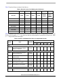
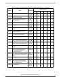
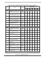
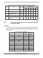
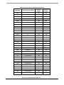
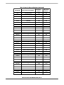
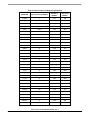
Freescale Semiconductor
Document Number: MPC850CE
Rev. 7, 11/2007
Errata
Device Errata for the
MPC850 Family
This document is a compilation of all MPC850 family device errata from silicon Revision 0.0 forward.
Herein, the errata are classified and numbered, and each erratum is provided with a description and
workarounds.
Table 1 provides a revision history for this document.
Table 1. Document Revision History
Rev. No.
Date
Significant Change(s)
7
11/2007
• Added ESD1 errata.
6
3/2006
• Added CPM18 errata. USB stall handshake
• Separates out rev C (End-Of-Life)
5
7/2005
• Updated CPM16 errata.
4
4/2005
• Updated CPM5 errata.
• Updated CPM17 errata.
Note: Revision 4 replaces MPC850 Family Device Errata Summary (MPC850CESUMM, rev. 2.1),
the contents of which are included here.
© Freescale Semiconductor, Inc., 2007. All rights reserved.
Table 2 lists the silicon revisions of each device.
Table 2. Revision Level to Part Marking Cross-Reference
Device
Rev 0.0
Rev 0.1
Rev 0.2
Rev 0.3
Rev A
Rev B
4H97G
0K24A
0K29A
0K45M
x
Mask Set
0F98S
1F98S
2F98S
3F98S
0H89G
2H89G
MPC850
x
x
x
x
x
MPC850DC
x
MPC850DE
x
MPC850DH
x
x
MPC850DSL
x
MPC850SAR
x
MPC850SE
x
x
x
x
MPC850SR
x
Table 3 summarizes all known errata for the MPC850 family and lists the corresponding silicon revision
level to which it applies. A “Y” entry indicates that the erratum applies to a particular revision level, while
a “—” entry means it does not apply.
Table 3. Summary of MPC850 Silicon Errata and Applicable Revision
Silicon Revision
Number
Name
Disposition
0.0
0.1
0.2
0.3
A
B
Global
Some registers are not initialized
correctly during Power-Up RESET,
HRESET, and SRESET
No plans to
fix this
Y
Y
Y
Y
Y
Y
SIU1
Spurious external bus transaction
following PLPRCR write
No fix
scheduled
Y
Y
Y
Y
Y
Y
SIU2
Missed DRAM refresh cycles with
external masters
Fixed in
Rev. B
Y
Y
Y
Y
Y
—
SIU3
Lock/unlock function of RSR also
locks/unlocks SCCR
Fixed in
Rev. A
Y
Y
Y
Y
—
—
SIU4
Possible external bus hang occurs
under certain error conditions
No fix
scheduled
Y
Y
Y
Y
Y
Y
SIU10
RTC/PIT doesn’t count properly
No plans to
fix this
Y
Y
Y
Y
Y
Y
Fixed in
Rev. B
Y
Y
Y
Y
Y
—
GLL1
SIU
CPM
CPM1
I2C receive problem in arbitration-lost
state
Device Errata for the MPC850 Family, Rev. 7
2
Freescale Semiconductor
Table 3. Summary of MPC850 Silicon Errata and Applicable Revision (continued)
Silicon Revision
Number
Name
Disposition
0.0
0.1
0.2
0.3
A
B
CPM2
I2C error in FLT bit
Fixed in
Rev. A
Y
Y
Y
Y
—
—
CPM3
I2C master fails to receive after
executing read or write
Fixed in
Rev. B
Y
Y
Y
Y
Y
—
CPM4
Receives single-byte buffers after
failed transaction
Fixed in
Rev. A
Y
Y
Y
Y
Y
—
CPM5
I2C receiver locks, holding SDA low
Work
around
Y
Y
Y
Y
Y
Y
CPM6
I2C master collision after “double start”
Fixed in
Rev. B
Y
Y
Y
Y
Y
—
CPM7
I2C: short aborted transmission after
NACK
Fixed in
Rev. B
Y
Y
Y
Y
Y
—
CPM8
I2C: split receive buffer between
loopback and read
Fixed in
Rev. B
Y
Y
Y
Y
Y
—
CPM9
I2C: spurious BUSY errors after
reception in I2C master mode
Fixed in
Rev. B
Y
Y
Y
Y
Y
—
CPM10
USB microcode may duplicate first
byte for IN token transfer
Fixed in
Rev. B
Y
Y
Y
Y
Y
—
CPM11
Port A pin (PA13) may consume
excess current in deep-sleep mode
Fixed in
Rev. B
Y
Y
Y
Y
Y
—
CPM12
Improper USB initialization may cause
excess current in deep-sleep mode
Fixed in
Rev. B
Y
Y
Y
Y
Y
—
CPM13
Port B pin (PB25) fails to function as
TXD3
Applies only
to Rev. A
—
—
—
—
Y
—
CPM14
The ERAM4K bit in the RISC
Microcode Development Support
Control Register (RMDS) is
erroneously cleared
No fix
scheduled
Y
Y
Y
Y
Y
Y
CPM15
USB underrun when ATM or Ethernet
function is used in conjunction with
USB
No fix
scheduled
Y
Y
Y
Y
Y
Y
CPM16
USB endpoint lock up
Work
around
Y
Y
Y
Y
Y
Y
CPM17
USB occasionally ignores tokens,
violates USB protocol by providing
incorrect responses, etc.
Work
around
Y
Y
Y
Y
Y
Y
CPM18
Stall handshake
Work
around
Y
Y
Y
Y
Y
Y
Device Errata for the MPC850 Family, Rev. 7
Freescale Semiconductor
3
Table 3. Summary of MPC850 Silicon Errata and Applicable Revision (continued)
Silicon Revision
Number
Name
Disposition
0.0
0.1
0.2
0.3
A
B
No fix
scheduled
Y
Y
Y
Y
Y
Y
General
G1
Core operation is limited to a 3.0V
minimum
G2
Higher than expected Keep Alive
Power (KAPWR) current when main
power (VDDH & VDDL) is removed
Fixed in
Rev. 0.2
Y
Y
—
—
—
—
G3
EXTCLK and CLKOUT clocks may not
be in phase in half-speed bus mode
Fixed in
Rev. B
Y
Y
Y
Y
Y
—
G4
Potential problems caused by skew
between EXTCLK and CLKOUT
Fixed in
Rev. B
Y
Y
Y
Y
Y
—
G5
Breakdown voltage for XFC pin less
than Motorola-imposed requirements
Fixed in
Rev. A
Y
Y
Y
Y
—
—
G6
Active pullup drivers switch to
high-impedance too early
Fixed in
Rev. A
Y
Y
Y
Y
—
—
G7
Restriction of open collector pull up
No fix
scheduled
Y
Y
Y
Y
Y
Y
CPU1
Bus error unsupported by the data
cache burst
No fix
scheduled
Y
Y
Y
Y
Y
Y
CPU2
D-Cache presents valid data when
parity error present on a burst
Fixed in
Rev. A
Y
Y
Y
Y
—
—
CPU3
Incorrect data breakpoint detection on
store instructions
No fix
scheduled
Y
Y
Y
Y
Y
Y
CPU4
Program trace mechanism error
No fix
scheduled
Y
Y
Y
Y
Y
Y
CPU5
Instruction cache replacement policy
bug
Fixed in
Rev. 0.3
Y
Y
Y
—
—
—
CPU6
Instruction MMU bug at page
boundaries in show-all mode
No fix
scheduled
Y
Y
Y
Y
Y
Y
CPU7
Possible data cache corruption when
writing SPRs
Fixed in
Rev. A
Y
Y
Y
Y
—
—
CPU8
Branch prediction with sequential
branch instructions
Fixed in
Rev. B
Y
Y
Y
Y
Y
—
CPU9
Missed instruction after conditional
branch
Fixed in
Rev. B
Y
Y
Y
Y
Y
—
CPU10
Instruction sequencer error when
modifying MSR with interrupts enabled
Fixed in
Rev. B
Y
Y
Y
Y
Y
—
CPU11
Possible excess current consumption
in deep sleep mode
No plans to
fix
Y
Y
Y
Y
Y
Y
CPU
ATM
Device Errata for the MPC850 Family, Rev. 7
4
Freescale Semiconductor
Table 3. Summary of MPC850 Silicon Errata and Applicable Revision (continued)
Silicon Revision
Number
Name
Disposition
0.0
0.1
0.2
0.3
A
B
ATM1
APCO interrupts cannot be masked
No fix
scheduled
Y
Y
Y
Y
Y
Y
ATM2
CPM lockup when issuing
APC_BYPASS when TX queue full
No fix
scheduled
Y
Y
Y
Y
Y
Y
ATM3
CPM lockup when issuing
APC_BYPASS when TX queue full
Fixed in
Rev. B
Y
Y
Y
Y
Y
—
No plans to
fix
Y
Y
Y
Y
Y
Y
ESD
ESD1
200 Volts ESD Machine Model (MM)
requirements on certain Parallel I/O
pins is not met
Global
GLL1
Some registers are not initialized correctly during Power-Up RESET,
HRESET, and SRESET
Description:
The following table is provided to clarify/correct the power-on RESET value of many of the
registers and lists whether each register is affected by HRESET* and/or SRESET*. The table
applies for the MPC850 Family, the MPC855T, the MPC857T, the MPC860 Family, and the
MPC862 Family.
Table 4. Power-On Reset of Registers
REGISTER
Value at Power-On RESET*
Affected by
HRESET*
Affected by
SRESET*
SIUMCR
01200000
YES
NO
SYPCR
FFFFFF07
YES
NO
SWSR
0
YES
YES
SIPEND
0000xxxx
YES
YES
SIMASK
0000xxxx
YES
YES
SIEL
0000xxxx
YES
NO
SIVEC
(xx11)(11xx)xxxxxx
YES
YES
TESR
XXXX0000
YES
YES
SDCR
0
YES
NO
PBR0
x
NO
NO
POR0
x
NO
NO
PBR1
x
NO
NO
Device Errata for the MPC850 Family, Rev. 7
Freescale Semiconductor
5
Table 4. Power-On Reset of Registers (continued)
REGISTER
Value at Power-On RESET*
Affected by
HRESET*
Affected by
SRESET*
POR1
x
NO
NO
PBR2
x
NO
NO
POR2
x
NO
NO
PBR3
x
NO
NO
POR3
x
NO
NO
PBR4
x
NO
NO
POR4
x
NO
NO
PBR5
x
NO
NO
POR5
x
NO
NO
PBR6
x
NO
NO
POR6
x
NO
NO
PBR7
x
NO
NO
POR7
x
NO
NO
PGCRA
0
YES
NO
PGCRB
0
YES
NO
PSCR
x
NO
NO
PIPR
??00??00
YES
YES
PER
0
YES
YES
BR0
XXXXX(??00)0(000?)
YES
NO
OR0
00000FF4
YES
NO
BR1
XXXXXX(xx00)0
YES
NO
OR1
XXXXXXX(xxx0)
YES
NO
BR2
XXXXXX(xx00)0
YES
NO
OR2
XXXXXXX(xxx0)
YES
NO
BR3
XXXXXX(xx00)0
YES
NO
OR3
XXXXXXX(xxx0)
YES
NO
BR4
XXXXXX(xx00)0
YES
NO
OR4
XXXXXXX(xxx0)
YES
NO
BR5
XXXXXX(xx00)0
YES
NO
OR5
XXXXXXX(xxx0)
YES
NO
BR6
XXXXXX(xx00)0
YES
NO
OR6
XXXXXXX(xxx0)
YES
NO
Device Errata for the MPC850 Family, Rev. 7
6
Freescale Semiconductor
Table 4. Power-On Reset of Registers (continued)
REGISTER
Value at Power-On RESET*
Affected by
HRESET*
Affected by
SRESET*
BR7
XXXXXX(xx00)0
YES
NO
OR7
XXXXXXX(xxx0)
YES
NO
MAR
x
NO
NO
MCR
(xx00)0(x000)0(xxx0)X(00xx)X
YES
NO
MAMR
xx001000
YES
NO
MBMR
xx001000
YES
NO
MSTAT
0
YES
NO
MPTPR
0200
YES
NO
MDR
x
NO
NO
TBSCR
0
YES
NO
TBREFA
x
NO
NO
TBREFB
x
NO
NO
RTCSC
00(000x)(000x)
YES
YES
RTC
x
NO
YES
RTSEC
x
NO
YES
RTCAL
x
NO
NO
PISCR
0
YES
NO
PITC
x
NO
NO
PITR
x
N/A
N/A
SCCR
0(000?)(?000)(0??0)0000
YES
NO
PLPRCR
???0(0100)000
YES
YES
RSR
0
YES
YES
TBSCRK
x
YES
YES
TBREFAK
x
YES
YES
TBREFBK
x
YES
YES
TBK
x
YES
YES
RTCSCK
x
YES
YES
RTCK
x
YES
YES
RTSECK
x
YES
YES
RTCALK
x
YES
YES
PISCRK
x
YES
YES
PITCK
x
YES
YES
Device Errata for the MPC850 Family, Rev. 7
Freescale Semiconductor
7
Table 4. Power-On Reset of Registers (continued)
REGISTER
Value at Power-On RESET*
Affected by
HRESET*
Affected by
SRESET*
SCCRK
x
YES
YES
PLPRCRK
x
YES
YES
RSRK
x
YES
YES
I2MOD
0
YES
YES
I2ADD
x
NO
NO
I2BRG
FFFF
YES
NO
I2COM
0
YES
YES
I2CER
0
YES
YES
I2CMR
0
YES
YES
SDAR
x
NO
NO
SDSR
0
YES
YES
SDMR
0
YES
YES
IDSR1
0
YES
YES
IDMR1
0
YES
YES
IDSR2
0
YES
YES
IDMR2
0
YES
YES
CIVR
0
YES
YES
CICR
0
YES
NO
CIPR
0
YES
YES
CIMR
0
YES
YES
CISR
0
YES
YES
PADIR
0
YES
NO
PAPAR
0
YES
NO
PAODR
0
YES
NO
PADAT
x
NO
NO
PCDIR
0
YES
NO
PCPAR
0
YES
NO
PCSO
0
YES
NO
PCDAT
x
NO
NO
PCINT
0
YES
NO
PDDIR
0
YES
NO
PDPAR
0
YES
NO
Device Errata for the MPC850 Family, Rev. 7
8
Freescale Semiconductor
Table 4. Power-On Reset of Registers (continued)
REGISTER
Value at Power-On RESET*
Affected by
HRESET*
Affected by
SRESET*
PDDAT
x
NO
NO
TGCR
0
YES
YES
TMR1
0
YES
YES
TMR2
0
YES
YES
TRR1
FFFF
YES
YES
TRR2
FFFF
YES
YES
TCR1
0
YES
YES
TCR2
0
YES
YES
TCN1
0
YES
YES
TCN2
0
YES
YES
TMR3
0
YES
YES
TMR4
0
YES
YES
TRR3
FFFF
YES
YES
TRR4
FFFF
YES
YES
TCR3
0
YES
YES
TCR4
0
YES
YES
TCN3
0
YES
YES
TCN4
0
YES
YES
TER1
0
YES
YES
TER2
0
YES
YES
TER3
0
YES
YES
TER4
0
YES
YES
CPCR
0
YES
YES
RCCR
0
YES
NO
RCTR1
NA
YES
YES
RCTR2
NA
YES
YES
RCTR3
NA
YES
YES
RCTR4
NA
YES
YES
RTER
0
YES
YES
RTMR
0
YES
YES
BRGC1
0
YES
NO
BRGC2
0
YES
NO
Device Errata for the MPC850 Family, Rev. 7
Freescale Semiconductor
9
Table 4. Power-On Reset of Registers (continued)
REGISTER
Value at Power-On RESET*
Affected by
HRESET*
Affected by
SRESET*
BRGC3
0
YES
NO
BRGC4
0
YES
NO
GSMR_L1
0
YES
YES
GSMR_H1
0
YES
YES
PSMR1
0
YES
YES
TODR1
0
YES
YES
DSR1
7E7E
YES
YES
SCCE1
0
YES
YES
SCCM1
0
YES
YES
SCCS1
0
YES
YES
GSMR_L2
0
YES
YES
GSMR_H2
0
YES
YES
PSMR2
0
YES
YES
TODR2
0
YES
YES
DSR2
7E7E
YES
YES
SCCE2
0
YES
YES
SCCM2
0
YES
YES
SCCS2
0
YES
YES
GSMR_L3
0
YES
YES
GSMR_H3
0
YES
YES
PSMR3
0
YES
YES
TODR3
0
YES
YES
DSR3
7E7E
YES
YES
SCCE3
0
YES
YES
SCCM3
0
YES
YES
SCCS3
0
YES
YES
GSMR_L4
0
YES
YES
GSMR_H4
0
YES
YES
PSMR4
0
YES
YES
TODR4
0
YES
YES
DSR4
7E7E
YES
YES
SCCE4
0
YES
YES
Device Errata for the MPC850 Family, Rev. 7
10
Freescale Semiconductor
Table 4. Power-On Reset of Registers (continued)
REGISTER
Value at Power-On RESET*
Affected by
HRESET*
Affected by
SRESET*
SCCM4
0
YES
YES
SCCS4
0
YES
YES
SMCMR1
0
YES
YES
SMCE1
0
YES
YES
SMCM1
0
YES
YES
SMCMR2
0
YES
YES
SMCE2
0
YES
YES
SMCM2
0
YES
YES
SPMODE
0
YES
YES
SPIE
0
YES
YES
SPIM
0
YES
YES
SPCOM
0
YES
YES
PIPC
0
YES
NO
PTPR
0
YES
NO
PBDIR
xxx(xx00)0000
YES
NO
PBPAR
xxx(xx00)0000
YES
NO
PBODR
0
YES
NO
PBDAT
x
YES
YES
SIMODE
0
YES
YES
SIGMR
0
YES
NO
SISTR
0
YES
NO
SICMR
0
YES
YES
SICR
0
YES
NO
SIRP
0
YES
YES
Legend:
x or X = “don’t care” in either bits, nibbles, or the entire register.
0 = a single zero indicates the entire register is reset to zeros.
( ) = isolates bits of a nibble of the register.
? = a don’t care for POR, but if this register is affected by HRESET* or SRESET*, indicates that the value will remain the
same as what it was before the reset occurred.
NA = Not Applicable, indicates that this register has no POR value.
Projected Solution:
Not scheduled to be corrected.
Device Errata for the MPC850 Family, Rev. 7
Freescale Semiconductor
11
SIU
SIU1
Spurious external bus transaction following PLPRCR write
Description:
This erratum only affects some designs which execute code from synchronous memories or bus
slaves.
Spurious external bus transactions can occur after executing a store to the PLPRCR register which
changes the PLL multiplication factor (MF bits). This store causes the PLL to freeze the clocks
while another external bus access is already visible on the pins of the chip. This appears externally
as a transaction which begins, has its clocks frozen, and then is abruptly aborted without following
the bus protocol.
This behavior will only affect systems with bus slaves that implement synchronous state machines
that are sensitive to bus protocol violations. Synchronous DRAMs are not affected, and
synchronous bus slaves that ignore bus signals when not selected (for example, Tundra QSPAN)
are not affected.
The only cases in which this erratum will cause problems are if:
1. The device is executing code from a slave which implements a state machine dependent on the
PowerPC bus protocol, where that state machine might “get lost.”
2. There is an external device which snoops the PowerPC bus and implements a state machine;
this state machine might “get lost.”
The impact of this erratum has been deemed minimal, and it will therefore not be corrected.
Work Arounds:
If the behavior described above is unacceptable in the system, the following procedure can be used
to avoid the spurious external bus transaction:
The instruction which performs the store to the PLPRCR should be on a burst-aligned address with
at least one isync instruction following it. The Instruction Cache should be enabled while executing
this sequence. Example code performing this is as follows:
bl .unlock_all
bl .invalid_all
bl .cache_en
# icache initialization
.
.
.
.
lis 3, 0x0050
ori 3, 3, 0x00C0
b st_algn
Device Errata for the MPC850 Family, Rev. 7
12
Freescale Semiconductor
.org
main + 0x0200
##
st_algn: stw 3, PLPRCR_OFFSET(4) # burst aligned address
isync
# isync
lis 3, 0x1234
# Any instruction
lis 3, 0x1234
# Any instruction
Projected Solution:
No scheduled fix.
Device Errata for the MPC850 Family, Rev. 7
Freescale Semiconductor
13
SIU
SIU2
Missed DRAM refresh cycles with external masters
Description:
IF the MPC850 is using internal arbitration (SIUMCR[EARB]=0) AND the arbitration request
level (SIUMCR[EARP]) for external masters is greater than zero,
THEN if a request by an external master (signalled by DREQ) occurs simultaneously with a
request from the DRAM refresh controller, then the request from the DRAM refresh controller will
be cancelled. This will result in a missed refresh cycle. In a system with many bus requests by
external masters, this can potentially result in the cancellation of all DRAM refreshes.
Work Arounds:
1. Program SIUMCR[EARP] to zero.
2. Increase the refresh rate to compensate for the potential cancellation of refresh cycles. Treated
probabilistically, it should be possible to keep the refresh rate above a minimum intended rate.
This is difficult to model exactly, but can be roughly estimated. For the following discussion:
N = proportion of bus bandwidth used by internal MPC850 masters (other than refresh)
E = proportion of bus bandwidth used by external masters
A = proportion of bus bandwidth available for refresh
By definition, N + E + A = 1.
The proportion of time that a refresh request can occur is (E+A).
The probability that a refresh request will be cancelled is E / (E+A). If P is the probability that
the refresh request will be successfully transacted, the P = 1 - [E / (E+A)].
Therefore, to compensate for cancellation of requests, increase the refresh request rate by 1/P.
For a numerical example, assume that internal and external masters each use 30% of the bus
bandwidth. Thus, N = 0.3, E = 0.3, and A = 0.4. In this example, set the refresh rate to 1.75
times the intended rate.
Note, however, that this workaround becomes impractical as A approaches zero.
3. Implement a software-controlled refresh, initiated by a periodic timer request. The user should
program the PIT timer (or a CPM timer) to provide a periodic interrupt. The interrupt service
routine should incorporate a software routine to refresh a memory block. This software refresh
routine can consist of either reads from the appropriate DRAM page or, more simply, execution
of the UPM’s refresh routine via a RUN command to the MCR. The second method is
recommended, as it is simpler and uses the DRAM’s internal counter to keep track of the row
to be refreshed. The user should choose the size of memory block to be refreshed per interrupt
in order to minimize the impact of the interrupt overhead.
Let’s look at an example at one extreme. Assume a system with two 4Mx32 DRAM banks
controlled by CS2 and CS3. Each bank has 2048 pages (rows) and each page must be refreshed
every 15.6 ms. If the UPM refresh pattern called by the software refresh routine is set up to loop
16 times (and therefore can refresh 16 rows per call), the timer interrupt should occur every
Device Errata for the MPC850 Family, Rev. 7
14
Freescale Semiconductor
(16/2048)*15.6ms, or approximately 120µs. If one iteration of the UPM refresh pattern is 5 clocks,
the total time required to execute the software refresh routine (plus overhead for fetching
instructions) for both banks is 5*16*2+20 = 180 clocks. Assuming an interrupt service routine
entry/exit overhead of 1200 clocks, each refresh interrupt would take approximate 1400 clocks, or
28µs (assuming a 50MHz system clock). An ISR consuming 28µs out of every 120µs period would
consume 23.3% of the CPU, with 8200 interrupts per second.
At the other extreme, we could refresh the entire memory (2048 refresh cycles per bank) every
15.6ms. In this case, the software refresh routine would require 1200+(2048/16*180) = 24240
clocks, or 485µs. In this case, the ISR would consume 485µs out of every 15.6ms, or 3% of the
CPU, and would require only 64 interrupts per second. However, system tasks would be stalled for
485µs while waiting for the refresh task to complete.
The best compromise lies between. For example, at 64 pages per interrupt, the software refresh
routine will consume 1200+(64/16*18) = 1920 clocks, or 38.5µs. The CPU bandwidth consumed
will be 38.5µs/(120µs*4) or about 8%, with about 2000 interrupts per second.
Example code implementing this software refresh follows below:
#=================================================================
#This code initialize the PIT timers to interrupt (number 0) every ~24000 clocks
xor 10,0,0
ori 10,10,0xaa33
oris 10,10,0x55cc
stw 10,RTSECK_OFFSET(20) # OPEN RTC KEY
stw 10,RTSEC_OFFSET(20)
# RESET RTC divider
addis 10,10,0x80
stw 10,PISCR_OFFSET(20)
# CLEAR PIT INT bit
lwz 7,SCCR_OFFSET(20)
andi. 8,7,0xffff
andis. 9,7,0xff7f
or 7,8,9
oris 7,7,0x0100
stw 7,SCCR_OFFSET(20)
# RTC_CLK = SYSCLK/512
xor 9,0,0
addis 9,9,0x2f
stw 9,PITC_OFFSET(20)
# Int every 24000 system clocks
xor 10,0,0
addis 10,10,0x85
stw 10,PISCR_OFFSET(20) # PIT enable
sync
#=================================================================
#The interrupt routine should include this code :
#=================================================================
INT0 :
lhz 9,PISCR_OFFSET(20) #
sth 9,PISCR_OFFSET(20) # CLEAR PIT INT bit
andi. 9,9,0x80
bc 0x4,2,INT0_L
xor 8,8,8
Device Errata for the MPC850 Family, Rev. 7
Freescale Semiconductor
15
ori 8,8,0x0030
oris 8,8,0x8080
# Refresh CS_0 by MCR command
stw 8,MCR_OFFSET(20) # MCR(UPMB,0x30)
stw 8,MCR_OFFSET(20) # MCR(UPMB,0x30)
stw 8,MCR_OFFSET(20) # MCR(UPMB,0x30)
stw 8,MCR_OFFSET(20) # MCR(UPMB,0x30)
ori
stw
stw
stw
stw
8,8,0x2000
# Refresh CS_1 by MCR command
8,MCR_OFFSET(20) # MCR(UPMB,0x30)
8,MCR_OFFSET(20) # MCR(UPMB,0x30)
8,MCR_OFFSET(20) # MCR(UPMB,0x30)
8,MCR_OFFSET(20) # MCR(UPMB,0x30)
Projected Solution:
Corrected in Revision B.
Device Errata for the MPC850 Family, Rev. 7
16
Freescale Semiconductor
SIU
SIU3
Lock/unlock function of RSR also locks/unlocks SCCR
Description:
When the RSR is locked or unlocked via the RSRK register, the same function is also performed
on the SCCR.
Work Arounds:
This erratum should not affect user software as long as one is aware of it. In order to avoid possible
software errors due to this (if, for example, the associated code statements were reordered by the
user in a code revision), as a code convention one should always perform the unlock-modify-lock
operations in immediate succession on individual registers. That is, unlock the register, modify it,
then lock it.
Projected Solution:
Corrected in Revision A.
Device Errata for the MPC850 Family, Rev. 7
Freescale Semiconductor
17
SIU
SIU4
Possible external bus hang occurs under certain error conditions
Description:
The external bus cycle may hang when the following sequence of events occur:
1. A transaction on the external bus ends as a result of an assertion of TEA or a bus monitor
timeout occurs.
2. The next transaction also ends as result of an assertion of TEA or a bus monitor timeout occurs.
(burt 300)
Work Arounds:
None.
Projected Solution:
No scheduled fix.
Device Errata for the MPC850 Family, Rev. 7
18
Freescale Semiconductor
SIU
SIU10
RTC/PIT doesn’t count properly
Description:
The periodic interrupt timer (PIT) consists of a 16-bit counter clocked by the PITRCLK clock
supplied by the clock RTCLK (Real time clock). The 16-bit counter counts down to zero when
loaded with a value from the PITC. After the timer reaches zero, the PS bit is set and an interrupt
is generated if the PIE bit is a logic one. The user can program the RTC and PIT clock to be divided
by 4 or 256 (depending on SCCR[RTDIV]). When the RTC clock is divided by 4, an interrupt will
not occur due to a bug in the rtclk_sync_raw logic. The rtclk_sync_raw is the real time clock for
the RTC timers, and its frequency is the same as rtclk_raw. If the pll output clock is enabled and
not in reset state, and the timer has not expired, then the rtclk_sync_raw clock has a 25% duty cycle
synchronous with system T4 tick, otherwise this clock is the same as rtclk_raw.
From the ckpspcl schematics, rtclk_raw also selects rtclk_sync_raw. There is no issue in the above
statement when the pre-divider is set to 256 clocks, this is because the select line is slower then the
selected clock source. But, when the pre-divider is set to 4, there is suppose to be a rtclk_sync_raw
edge every 2 clocks. The rising edge of this clock will disappear due to a race between
rtclk_sync_raw (as the select line) and the ckp_rtclk_sysd (as the data for the mux).
At room temperature, this will generate a spike signal, and at hot temperature, this will degrade and
disappear. When this happens, the RTC will not count properly, and no interrupt will occur.
Work Arounds:
None.
Projected Solution:
Not to be corrected.
Device Errata for the MPC850 Family, Rev. 7
Freescale Semiconductor
19
CPM
CPM1
I2C receive problem in arbitration-lost state
Description:
If the MPC850 I2C master transmitter loses arbitration to another I2C master which is transmitting
to the MPC850, the 860 receiver will not accept the message (address byte not acknowledged).
Work Arounds:
1. Avoid multimaster configuration.
2. The operation should be retried by the other master through software.
Projected Solution:
Corrected in Revision B.
Device Errata for the MPC850 Family, Rev. 7
20
Freescale Semiconductor
CPM
CPM2
I2C error in FLT bit
Description:
An error will occur if the FLT bit is set to turn on the digital filter for the I2C. The digital filter is
activated by setting the FLT bit in the I2C mode register and is turned off at reset.
(However, note that this digital filter is not required for normal operation. The MPC8xx I2C is fully
compliant to the I2C specification even without this digital filter.)
Work Arounds:
Do not turn on the digital filter for I2C clock filter.
Projected Solution:
Corrected in Revision A.
Device Errata for the MPC850 Family, Rev. 7
Freescale Semiconductor
21
SIU
CPM3
I2C master fails to receive after executing read or write
Description:
If the I2C channel is in master mode, after the I2C channel performs a transaction (read or write
command), the I2C channel will fail to receive a transmission from another master. It will respond
with NACK.
Furthermore, after the failed reception, if the I2C master then attempts to perform another
transaction (read or write command), the transaction will fail with an underrun error.
Work Arounds:
After the master I2C channel completes its transmission, disable and re-enable the channel in the
I2MOD register (thereby resetting it).
Projected Solution:
Corrected in Revision B.
Device Errata for the MPC850 Family, Rev. 7
22
Freescale Semiconductor
CPM
CPM4
Receives single-byte buffers after failed transaction
Description:
A. If the I2C channel is in master mode, then:
If the I2C master attempts a transaction (read or write command) which receives a NACK, AND
the I2C master then attempts to execute a read to another slave,
THEN the master will receive the first byte of the slave’s message in one buffer and will close the
BD, and then will continue to receive the rest of the message in the next BDs. This reception of the
first byte in a single-byte buffer will happen regardless of the MRBLR.
B. If the I2C channel is in slave mode, then:
If the I2C slave responds to a read command (for example, performs a transmission), AND
the I2C slave then responds to a write command (for example, performs a reception),
THEN the I2C slave will receive the first byte of the master’s message in one buffer and will close
the BD, and then will continue to receive the rest of the message in the next BDs. This reception
of the first byte in a single-byte buffer will happen regardless of the MRBLR.
Work Arounds:
After the I2C channel performs a transmission (master read or write, or slave response to read),
disable and re-enable the channel in the I2MOD register (thereby resetting it).
Projected Solution:
Corrected in Revision B.
Device Errata for the MPC850 Family, Rev. 7
Freescale Semiconductor
23
CPM
CPM5
I2C receiver locks, holding SDA low
Description:
The I2C receiver may lock up, holding the I2CSDA line low, in a system that has slow rise/fall time
on the I2C clock (I2CSCL) if the environment is noisy.
Work Arounds:
Set the I2C predivider to 32 (by setting I2MOD[PDIV]=00), and restrict rise/fall time of I2CSCL
to 0.5 µs. In addition to this, for MPC850 revision B.0 and later, enable the digital filter via the
I2MOD[FLT]. [For previous revisions of the MPC850, the digital filter is not functional.]
Projected Solution:
No scheduled fix.
Device Errata for the MPC850 Family, Rev. 7
24
Freescale Semiconductor
CPM
CPM6
I2C master collision after “double start”
Description:
The following situation will result in the I2C controller colliding with the transmission of another
master:
1. Another I2C master performs a “master write” to the I2C controller of the MPC850.
2. The I2C controller of the MPC850 is waiting for the I2C bus to become idle in order to become
the master and perform a transaction.
3. The other I2C master asserts a new “START” condition without asserting a “STOP” condition.
In this case, the I2C master of the MPC850 will incorrectly interpret the new “START” condition
as generated by itself, and will therefore drive the I2C bus concurrently with the other master.
Work Arounds:
Avoid performing back-to-back START conditions on the I2C bus.
Projected Solution:
Corrected in Revision B.
Device Errata for the MPC850 Family, Rev. 7
Freescale Semiconductor
25
CPM
CPM7
I2C: short aborted transmission after NACK
Description:
The following situation will cause the I2C controller of the MPC850 to send a short aborted
transmission:
1. The MPC850’s I2C controller performs a transaction, transmitting a buffer which has no STOP
condition at the end. The next buffer (not yet transmitted) will issue a START condition,
producing back-to-back transactions without an intervening STOP (also known as “double
start”).
2. The MPC850’s I2C controller receives a NACK on the last or next-to-last byte of the buffer.
If this case occurs, then the MPC850’s I2C controller will assert a STOP condition (as expected by
the I2C protocol). However, when software subsequently issues a new start command (I2COM =
0x81), the I2C master will begin its next transaction erratically. It will issue a START condition
and drive one bit of the message, then drive a new START condition and restart the transmission
(including the first bit).
Work Arounds:
Do not set up the MPC850’s I2C controller to perform “double start.”
Projected Solution:
Corrected in Revision B.
Device Errata for the MPC850 Family, Rev. 7
26
Freescale Semiconductor
CPM
CPM8
I2C: split receive buffer between loopback and read
Description:
IF the MPC850’s I2C master performs a loopback transaction (for example, a master write to its
own I2C address or a master write to the General Call address with General Call reception
enabled).
AND the MPC850’s I2C master then performs a master read transaction
THEN the receive buffer used for the loopback transaction will not be closed after the loopback
transaction. Instead, it will be closed after the first byte of the read transaction is received. Thus,
the received data from the read transaction will be split between the loopback buffer and the
intended receive buffer.
Work Arounds:
Avoid performing loopback transactions during normal operation.
Projected Solution:
Corrected in Revision B.
Device Errata for the MPC850 Family, Rev. 7
Freescale Semiconductor
27
CPM
CPM9
I2C: spurious BUSY errors after reception in I2C master mode
Description:
IF the MPC850’s I2C controller is configured as an I2C master
AND the I2C controller is the target of another master’s write,
THEN after the MPC850 receives the data from the master (and thus closes the receive buffer
appropriately), it will attempt to open the next receive buffer (even though there is no receive data).
If there is no buffer available, it will generate a BUSY error.
Work Arounds:
Ignore BUSY errors in this case.
Projected Solution:
Corrected in Revision B.
Device Errata for the MPC850 Family, Rev. 7
28
Freescale Semiconductor
CPM
CPM10
USB microcode may duplicate first byte for IN token transfer
Description:
If an IN token for an end-point is received exactly between the time the first byte was written to
the FIFO and the time the second byte is written to the FIFO, then the next IN token will be
answered with a frame that has the first byte duplicated. This is caused by the microcode aborting
the in_frame state when the IN token is received and the FIFO is not full. (burt_xxx)
Work Arounds:
A microcode patch is available and will be placed on the MPC850 web site. This microcode patch
will ignore the fifo_not_ready error if FIFO filling has already started. The microcode package
includes a README document, upatch (micro assembler source), upatcch.map (listing), upatch.c
(C-format object code), and an upatch.srx (S-record format object file).
Projected Solution:
Corrected in Revision B.
Device Errata for the MPC850 Family, Rev. 7
Freescale Semiconductor
29
CPM
CPM11
Port A pin (PA13) may consume excess current in deep-sleep mode
Description:
When the Port A pin PA13 is configured as the SCC2 function RXD2 and the IrDA logic is not
enabled (for example,,the EN=0 in the IRMODE register), then the MPC850 may consume excess
current due to internal contention after entering deep-sleep mode. Other than the approximate 1mA
of excess current, there are no operational issues.
Work Arounds:
Before entering deep-sleep mode, configure PA13 as a general-purpose input. When you exit
deep-sleep mode, reconfigure PA13 as the SCC2-controlled RXD2, as required.
Projected Solution:
Corrected in Revision B.
Device Errata for the MPC850 Family, Rev. 7
30
Freescale Semiconductor
CPM
CPM12
Improper USB initialization may cause excess current in deep-sleep
mode
Description:
An initialization problem in the USB block might cause excess current in the deep-sleep mode,
typically around 500µA.
Work Arounds:
As part of the power-on initialization sequence, the software should enable the baud rate generator
clock1 (BRGC1) by setting the EN bit to 1 and leaving it set for at least 16 system clocks before
changing the serial interface clock route register from its default value (0x00000000).
Projected Solution:
Corrected in Revision B.
Device Errata for the MPC850 Family, Rev. 7
Freescale Semiconductor
31
CPM
CPM13
Port B pin (PB25) fails to function as TXD3
Description:
If Port B pin PB25 is configured to function as TXD3, it will fail to transmit data.
Work Arounds:
Connect a pullup resistor to Port B pin PB25 if it is configured to function as TXD3. The pin will
then transmit normally.
Projected Solution:
Corrected in Revision B.
Device Errata for the MPC850 Family, Rev. 7
32
Freescale Semiconductor
CPM
CPM14
The ERAM4K bit in the RISC Microcode Development Support Control
Register (RMDS) is erroneously cleared
Description:
The ERAM4K bit is cleared in the RISC Microcode Development Support Control Register,
RMDS, if the register’s location is accessed as either part of a half-word or byte access.
Work Arounds:
If the ERAM4K is to be set, the RMDS must be accessed as part of a word starting at IMMR+9C4
to IMMR+9C7.
Projected Solution:
No scheduled fix.
Device Errata for the MPC850 Family, Rev. 7
Freescale Semiconductor
33
CPM
CPM15
USB underrun when ATM or Ethernet function is used in conjunction
with USB
Description:
If both USB and ATM or Ethernet are used simultaneously, USB underruns will occur.
Work Arounds:
Software should re-initialize the USB TX BD.
Projected Solution:
No scheduled fix.
Device Errata for the MPC850 Family, Rev. 7
34
Freescale Semiconductor
CPM
CPM16
USB endpoint lock up
Description:
When an endpoint is used only for receiving, there may be a case where this endpoint may lock up
when an IN token is received to this endpoint. For example: 3 endpoints are set up on the 850 USB.
Endpoint 0 being a control endpoint (usually both receive and transmit) and endpoint 1 is set up as
a transmit-only endpoint and endpoint 2 set up as a receive-only end point. A lock up may occur
on endpoint 1 when an IN token is received for endpoint 1. When this occurs, the 850 will fail to
respond to this IN token. (Neither NACK nor ACK is given by the 850.)
Work Arounds:
A fix package exists on the product website. The package includes a microcode patch and the
application software workaround procedure, as well as a text file with instructions on how to
implement the workaround.
Projected Solution:
No scheduled fix.
Device Errata for the MPC850 Family, Rev. 7
Freescale Semiconductor
35
CPM
CPM17
USB occasionally ignores tokens, violates USB protocol by providing
incorrect responses, etc.
Description:
A variety of erratic behavior occurs when a skew of greater than +4 or -20 ns is introduced between
the differential USB rxd-p/rxd-n pair and the single USB RX data single. This condition causes the
850’s USB module to misinterpret incoming tokens and data, further resulting in incorrect protocol
responses.
Work Arounds:
Add external logic to delay the differential input so that the skew will be less than +4 or -20 ns.
Projected Solution:
No scheduled fix.
Device Errata for the MPC850 Family, Rev. 7
36
Freescale Semiconductor
CPM
CPM18
Stall handshake
Description:
When a control endpoint’s USEP register has STALL handshake enabled, software may not have
enough time to exit STALL upon reception of the next transaction as required by the USB protocol.
Work Arounds:
A fix package exists on the product website that will exit the endpoint out of STALL in a timely
manner. This package includes the microcode patch for CPM18 as well as CPM16 in the form of
a combination patch. The package includes a microcode patch, application software workaround
procedure, as well as a text file with instructions on how to implement the workaround.
Projected Solution:
No scheduled fix.
Device Errata for the MPC850 Family, Rev. 7
Freescale Semiconductor
37
General
G1
Core operation is limited to a 3.0V minimum
Description:
The current versions of the MPC850 silicon are only tested and verified at 3.0V–3.6V power.
Because of this, low voltage operation at 2.2V cannot be used to power the core.
Work Arounds:
None.
Projected Solution:
No scheduled fix.
Device Errata for the MPC850 Family, Rev. 7
38
Freescale Semiconductor
General
G2
Higher than expected Keep Alive Power (KAPWR) current when main
power (VDDH & VDDL) is removed
Description:
There are four nodes within the MPC850 that are floating when VDDH and VDDL power is not
supplied to the device. When this condition occurs, which is typical in Power Down Mode, the
current drain on the Keep-Alive Power rail is greater than expected. (10 - 20 mA versus 10 µA).
Work Arounds:
Provide adequate current source for KAPWR pin in Power Down Mode.
Projected Solution:
Corrected in Revision 0.2.
Device Errata for the MPC850 Family, Rev. 7
Freescale Semiconductor
39
General
G3
EXTCLK and CLKOUT clocks may not be in phase in half-speed bus
mode
Description:
When the MPC850 uses EXTCLK as an input clock source and MF=001 in PLPRCR (for example,
the frequency of EXTCLK is 1/2 of the internal clock) and the half-speed bus mode is used
(EBDF=01 in SCCR), the output clock from CLKOUT could be 90 degrees or 180 degrees out of
phase from the input clock. This will affect synchronous designs where the same clock source is
used as an input to EXTCLK, as well as to an external synchronous device (for example, a
peripheral or ASIC).
Work Arounds:
Case 1. Where multiple external devices need to operate synchronously with the MPC850:
Use the CLKOUT pin of the MPC850 as the source of clock for all external, synchronous devices
(for example, CLKOUT is the affective system master clock to be used for distribution).
Case 2. Where it is necessary to synchronize an external master clock (for example, from a
backbone), an MPC850, and external peripherals, to allow data transfers in all three directions:
There is no known workaround for this case. Use full-speed bus operation.
Projected Solution:
Corrected in Revision B.
Device Errata for the MPC850 Family, Rev. 7
40
Freescale Semiconductor
General
G4
Potential problems caused by skew between EXTCLK and CLKOUT
Description:
In correct operation, the PLL of the MPC850 will lock on the rising edge of the input clock.
However, on these revisions of the MPC850, the PLL may lock on the falling edge of the input
clock. This will affect the skew between EXTCLK and CLKOUT at the rising edge. The skew is
dependent on the duty cycle of the input clock (but for a 50% duty cycle will not exceed 2nS). This
will affect synchronous designs where the same clock source is used as an input to EXTCLK, as
well as to an external synchronous device (for example, a peripheral or ASIC).
Work Arounds:
Case 1. Where multiple external devices need to operate synchronously with the MPC850:
Use the CLKOUT pin of the MPC850 as the source of clock for all external, synchronous devices
(for example, CLKOUT is the affective system master clock to be used for distribution).
Case 2. Where it is necessary to synchronize an external master clock (for example, from a
backbone), an MPC850, and external peripherals, to allow data transfers in all three directions:
[NOTE: This workaround is a concept only. It has not been verified in hardware.]
Insert a PLL between the external master clock and the EXTCLK pin of the MPC850. Connect the
phase comparison pin of the PLL to the CLKOUT pin of the MPC 860. Also use the CLKOUT
signal as the reference clock for distribution to the local external peripherals.
Important Note: The PLL has to be capable of operating with a permanent offset of -2nS, therefore
the range of lock should extend to about -4nS.
A diagram of this concept is given below:
Ext. Clock Source
CLKOUT
+
EXTCLK
PLL
860
Clock
Master
at
board
level
-
Projected Solution:
Corrected in Revision B.
Device Errata for the MPC850 Family, Rev. 7
Freescale Semiconductor
41
General
G5
Breakdown voltage for XFC pin less than Motorola-imposed
requirements
Description:
The XFC pin (B2) of this version of the MPC850 silicon fails Motorola’s XC qualification of 1 KV
for the Electrostatic Discharge (ESD) breakdown voltage test. The maximum ESD voltage that can
be applied to this pin on this silicon without damage is 750 volts.
Work Arounds:
Ensure that devices are not exposed to greater than 750 volts of electrostatic discharge.
Projected Solution:
Corrected in Revision A.
Device Errata for the MPC850 Family, Rev. 7
42
Freescale Semiconductor
General
G6
Active pullup drivers switch to high-impedance too early
Description:
The active pullup drivers (which include TS, TA, BI, and BB) switch to high-impedance at a
threshold voltage which is lower than the specified minimum output voltage level VOH.
Thereafter, the pullup resistor must pull the signal beyond the specified output voltage level.
Depending upon the pullup resistor value and the capacitive load of the signal, this can result in a
deassertion time which is longer than specified.
Work Arounds:
Use a 1 kΩ pullup resistor for these drivers.
NOTE
The long rise times do not cause a problem to the processor. Furthermore, in
most systems, the longer rise times for these signals will also not present a
problem for other devices.
1. TS is normally sampled at the beginning of a bus cycle, and is thereafter a “don’t-care” until
the cycle is terminated with TA. Thus, a TS which extends into the next clock cycles will be
ignored.
2. BI must only be in its negated state when sampled concurrently with TA when a cycle is to a
burstable target. In these systems, typically the only burstable target is the UPM, which will
drive the BI actively throughout cycles in which it is in control of the target. Therefore, this
behavior will not affect operation of the memory controller. Furthermore, for burstable targets
that are not in control of the memory controller, (A) the pullup resistor should have plenty of
time to complete the signal deassertion before the TA of the cycle, and (B) the worst that could
result from a falsely asserted BI is that the master would break the burst into four accesses,
resulting in a performance degradation but not a system failure.
3. For a non-burst cycle, TA is normally sampled only once after TS is driven. TA is then a
“don’t-care” until after the next TS is driven. Therefore, there should be sufficient time for the
pullup resistor to complete the signal deassertion of TA before termination conditions for the
next cycle are sampled. For burst cycles, typically the only burstable target in the system is the
UPM, which drives the TA signal actively until the completion of the entire burst cycle, thus
avoiding the problem during the burst. And for other burstable targets, it is the responsibility
of the target to meet the appropriate assertion/deassertion timing for TA.
4. If this condition results in a long deassertion time for BB, the only affect is increased latency
between bus cycles as the bus is handed off between bus masters. That is, the bus would falsely
appear busy for a short period after the on-chip master actually released the bus.
5. TS, TA, BI, and BB will typically be lightly loaded.
Projected Solution:
Corrected in Revision A.
Device Errata for the MPC850 Family, Rev. 7
Freescale Semiconductor
43
General
G7
Restriction of open collector pull up
Description:
Open collector signal may not be able to be pulled to greater than 3.5V.
Work Arounds:
Use external buffer if an open collector signal needs to be pulled to greater than 3.5V.
Projected Solution:
No scheduled fix.
Device Errata for the MPC850 Family, Rev. 7
44
Freescale Semiconductor
CPU
CPU1
Bus error unsupported by the data cache burst
Description:
The data cache does not support a bus error which might occur on the 2nd or 3rd data beat of a
burst.
Also see CPU2.
Work Arounds:
Avoid using bus error in this case.
Projected Solution:
No scheduled fix.
Device Errata for the MPC850 Family, Rev. 7
Freescale Semiconductor
45
CPU
CPU2
D-Cache presents valid data when parity error present on a burst
Description:
If the LDST unit requests data that is not in the Data Cache, then the Data Cache will initiate a burst
cycle to the memory. If during this burst cycle, a parity error is generated on the second or third
words and not on the critical word; then the Data Cache will present the data to the LDST as the
valid data.
Work Arounds:
Disable parity.
Projected Solution:
Corrected in Revision A.
Device Errata for the MPC850 Family, Rev. 7
46
Freescale Semiconductor
CPU
CPU3
Incorrect data breakpoint detection on store instructions
Description:
The data breakpoint mechanism comparison of operand data and operand size is faulty. If used, it
can cause breakpoints where they should not occur, and conversely can miss breakpoints where
they should occur.
Note: The instruction and address portions of the data breakpoint mechanism operate correctly. It
is therefore still possible to use the data breakpoints to break on a store to a particular address
and/or on a store instruction in a particular address range. Only the operand comparison portion of
the data breakpoints does not function properly.
Work Arounds:
Do not use the operand comparison function of the data breakpoints for store instructions.
Projected Solution:
No scheduled fix.
Device Errata for the MPC850 Family, Rev. 7
Freescale Semiconductor
47
CPU
CPU4
Program trace mechanism error
Description:
In the following case there is an error in the program trace mechanism.
Program
0x00004ff0: divw. r25,r27,r26
0x00004ff4: divw. r28,r27,r26
0x00004ff8: unimplemented
0x00004ffc: b 0x00005010
where 0x00005010 belong to a page with a page fault.
The divide takes a long time to complete so the instruction queue gets filled with the
unimplemented instruction, the branch and the branch target (page fault).
When the sequencer takes the unimplemented instruction it releases the fetch (that was blocked by
the MMU error). This causes the queue to get another instruction in addition to the first page fault.
Because the second fault is sequential to the branch target it is not reported by the queue flush (VF).
This causes an incorrect value to be present in the VF flush information when the unimplemented
exception occurs.
Work Arounds:
None.
Projected Solution:
No scheduled fix.
Device Errata for the MPC850 Family, Rev. 7
48
Freescale Semiconductor
CPU
CPU5
Instruction cache replacement policy bug
Description:
I-cache replacement policy is not optimized. This does not affect the correctness of program
execution, but will affect performance by an average of 10-20%. Once new silicon is available,
performance should improve without any software changes required.
Work Arounds:
None.
Projected Solution:
Corrected in Revision 0.3.
Device Errata for the MPC850 Family, Rev. 7
Freescale Semiconductor
49
CPU
CPU6
Instruction MMU bug at page boundaries in show-all mode
Description:
The wrong instruction address is driven by the core when all the following conditions occur:
1. MPC850 works in 'show all' mode (for example, ISCT_SER bits=000 in ICTRL)
2. Sequential instruction crosses IMMU page boundary
3. Instruction cache fails to get ownership of the internal U-bus on the first clock
In this case the address driven by the core will be of the previous page and not the current one.
The impact of this erratum has been deemed minimal, and it will therefore not be corrected.
Work Arounds:
Possible work arounds include:
1. Disable show all mode.
2. Invalidate the page next to current (by using the tlbie instruction) when performing the TLB
reload operation.
Projected Solution:
No scheduled fix.
Device Errata for the MPC850 Family, Rev. 7
50
Freescale Semiconductor
CPU
CPU7
Possible data cache corruption when writing SPRs
Description:
A write access to a special-purpose register located in caches, MMUs or SIU might corrupt the
contents of the data-cache.
This may happen regardless of whether the cache is currently enabled or disabled (by either writing
a disable command to the DC_CST or by setting all regions to cache-inhibited in via
MD_CTR[CIDEF]). Thus, it is not possible to work around this problem by simply temporarily
disabling the data cache.
NOTE: This is a probabilistic affect, caused by an internal race condition, and therefore does not
occur in all cases. However, as it is due to a race condition, it is affected by all parameters which
affect speed of the silicon (for example, silicon revision, temperature, voltage). Therefore, if a
system exhibits behavior which varies due to these factors, it is advisable to check for occurrence
of this erratum.
The special-purpose registers affected by this include:
SPR
spr_address
===========================
IMMR
0x3d30
IC_CST
0x2110
IC_ADR
0x2310
IC_DAT
0x2510
DC_CST
0x3110
DC_ADR
0x3310
DC_DAT
0x3510
MI_CTR
0x2180
MI_AP
0x2580
MI_EPN
0x2780
MI_TWC
0x2b80
MI_RPN
0x2d80
MI_DBCAM
0x2190
MI_DBRAM0
0x2390
MI_DBRAM1
0x2590
MD_CTR
0x3180
M_CASID
0x3380
MD_AP
0x3580
MD_EPN
0x3780
M_TWB
0x3980
Device Errata for the MPC850 Family, Rev. 7
Freescale Semiconductor
51
MD_TWC
MD_RPN
M_TW
MD_DBCAM
MD_DBRAM0
MD_DBRAM1
DEC
TB Write
TBU Write
DPDR
0x3b80
0x3d80
0x3f80
0x3190
0x3390
0x3590
0x2c00
0x3880
0x3a80
0x2d30
Work Arounds:
There are two possible work-arounds:
1. If the contents of the TLBs are not changed dynamically (fixed-page structure), any access to
the above-mentioned registers should be avoided (except for initialization).
2. If the contents of the TLBs are changed dynamically (pages are loaded on demand), then each
“mtspr” instruction which accesses one of these registers must be preceded by a store word and
a load word instruction of a data operand equal to the spr_address of the respective register. As
an example, to write the data from the general purpose register r1 to the special purpose register
M_TW, the following procedure should be followed:
lis r2, some_address_msb # an address in RAM
li r3, 0x3f80
# the spr_address of the M_TW from
# the table
stw r3, some_address_lsb(r2) # no interrupts
lwz r3, some_address_lsb(r2) # between these
mtspr M_TW, r1
# 3 instructions
Projected Solution:
Corrected in Revision A.
Device Errata for the MPC850 Family, Rev. 7
52
Freescale Semiconductor
CPU
CPU8
Branch prediction with sequential branch instructions
Description:
IF there are three branches in sequence in the run-time program flow
AND the third branch is in the mis-predicted path of the second branch,
THEN although the third branch is part of a predicted path, it may be “issued” from the instruction
queue. If this instruction issue in the mis-predicted path happens at the same time that the condition
of the prediction is resolved (thereby causing mis-predicted instructions to be flushed from the
instruction queue), then the resulting instruction cancellation will back up too far into the
instruction queue. This will cause the instruction sequence starting from the instruction
immediately preceding the first branch to be re-issued.
Notes:
1. Other factors of the internal state of the core also affect the occurrence of this behavior.
Therefore, not all occurrences of this instruction sequences necessarily exhibit this behavior.
2. This behavior is not necessarily harmful to the user application. For example, the instruction
preceding the first branch could be a simple move between registers.
3. Not all compilers generate this instruction sequence. The following compilers are known never
to generate code that is susceptible to this erratum:
Diab Data (all versions)
Metaware
We are continuing to investigate other compilers with their vendors; their status is unknown at this
time. We will update this list as our investigation progresses.
Work Arounds:
For every conditional branch preceded in program order by another branch:
1. IF the two possible targets of the conditional branch consist of a branch instruction and a
non-branch instruction
THEN force the prediction of the conditional branch to predict the non-branch instruction (using
the y-bit in the opcode of the conditional branch).
2. IF both of the possible targets of the conditional branch are branch instructions
THEN
1. insert a non-branch instruction before the branch on the predicted path
OR
2. insert an 'isync' instruction before the first branch.
Projected Solution:
Corrected in Revision B.
Device Errata for the MPC850 Family, Rev. 7
Freescale Semiconductor
53
CPU
CPU9
Missed instruction after conditional branch
Description:
IF the instruction cache is enabled, THEN:
IF a conditional branch residing near the boundary of the current memory page is mis-predicted
such that the CPU fetches beyond the page boundary
AND the branch target also resides on another memory page
THEN the instruction at the branch target address may not be executed.
[The boundary of the current memory page is as follows:
1. If the MMU is enabled (MSR[IR]=1), then it is as defined by the associated MMU page table
entry
2. If the MMU is disabled (MSR[IR]=0), then it is at a 4KB boundary.]
Note: This erratum depends also on the internal state of the core (instruction queue cancellation
and MMU page swap), so it does not occur in all cases.
Work Arounds:
1. Disable the instruction cache. This will cause the instruction to be fetched from external
memory, and will therefore the instruction queue will not be filled until the branch is resolved.
2. Run the CPU in serialized mode (by programming the ICTRL[ISCT_SER] bits). This mode
will keep the predicted instructions from executing until the branch is resolved.
3. Avoid conditional branches with predicted paths that cross page boundaries.
Projected Solution:
Corrected in Revision B.
Device Errata for the MPC850 Family, Rev. 7
54
Freescale Semiconductor
CPU
CPU10
Instruction sequencer error when modifying MSR with interrupts
enabled
Description:
IF the following instruction sequence occurs:
mtmsr
Rx
# change IR (Instruction Relocate) bit or PR (Problem # State) bit in
MSR
op1
op2
AND external interrupts were previously enabled (or are being enabled by this mtmsr instruction)
AND an external interrupt or decrementer interrupt occurs (or is already pending)
AND op1 not in the Instruction cache
AND the first instruction in the interrupt handler is fetched at the same clock that the op2
instruction is prefetched from external memory (as seen on the internal bus)
THEN the sequencer takes op2 as the first instruction in the interrupt handler. Also the sequencer
and Instruction cache are out of sync in subsequent instruction fetched in the interrupt handler until
a change of flow is executed. (“Change of flow” can also be isync and mtmsr commands.)
Work Arounds:
Do not execute mtmsr that changes IR or PR bits when external interrupt (and decrementer
interrupt) are enabled (for example, when MSR[EE]=1). Allow at least two sequential instructions
after the mtmsr that changes IR or PR before enabling interrupts.
Projected Solution:
Corrected in Revision B.
Device Errata for the MPC850 Family, Rev. 7
Freescale Semiconductor
55
CPU
CPU11
Possible excess current consumption in deep sleep mode
Description:
Certain nodes of the multiplier hardware are not initialized at reset, and may thus result in
non-destructive internal contention. As a result, if the processor is put into Deep Sleep mode
without first putting the multiplier into a known state, current consumption in this mode may be
higher than expected.
The impact of this erratum has been deemed minimal, and it will therefore not be corrected.
Work Arounds:
Execute a mullw instruction at any point after reset; this will put the internal nodes in an orderly
state. Deep Sleep mode may then be entered at any time thereafter.
Projected Solution:
No plans to fix this.
Device Errata for the MPC850 Family, Rev. 7
56
Freescale Semiconductor
ATM
ATM1
APCO interrupts cannot be masked
Description:
[Modes affected: All]
APCO interrupts cannot be masked with the IMASK field of the Receive Connection Table entry
(RCT).
Work Arounds:
Generally, if the APC is programmed well, there should not be any APCO. However, if they do
occur and the user wants to mask them, they may use one of the following methods.
A. Implement a software workaround which will:
1. Ignore the specific APCO interrupts in the Interrupt table,
OR
2. Mask all interrupts globally by using GINT mask in IDMR1 or SCCM.
B. Download the RAM microcode package for enhanced UBR support. An enhancement
supporting APCO masking has been integrated into this package.
Projected Solution:
No scheduled fix.
Device Errata for the MPC850 Family, Rev. 7
Freescale Semiconductor
57
ATM
ATM2
CPM lockup when issuing APC_BYPASS when TX queue full
Description:
[Modes affected: All]
If a cell is scheduled for transmission via the APC_BYPASS command when the transmit queue is
full, the CPM will lock up, causing immediate failure of all channels.
In the case of a CPM lockup, the CPM must be reset. This can be accomplished either through the
CPCR[RST] or by issuing an SRESET.
This case should not happen during optimal operation. An overflow of the TX queue indicates that
more transmit traffic has been scheduled than the physical layer can transmit, which is an error
condition. Software should avoid this situation.
To fix this, the operation will be changed in the following fashion:
Operation will be changed such that this condition will not cause lockup, and an additional
semaphore bit will be provided to assist in avoiding this situation.
Work Arounds:
Monitor the transmit queue status, and do not issue the APC_BYPASS command if the number of
empty entries in the transmit queue is less than (NCITS+2).
Projected Solution:
No scheduled fix.
Device Errata for the MPC850 Family, Rev. 7
58
Freescale Semiconductor
ATM
ATM3
Incorrect operation in Presync state of cell delineation
Description:
[Modes affected: Serial Receive]
If a HEC error occurs during the Presync state of the serial receive cell delineation state machine,
incorrect operation occurs. Instead of moving back to the Hunt state, the receiver decrements Alpha
by one, receives the cell into the Global Raw Cell Queue, and remains in the Presync state. The cell
delineation state machine will move back to the Hunt state only when the Alpha parameter reaches
zero. This erroneous operation can result in long receive startup times, as decrementing Alpha can
cause it to overflow back to 65535. The most common occurrence of this problem occurs when the
lock is lost due to a line going down, and in the received cell sequence when restarting there are
occurrences of both good and bad HECs.
Work Arounds:
IF at restart or in the case when lock state is lost
OR when the cell delineation state machine is not locked and the Global Raw Cell Queue contains
more than 7 cells with HEC errors
THEN program Alpha = 1 and Delta = 6.
After programming these parameters, the user must check after at least 4 system clocks that these
values were actually written to these parameters (and were not overwritten by the CPM).
[Note: A SYNC interrupt is issued in the case of loss of the lock state; see the description of the
SYNC interrupt in the User’s Manual.]
Projected Solution:
Corrected in Revision B.
Device Errata for the MPC850 Family, Rev. 7
Freescale Semiconductor
59
ESD
ESD1
200 Volts ESD Machine Model (MM) requirements on certain Parallel
I/O pins is not met
Description:
The MPC850 is rated for 200 Volts ESD-MM, but the PA15, PB30, PB31, PC15, PD5 and PD3
Parallel I/O pins do not meet the required 200V ESD-MM specified.
Work Arounds:
Observe proper ESD-MM handling precautions for the PA15, PB30, PB31, PC15, PD5 and PD3
Parallel I/O pins. All pins pass at 175V ESD-MM.
Projected Solution:
Will not be fixed.
Device Errata for the MPC850 Family, Rev. 7
60
Freescale Semiconductor
THIS PAGE INTENTIONALLY LEFT BLANK
Device Errata for the MPC850 Family, Rev. 7
Freescale Semiconductor
61
THIS PAGE INTENTIONALLY LEFT BLANK
Device Errata for the MPC850 Family, Rev. 7
62
Freescale Semiconductor
THIS PAGE INTENTIONALLY LEFT BLANK
Device Errata for the MPC850 Family, Rev. 7
Freescale Semiconductor
63
How to Reach Us:
Home Page:
www.freescale.com
email:
[email protected]
USA/Europe or Locations Not Listed:
Freescale Semiconductor
Technical Information Center, CH370
1300 N. Alma School Road
Chandler, Arizona 85224
(800) 521-6274
480-768-2130
[email protected]
Europe, Middle East, and Africa:
Freescale Halbleiter Deutschland GmbH
Technical Information Center
Schatzbogen 7
81829 Muenchen, Germany
+44 1296 380 456 (English)
+46 8 52200080 (English)
+49 89 92103 559 (German)
+33 1 69 35 48 48 (French)
[email protected]
Information in this document is provided solely to enable system and software
implementers to use Freescale Semiconductor products. There are no express or
implied copyright licenses granted hereunder to design or fabricate any integrated
circuits or integrated circuits based on the information in this document.
Freescale Semiconductor reserves the right to make changes without further notice to
any products herein. Freescale Semiconductor makes no warranty, representation or
guarantee regarding the suitability of its products for any particular purpose, nor does
Freescale Semiconductor assume any liability arising out of the application or use of
any product or circuit, and specifically disclaims any and all liability, including without
limitation consequential or incidental damages. “Typical” parameters which may be
provided in Freescale Semiconductor data sheets and/or specifications can and do
vary in different applications and actual performance may vary over time. All operating
Japan:
Freescale Semiconductor Japan Ltd.
Headquarters
ARCO Tower 15F
1-8-1, Shimo-Meguro, Meguro-ku
Tokyo 153-0064, Japan
0120 191014
+81 2666 8080
[email protected]
parameters, including “Typicals” must be validated for each customer application by
Asia/Pacific:
Freescale Semiconductor Hong Kong Ltd.
Technical Information Center
2 Dai King Street
Tai Po Industrial Estate,
Tai Po, N.T., Hong Kong
+800 2666 8080
[email protected]
purchase or use Freescale Semiconductor products for any such unintended or
For Literature Requests Only:
Freescale Semiconductor
Literature Distribution Center
P.O. Box 5405
Denver, Colorado 80217
(800) 441-2447
303-675-2140
Fax: 303-675-2150
LDCForFreescaleSemiconductor
@hibbertgroup.com
Document Number: MPC850CE
Rev. 7
11/2007
customer’s technical experts. Freescale Semiconductor does not convey any license
under its patent rights nor the rights of others. Freescale Semiconductor products are
not designed, intended, or authorized for use as components in systems intended for
surgical implant into the body, or other applications intended to support or sustain life,
or for any other application in which the failure of the Freescale Semiconductor product
could create a situation where personal injury or death may occur. Should Buyer
unauthorized application, Buyer shall indemnify and hold Freescale Semiconductor
and its officers, employees, subsidiaries, affiliates, and distributors harmless against all
claims, costs, damages, and expenses, and reasonable attorney fees arising out of,
directly or indirectly, any claim of personal injury or death associated with such
unintended or unauthorized use, even if such claim alleges that Freescale
Semiconductor was negligent regarding the design or manufacture of the part.
Freescale™ and the Freescale logo are trademarks of Freescale Semiconductor, Inc.
The Power Architecture and Power.org word marks and the Power and Power.org logos
and related marks are trademarks and service marks licensed by Power.org. All other
product or service names are the property of their respective owners.
© Freescale Semiconductor, Inc., 2007. Printed in the United States of
America. All rights reserved.