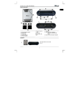
1
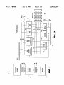
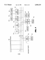
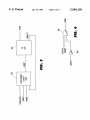
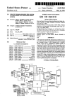
||||||m|||||m|||||nuagglgggllgggunm||||||n||||||||||||
United States Patent [191
[11]
Patent Number:
Ayash et al.
[45]
Date of Patent:
[54]
‘
CIRCUIT FOR DISABLING AN ADDRESS
MASKING CONTROL SIGNAL USING ()R
5,381,530
5,392,420
GATE WHEN A MICROPROCESSOR IS IN A
SYSTEM MANAGEMENT MODE
5,509,139
Apr. 16, 1996
1/1995 Thayer et al. ......... ..
.. 395/275
2/1995 Balmer et al. ........................ .. 395/500
FOREIGN PATENT DOCUMENTS
0426386
4/1991
European Pat. O?’. .
[75] Inventors: Basem A. Ayash, Houston; Gary W.
Thome, Tomball, both of Tex.
OTHER PUBLICATIONS
Pentium Processor User’s Manual, vol. 3: Architecture and
[73] Assignee: Compaq Computer Corp., Houston,
Tex.
Programming Manual, Intel Corp. 1993, pp. 20-1 to 20—9.
Donald Alpert et al, “Architecture of the Pentium Micro
processor”; IEEE Micro, Jun. 1993; pp. 11-21.
[21] Appl' No‘: 34’300
Primary Examiner—Meng-Ai An
[22] Filed;
Attorney, Agent, or Firm-Pravel, Hewitt, Kimball &
[51]
Man 22, 1993
Krieger
Int. Cl.6 .................................................... .. G06F 12/02
[52] US. Cl.
3951869; 395/823; 395/800;
364/9269; 364/926-93; 364/9469; 364/947-1;
364/9474; 364/9475; 364/9582; 364/2333;
364/259-7; 364/252-5; 364/259-1; 364/DIG- 1
[58]
Field of Search ................................... .. 395/800, 400,
Conventionally, bit 20 of the rnicroprocessor’s address out
395/425, 500, 275, 325, 775, 725, 869,
puts may be masked by asserting the FORCE A20 signal.
- 823; 364IDIG. l, DIG. 2
The computer system also operates in a system management
_
[56]
-
mode, which requires all of the address bits to be available
References Clted
for proper access to the system management interrupt vector.
U_S_ PATENT DOCUMENTS
When the computer is in system management mode, the
4,580,240
4,926,322
4/1986 Watanabe .............................. .. 395/425
5/1990 Stimac et a1. .
1?;
’
[57]
ABSTRACT
A system management mode address correction system for
a computer provides correct address values on the address
bus when the computer is in system management mode.
16mm“ -------- -at
1
r
........ .
computer s microprocessor asserts a system management
interrupt active (SMIACT*) signal. This signal is provided
to a circuit which also receives the FORCE A20 signal.
While the SMIACT signal is deactivated, the control circuit
.
-
""
-
provides the true FORCE A20 signal to the computer
5’175’853 12,1992 Kardach et a1
5,226,122
7/1993 Thayer et a1
5 255 379 10/1993 M610
system. When an SMI occurs, the SMIACT signal is acti
.
.
.
vated and the FORCE A20 signal is disabled. As a result, the
5:261:114 11/1993
address generated by the microprocessor is asserted on the
_____ __
5,274,834 12/1993 Kandach etal
5,303,378
5,283,889
address bus
4/1994
2/1994 De
Cohen
Lisle...................................
et al
.. 395/700
10 Claims, 4 Drawing Sheets
/162
PWRGOOD
D8RST
FAZOM'
PROCESSOR
[mu-[Y
CH'P
152
Am.
A<20>
P5
CPU
SMIACT‘
200
RSTSYS
FAZOM"
SMIACT’
204
AZOW
US. Patent
Apr. 16, 1996
Sheet 4 of 4
5,509,139
08
.5<_zw
.2§8~6<
2 $.
a2mow om@
H6>.5202
N2 7
“=5
ocwm>
QaWiE
Em a .EQNE
Wlg“
#8
.65
5,509,139
1
2
CIRCUIT FOR DISABLING AN ADDRESS
MASKJNG CONTROL SIGNAL USING OR
GATE WHEN A MICROPROCESSOR IS IN A
SYSTEM MANAGEMENT MODE
the next increment causes the counter value to become
1000000h. Consequently, the next address accessed would
be lOOOOOh, not 000000h which is accessed in an 8088
BACKGROUND OF THE INVENTION
As a result, the value asserted on the address bus is 000000h,
which is the proper value required to simulate the rollover of
microprocessor system. When the FORCE A20 signal is
asserted, however, bit A20 of the address bus is driven low.
the 8088 instruction register.
1. Field of the Invention
The invention relates to interrupt routines in computer
systems, and more particularly, to assertion of the proper
interrupt starting address on an address bus when a system
Another signi?cant development in personal computer
systems is the system management interrupt (SMI). Origi
nally, SMIs were power management interrupts devised by
Intel Corporation for portable systems. Portable computers
management interrupt is asserted.
2. Description of the Related Art
In the early years of personal computers, the International
Business Machines (IBM) PC computer dominated the ?eld.
often draw power from batteries which provide a limited
amount of energy. To maximize battery life, an SMI is
asserted to turn off or reduce the power to any system
component that is not currently in use. Although originally
meant for laptop models, SMIs have become popular for
desktop and other stationary models as well, and for pur
poses other than power management.
The IBM PC enjoyed sensational success, for it was one of
the ?rst a?ordable yet reasonably powerful desktop com
puters. Eventually, the domination of the IBM PC became so
widespread that the IBM PC set the standards for personal
SMIs are asserted by either an SMI timer, by a system
computer architecture, system design, and software.
request or by other means. An SMI is a nonmaskable
The IBM PC used the Intel Corporation’s 8088 rnicro
processor in its central processing unit (CPU), which
employs a 20-bit address bus for accessing system memory
and I/O devices. Because the IBM PC so thoroughly domi
nated the personal computer market, software vendors cre
interrupt having the highest priority in the system. When an
SMI is asserted, an Intel microprocessor maps a portion of
memory referred to as the system management memory
25
ated an array of software for the 20-bit bus of the 8088
microprocessor and the 8086 microprocessor. Much of this
software forms the foundation of modem software. Conse
quently, due to the early dominance of the 20-bit bus in the
IBM PC and the ground-breaking software created for it,
30
many basic applications in use today are based on a 20-bit
address bus.
The next generation of extremely successful IBM per
(SMRAM) into the main memory space. The entire CPU
state is then saved in the SMRAM in stack-like, last inl?rst
out fashion. After the CPU state is saved, the microprocessor
begins executing an SMI handler routine, which is an
interrupt service routine to perform speci?c system man
agement tasks, like reducing power to speci?c devices.
While the routine is executed, other interrupt requests are
not serviced, and are ignored until the interrupt routine is
completed or the microprocessor is reset. When the SMI
handler completes its task, the CPU state is retrieved from
sonal computers was the IBM PC/AT. To provide access to 35 the SMRAM, and the main program continues.
a wider range of memory and I/O devices, the IBM PC/AT
In the ?rst processors to use SMIs, the Intel Corporation
architecture incorporated a 24-bit bus. At the heart of the
80386SL and 80486SL microprocessors, the SMRAM is
IBM PC/AT was the Intel Corporation 80286 microproces
mapped into the main memory space between 30000h and
sor, which utilizes a 24-bit address bus. Although the 24-bit
3FFFFh. Data regarding the CPU state is stored starting at
addressing capability of the 286 microprocessor could drive
3FFFFh going down like a conventional stack. After the
the PC/AT’s 24-bit bus, a standard 24-bit con?guration was
CPU state is saved in the SMRAM, the microprocessor starts
incompatible with certain of the software ‘that had been
the SMI handler at memory address 38000h located in the
developed for the 20-bit 8088 microprocessor. This was
SMRAM space. In the 80386 and 80486 microprocessor
partially because the 8088 instruction register, when it
generations, the SMI start address is stored in a non
reaches its limit of FFFFFh, rolls over to an initial value of 45 accessible register so that it cannot be changed by the
(00000h. Thus, the memory space for an 8088 system can be
programmer. Similarly, the use of the memory space
viewed as continuous from the upper limit (FFFFFh) of the
between 30000h and SFFFFh is preset into the micropro
20-bit address bus to the initial value (00000h). A 24-bit
cessor and unchangeable. Although this placement of the
counter, however, generates a value of 100000h after
SMRAM and starting address is stable and known, it is often
OFFFFFh, and does not roll over. Because some programs
inconvenient. Any data stored in the main memory space
rely on the rollover characteristic, these programs are not
between 30000h and 3FFFFh before the SMI is asserted is
compatible with a 24-bit address bus which continues to
likely to be overwritten by the SMI handler and lost, unless
increment.
hardware is developed which maps in special memory and
maps out conventional memory. This mapping requirement
To maintain compatibility, an address bit 20 mask signal
was incorporated into the computer system to simulate the 55 has the problem of requiring extra logic and forces abrupt
changes in memory contents necessitating ?ushing of any
rollover of the 8088 counter. Although several names and
cache memory system. This has a cost and performance
logic senses are used to designate the address bit 20 mask
drawback. If the mapping is not performed, the software
signal, the signal is referred to as the FORCE A20 signal
must be carefully designed around the memory space used
herein, which is the common designation for the signal.
When asserted, the FORCE A20 signal causes bit 20 of the 60 by the SMRAM in order to prevent inadvertent loss of data.
address bus (bit A20) to be masked so that bit 20 is held low
To remedy this inconvenience, the latest generation of
at all times, regardless of the value generated by the micro
processor. The FORCE A20 signal is controlled by a register
that may be written by software. By driving bit A20 low, the
FORCE A20 signal causes the address value asserted on the 65
bus to simulate the rollover of the 8088 microprocessor. For
example, when a 24-bit counter reaches the value OFFFFFh,
microprocessors from Intel Corporation, known as the Pen
tium or PS microprocessors, permit the SMI handler starting
address and the location of the SMRAM space to be changed
by the user. Under the Pentium design, the SMI starting
address stored in the microprocessor register is initially set
to the conventional 30000h value. Consequently, when the
5,509,139
3
4
?rst SMI is asserted, the SMI handler starts at address
38000h. While the SMI handler routine is executing, how
ever, it may provide a different area of memory to be used
determines whether an SMI is in progress. If not, the control
circuit provides the FORCE A20 signal to the computer
system to simulate the rollover of the 8088 microprocessor.
If an SMI is in progress, however, the FORCE A20 signal is
disabled. Consequently, bit 20 of the address bus is not
masked and asserts its true value, generating the proper
as the SMRAM. This new SMRAM may start at any location
in the main memory space chosen by the programmer. The
SMRAM comprises a 64 kbyte block beginning at the new
SMRAM start address. When the SMI handler ?nishes, the
new starting address replaces the old starting address in the
address on the address bus.
microprocessor’s SMI starting address register.
In the preferred embodiment, the computer system uti
lizes a Pentium microprocessor. The Pentium microproces
When the next SMI is asserted, the microprocessor maps
the new 64 kbyte block of memory into the main memory
The SMIACT* signal is provided to a control circuit which
sor asserts an SMIACT* signal while an SMI is in progress.
also receives the FORCE A20 signal. While the SMIACT*
signal is deactivated, the control circuit provides the true
space as the SMRAM, and starts the SMI handler at the new
starting address at the midpoint of the new SMRAM. For
example, during the ?rst SMI service routine, the program
mer may change the SMRAM starting point from 030000h
to IOOOOOh. When the SMI is next asserted, the micropro
FORCE A20 signal to the computer system and permits bit
A20 to be masked. When an SMI occurs, SMI processing
begins and the SMIACT* signal is asserted. When the
SMIACT* signal is active, the FORCE A20 signal is dis
abled. Consequently, the value of the FORCE A20 signal
cessor maps the SMRAM into main memory space between
lOOOOOh and lOFFFFh. The microprocessor then references
address 108000h for the SMI handler. This feature thus
does not atTect the value of bit 20 of the address bus.
allows the programmer to choose a more convenient loca 20
Therefore, the address generated by the microprocessor is
tion in the main memory for the SMRAM.
Although the ability to relocate the SMRAM provides a
convenient option to the programmer, it presents a problem
asserted on the address bus and the proper starting address
is accessed. Because all addresses in the main memory space
can be asserted without bit A20 being masked, a program
mer using the present computer system may select any
portion of the main memory for the SMRAM.
for the computer architecture designer. As previously
described, when the FORCE A20 signal is asserted, bit 20 of
the address bus is driven low, regardless of the value
asserted by the microprocessor. When an SMI is generated,
25
BRIEF DESCRIPTION OF THE DRAWINGS
the SMRAM is mapped into the main memory space des
ignated by the programmer. If the 64 kbyte block of main
A better understanding of the present invention can be
memory is an odd Mbyte block instead of an even Mbyte 30 obtained when the following detailed description of the
block, bit 20 of the address bus must be driven high by the
microprocessor. If the FORCE A20 signal is activated at the
time the SMI is initiated, however, the FORCE A20 signal
holds bit 20 of the address bus low. Consequently, the
address value that is actually asserted on the bus is l Mbyte
lower than the interrupt vector provided by the programmer.
For example, if the start address chosen by the programmer
is 308000h, the SMRAM should be mapped into the
memory space between 300000h and 30FFFFh. If the
FORCE A20 signal is asserted, however, bit 20 is held low,
so that the address range actually provided to the main
memory is 200000h to 20FFFFh, and the SMI handler
starting address appearing on the bus is 208000h. The CPU
state is then saved starting at ZOFFFFh and going down,
potentially overwriting important data stored in main
preferred embodiment is considered in conjunction with the
following drawings, in which:
FIG. 1 is a block diagram of a computer system incor
porating the present invention;
FIG. 2 is a block diagram of the system board of FIG. 1;
FIG. 3 is a block diagram of the input/output board of
FIG. 1;
FIG. 4 is a block diagram of the processor board of FIG.
40
FIG. 5 is a block diagram of a portion of the processor
board of FIG. 4 and illustrates particular interconnections;
and
45
memory. When the microprocessor obtains the new starting
address, the address asserted is 208000h, which does not
contain the SMI handler routine. Consequently, the system
suffers an error and must be reset.
Because of this problem, a programmer choosing an
SMRAM location in a conventional system is limited to only
half of the potential main memory space in which to place
the SMRAM. If the programmer inadvertently selects an
SMRAM area within an odd Mbyte block of the main
memory, important data may be overwritten and the system
may suffer a failure. As a result, the ?exibility provided to
the programmer to select a convenient location for the
1;
50
55
FIG. 6 is a logic diagram of the signals generating the
A20M* signal of FIG. 5.
DETAILED DESCRIPTION OF THE
PREFERRED EMBODIMENT
Referring now to FIG. 1, a computer system C according
to the preferred embodiment is shown. A processor board P
contains the processor, cache memory and main memory
and associated equipment and a connector 100, preferably a
card edge. A system board S includes a connector 102 to
receive the connector 100, preferably a socket to receive a
card edge. The system board S contains common system
elements and slots or connectors for interchangeable circuit
boards. The system board 5 also contains an additional
SMRAM is limited to only half of the available memory
space.
60 connector 104. The connector 104 mates with a connector
106 on an input/output (I/O) board I. Preferably the I/O
board
I contains certain 110 related features of the computer
SUMMARY OF THE PRESENT INVENTION
C, such as the ?oppy and hard disk drive control units, an
Brie?y, a computer system according to the present inven
audio system and the parallel and serial ports. Additionally,
tion provides proper addressing for SMIs by disabling the
the real time clock and CMOS memory is on the [/0 board
address bit 20 masking function while the SMI handler
I. Each of the processor board P, system board S and I/O
controls the system. A control circuit in the computer system
board I are detailed below.
5,509,139
5
6
This is noted to be an exemplary and preferred embodi
ment of the computer system C and it is understood that
numerous other embodiments, such as having all of the
desired. Preferably, the graphics system in the preferred
computer system C is provided on a separate add in card
located in an EISA slot 108 and is not necessarily located on
the I/O board I.
Referring now to FIG. 4, the processor board P is shown
in more detail. The primary component on the processor
components on a single system board or mother board as is
common, could be readily developed.
Referring now to FIG. 2, a block diagram of the system
board S is shown. Two main buses, a host bus H and an EISA
board P is the CPU 152, in the preferred embodiment
preferably the P5 or Pentium microprocessor from Intel
Corp., the next generation design after the 80486. The P5 is
bus E, form the logical back bones of the system board S.
The host bus H has three components, the host data or HD
bus, the HA or host address bus and the HC or host control
a very high performance microprocessor having superscalar
bus. Preferably the HD bus is 64 bits wide and the HA bus
is provided for a 32 bit addressing space. The EISA bus E
has four major components, the SA and LA or system and
early address buses, the SD or system data bus and the SC
or system control bus. A plurality of EISA slots 108 are
connected to the EISA bus E. An EISA bus controller 110
provides the necessary capabilities to convert between host
bus H cycles and EISA bus E cycles and is connected
between the HA and HC buses and the SC bus. The EISA
architecture and integrated and separate code and data
caches. Like several recent generations of Intel Corporation
products, the P5 microprocessor operates in both protected
and real modes. In protected mode, the entire 36-bit address
bus and the full instruction set may be used. The P5
microprocessor includes system management memory or
bus controller 110 is connected to control a data EBB or
EISA bus buffer 112, which provides the necessary data
transceiving functions between the host bus H and the EISA
bus E and provides the data assembly and disassembly
requirements of an EISA system. Similarly, the EISA bus
controller 110 provides the control function for an address
EISA bus buffer or EBB 114. The address EBB 114 provides
transceiving capabilities between the EISA bus E and the
host bus H and in addition latches the HA bus signals to form
the SA bus signals as appropriate.
The computer C includes certain fundamental operations
20
SMRAM functions and includes an SMl pin as described in
the background. Additionally, as in the 80486, a FORCE
A20 signal provided to the P5 CPU causes address bit 20 to
be masked before performing a lookup in the internal cache
or driving a memory cycle to the system. The masking of bit
A20 simulates the rollover of the 8088 microprocessor.
Three buses are connected to the P5 CPU 152, the PD or
processor data bus, the PA or processor address bus and the
PC or processor control bus. A level two (L2) or external
cache 154 is connected to the PD and PA buses and receives
control signals from a memory controller 156. In the pre
ferred embodiment the memory controller 156 contains
conventional memory controller functions and additionally
includes the cache controller capabilities necessary to oper
such as an interrupt system, a DMA controller and a number
of timers, as well as arbitration of the EISA bus E. These
ate the L2 cache 154.
components are all contained in the EISA system peripheral
116, which is connected to the HA, HC and SC buses. A chip
referred to as the system glue chip 118 is connected to the
A data bu?er 158 is connected to the PD bus and develops
two new buses, the HD or host data bus and the MD or
memory data bus. The HD bus is connected to the connector
EISA bus E and to a bus referred to as the XD or X data bus
100 for connection to the system board S. The data buifer
158 is controlled by the memory controller 156. A trans~
ceiver/latch unit 160 is connected between the PA bus and
and performs numerous miscellaneous functions necessary
in the computer system C.
Finally, a third bus, referred to as the X bus X, is provided
the HA bus to provide latching and transceiving capabilities
to the connector 104. The X bus X has address XA, data 7G) 40 of addresses between the P5 CPU 152 and the host bus H.
The transceiver/latch 160 is controlled by the memory
and control SC portions. The XA lines are developed from
controller 156.
the SA bus by means of a buffer 120, while the XD bus is
formed from the SD bus by means of a buffer or transceiver
A processor utility chip 160 provides certain necessary
122. Preferably the XD bus is 16 bits wide, while the XA bus
utility operations for use with the CPU 152. The processor
is the same width as the SA bus. The host bus H and the XD 45 utility chip 162 is connected to the XD bus and is controlled
bus are provided to the connector 102 for provision to the
by the memory controller 156. The output of the processor
processor board P. In addition, the X1) bus is connected to
utility chip 162 is preferably provided to the PC bus to
the EISA system peripheral 116.
provide control functions of the P5 CPU 152. The memory
controller 156 is also connected to a unit referred to as the
Referring now to FIG. 3, the I/O board I is shown in more
detail. The backbone of the I/O board I is the X bus X. 50 DDF or data destination facility 164. The DDF 164 performs
memory module enabling, address translation and memory
Connected to the X bus X is a ROM or read only memory
124, which contains the basic operating sequences of the
computer system C. The ROM 124 is preferably a ?ash
EPROM to allow ease of changing of the basic operating
sequences. A real time clock (RTC)/CMOS unit 126 is
connected to the X bus X to provide real time clock
segment or page property storage. The DDF 164 provides
memory capabilities to indicate which particular bank of
memory is to be enabled, performs address translation on a
55
128k byte boundary and provides indications of certain
characteristics of each 128k block, such as whether it is
functions and longer tenn memory capabilities. A ?oppy
write protected, high speed, and/or cacheable and whether
disk controller 128 is connected to the X bus X and receives
that portion can be utilized by a writeback cache. Operation
of the DDF 164 is more completely explained in US. Pat.
No. 5,341,494, and E.P.O. Application No. 0 426 386,
publication date May 8, 1991, both of which are hereby
incorporated by reference. The outputs of the DDF 164 are
a series of RASEN enable signals for enabling a particular
memory module, certain translated addresses to indicate the
address bits above 128k, and page characteristic bits.
The memory portion of the processor board P is provided
a ?oppy disk unit 130. A keyboard controller 132, typically
an 8042 device, is connected to the X bus X and receives a 60
keyboard 134 and a mouse or pointing device 136. A
multiple peripheral chip 138 is connected to the X bus X and
provides an interface to a hard disk unit 140, a parallel port
142 and two serial ports 144 and 146. Finally, an audio
system 148 is connected to the X bus X to provide audio 65
functions, with a speaker 150 connected to the audio system.
Other components could be provided on the I/O board I if
as four identical modules, each module containing an
5,509,139
7
8
address/control buffer 166, one sockets for receiving an
individual SIMM unit 168 and base memory 170. The
system is supplying su?icient power and operating properly.
The DBRST signal only goes active immediately after the
address/control buffer 166 receives the PA bus, the address
and enable outputs of the DDF 164 and control signals from
the memory controller 156. The outputs of the address/
system is powered up and the main processor clock is stable.
Thus, the RSTSYS signal goes active until the power supply
to the computer system is at adequate levels or when the
system is ?rst powered up. The RSTSYS signal toggles to its
inactive state after the PWRGOOD signal is sampled active
and the DBRST signal has returned to its inactive state. In
control buffer 166 are the addresses provided to the SIMMs
168 or base memory devices 170 and the RAS*, CAS, and
WE, signals. These signals are provided to each of the
SlMMs 168. Additionally, each SIMM 168 or base memory
other words, the RSTSYS signal returns to its inactive state
when the power supply is turned on and operating function
ally and the processor clock signal is stable.
device 170 is connected to the memory data bus MD. As
indicated, there are four like modules. Other con?gurations
of the processor board P could be developed, with variations
FIG. 6 illustrates a logic circuit contained in the processor
utility chip 160 for implementing the logic equation above.
The A20M* signal is generated by an OR gate 200, which
has three inputs. A ?rst input receives the RSTSYS signal so
that the A20M* signal is driven high when the RSTSYS
signal is active. Similarly, a second input of the OR gate 200
obvious to one skilled in the art, with certain details pro
vided below.
The P5 CPU 152 drives the processor address bus PA and
receives the FORCE A20 signal. Referring now to FIG. 5,
the P5 CPU 152, the processor utility chip 160, and a set of
is connected to the inverse of the SMIACT* signal from an
inverter 204. When the P5 CPU 152 is in system manage
relevant signals are illustrated. For the purposes of this
disclosure, a signal designation followed by an asterisk (*)
ment mode, the SMIACT* signal is low, driving A20M*
high and preventing bit A20 from being masked. The last
indicates that the signal is active when asserted low. In
contrast, the absence of the asterisk indicates that the signal
is active when driven high. Bit 20 is held low by the P5 CPU
152 when the A20M* signal received by the P5 CPU 152 is
low. Thus, when the A20M* signal is deactivated, the P5
CPU 152 drives the processor address bit 20 conventionally.
When the A20M* signal is low, processor address bit 20 is
masked and is driven low as long as the A20M* signal
remains active. This is the conventional microprocessor
response to the FORCE A20 signal.
20
25
As shown by the equation and FIG. 6, bit 20 of the
processor address bus is masked only if the FA20M* signal
is asserted, the system is not being reset, and the P5 CPU 152
is not in system management mode. Thus, the processor
address bit 20 may only be masked if the P5 CPU 152 is not
The A20M* signal is generated by the processor utility
chip 160. The A20M* signal is controlled according to the
30
performing an SMI routine. If the P5 CPU 152 enters system
input is connected to the FA20M* signal so that the A20M*
signal follows the FA20M* signal when RSTSYS and
SMIACT* are inactive.
management mode, the SMIACT* signal is activated. This
following equation:
35
The FA20M* signal is the conventional FORCE A20
causes the A20M* signal to be deactivated, and the A20M*
remains deactivated until the P5 CPU 152 exits system
management mode and the remaining conditions of the
equation are satis?ed. Consequently, the P5 CPU may drive
the proper starting address onto the bus without masking bit
A20.
signal, and is generated conventionally. In the preferred
embodiment, the system glue chip 118 generates the
FA20M* signal by trapping operations to the system key
ment allows bit A20 to be masked to simulate the rollover of
board controller which indicate a request to change the
the 8088 microprocessor, yet provides the proper starting
A computer system according to the preferred embodi
FA20M* signal and performing the requested change
directly. The FA20M* signal is enabled by writing the
address on the address bus when an SMI is asserted. Thus,
proper data bits to a speci?c control register in the system.
Similarly, the FA20M* signal may be disabled by resetting
the control register bits.
The SMIACT* signal is generated by the P5 CPU 152 and
is provided to the processor utility chip 160. The SMIACT*
signal indicates that the P5 CPU 152 is operating in system
management mode. Operation in system management mode
45
indicates that an SMI has been asserted and is currently 50
being serviced by the P5 CPU 152. When the microproces~
the programmer may relocate the system management
memory at any location in the main memory. When the
system is initially powered up, the computer executes a
power-on self-test (POST) program. Part of the POST
program includes asserting an initial SMI to the P5 CPU.
When the initial SMI is asserted, the P5 CPU maps the
SMRAM into the main memory space between 30000h and
SFFFFh. The CPU state is then saved in the SMRAM
starting at BFFFFh and growing down in stack-like fashion.
The P5 CPU then enters real mode and begins executing a
sor enters system management mode, a system management
special SMI interrupt service routine designed for the POST
memory (SMRAM) space is mapped into memory. The
program. This special SMI routine changes one of the lines
entire CPU state is then stored in the SMRAM. While in
system management mode, the microprocessor operates in
real mode, but uses 32-bit wide addresses. System manage
ment mode is transparent to software, and is designed for
power conservation and other features. When the SMI
55
of data saved in, the SMRAM to replace the starting address
for the SMI handler. The old SMI starting address is replaced
with the value desired by the programmer for the new SMI
starting address. The SMI handler then completes the
remainder of the SM] routine and the stored CPU state is
service routine is completed, the SMIACT* signal is deac
retrieved from the SMRAM. When the CPU state is restored
tivated.
60 to the CPU, the P5 CPU exits the SMI handler and continues
The RSTSYS signal is the system reset request signal.
operations.
This output is generated by the processor utility chip 160,
When the POST program is complete, control of the
and is used to reset system logic other than the P5 CPU 152.
computer system is turned over to the operating system.
The RSTSYS signal is asserted when the power good
While the computer system operates conventionally, an SMI
(PWRGOOD) signal is sampled inactive or when the power 65 may be generated by some source, like a battery low signal,
on reset (DBRST) signal is sampled active. The PWRGOOD
a screen saver timer, a deadman timer on the hard drive, a
signal indicates that the power supply of the computer
processor request or on a periodic basis. When the SMI is
5,509,139
9
10
asserted, the P5 CPU maps the system management memory
into the 64 kbyte portion of the main memory space desig
nated by the SMRAM starting address. For example, if the
new SMRAM starting address is 590000h, the SMRAM is
mapped into the memory space between 590000h and
59FFFFh. To map the SMRAM into the main memory, the
P5 CPU drives the address values onto the address bus to
indicate the proper addresses. Before the SMRAM is
mapped into the memory, however, the SMIACT* signal is
2. The system management mode address correction
system of claim 1, wherein the microprocessor is an Intel
driven low to indicate that the P5 CPU has entered system
management mode. Although the A20M* signal is normally
activated when the P5 CPU is placed into real mode, the
active SMIACT* signal drives the output of the OR gate 200
high and disables the A20M* signal. As a result, the
SMRAM starting address generated by the P5 CPU is
590000h, instead of the 49000Oh which would be asserted if
the A20M* signal remained activated. After the SMRAM is
mapped into main memory, the CPU state is saved in the
SMRAM and the P5 CPU starts executing the SMI handler
Corporation Pentium compatible microprocessor, and
wherein said determining means includes a system manage
ment interrupt active signal generated by the Pentium micro
processor.
3. The system management mode address correction
system of claim 1, wherein n is 36.
4. The system management mode address correction
system of claim 3, wherein the masking means masks bit 20
of the n address outputs so that the register output simulates
the rollover eifect of a register having 20 bits.
5. The system management mode address correction
15 system of claim 1, wherein n is 36 and the microprocessor
is an Intel Corporation Pentium compatible microprocessor
having an address bit 20 mask signal input, and wherein the
masking means is connected to said address bit 20 mask
signal input of the Pentium compatible microprocessor.
routine at handler starting address 598000h. Thus, a com 20
puter system according to the preferred embodiment pro
vides correct addressing for the SMI handler when the
FORCE A20 signal is asserted. Consequently, system errors
due to improper addressing are avoided, and the program
mer is permitted to select a 64 kbyte portion of the main
6. A computer system having corrected system manage
ment mode addressing, comprising:
a microprocessor capable of initiating a system manage
ment interrupt routine, including:
25
memory at any location in the main memory space for the
means for asserting a system management interrupt active
signal while said system management interrupt routine
SMRAM.
The foregoing disclosure and description of the invention
are illustrative and explanatory thereof, and various changes
is in progress;
a set of n address outputs having a rollover effect as the
n address outputs are incremented; and
in the size, shape, materials, components, circuit elements,
means responsive to a masking control signal for masking
wiring connections and contacts, as well as in the details of
one of said n address outputs;
the illustrated circuitry and construction and method of
operation may be made without departing from the spirit of
the invention.
means for selectively providing the masking control sig
nal to said masking means; and
We claim:
35
1. A system management mode address correction system
for a computer having a microprocessor, the microprocessor
mented, the microprocessor further having a masking means
responsive to a masking control signal for masking at least
one of the n address outputs so that as the values are
incremented the register values at the n address outputs
simulate the rollover e?cect of a register having less than n 45
bits and wherein the microprocessor can operate in a system
management mode which utilizes all 11 bits of the n address
outputs, the system management mode address correction
means for selectively providing the masking control sig
8. The computer system of claim 6, wherein n is 36.
9. The computer system of claim 8, wherein the masking
means masks bit 20 of the n address outputs so that as the
n
address outputs are incremented the n address output
55
simulates the rollover effect of a set of n address outputs
and connected to said means for providing the mask
having 20 bits when said masking control signal is asserted.
10. The computer system of claim 7, wherein the micro
control signal for disabling said masking control signal
when the microprocessor is in system management
gate, the OR gate having an output providing the
masking control signal connected to the microproces
sor, a ?rst input receiving the masking control signal
processor, and wherein said system management interrupt
patible microprocessor.
nal to the masking means;
determining means connected to the microprocessor for
mode, wherein said disabling means includes an OR
active signal is asserted, wherein said disabling means
includes an OR gate, the OR gate having an output
connected to the microprocessor, a ?rst input receiving
said masking control signal, and a second input con
nected to said system management interrupt active
signal assertion means.
7. The computer system of claim 6, wherein said micro
processor is an Intel Corporation Pentium compatible micro
active signal assertion means includes the system manage
ment interrupt active signal generated by the Pentium com
system comprising:
determining if the microprocessor is operating in sys
agement interrupt active signal assertion means and
connected to said means for selectively providing the
masking control signal for disabling said masking
control signal when said system management interrupt
having n address outputs and a register having n bits for
providing values to the n address outputs, the n address
outputs having a rollover effect as the values are incre
tem management mode; and
disabling means responsive to said determining means
address correction means responsive to the system man
60
processor is a Pentium compatible microprocessor having an
address bit 20 mask signal input, and wherein said means for
selectively providing the masking control signal is con
nected to the address bit 20 mask signal input of the Pentium
compatible microprocessor.
and a second input connected to said determining
means.
*
*
*
*
*
UNITED STATES PATENT AND TRADEMARK OFFICE
CERTIFICATE OF CORRECTION
PATENT NO. : 5,509,139
DATED
: April 16, 1996
INVENTOR(S) : Basem A. Ayash et at.
Page 1 0f 1
It is certified that error appears in the above-identi?ed patent and that said Letters Patent is
hereby corrected as shown below:
Column 10
Line 5, after “Pentium” insert -- compatible
Signed and Sealed this
Twenty-fourth Day of January, 2006
m Watt,”
JON W. DUDAS
Director ofthe United States Patent and Trademark O?‘i'ce